US10643700B2 - Apparatuses and methods for adjusting write parameters based on a write count - Google Patents
Apparatuses and methods for adjusting write parameters based on a write countDownload PDFInfo
- Publication number
- US10643700B2 US10643700B2US14/927,329US201514927329AUS10643700B2US 10643700 B2US10643700 B2US 10643700B2US 201514927329 AUS201514927329 AUS 201514927329AUS 10643700 B2US10643700 B2US 10643700B2
- Authority
- US
- United States
- Prior art keywords
- write
- write operations
- operations
- bin
- bins
- Prior art date
- Legal status (The legal status is an assumption and is not a legal conclusion. Google has not performed a legal analysis and makes no representation as to the accuracy of the status listed.)
- Active
Links
Images


Classifications
- G—PHYSICS
- G11—INFORMATION STORAGE
- G11C—STATIC STORES
- G11C14/00—Digital stores characterised by arrangements of cells having volatile and non-volatile storage properties for back-up when the power is down
- G11C14/0009—Digital stores characterised by arrangements of cells having volatile and non-volatile storage properties for back-up when the power is down in which the volatile element is a DRAM cell
- G11C14/0045—Digital stores characterised by arrangements of cells having volatile and non-volatile storage properties for back-up when the power is down in which the volatile element is a DRAM cell and the nonvolatile element is a resistive RAM element, i.e. programmable resistors, e.g. formed of phase change or chalcogenide material
- G—PHYSICS
- G06—COMPUTING OR CALCULATING; COUNTING
- G06F—ELECTRIC DIGITAL DATA PROCESSING
- G06F13/00—Interconnection of, or transfer of information or other signals between, memories, input/output devices or central processing units
- G06F13/14—Handling requests for interconnection or transfer
- G06F13/16—Handling requests for interconnection or transfer for access to memory bus
- G06F13/1668—Details of memory controller
- G—PHYSICS
- G11—INFORMATION STORAGE
- G11C—STATIC STORES
- G11C13/00—Digital stores characterised by the use of storage elements not covered by groups G11C11/00, G11C23/00, or G11C25/00
- G11C13/0002—Digital stores characterised by the use of storage elements not covered by groups G11C11/00, G11C23/00, or G11C25/00 using resistive RAM [RRAM] elements
- G11C13/0004—Digital stores characterised by the use of storage elements not covered by groups G11C11/00, G11C23/00, or G11C25/00 using resistive RAM [RRAM] elements comprising amorphous/crystalline phase transition cells
- G—PHYSICS
- G11—INFORMATION STORAGE
- G11C—STATIC STORES
- G11C13/00—Digital stores characterised by the use of storage elements not covered by groups G11C11/00, G11C23/00, or G11C25/00
- G11C13/0002—Digital stores characterised by the use of storage elements not covered by groups G11C11/00, G11C23/00, or G11C25/00 using resistive RAM [RRAM] elements
- G11C13/0021—Auxiliary circuits
- G11C13/0035—Evaluating degradation, retention or wearout, e.g. by counting writing cycles
- G—PHYSICS
- G11—INFORMATION STORAGE
- G11C—STATIC STORES
- G11C13/00—Digital stores characterised by the use of storage elements not covered by groups G11C11/00, G11C23/00, or G11C25/00
- G11C13/0002—Digital stores characterised by the use of storage elements not covered by groups G11C11/00, G11C23/00, or G11C25/00 using resistive RAM [RRAM] elements
- G11C13/0021—Auxiliary circuits
- G11C13/0069—Writing or programming circuits or methods
- G—PHYSICS
- G11—INFORMATION STORAGE
- G11C—STATIC STORES
- G11C16/00—Erasable programmable read-only memories
- G11C16/02—Erasable programmable read-only memories electrically programmable
- G11C16/06—Auxiliary circuits, e.g. for writing into memory
- G11C16/10—Programming or data input circuits
- G—PHYSICS
- G11—INFORMATION STORAGE
- G11C—STATIC STORES
- G11C16/00—Erasable programmable read-only memories
- G11C16/02—Erasable programmable read-only memories electrically programmable
- G11C16/06—Auxiliary circuits, e.g. for writing into memory
- G11C16/34—Determination of programming status, e.g. threshold voltage, overprogramming or underprogramming, retention
- G11C16/349—Arrangements for evaluating degradation, retention or wearout, e.g. by counting erase cycles
- G11C16/3495—Circuits or methods to detect or delay wearout of nonvolatile EPROM or EEPROM memory devices, e.g. by counting numbers of erase or reprogram cycles, by using multiple memory areas serially or cyclically
- G—PHYSICS
- G11—INFORMATION STORAGE
- G11C—STATIC STORES
- G11C7/00—Arrangements for writing information into, or reading information out from, a digital store
- G11C7/10—Input/output [I/O] data interface arrangements, e.g. I/O data control circuits, I/O data buffers
- G11C7/1078—Data input circuits, e.g. write amplifiers, data input buffers, data input registers, data input level conversion circuits
- G11C7/1096—Write circuits, e.g. I/O line write drivers
- G—PHYSICS
- G11—INFORMATION STORAGE
- G11C—STATIC STORES
- G11C7/00—Arrangements for writing information into, or reading information out from, a digital store
- G11C7/24—Memory cell safety or protection circuits, e.g. arrangements for preventing inadvertent reading or writing; Status cells; Test cells
- G—PHYSICS
- G11—INFORMATION STORAGE
- G11C—STATIC STORES
- G11C8/00—Arrangements for selecting an address in a digital store
- G11C8/18—Address timing or clocking circuits; Address control signal generation or management, e.g. for row address strobe [RAS] or column address strobe [CAS] signals
- G—PHYSICS
- G06—COMPUTING OR CALCULATING; COUNTING
- G06F—ELECTRIC DIGITAL DATA PROCESSING
- G06F2212/00—Indexing scheme relating to accessing, addressing or allocation within memory systems or architectures
- G06F2212/72—Details relating to flash memory management
- G06F2212/7211—Wear leveling
- G—PHYSICS
- G11—INFORMATION STORAGE
- G11C—STATIC STORES
- G11C13/00—Digital stores characterised by the use of storage elements not covered by groups G11C11/00, G11C23/00, or G11C25/00
- G11C13/0002—Digital stores characterised by the use of storage elements not covered by groups G11C11/00, G11C23/00, or G11C25/00 using resistive RAM [RRAM] elements
- G11C13/0021—Auxiliary circuits
- G11C13/0069—Writing or programming circuits or methods
- G11C2013/0092—Write characterized by the shape, e.g. form, length, amplitude of the write pulse
- G—PHYSICS
- G11—INFORMATION STORAGE
- G11C—STATIC STORES
- G11C2213/00—Indexing scheme relating to G11C13/00 for features not covered by this group
- G11C2213/70—Resistive array aspects
- G11C2213/71—Three dimensional array
Definitions
- Non-volatile memory devicescan be read from and written to in order to retrieve and store information.
- One type of non-volatile memory deviceis phase change memory, which may be arranged in a three dimensional (3D) cross-point architecture.
- phase change memory deviceseach memory cell is formed from a material that can be selectively transformed from one phase to another.
- the materialmay be transformed from an amorphous state to a crystalline state by applying write voltages to the memory cell.
- Different stateshave different electrical properties, and can be sensed by applying a voltage to the material which, based on the present state of the material, results in a different electrical current being conducted through the cell.
- non-volatile memory deviceshave the benefit of retaining the stored information even when power is removed from the device, such devices typically suffer from limited write endurance and retention. That is, repeated accesses to the memory cells for read and write operations exert stresses on the components and memory cells of the device. As a result, memory devices can undergo physical changes and degradation over the life of the device.
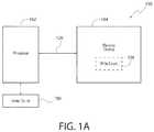
- FIG. 1Ais a functional block diagram of a memory system, in accordance with an embodiment of the present invention.
- FIG. 1Bis a functional block diagram of a memory device, in accordance with an embodiment of the present invention.
- FIG. 2is a diagram of a portion of a three-dimensional (3D) cross-point memory array, in accordance with an embodiment of the present invention.
- FIG. 3is a flowchart of a method of setting write parameters based on a write count, in accordance with an embodiment of the present invention.
- FIG. 4is an example parameter table, in accordance with an embodiment of the present invention.
- FIG. 5is a flowchart of a method of updating the applicable bin number based on a write count, in accordance with an embodiment of the present invention.
- Embodiments described hereinrecognize that many memory systems have limited write endurance and, therefore, degrade over time through repeated access.
- various physical parametersmay be tuned or adjusted based on the age of the device in order to reduce the failure rate of write operations. Accordingly, there is a need for a mechanism to track the age of the device in order to selectively adjust the write parameters to account for physical degradation of the cells of the device.
- Write parameterscan include, for example write voltages, such as the voltages applied to memory cells through word lines and/or the bit lines during a write operation. Other internal parameters can be adjusted as well.
- Example parametersinclude, but are not limited to pulse shape, leading edge, trailing edge, duration, etc.
- write parametersmay include any configurable settings in the memory device that can be adjusted as the cell ages in order to improve the probability of a successful write operation.
- FIG. 1Ais a functional block diagram of a memory system, generally designated 100 in accordance with an embodiment of the present invention.
- Memory system 100includes a processor 102 coupled to a memory device 104 .
- the processor 102can be any type of controlling circuitry configured to transmit instructions to the memory device 104 .
- the processormay be one or more microprocessors, an application specific integrated circuit, or other type of controlling circuitry.
- the memory device 104includes various circuits for memory operations. A discussed in further detail below with respect to FIG. 1B , the memory device 104 can include input/output (I/O) control circuitry, control logic, and a memory array comprising a plurality memory cells.
- I/Oinput/output
- Commands, address information, and write datamay be provided to the memory device 104 as sets of sequential input/output (I/O) transmitted through an I/O bus 128 .
- read datamay be provided from the memory device 104 through the I/O bus 128 .
- the processor 162may be further coupled to a write count circuit 106 .
- the write count circuit 106may be a register, a cache, or any other type of temporary memory configured to store a number of write operations executed by the memory device 104 .
- the write count circuit 106may be a non-volatile memory configured to store the number of write operations performed by the memory device 104 when power is removed from the memory device 104 .
- the write count circuit 106may be configured to store a value corresponding to the current number of write operations performed by the memory device 104 .
- the write count circuit 106may be accessed by the processor 102 during a set write cycle bin operation in order to determine the current number of write operations that have been performed by the memory device 104 .
- the value stored in the write count circuit 106may be used to adjust write parameters within the memory device 104 to improve the likelihood of successful write operations. Further, the processor 102 may periodically update the value stored in the write count circuit 106 to ensure that the number of write operations stored in the write count circuit 106 is consistent with the actual number of write operations that have been performed by the memory device 104 . In alternative embodiments, the write count circuit 106 may be located within the memory device 104 . In such embodiments, the memory device 104 may track the number of write operations performed by the memory device 104 and store the current number of write operations performed on the write count circuit 106 within the memory device 104 . The memory device may access the value stored locally in the memory device 104 to determine the number of write operations performed by the memory device 104 .
- FIG. 1Billustrates an apparatus that includes a memory device 104 according to an embodiment of the present invention.
- the memory device 104includes a memory array 160 with a plurality of memory cells that are configured to store data.
- the memory cellsmay be accessed in the array through the use of various signal lines, word lines (WLs) and/or bit lines (BLs).
- the memory cellsmay be non-volatile memory cells, such as NAND or NOR flash cells, phase change memory cells, or may generally be any type of memory cells.
- the memory cells of the memory array 160can be arranged in a memory array architecture. For example, in one embodiment, the memory cells are arranged in a 3D cross-point architecture.
- memory array architecturesmay be used, for example, a single-level cross-point architecture, among others.
- the memory cellsmay be single level cells configured to store data for one bit of data.
- the memory cellsmay also be multi-level cells configured to store data for more than one bit of data.
- a data strobe signal DOSmay be transmitted through a data strobe bus (not shown).
- the DOS signalmay be used to provide timing information for the transfer of data to the memory device 104 or from the memory device 104 .
- the I/O bus 128is connected to an I/O control circuit 120 that routes data signals, address information signals, and other signals between the I/O bus 128 and an internal data bus 122 , an internal address bus 124 , and/or an internal command bus 126 .
- the internal address bus 124may be provided address information by the I/O control circuit 120 .
- the internal address bus 124may provide block-row address signals to a row decoder 140 and column address signals to a column decoder 150 .
- the row decoder 140 and column decoder 150may be used to select blocks of memory cells for memory operations, for example, read and write operations.
- the row decoder 140 and/or the column decoder 150may include one or more signal line drivers configured to provide a biasing signal to one or more of the signal lines in the memory array 160 .
- the I/O control circuit 120is coupled to a status register 134 through a status register bus 132 . Status bits stored by the status register 134 may be provided by the I/O control circuit 120 responsive to a read status command provided to the memory device 104 .
- the status bitsmay have respective values to indicate a status condition of various aspects of the memory and its operation.
- the memory device 104also includes a control logic 110 that receives a number of control signals 138 either externally or through the command bus 126 to control the operation of the memory device 104 .
- the control signals 138may be implemented with any appropriate interface protocol.
- the control signals 138may be pin based, as is common in dynamic random access memory and flash memory (e.g., NAND flash), or op-code based.
- Example control signals 138include clock signals, read/write signals, clock enable signals, etc.
- a command register 136is coupled to the internal command bus 126 to store information received by the I/O control circuit 120 and provide the information to the control logic 110 .
- the control logic 110may further access a status register 134 through the status register bus 132 , for example, to update the status bits as status conditions change.
- the control logic 110may be configured to provide internal control signals to various circuits of the memory device 104 . For example, responsive to receiving a memory access command (e.g., read, write), the control logic 110 may provide internal control signals to control various memory access circuits to perform a memory access operation.
- the control logicmay be configured to set one or more write parameters, such as a write voltage used during write operations performed on the memory array 160 , based on a value stored in the write count circuit 106 and a plurality of write cycle bins (described below).
- the control logic 110may be further configured to perform wear levelling operations on the memory array 160 .
- Wear leveling operationscan redistribute data stored in the memory array 160 to ensure that some memory cells are not written to significantly more than other memory cells.
- the control logic 110may use static or dynamic wear leveling.
- the various memory access circuitsare used during the memory access operation, and may generally include circuits such as row and column decoders, charge pump circuits, signal line drivers, data and cache registers, I/O circuits, as well as others.
- a parameter table 162 that can be accessed by the control logic 110may be stored in the memory array 160 .
- the parameter table 162includes write cycle bin information which can be used to adjust one or more write parameters based on the number of write operations that have been performed for the memory array 160 .
- the write cycle bin informationincludes one or more ranges of write operations where each range defines a write cycle bin. For example, one bin may be defined by a range of 0 to 10,000 write operations. A second bin may be defined by a range of 1,000 to 100,000 write operations, and so on for additional bins. Each of the bins in the parameter table 162 may be associated with one or more write parameters.
- the write parametersmay define settings (e.g., write voltage, pulse duration, leading edge, trailing edge, pulse shape, etc.) to be used by the memory device 104 to perform a write operation.
- the current number of write operationsmay be stored in the write count circuit 106 ( FIG. 1A ) and can be compared to the one or more bins in the parameter table 162 to determine the applicable bin and identify the applicable write parameters.
- the parameter table 162may be stored in a dedicated portion of the memory array 160 .
- the parameter table 162can be stored in a separate memory area included in the memory device, a separate storage device, memory device, register, or other device accessible by the control logic 110 .
- the parameter tableis described in further detail below with respect to FIG. 4 .
- a data I/O circuit 170includes one or more circuits configured to facilitate data transfer between the I/O control circuit 120 and the memory array 160 based on signals received from the control logic 110 .
- the data I/O circuit 170may include one or more registers, buffers, and other circuits for managing data transfer between the memory array 160 and the I/O control circuit 120 .
- the I/O control circuit 120receives the data to be written through the I/O bus 128 and provides the data to the data I/O circuit 170 via the internal data bus 122 .
- the data I/O circuit 170writes the data to the memory array 160 based on control signals provided by the control logic 110 at a location specified by the row decoder 140 and the column decoder 150 .
- the data I/O circuitreads data from the memory array 160 based on control signals provided by the control logic 110 at an address specified by the row decoder 140 and the column decoder 150 .
- the data I/O circuitprovides the read data to the I/O control circuit via the internal data bus 122 .
- the I/O control circuit 120then provides the read data on the I/O bus 128 .
- FIG. 2is a diagram of a portion of a 3D cross-point memory array, generally designated 200 , in accordance with an embodiment of the present invention.
- the memory array 200can be implemented as the memory array 160 of FIG. 1B .
- the memory array 200includes a first number of word lines 202 A, 202 B, . . . , 202 N (collectively referred to as word lines 202 ) and a first number of bit lines 206 A, 206 B, . . . , 206 N (collectively referred to as bit lines 206 ).
- the word lines 202may be arranged parallel to one another.
- the bit lines 206can be arranged parallel to one another and orthogonal to the word lines 202 .
- the word lines 202 and the bit lines 206can be made from a conductive material, such as copper, tungsten, titanium, aluminum, etc. Layers or decks of word lines and bit lines can be stacked to create a 3D lattice structure. As shown in FIG. 2 , layers of word lines 202 alternate with layers of bit lines 206 to form a 3D structure.
- the memory array 200includes a plurality of memory cells 204 .
- the memory cells 204can be phase change memory cells.
- Each memory cell 204is connected to a word line (e.g., word line 202 A) and a bit line (e.g., bit line 206 A).
- word linee.g., word line 202 A
- bit linee.g., bit line 206 A
- each memory cell 204is individually accessible by specifying a word line and a bit line, for example, by a memory address.
- a subset of memory cells 204can be designated to store a parameter table, such as the parameter table 162 ( FIG. 1B ).
- the parameter table 162may be stored in separate registers.
- the parameter tableincludes a plurality of bins defined by ranges of write operations and various parameters related to write operations performed on the memory array 200 .
- the parameter tablemay be accessed by control logic (e.g., control logic 110 ), which may set one or more write parameters that are used to write to the memory cells 204 in the memory array 200 .
- FIG. 3is a flowchart of a method 300 of setting write parameters based on a write count, in accordance with an embodiment of the present invention.
- the control logic 110receives the current write count and accesses the parameter table 162 to read its contents.
- the control logic 110may be provided with the current write count stored on the write count circuit 106 by the processor.
- the processormay access the write count circuit 106 and transmit the value stored thereon to the control logic 110 via I/O bus 128 , I/O control circuit 120 , and command bus 126 .
- the control logic 110may access the memory array 160 and read the contents of the parameter table 162 , including the one or more write cycle bins and the associated write parameters of each bin.
- the parameter table 162may be stored in the memory array 160 .
- the parameter table 162may be stored in a dedicated subsection of the memory array, or in registers separate from the memory array 160 .
- the control logic 110may, in some embodiments, read the contents of the parameter table 162 to perform the set write cycle bin operation.
- the contents of the parameter table 162can be stored in a storage device, such as a register, a cache memory, or a random access memory, for reference in later set write cycle bin operations.
- the write count circuit 106may be located in the memory device 104 and coupled to the control logic 110 .
- control logic 110directly accesses the write count circuit 108 to determine the current number of write operations performed by the memory device 104 , thereby eliminating the need of the processor 102 to transmit the current write count value to the control logic 110 during the set write cycle bin operation.
- the control logic 110determines the applicable write cycle bin based on the parameter table 162 and the current write count value, as received in operation 306 .
- the parameter table 162generally defines a number of write cycle bins based on the number of write operations that have been performed by the memory array 160 .
- the control logic 110compares the current write count (as stored in the write count circuit 106 and received in operation 306 ) with the write cycle bins in the parameter table 162 to determine into which bin or bins the current write count falls.
- the current write countmay be 10,560 write operations.
- the parameter table 162may include a first bin having a range of 0 to 10,000 write operations and a second bin having a range of 1,000 to 100,000 write operations. In such an embodiment, the control logic 110 determines, that the current write count (10,560) is between 1,000 and 100,000, but not between 0 and 10,000. Therefore, the control logic 110 determines that the second bin is an applicable bin and the first bin is not an applicable bin.
- the parameter table 400may be implemented as the parameter table 162 in the embodiment of FIG. 1 .
- the parameter table 400generally includes a plurality of bins 402 , a maximum (max) write count 404 , and a minimum (min) write count 406 .
- the parameter table 400has four bins: bins 0, 1, 2, and 3. Each of the bins 0, 1, 2, and 3 has an associated max write count 404 and min write count 406 .
- the max write count 404 and min write count 406define the size of each bin (i.e., the range over which each bin applies to the write count).
- bin 0has a min write count 404 of 0 write operations (i.e., a memory array that has never been written) and a max write count 406 of 10,000 write operations. Accordingly, if the control logic 110 determines in operation 304 that the write count has a value of between 0 and 10,000, then the control logic 110 identifies bin 0 as the applicable bin. Although four bins are shown in FIG. 4 , those skilled in the art will appreciate that any number of bins may be used.
- the bin rangesmay overlap one another (e.g., by a factor of 10 or 100).
- bin 1 of the example parameter table 400has a range of 1,000 to 100,000 write operations, which overlaps with bin 0 by a factor of 10.
- the overlap rangeallows for variations in the actual number of write operations that may have been performed for a given block within the tolerances ranges of the wear levelling scheme.
- the write count circuit 106may store a value of 1,000 write operations. This write count falls within both bins 0 and 1. However, because of the wear levelling scheme, some blocks may have been written to less than 1,000 times, while others may have been written to 2,000 times or more.
- the overlap in bin rangeallows for wear leveling, which may not perfectly balance write operations among cells, but may ensure that all cells are written to within a certain range (e.g., no cell is written to more than a factor of 100 more times than any other cell).
- the control logic 110only identifies the higher bin once every block in the memory device 104 has been written to the minimum number of times for the higher bin. For example, the control logic 110 only recognizes bin 1 as applicable once every block of cells in the memory array 160 has been written to at least 1,000 times.
- the control logic 110identifies the applicable write parameters. As described above, each write cycle bin defined in the parameter table 162 is associated with a set of write parameters, such as write voltages. The control logic 110 identifies the applicable write parameters based on the applicable write cycle bin determined in operation 306 . For example, if the control logic 110 determines that bin 1 (see FIG. 4 ) is the applicable bin, then the control logic 110 identifies the write parameters associated with bin 1 in operation 308 . The write parameters associated with each bin may be stored in the memory device 104 and accessed in response to the determining the applicable bin. The applicable write parameters may include particular settings to be applied during a write operation.
- the particular settingsmay include a particular programming voltage (i.e., amplitude), pulse duration, pulse shape, leading edge, trailing edge, among other parameters. By adjusting these parameters, individually or in combination as the cells age, the likelihood of a successful write operation may be increased.
- the memory devicereceives a set write cycle bin command.
- the control logic 110may perform an operation to set a write cycle bin responsive to a command, for example, provided by the processor 102 and received by the control logic 110 , in various embodiments, the set write cycle bin command may be received from the processor 102 , a memory controller unit, an integrated memory controller, or other device.
- the command to set the write cycle binmay be initiated as part of or in response to a power up operation of the memory device 104 .
- the command to set the write cycle binmay be provided periodically to ensure that the write cycle bin is consistent with the current number of write operations that have been performed on the memory array 160 .
- the control logic 110applies the identified write parameters for the memory device 104 .
- the control logic 110applies the identified write parameters to all future write operations performed by the memory device 104 unless and until the applicable write cycle bin is changed.
- the control logic 110may apply the identified applicable write parameters when performing write operations via the data I/O circuit 170 .
- the control logic 110performs the write operation on the memory array 160 using the identified write parameters.
- the programming voltagemay be increased (e.g., a higher amplitude).
- the pulse durationmay be increased.
- the shape of the pulsemay be adjusted.
- other write parametersmay be adjusted in addition to, or instead of those discussed above. As the cells of the memory array 160 age, the write parameters may be further adjusted to reduce the likelihood of a failed write operation.
- FIG. 5is a flowchart of a method 500 of updating the applicable bin number based on a write count, in accordance with an embodiment of the present invention.
- the control logic 110updates the write cycle count stored in the write count circuit 106 .
- the write count circuit 106can be updated, for example, based on the amount of time since the write count was last updated (measured, for example, by clock cycles) and/or the number of write operations performed by the memory device 104 since the write count was last updated (e.g., the write count is updated for every 1,000 write operations performed by the memory device 104 ).
- the memory device 104may maintain an current count of write operations performed by the memory device 104 and update a write count circuit 106 external to the memory device 104 upon powering up the memory device.
- the write countmay be updated periodically (e.g., once per day).
- the write countis updated after each write operation.
- the write count circuit 106is non-volatile and the write count may be updated as part of a power down operation of the memory device 104 . In such embodiments, an updated write count is available immediately when powering up the memory device 104 .
- the memory device 104ensures that the number of write operations used to determine which write parameters to apply to the memory array 160 is consistent with the actual number of write operations that have been performed.
- the control logic 110determines whether to update the write cycle bin. In various embodiments, the control logic 110 may determine whether to update the write cycle bin based on a received command from the processor 102 . In other embodiments, the control logic 110 may determine to update the write cycle bin in response to the memory device 104 being powered on. In yet another embodiment, the control logic 110 may determine to update the write cycle bin in response to a periodic signal. The periodic signal may be based, for example, on a clock signal, which prompts the control logic 110 to update the write cycle bin at regular intervals. If the control logic 110 determines not to update the write cycle bin (decision block 504 , NO branch), then the control logic 110 continues to periodically update the write cycle count in operation 502 .
- control logic 110determines the applicable bin in operation 506 .
- the control logic 110 of the memory device 104can access the parameter table 162 and store the contents of the parameter table 162 in a memory, such as a register or a cache.
- the stored parameter table 162may be accessed in operation 506 to update the bin information for the memory array 160 .
- the control logic 110accesses the updated write count stored in the write count circuit 106 and compares the write count to the bins defined in the parameter table 162 .
- the control logic 110determines one or more bins matching the updated write count. If the control logic 110 identifies more than one applicable bin in operation 506 , then the control logic 110 selects a single bin to apply to the memory device 104 based on the write count for the blocks of the memory array 160 . For example, the control logic 110 determines whether each of the blocks of the memory array 160 has been written to a number of times at least equal to the minimum write count of the higher bin number. If each of the blocks has been written to a number of times equal to at least the minimum write count of the higher bin number, then the higher bin is identified as the applicable bin. If at least one block has not been written to at least as many times as the minimum write count of the higher bin number, then the lower bin number is identified as the applicable bin.
- the control logic 110identifies the updated write parameters for the memory device 104 based on the applicable bin. This operation may be performed in the same manner as operation 306 of FIG. 3 . Specifically, the control logic 110 determines the write parameters associated with the applicable bin by referencing the parameter table 162 or another memory location where the applicable parameters are stored. In operation 510 , the control logic 110 applies the write parameters for the memory device 104 according to the updated identified write parameters, as determined in operation 508 . The write parameters may be adjusted as described above with respect to operation 310 . In some embodiments, the write parameters may remain the same, for instance, when the updated write count falls into the same bin as previously identified. In other embodiments, the write parameters may be adjusted for all future write operations performed by the memory array 160 . By periodically updating the write parameters used by the memory array 160 when performing write operations, the control logic 110 reduces the risk of failed write operations and increases the ability of the memory device 104 to accurately store data.
Landscapes
- Engineering & Computer Science (AREA)
- Theoretical Computer Science (AREA)
- Chemical & Material Sciences (AREA)
- Crystallography & Structural Chemistry (AREA)
- Microelectronics & Electronic Packaging (AREA)
- Physics & Mathematics (AREA)
- General Engineering & Computer Science (AREA)
- General Physics & Mathematics (AREA)
- Read Only Memory (AREA)
- Techniques For Improving Reliability Of Storages (AREA)
Abstract
Description
Claims (29)
Priority Applications (8)
| Application Number | Priority Date | Filing Date | Title |
|---|---|---|---|
| US14/927,329US10643700B2 (en) | 2015-10-29 | 2015-10-29 | Apparatuses and methods for adjusting write parameters based on a write count |
| EP16860514.5AEP3368990B1 (en) | 2015-10-29 | 2016-10-18 | Apparatuses and methods for adjusting write parameters based on a write count |
| SG11201803518UASG11201803518UA (en) | 2015-10-29 | 2016-10-18 | Apparatuses and methods for adjusting write parameters based on a write count |
| CN201680070981.4ACN108292283B (en) | 2015-10-29 | 2016-10-18 | Apparatus and method for adjusting write parameters based on write count |
| PCT/US2016/057488WO2017074737A1 (en) | 2015-10-29 | 2016-10-18 | Apparatuses and methods for adjusting write parameters based on a write count |
| JP2018521640AJP6716693B2 (en) | 2015-10-29 | 2016-10-18 | Device and method for adjusting write parameters based on write count |
| KR1020187014407AKR102076434B1 (en) | 2015-10-29 | 2016-10-18 | Apparatus and Method for Adjusting Recording Parameters Based on Recording Counts |
| US16/832,061US11145369B2 (en) | 2015-10-29 | 2020-03-27 | Apparatuses and methods for adjusting write parameters based on a write count |
Applications Claiming Priority (1)
| Application Number | Priority Date | Filing Date | Title |
|---|---|---|---|
| US14/927,329US10643700B2 (en) | 2015-10-29 | 2015-10-29 | Apparatuses and methods for adjusting write parameters based on a write count |
Related Child Applications (1)
| Application Number | Title | Priority Date | Filing Date |
|---|---|---|---|
| US16/832,061ContinuationUS11145369B2 (en) | 2015-10-29 | 2020-03-27 | Apparatuses and methods for adjusting write parameters based on a write count |
Publications (2)
| Publication Number | Publication Date |
|---|---|
| US20170125099A1 US20170125099A1 (en) | 2017-05-04 |
| US10643700B2true US10643700B2 (en) | 2020-05-05 |
Family
ID=58630824
Family Applications (2)
| Application Number | Title | Priority Date | Filing Date |
|---|---|---|---|
| US14/927,329ActiveUS10643700B2 (en) | 2015-10-29 | 2015-10-29 | Apparatuses and methods for adjusting write parameters based on a write count |
| US16/832,061ActiveUS11145369B2 (en) | 2015-10-29 | 2020-03-27 | Apparatuses and methods for adjusting write parameters based on a write count |
Family Applications After (1)
| Application Number | Title | Priority Date | Filing Date |
|---|---|---|---|
| US16/832,061ActiveUS11145369B2 (en) | 2015-10-29 | 2020-03-27 | Apparatuses and methods for adjusting write parameters based on a write count |
Country Status (7)
| Country | Link |
|---|---|
| US (2) | US10643700B2 (en) |
| EP (1) | EP3368990B1 (en) |
| JP (1) | JP6716693B2 (en) |
| KR (1) | KR102076434B1 (en) |
| CN (1) | CN108292283B (en) |
| SG (1) | SG11201803518UA (en) |
| WO (1) | WO2017074737A1 (en) |
Cited By (1)
| Publication number | Priority date | Publication date | Assignee | Title |
|---|---|---|---|---|
| US20220342784A1 (en)* | 2019-08-07 | 2022-10-27 | Micron Technology, Inc. | Application of dynamic trim strategy in a die-protection memory sub-system |
Families Citing this family (13)
| Publication number | Priority date | Publication date | Assignee | Title |
|---|---|---|---|---|
| US10643700B2 (en) | 2015-10-29 | 2020-05-05 | Micron Technology, Inc. | Apparatuses and methods for adjusting write parameters based on a write count |
| US10475519B2 (en)* | 2018-03-23 | 2019-11-12 | Micron Technology, Inc. | Methods for detecting and mitigating memory media degradation and memory devices employing the same |
| CN118860284A (en) | 2018-12-21 | 2024-10-29 | 美光科技公司 | Method for activity-based memory maintenance operation and memory device and system using the same |
| US11158358B2 (en)* | 2019-07-22 | 2021-10-26 | Micron Technology, Inc. | Adaptive write operations for a memory device |
| US12249189B2 (en) | 2019-08-12 | 2025-03-11 | Micron Technology, Inc. | Predictive maintenance of automotive lighting |
| US10943657B1 (en)* | 2019-08-19 | 2021-03-09 | Micron Technology, Inc. | Mitigation of voltage threshold drift associated with power down condition of non-volatile memory device |
| US12210401B2 (en) | 2019-09-05 | 2025-01-28 | Micron Technology, Inc. | Temperature based optimization of data storage operations |
| US11435946B2 (en)* | 2019-09-05 | 2022-09-06 | Micron Technology, Inc. | Intelligent wear leveling with reduced write-amplification for data storage devices configured on autonomous vehicles |
| KR102767987B1 (en)* | 2020-02-17 | 2025-02-14 | 에스케이하이닉스 주식회사 | Self write method and semiconductor device using the same |
| DE102021106756A1 (en)* | 2020-05-29 | 2021-12-02 | Taiwan Semiconductor Manufacturing Co., Ltd. | METHOD OF TESTING A MEMORY CIRCUIT AND MEMORY CIRCUIT |
| US11599286B2 (en)* | 2021-06-03 | 2023-03-07 | Micron Technology, Inc. | Data age and validity-based memory management |
| KR20250098158A (en)* | 2023-12-22 | 2025-07-01 | 삼성전자주식회사 | Nonvolatile memory device, storage device and operation method of the same |
| CN119724272A (en)* | 2024-11-05 | 2025-03-28 | 新存微科技(北京)有限责任公司 | Storage control structure, control adjustment method and memory |
Citations (33)
| Publication number | Priority date | Publication date | Assignee | Title |
|---|---|---|---|---|
| KR100191096B1 (en) | 1994-11-10 | 1999-06-15 | 가네꼬 히사시 | Semiconductor memory device |
| JP2002133887A (en) | 2000-10-31 | 2002-05-10 | Matsushita Electric Ind Co Ltd | Nonvolatile semiconductor memory device |
| US20030151950A1 (en) | 2002-02-14 | 2003-08-14 | Mitsubishi Denki Kabushiki Kaisha | Non-volatile semiconductor memory device |
| US7058665B1 (en)* | 2002-06-21 | 2006-06-06 | Unisys Corporation | Verification of data coherency in word-addressable files that support concurrent access |
| US7085161B2 (en)* | 2003-01-28 | 2006-08-01 | Sandisk Corporation | Non-volatile semiconductor memory with large erase blocks storing cycle counts |
| US20060282610A1 (en) | 2005-06-08 | 2006-12-14 | M-Systems Flash Disk Pioneers Ltd. | Flash memory with programmable endurance |
| US20070127279A1 (en)* | 2005-10-21 | 2007-06-07 | Suyama Shoji | Memory system comprising semiconductor memory having plural different operation modes |
| US20090103371A1 (en) | 2007-10-22 | 2009-04-23 | Micron Technology, Inc. | Memory cell operation |
| US20100054018A1 (en)* | 2008-08-29 | 2010-03-04 | Elpida Memory Inc. | Semiconductor memory device and information processing system |
| US20100124122A1 (en) | 2008-11-14 | 2010-05-20 | Byoung Kwan Jeong | Method of operating nonvolatile memory device |
| US20110051521A1 (en) | 2009-08-26 | 2011-03-03 | Shmuel Levy | Flash memory module and method for programming a page of flash memory cells |
| US7948798B1 (en)* | 2009-07-22 | 2011-05-24 | Marvell International Ltd. | Mixed multi-level cell and single level cell storage device |
| KR101087308B1 (en) | 2006-12-27 | 2011-11-25 | 인텔 코오퍼레이션 | Initial wear leveling for nonvolatile memory |
| US20120011301A1 (en)* | 2010-07-09 | 2012-01-12 | Seagate Technology Llc | Dynamically controlling an operation execution time for a storage device |
| KR20120030817A (en) | 2010-09-20 | 2012-03-29 | 삼성전자주식회사 | Flash memory system and wl interleaving method thereof |
| US8250293B2 (en)* | 2009-01-19 | 2012-08-21 | Qimonda Ag | Data exchange in resistance changing memory for improved endurance |
| US20120239858A1 (en)* | 2010-07-07 | 2012-09-20 | Stec, Inc. | Apparatus and method for determining an operating condition of a memory cell based on cycle information |
| US20120243321A1 (en) | 2011-03-24 | 2012-09-27 | Kabushiki Kaisha Toshiba | Semiconductor memory device |
| US20130033929A1 (en)* | 2010-04-26 | 2013-02-07 | Mosaid Technologies Incorporated | Write scheme in a phase change memory |
| US20130188431A1 (en) | 2012-01-20 | 2013-07-25 | Roy E. Scheuerlein | Temperature compensation of conductive bridge memory arrays |
| US20130254508A1 (en)* | 2012-03-21 | 2013-09-26 | International Business Machines Corporation | Consideration of adjacent track interference and wide area adjacent track erasure during block allocation |
| US20130258775A1 (en) | 2012-04-02 | 2013-10-03 | Spansion Llc | Adaptively Programming or Erasing Flash Memory Blocks |
| US20140029342A1 (en)* | 2012-07-27 | 2014-01-30 | Sandisk Technologies Inc. | Experience count dependent program algorithm for flash memory |
| US20140156921A1 (en)* | 2011-09-09 | 2014-06-05 | OCZ Storage Solutions Inc. | Methods for writing data to non-volatile memory-based mass storage devices |
| US20140237286A1 (en)* | 2013-02-20 | 2014-08-21 | Samsung Electronics Co., Ltd. | Memory system performing address mapping according to bad page map |
| US20140281162A1 (en) | 2013-03-15 | 2014-09-18 | International Business Machines Corporation | Adaptive reference tuning for endurance enhancement of non-volatile memories |
| US20150113207A1 (en)* | 2013-10-17 | 2015-04-23 | SK Hynix Inc. | Operating method of data storage device |
| US20150162174A1 (en)* | 2013-11-26 | 2015-06-11 | Perkinelmer Health Sciences, Inc. | Detectors and methods of using them |
| US20150213891A1 (en) | 2013-12-06 | 2015-07-30 | Micron Technology, Inc. | Methods and apparatuses for programming memory cells |
| US20150262659A1 (en) | 2011-03-30 | 2015-09-17 | Stec, Inc. | Setting operating parameters for memory cells based on wordline address and cycle information |
| US20160070643A1 (en)* | 2014-09-08 | 2016-03-10 | Sandisk Technologies Inc. | System and method of counting program/erase cycles |
| US20160188212A1 (en)* | 2014-12-30 | 2016-06-30 | International Business Machines Corporation | Data storage system selectively employing multiple data compression techniques |
| US20160203864A1 (en)* | 2011-12-27 | 2016-07-14 | Intel Corporation | Adaptive configuration of non-volatile memory |
Family Cites Families (12)
| Publication number | Priority date | Publication date | Assignee | Title |
|---|---|---|---|---|
| KR100189530B1 (en)* | 1996-05-21 | 1999-06-01 | 윤종용 | Data interface method between microprocessor and memory |
| US6108764A (en)* | 1998-12-17 | 2000-08-22 | International Business Machines Corporation | Non-uniform memory access (NUMA) data processing system with multiple caches concurrently holding data in a recent state from which data can be sourced by shared intervention |
| US7058668B2 (en) | 2002-01-11 | 2006-06-06 | International Business Machines Corporation | System for estimating the temporal validity of location reports through pattern analysis |
| JP4633334B2 (en)* | 2003-01-27 | 2011-02-16 | パナソニック株式会社 | Information processing apparatus and memory access arbitration method |
| JP4282636B2 (en)* | 2005-06-22 | 2009-06-24 | 株式会社東芝 | Nonvolatile semiconductor memory device and data writing method thereof |
| JP4666080B2 (en)* | 2009-02-09 | 2011-04-06 | Tdk株式会社 | MEMORY CONTROLLER, FLASH MEMORY SYSTEM HAVING MEMORY CONTROLLER, AND FLASH MEMORY CONTROL METHOD |
| JP2012014816A (en)* | 2010-07-05 | 2012-01-19 | Toshiba Corp | Nonvolatile semiconductor storage device |
| US8737138B2 (en)* | 2010-11-18 | 2014-05-27 | Micron Technology, Inc. | Memory instruction including parameter to affect operating condition of memory |
| CN102915273B (en)* | 2011-08-02 | 2015-06-10 | 群联电子股份有限公司 | Data writing method, memory controller and memory storage device |
| US9183916B2 (en)* | 2011-09-15 | 2015-11-10 | The Regents Of The University Of California | Electro-mechanical diode non-volatile memory cell for cross-point memory arrays |
| US9153777B2 (en)* | 2013-06-03 | 2015-10-06 | Micron Technology, Inc. | Thermally optimized phase change memory cells and methods of fabricating the same |
| US10643700B2 (en) | 2015-10-29 | 2020-05-05 | Micron Technology, Inc. | Apparatuses and methods for adjusting write parameters based on a write count |
- 2015
- 2015-10-29USUS14/927,329patent/US10643700B2/enactiveActive
- 2016
- 2016-10-18EPEP16860514.5Apatent/EP3368990B1/enactiveActive
- 2016-10-18SGSG11201803518UApatent/SG11201803518UA/enunknown
- 2016-10-18CNCN201680070981.4Apatent/CN108292283B/enactiveActive
- 2016-10-18JPJP2018521640Apatent/JP6716693B2/enactiveActive
- 2016-10-18WOPCT/US2016/057488patent/WO2017074737A1/ennot_activeCeased
- 2016-10-18KRKR1020187014407Apatent/KR102076434B1/enactiveActive
- 2020
- 2020-03-27USUS16/832,061patent/US11145369B2/enactiveActive
Patent Citations (37)
| Publication number | Priority date | Publication date | Assignee | Title |
|---|---|---|---|---|
| KR100191096B1 (en) | 1994-11-10 | 1999-06-15 | 가네꼬 히사시 | Semiconductor memory device |
| JP2002133887A (en) | 2000-10-31 | 2002-05-10 | Matsushita Electric Ind Co Ltd | Nonvolatile semiconductor memory device |
| US20030151950A1 (en) | 2002-02-14 | 2003-08-14 | Mitsubishi Denki Kabushiki Kaisha | Non-volatile semiconductor memory device |
| JP2003242787A (en) | 2002-02-14 | 2003-08-29 | Mitsubishi Electric Corp | Nonvolatile semiconductor memory device |
| US7058665B1 (en)* | 2002-06-21 | 2006-06-06 | Unisys Corporation | Verification of data coherency in word-addressable files that support concurrent access |
| US7085161B2 (en)* | 2003-01-28 | 2006-08-01 | Sandisk Corporation | Non-volatile semiconductor memory with large erase blocks storing cycle counts |
| US20060282610A1 (en) | 2005-06-08 | 2006-12-14 | M-Systems Flash Disk Pioneers Ltd. | Flash memory with programmable endurance |
| US20070127279A1 (en)* | 2005-10-21 | 2007-06-07 | Suyama Shoji | Memory system comprising semiconductor memory having plural different operation modes |
| KR101087308B1 (en) | 2006-12-27 | 2011-11-25 | 인텔 코오퍼레이션 | Initial wear leveling for nonvolatile memory |
| US20090103371A1 (en) | 2007-10-22 | 2009-04-23 | Micron Technology, Inc. | Memory cell operation |
| US20100054018A1 (en)* | 2008-08-29 | 2010-03-04 | Elpida Memory Inc. | Semiconductor memory device and information processing system |
| US20100124122A1 (en) | 2008-11-14 | 2010-05-20 | Byoung Kwan Jeong | Method of operating nonvolatile memory device |
| US8250293B2 (en)* | 2009-01-19 | 2012-08-21 | Qimonda Ag | Data exchange in resistance changing memory for improved endurance |
| US7948798B1 (en)* | 2009-07-22 | 2011-05-24 | Marvell International Ltd. | Mixed multi-level cell and single level cell storage device |
| US8135913B1 (en)* | 2009-07-22 | 2012-03-13 | Marvell International Ltd. | Mixed multi-level cell and single level cell storage device |
| US20110051521A1 (en) | 2009-08-26 | 2011-03-03 | Shmuel Levy | Flash memory module and method for programming a page of flash memory cells |
| US20130033929A1 (en)* | 2010-04-26 | 2013-02-07 | Mosaid Technologies Incorporated | Write scheme in a phase change memory |
| US20120239858A1 (en)* | 2010-07-07 | 2012-09-20 | Stec, Inc. | Apparatus and method for determining an operating condition of a memory cell based on cycle information |
| US20140229774A1 (en) | 2010-07-07 | 2014-08-14 | Stec, Inc. | Apparatus and method for determining an operating condition of a memory cell based on cycle information |
| US20120011301A1 (en)* | 2010-07-09 | 2012-01-12 | Seagate Technology Llc | Dynamically controlling an operation execution time for a storage device |
| KR20120030817A (en) | 2010-09-20 | 2012-03-29 | 삼성전자주식회사 | Flash memory system and wl interleaving method thereof |
| US20120243321A1 (en) | 2011-03-24 | 2012-09-27 | Kabushiki Kaisha Toshiba | Semiconductor memory device |
| JP2012203951A (en) | 2011-03-24 | 2012-10-22 | Toshiba Corp | Semiconductor storage device |
| US20150262659A1 (en) | 2011-03-30 | 2015-09-17 | Stec, Inc. | Setting operating parameters for memory cells based on wordline address and cycle information |
| US20140156921A1 (en)* | 2011-09-09 | 2014-06-05 | OCZ Storage Solutions Inc. | Methods for writing data to non-volatile memory-based mass storage devices |
| US20160203864A1 (en)* | 2011-12-27 | 2016-07-14 | Intel Corporation | Adaptive configuration of non-volatile memory |
| US20130188431A1 (en) | 2012-01-20 | 2013-07-25 | Roy E. Scheuerlein | Temperature compensation of conductive bridge memory arrays |
| US20130254508A1 (en)* | 2012-03-21 | 2013-09-26 | International Business Machines Corporation | Consideration of adjacent track interference and wide area adjacent track erasure during block allocation |
| US20130258775A1 (en) | 2012-04-02 | 2013-10-03 | Spansion Llc | Adaptively Programming or Erasing Flash Memory Blocks |
| US20140029342A1 (en)* | 2012-07-27 | 2014-01-30 | Sandisk Technologies Inc. | Experience count dependent program algorithm for flash memory |
| US20140237286A1 (en)* | 2013-02-20 | 2014-08-21 | Samsung Electronics Co., Ltd. | Memory system performing address mapping according to bad page map |
| US20140281162A1 (en) | 2013-03-15 | 2014-09-18 | International Business Machines Corporation | Adaptive reference tuning for endurance enhancement of non-volatile memories |
| US20150113207A1 (en)* | 2013-10-17 | 2015-04-23 | SK Hynix Inc. | Operating method of data storage device |
| US20150162174A1 (en)* | 2013-11-26 | 2015-06-11 | Perkinelmer Health Sciences, Inc. | Detectors and methods of using them |
| US20150213891A1 (en) | 2013-12-06 | 2015-07-30 | Micron Technology, Inc. | Methods and apparatuses for programming memory cells |
| US20160070643A1 (en)* | 2014-09-08 | 2016-03-10 | Sandisk Technologies Inc. | System and method of counting program/erase cycles |
| US20160188212A1 (en)* | 2014-12-30 | 2016-06-30 | International Business Machines Corporation | Data storage system selectively employing multiple data compression techniques |
Non-Patent Citations (4)
| Title |
|---|
| English Translation of First Office Action for Korean Application No. 10-2018-7014407 dated Aug. 29, 2019, pp. all. |
| Extended European Search Report dated May 24, 2019 for European Application No. 16860514.5, 7 pages, pp. all. |
| International Search Report and Written Opinion Received PCT Appl. No. PCT/US2016/057488 dated Jan. 31, 2017. |
| JP Office Action dated Jun. 11, 2019 for Application No. 2018-521640, 16 pgs, pp. all. |
Cited By (2)
| Publication number | Priority date | Publication date | Assignee | Title |
|---|---|---|---|---|
| US20220342784A1 (en)* | 2019-08-07 | 2022-10-27 | Micron Technology, Inc. | Application of dynamic trim strategy in a die-protection memory sub-system |
| US11989107B2 (en)* | 2019-08-07 | 2024-05-21 | Micron Technology, Inc. | Application of dynamic trim strategy in a die-protection memory sub-system |
Also Published As
| Publication number | Publication date |
|---|---|
| WO2017074737A1 (en) | 2017-05-04 |
| US20200227116A1 (en) | 2020-07-16 |
| KR102076434B1 (en) | 2020-02-11 |
| CN108292283B (en) | 2022-03-29 |
| JP6716693B2 (en) | 2020-07-01 |
| EP3368990A1 (en) | 2018-09-05 |
| CN108292283A (en) | 2018-07-17 |
| SG11201803518UA (en) | 2018-05-30 |
| KR20180061383A (en) | 2018-06-07 |
| JP2018532219A (en) | 2018-11-01 |
| US11145369B2 (en) | 2021-10-12 |
| EP3368990A4 (en) | 2019-06-26 |
| US20170125099A1 (en) | 2017-05-04 |
| EP3368990B1 (en) | 2022-02-23 |
Similar Documents
| Publication | Publication Date | Title |
|---|---|---|
| US11145369B2 (en) | Apparatuses and methods for adjusting write parameters based on a write count | |
| CN108932110B (en) | Method and apparatus for managing data in memory | |
| US10846008B2 (en) | Apparatuses and methods for single level cell caching | |
| EP3180698B1 (en) | Apparatuses and methods for concurrently accessing different memory planes of a memory | |
| US8254181B2 (en) | Nonvolatile memory device and programming method | |
| KR101448915B1 (en) | A variable resistance memory device for performing program and verify operations | |
| US10242734B1 (en) | Resuming storage die programming after power loss | |
| US10192620B2 (en) | Nonvolatile memory device, operating method of nonvolatile memory device, and storage device including nonvolatile memory device | |
| US8565022B2 (en) | Memory system and method of operating the same | |
| US12354670B2 (en) | Dynamic adjustment of offset voltages for reading memory cells in a memory device | |
| US11226896B2 (en) | Trim setting determination on a memory device | |
| US9507710B2 (en) | Command execution using existing address information | |
| US11747842B1 (en) | Multi-referenced power supply | |
| US11747843B1 (en) | Power supply voltage drop compensation | |
| US20250273272A1 (en) | Apparatus with multi-bit cell read mechanism and methods for operating the same | |
| US8037231B2 (en) | Memory architecture for separation of code and data in a memory device |
Legal Events
| Date | Code | Title | Description |
|---|---|---|---|
| AS | Assignment | Owner name:MICRON TECHNOLOGY, INC., IDAHO Free format text:ASSIGNMENT OF ASSIGNORS INTEREST;ASSIGNORS:QAWAMI, SHEKOUFEH;SUNDARAM, RAJESH;SIGNING DATES FROM 20150922 TO 20151028;REEL/FRAME:037007/0453 | |
| AS | Assignment | Owner name:U.S. BANK NATIONAL ASSOCIATION, AS COLLATERAL AGEN Free format text:SECURITY INTEREST;ASSIGNOR:MICRON TECHNOLOGY, INC.;REEL/FRAME:038669/0001 Effective date:20160426 Owner name:U.S. BANK NATIONAL ASSOCIATION, AS COLLATERAL AGENT, CALIFORNIA Free format text:SECURITY INTEREST;ASSIGNOR:MICRON TECHNOLOGY, INC.;REEL/FRAME:038669/0001 Effective date:20160426 | |
| AS | Assignment | Owner name:MORGAN STANLEY SENIOR FUNDING, INC., AS COLLATERAL Free format text:PATENT SECURITY AGREEMENT;ASSIGNOR:MICRON TECHNOLOGY, INC.;REEL/FRAME:038954/0001 Effective date:20160426 Owner name:MORGAN STANLEY SENIOR FUNDING, INC., AS COLLATERAL AGENT, MARYLAND Free format text:PATENT SECURITY AGREEMENT;ASSIGNOR:MICRON TECHNOLOGY, INC.;REEL/FRAME:038954/0001 Effective date:20160426 | |
| AS | Assignment | Owner name:U.S. BANK NATIONAL ASSOCIATION, AS COLLATERAL AGENT, CALIFORNIA Free format text:CORRECTIVE ASSIGNMENT TO CORRECT THE REPLACE ERRONEOUSLY FILED PATENT #7358718 WITH THE CORRECT PATENT #7358178 PREVIOUSLY RECORDED ON REEL 038669 FRAME 0001. ASSIGNOR(S) HEREBY CONFIRMS THE SECURITY INTEREST;ASSIGNOR:MICRON TECHNOLOGY, INC.;REEL/FRAME:043079/0001 Effective date:20160426 Owner name:U.S. BANK NATIONAL ASSOCIATION, AS COLLATERAL AGEN Free format text:CORRECTIVE ASSIGNMENT TO CORRECT THE REPLACE ERRONEOUSLY FILED PATENT #7358718 WITH THE CORRECT PATENT #7358178 PREVIOUSLY RECORDED ON REEL 038669 FRAME 0001. ASSIGNOR(S) HEREBY CONFIRMS THE SECURITY INTEREST;ASSIGNOR:MICRON TECHNOLOGY, INC.;REEL/FRAME:043079/0001 Effective date:20160426 | |
| AS | Assignment | Owner name:JPMORGAN CHASE BANK, N.A., AS COLLATERAL AGENT, ILLINOIS Free format text:SECURITY INTEREST;ASSIGNORS:MICRON TECHNOLOGY, INC.;MICRON SEMICONDUCTOR PRODUCTS, INC.;REEL/FRAME:047540/0001 Effective date:20180703 Owner name:JPMORGAN CHASE BANK, N.A., AS COLLATERAL AGENT, IL Free format text:SECURITY INTEREST;ASSIGNORS:MICRON TECHNOLOGY, INC.;MICRON SEMICONDUCTOR PRODUCTS, INC.;REEL/FRAME:047540/0001 Effective date:20180703 | |
| AS | Assignment | Owner name:MICRON TECHNOLOGY, INC., IDAHO Free format text:RELEASE BY SECURED PARTY;ASSIGNOR:U.S. BANK NATIONAL ASSOCIATION, AS COLLATERAL AGENT;REEL/FRAME:047243/0001 Effective date:20180629 | |
| STPP | Information on status: patent application and granting procedure in general | Free format text:NON FINAL ACTION MAILED | |
| STPP | Information on status: patent application and granting procedure in general | Free format text:RESPONSE TO NON-FINAL OFFICE ACTION ENTERED AND FORWARDED TO EXAMINER | |
| STPP | Information on status: patent application and granting procedure in general | Free format text:FINAL REJECTION MAILED | |
| AS | Assignment | Owner name:MICRON TECHNOLOGY, INC., IDAHO Free format text:RELEASE BY SECURED PARTY;ASSIGNOR:MORGAN STANLEY SENIOR FUNDING, INC., AS COLLATERAL AGENT;REEL/FRAME:050937/0001 Effective date:20190731 | |
| AS | Assignment | Owner name:MICRON TECHNOLOGY, INC., IDAHO Free format text:RELEASE BY SECURED PARTY;ASSIGNOR:JPMORGAN CHASE BANK, N.A., AS COLLATERAL AGENT;REEL/FRAME:051028/0001 Effective date:20190731 Owner name:MICRON SEMICONDUCTOR PRODUCTS, INC., IDAHO Free format text:RELEASE BY SECURED PARTY;ASSIGNOR:JPMORGAN CHASE BANK, N.A., AS COLLATERAL AGENT;REEL/FRAME:051028/0001 Effective date:20190731 | |
| STPP | Information on status: patent application and granting procedure in general | Free format text:DOCKETED NEW CASE - READY FOR EXAMINATION | |
| STPP | Information on status: patent application and granting procedure in general | Free format text:NOTICE OF ALLOWANCE MAILED -- APPLICATION RECEIVED IN OFFICE OF PUBLICATIONS | |
| STCF | Information on status: patent grant | Free format text:PATENTED CASE | |
| MAFP | Maintenance fee payment | Free format text:PAYMENT OF MAINTENANCE FEE, 4TH YEAR, LARGE ENTITY (ORIGINAL EVENT CODE: M1551); ENTITY STATUS OF PATENT OWNER: LARGE ENTITY Year of fee payment:4 |