US10642039B2 - Surface relief grating in an optical waveguide having a reflecting surface and dielectric layer conforming to the surface - Google Patents
Surface relief grating in an optical waveguide having a reflecting surface and dielectric layer conforming to the surfaceDownload PDFInfo
- Publication number
- US10642039B2 US10642039B2US13/265,260US201013265260AUS10642039B2US 10642039 B2US10642039 B2US 10642039B2US 201013265260 AUS201013265260 AUS 201013265260AUS 10642039 B2US10642039 B2US 10642039B2
- Authority
- US
- United States
- Prior art keywords
- grating
- layer
- waveguide
- light
- dielectric material
- Prior art date
- Legal status (The legal status is an assumption and is not a legal conclusion. Google has not performed a legal analysis and makes no representation as to the accuracy of the status listed.)
- Active, expires
Links
- 230000003287optical effectEffects0.000titleclaimsabstractdescription31
- 239000003989dielectric materialSubstances0.000claimsabstractdescription31
- 238000002347injectionMethods0.000claimsabstractdescription8
- 239000007924injectionSubstances0.000claimsabstractdescription8
- 239000000463materialSubstances0.000claimsdescription22
- GWEVSGVZZGPLCZ-UHFFFAOYSA-NTitan oxideChemical compoundO=[Ti]=OGWEVSGVZZGPLCZ-UHFFFAOYSA-N0.000claimsdescription14
- 239000000758substrateSubstances0.000claimsdescription13
- 239000004408titanium dioxideSubstances0.000claimsdescription7
- VYPSYNLAJGMNEJ-UHFFFAOYSA-NSilicium dioxideChemical compoundO=[Si]=OVYPSYNLAJGMNEJ-UHFFFAOYSA-N0.000claimsdescription4
- 239000000377silicon dioxideSubstances0.000claimsdescription2
- 235000012239silicon dioxideNutrition0.000claimsdescription2
- 238000000034methodMethods0.000claims3
- 239000000395magnesium oxideSubstances0.000claims1
- CPLXHLVBOLITMK-UHFFFAOYSA-Nmagnesium oxideInorganic materials[Mg]=OCPLXHLVBOLITMK-UHFFFAOYSA-N0.000claims1
- AXZKOIWUVFPNLO-UHFFFAOYSA-Nmagnesium;oxygen(2-)Chemical compound[O-2].[Mg+2]AXZKOIWUVFPNLO-UHFFFAOYSA-N0.000claims1
- 239000011248coating agentSubstances0.000description14
- 238000000576coating methodMethods0.000description14
- 239000004568cementSubstances0.000description8
- 230000001902propagating effectEffects0.000description8
- BQCADISMDOOEFD-UHFFFAOYSA-NSilverChemical compound[Ag]BQCADISMDOOEFD-UHFFFAOYSA-N0.000description5
- 229910052709silverInorganic materials0.000description4
- 239000004332silverSubstances0.000description4
- PNEYBMLMFCGWSK-UHFFFAOYSA-NAluminaChemical compound[O-2].[O-2].[O-2].[Al+3].[Al+3]PNEYBMLMFCGWSK-UHFFFAOYSA-N0.000description3
- 230000008901benefitEffects0.000description3
- 230000005540biological transmissionEffects0.000description3
- 210000001747pupilAnatomy0.000description3
- 238000000605extractionMethods0.000description2
- 238000003384imaging methodMethods0.000description2
- 229920000642polymerPolymers0.000description2
- 230000000750progressive effectEffects0.000description2
- 239000004411aluminiumSubstances0.000description1
- XAGFODPZIPBFFR-UHFFFAOYSA-NaluminiumChemical compound[Al]XAGFODPZIPBFFR-UHFFFAOYSA-N0.000description1
- 229910052782aluminiumInorganic materials0.000description1
- 238000010276constructionMethods0.000description1
- 230000001419dependent effectEffects0.000description1
- 238000005530etchingMethods0.000description1
- 239000011521glassSubstances0.000description1
- PCHJSUWPFVWCPO-UHFFFAOYSA-NgoldChemical compound[Au]PCHJSUWPFVWCPO-UHFFFAOYSA-N0.000description1
- 229910052737goldInorganic materials0.000description1
- 239000010931goldSubstances0.000description1
- 230000003993interactionEffects0.000description1
- 238000004519manufacturing processMethods0.000description1
- 230000000737periodic effectEffects0.000description1
- 229920003023plasticPolymers0.000description1
- 230000000644propagated effectEffects0.000description1
- 230000010076replicationEffects0.000description1
- 230000003362replicative effectEffects0.000description1
- 239000013598vectorSubstances0.000description1
Images


Classifications
- G—PHYSICS
- G02—OPTICS
- G02B—OPTICAL ELEMENTS, SYSTEMS OR APPARATUS
- G02B27/00—Optical systems or apparatus not provided for by any of the groups G02B1/00 - G02B26/00, G02B30/00
- G02B27/01—Head-up displays
- G02B27/017—Head mounted
- G02B27/0172—Head mounted characterised by optical features
- G—PHYSICS
- G02—OPTICS
- G02B—OPTICAL ELEMENTS, SYSTEMS OR APPARATUS
- G02B27/00—Optical systems or apparatus not provided for by any of the groups G02B1/00 - G02B26/00, G02B30/00
- G02B27/01—Head-up displays
- G02B27/0101—Head-up displays characterised by optical features
- G—PHYSICS
- G02—OPTICS
- G02B—OPTICAL ELEMENTS, SYSTEMS OR APPARATUS
- G02B6/00—Light guides; Structural details of arrangements comprising light guides and other optical elements, e.g. couplings
- G02B6/0001—Light guides; Structural details of arrangements comprising light guides and other optical elements, e.g. couplings specially adapted for lighting devices or systems
- G02B6/0011—Light guides; Structural details of arrangements comprising light guides and other optical elements, e.g. couplings specially adapted for lighting devices or systems the light guides being planar or of plate-like form
- G02B6/0013—Means for improving the coupling-in of light from the light source into the light guide
- G02B6/0023—Means for improving the coupling-in of light from the light source into the light guide provided by one optical element, or plurality thereof, placed between the light guide and the light source, or around the light source
- G02B6/0026—Wavelength selective element, sheet or layer, e.g. filter or grating
- G—PHYSICS
- G02—OPTICS
- G02B—OPTICAL ELEMENTS, SYSTEMS OR APPARATUS
- G02B6/00—Light guides; Structural details of arrangements comprising light guides and other optical elements, e.g. couplings
- G02B6/0001—Light guides; Structural details of arrangements comprising light guides and other optical elements, e.g. couplings specially adapted for lighting devices or systems
- G02B6/0011—Light guides; Structural details of arrangements comprising light guides and other optical elements, e.g. couplings specially adapted for lighting devices or systems the light guides being planar or of plate-like form
- G02B6/0033—Means for improving the coupling-out of light from the light guide
- G02B6/0035—Means for improving the coupling-out of light from the light guide provided on the surface of the light guide or in the bulk of it
- G—PHYSICS
- G02—OPTICS
- G02B—OPTICAL ELEMENTS, SYSTEMS OR APPARATUS
- G02B27/00—Optical systems or apparatus not provided for by any of the groups G02B1/00 - G02B26/00, G02B30/00
- G02B27/01—Head-up displays
- G02B27/0101—Head-up displays characterised by optical features
- G02B2027/0123—Head-up displays characterised by optical features comprising devices increasing the field of view
- G—PHYSICS
- G02—OPTICS
- G02B—OPTICAL ELEMENTS, SYSTEMS OR APPARATUS
- G02B5/00—Optical elements other than lenses
- G02B5/18—Diffraction gratings
- G—PHYSICS
- G02—OPTICS
- G02B—OPTICAL ELEMENTS, SYSTEMS OR APPARATUS
- G02B6/00—Light guides; Structural details of arrangements comprising light guides and other optical elements, e.g. couplings
Definitions
- This inventionrelates to optical waveguides, particularly but not exclusively for use in waveguide-based imaging systems, such as for example head-up displays, head-mounted displays, helmet mounted displays and other projection displays.
- One aspect of the present inventioncan in its preferred embodiments provide a waveguide having such an injection grating.
- the inventionprovides a display device for displaying an image over a field of view, comprising: an optical arrangement for directing image bearing light from an image source so that the light has rays at a range of angles relative to an injection axis; and an optical waveguide having an input grating for diffracting into the waveguide said light over said range of angles such that all of the diffracted light is totally internally reflected within the waveguide and so that image bearing light output from the waveguide has a field of view corresponding to said range of angles, wherein the input grating is a surface relief grating having a profiled reflective surface and at least one layer of dielectric material conforming to the surface for diffracting light over said range of angles into the waveguide.
- the optical waveguidemay comprise a surface relief grating having a profiled reflecting surface and at least one layer of dielectric material conforming to the reflecting surface, the waveguide being operable such that light passes through the dielectric material to the reflecting surface.
- This aspect of the inventionalso provides the use, for the purpose of controlling the angular bandwidth of a reflecting surface relief grating of an optical waveguide in a display device, of at least one layer of dielectric material conforming to a reflecting profiled surface of the grating, the waveguide being operable such that light over a selected angular bandwidth passes through the dielectric material to the reflecting profiled surface for diffraction by the grating.
- layer or coating as used herein in connection with the dielectric materialmeans a layer of coating having a thickness substantially less than the wavelength of the visible light, for which it is to be used, for example in the range 5 to 250 ⁇ m, and preferably 15 to 70 ⁇ m.
- the at least one layer of dielectric materialmay comprise one or more of silicon dioxide, aluminium oxide or titanium dioxide. Preferably it is titanium dioxide.
- the thickness of the at least one dielectric layermay be selected to control the efficiency and/or angular bandwidth of the grating so that the diffraction grating can input into the waveguide image bearing light over said range of angles.
- the waveguidemay comprise a profiled waveguide surface, the at least one dielectric layer being disposed on the profiled waveguide surface so as to reproduce the profile thereof, the profiled reflective surface of the grating being a surface of a layer of material disposed on the at least one dielectric layer and conforming thereto.
- the profiled reflecting surfacemay be a reflective surface of a substrate which is conformably coated with the at least one dielectric layer and is optically contacted to a surface of the waveguide.
- the reflective surfacemay be a surface of a metallic or other material having a complex refractive index.
- the present inventionalso provides a display device for displaying an image over a field of view, comprising: an optical arrangement for directing image bearing light from an image source so that the light has rays at a range of angles relative to an injection axis; and an optical waveguide comprising: an input grating having a profiled surface and at least one layer of dielectric material conforming to the profiled surface for diffracting said light into the waveguide over said range of angles such that all of the diffracted light is totally internally reflected within the waveguide; and an output grating having a profiled surface and at least one layer of dielectric material conforming to the profiled surface for diffracting light passing along the waveguide over said range of angles out of the waveguide for displaying an image with a field of view corresponding to said range of angles.
- the imagemay be displayed directly to a user or through additional optics.
- the inventionalso relates to the use, for the purpose of controlling the angular bandwidth of input and output gratings of an optical waveguide in a display device, of at least one layer of dielectric material conforming to each of the profiled surfaces of the gratings so that the angular bandwidth of the gratings is generally matched, the waveguide being operable such that light can be input to the waveguide over a range of angles within the angular bandwidth of the input grating and the angular bandwidth of the output grating is sufficient to output from the waveguide light over said range of angles propagating by total internal reflection within the waveguide.
- a dielectric layer conforming to the profiled surface of a surface relief gratingmay also be used to advantage in the extraction of light from a waveguide.
- itmay be used in the invention of '034 in the extraction of light from a rod-like waveguide for supply to a plate waveguide and/or in the plate waveguide itself.
- the dielectric layercan be used to control the efficiency of the grating.
- This aspect of the inventionthus provides an optical waveguide comprising a body of material configured for the contained propagation of light therethrough, a surface relief grating within configured to receive the propagating light and at least partially to diffract or reflect it out of the waveguide, and at least one conforming layer of dielectric material of varying thickness on a profiled surface of the grating so that the grating exhibits a spatial variation in efficiency.
- This aspect of the inventionalso provides the use for the purpose of controlling the efficiency of a surface relief grating of an optical waveguide of at least one layer of dielectric material conforming to a profiled surface of the grating.
- efficiencywe mean reflective or transmissive efficiency, depending on whether the grating is a reflection or transmission grating.
- the gratingpreferably is a low-efficiency grating of high bandwidth, having a relatively low efficiency at the diffraction or reflection order of interest, the majority of the incident light remaining undiffracted in the zeroth order so as to continue to propagate within the waveguide.
- the gratingmay extend longitudinally of the waveguide, the efficiency of the grating varying longitudinally of the waveguide.
- the variation of efficiency of the gratingmay be such that for uniform input light to the waveguide the intensity of the light passing out of the waveguide is substantially constant along the grating in the direction of propagation.
- the inventionmay be applied to plate waveguides as well as those of elongate form.
- a plate waveguidemay be used in conjunction with a waveguide as set forth above.
- the spatial efficiency of the grating of the plate waveguidemay be such that for light of uniform intensity injected into the first-mentioned waveguide, an image formed by the plate waveguide is of substantially uniform intensity.
- the surface relief grating of the plate waveguidemay extend longitudinally and transversely of the direction of propagation, the thickness of the at least one layer varying in both the longitudinal and transverse directions.
- the thickness of the at least one layermay increase in both the longitudinal and transverse directions so that the efficiency of the grating increases from one corner thereof to an opposite corner.
- the plate waveguidemay be used to compensate for the attenuation suffered by light diffracted or reflected out of a conventional rod-like waveguide at different points along its length.
- the plate waveguidemay be used in combination with a further waveguide arranged to inject light into the plate at locations distributed along a transverse extent thereof, the variations in thickness of the at least one layer being such that the consequent spatial variation of the efficiency of the plate waveguide grating compensates for variations in the intensity of the light injected by the further waveguide.
- the exit gratings of known waveguidesare surface relief structures on the surface of the waveguide. We have found that as such a structure is vulnerable to the external environment, and needs a further cover piece (which does not optically contact the waveguide) to protect it. This can be inconvenient when integrating the waveguide into the design of other apparatus, and can add to the cost of the product.
- the gratingpreferably is embedded within the material of the waveguide.
- the gratingmay be disposed at an interface between two portions of the waveguide body material.
- itmay be disposed on a surface of a said portion at said interface.
- the waveguidemay comprise two external surfaces disposed parallel to the direction of propagation so as in operation to contain the propagating light, the grating extending parallel to the external surfaces.
- the waveguidemay comprise a beam splitter for directing propagating light towards both of said external surfaces.
- the position of the beam splitter transversely of the propagation direction relative to the external surfaceis selected so as to optimise the uniformity of a display formed by light diffracted or reflected out of the waveguide.
- the independent aspects of the invention set out abovecan be used singly or in any combination.
- the optional or preferred features set out abovemay be utilised in any operative combination with any aspect of the invention.
- a feature hereafter appearing in a subordinate claim dependent from an independent claim to one aspect of the inventionmay be incorporated in a claim to another aspect of the invention. All subordinate claims are deemed repeated in this introduction to the specification as consistory clauses, to the extent that they do not already appear above.
- FIG. 1shows a waveguide according to the invention
- FIG. 2shows part of the structure of FIG. 1 ;
- FIG. 3shows an alternative form of the structure of FIG. 2 ;
- FIG. 4( a )shows a prior art structure
- FIG. 4( b )shows an enlarged view of part of the structure of FIG. 2 ;
- FIG. 5shows the relative performance of the structures of FIGS. 4( a ) and 4( b ) ;
- FIG. 6shows a further part of the structure of FIG. 1 ;
- FIG. 7shows an enlarged view of part of the structure of FIG. 6 .
- FIG. 8shows the performance of two versions of the structure of FIG. 6 .
- FIG. 9shows part of the embodiment of FIG. 1 in greater detail
- FIG. 10shows another embodiment of the invention.
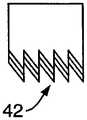
- a projection display suitable for use in a head-up displaycomprises a rod-like waveguide 10 of glass or transparent plastics material.
- the waveguide 10is of square or rectangular cross-section and is placed in close proximity to a plate waveguide 12 in which in operation the display is formed as explained in our '034 specification.
- Collimated image bearing light 14exits an optical arrangement which may be collimation optics (not shown), and is incident on an input reflection grating 16 which is disposed on a rear surface 20 of the waveguide 10 .
- the collimated lighthas rays at range of angles relative to the collimation, or injection, axis normal to the grating which determines the field of view of the system.
- collimated and collimationcovers partially collimated light having a range of angles relative to the collimation axis.
- the reflection gratingdiffracts the incident rays at angles such that all of them are totally internally reflected when incident on the four surfaces of the waveguide 10 ; two of the surfaces 20 and 22 are shown in FIG. 1 .
- the rays(a typical one of which is shown at 18 ) thus are contained within the waveguide 10 between its parallel opposite surfaces, and propagate down the length of the waveguide 10 . In this way, when image bearing light is displayed to a user, a field of view can be produced which corresponds to the range of angles input to the input grating.
- the propagating raysare incident repeatedly on a low efficiency grating 24 , each time a proportion 26 , 28 , 30 of the incident light being diffracted out of the waveguide 10 into the plate waveguide 12 .
- the remainder of the lightpasses through the grating and ultimately is absorbed at the end 32 of the waveguide 10 .
- the end 32 of the waveguide 10is coated or painted with a suitably absorbtive material.
- the distributed partial diffraction of the light into the plate waveguide 12results in expansion of the image in the plate waveguide across its width parallel to the extent of the waveguide 10 .
- the angular bandwidth of the input gratingis generally matched with, or less than, the angular bandwidth of the output grating so that light input to the waveguide over the range of angles can be output by the output grating.
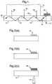
- FIG. 2shows the input grating 16 in more detail.
- the grating(here shown enlarged for clarity in FIG. 2( a ) ) is etched onto the surface 20 of the waveguide 10 , or is replicated on to it using a UV-curable polymer.
- the gratingis a periodic sawtooth profile.
- One or more layers 34 of dielectric material( FIG. 2( b ) ) are applied conformably to the surface of the grating, and a conforming metallic reflecting layer 36 ( FIG. 2 ( c ) ) is applied to the rear surface of the dielectric layer 34 .
- the metallic reflecting layer 36may be silver, gold, aluminium or another material having a complex refractive index. Preferably it is silver.
- FIG. 3shows an alternative form of the injection grating 16 .
- the gratingis either etched or replicated onto a substrate 38 using a UV-curable polymer ( FIG. 3( a ) ).
- a conformal metallic layer 40 of constant thicknessis applied to the grating, and is overlaid by one or more layers 42 of dielectric material.
- the material of the layers 40 , 42 and their thicknessesare chosen according to the same criteria as far the FIG. 2 embodiment.
- the grating 16is then glued to the surface 20 of the waveguide 10 by means of optical cement. It is not essential that the cement has exactly the same refractive index as the material of the waveguide 10 . For example, for waveguide material of n ⁇ 1.5, cement having 1.5 ⁇ n ⁇ 1.6 would be suitable.
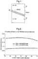
- a sawtooth type grating 16 with period 430 nm and height 250 nmis etched or replicated onto the surface 20 of the waveguide 10 .
- a thick layer (approximately 100 nm) of silver 44would be coated onto the surface of the grating, as shown in FIG. 4( a ) .
- FIG. 5shows the reflective efficiency of this conventional grating in the +1 diffraction order (dashed line) for input ray angles ranging from ⁇ 10° to +10° relative to the collimation axis, for light of wavelength 532 nm.
- a conformal layer 34 of titanium dioxide approximately 70 nm thickis first applied to the grating 16 .
- a layer 36 of silver approximately 100 nm thickis then overlaid onto the layer 34 .
- the efficiency of this grating under the same conditions as for the grating of FIG. 4( a )also is shown in FIG. 5 (solid line). It is evident that the efficiency and the bandwidth of the grating is substantially improved compared to that of FIG. 4( a ) .
- FIG. 6shows the embedded exit grating 24 in more detail.
- the waveguide 10comprises lower and upper substrates 50 , 52 , of respective thickness T 1 and T 2 , and having abutting surfaces 54 , 56 .
- the lower substrate 50has on its upper surface 54 a surface relief grating 58 (here of a sawtooth profile, shown much enlarged in FIG. 6( a ) ), produced by etching or replicating as already described for grating 16 .
- a conformal dielectric coating or layer 60( FIG. 6( b ) ) is applied to the grating in a thickness which increases in the direction of propagation of the light along the waveguide 10 (right to left in FIG. 6 ).
- the substrate 52is laid onto the lower substrate 50 and cemented thereto by optical cement 62 ( FIG. 6( c ) ) along its whole length so as to be optically continuous therewith.
- the choice of the refractive index of the cementwill depend on the range of angles in the propagating light rays within the waveguide, the refractive index of the substrates 50 , 52 the refractive index of the replication material and the refractive indices of the range of available optical cements with suitable optical properties. These choices are made when the waveguide based display is being designed. In the example described here, with substrates 50 , 52 having a refractive index n ⁇ 1.5, it is normally sufficient to use optical cement having n between about 1.5 and 1.6.
- the thickness of the coatingis chosen to increase the efficiency of the grating along the waveguide to compensate for the progressive attenuation of the light as it is propagated along the waveguide.
- the increase in thickness of the layer 60is such as fully to compensate for the attenuation, so that the intensity of the light diffracted transversely out of the waveguide from longitudinally separated points along the grating is equal.
- the increase in thickness of the layer 60is such as to compensate for the attenuation within acceptable limits, so that the intensity of the light diffracted transversely out of the waveguide from longitudinally separated points along the grating is approximately equal.
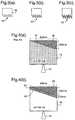
- FIG. 7shows one tooth of the sawtooth grating 24 .
- the gratinghas a period of 435 nm and a height of 150 nm.
- the titanium dioxide layer 60was made 20 nm thick. In another, it was made 40 nm thick.
- the substrates 50 , 52 and the optical cement 62had a refractive index n of approximately 1.5.
- FIG. 8shows the performance of the two prototypes with incident rays of wavelength 532 nm propagating within the waveguide 10 .
- the lower line in the graphshows the performance of the grating with the 20 nm titanium dioxide coating, and the upper line the performance of the grating with the 40 nm coating.
- the raysare incident on the waveguide at from 40° to 72°.
- This range of angles at the output gratingis produced by a range of angle at the input grating from about 16° to 16° so that the angular bandwidths are generally matched.
- the average efficiency of the grating with the 20 nm coatingis approximately 7.5%, for the other grating the efficiency is about 20% for angles of incidence between 40° and 62°, and falls away slightly above that range.
- the intensity of the diffracted output rays 26 , 28 , 30can be equalized, and a more even brightness can be obtained in the display in the plate waveguide 12 .
- Another advantage which may be obtainedis the more efficient utilisation of light, and hence a reduction in total intensity of the collimated light input 14 required to achieve a given brightness in the display in the waveguide 12 .
- the graduated thickness of the layer 60can be achieved by interposing a suitably shaped mask between the substrate 50 as the source in the coating chamber used to deposit the titanium dioxide material.
- a moveable bafflemay be used; moving it continuously at a controlled speed can enable the coating thickness on the grating to be varied in a controlled manner.
- the waveguide 10contains one or more beam-splitters 64 , FIG. 9 which are coplanar with the grating 24 and on which the beam 18 is incident before it arrives at the grating.
- the beam-splitters 64are one or more semi-reflecting surfaces disposed substantially parallel to the waveguide surfaces 20 , 22 .
- uniformitywe mean the lack of variation in the intensity of the output image, assuming that the intensity of the input image is itself uniform.
- any impinging image-bearing beam 18 with a beam splitterit is divided into two parts 68 , 70 one passing undeflected through the beam splitter, the other being reflected.
- this beam 68totally internally reflects off the wall 22 of the waveguide and impinges again on the beam splitter at 72 a distance (S) downstream of the previous impingement 66 .
- Sbeam width
- T 1is approximately 1 ⁇ 3 or 1 ⁇ 2 T 2
- T 1 to T 2Slightly different ratios of T 1 to T 2 will be obtained for different values of the refractive index n of the waveguide material.
- T 1 and T 2can be interchanged; indeed in FIG. 6 T 1 is shown as the larger of the two dimensions.
- the beam splitter 64is coplanar with the grating.
- the plate waveguide 12may also have a surface relief grating according to the invention embedded in it which forms a two dimensional image from the image-bearing beams 26 , 28 , 30 from the waveguide 10 .
- the gratingthus may be of similar construction to that shown in FIG. 6 with a conforming dielectric layer or existing applied to its profiled surface, and increasing in thickness with distance away from the interface of the waveguide 10 and 12 . Then the efficiency of the grating increases with distance away from the interface, thereby compensating for the attenuation suffered by the injected beams 26 , 28 , as they progress through the waveguide 12 .
- FIG. 10shows a plate waveguide for use with a conventional rod-like waveguide which does not have a variable efficiency grating according to the invention.
- Beams 76 , 78 , 80 , 82 , 84are diffracted out of a rod-like waveguide 74 by a conventional constant-efficiency grating from an injected beam propagating from left to right in FIG. 10 . Because of progressive attenuation down the waveguide 74 , the beams 76 - 84 have relative intensities proportional to the lengths of the illustrated vectors.
- the beamsenter a plate waveguide 86 wherein a two dimensional image is formed by a surface relief grating 88 .
- This gratinghas a dielectric coating or layer on its profiled surface similar to that described with reference to FIG. 6 , except that the coating varies in thickness in two dimensions.
- the thickness and the coating efficiencyincrease in the y direction away from the interface 90 with the waveguide 74 to compensate for attenuation in the waveguide 86 ; furthermore, the thickness and the grating also increase in the x direction away from the left-hand edge of the waveguide 90 to compensate for the attenuation in the waveguide 74 .
- the grating efficiencyincreases diagonally across the grating from a minimum at the corner A of the grating, to a maximum at corner B. This can materially assist in overcoming the fault often seen in prior art apparatus of this type where for an evenly-illuminated image injected into the waveguide 74 , the resulting display in the plate waveguide 90 is noticeably darker at point B than at point A.
- this specificationdiscloses the use, for the purpose of controlling the reflective or diffractive efficiency and/or angular bandwidth of a surface relief grating of an optical waveguide, of at least one layer or coating of dielectric material conforming to a profiled surface of the grating.
- the waveguideis operable such that light passes through the dielectric material to the profiled surface.
- the gratingmay be a reflection or transmission grating.
- the coatingmay vary in thickness so as to provide a grating having a spatial variation in efficiency.
Landscapes
- Physics & Mathematics (AREA)
- General Physics & Mathematics (AREA)
- Optics & Photonics (AREA)
- Optical Couplings Of Light Guides (AREA)
- Diffracting Gratings Or Hologram Optical Elements (AREA)
- Optical Integrated Circuits (AREA)
Abstract
Description
S/2T1=tan θ
andS=2T1tan θ
tan θ=3.08 and 2T=6.16T
Claims (10)
Applications Claiming Priority (6)
| Application Number | Priority Date | Filing Date | Title |
|---|---|---|---|
| GB0906706.7 | 2009-04-20 | ||
| EP09275025AEP2244114A1 (en) | 2009-04-20 | 2009-04-20 | Surface relief grating in an optical waveguide having a reflecting surface and dielectric layer conforming to the surface |
| EP09275025.6 | 2009-04-20 | ||
| GB0906706AGB0906706D0 (en) | 2009-04-20 | 2009-04-20 | Improvements in optical waveguides |
| EP09275025 | 2009-04-20 | ||
| PCT/GB2010/050640WO2010122330A1 (en) | 2009-04-20 | 2010-04-19 | Surface relief grating in an optical waveguide having a reflecting surface and dielectric layer conforming to the surface |
Publications (2)
| Publication Number | Publication Date |
|---|---|
| US20120120493A1 US20120120493A1 (en) | 2012-05-17 |
| US10642039B2true US10642039B2 (en) | 2020-05-05 |
Family
ID=42235675
Family Applications (1)
| Application Number | Title | Priority Date | Filing Date |
|---|---|---|---|
| US13/265,260Active2035-08-23US10642039B2 (en) | 2009-04-20 | 2010-04-19 | Surface relief grating in an optical waveguide having a reflecting surface and dielectric layer conforming to the surface |
Country Status (7)
| Country | Link |
|---|---|
| US (1) | US10642039B2 (en) |
| EP (1) | EP2422232B1 (en) |
| AU (1) | AU2010240707B2 (en) |
| CA (1) | CA2759296C (en) |
| ES (1) | ES2621820T3 (en) |
| IL (1) | IL215851A (en) |
| WO (1) | WO2010122330A1 (en) |
Families Citing this family (125)
| Publication number | Priority date | Publication date | Assignee | Title |
|---|---|---|---|---|
| GB0522968D0 (en) | 2005-11-11 | 2005-12-21 | Popovich Milan M | Holographic illumination device |
| GB0718706D0 (en) | 2007-09-25 | 2007-11-07 | Creative Physics Ltd | Method and apparatus for reducing laser speckle |
| US9335604B2 (en) | 2013-12-11 | 2016-05-10 | Milan Momcilo Popovich | Holographic waveguide display |
| US11726332B2 (en) | 2009-04-27 | 2023-08-15 | Digilens Inc. | Diffractive projection apparatus |
| US11320571B2 (en) | 2012-11-16 | 2022-05-03 | Rockwell Collins, Inc. | Transparent waveguide display providing upper and lower fields of view with uniform light extraction |
| US8233204B1 (en) | 2009-09-30 | 2012-07-31 | Rockwell Collins, Inc. | Optical displays |
| US11300795B1 (en) | 2009-09-30 | 2022-04-12 | Digilens Inc. | Systems for and methods of using fold gratings coordinated with output couplers for dual axis expansion |
| US10795160B1 (en) | 2014-09-25 | 2020-10-06 | Rockwell Collins, Inc. | Systems for and methods of using fold gratings for dual axis expansion |
| US20200057353A1 (en) | 2009-10-09 | 2020-02-20 | Digilens Inc. | Compact Edge Illuminated Diffractive Display |
| US11204540B2 (en) | 2009-10-09 | 2021-12-21 | Digilens Inc. | Diffractive waveguide providing a retinal image |
| US8659826B1 (en) | 2010-02-04 | 2014-02-25 | Rockwell Collins, Inc. | Worn display system and method without requiring real time tracking for boresight precision |
| WO2012136970A1 (en) | 2011-04-07 | 2012-10-11 | Milan Momcilo Popovich | Laser despeckler based on angular diversity |
| EP2995986B1 (en)* | 2011-08-24 | 2017-04-12 | Rockwell Collins, Inc. | Data display |
| US10670876B2 (en) | 2011-08-24 | 2020-06-02 | Digilens Inc. | Waveguide laser illuminator incorporating a despeckler |
| WO2016020630A2 (en) | 2014-08-08 | 2016-02-11 | Milan Momcilo Popovich | Waveguide laser illuminator incorporating a despeckler |
| US9507150B1 (en) | 2011-09-30 | 2016-11-29 | Rockwell Collins, Inc. | Head up display (HUD) using a bent waveguide assembly |
| US8903207B1 (en) | 2011-09-30 | 2014-12-02 | Rockwell Collins, Inc. | System for and method of extending vertical field of view in head up display utilizing a waveguide combiner |
| US9366864B1 (en) | 2011-09-30 | 2016-06-14 | Rockwell Collins, Inc. | System for and method of displaying information without need for a combiner alignment detector |
| US9715067B1 (en) | 2011-09-30 | 2017-07-25 | Rockwell Collins, Inc. | Ultra-compact HUD utilizing waveguide pupil expander with surface relief gratings in high refractive index materials |
| US8937772B1 (en) | 2011-09-30 | 2015-01-20 | Rockwell Collins, Inc. | System for and method of stowing HUD combiners |
| US8634139B1 (en) | 2011-09-30 | 2014-01-21 | Rockwell Collins, Inc. | System for and method of catadioptric collimation in a compact head up display (HUD) |
| GB201117029D0 (en) | 2011-10-04 | 2011-11-16 | Bae Systems Plc | Optical waveguide and display device |
| US20150010265A1 (en) | 2012-01-06 | 2015-01-08 | Milan, Momcilo POPOVICH | Contact image sensor using switchable bragg gratings |
| US9460029B2 (en) | 2012-03-02 | 2016-10-04 | Microsoft Technology Licensing, Llc | Pressure sensitive keys |
| US9075566B2 (en) | 2012-03-02 | 2015-07-07 | Microsoft Technoogy Licensing, LLC | Flexible hinge spine |
| GB2500631B (en) | 2012-03-27 | 2017-12-27 | Bae Systems Plc | Improvements in or relating to optical waveguides |
| US9523852B1 (en) | 2012-03-28 | 2016-12-20 | Rockwell Collins, Inc. | Micro collimator system and method for a head up display (HUD) |
| CN106125308B (en) | 2012-04-25 | 2019-10-25 | 罗克韦尔柯林斯公司 | Device and method for displaying images |
| WO2013167864A1 (en) | 2012-05-11 | 2013-11-14 | Milan Momcilo Popovich | Apparatus for eye tracking |
| US20130300590A1 (en) | 2012-05-14 | 2013-11-14 | Paul Henry Dietz | Audio Feedback |
| US9933684B2 (en) | 2012-11-16 | 2018-04-03 | Rockwell Collins, Inc. | Transparent waveguide display providing upper and lower fields of view having a specific light output aperture configuration |
| US9674413B1 (en) | 2013-04-17 | 2017-06-06 | Rockwell Collins, Inc. | Vision system and method having improved performance and solar mitigation |
| US10209517B2 (en) | 2013-05-20 | 2019-02-19 | Digilens, Inc. | Holographic waveguide eye tracker |
| WO2015015138A1 (en) | 2013-07-31 | 2015-02-05 | Milan Momcilo Popovich | Method and apparatus for contact image sensing |
| US9244281B1 (en) | 2013-09-26 | 2016-01-26 | Rockwell Collins, Inc. | Display system and method using a detached combiner |
| US9459451B2 (en) | 2013-12-26 | 2016-10-04 | Microsoft Technology Licensing, Llc | Eye tracking apparatus, method and system |
| US10732407B1 (en) | 2014-01-10 | 2020-08-04 | Rockwell Collins, Inc. | Near eye head up display system and method with fixed combiner |
| US9519089B1 (en) | 2014-01-30 | 2016-12-13 | Rockwell Collins, Inc. | High performance volume phase gratings |
| KR102260184B1 (en) | 2014-02-26 | 2021-06-04 | 삼성디스플레이 주식회사 | Cover window and display device having the same |
| US9244280B1 (en) | 2014-03-25 | 2016-01-26 | Rockwell Collins, Inc. | Near eye display system and method for display enhancement or redundancy |
| US9304235B2 (en) | 2014-07-30 | 2016-04-05 | Microsoft Technology Licensing, Llc | Microfabrication |
| US10324733B2 (en) | 2014-07-30 | 2019-06-18 | Microsoft Technology Licensing, Llc | Shutdown notifications |
| US10678412B2 (en) | 2014-07-31 | 2020-06-09 | Microsoft Technology Licensing, Llc | Dynamic joint dividers for application windows |
| US9787576B2 (en) | 2014-07-31 | 2017-10-10 | Microsoft Technology Licensing, Llc | Propagating routing awareness for autonomous networks |
| US10254942B2 (en) | 2014-07-31 | 2019-04-09 | Microsoft Technology Licensing, Llc | Adaptive sizing and positioning of application windows |
| US10592080B2 (en) | 2014-07-31 | 2020-03-17 | Microsoft Technology Licensing, Llc | Assisted presentation of application windows |
| US10359736B2 (en) | 2014-08-08 | 2019-07-23 | Digilens Inc. | Method for holographic mastering and replication |
| US9377623B2 (en) | 2014-08-11 | 2016-06-28 | Microsoft Technology Licensing, Llc | Waveguide eye tracking employing volume Bragg grating |
| WO2016042283A1 (en) | 2014-09-19 | 2016-03-24 | Milan Momcilo Popovich | Method and apparatus for generating input images for holographic waveguide displays |
| US9494799B2 (en) | 2014-09-24 | 2016-11-15 | Microsoft Technology Licensing, Llc | Waveguide eye tracking employing switchable diffraction gratings |
| US9715110B1 (en) | 2014-09-25 | 2017-07-25 | Rockwell Collins, Inc. | Automotive head up display (HUD) |
| US10088675B1 (en) | 2015-05-18 | 2018-10-02 | Rockwell Collins, Inc. | Turning light pipe for a pupil expansion system and method |
| EP3198192A1 (en) | 2014-09-26 | 2017-08-02 | Milan Momcilo Popovich | Holographic waveguide opticaltracker |
| WO2016113534A1 (en) | 2015-01-12 | 2016-07-21 | Milan Momcilo Popovich | Environmentally isolated waveguide display |
| US20180275402A1 (en) | 2015-01-12 | 2018-09-27 | Digilens, Inc. | Holographic waveguide light field displays |
| EP3248026B1 (en) | 2015-01-20 | 2019-09-04 | DigiLens Inc. | Holographic waveguide lidar |
| US9429692B1 (en) | 2015-02-09 | 2016-08-30 | Microsoft Technology Licensing, Llc | Optical components |
| US10018844B2 (en) | 2015-02-09 | 2018-07-10 | Microsoft Technology Licensing, Llc | Wearable image display system |
| US9535253B2 (en) | 2015-02-09 | 2017-01-03 | Microsoft Technology Licensing, Llc | Display system |
| US9372347B1 (en) | 2015-02-09 | 2016-06-21 | Microsoft Technology Licensing, Llc | Display system |
| US9423360B1 (en) | 2015-02-09 | 2016-08-23 | Microsoft Technology Licensing, Llc | Optical components |
| US10317677B2 (en) | 2015-02-09 | 2019-06-11 | Microsoft Technology Licensing, Llc | Display system |
| US9827209B2 (en) | 2015-02-09 | 2017-11-28 | Microsoft Technology Licensing, Llc | Display system |
| US9513480B2 (en) | 2015-02-09 | 2016-12-06 | Microsoft Technology Licensing, Llc | Waveguide |
| US11086216B2 (en) | 2015-02-09 | 2021-08-10 | Microsoft Technology Licensing, Llc | Generating electronic components |
| US9632226B2 (en) | 2015-02-12 | 2017-04-25 | Digilens Inc. | Waveguide grating device |
| DE102015102032A1 (en)* | 2015-02-12 | 2016-08-18 | Carl Zeiss Jena Gmbh | Optical element |
| IL237337B (en)* | 2015-02-19 | 2020-03-31 | Amitai Yaakov | Compact head-mounted display system having uniform image |
| WO2016146963A1 (en) | 2015-03-16 | 2016-09-22 | Popovich, Milan, Momcilo | Waveguide device incorporating a light pipe |
| WO2016156776A1 (en) | 2015-03-31 | 2016-10-06 | Milan Momcilo Popovich | Method and apparatus for contact image sensing |
| US10126552B2 (en) | 2015-05-18 | 2018-11-13 | Rockwell Collins, Inc. | Micro collimator system and method for a head up display (HUD) |
| US10247943B1 (en) | 2015-05-18 | 2019-04-02 | Rockwell Collins, Inc. | Head up display (HUD) using a light pipe |
| US11366316B2 (en) | 2015-05-18 | 2022-06-21 | Rockwell Collins, Inc. | Head up display (HUD) using a light pipe |
| WO2016187464A1 (en)* | 2015-05-19 | 2016-11-24 | Magic Leap, Inc. | Illuminator |
| US10108010B2 (en) | 2015-06-29 | 2018-10-23 | Rockwell Collins, Inc. | System for and method of integrating head up displays and head down displays |
| DE102015114990B4 (en)* | 2015-09-07 | 2022-05-12 | tooz technologies GmbH | Lens arrangement, in particular spectacle lens arrangement, display device and method for producing a lens arrangement |
| CN113759555B (en) | 2015-10-05 | 2024-09-20 | 迪吉伦斯公司 | Waveguide Display |
| US10359627B2 (en) | 2015-11-10 | 2019-07-23 | Microsoft Technology Licensing, Llc | Waveguide coatings or substrates to improve intensity distributions having adjacent planar optical component separate from an input, output, or intermediate coupler |
| US9791696B2 (en) | 2015-11-10 | 2017-10-17 | Microsoft Technology Licensing, Llc | Waveguide gratings to improve intensity distributions |
| US9915825B2 (en) | 2015-11-10 | 2018-03-13 | Microsoft Technology Licensing, Llc | Waveguides with embedded components to improve intensity distributions |
| US10598932B1 (en) | 2016-01-06 | 2020-03-24 | Rockwell Collins, Inc. | Head up display for integrating views of conformally mapped symbols and a fixed image source |
| CN109073889B (en) | 2016-02-04 | 2021-04-27 | 迪吉伦斯公司 | Holographic waveguide optical tracker |
| CN108780224B (en) | 2016-03-24 | 2021-08-03 | 迪吉伦斯公司 | Method and apparatus for providing a polarization selective holographic waveguide device |
| US10890707B2 (en) | 2016-04-11 | 2021-01-12 | Digilens Inc. | Holographic waveguide apparatus for structured light projection |
| WO2017193012A1 (en) | 2016-05-06 | 2017-11-09 | Magic Leap, Inc. | Metasurfaces with asymetric gratings for redirecting light and methods for fabricating |
| JP6823381B2 (en)* | 2016-05-25 | 2021-02-03 | キヤノン株式会社 | Optical equipment with a diffractive optical element and a diffraction grating and a camera with a diffraction grating |
| GB2556094A (en)* | 2016-11-18 | 2018-05-23 | Wave Optics Ltd | Optical device |
| WO2018102834A2 (en) | 2016-12-02 | 2018-06-07 | Digilens, Inc. | Waveguide device with uniform output illumination |
| US10545346B2 (en) | 2017-01-05 | 2020-01-28 | Digilens Inc. | Wearable heads up displays |
| CN108333749A (en)* | 2017-01-19 | 2018-07-27 | 中强光电股份有限公司 | Optical system and head-mounted display device |
| US10295824B2 (en) | 2017-01-26 | 2019-05-21 | Rockwell Collins, Inc. | Head up display with an angled light pipe |
| US20190056591A1 (en)* | 2017-08-18 | 2019-02-21 | Microsoft Technology Licensing, Llc | Optical waveguide with multiple antireflective coatings |
| WO2019079350A2 (en) | 2017-10-16 | 2019-04-25 | Digilens, Inc. | Systems and methods for multiplying the image resolution of a pixelated display |
| WO2019136476A1 (en) | 2018-01-08 | 2019-07-11 | Digilens, Inc. | Waveguide architectures and related methods of manufacturing |
| US10732569B2 (en) | 2018-01-08 | 2020-08-04 | Digilens Inc. | Systems and methods for high-throughput recording of holographic gratings in waveguide cells |
| EP3710894B1 (en) | 2018-01-08 | 2025-07-30 | Digilens Inc. | Methods for fabricating optical waveguides |
| EP3710876A4 (en) | 2018-01-08 | 2022-02-09 | DigiLens Inc. | SYSTEMS AND METHODS OF FABRICATING WAVEGUIDE CELLS |
| US11740399B2 (en)* | 2018-02-06 | 2023-08-29 | Raytheon Company | Low cost dispersive optical elements |
| US10690851B2 (en) | 2018-03-16 | 2020-06-23 | Digilens Inc. | Holographic waveguides incorporating birefringence control and methods for their fabrication |
| WO2020023546A1 (en)* | 2018-07-24 | 2020-01-30 | Magic Leap, Inc. | Diffractive optical elements with mitigation of rebounce-induced light loss and related systems and methods |
| WO2020023779A1 (en) | 2018-07-25 | 2020-01-30 | Digilens Inc. | Systems and methods for fabricating a multilayer optical structure |
| EP4481469A3 (en)* | 2018-11-07 | 2025-02-26 | Applied Materials, Inc. | Formation of angled gratings |
| US10690831B2 (en) | 2018-11-20 | 2020-06-23 | Facebook Technologies, Llc | Anisotropically formed diffraction grating device |
| US20200225471A1 (en) | 2019-01-14 | 2020-07-16 | Digilens Inc. | Holographic Waveguide Display with Light Control Layer |
| US20200247017A1 (en) | 2019-02-05 | 2020-08-06 | Digilens Inc. | Methods for Compensating for Optical Surface Nonuniformity |
| KR102866596B1 (en) | 2019-02-15 | 2025-09-29 | 디지렌즈 인코포레이티드. | Method and device for providing a holographic waveguide display using an integral grating |
| US20220283377A1 (en) | 2019-02-15 | 2022-09-08 | Digilens Inc. | Wide Angle Waveguide Display |
| WO2020186113A1 (en) | 2019-03-12 | 2020-09-17 | Digilens Inc. | Holographic waveguide backlight and related methods of manufacturing |
| EP3980825A4 (en) | 2019-06-07 | 2023-05-03 | Digilens Inc. | WAVEGUIDES WITH TRANSMITTING AND REFLECTING GRIDS AND RELATED MANUFACTURING PROCESSES |
| US11353702B2 (en)* | 2019-06-25 | 2022-06-07 | Microsoft Technology Licensing, Llc | Thickness-modulated conformal coatings on optical components |
| EP4004646A4 (en) | 2019-07-29 | 2023-09-06 | Digilens Inc. | METHODS AND APPARATUS FOR MULTIPLYING THE IMAGE RESOLUTION AND FIELD OF VIEW OF A PIXELATED DISPLAY SCREEN |
| US11099309B2 (en) | 2019-08-23 | 2021-08-24 | Facebook Technologies, Llc | Outward coupling suppression in waveguide display |
| KR102775783B1 (en) | 2019-08-29 | 2025-02-28 | 디지렌즈 인코포레이티드. | Vacuum grid and method for manufacturing the same |
| EP4025830B1 (en) | 2019-09-06 | 2024-11-06 | BAE SYSTEMS plc | Waveguide and method for fabricating a waveguide |
| GB2586850B (en)* | 2019-09-06 | 2023-05-24 | Bae Systems Plc | Waveguide and method for fabricating a waveguide |
| WO2021050924A1 (en) | 2019-09-11 | 2021-03-18 | Magic Leap, Inc. | Display device with diffraction grating having reduced polarization sensitivity |
| US11662584B2 (en) | 2019-12-26 | 2023-05-30 | Meta Platforms Technologies, Llc | Gradient refractive index grating for display leakage reduction |
| WO2022078072A1 (en)* | 2020-10-13 | 2022-04-21 | Oppo广东移动通信有限公司 | Diffraction grating structure, imaging device, and wearable device |
| JP2024502255A (en) | 2020-12-21 | 2024-01-18 | ディジレンズ インコーポレイテッド | Eye glow suppression in waveguide-based displays |
| WO2022150841A1 (en) | 2021-01-07 | 2022-07-14 | Digilens Inc. | Grating structures for color waveguides |
| US12158612B2 (en) | 2021-03-05 | 2024-12-03 | Digilens Inc. | Evacuated periodic structures and methods of manufacturing |
| CN113721320A (en)* | 2021-09-06 | 2021-11-30 | 宁波舜宇奥来技术有限公司 | Optical waveguide structure and display device |
| US20230120539A1 (en)* | 2021-10-15 | 2023-04-20 | Applied Materials, Inc. | Metallized high-index blaze grating incoupler |
| CN118091822A (en)* | 2022-02-16 | 2024-05-28 | 荣耀终端有限公司 | Display device, optical waveguide and augmented reality glasses |
| WO2023203597A1 (en)* | 2022-04-18 | 2023-10-26 | Cellid株式会社 | Projection substrate and substrate manufacturing method |
Citations (39)
| Publication number | Priority date | Publication date | Assignee | Title |
|---|---|---|---|---|
| US4330175A (en)* | 1978-07-18 | 1982-05-18 | Nippon Telegraph & Telephone Public Corporation | Blazed diffraction grating structures and method of manufacturing the same |
| US4711512A (en)* | 1985-07-12 | 1987-12-08 | Environmental Research Institute Of Michigan | Compact head-up display |
| US4887255A (en) | 1986-08-25 | 1989-12-12 | Canon Kabushiki Kaisha | Integrated optical head |
| US5007709A (en)* | 1987-12-28 | 1991-04-16 | Matsushita Electric Industrial Co., Ltd. | Diffraction grating and manufacturing method thereof |
| US5138687A (en)* | 1989-09-26 | 1992-08-11 | Omron Corporation | Rib optical waveguide and method of manufacturing the same |
| US5224198A (en)* | 1991-09-30 | 1993-06-29 | Motorola, Inc. | Waveguide virtual image display |
| US5377044A (en) | 1990-03-19 | 1994-12-27 | Canon Kabushiki Kaisha | Reflecting diffraction grating and device, such as encoder or the like, using the same |
| US5742373A (en) | 1995-10-13 | 1998-04-21 | Massachusetts Institute Of Technology | Color microdisplays and methods of manufacturing same |
| US5907436A (en)* | 1995-09-29 | 1999-05-25 | The Regents Of The University Of California | Multilayer dielectric diffraction gratings |
| US6169613B1 (en)* | 1993-02-26 | 2001-01-02 | Yeda Research & Devel Co., Ltd. | Planar holographic optical device for beam expansion and display |
| US6351334B1 (en) | 2000-10-10 | 2002-02-26 | Industrial Technology Research Institute | Reflective diffraction grating for use in display devices |
| EP1191360A2 (en) | 2000-09-21 | 2002-03-27 | Nippon Sheet Glass Co., Ltd. | Reflection type diffraction grating |
| EP1215526A1 (en) | 2000-07-11 | 2002-06-19 | Mitsubishi Chemical Corporation | Surface light source device |
| US20020141065A1 (en)* | 2000-08-01 | 2002-10-03 | James Cowan | Directional diffuser |
| WO2003046624A1 (en) | 2001-11-26 | 2003-06-05 | Lnl Optenia Inc. | Metallised echelle grating with reduced polarisation dependence using dielectric spacer layers |
| US6580529B1 (en)* | 1998-04-02 | 2003-06-17 | Elop Electro -Optics Industries Ltd. | Holographic optical devices |
| EP1385023A1 (en) | 2002-07-17 | 2004-01-28 | C.R.F. Società Consortile per Azioni | A light guide for display devices of the head-mounted or head-up type |
| US20040021946A1 (en)* | 2002-08-02 | 2004-02-05 | John Hoose | Grating device with high diffraction efficiency |
| US6754006B2 (en)* | 2001-10-05 | 2004-06-22 | General Atomics | Hybrid metallic-dielectric grating |
| US6829095B2 (en)* | 2000-06-05 | 2004-12-07 | Lumus, Ltd. | Substrate-guided optical beam expander |
| US7006733B2 (en)* | 2002-09-10 | 2006-02-28 | Photintech, Inc. | Method and apparatus for channel selective control of light propagation in an optical waveguide |
| US7021777B2 (en)* | 2003-09-10 | 2006-04-04 | Lumus Ltd. | Optical devices particularly for remote viewing applications |
| US7054065B2 (en)* | 2003-03-27 | 2006-05-30 | The Regents Of The University Of California | Durable silver thin film coating for diffraction gratings |
| US20060132914A1 (en)* | 2003-06-10 | 2006-06-22 | Victor Weiss | Method and system for displaying an informative image against a background image |
| US20060228073A1 (en)* | 2004-03-29 | 2006-10-12 | Hiroshi Mukawa | Optical device and virtual image display device |
| US20060291021A1 (en) | 2005-06-17 | 2006-12-28 | Hiroshi Mukawa | Optical device, and virtual image display |
| US20070008624A1 (en)* | 2004-03-12 | 2007-01-11 | Nikon Corporation | Optical image display system and image display unit |
| WO2007029034A1 (en) | 2005-09-07 | 2007-03-15 | Bae Systems Plc | A projection display with a rod-like, rectangular cross-section waveguide and a plate-like waveguide, each of them having a diffraction grating |
| US20070230534A1 (en)* | 2006-03-29 | 2007-10-04 | The Regents Of The University Of California | Grating enhanced solid-state laser amplifiers |
| US20080138013A1 (en) | 2004-04-23 | 2008-06-12 | Parriaux Olivier M | High Efficiency Optical Diffraction Device |
| US7391573B2 (en)* | 2003-09-10 | 2008-06-24 | Lumus Ltd. | Substrate-guided optical devices |
| US7430076B2 (en)* | 2001-09-13 | 2008-09-30 | Asahi Glass Company, Limited | Diffraction element |
| DE102007032371A1 (en) | 2007-07-06 | 2009-01-15 | Carl Zeiss Laser Optics Gmbh | Method for coating an optical component for a laser arrangement |
| US20090059375A1 (en)* | 2007-08-27 | 2009-03-05 | John Hoose | Grating Device with Adjusting Layer |
| US7535631B2 (en)* | 2005-01-26 | 2009-05-19 | Lockheed Martin Corporation | Method and apparatus for spectral-beam combining of fiber-amplified laser beams using high-efficiency dielectric diffractive gratings |
| US7653268B1 (en)* | 2008-07-03 | 2010-01-26 | Microvision, Inc. | Substrate guided relay with polarization rotating apparatus |
| US20100177388A1 (en)* | 2006-08-23 | 2010-07-15 | Mirage Innovations Ltd. | Diffractive optical relay device with improved color uniformity |
| US20110249692A1 (en)* | 2010-04-12 | 2011-10-13 | Lockheed Martin Corporation | Beam diagnostics and feedback system and method for spectrally beam-combined lasers |
| US8482855B2 (en)* | 2009-04-29 | 2013-07-09 | Horiba Jobin Yvon Sas | Dielectric coated metal diffraction grating with high reflection resistance to a femtosecond mode flow |
- 2010
- 2010-04-19ESES10715332.2Tpatent/ES2621820T3/enactiveActive
- 2010-04-19CACA2759296Apatent/CA2759296C/enactiveActive
- 2010-04-19AUAU2010240707Apatent/AU2010240707B2/enactiveActive
- 2010-04-19EPEP10715332.2Apatent/EP2422232B1/enactiveActive
- 2010-04-19WOPCT/GB2010/050640patent/WO2010122330A1/enactiveApplication Filing
- 2010-04-19USUS13/265,260patent/US10642039B2/enactiveActive
- 2011
- 2011-10-23ILIL215851Apatent/IL215851A/enactiveIP Right Grant
Patent Citations (44)
| Publication number | Priority date | Publication date | Assignee | Title |
|---|---|---|---|---|
| US4330175A (en)* | 1978-07-18 | 1982-05-18 | Nippon Telegraph & Telephone Public Corporation | Blazed diffraction grating structures and method of manufacturing the same |
| US4711512A (en)* | 1985-07-12 | 1987-12-08 | Environmental Research Institute Of Michigan | Compact head-up display |
| US4887255A (en) | 1986-08-25 | 1989-12-12 | Canon Kabushiki Kaisha | Integrated optical head |
| US5007709A (en)* | 1987-12-28 | 1991-04-16 | Matsushita Electric Industrial Co., Ltd. | Diffraction grating and manufacturing method thereof |
| US5138687A (en)* | 1989-09-26 | 1992-08-11 | Omron Corporation | Rib optical waveguide and method of manufacturing the same |
| US5377044A (en) | 1990-03-19 | 1994-12-27 | Canon Kabushiki Kaisha | Reflecting diffraction grating and device, such as encoder or the like, using the same |
| US5224198A (en)* | 1991-09-30 | 1993-06-29 | Motorola, Inc. | Waveguide virtual image display |
| US6169613B1 (en)* | 1993-02-26 | 2001-01-02 | Yeda Research & Devel Co., Ltd. | Planar holographic optical device for beam expansion and display |
| US5907436A (en)* | 1995-09-29 | 1999-05-25 | The Regents Of The University Of California | Multilayer dielectric diffraction gratings |
| US5742373A (en) | 1995-10-13 | 1998-04-21 | Massachusetts Institute Of Technology | Color microdisplays and methods of manufacturing same |
| US6580529B1 (en)* | 1998-04-02 | 2003-06-17 | Elop Electro -Optics Industries Ltd. | Holographic optical devices |
| US6829095B2 (en)* | 2000-06-05 | 2004-12-07 | Lumus, Ltd. | Substrate-guided optical beam expander |
| EP1215526A1 (en) | 2000-07-11 | 2002-06-19 | Mitsubishi Chemical Corporation | Surface light source device |
| US20020141065A1 (en)* | 2000-08-01 | 2002-10-03 | James Cowan | Directional diffuser |
| EP1191360A2 (en) | 2000-09-21 | 2002-03-27 | Nippon Sheet Glass Co., Ltd. | Reflection type diffraction grating |
| US20020044359A1 (en)* | 2000-09-21 | 2002-04-18 | Katsuhide Shimmo | Reflection type diffraction grating |
| US6839173B2 (en)* | 2000-09-21 | 2005-01-04 | Nippon Sheet Glass, Co., Ltd. | Reflection type diffraction grating |
| US6351334B1 (en) | 2000-10-10 | 2002-02-26 | Industrial Technology Research Institute | Reflective diffraction grating for use in display devices |
| US7430076B2 (en)* | 2001-09-13 | 2008-09-30 | Asahi Glass Company, Limited | Diffraction element |
| US6754006B2 (en)* | 2001-10-05 | 2004-06-22 | General Atomics | Hybrid metallic-dielectric grating |
| WO2003046624A1 (en) | 2001-11-26 | 2003-06-05 | Lnl Optenia Inc. | Metallised echelle grating with reduced polarisation dependence using dielectric spacer layers |
| EP1385023A1 (en) | 2002-07-17 | 2004-01-28 | C.R.F. Società Consortile per Azioni | A light guide for display devices of the head-mounted or head-up type |
| US6958859B2 (en)* | 2002-08-02 | 2005-10-25 | Chromaplex, Inc. | Grating device with high diffraction efficiency |
| US20040021946A1 (en)* | 2002-08-02 | 2004-02-05 | John Hoose | Grating device with high diffraction efficiency |
| US7006733B2 (en)* | 2002-09-10 | 2006-02-28 | Photintech, Inc. | Method and apparatus for channel selective control of light propagation in an optical waveguide |
| US7054065B2 (en)* | 2003-03-27 | 2006-05-30 | The Regents Of The University Of California | Durable silver thin film coating for diffraction gratings |
| US20060132914A1 (en)* | 2003-06-10 | 2006-06-22 | Victor Weiss | Method and system for displaying an informative image against a background image |
| US7021777B2 (en)* | 2003-09-10 | 2006-04-04 | Lumus Ltd. | Optical devices particularly for remote viewing applications |
| US7391573B2 (en)* | 2003-09-10 | 2008-06-24 | Lumus Ltd. | Substrate-guided optical devices |
| US20070008624A1 (en)* | 2004-03-12 | 2007-01-11 | Nikon Corporation | Optical image display system and image display unit |
| US20060228073A1 (en)* | 2004-03-29 | 2006-10-12 | Hiroshi Mukawa | Optical device and virtual image display device |
| US20080138013A1 (en) | 2004-04-23 | 2008-06-12 | Parriaux Olivier M | High Efficiency Optical Diffraction Device |
| US7535631B2 (en)* | 2005-01-26 | 2009-05-19 | Lockheed Martin Corporation | Method and apparatus for spectral-beam combining of fiber-amplified laser beams using high-efficiency dielectric diffractive gratings |
| US20060291021A1 (en) | 2005-06-17 | 2006-12-28 | Hiroshi Mukawa | Optical device, and virtual image display |
| WO2007029034A1 (en) | 2005-09-07 | 2007-03-15 | Bae Systems Plc | A projection display with a rod-like, rectangular cross-section waveguide and a plate-like waveguide, each of them having a diffraction grating |
| US20070230534A1 (en)* | 2006-03-29 | 2007-10-04 | The Regents Of The University Of California | Grating enhanced solid-state laser amplifiers |
| US20100177388A1 (en)* | 2006-08-23 | 2010-07-15 | Mirage Innovations Ltd. | Diffractive optical relay device with improved color uniformity |
| DE102007032371A1 (en) | 2007-07-06 | 2009-01-15 | Carl Zeiss Laser Optics Gmbh | Method for coating an optical component for a laser arrangement |
| US20090027776A1 (en)* | 2007-07-06 | 2009-01-29 | Carl Zeiss Laser Optics Gmbh | Method for coating an optical component for a laser arrangement and related optical component |
| US20090059375A1 (en)* | 2007-08-27 | 2009-03-05 | John Hoose | Grating Device with Adjusting Layer |
| US7653268B1 (en)* | 2008-07-03 | 2010-01-26 | Microvision, Inc. | Substrate guided relay with polarization rotating apparatus |
| US8482855B2 (en)* | 2009-04-29 | 2013-07-09 | Horiba Jobin Yvon Sas | Dielectric coated metal diffraction grating with high reflection resistance to a femtosecond mode flow |
| US20110249692A1 (en)* | 2010-04-12 | 2011-10-13 | Lockheed Martin Corporation | Beam diagnostics and feedback system and method for spectrally beam-combined lasers |
| US8411712B2 (en)* | 2010-04-12 | 2013-04-02 | Lockheed Martin Corporation | Beam diagnostics and feedback system and method for spectrally beam-combined lasers |
Non-Patent Citations (6)
| Title |
|---|
| Extended European Search Report dated Sep. 30, 2009 issued in 09275025.6. |
| International Preliminary Report on Patentability and Written Opinion, dated Nov. 3, 2011 from related International Application No. PCT/GB2010/050640. |
| International Search Report dated Jul. 22, 2010 issued in PCT/GB2010/050640. |
| Levola, Tapani, "7.1: Invited Paper: Novel Diffractive Optical Components for Near to Eye Displays", 2006 SID International Symposium,Society for Information Display, vol. XXXVII, May 24, 2005, pp. 64-67. |
| Perry, Michael, Multilayer Dielectric Gratings: Increasing the Power of Light, Science & Technology Review, p. 25, 1995, Available at https://str.llnl.gov/str/pdfs/09_95.2.pdf.* |
| UK Search Report dated Mar. 11, 2010 issued in GB0906706.7. |
Also Published As
| Publication number | Publication date |
|---|---|
| CA2759296C (en) | 2018-07-24 |
| WO2010122330A1 (en) | 2010-10-28 |
| AU2010240707A1 (en) | 2011-11-10 |
| IL215851A0 (en) | 2012-01-31 |
| CA2759296A1 (en) | 2010-10-28 |
| IL215851A (en) | 2016-08-31 |
| US20120120493A1 (en) | 2012-05-17 |
| AU2010240707B2 (en) | 2014-01-30 |
| EP2422232B1 (en) | 2017-03-08 |
| EP2422232A1 (en) | 2012-02-29 |
| ES2621820T3 (en) | 2017-07-05 |
Similar Documents
| Publication | Publication Date | Title |
|---|---|---|
| US10642039B2 (en) | Surface relief grating in an optical waveguide having a reflecting surface and dielectric layer conforming to the surface | |
| US9329325B2 (en) | Optical waveguides | |
| EP2244114A1 (en) | Surface relief grating in an optical waveguide having a reflecting surface and dielectric layer conforming to the surface | |
| US11846787B2 (en) | Diffractive waveguide element and diffractive waveguide display | |
| US9310566B2 (en) | Optical waveguides | |
| EP2764394B1 (en) | Optical waveguide and display device | |
| US8493662B2 (en) | Waveguides | |
| US8654420B2 (en) | Waveguides | |
| EP2561396B1 (en) | Optical waveguide and display device | |
| EP2244112A1 (en) | Improvements in optical waveguides | |
| FI128882B (en) | Optical waveguide and diffractive waveguide display | |
| EP2196842A1 (en) | Improvements in or relating to waveguides | |
| WO2022010375A1 (en) | Augmented and mixed reality device |
Legal Events
| Date | Code | Title | Description |
|---|---|---|---|
| AS | Assignment | Owner name:BAE SYSTEMS PLC, UNITED KINGDOM Free format text:ASSIGNMENT OF ASSIGNORS INTEREST;ASSIGNORS:SIMMONDS, MICHAEL DAVID;VALERA, MOHMED SALIM;REEL/FRAME:028436/0460 Effective date:20120528 | |
| STCV | Information on status: appeal procedure | Free format text:ON APPEAL -- AWAITING DECISION BY THE BOARD OF APPEALS | |
| STCV | Information on status: appeal procedure | Free format text:BOARD OF APPEALS DECISION RENDERED | |
| STPP | Information on status: patent application and granting procedure in general | Free format text:NOTICE OF ALLOWANCE MAILED -- APPLICATION RECEIVED IN OFFICE OF PUBLICATIONS | |
| STCF | Information on status: patent grant | Free format text:PATENTED CASE | |
| MAFP | Maintenance fee payment | Free format text:PAYMENT OF MAINTENANCE FEE, 4TH YEAR, LARGE ENTITY (ORIGINAL EVENT CODE: M1551); ENTITY STATUS OF PATENT OWNER: LARGE ENTITY Year of fee payment:4 | |
| AS | Assignment | Owner name:SNAP INC., CALIFORNIA Free format text:ASSIGNMENT OF ASSIGNORS INTEREST;ASSIGNOR:BAE SYSTEMS PLC;REEL/FRAME:070212/0921 Effective date:20220726 |