US10637196B2 - Modular jack contact assembly having controlled capacitive coupling positioned within a jack housing - Google Patents
Modular jack contact assembly having controlled capacitive coupling positioned within a jack housingDownload PDFInfo
- Publication number
- US10637196B2 US10637196B2US16/259,455US201916259455AUS10637196B2US 10637196 B2US10637196 B2US 10637196B2US 201916259455 AUS201916259455 AUS 201916259455AUS 10637196 B2US10637196 B2US 10637196B2
- Authority
- US
- United States
- Prior art keywords
- contacts
- jack
- network interface
- interface connector
- elongate
- Prior art date
- Legal status (The legal status is an assumption and is not a legal conclusion. Google has not performed a legal analysis and makes no representation as to the accuracy of the status listed.)
- Active
Links
- 230000008878couplingEffects0.000titledescription9
- 238000010168coupling processMethods0.000titledescription9
- 238000005859coupling reactionMethods0.000titledescription9
- RYGMFSIKBFXOCR-UHFFFAOYSA-NCopperChemical compound[Cu]RYGMFSIKBFXOCR-UHFFFAOYSA-N0.000claimsdescription33
- 229910052802copperInorganic materials0.000claimsdescription33
- 239000010949copperSubstances0.000claimsdescription33
- 239000012212insulatorSubstances0.000claimsdescription23
- 239000000758substrateSubstances0.000claimsdescription16
- 239000000463materialSubstances0.000claimsdescription15
- 230000015556catabolic processEffects0.000claimsdescription9
- 230000005540biological transmissionEffects0.000claimsdescription7
- 229920000106Liquid crystal polymerPolymers0.000claimsdescription5
- 239000004977Liquid-crystal polymers (LCPs)Substances0.000claimsdescription5
- 239000011810insulating materialSubstances0.000claimsdescription4
- 230000006835compressionEffects0.000claimsdescription3
- 238000007906compressionMethods0.000claimsdescription3
- WYTGDNHDOZPMIW-RCBQFDQVSA-NalstonineNatural productsC1=CC2=C3C=CC=CC3=NC2=C2N1C[C@H]1[C@H](C)OC=C(C(=O)OC)[C@H]1C2WYTGDNHDOZPMIW-RCBQFDQVSA-N0.000claims1
- 229910000679solderInorganic materials0.000description12
- PQHZWWBJPCNNGI-UHFFFAOYSA-N1,3,5-trichloro-2-(2,5-dichlorophenyl)benzeneChemical compoundClC1=CC=C(Cl)C(C=2C(=CC(Cl)=CC=2Cl)Cl)=C1PQHZWWBJPCNNGI-UHFFFAOYSA-N0.000description10
- 239000004033plasticSubstances0.000description9
- 230000004888barrier functionEffects0.000description8
- 239000003990capacitorSubstances0.000description7
- 230000007704transitionEffects0.000description7
- 230000013011matingEffects0.000description6
- 239000000969carrierSubstances0.000description5
- 238000000034methodMethods0.000description5
- 238000005476solderingMethods0.000description5
- 238000003466weldingMethods0.000description5
- 238000003780insertionMethods0.000description4
- 230000037431insertionEffects0.000description4
- 230000008569processEffects0.000description4
- 238000001228spectrumMethods0.000description4
- 230000008859changeEffects0.000description3
- 239000004020conductorSubstances0.000description3
- 238000006731degradation reactionMethods0.000description3
- 238000004519manufacturing processMethods0.000description3
- 230000010363phase shiftEffects0.000description3
- 239000010754BS 2869 Class FSubstances0.000description2
- 230000000593degrading effectEffects0.000description2
- 230000006870functionEffects0.000description2
- 238000002955isolationMethods0.000description2
- 230000000712assemblyEffects0.000description1
- 238000000429assemblyMethods0.000description1
- 238000005452bendingMethods0.000description1
- 230000008901benefitEffects0.000description1
- 238000012512characterization methodMethods0.000description1
- 238000006243chemical reactionMethods0.000description1
- 230000001419dependent effectEffects0.000description1
- 239000003989dielectric materialSubstances0.000description1
- 230000009977dual effectEffects0.000description1
- 230000000694effectsEffects0.000description1
- 230000006872improvementEffects0.000description1
- 238000009413insulationMethods0.000description1
- 230000003993interactionEffects0.000description1
- 230000009191jumpingEffects0.000description1
- 230000004048modificationEffects0.000description1
- 238000012986modificationMethods0.000description1
- 239000002991molded plasticSubstances0.000description1
- 230000006855networkingEffects0.000description1
- 230000037361pathwayEffects0.000description1
- 229920000642polymerPolymers0.000description1
- 230000001681protective effectEffects0.000description1
- 230000008054signal transmissionEffects0.000description1
- 239000007787solidSubstances0.000description1
Images


Classifications
- H—ELECTRICITY
- H01—ELECTRIC ELEMENTS
- H01R—ELECTRICALLY-CONDUCTIVE CONNECTIONS; STRUCTURAL ASSOCIATIONS OF A PLURALITY OF MUTUALLY-INSULATED ELECTRICAL CONNECTING ELEMENTS; COUPLING DEVICES; CURRENT COLLECTORS
- H01R13/00—Details of coupling devices of the kinds covered by groups H01R12/70 or H01R24/00 - H01R33/00
- H01R13/646—Details of coupling devices of the kinds covered by groups H01R12/70 or H01R24/00 - H01R33/00 specially adapted for high-frequency, e.g. structures providing an impedance match or phase match
- H01R13/6461—Means for preventing cross-talk
- H01R13/6467—Means for preventing cross-talk by cross-over of signal conductors
- H01R13/6469—Means for preventing cross-talk by cross-over of signal conductors on substrates
- H—ELECTRICITY
- H01—ELECTRIC ELEMENTS
- H01R—ELECTRICALLY-CONDUCTIVE CONNECTIONS; STRUCTURAL ASSOCIATIONS OF A PLURALITY OF MUTUALLY-INSULATED ELECTRICAL CONNECTING ELEMENTS; COUPLING DEVICES; CURRENT COLLECTORS
- H01R13/00—Details of coupling devices of the kinds covered by groups H01R12/70 or H01R24/00 - H01R33/00
- H01R13/646—Details of coupling devices of the kinds covered by groups H01R12/70 or H01R24/00 - H01R33/00 specially adapted for high-frequency, e.g. structures providing an impedance match or phase match
- H01R13/6461—Means for preventing cross-talk
- H01R13/6464—Means for preventing cross-talk by adding capacitive elements
- H01R13/6466—Means for preventing cross-talk by adding capacitive elements on substrates, e.g. printed circuit boards [PCB]
- H—ELECTRICITY
- H01—ELECTRIC ELEMENTS
- H01R—ELECTRICALLY-CONDUCTIVE CONNECTIONS; STRUCTURAL ASSOCIATIONS OF A PLURALITY OF MUTUALLY-INSULATED ELECTRICAL CONNECTING ELEMENTS; COUPLING DEVICES; CURRENT COLLECTORS
- H01R13/00—Details of coupling devices of the kinds covered by groups H01R12/70 or H01R24/00 - H01R33/00
- H01R13/646—Details of coupling devices of the kinds covered by groups H01R12/70 or H01R24/00 - H01R33/00 specially adapted for high-frequency, e.g. structures providing an impedance match or phase match
- H01R13/6473—Impedance matching
- H01R13/6477—Impedance matching by variation of dielectric properties
- H—ELECTRICITY
- H01—ELECTRIC ELEMENTS
- H01R—ELECTRICALLY-CONDUCTIVE CONNECTIONS; STRUCTURAL ASSOCIATIONS OF A PLURALITY OF MUTUALLY-INSULATED ELECTRICAL CONNECTING ELEMENTS; COUPLING DEVICES; CURRENT COLLECTORS
- H01R24/00—Two-part coupling devices, or either of their cooperating parts, characterised by their overall structure
- H01R24/60—Contacts spaced along planar side wall transverse to longitudinal axis of engagement
- H01R24/62—Sliding engagements with one side only, e.g. modular jack coupling devices
- H01R24/64—Sliding engagements with one side only, e.g. modular jack coupling devices for high frequency, e.g. RJ 45
- H—ELECTRICITY
- H05—ELECTRIC TECHNIQUES NOT OTHERWISE PROVIDED FOR
- H05K—PRINTED CIRCUITS; CASINGS OR CONSTRUCTIONAL DETAILS OF ELECTRIC APPARATUS; MANUFACTURE OF ASSEMBLAGES OF ELECTRICAL COMPONENTS
- H05K1/00—Printed circuits
- H05K1/02—Details
- H05K1/0213—Electrical arrangements not otherwise provided for
- H05K1/0216—Reduction of cross-talk, noise or electromagnetic interference
- H05K1/0228—Compensation of cross-talk by a mutually correlated lay-out of printed circuit traces, e.g. for compensation of cross-talk in mounted connectors
- H—ELECTRICITY
- H05—ELECTRIC TECHNIQUES NOT OTHERWISE PROVIDED FOR
- H05K—PRINTED CIRCUITS; CASINGS OR CONSTRUCTIONAL DETAILS OF ELECTRIC APPARATUS; MANUFACTURE OF ASSEMBLAGES OF ELECTRICAL COMPONENTS
- H05K1/00—Printed circuits
- H05K1/18—Printed circuits structurally associated with non-printed electric components
- H05K1/189—Printed circuits structurally associated with non-printed electric components characterised by the use of a flexible or folded printed circuit
- H—ELECTRICITY
- H01—ELECTRIC ELEMENTS
- H01R—ELECTRICALLY-CONDUCTIVE CONNECTIONS; STRUCTURAL ASSOCIATIONS OF A PLURALITY OF MUTUALLY-INSULATED ELECTRICAL CONNECTING ELEMENTS; COUPLING DEVICES; CURRENT COLLECTORS
- H01R13/00—Details of coupling devices of the kinds covered by groups H01R12/70 or H01R24/00 - H01R33/00
- H01R13/646—Details of coupling devices of the kinds covered by groups H01R12/70 or H01R24/00 - H01R33/00 specially adapted for high-frequency, e.g. structures providing an impedance match or phase match
- H01R13/6461—Means for preventing cross-talk
- H—ELECTRICITY
- H01—ELECTRIC ELEMENTS
- H01R—ELECTRICALLY-CONDUCTIVE CONNECTIONS; STRUCTURAL ASSOCIATIONS OF A PLURALITY OF MUTUALLY-INSULATED ELECTRICAL CONNECTING ELEMENTS; COUPLING DEVICES; CURRENT COLLECTORS
- H01R13/00—Details of coupling devices of the kinds covered by groups H01R12/70 or H01R24/00 - H01R33/00
- H01R13/648—Protective earth or shield arrangements on coupling devices, e.g. anti-static shielding
- H01R13/658—High frequency shielding arrangements, e.g. against EMI [Electro-Magnetic Interference] or EMP [Electro-Magnetic Pulse]
- H01R13/6591—Specific features or arrangements of connection of shield to conductive members
- H01R13/6594—Specific features or arrangements of connection of shield to conductive members the shield being mounted on a PCB and connected to conductive members
- H—ELECTRICITY
- H01—ELECTRIC ELEMENTS
- H01R—ELECTRICALLY-CONDUCTIVE CONNECTIONS; STRUCTURAL ASSOCIATIONS OF A PLURALITY OF MUTUALLY-INSULATED ELECTRICAL CONNECTING ELEMENTS; COUPLING DEVICES; CURRENT COLLECTORS
- H01R2107/00—Four or more poles
- H—ELECTRICITY
- H01—ELECTRIC ELEMENTS
- H01R—ELECTRICALLY-CONDUCTIVE CONNECTIONS; STRUCTURAL ASSOCIATIONS OF A PLURALITY OF MUTUALLY-INSULATED ELECTRICAL CONNECTING ELEMENTS; COUPLING DEVICES; CURRENT COLLECTORS
- H01R2201/00—Connectors or connections adapted for particular applications
- H01R2201/04—Connectors or connections adapted for particular applications for network, e.g. LAN connectors
- H—ELECTRICITY
- H05—ELECTRIC TECHNIQUES NOT OTHERWISE PROVIDED FOR
- H05K—PRINTED CIRCUITS; CASINGS OR CONSTRUCTIONAL DETAILS OF ELECTRIC APPARATUS; MANUFACTURE OF ASSEMBLAGES OF ELECTRICAL COMPONENTS
- H05K1/00—Printed circuits
- H05K1/02—Details
- H05K1/11—Printed elements for providing electric connections to or between printed circuits
- H05K1/118—Printed elements for providing electric connections to or between printed circuits specially for flexible printed circuits, e.g. using folded portions
- H—ELECTRICITY
- H05—ELECTRIC TECHNIQUES NOT OTHERWISE PROVIDED FOR
- H05K—PRINTED CIRCUITS; CASINGS OR CONSTRUCTIONAL DETAILS OF ELECTRIC APPARATUS; MANUFACTURE OF ASSEMBLAGES OF ELECTRICAL COMPONENTS
- H05K2201/00—Indexing scheme relating to printed circuits covered by H05K1/00
- H05K2201/10—Details of components or other objects attached to or integrated in a printed circuit board
- H05K2201/10007—Types of components
- H05K2201/10189—Non-printed connector
- H—ELECTRICITY
- H05—ELECTRIC TECHNIQUES NOT OTHERWISE PROVIDED FOR
- H05K—PRINTED CIRCUITS; CASINGS OR CONSTRUCTIONAL DETAILS OF ELECTRIC APPARATUS; MANUFACTURE OF ASSEMBLAGES OF ELECTRICAL COMPONENTS
- H05K2201/00—Indexing scheme relating to printed circuits covered by H05K1/00
- H05K2201/10—Details of components or other objects attached to or integrated in a printed circuit board
- H05K2201/10227—Other objects, e.g. metallic pieces
- H05K2201/10295—Metallic connector elements partly mounted in a hole of the PCB
- H05K2201/10303—Pin-in-hole mounted pins
Definitions
- the present inventionrelates generally to modular connectors. More particularly, the present invention relates to a modular jack design for very high speed applications in support 10, 25, 40 Gigabit Ethernet protocols, sometimes referred as MULTIGBASE-T protocols.
- Jacksreceive the plugs that are attached to the ends of an electrical cable. Jacks are mounted to, and are an integral part of electronic devices such as switches or routers in the data centers or computers in offices.
- the cableis terminated by plugs, and the electronic equipment has to have jacks corresponding to the plugs. Plugs and jacks are designed to be able to mate to provide both mechanical and electrical coupling. In premise wiring systems, the jack may also be connected to cables as a free hanging connector.
- the electrical cableshave multiple conductors or wires. For Ethernet connections, typically eight wires are used.
- the electromagnetic signals within each mated pairtravel from the equipment side to the cable side and vice versa, using designated contact pairs such as 1-2, 3-6, 4-5, 7-8.
- Mechanical dimensions of the plug and the jack and their interfaceare governed by international standards. In the case of the connectors employed in the Ethernet signal transmission, the governing standards are International Electrotechnical Commission (“IEC”) standards 60603-7 series.
- IECInternational Electrotechnical Commission
- the jacks, cable and plugrepresent components of a channel.
- the channels and corresponding components performanceare referred as classes and categories specified in the IEC/ISO 11801 standards shown in the following table:
- a common mechanical connector configuration known as RJ45allows for connections between 40 GbE (Gigabits per second of Ethernet frame transmission) and lower speed equipment through a feature called auto-negotiation.
- RJ45Gigabits per second of Ethernet frame transmission
- both devicesassume the master-slave relations and agree on the maximum speed for data to be transmitted.
- the channelsshould be able to support the Ethernet protocols and may affect the auto-negotiation. Electrical cables may be connected to plugs and plugged into jacks disposed within the various generations of Ethernet equipment. However, channels designed to older Ethernet speeds will slow down and force the newer and faster networking equipment to run below its intended speed. There are no known modular connectors that work in the wide spectra from 10 to 2000 MHz without causing some degradation of the signals.
- the Ethernet protocolsdivide the signal into four streams which are transmitted over the same cable.
- a mated connector pairthere are also four streams of signals operating simultaneously.
- the unwanted interaction of these signalscalled Near End Cross Talk (or “NEXT”) has to be minimized to allow error-free transmission.
- the most common means of reducing the NEXTis compensation. Compensation is a method of creating NEXT of similar amplitude but opposite polarity from the NEXT created at the interface between the jack and the plug.
- Signal degradation at high frequencyis caused by several mutually dependent issues.
- One issueis where the primary compensation is too far away from the interface, causing an unpredictable phase shift of electromagnetic signals traveling within the jack-plug mated connectors.
- Another issueis that the plug contact blades have high intrinsic self-inductance, and uncontrolled and relatively low capacitance between adjacent contacts.
- the jackshould compensate for the plug inductance and capacitance.
- Conventional designsinclude a board that adds compensation at the tips of the contacts, but the electrical length between the contact point and the compensation is too great to completely cancel the plug inductance and capacitance in both phase and magnitude.
- Embodiments of a modular jack connector as disclosed hereinmay comprise part of a Class I channel with category 8.1 connectors, supporting the 40 GbE protocol. Such connectors may desirably further assure safe electrical isolation, being configured to withstand 1000 VDC between adjacent contacts and 1500 VDC between all the contacts and shields.
- Connectors as disclosed hereinmay mate with either of slow speed equipment, i.e., 100 MHz and the highest speed equipment, i.e., 2000 MHz, without degrading performance. Such connectors may desirably further be of low cost and easy to manufacture, minimizing the number of jack piece parts and internal components. Still another exemplary aspect includes transmission pairs which are controlled within the jack, assuring isolation by air gap or other insulation.
- a jack contact assembly having controlled capacitive couplingis positioned within a jack housing.
- First and second sets of elongate contactseach are provided with a plug contact portion and a signal output portion, wherein each of the elongate contacts are configured such that their respective plug contact portions are coplanar and a signal path is defined between their plug contact portions and their signal output portions.
- a flexible circuit board (FCB)is coupled proximate to the plug contact portion, wherein the FCB is configured to provide capacitance compensation between respective contacts engaged thereby. The capacitance compensation is offset from a signal path defined between the plug contact portions and the corresponding signal output portions, but the phase shift between the primary compensation and contact interface is reduced due to the proximity of the FCB coupling.
- One desirable aspect of such an embodimentmay include that the offset introduces a controlled amount of inductance to the phase of the compensation circuit, approximately equal to the inductance of the corresponding plug contact blades. That compensating inductance allows the plug connector as disclosed herein to provide Near End Cross Talk compensation across very wide spectra from 10 to 2000 MHz. Exemplary offset dimensions in such an embodiment may range from 0.001′′ to 0.030′′.
- the plug contact portions for each of the elongate contacts in such an embodimentmay further be provided with a first side configured to engage a corresponding contact for a plug connector, and a second side coupled to the FCB.
- the FCB in such an embodimentmay further include a flexible substrate with first and second copper layers applied on opposing sides thereof.
- the controlled capacitance in such an embodiment of the FCBmay further be configured to cancel resident capacitance between adjacent plug contacts coupled to the jack contact assembly, wherein a value of the controlled capacitance is based on a controlled dielectric constant and thickness of the flexible substrate further in view of an overlapping area of first and second copper plates respectively associated with the first and second copper layers.
- the first copper plate in such an embodimentmay further be smaller than and enveloped with respect to the second copper plate.
- the FCB in such an embodimentmay further be coupled to the elongate contacts at a middle portion between first and second opposing ends, and the overlapping area of the first and second copper layers associated with one or more of the first and second opposing ends.
- the FCBmay be flexed from the middle portion into an arcuate configuration.
- the network interface connectormay further comprise at least one contact alignment member receiving each of the elongate contacts there through.
- the at least one contact alignment membermay further be molded over the elongate contacts and formed of an insulating material.
- each of the elongate contactsmay be coupled to the at least one contact alignment member between their respective plug contact and signal output portions.
- an electrically isolated compression springmay further be mounted between an internal wall of the jack housing and the at least one contact alignment member, and configured to apply a normal force to the contact assembly.
- the signal output portions of the first set of elongate contacts in an exemplary such embodimentmay further be maintained in a first coplanar array, wherein the signal output portions of the second set of elongate contacts are maintained in a second coplanar array parallel to the first coplanar array.
- Each of the elongate contacts in an exemplary such embodimentmay further comprise a lead-in contact portion extending from the plug contact portion and distal to the signal output portion, wherein the lead-in contact portion is configured to engage a corresponding plug contact during an insertion process and prior to full insertion and engagement of the plug contact.
- the network interface connector in an exemplary such embodimentmay further comprise an insulating contact guide frame surrounding the contact assembly, having embedded protective slots configured to receive the elongate contacts, and ribs extending from the contact guide frame to engage and guide plug contacts during an insertion process.
- a jack contact set with primary compensation(i.e., “engine”) according to such an embodiment may be capable of being mounted both to a printed circuit board (PCB) portion of active equipment and cable termination portions of free hanging jacks.
- PCBprinted circuit board
- An alternative network interface connectormay further comprise a rigid PCB to which each of the signal output portions are coupled, and configured to provide a secondary compensation.
- a jack shieldmay encapsulate the jack housing and further provide an electrical ground path between the rigid PCB and a plug connector when engaging the jack contact assembly.
- FIG. 1is an isometric view of a fully assembled network interface connector as disclosed herein.
- FIG. 2is an exploded view of the network interface connector of FIG. 1 .
- FIG. 3is an isometric view of a jack contact set and guide frame according to a first embodiment of the connector as disclosed herein.
- FIG. 4is an isometric view of the jack contact set of FIG. 3 .
- FIG. 5is a side view of the jack contact set of FIG. 3 .
- FIG. 6is an inverted isometric view of the jack contact set of FIG. 3 , with an exploded view of the flexible circuit boards.
- FIG. 7is a front view of one of the flexible circuit boards of FIG. 3 .
- FIG. 8is an exploded view of the flexible circuit board of FIG. 7 .
- FIG. 9is an isometric view of the first (top) contact array from the jack contact set of FIG. 3 .
- FIG. 10is an isometric view of the second (bottom) contact array from the jack contact set of FIG. 3 .
- FIG. 11is an isometric view of a jack contact set and guide frame according to a second embodiment of the connector as disclosed herein.
- FIG. 12is an isometric view of the jack contact set of FIG. 11 .
- FIG. 13is an isometric view of the guide frame of FIG. 11 .
- FIG. 14is an inverted isometric view of the jack contact set of FIG. 11 .
- FIG. 15is an inverted isometric view of the guide frame of FIG. 11 .
- FIG. 16is a detail view of the jack contact set of FIG. 11 .
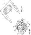
- FIG. 17is an isometric view of a jack contact set and guide frame according to a third embodiment of the connector as disclosed herein.
- FIG. 18is an isometric view of the jack contact set of FIG. 17 .
- FIG. 19is an isometric view of the guide frame of FIG. 17 .
- FIG. 20is an inverted isometric view of the jack contact set of FIG. 17 .
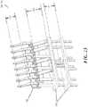
- FIG. 21is an isometric view of a jack contact set according to a fourth embodiment of the connector as disclosed herein.
- FIG. 22is a side view of the jack contact set of FIG. 21 .
- FIG. 23is an isometric view of a jack contact set according to a fifth embodiment of the connector as disclosed herein.
- FIG. 24is a side view of the jack contact set of FIG. 23 .
- FIG. 25is an isometric view of a jack contact set according to a sixth embodiment of the connector as disclosed herein.
- FIG. 26is a side view of the jack contact set of FIG. 25 .
- FIG. 27is an isometric view of a jack contact set according to a seventh embodiment of the connector as disclosed herein.
- FIG. 28is a side view of the jack contact set of FIG. 27 .
- FIG. 29is an isometric view of a jack contact set according to an eighth embodiment of the connector as disclosed herein.
- FIG. 30is a side view of the jack contact set of FIG. 29 .
- FIG. 31is a detail view of the flexible circuit board of the jack contact set of FIG. 29 .
- FIG. 32is a first view of a jack contact set according to a ninth embodiment of the connector as disclosed herein.
- FIG. 33is a second view of the jack contact set of FIG. 32 .
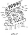
- FIG. 34is a third view of the jack contact set of FIG. 32 .
- FIGS. 1-34various exemplary embodiments of an invention may now be described in detail. Where the various figures may describe embodiments sharing various common elements and features with other embodiments, similar elements and features are given the same reference numerals and redundant description thereof may be omitted thereafter. The figures themselves are intended solely for the purposes of illustration, and are not limiting on the scope of an invention as disclosed herein unless otherwise expressly stated.
- embodiments of a modular jack design as disclosed hereincorrespond in mechanical details, size and shape to the industry standard RJ45 plug.
- the phase shift and corresponding signal degradationare minimized, as the primary compensation is in the immediate vicinity of the connector interface.
- each of the crosstalk compensation circuitsaddress a complete spectrum of the potential jack applications from about 10 to about 2000 MHz.
- various embodiments of a network interface connector 100 as disclosed hereinmay generally include a contact assembly 101 surrounded by an insulating guide frame 102 .
- the contact set 101 and guide frameare further mounted within a jack housing 104 .
- the jack housing 104holds the contact set 101 in proper orientation for engagement with the plug.
- a latching featuremay be provided within the housing 104 , enabling the plug to be easily attached and unattached to the jack by hand without the use of tools.
- the housingmay also have post features that locate the jack to a rigid PCB 103 , to which the contact set 101 is mounted.
- This PCB 103provides the circuit path to connect the contact set to either active equipment or transmission cables. Incorporated in this PCB 103 is secondary compensation that is needed for the system to meet the performance requirements.
- a helper spring 105may be provided.
- the helper spring 105may be isolated (insulated) from the jack contacts 101 , allowing it to add contact force without degrading the electrical performance.
- the helper spring 105may be a leaf spring that is mounted within the housing 104 between the housing internal wall and one or more over-molded contact carriers (further described below). This spring 105 acts in compression, bears on the inside back wall and applies a pre-loaded force to the contact set 101 . When the plug is inserted, the contact set 101 is deflected and simultaneously deflects the helper spring 105 .
- the total contact normal force for the jack systemconsists of the sum of the forces supplied by all of the contacts that comprise the contact set and the helper spring.
- a jack shield 106further provides an electrical ground path between the plug and the secondary compensation PCB 103 .
- This ground pathsurrounds the jack and protects the electrical signals contained within from outside interference (EMI, ESD, etc.).
- Spring-like panel ground features on the shieldextend the ground path by interconnecting to a conductive mounting panel or conductive shielding box (Faraday cage).
- a contact set 201that contribute to the improvement of the electrical performance of the system include short jack contacts 207 , short interconnecting branches 208 , first and second flexible circuit boards (FCBs) 209 , lead-in contact extensions 210 , a contact cross-over area 211 , and over-molded contact alignment members 212 .
- the contact set 201is contained within a jack housing 104 and provides the primary compensation for the interconnection of the plug to the secondary compensation and the output of the jack.
- the electrical length of the jack contacts 207may preferably be kept to a minimum. These jack contacts 207 interconnect the plug interface with the primary and secondary compensation. Short contacts do not typically lend themselves to the best mechanical performance, and therefore the jack contacts 207 of the disclosed design should provide good contact force to maintain stable, reliable electrical contact at the plug-jack interface. Short contacts are also typically stiff and easily overstressed. The jack contacts 207 of the present disclosure may accordingly be designed as thin and flexible to prevent overstressing and permanent deformation (yielding).
- branches 208connect primary compensation to the jack contact interface point 215 with the shortest possible electrical length, while retaining an offset of the primary compensation with respect to the signal path from the interface point 215 to the rigid PCB 103 .
- the branches 208may straddle the plastic barrier walls that are part of the plug specification, and may also be integral parts of the jack contacts 207 , thus eliminating the need for additional components to serve this purpose.
- the branches 208may be stamped and formed from the same piece of native base material. Alternatively, they could be formed separately and mechanically and electrically connected via welding, soldering, bonding, etc.
- FCBs 209Primary compensation is supplied to the jack connector in the first embodiment by a pair of FCBs 209 .
- the flexible nature of the FCBs 209allows for variation in the height of plug contacts while maintaining consistent and reliable contact force between the plug and jack contacts.
- These FCBs 209contain circuits connecting every other contact position with controlled capacitance. For example, one FCB 209 may supply capacitance to odd contacts (e.g., 1, 3, 5 and 7 in a typical 8-contact set), and the other supplies the compensation to the even contacts (e.g., 2, 4, 6, 8).
- the controlled capacitance in the FCBs 209cancels out the plug's resident capacitance between adjacent plug contacts.
- FCBs 209Using two FCBs 209 in the present embodiment enables simplification of the design of each FCB 209 , making them easier and less costly to produce, and further providing more direct connections to the compensation circuits and reducing the convolutions in the circuit paths needed to straddle the adjacent contacts and the electrical length of the compensation circuit. Shorter compensation circuit lengths better match phase and reduce the magnitude of the compensation needed to cancel the plug's resident capacitance.
- the individual FCBs 209have shorter electrical lengths, the mechanical distance between connection points (every other contact) are twice as long as a one piece FCB 209 that connects to every contact. This longer distance gives greater flexibility and significantly reduces the mechanical stress occurring during plug mating. Since each FCB 209 is only attached to four contacts, the contacts can move more independently, as opposed to a single FCB 209 that connects all eight contacts.
- one FCBapplies capacitance between contact positions 6 to 8, 6 to 4, and 6 to 2 (notice that position 6 is common to all).
- the other FCBapplies capacitance between contact positions 3 to 7, 3 to 5, and 3 to 1 (notice that position 3 is common to all).
- a flexible substrate 220may be composed of an insulating polymer with a controlled dielectric constant and thickness. This material provides the base foundation on which the FCB 209 is constructed. Top and bottom copper layers 221 , 222 are applied and bonded to this material 220 to control their location and any solder resist 225 is applied over the copper layers 221 , 222 .
- the top and bottom copper layers 221 , 222are conductive layers that are deposited and bonded to opposing sides of the substrate 220 and configured to provide the desired electrical properties. The bonding maintains the location and configuration during use and while being subjected to external bending forces.
- the common capacitor pad(position 6 is common to the even contacts and position 3 is common to the odd contacts) is located on the bottom copper layer 222 .
- the size of the capacitor pad on the bottom copper layer 222is larger than the size of the pads on the top copper layer 221 .
- the overlapping portions 223 of the top and bottom copper layers 221 , 222create three capacitance values when separated by a dielectric material (the flexible substrate layer 220 ). These three areas form what is referred to as parallel plate capacitors.
- the value of a parallel plate capacitoris a function of the overlapping area 223 , the distance between the copper plates, and the dielectric constant of the material that separates these plates.
- the area of the capacitor plates that are located on the top copper layer 221are smaller than the plate area on the bottom copper layer 222 . Since the capacitance is controlled by the area of the overlapping portion of the plates, the smaller plate dictates the capacitance value.
- the bottom plateis larger than the plate on the top copper layer 221 to allow for registration mismatch between the copper layers. As long as the smaller plate is within the envelope of the larger plate the effective area of the capacitor plates is maintained and thus the capacitance value will be constant.
- solder pads 226Surrounding the through holes in the FCBs 209 are copper solder pads 226 . These pads 226 provide surfaces for the solder to adhere to when the contacts are soldered to the FCBs 209 .
- the pads 226are on both top and bottom copper sides to assure that good connections are made. Having solder pads 226 on both sides provides both electrical and mechanical connection to the FCB 209 .
- the solder resist 225prevents the solder from adhering to unintended surfaces.
- the solder resist 225may be composed of non-conducting material laminates that cover portions of the copper layers 221 , 222 and the substrate 220 . These solder resist materials are selectively applied in the areas where exposed copper could also contact extraneous conductive materials and potentially cause short-circuits. In the areas where solder connections are desired (solder pads for instance) no solder resist material would be applied.
- the solder resistalso prevents high voltage arcs from forming and jumping the gaps between copper surfaces of different electrical potential.
- the contact branches 208 and their associated FCBs 209are the lead-in portion 210 of the jack contacts 207 .
- These lead-in portions 210engage with the plug as it is inserted and prior to full insertion.
- These lead-in portions 210guide the jack contacts 207 onto the plug contacts and prevent binding, buckling or mis-mating.
- the lead-ins 210are narrow to reduce contact-to-contact electrical coupling, keeping the contacts as short as possible.
- these lead-insmay be integral parts of the jack contacts 207 , thus eliminating the need for any additional components.
- the tails (signal output portions) 213 of the jack contacts 207are separated into two planes in the cross-over area 211 . Also in this area, the contacts 207 are jogged together and apart to control the coupling between pairs. Maintaining the location of the jack contacts 207 are two molded plastic insulating alignment members or carriers 212 . These carriers 212 hold the contacts in the cross-over area 211 in proper alignment and keep the electrical coupling in this area stable. Without these carriers 212 , the contacts 207 could deflect at different rates as the plug is inserted during mating. The contact carriers 212 keep the contacts moving together and moving in parallel.
- each jack contact 207includes a plug contact portion 215 extending a first direction from a first carrier, and a signal output portion 213 extending in the opposite direction from a second carrier, with the signal output portions 213 collectively arranged for connection to a rigid PCB 103 providing secondary compensation.
- an insulating frame 202Surrounding the contact set 201 is an insulating frame 202 . Slots in this frame locate the tips of the contact lead-ins 210 . These slots protect the contacts from foreign objects or misaligned plugs that may be forced into the jack. Small ribs on the frame engage with the plug interface and guide the plug into proper alignment.
- a second embodiment of the jack interface connector 300is now described with reference to FIGS. 11-16 .
- the second embodimentincorporates many features that are depicted in the first embodiment, primarily differing with respect to the contact assembly 301 and the contact guide frame 302 .
- the compensation FCBs 309are attached to interconnection lead-in tips 308 of the contacts, not to side branches.
- the jack contacts 307are extended with short curved portions 308 to provide mounting of the FCBs 309 at the ends 314 thereof.
- the FCBs 309are electrically and mechanically mounted via soldering, welding, or otherwise bonding.
- the contact portions 308connect primary compensation to the jack contact interface point.
- These branches 308should straddle the plastic barrier walls that are part of the plug specification.
- the bend transition between the contact 307 and the lead-in portion 308may preferably be gradual to best promote the mating of the plug contact without binding, buckling or mis-mating that can be caused by an abrupt surface change.
- These lead-in tips 308may be integral parts with respect to the jack contacts 307 , thus eliminating the need for additional components to serve this purpose.
- the tips 308may for example be stamped and formed from the same piece of native base material. Because the length and transition of the lead-in portion 308 is between the contact interface and the primary compensation, the electrical length should be kept short to reduce phase mismatch and/or excessive compensation capacitance.
- the contact set 301 according to the second embodimentis surrounded by an insulating frame 302 .
- Slots in this frame 302similarly locate the tips of the contact lead-ins 308 , and protect the contacts 301 from foreign objects or misaligned plugs that may be forced into the jack.
- the slots 302may preferably however be tighter than those described with respect to the first embodiment to better control and protect the shorter contact lead-in tips.
- a third embodiment of the jack interface connector 400is now described with reference to FIGS. 17-20 .
- the third embodimentis similar in most respects to the second embodiment, primarily differing with respect to the contact assembly 401 and the contact guide frame 402 in that the outer contacts 415 (e.g., in positions 1 and 8) are longer than the inner contacts 407 (e.g., in positions 2-7). This extra length allows these two outer contacts 415 to engage the mating plug earlier and act to guide the inter-mating of the plug and jack contacts. As the plug engages the outer contacts 415 , it is guided into position and the engagement of the shorter inner contacts 407 .
- the electrical performance of positions 1 and 8are less sensitive to changes in electrical length than the inner positions so these longer outer contacts have no derogatory effect on the electrical performance on the connector system as a whole.
- contact interconnection lead-in tips 416are provided at the end of the outer contacts 415 and the inner contacts 407 .
- the FCBs 409are modified accordingly.
- the additional trace length of positions 1 and 8does not significantly affect the overall electrical performance of the connector system.
- the contact guide frame 402is also modified from the second embodiment, wherein the slot length of the guide frame 402 varies to accommodate the differences in the contact lengths.
- a fourth embodiment of the jack interface connector 500is now described with reference to FIGS. 21-22 .
- the fourth embodimentis similar in most respects to the first embodiment, primarily differing with respect to the interconnection branches 508 of the contact assembly 501 . More particularly, these branches 508 are not only integral parts of the jack contacts 507 , thus eliminating the need for additional components to serve this purpose, but they are sheared out of a central portion 518 of the short jack contacts 507 and formed from the same piece of native base material.
- a fifth embodiment of the jack interface connector 600is now described with reference to FIGS. 23-24 .
- the fifth embodimentis similar in most respects to the first embodiment, primarily differing with respect to the contact assembly 601 .
- the contact assembly 601includes not only the series of contacts 607 a arranged to interface with the plug contacts, but also a second and parallel series of contacts 607 b . Since the primary contacts 607 a are preferably short, thin and flexible as described above, the set of secondary contacts 607 b is added to provide additional contact force and reliability. This may eliminate the need for a helper spring as previously described, and further eliminates the need for the interconnection branches described in the first embodiment. By removing the branches, the manufacturing complexity of the primary contacts may be reduced.
- the secondary jack contacts 607 bare short curved portions 608 that are extended to provide mounting of the FCBs 609 .
- the FCBs 609are electrically and mechanically mounted via soldering, welding, or otherwise bonding.
- the tips of the secondary contacts 607 bare in physical contact with the primary contacts 607 a and make short electrical connection between the primary compensation and the jack contact interface point. These tips should straddle the plastic barrier walls that are part of the plug specification.
- the bend transition of the secondary contacts 607 bno longer needs to be gradual since it does not make direct physical contact with the plug.
- the primary contact 607 aoffers a smooth and straight interface that will not bind, buckle or mis-mate that can otherwise be caused by an abrupt surface change.
- the portions 613 of the contacts that are inserted into the secondary compensation PCB 103are specially formed.
- the primary 607 a and secondary contacts 607 bare jogged in opposite directions so that they form a resilient interconnection pin.
- the distance between the jogged portionsis greater than the size of the receiving hole in the rigid PCB 103 .
- These pinsare forced into the smaller holes when the jack is assembled.
- the radial force of the sides of the holeprovides substantial reaction force on the primary 607 a and secondary 607 b contacts. This force maintains a stable interconnection and eliminates the need for a soldered joint, thus eliminating associated manufacturing operations and reducing cost.
- a sixth embodiment of the jack interface connector 700is now described with reference to FIGS. 25-26 .
- the sixth embodimentis similar in most respects to the first embodiment, primarily differing with respect to the interconnecting branches being eliminated in their previous form and incorporated in the transition 708 between the lead-in 710 and the short jack contacts 707 .
- the portion of the stamped contact array between the jack contact interface and the primary compensation FCBs 709should be as short as possible, and may be referred to herein as the short jack contact/contact lead-in transition area 708 .
- This transition area 708is accomplished by a short right angle jog in the native contact 707 . They are integral parts of the jack contacts 707 , thus eliminating the need for additional components to serve this purpose.
- This jogshould also straddle the plastic barrier walls that are part of the plug specification, yet provide a short direct electrical pathway.
- On one side of the jogis a flat surface to which the FCBs 709 are mounted via soldering, welding, or otherwise bonding, as may be performed by a “surface mounting” process as known in the art.
- a seventh embodiment of the jack interface connector 800is now described with reference to FIGS. 27-28 .
- the seventh embodimentis similar in most respects to the first embodiment, primarily differing in that there are separate contact tips 810 that perform the function of the interconnecting branches and the lead-in area.
- the contact tips 810are separate short curved structures applied to the ends of the short jack contacts 807 , and guide the plug, by way of the plug's plastic barrier walls, into position during the mating operation.
- the bend transition between the contact point and the lead-in portionmay preferably be gradual to best promote the mating of the plug contact without binding, buckling or mis-mating that can be caused by an abrupt surface change.
- Each lead-in tip 810contains a short interconnection branch 808 as an integral part, thus eliminating the need for additional components to serve this purpose.
- the tips 810are cut away to ensure that the capacitive coupling between neighboring tips remain at the lowest possible value.
- Each of the eight short interconnection branches 808 of the corresponding contact interconnection lead-in tips 810pass through a finger of the FCBs 809 and thus interconnects all eight of the tips 810 , the two FCBs 809 and the eight short jack contacts 807 with a minimum of bonding joints.
- These branches 808connect primary compensation to the jack contact interface point with the shortest possible electrical length.
- These branches 808may preferably straddle the plastic barrier walls that are part of the plug specification, and comprise integral parts of the jack contacts 807 , thus eliminating the need for additional components to serve this purpose.
- the branches 808may be sheared out of the central portion of the contact interconnection lead-in tips 810 and formed from the same piece of native base material.
- FIGS. 29-31An eighth embodiment of the jack interface connector 900 is now described with reference to FIGS. 29-31 .
- This eighth embodimentdiffers from the previous embodiments in that a single FCB 909 is electrically and physically coupled at a middle portion to an inner portion of each of the contacts 907 in the contact assembly 901 .
- Parallel capacitor plates 923are provided in the single FCB 909 , having overlapping areas in opposing ends with respect to the middle portion.
- the FCB 909further differs from previous embodiments in that it may be flexed from the middle portion on both opposing ends into an arcuate configuration.
- the primary compensating capacitance of the FCB 909is in immediate proximity with the plug interface but maintained outside of the signal path, defined by a plug interface (outer) portion of the contact 907 and an interface portion 913 with the secondary compensation PCB 103 .
- signals provided from the plugare transmitted through the jack contacts 907 to the rigid PCB 103 via ends 913 , but without traveling through the FCB 909 as being connected proximate to the plug interface but specifically offset set from the signal path.
- One desirable aspect of the offsetmay include that it introduces a controlled amount of inductance to the phase of the compensation circuit, approximately equal to the inductance of the corresponding plug contact blades. That compensating inductance allows the plug connector as disclosed herein to provide Near End Cross Talk compensation across very wide spectra from 10 to 2000 MHz. Exemplary offset dimensions in such an embodiment may range from 0.001′′ to 0.030′′.
- a ninth embodiment of the jack interface connector 1000is now described with reference to FIGS. 32-34 .
- a single FCB 1009is electrically and physically coupled at the respective tips 1009 of each of the contacts 1007 in the contact assembly 1001 .
- the FCB in an example as illustrated in FIG. 34includes an interior aperture having a serpentine configuration so as to provide gaps in the FCB substrate between each adjacent contact tip, and may further be flexed along at least one middle portion into a semi-arcuate form. The semi-arcuate form may facilitate engagement of the contacts and the FCB with the insulating frame 1002 of the assembly.
- the primary compensating capacitance of the FCB 1009is in immediate proximity with the plug interface but maintained outside of the signal path, defined by a plug interface (outer) portion of the contact 1007 and an interface portion 1013 with the secondary compensation PCB 1003 .
- signals provided from the plugare transmitted through the jack contacts 1007 to the rigid PCB 1003 via ends 1013 , but without traveling through the FCB 1009 as being connected proximate to the plug interface but specifically offset set from the signal path.
- a jack connector as disclosed hereinmay further be distinguishable on the basis of a reduced air gap between certain adjacent contacts, and one or more transverse insulators disposed there between.
- At least one pair of adjacent contactsare not separated along their respective lengths in an equidistant manner between the FCB 1009 and the secondary compensation PCB 1003 , but rather are jogged inward and towards each other.
- contacts 1007 a , 1007 b , 1007 g , and 1007 heach extend between the FCB and the secondary compensation PCB along parallel vertical planes (e.g., transversely disposed with respect to a “horizontal” plane of the PCB).
- Contacts 1007 c and 1007 eextend from the FCB in parallel planes, and then jog inwards toward each other before again turning and extending to the PCB along substantially parallel planes.
- Contacts 1007 d and 1007 flikewise extend from the FCB in parallel planes with respect to each other, and then jog inwards before again turning and extending to the PCB along substantially parallel planes with respect to each other.
- the inwardly extending configuration for at least a portion of the adjacent contactsresults in an air gap of, e.g., 0.009′′ (about 0.23 mm) there between, which would short circuit with the application of only 630 volts DC.
- a transverse insulator 1030is added in the form of a rib of plastic material between the aforementioned contacts at the inwardly extended portions.
- transverse insulatorrefers to an insulating barrier that may be positioned in the narrow gap between the adjacent contacts, and further extends along the air gap in a substantially transverse orientation with respect to the aforementioned plane of the PCB.
- the transverse insulatormay have portions of a non-transverse orientation within the scope of the present disclosure, such as for example in embodiments where the intended barrier may be integrally formed with respect to an insulating alignment member 1012 along the face of the PCB.
- the rib in an embodimentmay be 0.008′′ wide with a 0.0005′′ clearance at either side between the rib and the respective adjacent contacts.
- the ribmay in an embodiment be manufactured of liquid crystal polymer (LCP) plastic material having a dielectric strength of 812 volts per 0.001′′, wherein almost 6500 volts DC would be required to short circuit across the 0.008′′ wide rib of plastic.
- LCPliquid crystal polymer
- the transverse insulator 1030is not limited to application in association with the ninth embodiment of the connector 1000 as disclosed herein, but may further be applied for various other embodiments as disclosed herein, or foreseeable equivalents and modifications thereto. See for example the transverse insulator 930 as provided for the embodiment of FIGS. 29-31 , as well as first through seventh embodiments having inwardly jogged portions of at least first pairs of contacts in at least respective contact cross-over areas, wherein an appropriately configured transverse insulator may be provided for air gaps of less than 0.01′′ to prevent dielectric voltage breakdown.
Landscapes
- Engineering & Computer Science (AREA)
- Microelectronics & Electronic Packaging (AREA)
- Physics & Mathematics (AREA)
- Electromagnetism (AREA)
- Details Of Connecting Devices For Male And Female Coupling (AREA)
Abstract
Description
| ISO/TEC | ANSI/TIA-568-C.1 | FREQ. MAX. | ||
| 11801 | CATEGORY | CHARACTERIZATION | ||
| Class C | 3 | 16 | MHz | ||
| Class D | 5e | 100 | MHz | ||
| Class E | 6 | 250 | MHz | ||
| Class EA | 6A | 500 | MHz | ||
| Class F | 7 | 600 | MHz | ||
| Class FA | 7A | 1000 | MHz | ||
| Class I | 8.1 | 2000 | MHz | ||
| Class II | 8.2 | 2000 | MHz | ||
Claims (29)
Priority Applications (1)
| Application Number | Priority Date | Filing Date | Title |
|---|---|---|---|
| US16/259,455US10637196B2 (en) | 2015-11-11 | 2019-01-28 | Modular jack contact assembly having controlled capacitive coupling positioned within a jack housing |
Applications Claiming Priority (5)
| Application Number | Priority Date | Filing Date | Title |
|---|---|---|---|
| US201562254023P | 2015-11-11 | 2015-11-11 | |
| US201662297640P | 2016-02-19 | 2016-02-19 | |
| PCT/US2016/060963WO2017083287A1 (en) | 2015-11-11 | 2016-11-08 | Modular jack connector |
| US15/963,765US10424874B2 (en) | 2015-11-11 | 2018-04-26 | Modular jack connector with offset circuitry for controlled capacitance compensation |
| US16/259,455US10637196B2 (en) | 2015-11-11 | 2019-01-28 | Modular jack contact assembly having controlled capacitive coupling positioned within a jack housing |
Related Parent Applications (1)
| Application Number | Title | Priority Date | Filing Date |
|---|---|---|---|
| US15/963,765Continuation-In-PartUS10424874B2 (en) | 2015-11-11 | 2018-04-26 | Modular jack connector with offset circuitry for controlled capacitance compensation |
Publications (2)
| Publication Number | Publication Date |
|---|---|
| US20190157808A1 US20190157808A1 (en) | 2019-05-23 |
| US10637196B2true US10637196B2 (en) | 2020-04-28 |
Family
ID=66533371
Family Applications (1)
| Application Number | Title | Priority Date | Filing Date |
|---|---|---|---|
| US16/259,455ActiveUS10637196B2 (en) | 2015-11-11 | 2019-01-28 | Modular jack contact assembly having controlled capacitive coupling positioned within a jack housing |
Country Status (1)
| Country | Link |
|---|---|
| US (1) | US10637196B2 (en) |
Citations (63)
| Publication number | Priority date | Publication date | Assignee | Title |
|---|---|---|---|---|
| US4508410A (en) | 1981-12-01 | 1985-04-02 | Allied Corporation | Electrical termination system and connector member |
| EP0971459A2 (en) | 1998-06-30 | 2000-01-12 | Lucent Technologies Inc. | Communication plug having low complementary crosstalk delay |
| GB2343558A (en) | 1998-11-04 | 2000-05-10 | Itt Mfg Enterprises Inc | Electrical connector |
| US6231397B1 (en) | 1998-04-16 | 2001-05-15 | Thomas & Betts International, Inc. | Crosstalk reducing electrical jack and plug connector |
| US20010016455A1 (en) | 2000-02-21 | 2001-08-23 | Hans Reichle | Plug connector part |
| US6443777B1 (en)* | 2001-06-22 | 2002-09-03 | Avaya Technology Corp. | Inductive crosstalk compensation in a communication connector |
| EP1246318A2 (en) | 2001-03-28 | 2002-10-02 | Ortronics, Inc. | Dual reactance low noise modular connector insert |
| US20030134529A1 (en) | 2002-01-16 | 2003-07-17 | Murr Keith Mcquilkin | Connector with interchangeable impedance tuner |
| US20030194908A1 (en) | 2002-04-15 | 2003-10-16 | Brown Curtis D. | Compact serial -to ethernet conversion port |
| US20040023563A1 (en) | 2002-08-05 | 2004-02-05 | Andrew Ciezak | Vertical pcb jack with shield |
| US20040127105A1 (en) | 2002-09-27 | 2004-07-01 | Leviton Manufacturing Co., Inc. | Electrical connector jack |
| US6769937B1 (en)* | 2003-05-13 | 2004-08-03 | Molex Incorporated | Modular jack assembly for jack plugs with varying numbers of wires |
| US6877222B2 (en) | 1994-01-11 | 2005-04-12 | Stewart Connector Systems, Inc. | Method for manufacturing a high frequency electrical connector |
| WO2005101588A1 (en) | 2004-04-06 | 2005-10-27 | Panduit Corp. | Electrical connector with improved crosstalk compensation |
| US7038554B2 (en) | 2004-05-17 | 2006-05-02 | Leviton Manufacturing Co., Inc. | Crosstalk compensation with balancing capacitance system and method |
| US7048590B2 (en) | 2002-11-10 | 2006-05-23 | Bel Fuse Ltd. | High performance, high capacitance gain, jack connector for data transmission or the like |
| WO2006081423A1 (en) | 2005-01-28 | 2006-08-03 | Commscope Inc. Of North Carolina | Controlled mode conversion connector for reduced alien crosstalk |
| US7153163B2 (en) | 2002-07-16 | 2006-12-26 | Tyco Electronics Corporation | Modular jack for ethernet applications |
| US7166000B2 (en) | 2004-12-07 | 2007-01-23 | Commscope Solutions Properties, Llc | Communications connector with leadframe contact wires that compensate differential to common mode crosstalk |
| US20070040645A1 (en) | 2005-08-19 | 2007-02-22 | Sedio Stephen M | Transformer And Method Of Winding Same |
| US7190594B2 (en) | 2004-05-14 | 2007-03-13 | Commscope Solutions Properties, Llc | Next high frequency improvement by using frequency dependent effective capacitance |
| US20070217173A1 (en) | 2006-03-16 | 2007-09-20 | Fujitsu Limited | Circuit board |
| US7429195B2 (en) | 2007-02-16 | 2008-09-30 | Bel Fuse (Macao Commercial Offshore) Ltd. | Connector including isolation magnetic devices capable of handling high speed communications |
| US7485010B2 (en)* | 2007-06-14 | 2009-02-03 | Ortronics, Inc. | Modular connector exhibiting quad reactance balance functionality |
| US20090142968A1 (en) | 2007-09-12 | 2009-06-04 | Robert Ray Goodrich | Board Edge Termination Back-End Connection Assemblies and Communications Connectors Including Such Assemblies |
| US20090191740A1 (en)* | 2007-06-14 | 2009-07-30 | Ortronics, Inc. | Method For Accommodating Plugs With Different Contact Layout Geometries |
| US7601034B1 (en)* | 2008-05-07 | 2009-10-13 | Ortronics, Inc. | Modular insert and jack including moveable reactance section |
| US20090265918A1 (en) | 2008-04-23 | 2009-10-29 | Dounaevsky Oleg | System and method for automated production of rf chokes |
| US20100048040A1 (en) | 2008-08-20 | 2010-02-25 | Panduit Corp. | High-speed connector with multi-stage compensation |
| US7682203B1 (en)* | 2008-11-04 | 2010-03-23 | Commscope, Inc. Of North Carolina | Communications jacks having contact wire configurations that provide crosstalk compensation |
| US7686650B2 (en) | 2006-05-17 | 2010-03-30 | Bel Fuse Ltd. | High speed modular jack with flexible compensation circuit |
| CN201440501U (en) | 2009-06-23 | 2010-04-21 | 佛山市顺德区泛仕达机电有限公司 | a socket terminal |
| US7708603B1 (en)* | 2009-01-12 | 2010-05-04 | Hon Hai Precision Ind. Co., Ltd. | Electrical connector with improved crosstalk features |
| WO2010065588A1 (en) | 2008-12-02 | 2010-06-10 | Panduit Corp. | Method and system for improving crosstalk attenuation within a plug/jack connection and between nearby plug/jack combinations |
| US7857667B1 (en)* | 2009-11-19 | 2010-12-28 | Leviton Manufacturing Co., Inc. | Spring assembly with spring members biasing and capacitively coupling jack contacts |
| US7914346B2 (en)* | 2008-11-04 | 2011-03-29 | Commscope, Inc. Of North Carolina | Communications jacks having contact wire configurations that provide crosstalk compensation |
| US7924130B2 (en) | 2008-08-20 | 2011-04-12 | Bel Fuse (Macao Commercial Offshore) Limited | Isolation magnetic devices capable of handling high speed communications |
| US7967644B2 (en) | 2009-08-25 | 2011-06-28 | Tyco Electronics Corporation | Electrical connector with separable contacts |
| US7967645B2 (en)* | 2007-09-19 | 2011-06-28 | Leviton Manufacturing Co., Inc. | High speed data communications connector circuits, systems, and methods for reducing crosstalk in communications systems |
| US7976348B2 (en)* | 2008-05-07 | 2011-07-12 | Ortronics, Inc. | Modular insert and jack including moveable reactance section |
| US8033863B2 (en) | 2009-11-03 | 2011-10-11 | Bel Fuse (Macao Commercial Offshore) Limited | Modular connector plug having a wire guide filter with an impedance containing portion and a cable guide portion |
| US8077004B2 (en) | 2007-02-16 | 2011-12-13 | Bel Fuse (Macao Commercial Offshore) Limited | Electrical isolation device capable of limiting magnetic saturation even upon receipt of high power D.C. bias and, method for making the same and connector incorporating the same |
| US8128432B2 (en)* | 2008-07-28 | 2012-03-06 | Legrand France | Insert and method of assembling such an insert |
| US20120076459A1 (en) | 2010-09-28 | 2012-03-29 | Bel Fuse (Macao Commercial Offshore) Limited | Fiber Optic Cable Assembly And Methods |
| US20120100744A1 (en) | 2010-10-21 | 2012-04-26 | Panduit Corp. | Communication Plug with Improved Crosstalk |
| US20120156932A1 (en)* | 2007-12-19 | 2012-06-21 | Panduit Corp. | Method and System for Reducing Internal Crosstalk and Common Mode Signal Generation Within a Plug/Jack Combination |
| US8395329B2 (en) | 2009-09-09 | 2013-03-12 | Bel Fuse (Macao Commercial Offshore) | LED ballast power supply having digital controller |
| US8405481B2 (en) | 2010-02-23 | 2013-03-26 | Pulse Electronics, Inc. | Woven wire, inductive devices, and methods of manufacturing |
| US20130210288A1 (en) | 2012-02-13 | 2013-08-15 | Commscope, Inc. Of North Carolina | Small Form-Factor Modular Plugs with Low-Profile Surface Mounted Printed Circuit Board Plug Blades |
| US20130210289A1 (en) | 2012-02-13 | 2013-08-15 | Commscope, Inc. Of North Carolina | Communications Plugs Having Plug Blades with Staggered Current-Carrying Paths and Controlled Offending Crosstalk and Patch Cords Including Such Plugs |
| US20140011403A1 (en) | 2012-06-28 | 2014-01-09 | Belden Canada Inc. | Matched high-speed interconnector assembly |
| US20140073196A1 (en) | 2012-09-07 | 2014-03-13 | Commscope, Inc. Of North Carolina | High Performance Communications Jacks Having Crosstalk Compensation and/or Return Loss Improvement Circuitry |
| US20140203886A1 (en) | 2013-01-23 | 2014-07-24 | Commscope, Inc. Of North Carolina | Communications Connectors Including Transmission Lines Having Impedance Discontinuities that Improve Return Loss And/or Insertion Loss Performance and Related Methods |
| EP2765656A1 (en) | 2013-01-23 | 2014-08-13 | CommScope, Inc. of North Carolina | Patch cord |
| US20140227911A1 (en) | 2011-04-28 | 2014-08-14 | 3M Innovative Properties Company | Electrical Connector |
| US20140273657A1 (en) | 2013-03-14 | 2014-09-18 | Commscope, Inc. Of North Carolina | Communications plugs and patch cords with mode conversion control circuitry |
| US20140273629A1 (en) | 2013-03-14 | 2014-09-18 | Commscope, Inc. Of North Carolina | Communication plug having a plurality of coupled conductive paths |
| US9124101B2 (en) | 2013-04-02 | 2015-09-01 | Bel Fuse (Macao Commercial Offshore) Limited | Power supply having selectable operation based on communications with load |
| US20160020567A1 (en) | 2014-06-05 | 2016-01-21 | Bel Fuse (Macao Commercial Offshore) Ltd. | Network interface connector with proximity compensation |
| US20160093431A1 (en) | 2005-09-22 | 2016-03-31 | Radial Electronics, Inc. | Arrayed embedded magnetic components and methods |
| US20160172079A1 (en) | 2013-07-11 | 2016-06-16 | Christian Rohrer | Use of a cable for the transmission of audio signals |
| US20160187951A1 (en) | 2014-08-20 | 2016-06-30 | Bel Fuse (Macao Commercial Offshore) Ltd. | Power over ethernet for 10gbase-t ethernet |
| US9407044B2 (en) | 2004-03-12 | 2016-08-02 | Panduit Corp. | Method for reducing crosstalk in electrical connectors |
- 2019
- 2019-01-28USUS16/259,455patent/US10637196B2/enactiveActive
Patent Citations (68)
| Publication number | Priority date | Publication date | Assignee | Title |
|---|---|---|---|---|
| US4508410A (en) | 1981-12-01 | 1985-04-02 | Allied Corporation | Electrical termination system and connector member |
| US6877222B2 (en) | 1994-01-11 | 2005-04-12 | Stewart Connector Systems, Inc. | Method for manufacturing a high frequency electrical connector |
| US6231397B1 (en) | 1998-04-16 | 2001-05-15 | Thomas & Betts International, Inc. | Crosstalk reducing electrical jack and plug connector |
| EP0971459A2 (en) | 1998-06-30 | 2000-01-12 | Lucent Technologies Inc. | Communication plug having low complementary crosstalk delay |
| GB2343558A (en) | 1998-11-04 | 2000-05-10 | Itt Mfg Enterprises Inc | Electrical connector |
| US20010016455A1 (en) | 2000-02-21 | 2001-08-23 | Hans Reichle | Plug connector part |
| EP1246318A2 (en) | 2001-03-28 | 2002-10-02 | Ortronics, Inc. | Dual reactance low noise modular connector insert |
| US7037140B2 (en)* | 2001-03-28 | 2006-05-02 | Ortronics, Inc. | Dual reactance low noise modular connector insert |
| US6443777B1 (en)* | 2001-06-22 | 2002-09-03 | Avaya Technology Corp. | Inductive crosstalk compensation in a communication connector |
| US20030134529A1 (en) | 2002-01-16 | 2003-07-17 | Murr Keith Mcquilkin | Connector with interchangeable impedance tuner |
| US20030194908A1 (en) | 2002-04-15 | 2003-10-16 | Brown Curtis D. | Compact serial -to ethernet conversion port |
| US7153163B2 (en) | 2002-07-16 | 2006-12-26 | Tyco Electronics Corporation | Modular jack for ethernet applications |
| US20040023563A1 (en) | 2002-08-05 | 2004-02-05 | Andrew Ciezak | Vertical pcb jack with shield |
| US20040127105A1 (en) | 2002-09-27 | 2004-07-01 | Leviton Manufacturing Co., Inc. | Electrical connector jack |
| US7048590B2 (en) | 2002-11-10 | 2006-05-23 | Bel Fuse Ltd. | High performance, high capacitance gain, jack connector for data transmission or the like |
| US6769937B1 (en)* | 2003-05-13 | 2004-08-03 | Molex Incorporated | Modular jack assembly for jack plugs with varying numbers of wires |
| US9407044B2 (en) | 2004-03-12 | 2016-08-02 | Panduit Corp. | Method for reducing crosstalk in electrical connectors |
| US7153168B2 (en) | 2004-04-06 | 2006-12-26 | Panduit Corp. | Electrical connector with improved crosstalk compensation |
| WO2005101588A1 (en) | 2004-04-06 | 2005-10-27 | Panduit Corp. | Electrical connector with improved crosstalk compensation |
| US7190594B2 (en) | 2004-05-14 | 2007-03-13 | Commscope Solutions Properties, Llc | Next high frequency improvement by using frequency dependent effective capacitance |
| US7038554B2 (en) | 2004-05-17 | 2006-05-02 | Leviton Manufacturing Co., Inc. | Crosstalk compensation with balancing capacitance system and method |
| US7166000B2 (en) | 2004-12-07 | 2007-01-23 | Commscope Solutions Properties, Llc | Communications connector with leadframe contact wires that compensate differential to common mode crosstalk |
| WO2006081423A1 (en) | 2005-01-28 | 2006-08-03 | Commscope Inc. Of North Carolina | Controlled mode conversion connector for reduced alien crosstalk |
| US20070040645A1 (en) | 2005-08-19 | 2007-02-22 | Sedio Stephen M | Transformer And Method Of Winding Same |
| US20160093431A1 (en) | 2005-09-22 | 2016-03-31 | Radial Electronics, Inc. | Arrayed embedded magnetic components and methods |
| US20070217173A1 (en) | 2006-03-16 | 2007-09-20 | Fujitsu Limited | Circuit board |
| US7686650B2 (en) | 2006-05-17 | 2010-03-30 | Bel Fuse Ltd. | High speed modular jack with flexible compensation circuit |
| US8077004B2 (en) | 2007-02-16 | 2011-12-13 | Bel Fuse (Macao Commercial Offshore) Limited | Electrical isolation device capable of limiting magnetic saturation even upon receipt of high power D.C. bias and, method for making the same and connector incorporating the same |
| US7429195B2 (en) | 2007-02-16 | 2008-09-30 | Bel Fuse (Macao Commercial Offshore) Ltd. | Connector including isolation magnetic devices capable of handling high speed communications |
| US20090191740A1 (en)* | 2007-06-14 | 2009-07-30 | Ortronics, Inc. | Method For Accommodating Plugs With Different Contact Layout Geometries |
| US7485010B2 (en)* | 2007-06-14 | 2009-02-03 | Ortronics, Inc. | Modular connector exhibiting quad reactance balance functionality |
| US20090142968A1 (en) | 2007-09-12 | 2009-06-04 | Robert Ray Goodrich | Board Edge Termination Back-End Connection Assemblies and Communications Connectors Including Such Assemblies |
| US7967645B2 (en)* | 2007-09-19 | 2011-06-28 | Leviton Manufacturing Co., Inc. | High speed data communications connector circuits, systems, and methods for reducing crosstalk in communications systems |
| US20120156932A1 (en)* | 2007-12-19 | 2012-06-21 | Panduit Corp. | Method and System for Reducing Internal Crosstalk and Common Mode Signal Generation Within a Plug/Jack Combination |
| US20090265918A1 (en) | 2008-04-23 | 2009-10-29 | Dounaevsky Oleg | System and method for automated production of rf chokes |
| US7601034B1 (en)* | 2008-05-07 | 2009-10-13 | Ortronics, Inc. | Modular insert and jack including moveable reactance section |
| US7976348B2 (en)* | 2008-05-07 | 2011-07-12 | Ortronics, Inc. | Modular insert and jack including moveable reactance section |
| US8128432B2 (en)* | 2008-07-28 | 2012-03-06 | Legrand France | Insert and method of assembling such an insert |
| US7924130B2 (en) | 2008-08-20 | 2011-04-12 | Bel Fuse (Macao Commercial Offshore) Limited | Isolation magnetic devices capable of handling high speed communications |
| US8137141B2 (en)* | 2008-08-20 | 2012-03-20 | Panduit Corp. | High-speed connector with multi-stage compensation |
| US20100048040A1 (en) | 2008-08-20 | 2010-02-25 | Panduit Corp. | High-speed connector with multi-stage compensation |
| US7914346B2 (en)* | 2008-11-04 | 2011-03-29 | Commscope, Inc. Of North Carolina | Communications jacks having contact wire configurations that provide crosstalk compensation |
| US7682203B1 (en)* | 2008-11-04 | 2010-03-23 | Commscope, Inc. Of North Carolina | Communications jacks having contact wire configurations that provide crosstalk compensation |
| WO2010065588A1 (en) | 2008-12-02 | 2010-06-10 | Panduit Corp. | Method and system for improving crosstalk attenuation within a plug/jack connection and between nearby plug/jack combinations |
| US8167661B2 (en)* | 2008-12-02 | 2012-05-01 | Panduit Corp. | Method and system for improving crosstalk attenuation within a plug/jack connection and between nearby plug/jack combinations |
| US7708603B1 (en)* | 2009-01-12 | 2010-05-04 | Hon Hai Precision Ind. Co., Ltd. | Electrical connector with improved crosstalk features |
| CN201440501U (en) | 2009-06-23 | 2010-04-21 | 佛山市顺德区泛仕达机电有限公司 | a socket terminal |
| US7967644B2 (en) | 2009-08-25 | 2011-06-28 | Tyco Electronics Corporation | Electrical connector with separable contacts |
| US8395329B2 (en) | 2009-09-09 | 2013-03-12 | Bel Fuse (Macao Commercial Offshore) | LED ballast power supply having digital controller |
| US8033863B2 (en) | 2009-11-03 | 2011-10-11 | Bel Fuse (Macao Commercial Offshore) Limited | Modular connector plug having a wire guide filter with an impedance containing portion and a cable guide portion |
| US7857667B1 (en)* | 2009-11-19 | 2010-12-28 | Leviton Manufacturing Co., Inc. | Spring assembly with spring members biasing and capacitively coupling jack contacts |
| US8405481B2 (en) | 2010-02-23 | 2013-03-26 | Pulse Electronics, Inc. | Woven wire, inductive devices, and methods of manufacturing |
| US20120076459A1 (en) | 2010-09-28 | 2012-03-29 | Bel Fuse (Macao Commercial Offshore) Limited | Fiber Optic Cable Assembly And Methods |
| US20120100744A1 (en) | 2010-10-21 | 2012-04-26 | Panduit Corp. | Communication Plug with Improved Crosstalk |
| US20140227911A1 (en) | 2011-04-28 | 2014-08-14 | 3M Innovative Properties Company | Electrical Connector |
| US20130210288A1 (en) | 2012-02-13 | 2013-08-15 | Commscope, Inc. Of North Carolina | Small Form-Factor Modular Plugs with Low-Profile Surface Mounted Printed Circuit Board Plug Blades |
| US20130210289A1 (en) | 2012-02-13 | 2013-08-15 | Commscope, Inc. Of North Carolina | Communications Plugs Having Plug Blades with Staggered Current-Carrying Paths and Controlled Offending Crosstalk and Patch Cords Including Such Plugs |
| US20140011403A1 (en) | 2012-06-28 | 2014-01-09 | Belden Canada Inc. | Matched high-speed interconnector assembly |
| US8951072B2 (en)* | 2012-09-07 | 2015-02-10 | Commscope, Inc. Of North Carolina | Communication jacks having longitudinally staggered jackwire contacts |
| US20140073196A1 (en) | 2012-09-07 | 2014-03-13 | Commscope, Inc. Of North Carolina | High Performance Communications Jacks Having Crosstalk Compensation and/or Return Loss Improvement Circuitry |
| EP2765656A1 (en) | 2013-01-23 | 2014-08-13 | CommScope, Inc. of North Carolina | Patch cord |
| US20140203886A1 (en) | 2013-01-23 | 2014-07-24 | Commscope, Inc. Of North Carolina | Communications Connectors Including Transmission Lines Having Impedance Discontinuities that Improve Return Loss And/or Insertion Loss Performance and Related Methods |
| US20140273657A1 (en) | 2013-03-14 | 2014-09-18 | Commscope, Inc. Of North Carolina | Communications plugs and patch cords with mode conversion control circuitry |
| US20140273629A1 (en) | 2013-03-14 | 2014-09-18 | Commscope, Inc. Of North Carolina | Communication plug having a plurality of coupled conductive paths |
| US9124101B2 (en) | 2013-04-02 | 2015-09-01 | Bel Fuse (Macao Commercial Offshore) Limited | Power supply having selectable operation based on communications with load |
| US20160172079A1 (en) | 2013-07-11 | 2016-06-16 | Christian Rohrer | Use of a cable for the transmission of audio signals |
| US20160020567A1 (en) | 2014-06-05 | 2016-01-21 | Bel Fuse (Macao Commercial Offshore) Ltd. | Network interface connector with proximity compensation |
| US20160187951A1 (en) | 2014-08-20 | 2016-06-30 | Bel Fuse (Macao Commercial Offshore) Ltd. | Power over ethernet for 10gbase-t ethernet |
Non-Patent Citations (4)
| Title |
|---|
| International Search Report and Written Opinion for International Application PCT/US2016/043334, dated Aug. 4, 2017, 9 pages. |
| International Search Report and Written Opinion for International Application PCT/US2018/025858, dated Jun. 22, 2018, 13 pages. |
| International Search Report for International Application PCT/US2016/060963, dated Feb. 17, 2017, 13 pages. |
| Search Report for CN201680078668.5 dated Apr. 3, 2019 with English translation. |
Also Published As
| Publication number | Publication date |
|---|---|
| US20190157808A1 (en) | 2019-05-23 |
Similar Documents
| Publication | Publication Date | Title |
|---|---|---|
| US9819124B2 (en) | Low crosstalk printed circuit board based communications plugs and patch cords including such plugs | |
| US8047879B2 (en) | Printed wiring boards and communication connectors having series inductor-capacitor crosstalk compensation circuits that share a common inductor | |
| US9825406B2 (en) | Methods of manufacture of communication connectors and communication connector circuits | |
| US10050383B2 (en) | Communication connectors | |
| US9337583B2 (en) | Communications jacks having conductive paths with the same current direction that inductively and capacitively couple | |
| US8864532B2 (en) | Communications jacks having low crosstalk and/or solder-less wire connection assemblies | |
| US7985103B2 (en) | Communication connector with improved crosstalk communication | |
| US9419391B2 (en) | Communication connector | |
| CN105051988B (en) | Communication plug and patch cord with mode switching control circuit | |
| US10424874B2 (en) | Modular jack connector with offset circuitry for controlled capacitance compensation | |
| US8353723B2 (en) | Communications patching devices having capacitor-based multi-stage near-end alien crosstalk compensation circuits between adjacent connector ports | |
| US9246274B2 (en) | Communication connectors having crosstalk compensation networks | |
| CN103944022A (en) | Communications plugs having plug blades with staggered current-carrying paths and controlled offending crosstalk and patch cords including such plugs | |
| US10439329B2 (en) | Modular connector plug for high speed data transmission networks | |
| US10530106B2 (en) | Modular plug connector with multilayer PCB for very high speed applications | |
| US10637196B2 (en) | Modular jack contact assembly having controlled capacitive coupling positioned within a jack housing | |
| US10734765B2 (en) | Connector with capacitive crosstalk compensation |
Legal Events
| Date | Code | Title | Description |
|---|---|---|---|
| FEPP | Fee payment procedure | Free format text:ENTITY STATUS SET TO UNDISCOUNTED (ORIGINAL EVENT CODE: BIG.); ENTITY STATUS OF PATENT OWNER: LARGE ENTITY | |
| AS | Assignment | Owner name:BEL FUSE (MACAO COMMERCIAL OFFSHORE) LIMITED, MACA Free format text:ASSIGNMENT OF ASSIGNORS INTEREST;ASSIGNORS:BAUM, ANDREW DAVID;BELOPOLSKY, YAKOV;ELLIS, MARK;AND OTHERS;SIGNING DATES FROM 20180516 TO 20181128;REEL/FRAME:048163/0775 Owner name:BEL FUSE (MACAO COMMERCIAL OFFSHORE) LIMITED, MACAU Free format text:ASSIGNMENT OF ASSIGNORS INTEREST;ASSIGNORS:BAUM, ANDREW DAVID;BELOPOLSKY, YAKOV;ELLIS, MARK;AND OTHERS;SIGNING DATES FROM 20180516 TO 20181128;REEL/FRAME:048163/0775 | |
| STPP | Information on status: patent application and granting procedure in general | Free format text:DOCKETED NEW CASE - READY FOR EXAMINATION | |
| STPP | Information on status: patent application and granting procedure in general | Free format text:NON FINAL ACTION MAILED | |
| STPP | Information on status: patent application and granting procedure in general | Free format text:RESPONSE TO NON-FINAL OFFICE ACTION ENTERED AND FORWARDED TO EXAMINER | |
| STCF | Information on status: patent grant | Free format text:PATENTED CASE | |
| AS | Assignment | Owner name:KEYBANK NATIONAL ASSOCIATION, AS ADMINISTRATIVE AGENT, OHIO Free format text:SECURITY INTEREST;ASSIGNOR:BEL FUSE INC.;REEL/FRAME:058917/0452 Effective date:20210902 | |
| MAFP | Maintenance fee payment | Free format text:PAYMENT OF MAINTENANCE FEE, 4TH YEAR, LARGE ENTITY (ORIGINAL EVENT CODE: M1551); ENTITY STATUS OF PATENT OWNER: LARGE ENTITY Year of fee payment:4 |