US10636757B2 - Integrated circuit component package and method of fabricating the same - Google Patents
Integrated circuit component package and method of fabricating the sameDownload PDFInfo
- Publication number
- US10636757B2 US10636757B2US15/690,196US201715690196AUS10636757B2US 10636757 B2US10636757 B2US 10636757B2US 201715690196 AUS201715690196 AUS 201715690196AUS 10636757 B2US10636757 B2US 10636757B2
- Authority
- US
- United States
- Prior art keywords
- layer
- alignment mark
- conductive
- integrated circuit
- openings
- Prior art date
- Legal status (The legal status is an assumption and is not a legal conclusion. Google has not performed a legal analysis and makes no representation as to the accuracy of the status listed.)
- Active
Links
Images


Classifications
- H—ELECTRICITY
- H01—ELECTRIC ELEMENTS
- H01L—SEMICONDUCTOR DEVICES NOT COVERED BY CLASS H10
- H01L24/00—Arrangements for connecting or disconnecting semiconductor or solid-state bodies; Methods or apparatus related thereto
- H01L24/01—Means for bonding being attached to, or being formed on, the surface to be connected, e.g. chip-to-package, die-attach, "first-level" interconnects; Manufacturing methods related thereto
- H01L24/02—Bonding areas ; Manufacturing methods related thereto
- H01L24/07—Structure, shape, material or disposition of the bonding areas after the connecting process
- H01L24/09—Structure, shape, material or disposition of the bonding areas after the connecting process of a plurality of bonding areas
- H—ELECTRICITY
- H01—ELECTRIC ELEMENTS
- H01L—SEMICONDUCTOR DEVICES NOT COVERED BY CLASS H10
- H01L23/00—Details of semiconductor or other solid state devices
- H01L23/28—Encapsulations, e.g. encapsulating layers, coatings, e.g. for protection
- H01L23/31—Encapsulations, e.g. encapsulating layers, coatings, e.g. for protection characterised by the arrangement or shape
- H01L23/3107—Encapsulations, e.g. encapsulating layers, coatings, e.g. for protection characterised by the arrangement or shape the device being completely enclosed
- H—ELECTRICITY
- H01—ELECTRIC ELEMENTS
- H01L—SEMICONDUCTOR DEVICES NOT COVERED BY CLASS H10
- H01L21/00—Processes or apparatus adapted for the manufacture or treatment of semiconductor or solid state devices or of parts thereof
- H01L21/02—Manufacture or treatment of semiconductor devices or of parts thereof
- H01L21/04—Manufacture or treatment of semiconductor devices or of parts thereof the devices having potential barriers, e.g. a PN junction, depletion layer or carrier concentration layer
- H01L21/50—Assembly of semiconductor devices using processes or apparatus not provided for in a single one of the groups H01L21/18 - H01L21/326 or H10D48/04 - H10D48/07 e.g. sealing of a cap to a base of a container
- H01L21/56—Encapsulations, e.g. encapsulation layers, coatings
- H01L21/561—Batch processing
- H—ELECTRICITY
- H01—ELECTRIC ELEMENTS
- H01L—SEMICONDUCTOR DEVICES NOT COVERED BY CLASS H10
- H01L21/00—Processes or apparatus adapted for the manufacture or treatment of semiconductor or solid state devices or of parts thereof
- H01L21/02—Manufacture or treatment of semiconductor devices or of parts thereof
- H01L21/04—Manufacture or treatment of semiconductor devices or of parts thereof the devices having potential barriers, e.g. a PN junction, depletion layer or carrier concentration layer
- H01L21/50—Assembly of semiconductor devices using processes or apparatus not provided for in a single one of the groups H01L21/18 - H01L21/326 or H10D48/04 - H10D48/07 e.g. sealing of a cap to a base of a container
- H01L21/56—Encapsulations, e.g. encapsulation layers, coatings
- H01L21/568—Temporary substrate used as encapsulation process aid
- H—ELECTRICITY
- H01—ELECTRIC ELEMENTS
- H01L—SEMICONDUCTOR DEVICES NOT COVERED BY CLASS H10
- H01L21/00—Processes or apparatus adapted for the manufacture or treatment of semiconductor or solid state devices or of parts thereof
- H01L21/67—Apparatus specially adapted for handling semiconductor or electric solid state devices during manufacture or treatment thereof; Apparatus specially adapted for handling wafers during manufacture or treatment of semiconductor or electric solid state devices or components ; Apparatus not specifically provided for elsewhere
- H01L21/683—Apparatus specially adapted for handling semiconductor or electric solid state devices during manufacture or treatment thereof; Apparatus specially adapted for handling wafers during manufacture or treatment of semiconductor or electric solid state devices or components ; Apparatus not specifically provided for elsewhere for supporting or gripping
- H01L21/6835—Apparatus specially adapted for handling semiconductor or electric solid state devices during manufacture or treatment thereof; Apparatus specially adapted for handling wafers during manufacture or treatment of semiconductor or electric solid state devices or components ; Apparatus not specifically provided for elsewhere for supporting or gripping using temporarily an auxiliary support
- H—ELECTRICITY
- H01—ELECTRIC ELEMENTS
- H01L—SEMICONDUCTOR DEVICES NOT COVERED BY CLASS H10
- H01L21/00—Processes or apparatus adapted for the manufacture or treatment of semiconductor or solid state devices or of parts thereof
- H01L21/70—Manufacture or treatment of devices consisting of a plurality of solid state components formed in or on a common substrate or of parts thereof; Manufacture of integrated circuit devices or of parts thereof
- H01L21/71—Manufacture of specific parts of devices defined in group H01L21/70
- H01L21/768—Applying interconnections to be used for carrying current between separate components within a device comprising conductors and dielectrics
- H01L21/76801—Applying interconnections to be used for carrying current between separate components within a device comprising conductors and dielectrics characterised by the formation and the after-treatment of the dielectrics, e.g. smoothing
- H01L21/76819—Smoothing of the dielectric
- H—ELECTRICITY
- H01—ELECTRIC ELEMENTS
- H01L—SEMICONDUCTOR DEVICES NOT COVERED BY CLASS H10
- H01L21/00—Processes or apparatus adapted for the manufacture or treatment of semiconductor or solid state devices or of parts thereof
- H01L21/70—Manufacture or treatment of devices consisting of a plurality of solid state components formed in or on a common substrate or of parts thereof; Manufacture of integrated circuit devices or of parts thereof
- H01L21/71—Manufacture of specific parts of devices defined in group H01L21/70
- H01L21/768—Applying interconnections to be used for carrying current between separate components within a device comprising conductors and dielectrics
- H01L21/76801—Applying interconnections to be used for carrying current between separate components within a device comprising conductors and dielectrics characterised by the formation and the after-treatment of the dielectrics, e.g. smoothing
- H01L21/76837—Filling up the space between adjacent conductive structures; Gap-filling properties of dielectrics
- H—ELECTRICITY
- H01—ELECTRIC ELEMENTS
- H01L—SEMICONDUCTOR DEVICES NOT COVERED BY CLASS H10
- H01L23/00—Details of semiconductor or other solid state devices
- H01L23/28—Encapsulations, e.g. encapsulating layers, coatings, e.g. for protection
- H01L23/31—Encapsulations, e.g. encapsulating layers, coatings, e.g. for protection characterised by the arrangement or shape
- H01L23/3107—Encapsulations, e.g. encapsulating layers, coatings, e.g. for protection characterised by the arrangement or shape the device being completely enclosed
- H01L23/3121—Encapsulations, e.g. encapsulating layers, coatings, e.g. for protection characterised by the arrangement or shape the device being completely enclosed a substrate forming part of the encapsulation
- H—ELECTRICITY
- H01—ELECTRIC ELEMENTS
- H01L—SEMICONDUCTOR DEVICES NOT COVERED BY CLASS H10
- H01L23/00—Details of semiconductor or other solid state devices
- H01L23/28—Encapsulations, e.g. encapsulating layers, coatings, e.g. for protection
- H01L23/31—Encapsulations, e.g. encapsulating layers, coatings, e.g. for protection characterised by the arrangement or shape
- H01L23/3157—Partial encapsulation or coating
- H01L23/3171—Partial encapsulation or coating the coating being directly applied to the semiconductor body, e.g. passivation layer
- H—ELECTRICITY
- H01—ELECTRIC ELEMENTS
- H01L—SEMICONDUCTOR DEVICES NOT COVERED BY CLASS H10
- H01L23/00—Details of semiconductor or other solid state devices
- H01L23/48—Arrangements for conducting electric current to or from the solid state body in operation, e.g. leads, terminal arrangements ; Selection of materials therefor
- H01L23/488—Arrangements for conducting electric current to or from the solid state body in operation, e.g. leads, terminal arrangements ; Selection of materials therefor consisting of soldered or bonded constructions
- H01L23/498—Leads, i.e. metallisations or lead-frames on insulating substrates, e.g. chip carriers
- H01L23/49811—Additional leads joined to the metallisation on the insulating substrate, e.g. pins, bumps, wires, flat leads
- H01L23/49816—Spherical bumps on the substrate for external connection, e.g. ball grid arrays [BGA]
- H—ELECTRICITY
- H01—ELECTRIC ELEMENTS
- H01L—SEMICONDUCTOR DEVICES NOT COVERED BY CLASS H10
- H01L23/00—Details of semiconductor or other solid state devices
- H01L23/48—Arrangements for conducting electric current to or from the solid state body in operation, e.g. leads, terminal arrangements ; Selection of materials therefor
- H01L23/488—Arrangements for conducting electric current to or from the solid state body in operation, e.g. leads, terminal arrangements ; Selection of materials therefor consisting of soldered or bonded constructions
- H01L23/498—Leads, i.e. metallisations or lead-frames on insulating substrates, e.g. chip carriers
- H01L23/49827—Via connections through the substrates, e.g. pins going through the substrate, coaxial cables
- H—ELECTRICITY
- H01—ELECTRIC ELEMENTS
- H01L—SEMICONDUCTOR DEVICES NOT COVERED BY CLASS H10
- H01L23/00—Details of semiconductor or other solid state devices
- H01L23/52—Arrangements for conducting electric current within the device in operation from one component to another, i.e. interconnections, e.g. wires, lead frames
- H01L23/522—Arrangements for conducting electric current within the device in operation from one component to another, i.e. interconnections, e.g. wires, lead frames including external interconnections consisting of a multilayer structure of conductive and insulating layers inseparably formed on the semiconductor body
- H01L23/5226—Via connections in a multilevel interconnection structure
- H—ELECTRICITY
- H01—ELECTRIC ELEMENTS
- H01L—SEMICONDUCTOR DEVICES NOT COVERED BY CLASS H10
- H01L23/00—Details of semiconductor or other solid state devices
- H01L23/52—Arrangements for conducting electric current within the device in operation from one component to another, i.e. interconnections, e.g. wires, lead frames
- H01L23/538—Arrangements for conducting electric current within the device in operation from one component to another, i.e. interconnections, e.g. wires, lead frames the interconnection structure between a plurality of semiconductor chips being formed on, or in, insulating substrates
- H01L23/5389—Arrangements for conducting electric current within the device in operation from one component to another, i.e. interconnections, e.g. wires, lead frames the interconnection structure between a plurality of semiconductor chips being formed on, or in, insulating substrates the chips being integrally enclosed by the interconnect and support structures
- H—ELECTRICITY
- H01—ELECTRIC ELEMENTS
- H01L—SEMICONDUCTOR DEVICES NOT COVERED BY CLASS H10
- H01L23/00—Details of semiconductor or other solid state devices
- H01L23/544—Marks applied to semiconductor devices or parts, e.g. registration marks, alignment structures, wafer maps
- H—ELECTRICITY
- H01—ELECTRIC ELEMENTS
- H01L—SEMICONDUCTOR DEVICES NOT COVERED BY CLASS H10
- H01L24/00—Arrangements for connecting or disconnecting semiconductor or solid-state bodies; Methods or apparatus related thereto
- H01L24/01—Means for bonding being attached to, or being formed on, the surface to be connected, e.g. chip-to-package, die-attach, "first-level" interconnects; Manufacturing methods related thereto
- H01L24/10—Bump connectors ; Manufacturing methods related thereto
- H01L24/11—Manufacturing methods
- H—ELECTRICITY
- H01—ELECTRIC ELEMENTS
- H01L—SEMICONDUCTOR DEVICES NOT COVERED BY CLASS H10
- H01L24/00—Arrangements for connecting or disconnecting semiconductor or solid-state bodies; Methods or apparatus related thereto
- H01L24/01—Means for bonding being attached to, or being formed on, the surface to be connected, e.g. chip-to-package, die-attach, "first-level" interconnects; Manufacturing methods related thereto
- H01L24/10—Bump connectors ; Manufacturing methods related thereto
- H01L24/12—Structure, shape, material or disposition of the bump connectors prior to the connecting process
- H01L24/14—Structure, shape, material or disposition of the bump connectors prior to the connecting process of a plurality of bump connectors
- H—ELECTRICITY
- H01—ELECTRIC ELEMENTS
- H01L—SEMICONDUCTOR DEVICES NOT COVERED BY CLASS H10
- H01L24/00—Arrangements for connecting or disconnecting semiconductor or solid-state bodies; Methods or apparatus related thereto
- H01L24/01—Means for bonding being attached to, or being formed on, the surface to be connected, e.g. chip-to-package, die-attach, "first-level" interconnects; Manufacturing methods related thereto
- H01L24/18—High density interconnect [HDI] connectors; Manufacturing methods related thereto
- H01L24/19—Manufacturing methods of high density interconnect preforms
- H—ELECTRICITY
- H01—ELECTRIC ELEMENTS
- H01L—SEMICONDUCTOR DEVICES NOT COVERED BY CLASS H10
- H01L24/00—Arrangements for connecting or disconnecting semiconductor or solid-state bodies; Methods or apparatus related thereto
- H01L24/01—Means for bonding being attached to, or being formed on, the surface to be connected, e.g. chip-to-package, die-attach, "first-level" interconnects; Manufacturing methods related thereto
- H01L24/18—High density interconnect [HDI] connectors; Manufacturing methods related thereto
- H01L24/20—Structure, shape, material or disposition of high density interconnect preforms
- H—ELECTRICITY
- H01—ELECTRIC ELEMENTS
- H01L—SEMICONDUCTOR DEVICES NOT COVERED BY CLASS H10
- H01L24/00—Arrangements for connecting or disconnecting semiconductor or solid-state bodies; Methods or apparatus related thereto
- H01L24/93—Batch processes
- H01L24/95—Batch processes at chip-level, i.e. with connecting carried out on a plurality of singulated devices, i.e. on diced chips
- H01L24/96—Batch processes at chip-level, i.e. with connecting carried out on a plurality of singulated devices, i.e. on diced chips the devices being encapsulated in a common layer, e.g. neo-wafer or pseudo-wafer, said common layer being separable into individual assemblies after connecting
- H—ELECTRICITY
- H01—ELECTRIC ELEMENTS
- H01L—SEMICONDUCTOR DEVICES NOT COVERED BY CLASS H10
- H01L25/00—Assemblies consisting of a plurality of semiconductor or other solid state devices
- H01L25/03—Assemblies consisting of a plurality of semiconductor or other solid state devices all the devices being of a type provided for in a single subclass of subclasses H10B, H10D, H10F, H10H, H10K or H10N, e.g. assemblies of rectifier diodes
- H01L25/04—Assemblies consisting of a plurality of semiconductor or other solid state devices all the devices being of a type provided for in a single subclass of subclasses H10B, H10D, H10F, H10H, H10K or H10N, e.g. assemblies of rectifier diodes the devices not having separate containers
- H01L25/065—Assemblies consisting of a plurality of semiconductor or other solid state devices all the devices being of a type provided for in a single subclass of subclasses H10B, H10D, H10F, H10H, H10K or H10N, e.g. assemblies of rectifier diodes the devices not having separate containers the devices being of a type provided for in group H10D89/00
- H01L25/0657—Stacked arrangements of devices
- H—ELECTRICITY
- H01—ELECTRIC ELEMENTS
- H01L—SEMICONDUCTOR DEVICES NOT COVERED BY CLASS H10
- H01L2221/00—Processes or apparatus adapted for the manufacture or treatment of semiconductor or solid state devices or of parts thereof covered by H01L21/00
- H01L2221/67—Apparatus for handling semiconductor or electric solid state devices during manufacture or treatment thereof; Apparatus for handling wafers during manufacture or treatment of semiconductor or electric solid state devices or components; Apparatus not specifically provided for elsewhere
- H01L2221/683—Apparatus for handling semiconductor or electric solid state devices during manufacture or treatment thereof; Apparatus for handling wafers during manufacture or treatment of semiconductor or electric solid state devices or components; Apparatus not specifically provided for elsewhere for supporting or gripping
- H01L2221/68304—Apparatus for handling semiconductor or electric solid state devices during manufacture or treatment thereof; Apparatus for handling wafers during manufacture or treatment of semiconductor or electric solid state devices or components; Apparatus not specifically provided for elsewhere for supporting or gripping using temporarily an auxiliary support
- H01L2221/68318—Auxiliary support including means facilitating the separation of a device or wafer from the auxiliary support
- H—ELECTRICITY
- H01—ELECTRIC ELEMENTS
- H01L—SEMICONDUCTOR DEVICES NOT COVERED BY CLASS H10
- H01L2221/00—Processes or apparatus adapted for the manufacture or treatment of semiconductor or solid state devices or of parts thereof covered by H01L21/00
- H01L2221/67—Apparatus for handling semiconductor or electric solid state devices during manufacture or treatment thereof; Apparatus for handling wafers during manufacture or treatment of semiconductor or electric solid state devices or components; Apparatus not specifically provided for elsewhere
- H01L2221/683—Apparatus for handling semiconductor or electric solid state devices during manufacture or treatment thereof; Apparatus for handling wafers during manufacture or treatment of semiconductor or electric solid state devices or components; Apparatus not specifically provided for elsewhere for supporting or gripping
- H01L2221/68304—Apparatus for handling semiconductor or electric solid state devices during manufacture or treatment thereof; Apparatus for handling wafers during manufacture or treatment of semiconductor or electric solid state devices or components; Apparatus not specifically provided for elsewhere for supporting or gripping using temporarily an auxiliary support
- H01L2221/68359—Apparatus for handling semiconductor or electric solid state devices during manufacture or treatment thereof; Apparatus for handling wafers during manufacture or treatment of semiconductor or electric solid state devices or components; Apparatus not specifically provided for elsewhere for supporting or gripping using temporarily an auxiliary support used as a support during manufacture of interconnect decals or build up layers
- H—ELECTRICITY
- H01—ELECTRIC ELEMENTS
- H01L—SEMICONDUCTOR DEVICES NOT COVERED BY CLASS H10
- H01L2221/00—Processes or apparatus adapted for the manufacture or treatment of semiconductor or solid state devices or of parts thereof covered by H01L21/00
- H01L2221/67—Apparatus for handling semiconductor or electric solid state devices during manufacture or treatment thereof; Apparatus for handling wafers during manufacture or treatment of semiconductor or electric solid state devices or components; Apparatus not specifically provided for elsewhere
- H01L2221/683—Apparatus for handling semiconductor or electric solid state devices during manufacture or treatment thereof; Apparatus for handling wafers during manufacture or treatment of semiconductor or electric solid state devices or components; Apparatus not specifically provided for elsewhere for supporting or gripping
- H01L2221/68304—Apparatus for handling semiconductor or electric solid state devices during manufacture or treatment thereof; Apparatus for handling wafers during manufacture or treatment of semiconductor or electric solid state devices or components; Apparatus not specifically provided for elsewhere for supporting or gripping using temporarily an auxiliary support
- H01L2221/68372—Apparatus for handling semiconductor or electric solid state devices during manufacture or treatment thereof; Apparatus for handling wafers during manufacture or treatment of semiconductor or electric solid state devices or components; Apparatus not specifically provided for elsewhere for supporting or gripping using temporarily an auxiliary support used to support a device or wafer when forming electrical connections thereto
- H—ELECTRICITY
- H01—ELECTRIC ELEMENTS
- H01L—SEMICONDUCTOR DEVICES NOT COVERED BY CLASS H10
- H01L2221/00—Processes or apparatus adapted for the manufacture or treatment of semiconductor or solid state devices or of parts thereof covered by H01L21/00
- H01L2221/67—Apparatus for handling semiconductor or electric solid state devices during manufacture or treatment thereof; Apparatus for handling wafers during manufacture or treatment of semiconductor or electric solid state devices or components; Apparatus not specifically provided for elsewhere
- H01L2221/683—Apparatus for handling semiconductor or electric solid state devices during manufacture or treatment thereof; Apparatus for handling wafers during manufacture or treatment of semiconductor or electric solid state devices or components; Apparatus not specifically provided for elsewhere for supporting or gripping
- H01L2221/68304—Apparatus for handling semiconductor or electric solid state devices during manufacture or treatment thereof; Apparatus for handling wafers during manufacture or treatment of semiconductor or electric solid state devices or components; Apparatus not specifically provided for elsewhere for supporting or gripping using temporarily an auxiliary support
- H01L2221/68381—Details of chemical or physical process used for separating the auxiliary support from a device or wafer
- H—ELECTRICITY
- H01—ELECTRIC ELEMENTS
- H01L—SEMICONDUCTOR DEVICES NOT COVERED BY CLASS H10
- H01L2223/00—Details relating to semiconductor or other solid state devices covered by the group H01L23/00
- H01L2223/544—Marks applied to semiconductor devices or parts
- H01L2223/5442—Marks applied to semiconductor devices or parts comprising non digital, non alphanumeric information, e.g. symbols
- H—ELECTRICITY
- H01—ELECTRIC ELEMENTS
- H01L—SEMICONDUCTOR DEVICES NOT COVERED BY CLASS H10
- H01L2223/00—Details relating to semiconductor or other solid state devices covered by the group H01L23/00
- H01L2223/544—Marks applied to semiconductor devices or parts
- H01L2223/54426—Marks applied to semiconductor devices or parts for alignment
- H—ELECTRICITY
- H01—ELECTRIC ELEMENTS
- H01L—SEMICONDUCTOR DEVICES NOT COVERED BY CLASS H10
- H01L2223/00—Details relating to semiconductor or other solid state devices covered by the group H01L23/00
- H01L2223/544—Marks applied to semiconductor devices or parts
- H01L2223/54473—Marks applied to semiconductor devices or parts for use after dicing
- H01L2223/5448—Located on chip prior to dicing and remaining on chip after dicing
- H—ELECTRICITY
- H01—ELECTRIC ELEMENTS
- H01L—SEMICONDUCTOR DEVICES NOT COVERED BY CLASS H10
- H01L2224/00—Indexing scheme for arrangements for connecting or disconnecting semiconductor or solid-state bodies and methods related thereto as covered by H01L24/00
- H01L2224/01—Means for bonding being attached to, or being formed on, the surface to be connected, e.g. chip-to-package, die-attach, "first-level" interconnects; Manufacturing methods related thereto
- H01L2224/18—High density interconnect [HDI] connectors; Manufacturing methods related thereto
- H—ELECTRICITY
- H01—ELECTRIC ELEMENTS
- H01L—SEMICONDUCTOR DEVICES NOT COVERED BY CLASS H10
- H01L2224/00—Indexing scheme for arrangements for connecting or disconnecting semiconductor or solid-state bodies and methods related thereto as covered by H01L24/00
- H01L2224/01—Means for bonding being attached to, or being formed on, the surface to be connected, e.g. chip-to-package, die-attach, "first-level" interconnects; Manufacturing methods related thereto
- H01L2224/42—Wire connectors; Manufacturing methods related thereto
- H01L2224/44—Structure, shape, material or disposition of the wire connectors prior to the connecting process
- H01L2224/45—Structure, shape, material or disposition of the wire connectors prior to the connecting process of an individual wire connector
- H01L2224/45001—Core members of the connector
- H01L2224/45099—Material
- H—ELECTRICITY
- H01—ELECTRIC ELEMENTS
- H01L—SEMICONDUCTOR DEVICES NOT COVERED BY CLASS H10
- H01L2224/00—Indexing scheme for arrangements for connecting or disconnecting semiconductor or solid-state bodies and methods related thereto as covered by H01L24/00
- H01L2224/01—Means for bonding being attached to, or being formed on, the surface to be connected, e.g. chip-to-package, die-attach, "first-level" interconnects; Manufacturing methods related thereto
- H01L2224/42—Wire connectors; Manufacturing methods related thereto
- H01L2224/47—Structure, shape, material or disposition of the wire connectors after the connecting process
- H01L2224/48—Structure, shape, material or disposition of the wire connectors after the connecting process of an individual wire connector
- H01L2224/4805—Shape
- H01L2224/4809—Loop shape
- H01L2224/48091—Arched
- H—ELECTRICITY
- H01—ELECTRIC ELEMENTS
- H01L—SEMICONDUCTOR DEVICES NOT COVERED BY CLASS H10
- H01L2224/00—Indexing scheme for arrangements for connecting or disconnecting semiconductor or solid-state bodies and methods related thereto as covered by H01L24/00
- H01L2224/01—Means for bonding being attached to, or being formed on, the surface to be connected, e.g. chip-to-package, die-attach, "first-level" interconnects; Manufacturing methods related thereto
- H01L2224/42—Wire connectors; Manufacturing methods related thereto
- H01L2224/47—Structure, shape, material or disposition of the wire connectors after the connecting process
- H01L2224/48—Structure, shape, material or disposition of the wire connectors after the connecting process of an individual wire connector
- H01L2224/481—Disposition
- H01L2224/48151—Connecting between a semiconductor or solid-state body and an item not being a semiconductor or solid-state body, e.g. chip-to-substrate, chip-to-passive
- H01L2224/48221—Connecting between a semiconductor or solid-state body and an item not being a semiconductor or solid-state body, e.g. chip-to-substrate, chip-to-passive the body and the item being stacked
- H01L2224/48225—Connecting between a semiconductor or solid-state body and an item not being a semiconductor or solid-state body, e.g. chip-to-substrate, chip-to-passive the body and the item being stacked the item being non-metallic, e.g. insulating substrate with or without metallisation
- H01L2224/48227—Connecting between a semiconductor or solid-state body and an item not being a semiconductor or solid-state body, e.g. chip-to-substrate, chip-to-passive the body and the item being stacked the item being non-metallic, e.g. insulating substrate with or without metallisation connecting the wire to a bond pad of the item
- H—ELECTRICITY
- H01—ELECTRIC ELEMENTS
- H01L—SEMICONDUCTOR DEVICES NOT COVERED BY CLASS H10
- H01L2224/00—Indexing scheme for arrangements for connecting or disconnecting semiconductor or solid-state bodies and methods related thereto as covered by H01L24/00
- H01L2224/73—Means for bonding being of different types provided for in two or more of groups H01L2224/10, H01L2224/18, H01L2224/26, H01L2224/34, H01L2224/42, H01L2224/50, H01L2224/63, H01L2224/71
- H01L2224/732—Location after the connecting process
- H01L2224/73251—Location after the connecting process on different surfaces
- H01L2224/73265—Layer and wire connectors
- H—ELECTRICITY
- H01—ELECTRIC ELEMENTS
- H01L—SEMICONDUCTOR DEVICES NOT COVERED BY CLASS H10
- H01L2224/00—Indexing scheme for arrangements for connecting or disconnecting semiconductor or solid-state bodies and methods related thereto as covered by H01L24/00
- H01L2224/73—Means for bonding being of different types provided for in two or more of groups H01L2224/10, H01L2224/18, H01L2224/26, H01L2224/34, H01L2224/42, H01L2224/50, H01L2224/63, H01L2224/71
- H01L2224/732—Location after the connecting process
- H01L2224/73251—Location after the connecting process on different surfaces
- H01L2224/73267—Layer and HDI connectors
- H—ELECTRICITY
- H01—ELECTRIC ELEMENTS
- H01L—SEMICONDUCTOR DEVICES NOT COVERED BY CLASS H10
- H01L24/00—Arrangements for connecting or disconnecting semiconductor or solid-state bodies; Methods or apparatus related thereto
- H01L24/01—Means for bonding being attached to, or being formed on, the surface to be connected, e.g. chip-to-package, die-attach, "first-level" interconnects; Manufacturing methods related thereto
- H01L24/42—Wire connectors; Manufacturing methods related thereto
- H01L24/47—Structure, shape, material or disposition of the wire connectors after the connecting process
- H01L24/48—Structure, shape, material or disposition of the wire connectors after the connecting process of an individual wire connector
- H—ELECTRICITY
- H01—ELECTRIC ELEMENTS
- H01L—SEMICONDUCTOR DEVICES NOT COVERED BY CLASS H10
- H01L25/00—Assemblies consisting of a plurality of semiconductor or other solid state devices
- H01L25/03—Assemblies consisting of a plurality of semiconductor or other solid state devices all the devices being of a type provided for in a single subclass of subclasses H10B, H10D, H10F, H10H, H10K or H10N, e.g. assemblies of rectifier diodes
- H01L25/10—Assemblies consisting of a plurality of semiconductor or other solid state devices all the devices being of a type provided for in a single subclass of subclasses H10B, H10D, H10F, H10H, H10K or H10N, e.g. assemblies of rectifier diodes the devices having separate containers
- H01L25/105—Assemblies consisting of a plurality of semiconductor or other solid state devices all the devices being of a type provided for in a single subclass of subclasses H10B, H10D, H10F, H10H, H10K or H10N, e.g. assemblies of rectifier diodes the devices having separate containers the devices being integrated devices of class H10
- H—ELECTRICITY
- H01—ELECTRIC ELEMENTS
- H01L—SEMICONDUCTOR DEVICES NOT COVERED BY CLASS H10
- H01L2924/00—Indexing scheme for arrangements or methods for connecting or disconnecting semiconductor or solid-state bodies as covered by H01L24/00
- H01L2924/0001—Technical content checked by a classifier
- H01L2924/00012—Relevant to the scope of the group, the symbol of which is combined with the symbol of this group
- H—ELECTRICITY
- H01—ELECTRIC ELEMENTS
- H01L—SEMICONDUCTOR DEVICES NOT COVERED BY CLASS H10
- H01L2924/00—Indexing scheme for arrangements or methods for connecting or disconnecting semiconductor or solid-state bodies as covered by H01L24/00
- H01L2924/0001—Technical content checked by a classifier
- H01L2924/00014—Technical content checked by a classifier the subject-matter covered by the group, the symbol of which is combined with the symbol of this group, being disclosed without further technical details
- H—ELECTRICITY
- H01—ELECTRIC ELEMENTS
- H01L—SEMICONDUCTOR DEVICES NOT COVERED BY CLASS H10
- H01L2924/00—Indexing scheme for arrangements or methods for connecting or disconnecting semiconductor or solid-state bodies as covered by H01L24/00
- H01L2924/10—Details of semiconductor or other solid state devices to be connected
- H01L2924/11—Device type
- H01L2924/14—Integrated circuits
- H—ELECTRICITY
- H01—ELECTRIC ELEMENTS
- H01L—SEMICONDUCTOR DEVICES NOT COVERED BY CLASS H10
- H01L2924/00—Indexing scheme for arrangements or methods for connecting or disconnecting semiconductor or solid-state bodies as covered by H01L24/00
- H01L2924/15—Details of package parts other than the semiconductor or other solid state devices to be connected
- H01L2924/181—Encapsulation
- H01L2924/1815—Shape
- H01L2924/1816—Exposing the passive side of the semiconductor or solid-state body
- H01L2924/18162—Exposing the passive side of the semiconductor or solid-state body of a chip with build-up interconnect
Definitions
- Semiconductor devicesare used in a variety of electronic applications, such as personal computers, cell phones, digital cameras, and other electronic equipment. Semiconductor devices are typically fabricated by sequentially depositing insulating or dielectric layers, conductive layers, and semiconductor layers of material over a semiconductor substrate, and patterning the various material layers using lithography to form circuit components and elements thereon. Many integrated circuits are typically manufactured on a single semiconductor wafer. The dies of the wafer may be processed and packaged at the wafer level, and various technologies have been developed for wafer level packaging.
- FIG. 1 to FIG. 11illustrate a process flow for fabricating an integrated circuit package in accordance with some embodiments.
- FIG. 11Aillustrates a cross sectional view of an integrated circuit package in accordance with some embodiments.
- FIG. 12is a cross-sectional view illustrating a package-on-package (POP) structure in accordance with some embodiments.
- POPpackage-on-package
- FIG. 13is a schematic view illustrating an integrated circuit component in accordance with some embodiments.
- first and second featuresare formed in direct contact
- additional featuresmay be formed between the first and second features, such that the first and second features may not be in direct contact
- present disclosuremay repeat reference numerals and/or letters in the various examples. This repetition is for the purpose of simplicity and clarity and does not in itself dictate a relationship between the various embodiments and/or configurations discussed.
- spatially relative termssuch as “beneath,” “below,” “lower,” “above,” “upper” and the like, may be used herein for ease of description to describe one element or feature's relationship to another element(s) or feature(s) as illustrated in the figures.
- the spatially relative termsare intended to encompass different orientations of the device in use or operation in addition to the orientation depicted in the figures.
- the apparatusmay be otherwise oriented (rotated 90 degrees or at other orientations) and the spatially relative descriptors used herein may likewise be interpreted accordingly.
- FIG. 1 to FIG. 11illustrate a process flow for fabricating an integrated fan-out package in accordance with some embodiments.
- the integrated circuit package 100is an integrated fan-out (InFO) package.
- the method for fabricating an integrated circuit package 100may include the following steps. Referring to FIG. 1 , a wafer 110 a including a plurality of semiconductor die 110 arranged in an array is provided. Before a wafer dicing process is performed on the wafer 110 a , semiconductor die 110 of the wafer 110 a are connected one another.
- the wafer 110 aincludes a semiconductor substrate 111 , plurality of conductive pads 112 and a passivation layer 116 .
- the conductive pads 112are formed on an active surface 114 of the semiconductor substrate 111 .
- the passivation layer 116is formed on the wafer 110 a .
- the passivation layer 116is formed on the active surface 114 and includes a plurality of first openings 116 a corresponding to the conductive pads 112 respectively.
- the first openings 116 aare located on the conductive pads 112 and the passivation layer 116 partially covers the conductive pads 112 . In other words, the conductive pads 112 are partially exposed by the first openings 116 a of the passivation layer 116 .
- the semiconductor substrate 111 of the wafer 110 amay be a silicon substrate, which includes active components (e.g., transistors or the like) and/or passive components (e.g., resistors, capacitors, inductors or the like) formed therein.
- the conductive pads 120may be aluminum pads, copper pads or other suitable metal pads.
- the passivation layer 116may be a silicon oxide layer, a silicon nitride layer, a silicon oxy-nitride layer or a dielectric layer foamed by other suitable dielectric materials.
- the passivation layer 116is a single-layered passivation layer 116 and may be directly in contact with the active surface 114 . With this arrangement, multiple layers of the passivation layers on the semiconductor die 110 may be omitted so as to reduce the production cost of the integrated circuit package.
- a patterned photoresist layer PRis formed on the passivation layer 116 .
- the patterned photoresist layer PRincludes a plurality of first pattern openings OP 1 and a second pattern opening OP 2 .
- the first pattern openings OP 1reveals the first openings 116 a of the passivation layer 116 and the conductive pads 112 underneath the first openings 116 a .
- the second pattern opening OP 2reveals the passivation layer 116 .
- a plurality of conductive vias 120are formed in the first pattern openings OP 1 and at least one alignment mark 130 is formed in the second pattern opening OP 2 .
- the conductive vias 120may be in direct contact with the conductive pads 112 respectively, and the alignment mark 130 may be in direct contact with the passivation layer 116 .
- the alignment mark 130is spaced apart from the conductive vias 120 . Accordingly, a gap G 1 exists between the alignment mark 130 and the conductive vias 120 . In other words, the alignment mark 130 maintains a distance from the first openings 116 a . In addition, another gap exists between the alignment mark 130 and the conductive pads 112 .
- the passivation layer 116may be partially covered by the conductive vias 120 , and the alignment mark 130 is separated from the active surface 114 by the passivation layer 116 .
- the conductive vias 120are formed on the conductive pads 112 through plating.
- a seed layermay be firstly sputtered onto the passivation layer 116 and the conductive pads 112 exposed by the passivation layer 116 .
- the patterned photoresist layer PR including the first pattern openings OP 1 and the second pattern opening OP 2is then formed over the seed layer by photolithography.
- the wafer 110 a with the patterned photoresist layer PR formed thereonis then immersed into a plating solution such that the conductive vias 120 and the alignment mark 130 are plated on the seed layer that is corresponding in position to the first pattern openings OP 1 and the second pattern opening OP 2 .
- the patterned photoresist layer PRis removed. Thereafter, by using the conductive vias 120 and the alignment mark 130 as a hard mask, portions of the seed layer that are not covered by the conductive vias 120 and the alignment mark 130 are removed by etching process, for example, until the passivation layer 116 is revealed.
- the conductive vias 120are copper vias or other metallic vias.
- FIG. 13is a schematic view illustrating an integrated circuit component in accordance with some embodiments.
- the conductive vias 120 and the alignment mark 130are fabricated by the same process (e.g., a plating process).
- the material of the conductive vias 120is substantially the same with that of the alignment mark 130 .
- the alignment mark 130may be a triangular alignment mark 130 a , a rectangular alignment mark 130 b , a L-shaped alignment mark 130 c , a cross-shaped alignment mark 130 d , or an alignment mark with other suitable shapes.
- a top view of the alignment mark 130may be in triangle shape, rectangle shape, cross shape or L shape.
- the shape and number of the alignment mark 130are not limited thereto according to the present disclosure.
- the integrated circuit component 115may include more than one alignment marks 130 , and the shapes of the alignment marks 130 may be the same or different from one another.
- a back side grinding processmay be performed on a rear surface of semiconductor substrate 111 after the conductive vias 120 and the alignment mark 130 are formed.
- the semiconductor substrate 111is grinded such that a thinned wafer including a thinned semiconductor substrate 111 ′, the conductive pads 112 , the passivation layer 116 , the conductive vias 120 , and the alignment mark 130 is formed.
- each of the integrated circuit components 115includes the semiconductor die 110 ′, the conductive vias 120 and the alignment mark 130 , wherein the conductive vias 120 contact the conductive pads 112 of the semiconductor die 110 ′ respectively and are spaced apart from the alignment mark 130 .
- the materials and properties of the semiconductor die 110 ′ including the semiconductor substrate 111 ′ and the passivation layer 116 ′are similar with those of the semiconductor substrate 111 and the passivation layer 116 as shown in FIG. 1 . Thus, the detailed descriptions of the semiconductor substrate 111 ′ and the passivation layer 116 ′ are omitted herein for the sake of brevity.
- a carrier 10 having a de-bonding layer 12 and an insulating layer 170 formed thereonwherein the de-bonding layer 12 is disposed between the carrier 10 and the insulating layer 170 .
- the carrier 10may be a glass substrate
- the de-bonding layer 12may be a light to heat conversion (LTHC) release layer formed on the glass substrate
- the insulating layer 170may be a polybenzoxazole (PBO) layer formed on the de-bonding layer 12 , for example.
- the insulating layer 170may be omitted. In other words, the formation of the insulating layer 170 is optional in some alternative embodiments.
- materials for the carrier 10 , the de-bonding layer 12 , and the insulating layer 170are not limited to what are disclosed herein according to the present disclosure.
- a plurality of conductive pillars 160are formed on the carrier 10 .
- the conductive pillars 160are formed over the carrier 10 (e.g. on the insulating layer 170 or on the de-bonding layer 12 if the insulating layer 170 is omitted) by photolithography, plating, and photoresist stripping process.
- the conductive pillars 160may be pre-fabricated through other processes and are mounted over the carrier 10 .
- the conductive pillars 160include copper posts or other metallic posts.
- one of the integrated circuit components 115 including the conductive vias 120 and the alignments mark 130 as shown in FIG. 3may be picked-up and placed on the carrier 10 .
- the integrated circuit component 115may be attached or adhered on the carrier 10 through a die attach film 172 , an adhesion paste or the like.
- more than one of the integrated circuit components 115may be picked-up and placed on the carrier 10 and the integrated circuit components 115 which are removably bonded to the carrier 10 may be arranged in an array.
- the conductive pillars 160may be divided into groups corresponding to the number of the integrated circuit components 115 .
- one integrated circuit component 115is depicted in the disclosure, but the number of the integrated circuit components 115 is not limited thereto.
- the integrated circuit component 115may have a thickness less than a height of the conductive pillars 160 .
- the disclosureis not limited thereto.
- the thickness of the integrated circuit component 115may be greater than or substantially equal to the height of the conductive pillars 160 .
- one or more of the integrated circuit components 115may be picked-up and placed on the carrier 10 after the formation of the conductive pillars 160 .
- the disclosureis not limited thereto.
- one or more of the integrated circuit components 115may be picked-up and placed on carrier 10 before the forrmulation of the conductive pillars 160 .
- an insulating encapsulation 140 ais formed over the carrier 10 (e.g., on the insulating layer 170 or on the de-bonding layer 12 if the insulating layer 170 is omitted) to encapsulate the integrated circuit component 115 including the semiconductor die 110 ′.
- the insulating encapsulation 140 aencapsulates and is in contact with side surfaces of the conductive vias 120 and the alignment mark 130 .
- the insulating encapsulation 140 afills the gap between the conductive vias 120 and the alignment mark 130 and the gap between the conductive pads 112 and the alignment mark 130 .
- the insulating encapsulation 140 afills the gap between the conductive vias 120 , and the gap between the conductive pillars 160 .
- the insulating encapsulation 140 ais a single-layered insulating encapsulation, which may include a molding compound formed by a molding process.
- the material of the insulating encapsulation 140 amay include epoxy or other suitable resins.
- the insulating encapsulation 140 amay be epoxy resin containing chemical filler.
- the insulating encapsulation 140 ais ground until the top surfaces of the conductive vias 120 and the alignment mark 130 are revealed. After the insulating encapsulation 140 a is ground, an insulating encapsulation 140 as shown in FIG. 6 is formed. A ground surface of the insulating encapsulation 140 is substantially coplanar with the top surfaces of the conductive vias 120 and the alignment mark 130 . In some embodiments, during the grinding process of the insulating encapsulation 140 a , top portions of the conductive pillars 160 , the conductive vias 120 and the alignment mark 130 may also be ground.
- the ground surface of the insulating encapsulation 140is substantially coplanar with ground top surfaces of the conductive pillars 160 , ground top surfaces of the conductive vias 120 and a ground top surface of the alignment mark 130 .
- the insulating encapsulation 140may be formed by mechanical grinding or chemical mechanical polishing (CMP), for example.
- the insulating encapsulation 140fills between the conductive vias 120 and the alignment mark 130 , and is in contact with the side surfaces of the conductive vias 120 and the alignment mark 130 .
- the integrated circuit component 115 and the conductive pillars 160are mostly embedded in the insulating encapsulation 140 with merely the top surfaces thereof being revealed.
- the materials and properties of the insulating encapsulation 140are similar with those of the insulating encapsulation 140 a as shown in FIG. 5 . Thus, the detailed descriptions of the insulating encapsulation 140 are omitted herein for the sake of brevity.
- a plurality of grinding marksresulted from the grinding process may be generated and distributed on the top surfaces of the conductive vias 120 .
- the above-mentioned grinding marksare not only found on the top surfaces of the conductive vias 120 , but also found on the top surface of the alignment mark 130 , the top surfaces of the conductive pillars 160 , and the ground surface of the insulating encapsulation 140 .
- the rough grinded surface of the alignment mark 130are recognizable and feasible in an infrared (IR) alignment process because the IR alignment process is less sensitive to roughness of the grinded surfaces of the alignment mark 130 .
- IRinfrared
- a redistribution layer 150is formed on the insulating encapsulation 140 and the integrated circuit component 115 including the semiconductor die 110 ′.
- the fabrication process of the redistribution layer 150may include the following steps. For example, a redistribution circuit layer 152 is formed on the ground surface of the insulating encapsulation 140 , and a dielectric layer 154 is then formed on the ground surface of the insulating encapsulation 140 and the redistribution circuit layer 150 .
- the redistribution circuit layer 152connects the ground surface of the insulating encapsulation 140 , the top surfaces of the conductive vias 120 , the alignment mark 130 and the conductive pillars 160 .
- the redistribution circuit layer 152is fabricated to electrically connect with one or more connectors underneath.
- the afore-said connectorsmay be the conductive vias 120 and/or the conductive pillars 160 .
- the alignment markmay be electrically connected to the conductive vias 120 through the redistribution circuit layer 152 as it is shown in FIG. 7 .
- the alignment mark 130may be electrically insulated from the conductive vias 120 .
- the alignment marks 130may or may not be in contact with the redistribution circuit layer 152 .
- the redistribution circuit layer 152may include a plurality of ball pads for mounting of conductive balls and at least one connection pad for mounting of passive components.
- the dielectric layer 154includes a plurality of second openings 154 a located on the redistribution circuit layer 152 for revealing the ball pads and the connection pad of the redistribution circuit layer 152 .
- the redistribution layer 150may further include a plurality of dielectric layers and a plurality of redistribution circuit layers stacked alternately.
- the top surfaces of the conductive vias 120 , the alignment mark 130 and the conductive pillars 160may be in contact with the bottommost one of the redistribution circuit layers.
- the top surfaces of the conductive vias 120 , the alignment mark 130 and the conductive pillars 160are partially covered by the bottommost dielectric layers.
- a plurality of conductive balls 180are formed in the second openings 154 a .
- the conductive balls 180are in contact with the redistribution circuit layer 152 through the second openings 154 a .
- the conductive balls 180fill the second openings 154 a .
- the conductive balls 180are directly mounting on the pads of the redistribution circuit layer 152 through the second openings 154 a .
- a plurality of under-ball metallurgy (UBM) patterns for ball mountmay be omitted to further reduce the production cost.
- the conductive balls 180may be placed on pads of the redistribution circuit layer 152 through ball placement process and at least one passive component may be mounted on the connection pads of the redistribution circuit layer 152 through soldering process.
- the de-bonding layer 12is de-bonded from the insulating layer 170 (if any), the insulating encapsulation 140 and the integrated circuit component 115 carried by the carrier 10 to form the structure shown in FIG. 9 .
- an UV laser irradiation processmay be performed on the de-bonding layer 12 to facilitate peeling of the de-bonding layer 12 and the carrier 10 .
- a plurality of conductive balls 190are formed on the bottom surfaces of the conductive pillars 160 through the contact openings 172 .
- the conductive balls 190may be, for example, reflowed to bond with the bottom surfaces of the conductive pillars 160 .
- the formation of an integrated circuit package 100e.g. integrated fan-out (InFO) package, of the integrated circuit component 115 having dual-side terminals is accomplished. At this point, the fabrication process of the integrated circuit package 100 may be substantially done.
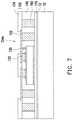
- FIG. 11Aillustrates a cross sectional view of an integrated circuit package in accordance with some embodiments.
- the carrier 10may not include the insulating layer 170 formed thereon.
- the de-bonding layer 12is de-bonded from the insulating encapsulation 140 and the integrated circuit component 115 carried by the carrier 10 . Accordingly, a bottom surface of the insulating encapsulation 140 , a bottom surface of the integrated circuit component 115 (with the die attach film) and bottom surfaces of the conductive pillars 116 are revealed.
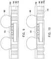
- FIG. 12is a cross-sectional view illustrating a package-on-package (POP) structure in accordance with some embodiments.
- POPpackage-on-package
- another package 200may be provided.
- the package 200 providedis, for example, a memory device, etc.
- the package 200may be stacked over and electrically connected to the integrated circuit package 100 illustrated in FIG. 11 or the integrated circuit package 100 ′ illustrated in FIG. 11A through the conductive balls 190 , such that a package-on-package (POP) structure 300 is fabricated.
- POPpackage-on-package
- the conductive viasare electrically connected to the conductive pads through the first openings, and the passivation layer is partially covered by the conductive vias.
- the alignment markis disposed on the passivation layer and is separated from the active surface by the passivation layer.
- the passivation layeris a single-layered passivation layer.
- a top surface of the insulating encapsulationis substantially coplanar with top surfaces of the conductive vias and the alignment mark.
- the integrated circuit packagefurther includes a redistribution layer disposed on the insulating encapsulation and the semiconductor die.
- the redistribution layerincludes a redistribution circuit layer and a dielectric layer.
- the redistribution circuit layeris in contact with top surfaces of the insulating encapsulation, the conductive vias and the alignment mark.
- the dielectric layeris disposed on the insulating encapsulation and the redistribution circuit layer.
- an integrated circuit packageincludes a semiconductor die, a plurality of conductive vias, an alignment mark, an insulating encapsulation and a redistribution layer.
- the semiconductor dieincludes a plurality of conductive pads disposed on an active surface of the semiconductor die and a passivation layer covering the active surface, wherein the passivation layer includes a plurality of first openings corresponding to the conductive pads.
- the conductive viasare disposed in the first openings and in contact with the conductive pads through the first openings.
- the alignment markis disposed on the passivation layer and separated from the active surface by the passivation layer, wherein the alignment mark maintains a distance from the first openings.
- the insulating encapsulationencapsulates side surfaces of the semiconductor die and is in contact with the passivation layer, wherein the alignment mark is separated from the conductive vias by the insulating encapsulation.
- the redistribution layeris disposed on the insulating encapsulation and the semiconductor die.
- a top surface of the insulating encapsulationis substantially coplanar with top surfaces of the conductive vias and the alignment mark.
- the passivation layeris a single-layered passivation layer.
- the integrated circuit packagefurther includes a plurality of conductive balls, wherein the dielectric layer includes a plurality of second openings disposed on the redistribution circuit layer, and the conductive balls are disposed in the second openings respectively and in contact with the redistribution circuit layer through the second openings.
- providing the integrated circuit componentincludes the following steps.
- a wafer including the semiconductor dieis provided.
- a passivation layeris formed on the wafer, wherein the passivation layer includes a plurality of first openings corresponding to the conductive pads respectively.
- a patterned photoresist layeris formed on the passivation layer, wherein the patterned photoresist layer includes a plurality of first pattern openings and a second pattern opening, the first pattern openings reveals the first openings and the conductive pads, and the second pattern opening reveals the passivation layer.
- the conductive viasare formed in the first pattern openings and the alignment mark is formed in the second pattern opening.
- the patterned photoresist layeris removed.
- the waferis diced to form the integrated circuit component.
- a plurality of conductive pillarsare formed on the carrier before the integrated circuit component is removably bonded to the carrier, and the insulating encapsulation encapsulates side surfaces of the conductive pillars.
- the methodfurther includes the following steps.
- a redistribution circuit layeris formed on the ground surface of the insulating encapsulation, wherein the redistribution circuit layer connects the top surfaces of the conductive vias and the alignment mark.
- a dielectric layeris formed on the ground surface of the insulating encapsulation and the redistribution circuit layer, wherein the dielectric layer includes a plurality of second openings disposed on the redistribution circuit layer.
- the methodfurther includes the following steps.
- a plurality of conductive ballsare formed in the second openings, wherein the conductive balls are in contact with the redistribution circuit layer through the second openings.
Landscapes
- Engineering & Computer Science (AREA)
- Microelectronics & Electronic Packaging (AREA)
- Power Engineering (AREA)
- Computer Hardware Design (AREA)
- Physics & Mathematics (AREA)
- Condensed Matter Physics & Semiconductors (AREA)
- General Physics & Mathematics (AREA)
- Manufacturing & Machinery (AREA)
- Internal Circuitry In Semiconductor Integrated Circuit Devices (AREA)
- Production Of Multi-Layered Print Wiring Board (AREA)
Abstract
Description
Claims (19)
Priority Applications (3)
| Application Number | Priority Date | Filing Date | Title |
|---|---|---|---|
| US15/690,196US10636757B2 (en) | 2017-08-29 | 2017-08-29 | Integrated circuit component package and method of fabricating the same |
| TW106135546ATW201913899A (en) | 2017-08-29 | 2017-10-17 | Integrated circuit package and manufacturing method thereof |
| CN201711069152.7ACN109427700A (en) | 2017-08-29 | 2017-11-03 | Integrated circuit package and method of making the same |
Applications Claiming Priority (1)
| Application Number | Priority Date | Filing Date | Title |
|---|---|---|---|
| US15/690,196US10636757B2 (en) | 2017-08-29 | 2017-08-29 | Integrated circuit component package and method of fabricating the same |
Publications (2)
| Publication Number | Publication Date |
|---|---|
| US20190067226A1 US20190067226A1 (en) | 2019-02-28 |
| US10636757B2true US10636757B2 (en) | 2020-04-28 |
Family
ID=65435612
Family Applications (1)
| Application Number | Title | Priority Date | Filing Date |
|---|---|---|---|
| US15/690,196ActiveUS10636757B2 (en) | 2017-08-29 | 2017-08-29 | Integrated circuit component package and method of fabricating the same |
Country Status (3)
| Country | Link |
|---|---|
| US (1) | US10636757B2 (en) |
| CN (1) | CN109427700A (en) |
| TW (1) | TW201913899A (en) |
Cited By (2)
| Publication number | Priority date | Publication date | Assignee | Title |
|---|---|---|---|---|
| USD920266S1 (en)* | 2019-09-29 | 2021-05-25 | China Chippacking Technology Co., Ltd. | Integrated circuit package |
| USD920265S1 (en)* | 2019-09-29 | 2021-05-25 | China Chippacking Technology Co., Ltd. | Integrated circuit package |
Families Citing this family (2)
| Publication number | Priority date | Publication date | Assignee | Title |
|---|---|---|---|---|
| CN111430313A (en)* | 2020-05-11 | 2020-07-17 | 上海天马微电子有限公司 | Semiconductor package and method of manufacturing the same |
| TWI753700B (en)* | 2020-12-11 | 2022-01-21 | 矽品精密工業股份有限公司 | Electronic packaging and manufacturing method thereof |
Citations (106)
| Publication number | Priority date | Publication date | Assignee | Title |
|---|---|---|---|---|
| US7170162B2 (en)* | 2004-05-11 | 2007-01-30 | Via Technologies, Inc. | Chip embedded package structure |
| US20090206411A1 (en)* | 2008-02-14 | 2009-08-20 | Renesas Technology Corp. | Semiconductor device and a method of manufacturing the same |
| US20090205202A1 (en)* | 2008-02-14 | 2009-08-20 | Ibiden Co., Ltd. | Method of manufacturing printed wiring board with built-in electronic component |
| US20090244865A1 (en)* | 2008-03-27 | 2009-10-01 | Ibiden Co., Ltd | Method for manufacturing multilayer printed wiring board |
| US20100090352A1 (en)* | 2008-10-14 | 2010-04-15 | Shinko Electric Industries Co., Ltd. | Flip-chip substrate and method of manufacturing the same |
| US20110248398A1 (en)* | 2010-04-07 | 2011-10-13 | Maxim Integrated Products, Inc. | Wafer-level chip-scale package device having bump assemblies configured to mitigate failures due to stress |
| US20110291288A1 (en)* | 2010-05-26 | 2011-12-01 | Taiwan Semiconductor Manufacturing Company, Ltd. | Package systems having interposers |
| US20120153462A1 (en)* | 2010-12-17 | 2012-06-21 | Sony Corporation | Semiconductor device and method of manufacturing semiconductor device |
| US20120313236A1 (en)* | 2011-06-09 | 2012-12-13 | Sony Corporation | Semiconductor device and manufacturing method for semiconductor device |
| US20130062760A1 (en)* | 2010-10-14 | 2013-03-14 | Taiwan Semiconductor Manufacturing Company, Ltd. | Packaging Methods and Structures Using a Die Attach Film |
| US20130168848A1 (en)* | 2011-12-28 | 2013-07-04 | Taiwan Semiconductor Manufacturing Company, Ltd. | Packaged semiconductor device and method of packaging the semiconductor device |
| US20130187270A1 (en)* | 2012-01-23 | 2013-07-25 | Taiwan Semiconductor Manufacturing Company, Ltd. | Multi-Chip Fan Out Package and Methods of Forming the Same |
| US20130307140A1 (en)* | 2012-05-18 | 2013-11-21 | Taiwan Semiconductor Manufacturing Company, Ltd. | Packaging with interposer frame |
| US20130341784A1 (en)* | 2012-06-21 | 2013-12-26 | Stats Chippac, Ltd. | Semiconductor Device and Method of Forming an Embedded SOP Fan-Out Package |
| US20130341800A1 (en)* | 2012-06-21 | 2013-12-26 | Taiwan Semiconductor Manufacturing Company, Ltd. | Integrated Circuit Packages and Methods for Forming the Same |
| US8778738B1 (en)* | 2013-02-19 | 2014-07-15 | Taiwan Semiconductor Manufacturing Company, Ltd. | Packaged semiconductor devices and packaging devices and methods |
| US8829676B2 (en)* | 2011-06-28 | 2014-09-09 | Taiwan Semiconductor Manufacturing Company, Ltd. | Interconnect structure for wafer level package |
| US20140252646A1 (en)* | 2013-03-06 | 2014-09-11 | Taiwan Semiconductor Manufacturing Company, Ltd. | Interconnect Structure for Package-on-Package Devices |
| US20140287541A1 (en)* | 2013-03-22 | 2014-09-25 | Renesas Electronics Corporation | Semiconductor chip and semiconductor device |
| US8877554B2 (en)* | 2013-03-15 | 2014-11-04 | Taiwan Semiconductor Manufacturing Company, Ltd. | Packaged semiconductor devices, methods of packaging semiconductor devices, and PoP devices |
| US20140374899A1 (en)* | 2013-06-25 | 2014-12-25 | Taiwan Semiconductor Manufacturing Company, Ltd. | Package with Solder Regions Aligned to Recesses |
| US20150145145A1 (en)* | 2013-11-27 | 2015-05-28 | Tdk Corporation | Ic embedded substrate and method of manufacturing the same |
| US9059107B2 (en)* | 2012-09-12 | 2015-06-16 | Taiwan Semiconductor Manufacturing Company, Ltd. | Packaging methods and packaged devices |
| US20150235977A1 (en)* | 2014-02-17 | 2015-08-20 | Taiwan Semiconductor Manufacturing Company Ltd. | Semiconductor device and manufacturing method thereof |
| US20150255406A1 (en)* | 2013-12-05 | 2015-09-10 | Taiwan Semiconductor Manufacturing Company, Ltd. | Solder ball protection in packages |
| US20150287697A1 (en)* | 2014-04-02 | 2015-10-08 | Taiwan Semiconductor Manufacturing Company, Ltd. | Semiconductor Device and Method |
| US20150311132A1 (en)* | 2014-04-28 | 2015-10-29 | Taiwan Semiconductor Manufacturing Company, Ltd. | Scribe line structure and method of forming same |
| US20150318267A1 (en)* | 2014-04-30 | 2015-11-05 | Taiwan Semiconductor Manufacturing Company, Ltd. | 3d stacked-chip package |
| US20150348904A1 (en)* | 2014-05-29 | 2015-12-03 | Taiwan Semiconductor Manufacturing Company, Ltd. | Alignment mark design for packages |
| US20160005716A1 (en)* | 2014-07-01 | 2016-01-07 | Taiwan Semiconductor Manufacturing Company, Ltd. | Semiconductor Package and Method |
| US20160093572A1 (en)* | 2014-09-29 | 2016-03-31 | Taiwan Semiconductor Manufacturing Company, Ltd. | Integrated fan-out package with dummy vias |
| US20160093580A1 (en)* | 2011-12-30 | 2016-03-31 | Deca Technologies Inc. | Semiconductor device and method comprising redistribution layers |
| US9318429B2 (en)* | 2014-03-31 | 2016-04-19 | Taiwan Semiconductor Manufacturing Company, Ltd. | Integrated structure in wafer level package |
| US20160163578A1 (en)* | 2014-12-03 | 2016-06-09 | Taiwan Semiconductor Manufacturing Company, Ltd. | Semiconductor Packages and Methods of Forming the Same |
| US20160163564A1 (en)* | 2014-12-03 | 2016-06-09 | Taiwan Semiconductor Manufacturing Company, Ltd. | Semiconductor Packages and Methods of Forming the Same |
| US20160190098A1 (en)* | 2014-12-29 | 2016-06-30 | Taiwan Semiconductor Manufacturing Company, Ltd. | Devices and Methods of Packaging Semiconductor Devices |
| US20160190041A1 (en)* | 2014-12-29 | 2016-06-30 | Globalfoundries Singapore Pte. Ltd. | Device without zero mark layer |
| US9391028B1 (en)* | 2015-07-31 | 2016-07-12 | Taiwan Semiconductor Manufacturing Company, Ltd. | Integrated circuit dies having alignment marks and methods of forming same |
| US9391046B2 (en)* | 2011-05-20 | 2016-07-12 | STATS ChipPAC Pte. Ltd. | Semiconductor device and method of forming 3D semiconductor package with semiconductor die stacked over semiconductor wafer |
| US20160276248A1 (en)* | 2015-03-16 | 2016-09-22 | Taiwan Semiconductor Manufacturing Company, Ltd. | Non-vertical through-via in package |
| US9484227B1 (en)* | 2015-06-22 | 2016-11-01 | Taiwan Semiconductor Manufacturing Company, Ltd. | Dicing in wafer level package |
| US20170005067A1 (en)* | 2015-06-30 | 2017-01-05 | Taiwan Semiconductor Manufacturing Company, Ltd. | Packages for Semiconductor Devices, Packaged Semiconductor Devices, and Methods of Packaging Semiconductor Devices |
| US20170005054A1 (en)* | 2015-06-30 | 2017-01-05 | Taiwan Semiconductor Manufacturing Company, Ltd. | Post-passivation interconnect structure and methods thereof |
| US20170018534A1 (en)* | 2015-07-14 | 2017-01-19 | Shinko Electric Industries Co., Ltd. | Electronic component device and manufacturing method thereof |
| US9570410B1 (en)* | 2015-07-31 | 2017-02-14 | Taiwan Semiconductor Manufacturing Company, Ltd. | Methods of forming connector pad structures, interconnect structures, and structures thereof |
| US9589903B2 (en)* | 2015-03-16 | 2017-03-07 | Taiwan Semiconductor Manufacturing Company, Ltd. | Eliminate sawing-induced peeling through forming trenches |
| US9595482B2 (en)* | 2015-03-16 | 2017-03-14 | Taiwan Semiconductor Manufacturing Company, Ltd. | Structure for die probing |
| US20170084589A1 (en)* | 2015-09-23 | 2017-03-23 | Mediatek Inc. | Semiconductor package structure and method for forming the same |
| US20170092581A1 (en)* | 2015-09-30 | 2017-03-30 | Taiwan Semiconductor Manufacturing Company, Ltd. | Integrated Fan-Out Structure and Method of Forming |
| US20170110421A1 (en)* | 2015-10-20 | 2017-04-20 | Taiwan Semiconductor Manufacturing Company, Ltd. | Semiconductor Device and Method |
| US9640531B1 (en)* | 2014-01-28 | 2017-05-02 | Monolithic 3D Inc. | Semiconductor device, structure and methods |
| US20170133354A1 (en)* | 2015-11-06 | 2017-05-11 | Taiwan Semiconductor Manufacturing Company, Ltd. | Integrated circuit process having alignment marks for underfill |
| US9653391B1 (en)* | 2016-06-30 | 2017-05-16 | Taiwan Semiconductor Manufacturing Company Ltd. | Semiconductor packaging structure and manufacturing method thereof |
| US9659805B2 (en)* | 2015-04-17 | 2017-05-23 | Taiwan Semiconductor Manufacturing Company, Ltd. | Fan-out interconnect structure and methods forming the same |
| US9666502B2 (en)* | 2015-04-17 | 2017-05-30 | Taiwan Semiconductor Manufacturing Company, Ltd. | Discrete polymer in fan-out packages |
| US9685411B2 (en)* | 2015-09-18 | 2017-06-20 | Taiwan Semiconductor Manufacturing Company, Ltd. | Integrated circuit dies having alignment marks and methods of forming same |
| US20170188458A1 (en)* | 2015-12-28 | 2017-06-29 | Taiwan Semiconductor Manufacturing Company, Ltd. | Opening in the Pad for Bonding Integrated Passive Device in InFO Package |
| US9735131B2 (en)* | 2015-11-10 | 2017-08-15 | Taiwan Semiconductor Manufacturing Company, Ltd. | Multi-stack package-on-package structures |
| US20170271283A1 (en)* | 2016-03-15 | 2017-09-21 | Taiwan Semiconductor Manufacturing Co., Ltd. | Integrated fan-out package, redistribution circuit structure, and method of fabricating the same |
| US9793230B1 (en)* | 2016-07-08 | 2017-10-17 | Taiwan Semiconductor Manufacturing Company, Ltd. | Semiconductor structure and method of forming |
| US20170323840A1 (en)* | 2016-05-05 | 2017-11-09 | Taiwan Semiconductor Manufacturing Company, Ltd. | Package with Tilted Interface between Device Die and Encapsulating Material |
| US9825007B1 (en)* | 2016-07-13 | 2017-11-21 | Taiwan Semiconductor Manufacturing Co., Ltd. | Chip package structure with molding layer and method for forming the same |
| US9824990B2 (en)* | 2014-06-12 | 2017-11-21 | Taiwan Semiconductor Manufacturing Company, Ltd. | Pad design for reliability enhancement in packages |
| US20170338196A1 (en)* | 2016-05-17 | 2017-11-23 | Taiwan Semiconductor Manufacturing Co., Ltd. | Integrated fan-out package and method of fabricating the same |
| US20170345762A1 (en)* | 2016-05-30 | 2017-11-30 | Taiwan Semiconductor Manufacturing Co., Ltd. | Conductive pattern and integrated fan-out package having the same |
| US9837359B1 (en)* | 2016-09-30 | 2017-12-05 | Taiwan Semiconductor Manufacturing Co., Ltd. | Integrated fan-out package and method of fabricating the same |
| US9847269B2 (en)* | 2015-07-31 | 2017-12-19 | Taiwan Semiconductor Manufacturing Company, Ltd. | Fan-out packages and methods of forming same |
| US9859254B1 (en)* | 2016-06-30 | 2018-01-02 | Taiwan Semiconductor Manufacturing Company Ltd. | Semiconductor structure and a manufacturing method thereof |
| US9859229B2 (en)* | 2016-04-28 | 2018-01-02 | Taiwan Semiconductor Manufacturing Co., Ltd. | Package structure and method for forming the same |
| US20180013052A1 (en)* | 2015-07-23 | 2018-01-11 | Massachusetts Institute Of Technology | Qubit and Coupler Circuit Structures and Coupling Techniques |
| US9870997B2 (en)* | 2016-05-24 | 2018-01-16 | Taiwan Semiconductor Manufacturing Co., Ltd. | Integrated fan-out package and method of fabricating the same |
| US20180025986A1 (en)* | 2016-07-21 | 2018-01-25 | Taiwan Semiconductor Manufacturing Co., Ltd. | Integrated fan-out package |
| US20180061669A1 (en)* | 2016-08-23 | 2018-03-01 | Taiwan Semiconductor Manufacturing Company, Ltd. | Semiconductor Device and Method |
| US9911672B1 (en)* | 2016-09-30 | 2018-03-06 | Taiwan Semiconductor Manufacturing Co., Ltd. | Semiconductor devices, method for fabricating integrated fan-out packages, and method for fabricating semiconductor devices |
| US9922896B1 (en)* | 2016-09-16 | 2018-03-20 | Taiwan Semiconductor Manufacturing Company, Ltd. | Info structure with copper pillar having reversed profile |
| US20180082988A1 (en)* | 2016-09-16 | 2018-03-22 | Taiwan Semiconductor Manufacturing Company, Ltd. | Package structure and method of forming the same |
| US9935080B2 (en)* | 2016-04-29 | 2018-04-03 | Taiwan Semiconductor Manufacturing Company, Ltd. | Three-layer Package-on-Package structure and method forming same |
| US9935090B2 (en)* | 2014-02-14 | 2018-04-03 | Taiwan Semiconductor Manufacturing Company, Ltd. | Substrate design for semiconductor packages and method of forming same |
| US20180096939A1 (en)* | 2016-10-03 | 2018-04-05 | Taiwan Semiconductor Manufacturing Co., Ltd. | Package structure with bump |
| US9966360B2 (en)* | 2016-07-05 | 2018-05-08 | Taiwan Semiconductor Manufacturing Co., Ltd. | Semiconductor package and manufacturing method thereof |
| US20180138115A1 (en)* | 2016-11-11 | 2018-05-17 | Advanced Semiconductor Engineering, Inc. | Semiconductor package structure and method for manufacturing the same |
| US9978657B2 (en)* | 2013-10-18 | 2018-05-22 | Taiwan Semiconductor Manufacturing Company Ltd. | Semiconductor package device and manufacturing method thereof |
| US9984960B2 (en)* | 2016-07-21 | 2018-05-29 | Taiwan Semiconductor Manufacturing Co., Ltd. | Integrated fan-out package and method of fabricating the same |
| US9985006B2 (en)* | 2016-05-31 | 2018-05-29 | Taiwan Semiconductor Manufacturing Company Ltd. | Semiconductor structure and manufacturing method thereof |
| US20180151493A1 (en)* | 2016-11-29 | 2018-05-31 | Taiwan Semiconductor Manufacturing Company Ltd. | Semiconductor device and method of forming the same |
| US10103125B2 (en)* | 2016-11-28 | 2018-10-16 | Taiwan Semiconductor Manufacturing Co., Ltd. | Chip package structure and method for forming the same |
| US20180301389A1 (en)* | 2017-04-13 | 2018-10-18 | Taiwan Semiconductor Manufacturing Co., Ltd. | Integrated circuit package and method of fabricating the same |
| US10128193B2 (en)* | 2016-11-29 | 2018-11-13 | Taiwan Semiconductor Manufacturing Co., Ltd. | Package structure and method for forming the same |
| US10134708B2 (en)* | 2016-08-05 | 2018-11-20 | Taiwan Semiconductor Manufacturing Company, Ltd. | Package with thinned substrate |
| US10141288B2 (en)* | 2015-07-31 | 2018-11-27 | Taiwan Semiconductor Manufacturing Company, Ltd. | Surface mount device/integrated passive device on package or device structure and methods of forming |
| US10157807B2 (en)* | 2016-05-26 | 2018-12-18 | Taiwan Semiconductor Manufacturing Co., Ltd. | Sensor packages and manufacturing mehtods thereof |
| US10157846B2 (en)* | 2016-10-13 | 2018-12-18 | Taiwan Semiconductor Manufacturing Co., Ltd. | Method for forming chip package involving cutting process |
| US20180366412A1 (en)* | 2016-02-26 | 2018-12-20 | Taiwan Semiconductor Manufacturing Company, Ltd. | Semiconductor Package and Method of Forming the Same |
| US20180366410A1 (en)* | 2017-06-20 | 2018-12-20 | Taiwan Semiconductor Manufacturing Co., Ltd. | Integrated fan-out packages and methods of forming the same |
| US20180366347A1 (en)* | 2017-06-20 | 2018-12-20 | Taiwan Semiconductor Manufacturing Co., Ltd. | Integrated fan-out package having multi-band antenna and method of forming the same |
| US10163813B2 (en)* | 2016-11-17 | 2018-12-25 | Taiwan Semiconductor Manufacturing Co., Ltd. | Chip package structure including redistribution structure and conductive shielding film |
| US10163800B2 (en)* | 2016-07-08 | 2018-12-25 | Taiwan Semiconductor Manufacturing Co., Ltd. | Package structure with dummy feature in passivation layer |
| US10163866B2 (en)* | 2015-11-16 | 2018-12-25 | Taiwan Semiconductor Manufacturing Company, Ltd. | Semiconductor device and method of manufacture |
| US10163701B2 (en)* | 2016-05-12 | 2018-12-25 | Taiwan Semiconductor Manufacturing Company, Ltd. | Multi-stack package-on-package structures |
| US20180374824A1 (en)* | 2016-08-18 | 2018-12-27 | Taiwan Semiconductor Manufacturing Company, Ltd. | Semiconductor Packages with Thermal-Electrical-Mechanical Chips and Methods of Forming the Same |
| US20180374822A1 (en)* | 2013-10-30 | 2018-12-27 | Taiwan Semiconductor Manufacturing Company, Ltd. | Chip on Package Structure and Method |
| US20180374797A1 (en)* | 2016-05-05 | 2018-12-27 | Taiwan Semiconductor Manufacturing Co., Ltd. | Integrated fan-out package and method of fabricating the same |
| US20190035759A1 (en)* | 2017-07-27 | 2019-01-31 | Taiwan Semiconductor Manufacturing Co., Ltd. | Integrated fan-out package and method of fabricating the same |
| US20190067001A1 (en)* | 2017-08-31 | 2019-02-28 | Taiwan Semiconductor Manufacturing Co., Ltd. | Mask assembly and method for fabricating a chip package |
| US20190131249A1 (en)* | 2016-07-01 | 2019-05-02 | Taiwan Semiconductor Manufacturing Co., Ltd. | Method for forming package structure |
| US20190355679A1 (en)* | 2018-05-16 | 2019-11-21 | Taiwan Semiconductor Manufacturing Co., Ltd. | Package structure and manufacturing method thereof |
- 2017
- 2017-08-29USUS15/690,196patent/US10636757B2/enactiveActive
- 2017-10-17TWTW106135546Apatent/TW201913899A/enunknown
- 2017-11-03CNCN201711069152.7Apatent/CN109427700A/enactivePending
Patent Citations (115)
| Publication number | Priority date | Publication date | Assignee | Title |
|---|---|---|---|---|
| US7170162B2 (en)* | 2004-05-11 | 2007-01-30 | Via Technologies, Inc. | Chip embedded package structure |
| US20090206411A1 (en)* | 2008-02-14 | 2009-08-20 | Renesas Technology Corp. | Semiconductor device and a method of manufacturing the same |
| US20090205202A1 (en)* | 2008-02-14 | 2009-08-20 | Ibiden Co., Ltd. | Method of manufacturing printed wiring board with built-in electronic component |
| US20090244865A1 (en)* | 2008-03-27 | 2009-10-01 | Ibiden Co., Ltd | Method for manufacturing multilayer printed wiring board |
| US20100090352A1 (en)* | 2008-10-14 | 2010-04-15 | Shinko Electric Industries Co., Ltd. | Flip-chip substrate and method of manufacturing the same |
| US20110248398A1 (en)* | 2010-04-07 | 2011-10-13 | Maxim Integrated Products, Inc. | Wafer-level chip-scale package device having bump assemblies configured to mitigate failures due to stress |
| US20110291288A1 (en)* | 2010-05-26 | 2011-12-01 | Taiwan Semiconductor Manufacturing Company, Ltd. | Package systems having interposers |
| US20130062760A1 (en)* | 2010-10-14 | 2013-03-14 | Taiwan Semiconductor Manufacturing Company, Ltd. | Packaging Methods and Structures Using a Die Attach Film |
| US20120153462A1 (en)* | 2010-12-17 | 2012-06-21 | Sony Corporation | Semiconductor device and method of manufacturing semiconductor device |
| US9391046B2 (en)* | 2011-05-20 | 2016-07-12 | STATS ChipPAC Pte. Ltd. | Semiconductor device and method of forming 3D semiconductor package with semiconductor die stacked over semiconductor wafer |
| US20120313236A1 (en)* | 2011-06-09 | 2012-12-13 | Sony Corporation | Semiconductor device and manufacturing method for semiconductor device |
| US8829676B2 (en)* | 2011-06-28 | 2014-09-09 | Taiwan Semiconductor Manufacturing Company, Ltd. | Interconnect structure for wafer level package |
| US20130168848A1 (en)* | 2011-12-28 | 2013-07-04 | Taiwan Semiconductor Manufacturing Company, Ltd. | Packaged semiconductor device and method of packaging the semiconductor device |
| US20160093580A1 (en)* | 2011-12-30 | 2016-03-31 | Deca Technologies Inc. | Semiconductor device and method comprising redistribution layers |
| US20130187270A1 (en)* | 2012-01-23 | 2013-07-25 | Taiwan Semiconductor Manufacturing Company, Ltd. | Multi-Chip Fan Out Package and Methods of Forming the Same |
| US20130307140A1 (en)* | 2012-05-18 | 2013-11-21 | Taiwan Semiconductor Manufacturing Company, Ltd. | Packaging with interposer frame |
| US20130341800A1 (en)* | 2012-06-21 | 2013-12-26 | Taiwan Semiconductor Manufacturing Company, Ltd. | Integrated Circuit Packages and Methods for Forming the Same |
| US20130341784A1 (en)* | 2012-06-21 | 2013-12-26 | Stats Chippac, Ltd. | Semiconductor Device and Method of Forming an Embedded SOP Fan-Out Package |
| US9059107B2 (en)* | 2012-09-12 | 2015-06-16 | Taiwan Semiconductor Manufacturing Company, Ltd. | Packaging methods and packaged devices |
| US8778738B1 (en)* | 2013-02-19 | 2014-07-15 | Taiwan Semiconductor Manufacturing Company, Ltd. | Packaged semiconductor devices and packaging devices and methods |
| US20140252646A1 (en)* | 2013-03-06 | 2014-09-11 | Taiwan Semiconductor Manufacturing Company, Ltd. | Interconnect Structure for Package-on-Package Devices |
| US9460987B2 (en)* | 2013-03-06 | 2016-10-04 | Taiwan Semiconductor Manufacturing Company, Ltd. | Interconnect structure for package-on-package devices and a method of fabricating |
| US8877554B2 (en)* | 2013-03-15 | 2014-11-04 | Taiwan Semiconductor Manufacturing Company, Ltd. | Packaged semiconductor devices, methods of packaging semiconductor devices, and PoP devices |
| US20140287541A1 (en)* | 2013-03-22 | 2014-09-25 | Renesas Electronics Corporation | Semiconductor chip and semiconductor device |
| US20140374899A1 (en)* | 2013-06-25 | 2014-12-25 | Taiwan Semiconductor Manufacturing Company, Ltd. | Package with Solder Regions Aligned to Recesses |
| US9978657B2 (en)* | 2013-10-18 | 2018-05-22 | Taiwan Semiconductor Manufacturing Company Ltd. | Semiconductor package device and manufacturing method thereof |
| US20180374822A1 (en)* | 2013-10-30 | 2018-12-27 | Taiwan Semiconductor Manufacturing Company, Ltd. | Chip on Package Structure and Method |
| US20150145145A1 (en)* | 2013-11-27 | 2015-05-28 | Tdk Corporation | Ic embedded substrate and method of manufacturing the same |
| US20150255406A1 (en)* | 2013-12-05 | 2015-09-10 | Taiwan Semiconductor Manufacturing Company, Ltd. | Solder ball protection in packages |
| US9640531B1 (en)* | 2014-01-28 | 2017-05-02 | Monolithic 3D Inc. | Semiconductor device, structure and methods |
| US9935090B2 (en)* | 2014-02-14 | 2018-04-03 | Taiwan Semiconductor Manufacturing Company, Ltd. | Substrate design for semiconductor packages and method of forming same |
| US20150235977A1 (en)* | 2014-02-17 | 2015-08-20 | Taiwan Semiconductor Manufacturing Company Ltd. | Semiconductor device and manufacturing method thereof |
| US9318429B2 (en)* | 2014-03-31 | 2016-04-19 | Taiwan Semiconductor Manufacturing Company, Ltd. | Integrated structure in wafer level package |
| US20150287697A1 (en)* | 2014-04-02 | 2015-10-08 | Taiwan Semiconductor Manufacturing Company, Ltd. | Semiconductor Device and Method |
| US20150311132A1 (en)* | 2014-04-28 | 2015-10-29 | Taiwan Semiconductor Manufacturing Company, Ltd. | Scribe line structure and method of forming same |
| US20150318267A1 (en)* | 2014-04-30 | 2015-11-05 | Taiwan Semiconductor Manufacturing Company, Ltd. | 3d stacked-chip package |
| US20150348904A1 (en)* | 2014-05-29 | 2015-12-03 | Taiwan Semiconductor Manufacturing Company, Ltd. | Alignment mark design for packages |
| US9824990B2 (en)* | 2014-06-12 | 2017-11-21 | Taiwan Semiconductor Manufacturing Company, Ltd. | Pad design for reliability enhancement in packages |
| US9449947B2 (en)* | 2014-07-01 | 2016-09-20 | Taiwan Semiconductor Manufacturing Company, Ltd. | Semiconductor package for thermal dissipation |
| US20160005716A1 (en)* | 2014-07-01 | 2016-01-07 | Taiwan Semiconductor Manufacturing Company, Ltd. | Semiconductor Package and Method |
| US20160093572A1 (en)* | 2014-09-29 | 2016-03-31 | Taiwan Semiconductor Manufacturing Company, Ltd. | Integrated fan-out package with dummy vias |
| US20160163564A1 (en)* | 2014-12-03 | 2016-06-09 | Taiwan Semiconductor Manufacturing Company, Ltd. | Semiconductor Packages and Methods of Forming the Same |
| US20160163578A1 (en)* | 2014-12-03 | 2016-06-09 | Taiwan Semiconductor Manufacturing Company, Ltd. | Semiconductor Packages and Methods of Forming the Same |
| US20160190041A1 (en)* | 2014-12-29 | 2016-06-30 | Globalfoundries Singapore Pte. Ltd. | Device without zero mark layer |
| US20160190098A1 (en)* | 2014-12-29 | 2016-06-30 | Taiwan Semiconductor Manufacturing Company, Ltd. | Devices and Methods of Packaging Semiconductor Devices |
| US20160276248A1 (en)* | 2015-03-16 | 2016-09-22 | Taiwan Semiconductor Manufacturing Company, Ltd. | Non-vertical through-via in package |
| US10115647B2 (en)* | 2015-03-16 | 2018-10-30 | Taiwan Semiconductor Manufacturing Company, Ltd. | Non-vertical through-via in package |
| US9589903B2 (en)* | 2015-03-16 | 2017-03-07 | Taiwan Semiconductor Manufacturing Company, Ltd. | Eliminate sawing-induced peeling through forming trenches |
| US9595482B2 (en)* | 2015-03-16 | 2017-03-14 | Taiwan Semiconductor Manufacturing Company, Ltd. | Structure for die probing |
| US9666502B2 (en)* | 2015-04-17 | 2017-05-30 | Taiwan Semiconductor Manufacturing Company, Ltd. | Discrete polymer in fan-out packages |
| US9659805B2 (en)* | 2015-04-17 | 2017-05-23 | Taiwan Semiconductor Manufacturing Company, Ltd. | Fan-out interconnect structure and methods forming the same |
| US9484227B1 (en)* | 2015-06-22 | 2016-11-01 | Taiwan Semiconductor Manufacturing Company, Ltd. | Dicing in wafer level package |
| US20170005054A1 (en)* | 2015-06-30 | 2017-01-05 | Taiwan Semiconductor Manufacturing Company, Ltd. | Post-passivation interconnect structure and methods thereof |
| US20170005067A1 (en)* | 2015-06-30 | 2017-01-05 | Taiwan Semiconductor Manufacturing Company, Ltd. | Packages for Semiconductor Devices, Packaged Semiconductor Devices, and Methods of Packaging Semiconductor Devices |
| US9825006B2 (en)* | 2015-07-14 | 2017-11-21 | Shinko Electric Industries Co., Ltd. | Electronic component device and manufacturing method thereof |
| US20170018534A1 (en)* | 2015-07-14 | 2017-01-19 | Shinko Electric Industries Co., Ltd. | Electronic component device and manufacturing method thereof |
| US20180013052A1 (en)* | 2015-07-23 | 2018-01-11 | Massachusetts Institute Of Technology | Qubit and Coupler Circuit Structures and Coupling Techniques |
| US10141288B2 (en)* | 2015-07-31 | 2018-11-27 | Taiwan Semiconductor Manufacturing Company, Ltd. | Surface mount device/integrated passive device on package or device structure and methods of forming |
| US9847269B2 (en)* | 2015-07-31 | 2017-12-19 | Taiwan Semiconductor Manufacturing Company, Ltd. | Fan-out packages and methods of forming same |
| US9570410B1 (en)* | 2015-07-31 | 2017-02-14 | Taiwan Semiconductor Manufacturing Company, Ltd. | Methods of forming connector pad structures, interconnect structures, and structures thereof |
| US9391028B1 (en)* | 2015-07-31 | 2016-07-12 | Taiwan Semiconductor Manufacturing Company, Ltd. | Integrated circuit dies having alignment marks and methods of forming same |
| US9685411B2 (en)* | 2015-09-18 | 2017-06-20 | Taiwan Semiconductor Manufacturing Company, Ltd. | Integrated circuit dies having alignment marks and methods of forming same |
| US20170084589A1 (en)* | 2015-09-23 | 2017-03-23 | Mediatek Inc. | Semiconductor package structure and method for forming the same |
| US20170092581A1 (en)* | 2015-09-30 | 2017-03-30 | Taiwan Semiconductor Manufacturing Company, Ltd. | Integrated Fan-Out Structure and Method of Forming |
| US20170110421A1 (en)* | 2015-10-20 | 2017-04-20 | Taiwan Semiconductor Manufacturing Company, Ltd. | Semiconductor Device and Method |
| US20170133354A1 (en)* | 2015-11-06 | 2017-05-11 | Taiwan Semiconductor Manufacturing Company, Ltd. | Integrated circuit process having alignment marks for underfill |
| US9735131B2 (en)* | 2015-11-10 | 2017-08-15 | Taiwan Semiconductor Manufacturing Company, Ltd. | Multi-stack package-on-package structures |
| US10163866B2 (en)* | 2015-11-16 | 2018-12-25 | Taiwan Semiconductor Manufacturing Company, Ltd. | Semiconductor device and method of manufacture |
| US20170188458A1 (en)* | 2015-12-28 | 2017-06-29 | Taiwan Semiconductor Manufacturing Company, Ltd. | Opening in the Pad for Bonding Integrated Passive Device in InFO Package |
| US20180366412A1 (en)* | 2016-02-26 | 2018-12-20 | Taiwan Semiconductor Manufacturing Company, Ltd. | Semiconductor Package and Method of Forming the Same |
| US20170271283A1 (en)* | 2016-03-15 | 2017-09-21 | Taiwan Semiconductor Manufacturing Co., Ltd. | Integrated fan-out package, redistribution circuit structure, and method of fabricating the same |
| US9859229B2 (en)* | 2016-04-28 | 2018-01-02 | Taiwan Semiconductor Manufacturing Co., Ltd. | Package structure and method for forming the same |
| US9935080B2 (en)* | 2016-04-29 | 2018-04-03 | Taiwan Semiconductor Manufacturing Company, Ltd. | Three-layer Package-on-Package structure and method forming same |
| US20180204780A1 (en)* | 2016-05-05 | 2018-07-19 | Taiwan Semiconductor Manufacturing Company, Ltd. | Package with Tilted Interface between Device Die and Encapsulating Material |
| US20170323840A1 (en)* | 2016-05-05 | 2017-11-09 | Taiwan Semiconductor Manufacturing Company, Ltd. | Package with Tilted Interface between Device Die and Encapsulating Material |
| US10163745B2 (en)* | 2016-05-05 | 2018-12-25 | Taiwan Semiconductor Manufacturing Company, Ltd. | Package with tilted interface between device die and encapsulating material |
| US20180374797A1 (en)* | 2016-05-05 | 2018-12-27 | Taiwan Semiconductor Manufacturing Co., Ltd. | Integrated fan-out package and method of fabricating the same |
| US9922895B2 (en)* | 2016-05-05 | 2018-03-20 | Taiwan Semiconductor Manufacturing Company, Ltd. | Package with tilted interface between device die and encapsulating material |
| US10163701B2 (en)* | 2016-05-12 | 2018-12-25 | Taiwan Semiconductor Manufacturing Company, Ltd. | Multi-stack package-on-package structures |
| US20170338196A1 (en)* | 2016-05-17 | 2017-11-23 | Taiwan Semiconductor Manufacturing Co., Ltd. | Integrated fan-out package and method of fabricating the same |
| US9870997B2 (en)* | 2016-05-24 | 2018-01-16 | Taiwan Semiconductor Manufacturing Co., Ltd. | Integrated fan-out package and method of fabricating the same |
| US10157807B2 (en)* | 2016-05-26 | 2018-12-18 | Taiwan Semiconductor Manufacturing Co., Ltd. | Sensor packages and manufacturing mehtods thereof |
| US20170345762A1 (en)* | 2016-05-30 | 2017-11-30 | Taiwan Semiconductor Manufacturing Co., Ltd. | Conductive pattern and integrated fan-out package having the same |
| US9985006B2 (en)* | 2016-05-31 | 2018-05-29 | Taiwan Semiconductor Manufacturing Company Ltd. | Semiconductor structure and manufacturing method thereof |
| US9653391B1 (en)* | 2016-06-30 | 2017-05-16 | Taiwan Semiconductor Manufacturing Company Ltd. | Semiconductor packaging structure and manufacturing method thereof |
| US9859254B1 (en)* | 2016-06-30 | 2018-01-02 | Taiwan Semiconductor Manufacturing Company Ltd. | Semiconductor structure and a manufacturing method thereof |
| US20190131249A1 (en)* | 2016-07-01 | 2019-05-02 | Taiwan Semiconductor Manufacturing Co., Ltd. | Method for forming package structure |
| US9966360B2 (en)* | 2016-07-05 | 2018-05-08 | Taiwan Semiconductor Manufacturing Co., Ltd. | Semiconductor package and manufacturing method thereof |
| US9793230B1 (en)* | 2016-07-08 | 2017-10-17 | Taiwan Semiconductor Manufacturing Company, Ltd. | Semiconductor structure and method of forming |
| US10163800B2 (en)* | 2016-07-08 | 2018-12-25 | Taiwan Semiconductor Manufacturing Co., Ltd. | Package structure with dummy feature in passivation layer |
| US9825007B1 (en)* | 2016-07-13 | 2017-11-21 | Taiwan Semiconductor Manufacturing Co., Ltd. | Chip package structure with molding layer and method for forming the same |
| US9984960B2 (en)* | 2016-07-21 | 2018-05-29 | Taiwan Semiconductor Manufacturing Co., Ltd. | Integrated fan-out package and method of fabricating the same |
| US20180025986A1 (en)* | 2016-07-21 | 2018-01-25 | Taiwan Semiconductor Manufacturing Co., Ltd. | Integrated fan-out package |
| US10134708B2 (en)* | 2016-08-05 | 2018-11-20 | Taiwan Semiconductor Manufacturing Company, Ltd. | Package with thinned substrate |
| US20180374824A1 (en)* | 2016-08-18 | 2018-12-27 | Taiwan Semiconductor Manufacturing Company, Ltd. | Semiconductor Packages with Thermal-Electrical-Mechanical Chips and Methods of Forming the Same |
| US20180061669A1 (en)* | 2016-08-23 | 2018-03-01 | Taiwan Semiconductor Manufacturing Company, Ltd. | Semiconductor Device and Method |
| US20180350784A1 (en)* | 2016-09-16 | 2018-12-06 | Taiwan Semiconductor Manufacturing Company, Ltd. | Package Structure and Method of Forming the Same |
| US9922896B1 (en)* | 2016-09-16 | 2018-03-20 | Taiwan Semiconductor Manufacturing Company, Ltd. | Info structure with copper pillar having reversed profile |
| US20180082988A1 (en)* | 2016-09-16 | 2018-03-22 | Taiwan Semiconductor Manufacturing Company, Ltd. | Package structure and method of forming the same |
| US9837359B1 (en)* | 2016-09-30 | 2017-12-05 | Taiwan Semiconductor Manufacturing Co., Ltd. | Integrated fan-out package and method of fabricating the same |
| US9911672B1 (en)* | 2016-09-30 | 2018-03-06 | Taiwan Semiconductor Manufacturing Co., Ltd. | Semiconductor devices, method for fabricating integrated fan-out packages, and method for fabricating semiconductor devices |
| US20180096943A1 (en)* | 2016-09-30 | 2018-04-05 | Taiwan Semiconductor Manufacturing Co., Ltd. | Integrated fan-out package and method of fabricating the same |
| US20180096939A1 (en)* | 2016-10-03 | 2018-04-05 | Taiwan Semiconductor Manufacturing Co., Ltd. | Package structure with bump |
| US10157846B2 (en)* | 2016-10-13 | 2018-12-18 | Taiwan Semiconductor Manufacturing Co., Ltd. | Method for forming chip package involving cutting process |
| US20180138115A1 (en)* | 2016-11-11 | 2018-05-17 | Advanced Semiconductor Engineering, Inc. | Semiconductor package structure and method for manufacturing the same |
| US10163813B2 (en)* | 2016-11-17 | 2018-12-25 | Taiwan Semiconductor Manufacturing Co., Ltd. | Chip package structure including redistribution structure and conductive shielding film |
| US10103125B2 (en)* | 2016-11-28 | 2018-10-16 | Taiwan Semiconductor Manufacturing Co., Ltd. | Chip package structure and method for forming the same |
| US10128193B2 (en)* | 2016-11-29 | 2018-11-13 | Taiwan Semiconductor Manufacturing Co., Ltd. | Package structure and method for forming the same |
| US20180151493A1 (en)* | 2016-11-29 | 2018-05-31 | Taiwan Semiconductor Manufacturing Company Ltd. | Semiconductor device and method of forming the same |
| US20180301389A1 (en)* | 2017-04-13 | 2018-10-18 | Taiwan Semiconductor Manufacturing Co., Ltd. | Integrated circuit package and method of fabricating the same |
| US20180366347A1 (en)* | 2017-06-20 | 2018-12-20 | Taiwan Semiconductor Manufacturing Co., Ltd. | Integrated fan-out package having multi-band antenna and method of forming the same |
| US20180366410A1 (en)* | 2017-06-20 | 2018-12-20 | Taiwan Semiconductor Manufacturing Co., Ltd. | Integrated fan-out packages and methods of forming the same |
| US20190035759A1 (en)* | 2017-07-27 | 2019-01-31 | Taiwan Semiconductor Manufacturing Co., Ltd. | Integrated fan-out package and method of fabricating the same |
| US20190067001A1 (en)* | 2017-08-31 | 2019-02-28 | Taiwan Semiconductor Manufacturing Co., Ltd. | Mask assembly and method for fabricating a chip package |
| US20190355679A1 (en)* | 2018-05-16 | 2019-11-21 | Taiwan Semiconductor Manufacturing Co., Ltd. | Package structure and manufacturing method thereof |
Cited By (2)
| Publication number | Priority date | Publication date | Assignee | Title |
|---|---|---|---|---|
| USD920266S1 (en)* | 2019-09-29 | 2021-05-25 | China Chippacking Technology Co., Ltd. | Integrated circuit package |
| USD920265S1 (en)* | 2019-09-29 | 2021-05-25 | China Chippacking Technology Co., Ltd. | Integrated circuit package |
Also Published As
| Publication number | Publication date |
|---|---|
| US20190067226A1 (en) | 2019-02-28 |
| TW201913899A (en) | 2019-04-01 |
| CN109427700A (en) | 2019-03-05 |
Similar Documents
| Publication | Publication Date | Title |
|---|---|---|
| US12315831B2 (en) | Package structure and manufacturing method thereof | |
| US11854993B2 (en) | Integrated fan-out package | |
| US12322705B2 (en) | Chip package and manufacturing method thereof | |
| US10522476B2 (en) | Package structure, integrated fan-out package and method of fabricating the same | |
| US10037961B2 (en) | Integrated fan-out package and method of fabricating the same | |
| US12074066B2 (en) | Integrated circuit component with conductive terminals of different dimensions and package structure having the same | |
| US11205603B2 (en) | Semiconductor package and method manufacturing the same | |
| US10685896B2 (en) | Integrated circuit package and method of fabricating the same | |
| US10134685B1 (en) | Integrated circuit package and method of fabricating the same | |
| US10879147B1 (en) | Method of manufacturing package structure | |
| US10636757B2 (en) | Integrated circuit component package and method of fabricating the same | |
| US10157862B1 (en) | Integrated fan-out package and method of fabricating the same |
Legal Events
| Date | Code | Title | Description |
|---|---|---|---|
| FEPP | Fee payment procedure | Free format text:ENTITY STATUS SET TO UNDISCOUNTED (ORIGINAL EVENT CODE: BIG.); ENTITY STATUS OF PATENT OWNER: LARGE ENTITY | |
| AS | Assignment | Owner name:TAIWAN SEMICONDUCTOR MANUFACTURING CO., LTD., TAIW Free format text:ASSIGNMENT OF ASSIGNORS INTEREST;ASSIGNORS:YANG, CHING-JUNG;CHIU, MING-YEN;SIGNING DATES FROM 20170828 TO 20170831;REEL/FRAME:043540/0312 Owner name:TAIWAN SEMICONDUCTOR MANUFACTURING CO., LTD., TAIWAN Free format text:ASSIGNMENT OF ASSIGNORS INTEREST;ASSIGNORS:YANG, CHING-JUNG;CHIU, MING-YEN;SIGNING DATES FROM 20170828 TO 20170831;REEL/FRAME:043540/0312 | |
| STPP | Information on status: patent application and granting procedure in general | Free format text:RESPONSE TO NON-FINAL OFFICE ACTION ENTERED AND FORWARDED TO EXAMINER | |
| STPP | Information on status: patent application and granting procedure in general | Free format text:FINAL REJECTION MAILED | |
| STPP | Information on status: patent application and granting procedure in general | Free format text:RESPONSE AFTER FINAL ACTION FORWARDED TO EXAMINER | |
| STPP | Information on status: patent application and granting procedure in general | Free format text:ADVISORY ACTION MAILED | |
| STPP | Information on status: patent application and granting procedure in general | Free format text:DOCKETED NEW CASE - READY FOR EXAMINATION | |
| STPP | Information on status: patent application and granting procedure in general | Free format text:NOTICE OF ALLOWANCE MAILED -- APPLICATION RECEIVED IN OFFICE OF PUBLICATIONS | |
| STCF | Information on status: patent grant | Free format text:PATENTED CASE | |
| MAFP | Maintenance fee payment | Free format text:PAYMENT OF MAINTENANCE FEE, 4TH YEAR, LARGE ENTITY (ORIGINAL EVENT CODE: M1551); ENTITY STATUS OF PATENT OWNER: LARGE ENTITY Year of fee payment:4 |