US10629260B2 - Dynamic management of programming states to improve endurance - Google Patents
Dynamic management of programming states to improve enduranceDownload PDFInfo
- Publication number
- US10629260B2 US10629260B2US16/146,351US201816146351AUS10629260B2US 10629260 B2US10629260 B2US 10629260B2US 201816146351 AUS201816146351 AUS 201816146351AUS 10629260 B2US10629260 B2US 10629260B2
- Authority
- US
- United States
- Prior art keywords
- memory
- programming
- per cell
- bits per
- states
- Prior art date
- Legal status (The legal status is an assumption and is not a legal conclusion. Google has not performed a legal analysis and makes no representation as to the accuracy of the status listed.)
- Active
Links
Images


Classifications
- G—PHYSICS
- G11—INFORMATION STORAGE
- G11C—STATIC STORES
- G11C11/00—Digital stores characterised by the use of particular electric or magnetic storage elements; Storage elements therefor
- G11C11/56—Digital stores characterised by the use of particular electric or magnetic storage elements; Storage elements therefor using storage elements with more than two stable states represented by steps, e.g. of voltage, current, phase, frequency
- G11C11/5621—Digital stores characterised by the use of particular electric or magnetic storage elements; Storage elements therefor using storage elements with more than two stable states represented by steps, e.g. of voltage, current, phase, frequency using charge storage in a floating gate
- G11C11/5628—Programming or writing circuits; Data input circuits
- G—PHYSICS
- G06—COMPUTING OR CALCULATING; COUNTING
- G06F—ELECTRIC DIGITAL DATA PROCESSING
- G06F11/00—Error detection; Error correction; Monitoring
- G06F11/07—Responding to the occurrence of a fault, e.g. fault tolerance
- G06F11/08—Error detection or correction by redundancy in data representation, e.g. by using checking codes
- G06F11/10—Adding special bits or symbols to the coded information, e.g. parity check, casting out 9's or 11's
- G06F11/1008—Adding special bits or symbols to the coded information, e.g. parity check, casting out 9's or 11's in individual solid state devices
- G06F11/1012—Adding special bits or symbols to the coded information, e.g. parity check, casting out 9's or 11's in individual solid state devices using codes or arrangements adapted for a specific type of error
- G—PHYSICS
- G06—COMPUTING OR CALCULATING; COUNTING
- G06F—ELECTRIC DIGITAL DATA PROCESSING
- G06F11/00—Error detection; Error correction; Monitoring
- G06F11/07—Responding to the occurrence of a fault, e.g. fault tolerance
- G06F11/08—Error detection or correction by redundancy in data representation, e.g. by using checking codes
- G06F11/10—Adding special bits or symbols to the coded information, e.g. parity check, casting out 9's or 11's
- G06F11/1076—Parity data used in redundant arrays of independent storages, e.g. in RAID systems
- G—PHYSICS
- G06—COMPUTING OR CALCULATING; COUNTING
- G06F—ELECTRIC DIGITAL DATA PROCESSING
- G06F12/00—Accessing, addressing or allocating within memory systems or architectures
- G06F12/02—Addressing or allocation; Relocation
- G06F12/0223—User address space allocation, e.g. contiguous or non contiguous base addressing
- G06F12/023—Free address space management
- G06F12/0238—Memory management in non-volatile memory, e.g. resistive RAM or ferroelectric memory
- G06F12/0246—Memory management in non-volatile memory, e.g. resistive RAM or ferroelectric memory in block erasable memory, e.g. flash memory
- G—PHYSICS
- G11—INFORMATION STORAGE
- G11C—STATIC STORES
- G11C11/00—Digital stores characterised by the use of particular electric or magnetic storage elements; Storage elements therefor
- G11C11/56—Digital stores characterised by the use of particular electric or magnetic storage elements; Storage elements therefor using storage elements with more than two stable states represented by steps, e.g. of voltage, current, phase, frequency
- G11C11/5621—Digital stores characterised by the use of particular electric or magnetic storage elements; Storage elements therefor using storage elements with more than two stable states represented by steps, e.g. of voltage, current, phase, frequency using charge storage in a floating gate
- G11C11/5642—Sensing or reading circuits; Data output circuits
- G—PHYSICS
- G11—INFORMATION STORAGE
- G11C—STATIC STORES
- G11C16/00—Erasable programmable read-only memories
- G11C16/02—Erasable programmable read-only memories electrically programmable
- G11C16/06—Auxiliary circuits, e.g. for writing into memory
- G11C16/34—Determination of programming status, e.g. threshold voltage, overprogramming or underprogramming, retention
- G11C16/3436—Arrangements for verifying correct programming or erasure
- G11C16/344—Arrangements for verifying correct erasure or for detecting overerased cells
- G11C16/3445—Circuits or methods to verify correct erasure of nonvolatile memory cells
- G—PHYSICS
- G11—INFORMATION STORAGE
- G11C—STATIC STORES
- G11C16/00—Erasable programmable read-only memories
- G11C16/02—Erasable programmable read-only memories electrically programmable
- G11C16/06—Auxiliary circuits, e.g. for writing into memory
- G11C16/34—Determination of programming status, e.g. threshold voltage, overprogramming or underprogramming, retention
- G11C16/3436—Arrangements for verifying correct programming or erasure
- G11C16/3454—Arrangements for verifying correct programming or for detecting overprogrammed cells
- G—PHYSICS
- G11—INFORMATION STORAGE
- G11C—STATIC STORES
- G11C16/00—Erasable programmable read-only memories
- G11C16/02—Erasable programmable read-only memories electrically programmable
- G11C16/06—Auxiliary circuits, e.g. for writing into memory
- G11C16/34—Determination of programming status, e.g. threshold voltage, overprogramming or underprogramming, retention
- G11C16/349—Arrangements for evaluating degradation, retention or wearout, e.g. by counting erase cycles
- G11C16/3495—Circuits or methods to detect or delay wearout of nonvolatile EPROM or EEPROM memory devices, e.g. by counting numbers of erase or reprogram cycles, by using multiple memory areas serially or cyclically
- G—PHYSICS
- G11—INFORMATION STORAGE
- G11C—STATIC STORES
- G11C29/00—Checking stores for correct operation ; Subsequent repair; Testing stores during standby or offline operation
- G11C29/02—Detection or location of defective auxiliary circuits, e.g. defective refresh counters
- G11C29/021—Detection or location of defective auxiliary circuits, e.g. defective refresh counters in voltage or current generators
- G—PHYSICS
- G11—INFORMATION STORAGE
- G11C—STATIC STORES
- G11C29/00—Checking stores for correct operation ; Subsequent repair; Testing stores during standby or offline operation
- G11C29/02—Detection or location of defective auxiliary circuits, e.g. defective refresh counters
- G11C29/028—Detection or location of defective auxiliary circuits, e.g. defective refresh counters with adaption or trimming of parameters
- G—PHYSICS
- G11—INFORMATION STORAGE
- G11C—STATIC STORES
- G11C29/00—Checking stores for correct operation ; Subsequent repair; Testing stores during standby or offline operation
- G11C29/70—Masking faults in memories by using spares or by reconfiguring
- G11C29/78—Masking faults in memories by using spares or by reconfiguring using programmable devices
- G—PHYSICS
- G11—INFORMATION STORAGE
- G11C—STATIC STORES
- G11C16/00—Erasable programmable read-only memories
- G11C16/02—Erasable programmable read-only memories electrically programmable
- G11C16/06—Auxiliary circuits, e.g. for writing into memory
- G11C16/24—Bit-line control circuits
- G—PHYSICS
- G11—INFORMATION STORAGE
- G11C—STATIC STORES
- G11C29/00—Checking stores for correct operation ; Subsequent repair; Testing stores during standby or offline operation
- G11C29/04—Detection or location of defective memory elements, e.g. cell constructio details, timing of test signals
- G11C2029/0401—Detection or location of defective memory elements, e.g. cell constructio details, timing of test signals in embedded memories
- G—PHYSICS
- G11—INFORMATION STORAGE
- G11C—STATIC STORES
- G11C29/00—Checking stores for correct operation ; Subsequent repair; Testing stores during standby or offline operation
- G11C29/52—Protection of memory contents; Detection of errors in memory contents
Definitions
- This applicationrelates generally to memory devices. More specifically, this application relates to improving endurance and faster programming by reassigning programming states.
- Non-volatile memory systemssuch as flash memory
- Flash memorymay be found in different forms, for example in the form of a portable memory card that can be carried between host devices or as a solid state disk (SSD) embedded in a host device.
- SSDsolid state disk
- NANDis one example of a non-volatile flash memory. Flash memory may have a limited endurance, which determines a number of times a particular memory can be erased and re-programmed. As the non-volatile memory cell scales to smaller dimensions with higher capacity per unit area, the cell endurance due to program and erase cycling, and disturbances (e.g. due to either read or program) may become more prominent.
- the overall vulnerability of memory cells and the defect level during the silicon processmay become elevated as the cell dimension shrinks and process complexity increases, which directly affects the data integrity at both the memory and system. For example, with an increase in the number of bits per cell, the bit error rate may increase as both programming and reading must be more exact.
- FIG. 1Ais a block diagram of an example non-volatile memory system.
- FIG. 1Bis a block diagram of a storage module that includes a plurality of non-volatile memory systems.
- FIG. 1Cis a block diagram of a hierarchical storage system.
- FIG. 2Ais a block diagram of exemplary components of a controller of a non-volatile memory system.
- FIG. 2Bis a block diagram of exemplary components of a non-volatile memory of a non-volatile memory storage system.
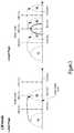
- FIG. 3is a diagram illustrating charge levels in a multi-level cell memory operated to store two bits of data in a memory cell.
- FIG. 4is a diagram illustrating charge levels in a multi-level cell memory
- FIG. 5is a diagram of charge distribution with single level cell programming.
- FIG. 6is a diagram of charge distribution showing multiple single level cell programming.
- FIG. 7is another diagram of charge distribution showing multiple single level cell programming.
- FIG. 8is a flowchart illustrating program state modification.
- a storage device with a memorymay include improved endurance and programming speed by modifying the programming states of the memory blocks.
- the blocksmay be three bit memory blocks, but a dynamic reassignment of read margins and verify levels can result in the block acting like a two bit memory block.
- Memory blocksmay be designed for a certain number of bits per cell (i.e. number of states) and the programming is based on that number.
- single level cell (SLC) programmingis also possible in addition to programming according to the number of bits per cell that the memory is designed for. Multiple SLC programming steps can be used to modify the number of states for certain memory cells.
- This dynamic reassignment of the programmed statemay be performed when an erase cycle is needed.
- the original data and newer datacan be programmed on the same SLC block and the erase can be performed once (e.g. the erase is every two programs rather than one program).
- PIEprogram/erase
- the number of program/erase (“PIE”) cyclingcan be doubled while the SLC is converted to a different type of memory (different number of states) that may have better endurance and faster programming. Decreasing the number of states for each memory cell may result in the P/E ratio being increased.
- the increase of the block programming allowed per erase instancemay help increase the cycling performance of the flash memory, mainly due to the reduced stress time from the erase.
- This system/methodsmartly manages the data written to the flash memory during the program and erase operation to the memory blocks. By doing so, the erase counts to the memory may be effectively reduced while the performance of the write can be enhanced.
- the memory devicemay be an 8 states or 3 bit per cell memory.
- the circuitry of the memory systemcan read/write with the 8 states, but there is no 4 state modes for this memory.
- the circuitrycan also read/write to 2 states using SLC programming. Regardless of the number of states that the memory is designed for, it can still perform SLC programming with 2 states. Using multiple SLC programming steps and modifying both the read margin and program verify level the 8-state memory can be used as 4-state memory. This provides interchangeability for different technologies that were previously incompatible.
- the number of states (or bits per cell)may be different, but SLC may still be used to treat the memory as if it was designed for a different number of states.
- FIGS. 1A-2Bare exemplary memory systems which may implement BDRL.
- FIG. 1Ais a block diagram illustrating a non-volatile memory system.
- the non-volatile memory system 100includes a controller 102 and non-volatile memory that may be made up of one or more non-volatile memory die 104 .
- the term dierefers to the set of non-volatile memory cells, and associated circuitry for managing the physical operation of those non-volatile memory cells, that are formed on a single semiconductor substrate.
- Controller 102interfaces with a host system and transmits command sequences for read, program, and erase operations to non-volatile memory die 104 .
- the non-volatile memory die 104may store an operating system for the host.
- Examples of host systemsinclude, but are not limited to, personal computers (PCs), such as desktop or laptop and other portable computers, tablets, mobile devices, cellular telephones, smartphones, personal digital assistants (PDAs), gaming devices, digital still cameras, digital movie cameras, and portable media players.
- PCspersonal computers
- PDAspersonal digital assistants
- a hostmay include a built-in receptacle for one or more types of memory cards or flash drives, or a host may require adapters into which a memory card is plugged.
- the memory systemmay include its own memory controller and drivers but there may also be some memory-only systems that are instead controlled by software executed by the host to which the memory is connected. In some memory systems containing the controller, especially those embedded within a host, the memory, controller and drivers are often formed on a single integrated circuit chip.
- the hostmay communicate with the memory card using any communication protocol such as but not limited to Secure Digital (SD) protocol, Memory Stick (MS) protocol and Universal Serial Bus (USB) protocol.
- SDSecure Digital
- MSMemory Stick
- the controller 102(which may be a flash memory controller) can take the form of processing circuitry, a microprocessor or processor, and a computer-readable medium that stores computer-readable program code (e.g., software or firmware) executable by the (micro)processor, logic gates, switches, an application specific integrated circuit (ASIC), a programmable logic controller, and an embedded microcontroller, for example.
- the controller 102can be configured with hardware and/or firmware to perform the various functions described below and shown in the flow diagrams. Also, some of the components shown as being internal to the controller can also be stored external to the controller, and other components can be used. Additionally, the phrase “operatively in communication with” could mean directly in communication with or indirectly (wired or wireless) in communication with through one or more components, which may or may not be shown or described herein.
- a flash memory controlleris a device that manages data stored on flash memory and communicates with a host, such as a computer or electronic device.
- a flash memory controllercan have various functionality in addition to the specific functionality described herein.
- the flash memory controllercan format the flash memory to ensure the memory is operating properly, map out bad flash memory cells, and allocate spare cells to be substituted for future failed cells. Some part of the spare cells can be used to hold firmware to operate the flash memory controller and implement other features.
- the flash memory controllercan convert the logical address received from the host to a physical address in the flash memory.
- the flash memory controllercan also perform various memory management functions, such as, but not limited to, wear leveling (distributing writes to avoid wearing out specific blocks of memory that would otherwise be repeatedly written to) and garbage collection (after a block is full, moving only the valid pages of data to a new block, so the full block can be erased and reused).
- wear levelingdistributing writes to avoid wearing out specific blocks of memory that would otherwise be repeatedly written to
- garbage collectionafter a block is full, moving only the valid pages of data to a new block, so the full block can be erased and reused.
- Non-volatile memory die 104may include any suitable non-volatile storage medium, including NAND flash memory cells and/or NOR flash memory cells.
- the memory cellscan take the form of solid-state (e.g., flash) memory cells and can be one-time programmable, few-time programmable, or many-time programmable.
- the memory cellscan also be single-level cells (SLC), multiple-level cells (MLC), triple-level cells (TLC), or use other memory cell level technologies, now known or later developed.
- the memory cellscan be fabricated in a two-dimensional or three-dimensional fashion.
- the interface between controller 102 and non-volatile memory die 104may be any suitable flash interface, such as Toggle Mode 200 , 400 , or 800 .
- memory system 100may be a card based system, such as a secure digital (SD) or a micro secure digital (micro-SD) card.
- memory system 100may be part of an embedded memory system.
- the flash memorymay be embedded within the host, such as in the form of a solid state disk (SSD) drive installed in a personal computer.
- SSDsolid state disk
- non-volatile memory system 100includes a single channel between controller 102 and non-volatile memory die 104
- the subject matter described hereinis not limited to having a single memory channel.
- 2, 4, 8 or more NAND channelsmay exist between the controller and the NAND memory device, depending on controller capabilities.
- more than a single channelmay exist between the controller and the memory die, even if a single channel is shown in the drawings.
- FIG. 1Billustrates a storage module 200 that includes plural non-volatile memory systems 100 .
- storage module 200may include a storage controller 202 that interfaces with a host and with storage system 204 , which includes a plurality of non-volatile memory systems 100 .
- the interface between storage controller 202 and non-volatile memory systems 100may be a bus interface, such as a serial advanced technology attachment (SATA) or peripheral component interface express (PCIe) interface.
- Storage module 200in one embodiment, may be a solid state drive (SSD), such as found in portable computing devices, such as laptop computers, and tablet computers.
- SSDsolid state drive
- FIG. 1Cis a block diagram illustrating a hierarchical storage system.
- a hierarchical storage system 210includes a plurality of storage controllers 202 , each of which control a respective storage system 204 .
- Host systems 212may access memories within the hierarchical storage system via a bus interface.
- the bus interfacemay be a non-volatile memory express (NVMe) or a fiber channel over Ethernet (FCoE) interface.
- the system illustrated in FIG. 1Cmay be a rack mountable mass storage system that is accessible by multiple host computers, such as would be found in a data center or other location where mass storage is needed.
- FIG. 2Ais a block diagram illustrating exemplary components of controller 102 in more detail.
- Controller 102includes a front end module 108 that interfaces with a host, a back end module 110 that interfaces with the one or more non-volatile memory die 104 , and various other modules that perform functions which will now be described in detail.
- a modulemay take the form of a packaged functional hardware unit designed for use with other components, a portion of a program code (e.g., software or firmware) executable by a (micro)processor or processing circuitry that usually performs a particular function of related functions, or a self-contained hardware or software component that interfaces with a larger system, for example.
- each modulemay include an application specific integrated circuit (ASIC), a Field Programmable Gate Array (FPGA), a circuit, a digital logic circuit, an analog circuit, a combination of discrete circuits, gates, or any other type of hardware or combination thereof.
- ASICapplication specific integrated circuit
- FPGAField Programmable Gate Array
- each modulemay include memory hardware, such as a portion of the memory 104 , for example, that comprises instructions executable with a processor to implement one or more of the features of the module.
- memory hardwaresuch as a portion of the memory 104 , for example, that comprises instructions executable with a processor to implement one or more of the features of the module.
- the modulemay or may not include the processor.
- each modulemay just be the portion of the memory 104 or other physical memory that comprises instructions executable with the processor to implement the features of the corresponding module.
- the controller 102may include program state circuitry 112 .
- the program state circuitry 112may be used for assigning a different number of states to cells in a block. That number may be different from what the block was designed for.
- SLC programmingmay be used to generate a different distribution of states.
- the memory 104may be designed for 8 states per cell (3 bits per cell), but using SLC programming, certain blocks may be programmed with only 4 states (2 bits per cell) even if the other circuitry of the NAND or memory system was only designed for 8 states per cell.
- a buffer manager/bus controller 114manages buffers in random access memory (RAM) 116 and controls the internal bus arbitration of controller 102 .
- a read only memory (ROM) 118stores system boot code. Although illustrated in FIG. 2A as located separately from the controller 102 , in other embodiments one or both of the RAM 116 and ROM 118 may be located within the controller. In yet other embodiments, portions of RAM and ROM may be located both within the controller 102 and outside the controller. Further, in some implementations, the controller 102 , RAM 116 , and ROM 118 may be located on separate semiconductor die.
- Front end module 108includes a host interface 120 and a physical layer interface (PHY) 122 that provide the electrical interface with the host or next level storage controller.
- PHYphysical layer interface
- the choice of the type of host interface 120can depend on the type of memory being used. Examples of host interfaces 120 include, but are not limited to, SATA, SATA Express, SAS, Fibre Channel, USB, PCIe, and NVMe.
- the host interface 120typically facilitates transfer for data, control signals, and timing signals.
- Back end module 110includes an error correction controller (ECC) engine 124 that encodes the data bytes received from the host, and decodes and error corrects the data bytes read from the non-volatile memory.
- ECCerror correction controller
- a command sequencer 126generates command sequences, such as program and erase command sequences, to be transmitted to non-volatile memory die 104 .
- a RAID (Redundant Array of Independent Drives) module 128manages generation of RAID parity and recovery of failed data. The RAID parity may be used as an additional level of integrity protection for the data being written into the non-volatile memory system 100 . In some cases, the RAID module 128 may be a part of the ECC engine 124 .
- a memory interface 130provides the command sequences to non-volatile memory die 104 and receives status information from non-volatile memory die 104 .
- memory interface 130may be a double data rate (DDR) interface, such as a Toggle Mode 200 , 400 , or 800 interface.
- DDRdouble data rate
- a flash control layer 132controls the overall operation of back end module 110 .
- System 100includes media management layer 138 , which performs wear leveling of memory cells of non-volatile memory die 104 .
- System 100also includes other discrete components 140 , such as external electrical interfaces, external RAM, resistors, capacitors, or other components that may interface with controller 102 .
- one or more of the physical layer interface 122 , RAID module 128 , media management layer 138 and buffer management/bus controller 114are optional components that are not necessary in the controller 102 .
- the FTL or MML 138may be integrated as part of the flash management that may handle flash errors and interfacing with the host.
- MMLmay be a module in flash management and may be responsible for the internals of NAND management.
- the MML 138may include an algorithm in the memory device firmware which translates writes from the host into writes to the flash memory 104 .
- the MML 138may be needed because: 1) the flash memory may have limited endurance; 2) the flash memory 104 may only be written in multiples of pages; and/or 3) the flash memory 104 may not be written unless it is erased as a block.
- the MML 138understands these potential limitations of the flash memory 104 which may not be visible to the host.
- the MML 138attempts to translate the writes from host into writes into the flash memory 104 .
- erratic bitsmay be identified and recorded using the MML 138 . This recording of erratic bits can be used for evaluating the health of blocks.
- FIG. 2Bis a block diagram illustrating exemplary components of non-volatile memory die 104 in more detail.
- Non-volatile memory die 104includes peripheral circuitry 141 and non-volatile memory array 142 .
- Non-volatile memory array 142includes the non-volatile memory cells used to store data.
- the non-volatile memory cellsmay be any suitable non-volatile memory cells, including NAND flash memory cells and/or NOR flash memory cells in a two dimensional and/or three dimensional configuration.
- Peripheral circuitry 141includes a state machine 152 that provides status information to controller 102 .
- Non-volatile memory die 104further includes a data cache 156 that caches data.
- Exemplary peripheral circuitry 141may include clocks, pumps, ESD, current shunt, current sink, and/or closely-packed logic circuits.
- the logic interpretation of the program stateis achieved by the NAND read circuits by setting appropriate read levels against the expected charge states.
- the data into and from the NAND chipmay be controlled by the MCU or ASIC circuitry and a data processing algorithm unit of the system where the data is interpreted and further transferred to the host.
- FIG. 3is a diagram illustrating charge levels in cell memory.
- the charge storage elements of the memory cellsare most commonly conductive floating gates but may alternatively be non-conductive dielectric charge trapping material.
- Each cell or memory unitmay store a certain number of bits of data per cell.
- MLC memorymay store four states and can retain two bits of data: 00 or 01 and 10 or 11.
- MLC memorymay store eight states for retaining three bits of data as shown in FIG. 4 . In other embodiments, there may be a different number of bits per cell.
- FIG. 3illustrates a memory cell that is operated to store two bits of data.
- This memory schememay be referred to as eX2 memory because it has two bits per cell.
- the memory cellsmay be operated to store two levels of charge so that a single bit of data is stored in each cell. This is typically referred to as a binary or single level cell (SLC) memory.
- SLC memorymay store two states: 0 or 1.
- the memory cellsmay be operated to store more than two detectable levels of charge in each charge storage element or region, thereby to store more than one bit of data in each. This latter configuration is referred to as multi-level cell (MLC) memory.
- MLCmulti-level cell
- FIG. 3illustrates a two-bit per cell memory scheme in which either four states (Erase, A, B, C) or with two states of SLC memory.
- This two-bit per cell memory (i.e. eX2) memorycan operate as SLC or as four state MLC.
- three-bit per cell memoryi.e. eX3
- the NAND circuitrymay be configured for only a certain number of bit per cell MLC memory, but still operate as SLC.
- MLC memorycan operate as a MLC or SLC, but with regard to the MLC operation three bit per cell memory cannot operate as two bit per cell memory and vice-versa.
- the embodiments described belowutilize any MLC memory scheme's ability to work with SLC to then operate at different bits per cell.
- FIG. 3illustrates one implementation of the four charge levels used to represent two bits of data in a memory cell.
- each memory cellis configured to store four levels of charge corresponding to values of “11,” “01,” “10,” and “00.”
- Each bit of the two bits of datamay represent a page bit of a lower page or a page bit of an upper page, where the lower page and upper page span across a series of memory cells sharing a common word line.
- the less significant bit of the two bits of datarepresents a page bit of a lower page and the more significant bit of the two bits of data represents a page bit of an upper page.
- the read marginsare established for identifying each state.
- the three read marginsdelineate the four states.
- there is a verify leveli.e. a voltage level
- FIG. 3is labeled as LM mode which may be referred to as lower at middle mode and will further be described below regarding the lower at middle or lower-middle intermediate state.
- the LM intermediate statemay also be referred to as a lower page programmed stage.
- a value of “11”corresponds to an un-programmed state or erase state of the memory cell.
- the level of chargeis increased to represent a value of “10” corresponding to a programmed state of the page bit of the lower page.
- the lower pagemay be considered a logical concept that represents a location on a multi-level cell (MLC).
- MLCmulti-level cell
- a logical pagemay include all the least significant bits of the cells on the wordline that are grouped together.
- the lower pageis the least significant bits.
- programming pulsesare applied to the memory cell for the page bit of the upper page to increase the level of charge to correspond to a value of “00” or “10” depending on the desired value of the page bit of the upper page.
- FIG. 4is a diagram illustrating charge levels in a multi-level cell memory operated to store three bits of data in a memory cell.
- FIG. 4illustrates MLC memory with three bits of data which are stored in a single cell by establishing eight states or voltage level distinctions. This memory may be referred to as X3 memory.
- FIG. 4illustrates the stages that may be used for programming three bit memory. In a first stage, the voltage levels are divided out at two levels, and at the second stage (i.e. foggy program), those two levels are divided up into the eight states without setting the distinct levels between states. At the third stage (i.e. fine program), the voltage levels for each of the eight states are separated and distinct. The fine programming establishes the voltage levels for each of the states. As compared with two bit memory, the three bit memory in FIG. 4 requires more exact programming voltages to avoid errors. Electron movement or loss from the charge values may result in problems. Endurance and programming speed may decrease based on the exact programming that is required.
- nbits per cell
- SLC programmingSLC programming
- FIG. 5is a diagram of charge distribution with single level cell (SLC) programming.
- the two statesare the erase state and the program state. This particular cell can provide either a 0 or a 1 as the stored bit.
- FIG. 5illustrates the voltage along the x-axis with both SLC states. The distributions represent the range of voltage levels for each state.
- the programming performed for these two statesis SLC programming. Even for memory that is multiple bits per cell, this type of SLC programming may still be performed. In other words, multiple bit per cell memory can still be used with two states from SLC programming. This may be the first programming after a fresh erase.
- FIG. 6is a diagram of charge distribution showing multiple single level cell programming.
- the programming shown in both FIG. 6 and FIG. 7is part of a second programming that follows the initial programming of FIG. 5 .
- the new datamay be received for programming.
- this flagmay identify whether the block is fully programmed (e.g. 3 bit per cell memory being programmed with 3 bits per cell) or partially programmed using multiple SLC programs (e.g. 3 bit per cell memory being programmed with 2 bits per cell).
- the secondary programming shown with respect to FIG. 6 and FIG. 7may only be performed when the flag identifies this partial programming.
- FIG. 6illustrates that the program state (from FIG. 5 ) can be reprogrammed to be another program state.
- the two programmed states shown in FIG. 6are the B state (SLC_B) and the C state (SLC_C).
- the B stateis the original state programmed with the first SLC programming operation and the C state is the newly programmed state.
- the C stateis programmed from the original program state (from FIG. 5 ) which is now the B state.
- the program verify voltage (PGMV) of the C stateis set to be outside of the read level. The reassignment of the read margin and program verify voltages can be used to establish a different number of states.
- FIG. 7is another diagram of charge distribution showing multiple single level cell programming.
- the programming in FIG. 7may be additional programming or may be part of (e.g. parallel to) the programming shown in FIG. 6 .
- the erase stateis programmed to be the A state (SLC_A).
- the A stateis newly programmed from the original erase state.
- the third program verify level (PGMV)is set to be outside of the erase state. Accordingly, the read margin separates the erase state from the A state.
- the read margin in front of the B stateis outside of the A state.
- the C statemay be programmed based on the erase state. In other words, the original erase state is used for programming the new state C.
- the embodiment shown in FIG. 6illustrates that state C is programmed from the original program state (now state B) rather than the erase state.
- FIG. 7illustrates the establishment of four states (e.g. 2 bits per cell).
- the reassignment of the programmed statesmay allow memory configured for 8 states (e.g. 3 bits per cell) to be repurposed into four states using the SLC programming described. This may be referred to as dynamic reassignment of the programmed states or of the distribution.
- the initial programminge.g. FIG. 5
- the initial programmingmay refer to old data that is assigned the lower page, while the new data of the subsequent programming is assigned to the upper page.
- the assignment of a different bit per cell schememay be done at the block level. For example, in a 3 bit per cell NAND, there may be certain blocks that are treated as 2 bit per cell. Alternatively, the management of the bit per cell structure may be at a larger scale (e.g. meta-block, plane, die, etc.) or at a smaller scale (e.g. page level) in other embodiments.
- a larger scalee.g. meta-block, plane, die, etc.
- a smaller scalee.g. page level
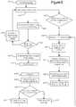
- FIG. 8is a flowchart illustrating program state modification.
- the programmingis started in block 802 .
- the programming flagis read in block 804 .
- the programming flagmay indicate whether the memory is in a default mode or in a mode where the number of states has been modified with SLC programs.
- the memory blockis checked to see if it is freshly erased or partially programmed for the first time.
- the memory blockis programmed using a first set of verify and read settings in block 808 .
- the first set of verify and read settingscorrespond to a first programming (i.e. FIG. 5 ).
- a second set of verify and read settingscorrespond to a second programming (i.e. FIG. 6 and/or FIG. 7 ).
- the programming flagis set for regular programming (default mode) in block 812 .
- the readcan be continued in block 814 .
- the first programmingcontinues with the original settings in block 816 .
- the second programmingis performed in block 818 . Then a second set of verify and read settings are utilized for the second programming in block 820 . The second programming is continued with the second settings until it is fully programmed in block 822 . The programming flag is set for the revised or reassigned (second) programming state mode in block 824 . The reading is continued with the second set of read settings in block 826 .
- the erase commandis issued in block 830 .
- the programming flagis checked to determine if the flag identifies the first programming or the second programming in block 832 .
- the programming flagidentifies the second programming then the block is erased and the flag is reset in block 834 . If the flag identifies the first programming, then the post first programming flow is continued in block 836 . In particular, the first programming is performed in block 818 .
- circuitrythat includes an instruction processor, such as a Central Processing Unit (CPU), microcontroller, or a microprocessor; or as an Application Specific Integrated Circuit (ASIC), Programmable Logic Device (PLD), or Field Programmable Gate Array (FPGA); or as circuitry that includes discrete logic or other circuit components, including analog circuit components, digital circuit components or both; or any combination thereof.
- instruction processorsuch as a Central Processing Unit (CPU), microcontroller, or a microprocessor
- ASICApplication Specific Integrated Circuit
- PLDProgrammable Logic Device
- FPGAField Programmable Gate Array
- the circuitrymay include discrete interconnected hardware components or may be combined on a single integrated circuit die, distributed among multiple integrated circuit dies, or implemented in a Multiple Chip Module (MCM) of multiple integrated circuit dies in a common package, as examples.
- MCMMultiple Chip Module
- the circuitrymay store or access instructions for execution, or may implement its functionality in hardware alone.
- the instructionsmay be stored in a tangible storage medium that is other than a transitory signal, such as a flash memory, a Random Access Memory (RAM), a Read Only Memory (ROM), an Erasable Programmable Read Only Memory (EPROM); or on a magnetic or optical disc, such as a Compact Disc Read Only Memory (CDROM), Hard Disk Drive (HDD), or other magnetic or optical disk; or in or on another machine-readable medium.
- a productsuch as a computer program product, may include a storage medium and instructions stored in or on the medium, and the instructions when executed by the circuitry in a device may cause the device to implement any of the processing described above or illustrated in the drawings.
- the circuitrymay include multiple distinct system components, such as multiple processors and memories, and may span multiple distributed processing systems.
- Parameters, databases, and other data structuresmay be separately stored and managed, may be incorporated into a single memory or database, may be logically and physically organized in many different ways, and may be implemented in many different ways.
- Example implementationsinclude linked lists, program variables, hash tables, arrays, records (e.g., database records), objects, and implicit storage mechanisms. Instructions may form parts (e.g., subroutines or other code sections) of a single program, may form multiple separate programs, may be distributed across multiple memories and processors, and may be implemented in many different ways.
- Example implementationsinclude stand-alone programs, and as part of a library, such as a shared library like a Dynamic Link Library (DLL).
- the librarymay contain shared data and one or more shared programs that include instructions that perform any of the processing described above or illustrated in the drawings, when executed by the circuitry.
- the semiconductor memory elements located within and/or over a substratemay be arranged in two or three dimensions, such as a two dimensional memory structure or a three dimensional memory structure.
- the semiconductor memory elementsare arranged in a single plane or a single memory device level.
- memory elementsare arranged in a plane (e.g., in an x-z direction plane) which extends substantially parallel to a major surface of a substrate that supports the memory elements.
- the substratemay be a wafer over or in which the layer of the memory elements are formed or it may be a carrier substrate which is attached to the memory elements after they are formed.
- the substratemay include a semiconductor such as silicon.
- the memory elementsmay be arranged in the single memory device level in an ordered array, such as in a plurality of rows and/or columns. However, the memory elements may be arrayed in non-regular or non-orthogonal configurations.
- the memory elementsmay each have two or more electrodes or contact lines, such as bit lines and word lines.
- a three dimensional memory arrayis arranged so that memory elements occupy multiple planes or multiple memory device levels, thereby forming a structure in three dimensions (i.e., in the x, y and z directions, where the y direction is substantially perpendicular and the x and z directions are substantially parallel to the major surface of the substrate).
- a three dimensional memory structuremay be vertically arranged as a stack of multiple two dimensional memory device levels.
- a three dimensional memory arraymay be arranged as multiple vertical columns (e.g., columns extending substantially perpendicular to the major surface of the substrate, i.e., in the y direction) with each column having multiple memory elements in each column.
- the columnsmay be arranged in a two dimensional configuration, e.g., in an x-z plane, resulting in a three dimensional arrangement of memory elements with elements on multiple vertically stacked memory planes.
- Other configurations of memory elements in three dimensionscan also constitute a three dimensional memory array.
- the memory elementsmay be coupled together to form a NAND string within a single horizontal (e.g., x-z) memory device levels.
- the memory elementsmay be coupled together to form a vertical NAND string that traverses across multiple horizontal memory device levels.
- Other three dimensional configurationscan be envisioned wherein some NAND strings contain memory elements in a single memory level while other strings contain memory elements which span through multiple memory levels.
- Three dimensional memory arraysmay also be designed in a NOR configuration and in a ReRAM configuration.
- a monolithic three dimensional memory arraytypically, one or more memory device levels are formed above a single substrate.
- the monolithic three dimensional memory arraymay also have one or more memory layers at least partially within the single substrate.
- the substratemay include a semiconductor such as silicon.
- the layers constituting each memory device level of the arrayare typically formed on the layers of the underlying memory device levels of the array.
- layers of adjacent memory device levels of a monolithic three dimensional memory arraymay be shared or have intervening layers between memory device levels.
- non-monolithic stacked memoriescan be constructed by forming memory levels on separate substrates and then stacking the memory levels atop each other. The substrates may be thinned or removed from the memory device levels before stacking, but as the memory device levels are initially formed over separate substrates, the resulting memory arrays are not monolithic three dimensional memory arrays. Further, multiple two dimensional memory arrays or three dimensional memory arrays (monolithic or non-monolithic) may be formed on separate chips and then packaged together to form a stacked-chip memory device.
- Associated circuitryis typically required for operation of the memory elements and for communication with the memory elements.
- memory devicesmay have circuitry used for controlling and driving memory elements to accomplish functions such as programming and reading.
- This associated circuitrymay be on the same substrate as the memory elements and/or on a separate substrate.
- a controller for memory read-write operationsmay be located on a separate controller chip and/or on the same substrate as the memory elements.
- semiconductor memory devicessuch as those described in the present application may include volatile memory devices, such as dynamic random access memory (“DRAM”) or static random access memory (“SRAM”) devices, non-volatile memory devices, such as resistive random access memory (“ReRAM”), electrically erasable programmable read only memory (“EEPROM”), flash memory (which can also be considered a subset of EEPROM), ferroelectric random access memory (“FRAM”), and magneto-resistive random access memory (“MRAM”), and other semiconductor elements capable of storing information.
- volatile memory devicessuch as dynamic random access memory (“DRAM”) or static random access memory (“SRAM”) devices
- non-volatile memory devicessuch as resistive random access memory (“ReRAM”), electrically erasable programmable read only memory (“EEPROM”), flash memory (which can also be considered a subset of EEPROM), ferroelectric random access memory (“FRAM”), and magneto-resistive random access memory (“MRAM”), and other semiconductor elements capable of storing information.
- ReRAMresistive random access
- the memory devicescan be formed from passive and/or active elements, in any combinations.
- passive semiconductor memory elementsinclude ReRAM device elements, which in some embodiments include a resistivity switching storage element, such as an anti-fuse, phase change material, etc., and optionally a steering element, such as a diode, etc.
- active semiconductor memory elementsinclude EEPROM and flash memory device elements, which in some embodiments include elements containing a charge storage region, such as a floating gate, conductive nanoparticles, or a charge storage dielectric material.
- Multiple memory elementsmay be configured so that they are connected in series or so that each element is individually accessible.
- flash memory devices in a NAND configurationtypically contain memory elements connected in series.
- a NAND memory arraymay be configured so that the array is composed of multiple strings of memory in which a string is composed of multiple memory elements sharing a single bit line and accessed as a group.
- memory elementsmay be configured so that each element is individually accessible, e.g., a NOR memory array.
- NAND and NOR memory configurationsare exemplary, and memory elements may be otherwise configured.
- a “computer-readable medium,” “machine readable medium,” “propagated-signal” medium, and/or “signal-bearing medium”may comprise any device that includes, stores, communicates, propagates, or transports software for use by or in connection with an instruction executable system, apparatus, or device.
- the machine-readable mediummay selectively be, but not limited to, an electronic, magnetic, optical, electromagnetic, infrared, or semiconductor system, apparatus, device, or propagation medium.
- a non-exhaustive list of examples of a machine-readable mediumwould include: an electrical connection “electronic” having one or more wires, a portable magnetic or optical disk, a volatile memory such as a Random Access Memory “RAM”, a Read-Only Memory “ROM”, an Erasable Programmable Read-Only Memory (EPROM or Flash memory), or an optical fiber.
- a machine-readable mediummay also include a tangible medium upon which software is printed, as the software may be electronically stored as an image or in another format (e.g., through an optical scan), then compiled, and/or interpreted or otherwise processed. The processed medium may then be stored in a computer and/or machine memory.
- dedicated hardware implementationssuch as application specific integrated circuits, programmable logic arrays and other hardware devices, can be constructed to implement one or more of the methods described herein.
- Applicationsthat may include the apparatus and systems of various embodiments can broadly include a variety of electronic and computer systems.
- One or more embodiments described hereinmay implement functions using two or more specific interconnected hardware modules or devices with related control and data signals that can be communicated between and through the modules, or as portions of an application-specific integrated circuit. Accordingly, the present system encompasses software, firmware, and hardware implementations.
Landscapes
- Engineering & Computer Science (AREA)
- Theoretical Computer Science (AREA)
- Physics & Mathematics (AREA)
- General Engineering & Computer Science (AREA)
- General Physics & Mathematics (AREA)
- Quality & Reliability (AREA)
- Computer Hardware Design (AREA)
- Read Only Memory (AREA)
Abstract
Description
Claims (22)
Priority Applications (1)
| Application Number | Priority Date | Filing Date | Title |
|---|---|---|---|
| US16/146,351US10629260B2 (en) | 2015-09-01 | 2018-09-28 | Dynamic management of programming states to improve endurance |
Applications Claiming Priority (2)
| Application Number | Priority Date | Filing Date | Title |
|---|---|---|---|
| US14/842,550US10096355B2 (en) | 2015-09-01 | 2015-09-01 | Dynamic management of programming states to improve endurance |
| US16/146,351US10629260B2 (en) | 2015-09-01 | 2018-09-28 | Dynamic management of programming states to improve endurance |
Related Parent Applications (2)
| Application Number | Title | Priority Date | Filing Date |
|---|---|---|---|
| US14/842,550ContinuationUS10096355B2 (en) | 2015-09-01 | 2015-09-01 | Dynamic management of programming states to improve endurance |
| US14/842,550DivisionUS10096355B2 (en) | 2015-09-01 | 2015-09-01 | Dynamic management of programming states to improve endurance |
Publications (2)
| Publication Number | Publication Date |
|---|---|
| US20190035457A1 US20190035457A1 (en) | 2019-01-31 |
| US10629260B2true US10629260B2 (en) | 2020-04-21 |
Family
ID=58096645
Family Applications (2)
| Application Number | Title | Priority Date | Filing Date |
|---|---|---|---|
| US14/842,550Active2035-12-15US10096355B2 (en) | 2015-09-01 | 2015-09-01 | Dynamic management of programming states to improve endurance |
| US16/146,351ActiveUS10629260B2 (en) | 2015-09-01 | 2018-09-28 | Dynamic management of programming states to improve endurance |
Family Applications Before (1)
| Application Number | Title | Priority Date | Filing Date |
|---|---|---|---|
| US14/842,550Active2035-12-15US10096355B2 (en) | 2015-09-01 | 2015-09-01 | Dynamic management of programming states to improve endurance |
Country Status (1)
| Country | Link |
|---|---|
| US (2) | US10096355B2 (en) |
Cited By (1)
| Publication number | Priority date | Publication date | Assignee | Title |
|---|---|---|---|---|
| US11862261B2 (en) | 2020-11-30 | 2024-01-02 | Samsung Electronics Co., Ltd. | Method of writing data in nonvolatile memory device, nonvolatile memory device performing the same and method of operating memory system using the same |
Families Citing this family (6)
| Publication number | Priority date | Publication date | Assignee | Title |
|---|---|---|---|---|
| KR102274280B1 (en)* | 2015-06-22 | 2021-07-07 | 삼성전자주식회사 | Method of operating a non-volatile memory device |
| US11049009B2 (en)* | 2017-06-12 | 2021-06-29 | Western Digital Technologies, Inc. | Identifying memory block write endurance using machine learning |
| US10580481B1 (en)* | 2019-01-14 | 2020-03-03 | University Of Virginia Patent Foundation | Methods, circuits, systems, and articles of manufacture for state machine interconnect architecture using embedded DRAM |
| US11061768B1 (en)* | 2020-02-14 | 2021-07-13 | Western Digital Technologies, Inc. | Storage device with increased endurance |
| CN111415697B (en)* | 2020-03-20 | 2022-08-16 | 杭州华澜微电子股份有限公司 | Method, device and system for verifying flash translation layer algorithm |
| JP7358312B2 (en) | 2020-08-25 | 2023-10-10 | 株式会社東芝 | Memory and neural network devices |
Citations (59)
| Publication number | Priority date | Publication date | Assignee | Title |
|---|---|---|---|---|
| US5930167A (en) | 1997-07-30 | 1999-07-27 | Sandisk Corporation | Multi-state non-volatile flash memory capable of being its own two state write cache |
| US6532169B1 (en) | 2001-06-26 | 2003-03-11 | Cypress Semiconductor Corp. | SONOS latch and application |
| US20050180209A1 (en) | 2004-02-15 | 2005-08-18 | M-Systems Flash Disk Pioneers, Ltd. | Method of managing a multi-bit-cell flash memory |
| US20050273549A1 (en) | 2004-06-04 | 2005-12-08 | Micron Technology, Inc. | Memory device with user configurable density/performance |
| US20060004952A1 (en) | 2004-02-15 | 2006-01-05 | M-Systems Flash Disk Pioneers, Ltd. | Method of managing a multi-bit-cell flash memory |
| US20070061502A1 (en)* | 2005-09-09 | 2007-03-15 | M-Systems Flash Disk Pioneers Ltd. | Flash memory storage system and method |
| US20070070696A1 (en)* | 2004-07-26 | 2007-03-29 | Msystems Ltd | Drift compensation in a flash memory |
| US7218551B2 (en)* | 2004-06-25 | 2007-05-15 | Micron Technology, Inc. | Multiple level cell memory device with single bit per cell, re-mappable memory block |
| US20070195607A1 (en)* | 2006-02-21 | 2007-08-23 | Saifun Semiconductors Ltd. | Nrom non-volatile memory and mode of operation |
| US7308525B2 (en) | 2005-01-10 | 2007-12-11 | Sandisk Il Ltd. | Method of managing a multi-bit cell flash memory with improved reliablility and performance |
| US20080123406A1 (en)* | 2006-11-02 | 2008-05-29 | Macronix International Co., Ltd. | Dynamic Program and Read Adjustment for Multi-Level Cell Memory Array |
| US20080172521A1 (en) | 2007-01-16 | 2008-07-17 | Samsung Electronics Co., Ltd. | Memory System Determining Storage Mode According to Host Provided Data Information |
| US20080172520A1 (en)* | 2007-01-17 | 2008-07-17 | Samsung Electronics Co., Ltd. | Nonvolatile memory devices including multiple user-selectable program modes and related methods of operation |
| US20080198651A1 (en)* | 2007-02-16 | 2008-08-21 | Mosaid Technologies Incorporated | Non-volatile memory with dynamic multi-mode operation |
| US20080222353A1 (en) | 2007-03-08 | 2008-09-11 | Samsung Electronics Co., Ltd. | Method of converting a hybrid hard disk drive to a normal hdd |
| US7508732B2 (en) | 2006-10-26 | 2009-03-24 | Samsung Electronics Co., Ltd. | Multi-bit flash memory device including memory cells storing different numbers of bits |
| US7545673B2 (en) | 2007-09-25 | 2009-06-09 | Sandisk Il Ltd. | Using MLC flash as SLC by writing dummy data |
| US7593263B2 (en) | 2006-12-17 | 2009-09-22 | Anobit Technologies Ltd. | Memory device with reduced reading latency |
| US20090327590A1 (en)* | 2008-06-25 | 2009-12-31 | Stec, Inc. | Enhanced mlc solid state device |
| US20100020601A1 (en)* | 2008-07-22 | 2010-01-28 | Se-Hoon Lee | Multi-Bit Flash Memory Devices and Methods of Programming and Erasing the Same |
| US20100042772A1 (en)* | 2008-08-14 | 2010-02-18 | Addmm, Llc | Method and apparatus for high reliability data storage and retrieval operations in multi-level flash cells |
| US7698615B2 (en)* | 2006-12-06 | 2010-04-13 | Samsung Electronics Co., Ltd. | Semiconductor memory device having single-level cells and multi-level cells and method of driving the semiconductor memory device |
| US20100122016A1 (en)* | 2008-11-12 | 2010-05-13 | Micron Technology | Dynamic slc/mlc blocks allocations for non-volatile memory |
| US20100149870A1 (en)* | 2008-12-04 | 2010-06-17 | Riichiro Shirota | Non-volatile semiconductor memory, and the method thereof |
| US20100232240A1 (en) | 2009-03-13 | 2010-09-16 | Unity Semiconductor Corporation | Columnar replacement of defective memory cells |
| US20100332922A1 (en)* | 2009-06-30 | 2010-12-30 | Mediatek Inc. | Method for managing device and solid state disk drive utilizing the same |
| US20110157982A1 (en)* | 2009-07-10 | 2011-06-30 | Peter Wung Lee | Novel High Speed High Density NAND-Based 2T-NOR Flash Memory Design |
| US20110208896A1 (en) | 2010-02-25 | 2011-08-25 | Apple Inc. | Dynamically allocating number of bits per cell for memory locations of a non-volatile memory |
| US20110302354A1 (en)* | 2010-06-02 | 2011-12-08 | Conexant Systems, Inc. | Systems and methods for reliable multi-level cell flash storage |
| US8085569B2 (en)* | 2006-12-28 | 2011-12-27 | Hynix Semiconductor Inc. | Semiconductor memory device, and multi-chip package and method of operating the same |
| US20120008390A1 (en)* | 2010-07-09 | 2012-01-12 | Jin Yong Seong | Semiconductor memory device and method of operating the same |
| US20120173827A1 (en)* | 2009-03-13 | 2012-07-05 | Wood Robert B | Apparatus, system, and method for using multi-level cell storage in a single-level cell mode |
| US20120240012A1 (en)* | 2010-07-07 | 2012-09-20 | Stec, Inc. | Apparatus and method for multi-mode operation of a flash memory device |
| US8332578B2 (en)* | 2009-07-31 | 2012-12-11 | Intel Corporation | Method and system to improve the performance of a multi-level cell (MLC) NAND flash memory |
| US8341331B2 (en) | 2008-04-10 | 2012-12-25 | Sandisk Il Ltd. | Method, apparatus and computer readable medium for storing data on a flash device using multiple writing modes |
| US20130080730A1 (en)* | 2011-09-23 | 2013-03-28 | Mosaid Technologies Incorporated | Flash memory system |
| US20130124787A1 (en) | 2011-09-09 | 2013-05-16 | Ocz Technology Group Inc. | Nand flash-based storage device and methods of using |
| US20130339603A1 (en)* | 2011-12-23 | 2013-12-19 | Feng Zhu | Method, apparatus and system for determining access to a memory array |
| US20140129874A1 (en) | 2012-11-07 | 2014-05-08 | Apple Inc. | Redundancy schemes for non-volatile memory using parity zones having new and old parity blocks |
| US8730725B2 (en) | 2010-07-07 | 2014-05-20 | Skymedi Corporation | Method of programming/reading a non-volatile memory with a sequence |
| US20140160842A1 (en)* | 2012-12-06 | 2014-06-12 | Sandisk Technologies Inc. | Adaptive Operation of Multi Level Cell Memory |
| US20140173184A1 (en)* | 2012-12-18 | 2014-06-19 | SK Hynix Inc. | Data storage device and operating method thereof |
| US20140201423A1 (en)* | 2013-01-14 | 2014-07-17 | Western Digital Technologies, Inc. | Systems and methods of configuring a mode of operation in a solid-state memory |
| US8886911B2 (en) | 2011-05-31 | 2014-11-11 | Micron Technology, Inc. | Dynamic memory cache size adjustment in a memory device |
| US8898374B2 (en) | 2010-07-21 | 2014-11-25 | Silicon Motion, Inc. | Flash memory device and method for managing flash memory device |
| US9021177B2 (en) | 2010-04-29 | 2015-04-28 | Densbits Technologies Ltd. | System and method for allocating and using spare blocks in a flash memory |
| US20150213896A1 (en) | 2014-01-29 | 2015-07-30 | Sandisk Technologies Inc. | Methods for Balancing Write Operations of SLC Blocks in Different Memory Areas and Apparatus Implementing the Same |
| US9274893B2 (en)* | 2013-05-31 | 2016-03-01 | Silicon Motion, Inc. | Data storage device and error correction method thereof |
| US9348741B1 (en)* | 2011-12-19 | 2016-05-24 | Western Digital Technologies, Inc. | Systems and methods for handling write data access requests in data storage devices |
| US20160147464A1 (en)* | 2014-11-25 | 2016-05-26 | Macronix International Co., Ltd. | Memory orprating method and memory device using the same |
| US9448905B2 (en)* | 2013-04-29 | 2016-09-20 | Samsung Electronics Co., Ltd. | Monitoring and control of storage device based on host-specified quality condition |
| US9632866B2 (en) | 2012-09-28 | 2017-04-25 | Duke University | Systems for and methods of extending lifetime of non-volatile memory |
| US10236908B2 (en)* | 2016-04-27 | 2019-03-19 | Silicon Motion Inc. | Flash memory apparatus and storage management method for flash memory |
| US10275172B2 (en)* | 2016-07-27 | 2019-04-30 | Samsung Electronics Co., Ltd. | Solid state drive devices and methods of operating thereof |
| US10310971B2 (en)* | 2015-01-15 | 2019-06-04 | Huawei Technologies Co., Ltd. | Method and apparatus for processing memory page in memory |
| US10347329B2 (en)* | 2017-08-29 | 2019-07-09 | Micron Technology, Inc. | Reflow protection |
| US10359933B2 (en)* | 2016-09-19 | 2019-07-23 | Micron Technology, Inc. | Memory devices and electronic systems having a hybrid cache including static and dynamic caches with single and multiple bits per cell, and related methods |
| US10459837B2 (en)* | 2017-05-02 | 2019-10-29 | Silicon Motion, Inc. | Data storage device with production state awareness and non-volatile memory operating method with production state awareness |
| US10521146B1 (en)* | 2017-11-09 | 2019-12-31 | Micron Technology, Inc. | UFS based idle time garbage collection management |
- 2015
- 2015-09-01USUS14/842,550patent/US10096355B2/enactiveActive
- 2018
- 2018-09-28USUS16/146,351patent/US10629260B2/enactiveActive
Patent Citations (66)
| Publication number | Priority date | Publication date | Assignee | Title |
|---|---|---|---|---|
| US5930167A (en) | 1997-07-30 | 1999-07-27 | Sandisk Corporation | Multi-state non-volatile flash memory capable of being its own two state write cache |
| US6532169B1 (en) | 2001-06-26 | 2003-03-11 | Cypress Semiconductor Corp. | SONOS latch and application |
| US20060004952A1 (en) | 2004-02-15 | 2006-01-05 | M-Systems Flash Disk Pioneers, Ltd. | Method of managing a multi-bit-cell flash memory |
| US20050180209A1 (en) | 2004-02-15 | 2005-08-18 | M-Systems Flash Disk Pioneers, Ltd. | Method of managing a multi-bit-cell flash memory |
| US20080123412A1 (en)* | 2004-04-23 | 2008-05-29 | Sandisk Il Ltd. | Method of managing a multi-bit-cell flash memory |
| US20050273549A1 (en) | 2004-06-04 | 2005-12-08 | Micron Technology, Inc. | Memory device with user configurable density/performance |
| US7436705B2 (en) | 2004-06-25 | 2008-10-14 | Micron Technology, Inc. | Multiple level cell memory device with single bit per cell, re-mappable memory block |
| US7218551B2 (en)* | 2004-06-25 | 2007-05-15 | Micron Technology, Inc. | Multiple level cell memory device with single bit per cell, re-mappable memory block |
| US20070070696A1 (en)* | 2004-07-26 | 2007-03-29 | Msystems Ltd | Drift compensation in a flash memory |
| US7308525B2 (en) | 2005-01-10 | 2007-12-11 | Sandisk Il Ltd. | Method of managing a multi-bit cell flash memory with improved reliablility and performance |
| US20070061502A1 (en)* | 2005-09-09 | 2007-03-15 | M-Systems Flash Disk Pioneers Ltd. | Flash memory storage system and method |
| US20070195607A1 (en)* | 2006-02-21 | 2007-08-23 | Saifun Semiconductors Ltd. | Nrom non-volatile memory and mode of operation |
| US7508732B2 (en) | 2006-10-26 | 2009-03-24 | Samsung Electronics Co., Ltd. | Multi-bit flash memory device including memory cells storing different numbers of bits |
| US20080123406A1 (en)* | 2006-11-02 | 2008-05-29 | Macronix International Co., Ltd. | Dynamic Program and Read Adjustment for Multi-Level Cell Memory Array |
| US7698615B2 (en)* | 2006-12-06 | 2010-04-13 | Samsung Electronics Co., Ltd. | Semiconductor memory device having single-level cells and multi-level cells and method of driving the semiconductor memory device |
| US7593263B2 (en) | 2006-12-17 | 2009-09-22 | Anobit Technologies Ltd. | Memory device with reduced reading latency |
| US8085569B2 (en)* | 2006-12-28 | 2011-12-27 | Hynix Semiconductor Inc. | Semiconductor memory device, and multi-chip package and method of operating the same |
| US20080172521A1 (en) | 2007-01-16 | 2008-07-17 | Samsung Electronics Co., Ltd. | Memory System Determining Storage Mode According to Host Provided Data Information |
| US20080172520A1 (en)* | 2007-01-17 | 2008-07-17 | Samsung Electronics Co., Ltd. | Nonvolatile memory devices including multiple user-selectable program modes and related methods of operation |
| US7646636B2 (en) | 2007-02-16 | 2010-01-12 | Mosaid Technologies Incorporated | Non-volatile memory with dynamic multi-mode operation |
| US20080198651A1 (en)* | 2007-02-16 | 2008-08-21 | Mosaid Technologies Incorporated | Non-volatile memory with dynamic multi-mode operation |
| US20080222353A1 (en) | 2007-03-08 | 2008-09-11 | Samsung Electronics Co., Ltd. | Method of converting a hybrid hard disk drive to a normal hdd |
| US7545673B2 (en) | 2007-09-25 | 2009-06-09 | Sandisk Il Ltd. | Using MLC flash as SLC by writing dummy data |
| US8341331B2 (en) | 2008-04-10 | 2012-12-25 | Sandisk Il Ltd. | Method, apparatus and computer readable medium for storing data on a flash device using multiple writing modes |
| US20090327590A1 (en)* | 2008-06-25 | 2009-12-31 | Stec, Inc. | Enhanced mlc solid state device |
| US8072804B2 (en) | 2008-07-22 | 2011-12-06 | Samsung Electronics Co., Ltd. | Multi-bit flash memory devices and methods of programming and erasing the same |
| US20100020601A1 (en)* | 2008-07-22 | 2010-01-28 | Se-Hoon Lee | Multi-Bit Flash Memory Devices and Methods of Programming and Erasing the Same |
| US20100042772A1 (en)* | 2008-08-14 | 2010-02-18 | Addmm, Llc | Method and apparatus for high reliability data storage and retrieval operations in multi-level flash cells |
| US20100122016A1 (en)* | 2008-11-12 | 2010-05-13 | Micron Technology | Dynamic slc/mlc blocks allocations for non-volatile memory |
| US20100149870A1 (en)* | 2008-12-04 | 2010-06-17 | Riichiro Shirota | Non-volatile semiconductor memory, and the method thereof |
| US20100232240A1 (en) | 2009-03-13 | 2010-09-16 | Unity Semiconductor Corporation | Columnar replacement of defective memory cells |
| US20120173827A1 (en)* | 2009-03-13 | 2012-07-05 | Wood Robert B | Apparatus, system, and method for using multi-level cell storage in a single-level cell mode |
| US20100332922A1 (en)* | 2009-06-30 | 2010-12-30 | Mediatek Inc. | Method for managing device and solid state disk drive utilizing the same |
| US20110157982A1 (en)* | 2009-07-10 | 2011-06-30 | Peter Wung Lee | Novel High Speed High Density NAND-Based 2T-NOR Flash Memory Design |
| US8332578B2 (en)* | 2009-07-31 | 2012-12-11 | Intel Corporation | Method and system to improve the performance of a multi-level cell (MLC) NAND flash memory |
| US20110208896A1 (en) | 2010-02-25 | 2011-08-25 | Apple Inc. | Dynamically allocating number of bits per cell for memory locations of a non-volatile memory |
| US8402243B2 (en)* | 2010-02-25 | 2013-03-19 | Apple Inc. | Dynamically allocating number of bits per cell for memory locations of a non-volatile memory |
| US9021177B2 (en) | 2010-04-29 | 2015-04-28 | Densbits Technologies Ltd. | System and method for allocating and using spare blocks in a flash memory |
| US20110302354A1 (en)* | 2010-06-02 | 2011-12-08 | Conexant Systems, Inc. | Systems and methods for reliable multi-level cell flash storage |
| US20120240012A1 (en)* | 2010-07-07 | 2012-09-20 | Stec, Inc. | Apparatus and method for multi-mode operation of a flash memory device |
| US8730725B2 (en) | 2010-07-07 | 2014-05-20 | Skymedi Corporation | Method of programming/reading a non-volatile memory with a sequence |
| US20120008390A1 (en)* | 2010-07-09 | 2012-01-12 | Jin Yong Seong | Semiconductor memory device and method of operating the same |
| US8898374B2 (en) | 2010-07-21 | 2014-11-25 | Silicon Motion, Inc. | Flash memory device and method for managing flash memory device |
| US8886911B2 (en) | 2011-05-31 | 2014-11-11 | Micron Technology, Inc. | Dynamic memory cache size adjustment in a memory device |
| US20130124787A1 (en) | 2011-09-09 | 2013-05-16 | Ocz Technology Group Inc. | Nand flash-based storage device and methods of using |
| US20130080730A1 (en)* | 2011-09-23 | 2013-03-28 | Mosaid Technologies Incorporated | Flash memory system |
| US9588883B2 (en) | 2011-09-23 | 2017-03-07 | Conversant Intellectual Property Management Inc. | Flash memory system |
| US9348741B1 (en)* | 2011-12-19 | 2016-05-24 | Western Digital Technologies, Inc. | Systems and methods for handling write data access requests in data storage devices |
| US20130339603A1 (en)* | 2011-12-23 | 2013-12-19 | Feng Zhu | Method, apparatus and system for determining access to a memory array |
| US9632866B2 (en) | 2012-09-28 | 2017-04-25 | Duke University | Systems for and methods of extending lifetime of non-volatile memory |
| US20140129874A1 (en) | 2012-11-07 | 2014-05-08 | Apple Inc. | Redundancy schemes for non-volatile memory using parity zones having new and old parity blocks |
| US8995184B2 (en) | 2012-12-06 | 2015-03-31 | Sandisk Technologies Inc. | Adaptive operation of multi level cell memory |
| US20140160842A1 (en)* | 2012-12-06 | 2014-06-12 | Sandisk Technologies Inc. | Adaptive Operation of Multi Level Cell Memory |
| US20140173184A1 (en)* | 2012-12-18 | 2014-06-19 | SK Hynix Inc. | Data storage device and operating method thereof |
| US20140201423A1 (en)* | 2013-01-14 | 2014-07-17 | Western Digital Technologies, Inc. | Systems and methods of configuring a mode of operation in a solid-state memory |
| US9448905B2 (en)* | 2013-04-29 | 2016-09-20 | Samsung Electronics Co., Ltd. | Monitoring and control of storage device based on host-specified quality condition |
| US9274893B2 (en)* | 2013-05-31 | 2016-03-01 | Silicon Motion, Inc. | Data storage device and error correction method thereof |
| US20150213896A1 (en) | 2014-01-29 | 2015-07-30 | Sandisk Technologies Inc. | Methods for Balancing Write Operations of SLC Blocks in Different Memory Areas and Apparatus Implementing the Same |
| US20160147464A1 (en)* | 2014-11-25 | 2016-05-26 | Macronix International Co., Ltd. | Memory orprating method and memory device using the same |
| US10310971B2 (en)* | 2015-01-15 | 2019-06-04 | Huawei Technologies Co., Ltd. | Method and apparatus for processing memory page in memory |
| US10236908B2 (en)* | 2016-04-27 | 2019-03-19 | Silicon Motion Inc. | Flash memory apparatus and storage management method for flash memory |
| US10275172B2 (en)* | 2016-07-27 | 2019-04-30 | Samsung Electronics Co., Ltd. | Solid state drive devices and methods of operating thereof |
| US10359933B2 (en)* | 2016-09-19 | 2019-07-23 | Micron Technology, Inc. | Memory devices and electronic systems having a hybrid cache including static and dynamic caches with single and multiple bits per cell, and related methods |
| US10459837B2 (en)* | 2017-05-02 | 2019-10-29 | Silicon Motion, Inc. | Data storage device with production state awareness and non-volatile memory operating method with production state awareness |
| US10347329B2 (en)* | 2017-08-29 | 2019-07-09 | Micron Technology, Inc. | Reflow protection |
| US10521146B1 (en)* | 2017-11-09 | 2019-12-31 | Micron Technology, Inc. | UFS based idle time garbage collection management |
Cited By (1)
| Publication number | Priority date | Publication date | Assignee | Title |
|---|---|---|---|---|
| US11862261B2 (en) | 2020-11-30 | 2024-01-02 | Samsung Electronics Co., Ltd. | Method of writing data in nonvolatile memory device, nonvolatile memory device performing the same and method of operating memory system using the same |
Also Published As
| Publication number | Publication date |
|---|---|
| US20190035457A1 (en) | 2019-01-31 |
| US20170062069A1 (en) | 2017-03-02 |
| US10096355B2 (en) | 2018-10-09 |
Similar Documents
| Publication | Publication Date | Title |
|---|---|---|
| US10102920B2 (en) | Memory system with a weighted read retry table | |
| US10629260B2 (en) | Dynamic management of programming states to improve endurance | |
| US9741444B2 (en) | Proxy wordline stress for read disturb detection | |
| US10372603B2 (en) | Handling of unaligned writes | |
| US9530517B2 (en) | Read disturb detection in open blocks | |
| US9530491B1 (en) | System and method for direct write to MLC memory | |
| US10468117B2 (en) | Read threshold adjustment with feedback information from error recovery | |
| US9891847B2 (en) | Block management in a dual write memory system | |
| US9812209B2 (en) | System and method for memory integrated circuit chip write abort indication | |
| CN108475530A (en) | System and method for erasure detection prior to programming of a storage device | |
| US10095412B2 (en) | Memory system and method for improving write performance in a multi-die environment | |
| US10818366B2 (en) | Post write erase conditioning | |
| US9728262B2 (en) | Non-volatile memory systems with multi-write direction memory units | |
| US9753657B2 (en) | Dynamic reconditioning of charge trapped based memory | |
| US10048898B2 (en) | Data retention in a memory block based on local heating | |
| US11437104B2 (en) | Storage system and method for a hybrid quad-level cell (QLC) write scheme for reduced random access memory (RAM) footprint | |
| US11442666B2 (en) | Storage system and dual-write programming method with reverse order for secondary block | |
| US11334256B2 (en) | Storage system and method for boundary wordline data retention handling | |
| US9620201B1 (en) | Storage system and method for using hybrid blocks with sub-block erase operations | |
| US10725705B1 (en) | System and method for storage system property deviation | |
| US12153804B1 (en) | Data storage device and method for scanning memory blocks | |
| US11915772B1 (en) | Data storage device and method for power on reset and read error handling |
Legal Events
| Date | Code | Title | Description |
|---|---|---|---|
| FEPP | Fee payment procedure | Free format text:ENTITY STATUS SET TO UNDISCOUNTED (ORIGINAL EVENT CODE: BIG.); ENTITY STATUS OF PATENT OWNER: LARGE ENTITY | |
| AS | Assignment | Owner name:SANDISK TECHNOLOGIES LLC, TEXAS Free format text:ASSIGNMENT OF ASSIGNORS INTEREST;ASSIGNORS:YANG, NIAN NILES;MANOHAR, ABHIJEET;SIGNING DATES FROM 20150831 TO 20150901;REEL/FRAME:047070/0616 | |
| STPP | Information on status: patent application and granting procedure in general | Free format text:DOCKETED NEW CASE - READY FOR EXAMINATION | |
| STPP | Information on status: patent application and granting procedure in general | Free format text:NON FINAL ACTION MAILED | |
| STPP | Information on status: patent application and granting procedure in general | Free format text:RESPONSE TO NON-FINAL OFFICE ACTION ENTERED AND FORWARDED TO EXAMINER | |
| STPP | Information on status: patent application and granting procedure in general | Free format text:NOTICE OF ALLOWANCE MAILED -- APPLICATION RECEIVED IN OFFICE OF PUBLICATIONS | |
| STCF | Information on status: patent grant | Free format text:PATENTED CASE | |
| MAFP | Maintenance fee payment | Free format text:PAYMENT OF MAINTENANCE FEE, 4TH YEAR, LARGE ENTITY (ORIGINAL EVENT CODE: M1551); ENTITY STATUS OF PATENT OWNER: LARGE ENTITY Year of fee payment:4 | |
| AS | Assignment | Owner name:SANDISK TECHNOLOGIES, INC., CALIFORNIA Free format text:ASSIGNMENT OF ASSIGNORS INTEREST;ASSIGNOR:SANDISK TECHNOLOGIES LLC;REEL/FRAME:069796/0423 Effective date:20241227 | |
| AS | Assignment | Owner name:SANDISK TECHNOLOGIES, INC., CALIFORNIA Free format text:PARTIAL RELEASE OF SECURITY INTERESTS;ASSIGNOR:JPMORGAN CHASE BANK, N.A., AS AGENT;REEL/FRAME:071382/0001 Effective date:20250424 Owner name:JPMORGAN CHASE BANK, N.A., AS COLLATERAL AGENT, ILLINOIS Free format text:SECURITY AGREEMENT;ASSIGNOR:SANDISK TECHNOLOGIES, INC.;REEL/FRAME:071050/0001 Effective date:20250424 |