US10628320B2 - Modulization of cache structure utilizing independent tag array and data array in microprocessor - Google Patents
Modulization of cache structure utilizing independent tag array and data array in microprocessorDownload PDFInfo
- Publication number
- US10628320B2 US10628320B2US15/172,906US201615172906AUS10628320B2US 10628320 B2US10628320 B2US 10628320B2US 201615172906 AUS201615172906 AUS 201615172906AUS 10628320 B2US10628320 B2US 10628320B2
- Authority
- US
- United States
- Prior art keywords
- data
- tag
- array
- queue
- data index
- Prior art date
- Legal status (The legal status is an assumption and is not a legal conclusion. Google has not performed a legal analysis and makes no representation as to the accuracy of the status listed.)
- Active, expires
Links
Images


Classifications
- G—PHYSICS
- G06—COMPUTING OR CALCULATING; COUNTING
- G06F—ELECTRIC DIGITAL DATA PROCESSING
- G06F12/00—Accessing, addressing or allocating within memory systems or architectures
- G06F12/02—Addressing or allocation; Relocation
- G06F12/08—Addressing or allocation; Relocation in hierarchically structured memory systems, e.g. virtual memory systems
- G06F12/0802—Addressing of a memory level in which the access to the desired data or data block requires associative addressing means, e.g. caches
- G06F12/0875—Addressing of a memory level in which the access to the desired data or data block requires associative addressing means, e.g. caches with dedicated cache, e.g. instruction or stack
- G—PHYSICS
- G06—COMPUTING OR CALCULATING; COUNTING
- G06F—ELECTRIC DIGITAL DATA PROCESSING
- G06F12/00—Accessing, addressing or allocating within memory systems or architectures
- G06F12/02—Addressing or allocation; Relocation
- G06F12/08—Addressing or allocation; Relocation in hierarchically structured memory systems, e.g. virtual memory systems
- G06F12/0802—Addressing of a memory level in which the access to the desired data or data block requires associative addressing means, e.g. caches
- G06F12/0806—Multiuser, multiprocessor or multiprocessing cache systems
- G06F12/084—Multiuser, multiprocessor or multiprocessing cache systems with a shared cache
- G—PHYSICS
- G06—COMPUTING OR CALCULATING; COUNTING
- G06F—ELECTRIC DIGITAL DATA PROCESSING
- G06F12/00—Accessing, addressing or allocating within memory systems or architectures
- G06F12/02—Addressing or allocation; Relocation
- G06F12/08—Addressing or allocation; Relocation in hierarchically structured memory systems, e.g. virtual memory systems
- G06F12/0802—Addressing of a memory level in which the access to the desired data or data block requires associative addressing means, e.g. caches
- G06F12/0893—Caches characterised by their organisation or structure
- G06F12/0895—Caches characterised by their organisation or structure of parts of caches, e.g. directory or tag array
- G—PHYSICS
- G06—COMPUTING OR CALCULATING; COUNTING
- G06F—ELECTRIC DIGITAL DATA PROCESSING
- G06F2212/00—Indexing scheme relating to accessing, addressing or allocation within memory systems or architectures
- G06F2212/45—Caching of specific data in cache memory
- G06F2212/452—Instruction code
- G—PHYSICS
- G06—COMPUTING OR CALCULATING; COUNTING
- G06F—ELECTRIC DIGITAL DATA PROCESSING
- G06F2212/00—Indexing scheme relating to accessing, addressing or allocation within memory systems or architectures
- G06F2212/60—Details of cache memory
- G—PHYSICS
- G06—COMPUTING OR CALCULATING; COUNTING
- G06F—ELECTRIC DIGITAL DATA PROCESSING
- G06F2212/00—Indexing scheme relating to accessing, addressing or allocation within memory systems or architectures
- G06F2212/62—Details of cache specific to multiprocessor cache arrangements
- G06F2212/621—Coherency control relating to peripheral accessing, e.g. from DMA or I/O device
- Y—GENERAL TAGGING OF NEW TECHNOLOGICAL DEVELOPMENTS; GENERAL TAGGING OF CROSS-SECTIONAL TECHNOLOGIES SPANNING OVER SEVERAL SECTIONS OF THE IPC; TECHNICAL SUBJECTS COVERED BY FORMER USPC CROSS-REFERENCE ART COLLECTIONS [XRACs] AND DIGESTS
- Y02—TECHNOLOGIES OR APPLICATIONS FOR MITIGATION OR ADAPTATION AGAINST CLIMATE CHANGE
- Y02D—CLIMATE CHANGE MITIGATION TECHNOLOGIES IN INFORMATION AND COMMUNICATION TECHNOLOGIES [ICT], I.E. INFORMATION AND COMMUNICATION TECHNOLOGIES AIMING AT THE REDUCTION OF THEIR OWN ENERGY USE
- Y02D10/00—Energy efficient computing, e.g. low power processors, power management or thermal management
- Y02D10/13—
Definitions
- the present disclosuregenerally relates to a microprocessor architecture, and specifically relates to modularization of cache structure in the microprocessor.
- a Level-1 (L1) cache of a microprocessoris commonly implemented as a tightly coupled unit of tag and data arrays. Whether the L1 cache is implemented as a single-port cache array or a dual-port cache array, processes of fetching address and data are tightly coupled. If there is an address or data conflict related to at least two consecutive memory access instructions, then one of the memory access instructions needs to stall in a pipeline causing stalling of one or more following instructions that leads to performance degradation of the L1 cache as well as to performance degradation of a microprocessor where the L1 cache is incorporated. Stalling of instructions due to address and/or data conflict is further undesirable since the effective clock frequency of operating the L1 cache is substantially reduced. In addition, there is a negative performance impact if the tag array is not accessed as early as possible.
- a data array of the L1 cacheis typically much larger than a tag array.
- the data arraymay be, for example, a large compiler memory that typically requires multiple clock cycles (e.g., two clock cycles) for memory access, such as data load/store. Because of the multi-cycle memory access, the data array is typically implemented by using multiple memory banks that can be simultaneously accessed. If, for example, two consecutive memory access instructions request access to two different memory banks, no bank conflict exists and addresses in separate memory banks can be simultaneously accessed without any conflict.
- a bank conflictexists (e.g., data or address conflict), and one of the memory access instructions (e.g., a later instruction of the two consecutive instructions) needs to be stalled. Since instructions are executed in order, one or more instructions following the stalled instruction can be also stalled, which is undesirable since it negatively affects performance of an L1 cache as well as performance of a microprocessor incorporating the L1 cache.
- the multi-cycle access of a data arraycan cause more bank conflicts than accessing of a smaller tag array.
- Certain embodiments of the present disclosuresupport implementation of a Level-1 (L1) cache in a microprocessor based on data arrays and tag arrays that are independently accessed. No stall pipeline mechanism is required for L1 cache implementations presented herein since stall of instructions is avoided when there is a memory conflict.
- L1 cacheLevel-1
- Example embodiments of the present disclosureinclude configurations that may include structures and processes within a microprocessor.
- a configurationmay include a data array in a cache of the microprocessor interfaced with one or more data index queues, a tag array, and circuitry coupled to the data array and the tag array.
- the one or more data index queuescan store, upon occurrence of a conflict between at least one instruction requesting access to the data array and at least one other instruction that accessed the data array, at least one data index for accessing the data array associated with the at least one instruction.
- the tag array in the cacheis coupled with a tag queue that stores one or more tag entries associated with one or more data outputs read from the data array based on accessing the data array.
- the circuitry in the cache coupled to the data array and the tag arrayis configured for independent access of the data array and the tag array.
- Example embodiments of the present disclosureinclude configurations that may include structures and processes within a microprocessor.
- a configurationmay include issuing one or more instructions per clock cycle for accessing a data array in a cache of the microprocessor interfaced with one or more data index queues, keeping, in the one or more data index queues upon occurrence of a conflict between at least one instruction requesting access to the data array and at least one other instruction that accessed the data array, at least one data index for accessing the data array associated with the at least one instruction, accessing, for the at least one instruction and the at least one other instruction, a tag array in the cache interfaced with a tag queue independently of accessing the data array, and storing, in the tag queue based on accessing the tag array, one or more tag entries associated with one or more data outputs read from the data array in response to accessing the data array.
- FIG. 1is an architecture diagram of a Level-1 (L1) cache implemented with tightly coupling of tag and data arrays.
- L1Level-1
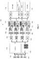
- FIG. 2is an architecture diagram of a single-port L1 cache with tag and data arrays implemented as independent modules, in accordance with example embodiments of the present disclosure.
- FIG. 3is an architecture diagram of a dual-port L1 cache with tag and data arrays implemented as independent modules, in accordance with example embodiments of the present disclosure.
- FIG. 4is an architecture diagram of L1 cache with multiple queues for data banks, in accordance with example embodiments of the present disclosure.
- FIG. 5is an example of pointer manipulation of a data index queue within the single-port L1 cache shown in FIG. 2 and/or within the dual-port L1 cache shown in FIG. 3 , in accordance with example embodiments of the present disclosure.
- FIG. 6is a table showing performance improvement of a scalar microprocessor having an L1 cache implemented with independent tag and data array accesses, in accordance with example embodiments of the present disclosure.
- FIG. 7is an architecture block diagram of a microprocessor comprising implementation of L1 cache illustrated in Figures ( FIGS. 2, 3 and 4 , in accordance with example embodiments of the present disclosure.
- FIG. 1is an architecture block diagram of a Level-1 (L1) cache 100 with tightly coupling of data and tag arrays, such as data memory banks or a data array 102 and tag arrays 104 .
- the data array 102can be implemented as multiple data memory banks, wherein each data memory bank requires multiple clock cycles (e.g., two clock cycles) for memory access, while multiple memory accesses (e.g., two memory accesses) can be performed in parallel during the multi-cycle memory access.
- a bank conflictmay exist when, for example, two consecutive or concurrent memory access instructions (e.g., load accesses) try to access the same memory bank (e.g., the same address index in a memory bank) of the data array 102 .
- a part of the addressis typically used as an index to access a specific entry in a data memory bank.
- the stall mechanismmay be launched in order to stall one of the concurrent memory access instructions (e.g., a later load access) as well as other instruction(s) following the two concurrent memory access instructions. Therefore, at least one load access instructions is in a locked step through a load/store pipeline of the L1 cache 100 , as illustrated in FIG. 1 .
- a tag array unit within an L1 cachecan be more critical in terms of performance in relation to tag hit/miss information. Because a tag array unit is substantially smaller than a data array unit, accessing of the tag array unit can be performed in a single cycle, unlike accessing the data array that requires multiple clock cycles. It is therefore beneficial not to penalize operation of a tag array unit in case of a bank conflict related to accessing the data array. Therefore, a tag array unit of an L1 cache may be accessed independently from accessing a data array unit, which may accordingly improve performance. For example, the decision of whether a load instruction can commit may be dependent on a tag hit/miss indication.
- FIG. 2is an example architecture block diagram of a single-port L1 cache 200 with independent data and tag array accesses, in accordance with embodiments of the present disclosure.
- the single-port L1 cache 200can correspond to instruction cache, data cache, or any other type of cache.
- a data array 202e.g., data memory banks
- a tag arrays unit 204 of the L1 cache 200are implemented as two independently accessed modules.
- the L1 cache 200may comprise a data index queue 206 associated with the data array 202 , wherein the data index queue 206 may store data indexes related to accesses of the data array 202 .
- the data index queue 206may be configured to keep one or more data indexes associated with one or more accesses of the data array 202 when there is a conflict, which may be detected by an interface circuit 208 coupled to the data index queue 206 and the data array 202 .
- a data array access(e.g., access of the data array 202 ) is typically slower than a tag array access (e.g., access of the tag array 204 ) due to the aforementioned multi-cycle access of large data arrays.
- the tag arrays 204 as well as a data translation look-aside buffer (DT LB) 210 associated with the tag arrays 204are substantially smaller than the data array (data memory banks) 202 and may be accessed within a single clock cycle.
- DT LBdata translation look-aside buffer
- a tag queue 212may be implemented at an output of the tag arrays 204 and the DTLB 210 for storing tags from the tag arrays 204 , wherein each entry in the tag queue 212 is associated with a corresponding data being produced by the data array 202 .
- the first entry in the tag queue 212may be associated with the first data being produced by the data array 202
- the second entry in the tag queue 212may be associated with the second data being produced by the data array 202 , and so on.
- a read pointer 214 of the data index queue 206may be manipulated (changed) to resend an instruction (e.g., data access) when a conflict is removed, without accessing again the tag arrays 204 and the DTLB 210 .
- an instructione.g., data access
- a stalled instructionmust be replayed from a Load/Store (LS) input queue, followed by performing an address generation unit (AGU) operation and again accessing a tag array, which may produce a higher power consumption of the L1 cache with the stall pipeline and of a microprocessor that incorporates this kind of L1 cache.
- LSLoad/Store
- AGUaddress generation unit
- this entry (data index) of the data index queue 206may be invalidated and removed from the data index queue 206 based on tag hit/miss information 216 .
- accessing of the data array 202may be cancelled, which may provide lower power consumption of the L1 cache 200 .
- a specific way of data array accessing and/or tag array accessingcan save power consumption of the L1 cache.
- information 216 about a translation look-aside buffer (TLB) miss in relation to DTLB 210can be used to cancel a corresponding entry in the data index queue 206 . Then, an instruction with the TLB miss and subsequent instruction(s) may be cancelled and replayed from the LS input queue 218 .
- a microprocessormay attempt to fetch a TLB entry from Level-2 TLB cache (not shown in FIG. 2 ) and restart the instruction that had the TLB miss from the LS input queue 218 again. On second attempt, the TLB miss becomes an exception so that a software instruction can load the TLB entry from a memory.
- the tag array 204 and the DTLB 210may be configured to detect tag hit/miss and send the tag hit/miss information 216 to a reorder buffer (ROB), not shown in FIG. 2 .
- ROBmay allow a corresponding instruction to be committed earlier leading to improved running performance of a microprocessor.
- the instructioncan be moved from the ROB to a Retire Queue (RQ) when the instruction passes a commit stage without any exception (e.g., in case of the DTLB hit).
- the instructionmay be moved to a graduate Buffer (GB) of the RQ if the tag hit/miss information 216 indicates a tag miss.
- RQRetire Queue
- GBGraduate Buffer
- instructions from a Load/Store (LS) input queue 218may go through into the data index queue 206 and to the tag queue 208 until there is enough space in the data index queue 206 and the tag queue 212 .
- the LS input queue 218may directly communicate with the tag queue 212 in order to prevent overflowing of the tag queue 212 .
- the interface circuit 208may control the read pointer 214 and a write pointer (not shown in FIG. 2 ) of the data index queue 206 (and of the LS input queue 218 ) based on the detection of the conflict, as discussed in more detail below.
- the data index queue 206 , the interface circuit 208 , the tag queue 212 , and the LS input queue 218may be configured to provide circuitry for independent access of the data array 202 and the tag arrays module 204 .
- L1 cache 200does not include any stall pipeline.
- the implementation of L1 cache without a stall pipeline presented hereinmay lead to a higher clock frequency of operating the L1 cache within a microprocessor.
- an L1 cache(e.g., the single-port L1 cache 200 illustrated in FIG. 2 ) may be implemented with data and tag arrays as two independently operating modules (e.g., the data array module 202 and the tag arrays module 204 shown in FIG. 2 ). If there is a bank conflict, a data index associated with a data access may be stored in a data input queue, such as the data index queue 206 .
- An output queue for the tag arrays(e.g., the tag queue 212 shown in FIG. 2 ) may be implemented having each entry associated with corresponding output data from the data array (e.g., the data array 202 ).
- a tag array output(e.g., the tag hit/miss information 216 ) may be sent directly to an ROB independent of data output result originating from the data array 202 .
- the tag array output(e.g., the hit/miss information 216 ) may be also communicated to the data input queue (e.g., the data index queue 206 ) for invalidation of data access in case of a tag miss.
- FIG. 3is an architecture block diagram of a dual-port L1 cache 300 with independent data and tag array accesses, in accordance with embodiments of the present disclosure.
- the dual-port L1 cache 300can correspond to instruction cache, data cache, or any other type of cache.
- a data array 302e.g., data memory banks
- tag arrays 304are implemented as two independently accessed modules.
- the data array 302data memory banks
- the data array 302can be implemented as dual-port memory banks for simultaneous access of two addresses in each memory bank.
- Tag arrays 304are duplicated relative to the tag arrays 204 of the L1 cache 200 shown in FIG. 2 , so as two memory accesses can be performed simultaneously (in parallel), if there is no conflict.
- An interface circuit 306 coupled to a data index queue 308 and the data array 302may be configured to detect conflict when accessing the data array 302 based on data indexes from the data index queue 308 .
- DTLB 310 shown in FIG. 3can be implemented using register-cells, which can inherently have dual ports for two simultaneous accesses, i.e., the DTLB 310 of the dual-port L1 cache 300 is not duplicated relative to the DTLB 210 of the single-port L1 cache 200 illustrated in FIG. 2 .
- the dual-entry data index queue 308is included in the dual-port L1 cache 300 for storing data indexes related to accesses of the data array 302 ; and an appropriate (e.g., dual-entry) tag queue 312 may be implemented at an output of the tag arrays 304 and the DTLB 310 for storing tags from the tag arrays 304 , wherein each entry in the tag queue 312 is associated with a corresponding data being produced by the data array 302 .
- the interface circuit 306may control read and write pointers 314 of the data index queue 308 (and of an LS input queue 316 ) based on the detection of the conflict, as discussed in more detail below.
- a store instructiondoes not need to access the data array 302 (data memory banks) when the store instruction is issued from a decode unit. Therefore, the store instruction does not have an entry in the data index queue 308 . Since there is no stall on any store operation, performance of an L1 cache (e.g., the dual-port L1 cache 300 illustrated in FIG. 3 ) is improved.
- data related to the store instructionmay be kept in a store buffer. When the data is retired from an ROB, the data related to the store instruction may be allowed to be written from a write buffer to the data array 302 (data memory banks) through the data index queue 308 .
- FIG. 4is an architecture diagram of L1 cache 400 with multiple queues interfaced with data banks, in accordance with embodiments of the present disclosure.
- the L1 cache 400can correspond to instruction cache, data cache, or any other type of cache.
- each data bank 402may be interfaced with its own data index queue 404 .
- One data index queue 404comprises an interface with one of the data banks 402 .
- the interface of the data index queue 404 with the data bank 402provides independent access from each data index queue 404 into each data bank 402 .
- Each data index queue 404 interfaced with one data bank 402can be configured to detect based on data indexes in that data index queue 404 if there is a conflict when accessing the data bank 402 interfaced with that data index queue 404 .
- a data output queue 406 associated with all data banks 402may match entries in a tag output queue 408 that stores tags entries from tag arrays 410 and/or DTLB 412 .
- a first entry in the data output queue 406may bypass directly to a result data register and then to ROB.
- output data from the data banks 402may be known two cycles early, and any entry with valid result data can bypass to the result data register and then to ROB.
- FIG. 5illustrates an example 500 of pointer manipulation of a data index queue 502 for writing and reading data indexes from/to the data index queue 502 , in accordance with embodiments of the present disclosure.
- the data index queue 502may correspond to the data index queue 206 of the single-port L1 cache 200 illustrated in FIG. 2 .
- the data index queue 502may correspond to the data index queue 308 of the dual port L1 cache 300 shown in FIG. 3 .
- the data index queue 502may correspond to the data index queue 404 of multi-port L1 cache 400 shown in FIG. 4 . As illustrated in FIG.
- a write pointer (wrptr) 504may be separate from a read pointer (rdptr) 506 , i.e., a write location of the data index queue 502 may be separate and independent from a read location of the data index queue 502 .
- the write pointer 504 , the read pointer 506 , and a saved read pointer (srdptr) 508 used for restoring the read pointer 506may be controlled by the interface circuit 208 of the single-port L1 cache 200 shown in FIG. 2 and/or by the interface circuit 306 of the dual port L1 cache 300 shown in FIG. 3 .
- the new inputmay be written into a location of the data index queue 502 indicated by the write pointer 504 .
- the write pointer 504may increment and point to a next write location in the data index queue 502 . If an entry (data index) is about to be read from the data index queue 502 since a request to access a data array is sent, the data index may be read from a location of the data index queue 502 indicated by the read pointer 506 .
- the read pointer 506then increments and moves to a next read location of the data index queue 502 , whereas the saved read pointer 508 does not yet increment and still points to a previous read location that was pointed to by the read pointer 506 before the read pointer 506 increments. If the request for data access is incomplete (i.e., if there is a memory bank conflict), the read pointer 506 may be restored based on a value of the saved read pointer 508 . If the request for data access is complete (i.e., if there is no memory bank conflict), the saved read pointer 508 also increments.
- a difference in number of locations of the data index queue 502 between the write pointer 504 and the saved read pointer 508is equal to a predefined threshold value (e.g., Q-full)
- a predefined threshold valuee.g., Q-full
- FIG. 6illustrates a table 600 showing performance of a scalar microprocessor with in-order instruction execution and of a microprocessor with out-of-order instruction execution using the modulized L1 cache implementation presented in this disclosure.
- the estimated performance improvementis approximately 2% based on L1 cache miss alone.
- the achieved saving in power consumptioncan be related to cancelling access of a data array on a cache miss.
- the estimated power consumption savingis approximately 1.5% for 10% of the L1 cache miss.
- the modulized implementation of L1 cache presented in this disclosureis simpler than that of the L1 cache with tightly coupled tag array and data array, since the mechanism for stalling of instructions is not needed and tight coupling of data and tag arrays is avoided.
- the performance improvement shown in FIG. 6relate to operating L1 cache while considering execution of only load instructions. Further improvement can be achieved when considering execution of store instructions, e.g., especially when each load instruction is followed by a store instruction.
- L1 cache implementation with a stall pipelinee.g., the L1 cache 100 illustrated in FIG. 1
- a load instruction stallsbecause a load instruction stalls, a following store instruction also stalls although the store instruction does not need to access a data array to obtain data.
- modulized L1 cache implementation presented in this disclosuree.g., the single-port L1 cache 200 illustrated in FIG. 2 , the dual-port L1 cache 300 illustrated in FIG. 3 , the L1 cache 400 with multiple queues for data banks illustrated in FIG. 4
- data and tag arraysare independently accessed, there is no stall pipeline, and both load and store instructions can go through pipeline stages and execute in order.
- FIG. 7illustrates an architecture block diagram of a microprocessor 700 with high performance implementation of multi-threading, in which embodiments of the present disclosure can be implemented.
- the microprocessor 700may comprise multiple resources dedicated to different threads, such as program counters (PCs) 702 (e.g., selected in a round robin manner), multiple instruction queues (IQs) 704 , multiple decode units 706 , Early Arithmetic Logic Units (ALUs) 708 , register files 710 , Late ALU Queues (LAQs) 712 and Late ALUs 714 .
- PCsprogram counters
- IQsinstruction queues
- ALUsEarly Arithmetic Logic Units
- register files 710e.g., Late ALU Queues (LAQs) 712 and Late ALUs 714 .
- LAQsLate ALU Queues
- More expensive resourcessuch as an instruction cache 716 , a data cache 718 , branch prediction unit (BPU) 720 , and floating point unit (FPU) 722 are not replicated, i.e., they are shared among multiple threads. Furthermore, those infrequently used resources, such as a divide unit (DIV) 722 and an Integer Multiplier (IMUL) unit 724 are also not replicated.
- Arc Processor Extension (APEX) unit 726can be implemented as a customer specific functional unit. In one or more embodiments, APEX unit 726 can comprise independent functional sub-units allocated to the multiple threads.
- APEX unit 726can be defined as a functional unit shared among the multiple threads.
- an Arc Processor-extension Queue (APQ) interfaced with APEX unitcan be defined as a shared resource and implemented as shared APQ 728 illustrated in FIG. 7 , or APQ can be implemented as independent APQs (not shown in FIG. 7 ).
- APQArc Processor-extension Queue
- the instruction cache 716 or the data cache 718may correspond to the single-port L1 cache 200 illustrated in FIG. 2 . In some other embodiments, the instruction cache 716 or the data cache 718 may correspond to the dual-port L1 cache 300 illustrated in FIG. 3 . In yet some other embodiments, the instruction cache 716 or the data cache 718 may correspond to the L1 cache 400 with multiple queues for data banks illustrated in FIG. 4 .
- a software moduleis implemented with a computer program product comprising a computer-readable medium containing computer program code, which can be executed by a computer processor for performing any or all of the steps, operations, or processes described.
- Embodiments of the disclosuremay also relate to an apparatus for performing the operations herein.
- This apparatusmay be specially constructed for the required purposes, and/or it may comprise a general-purpose computing device selectively activated or reconfigured by a computer program stored in the computer.
- a computer programmay be stored in a non-transitory, tangible computer readable storage medium, or any type of media suitable for storing electronic instructions, which may be coupled to a computer system bus.
- any computing systems referred to in the specificationmay include a single processor or may be architectures employing multiple processor designs for increased computing capability.
- Embodiments of the disclosuremay also relate to a product that is produced by a computing process described herein.
- a productmay comprise information resulting from a computing process, where the information is stored on a non-transitory, tangible computer readable storage medium and may include any embodiment of a computer program product or other data combination described herein.
Landscapes
- Engineering & Computer Science (AREA)
- Theoretical Computer Science (AREA)
- Physics & Mathematics (AREA)
- General Engineering & Computer Science (AREA)
- General Physics & Mathematics (AREA)
- Advance Control (AREA)
- Memory System Of A Hierarchy Structure (AREA)
Abstract
Description
The present disclosure generally relates to a microprocessor architecture, and specifically relates to modularization of cache structure in the microprocessor.
A Level-1 (L1) cache of a microprocessor is commonly implemented as a tightly coupled unit of tag and data arrays. Whether the L1 cache is implemented as a single-port cache array or a dual-port cache array, processes of fetching address and data are tightly coupled. If there is an address or data conflict related to at least two consecutive memory access instructions, then one of the memory access instructions needs to stall in a pipeline causing stalling of one or more following instructions that leads to performance degradation of the L1 cache as well as to performance degradation of a microprocessor where the L1 cache is incorporated. Stalling of instructions due to address and/or data conflict is further undesirable since the effective clock frequency of operating the L1 cache is substantially reduced. In addition, there is a negative performance impact if the tag array is not accessed as early as possible.
A data array of the L1 cache is typically much larger than a tag array. The data array may be, for example, a large compiler memory that typically requires multiple clock cycles (e.g., two clock cycles) for memory access, such as data load/store. Because of the multi-cycle memory access, the data array is typically implemented by using multiple memory banks that can be simultaneously accessed. If, for example, two consecutive memory access instructions request access to two different memory banks, no bank conflict exists and addresses in separate memory banks can be simultaneously accessed without any conflict. On the other hand, if two consecutive memory access instructions request access to the same memory bank (either the same or different data), then a bank conflict exists (e.g., data or address conflict), and one of the memory access instructions (e.g., a later instruction of the two consecutive instructions) needs to be stalled. Since instructions are executed in order, one or more instructions following the stalled instruction can be also stalled, which is undesirable since it negatively affects performance of an L1 cache as well as performance of a microprocessor incorporating the L1 cache. Generally, the multi-cycle access of a data array can cause more bank conflicts than accessing of a smaller tag array.
Certain embodiments of the present disclosure support implementation of a Level-1 (L1) cache in a microprocessor based on data arrays and tag arrays that are independently accessed. No stall pipeline mechanism is required for L1 cache implementations presented herein since stall of instructions is avoided when there is a memory conflict.
Example embodiments of the present disclosure include configurations that may include structures and processes within a microprocessor. For example, a configuration may include a data array in a cache of the microprocessor interfaced with one or more data index queues, a tag array, and circuitry coupled to the data array and the tag array. The one or more data index queues can store, upon occurrence of a conflict between at least one instruction requesting access to the data array and at least one other instruction that accessed the data array, at least one data index for accessing the data array associated with the at least one instruction. The tag array in the cache is coupled with a tag queue that stores one or more tag entries associated with one or more data outputs read from the data array based on accessing the data array. The circuitry in the cache coupled to the data array and the tag array is configured for independent access of the data array and the tag array.
Example embodiments of the present disclosure include configurations that may include structures and processes within a microprocessor. For example, a configuration may include issuing one or more instructions per clock cycle for accessing a data array in a cache of the microprocessor interfaced with one or more data index queues, keeping, in the one or more data index queues upon occurrence of a conflict between at least one instruction requesting access to the data array and at least one other instruction that accessed the data array, at least one data index for accessing the data array associated with the at least one instruction, accessing, for the at least one instruction and the at least one other instruction, a tag array in the cache interfaced with a tag queue independently of accessing the data array, and storing, in the tag queue based on accessing the tag array, one or more tag entries associated with one or more data outputs read from the data array in response to accessing the data array.
The figures depict embodiments of the present disclosure for purposes of illustration only. One skilled in the art will readily recognize from the following description that alternative embodiments of the structures and methods illustrated herein may be employed without departing from the principles, or benefits touted, of the disclosure described herein.
For certain embodiments, a tag array unit within an L1 cache (e.g., thetag arrays 104 of theL1 cache 100 shown inFIG. 1 ) can be more critical in terms of performance in relation to tag hit/miss information. Because a tag array unit is substantially smaller than a data array unit, accessing of the tag array unit can be performed in a single cycle, unlike accessing the data array that requires multiple clock cycles. It is therefore beneficial not to penalize operation of a tag array unit in case of a bank conflict related to accessing the data array. Therefore, a tag array unit of an L1 cache may be accessed independently from accessing a data array unit, which may accordingly improve performance. For example, the decision of whether a load instruction can commit may be dependent on a tag hit/miss indication. In accordance with embodiments of the present disclosure, tag and the data arrays of the L1 cache may be implemented as two independent modules. Embodiments of the present disclosure relate to modulization of the L1 cache structure for achieving performance improvement.
A data array access (e.g., access of the data array202) is typically slower than a tag array access (e.g., access of the tag array204) due to the aforementioned multi-cycle access of large data arrays. Thetag arrays 204 as well as a data translation look-aside buffer (DT LB)210 associated with thetag arrays 204 are substantially smaller than the data array (data memory banks)202 and may be accessed within a single clock cycle. In one or more embodiments of the present disclosure, as illustrated inFIG. 2 , atag queue 212 may be implemented at an output of thetag arrays 204 and theDTLB 210 for storing tags from thetag arrays 204, wherein each entry in thetag queue 212 is associated with a corresponding data being produced by thedata array 202. For example, the first entry in thetag queue 212 may be associated with the first data being produced by thedata array 202, the second entry in thetag queue 212 may be associated with the second data being produced by thedata array 202, and so on.
For some embodiments, aread pointer 214 of thedata index queue 206 may be manipulated (changed) to resend an instruction (e.g., data access) when a conflict is removed, without accessing again thetag arrays 204 and theDTLB 210. In contrast, for the L1 cache implementation based on a stall pipeline (e.g., theL1 cache 100 illustrated inFIG. 1 ), a stalled instruction must be replayed from a Load/Store (LS) input queue, followed by performing an address generation unit (AGU) operation and again accessing a tag array, which may produce a higher power consumption of the L1 cache with the stall pipeline and of a microprocessor that incorporates this kind of L1 cache.
For some embodiments, in case of a tag miss, if the data index associated with data access is still in thedata input queue 206, then this entry (data index) of thedata index queue 206 may be invalidated and removed from thedata index queue 206 based on tag hit/miss information 216. Hence, in the case of tag miss, accessing of thedata array 202 may be cancelled, which may provide lower power consumption of theL1 cache 200. In general, if the corresponding entry in thedata index queue 206 is not yet issued to thedata array 202, then a specific way of data array accessing and/or tag array accessing can save power consumption of the L1 cache. In some embodiments,information 216 about a translation look-aside buffer (TLB) miss in relation to DTLB210 can be used to cancel a corresponding entry in thedata index queue 206. Then, an instruction with the TLB miss and subsequent instruction(s) may be cancelled and replayed from theLS input queue 218. A microprocessor may attempt to fetch a TLB entry from Level-2 TLB cache (not shown inFIG. 2 ) and restart the instruction that had the TLB miss from theLS input queue 218 again. On second attempt, the TLB miss becomes an exception so that a software instruction can load the TLB entry from a memory.
For some embodiments, thetag array 204 and theDTLB 210 may be configured to detect tag hit/miss and send the tag hit/miss information 216 to a reorder buffer (ROB), not shown inFIG. 2 . ROB may allow a corresponding instruction to be committed earlier leading to improved running performance of a microprocessor. The instruction can be moved from the ROB to a Retire Queue (RQ) when the instruction passes a commit stage without any exception (e.g., in case of the DTLB hit). In an embodiment, the instruction may be moved to a Graduate Buffer (GB) of the RQ if the tag hit/miss information 216 indicates a tag miss.
In accordance with embodiments of the present disclosure, instructions from a Load/Store (LS)input queue 218 may go through into thedata index queue 206 and to thetag queue 208 until there is enough space in thedata index queue 206 and thetag queue 212. In one or more embodiments, theLS input queue 218 may directly communicate with thetag queue 212 in order to prevent overflowing of thetag queue 212. In one or more embodiments, theinterface circuit 208 may control theread pointer 214 and a write pointer (not shown inFIG. 2 ) of the data index queue206 (and of the LS input queue218) based on the detection of the conflict, as discussed in more detail below. In some embodiments, thedata index queue 206, theinterface circuit 208, thetag queue 212, and theLS input queue 218 may be configured to provide circuitry for independent access of thedata array 202 and thetag arrays module 204.
Because of the modulized implementation of the single-port L1 cache 200 illustrated inFIG. 2 that is based on independently accessing the data array module202 (data memory banks) and thetag arrays module 204, the structure ofL1 cache 200 does not include any stall pipeline. The implementation of L1 cache without a stall pipeline presented herein may lead to a higher clock frequency of operating the L1 cache within a microprocessor.
In accordance with embodiments of the present disclosure, as discussed above, an L1 cache (e.g., the single-port L1 cache 200 illustrated inFIG. 2 ) may be implemented with data and tag arrays as two independently operating modules (e.g., thedata array module 202 and thetag arrays module 204 shown inFIG. 2 ). If there is a bank conflict, a data index associated with a data access may be stored in a data input queue, such as thedata index queue 206. An output queue for the tag arrays (e.g., thetag queue 212 shown inFIG. 2 ) may be implemented having each entry associated with corresponding output data from the data array (e.g., the data array202). Furthermore, a tag array output (e.g., the tag hit/miss information216) may be sent directly to an ROB independent of data output result originating from thedata array 202. In addition, the tag array output (e.g., the hit/miss information216) may be also communicated to the data input queue (e.g., the data index queue206) for invalidation of data access in case of a tag miss.
As illustrated inFIG. 3 , other components and parts of the dual-port L1 cache 300 are substantially similar as corresponding components and parts of the single-port L1 cache 200 illustrated inFIG. 2 . For example, the dual-entrydata index queue 308 is included in the dual-port L1 cache 300 for storing data indexes related to accesses of thedata array 302; and an appropriate (e.g., dual-entry)tag queue 312 may be implemented at an output of thetag arrays 304 and theDTLB 310 for storing tags from thetag arrays 304, wherein each entry in thetag queue 312 is associated with a corresponding data being produced by thedata array 302. In some embodiments, theinterface circuit 306 may control read and writepointers 314 of the data index queue308 (and of an LS input queue316) based on the detection of the conflict, as discussed in more detail below.
For some embodiments of the present disclosure, a store instruction does not need to access the data array302 (data memory banks) when the store instruction is issued from a decode unit. Therefore, the store instruction does not have an entry in thedata index queue 308. Since there is no stall on any store operation, performance of an L1 cache (e.g., the dual-port L1 cache 300 illustrated inFIG. 3 ) is improved. In one or more embodiments, data related to the store instruction may be kept in a store buffer. When the data is retired from an ROB, the data related to the store instruction may be allowed to be written from a write buffer to the data array302 (data memory banks) through thedata index queue 308.
In some embodiments, adata output queue 406 associated with alldata banks 402 may match entries in atag output queue 408 that stores tags entries fromtag arrays 410 and/orDTLB 412. In one embodiment, in case of returning result data to ROB in-order, a first entry in thedata output queue 406 may bypass directly to a result data register and then to ROB. In another embodiment, in case of returning result data to ROB out-of-order, output data from thedata banks 402 may be known two cycles early, and any entry with valid result data can bypass to the result data register and then to ROB.
In accordance with embodiments of the present disclosure, if there is a new input (i.e., a new data index) written in thedata index queue 502, the new input may be written into a location of thedata index queue 502 indicated by thewrite pointer 504. After that, thewrite pointer 504 may increment and point to a next write location in thedata index queue 502. If an entry (data index) is about to be read from thedata index queue 502 since a request to access a data array is sent, the data index may be read from a location of thedata index queue 502 indicated by theread pointer 506. Theread pointer 506 then increments and moves to a next read location of thedata index queue 502, whereas the saved readpointer 508 does not yet increment and still points to a previous read location that was pointed to by theread pointer 506 before theread pointer 506 increments. If the request for data access is incomplete (i.e., if there is a memory bank conflict), theread pointer 506 may be restored based on a value of the saved readpointer 508. If the request for data access is complete (i.e., if there is no memory bank conflict), the saved readpointer 508 also increments. In one or more embodiments, if a difference in number of locations of thedata index queue 502 between thewrite pointer 504 and the saved readpointer 508 is equal to a predefined threshold value (e.g., Q-full), then thedata index queue 502 is full and a new data index entry cannot be written into thedata index queue 502.
It should be noted that the performance improvement shown inFIG. 6 relate to operating L1 cache while considering execution of only load instructions. Further improvement can be achieved when considering execution of store instructions, e.g., especially when each load instruction is followed by a store instruction. In the case of L1 cache implementation with a stall pipeline (e.g., theL1 cache 100 illustrated inFIG. 1 ), because a load instruction stalls, a following store instruction also stalls although the store instruction does not need to access a data array to obtain data. For the modulized L1 cache implementation presented in this disclosure (e.g., the single-port L1 cache 200 illustrated inFIG. 2 , the dual-port L1 cache 300 illustrated inFIG. 3 , theL1 cache 400 with multiple queues for data banks illustrated inFIG. 4 ), data and tag arrays are independently accessed, there is no stall pipeline, and both load and store instructions can go through pipeline stages and execute in order.
In some embodiments, theinstruction cache 716 or thedata cache 718 may correspond to the single-port L1 cache 200 illustrated inFIG. 2 . In some other embodiments, theinstruction cache 716 or thedata cache 718 may correspond to the dual-port L1 cache 300 illustrated inFIG. 3 . In yet some other embodiments, theinstruction cache 716 or thedata cache 718 may correspond to theL1 cache 400 with multiple queues for data banks illustrated inFIG. 4 .
Additional Considerations
The foregoing description of the embodiments of the disclosure has been presented for the purpose of illustration; it is not intended to be exhaustive or to limit the disclosure to the precise forms disclosed. Persons skilled in the relevant art can appreciate that many modifications and variations are possible in light of the above disclosure.
Some portions of this description describe the embodiments of the disclosure in terms of algorithms and symbolic representations of operations on information. These algorithmic descriptions and representations are commonly used by those skilled in the data processing arts to convey the substance of their work effectively to others skilled in the art. These operations, while described functionally, computationally, or logically, are understood to be implemented by computer programs or equivalent electrical circuits, microcode, or the like. Furthermore, it has also proven convenient at times, to refer to these arrangements of operations as modules, without loss of generality. The described operations and their associated modules may be embodied in software, firmware, hardware, or any combinations thereof.
Any of the steps, operations, or processes described herein may be performed or implemented with one or more hardware or software modules, alone or in combination with other devices. In one embodiment, a software module is implemented with a computer program product comprising a computer-readable medium containing computer program code, which can be executed by a computer processor for performing any or all of the steps, operations, or processes described.
Embodiments of the disclosure may also relate to an apparatus for performing the operations herein. This apparatus may be specially constructed for the required purposes, and/or it may comprise a general-purpose computing device selectively activated or reconfigured by a computer program stored in the computer. Such a computer program may be stored in a non-transitory, tangible computer readable storage medium, or any type of media suitable for storing electronic instructions, which may be coupled to a computer system bus. Furthermore, any computing systems referred to in the specification may include a single processor or may be architectures employing multiple processor designs for increased computing capability.
Embodiments of the disclosure may also relate to a product that is produced by a computing process described herein. Such a product may comprise information resulting from a computing process, where the information is stored on a non-transitory, tangible computer readable storage medium and may include any embodiment of a computer program product or other data combination described herein.
Finally, the language used in the specification has been principally selected for readability and instructional purposes, and it may not have been selected to delineate or circumscribe the inventive subject matter. It is therefore intended that the scope of the disclosure be limited not by this detailed description, but rather by any claims that issue on an application based hereon. Accordingly, the disclosure of the embodiments is intended to be illustrative, but not limiting, of the scope of the disclosure, which is set forth in the following claims.
Claims (19)
1. A microprocessor, comprising:
a data array in a cache of the microprocessor, the data array directly interfaced with one or more data index queues, wherein:
upon detection of a conflict between a plurality of instructions issued from an input queue requesting access to the data array, at least one data index associated with at least one of the instructions is stored into the one or more data index queues,
the at least one data index is kept in the one or more data index queues until after removal of the conflict, and
upon the removal of the conflict, the data array is accessed based on the at least one data index stored in the one or more data index queues;
a tag array in the cache accessed by the instructions prior to the detection of the conflict, the tag array interfaced with a tag queue that stores tag entries from the tag array, The tag entries associated with data outputs read from the data array in response to accessing the data array when executing the instruction, the tag entries being kept in the tag queue until after the removal of the conflict, the input queue directly communicating with the tag queue to prevent overflowing of the tag queue when the tag entries associated with the instructions are being kept in the tag queue; and
circuitry in the cache couple to the data array and the tag array, the circuitry configured, upon the removal of the conflict, to initiate resending the at least one of the instructions from the input queue without re-accessing the tag array and the one or more data index queues for storing the at least one data index.
2. The microprocessor ofclaim 1 , wherein the circuitry comprises:
an interface circuit coupled with the data array and with at least one of the one or more data index queues to detect occurrence of the conflict; and
a circuit to store, based on the detection of the conflict, the at least one data index for accessing the data array in the at least one data index queue.
3. The microprocessor ofclaim 1 , wherein the circuitry further comprises:
a circuit coupled to the tag array configured to detect at least one tag miss, wherein
the circuit is further configured to trigger removal of the at least one data index from the one or more data index queues based on information about the at least one tag miss.
4. The microprocessor ofclaim 1 , further comprising:
a data queue interface with the data array for storing one or more data outputs from the data array.
5. The microprocessor ofclaim 4 , wherein each tag entry of the one or more tag entries in the tag queue stored from the tag array is associated with one data output of the one or more data outputs stored in the data queue from the data array.
6. The microprocessor ofclaim 1 , wherein:
the data array comprises a plurality of data banks, and
each data index queue of the one or more data index queues comprises an interface with a different data bank of the plurality of data banks.
7. The microprocessor ofclaim 1 , further comprising:
a data translation look-aside buffer (DTLB) in the data cache associated with the tag array and accessed independently of the data array; and
a circuit coupled to the tag array and the DTLB configured to detect at least one tag miss.
8. The microprocessor ofclaim 1 , further comprising:
a read pointer of a data index queue of the one or more data index queues indicating an entry in the data index queue for requesting access to the data array in relation to the at least one instruction;
a save read pointer of the data index queue for restoring a value of the read pointer after occurrence of the conflict when accessing the data array in relation to the at least one instruction; and
a write pointer of the data index queue indicating another entry in the data index queue for requesting access to the data array in relation to another instruction of the plurality of instructions.
9. The microprocessor ofclaim 1 , wherein:
the at least one instruction is issued concurrently with at least one other instruction of the plurality of instructions, or
the at least one instruction is issued after the at least one other instruction.
10. A method executed by a microprocessor, comprising:
issuing, from an input queue, one or more instructions per clock cycle for accessing a data array in a cache of the microprocessor, the data array directly interfaced with one or more data index queues;
upon detection of a conflict between a plurality of instructions issued from the input queue requesting access to the data array, storing at least one data index associated with at least one of the instructions into the one or more data index queues;
keeping the at least one data index in the one or more data index queues until after removal of the conflict;
upon the removal of the conflict, accessing the data array based on the at least one data index stored in the one or more data index queues;
accessing, by the instructions prior to the detection of the conflict, a tag array in the cache interfaced with a ta queue;
storing, in the tag queue based on accessing the tag array, tag entries from the tag array, The tag entries associated with data outputs read from the data array in response to accessing the data array when executing the instructions;
keeping the tag entries in the tag queue until after the removal of the conflict communicating, by the input queue, directly with the tag queue to prevent overflowing of the tag queue when the tag entries associated with the instructions are being kept in the tag queue; and
upon the removal of the conflict, resending the at least one of the instructions from the input queue without re-accessing the tag array and the one or more data index queues for storing the at least one data index.
11. The method ofclaim 10 , further comprising:
detecting at least one tag miss based on accessing the tag array; and
removing, from the one or more data index queues, the at least one data index based on information about the at least one tag miss.
12. The method ofclaim 10 , further comprising:
directly accessing the data array, if at least one data index queue of the one or more data index queues is empty.
13. The method ofclaim 10 , further comprising:
storing the one or more data outputs from the data array into a data queue interfaced with the data array.
14. The method ofclaim 13 , wherein each tag entry of the one or more tag entries in the tag queue stored from the tag array is associated with one data output of one or more data outputs stored in the data queue from the data array.
15. The method ofclaim 10 , further comprising:
incrementing a read pointer of a data index queue of the one or more data index queues based on the at least one instruction requesting access to the array, the read pointer indicating an entry in the data index queue for requesting access to the data array in relation to the at least one instruction;
incrementing, if no conflict occurs when accessing the data array in relation to the at least one instruction, a save read pointer of the data index queue;
restoring, if the conflict occurs when accessing the data array in relation to the at least one instruction, the read pointer based on a value of the save read pointer; and
incrementing, based on issuing an instruction of the plurality of instructions for accessing the data array, a write pointer of the data index queue indicating another entry in the data index queue for requesting access to the data array in relation to the instruction.
16. The method ofclaim 15 , further comprising:
triggering indication that the data index is full when the write pointer is same as the save read pointer.
17. The method ofclaim 10 , further comprising:
replaying the at least one instruction based on the at least one data index kept in the one or more data index queue when the conflict is removed.
18. The method ofclaim 10 , wherein issuing the one or more instructions per clock cycle comprises:
issuing the at least one instruction concurrently with issuing at least one other instruction of the plurality of instructions.
19. The method ofclaim 10 , wherein issuing the one or more instructions per clock cycle comprises:
issuing the at least one instruction after issuing at least one other instruction of the plurality of instructions.
Priority Applications (1)
| Application Number | Priority Date | Filing Date | Title |
|---|---|---|---|
| US15/172,906US10628320B2 (en) | 2016-06-03 | 2016-06-03 | Modulization of cache structure utilizing independent tag array and data array in microprocessor |
Applications Claiming Priority (1)
| Application Number | Priority Date | Filing Date | Title |
|---|---|---|---|
| US15/172,906US10628320B2 (en) | 2016-06-03 | 2016-06-03 | Modulization of cache structure utilizing independent tag array and data array in microprocessor |
Publications (2)
| Publication Number | Publication Date |
|---|---|
| US20170351610A1 US20170351610A1 (en) | 2017-12-07 |
| US10628320B2true US10628320B2 (en) | 2020-04-21 |
Family
ID=60483358
Family Applications (1)
| Application Number | Title | Priority Date | Filing Date |
|---|---|---|---|
| US15/172,906Active2036-08-06US10628320B2 (en) | 2016-06-03 | 2016-06-03 | Modulization of cache structure utilizing independent tag array and data array in microprocessor |
Country Status (1)
| Country | Link |
|---|---|
| US (1) | US10628320B2 (en) |
Families Citing this family (7)
| Publication number | Priority date | Publication date | Assignee | Title |
|---|---|---|---|---|
| US10565121B2 (en)* | 2016-12-16 | 2020-02-18 | Alibaba Group Holding Limited | Method and apparatus for reducing read/write contention to a cache |
| US11188341B2 (en) | 2019-03-26 | 2021-11-30 | Intel Corporation | System, apparatus and method for symbolic store address generation for data-parallel processor |
| US10896141B2 (en)* | 2019-03-26 | 2021-01-19 | Intel Corporation | Gather-scatter cache architecture having plurality of tag and data banks and arbiter for single program multiple data (SPMD) processor |
| US11243775B2 (en) | 2019-03-26 | 2022-02-08 | Intel Corporation | System, apparatus and method for program order queue (POQ) to manage data dependencies in processor having multiple instruction queues |
| US11175917B1 (en)* | 2020-09-11 | 2021-11-16 | Apple Inc. | Buffer for replayed loads in parallel with reservation station for rapid rescheduling |
| US12013786B2 (en)* | 2021-12-22 | 2024-06-18 | Samsung Electronics Co., Ltd. | Multi-port queueing cache and data processing system including the same |
| US11983538B2 (en)* | 2022-04-18 | 2024-05-14 | Cadence Design Systems, Inc. | Load-store unit dual tags and replays |
Citations (75)
| Publication number | Priority date | Publication date | Assignee | Title |
|---|---|---|---|---|
| US5274790A (en)* | 1990-04-30 | 1993-12-28 | Nec Corporation | Cache memory apparatus having a plurality of accessibility ports |
| US5333284A (en) | 1990-09-10 | 1994-07-26 | Honeywell, Inc. | Repeated ALU in pipelined processor design |
| US5463745A (en) | 1993-12-22 | 1995-10-31 | Intel Corporation | Methods and apparatus for determining the next instruction pointer in an out-of-order execution computer system |
| US5471591A (en)* | 1990-06-29 | 1995-11-28 | Digital Equipment Corporation | Combined write-operand queue and read-after-write dependency scoreboard |
| US5519864A (en) | 1993-12-27 | 1996-05-21 | Intel Corporation | Method and apparatus for scheduling the dispatch of instructions from a reservation station |
| US5584038A (en) | 1994-03-01 | 1996-12-10 | Intel Corporation | Entry allocation in a circular buffer using wrap bits indicating whether a queue of the circular buffer has been traversed |
| US5675758A (en) | 1994-11-15 | 1997-10-07 | Advanced Micro Devices, Inc. | Processor having primary integer execution unit and supplemental integer execution unit for performing out-of-order add and move operations |
| US5684971A (en) | 1993-12-27 | 1997-11-04 | Intel Corporation | Reservation station with a pseudo-FIFO circuit for scheduling dispatch of instructions |
| US5761476A (en) | 1993-12-30 | 1998-06-02 | Intel Corporation | Non-clocked early read for back-to-back scheduling of instructions |
| US5948098A (en) | 1997-06-30 | 1999-09-07 | Sun Microsystems, Inc. | Execution unit and method for executing performance critical and non-performance critical arithmetic instructions in separate pipelines |
| US5987620A (en) | 1997-09-19 | 1999-11-16 | Thang Tran | Method and apparatus for a self-timed and self-enabled distributed clock |
| US6076145A (en)* | 1995-07-14 | 2000-06-13 | Fujitsu Limited | Data supplying apparatus for independently performing hit determination and data access |
| US6108769A (en) | 1996-05-17 | 2000-08-22 | Advanced Micro Devices, Inc. | Dependency table for reducing dependency checking hardware |
| US6112019A (en) | 1995-06-12 | 2000-08-29 | Georgia Tech Research Corp. | Distributed instruction queue |
| US6205543B1 (en) | 1998-12-03 | 2001-03-20 | Sun Microsystems, Inc. | Efficient handling of a large register file for context switching |
| US6233599B1 (en) | 1997-07-10 | 2001-05-15 | International Business Machines Corporation | Apparatus and method for retrofitting multi-threaded operations on a computer by partitioning and overlapping registers |
| US6247094B1 (en)* | 1997-12-22 | 2001-06-12 | Intel Corporation | Cache memory architecture with on-chip tag array and off-chip data array |
| US6272520B1 (en) | 1997-12-31 | 2001-08-07 | Intel Corporation | Method for detecting thread switch events |
| US20010056456A1 (en) | 1997-07-08 | 2001-12-27 | Erik Cota-Robles | Priority based simultaneous multi-threading |
| US6341301B1 (en)* | 1997-01-10 | 2002-01-22 | Lsi Logic Corporation | Exclusive multiple queue handling using a common processing algorithm |
| US6408325B1 (en) | 1998-05-06 | 2002-06-18 | Sun Microsystems, Inc. | Context switching technique for processors with large register files |
| US20020083304A1 (en) | 2000-12-23 | 2002-06-27 | Ibm | Rename finish conflict detection and recovery |
| US6425072B1 (en) | 1999-08-31 | 2002-07-23 | Advanced Micro Devices, Inc. | System for implementing a register free-list by using swap bit to select first or second register tag in retire queue |
| US20030005266A1 (en) | 2001-06-28 | 2003-01-02 | Haitham Akkary | Multithreaded processor capable of implicit multithreaded execution of a single-thread program |
| US20030005263A1 (en) | 2001-06-28 | 2003-01-02 | International Business Machines Corporation | Shared resource queue for simultaneous multithreaded processing |
| US20030033509A1 (en) | 2001-08-07 | 2003-02-13 | Sun Microsystems, Inc. | Architectural reuse of registers for out of order simultaneous multi-threading |
| US20030061467A1 (en) | 2001-09-24 | 2003-03-27 | Tse-Yu Yeh | Scoreboarding mechanism in a pipeline that includes replays and redirects |
| US6557078B1 (en)* | 2000-02-21 | 2003-04-29 | Hewlett Packard Development Company, L.P. | Cache chain structure to implement high bandwidth low latency cache memory subsystem |
| US20040015684A1 (en) | 2002-05-30 | 2004-01-22 | International Business Machines Corporation | Method, apparatus and computer program product for scheduling multiple threads for a processor |
| US6697939B1 (en)* | 2000-01-06 | 2004-02-24 | International Business Machines Corporation | Basic block cache microprocessor with instruction history information |
| US20040139306A1 (en) | 2003-01-09 | 2004-07-15 | Sony Corporation | Partial and start-over threads in embedded real-time kernel |
| US6785803B1 (en)* | 1996-11-13 | 2004-08-31 | Intel Corporation | Processor including replay queue to break livelocks |
| US20040172523A1 (en) | 1996-11-13 | 2004-09-02 | Merchant Amit A. | Multi-threading techniques for a processor utilizing a replay queue |
| US20040243764A1 (en)* | 2003-05-29 | 2004-12-02 | Via-Cyrix, Inc. | Tag array access reduction in a cache memory |
| US20050044327A1 (en)* | 2003-08-19 | 2005-02-24 | Quicksilver Technology, Inc. | Asynchronous, independent and multiple process shared memory system in an adaptive computing architecture |
| US20050125802A1 (en)* | 2003-12-05 | 2005-06-09 | Wang Perry H. | User-programmable low-overhead multithreading |
| US20050149936A1 (en) | 2003-12-19 | 2005-07-07 | Stmicroelectronics, Inc. | Thread execution scheduler for multi-processing system and method |
| US20050273580A1 (en) | 2004-06-03 | 2005-12-08 | Shailender Chaudhry | Avoiding register RAW hazards when returning from speculative execution |
| US20060117316A1 (en) | 2004-11-24 | 2006-06-01 | Cismas Sorin C | Hardware multithreading systems and methods |
| US20070136562A1 (en) | 2005-12-09 | 2007-06-14 | Paul Caprioli | Decoupling register bypassing from pipeline depth |
| US20070204137A1 (en)* | 2004-08-30 | 2007-08-30 | Texas Instruments Incorporated | Multi-threading processors, integrated circuit devices, systems, and processes of operation and manufacture |
| US20070266387A1 (en) | 2006-04-27 | 2007-11-15 | Matsushita Electric Industrial Co., Ltd. | Multithreaded computer system and multithread execution control method |
| US20080082755A1 (en)* | 2006-09-29 | 2008-04-03 | Kornegay Marcus L | Administering An Access Conflict In A Computer Memory Cache |
| US7434032B1 (en) | 2005-12-13 | 2008-10-07 | Nvidia Corporation | Tracking register usage during multithreaded processing using a scoreboard having separate memory regions and storing sequential register size indicators |
| US20080295105A1 (en) | 2007-05-22 | 2008-11-27 | Arm Limited | Data processing apparatus and method for managing multiple program threads executed by processing circuitry |
| US20090037698A1 (en) | 2007-08-03 | 2009-02-05 | Nguyen Dung Q | Adaptive allocation of reservation station entries to an instruction set with variable operands in a microprocessor |
| US7610473B2 (en) | 2003-08-28 | 2009-10-27 | Mips Technologies, Inc. | Apparatus, method, and instruction for initiation of concurrent instruction streams in a multithreading microprocessor |
| US7644221B1 (en)* | 2005-04-11 | 2010-01-05 | Sun Microsystems, Inc. | System interface unit |
| US20100031268A1 (en) | 2008-07-31 | 2010-02-04 | Dwyer Michael K | Thread ordering techniques |
| US20100083267A1 (en) | 2008-09-30 | 2010-04-01 | Nec Electronics Corporation | Multi-thread processor and its hardware thread scheduling method |
| US20100082945A1 (en) | 2008-09-30 | 2010-04-01 | Nec Electronics Corporation | Multi-thread processor and its hardware thread scheduling method |
| US20100138608A1 (en)* | 2008-12-02 | 2010-06-03 | Lihu Rappoport | Method and apparatus for pipeline inclusion and instruction restarts in a micro-op cache of a processor |
| US20100250902A1 (en) | 2009-03-24 | 2010-09-30 | International Business Machines Corporation | Tracking Deallocated Load Instructions Using a Dependence Matrix |
| US20110067034A1 (en) | 2008-06-25 | 2011-03-17 | Takuji Kawamoto | Information processing apparatus, information processing method, and information processing program |
| US20110296423A1 (en) | 2010-05-27 | 2011-12-01 | International Business Machines Corporation | Framework for scheduling multicore processors |
| US20120054447A1 (en)* | 2010-08-31 | 2012-03-01 | Oracle International Corporation | Method and system for removing cache blocks |
| US20120173818A1 (en)* | 2011-01-05 | 2012-07-05 | International Business Machines Corporation | Detecting address conflicts in a cache memory system |
| US20120278596A1 (en) | 2011-04-26 | 2012-11-01 | Freescale Semiconductor, Inc. | Apparatus and method for checkpoint repair in a processing device |
| US20120303936A1 (en) | 2011-05-26 | 2012-11-29 | Freescale Semiconductor, Inc. | Data processing system with latency tolerance execution |
| US20130290639A1 (en) | 2012-04-25 | 2013-10-31 | Freescale Semiconductor, Inc. | Apparatus and method for memory copy at a processor |
| US20130297916A1 (en) | 2012-05-01 | 2013-11-07 | Renesas Electronics Corporation | Semiconductor device |
| US20130297912A1 (en) | 2012-05-03 | 2013-11-07 | Freescale Semiconductor, Inc. | Apparatus and method for dynamic allocation of execution queues |
| US20130339619A1 (en) | 2012-06-17 | 2013-12-19 | Freescale Semiconductor, Inc | System for reducing memory latency in processor |
| US20140047215A1 (en) | 2012-08-13 | 2014-02-13 | International Business Machines Corporation | Stall reducing method, device and program for pipeline of processor with simultaneous multithreading function |
| US20140109098A1 (en) | 2012-10-17 | 2014-04-17 | Renesas Electronics Corporation | Multi-thread processor |
| US20140189324A1 (en) | 2012-12-27 | 2014-07-03 | Jonathan D. Combs | Physical register table for eliminating move instructions |
| US20140372732A1 (en) | 2013-06-14 | 2014-12-18 | Advanced Micro Devices, Inc. | Accelerated reversal of speculative state changes and resource recovery |
| US20150220347A1 (en) | 2014-02-06 | 2015-08-06 | Optimum Semiconductor Technologies, Inc. | Deterministic and opportunistic multithreading |
| US20160004534A1 (en) | 2014-07-03 | 2016-01-07 | The Regents Of The University Of Michigan | Control of switching between executed mechanisms |
| US9348595B1 (en) | 2014-12-22 | 2016-05-24 | Centipede Semi Ltd. | Run-time code parallelization with continuous monitoring of repetitive instruction sequences |
| US20160246728A1 (en) | 2015-02-19 | 2016-08-25 | Apple Inc. | Register caching techniques for thread switches |
| US20160291982A1 (en) | 2015-03-31 | 2016-10-06 | Centipede Semi Ltd. | Parallelized execution of instruction sequences based on pre-monitoring |
| US20160306633A1 (en) | 2015-04-19 | 2016-10-20 | Centipede Semi Ltd. | Run-time parallelization of code execution based on an approximate register-access specification |
| US20170046164A1 (en) | 2015-08-14 | 2017-02-16 | Qualcomm Incorporated | High performance recovery from misspeculation of load latency |
| US20170168949A1 (en)* | 2013-03-05 | 2017-06-15 | Imagination Technologies Limited | Migration of Data to Register File Cache |
- 2016
- 2016-06-03USUS15/172,906patent/US10628320B2/enactiveActive
Patent Citations (76)
| Publication number | Priority date | Publication date | Assignee | Title |
|---|---|---|---|---|
| US5274790A (en)* | 1990-04-30 | 1993-12-28 | Nec Corporation | Cache memory apparatus having a plurality of accessibility ports |
| US5471591A (en)* | 1990-06-29 | 1995-11-28 | Digital Equipment Corporation | Combined write-operand queue and read-after-write dependency scoreboard |
| US5333284A (en) | 1990-09-10 | 1994-07-26 | Honeywell, Inc. | Repeated ALU in pipelined processor design |
| US5463745A (en) | 1993-12-22 | 1995-10-31 | Intel Corporation | Methods and apparatus for determining the next instruction pointer in an out-of-order execution computer system |
| US5684971A (en) | 1993-12-27 | 1997-11-04 | Intel Corporation | Reservation station with a pseudo-FIFO circuit for scheduling dispatch of instructions |
| US5519864A (en) | 1993-12-27 | 1996-05-21 | Intel Corporation | Method and apparatus for scheduling the dispatch of instructions from a reservation station |
| US5761476A (en) | 1993-12-30 | 1998-06-02 | Intel Corporation | Non-clocked early read for back-to-back scheduling of instructions |
| US5584038A (en) | 1994-03-01 | 1996-12-10 | Intel Corporation | Entry allocation in a circular buffer using wrap bits indicating whether a queue of the circular buffer has been traversed |
| US5675758A (en) | 1994-11-15 | 1997-10-07 | Advanced Micro Devices, Inc. | Processor having primary integer execution unit and supplemental integer execution unit for performing out-of-order add and move operations |
| US6112019A (en) | 1995-06-12 | 2000-08-29 | Georgia Tech Research Corp. | Distributed instruction queue |
| US6076145A (en)* | 1995-07-14 | 2000-06-13 | Fujitsu Limited | Data supplying apparatus for independently performing hit determination and data access |
| US6108769A (en) | 1996-05-17 | 2000-08-22 | Advanced Micro Devices, Inc. | Dependency table for reducing dependency checking hardware |
| US20040172523A1 (en) | 1996-11-13 | 2004-09-02 | Merchant Amit A. | Multi-threading techniques for a processor utilizing a replay queue |
| US6785803B1 (en)* | 1996-11-13 | 2004-08-31 | Intel Corporation | Processor including replay queue to break livelocks |
| US6341301B1 (en)* | 1997-01-10 | 2002-01-22 | Lsi Logic Corporation | Exclusive multiple queue handling using a common processing algorithm |
| US5948098A (en) | 1997-06-30 | 1999-09-07 | Sun Microsystems, Inc. | Execution unit and method for executing performance critical and non-performance critical arithmetic instructions in separate pipelines |
| US20010056456A1 (en) | 1997-07-08 | 2001-12-27 | Erik Cota-Robles | Priority based simultaneous multi-threading |
| US6233599B1 (en) | 1997-07-10 | 2001-05-15 | International Business Machines Corporation | Apparatus and method for retrofitting multi-threaded operations on a computer by partitioning and overlapping registers |
| US5987620A (en) | 1997-09-19 | 1999-11-16 | Thang Tran | Method and apparatus for a self-timed and self-enabled distributed clock |
| US6247094B1 (en)* | 1997-12-22 | 2001-06-12 | Intel Corporation | Cache memory architecture with on-chip tag array and off-chip data array |
| US6272520B1 (en) | 1997-12-31 | 2001-08-07 | Intel Corporation | Method for detecting thread switch events |
| US6408325B1 (en) | 1998-05-06 | 2002-06-18 | Sun Microsystems, Inc. | Context switching technique for processors with large register files |
| US6205543B1 (en) | 1998-12-03 | 2001-03-20 | Sun Microsystems, Inc. | Efficient handling of a large register file for context switching |
| US6425072B1 (en) | 1999-08-31 | 2002-07-23 | Advanced Micro Devices, Inc. | System for implementing a register free-list by using swap bit to select first or second register tag in retire queue |
| US6697939B1 (en)* | 2000-01-06 | 2004-02-24 | International Business Machines Corporation | Basic block cache microprocessor with instruction history information |
| US6557078B1 (en)* | 2000-02-21 | 2003-04-29 | Hewlett Packard Development Company, L.P. | Cache chain structure to implement high bandwidth low latency cache memory subsystem |
| US20020083304A1 (en) | 2000-12-23 | 2002-06-27 | Ibm | Rename finish conflict detection and recovery |
| US20030005263A1 (en) | 2001-06-28 | 2003-01-02 | International Business Machines Corporation | Shared resource queue for simultaneous multithreaded processing |
| US20030005266A1 (en) | 2001-06-28 | 2003-01-02 | Haitham Akkary | Multithreaded processor capable of implicit multithreaded execution of a single-thread program |
| US20030033509A1 (en) | 2001-08-07 | 2003-02-13 | Sun Microsystems, Inc. | Architectural reuse of registers for out of order simultaneous multi-threading |
| US20030061467A1 (en) | 2001-09-24 | 2003-03-27 | Tse-Yu Yeh | Scoreboarding mechanism in a pipeline that includes replays and redirects |
| US20040015684A1 (en) | 2002-05-30 | 2004-01-22 | International Business Machines Corporation | Method, apparatus and computer program product for scheduling multiple threads for a processor |
| US20040139306A1 (en) | 2003-01-09 | 2004-07-15 | Sony Corporation | Partial and start-over threads in embedded real-time kernel |
| US20040243764A1 (en)* | 2003-05-29 | 2004-12-02 | Via-Cyrix, Inc. | Tag array access reduction in a cache memory |
| US7143243B2 (en)* | 2003-05-29 | 2006-11-28 | Via-Cyrix, Inc. | Tag array access reduction in a cache memory |
| US20050044327A1 (en)* | 2003-08-19 | 2005-02-24 | Quicksilver Technology, Inc. | Asynchronous, independent and multiple process shared memory system in an adaptive computing architecture |
| US7610473B2 (en) | 2003-08-28 | 2009-10-27 | Mips Technologies, Inc. | Apparatus, method, and instruction for initiation of concurrent instruction streams in a multithreading microprocessor |
| US20050125802A1 (en)* | 2003-12-05 | 2005-06-09 | Wang Perry H. | User-programmable low-overhead multithreading |
| US20050149936A1 (en) | 2003-12-19 | 2005-07-07 | Stmicroelectronics, Inc. | Thread execution scheduler for multi-processing system and method |
| US20050273580A1 (en) | 2004-06-03 | 2005-12-08 | Shailender Chaudhry | Avoiding register RAW hazards when returning from speculative execution |
| US20070204137A1 (en)* | 2004-08-30 | 2007-08-30 | Texas Instruments Incorporated | Multi-threading processors, integrated circuit devices, systems, and processes of operation and manufacture |
| US20060117316A1 (en) | 2004-11-24 | 2006-06-01 | Cismas Sorin C | Hardware multithreading systems and methods |
| US7644221B1 (en)* | 2005-04-11 | 2010-01-05 | Sun Microsystems, Inc. | System interface unit |
| US20070136562A1 (en) | 2005-12-09 | 2007-06-14 | Paul Caprioli | Decoupling register bypassing from pipeline depth |
| US7434032B1 (en) | 2005-12-13 | 2008-10-07 | Nvidia Corporation | Tracking register usage during multithreaded processing using a scoreboard having separate memory regions and storing sequential register size indicators |
| US20070266387A1 (en) | 2006-04-27 | 2007-11-15 | Matsushita Electric Industrial Co., Ltd. | Multithreaded computer system and multithread execution control method |
| US20080082755A1 (en)* | 2006-09-29 | 2008-04-03 | Kornegay Marcus L | Administering An Access Conflict In A Computer Memory Cache |
| US20080295105A1 (en) | 2007-05-22 | 2008-11-27 | Arm Limited | Data processing apparatus and method for managing multiple program threads executed by processing circuitry |
| US20090037698A1 (en) | 2007-08-03 | 2009-02-05 | Nguyen Dung Q | Adaptive allocation of reservation station entries to an instruction set with variable operands in a microprocessor |
| US20110067034A1 (en) | 2008-06-25 | 2011-03-17 | Takuji Kawamoto | Information processing apparatus, information processing method, and information processing program |
| US20100031268A1 (en) | 2008-07-31 | 2010-02-04 | Dwyer Michael K | Thread ordering techniques |
| US20100083267A1 (en) | 2008-09-30 | 2010-04-01 | Nec Electronics Corporation | Multi-thread processor and its hardware thread scheduling method |
| US20100082945A1 (en) | 2008-09-30 | 2010-04-01 | Nec Electronics Corporation | Multi-thread processor and its hardware thread scheduling method |
| US20100138608A1 (en)* | 2008-12-02 | 2010-06-03 | Lihu Rappoport | Method and apparatus for pipeline inclusion and instruction restarts in a micro-op cache of a processor |
| US20100250902A1 (en) | 2009-03-24 | 2010-09-30 | International Business Machines Corporation | Tracking Deallocated Load Instructions Using a Dependence Matrix |
| US20110296423A1 (en) | 2010-05-27 | 2011-12-01 | International Business Machines Corporation | Framework for scheduling multicore processors |
| US20120054447A1 (en)* | 2010-08-31 | 2012-03-01 | Oracle International Corporation | Method and system for removing cache blocks |
| US20120173818A1 (en)* | 2011-01-05 | 2012-07-05 | International Business Machines Corporation | Detecting address conflicts in a cache memory system |
| US20120278596A1 (en) | 2011-04-26 | 2012-11-01 | Freescale Semiconductor, Inc. | Apparatus and method for checkpoint repair in a processing device |
| US20120303936A1 (en) | 2011-05-26 | 2012-11-29 | Freescale Semiconductor, Inc. | Data processing system with latency tolerance execution |
| US20130290639A1 (en) | 2012-04-25 | 2013-10-31 | Freescale Semiconductor, Inc. | Apparatus and method for memory copy at a processor |
| US20130297916A1 (en) | 2012-05-01 | 2013-11-07 | Renesas Electronics Corporation | Semiconductor device |
| US20130297912A1 (en) | 2012-05-03 | 2013-11-07 | Freescale Semiconductor, Inc. | Apparatus and method for dynamic allocation of execution queues |
| US20130339619A1 (en) | 2012-06-17 | 2013-12-19 | Freescale Semiconductor, Inc | System for reducing memory latency in processor |
| US20140047215A1 (en) | 2012-08-13 | 2014-02-13 | International Business Machines Corporation | Stall reducing method, device and program for pipeline of processor with simultaneous multithreading function |
| US20140109098A1 (en) | 2012-10-17 | 2014-04-17 | Renesas Electronics Corporation | Multi-thread processor |
| US20140189324A1 (en) | 2012-12-27 | 2014-07-03 | Jonathan D. Combs | Physical register table for eliminating move instructions |
| US20170168949A1 (en)* | 2013-03-05 | 2017-06-15 | Imagination Technologies Limited | Migration of Data to Register File Cache |
| US20140372732A1 (en) | 2013-06-14 | 2014-12-18 | Advanced Micro Devices, Inc. | Accelerated reversal of speculative state changes and resource recovery |
| US20150220347A1 (en) | 2014-02-06 | 2015-08-06 | Optimum Semiconductor Technologies, Inc. | Deterministic and opportunistic multithreading |
| US20160004534A1 (en) | 2014-07-03 | 2016-01-07 | The Regents Of The University Of Michigan | Control of switching between executed mechanisms |
| US9348595B1 (en) | 2014-12-22 | 2016-05-24 | Centipede Semi Ltd. | Run-time code parallelization with continuous monitoring of repetitive instruction sequences |
| US20160246728A1 (en) | 2015-02-19 | 2016-08-25 | Apple Inc. | Register caching techniques for thread switches |
| US20160291982A1 (en) | 2015-03-31 | 2016-10-06 | Centipede Semi Ltd. | Parallelized execution of instruction sequences based on pre-monitoring |
| US20160306633A1 (en) | 2015-04-19 | 2016-10-20 | Centipede Semi Ltd. | Run-time parallelization of code execution based on an approximate register-access specification |
| US20170046164A1 (en) | 2015-08-14 | 2017-02-16 | Qualcomm Incorporated | High performance recovery from misspeculation of load latency |
Non-Patent Citations (3)
| Title |
|---|
| Markovic, N., "Hardware Thread Scheduling Algorithms for Single-I SA Asymmetric CMPs," (2015). (Year: 2015). |
| Pandey, R., Lecture Notes-"Process and Thread Scheduling," Department of Computer Sciences, University of California, Davis, Winter 2005 (Year: 2005). |
| Pandey, R., Lecture Notes—"Process and Thread Scheduling," Department of Computer Sciences, University of California, Davis, Winter 2005 (Year: 2005). |
Also Published As
| Publication number | Publication date |
|---|---|
| US20170351610A1 (en) | 2017-12-07 |
Similar Documents
| Publication | Publication Date | Title |
|---|---|---|
| US10628320B2 (en) | Modulization of cache structure utilizing independent tag array and data array in microprocessor | |
| US9448936B2 (en) | Concurrent store and load operations | |
| US9086889B2 (en) | Reducing pipeline restart penalty | |
| US9213551B2 (en) | Return address prediction in multithreaded processors | |
| EP2707794B1 (en) | Suppression of control transfer instructions on incorrect speculative execution paths | |
| US8429636B2 (en) | Handling dependency conditions between machine instructions | |
| US10318295B2 (en) | Transaction end plus commit to persistence instructions, processors, methods, and systems | |
| US9262171B2 (en) | Dependency matrix for the determination of load dependencies | |
| US8627044B2 (en) | Issuing instructions with unresolved data dependencies | |
| US8521965B2 (en) | Hardware acceleration for a software transactional memory system | |
| CN106648843B (en) | System, method and apparatus for improving throughput of contiguous transactional memory regions | |
| US8572356B2 (en) | Space-efficient mechanism to support additional scouting in a processor using checkpoints | |
| US8335912B2 (en) | Logical map table for detecting dependency conditions between instructions having varying width operand values | |
| US10338928B2 (en) | Utilizing a stack head register with a call return stack for each instruction fetch | |
| US20100274961A1 (en) | Physically-indexed logical map table | |
| US20120290821A1 (en) | Low-latency branch target cache | |
| US20110276760A1 (en) | Non-committing store instructions | |
| US20130024647A1 (en) | Cache backed vector registers | |
| US10073789B2 (en) | Method for load instruction speculation past older store instructions | |
| EP3171264B1 (en) | System and method of speculative parallel execution of cache line unaligned load instructions | |
| US6148394A (en) | Apparatus and method for tracking out of order load instructions to avoid data coherency violations in a processor | |
| US20130138888A1 (en) | Storing a target address of a control transfer instruction in an instruction field | |
| US10318302B2 (en) | Thread switching in microprocessor without full save and restore of register file | |
| US5802340A (en) | Method and system of executing speculative store instructions in a parallel processing computer system | |
| JP7561376B2 (en) | Processing Unit |
Legal Events
| Date | Code | Title | Description |
|---|---|---|---|
| AS | Assignment | Owner name:SYNOPSYS, INC., CALIFORNIA Free format text:ASSIGNMENT OF ASSIGNORS INTEREST;ASSIGNOR:TRAN, THANG;REEL/FRAME:038803/0591 Effective date:20160602 | |
| STPP | Information on status: patent application and granting procedure in general | Free format text:DOCKETED NEW CASE - READY FOR EXAMINATION | |
| STPP | Information on status: patent application and granting procedure in general | Free format text:NON FINAL ACTION MAILED | |
| STPP | Information on status: patent application and granting procedure in general | Free format text:FINAL REJECTION MAILED | |
| STPP | Information on status: patent application and granting procedure in general | Free format text:RESPONSE AFTER FINAL ACTION FORWARDED TO EXAMINER | |
| STPP | Information on status: patent application and granting procedure in general | Free format text:ADVISORY ACTION MAILED | |
| STPP | Information on status: patent application and granting procedure in general | Free format text:DOCKETED NEW CASE - READY FOR EXAMINATION | |
| STCF | Information on status: patent grant | Free format text:PATENTED CASE | |
| CC | Certificate of correction | ||
| MAFP | Maintenance fee payment | Free format text:PAYMENT OF MAINTENANCE FEE, 4TH YEAR, LARGE ENTITY (ORIGINAL EVENT CODE: M1551); ENTITY STATUS OF PATENT OWNER: LARGE ENTITY Year of fee payment:4 |