US10622196B2 - Plasma processing apparatus - Google Patents
Plasma processing apparatusDownload PDFInfo
- Publication number
- US10622196B2 US10622196B2US14/461,537US201414461537AUS10622196B2US 10622196 B2US10622196 B2US 10622196B2US 201414461537 AUS201414461537 AUS 201414461537AUS 10622196 B2US10622196 B2US 10622196B2
- Authority
- US
- United States
- Prior art keywords
- focus ring
- mounting stage
- heat transfer
- ring
- magnetic
- Prior art date
- Legal status (The legal status is an assumption and is not a legal conclusion. Google has not performed a legal analysis and makes no representation as to the accuracy of the status listed.)
- Active, expires
Links
- 238000012545processingMethods0.000titleclaimsabstractdescription42
- 238000012546transferMethods0.000claimsabstractdescription75
- 239000000758substrateSubstances0.000claimsabstractdescription22
- 239000000463materialSubstances0.000claimsdescription5
- 230000002093peripheral effectEffects0.000claims2
- XEEYBQQBJWHFJM-UHFFFAOYSA-NIronChemical compound[Fe]XEEYBQQBJWHFJM-UHFFFAOYSA-N0.000description46
- 239000007789gasSubstances0.000description46
- 229910052742ironInorganic materials0.000description23
- 230000004907fluxEffects0.000description18
- 238000000034methodMethods0.000description16
- 230000008569processEffects0.000description10
- 230000006870functionEffects0.000description9
- 239000000696magnetic materialSubstances0.000description7
- 239000000126substanceSubstances0.000description6
- 238000007789sealingMethods0.000description5
- 229920001971elastomerPolymers0.000description4
- 239000010408filmSubstances0.000description4
- 229910052751metalInorganic materials0.000description4
- 239000002184metalSubstances0.000description4
- 239000004065semiconductorSubstances0.000description4
- 238000003860storageMethods0.000description4
- XUIMIQQOPSSXEZ-UHFFFAOYSA-NSiliconChemical compound[Si]XUIMIQQOPSSXEZ-UHFFFAOYSA-N0.000description3
- 238000011109contaminationMethods0.000description3
- 238000005530etchingMethods0.000description3
- 230000007246mechanismEffects0.000description3
- 239000005060rubberSubstances0.000description3
- 229910052710siliconInorganic materials0.000description3
- 239000010703siliconSubstances0.000description3
- OKTJSMMVPCPJKN-UHFFFAOYSA-NCarbonChemical compound[C]OKTJSMMVPCPJKN-UHFFFAOYSA-N0.000description2
- PXHVJJICTQNCMI-UHFFFAOYSA-NNickelChemical compound[Ni]PXHVJJICTQNCMI-UHFFFAOYSA-N0.000description2
- 239000000853adhesiveSubstances0.000description2
- 230000001070adhesive effectEffects0.000description2
- 239000002390adhesive tapeSubstances0.000description2
- 229910052782aluminiumInorganic materials0.000description2
- XAGFODPZIPBFFR-UHFFFAOYSA-NaluminiumChemical compound[Al]XAGFODPZIPBFFR-UHFFFAOYSA-N0.000description2
- 239000002041carbon nanotubeSubstances0.000description2
- 229910021393carbon nanotubeInorganic materials0.000description2
- 238000001816coolingMethods0.000description2
- 230000008021depositionEffects0.000description2
- 238000006073displacement reactionMethods0.000description2
- 238000009826distributionMethods0.000description2
- 238000012986modificationMethods0.000description2
- 230000004048modificationEffects0.000description2
- 229910001172neodymium magnetInorganic materials0.000description2
- 230000002265preventionEffects0.000description2
- 238000003672processing methodMethods0.000description2
- BSYNRYMUTXBXSQ-UHFFFAOYSA-NAspirinChemical compoundCC(=O)OC1=CC=CC=C1C(O)=OBSYNRYMUTXBXSQ-UHFFFAOYSA-N0.000description1
- 229920006169PerfluoroelastomerPolymers0.000description1
- 230000009471actionEffects0.000description1
- 238000004380ashingMethods0.000description1
- 230000008901benefitEffects0.000description1
- 238000005422blastingMethods0.000description1
- 239000000919ceramicSubstances0.000description1
- 239000002826coolantSubstances0.000description1
- 238000005336crackingMethods0.000description1
- 230000007423decreaseEffects0.000description1
- 230000003247decreasing effectEffects0.000description1
- 239000003989dielectric materialSubstances0.000description1
- 230000003292diminished effectEffects0.000description1
- 239000000806elastomerSubstances0.000description1
- 239000011521glassSubstances0.000description1
- PCHJSUWPFVWCPO-UHFFFAOYSA-NgoldChemical compound[Au]PCHJSUWPFVWCPO-UHFFFAOYSA-N0.000description1
- 229910052737goldInorganic materials0.000description1
- 239000010931goldSubstances0.000description1
- 230000005484gravityEffects0.000description1
- 239000001307heliumSubstances0.000description1
- 229910052734heliumInorganic materials0.000description1
- SWQJXJOGLNCZEY-UHFFFAOYSA-Nhelium atomChemical compound[He]SWQJXJOGLNCZEY-UHFFFAOYSA-N0.000description1
- 238000009616inductively coupled plasmaMethods0.000description1
- 239000007788liquidSubstances0.000description1
- 230000005415magnetizationEffects0.000description1
- 238000004519manufacturing processMethods0.000description1
- 229910052759nickelInorganic materials0.000description1
- 238000010943off-gassingMethods0.000description1
- 239000000123paperSubstances0.000description1
- 239000004033plasticSubstances0.000description1
- 238000007747platingMethods0.000description1
- 230000003449preventive effectEffects0.000description1
- 239000010453quartzSubstances0.000description1
- 239000011347resinSubstances0.000description1
- 229920005989resinPolymers0.000description1
- VYPSYNLAJGMNEJ-UHFFFAOYSA-Nsilicon dioxideInorganic materialsO=[Si]=OVYPSYNLAJGMNEJ-UHFFFAOYSA-N0.000description1
- 229920002379silicone rubberPolymers0.000description1
- 239000007921spraySubstances0.000description1
- 229910001220stainless steelInorganic materials0.000description1
- 239000010935stainless steelSubstances0.000description1
- 238000007751thermal sprayingMethods0.000description1
- 239000010409thin filmSubstances0.000description1
- WFKWXMTUELFFGS-UHFFFAOYSA-NtungstenChemical compound[W]WFKWXMTUELFFGS-UHFFFAOYSA-N0.000description1
- 229910052721tungstenInorganic materials0.000description1
- 239000010937tungstenSubstances0.000description1
- 239000002023woodSubstances0.000description1
Images


Classifications
- H—ELECTRICITY
- H01—ELECTRIC ELEMENTS
- H01J—ELECTRIC DISCHARGE TUBES OR DISCHARGE LAMPS
- H01J37/00—Discharge tubes with provision for introducing objects or material to be exposed to the discharge, e.g. for the purpose of examination or processing thereof
- H01J37/32—Gas-filled discharge tubes
- H01J37/32431—Constructional details of the reactor
- H01J37/32623—Mechanical discharge control means
- H01J37/32642—Focus rings
- H—ELECTRICITY
- H01—ELECTRIC ELEMENTS
- H01J—ELECTRIC DISCHARGE TUBES OR DISCHARGE LAMPS
- H01J37/00—Discharge tubes with provision for introducing objects or material to be exposed to the discharge, e.g. for the purpose of examination or processing thereof
- H01J37/32—Gas-filled discharge tubes
- H01J37/32431—Constructional details of the reactor
- H01J37/32458—Vessel
- H01J37/32513—Sealing means, e.g. sealing between different parts of the vessel
- H—ELECTRICITY
- H01—ELECTRIC ELEMENTS
- H01J—ELECTRIC DISCHARGE TUBES OR DISCHARGE LAMPS
- H01J37/00—Discharge tubes with provision for introducing objects or material to be exposed to the discharge, e.g. for the purpose of examination or processing thereof
- H01J37/32—Gas-filled discharge tubes
- H01J37/32431—Constructional details of the reactor
- H01J37/32458—Vessel
- H01J37/32522—Temperature
- H—ELECTRICITY
- H01—ELECTRIC ELEMENTS
- H01J—ELECTRIC DISCHARGE TUBES OR DISCHARGE LAMPS
- H01J37/00—Discharge tubes with provision for introducing objects or material to be exposed to the discharge, e.g. for the purpose of examination or processing thereof
- H01J37/32—Gas-filled discharge tubes
- H01J37/32431—Constructional details of the reactor
- H01J37/3266—Magnetic control means
- H01J37/32669—Particular magnets or magnet arrangements for controlling the discharge
- H—ELECTRICITY
- H01—ELECTRIC ELEMENTS
- H01J—ELECTRIC DISCHARGE TUBES OR DISCHARGE LAMPS
- H01J37/00—Discharge tubes with provision for introducing objects or material to be exposed to the discharge, e.g. for the purpose of examination or processing thereof
- H01J37/32—Gas-filled discharge tubes
- H01J37/32431—Constructional details of the reactor
- H01J37/32715—Workpiece holder
Definitions
- the present inventiongenerally relates to a plasma processing apparatus.
- etching and film depositionare performed on a workpiece such as a semiconductor wafer (simply referred to as “wafer” hereinafter).
- Plasma processing apparatusesthat subject a wafer to a plasma process include a mounting stage on which the wafer is mounted and a focus ring arranged on the mounting stage to surround the periphery of the wafer.
- the focus ringis configured to extend a plasma distribution region generated above the wafer to a region above the focus ring in order to secure plasma processing uniformity of a plasma process that is performed on the entire face of the wafer.
- the wafer and the focus ringare directly exposed to plasma and is heated to a relatively high temperature.
- the temperature of the mounting stageis desirably controlled so that the temperature of the wafer and the temperature of the focus ring may be controlled and the focus ring may be cooled.
- heat transfer efficiency between the mounting stage and the focus ringis low, heat input from plasma may not be efficiently transferred from the focus ring to the mounting stage and temperature adjustment of the focus ring may be difficult.
- a techniqueis known that involves fixing a heat transfer sheet such as silicon rubber to the focus ring to improve the heat transfer efficiency between the mounting stage and the focus ring (see e.g. Japanese Laid-Open Patent Publication No. 2008-171899).
- the heat transfer sheetis an adhesive sheet and its heat transfer performance may vary depending on the manner in which the heat transfer sheet is adhered to the focus ring as well as the individual variability of the heat transfer sheet. That is, when the adhesive power of the heat transfer sheet is weak, the adhesion between the focus ring and the mounting stage may be degraded, and heat may not be efficiently transferred from the focus ring to the mounting stage. Also, outgassing from the heat transfer sheet may occur. Further, the heat transfer sheet may not be easily peeled off of the focus ring. Accordingly, the temperature of the focus ring is fixed by the specification of the heat transfer sheet and the temperature of the focus ring cannot be variably controlled.
- a plasma processing apparatusincludes a mounting stage on which a substrate is mounted, a focus ring arranged around a periphery of the mounting stage, a plurality of magnetic members arranged at a surface of the focus ring and a surface of the mounting stage facing opposite each other, and a temperature adjustment unit configured to adjust a temperature of the focus ring by introducing a heat transfer gas between the surface of the focus ring and the surface of the mounting stage facing opposite each other.
- heat transfer efficiency between the mounting stage and the focus ringmay be improved and the temperature of the focus ring may be variably controlled.
- FIG. 1is a longitudinal cross-sectional view of a plasma processing apparatus according to an embodiment of the present invention
- FIG. 2illustrates an exemplary configuration of the plasma processing apparatus near a focus ring according to an embodiment of the present invention
- FIGS. 3A-3Cillustrate another exemplary configuration of the plasma processing apparatus near the focus ring according to an embodiment of the present invention
- FIGS. 4A-4Cillustrate other exemplary configurations of the plasma processing apparatus near the focus ring according to an embodiment of the present invention
- FIG. 5illustrates temperature adjustment of the focus ring according to an embodiment of the present invention.
- FIGS. 6A-6Bare graphs illustrating relationships between a distance of a magnet from an iron plate, a magnetic flux density, and an attraction force of the magnet according to an embodiment of the present invention
- FIG. 7is a table illustrating a relationship between the magnetic flux density and the attraction force of a magnet according to an embodiment of the present invention.
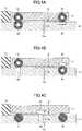
- FIGS. 8A-8Cillustrate other exemplary configurations of the plasma processing apparatus near the focus ring.
- FIGS. 9A-9Cillustrate a displacement prevention mechanism according to an embodiment of the present invention.
- FIG. 1is a longitudinal cross-sectional view of a plasma processing apparatus according to an embodiment of the present invention.
- the plasma processing apparatus 1 illustrated in FIG. 1includes a chamber (processing chamber) C that may be cylindrically-shaped, for example.
- the chamber Cis grounded.
- a substrate supporting apparatus 10is arranged on a lower wall of the chamber C.
- An upper electrode 2is arranged at a ceiling portion of the chamber C to face opposite the substrate supporting apparatus 10 .
- a gas supply source 4is connected to the upper electrode 2 . Gas supplied from the gas supply source 4 passes through a plurality of gas holes 2 a arranged at the upper electrode 2 to be introduced into the chamber C.
- the upper electrode 2acts as a shower head for supplying gas into the chamber C as well as an electrode.
- a plasma processis performed on a wafer using a plasma generated from the gas supplied thereto.
- the substrate supporting apparatus 10acts as an electrode facing opposite the upper electrode 2 and a holding mechanism for holding a substrate such as a semiconductor wafer (referred to as “wafer W” hereinafter).
- the substrate supporting apparatus 10includes a mounting stage 12 , an electrostatic chuck 13 , insulating members 14 - 16 , and a focus ring 17 .
- the substrate supporting apparatus 10also has a ring-shaped side wall 18 fixed to the lower wall 11 .
- the insulating member 14is fixed to the lower wall 11 .
- the mounting stage 12is arranged on a top surface of the insulating member 14 .
- the mounting stage 12may be made of aluminum, for example.
- the insulating member 15is ring-shaped and is arranged around the mounting stage 12 and the insulating member 14 .
- the insulating member 15is arranged to be in contact with an inner face of the side wall 18 .
- the electrostatic chuck 13is fixed on the mounting stage 12 .
- the electrostatic chuck 13includes an electrode 13 a made of a conductive film that is interposed between a pair of insulating sheets 13 b and 13 c .
- a DC power supply source 20is connected to the electrode 13 a . When a voltage is supplied from the DC power supply source 20 , the wafer W is electrostatically attracted to the electrostatic chuck 13 by a Coulomb force.
- the focus ring 17 for improving in-plane etching uniformityis arranged around the periphery of the electrostatic chuck 13 .
- the focus ring 17may be made of a dielectric material such as quartz, for example.
- a wafer W (example of a substrate) to be processedis placed on the electrostatic chuck 13 .
- the focus ring 17is arranged within an inner space created by the insulating member 16 , which is arranged into a planar ring-shaped member.
- a high frequency currentis supplied to the mounting stage 12 from a high frequency power source 21 via a matching circuit 22 .
- the mounting stage 12is electrically insulated from the chamber C, including the lower wall 11 , by the insulating members 14 and 15 .
- a path 30 for enabling the flow of a liquid for temperature controlis formed within the mounting stage 12 .
- the path 30is connected to a chiller unit 31 via pipes 32 and 33 .
- a coolant at a predetermined temperature that is output from the chiller unit 31is supplied to and circulated within the pipes 32 and 33 and the path 30 . In this way, the temperature of the mounting stage 12 may be controlled and maintained at a desired temperature or within a desired temperature range, for example.
- a heat transfer gas supply source 40supplies a heat transfer gas such as helium (He) gas between an upper surface (front side surface) of the electrostatic chuck 13 and a bottom surface (backside surface) of the wafer W via a gas supply line 41 .
- a heat transfer gassuch as helium (He) gas between an upper surface (front side surface) of the electrostatic chuck 13 and a bottom surface (backside surface) of the wafer W via a gas supply line 41 .
- Hehelium
- the heat transfer gas supply source 40supplies the heat transfer gas such as He gas between the upper surface (front side surface) of the mounting stage 12 and a bottom surface (backside surface) of the focus ring 17 via gas supply lines 42 and 43 . In this way, heat transfer efficiency between the mounting stage 12 and the focus ring 17 may be improved by the heat transfer gas.
- the heat transfer gassuch as He gas between the upper surface (front side surface) of the mounting stage 12 and a bottom surface (backside surface) of the focus ring 17 via gas supply lines 42 and 43 .
- the controller 50controls the DC power supply source 20 , the high frequency power source 21 , the matching circuit 22 , the chiller unit 31 , and the heat transfer gas supply source 40 . Also, a pressure gauge 51 is attached to the gas supply line 43 and is configured to measure the pressure of the heat transfer gas supplied between the mounting stage 12 and the focus ring 17 . The pressure gauge 51 is connected to the controller 50 and is configured to communicate the measured pressure value to the controller 50 .
- the controller 50controls the flow rate of the heat transfer gas output from the heat transfer gas supply source 40 based on the pressure value to control the pressure of the heat transfer gas supplied between the mounting stage 12 and the focus ring 17 .
- the pressure of the heat transfer gasmay be raised by increasing the flow rate of the heat transfer gas. In this way, heat transfer efficiency between the mounting stage 12 and the focus ring 17 may be improved and cooling of the focus ring 17 may be accelerated.
- the controller 50is an example of a temperature adjustment unit configured to adjust the temperature of the focus ring 17 by introducing a heat transfer gas between surfaces of the mounting stage 12 and the focus ring 17 facing opposite each other.
- the controller 50includes a CPU (Central Processing Unit), a ROM (Read Only Memory), and a RAM (Random Access Memory), which are not shown.
- the CPUexecutes programs for performing a plasma process or adjusting the temperature of the focus ring 17 according to various recipes stored in a storage unit such as the RAM or ROM.
- the recipesmay be stored in a storage medium and loaded in the storage unit via a driver (not shown), or the recipes may be downloaded from a network (not shown) and stored in the storage unit, for example.
- the functions of the elements described abovemay be implemented by a DSP (Digital Signal Processor) instead of the CPU, for example.
- the functions of the controller 50may be implemented by hardware, software, or a combination thereof, for example.
- magnetic members arranged at the surfaces of the focus ring 17 and the mounting stage 12 facing opposite each otherare described.
- magnetic O-ring members 60 and 61are respectively arranged along an outer circumference and an inner circumference of the bottom surface of the focus ring 17 .
- magnetic bodies 62 and 63are arranged at positions facing opposite the magnetic O-ring members 60 and 61 , respectively.
- the magnetic O-ring members 60 and 61include O-rings 60 a and 61 a that are made of rubber and magnets 60 b and 61 b that are embedded within the O-rings 60 a and 61 a , respectively. With such configurations, the magnetic O-ring members 60 and 61 may function as magnets and sealing members.
- groovesmay be formed along the outer circumference and the inner circumference of the bottom surface of the focus ring 17 , and the magnetic O-ring members 60 and 61 may be fitted into the grooves utilizing the contractility of the O-rings 60 a and 61 a , which are made of rubber.
- the shape of the grooves formed at the bottom surface of the focus ring 17may have specific features.
- the groovesmay be arranged into dovetail (trapezoidal) grooves, the grooves may have specific designs at entry points, or the grooves may have specific groove depths.
- the magnetic bodies 62 and 63may be magnetic plate members including plates 62 a and 63 a spray coated with magnetic materials 62 b and 63 b , or magnetic sheets coated with magnetic material, for example. To avoid metal contamination within the processing chamber C, the magnetic materials 62 and 63 are preferably not exposed at the mounting stage 12 and are embedded within the mounting stage 12 . Note that sealing properties of the magnetic bodies 62 and 63 may be inferior to those of the magnetic O-ring members 60 and 61 , but the magnetic bodies 62 and 63 may have a superior attraction force (clamping force), for example.
- the magnetic body 62 and the magnetic O-ring member 60are provided as a pair at positions facing opposite each other on the surfaces of the focus ring 17 and the mounting stage 12 facing opposite each other.
- the magnetic body 62 and the magnetic O-ring member 60have opposite magnetic poles (N pole or S pole).
- the magnetic body 63 and the magnetic O-ring member 61are provided as a pair at positions facing opposite each other on the surfaces of the focus ring 17 and the mounting stage 12 facing opposite each other, and the magnetic body 63 and the magnetic O-ring member 61 have opposite magnetic poles (N pole or S pole). In this way, a clamping force may be generated by the magnetic force between the bottom surface of the focus ring 17 and the upper surface of the mounting stage 12 .
- the magnetic O-ring members 60 and 61seal a space S between the bottom surface of the focus ring 17 and the upper surface of the mounting stage 12 .
- Heat transfer gassuch as He gas is filled into the space S.
- heat transfer efficiency between the focus ring 17 and the mounting stage 12may be improved such that heat input from plasma to the focus ring 17 during a plasma process may be efficiently transmitted to the mounting stage 12 .
- the focus ring 17may be efficiently cooled.
- magnetic O-ring members 60 and 61and the magnetic bodies 62 and 63 are merely illustrative examples of magnetic members, and the magnetic members are not limited to these examples.
- Other examples of magnetic membersinclude magnets 64 and 65 as illustrated in FIG. 3A , for example.
- the combination of magnetic members disposed on the mounting stage 12 and the focus ring 17may be any combination of the magnetic O-ring members, the magnetic bodies, and/or the magnets, for example. Further, a combination of magnetic members of the same type may be disposed at opposite positions of the focus ring 17 and the mounting stage 12 , or a combination of different types of magnetic members may be disposed at opposite positions of the focus ring 17 and the mounting stage 12 .
- O-ring members 70 and 71may be fit into the bottom surface of the focus ring 17 along the outer circumference and inner circumference of the focus ring 17 , and the magnets 64 and 65 may be disposed at center positions of the surfaces of the focus ring 17 and the mounting stage 12 facing opposite each other to generate a clamping force.
- heat transfer gassuch as He gas is preferably filled into the space S, which is sealed by the O-ring members 70 and 71 . In this way, heat input to the focus ring 17 may be efficiently transferred to the mounting stage 12 .
- FIG. 3Billustrates the bottom surface of the focus ring 17 .
- the O-ring members 70 and 71may be arranged into rings encircling the bottom surface of the focus ring 17 .
- the magnets 64may be arranged in a ring. In FIG. 3B , the magnets 64 are disposed at equal intervals in the circumferential direction of the focus ring 17 .
- FIG. 3Cillustrates an exemplary method of fixing magnet parts 64 b of the magnets 64 in the focus ring 17 in order to realize the arrangement of the magnets 64 as illustrated in FIG. 3B .
- a locknut 64 ais divided into two parts; namely, an inner part and an outer part.
- a helical grooveis formed at an opening arranged at the center of the inner part of the locknut 64 a as a screw structure.
- a helical grooveis also formed at the periphery of the magnet 64 as a screw structure.
- the locknut 64 amay be made of resin, a ceramic, or a non-magnetic metal, for example.
- the outer part of the locknut 64 ais arranged at a shoulder portion of a groove 17 a formed at the focus ring 17 . Then, the inner part of the locknut 64 a is inserted into the center of the groove 17 a . Then, the opening arranged at the center of the locknut 64 a is opened, the magnet part 64 b is inserted into the opening, and the magnet part 64 b is screwed into the locknut 64 a.
- the magnetic O-ring members 60 and 61are arranged along the outer circumference and the inner circumference of the bottom surface of the focus ring 17 .
- the magnetic body 62is arranged along an outer circumference of the upper surface of the mounting stage 12 at a position facing opposite the magnetic O-ring 61
- a magnetic O-ring member 59is arranged along an inner circumference of the upper surface of the mounting stage 12 at a position facing opposite the magnetic O-ring member 61 .
- a clamping functionmay be achieved by the above magnetic members and a sealing function may be achieved by the magnetic O-rings 59 - 61 .
- the temperature of the focus ring 17may be adjusted by the He gas supplied from the gas supply line 43 .
- the magnetic body 62 and the magnetic O-ring member 61are arranged along the outer circumference and the inner circumference of the bottom surface of the focus ring 17 .
- the magnetic O-ring member 60is arranged along the outer circumference of the upper surface of the mounting stage 12 at a position facing opposite the magnetic body 62
- the magnets 63are arranged along the inner circumference of the upper surface of the mounting stage 12 at positions facing opposite the magnetic O-ring member 61 .
- the clamping functionmay be achieved by the above magnetic members and the sealing function may be achieved by the magnetic O-ring members 60 and 61 .
- the temperature of the focus ring 17may be adjusted by the He gas supplied from the gas supply line 43 .
- the magnetic body 62is arranged at a center position of the bottom surface of the focus ring 17 .
- the magnet 64is arranged to face opposite the magnetic body 62 at a center position of the upper surface of the mounting stage 12 .
- the O-ring members 70 and 71are arranged along the outer circumference and the inner circumference of the upper surface of the mounting stage 12 . In this way, the clamping function may be achieved by the magnetic members arranged at the center positions of the focus ring 17 and the mounting stage 12 , whereas the sealing function may be achieved by the O-ring members 70 and 71 arranged along the outer circumference and the inner circumference of the mounting stage 12 .
- the temperature of the focus ring 17may be adjusted by the He gas supplied from the gas supply line 43 .
- the arrangements of the magnetic members illustrated in FIGS. 2-4Care merely illustrative examples.
- the arrangement of the magnetic membersis not particularly limited and may take other various arrangements.
- the combination of magnetic members disposed at positions of the focus ring 17 and the mounting stage 12 facing opposite each othermay be any combination of the various types of magnetic members.
- one or more ring-shaped magnetic membersmay be arranged along the circumferential directions of the focus ring 17 and the mounting stage 12
- one or more rod-shaped magnetic membersmay be arranged along the radial directions of the focus ring 17 and the mounting stage 12 .
- the magnetic membersmay be arranged at equidistant intervals, or the magnetic members may be arranged at varying intervals.
- At least two magnetic membersare preferably arranged at the inner circumference side and the outer circumference side of the focus ring 17 and the mounting stage 12 .
- the heat transfer efficiencymay be improved by increasing the volume of He gas enclosed in the space S between the focus ring 17 and the mounting stage 12 .
- a plurality of magnetic membersare preferably arranged in order to achieve uniformity in the clamping force. In this way, uniformity may be achieved in the temperature distribution within the space S, and heat transfer efficiency may be further improved, for example.
- the gap Gpis preferably arranged to be around 10 ⁇ m.
- the width of the space Sis roughly around 20-30 mm.
- a groove 12 a for diffusing the heat transfer gasmay be formed in at least one of the surfaces of the focus ring 17 and the mounting stage 12 facing opposite each other.
- the groove 12 ais formed in the mounting stage 12 .
- the groove 12 amay be formed in one or both of the surfaces of the focus ring 17 and the mounting stage 12 defining the boundaries of the space S.
- the groove 12 amay be arranged into at least one circle, and in some embodiments, the groove 12 a may be arranged into two or three concentric circles, for example.
- the shape of the groove 12 ais not limited to a ring-shape, and in other embodiments, the groove 12 a may be arranged into a spiral shape or the groove 12 a may be arranged radially, for example.
- the backside surface of the focus ring 17may be arranged into a concavo-convex surface to increase the surface area of the backside surface of the focus ring 17 .
- Blastingis one exemplary processing method that may be used to arrange the backside surface of the focus ring 17 into a concavo-convex surface.
- Thermal sprayingis another processing method that may be used. In this case, silicon is preferably sprayed on the backside surface of the focus ring 17 to form a concavo-convex surface.
- the surface area (heat transfer area) of the backside surface of the focus ring 17may be enlarged while maintaining the gap Gp to be within a range of several ⁇ m to 10 ⁇ m so that the heat transfer efficiency may be improved.
- the concavo-convex surfacemay be formed on the mounting stage 12 .
- a special sheetmay be arranged on a surface defining the space S.
- an adhesive tape having carbon nanotubes with diameters of several to several tens of nanometers arranged at a density of approximately 100 billion per 1 cm 2may be arranged on at least one of the backside surface of the focus ring 17 and the upper surface of the mounting stage 12 defining the boundaries of the space S.
- the surface area the surface defining the space Smay be substantially increased by the carbon nanotubes growing from the adhesive tape arranged on the backside surface of the focus ring 17 and/or the upper surface of the mounting stage 12 .
- heat transfer efficiencymay be further improved.
- the attraction force of the magnet toward the iron plateis proportional to the squared value of a surface magnetic flux density at the contact surface and the area of contact between the magnet and the iron plate.
- the attraction force of the magnet toward the iron platemay be assumed to be proportional to the squared value of a space magnetic flux density and the area of the magnet relative to the iron plate.
- space magnetic flux densityrefers to the magnetic flux density at the position of the iron plate spaced apart from the magnet.
- the situationis somewhat complicated because the following relation also applies. That is, when the magnet is spaced apart from the iron plate, the attraction force of the magnet to the iron plate is inversely proportional to the squared value of the distance between the magnet and the iron plate.
- FIGS. 6A-6Bare graphs illustrating relationships between the attraction force F, the magnetic flux density Bp, and the distance X of a ⁇ 20 ⁇ 10 mm neodymium magnet (Neo48) with respect to an iron plate.
- the magnetic flux density Bpdecreases as the distance X of the magnet from the iron plate increases.
- the magnetic flux densitymay vary depending on the residual magnetic flux density and the shape of the magnet. For example, as can be appreciated from FIG. 7 , the magnetic flux density and the attraction force of a magnet do not have a proportional relationship. That is, the magnetic flux density increases as the height of the magnet in its magnetization direction increases.
- the attraction force F of the magnetmay vary depending on the residual magnetic flux density and the shape of the magnet. According to FIG. 6B , the attraction force F of the magnet becomes weaker as the distance X of the magnet from the iron plate increases. Note that the magnetic flux density Bp and the attraction force F when the distance X is equal to 0 (zero) corresponds to the surface magnetic flux density and the attraction force of the magnet, respectively, when the magnet is adhered to the iron plate.
- the magnetic flux density Bpmay be assumed to be substantially similar to the attraction force of the magnet spaced apart from the iron plate.
- the abovemay apply to situations where a substance such as plastic, glass, rubber, paper, wood or the like is inserted between the magnets. Further, the above may apply to situations where a non-magnetic metal that is not attracted to a magnet such as aluminum or stainless steel is inserted between the magnets.
- the magnetic field linesare blocked (absorbed).
- the attraction force of the magnet toward the iron platemay be diminished or completely lost.
- a magnetic materialis placed between the magnet and the iron plate, if the magnetic material is very thin, most of the field lines may pass through the magnetic material.
- nickelwhich is a magnetic material, because they are thin films with film thicknesses of about 10 micrometers, they do not significantly affect the performance of the magnet.
- the space (surface) magnetic flux density between the magnetsmay be substantially equivalent to the magnetic flux density when the distance between the magnet and the iron plate is reduced to about 1 ⁇ 2.
- a very strong attraction forcemay be generated in this case.
- FIGS. 8A-8Cother exemplary configurations of the substrate supporting apparatus 10 near the focus ring 17 are described with reference to FIGS. 8A-8C .
- a heat transfer sheet 80is arranged within the gap Gp between the focus ring 17 and the mounting stage 12 .
- the heat transfer sheet 80may be attached to the focus ring 17 or the mounting stage 12 , or embedded between the focus ring 17 and the mounting stage 12 , for example.
- the magnetic body 64is arranged at the center position of the bottom surface of the focus ring 17 .
- the magnet 65is arranged on the upper surface of the mounting stage 12 at a position opposite the magnetic body 64 .
- the heat transfer sheet 80is arranged within the gap Gp.
- a weight 73is arranged at the bottom surface of the focus ring 17 .
- the focus ring 17is made of silicon and is therefore relatively lightweight. Accordingly, in the present example, a substance that is relatively heavy is embedded in the focus ring 17 . In this way, adhesion between the focus ring 17 and the mounting stage 12 may be reinforced by gravity.
- the weight 73may be made of tungsten or gold, for example. Note, however, that in order to avoid metal contamination in the processing chamber C, the weight 73 is preferably embedded in the focus ring 17 so as not to be exposed to the plasma space. Also, the heat transfer sheet 80 is arranged within the gap Gp.
- a sheet memberin addition to arranging the heat transfer sheet 80 on at least one of the surfaces of the focus ring 17 and the mounting stage 12 facing opposite each other, a sheet member may be arranged as a preventive measure against contamination of the processing chamber C by the heat transfer sheet 80 .
- a sheet member (plate member) 81 coated with an O-ring materialis arranged along the inner circumference and the outer circumference of the focus ring 17 .
- the O-ring materialmay be a radical resistant material such as perfluoro-elastomer (FFKM) or silicon, for example.
- the magnet 64is arranged at the center position of the bottom surface of the focus ring 17 and the magnetic body 62 is arranged at the upper surface of the mounting stage 12 at a position facing opposite the magnet 64 .
- a heat transfer gasmay be introduced between the surfaces of the focus ring 17 and the mounting stage 12 facing opposite each other in addition to arranging the heat transfer sheet 80 on at least one of the surfaces of the focus ring 17 and the mounting stage 12 facing opposite each other.
- magnetic membersare arranged on the surfaces of the focus ring 17 and the mounting stage 12 facing opposite each other.
- an interspace Dis provided between the periphery of the electrostatic chuck 13 and the inner periphery of the focus ring 17 .
- the interspace Dneeds to be provided in order to prevent cracking or damage to the focus ring 17 . That is, because the electrostatic chuck 13 and the focus ring 17 have differing thermal expansion coefficients, the electrostatic chuck 13 may thermally expand to a greater extent than the focus ring 17 during a plasma process, for example. As a result, the periphery of the electrostatic chuck 13 may come into contact with and press the inner periphery of the focus ring 17 to thereby cause damage to the focus ring 17 . To avoid such damage to the focus ring 17 , the interspace D is preferably provided at a uniform width in the radial direction.
- FIG. 9Billustrates one exemplary positioning method that may be used.
- a plurality of recesses 17 bmay be arranged on the bottom surface of the focus ring 17 , and a positioning pin 90 projecting from the mounting stage 12 may be inserted into the recess 17 b to enable positioning of the electrostatic chuck 13 and the focus ring 17 .
- the width of the recess 17 b in the radial directionis arranged to be greater than the width of the positioning pin 90 in consideration of thermal expansion.
- the positioning pin 90may move within the recess 17 b and the position of the focus ring 17 may deviate to the extent of the movement range of the positioning pin 90 .
- magnets 66 and 67are arranged on the surfaces of the focus ring 17 and the mounting stage 12 facing opposite each other.
- the magnet 66may be returned to a position above the magnet 67 by magnetic force.
- the focus ring 17may be returned to its proper position with respect to the electrostatic chuck 13 .
- the interspace D between the electrostatic chuck 13 and the focus ring 17may be arranged to have a uniform width in the radial direction.
- magnets 66 and 67may be used instead of the magnets 66 and 67 .
- a plurality of magnetic memberssuch as the magnets 66 and 67 may be disposed at positions of the focus ring 17 and the mounting stage 12 facing opposite each other, the positions being arranged such that the distance from the center of the inner diameter of the focus ring 17 to the position of the focus ring 17 is equal to the distance from the center of the mounting stage 12 to the position of the mounting stage 12 .
- one pair or two or more pairs of ring-shaped magnetic membersmay be disposed at positions of the focus ring 17 and the mounting stage 12 facing opposite each other, the positions being arranged such that the distance from the center of the inner diameter of the focus ring 17 to the position of the focus ring 17 is equal to the distance from the center of the mounting stage 12 to the position of the mounting stage 12 .
- heat transfer efficiency between the mounting stage 12 and the focus ring 17 of the substrate supporting apparatus 10may be improved, and temperature adjustment of the focus ring 17 may be effectively performed.
- the substrate supporting apparatus described abovemay be applied to various plasma processing apparatuses for processing a substrate using plasma.
- the plasma processing apparatusesmay include any apparatus configured to process a substrate by the action of a plasma such as an etching apparatus, an ashing apparatus, and a film deposition apparatus.
- examples of means used by the plasma processing apparatus to generate a plasmamay include a capacitively coupled plasma (CCP) generating unit, an inductively coupled plasma (ICP) generating unit, a helicon wave plasma (HWP) generating unit, a microwave surface wave plasma generating unit for generating a microwave plasma such as a slot plane antenna (SPA) plasma or a microwave plasma generated from a radial line slot antenna, an electron cyclotron resonance plasma (ECR) generating unit, and a remote plasma generating unit using the above plasma generating units, for example.
- CCPcapacitively coupled plasma
- ICPinductively coupled plasma
- HWPhelicon wave plasma
- a microwave surface wave plasma generating unitfor generating a microwave plasma such as a slot plane antenna (SPA) plasma or a microwave plasma generated from a radial line slot antenna
- ECRelectron cyclotron resonance plasma
- the workpiece subject to processing in the present inventionis not limited to a semiconductor wafer, but may be a large-sized substrate for a flat panel display, or a substrate for a solar cell or an EL element, for example.
Landscapes
- Chemical & Material Sciences (AREA)
- Engineering & Computer Science (AREA)
- Physics & Mathematics (AREA)
- Plasma & Fusion (AREA)
- Analytical Chemistry (AREA)
- Drying Of Semiconductors (AREA)
- Container, Conveyance, Adherence, Positioning, Of Wafer (AREA)
- General Chemical & Material Sciences (AREA)
- Chemical Kinetics & Catalysis (AREA)
- Materials Engineering (AREA)
- Mechanical Engineering (AREA)
- Metallurgy (AREA)
- Organic Chemistry (AREA)
- Plasma Technology (AREA)
Abstract
Description
This patent application is based upon and claims the benefit of priority of Japanese Patent Application No. 2013-171081 filed on Aug. 21, 2013, the entire contents of which are incorporated herein by reference.
The present invention generally relates to a plasma processing apparatus.
In a semiconductor manufacturing process, plasma processes such as etching and film deposition are performed on a workpiece such as a semiconductor wafer (simply referred to as “wafer” hereinafter).
Plasma processing apparatuses that subject a wafer to a plasma process include a mounting stage on which the wafer is mounted and a focus ring arranged on the mounting stage to surround the periphery of the wafer. The focus ring is configured to extend a plasma distribution region generated above the wafer to a region above the focus ring in order to secure plasma processing uniformity of a plasma process that is performed on the entire face of the wafer.
During a plasma process, the wafer and the focus ring are directly exposed to plasma and is heated to a relatively high temperature. Thus, the temperature of the mounting stage is desirably controlled so that the temperature of the wafer and the temperature of the focus ring may be controlled and the focus ring may be cooled. When the heat transfer efficiency between the mounting stage and the focus ring is low, heat input from plasma may not be efficiently transferred from the focus ring to the mounting stage and temperature adjustment of the focus ring may be difficult. In this respect, a technique is known that involves fixing a heat transfer sheet such as silicon rubber to the focus ring to improve the heat transfer efficiency between the mounting stage and the focus ring (see e.g. Japanese Laid-Open Patent Publication No. 2008-171899).
However, the heat transfer sheet is an adhesive sheet and its heat transfer performance may vary depending on the manner in which the heat transfer sheet is adhered to the focus ring as well as the individual variability of the heat transfer sheet. That is, when the adhesive power of the heat transfer sheet is weak, the adhesion between the focus ring and the mounting stage may be degraded, and heat may not be efficiently transferred from the focus ring to the mounting stage. Also, outgassing from the heat transfer sheet may occur. Further, the heat transfer sheet may not be easily peeled off of the focus ring. Accordingly, the temperature of the focus ring is fixed by the specification of the heat transfer sheet and the temperature of the focus ring cannot be variably controlled.
In light of the above, there is a demand for a technique for improving the heat transfer efficiency between the mounting stage and the focus ring and enabling variable control of the temperature of the focus ring.
According to an embodiment of the present invention, a plasma processing apparatus is provided that includes a mounting stage on which a substrate is mounted, a focus ring arranged around a periphery of the mounting stage, a plurality of magnetic members arranged at a surface of the focus ring and a surface of the mounting stage facing opposite each other, and a temperature adjustment unit configured to adjust a temperature of the focus ring by introducing a heat transfer gas between the surface of the focus ring and the surface of the mounting stage facing opposite each other.
According to an aspect of the present invention, heat transfer efficiency between the mounting stage and the focus ring may be improved and the temperature of the focus ring may be variably controlled.
In the following, embodiments of the present invention are described with reference to the accompanying drawings. Note that elements described below having substantially identical features are given the same reference symbols and overlapping descriptions thereof may be omitted.
[Plasma Processing Apparatus/Substrate Supporting Apparatus]
In the following, a plasma processing apparatus and a substrate supporting apparatus according to an embodiment of the present invention are described with reference toFIG. 1 .FIG. 1 is a longitudinal cross-sectional view of a plasma processing apparatus according to an embodiment of the present invention. Theplasma processing apparatus 1 illustrated inFIG. 1 includes a chamber (processing chamber) C that may be cylindrically-shaped, for example. The chamber C is grounded. Asubstrate supporting apparatus 10 is arranged on a lower wall of the chamber C. Anupper electrode 2 is arranged at a ceiling portion of the chamber C to face opposite thesubstrate supporting apparatus 10. Agas supply source 4 is connected to theupper electrode 2. Gas supplied from thegas supply source 4 passes through a plurality ofgas holes 2aarranged at theupper electrode 2 to be introduced into the chamber C. Theupper electrode 2 acts as a shower head for supplying gas into the chamber C as well as an electrode. In the chamber C, a plasma process is performed on a wafer using a plasma generated from the gas supplied thereto.
Thesubstrate supporting apparatus 10 acts as an electrode facing opposite theupper electrode 2 and a holding mechanism for holding a substrate such as a semiconductor wafer (referred to as “wafer W” hereinafter).
Thesubstrate supporting apparatus 10 includes amounting stage 12, anelectrostatic chuck 13, insulating members14-16, and afocus ring 17. Thesubstrate supporting apparatus 10 also has a ring-shaped side wall 18 fixed to thelower wall 11. Theinsulating member 14 is fixed to thelower wall 11. Themounting stage 12 is arranged on a top surface of the insulatingmember 14. Themounting stage 12 may be made of aluminum, for example. Theinsulating member 15 is ring-shaped and is arranged around themounting stage 12 and theinsulating member 14. Theinsulating member 15 is arranged to be in contact with an inner face of theside wall 18.
Theelectrostatic chuck 13 is fixed on themounting stage 12. Theelectrostatic chuck 13 includes anelectrode 13amade of a conductive film that is interposed between a pair ofinsulating sheets power supply source 20 is connected to theelectrode 13a. When a voltage is supplied from the DCpower supply source 20, the wafer W is electrostatically attracted to theelectrostatic chuck 13 by a Coulomb force.
Thefocus ring 17 for improving in-plane etching uniformity is arranged around the periphery of theelectrostatic chuck 13. Thefocus ring 17 may be made of a dielectric material such as quartz, for example. A wafer W (example of a substrate) to be processed is placed on theelectrostatic chuck 13. Thefocus ring 17 is arranged within an inner space created by the insulatingmember 16, which is arranged into a planar ring-shaped member.
A high frequency current is supplied to the mountingstage 12 from a highfrequency power source 21 via amatching circuit 22. The mountingstage 12 is electrically insulated from the chamber C, including thelower wall 11, by the insulatingmembers
Apath 30 for enabling the flow of a liquid for temperature control is formed within the mountingstage 12. Thepath 30 is connected to achiller unit 31 viapipes chiller unit 31 is supplied to and circulated within thepipes path 30. In this way, the temperature of the mountingstage 12 may be controlled and maintained at a desired temperature or within a desired temperature range, for example.
A heat transfergas supply source 40 supplies a heat transfer gas such as helium (He) gas between an upper surface (front side surface) of theelectrostatic chuck 13 and a bottom surface (backside surface) of the wafer W via agas supply line 41. In this way, heat transfer efficiency between theelectrostatic chuck 13 and the wafer W may be improved by the heat transfer gas.
Also, the heat transfergas supply source 40 supplies the heat transfer gas such as He gas between the upper surface (front side surface) of the mountingstage 12 and a bottom surface (backside surface) of thefocus ring 17 viagas supply lines stage 12 and thefocus ring 17 may be improved by the heat transfer gas.
Thecontroller 50 controls the DCpower supply source 20, the highfrequency power source 21, the matchingcircuit 22, thechiller unit 31, and the heat transfergas supply source 40. Also, apressure gauge 51 is attached to thegas supply line 43 and is configured to measure the pressure of the heat transfer gas supplied between the mountingstage 12 and thefocus ring 17. Thepressure gauge 51 is connected to thecontroller 50 and is configured to communicate the measured pressure value to thecontroller 50.
Thecontroller 50 controls the flow rate of the heat transfer gas output from the heat transfergas supply source 40 based on the pressure value to control the pressure of the heat transfer gas supplied between the mountingstage 12 and thefocus ring 17. For example, the pressure of the heat transfer gas may be raised by increasing the flow rate of the heat transfer gas. In this way, heat transfer efficiency between the mountingstage 12 and thefocus ring 17 may be improved and cooling of thefocus ring 17 may be accelerated. On the other hand, when the flow rate of the heat transfer gas is decreased, the pressure of the heat transfer gas is reduced. As a result, the heat transfer efficiency is degraded and cooling of thefocus ring 17 is suppressed. Thecontroller 50 is an example of a temperature adjustment unit configured to adjust the temperature of thefocus ring 17 by introducing a heat transfer gas between surfaces of the mountingstage 12 and thefocus ring 17 facing opposite each other.
Thecontroller 50 includes a CPU (Central Processing Unit), a ROM (Read Only Memory), and a RAM (Random Access Memory), which are not shown. The CPU executes programs for performing a plasma process or adjusting the temperature of thefocus ring 17 according to various recipes stored in a storage unit such as the RAM or ROM. In some embodiments, the recipes may be stored in a storage medium and loaded in the storage unit via a driver (not shown), or the recipes may be downloaded from a network (not shown) and stored in the storage unit, for example. Further, the functions of the elements described above may be implemented by a DSP (Digital Signal Processor) instead of the CPU, for example. Note that the functions of thecontroller 50 may be implemented by hardware, software, or a combination thereof, for example.
(Magnetic Members)
In the following, magnetic members arranged at the surfaces of thefocus ring 17 and the mountingstage 12 facing opposite each other are described. As illustrated inFIGS. 1 and 2 , magnetic O-ring members focus ring 17. Also, on the upper surface of the mountingstage 12 facing opposite thefocus ring 17,magnetic bodies ring members
The magnetic O-ring members rings magnets rings ring members
As an exemplary method for fixing the magnetic O-ring members focus ring 17, grooves may be formed along the outer circumference and the inner circumference of the bottom surface of thefocus ring 17, and the magnetic O-ring members rings focus ring 17 may have specific features. For example, the grooves may be arranged into dovetail (trapezoidal) grooves, the grooves may have specific designs at entry points, or the grooves may have specific groove depths.
Themagnetic bodies members including plates magnetic materials magnetic materials stage 12 and are embedded within the mountingstage 12. Note that sealing properties of themagnetic bodies ring members magnetic bodies
Themagnetic body 62 and the magnetic O-ring member 60 are provided as a pair at positions facing opposite each other on the surfaces of thefocus ring 17 and the mountingstage 12 facing opposite each other. Themagnetic body 62 and the magnetic O-ring member 60 have opposite magnetic poles (N pole or S pole). Similarly, themagnetic body 63 and the magnetic O-ring member 61 are provided as a pair at positions facing opposite each other on the surfaces of thefocus ring 17 and the mountingstage 12 facing opposite each other, and themagnetic body 63 and the magnetic O-ring member 61 have opposite magnetic poles (N pole or S pole). In this way, a clamping force may be generated by the magnetic force between the bottom surface of thefocus ring 17 and the upper surface of the mountingstage 12.
Also, the magnetic O-ring members focus ring 17 and the upper surface of the mountingstage 12. Heat transfer gas such as He gas is filled into the space S. In this way, heat transfer efficiency between thefocus ring 17 and the mountingstage 12 may be improved such that heat input from plasma to thefocus ring 17 during a plasma process may be efficiently transmitted to the mountingstage 12. Thus, thefocus ring 17 may be efficiently cooled.
Note that the magnetic O-ring members magnetic bodies magnets FIG. 3A , for example.
The combination of magnetic members disposed on the mountingstage 12 and thefocus ring 17 may be any combination of the magnetic O-ring members, the magnetic bodies, and/or the magnets, for example. Further, a combination of magnetic members of the same type may be disposed at opposite positions of thefocus ring 17 and the mountingstage 12, or a combination of different types of magnetic members may be disposed at opposite positions of thefocus ring 17 and the mountingstage 12.
For example, as illustrated inFIG. 3A , O-ring members focus ring 17 along the outer circumference and inner circumference of thefocus ring 17, and themagnets focus ring 17 and the mountingstage 12 facing opposite each other to generate a clamping force. Also, heat transfer gas such as He gas is preferably filled into the space S, which is sealed by the O-ring members focus ring 17 may be efficiently transferred to the mountingstage 12.
As illustrated inFIG. 3C , alocknut 64ais divided into two parts; namely, an inner part and an outer part. A helical groove is formed at an opening arranged at the center of the inner part of thelocknut 64aas a screw structure. A helical groove is also formed at the periphery of themagnet 64 as a screw structure. Thelocknut 64amay be made of resin, a ceramic, or a non-magnetic metal, for example.
To fix themagnet 64 to thefocus ring 17, first, the outer part of thelocknut 64ais arranged at a shoulder portion of agroove 17aformed at thefocus ring 17. Then, the inner part of thelocknut 64ais inserted into the center of thegroove 17a. Then, the opening arranged at the center of thelocknut 64ais opened, themagnet part 64bis inserted into the opening, and themagnet part 64bis screwed into thelocknut 64a.
In the following, other exemplary combinations of the magnetic members arranged at thefocus ring 17 and the mountingstage 12 are described with reference toFIGS. 4A-4C .
InFIG. 4A , the magnetic O-ring members focus ring 17. Themagnetic body 62 is arranged along an outer circumference of the upper surface of the mountingstage 12 at a position facing opposite the magnetic O-ring 61, and a magnetic O-ring member 59 is arranged along an inner circumference of the upper surface of the mountingstage 12 at a position facing opposite the magnetic O-ring member 61. In this way, a clamping function may be achieved by the above magnetic members and a sealing function may be achieved by the magnetic O-rings59-61. Also, the temperature of thefocus ring 17 may be adjusted by the He gas supplied from thegas supply line 43.
InFIG. 4B , themagnetic body 62 and the magnetic O-ring member 61 are arranged along the outer circumference and the inner circumference of the bottom surface of thefocus ring 17. The magnetic O-ring member 60 is arranged along the outer circumference of the upper surface of the mountingstage 12 at a position facing opposite themagnetic body 62, and themagnets 63 are arranged along the inner circumference of the upper surface of the mountingstage 12 at positions facing opposite the magnetic O-ring member 61. In this way, the clamping function may be achieved by the above magnetic members and the sealing function may be achieved by the magnetic O-ring members focus ring 17 may be adjusted by the He gas supplied from thegas supply line 43.
InFIG. 4C , themagnetic body 62 is arranged at a center position of the bottom surface of thefocus ring 17. Themagnet 64 is arranged to face opposite themagnetic body 62 at a center position of the upper surface of the mountingstage 12. The O-ring members stage 12. In this way, the clamping function may be achieved by the magnetic members arranged at the center positions of thefocus ring 17 and the mountingstage 12, whereas the sealing function may be achieved by the O-ring members stage 12. Also, the temperature of thefocus ring 17 may be adjusted by the He gas supplied from thegas supply line 43.
Note that the arrangements of the magnetic members illustrated inFIGS. 2-4C are merely illustrative examples. The arrangement of the magnetic members is not particularly limited and may take other various arrangements. Also, the combination of magnetic members disposed at positions of thefocus ring 17 and the mountingstage 12 facing opposite each other may be any combination of the various types of magnetic members. For example, one or more ring-shaped magnetic members may be arranged along the circumferential directions of thefocus ring 17 and the mountingstage 12, one or more rod-shaped magnetic members may be arranged along the radial directions of thefocus ring 17 and the mountingstage 12. Also, the magnetic members may be arranged at equidistant intervals, or the magnetic members may be arranged at varying intervals. Note, however, that at least two magnetic members are preferably arranged at the inner circumference side and the outer circumference side of thefocus ring 17 and the mountingstage 12. Also, note that the heat transfer efficiency may be improved by increasing the volume of He gas enclosed in the space S between thefocus ring 17 and the mountingstage 12. Also, a plurality of magnetic members are preferably arranged in order to achieve uniformity in the clamping force. In this way, uniformity may be achieved in the temperature distribution within the space S, and heat transfer efficiency may be further improved, for example.
[Gap]
Note that when a gap Gp between thefocus ring 17 and the mounting stage12 (seeFIG. 5 ) is too wide, an adequately high heat transfer efficiency cannot be obtained even if He gas is introduced into the space S between thefocus ring 17 and the mountingstage 12. To obtain an adequately high heat transfer efficiency, the gap Gp is preferably arranged to be around 10 μm. Meanwhile, the width of the space S (distance between the O-rings FIG. 5 ) is roughly around 20-30 mm. When the space S has a small height and a relatively large width, He gas is prevented from being effectively diffused within the space S. Accordingly, in some embodiments, agroove 12afor diffusing the heat transfer gas may be formed in at least one of the surfaces of thefocus ring 17 and the mountingstage 12 facing opposite each other. In this way, heat transfer efficiency may be improved. Note that inFIG. 5 , thegroove 12ais formed in the mountingstage 12. However, this is merely one illustrative example. That is, thegroove 12amay be formed in one or both of the surfaces of thefocus ring 17 and the mountingstage 12 defining the boundaries of the space S. In a case where thegroove 12ais ring-shaped, thegroove 12amay be arranged into at least one circle, and in some embodiments, thegroove 12amay be arranged into two or three concentric circles, for example. Further, the shape of thegroove 12ais not limited to a ring-shape, and in other embodiments, thegroove 12amay be arranged into a spiral shape or thegroove 12amay be arranged radially, for example.
Further, in order to improve heat transfer efficiency, the backside surface of thefocus ring 17 may be arranged into a concavo-convex surface to increase the surface area of the backside surface of thefocus ring 17. Blasting is one exemplary processing method that may be used to arrange the backside surface of thefocus ring 17 into a concavo-convex surface. Thermal spraying is another processing method that may be used. In this case, silicon is preferably sprayed on the backside surface of thefocus ring 17 to form a concavo-convex surface. In this way, the surface area (heat transfer area) of the backside surface of thefocus ring 17 may be enlarged while maintaining the gap Gp to be within a range of several μm to 10 μm so that the heat transfer efficiency may be improved. Note that in some embodiments, the concavo-convex surface may be formed on the mountingstage 12.
Further, in order to increase the surface area, a special sheet may be arranged on a surface defining the space S. For example, an adhesive tape having carbon nanotubes with diameters of several to several tens of nanometers arranged at a density of approximately 100 billion per 1 cm2may be arranged on at least one of the backside surface of thefocus ring 17 and the upper surface of the mountingstage 12 defining the boundaries of the space S. In this way, the surface area the surface defining the space S may be substantially increased by the carbon nanotubes growing from the adhesive tape arranged on the backside surface of thefocus ring 17 and/or the upper surface of the mountingstage 12. As a result, heat transfer efficiency may be further improved.
(Attraction Force of Magnet Spaced from Iron Plate)
With respect to a magnet that is adhered to an iron plate, the attraction force of the magnet toward the iron plate is proportional to the squared value of a surface magnetic flux density at the contact surface and the area of contact between the magnet and the iron plate. Similarly, with respect to a magnet that is spaced apart from an iron plate, the attraction force of the magnet toward the iron plate may be assumed to be proportional to the squared value of a space magnetic flux density and the area of the magnet relative to the iron plate. Note that “space magnetic flux density” refers to the magnetic flux density at the position of the iron plate spaced apart from the magnet. However, in the present case, the situation is somewhat complicated because the following relation also applies. That is, when the magnet is spaced apart from the iron plate, the attraction force of the magnet to the iron plate is inversely proportional to the squared value of the distance between the magnet and the iron plate.
Note, however, that the inverse-square law is based on Coulomb's law for magnetic poles, and actual magnets do not accurately follow the inverse-square law and vary greatly depending on their shapes, for example.
Similarly, the attraction force F of the magnet may vary depending on the residual magnetic flux density and the shape of the magnet. According toFIG. 6B , the attraction force F of the magnet becomes weaker as the distance X of the magnet from the iron plate increases. Note that the magnetic flux density Bp and the attraction force F when the distance X is equal to 0 (zero) corresponds to the surface magnetic flux density and the attraction force of the magnet, respectively, when the magnet is adhered to the iron plate.
(Influence of Substance between Iron Plate and Magnet)
Even if a substance that is not attracted to a magnet is inserted between magnets having opposite magnetic poles, magnetic field lines may pass through the substance as in the case of passing through air. Thus, the magnetic flux density Bp may be assumed to be substantially similar to the attraction force of the magnet spaced apart from the iron plate. For example, the above may apply to situations where a substance such as plastic, glass, rubber, paper, wood or the like is inserted between the magnets. Further, the above may apply to situations where a non-magnetic metal that is not attracted to a magnet such as aluminum or stainless steel is inserted between the magnets. On the other hand, when a substance that is attracted to a magnet is inserted between the magnet and the iron plate, the magnetic field lines are blocked (absorbed). Thus, the attraction force of the magnet toward the iron plate may be diminished or completely lost. Note, however, that even if a magnetic material is placed between the magnet and the iron plate, if the magnetic material is very thin, most of the field lines may pass through the magnetic material. Although neodymium magnets are covered by nickel (plating), which is a magnetic material, because they are thin films with film thicknesses of about 10 micrometers, they do not significantly affect the performance of the magnet.
(Attraction Force Between Magnets)
In a case where a set of magnetized magnets having the same shape are arranged opposite each other at the N pole and the S pole, when compared with the case where the magnet is facing opposite an iron plate, the space (surface) magnetic flux density between the magnets may be substantially equivalent to the magnetic flux density when the distance between the magnet and the iron plate is reduced to about ½. Thus, a very strong attraction force may be generated in this case.
[Other Configurations]
In the following, other exemplary configurations of thesubstrate supporting apparatus 10 near thefocus ring 17 are described with reference toFIGS. 8A-8C . Note that in the examples illustrated inFIGS. 8A-8C , instead of filling the gap Gp (seeFIG. 5 ) with He gas to control the temperature of thefocus ring 17, aheat transfer sheet 80 is arranged within the gap Gp between thefocus ring 17 and the mountingstage 12. Theheat transfer sheet 80 may be attached to thefocus ring 17 or the mountingstage 12, or embedded between thefocus ring 17 and the mountingstage 12, for example.
In the example illustrated inFIG. 8A , themagnetic body 64 is arranged at the center position of the bottom surface of thefocus ring 17. Themagnet 65 is arranged on the upper surface of the mountingstage 12 at a position opposite themagnetic body 64. Theheat transfer sheet 80 is arranged within the gap Gp.
In the example illustrated inFIG. 8B , aweight 73 is arranged at the bottom surface of thefocus ring 17. Thefocus ring 17 is made of silicon and is therefore relatively lightweight. Accordingly, in the present example, a substance that is relatively heavy is embedded in thefocus ring 17. In this way, adhesion between thefocus ring 17 and the mountingstage 12 may be reinforced by gravity. Theweight 73 may be made of tungsten or gold, for example. Note, however, that in order to avoid metal contamination in the processing chamber C, theweight 73 is preferably embedded in thefocus ring 17 so as not to be exposed to the plasma space. Also, theheat transfer sheet 80 is arranged within the gap Gp.
Further, although not illustrated inFIGS. 8A and 8B , in some embodiments, in addition to arranging theheat transfer sheet 80 on at least one of the surfaces of thefocus ring 17 and the mountingstage 12 facing opposite each other, a sheet member may be arranged as a preventive measure against contamination of the processing chamber C by theheat transfer sheet 80. In the example illustrated inFIG. 8C , a sheet member (plate member)81 coated with an O-ring material is arranged along the inner circumference and the outer circumference of thefocus ring 17. The O-ring material may be a radical resistant material such as perfluoro-elastomer (FFKM) or silicon, for example. Also, in the example illustrated inFIG. 8C , themagnet 64 is arranged at the center position of the bottom surface of thefocus ring 17 and themagnetic body 62 is arranged at the upper surface of the mountingstage 12 at a position facing opposite themagnet 64.
Note that although a gas supply line for supplying a heat transfer gas is not shown inFIGS. 8A-8C , in some embodiments, a heat transfer gas may be introduced between the surfaces of thefocus ring 17 and the mountingstage 12 facing opposite each other in addition to arranging theheat transfer sheet 80 on at least one of the surfaces of thefocus ring 17 and the mountingstage 12 facing opposite each other. Also, magnetic members are arranged on the surfaces of thefocus ring 17 and the mountingstage 12 facing opposite each other.
[Displacement Prevention Mechanism]
As illustrated inFIG. 9A , an interspace D is provided between the periphery of theelectrostatic chuck 13 and the inner periphery of thefocus ring 17. The interspace D needs to be provided in order to prevent cracking or damage to thefocus ring 17. That is, because theelectrostatic chuck 13 and thefocus ring 17 have differing thermal expansion coefficients, theelectrostatic chuck 13 may thermally expand to a greater extent than thefocus ring 17 during a plasma process, for example. As a result, the periphery of theelectrostatic chuck 13 may come into contact with and press the inner periphery of thefocus ring 17 to thereby cause damage to thefocus ring 17. To avoid such damage to thefocus ring 17, the interspace D is preferably provided at a uniform width in the radial direction.
In order to arrange the interspace D to have a uniform width, positioning of theelectrostatic chuck 13 and thefocus ring 17 needs to be performed.FIG. 9B illustrates one exemplary positioning method that may be used. As illustrated inFIG. 9B , a plurality ofrecesses 17b(only one of which is illustrated inFIG. 9B ) may be arranged on the bottom surface of thefocus ring 17, and apositioning pin 90 projecting from the mountingstage 12 may be inserted into therecess 17bto enable positioning of theelectrostatic chuck 13 and thefocus ring 17. However, in this positioning method, the width of therecess 17bin the radial direction is arranged to be greater than the width of thepositioning pin 90 in consideration of thermal expansion. Thus, thepositioning pin 90 may move within therecess 17band the position of thefocus ring 17 may deviate to the extent of the movement range of thepositioning pin 90.
In view of the above, as illustrated inFIG. 9C , in thesubstrate supporting apparatus 10 according to the present embodiment,magnets focus ring 17 and the mountingstage 12 facing opposite each other. In this way, even when thefocus ring 17 is slightly deviated by stress from heat input during a plasma process, for example, themagnet 66 may be returned to a position above themagnet 67 by magnetic force. As a result, thefocus ring 17 may be returned to its proper position with respect to theelectrostatic chuck 13. In this way, the interspace D between theelectrostatic chuck 13 and thefocus ring 17 may be arranged to have a uniform width in the radial direction.
Note that in some embodiments, other magnetic members may be used instead of themagnets magnets focus ring 17 and the mountingstage 12 facing opposite each other, the positions being arranged such that the distance from the center of the inner diameter of thefocus ring 17 to the position of thefocus ring 17 is equal to the distance from the center of the mountingstage 12 to the position of the mountingstage 12. Also, one pair or two or more pairs of ring-shaped magnetic members may be disposed at positions of thefocus ring 17 and the mountingstage 12 facing opposite each other, the positions being arranged such that the distance from the center of the inner diameter of thefocus ring 17 to the position of thefocus ring 17 is equal to the distance from the center of the mountingstage 12 to the position of the mountingstage 12.
In theplasma processing apparatus 1 according to the present embodiment as described above, heat transfer efficiency between the mountingstage 12 and thefocus ring 17 of thesubstrate supporting apparatus 10 may be improved, and temperature adjustment of thefocus ring 17 may be effectively performed.
Although illustrative embodiments of a plasma processing apparatus and a substrate supporting apparatus according to the present invention have been described above, the present invention is not limited to these embodiments but includes various variations and modifications that may be made within the spirit and scope of the present invention. Further, the various embodiments and modifications may be combined to the extent practicable.
[Plasma Processing Apparatus]
The substrate supporting apparatus described above may be applied to various plasma processing apparatuses for processing a substrate using plasma. For example, the plasma processing apparatuses may include any apparatus configured to process a substrate by the action of a plasma such as an etching apparatus, an ashing apparatus, and a film deposition apparatus. Also, examples of means used by the plasma processing apparatus to generate a plasma may include a capacitively coupled plasma (CCP) generating unit, an inductively coupled plasma (ICP) generating unit, a helicon wave plasma (HWP) generating unit, a microwave surface wave plasma generating unit for generating a microwave plasma such as a slot plane antenna (SPA) plasma or a microwave plasma generated from a radial line slot antenna, an electron cyclotron resonance plasma (ECR) generating unit, and a remote plasma generating unit using the above plasma generating units, for example.
Also, note that the workpiece subject to processing in the present invention is not limited to a semiconductor wafer, but may be a large-sized substrate for a flat panel display, or a substrate for a solar cell or an EL element, for example.
Claims (13)
1. A plasma processing apparatus comprising:
a mounting stage on which a substrate is mounted;
a focus ring disposed over a peripheral region of the mounting stage;
a first magnet, magnetic body, or magnetic O-ring member provided at the bottom surface of the focus ring;
a second magnet, magnetic body, or magnetic O-ring member provided at the upper surface of the mounting stage and arranged at a position opposite the first magnet, magnetic body, or magnetic O-ring member;
a plurality of members that are made of a material different from the focus ring and are provided in between the focus ring and the mounting stage, whereby the plurality of members seal a heat transfer space defined by a bottom surface of the focus ring, an upper surface of the mounting stage, and the plurality of members, each member of the plurality of members being provided on opposite sides of the space; and
a temperature adjustment unit configured to adjust a temperature of the focus ring, the temperature adjustment unit including a heat transfer gas supply unit, wherein
the heat transfer supply unit is configured to supply a heat transfer gas into the heat transfer space,
the bottom surface of the focus ring, facing opposite the mounting stage, includes a concavo-convex surface,
the heat transfer space has a height of up to 10 μm,
each of the plurality of members are provided in a groove formed in at least one of the bottom surface of the focus ring or the upper surface of the mounting stage,
a first member of the plurality of members being provided along an outer circumference of the focus ring and a second member of the plurality of members being provided along an inner circumference of the focus ring, and
each of the first member and the second member is an O-ring member.
2. The plasma processing apparatus as claimed inclaim 1 , wherein the temperature adjustment unit adjusts the temperature of the focus ring by controlling a pressure of the heat transfer gas that is supplied between the bottom surface of the focus ring and the upper surface of the mounting stage.
3. The plasma processing apparatus as claimed inclaim 1 , wherein at least one of the bottom surface of the focus ring and the upper surface of the mounting stage facing opposite each other includes a groove for diffusing the heat transfer gas.
4. The plasma processing apparatus as claimed inclaim 1 , wherein the mounting stage includes an electrostatic chuck.
5. The plasma processing apparatus as claimed inclaim 1 , wherein the temperature adjustment unit adjusts the temperature of the focus ring by supplying the heat transfer gas between the bottom surface of the focus ring and the upper surface of the mounting stage facing opposite each other.
6. The plasma processing apparatus as claimed inclaim 1 , wherein the heat transfer gas supply unit of the plasma processing apparatus is provided as a single heat transfer gas supply unit.
7. The plasma processing apparatus as claimed inclaim 1 , wherein
the first member and the second member of the plurality of members are provided in the upper surface of the mounting stage.
8. The plasma processing apparatus as claimed inclaim 1 , wherein the first member and the second member are provided in the grooves in the bottom surface of the focus ring; wherein the first member is the first magnetic O-ring member, and the second magnet or magnetic body is located opposite the first member; and the second member is a third magnetic O-ring member, and a fourth magnet or magnetic body is located in the upper surface of the mounting stage opposite the second member.
9. The plasma processing apparatus as claimed inclaim 1 , wherein the first magnet or magnetic body is provided at a center position of the bottom surface of the focus ring; and the second magnet or magnetic body, is provided at a center position of the upper surface of the mounting stage and arranged at a position opposite the first magnet or magnetic body.
10. The plasma processing apparatus as claimed inclaim 1 , wherein the first member and the second member are provided in the grooves in the bottom surface of the focus ring; wherein the first member is the first magnetic O-ring member, and the second magnetic O-ring member is located opposite the first member; and the second member is a third magnetic O-ring member, and a fourth magnet or magnetic body is located in the upper surface of the mounting stage opposite the second member.
11. The plasma processing apparatus as claimed inclaim 1 , wherein the first member is provided in the groove in the bottom surface of the focus ring and the second member is provided in the groove in the upper surface of the mounting stage; wherein the first member is the first magnetic O-ring member, and the second magnet or magnetic body is located opposite the first member; and the second member is a third magnetic O-ring member, and a fourth magnet or magnetic body located in the bottom surface of the focus ring and opposite the second member.
12. A plasma processing apparatus comprising:
a mounting stage on which a substrate is mounted;
a focus ring disposed over a peripheral region of the mounting stage;
a first magnet or magnetic body provided at a center position of the bottom surface of the focus ring;
a second magnet or magnetic body provided at a center position of the upper surface of the mounting stage and arranged at a position opposite the first magnet or magnetic body;
a plurality of members that are made of a material different from the focus ring and are provided in between the focus ring and the mounting stage, whereby the plurality of members seal a heat transfer space defined by a bottom surface of the focus ring, an upper surface of the mounting stage, and the plurality of members, each member of the plurality of members being provided on opposite sides of the space; and
a temperature adjustment unit configured to adjust a temperature of the focus ring, the temperature adjustment unit including a heat transfer sheet, wherein
the heat transfer sheet is provided in the heat transfer space,
the bottom surface of the focus ring, facing opposite the mounting stage, includes a concavo-convex surface,
the heat transfer space has a height of up to 10 μm,
a first member and a second member of the plurality of members are provided between the bottom surface of the focus ring and the upper surface of the mounting stage,
the first member being provided along an outer circumference of the focus ring and the second member being provided along an inner circumference of the focus ring, and
each of the first member and the second member is an O-ring member.
13. The plasma processing apparatus as claimed inclaim 12 , wherein the temperature adjustment unit uses the heat transfer sheet to adjust the temperature of the focus ring.
Applications Claiming Priority (2)
| Application Number | Priority Date | Filing Date | Title |
|---|---|---|---|
| JP2013171081AJP6689020B2 (en) | 2013-08-21 | 2013-08-21 | Plasma processing device |
| JP2013-171081 | 2013-08-21 |
Publications (2)
| Publication Number | Publication Date |
|---|---|
| US20150053348A1 US20150053348A1 (en) | 2015-02-26 |
| US10622196B2true US10622196B2 (en) | 2020-04-14 |
Family
ID=52479300
Family Applications (1)
| Application Number | Title | Priority Date | Filing Date |
|---|---|---|---|
| US14/461,537Active2037-11-14US10622196B2 (en) | 2013-08-21 | 2014-08-18 | Plasma processing apparatus |
Country Status (4)
| Country | Link |
|---|---|
| US (1) | US10622196B2 (en) |
| JP (1) | JP6689020B2 (en) |
| KR (1) | KR102175862B1 (en) |
| TW (1) | TWI636153B (en) |
Cited By (275)
| Publication number | Priority date | Publication date | Assignee | Title |
|---|---|---|---|---|
| US20200385858A1 (en)* | 2019-06-06 | 2020-12-10 | Picosun Oy | Coating of fluid-permeable materials |
| US11004977B2 (en) | 2017-07-19 | 2021-05-11 | Asm Ip Holding B.V. | Method for depositing a group IV semiconductor and related semiconductor device structures |
| US11001925B2 (en) | 2016-12-19 | 2021-05-11 | Asm Ip Holding B.V. | Substrate processing apparatus |
| US11018002B2 (en) | 2017-07-19 | 2021-05-25 | Asm Ip Holding B.V. | Method for selectively depositing a Group IV semiconductor and related semiconductor device structures |
| US11015245B2 (en) | 2014-03-19 | 2021-05-25 | Asm Ip Holding B.V. | Gas-phase reactor and system having exhaust plenum and components thereof |
| US11022879B2 (en) | 2017-11-24 | 2021-06-01 | Asm Ip Holding B.V. | Method of forming an enhanced unexposed photoresist layer |
| US11031242B2 (en) | 2018-11-07 | 2021-06-08 | Asm Ip Holding B.V. | Methods for depositing a boron doped silicon germanium film |
| USD922229S1 (en) | 2019-06-05 | 2021-06-15 | Asm Ip Holding B.V. | Device for controlling a temperature of a gas supply unit |
| US11049751B2 (en) | 2018-09-14 | 2021-06-29 | Asm Ip Holding B.V. | Cassette supply system to store and handle cassettes and processing apparatus equipped therewith |
| US11056344B2 (en) | 2017-08-30 | 2021-07-06 | Asm Ip Holding B.V. | Layer forming method |
| US11053591B2 (en) | 2018-08-06 | 2021-07-06 | Asm Ip Holding B.V. | Multi-port gas injection system and reactor system including same |
| US11069510B2 (en) | 2017-08-30 | 2021-07-20 | Asm Ip Holding B.V. | Substrate processing apparatus |
| US11081345B2 (en) | 2018-02-06 | 2021-08-03 | Asm Ip Holding B.V. | Method of post-deposition treatment for silicon oxide film |
| US11087997B2 (en) | 2018-10-31 | 2021-08-10 | Asm Ip Holding B.V. | Substrate processing apparatus for processing substrates |
| US11088002B2 (en) | 2018-03-29 | 2021-08-10 | Asm Ip Holding B.V. | Substrate rack and a substrate processing system and method |
| US11094582B2 (en) | 2016-07-08 | 2021-08-17 | Asm Ip Holding B.V. | Selective deposition method to form air gaps |
| US11094546B2 (en) | 2017-10-05 | 2021-08-17 | Asm Ip Holding B.V. | Method for selectively depositing a metallic film on a substrate |
| US11101370B2 (en) | 2016-05-02 | 2021-08-24 | Asm Ip Holding B.V. | Method of forming a germanium oxynitride film |
| US11107676B2 (en) | 2016-07-28 | 2021-08-31 | Asm Ip Holding B.V. | Method and apparatus for filling a gap |
| US11114283B2 (en) | 2018-03-16 | 2021-09-07 | Asm Ip Holding B.V. | Reactor, system including the reactor, and methods of manufacturing and using same |
| US11114294B2 (en) | 2019-03-08 | 2021-09-07 | Asm Ip Holding B.V. | Structure including SiOC layer and method of forming same |
| USD930782S1 (en) | 2019-08-22 | 2021-09-14 | Asm Ip Holding B.V. | Gas distributor |
| US11127617B2 (en) | 2017-11-27 | 2021-09-21 | Asm Ip Holding B.V. | Storage device for storing wafer cassettes for use with a batch furnace |
| US11127589B2 (en) | 2019-02-01 | 2021-09-21 | Asm Ip Holding B.V. | Method of topology-selective film formation of silicon oxide |
| USD931978S1 (en) | 2019-06-27 | 2021-09-28 | Asm Ip Holding B.V. | Showerhead vacuum transport |
| US11139308B2 (en) | 2015-12-29 | 2021-10-05 | Asm Ip Holding B.V. | Atomic layer deposition of III-V compounds to form V-NAND devices |
| US11139191B2 (en) | 2017-08-09 | 2021-10-05 | Asm Ip Holding B.V. | Storage apparatus for storing cassettes for substrates and processing apparatus equipped therewith |
| US11158513B2 (en) | 2018-12-13 | 2021-10-26 | Asm Ip Holding B.V. | Methods for forming a rhenium-containing film on a substrate by a cyclical deposition process and related semiconductor device structures |
| US11164955B2 (en) | 2017-07-18 | 2021-11-02 | Asm Ip Holding B.V. | Methods for forming a semiconductor device structure and related semiconductor device structures |
| USD935572S1 (en) | 2019-05-24 | 2021-11-09 | Asm Ip Holding B.V. | Gas channel plate |
| US11168395B2 (en) | 2018-06-29 | 2021-11-09 | Asm Ip Holding B.V. | Temperature-controlled flange and reactor system including same |
| US11171025B2 (en) | 2019-01-22 | 2021-11-09 | Asm Ip Holding B.V. | Substrate processing device |
| US11205585B2 (en) | 2016-07-28 | 2021-12-21 | Asm Ip Holding B.V. | Substrate processing apparatus and method of operating the same |
| US11217444B2 (en) | 2018-11-30 | 2022-01-04 | Asm Ip Holding B.V. | Method for forming an ultraviolet radiation responsive metal oxide-containing film |
| US11222772B2 (en) | 2016-12-14 | 2022-01-11 | Asm Ip Holding B.V. | Substrate processing apparatus |
| USD940837S1 (en) | 2019-08-22 | 2022-01-11 | Asm Ip Holding B.V. | Electrode |
| US11227782B2 (en) | 2019-07-31 | 2022-01-18 | Asm Ip Holding B.V. | Vertical batch furnace assembly |
| US11227789B2 (en) | 2019-02-20 | 2022-01-18 | Asm Ip Holding B.V. | Method and apparatus for filling a recess formed within a substrate surface |
| US11233133B2 (en) | 2015-10-21 | 2022-01-25 | Asm Ip Holding B.V. | NbMC layers |
| US11230766B2 (en) | 2018-03-29 | 2022-01-25 | Asm Ip Holding B.V. | Substrate processing apparatus and method |
| US11232963B2 (en) | 2018-10-03 | 2022-01-25 | Asm Ip Holding B.V. | Substrate processing apparatus and method |
| US11242598B2 (en) | 2015-06-26 | 2022-02-08 | Asm Ip Holding B.V. | Structures including metal carbide material, devices including the structures, and methods of forming same |
| US11244825B2 (en) | 2018-11-16 | 2022-02-08 | Asm Ip Holding B.V. | Methods for depositing a transition metal chalcogenide film on a substrate by a cyclical deposition process |
| US11251040B2 (en) | 2019-02-20 | 2022-02-15 | Asm Ip Holding B.V. | Cyclical deposition method including treatment step and apparatus for same |
| US11251068B2 (en) | 2018-10-19 | 2022-02-15 | Asm Ip Holding B.V. | Substrate processing apparatus and substrate processing method |
| US11251035B2 (en) | 2016-12-22 | 2022-02-15 | Asm Ip Holding B.V. | Method of forming a structure on a substrate |
| USD944946S1 (en) | 2019-06-14 | 2022-03-01 | Asm Ip Holding B.V. | Shower plate |
| US11270899B2 (en) | 2018-06-04 | 2022-03-08 | Asm Ip Holding B.V. | Wafer handling chamber with moisture reduction |
| US11274369B2 (en) | 2018-09-11 | 2022-03-15 | Asm Ip Holding B.V. | Thin film deposition method |
| US11282698B2 (en) | 2019-07-19 | 2022-03-22 | Asm Ip Holding B.V. | Method of forming topology-controlled amorphous carbon polymer film |
| US11289326B2 (en) | 2019-05-07 | 2022-03-29 | Asm Ip Holding B.V. | Method for reforming amorphous carbon polymer film |
| US11286562B2 (en) | 2018-06-08 | 2022-03-29 | Asm Ip Holding B.V. | Gas-phase chemical reactor and method of using same |
| US11286558B2 (en) | 2019-08-23 | 2022-03-29 | Asm Ip Holding B.V. | Methods for depositing a molybdenum nitride film on a surface of a substrate by a cyclical deposition process and related semiconductor device structures including a molybdenum nitride film |
| US11296189B2 (en) | 2018-06-21 | 2022-04-05 | Asm Ip Holding B.V. | Method for depositing a phosphorus doped silicon arsenide film and related semiconductor device structures |
| USD947913S1 (en) | 2019-05-17 | 2022-04-05 | Asm Ip Holding B.V. | Susceptor shaft |
| US11295980B2 (en) | 2017-08-30 | 2022-04-05 | Asm Ip Holding B.V. | Methods for depositing a molybdenum metal film over a dielectric surface of a substrate by a cyclical deposition process and related semiconductor device structures |
| USD948463S1 (en) | 2018-10-24 | 2022-04-12 | Asm Ip Holding B.V. | Susceptor for semiconductor substrate supporting apparatus |
| USD949319S1 (en) | 2019-08-22 | 2022-04-19 | Asm Ip Holding B.V. | Exhaust duct |
| US11306395B2 (en) | 2017-06-28 | 2022-04-19 | Asm Ip Holding B.V. | Methods for depositing a transition metal nitride film on a substrate by atomic layer deposition and related deposition apparatus |
| US11315794B2 (en) | 2019-10-21 | 2022-04-26 | Asm Ip Holding B.V. | Apparatus and methods for selectively etching films |
| US11342216B2 (en) | 2019-02-20 | 2022-05-24 | Asm Ip Holding B.V. | Cyclical deposition method and apparatus for filling a recess formed within a substrate surface |
| US11339476B2 (en) | 2019-10-08 | 2022-05-24 | Asm Ip Holding B.V. | Substrate processing device having connection plates, substrate processing method |
| US11345999B2 (en) | 2019-06-06 | 2022-05-31 | Asm Ip Holding B.V. | Method of using a gas-phase reactor system including analyzing exhausted gas |
| US11355338B2 (en) | 2019-05-10 | 2022-06-07 | Asm Ip Holding B.V. | Method of depositing material onto a surface and structure formed according to the method |
| US11361990B2 (en) | 2018-05-28 | 2022-06-14 | Asm Ip Holding B.V. | Substrate processing method and device manufactured by using the same |
| US11374112B2 (en) | 2017-07-19 | 2022-06-28 | Asm Ip Holding B.V. | Method for depositing a group IV semiconductor and related semiconductor device structures |
| US11378337B2 (en) | 2019-03-28 | 2022-07-05 | Asm Ip Holding B.V. | Door opener and substrate processing apparatus provided therewith |
| US11387120B2 (en) | 2017-09-28 | 2022-07-12 | Asm Ip Holding B.V. | Chemical dispensing apparatus and methods for dispensing a chemical to a reaction chamber |
| US11387106B2 (en) | 2018-02-14 | 2022-07-12 | Asm Ip Holding B.V. | Method for depositing a ruthenium-containing film on a substrate by a cyclical deposition process |
| US11390950B2 (en) | 2017-01-10 | 2022-07-19 | Asm Ip Holding B.V. | Reactor system and method to reduce residue buildup during a film deposition process |
| US11390945B2 (en) | 2019-07-03 | 2022-07-19 | Asm Ip Holding B.V. | Temperature control assembly for substrate processing apparatus and method of using same |
| US11393690B2 (en) | 2018-01-19 | 2022-07-19 | Asm Ip Holding B.V. | Deposition method |
| US11390946B2 (en) | 2019-01-17 | 2022-07-19 | Asm Ip Holding B.V. | Methods of forming a transition metal containing film on a substrate by a cyclical deposition process |
| US11398382B2 (en) | 2018-03-27 | 2022-07-26 | Asm Ip Holding B.V. | Method of forming an electrode on a substrate and a semiconductor device structure including an electrode |
| US11396702B2 (en) | 2016-11-15 | 2022-07-26 | Asm Ip Holding B.V. | Gas supply unit and substrate processing apparatus including the gas supply unit |
| US11401605B2 (en) | 2019-11-26 | 2022-08-02 | Asm Ip Holding B.V. | Substrate processing apparatus |
| US11410851B2 (en) | 2017-02-15 | 2022-08-09 | Asm Ip Holding B.V. | Methods for forming a metallic film on a substrate by cyclical deposition and related semiconductor device structures |
| US11411088B2 (en) | 2018-11-16 | 2022-08-09 | Asm Ip Holding B.V. | Methods for forming a metal silicate film on a substrate in a reaction chamber and related semiconductor device structures |
| US11417545B2 (en) | 2017-08-08 | 2022-08-16 | Asm Ip Holding B.V. | Radiation shield |
| US11414760B2 (en) | 2018-10-08 | 2022-08-16 | Asm Ip Holding B.V. | Substrate support unit, thin film deposition apparatus including the same, and substrate processing apparatus including the same |
| US11424119B2 (en) | 2019-03-08 | 2022-08-23 | Asm Ip Holding B.V. | Method for selective deposition of silicon nitride layer and structure including selectively-deposited silicon nitride layer |
| US11430640B2 (en) | 2019-07-30 | 2022-08-30 | Asm Ip Holding B.V. | Substrate processing apparatus |
| US11430674B2 (en) | 2018-08-22 | 2022-08-30 | Asm Ip Holding B.V. | Sensor array, apparatus for dispensing a vapor phase reactant to a reaction chamber and related methods |
| US11437241B2 (en) | 2020-04-08 | 2022-09-06 | Asm Ip Holding B.V. | Apparatus and methods for selectively etching silicon oxide films |
| US11443926B2 (en) | 2019-07-30 | 2022-09-13 | Asm Ip Holding B.V. | Substrate processing apparatus |
| US11447861B2 (en) | 2016-12-15 | 2022-09-20 | Asm Ip Holding B.V. | Sequential infiltration synthesis apparatus and a method of forming a patterned structure |
| US11447864B2 (en) | 2019-04-19 | 2022-09-20 | Asm Ip Holding B.V. | Layer forming method and apparatus |
| USD965044S1 (en) | 2019-08-19 | 2022-09-27 | Asm Ip Holding B.V. | Susceptor shaft |
| US11453943B2 (en) | 2016-05-25 | 2022-09-27 | Asm Ip Holding B.V. | Method for forming carbon-containing silicon/metal oxide or nitride film by ALD using silicon precursor and hydrocarbon precursor |
| USD965524S1 (en) | 2019-08-19 | 2022-10-04 | Asm Ip Holding B.V. | Susceptor support |
| US11469098B2 (en) | 2018-05-08 | 2022-10-11 | Asm Ip Holding B.V. | Methods for depositing an oxide film on a substrate by a cyclical deposition process and related device structures |
| US11473195B2 (en) | 2018-03-01 | 2022-10-18 | Asm Ip Holding B.V. | Semiconductor processing apparatus and a method for processing a substrate |
| US11476109B2 (en) | 2019-06-11 | 2022-10-18 | Asm Ip Holding B.V. | Method of forming an electronic structure using reforming gas, system for performing the method, and structure formed using the method |
| US11482418B2 (en) | 2018-02-20 | 2022-10-25 | Asm Ip Holding B.V. | Substrate processing method and apparatus |
| US11482533B2 (en) | 2019-02-20 | 2022-10-25 | Asm Ip Holding B.V. | Apparatus and methods for plug fill deposition in 3-D NAND applications |
| US11482412B2 (en) | 2018-01-19 | 2022-10-25 | Asm Ip Holding B.V. | Method for depositing a gap-fill layer by plasma-assisted deposition |
| US11488819B2 (en) | 2018-12-04 | 2022-11-01 | Asm Ip Holding B.V. | Method of cleaning substrate processing apparatus |
| US11488854B2 (en) | 2020-03-11 | 2022-11-01 | Asm Ip Holding B.V. | Substrate handling device with adjustable joints |
| US11495459B2 (en) | 2019-09-04 | 2022-11-08 | Asm Ip Holding B.V. | Methods for selective deposition using a sacrificial capping layer |
| US11492703B2 (en) | 2018-06-27 | 2022-11-08 | Asm Ip Holding B.V. | Cyclic deposition methods for forming metal-containing material and films and structures including the metal-containing material |
| US11499226B2 (en) | 2018-11-02 | 2022-11-15 | Asm Ip Holding B.V. | Substrate supporting unit and a substrate processing device including the same |
| US11501956B2 (en) | 2012-10-12 | 2022-11-15 | Asm Ip Holding B.V. | Semiconductor reaction chamber showerhead |
| US11501968B2 (en) | 2019-11-15 | 2022-11-15 | Asm Ip Holding B.V. | Method for providing a semiconductor device with silicon filled gaps |
| US11499222B2 (en) | 2018-06-27 | 2022-11-15 | Asm Ip Holding B.V. | Cyclic deposition methods for forming metal-containing material and films and structures including the metal-containing material |
| US11501973B2 (en) | 2018-01-16 | 2022-11-15 | Asm Ip Holding B.V. | Method for depositing a material film on a substrate within a reaction chamber by a cyclical deposition process and related device structures |
| US11515187B2 (en) | 2020-05-01 | 2022-11-29 | Asm Ip Holding B.V. | Fast FOUP swapping with a FOUP handler |
| US11515188B2 (en) | 2019-05-16 | 2022-11-29 | Asm Ip Holding B.V. | Wafer boat handling device, vertical batch furnace and method |
| US11521851B2 (en) | 2020-02-03 | 2022-12-06 | Asm Ip Holding B.V. | Method of forming structures including a vanadium or indium layer |
| US11527400B2 (en) | 2019-08-23 | 2022-12-13 | Asm Ip Holding B.V. | Method for depositing silicon oxide film having improved quality by peald using bis(diethylamino)silane |
| US11527403B2 (en) | 2019-12-19 | 2022-12-13 | Asm Ip Holding B.V. | Methods for filling a gap feature on a substrate surface and related semiconductor structures |
| US11530483B2 (en) | 2018-06-21 | 2022-12-20 | Asm Ip Holding B.V. | Substrate processing system |
| US11530876B2 (en) | 2020-04-24 | 2022-12-20 | Asm Ip Holding B.V. | Vertical batch furnace assembly comprising a cooling gas supply |
| US11532757B2 (en) | 2016-10-27 | 2022-12-20 | Asm Ip Holding B.V. | Deposition of charge trapping layers |
| US11551912B2 (en) | 2020-01-20 | 2023-01-10 | Asm Ip Holding B.V. | Method of forming thin film and method of modifying surface of thin film |
| US11551925B2 (en) | 2019-04-01 | 2023-01-10 | Asm Ip Holding B.V. | Method for manufacturing a semiconductor device |
| US11557474B2 (en) | 2019-07-29 | 2023-01-17 | Asm Ip Holding B.V. | Methods for selective deposition utilizing n-type dopants and/or alternative dopants to achieve high dopant incorporation |
| USD975665S1 (en) | 2019-05-17 | 2023-01-17 | Asm Ip Holding B.V. | Susceptor shaft |
| US11562901B2 (en) | 2019-09-25 | 2023-01-24 | Asm Ip Holding B.V. | Substrate processing method |
| US11572620B2 (en) | 2018-11-06 | 2023-02-07 | Asm Ip Holding B.V. | Methods for selectively depositing an amorphous silicon film on a substrate |
| US11581186B2 (en) | 2016-12-15 | 2023-02-14 | Asm Ip Holding B.V. | Sequential infiltration synthesis apparatus |
| US11587815B2 (en) | 2019-07-31 | 2023-02-21 | Asm Ip Holding B.V. | Vertical batch furnace assembly |
| US11587821B2 (en) | 2017-08-08 | 2023-02-21 | Asm Ip Holding B.V. | Substrate lift mechanism and reactor including same |
| US11587814B2 (en) | 2019-07-31 | 2023-02-21 | Asm Ip Holding B.V. | Vertical batch furnace assembly |
| USD979506S1 (en) | 2019-08-22 | 2023-02-28 | Asm Ip Holding B.V. | Insulator |
| US11594600B2 (en) | 2019-11-05 | 2023-02-28 | Asm Ip Holding B.V. | Structures with doped semiconductor layers and methods and systems for forming same |
| US11594450B2 (en) | 2019-08-22 | 2023-02-28 | Asm Ip Holding B.V. | Method for forming a structure with a hole |
| USD980813S1 (en) | 2021-05-11 | 2023-03-14 | Asm Ip Holding B.V. | Gas flow control plate for substrate processing apparatus |
| US11605528B2 (en) | 2019-07-09 | 2023-03-14 | Asm Ip Holding B.V. | Plasma device using coaxial waveguide, and substrate treatment method |
| USD980814S1 (en) | 2021-05-11 | 2023-03-14 | Asm Ip Holding B.V. | Gas distributor for substrate processing apparatus |
| US11610775B2 (en) | 2016-07-28 | 2023-03-21 | Asm Ip Holding B.V. | Method and apparatus for filling a gap |
| US11610774B2 (en) | 2019-10-02 | 2023-03-21 | Asm Ip Holding B.V. | Methods for forming a topographically selective silicon oxide film by a cyclical plasma-enhanced deposition process |
| US11615970B2 (en) | 2019-07-17 | 2023-03-28 | Asm Ip Holding B.V. | Radical assist ignition plasma system and method |
| USD981973S1 (en) | 2021-05-11 | 2023-03-28 | Asm Ip Holding B.V. | Reactor wall for substrate processing apparatus |
| US11626308B2 (en) | 2020-05-13 | 2023-04-11 | Asm Ip Holding B.V. | Laser alignment fixture for a reactor system |
| US11626316B2 (en) | 2019-11-20 | 2023-04-11 | Asm Ip Holding B.V. | Method of depositing carbon-containing material on a surface of a substrate, structure formed using the method, and system for forming the structure |
| US11629406B2 (en) | 2018-03-09 | 2023-04-18 | Asm Ip Holding B.V. | Semiconductor processing apparatus comprising one or more pyrometers for measuring a temperature of a substrate during transfer of the substrate |
| US11629407B2 (en) | 2019-02-22 | 2023-04-18 | Asm Ip Holding B.V. | Substrate processing apparatus and method for processing substrates |
| US11637011B2 (en) | 2019-10-16 | 2023-04-25 | Asm Ip Holding B.V. | Method of topology-selective film formation of silicon oxide |
| US11637014B2 (en) | 2019-10-17 | 2023-04-25 | Asm Ip Holding B.V. | Methods for selective deposition of doped semiconductor material |
| US11639548B2 (en) | 2019-08-21 | 2023-05-02 | Asm Ip Holding B.V. | Film-forming material mixed-gas forming device and film forming device |
| US11639811B2 (en) | 2017-11-27 | 2023-05-02 | Asm Ip Holding B.V. | Apparatus including a clean mini environment |
| US11646205B2 (en) | 2019-10-29 | 2023-05-09 | Asm Ip Holding B.V. | Methods of selectively forming n-type doped material on a surface, systems for selectively forming n-type doped material, and structures formed using same |
| US11643724B2 (en) | 2019-07-18 | 2023-05-09 | Asm Ip Holding B.V. | Method of forming structures using a neutral beam |
| US11646197B2 (en) | 2018-07-03 | 2023-05-09 | Asm Ip Holding B.V. | Method for depositing silicon-free carbon-containing film as gap-fill layer by pulse plasma-assisted deposition |
| US11646184B2 (en) | 2019-11-29 | 2023-05-09 | Asm Ip Holding B.V. | Substrate processing apparatus |
| US11644758B2 (en) | 2020-07-17 | 2023-05-09 | Asm Ip Holding B.V. | Structures and methods for use in photolithography |
| US11646204B2 (en) | 2020-06-24 | 2023-05-09 | Asm Ip Holding B.V. | Method for forming a layer provided with silicon |
| US11649546B2 (en) | 2016-07-08 | 2023-05-16 | Asm Ip Holding B.V. | Organic reactants for atomic layer deposition |
| US11658030B2 (en) | 2017-03-29 | 2023-05-23 | Asm Ip Holding B.V. | Method for forming doped metal oxide films on a substrate by cyclical deposition and related semiconductor device structures |
| US11658035B2 (en) | 2020-06-30 | 2023-05-23 | Asm Ip Holding B.V. | Substrate processing method |
| US11658029B2 (en) | 2018-12-14 | 2023-05-23 | Asm Ip Holding B.V. | Method of forming a device structure using selective deposition of gallium nitride and system for same |
| US11664199B2 (en) | 2018-10-19 | 2023-05-30 | Asm Ip Holding B.V. | Substrate processing apparatus and substrate processing method |
| US11664245B2 (en) | 2019-07-16 | 2023-05-30 | Asm Ip Holding B.V. | Substrate processing device |
| US11664267B2 (en) | 2019-07-10 | 2023-05-30 | Asm Ip Holding B.V. | Substrate support assembly and substrate processing device including the same |
| US11676812B2 (en) | 2016-02-19 | 2023-06-13 | Asm Ip Holding B.V. | Method for forming silicon nitride film selectively on top/bottom portions |
| US11674220B2 (en) | 2020-07-20 | 2023-06-13 | Asm Ip Holding B.V. | Method for depositing molybdenum layers using an underlayer |
| US11680839B2 (en) | 2019-08-05 | 2023-06-20 | Asm Ip Holding B.V. | Liquid level sensor for a chemical source vessel |
| USD990441S1 (en) | 2021-09-07 | 2023-06-27 | Asm Ip Holding B.V. | Gas flow control plate |
| US11688603B2 (en) | 2019-07-17 | 2023-06-27 | Asm Ip Holding B.V. | Methods of forming silicon germanium structures |
| US11685991B2 (en) | 2018-02-14 | 2023-06-27 | Asm Ip Holding B.V. | Method for depositing a ruthenium-containing film on a substrate by a cyclical deposition process |
| USD990534S1 (en) | 2020-09-11 | 2023-06-27 | Asm Ip Holding B.V. | Weighted lift pin |
| US11705333B2 (en) | 2020-05-21 | 2023-07-18 | Asm Ip Holding B.V. | Structures including multiple carbon layers and methods of forming and using same |
| US11718913B2 (en) | 2018-06-04 | 2023-08-08 | Asm Ip Holding B.V. | Gas distribution system and reactor system including same |
| US11725277B2 (en) | 2011-07-20 | 2023-08-15 | Asm Ip Holding B.V. | Pressure transmitter for a semiconductor processing environment |
| US11725280B2 (en) | 2020-08-26 | 2023-08-15 | Asm Ip Holding B.V. | Method for forming metal silicon oxide and metal silicon oxynitride layers |
| US11735422B2 (en) | 2019-10-10 | 2023-08-22 | Asm Ip Holding B.V. | Method of forming a photoresist underlayer and structure including same |
| US11742198B2 (en) | 2019-03-08 | 2023-08-29 | Asm Ip Holding B.V. | Structure including SiOCN layer and method of forming same |
| US11742189B2 (en) | 2015-03-12 | 2023-08-29 | Asm Ip Holding B.V. | Multi-zone reactor, system including the reactor, and method of using the same |
| US11767589B2 (en) | 2020-05-29 | 2023-09-26 | Asm Ip Holding B.V. | Substrate processing device |
| US11769682B2 (en) | 2017-08-09 | 2023-09-26 | Asm Ip Holding B.V. | Storage apparatus for storing cassettes for substrates and processing apparatus equipped therewith |
| US11776846B2 (en) | 2020-02-07 | 2023-10-03 | Asm Ip Holding B.V. | Methods for depositing gap filling fluids and related systems and devices |
| US11781221B2 (en) | 2019-05-07 | 2023-10-10 | Asm Ip Holding B.V. | Chemical source vessel with dip tube |
| US11781243B2 (en) | 2020-02-17 | 2023-10-10 | Asm Ip Holding B.V. | Method for depositing low temperature phosphorous-doped silicon |
| US11795545B2 (en) | 2014-10-07 | 2023-10-24 | Asm Ip Holding B.V. | Multiple temperature range susceptor, assembly, reactor and system including the susceptor, and methods of using the same |
| US11804364B2 (en) | 2020-05-19 | 2023-10-31 | Asm Ip Holding B.V. | Substrate processing apparatus |
| US11804388B2 (en) | 2018-09-11 | 2023-10-31 | Asm Ip Holding B.V. | Substrate processing apparatus and method |
| US11802338B2 (en) | 2017-07-26 | 2023-10-31 | Asm Ip Holding B.V. | Chemical treatment, deposition and/or infiltration apparatus and method for using the same |
| US11810788B2 (en) | 2016-11-01 | 2023-11-07 | Asm Ip Holding B.V. | Methods for forming a transition metal niobium nitride film on a substrate by atomic layer deposition and related semiconductor device structures |
| US11814747B2 (en) | 2019-04-24 | 2023-11-14 | Asm Ip Holding B.V. | Gas-phase reactor system-with a reaction chamber, a solid precursor source vessel, a gas distribution system, and a flange assembly |
| US11821078B2 (en) | 2020-04-15 | 2023-11-21 | Asm Ip Holding B.V. | Method for forming precoat film and method for forming silicon-containing film |
| US11823866B2 (en) | 2020-04-02 | 2023-11-21 | Asm Ip Holding B.V. | Thin film forming method |
| US11823876B2 (en) | 2019-09-05 | 2023-11-21 | Asm Ip Holding B.V. | Substrate processing apparatus |
| US11827981B2 (en) | 2020-10-14 | 2023-11-28 | Asm Ip Holding B.V. | Method of depositing material on stepped structure |
| US11830738B2 (en) | 2020-04-03 | 2023-11-28 | Asm Ip Holding B.V. | Method for forming barrier layer and method for manufacturing semiconductor device |
| US11830730B2 (en) | 2017-08-29 | 2023-11-28 | Asm Ip Holding B.V. | Layer forming method and apparatus |
| US11828707B2 (en) | 2020-02-04 | 2023-11-28 | Asm Ip Holding B.V. | Method and apparatus for transmittance measurements of large articles |
| US11840761B2 (en) | 2019-12-04 | 2023-12-12 | Asm Ip Holding B.V. | Substrate processing apparatus |
| US11848200B2 (en) | 2017-05-08 | 2023-12-19 | Asm Ip Holding B.V. | Methods for selectively forming a silicon nitride film on a substrate and related semiconductor device structures |
| US11876356B2 (en) | 2020-03-11 | 2024-01-16 | Asm Ip Holding B.V. | Lockout tagout assembly and system and method of using same |
| US11873557B2 (en) | 2020-10-22 | 2024-01-16 | Asm Ip Holding B.V. | Method of depositing vanadium metal |
| US11875970B2 (en) | 2018-12-17 | 2024-01-16 | Advanced Micro-Fabrication Equipment Inc. China | Radio frequency electrode assembly for plasma processing apparatus, and plasma processing apparatus |
| US11885023B2 (en) | 2018-10-01 | 2024-01-30 | Asm Ip Holding B.V. | Substrate retaining apparatus, system including the apparatus, and method of using same |
| US11885020B2 (en) | 2020-12-22 | 2024-01-30 | Asm Ip Holding B.V. | Transition metal deposition method |
| USD1012873S1 (en) | 2020-09-24 | 2024-01-30 | Asm Ip Holding B.V. | Electrode for semiconductor processing apparatus |
| US11887857B2 (en) | 2020-04-24 | 2024-01-30 | Asm Ip Holding B.V. | Methods and systems for depositing a layer comprising vanadium, nitrogen, and a further element |
| US11885013B2 (en) | 2019-12-17 | 2024-01-30 | Asm Ip Holding B.V. | Method of forming vanadium nitride layer and structure including the vanadium nitride layer |
| US11891696B2 (en) | 2020-11-30 | 2024-02-06 | Asm Ip Holding B.V. | Injector configured for arrangement within a reaction chamber of a substrate processing apparatus |
| US11901179B2 (en) | 2020-10-28 | 2024-02-13 | Asm Ip Holding B.V. | Method and device for depositing silicon onto substrates |
| US11898243B2 (en) | 2020-04-24 | 2024-02-13 | Asm Ip Holding B.V. | Method of forming vanadium nitride-containing layer |
| US11915929B2 (en) | 2019-11-26 | 2024-02-27 | Asm Ip Holding B.V. | Methods for selectively forming a target film on a substrate comprising a first dielectric surface and a second metallic surface |
| US11923181B2 (en) | 2019-11-29 | 2024-03-05 | Asm Ip Holding B.V. | Substrate processing apparatus for minimizing the effect of a filling gas during substrate processing |
| US11923190B2 (en) | 2018-07-03 | 2024-03-05 | Asm Ip Holding B.V. | Method for depositing silicon-free carbon-containing film as gap-fill layer by pulse plasma-assisted deposition |
| US11929251B2 (en) | 2019-12-02 | 2024-03-12 | Asm Ip Holding B.V. | Substrate processing apparatus having electrostatic chuck and substrate processing method |
| US11939673B2 (en) | 2018-02-23 | 2024-03-26 | Asm Ip Holding B.V. | Apparatus for detecting or monitoring for a chemical precursor in a high temperature environment |
| US11946137B2 (en) | 2020-12-16 | 2024-04-02 | Asm Ip Holding B.V. | Runout and wobble measurement fixtures |
| US11959168B2 (en) | 2020-04-29 | 2024-04-16 | Asm Ip Holding B.V. | Solid source precursor vessel |
| US11961741B2 (en) | 2020-03-12 | 2024-04-16 | Asm Ip Holding B.V. | Method for fabricating layer structure having target topological profile |
| US11967488B2 (en) | 2013-02-01 | 2024-04-23 | Asm Ip Holding B.V. | Method for treatment of deposition reactor |
| USD1023959S1 (en) | 2021-05-11 | 2024-04-23 | Asm Ip Holding B.V. | Electrode for substrate processing apparatus |
| US11976359B2 (en) | 2020-01-06 | 2024-05-07 | Asm Ip Holding B.V. | Gas supply assembly, components thereof, and reactor system including same |
| US11987881B2 (en) | 2020-05-22 | 2024-05-21 | Asm Ip Holding B.V. | Apparatus for depositing thin films using hydrogen peroxide |
| US11986868B2 (en) | 2020-02-28 | 2024-05-21 | Asm Ip Holding B.V. | System dedicated for parts cleaning |
| US11996289B2 (en) | 2020-04-16 | 2024-05-28 | Asm Ip Holding B.V. | Methods of forming structures including silicon germanium and silicon layers, devices formed using the methods, and systems for performing the methods |
| US11996292B2 (en) | 2019-10-25 | 2024-05-28 | Asm Ip Holding B.V. | Methods for filling a gap feature on a substrate surface and related semiconductor structures |
| US11993847B2 (en) | 2020-01-08 | 2024-05-28 | Asm Ip Holding B.V. | Injector |
| US11996309B2 (en) | 2019-05-16 | 2024-05-28 | Asm Ip Holding B.V. | Wafer boat handling device, vertical batch furnace and method |
| US12006572B2 (en) | 2019-10-08 | 2024-06-11 | Asm Ip Holding B.V. | Reactor system including a gas distribution assembly for use with activated species and method of using same |
| US12009241B2 (en) | 2019-10-14 | 2024-06-11 | Asm Ip Holding B.V. | Vertical batch furnace assembly with detector to detect cassette |
| US12009224B2 (en) | 2020-09-29 | 2024-06-11 | Asm Ip Holding B.V. | Apparatus and method for etching metal nitrides |
| US12020934B2 (en) | 2020-07-08 | 2024-06-25 | Asm Ip Holding B.V. | Substrate processing method |
| US12025484B2 (en) | 2018-05-08 | 2024-07-02 | Asm Ip Holding B.V. | Thin film forming method |
| US12027365B2 (en) | 2020-11-24 | 2024-07-02 | Asm Ip Holding B.V. | Methods for filling a gap and related systems and devices |
| US12033885B2 (en) | 2020-01-06 | 2024-07-09 | Asm Ip Holding B.V. | Channeled lift pin |
| US12040184B2 (en) | 2017-10-30 | 2024-07-16 | Asm Ip Holding B.V. | Methods for forming a semiconductor structure and related semiconductor structures |
| US12040199B2 (en) | 2018-11-28 | 2024-07-16 | Asm Ip Holding B.V. | Substrate processing apparatus for processing substrates |
| US12040177B2 (en) | 2020-08-18 | 2024-07-16 | Asm Ip Holding B.V. | Methods for forming a laminate film by cyclical plasma-enhanced deposition processes |
| US12040200B2 (en) | 2017-06-20 | 2024-07-16 | Asm Ip Holding B.V. | Semiconductor processing apparatus and methods for calibrating a semiconductor processing apparatus |
| US12051567B2 (en) | 2020-10-07 | 2024-07-30 | Asm Ip Holding B.V. | Gas supply unit and substrate processing apparatus including gas supply unit |
| US12051602B2 (en) | 2020-05-04 | 2024-07-30 | Asm Ip Holding B.V. | Substrate processing system for processing substrates with an electronics module located behind a door in a front wall of the substrate processing system |
| US12057314B2 (en) | 2020-05-15 | 2024-08-06 | Asm Ip Holding B.V. | Methods for silicon germanium uniformity control using multiple precursors |
| US12074022B2 (en) | 2020-08-27 | 2024-08-27 | Asm Ip Holding B.V. | Method and system for forming patterned structures using multiple patterning process |
| US12087586B2 (en) | 2020-04-15 | 2024-09-10 | Asm Ip Holding B.V. | Method of forming chromium nitride layer and structure including the chromium nitride layer |
| US12106944B2 (en) | 2020-06-02 | 2024-10-01 | Asm Ip Holding B.V. | Rotating substrate support |
| US12107005B2 (en) | 2020-10-06 | 2024-10-01 | Asm Ip Holding B.V. | Deposition method and an apparatus for depositing a silicon-containing material |
| US12112940B2 (en) | 2019-07-19 | 2024-10-08 | Asm Ip Holding B.V. | Method of forming topology-controlled amorphous carbon polymer film |
| US12125700B2 (en) | 2020-01-16 | 2024-10-22 | Asm Ip Holding B.V. | Method of forming high aspect ratio features |
| US12131885B2 (en) | 2020-12-22 | 2024-10-29 | Asm Ip Holding B.V. | Plasma treatment device having matching box |
| US12129545B2 (en) | 2020-12-22 | 2024-10-29 | Asm Ip Holding B.V. | Precursor capsule, a vessel and a method |
| US12148609B2 (en) | 2020-09-16 | 2024-11-19 | Asm Ip Holding B.V. | Silicon oxide deposition method |
| US12154824B2 (en) | 2020-08-14 | 2024-11-26 | Asm Ip Holding B.V. | Substrate processing method |
| US12159788B2 (en) | 2020-12-14 | 2024-12-03 | Asm Ip Holding B.V. | Method of forming structures for threshold voltage control |
| US12169361B2 (en) | 2019-07-30 | 2024-12-17 | Asm Ip Holding B.V. | Substrate processing apparatus and method |
| US12173404B2 (en) | 2020-03-17 | 2024-12-24 | Asm Ip Holding B.V. | Method of depositing epitaxial material, structure formed using the method, and system for performing the method |
| US12173402B2 (en) | 2018-02-15 | 2024-12-24 | Asm Ip Holding B.V. | Method of forming a transition metal containing film on a substrate by a cyclical deposition process, a method for supplying a transition metal halide compound to a reaction chamber, and related vapor deposition apparatus |
| US12195852B2 (en) | 2020-11-23 | 2025-01-14 | Asm Ip Holding B.V. | Substrate processing apparatus with an injector |
| US12209308B2 (en) | 2020-11-12 | 2025-01-28 | Asm Ip Holding B.V. | Reactor and related methods |
| US12211742B2 (en) | 2020-09-10 | 2025-01-28 | Asm Ip Holding B.V. | Methods for depositing gap filling fluid |
| US12217954B2 (en) | 2020-08-25 | 2025-02-04 | Asm Ip Holding B.V. | Method of cleaning a surface |
| US12218000B2 (en) | 2020-09-25 | 2025-02-04 | Asm Ip Holding B.V. | Semiconductor processing method |
| US12218269B2 (en) | 2020-02-13 | 2025-02-04 | Asm Ip Holding B.V. | Substrate processing apparatus including light receiving device and calibration method of light receiving device |
| USD1060598S1 (en) | 2021-12-03 | 2025-02-04 | Asm Ip Holding B.V. | Split showerhead cover |
| US12217946B2 (en) | 2020-10-15 | 2025-02-04 | Asm Ip Holding B.V. | Method of manufacturing semiconductor device, and substrate treatment apparatus using ether-CAT |
| US12221357B2 (en) | 2020-04-24 | 2025-02-11 | Asm Ip Holding B.V. | Methods and apparatus for stabilizing vanadium compounds |
| US12230531B2 (en) | 2018-04-09 | 2025-02-18 | Asm Ip Holding B.V. | Substrate supporting apparatus, substrate processing apparatus including the same, and substrate processing method |
| US12243757B2 (en) | 2020-05-21 | 2025-03-04 | Asm Ip Holding B.V. | Flange and apparatus for processing substrates |
| US12243742B2 (en) | 2020-04-21 | 2025-03-04 | Asm Ip Holding B.V. | Method for processing a substrate |
| US12243747B2 (en) | 2020-04-24 | 2025-03-04 | Asm Ip Holding B.V. | Methods of forming structures including vanadium boride and vanadium phosphide layers |
| US12240760B2 (en) | 2016-03-18 | 2025-03-04 | Asm Ip Holding B.V. | Aligned carbon nanotubes |
| US12241158B2 (en) | 2020-07-20 | 2025-03-04 | Asm Ip Holding B.V. | Method for forming structures including transition metal layers |
| US12247286B2 (en) | 2019-08-09 | 2025-03-11 | Asm Ip Holding B.V. | Heater assembly including cooling apparatus and method of using same |
| US12255053B2 (en) | 2020-12-10 | 2025-03-18 | Asm Ip Holding B.V. | Methods and systems for depositing a layer |
| US12252785B2 (en) | 2019-06-10 | 2025-03-18 | Asm Ip Holding B.V. | Method for cleaning quartz epitaxial chambers |
| US12266524B2 (en) | 2020-06-16 | 2025-04-01 | Asm Ip Holding B.V. | Method for depositing boron containing silicon germanium layers |
| US12272527B2 (en) | 2018-05-09 | 2025-04-08 | Asm Ip Holding B.V. | Apparatus for use with hydrogen radicals and method of using same |
| US12276023B2 (en) | 2017-08-04 | 2025-04-15 | Asm Ip Holding B.V. | Showerhead assembly for distributing a gas within a reaction chamber |
| US12278129B2 (en) | 2020-03-04 | 2025-04-15 | Asm Ip Holding B.V. | Alignment fixture for a reactor system |
| US12288710B2 (en) | 2020-12-18 | 2025-04-29 | Asm Ip Holding B.V. | Wafer processing apparatus with a rotatable table |
| US12322591B2 (en) | 2020-07-27 | 2025-06-03 | Asm Ip Holding B.V. | Thin film deposition process |
| US12378665B2 (en) | 2018-10-26 | 2025-08-05 | Asm Ip Holding B.V. | High temperature coatings for a preclean and etch apparatus and related methods |
| US12406846B2 (en) | 2020-05-26 | 2025-09-02 | Asm Ip Holding B.V. | Method for depositing boron and gallium containing silicon germanium layers |
| US12410515B2 (en) | 2020-01-29 | 2025-09-09 | Asm Ip Holding B.V. | Contaminant trap system for a reactor system |
| US12428726B2 (en) | 2019-10-08 | 2025-09-30 | Asm Ip Holding B.V. | Gas injection system and reactor system including same |
| US12431354B2 (en) | 2020-07-01 | 2025-09-30 | Asm Ip Holding B.V. | Silicon nitride and silicon oxide deposition methods using fluorine inhibitor |
| US12431334B2 (en) | 2020-02-13 | 2025-09-30 | Asm Ip Holding B.V. | Gas distribution assembly |
| US12444599B2 (en) | 2021-12-08 | 2025-10-14 | Asm Ip Holding B.V. | Method for forming an ultraviolet radiation responsive metal oxide-containing film |
Families Citing this family (24)
| Publication number | Priority date | Publication date | Assignee | Title |
|---|---|---|---|---|
| US10153192B2 (en) | 2015-09-25 | 2018-12-11 | Sumitomo Osaka Cement Co., Ltd. | Electrostatic chuck device |
| CN107316795B (en)* | 2016-04-26 | 2020-01-03 | 北京北方华创微电子装备有限公司 | Focusing ring and plasma processing device |
| US10753840B2 (en)* | 2016-08-29 | 2020-08-25 | Alexandre N. Terentiev | Sensor for seal applications and related methods |
| US9922857B1 (en)* | 2016-11-03 | 2018-03-20 | Lam Research Corporation | Electrostatically clamped edge ring |
| TWI843457B (en)* | 2017-04-26 | 2024-05-21 | 日商東京威力科創股份有限公司 | Plasma processing apparatus |
| JP7033926B2 (en)* | 2017-04-26 | 2022-03-11 | 東京エレクトロン株式会社 | Plasma processing equipment |
| JP6797079B2 (en)* | 2017-06-06 | 2020-12-09 | 東京エレクトロン株式会社 | Plasma processing equipment, plasma control method, and plasma control program |
| WO2019088204A1 (en)* | 2017-11-06 | 2019-05-09 | 日本碍子株式会社 | Electrostatic chuck assembly, electrostatic chuck, and focus ring |
| US11043400B2 (en)* | 2017-12-21 | 2021-06-22 | Applied Materials, Inc. | Movable and removable process kit |
| CN110323117B (en)* | 2018-03-28 | 2024-06-21 | 三星电子株式会社 | Plasma treatment equipment |
| JP7204350B2 (en)* | 2018-06-12 | 2023-01-16 | 東京エレクトロン株式会社 | Mounting table, substrate processing device and edge ring |
| JP7228989B2 (en)* | 2018-11-05 | 2023-02-27 | 東京エレクトロン株式会社 | PLACE, EDGE RING POSITIONING METHOD, AND SUBSTRATE PROCESSING APPARATUS |
| JP7129325B2 (en)* | 2018-12-14 | 2022-09-01 | 東京エレクトロン株式会社 | Conveying method and conveying system |
| CN111326390B (en)* | 2018-12-17 | 2023-09-12 | 中微半导体设备(上海)股份有限公司 | Radio frequency electrode assembly and plasma processing apparatus |
| JP7340938B2 (en)* | 2019-02-25 | 2023-09-08 | 東京エレクトロン株式会社 | Mounting table and substrate processing equipment |
| JP2021027152A (en)* | 2019-08-05 | 2021-02-22 | キオクシア株式会社 | Plasma processing apparatus and plasma processing method |
| KR102335472B1 (en)* | 2019-09-04 | 2021-12-07 | 세메스 주식회사 | Apparatus and method for treating substrate |
| KR102697630B1 (en)* | 2019-10-15 | 2024-08-23 | 삼성전자주식회사 | Etching apparatus |
| JP7308767B2 (en)* | 2020-01-08 | 2023-07-14 | 東京エレクトロン株式会社 | Mounting table and plasma processing device |
| CN115362543A (en)* | 2020-04-02 | 2022-11-18 | 朗姆研究公司 | Cooling edge ring with integrated seal |
| KR102608903B1 (en) | 2021-04-12 | 2023-12-04 | 삼성전자주식회사 | Apparatus and method for plasma etching |
| KR20230171955A (en) | 2021-04-21 | 2023-12-21 | 도쿄엘렉트론가부시키가이샤 | Gas supply system, substrate processing device, and operating method of the gas supply system |
| KR20230067256A (en)* | 2021-11-09 | 2023-05-16 | 삼성전자주식회사 | chuck assembly, manufacturing apparatus of semiconductor device including the same and manufacturing method of semiconductor device |
| JP7710382B2 (en) | 2022-02-07 | 2025-07-18 | 東京エレクトロン株式会社 | SUBSTRATE PROCESSING APPARATUS AND METHOD FOR CORRECTING POSITIONAL MISREGION |
Citations (14)
| Publication number | Priority date | Publication date | Assignee | Title |
|---|---|---|---|---|
| US5203981A (en)* | 1991-06-05 | 1993-04-20 | Mitsubishi Denki Kabushiki Kaisha | Vacuum-treatment apparatus |
| JPH11330047A (en) | 1998-05-12 | 1999-11-30 | Sony Corp | Etching apparatus and method thereof |
| US20040152827A1 (en)* | 2002-10-29 | 2004-08-05 | Kaori Iwamoto | Plasma resistant elastomer parts |
| US20040261946A1 (en)* | 2003-04-24 | 2004-12-30 | Tokyo Electron Limited | Plasma processing apparatus, focus ring, and susceptor |
| JP2005064460A (en) | 2003-04-24 | 2005-03-10 | Tokyo Electron Ltd | Plasma processing apparatus, focus ring, and holding apparatus of work |
| US20050185359A1 (en) | 2004-02-19 | 2005-08-25 | Anelva Corporation | Wafer Stage |
| JP2008171899A (en) | 2007-01-09 | 2008-07-24 | Tokyo Electron Ltd | Method of improving heat transfer of focus ring in placement device for processing substrate |
| US20100040768A1 (en)* | 2008-08-15 | 2010-02-18 | Lam Research Corporation | Temperature controlled hot edge ring assembly |
| JP2010171344A (en) | 2009-01-26 | 2010-08-05 | Tokyo Electron Ltd | Vacuum treatment device |
| JP2012109608A (en) | 2012-02-20 | 2012-06-07 | Tokyo Electron Ltd | Plasma processing apparatus, method and focus ring |
| JP2012134375A (en) | 2010-12-22 | 2012-07-12 | Tokyo Electron Ltd | Substrate processing apparatus and substrate processing method |
| JP2012209359A (en) | 2011-03-29 | 2012-10-25 | Tokyo Electron Ltd | Plasma processing equipment |
| US20120281334A1 (en)* | 2009-12-10 | 2012-11-08 | Sumitomo Osaka Cement Co., Ltd. | Electrostatic chuck apparatus |
| JP2012216607A (en) | 2011-03-31 | 2012-11-08 | Tokyo Electron Ltd | Ceiling electrode plate and substrate processing device |
Family Cites Families (3)
| Publication number | Priority date | Publication date | Assignee | Title |
|---|---|---|---|---|
| JP2000036486A (en)* | 1998-07-16 | 2000-02-02 | Toshiba Corp | Plasma processing apparatus and method |
| JP4592916B2 (en)* | 2000-04-25 | 2010-12-08 | 東京エレクトロン株式会社 | Placement device for workpiece |
| JP2010232476A (en)* | 2009-03-27 | 2010-10-14 | Tokyo Electron Ltd | Plasma processing apparatus |
- 2013
- 2013-08-21JPJP2013171081Apatent/JP6689020B2/enactiveActive
- 2014
- 2014-08-14KRKR1020140105794Apatent/KR102175862B1/enactiveActive
- 2014-08-18USUS14/461,537patent/US10622196B2/enactiveActive
- 2014-08-19TWTW103128379Apatent/TWI636153B/enactive
Patent Citations (15)
| Publication number | Priority date | Publication date | Assignee | Title |
|---|---|---|---|---|
| US5203981A (en)* | 1991-06-05 | 1993-04-20 | Mitsubishi Denki Kabushiki Kaisha | Vacuum-treatment apparatus |
| JPH11330047A (en) | 1998-05-12 | 1999-11-30 | Sony Corp | Etching apparatus and method thereof |
| US20040152827A1 (en)* | 2002-10-29 | 2004-08-05 | Kaori Iwamoto | Plasma resistant elastomer parts |
| US20040261946A1 (en)* | 2003-04-24 | 2004-12-30 | Tokyo Electron Limited | Plasma processing apparatus, focus ring, and susceptor |
| JP2005064460A (en) | 2003-04-24 | 2005-03-10 | Tokyo Electron Ltd | Plasma processing apparatus, focus ring, and holding apparatus of work |
| JP2005235970A (en) | 2004-02-19 | 2005-09-02 | Anelva Corp | Wafer stage |
| US20050185359A1 (en) | 2004-02-19 | 2005-08-25 | Anelva Corporation | Wafer Stage |
| JP2008171899A (en) | 2007-01-09 | 2008-07-24 | Tokyo Electron Ltd | Method of improving heat transfer of focus ring in placement device for processing substrate |
| US20100040768A1 (en)* | 2008-08-15 | 2010-02-18 | Lam Research Corporation | Temperature controlled hot edge ring assembly |
| JP2010171344A (en) | 2009-01-26 | 2010-08-05 | Tokyo Electron Ltd | Vacuum treatment device |
| US20120281334A1 (en)* | 2009-12-10 | 2012-11-08 | Sumitomo Osaka Cement Co., Ltd. | Electrostatic chuck apparatus |
| JP2012134375A (en) | 2010-12-22 | 2012-07-12 | Tokyo Electron Ltd | Substrate processing apparatus and substrate processing method |
| JP2012209359A (en) | 2011-03-29 | 2012-10-25 | Tokyo Electron Ltd | Plasma processing equipment |
| JP2012216607A (en) | 2011-03-31 | 2012-11-08 | Tokyo Electron Ltd | Ceiling electrode plate and substrate processing device |
| JP2012109608A (en) | 2012-02-20 | 2012-06-07 | Tokyo Electron Ltd | Plasma processing apparatus, method and focus ring |
Cited By (328)
| Publication number | Priority date | Publication date | Assignee | Title |
|---|---|---|---|---|
| US11725277B2 (en) | 2011-07-20 | 2023-08-15 | Asm Ip Holding B.V. | Pressure transmitter for a semiconductor processing environment |
| US11501956B2 (en) | 2012-10-12 | 2022-11-15 | Asm Ip Holding B.V. | Semiconductor reaction chamber showerhead |
| US11967488B2 (en) | 2013-02-01 | 2024-04-23 | Asm Ip Holding B.V. | Method for treatment of deposition reactor |
| US11015245B2 (en) | 2014-03-19 | 2021-05-25 | Asm Ip Holding B.V. | Gas-phase reactor and system having exhaust plenum and components thereof |
| US11795545B2 (en) | 2014-10-07 | 2023-10-24 | Asm Ip Holding B.V. | Multiple temperature range susceptor, assembly, reactor and system including the susceptor, and methods of using the same |
| US11742189B2 (en) | 2015-03-12 | 2023-08-29 | Asm Ip Holding B.V. | Multi-zone reactor, system including the reactor, and method of using the same |
| US11242598B2 (en) | 2015-06-26 | 2022-02-08 | Asm Ip Holding B.V. | Structures including metal carbide material, devices including the structures, and methods of forming same |
| US11233133B2 (en) | 2015-10-21 | 2022-01-25 | Asm Ip Holding B.V. | NbMC layers |
| US11139308B2 (en) | 2015-12-29 | 2021-10-05 | Asm Ip Holding B.V. | Atomic layer deposition of III-V compounds to form V-NAND devices |
| US11956977B2 (en) | 2015-12-29 | 2024-04-09 | Asm Ip Holding B.V. | Atomic layer deposition of III-V compounds to form V-NAND devices |
| US11676812B2 (en) | 2016-02-19 | 2023-06-13 | Asm Ip Holding B.V. | Method for forming silicon nitride film selectively on top/bottom portions |
| US12240760B2 (en) | 2016-03-18 | 2025-03-04 | Asm Ip Holding B.V. | Aligned carbon nanotubes |
| US11101370B2 (en) | 2016-05-02 | 2021-08-24 | Asm Ip Holding B.V. | Method of forming a germanium oxynitride film |
| US11453943B2 (en) | 2016-05-25 | 2022-09-27 | Asm Ip Holding B.V. | Method for forming carbon-containing silicon/metal oxide or nitride film by ALD using silicon precursor and hydrocarbon precursor |
| US11649546B2 (en) | 2016-07-08 | 2023-05-16 | Asm Ip Holding B.V. | Organic reactants for atomic layer deposition |
| US11749562B2 (en) | 2016-07-08 | 2023-09-05 | Asm Ip Holding B.V. | Selective deposition method to form air gaps |
| US11094582B2 (en) | 2016-07-08 | 2021-08-17 | Asm Ip Holding B.V. | Selective deposition method to form air gaps |
| US11610775B2 (en) | 2016-07-28 | 2023-03-21 | Asm Ip Holding B.V. | Method and apparatus for filling a gap |
| US11107676B2 (en) | 2016-07-28 | 2021-08-31 | Asm Ip Holding B.V. | Method and apparatus for filling a gap |
| US11694892B2 (en) | 2016-07-28 | 2023-07-04 | Asm Ip Holding B.V. | Method and apparatus for filling a gap |
| US11205585B2 (en) | 2016-07-28 | 2021-12-21 | Asm Ip Holding B.V. | Substrate processing apparatus and method of operating the same |
| US11532757B2 (en) | 2016-10-27 | 2022-12-20 | Asm Ip Holding B.V. | Deposition of charge trapping layers |
| US11810788B2 (en) | 2016-11-01 | 2023-11-07 | Asm Ip Holding B.V. | Methods for forming a transition metal niobium nitride film on a substrate by atomic layer deposition and related semiconductor device structures |
| US11396702B2 (en) | 2016-11-15 | 2022-07-26 | Asm Ip Holding B.V. | Gas supply unit and substrate processing apparatus including the gas supply unit |
| US11222772B2 (en) | 2016-12-14 | 2022-01-11 | Asm Ip Holding B.V. | Substrate processing apparatus |
| US11851755B2 (en) | 2016-12-15 | 2023-12-26 | Asm Ip Holding B.V. | Sequential infiltration synthesis apparatus and a method of forming a patterned structure |
| US11581186B2 (en) | 2016-12-15 | 2023-02-14 | Asm Ip Holding B.V. | Sequential infiltration synthesis apparatus |
| US11970766B2 (en) | 2016-12-15 | 2024-04-30 | Asm Ip Holding B.V. | Sequential infiltration synthesis apparatus |
| US12000042B2 (en) | 2016-12-15 | 2024-06-04 | Asm Ip Holding B.V. | Sequential infiltration synthesis apparatus and a method of forming a patterned structure |
| US11447861B2 (en) | 2016-12-15 | 2022-09-20 | Asm Ip Holding B.V. | Sequential infiltration synthesis apparatus and a method of forming a patterned structure |
| US11001925B2 (en) | 2016-12-19 | 2021-05-11 | Asm Ip Holding B.V. | Substrate processing apparatus |
| US11251035B2 (en) | 2016-12-22 | 2022-02-15 | Asm Ip Holding B.V. | Method of forming a structure on a substrate |
| US12043899B2 (en) | 2017-01-10 | 2024-07-23 | Asm Ip Holding B.V. | Reactor system and method to reduce residue buildup during a film deposition process |
| US11390950B2 (en) | 2017-01-10 | 2022-07-19 | Asm Ip Holding B.V. | Reactor system and method to reduce residue buildup during a film deposition process |
| US11410851B2 (en) | 2017-02-15 | 2022-08-09 | Asm Ip Holding B.V. | Methods for forming a metallic film on a substrate by cyclical deposition and related semiconductor device structures |
| US12106965B2 (en) | 2017-02-15 | 2024-10-01 | Asm Ip Holding B.V. | Methods for forming a metallic film on a substrate by cyclical deposition and related semiconductor device structures |
| US11658030B2 (en) | 2017-03-29 | 2023-05-23 | Asm Ip Holding B.V. | Method for forming doped metal oxide films on a substrate by cyclical deposition and related semiconductor device structures |
| US11848200B2 (en) | 2017-05-08 | 2023-12-19 | Asm Ip Holding B.V. | Methods for selectively forming a silicon nitride film on a substrate and related semiconductor device structures |
| US12040200B2 (en) | 2017-06-20 | 2024-07-16 | Asm Ip Holding B.V. | Semiconductor processing apparatus and methods for calibrating a semiconductor processing apparatus |
| US11976361B2 (en) | 2017-06-28 | 2024-05-07 | Asm Ip Holding B.V. | Methods for depositing a transition metal nitride film on a substrate by atomic layer deposition and related deposition apparatus |
| US11306395B2 (en) | 2017-06-28 | 2022-04-19 | Asm Ip Holding B.V. | Methods for depositing a transition metal nitride film on a substrate by atomic layer deposition and related deposition apparatus |
| US11695054B2 (en) | 2017-07-18 | 2023-07-04 | Asm Ip Holding B.V. | Methods for forming a semiconductor device structure and related semiconductor device structures |
| US11164955B2 (en) | 2017-07-18 | 2021-11-02 | Asm Ip Holding B.V. | Methods for forming a semiconductor device structure and related semiconductor device structures |
| US12363960B2 (en) | 2017-07-19 | 2025-07-15 | Asm Ip Holding B.V. | Method for depositing a Group IV semiconductor and related semiconductor device structures |
| US11018002B2 (en) | 2017-07-19 | 2021-05-25 | Asm Ip Holding B.V. | Method for selectively depositing a Group IV semiconductor and related semiconductor device structures |
| US11374112B2 (en) | 2017-07-19 | 2022-06-28 | Asm Ip Holding B.V. | Method for depositing a group IV semiconductor and related semiconductor device structures |
| US11004977B2 (en) | 2017-07-19 | 2021-05-11 | Asm Ip Holding B.V. | Method for depositing a group IV semiconductor and related semiconductor device structures |
| US11802338B2 (en) | 2017-07-26 | 2023-10-31 | Asm Ip Holding B.V. | Chemical treatment, deposition and/or infiltration apparatus and method for using the same |
| US12276023B2 (en) | 2017-08-04 | 2025-04-15 | Asm Ip Holding B.V. | Showerhead assembly for distributing a gas within a reaction chamber |
| US11587821B2 (en) | 2017-08-08 | 2023-02-21 | Asm Ip Holding B.V. | Substrate lift mechanism and reactor including same |
| US11417545B2 (en) | 2017-08-08 | 2022-08-16 | Asm Ip Holding B.V. | Radiation shield |
| US11139191B2 (en) | 2017-08-09 | 2021-10-05 | Asm Ip Holding B.V. | Storage apparatus for storing cassettes for substrates and processing apparatus equipped therewith |
| US11769682B2 (en) | 2017-08-09 | 2023-09-26 | Asm Ip Holding B.V. | Storage apparatus for storing cassettes for substrates and processing apparatus equipped therewith |
| US11830730B2 (en) | 2017-08-29 | 2023-11-28 | Asm Ip Holding B.V. | Layer forming method and apparatus |
| US11069510B2 (en) | 2017-08-30 | 2021-07-20 | Asm Ip Holding B.V. | Substrate processing apparatus |
| US11581220B2 (en) | 2017-08-30 | 2023-02-14 | Asm Ip Holding B.V. | Methods for depositing a molybdenum metal film over a dielectric surface of a substrate by a cyclical deposition process and related semiconductor device structures |
| US11295980B2 (en) | 2017-08-30 | 2022-04-05 | Asm Ip Holding B.V. | Methods for depositing a molybdenum metal film over a dielectric surface of a substrate by a cyclical deposition process and related semiconductor device structures |
| US11056344B2 (en) | 2017-08-30 | 2021-07-06 | Asm Ip Holding B.V. | Layer forming method |
| US11387120B2 (en) | 2017-09-28 | 2022-07-12 | Asm Ip Holding B.V. | Chemical dispensing apparatus and methods for dispensing a chemical to a reaction chamber |
| US11094546B2 (en) | 2017-10-05 | 2021-08-17 | Asm Ip Holding B.V. | Method for selectively depositing a metallic film on a substrate |
| US12033861B2 (en) | 2017-10-05 | 2024-07-09 | Asm Ip Holding B.V. | Method for selectively depositing a metallic film on a substrate |
| US12040184B2 (en) | 2017-10-30 | 2024-07-16 | Asm Ip Holding B.V. | Methods for forming a semiconductor structure and related semiconductor structures |
| US11022879B2 (en) | 2017-11-24 | 2021-06-01 | Asm Ip Holding B.V. | Method of forming an enhanced unexposed photoresist layer |
| US11682572B2 (en) | 2017-11-27 | 2023-06-20 | Asm Ip Holdings B.V. | Storage device for storing wafer cassettes for use with a batch furnace |
| US11127617B2 (en) | 2017-11-27 | 2021-09-21 | Asm Ip Holding B.V. | Storage device for storing wafer cassettes for use with a batch furnace |
| US11639811B2 (en) | 2017-11-27 | 2023-05-02 | Asm Ip Holding B.V. | Apparatus including a clean mini environment |
| US11501973B2 (en) | 2018-01-16 | 2022-11-15 | Asm Ip Holding B.V. | Method for depositing a material film on a substrate within a reaction chamber by a cyclical deposition process and related device structures |
| US11393690B2 (en) | 2018-01-19 | 2022-07-19 | Asm Ip Holding B.V. | Deposition method |
| US11972944B2 (en) | 2018-01-19 | 2024-04-30 | Asm Ip Holding B.V. | Method for depositing a gap-fill layer by plasma-assisted deposition |
| US12119228B2 (en) | 2018-01-19 | 2024-10-15 | Asm Ip Holding B.V. | Deposition method |
| US11482412B2 (en) | 2018-01-19 | 2022-10-25 | Asm Ip Holding B.V. | Method for depositing a gap-fill layer by plasma-assisted deposition |
| US11735414B2 (en) | 2018-02-06 | 2023-08-22 | Asm Ip Holding B.V. | Method of post-deposition treatment for silicon oxide film |
| US11081345B2 (en) | 2018-02-06 | 2021-08-03 | Asm Ip Holding B.V. | Method of post-deposition treatment for silicon oxide film |
| US11387106B2 (en) | 2018-02-14 | 2022-07-12 | Asm Ip Holding B.V. | Method for depositing a ruthenium-containing film on a substrate by a cyclical deposition process |
| US11685991B2 (en) | 2018-02-14 | 2023-06-27 | Asm Ip Holding B.V. | Method for depositing a ruthenium-containing film on a substrate by a cyclical deposition process |
| US12173402B2 (en) | 2018-02-15 | 2024-12-24 | Asm Ip Holding B.V. | Method of forming a transition metal containing film on a substrate by a cyclical deposition process, a method for supplying a transition metal halide compound to a reaction chamber, and related vapor deposition apparatus |
| US11482418B2 (en) | 2018-02-20 | 2022-10-25 | Asm Ip Holding B.V. | Substrate processing method and apparatus |
| US11939673B2 (en) | 2018-02-23 | 2024-03-26 | Asm Ip Holding B.V. | Apparatus for detecting or monitoring for a chemical precursor in a high temperature environment |
| US11473195B2 (en) | 2018-03-01 | 2022-10-18 | Asm Ip Holding B.V. | Semiconductor processing apparatus and a method for processing a substrate |
| US11629406B2 (en) | 2018-03-09 | 2023-04-18 | Asm Ip Holding B.V. | Semiconductor processing apparatus comprising one or more pyrometers for measuring a temperature of a substrate during transfer of the substrate |
| US11114283B2 (en) | 2018-03-16 | 2021-09-07 | Asm Ip Holding B.V. | Reactor, system including the reactor, and methods of manufacturing and using same |
| US12020938B2 (en) | 2018-03-27 | 2024-06-25 | Asm Ip Holding B.V. | Method of forming an electrode on a substrate and a semiconductor device structure including an electrode |
| US11398382B2 (en) | 2018-03-27 | 2022-07-26 | Asm Ip Holding B.V. | Method of forming an electrode on a substrate and a semiconductor device structure including an electrode |
| US11088002B2 (en) | 2018-03-29 | 2021-08-10 | Asm Ip Holding B.V. | Substrate rack and a substrate processing system and method |
| US11230766B2 (en) | 2018-03-29 | 2022-01-25 | Asm Ip Holding B.V. | Substrate processing apparatus and method |
| US12230531B2 (en) | 2018-04-09 | 2025-02-18 | Asm Ip Holding B.V. | Substrate supporting apparatus, substrate processing apparatus including the same, and substrate processing method |
| US11469098B2 (en) | 2018-05-08 | 2022-10-11 | Asm Ip Holding B.V. | Methods for depositing an oxide film on a substrate by a cyclical deposition process and related device structures |
| US12025484B2 (en) | 2018-05-08 | 2024-07-02 | Asm Ip Holding B.V. | Thin film forming method |
| US12272527B2 (en) | 2018-05-09 | 2025-04-08 | Asm Ip Holding B.V. | Apparatus for use with hydrogen radicals and method of using same |
| US11361990B2 (en) | 2018-05-28 | 2022-06-14 | Asm Ip Holding B.V. | Substrate processing method and device manufactured by using the same |
| US11908733B2 (en) | 2018-05-28 | 2024-02-20 | Asm Ip Holding B.V. | Substrate processing method and device manufactured by using the same |
| US11837483B2 (en) | 2018-06-04 | 2023-12-05 | Asm Ip Holding B.V. | Wafer handling chamber with moisture reduction |
| US11718913B2 (en) | 2018-06-04 | 2023-08-08 | Asm Ip Holding B.V. | Gas distribution system and reactor system including same |
| US11270899B2 (en) | 2018-06-04 | 2022-03-08 | Asm Ip Holding B.V. | Wafer handling chamber with moisture reduction |
| US11286562B2 (en) | 2018-06-08 | 2022-03-29 | Asm Ip Holding B.V. | Gas-phase chemical reactor and method of using same |
| US11530483B2 (en) | 2018-06-21 | 2022-12-20 | Asm Ip Holding B.V. | Substrate processing system |
| US11296189B2 (en) | 2018-06-21 | 2022-04-05 | Asm Ip Holding B.V. | Method for depositing a phosphorus doped silicon arsenide film and related semiconductor device structures |
| US11499222B2 (en) | 2018-06-27 | 2022-11-15 | Asm Ip Holding B.V. | Cyclic deposition methods for forming metal-containing material and films and structures including the metal-containing material |
| US11492703B2 (en) | 2018-06-27 | 2022-11-08 | Asm Ip Holding B.V. | Cyclic deposition methods for forming metal-containing material and films and structures including the metal-containing material |
| US11952658B2 (en) | 2018-06-27 | 2024-04-09 | Asm Ip Holding B.V. | Cyclic deposition methods for forming metal-containing material and films and structures including the metal-containing material |
| US11814715B2 (en) | 2018-06-27 | 2023-11-14 | Asm Ip Holding B.V. | Cyclic deposition methods for forming metal-containing material and films and structures including the metal-containing material |
| US11168395B2 (en) | 2018-06-29 | 2021-11-09 | Asm Ip Holding B.V. | Temperature-controlled flange and reactor system including same |
| US11646197B2 (en) | 2018-07-03 | 2023-05-09 | Asm Ip Holding B.V. | Method for depositing silicon-free carbon-containing film as gap-fill layer by pulse plasma-assisted deposition |
| US11923190B2 (en) | 2018-07-03 | 2024-03-05 | Asm Ip Holding B.V. | Method for depositing silicon-free carbon-containing film as gap-fill layer by pulse plasma-assisted deposition |
| US11053591B2 (en) | 2018-08-06 | 2021-07-06 | Asm Ip Holding B.V. | Multi-port gas injection system and reactor system including same |
| US11430674B2 (en) | 2018-08-22 | 2022-08-30 | Asm Ip Holding B.V. | Sensor array, apparatus for dispensing a vapor phase reactant to a reaction chamber and related methods |
| US11804388B2 (en) | 2018-09-11 | 2023-10-31 | Asm Ip Holding B.V. | Substrate processing apparatus and method |
| US11274369B2 (en) | 2018-09-11 | 2022-03-15 | Asm Ip Holding B.V. | Thin film deposition method |
| US11049751B2 (en) | 2018-09-14 | 2021-06-29 | Asm Ip Holding B.V. | Cassette supply system to store and handle cassettes and processing apparatus equipped therewith |
| US11885023B2 (en) | 2018-10-01 | 2024-01-30 | Asm Ip Holding B.V. | Substrate retaining apparatus, system including the apparatus, and method of using same |
| US11232963B2 (en) | 2018-10-03 | 2022-01-25 | Asm Ip Holding B.V. | Substrate processing apparatus and method |
| US11414760B2 (en) | 2018-10-08 | 2022-08-16 | Asm Ip Holding B.V. | Substrate support unit, thin film deposition apparatus including the same, and substrate processing apparatus including the same |
| US11664199B2 (en) | 2018-10-19 | 2023-05-30 | Asm Ip Holding B.V. | Substrate processing apparatus and substrate processing method |
| US11251068B2 (en) | 2018-10-19 | 2022-02-15 | Asm Ip Holding B.V. | Substrate processing apparatus and substrate processing method |
| USD948463S1 (en) | 2018-10-24 | 2022-04-12 | Asm Ip Holding B.V. | Susceptor for semiconductor substrate supporting apparatus |
| US12378665B2 (en) | 2018-10-26 | 2025-08-05 | Asm Ip Holding B.V. | High temperature coatings for a preclean and etch apparatus and related methods |
| US11087997B2 (en) | 2018-10-31 | 2021-08-10 | Asm Ip Holding B.V. | Substrate processing apparatus for processing substrates |
| US11735445B2 (en) | 2018-10-31 | 2023-08-22 | Asm Ip Holding B.V. | Substrate processing apparatus for processing substrates |
| US11499226B2 (en) | 2018-11-02 | 2022-11-15 | Asm Ip Holding B.V. | Substrate supporting unit and a substrate processing device including the same |
| US11866823B2 (en) | 2018-11-02 | 2024-01-09 | Asm Ip Holding B.V. | Substrate supporting unit and a substrate processing device including the same |
| US11572620B2 (en) | 2018-11-06 | 2023-02-07 | Asm Ip Holding B.V. | Methods for selectively depositing an amorphous silicon film on a substrate |
| US11031242B2 (en) | 2018-11-07 | 2021-06-08 | Asm Ip Holding B.V. | Methods for depositing a boron doped silicon germanium film |
| US11411088B2 (en) | 2018-11-16 | 2022-08-09 | Asm Ip Holding B.V. | Methods for forming a metal silicate film on a substrate in a reaction chamber and related semiconductor device structures |
| US11798999B2 (en) | 2018-11-16 | 2023-10-24 | Asm Ip Holding B.V. | Methods for forming a metal silicate film on a substrate in a reaction chamber and related semiconductor device structures |
| US11244825B2 (en) | 2018-11-16 | 2022-02-08 | Asm Ip Holding B.V. | Methods for depositing a transition metal chalcogenide film on a substrate by a cyclical deposition process |
| US12040199B2 (en) | 2018-11-28 | 2024-07-16 | Asm Ip Holding B.V. | Substrate processing apparatus for processing substrates |
| US11217444B2 (en) | 2018-11-30 | 2022-01-04 | Asm Ip Holding B.V. | Method for forming an ultraviolet radiation responsive metal oxide-containing film |
| US11488819B2 (en) | 2018-12-04 | 2022-11-01 | Asm Ip Holding B.V. | Method of cleaning substrate processing apparatus |
| US11769670B2 (en) | 2018-12-13 | 2023-09-26 | Asm Ip Holding B.V. | Methods for forming a rhenium-containing film on a substrate by a cyclical deposition process and related semiconductor device structures |
| US11158513B2 (en) | 2018-12-13 | 2021-10-26 | Asm Ip Holding B.V. | Methods for forming a rhenium-containing film on a substrate by a cyclical deposition process and related semiconductor device structures |
| US11658029B2 (en) | 2018-12-14 | 2023-05-23 | Asm Ip Holding B.V. | Method of forming a device structure using selective deposition of gallium nitride and system for same |
| US11875970B2 (en) | 2018-12-17 | 2024-01-16 | Advanced Micro-Fabrication Equipment Inc. China | Radio frequency electrode assembly for plasma processing apparatus, and plasma processing apparatus |
| US11959171B2 (en) | 2019-01-17 | 2024-04-16 | Asm Ip Holding B.V. | Methods of forming a transition metal containing film on a substrate by a cyclical deposition process |
| US11390946B2 (en) | 2019-01-17 | 2022-07-19 | Asm Ip Holding B.V. | Methods of forming a transition metal containing film on a substrate by a cyclical deposition process |
| US11171025B2 (en) | 2019-01-22 | 2021-11-09 | Asm Ip Holding B.V. | Substrate processing device |
| US11127589B2 (en) | 2019-02-01 | 2021-09-21 | Asm Ip Holding B.V. | Method of topology-selective film formation of silicon oxide |
| US11798834B2 (en) | 2019-02-20 | 2023-10-24 | Asm Ip Holding B.V. | Cyclical deposition method and apparatus for filling a recess formed within a substrate surface |
| US11251040B2 (en) | 2019-02-20 | 2022-02-15 | Asm Ip Holding B.V. | Cyclical deposition method including treatment step and apparatus for same |
| US12176243B2 (en) | 2019-02-20 | 2024-12-24 | Asm Ip Holding B.V. | Method and apparatus for filling a recess formed within a substrate surface |
| US11227789B2 (en) | 2019-02-20 | 2022-01-18 | Asm Ip Holding B.V. | Method and apparatus for filling a recess formed within a substrate surface |
| US11615980B2 (en) | 2019-02-20 | 2023-03-28 | Asm Ip Holding B.V. | Method and apparatus for filling a recess formed within a substrate surface |
| US11482533B2 (en) | 2019-02-20 | 2022-10-25 | Asm Ip Holding B.V. | Apparatus and methods for plug fill deposition in 3-D NAND applications |
| US11342216B2 (en) | 2019-02-20 | 2022-05-24 | Asm Ip Holding B.V. | Cyclical deposition method and apparatus for filling a recess formed within a substrate surface |
| US11629407B2 (en) | 2019-02-22 | 2023-04-18 | Asm Ip Holding B.V. | Substrate processing apparatus and method for processing substrates |
| US12410522B2 (en) | 2019-02-22 | 2025-09-09 | Asm Ip Holding B.V. | Substrate processing apparatus and method for processing substrates |
| US11901175B2 (en) | 2019-03-08 | 2024-02-13 | Asm Ip Holding B.V. | Method for selective deposition of silicon nitride layer and structure including selectively-deposited silicon nitride layer |
| US11742198B2 (en) | 2019-03-08 | 2023-08-29 | Asm Ip Holding B.V. | Structure including SiOCN layer and method of forming same |
| US11114294B2 (en) | 2019-03-08 | 2021-09-07 | Asm Ip Holding B.V. | Structure including SiOC layer and method of forming same |
| US11424119B2 (en) | 2019-03-08 | 2022-08-23 | Asm Ip Holding B.V. | Method for selective deposition of silicon nitride layer and structure including selectively-deposited silicon nitride layer |
| US11378337B2 (en) | 2019-03-28 | 2022-07-05 | Asm Ip Holding B.V. | Door opener and substrate processing apparatus provided therewith |
| US11551925B2 (en) | 2019-04-01 | 2023-01-10 | Asm Ip Holding B.V. | Method for manufacturing a semiconductor device |
| US11447864B2 (en) | 2019-04-19 | 2022-09-20 | Asm Ip Holding B.V. | Layer forming method and apparatus |
| US11814747B2 (en) | 2019-04-24 | 2023-11-14 | Asm Ip Holding B.V. | Gas-phase reactor system-with a reaction chamber, a solid precursor source vessel, a gas distribution system, and a flange assembly |
| US11289326B2 (en) | 2019-05-07 | 2022-03-29 | Asm Ip Holding B.V. | Method for reforming amorphous carbon polymer film |
| US11781221B2 (en) | 2019-05-07 | 2023-10-10 | Asm Ip Holding B.V. | Chemical source vessel with dip tube |
| US11355338B2 (en) | 2019-05-10 | 2022-06-07 | Asm Ip Holding B.V. | Method of depositing material onto a surface and structure formed according to the method |
| US11515188B2 (en) | 2019-05-16 | 2022-11-29 | Asm Ip Holding B.V. | Wafer boat handling device, vertical batch furnace and method |
| US11996309B2 (en) | 2019-05-16 | 2024-05-28 | Asm Ip Holding B.V. | Wafer boat handling device, vertical batch furnace and method |
| USD975665S1 (en) | 2019-05-17 | 2023-01-17 | Asm Ip Holding B.V. | Susceptor shaft |
| USD947913S1 (en) | 2019-05-17 | 2022-04-05 | Asm Ip Holding B.V. | Susceptor shaft |
| USD935572S1 (en) | 2019-05-24 | 2021-11-09 | Asm Ip Holding B.V. | Gas channel plate |
| USD922229S1 (en) | 2019-06-05 | 2021-06-15 | Asm Ip Holding B.V. | Device for controlling a temperature of a gas supply unit |
| US20200385858A1 (en)* | 2019-06-06 | 2020-12-10 | Picosun Oy | Coating of fluid-permeable materials |
| US12195855B2 (en) | 2019-06-06 | 2025-01-14 | Asm Ip Holding B.V. | Gas-phase reactor system including a gas detector |
| US12065730B2 (en)* | 2019-06-06 | 2024-08-20 | Picosun Oy | Coating of fluid-permeable materials |
| US11453946B2 (en) | 2019-06-06 | 2022-09-27 | Asm Ip Holding B.V. | Gas-phase reactor system including a gas detector |
| US11345999B2 (en) | 2019-06-06 | 2022-05-31 | Asm Ip Holding B.V. | Method of using a gas-phase reactor system including analyzing exhausted gas |
| US12252785B2 (en) | 2019-06-10 | 2025-03-18 | Asm Ip Holding B.V. | Method for cleaning quartz epitaxial chambers |
| US11476109B2 (en) | 2019-06-11 | 2022-10-18 | Asm Ip Holding B.V. | Method of forming an electronic structure using reforming gas, system for performing the method, and structure formed using the method |
| US11908684B2 (en) | 2019-06-11 | 2024-02-20 | Asm Ip Holding B.V. | Method of forming an electronic structure using reforming gas, system for performing the method, and structure formed using the method |
| USD944946S1 (en) | 2019-06-14 | 2022-03-01 | Asm Ip Holding B.V. | Shower plate |
| USD931978S1 (en) | 2019-06-27 | 2021-09-28 | Asm Ip Holding B.V. | Showerhead vacuum transport |
| US11390945B2 (en) | 2019-07-03 | 2022-07-19 | Asm Ip Holding B.V. | Temperature control assembly for substrate processing apparatus and method of using same |
| US11746414B2 (en) | 2019-07-03 | 2023-09-05 | Asm Ip Holding B.V. | Temperature control assembly for substrate processing apparatus and method of using same |
| US11605528B2 (en) | 2019-07-09 | 2023-03-14 | Asm Ip Holding B.V. | Plasma device using coaxial waveguide, and substrate treatment method |
| US12107000B2 (en) | 2019-07-10 | 2024-10-01 | Asm Ip Holding B.V. | Substrate support assembly and substrate processing device including the same |
| US11664267B2 (en) | 2019-07-10 | 2023-05-30 | Asm Ip Holding B.V. | Substrate support assembly and substrate processing device including the same |
| US11996304B2 (en) | 2019-07-16 | 2024-05-28 | Asm Ip Holding B.V. | Substrate processing device |
| US11664245B2 (en) | 2019-07-16 | 2023-05-30 | Asm Ip Holding B.V. | Substrate processing device |
| US11688603B2 (en) | 2019-07-17 | 2023-06-27 | Asm Ip Holding B.V. | Methods of forming silicon germanium structures |
| US11615970B2 (en) | 2019-07-17 | 2023-03-28 | Asm Ip Holding B.V. | Radical assist ignition plasma system and method |
| US12129548B2 (en) | 2019-07-18 | 2024-10-29 | Asm Ip Holding B.V. | Method of forming structures using a neutral beam |
| US11643724B2 (en) | 2019-07-18 | 2023-05-09 | Asm Ip Holding B.V. | Method of forming structures using a neutral beam |
| US11282698B2 (en) | 2019-07-19 | 2022-03-22 | Asm Ip Holding B.V. | Method of forming topology-controlled amorphous carbon polymer film |
| US12112940B2 (en) | 2019-07-19 | 2024-10-08 | Asm Ip Holding B.V. | Method of forming topology-controlled amorphous carbon polymer film |
| US11557474B2 (en) | 2019-07-29 | 2023-01-17 | Asm Ip Holding B.V. | Methods for selective deposition utilizing n-type dopants and/or alternative dopants to achieve high dopant incorporation |
| US12169361B2 (en) | 2019-07-30 | 2024-12-17 | Asm Ip Holding B.V. | Substrate processing apparatus and method |
| US11430640B2 (en) | 2019-07-30 | 2022-08-30 | Asm Ip Holding B.V. | Substrate processing apparatus |
| US11443926B2 (en) | 2019-07-30 | 2022-09-13 | Asm Ip Holding B.V. | Substrate processing apparatus |
| US11876008B2 (en) | 2019-07-31 | 2024-01-16 | Asm Ip Holding B.V. | Vertical batch furnace assembly |
| US11587815B2 (en) | 2019-07-31 | 2023-02-21 | Asm Ip Holding B.V. | Vertical batch furnace assembly |
| US11587814B2 (en) | 2019-07-31 | 2023-02-21 | Asm Ip Holding B.V. | Vertical batch furnace assembly |
| US11227782B2 (en) | 2019-07-31 | 2022-01-18 | Asm Ip Holding B.V. | Vertical batch furnace assembly |
| US11680839B2 (en) | 2019-08-05 | 2023-06-20 | Asm Ip Holding B.V. | Liquid level sensor for a chemical source vessel |
| US12247286B2 (en) | 2019-08-09 | 2025-03-11 | Asm Ip Holding B.V. | Heater assembly including cooling apparatus and method of using same |
| USD965044S1 (en) | 2019-08-19 | 2022-09-27 | Asm Ip Holding B.V. | Susceptor shaft |
| USD965524S1 (en) | 2019-08-19 | 2022-10-04 | Asm Ip Holding B.V. | Susceptor support |
| US11639548B2 (en) | 2019-08-21 | 2023-05-02 | Asm Ip Holding B.V. | Film-forming material mixed-gas forming device and film forming device |
| USD979506S1 (en) | 2019-08-22 | 2023-02-28 | Asm Ip Holding B.V. | Insulator |
| US12040229B2 (en) | 2019-08-22 | 2024-07-16 | Asm Ip Holding B.V. | Method for forming a structure with a hole |
| USD949319S1 (en) | 2019-08-22 | 2022-04-19 | Asm Ip Holding B.V. | Exhaust duct |
| US11594450B2 (en) | 2019-08-22 | 2023-02-28 | Asm Ip Holding B.V. | Method for forming a structure with a hole |
| USD930782S1 (en) | 2019-08-22 | 2021-09-14 | Asm Ip Holding B.V. | Gas distributor |
| USD940837S1 (en) | 2019-08-22 | 2022-01-11 | Asm Ip Holding B.V. | Electrode |
| US11827978B2 (en) | 2019-08-23 | 2023-11-28 | Asm Ip Holding B.V. | Methods for depositing a molybdenum nitride film on a surface of a substrate by a cyclical deposition process and related semiconductor device structures including a molybdenum nitride film |
| US11286558B2 (en) | 2019-08-23 | 2022-03-29 | Asm Ip Holding B.V. | Methods for depositing a molybdenum nitride film on a surface of a substrate by a cyclical deposition process and related semiconductor device structures including a molybdenum nitride film |
| US12033849B2 (en) | 2019-08-23 | 2024-07-09 | Asm Ip Holding B.V. | Method for depositing silicon oxide film having improved quality by PEALD using bis(diethylamino)silane |
| US11527400B2 (en) | 2019-08-23 | 2022-12-13 | Asm Ip Holding B.V. | Method for depositing silicon oxide film having improved quality by peald using bis(diethylamino)silane |
| US11898242B2 (en) | 2019-08-23 | 2024-02-13 | Asm Ip Holding B.V. | Methods for forming a polycrystalline molybdenum film over a surface of a substrate and related structures including a polycrystalline molybdenum film |
| US11495459B2 (en) | 2019-09-04 | 2022-11-08 | Asm Ip Holding B.V. | Methods for selective deposition using a sacrificial capping layer |
| US11823876B2 (en) | 2019-09-05 | 2023-11-21 | Asm Ip Holding B.V. | Substrate processing apparatus |
| US11562901B2 (en) | 2019-09-25 | 2023-01-24 | Asm Ip Holding B.V. | Substrate processing method |
| US12230497B2 (en) | 2019-10-02 | 2025-02-18 | Asm Ip Holding B.V. | Methods for forming a topographically selective silicon oxide film by a cyclical plasma-enhanced deposition process |
| US11610774B2 (en) | 2019-10-02 | 2023-03-21 | Asm Ip Holding B.V. | Methods for forming a topographically selective silicon oxide film by a cyclical plasma-enhanced deposition process |
| US12428726B2 (en) | 2019-10-08 | 2025-09-30 | Asm Ip Holding B.V. | Gas injection system and reactor system including same |
| US11339476B2 (en) | 2019-10-08 | 2022-05-24 | Asm Ip Holding B.V. | Substrate processing device having connection plates, substrate processing method |
| US12006572B2 (en) | 2019-10-08 | 2024-06-11 | Asm Ip Holding B.V. | Reactor system including a gas distribution assembly for use with activated species and method of using same |
| US11735422B2 (en) | 2019-10-10 | 2023-08-22 | Asm Ip Holding B.V. | Method of forming a photoresist underlayer and structure including same |
| US12009241B2 (en) | 2019-10-14 | 2024-06-11 | Asm Ip Holding B.V. | Vertical batch furnace assembly with detector to detect cassette |
| US11637011B2 (en) | 2019-10-16 | 2023-04-25 | Asm Ip Holding B.V. | Method of topology-selective film formation of silicon oxide |
| US11637014B2 (en) | 2019-10-17 | 2023-04-25 | Asm Ip Holding B.V. | Methods for selective deposition of doped semiconductor material |
| US11315794B2 (en) | 2019-10-21 | 2022-04-26 | Asm Ip Holding B.V. | Apparatus and methods for selectively etching films |
| US11996292B2 (en) | 2019-10-25 | 2024-05-28 | Asm Ip Holding B.V. | Methods for filling a gap feature on a substrate surface and related semiconductor structures |
| US11646205B2 (en) | 2019-10-29 | 2023-05-09 | Asm Ip Holding B.V. | Methods of selectively forming n-type doped material on a surface, systems for selectively forming n-type doped material, and structures formed using same |
| US11594600B2 (en) | 2019-11-05 | 2023-02-28 | Asm Ip Holding B.V. | Structures with doped semiconductor layers and methods and systems for forming same |
| US12266695B2 (en) | 2019-11-05 | 2025-04-01 | Asm Ip Holding B.V. | Structures with doped semiconductor layers and methods and systems for forming same |
| US11501968B2 (en) | 2019-11-15 | 2022-11-15 | Asm Ip Holding B.V. | Method for providing a semiconductor device with silicon filled gaps |
| US11626316B2 (en) | 2019-11-20 | 2023-04-11 | Asm Ip Holding B.V. | Method of depositing carbon-containing material on a surface of a substrate, structure formed using the method, and system for forming the structure |
| US11915929B2 (en) | 2019-11-26 | 2024-02-27 | Asm Ip Holding B.V. | Methods for selectively forming a target film on a substrate comprising a first dielectric surface and a second metallic surface |
| US11401605B2 (en) | 2019-11-26 | 2022-08-02 | Asm Ip Holding B.V. | Substrate processing apparatus |
| US11646184B2 (en) | 2019-11-29 | 2023-05-09 | Asm Ip Holding B.V. | Substrate processing apparatus |
| US11923181B2 (en) | 2019-11-29 | 2024-03-05 | Asm Ip Holding B.V. | Substrate processing apparatus for minimizing the effect of a filling gas during substrate processing |
| US11929251B2 (en) | 2019-12-02 | 2024-03-12 | Asm Ip Holding B.V. | Substrate processing apparatus having electrostatic chuck and substrate processing method |
| US11840761B2 (en) | 2019-12-04 | 2023-12-12 | Asm Ip Holding B.V. | Substrate processing apparatus |
| US11885013B2 (en) | 2019-12-17 | 2024-01-30 | Asm Ip Holding B.V. | Method of forming vanadium nitride layer and structure including the vanadium nitride layer |
| US11527403B2 (en) | 2019-12-19 | 2022-12-13 | Asm Ip Holding B.V. | Methods for filling a gap feature on a substrate surface and related semiconductor structures |
| US12119220B2 (en) | 2019-12-19 | 2024-10-15 | Asm Ip Holding B.V. | Methods for filling a gap feature on a substrate surface and related semiconductor structures |
| US12033885B2 (en) | 2020-01-06 | 2024-07-09 | Asm Ip Holding B.V. | Channeled lift pin |
| US11976359B2 (en) | 2020-01-06 | 2024-05-07 | Asm Ip Holding B.V. | Gas supply assembly, components thereof, and reactor system including same |
| US11993847B2 (en) | 2020-01-08 | 2024-05-28 | Asm Ip Holding B.V. | Injector |
| US12125700B2 (en) | 2020-01-16 | 2024-10-22 | Asm Ip Holding B.V. | Method of forming high aspect ratio features |
| US11551912B2 (en) | 2020-01-20 | 2023-01-10 | Asm Ip Holding B.V. | Method of forming thin film and method of modifying surface of thin film |
| US12410515B2 (en) | 2020-01-29 | 2025-09-09 | Asm Ip Holding B.V. | Contaminant trap system for a reactor system |
| US11521851B2 (en) | 2020-02-03 | 2022-12-06 | Asm Ip Holding B.V. | Method of forming structures including a vanadium or indium layer |
| US11828707B2 (en) | 2020-02-04 | 2023-11-28 | Asm Ip Holding B.V. | Method and apparatus for transmittance measurements of large articles |
| US11776846B2 (en) | 2020-02-07 | 2023-10-03 | Asm Ip Holding B.V. | Methods for depositing gap filling fluids and related systems and devices |
| US12431334B2 (en) | 2020-02-13 | 2025-09-30 | Asm Ip Holding B.V. | Gas distribution assembly |
| US12218269B2 (en) | 2020-02-13 | 2025-02-04 | Asm Ip Holding B.V. | Substrate processing apparatus including light receiving device and calibration method of light receiving device |
| US11781243B2 (en) | 2020-02-17 | 2023-10-10 | Asm Ip Holding B.V. | Method for depositing low temperature phosphorous-doped silicon |
| US11986868B2 (en) | 2020-02-28 | 2024-05-21 | Asm Ip Holding B.V. | System dedicated for parts cleaning |
| US12278129B2 (en) | 2020-03-04 | 2025-04-15 | Asm Ip Holding B.V. | Alignment fixture for a reactor system |
| US11837494B2 (en) | 2020-03-11 | 2023-12-05 | Asm Ip Holding B.V. | Substrate handling device with adjustable joints |
| US11488854B2 (en) | 2020-03-11 | 2022-11-01 | Asm Ip Holding B.V. | Substrate handling device with adjustable joints |
| US11876356B2 (en) | 2020-03-11 | 2024-01-16 | Asm Ip Holding B.V. | Lockout tagout assembly and system and method of using same |
| US11961741B2 (en) | 2020-03-12 | 2024-04-16 | Asm Ip Holding B.V. | Method for fabricating layer structure having target topological profile |
| US12173404B2 (en) | 2020-03-17 | 2024-12-24 | Asm Ip Holding B.V. | Method of depositing epitaxial material, structure formed using the method, and system for performing the method |
| US11823866B2 (en) | 2020-04-02 | 2023-11-21 | Asm Ip Holding B.V. | Thin film forming method |
| US11830738B2 (en) | 2020-04-03 | 2023-11-28 | Asm Ip Holding B.V. | Method for forming barrier layer and method for manufacturing semiconductor device |
| US11437241B2 (en) | 2020-04-08 | 2022-09-06 | Asm Ip Holding B.V. | Apparatus and methods for selectively etching silicon oxide films |
| US12087586B2 (en) | 2020-04-15 | 2024-09-10 | Asm Ip Holding B.V. | Method of forming chromium nitride layer and structure including the chromium nitride layer |
| US11821078B2 (en) | 2020-04-15 | 2023-11-21 | Asm Ip Holding B.V. | Method for forming precoat film and method for forming silicon-containing film |
| US11996289B2 (en) | 2020-04-16 | 2024-05-28 | Asm Ip Holding B.V. | Methods of forming structures including silicon germanium and silicon layers, devices formed using the methods, and systems for performing the methods |
| US12243742B2 (en) | 2020-04-21 | 2025-03-04 | Asm Ip Holding B.V. | Method for processing a substrate |
| US11887857B2 (en) | 2020-04-24 | 2024-01-30 | Asm Ip Holding B.V. | Methods and systems for depositing a layer comprising vanadium, nitrogen, and a further element |
| US12243747B2 (en) | 2020-04-24 | 2025-03-04 | Asm Ip Holding B.V. | Methods of forming structures including vanadium boride and vanadium phosphide layers |
| US11898243B2 (en) | 2020-04-24 | 2024-02-13 | Asm Ip Holding B.V. | Method of forming vanadium nitride-containing layer |
| US12221357B2 (en) | 2020-04-24 | 2025-02-11 | Asm Ip Holding B.V. | Methods and apparatus for stabilizing vanadium compounds |
| US12130084B2 (en) | 2020-04-24 | 2024-10-29 | Asm Ip Holding B.V. | Vertical batch furnace assembly comprising a cooling gas supply |
| US11530876B2 (en) | 2020-04-24 | 2022-12-20 | Asm Ip Holding B.V. | Vertical batch furnace assembly comprising a cooling gas supply |
| US11959168B2 (en) | 2020-04-29 | 2024-04-16 | Asm Ip Holding B.V. | Solid source precursor vessel |
| US11515187B2 (en) | 2020-05-01 | 2022-11-29 | Asm Ip Holding B.V. | Fast FOUP swapping with a FOUP handler |
| US11798830B2 (en) | 2020-05-01 | 2023-10-24 | Asm Ip Holding B.V. | Fast FOUP swapping with a FOUP handler |
| US12051602B2 (en) | 2020-05-04 | 2024-07-30 | Asm Ip Holding B.V. | Substrate processing system for processing substrates with an electronics module located behind a door in a front wall of the substrate processing system |
| US11626308B2 (en) | 2020-05-13 | 2023-04-11 | Asm Ip Holding B.V. | Laser alignment fixture for a reactor system |
| US12057314B2 (en) | 2020-05-15 | 2024-08-06 | Asm Ip Holding B.V. | Methods for silicon germanium uniformity control using multiple precursors |
| US11804364B2 (en) | 2020-05-19 | 2023-10-31 | Asm Ip Holding B.V. | Substrate processing apparatus |
| US12243757B2 (en) | 2020-05-21 | 2025-03-04 | Asm Ip Holding B.V. | Flange and apparatus for processing substrates |
| US11705333B2 (en) | 2020-05-21 | 2023-07-18 | Asm Ip Holding B.V. | Structures including multiple carbon layers and methods of forming and using same |
| US11987881B2 (en) | 2020-05-22 | 2024-05-21 | Asm Ip Holding B.V. | Apparatus for depositing thin films using hydrogen peroxide |
| US12406846B2 (en) | 2020-05-26 | 2025-09-02 | Asm Ip Holding B.V. | Method for depositing boron and gallium containing silicon germanium layers |
| US11767589B2 (en) | 2020-05-29 | 2023-09-26 | Asm Ip Holding B.V. | Substrate processing device |
| US12106944B2 (en) | 2020-06-02 | 2024-10-01 | Asm Ip Holding B.V. | Rotating substrate support |
| US12266524B2 (en) | 2020-06-16 | 2025-04-01 | Asm Ip Holding B.V. | Method for depositing boron containing silicon germanium layers |
| US11646204B2 (en) | 2020-06-24 | 2023-05-09 | Asm Ip Holding B.V. | Method for forming a layer provided with silicon |
| US11658035B2 (en) | 2020-06-30 | 2023-05-23 | Asm Ip Holding B.V. | Substrate processing method |
| US12431354B2 (en) | 2020-07-01 | 2025-09-30 | Asm Ip Holding B.V. | Silicon nitride and silicon oxide deposition methods using fluorine inhibitor |
| US12020934B2 (en) | 2020-07-08 | 2024-06-25 | Asm Ip Holding B.V. | Substrate processing method |
| US12055863B2 (en) | 2020-07-17 | 2024-08-06 | Asm Ip Holding B.V. | Structures and methods for use in photolithography |
| US11644758B2 (en) | 2020-07-17 | 2023-05-09 | Asm Ip Holding B.V. | Structures and methods for use in photolithography |
| US12241158B2 (en) | 2020-07-20 | 2025-03-04 | Asm Ip Holding B.V. | Method for forming structures including transition metal layers |
| US11674220B2 (en) | 2020-07-20 | 2023-06-13 | Asm Ip Holding B.V. | Method for depositing molybdenum layers using an underlayer |
| US12322591B2 (en) | 2020-07-27 | 2025-06-03 | Asm Ip Holding B.V. | Thin film deposition process |
| US12154824B2 (en) | 2020-08-14 | 2024-11-26 | Asm Ip Holding B.V. | Substrate processing method |
| US12040177B2 (en) | 2020-08-18 | 2024-07-16 | Asm Ip Holding B.V. | Methods for forming a laminate film by cyclical plasma-enhanced deposition processes |
| US12217954B2 (en) | 2020-08-25 | 2025-02-04 | Asm Ip Holding B.V. | Method of cleaning a surface |
| US11725280B2 (en) | 2020-08-26 | 2023-08-15 | Asm Ip Holding B.V. | Method for forming metal silicon oxide and metal silicon oxynitride layers |
| US12074022B2 (en) | 2020-08-27 | 2024-08-27 | Asm Ip Holding B.V. | Method and system for forming patterned structures using multiple patterning process |
| US12211742B2 (en) | 2020-09-10 | 2025-01-28 | Asm Ip Holding B.V. | Methods for depositing gap filling fluid |
| USD990534S1 (en) | 2020-09-11 | 2023-06-27 | Asm Ip Holding B.V. | Weighted lift pin |
| US12148609B2 (en) | 2020-09-16 | 2024-11-19 | Asm Ip Holding B.V. | Silicon oxide deposition method |
| USD1012873S1 (en) | 2020-09-24 | 2024-01-30 | Asm Ip Holding B.V. | Electrode for semiconductor processing apparatus |
| US12218000B2 (en) | 2020-09-25 | 2025-02-04 | Asm Ip Holding B.V. | Semiconductor processing method |
| US12009224B2 (en) | 2020-09-29 | 2024-06-11 | Asm Ip Holding B.V. | Apparatus and method for etching metal nitrides |
| US12107005B2 (en) | 2020-10-06 | 2024-10-01 | Asm Ip Holding B.V. | Deposition method and an apparatus for depositing a silicon-containing material |
| US12051567B2 (en) | 2020-10-07 | 2024-07-30 | Asm Ip Holding B.V. | Gas supply unit and substrate processing apparatus including gas supply unit |
| US11827981B2 (en) | 2020-10-14 | 2023-11-28 | Asm Ip Holding B.V. | Method of depositing material on stepped structure |
| US12217946B2 (en) | 2020-10-15 | 2025-02-04 | Asm Ip Holding B.V. | Method of manufacturing semiconductor device, and substrate treatment apparatus using ether-CAT |
| US11873557B2 (en) | 2020-10-22 | 2024-01-16 | Asm Ip Holding B.V. | Method of depositing vanadium metal |
| US11901179B2 (en) | 2020-10-28 | 2024-02-13 | Asm Ip Holding B.V. | Method and device for depositing silicon onto substrates |
| US12209308B2 (en) | 2020-11-12 | 2025-01-28 | Asm Ip Holding B.V. | Reactor and related methods |
| US12195852B2 (en) | 2020-11-23 | 2025-01-14 | Asm Ip Holding B.V. | Substrate processing apparatus with an injector |
| US12027365B2 (en) | 2020-11-24 | 2024-07-02 | Asm Ip Holding B.V. | Methods for filling a gap and related systems and devices |
| US11891696B2 (en) | 2020-11-30 | 2024-02-06 | Asm Ip Holding B.V. | Injector configured for arrangement within a reaction chamber of a substrate processing apparatus |
| US12255053B2 (en) | 2020-12-10 | 2025-03-18 | Asm Ip Holding B.V. | Methods and systems for depositing a layer |
| US12159788B2 (en) | 2020-12-14 | 2024-12-03 | Asm Ip Holding B.V. | Method of forming structures for threshold voltage control |
| US11946137B2 (en) | 2020-12-16 | 2024-04-02 | Asm Ip Holding B.V. | Runout and wobble measurement fixtures |
| US12288710B2 (en) | 2020-12-18 | 2025-04-29 | Asm Ip Holding B.V. | Wafer processing apparatus with a rotatable table |
| US12131885B2 (en) | 2020-12-22 | 2024-10-29 | Asm Ip Holding B.V. | Plasma treatment device having matching box |
| US12129545B2 (en) | 2020-12-22 | 2024-10-29 | Asm Ip Holding B.V. | Precursor capsule, a vessel and a method |
| US11885020B2 (en) | 2020-12-22 | 2024-01-30 | Asm Ip Holding B.V. | Transition metal deposition method |
| US12442082B2 (en) | 2021-05-04 | 2025-10-14 | Asm Ip Holding B.V. | Reactor system comprising a tuning circuit |
| USD981973S1 (en) | 2021-05-11 | 2023-03-28 | Asm Ip Holding B.V. | Reactor wall for substrate processing apparatus |
| USD980814S1 (en) | 2021-05-11 | 2023-03-14 | Asm Ip Holding B.V. | Gas distributor for substrate processing apparatus |
| USD1023959S1 (en) | 2021-05-11 | 2024-04-23 | Asm Ip Holding B.V. | Electrode for substrate processing apparatus |
| USD980813S1 (en) | 2021-05-11 | 2023-03-14 | Asm Ip Holding B.V. | Gas flow control plate for substrate processing apparatus |
| USD990441S1 (en) | 2021-09-07 | 2023-06-27 | Asm Ip Holding B.V. | Gas flow control plate |
| USD1060598S1 (en) | 2021-12-03 | 2025-02-04 | Asm Ip Holding B.V. | Split showerhead cover |
| US12444599B2 (en) | 2021-12-08 | 2025-10-14 | Asm Ip Holding B.V. | Method for forming an ultraviolet radiation responsive metal oxide-containing film |
Also Published As
| Publication number | Publication date |
|---|---|
| TWI636153B (en) | 2018-09-21 |
| JP2015041451A (en) | 2015-03-02 |
| KR102175862B1 (en) | 2020-11-06 |
| KR20150021889A (en) | 2015-03-03 |
| US20150053348A1 (en) | 2015-02-26 |
| TW201522702A (en) | 2015-06-16 |
| JP6689020B2 (en) | 2020-04-28 |
Similar Documents
| Publication | Publication Date | Title |
|---|---|---|
| US10622196B2 (en) | Plasma processing apparatus | |
| US10872748B2 (en) | Systems and methods for correcting non-uniformities in plasma processing of substrates | |
| JP5029089B2 (en) | Mounting table for plasma processing apparatus and plasma processing apparatus | |
| US8441772B2 (en) | Substrate for electrostatic chuck and electrostatic chuck | |
| KR101902505B1 (en) | Plasma processing apparatus | |
| JP5222442B2 (en) | Substrate mounting table, substrate processing apparatus, and temperature control method for substrate to be processed | |
| KR101773448B1 (en) | Antenna and apparatus for treating substrate utilizing the same | |
| US7159537B2 (en) | Device for fixing a gas showerhead or target plate to an electrode in plasma processing systems | |
| KR20230132401A (en) | electrostatic chuck assembly | |
| TWI520169B (en) | Inductive plasma source with metallic shower head using b-field concentrator | |
| WO2015155923A1 (en) | Plasma processing device and plasma processing method | |
| TWI734185B (en) | Plasma processing apparatus | |
| JP6552346B2 (en) | Substrate processing equipment | |
| US20200013595A1 (en) | Electrostatic chuck and plasma processing apparatus including the same | |
| KR20160015510A (en) | Electrostatic chuck assemblies, semiconducotor fabricating apparatus having the same, and plasma treatment methods using the same | |
| KR20200051494A (en) | Placing table, positioning method of edge ring and substrate processing apparatus | |
| US20190189396A1 (en) | Plasma processing apparatus | |
| JP6469985B2 (en) | Plasma processing equipment | |
| JP2016127090A (en) | Mounting table and plasma processing apparatus | |
| US20080038162A1 (en) | Table for use in plasma processing system and plasma processing system | |
| JP2017126727A (en) | Structure of mounting table and semiconductor processing device | |
| KR20200051505A (en) | Placing table and substrate processing apparatus | |
| KR101216701B1 (en) | Apparatus for Dry Etching | |
| TW200539258A (en) | Wafer stage | |
| JP2011124274A (en) | Plasma treatment apparatus |
Legal Events
| Date | Code | Title | Description |
|---|---|---|---|
| AS | Assignment | Owner name:TOKYO ELECTRON LIMITED, JAPAN Free format text:ASSIGNMENT OF ASSIGNORS INTEREST;ASSIGNORS:NAGAYAMA, NOBUYUKI;SATOH, NAOYUKI;REEL/FRAME:033657/0053 Effective date:20140822 | |
| STPP | Information on status: patent application and granting procedure in general | Free format text:DOCKETED NEW CASE - READY FOR EXAMINATION | |
| STPP | Information on status: patent application and granting procedure in general | Free format text:NON FINAL ACTION MAILED | |
| STPP | Information on status: patent application and granting procedure in general | Free format text:RESPONSE TO NON-FINAL OFFICE ACTION ENTERED AND FORWARDED TO EXAMINER | |
| STPP | Information on status: patent application and granting procedure in general | Free format text:NOTICE OF ALLOWANCE MAILED -- APPLICATION RECEIVED IN OFFICE OF PUBLICATIONS | |
| STPP | Information on status: patent application and granting procedure in general | Free format text:AWAITING TC RESP., ISSUE FEE NOT PAID | |
| STCF | Information on status: patent grant | Free format text:PATENTED CASE | |
| MAFP | Maintenance fee payment | Free format text:PAYMENT OF MAINTENANCE FEE, 4TH YEAR, LARGE ENTITY (ORIGINAL EVENT CODE: M1551); ENTITY STATUS OF PATENT OWNER: LARGE ENTITY Year of fee payment:4 |