US10615152B2 - Semiconductor device on glass substrate - Google Patents
Semiconductor device on glass substrateDownload PDFInfo
- Publication number
- US10615152B2 US10615152B2US15/600,637US201715600637AUS10615152B2US 10615152 B2US10615152 B2US 10615152B2US 201715600637 AUS201715600637 AUS 201715600637AUS 10615152 B2US10615152 B2US 10615152B2
- Authority
- US
- United States
- Prior art keywords
- die
- product substrate
- transfer
- wafer tape
- dies
- Prior art date
- Legal status (The legal status is an assumption and is not a legal conclusion. Google has not performed a legal analysis and makes no representation as to the accuracy of the status listed.)
- Active, expires
Links
Images


Classifications
- H—ELECTRICITY
- H01—ELECTRIC ELEMENTS
- H01L—SEMICONDUCTOR DEVICES NOT COVERED BY CLASS H10
- H01L25/00—Assemblies consisting of a plurality of semiconductor or other solid state devices
- H01L25/03—Assemblies consisting of a plurality of semiconductor or other solid state devices all the devices being of a type provided for in a single subclass of subclasses H10B, H10D, H10F, H10H, H10K or H10N, e.g. assemblies of rectifier diodes
- H01L25/04—Assemblies consisting of a plurality of semiconductor or other solid state devices all the devices being of a type provided for in a single subclass of subclasses H10B, H10D, H10F, H10H, H10K or H10N, e.g. assemblies of rectifier diodes the devices not having separate containers
- H01L25/075—Assemblies consisting of a plurality of semiconductor or other solid state devices all the devices being of a type provided for in a single subclass of subclasses H10B, H10D, H10F, H10H, H10K or H10N, e.g. assemblies of rectifier diodes the devices not having separate containers the devices being of a type provided for in group H10H20/00
- H01L25/0753—Assemblies consisting of a plurality of semiconductor or other solid state devices all the devices being of a type provided for in a single subclass of subclasses H10B, H10D, H10F, H10H, H10K or H10N, e.g. assemblies of rectifier diodes the devices not having separate containers the devices being of a type provided for in group H10H20/00 the devices being arranged next to each other
- H—ELECTRICITY
- H01—ELECTRIC ELEMENTS
- H01L—SEMICONDUCTOR DEVICES NOT COVERED BY CLASS H10
- H01L21/00—Processes or apparatus adapted for the manufacture or treatment of semiconductor or solid state devices or of parts thereof
- H01L21/67—Apparatus specially adapted for handling semiconductor or electric solid state devices during manufacture or treatment thereof; Apparatus specially adapted for handling wafers during manufacture or treatment of semiconductor or electric solid state devices or components ; Apparatus not specifically provided for elsewhere
- H01L21/683—Apparatus specially adapted for handling semiconductor or electric solid state devices during manufacture or treatment thereof; Apparatus specially adapted for handling wafers during manufacture or treatment of semiconductor or electric solid state devices or components ; Apparatus not specifically provided for elsewhere for supporting or gripping
- H01L21/6835—Apparatus specially adapted for handling semiconductor or electric solid state devices during manufacture or treatment thereof; Apparatus specially adapted for handling wafers during manufacture or treatment of semiconductor or electric solid state devices or components ; Apparatus not specifically provided for elsewhere for supporting or gripping using temporarily an auxiliary support
- H01L21/6836—Wafer tapes, e.g. grinding or dicing support tapes
- G—PHYSICS
- G02—OPTICS
- G02F—OPTICAL DEVICES OR ARRANGEMENTS FOR THE CONTROL OF LIGHT BY MODIFICATION OF THE OPTICAL PROPERTIES OF THE MEDIA OF THE ELEMENTS INVOLVED THEREIN; NON-LINEAR OPTICS; FREQUENCY-CHANGING OF LIGHT; OPTICAL LOGIC ELEMENTS; OPTICAL ANALOGUE/DIGITAL CONVERTERS
- G02F1/00—Devices or arrangements for the control of the intensity, colour, phase, polarisation or direction of light arriving from an independent light source, e.g. switching, gating or modulating; Non-linear optics
- G02F1/01—Devices or arrangements for the control of the intensity, colour, phase, polarisation or direction of light arriving from an independent light source, e.g. switching, gating or modulating; Non-linear optics for the control of the intensity, phase, polarisation or colour
- G02F1/13—Devices or arrangements for the control of the intensity, colour, phase, polarisation or direction of light arriving from an independent light source, e.g. switching, gating or modulating; Non-linear optics for the control of the intensity, phase, polarisation or colour based on liquid crystals, e.g. single liquid crystal display cells
- G02F1/133—Constructional arrangements; Operation of liquid crystal cells; Circuit arrangements
- G02F1/1333—Constructional arrangements; Manufacturing methods
- G02F1/1335—Structural association of cells with optical devices, e.g. polarisers or reflectors
- G02F1/1336—Illuminating devices
- G02F1/133602—Direct backlight
- G02F1/133603—Direct backlight with LEDs
- G—PHYSICS
- G02—OPTICS
- G02F—OPTICAL DEVICES OR ARRANGEMENTS FOR THE CONTROL OF LIGHT BY MODIFICATION OF THE OPTICAL PROPERTIES OF THE MEDIA OF THE ELEMENTS INVOLVED THEREIN; NON-LINEAR OPTICS; FREQUENCY-CHANGING OF LIGHT; OPTICAL LOGIC ELEMENTS; OPTICAL ANALOGUE/DIGITAL CONVERTERS
- G02F1/00—Devices or arrangements for the control of the intensity, colour, phase, polarisation or direction of light arriving from an independent light source, e.g. switching, gating or modulating; Non-linear optics
- G02F1/01—Devices or arrangements for the control of the intensity, colour, phase, polarisation or direction of light arriving from an independent light source, e.g. switching, gating or modulating; Non-linear optics for the control of the intensity, phase, polarisation or colour
- G02F1/13—Devices or arrangements for the control of the intensity, colour, phase, polarisation or direction of light arriving from an independent light source, e.g. switching, gating or modulating; Non-linear optics for the control of the intensity, phase, polarisation or colour based on liquid crystals, e.g. single liquid crystal display cells
- G02F1/133—Constructional arrangements; Operation of liquid crystal cells; Circuit arrangements
- G02F1/1333—Constructional arrangements; Manufacturing methods
- G02F1/1335—Structural association of cells with optical devices, e.g. polarisers or reflectors
- G02F1/1336—Illuminating devices
- G02F1/133602—Direct backlight
- G02F1/133605—Direct backlight including specially adapted reflectors
- G—PHYSICS
- G02—OPTICS
- G02F—OPTICAL DEVICES OR ARRANGEMENTS FOR THE CONTROL OF LIGHT BY MODIFICATION OF THE OPTICAL PROPERTIES OF THE MEDIA OF THE ELEMENTS INVOLVED THEREIN; NON-LINEAR OPTICS; FREQUENCY-CHANGING OF LIGHT; OPTICAL LOGIC ELEMENTS; OPTICAL ANALOGUE/DIGITAL CONVERTERS
- G02F1/00—Devices or arrangements for the control of the intensity, colour, phase, polarisation or direction of light arriving from an independent light source, e.g. switching, gating or modulating; Non-linear optics
- G02F1/01—Devices or arrangements for the control of the intensity, colour, phase, polarisation or direction of light arriving from an independent light source, e.g. switching, gating or modulating; Non-linear optics for the control of the intensity, phase, polarisation or colour
- G02F1/13—Devices or arrangements for the control of the intensity, colour, phase, polarisation or direction of light arriving from an independent light source, e.g. switching, gating or modulating; Non-linear optics for the control of the intensity, phase, polarisation or colour based on liquid crystals, e.g. single liquid crystal display cells
- G02F1/133—Constructional arrangements; Operation of liquid crystal cells; Circuit arrangements
- G02F1/1333—Constructional arrangements; Manufacturing methods
- G02F1/1335—Structural association of cells with optical devices, e.g. polarisers or reflectors
- G02F1/1336—Illuminating devices
- G02F1/133602—Direct backlight
- G02F1/133606—Direct backlight including a specially adapted diffusing, scattering or light controlling members
- G—PHYSICS
- G02—OPTICS
- G02F—OPTICAL DEVICES OR ARRANGEMENTS FOR THE CONTROL OF LIGHT BY MODIFICATION OF THE OPTICAL PROPERTIES OF THE MEDIA OF THE ELEMENTS INVOLVED THEREIN; NON-LINEAR OPTICS; FREQUENCY-CHANGING OF LIGHT; OPTICAL LOGIC ELEMENTS; OPTICAL ANALOGUE/DIGITAL CONVERTERS
- G02F1/00—Devices or arrangements for the control of the intensity, colour, phase, polarisation or direction of light arriving from an independent light source, e.g. switching, gating or modulating; Non-linear optics
- G02F1/01—Devices or arrangements for the control of the intensity, colour, phase, polarisation or direction of light arriving from an independent light source, e.g. switching, gating or modulating; Non-linear optics for the control of the intensity, phase, polarisation or colour
- G02F1/13—Devices or arrangements for the control of the intensity, colour, phase, polarisation or direction of light arriving from an independent light source, e.g. switching, gating or modulating; Non-linear optics for the control of the intensity, phase, polarisation or colour based on liquid crystals, e.g. single liquid crystal display cells
- G02F1/133—Constructional arrangements; Operation of liquid crystal cells; Circuit arrangements
- G02F1/1333—Constructional arrangements; Manufacturing methods
- G02F1/1335—Structural association of cells with optical devices, e.g. polarisers or reflectors
- G02F1/1336—Illuminating devices
- G02F1/133602—Direct backlight
- G02F1/133612—Electrical details
- H—ELECTRICITY
- H01—ELECTRIC ELEMENTS
- H01L—SEMICONDUCTOR DEVICES NOT COVERED BY CLASS H10
- H01L21/00—Processes or apparatus adapted for the manufacture or treatment of semiconductor or solid state devices or of parts thereof
- H01L21/02—Manufacture or treatment of semiconductor devices or of parts thereof
- H01L21/04—Manufacture or treatment of semiconductor devices or of parts thereof the devices having potential barriers, e.g. a PN junction, depletion layer or carrier concentration layer
- H01L21/48—Manufacture or treatment of parts, e.g. containers, prior to assembly of the devices, using processes not provided for in a single one of the groups H01L21/18 - H01L21/326 or H10D48/04 - H10D48/07
- H01L21/4814—Conductive parts
- H01L21/4846—Leads on or in insulating or insulated substrates, e.g. metallisation
- H01L21/4853—Connection or disconnection of other leads to or from a metallisation, e.g. pins, wires, bumps
- H—ELECTRICITY
- H01—ELECTRIC ELEMENTS
- H01L—SEMICONDUCTOR DEVICES NOT COVERED BY CLASS H10
- H01L21/00—Processes or apparatus adapted for the manufacture or treatment of semiconductor or solid state devices or of parts thereof
- H01L21/67—Apparatus specially adapted for handling semiconductor or electric solid state devices during manufacture or treatment thereof; Apparatus specially adapted for handling wafers during manufacture or treatment of semiconductor or electric solid state devices or components ; Apparatus not specifically provided for elsewhere
- H01L21/67005—Apparatus not specifically provided for elsewhere
- H01L21/67011—Apparatus for manufacture or treatment
- H01L21/67132—Apparatus for placing on an insulating substrate, e.g. tape
- H—ELECTRICITY
- H01—ELECTRIC ELEMENTS
- H01L—SEMICONDUCTOR DEVICES NOT COVERED BY CLASS H10
- H01L21/00—Processes or apparatus adapted for the manufacture or treatment of semiconductor or solid state devices or of parts thereof
- H01L21/67—Apparatus specially adapted for handling semiconductor or electric solid state devices during manufacture or treatment thereof; Apparatus specially adapted for handling wafers during manufacture or treatment of semiconductor or electric solid state devices or components ; Apparatus not specifically provided for elsewhere
- H01L21/67005—Apparatus not specifically provided for elsewhere
- H01L21/67011—Apparatus for manufacture or treatment
- H01L21/67144—Apparatus for mounting on conductive members, e.g. leadframes or conductors on insulating substrates
- H—ELECTRICITY
- H01—ELECTRIC ELEMENTS
- H01L—SEMICONDUCTOR DEVICES NOT COVERED BY CLASS H10
- H01L21/00—Processes or apparatus adapted for the manufacture or treatment of semiconductor or solid state devices or of parts thereof
- H01L21/67—Apparatus specially adapted for handling semiconductor or electric solid state devices during manufacture or treatment thereof; Apparatus specially adapted for handling wafers during manufacture or treatment of semiconductor or electric solid state devices or components ; Apparatus not specifically provided for elsewhere
- H01L21/67005—Apparatus not specifically provided for elsewhere
- H01L21/67011—Apparatus for manufacture or treatment
- H01L21/67155—Apparatus for manufacturing or treating in a plurality of work-stations
- H01L21/67196—Apparatus for manufacturing or treating in a plurality of work-stations characterized by the construction of the transfer chamber
- H—ELECTRICITY
- H01—ELECTRIC ELEMENTS
- H01L—SEMICONDUCTOR DEVICES NOT COVERED BY CLASS H10
- H01L21/00—Processes or apparatus adapted for the manufacture or treatment of semiconductor or solid state devices or of parts thereof
- H01L21/67—Apparatus specially adapted for handling semiconductor or electric solid state devices during manufacture or treatment thereof; Apparatus specially adapted for handling wafers during manufacture or treatment of semiconductor or electric solid state devices or components ; Apparatus not specifically provided for elsewhere
- H01L21/67005—Apparatus not specifically provided for elsewhere
- H01L21/67242—Apparatus for monitoring, sorting or marking
- H01L21/67259—Position monitoring, e.g. misposition detection or presence detection
- H01L21/67265—Position monitoring, e.g. misposition detection or presence detection of substrates stored in a container, a magazine, a carrier, a boat or the like
- H—ELECTRICITY
- H01—ELECTRIC ELEMENTS
- H01L—SEMICONDUCTOR DEVICES NOT COVERED BY CLASS H10
- H01L21/00—Processes or apparatus adapted for the manufacture or treatment of semiconductor or solid state devices or of parts thereof
- H01L21/67—Apparatus specially adapted for handling semiconductor or electric solid state devices during manufacture or treatment thereof; Apparatus specially adapted for handling wafers during manufacture or treatment of semiconductor or electric solid state devices or components ; Apparatus not specifically provided for elsewhere
- H01L21/677—Apparatus specially adapted for handling semiconductor or electric solid state devices during manufacture or treatment thereof; Apparatus specially adapted for handling wafers during manufacture or treatment of semiconductor or electric solid state devices or components ; Apparatus not specifically provided for elsewhere for conveying, e.g. between different workstations
- H01L21/67703—Apparatus specially adapted for handling semiconductor or electric solid state devices during manufacture or treatment thereof; Apparatus specially adapted for handling wafers during manufacture or treatment of semiconductor or electric solid state devices or components ; Apparatus not specifically provided for elsewhere for conveying, e.g. between different workstations between different workstations
- H01L21/67715—Changing the direction of the conveying path
- H—ELECTRICITY
- H01—ELECTRIC ELEMENTS
- H01L—SEMICONDUCTOR DEVICES NOT COVERED BY CLASS H10
- H01L21/00—Processes or apparatus adapted for the manufacture or treatment of semiconductor or solid state devices or of parts thereof
- H01L21/67—Apparatus specially adapted for handling semiconductor or electric solid state devices during manufacture or treatment thereof; Apparatus specially adapted for handling wafers during manufacture or treatment of semiconductor or electric solid state devices or components ; Apparatus not specifically provided for elsewhere
- H01L21/677—Apparatus specially adapted for handling semiconductor or electric solid state devices during manufacture or treatment thereof; Apparatus specially adapted for handling wafers during manufacture or treatment of semiconductor or electric solid state devices or components ; Apparatus not specifically provided for elsewhere for conveying, e.g. between different workstations
- H01L21/67763—Apparatus specially adapted for handling semiconductor or electric solid state devices during manufacture or treatment thereof; Apparatus specially adapted for handling wafers during manufacture or treatment of semiconductor or electric solid state devices or components ; Apparatus not specifically provided for elsewhere for conveying, e.g. between different workstations the wafers being stored in a carrier, involving loading and unloading
- H01L21/67778—Apparatus specially adapted for handling semiconductor or electric solid state devices during manufacture or treatment thereof; Apparatus specially adapted for handling wafers during manufacture or treatment of semiconductor or electric solid state devices or components ; Apparatus not specifically provided for elsewhere for conveying, e.g. between different workstations the wafers being stored in a carrier, involving loading and unloading involving loading and unloading of wafers
- H—ELECTRICITY
- H01—ELECTRIC ELEMENTS
- H01L—SEMICONDUCTOR DEVICES NOT COVERED BY CLASS H10
- H01L21/00—Processes or apparatus adapted for the manufacture or treatment of semiconductor or solid state devices or of parts thereof
- H01L21/67—Apparatus specially adapted for handling semiconductor or electric solid state devices during manufacture or treatment thereof; Apparatus specially adapted for handling wafers during manufacture or treatment of semiconductor or electric solid state devices or components ; Apparatus not specifically provided for elsewhere
- H01L21/68—Apparatus specially adapted for handling semiconductor or electric solid state devices during manufacture or treatment thereof; Apparatus specially adapted for handling wafers during manufacture or treatment of semiconductor or electric solid state devices or components ; Apparatus not specifically provided for elsewhere for positioning, orientation or alignment
- H01L21/681—Apparatus specially adapted for handling semiconductor or electric solid state devices during manufacture or treatment thereof; Apparatus specially adapted for handling wafers during manufacture or treatment of semiconductor or electric solid state devices or components ; Apparatus not specifically provided for elsewhere for positioning, orientation or alignment using optical controlling means
- H—ELECTRICITY
- H01—ELECTRIC ELEMENTS
- H01L—SEMICONDUCTOR DEVICES NOT COVERED BY CLASS H10
- H01L21/00—Processes or apparatus adapted for the manufacture or treatment of semiconductor or solid state devices or of parts thereof
- H01L21/67—Apparatus specially adapted for handling semiconductor or electric solid state devices during manufacture or treatment thereof; Apparatus specially adapted for handling wafers during manufacture or treatment of semiconductor or electric solid state devices or components ; Apparatus not specifically provided for elsewhere
- H01L21/683—Apparatus specially adapted for handling semiconductor or electric solid state devices during manufacture or treatment thereof; Apparatus specially adapted for handling wafers during manufacture or treatment of semiconductor or electric solid state devices or components ; Apparatus not specifically provided for elsewhere for supporting or gripping
- H01L21/687—Apparatus specially adapted for handling semiconductor or electric solid state devices during manufacture or treatment thereof; Apparatus specially adapted for handling wafers during manufacture or treatment of semiconductor or electric solid state devices or components ; Apparatus not specifically provided for elsewhere for supporting or gripping using mechanical means, e.g. chucks, clamps or pinches
- H01L21/68714—Apparatus specially adapted for handling semiconductor or electric solid state devices during manufacture or treatment thereof; Apparatus specially adapted for handling wafers during manufacture or treatment of semiconductor or electric solid state devices or components ; Apparatus not specifically provided for elsewhere for supporting or gripping using mechanical means, e.g. chucks, clamps or pinches the wafers being placed on a susceptor, stage or support
- H01L21/68742—Apparatus specially adapted for handling semiconductor or electric solid state devices during manufacture or treatment thereof; Apparatus specially adapted for handling wafers during manufacture or treatment of semiconductor or electric solid state devices or components ; Apparatus not specifically provided for elsewhere for supporting or gripping using mechanical means, e.g. chucks, clamps or pinches the wafers being placed on a susceptor, stage or support characterised by a lifting arrangement, e.g. lift pins
- H—ELECTRICITY
- H01—ELECTRIC ELEMENTS
- H01L—SEMICONDUCTOR DEVICES NOT COVERED BY CLASS H10
- H01L22/00—Testing or measuring during manufacture or treatment; Reliability measurements, i.e. testing of parts without further processing to modify the parts as such; Structural arrangements therefor
- H01L22/10—Measuring as part of the manufacturing process
- H01L22/12—Measuring as part of the manufacturing process for structural parameters, e.g. thickness, line width, refractive index, temperature, warp, bond strength, defects, optical inspection, electrical measurement of structural dimensions, metallurgic measurement of diffusions
- H—ELECTRICITY
- H01—ELECTRIC ELEMENTS
- H01L—SEMICONDUCTOR DEVICES NOT COVERED BY CLASS H10
- H01L22/00—Testing or measuring during manufacture or treatment; Reliability measurements, i.e. testing of parts without further processing to modify the parts as such; Structural arrangements therefor
- H01L22/20—Sequence of activities consisting of a plurality of measurements, corrections, marking or sorting steps
- H—ELECTRICITY
- H01—ELECTRIC ELEMENTS
- H01L—SEMICONDUCTOR DEVICES NOT COVERED BY CLASS H10
- H01L23/00—Details of semiconductor or other solid state devices
- H01L23/52—Arrangements for conducting electric current within the device in operation from one component to another, i.e. interconnections, e.g. wires, lead frames
- H01L23/522—Arrangements for conducting electric current within the device in operation from one component to another, i.e. interconnections, e.g. wires, lead frames including external interconnections consisting of a multilayer structure of conductive and insulating layers inseparably formed on the semiconductor body
- H01L23/532—Arrangements for conducting electric current within the device in operation from one component to another, i.e. interconnections, e.g. wires, lead frames including external interconnections consisting of a multilayer structure of conductive and insulating layers inseparably formed on the semiconductor body characterised by the materials
- H01L23/53204—Conductive materials
- H01L23/53209—Conductive materials based on metals, e.g. alloys, metal silicides
- H01L23/53242—Conductive materials based on metals, e.g. alloys, metal silicides the principal metal being a noble metal, e.g. gold
- H—ELECTRICITY
- H01—ELECTRIC ELEMENTS
- H01L—SEMICONDUCTOR DEVICES NOT COVERED BY CLASS H10
- H01L23/00—Details of semiconductor or other solid state devices
- H01L23/544—Marks applied to semiconductor devices or parts, e.g. registration marks, alignment structures, wafer maps
- H—ELECTRICITY
- H01—ELECTRIC ELEMENTS
- H01L—SEMICONDUCTOR DEVICES NOT COVERED BY CLASS H10
- H01L24/00—Arrangements for connecting or disconnecting semiconductor or solid-state bodies; Methods or apparatus related thereto
- H01L24/74—Apparatus for manufacturing arrangements for connecting or disconnecting semiconductor or solid-state bodies
- H01L24/75—Apparatus for connecting with bump connectors or layer connectors
- H—ELECTRICITY
- H01—ELECTRIC ELEMENTS
- H01L—SEMICONDUCTOR DEVICES NOT COVERED BY CLASS H10
- H01L24/00—Arrangements for connecting or disconnecting semiconductor or solid-state bodies; Methods or apparatus related thereto
- H01L24/80—Methods for connecting semiconductor or other solid state bodies using means for bonding being attached to, or being formed on, the surface to be connected
- H01L24/83—Methods for connecting semiconductor or other solid state bodies using means for bonding being attached to, or being formed on, the surface to be connected using a layer connector
- H—ELECTRICITY
- H01—ELECTRIC ELEMENTS
- H01L—SEMICONDUCTOR DEVICES NOT COVERED BY CLASS H10
- H01L24/00—Arrangements for connecting or disconnecting semiconductor or solid-state bodies; Methods or apparatus related thereto
- H01L24/80—Methods for connecting semiconductor or other solid state bodies using means for bonding being attached to, or being formed on, the surface to be connected
- H01L24/89—Methods for connecting semiconductor or other solid state bodies using means for bonding being attached to, or being formed on, the surface to be connected using at least one connector not provided for in any of the groups H01L24/81 - H01L24/86
- H01L33/62—
- H—ELECTRICITY
- H10—SEMICONDUCTOR DEVICES; ELECTRIC SOLID-STATE DEVICES NOT OTHERWISE PROVIDED FOR
- H10H—INORGANIC LIGHT-EMITTING SEMICONDUCTOR DEVICES HAVING POTENTIAL BARRIERS
- H10H20/00—Individual inorganic light-emitting semiconductor devices having potential barriers, e.g. light-emitting diodes [LED]
- H10H20/80—Constructional details
- H10H20/81—Bodies
- H10H20/816—Bodies having carrier transport control structures, e.g. highly-doped semiconductor layers or current-blocking structures
- H—ELECTRICITY
- H10—SEMICONDUCTOR DEVICES; ELECTRIC SOLID-STATE DEVICES NOT OTHERWISE PROVIDED FOR
- H10H—INORGANIC LIGHT-EMITTING SEMICONDUCTOR DEVICES HAVING POTENTIAL BARRIERS
- H10H20/00—Individual inorganic light-emitting semiconductor devices having potential barriers, e.g. light-emitting diodes [LED]
- H10H20/80—Constructional details
- H10H20/81—Bodies
- H10H20/819—Bodies characterised by their shape, e.g. curved or truncated substrates
- H10H20/82—Roughened surfaces, e.g. at the interface between epitaxial layers
- H—ELECTRICITY
- H10—SEMICONDUCTOR DEVICES; ELECTRIC SOLID-STATE DEVICES NOT OTHERWISE PROVIDED FOR
- H10H—INORGANIC LIGHT-EMITTING SEMICONDUCTOR DEVICES HAVING POTENTIAL BARRIERS
- H10H20/00—Individual inorganic light-emitting semiconductor devices having potential barriers, e.g. light-emitting diodes [LED]
- H10H20/80—Constructional details
- H10H20/83—Electrodes
- H—ELECTRICITY
- H10—SEMICONDUCTOR DEVICES; ELECTRIC SOLID-STATE DEVICES NOT OTHERWISE PROVIDED FOR
- H10H—INORGANIC LIGHT-EMITTING SEMICONDUCTOR DEVICES HAVING POTENTIAL BARRIERS
- H10H20/00—Individual inorganic light-emitting semiconductor devices having potential barriers, e.g. light-emitting diodes [LED]
- H10H20/80—Constructional details
- H10H20/85—Packages
- H10H20/855—Optical field-shaping means, e.g. lenses
- H10H20/856—Reflecting means
- H—ELECTRICITY
- H10—SEMICONDUCTOR DEVICES; ELECTRIC SOLID-STATE DEVICES NOT OTHERWISE PROVIDED FOR
- H10H—INORGANIC LIGHT-EMITTING SEMICONDUCTOR DEVICES HAVING POTENTIAL BARRIERS
- H10H20/00—Individual inorganic light-emitting semiconductor devices having potential barriers, e.g. light-emitting diodes [LED]
- H10H20/80—Constructional details
- H10H20/85—Packages
- H10H20/857—Interconnections, e.g. lead-frames, bond wires or solder balls
- G02F2001/133612—
- H—ELECTRICITY
- H01—ELECTRIC ELEMENTS
- H01L—SEMICONDUCTOR DEVICES NOT COVERED BY CLASS H10
- H01L2221/00—Processes or apparatus adapted for the manufacture or treatment of semiconductor or solid state devices or of parts thereof covered by H01L21/00
- H01L2221/67—Apparatus for handling semiconductor or electric solid state devices during manufacture or treatment thereof; Apparatus for handling wafers during manufacture or treatment of semiconductor or electric solid state devices or components; Apparatus not specifically provided for elsewhere
- H01L2221/683—Apparatus for handling semiconductor or electric solid state devices during manufacture or treatment thereof; Apparatus for handling wafers during manufacture or treatment of semiconductor or electric solid state devices or components; Apparatus not specifically provided for elsewhere for supporting or gripping
- H01L2221/68304—Apparatus for handling semiconductor or electric solid state devices during manufacture or treatment thereof; Apparatus for handling wafers during manufacture or treatment of semiconductor or electric solid state devices or components; Apparatus not specifically provided for elsewhere for supporting or gripping using temporarily an auxiliary support
- H01L2221/68318—Auxiliary support including means facilitating the separation of a device or wafer from the auxiliary support
- H01L2221/68322—Auxiliary support including means facilitating the selective separation of some of a plurality of devices from the auxiliary support
- H—ELECTRICITY
- H01—ELECTRIC ELEMENTS
- H01L—SEMICONDUCTOR DEVICES NOT COVERED BY CLASS H10
- H01L2221/00—Processes or apparatus adapted for the manufacture or treatment of semiconductor or solid state devices or of parts thereof covered by H01L21/00
- H01L2221/67—Apparatus for handling semiconductor or electric solid state devices during manufacture or treatment thereof; Apparatus for handling wafers during manufacture or treatment of semiconductor or electric solid state devices or components; Apparatus not specifically provided for elsewhere
- H01L2221/683—Apparatus for handling semiconductor or electric solid state devices during manufacture or treatment thereof; Apparatus for handling wafers during manufacture or treatment of semiconductor or electric solid state devices or components; Apparatus not specifically provided for elsewhere for supporting or gripping
- H01L2221/68304—Apparatus for handling semiconductor or electric solid state devices during manufacture or treatment thereof; Apparatus for handling wafers during manufacture or treatment of semiconductor or electric solid state devices or components; Apparatus not specifically provided for elsewhere for supporting or gripping using temporarily an auxiliary support
- H01L2221/68327—Apparatus for handling semiconductor or electric solid state devices during manufacture or treatment thereof; Apparatus for handling wafers during manufacture or treatment of semiconductor or electric solid state devices or components; Apparatus not specifically provided for elsewhere for supporting or gripping using temporarily an auxiliary support used during dicing or grinding
- H—ELECTRICITY
- H01—ELECTRIC ELEMENTS
- H01L—SEMICONDUCTOR DEVICES NOT COVERED BY CLASS H10
- H01L2221/00—Processes or apparatus adapted for the manufacture or treatment of semiconductor or solid state devices or of parts thereof covered by H01L21/00
- H01L2221/67—Apparatus for handling semiconductor or electric solid state devices during manufacture or treatment thereof; Apparatus for handling wafers during manufacture or treatment of semiconductor or electric solid state devices or components; Apparatus not specifically provided for elsewhere
- H01L2221/683—Apparatus for handling semiconductor or electric solid state devices during manufacture or treatment thereof; Apparatus for handling wafers during manufacture or treatment of semiconductor or electric solid state devices or components; Apparatus not specifically provided for elsewhere for supporting or gripping
- H01L2221/68304—Apparatus for handling semiconductor or electric solid state devices during manufacture or treatment thereof; Apparatus for handling wafers during manufacture or treatment of semiconductor or electric solid state devices or components; Apparatus not specifically provided for elsewhere for supporting or gripping using temporarily an auxiliary support
- H01L2221/68354—Apparatus for handling semiconductor or electric solid state devices during manufacture or treatment thereof; Apparatus for handling wafers during manufacture or treatment of semiconductor or electric solid state devices or components; Apparatus not specifically provided for elsewhere for supporting or gripping using temporarily an auxiliary support used to support diced chips prior to mounting
- H—ELECTRICITY
- H01—ELECTRIC ELEMENTS
- H01L—SEMICONDUCTOR DEVICES NOT COVERED BY CLASS H10
- H01L2221/00—Processes or apparatus adapted for the manufacture or treatment of semiconductor or solid state devices or of parts thereof covered by H01L21/00
- H01L2221/67—Apparatus for handling semiconductor or electric solid state devices during manufacture or treatment thereof; Apparatus for handling wafers during manufacture or treatment of semiconductor or electric solid state devices or components; Apparatus not specifically provided for elsewhere
- H01L2221/683—Apparatus for handling semiconductor or electric solid state devices during manufacture or treatment thereof; Apparatus for handling wafers during manufacture or treatment of semiconductor or electric solid state devices or components; Apparatus not specifically provided for elsewhere for supporting or gripping
- H01L2221/68304—Apparatus for handling semiconductor or electric solid state devices during manufacture or treatment thereof; Apparatus for handling wafers during manufacture or treatment of semiconductor or electric solid state devices or components; Apparatus not specifically provided for elsewhere for supporting or gripping using temporarily an auxiliary support
- H01L2221/68363—Apparatus for handling semiconductor or electric solid state devices during manufacture or treatment thereof; Apparatus for handling wafers during manufacture or treatment of semiconductor or electric solid state devices or components; Apparatus not specifically provided for elsewhere for supporting or gripping using temporarily an auxiliary support used in a transfer process involving transfer directly from an origin substrate to a target substrate without use of an intermediate handle substrate
- H—ELECTRICITY
- H01—ELECTRIC ELEMENTS
- H01L—SEMICONDUCTOR DEVICES NOT COVERED BY CLASS H10
- H01L2221/00—Processes or apparatus adapted for the manufacture or treatment of semiconductor or solid state devices or of parts thereof covered by H01L21/00
- H01L2221/67—Apparatus for handling semiconductor or electric solid state devices during manufacture or treatment thereof; Apparatus for handling wafers during manufacture or treatment of semiconductor or electric solid state devices or components; Apparatus not specifically provided for elsewhere
- H01L2221/683—Apparatus for handling semiconductor or electric solid state devices during manufacture or treatment thereof; Apparatus for handling wafers during manufacture or treatment of semiconductor or electric solid state devices or components; Apparatus not specifically provided for elsewhere for supporting or gripping
- H01L2221/68304—Apparatus for handling semiconductor or electric solid state devices during manufacture or treatment thereof; Apparatus for handling wafers during manufacture or treatment of semiconductor or electric solid state devices or components; Apparatus not specifically provided for elsewhere for supporting or gripping using temporarily an auxiliary support
- H01L2221/68381—Details of chemical or physical process used for separating the auxiliary support from a device or wafer
- H—ELECTRICITY
- H01—ELECTRIC ELEMENTS
- H01L—SEMICONDUCTOR DEVICES NOT COVERED BY CLASS H10
- H01L2223/00—Details relating to semiconductor or other solid state devices covered by the group H01L23/00
- H01L2223/544—Marks applied to semiconductor devices or parts
- H01L2223/54413—Marks applied to semiconductor devices or parts comprising digital information, e.g. bar codes, data matrix
- H—ELECTRICITY
- H01—ELECTRIC ELEMENTS
- H01L—SEMICONDUCTOR DEVICES NOT COVERED BY CLASS H10
- H01L2223/00—Details relating to semiconductor or other solid state devices covered by the group H01L23/00
- H01L2223/544—Marks applied to semiconductor devices or parts
- H01L2223/54426—Marks applied to semiconductor devices or parts for alignment
- H—ELECTRICITY
- H01—ELECTRIC ELEMENTS
- H01L—SEMICONDUCTOR DEVICES NOT COVERED BY CLASS H10
- H01L2223/00—Details relating to semiconductor or other solid state devices covered by the group H01L23/00
- H01L2223/544—Marks applied to semiconductor devices or parts
- H01L2223/54433—Marks applied to semiconductor devices or parts containing identification or tracking information
- H—ELECTRICITY
- H01—ELECTRIC ELEMENTS
- H01L—SEMICONDUCTOR DEVICES NOT COVERED BY CLASS H10
- H01L2223/00—Details relating to semiconductor or other solid state devices covered by the group H01L23/00
- H01L2223/544—Marks applied to semiconductor devices or parts
- H01L2223/54473—Marks applied to semiconductor devices or parts for use after dicing
- H01L2223/54486—Located on package parts, e.g. encapsulation, leads, package substrate
- H—ELECTRICITY
- H01—ELECTRIC ELEMENTS
- H01L—SEMICONDUCTOR DEVICES NOT COVERED BY CLASS H10
- H01L2224/00—Indexing scheme for arrangements for connecting or disconnecting semiconductor or solid-state bodies and methods related thereto as covered by H01L24/00
- H01L2224/01—Means for bonding being attached to, or being formed on, the surface to be connected, e.g. chip-to-package, die-attach, "first-level" interconnects; Manufacturing methods related thereto
- H01L2224/10—Bump connectors; Manufacturing methods related thereto
- H01L2224/15—Structure, shape, material or disposition of the bump connectors after the connecting process
- H01L2224/16—Structure, shape, material or disposition of the bump connectors after the connecting process of an individual bump connector
- H01L2224/161—Disposition
- H01L2224/16151—Disposition the bump connector connecting between a semiconductor or solid-state body and an item not being a semiconductor or solid-state body, e.g. chip-to-substrate, chip-to-passive
- H01L2224/16221—Disposition the bump connector connecting between a semiconductor or solid-state body and an item not being a semiconductor or solid-state body, e.g. chip-to-substrate, chip-to-passive the body and the item being stacked
- H01L2224/16225—Disposition the bump connector connecting between a semiconductor or solid-state body and an item not being a semiconductor or solid-state body, e.g. chip-to-substrate, chip-to-passive the body and the item being stacked the item being non-metallic, e.g. insulating substrate with or without metallisation
- H01L2224/16238—Disposition the bump connector connecting between a semiconductor or solid-state body and an item not being a semiconductor or solid-state body, e.g. chip-to-substrate, chip-to-passive the body and the item being stacked the item being non-metallic, e.g. insulating substrate with or without metallisation the bump connector connecting to a bonding area protruding from the surface of the item
- H—ELECTRICITY
- H01—ELECTRIC ELEMENTS
- H01L—SEMICONDUCTOR DEVICES NOT COVERED BY CLASS H10
- H01L2224/00—Indexing scheme for arrangements for connecting or disconnecting semiconductor or solid-state bodies and methods related thereto as covered by H01L24/00
- H01L2224/74—Apparatus for manufacturing arrangements for connecting or disconnecting semiconductor or solid-state bodies and for methods related thereto
- H01L2224/75—Apparatus for connecting with bump connectors or layer connectors
- H01L2224/7525—Means for applying energy, e.g. heating means
- H01L2224/75252—Means for applying energy, e.g. heating means in the upper part of the bonding apparatus, e.g. in the bonding head
- H—ELECTRICITY
- H01—ELECTRIC ELEMENTS
- H01L—SEMICONDUCTOR DEVICES NOT COVERED BY CLASS H10
- H01L2224/00—Indexing scheme for arrangements for connecting or disconnecting semiconductor or solid-state bodies and methods related thereto as covered by H01L24/00
- H01L2224/74—Apparatus for manufacturing arrangements for connecting or disconnecting semiconductor or solid-state bodies and for methods related thereto
- H01L2224/75—Apparatus for connecting with bump connectors or layer connectors
- H01L2224/7525—Means for applying energy, e.g. heating means
- H01L2224/75261—Laser
- H01L2224/75262—Laser in the lower part of the bonding apparatus, e.g. in the apparatus chuck
- H—ELECTRICITY
- H01—ELECTRIC ELEMENTS
- H01L—SEMICONDUCTOR DEVICES NOT COVERED BY CLASS H10
- H01L2224/00—Indexing scheme for arrangements for connecting or disconnecting semiconductor or solid-state bodies and methods related thereto as covered by H01L24/00
- H01L2224/74—Apparatus for manufacturing arrangements for connecting or disconnecting semiconductor or solid-state bodies and for methods related thereto
- H01L2224/75—Apparatus for connecting with bump connectors or layer connectors
- H01L2224/7525—Means for applying energy, e.g. heating means
- H01L2224/753—Means for applying energy, e.g. heating means by means of pressure
- H01L2224/75301—Bonding head
- H01L2224/75302—Shape
- H01L2224/75303—Shape of the pressing surface
- H—ELECTRICITY
- H01—ELECTRIC ELEMENTS
- H01L—SEMICONDUCTOR DEVICES NOT COVERED BY CLASS H10
- H01L2224/00—Indexing scheme for arrangements for connecting or disconnecting semiconductor or solid-state bodies and methods related thereto as covered by H01L24/00
- H01L2224/74—Apparatus for manufacturing arrangements for connecting or disconnecting semiconductor or solid-state bodies and for methods related thereto
- H01L2224/75—Apparatus for connecting with bump connectors or layer connectors
- H01L2224/7525—Means for applying energy, e.g. heating means
- H01L2224/753—Means for applying energy, e.g. heating means by means of pressure
- H01L2224/75301—Bonding head
- H01L2224/75302—Shape
- H01L2224/7531—Shape of other parts
- H—ELECTRICITY
- H01—ELECTRIC ELEMENTS
- H01L—SEMICONDUCTOR DEVICES NOT COVERED BY CLASS H10
- H01L2224/00—Indexing scheme for arrangements for connecting or disconnecting semiconductor or solid-state bodies and methods related thereto as covered by H01L24/00
- H01L2224/74—Apparatus for manufacturing arrangements for connecting or disconnecting semiconductor or solid-state bodies and for methods related thereto
- H01L2224/75—Apparatus for connecting with bump connectors or layer connectors
- H01L2224/7525—Means for applying energy, e.g. heating means
- H01L2224/753—Means for applying energy, e.g. heating means by means of pressure
- H01L2224/75301—Bonding head
- H01L2224/75314—Auxiliary members on the pressing surface
- H01L2224/75317—Removable auxiliary member
- H—ELECTRICITY
- H01—ELECTRIC ELEMENTS
- H01L—SEMICONDUCTOR DEVICES NOT COVERED BY CLASS H10
- H01L2224/00—Indexing scheme for arrangements for connecting or disconnecting semiconductor or solid-state bodies and methods related thereto as covered by H01L24/00
- H01L2224/74—Apparatus for manufacturing arrangements for connecting or disconnecting semiconductor or solid-state bodies and for methods related thereto
- H01L2224/75—Apparatus for connecting with bump connectors or layer connectors
- H01L2224/7565—Means for transporting the components to be connected
- H01L2224/75651—Belt conveyor
- H—ELECTRICITY
- H01—ELECTRIC ELEMENTS
- H01L—SEMICONDUCTOR DEVICES NOT COVERED BY CLASS H10
- H01L2224/00—Indexing scheme for arrangements for connecting or disconnecting semiconductor or solid-state bodies and methods related thereto as covered by H01L24/00
- H01L2224/74—Apparatus for manufacturing arrangements for connecting or disconnecting semiconductor or solid-state bodies and for methods related thereto
- H01L2224/75—Apparatus for connecting with bump connectors or layer connectors
- H01L2224/757—Means for aligning
- H01L2224/75753—Means for optical alignment, e.g. sensors
- H—ELECTRICITY
- H01—ELECTRIC ELEMENTS
- H01L—SEMICONDUCTOR DEVICES NOT COVERED BY CLASS H10
- H01L2224/00—Indexing scheme for arrangements for connecting or disconnecting semiconductor or solid-state bodies and methods related thereto as covered by H01L24/00
- H01L2224/74—Apparatus for manufacturing arrangements for connecting or disconnecting semiconductor or solid-state bodies and for methods related thereto
- H01L2224/75—Apparatus for connecting with bump connectors or layer connectors
- H01L2224/758—Means for moving parts
- H01L2224/75821—Upper part of the bonding apparatus, i.e. bonding head
- H01L2224/75824—Translational mechanism
- H—ELECTRICITY
- H01—ELECTRIC ELEMENTS
- H01L—SEMICONDUCTOR DEVICES NOT COVERED BY CLASS H10
- H01L2224/00—Indexing scheme for arrangements for connecting or disconnecting semiconductor or solid-state bodies and methods related thereto as covered by H01L24/00
- H01L2224/74—Apparatus for manufacturing arrangements for connecting or disconnecting semiconductor or solid-state bodies and for methods related thereto
- H01L2224/75—Apparatus for connecting with bump connectors or layer connectors
- H01L2224/758—Means for moving parts
- H01L2224/75841—Means for moving parts of the bonding head
- H01L2224/75842—Rotational mechanism
- H01L2224/75843—Pivoting mechanism
- H—ELECTRICITY
- H01—ELECTRIC ELEMENTS
- H01L—SEMICONDUCTOR DEVICES NOT COVERED BY CLASS H10
- H01L2224/00—Indexing scheme for arrangements for connecting or disconnecting semiconductor or solid-state bodies and methods related thereto as covered by H01L24/00
- H01L2224/80—Methods for connecting semiconductor or other solid state bodies using means for bonding being attached to, or being formed on, the surface to be connected
- H01L2224/81—Methods for connecting semiconductor or other solid state bodies using means for bonding being attached to, or being formed on, the surface to be connected using a bump connector
- H01L2224/8119—Arrangement of the bump connectors prior to mounting
- H01L2224/81191—Arrangement of the bump connectors prior to mounting wherein the bump connectors are disposed only on the semiconductor or solid-state body
- H—ELECTRICITY
- H01—ELECTRIC ELEMENTS
- H01L—SEMICONDUCTOR DEVICES NOT COVERED BY CLASS H10
- H01L2224/00—Indexing scheme for arrangements for connecting or disconnecting semiconductor or solid-state bodies and methods related thereto as covered by H01L24/00
- H01L2224/80—Methods for connecting semiconductor or other solid state bodies using means for bonding being attached to, or being formed on, the surface to be connected
- H01L2224/81—Methods for connecting semiconductor or other solid state bodies using means for bonding being attached to, or being formed on, the surface to be connected using a bump connector
- H01L2224/812—Applying energy for connecting
- H01L2224/81201—Compression bonding
- H01L2224/81205—Ultrasonic bonding
- H—ELECTRICITY
- H01—ELECTRIC ELEMENTS
- H01L—SEMICONDUCTOR DEVICES NOT COVERED BY CLASS H10
- H01L2224/00—Indexing scheme for arrangements for connecting or disconnecting semiconductor or solid-state bodies and methods related thereto as covered by H01L24/00
- H01L2224/80—Methods for connecting semiconductor or other solid state bodies using means for bonding being attached to, or being formed on, the surface to be connected
- H01L2224/81—Methods for connecting semiconductor or other solid state bodies using means for bonding being attached to, or being formed on, the surface to be connected using a bump connector
- H01L2224/812—Applying energy for connecting
- H01L2224/8122—Applying energy for connecting with energy being in the form of electromagnetic radiation
- H01L2224/81224—Applying energy for connecting with energy being in the form of electromagnetic radiation using a laser
- H—ELECTRICITY
- H01—ELECTRIC ELEMENTS
- H01L—SEMICONDUCTOR DEVICES NOT COVERED BY CLASS H10
- H01L2224/00—Indexing scheme for arrangements for connecting or disconnecting semiconductor or solid-state bodies and methods related thereto as covered by H01L24/00
- H01L2224/80—Methods for connecting semiconductor or other solid state bodies using means for bonding being attached to, or being formed on, the surface to be connected
- H01L2224/83—Methods for connecting semiconductor or other solid state bodies using means for bonding being attached to, or being formed on, the surface to be connected using a layer connector
- H01L2224/832—Applying energy for connecting
- H01L2224/8322—Applying energy for connecting with energy being in the form of electromagnetic radiation
- H01L2224/83224—Applying energy for connecting with energy being in the form of electromagnetic radiation using a laser
- H—ELECTRICITY
- H01—ELECTRIC ELEMENTS
- H01L—SEMICONDUCTOR DEVICES NOT COVERED BY CLASS H10
- H01L24/00—Arrangements for connecting or disconnecting semiconductor or solid-state bodies; Methods or apparatus related thereto
- H01L24/80—Methods for connecting semiconductor or other solid state bodies using means for bonding being attached to, or being formed on, the surface to be connected
- H01L24/81—Methods for connecting semiconductor or other solid state bodies using means for bonding being attached to, or being formed on, the surface to be connected using a bump connector
- H—ELECTRICITY
- H01—ELECTRIC ELEMENTS
- H01L—SEMICONDUCTOR DEVICES NOT COVERED BY CLASS H10
- H01L2924/00—Indexing scheme for arrangements or methods for connecting or disconnecting semiconductor or solid-state bodies as covered by H01L24/00
- H01L2924/0001—Technical content checked by a classifier
- H01L2924/00014—Technical content checked by a classifier the subject-matter covered by the group, the symbol of which is combined with the symbol of this group, being disclosed without further technical details
- H—ELECTRICITY
- H01—ELECTRIC ELEMENTS
- H01L—SEMICONDUCTOR DEVICES NOT COVERED BY CLASS H10
- H01L2924/00—Indexing scheme for arrangements or methods for connecting or disconnecting semiconductor or solid-state bodies as covered by H01L24/00
- H01L2924/10—Details of semiconductor or other solid state devices to be connected
- H01L2924/11—Device type
- H01L2924/12—Passive devices, e.g. 2 terminal devices
- H01L2924/1204—Optical Diode
- H01L2924/12041—LED
- H—ELECTRICITY
- H01—ELECTRIC ELEMENTS
- H01L—SEMICONDUCTOR DEVICES NOT COVERED BY CLASS H10
- H01L2924/00—Indexing scheme for arrangements or methods for connecting or disconnecting semiconductor or solid-state bodies as covered by H01L24/00
- H01L2924/40—Details of apparatuses used for either manufacturing connectors or connecting the semiconductor or solid-state body
- H01L2924/401—LASER
- H01L2924/405—Wavelength
- H01L2933/0066—
- H—ELECTRICITY
- H10—SEMICONDUCTOR DEVICES; ELECTRIC SOLID-STATE DEVICES NOT OTHERWISE PROVIDED FOR
- H10H—INORGANIC LIGHT-EMITTING SEMICONDUCTOR DEVICES HAVING POTENTIAL BARRIERS
- H10H20/00—Individual inorganic light-emitting semiconductor devices having potential barriers, e.g. light-emitting diodes [LED]
- H10H20/01—Manufacture or treatment
- H10H20/036—Manufacture or treatment of packages
- H10H20/0364—Manufacture or treatment of packages of interconnections
Definitions
- Semiconductor devicesare electrical components that utilize semiconductor material, such as silicon, germanium, gallium arsenide, and the like. Semiconductor devices are typically manufactured as single discrete devices or as integrated circuits (ICs). Examples of single discrete devices include electrically-actuatable elements such as light-emitting diodes (LEDs), diodes, transistors, resistors, capacitors, fuses, and the like.
- LEDslight-emitting diodes
- the fabrication of semiconductor devicestypically involves an intricate manufacturing process with a myriad of steps.
- the end-product of the fabricationis a “packaged” semiconductor device.
- the “packaged” modifierrefers to the enclosure and protective features built into the final product as well as the interface that enables the device in the package to be incorporated into an ultimate circuit.
- the conventional fabrication process for semiconductor devicesstarts with handling a semiconductor wafer.
- the waferis diced into a multitude of “unpackaged” semiconductor devices.
- the “unpackaged” modifierrefers to an unenclosed semiconductor device without protective features.
- unpackaged semiconductor devicesmay be called semiconductor device dies, or just “dies” for simplicity.
- a single semiconductor wafermay be diced to create dies of various sizes, so as to form upwards of more than 100,000 or even 1,000,000 dies from the semiconductor wafer (depending on the starting size of the semiconductor), and each die has a certain quality.
- the unpackaged diesare then “packaged” via a conventional fabrication process discussed briefly below.
- the actions between the wafer handling and the packagingmay be referred to as “die preparation.”
- the die preparationmay include sorting the dies via a “pick and place process,” whereby diced dies are picked up individually and sorted into bins.
- the sortingmay be based on the forward voltage capacity of the die, the average power of the die, and/or the wavelength of the die.
- the packaginginvolves mounting a die into a plastic or ceramic package (e.g., mold or enclosure).
- the packagingalso includes connecting the die contacts to pins/wires for interfacing/interconnecting with ultimate circuitry.
- the packaging of the semiconductor deviceis typically completed by sealing the die to protect it from the environment (e.g., dust).
- a product manufacturerthen places packaged semiconductor devices in product circuitry. Due to the packaging, the devices are ready to be “plugged in” to the circuit assembly of the product being manufactured. Additionally, while the packaging of the devices protects them from elements that might degrade or destroy the devices, the packaged devices are inherently larger (e.g., in some cases, around 10 times the thickness and 10 times the area, resulting in 100 times the volume) than the die found inside the package. Thus, the resulting circuit assembly cannot be any thinner than the packaging of the semiconductor devices.
- FIG. 1illustrates an isometric view of an embodiment of a transfer apparatus.
- FIG. 2Arepresents a schematic view of an embodiment of a transfer apparatus in a pre-transfer position.
- FIG. 2Brepresents a schematic view of an embodiment of a transfer apparatus in a transfer position.
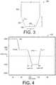
- FIG. 3illustrates an embodiment of a shape profile of the end of a needle of a transfer mechanism.
- FIG. 4illustrates an embodiment of a needle actuation stroke profile.
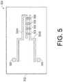
- FIG. 5illustrates a plan view of an embodiment of a product substrate having a circuit trace thereon.
- FIG. 6illustrates a schematic view of an embodiment of elements of a die transfer system.
- FIG. 7illustrates a schematic view of an embodiment of a circuitry path between machine hardware and controllers of a die transfer system.
- FIG. 8illustrates a method of a die transfer process according to an embodiment of this application.
- FIG. 9illustrates a method of a die transfer operation according to an embodiment of this application.
- FIG. 10illustrates an embodiment of a direct transfer apparatus and process implementing a conveyor system.
- FIG. 11Aillustrates a schematic view of another embodiment of a transfer apparatus in a pre-transfer position.
- FIG. 11Billustrates a schematic top view of the product substrate conveyance mechanism post-transfer operation of the embodiment in FIG. 11A .
- FIG. 12illustrates a schematic view of another embodiment of a transfer apparatus in a pre-transfer position.
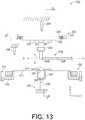
- FIG. 13illustrates a schematic view of another embodiment of a transfer apparatus in a pre-transfer position.
- This disclosureis directed to a machine that directly transfers and affixes semiconductor device dies to a circuit and to the process for achieving the same, as well as to the circuit having dies affixed thereto (as the output product).
- the machinefunctions to transfer unpackaged dies directly from a substrate such as a “wafer tape” to a product substrate, such as a circuit substrate.
- the direct transfer of unpackaged diesmay significantly reduce the thickness of an end product compared to a similar product produced by conventional means, as well as the amount of time and/or cost to manufacture the product substrate.
- the term “substrate”refers to any substance on which, or to which, a process or action occurs.
- the term “product”refers to the desired output from a process or action, regardless of the state of completion.
- a product substraterefers to any substance on which, or to which, a process or action is caused to occur for a desired output.
- the machinemay secure a product substrate for receiving “unpackaged” dies, such as LEDs, transferred from the wafer tape, for example.
- diesare very small and thin, for example, a die may be about 50 microns thick. Due to the relatively small size of the dies, the machine includes components that function to precisely align both the wafer tape carrying the dies and the product substrate to ensure accurate placement and/or avoid product material waste.
- the components that align the product substrate and the dies on the wafer tapemay include a set of frames in which the wafer tape and the product substrate are secured respectively and conveyed individually to a position of alignment such that a specific die on the wafer tape is transferred to a specific spot on the product substrate.
- the frame that conveys the product substratemay travel in various directions, including horizontal directions and/or vertical directions, or even directions that would permit transfer to a curved surface.
- the frame that conveys the wafer tapemay travel in various directions also.
- a system of gears, tracks, motors, and/or other elementsmay be used to secure and convey the frames carrying the product substrate and the wafer tape respectively to align the product substrate with the wafer tape in order to place a die on the correct position of the product substrate.
- Each frame systemmay also be moved to an extraction position in order to facilitate extraction of the wafer tape and the product substrate upon completion of the transfer process.
- the machinemay further include a transfer mechanism for transferring the dies directly from the wafer tape to the product substrate without “packaging” the dies.
- the transfer mechanismmay be disposed vertically above the wafer tape so as to press down on the dies via the wafer tape toward the product substrate. This process of pressing down on the dies may cause the dies to peel off of the wafer tape, starting at the sides of the dies until the dies separate from the wafer tape to be attached to the product substrate. That is, by reducing the adhesion force between the die and the wafer tape, and increasing the adhesion force between the die and the product substrate, the die may be transferred.
- the transfer mechanismmay include an elongated rod, such as a pin or needle that may be cyclically actuated against the wafer tape to push the wafer tape from a top side.
- the needlemay be sized so as to be no wider than a width of the die being transferred. Although in other instances, the width of the needle may wider, or any other dimension.
- the wafer tapemay experience a local deflection at the area between the die and the wafer tape. Inasmuch as the deflection is highly localized and rapidly performed, the portion of the wafer tape that does not receive pressure from the needle may begin to flex away from the surface of the die.
- This partial separationmay thus cause the die to lose sufficient contact with the wafer tape, so as to be released from the wafer tape.
- the deflection of the wafer tapemay be so minimal, as to maintain an entirety of the surface area of the die in contact with the wafer tape, while still causing the opposing surface of the die to extend beyond a plane of extension of the corresponding surface of the adjacent dies to avoid unintentional transfer of the adjacent dies.
- the machinemay further include a fixing mechanism for affixing the separated, “unpackaged” dies to the product substrate.
- the product substratemay have thereon a circuit trace to which the dies are transferred and affixed.
- the fixing mechanismmay include a device that emits energy, such as a laser, to melt/soften the material of the circuit trace on the product substrate.
- the lasermay be used to activate/harden the material of the circuit trace.
- the fixing mechanismmay be actuated before, and/or after the die is in contact with the material of the circuit trace.
- the energy emitting devicemay also be activated so as to prepare the trace material to receive the die.
- the activation of the energy emitting devicemay further enhance the release and capture of the die from the wafer tape so as to begin formation of a semiconductor product on the product substrate.
- FIG. 1illustrates an embodiment of an apparatus 100 that may be used to directly transfer unpackaged semiconductor components (or “dies”) from a wafer tape to a product substrate.
- the wafer tapemay also be referred to herein as the semiconductor device die substrate, or simply a die substrate.
- the apparatus 100may include a product substrate conveyance mechanism 102 and a wafer tape conveyance mechanism 104 .
- Each of the product substrate conveyance mechanism 102 and the wafer tape conveyance mechanism 104may include a frame system or other means to secure the respective substrates to be conveyed to desired alignment positions with respect to each other.
- the apparatus 100may further include a transfer mechanism 106 , which, as shown, may be disposed vertically above the wafer tape conveyance mechanism 104 .
- the transfer mechanism 106may be located so as to nearly contact the wafer substrate.
- the apparatus 100may include a fixing mechanism 108 .
- the fixing mechanism 108may be disposed vertically beneath the product substrate conveyance mechanism 102 in alignment with the transfer mechanism 106 at a transfer position, where a die may be placed on the product substrate.
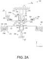
- FIGS. 2A and 2Billustrate example details of the apparatus 100 .
- FIGS. 2A and 2Bdepict different stages of the transfer operation, while referring to the same elements and features of apparatus 200 , the following discussion of specific features may refer interchangeably to either or both of FIGS. 2A and 2B , except where explicitly indicated.
- FIGS. 2A and 2Billustrate an embodiment of an apparatus 200 , including a product substrate conveyance mechanism 202 , a wafer tape conveyance mechanism 204 , a transfer mechanism 206 , and a fixing mechanism 208 .
- the product substrate conveyance mechanism 202may be disposed adjacent to the wafer tape conveyance mechanism 204 .
- the product substrate conveyance mechanism 202may extend in a substantially horizontal direction and may be disposed vertically beneath the wafer tape conveyance mechanism 204 so as to take advantage of any effect that gravity may have in the transfer process.
- the product substrate conveyance mechanism 202may be oriented so as to extend transversely to a horizontal plane.
- the conveyance mechanisms 202 , 204may be positioned such that a space between a surface of a product substrate carried by the product substrate conveyance mechanism 202 and a surface of a wafer tape carried by the wafer tape conveyance mechanism 204 may be more or less than 1 mm, depending on various other aspects of the apparatus 200 , including the amount of deflection that occurs by components during the transfer operation, as described herein below.
- the respective opposing surfaces of the wafer tape and the product substratemay be the most prominent structures in comparison to the supporting structures of the conveyance mechanisms 202 , 204 .
- a distance between the respective surfaces of the wafer tape and product substratemay be less than a distance between either of the surfaces and any other opposing structural component.
- the transfer mechanism 206may be disposed vertically above the wafer tape conveyance mechanism 204 , and the fixing mechanism 208 may be disposed vertically beneath the product substrate conveyance mechanism 202 . It is contemplated that in some embodiments, one or both of the transfer mechanism 206 and the fixing mechanism 208 may be oriented in different positions than the positions illustrated in FIGS. 2A and 2B .
- the transfer mechanism 206may be disposed so as to extend at an acute angle with respect to a horizontal plane.
- the fixing mechanism 208may be oriented to emit energy during the transfer process from the same direction of actuation as the transfer mechanism 206 , or alternatively, from any orientation and position from which the fixing mechanism 208 is able to participate in the transfer process.
- the product substrate conveyance mechanism 202may be used to secure a product substrate 210 .
- the term “product substrate”may include, but is not limited to: a wafer tape (for example, to presort the dies and create sorted die sheets for future use); a paper or polymer substrate formed as a sheet or other non-planar shape, where the polymer—translucent or otherwise—may be selected from any suitable polymers, including, but not limited to, a silicone, an acrylic, a polyester, a polycarbonate, etc.; a circuit board (such as a printed circuit board (PCB)); a string or thread circuit, which may include a pair of conductive wires or “threads” extending in parallel; and a cloth material of cotton, nylon, rayon, leather, etc.
- a wafer tapefor example, to presort the dies and create sorted die sheets for future use
- a paper or polymer substrateformed as a sheet or other non-planar shape, where the polymer—translucent or otherwise—may be selected from
- the choice of material of the product substratemay include durable materials, flexible materials, rigid materials, and other materials with which the transfer process is successful and which maintain suitability for the end use of the product substrate.
- the product substrate 210may be formed solely or at least partially of conductive material such that the product substrate 210 acts as a conductive circuit for forming a product.
- the potential types of product substratemay further include items, such as glass bottles, vehicle windows, or sheets of glass.
- the product substrate 210may include a circuit trace 212 disposed thereon.
- the circuit trace 212may include a pair of adjacent trace lines spaced apart by a trace spacing, or gap so as to accommodate a distance between electrical contact terminals (not shown) on the dies being transferred.
- the trace spacing, or gap between the adjacent trace lines of the circuit trace 212may be sized according to the size of the die being transferred to ensure proper connectivity and subsequent activation of the die.
- the circuit trace 212may have a trace spacing, or gap ranging from about 75 to 200 microns, about 100 to 175 microns, or about 125 to 150 microns.
- the circuit trace 212may be formed from a conductive ink disposed via screen printing, inkjet printing, laser printing, manual printing, or other printing means. Further, the circuit trace 212 may be pre-cured and semi-dry or dry to provide additional stability, while still being activatable for die conductivity purposes. A wet conductive ink may also be used to form the circuit trace 212 , or a combination of wet and dry ink may be used for the circuit trace 212 . Alternatively, or additionally, the circuit trace 212 may be pre-formed as a wire trace, or photo-etched, or from molten material formed into a circuit pattern and subsequently adhered, embedded, or otherwise secured to the product substrate 210 .
- the material of the circuit trace 212may include, but is not limited to, silver, copper, gold, carbon, conductive polymers, etc. In some instances, the circuit trace 212 may include a silver-coated copper particle.
- a thickness of the circuit trace 212may vary depending on the type of material used, the intended function and appropriate strength or flexibility to achieve that function, the energy capacity, the size of the LED, etc. For example, a thickness of the circuit trace may range from about 5 microns to 20 microns, from about 7 microns to 15 microns, or from about 10 microns to 12 microns.
- the product substrate 210may be a flexible, translucent polyester sheet having a desired circuit pattern screen printed thereon using a silver-based conductive ink material to form the circuit trace 212 .
- the product substrate conveyance mechanism 202may include a product substrate conveyor frame 214 for securing a product substrate holder frame 216 .
- the structure of the product substrate holder frame 216may vary significantly depending on the type and properties (e.g., shape, size, elasticity, etc.) of the product substrate being used.
- product substrate 210may be a flexible material
- product substrate 210may be held under tension in the product substrate holder frame 216 , so as to create a more rigid surface upon which a transfer operation, discussed herein below, is performed.
- the rigidity created by the tension in the product substrate 210may increase the placement accuracy when transferring components.
- a durable or more rigid material for the product substrate 210naturally provides a firm surface for component placement accuracy.
- wrinkles and/or other discontinuitiesmay form in the product substrate 210 and interfere with the pre-set pattern of the circuit trace 212 , to the extent that the transfer operation may be unsuccessful.
- FIG. 2Aillustrates an embodiment of a product substrate holder frame 216 including a first portion 216 a having a concave shape and a second portion 216 b having a convex counter shape that corresponds in shape to the concave shape.
- tensionis created for the product substrate 210 by inserting an outer perimeter of the product substrate 210 between the first portion 216 a and the second portion 216 b to thereby clamp the product substrate 210 tightly.
- the product substrate conveyor frame 214may be conveyed in at least three directions—two directions in the horizontal plane and vertically as well. The conveyance may be accomplished via a system of motors, rails, and gears (none of which are shown). As such, the product substrate tensioner frame 216 may be conveyed to and held in a specific position as directed and/or programmed and controlled by a user of the apparatus 200 .
- the wafer tape conveyance mechanism 204may be implemented to secure a wafer tape 218 having dies 220 (i.e., semiconductor device dies) thereon.
- the wafer tape 218may be conveyed in multiple directions to the specific transfer positions for the transfer operation via a wafer tape conveyor frame 222 .
- the wafer tape conveyor frame 222may include a system of motors, rails, and gears (none of which are shown).
- the unpackaged semiconductor dies 220 for transfermay be extremely small. Indeed, the height of the dies 220 may range from 12.5 to 200 microns, or from 25 to 100 microns, or from 50 to 80 microns.
- a gap spacing between the wafer tape 218 and the product substrate 210may range from about 0.25 mm to 1.50 mm, or about 0.50 mm to 1.25 mm, or about 0.75 mm to 1.00 mm, for example.
- a minimum gap spacingmay depend on factors including: a thickness of the die being transferred, a stiffness of the wafer tape involved, an amount of deflection of the wafer tape needed to provide adequate capture and release of the die, a proximity of the adjacent dies, etc.
- a speed of the transfer operationmay also decrease due to the reduced cycle time (discussed further herein) of the transfer operation.
- Such a decrease in the duration of a transfer operationmay therefore increase a rate of die transfers.
- the die transfer ratemay range from about 6-20 dies placed per second.
- the wafer tape conveyor frame 222may secure a wafer tape holder frame 224 , which may stretch and hold the wafer tape 218 under tension.
- the wafer tape 218may be secured in the wafer tape holder frame 224 via clamping a perimeter of the wafer tape 218 between adjacent components of the wafer holder frame 224 .
- Such clampingassists in maintaining the tension and stretched characteristic of the wafer tape 218 , thereby increasing the success rate of the transfer operation.
- a particular wafer tapemay be selected for use based on an ability to consistently remain at a desired tension during a transfer process.
- the needle actuation performance profile(discussed further herein below) may change depending on the tension of the wafer tape 218 .
- the material used for the wafer tape 218may include a material having elastic properties, such as a rubber or silicone, for example. Furthermore, inasmuch as temperature of the environment and the wafer tape 218 itself may contribute to potential damage to the wafer tape 218 during the transfer process, a material having properties that are resistant to temperature fluctuation may be advantageous. Additionally, in some instances, the wafer tape 218 may be stretched slightly so as to create a separation or gap between individual dies 220 to assist in the transfer operation. A surface of the wafer tape 218 may include a sticky substance via which the dies 220 may be removably adhered to the wafer tape 218 .
- the dies 220 on the wafer tape 218may include dies that were individually cut from a solid semiconductor wafer and then placed onto the wafer tape 218 to secure the dies.
- the diesmay have been pre-sorted and explicitly organized on the wafer tape 218 , in order, for example, to assist in the transfer operation.
- the dies 220may be arranged sequentially as to the expected order of transfer to the product substrate 210 . Such pre-arrangement of the dies 220 on the wafer tape 218 may reduce the amount of travel that would otherwise occur between the product substrate conveyance mechanism 202 and the wafer tape conveyance mechanism 204 .
- the dies on the wafer tape 218may have been pre-sorted to include only dies having substantially equivalent performance properties. In this case, efficiency of the supply chain may be increased and thus, travel time of the wafer tape conveyance mechanism 204 may be reduced to a minimum.
- materials used for the diesmay include, but is not limited to, silicon carbide, gallium nitride, a coated silicon oxide, etc.
- sapphire or siliconmay be used as a die as well.
- a “die”may be representative herein of an electrically actuatable element generally.
- the wafer tape 218may include dies that are not pre-sorted, but rather are formed by simply cutting a semiconductor directly on wafer tape, and then leaving the dies on the wafer tape without “picking and placing” to sort the dies depending on the respective performance quality of the dies.
- the dies on the wafer tapemay be mapped to describe the exact relative locations of the different quality dies. Therefore, in some instances, it may be unnecessary to use wafer tape having pre-sorted dies. In such a case, the amount of time and travel for the wafer tape conveyance mechanism 204 to move between particular dies for each sequential transfer operation may increase.
- the wafer tape conveyance mechanism 204may move the wafer tape 218 further to align an appropriate die of a specific quality for transfer than would be necessary for a wafer tape 218 containing dies of substantially equivalent quality.
- a data map of the dies 220may be provided with the wafer tape 218 .
- the data mapmay include a digital file providing information that describes the specific quality and location of each die on the wafer tape 218 .
- the data map filemay be input into a processing system in communication with the apparatus 200 , whereby the apparatus 200 may be controlled/programmed to seek the correct die 220 on the wafer tape 218 for transfer to the product substrate 210 .
- a transfer operationis performed, in part, via the transfer mechanism 206 , which is a die separation device for assisting in separation of dies from the wafer tape 218 .
- the actuation of the transfer mechanism 206may cause one or more dies 220 to be released from the wafer tape 218 and to be captured by the product substrate 210 .
- the transfer mechanism 206may operate by pressing an elongated rod, such as a pin or a needle 226 into a top surface of the wafer tape 218 against a die 220 .
- the needle 226may be connected to a needle actuator 228 .
- the needle actuator 228may include a motor connected to the needle 226 to drive the needle 226 toward the wafer tape 218 at predetermined/programmed times.
- the needle 226may include a material that is sufficiently durable to withstand repetitive, rapid, minor impacts while minimizing potential harm to the dies 220 upon impact.
- the needle 226may include a metal, a ceramic, a plastic, etc.
- a tip of the needle 226may have a particular shape profile, which may affect the ability of the needle to function repetitively without frequently breaking either the tip or damaging the wafer tape 218 or the dies 220 . The profile shape of the tip of the needle is discussed in greater detail below with respect to FIG. 3 .
- the needle 226may be aligned with a die 220 , as depicted in FIG. 2A , and the needle actuator may move the needle 226 to push against an adjacent side of the wafer tape 218 at a position in which the die 220 is aligned on the opposing side of the wafer tape 218 , as depicted in FIG. 2B .
- the pressure from the needle 226may cause the wafer tape 218 to deflect so as to extend the die 220 to a position closer to the product substrate 226 than adjacent dies 220 , which are not being transferred.
- the amount of deflectionmay vary depending several factors, such as the thickness of the die and circuit trace.
- an amount of deflection of the wafer tape 218may be about 75 microns.
- the die 220may be pressed via the needle 226 toward the product substrate 210 to the extent that the electrical contact terminals (not shown) of the die are able to bond with the circuit trace 212 , at which point, the transfer operation proceeds to completion and the die 220 is released from the wafer tape 218 .
- the transfer processmay include a rapidly repeated set of steps including a cyclical actuation of the needle 226 pressing upon a die 220 , a method of the process is described in detail herein below with respect to FIG. 8 . Further, the stroke profile of the actuation of the needle 226 (within the context of the transfer process) is discussed in more detail hereafter with respect to FIG. 4 .
- the transfer mechanism 206may further include a needle retraction support 230 , (also known as a pepper pot).
- the support 230may include a structure having a hollowed space wherein the needle 226 may be accommodated by passing into the space via an opening 232 in a first end of the support 230 .
- the support 230may further include at least one opening 234 on a second opposing end of the support 230 .
- the supportmay include multiple perforations near opening 234 .
- the at least one opening 234may be sized with respect to a diameter of the needle 226 to accommodate passage of the needle 226 therethrough so as to press on the wafer tape 218 during the transfer process.
- the support 230may be disposed adjacent to the upper surface of the wafer tape 218 .
- a base surface of the support 230(having the at least one opening 234 therein) may come into contact with the upper surface of the wafer tape 218 , thereby preventing upward deflection of the wafer tape 218 .
- This upward deflectionmay be caused in the event where the needle 226 pierces at least partially into the wafer tape 218 , and while retracting, the wafer tape is stuck to the tip of the needle 226 .
- the support 230may reduce the time it takes to move to the next die 220 .
- a wall perimeter shape of the support 230may be cylindrical or any other shape that may be accommodated in the apparatus 200 . Accordingly, the support 230 may be disposed between the needle 226 and an upper surface of the wafer tape 218 .
- a temperature of support 230may be adjusted so as to regulate the temperature of the needle 226 and the wafer tape 218 , at least near the point of the transfer operation. Accordingly, the temperature of the support 230 may be heated or cooled, and a material of the support 230 may be selected to maximize thermal conductivity.
- the support 230may be formed of aluminum, or another relatively high thermal conductivity metal or comparable material, whereby the temperature may be regulated to maintain consistent results of the transfer operations.
- airmay be circulated within the support 230 to assist in regulating the temperature of a local portion of the wafer tape 218 .
- a fiber optic cable 230 amay be inserted into the needle retraction support 230 , and may further be against the needle 226 to assist in temperature regulation of the wafer tape 218 and/or the needle 226 .
- fixing mechanism 208may assist in affixing the die 220 to the circuit trace 212 on a surface of the product substrate 210 .
- FIG. 2Billustrates the apparatus 200 in a transfer stage, where the die 220 is pushed against the circuit trace 212 .
- fixing mechanism 208may include an energy-emitting device 236 including, but not limited to, a laser, electromagnetic radiation, pressure vibration, ultrasonic welding, etc.
- the use of pressure vibration for the energy-emitting device 236may function by emitting a vibratory energy force so as to cause disruption of the molecules within the circuit trace against those of the electrical contact terminals so as to form a bond via the vibratory pressure.
- a lasermay be implemented as the energy-emitting device 236 .
- laser 236may be activated to emit a specific wavelength and intensity of light energy directed at the die 220 being transferred.
- the wavelength of the light of the laser 236may be selected specifically based on the absorption of that wavelength of light with respect to the material of the circuit trace 212 without significantly affecting the material of the product substrate 210 .
- a laser having an operational wavelength of 808 nm, and operating at 5 Wmay be readily absorbed by silver, but not by polyester. As such, the laser beam may pass through the substrate of polyester and affect the silver of a circuit trace.
- the wavelength of lasermay match the absorption of the circuit trace and the material of the substrate.
- the focus area of the laser 236(indicated by the dashed lines emanating vertically from the laser 236 in FIG. 2B toward the product substrate 210 ) may be sized according to the size of the LED, such as for example, a 300 micron wide area.
- the circuit trace 212may begin to cure (and/or melt or soften) to an extent that a fusing bond may form between the material of the circuit trace 212 and the electrical contact terminals (not shown) on the die 220 .
- This bondfurther assists in separating the unpackaged die 220 from the wafer tape 218 , as well as simultaneously affixing the die 220 to the product substrate 210 .
- the laser 236may cause some heat transfer on the wafer tape 218 , thereby reducing adhesion of the die 220 to the wafer tape 218 and thus assisting in the transfer operation.
- diesmay be released and fixed to the product substrates in many ways, including using a laser having a predetermined wavelength or a focused light (e.g., IR, UV, broadband/multispectral) for heating/activating circuit traces to thereby cure an epoxy or phase change bond materials, or for deactivating/releasing a die from wafer tape, or for initiating some combination of reactions.
- a specific wavelength laser or lightmay be used to pass through one layer of the system and interact with another layer.
- a vacuummay be implemented to pull a die from the wafer tape, and air pressure may be implemented to push the die onto a product substrate, potentially including a rotary head between the die wafer substrate and the product substrate.
- ultrasonic vibrationmay be combined with pressure to cause the die to bond to the circuit traces.
- the fixing mechanismmay also include a product substrate support 238 , which may be disposed between the laser 236 and the bottom surface of the product substrate 210 .
- the support 238may include an opening 240 at a base end thereof and an opening 242 at an upper end thereof.
- the support 238may be formed as a ring or hollow cylinder.
- the supportmay further include structure to secure a lens (not shown) to assist in directing the laser.
- the laser 236emits the light through the openings 240 , 242 to reach the product substrate 210 .
- the upper end of the sidewalls of the support 238may be disposed in direct contact with or closely adjacent to the bottom surface of the product substrate 210 .
- the support 238may help to prevent damage from occurring to the product substrate 210 during the stroke of the needle 226 at the time of a transfer operation.
- the portion of the bottom surface of the product substrate 210 that is aligned with the support 238may contact the support 238 , which thereby provides resistance against the incoming motion of the die 220 being pressed by the needle 226 .
- the support 238may be movable in a direction of the vertical axis to be able to adjust a height thereof so as to raise and lower support 238 as necessary, including to a height of the product substrate 210 .
- apparatus 200may further include a first sensor 244 , from which apparatus 200 receives information regarding the dies 220 on the wafer tape 218 .
- the wafer tape 218may have a bar code (not shown) or other identifier, which is read or otherwise detected.
- the identifiermay provide die map data to the apparatus 200 via the first sensor 244 .
- the first sensor 244may be positioned near the transfer mechanism 206 (or the needle 226 specifically), spaced apart from the transfer mechanism 206 by a distance d, which may range from about 1-5 inches, so as to enhance the accuracy of location detection.
- first sensor 244may be disposed adjacent the tip of the needle 226 in order to sense the exact position of the dies 220 in real time.
- the wafer tape 218may be punctured and or further stretched over time, which may alter the previously mapped, and thus expected, locations of the dies 220 on the wafer tape 218 . As such, small changes in the stretching of the wafer tape 218 could add up to significant errors in alignment of the dies 220 being transferred.
- real time sensingmay be implemented to assist in accurate die location.
- the first sensor 244may be able to identify the precise location and type of die 220 that is being sensed. This information may be used to provide instructions to the wafer tape conveyor frame 222 indicating the exact location to which the wafer tape 218 should be conveyed in order to perform the transfer operation.
- Sensor 244may be one of many types of sensors, or a combination of sensor types to better perform multiple functions.
- Sensor 244may include, but is not limited to: a laser range finder, or an optical sensor, such as a non-limiting example of a high-definition optical camera having micro photography capabilities.
- a second sensor 246may also be included in apparatus 200 .
- the second sensor 246may be disposed with respect to the product substrate 210 so as to detect the precise position of the circuit trace 212 on the product substrate 210 . This information may then be used to determine any positional adjustment needed to align the product substrate 210 between the transfer mechanism 206 and the fixing mechanism 208 so that the next transfer operation occurs in the correct location on the circuit trace 212 . This information may further be relayed to the apparatus 200 to coordinate conveying the product substrate 210 to a correct position, while simultaneously conveying instructions to the wafer tape conveyor frame 222 .
- a variety of sensorsare also contemplated for sensor 246 including optical sensors, such as one non-limiting example of a high-definition optical camera having micro photography capabilities.
- FIGS. 2A and 2Bfurther illustrate that the first sensor 244 , the second sensor 246 , and the laser 236 may be grounded.
- the first sensor 244 , the second sensor 246 , and the laser 236may all be grounded to the same ground (G), or alternatively, to a different ground (G).
- the first or second sensorsmay further be able to test the functionality of transferred dies.
- an additional tester sensor(not shown) may be incorporated into the structure of apparatus 200 to test individual dies before removing the product substrate 210 from the apparatus 200 .
- multiple independently-actuatable needles and/or lasersmay be implemented in a machine in order to transfer and fix multiple dies at a given time.
- the multiple needles and/or lasersmay be independently movable within a three-dimensional space. Multiple die transfers may be done synchronously (multiple needles going down at the same time), or concurrently but not necessarily synchronously (e.g., one needle going down while the other is going up, which arrangement may balance better the components and minimize vibration). Control of the multiple needles and/or lasers may be coordinated to avoid collisions between the plurality of components.
- the multiple needles and/or lasersmay be arranged in fixed positions relative to each other.
- the tip 300 of a needleis discussed with respect to FIG. 3 , which shows a schematic example profile shape of the tip 300 .
- the tip 300may be defined as the end of the needle, including sidewalls 302 adjoining tapered portion 304 , corner 306 , and base end 308 , which may extend transversely to the opposing side of the needle.
- the specific size and shape of the tip 300may vary according to factors of the transfer process such as, for example, the size of the die 220 being transferred and the speed and the impact force, of a transfer operation. For example, the angle ⁇ seen in FIG.
- the tapered portion 304as measured between a longitudinal direction of the central axis of the needle and the tapered portion 304 may range from about 10 to 15°; the radius r of the corner 306 may range from about 15 to 50+ microns; the width w of the base end 308 may range from about 0 to 100+ microns ( ⁇ m), where w may be less than or equal to the width of the die 220 being transferred; the height h of the tapered portion 304 may range from about 1 to 2 mm, where h may be greater than a distance traveled by needle during a stroke of a transfer operation; and the diameter d of the needle 226 may be approximately 1 mm.
- the needle tip 300may be more blunt to mirror the width of the die or more pointed so as to press in a smaller area of the wafer tape.
- FIG. 4Illustrated in FIG. 4 is an embodiment of a needle actuation performance profile. That is, FIG. 4 depicts an example of the stroke pattern performed during a transfer operation by displaying the height of the needle tip with respect to the plane of the wafer tape 218 as it varies with time. As such, the “0” position in FIG. 4 may be the upper surface of the wafer tape 218 . Further, inasmuch as the idle time of the needle and the ready time of the needle may vary depending on the programmed process or the varying duration of time between transferring a first die and the time it takes to reach a second die for transfer, the dashed lines shown at the idle and ready phases of the stroke pattern indicate that the time is approximate, but may be longer or shorter in duration.
- the solid lines shown for use of the laserare example times for an embodiment illustrated herewith, however, the actual duration of laser on and off time may vary depending on the materials used in forming the circuit (such as the material choice of the circuit trace), the type of product substrate, the desired effect (pre-melting circuit trace, partial bond, complete bond, etc.), the distance of the laser from the bond point (i.e., the upper surface of the product substrate), the size of the die being transferred, and the power/intensity/wavelength of the laser, etc. Accordingly, the following description of the profile shown in FIG. 4 may be an example embodiment of a needle profile.
- a fully retracted needle tipmay be idle at approximately 2000 ⁇ m above the surface of the wafer tape. After a varying amount of time, the needle tip may descend rapidly to rest in the ready state at approximately 750 ⁇ m above the surface of the wafer tape. After another undetermined amount of time at the ready state, the needle tip may descend again to contact the die and press the wafer tape with the die down to a height of approximately ⁇ 1000 ⁇ m, where at the die may be transferred to the product substrate.
- the dotted vertical line at the start of the laser on sectionindicates that the laser may come on at some point between the beginning of the descent from the ready phase and the bottom of the stroke of the needle tip.
- the lasermay turn on at approximately 50% of the way through the descent.
- the circuit tracemay begin to soften prior to contact with the die so as to form a stronger bond, or additionally, the die wafer may be affected or prepared during this time.
- the phase in which the laser turns onmay last approximately 20 ms (“milliseconds”). At the bottom of the stroke, where the laser is on, that phase may be a bonding phase between the die and the product substrate. This bonding phase may allow the circuit trace to attach to the die contacts, which stiffens quickly after the laser is turned off. As such, the die may be bonded to the product substrate.
- the bonding phasemay last approximately 30 ms.
- the lasermay be turned off and the needle may ascend to the ready phase rapidly.
- the lasermay be turned off before the needle begins to ascend, or at some point during the ascent of the needle tip back to the ready phase, the laser may be turned off.
- the height of the needle tipmay overshoot and bounce back under the height of the ready phase somewhat buoyantly. While some of the buoyancy may be attributed to the speed at which the needle tip ascends to the ready phase, the speed and the buoyancy may be intentional in order to assist in retracting a tip of the needle from a surface of the wafer tape in the case where the needle has pierced the wafer tape and may be stuck therein.
- the timing in which the laser is turned offmay be longer than the timing in which the laser is turned on, where a slower speed of the descent may assist in preventing damage to the die, and as mentioned above, the rapid rate of ascent may assist in extracting the needle tip from the wafer tape more effectively.
- the timing shown on FIG. 4is approximate, particularly with respect to the idle and ready periods. Therefore, the numerical values assigned along the bottom edge of the FIG. 4 are for reference and should not be taken literally, except when otherwise stated.
- FIG. 5illustrates an example embodiment of a processed product substrate 500 .
- a product substrate 502may include a first portion of a circuit trace 504 A, which may perform as a negative or positive power terminal when power is applied thereto.
- a second portion of the circuit trace 504 Bmay extend adjacent to the first portion of the circuit trace 504 A, and may act as a corresponding positive or negative power terminal when power is applied thereto.
- the product substrate 502may have a bar code (not shown) or other identifier, which is read or otherwise detected.
- the identifiermay provide circuit trace data to the apparatus.
- the product substrate 502may further include datum points 506 .
- Datum points 506may be visual indicators for sensing by the product substrate sensor (for example, second sensor 246 in FIG. 2 ) to locate the first and second portions of the circuit trace 504 A, 504 B. Once the datum points 506 are sensed, a shape and relative position of the first and second portions of the circuit trace 504 A, 504 B with respect to the datum points 506 may be determined based on preprogrammed information. Using the sensed information in connection with the preprogrammed information, the product substrate conveyance mechanism may convey the product substrate 502 to the proper alignment position for the transfer operation.
- dies 508are depicted in FIG. 5 as straddling between the first and second portions of the circuit trace 504 A, 504 B.
- the electrical contact terminals (not shown) of the dies 508may be bonded to the product substrate 502 during a transfer operation.
- powermay be applied to run between the first and second portions of the circuit trace 504 A, 504 B, and thereby powering dies 508 .
- the diesmay be unpackaged LEDs that were directly transferred from a wafer tape to the circuit trace on the product substrate 502 . Thereafter, the product substrate 502 may be processed for completion of the product substrate 502 and used in a circuit or other final product. Further, other components of a circuit may be added by the same or other means of transfer to create a complete circuit, and may include control logic to control LEDs as one or more groups in some static or programmable or adaptable fashion.
- the transfer system 600may include a personal computer (PC) 602 (or server, data input device, user interface, etc.), a data store 604 , a wafer tape mechanism 606 , a product substrate mechanism 608 , a transfer mechanism 610 , and a fixing mechanism 612 .
- PCpersonal computer
- a wafer tape mechanism 606a wafer tape mechanism 606
- a product substrate mechanism 608a product substrate mechanism 608
- a transfer mechanism 610a transfer mechanism 612
- specific details about these mechanismsis not repeated here.
- a brief description of how the wafer tape mechanism 606 , the product substrate mechanism 608 , the transfer mechanism 610 , and the fixing mechanism 612 relate to interactions between the PC 602 and the data store 604is described hereafter.
- the PC 602communicates with data store 604 to receive information and data useful in the transfer process of directly transferring dies from a wafer tape in wafer tape mechanism 606 using the transfer mechanism 610 on to a product substrate in the product substrate mechanism 608 whereat the dies may be fixed upon the product substrate via actuation of a laser or other energy-emitting device located in the fixing mechanism 612 .
- PC 602may also serve as a receiver, compiler, organizer, and controller of data being relayed to and from each of the wafer tape mechanism 606 , the product substrate mechanism 608 , the transfer mechanism 610 , and the fixing mechanism 612 .
- PC 602may further receive directed information from a user of the transfer system 600 .
- FIG. 6depicts directional movement capability arrows adjacent to the wafer tape mechanism 606 and the product substrate mechanism 608 , those arrows merely indicate general directions for mobility, however, it is contemplated that both the wafer tape mechanism 606 and the product substrate mechanism 608 may also be able to move in other directions including rotation in plane, pitch, roll, and yaw, for example.
- a schematic of the communication pathways between the respective elements of a transfer system 700may be described as follows.
- the direct transfer systemmay include a personal computer (PC) 702 (or server, data input device, user interface, etc.), which may receive communication from, and provide communication to a data store 704 .
- the PC 702may further communicate with a first cell manager 706 (illustrated as “Cell Manager 1 ”) and a second cell manager 708 (illustrated as “Cell Manager 2 ”). Therefore, the PC 702 may control and synchronize the instructions between the first cell manager 706 and the second cell manager 708 .
- PCpersonal computer
- PC 702may include processors and memory components with which instructions may be executed to perform various functions with respect to the first and second cell managers 706 , 708 , as well as data store 704 .
- PC 702may include a project manager 710 and a needle profile definer 712 .
- Project manager 710may receive input from the first and second cell managers 706 , 708 and data store 704 to organize the direct transfer process and maintain smooth functioning with respect to orientation and alignment of the product substrate with respect to the wafer tape and the dies thereon.
- Needle profile definer 712may contain data regarding the needle stroke performance profile, which may be used to instruct the transfer mechanism regarding the desired needle stroke performance according to the specific dies on the loaded wafer tape and the pattern of the circuit trace on the product substrate. Additional details of the needle profile definer 712 are discussed further herein below.
- data store 704may include memory containing data such as a die map 714 , which may be specific to the wafer tape loaded in the wafer tape mechanism. As explained previously, a die map may describe the relative locations of each die on the wafer tape and the quality thereof for the purpose of providing a pre-organized description of the location of specific dies. Further, data store 704 may also include memory containing circuit CAD files 716 . Circuit CAD files 716 may contain data regarding a specific circuit trace pattern on the loaded product substrate.
- Project manager 710may receive the die map 714 and circuit CAD files 716 from the data store 704 , and may relay the respective information to the first and second cell managers 706 , 708 , respectively.
- the first cell manager 706may use the die map 714 from data store 704 via a die manager 718 . More specifically, die manager 718 may compare die map 714 with the information received by a sensor manager 720 , and based thereon, may provide instructions to a motion manager 722 regarding the location of a particular die. Sensor manager 720 may receive data regarding the actual location of dies on the wafer tape from a die detector 724 . Sensor manager 720 may also instruct the die detector 724 to look for a particular die in a particular location according to die map 714 .
- the die detector 724may include a sensor such as the second sensor 244 in FIGS. 2A and 2B .
- the motion manager 722may instruct a first robot 726 (illustrated as “Robot 1 ”) to convey the wafer tape to an alignment position with the needle of the transfer mechanism.
- the first robot 726may communicate the completion of its movement to a needle controlboard manager 728 .
- the needle control board manager 728may directly communicate with the PC 702 to coordinate the execution of the transfer operation.
- the PC 702may instruct the needle control board manager 728 to activate the needle actuator/needle 730 , thereby causing the needle to perform a stroke in accordance with the loaded needle profile in the needle profile definer 712 .
- the needle controlboard manager 728may also activate the laser control/laser 732 , thereby causing the laser to emit a beam toward the product substrate as the needle presses down a die via the wafer tape to execute the transfer operation.
- the activation of the laser control/laser 732may occur prior to, simultaneously, during, or after activation, or even a complete actuation, of the needle stroke.
- the first cell manager 706may pass through a plurality of states including: determining where to tell the first robot 726 to go; telling the first robot 726 to go to the determined location; turning on the needle; activating the fixing device; and resetting.
- the project manager 710may relay the data of the circuit CAD files 716 to the second cell manager 708 .
- the second cell manager 708may include a sensor manager 734 and a motion manager 736 .
- the sensor manager 734may instruct the substrate alignment sensor 738 to find the datum points on the product substrate and thereby detect and orient the product substrate according to the location of the circuit trace thereon.
- the sensor manager 734may receive confirmation or updated location information of the circuit trace pattern on the product substrate.
- the sensor manager 734may coordinate with the motion manager 736 to provide instructions to a second robot 740 (illustrated as “Robot 2 ”) to convey the product substrate to an alignment position (i.e., a transfer fixing position) for execution of the transfer operation.
- a second robot 740illustrated as “Robot 2 ”
- the circuit CAD files 716may assist the project manager 710 in aligning the product substrate with respect to the wafer tape such that the dies may be accurately transferred to the circuit trace thereon.
- the second cell manager 708may pass through a plurality of states including: determining where to tell the second robot 740 to go; telling the second robot 740 to go to the determined location; and resetting.
- a method 800 of executing a direct transfer process, in which one or more dies is directly transferred from a wafer tape to a product substrate,is illustrated in FIG. 8 .
- the steps of the method 800 described hereinmay not be in any particular order and as such may be executed in any satisfactory order to achieve a desired product state.
- the method 800may include a step of loading transfer process data into a PC and/or a data store 802 .
- the transfer process datamay include data such as die map data, circuit CAD files data, and needle profile data.
- a step of loading a wafer tape into a wafer tape conveyor mechanism 804may also be included in method 800 .
- Loading the wafer tape into the wafer tape conveyor mechanismmay include controlling the wafer tape conveyor mechanism to move to a load position, which is also known as an extract position.
- the wafer tapemay be secured in the wafer tape conveyor mechanism in the load position.
- the wafer tapemay be loaded so that the dies of the semiconductor are facing downward toward the product substrate conveyor mechanism.
- the method 800may further include a step of preparing the product substrate to load into the product substrate conveyor mechanism 806 .
- Preparing the product substratemay include a step of screen printing a circuit trace on the product substrate according to the pattern of the CAD files being loaded into the PC or data store. Additionally, datum points may be printed onto the circuit substrate in order to assist in the transfer process.
- the product substrate conveyor mechanismmay be controlled to move to a load position, which is also known as an extraction position, whereat the product substrate may be loaded into the product substrate conveyor mechanism.
- the product substratemay be loaded so that the circuit trace faces toward the dies on the wafer.
- the product substratemay be delivered and placed in the load position by a conveyor (not shown) or other automated mechanism, such as in the style of an assembly line.
- the product substratemay be manually loaded by an operator.
- a program to control the direct transfer of the dies from the wafer tape to the circuit trace of the product substratemay be executed via the PC to commence the direct transfer operation 808 .
- the details of the direct transfer operationare described below.
- a method 900 of the direct transfer operation of causing dies to be transferred directly from the wafer tape (or other substrate holding dies, also called a “die substrate” for simplified description of FIG. 9 ) to the product substrateis illustrated in FIG. 9 .
- the steps of the method 900 described hereinmay not be in any particular order and as such may be executed in any satisfactory order to achieve a desired product state.
- the PCmay receive input regarding the identification of the product substrate and the identification of the die substrate containing the dies to be transferred 902 .
- This inputmay be entered manually by a user, or the PC may send a request to the cell managers in control, respectively, of the product substrate alignment sensor and the die detector.
- the requestmay instruct the sensor to scan the loaded substrate for an identification marker, such as a barcode or QR code; and/or the request may instruct the detector to scan the loaded die substrate for an identification marker, such as a barcode or QR code.
- the PCmay query the data store or other memory to match the respective identification markers of the product substrate and the die substrate and retrieve the associated data files 904 .
- the PCmay retrieve a circuit CAD file associated with the product substrate that describes the pattern of the circuit trace on the product substrate.
- the circuit CAD filemay further contain data such as the number of, relative positions of, and respective quality requirement of, the dies to be transferred to the circuit trace.
- the PCmay retrieve a die map data file associated with the die substrate that provides a map of the relative locations of the specific dies on the die substrate.
- the PCmay determine the initial orientation of the product substrate and the die substrate relative to the transfer mechanism and the fixing mechanism 906 .
- the PCmay instruct the substrate alignment sensor to locate datum points on the product substrate.
- the datum pointsmay be used as reference markers for determining the relative location and orientation of the circuit trace on the product substrate.
- the PCmay instruct the die detector to locate one or more reference points on the die substrate to determine the outlay of the dies.
- the PCmay instruct the respective product substrate and die substrate conveyance mechanisms to orient the product substrate and die substrate, respectively, into a position of alignment with the transfer mechanism and the fixing mechanism 908 .
- the alignment step 908may include determining the location of the portion of the circuit trace to which a die is to be transferred 910 , and where the portion is located relative to the transfer fixing position 912 .
- the transfer fixing positionmay be considered to be the point of alignment between the transfer mechanism and the fixing mechanism.
- the PCmay instruct the product substrate conveyance mechanism to convey the product substrate so as to align the portion of the circuit trace to which a die is to be transferred with the transfer fixing position 914 .
- the alignment step 908may further include determining which die on the die substrate will be transferred 916 , and where the die is located relative to the transfer fixing position 918 . Based on the data determined in steps 916 and 918 , the PC may instruct the wafer tape conveyance mechanism to convey the die substrate so as to align the die to be transferred with the transfer fixing position 920 .
- the needle and the fixing devicee.g., laser
- the needle and the fixing devicemay be actuated 922 to effectuate the transfer of the die from the die substrate to the product substrate.
- the PCmay determine whether additional dies are to be transferred 924 . In the case where another die is to be transferred, the PC may revert to step 908 and realign the product and die substrates accordingly for a subsequent transfer operation. In the case where there will not be another die transferred, the transfer process is ended 926 .
- FIG. 10illustrates several of the components of the direct transfer apparatus described above in a conveyor/assembly line system 1000 (hereinafter “conveyor system”).
- FIGS. 2A and 2Bdepict the product substrate 210 being held by the product substrate conveyor frame 214 and tensioned by the product substrate tensioner frame 216 .
- FIG. 10illustrates the product substrate conveyor frame 214 being conveyed through the conveyor system 1000 in which the product substrate goes through an assembly line style process.
- the conveyor system 1000may include a series of tracks, rollers, and belts 1002 and/or other handling devices to sequentially convey a plurality of product substrate conveyor frames 214 , each holding a product substrate.
- operation stations of the conveyor system 1000may include one or more printing stations 1004 .
- a circuit tracemay be printed thereon.
- the multiple printing stations 1004may be arranged serially, and may be configured to perform one or more printing operations each so as to form a complete circuit trace.
- the product substrate conveyor frame 214may be conveyed to one or more die transfer stations 1006 .
- the multiple die transfer stations 1006may be arranged serially, and may be configured to perform one or more die transfers each.
- the product substratesmay have one or more dies transferred and affixed thereto via a transfer operation using one or more of the direct transfer apparatus embodiments described herein.
- each transfer station 1006may include a wafer tape conveyance mechanism, a transfer mechanism, and a fixing mechanism.
- a circuit tracemay have been previously prepared on the product substrate, and as such, the product substrate may be conveyed directly to the one or more transfer stations 1006 .
- the wafer tape conveyance mechanism, the transfer mechanism, and the fixing mechanismmay be aligned with respect to the conveyed product substrate conveyor frame 214 upon entering the station.
- the transfer station 1006 componentsmay repeatedly perform the same transfer operation in the same relative position on each product substrate as the plurality of product substrates are conveyed through the conveyor system 1000 .
- the conveyor system 1000may further include one or more finishing stations 1008 to which the product substrate may be conveyed to have final processing performed.
- the type, amount, and duration of the final processingmay depend on the features of the product and the properties of the materials used to make the product.
- the product substratemay receive additional curing time, a protective coating, additional components, etc., at the finishing station(s) 1008 .
- a “light string”may be formed. While many of the features of apparatus 1100 may remain substantially similar to those of apparatus 200 of FIGS. 2A and 2B , product substrate conveyance mechanism 1102 , as depicted in FIGS. 11A and 11B , may be configured to convey a product substrate 1104 that is different than the product substrate 212 . Specifically, in FIGS. 2A and 2B , the product substrate conveyance mechanism 202 includes the conveyor frame 214 and the tensioner frame 216 , which secure the sheet-like product substrate 212 under tension. In the embodiment of FIGS. 11A and 11B , however, the product substrate conveyance mechanism 1102 may include a product substrate reel system.
- the product substrate reel systemmay include one or two circuit trace reels 1106 that are wound with a “string circuit,” which may include a pair of adjacently wound conductive strings or wires as the product substrate 1104 .
- the reel 1106may be located on a first side of the transfer position, and the pair of conductive strings ( 1104 ) may be wound around the single reel 1106 .
- the die transfer process of forming the string circuitmay be substantially similar in each case.
- the conductive strings of the product substrate 1104may be threaded from the reel(s) 1106 across the transfer position and may be fed into a finishing device 1108 .
- the finishing device 1108may be: a coating device to receive a protective coating, for example, of a translucent or transparent plastic; or a curing apparatus, which may finish curing the string circuit as a part of final processing of the product.
- the circuit stringmay be fed onto another reel, which may wind up the string circuit thereon before final processing of the string circuit.
- the transfer mechanism 206may be actuated to perform a needle stroke (as described above) to transfer dies 220 to the conductive strings of the product substrate 1104 so that electrical contact terminals of the dies 220 are placed, respectively, on the adjacent strings, and the fixing mechanism 208 may be actuated to affix the dies 220 in position.
- apparatus 1100may include tensioning rollers 1110 on which the conductive strings of the product substrate 1104 may be supported and further tensioned against.
- the tensioning rollers 1110may assist in maintaining tension in the formed string circuit so as to enhance the die transfer accuracy.
- dies 220are depicted as having been transferred to the conductive strings of the product substrate 1104 , thereby uniting (to some extent) the conductive strings of the product substrate 1104 and forming a string circuit.
- apparatus 1200may include a wafer tape conveyance mechanism 1202 .
- the wafer tape conveyance mechanism 1202may include a system of one or more reels 1204 to convey dies 220 through the transfer position of the apparatus 1200 to transfer dies to a single substrate.
- each reel 1204may include a substrate 1206 formed as a narrow, continuous, elongated strip having dies 220 attached consecutively along the length of the strip.
- a transfer operationmay include conveying the product substrate 210 via the product substrate conveyance mechanism 202 substantially as described above, using motors, tracks, and gears.
- the wafer tape conveyance mechanism 1202may include a substantially static mechanism, in that, while the dies 220 may be fed continuously through the transfer position by unrolling the substrate 1206 from reel 1204 , the reel 1204 itself main remain in a fixed position.
- the tension of the substrate 1206may be maintained for stability purposes by tensioning rollers 1208 , and/or a tensioning reel 1210 , which may be disposed on a side of the apparatus 1200 opposite the reel 1204 .
- the tensioning reel 1210may roll up the substrate 1206 after the dies have been transferred.
- the tensionmay be maintained by any other suitable means to secure the substrate 1206 so as to assist in pulling it through the transfer position after each transfer operation to cycle through the dies 220 .
- each reel 1204may be disposed laterally adjacent to other reels 1204 .
- Each reel 1204may be paired with a specific transfer mechanism 206 and a specific fixing mechanism 208 .
- each respective set of transfer mechanisms and fixing mechanismsmay be arranged with respect to the product substrate 210 such that multiple dies may be placed in multiple locations on the same product substrate 210 simultaneously.
- the respective transfer positionsi.e., the alignment between a transfer mechanism and a corresponding fixing mechanism
- the die transfer operationmay be relatively similar to the transfer operation as described above with respect to the first example embodiment of the direct transfer apparatus 200 .
- the product substrate 210may be conveyed to a transfer position (die fixing position) in the same manner as described above via the product substrate conveyance mechanism 202 , the transfer mechanism(s) 206 may perform a needle stroke to transfer the die 220 from the die substrate 1206 to the product substrate 210 , and the fixing mechanism 208 may be actuated to assist in affixing the die 220 to the product substrate 210 .
- a circuit trace patternmay be such that not every transfer mechanism may need to be actuated simultaneously. Accordingly, multiple transfer mechanisms may be actuated intermittently as the product substrate is conveyed to various positions for transfer.
- FIG. 13depicts an embodiment of a direct transfer apparatus 1300 .
- the product substrate conveyance mechanism 202may be disposed adjacent to the wafer tape conveyance mechanism 204 .
- a transfer mechanism 1302may be disposed to effectuate the transfer of the dies 220 from the wafer tape 218 to the product substrate 210 .
- the transfer mechanism 1302may include a collet 1304 that picks the dies 220 , one or more at a time, from the wafer tape 218 and rotates about an axis A that extends through arm 1306 .
- FIG. 13depicts the wafer tape 218 facing the product substrate 210 such that the collet 1304 may pivot 180 degrees about pivot point 1308 (see directional pivot arrows) between the die-carrying surface of the wafer tape 218 and the transfer surface of the product substrate 210 . That is, the direction of extension of the collet 1304 pivots in a plane that is orthogonal to the surface or plane of transfer of both the wafer tape 218 and the product substrate 210 .
- the arm structure of the colletmay be arranged to pivot between two parallel surfaces, and the arm of the collet may pivot along parallel plane.
- the collet 1304may pick the die 220 and then immediately pivot to the surface of the product substrate 210 to be in line with the fixing mechanism 208 .
- the collet 1304then releases the die 220 so as to transfer the die 220 to be affixed to the circuit trace 212 on the product substrate 210 .
- the transfer mechanism 1302may include two or more collets (not shown) extending from the arm in different directions.
- the colletsmay be indexed rotatingly 360 degrees through the collet stop locations and picking and transferring a die every time a collet passes the wafer tape 218 .
- the one or more collets 1304may pick and release the dies 220 from the wafer tape using positive and negative vacuum pressure through the collet 1304 .
Landscapes
- Engineering & Computer Science (AREA)
- Physics & Mathematics (AREA)
- Power Engineering (AREA)
- Microelectronics & Electronic Packaging (AREA)
- Computer Hardware Design (AREA)
- General Physics & Mathematics (AREA)
- Condensed Matter Physics & Semiconductors (AREA)
- Manufacturing & Machinery (AREA)
- Nonlinear Science (AREA)
- Crystallography & Structural Chemistry (AREA)
- Chemical & Material Sciences (AREA)
- Mathematical Physics (AREA)
- Optics & Photonics (AREA)
- Ceramic Engineering (AREA)
- Container, Conveyance, Adherence, Positioning, Of Wafer (AREA)
- Planar Illumination Modules (AREA)
- Led Device Packages (AREA)
- Wire Bonding (AREA)
- Fastening Of Light Sources Or Lamp Holders (AREA)
- Die Bonding (AREA)
- Optical Elements Other Than Lenses (AREA)
- Liquid Crystal (AREA)
- Arrangement Of Elements, Cooling, Sealing, Or The Like Of Lighting Devices (AREA)
Abstract
Description
Claims (6)
Priority Applications (6)
| Application Number | Priority Date | Filing Date | Title |
|---|---|---|---|
| US15/600,637US10615152B2 (en) | 2015-03-20 | 2017-05-19 | Semiconductor device on glass substrate |
| US15/691,657US10325885B2 (en) | 2015-03-20 | 2017-08-30 | Semiconductor device on string circuit and method of making the same |
| US15/796,533US10373937B2 (en) | 2015-03-20 | 2017-10-27 | Apparatus for multi-direct transfer of semiconductors |
| US16/523,909US10566319B2 (en) | 2015-03-20 | 2019-07-26 | Apparatus for direct transfer of semiconductor device die |
| US16/792,045US10910354B2 (en) | 2015-03-20 | 2020-02-14 | Apparatus for direct transfer of semiconductor device die |
| US16/841,090US11488940B2 (en) | 2015-03-20 | 2020-04-06 | Method for transfer of semiconductor devices onto glass substrates |
Applications Claiming Priority (5)
| Application Number | Priority Date | Filing Date | Title |
|---|---|---|---|
| US201562136434P | 2015-03-20 | 2015-03-20 | |
| US201562146956P | 2015-04-13 | 2015-04-13 | |
| US14/939,896US9633883B2 (en) | 2015-03-20 | 2015-11-12 | Apparatus for transfer of semiconductor devices |
| US15/074,994US9871023B2 (en) | 2015-03-20 | 2016-03-18 | Method for transfer of semiconductor devices |
| US15/600,637US10615152B2 (en) | 2015-03-20 | 2017-05-19 | Semiconductor device on glass substrate |
Related Parent Applications (1)
| Application Number | Title | Priority Date | Filing Date |
|---|---|---|---|
| US15/074,994ContinuationUS9871023B2 (en) | 2015-03-20 | 2016-03-18 | Method for transfer of semiconductor devices |
Related Child Applications (2)
| Application Number | Title | Priority Date | Filing Date |
|---|---|---|---|
| US15/691,657ContinuationUS10325885B2 (en) | 2015-03-20 | 2017-08-30 | Semiconductor device on string circuit and method of making the same |
| US16/841,090DivisionUS11488940B2 (en) | 2015-03-20 | 2020-04-06 | Method for transfer of semiconductor devices onto glass substrates |
Publications (2)
| Publication Number | Publication Date |
|---|---|
| US20170256524A1 US20170256524A1 (en) | 2017-09-07 |
| US10615152B2true US10615152B2 (en) | 2020-04-07 |
Family
ID=56925017
Family Applications (24)
| Application Number | Title | Priority Date | Filing Date |
|---|---|---|---|
| US14/939,896ActiveUS9633883B2 (en) | 2015-03-20 | 2015-11-12 | Apparatus for transfer of semiconductor devices |
| US15/075,001Expired - Fee RelatedUS9678383B1 (en) | 2015-03-20 | 2016-03-18 | Method and apparatus for light diffusion |
| US15/074,994ActiveUS9871023B2 (en) | 2015-03-20 | 2016-03-18 | Method for transfer of semiconductor devices |
| US15/345,425ActiveUS9985003B2 (en) | 2015-03-20 | 2016-11-07 | Substrate with array of LEDs for backlighting a display device |
| US15/418,605Active2036-10-04US10636770B2 (en) | 2015-03-20 | 2017-01-27 | Apparatus and method for direct transfer of semiconductor devices from a substrate and stacking semiconductor devices on each other |
| US15/418,573Active2036-07-03US10490532B2 (en) | 2015-03-20 | 2017-01-27 | Apparatus and method for direct transfer of semiconductor devices |
| US15/479,063ActiveUS10157896B2 (en) | 2015-03-20 | 2017-04-04 | Method and apparatus for light diffusion |
| US15/600,637Active2036-01-19US10615152B2 (en) | 2015-03-20 | 2017-05-19 | Semiconductor device on glass substrate |
| US15/600,611Active2036-04-06US10622337B2 (en) | 2015-03-20 | 2017-05-19 | Method and apparatus for transfer of semiconductor devices |
| US15/691,657ActiveUS10325885B2 (en) | 2015-03-20 | 2017-08-30 | Semiconductor device on string circuit and method of making the same |
| US15/796,533ActiveUS10373937B2 (en) | 2015-03-20 | 2017-10-27 | Apparatus for multi-direct transfer of semiconductors |
| US15/951,094ActiveUS10361176B2 (en) | 2015-03-20 | 2018-04-11 | Substrate with array of LEDs for backlighting a display device |
| US15/978,092ActiveUS10242971B2 (en) | 2015-03-20 | 2018-05-12 | Apparatus for direct transfer of semiconductor devices with needle retraction support |
| US15/978,091ActiveUS10290615B2 (en) | 2015-03-20 | 2018-05-12 | Method and apparatus for improved direct transfer of semiconductor die |
| US15/978,093ActiveUS10170454B2 (en) | 2015-03-20 | 2018-05-12 | Method and apparatus for direct transfer of semiconductor device die from a mapped wafer |
| US16/000,746ActiveUS10615153B2 (en) | 2015-03-20 | 2018-06-05 | Apparatus for direct transfer of semiconductor device die |
| US16/013,755AbandonedUS20180301439A1 (en) | 2015-03-20 | 2018-06-20 | Substrate with Array of LEDs for Backlighting a Display Device |
| US16/222,873AbandonedUS20190139945A1 (en) | 2015-03-20 | 2018-12-17 | Method and apparatus for light diffusion |
| US16/381,982Active2036-09-28US11152339B2 (en) | 2015-03-20 | 2019-04-11 | Method for improved transfer of semiconductor die |
| US16/523,909ActiveUS10566319B2 (en) | 2015-03-20 | 2019-07-26 | Apparatus for direct transfer of semiconductor device die |
| US16/694,665Active2035-11-16US11562990B2 (en) | 2015-03-20 | 2019-11-25 | Systems for direct transfer of semiconductor device die |
| US16/792,045ActiveUS10910354B2 (en) | 2015-03-20 | 2020-02-14 | Apparatus for direct transfer of semiconductor device die |
| US16/841,090Active2036-04-11US11488940B2 (en) | 2015-03-20 | 2020-04-06 | Method for transfer of semiconductor devices onto glass substrates |
| US16/856,970Active2036-04-26US11515293B2 (en) | 2015-03-20 | 2020-04-23 | Direct transfer of semiconductor devices from a substrate |
Family Applications Before (7)
| Application Number | Title | Priority Date | Filing Date |
|---|---|---|---|
| US14/939,896ActiveUS9633883B2 (en) | 2015-03-20 | 2015-11-12 | Apparatus for transfer of semiconductor devices |
| US15/075,001Expired - Fee RelatedUS9678383B1 (en) | 2015-03-20 | 2016-03-18 | Method and apparatus for light diffusion |
| US15/074,994ActiveUS9871023B2 (en) | 2015-03-20 | 2016-03-18 | Method for transfer of semiconductor devices |
| US15/345,425ActiveUS9985003B2 (en) | 2015-03-20 | 2016-11-07 | Substrate with array of LEDs for backlighting a display device |
| US15/418,605Active2036-10-04US10636770B2 (en) | 2015-03-20 | 2017-01-27 | Apparatus and method for direct transfer of semiconductor devices from a substrate and stacking semiconductor devices on each other |
| US15/418,573Active2036-07-03US10490532B2 (en) | 2015-03-20 | 2017-01-27 | Apparatus and method for direct transfer of semiconductor devices |
| US15/479,063ActiveUS10157896B2 (en) | 2015-03-20 | 2017-04-04 | Method and apparatus for light diffusion |
Family Applications After (16)
| Application Number | Title | Priority Date | Filing Date |
|---|---|---|---|
| US15/600,611Active2036-04-06US10622337B2 (en) | 2015-03-20 | 2017-05-19 | Method and apparatus for transfer of semiconductor devices |
| US15/691,657ActiveUS10325885B2 (en) | 2015-03-20 | 2017-08-30 | Semiconductor device on string circuit and method of making the same |
| US15/796,533ActiveUS10373937B2 (en) | 2015-03-20 | 2017-10-27 | Apparatus for multi-direct transfer of semiconductors |
| US15/951,094ActiveUS10361176B2 (en) | 2015-03-20 | 2018-04-11 | Substrate with array of LEDs for backlighting a display device |
| US15/978,092ActiveUS10242971B2 (en) | 2015-03-20 | 2018-05-12 | Apparatus for direct transfer of semiconductor devices with needle retraction support |
| US15/978,091ActiveUS10290615B2 (en) | 2015-03-20 | 2018-05-12 | Method and apparatus for improved direct transfer of semiconductor die |
| US15/978,093ActiveUS10170454B2 (en) | 2015-03-20 | 2018-05-12 | Method and apparatus for direct transfer of semiconductor device die from a mapped wafer |
| US16/000,746ActiveUS10615153B2 (en) | 2015-03-20 | 2018-06-05 | Apparatus for direct transfer of semiconductor device die |
| US16/013,755AbandonedUS20180301439A1 (en) | 2015-03-20 | 2018-06-20 | Substrate with Array of LEDs for Backlighting a Display Device |
| US16/222,873AbandonedUS20190139945A1 (en) | 2015-03-20 | 2018-12-17 | Method and apparatus for light diffusion |
| US16/381,982Active2036-09-28US11152339B2 (en) | 2015-03-20 | 2019-04-11 | Method for improved transfer of semiconductor die |
| US16/523,909ActiveUS10566319B2 (en) | 2015-03-20 | 2019-07-26 | Apparatus for direct transfer of semiconductor device die |
| US16/694,665Active2035-11-16US11562990B2 (en) | 2015-03-20 | 2019-11-25 | Systems for direct transfer of semiconductor device die |
| US16/792,045ActiveUS10910354B2 (en) | 2015-03-20 | 2020-02-14 | Apparatus for direct transfer of semiconductor device die |
| US16/841,090Active2036-04-11US11488940B2 (en) | 2015-03-20 | 2020-04-06 | Method for transfer of semiconductor devices onto glass substrates |
| US16/856,970Active2036-04-26US11515293B2 (en) | 2015-03-20 | 2020-04-23 | Direct transfer of semiconductor devices from a substrate |
Country Status (8)
| Country | Link |
|---|---|
| US (24) | US9633883B2 (en) |
| EP (2) | EP3780079A1 (en) |
| JP (4) | JP6931328B2 (en) |
| KR (5) | KR102711179B1 (en) |
| CN (4) | CN114446858A (en) |
| ES (2) | ES2837254T3 (en) |
| SG (2) | SG11201708800UA (en) |
| WO (2) | WO2016154061A1 (en) |
Cited By (4)
| Publication number | Priority date | Publication date | Assignee | Title |
|---|---|---|---|---|
| US11462433B2 (en) | 2016-11-23 | 2022-10-04 | Rohinni, LLC | Direct transfer apparatus for a pattern array of semiconductor device die |
| US11488940B2 (en)* | 2015-03-20 | 2022-11-01 | Rohinni, Inc. | Method for transfer of semiconductor devices onto glass substrates |
| US11716477B2 (en) | 2021-07-09 | 2023-08-01 | Samsung Display Co., Ltd. | Display device |
| US11728195B2 (en) | 2018-09-28 | 2023-08-15 | Rohinni, Inc. | Apparatuses for executing a direct transfer of a semiconductor device die disposed on a first substrate to a second substrate |
Families Citing this family (87)
| Publication number | Priority date | Publication date | Assignee | Title |
|---|---|---|---|---|
| AT513747B1 (en)* | 2013-02-28 | 2014-07-15 | Mikroelektronik Ges Mit Beschränkter Haftung Ab | Assembly process for circuit carriers and circuit carriers |
| US20170194171A1 (en)* | 2014-06-06 | 2017-07-06 | Rohinni, LLC | Manufacture of Circuit Assembly with Unpackaged Semiconductor Devices |
| JP6367084B2 (en)* | 2014-10-30 | 2018-08-01 | 株式会社東芝 | Semiconductor chip bonding method and semiconductor chip bonding apparatus |
| DE102016113328B4 (en)* | 2015-08-31 | 2018-07-19 | Besi Switzerland Ag | Method for mounting bumped semiconductor chips on substrate sites of a substrate |
| US20170140971A1 (en)* | 2015-11-14 | 2017-05-18 | Nachiket R. Raravikar | Adhesive with tunable adhesion for handling ultra-thin wafer |
| KR102651054B1 (en)* | 2016-02-22 | 2024-03-26 | 삼성디스플레이 주식회사 | Transfering device, Method using the same and Display apparatus |
| US10309589B2 (en) | 2016-05-13 | 2019-06-04 | Rohinni, LLC | Light vectoring apparatus |
| CN106228913B (en)* | 2016-08-24 | 2022-12-30 | 京东方科技集团股份有限公司 | Transfer printing equipment and transfer printing method thereof |
| US20180118101A1 (en) | 2016-10-28 | 2018-05-03 | Ford Global Technologies, Llc | Vehicle illuminated trim |
| US10141215B2 (en)* | 2016-11-03 | 2018-11-27 | Rohinni, LLC | Compliant needle for direct transfer of semiconductor devices |
| US9902314B1 (en) | 2016-11-17 | 2018-02-27 | Ford Global Technologies, Llc | Vehicle light system |
| US10297478B2 (en)* | 2016-11-23 | 2019-05-21 | Rohinni, LLC | Method and apparatus for embedding semiconductor devices |
| US10471545B2 (en) | 2016-11-23 | 2019-11-12 | Rohinni, LLC | Top-side laser for direct transfer of semiconductor devices |
| US9994089B1 (en) | 2016-11-29 | 2018-06-12 | Ford Global Technologies, Llc | Vehicle curtain |
| US10118538B2 (en) | 2016-12-07 | 2018-11-06 | Ford Global Technologies, Llc | Illuminated rack |
| US10422501B2 (en) | 2016-12-14 | 2019-09-24 | Ford Global Technologies, Llc | Vehicle lighting assembly |
| US20180180795A1 (en)* | 2016-12-22 | 2018-06-28 | Dura Operating, Llc | Light guide and method of creating a light guide by screen-printing |
| US10062588B2 (en) | 2017-01-18 | 2018-08-28 | Rohinni, LLC | Flexible support substrate for transfer of semiconductor devices |
| DE102017101536B4 (en) | 2017-01-26 | 2022-06-02 | OSRAM Opto Semiconductors Gesellschaft mit beschränkter Haftung | Process for selecting semiconductor chips |
| US10672638B2 (en)* | 2017-01-27 | 2020-06-02 | International Business Machines Corporation | Picking up irregular semiconductor chips |
| US10529685B2 (en)* | 2017-02-07 | 2020-01-07 | Rohinni, LLC | Apparatus and method for transfering semiconductor devices from a substrate and stacking semiconductor devices on each other |
| US20180248090A1 (en)* | 2017-02-27 | 2018-08-30 | Rohinni, LLC | Semiconductor Device Circuit Apparatus Bonded with Anisotropic Conductive Film and Method of Direct Transfer for Making the Same |
| KR102008515B1 (en)* | 2017-03-13 | 2019-10-22 | 한미반도체 주식회사 | semiconductor manufacturing apparatus and controlling method of the same |
| US20180361831A1 (en) | 2017-06-14 | 2018-12-20 | Ford Global Technologies, Llc | Vehicle shade assembly |
| KR102369934B1 (en) | 2017-06-23 | 2022-03-03 | 삼성전자주식회사 | Chip mounting apparatus and method using the same |
| TW201917811A (en)* | 2017-06-26 | 2019-05-01 | 美商特索羅科學有限公司 | Light emitting diode (LED) mass-transfer apparatus and method of manufacture |
| WO2019040703A1 (en) | 2017-08-23 | 2019-02-28 | Magna Mirrors Of America, Inc. | Interior rearview mirror assembly with full screen video display |
| TWI713131B (en)* | 2017-10-13 | 2020-12-11 | 久元電子股份有限公司 | Crystal grain transfer equipment and method for transferring crystal grains using the equipment |
| US11664344B2 (en)* | 2017-12-01 | 2023-05-30 | Shinkawa Ltd. | Mounting apparatus |
| CN108231651B (en)* | 2017-12-26 | 2020-02-21 | 厦门市三安光电科技有限公司 | Micro-component transfer device and transfer method |
| KR101936356B1 (en)* | 2018-01-31 | 2019-01-08 | 주식회사 레다즈 | Apparatus and method for transferring micro element to target object |
| US10573543B2 (en)* | 2018-04-30 | 2020-02-25 | Cree, Inc. | Apparatus and methods for mass transfer of electronic die |
| US10490525B1 (en) | 2018-05-10 | 2019-11-26 | International Business Machines Corporation | High speed handling of ultra-small chips by selective laser bonding and debonding |
| US10410905B1 (en)* | 2018-05-12 | 2019-09-10 | Rohinni, LLC | Method and apparatus for direct transfer of multiple semiconductor devices |
| US11069555B2 (en)* | 2018-09-03 | 2021-07-20 | Assembleon B.V. | Die attach systems, and methods of attaching a die to a substrate |
| US11134595B2 (en) | 2018-09-05 | 2021-09-28 | Assembleon B.V. | Compliant die attach systems having spring-driven bond tools |
| KR102771049B1 (en) | 2018-09-05 | 2025-02-24 | 아셈블레온 비.브이. | Die attach system, and method for integrated accuracy verification and calibration using such system |
| US11001078B2 (en)* | 2018-09-28 | 2021-05-11 | Rohinni, LLC | Interchangeable guide head for transfer mechanism |
| US11232968B2 (en)* | 2018-09-28 | 2022-01-25 | Rohinni, LLC | Variable pitch multi-needle head for transfer of semiconductor devices |
| US11062923B2 (en)* | 2018-09-28 | 2021-07-13 | Rohinni, LLC | Apparatus to control transfer parameters during transfer of semiconductor devices |
| US10573544B1 (en)* | 2018-10-17 | 2020-02-25 | X-Celeprint Limited | Micro-transfer printing with selective component removal |
| US10796938B2 (en) | 2018-10-17 | 2020-10-06 | X Display Company Technology Limited | Micro-transfer printing with selective component removal |
| TWI690980B (en)* | 2018-12-07 | 2020-04-11 | 台灣愛司帝科技股份有限公司 | Wafer transfer method and wafer transfer equipment |
| JP7417029B2 (en) | 2018-12-14 | 2024-01-18 | 日亜化学工業株式会社 | Light emitting device and its manufacturing method |
| US10971471B2 (en)* | 2018-12-29 | 2021-04-06 | Micron Technology, Inc. | Methods and systems for manufacturing semiconductor devices |
| CN109856857B (en)* | 2019-02-28 | 2021-11-12 | 重庆京东方光电科技有限公司 | Light-emitting component, backlight source and display panel |
| US11217471B2 (en)* | 2019-03-06 | 2022-01-04 | Rohinni, LLC | Multi-axis movement for transfer of semiconductor devices |
| US10903267B2 (en)* | 2019-04-04 | 2021-01-26 | Bor-Jen Wu | System and method for making micro LED display |
| US11282730B2 (en)* | 2019-08-02 | 2022-03-22 | Rohinni, LLC | Bridge apparatus for semiconductor die transfer |
| JP6860044B2 (en) | 2019-08-02 | 2021-04-14 | 日亜化学工業株式会社 | Light emitting device |
| CN110911334B (en)* | 2019-11-13 | 2021-06-15 | 东莞普莱信智能技术有限公司 | Positioning and laminating device and method for miniature electronic element |
| JP7002714B2 (en) | 2020-01-31 | 2022-02-04 | 日亜化学工業株式会社 | Manufacturing method of light emitting module, planar light source, and light emitting module |
| CN111367124B (en)* | 2020-02-12 | 2021-06-01 | 武汉华星光电技术有限公司 | Alignment film transfer plate and alignment film manufacturing method |
| US11817326B2 (en)* | 2020-03-10 | 2023-11-14 | Pyxis Cf Pte. Ltd. | Precision reconstruction for panel-level packaging |
| TW202201592A (en)* | 2020-06-15 | 2022-01-01 | 賢昇科技股份有限公司 | Equipment and method for transferring workpieces including a carrying apparatus, a pressing apparatus, a peeling apparatus and a controlling apparatus |
| TWI747327B (en)* | 2020-06-15 | 2021-11-21 | 吳伯仁 | System and method for making micro led display |
| US20220016282A1 (en)* | 2020-07-14 | 2022-01-20 | Gerald Ho Kim | Self-Disinfection Device |
| TWI727853B (en)* | 2020-07-15 | 2021-05-11 | 歆熾電氣技術股份有限公司 | Chip-transferring system and chip-transferring method |
| US12040207B2 (en)* | 2020-07-30 | 2024-07-16 | Rohinni, Inc. | Apparatus and method for orientation of semiconductor device die |
| CN112967956A (en)* | 2021-02-05 | 2021-06-15 | 惠州市聚飞光电有限公司 | Chip packaging structure, chip transferring method and display device |
| TWI798595B (en)* | 2020-10-22 | 2023-04-11 | 均華精密工業股份有限公司 | Die bonding device |
| CN114446860B (en)* | 2020-10-30 | 2025-05-09 | 均华精密工业股份有限公司 | Chip die bonding device |
| US11889742B2 (en)* | 2020-11-04 | 2024-01-30 | Samsung Display Co., Ltd. | Apparatus of manufacturing display device and method of manufacturing display device |
| TWI815066B (en)* | 2020-12-14 | 2023-09-11 | 萬潤科技股份有限公司 | Positioning method, device and application equipment for objects to be sputtered |
| TWI766646B (en)* | 2021-04-16 | 2022-06-01 | 梭特科技股份有限公司 | Method for quick positioning chips |
| US11973054B2 (en)* | 2021-05-06 | 2024-04-30 | Stroke Precision Advanced Engineering Co., Ltd. | Method for transferring electronic device |
| TWI819390B (en)* | 2021-05-06 | 2023-10-21 | 台灣愛司帝科技股份有限公司 | Apparatus for transferring electronic component, method for transferring electronic component and manufacturing method of a light-emitting diode panel |
| CN115312443A (en)* | 2021-05-06 | 2022-11-08 | 台湾爱司帝科技股份有限公司 | Electronic component transfer apparatus, electronic component transfer method, and manufacturing method of light emitting diode panel |
| CN115692272A (en)* | 2021-07-21 | 2023-02-03 | 久元电子股份有限公司 | transfer device |
| TWI812980B (en)* | 2021-07-21 | 2023-08-21 | 久元電子股份有限公司 | Transfer apparatus |
| KR20230030385A (en) | 2021-08-25 | 2023-03-06 | 레이저쎌 주식회사 | Ultra-small LED chip rework apparatus using transfer method and rework method thereof |
| JP2023038724A (en)* | 2021-09-07 | 2023-03-17 | 株式会社ディスコ | Wafer transfer method |
| KR20230064115A (en) | 2021-11-03 | 2023-05-10 | 엘지전자 주식회사 | Light Emitting Diode transfer apparatus and Control method of the same |
| TWI800211B (en)* | 2021-11-05 | 2023-04-21 | 斯託克精密科技股份有限公司 | Apparatus for transferring electronic component from flexible carrier substrate to flexible target substrate and method of transferring electronic component |
| CN116092971A (en) | 2021-11-05 | 2023-05-09 | 斯托克精密科技股份有限公司 | Apparatus for transferring electronic components from a flexible carrier substrate to a flexible target substrate and method for transferring electronic components |
| KR102534723B1 (en)* | 2021-12-15 | 2023-05-26 | 주식회사 선일기연 | Terminal carrier automatic ejection device for PCB and automatic ejection method thereof |
| KR102534727B1 (en)* | 2021-12-15 | 2023-05-26 | 주식회사 선일기연 | Terminal carrier automatic continuous feeding device for PCB and automatic continuous feeding method thereof |
| EP4227981A1 (en) | 2022-02-15 | 2023-08-16 | Nexperia B.V. | Curved wafer stage |
| EP4227982B1 (en) | 2022-02-15 | 2025-01-01 | Nexperia B.V. | Film frame carrier for a curved wafer stage |
| US12230519B2 (en) | 2022-05-23 | 2025-02-18 | Cowles Semi, Llc | Method and apparatus for multiple axis direct transfers of semiconductor devices |
| TWI820938B (en)* | 2022-09-29 | 2023-11-01 | 強茂股份有限公司 | Die suction auxiliary device |
| CN115642116B (en)* | 2022-11-04 | 2023-10-31 | 江苏希太芯科技有限公司 | Wafer bonding strength measuring device and measuring method |
| CN115996558B (en)* | 2023-03-23 | 2023-06-02 | 青岛育豪微电子设备有限公司 | Semiconductor mounting equipment |
| DE102023122173A1 (en) | 2023-08-18 | 2025-02-20 | Marco Systemanalyse Und Entwicklung Gmbh | DEVICE FOR TRANSMITTING ELECTRONIC COMPONENTS |
| CN117239022B (en)* | 2023-11-10 | 2024-01-30 | 迈为技术(珠海)有限公司 | Pressing device |
| CN117367602B (en)* | 2023-11-15 | 2024-07-23 | 扬德电气集团有限公司 | Junction temperature testing device and method for LED lamp |
| KR20250089624A (en) | 2023-12-11 | 2025-06-19 | 인펠 주식회사 | Ultra-small LED chip laser rework apparatus |
Citations (266)
| Publication number | Priority date | Publication date | Assignee | Title |
|---|---|---|---|---|
| US3724068A (en) | 1971-02-25 | 1973-04-03 | Du Pont | Semiconductor chip packaging apparatus and method |
| US3887996A (en) | 1974-05-01 | 1975-06-10 | Gen Motors Corp | iconductor loading apparatus for bonding |
| US4667402A (en) | 1983-10-07 | 1987-05-26 | Siemens Aktiengesellschaft | Method for micro-pack production |
| US4859269A (en) | 1987-08-31 | 1989-08-22 | Sumitomo Electric Industries, Ltd. | Chip mounting apparatus |
| US4859267A (en) | 1985-12-26 | 1989-08-22 | The Boeing Company | Method for consolidating composite materials |
| US4906812A (en) | 1988-12-22 | 1990-03-06 | General Electric Company | Fiber optic laser joining apparatus |
| EP0375293A2 (en) | 1988-12-15 | 1990-06-27 | Tama Denki Kogyo Kabushiki Kaisha | Back-lighting apparatus for screen |
| US5105255A (en) | 1990-01-10 | 1992-04-14 | Hughes Aircraft Company | MMIC die attach design for manufacturability |
| US5362681A (en) | 1992-07-22 | 1994-11-08 | Anaglog Devices, Inc. | Method for separating circuit dies from a wafer |
| US5415331A (en) | 1992-07-16 | 1995-05-16 | National Semiconductor Corporation | Method of placing a semiconductor with die collet having cavity wall recess |
| US5670429A (en) | 1993-06-30 | 1997-09-23 | Rohm Co. Ltd. | Process of conveying an encapsulated electronic component by engaging an integral resin projection |
| JPH10294493A (en) | 1997-02-21 | 1998-11-04 | Toshiba Corp | Semiconductor light emitting device |
| US5951918A (en) | 1995-02-08 | 1999-09-14 | Hitachi Chemical Company, Ltd. | Composite electroconductive powder, electroconductive paste, process for producing electroconductive paste, electric circuit and process for producing electric circuit |
| US5976912A (en) | 1994-03-18 | 1999-11-02 | Hitachi Chemical Company, Ltd. | Fabrication process of semiconductor package and semiconductor package |
| US6002180A (en) | 1996-07-30 | 1999-12-14 | Micron Technology, Inc. | Multi chip module with conductive adhesive layer |
| US6080336A (en) | 1998-06-19 | 2000-06-27 | Kyoto Elex Co., Ltd. | Via-filling conductive paste composition |
| US6085573A (en) | 1998-01-20 | 2000-07-11 | Mcms, Inc. | Glass parts pick-up jig |
| US6171736B1 (en) | 1997-07-23 | 2001-01-09 | Nikon Corporation | Projection-microlithography alignment method utilizing mask with separate mask substrates |
| US6173750B1 (en) | 1998-02-18 | 2001-01-16 | Hover-Davis, Inc. | Method and apparatus for removing die from a wafer and conveying die to a pickup location |
| US6204092B1 (en) | 1999-04-13 | 2001-03-20 | Lucent Technologies, Inc. | Apparatus and method for transferring semiconductor die to a carrier |
| US6207473B1 (en) | 1997-07-17 | 2001-03-27 | Rohm Co., Ltd. | Process for manufacturing semiconductor wafer, process for manufacturing semiconductor chip, and IC card |
| US6228676B1 (en) | 1996-10-31 | 2001-05-08 | Amkor Technology, Inc. | Near chip size integrated circuit package |
| US6238597B1 (en) | 1999-03-10 | 2001-05-29 | Korea Advanced Institute Of Science And Technology | Preparation method of anisotropic conductive adhesive for flip chip interconnection on organic substrate |
| US6284998B1 (en) | 1998-06-12 | 2001-09-04 | Visteon Global Technologies, Inc. | Method for laser soldering a three dimensional component |
| US6284569B1 (en) | 1998-02-05 | 2001-09-04 | Asat, Limited | Method of manufacturing a flexible integrated circuit package utilizing an integrated carrier ring/stiffener |
| US6319754B1 (en) | 2000-07-10 | 2001-11-20 | Advanced Semiconductor Engineering, Inc. | Wafer-dicing process |
| US6323659B1 (en) | 1998-04-29 | 2001-11-27 | General Electric Company | Material for improved sensitivity of stray field electrodes |
| US20010047225A1 (en) | 1999-01-29 | 2001-11-29 | Hiroshi Shimoike | Substrate conveying system in semiconductor manufacturing apparatus |
| US6352073B1 (en) | 1998-11-12 | 2002-03-05 | Kabushiki Kaisha Toshiba | Semiconductor manufacturing equipment |
| US6353202B1 (en) | 1997-07-23 | 2002-03-05 | Infineon Technologies Ag | Apparatus and method for producing a chip-substrate connection |
| US20020043923A1 (en) | 2000-08-18 | 2002-04-18 | Takehisa Natori | Image display unit and production method thereof |
| US20020102760A1 (en) | 2000-10-13 | 2002-08-01 | Mark Gottfried | Method of making an electrode |
| CN1370306A (en) | 1999-06-15 | 2002-09-18 | 格姆普拉斯公司 | Device and method for making devices comprising at least chip mounted on support |
| US20020149092A1 (en) | 2001-04-11 | 2002-10-17 | Lee Ki Wook | Carrier frame and semiconductor package including carrier frame |
| US6538254B1 (en) | 1997-07-22 | 2003-03-25 | Hitachi, Ltd. | Method and apparatus for sample fabrication |
| US6589809B1 (en) | 2001-07-16 | 2003-07-08 | Micron Technology, Inc. | Method for attaching semiconductor components to a substrate using local UV curing of dicing tape |
| US20030140486A1 (en) | 2002-01-28 | 2003-07-31 | Chen Shiuh-Hui Steven | Method of separating and handling a thin semiconductor die on a wafer |
| US20030153099A1 (en) | 2000-08-31 | 2003-08-14 | Tongbi Jiang | Method of making a flexible substrate with a filler material |
| US6637905B1 (en) | 2002-09-26 | 2003-10-28 | Agilent Technologies, Inc. | Method and system for providing backlighting utilizing a luminescent impregnated material |
| US20030230799A1 (en) | 2002-06-17 | 2003-12-18 | Micron Technology, Inc. | Intrinsic thermal enhancement for FBGA package |
| US20040020040A1 (en) | 2002-08-02 | 2004-02-05 | Matrics, Inc. | Method and system for forming a die frame for transferring dies therewith |
| US20040020039A1 (en) | 2002-08-02 | 2004-02-05 | Matrics, Inc. | Multi-barrel die transfer apparatus and method for transferring dies therewith |
| US6713714B1 (en) | 1999-01-18 | 2004-03-30 | Pac Tech-Packaging Technologies Gmbh | Method and device for thermally connecting the contact surfaces of two substrates |
| US6730933B1 (en) | 1999-08-25 | 2004-05-04 | Sanyo Electric Co., Ltd. | Hybrid integrated circuit device |
| US20040239861A1 (en) | 2002-07-12 | 2004-12-02 | Hideki Uchida | Wiring structure, display apparatus, and active device substrate |
| US20040250417A1 (en) | 2003-06-12 | 2004-12-16 | Arneson Michael R. | Method, system, and apparatus for transfer of dies using a die plate |
| US20050009244A1 (en) | 2003-07-09 | 2005-01-13 | Toshio Shiobara | Method for sealing semiconductor component |
| US20050007516A1 (en) | 2003-07-07 | 2005-01-13 | Lg.Philips Lcd Co., Ltd. | Liquid crystal display module and driving method thereof |
| US20050057906A1 (en) | 2003-09-12 | 2005-03-17 | Seiichi Nakatani | Connector sheet and wiring board, and production processes of the same |
| US6889427B2 (en) | 2002-02-15 | 2005-05-10 | Freescale Semiconductor, Inc. | Process for disengaging semiconductor die from an adhesive film |
| US20050101052A1 (en) | 2003-10-28 | 2005-05-12 | Yoshihiko Kobayashi | Manufacturing method of semiconductor device and semiconductor device |
| US20050115602A1 (en) | 2003-11-28 | 2005-06-02 | Kyocera Corporation | Photo-electric conversion cell and array, and photo-electric generation system |
| US20050155792A1 (en) | 2002-02-22 | 2005-07-21 | Fujikura Ltd. | Multilayer wiring board, base for multilayer wiring board, printed wiring board and its manufacturing method |
| US6961111B1 (en) | 1999-09-08 | 2005-11-01 | Matsushita Electric Industrial Co., Ltd. | Display device and method of producing same |
| US20050253161A1 (en) | 2004-05-11 | 2005-11-17 | Stanley Electric Co., Ltd. | Semiconductor light emitting device on insulating substrate and its manufacture method |
| JP2005327923A (en) | 2004-05-14 | 2005-11-24 | Alps Electric Co Ltd | Method and device of sticking conductive joint film |
| US20060002146A1 (en) | 2004-07-01 | 2006-01-05 | Nec Lcd Technologies, Ltd. | Backlight unit and liquid crystal display device using the same |
| US20060076690A1 (en) | 2004-09-27 | 2006-04-13 | Formfactor, Inc. | Stacked Die Module |
| US7060593B2 (en) | 2001-09-27 | 2006-06-13 | Kabushiki Kaisha Toshiba | Method of and mechanism for peeling adhesive tape bonded to segmented semiconductor wafer |
| US20060145125A1 (en) | 2002-05-17 | 2006-07-06 | Hideji Kuwajima | Conductive paste |
| US20060181600A1 (en) | 2005-02-15 | 2006-08-17 | Eastman Kodak Company | Patterns formed by transfer of conductive particles |
| US20060180344A1 (en) | 2003-01-20 | 2006-08-17 | Shoji Ito | Multilayer printed wiring board and process for producing the same |
| US20060225273A1 (en) | 2005-03-29 | 2006-10-12 | Symbol Technologies, Inc. | Transferring die(s) from an intermediate surface to a substrate |
| CN1875455A (en) | 2003-10-25 | 2006-12-06 | 米尔鲍尔股份公司 | Positioning device and method for transferring electronic components |
| WO2007011068A1 (en) | 2005-07-22 | 2007-01-25 | Showa Denko K.K. | Light-emitting diode light source |
| US7192843B2 (en) | 2001-10-02 | 2007-03-20 | Rohm Co., Ltd. | Method of fabricating semiconductor device |
| US20070076433A1 (en) | 2005-09-28 | 2007-04-05 | Yasushi Kinoshita | Liquid crystal display, illuminant module and its manufacturing method |
| US20070086211A1 (en) | 2005-10-18 | 2007-04-19 | Goldeneye, Inc. | Side emitting illumination systems incorporating light emitting diodes |
| US20070095791A1 (en) | 2005-01-28 | 2007-05-03 | E-Beam Corporation | Substrate processing apparatus and substrate processing method |
| US20070131016A1 (en) | 2005-12-13 | 2007-06-14 | Symbol Technologies, Inc. | Transferring die(s) from an intermediate surface to a substrate |
| US20070138494A1 (en) | 2005-12-19 | 2007-06-21 | Lumileds Lighting U.S., Llc | Light-emitting device |
| US20070152577A1 (en) | 2006-01-05 | 2007-07-05 | Samsung Electro-Mechanics Co., Ltd. | Flexible display using semiconductor light-emitting device and method of manufacturing the same |
| US20070164260A1 (en) | 2003-09-26 | 2007-07-19 | Hideji Kuwajima | Mixed conductive power and use thereof |
| US20070171651A1 (en) | 2006-01-23 | 2007-07-26 | Se-Ki Park | Backlight assembly that increases color uniformity and display device having the same |
| US7279347B2 (en) | 2002-11-25 | 2007-10-09 | Super Nova Optoelectronics Corp. | Method for manufacturing a light-emitting structure of a light-emitting device (LED) |
| US7279346B2 (en) | 2004-03-31 | 2007-10-09 | Cree, Inc. | Method for packaging a light emitting device by one dispense then cure step followed by another |
| US20070263190A1 (en) | 2006-05-15 | 2007-11-15 | Asml Netherlands B.V. | Method for patterning a radiation beam, patterning device for patterning a radiation beam |
| WO2007143623A2 (en) | 2006-06-02 | 2007-12-13 | Stalford Harold L | Methods and systems for micro machines |
| US20080005895A1 (en) | 2003-02-07 | 2008-01-10 | Hallys Corporation | Random-period chip transfer method |
| US20080032484A1 (en) | 2006-08-04 | 2008-02-07 | Texas Instruments Incorporated | Substrate bonding process with integrated vents |
| US7364983B2 (en) | 2005-05-04 | 2008-04-29 | Avery Dennison Corporation | Method and apparatus for creating RFID devices |
| US20080118681A1 (en) | 2006-11-20 | 2008-05-22 | Yukihiro Ueno | Printed wiring board manufacturing apparatus, printed wiring board, method for manufacturing printed wiring board, and electronic device |
| US20080124842A1 (en) | 2006-11-07 | 2008-05-29 | Avery Dennison Corporation | Method and apparatus for linear die transfer |
| US20080145968A1 (en) | 1999-08-04 | 2008-06-19 | Super Talent Electronics, Inc. | Manufacturing Method For Micro-SD Flash Memory Card |
| US20080185972A1 (en) | 2006-12-22 | 2008-08-07 | Oki Data Corporation | Light emitting display device |
| RU2331951C1 (en) | 2007-07-24 | 2008-08-20 | Закрытое акционерное общество "Светлана-Оптоэлектроника" | Led with double-layer compound zone |
| CN101295037A (en) | 2007-04-27 | 2008-10-29 | 鸿富锦精密工业(深圳)有限公司 | Backlight module and its optical board |
| US7445688B2 (en) | 2003-07-09 | 2008-11-04 | Tdk Corporation | Method and apparatus for picking up work piece and mounting machine |
| CN101308225A (en) | 2007-05-18 | 2008-11-19 | 鸿富锦精密工业(深圳)有限公司 | Backlight module and its optical board |
| US20090030312A1 (en) | 2007-07-27 | 2009-01-29 | Andreas Hadjicostis | Image-guided intravascular therapy catheters |
| US20090032295A1 (en) | 2005-04-19 | 2009-02-05 | Denki Kagaku Kogyo Kabushiki Kaisha | Metal base circuit board, led, and led light source unit |
| US20090039376A1 (en) | 2004-08-06 | 2009-02-12 | Matsushita Electric Industrial Co., Ltd. | Light source, manufacturing method of light source, lighting apparatus, and display apparatus |
| US20090065588A1 (en) | 2005-05-31 | 2009-03-12 | Semiconductor Energy Laboratory Co., Ltd. | Semiconductor Device, Manufacturing Method Thereof, and Manufacturing Method of Antenna |
| US7510747B2 (en) | 2005-01-19 | 2009-03-31 | Samsung Electronics Co., Ltd. | Lens composition of light emission diode device, LED device, backlight unit and liquid crystal display comprising the same |
| US20090090468A1 (en) | 2007-10-03 | 2009-04-09 | Shinko Electric Industries Co., Ltd. | Flip-chip mounting apparatus |
| US20090095963A1 (en) | 2007-10-16 | 2009-04-16 | Articulated Technologies, Llc | Bare die semiconductor device configured for lamination |
| US20090096413A1 (en) | 2006-01-31 | 2009-04-16 | Mojo Mobility, Inc. | System and method for inductive charging of portable devices |
| JP2009101762A (en) | 2007-10-22 | 2009-05-14 | Nifco Inc | Damper device for in-vehicle seat and slide type seat equipped therewith |
| US20090283220A1 (en) | 2008-05-15 | 2009-11-19 | Yu-Jen Chen | Die bonding apparatus |
| US7623034B2 (en) | 2005-04-25 | 2009-11-24 | Avery Dennison Corporation | High-speed RFID circuit placement method and device |
| US7632587B2 (en) | 2004-05-04 | 2009-12-15 | Angstrom Power Incorporated | Electrochemical cells having current-carrying structures underlying electrochemical reaction layers |
| US7637714B2 (en) | 2003-09-08 | 2009-12-29 | Panasonic Corporation | Apparatus and method for removing semiconductor chip |
| US20100044845A1 (en) | 2006-04-27 | 2010-02-25 | Nec Corporation | Circuit substrate, an electronic device arrangement and a manufacturing process for the circuit substrate |
| US20100075459A1 (en) | 2008-09-24 | 2010-03-25 | Kerr Roger S | Thermal barrier layer for integrated circuit manufacture |
| US20100073597A1 (en) | 2008-09-24 | 2010-03-25 | Koninklijke Philips Electronics N.V. | Thin edge backlight with leds optically coupled to the back surface |
| US7757742B2 (en) | 2007-07-31 | 2010-07-20 | Asm Assembly Automation Ltd | Vibration-induced die detachment system |
| JP2010161155A (en) | 2009-01-07 | 2010-07-22 | Canon Machinery Inc | Chip transfer method and chip transfer apparatus |
| US20100200898A1 (en) | 2009-02-11 | 2010-08-12 | Megica Corporation | Image and light sensor chip packages |
| US20100246152A1 (en) | 2009-03-30 | 2010-09-30 | Megica Corporation | Integrated circuit chip using top post-passivation technology and bottom structure technology |
| US7857569B2 (en) | 2002-02-25 | 2010-12-28 | Tokyo Electron Limited | Semiconductor processing system |
| US20110034912A1 (en) | 2008-10-07 | 2011-02-10 | Mc10, Inc. | Systems,methods, and devices having stretchable integrated circuitry for sensing and delivering therapy |
| US7906787B2 (en) | 2003-08-08 | 2011-03-15 | Sang-Kyu Kang | Nitride micro light emitting diode with high brightness and method for manufacturing the same |
| US20110089443A1 (en) | 2009-10-15 | 2011-04-21 | Forward Electronics Co., Ltd. | Packaging Structure of AC light-emitting diodes |
| US20110120761A1 (en) | 2009-11-26 | 2011-05-26 | Ajinomoto Co. Inc. | Epoxy resin compositions |
| US20110123796A1 (en) | 2009-11-20 | 2011-05-26 | E.I. Dupont De Nemours And Company | Interposer films useful in semiconductor packaging applications, and methods relating thereto |
| US20110175518A1 (en) | 2010-01-15 | 2011-07-21 | Reed William G | Apparatus, method to change light source color temperature with reduced optical filtering losses |
| US20110180137A1 (en) | 2010-01-25 | 2011-07-28 | Hitachi Chemical Company, Ltd. | Paste composition for electrode and photovoltaic cell |
| US20110180138A1 (en) | 2010-01-25 | 2011-07-28 | Hitachi Chemical Company, Ltd. | Paste composition for electrode and photovoltaic cell |
| US20110209751A1 (en) | 2010-01-25 | 2011-09-01 | Hitachi Chemical Company, Ltd. | Paste composition for electrode and photovoltaic cell |
| WO2011111293A1 (en) | 2010-03-10 | 2011-09-15 | パナソニック株式会社 | Led-packaging resin body, led device, and method for manufacturing led device |
| US20110232082A1 (en) | 2010-03-26 | 2011-09-29 | Taehyun Kim | Apparatus for mounting semiconductor device |
| US8034647B2 (en) | 2004-07-02 | 2011-10-11 | Cree, Inc. | LED with substrate modifications for enhanced light extraction and method of making same |
| US20110277831A1 (en) | 2010-01-25 | 2011-11-17 | Hitachi Chemical Co., Ltd. | Paste composition for electrode and photovoltaic cell |
| US20110315956A1 (en) | 2010-06-29 | 2011-12-29 | Michael Tischler | Electronic Devices with Yielding Substrates |
| US20110317417A1 (en) | 2006-03-24 | 2011-12-29 | James Gourlay | Light guides |
| JP2012015318A (en) | 2010-06-30 | 2012-01-19 | Sharp Corp | Light emitting device and method of manufacturing the same |
| US8110839B2 (en) | 2009-07-13 | 2012-02-07 | Luxingtek, Ltd. | Lighting device, display, and method for manufacturing the same |
| US20120044441A1 (en) | 2009-04-17 | 2012-02-23 | Sharp Kabushiki Kaisha | Lighting device and display device |
| US20120049204A1 (en) | 2010-08-25 | 2012-03-01 | Foxsemicon Integrated Technology, Inc. | Led module |
| EP2426398A1 (en) | 2009-06-15 | 2012-03-07 | Sharp Kabushiki Kaisha | Illuminating device, display device, and television receiver |
| US20120070570A1 (en) | 2010-09-16 | 2012-03-22 | Xerox Corporation | Conductive thick metal electrode forming method |
| US8142611B2 (en) | 2007-03-16 | 2012-03-27 | Kabushiki Kaisha Toshiba | Semiconductor-chip exfoliating device and semiconductor-device manufacturing method |
| US20120092389A1 (en)* | 2010-10-15 | 2012-04-19 | Sony Corporation | Light-emitting device and display device |
| US8198176B2 (en) | 2007-10-09 | 2012-06-12 | Hitachi Chemical Company, Ltd. | Method for producing semiconductor chip with adhesive film, adhesive film for semiconductor used in the method, and method for producing semiconductor device |
| US20120156814A1 (en) | 2010-12-21 | 2012-06-21 | Ultratech, Inc. | Phase-shift mask with assist phase regions |
| US20120157804A1 (en) | 2009-12-16 | 2012-06-21 | Rogers John A | High-Speed, High-Resolution Electrophysiology In-Vivo Using Conformal Electronics |
| US20120165759A1 (en) | 2009-12-16 | 2012-06-28 | Rogers John A | Waterproof stretchable optoelectronics |
| US20120193662A1 (en) | 2011-01-31 | 2012-08-02 | Cree, Inc. | Reflective mounting substrates for flip-chip mounted horizontal leds |
| JP2012156473A (en) | 2011-01-28 | 2012-08-16 | Adwelds:Kk | Component transfer device and component transfer method |
| US20120224111A1 (en) | 2011-03-01 | 2012-09-06 | Panasonic Liquid Crystal Display Co., Ltd. | Planar light source device, liquid crystal display device, and television set |
| US20120247817A1 (en) | 2011-03-30 | 2012-10-04 | Sony Corporation | Conductive particles, conductive paste, and circuit board |
| WO2012148231A2 (en) | 2011-04-28 | 2012-11-01 | 국민대학교 산학협력단 | Micro led bundle and method for manufacturing same |
| US20120292086A1 (en) | 2009-11-20 | 2012-11-22 | E. I. Du Pont De Nemours And Company | Interposer films useful in semiconductor packaging applications, and methods relating thereto |
| US20120320581A1 (en) | 2011-05-16 | 2012-12-20 | Rogers John A | Thermally Managed LED Arrays Assembled by Printing |
| US8344397B2 (en) | 2010-08-27 | 2013-01-01 | Quarkstar Llc | Solid state light sheet having wide support substrate and narrow strips enclosing LED dies in series |
| US20130037838A1 (en) | 2011-08-08 | 2013-02-14 | Quarkstar Llc | Method and Apparatus for Coupling Light-Emitting Elements with Light-Converting Material |
| US20130041235A1 (en) | 2009-12-16 | 2013-02-14 | John A. Rogers | Flexible and Stretchable Electronic Systems for Epidermal Electronics |
| US20130056749A1 (en) | 2011-09-07 | 2013-03-07 | Michael Tischler | Broad-area lighting systems |
| US20130062637A1 (en) | 2011-09-14 | 2013-03-14 | Express Imaging Systems, Llc | Apparatus, method to enhance color contrast in phosphor-based solid state lights |
| US8415879B2 (en) | 2007-05-31 | 2013-04-09 | Nthdegree Technologies Worldwide Inc | Diode for a printable composition |
| US8415771B1 (en) | 2012-05-25 | 2013-04-09 | LuxVue Technology Corporation | Micro device transfer head with silicon electrode |
| US20130119538A1 (en) | 2011-11-16 | 2013-05-16 | Texas Instruments Incorporated | Wafer level chip size package |
| US20130208026A1 (en) | 2012-02-10 | 2013-08-15 | Oki Data Corporation | Semiconductor light emitting apparatus, image displaying apparatus, mobile terminal, head-up display apparatus, image projector, head-mounted display apparatus, and image forming apparatus |
| US20130264592A1 (en) | 2012-04-09 | 2013-10-10 | Cree, Inc. | Wafer level packaging of multiple light emitting diodes (leds) on a single carrier die |
| US20130271959A1 (en) | 2010-10-21 | 2013-10-17 | Graham John Woodgate | Illumination apparatus |
| US20130294006A1 (en) | 2012-05-04 | 2013-11-07 | Samsung Electro-Mechanics Co., Ltd. | Conductive resin composition, multilayer ceramic capacitor having the same and method of manufacturing the same |
| US20130309792A1 (en) | 2012-05-21 | 2013-11-21 | Michael A. Tischler | Light-emitting dies incorporating wavelength-conversion materials and related methods |
| US20140008017A1 (en) | 2012-07-04 | 2014-01-09 | Fraunhofer-Gesellschaft Zur Forderung Der Angewandten Forschung E.V | Ejection apparatus for lifting chips off of carrier materials |
| US20140028953A1 (en) | 2011-01-26 | 2014-01-30 | Hidenao Kubota | Liquid crystal display device |
| US20140062316A1 (en) | 2012-09-06 | 2014-03-06 | Michael A. Tischler | Wiring boards for array-based electronic devices |
| US20140065741A1 (en) | 2011-10-06 | 2014-03-06 | Tsmc Solid State Lighting Ltd. | Method and Apparatus for Accurate Die-to-Wafer Bonding |
| US20140071413A1 (en) | 2012-09-07 | 2014-03-13 | Kabushiki Kaisha Toshiba | Pattern formation method, pattern formation apparatus, and recording medium recorded with alignment program |
| US20140094878A1 (en) | 2012-10-01 | 2014-04-03 | Albert-Ludwigs-Universitat Freiburg | Method for producing a micro-led matrix, micro-led matrix and use of a micro-led matrix |
| US20140091337A1 (en) | 2012-05-23 | 2014-04-03 | Nitto Denko Corporation | Light-emitting device, light-emitting device assembly, and electrode-bearing substrate |
| US20140098557A1 (en) | 2012-10-04 | 2014-04-10 | Guardian Industries Corp. | Laminated led array and/or products including the same |
| US20140104850A1 (en) | 2011-06-17 | 2014-04-17 | Sony Corporation | Light source circuit unit, illuminator, and display |
| US20140110859A1 (en) | 2012-10-09 | 2014-04-24 | Mc10, Inc. | Embedding thin chips in polymer |
| US20140120640A1 (en) | 2012-10-30 | 2014-05-01 | Chan- Long Shieh | Led die dispersal in displays and light panels with preserving neighboring relationship |
| US20140130340A1 (en) | 2012-11-15 | 2014-05-15 | Lextar Electronics Corporation | Die-positioning device, die-positioning system having the same, and die-positioning method of led display board |
| US20140142740A1 (en) | 2011-06-15 | 2014-05-22 | Uladimir Prakapenka | Apparatus and method for positioning an electronic component and/or a carrier relative to a discharging device |
| US20140159072A1 (en) | 2012-12-10 | 2014-06-12 | Nitto Denko Corporation | Light-emitting device, light-emitting device assembly, and electrode-bearing substrate |
| US20140167611A1 (en) | 2010-01-04 | 2014-06-19 | Michael A. Tischler | Light-emitting element repair in array-based lighting devices |
| US20140199635A1 (en) | 2013-01-15 | 2014-07-17 | Canon Kabushiki Kaisha | Processing apparatus and device manufacturing method |
| US8791530B2 (en) | 2012-09-06 | 2014-07-29 | LuxVue Technology Corporation | Compliant micro device transfer head with integrated electrode leads |
| US8794501B2 (en) | 2011-11-18 | 2014-08-05 | LuxVue Technology Corporation | Method of transferring a light emitting diode |
| US8835940B2 (en) | 2012-09-24 | 2014-09-16 | LuxVue Technology Corporation | Micro device stabilization post |
| US20140264407A1 (en) | 2013-03-15 | 2014-09-18 | Michael A. Tischler | Stress relief for array-based electronic devices |
| US20140303452A1 (en) | 2008-10-07 | 2014-10-09 | Roozbeh Ghaffari | Systems, Methods, and Devices Having Stretchable Integrated Circuitry for Sensing and Delivering Therapy |
| US8865489B2 (en) | 2009-05-12 | 2014-10-21 | The Board Of Trustees Of The University Of Illinois | Printed assemblies of ultrathin, microscale inorganic light emitting diodes for deformable and semitransparent displays |
| US20140355251A1 (en) | 2013-06-04 | 2014-12-04 | Nthdegree Technologies Worldwide Inc. | Molded led light sheet |
| US8928021B1 (en) | 2013-06-18 | 2015-01-06 | LuxVue Technology Corporation | LED light pipe |
| US8933433B2 (en) | 2012-07-30 | 2015-01-13 | LuxVue Technology Corporation | Method and structure for receiving a micro device |
| US20150023023A1 (en) | 2011-08-11 | 2015-01-22 | Goldeneye, Inc. | Lighting systems with heat extracting light emitting elements |
| US20150037517A1 (en) | 2013-07-31 | 2015-02-05 | Sabic Global Technologies B.V. | Process for making materials with micro- or nanostructured conductive layers |
| US20150034989A1 (en) | 2012-04-17 | 2015-02-05 | Dexerials Corporation | Anisotropic conductive adhesive and method for manufacturing same, light-emitting device and method for manufacturing same |
| US20150054003A1 (en) | 2013-08-20 | 2015-02-26 | Nthdegree Technologies Worldwide Inc. | Geometrical light extraction structures for printed leds |
| US8998068B2 (en) | 2011-07-06 | 2015-04-07 | Samsung Electronics Co., Ltd. | Removal apparatuses for semiconductor chips |
| US9000566B2 (en) | 2012-07-06 | 2015-04-07 | LuxVue Technology Corporation | Compliant micro device transfer head |
| US9000470B2 (en) | 2010-11-22 | 2015-04-07 | Cree, Inc. | Light emitter devices |
| US9069128B2 (en) | 2008-11-21 | 2015-06-30 | Hitachi Chemical Company, Ltd. | Opto-electric combined circuit board and electronic devices |
| US9082936B2 (en) | 2013-01-29 | 2015-07-14 | Nthdegree Technologies Worldwide Inc. | Transparent LED lamp for bidirectional lighting |
| US9087764B2 (en) | 2013-07-26 | 2015-07-21 | LuxVue Technology Corporation | Adhesive wafer bonding with controlled thickness variation |
| US20150204490A1 (en) | 2014-01-18 | 2015-07-23 | Nthdegree Technologies Worldwide Inc. | Printed led layer with diffusing dielectric and conductor layers |
| US9099568B2 (en) | 2013-03-14 | 2015-08-04 | Nthdegree Technologies Worldwide Inc. | Three-terminal printed devices interconnected as circuits |
| US9105714B2 (en) | 2012-12-11 | 2015-08-11 | LuxVue Technology Corporation | Stabilization structure including sacrificial release layer and staging bollards |
| US9111984B2 (en) | 2013-10-28 | 2015-08-18 | Freescale Semiconductor Inc. | Devices and methods of operation for separating semiconductor die from adhesive tape |
| US9136161B2 (en) | 2013-06-04 | 2015-09-15 | LuxVue Technology Corporation | Micro pick up array with compliant contact |
| US20150262729A1 (en) | 2012-11-30 | 2015-09-17 | Mitsui Mining & Smelting Co., Ltd. | Silver-coated copper powder, and method for producing same |
| US9142535B2 (en) | 2013-01-31 | 2015-09-22 | Nthdegree Technologies Worldwide Inc. | Vertically printing LEDs in series |
| US9153171B2 (en) | 2012-12-17 | 2015-10-06 | LuxVue Technology Corporation | Smart pixel lighting and display microcontroller |
| US9159707B2 (en) | 2008-01-04 | 2015-10-13 | Nanolumens Acquisition, Inc. | Flexible display |
| US9166126B2 (en) | 2011-01-31 | 2015-10-20 | Cree, Inc. | Conformally coated light emitting devices and methods for providing the same |
| US9166114B2 (en) | 2012-12-11 | 2015-10-20 | LuxVue Technology Corporation | Stabilization structure including sacrificial release layer and staging cavity |
| US20150308632A1 (en) | 2012-12-13 | 2015-10-29 | Panasonic Intellectual Property Management Co., Ltd. | Light-emitting device, illumination light source, and illumination device |
| US20150332635A1 (en) | 2014-05-14 | 2015-11-19 | The Hong Kong University Of Science And Technology | Passive-matrix light-emitting diodes on silicon micro-display |
| WO2015188172A2 (en) | 2014-06-06 | 2015-12-10 | Rohinni, LLC | Manufacture of circuit assembly with unpackaged semiconductor devices |
| US20150364633A1 (en) | 2012-12-28 | 2015-12-17 | Kyocera Corporation | Solar cell element and method for manufacturing solar cell element |
| US9217541B2 (en) | 2013-05-14 | 2015-12-22 | LuxVue Technology Corporation | Stabilization structure including shear release posts |
| US20150371585A1 (en) | 2014-06-18 | 2015-12-24 | X-Celeprint Limited | Micro assembled led displays and lighting elements |
| US20150370130A1 (en) | 2014-06-19 | 2015-12-24 | Kun Hsin Technology Inc. | Light-emitting modules and lighting modules |
| US9224629B2 (en) | 2012-07-06 | 2015-12-29 | LuxVue Technology Corporation | Compliant bipolar micro device transfer head with silicon electrodes |
| US9229597B2 (en) | 2013-02-22 | 2016-01-05 | Nthdegree Technologies Worldwide, Inc. | Integrated capacitive touch screen and LED layer |
| US9236815B2 (en) | 2012-12-10 | 2016-01-12 | LuxVue Technology Corporation | Compliant micro device transfer head array with metal electrodes |
| CN105278160A (en) | 2015-10-29 | 2016-01-27 | 深圳市华星光电技术有限公司 | Backlight unit, backlight module and display device |
| US20160026846A1 (en) | 2014-07-22 | 2016-01-28 | Yi-Jun Lin | Flexible fingerprint sensor materials and processes |
| US9255001B2 (en) | 2012-12-10 | 2016-02-09 | LuxVue Technology Corporation | Micro device transfer head array with metal electrodes |
| US20160064196A1 (en) | 2014-09-02 | 2016-03-03 | Panasonic Intellectual Property Management Co., Ltd. | Plasma processing apparatus and plasma processing method |
| US20160066789A1 (en) | 2013-02-13 | 2016-03-10 | John Rogers | Injectable and implantable cellular-scale electronic devices |
| US9288899B2 (en) | 2012-05-25 | 2016-03-15 | LuxVue Technology Corporation | Micro device transfer head array |
| US20160079112A1 (en) | 2014-09-12 | 2016-03-17 | Kabushiki Kaisha Toshiba | Manufacturing apparatus of semiconductor device, and manufacturing method of semiconductor device |
| US9296111B2 (en) | 2013-07-22 | 2016-03-29 | LuxVue Technology Corporation | Micro pick up array alignment encoder |
| US9308649B2 (en) | 2013-02-25 | 2016-04-12 | LuxVue Techonology Corporation | Mass transfer tool manipulator assembly |
| US9314930B2 (en) | 2012-12-14 | 2016-04-19 | LuxVue Technology Corporation | Micro pick up array with integrated pivot mount |
| US9318475B2 (en) | 2014-05-15 | 2016-04-19 | LuxVue Technology Corporation | Flexible display and method of formation with sacrificial release layer |
| US9324693B2 (en) | 2013-09-09 | 2016-04-26 | Nthdegree Technologies Worldwide Inc. | Folded 3-D light sheets containing printed LEDs |
| US9324692B2 (en) | 2013-02-18 | 2016-04-26 | Nthdegree Technologies Worldwide Inc. | Transparent LED layer between phosphor layer and light exit surface of lamp |
| WO2016069766A1 (en) | 2014-10-28 | 2016-05-06 | The Regents Of The University Of California | Flexible arrays of micro light emitting diodes using a photoelectrochemical (pec) liftoff technique |
| US9368549B1 (en) | 2015-09-02 | 2016-06-14 | Nthdegree Technologies Worldwide Inc. | Printed mesh defining pixel areas for printed inorganic LED dies |
| US20160172562A1 (en) | 2014-01-31 | 2016-06-16 | Sharp Laboratories Of America, Inc. | Method for forming Circuit-on-Wire |
| US9370864B2 (en) | 2012-05-08 | 2016-06-21 | Apple Inc. | Compliant micro device transfer head |
| US9379092B2 (en) | 2013-07-08 | 2016-06-28 | Apple Inc. | Micro device with stabilization post |
| US9391042B2 (en) | 2012-12-14 | 2016-07-12 | Apple Inc. | Micro device transfer system with pivot mount |
| US20160211415A1 (en) | 2015-01-15 | 2016-07-21 | Industrial Technology Research Institute | Semiconductor light emitting device and fabricating method thereof |
| US20160218264A1 (en) | 2015-01-26 | 2016-07-28 | Michael A. Tischler | Methods for adhesive bonding of electronic devices |
| US20160233269A1 (en) | 2014-08-21 | 2016-08-11 | The University Of Hong Kong | Flexible gan light-emitting diodes |
| US9418979B2 (en) | 2012-04-20 | 2016-08-16 | Renssealer Polytechnic Institute | Light emitting diodes and a method of packaging the same |
| US9425151B2 (en) | 2014-06-17 | 2016-08-23 | Apple Inc. | Compliant electrostatic transfer head with spring support layer |
| US20160267836A1 (en) | 2013-10-28 | 2016-09-15 | Barco N.V. | Tiled display and method of assembling same |
| US9450043B2 (en) | 2004-06-04 | 2016-09-20 | The Board Of Trustees Of The University Of Illinois | Methods and devices for fabricating and assembling printable semiconductor elements |
| US20160275205A1 (en) | 2013-12-05 | 2016-09-22 | Hewlett Packard Enterprise Development Lp | Regular expression matching |
| WO2016154956A1 (en) | 2015-04-01 | 2016-10-06 | Goertek.Inc | Transferring method, manufacturing method, device and electronic apparatus of micro-led |
| US9490407B2 (en) | 2014-02-10 | 2016-11-08 | Nthdegree Technologies Worldwide Inc. | Process for forming ultra-micro LEDS |
| WO2016183844A1 (en) | 2015-05-21 | 2016-11-24 | Goertek.Inc | Transferring method, manufacturing method, device and electronic apparatus of micro-led |
| WO2016183845A1 (en) | 2015-05-21 | 2016-11-24 | Goertek.Inc | Transferring method, manufacturing method, device and electronic apparatus of micro-led |
| US9508694B2 (en) | 2014-03-04 | 2016-11-29 | Nthdegree Technologies Worldwide Inc. | Multi-layer conductive backplane for LED light sheet segments |
| WO2016200440A1 (en) | 2015-06-11 | 2016-12-15 | The Procter & Gamble Company | Device and methods for applying compositions to surfaces |
| US20170005077A1 (en) | 2015-06-30 | 2017-01-05 | Apple Inc. | Electronic Devices With Soft Input-Output Components |
| WO2017008253A1 (en) | 2015-07-14 | 2017-01-19 | Goertek. Inc | Transferring method, manufacturing method, device and electronic apparatus of micro-led |
| US9570427B2 (en) | 2013-06-17 | 2017-02-14 | Apple Inc. | Method for integrating a light emitting device |
| WO2017028207A1 (en) | 2015-08-18 | 2017-02-23 | Goertek.Inc | Pre-screening method, manufacturing method, device and electronic apparatus of micro-led |
| WO2017028206A1 (en) | 2015-08-18 | 2017-02-23 | Goertek.Inc | Repairing method, manufacturing method, device and electronic apparatus of micro-led |
| US9583533B2 (en) | 2014-03-13 | 2017-02-28 | Apple Inc. | LED device with embedded nanowire LEDs |
| US9583466B2 (en) | 2013-12-27 | 2017-02-28 | Apple Inc. | Etch removal of current distribution layer for LED current confinement |
| US20170062400A1 (en) | 2014-11-27 | 2017-03-02 | Sct Technology, Ltd. | Method for manufacturing a light emitted diode display |
| US20170062683A1 (en) | 2015-08-27 | 2017-03-02 | Mikro Mesa Technology Co., Ltd. | Micro-light emitting diode (micro-led) device |
| US9595638B2 (en) | 2012-04-30 | 2017-03-14 | Pukyong National University Industry-University Cooperation Foundation | Light emitting diode package and method for manufacturing the same |
| US20170150602A1 (en) | 2015-11-25 | 2017-05-25 | The Boeing Company | Forming integrated composite structures system and methods |
| US20170188427A1 (en) | 2015-08-10 | 2017-06-29 | X-Celeprint Limited | Two-terminal store-and-control circuit |
| US20170256523A1 (en) | 2015-03-20 | 2017-09-07 | Rohinni, LLC | Method and apparatus for transfer of semiconductor devices |
| US20180040665A1 (en) | 2015-03-20 | 2018-02-08 | Sony Semiconductor Solutions Corporation | Display apparatus and illumination apparatus, and light emitting element and semiconductor device |
| US20180045379A1 (en) | 2014-09-28 | 2018-02-15 | Zhejiang Super Lighting Electric Appliance Co., Ltd. | Led bulb lamp |
| US20180122673A1 (en) | 2016-11-03 | 2018-05-03 | Rohinni, LLC | Compliant Needle for Direct Transfer of Semiconductor Devices |
| US20180141163A1 (en) | 2016-11-23 | 2018-05-24 | Rohinni, LLC. | Top-Side Laser for Direct Transfer of Semiconductor Devices |
| US20180204749A1 (en) | 2017-01-18 | 2018-07-19 | Rohinni, LLC | Flexible support substrate for transfer of semiconductor devices |
| US20180226376A1 (en) | 2017-02-07 | 2018-08-09 | Rohinni, LLC | Apparatus and method for stacking semiconductor devices |
| US20180248090A1 (en) | 2017-02-27 | 2018-08-30 | Rohinni, LLC | Semiconductor Device Circuit Apparatus Bonded with Anisotropic Conductive Film and Method of Direct Transfer for Making the Same |
Family Cites Families (81)
| Publication number | Priority date | Publication date | Assignee | Title |
|---|---|---|---|---|
| JPS487643Y1 (en) | 1969-11-25 | 1973-02-27 | ||
| JPS52137983A (en) | 1976-05-14 | 1977-11-17 | Shinkawa Seisakusho Kk | Mounting method of semiconductor tip by tapeecarrier system |
| JPS61116846A (en)* | 1984-11-13 | 1986-06-04 | Mitsubishi Electric Corp | die bond method |
| JPH0332422U (en)* | 1989-08-08 | 1991-03-29 | ||
| US5270260A (en)* | 1990-08-23 | 1993-12-14 | Siemens Aktiengesellschaft | Method and apparatus for connecting a semiconductor chip to a carrier system |
| US5461326A (en) | 1993-02-25 | 1995-10-24 | Hughes Aircraft Company | Self leveling and self tensioning membrane test probe |
| JPH0737912A (en)* | 1993-07-22 | 1995-02-07 | Sharp Corp | Semiconductor laser chip feeder |
| JPH09181150A (en) | 1995-12-25 | 1997-07-11 | Rohm Co Ltd | Pickup equipment of semiconductor chip and pickup method using the same |
| JPH10112491A (en)* | 1996-10-04 | 1998-04-28 | Sharp Corp | How to pick up chips |
| JPH1123394A (en) | 1997-07-07 | 1999-01-29 | Techno Excel Co Ltd | Pressure sensor |
| JPH1187370A (en) | 1997-09-05 | 1999-03-30 | Oki Electric Ind Co Ltd | Positioning device |
| JPH11220170A (en) | 1998-01-29 | 1999-08-10 | Rohm Co Ltd | Light emitting diode element |
| US6091332A (en) | 1998-06-09 | 2000-07-18 | Motorola, Inc. | Radio frequency identification tag having printed circuit interconnections |
| US6452694B1 (en) | 1998-08-14 | 2002-09-17 | 3M Innovative Properties Company | Design of text and graphic imagery on flag or tab media |
| DE50010902D1 (en) | 1999-04-20 | 2005-09-15 | Siemens Ag | fluid metering |
| JP2001053341A (en)* | 1999-08-09 | 2001-02-23 | Kazuo Kobayashi | Surface-emitting display |
| KR20010100868A (en)* | 2000-04-06 | 2001-11-14 | 이주하라 요죠우 | Optical write head, and method of assembling the same |
| JP2002050670A (en)* | 2000-08-04 | 2002-02-15 | Toshiba Corp | Pickup device and pickup method |
| JP4065655B2 (en) | 2000-11-09 | 2008-03-26 | 昭和電工株式会社 | Flip-chip type semiconductor light-emitting device, manufacturing method thereof, light-emitting diode lamp, display device, and electrode for flip-chip type semiconductor light-emitting device |
| JP4021614B2 (en) | 2000-12-11 | 2007-12-12 | 株式会社東芝 | Semiconductor element pickup jig, semiconductor element pickup device, semiconductor element pickup method, semiconductor device manufacturing method, and semiconductor device manufacturing apparatus |
| JP2004186352A (en)* | 2002-12-03 | 2004-07-02 | Renesas Technology Corp | Semiconductor device and its manufacturing method |
| JP4411575B2 (en)* | 2002-04-25 | 2010-02-10 | セイコーエプソン株式会社 | Electronic device manufacturing equipment |
| JP4215998B2 (en)* | 2002-04-30 | 2009-01-28 | リンテック株式会社 | Semiconductor wafer processing method and semiconductor wafer transfer apparatus therefor |
| CA2494487A1 (en) | 2002-08-02 | 2004-02-12 | Symbol Technologies, Inc. | Method and apparatus for high volume assembly of radio frequency identification tags |
| US7138629B2 (en)* | 2003-04-22 | 2006-11-21 | Ebara Corporation | Testing apparatus using charged particles and device manufacturing method using the testing apparatus |
| JP2005203225A (en)* | 2004-01-15 | 2005-07-28 | Nippon Leiz Co Ltd | Light guide body and plane light emitting device |
| JP2005222989A (en) | 2004-02-03 | 2005-08-18 | Disco Abrasive Syst Ltd | Wafer division method |
| JP4397728B2 (en)* | 2004-04-21 | 2010-01-13 | 日東電工株式会社 | Direct type backlight |
| US20050282355A1 (en) | 2004-06-18 | 2005-12-22 | Edwards David N | High density bonding of electrical devices |
| KR100582056B1 (en) | 2004-07-05 | 2006-05-23 | 삼성전자주식회사 | Thin chip separating device and thin chip separating method using same |
| JP2006114691A (en) | 2004-10-14 | 2006-04-27 | Disco Abrasive Syst Ltd | Wafer division method |
| US7601272B2 (en) | 2005-01-08 | 2009-10-13 | Applied Materials, Inc. | Method and apparatus for integrating metrology with etch processing |
| JP4624813B2 (en) | 2005-01-21 | 2011-02-02 | ルネサスエレクトロニクス株式会社 | Semiconductor device manufacturing method and semiconductor manufacturing apparatus |
| JP4902838B2 (en)* | 2005-05-27 | 2012-03-21 | 株式会社日立ハイテクインスツルメンツ | Electronic component pickup device and taping device |
| JP4507985B2 (en)* | 2005-05-27 | 2010-07-21 | パナソニック株式会社 | Chip pickup device and pickup method |
| JP4739900B2 (en) | 2005-10-13 | 2011-08-03 | リンテック株式会社 | Transfer device and transfer method |
| US7663216B2 (en)* | 2005-11-02 | 2010-02-16 | Sandisk Corporation | High density three dimensional semiconductor die package |
| US7470120B2 (en) | 2005-12-01 | 2008-12-30 | Asm Assembly Automation, Ltd. | Configurable die detachment apparatus |
| JP2007194571A (en)* | 2006-01-20 | 2007-08-02 | M Tec Kk | Separation method and equipment of semiconductor chip |
| JP2007193197A (en) | 2006-01-20 | 2007-08-02 | Nsk Ltd | Article positioning apparatus and method |
| FR2904508B1 (en) | 2006-07-28 | 2014-08-22 | Saint Gobain | ENCAPSULATED ELECTROLUMINESCENT DEVICE |
| US20080060750A1 (en)* | 2006-08-31 | 2008-03-13 | Avery Dennison Corporation | Method and apparatus for creating rfid devices using penetrable carrier |
| TW200825529A (en)* | 2006-12-06 | 2008-06-16 | Chi Lin Technology Co Ltd | Light mixer and backlight module having it |
| US8221583B2 (en) | 2007-01-20 | 2012-07-17 | Stats Chippac Ltd. | System for peeling semiconductor chips from tape |
| JP2008173744A (en) | 2007-01-22 | 2008-07-31 | Tokyo Electron Ltd | Conveying position alignment method for conveying system |
| US9106056B1 (en)* | 2007-04-25 | 2015-08-11 | Stc.Unm | Phase-coupled arrays of nanowire laser devices and method of controlling an array of such devices |
| KR20080107651A (en) | 2007-06-07 | 2008-12-11 | 삼성전자주식회사 | Transfer device and image forming device having same |
| NL1036025A1 (en) | 2007-10-10 | 2009-04-15 | Asml Netherlands Bv | Method of transferring a substrate, transfer system and lithographic projection apparatus. |
| TWI416755B (en)* | 2008-05-30 | 2013-11-21 | Epistar Corp | Light source module, corresponding light bar and corresponding liquid crystal display device thereof |
| JP2010087359A (en) | 2008-10-01 | 2010-04-15 | Nec Corp | Pickup apparatus |
| US8372726B2 (en)* | 2008-10-07 | 2013-02-12 | Mc10, Inc. | Methods and applications of non-planar imaging arrays |
| US9123614B2 (en)* | 2008-10-07 | 2015-09-01 | Mc10, Inc. | Methods and applications of non-planar imaging arrays |
| US20110037740A1 (en)* | 2008-12-15 | 2011-02-17 | Panasonic Corporation | Planar illumination device and liquid crystal display |
| US8141612B2 (en) | 2009-04-02 | 2012-03-27 | Asm Assembly Automation Ltd | Device for thin die detachment and pick-up |
| WO2011016607A1 (en)* | 2009-08-02 | 2011-02-10 | (주)큐엠씨 | Pickup apparatus and led chip classification apparatus including same |
| JP5532863B2 (en) | 2009-11-27 | 2014-06-25 | 株式会社リコー | Paper feeding device and image forming apparatus |
| JP6174487B2 (en)* | 2010-09-15 | 2017-08-02 | マイクロニック アーベーMycronic Ab | Method and apparatus for generating a pattern on a workpiece |
| US8455895B2 (en)* | 2010-11-08 | 2013-06-04 | Bridgelux, Inc. | LED-based light source utilizing asymmetric conductors |
| TWI408463B (en) | 2010-11-18 | 2013-09-11 | Young Lighting Technology Corp | Light source module and illumination apparatus |
| KR20120096669A (en) | 2011-02-23 | 2012-08-31 | 주식회사 엘지실트론 | An apparatus for compiling shipment of a wafer |
| JP2012195350A (en)* | 2011-03-15 | 2012-10-11 | Stanley Electric Co Ltd | Light-emitting device and method of manufacturing the same |
| TWI444721B (en)* | 2011-04-29 | 2014-07-11 | Au Optronics Corp | Backlight module |
| JP2013118244A (en)* | 2011-12-02 | 2013-06-13 | Citizen Holdings Co Ltd | Semiconductor light-emitting device and lighting apparatus using the same |
| WO2013116623A1 (en)* | 2012-02-02 | 2013-08-08 | The Procter & Gamble Company | Bidirectional light sheet |
| WO2013161061A1 (en)* | 2012-04-27 | 2013-10-31 | 富士機械製造株式会社 | Wafer map management device and die mounting method of die mounting system |
| JP5770677B2 (en) | 2012-05-08 | 2015-08-26 | 株式会社ディスコ | Wafer processing method |
| US9231178B2 (en)* | 2012-06-07 | 2016-01-05 | Cooledge Lighting, Inc. | Wafer-level flip chip device packages and related methods |
| JP5968705B2 (en)* | 2012-07-13 | 2016-08-10 | ルネサスエレクトロニクス株式会社 | Manufacturing method of semiconductor device |
| CN102931309B (en) | 2012-11-15 | 2015-04-01 | 安徽三安光电有限公司 | Inverted LED and manufacturing method thereof |
| JP6161319B2 (en) | 2013-02-22 | 2017-07-12 | ニスカ株式会社 | Transfer apparatus and transfer method |
| US9484504B2 (en)* | 2013-05-14 | 2016-11-01 | Apple Inc. | Micro LED with wavelength conversion layer |
| JP2015035532A (en)* | 2013-08-09 | 2015-02-19 | シチズン電子株式会社 | Led aggregation plate and light-emitting device using the same |
| DE112013007505B4 (en) | 2013-10-15 | 2023-06-07 | Mitsubishi Electric Corporation | Semiconductor Element Manufacturing Process |
| US9318671B2 (en)* | 2014-04-18 | 2016-04-19 | Toshiba Corporation | High efficiency light emitting diode package suitable for wafer level packaging |
| US9660151B2 (en)* | 2014-05-21 | 2017-05-23 | Nichia Corporation | Method for manufacturing light emitting device |
| JP6608298B2 (en) | 2016-02-05 | 2019-11-20 | 川田工業株式会社 | Composite beam material and manufacturing method thereof |
| US10193031B2 (en) | 2016-03-11 | 2019-01-29 | Rohinni, LLC | Method for applying phosphor to light emitting diodes and apparatus thereof |
| KR20170106575A (en)* | 2016-03-11 | 2017-09-21 | 삼성전자주식회사 | Light source module and lighting apparatus having the same |
| US10504767B2 (en) | 2016-11-23 | 2019-12-10 | Rohinni, LLC | Direct transfer apparatus for a pattern array of semiconductor device die |
| US10410905B1 (en) | 2018-05-12 | 2019-09-10 | Rohinni, LLC | Method and apparatus for direct transfer of multiple semiconductor devices |
| US11094571B2 (en) | 2018-09-28 | 2021-08-17 | Rohinni, LLC | Apparatus to increase transferspeed of semiconductor devices with micro-adjustment |
- 2015
- 2015-11-12USUS14/939,896patent/US9633883B2/enactiveActive
- 2016
- 2016-03-18SGSG11201708800UApatent/SG11201708800UA/enunknown
- 2016-03-18USUS15/075,001patent/US9678383B1/ennot_activeExpired - Fee Related
- 2016-03-18KRKR1020237028209Apatent/KR102711179B1/enactiveActive
- 2016-03-18SGSG10202013250YApatent/SG10202013250YA/enunknown
- 2016-03-18WOPCT/US2016/023280patent/WO2016154061A1/ennot_activeCeased
- 2016-03-18CNCN202111618954.5Apatent/CN114446858A/enactivePending
- 2016-03-18EPEP20196959.9Apatent/EP3780079A1/enactivePending
- 2016-03-18JPJP2017549243Apatent/JP6931328B2/enactiveActive
- 2016-03-18KRKR1020217038411Apatent/KR20210148391A/ennot_activeCeased
- 2016-03-18CNCN201680016956.8Apatent/CN107431024A/enactivePending
- 2016-03-18CNCN201910706964.0Apatent/CN110544666B/enactiveActive
- 2016-03-18KRKR1020177026529Apatent/KR101937071B1/enactiveActive
- 2016-03-18ESES16769455Tpatent/ES2837254T3/enactiveActive
- 2016-03-18KRKR1020197000016Apatent/KR102332400B1/enactiveActive
- 2016-03-18EPEP16769455.3Apatent/EP3271937B1/enactiveActive
- 2016-03-18USUS15/074,994patent/US9871023B2/enactiveActive
- 2016-11-07USUS15/345,425patent/US9985003B2/enactiveActive
- 2017
- 2017-01-27USUS15/418,605patent/US10636770B2/enactiveActive
- 2017-01-27USUS15/418,573patent/US10490532B2/enactiveActive
- 2017-03-17ESES17767669Tpatent/ES2960229T3/enactiveActive
- 2017-03-17KRKR1020187030172Apatent/KR102389676B1/enactiveActive
- 2017-03-17WOPCT/US2017/023061patent/WO2017161330A1/ennot_activeCeased
- 2017-03-17CNCN201780027031.8Apatent/CN109154743A/enactivePending
- 2017-03-17JPJP2018548830Apatent/JP2019513300A/enactivePending
- 2017-04-04USUS15/479,063patent/US10157896B2/enactiveActive
- 2017-05-19USUS15/600,637patent/US10615152B2/enactiveActive
- 2017-05-19USUS15/600,611patent/US10622337B2/enactiveActive
- 2017-08-30USUS15/691,657patent/US10325885B2/enactiveActive
- 2017-10-27USUS15/796,533patent/US10373937B2/enactiveActive
- 2018
- 2018-04-11USUS15/951,094patent/US10361176B2/enactiveActive
- 2018-05-12USUS15/978,092patent/US10242971B2/enactiveActive
- 2018-05-12USUS15/978,091patent/US10290615B2/enactiveActive
- 2018-05-12USUS15/978,093patent/US10170454B2/enactiveActive
- 2018-06-05USUS16/000,746patent/US10615153B2/enactiveActive
- 2018-06-20USUS16/013,755patent/US20180301439A1/ennot_activeAbandoned
- 2018-12-17USUS16/222,873patent/US20190139945A1/ennot_activeAbandoned
- 2019
- 2019-04-11USUS16/381,982patent/US11152339B2/enactiveActive
- 2019-07-26USUS16/523,909patent/US10566319B2/enactiveActive
- 2019-11-25USUS16/694,665patent/US11562990B2/enactiveActive
- 2019-12-27JPJP2019238704Apatent/JP6977020B2/enactiveActive
- 2020
- 2020-02-14USUS16/792,045patent/US10910354B2/enactiveActive
- 2020-04-06USUS16/841,090patent/US11488940B2/enactiveActive
- 2020-04-23USUS16/856,970patent/US11515293B2/enactiveActive
- 2021
- 2021-11-10JPJP2021183364Apatent/JP7664149B2/enactiveActive
Patent Citations (294)
| Publication number | Priority date | Publication date | Assignee | Title |
|---|---|---|---|---|
| US3724068A (en) | 1971-02-25 | 1973-04-03 | Du Pont | Semiconductor chip packaging apparatus and method |
| US3887996A (en) | 1974-05-01 | 1975-06-10 | Gen Motors Corp | iconductor loading apparatus for bonding |
| US4667402A (en) | 1983-10-07 | 1987-05-26 | Siemens Aktiengesellschaft | Method for micro-pack production |
| US4859267A (en) | 1985-12-26 | 1989-08-22 | The Boeing Company | Method for consolidating composite materials |
| US4859269A (en) | 1987-08-31 | 1989-08-22 | Sumitomo Electric Industries, Ltd. | Chip mounting apparatus |
| EP0375293A2 (en) | 1988-12-15 | 1990-06-27 | Tama Denki Kogyo Kabushiki Kaisha | Back-lighting apparatus for screen |
| US4906812A (en) | 1988-12-22 | 1990-03-06 | General Electric Company | Fiber optic laser joining apparatus |
| US5105255A (en) | 1990-01-10 | 1992-04-14 | Hughes Aircraft Company | MMIC die attach design for manufacturability |
| US5415331A (en) | 1992-07-16 | 1995-05-16 | National Semiconductor Corporation | Method of placing a semiconductor with die collet having cavity wall recess |
| US5362681A (en) | 1992-07-22 | 1994-11-08 | Anaglog Devices, Inc. | Method for separating circuit dies from a wafer |
| US5670429A (en) | 1993-06-30 | 1997-09-23 | Rohm Co. Ltd. | Process of conveying an encapsulated electronic component by engaging an integral resin projection |
| US5976912A (en) | 1994-03-18 | 1999-11-02 | Hitachi Chemical Company, Ltd. | Fabrication process of semiconductor package and semiconductor package |
| US5951918A (en) | 1995-02-08 | 1999-09-14 | Hitachi Chemical Company, Ltd. | Composite electroconductive powder, electroconductive paste, process for producing electroconductive paste, electric circuit and process for producing electric circuit |
| US6002180A (en) | 1996-07-30 | 1999-12-14 | Micron Technology, Inc. | Multi chip module with conductive adhesive layer |
| US6228676B1 (en) | 1996-10-31 | 2001-05-08 | Amkor Technology, Inc. | Near chip size integrated circuit package |
| JPH10294493A (en) | 1997-02-21 | 1998-11-04 | Toshiba Corp | Semiconductor light emitting device |
| US6207473B1 (en) | 1997-07-17 | 2001-03-27 | Rohm Co., Ltd. | Process for manufacturing semiconductor wafer, process for manufacturing semiconductor chip, and IC card |
| US6538254B1 (en) | 1997-07-22 | 2003-03-25 | Hitachi, Ltd. | Method and apparatus for sample fabrication |
| US6171736B1 (en) | 1997-07-23 | 2001-01-09 | Nikon Corporation | Projection-microlithography alignment method utilizing mask with separate mask substrates |
| US6353202B1 (en) | 1997-07-23 | 2002-03-05 | Infineon Technologies Ag | Apparatus and method for producing a chip-substrate connection |
| US6085573A (en) | 1998-01-20 | 2000-07-11 | Mcms, Inc. | Glass parts pick-up jig |
| US6284569B1 (en) | 1998-02-05 | 2001-09-04 | Asat, Limited | Method of manufacturing a flexible integrated circuit package utilizing an integrated carrier ring/stiffener |
| US6173750B1 (en) | 1998-02-18 | 2001-01-16 | Hover-Davis, Inc. | Method and apparatus for removing die from a wafer and conveying die to a pickup location |
| US6323659B1 (en) | 1998-04-29 | 2001-11-27 | General Electric Company | Material for improved sensitivity of stray field electrodes |
| US6284998B1 (en) | 1998-06-12 | 2001-09-04 | Visteon Global Technologies, Inc. | Method for laser soldering a three dimensional component |
| US6080336A (en) | 1998-06-19 | 2000-06-27 | Kyoto Elex Co., Ltd. | Via-filling conductive paste composition |
| US6352073B1 (en) | 1998-11-12 | 2002-03-05 | Kabushiki Kaisha Toshiba | Semiconductor manufacturing equipment |
| US6713714B1 (en) | 1999-01-18 | 2004-03-30 | Pac Tech-Packaging Technologies Gmbh | Method and device for thermally connecting the contact surfaces of two substrates |
| US20010047225A1 (en) | 1999-01-29 | 2001-11-29 | Hiroshi Shimoike | Substrate conveying system in semiconductor manufacturing apparatus |
| US6238597B1 (en) | 1999-03-10 | 2001-05-29 | Korea Advanced Institute Of Science And Technology | Preparation method of anisotropic conductive adhesive for flip chip interconnection on organic substrate |
| US6204092B1 (en) | 1999-04-13 | 2001-03-20 | Lucent Technologies, Inc. | Apparatus and method for transferring semiconductor die to a carrier |
| CN1370306A (en) | 1999-06-15 | 2002-09-18 | 格姆普拉斯公司 | Device and method for making devices comprising at least chip mounted on support |
| US20080145968A1 (en) | 1999-08-04 | 2008-06-19 | Super Talent Electronics, Inc. | Manufacturing Method For Micro-SD Flash Memory Card |
| US6730933B1 (en) | 1999-08-25 | 2004-05-04 | Sanyo Electric Co., Ltd. | Hybrid integrated circuit device |
| US6961111B1 (en) | 1999-09-08 | 2005-11-01 | Matsushita Electric Industrial Co., Ltd. | Display device and method of producing same |
| US6319754B1 (en) | 2000-07-10 | 2001-11-20 | Advanced Semiconductor Engineering, Inc. | Wafer-dicing process |
| US20020043923A1 (en) | 2000-08-18 | 2002-04-18 | Takehisa Natori | Image display unit and production method thereof |
| US20030153099A1 (en) | 2000-08-31 | 2003-08-14 | Tongbi Jiang | Method of making a flexible substrate with a filler material |
| US20020102760A1 (en) | 2000-10-13 | 2002-08-01 | Mark Gottfried | Method of making an electrode |
| US20020149092A1 (en) | 2001-04-11 | 2002-10-17 | Lee Ki Wook | Carrier frame and semiconductor package including carrier frame |
| US6770961B2 (en) | 2001-04-11 | 2004-08-03 | Amkor Technology, Inc. | Carrier frame and semiconductor package including carrier frame |
| US6589809B1 (en) | 2001-07-16 | 2003-07-08 | Micron Technology, Inc. | Method for attaching semiconductor components to a substrate using local UV curing of dicing tape |
| US7060593B2 (en) | 2001-09-27 | 2006-06-13 | Kabushiki Kaisha Toshiba | Method of and mechanism for peeling adhesive tape bonded to segmented semiconductor wafer |
| US7192843B2 (en) | 2001-10-02 | 2007-03-20 | Rohm Co., Ltd. | Method of fabricating semiconductor device |
| US20030140486A1 (en) | 2002-01-28 | 2003-07-31 | Chen Shiuh-Hui Steven | Method of separating and handling a thin semiconductor die on a wafer |
| US6889427B2 (en) | 2002-02-15 | 2005-05-10 | Freescale Semiconductor, Inc. | Process for disengaging semiconductor die from an adhesive film |
| US20050155792A1 (en) | 2002-02-22 | 2005-07-21 | Fujikura Ltd. | Multilayer wiring board, base for multilayer wiring board, printed wiring board and its manufacturing method |
| US7857569B2 (en) | 2002-02-25 | 2010-12-28 | Tokyo Electron Limited | Semiconductor processing system |
| US20060145125A1 (en) | 2002-05-17 | 2006-07-06 | Hideji Kuwajima | Conductive paste |
| US20030230799A1 (en) | 2002-06-17 | 2003-12-18 | Micron Technology, Inc. | Intrinsic thermal enhancement for FBGA package |
| US20040239861A1 (en) | 2002-07-12 | 2004-12-02 | Hideki Uchida | Wiring structure, display apparatus, and active device substrate |
| US20040020040A1 (en) | 2002-08-02 | 2004-02-05 | Matrics, Inc. | Method and system for forming a die frame for transferring dies therewith |
| US7102524B2 (en) | 2002-08-02 | 2006-09-05 | Symbol Technologies, Inc. | Die frame apparatus and method of transferring dies therewith |
| US20040020037A1 (en) | 2002-08-02 | 2004-02-05 | Matrics, Inc. | Die frame apparatus and method of transferring dies therewith |
| US20040020039A1 (en) | 2002-08-02 | 2004-02-05 | Matrics, Inc. | Multi-barrel die transfer apparatus and method for transferring dies therewith |
| US6637905B1 (en) | 2002-09-26 | 2003-10-28 | Agilent Technologies, Inc. | Method and system for providing backlighting utilizing a luminescent impregnated material |
| US7279347B2 (en) | 2002-11-25 | 2007-10-09 | Super Nova Optoelectronics Corp. | Method for manufacturing a light-emitting structure of a light-emitting device (LED) |
| US7886438B2 (en) | 2003-01-20 | 2011-02-15 | Fujikura Ltd. | Process for producing multilayer printed wiring board |
| US20090217522A1 (en) | 2003-01-20 | 2009-09-03 | Fujikura Ltd. | Process for producing multilayer printed wiring board |
| US20060180344A1 (en) | 2003-01-20 | 2006-08-17 | Shoji Ito | Multilayer printed wiring board and process for producing the same |
| US20080005895A1 (en) | 2003-02-07 | 2008-01-10 | Hallys Corporation | Random-period chip transfer method |
| US20050015970A1 (en) | 2003-06-12 | 2005-01-27 | Matrics, Inc. | Method, system, and apparatus for transfer of dies using a pin plate |
| US7795076B2 (en) | 2003-06-12 | 2010-09-14 | Symbol Technologies, Inc. | Method, system, and apparatus for transfer of dies using a die plate having die cavities |
| US20040250417A1 (en) | 2003-06-12 | 2004-12-16 | Arneson Michael R. | Method, system, and apparatus for transfer of dies using a die plate |
| US20050007516A1 (en) | 2003-07-07 | 2005-01-13 | Lg.Philips Lcd Co., Ltd. | Liquid crystal display module and driving method thereof |
| US7445688B2 (en) | 2003-07-09 | 2008-11-04 | Tdk Corporation | Method and apparatus for picking up work piece and mounting machine |
| US20050009244A1 (en) | 2003-07-09 | 2005-01-13 | Toshio Shiobara | Method for sealing semiconductor component |
| US7906787B2 (en) | 2003-08-08 | 2011-03-15 | Sang-Kyu Kang | Nitride micro light emitting diode with high brightness and method for manufacturing the same |
| US7637714B2 (en) | 2003-09-08 | 2009-12-29 | Panasonic Corporation | Apparatus and method for removing semiconductor chip |
| US20050057906A1 (en) | 2003-09-12 | 2005-03-17 | Seiichi Nakatani | Connector sheet and wiring board, and production processes of the same |
| US20070164260A1 (en) | 2003-09-26 | 2007-07-19 | Hideji Kuwajima | Mixed conductive power and use thereof |
| CN1875455A (en) | 2003-10-25 | 2006-12-06 | 米尔鲍尔股份公司 | Positioning device and method for transferring electronic components |
| US20080267745A1 (en) | 2003-10-25 | 2008-10-30 | Gerhard Schiller | Positioning Device and Method for Transferring Electronic Components |
| US8136231B2 (en) | 2003-10-25 | 2012-03-20 | Muehlbauer Ag | Positioning device and method for transferring electronic components using optical alignment |
| US20050101052A1 (en) | 2003-10-28 | 2005-05-12 | Yoshihiko Kobayashi | Manufacturing method of semiconductor device and semiconductor device |
| US20050115602A1 (en) | 2003-11-28 | 2005-06-02 | Kyocera Corporation | Photo-electric conversion cell and array, and photo-electric generation system |
| US7279346B2 (en) | 2004-03-31 | 2007-10-09 | Cree, Inc. | Method for packaging a light emitting device by one dispense then cure step followed by another |
| US7632587B2 (en) | 2004-05-04 | 2009-12-15 | Angstrom Power Incorporated | Electrochemical cells having current-carrying structures underlying electrochemical reaction layers |
| US20050253161A1 (en) | 2004-05-11 | 2005-11-17 | Stanley Electric Co., Ltd. | Semiconductor light emitting device on insulating substrate and its manufacture method |
| JP2005327923A (en) | 2004-05-14 | 2005-11-24 | Alps Electric Co Ltd | Method and device of sticking conductive joint film |
| US9450043B2 (en) | 2004-06-04 | 2016-09-20 | The Board Of Trustees Of The University Of Illinois | Methods and devices for fabricating and assembling printable semiconductor elements |
| US20060002146A1 (en) | 2004-07-01 | 2006-01-05 | Nec Lcd Technologies, Ltd. | Backlight unit and liquid crystal display device using the same |
| US8034647B2 (en) | 2004-07-02 | 2011-10-11 | Cree, Inc. | LED with substrate modifications for enhanced light extraction and method of making same |
| US20090039376A1 (en) | 2004-08-06 | 2009-02-12 | Matsushita Electric Industrial Co., Ltd. | Light source, manufacturing method of light source, lighting apparatus, and display apparatus |
| US20060076690A1 (en) | 2004-09-27 | 2006-04-13 | Formfactor, Inc. | Stacked Die Module |
| US7510747B2 (en) | 2005-01-19 | 2009-03-31 | Samsung Electronics Co., Ltd. | Lens composition of light emission diode device, LED device, backlight unit and liquid crystal display comprising the same |
| US20070095791A1 (en) | 2005-01-28 | 2007-05-03 | E-Beam Corporation | Substrate processing apparatus and substrate processing method |
| US20060181600A1 (en) | 2005-02-15 | 2006-08-17 | Eastman Kodak Company | Patterns formed by transfer of conductive particles |
| US20060225273A1 (en) | 2005-03-29 | 2006-10-12 | Symbol Technologies, Inc. | Transferring die(s) from an intermediate surface to a substrate |
| US20090032295A1 (en) | 2005-04-19 | 2009-02-05 | Denki Kagaku Kogyo Kabushiki Kaisha | Metal base circuit board, led, and led light source unit |
| US7623034B2 (en) | 2005-04-25 | 2009-11-24 | Avery Dennison Corporation | High-speed RFID circuit placement method and device |
| US7364983B2 (en) | 2005-05-04 | 2008-04-29 | Avery Dennison Corporation | Method and apparatus for creating RFID devices |
| US20090065588A1 (en) | 2005-05-31 | 2009-03-12 | Semiconductor Energy Laboratory Co., Ltd. | Semiconductor Device, Manufacturing Method Thereof, and Manufacturing Method of Antenna |
| WO2007011068A1 (en) | 2005-07-22 | 2007-01-25 | Showa Denko K.K. | Light-emitting diode light source |
| US20070076433A1 (en) | 2005-09-28 | 2007-04-05 | Yasushi Kinoshita | Liquid crystal display, illuminant module and its manufacturing method |
| US20070086211A1 (en) | 2005-10-18 | 2007-04-19 | Goldeneye, Inc. | Side emitting illumination systems incorporating light emitting diodes |
| US20070131016A1 (en) | 2005-12-13 | 2007-06-14 | Symbol Technologies, Inc. | Transferring die(s) from an intermediate surface to a substrate |
| US20070138494A1 (en) | 2005-12-19 | 2007-06-21 | Lumileds Lighting U.S., Llc | Light-emitting device |
| US20070152577A1 (en) | 2006-01-05 | 2007-07-05 | Samsung Electro-Mechanics Co., Ltd. | Flexible display using semiconductor light-emitting device and method of manufacturing the same |
| US20070171651A1 (en) | 2006-01-23 | 2007-07-26 | Se-Ki Park | Backlight assembly that increases color uniformity and display device having the same |
| US20090096413A1 (en) | 2006-01-31 | 2009-04-16 | Mojo Mobility, Inc. | System and method for inductive charging of portable devices |
| US20110317417A1 (en) | 2006-03-24 | 2011-12-29 | James Gourlay | Light guides |
| US20100044845A1 (en) | 2006-04-27 | 2010-02-25 | Nec Corporation | Circuit substrate, an electronic device arrangement and a manufacturing process for the circuit substrate |
| US20070263190A1 (en) | 2006-05-15 | 2007-11-15 | Asml Netherlands B.V. | Method for patterning a radiation beam, patterning device for patterning a radiation beam |
| WO2007143623A2 (en) | 2006-06-02 | 2007-12-13 | Stalford Harold L | Methods and systems for micro machines |
| US20080032484A1 (en) | 2006-08-04 | 2008-02-07 | Texas Instruments Incorporated | Substrate bonding process with integrated vents |
| US7560303B2 (en) | 2006-11-07 | 2009-07-14 | Avery Dennison Corporation | Method and apparatus for linear die transfer |
| US20080124842A1 (en) | 2006-11-07 | 2008-05-29 | Avery Dennison Corporation | Method and apparatus for linear die transfer |
| US20080118681A1 (en) | 2006-11-20 | 2008-05-22 | Yukihiro Ueno | Printed wiring board manufacturing apparatus, printed wiring board, method for manufacturing printed wiring board, and electronic device |
| US20080185972A1 (en) | 2006-12-22 | 2008-08-07 | Oki Data Corporation | Light emitting display device |
| US8142611B2 (en) | 2007-03-16 | 2012-03-27 | Kabushiki Kaisha Toshiba | Semiconductor-chip exfoliating device and semiconductor-device manufacturing method |
| CN101295037A (en) | 2007-04-27 | 2008-10-29 | 鸿富锦精密工业(深圳)有限公司 | Backlight module and its optical board |
| CN101308225A (en) | 2007-05-18 | 2008-11-19 | 鸿富锦精密工业(深圳)有限公司 | Backlight module and its optical board |
| US8415879B2 (en) | 2007-05-31 | 2013-04-09 | Nthdegree Technologies Worldwide Inc | Diode for a printable composition |
| RU2331951C1 (en) | 2007-07-24 | 2008-08-20 | Закрытое акционерное общество "Светлана-Оптоэлектроника" | Led with double-layer compound zone |
| US20090030312A1 (en) | 2007-07-27 | 2009-01-29 | Andreas Hadjicostis | Image-guided intravascular therapy catheters |
| US7757742B2 (en) | 2007-07-31 | 2010-07-20 | Asm Assembly Automation Ltd | Vibration-induced die detachment system |
| US20090090468A1 (en) | 2007-10-03 | 2009-04-09 | Shinko Electric Industries Co., Ltd. | Flip-chip mounting apparatus |
| US8198176B2 (en) | 2007-10-09 | 2012-06-12 | Hitachi Chemical Company, Ltd. | Method for producing semiconductor chip with adhesive film, adhesive film for semiconductor used in the method, and method for producing semiconductor device |
| US20090095963A1 (en) | 2007-10-16 | 2009-04-16 | Articulated Technologies, Llc | Bare die semiconductor device configured for lamination |
| JP2009101762A (en) | 2007-10-22 | 2009-05-14 | Nifco Inc | Damper device for in-vehicle seat and slide type seat equipped therewith |
| US9159707B2 (en) | 2008-01-04 | 2015-10-13 | Nanolumens Acquisition, Inc. | Flexible display |
| US20090283220A1 (en) | 2008-05-15 | 2009-11-19 | Yu-Jen Chen | Die bonding apparatus |
| US8361840B2 (en) | 2008-09-24 | 2013-01-29 | Eastman Kodak Company | Thermal barrier layer for integrated circuit manufacture |
| US20100075459A1 (en) | 2008-09-24 | 2010-03-25 | Kerr Roger S | Thermal barrier layer for integrated circuit manufacture |
| US20100073597A1 (en) | 2008-09-24 | 2010-03-25 | Koninklijke Philips Electronics N.V. | Thin edge backlight with leds optically coupled to the back surface |
| US20140303452A1 (en) | 2008-10-07 | 2014-10-09 | Roozbeh Ghaffari | Systems, Methods, and Devices Having Stretchable Integrated Circuitry for Sensing and Delivering Therapy |
| US20110034912A1 (en) | 2008-10-07 | 2011-02-10 | Mc10, Inc. | Systems,methods, and devices having stretchable integrated circuitry for sensing and delivering therapy |
| US9069128B2 (en) | 2008-11-21 | 2015-06-30 | Hitachi Chemical Company, Ltd. | Opto-electric combined circuit board and electronic devices |
| JP2010161155A (en) | 2009-01-07 | 2010-07-22 | Canon Machinery Inc | Chip transfer method and chip transfer apparatus |
| US20100200898A1 (en) | 2009-02-11 | 2010-08-12 | Megica Corporation | Image and light sensor chip packages |
| US20100246152A1 (en) | 2009-03-30 | 2010-09-30 | Megica Corporation | Integrated circuit chip using top post-passivation technology and bottom structure technology |
| US20120044441A1 (en) | 2009-04-17 | 2012-02-23 | Sharp Kabushiki Kaisha | Lighting device and display device |
| US8865489B2 (en) | 2009-05-12 | 2014-10-21 | The Board Of Trustees Of The University Of Illinois | Printed assemblies of ultrathin, microscale inorganic light emitting diodes for deformable and semitransparent displays |
| EP2426398A1 (en) | 2009-06-15 | 2012-03-07 | Sharp Kabushiki Kaisha | Illuminating device, display device, and television receiver |
| US8110839B2 (en) | 2009-07-13 | 2012-02-07 | Luxingtek, Ltd. | Lighting device, display, and method for manufacturing the same |
| US20110089443A1 (en) | 2009-10-15 | 2011-04-21 | Forward Electronics Co., Ltd. | Packaging Structure of AC light-emitting diodes |
| US20120292086A1 (en) | 2009-11-20 | 2012-11-22 | E. I. Du Pont De Nemours And Company | Interposer films useful in semiconductor packaging applications, and methods relating thereto |
| US20110123796A1 (en) | 2009-11-20 | 2011-05-26 | E.I. Dupont De Nemours And Company | Interposer films useful in semiconductor packaging applications, and methods relating thereto |
| US20110120761A1 (en) | 2009-11-26 | 2011-05-26 | Ajinomoto Co. Inc. | Epoxy resin compositions |
| US20120165759A1 (en) | 2009-12-16 | 2012-06-28 | Rogers John A | Waterproof stretchable optoelectronics |
| US20120157804A1 (en) | 2009-12-16 | 2012-06-21 | Rogers John A | High-Speed, High-Resolution Electrophysiology In-Vivo Using Conformal Electronics |
| US20130041235A1 (en) | 2009-12-16 | 2013-02-14 | John A. Rogers | Flexible and Stretchable Electronic Systems for Epidermal Electronics |
| US20140167611A1 (en) | 2010-01-04 | 2014-06-19 | Michael A. Tischler | Light-emitting element repair in array-based lighting devices |
| US20110175518A1 (en) | 2010-01-15 | 2011-07-21 | Reed William G | Apparatus, method to change light source color temperature with reduced optical filtering losses |
| US20110277831A1 (en) | 2010-01-25 | 2011-11-17 | Hitachi Chemical Co., Ltd. | Paste composition for electrode and photovoltaic cell |
| US20110209751A1 (en) | 2010-01-25 | 2011-09-01 | Hitachi Chemical Company, Ltd. | Paste composition for electrode and photovoltaic cell |
| US20110180138A1 (en) | 2010-01-25 | 2011-07-28 | Hitachi Chemical Company, Ltd. | Paste composition for electrode and photovoltaic cell |
| US20110180137A1 (en) | 2010-01-25 | 2011-07-28 | Hitachi Chemical Company, Ltd. | Paste composition for electrode and photovoltaic cell |
| WO2011111293A1 (en) | 2010-03-10 | 2011-09-15 | パナソニック株式会社 | Led-packaging resin body, led device, and method for manufacturing led device |
| US20110232082A1 (en) | 2010-03-26 | 2011-09-29 | Taehyun Kim | Apparatus for mounting semiconductor device |
| US20110315956A1 (en) | 2010-06-29 | 2011-12-29 | Michael Tischler | Electronic Devices with Yielding Substrates |
| JP2012015318A (en) | 2010-06-30 | 2012-01-19 | Sharp Corp | Light emitting device and method of manufacturing the same |
| US20120049204A1 (en) | 2010-08-25 | 2012-03-01 | Foxsemicon Integrated Technology, Inc. | Led module |
| US8344397B2 (en) | 2010-08-27 | 2013-01-01 | Quarkstar Llc | Solid state light sheet having wide support substrate and narrow strips enclosing LED dies in series |
| US20120070570A1 (en) | 2010-09-16 | 2012-03-22 | Xerox Corporation | Conductive thick metal electrode forming method |
| US20120092389A1 (en)* | 2010-10-15 | 2012-04-19 | Sony Corporation | Light-emitting device and display device |
| US20130271959A1 (en) | 2010-10-21 | 2013-10-17 | Graham John Woodgate | Illumination apparatus |
| US9000470B2 (en) | 2010-11-22 | 2015-04-07 | Cree, Inc. | Light emitter devices |
| US20120156814A1 (en) | 2010-12-21 | 2012-06-21 | Ultratech, Inc. | Phase-shift mask with assist phase regions |
| US20140028953A1 (en) | 2011-01-26 | 2014-01-30 | Hidenao Kubota | Liquid crystal display device |
| JP2012156473A (en) | 2011-01-28 | 2012-08-16 | Adwelds:Kk | Component transfer device and component transfer method |
| US20120193662A1 (en) | 2011-01-31 | 2012-08-02 | Cree, Inc. | Reflective mounting substrates for flip-chip mounted horizontal leds |
| US9166126B2 (en) | 2011-01-31 | 2015-10-20 | Cree, Inc. | Conformally coated light emitting devices and methods for providing the same |
| US20120224111A1 (en) | 2011-03-01 | 2012-09-06 | Panasonic Liquid Crystal Display Co., Ltd. | Planar light source device, liquid crystal display device, and television set |
| US20120247817A1 (en) | 2011-03-30 | 2012-10-04 | Sony Corporation | Conductive particles, conductive paste, and circuit board |
| WO2012148231A2 (en) | 2011-04-28 | 2012-11-01 | 국민대학교 산학협력단 | Micro led bundle and method for manufacturing same |
| US20120320581A1 (en) | 2011-05-16 | 2012-12-20 | Rogers John A | Thermally Managed LED Arrays Assembled by Printing |
| US20140142740A1 (en) | 2011-06-15 | 2014-05-22 | Uladimir Prakapenka | Apparatus and method for positioning an electronic component and/or a carrier relative to a discharging device |
| US8948905B2 (en) | 2011-06-15 | 2015-02-03 | Muehlbauer GmbH & Co. KG | Apparatus and method for positioning an electronic component and/or a carrier relative to a discharging device |
| US20140104850A1 (en) | 2011-06-17 | 2014-04-17 | Sony Corporation | Light source circuit unit, illuminator, and display |
| US8998068B2 (en) | 2011-07-06 | 2015-04-07 | Samsung Electronics Co., Ltd. | Removal apparatuses for semiconductor chips |
| US20130037838A1 (en) | 2011-08-08 | 2013-02-14 | Quarkstar Llc | Method and Apparatus for Coupling Light-Emitting Elements with Light-Converting Material |
| US20150023023A1 (en) | 2011-08-11 | 2015-01-22 | Goldeneye, Inc. | Lighting systems with heat extracting light emitting elements |
| US20130056749A1 (en) | 2011-09-07 | 2013-03-07 | Michael Tischler | Broad-area lighting systems |
| US20130062637A1 (en) | 2011-09-14 | 2013-03-14 | Express Imaging Systems, Llc | Apparatus, method to enhance color contrast in phosphor-based solid state lights |
| US20140065741A1 (en) | 2011-10-06 | 2014-03-06 | Tsmc Solid State Lighting Ltd. | Method and Apparatus for Accurate Die-to-Wafer Bonding |
| US20130119538A1 (en) | 2011-11-16 | 2013-05-16 | Texas Instruments Incorporated | Wafer level chip size package |
| US8794501B2 (en) | 2011-11-18 | 2014-08-05 | LuxVue Technology Corporation | Method of transferring a light emitting diode |
| US20130208026A1 (en) | 2012-02-10 | 2013-08-15 | Oki Data Corporation | Semiconductor light emitting apparatus, image displaying apparatus, mobile terminal, head-up display apparatus, image projector, head-mounted display apparatus, and image forming apparatus |
| US20130264592A1 (en) | 2012-04-09 | 2013-10-10 | Cree, Inc. | Wafer level packaging of multiple light emitting diodes (leds) on a single carrier die |
| US9666764B2 (en) | 2012-04-09 | 2017-05-30 | Cree, Inc. | Wafer level packaging of multiple light emitting diodes (LEDs) on a single carrier die |
| US20150034989A1 (en) | 2012-04-17 | 2015-02-05 | Dexerials Corporation | Anisotropic conductive adhesive and method for manufacturing same, light-emitting device and method for manufacturing same |
| US9418979B2 (en) | 2012-04-20 | 2016-08-16 | Renssealer Polytechnic Institute | Light emitting diodes and a method of packaging the same |
| US9595638B2 (en) | 2012-04-30 | 2017-03-14 | Pukyong National University Industry-University Cooperation Foundation | Light emitting diode package and method for manufacturing the same |
| US20130294006A1 (en) | 2012-05-04 | 2013-11-07 | Samsung Electro-Mechanics Co., Ltd. | Conductive resin composition, multilayer ceramic capacitor having the same and method of manufacturing the same |
| US9370864B2 (en) | 2012-05-08 | 2016-06-21 | Apple Inc. | Compliant micro device transfer head |
| US20130309792A1 (en) | 2012-05-21 | 2013-11-21 | Michael A. Tischler | Light-emitting dies incorporating wavelength-conversion materials and related methods |
| US20140091337A1 (en) | 2012-05-23 | 2014-04-03 | Nitto Denko Corporation | Light-emitting device, light-emitting device assembly, and electrode-bearing substrate |
| US8415771B1 (en) | 2012-05-25 | 2013-04-09 | LuxVue Technology Corporation | Micro device transfer head with silicon electrode |
| US9288899B2 (en) | 2012-05-25 | 2016-03-15 | LuxVue Technology Corporation | Micro device transfer head array |
| US20140008017A1 (en) | 2012-07-04 | 2014-01-09 | Fraunhofer-Gesellschaft Zur Forderung Der Angewandten Forschung E.V | Ejection apparatus for lifting chips off of carrier materials |
| US9000566B2 (en) | 2012-07-06 | 2015-04-07 | LuxVue Technology Corporation | Compliant micro device transfer head |
| US9224629B2 (en) | 2012-07-06 | 2015-12-29 | LuxVue Technology Corporation | Compliant bipolar micro device transfer head with silicon electrodes |
| US8933433B2 (en) | 2012-07-30 | 2015-01-13 | LuxVue Technology Corporation | Method and structure for receiving a micro device |
| US8791530B2 (en) | 2012-09-06 | 2014-07-29 | LuxVue Technology Corporation | Compliant micro device transfer head with integrated electrode leads |
| US20140062316A1 (en) | 2012-09-06 | 2014-03-06 | Michael A. Tischler | Wiring boards for array-based electronic devices |
| US20140071413A1 (en) | 2012-09-07 | 2014-03-13 | Kabushiki Kaisha Toshiba | Pattern formation method, pattern formation apparatus, and recording medium recorded with alignment program |
| US8835940B2 (en) | 2012-09-24 | 2014-09-16 | LuxVue Technology Corporation | Micro device stabilization post |
| US20140094878A1 (en) | 2012-10-01 | 2014-04-03 | Albert-Ludwigs-Universitat Freiburg | Method for producing a micro-led matrix, micro-led matrix and use of a micro-led matrix |
| US20140098557A1 (en) | 2012-10-04 | 2014-04-10 | Guardian Industries Corp. | Laminated led array and/or products including the same |
| US20140110859A1 (en) | 2012-10-09 | 2014-04-24 | Mc10, Inc. | Embedding thin chips in polymer |
| US20140120640A1 (en) | 2012-10-30 | 2014-05-01 | Chan- Long Shieh | Led die dispersal in displays and light panels with preserving neighboring relationship |
| US20140130340A1 (en) | 2012-11-15 | 2014-05-15 | Lextar Electronics Corporation | Die-positioning device, die-positioning system having the same, and die-positioning method of led display board |
| US20150262729A1 (en) | 2012-11-30 | 2015-09-17 | Mitsui Mining & Smelting Co., Ltd. | Silver-coated copper powder, and method for producing same |
| US9236815B2 (en) | 2012-12-10 | 2016-01-12 | LuxVue Technology Corporation | Compliant micro device transfer head array with metal electrodes |
| US20140159072A1 (en) | 2012-12-10 | 2014-06-12 | Nitto Denko Corporation | Light-emitting device, light-emitting device assembly, and electrode-bearing substrate |
| US9255001B2 (en) | 2012-12-10 | 2016-02-09 | LuxVue Technology Corporation | Micro device transfer head array with metal electrodes |
| US9166114B2 (en) | 2012-12-11 | 2015-10-20 | LuxVue Technology Corporation | Stabilization structure including sacrificial release layer and staging cavity |
| US9105714B2 (en) | 2012-12-11 | 2015-08-11 | LuxVue Technology Corporation | Stabilization structure including sacrificial release layer and staging bollards |
| US20150308632A1 (en) | 2012-12-13 | 2015-10-29 | Panasonic Intellectual Property Management Co., Ltd. | Light-emitting device, illumination light source, and illumination device |
| US9391042B2 (en) | 2012-12-14 | 2016-07-12 | Apple Inc. | Micro device transfer system with pivot mount |
| US9314930B2 (en) | 2012-12-14 | 2016-04-19 | LuxVue Technology Corporation | Micro pick up array with integrated pivot mount |
| US9153171B2 (en) | 2012-12-17 | 2015-10-06 | LuxVue Technology Corporation | Smart pixel lighting and display microcontroller |
| US20150364633A1 (en) | 2012-12-28 | 2015-12-17 | Kyocera Corporation | Solar cell element and method for manufacturing solar cell element |
| US20140199635A1 (en) | 2013-01-15 | 2014-07-17 | Canon Kabushiki Kaisha | Processing apparatus and device manufacturing method |
| US9082936B2 (en) | 2013-01-29 | 2015-07-14 | Nthdegree Technologies Worldwide Inc. | Transparent LED lamp for bidirectional lighting |
| US9142535B2 (en) | 2013-01-31 | 2015-09-22 | Nthdegree Technologies Worldwide Inc. | Vertically printing LEDs in series |
| US20160066789A1 (en) | 2013-02-13 | 2016-03-10 | John Rogers | Injectable and implantable cellular-scale electronic devices |
| US9324692B2 (en) | 2013-02-18 | 2016-04-26 | Nthdegree Technologies Worldwide Inc. | Transparent LED layer between phosphor layer and light exit surface of lamp |
| US9229597B2 (en) | 2013-02-22 | 2016-01-05 | Nthdegree Technologies Worldwide, Inc. | Integrated capacitive touch screen and LED layer |
| US9308649B2 (en) | 2013-02-25 | 2016-04-12 | LuxVue Techonology Corporation | Mass transfer tool manipulator assembly |
| US9099568B2 (en) | 2013-03-14 | 2015-08-04 | Nthdegree Technologies Worldwide Inc. | Three-terminal printed devices interconnected as circuits |
| US20140264407A1 (en) | 2013-03-15 | 2014-09-18 | Michael A. Tischler | Stress relief for array-based electronic devices |
| US9217541B2 (en) | 2013-05-14 | 2015-12-22 | LuxVue Technology Corporation | Stabilization structure including shear release posts |
| US9136161B2 (en) | 2013-06-04 | 2015-09-15 | LuxVue Technology Corporation | Micro pick up array with compliant contact |
| US20140355251A1 (en) | 2013-06-04 | 2014-12-04 | Nthdegree Technologies Worldwide Inc. | Molded led light sheet |
| US9570427B2 (en) | 2013-06-17 | 2017-02-14 | Apple Inc. | Method for integrating a light emitting device |
| US8928021B1 (en) | 2013-06-18 | 2015-01-06 | LuxVue Technology Corporation | LED light pipe |
| US9379092B2 (en) | 2013-07-08 | 2016-06-28 | Apple Inc. | Micro device with stabilization post |
| US9296111B2 (en) | 2013-07-22 | 2016-03-29 | LuxVue Technology Corporation | Micro pick up array alignment encoder |
| US9087764B2 (en) | 2013-07-26 | 2015-07-21 | LuxVue Technology Corporation | Adhesive wafer bonding with controlled thickness variation |
| US20150037517A1 (en) | 2013-07-31 | 2015-02-05 | Sabic Global Technologies B.V. | Process for making materials with micro- or nanostructured conductive layers |
| US20150054003A1 (en) | 2013-08-20 | 2015-02-26 | Nthdegree Technologies Worldwide Inc. | Geometrical light extraction structures for printed leds |
| US9324693B2 (en) | 2013-09-09 | 2016-04-26 | Nthdegree Technologies Worldwide Inc. | Folded 3-D light sheets containing printed LEDs |
| US20160267836A1 (en) | 2013-10-28 | 2016-09-15 | Barco N.V. | Tiled display and method of assembling same |
| US9111984B2 (en) | 2013-10-28 | 2015-08-18 | Freescale Semiconductor Inc. | Devices and methods of operation for separating semiconductor die from adhesive tape |
| US20160275205A1 (en) | 2013-12-05 | 2016-09-22 | Hewlett Packard Enterprise Development Lp | Regular expression matching |
| US9583466B2 (en) | 2013-12-27 | 2017-02-28 | Apple Inc. | Etch removal of current distribution layer for LED current confinement |
| US20150204490A1 (en) | 2014-01-18 | 2015-07-23 | Nthdegree Technologies Worldwide Inc. | Printed led layer with diffusing dielectric and conductor layers |
| US20160172562A1 (en) | 2014-01-31 | 2016-06-16 | Sharp Laboratories Of America, Inc. | Method for forming Circuit-on-Wire |
| US9490407B2 (en) | 2014-02-10 | 2016-11-08 | Nthdegree Technologies Worldwide Inc. | Process for forming ultra-micro LEDS |
| US9508694B2 (en) | 2014-03-04 | 2016-11-29 | Nthdegree Technologies Worldwide Inc. | Multi-layer conductive backplane for LED light sheet segments |
| US9583533B2 (en) | 2014-03-13 | 2017-02-28 | Apple Inc. | LED device with embedded nanowire LEDs |
| US20150332635A1 (en) | 2014-05-14 | 2015-11-19 | The Hong Kong University Of Science And Technology | Passive-matrix light-emitting diodes on silicon micro-display |
| US9318475B2 (en) | 2014-05-15 | 2016-04-19 | LuxVue Technology Corporation | Flexible display and method of formation with sacrificial release layer |
| US20170194171A1 (en) | 2014-06-06 | 2017-07-06 | Rohinni, LLC | Manufacture of Circuit Assembly with Unpackaged Semiconductor Devices |
| WO2015188172A2 (en) | 2014-06-06 | 2015-12-10 | Rohinni, LLC | Manufacture of circuit assembly with unpackaged semiconductor devices |
| US9425151B2 (en) | 2014-06-17 | 2016-08-23 | Apple Inc. | Compliant electrostatic transfer head with spring support layer |
| US20150371585A1 (en) | 2014-06-18 | 2015-12-24 | X-Celeprint Limited | Micro assembled led displays and lighting elements |
| US20150370130A1 (en) | 2014-06-19 | 2015-12-24 | Kun Hsin Technology Inc. | Light-emitting modules and lighting modules |
| US20160026846A1 (en) | 2014-07-22 | 2016-01-28 | Yi-Jun Lin | Flexible fingerprint sensor materials and processes |
| US20160233269A1 (en) | 2014-08-21 | 2016-08-11 | The University Of Hong Kong | Flexible gan light-emitting diodes |
| US20160064196A1 (en) | 2014-09-02 | 2016-03-03 | Panasonic Intellectual Property Management Co., Ltd. | Plasma processing apparatus and plasma processing method |
| US20160079112A1 (en) | 2014-09-12 | 2016-03-17 | Kabushiki Kaisha Toshiba | Manufacturing apparatus of semiconductor device, and manufacturing method of semiconductor device |
| US20180045379A1 (en) | 2014-09-28 | 2018-02-15 | Zhejiang Super Lighting Electric Appliance Co., Ltd. | Led bulb lamp |
| WO2016069766A1 (en) | 2014-10-28 | 2016-05-06 | The Regents Of The University Of California | Flexible arrays of micro light emitting diodes using a photoelectrochemical (pec) liftoff technique |
| US20170062400A1 (en) | 2014-11-27 | 2017-03-02 | Sct Technology, Ltd. | Method for manufacturing a light emitted diode display |
| US20160211415A1 (en) | 2015-01-15 | 2016-07-21 | Industrial Technology Research Institute | Semiconductor light emitting device and fabricating method thereof |
| US20160218264A1 (en) | 2015-01-26 | 2016-07-28 | Michael A. Tischler | Methods for adhesive bonding of electronic devices |
| US20180233495A1 (en) | 2015-03-20 | 2018-08-16 | Rohinni, LLC | Substrate with array of leds for backlighting a display device |
| US20170256524A1 (en)* | 2015-03-20 | 2017-09-07 | Rohinni, LLC | Semiconductor device on glass substrate and method of making the same |
| US20180261580A1 (en) | 2015-03-20 | 2018-09-13 | Rohinni, LLC | Apparatus for direct transfer of semiconductor devices with needle retraction support |
| US20180261581A1 (en) | 2015-03-20 | 2018-09-13 | Rohinni, LLC | Method and apparatus for direct transfer of semiconductor device die from a mapped wafer |
| US9871023B2 (en) | 2015-03-20 | 2018-01-16 | Rohinni, LLC | Method for transfer of semiconductor devices |
| US20170365586A1 (en) | 2015-03-20 | 2017-12-21 | Rohinni, LLC | Semiconductor Device on String Circuit and Method of Making the Same |
| US20180301439A1 (en) | 2015-03-20 | 2018-10-18 | Rohinni, LLC | Substrate with Array of LEDs for Backlighting a Display Device |
| US20180040665A1 (en) | 2015-03-20 | 2018-02-08 | Sony Semiconductor Solutions Corporation | Display apparatus and illumination apparatus, and light emitting element and semiconductor device |
| US20180053752A1 (en) | 2015-03-20 | 2018-02-22 | Rohinni, LLC | Apparatus for Multi-Direct Transfer of Semiconductors |
| US20190237445A1 (en) | 2015-03-20 | 2019-08-01 | Rohinni, LLC | Method for improved transfer of semiconductor die |
| US20170269430A1 (en) | 2015-03-20 | 2017-09-21 | Rohinni, LLC | Method and apparatus for light diffusion |
| US20180286838A1 (en) | 2015-03-20 | 2018-10-04 | Rohinni, LLC | Apparatus for direct transfer of semiconductor device die |
| US20170256523A1 (en) | 2015-03-20 | 2017-09-07 | Rohinni, LLC | Method and apparatus for transfer of semiconductor devices |
| US20180261579A1 (en) | 2015-03-20 | 2018-09-13 | Rohinni, LLC | Method and apparatus for improved direct transfer of semiconductor die |
| WO2016154956A1 (en) | 2015-04-01 | 2016-10-06 | Goertek.Inc | Transferring method, manufacturing method, device and electronic apparatus of micro-led |
| WO2016183844A1 (en) | 2015-05-21 | 2016-11-24 | Goertek.Inc | Transferring method, manufacturing method, device and electronic apparatus of micro-led |
| WO2016183845A1 (en) | 2015-05-21 | 2016-11-24 | Goertek.Inc | Transferring method, manufacturing method, device and electronic apparatus of micro-led |
| WO2016200440A1 (en) | 2015-06-11 | 2016-12-15 | The Procter & Gamble Company | Device and methods for applying compositions to surfaces |
| US20170005077A1 (en) | 2015-06-30 | 2017-01-05 | Apple Inc. | Electronic Devices With Soft Input-Output Components |
| WO2017008253A1 (en) | 2015-07-14 | 2017-01-19 | Goertek. Inc | Transferring method, manufacturing method, device and electronic apparatus of micro-led |
| US20170188427A1 (en) | 2015-08-10 | 2017-06-29 | X-Celeprint Limited | Two-terminal store-and-control circuit |
| WO2017028207A1 (en) | 2015-08-18 | 2017-02-23 | Goertek.Inc | Pre-screening method, manufacturing method, device and electronic apparatus of micro-led |
| WO2017028206A1 (en) | 2015-08-18 | 2017-02-23 | Goertek.Inc | Repairing method, manufacturing method, device and electronic apparatus of micro-led |
| US20170062683A1 (en) | 2015-08-27 | 2017-03-02 | Mikro Mesa Technology Co., Ltd. | Micro-light emitting diode (micro-led) device |
| US9368549B1 (en) | 2015-09-02 | 2016-06-14 | Nthdegree Technologies Worldwide Inc. | Printed mesh defining pixel areas for printed inorganic LED dies |
| CN105278160A (en) | 2015-10-29 | 2016-01-27 | 深圳市华星光电技术有限公司 | Backlight unit, backlight module and display device |
| US20170150602A1 (en) | 2015-11-25 | 2017-05-25 | The Boeing Company | Forming integrated composite structures system and methods |
| US20180122673A1 (en) | 2016-11-03 | 2018-05-03 | Rohinni, LLC | Compliant Needle for Direct Transfer of Semiconductor Devices |
| US20190096727A1 (en) | 2016-11-03 | 2019-03-28 | Rohinni, LLC | Compliant Needle for Direct Transfer of Semiconductor Devices |
| US20180141163A1 (en) | 2016-11-23 | 2018-05-24 | Rohinni, LLC. | Top-Side Laser for Direct Transfer of Semiconductor Devices |
| US20180204749A1 (en) | 2017-01-18 | 2018-07-19 | Rohinni, LLC | Flexible support substrate for transfer of semiconductor devices |
| US20180269086A1 (en) | 2017-01-18 | 2018-09-20 | Rohinni, LLC | Support substrate for transfer of semiconductor devices |
| US20180226376A1 (en) | 2017-02-07 | 2018-08-09 | Rohinni, LLC | Apparatus and method for stacking semiconductor devices |
| US20180248090A1 (en) | 2017-02-27 | 2018-08-30 | Rohinni, LLC | Semiconductor Device Circuit Apparatus Bonded with Anisotropic Conductive Film and Method of Direct Transfer for Making the Same |
Non-Patent Citations (59)
| Title |
|---|
| Final Office Action dated Aug. 16, 2019 for U.S. Appl. No. 15/360,645 "Direct Transfer Apparatus for a Pattern Array of Semiconductor Device Die" Peterson, 10 pages. |
| Final Office Action dated Aug. 26, 2019 for U.S. Appl. No. 16/222,873 "Method and Apparatus for Light Diffusion" Peterson, 10 pages. |
| Final Office Action dated Feb. 11, 2019 for U.S. Appl. No. 16/013,755 "Substrate with Array of LEDs for Backlighting a Display Device" Peterson, 12 pages. |
| Final Office Action dated Jan. 14, 2019 for U.S. Appl. No. 15/796,533 "Apparatus for Multi-Direct Transfer of Semiconductors" Huska, 17 pages. |
| Final Office Action dated May 29, 2019 for U.S. Appl. No. 15/316,505 "Manufacture of Circuit Assembly with Unpackaged Semiconductor Devices" Peterson, 28 pages. |
| Non Final Office Action dated Dec. 5, 2018 for U.S. Appl. No. 15/978,091 "Apparatus for Improved Direct Transfer of Semiconductor Die" Huska, 16 pages. |
| Non Final Office Action dated Jun. 11, 2019 for U.S. Appl. No. 15/600,611 "Method and Apparatus for Transfer of Semiconductor Devices" Huska, 10 pages. |
| Non Final Office Action dated Mar. 19, 2019 for U.S. Appl. No. 15/978,094 "Method and Apparatus for Multiple Direct Transfers of Semiconductor Devices" Peterson, 12 pages. |
| Non Final Office Action dated Mar. 26, 2019 for U.S. Appl. No. 15/360,645 "Pattern Array Direct Transfer Apparatus and Method Therefor" Peterson, 13 pages. |
| Non Final Office Action dated Mar. 8, 2019 for U.S. Appl. No. 15/360,471 "Top-Side Laser for Direct Transfer of Semiconductor Devices" Wendt, 21 pages. |
| Non Final Office Action dated Sep. 12, 2019 for U.S. Appl. No. 16/523,909 "Apparatus for Direct Transfer of Semiconductor Device Die" Peterson, 12 pages. |
| Office action for U.S. Appl. No. 14/939,896, dated Jul. 5, 2016, Huska et al., "Method and Apparatus for Transfer of Semiconductor Devices", 9 pages. |
| Office action for U.S. Appl. No. 15/074,994, dated Oct. 3, 2016, Huska et al., "Method for Transfer of Semiconductor Devices", 10 pages. |
| Office action for U.S. Appl. No. 15/075,001, dated Aug. 18, 2016, Peterson et al., "Method and Apparatus for Light Diffusion", 13 pages. |
| Office Action for U.S. Appl. No. 15/316,505, dated Nov. 16, 2018, Peterson et al, "Manufacture of Circuit Assembly with Unpackaged Semiconductor Devices", 22 pages. |
| Office action for U.S. Appl. No. 15/345,425, dated Aug. 11, 2017, Huska et al., "Substrate With Array of LEDs for Backlighting a Display Device", 12 pages. |
| Office action for U.S. Appl. No. 15/345,425, dated Jul. 11, 2017, Huska et al., "Substrate With Array of LEDs for Backlighting a Display Device", 12 pages. |
| Office action for U.S. Appl. No. 15/345,425, dated Nov. 21, 2017, Huska et al., "Substrate With Array of LEDs for Backlighting a Display Device", 14 pages. |
| Office action for U.S. Appl. No. 15/409,409, dated Oct. 5, 2017, Huska et al., "Flexible Support Substrate for Transfer of Semiconductor Devices", 10 pages. |
| Office Action for U.S. Appl. No. 15/418,573, dated Apr. 10, 2019, Huska et al., "Apparatus and Method for Direct Transfer of Semiconductor Devices", 9 pages. |
| Office Action for U.S. Appl. No. 15/418,573, dated Aug. 8, 2019, Huska et al., "Apparatus and Method for Direct Transfer of Semiconductor Devices", 6 pages. |
| Office Action for U.S. Appl. No. 15/418,605, dated Apr. 12, 2019, Huska et al., "Apparatus and Method for Direct Transfer of Semiconductor Devices via Stacking", 10 pages. |
| Office Action for U.S. Appl. No. 15/418,605, dated Sep. 18, 2019, Huska, "Apparatus and Method for Direct Transfer of Semiconductor Devices via Stacking", 6 pages. |
| Office Action for U.S. Appl. No. 15/444,013, dated Mar. 22, 2018, Huska et al., "Semiconductor Device Circuit Apparatus Bonded with Anisotropic Conductive Film and Method of Direct Transfer for Making the Same", 16 pages. |
| Office Action for U.S. Appl. No. 15/444,013, dated Oct. 4, 2018, Huska et al, "Semiconductor Device Circuit Apparatus Bonded with Anisotropic Conductive Film and Method of Direct Transfer for Making the Same", 15 pages. |
| Office Action for U.S. Appl. No. 15/479,063, dated Apr. 19, 2018, Peterson, "Method and Apparatus for Light Diffusion", 12 pages. |
| Office Action for U.S. Appl. No. 15/479,063, dated Sep. 11, 2017, Peterson, "Method and Apparatus for Light Diffusion", 11 pages. |
| Office Action for U.S. Appl. No. 15/951,094, dated Jan. 28, 2019, Peterson et al., "Substrate With Array of LEDs for Backlighting a Display Device", 15 pages. |
| Office Action for U.S. Appl. No. 15/951,094, dated Oct. 11, 2018, Peterson et al., "Substrate With Array of LEDs for Backlighting a Display Device", 13 pages. |
| Office Action for U.S. Appl. No. 15/978,092, dated Aug. 30, 2018, Andrew Huska, "Apparatus for Direct Transfer of Semiconductor Devices With Needle Retraction Support", 14 pages. |
| Office Action for U.S. Appl. No. 15/984,126, dated Aug. 14, 2018, Andrew Huska, "Support Substrate for Transfer of Semiconductor Devices", 10 pages. |
| Office Action for U.S. Appl. No. 15/984,126, dated Aug. 30, 2018, Andrew Huska, "Apparatus for Direct Transfer of Semiconductor Devices With Needle Retraction Support", 14 pages. |
| Office Action for U.S. Appl. No. 15/984,126, dated Feb. 6, 2019, Huska et al, "Support Substrate for Transfer of Semiconductor Devices", 7 pages. |
| Office Action for U.S. Appl. No. 16/000,746, dated Apr. 9, 2019, Huska et al., "Apparatus for Direct Transfer of Semiconductor Device Die", 10 pages. |
| Office Action for U.S. Appl. No. 16/013,755, dated Oct. 25, 2018, Peterson et al, "Substrate with Array of LEDs for Backlighting a Display Device", 12 pages. |
| Office action for U.S. Appl. No. 16/222,873 dated Feb. 26, 2019, Peterson, "Method and Apparatus for Light Diffusion", 4 pages. |
| Office Action for U.S. Appl. No. 16/222,873, dated Nov. 1, 2019, Peterson, "Method and Apparatus for Light Diffusion", 17 pages. |
| Office Action U.S. Appl. No. 15/444,013, dated Sep. 20, 2017, Huska et al., "Semiconductor Device Circuit Apparatus Bonded with Anisotropic Conductive Film and Method of Direct Transfer for Making the Same", 14 pages. |
| PCT Search Report and Written Opinion dated Apr. 12, 2018 for PCT Application No. PCT/US17/62981, 7 pages. |
| PCT Search Report and Written Opinion dated Aug. 14, 2017 for PCT Application No. PCT/US17/23061, 10 pages. |
| PCT Search Report and Written Opinion dated May 4, 2018 for PCT Application No. PCT/US18/19773, 7 pages. |
| The Chinese Office Action dated Aug. 28, 2019 for Chinese Patent Application No. 201680016956.8, a counterpart of U.S. Pat. No. 9,633,883, 8 pages. |
| The Chinese Office Action dated Jul. 12, 2019 for Chinese Patent Application No. 201780027031.8, a counterpart of U.S. Pat. No. 9,678,383, 17 pages. |
| The Chinese Office Action dated Oct. 9, 2018, for Chinese Patent Application No. 201580037905.9, a counterpart foreign applicaiton of U.S. Appl. No. 15/316,505, 9 pages. |
| The European Office Action dated Sep. 9, 2019 for European Patent Application No. 16769455.3, counterpart foreing application of the U.S. Appl. No. 14/939,896, 8 pages. |
| The Extended European Search Report dated Feb. 2, 2018 for European Patent Application No. 15803526.1, 6 pages. |
| The Extended European Search Report dated Sep. 19, 2018 for European Application No. 16769455.3, 9 pages. |
| The Japanese Office Action dated Apr. 2, 2019 for Japanese Patent Application No. 2017-516645, a counterpart of U.S. Appl. No. 15/316,505, 11 pages. |
| The Japanese Office Action dated Aug. 27, 2019 for Japanese Patent Application No. 2017-549243, a counterpart of U.S. Pat. No. 9,633,883, 6 pages. |
| The Japanese Office Action dated May 7, 2019 for Japanese Patent Application No. 2017-549243, a counterpart of U.S. Pat. No. 9,633,883, 12 pages. |
| The Korean Office Action dated Feb. 26, 2019 for Korean Patent Application No. 10-2017-7000397, a counterpart of U.S. Appl. No. 15/316,505, 20 pages. |
| The Korean Office Action dated Jul. 2, 2018, for the Korean Patent Application No. 10-2017-7026529, a counterpart foreign application of U.S. Pat. No. 9,633,883, 5 pages. |
| The Korean Office Action dated Nov. 26, 2018 for Korean Patent Application No. 10-2017-7000397, a counterpart of U.S. Appl. No. 15/316,505, 20 pages. |
| The PCT Search Report and Written Opinion dated Aug. 15, 2019, for PCT Application No. PCT/U52019/029996, 7 pages. |
| The PCT Search Report and Written Opinion dated Aug. 15, 2019, for PCT Application No. PCT/US2019/029996, 7 pages. |
| The PCT Search Report and Written Opinion dated Dec. 10, 2015 for PCT application No. PCT/US2015/034596, 9 pages. |
| The PCT Search Report and Written Opinion dated Jun. 2, 2016 for PCT application No. PCT/US2016/023280, 7 pages. |
| The PCT Search Report and Written Opinion dated Mar. 15, 2018 for PCT application No. PCT/US2017/062968, 7 pages. |
| The PCT Search Report and Written Opinion dated May 10, 2018 for PCT application No. PCT/US2018/014256, 7 pages. |
Cited By (7)
| Publication number | Priority date | Publication date | Assignee | Title |
|---|---|---|---|---|
| US11488940B2 (en)* | 2015-03-20 | 2022-11-01 | Rohinni, Inc. | Method for transfer of semiconductor devices onto glass substrates |
| US11515293B2 (en) | 2015-03-20 | 2022-11-29 | Rohinni, LLC | Direct transfer of semiconductor devices from a substrate |
| US11562990B2 (en) | 2015-03-20 | 2023-01-24 | Rohinni, Inc. | Systems for direct transfer of semiconductor device die |
| US11462433B2 (en) | 2016-11-23 | 2022-10-04 | Rohinni, LLC | Direct transfer apparatus for a pattern array of semiconductor device die |
| US11728195B2 (en) | 2018-09-28 | 2023-08-15 | Rohinni, Inc. | Apparatuses for executing a direct transfer of a semiconductor device die disposed on a first substrate to a second substrate |
| US12165895B2 (en) | 2018-09-28 | 2024-12-10 | Cowles Semi, Llc | Apparatuses for executing a direct transfer of a semiconductor device die disposed on a first substrate to a second substrate |
| US11716477B2 (en) | 2021-07-09 | 2023-08-01 | Samsung Display Co., Ltd. | Display device |
Also Published As
Similar Documents
| Publication | Publication Date | Title |
|---|---|---|
| US11488940B2 (en) | Method for transfer of semiconductor devices onto glass substrates | |
| US11183478B2 (en) | Apparatus and method for transferring semiconductor devices from a substrate and stacking semiconductor devices on each other | |
| US10410905B1 (en) | Method and apparatus for direct transfer of multiple semiconductor devices | |
| HK1242472B (en) | Apparatus for transfer of semiconductor devices |
Legal Events
| Date | Code | Title | Description |
|---|---|---|---|
| AS | Assignment | Owner name:ROHINNI, LLC, IDAHO Free format text:ASSIGNMENT OF ASSIGNORS INTEREST;ASSIGNORS:HUSKA, ANDREW;PETERSON, CODY;ADAMS, CLINTON;AND OTHERS;SIGNING DATES FROM 20170126 TO 20170127;REEL/FRAME:042442/0927 | |
| STPP | Information on status: patent application and granting procedure in general | Free format text:NON FINAL ACTION MAILED | |
| STPP | Information on status: patent application and granting procedure in general | Free format text:RESPONSE TO NON-FINAL OFFICE ACTION ENTERED AND FORWARDED TO EXAMINER | |
| STPP | Information on status: patent application and granting procedure in general | Free format text:NOTICE OF ALLOWANCE MAILED -- APPLICATION RECEIVED IN OFFICE OF PUBLICATIONS | |
| STPP | Information on status: patent application and granting procedure in general | Free format text:NOTICE OF ALLOWANCE MAILED -- APPLICATION RECEIVED IN OFFICE OF PUBLICATIONS | |
| STPP | Information on status: patent application and granting procedure in general | Free format text:PUBLICATIONS -- ISSUE FEE PAYMENT RECEIVED | |
| STCF | Information on status: patent grant | Free format text:PATENTED CASE | |
| AS | Assignment | Owner name:COWLES COMPANY, WASHINGTON Free format text:SECURITY INTEREST;ASSIGNOR:ROHINNI, INC.;REEL/FRAME:064417/0238 Effective date:20230404 | |
| MAFP | Maintenance fee payment | Free format text:PAYMENT OF MAINTENANCE FEE, 4TH YR, SMALL ENTITY (ORIGINAL EVENT CODE: M2551); ENTITY STATUS OF PATENT OWNER: SMALL ENTITY Year of fee payment:4 | |
| AS | Assignment | Owner name:MAGNA ELECTRONICS, INC., CANADA Free format text:LICENSE;ASSIGNOR:ROHINNI INC.;REEL/FRAME:066286/0270 Effective date:20220921 | |
| AS | Assignment | Owner name:COWLES SEMI, LLC, WASHINGTON Free format text:COURT ORDER;ASSIGNOR:ROHINNI, INC.;REEL/FRAME:067428/0189 Effective date:20240507 |