US10614184B2 - Semiconductor process and performance sensor - Google Patents
Semiconductor process and performance sensorDownload PDFInfo
- Publication number
- US10614184B2 US10614184B2US16/242,405US201916242405AUS10614184B2US 10614184 B2US10614184 B2US 10614184B2US 201916242405 AUS201916242405 AUS 201916242405AUS 10614184 B2US10614184 B2US 10614184B2
- Authority
- US
- United States
- Prior art keywords
- output
- timing
- circuit
- clock
- gate
- Prior art date
- Legal status (The legal status is an assumption and is not a legal conclusion. Google has not performed a legal analysis and makes no representation as to the accuracy of the status listed.)
- Active
Links
Images


Classifications
- G—PHYSICS
- G01—MEASURING; TESTING
- G01R—MEASURING ELECTRIC VARIABLES; MEASURING MAGNETIC VARIABLES
- G01R31/00—Arrangements for testing electric properties; Arrangements for locating electric faults; Arrangements for electrical testing characterised by what is being tested not provided for elsewhere
- G01R31/28—Testing of electronic circuits, e.g. by signal tracer
- G01R31/317—Testing of digital circuits
- G01R31/31725—Timing aspects, e.g. clock distribution, skew, propagation delay
- G06F17/5031—
- G—PHYSICS
- G01—MEASURING; TESTING
- G01R—MEASURING ELECTRIC VARIABLES; MEASURING MAGNETIC VARIABLES
- G01R31/00—Arrangements for testing electric properties; Arrangements for locating electric faults; Arrangements for electrical testing characterised by what is being tested not provided for elsewhere
- G01R31/28—Testing of electronic circuits, e.g. by signal tracer
- G01R31/2851—Testing of integrated circuits [IC]
- G01R31/2884—Testing of integrated circuits [IC] using dedicated test connectors, test elements or test circuits on the IC under test
- G06F17/505—
- G06F17/5081—
- G—PHYSICS
- G06—COMPUTING OR CALCULATING; COUNTING
- G06F—ELECTRIC DIGITAL DATA PROCESSING
- G06F30/00—Computer-aided design [CAD]
- G06F30/30—Circuit design
- G06F30/32—Circuit design at the digital level
- G06F30/33—Design verification, e.g. functional simulation or model checking
- G06F30/3308—Design verification, e.g. functional simulation or model checking using simulation
- G06F30/3312—Timing analysis
- G—PHYSICS
- G06—COMPUTING OR CALCULATING; COUNTING
- G06F—ELECTRIC DIGITAL DATA PROCESSING
- G06F30/00—Computer-aided design [CAD]
- G06F30/30—Circuit design
- G06F30/39—Circuit design at the physical level
- G06F30/398—Design verification or optimisation, e.g. using design rule check [DRC], layout versus schematics [LVS] or finite element methods [FEM]
- G—PHYSICS
- G01—MEASURING; TESTING
- G01R—MEASURING ELECTRIC VARIABLES; MEASURING MAGNETIC VARIABLES
- G01R31/00—Arrangements for testing electric properties; Arrangements for locating electric faults; Arrangements for electrical testing characterised by what is being tested not provided for elsewhere
- G01R31/28—Testing of electronic circuits, e.g. by signal tracer
- G01R31/2851—Testing of integrated circuits [IC]
- G01R31/2882—Testing timing characteristics
- G—PHYSICS
- G06—COMPUTING OR CALCULATING; COUNTING
- G06F—ELECTRIC DIGITAL DATA PROCESSING
- G06F2119/00—Details relating to the type or aim of the analysis or the optimisation
- G06F2119/06—Power analysis or power optimisation
- G—PHYSICS
- G06—COMPUTING OR CALCULATING; COUNTING
- G06F—ELECTRIC DIGITAL DATA PROCESSING
- G06F2119/00—Details relating to the type or aim of the analysis or the optimisation
- G06F2119/08—Thermal analysis or thermal optimisation
- G—PHYSICS
- G06—COMPUTING OR CALCULATING; COUNTING
- G06F—ELECTRIC DIGITAL DATA PROCESSING
- G06F2119/00—Details relating to the type or aim of the analysis or the optimisation
- G06F2119/12—Timing analysis or timing optimisation
- G06F2217/80—
- G06F2217/84—
- G—PHYSICS
- G06—COMPUTING OR CALCULATING; COUNTING
- G06F—ELECTRIC DIGITAL DATA PROCESSING
- G06F30/00—Computer-aided design [CAD]
- G06F30/30—Circuit design
- G06F30/32—Circuit design at the digital level
- G06F30/327—Logic synthesis; Behaviour synthesis, e.g. mapping logic, HDL to netlist, high-level language to RTL or netlist
- H—ELECTRICITY
- H03—ELECTRONIC CIRCUITRY
- H03K—PULSE TECHNIQUE
- H03K19/00—Logic circuits, i.e. having at least two inputs acting on one output; Inverting circuits
- H03K19/003—Modifications for increasing the reliability for protection
- H03K19/00369—Modifications for compensating variations of temperature, supply voltage or other physical parameters
Definitions
- the present disclosurerelates to circuits for measuring semiconductor device performance.
- SoCsystems on a chip
- processorscell phone chips
- other circuitsvary in performance over temperature, vary due to semiconductor process variations, and vary according to where on a wafer the chip was located during processing.
- Techniquesare needed to compensate for these variations and to allow for operating these circuits with power efficiency while guaranteeing the expected performance.
- IOTInternet of Things
- the small form factor, ultra-low power consumption, and low cost requirementsmake power consumption and high efficiency power management critically important in IoT applications since they directly impact the battery lifetime of the system.
- FIG. 1illustrates a system including a sensor circuit for adjusting clock rate and/or supply voltage to a semiconductor circuit in accordance with some example embodiments.
- FIG. 2illustrates a systematic binning operation for classifying parameters having design and process dependencies in accordance with some example embodiments.
- FIG. 3is an example sensor circuit in accordance with some example embodiments.
- FIG. 4illustrates an example timing diagram for the example sensor configuration of FIG. 3 .
- FIG. 5illustrates a set of operations for generating a profile of a semiconductor circuit in accordance with some example embodiments.
- a single semiconductor wafermay include tens to thousands of chips replicated on the wafer for mass production.
- the wafer as a wholeis processed according to semiconductor processing techniques to produce chips from the various locations on the wafer that are generally well matched to one another. Even so, the performance of chips from different locations across a wafer can vary. Moreover, processing from wafer to wafer can vary causing the chips from one wafer to perform slightly differently from chips from another wafer. Furthermore, chip performance varies across changing environmental factors such as temperature. Existing design techniques sometimes use worst case conditions for various processing and environmental variables in order to ensure that each chip performed at least at a minimum level. Individual chip testing has also been used to categorize chips according to performance. A manufacturer could charge more for higher performing chips than lower performing chips.
- the techniquesinclude determining a series of variables that affect performance, determining the sensitivity of paths in the circuit to each variable, duplicating the most sensitive paths and including them in a sensor circuit that can be used in real-time to determine when the chip is performing as required and when it is not, and adjusting one or more supply voltages and/or clock rates when the circuit is not performing as required.
- the operating voltage for the logic in a device under test (DUT) as depicted in FIG. 1often is dynamically adjusted to compensate for process and temperature variations.
- the typical methods to evaluate the process or temperature variationsare to use a set of ring-oscillators (RO) or a set of critical paths replica (CPR) as sensors. Based on the sensor output, the supply voltage and/or operation of the DUT is adjusted accordingly.
- ROring-oscillators
- CPRcritical paths replica
- DVSDynamic Voltage Scaling
- DCVSDynamic Core-Voltage Scaling
- DVFSDynamic Voltage-Frequency Scaling
- AVSAdaptive Voltage Scaling
- AVFSAdaptive Voltage-Frequency Scaling.
- Ring oscillator (RO) sensorsprovide a relative measure as to how fast or slow a given logic circuit performs post fabrication.
- RO sensorsdo not cover design specific parameters such as wire delay, and fan-out, which leads to either over-margining or fall-out.
- extensive post silicon characterizationmay be performed to determine the required margin for different operating modes.
- the RO designmay be changed to better match the circuit design, but when the design complexity increases, each block of the circuit may require its own set of ROs.
- a critical paths replica (CPR) sensoris another technique that addresses some of the concerns with RO sensors by utilizing a set of critical paths (i.e., paths with minimum timing slack at a given process-voltage-temperature (PVT) corner) in the design of the sensors.
- This approachcan cover design sensitivity to some degree, however, it requires a large set of paths to cover different combinations, which leads to a large sensor circuit (area overhead) and increases the power consumption of the circuit.
- IR droprefers to a voltage drop between the voltage source and the logic circuit due the resistance of the power delivery network (PDN).
- PDNpower delivery network
- firmware or softwaremay be used to setup the system and may require a dedicated micro-controller to execute it.
- the disclosed embodimentsaddress the shortcomings of prior systems. For example, in contrast to the previous approaches, the disclosed embodiments provide a progressive approach to determine design sensitivity to the process, design and environmental parameters as compared to the CPR method, which only considers the minimum timing slack at the extreme timing corners.
- FIG. 1depicts an example of a system 100 including a sensor circuit for adjusting clock rate and/or supply voltage to a semiconductor circuit, in accordance with some example embodiments.
- System 100includes power management unit (PMU)/system management using (SMU)/energy management unit (EMU) 110 (hereinafter, referred to as PMU 110 ), sensor 130 , and device under test (DUT) 150 .
- DUT 150is a circuit (such as a processor, a CPU (Central Processing Unit), a GPU (Graphics Processing Unit), a DSP (Digital Signal Processor), a PLD (Programmable Logic Device), an ASIC (Application Specific Integrated Circuits), an SoC (System on Chip), or another circuit) whose performance is being monitored.
- PMUpower management unit
- SMUsystem management using
- EMUenergy management unit
- DUT 150is a circuit (such as a processor, a CPU (Central Processing Unit), a GPU (Graphics Processing Unit), a DSP (Digital Signal Processor),
- PMU 110 , sensor 130 , and DUT 150may be produced together on a single chip.
- System 100also includes voltage regulator 140 producing one or more supply voltages 145 .
- Firmware or software 120(hereinafter referred to as software 120 ) may be used to setup, to adjust, to enable or to disable the sensor, and can run on a microcontroller in PMU 110 or may run on a processor included in DUT 150 .
- PMU 110 and software 120control sensor 130 via registers included in sensor 130 .
- Sensor 130generates results used to determine if DUT 150 is meeting a performance metric such as meeting a timing requirement.
- PMU 110 and software 120may command voltage regulator to adjust up or down one or more voltages being supplied to DUT 150 .
- the sensor 130 and techniques for determining timing paths to include in sensor 130are further described.
- the system 100also utilizes one or more clocks that are generated using a clock generation circuitry (not shown).
- the clock generatorcan include a crystal piezo-electric oscillator, can be constructed using tank circuits and even RC circuits, depending on the application.
- the clock signalmay be provided via a remote source, through for example an IEEE 1588 connection, a GPS receiver, or through other means.
- the clock source and/or the voltage sourcecan be integrated with the sensor in the same semiconductor or reside externally on a substrate or a printed circuit board.
- One aspect of the disclosed embodimentsrelates to a profiling operation to analyze a given logic design such as a central processing unit (CPU), graphics processing unit (GPU), digital signal processor (DSP), or another circuit in a selected semiconductor technology to determine the sensitivity to the design and process parameters, and to extract the most sensitive paths related to each parameter.
- a sensorincluding an architecture, circuit design and implementation of a sensor that may be used to represent the logic design. As will be described in more detail, the sensor is designed to be representative of specific delay paths through the logic design from which a supply voltage to the logic circuit and/or a clock frequency may be adjusted to keep the logic timing within a predetermined tolerance.
- FIG. 2depicts a representation of a systematic approach that is used to list the parameters which define the design and process dependencies, which may lead to a timing failure. It should be noted that the listing in FIG. 2 is not intended to be exhaustive, and the listing can include additional or fewer items. For example, new mechanisms, which are found during or after the design cycle, can be added to the list. The design timing paths are extracted and placed in logical bins based on each parameter at the required PVT corners to determine the design sensitivity to each given parameter.
- FIG. 2depicts some example parameters associated with the different bins.
- the parametersinclude front-end of line (FEOL) parameters 210 , back-end of line (BEOL) parameters 230 , and design dependencies 250 .
- Front-end of line parameters 210include parameters such as threshold voltage (Vth)/mobility/drain-source resistance (RDS ON) 212 , mismatch between n-type devices and p-type devices 214 , and contact resistance and middle of line (MOL) variations 216 , as well as other parameters.
- Back-end of line parameters 230include parameters such as wire delay 232 and effects of a long routing on a single layer 234 , as well as other parameters.
- Design dependencies 250include parameters such as design voltage scalability 252 , paths dominated with PMOS or NMOS 254 , voltage crossing paths 256 , standard cell design 258 , power delivery network (PDN) impedance 260 , design temperature scalability 262 , and high fan-out nets 264 , as well as other parameters.
- PDNpower delivery network
- a path most sensitive to each of the parametersis selected from each bin to use as a representative timing path in the sensor.
- a representative pathmay be selected for each parameter.
- the representative pathsmay be duplicated in the sensor so that the sensor timing performance is representative of the most sensitive paths in the DUT 150 .
- the logic designtoo will meet the timing requirements.
- Each selected representative pathis used to determine the timing sensitivity of the design (change of timing slack per unit change of parameter, e.g., for temperature scalability ps/C or for voltage scalability in ps/mV to the associated parameter).
- the absolute value of the slackmay not be the deciding factor. Instead, the maximum amount of slack change per parameter may be the deciding factor. It is important to point out one advantage of the above methodology to the CPR method, since a path selected in accordance with the disclosed technology having a relatively large timing slack evaluated at a given timing corner may not be considered critical (and thus may not be included in the CPR method); yet such a path may quickly loose its margin if one or more process parameters are skewed outside of the process window leading to a timing failure. Based on the disclosed approach of the present document, such a path would be included given its higher sensitivity. Furthermore, in the CPR approach, the only way to increase the design coverage is to increase the number of selected paths, which often leads to hundreds (or more) paths. In this approach, since the most sensitive paths are selected, the total number of paths utilized as the sensor are reduced.
- the outcomeis a sensitivity table with the list of most sensitive paths.
- the designcan then be improved by modifying it to reduce its sensitivity to the given parameters, where possible. This step can be repeated to refine the design and to update the selected paths.
- the most sensitive paths from each bincan be compared in order to remove/merge redundant or similar paths. Additional filtering can be done to exclude paths which are not practical to use.
- the outcome of this stageis a collection of paths representing the design. This collection can be used to implement the sensor.
- a set of pathsis selected from the DUT design that is representative of the most sensitive paths with respect to each of the parameters.
- the set of paths representing the designis extracted from the design of the DUT.
- the term “most sensitive” pathis used to convey the selection of one or more paths that exhibit a high or a highest sensitivity (with respect to a parameter) compared to other paths that are analyzed or evaluated. It is understood that the most sensitive path may or may not produce the most sensitivity (with respect to a parameter) in its theoretical sense.
- FIG. 3depicts an example circuit topology to dynamically evaluate the DUT timing to provide an indication whether the operating voltage or the clock frequency need to be adjusted to avoid a timing failure.
- a set of pathsare selected for implementation in the sensor 300 .
- Each selected pathis depicted as pps_p0 (path index zero) 310 to ppspn (path index n) 320 , where n+1 represents the number of desired paths (e.g., 8).
- Each pathhas a launch flop, which can be reset by pps_rst 372 , and clocked by clkc_launch 370 A with the input data pin connected to a signal called pps_trigger 381 .
- the output of the launch clock 370 Agoes through combinational logic, which is extracted from the design.
- the output of all pathsare merged to generate two signals: a) the logical AND of all signals (pps_and 332 ) and b) the logical OR of all signals (pps_or 334 ).
- pps_or 334When a rising edge is propagating through all paths, and all paths are adjusted to have a non-inverting output, pps_or 334 will change to logic high when the first path's output goes to logic level 1, and pps_and 332 will go to logic high when the last path's output goes to logic level 1. When a falling edge is propagating through all paths, pps_and 332 will go to logic low when the first path's output goes to logic level low and pps_or 334 will change to logic level low when the last path's output goes to logic level zero.
- the logical AND and OR outputsare not sensitive to a specific ordering of the selected paths, but rather the OR output 334 toggles when a first path (corresponding to any of the paths pps0 to ppsn) transitions, and the AND output 332 toggles when the last path (corresponding to any of the paths pp0 to ppsn) transitions.
- the exclusive NOR performed by exclusive NOR gate 340 with inputs pps_and 332 and pps_or 334generates a set of rising and falling edges for each input level (high or low) fed into the paths.
- the edgesare used to toggle the input edge to the paths by toggling the output of FF0 (pps_trigger 381 ).
- the edgesare also used to determine if the largest path delay (out of “n+1” paths) is less than the clock cycle or not, which is captured by FF1, where pps_sos 386 is high when the largest delay is longer than the clock cycle.
- Sensor 300indicates that a timing requirement is not being met when the pps_sos 386 output is active.
- the supply voltagemay not be sufficient for the given clock rate.
- Sensor 300indicates that the supply voltage is sufficient for the given clock rate when the pps_sos 386 output is inactive.
- pps_sos 386is active when it is high and inactive when low.
- pps_sos 386may be active when low and inactive when high.
- system 100may increase the supply voltage produced by voltage regulator 140 by one or more voltage steps and/or may reduce the frequency of the clock 370 (sometimes referred to as the system clock). By increasing a supply voltage, the DUT circuit and corresponding sensor 130 may speed up. By decreasing the clock rate, more time is available for the timing delays in the DUT 150 and corresponding sensor 130 .
- Each pathcan be disabled using a pps_dis 386 signal, one per path, by, for example, masking the path output for “AND” and “OR” circuits to make the path output logically neutral.
- An enable signalis added, pps_en 374 , to reinitialize the sensor when it is being configured or to disable the sensor when it is not required, thereby saving power.
- a programmable or fixed delaycan be inserted between the merged path's outputs and the capture flops to increase the sensor delay margin as required (not depicted in FIG. 3 ) beyond the combinational logic already added.
- the launch clock 370 A and capture clock 370 Bcan individually be delayed to increase or decrease the delay margin via a delay chain of logic or other means, as represented by the timing adjustment circuitry 388 in FIG. 3 that receives the clkc 370 .
- a delay chain of logic or other meansas represented by the timing adjustment circuitry 388 in FIG. 3 that receives the clkc 370 .
- such a blockcan be implemented as a programmable block.
- the launch or capture clockscan be inverted to cover falling-to-falling, rising-to-falling, or falling-to-rising edge combinations of logic circuits with half-clock cycle paths or inverted-clock paths.
- a logic circuit designis represented by paths which are based on its sensitivity to a set of parameters, such as, but not limited those depicted in FIG. 2 .
- the outputs from multiple pathsmay be merged into one signal using combinational logic such as, but not limited to, “AND,” “OR,” or “XNOR” circuits described above or as in FIG. 3 .
- a programmable or a fixed delaymay be inserted between the combined paths output and the capture and/or trigger flops to set, increase or adjust the sensor delay margin.
- the circuit in FIG. 3may be used as a custom circuit design, synthesizable Verilog, System-Verilog or RTL code, which may be translated to different gate-level implementations by a compiler or hybrid of the two methods.
- Disable signals(pps_dis 336 ) or enable signals (pps_en 374 ) may be used to control the toggle rate of the paths to adjust the sensor aging to match that of the given design.
- the PPS sensormay be used for static (one-time), dynamic (open loop, lookup table, DVS, DVFS or DCVS) or adaptive (closed loop, AVS, or AVFS) adjustment of the supply voltage or the clock frequency of the given circuit.
- the PPS sensormay be an integrated or an add-on part of a system used for power or energy management of a CPU, GPU, ASIC, PLD, FPGA or SoC.
- An active high or an active low signal polaritymay be used for one or more of the signals pps_rst 372 , pps_en 374 , or pps_dis 336 .
- Different flip-flop or latch typesmay be used in the DUT, for the launch, capture or trigger flip-flops depicted in FIG. 3 .
- Additional flip-flops per pathmay be added to generate multi-clock cycle paths or output signal pps_sos 386 . Additionally, one or more extra flop can be added to each path to reduce the sensor bandwidth, to make the decision regarding clock or voltage adjustment every other clock cycle.
- one or more of the sub-blocksmay operate at the half the clock frequency of the main block; in these implementations, two flops can be implemented in the corresponding sub-blocks.
- a programmable delaymay be used (e.g., as part of the clock adjustment circuitry 388 ) to skew the launch or capture clock to match the clock skew in the design, to invert the clock, to adjust the timing margin of the sensor, or to make other adjustments to the clock 370 as needed.
- the launch or capture clockmay be inverted to utilize a fall-to-fall, rise-to-fall or fall-to-rise relation between the launch and capture clock to cover half-cycle paths, inverted clocks, or to generate half-clock cycle phase shift.
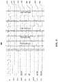
- FIG. 4depicts an example of a timing diagram to illustrate both pps_sos (FF1/q) 386 logic high and logic low conditions that are produced in accordance with the circuit configuration of FIG. 3 .
- certain transitions in lines 378 through 386occur after the initial reset (pps_rst going from high to low), and after the enable input is activated (pps_en going from low to high).
- the output pps_sos 386transitions from low to high at the rising edges of clock cycles 10 and 12 , indicating that a timing requirement is not being met.
- Such an outputcan be provided to a voltage regulator and/or to a clock generation circuit to adjust one or both of the supply voltage or the clock rate.
- disclosed sensor circuitcan be used one-time to determine the starting clock rate or supply voltage of a semiconductor circuit, can be used periodically or intermittently (e.g., as a circuit ages), and/or dynamically in a closed-loop fashion to dynamically adjust a clock rate or a supply voltage for the semiconductor circuit in operation.
- the disclosed sensor circuitcan be implemented using a synthesizable code, a custom harden circuit, logic gates, or transistors.
- FIG. 5illustrates a set of example operations 500 for generating a profile of a semiconductor circuit in accordance with some example embodiments.
- circuit and process parameters that affect circuit timing performanceare determined.
- the dependence of the circuit timing performance on each of the circuit and process parametersis determined.
- timing paths representative the semiconductor circuitare extracted and each timing path is placed in a bin according to the sensitivity of each timing path to the circuit and process parameters.
- the timing paths most sensitive to each of the parametersare selected.
- the circuit and process parametersinclude one or more of a transistor threshold voltage, and electron mobility, a drain-source resistance, a mismatch between n-type devices and p-type devices, a contact resistance, a wire delay, a routing on a single layer, a voltage scalability, a heavy PMOS or NMOS path, a voltage crossing path, a standard cell design, a power delivery impedance, a temperature scalability, and a high fan-out net.
- Another example aspect of the disclosed embodimentsrelates to a method of operating a semiconductor circuit that includes operating a circuit performance sensor to determine when the semiconductor circuit is meeting a timing requirement, and adjusting, when the timing requirement is not being met, a supply voltage or a clock frequency to cause the semiconductor circuit to meet the timing requirement.
- a voltage regulatorincreases its output voltage.
- a toggle rate of a system clockis decreased.
- a semiconductor circuit performance sensor apparatusthat includes a plurality of timing paths, where each timing path has an input and an output, and where each timing path is selected to be representative of a semiconductor circuit parameter dependent on one or more of a temperature and a semiconductor process parameter.
- This apparatusalso includes an AND gate with a plurality of inputs and a first gate output, where the outputs from each of the timing paths are connected to an input of the AND gate, and an OR gate with another plurality of inputs and a second gate output, where the outputs from each of the timing paths are connected to an input of the OR gate.
- the apparatusfurther includes an exclusive NOR gate with a plurality of inputs and a third gate output, where the inputs of the exclusive NOR gate include the first gate output and the second gate output, and a trigger flip-flop clocked by the third gate output, where a trigger output drives the input to each timing path.
- a timing flip-flopis also included in the apparatus whose data input is related to the third gate output and whose output indicates when a timing requirement is being met and when the timing requirement is not being met.
- the apparatuswhen the timing flip-flop output indicates the timing requirement is not being met, causes a voltage regulator supplying power to the apparatus to increase its output voltage.
- the apparatuswhen the timing flip-flop output indicates the timing requirement is not being met, the apparatus causes a clock signal clocking the apparatus to decrease its toggle rate.
- Another aspect of the disclosed embodimentsrelates to a method for generating a profile of a semiconductor circuit to facilitate real-time adjustment of the semiconductor performance.
- the methodincludes determining circuit and process parameters that affect circuit timing performance, determining a dependence of the circuit timing performance on each of the circuit and process parameters, extracting a plurality of timing paths representative of the semiconductor circuit and placing each timing path in a bin according to the sensitivity of each timing path to the circuit and process parameters, and selecting the timing paths most sensitive to each of the parameters to enable a determination of an adjustment of a voltage supply or a clock rate to the semiconductor circuit based on a performance indicator of the selected timing paths.
- the circuit and process parametersinclude one or more of a front-end of line (FEOL) parameters, a back-end of line (BEOL) parameters, or design dependency parameters.
- the FEOL parametersinclude one or more of a transistor threshold voltage, an electron mobility, a drain-source resistance, a mismatch between n-type devices and p-type devices, or a contact resistance.
- the BEOL parametersinclude one or more of a wire delay or a routing on a single layer.
- the design dependency parametersinclude one or more of a voltage scalability, a heavy PMOS or NMOS path, a voltage crossing path, a standard cell design, a power delivery impedance, a temperature scalability, or a high fan-out net.
- selecting the timing paths most sensitive to each of the parametersincludes selecting the timing paths having a maximum amount of slack change for one or more parameters.
- the maximum amount of slack for parameter temperature scalabilityis measured in the units of time per degree Celsius
- the maximum amount of slack for parameter voltage scalabilityis measured in the units of time per voltage.
- the above noted methodfurther includes designing a sensor circuit that includes the selected timing paths so that a timing performance of the sensor circuit is representative of the selected timing paths that are most sensitive to each of the parameters.
- the sensor circuitincludes an output signal representative of the output performance indicator.
- the sensor circuit outputproduces a first value or a first level indicative of an underperformance of the semiconductor circuit upon a determination of a timing or a slack deficiency associated with any one of the selected timing paths.
- the above methodincludes determining that a timing requirement of the selected timing paths is not being met, and providing an indication to (a) dynamically increase a voltage to the semiconductor circuit, or (b) dynamically decrease a clock rate provided to the semiconductor circuit.
- a performance sensor apparatusthat includes a plurality of timing paths, where each timing path has an input and an output, and where each timing path is representative of a path in a semiconductor circuit. Each timing path is associated with a particular parameter dependent on one or more of a temperature or a semiconductor process.
- the performance sensor apparatusfurther includes a logic circuit having a plurality of inputs and at least one output, where the output from each of the timing paths is coupled to an input of the logic circuit.
- the performance sensor apparatusalso includes a trigger circuit having a clock input obtained from the output of the logic circuit, and a timing circuit having an input that is related to the output of the logic circuit and having an output that changes from a first level to a second level upon a determination that a timing requirement for at least one of the timing paths is not met.
- the timing pathsare implemented using combinational logic circuits.
- the logic circuitincludes an AND gate configured to receive each of the plurality of inputs of the logic circuit, the AND gate having an output, an OR gate configured to receive each of the plurality of inputs of the logic circuit, the OR gate having an output.
- the outputs of the AND gate and the OR gateare coupled to the at least one output of the logic circuit.
- the outputs of the AND gate and the OR gateare coupled to inputs of an exclusive NOR gate, and the output of the exclusive NOR gate is connected to the at least one output of the logic circuit.
- an output of the trigger circuitis operable to provide a trigger signal to a launch flip flop for one or more of the timing paths.
- the above performance sensor apparatusfurther includes a clock adjustment circuit including an input configured to receive a system clock, a launch clock output coupled to each of the timing paths, and a capture clock output coupled to a clock input of the timing circuit.
- the clock adjustment circuitis configured to apply one or more of a clock skew adjustment, clock inversion or a margin adjustment in generating the launch clock or the capture clock.
- the clock adjustment circuitincludes one or more programmable delay circuits.
- the input of the timing circuitis configured to receive a logical inverse of the output of the logic circuit.
- the performance sensor apparatusincludes one or more programmable or fixed delay circuits positioned after the output of the one or more timing paths to provide further adjustment for a delay margin of the performance sensor.
- each timing pathrepresents a most sensitive path with respect to the particular parameter associated with that path, wherein the most sensitive path is characterized as having a largest amount of slack change for the particular parameters compared to other paths.
- the systemincludes a performance sensor that includes a system clock input configured to receive a clock signal, a plurality of timing paths, where each timing path has an input and an output, each timing path is representative of a path in a semiconductor circuit and each timing path is associated with a particular parameter dependent on one or more of a temperature or a semiconductor process.
- the performance sensorfurther includes a logic circuit having a plurality of inputs and at least one output, wherein the output from each of the timing paths is coupled to an input of the logic circuit, a trigger circuit having a clock input obtained from the output of the logic circuit, and a timing circuit having an input that is related to the output of the logic circuit and having an output that changes from a first level to a second level upon a determination that a timing requirement for at least one of the timing paths is not met.
- the above noted systemalso includes a voltage regulator circuit coupled to the output of the performance sensor. The voltage regulator is configured to receive a source voltage and to adjust a value of the source voltage based on the output of the performance sensor.
- the voltage regulatoris configured to increase the source voltage output based on the output of the timing circuit.
- the output of the timing circuitis coupled to a clock generation circuitry to cause a change in system clock rate based on the output of the timing circuit.
- the above noted systemfurther includes the semiconductor circuit, and the performance sensor is operable to provide the output of the timing circuit to the voltage regulator or to a clock generator in real time during an operation of the semiconductor circuit, where the voltage regulator or the clock generator are configured to adjust one or both of the value of the supply voltage or a system clock rate based on the output of the timing circuit.
- the subject matter described hereinmay be embodied in systems, apparatus, methods, and/or articles depending on the desired configuration.
- at least a portion of the systems, apparatus, methods, and/or articles described hereincan be implemented using one or more of the following: one or more semiconductor materials or substrates such as silicon, printed circuit board techniques, discrete electronic components such as transistors, inductors, capacitors, resistors, and the like, a processor executing program code, an application-specific integrated circuit (ASIC), a digital signal processor (DSP), an embedded processor, a field programmable gate array (FPGA), and/or combinations thereof.
- ASICapplication-specific integrated circuit
- DSPdigital signal processor
- FPGAfield programmable gate array
- These various example embodimentsmay include implementations in one or more computer programs that are executable and/or interpretable on a programmable system including at least one programmable processor, which may be special or general purpose, coupled to receive data and instructions from, and to transmit data and instructions to, a storage system, at least one input device, and at least one output device.
- These computer programsalso known as programs, software, software applications, applications, components, program code, or code
- machine-readable mediumrefers to any computer program product, computer-readable medium, computer-readable storage medium, apparatus and/or device (for example, magnetic discs, optical disks, memory, Programmable Logic Devices (PLDs)) used to provide machine instructions and/or data to a programmable processor, including a machine-readable medium that receives machine instructions.
- a “machine-readable medium”may be any non-transitory media that can contain, store, communicate, propagate or transport the instructions for use by or in connection with an instruction execution system, apparatus, or device, such as a computer or data processor circuitry.
- a computer-readable mediummay comprise a non-transitory computer-readable storage medium that may be any media that can contain or store the instructions for use by or in connection with an instruction execution system, apparatus, or device, such as a computer. Furthermore, some of the embodiments disclosed herein include computer programs configured to cause methods as disclosed herein.
Landscapes
- Engineering & Computer Science (AREA)
- Computer Hardware Design (AREA)
- Physics & Mathematics (AREA)
- Theoretical Computer Science (AREA)
- General Engineering & Computer Science (AREA)
- General Physics & Mathematics (AREA)
- Evolutionary Computation (AREA)
- Geometry (AREA)
- Microelectronics & Electronic Packaging (AREA)
- Semiconductor Integrated Circuits (AREA)
Abstract
Description
Claims (24)
Priority Applications (1)
| Application Number | Priority Date | Filing Date | Title |
|---|---|---|---|
| US16/242,405US10614184B2 (en) | 2018-01-08 | 2019-01-08 | Semiconductor process and performance sensor |
Applications Claiming Priority (2)
| Application Number | Priority Date | Filing Date | Title |
|---|---|---|---|
| US201862614909P | 2018-01-08 | 2018-01-08 | |
| US16/242,405US10614184B2 (en) | 2018-01-08 | 2019-01-08 | Semiconductor process and performance sensor |
Publications (2)
| Publication Number | Publication Date |
|---|---|
| US20190213292A1 US20190213292A1 (en) | 2019-07-11 |
| US10614184B2true US10614184B2 (en) | 2020-04-07 |
Family
ID=67140891
Family Applications (1)
| Application Number | Title | Priority Date | Filing Date |
|---|---|---|---|
| US16/242,405ActiveUS10614184B2 (en) | 2018-01-08 | 2019-01-08 | Semiconductor process and performance sensor |
Country Status (1)
| Country | Link |
|---|---|
| US (1) | US10614184B2 (en) |
Cited By (125)
| Publication number | Priority date | Publication date | Assignee | Title |
|---|---|---|---|---|
| US20220273300A1 (en)* | 2021-02-26 | 2022-09-01 | Ethicon Llc | Adjustment to transfer parameters to improve available power |
| US11717297B2 (en) | 2014-09-05 | 2023-08-08 | Cilag Gmbh International | Smart cartridge wake up operation and data retention |
| US11723658B2 (en) | 2021-03-22 | 2023-08-15 | Cilag Gmbh International | Staple cartridge comprising a firing lockout |
| US11730471B2 (en) | 2016-02-09 | 2023-08-22 | Cilag Gmbh International | Articulatable surgical instruments with single articulation link arrangements |
| US11730477B2 (en) | 2008-10-10 | 2023-08-22 | Cilag Gmbh International | Powered surgical system with manually retractable firing system |
| US11737749B2 (en) | 2021-03-22 | 2023-08-29 | Cilag Gmbh International | Surgical stapling instrument comprising a retraction system |
| US11737754B2 (en) | 2010-09-30 | 2023-08-29 | Cilag Gmbh International | Surgical stapler with floating anvil |
| US11737751B2 (en) | 2020-12-02 | 2023-08-29 | Cilag Gmbh International | Devices and methods of managing energy dissipated within sterile barriers of surgical instrument housings |
| US11744583B2 (en) | 2021-02-26 | 2023-09-05 | Cilag Gmbh International | Distal communication array to tune frequency of RF systems |
| US11744603B2 (en) | 2021-03-24 | 2023-09-05 | Cilag Gmbh International | Multi-axis pivot joints for surgical instruments and methods for manufacturing same |
| US11744588B2 (en) | 2015-02-27 | 2023-09-05 | Cilag Gmbh International | Surgical stapling instrument including a removably attachable battery pack |
| US11744593B2 (en) | 2019-06-28 | 2023-09-05 | Cilag Gmbh International | Method for authenticating the compatibility of a staple cartridge with a surgical instrument |
| US11749877B2 (en) | 2021-02-26 | 2023-09-05 | Cilag Gmbh International | Stapling instrument comprising a signal antenna |
| US11751869B2 (en) | 2021-02-26 | 2023-09-12 | Cilag Gmbh International | Monitoring of multiple sensors over time to detect moving characteristics of tissue |
| US11751867B2 (en) | 2017-12-21 | 2023-09-12 | Cilag Gmbh International | Surgical instrument comprising sequenced systems |
| US11759208B2 (en) | 2015-12-30 | 2023-09-19 | Cilag Gmbh International | Mechanisms for compensating for battery pack failure in powered surgical instruments |
| US11771425B2 (en) | 2005-08-31 | 2023-10-03 | Cilag Gmbh International | Stapling assembly for forming staples to different formed heights |
| US11779336B2 (en) | 2016-02-12 | 2023-10-10 | Cilag Gmbh International | Mechanisms for compensating for drivetrain failure in powered surgical instruments |
| US11779330B2 (en) | 2020-10-29 | 2023-10-10 | Cilag Gmbh International | Surgical instrument comprising a jaw alignment system |
| US11779420B2 (en) | 2012-06-28 | 2023-10-10 | Cilag Gmbh International | Robotic surgical attachments having manually-actuated retraction assemblies |
| US11793518B2 (en) | 2006-01-31 | 2023-10-24 | Cilag Gmbh International | Powered surgical instruments with firing system lockout arrangements |
| US11793513B2 (en) | 2017-06-20 | 2023-10-24 | Cilag Gmbh International | Systems and methods for controlling motor speed according to user input for a surgical instrument |
| US11793509B2 (en) | 2012-03-28 | 2023-10-24 | Cilag Gmbh International | Staple cartridge including an implantable layer |
| US11793512B2 (en) | 2005-08-31 | 2023-10-24 | Cilag Gmbh International | Staple cartridges for forming staples having differing formed staple heights |
| US11801047B2 (en) | 2008-02-14 | 2023-10-31 | Cilag Gmbh International | Surgical stapling system comprising a control circuit configured to selectively monitor tissue impedance and adjust control of a motor |
| US11806011B2 (en) | 2021-03-22 | 2023-11-07 | Cilag Gmbh International | Stapling instrument comprising tissue compression systems |
| US11806013B2 (en) | 2012-06-28 | 2023-11-07 | Cilag Gmbh International | Firing system arrangements for surgical instruments |
| US11811253B2 (en) | 2016-04-18 | 2023-11-07 | Cilag Gmbh International | Surgical robotic system with fault state detection configurations based on motor current draw |
| US11812964B2 (en) | 2021-02-26 | 2023-11-14 | Cilag Gmbh International | Staple cartridge comprising a power management circuit |
| US11812965B2 (en) | 2010-09-30 | 2023-11-14 | Cilag Gmbh International | Layer of material for a surgical end effector |
| US11812954B2 (en) | 2008-09-23 | 2023-11-14 | Cilag Gmbh International | Robotically-controlled motorized surgical instrument with an end effector |
| US11812961B2 (en) | 2007-01-10 | 2023-11-14 | Cilag Gmbh International | Surgical instrument including a motor control system |
| US11826012B2 (en) | 2021-03-22 | 2023-11-28 | Cilag Gmbh International | Stapling instrument comprising a pulsed motor-driven firing rack |
| US11826042B2 (en) | 2021-03-22 | 2023-11-28 | Cilag Gmbh International | Surgical instrument comprising a firing drive including a selectable leverage mechanism |
| US11826047B2 (en) | 2021-05-28 | 2023-11-28 | Cilag Gmbh International | Stapling instrument comprising jaw mounts |
| US11839375B2 (en) | 2005-08-31 | 2023-12-12 | Cilag Gmbh International | Fastener cartridge assembly comprising an anvil and different staple heights |
| US11839352B2 (en) | 2007-01-11 | 2023-12-12 | Cilag Gmbh International | Surgical stapling device with an end effector |
| US11850310B2 (en) | 2010-09-30 | 2023-12-26 | Cilag Gmbh International | Staple cartridge including an adjunct |
| US11849945B2 (en) | 2021-03-24 | 2023-12-26 | Cilag Gmbh International | Rotary-driven surgical stapling assembly comprising eccentrically driven firing member |
| US11849941B2 (en) | 2007-06-29 | 2023-12-26 | Cilag Gmbh International | Staple cartridge having staple cavities extending at a transverse angle relative to a longitudinal cartridge axis |
| US11849952B2 (en) | 2010-09-30 | 2023-12-26 | Cilag Gmbh International | Staple cartridge comprising staples positioned within a compressible portion thereof |
| US11849943B2 (en) | 2020-12-02 | 2023-12-26 | Cilag Gmbh International | Surgical instrument with cartridge release mechanisms |
| US11849946B2 (en) | 2015-09-23 | 2023-12-26 | Cilag Gmbh International | Surgical stapler having downstream current-based motor control |
| US11857187B2 (en) | 2010-09-30 | 2024-01-02 | Cilag Gmbh International | Tissue thickness compensator comprising controlled release and expansion |
| US11857181B2 (en) | 2007-06-04 | 2024-01-02 | Cilag Gmbh International | Robotically-controlled shaft based rotary drive systems for surgical instruments |
| US11871939B2 (en) | 2017-06-20 | 2024-01-16 | Cilag Gmbh International | Method for closed loop control of motor velocity of a surgical stapling and cutting instrument |
| US11871923B2 (en) | 2008-09-23 | 2024-01-16 | Cilag Gmbh International | Motorized surgical instrument |
| US11877748B2 (en) | 2006-10-03 | 2024-01-23 | Cilag Gmbh International | Robotically-driven surgical instrument with E-beam driver |
| USD1013170S1 (en) | 2020-10-29 | 2024-01-30 | Cilag Gmbh International | Surgical instrument assembly |
| US11882987B2 (en) | 2004-07-28 | 2024-01-30 | Cilag Gmbh International | Articulating surgical stapling instrument incorporating a two-piece E-beam firing mechanism |
| US11883020B2 (en) | 2006-01-31 | 2024-01-30 | Cilag Gmbh International | Surgical instrument having a feedback system |
| US11883025B2 (en) | 2010-09-30 | 2024-01-30 | Cilag Gmbh International | Tissue thickness compensator comprising a plurality of layers |
| US11883026B2 (en) | 2014-04-16 | 2024-01-30 | Cilag Gmbh International | Fastener cartridge assemblies and staple retainer cover arrangements |
| US11890015B2 (en) | 2015-09-30 | 2024-02-06 | Cilag Gmbh International | Compressible adjunct with crossing spacer fibers |
| US11890005B2 (en) | 2017-06-29 | 2024-02-06 | Cilag Gmbh International | Methods for closed loop velocity control for robotic surgical instrument |
| US11890012B2 (en) | 2004-07-28 | 2024-02-06 | Cilag Gmbh International | Staple cartridge comprising cartridge body and attached support |
| US11890008B2 (en) | 2006-01-31 | 2024-02-06 | Cilag Gmbh International | Surgical instrument with firing lockout |
| US11890029B2 (en) | 2006-01-31 | 2024-02-06 | Cilag Gmbh International | Motor-driven surgical cutting and fastening instrument |
| US11896219B2 (en) | 2021-03-24 | 2024-02-13 | Cilag Gmbh International | Mating features between drivers and underside of a cartridge deck |
| US11896222B2 (en) | 2017-12-15 | 2024-02-13 | Cilag Gmbh International | Methods of operating surgical end effectors |
| US11903581B2 (en) | 2019-04-30 | 2024-02-20 | Cilag Gmbh International | Methods for stapling tissue using a surgical instrument |
| US11911027B2 (en) | 2010-09-30 | 2024-02-27 | Cilag Gmbh International | Adhesive film laminate |
| US11918222B2 (en) | 2014-04-16 | 2024-03-05 | Cilag Gmbh International | Stapling assembly having firing member viewing windows |
| US11918210B2 (en) | 2014-10-16 | 2024-03-05 | Cilag Gmbh International | Staple cartridge comprising a cartridge body including a plurality of wells |
| US11918212B2 (en) | 2015-03-31 | 2024-03-05 | Cilag Gmbh International | Surgical instrument with selectively disengageable drive systems |
| US11918220B2 (en) | 2012-03-28 | 2024-03-05 | Cilag Gmbh International | Tissue thickness compensator comprising tissue ingrowth features |
| US11918215B2 (en) | 2016-12-21 | 2024-03-05 | Cilag Gmbh International | Staple cartridge with array of staple pockets |
| US11918208B2 (en) | 2011-05-27 | 2024-03-05 | Cilag Gmbh International | Robotically-controlled shaft based rotary drive systems for surgical instruments |
| USD1018577S1 (en) | 2017-06-28 | 2024-03-19 | Cilag Gmbh International | Display screen or portion thereof with a graphical user interface for a surgical instrument |
| US11931028B2 (en) | 2016-04-15 | 2024-03-19 | Cilag Gmbh International | Surgical instrument with multiple program responses during a firing motion |
| US11931025B2 (en) | 2020-10-29 | 2024-03-19 | Cilag Gmbh International | Surgical instrument comprising a releasable closure drive lock |
| US11931034B2 (en) | 2016-12-21 | 2024-03-19 | Cilag Gmbh International | Surgical stapling instruments with smart staple cartridges |
| US11937816B2 (en) | 2021-10-28 | 2024-03-26 | Cilag Gmbh International | Electrical lead arrangements for surgical instruments |
| US11944296B2 (en) | 2020-12-02 | 2024-04-02 | Cilag Gmbh International | Powered surgical instruments with external connectors |
| US11944338B2 (en) | 2015-03-06 | 2024-04-02 | Cilag Gmbh International | Multiple level thresholds to modify operation of powered surgical instruments |
| US11957339B2 (en) | 2018-08-20 | 2024-04-16 | Cilag Gmbh International | Method for fabricating surgical stapler anvils |
| US11957345B2 (en) | 2013-03-01 | 2024-04-16 | Cilag Gmbh International | Articulatable surgical instruments with conductive pathways for signal communication |
| US11963678B2 (en) | 2014-04-16 | 2024-04-23 | Cilag Gmbh International | Fastener cartridges including extensions having different configurations |
| US11963680B2 (en) | 2017-10-31 | 2024-04-23 | Cilag Gmbh International | Cartridge body design with force reduction based on firing completion |
| US11974747B2 (en) | 2011-05-27 | 2024-05-07 | Cilag Gmbh International | Surgical stapling instruments with rotatable staple deployment arrangements |
| US11974746B2 (en) | 2014-04-16 | 2024-05-07 | Cilag Gmbh International | Anvil for use with a surgical stapling assembly |
| US11974742B2 (en) | 2017-08-03 | 2024-05-07 | Cilag Gmbh International | Surgical system comprising an articulation bailout |
| US11980363B2 (en) | 2021-10-18 | 2024-05-14 | Cilag Gmbh International | Row-to-row staple array variations |
| US11980366B2 (en) | 2006-10-03 | 2024-05-14 | Cilag Gmbh International | Surgical instrument |
| US11986183B2 (en) | 2008-02-14 | 2024-05-21 | Cilag Gmbh International | Surgical cutting and fastening instrument comprising a plurality of sensors to measure an electrical parameter |
| US11992213B2 (en) | 2016-12-21 | 2024-05-28 | Cilag Gmbh International | Surgical stapling instruments with replaceable staple cartridges |
| US11992214B2 (en) | 2013-03-14 | 2024-05-28 | Cilag Gmbh International | Control systems for surgical instruments |
| US11998194B2 (en) | 2008-02-15 | 2024-06-04 | Cilag Gmbh International | Surgical stapling assembly comprising an adjunct applicator |
| US11998206B2 (en) | 2008-02-14 | 2024-06-04 | Cilag Gmbh International | Detachable motor powered surgical instrument |
| US11998198B2 (en) | 2004-07-28 | 2024-06-04 | Cilag Gmbh International | Surgical stapling instrument incorporating a two-piece E-beam firing mechanism |
| US12011166B2 (en) | 2016-12-21 | 2024-06-18 | Cilag Gmbh International | Articulatable surgical stapling instruments |
| US12016564B2 (en) | 2014-09-26 | 2024-06-25 | Cilag Gmbh International | Circular fastener cartridges for applying radially expandable fastener lines |
| US12023022B2 (en) | 2014-03-26 | 2024-07-02 | Cilag Gmbh International | Systems and methods for controlling a segmented circuit |
| US12029415B2 (en) | 2008-09-23 | 2024-07-09 | Cilag Gmbh International | Motor-driven surgical cutting instrument |
| US12035913B2 (en) | 2019-12-19 | 2024-07-16 | Cilag Gmbh International | Staple cartridge comprising a deployable knife |
| US12053176B2 (en) | 2013-08-23 | 2024-08-06 | Cilag Gmbh International | End effector detention systems for surgical instruments |
| US12076008B2 (en) | 2018-08-20 | 2024-09-03 | Cilag Gmbh International | Method for operating a powered articulatable surgical instrument |
| US12076011B2 (en) | 2017-10-30 | 2024-09-03 | Cilag Gmbh International | Surgical stapler knife motion controls |
| US12076017B2 (en) | 2014-09-18 | 2024-09-03 | Cilag Gmbh International | Surgical instrument including a deployable knife |
| US12076096B2 (en) | 2017-12-19 | 2024-09-03 | Cilag Gmbh International | Method for determining the position of a rotatable jaw of a surgical instrument attachment assembly |
| US12082806B2 (en) | 2007-01-10 | 2024-09-10 | Cilag Gmbh International | Surgical instrument with wireless communication between control unit and sensor transponders |
| US12089841B2 (en) | 2021-10-28 | 2024-09-17 | Cilag CmbH International | Staple cartridge identification systems |
| US12108950B2 (en) | 2014-12-18 | 2024-10-08 | Cilag Gmbh International | Surgical instrument assembly comprising a flexible articulation system |
| US12108951B2 (en) | 2021-02-26 | 2024-10-08 | Cilag Gmbh International | Staple cartridge comprising a sensing array and a temperature control system |
| US12137912B2 (en) | 2015-09-30 | 2024-11-12 | Cilag Gmbh International | Compressible adjunct with attachment regions |
| US12144500B2 (en) | 2016-04-15 | 2024-11-19 | Cilag Gmbh International | Surgical instrument with multiple program responses during a firing motion |
| US12156653B2 (en) | 2015-12-30 | 2024-12-03 | Cilag Gmbh International | Surgical instruments with motor control circuits |
| US12161320B2 (en) | 2013-04-16 | 2024-12-10 | Cilag Gmbh International | Powered surgical stapler |
| US12171508B2 (en) | 2006-03-23 | 2024-12-24 | Cilag Gmbh International | Robotically-controlled surgical instrument with selectively articulatable end effector |
| US12171507B2 (en) | 2016-08-16 | 2024-12-24 | Cilag Gmbh International | Surgical tool with manual control of end effector jaws |
| US12213671B2 (en) | 2008-02-14 | 2025-02-04 | Cilag Gmbh International | Motorized system having a plurality of power sources |
| US12213666B2 (en) | 2010-09-30 | 2025-02-04 | Cilag Gmbh International | Tissue thickness compensator comprising layers |
| US12232723B2 (en) | 2014-03-26 | 2025-02-25 | Cilag Gmbh International | Systems and methods for controlling a segmented circuit |
| US12239316B2 (en) | 2011-05-27 | 2025-03-04 | Cilag Gmbh International | Automated end effector component reloading system for use with a robotic system |
| US12245764B2 (en) | 2016-12-21 | 2025-03-11 | Cilag Gmbh International | Shaft assembly comprising a lockout |
| US12245901B2 (en) | 2015-09-25 | 2025-03-11 | Cilag Gmbh International | Implantable layer comprising boundary indicators |
| US12262888B2 (en) | 2018-08-20 | 2025-04-01 | Cilag Gmbh International | Surgical instruments with progressive jaw closure arrangements |
| US12324581B2 (en) | 2017-06-28 | 2025-06-10 | Cilag Gmbh International | Surgical instrument comprising selectively actuatable rotatable couplers |
| US12329381B2 (en) | 2019-04-30 | 2025-06-17 | Cilag Gmbh International | Stapling instrument comprising a mounted shaft orientation sensor |
| US12336705B2 (en) | 2017-12-21 | 2025-06-24 | Cilag Gmbh International | Continuous use self-propelled stapling instrument |
| US12383267B2 (en) | 2012-06-28 | 2025-08-12 | Cilag Gmbh International | Robotically powered surgical device with manually-actuatable reversing system |
| US12414768B2 (en) | 2014-09-05 | 2025-09-16 | Cilag Gmbh International | Staple cartridge electrical contacts |
| US12432790B2 (en) | 2021-10-28 | 2025-09-30 | Cilag Gmbh International | Method and device for transmitting UART communications over a security short range wireless communication |
| US12433584B2 (en) | 2006-01-31 | 2025-10-07 | Cilag Gmbh International | Robotically-controlled end effector |
| US12440209B2 (en) | 2023-05-09 | 2025-10-14 | Cilag Gmbh International | Surgical instrument with multiple program responses during a firing motion |
Families Citing this family (4)
| Publication number | Priority date | Publication date | Assignee | Title |
|---|---|---|---|---|
| WO2019136299A1 (en) | 2018-01-05 | 2019-07-11 | Atlazo, Inc. | Power management system |
| US10635130B2 (en) | 2018-02-01 | 2020-04-28 | Atlazo, Inc. | Process, voltage and temperature tolerant clock generator |
| US10571945B2 (en) | 2018-02-21 | 2020-02-25 | Atlazo, Inc. | Low power regulator circuits, systems and methods regarding the same |
| US10700604B2 (en) | 2018-03-07 | 2020-06-30 | Atlazo, Inc. | High performance switch devices and methods for operating the same |
Citations (66)
| Publication number | Priority date | Publication date | Assignee | Title |
|---|---|---|---|---|
| US5481178A (en) | 1993-03-23 | 1996-01-02 | Linear Technology Corporation | Control circuit and method for maintaining high efficiency over broad current ranges in a switching regulator circuit |
| US6636022B2 (en) | 2001-01-17 | 2003-10-21 | Koninklijke Philips Electronics N.V. | Controlled multi-output DC/DC converter |
| US20050184711A1 (en) | 2004-02-25 | 2005-08-25 | Jiwei Chen | Low dropout voltage regulator |
| US20060114017A1 (en)* | 2004-11-30 | 2006-06-01 | El-Kik Tony S | Adjusting settings of an I/O circuit for process, voltage, and/or temperature variations |
| US20070018712A1 (en)* | 2005-07-22 | 2007-01-25 | Gk Siddhartha | PVT variation detection and compensation circuit |
| US7174523B2 (en)* | 2004-07-30 | 2007-02-06 | International Business Machines Corporation | Variable sigma adjust methodology for static timing |
| US7298119B1 (en) | 2005-06-03 | 2007-11-20 | Maxim Integrated Products, Inc. | Step-up/step-down (buck/boost) switching regulator control methods |
| US20080122291A1 (en) | 2004-10-19 | 2008-05-29 | Rohm Co., Ltd | Switching Power Supply Control Circuit, Switching Power Supply Device and Electronic Apparatus Employing the Same |
| US7487474B2 (en)* | 2003-01-02 | 2009-02-03 | Pdf Solutions, Inc. | Designing an integrated circuit to improve yield using a variant design element |
| US20090037854A1 (en)* | 2007-08-01 | 2009-02-05 | Bittlestone Clive D | Test Method and System for Characterizing and/or Refining an IC Design Cycle |
| US7552409B2 (en)* | 2005-06-07 | 2009-06-23 | Synopsys, Inc. | Engineering change order process optimization |
| US20090284240A1 (en) | 2008-05-14 | 2009-11-19 | National Semiconductor Corporation | Method and system for providing local converters to provide maximum power point tracking in an energy generating system |
| US20100052635A1 (en) | 2008-08-26 | 2010-03-04 | Texas Instruments Incorporated | Compensation of LDO regulator using parallel signal path with fractional frequency response |
| US20100194434A1 (en)* | 2009-01-30 | 2010-08-05 | East-West Innovation Corporation | Systems and methods of integrated circuit clocking |
| US20100327952A1 (en)* | 2007-09-24 | 2010-12-30 | Media Tek Inc. | Electronic System Capable of Compensating Process, Voltage and Temperature Effects |
| US7913071B2 (en) | 2007-07-31 | 2011-03-22 | Northwestern University | Systems and methods for process and user driven dynamic voltage and frequency scaling |
| US8018212B1 (en) | 2007-08-24 | 2011-09-13 | Intersil Americas Inc. | Buck-boost regulator |
| US20110248764A1 (en) | 2010-04-12 | 2011-10-13 | Qualcomm Incorporated | Clock Divider System and Method |
| US8049568B2 (en) | 2009-09-10 | 2011-11-01 | Broadcom Corporation | Feedback-based linearization of voltage controlled oscillator |
| US20110267017A1 (en) | 2010-04-29 | 2011-11-03 | Qualcomm Incorporated | On-Chip Low Voltage Capacitor-Less Low Dropout Regulator with Q-Control |
| US8129961B2 (en) | 2006-08-15 | 2012-03-06 | St-Ericsson Sa | DC/DC-converter |
| US8169203B1 (en) | 2010-11-19 | 2012-05-01 | Nxp B.V. | Low dropout regulator |
| US20120124538A1 (en)* | 2007-10-09 | 2012-05-17 | International Business Machines Corporation | Method and device for selectively adding timing margin in an integrated circuit |
| US20120159216A1 (en) | 2011-12-22 | 2012-06-21 | Wells Ryan D | Method, apparatus, and system for energy efficiency and energy conservation including enhanced temperature based voltage control |
| US8307317B2 (en)* | 2008-08-19 | 2012-11-06 | Synopsys, Inc. | Statistical on-chip variation timing analysis |
| US20130069608A1 (en) | 2011-09-19 | 2013-03-21 | Texas Instruments Incorporated | Voltage regulator stabilization for operation with a wide range of output capacitances |
| US20130099764A1 (en) | 2011-10-21 | 2013-04-25 | Qualcomm Incorporated | System and method to regulate voltage |
| US8464199B1 (en)* | 2012-05-16 | 2013-06-11 | International Business Machines Corporation | Circuit design using design variable function slope sensitivity |
| US8543966B2 (en)* | 2011-11-11 | 2013-09-24 | International Business Machines Corporation | Test path selection and test program generation for performance testing integrated circuit chips |
| US20130271100A1 (en) | 2012-04-16 | 2013-10-17 | Vidatronic, Inc. | High power supply rejection linear low-dropout regulator for a wide range of capacitance loads |
| US8692584B2 (en) | 2010-02-19 | 2014-04-08 | Renesas Electronics Corporation | Semiconductor integrated circuit device |
| JP2014064436A (en) | 2012-09-24 | 2014-04-10 | Renesas Electronics Corp | Power supply device |
| US20140152344A1 (en)* | 2012-12-04 | 2014-06-05 | National Cheng Kung University | In situ pulse-based delay variation monitor predicting timing error caused by process and environmental variation |
| US20140225579A1 (en) | 2013-02-08 | 2014-08-14 | Nvidia Corporation | Current-parking switching regulator upstream controller |
| US20140232360A1 (en) | 2013-02-19 | 2014-08-21 | Nvidia Corporation | Predictive current sensing |
| US20150198960A1 (en) | 2014-01-14 | 2015-07-16 | Broadcom Corporation | Low-power low-dropout voltage regulators with high power supply rejection and fast settling performance |
| US20150214841A1 (en) | 2014-01-28 | 2015-07-30 | Stmicroelectronics S.R.I | Dc-dc converter with improved energy management, method for operating the dc-dc converter, environmental energy harvesting system using the dc-dc converter, and apparatus using the energy harvesting system |
| US9281780B2 (en) | 2012-10-31 | 2016-03-08 | Renesas Electronics Corporation | Resistance correction circuit, resistance correction method, and semiconductor device |
| US20160077537A1 (en) | 2013-04-30 | 2016-03-17 | Freescale Semiconductor, Inc. | A low drop-out voltage regulator and a method of providing a regulated voltage |
| US20160094125A1 (en) | 2014-09-25 | 2016-03-31 | Maxim Integrated Products, Inc. | Three phases controller for buck-boost regulators |
| US9317048B2 (en) | 2011-08-12 | 2016-04-19 | Allwinner Technology Co., Ltd. | Circuit control system and method for dynamically adjusting voltage and frequency |
| US20160118894A1 (en) | 2014-10-24 | 2016-04-28 | STMicroelectronics (Shenzhen) R&D Co. Ltd | Inverting buck-boost converter drive circuit and method |
| US20160164497A1 (en)* | 2014-12-04 | 2016-06-09 | International Business Machines Corporation | Minimization of bias temperature instability (bti) degradation in circuits |
| US9408266B2 (en) | 2011-08-26 | 2016-08-02 | Infineon Technologies Ag | Driver circuit for efficiently driving a large number of LEDs |
| US20160334818A1 (en) | 2015-05-15 | 2016-11-17 | Analog Devices Global | Circuits and techniques including cascaded ldo regulation |
| US9503106B1 (en) | 2015-12-11 | 2016-11-22 | Globalfoundries Inc. | Frequency-locked voltage regulated loop |
| US20160359421A1 (en) | 2014-12-07 | 2016-12-08 | Alpha And Omega Semiconductor (Cayman) Ltd. | Power supply device |
| US20170033698A1 (en) | 2015-07-31 | 2017-02-02 | Texas Instruments Incorporated | Flyback converter with secondary side regulation |
| US20170093350A1 (en) | 2015-09-28 | 2017-03-30 | Dialog Semiconductor (Uk) Limited | Multi-Stage Amplifier with Improved Operating Efficiency |
| US20170115678A1 (en) | 2015-10-23 | 2017-04-27 | Nxp B.V. | Low drop-out voltage regulator and method for tracking and compensating load current |
| US20170160757A1 (en) | 2015-12-07 | 2017-06-08 | Macronix International Co., Ltd. | Semiconductor device having output compensation |
| US9698674B1 (en) | 2015-12-30 | 2017-07-04 | Silicon Laboratories Inc. | Timing based approach for efficient switched mode power conversion |
| US20170272073A1 (en) | 2016-03-18 | 2017-09-21 | Altera Corporation | Dynamic parameter operation of an fpga |
| US9915963B1 (en) | 2017-07-05 | 2018-03-13 | Psemi Corporation | Methods for adaptive compensation of linear voltage regulators |
| US20180120879A1 (en) | 2016-10-27 | 2018-05-03 | Qualcomm Incorporated | Voltage regulator with enhanced power supply rejection ratio and load-transient performance |
| US20180173258A1 (en) | 2016-12-19 | 2018-06-21 | Qorvo Us, Inc. | Voltage regulator with fast transient response |
| US20180284829A1 (en) | 2017-04-03 | 2018-10-04 | Vidatronic, Inc. | Voltage regulators with improved power supply rejection using negative impedance |
| US20180321092A1 (en)* | 2015-11-18 | 2018-11-08 | Pst Sensors (Proprietary) Limited | Digital sensor |
| US10222852B2 (en)* | 2016-10-06 | 2019-03-05 | International Business Machines Corporation | Voltage and frequency balancing at nominal point |
| US10236763B2 (en) | 2015-08-04 | 2019-03-19 | Power Integrations, Inc. | Reverse current blockage through buck controller block |
| US20190131876A1 (en) | 2017-10-30 | 2019-05-02 | Renesas Electronics America Inc. | Window comparator structure for low power hysteretic buck-boost dc-dc controller |
| US20190212799A1 (en) | 2018-01-10 | 2019-07-11 | Atlazo, Inc. | Adaptive energy optimal computing |
| US20190214906A1 (en) | 2018-01-05 | 2019-07-11 | Atlazo, lnc. | Power management system |
| US20190235566A1 (en) | 2018-02-01 | 2019-08-01 | Atlazo, Inc. | Process, voltage and temperature tolerant clock generator |
| US20190258283A1 (en) | 2018-02-21 | 2019-08-22 | Atlazo, Inc. | Low power regulator circuits, systems and methods regarding the same |
| US20190280593A1 (en) | 2018-03-07 | 2019-09-12 | Atlazo, Inc. | High performance switch devices and methods for operating the same |
- 2019
- 2019-01-08USUS16/242,405patent/US10614184B2/enactiveActive
Patent Citations (70)
| Publication number | Priority date | Publication date | Assignee | Title |
|---|---|---|---|---|
| US5481178A (en) | 1993-03-23 | 1996-01-02 | Linear Technology Corporation | Control circuit and method for maintaining high efficiency over broad current ranges in a switching regulator circuit |
| US6636022B2 (en) | 2001-01-17 | 2003-10-21 | Koninklijke Philips Electronics N.V. | Controlled multi-output DC/DC converter |
| US7487474B2 (en)* | 2003-01-02 | 2009-02-03 | Pdf Solutions, Inc. | Designing an integrated circuit to improve yield using a variant design element |
| US20050184711A1 (en) | 2004-02-25 | 2005-08-25 | Jiwei Chen | Low dropout voltage regulator |
| US7174523B2 (en)* | 2004-07-30 | 2007-02-06 | International Business Machines Corporation | Variable sigma adjust methodology for static timing |
| US20070089078A1 (en)* | 2004-07-30 | 2007-04-19 | Engel James J | Variable Sigma Adjust Methodology For Static Timing |
| US20080122291A1 (en) | 2004-10-19 | 2008-05-29 | Rohm Co., Ltd | Switching Power Supply Control Circuit, Switching Power Supply Device and Electronic Apparatus Employing the Same |
| US20060114017A1 (en)* | 2004-11-30 | 2006-06-01 | El-Kik Tony S | Adjusting settings of an I/O circuit for process, voltage, and/or temperature variations |
| US7298119B1 (en) | 2005-06-03 | 2007-11-20 | Maxim Integrated Products, Inc. | Step-up/step-down (buck/boost) switching regulator control methods |
| US7552409B2 (en)* | 2005-06-07 | 2009-06-23 | Synopsys, Inc. | Engineering change order process optimization |
| US20070018712A1 (en)* | 2005-07-22 | 2007-01-25 | Gk Siddhartha | PVT variation detection and compensation circuit |
| US8129961B2 (en) | 2006-08-15 | 2012-03-06 | St-Ericsson Sa | DC/DC-converter |
| US7913071B2 (en) | 2007-07-31 | 2011-03-22 | Northwestern University | Systems and methods for process and user driven dynamic voltage and frequency scaling |
| US20090037854A1 (en)* | 2007-08-01 | 2009-02-05 | Bittlestone Clive D | Test Method and System for Characterizing and/or Refining an IC Design Cycle |
| US8051398B2 (en)* | 2007-08-01 | 2011-11-01 | Texas Instruments Incorporated | Test method and system for characterizing and/or refining an IC design cycle |
| US8018212B1 (en) | 2007-08-24 | 2011-09-13 | Intersil Americas Inc. | Buck-boost regulator |
| US20100327952A1 (en)* | 2007-09-24 | 2010-12-30 | Media Tek Inc. | Electronic System Capable of Compensating Process, Voltage and Temperature Effects |
| US20120124538A1 (en)* | 2007-10-09 | 2012-05-17 | International Business Machines Corporation | Method and device for selectively adding timing margin in an integrated circuit |
| US20090284240A1 (en) | 2008-05-14 | 2009-11-19 | National Semiconductor Corporation | Method and system for providing local converters to provide maximum power point tracking in an energy generating system |
| US8307317B2 (en)* | 2008-08-19 | 2012-11-06 | Synopsys, Inc. | Statistical on-chip variation timing analysis |
| US20100052635A1 (en) | 2008-08-26 | 2010-03-04 | Texas Instruments Incorporated | Compensation of LDO regulator using parallel signal path with fractional frequency response |
| US20100194434A1 (en)* | 2009-01-30 | 2010-08-05 | East-West Innovation Corporation | Systems and methods of integrated circuit clocking |
| US8049568B2 (en) | 2009-09-10 | 2011-11-01 | Broadcom Corporation | Feedback-based linearization of voltage controlled oscillator |
| US8692584B2 (en) | 2010-02-19 | 2014-04-08 | Renesas Electronics Corporation | Semiconductor integrated circuit device |
| US20110248764A1 (en) | 2010-04-12 | 2011-10-13 | Qualcomm Incorporated | Clock Divider System and Method |
| US20110267017A1 (en) | 2010-04-29 | 2011-11-03 | Qualcomm Incorporated | On-Chip Low Voltage Capacitor-Less Low Dropout Regulator with Q-Control |
| US8169203B1 (en) | 2010-11-19 | 2012-05-01 | Nxp B.V. | Low dropout regulator |
| US9317048B2 (en) | 2011-08-12 | 2016-04-19 | Allwinner Technology Co., Ltd. | Circuit control system and method for dynamically adjusting voltage and frequency |
| US9408266B2 (en) | 2011-08-26 | 2016-08-02 | Infineon Technologies Ag | Driver circuit for efficiently driving a large number of LEDs |
| US20130069608A1 (en) | 2011-09-19 | 2013-03-21 | Texas Instruments Incorporated | Voltage regulator stabilization for operation with a wide range of output capacitances |
| US20130099764A1 (en) | 2011-10-21 | 2013-04-25 | Qualcomm Incorporated | System and method to regulate voltage |
| US8543966B2 (en)* | 2011-11-11 | 2013-09-24 | International Business Machines Corporation | Test path selection and test program generation for performance testing integrated circuit chips |
| US20120159216A1 (en) | 2011-12-22 | 2012-06-21 | Wells Ryan D | Method, apparatus, and system for energy efficiency and energy conservation including enhanced temperature based voltage control |
| US20130271100A1 (en) | 2012-04-16 | 2013-10-17 | Vidatronic, Inc. | High power supply rejection linear low-dropout regulator for a wide range of capacitance loads |
| US8464199B1 (en)* | 2012-05-16 | 2013-06-11 | International Business Machines Corporation | Circuit design using design variable function slope sensitivity |
| JP2014064436A (en) | 2012-09-24 | 2014-04-10 | Renesas Electronics Corp | Power supply device |
| US9281780B2 (en) | 2012-10-31 | 2016-03-08 | Renesas Electronics Corporation | Resistance correction circuit, resistance correction method, and semiconductor device |
| US9829911B2 (en) | 2012-10-31 | 2017-11-28 | Renesas Electronics Corporation | Resistance correction circuit, resistance correction method, and semiconductor device |
| US20140152344A1 (en)* | 2012-12-04 | 2014-06-05 | National Cheng Kung University | In situ pulse-based delay variation monitor predicting timing error caused by process and environmental variation |
| US20140225579A1 (en) | 2013-02-08 | 2014-08-14 | Nvidia Corporation | Current-parking switching regulator upstream controller |
| US20140232360A1 (en) | 2013-02-19 | 2014-08-21 | Nvidia Corporation | Predictive current sensing |
| US20160077537A1 (en) | 2013-04-30 | 2016-03-17 | Freescale Semiconductor, Inc. | A low drop-out voltage regulator and a method of providing a regulated voltage |
| US20150198960A1 (en) | 2014-01-14 | 2015-07-16 | Broadcom Corporation | Low-power low-dropout voltage regulators with high power supply rejection and fast settling performance |
| US20150214841A1 (en) | 2014-01-28 | 2015-07-30 | Stmicroelectronics S.R.I | Dc-dc converter with improved energy management, method for operating the dc-dc converter, environmental energy harvesting system using the dc-dc converter, and apparatus using the energy harvesting system |
| US20160094125A1 (en) | 2014-09-25 | 2016-03-31 | Maxim Integrated Products, Inc. | Three phases controller for buck-boost regulators |
| US20160118894A1 (en) | 2014-10-24 | 2016-04-28 | STMicroelectronics (Shenzhen) R&D Co. Ltd | Inverting buck-boost converter drive circuit and method |
| US20160164497A1 (en)* | 2014-12-04 | 2016-06-09 | International Business Machines Corporation | Minimization of bias temperature instability (bti) degradation in circuits |
| US20160359421A1 (en) | 2014-12-07 | 2016-12-08 | Alpha And Omega Semiconductor (Cayman) Ltd. | Power supply device |
| US20160334818A1 (en) | 2015-05-15 | 2016-11-17 | Analog Devices Global | Circuits and techniques including cascaded ldo regulation |
| US20170033698A1 (en) | 2015-07-31 | 2017-02-02 | Texas Instruments Incorporated | Flyback converter with secondary side regulation |
| US10236763B2 (en) | 2015-08-04 | 2019-03-19 | Power Integrations, Inc. | Reverse current blockage through buck controller block |
| US20170093350A1 (en) | 2015-09-28 | 2017-03-30 | Dialog Semiconductor (Uk) Limited | Multi-Stage Amplifier with Improved Operating Efficiency |
| US20170115678A1 (en) | 2015-10-23 | 2017-04-27 | Nxp B.V. | Low drop-out voltage regulator and method for tracking and compensating load current |
| US20180321092A1 (en)* | 2015-11-18 | 2018-11-08 | Pst Sensors (Proprietary) Limited | Digital sensor |
| US20170160757A1 (en) | 2015-12-07 | 2017-06-08 | Macronix International Co., Ltd. | Semiconductor device having output compensation |
| US9503106B1 (en) | 2015-12-11 | 2016-11-22 | Globalfoundries Inc. | Frequency-locked voltage regulated loop |
| US9698674B1 (en) | 2015-12-30 | 2017-07-04 | Silicon Laboratories Inc. | Timing based approach for efficient switched mode power conversion |
| US20170272073A1 (en) | 2016-03-18 | 2017-09-21 | Altera Corporation | Dynamic parameter operation of an fpga |
| US10222852B2 (en)* | 2016-10-06 | 2019-03-05 | International Business Machines Corporation | Voltage and frequency balancing at nominal point |
| US20180120879A1 (en) | 2016-10-27 | 2018-05-03 | Qualcomm Incorporated | Voltage regulator with enhanced power supply rejection ratio and load-transient performance |
| US20180173258A1 (en) | 2016-12-19 | 2018-06-21 | Qorvo Us, Inc. | Voltage regulator with fast transient response |
| US20180284829A1 (en) | 2017-04-03 | 2018-10-04 | Vidatronic, Inc. | Voltage regulators with improved power supply rejection using negative impedance |
| US9915963B1 (en) | 2017-07-05 | 2018-03-13 | Psemi Corporation | Methods for adaptive compensation of linear voltage regulators |
| US20190131876A1 (en) | 2017-10-30 | 2019-05-02 | Renesas Electronics America Inc. | Window comparator structure for low power hysteretic buck-boost dc-dc controller |
| US20190214906A1 (en) | 2018-01-05 | 2019-07-11 | Atlazo, lnc. | Power management system |
| US20190212799A1 (en) | 2018-01-10 | 2019-07-11 | Atlazo, Inc. | Adaptive energy optimal computing |
| US10416746B2 (en) | 2018-01-10 | 2019-09-17 | Atlazo, Inc. | Adaptive energy optimal computing |
| US20190235566A1 (en) | 2018-02-01 | 2019-08-01 | Atlazo, Inc. | Process, voltage and temperature tolerant clock generator |
| US20190258283A1 (en) | 2018-02-21 | 2019-08-22 | Atlazo, Inc. | Low power regulator circuits, systems and methods regarding the same |
| US20190280593A1 (en) | 2018-03-07 | 2019-09-12 | Atlazo, Inc. | High performance switch devices and methods for operating the same |
Non-Patent Citations (37)
| Title |
|---|
| A. Tajalli and Y. Leblebici, "A 9 pW/Hz adjustable clock generator with 3-decade tuning range for dynamic power management in subthreshold SCL systems," 2010 Proceedings of ESSCIRC, Seville, 2010, pp. 242-245. |
| Bo Zhai et al., "Energy-Efficient Subthreshold Processor Design," IEEE Trans. Very Large Scale Integr. (VLSI) Syst., vol. 17, pp. 1127-1137, Aug. 2009. |
| BSIM4.3.0 MOSFET Model—User's Manual, Department of Electrical Engineering and Computer Sciences, University of California, Berkeley, CA, 2003. |
| Chen, Y. et. al, "An Ultra-low Quiescent Current Output Capacitor-less Low-Dropout Regulator with a Novel Slew-rate-enhanced Circuit", 2014 IEEE International Symposium on Radio-Frequency Integration Technology. |
| Chien-Yi Wu et al, "An ultra-low power capacitor-less LDO for always-on domain in NB-IoT applications", 2018 IEEE International Conference on Applied System Invention (ICASI). |
| D. Bol et al., "Interests and Limitations of Technology Scaling for Subthreshold Logic," IEEE Trans. Very Large Scale Integr. (VLSI) Syst., vol. 17, pp. 1508-1519, Oct. 2009. |
| D. Wolpert and P. Ampadu, "Exploiting Programmable Temperature Compensation Devices to Manage Temperature-Induced Delay Uncertainty," IEEE Trans. Circuits and Syst. I: Reg. Papers, vol. 59, pp. 735-748, Apr. 2012. |
| David M. Harris et al., "A transregional model for near-threshold circuits with application to minimum-energy operation," in Proc. 2010 Int. Conf. Microelectronics (ICM), Cairo, Egypt, Dec. 19-22, 2010, pp. 64-67. |
| Ensafdaran, Masoud et al. U.S. Appl. No. 16/265,648 Non-Final Office Action dated Aug. 9, 2019. |
| Hedayati, Hajir et al. U.S. Appl. No. 16/295,876 Non-Final Office Action dated Sep. 12, 2019. |
| International Application No. PCT/US/2019/012414 International Search Report and Written Opinion dated May 8, 2019. |
| J. Liu et al., "A 0.8V, sub-mW, varactor-tuning ring-oscillator-based clock generator in 32nm CMOS," IEEE Asian Solid-State Circuits Conference 2011, Jeju, 2011, pp. 337-340. |
| Jungseob Lee et al., "Improving Throughput of Power-Constrained GPUs Using Dynamic Voltage/Frequency and Core Scaling," in Proc. 2011 Int. Conf. Parallel Architectures and Compilation Techniques (PACT), Galveston, TX, Oct. 10-14, 2011, pp. 111-120. |
| Ko, Y. et al. (Jun. 2014) Load-Balance-Independent High Efficiency Single-Inductor Multiple-Output (SIMO) DC-DC Converters. Journal of Semiconductor Technology and Science, vol. 14, No. 3., p. 300-312. (13 pages). |
| Liang et al, "A 802 nA Quiescent Current and 100 mA Load Low-Dropout Regulator for Micro Energy Harvest System", 2018 2018 13th IEEE Conference on Industrial Electronics and Applications (ICIEA). |
| Liu et al, "A 90nA quiescent current 1.5V-5V 50mA asynchronous folding LDO using dual loop control", 2016 IEEE Asian Solid-State Circuits Conference (A-SSCC). |
| Liu et al, "An Ultra-Low Power Voltage Regulator for RFID Application", Chia-Chin, Chunhong Chen, 2013 IEEE 56th International Midwest Symposium on Circuits and Systems (MWSCAS). |
| M. Faisal, N. E. Roberts and D. D. Wentzloff, "A 300nW near-threshold 187.5-500 kHz programmable clock generator for ultra low power SoCs," 2015 IEEE SOI-3D-Subthreshold Microelectronics Technology Unified Conference (S3S), Rohnert Park, CA, 2015, pp. 1-3. |
| M. Huang and C. Hung, "Full-custom all-digital phase locked loop for clock generation," VLSI Design, Automation and Test(VLSI-DAT), Hsinchu, 2015, pp. 1-4. |
| Mahmoudi, Farsheed, et al. U.S. Appl. No. 16/240,557 Non-Final Office Action dated Aug. 2, 2019. |
| Man et al, "A High Slew-Rate Push-Pull Output Amplifier for Low-Quiescent Current Low-Dropout Regulators With Transient-Response Improvement", IEEE Transactions on Circuits and Systems II: Express Briefs, 2007. |
| Massimo Alioto, "Ultra-Low Power VLSI Circuit Design Demystified and Explained: A Tutorial," IEEE Trans. Circuits Syst. I, Reg. Papers, vol. 59, pp. 3-29, Jan. 2012. |
| Mazumdar et al, "A Digitally-Controlled Power-Aware Low-Dropout Regulator to Reduce Standby Current Drain in Ultra-Low-Power MCU", 2015 International Symposium on Quality Electronic Design. |
| Pishdad, Bardia et al. U.S. Appl. No. 16/281,021 Non-Final Office Action dated Jul. 10, 2019. |
| Pishdad, Bardia et al. U.S. Appl. No. 16/281,021 Notice of Allowance dated Oct. 17, 2019. |
| Qian, J. et al. (Dec. 2009). Single-inductor Dual-output DC/DC Buck converter With High full-load Efficiency. 10.1109/EDSSC.2009.5394235. (3 pages). |
| Rikan et. al, "A low leakage retention LDO and leakage-based BGR with 120nA quiescent current", 2017 International SoC Design Conference (ISOCC). |
| S. Jain et al., "A 280mV-to-1.2V wide-operating-range IA-32 processor in 32nm CMOS," in Digest of Technical Papers 2012 IEEE Int. Solid-State Circuits Conf. (ISSCC), San Francisco, CA, Feb. 19-23, 2012, pp. 66-68. |
| S. Kosonocky et al., "Designing in Scaled Technologies: 32nm and Beyond," presented at 2012 Symposia on VLSI Technology and Circuits, Honolulu, HI, Jun. 2012. |
| S. V. Kosonocky, et al., "Optimal supply and threshold scaling for subthreshold CMOS circuits," in Proc. 2002 IEEE Computer Society Annu. Symp. VLSI, Pittsburg, PA, Apr. 25-26, 2002, pp. 5-9. |
| Solki, Shahin et al. U.S. Appl. No. 16/244,509 Non-Final Office Action dated Mar. 28, 2019. |
| Solki, Shahin et al. U.S. Appl. No. 16/244,509 Notice of Allowance dated Jul. 17, 2019. |
| Tao, C. et al. (Nov. 2011). A Buck Converter With Reduced Output Spurs Using Asynchronous Frequency Hopping. IEEE Transactions on Circuits and Systems—II: Express Briefs, vol. 58, No. 11, p. 709-713. (5 pages). |
| X. Ming, et al, "A Low-Power Ultra-Fast Capacitor-Less LDO With Advanced Dynamic Push-Pull Techniques", International Conference on VLSI and System-on-Chip, pp. 54-59, 2011. |
| X. Zhang and A. B. Apsel, "A Low-Power, Process-and-Temperature-Compensated Ring Oscillator With Addition-Based Current Source," in IEEE Transactions on Circuits and Systems I: Regular Papers, vol. 58, No. 5, pp. 868-878, May 2011. |
| Y. Lu, et al., "A 0.65ns-Response-Time 3.01ps FOM Fully-Integrated Low-Dropout Regulator with Full-Spectrum Power-Supply-Rejection for Wideband Communication Systems", IEEE ISSCC, pp. 306-307, Feb. 2014. |
| Y. Pu et al., "Misleading energy and performance claims in sub/near threshold digital systems," in Proc. 2010 IEEE/ACM Int. Conf. Computer-Aided Design (ICCAD), San Jose, CA, Nov. 7-11, 2010, pp. 625-631. |
Cited By (177)
| Publication number | Priority date | Publication date | Assignee | Title |
|---|---|---|---|---|
| US11998198B2 (en) | 2004-07-28 | 2024-06-04 | Cilag Gmbh International | Surgical stapling instrument incorporating a two-piece E-beam firing mechanism |
| US11963679B2 (en) | 2004-07-28 | 2024-04-23 | Cilag Gmbh International | Articulating surgical stapling instrument incorporating a two-piece E-beam firing mechanism |
| US11882987B2 (en) | 2004-07-28 | 2024-01-30 | Cilag Gmbh International | Articulating surgical stapling instrument incorporating a two-piece E-beam firing mechanism |
| US11890012B2 (en) | 2004-07-28 | 2024-02-06 | Cilag Gmbh International | Staple cartridge comprising cartridge body and attached support |
| US12029423B2 (en) | 2004-07-28 | 2024-07-09 | Cilag Gmbh International | Surgical stapling instrument comprising a staple cartridge |
| US11896225B2 (en) | 2004-07-28 | 2024-02-13 | Cilag Gmbh International | Staple cartridge comprising a pan |
| US12011165B2 (en) | 2004-07-28 | 2024-06-18 | Cilag Gmbh International | Surgical stapling instrument comprising replaceable staple cartridge |
| US11839375B2 (en) | 2005-08-31 | 2023-12-12 | Cilag Gmbh International | Fastener cartridge assembly comprising an anvil and different staple heights |
| US11793512B2 (en) | 2005-08-31 | 2023-10-24 | Cilag Gmbh International | Staple cartridges for forming staples having differing formed staple heights |
| US11771425B2 (en) | 2005-08-31 | 2023-10-03 | Cilag Gmbh International | Stapling assembly for forming staples to different formed heights |
| US12161329B2 (en) | 2006-01-31 | 2024-12-10 | Cilag Gmbh International | Surgical systems comprising a control circuit including a timer |
| US11890029B2 (en) | 2006-01-31 | 2024-02-06 | Cilag Gmbh International | Motor-driven surgical cutting and fastening instrument |
| US11890008B2 (en) | 2006-01-31 | 2024-02-06 | Cilag Gmbh International | Surgical instrument with firing lockout |
| US11883020B2 (en) | 2006-01-31 | 2024-01-30 | Cilag Gmbh International | Surgical instrument having a feedback system |
| US11944299B2 (en) | 2006-01-31 | 2024-04-02 | Cilag Gmbh International | Surgical instrument having force feedback capabilities |
| US11793518B2 (en) | 2006-01-31 | 2023-10-24 | Cilag Gmbh International | Powered surgical instruments with firing system lockout arrangements |
| US12433584B2 (en) | 2006-01-31 | 2025-10-07 | Cilag Gmbh International | Robotically-controlled end effector |
| US12171508B2 (en) | 2006-03-23 | 2024-12-24 | Cilag Gmbh International | Robotically-controlled surgical instrument with selectively articulatable end effector |
| US11980366B2 (en) | 2006-10-03 | 2024-05-14 | Cilag Gmbh International | Surgical instrument |
| US12178434B2 (en) | 2006-10-03 | 2024-12-31 | Cilag Gmbh International | Surgical stapling system including control circuit to monitor clamping pressure |
| US11877748B2 (en) | 2006-10-03 | 2024-01-23 | Cilag Gmbh International | Robotically-driven surgical instrument with E-beam driver |
| US11812961B2 (en) | 2007-01-10 | 2023-11-14 | Cilag Gmbh International | Surgical instrument including a motor control system |
| US11937814B2 (en) | 2007-01-10 | 2024-03-26 | Cilag Gmbh International | Surgical instrument for use with a robotic system |
| US11918211B2 (en) | 2007-01-10 | 2024-03-05 | Cilag Gmbh International | Surgical stapling instrument for use with a robotic system |
| US11849947B2 (en) | 2007-01-10 | 2023-12-26 | Cilag Gmbh International | Surgical system including a control circuit and a passively-powered transponder |
| US11931032B2 (en) | 2007-01-10 | 2024-03-19 | Cilag Gmbh International | Surgical instrument with wireless communication between a control unit of a robotic system and remote sensor |
| US12082806B2 (en) | 2007-01-10 | 2024-09-10 | Cilag Gmbh International | Surgical instrument with wireless communication between control unit and sensor transponders |
| US11844521B2 (en) | 2007-01-10 | 2023-12-19 | Cilag Gmbh International | Surgical instrument for use with a robotic system |
| US12004743B2 (en) | 2007-01-10 | 2024-06-11 | Cilag Gmbh International | Staple cartridge comprising a sloped wall |
| US11839352B2 (en) | 2007-01-11 | 2023-12-12 | Cilag Gmbh International | Surgical stapling device with an end effector |
| US11911028B2 (en) | 2007-06-04 | 2024-02-27 | Cilag Gmbh International | Surgical instruments for use with a robotic surgical system |
| US12035906B2 (en) | 2007-06-04 | 2024-07-16 | Cilag Gmbh International | Surgical instrument including a handle system for advancing a cutting member |
| US12023024B2 (en) | 2007-06-04 | 2024-07-02 | Cilag Gmbh International | Robotically-controlled shaft based rotary drive systems for surgical instruments |
| US11992208B2 (en) | 2007-06-04 | 2024-05-28 | Cilag Gmbh International | Rotary drive systems for surgical instruments |
| US11857181B2 (en) | 2007-06-04 | 2024-01-02 | Cilag Gmbh International | Robotically-controlled shaft based rotary drive systems for surgical instruments |
| US12023025B2 (en) | 2007-06-29 | 2024-07-02 | Cilag Gmbh International | Surgical stapling instrument having a releasable buttress material |
| US11849941B2 (en) | 2007-06-29 | 2023-12-26 | Cilag Gmbh International | Staple cartridge having staple cavities extending at a transverse angle relative to a longitudinal cartridge axis |
| US11986183B2 (en) | 2008-02-14 | 2024-05-21 | Cilag Gmbh International | Surgical cutting and fastening instrument comprising a plurality of sensors to measure an electrical parameter |
| US11801047B2 (en) | 2008-02-14 | 2023-10-31 | Cilag Gmbh International | Surgical stapling system comprising a control circuit configured to selectively monitor tissue impedance and adjust control of a motor |
| US11998206B2 (en) | 2008-02-14 | 2024-06-04 | Cilag Gmbh International | Detachable motor powered surgical instrument |
| US12213671B2 (en) | 2008-02-14 | 2025-02-04 | Cilag Gmbh International | Motorized system having a plurality of power sources |
| US11998194B2 (en) | 2008-02-15 | 2024-06-04 | Cilag Gmbh International | Surgical stapling assembly comprising an adjunct applicator |
| US11812954B2 (en) | 2008-09-23 | 2023-11-14 | Cilag Gmbh International | Robotically-controlled motorized surgical instrument with an end effector |
| US12029415B2 (en) | 2008-09-23 | 2024-07-09 | Cilag Gmbh International | Motor-driven surgical cutting instrument |
| US11871923B2 (en) | 2008-09-23 | 2024-01-16 | Cilag Gmbh International | Motorized surgical instrument |
| US11730477B2 (en) | 2008-10-10 | 2023-08-22 | Cilag Gmbh International | Powered surgical system with manually retractable firing system |
| US12178432B2 (en) | 2010-09-30 | 2024-12-31 | Cilag Gmbh International | Tissue thickness compensator comprising laterally offset layers |
| US11925354B2 (en) | 2010-09-30 | 2024-03-12 | Cilag Gmbh International | Staple cartridge comprising staples positioned within a compressible portion thereof |
| US11911027B2 (en) | 2010-09-30 | 2024-02-27 | Cilag Gmbh International | Adhesive film laminate |
| US12213666B2 (en) | 2010-09-30 | 2025-02-04 | Cilag Gmbh International | Tissue thickness compensator comprising layers |
| US11957795B2 (en) | 2010-09-30 | 2024-04-16 | Cilag Gmbh International | Tissue thickness compensator configured to redistribute compressive forces |
| US11944292B2 (en) | 2010-09-30 | 2024-04-02 | Cilag Gmbh International | Anvil layer attached to a proximal end of an end effector |
| US11849952B2 (en) | 2010-09-30 | 2023-12-26 | Cilag Gmbh International | Staple cartridge comprising staples positioned within a compressible portion thereof |
| US11850310B2 (en) | 2010-09-30 | 2023-12-26 | Cilag Gmbh International | Staple cartridge including an adjunct |
| US11883025B2 (en) | 2010-09-30 | 2024-01-30 | Cilag Gmbh International | Tissue thickness compensator comprising a plurality of layers |
| US11737754B2 (en) | 2010-09-30 | 2023-08-29 | Cilag Gmbh International | Surgical stapler with floating anvil |
| US11857187B2 (en) | 2010-09-30 | 2024-01-02 | Cilag Gmbh International | Tissue thickness compensator comprising controlled release and expansion |
| US11812965B2 (en) | 2010-09-30 | 2023-11-14 | Cilag Gmbh International | Layer of material for a surgical end effector |
| US12256930B2 (en) | 2011-05-27 | 2025-03-25 | Cilag Gmbh International | Robotically-driven surgical instrument with E-beam driver |
| US12290261B2 (en) | 2011-05-27 | 2025-05-06 | Cilag Gmbh International | Robotically-driven surgical instrument with E-beam driver |
| US12239316B2 (en) | 2011-05-27 | 2025-03-04 | Cilag Gmbh International | Automated end effector component reloading system for use with a robotic system |
| US11974747B2 (en) | 2011-05-27 | 2024-05-07 | Cilag Gmbh International | Surgical stapling instruments with rotatable staple deployment arrangements |
| US11918208B2 (en) | 2011-05-27 | 2024-03-05 | Cilag Gmbh International | Robotically-controlled shaft based rotary drive systems for surgical instruments |
| US12059154B2 (en) | 2011-05-27 | 2024-08-13 | Cilag Gmbh International | Surgical instrument with detachable motor control unit |
| US12121234B2 (en) | 2012-03-28 | 2024-10-22 | Cilag Gmbh International | Staple cartridge assembly comprising a compensator |
| US11793509B2 (en) | 2012-03-28 | 2023-10-24 | Cilag Gmbh International | Staple cartridge including an implantable layer |
| US11918220B2 (en) | 2012-03-28 | 2024-03-05 | Cilag Gmbh International | Tissue thickness compensator comprising tissue ingrowth features |
| US12369911B2 (en) | 2012-06-28 | 2025-07-29 | Cilag Gmbh International | Firing system lockout arrangements for surgical instruments |
| US12383267B2 (en) | 2012-06-28 | 2025-08-12 | Cilag Gmbh International | Robotically powered surgical device with manually-actuatable reversing system |
| US11918213B2 (en) | 2012-06-28 | 2024-03-05 | Cilag Gmbh International | Surgical stapler including couplers for attaching a shaft to an end effector |
| US11779420B2 (en) | 2012-06-28 | 2023-10-10 | Cilag Gmbh International | Robotic surgical attachments having manually-actuated retraction assemblies |
| US12343013B2 (en) | 2012-06-28 | 2025-07-01 | Cilag Gmbh International | Interconnected joint segments forming drive tube for stapling assembly |
| US11806013B2 (en) | 2012-06-28 | 2023-11-07 | Cilag Gmbh International | Firing system arrangements for surgical instruments |
| US11957345B2 (en) | 2013-03-01 | 2024-04-16 | Cilag Gmbh International | Articulatable surgical instruments with conductive pathways for signal communication |
| US11992214B2 (en) | 2013-03-14 | 2024-05-28 | Cilag Gmbh International | Control systems for surgical instruments |
| US12161320B2 (en) | 2013-04-16 | 2024-12-10 | Cilag Gmbh International | Powered surgical stapler |
| US12178429B2 (en) | 2013-04-16 | 2024-12-31 | Cilag Gmbh International | Surgical instruments having modular end effector selectively coupleable to housing assembly |
| US12053176B2 (en) | 2013-08-23 | 2024-08-06 | Cilag Gmbh International | End effector detention systems for surgical instruments |
| US12023022B2 (en) | 2014-03-26 | 2024-07-02 | Cilag Gmbh International | Systems and methods for controlling a segmented circuit |
| US12232723B2 (en) | 2014-03-26 | 2025-02-25 | Cilag Gmbh International | Systems and methods for controlling a segmented circuit |
| US11944307B2 (en) | 2014-04-16 | 2024-04-02 | Cilag Gmbh International | Surgical stapling system including jaw windows |
| US11974746B2 (en) | 2014-04-16 | 2024-05-07 | Cilag Gmbh International | Anvil for use with a surgical stapling assembly |
| US12274445B2 (en) | 2014-04-16 | 2025-04-15 | Cilag Gmbh International | Fastener cartridges including extensions having different configurations |
| US11963678B2 (en) | 2014-04-16 | 2024-04-23 | Cilag Gmbh International | Fastener cartridges including extensions having different configurations |
| US11918222B2 (en) | 2014-04-16 | 2024-03-05 | Cilag Gmbh International | Stapling assembly having firing member viewing windows |
| US11883026B2 (en) | 2014-04-16 | 2024-01-30 | Cilag Gmbh International | Fastener cartridge assemblies and staple retainer cover arrangements |
| US11925353B2 (en) | 2014-04-16 | 2024-03-12 | Cilag Gmbh International | Surgical stapling instrument comprising internal passage between stapling cartridge and elongate channel |
| US12042147B2 (en) | 2014-09-05 | 2024-07-23 | Cllag GmbH International | Smart cartridge wake up operation and data retention |
| US12336709B2 (en) | 2014-09-05 | 2025-06-24 | Cilag Gmbh International | Smart cartridge wake up operation and data retention |
| US12414768B2 (en) | 2014-09-05 | 2025-09-16 | Cilag Gmbh International | Staple cartridge electrical contacts |
| US11717297B2 (en) | 2014-09-05 | 2023-08-08 | Cilag Gmbh International | Smart cartridge wake up operation and data retention |
| US12076017B2 (en) | 2014-09-18 | 2024-09-03 | Cilag Gmbh International | Surgical instrument including a deployable knife |
| US12016564B2 (en) | 2014-09-26 | 2024-06-25 | Cilag Gmbh International | Circular fastener cartridges for applying radially expandable fastener lines |
| US12004741B2 (en) | 2014-10-16 | 2024-06-11 | Cilag Gmbh International | Staple cartridge comprising a tissue thickness compensator |
| US11918210B2 (en) | 2014-10-16 | 2024-03-05 | Cilag Gmbh International | Staple cartridge comprising a cartridge body including a plurality of wells |
| US12108950B2 (en) | 2014-12-18 | 2024-10-08 | Cilag Gmbh International | Surgical instrument assembly comprising a flexible articulation system |
| US11744588B2 (en) | 2015-02-27 | 2023-09-05 | Cilag Gmbh International | Surgical stapling instrument including a removably attachable battery pack |
| US12076018B2 (en) | 2015-02-27 | 2024-09-03 | Cilag Gmbh International | Modular stapling assembly |
| US11944338B2 (en) | 2015-03-06 | 2024-04-02 | Cilag Gmbh International | Multiple level thresholds to modify operation of powered surgical instruments |
| US11918212B2 (en) | 2015-03-31 | 2024-03-05 | Cilag Gmbh International | Surgical instrument with selectively disengageable drive systems |
| US11849946B2 (en) | 2015-09-23 | 2023-12-26 | Cilag Gmbh International | Surgical stapler having downstream current-based motor control |
| US12245901B2 (en) | 2015-09-25 | 2025-03-11 | Cilag Gmbh International | Implantable layer comprising boundary indicators |
| US12137912B2 (en) | 2015-09-30 | 2024-11-12 | Cilag Gmbh International | Compressible adjunct with attachment regions |
| US11890015B2 (en) | 2015-09-30 | 2024-02-06 | Cilag Gmbh International | Compressible adjunct with crossing spacer fibers |
| US11944308B2 (en) | 2015-09-30 | 2024-04-02 | Cilag Gmbh International | Compressible adjunct with crossing spacer fibers |
| US11903586B2 (en) | 2015-09-30 | 2024-02-20 | Cilag Gmbh International | Compressible adjunct with crossing spacer fibers |
| US12156653B2 (en) | 2015-12-30 | 2024-12-03 | Cilag Gmbh International | Surgical instruments with motor control circuits |
| US12324579B2 (en) | 2015-12-30 | 2025-06-10 | Cilag Gmbh International | Mechanisms for compensating for battery pack failure in powered surgical instruments |
| US11759208B2 (en) | 2015-12-30 | 2023-09-19 | Cilag Gmbh International | Mechanisms for compensating for battery pack failure in powered surgical instruments |
| US11730471B2 (en) | 2016-02-09 | 2023-08-22 | Cilag Gmbh International | Articulatable surgical instruments with single articulation link arrangements |
| US11779336B2 (en) | 2016-02-12 | 2023-10-10 | Cilag Gmbh International | Mechanisms for compensating for drivetrain failure in powered surgical instruments |
| US12144500B2 (en) | 2016-04-15 | 2024-11-19 | Cilag Gmbh International | Surgical instrument with multiple program responses during a firing motion |
| US11931028B2 (en) | 2016-04-15 | 2024-03-19 | Cilag Gmbh International | Surgical instrument with multiple program responses during a firing motion |
| US11811253B2 (en) | 2016-04-18 | 2023-11-07 | Cilag Gmbh International | Surgical robotic system with fault state detection configurations based on motor current draw |
| US12261471B2 (en) | 2016-04-18 | 2025-03-25 | Cilag Gmbh International | Technologies for detection of drive train failures in a surgical instrument |
| US12171507B2 (en) | 2016-08-16 | 2024-12-24 | Cilag Gmbh International | Surgical tool with manual control of end effector jaws |
| US11918215B2 (en) | 2016-12-21 | 2024-03-05 | Cilag Gmbh International | Staple cartridge with array of staple pockets |
| US12011166B2 (en) | 2016-12-21 | 2024-06-18 | Cilag Gmbh International | Articulatable surgical stapling instruments |
| US12185946B2 (en) | 2016-12-21 | 2025-01-07 | Cilag Gmbh International | Articulatable surgical stapling instruments |
| US11931034B2 (en) | 2016-12-21 | 2024-03-19 | Cilag Gmbh International | Surgical stapling instruments with smart staple cartridges |
| US12245764B2 (en) | 2016-12-21 | 2025-03-11 | Cilag Gmbh International | Shaft assembly comprising a lockout |
| US11992213B2 (en) | 2016-12-21 | 2024-05-28 | Cilag Gmbh International | Surgical stapling instruments with replaceable staple cartridges |
| US11871939B2 (en) | 2017-06-20 | 2024-01-16 | Cilag Gmbh International | Method for closed loop control of motor velocity of a surgical stapling and cutting instrument |
| US11793513B2 (en) | 2017-06-20 | 2023-10-24 | Cilag Gmbh International | Systems and methods for controlling motor speed according to user input for a surgical instrument |
| US12324581B2 (en) | 2017-06-28 | 2025-06-10 | Cilag Gmbh International | Surgical instrument comprising selectively actuatable rotatable couplers |
| USD1018577S1 (en) | 2017-06-28 | 2024-03-19 | Cilag Gmbh International | Display screen or portion thereof with a graphical user interface for a surgical instrument |
| US11890005B2 (en) | 2017-06-29 | 2024-02-06 | Cilag Gmbh International | Methods for closed loop velocity control for robotic surgical instrument |
| US11974742B2 (en) | 2017-08-03 | 2024-05-07 | Cilag Gmbh International | Surgical system comprising an articulation bailout |
| US12076011B2 (en) | 2017-10-30 | 2024-09-03 | Cilag Gmbh International | Surgical stapler knife motion controls |
| US11963680B2 (en) | 2017-10-31 | 2024-04-23 | Cilag Gmbh International | Cartridge body design with force reduction based on firing completion |
| US11896222B2 (en) | 2017-12-15 | 2024-02-13 | Cilag Gmbh International | Methods of operating surgical end effectors |
| US12076096B2 (en) | 2017-12-19 | 2024-09-03 | Cilag Gmbh International | Method for determining the position of a rotatable jaw of a surgical instrument attachment assembly |
| US12336705B2 (en) | 2017-12-21 | 2025-06-24 | Cilag Gmbh International | Continuous use self-propelled stapling instrument |
| US11751867B2 (en) | 2017-12-21 | 2023-09-12 | Cilag Gmbh International | Surgical instrument comprising sequenced systems |
| US11849939B2 (en) | 2017-12-21 | 2023-12-26 | Cilag Gmbh International | Continuous use self-propelled stapling instrument |
| US12076008B2 (en) | 2018-08-20 | 2024-09-03 | Cilag Gmbh International | Method for operating a powered articulatable surgical instrument |
| US11957339B2 (en) | 2018-08-20 | 2024-04-16 | Cilag Gmbh International | Method for fabricating surgical stapler anvils |
| US12262888B2 (en) | 2018-08-20 | 2025-04-01 | Cilag Gmbh International | Surgical instruments with progressive jaw closure arrangements |
| US11903581B2 (en) | 2019-04-30 | 2024-02-20 | Cilag Gmbh International | Methods for stapling tissue using a surgical instrument |
| US12329381B2 (en) | 2019-04-30 | 2025-06-17 | Cilag Gmbh International | Stapling instrument comprising a mounted shaft orientation sensor |
| US11744593B2 (en) | 2019-06-28 | 2023-09-05 | Cilag Gmbh International | Method for authenticating the compatibility of a staple cartridge with a surgical instrument |
| US12035913B2 (en) | 2019-12-19 | 2024-07-16 | Cilag Gmbh International | Staple cartridge comprising a deployable knife |
| USD1013170S1 (en) | 2020-10-29 | 2024-01-30 | Cilag Gmbh International | Surgical instrument assembly |
| US11931025B2 (en) | 2020-10-29 | 2024-03-19 | Cilag Gmbh International | Surgical instrument comprising a releasable closure drive lock |
| US11779330B2 (en) | 2020-10-29 | 2023-10-10 | Cilag Gmbh International | Surgical instrument comprising a jaw alignment system |
| US11849943B2 (en) | 2020-12-02 | 2023-12-26 | Cilag Gmbh International | Surgical instrument with cartridge release mechanisms |
| US11944296B2 (en) | 2020-12-02 | 2024-04-02 | Cilag Gmbh International | Powered surgical instruments with external connectors |
| US12133648B2 (en) | 2020-12-02 | 2024-11-05 | Cilag Gmbh International | Surgical instrument with cartridge release mechanisms |
| US11737751B2 (en) | 2020-12-02 | 2023-08-29 | Cilag Gmbh International | Devices and methods of managing energy dissipated within sterile barriers of surgical instrument housings |
| US11751869B2 (en) | 2021-02-26 | 2023-09-12 | Cilag Gmbh International | Monitoring of multiple sensors over time to detect moving characteristics of tissue |
| US20220273300A1 (en)* | 2021-02-26 | 2022-09-01 | Ethicon Llc | Adjustment to transfer parameters to improve available power |
| US11812964B2 (en) | 2021-02-26 | 2023-11-14 | Cilag Gmbh International | Staple cartridge comprising a power management circuit |
| US11744583B2 (en) | 2021-02-26 | 2023-09-05 | Cilag Gmbh International | Distal communication array to tune frequency of RF systems |
| US12357309B2 (en) | 2021-02-26 | 2025-07-15 | Cilag Gmbh International | Staple cartridge comprising a power management circuit |
| US12108951B2 (en) | 2021-02-26 | 2024-10-08 | Cilag Gmbh International | Staple cartridge comprising a sensing array and a temperature control system |
| US11749877B2 (en) | 2021-02-26 | 2023-09-05 | Cilag Gmbh International | Stapling instrument comprising a signal antenna |
| US12369909B2 (en) | 2021-02-26 | 2025-07-29 | Cilag Gmbh International | Monitoring of multiple sensors over time to detect moving characteristics of tissue |
| US11925349B2 (en)* | 2021-02-26 | 2024-03-12 | Cilag Gmbh International | Adjustment to transfer parameters to improve available power |
| US11806011B2 (en) | 2021-03-22 | 2023-11-07 | Cilag Gmbh International | Stapling instrument comprising tissue compression systems |
| US11737749B2 (en) | 2021-03-22 | 2023-08-29 | Cilag Gmbh International | Surgical stapling instrument comprising a retraction system |
| US12023026B2 (en) | 2021-03-22 | 2024-07-02 | Cilag Gmbh International | Staple cartridge comprising a firing lockout |
| US11723658B2 (en) | 2021-03-22 | 2023-08-15 | Cilag Gmbh International | Staple cartridge comprising a firing lockout |
| US11826042B2 (en) | 2021-03-22 | 2023-11-28 | Cilag Gmbh International | Surgical instrument comprising a firing drive including a selectable leverage mechanism |
| US11826012B2 (en) | 2021-03-22 | 2023-11-28 | Cilag Gmbh International | Stapling instrument comprising a pulsed motor-driven firing rack |
| US12042146B2 (en) | 2021-03-22 | 2024-07-23 | Cilag Gmbh International | Surgical stapling instrument comprising a retraction system |
| US11849945B2 (en) | 2021-03-24 | 2023-12-26 | Cilag Gmbh International | Rotary-driven surgical stapling assembly comprising eccentrically driven firing member |
| US11744603B2 (en) | 2021-03-24 | 2023-09-05 | Cilag Gmbh International | Multi-axis pivot joints for surgical instruments and methods for manufacturing same |
| US11896219B2 (en) | 2021-03-24 | 2024-02-13 | Cilag Gmbh International | Mating features between drivers and underside of a cartridge deck |
| US11998201B2 (en) | 2021-05-28 | 2024-06-04 | Cilag CmbH International | Stapling instrument comprising a firing lockout |
| US11826047B2 (en) | 2021-05-28 | 2023-11-28 | Cilag Gmbh International | Stapling instrument comprising jaw mounts |
| US11918217B2 (en) | 2021-05-28 | 2024-03-05 | Cilag Gmbh International | Stapling instrument comprising a staple cartridge insertion stop |
| US11980363B2 (en) | 2021-10-18 | 2024-05-14 | Cilag Gmbh International | Row-to-row staple array variations |
| US11937816B2 (en) | 2021-10-28 | 2024-03-26 | Cilag Gmbh International | Electrical lead arrangements for surgical instruments |
| US12089841B2 (en) | 2021-10-28 | 2024-09-17 | Cilag CmbH International | Staple cartridge identification systems |
| US12432790B2 (en) | 2021-10-28 | 2025-09-30 | Cilag Gmbh International | Method and device for transmitting UART communications over a security short range wireless communication |
| US12440209B2 (en) | 2023-05-09 | 2025-10-14 | Cilag Gmbh International | Surgical instrument with multiple program responses during a firing motion |
| US12440208B2 (en) | 2023-08-23 | 2025-10-14 | Cilag Gmbh International | Powered surgical instrument |
Also Published As
| Publication number | Publication date |
|---|---|
| US20190213292A1 (en) | 2019-07-11 |
Similar Documents
| Publication | Publication Date | Title |
|---|---|---|
| US10614184B2 (en) | Semiconductor process and performance sensor | |
| Amouri et al. | Aging effects in FPGAs: An experimental analysis | |
| US9536038B1 (en) | Method and algorithm for functional critical paths selection and critical path sensors and controller insertion | |
| Chow et al. | Dynamic voltage scaling for commercial FPGAs | |
| US9564883B1 (en) | Circuitry and method for timing speculation via toggling functional critical paths | |
| US7911221B2 (en) | Semiconductor device with speed performance measurement | |
| US9400308B2 (en) | Multi-domain heterogeneous process-voltage-temperature tracking for integrated circuit power reduction | |
| EP2707955B1 (en) | Synchronized output of multiple ring oscillators | |
| CN106026994A (en) | Wide voltage clock stretching circuit based on PVTM | |
| CN105680852A (en) | Chip internal clock generation and difference detection method and circuit | |
| Raychowdhury et al. | A novel on-chip delay measurement hardware for efficient speed-binning | |
| EP1969382A2 (en) | System and method of determining the speed of digital application specific integrated circuits | |
| Zhao et al. | Robust self-calibrated dynamic voltage scaling in fpgas with thermal and ir-drop compensation | |
| US20110181331A1 (en) | Integrated circuit with leakage reduction in static nets | |
| US9575119B1 (en) | Measurement of signal delays in microprocessor integrated circuits with sub-picosecond accuracy using frequency stepping | |
| Xie et al. | Delay-line temperature sensors and VLSI thermal management demonstrated on a 60nm FPGA | |
| US11073861B2 (en) | Digital circuits for radically reduced power and improved timing performance on advanced semiconductor manufacturing processes | |
| US8315830B2 (en) | On-chip variation, speed and power regulator | |
| JP4413516B2 (en) | Signal timing adjustment system and signal timing adjustment amount setting program | |
| Nunez-Yanez | Energy proportional computing in commercial FPGAs with adaptive voltage scaling | |
| WO2007080498A2 (en) | System and method of determining the speed of digital application specific integrated circuits | |
| US11879938B2 (en) | Method for detecting perturbations in a logic circuit and logic circuit for implementing this method | |
| Maragos et al. | Application performance improvement by exploiting process variability on FPGA devices | |
| CN106872772A (en) | Dithering measuring circuit on a kind of phaselocked loop piece | |
| US9960771B2 (en) | Hum generation using representative circuitry |
Legal Events
| Date | Code | Title | Description |
|---|---|---|---|
| AS | Assignment | Owner name:ATLAZO, INC., CALIFORNIA Free format text:ASSIGNMENT OF ASSIGNORS INTEREST;ASSIGNOR:SOLKI, SHAHIN;REEL/FRAME:048030/0055 Effective date:20180105 | |
| FEPP | Fee payment procedure | Free format text:ENTITY STATUS SET TO UNDISCOUNTED (ORIGINAL EVENT CODE: BIG.); ENTITY STATUS OF PATENT OWNER: SMALL ENTITY | |
| FEPP | Fee payment procedure | Free format text:ENTITY STATUS SET TO SMALL (ORIGINAL EVENT CODE: SMAL); ENTITY STATUS OF PATENT OWNER: SMALL ENTITY | |
| STPP | Information on status: patent application and granting procedure in general | Free format text:RESPONSE TO NON-FINAL OFFICE ACTION ENTERED AND FORWARDED TO EXAMINER | |
| STPP | Information on status: patent application and granting procedure in general | Free format text:NON FINAL ACTION MAILED | |
| STPP | Information on status: patent application and granting procedure in general | Free format text:RESPONSE TO NON-FINAL OFFICE ACTION ENTERED AND FORWARDED TO EXAMINER | |
| STPP | Information on status: patent application and granting procedure in general | Free format text:NOTICE OF ALLOWANCE MAILED -- APPLICATION RECEIVED IN OFFICE OF PUBLICATIONS | |
| STPP | Information on status: patent application and granting procedure in general | Free format text:PUBLICATIONS -- ISSUE FEE PAYMENT RECEIVED | |
| STCF | Information on status: patent grant | Free format text:PATENTED CASE | |
| MAFP | Maintenance fee payment | Free format text:PAYMENT OF MAINTENANCE FEE, 4TH YR, SMALL ENTITY (ORIGINAL EVENT CODE: M2551); ENTITY STATUS OF PATENT OWNER: SMALL ENTITY Year of fee payment:4 | |
| AS | Assignment | Owner name:NORDIC SEMICONDUCTOR ASA, NORWAY Free format text:ASSIGNMENT OF ASSIGNORS INTEREST;ASSIGNOR:ATLAZO, INC.;REEL/FRAME:066068/0249 Effective date:20231127 | |
| FEPP | Fee payment procedure | Free format text:ENTITY STATUS SET TO UNDISCOUNTED (ORIGINAL EVENT CODE: BIG.); ENTITY STATUS OF PATENT OWNER: LARGE ENTITY |