US10614183B2 - Reducing clock power consumption of a computer processor - Google Patents
Reducing clock power consumption of a computer processorDownload PDFInfo
- Publication number
- US10614183B2 US10614183B2US15/857,699US201715857699AUS10614183B2US 10614183 B2US10614183 B2US 10614183B2US 201715857699 AUS201715857699 AUS 201715857699AUS 10614183 B2US10614183 B2US 10614183B2
- Authority
- US
- United States
- Prior art keywords
- computer processor
- instruction
- processor design
- circuit
- cpdi
- Prior art date
- Legal status (The legal status is an assumption and is not a legal conclusion. Google has not performed a legal analysis and makes no representation as to the accuracy of the status listed.)
- Expired - Fee Related, expires
Links
Images


Classifications
- G06F17/5031—
- G—PHYSICS
- G06—COMPUTING OR CALCULATING; COUNTING
- G06F—ELECTRIC DIGITAL DATA PROCESSING
- G06F30/00—Computer-aided design [CAD]
- G06F30/30—Circuit design
- G06F30/32—Circuit design at the digital level
- G06F30/33—Design verification, e.g. functional simulation or model checking
- G06F30/3308—Design verification, e.g. functional simulation or model checking using simulation
- G—PHYSICS
- G06—COMPUTING OR CALCULATING; COUNTING
- G06F—ELECTRIC DIGITAL DATA PROCESSING
- G06F1/00—Details not covered by groups G06F3/00 - G06F13/00 and G06F21/00
- G06F1/04—Generating or distributing clock signals or signals derived directly therefrom
- G06F1/10—Distribution of clock signals, e.g. skew
- G—PHYSICS
- G06—COMPUTING OR CALCULATING; COUNTING
- G06F—ELECTRIC DIGITAL DATA PROCESSING
- G06F1/00—Details not covered by groups G06F3/00 - G06F13/00 and G06F21/00
- G06F1/26—Power supply means, e.g. regulation thereof
- G06F1/32—Means for saving power
- G06F1/3203—Power management, i.e. event-based initiation of a power-saving mode
- G06F1/3206—Monitoring of events, devices or parameters that trigger a change in power modality
- G06F1/3228—Monitoring task completion, e.g. by use of idle timers, stop commands or wait commands
- G—PHYSICS
- G06—COMPUTING OR CALCULATING; COUNTING
- G06F—ELECTRIC DIGITAL DATA PROCESSING
- G06F1/00—Details not covered by groups G06F3/00 - G06F13/00 and G06F21/00
- G06F1/26—Power supply means, e.g. regulation thereof
- G06F1/32—Means for saving power
- G06F1/3203—Power management, i.e. event-based initiation of a power-saving mode
- G06F1/3234—Power saving characterised by the action undertaken
- G06F1/324—Power saving characterised by the action undertaken by lowering clock frequency
- G—PHYSICS
- G06—COMPUTING OR CALCULATING; COUNTING
- G06F—ELECTRIC DIGITAL DATA PROCESSING
- G06F1/00—Details not covered by groups G06F3/00 - G06F13/00 and G06F21/00
- G06F1/26—Power supply means, e.g. regulation thereof
- G06F1/32—Means for saving power
- G06F1/3203—Power management, i.e. event-based initiation of a power-saving mode
- G06F1/3234—Power saving characterised by the action undertaken
- G06F1/3287—Power saving characterised by the action undertaken by switching off individual functional units in the computer system
- G—PHYSICS
- G06—COMPUTING OR CALCULATING; COUNTING
- G06F—ELECTRIC DIGITAL DATA PROCESSING
- G06F11/00—Error detection; Error correction; Monitoring
- G06F11/30—Monitoring
- G06F11/34—Recording or statistical evaluation of computer activity, e.g. of down time, of input/output operation ; Recording or statistical evaluation of user activity, e.g. usability assessment
- G06F11/3409—Recording or statistical evaluation of computer activity, e.g. of down time, of input/output operation ; Recording or statistical evaluation of user activity, e.g. usability assessment for performance assessment
- G06F17/5022—
- G06F17/505—
- G—PHYSICS
- G06—COMPUTING OR CALCULATING; COUNTING
- G06F—ELECTRIC DIGITAL DATA PROCESSING
- G06F30/00—Computer-aided design [CAD]
- G06F30/30—Circuit design
- G06F30/32—Circuit design at the digital level
- G06F30/327—Logic synthesis; Behaviour synthesis, e.g. mapping logic, HDL to netlist, high-level language to RTL or netlist
- G—PHYSICS
- G06—COMPUTING OR CALCULATING; COUNTING
- G06F—ELECTRIC DIGITAL DATA PROCESSING
- G06F30/00—Computer-aided design [CAD]
- G06F30/30—Circuit design
- G06F30/32—Circuit design at the digital level
- G06F30/33—Design verification, e.g. functional simulation or model checking
- G—PHYSICS
- G06—COMPUTING OR CALCULATING; COUNTING
- G06F—ELECTRIC DIGITAL DATA PROCESSING
- G06F30/00—Computer-aided design [CAD]
- G06F30/30—Circuit design
- G06F30/32—Circuit design at the digital level
- G06F30/33—Design verification, e.g. functional simulation or model checking
- G06F30/3308—Design verification, e.g. functional simulation or model checking using simulation
- G06F30/3312—Timing analysis
- G—PHYSICS
- G06—COMPUTING OR CALCULATING; COUNTING
- G06F—ELECTRIC DIGITAL DATA PROCESSING
- G06F30/00—Computer-aided design [CAD]
- G06F30/30—Circuit design
- G06F30/39—Circuit design at the physical level
- G06F30/396—Clock trees
- G—PHYSICS
- G06—COMPUTING OR CALCULATING; COUNTING
- G06F—ELECTRIC DIGITAL DATA PROCESSING
- G06F1/00—Details not covered by groups G06F3/00 - G06F13/00 and G06F21/00
- G06F1/26—Power supply means, e.g. regulation thereof
- G06F1/32—Means for saving power
- G06F1/3203—Power management, i.e. event-based initiation of a power-saving mode
- G06F1/3234—Power saving characterised by the action undertaken
- G06F1/329—Power saving characterised by the action undertaken by task scheduling
- G—PHYSICS
- G06—COMPUTING OR CALCULATING; COUNTING
- G06F—ELECTRIC DIGITAL DATA PROCESSING
- G06F2111/00—Details relating to CAD techniques
- G06F2111/20—Configuration CAD, e.g. designing by assembling or positioning modules selected from libraries of predesigned modules
- G—PHYSICS
- G06—COMPUTING OR CALCULATING; COUNTING
- G06F—ELECTRIC DIGITAL DATA PROCESSING
- G06F2115/00—Details relating to the type of the circuit
- G06F2115/10—Processors
- G—PHYSICS
- G06—COMPUTING OR CALCULATING; COUNTING
- G06F—ELECTRIC DIGITAL DATA PROCESSING
- G06F2117/00—Details relating to the type or aim of the circuit design
- G06F2117/04—Clock gating
- G—PHYSICS
- G06—COMPUTING OR CALCULATING; COUNTING
- G06F—ELECTRIC DIGITAL DATA PROCESSING
- G06F2119/00—Details relating to the type or aim of the analysis or the optimisation
- G06F2119/06—Power analysis or power optimisation
- G—PHYSICS
- G06—COMPUTING OR CALCULATING; COUNTING
- G06F—ELECTRIC DIGITAL DATA PROCESSING
- G06F2119/00—Details relating to the type or aim of the analysis or the optimisation
- G06F2119/12—Timing analysis or timing optimisation
- G06F2217/02—
- G06F2217/62—
- G06F2217/68—
- G06F2217/78—
- G06F2217/84—
- G—PHYSICS
- G06—COMPUTING OR CALCULATING; COUNTING
- G06F—ELECTRIC DIGITAL DATA PROCESSING
- G06F9/00—Arrangements for program control, e.g. control units
- G06F9/06—Arrangements for program control, e.g. control units using stored programs, i.e. using an internal store of processing equipment to receive or retain programs
- G06F9/30—Arrangements for executing machine instructions, e.g. instruction decode
- G06F9/38—Concurrent instruction execution, e.g. pipeline or look ahead
- G06F9/3867—Concurrent instruction execution, e.g. pipeline or look ahead using instruction pipelines
- G06F9/3869—Implementation aspects, e.g. pipeline latches; pipeline synchronisation and clocking
- Y—GENERAL TAGGING OF NEW TECHNOLOGICAL DEVELOPMENTS; GENERAL TAGGING OF CROSS-SECTIONAL TECHNOLOGIES SPANNING OVER SEVERAL SECTIONS OF THE IPC; TECHNICAL SUBJECTS COVERED BY FORMER USPC CROSS-REFERENCE ART COLLECTIONS [XRACs] AND DIGESTS
- Y02—TECHNOLOGIES OR APPLICATIONS FOR MITIGATION OR ADAPTATION AGAINST CLIMATE CHANGE
- Y02D—CLIMATE CHANGE MITIGATION TECHNOLOGIES IN INFORMATION AND COMMUNICATION TECHNOLOGIES [ICT], I.E. INFORMATION AND COMMUNICATION TECHNOLOGIES AIMING AT THE REDUCTION OF THEIR OWN ENERGY USE
- Y02D10/00—Energy efficient computing, e.g. low power processors, power management or thermal management
Definitions
- clock gatingis used to conserve power by preventing a circuit from receiving the clock signal if that circuit is not required for a particular operation. Ideally, every circuit that is not required for a particular operation should be clock gated for that operation in order to receive maximum benefit from clock gating. However, determining which circuits may be clock gated for various operations is a significant design challenge.
- a method for reducing clock power consumption of a computer processorincluding, in a baseline simulation of a computer processor design using a software model of the computer processor design, simulating performance of an instruction by the computer processor design, to produce a baseline result of the instruction, and identifying a circuit of the computer processor design that receives a clock signal during performance of the instruction, and in a comparison simulation of the computer processor design using the software model of the computer processor design, simulating performance of the instruction by the computer processor design while injecting a corruption signal into the circuit, to produce a comparison result of the instruction, and designating the circuit for clock gating when processing the instruction, if the comparison result of the instruction is identical to the baseline result of the instruction.
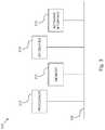
- FIG. 1Ais a simplified conceptual illustration of a system for reducing clock power consumption of a computer processor, constructed and operative in accordance with an embodiment of the disclosure
- FIG. 1Bis a circuit diagram illustrating an exemplary application of the disclosure
- FIG. 2is a simplified flowchart illustration of an exemplary method of operation of the system of FIG. 1 , operative in accordance with an embodiment of the disclosure.
- FIG. 3is a simplified block diagram illustration of an exemplary hardware implementation of a computing system, constructed and operative in accordance with an embodiment of the disclosure.
- FIG. 1Ais a simplified conceptual illustration of a system for reducing clock power consumption of a computer processor, constructed and operative in accordance with some embodiments of the present disclosure.
- a design analyzer 100is configured to analyze a model 102 of a computer processor design, such as where software model 102 is constructed in accordance with conventional techniques using a hardware description language, such as the VHSIC Hardware Description Language (VHDL).
- Design analyzer 100is, in some embodiments, configured to identify a set of circuits 104 that includes any, and in some embodiments, every circuit in model 102 that receives a clock signal.
- a computer processor simulator 106is configured, in accordance with conventional techniques, to perform a baseline simulation of the computer processor design using model 102 .
- computer processor simulator 106is configured to perform the baseline simulation by simulating the processing of a predefined set of instructions 108 and producing a baseline log 110 , where baseline log 110 , in some embodiments, indicates, for each instruction 108 processed during the baseline simulation, which circuits 104 received a clock signal, and at which cycles, during the simulated processing of the instruction, and the result of the instruction, hereinafter referred to as the baseline result of the instruction.
- instructions 108includes multiple versions of the instruction, where each version includes different operands and/or operand values, just in case different versions of an instruction cause different circuits 104 to receive a clock signal during the simulated processing of the instruction.
- Computer processor simulator 106is further configured to perform multiple comparison simulations of the computer processor design using model 102 , where a different comparison simulation is performed for any, and, in some embodiments, each, of the instructions in instructions 108 , and for any, and, in some embodiments, each, of the circuits 104 that received a clock signal when the instruction was processed during the baseline simulation.
- a different comparison simulationis performed for any, and, in some embodiments, each, of the instructions in instructions 108 , and for any, and, in some embodiments, each, of the circuits 104 that received a clock signal when the instruction was processed during the baseline simulation.
- the processing of one of instructions 108is simulated, during which processing a corruption signal is injected into one of the circuits 104 that received a clock signal when the instruction was processed during the baseline simulation.
- a corruption signalis injected into one of the circuits 104 that received a clock signal when the instruction was processed during the baseline simulation.
- an AND gate 120allows a clock signal 122 to reach circuit 118 due to a condition signal 124 being active at a specific cycle when processing a given instruction during the baseline simulation.
- the same instructionis processed, and one of the following corruption signals are injected into a data bus 126 of circuit 118 at the cycle when clock signal 122 reaches circuit 118 , in some embodiments, formatted to match the width of the bus:
- a simulation evaluator 114is configured to compare, for any given one of instructions 108 that was processed during a comparison simulation, the comparison result produced by the given instruction to the baseline result produced by the same instruction during the baseline simulation. If the comparison result of the instruction is identical to the baseline result of the same instruction, then the circuit 104 into which a corruption signal was injected during the comparison simulation of the instruction is, in some embodiments, designated by simulation evaluator 114 for clock gating for that instruction. Simulation evaluator 114 , in some embodiments, performs this comparison for each of the comparison simulations. Simulation evaluator 114 is, in some embodiments, configured, in accordance with conventional techniques, to provide a report indicating which circuits 104 are designated for clock gating and for which instructions.
- FIG. 1AAny of the elements shown in FIG. 1A are, in some embodiments, implemented by one or more computers in computer hardware and/or in computer software embodied in a non-transitory, computer-readable medium in accordance with conventional techniques, such as where any of the elements shown in FIG. 1A are hosted by a computer 116 .
- FIG. 2is a simplified flowchart illustration of an exemplary method of operation of the system of FIG. 1A , operative in accordance with some embodiments.
- a model of a computer processor designis analyzed to identify any circuits in the computer processor design that receive a clock signal (step 200 ).
- a baseline simulation of the computer processor designis performed using the model, in which the processing of a predefined set of instructions is simulated (step 202 ) and a baseline log is produced indicating, for each instruction processed during the baseline simulation, which circuits received a clock signal, and at which cycles, during the simulated processing of the instruction, and the baseline result of the instruction (step 204 ).
- a comparison simulationis performed for a combination of an instruction and a circuit that received a clock signal when the instruction was processed during the baseline simulation (step 206 ).
- a corruption signalis injected into the circuit during a clock-receiving cycle (step 208 ).
- Steps 206 and 208are, in some embodiments, performed for each unique combination of an instruction and a circuit that received a clock signal when the instruction was processed during the baseline simulation.
- a comparison logis produced indicating, for each instruction processed during the comparison simulations, which circuit received a corruption signal injection during the simulated processing of the instruction, and the comparison result of the instruction (step 210 ).
- step 212For any instruction who's comparison result is identical to the baseline result of the same instruction (step 212 ), the circuit into which a corruption signal was injected during the comparison simulation of the instruction is designated for clock gating for that instruction (step 214 ), and a report is provided indicating which circuits are designated for clock gating and for which instructions (step 216 ).
- the method of FIG. 2thus identifies, for a given instruction, any circuit that is activated by receiving a clock signal during a baseline simulated processing of the instruction. And by corrupting the circuit during a comparison simulated processing of the instruction, and determining that the corruption does not change the result of the instruction, the method of FIG. 2 thus determines that the circuit has no effect on the instruction being simulated, and therefore the circuit may be designated for clock gating for that instruction, such that it will no longer be activated when the instruction is processed, thereby conserving power.
- block diagram 300illustrates an exemplary hardware implementation of a computing system in accordance with which one or more components/methodologies of the disclosure (e.g., components/methodologies described in the context of FIGS. 1A-2 ) which may be implemented, according to some embodiments.
- Some embodimentsmay include a processor 310 , a memory 312 , I/O devices 314 , and a network interface 316 , coupled via a computer bus 318 or alternate connection arrangement.
- processoras used herein is intended to include any processing device, such as, for example, one that includes a CPU (central processing unit) and/or other processing circuitry. It is also to be understood that the term “processor” may refer to more than one processing device and that various elements associated with a processing device may be shared by other processing devices.
- memoryas used herein is intended to include memory associated with a processor or CPU, such as, for example, RAM, ROM, a fixed memory device (e.g., hard drive), a removable memory device (e.g., diskette), flash memory, etc. Such memory may be considered a computer readable storage medium.
- input/output devicesor “I/O devices” as used herein is intended to include, for example, one or more input devices (e.g., keyboard, mouse, scanner, etc.) for entering data to the processing unit, and/or one or more output devices (e.g., speaker, display, printer, etc.) for presenting results associated with the processing unit.
- input devicese.g., keyboard, mouse, scanner, etc.
- output devicese.g., speaker, display, printer, etc.
- Embodiments of the disclosuremay include a system, a method, and/or a computer program product.
- the computer program productmay include a computer readable storage medium (or media) having computer readable program instructions thereon for causing a processor to carry out aspects of the disclosure.
- the computer readable storage mediumcan be a tangible device that can retain and store instructions for use by an instruction execution device.
- the computer readable storage mediummay be, for example, but is not limited to, an electronic storage device, a magnetic storage device, an optical storage device, an electromagnetic storage device, a semiconductor storage device, or any suitable combination of the foregoing.
- a non-exhaustive list of more specific examples of the computer readable storage mediumincludes the following: a portable computer diskette, a hard disk, a random access memory (RAM), a read-only memory (ROM), an erasable programmable read-only memory (EPROM or Flash memory), a static random access memory (SRAM), a portable compact disc read-only memory (CD-ROM), a digital versatile disk (DVD), a memory stick, a floppy disk, a mechanically encoded device such as punch-cards or raised structures in a groove having instructions recorded thereon, and any suitable combination of the foregoing.
- RAMrandom access memory
- ROMread-only memory
- EPROM or Flash memoryerasable programmable read-only memory
- SRAMstatic random access memory
- CD-ROMcompact disc read-only memory
- DVDdigital versatile disk
- memory sticka floppy disk
- a mechanically encoded devicesuch as punch-cards or raised structures in a groove having instructions recorded thereon
- a computer readable storage mediumis not to be construed as being transitory signals per se, such as radio waves or other freely propagating electromagnetic waves, electromagnetic waves propagating through a waveguide or other transmission media (e.g., light pulses passing through a fiber-optic cable), or electrical signals transmitted through a wire.
- Computer readable program instructions described hereincan be downloaded to respective computing/processing devices from a computer readable storage medium or to an external computer or external storage device via a network, for example, the Internet, a local area network, a wide area network and/or a wireless network.
- the networkmay comprise copper transmission cables, optical transmission fibers, wireless transmission, routers, firewalls, switches, gateway computers and/or edge servers.
- a network adapter card or network interface in each computing/processing devicereceives computer readable program instructions from the network and forwards the computer readable program instructions for storage in a computer readable storage medium within the respective computing/processing device.
- Computer readable program instructions for carrying out operations of the disclosuremay be assembler instructions, instruction-set-architecture (ISA) instructions, machine instructions, machine dependent instructions, microcode, firmware instructions, state-setting data, or either source code or object code written in any combination of one or more programming languages, including an object oriented programming language such as Java, Smalltalk, C++ or the like, and conventional procedural programming languages, such as the “C” programming language or similar programming languages.
- the computer readable program instructionsmay execute entirely on the user's computer, partly on the user's computer, as a stand-alone software package, partly on the user's computer and partly on a remote computer or entirely on the remote computer or server.
- the remote computermay be connected to the user's computer through any type of network, including a local area network (LAN) or a wide area network (WAN), or the connection may be made to an external computer (for example, through the Internet using an Internet Service Provider).
- electronic circuitryincluding, for example, programmable logic circuitry, field-programmable gate arrays (FPGA), or programmable logic arrays (PLA) may execute the computer readable program instructions by utilizing state information of the computer readable program instructions to personalize the electronic circuitry, in order to perform aspects of the disclosure.
- These computer readable program instructionsmay be provided to a processor of a general purpose computer, special purpose computer, or other programmable data processing apparatus to produce a machine, such that the instructions, which execute via the processor of the computer or other programmable data processing apparatus, create means for implementing the functions/acts specified in the flowchart and/or block diagram block or blocks.
- These computer readable program instructionsmay also be stored in a computer readable storage medium that can direct a computer, a programmable data processing apparatus, and/or other devices to function in a particular manner, such that the computer readable storage medium having instructions stored therein comprises an article of manufacture including instructions which implement aspects of the function/act specified in the flowchart and/or block diagram block or blocks.
- the computer readable program instructionsmay also be loaded onto a computer, other programmable data processing apparatus, or other device to cause a series of operational steps to be performed on the computer, other programmable apparatus or other device to produce a computer implemented process, such that the instructions which execute on the computer, other programmable apparatus, or other device implement the functions/acts specified in the flowchart and/or block diagram block or blocks.
- each block in the flowchart or block diagramsmay represent a module, segment, or portion of instructions, which comprises one or more executable instructions for implementing the specified logical function(s).
- the functions noted in the blockmay occur out of the order noted in the figures.
- two blocks shown in successionmay, in fact, be executed substantially concurrently, or the blocks may sometimes be executed in the reverse order, depending upon the functionality involved.
Landscapes
- Engineering & Computer Science (AREA)
- Theoretical Computer Science (AREA)
- Physics & Mathematics (AREA)
- General Engineering & Computer Science (AREA)
- Computer Hardware Design (AREA)
- General Physics & Mathematics (AREA)
- Evolutionary Computation (AREA)
- Geometry (AREA)
- Computing Systems (AREA)
- Quality & Reliability (AREA)
- Debugging And Monitoring (AREA)
Abstract
Description
- 0x5555 . . . (binary 01010101 . . . )
- 0xAAAA . . . (binary 10101010 . . . )
- 0xFFFF . . . (binary 11111111 . . . )
- 0x0000 . . . (binary 00000000 . . . )
The comparison simulation of the same instruction is, in some embodiments, repeated such that a different corruption signal is injected during each such simulation.Computer processor simulator 106, in some embodiments, produces acomparison log 112, which, in some embodiments, indicates, for eachinstruction 108 processed during the comparison simulations, whichcircuit 104 received a corruption signal during the simulated processing of the instruction, and the result of the instruction, hereinafter referred to as the comparison result of the instruction.
Claims (3)
Priority Applications (1)
| Application Number | Priority Date | Filing Date | Title |
|---|---|---|---|
| US15/857,699US10614183B2 (en) | 2017-06-26 | 2017-12-29 | Reducing clock power consumption of a computer processor |
Applications Claiming Priority (2)
| Application Number | Priority Date | Filing Date | Title |
|---|---|---|---|
| US15/632,642US10585995B2 (en) | 2017-06-26 | 2017-06-26 | Reducing clock power consumption of a computer processor |
| US15/857,699US10614183B2 (en) | 2017-06-26 | 2017-12-29 | Reducing clock power consumption of a computer processor |
Related Parent Applications (1)
| Application Number | Title | Priority Date | Filing Date |
|---|---|---|---|
| US15/632,642ContinuationUS10585995B2 (en) | 2017-06-26 | 2017-06-26 | Reducing clock power consumption of a computer processor |
Publications (2)
| Publication Number | Publication Date |
|---|---|
| US20180373611A1 US20180373611A1 (en) | 2018-12-27 |
| US10614183B2true US10614183B2 (en) | 2020-04-07 |
Family
ID=64692628
Family Applications (3)
| Application Number | Title | Priority Date | Filing Date |
|---|---|---|---|
| US15/632,642Expired - Fee RelatedUS10585995B2 (en) | 2017-06-26 | 2017-06-26 | Reducing clock power consumption of a computer processor |
| US15/857,699Expired - Fee RelatedUS10614183B2 (en) | 2017-06-26 | 2017-12-29 | Reducing clock power consumption of a computer processor |
| US15/903,697Expired - Fee RelatedUS10296687B2 (en) | 2017-06-26 | 2018-02-23 | Reducing clock power consumption of a computer processor |
Family Applications Before (1)
| Application Number | Title | Priority Date | Filing Date |
|---|---|---|---|
| US15/632,642Expired - Fee RelatedUS10585995B2 (en) | 2017-06-26 | 2017-06-26 | Reducing clock power consumption of a computer processor |
Family Applications After (1)
| Application Number | Title | Priority Date | Filing Date |
|---|---|---|---|
| US15/903,697Expired - Fee RelatedUS10296687B2 (en) | 2017-06-26 | 2018-02-23 | Reducing clock power consumption of a computer processor |
Country Status (1)
| Country | Link |
|---|---|
| US (3) | US10585995B2 (en) |
Families Citing this family (1)
| Publication number | Priority date | Publication date | Assignee | Title |
|---|---|---|---|---|
| JP7475380B2 (en)* | 2022-01-31 | 2024-04-26 | キヤノン株式会社 | Imaging apparatus, device, and control method and program thereof |
Citations (19)
| Publication number | Priority date | Publication date | Assignee | Title |
|---|---|---|---|---|
| US4727545A (en) | 1986-09-02 | 1988-02-23 | Digital Equipment Corporation | Method and apparatus for isolating faults in a digital logic circuit |
| US20030192017A1 (en) | 2002-04-04 | 2003-10-09 | International Business Machines Corporation | Apparatus and method for representing gated-clock latches for phase abstraction |
| US20030192018A1 (en) | 2002-04-04 | 2003-10-09 | International Business Machines Corporation | Apparatus and method for automated use of phase abstraction for enhanced verification of circuit designs |
| US20050028118A1 (en)* | 2003-08-01 | 2005-02-03 | Atrenta, Inc. | Identification and implementation of clock gating in the design of integrated circuits |
| US7080334B2 (en) | 2003-05-09 | 2006-07-18 | Incentia Design Systems Corp. | Automatic clock gating insertion in an IC design |
| US20080301604A1 (en) | 2007-05-30 | 2008-12-04 | Alexander Itskovich | Apparatus for and method of estimating the quality of clock gating solutions for integrated circuit design |
| US20090055668A1 (en)* | 2007-08-21 | 2009-02-26 | Ibm Corporation | Method and Apparatus for Detecting Clock Gating Opportunities in a Pipelined Electronic Circuit Design |
| US7542728B2 (en) | 2006-02-09 | 2009-06-02 | Altair Semiconductor Ltd. | Dual-function wireless data terminal |
| US20090282377A1 (en)* | 2008-05-09 | 2009-11-12 | Fujitsu Limited | Verification support apparatus, verification support method, and computer product |
| US20100058146A1 (en) | 2007-12-12 | 2010-03-04 | Hanan Weingarten | Chien-search system employing a clock-gating scheme to save power for error correction decoder and other applications |
| US7712062B2 (en) | 2004-06-01 | 2010-05-04 | Tai An Ly | Metastability effects simulation for a circuit description |
| US20110218779A1 (en)* | 2010-03-05 | 2011-09-08 | Vasant Palisetti | Identification of Critical Enables Using MEA and WAA Metrics |
| US20120166168A1 (en)* | 2010-12-23 | 2012-06-28 | Oracle International Corporation | Methods and systems for fault-tolerant power analysis |
| US8244515B2 (en) | 2007-08-21 | 2012-08-14 | International Business Machines Corporation | Structure for detecting clock gating opportunities in a pipelined electronic circuit design |
| US20140258948A1 (en) | 2013-03-07 | 2014-09-11 | Cadence Design Systems, Inc. | Design synthesis of clock gated circuit |
| US9311102B2 (en) | 2010-07-13 | 2016-04-12 | Advanced Micro Devices, Inc. | Dynamic control of SIMDs |
| US20170351318A1 (en) | 2016-06-02 | 2017-12-07 | Northwestern University | System and method for associative power and clock management with instruction governed operation for power efficient computing |
| US20170357302A1 (en) | 2016-06-10 | 2017-12-14 | Apple Inc. | Processor unit efficiency control |
| US20180107264A1 (en) | 2016-10-13 | 2018-04-19 | International Business Machines Corporation | Managing power consumption of a gated clock mesh |
- 2017
- 2017-06-26USUS15/632,642patent/US10585995B2/ennot_activeExpired - Fee Related
- 2017-12-29USUS15/857,699patent/US10614183B2/ennot_activeExpired - Fee Related
- 2018
- 2018-02-23USUS15/903,697patent/US10296687B2/ennot_activeExpired - Fee Related
Patent Citations (21)
| Publication number | Priority date | Publication date | Assignee | Title |
|---|---|---|---|---|
| US4727545A (en) | 1986-09-02 | 1988-02-23 | Digital Equipment Corporation | Method and apparatus for isolating faults in a digital logic circuit |
| US20030192017A1 (en) | 2002-04-04 | 2003-10-09 | International Business Machines Corporation | Apparatus and method for representing gated-clock latches for phase abstraction |
| US20030192018A1 (en) | 2002-04-04 | 2003-10-09 | International Business Machines Corporation | Apparatus and method for automated use of phase abstraction for enhanced verification of circuit designs |
| US6745377B2 (en) | 2002-04-04 | 2004-06-01 | International Business Machines Corporation | Apparatus and method for representing gated-clock latches for phase abstraction |
| US7080334B2 (en) | 2003-05-09 | 2006-07-18 | Incentia Design Systems Corp. | Automatic clock gating insertion in an IC design |
| US20050028118A1 (en)* | 2003-08-01 | 2005-02-03 | Atrenta, Inc. | Identification and implementation of clock gating in the design of integrated circuits |
| US7712062B2 (en) | 2004-06-01 | 2010-05-04 | Tai An Ly | Metastability effects simulation for a circuit description |
| US7542728B2 (en) | 2006-02-09 | 2009-06-02 | Altair Semiconductor Ltd. | Dual-function wireless data terminal |
| US20080301604A1 (en) | 2007-05-30 | 2008-12-04 | Alexander Itskovich | Apparatus for and method of estimating the quality of clock gating solutions for integrated circuit design |
| US20090055668A1 (en)* | 2007-08-21 | 2009-02-26 | Ibm Corporation | Method and Apparatus for Detecting Clock Gating Opportunities in a Pipelined Electronic Circuit Design |
| US8244515B2 (en) | 2007-08-21 | 2012-08-14 | International Business Machines Corporation | Structure for detecting clock gating opportunities in a pipelined electronic circuit design |
| US20100058146A1 (en) | 2007-12-12 | 2010-03-04 | Hanan Weingarten | Chien-search system employing a clock-gating scheme to save power for error correction decoder and other applications |
| US20090282377A1 (en)* | 2008-05-09 | 2009-11-12 | Fujitsu Limited | Verification support apparatus, verification support method, and computer product |
| US20110218779A1 (en)* | 2010-03-05 | 2011-09-08 | Vasant Palisetti | Identification of Critical Enables Using MEA and WAA Metrics |
| US9311102B2 (en) | 2010-07-13 | 2016-04-12 | Advanced Micro Devices, Inc. | Dynamic control of SIMDs |
| US20120166168A1 (en)* | 2010-12-23 | 2012-06-28 | Oracle International Corporation | Methods and systems for fault-tolerant power analysis |
| US20140258948A1 (en) | 2013-03-07 | 2014-09-11 | Cadence Design Systems, Inc. | Design synthesis of clock gated circuit |
| US9003339B2 (en) | 2013-03-07 | 2015-04-07 | Cadence Design Systems, Inc. | Synthesis of clock gated circuit |
| US20170351318A1 (en) | 2016-06-02 | 2017-12-07 | Northwestern University | System and method for associative power and clock management with instruction governed operation for power efficient computing |
| US20170357302A1 (en) | 2016-06-10 | 2017-12-14 | Apple Inc. | Processor unit efficiency control |
| US20180107264A1 (en) | 2016-10-13 | 2018-04-19 | International Business Machines Corporation | Managing power consumption of a gated clock mesh |
Non-Patent Citations (8)
| Title |
|---|
| Accelerated Examination Support Document, dated Feb. 15, 2018, 14 pages. |
| Barak et al., "Reducing Clock Power Consumption of a Computer Processor," U.S. Appl. No. 15/632,642, filed Jun. 26, 2017. |
| Barak et al., "Reducing Clock Power Consumption of a Computer Processor," U.S. Appl. No. 15/903,697, filed Feb. 23, 2018. |
| Benini et al., "A Refinement Methodology for Clock Gating Optimization at Layout Level in Digital Circuits," Journal of Low Power Electronics, vol. 6, No. 1, Apr. 2010, pp. 44-55, (abstract provided), American Scientific Publishers. DOI: 10.1166/jolpe.2010.1055. |
| List of IBM Patents or Patent Applications Treated as Related, Dated Dec. 28, 2017, 2 pages. |
| List of IBM Patents or Patent Applications Treated as Related, Filed Feb. 23, 2018, 2 pages. |
| Pandey et al., "Clock Gating Aware Low Power ALU Design and Implementation on FPGA," International Journal of Future Computer and Communication, vol. 2, No. 5, Oct. 2013, pp. 461-465. DOI: 10.7763/IJFCC.2013.V2.206. |
| Wimer et al., "The Optimal Fan-Out of Clock Network for Power Minimization by Adaptive Gating," IEEE Transactions on Very Large Scale Integration (VLSI) Systems, vol. 20, No. 10, Oct. 2012, pp. 1772-1780. DOI: 10.1109/TVLSI.2011.2162861. |
Also Published As
| Publication number | Publication date |
|---|---|
| US20180373828A1 (en) | 2018-12-27 |
| US10585995B2 (en) | 2020-03-10 |
| US20180373611A1 (en) | 2018-12-27 |
| US10296687B2 (en) | 2019-05-21 |
| US20180373610A1 (en) | 2018-12-27 |
Similar Documents
| Publication | Publication Date | Title |
|---|---|---|
| US9632917B2 (en) | Software testing | |
| US10324816B2 (en) | Checking a computer processor design for soft error handling | |
| US11176248B2 (en) | Remediation of security vulnerabilities in computer software | |
| US10380285B2 (en) | Static timing analysis in circuit design | |
| US9542298B2 (en) | Reducing resource overhead in verbose trace using recursive object pruning prior to string serialization | |
| US10055335B2 (en) | Programming assistance to identify suboptimal performing code and suggesting alternatives | |
| US20200104452A1 (en) | Integrated circuit design with optimized timing constraint configuration | |
| US9329979B2 (en) | Derivation of generalized test cases | |
| US10614183B2 (en) | Reducing clock power consumption of a computer processor | |
| US10127132B2 (en) | Optimizing automated interactions with web applications | |
| US9069892B2 (en) | Reducing false-positive errors in a software change-impact analysis | |
| US11023627B2 (en) | Modeling and cooperative simulation of systems with interdependent discrete and continuous elements | |
| US20160371171A1 (en) | Stream-based breakpoint for too many tuple creations | |
| US10157049B2 (en) | Static analysis with input reduction | |
| US20180322427A1 (en) | System and method for time critical automation | |
| US10324815B2 (en) | Error checking of a multi-threaded computer processor design under test | |
| US9069562B2 (en) | Mobile computing program slicing and behavior | |
| US9239927B2 (en) | Static analysis for discovery of timing attack vulnerabilities in a computer software application | |
| US10606971B2 (en) | Testing netlists based on singular independent signals | |
| US10885462B2 (en) | Determine an interval duration and a training period length for log anomaly detection |
Legal Events
| Date | Code | Title | Description |
|---|---|---|---|
| AS | Assignment | Owner name:INTERNATIONAL BUSINESS MACHINES CORPORATION, NEW YORK Free format text:ASSIGNMENT OF ASSIGNORS INTEREST;ASSIGNORS:BARAK, EREZ;BIRAN, GIORA;TURI, AMIR;AND OTHERS;SIGNING DATES FROM 20170613 TO 20170620;REEL/FRAME:044503/0862 Owner name:INTERNATIONAL BUSINESS MACHINES CORPORATION, NEW Y Free format text:ASSIGNMENT OF ASSIGNORS INTEREST;ASSIGNORS:BARAK, EREZ;BIRAN, GIORA;TURI, AMIR;AND OTHERS;SIGNING DATES FROM 20170613 TO 20170620;REEL/FRAME:044503/0862 | |
| FEPP | Fee payment procedure | Free format text:ENTITY STATUS SET TO UNDISCOUNTED (ORIGINAL EVENT CODE: BIG.); ENTITY STATUS OF PATENT OWNER: LARGE ENTITY | |
| STPP | Information on status: patent application and granting procedure in general | Free format text:DOCKETED NEW CASE - READY FOR EXAMINATION | |
| STPP | Information on status: patent application and granting procedure in general | Free format text:NON FINAL ACTION MAILED | |
| STPP | Information on status: patent application and granting procedure in general | Free format text:RESPONSE TO NON-FINAL OFFICE ACTION ENTERED AND FORWARDED TO EXAMINER | |
| STPP | Information on status: patent application and granting procedure in general | Free format text:NOTICE OF ALLOWANCE MAILED -- APPLICATION RECEIVED IN OFFICE OF PUBLICATIONS | |
| ZAAA | Notice of allowance and fees due | Free format text:ORIGINAL CODE: NOA | |
| ZAAB | Notice of allowance mailed | Free format text:ORIGINAL CODE: MN/=. | |
| STPP | Information on status: patent application and granting procedure in general | Free format text:PUBLICATIONS -- ISSUE FEE PAYMENT RECEIVED | |
| STCF | Information on status: patent grant | Free format text:PATENTED CASE | |
| FEPP | Fee payment procedure | Free format text:MAINTENANCE FEE REMINDER MAILED (ORIGINAL EVENT CODE: REM.); ENTITY STATUS OF PATENT OWNER: LARGE ENTITY | |
| LAPS | Lapse for failure to pay maintenance fees | Free format text:PATENT EXPIRED FOR FAILURE TO PAY MAINTENANCE FEES (ORIGINAL EVENT CODE: EXP.); ENTITY STATUS OF PATENT OWNER: LARGE ENTITY | |
| STCH | Information on status: patent discontinuation | Free format text:PATENT EXPIRED DUE TO NONPAYMENT OF MAINTENANCE FEES UNDER 37 CFR 1.362 | |
| FP | Lapsed due to failure to pay maintenance fee | Effective date:20240407 |