US10613447B2 - Lithographic apparatus and device manufacturing method - Google Patents
Lithographic apparatus and device manufacturing methodDownload PDFInfo
- Publication number
- US10613447B2 US10613447B2US15/794,256US201715794256AUS10613447B2US 10613447 B2US10613447 B2US 10613447B2US 201715794256 AUS201715794256 AUS 201715794256AUS 10613447 B2US10613447 B2US 10613447B2
- Authority
- US
- United States
- Prior art keywords
- substrate
- liquid
- barrier member
- outlet opening
- fluid outlet
- Prior art date
- Legal status (The legal status is an assumption and is not a legal conclusion. Google has not performed a legal analysis and makes no representation as to the accuracy of the status listed.)
- Expired - Fee Related
Links
- 238000004519manufacturing processMethods0.000titledescription11
- 239000000758substrateSubstances0.000claimsabstractdescription194
- 239000007788liquidSubstances0.000claimsabstractdescription138
- 230000004888barrier functionEffects0.000claimsabstractdescription95
- 238000007654immersionMethods0.000claimsabstractdescription33
- 239000012530fluidSubstances0.000claimsdescription26
- 230000005855radiationEffects0.000claimsdescription23
- 230000002093peripheral effectEffects0.000claims3
- 238000000059patterningMethods0.000description21
- 230000003287optical effectEffects0.000description14
- 238000003384imaging methodMethods0.000description8
- 238000005286illuminationMethods0.000description6
- 230000033001locomotionEffects0.000description6
- 239000010410layerSubstances0.000description5
- 230000005540biological transmissionEffects0.000description3
- XLYOFNOQVPJJNP-UHFFFAOYSA-NwaterSubstancesOXLYOFNOQVPJJNP-UHFFFAOYSA-N0.000description3
- 230000000694effectsEffects0.000description2
- 239000011796hollow space materialSubstances0.000description2
- 238000001459lithographyMethods0.000description2
- 230000010363phase shiftEffects0.000description2
- 230000003068static effectEffects0.000description2
- XUIMIQQOPSSXEZ-UHFFFAOYSA-NSiliconChemical compound[Si]XUIMIQQOPSSXEZ-UHFFFAOYSA-N0.000description1
- 230000003044adaptive effectEffects0.000description1
- 238000003491arrayMethods0.000description1
- 230000002238attenuated effectEffects0.000description1
- 230000015572biosynthetic processEffects0.000description1
- 230000001143conditioned effectEffects0.000description1
- 238000001514detection methodMethods0.000description1
- 230000009977dual effectEffects0.000description1
- 230000005670electromagnetic radiationEffects0.000description1
- 238000007689inspectionMethods0.000description1
- 230000003993interactionEffects0.000description1
- 239000002346layers by functionSubstances0.000description1
- 239000004973liquid crystal related substanceSubstances0.000description1
- 230000005381magnetic domainEffects0.000description1
- 239000000463materialSubstances0.000description1
- 239000011159matrix materialSubstances0.000description1
- 230000015654memoryEffects0.000description1
- 230000005499meniscusEffects0.000description1
- QSHDDOUJBYECFT-UHFFFAOYSA-NmercuryChemical compound[Hg]QSHDDOUJBYECFT-UHFFFAOYSA-N0.000description1
- 229910052753mercuryInorganic materials0.000description1
- 210000001747pupilAnatomy0.000description1
- 238000007493shaping processMethods0.000description1
- 229910052710siliconInorganic materials0.000description1
- 239000010703siliconSubstances0.000description1
- 239000010409thin filmSubstances0.000description1
Images


Classifications
- G—PHYSICS
- G03—PHOTOGRAPHY; CINEMATOGRAPHY; ANALOGOUS TECHNIQUES USING WAVES OTHER THAN OPTICAL WAVES; ELECTROGRAPHY; HOLOGRAPHY
- G03F—PHOTOMECHANICAL PRODUCTION OF TEXTURED OR PATTERNED SURFACES, e.g. FOR PRINTING, FOR PROCESSING OF SEMICONDUCTOR DEVICES; MATERIALS THEREFOR; ORIGINALS THEREFOR; APPARATUS SPECIALLY ADAPTED THEREFOR
- G03F7/00—Photomechanical, e.g. photolithographic, production of textured or patterned surfaces, e.g. printing surfaces; Materials therefor, e.g. comprising photoresists; Apparatus specially adapted therefor
- G03F7/70—Microphotolithographic exposure; Apparatus therefor
- G03F7/708—Construction of apparatus, e.g. environment aspects, hygiene aspects or materials
- G03F7/70858—Environment aspects, e.g. pressure of beam-path gas, temperature
- G03F7/70866—Environment aspects, e.g. pressure of beam-path gas, temperature of mask or workpiece
- G—PHYSICS
- G03—PHOTOGRAPHY; CINEMATOGRAPHY; ANALOGOUS TECHNIQUES USING WAVES OTHER THAN OPTICAL WAVES; ELECTROGRAPHY; HOLOGRAPHY
- G03F—PHOTOMECHANICAL PRODUCTION OF TEXTURED OR PATTERNED SURFACES, e.g. FOR PRINTING, FOR PROCESSING OF SEMICONDUCTOR DEVICES; MATERIALS THEREFOR; ORIGINALS THEREFOR; APPARATUS SPECIALLY ADAPTED THEREFOR
- G03F7/00—Photomechanical, e.g. photolithographic, production of textured or patterned surfaces, e.g. printing surfaces; Materials therefor, e.g. comprising photoresists; Apparatus specially adapted therefor
- G03F7/20—Exposure; Apparatus therefor
- G03F7/2041—Exposure; Apparatus therefor in the presence of a fluid, e.g. immersion; using fluid cooling means
- G—PHYSICS
- G03—PHOTOGRAPHY; CINEMATOGRAPHY; ANALOGOUS TECHNIQUES USING WAVES OTHER THAN OPTICAL WAVES; ELECTROGRAPHY; HOLOGRAPHY
- G03F—PHOTOMECHANICAL PRODUCTION OF TEXTURED OR PATTERNED SURFACES, e.g. FOR PRINTING, FOR PROCESSING OF SEMICONDUCTOR DEVICES; MATERIALS THEREFOR; ORIGINALS THEREFOR; APPARATUS SPECIALLY ADAPTED THEREFOR
- G03F7/00—Photomechanical, e.g. photolithographic, production of textured or patterned surfaces, e.g. printing surfaces; Materials therefor, e.g. comprising photoresists; Apparatus specially adapted therefor
- G03F7/70—Microphotolithographic exposure; Apparatus therefor
- G03F7/70216—Mask projection systems
- G03F7/70341—Details of immersion lithography aspects, e.g. exposure media or control of immersion liquid supply
- G—PHYSICS
- G03—PHOTOGRAPHY; CINEMATOGRAPHY; ANALOGOUS TECHNIQUES USING WAVES OTHER THAN OPTICAL WAVES; ELECTROGRAPHY; HOLOGRAPHY
- G03F—PHOTOMECHANICAL PRODUCTION OF TEXTURED OR PATTERNED SURFACES, e.g. FOR PRINTING, FOR PROCESSING OF SEMICONDUCTOR DEVICES; MATERIALS THEREFOR; ORIGINALS THEREFOR; APPARATUS SPECIALLY ADAPTED THEREFOR
- G03F7/00—Photomechanical, e.g. photolithographic, production of textured or patterned surfaces, e.g. printing surfaces; Materials therefor, e.g. comprising photoresists; Apparatus specially adapted therefor
- G03F7/70—Microphotolithographic exposure; Apparatus therefor
- G03F7/708—Construction of apparatus, e.g. environment aspects, hygiene aspects or materials
- G03F7/70858—Environment aspects, e.g. pressure of beam-path gas, temperature
Definitions
- the present inventionrelates to a lithographic apparatus, a device manufacturing method and device manufactured thereby.
- a lithographic apparatusis a machine that applies a desired pattern onto a target portion of a substrate.
- Lithographic apparatuscan be used, for example, in the manufacture of integrated circuits (ICs).
- a patterning devicesuch as a mask, may be used to generate a circuit pattern corresponding to an individual layer of the IC, and this pattern can be imaged onto a target portion (e.g. comprising part of, one or several dies) on a substrate (e.g. a silicon wafer) that has a layer of radiation-sensitive material (resist).
- a single substratewill contain a network of adjacent target portions that are successively exposed.
- lithographic apparatusinclude so-called steppers, in which each target portion is irradiated by exposing an entire pattern onto the target portion at one time, and so-called scanners, in which each target portion is irradiated by scanning the pattern through the projection beam in a given direction (the “scanning”-direction) while synchronously scanning the substrate parallel or anti-parallel to this direction.
- liquid supply systemto provide liquid on only a localized area of the substrate and in between the final element of the projection system and the substrate using a liquid supply system (the substrate generally has a larger surface area than the final element of the projection system).
- the substrategenerally has a larger surface area than the final element of the projection system.
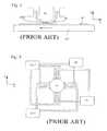
- liquidis supplied by at least one inlet IN onto the substrate, preferably along the direction of movement of the substrate relative to the final element, and is removed by at least one outlet OUT after having passed under the projection system.
- FIG. 2shows the arrangement schematically in which liquid is supplied via inlet IN and is taken up on the other side of the element by outlet OUT which is connected to a low pressure source.
- the liquidis supplied along the direction of movement of the substrate relative to the final element, though this does not need to be the case.
- FIG. 3Various orientations and numbers of in- and out-lets positioned around the final element are possible, one example is illustrated in FIG. 3 in which four sets of an inlet with an outlet on either side are provided in a regular pattern around the final element.
- a liquid supply system in a second solutionmay be provided that comprises a seal member which extends along at least a part of a boundary of the space between the final element of the projection system and the substrate table.
- the seal memberis substantially stationary relative to the projection system in the XY plane though there may be some relative movement in the Z direction (in the direction of the optical axis).
- a sealis formed between the seal member and the surface of the substrate.
- the sealis a contactless seal such as a gas seal.
- a third solution that may be providedcomprises a member attached to the projection system which forms a hollow space underneath the final element of the projection system.
- the bottom of the memberis provided close enough to the surface of the substrate such that capillary forces are strong enough to contain the immersion liquid in the hollow space created by the member between the final element of the projection system and the substrate.
- each of the solutionsmay be improved.
- the first solutionhas proved to be hard to implement without large and uncontrolled liquid spillage.
- the second and third solutionsmay deleteriously transmit disturbance forces to the substrate and/or projection system because of their close interaction with the surface of the substrate which is necessary in order to keep the liquid in the space.
- each of the solutionsmay not be particularly well suited for imaging objects of different height on the substrate table, such as through lens sensors. There is not a great deal of available space with these systems between the projection system and the substrate and building a liquid supply system which can operate at high NA can be difficult.
- Each of the solutionsmay present difficulties with the imaging of edge portions of the substrate, such as the gas seal may become unbalanced when it is partly positioned over the edge of the substrate and/or the capillary force can be lost when imaging edge portions.
- These solutionsall work best with a low free working distance (which would advantageously be higher) and with high fluid pressures (which would advantageously be lower).
- a lithographic apparatuscomprising:
- an illumination systemconfigured to provide a beam of radiation
- a support structureconfigured to hold a patterning device, the patterning device configured to impart the beam with a pattern in its cross-section;
- a substrate tableconfigured to hold a substrate
- a projection systemconfigured to project the patterned beam onto a target portion of the substrate
- a liquid supply systemconfigured to provide an immersion liquid to a space between the substrate and the projection system, the liquid supply system comprising a barrier member extending along at least a part of the boundary of the space and being in a position relative to an object on the substrate table so that any capillary pressure generated by the immersion liquid between the barrier member and the object is not large enough to constrain the immersion liquid in the space,
- the immersion liquidis allowed to leak out of the space between the bottom of the barrier member and the substrate and is thereby not constrained in the space.
- the transmission of disturbance forces between the projection system, the barrier member and the substratemay be reduced or minimized.
- a high rate of liquid replenishment in the spacemay be possible without the necessity for the use of high liquid pressures.
- the force in the direction of the optical axis on the substrate tablemay also be reduced and be more constant in comparison to other liquid supply systems.
- the imaging of edge portionsmay become easier as complicated measures are not necessary as the barrier member passes over the edge of the substrate as there is no seal to be disturbed at the edge of the substrate.
- the simplicity of the barrier membermay be increased as only liquid inlets are required and no gas supplies. The lack of gas supplies means that the chance of bubble formation in the immersion liquid which can deleteriously affect the imaging quality may be reduced or minimized.
- a larger free working distance(the distance between the projection system and the substrate) may be increased compared to other supply systems.
- the apparatusfurther comprises at least one outlet to remove immersion liquid, the outlet being radially outwardly of the barrier member.
- immersion liquid which has spilled from the localized area of the supply systemi.e. the area under the projection system
- the outletis on the substrate table.
- the barrier memberis mechanically isolated from the projection system so that disturbance forces are not automatically transmitted to the projection system by the barrier member.
- the barrier memberis connected to a base frame which supports the substrate table and/or a projection system frame which supports the projection system.
- the barrier memberis free to move in the direction of an optical axis of the projection system.
- the apparatusmay comprise an actuator configured to adjust the height and/or tilt of the barrier member relative to the substrate.
- a device manufacturing methodcomprising:
- a devicemanufactured according to the above-referenced device manufacturing method and/or by the above-referenced lithographic apparatus.
- lithographic apparatusin the manufacture of ICs, it should be understood that the lithographic apparatus described herein may have other applications, such as the manufacture of integrated optical systems, guidance and detection patterns for magnetic domain memories, liquid-crystal displays (LCDs), thin-film magnetic heads, etc.
- LCDsliquid-crystal displays
- any use of the terms “wafer” or “die” hereinmay be considered as synonymous with the more general terms “substrate” or “target portion”, respectively.
- the substrate referred to hereinmay be processed, before or after exposure, in for example a track (a tool that typically applies a layer of resist to a substrate and develops the exposed resist) or a metrology or inspection tool.
- the disclosure hereinmay be applied to such and other substrate processing tools.
- the substratemay be processed more than once, for example in order to create a multi-layer IC, so that the term substrate used herein may also refer to a substrate that already contains multiple processed layers.
- UV radiatione.g. having a wavelength of 365, 248, 193, 157 or 126 nm.
- patterning deviceused herein should be broadly interpreted as referring to any device that can be used to impart a projection beam with a pattern in its cross-section such as to create a pattern in a target portion of the substrate. It should be noted that the pattern imparted to the projection beam may not exactly correspond to the desired pattern in the target portion of the substrate. Generally, the pattern imparted to the projection beam will correspond to a particular functional layer in a device being created in the target portion, such as an integrated circuit.
- a patterning devicemay be transmissive or reflective.
- Examples of patterning devicesinclude masks, programmable mirror arrays, and programmable LCD panels.
- Masksare well known in lithography, and include mask types such as binary, alternating phase-shift, and attenuated phase-shift, as well as various hybrid mask types.
- An example of a programmable mirror arrayemploys a matrix arrangement of small mirrors, each of which can be individually tilted so as to reflect an incoming radiation beam in different directions; in this manner, the reflected beam is patterned.
- the support structuremay be a frame or table, for example, which may be fixed or movable as required and which may ensure that the patterning device is at a desired position, for example with respect to the projection system. Any use of the terms “reticle” or “mask” herein may be considered synonymous with the more general term “patterning device”.
- projection systemused herein should be broadly interpreted as encompassing various types of projection system, including refractive optical systems, reflective optical systems, and catadioptric optical systems, as appropriate for example for the exposure radiation being used, or for other factors such as the use of an immersion fluid or the use of a vacuum. Any use of the term “lens” herein may be considered as synonymous with the more general term “projection system”.
- the illumination systemmay also encompass various types of optical components, including refractive, reflective, and catadioptric optical components for directing, shaping, or controlling the projection beam of radiation, and such components may also be referred to below, collectively or singularly, as a “lens”.
- the lithographic apparatusmay be of a type having two (dual stage) or more substrate tables (and/or two or more mask tables). In such “multiple stage” machines the additional tables may be used in parallel, or preparatory steps may be carried out on one or more tables while one or more other tables are being used for exposure.
- FIG. 1depicts a lithographic apparatus according to an embodiment of the invention
- FIG. 2illustrates, in cross-section, a liquid supply system of the prior art
- FIG. 3illustrates, in plan, the liquid supply system of FIG. 2 ;
- FIG. 4illustrates the liquid supply system according to an embodiment of the present invention.
- FIG. 1schematically depicts a lithographic apparatus according to a particular embodiment of the invention.
- the apparatuscomprises:
- an illumination system (illuminator) ILfor providing a projection beam PB of radiation (e.g. UV radiation);
- a first support structuree.g. a mask table
- a patterning devicee.g. a mask
- PMa first positioning device
- a substrate tablee.g. a wafer table
- a substratee.g. a resist-coated wafer
- PWa second positioning device
- a projection systeme.g. a refractive projection lens
- PLfor imaging a pattern imparted to the projection beam PB by patterning device MA onto a target portion C (e.g. comprising one or more dies) of the substrate W.
- the apparatusis of a transmissive type (e.g. employing a transmissive mask).
- the apparatusmay be of a reflective type (e.g. employing a programmable mirror array of a type as referred to above).
- the illuminator ILreceives a beam of radiation from a radiation source SO.
- the source and the lithographic apparatusmay be separate entities, for example when the source is an excimer laser. In such cases, the source is not considered to form part of the lithographic apparatus and the radiation beam is passed from the source SO to the illuminator IL with the aid of a beam delivery system BD comprising for example suitable directing mirrors and/or a beam expander. In other cases the source may be integral part of the apparatus, for example when the source is a mercury lamp.
- the source SO and the illuminator IL, together with the beam delivery system BD if required,may be referred to as a radiation system.
- the illuminator ILmay comprise an adjusting device AM for adjusting the angular intensity distribution of the beam.
- an adjusting device AMfor adjusting the angular intensity distribution of the beam.
- the illuminator ILgenerally comprises various other components, such as an integrator IN and a condenser CO.
- the illuminatorprovides a conditioned beam of radiation, referred to as the projection beam PB, having a desired uniformity and intensity distribution in its cross-section.
- the projection beam PBis incident on the mask MA, which is held on the mask table MT. Having traversed the mask MA, the projection beam PB passes through the lens PL, which focuses the beam onto a target portion C of the substrate W.
- the substrate table WTcan be moved accurately, e.g. so as to position different target portions C in the path of the beam PB.
- the first positioning device PM and another position sensorcan be used to accurately position the mask MA with respect to the path of the beam PB, e.g. after mechanical retrieval from a mask library, or during a scan.
- the mask table MTmay be connected to a short stroke actuator only, or may be fixed.
- Mask MA and substrate Wmay be aligned using mask alignment marks M 1 , M 2 and substrate alignment marks P 1 , P 2 .
- step modethe mask table MT and the substrate table WT are kept essentially stationary, while an entire pattern imparted to the projection beam is projected onto a target portion C in one go (i.e. a single static exposure).
- the substrate table WTis then shifted in the X and/or Y direction so that a different target portion C can be exposed.
- step modethe maximum size of the exposure field limits the size of the target portion C imaged in a single static exposure.
- the mask table MT and the substrate table WTare scanned synchronously while a pattern imparted to the projection beam is projected onto a target portion C (i.e. a single dynamic exposure).
- the velocity and direction of the substrate table WT relative to the mask table MTis determined by the (de-) magnification and image reversal characteristics of the projection system PL.
- the maximum size of the exposure fieldlimits the width (in the non-scanning direction) of the target portion in a single dynamic exposure, whereas the length of the scanning motion determines the height (in the scanning direction) of the target portion.
- the mask table MTis kept essentially stationary holding a programmable patterning device, and the substrate table WT is moved or scanned while a pattern imparted to the projection beam is projected onto a target portion C.
- a pulsed radiation sourceis employed and the programmable patterning device is updated as required after each movement of the substrate table WT or in between successive radiation pulses during a scan.
- This mode of operationcan be readily applied to maskless lithography that utilizes a programmable patterning device, such as a programmable mirror array of a type as referred to above.
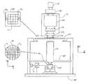
- FIG. 4shows a liquid supply system according to an embodiment of the present invention.
- the liquid supply systemcomprises a barrier member 10 .
- the barrier member 10surrounds the final element of the projection system PL.
- the barrier member 10extends along at least part of the boundary of a space between the final element of the projection system PL and the substrate W.
- the space generally bounded by the projection system PL, the barrier member 10 and the substrate Wis filled with an immersion liquid 5 .
- the barrier member 10is far enough above the substrate W such that capillary forces do not act to contain the immersion liquid 5 in the space between the final element of the projection system PL and the substrate W bounded by the barrier member 10 ; in use, such as during scanning or stepping, immersion liquid 5 flows out under the barrier member 10 as illustrated because any capillary pressure generated in the gap between the bottom of the barrier member 10 and the top of the substrate W is not large enough to contain the liquid.
- the barrier member 10may be connected to the base frame BF, the projection system frame RF and/or another frame. In an embodiment, the barrier member 10 is mechanically isolated from the projection system PL so that disturbances forces imparted on or generated by the barrier member 10 can be prevented or at least limited from being transmitted to the projection system PL.
- the barrier member 10may be comprised solely of the one or more inlet ports 20 so that the arrangement is similar to that shown in FIG. 3 except the outlet ports OUT are inlet ports.
- the one or more inlet ports 20are positioned circumferentially around the optical axis of the apparatus.
- Immersion liquid 5is provided to the space through the one or more inlet ports 20 which is/are formed on a bottom inner edge of the generally annular shaped barrier member 10 .
- the barrier member 10may be other shapes whether closed (e.g., rectangular) or open (e.g., U-shaped).
- a chamber 24 provided between the one or more inlet ports 20 and the supply of immersion liquid 22ensures that immersion liquid is provided into the space at an even pressure around the inner periphery of the barrier member 10 even though the sources of immersion liquid may be provided via one or more discrete channels 22 (as opposed to, for example, a continuous groove).
- the one or more inlet ports 20may be a continuous groove.
- the barrier member 10extends below the one or more inlet ports 20 radially outwardly of the one or more inlet ports 20 , whereas radially inwardly the barrier member 10 is further displaced from the substrate W than on the other side of the one or more inlet ports 20 . This design reduces the chance of gas inclusion at the one or more inlet ports 20 .
- the bottom of the barrier memberis, in an embodiment, at least 50 ⁇ m from the substrate W.
- the distance 30is substantially 100 ⁇ m or substantially 150 ⁇ m.
- a distance 30 of over 300 ⁇ m (even 400 ⁇ m)may not be uncommon, for instance during scanning of sensors 70 . These are typical distances if the immersion liquid is water. The required distance may be different for other liquids.
- the barrier member 10may be moveable in the Z axis 40 such that the distance 30 between the substrate W (or any other object) and the barrier member 10 can be adjusted.
- the barrier membermay also be moveable about one or more axes substantially perpendicular to the Z axis 40 such that the tilt between the substrate W (or any other object) and the barrier member 10 can be adjusted.
- the substrate table WTmay be moveable in the Z axis 40 to adjust the distance 30 between the substrate W (or any other object) and the barrier member 10 and/or moveable about one or more axes substantially perpendicular to the Z axis 40 to adjust a tilt between the substrate W (or any other object) and the barrier member 10 .
- the immersion liquidis spilt radially outwardly of the barrier member 10 and flows on the substrate (or object (e.g. substrate table WT)) and immersion liquid can be provided through the one or more inlet ports 20 at a low pressure.
- the immersion liquidis water, a pressure of about 1000 Pa in the one or more inlet ports 20 is about right and with a suitable restriction between the supply channel and the containment under the projection system, a pressure of about 100 Pa can be achieved under the projection system.
- a small constant Z force on the substrate table WTis provided of about 50 mN.
- outlets 60 , 63 , 66may be provided.
- the outletsare positioned radially outwardly of the barrier member 10 and do not form part of the barrier member 10 . Any arrangement can be used for outlets and three possibilities are shown in FIG. 4 .
- a typical outlet 60might be one which is connected either to the base frame BF or the projection system frame RF (shown in FIG. 1 ) and which removes liquid from the surface of the substrate W or substrate table WT or a substrate table mounted sensor 70 or a shutter member 80 (described in more detail hereafter).
- one or more outlets 63may be provided in the top surface of the substrate table WT and/or one or more outlets 66 can be provided at the edge of the substrate W.
- a rim 50may be provided around the substrate table WT.
- the liquid supply systemmay be used for imaging of through lens sensors 70 mounted on the substrate table WT as well as with a shutter member 80 , which can be attached to the bottom of the barrier member 10 through a vacuum source, by magnets, etc. which ensures that the final element of the projection system PL is maintained wet during substrate W swap.
- Shutter membersare described in more detail in U.S. patent application U.S. Ser. No. 10/705,785, herein incorporated in its entirety by reference.
- the barrier member 10may be lowered towards the substrate W (and/or the substrate table WT may be raised towards the barrier member 10 ).
- Adaptive height control of the barrier member 10could be used (see European patent application EP 03256643.2, herein incorporated in its entirety by reference) possibly based on the position of the substrate table WT with respect to the projection system.
- a lithographic apparatuscomprising: an illumination system configured to provide a beam of radiation; a support structure configured to hold a patterning device, the patterning device configured to impart the beam with a pattern in its cross-section; a substrate table configured to hold a substrate; a projection system configured to project the patterned beam onto a target portion of the substrate; and a liquid supply system configured to provide a liquid to a space between the substrate and the projection system, the liquid supply system comprising a barrier member extending along at least a part of the boundary of the space and being in a position relative to an object on the substrate table so that any capillary pressure generated by the liquid between the barrier member and the object is not large enough to constrain the liquid in the space, wherein no seal is provided between the barrier member and the object.
- the apparatusfurther comprises an outlet to remove liquid, the outlet being radially outwardly of the barrier member.
- the outletis on the substrate table.
- the outletis suspended above the substrate table.
- the objectcomprises the substrate and a distance between the barrier member and the substrate is at least 50 ⁇ m.
- the objectcomprises the substrate and a distance between the barrier member and the substrate is one of substantially 100 ⁇ m, 150 ⁇ m or 300 ⁇ m.
- the barrier memberis mechanically isolated from the projection system.
- the barrier memberis connected to a base frame that supports the substrate table, or a projection system frame that supports the projection system, or both the base frame and the projection system frame.
- the barrier memberis free to move in the direction of an optical axis of the projection system.
- the apparatusfurther comprises an actuator configured to adjust a height, or a tilt, or both, of the barrier member relative to the object.
- the objectcomprises the substrate, or a sensor, or a shutter, or any combination of the foregoing.
- the barrier membercomprises an inlet to supply the liquid to the space.
- a device manufacturing methodcomprising: providing a liquid to a space between a substrate on a substrate table and a projection system, a barrier member extending along at least a part of the boundary of the space; allowing liquid to leak between the barrier member and an object on the substrate table by positioning the barrier member, or the object, or both the barrier member and the object, so that any capillary pressure generated by the liquid between the barrier member and the object is not large enough to constrain the liquid in the space; and projecting a patterned beam of radiation onto a target portion of the substrate using the projection system.
- the device manufacturing methodcomprises removing liquid through an outlet positioned radially outwardly of the barrier member.
- the outletis positioned on the substrate table.
- the objectcomprises the substrate and a distance between the barrier member and the substrate is at least 50 ⁇ m.
- the barrier memberis mechanically isolated from the projection system.
- the device manufacturing methodcomprises moving the barrier member in the direction of an optical axis of the projection system.
- the objectcomprises the substrate, or a sensor, or a shutter, or any combination of the foregoing.
- the device manufacturing methodcomprises supplying the liquid, from the barrier member, to the space.
- a lithographic apparatuscomprising: an illumination system configured to provide a beam of radiation; a support structure configured to hold a patterning device, the patterning device configured to impart the beam with a pattern in its cross-section; a substrate table configured to hold a substrate; a projection system configured to project the patterned beam onto a target portion of the substrate; and a liquid supply system configured to provide a liquid to a space between the substrate and the projection system, the liquid supply system comprising a liquid inlet port provided on a boundary of the space, wherein the liquid is not substantially confined in the space so that liquid can flow out of the space.
- the apparatusfurther comprises a liquid outlet port, the liquid outlet port being radially outwardly of the liquid inlet port.
- the liquid outletis on the substrate table.
- the outletis suspended above the substrate table.
- a distance between a barrier member of the liquid supply system and the substrateis at least 50 ⁇ m.
- the liquid inlet portis mechanically isolated from the projection system.
- the liquid inlet portis connected to a base frame that supports the substrate table, or a projection system frame that supports the projection system, or both the base frame and the projection system frame.
- the liquid inlet portis free to move in the direction of an optical axis of the projection system.
- the apparatusfurther comprises an actuator configured to adjust a height, or a tilt, or both, of the liquid inlet port relative to the substrate.
- a lithographic apparatuscomprising: an illumination system configured to provide a beam of radiation; a support structure configured to hold a patterning device, the patterning device configured to impart the beam with a pattern in its cross-section; a substrate table configured to hold a substrate; a projection system configured to project the patterned beam onto a target portion of the substrate; and a liquid supply system configured to provide a liquid to a space between the substrate and the projection system, the liquid supply system comprising a liquid inlet port, wherein a liquid outlet port is provided only on the substrate table, or suspended above the substrate table, or both.
- the liquid outlet portis radially outwardly of the liquid inlet port. In an embodiment, a distance between the liquid inlet port and the substrate is at least 50 ⁇ m. In an embodiment, the liquid inlet port is mechanically isolated from the projection system. In an embodiment, the liquid inlet port is connected to a base frame that supports the substrate table, or a projection system frame that supports the projection system, or both the base frame and the projection system frame. In an embodiment, the liquid inlet port is free to move in the direction of an optical axis of the projection system. In an embodiment, the apparatus further comprises an actuator configured to adjust a height, or a tilt, or both, of the liquid inlet port relative to the substrate. In an embodiment, a liquid outlet port is on the substrate table.
Landscapes
- Physics & Mathematics (AREA)
- General Physics & Mathematics (AREA)
- Health & Medical Sciences (AREA)
- Engineering & Computer Science (AREA)
- Atmospheric Sciences (AREA)
- Toxicology (AREA)
- Life Sciences & Earth Sciences (AREA)
- Environmental & Geological Engineering (AREA)
- Epidemiology (AREA)
- Public Health (AREA)
- Exposure And Positioning Against Photoresist Photosensitive Materials (AREA)
- Exposure Of Semiconductors, Excluding Electron Or Ion Beam Exposure (AREA)
- Sealing Devices (AREA)
Abstract
Description
Claims (21)
Priority Applications (2)
| Application Number | Priority Date | Filing Date | Title |
|---|---|---|---|
| US15/794,256US10613447B2 (en) | 2003-12-23 | 2017-10-26 | Lithographic apparatus and device manufacturing method |
| US16/656,755US10768538B2 (en) | 2003-12-23 | 2019-10-18 | Lithographic apparatus and device manufacturing method |
Applications Claiming Priority (9)
| Application Number | Priority Date | Filing Date | Title |
|---|---|---|---|
| US10/743,271US7394521B2 (en) | 2003-12-23 | 2003-12-23 | Lithographic apparatus and device manufacturing method |
| US64362605P | 2005-01-14 | 2005-01-14 | |
| US11/330,394US7705962B2 (en) | 2005-01-14 | 2006-01-12 | Lithographic apparatus and device manufacturing method |
| US11/882,292US7710541B2 (en) | 2003-12-23 | 2007-07-31 | Lithographic apparatus and device manufacturing method |
| US12/727,456US8767171B2 (en) | 2003-12-23 | 2010-03-19 | Lithographic apparatus and device manufacturing method |
| US14/311,723US9465301B2 (en) | 2003-12-23 | 2014-06-23 | Lithographic apparatus and device manufacturing method |
| US15/287,547US9684250B2 (en) | 2003-12-23 | 2016-10-06 | Lithographic apparatus and device manufacturing method |
| US15/599,811US9817321B2 (en) | 2003-12-23 | 2017-05-19 | Lithographic apparatus and device manufacturing method |
| US15/794,256US10613447B2 (en) | 2003-12-23 | 2017-10-26 | Lithographic apparatus and device manufacturing method |
Related Parent Applications (1)
| Application Number | Title | Priority Date | Filing Date |
|---|---|---|---|
| US15/599,811ContinuationUS9817321B2 (en) | 2003-12-23 | 2017-05-19 | Lithographic apparatus and device manufacturing method |
Related Child Applications (1)
| Application Number | Title | Priority Date | Filing Date |
|---|---|---|---|
| US16/656,755ContinuationUS10768538B2 (en) | 2003-12-23 | 2019-10-18 | Lithographic apparatus and device manufacturing method |
Publications (2)
| Publication Number | Publication Date |
|---|---|
| US20180046094A1 US20180046094A1 (en) | 2018-02-15 |
| US10613447B2true US10613447B2 (en) | 2020-04-07 |
Family
ID=36263975
Family Applications (8)
| Application Number | Title | Priority Date | Filing Date |
|---|---|---|---|
| US11/330,394Active2028-07-23US7705962B2 (en) | 2003-12-23 | 2006-01-12 | Lithographic apparatus and device manufacturing method |
| US12/718,112AbandonedUS20100157277A1 (en) | 2005-01-14 | 2010-03-05 | Lithographic apparatus and device manufacturing method |
| US12/727,456Expired - Fee RelatedUS8767171B2 (en) | 2003-12-23 | 2010-03-19 | Lithographic apparatus and device manufacturing method |
| US14/311,723Expired - Fee RelatedUS9465301B2 (en) | 2003-12-23 | 2014-06-23 | Lithographic apparatus and device manufacturing method |
| US15/287,547Expired - Fee RelatedUS9684250B2 (en) | 2003-12-23 | 2016-10-06 | Lithographic apparatus and device manufacturing method |
| US15/599,811Expired - Fee RelatedUS9817321B2 (en) | 2003-12-23 | 2017-05-19 | Lithographic apparatus and device manufacturing method |
| US15/794,256Expired - Fee RelatedUS10613447B2 (en) | 2003-12-23 | 2017-10-26 | Lithographic apparatus and device manufacturing method |
| US16/656,755Expired - Fee RelatedUS10768538B2 (en) | 2003-12-23 | 2019-10-18 | Lithographic apparatus and device manufacturing method |
Family Applications Before (6)
| Application Number | Title | Priority Date | Filing Date |
|---|---|---|---|
| US11/330,394Active2028-07-23US7705962B2 (en) | 2003-12-23 | 2006-01-12 | Lithographic apparatus and device manufacturing method |
| US12/718,112AbandonedUS20100157277A1 (en) | 2005-01-14 | 2010-03-05 | Lithographic apparatus and device manufacturing method |
| US12/727,456Expired - Fee RelatedUS8767171B2 (en) | 2003-12-23 | 2010-03-19 | Lithographic apparatus and device manufacturing method |
| US14/311,723Expired - Fee RelatedUS9465301B2 (en) | 2003-12-23 | 2014-06-23 | Lithographic apparatus and device manufacturing method |
| US15/287,547Expired - Fee RelatedUS9684250B2 (en) | 2003-12-23 | 2016-10-06 | Lithographic apparatus and device manufacturing method |
| US15/599,811Expired - Fee RelatedUS9817321B2 (en) | 2003-12-23 | 2017-05-19 | Lithographic apparatus and device manufacturing method |
Family Applications After (1)
| Application Number | Title | Priority Date | Filing Date |
|---|---|---|---|
| US16/656,755Expired - Fee RelatedUS10768538B2 (en) | 2003-12-23 | 2019-10-18 | Lithographic apparatus and device manufacturing method |
Country Status (8)
| Country | Link |
|---|---|
| US (8) | US7705962B2 (en) |
| EP (1) | EP1681597B1 (en) |
| JP (3) | JP4679371B2 (en) |
| KR (1) | KR100737505B1 (en) |
| CN (2) | CN100559276C (en) |
| DE (1) | DE602006012746D1 (en) |
| SG (1) | SG124359A1 (en) |
| TW (1) | TWI322336B (en) |
Families Citing this family (98)
| Publication number | Priority date | Publication date | Assignee | Title |
|---|---|---|---|---|
| US7370659B2 (en) | 2003-08-06 | 2008-05-13 | Micron Technology, Inc. | Photolithographic stepper and/or scanner machines including cleaning devices and methods of cleaning photolithographic stepper and/or scanner machines |
| EP3223053A1 (en) | 2003-09-03 | 2017-09-27 | Nikon Corporation | Apparatus and method for providing fluid for immersion lithography |
| WO2005104195A1 (en) | 2004-04-19 | 2005-11-03 | Nikon Corporation | Exposure apparatus and device producing method |
| US8054448B2 (en)* | 2004-05-04 | 2011-11-08 | Nikon Corporation | Apparatus and method for providing fluid for immersion lithography |
| US7701550B2 (en) | 2004-08-19 | 2010-04-20 | Asml Netherlands B.V. | Lithographic apparatus and device manufacturing method |
| DE602006012746D1 (en) | 2005-01-14 | 2010-04-22 | Asml Netherlands Bv | Lithographic apparatus and manufacturing method |
| US8692973B2 (en)* | 2005-01-31 | 2014-04-08 | Nikon Corporation | Exposure apparatus and method for producing device |
| KR101513840B1 (en)* | 2005-01-31 | 2015-04-20 | 가부시키가이샤 니콘 | Exposure apparatus and method for manufacturing device |
| US7411654B2 (en) | 2005-04-05 | 2008-08-12 | Asml Netherlands B.V. | Lithographic apparatus and device manufacturing method |
| US7751027B2 (en) | 2005-06-21 | 2010-07-06 | Asml Netherlands B.V. | Lithographic apparatus and device manufacturing method |
| US7652746B2 (en) | 2005-06-21 | 2010-01-26 | Asml Netherlands B.V. | Lithographic apparatus and device manufacturing method |
| US7468779B2 (en)* | 2005-06-28 | 2008-12-23 | Asml Netherlands B.V. | Lithographic apparatus and device manufacturing method |
| US7583358B2 (en) | 2005-07-25 | 2009-09-01 | Micron Technology, Inc. | Systems and methods for retrieving residual liquid during immersion lens photolithography |
| US7456928B2 (en) | 2005-08-29 | 2008-11-25 | Micron Technology, Inc. | Systems and methods for controlling ambient pressure during processing of microfeature workpieces, including during immersion lithography |
| US7804577B2 (en) | 2005-11-16 | 2010-09-28 | Asml Netherlands B.V. | Lithographic apparatus |
| US7864292B2 (en) | 2005-11-16 | 2011-01-04 | Asml Netherlands B.V. | Lithographic apparatus and device manufacturing method |
| US8472004B2 (en) | 2006-01-18 | 2013-06-25 | Micron Technology, Inc. | Immersion photolithography scanner |
| US7656502B2 (en)* | 2006-06-22 | 2010-02-02 | Asml Netherlands B.V. | Lithographic apparatus and device manufacturing method |
| US7826030B2 (en) | 2006-09-07 | 2010-11-02 | Asml Netherlands B.V. | Lithographic apparatus and device manufacturing method |
| US8330936B2 (en) | 2006-09-20 | 2012-12-11 | Asml Netherlands B.V. | Lithographic apparatus and device manufacturing method |
| US8045135B2 (en)* | 2006-11-22 | 2011-10-25 | Asml Netherlands B.V. | Lithographic apparatus with a fluid combining unit and related device manufacturing method |
| US7866637B2 (en)* | 2007-01-26 | 2011-01-11 | Asml Netherlands B.V. | Humidifying apparatus, lithographic apparatus and humidifying method |
| US7576833B2 (en)* | 2007-06-28 | 2009-08-18 | Nikon Corporation | Gas curtain type immersion lithography tool using porous material for fluid removal |
| US7916269B2 (en) | 2007-07-24 | 2011-03-29 | Asml Netherlands B.V. | Lithographic apparatus and contamination removal or prevention method |
| US20090025753A1 (en)* | 2007-07-24 | 2009-01-29 | Asml Netherlands B.V. | Lithographic Apparatus And Contamination Removal Or Prevention Method |
| NL1035757A1 (en)* | 2007-08-02 | 2009-02-03 | Asml Netherlands Bv | Lithographic apparatus and device manufacturing method. |
| NL1035908A1 (en) | 2007-09-25 | 2009-03-26 | Asml Netherlands Bv | Lithographic apparatus and device manufacturing method. |
| SG151198A1 (en) | 2007-09-27 | 2009-04-30 | Asml Netherlands Bv | Methods relating to immersion lithography and an immersion lithographic apparatus |
| NL1036009A1 (en)* | 2007-10-05 | 2009-04-07 | Asml Netherlands Bv | An Immersion Lithography Apparatus. |
| NL1036069A1 (en)* | 2007-10-30 | 2009-05-07 | Asml Netherlands Bv | An Immersion Lithography Apparatus. |
| JP5017232B2 (en)* | 2007-10-31 | 2012-09-05 | エーエスエムエル ネザーランズ ビー.ブイ. | Cleaning apparatus and immersion lithography apparatus |
| NL1036211A1 (en)* | 2007-12-03 | 2009-06-04 | Asml Netherlands Bv | Lithographic Apparatus and Device Manufacturing Method. |
| NL1036273A1 (en)* | 2007-12-18 | 2009-06-19 | Asml Netherlands Bv | Lithographic apparatus and method of cleaning a surface or an immersion lithographic apparatus. |
| NL1036306A1 (en) | 2007-12-20 | 2009-06-23 | Asml Netherlands Bv | Lithographic apparatus and in-line cleaning apparatus. |
| US8339572B2 (en) | 2008-01-25 | 2012-12-25 | Asml Netherlands B.V. | Lithographic apparatus and device manufacturing method |
| US8889042B2 (en)* | 2008-02-14 | 2014-11-18 | Asml Netherlands B.V. | Coatings |
| NL1036579A1 (en)* | 2008-02-19 | 2009-08-20 | Asml Netherlands Bv | Lithographic apparatus and methods. |
| NL1036596A1 (en) | 2008-02-21 | 2009-08-24 | Asml Holding Nv | Re-flow and buffer system for immersion lithography. |
| NL1036715A1 (en)* | 2008-04-16 | 2009-10-19 | Asml Netherlands Bv | Lithographic apparatus. |
| NL1036709A1 (en) | 2008-04-24 | 2009-10-27 | Asml Netherlands Bv | Lithographic apparatus and a method of operating the apparatus. |
| EP2131241B1 (en)* | 2008-05-08 | 2019-07-31 | ASML Netherlands B.V. | Fluid handling structure, lithographic apparatus and device manufacturing method |
| NL1036835A1 (en)* | 2008-05-08 | 2009-11-11 | Asml Netherlands Bv | Lithographic Apparatus and Method. |
| US9176393B2 (en) | 2008-05-28 | 2015-11-03 | Asml Netherlands B.V. | Lithographic apparatus and a method of operating the apparatus |
| NL2002964A1 (en)* | 2008-06-16 | 2009-12-17 | Asml Netherlands Bv | Lithographic Apparatus, a Metrology Apparatus and a Method of Using the Apparatus. |
| EP2136250A1 (en)* | 2008-06-18 | 2009-12-23 | ASML Netherlands B.V. | Lithographic apparatus and method |
| NL2002983A1 (en)* | 2008-06-26 | 2009-12-29 | Asml Netherlands Bv | A lithographic apparatus and a method of operating the lithographic apparatus. |
| JP4922359B2 (en)* | 2008-07-25 | 2012-04-25 | エーエスエムエル ネザーランズ ビー.ブイ. | Fluid handling structure, lithographic apparatus, and device manufacturing method |
| NL2003392A (en) | 2008-09-17 | 2010-03-18 | Asml Netherlands Bv | Lithographic apparatus and a method of operating the apparatus. |
| NL2003421A (en)* | 2008-10-21 | 2010-04-22 | Asml Netherlands Bv | Lithographic apparatus and a method of removing contamination. |
| US8896806B2 (en) | 2008-12-29 | 2014-11-25 | Nikon Corporation | Exposure apparatus, exposure method, and device manufacturing method |
| NL2004497A (en) | 2009-05-01 | 2010-11-02 | Asml Netherlands Bv | Lithographic apparatus and a method of operating the apparatus. |
| TWI399620B (en)* | 2009-05-05 | 2013-06-21 | Nat Synchrotron Radiation Res Ct | Method for fabricating 3d microstructure |
| NL2004540A (en)* | 2009-05-14 | 2010-11-18 | Asml Netherlands Bv | Lithographic apparatus and a method of operating the apparatus. |
| EP2256553B1 (en) | 2009-05-26 | 2016-05-25 | ASML Netherlands B.V. | Fluid handling structure and lithographic apparatus |
| NL2004907A (en) | 2009-06-19 | 2010-12-20 | Asml Netherlands Bv | Lithographic apparatus and device manufacturing method. |
| EP2264528A1 (en) | 2009-06-19 | 2010-12-22 | ASML Netherlands B.V. | Sensor and lithographic apparatus |
| NL2004808A (en)* | 2009-06-30 | 2011-01-12 | Asml Netherlands Bv | Fluid handling structure, lithographic apparatus and device manufacturing method. |
| NL2004820A (en)* | 2009-06-30 | 2011-01-04 | Asml Netherlands Bv | Lithographic apparatus and a method of measuring flow rate in a two phase flow. |
| NL2004980A (en)* | 2009-07-13 | 2011-01-17 | Asml Netherlands Bv | Heat transfers assembly, lithographic apparatus and manufacturing method. |
| NL2005009A (en)* | 2009-07-27 | 2011-01-31 | Asml Netherlands Bv | Lithographic apparatus and device manufacturing method. |
| NL2005322A (en) | 2009-09-11 | 2011-03-14 | Asml Netherlands Bv | A shutter member, a lithographic apparatus and device manufacturing method. |
| NL2005120A (en)* | 2009-09-21 | 2011-03-22 | Asml Netherlands Bv | Lithographic apparatus, coverplate and device manufacturing method. |
| NL2005126A (en)* | 2009-09-21 | 2011-03-22 | Asml Netherlands Bv | Lithographic apparatus, coverplate and device manufacturing method. |
| NL2005208A (en)* | 2009-09-28 | 2011-03-29 | Asml Netherlands Bv | Heat pipe, lithographic apparatus and device manufacturing method. |
| NL2005207A (en)* | 2009-09-28 | 2011-03-29 | Asml Netherlands Bv | Heat pipe, lithographic apparatus and device manufacturing method. |
| NL2005167A (en)* | 2009-10-02 | 2011-04-05 | Asml Netherlands Bv | Lithographic apparatus and a method of operating the apparatus. |
| NL2005478A (en)* | 2009-11-17 | 2011-05-18 | Asml Netherlands Bv | Lithographic apparatus, removable member and device manufacturing method. |
| NL2005479A (en)* | 2009-11-17 | 2011-05-18 | Asml Netherlands Bv | Lithographic apparatus, removable member and device manufacturing method. |
| NL2005610A (en) | 2009-12-02 | 2011-06-06 | Asml Netherlands Bv | Lithographic apparatus and surface cleaning method. |
| NL2005655A (en)* | 2009-12-09 | 2011-06-14 | Asml Netherlands Bv | A lithographic apparatus and a device manufacturing method. |
| EP2365390A3 (en) | 2010-03-12 | 2017-10-04 | ASML Netherlands B.V. | Lithographic apparatus and method |
| EP2381310B1 (en) | 2010-04-22 | 2015-05-06 | ASML Netherlands BV | Fluid handling structure and lithographic apparatus |
| JP5313293B2 (en) | 2010-05-19 | 2013-10-09 | エーエスエムエル ネザーランズ ビー.ブイ. | Lithographic apparatus, fluid handling structure used in lithographic apparatus, and device manufacturing method |
| NL2007453A (en) | 2010-10-18 | 2012-04-19 | Asml Netherlands Bv | A fluid handling structure, a lithographic apparatus and a device manufacturing method. |
| NL2008845A (en)* | 2011-05-24 | 2012-11-27 | Asml Netherlands Bv | Lithographic apparatus and component. |
| NL2008980A (en) | 2011-07-11 | 2013-01-14 | Asml Netherlands Bv | A fluid handling structure, a lithographic apparatus and a device manufacturing method. |
| NL2008979A (en) | 2011-07-11 | 2013-01-14 | Asml Netherlands Bv | A fluid handling structure, a lithographic apparatus and a device manufacturing method. |
| NL2009139A (en) | 2011-08-05 | 2013-02-06 | Asml Netherlands Bv | A fluid handling structure, a lithographic apparatus and a device manufacturing method. |
| JP5778093B2 (en) | 2011-08-10 | 2015-09-16 | エーエスエムエル ネザーランズ ビー.ブイ. | Substrate table assembly, immersion lithographic apparatus and device manufacturing method |
| NL2009189A (en) | 2011-08-17 | 2013-02-19 | Asml Netherlands Bv | Support table for a lithographic apparatus, lithographic apparatus and device manufacturing method. |
| SG188036A1 (en) | 2011-08-18 | 2013-03-28 | Asml Netherlands Bv | Lithographic apparatus, support table for a lithographic apparatus and device manufacturing method |
| NL2009272A (en) | 2011-08-31 | 2013-03-04 | Asml Netherlands Bv | A fluid handling structure, a lithographic apparatus and a device manufacturing method. |
| NL2009692A (en) | 2011-12-07 | 2013-06-10 | Asml Netherlands Bv | A lithographic apparatus and a device manufacturing method. |
| NL2009899A (en) | 2011-12-20 | 2013-06-24 | Asml Netherlands Bv | A pump system, a carbon dioxide supply system, an extraction system, a lithographic apparatus and a device manufacturing method. |
| CN102621818B (en)* | 2012-04-10 | 2013-12-04 | 中国科学院光电技术研究所 | Immersion control device for photoetching machine |
| US9891541B2 (en) | 2012-05-17 | 2018-02-13 | Asml Netherlands B.V. | Thermal conditioning unit, lithographic apparatus and device manufacturing method |
| KR102003416B1 (en) | 2012-05-29 | 2019-07-24 | 에이에스엠엘 네델란즈 비.브이. | Support apparatus, lithographic apparatus and device manufacturing method |
| KR102054322B1 (en) | 2012-05-29 | 2019-12-10 | 에이에스엠엘 네델란즈 비.브이. | Object holder and lithographic apparatus |
| KR101754679B1 (en) | 2012-12-20 | 2017-07-06 | 에이에스엠엘 네델란즈 비.브이. | Lithographic apparatus and table for use in such an apparatus |
| US9651873B2 (en)* | 2012-12-27 | 2017-05-16 | Nikon Corporation | Liquid immersion member, exposure apparatus, exposing method, method of manufacturing device, program, and recording medium |
| US9720331B2 (en)* | 2012-12-27 | 2017-08-01 | Nikon Corporation | Liquid immersion member, exposure apparatus, exposing method, method of manufacturing device, program, and recording medium |
| US10216095B2 (en) | 2013-08-30 | 2019-02-26 | Asml Netherlands B.V. | Immersion lithographic apparatus |
| WO2015043890A1 (en) | 2013-09-27 | 2015-04-02 | Asml Netherlands B.V. | Support table for a lithographic apparatus, lithographic apparatus and device manufacturing method |
| WO2015106860A1 (en) | 2014-01-20 | 2015-07-23 | Asml Netherlands B.V. | Substrate holder and support table for lithography |
| NL2014516A (en) | 2014-04-30 | 2016-03-08 | Asml Netherlands Bv | Support table for a lithographic apparatus, lithographic apparatus and device manufacturing method. |
| NL2015915A (en) | 2014-12-19 | 2016-09-20 | Asml Netherlands Bv | A Fluid Handling Structure, A Lithographic Apparatus and a Device Manufacturing Method. |
| KR102738396B1 (en)* | 2016-01-13 | 2024-12-06 | 에이에스엠엘 네델란즈 비.브이. | A fluid handling structure and a lithographic apparatus |
| CN112286012A (en)* | 2020-10-29 | 2021-01-29 | 浙江启尔机电技术有限公司 | Immersion liquid recovery system and immersion liquid recovery method adopting same |
Citations (156)
| Publication number | Priority date | Publication date | Assignee | Title |
|---|---|---|---|---|
| DE224448C (en) | ||||
| DE206607C (en) | ||||
| DE221563C (en) | ||||
| DE242880C (en) | ||||
| US3573975A (en) | 1968-07-10 | 1971-04-06 | Ibm | Photochemical fabrication process |
| US3648587A (en) | 1967-10-20 | 1972-03-14 | Eastman Kodak Co | Focus control for optical instruments |
| EP0023231A1 (en) | 1979-07-27 | 1981-02-04 | Tabarelli, Werner, Dr. | Optical lithographic method and apparatus for copying a pattern onto a semiconductor wafer |
| FR2474708A1 (en) | 1980-01-24 | 1981-07-31 | Dme | Micro:photo:lithographic process giving high line resolution - with application of immersion oil between mask and photosensitive layer before exposure |
| US4346164A (en) | 1980-10-06 | 1982-08-24 | Werner Tabarelli | Photolithographic method for the manufacture of integrated circuits |
| JPS57153433A (en) | 1981-03-18 | 1982-09-22 | Hitachi Ltd | Manufacturing device for semiconductor |
| US4390273A (en) | 1981-02-17 | 1983-06-28 | Censor Patent-Und Versuchsanstalt | Projection mask as well as a method and apparatus for the embedding thereof and projection printing system |
| US4396705A (en) | 1980-09-19 | 1983-08-02 | Hitachi, Ltd. | Pattern forming method and pattern forming apparatus using exposures in a liquid |
| JPS58202448A (en) | 1982-05-21 | 1983-11-25 | Hitachi Ltd | exposure equipment |
| JPS5919912A (en) | 1982-07-26 | 1984-02-01 | Hitachi Ltd | Immersion distance holding device |
| US4509852A (en) | 1980-10-06 | 1985-04-09 | Werner Tabarelli | Apparatus for the photolithographic manufacture of integrated circuit elements |
| JPS61187984A (en) | 1985-02-15 | 1986-08-21 | Hitachi Ltd | Apparatus for producing extremely pure demineralized water |
| JPS6265326A (en) | 1985-09-18 | 1987-03-24 | Hitachi Ltd | Exposure device |
| JPS62121417A (en) | 1985-11-22 | 1987-06-02 | Hitachi Ltd | Immersion objective lens device |
| JPS63157419A (en) | 1986-12-22 | 1988-06-30 | Toshiba Corp | Fine pattern transfer apparatus |
| EP0418427A2 (en) | 1989-09-06 | 1991-03-27 | Eiichi Miyake | Exposure process |
| US5040020A (en) | 1988-03-31 | 1991-08-13 | Cornell Research Foundation, Inc. | Self-aligned, high resolution resonant dielectric lithography |
| US5121256A (en) | 1991-03-14 | 1992-06-09 | The Board Of Trustees Of The Leland Stanford Junior University | Lithography system employing a solid immersion lens |
| JPH04305917A (en) | 1991-04-02 | 1992-10-28 | Nikon Corp | Close-contact exposure equipment |
| JPH04305915A (en) | 1991-04-02 | 1992-10-28 | Nikon Corp | Adhesion type exposure device |
| JPH0562877A (en) | 1991-09-02 | 1993-03-12 | Yasuko Shinohara | Optical system for lsi manufacturing contraction projection aligner by light |
| JPH05304072A (en) | 1992-04-08 | 1993-11-16 | Nec Corp | Manufacture of semiconductor device |
| JPH06124873A (en) | 1992-10-09 | 1994-05-06 | Canon Inc | Immersion projection exposure system |
| JPH06168866A (en) | 1992-11-27 | 1994-06-14 | Canon Inc | Immersion projection exposure system |
| JPH06181157A (en) | 1992-12-15 | 1994-06-28 | Nikon Corp | Low dust generation device |
| JPH07132262A (en) | 1992-12-21 | 1995-05-23 | Tokyo Electron Ltd | Liquid treating device of immersion type |
| JPH07220990A (en) | 1994-01-28 | 1995-08-18 | Hitachi Ltd | Pattern forming method and exposure apparatus thereof |
| JPH08316125A (en) | 1995-05-19 | 1996-11-29 | Hitachi Ltd | Projection exposure method and exposure apparatus |
| JPH09192661A (en) | 1996-01-17 | 1997-07-29 | Japan Organo Co Ltd | Ultrapure water producing device |
| US5715039A (en) | 1995-05-19 | 1998-02-03 | Hitachi, Ltd. | Projection exposure apparatus and method which uses multiple diffraction gratings in order to produce a solid state device with fine patterns |
| EP0834773A2 (en) | 1996-10-07 | 1998-04-08 | Nikon Corporation | Focusing and tilting adjustment system for lithography aligner, manufacturing apparatus or inspection apparatus |
| JPH10116760A (en) | 1996-10-08 | 1998-05-06 | Nikon Corp | Exposure device and substrate holding device |
| JPH10228661A (en) | 1997-02-14 | 1998-08-25 | Sony Corp | Master disk manufacturing aligner for optical recording medium |
| JPH10255319A (en) | 1997-03-12 | 1998-09-25 | Hitachi Maxell Ltd | Master exposure apparatus and method |
| JPH10303114A (en) | 1997-04-23 | 1998-11-13 | Nikon Corp | Immersion type exposure equipment |
| JPH10340846A (en) | 1997-06-10 | 1998-12-22 | Nikon Corp | Aligner, its manufacture, exposing method and device manufacturing method |
| JPH1136837A (en) | 1997-07-17 | 1999-02-09 | Yanmar Diesel Engine Co Ltd | Oil cooler |
| US5900354A (en) | 1997-07-03 | 1999-05-04 | Batchelder; John Samuel | Method for optical inspection and lithography |
| JPH11166990A (en) | 1997-12-04 | 1999-06-22 | Nikon Corp | Stage apparatus, exposure apparatus, and scanning exposure apparatus |
| JPH11176727A (en) | 1997-12-11 | 1999-07-02 | Nikon Corp | Projection exposure equipment |
| WO1999049504A1 (en) | 1998-03-26 | 1999-09-30 | Nikon Corporation | Projection exposure method and system |
| JP2000058436A (en) | 1998-08-11 | 2000-02-25 | Nikon Corp | Projection exposure apparatus and exposure method |
| EP1039511A1 (en) | 1997-12-12 | 2000-09-27 | Nikon Corporation | Projection exposure method and projection aligner |
| JP2001091849A (en) | 1999-09-21 | 2001-04-06 | Olympus Optical Co Ltd | Immersion objective lens for microscope |
| US6236634B1 (en) | 1996-08-26 | 2001-05-22 | Digital Papyrus Corporation | Method and apparatus for coupling an optical lens to a disk through a coupling medium having a relatively high index of refraction |
| US20010006412A1 (en) | 1999-12-29 | 2001-07-05 | Schuster Karl-Heinz | Optical arrangement |
| US20020020821A1 (en) | 2000-08-08 | 2002-02-21 | Koninklijke Philips Electronics N.V. | Method of manufacturing an optically scannable information carrier |
| US20020109823A1 (en) | 2001-02-09 | 2002-08-15 | Nikon Corporation. | Wafer stage assembly |
| US20020163629A1 (en) | 2001-05-07 | 2002-11-07 | Michael Switkes | Methods and apparatus employing an index matching medium |
| US20030030916A1 (en) | 2000-12-11 | 2003-02-13 | Nikon Corporation | Projection optical system and exposure apparatus having the projection optical system |
| US20030081191A1 (en) | 1995-03-16 | 2003-05-01 | Nikon Corporation | Exposure apparatus and method |
| US6560032B2 (en) | 2000-03-27 | 2003-05-06 | Olympus Optical Co., Ltd. | Liquid immersion lens system and optical apparatus using the same |
| US20030123040A1 (en) | 2001-11-07 | 2003-07-03 | Gilad Almogy | Optical spot grid array printer |
| US6600547B2 (en) | 2001-09-24 | 2003-07-29 | Nikon Corporation | Sliding seal |
| US6603130B1 (en) | 1999-04-19 | 2003-08-05 | Asml Netherlands B.V. | Gas bearings for use with vacuum chambers and their application in lithographic projection apparatuses |
| US20030174408A1 (en) | 2002-03-08 | 2003-09-18 | Carl Zeiss Smt Ag | Refractive projection objective for immersion lithography |
| US6665046B2 (en) | 2000-06-15 | 2003-12-16 | Canon Kabushiki Kaisha | Exposure apparatus and device manufacturing method |
| US20040000627A1 (en) | 2002-06-28 | 2004-01-01 | Carl Zeiss Semiconductor Manufacturing Technologies Ag | Method for focus detection and an imaging system with a focus-detection system |
| WO2004019128A2 (en) | 2002-08-23 | 2004-03-04 | Nikon Corporation | Projection optical system and method for photolithography and exposure apparatus and method using same |
| US20040075895A1 (en) | 2002-10-22 | 2004-04-22 | Taiwan Semiconductor Manufacturing Co., Ltd. | Apparatus for method for immersion lithography |
| EP1420299A2 (en) | 2002-11-12 | 2004-05-19 | ASML Netherlands B.V. | Immersion lithographic apparatus and device manufacturing method |
| US20040109237A1 (en) | 2002-12-09 | 2004-06-10 | Carl Zeiss Smt Ag | Projection objective, especially for microlithography, and method for adjusting a projection objective |
| US20040114117A1 (en) | 2002-11-18 | 2004-06-17 | Asml Netherlands B.V. | Lithographic apparatus and device manufacturing method |
| WO2004053953A1 (en) | 2002-12-10 | 2004-06-24 | Nikon Corporation | Exposure apparatus and method for manufacturing device |
| WO2004053596A2 (en) | 2002-12-10 | 2004-06-24 | Carl Zeiss Smt Ag | Method for adjusting a desired optical property of a positioning lens and microlithographic projection exposure system |
| WO2004053952A1 (en) | 2002-12-10 | 2004-06-24 | Nikon Corporation | Exposure apparatus and method for manufacturing device |
| WO2004053955A1 (en) | 2002-12-10 | 2004-06-24 | Nikon Corporation | Exposure system and device producing method |
| WO2004053954A1 (en) | 2002-12-10 | 2004-06-24 | Nikon Corporation | Exposure apparatus and method for manufacturing device |
| US20040118184A1 (en) | 2002-12-19 | 2004-06-24 | Asml Holding N.V. | Liquid flow proximity sensor for use in immersion lithography |
| WO2004053950A1 (en) | 2002-12-10 | 2004-06-24 | Nikon Corporation | Exposure apparatus and method for manufacturing device |
| US20040119954A1 (en) | 2002-12-10 | 2004-06-24 | Miyoko Kawashima | Exposure apparatus and method |
| WO2004053958A1 (en) | 2002-12-10 | 2004-06-24 | Nikon Corporation | Exposure apparatus and method for manufacturing device |
| WO2004053957A1 (en) | 2002-12-10 | 2004-06-24 | Nikon Corporation | Surface position detection apparatus, exposure method, and device porducing method |
| WO2004053959A1 (en) | 2002-12-10 | 2004-06-24 | Nikon Corporation | Optical device and projection exposure apparatus using such optical device |
| WO2004053956A1 (en) | 2002-12-10 | 2004-06-24 | Nikon Corporation | Exposure apparatus, exposure method and method for manufacturing device |
| WO2004053951A1 (en) | 2002-12-10 | 2004-06-24 | Nikon Corporation | Exposure method, exposure apparatus and method for manufacturing device |
| WO2004055803A1 (en) | 2002-12-13 | 2004-07-01 | Koninklijke Philips Electronics N.V. | Liquid removal in a method and device for irradiating spots on a layer |
| US20040125351A1 (en) | 2002-12-30 | 2004-07-01 | Krautschik Christof Gabriel | Immersion lithography |
| WO2004057589A1 (en) | 2002-12-19 | 2004-07-08 | Koninklijke Philips Electronics N.V. | Method and device for irradiating spots on a layer |
| WO2004057590A1 (en) | 2002-12-19 | 2004-07-08 | Koninklijke Philips Electronics N.V. | Method and device for irradiating spots on a layer |
| JP2004193252A (en) | 2002-12-10 | 2004-07-08 | Nikon Corp | Exposure method and device manufacturing method |
| US20040136494A1 (en) | 2002-11-12 | 2004-07-15 | Asml Netherlands B.V. | Lithographic apparatus and device manufacturing method |
| US20040135099A1 (en) | 2002-11-29 | 2004-07-15 | Asml Netherlands B.V. | Lithographic apparatus and device manufacturing method |
| US20040160582A1 (en) | 2002-11-12 | 2004-08-19 | Asml Netherlands B.V. | Lithographic apparatus and device manufacturing method |
| US20040165159A1 (en) | 2002-11-12 | 2004-08-26 | Asml Netherlands B.V. | Lithographic apparatus and device manufacturing method |
| US20040169924A1 (en) | 2003-02-27 | 2004-09-02 | Asml Netherlands, B.V. | Stationary and dynamic radial transverse electric polarizer for high numerical aperture systems |
| US20040169834A1 (en) | 2002-11-18 | 2004-09-02 | Infineon Technologies Ag | Optical device for use with a lithography method |
| WO2004077154A2 (en) | 2003-02-21 | 2004-09-10 | Asml Holding N.V. | Lithographic printing with polarized light |
| US20040180299A1 (en) | 2003-03-11 | 2004-09-16 | Rolland Jason P. | Immersion lithography methods using carbon dioxide |
| JP2004259966A (en) | 2003-02-26 | 2004-09-16 | Nikon Corp | Exposure apparatus and device manufacturing method |
| WO2004090634A2 (en) | 2003-04-10 | 2004-10-21 | Nikon Corporation | Environmental system including vaccum scavange for an immersion lithography apparatus |
| WO2004090577A2 (en) | 2003-04-11 | 2004-10-21 | Nikon Corporation | Maintaining immersion fluid under a lithographic projection lens |
| WO2004090633A2 (en) | 2003-04-10 | 2004-10-21 | Nikon Corporation | An electro-osmotic element for an immersion lithography apparatus |
| US20040207824A1 (en) | 2002-11-12 | 2004-10-21 | Asml Netherlands B.V. | Lithographic apparatus and device manufacturing method |
| US6809794B1 (en) | 2003-06-27 | 2004-10-26 | Asml Holding N.V. | Immersion photolithography system and method using inverted wafer-projection optics interface |
| WO2004092830A2 (en) | 2003-04-11 | 2004-10-28 | Nikon Corporation | Liquid jet and recovery system for immersion lithography |
| US20040211920A1 (en) | 2002-11-12 | 2004-10-28 | Asml Netherlands B.V. | Lithographic apparatus and device manufacturing method |
| WO2004093130A2 (en) | 2003-04-11 | 2004-10-28 | Nikon Corporation | Cleanup method for optics in immersion lithography |
| WO2004093159A2 (en) | 2003-04-09 | 2004-10-28 | Nikon Corporation | Immersion lithography fluid control system |
| WO2004092833A2 (en) | 2003-04-10 | 2004-10-28 | Nikon Corporation | Environmental system including a transport region for an immersion lithography apparatus |
| WO2004093160A2 (en) | 2003-04-10 | 2004-10-28 | Nikon Corporation | Run-off path to collect liquid for an immersion lithography apparatus |
| WO2004095135A2 (en) | 2003-04-17 | 2004-11-04 | Nikon Corporation | Optical arrangement of autofocus elements for use with immersion lithography |
| US20040224265A1 (en) | 2003-05-09 | 2004-11-11 | Matsushita Electric Industrial Co., Ltd | Pattern formation method and exposure system |
| US20040224525A1 (en) | 2003-05-09 | 2004-11-11 | Matsushita Electric Industrial Co., Ltd. | Pattern formation method |
| US20040227923A1 (en) | 2003-02-27 | 2004-11-18 | Flagello Donis George | Stationary and dynamic radial transverse electric polarizer for high numerical aperture systems |
| US20040253547A1 (en) | 2003-06-12 | 2004-12-16 | Matsushita Electric Industrial Co., Ltd. | Pattern formation method |
| US20040253548A1 (en) | 2003-06-12 | 2004-12-16 | Matsushita Electric Industrial Co., Ltd. | Pattern formation method |
| US20040259040A1 (en) | 2003-06-23 | 2004-12-23 | Matsushita Electric Industrial Co., Ltd. | Pattern formation method |
| US20040259008A1 (en) | 2003-06-23 | 2004-12-23 | Matsushita Electric Industrial Co., Ltd. | Pattern formation method |
| US20040257544A1 (en) | 2003-06-19 | 2004-12-23 | Asml Holding N.V. | Immersion photolithography system and method using microchannel nozzles |
| WO2005001432A2 (en) | 2003-03-24 | 2005-01-06 | Massachusetts Institute Of Technology | Optical fluids, and systems and methods of making and using the same |
| WO2005003864A2 (en) | 2003-06-24 | 2005-01-13 | Lam Research Corporation | Apparatus and method for providing a confined liquid for immersion lithography |
| WO2005006026A2 (en) | 2003-07-01 | 2005-01-20 | Nikon Corporation | Using isotopically specified fluids as optical elements |
| WO2005008339A2 (en) | 2003-07-21 | 2005-01-27 | Asml Netherlands B.V. | Lithographic projection apparatus, purge gas supply system and gas purging method |
| US20050030506A1 (en) | 2002-03-08 | 2005-02-10 | Carl Zeiss Smt Ag | Projection exposure method and projection exposure system |
| WO2005013008A2 (en) | 2003-07-25 | 2005-02-10 | Advanced Micro Devices, Inc. | Method for monitoring and controlling imaging in immersion lithography systems |
| US20050036183A1 (en) | 2003-08-11 | 2005-02-17 | Yee-Chia Yeo | Immersion fluid for immersion Lithography, and method of performing immersion lithography |
| US20050036121A1 (en) | 2002-11-12 | 2005-02-17 | Asml Netherlands B.V. | Lithographic apparatus and device manufacturing method |
| WO2005015283A1 (en) | 2003-08-12 | 2005-02-17 | Carl Zeiss Smt Ag | Projection objectives including a plurality of curved mirrors with lenses ahead of the last but one mirror |
| US20050037269A1 (en) | 2003-08-11 | 2005-02-17 | Levinson Harry J. | Method and apparatus for monitoring and controlling imaging in immersion lithography systems |
| US20050036184A1 (en) | 2003-08-11 | 2005-02-17 | Yee-Chia Yeo | Lithography apparatus for manufacture of integrated circuits |
| WO2005019935A2 (en) | 2003-08-21 | 2005-03-03 | Advanced Micro Devices, Inc. | Refractive index system monitor and control for immersion lithography |
| US20050046934A1 (en) | 2003-08-29 | 2005-03-03 | Tokyo Electron Limited | Method and system for drying a substrate |
| WO2005022266A2 (en) | 2003-09-02 | 2005-03-10 | Advanced Micro Devices, Inc. | Immersion medium bubble elimination in immersion lithography |
| WO2005024517A2 (en) | 2003-09-03 | 2005-03-17 | Nikon Corporation | Apparatus and method for providing fluid for immersion lithography |
| US20050068639A1 (en) | 2003-09-26 | 2005-03-31 | Fortis Systems Inc. | Contact printing using a magnified mask image |
| US20050073670A1 (en) | 2003-10-03 | 2005-04-07 | Micronic Laser Systems Ab | Method and device for immersion lithography |
| JP2005101488A (en) | 2002-12-10 | 2005-04-14 | Nikon Corp | Aligner, exposure method, and manufacturing method of device |
| US20050084794A1 (en) | 2003-10-16 | 2005-04-21 | Meagley Robert P. | Methods and compositions for providing photoresist with improved properties for contacting liquids |
| US20050094116A1 (en) | 2003-08-29 | 2005-05-05 | Asml Netherlands B.V. | Gradient immersion lithography |
| WO2005041276A1 (en) | 2003-10-28 | 2005-05-06 | Nikon Corporation | Exposure apparatus, exposure method, and device producing method |
| US20050100745A1 (en) | 2003-11-06 | 2005-05-12 | Taiwan Semiconductor Manufacturing Company, Ltd. | Anti-corrosion layer on objective lens for liquid immersion lithography applications |
| US20050110973A1 (en) | 2003-11-24 | 2005-05-26 | Asml Netherlands B.V. | Lithographic apparatus and device manufacturing method |
| US20050117224A1 (en) | 1999-12-29 | 2005-06-02 | Carl Zeiss Smt Ag | Catadioptric projection objective with geometric beam splitting |
| US20050122497A1 (en) | 2003-12-03 | 2005-06-09 | Lyons Christopher F. | Immersion lithographic process using a conforming immersion medium |
| WO2005054953A2 (en) | 2003-11-24 | 2005-06-16 | Carl-Zeiss Smt Ag | Holding device for an optical element in an objective |
| US20050132914A1 (en) | 2003-12-23 | 2005-06-23 | Asml Netherlands B.V. | Lithographic apparatus, alignment apparatus, device manufacturing method, and a method of converting an apparatus |
| US20050134815A1 (en) | 2003-12-23 | 2005-06-23 | Asml Netherlands B.V. | Lithographic apparatus and device manufacturing method |
| US20050190455A1 (en) | 1999-12-29 | 2005-09-01 | Carl Zeiss Smt Ag | Refractive projection objective for immersion lithography |
| US20050217137A1 (en) | 2002-09-30 | 2005-10-06 | Lam Research Corp. | Concentric proximity processing head |
| JP2005277363A (en) | 2003-05-23 | 2005-10-06 | Nikon Corp | Exposure apparatus and device manufacturing method |
| US20050217703A1 (en) | 2002-09-30 | 2005-10-06 | Lam Research Corp. | Apparatus and method for utilizing a meniscus in substrate processing |
| US20050217135A1 (en) | 2002-09-30 | 2005-10-06 | Lam Research Corp. | Phobic barrier meniscus separation and containment |
| US20050231694A1 (en) | 2004-04-14 | 2005-10-20 | Asml Netherlands B.V. | Lithographic apparatus and device manufacturing method |
| EP1641028A1 (en) | 2003-06-13 | 2006-03-29 | Nikon Corporation | Exposure method, substrate stage, exposure apparatus and method for manufacturing device |
| US7050146B2 (en) | 2004-02-09 | 2006-05-23 | Asml Netherlands B.V. | Lithographic apparatus and device manufacturing method |
| EP1699073A1 (en) | 2003-12-15 | 2006-09-06 | Nikon Corporation | Stage system, exposure apparatus and exposure method |
| US7130037B1 (en) | 2003-01-09 | 2006-10-31 | Kla-Tencor Technologies Corp. | Systems for inspecting wafers and reticles with increased resolution |
| US7326522B2 (en) | 2004-02-11 | 2008-02-05 | Asml Netherlands B.V. | Device manufacturing method and a substrate |
| US20080309891A1 (en) | 2007-06-13 | 2008-12-18 | Taiwan Semiconductor Manufacturing Company, Ltd. | Apparatus and method for immersion lithography |
| US20100279232A1 (en) | 2009-04-10 | 2010-11-04 | Asml Netherlands B.V. | Immersion lithographic apparatus and a device manufacturing method |
| US8767171B2 (en) | 2003-12-23 | 2014-07-01 | Asml Netherlands B.V. | Lithographic apparatus and device manufacturing method |
Family Cites Families (39)
| Publication number | Priority date | Publication date | Assignee | Title |
|---|---|---|---|---|
| DD206607A1 (en) | 1982-06-16 | 1984-02-01 | Mikroelektronik Zt Forsch Tech | METHOD AND DEVICE FOR ELIMINATING INTERFERENCE EFFECTS |
| DD242880A1 (en) | 1983-01-31 | 1987-02-11 | Kuch Karl Heinz | DEVICE FOR PHOTOLITHOGRAPHIC STRUCTURAL TRANSMISSION |
| DD221563A1 (en) | 1983-09-14 | 1985-04-24 | Mikroelektronik Zt Forsch Tech | IMMERSIONS OBJECTIVE FOR THE STEP-BY-STEP PROJECTION IMAGING OF A MASK STRUCTURE |
| DD224448A1 (en) | 1984-03-01 | 1985-07-03 | Zeiss Jena Veb Carl | DEVICE FOR PHOTOLITHOGRAPHIC STRUCTURAL TRANSMISSION |
| JPS61187984U (en) | 1985-05-15 | 1986-11-22 | ||
| JPS6265326U (en) | 1985-10-16 | 1987-04-23 | ||
| JPS62121417U (en) | 1986-01-24 | 1987-08-01 | ||
| JPS63157419U (en) | 1987-03-31 | 1988-10-14 | ||
| US7131737B2 (en) | 2002-06-05 | 2006-11-07 | Moxtek, Inc. | Housing for mounting a beamsplitter and a spatial light modulator with an output optical path |
| EP1420300B1 (en) | 2002-11-12 | 2015-07-29 | ASML Netherlands B.V. | Lithographic apparatus and device manufacturing method |
| JP4595320B2 (en)* | 2002-12-10 | 2010-12-08 | 株式会社ニコン | Exposure apparatus and device manufacturing method |
| US7242455B2 (en)* | 2002-12-10 | 2007-07-10 | Nikon Corporation | Exposure apparatus and method for producing device |
| EP2466623B1 (en)* | 2003-02-26 | 2015-04-22 | Nikon Corporation | Exposure apparatus, exposure method, and method for producing device |
| TWI295414B (en)* | 2003-05-13 | 2008-04-01 | Asml Netherlands Bv | Lithographic apparatus and device manufacturing method |
| US7274472B2 (en)* | 2003-05-28 | 2007-09-25 | Timbre Technologies, Inc. | Resolution enhanced optical metrology |
| EP2261741A3 (en)* | 2003-06-11 | 2011-05-25 | ASML Netherlands B.V. | Lithographic apparatus and device manufacturing method |
| JP4343597B2 (en)* | 2003-06-25 | 2009-10-14 | キヤノン株式会社 | Exposure apparatus and device manufacturing method |
| JP2005019616A (en)* | 2003-06-25 | 2005-01-20 | Canon Inc | Immersion exposure equipment |
| EP1491956B1 (en)* | 2003-06-27 | 2006-09-06 | ASML Netherlands B.V. | Lithographic apparatus and device manufacturing method |
| JP3862678B2 (en)* | 2003-06-27 | 2006-12-27 | キヤノン株式会社 | Exposure apparatus and device manufacturing method |
| EP1494079B1 (en)* | 2003-06-27 | 2008-01-02 | ASML Netherlands B.V. | Lithographic Apparatus |
| EP1498778A1 (en)* | 2003-06-27 | 2005-01-19 | ASML Netherlands B.V. | Lithographic apparatus and device manufacturing method |
| SG109000A1 (en)* | 2003-07-16 | 2005-02-28 | Asml Netherlands Bv | Lithographic apparatus and device manufacturing method |
| JP4378136B2 (en)* | 2003-09-04 | 2009-12-02 | キヤノン株式会社 | Exposure apparatus and device manufacturing method |
| JP3870182B2 (en)* | 2003-09-09 | 2007-01-17 | キヤノン株式会社 | Exposure apparatus and device manufacturing method |
| JP2005159322A (en)* | 2003-10-31 | 2005-06-16 | Nikon Corp | Surface plate, stage apparatus, exposure apparatus and exposure method |
| JP2005175016A (en)* | 2003-12-08 | 2005-06-30 | Canon Inc | Substrate holding apparatus, exposure apparatus using the same, and device manufacturing method |
| JP2005175034A (en)* | 2003-12-09 | 2005-06-30 | Canon Inc | Exposure equipment |
| JP2005183744A (en) | 2003-12-22 | 2005-07-07 | Nikon Corp | Exposure apparatus and device manufacturing method |
| JP2005191381A (en)* | 2003-12-26 | 2005-07-14 | Canon Inc | Exposure method and apparatus |
| JP2005191393A (en)* | 2003-12-26 | 2005-07-14 | Canon Inc | Exposure method and apparatus |
| JP4429023B2 (en)* | 2004-01-07 | 2010-03-10 | キヤノン株式会社 | Exposure apparatus and device manufacturing method |
| JP4018647B2 (en)* | 2004-02-09 | 2007-12-05 | キヤノン株式会社 | Projection exposure apparatus and device manufacturing method |
| JP4510494B2 (en)* | 2004-03-29 | 2010-07-21 | キヤノン株式会社 | Exposure equipment |
| JP2005286068A (en)* | 2004-03-29 | 2005-10-13 | Canon Inc | Exposure apparatus and method |
| US7701550B2 (en)* | 2004-08-19 | 2010-04-20 | Asml Netherlands B.V. | Lithographic apparatus and device manufacturing method |
| JP2006060016A (en) | 2004-08-20 | 2006-03-02 | Canon Inc | Fluid supply / discharge device and exposure apparatus having the same |
| US7403261B2 (en)* | 2004-12-15 | 2008-07-22 | Asml Netherlands B.V. | Lithographic apparatus and device manufacturing method |
| JP3997243B2 (en) | 2005-10-04 | 2007-10-24 | キヤノン株式会社 | Exposure apparatus and device manufacturing method |
- 2006
- 2006-01-11DEDE602006012746Tpatent/DE602006012746D1/enactiveActive
- 2006-01-11EPEP06250137Apatent/EP1681597B1/ennot_activeCeased
- 2006-01-11SGSG200600186Apatent/SG124359A1/enunknown
- 2006-01-12USUS11/330,394patent/US7705962B2/enactiveActive
- 2006-01-12CNCNB2006100592279Apatent/CN100559276C/enactiveActive
- 2006-01-12CNCN2009101734783Apatent/CN101655671B/enactiveActive
- 2006-01-13TWTW095101302Apatent/TWI322336B/enactive
- 2006-01-13JPJP2006005636Apatent/JP4679371B2/enactiveActive
- 2006-01-13KRKR1020060003912Apatent/KR100737505B1/ennot_activeExpired - Fee Related
- 2009
- 2009-04-09JPJP2009094993Apatent/JP4927902B2/enactiveActive
- 2010
- 2010-02-17JPJP2010032113Apatent/JP5100768B2/enactiveActive
- 2010-03-05USUS12/718,112patent/US20100157277A1/ennot_activeAbandoned
- 2010-03-19USUS12/727,456patent/US8767171B2/ennot_activeExpired - Fee Related
- 2014
- 2014-06-23USUS14/311,723patent/US9465301B2/ennot_activeExpired - Fee Related
- 2016
- 2016-10-06USUS15/287,547patent/US9684250B2/ennot_activeExpired - Fee Related
- 2017
- 2017-05-19USUS15/599,811patent/US9817321B2/ennot_activeExpired - Fee Related
- 2017-10-26USUS15/794,256patent/US10613447B2/ennot_activeExpired - Fee Related
- 2019
- 2019-10-18USUS16/656,755patent/US10768538B2/ennot_activeExpired - Fee Related
Patent Citations (192)
| Publication number | Priority date | Publication date | Assignee | Title |
|---|---|---|---|---|
| DE206607C (en) | ||||
| DE221563C (en) | ||||
| DE242880C (en) | ||||
| DE224448C (en) | ||||
| US3648587A (en) | 1967-10-20 | 1972-03-14 | Eastman Kodak Co | Focus control for optical instruments |
| US3573975A (en) | 1968-07-10 | 1971-04-06 | Ibm | Photochemical fabrication process |
| EP0023231A1 (en) | 1979-07-27 | 1981-02-04 | Tabarelli, Werner, Dr. | Optical lithographic method and apparatus for copying a pattern onto a semiconductor wafer |
| FR2474708A1 (en) | 1980-01-24 | 1981-07-31 | Dme | Micro:photo:lithographic process giving high line resolution - with application of immersion oil between mask and photosensitive layer before exposure |
| US4396705A (en) | 1980-09-19 | 1983-08-02 | Hitachi, Ltd. | Pattern forming method and pattern forming apparatus using exposures in a liquid |
| US4509852A (en) | 1980-10-06 | 1985-04-09 | Werner Tabarelli | Apparatus for the photolithographic manufacture of integrated circuit elements |
| US4346164A (en) | 1980-10-06 | 1982-08-24 | Werner Tabarelli | Photolithographic method for the manufacture of integrated circuits |
| US4390273A (en) | 1981-02-17 | 1983-06-28 | Censor Patent-Und Versuchsanstalt | Projection mask as well as a method and apparatus for the embedding thereof and projection printing system |
| JPS57153433A (en) | 1981-03-18 | 1982-09-22 | Hitachi Ltd | Manufacturing device for semiconductor |
| US4480910A (en) | 1981-03-18 | 1984-11-06 | Hitachi, Ltd. | Pattern forming apparatus |
| JPS58202448A (en) | 1982-05-21 | 1983-11-25 | Hitachi Ltd | exposure equipment |
| JPS5919912A (en) | 1982-07-26 | 1984-02-01 | Hitachi Ltd | Immersion distance holding device |
| JPS61187984A (en) | 1985-02-15 | 1986-08-21 | Hitachi Ltd | Apparatus for producing extremely pure demineralized water |
| JPS6265326A (en) | 1985-09-18 | 1987-03-24 | Hitachi Ltd | Exposure device |
| JPS62121417A (en) | 1985-11-22 | 1987-06-02 | Hitachi Ltd | Immersion objective lens device |
| JPS63157419A (en) | 1986-12-22 | 1988-06-30 | Toshiba Corp | Fine pattern transfer apparatus |
| US5040020A (en) | 1988-03-31 | 1991-08-13 | Cornell Research Foundation, Inc. | Self-aligned, high resolution resonant dielectric lithography |
| EP0418427A2 (en) | 1989-09-06 | 1991-03-27 | Eiichi Miyake | Exposure process |
| US5121256A (en) | 1991-03-14 | 1992-06-09 | The Board Of Trustees Of The Leland Stanford Junior University | Lithography system employing a solid immersion lens |
| JPH04305917A (en) | 1991-04-02 | 1992-10-28 | Nikon Corp | Close-contact exposure equipment |
| JPH04305915A (en) | 1991-04-02 | 1992-10-28 | Nikon Corp | Adhesion type exposure device |
| JPH0562877A (en) | 1991-09-02 | 1993-03-12 | Yasuko Shinohara | Optical system for lsi manufacturing contraction projection aligner by light |
| JPH05304072A (en) | 1992-04-08 | 1993-11-16 | Nec Corp | Manufacture of semiconductor device |
| JPH06124873A (en) | 1992-10-09 | 1994-05-06 | Canon Inc | Immersion projection exposure system |
| JPH06168866A (en) | 1992-11-27 | 1994-06-14 | Canon Inc | Immersion projection exposure system |
| US5610683A (en) | 1992-11-27 | 1997-03-11 | Canon Kabushiki Kaisha | Immersion type projection exposure apparatus |
| JPH06181157A (en) | 1992-12-15 | 1994-06-28 | Nikon Corp | Low dust generation device |
| JPH07132262A (en) | 1992-12-21 | 1995-05-23 | Tokyo Electron Ltd | Liquid treating device of immersion type |
| JPH07220990A (en) | 1994-01-28 | 1995-08-18 | Hitachi Ltd | Pattern forming method and exposure apparatus thereof |
| US20030081191A1 (en) | 1995-03-16 | 2003-05-01 | Nikon Corporation | Exposure apparatus and method |
| JPH08316125A (en) | 1995-05-19 | 1996-11-29 | Hitachi Ltd | Projection exposure method and exposure apparatus |
| US5715039A (en) | 1995-05-19 | 1998-02-03 | Hitachi, Ltd. | Projection exposure apparatus and method which uses multiple diffraction gratings in order to produce a solid state device with fine patterns |
| JPH09192661A (en) | 1996-01-17 | 1997-07-29 | Japan Organo Co Ltd | Ultrapure water producing device |
| US6236634B1 (en) | 1996-08-26 | 2001-05-22 | Digital Papyrus Corporation | Method and apparatus for coupling an optical lens to a disk through a coupling medium having a relatively high index of refraction |
| EP0834773A2 (en) | 1996-10-07 | 1998-04-08 | Nikon Corporation | Focusing and tilting adjustment system for lithography aligner, manufacturing apparatus or inspection apparatus |
| JPH10154659A (en) | 1996-10-07 | 1998-06-09 | Nikon Corp | Focus and tilt adjustment system for lithography aligner, manufacturing equipment or inspection equipment |
| US6191429B1 (en) | 1996-10-07 | 2001-02-20 | Nikon Precision Inc. | Projection exposure apparatus and method with workpiece area detection |
| US5825043A (en) | 1996-10-07 | 1998-10-20 | Nikon Precision Inc. | Focusing and tilting adjustment system for lithography aligner, manufacturing apparatus or inspection apparatus |
| JPH10116760A (en) | 1996-10-08 | 1998-05-06 | Nikon Corp | Exposure device and substrate holding device |
| JPH10228661A (en) | 1997-02-14 | 1998-08-25 | Sony Corp | Master disk manufacturing aligner for optical recording medium |
| JPH10255319A (en) | 1997-03-12 | 1998-09-25 | Hitachi Maxell Ltd | Master exposure apparatus and method |
| JPH10303114A (en) | 1997-04-23 | 1998-11-13 | Nikon Corp | Immersion type exposure equipment |
| JPH10340846A (en) | 1997-06-10 | 1998-12-22 | Nikon Corp | Aligner, its manufacture, exposing method and device manufacturing method |
| US5900354A (en) | 1997-07-03 | 1999-05-04 | Batchelder; John Samuel | Method for optical inspection and lithography |
| JPH1136837A (en) | 1997-07-17 | 1999-02-09 | Yanmar Diesel Engine Co Ltd | Oil cooler |
| JPH11166990A (en) | 1997-12-04 | 1999-06-22 | Nikon Corp | Stage apparatus, exposure apparatus, and scanning exposure apparatus |
| JPH11176727A (en) | 1997-12-11 | 1999-07-02 | Nikon Corp | Projection exposure equipment |
| EP1039511A1 (en) | 1997-12-12 | 2000-09-27 | Nikon Corporation | Projection exposure method and projection aligner |
| WO1999049504A1 (en) | 1998-03-26 | 1999-09-30 | Nikon Corporation | Projection exposure method and system |
| JP2000058436A (en) | 1998-08-11 | 2000-02-25 | Nikon Corp | Projection exposure apparatus and exposure method |
| US6603130B1 (en) | 1999-04-19 | 2003-08-05 | Asml Netherlands B.V. | Gas bearings for use with vacuum chambers and their application in lithographic projection apparatuses |
| JP2001091849A (en) | 1999-09-21 | 2001-04-06 | Olympus Optical Co Ltd | Immersion objective lens for microscope |
| US6781668B2 (en) | 1999-12-29 | 2004-08-24 | Carl-Zeiss-Stiftung | Optical arrangement |
| US20050117224A1 (en) | 1999-12-29 | 2005-06-02 | Carl Zeiss Smt Ag | Catadioptric projection objective with geometric beam splitting |
| US20050190455A1 (en) | 1999-12-29 | 2005-09-01 | Carl Zeiss Smt Ag | Refractive projection objective for immersion lithography |
| US20010006412A1 (en) | 1999-12-29 | 2001-07-05 | Schuster Karl-Heinz | Optical arrangement |
| US6560032B2 (en) | 2000-03-27 | 2003-05-06 | Olympus Optical Co., Ltd. | Liquid immersion lens system and optical apparatus using the same |
| US6665046B2 (en) | 2000-06-15 | 2003-12-16 | Canon Kabushiki Kaisha | Exposure apparatus and device manufacturing method |
| US20020020821A1 (en) | 2000-08-08 | 2002-02-21 | Koninklijke Philips Electronics N.V. | Method of manufacturing an optically scannable information carrier |
| US20040021844A1 (en) | 2000-12-11 | 2004-02-05 | Nikon Corporation | Projection optical system and exposure apparatus having the projection optical system |
| US20030030916A1 (en) | 2000-12-11 | 2003-02-13 | Nikon Corporation | Projection optical system and exposure apparatus having the projection optical system |
| US6633365B2 (en) | 2000-12-11 | 2003-10-14 | Nikon Corporation | Projection optical system and exposure apparatus having the projection optical system |
| US20020109823A1 (en) | 2001-02-09 | 2002-08-15 | Nikon Corporation. | Wafer stage assembly |
| US20020163629A1 (en) | 2001-05-07 | 2002-11-07 | Michael Switkes | Methods and apparatus employing an index matching medium |
| WO2002091078A1 (en) | 2001-05-07 | 2002-11-14 | Massachusetts Institute Of Technology | Methods and apparatus employing an index matching medium |
| US6600547B2 (en) | 2001-09-24 | 2003-07-29 | Nikon Corporation | Sliding seal |
| US20030123040A1 (en) | 2001-11-07 | 2003-07-03 | Gilad Almogy | Optical spot grid array printer |
| WO2003077037A1 (en) | 2002-03-08 | 2003-09-18 | Carl Zeiss Smt Ag | Refractive projection objective for immersion lithography |
| WO2003077036A1 (en) | 2002-03-08 | 2003-09-18 | Carl Zeiss Smt Ag | High-aperture projection lens |
| US20050030506A1 (en) | 2002-03-08 | 2005-02-10 | Carl Zeiss Smt Ag | Projection exposure method and projection exposure system |
| US20030174408A1 (en) | 2002-03-08 | 2003-09-18 | Carl Zeiss Smt Ag | Refractive projection objective for immersion lithography |
| US20050141098A1 (en) | 2002-03-08 | 2005-06-30 | Carl Zeiss Smt Ag | Very high-aperture projection objective |
| US20040000627A1 (en) | 2002-06-28 | 2004-01-01 | Carl Zeiss Semiconductor Manufacturing Technologies Ag | Method for focus detection and an imaging system with a focus-detection system |
| WO2004019128A2 (en) | 2002-08-23 | 2004-03-04 | Nikon Corporation | Projection optical system and method for photolithography and exposure apparatus and method using same |
| US20050217137A1 (en) | 2002-09-30 | 2005-10-06 | Lam Research Corp. | Concentric proximity processing head |
| US20050217703A1 (en) | 2002-09-30 | 2005-10-06 | Lam Research Corp. | Apparatus and method for utilizing a meniscus in substrate processing |
| US20050217135A1 (en) | 2002-09-30 | 2005-10-06 | Lam Research Corp. | Phobic barrier meniscus separation and containment |
| US6788477B2 (en) | 2002-10-22 | 2004-09-07 | Taiwan Semiconductor Manufacturing Co., Ltd. | Apparatus for method for immersion lithography |
| US20040075895A1 (en) | 2002-10-22 | 2004-04-22 | Taiwan Semiconductor Manufacturing Co., Ltd. | Apparatus for method for immersion lithography |
| US20040160582A1 (en) | 2002-11-12 | 2004-08-19 | Asml Netherlands B.V. | Lithographic apparatus and device manufacturing method |
| US20040207824A1 (en) | 2002-11-12 | 2004-10-21 | Asml Netherlands B.V. | Lithographic apparatus and device manufacturing method |
| US20050036121A1 (en) | 2002-11-12 | 2005-02-17 | Asml Netherlands B.V. | Lithographic apparatus and device manufacturing method |
| US6952253B2 (en) | 2002-11-12 | 2005-10-04 | Asml Netherlands B.V. | Lithographic apparatus and device manufacturing method |
| US20040136494A1 (en) | 2002-11-12 | 2004-07-15 | Asml Netherlands B.V. | Lithographic apparatus and device manufacturing method |
| US20040165159A1 (en) | 2002-11-12 | 2004-08-26 | Asml Netherlands B.V. | Lithographic apparatus and device manufacturing method |
| EP1420299A2 (en) | 2002-11-12 | 2004-05-19 | ASML Netherlands B.V. | Immersion lithographic apparatus and device manufacturing method |
| US20040211920A1 (en) | 2002-11-12 | 2004-10-28 | Asml Netherlands B.V. | Lithographic apparatus and device manufacturing method |
| US7075616B2 (en) | 2002-11-12 | 2006-07-11 | Asml Netherlands B.V. | Lithographic apparatus and device manufacturing method |
| US7081943B2 (en) | 2002-11-12 | 2006-07-25 | Asml Netherlands B.V. | Lithographic apparatus and device manufacturing method |
| US20040169834A1 (en) | 2002-11-18 | 2004-09-02 | Infineon Technologies Ag | Optical device for use with a lithography method |
| US20040114117A1 (en) | 2002-11-18 | 2004-06-17 | Asml Netherlands B.V. | Lithographic apparatus and device manufacturing method |
| US20040135099A1 (en) | 2002-11-29 | 2004-07-15 | Asml Netherlands B.V. | Lithographic apparatus and device manufacturing method |
| US20040109237A1 (en) | 2002-12-09 | 2004-06-10 | Carl Zeiss Smt Ag | Projection objective, especially for microlithography, and method for adjusting a projection objective |
| US20050259234A1 (en) | 2002-12-10 | 2005-11-24 | Nikon Corporation | Exposure apparatus and device manufacturing method |
| WO2004053596A2 (en) | 2002-12-10 | 2004-06-24 | Carl Zeiss Smt Ag | Method for adjusting a desired optical property of a positioning lens and microlithographic projection exposure system |
| WO2004053950A1 (en) | 2002-12-10 | 2004-06-24 | Nikon Corporation | Exposure apparatus and method for manufacturing device |
| WO2004053955A1 (en) | 2002-12-10 | 2004-06-24 | Nikon Corporation | Exposure system and device producing method |
| JP2004193252A (en) | 2002-12-10 | 2004-07-08 | Nikon Corp | Exposure method and device manufacturing method |
| WO2004053954A1 (en) | 2002-12-10 | 2004-06-24 | Nikon Corporation | Exposure apparatus and method for manufacturing device |
| WO2004053958A1 (en) | 2002-12-10 | 2004-06-24 | Nikon Corporation | Exposure apparatus and method for manufacturing device |
| JP2005101488A (en) | 2002-12-10 | 2005-04-14 | Nikon Corp | Aligner, exposure method, and manufacturing method of device |
| WO2004053952A1 (en) | 2002-12-10 | 2004-06-24 | Nikon Corporation | Exposure apparatus and method for manufacturing device |
| US20050264774A1 (en) | 2002-12-10 | 2005-12-01 | Nikon Corporation | Exposure apparatus and method for producing device |
| WO2004053953A1 (en) | 2002-12-10 | 2004-06-24 | Nikon Corporation | Exposure apparatus and method for manufacturing device |
| WO2004053957A1 (en) | 2002-12-10 | 2004-06-24 | Nikon Corporation | Surface position detection apparatus, exposure method, and device porducing method |
| US20060238730A1 (en) | 2002-12-10 | 2006-10-26 | Nikon Corporation | Exposure apparatus and method for producing device |
| US20040119954A1 (en) | 2002-12-10 | 2004-06-24 | Miyoko Kawashima | Exposure apparatus and method |
| WO2004053959A1 (en) | 2002-12-10 | 2004-06-24 | Nikon Corporation | Optical device and projection exposure apparatus using such optical device |
| WO2004053956A1 (en) | 2002-12-10 | 2004-06-24 | Nikon Corporation | Exposure apparatus, exposure method and method for manufacturing device |
| WO2004053951A1 (en) | 2002-12-10 | 2004-06-24 | Nikon Corporation | Exposure method, exposure apparatus and method for manufacturing device |
| WO2004055803A1 (en) | 2002-12-13 | 2004-07-01 | Koninklijke Philips Electronics N.V. | Liquid removal in a method and device for irradiating spots on a layer |
| WO2004057589A1 (en) | 2002-12-19 | 2004-07-08 | Koninklijke Philips Electronics N.V. | Method and device for irradiating spots on a layer |
| US20040118184A1 (en) | 2002-12-19 | 2004-06-24 | Asml Holding N.V. | Liquid flow proximity sensor for use in immersion lithography |
| WO2004057590A1 (en) | 2002-12-19 | 2004-07-08 | Koninklijke Philips Electronics N.V. | Method and device for irradiating spots on a layer |
| US20040125351A1 (en) | 2002-12-30 | 2004-07-01 | Krautschik Christof Gabriel | Immersion lithography |
| US7130037B1 (en) | 2003-01-09 | 2006-10-31 | Kla-Tencor Technologies Corp. | Systems for inspecting wafers and reticles with increased resolution |
| WO2004077154A2 (en) | 2003-02-21 | 2004-09-10 | Asml Holding N.V. | Lithographic printing with polarized light |
| US20040180294A1 (en) | 2003-02-21 | 2004-09-16 | Asml Holding N.V. | Lithographic printing with polarized light |
| JP2004259966A (en) | 2003-02-26 | 2004-09-16 | Nikon Corp | Exposure apparatus and device manufacturing method |
| US20040227923A1 (en) | 2003-02-27 | 2004-11-18 | Flagello Donis George | Stationary and dynamic radial transverse electric polarizer for high numerical aperture systems |
| US20040169924A1 (en) | 2003-02-27 | 2004-09-02 | Asml Netherlands, B.V. | Stationary and dynamic radial transverse electric polarizer for high numerical aperture systems |
| WO2004081666A1 (en) | 2003-03-11 | 2004-09-23 | University Of North Carolina At Chapel Hill | Immersion lithography methods using carbon dioxide |
| US20040180299A1 (en) | 2003-03-11 | 2004-09-16 | Rolland Jason P. | Immersion lithography methods using carbon dioxide |
| WO2005001432A2 (en) | 2003-03-24 | 2005-01-06 | Massachusetts Institute Of Technology | Optical fluids, and systems and methods of making and using the same |
| WO2004093159A2 (en) | 2003-04-09 | 2004-10-28 | Nikon Corporation | Immersion lithography fluid control system |
| WO2004090633A2 (en) | 2003-04-10 | 2004-10-21 | Nikon Corporation | An electro-osmotic element for an immersion lithography apparatus |
| US20060023182A1 (en) | 2003-04-10 | 2006-02-02 | Nikon Corporation | Environmental system including a transport region for an immersion lithography apparatus |
| WO2004093160A2 (en) | 2003-04-10 | 2004-10-28 | Nikon Corporation | Run-off path to collect liquid for an immersion lithography apparatus |
| WO2004092833A2 (en) | 2003-04-10 | 2004-10-28 | Nikon Corporation | Environmental system including a transport region for an immersion lithography apparatus |
| WO2004090634A2 (en) | 2003-04-10 | 2004-10-21 | Nikon Corporation | Environmental system including vaccum scavange for an immersion lithography apparatus |
| WO2004093130A2 (en) | 2003-04-11 | 2004-10-28 | Nikon Corporation | Cleanup method for optics in immersion lithography |
| WO2004090577A2 (en) | 2003-04-11 | 2004-10-21 | Nikon Corporation | Maintaining immersion fluid under a lithographic projection lens |
| WO2004092830A2 (en) | 2003-04-11 | 2004-10-28 | Nikon Corporation | Liquid jet and recovery system for immersion lithography |
| WO2004095135A2 (en) | 2003-04-17 | 2004-11-04 | Nikon Corporation | Optical arrangement of autofocus elements for use with immersion lithography |
| US20040224525A1 (en) | 2003-05-09 | 2004-11-11 | Matsushita Electric Industrial Co., Ltd. | Pattern formation method |
| US20040224265A1 (en) | 2003-05-09 | 2004-11-11 | Matsushita Electric Industrial Co., Ltd | Pattern formation method and exposure system |
| JP2005277363A (en) | 2003-05-23 | 2005-10-06 | Nikon Corp | Exposure apparatus and device manufacturing method |
| US20040253547A1 (en) | 2003-06-12 | 2004-12-16 | Matsushita Electric Industrial Co., Ltd. | Pattern formation method |
| US20040253548A1 (en) | 2003-06-12 | 2004-12-16 | Matsushita Electric Industrial Co., Ltd. | Pattern formation method |
| EP1641028A1 (en) | 2003-06-13 | 2006-03-29 | Nikon Corporation | Exposure method, substrate stage, exposure apparatus and method for manufacturing device |
| US20040257544A1 (en) | 2003-06-19 | 2004-12-23 | Asml Holding N.V. | Immersion photolithography system and method using microchannel nozzles |
| US6867844B2 (en) | 2003-06-19 | 2005-03-15 | Asml Holding N.V. | Immersion photolithography system and method using microchannel nozzles |
| US20040259040A1 (en) | 2003-06-23 | 2004-12-23 | Matsushita Electric Industrial Co., Ltd. | Pattern formation method |
| US20040259008A1 (en) | 2003-06-23 | 2004-12-23 | Matsushita Electric Industrial Co., Ltd. | Pattern formation method |
| WO2005003864A2 (en) | 2003-06-24 | 2005-01-13 | Lam Research Corporation | Apparatus and method for providing a confined liquid for immersion lithography |
| US6809794B1 (en) | 2003-06-27 | 2004-10-26 | Asml Holding N.V. | Immersion photolithography system and method using inverted wafer-projection optics interface |
| US20040263808A1 (en) | 2003-06-27 | 2004-12-30 | Asml Holding N.V. | Immersion photolithography system and method using inverted wafer-projection optics interface |
| WO2005006026A2 (en) | 2003-07-01 | 2005-01-20 | Nikon Corporation | Using isotopically specified fluids as optical elements |
| WO2005008339A2 (en) | 2003-07-21 | 2005-01-27 | Asml Netherlands B.V. | Lithographic projection apparatus, purge gas supply system and gas purging method |
| WO2005013008A2 (en) | 2003-07-25 | 2005-02-10 | Advanced Micro Devices, Inc. | Method for monitoring and controlling imaging in immersion lithography systems |
| US20050036184A1 (en) | 2003-08-11 | 2005-02-17 | Yee-Chia Yeo | Lithography apparatus for manufacture of integrated circuits |
| WO2005017625A2 (en) | 2003-08-11 | 2005-02-24 | Advanced Micro Devices, Inc. | Method and apparatus for monitoring and controlling imaging in immersion lithography systems |
| US20050037269A1 (en) | 2003-08-11 | 2005-02-17 | Levinson Harry J. | Method and apparatus for monitoring and controlling imaging in immersion lithography systems |
| US20050036183A1 (en) | 2003-08-11 | 2005-02-17 | Yee-Chia Yeo | Immersion fluid for immersion Lithography, and method of performing immersion lithography |
| US20050036213A1 (en) | 2003-08-12 | 2005-02-17 | Hans-Jurgen Mann | Projection objectives including a plurality of mirrors with lenses ahead of mirror M3 |
| WO2005015283A1 (en) | 2003-08-12 | 2005-02-17 | Carl Zeiss Smt Ag | Projection objectives including a plurality of curved mirrors with lenses ahead of the last but one mirror |
| WO2005019935A2 (en) | 2003-08-21 | 2005-03-03 | Advanced Micro Devices, Inc. | Refractive index system monitor and control for immersion lithography |
| US20050094116A1 (en) | 2003-08-29 | 2005-05-05 | Asml Netherlands B.V. | Gradient immersion lithography |
| WO2005024325A2 (en) | 2003-08-29 | 2005-03-17 | Tokyo Electron Limited | Method and system for drying a substrate |
| US20050046934A1 (en) | 2003-08-29 | 2005-03-03 | Tokyo Electron Limited | Method and system for drying a substrate |
| WO2005022266A2 (en) | 2003-09-02 | 2005-03-10 | Advanced Micro Devices, Inc. | Immersion medium bubble elimination in immersion lithography |
| WO2005024517A2 (en) | 2003-09-03 | 2005-03-17 | Nikon Corporation | Apparatus and method for providing fluid for immersion lithography |
| US20050068639A1 (en) | 2003-09-26 | 2005-03-31 | Fortis Systems Inc. | Contact printing using a magnified mask image |
| WO2005034174A2 (en) | 2003-10-03 | 2005-04-14 | Micronic Laser Systems Ab | Method and device for immersion lithography |
| US20050073670A1 (en) | 2003-10-03 | 2005-04-07 | Micronic Laser Systems Ab | Method and device for immersion lithography |
| US20050084794A1 (en) | 2003-10-16 | 2005-04-21 | Meagley Robert P. | Methods and compositions for providing photoresist with improved properties for contacting liquids |
| WO2005041276A1 (en) | 2003-10-28 | 2005-05-06 | Nikon Corporation | Exposure apparatus, exposure method, and device producing method |
| US20050100745A1 (en) | 2003-11-06 | 2005-05-12 | Taiwan Semiconductor Manufacturing Company, Ltd. | Anti-corrosion layer on objective lens for liquid immersion lithography applications |
| US20050110973A1 (en) | 2003-11-24 | 2005-05-26 | Asml Netherlands B.V. | Lithographic apparatus and device manufacturing method |
| WO2005054955A2 (en) | 2003-11-24 | 2005-06-16 | Asml Netherlands B.V. | Lithographic apparatus and device manufacturing method |
| WO2005054953A2 (en) | 2003-11-24 | 2005-06-16 | Carl-Zeiss Smt Ag | Holding device for an optical element in an objective |
| US20050122497A1 (en) | 2003-12-03 | 2005-06-09 | Lyons Christopher F. | Immersion lithographic process using a conforming immersion medium |
| WO2005062128A2 (en) | 2003-12-03 | 2005-07-07 | Advanced Micro Devices, Inc. | Immersion lithographic process using a conforming immersion medium |
| EP1699073A1 (en) | 2003-12-15 | 2006-09-06 | Nikon Corporation | Stage system, exposure apparatus and exposure method |
| US7394521B2 (en) | 2003-12-23 | 2008-07-01 | Asml Netherlands B.V. | Lithographic apparatus and device manufacturing method |
| US9465301B2 (en) | 2003-12-23 | 2016-10-11 | Asml Netherlands B.V. | Lithographic apparatus and device manufacturing method |
| US9817321B2 (en)* | 2003-12-23 | 2017-11-14 | Asml Netherlands B.V. | Lithographic apparatus and device manufacturing method |
| US20050132914A1 (en) | 2003-12-23 | 2005-06-23 | Asml Netherlands B.V. | Lithographic apparatus, alignment apparatus, device manufacturing method, and a method of converting an apparatus |
| US9684250B2 (en)* | 2003-12-23 | 2017-06-20 | Asml Netherlands B.V. | Lithographic apparatus and device manufacturing method |
| US20050134815A1 (en) | 2003-12-23 | 2005-06-23 | Asml Netherlands B.V. | Lithographic apparatus and device manufacturing method |
| US20170023871A1 (en) | 2003-12-23 | 2017-01-26 | Asml Netherlands B.V. | Lithographic apparatus and device manufacturing method |
| US7710541B2 (en) | 2003-12-23 | 2010-05-04 | Asml Netherlands B.V. | Lithographic apparatus and device manufacturing method |
| US8767171B2 (en) | 2003-12-23 | 2014-07-01 | Asml Netherlands B.V. | Lithographic apparatus and device manufacturing method |
| US7050146B2 (en) | 2004-02-09 | 2006-05-23 | Asml Netherlands B.V. | Lithographic apparatus and device manufacturing method |
| US7326522B2 (en) | 2004-02-11 | 2008-02-05 | Asml Netherlands B.V. | Device manufacturing method and a substrate |
| US20050231694A1 (en) | 2004-04-14 | 2005-10-20 | Asml Netherlands B.V. | Lithographic apparatus and device manufacturing method |
| US20080309891A1 (en) | 2007-06-13 | 2008-12-18 | Taiwan Semiconductor Manufacturing Company, Ltd. | Apparatus and method for immersion lithography |
| US20100279232A1 (en) | 2009-04-10 | 2010-11-04 | Asml Netherlands B.V. | Immersion lithographic apparatus and a device manufacturing method |
Non-Patent Citations (32)
| Title |
|---|
| "Depth-of-Focus Enhancement Using High Refractive Index Layer on the Imaging Layer", IBM Technical Disclosure Bulletin, vol. 27, No. 11, Apr. 1985, p. 6521. |
| A. Suzuki, "Lithography Advances on Multiple Fronts", EEdesign, EE Times, Jan. 5, 2004. |
| B. Lin, The κ3 coefficient in nonparaxial λ/NA scaling equations for resolution, depth of focus, and immersion lithography, J. Microlith., Microfab., Microsyst. 1(1):7-12 (2002). |
| B.J. Lin, "Drivers, Prospects and Challenges for Immersion Lithography", TSMC, Inc., Sep. 2002. |
| B.J. Lin, "Proximity Printing Through Liquid", IBM Technical Disclosure Bulletin, vol. 20, No. 11B, Apr. 1978, p. 4997. |
| B.J. Lin, "The Paths To Subhalf-Micrometer Optical Lithography", SPIE vol. 922, Optical/Laser Microlithography (1988), pp. 256-269. |
| B.W. Smith et al., "Immersion Optical Lithography at 193nm", Future Fab International, vol. 15, Jul. 11, 2003. |
| Chinese Office Action for Chinese Patent Application No. 200480038343.1 dated Jun. 20, 2008. |
| European Search Report dated Nov. 8, 2010 in related European patent application No. 10180289.0-1226. |
| Extended European Search Report EP Application No. 17181223.3 dated Jan. 29, 2018. |
| G. Owen et al., "1/8μm Optical Lithography", J. Vac. Sci. Technol, B., vol. 10, No. 6, Nov./Dec. 1992, pp. 3032-3036. |
| G.W.W. Stevens, "Reduction of Waste Resulting from Mask Defects", Solid State Technology, Aug. 1978, vol. 21 008, pp. 68-72. |
| H. Hata, "The Development of Immersion Exposure Tools", Litho Forum, International SEMATECH, Los Angeles, Jan. 27-29, 2004, Slide Nos. 1-22. |
| H. Hogan; "New Semiconductor Lithography Makes a Splash", Photonics Spectra, Photonics TechnologyWorld, Oct. 2003 Edition, pp. 1-3. |
| H. Kawata et al., "Fabrication of 0.2μm Fine Patterns Using Optical Projection Lithography with an Oil Immersion Lens", Jpn. J. Appl. Phys. vol. 31 (1992), pp. 4174-4177. |
| H. Kawata et al., "Optical Projection Lithography using Lenses with Numerical Apertures Greater than Unity", Microelectronic Engineering 9 (1989), pp. 31-36. |
| Information Disclosure Statement for U.S. Appl. No. 11/473,147, filed Jun. 23, 2006. |
| International Search Report for International Application No. PCT/JP99/01262 dated Jun. 15, 1999. |
| J.A. Hoffnagle et al., "Liquid Immersion Deep-Ultraviolet Interferometric Lithography", J. Vac. Sci. Technol. B., vol. 17, No. 6, Nov./Dec. 1999, pp. 3306-3309. |
| Japanese Office Action issued for Japanese Patent Application No. 2006-545996, dated Jul. 18, 2007. |
| M. Switkes et al., "Immersion Lithography at 157 nm", J. Vac. Sci. Technol. B., vol. 19, No. 6, Nov./Dec. 2001 pp. 2353-2356. |
| M. Switkes et al., "Immersion Lithography at 157 nm", MIT Lincoln Lab, Orlando Jan. 2001, Dec. 17, 2001. |
| M. Switkes et al., "Immersion Lithography: Optics for the 50 nm Node", 157 Anvers-1, Sep. 4, 2002. |
| Nikon Precision Europe GmbH, "Investor Relations-Nikon's Real Solutions", May 15, 2003. |
| Nikon Precision Europe GmbH, "Investor Relations—Nikon's Real Solutions", May 15, 2003. |
| Notice of Reasons for Rejection for Japanese Patent Application No. 2008-062774 dated Apr. 2, 2009. |
| S. Owa et al., "Advantage and Feasibility of Immersion Lithography", Proc. SPIE 5040 (2003). |
| S. Owa et al., "Immersion Lithography; its potential performance and issues", SPIE Microlithography 2003, 5040-186, Feb. 27, 2003. |
| S. Owa et al., "Updated on 193nm immersion exposure tool", Litho Forum, International SEMATECH, Los Angeles, Jan. 27-29, 2004, Slide Nos. 1-51. |
| S. Owe and N. Nagasaka, "Potential Performance and Feasibility of Immersion Lithography", NGL Workshop2003, Jul. 10, 2003, Slide Nos. 1-33. |
| T. Matsuyama et al., "Nikon Projection Lens Update", SPIE Microlithography 2004, 5377-65, Mar. 2004. |
| United States Office Action issued for U.S. Appl. No. 11/473,147, dated Mar. 20, 2007. |
Also Published As
| Publication number | Publication date |
|---|---|
| US20100157277A1 (en) | 2010-06-24 |
| US10768538B2 (en) | 2020-09-08 |
| US7705962B2 (en) | 2010-04-27 |
| US20170023871A1 (en) | 2017-01-26 |
| US8767171B2 (en) | 2014-07-01 |
| EP1681597A3 (en) | 2007-04-18 |
| EP1681597A2 (en) | 2006-07-19 |
| US20200057392A1 (en) | 2020-02-20 |
| TW200632586A (en) | 2006-09-16 |
| US20180046094A1 (en) | 2018-02-15 |
| EP1681597B1 (en) | 2010-03-10 |
| JP2010109395A (en) | 2010-05-13 |
| JP2006196905A (en) | 2006-07-27 |
| US9465301B2 (en) | 2016-10-11 |
| US20140368799A1 (en) | 2014-12-18 |
| CN1821884A (en) | 2006-08-23 |
| DE602006012746D1 (en) | 2010-04-22 |
| JP4679371B2 (en) | 2011-04-27 |
| SG124359A1 (en) | 2006-08-30 |
| CN100559276C (en) | 2009-11-11 |
| US20060158627A1 (en) | 2006-07-20 |
| KR20060083160A (en) | 2006-07-20 |
| KR100737505B1 (en) | 2007-07-09 |
| CN101655671A (en) | 2010-02-24 |
| TWI322336B (en) | 2010-03-21 |
| JP5100768B2 (en) | 2012-12-19 |
| US9684250B2 (en) | 2017-06-20 |
| JP4927902B2 (en) | 2012-05-09 |
| US9817321B2 (en) | 2017-11-14 |
| JP2009158976A (en) | 2009-07-16 |
| US20170255111A1 (en) | 2017-09-07 |
| US20100182576A1 (en) | 2010-07-22 |
| CN101655671B (en) | 2013-07-24 |
Similar Documents
| Publication | Publication Date | Title |
|---|---|---|
| US10768538B2 (en) | Lithographic apparatus and device manufacturing method | |
| US7394521B2 (en) | Lithographic apparatus and device manufacturing method | |
| US10705432B2 (en) | Lithographic apparatus and device manufacturing method | |
| US7808614B2 (en) | Lithographic apparatus and device manufacturing method | |
| US7929112B2 (en) | Lithographic apparatus and device manufacturing method | |
| EP1850181A1 (en) | Lithographic projection apparatus and device manufacturing method |
Legal Events
| Date | Code | Title | Description |
|---|---|---|---|
| AS | Assignment | Owner name:ASML NETHERLANDS B.V., NETHERLANDS Free format text:ASSIGNMENT OF ASSIGNORS INTEREST;ASSIGNORS:VAN SANTEN, HELMAR;KOLESNYCHENKO, ALEKSEY YURIEVICH;REEL/FRAME:043960/0384 Effective date:20040825 | |
| FEPP | Fee payment procedure | Free format text:ENTITY STATUS SET TO UNDISCOUNTED (ORIGINAL EVENT CODE: BIG.); ENTITY STATUS OF PATENT OWNER: LARGE ENTITY | |
| STPP | Information on status: patent application and granting procedure in general | Free format text:NOTICE OF ALLOWANCE MAILED -- APPLICATION RECEIVED IN OFFICE OF PUBLICATIONS | |
| ZAAA | Notice of allowance and fees due | Free format text:ORIGINAL CODE: NOA | |
| ZAAB | Notice of allowance mailed | Free format text:ORIGINAL CODE: MN/=. | |
| STPP | Information on status: patent application and granting procedure in general | Free format text:DOCKETED NEW CASE - READY FOR EXAMINATION | |
| STPP | Information on status: patent application and granting procedure in general | Free format text:NOTICE OF ALLOWANCE MAILED -- APPLICATION RECEIVED IN OFFICE OF PUBLICATIONS | |
| ZAAA | Notice of allowance and fees due | Free format text:ORIGINAL CODE: NOA | |
| ZAAB | Notice of allowance mailed | Free format text:ORIGINAL CODE: MN/=. | |
| STPP | Information on status: patent application and granting procedure in general | Free format text:AWAITING TC RESP, ISSUE FEE PAYMENT VERIFIED | |
| STPP | Information on status: patent application and granting procedure in general | Free format text:PUBLICATIONS -- ISSUE FEE PAYMENT VERIFIED | |
| ZAAA | Notice of allowance and fees due | Free format text:ORIGINAL CODE: NOA | |
| ZAAA | Notice of allowance and fees due | Free format text:ORIGINAL CODE: NOA | |
| STCF | Information on status: patent grant | Free format text:PATENTED CASE | |
| FEPP | Fee payment procedure | Free format text:MAINTENANCE FEE REMINDER MAILED (ORIGINAL EVENT CODE: REM.); ENTITY STATUS OF PATENT OWNER: LARGE ENTITY | |
| LAPS | Lapse for failure to pay maintenance fees | Free format text:PATENT EXPIRED FOR FAILURE TO PAY MAINTENANCE FEES (ORIGINAL EVENT CODE: EXP.); ENTITY STATUS OF PATENT OWNER: LARGE ENTITY | |
| STCH | Information on status: patent discontinuation | Free format text:PATENT EXPIRED DUE TO NONPAYMENT OF MAINTENANCE FEES UNDER 37 CFR 1.362 | |
| FP | Lapsed due to failure to pay maintenance fee | Effective date:20240407 |