US10609819B2 - Hybrid printed circuit assembly with low density main core and embedded high density circuit regions - Google Patents
Hybrid printed circuit assembly with low density main core and embedded high density circuit regionsDownload PDFInfo
- Publication number
- US10609819B2 US10609819B2US15/609,047US201715609047AUS10609819B2US 10609819 B2US10609819 B2US 10609819B2US 201715609047 AUS201715609047 AUS 201715609047AUS 10609819 B2US10609819 B2US 10609819B2
- Authority
- US
- United States
- Prior art keywords
- conductive
- layer
- recesses
- circuit
- density circuit
- Prior art date
- Legal status (The legal status is an assumption and is not a legal conclusion. Google has not performed a legal analysis and makes no representation as to the accuracy of the status listed.)
- Active, expires
Links
- 238000007747platingMethods0.000claimsabstractdescription38
- 239000004020conductorSubstances0.000claimsabstractdescription32
- 239000007788liquidSubstances0.000claimsabstractdescription11
- 238000000034methodMethods0.000claimsdescription87
- 239000004977Liquid-crystal polymers (LCPs)Substances0.000claimsdescription30
- 229920000106Liquid crystal polymerPolymers0.000claimsdescription29
- 238000000151depositionMethods0.000claimsdescription24
- 238000007639printingMethods0.000claimsdescription15
- 229910000679solderInorganic materials0.000claimsdescription13
- 230000008878couplingEffects0.000claimsdescription9
- 238000010168coupling processMethods0.000claimsdescription9
- 238000005859coupling reactionMethods0.000claimsdescription9
- 239000002659electrodepositSubstances0.000claimsdescription6
- 238000011049fillingMethods0.000claimsdescription6
- 238000005530etchingMethods0.000claimsdescription5
- 239000010410layerSubstances0.000description131
- RYGMFSIKBFXOCR-UHFFFAOYSA-NCopperChemical compound[Cu]RYGMFSIKBFXOCR-UHFFFAOYSA-N0.000description73
- 239000000463materialSubstances0.000description58
- 230000008569processEffects0.000description45
- 229910052802copperInorganic materials0.000description32
- 239000010949copperSubstances0.000description32
- 239000004065semiconductorSubstances0.000description23
- 239000003989dielectric materialSubstances0.000description21
- 239000000758substrateSubstances0.000description20
- 239000010408filmSubstances0.000description19
- 239000011888foilSubstances0.000description15
- 230000003287optical effectEffects0.000description15
- 239000000976inkSubstances0.000description14
- -1resistorSubstances0.000description14
- 239000011162core materialSubstances0.000description11
- 238000004519manufacturing processMethods0.000description11
- 230000008021depositionEffects0.000description10
- 238000000576coating methodMethods0.000description9
- 229910052751metalInorganic materials0.000description9
- 239000002184metalSubstances0.000description9
- 239000011248coating agentSubstances0.000description8
- 238000005516engineering processMethods0.000description8
- 238000010276constructionMethods0.000description7
- 238000003384imaging methodMethods0.000description7
- 239000013307optical fiberSubstances0.000description7
- 229920000642polymerPolymers0.000description7
- 238000012545processingMethods0.000description7
- 230000008901benefitEffects0.000description6
- 239000011889copper foilSubstances0.000description6
- 238000007772electroless platingMethods0.000description6
- 238000009713electroplatingMethods0.000description5
- 230000005669field effectEffects0.000description5
- 239000012530fluidSubstances0.000description5
- 238000004806packaging method and processMethods0.000description5
- OKTJSMMVPCPJKN-UHFFFAOYSA-NCarbonChemical compound[C]OKTJSMMVPCPJKN-UHFFFAOYSA-N0.000description4
- 239000003990capacitorSubstances0.000description4
- 238000005553drillingMethods0.000description4
- 239000011521glassSubstances0.000description4
- 229920001721polyimidePolymers0.000description4
- 229920006254polymer filmPolymers0.000description4
- 239000004642PolyimideSubstances0.000description3
- VYPSYNLAJGMNEJ-UHFFFAOYSA-NSilicium dioxideChemical compoundO=[Si]=OVYPSYNLAJGMNEJ-UHFFFAOYSA-N0.000description3
- 230000005540biological transmissionEffects0.000description3
- 229910052799carbonInorganic materials0.000description3
- 238000011065in-situ storageMethods0.000description3
- 238000007641inkjet printingMethods0.000description3
- 238000001465metallisationMethods0.000description3
- 150000002739metalsChemical class0.000description3
- 239000000203mixtureSubstances0.000description3
- 239000004033plasticSubstances0.000description3
- 229920003023plasticPolymers0.000description3
- 229920000728polyesterPolymers0.000description3
- 239000010703siliconSubstances0.000description3
- 229910052710siliconInorganic materials0.000description3
- 238000005476solderingMethods0.000description3
- 238000012546transferMethods0.000description3
- XMWRBQBLMFGWIX-UHFFFAOYSA-NC60 fullereneChemical compoundC12=C3C(C4=C56)=C7C8=C5C5=C9C%10=C6C6=C4C1=C1C4=C6C6=C%10C%10=C9C9=C%11C5=C8C5=C8C7=C3C3=C7C2=C1C1=C2C4=C6C4=C%10C6=C9C9=C%11C5=C5C8=C3C3=C7C1=C1C2=C4C6=C2C9=C5C3=C12XMWRBQBLMFGWIX-UHFFFAOYSA-N0.000description2
- PXHVJJICTQNCMI-UHFFFAOYSA-NNickelChemical compound[Ni]PXHVJJICTQNCMI-UHFFFAOYSA-N0.000description2
- XUIMIQQOPSSXEZ-UHFFFAOYSA-NSiliconChemical compound[Si]XUIMIQQOPSSXEZ-UHFFFAOYSA-N0.000description2
- 239000000853adhesiveSubstances0.000description2
- 230000001070adhesive effectEffects0.000description2
- 229910052782aluminiumInorganic materials0.000description2
- XAGFODPZIPBFFR-UHFFFAOYSA-NaluminiumChemical compound[Al]XAGFODPZIPBFFR-UHFFFAOYSA-N0.000description2
- 230000015572biosynthetic processEffects0.000description2
- 239000000919ceramicSubstances0.000description2
- 230000002708enhancing effectEffects0.000description2
- 239000003822epoxy resinSubstances0.000description2
- 239000012212insulatorSubstances0.000description2
- 238000005304joiningMethods0.000description2
- 238000000608laser ablationMethods0.000description2
- 239000011344liquid materialSubstances0.000description2
- 229910044991metal oxideInorganic materials0.000description2
- 150000004706metal oxidesChemical class0.000description2
- 238000000206photolithographyMethods0.000description2
- 229920000301poly(3-hexylthiophene-2,5-diyl) polymerPolymers0.000description2
- 239000004417polycarbonateSubstances0.000description2
- 150000003071polychlorinated biphenylsChemical class0.000description2
- 229920000647polyepoxidePolymers0.000description2
- 229920000139polyethylene terephthalatePolymers0.000description2
- 239000005020polyethylene terephthalateSubstances0.000description2
- 229920000123polythiophenePolymers0.000description2
- 239000002243precursorSubstances0.000description2
- 239000011241protective layerSubstances0.000description2
- 230000002829reductive effectEffects0.000description2
- 238000007650screen-printingMethods0.000description2
- 239000002356single layerSubstances0.000description2
- 238000005507sprayingMethods0.000description2
- 239000000126substanceSubstances0.000description2
- PYJJCSYBSYXGQQ-UHFFFAOYSA-Ntrichloro(octadecyl)silaneChemical compoundCCCCCCCCCCCCCCCCCC[Si](Cl)(Cl)ClPYJJCSYBSYXGQQ-UHFFFAOYSA-N0.000description2
- RNFJDJUURJAICM-UHFFFAOYSA-N2,2,4,4,6,6-hexaphenoxy-1,3,5-triaza-2$l^{5},4$l^{5},6$l^{5}-triphosphacyclohexa-1,3,5-trieneChemical compoundN=1P(OC=2C=CC=CC=2)(OC=2C=CC=CC=2)=NP(OC=2C=CC=CC=2)(OC=2C=CC=CC=2)=NP=1(OC=1C=CC=CC=1)OC1=CC=CC=C1RNFJDJUURJAICM-UHFFFAOYSA-N0.000description1
- JESXATFQYMPTNL-UHFFFAOYSA-N2-ethenylphenolChemical compoundOC1=CC=CC=C1C=CJESXATFQYMPTNL-UHFFFAOYSA-N0.000description1
- 229920002844BT-EpoxyPolymers0.000description1
- 239000004593EpoxySubstances0.000description1
- 239000004820Pressure-sensitive adhesiveSubstances0.000description1
- 239000004736Ryton®Substances0.000description1
- 229910052581Si3N4Inorganic materials0.000description1
- 239000004809TeflonSubstances0.000description1
- 229920006362Teflon®Polymers0.000description1
- 229920001646UPILEXPolymers0.000description1
- 239000000654additiveSubstances0.000description1
- 230000000996additive effectEffects0.000description1
- 239000000443aerosolSubstances0.000description1
- 238000007754air knife coatingMethods0.000description1
- 238000000889atomisationMethods0.000description1
- 239000011230binding agentSubstances0.000description1
- 239000003575carbonaceous materialSubstances0.000description1
- 238000003486chemical etchingMethods0.000description1
- 239000000084colloidal systemSubstances0.000description1
- 238000004891communicationMethods0.000description1
- 239000002131composite materialSubstances0.000description1
- 150000001875compoundsChemical class0.000description1
- 230000006835compressionEffects0.000description1
- 238000007906compressionMethods0.000description1
- 229920001940conductive polymerPolymers0.000description1
- 238000011109contaminationMethods0.000description1
- 238000007796conventional methodMethods0.000description1
- 238000007766curtain coatingMethods0.000description1
- 230000000593degrading effectEffects0.000description1
- 238000013461designMethods0.000description1
- 238000011161developmentMethods0.000description1
- 238000007607die coating methodMethods0.000description1
- 238000003618dip coatingMethods0.000description1
- 239000006185dispersionSubstances0.000description1
- 230000000694effectsEffects0.000description1
- 230000005684electric fieldEffects0.000description1
- 238000004049embossingMethods0.000description1
- 238000007765extrusion coatingMethods0.000description1
- 239000003063flame retardantSubstances0.000description1
- 239000003365glass fiberSubstances0.000description1
- PCHJSUWPFVWCPO-UHFFFAOYSA-NgoldChemical compound[Au]PCHJSUWPFVWCPO-UHFFFAOYSA-N0.000description1
- 229910052737goldInorganic materials0.000description1
- 239000010931goldSubstances0.000description1
- 229910002804graphiteInorganic materials0.000description1
- 239000010439graphiteSubstances0.000description1
- 238000007756gravure coatingMethods0.000description1
- LNEPOXFFQSENCJ-UHFFFAOYSA-NhaloperidolChemical compoundC1CC(O)(C=2C=CC(Cl)=CC=2)CCN1CCCC(=O)C1=CC=C(F)C=C1LNEPOXFFQSENCJ-UHFFFAOYSA-N0.000description1
- 238000010438heat treatmentMethods0.000description1
- 230000006872improvementEffects0.000description1
- AMGQUBHHOARCQH-UHFFFAOYSA-Nindium;oxotinChemical compound[In].[Sn]=OAMGQUBHHOARCQH-UHFFFAOYSA-N0.000description1
- 229910052809inorganic oxideInorganic materials0.000description1
- 238000003780insertionMethods0.000description1
- 230000037431insertionEffects0.000description1
- 239000011810insulating materialSubstances0.000description1
- 238000009685knife-over-roll coatingMethods0.000description1
- 239000002648laminated materialSubstances0.000description1
- 238000003475laminationMethods0.000description1
- 238000003698laser cuttingMethods0.000description1
- 230000000670limiting effectEffects0.000description1
- 230000000873masking effectEffects0.000description1
- 230000013011matingEffects0.000description1
- 230000005499meniscusEffects0.000description1
- 239000007769metal materialSubstances0.000description1
- 239000002923metal particleSubstances0.000description1
- 230000003278mimic effectEffects0.000description1
- 239000002105nanoparticleSubstances0.000description1
- 229910052759nickelInorganic materials0.000description1
- 150000004767nitridesChemical class0.000description1
- 239000012811non-conductive materialSubstances0.000description1
- 230000005693optoelectronicsEffects0.000description1
- 238000000059patterningMethods0.000description1
- SLIUAWYAILUBJU-UHFFFAOYSA-NpentaceneChemical compoundC1=CC=CC2=CC3=CC4=CC5=CC=CC=C5C=C4C=C3C=C21SLIUAWYAILUBJU-UHFFFAOYSA-N0.000description1
- 230000002093peripheral effectEffects0.000description1
- 239000003208petroleumSubstances0.000description1
- IEQIEDJGQAUEQZ-UHFFFAOYSA-NphthalocyanineChemical compoundN1C(N=C2C3=CC=CC=C3C(N=C3C4=CC=CC=C4C(=N4)N3)=N2)=C(C=CC=C2)C2=C1N=C1C2=CC=CC=C2C4=N1IEQIEDJGQAUEQZ-UHFFFAOYSA-N0.000description1
- 230000000704physical effectEffects0.000description1
- 238000009832plasma treatmentMethods0.000description1
- 229920003229poly(methyl methacrylate)Polymers0.000description1
- 229920000553poly(phenylenevinylene)Polymers0.000description1
- 229920003223poly(pyromellitimide-1,4-diphenyl ether)Polymers0.000description1
- 229920000767polyanilinePolymers0.000description1
- 229920000515polycarbonatePolymers0.000description1
- 239000004926polymethyl methacrylateSubstances0.000description1
- 235000013824polyphenolsNutrition0.000description1
- 229920001296polysiloxanePolymers0.000description1
- 239000000047productSubstances0.000description1
- 230000003014reinforcing effectEffects0.000description1
- 229920005989resinPolymers0.000description1
- 239000011347resinSubstances0.000description1
- 238000007763reverse roll coatingMethods0.000description1
- 235000012239silicon dioxideNutrition0.000description1
- 239000000377silicon dioxideSubstances0.000description1
- HQVNEWCFYHHQES-UHFFFAOYSA-Nsilicon nitrideChemical compoundN12[Si]34N5[Si]62N3[Si]51N64HQVNEWCFYHHQES-UHFFFAOYSA-N0.000description1
- 229910052814silicon oxideInorganic materials0.000description1
- 229920002379silicone rubberPolymers0.000description1
- 239000004945silicone rubberSubstances0.000description1
- 229910052709silverInorganic materials0.000description1
- 239000004332silverSubstances0.000description1
- 239000007787solidSubstances0.000description1
- 239000002904solventSubstances0.000description1
- 238000004528spin coatingMethods0.000description1
- 230000003068static effectEffects0.000description1
- 239000013589supplementSubstances0.000description1
- 230000001502supplementing effectEffects0.000description1
- 239000004094surface-active agentSubstances0.000description1
- 230000008685targetingEffects0.000description1
- 238000012360testing methodMethods0.000description1
- 238000007651thermal printingMethods0.000description1
- 238000007669thermal treatmentMethods0.000description1
- 229920001187thermosetting polymerPolymers0.000description1
- CRUIOQJBPNKOJG-UHFFFAOYSA-Nthieno[3,2-e][1]benzothioleChemical compoundC1=C2SC=CC2=C2C=CSC2=C1CRUIOQJBPNKOJG-UHFFFAOYSA-N0.000description1
- 239000010409thin filmSubstances0.000description1
- 229930192474thiopheneNatural products0.000description1
- 150000003577thiophenesChemical class0.000description1
- XOLBLPGZBRYERU-UHFFFAOYSA-Ntin dioxideChemical compoundO=[Sn]=OXOLBLPGZBRYERU-UHFFFAOYSA-N0.000description1
- 229910001887tin oxideInorganic materials0.000description1
- 238000012876topographyMethods0.000description1
- 230000007704transitionEffects0.000description1
- 238000009966trimmingMethods0.000description1
- 238000003466weldingMethods0.000description1
Images


Classifications
- H—ELECTRICITY
- H05—ELECTRIC TECHNIQUES NOT OTHERWISE PROVIDED FOR
- H05K—PRINTED CIRCUITS; CASINGS OR CONSTRUCTIONAL DETAILS OF ELECTRIC APPARATUS; MANUFACTURE OF ASSEMBLAGES OF ELECTRICAL COMPONENTS
- H05K1/00—Printed circuits
- H05K1/18—Printed circuits structurally associated with non-printed electric components
- H05K1/181—Printed circuits structurally associated with non-printed electric components associated with surface mounted components
- B—PERFORMING OPERATIONS; TRANSPORTING
- B33—ADDITIVE MANUFACTURING TECHNOLOGY
- B33Y—ADDITIVE MANUFACTURING, i.e. MANUFACTURING OF THREE-DIMENSIONAL [3-D] OBJECTS BY ADDITIVE DEPOSITION, ADDITIVE AGGLOMERATION OR ADDITIVE LAYERING, e.g. BY 3-D PRINTING, STEREOLITHOGRAPHY OR SELECTIVE LASER SINTERING
- B33Y80/00—Products made by additive manufacturing
- H—ELECTRICITY
- H01—ELECTRIC ELEMENTS
- H01L—SEMICONDUCTOR DEVICES NOT COVERED BY CLASS H10
- H01L23/00—Details of semiconductor or other solid state devices
- H01L23/48—Arrangements for conducting electric current to or from the solid state body in operation, e.g. leads, terminal arrangements ; Selection of materials therefor
- H01L23/488—Arrangements for conducting electric current to or from the solid state body in operation, e.g. leads, terminal arrangements ; Selection of materials therefor consisting of soldered or bonded constructions
- H01L23/498—Leads, i.e. metallisations or lead-frames on insulating substrates, e.g. chip carriers
- H01L23/4985—Flexible insulating substrates
- H—ELECTRICITY
- H05—ELECTRIC TECHNIQUES NOT OTHERWISE PROVIDED FOR
- H05K—PRINTED CIRCUITS; CASINGS OR CONSTRUCTIONAL DETAILS OF ELECTRIC APPARATUS; MANUFACTURE OF ASSEMBLAGES OF ELECTRICAL COMPONENTS
- H05K1/00—Printed circuits
- H05K1/02—Details
- H05K1/0213—Electrical arrangements not otherwise provided for
- H05K1/0216—Reduction of cross-talk, noise or electromagnetic interference
- H—ELECTRICITY
- H05—ELECTRIC TECHNIQUES NOT OTHERWISE PROVIDED FOR
- H05K—PRINTED CIRCUITS; CASINGS OR CONSTRUCTIONAL DETAILS OF ELECTRIC APPARATUS; MANUFACTURE OF ASSEMBLAGES OF ELECTRICAL COMPONENTS
- H05K1/00—Printed circuits
- H05K1/02—Details
- H05K1/0213—Electrical arrangements not otherwise provided for
- H05K1/0254—High voltage adaptations; Electrical insulation details; Overvoltage or electrostatic discharge protection ; Arrangements for regulating voltages or for using plural voltages
- H05K1/0256—Electrical insulation details, e.g. around high voltage areas
- H—ELECTRICITY
- H05—ELECTRIC TECHNIQUES NOT OTHERWISE PROVIDED FOR
- H05K—PRINTED CIRCUITS; CASINGS OR CONSTRUCTIONAL DETAILS OF ELECTRIC APPARATUS; MANUFACTURE OF ASSEMBLAGES OF ELECTRICAL COMPONENTS
- H05K1/00—Printed circuits
- H05K1/02—Details
- H05K1/0284—Details of three-dimensional rigid printed circuit boards
- H—ELECTRICITY
- H05—ELECTRIC TECHNIQUES NOT OTHERWISE PROVIDED FOR
- H05K—PRINTED CIRCUITS; CASINGS OR CONSTRUCTIONAL DETAILS OF ELECTRIC APPARATUS; MANUFACTURE OF ASSEMBLAGES OF ELECTRICAL COMPONENTS
- H05K1/00—Printed circuits
- H05K1/02—Details
- H05K1/11—Printed elements for providing electric connections to or between printed circuits
- H05K1/118—Printed elements for providing electric connections to or between printed circuits specially for flexible printed circuits, e.g. using folded portions
- H—ELECTRICITY
- H05—ELECTRIC TECHNIQUES NOT OTHERWISE PROVIDED FOR
- H05K—PRINTED CIRCUITS; CASINGS OR CONSTRUCTIONAL DETAILS OF ELECTRIC APPARATUS; MANUFACTURE OF ASSEMBLAGES OF ELECTRICAL COMPONENTS
- H05K3/00—Apparatus or processes for manufacturing printed circuits
- H05K3/10—Apparatus or processes for manufacturing printed circuits in which conductive material is applied to the insulating support in such a manner as to form the desired conductive pattern
- H05K3/107—Apparatus or processes for manufacturing printed circuits in which conductive material is applied to the insulating support in such a manner as to form the desired conductive pattern by filling grooves in the support with conductive material
- H—ELECTRICITY
- H05—ELECTRIC TECHNIQUES NOT OTHERWISE PROVIDED FOR
- H05K—PRINTED CIRCUITS; CASINGS OR CONSTRUCTIONAL DETAILS OF ELECTRIC APPARATUS; MANUFACTURE OF ASSEMBLAGES OF ELECTRICAL COMPONENTS
- H05K3/00—Apparatus or processes for manufacturing printed circuits
- H05K3/10—Apparatus or processes for manufacturing printed circuits in which conductive material is applied to the insulating support in such a manner as to form the desired conductive pattern
- H05K3/12—Apparatus or processes for manufacturing printed circuits in which conductive material is applied to the insulating support in such a manner as to form the desired conductive pattern using thick film techniques, e.g. printing techniques to apply the conductive material or similar techniques for applying conductive paste or ink patterns
- H05K3/1258—Apparatus or processes for manufacturing printed circuits in which conductive material is applied to the insulating support in such a manner as to form the desired conductive pattern using thick film techniques, e.g. printing techniques to apply the conductive material or similar techniques for applying conductive paste or ink patterns by using a substrate provided with a shape pattern, e.g. grooves, banks, resist pattern
- H—ELECTRICITY
- H05—ELECTRIC TECHNIQUES NOT OTHERWISE PROVIDED FOR
- H05K—PRINTED CIRCUITS; CASINGS OR CONSTRUCTIONAL DETAILS OF ELECTRIC APPARATUS; MANUFACTURE OF ASSEMBLAGES OF ELECTRICAL COMPONENTS
- H05K3/00—Apparatus or processes for manufacturing printed circuits
- H05K3/40—Forming printed elements for providing electric connections to or between printed circuits
- H05K3/4007—Surface contacts, e.g. bumps
- H—ELECTRICITY
- H05—ELECTRIC TECHNIQUES NOT OTHERWISE PROVIDED FOR
- H05K—PRINTED CIRCUITS; CASINGS OR CONSTRUCTIONAL DETAILS OF ELECTRIC APPARATUS; MANUFACTURE OF ASSEMBLAGES OF ELECTRICAL COMPONENTS
- H05K3/00—Apparatus or processes for manufacturing printed circuits
- H05K3/46—Manufacturing multilayer circuits
- H05K3/4644—Manufacturing multilayer circuits by building the multilayer layer by layer, i.e. build-up multilayer circuits
- H05K3/4664—Adding a circuit layer by thick film methods, e.g. printing techniques or by other techniques for making conductive patterns by using pastes, inks or powders
- H—ELECTRICITY
- H05—ELECTRIC TECHNIQUES NOT OTHERWISE PROVIDED FOR
- H05K—PRINTED CIRCUITS; CASINGS OR CONSTRUCTIONAL DETAILS OF ELECTRIC APPARATUS; MANUFACTURE OF ASSEMBLAGES OF ELECTRICAL COMPONENTS
- H05K3/00—Apparatus or processes for manufacturing printed circuits
- H05K3/46—Manufacturing multilayer circuits
- H05K3/4688—Composite multilayer circuits, i.e. comprising insulating layers having different properties
- H05K3/4694—Partitioned multilayer circuits having adjacent regions with different properties, e.g. by adding or inserting locally circuit layers having a higher circuit density
- H—ELECTRICITY
- H01—ELECTRIC ELEMENTS
- H01L—SEMICONDUCTOR DEVICES NOT COVERED BY CLASS H10
- H01L2224/00—Indexing scheme for arrangements for connecting or disconnecting semiconductor or solid-state bodies and methods related thereto as covered by H01L24/00
- H01L2224/01—Means for bonding being attached to, or being formed on, the surface to be connected, e.g. chip-to-package, die-attach, "first-level" interconnects; Manufacturing methods related thereto
- H01L2224/10—Bump connectors; Manufacturing methods related thereto
- H01L2224/15—Structure, shape, material or disposition of the bump connectors after the connecting process
- H01L2224/16—Structure, shape, material or disposition of the bump connectors after the connecting process of an individual bump connector
- H—ELECTRICITY
- H01—ELECTRIC ELEMENTS
- H01L—SEMICONDUCTOR DEVICES NOT COVERED BY CLASS H10
- H01L2924/00—Indexing scheme for arrangements or methods for connecting or disconnecting semiconductor or solid-state bodies as covered by H01L24/00
- H01L2924/095—Indexing scheme for arrangements or methods for connecting or disconnecting semiconductor or solid-state bodies as covered by H01L24/00 with a principal constituent of the material being a combination of two or more materials provided in the groups H01L2924/013 - H01L2924/0715
- H01L2924/097—Glass-ceramics, e.g. devitrified glass
- H01L2924/09701—Low temperature co-fired ceramic [LTCC]
- H—ELECTRICITY
- H01—ELECTRIC ELEMENTS
- H01L—SEMICONDUCTOR DEVICES NOT COVERED BY CLASS H10
- H01L2924/00—Indexing scheme for arrangements or methods for connecting or disconnecting semiconductor or solid-state bodies as covered by H01L24/00
- H01L2924/10—Details of semiconductor or other solid state devices to be connected
- H01L2924/11—Device type
- H01L2924/12—Passive devices, e.g. 2 terminal devices
- H01L2924/1204—Optical Diode
- H01L2924/12044—OLED
- H—ELECTRICITY
- H01—ELECTRIC ELEMENTS
- H01L—SEMICONDUCTOR DEVICES NOT COVERED BY CLASS H10
- H01L2924/00—Indexing scheme for arrangements or methods for connecting or disconnecting semiconductor or solid-state bodies as covered by H01L24/00
- H01L2924/30—Technical effects
- H01L2924/301—Electrical effects
- H01L2924/3011—Impedance
- H—ELECTRICITY
- H05—ELECTRIC TECHNIQUES NOT OTHERWISE PROVIDED FOR
- H05K—PRINTED CIRCUITS; CASINGS OR CONSTRUCTIONAL DETAILS OF ELECTRIC APPARATUS; MANUFACTURE OF ASSEMBLAGES OF ELECTRICAL COMPONENTS
- H05K1/00—Printed circuits
- H05K1/02—Details
- H05K1/0213—Electrical arrangements not otherwise provided for
- H05K1/0216—Reduction of cross-talk, noise or electromagnetic interference
- H05K1/0218—Reduction of cross-talk, noise or electromagnetic interference by printed shielding conductors, ground planes or power plane
- H05K1/0219—Printed shielding conductors for shielding around or between signal conductors, e.g. coplanar or coaxial printed shielding conductors
- H05K1/0221—Coaxially shielded signal lines comprising a continuous shielding layer partially or wholly surrounding the signal lines
- H—ELECTRICITY
- H05—ELECTRIC TECHNIQUES NOT OTHERWISE PROVIDED FOR
- H05K—PRINTED CIRCUITS; CASINGS OR CONSTRUCTIONAL DETAILS OF ELECTRIC APPARATUS; MANUFACTURE OF ASSEMBLAGES OF ELECTRICAL COMPONENTS
- H05K1/00—Printed circuits
- H05K1/02—Details
- H05K1/0274—Optical details, e.g. printed circuits comprising integral optical means
- H—ELECTRICITY
- H05—ELECTRIC TECHNIQUES NOT OTHERWISE PROVIDED FOR
- H05K—PRINTED CIRCUITS; CASINGS OR CONSTRUCTIONAL DETAILS OF ELECTRIC APPARATUS; MANUFACTURE OF ASSEMBLAGES OF ELECTRICAL COMPONENTS
- H05K1/00—Printed circuits
- H05K1/16—Printed circuits incorporating printed electric components, e.g. printed resistor, capacitor, inductor
- H—ELECTRICITY
- H05—ELECTRIC TECHNIQUES NOT OTHERWISE PROVIDED FOR
- H05K—PRINTED CIRCUITS; CASINGS OR CONSTRUCTIONAL DETAILS OF ELECTRIC APPARATUS; MANUFACTURE OF ASSEMBLAGES OF ELECTRICAL COMPONENTS
- H05K2201/00—Indexing scheme relating to printed circuits covered by H05K1/00
- H05K2201/03—Conductive materials
- H05K2201/0332—Structure of the conductor
- H05K2201/0335—Layered conductors or foils
- H05K2201/0344—Electroless sublayer, e.g. Ni, Co, Cd or Ag; Transferred electroless sublayer
- H—ELECTRICITY
- H05—ELECTRIC TECHNIQUES NOT OTHERWISE PROVIDED FOR
- H05K—PRINTED CIRCUITS; CASINGS OR CONSTRUCTIONAL DETAILS OF ELECTRIC APPARATUS; MANUFACTURE OF ASSEMBLAGES OF ELECTRICAL COMPONENTS
- H05K2201/00—Indexing scheme relating to printed circuits covered by H05K1/00
- H05K2201/03—Conductive materials
- H05K2201/0332—Structure of the conductor
- H05K2201/0364—Conductor shape
- H05K2201/0367—Metallic bump or raised conductor not used as solder bump
- H—ELECTRICITY
- H05—ELECTRIC TECHNIQUES NOT OTHERWISE PROVIDED FOR
- H05K—PRINTED CIRCUITS; CASINGS OR CONSTRUCTIONAL DETAILS OF ELECTRIC APPARATUS; MANUFACTURE OF ASSEMBLAGES OF ELECTRICAL COMPONENTS
- H05K2201/00—Indexing scheme relating to printed circuits covered by H05K1/00
- H05K2201/09—Shape and layout
- H05K2201/09009—Substrate related
- H05K2201/09109—Locally detached layers, e.g. in multilayer
- H—ELECTRICITY
- H05—ELECTRIC TECHNIQUES NOT OTHERWISE PROVIDED FOR
- H05K—PRINTED CIRCUITS; CASINGS OR CONSTRUCTIONAL DETAILS OF ELECTRIC APPARATUS; MANUFACTURE OF ASSEMBLAGES OF ELECTRICAL COMPONENTS
- H05K2201/00—Indexing scheme relating to printed circuits covered by H05K1/00
- H05K2201/10—Details of components or other objects attached to or integrated in a printed circuit board
- H05K2201/10613—Details of electrical connections of non-printed components, e.g. special leads
- H05K2201/10621—Components characterised by their electrical contacts
- H05K2201/10674—Flip chip
- H—ELECTRICITY
- H05—ELECTRIC TECHNIQUES NOT OTHERWISE PROVIDED FOR
- H05K—PRINTED CIRCUITS; CASINGS OR CONSTRUCTIONAL DETAILS OF ELECTRIC APPARATUS; MANUFACTURE OF ASSEMBLAGES OF ELECTRICAL COMPONENTS
- H05K2201/00—Indexing scheme relating to printed circuits covered by H05K1/00
- H05K2201/10—Details of components or other objects attached to or integrated in a printed circuit board
- H05K2201/10613—Details of electrical connections of non-printed components, e.g. special leads
- H05K2201/10621—Components characterised by their electrical contacts
- H05K2201/10734—Ball grid array [BGA]; Bump grid array
- H—ELECTRICITY
- H05—ELECTRIC TECHNIQUES NOT OTHERWISE PROVIDED FOR
- H05K—PRINTED CIRCUITS; CASINGS OR CONSTRUCTIONAL DETAILS OF ELECTRIC APPARATUS; MANUFACTURE OF ASSEMBLAGES OF ELECTRICAL COMPONENTS
- H05K3/00—Apparatus or processes for manufacturing printed circuits
- H05K3/10—Apparatus or processes for manufacturing printed circuits in which conductive material is applied to the insulating support in such a manner as to form the desired conductive pattern
- H05K3/20—Apparatus or processes for manufacturing printed circuits in which conductive material is applied to the insulating support in such a manner as to form the desired conductive pattern by affixing prefabricated conductor pattern
- H05K3/207—Apparatus or processes for manufacturing printed circuits in which conductive material is applied to the insulating support in such a manner as to form the desired conductive pattern by affixing prefabricated conductor pattern using a prefabricated paste pattern, ink pattern or powder pattern
- H—ELECTRICITY
- H05—ELECTRIC TECHNIQUES NOT OTHERWISE PROVIDED FOR
- H05K—PRINTED CIRCUITS; CASINGS OR CONSTRUCTIONAL DETAILS OF ELECTRIC APPARATUS; MANUFACTURE OF ASSEMBLAGES OF ELECTRICAL COMPONENTS
- H05K3/00—Apparatus or processes for manufacturing printed circuits
- H05K3/22—Secondary treatment of printed circuits
- H05K3/24—Reinforcing the conductive pattern
- H05K3/245—Reinforcing conductive patterns made by printing techniques or by other techniques for applying conductive pastes, inks or powders; Reinforcing other conductive patterns by such techniques
- H05K3/246—Reinforcing conductive paste, ink or powder patterns by other methods, e.g. by plating
- H—ELECTRICITY
- H05—ELECTRIC TECHNIQUES NOT OTHERWISE PROVIDED FOR
- H05K—PRINTED CIRCUITS; CASINGS OR CONSTRUCTIONAL DETAILS OF ELECTRIC APPARATUS; MANUFACTURE OF ASSEMBLAGES OF ELECTRICAL COMPONENTS
- H05K3/00—Apparatus or processes for manufacturing printed circuits
- H05K3/22—Secondary treatment of printed circuits
- H05K3/28—Applying non-metallic protective coatings
- Y—GENERAL TAGGING OF NEW TECHNOLOGICAL DEVELOPMENTS; GENERAL TAGGING OF CROSS-SECTIONAL TECHNOLOGIES SPANNING OVER SEVERAL SECTIONS OF THE IPC; TECHNICAL SUBJECTS COVERED BY FORMER USPC CROSS-REFERENCE ART COLLECTIONS [XRACs] AND DIGESTS
- Y10—TECHNICAL SUBJECTS COVERED BY FORMER USPC
- Y10T—TECHNICAL SUBJECTS COVERED BY FORMER US CLASSIFICATION
- Y10T29/00—Metal working
- Y10T29/49—Method of mechanical manufacture
- Y10T29/49002—Electrical device making
- Y10T29/49117—Conductor or circuit manufacturing
- Y10T29/49124—On flat or curved insulated base, e.g., printed circuit, etc.
- Y10T29/49155—Manufacturing circuit on or in base
Definitions
- the present disclosurerelates to a high density circuit embedded or merged with a lower density circuit, such as a printed circuit board (“PCB”).
- PCBprinted circuit board
- PCBprinted circuit board
- Flexible circuitshave become very popular in many applications where the ability to bend the circuit to connect one member of a system to another has some benefit. These flexible circuits are made in a very similar fashion as rigid PCB's, where layers of circuitry and dielectric materials are laminated. The main difference is the material set used for construction. Typical flexible circuits start with a polymer film that is clad, laminated, or deposited with copper. A photolithography image with the desired circuitry geometry is printed onto the copper, and the polymer film is etched to remove the unwanted copper. Flexible circuits are very commonly used in many electronic systems such as notebook computers, medical devices, displays, handheld devices, autos, aircraft and many others.
- Flexible circuitsare processed similar to that of rigid PCB's with a series of imaging, masking, drilling, via creation, plating, and trimming steps. The resulting circuit can be bent, without damaging the copper circuitry. Flexible circuits are solderable, and can have devices attached to provide some desired function. The materials used to make flexible circuits can be used in high frequency applications where the material set and design features can often provide better electrical performance than a comparable rigid circuit.
- Circuitsare connected to electrical system in a variety of ways. In most cases, a portion of the circuitry is exposed to create a connection point. Once exposed, the circuitry can be connected to another circuit or component by soldering, conductive adhesive, thermo-sonic welding, pressure or a mechanical connector. In general, the terminals are located on an end of the flexible circuit, where edge traces are exposed or in some cases an area array of terminals are exposed. Often there is some sort of mechanical enhancement at or near the connection to prevent the joints from being disconnected during use or flexure.
- Rigid PCBs and package substratesexperience challenges as the feature sizes and line spacing are reduced to achieve further miniaturization and increased circuit density.
- the use of laser ablationhas become increasingly used to create the via structures for fine line or fine pitch structures.
- the use of lasersallows localized structure creation, where the processed circuits are plated together to create via connections from one layer to another.
- laser processed via structurescan experience significant taper, carbon contamination, layer-to-layer shorting during the plating process due to registration issues, and high resistance interconnections that may be prone to result in reliability issues.
- the challenge of making fine line PCBsoften relates to the difficulty in creating very small or blind and buried vias.
- the process used by current technologyis based upon a dry film process, where a substrate of some sort has a copper layer as the base circuit layer onto which a dry film is applied.
- the dry filmis then patterned with a laser to create the circuit patterns.
- the next copper layeris added and etched as appropriate, with the laser used to drill through the film to expose the previous copper layer so a via can be plated to join the circuit layers.
- This processis typically used for semiconductor package substrates and larger format circuit boards, such as used in a cell phone.
- the dry film technologyis used to build fine line circuits on top of base circuit board made with conventional low density lamination techniques.
- the package substrate and the larger format circuit board build upare very expensive compared to traditional low density laminate technology, and suffer from several limitations inherent to the process.
- the costincreases dramatically since the entire surface of the lower density base board must be processed with the build up process across the entire area, not just in the areas where the high density is required.
- the viasrequire drilling through the dry film to expose the previous circuit layer in order to create the via that connects the circuit layers.
- the dry filmis applied as a solid contiguous sheet where the material on that particular layer is restricted to that particular material across the entire layer in the build up less the areas ablated to create the via target for joining the previous and subsequent circuit layers. That is, the dry layer film is homogeneous across the entire layer.
- the present disclosurerelates to a high density localized circuit region embedded or merged with a lower density circuit, such as a PCB, flexible circuit, or the like.
- the present methodmerges processes used in the printed circuit and semiconductor packaging industries that will enable next generation electrical performance.
- the present disclosureenables fine line high density circuit structures with attractive cost of manufacture.
- the present disclosurepermits bulk conductive material to be added to create a very small low resistance vias to increase density and reduce line and feature pitch of the high density circuit.
- the printed circuitcan be produced to replicate a traditional circuit, or it can be an interconnect to one or more members of a system embedded or incorporated.
- the structureleverages methods used in the semiconductor packaging industry such as pillar termination to act as the via connecting layers within the circuit stack.
- the high density circuitcan be treated as a system of its own by incorporating printed transistors or other passive and active function.
- HDIHigh Density Interconnect
- Build Upthe main substrate has the lower density regions and the higher density regions are built up onto the lower density core.
- This processemploys a dry film with laser drilled vias within the build-up areas to create the layer to layer interconnect.
- the present disclosurealso provides a high density circuit structure embedded or merged with a lower density main PCB produced with a low cost conventional fabrication method.
- the present fabrication processincludes depositing a liquid dielectric material onto a high density substrate, patterning the dielectric material to create desired features and via locations, processing the dielectric material to create a surface that will accept electro-less copper deposition, directly metalizing, etching to create circuit patterns, copper flash or electro-deposit plating to build up thicker copper structures etc., with steps repeated to create multiple layers.
- the merger of the high density circuit structure to the lower density circuitis typically accomplished by targeting copper terminal points in the lower density circuit that are plated together with corresponding locations within the high density circuit.
- the final assemblyis optionally coated with final mask that essentially provides the appearance of a contiguous construction.
- a high density couponwhich appears similar in nature to a semiconductor package substrate is mated with corresponding terminal locations within the low density circuit and plated or thermal compression bonded together.
- the high density circuitcan also be formed in situ directly on the low density circuit.
- the present disclosureincludes electro-less plating surfaces of recesses in dielectric layers to create conductive structures, such as vias.
- the plated recessesare then filled with a conductive material using electroplating techniques.
- the resulting structureis a very small low resistance vias that permits increased density and reduced line and feature pitch
- the present high performance electrical circuitcan be treated as a system of its own by incorporating electrical devices or other passive and active function, such as for example, ground planes, power planes, electrical connections to other circuit members, dielectric layers, conductive traces, transistors, capacitors, resistors, RF antennae, shielding, filters, signal or power altering and enhancing devices, memory devices, embedded IC, and the like.
- electrical devicescan be formed using printing technology, adding intelligence to the circuit assembly.
- the liquid dielectriccan be processed to create vias and associated circuit geometry having a variety of shapes and sizes, depending on the terminal structure on the circuit members.
- the contact members and viascan be positioned at a variety of locations, heights, or spacing to match the parameters of existing connections making it easy to replace an existing circuit without changing hardware or the low density circuit.
- the present disclosurepermits the creation of blind or buried conductive structures on very tight pitch of about 25 microns or below without the use of laser ablation.
- the present disclosureis directed to a high density region for a low density circuit.
- At least a first liquid dielectric layeris deposited on the first surface of a first circuitry layer imaged to create a plurality of first recesses. Surfaces of the first recesses are plated electro-lessly with a conductive material to create a first conductive structure electrically coupled to, and extending generally perpendicular to, the first circuitry layer.
- a conductive materialis electro-plated to the first conductive structure to substantially fill the first recesses.
- At least a second liquid dielectric layeris deposited on the first dielectric layer to include a plurality of second recesses imaged to generally align with a plurality of the first conductive structures.
- Second recessesare plated electro-lessly with a conductive material create second conductive structures electrically coupled to, and extending generally perpendicular to, the first conductive structures.
- a conductive materialis electro-plated to the second conductive structures to substantially fill the second recesses.
- an IC deviceis electrically coupled to the plating in a plurality of the second recesses.
- the high density regioncan include a second circuitry layer located on the second dielectric layer and electrically coupled with a plurality of the second conductive structures.
- a third dielectric layeris optionally deposited on the second dielectric layer imaged to include a plurality of third recesses generally aligned with a plurality of the second conductive structures.
- the high density regioncan include a conductive material plated on surfaces of a plurality of the third recesses to create a third conductive structure electrically coupled to, and extending parallel to the second conductive structures.
- a conductive materialis electro-plated to the third conductive structures to substantially fill the third recesses.
- An IC device including a plurality of contact padsis electrically coupled to a plurality of the third conductive structures, wherein the IC device is electrically coupled by one of a flip chip attachment directly to a plurality of third conductive structures, solder balls, or wire bonding.
- the high density circuitcan be constructed on the low density circuit or as a separate structure that is later merged with the low density circuit.
- the first circuitry layeris formed on the low density circuit and the high density circuit is formed on the first circuitry layer.
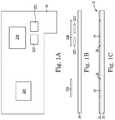
- FIGS. 1A and 1Bare top and side views of a plurality of high density circuit structures combined with a low density PCB in accordance with an embodiment of the present disclosure.
- FIG. 1Cis a side view of the PCB merged with the high density circuit structures in accordance with an embodiment of the present disclosure.
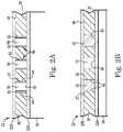
- FIG. 2Ais a cross-sectional view of a method of making a high density circuit structure in accordance with an embodiment of the present disclosure.
- FIG. 2Bis a cross-sectional view of an alternate method of making a high density circuit structure in accordance with an embodiment of the present disclosure.
- FIG. 3illustrates an optional additional layer on the high density electrical circuit of FIG. 1 in accordance with an embodiment of the present disclosure.
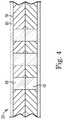
- FIG. 4illustrates application to a second circuitry layer to the high density electrical circuit of FIG. 1 in accordance with an embodiment of the present disclosure.
- FIG. 5illustrates an optional dielectric layer on the high density electrical circuit of FIG. 1 in accordance with an embodiment of the present disclosure.
- FIG. 6illustrates an optional etching step on the high density electrical circuit of FIG. 1 in accordance with an embodiment of the present disclosure.
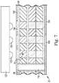
- FIG. 7illustrates an electrical interconnect interfaced with a BGA device in accordance with an embodiment of the present disclosure.
- FIG. 8illustrates an electrical interconnect for a flexible circuit in accordance with an embodiment of the present disclosure.
- FIG. 9illustrates an electrical interconnect for an IC package in accordance with an embodiment of the present disclosure.
- FIG. 10illustrates an alternate electrical circuit for an IC package in accordance with an embodiment of the present disclosure.
- FIG. 11is a side sectional view of an electrical circuit in accordance with an embodiment of the present disclosure.
- FIG. 12is a side sectional view of an alternate electrical circuit with printed compliant material in accordance with an embodiment of the present disclosure.
- FIG. 13illustrates an electrical circuit with optical features in accordance with an embodiment of the present disclosure.
- FIG. 14illustrates an alternate high density electrical circuit with optical features in accordance with an embodiment of the present disclosure.
- FIG. 15illustrates an alternate high density circuit structure with printed vias in accordance with an embodiment of the present disclosure.
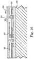
- FIG. 16illustrates an alternate high density circuit structure with printed electrical devices in accordance with an embodiment of the present disclosure.
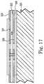
- FIG. 17illustrates an alternate high density electrical circuit with printed compliant electrical pads to plug into another connector in accordance with an embodiment of the present disclosure.
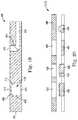
- FIG. 18is a top view of a high density electrical circuit in accordance with an embodiment of the present disclosure.
- FIG. 19is a side view of an alternate high density circuit with RF wave guides in accordance with an embodiment of the present disclosure.
- FIG. 20is a side view of various methods of coupling a high density circuit with a low density circuit in accordance with an embodiment of the present disclosure.
- a high density circuit structure according to the present disclosuremay permit fine contact-to-contact spacing (pitch) on the order of less than 1.0 mm pitch, and more preferably a pitch of less than about 0.7 millimeter, and most preferably a pitch of less than about 0.4 millimeter.
- pitchfine contact-to-contact spacing
- Such fine pitch high density circuit structuresare especially useful for communications, wireless, and memory devices.
- the present high density circuit structurecan be configured as a low cost, high signal performance electrical interconnect assembly, which has a low profile that is particularly useful for desktop and mobile PC applications.
- IC devicescan be installed and uninstalled without the need to reflow solder.
- the solder-free electrical connection of the IC devicesis environmentally friendly.
- the high density circuit structurecan also be a portion of a socket or semiconductor package.
- FIGS. 1A and 1Bschematically illustrate the merger of a lower density circuit 20 with one or more high density circuits 22 A, 22 B, 22 C, 22 D (“ 22 ”) into the contiguous assembly of FIG. 1C .
- the lower density circuit 20may be a printed circuit board, a flexible circuit, or the like.
- the high density circuit 22can be a printed circuit board, an IC socket, a semiconductor package, or the like.
- Dielectric material 24is optionally applied to the surface 26 of the low density circuit 20 so the location of the high density circuits 22 is at least partially defined and isolated.
- the dielectric material 24may be a film or a liquid dielectric.
- the dielectric material 24is imaged to expose the circuit locations 28 for the high density circuits 22 , improving alignment of vias on the lower density main core 20 with the high density circuits 22 .
- the dielectric 24is optionally processed to enable electro-less or electrolytic copper plating to adhere to the surface of the dielectric and grow a thick trace or pillar or via structure within the imaged region with undesired areas remaining un-plated or post plate etched to remove unwanted copper. Once the surfaces are plated, a higher deposition rate electroplate copper can be applied to build up the thickness or area of copper as desired.
- the base layercan be a material such as polyimide or liquid crystal polymer. If the circuit assembly 30 is a rigid circuit board, the base can be FR4 or one of many high speed laminates or substrates. If the circuit assembly 30 is a semiconductor package, the base can be a material such as FR4, BT resin of any one of a variety of laminate or substrate materials. If the circuit assembly 30 is an electrical connector or socket, the base can be molded LCP, machined plastic, or a variety of films or substrate materials.
- the high density circuits 22can be made using conventional build up technology described above or using the process described below.
- the high density circuits 22are then merged with the low density circuit 20 .
- the high density circuits 22can be fabricated in-situ directly on the low density circuit 20 using the processes described herein. The present method permits the high density circuits 22 to be formed directly in the circuit locations 28 , without having to extend the processing across the entire low density circuit 20 .
- FIG. 2Ais a side cross-sectional view of a method of making the high density electrical circuits 22 in accordance with an embodiment of the present disclosure.
- the first stepis to start with base material of some sort, such as a copper foil 32 A or a core 34 of some sort to act as a support member. If the starting base is copper foil 32 A, then the foil can act as the first layer circuitry or escape layer which would be the layer to be merged with the circuit locations 28 on the low density circuit 20 .
- the foil 32 Acan be the termination points for BGA attachment to the low density circuit 20 .
- the base 34can also be a sacrificial member that is removed at some point later in the process to reveal the individual coupons 22 .
- copper foil circuitry layer 32 Ais located on reinforcing layer 34 .
- the layer 34can be a traditional PCB or laminated to a stiffening layer or core, such as glass-reinforced epoxy laminate sheets (e.g., FR4).
- the circuitry layer 32 Acan be preformed or can be formed using a fine line imaging step is conducted to etch copper foil as done with many PCB processes.
- Liquid dielectric material 36is applied to surface 38 and flows between the regions of the circuitry 32 A.
- a dry dielectric filmby contrast, does not flow into the recessed regions.
- the dielectric layer 36can be tack cured to partially link the polymer and allow for handling, while retaining the ability to image the material in a photolithography process.
- the dielectric layer 36can be processed with a laser direct imaging process known as LDI.
- the dielectric material 36is typically imaged to create recesses 37 that expose the desired locations 40 on circuitry layer 32 A with theoretical via locations 37 created as part of the image directly in proximity to the circuitry layer 32 A.
- One benefit of imaging the dielectric layer 36is that the via structures do not need to be round as with traditional drilled vias. Any shape that can be imaged and will result in a grown full metal via 54 of the desired shape.
- the dielectric surface 46can be planarized to create a very consistent dielectric thickness and planarity, as well as assist with preparing select surfaces for electro-less copper plating adhesion. Planarization also permits as many layers to be added to the circuit 22 as needed.
- the dielectric layer 36is preferably processed to promote electro-less copper plating using one or more of plasma treatment, permanganate, carbon treatment, impregnating copper nano-particles to activate the desired surfaces to promote electroplating.
- the dielectric material 36is processed to promote plating adhesion to the side walls 44 of the recesses 37 .
- Electro-less copper platingis applied to the side walls 44 of the recesses 37 to create conductive structures 50 , resulting in a three-dimensional landscape. Additional discussion of the use of electro-less plating of the dielectric structure is disclosed in PCT/US2012/53848, filed Sep. 6, 2012, entitled DIRECT METALIZATION OF ELECTRICAL CIRCUIT STRUCTURES, the entire of disclosure of which is hereby incorporated by reference.
- a plating resistis applied, imaged and developed to expose the via location 37 and previous circuit layer 32 A.
- the conductive structure 50is an annular-shaped via electrically coupled to the circuitry layer 32 A with a center opening or recess 52 .
- a higher deposition rate electroplate coppercan be used to fill the recess 52 with conductive material 54 to form a conductive pillar 56 .
- the plating resistis stripped and the copper deposition 50 , 54 is optionally planarized.
- the resulting conductive pillars 56include a shell 50 of electro-less conductive material and a core 54 of electro-plated conductive material.
- a present processcreates the ability to stack full metal vias 54 in subsequent deposition steps to create a high aspect ratio via without the need to drill through the entire stack 22 in one operation. Another benefit is the ability to provide a mounting point for a packaged semiconductor device where a copper pillars 54 are created as an alternative to conventional via in pad construction which can be plagued with reliability issues and high costs to manufacture.
- the present processenhances the electroplating process is to deposit electro-less copper or copper flash to provide a bus structure for bulk copper electro plating.
- the copper bus structureis subsequently removed with a differential etch process that leaves bulk copper 54 intact.
- An alternate stepcan be employed to add multiple layers of resist 36 and continue the copper growth procedure if desired, with the resulting structures encapsulated by the next dielectric application.
- the shape of the conductive structures 50 , 54is dictated by the shape of the recesses 37 .
- a square recess 37results in a square-shaped conductive structure 54 .
- the plating processcan be controlled to a certain degree, but in some cases with fine pitch geometries and high speed circuits, upper surfaces 46 of the dielectric 36 and the conductive structure 54 may vary in topography or height relative to the field, and the dielectric material 36 may vary in thickness slightly especially if liquid material is used. Consequently, it is preferred to planarize to surfaces 46 of the conductive structures 54 and the exposed surface 46 of the dielectric 36 between steps to control thickness and flatness of the electrical circuit 22 .
- additional foil layer 32 Bis applied and processed to create a circuit structure using any of the techniques discussed herein.
- the conductive material 54electrically couples the circuit layer 32 A to the circuit layer 32 B.
- the present methodpermits the material between layers and within each layer to be varied.
- One aspect of the present process that differs from the traditional dry film build up processis the nature of the dielectric deposition in liquid form.
- the dielectric layer 36can be applied by screen printing, stencil printing, jetting, flooding, spraying etc.
- the liquid material 36flows and fills any recessed regions within a previous circuit landscape 32 A.
- desired regionsremain and the regions that are not desired are washed away with fine resolution of the transition regions within the landscape.
- Multiple depositions stepscan be tack cured and imaged such that thicker sections of dielectric 36 can be developed and washed away in one or multiple strip operations.
- the excavated regionscan be filled or treated with materials that have a different dielectric constant, vary in conductive or mechanical or thermal properties to achieve a desired performance function not possible with a contiguous dry film technique.
- the present processnot only provides the ability to alter the material set and associated properties in a given layer, but the material set can be altered at any given point within a given deposition or layer.
- the present processcan also be used in combination with existing dry film techniques.
- one or more of the layerscan be a preformed dielectric film to leave air dielectric gaps between traces.
- Recesses 37 in the dielectric layer 36 that expose circuitry 32 Acan be formed by printing, embossing, imprinting, laser cutting, chemical etching with a printed mask, or a variety of other techniques.
- FIG. 2Billustrates an alternate high density electrical circuit 22 in accordance with an embodiment of the present disclosure.
- the processis the same as discussed in connection with FIG. 2A , except that the sidewalls 44 of the dielectric material 36 are not processed to receive electro-less plating. Rather, a bulk conductive material 42 is applied directly to exposed portions 40 of the circuit layer 32 A.
- the surface 46is preferably planarized and the circuit layer 32 B is applied using any of the techniques disclosed herein.
- FIG. 3illustrates higher aspect ratio conductive pillar 60 formed on the high density electrical circuit 22 without the foil layer 32 B.
- the process discussed aboveis repeated by applying another layer 62 of dielectric 36 that is imaged to created recesses 64 that expose the upper surface 66 of the copper pillar 42 .
- the upper surfaces 66 of the copper pillars 42are then plated as discussed above to create conductive extension 68 of the copper pillar 42 .
- the conductive extensions 68are planarized to permit die attach point 70 to facilitate flip chip attach of the die 72 to the conductive extensions 68 directly.
- exposed surfaces 74 of the platingcan be enlarged to facilitate soldering of the die 72 to the conductive extensions 68 .
- FIG. 4illustrates circuitry layer 80 is applied to the top surface 78 of the electrical circuit 22 and coupled to the conductive extensions 68 .
- the circuitry layer 80creates the base for additional routing layers and to facilitate vertical connection to subsequent layers in the stack in accordance with an alternate embodiment of the present disclosure.
- FIG. 5illustrates dielectric layer 90 added to the subsequent circuitry layer 80 in accordance with an alternate embodiment of the present disclosure.
- the dielectric layer 90is imaged to create recesses 92 that expose portions 94 of the circuitry layer 80 that corresponds with the via extensions 68 .
- the dielectric layer 90protects the portions of the circuitry layers 80 that are not to be etched and provides access to the foil intimate to the conductive structures 42 and 68 .
- the extension 68is optionally conductive structure 50 with a core 54 of conductive or non-conductive material.
- FIG. 6illustrates a subsequent etch process that removes the copper foil 94 (see FIG. 5 ) located in the recesses 92 to allow access for the next plating step to join the layers together in accordance with an alternate embodiment of the present disclosure.
- the resist layer 90can be stripped to provide a level to be planarized as the base of further processing or the resist layer 90 can be left in place provided it is of the proper material type.
- the exposed regions that provided access for etch and platingcan be filled with similar material to seal the layer which can be planarized for further processing if desired.
- FIG. 7illustrates one possible variation of the electrical circuit 22 .
- Recesses 92are filled with a dielectric material 96 and the surface 98 is planarized to receive circuitry plane 100 .
- Dielectric layer 102is deposited on the circuitry plane 100 to expose selective regions 104 .
- the selective regions 104are configured to correspond to solder balls 120 on BGA device 122 .
- bottom dielectric layer 106is optionally deposited on circuitry layer 52 in a manner to expose selective regions 108 .
- the electrical circuit 22is further processed with conventional circuit fabrication processes to create larger diameter through vias or through holes plated 110 as needed, solder mask applied and imaged to expose device termination locations 104 , 108 , laser direct imaging, legend application etc.
- the via 110is formed using electro-less plating of each layer of the stack, as illustrated in FIG. 6 .
- FIG. 8illustrate an alternate embodiment in which the electrical circuit 22 is used in a flexible circuit applications.
- the electrical circuit 22is laminated with ground planes and cover layers 112 , 114 .
- the insulating layers 112 , 114are applied by jet printing of polyimide or liquid crystal polymers (LCP) inks as a final layer or as a combination of laminated film and jetted material.
- LCPliquid crystal polymers
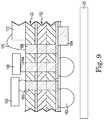
- FIG. 9illustrates an electrical circuit 22 for semiconductor packaging applications in accordance with an embodiment of the present disclosure.
- the stack 152can be final processed with a variety of options to facilitate electrical connections to IC devices 162 , 166 , 172 and to system level attachment to low density circuit 20 .
- the plating 160is planarized to facilitate flip chip attach to the structure directly (see e.g., FIG. 2 ) or to receive BGA device 162 .
- plating 164is extended to facilitate direct soldering of IC device die 166 with paste.
- plating 168is wire bonded 170 to the IC device 172 .
- the low density main core 20can be processed to accept a traditional ball grid array attachment 182 for an area array configuration or plated with solder/tin etc. for a no lead peripheral termination.
- the low density main core 20can also be fashioned to have plating or post extensions 184 to facilitate direct solder attach with paste and provide a natural standoff from the low density circuit 20 .
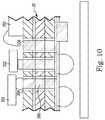
- FIG. 10illustrates an electrical circuit 22 for a semiconductor packages 202 with dielectric materials 204 surrounding the conductive structures 206 in accordance with an embodiment of the present disclosure.
- Internal circuits and terminationsmay also be added by imaging or drilling the core material with a larger opening than needed and filling those openings with dielectric and imaging the desired geometry to facilitate conductive structure formation.
- FIG. 11illustrates an alternate electrical circuit 230 with an insulating layer 232 applied to the circuit geometry 234 .
- the nature of the liquid dielectric application processallows for selective application of dielectric layer 232 to leave selected portions 236 of the circuit geometry 234 expose if desired.
- the resulting high density electrical circuit 230can potentially be considered entirely “green” with limited or no chemistry used to produce beyond the direct write materials.
- the dielectric layers of the present disclosuremay be constructed of any of a number of dielectric materials that are currently used to make sockets, semiconductor packaging, and printed circuit boards. Examples may include UV stabilized tetrafunctional epoxy resin systems referred to as Flame Retardant 4 (FR-4); bismaleimide-triazine thermoset epoxy resins referred to as BT-Epoxy or BT Resin; and liquid crystal polymers (LCPs), which are polyester polymers that are extremely unreactive, inert and resistant to fire. Other suitable plastics include phenolics, polyesters, and Ryton® available from Phillips Petroleum Company.
- one or more of the dielectric materialsare designed to provide electrostatic dissipation or to reduce cross-talk between the traces of the circuit geometry.
- An efficient way to prevent electrostatic discharge (“ESD”)is to construct one of the layers from materials that are not too conductive but that will slowly conduct static charges away. These materials preferably have resistivity values in the range of 10 5 to 10 11 Ohm-meters.
- FIG. 12illustrates an alternate high density electrical circuit 250 in accordance with an embodiment of the present disclosure.
- Dielectric layer 252includes openings 254 into which compliant material 256 is deposited or printed before formation of circuit geometry 258 .
- the compliant material 256improves reliability during flexure of the electrical circuit 250 .
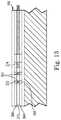
- FIG. 13illustrates an alternate high performance electrical circuit 260 in accordance with an embodiment of the present disclosure.
- Optical fibers 262are located between layers 264 , 266 of dielectric material.
- optical fibers 262are positioned over compliant layer 268
- dielectric layer 270is formed over and around the optical fibers 262 .
- a compliant layer 272is preferably provided above the optical fiber 262 as well.
- the compliant layers 268 , 272support the optical fibers 262 during flexure.
- the dielectric layer 270is imaged with recesses into which the optical fibers 262 are deposited.
- optical quality materials 274are printed during assembly of the high density electrical circuit 260 .
- the optical quality material 274 and/or the optical fibers 262comprise optical circuit geometries.
- the printing processallows for deposition of coatings in-situ that enhances the optical transmission or reduces loss.
- the precision of the printing processreduces misalignment issues when the optical materials 274 are optically coupled with another optical structure.
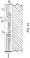
- FIG. 14illustrates another embodiment of a present high density electrical circuit 280 in accordance with an embodiment of the present disclosure.
- Embedded coaxial RF circuits 282 or printed micro strip RF circuits 284are located within the dielectric layers 286 . These RF circuits 282 , 284 are preferably created by printing dielectrics and metallization geometry.
- use of the present processallows the creation of a high density electrical circuit 290 with inter-circuit, 3D lattice structures 292 having intricate routing schemes.
- Conductive pillars 294can be plated with each layer, without drilling.
- the nature of the present processpermit controlled application of dielectric layers 296 creates recesses 298 that control the location, cross section, material content, and aspect ratio of the conductive traces 292 and the conductive pillars 294 .
- Maintaining the conductive traces 292 and conductive pillars 294 with a cross-section of 1:1 or greaterprovides greater signal integrity than traditional subtractive trace forming technologies. For example, traditional methods take a sheet of a given thickness and etches the material between the traces away to have a resultant trace that is usually wider than it is thick. The etching process also removes more material at the top surface of the trace than at the bottom, leaving a trace with a trapezoidal cross-sectional shape, degrading signal integrity in some applications.
- the recesses 298are preferably processed to receive electro-less plating, followed by electroplating to build up the conductive traces 292 .
- pre-patterned or pre-etched thin conductive foil circuit tracesare transferred to the recesses 298 .
- a pressure sensitive adhesivecan be used to retain the copper foil circuit traces in the recesses 298 .
- the trapezoidal cross-sections of the preformed conductive foil tracesare then post-plated.
- the plating materialfills the open spaces in the recesses 298 not occupied by the foil circuit geometry, resulting in a substantially rectangular or square cross-sectional shape corresponding to the shape of the recesses 298 .
- a thin conductive foilis pressed into the recesses 298 , and the edges of the recesses 298 acts to cut or shear the conductive foil.
- the processlocates a portion of the conductive foil in the recesses 298 , but leaves the negative pattern of the conductive foil not wanted outside and above the recesses 298 for easy removal.
- the foil in the recesses 298is preferably post plated to add material to increase the thickness of the conductive traces 292 in the circuit geometry and to fill any voids left between the conductive foil and the recesses 298 .
- FIG. 16illustrates a high density electrical circuit 300 with printed electrical devices 302 .
- the electrical devices 302can include passive or active functional elements. Passive structure refers to a structure having a desired electrical, magnetic, or other property, including but not limited to a conductor, resistor, capacitor, inductor, insulator, dielectric, suppressor, filter, varistor, ferromagnet, and the like.
- electrical devices 302include printed LED indicator 304 and display electronics 306 .
- Geometriescan also be printed to provide capacitive coupling 308 . Compliant material can be added between circuit geometry, such as discussed above, so the present electrical circuit can be plugged into a receptacle or socket, supplementing or replacing the need for compliance within the connector.
- the electrical devices 302are preferably printed during construction of the circuit assembly 300 .
- the electrical devices 302can be ground planes, power planes, electrical connections to other circuit members, dielectric layers, conductive traces, transistors, capacitors, resistors, RF antennae, shielding, filters, signal or power altering and enhancing devices, memory devices, embedded IC, and the like.
- the electrical devices 302can be formed using printing technology, adding intelligence to the high performance electrical circuit 300 .
- Features that are typically located on other circuit memberscan be incorporated into the circuit 300 in accordance with an embodiment of the present disclosure.
- 6,750,473(Amundson et al.), which are incorporated by reference, teach using ink-jet printing to make various electrical devices, such as, resistors, capacitors, diodes, inductors (or elements which may be used in radio applications or magnetic or electric field transmission of power or data), semiconductor logic elements, electro-optical elements, transistor (including, light emitting, light sensing or solar cell elements, field effect transistor, top gate structures), and the like.
- the electrical devices 302can also be created by aerosol printing, such as disclosed in U.S. Pat. No. 7,674,671 (Renn et al.); U.S. Pat. No. 7,658,163 (Renn et al.); U.S. Pat. No. 7,485,345 (Renn et al.); U.S. Pat. No. 7,045,015 (Renn et al.); and U.S. Pat. No. 6,823,124 (Renn et al.), which are hereby incorporated by reference.
- Printing processesare preferably used to fabricate various functional structures, such as conductive paths and electrical devices, without the use of masks or resists.
- Features down to about 10 micronscan be directly written in a wide variety of functional inks, including metals, ceramics, polymers and adhesives, on virtually any substrate—silicon, glass, polymers, metals and ceramics.
- the substratescan be planar and non-planar surfaces.
- the printing processis typically followed by a thermal treatment, such as in a furnace or with a laser, to achieve dense functionalized structures.
- Ink jet printing of electronically active inkscan be done on a large class of substrates, without the requirements of standard vacuum processing or etching.
- the inksmay incorporate mechanical, electrical or other properties, such as, conducting, insulating, resistive, magnetic, semi conductive, light modulating, piezoelectric, spin, optoelectronic, thermoelectric or radio frequency.
- a plurality of ink dropsare dispensed from the print head directly to a substrate or on an intermediate transfer member.
- the transfer membercan be a planar or non-planar structure, such as a drum.
- the surface of the transfer membercan be coated with a non-sticking layer, such as silicone, silicone rubber, or Teflon.
- the ink(also referred to as function inks) can include conductive materials, semi-conductive materials (e.g., p-type and n-type semiconducting materials), metallic material, insulating materials, and/or release materials.
- the ink patterncan be deposited in precise locations on a substrate to create fine lines having a width smaller than 10 microns, with precisely controlled spaces between the lines.
- the ink dropsform an ink pattern corresponding to portions of a transistor, such as a source electrode, a drain electrode, a dielectric layer, a semiconductor layer, or a gate electrode.
- the substratecan be an insulating polymer, such as polyethylene terephthalate (PET), polyester, polyethersulphone (PES), polyimide film (e.g. Kapton, available from DuPont located in Wilmington, Del.; Upilex available from Ube Corporation located in Japan), or polycarbonate.
- PETpolyethylene terephthalate
- PETpolyethylene terephthalate
- PETpolyethersulphone
- polyimide filme.g. Kapton, available from DuPont located in Wilmington, Del.; Upilex available from Ube Corporation located in Japan
- polycarbonatee.g. Kapton, available from DuPont located in Wilmington, Del.; Upilex available from Ube Corporation located in Japan
- the substratecan be made of an insulator such as undoped silicon, glass, or a plastic material.
- the substratecan also be patterned to serve as an electrode.
- the substratecan further be a metal foil insulated from the gate electrode by a non-conducting material.
- the substratecan also be
- Electrodescan be printed with metals, such as aluminum or gold, or conductive polymers, such as polythiophene or polyaniline.
- the electrodesmay also include a printed conductor, such as a polymer film comprising metal particles, such as silver or nickel, a printed conductor comprising a polymer film containing graphite or some other conductive carbon material, or a conductive oxide such as tin oxide or indium tin oxide.
- Dielectric layerscan be printed with a silicon dioxide layer, an insulating polymer, such as polyimide and its derivatives, poly-vinyl phenol, polymethylmethacrylate, polyvinyldenedifluoride, an inorganic oxide, such as metal oxide, an inorganic nitride such as silicon nitride, or an inorganic/organic composite material such as an organic-substituted silicon oxide, or a sol-gel organosilicon glass.
- Dielectric layerscan also include a bicylcobutene derivative (BCB) available from Dow Chemical (Midland, Mich.), spin-on glass, or dispersions of dielectric colloid materials in a binder or solvent.
- BCBbicylcobutene derivative
- Semiconductor layerscan be printed with polymeric semiconductors, such as, polythiophene, poly(3-alkyl)thiophenes, alkyl-substituted oligothiophene, polythienylenevinylene, poly(para-phenylenevinylene) and doped versions of these polymers.
- polymeric semiconductorssuch as, polythiophene, poly(3-alkyl)thiophenes, alkyl-substituted oligothiophene, polythienylenevinylene, poly(para-phenylenevinylene) and doped versions of these polymers.
- An example of suitable oligomeric semiconductoris alpha-hexathienylene. Horowitz, Organic Field-Effect Transistors, Adv. Mater., 10, No. 5, p. 365 (1998) describes the use of unsubstituted and alkyl-substituted oligothiophenes in transistors.
- a field effect transistor made with regioregular poly(3-hexylthiophene) as the semiconductor layeris described in Bao et al., Soluble and Processable Regioregular Poly(3-hexylthiophene) for Thin Film Field-Effect Transistor Applications with High Mobility, Appl. Phys. Lett. 69 (26), p. 4108 (December 1996).
- a field effect transistor made with a-hexathienyleneis described in U.S. Pat. No. 5,659,181, which is incorporated herein by reference.
- a protective layercan optionally be printed onto the electrical devices.
- the protective layercan be an aluminum film, a metal oxide coating, a polymeric film, or a combination thereof.
- Organic semiconductorscan be printed using suitable carbon-based compounds, such as, pentacene, phthalocyanine, benzodithiophene, buckminsterfullerene or other fullerene derivatives, tetracyanonaphthoquinone, and tetrakisimethylanimoethylene.
- suitable carbon-based compoundssuch as, pentacene, phthalocyanine, benzodithiophene, buckminsterfullerene or other fullerene derivatives, tetracyanonaphthoquinone, and tetrakisimethylanimoethylene.
- suitable carbon-based compoundssuch as, pentacene, phthalocyanine, benzodithiophene, buckminsterfullerene or other fullerene derivatives, tetracyanonaphthoquinone, and tetrakisimethylanimoethylene.
- the ink-jet print headpreferably includes a plurality of orifices for dispensing one or more fluids onto a desired media, such as for example, a conducting fluid solution, a semiconducting fluid solution, an insulating fluid solution, and a precursor material to facilitate subsequent deposition.
- a desired mediasuch as for example, a conducting fluid solution, a semiconducting fluid solution, an insulating fluid solution, and a precursor material to facilitate subsequent deposition.
- the precursor materialcan be surface active agents, such as octadecyltrichlorosilane (OTS).
- a separate print headis used for each fluid solution.
- the print head nozzlescan be held at different potentials to aid in atomization and imparting a charge to the droplets, such as disclosed in U.S. Pat. No. 7,148,128 (Jacobson), which is hereby incorporated by reference.
- Alternate print headsare disclosed in U.S. Pat. No. 6,626,526 (Ueki et al.), and U.S. Pat. Publication Nos. 2006/0044357 (Andersen et al.) and 2009/0061089 (King et al.), which are hereby incorporated by reference.
- the print headpreferably uses a pulse-on-demand method, and can employ one of the following methods to dispense the ink drops: piezoelectric, magnetostrictive, electromechanical, electro pneumatic, electrostatic, rapid ink heating, magneto hydrodynamic, or any other technique well known to those skilled in the art.
- the deposited ink patternstypically undergo a curing step or another processing step before subsequent layers are applied.
- printingis intended to include all forms of printing and coating, including: pre-metered coating such as patch die coating, slot or extrusion coating, slide or cascade coating, and curtain coating; roll coating such as knife over roll coating, forward and reverse roll coating; gravure coating; dip coating; spray coating; meniscus coating, spin coating, brush coating, air knife coating; screen printing processes; electrostatic printing processes; thermal printing processes; and other similar techniques.
- pre-metered coatingsuch as patch die coating, slot or extrusion coating, slide or cascade coating, and curtain coating
- roll coatingsuch as knife over roll coating, forward and reverse roll coating
- gravure coatingdip coating
- spray coatingmeniscus coating, spin coating, brush coating, air knife coating
- screen printing processeselectrostatic printing processes
- thermal printing processesand other similar techniques.
- FIG. 17illustrates an alternate high density electrical circuit 320 with compliant material 322 added between circuit geometries 324 , 326 to facilitate insertion of circuit geometries 328 , 330 into a receptacle or socket.
- the compliant material 322can supplement or replace the compliance in the receptacle or socket.
- the complianceis provided by a combination of the compliant material 322 and the exposed circuit geometries 328 , 330 .
- FIG. 18illustrates the unique nature of the present high density circuit construction, where the various circuits and via locations are surrounded by the deposited dielectric within a single layer, rather than layer by layer differential in dielectric or laminate material as seen with conventional methods.
- lower level circuit structures 352 , 356are visible through an optically transparent metalized dielectric.
- Metalized dielectric 350 and printed dielectric 358can exist in the same layers.
- Optically imaged via structures 354span multiple layers.
- FIG. 19illustrates a high density circuit 400 with optical waveguides in accordance with an embodiment of the present disclosure.
- Metalized channels 402 , 404can function as RF waveguides, embedded antennae, embedded microstrip, and the like.
- the channels 402 , 404can be metalized using the electro-less plating discussed herein.
- the channels 402 , 404 in the dielectric 406are filled with optical transmission material.
- the channels 402 , 404can optionally be sealed or encapsulated by subsequent dielectric layers.
- the channel 404includes optional directional mirror 408 to direct the light with low loss in the X and Y planes in ways that are not possible to bend glass fiber.
- the mirror 408creates an Z-axis optical via 410 .
- metal circuits 412 , 414are created at the top and bottom of the channel 402 , and/or on the side walls 416 of the channel 402 .
- the channel 402is preferably filled with the appropriate optical material 418 .
- the combined or hybrid channel 402can act as an optical waveguide through the optical material, with an RF signal passing through the optical material of a given dielectric constant guided by the Metalized surfaces 412 , 414 .
- the photonic sourcecan be external to the high density circuit 400 or embedded within the circuit 400 and activated by the appropriate metal circuitry.
- FIG. 20illustrates an embodiment for merging a high density circuit 22 with a low density circuit 20 in accordance with an embodiment of the present disclosure.
- FIG. 20illustrates various termination points that can be formed on the high density coupon 22 and/or the low density board 20 .
- copper pillar 430is plated up to correspond to a through hole 432 in the mating circuit such that the post 430 resides inside the hole 432 .
- the hole 432is slightly larger than the post 430 for alignment purposes and the two 430 , 432 are plated together.
- the center left versionshows a post 434 with a tapered top 436 that is essentially a friction or slight deformation fit to mechanically join with the recess 438 .
- the center rightshows a through hole 440 and a corresponding pad or trace 442 that align with the hole 440 .
- the two features 440 , 442are preferably plated together.
- the right handshows a stud bump or plated bump 444 that is configured to pierce the circuit layer 446 .
- Each of these types of interfacescan be on the high density coupon 22 , or on the low density circuit 20 or a mixture of both locations as well as a mixture of types within the same construction.
- the interconnect pointsare typically buried by the final solder mask and reinforced mechanically, or they may reside directly under the high density coupon 22 in some cases.
- An alternate methodis to mimic the traditional build up process, a portion of the final copper layer on the low density base board 20 is designed and structured to act as the first circuit layer 32 A for the high density circuit 22 (see FIG. 2A ).
- the high density circuit 22is then constructed directly on the low density circuit 20 at that location as described herein.
- a final solder maskis applied to fully encapsulate the high density regions 22 and leave desired high density terminals flush with the final solder mask.
- the resulting hybrid structure 30appears to resemble a board that was built entirely with the low density process, but actually contains the high density regions deposited and grown in place with underlying circuit structures encapsulated and reinforced with the final solder mask layer.
Landscapes
- Engineering & Computer Science (AREA)
- Microelectronics & Electronic Packaging (AREA)
- Manufacturing & Machinery (AREA)
- Physics & Mathematics (AREA)
- General Physics & Mathematics (AREA)
- Condensed Matter Physics & Semiconductors (AREA)
- Computer Hardware Design (AREA)
- Power Engineering (AREA)
- Chemical & Material Sciences (AREA)
- Materials Engineering (AREA)
- Electromagnetism (AREA)
- Structure Of Printed Boards (AREA)
- Production Of Multi-Layered Print Wiring Board (AREA)
Abstract
Description
Claims (11)
Priority Applications (1)
| Application Number | Priority Date | Filing Date | Title |
|---|---|---|---|
| US15/609,047US10609819B2 (en) | 2009-06-02 | 2017-05-31 | Hybrid printed circuit assembly with low density main core and embedded high density circuit regions |
Applications Claiming Priority (11)
| Application Number | Priority Date | Filing Date | Title |
|---|---|---|---|
| US18334009P | 2009-06-02 | 2009-06-02 | |
| PCT/US2010/036282WO2010141295A1 (en) | 2009-06-02 | 2010-05-27 | Compliant printed flexible circuit |
| US201161451685P | 2011-03-11 | 2011-03-11 | |
| US201161523379P | 2011-08-14 | 2011-08-14 | |
| US201113320285A | 2011-11-14 | 2011-11-14 | |
| US13/413,724US8987886B2 (en) | 2009-06-02 | 2012-03-07 | Copper pillar full metal via electrical circuit structure |
| US201261669884P | 2012-07-10 | 2012-07-10 | |
| PCT/US2013/030856WO2014011226A1 (en) | 2012-07-10 | 2013-03-13 | Hybrid printed circuit assembly with low density main core and embedded high density circuit regions |
| US201414238638A | 2014-02-12 | 2014-02-12 | |
| US201414408205A | 2014-12-15 | 2014-12-15 | |
| US15/609,047US10609819B2 (en) | 2009-06-02 | 2017-05-31 | Hybrid printed circuit assembly with low density main core and embedded high density circuit regions |
Related Parent Applications (4)
| Application Number | Title | Priority Date | Filing Date |
|---|---|---|---|
| US13/413,724Continuation-In-PartUS8987886B2 (en) | 2009-06-02 | 2012-03-07 | Copper pillar full metal via electrical circuit structure |
| PCT/US2013/030856ContinuationWO2014011226A1 (en) | 2009-06-02 | 2013-03-13 | Hybrid printed circuit assembly with low density main core and embedded high density circuit regions |
| US14/408,205ContinuationUS9699906B2 (en) | 2009-06-02 | 2013-03-13 | Hybrid printed circuit assembly with low density main core and embedded high density circuit regions |
| US201414408205AContinuation | 2009-06-02 | 2014-12-15 |
Related Child Applications (1)
| Application Number | Title | Priority Date | Filing Date |
|---|---|---|---|
| US201414408205AContinuation-In-Part | 2009-06-02 | 2014-12-15 |
Publications (2)
| Publication Number | Publication Date |
|---|---|
| US20170303401A1 US20170303401A1 (en) | 2017-10-19 |
| US10609819B2true US10609819B2 (en) | 2020-03-31 |
Family
ID=43298042
Family Applications (2)
| Application Number | Title | Priority Date | Filing Date |
|---|---|---|---|
| US13/320,285ActiveUS9414500B2 (en) | 2009-06-02 | 2010-05-27 | Compliant printed flexible circuit |
| US15/609,047Active2030-10-01US10609819B2 (en) | 2009-06-02 | 2017-05-31 | Hybrid printed circuit assembly with low density main core and embedded high density circuit regions |
Family Applications Before (1)
| Application Number | Title | Priority Date | Filing Date |
|---|---|---|---|
| US13/320,285ActiveUS9414500B2 (en) | 2009-06-02 | 2010-05-27 | Compliant printed flexible circuit |
Country Status (2)
| Country | Link |
|---|---|
| US (2) | US9414500B2 (en) |
| WO (1) | WO2010141295A1 (en) |
Families Citing this family (64)
| Publication number | Priority date | Publication date | Assignee | Title |
|---|---|---|---|---|
| US9536815B2 (en) | 2009-05-28 | 2017-01-03 | Hsio Technologies, Llc | Semiconductor socket with direct selective metalization |
| US8955215B2 (en) | 2009-05-28 | 2015-02-17 | Hsio Technologies, Llc | High performance surface mount electrical interconnect |
| WO2011153298A1 (en) | 2010-06-03 | 2011-12-08 | Hsio Technologies, Llc | Electrical connector insulator housing |
| WO2010147939A1 (en) | 2009-06-17 | 2010-12-23 | Hsio Technologies, Llc | Semiconductor socket |
| US9276336B2 (en) | 2009-05-28 | 2016-03-01 | Hsio Technologies, Llc | Metalized pad to electrical contact interface |
| US9603249B2 (en) | 2009-06-02 | 2017-03-21 | Hsio Technologies, Llc | Direct metalization of electrical circuit structures |
| WO2010141313A1 (en) | 2009-06-02 | 2010-12-09 | Hsio Technologies, Llc | Compliant printed circuit socket diagnostic tool |
| US9232654B2 (en) | 2009-06-02 | 2016-01-05 | Hsio Technologies, Llc | High performance electrical circuit structure |
| WO2010141318A1 (en) | 2009-06-02 | 2010-12-09 | Hsio Technologies, Llc | Compliant printed circuit peripheral lead semiconductor test socket |
| WO2010141264A1 (en) | 2009-06-03 | 2010-12-09 | Hsio Technologies, Llc | Compliant wafer level probe assembly |
| US8610265B2 (en) | 2009-06-02 | 2013-12-17 | Hsio Technologies, Llc | Compliant core peripheral lead semiconductor test socket |
| US9414500B2 (en) | 2009-06-02 | 2016-08-09 | Hsio Technologies, Llc | Compliant printed flexible circuit |
| US9054097B2 (en) | 2009-06-02 | 2015-06-09 | Hsio Technologies, Llc | Compliant printed circuit area array semiconductor device package |
| US8987886B2 (en) | 2009-06-02 | 2015-03-24 | Hsio Technologies, Llc | Copper pillar full metal via electrical circuit structure |
| WO2012074963A1 (en) | 2010-12-01 | 2012-06-07 | Hsio Technologies, Llc | High performance surface mount electrical interconnect |
| US9231328B2 (en) | 2009-06-02 | 2016-01-05 | Hsio Technologies, Llc | Resilient conductive electrical interconnect |
| WO2011002709A1 (en)* | 2009-06-29 | 2011-01-06 | Hsio Technologies, Llc | Compliant printed circuit semiconductor tester interface |
| US9184145B2 (en) | 2009-06-02 | 2015-11-10 | Hsio Technologies, Llc | Semiconductor device package adapter |
| WO2010141296A1 (en) | 2009-06-02 | 2010-12-09 | Hsio Technologies, Llc | Compliant printed circuit semiconductor package |
| US8955216B2 (en) | 2009-06-02 | 2015-02-17 | Hsio Technologies, Llc | Method of making a compliant printed circuit peripheral lead semiconductor package |
| WO2010141298A1 (en) | 2009-06-02 | 2010-12-09 | Hsio Technologies, Llc | Composite polymer-metal electrical contacts |
| US9699906B2 (en) | 2009-06-02 | 2017-07-04 | Hsio Technologies, Llc | Hybrid printed circuit assembly with low density main core and embedded high density circuit regions |
| US8912812B2 (en) | 2009-06-02 | 2014-12-16 | Hsio Technologies, Llc | Compliant printed circuit wafer probe diagnostic tool |
| US9320133B2 (en) | 2009-06-02 | 2016-04-19 | Hsio Technologies, Llc | Electrical interconnect IC device socket |
| WO2010147934A1 (en) | 2009-06-16 | 2010-12-23 | Hsio Technologies, Llc | Semiconductor die terminal |
| US9613841B2 (en) | 2009-06-02 | 2017-04-04 | Hsio Technologies, Llc | Area array semiconductor device package interconnect structure with optional package-to-package or flexible circuit to package connection |
| US8525346B2 (en) | 2009-06-02 | 2013-09-03 | Hsio Technologies, Llc | Compliant conductive nano-particle electrical interconnect |
| US9318862B2 (en) | 2009-06-02 | 2016-04-19 | Hsio Technologies, Llc | Method of making an electronic interconnect |
| US9930775B2 (en) | 2009-06-02 | 2018-03-27 | Hsio Technologies, Llc | Copper pillar full metal via electrical circuit structure |
| US9196980B2 (en) | 2009-06-02 | 2015-11-24 | Hsio Technologies, Llc | High performance surface mount electrical interconnect with external biased normal force loading |
| US9136196B2 (en) | 2009-06-02 | 2015-09-15 | Hsio Technologies, Llc | Compliant printed circuit wafer level semiconductor package |
| US9276339B2 (en) | 2009-06-02 | 2016-03-01 | Hsio Technologies, Llc | Electrical interconnect IC device socket |
| US8988093B2 (en) | 2009-06-02 | 2015-03-24 | Hsio Technologies, Llc | Bumped semiconductor wafer or die level electrical interconnect |
| WO2010147782A1 (en) | 2009-06-16 | 2010-12-23 | Hsio Technologies, Llc | Simulated wirebond semiconductor package |
| US8984748B2 (en) | 2009-06-29 | 2015-03-24 | Hsio Technologies, Llc | Singulated semiconductor device separable electrical interconnect |
| US8758067B2 (en) | 2010-06-03 | 2014-06-24 | Hsio Technologies, Llc | Selective metalization of electrical connector or socket housing |
| US9350093B2 (en) | 2010-06-03 | 2016-05-24 | Hsio Technologies, Llc | Selective metalization of electrical connector or socket housing |
| US10159154B2 (en) | 2010-06-03 | 2018-12-18 | Hsio Technologies, Llc | Fusion bonded liquid crystal polymer circuit structure |
| US9689897B2 (en) | 2010-06-03 | 2017-06-27 | Hsio Technologies, Llc | Performance enhanced semiconductor socket |
| US9041255B2 (en)* | 2011-07-22 | 2015-05-26 | Moon J. Kim | High capacity electronic switch |
| US9761520B2 (en) | 2012-07-10 | 2017-09-12 | Hsio Technologies, Llc | Method of making an electrical connector having electrodeposited terminals |
| US10506722B2 (en) | 2013-07-11 | 2019-12-10 | Hsio Technologies, Llc | Fusion bonded liquid crystal polymer electrical circuit structure |
| US10667410B2 (en) | 2013-07-11 | 2020-05-26 | Hsio Technologies, Llc | Method of making a fusion bonded circuit structure |
| US9326373B2 (en)* | 2014-04-09 | 2016-04-26 | Finisar Corporation | Aluminum nitride substrate |
| US9559447B2 (en) | 2015-03-18 | 2017-01-31 | Hsio Technologies, Llc | Mechanical contact retention within an electrical connector |
| CN109156080B (en) | 2016-05-16 | 2021-10-08 | 株式会社村田制作所 | Ceramic electronic parts |
| US20170356640A1 (en) | 2016-06-10 | 2017-12-14 | Innotec, Corp. | Illumination assembly including thermal energy management |
| WO2019007488A1 (en)* | 2017-07-04 | 2019-01-10 | Cleanpart Group Gmbh | Process chamber component and method of forming a surface texture |
| US10842026B2 (en) | 2018-02-12 | 2020-11-17 | Xerox Corporation | System for forming electrical circuits on non-planar objects |
| WO2019211406A1 (en)* | 2018-05-03 | 2019-11-07 | University Of Limerick | A pcb structure for embedding electronic components |
| US10517167B1 (en)* | 2018-10-19 | 2019-12-24 | Eagle Technology, Llc | Systems and methods for providing a high speed interconnect system with reduced crosstalk |
| TWI668829B (en)* | 2018-11-05 | 2019-08-11 | 華邦電子股份有限公司 | Redistribution layer (rdl) structure and method of manufacturing the same |
| CN111211104B (en)* | 2018-11-22 | 2021-09-07 | 华邦电子股份有限公司 | Circuit structure and manufacturing method thereof |
| TWI678289B (en)* | 2018-12-07 | 2019-12-01 | 謙華科技股份有限公司 | Manufacturing method of thermal head |
| CN111385960B (en)* | 2018-12-27 | 2022-10-11 | 中兴通讯股份有限公司 | Circuit board, preparation method and electronic device |
| US11063010B2 (en) | 2019-02-01 | 2021-07-13 | Winbond Electronics Corp. | Redistribution layer (RDL) structure and method of manufacturing the same |
| US11056850B2 (en) | 2019-07-26 | 2021-07-06 | Eagle Technology, Llc | Systems and methods for providing a soldered interface on a printed circuit board having a blind feature |
| US11602800B2 (en) | 2019-10-10 | 2023-03-14 | Eagle Technology, Llc | Systems and methods for providing an interface on a printed circuit board using pin solder enhancement |
| US11569189B2 (en)* | 2020-08-27 | 2023-01-31 | Nanya Technology Corporation | Semiconductor device structure with conductive polymer liner and method for forming the same |
| CN114390783A (en)* | 2020-10-20 | 2022-04-22 | 深南电路股份有限公司 | Circuit board manufacturing method and circuit board |
| US11283204B1 (en) | 2020-11-19 | 2022-03-22 | Eagle Technology, Llc | Systems and methods for providing a composite connector for high speed interconnect systems |
| CN112770543A (en)* | 2020-12-10 | 2021-05-07 | 安捷利(番禺)电子实业有限公司 | Preparation method of FPC board |
| CN115551206A (en)* | 2022-09-23 | 2022-12-30 | 安捷利美维电子(厦门)有限责任公司 | Packaging substrate and preparation method thereof, and packaging substrate heat dissipation detection system and method |
| DE102022213912A1 (en)* | 2022-12-19 | 2024-06-20 | Hahn-Schickard-Gesellschaft für angewandte Forschung e.V. | METHOD FOR PRODUCING INTEGRATED VOLUME COMPONENTS AND INTEGRATED VOLUME COMPONENT |
Citations (385)
| Publication number | Priority date | Publication date | Assignee | Title |
|---|---|---|---|---|
| US3672986A (en) | 1969-12-19 | 1972-06-27 | Day Co Nv | Metallization of insulating substrates |
| US4188438A (en) | 1975-06-02 | 1980-02-12 | National Semiconductor Corporation | Antioxidant coating of copper parts for thermal compression gang bonding of semiconductive devices |
| US4295700A (en) | 1978-10-12 | 1981-10-20 | Shin-Etsu Polymer Co., Ltd. | Interconnectors |
| US4489999A (en) | 1983-02-15 | 1984-12-25 | Motorola, Inc. | Socket and flexible PC board assembly and method for making |
| US4922376A (en) | 1989-04-10 | 1990-05-01 | Unistructure, Inc. | Spring grid array interconnection for active microelectronic elements |
| US4959515A (en) | 1984-05-01 | 1990-09-25 | The Foxboro Company | Micromechanical electric shunt and encoding devices made therefrom |
| US4964948A (en) | 1985-04-16 | 1990-10-23 | Protocad, Inc. | Printed circuit board through hole technique |
| US5014159A (en) | 1982-04-19 | 1991-05-07 | Olin Corporation | Semiconductor package |
| US5046238A (en) | 1990-03-15 | 1991-09-10 | Rogers Corporation | Method of manufacturing a multilayer circuit board |
| WO1991014015A1 (en) | 1990-03-05 | 1991-09-19 | Olin Corporation | Method and materials for forming multi-layer circuits by an additive process |
| US5071363A (en) | 1990-04-18 | 1991-12-10 | Minnesota Mining And Manufacturing Company | Miniature multiple conductor electrical connector |
| US5072520A (en) | 1990-10-23 | 1991-12-17 | Rogers Corporation | Method of manufacturing an interconnect device having coplanar contact bumps |
| US5090116A (en) | 1990-12-21 | 1992-02-25 | Amp Incorporated | Method of assembling a connector to a circuit element and soldering lead frame for use therein |
| US5096426A (en) | 1989-12-19 | 1992-03-17 | Rogers Corporation | Connector arrangement system and interconnect element |
| US5127837A (en) | 1989-06-09 | 1992-07-07 | Labinal Components And Systems, Inc. | Electrical connectors and IC chip tester embodying same |
| US5129573A (en) | 1991-10-25 | 1992-07-14 | Compaq Computer Corporation | Method for attaching through-hole devices to a circuit board using solder paste |
| US5161983A (en) | 1991-02-11 | 1992-11-10 | Kel Corporation | Low profile socket connector |
| US5167512A (en) | 1991-07-05 | 1992-12-01 | Walkup William B | Multi-chip module connector element and system |
| US5208068A (en) | 1989-04-17 | 1993-05-04 | International Business Machines Corporation | Lamination method for coating the sidewall or filling a cavity in a substrate |
| US5237203A (en) | 1991-05-03 | 1993-08-17 | Trw Inc. | Multilayer overlay interconnect for high-density packaging of circuit elements |
| US5246880A (en) | 1992-04-27 | 1993-09-21 | Eastman Kodak Company | Method for creating substrate electrodes for flip chip and other applications |
| US5286680A (en) | 1988-12-07 | 1994-02-15 | Tribotech | Semiconductor die packages having lead support frame |
| US5334029A (en) | 1993-05-11 | 1994-08-02 | At&T Bell Laboratories | High density connector for stacked circuit boards |
| US5358621A (en) | 1991-12-10 | 1994-10-25 | Nec Corporation | Method of manufacturing semiconductor devices |
| US5378981A (en) | 1993-02-02 | 1995-01-03 | Motorola, Inc. | Method for testing a semiconductor device on a universal test circuit substrate |
| US5419038A (en) | 1993-06-17 | 1995-05-30 | Fujitsu Limited | Method for fabricating thin-film interconnector |
| US5454161A (en) | 1993-04-29 | 1995-10-03 | Fujitsu Limited | Through hole interconnect substrate fabrication process |
| US5479319A (en) | 1992-12-30 | 1995-12-26 | Interconnect Systems, Inc. | Multi-level assemblies for interconnecting integrated circuits |
| US5509019A (en) | 1990-09-20 | 1996-04-16 | Fujitsu Limited | Semiconductor integrated circuit device having test control circuit in input/output area |
| US5527998A (en) | 1993-10-22 | 1996-06-18 | Sheldahl, Inc. | Flexible multilayer printed circuit boards and methods of manufacture |
| US5534787A (en) | 1994-12-09 | 1996-07-09 | Vlsi Technology, Inc. | High-frequency coaxial interface test fixture |
| US5562462A (en) | 1994-07-19 | 1996-10-08 | Matsuba; Stanley | Reduced crosstalk and shielded adapter for mounting an integrated chip package on a circuit board like member |
| US5596178A (en) | 1995-10-12 | 1997-01-21 | Christian; Suzanne | single replacement pad with perforated shaft for the repair of printed circuit boards |
| US5619018A (en) | 1995-04-03 | 1997-04-08 | Compaq Computer Corporation | Low weight multilayer printed circuit board |
| US5659181A (en) | 1995-03-02 | 1997-08-19 | Lucent Technologies Inc. | Article comprising α-hexathienyl |
| US5674595A (en) | 1996-04-22 | 1997-10-07 | International Business Machines Corporation | Coverlay for printed circuit boards |
| US5691041A (en) | 1995-09-29 | 1997-11-25 | International Business Machines Corporation | Socket for semi-permanently connecting a solder ball grid array device using a dendrite interposer |
| US5716663A (en) | 1990-02-09 | 1998-02-10 | Toranaga Technologies | Multilayer printed circuit |
| US5741624A (en) | 1996-02-13 | 1998-04-21 | Micron Technology, Inc. | Method for reducing photolithographic steps in a semiconductor interconnect process |
| US5746608A (en) | 1995-11-30 | 1998-05-05 | Taylor; Attalee S. | Surface mount socket for an electronic package, and contact for use therewith |
| US5761801A (en) | 1995-06-07 | 1998-06-09 | The Dexter Corporation | Method for making a conductive film composite |
| US5764485A (en) | 1996-04-19 | 1998-06-09 | Lebaschi; Ali | Multi-layer PCB blockade-via pad-connection |
| US5772451A (en) | 1993-11-16 | 1998-06-30 | Form Factor, Inc. | Sockets for electronic components and methods of connecting to electronic components |
| US5785538A (en) | 1995-11-27 | 1998-07-28 | International Business Machines Corporation | High density test probe with rigid surface structure |
| US5787976A (en) | 1996-07-01 | 1998-08-04 | Digital Equipment Corporation | Interleaved-fin thermal connector |
| US5802699A (en) | 1994-06-07 | 1998-09-08 | Tessera, Inc. | Methods of assembling microelectronic assembly with socket for engaging bump leads |
| US5802711A (en) | 1992-11-16 | 1998-09-08 | International Business Machines Corporation | Process for making an electrical interconnect structure |
| US5819579A (en) | 1992-02-14 | 1998-10-13 | Research Organization For Circuit Knowledge | Forming die for manufacturing printed circuits |
| US5880590A (en) | 1997-05-07 | 1999-03-09 | International Business Machines Corporation | Apparatus and method for burn-in and testing of devices with solder bumps or preforms |
| US5904546A (en) | 1996-02-12 | 1999-05-18 | Micron Technology, Inc. | Method and apparatus for dicing semiconductor wafers |
| US5913109A (en) | 1994-07-07 | 1999-06-15 | Tessera, Inc. | Fixtures and methods for lead bonding and deformation |
| US5921786A (en) | 1997-04-03 | 1999-07-13 | Kinetrix, Inc. | Flexible shielded laminated beam for electrical contacts and the like and method of contact operation |
| US5925931A (en) | 1996-10-31 | 1999-07-20 | Casio Computer Co., Ltd. | Semiconductor device having interconnect lines and connection electrodes formed in groove portions of an insulating layer |
| US5933558A (en) | 1997-05-22 | 1999-08-03 | Motorola, Inc. | Optoelectronic device and method of assembly |
| US5973394A (en) | 1998-01-23 | 1999-10-26 | Kinetrix, Inc. | Small contactor for test probes, chip packaging and the like |
| US6020597A (en) | 1997-03-05 | 2000-02-01 | Lg Semicon Co., Ltd. | Repairable multichip module |
| US6080932A (en) | 1998-04-14 | 2000-06-27 | Tessera, Inc. | Semiconductor package assemblies with moisture vents |
| US6107109A (en) | 1997-12-18 | 2000-08-22 | Micron Technology, Inc. | Method for fabricating a semiconductor interconnect with laser machined electrical paths through substrate |
| US6114240A (en) | 1997-12-18 | 2000-09-05 | Micron Technology, Inc. | Method for fabricating semiconductor components using focused laser beam |
| US6118426A (en) | 1995-07-20 | 2000-09-12 | E Ink Corporation | Transducers and indicators having printed displays |
| US6120588A (en) | 1996-07-19 | 2000-09-19 | E Ink Corporation | Electronically addressable microencapsulated ink and display thereof |
| US6137687A (en) | 1996-08-09 | 2000-10-24 | Hitachi, Ltd. | Printed circuit board, IC card, and manufacturing method thereof |
| US6172879B1 (en) | 1998-06-30 | 2001-01-09 | Sun Microsystems, Inc. | BGA pin isolation and signal routing process |
| US6178540B1 (en) | 1998-03-11 | 2001-01-23 | Industrial Technology Research Institute | Profile design for wire bonding |
| US6177921B1 (en) | 1997-08-28 | 2001-01-23 | E Ink Corporation | Printable electrode structures for displays |
| US6181144B1 (en) | 1998-02-25 | 2001-01-30 | Micron Technology, Inc. | Semiconductor probe card having resistance measuring circuitry and method fabrication |
| US6200143B1 (en) | 1998-01-09 | 2001-03-13 | Tessera, Inc. | Low insertion force connector for microelectronic elements |
| US6207259B1 (en) | 1998-11-02 | 2001-03-27 | Kyocera Corporation | Wiring board |
| US6225692B1 (en) | 1999-06-03 | 2001-05-01 | Cts Corporation | Flip chip package for micromachined semiconductors |
| US6247938B1 (en) | 1997-05-06 | 2001-06-19 | Gryphics, Inc. | Multi-mode compliance connector and replaceable chip module utilizing the same |
| US6252564B1 (en) | 1997-08-28 | 2001-06-26 | E Ink Corporation | Tiled displays |
| US6255126B1 (en) | 1998-12-02 | 2001-07-03 | Formfactor, Inc. | Lithographic contact elements |
| US6263566B1 (en) | 1999-05-03 | 2001-07-24 | Micron Technology, Inc. | Flexible semiconductor interconnect fabricated by backslide thinning |
| US6270363B1 (en) | 1999-05-18 | 2001-08-07 | International Business Machines Corporation | Z-axis compressible polymer with fine metal matrix suspension |
| US20010012707A1 (en) | 1999-12-07 | 2001-08-09 | Urex Precision, Inc. | Integrated circuit socket with contact pad |
| US20010016551A1 (en) | 1998-07-22 | 2001-08-23 | Sumitomo Electric Industries, Ltd. | Aluminum nitride sintered body and method of preparing the same |
| US6288451B1 (en) | 1998-06-24 | 2001-09-11 | Vanguard International Semiconductor Corporation | Flip-chip package utilizing a printed circuit board having a roughened surface for increasing bond strength |
| US6313528B1 (en) | 1996-12-13 | 2001-11-06 | Tessera, Inc. | Compliant multichip package |
| US6312971B1 (en) | 1999-08-31 | 2001-11-06 | E Ink Corporation | Solvent annealing process for forming a thin semiconductor film with advantageous properties |
| US6320256B1 (en) | 1999-12-20 | 2001-11-20 | Thin Film Module, Inc. | Quick turn around fabrication process for packaging substrates and high density cards |
| US20020011639A1 (en) | 1999-07-02 | 2002-01-31 | Carlson Lars S. | Indirect back surface contact to semiconductor devices |
| US6350386B1 (en) | 2000-09-20 | 2002-02-26 | Charles W. C. Lin | Method of making a support circuit with a tapered through-hole for a semiconductor chip assembly |
| US20020027441A1 (en) | 1996-04-01 | 2002-03-07 | Salman Akram | Semiconductor test interconnect with variable flexure contacts |
| US6359790B1 (en) | 1999-07-01 | 2002-03-19 | Infineon Technologies Ag | Multichip module having a silicon carrier substrate |
| JP3274601B2 (en) | 1996-03-11 | 2002-04-15 | 東レエンジニアリング株式会社 | Circuit board manufacturing method |
| US20020062200A1 (en) | 2000-11-22 | 2002-05-23 | Mitsubishi Denki Kabushiki Kaisha | Tester for semiconductor integrated circuits and method for testing semiconductor integrated circuits |
| US20020079912A1 (en) | 2000-12-22 | 2002-06-27 | Intel Corporation | Test socket and system |
| US6413790B1 (en) | 1999-07-21 | 2002-07-02 | E Ink Corporation | Preferred methods for producing electrical circuit elements used to control an electronic display |
| US20020088116A1 (en) | 2000-09-19 | 2002-07-11 | International Business Machines Corporation | Method of making a CTE compensated chip interposer |
| US20020098740A1 (en) | 2001-01-19 | 2002-07-25 | Yamaichi Electronics Co., Ltd | Card connector |
| US20020105087A1 (en) | 2001-02-08 | 2002-08-08 | Leonard Forbes | High performance silicon contact for flip chip |
| US20020105080A1 (en) | 1997-10-14 | 2002-08-08 | Stuart Speakman | Method of forming an electronic device |
| US6433427B1 (en) | 2001-01-16 | 2002-08-13 | Industrial Technology Research Institute | Wafer level package incorporating dual stress buffer layers for I/O redistribution and method for fabrication |
| US6437452B2 (en) | 1998-12-17 | 2002-08-20 | Charles Wen Chyang Lin | Bumpless flip chip assembly with strips-in-via and plating |
| US6437591B1 (en) | 1999-03-25 | 2002-08-20 | Micron Technology, Inc. | Test interconnect for bumped semiconductor components and method of fabrication |
| US6459418B1 (en) | 1995-07-20 | 2002-10-01 | E Ink Corporation | Displays combining active and non-active inks |
| US6461183B1 (en) | 2001-12-27 | 2002-10-08 | Hon Hai Precision Ind. Co., Ltd. | Terminal of socket connector |
| US6462418B2 (en) | 2000-09-06 | 2002-10-08 | Sanyo Electric Co., Ltd. | Semiconductor device having improved heat radiation |
| US6462568B1 (en) | 2000-08-31 | 2002-10-08 | Micron Technology, Inc. | Conductive polymer contact system and test method for semiconductor components |
| US20020160103A1 (en) | 1999-11-30 | 2002-10-31 | Akira Fukunaga | Method and apparatus for forming thin film of metal |
| US6477286B1 (en) | 1999-07-16 | 2002-11-05 | Canon Kabushiki Kaisha | Integrated optoelectronic device, and integrated circuit device |
| US20020179334A1 (en) | 2001-05-29 | 2002-12-05 | Curcio Brian E. | Solid via layer to layer interconnect |
| US6490786B2 (en) | 2001-04-17 | 2002-12-10 | Visteon Global Technologies, Inc. | Circuit assembly and a method for making the same |
| US6494725B2 (en) | 2000-08-25 | 2002-12-17 | Molex Incorporated | Electrical connector |
| US20030003779A1 (en) | 2000-01-20 | 2003-01-02 | Rathburn James J | Flexible compliant interconnect assembly |
| US6506438B2 (en) | 1998-12-15 | 2003-01-14 | E Ink Corporation | Method for printing of transistor arrays on plastic substrates |
| US6545291B1 (en) | 1999-08-31 | 2003-04-08 | E Ink Corporation | Transistor design for use in the construction of an electronically driven display |
| US20030096512A1 (en) | 2001-06-14 | 2003-05-22 | Christopher Cornell | Electrical interconnect device incorporating anisotropically conductive elastomer and flexible circuit |
| US6574114B1 (en) | 2002-05-02 | 2003-06-03 | 3M Innovative Properties Company | Low contact force, dual fraction particulate interconnect |
| US6572396B1 (en) | 1999-02-02 | 2003-06-03 | Gryphics, Inc. | Low or zero insertion force connector for printed circuit boards and electrical devices |
| US20030114029A1 (en) | 2001-12-14 | 2003-06-19 | Genn-Sheng Lee | Contact for ball grid array connector |
| US20030117161A1 (en) | 2001-12-21 | 2003-06-26 | Burns Mark A. | Parallel integrated circuit test apparatus and test method |
| US6593535B2 (en) | 2001-06-26 | 2003-07-15 | Teradyne, Inc. | Direct inner layer interconnect for a high speed printed circuit board |
| US20030141884A1 (en) | 2000-06-26 | 2003-07-31 | Fujitsu Limited | Contactor having conductive particles in a hole as a contact electrode |
| JP2003217774A (en) | 2002-01-28 | 2003-07-31 | Enplas Corp | Contact pin and ic socket |
| US6603080B2 (en) | 2001-09-27 | 2003-08-05 | Andrew Corporation | Circuit board having ferrite powder containing layer |
| US20030156400A1 (en) | 1999-07-15 | 2003-08-21 | Dibene Joseph Ted | Method and apparatus for providing power to a microprocessor with intergrated thermal and EMI management |
| US20030162418A1 (en) | 2002-02-27 | 2003-08-28 | Enplas Corporation | Socket for electrical parts |
| US6614104B2 (en) | 1998-06-05 | 2003-09-02 | Micron Technology, Inc. | Stackable semiconductor package having conductive layer and insulating layers |
| US20030164548A1 (en) | 2002-03-04 | 2003-09-04 | Lee Teck Kheng | Flip chip packaging using recessed interposer terminals |
| US6626526B2 (en) | 2000-07-27 | 2003-09-30 | Kyocera Corporation | Layered unit provided with piezoelectric ceramics, method for producing the same, and ink jet printing head employing the same |
| US20030188890A1 (en) | 2002-03-18 | 2003-10-09 | Ibm Corporation | Printed wiring board |
| US20030189083A1 (en) | 2001-12-29 | 2003-10-09 | Olsen Edward H. | Solderless test interface for a semiconductor device package |
| US6639578B1 (en) | 1995-07-20 | 2003-10-28 | E Ink Corporation | Flexible displays |
| US6642127B2 (en) | 2001-10-19 | 2003-11-04 | Applied Materials, Inc. | Method for dicing a semiconductor wafer |
| US6661084B1 (en) | 2000-05-16 | 2003-12-09 | Sandia Corporation | Single level microelectronic device package with an integral window |
| US6662442B1 (en) | 1999-07-19 | 2003-12-16 | Nitto Denko Corporation | Process for manufacturing printed wiring board using metal plating techniques |
| US20030231819A1 (en) | 2002-06-12 | 2003-12-18 | Mcnc | Flexible optoelectronic circuit and associated method |
| US20040016995A1 (en) | 2002-07-25 | 2004-01-29 | Kuo Shun Meen | MEMS control chip integration |
| US20040029411A1 (en) | 2000-01-20 | 2004-02-12 | Rathburn James J. | Compliant interconnect assembly |
| US20040048523A1 (en) | 2002-09-09 | 2004-03-11 | Huang Chieh Rung | High elasticity contact for electrical connector and contact carrier |
| US6709967B2 (en) | 1996-05-28 | 2004-03-23 | Micron Technology, Inc. | Laser wire bonding for wire embedded dielectrics to integrated circuits |
| US20040070042A1 (en) | 2002-10-15 | 2004-04-15 | Megic Corporation | Method of wire bonding over active area of a semiconductor circuit |
| US20040077190A1 (en) | 2002-10-18 | 2004-04-22 | Chih-Rung Huang | Electrical contact having contact portion with enhanced resiliency |
| US6744126B1 (en) | 2002-01-09 | 2004-06-01 | Bridge Semiconductor Corporation | Multichip semiconductor package device |
| US6758691B1 (en) | 2003-04-10 | 2004-07-06 | Hon Hai Precision Ind. Co., Ltd | Land grid array connector assembly with sliding lever |
| US6765288B2 (en) | 2002-08-05 | 2004-07-20 | Tessera, Inc. | Microelectronic adaptors, assemblies and methods |
| US6773302B2 (en) | 2001-03-16 | 2004-08-10 | Pulse Engineering, Inc. | Advanced microelectronic connector assembly and method of manufacturing |
| US20040174180A1 (en) | 2002-10-31 | 2004-09-09 | Kentaro Fukushima | Connection unit, a board for mounting a device under test, a probe card and a device interfacing part |
| US20040184219A1 (en) | 2003-03-19 | 2004-09-23 | Ngk Spark Plug Co., Ltd. | Assembly of semiconductor device, interposer and substrate |
| US20040183557A1 (en) | 2000-08-31 | 2004-09-23 | Salman Akram | Air socket for testing integrated circuits |
| US6796810B2 (en) | 2002-12-10 | 2004-09-28 | Tyco Electronics Corporation | Conductive elastomeric contact system |
| US6800169B2 (en) | 2001-01-08 | 2004-10-05 | Fujitsu Limited | Method for joining conductive structures and an electrical conductive article |
| US6809414B1 (en) | 2000-10-13 | 2004-10-26 | Bridge Semiconductor Corporation | Semiconductor chip assembly with bumped conductive trace |
| US20040217473A1 (en) | 2003-05-02 | 2004-11-04 | Yu-Nung Shen | Wafer level package, wafer level packaging procedure for making wafer level package |
| US6821131B2 (en) | 2002-10-28 | 2004-11-23 | Yamaichi Electronics Co., Ltd. | IC socket for a fine pitch IC package |
| US6823124B1 (en) | 1998-09-30 | 2004-11-23 | Optomec Design Company | Laser-guided manipulation of non-atomic particles |
| US6825829B1 (en) | 1997-08-28 | 2004-11-30 | E Ink Corporation | Adhesive backed displays |
| US20040243348A1 (en) | 2002-02-28 | 2004-12-02 | Aisin Aw Co., Ltd. | Apparatus and method for detecting incorrect connector insertion, and program for carrying out the method |
| US6827611B1 (en) | 2003-06-18 | 2004-12-07 | Teradyne, Inc. | Electrical connector with multi-beam contact |
| US6830460B1 (en) | 1999-08-02 | 2004-12-14 | Gryphics, Inc. | Controlled compliance fine pitch interconnect |
| US6840777B2 (en) | 2000-11-30 | 2005-01-11 | Intel Corporation | Solderless electronics packaging |
| US20050020116A1 (en) | 2002-12-24 | 2005-01-27 | Katsuro Kawazoe | Connector and an electronic apparatus having electronic parts connected to each other by the connector |
| US6853087B2 (en) | 2000-09-19 | 2005-02-08 | Nanopierce Technologies, Inc. | Component and antennae assembly in radio frequency identification devices |
| US6857880B2 (en) | 2001-11-09 | 2005-02-22 | Tomonari Ohtsuki | Electrical connector |
| US6861345B2 (en) | 1999-08-27 | 2005-03-01 | Micron Technology, Inc. | Method of disposing conductive bumps onto a semiconductor device |
| US20050048680A1 (en) | 2003-08-29 | 2005-03-03 | Texas Instruments Incorporated | Printing one or more electrically conductive bonding lines to provide electrical conductivity in a circuit |
| US20050100294A1 (en) | 2000-05-09 | 2005-05-12 | National Semiconductor Corporation | Techniques for joining an opto-electronic module to a semiconductor package |
| US6910897B2 (en) | 2001-01-12 | 2005-06-28 | Litton Systems, Inc. | Interconnection system |
| US20050162176A1 (en) | 2003-11-27 | 2005-07-28 | Thorsten Bucksch | Test device for wafer testing digital semiconductor circuits |
| US20050164527A1 (en) | 2003-04-11 | 2005-07-28 | Radza Eric M. | Method and system for batch forming spring elements in three dimensions |
| US20050196511A1 (en) | 2003-11-13 | 2005-09-08 | Garrity Aaron R. | Nutraceutical mangosteen tea |
| US6946325B2 (en) | 2003-03-14 | 2005-09-20 | Micron Technology, Inc. | Methods for packaging microelectronic devices |
| US6962829B2 (en) | 1996-10-31 | 2005-11-08 | Amkor Technology, Inc. | Method of making near chip size integrated circuit package |
| US6965168B2 (en) | 2002-02-26 | 2005-11-15 | Cts Corporation | Micro-machined semiconductor package |
| US6967640B2 (en) | 2001-07-27 | 2005-11-22 | E Ink Corporation | Microencapsulated electrophoretic display with integrated driver |
| US6971902B2 (en) | 2004-03-01 | 2005-12-06 | Tyco Electronics Corporation | Self loading LGA socket connector |
| US20060001152A1 (en) | 2004-07-02 | 2006-01-05 | Phoenix Precision Technology Corporation | Direct connection multi-chip semiconductor element structure |
| US6987661B1 (en) | 2001-06-19 | 2006-01-17 | Amkor Technology, Inc. | Integrated circuit substrate having embedded passive components and methods therefor |
| US20060012966A1 (en) | 2000-07-31 | 2006-01-19 | Intel Corporation | Electronic assemblies and systems comprising interposer with embedded capacitors |
| US6992376B2 (en) | 2003-07-17 | 2006-01-31 | Intel Corporation | Electronic package having a folded package substrate |
| US20060024924A1 (en) | 2004-08-02 | 2006-02-02 | Hiroshi Haji | Manufacturing method for semiconductor devices, and formation apparatus for semiconductor wafer dicing masks |
| US20060022341A1 (en)* | 2004-07-28 | 2006-02-02 | Sir Jiun H | Interconnects with interlocks |
| US20060044357A1 (en) | 2004-08-27 | 2006-03-02 | Anderson Frank E | Low ejection energy micro-fluid ejection heads |
| US7009413B1 (en) | 2003-10-10 | 2006-03-07 | Qlogic Corporation | System and method for testing ball grid arrays |
| WO2006036277A2 (en) | 2004-09-23 | 2006-04-06 | Transcontinental Events, Llc | System and method for on-demand cloning of virtual machines |
| US7025600B2 (en) | 2003-02-25 | 2006-04-11 | Shinko Electric Industries Co., Ltd. | Semiconductor device having external contact terminals and method for using the same |
| US7029289B2 (en) | 2003-03-24 | 2006-04-18 | Che-Yu Li & Company Llc | Interconnection device and system |
| US20060087064A1 (en) | 2004-10-27 | 2006-04-27 | Palo Alto Research Center Incorporated | Oblique parts or surfaces |
| US7045015B2 (en) | 1998-09-30 | 2006-05-16 | Optomec Design Company | Apparatuses and method for maskless mesoscale material deposition |
| US7049838B2 (en) | 2003-12-10 | 2006-05-23 | Oki Electric Industry Co., Ltd. | Semiconductor device tester with slanted contact ends |
| US20060125500A1 (en) | 2003-10-14 | 2006-06-15 | Watkins Charles M | Compliant contact structure |
| US7064412B2 (en) | 2000-01-25 | 2006-06-20 | 3M Innovative Properties Company | Electronic package with integrated capacitor |
| US7070419B2 (en) | 2003-06-11 | 2006-07-04 | Neoconix Inc. | Land grid array connector including heterogeneous contact elements |
| US20060149491A1 (en) | 2004-11-30 | 2006-07-06 | Infineon Technologies Ag | Insertable calibration device |
| US20060145338A1 (en) | 2004-12-31 | 2006-07-06 | Wen-Chang Dong | Thin film with MEMS probe circuits and MEMS thin film probe head using the same |
| US20060157103A1 (en) | 2005-01-20 | 2006-07-20 | Nanosolar, Inc. | Optoelectronic architecture having compound conducting substrate cross-reference to related application |
| US7095090B2 (en) | 1992-09-11 | 2006-08-22 | Semiconductor Energy Laboratory Co., Ltd. | Photoelectric conversion device |
| US20060186906A1 (en) | 2000-05-23 | 2006-08-24 | Bottoms W R | High density interconnect system for IC packages and interconnect assemblies |
| US7101210B2 (en) | 2004-11-26 | 2006-09-05 | Hon Hai Precision Ind. Co., Ltd. | LGA socket |
| US20060208230A1 (en) | 2005-03-18 | 2006-09-21 | Hye-Jin Cho | Method for manufacturing printed circuit board using Ag-Pd alloy nanoparticles |
| US7118391B2 (en) | 2001-11-14 | 2006-10-10 | Fci Americas Technology, Inc. | Electrical connectors having contacts that may be selectively designated as either signal or ground contacts |
| US7121837B2 (en) | 2002-07-02 | 2006-10-17 | Fujitsu Component Limited | Connector |
| US20060258912A1 (en) | 2000-04-03 | 2006-11-16 | Amir Belson | Activated polymer articulated instruments and methods of insertion |
| US7138328B2 (en) | 2002-12-18 | 2006-11-21 | Freescale Semiconductor, Inc. | Packaged IC using insulated wire |
| WO2006124597A2 (en) | 2005-05-12 | 2006-11-23 | Foster Ron B | Infinitely stackable interconnect device and method |
| US20060261827A1 (en) | 2002-12-16 | 2006-11-23 | Formfactor, Inc. | Apparatus And Method For Limiting Over Travel In A Probe Card Assembly |
| US20060265919A1 (en) | 2005-05-30 | 2006-11-30 | Hui-Tung Huang | Transparent light-conducting module |
| US20060274510A1 (en) | 2004-11-09 | 2006-12-07 | Masakazu Nakada | Multilayer wiring board and fabricating method of the same |
| US20060281303A1 (en) | 2005-06-14 | 2006-12-14 | John Trezza | Tack & fuse chip bonding |
| US7154175B2 (en) | 2004-06-21 | 2006-12-26 | Intel Corporation | Ground plane for integrated circuit package |
| US7157799B2 (en) | 2001-04-23 | 2007-01-02 | Fairchild Semiconductor Corporation | Semiconductor die package including carrier with mask and semiconductor die |
| US20070021002A1 (en) | 2005-03-31 | 2007-01-25 | Molex Incorporated | High-density, robust connector |
| US20070026999A1 (en) | 2005-07-28 | 2007-02-01 | Breaking Plateaus, L.L.C. | Breaking plateaus multi-evaluation computerized weight-training log and system |
| US20070035030A1 (en) | 2005-08-11 | 2007-02-15 | International Business Machines Corporation | Techniques for providing decoupling capacitance |
| US20070057382A1 (en) | 2005-09-12 | 2007-03-15 | Weifeng Liu | Electronic package with compliant electrically-conductive ball interconnect |
| US20070059901A1 (en) | 2005-09-15 | 2007-03-15 | Eastman Kodak Company | Metal and electronically conductive polymer transfer |
| US7217996B2 (en) | 2004-03-12 | 2007-05-15 | Hon Hai Precision Ind. Co., Ltd. | Ball grid array socket having improved housing |
| US7220287B1 (en) | 2003-09-03 | 2007-05-22 | Nortel Networks Limited | Method for tuning an embedded capacitor in a multilayer circuit board |
| US7229293B2 (en) | 2004-07-15 | 2007-06-12 | Matsushita Electric Industrial Co., Ltd. | Connecting structure of circuit board and method for manufacturing the same |
| US7232263B2 (en) | 2002-11-13 | 2007-06-19 | Matsushita Electric Industrial Co., Ltd. | Optical communications module and substrate for the same |
| US20070145981A1 (en) | 2005-12-22 | 2007-06-28 | Matsushita Electric Industrial Co., Ltd. | Semiconductor leakage current detector and leakage current measurement method, semiconductor leakage current detector with voltage trimming function and reference voltage trimming method, and semiconductor intergrated circuit thereof |
| US20070148822A1 (en) | 2005-12-23 | 2007-06-28 | Tessera, Inc. | Microelectronic packages and methods therefor |
| US7244967B2 (en) | 2002-07-22 | 2007-07-17 | Stmicroelectronics, Inc. | Apparatus and method for attaching an integrating circuit sensor to a substrate |
| US20070170595A1 (en) | 2003-09-23 | 2007-07-26 | Nishant Sinha | Semiconductor device components with conductive vias and systems including the components |
| US7249954B2 (en) | 2002-02-26 | 2007-07-31 | Paricon Technologies Corporation | Separable electrical interconnect with anisotropic conductive elastomer for translating footprint |
| US20070182431A1 (en) | 2006-02-03 | 2007-08-09 | Tokyo Electron Limited | Probe card and probe device |
| US20070201209A1 (en) | 2006-02-27 | 2007-08-30 | Francis Sally J | Connection apparatus and method |
| US20070221404A1 (en) | 2005-10-06 | 2007-09-27 | Endicott Interconnect Technologies, Inc. | Circuitized substrate with conductive paste, electrical assembly including said circuitized substrate and method of making said substrate |
| US20070224735A1 (en) | 2004-01-22 | 2007-09-27 | Matsushita Electric Industrial Co., Ltd. | Optical transmission channel board, board with built-in optical transmission channel, and data processing apparatus |
| US7276919B1 (en) | 1995-04-20 | 2007-10-02 | International Business Machines Corporation | High density integral test probe |
| US20070232059A1 (en) | 2006-03-28 | 2007-10-04 | Fujitsu Limited | Multilayer interconnection substrate and method of manufacturing the same |
| US20070259539A1 (en) | 2003-04-11 | 2007-11-08 | Brown Dirk D | Method and system for batch manufacturing of spring elements |
| US7297003B2 (en) | 2003-07-16 | 2007-11-20 | Gryphics, Inc. | Fine pitch electrical interconnect assembly |
| US20070267138A1 (en) | 2003-03-28 | 2007-11-22 | White George E | Methods for Fabricating Three-Dimensional All Organic Interconnect Structures |
| US7301105B2 (en) | 2004-08-27 | 2007-11-27 | Stablcor, Inc. | Printed wiring boards possessing regions with different coefficients of thermal expansion |
| US20070273394A1 (en) | 2003-06-06 | 2007-11-29 | M.B.T.L. Limited | Environmental sensor |
| US20070287304A1 (en) | 1999-08-17 | 2007-12-13 | Formfactor, Inc. | Electrical Contactor, Espcecially Wafer Level Contactor, Using Fluid Pressure |
| US20070289127A1 (en) | 2006-04-20 | 2007-12-20 | Amitec- Advanced Multilayer Interconnect Technologies Ltd | Coreless cavity substrates for chip packaging and their fabrication |
| US20070296090A1 (en) | 2006-06-21 | 2007-12-27 | Hembree David R | Die package and probe card structures and fabrication methods |
| US20080008822A1 (en) | 2001-10-05 | 2008-01-10 | Cabot Corporation | Controlling ink migration during the formation of printable electronic features |
| US7321168B2 (en) | 2003-06-10 | 2008-01-22 | Advanced Semiconductor Engineering, Inc. | Semiconductor package and method for manufacturing the same |
| US20080020624A1 (en) | 2006-07-21 | 2008-01-24 | Fujikura Ltd. | Ic socket and manufacturing method for the same |
| US20080020566A1 (en) | 2005-04-21 | 2008-01-24 | Endicott Interconnect Technologies, Inc. | Method of making an interposer |
| US7327006B2 (en) | 2005-06-23 | 2008-02-05 | Nokia Corporation | Semiconductor package |
| US7326064B2 (en) | 2003-07-16 | 2008-02-05 | Gryphics, Inc. | Fine pitch electrical interconnect assembly |
| US20080041822A1 (en) | 2006-08-18 | 2008-02-21 | Advanced Semiconductor Engineering, Inc. | Substrate having blind hole and method for forming blind hole |
| US7337537B1 (en) | 2003-09-22 | 2008-03-04 | Alcatel Lucent | Method for forming a back-drilled plated through hole in a printed circuit board and the resulting printed circuit board |
| US20080060838A1 (en) | 2006-09-13 | 2008-03-13 | Phoenix Precision Technology Corporation | Flip chip substrate structure and the method for manufacturing the same |
| US20080073110A1 (en)* | 2006-09-26 | 2008-03-27 | Fujitsu Limited | Interposer and method for manufacturing the same |
| US20080093115A1 (en) | 2006-10-20 | 2008-04-24 | Industrial Technology Research Institute | Interposer, electrical package, and contact structure and fabricating method thereof |
| US20080115961A1 (en) | 2006-11-21 | 2008-05-22 | Samsung Electro-Mechanics Co., Ltd. | Printed circuit board and manufacturing method thereof |
| US20080117606A1 (en) | 2006-11-16 | 2008-05-22 | Karlsson Ulf G | Printed circuit board with embedded circuit component |
| US20080143358A1 (en) | 2006-12-14 | 2008-06-19 | Formfactor, Inc. | Electrical guard structures for protecting a signal trace from electrical interference |
| US20080143367A1 (en) | 2006-12-14 | 2008-06-19 | Scott Chabineau-Lovgren | Compliant electrical contact having maximized the internal spring volume |
| US20080156856A1 (en) | 2006-12-28 | 2008-07-03 | Blackstone International Ltd. | Packaging with increased viewing area |
| US20080157361A1 (en) | 2006-12-28 | 2008-07-03 | Micron Technology, Inc. | Semiconductor components having through interconnects and methods of fabrication |
| US7402515B2 (en) | 2005-06-28 | 2008-07-22 | Intel Corporation | Method of forming through-silicon vias with stress buffer collars and resulting devices |
| US20080185180A1 (en) | 2005-12-02 | 2008-08-07 | Cisco Technology, Inc. | Method for fabricating a printed circuit board having a coaxial via |
| US7411304B2 (en) | 2003-07-14 | 2008-08-12 | Micron Technology, Inc. | Semiconductor interconnect having conductive spring contacts |
| US20080197867A1 (en) | 2007-02-15 | 2008-08-21 | Texas Instruments Incorporated | Socket signal extender |
| US7417314B1 (en) | 2003-11-20 | 2008-08-26 | Bridge Semiconductor Corporation | Semiconductor chip assembly with laterally aligned bumped terminal and filler |
| US7423219B2 (en) | 2004-06-11 | 2008-09-09 | Ibiden Co., Ltd. | Flex-rigid wiring board |
| US20080220584A1 (en) | 2007-03-08 | 2008-09-11 | Jun-Jung Kim | Methods of Forming Integrated Circuit Structures Using Insulator Deposition and Insulator Gap Filling Techniques |
| US7427717B2 (en) | 2004-05-19 | 2008-09-23 | Matsushita Electric Industrial Co., Ltd. | Flexible printed wiring board and manufacturing method thereof |
| US20080241997A1 (en) | 2005-08-22 | 2008-10-02 | Shinko Electric Industries Co., Ltd | Interposer and method for producing the same and electronic device |
| US7432600B2 (en) | 2003-01-27 | 2008-10-07 | Micron Technology, Inc. | System having semiconductor component with multiple stacked dice |
| US20080250363A1 (en) | 2004-11-01 | 2008-10-09 | Mitsubishi Denki Kabushiki Kaisha | Design Support Apparatus for Semiconductor Devices |
| US20080246136A1 (en) | 2007-03-05 | 2008-10-09 | Tessera, Inc. | Chips having rear contacts connected by through vias to front contacts |
| US20080248596A1 (en) | 2007-04-04 | 2008-10-09 | Endicott Interconnect Technologies, Inc. | Method of making a circuitized substrate having at least one capacitor therein |
| US20080265919A1 (en) | 2007-04-02 | 2008-10-30 | Izadian Jamal S | Scalable wideband probes, fixtures, and sockets for high speed ic testing and interconnects |
| US20080290885A1 (en) | 2007-05-23 | 2008-11-27 | Texas Instruments Incorporated | Probe test system and method for testing a semiconductor package |
| US7459393B2 (en) | 2003-03-31 | 2008-12-02 | Micron Technology, Inc. | Method for fabricating semiconductor components with thinned substrate, circuit side contacts, conductive vias and backside contacts |
| US7458150B2 (en) | 2005-08-17 | 2008-12-02 | Denso Corporation | Method of producing circuit board |
| US20080309349A1 (en) | 2007-06-15 | 2008-12-18 | Computer Access Technology Corporation | Flexible interposer system |
| WO2008156856A2 (en) | 2007-06-20 | 2008-12-24 | Molex Incorporated | Connector with bifurcated contact arms |
| US7489524B2 (en) | 2004-06-02 | 2009-02-10 | Tessera, Inc. | Assembly including vertical and horizontal joined circuit panels |
| US20090039496A1 (en) | 2007-08-10 | 2009-02-12 | Infineon Technologies Ag | Method for fabricating a semiconductor and semiconductor package |
| US20090047808A1 (en) | 2007-08-17 | 2009-02-19 | Hon Hai Precision Ind. Co., Ltd. | Electrical connector |
| US20090058444A1 (en) | 2007-09-04 | 2009-03-05 | Mcintyre Michael G | Method and apparatus for relative testing of integrated circuit devices |
| US20090061089A1 (en) | 2007-08-30 | 2009-03-05 | Optomec, Inc. | Mechanically Integrated and Closely Coupled Print Head and Mist Source |
| US7508076B2 (en) | 2004-03-31 | 2009-03-24 | Endicott Interconnect Technologies, Inc. | Information handling system including a circuitized substrate having a dielectric layer without continuous fibers |
| US7527502B2 (en) | 2005-11-01 | 2009-05-05 | Che-Yu Li | Electrical contact assembly and connector system |
| US7536714B2 (en) | 2003-07-11 | 2009-05-19 | Computer Associates Think, Inc. | System and method for synchronizing login processes |
| US7536415B2 (en) | 2002-08-26 | 2009-05-19 | Toyota Jidosha Kabushiki Kaisha | Information providing method, information providing system, information providing apparatus, and information obtaining apparatus |
| US7535114B2 (en) | 2005-12-13 | 2009-05-19 | Intel Corporation | Integrated circuit devices including compliant material under bond pads and methods of fabrication |
| US20090127698A1 (en) | 2006-03-20 | 2009-05-21 | Gryphics , Inc. A Corporation | Composite contact for fine pitch electrical interconnect assembly |
| US7537461B2 (en) | 2003-07-16 | 2009-05-26 | Gryphics, Inc. | Fine pitch electrical interconnect assembly |
| US20090133906A1 (en) | 2007-11-27 | 2009-05-28 | Baek Jae Myung | Flexible printed circuit board and manufacturing method thereof |
| US20090158581A1 (en) | 2007-10-31 | 2009-06-25 | Verticaltest, Inc. | Process for Making a Multilayer Circuit Device Having Electrically Isolated Tightly Spaced Electrical Current Carrying Traces |
| US20090178273A1 (en)* | 2008-01-15 | 2009-07-16 | Endicott Interconnect Technologies, Inc. | Method of making circuitized assembly including a plurality of circuitized substrates |
| US20090180236A1 (en) | 2007-11-21 | 2009-07-16 | Industrial Technology Research Institute | Stepwise capacitor structure, fabrication method thereof and substrate employing the same |
| US7595454B2 (en) | 2006-11-01 | 2009-09-29 | Endicott Interconnect Technologies, Inc. | Method of making a circuitized substrate with enhanced circuitry and electrical assembly utilizing said substrate |
| US20090241332A1 (en)* | 2008-03-28 | 2009-10-01 | Lauffer John M | Circuitized substrate and method of making same |
| US20090267628A1 (en) | 2008-02-26 | 2009-10-29 | Nec Electronics Corporation | Circuit board test system and test method |
| US7619309B2 (en) | 2003-08-14 | 2009-11-17 | Infineon Technologies Ag | Integrated connection arrangements |
| US7621761B2 (en) | 2000-06-20 | 2009-11-24 | Nanonexus, Inc. | Systems for testing and packaging integrated circuits |
| US7628617B2 (en) | 2003-06-11 | 2009-12-08 | Neoconix, Inc. | Structure and process for a contact grid array formed in a circuitized substrate |
| US7632106B2 (en) | 2007-08-09 | 2009-12-15 | Yamaichi Electronics Co., Ltd. | IC socket to be mounted on a circuit board |
| US20090321915A1 (en) | 2008-06-30 | 2009-12-31 | Advanced Chip Engineering Technology Inc. | System-in-package and manufacturing method of the same |
| US7645635B2 (en) | 2004-08-16 | 2010-01-12 | Micron Technology, Inc. | Frame structure and semiconductor attach process for use therewith for fabrication of image sensor packages and the like, and resulting packages |
| US7651382B2 (en) | 2006-12-01 | 2010-01-26 | Interconnect Portfolio Llc | Electrical interconnection devices incorporating redundant contact points for reducing capacitive stubs and improved signal integrity |
| US7656163B2 (en) | 2006-07-06 | 2010-02-02 | Nissan Motor Co., Ltd. | Remaining-capacity dispersion detecting apparatus and remaining-capacity control apparatus for battery pack |
| US20100030734A1 (en) | 2005-07-22 | 2010-02-04 | Rathod Yogesh Chunilal | Universal knowledge management and desktop search system |
| US7658617B1 (en) | 2009-02-02 | 2010-02-09 | International Business Machines Corporation | Plastic land grid array (PLGA) module with inverted hybrid land grid array (LGA) interposer |
| US7674671B2 (en) | 2004-12-13 | 2010-03-09 | Optomec Design Company | Aerodynamic jetting of aerosolized fluids for fabrication of passive structures |
| US7726984B2 (en) | 2007-12-18 | 2010-06-01 | Bumb Jr Frank E | Compliant interconnect apparatus with laminate interposer structure |
| US20100133680A1 (en) | 2008-12-03 | 2010-06-03 | Samsung Electro-Mechanics Co., Ltd. | Wafer level package and method of manufacturing the same and method of reusing chip |
| US20100143194A1 (en) | 2008-12-08 | 2010-06-10 | Electronics And Telecommunications Research Institute | Microfluidic device |
| US7736152B2 (en) | 2002-10-24 | 2010-06-15 | International Business Machines Corporation | Land grid array fabrication using elastomer core and conducting metal shell or mesh |
| US7748110B2 (en) | 2004-02-20 | 2010-07-06 | Panasonic Corporation | Method for producing connection member |
| US20100188112A1 (en) | 2009-01-29 | 2010-07-29 | Yokowo Co., Ltd. | Inspection socket |
| US20100213960A1 (en) | 2007-10-11 | 2010-08-26 | Sammy Mok | Probe Card Test Apparatus And Method |
| US7800916B2 (en) | 2007-04-09 | 2010-09-21 | Endicott Interconnect Technologies, Inc. | Circuitized substrate with internal stacked semiconductor chips, method of making same, electrical assembly utilizing same and information handling system utilizing same |
| US20100244872A1 (en) | 2009-03-31 | 2010-09-30 | Takuto Yoshida | Inspection socket and method of producing the same |
| US20100290501A1 (en) | 2009-05-14 | 2010-11-18 | Palo Alto Research Center Incorporated | Nanocalorimeter based on thermal probes |
| US7836587B2 (en) | 2006-09-21 | 2010-11-23 | Formfactor, Inc. | Method of repairing a contactor apparatus |
| WO2010138493A1 (en) | 2009-05-28 | 2010-12-02 | Hsio Technologies, Llc | High performance surface mount electrical interconnect |
| WO2010141297A1 (en) | 2009-06-02 | 2010-12-09 | Hsio Technologies, Llc | Compliant printed circuit wafer level semiconductor package |
| WO2010141303A1 (en) | 2009-06-02 | 2010-12-09 | Hsio Technologies, Llc | Resilient conductive electrical interconnect |
| WO2010141318A1 (en) | 2009-06-02 | 2010-12-09 | Hsio Technologies, Llc | Compliant printed circuit peripheral lead semiconductor test socket |
| WO2010141266A1 (en) | 2009-06-02 | 2010-12-09 | Hsio Technologies, Llc | Compliant printed circuit peripheral lead semiconductor package |
| WO2010141295A1 (en) | 2009-06-02 | 2010-12-09 | Hsio Technologies, Llc | Compliant printed flexible circuit |
| WO2010141296A1 (en) | 2009-06-02 | 2010-12-09 | Hsio Technologies, Llc | Compliant printed circuit semiconductor package |
| WO2010141298A1 (en) | 2009-06-02 | 2010-12-09 | Hsio Technologies, Llc | Composite polymer-metal electrical contacts |
| WO2010141316A1 (en) | 2009-06-02 | 2010-12-09 | Hsio Technologies, Llc | Compliant printed circuit wafer probe diagnostic tool |
| WO2010141264A1 (en) | 2009-06-03 | 2010-12-09 | Hsio Technologies, Llc | Compliant wafer level probe assembly |
| WO2010141313A1 (en) | 2009-06-02 | 2010-12-09 | Hsio Technologies, Llc | Compliant printed circuit socket diagnostic tool |
| WO2010141311A1 (en) | 2009-06-02 | 2010-12-09 | Hsio Technologies, Llc | Compliant printed circuit area array semiconductor device package |
| WO2010147782A1 (en) | 2009-06-16 | 2010-12-23 | Hsio Technologies, Llc | Simulated wirebond semiconductor package |
| WO2010147934A1 (en) | 2009-06-16 | 2010-12-23 | Hsio Technologies, Llc | Semiconductor die terminal |
| WO2010147939A1 (en) | 2009-06-17 | 2010-12-23 | Hsio Technologies, Llc | Semiconductor socket |
| WO2011002709A1 (en) | 2009-06-29 | 2011-01-06 | Hsio Technologies, Llc | Compliant printed circuit semiconductor tester interface |
| WO2011002712A1 (en) | 2009-06-29 | 2011-01-06 | Hsio Technologies, Llc | Singulated semiconductor device separable electrical interconnect |
| US7868469B2 (en) | 2008-07-10 | 2011-01-11 | Renesas Electronics Corporation | Adapter board and method for manufacturing same, probe card, method for inspecting semiconductor wafer, and method for manufacturing semiconductor device |
| US7874847B2 (en) | 2005-03-18 | 2011-01-25 | Fujitsu Limited | Electronic part and circuit substrate |
| US7898087B2 (en) | 2006-08-11 | 2011-03-01 | International Business Machines Corporation | Integrated chip carrier with compliant interconnects |
| US7950927B2 (en) | 2006-12-15 | 2011-05-31 | Nhk Spring Co., Ltd. | Conductive contact holder and conductive contact unit |
| US7955088B2 (en) | 2009-04-22 | 2011-06-07 | Centipede Systems, Inc. | Axially compliant microelectronic contactor |
| WO2011097160A1 (en) | 2010-02-02 | 2011-08-11 | Hsio Technologies, Llc | High speed backplane connector |
| US7999369B2 (en) | 2006-08-29 | 2011-08-16 | Denso Corporation | Power electronic package having two substrates with multiple semiconductor chips and electronic components |
| US8004092B2 (en) | 2005-10-28 | 2011-08-23 | Megica Corporation | Semiconductor chip with post-passivation scheme formed over passivation layer |
| WO2011139619A1 (en) | 2010-04-26 | 2011-11-10 | Hsio Technologies, Llc | Semiconductor device package adapter |
| US8072058B2 (en) | 2004-10-25 | 2011-12-06 | Amkor Technology, Inc. | Semiconductor package having a plurality input/output members |
| WO2011153298A1 (en) | 2010-06-03 | 2011-12-08 | Hsio Technologies, Llc | Electrical connector insulator housing |
| US8120173B2 (en) | 2005-05-03 | 2012-02-21 | Lockheed Martin Corporation | Thin embedded active IC circuit integration techniques for flexible and rigid circuits |
| US8144687B2 (en) | 2005-06-21 | 2012-03-27 | Motorola Mobility, Inc. | Method, apparatus and system for establishing a direct route between agents of a sender node and a receiver node |
| US8148643B2 (en) | 1998-09-03 | 2012-04-03 | Ibiden Co., Ltd. | Multilayered printed circuit board and manufacturing method thereof |
| US8154119B2 (en) | 2010-03-31 | 2012-04-10 | Toyota Motor Engineering & Manufacturing North America, Inc. | Compliant spring interposer for wafer level three dimensional (3D) integration and method of manufacturing |
| US8159824B2 (en) | 2007-09-28 | 2012-04-17 | Samsung Electro-Mechanics Co., Ltd. | Printed circuit board |
| WO2012061008A1 (en) | 2010-10-25 | 2012-05-10 | Hsio Technologies, Llc | High performance electrical circuit structure |
| US8178978B2 (en) | 2008-03-12 | 2012-05-15 | Vertical Circuits, Inc. | Support mounted electrically interconnected die assembly |
| WO2012074963A1 (en) | 2010-12-01 | 2012-06-07 | Hsio Technologies, Llc | High performance surface mount electrical interconnect |
| WO2012074969A2 (en) | 2010-12-03 | 2012-06-07 | Hsio Technologies, Llc | Electrical interconnect ic device socket |
| WO2012078493A1 (en) | 2010-12-06 | 2012-06-14 | Hsio Technologies, Llc | Electrical interconnect ic device socket |
| US8203207B2 (en) | 2007-02-25 | 2012-06-19 | Samsung Electronics Co., Ltd. | Electronic device packages and methods of formation |
| US20120164888A1 (en) | 2009-05-28 | 2012-06-28 | Hsio Technologies, Llc | Metalized pad to electrical contact interface |
| US20120161317A1 (en) | 2009-06-02 | 2012-06-28 | Hsio Technologies, Llc | Area array semiconductor device package interconnect structure with optional package-to-package or flexible circuit to package connection |
| US20120171907A1 (en) | 2010-06-03 | 2012-07-05 | Hiso Technologies, Llc | Selective metalization of electrical connector or socket housing |
| US20120168948A1 (en) | 2009-06-02 | 2012-07-05 | Hsio Technologies, Llc | Copper pillar full metal via electrical circuit structure |
| US20120182035A1 (en) | 2009-06-02 | 2012-07-19 | Hsio Technologies, Llc | Bumped semiconductor wafer or die level electrical interconnect |
| US8227703B2 (en) | 2007-04-03 | 2012-07-24 | Sumitomo Bakelite Company, Ltd. | Multilayered circuit board and semiconductor device |
| US20120202364A1 (en) | 2009-06-02 | 2012-08-09 | Hsio Technologies, Llc | Compliant conductive nano-particle electrical interconnect |
| US20120199985A1 (en) | 2009-06-02 | 2012-08-09 | Hsio Technologies, Llc | Compliant core peripheral lead semiconductor test socket |
| US8247702B2 (en) | 2009-02-27 | 2012-08-21 | Denso Corporation | Integrated circuit mounted board, printed wiring board, and method of manufacturing integrated circuit mounted board |
| WO2012122142A2 (en) | 2011-03-07 | 2012-09-13 | Hsio Technologies, Llc | Selective metalization of electrical connector or socket housing |
| WO2012125331A1 (en) | 2011-03-11 | 2012-09-20 | Hsio Technologies, Llc | Copper pillar full metal via electrical circuit structure |
| US20120244728A1 (en) | 2009-06-02 | 2012-09-27 | Hsio Technologies, Llc | High performance surface mount electrical interconnect with external biased normal force loading |
| US8278141B2 (en) | 2008-06-11 | 2012-10-02 | Stats Chippac Ltd. | Integrated circuit package system with internal stacking module |
| US20120252164A1 (en) | 2011-03-30 | 2012-10-04 | Tokyo Electron Limited | Method for manufacturing semiconductor device |
| US20120257343A1 (en) | 2011-04-08 | 2012-10-11 | Endicott Interconnect Technologies, Inc. | Conductive metal micro-pillars for enhanced electrical interconnection |
| US8299494B2 (en) | 2009-06-12 | 2012-10-30 | Alpha & Omega Semiconductor, Inc. | Nanotube semiconductor devices |
| US8329581B2 (en) | 2004-06-25 | 2012-12-11 | Tessera, Inc. | Microelectronic packages and methods therefor |
| US20130002285A1 (en) | 2010-03-10 | 2013-01-03 | Johnstech International Corporation | Electrically Conductive Pins For Microcircuit Tester |
| US8373428B2 (en) | 1993-11-16 | 2013-02-12 | Formfactor, Inc. | Probe card assembly and kit, and methods of making same |
| WO2013036565A1 (en) | 2011-09-08 | 2013-03-14 | Hsio Technologies, Llc | Direct metalization of electrical circuit structures |
| US8421151B2 (en) | 2009-10-22 | 2013-04-16 | Panasonic Corporation | Semiconductor device and process for production thereof |
| US20130210276A1 (en) | 2009-06-02 | 2013-08-15 | Hsio Technologies, Llc | Electrical interconnect ic device socket |
| US8536714B2 (en) | 2011-06-21 | 2013-09-17 | Shinko Electric Industries Co., Ltd. | Interposer, its manufacturing method, and semiconductor device |
| US8536889B2 (en) | 2009-03-10 | 2013-09-17 | Johnstech International Corporation | Electrically conductive pins for microcircuit tester |
| US20130283922A1 (en) | 2010-09-13 | 2013-10-31 | Fondazione Istituto Italiano Di Tecnologia | Electro-active microelectromechanical device and corresponding detection process |
| WO2014011232A1 (en) | 2012-07-12 | 2014-01-16 | Hsio Technologies, Llc | Semiconductor socket with direct selective metalization |
| WO2014011228A1 (en) | 2012-07-10 | 2014-01-16 | Hsio Technologies, Llc | High speed circuit assembly with integral terminal and mating bias loading electrical connector assembly |
| WO2014011226A1 (en) | 2012-07-10 | 2014-01-16 | Hsio Technologies, Llc | Hybrid printed circuit assembly with low density main core and embedded high density circuit regions |
| US20140045350A1 (en) | 2012-08-07 | 2014-02-13 | Amphenol InterCon Systems, Inc. | Interposer Plate |
| US20140220797A1 (en) | 2009-06-02 | 2014-08-07 | Hsio Technologies, Llc | High performance electrical connector with translated insulator contact positioning |
| US20140225255A1 (en) | 2009-06-02 | 2014-08-14 | Hsio Technologies, Llc | Copper pillar full metal via electrical circuit structure |
| US20140242816A1 (en) | 2010-06-03 | 2014-08-28 | Hsio Technologies, Llc | Selective metalization of electrical connector or socket housing |
| US20140273641A1 (en) | 2013-03-15 | 2014-09-18 | Neoconix, Inc. | Electrical Connector with Electrical Contacts Protected by a Layer of Compressible Material and Method of Making It |
| US8911266B2 (en) | 2010-06-01 | 2014-12-16 | 3M Innovative Properties Company | Contact holder |
| US20150013901A1 (en) | 2013-07-11 | 2015-01-15 | Hsio Technologies, Llc | Matrix defined electrical circuit structure |
| WO2015006393A1 (en) | 2013-07-11 | 2015-01-15 | Hsio Technologies, Llc | Fusion bonded liquid crystal polymer circuit structure |
| US20150091600A1 (en) | 2010-06-03 | 2015-04-02 | Hsio Technologies, Llc. | Performance enhanced semiconductor socket |
| US20150181810A1 (en) | 2014-01-02 | 2015-07-02 | Nam Sun CHO | Binding machine for agriculture |
| US9350214B2 (en) | 2010-11-30 | 2016-05-24 | Magna Powertrain Ag & Co Kg | Actuator |
Family Cites Families (11)
| Publication number | Priority date | Publication date | Assignee | Title |
|---|---|---|---|---|
| US5791911A (en) | 1996-10-25 | 1998-08-11 | International Business Machines Corporation | Coaxial interconnect devices and methods of making the same |
| US7108894B2 (en) | 1998-09-30 | 2006-09-19 | Optomec Design Company | Direct Write™ System |
| US6750551B1 (en) | 1999-12-28 | 2004-06-15 | Intel Corporation | Direct BGA attachment without solder reflow |
| US7548430B1 (en) | 2002-05-01 | 2009-06-16 | Amkor Technology, Inc. | Buildup dielectric and metallization process and semiconductor package |
| US7538415B1 (en) | 2003-11-20 | 2009-05-26 | Bridge Semiconductor Corporation | Semiconductor chip assembly with bumped terminal, filler and insulative base |
| US7371117B2 (en) | 2004-09-30 | 2008-05-13 | Amphenol Corporation | High speed, high density electrical connector |
| US7601009B2 (en) | 2006-05-18 | 2009-10-13 | Centipede Systems, Inc. | Socket for an electronic device |
| US7592693B2 (en) | 2007-09-06 | 2009-09-22 | Advanced Interconnections Corporation | Interconnecting electrical devices |
| JP5653899B2 (en) | 2008-03-17 | 2015-01-14 | ボード・オブ・リージエンツ,ザ・ユニバーシテイ・オブ・テキサス・システム | Identification of microRNAs involved in the maintenance and regeneration of neuromuscular synapses |
| US8033877B2 (en) | 2008-07-22 | 2011-10-11 | Centipede Systems, Inc. | Connector for microelectronic devices |
| US20100300734A1 (en) | 2009-05-27 | 2010-12-02 | Raytheon Company | Method and Apparatus for Building Multilayer Circuits |
- 2010
- 2010-05-27USUS13/320,285patent/US9414500B2/enactiveActive
- 2010-05-27WOPCT/US2010/036282patent/WO2010141295A1/enactiveApplication Filing
- 2017
- 2017-05-31USUS15/609,047patent/US10609819B2/enactiveActive
Patent Citations (488)
| Publication number | Priority date | Publication date | Assignee | Title |
|---|---|---|---|---|
| US3672986A (en) | 1969-12-19 | 1972-06-27 | Day Co Nv | Metallization of insulating substrates |
| US4188438A (en) | 1975-06-02 | 1980-02-12 | National Semiconductor Corporation | Antioxidant coating of copper parts for thermal compression gang bonding of semiconductive devices |
| US4295700A (en) | 1978-10-12 | 1981-10-20 | Shin-Etsu Polymer Co., Ltd. | Interconnectors |
| US5014159A (en) | 1982-04-19 | 1991-05-07 | Olin Corporation | Semiconductor package |
| US4489999A (en) | 1983-02-15 | 1984-12-25 | Motorola, Inc. | Socket and flexible PC board assembly and method for making |
| US4959515A (en) | 1984-05-01 | 1990-09-25 | The Foxboro Company | Micromechanical electric shunt and encoding devices made therefrom |
| US4964948A (en) | 1985-04-16 | 1990-10-23 | Protocad, Inc. | Printed circuit board through hole technique |
| US5286680A (en) | 1988-12-07 | 1994-02-15 | Tribotech | Semiconductor die packages having lead support frame |
| US4922376A (en) | 1989-04-10 | 1990-05-01 | Unistructure, Inc. | Spring grid array interconnection for active microelectronic elements |
| US5208068A (en) | 1989-04-17 | 1993-05-04 | International Business Machines Corporation | Lamination method for coating the sidewall or filling a cavity in a substrate |
| US5127837A (en) | 1989-06-09 | 1992-07-07 | Labinal Components And Systems, Inc. | Electrical connectors and IC chip tester embodying same |
| US5096426A (en) | 1989-12-19 | 1992-03-17 | Rogers Corporation | Connector arrangement system and interconnect element |
| US5716663A (en) | 1990-02-09 | 1998-02-10 | Toranaga Technologies | Multilayer printed circuit |
| WO1991014015A1 (en) | 1990-03-05 | 1991-09-19 | Olin Corporation | Method and materials for forming multi-layer circuits by an additive process |
| US5046238A (en) | 1990-03-15 | 1991-09-10 | Rogers Corporation | Method of manufacturing a multilayer circuit board |
| US5071363A (en) | 1990-04-18 | 1991-12-10 | Minnesota Mining And Manufacturing Company | Miniature multiple conductor electrical connector |
| US5509019A (en) | 1990-09-20 | 1996-04-16 | Fujitsu Limited | Semiconductor integrated circuit device having test control circuit in input/output area |
| US5072520A (en) | 1990-10-23 | 1991-12-17 | Rogers Corporation | Method of manufacturing an interconnect device having coplanar contact bumps |
| US5090116A (en) | 1990-12-21 | 1992-02-25 | Amp Incorporated | Method of assembling a connector to a circuit element and soldering lead frame for use therein |
| US5161983A (en) | 1991-02-11 | 1992-11-10 | Kel Corporation | Low profile socket connector |
| US5237203A (en) | 1991-05-03 | 1993-08-17 | Trw Inc. | Multilayer overlay interconnect for high-density packaging of circuit elements |
| US5167512A (en) | 1991-07-05 | 1992-12-01 | Walkup William B | Multi-chip module connector element and system |
| US5129573A (en) | 1991-10-25 | 1992-07-14 | Compaq Computer Corporation | Method for attaching through-hole devices to a circuit board using solder paste |
| US5358621A (en) | 1991-12-10 | 1994-10-25 | Nec Corporation | Method of manufacturing semiconductor devices |
| US5819579A (en) | 1992-02-14 | 1998-10-13 | Research Organization For Circuit Knowledge | Forming die for manufacturing printed circuits |
| US5246880A (en) | 1992-04-27 | 1993-09-21 | Eastman Kodak Company | Method for creating substrate electrodes for flip chip and other applications |
| US7095090B2 (en) | 1992-09-11 | 2006-08-22 | Semiconductor Energy Laboratory Co., Ltd. | Photoelectric conversion device |
| US5802711A (en) | 1992-11-16 | 1998-09-08 | International Business Machines Corporation | Process for making an electrical interconnect structure |
| US5479319A (en) | 1992-12-30 | 1995-12-26 | Interconnect Systems, Inc. | Multi-level assemblies for interconnecting integrated circuits |
| US5378981A (en) | 1993-02-02 | 1995-01-03 | Motorola, Inc. | Method for testing a semiconductor device on a universal test circuit substrate |
| US5454161A (en) | 1993-04-29 | 1995-10-03 | Fujitsu Limited | Through hole interconnect substrate fabrication process |
| US5334029A (en) | 1993-05-11 | 1994-08-02 | At&T Bell Laboratories | High density connector for stacked circuit boards |
| US5419038A (en) | 1993-06-17 | 1995-05-30 | Fujitsu Limited | Method for fabricating thin-film interconnector |
| US5527998A (en) | 1993-10-22 | 1996-06-18 | Sheldahl, Inc. | Flexible multilayer printed circuit boards and methods of manufacture |
| US8373428B2 (en) | 1993-11-16 | 2013-02-12 | Formfactor, Inc. | Probe card assembly and kit, and methods of making same |
| US5772451A (en) | 1993-11-16 | 1998-06-30 | Form Factor, Inc. | Sockets for electronic components and methods of connecting to electronic components |
| US5802699A (en) | 1994-06-07 | 1998-09-08 | Tessera, Inc. | Methods of assembling microelectronic assembly with socket for engaging bump leads |
| US5913109A (en) | 1994-07-07 | 1999-06-15 | Tessera, Inc. | Fixtures and methods for lead bonding and deformation |
| US5562462A (en) | 1994-07-19 | 1996-10-08 | Matsuba; Stanley | Reduced crosstalk and shielded adapter for mounting an integrated chip package on a circuit board like member |
| US5534787A (en) | 1994-12-09 | 1996-07-09 | Vlsi Technology, Inc. | High-frequency coaxial interface test fixture |
| US5659181A (en) | 1995-03-02 | 1997-08-19 | Lucent Technologies Inc. | Article comprising α-hexathienyl |
| US5619018A (en) | 1995-04-03 | 1997-04-08 | Compaq Computer Corporation | Low weight multilayer printed circuit board |
| US7276919B1 (en) | 1995-04-20 | 2007-10-02 | International Business Machines Corporation | High density integral test probe |
| US5761801A (en) | 1995-06-07 | 1998-06-09 | The Dexter Corporation | Method for making a conductive film composite |
| US6459418B1 (en) | 1995-07-20 | 2002-10-01 | E Ink Corporation | Displays combining active and non-active inks |
| US6118426A (en) | 1995-07-20 | 2000-09-12 | E Ink Corporation | Transducers and indicators having printed displays |
| US6639578B1 (en) | 1995-07-20 | 2003-10-28 | E Ink Corporation | Flexible displays |
| US5691041A (en) | 1995-09-29 | 1997-11-25 | International Business Machines Corporation | Socket for semi-permanently connecting a solder ball grid array device using a dendrite interposer |
| US5596178A (en) | 1995-10-12 | 1997-01-21 | Christian; Suzanne | single replacement pad with perforated shaft for the repair of printed circuit boards |
| US5785538A (en) | 1995-11-27 | 1998-07-28 | International Business Machines Corporation | High density test probe with rigid surface structure |
| US6062879A (en) | 1995-11-27 | 2000-05-16 | International Business Machines Corporation | High density test probe with rigid surface structure |
| US5746608A (en) | 1995-11-30 | 1998-05-05 | Taylor; Attalee S. | Surface mount socket for an electronic package, and contact for use therewith |
| US5904546A (en) | 1996-02-12 | 1999-05-18 | Micron Technology, Inc. | Method and apparatus for dicing semiconductor wafers |
| US5741624A (en) | 1996-02-13 | 1998-04-21 | Micron Technology, Inc. | Method for reducing photolithographic steps in a semiconductor interconnect process |
| JP3274601B2 (en) | 1996-03-11 | 2002-04-15 | 東レエンジニアリング株式会社 | Circuit board manufacturing method |
| US20020027441A1 (en) | 1996-04-01 | 2002-03-07 | Salman Akram | Semiconductor test interconnect with variable flexure contacts |
| US5764485A (en) | 1996-04-19 | 1998-06-09 | Lebaschi; Ali | Multi-layer PCB blockade-via pad-connection |
| US5674595A (en) | 1996-04-22 | 1997-10-07 | International Business Machines Corporation | Coverlay for printed circuit boards |
| US6709967B2 (en) | 1996-05-28 | 2004-03-23 | Micron Technology, Inc. | Laser wire bonding for wire embedded dielectrics to integrated circuits |
| US5787976A (en) | 1996-07-01 | 1998-08-04 | Digital Equipment Corporation | Interleaved-fin thermal connector |
| US6120588A (en) | 1996-07-19 | 2000-09-19 | E Ink Corporation | Electronically addressable microencapsulated ink and display thereof |
| US20040054031A1 (en) | 1996-07-19 | 2004-03-18 | E Ink Corporation | Electronically addressable microencapsulated ink and display thereof |
| US6652075B2 (en) | 1996-07-19 | 2003-11-25 | E Ink Corporation | Electronically addressable microencapsulated ink and display thereof |
| US6422687B1 (en) | 1996-07-19 | 2002-07-23 | E Ink Corporation | Electronically addressable microencapsulated ink and display thereof |
| US7148128B2 (en) | 1996-07-19 | 2006-12-12 | E Ink Corporation | Electronically addressable microencapsulated ink and display thereof |
| US6137687A (en) | 1996-08-09 | 2000-10-24 | Hitachi, Ltd. | Printed circuit board, IC card, and manufacturing method thereof |
| US6962829B2 (en) | 1996-10-31 | 2005-11-08 | Amkor Technology, Inc. | Method of making near chip size integrated circuit package |
| US5925931A (en) | 1996-10-31 | 1999-07-20 | Casio Computer Co., Ltd. | Semiconductor device having interconnect lines and connection electrodes formed in groove portions of an insulating layer |
| US6313528B1 (en) | 1996-12-13 | 2001-11-06 | Tessera, Inc. | Compliant multichip package |
| US6020597A (en) | 1997-03-05 | 2000-02-01 | Lg Semicon Co., Ltd. | Repairable multichip module |
| US5921786A (en) | 1997-04-03 | 1999-07-13 | Kinetrix, Inc. | Flexible shielded laminated beam for electrical contacts and the like and method of contact operation |
| US6247938B1 (en) | 1997-05-06 | 2001-06-19 | Gryphics, Inc. | Multi-mode compliance connector and replaceable chip module utilizing the same |
| US5880590A (en) | 1997-05-07 | 1999-03-09 | International Business Machines Corporation | Apparatus and method for burn-in and testing of devices with solder bumps or preforms |
| US5933558A (en) | 1997-05-22 | 1999-08-03 | Motorola, Inc. | Optoelectronic device and method of assembly |
| US6252564B1 (en) | 1997-08-28 | 2001-06-26 | E Ink Corporation | Tiled displays |
| US6825829B1 (en) | 1997-08-28 | 2004-11-30 | E Ink Corporation | Adhesive backed displays |
| US6177921B1 (en) | 1997-08-28 | 2001-01-23 | E Ink Corporation | Printable electrode structures for displays |
| US20020105080A1 (en) | 1997-10-14 | 2002-08-08 | Stuart Speakman | Method of forming an electronic device |
| US7129166B2 (en) | 1997-10-14 | 2006-10-31 | Patterning Technologies Limited | Method of forming an electronic device |
| US6107109A (en) | 1997-12-18 | 2000-08-22 | Micron Technology, Inc. | Method for fabricating a semiconductor interconnect with laser machined electrical paths through substrate |
| US6114240A (en) | 1997-12-18 | 2000-09-05 | Micron Technology, Inc. | Method for fabricating semiconductor components using focused laser beam |
| US6428328B2 (en) | 1998-01-09 | 2002-08-06 | Tessera, Inc. | Method of making a connection to a microelectronic element |
| US6200143B1 (en) | 1998-01-09 | 2001-03-13 | Tessera, Inc. | Low insertion force connector for microelectronic elements |
| US5973394A (en) | 1998-01-23 | 1999-10-26 | Kinetrix, Inc. | Small contactor for test probes, chip packaging and the like |
| US6181144B1 (en) | 1998-02-25 | 2001-01-30 | Micron Technology, Inc. | Semiconductor probe card having resistance measuring circuitry and method fabrication |
| US6178540B1 (en) | 1998-03-11 | 2001-01-23 | Industrial Technology Research Institute | Profile design for wire bonding |
| US6080932A (en) | 1998-04-14 | 2000-06-27 | Tessera, Inc. | Semiconductor package assemblies with moisture vents |
| US6614104B2 (en) | 1998-06-05 | 2003-09-02 | Micron Technology, Inc. | Stackable semiconductor package having conductive layer and insulating layers |
| US6288451B1 (en) | 1998-06-24 | 2001-09-11 | Vanguard International Semiconductor Corporation | Flip-chip package utilizing a printed circuit board having a roughened surface for increasing bond strength |
| US6172879B1 (en) | 1998-06-30 | 2001-01-09 | Sun Microsystems, Inc. | BGA pin isolation and signal routing process |
| US20010016551A1 (en) | 1998-07-22 | 2001-08-23 | Sumitomo Electric Industries, Ltd. | Aluminum nitride sintered body and method of preparing the same |
| US8148643B2 (en) | 1998-09-03 | 2012-04-03 | Ibiden Co., Ltd. | Multilayered printed circuit board and manufacturing method thereof |
| US6823124B1 (en) | 1998-09-30 | 2004-11-23 | Optomec Design Company | Laser-guided manipulation of non-atomic particles |
| US7045015B2 (en) | 1998-09-30 | 2006-05-16 | Optomec Design Company | Apparatuses and method for maskless mesoscale material deposition |
| US7485345B2 (en) | 1998-09-30 | 2009-02-03 | Optomec Design Company | Apparatuses and methods for maskless mesoscale material deposition |
| US6207259B1 (en) | 1998-11-02 | 2001-03-27 | Kyocera Corporation | Wiring board |
| US6255126B1 (en) | 1998-12-02 | 2001-07-03 | Formfactor, Inc. | Lithographic contact elements |
| US6506438B2 (en) | 1998-12-15 | 2003-01-14 | E Ink Corporation | Method for printing of transistor arrays on plastic substrates |
| US6437452B2 (en) | 1998-12-17 | 2002-08-20 | Charles Wen Chyang Lin | Bumpless flip chip assembly with strips-in-via and plating |
| US6572396B1 (en) | 1999-02-02 | 2003-06-03 | Gryphics, Inc. | Low or zero insertion force connector for printed circuit boards and electrical devices |
| US6437591B1 (en) | 1999-03-25 | 2002-08-20 | Micron Technology, Inc. | Test interconnect for bumped semiconductor components and method of fabrication |
| US6263566B1 (en) | 1999-05-03 | 2001-07-24 | Micron Technology, Inc. | Flexible semiconductor interconnect fabricated by backslide thinning |
| US6270363B1 (en) | 1999-05-18 | 2001-08-07 | International Business Machines Corporation | Z-axis compressible polymer with fine metal matrix suspension |
| US6225692B1 (en) | 1999-06-03 | 2001-05-01 | Cts Corporation | Flip chip package for micromachined semiconductors |
| US6359790B1 (en) | 1999-07-01 | 2002-03-19 | Infineon Technologies Ag | Multichip module having a silicon carrier substrate |
| US20020011639A1 (en) | 1999-07-02 | 2002-01-31 | Carlson Lars S. | Indirect back surface contact to semiconductor devices |
| US20030156400A1 (en) | 1999-07-15 | 2003-08-21 | Dibene Joseph Ted | Method and apparatus for providing power to a microprocessor with intergrated thermal and EMI management |
| US6477286B1 (en) | 1999-07-16 | 2002-11-05 | Canon Kabushiki Kaisha | Integrated optoelectronic device, and integrated circuit device |
| US6662442B1 (en) | 1999-07-19 | 2003-12-16 | Nitto Denko Corporation | Process for manufacturing printed wiring board using metal plating techniques |
| US6413790B1 (en) | 1999-07-21 | 2002-07-02 | E Ink Corporation | Preferred methods for producing electrical circuit elements used to control an electronic display |
| US6521489B2 (en) | 1999-07-21 | 2003-02-18 | E Ink Corporation | Preferred methods for producing electrical circuit elements used to control an electronic display |
| US6830460B1 (en) | 1999-08-02 | 2004-12-14 | Gryphics, Inc. | Controlled compliance fine pitch interconnect |
| US20070287304A1 (en) | 1999-08-17 | 2007-12-13 | Formfactor, Inc. | Electrical Contactor, Espcecially Wafer Level Contactor, Using Fluid Pressure |
| US6861345B2 (en) | 1999-08-27 | 2005-03-01 | Micron Technology, Inc. | Method of disposing conductive bumps onto a semiconductor device |
| US6545291B1 (en) | 1999-08-31 | 2003-04-08 | E Ink Corporation | Transistor design for use in the construction of an electronically driven display |
| US6750473B2 (en) | 1999-08-31 | 2004-06-15 | E-Ink Corporation | Transistor design for use in the construction of an electronically driven display |
| US6312971B1 (en) | 1999-08-31 | 2001-11-06 | E Ink Corporation | Solvent annealing process for forming a thin semiconductor film with advantageous properties |
| US20020160103A1 (en) | 1999-11-30 | 2002-10-31 | Akira Fukunaga | Method and apparatus for forming thin film of metal |
| US20010012707A1 (en) | 1999-12-07 | 2001-08-09 | Urex Precision, Inc. | Integrated circuit socket with contact pad |
| US6320256B1 (en) | 1999-12-20 | 2001-11-20 | Thin Film Module, Inc. | Quick turn around fabrication process for packaging substrates and high density cards |
| US20050101164A1 (en) | 2000-01-20 | 2005-05-12 | Gryphics, Inc. | Compliant interconnect assembly |
| US20060160379A1 (en) | 2000-01-20 | 2006-07-20 | Gryphics, Inc. | Compliant interconnect assembly |
| US7121839B2 (en) | 2000-01-20 | 2006-10-17 | Gryphics, Inc. | Compliant interconnect assembly |
| US20030003779A1 (en) | 2000-01-20 | 2003-01-02 | Rathburn James J | Flexible compliant interconnect assembly |
| US20040029411A1 (en) | 2000-01-20 | 2004-02-12 | Rathburn James J. | Compliant interconnect assembly |
| US7114960B2 (en) | 2000-01-20 | 2006-10-03 | Gryhics, Inc. | Compliant interconnect assembly |
| US7064412B2 (en) | 2000-01-25 | 2006-06-20 | 3M Innovative Properties Company | Electronic package with integrated capacitor |
| US20060258912A1 (en) | 2000-04-03 | 2006-11-16 | Amir Belson | Activated polymer articulated instruments and methods of insertion |
| US20050100294A1 (en) | 2000-05-09 | 2005-05-12 | National Semiconductor Corporation | Techniques for joining an opto-electronic module to a semiconductor package |
| US6661084B1 (en) | 2000-05-16 | 2003-12-09 | Sandia Corporation | Single level microelectronic device package with an integral window |
| US20060186906A1 (en) | 2000-05-23 | 2006-08-24 | Bottoms W R | High density interconnect system for IC packages and interconnect assemblies |
| US7621761B2 (en) | 2000-06-20 | 2009-11-24 | Nanonexus, Inc. | Systems for testing and packaging integrated circuits |
| US20030141884A1 (en) | 2000-06-26 | 2003-07-31 | Fujitsu Limited | Contactor having conductive particles in a hole as a contact electrode |
| US6626526B2 (en) | 2000-07-27 | 2003-09-30 | Kyocera Corporation | Layered unit provided with piezoelectric ceramics, method for producing the same, and ink jet printing head employing the same |
| US20060012966A1 (en) | 2000-07-31 | 2006-01-19 | Intel Corporation | Electronic assemblies and systems comprising interposer with embedded capacitors |
| US6494725B2 (en) | 2000-08-25 | 2002-12-17 | Molex Incorporated | Electrical connector |
| US6856151B1 (en) | 2000-08-31 | 2005-02-15 | Micron Technology, Inc. | Conductive polymer contact system and test method for semiconductor components |
| US6462568B1 (en) | 2000-08-31 | 2002-10-08 | Micron Technology, Inc. | Conductive polymer contact system and test method for semiconductor components |
| US20040183557A1 (en) | 2000-08-31 | 2004-09-23 | Salman Akram | Air socket for testing integrated circuits |
| US20050253610A1 (en) | 2000-08-31 | 2005-11-17 | Cram Daniel P | Test method for semiconductor components using anisotropic conductive polymer contact system |
| US6462418B2 (en) | 2000-09-06 | 2002-10-08 | Sanyo Electric Co., Ltd. | Semiconductor device having improved heat radiation |
| US20020088116A1 (en) | 2000-09-19 | 2002-07-11 | International Business Machines Corporation | Method of making a CTE compensated chip interposer |
| US6853087B2 (en) | 2000-09-19 | 2005-02-08 | Nanopierce Technologies, Inc. | Component and antennae assembly in radio frequency identification devices |
| US6350386B1 (en) | 2000-09-20 | 2002-02-26 | Charles W. C. Lin | Method of making a support circuit with a tapered through-hole for a semiconductor chip assembly |
| US6809414B1 (en) | 2000-10-13 | 2004-10-26 | Bridge Semiconductor Corporation | Semiconductor chip assembly with bumped conductive trace |
| US20020062200A1 (en) | 2000-11-22 | 2002-05-23 | Mitsubishi Denki Kabushiki Kaisha | Tester for semiconductor integrated circuits and method for testing semiconductor integrated circuits |
| US6840777B2 (en) | 2000-11-30 | 2005-01-11 | Intel Corporation | Solderless electronics packaging |
| US20020079912A1 (en) | 2000-12-22 | 2002-06-27 | Intel Corporation | Test socket and system |
| US6800169B2 (en) | 2001-01-08 | 2004-10-05 | Fujitsu Limited | Method for joining conductive structures and an electrical conductive article |
| US6910897B2 (en) | 2001-01-12 | 2005-06-28 | Litton Systems, Inc. | Interconnection system |
| US6433427B1 (en) | 2001-01-16 | 2002-08-13 | Industrial Technology Research Institute | Wafer level package incorporating dual stress buffer layers for I/O redistribution and method for fabrication |
| US20020098740A1 (en) | 2001-01-19 | 2002-07-25 | Yamaichi Electronics Co., Ltd | Card connector |
| US20020105087A1 (en) | 2001-02-08 | 2002-08-08 | Leonard Forbes | High performance silicon contact for flip chip |
| US6773302B2 (en) | 2001-03-16 | 2004-08-10 | Pulse Engineering, Inc. | Advanced microelectronic connector assembly and method of manufacturing |
| US6490786B2 (en) | 2001-04-17 | 2002-12-10 | Visteon Global Technologies, Inc. | Circuit assembly and a method for making the same |
| US7157799B2 (en) | 2001-04-23 | 2007-01-02 | Fairchild Semiconductor Corporation | Semiconductor die package including carrier with mask and semiconductor die |
| US20020179334A1 (en) | 2001-05-29 | 2002-12-05 | Curcio Brian E. | Solid via layer to layer interconnect |
| US20030096512A1 (en) | 2001-06-14 | 2003-05-22 | Christopher Cornell | Electrical interconnect device incorporating anisotropically conductive elastomer and flexible circuit |
| US6987661B1 (en) | 2001-06-19 | 2006-01-17 | Amkor Technology, Inc. | Integrated circuit substrate having embedded passive components and methods therefor |
| US6593535B2 (en) | 2001-06-26 | 2003-07-15 | Teradyne, Inc. | Direct inner layer interconnect for a high speed printed circuit board |
| US6967640B2 (en) | 2001-07-27 | 2005-11-22 | E Ink Corporation | Microencapsulated electrophoretic display with integrated driver |
| US7382363B2 (en) | 2001-07-27 | 2008-06-03 | E Ink Corporation | Microencapsulated electrophoretic display with integrated driver |
| US6603080B2 (en) | 2001-09-27 | 2003-08-05 | Andrew Corporation | Circuit board having ferrite powder containing layer |
| US20080008822A1 (en) | 2001-10-05 | 2008-01-10 | Cabot Corporation | Controlling ink migration during the formation of printable electronic features |
| US6642127B2 (en) | 2001-10-19 | 2003-11-04 | Applied Materials, Inc. | Method for dicing a semiconductor wafer |
| US6857880B2 (en) | 2001-11-09 | 2005-02-22 | Tomonari Ohtsuki | Electrical connector |
| US7118391B2 (en) | 2001-11-14 | 2006-10-10 | Fci Americas Technology, Inc. | Electrical connectors having contacts that may be selectively designated as either signal or ground contacts |
| US20030114029A1 (en) | 2001-12-14 | 2003-06-19 | Genn-Sheng Lee | Contact for ball grid array connector |
| US20030117161A1 (en) | 2001-12-21 | 2003-06-26 | Burns Mark A. | Parallel integrated circuit test apparatus and test method |
| US6461183B1 (en) | 2001-12-27 | 2002-10-08 | Hon Hai Precision Ind. Co., Ltd. | Terminal of socket connector |
| US20030189083A1 (en) | 2001-12-29 | 2003-10-09 | Olsen Edward H. | Solderless test interface for a semiconductor device package |
| US6744126B1 (en) | 2002-01-09 | 2004-06-01 | Bridge Semiconductor Corporation | Multichip semiconductor package device |
| JP2003217774A (en) | 2002-01-28 | 2003-07-31 | Enplas Corp | Contact pin and ic socket |
| US6965168B2 (en) | 2002-02-26 | 2005-11-15 | Cts Corporation | Micro-machined semiconductor package |
| US7249954B2 (en) | 2002-02-26 | 2007-07-31 | Paricon Technologies Corporation | Separable electrical interconnect with anisotropic conductive elastomer for translating footprint |
| US20030162418A1 (en) | 2002-02-27 | 2003-08-28 | Enplas Corporation | Socket for electrical parts |
| US20040243348A1 (en) | 2002-02-28 | 2004-12-02 | Aisin Aw Co., Ltd. | Apparatus and method for detecting incorrect connector insertion, and program for carrying out the method |
| US7531906B2 (en) | 2002-03-04 | 2009-05-12 | Micron Technology, Inc. | Flip chip packaging using recessed interposer terminals |
| US20030164548A1 (en) | 2002-03-04 | 2003-09-04 | Lee Teck Kheng | Flip chip packaging using recessed interposer terminals |
| US20030188890A1 (en) | 2002-03-18 | 2003-10-09 | Ibm Corporation | Printed wiring board |
| US6574114B1 (en) | 2002-05-02 | 2003-06-03 | 3M Innovative Properties Company | Low contact force, dual fraction particulate interconnect |
| US20030231819A1 (en) | 2002-06-12 | 2003-12-18 | Mcnc | Flexible optoelectronic circuit and associated method |
| US7121837B2 (en) | 2002-07-02 | 2006-10-17 | Fujitsu Component Limited | Connector |
| US7244967B2 (en) | 2002-07-22 | 2007-07-17 | Stmicroelectronics, Inc. | Apparatus and method for attaching an integrating circuit sensor to a substrate |
| US20040016995A1 (en) | 2002-07-25 | 2004-01-29 | Kuo Shun Meen | MEMS control chip integration |
| US6765288B2 (en) | 2002-08-05 | 2004-07-20 | Tessera, Inc. | Microelectronic adaptors, assemblies and methods |
| US7536415B2 (en) | 2002-08-26 | 2009-05-19 | Toyota Jidosha Kabushiki Kaisha | Information providing method, information providing system, information providing apparatus, and information obtaining apparatus |
| US20040048523A1 (en) | 2002-09-09 | 2004-03-11 | Huang Chieh Rung | High elasticity contact for electrical connector and contact carrier |
| US20040070042A1 (en) | 2002-10-15 | 2004-04-15 | Megic Corporation | Method of wire bonding over active area of a semiconductor circuit |
| US20040077190A1 (en) | 2002-10-18 | 2004-04-22 | Chih-Rung Huang | Electrical contact having contact portion with enhanced resiliency |
| US7736152B2 (en) | 2002-10-24 | 2010-06-15 | International Business Machines Corporation | Land grid array fabrication using elastomer core and conducting metal shell or mesh |
| US6821131B2 (en) | 2002-10-28 | 2004-11-23 | Yamaichi Electronics Co., Ltd. | IC socket for a fine pitch IC package |
| US20040174180A1 (en) | 2002-10-31 | 2004-09-09 | Kentaro Fukushima | Connection unit, a board for mounting a device under test, a probe card and a device interfacing part |
| US7232263B2 (en) | 2002-11-13 | 2007-06-19 | Matsushita Electric Industrial Co., Ltd. | Optical communications module and substrate for the same |
| US6796810B2 (en) | 2002-12-10 | 2004-09-28 | Tyco Electronics Corporation | Conductive elastomeric contact system |
| US20060261827A1 (en) | 2002-12-16 | 2006-11-23 | Formfactor, Inc. | Apparatus And Method For Limiting Over Travel In A Probe Card Assembly |
| US7138328B2 (en) | 2002-12-18 | 2006-11-21 | Freescale Semiconductor, Inc. | Packaged IC using insulated wire |
| US20050020116A1 (en) | 2002-12-24 | 2005-01-27 | Katsuro Kawazoe | Connector and an electronic apparatus having electronic parts connected to each other by the connector |
| US7432600B2 (en) | 2003-01-27 | 2008-10-07 | Micron Technology, Inc. | System having semiconductor component with multiple stacked dice |
| US7025600B2 (en) | 2003-02-25 | 2006-04-11 | Shinko Electric Industries Co., Ltd. | Semiconductor device having external contact terminals and method for using the same |
| US20060006534A1 (en) | 2003-03-14 | 2006-01-12 | Yean Tay W | Microelectronic devices and methods for packaging microelectronic devices |
| US6946325B2 (en) | 2003-03-14 | 2005-09-20 | Micron Technology, Inc. | Methods for packaging microelectronic devices |
| US7145228B2 (en) | 2003-03-14 | 2006-12-05 | Micron Technology, Inc. | Microelectronic devices |
| US20040184219A1 (en) | 2003-03-19 | 2004-09-23 | Ngk Spark Plug Co., Ltd. | Assembly of semiconductor device, interposer and substrate |
| US7040902B2 (en) | 2003-03-24 | 2006-05-09 | Che-Yu Li & Company, Llc | Electrical contact |
| US7029289B2 (en) | 2003-03-24 | 2006-04-18 | Che-Yu Li & Company Llc | Interconnection device and system |
| US20070267138A1 (en) | 2003-03-28 | 2007-11-22 | White George E | Methods for Fabricating Three-Dimensional All Organic Interconnect Structures |
| US7459393B2 (en) | 2003-03-31 | 2008-12-02 | Micron Technology, Inc. | Method for fabricating semiconductor components with thinned substrate, circuit side contacts, conductive vias and backside contacts |
| US6758691B1 (en) | 2003-04-10 | 2004-07-06 | Hon Hai Precision Ind. Co., Ltd | Land grid array connector assembly with sliding lever |
| US20070259539A1 (en) | 2003-04-11 | 2007-11-08 | Brown Dirk D | Method and system for batch manufacturing of spring elements |
| US20050164527A1 (en) | 2003-04-11 | 2005-07-28 | Radza Eric M. | Method and system for batch forming spring elements in three dimensions |
| US7758351B2 (en) | 2003-04-11 | 2010-07-20 | Neoconix, Inc. | Method and system for batch manufacturing of spring elements |
| US20040217473A1 (en) | 2003-05-02 | 2004-11-04 | Yu-Nung Shen | Wafer level package, wafer level packaging procedure for making wafer level package |
| US20070273394A1 (en) | 2003-06-06 | 2007-11-29 | M.B.T.L. Limited | Environmental sensor |
| US7321168B2 (en) | 2003-06-10 | 2008-01-22 | Advanced Semiconductor Engineering, Inc. | Semiconductor package and method for manufacturing the same |
| US7628617B2 (en) | 2003-06-11 | 2009-12-08 | Neoconix, Inc. | Structure and process for a contact grid array formed in a circuitized substrate |
| US7070419B2 (en) | 2003-06-11 | 2006-07-04 | Neoconix Inc. | Land grid array connector including heterogeneous contact elements |
| US6827611B1 (en) | 2003-06-18 | 2004-12-07 | Teradyne, Inc. | Electrical connector with multi-beam contact |
| US7536714B2 (en) | 2003-07-11 | 2009-05-19 | Computer Associates Think, Inc. | System and method for synchronizing login processes |
| US7411304B2 (en) | 2003-07-14 | 2008-08-12 | Micron Technology, Inc. | Semiconductor interconnect having conductive spring contacts |
| US7537461B2 (en) | 2003-07-16 | 2009-05-26 | Gryphics, Inc. | Fine pitch electrical interconnect assembly |
| US7326064B2 (en) | 2003-07-16 | 2008-02-05 | Gryphics, Inc. | Fine pitch electrical interconnect assembly |
| US7297003B2 (en) | 2003-07-16 | 2007-11-20 | Gryphics, Inc. | Fine pitch electrical interconnect assembly |
| US20080057753A1 (en) | 2003-07-16 | 2008-03-06 | Gryphics, Inc | Fine pitch electrical interconnect assembly |
| US7563645B2 (en) | 2003-07-17 | 2009-07-21 | Intel Corporation | Electronic package having a folded package substrate |
| US6992376B2 (en) | 2003-07-17 | 2006-01-31 | Intel Corporation | Electronic package having a folded package substrate |
| US7619309B2 (en) | 2003-08-14 | 2009-11-17 | Infineon Technologies Ag | Integrated connection arrangements |
| US20050048680A1 (en) | 2003-08-29 | 2005-03-03 | Texas Instruments Incorporated | Printing one or more electrically conductive bonding lines to provide electrical conductivity in a circuit |
| US7220287B1 (en) | 2003-09-03 | 2007-05-22 | Nortel Networks Limited | Method for tuning an embedded capacitor in a multilayer circuit board |
| US7337537B1 (en) | 2003-09-22 | 2008-03-04 | Alcatel Lucent | Method for forming a back-drilled plated through hole in a printed circuit board and the resulting printed circuit board |
| US20070170595A1 (en) | 2003-09-23 | 2007-07-26 | Nishant Sinha | Semiconductor device components with conductive vias and systems including the components |
| US7009413B1 (en) | 2003-10-10 | 2006-03-07 | Qlogic Corporation | System and method for testing ball grid arrays |
| US20060125500A1 (en) | 2003-10-14 | 2006-06-15 | Watkins Charles M | Compliant contact structure |
| US20050196511A1 (en) | 2003-11-13 | 2005-09-08 | Garrity Aaron R. | Nutraceutical mangosteen tea |
| US7417314B1 (en) | 2003-11-20 | 2008-08-26 | Bridge Semiconductor Corporation | Semiconductor chip assembly with laterally aligned bumped terminal and filler |
| US20050162176A1 (en) | 2003-11-27 | 2005-07-28 | Thorsten Bucksch | Test device for wafer testing digital semiconductor circuits |
| US7180313B2 (en) | 2003-11-27 | 2007-02-20 | Infineon Technologies Ag | Test device for wafer testing digital semiconductor circuits |
| US7049838B2 (en) | 2003-12-10 | 2006-05-23 | Oki Electric Industry Co., Ltd. | Semiconductor device tester with slanted contact ends |
| US20070224735A1 (en) | 2004-01-22 | 2007-09-27 | Matsushita Electric Industrial Co., Ltd. | Optical transmission channel board, board with built-in optical transmission channel, and data processing apparatus |
| US7748110B2 (en) | 2004-02-20 | 2010-07-06 | Panasonic Corporation | Method for producing connection member |
| US6971902B2 (en) | 2004-03-01 | 2005-12-06 | Tyco Electronics Corporation | Self loading LGA socket connector |
| US7217996B2 (en) | 2004-03-12 | 2007-05-15 | Hon Hai Precision Ind. Co., Ltd. | Ball grid array socket having improved housing |
| US7508076B2 (en) | 2004-03-31 | 2009-03-24 | Endicott Interconnect Technologies, Inc. | Information handling system including a circuitized substrate having a dielectric layer without continuous fibers |
| US7427717B2 (en) | 2004-05-19 | 2008-09-23 | Matsushita Electric Industrial Co., Ltd. | Flexible printed wiring board and manufacturing method thereof |
| US7489524B2 (en) | 2004-06-02 | 2009-02-10 | Tessera, Inc. | Assembly including vertical and horizontal joined circuit panels |
| US7423219B2 (en) | 2004-06-11 | 2008-09-09 | Ibiden Co., Ltd. | Flex-rigid wiring board |
| US7154175B2 (en) | 2004-06-21 | 2006-12-26 | Intel Corporation | Ground plane for integrated circuit package |
| US8329581B2 (en) | 2004-06-25 | 2012-12-11 | Tessera, Inc. | Microelectronic packages and methods therefor |
| US7417299B2 (en) | 2004-07-02 | 2008-08-26 | Phoenix Precision Technology Corporation | Direct connection multi-chip semiconductor element structure |
| US20060001152A1 (en) | 2004-07-02 | 2006-01-05 | Phoenix Precision Technology Corporation | Direct connection multi-chip semiconductor element structure |
| US7229293B2 (en) | 2004-07-15 | 2007-06-12 | Matsushita Electric Industrial Co., Ltd. | Connecting structure of circuit board and method for manufacturing the same |
| US20060022341A1 (en)* | 2004-07-28 | 2006-02-02 | Sir Jiun H | Interconnects with interlocks |
| US20060024924A1 (en) | 2004-08-02 | 2006-02-02 | Hiroshi Haji | Manufacturing method for semiconductor devices, and formation apparatus for semiconductor wafer dicing masks |
| US7645635B2 (en) | 2004-08-16 | 2010-01-12 | Micron Technology, Inc. | Frame structure and semiconductor attach process for use therewith for fabrication of image sensor packages and the like, and resulting packages |
| US7301105B2 (en) | 2004-08-27 | 2007-11-27 | Stablcor, Inc. | Printed wiring boards possessing regions with different coefficients of thermal expansion |
| US20060044357A1 (en) | 2004-08-27 | 2006-03-02 | Anderson Frank E | Low ejection energy micro-fluid ejection heads |
| WO2006036277A2 (en) | 2004-09-23 | 2006-04-06 | Transcontinental Events, Llc | System and method for on-demand cloning of virtual machines |
| US8072058B2 (en) | 2004-10-25 | 2011-12-06 | Amkor Technology, Inc. | Semiconductor package having a plurality input/output members |
| US8525322B1 (en) | 2004-10-25 | 2013-09-03 | Yong Woo Kim | Semiconductor package having a plurality of input/output members |
| US20060087064A1 (en) | 2004-10-27 | 2006-04-27 | Palo Alto Research Center Incorporated | Oblique parts or surfaces |
| US20080250363A1 (en) | 2004-11-01 | 2008-10-09 | Mitsubishi Denki Kabushiki Kaisha | Design Support Apparatus for Semiconductor Devices |
| US20060274510A1 (en) | 2004-11-09 | 2006-12-07 | Masakazu Nakada | Multilayer wiring board and fabricating method of the same |
| US7101210B2 (en) | 2004-11-26 | 2006-09-05 | Hon Hai Precision Ind. Co., Ltd. | LGA socket |
| US20060149491A1 (en) | 2004-11-30 | 2006-07-06 | Infineon Technologies Ag | Insertable calibration device |
| US7674671B2 (en) | 2004-12-13 | 2010-03-09 | Optomec Design Company | Aerodynamic jetting of aerosolized fluids for fabrication of passive structures |
| US20060145338A1 (en) | 2004-12-31 | 2006-07-06 | Wen-Chang Dong | Thin film with MEMS probe circuits and MEMS thin film probe head using the same |
| US20060157103A1 (en) | 2005-01-20 | 2006-07-20 | Nanosolar, Inc. | Optoelectronic architecture having compound conducting substrate cross-reference to related application |
| US7874847B2 (en) | 2005-03-18 | 2011-01-25 | Fujitsu Limited | Electronic part and circuit substrate |
| US20060208230A1 (en) | 2005-03-18 | 2006-09-21 | Hye-Jin Cho | Method for manufacturing printed circuit board using Ag-Pd alloy nanoparticles |
| US20070021002A1 (en) | 2005-03-31 | 2007-01-25 | Molex Incorporated | High-density, robust connector |
| US20080020566A1 (en) | 2005-04-21 | 2008-01-24 | Endicott Interconnect Technologies, Inc. | Method of making an interposer |
| US8120173B2 (en) | 2005-05-03 | 2012-02-21 | Lockheed Martin Corporation | Thin embedded active IC circuit integration techniques for flexible and rigid circuits |
| US7897503B2 (en) | 2005-05-12 | 2011-03-01 | The Board Of Trustees Of The University Of Arkansas | Infinitely stackable interconnect device and method |
| WO2006124597A2 (en) | 2005-05-12 | 2006-11-23 | Foster Ron B | Infinitely stackable interconnect device and method |
| US20060265919A1 (en) | 2005-05-30 | 2006-11-30 | Hui-Tung Huang | Transparent light-conducting module |
| US20060281303A1 (en) | 2005-06-14 | 2006-12-14 | John Trezza | Tack & fuse chip bonding |
| US8144687B2 (en) | 2005-06-21 | 2012-03-27 | Motorola Mobility, Inc. | Method, apparatus and system for establishing a direct route between agents of a sender node and a receiver node |
| US7327006B2 (en) | 2005-06-23 | 2008-02-05 | Nokia Corporation | Semiconductor package |
| US7402515B2 (en) | 2005-06-28 | 2008-07-22 | Intel Corporation | Method of forming through-silicon vias with stress buffer collars and resulting devices |
| US20100030734A1 (en) | 2005-07-22 | 2010-02-04 | Rathod Yogesh Chunilal | Universal knowledge management and desktop search system |
| US20070026999A1 (en) | 2005-07-28 | 2007-02-01 | Breaking Plateaus, L.L.C. | Breaking plateaus multi-evaluation computerized weight-training log and system |
| US20070035030A1 (en) | 2005-08-11 | 2007-02-15 | International Business Machines Corporation | Techniques for providing decoupling capacitance |
| US7458150B2 (en) | 2005-08-17 | 2008-12-02 | Denso Corporation | Method of producing circuit board |
| US20080241997A1 (en) | 2005-08-22 | 2008-10-02 | Shinko Electric Industries Co., Ltd | Interposer and method for producing the same and electronic device |
| US20070057382A1 (en) | 2005-09-12 | 2007-03-15 | Weifeng Liu | Electronic package with compliant electrically-conductive ball interconnect |
| US20070059901A1 (en) | 2005-09-15 | 2007-03-15 | Eastman Kodak Company | Metal and electronically conductive polymer transfer |
| US7410825B2 (en) | 2005-09-15 | 2008-08-12 | Eastman Kodak Company | Metal and electronically conductive polymer transfer |
| US20070221404A1 (en) | 2005-10-06 | 2007-09-27 | Endicott Interconnect Technologies, Inc. | Circuitized substrate with conductive paste, electrical assembly including said circuitized substrate and method of making said substrate |
| US8004092B2 (en) | 2005-10-28 | 2011-08-23 | Megica Corporation | Semiconductor chip with post-passivation scheme formed over passivation layer |
| US7527502B2 (en) | 2005-11-01 | 2009-05-05 | Che-Yu Li | Electrical contact assembly and connector system |
| US20080185180A1 (en) | 2005-12-02 | 2008-08-07 | Cisco Technology, Inc. | Method for fabricating a printed circuit board having a coaxial via |
| US7535114B2 (en) | 2005-12-13 | 2009-05-19 | Intel Corporation | Integrated circuit devices including compliant material under bond pads and methods of fabrication |
| US20070145981A1 (en) | 2005-12-22 | 2007-06-28 | Matsushita Electric Industrial Co., Ltd. | Semiconductor leakage current detector and leakage current measurement method, semiconductor leakage current detector with voltage trimming function and reference voltage trimming method, and semiconductor intergrated circuit thereof |
| US20070148822A1 (en) | 2005-12-23 | 2007-06-28 | Tessera, Inc. | Microelectronic packages and methods therefor |
| US20070182431A1 (en) | 2006-02-03 | 2007-08-09 | Tokyo Electron Limited | Probe card and probe device |
| US20070201209A1 (en) | 2006-02-27 | 2007-08-30 | Francis Sally J | Connection apparatus and method |
| US20090127698A1 (en) | 2006-03-20 | 2009-05-21 | Gryphics , Inc. A Corporation | Composite contact for fine pitch electrical interconnect assembly |
| US8044502B2 (en) | 2006-03-20 | 2011-10-25 | Gryphics, Inc. | Composite contact for fine pitch electrical interconnect assembly |
| US8232632B2 (en) | 2006-03-20 | 2012-07-31 | R&D Sockets, Inc. | Composite contact for fine pitch electrical interconnect assembly |
| US8158503B2 (en) | 2006-03-28 | 2012-04-17 | Fujitsu Limited | Multilayer interconnection substrate and method of manufacturing the same |
| US20070232059A1 (en) | 2006-03-28 | 2007-10-04 | Fujitsu Limited | Multilayer interconnection substrate and method of manufacturing the same |
| US20070289127A1 (en) | 2006-04-20 | 2007-12-20 | Amitec- Advanced Multilayer Interconnect Technologies Ltd | Coreless cavity substrates for chip packaging and their fabrication |
| US20070296090A1 (en) | 2006-06-21 | 2007-12-27 | Hembree David R | Die package and probe card structures and fabrication methods |
| US7656163B2 (en) | 2006-07-06 | 2010-02-02 | Nissan Motor Co., Ltd. | Remaining-capacity dispersion detecting apparatus and remaining-capacity control apparatus for battery pack |
| US20080020624A1 (en) | 2006-07-21 | 2008-01-24 | Fujikura Ltd. | Ic socket and manufacturing method for the same |
| US20110101540A1 (en) | 2006-08-11 | 2011-05-05 | International Business Machines Corporation | Integrated chip carrier with compliant interconnects |
| US8344516B2 (en) | 2006-08-11 | 2013-01-01 | International Business Machines Corporation | Integrated chip carrier with compliant interconnects |
| US7898087B2 (en) | 2006-08-11 | 2011-03-01 | International Business Machines Corporation | Integrated chip carrier with compliant interconnects |
| US20080041822A1 (en) | 2006-08-18 | 2008-02-21 | Advanced Semiconductor Engineering, Inc. | Substrate having blind hole and method for forming blind hole |
| US7999369B2 (en) | 2006-08-29 | 2011-08-16 | Denso Corporation | Power electronic package having two substrates with multiple semiconductor chips and electronic components |
| US20080060838A1 (en) | 2006-09-13 | 2008-03-13 | Phoenix Precision Technology Corporation | Flip chip substrate structure and the method for manufacturing the same |
| US7836587B2 (en) | 2006-09-21 | 2010-11-23 | Formfactor, Inc. | Method of repairing a contactor apparatus |
| US20080073110A1 (en)* | 2006-09-26 | 2008-03-27 | Fujitsu Limited | Interposer and method for manufacturing the same |
| US20080093115A1 (en) | 2006-10-20 | 2008-04-24 | Industrial Technology Research Institute | Interposer, electrical package, and contact structure and fabricating method thereof |
| US7595454B2 (en) | 2006-11-01 | 2009-09-29 | Endicott Interconnect Technologies, Inc. | Method of making a circuitized substrate with enhanced circuitry and electrical assembly utilizing said substrate |
| US20080117606A1 (en) | 2006-11-16 | 2008-05-22 | Karlsson Ulf G | Printed circuit board with embedded circuit component |
| US20080115961A1 (en) | 2006-11-21 | 2008-05-22 | Samsung Electro-Mechanics Co., Ltd. | Printed circuit board and manufacturing method thereof |
| US8058558B2 (en) | 2006-11-21 | 2011-11-15 | Samsung Electro-Mechanics Co., Ltd. | Printed circuit board and manufacturing method thereof |
| US7651382B2 (en) | 2006-12-01 | 2010-01-26 | Interconnect Portfolio Llc | Electrical interconnection devices incorporating redundant contact points for reducing capacitive stubs and improved signal integrity |
| US20080143367A1 (en) | 2006-12-14 | 2008-06-19 | Scott Chabineau-Lovgren | Compliant electrical contact having maximized the internal spring volume |
| US20080143358A1 (en) | 2006-12-14 | 2008-06-19 | Formfactor, Inc. | Electrical guard structures for protecting a signal trace from electrical interference |
| US7950927B2 (en) | 2006-12-15 | 2011-05-31 | Nhk Spring Co., Ltd. | Conductive contact holder and conductive contact unit |
| US20080156856A1 (en) | 2006-12-28 | 2008-07-03 | Blackstone International Ltd. | Packaging with increased viewing area |
| US20090224404A1 (en) | 2006-12-28 | 2009-09-10 | Wood Alan G | Method And System For Fabricating Semiconductor Components With Through Interconnects |
| US20080157361A1 (en) | 2006-12-28 | 2008-07-03 | Micron Technology, Inc. | Semiconductor components having through interconnects and methods of fabrication |
| US7833832B2 (en) | 2006-12-28 | 2010-11-16 | Micron Technology, Inc. | Method of fabricating semiconductor components with through interconnects |
| US20080197867A1 (en) | 2007-02-15 | 2008-08-21 | Texas Instruments Incorporated | Socket signal extender |
| US8203207B2 (en) | 2007-02-25 | 2012-06-19 | Samsung Electronics Co., Ltd. | Electronic device packages and methods of formation |
| US20080246136A1 (en) | 2007-03-05 | 2008-10-09 | Tessera, Inc. | Chips having rear contacts connected by through vias to front contacts |
| US20080220584A1 (en) | 2007-03-08 | 2008-09-11 | Jun-Jung Kim | Methods of Forming Integrated Circuit Structures Using Insulator Deposition and Insulator Gap Filling Techniques |
| US20080265919A1 (en) | 2007-04-02 | 2008-10-30 | Izadian Jamal S | Scalable wideband probes, fixtures, and sockets for high speed ic testing and interconnects |
| US8227703B2 (en) | 2007-04-03 | 2012-07-24 | Sumitomo Bakelite Company, Ltd. | Multilayered circuit board and semiconductor device |
| US20080248596A1 (en) | 2007-04-04 | 2008-10-09 | Endicott Interconnect Technologies, Inc. | Method of making a circuitized substrate having at least one capacitor therein |
| US7800916B2 (en) | 2007-04-09 | 2010-09-21 | Endicott Interconnect Technologies, Inc. | Circuitized substrate with internal stacked semiconductor chips, method of making same, electrical assembly utilizing same and information handling system utilizing same |
| US20120017437A1 (en) | 2007-05-23 | 2012-01-26 | Endicott Interconnect Technologies, Inc. | Circuitized substrate with conductive paste, electrical assembly including said circuitized substrate and method of making said substrate |
| US20080290885A1 (en) | 2007-05-23 | 2008-11-27 | Texas Instruments Incorporated | Probe test system and method for testing a semiconductor package |
| US20080309349A1 (en) | 2007-06-15 | 2008-12-18 | Computer Access Technology Corporation | Flexible interposer system |
| WO2008156856A2 (en) | 2007-06-20 | 2008-12-24 | Molex Incorporated | Connector with bifurcated contact arms |
| US7632106B2 (en) | 2007-08-09 | 2009-12-15 | Yamaichi Electronics Co., Ltd. | IC socket to be mounted on a circuit board |
| US20090039496A1 (en) | 2007-08-10 | 2009-02-12 | Infineon Technologies Ag | Method for fabricating a semiconductor and semiconductor package |
| US20090047808A1 (en) | 2007-08-17 | 2009-02-19 | Hon Hai Precision Ind. Co., Ltd. | Electrical connector |
| US20090061089A1 (en) | 2007-08-30 | 2009-03-05 | Optomec, Inc. | Mechanically Integrated and Closely Coupled Print Head and Mist Source |
| US20090058444A1 (en) | 2007-09-04 | 2009-03-05 | Mcintyre Michael G | Method and apparatus for relative testing of integrated circuit devices |
| US8159824B2 (en) | 2007-09-28 | 2012-04-17 | Samsung Electro-Mechanics Co., Ltd. | Printed circuit board |
| US20100213960A1 (en) | 2007-10-11 | 2010-08-26 | Sammy Mok | Probe Card Test Apparatus And Method |
| US20090158581A1 (en) | 2007-10-31 | 2009-06-25 | Verticaltest, Inc. | Process for Making a Multilayer Circuit Device Having Electrically Isolated Tightly Spaced Electrical Current Carrying Traces |
| US20110083881A1 (en) | 2007-10-31 | 2011-04-14 | Nguyen Vinh T | Device and Process for Making a Multilayer Circuit Device Having Electrically Isolated Tightly Spaced Electrical Current Carrying Traces |
| US20090180236A1 (en) | 2007-11-21 | 2009-07-16 | Industrial Technology Research Institute | Stepwise capacitor structure, fabrication method thereof and substrate employing the same |
| US20090133906A1 (en) | 2007-11-27 | 2009-05-28 | Baek Jae Myung | Flexible printed circuit board and manufacturing method thereof |
| US7726984B2 (en) | 2007-12-18 | 2010-06-01 | Bumb Jr Frank E | Compliant interconnect apparatus with laminate interposer structure |
| US20090178273A1 (en)* | 2008-01-15 | 2009-07-16 | Endicott Interconnect Technologies, Inc. | Method of making circuitized assembly including a plurality of circuitized substrates |
| US20090267628A1 (en) | 2008-02-26 | 2009-10-29 | Nec Electronics Corporation | Circuit board test system and test method |
| US8178978B2 (en) | 2008-03-12 | 2012-05-15 | Vertical Circuits, Inc. | Support mounted electrically interconnected die assembly |
| US20090241332A1 (en)* | 2008-03-28 | 2009-10-01 | Lauffer John M | Circuitized substrate and method of making same |
| US8278141B2 (en) | 2008-06-11 | 2012-10-02 | Stats Chippac Ltd. | Integrated circuit package system with internal stacking module |
| US20090321915A1 (en) | 2008-06-30 | 2009-12-31 | Advanced Chip Engineering Technology Inc. | System-in-package and manufacturing method of the same |
| US7868469B2 (en) | 2008-07-10 | 2011-01-11 | Renesas Electronics Corporation | Adapter board and method for manufacturing same, probe card, method for inspecting semiconductor wafer, and method for manufacturing semiconductor device |
| US20100133680A1 (en) | 2008-12-03 | 2010-06-03 | Samsung Electro-Mechanics Co., Ltd. | Wafer level package and method of manufacturing the same and method of reusing chip |
| US20100143194A1 (en) | 2008-12-08 | 2010-06-10 | Electronics And Telecommunications Research Institute | Microfluidic device |
| US20100188112A1 (en) | 2009-01-29 | 2010-07-29 | Yokowo Co., Ltd. | Inspection socket |
| US7658617B1 (en) | 2009-02-02 | 2010-02-09 | International Business Machines Corporation | Plastic land grid array (PLGA) module with inverted hybrid land grid array (LGA) interposer |
| US8247702B2 (en) | 2009-02-27 | 2012-08-21 | Denso Corporation | Integrated circuit mounted board, printed wiring board, and method of manufacturing integrated circuit mounted board |
| US8536889B2 (en) | 2009-03-10 | 2013-09-17 | Johnstech International Corporation | Electrically conductive pins for microcircuit tester |
| US20100244872A1 (en) | 2009-03-31 | 2010-09-30 | Takuto Yoshida | Inspection socket and method of producing the same |
| US7955088B2 (en) | 2009-04-22 | 2011-06-07 | Centipede Systems, Inc. | Axially compliant microelectronic contactor |
| US20100290501A1 (en) | 2009-05-14 | 2010-11-18 | Palo Alto Research Center Incorporated | Nanocalorimeter based on thermal probes |
| US9276336B2 (en) | 2009-05-28 | 2016-03-01 | Hsio Technologies, Llc | Metalized pad to electrical contact interface |
| WO2010138493A1 (en) | 2009-05-28 | 2010-12-02 | Hsio Technologies, Llc | High performance surface mount electrical interconnect |
| US20120164888A1 (en) | 2009-05-28 | 2012-06-28 | Hsio Technologies, Llc | Metalized pad to electrical contact interface |
| US20120055701A1 (en) | 2009-05-28 | 2012-03-08 | Hsio Technologies, Llc | High performance surface mount electrical interconnect |
| US20150162678A1 (en) | 2009-05-28 | 2015-06-11 | Hsio Technologies, Llc | High performance surface mount electrical interconnect |
| US8955215B2 (en) | 2009-05-28 | 2015-02-17 | Hsio Technologies, Llc | High performance surface mount electrical interconnect |
| US20140225255A1 (en) | 2009-06-02 | 2014-08-14 | Hsio Technologies, Llc | Copper pillar full metal via electrical circuit structure |
| US8525346B2 (en) | 2009-06-02 | 2013-09-03 | Hsio Technologies, Llc | Compliant conductive nano-particle electrical interconnect |
| US20120043667A1 (en) | 2009-06-02 | 2012-02-23 | Hsio Technologies, Llc | Compliant printed circuit semiconductor package |
| US9414500B2 (en) | 2009-06-02 | 2016-08-09 | Hsio Technologies, Llc | Compliant printed flexible circuit |
| US9320133B2 (en) | 2009-06-02 | 2016-04-19 | Hsio Technologies, Llc | Electrical interconnect IC device socket |
| US20120049877A1 (en) | 2009-06-02 | 2012-03-01 | Hsio Technologies, Llc | Compliant printed circuit peripheral lead semiconductor test socket |
| US20120056332A1 (en) | 2009-06-02 | 2012-03-08 | Hsio Technologies, Llc | Compliant printed circuit wafer level semiconductor package |
| US20120055702A1 (en) | 2009-06-02 | 2012-03-08 | Hsio Technologies, Llc | Compliant printed flexible circuit |
| US9318862B2 (en) | 2009-06-02 | 2016-04-19 | Hsio Technologies, Llc | Method of making an electronic interconnect |
| US20120043130A1 (en) | 2009-06-02 | 2012-02-23 | Hsio Technologies, Llc | Resilient conductive electrical interconnect |
| US9276339B2 (en) | 2009-06-02 | 2016-03-01 | Hsio Technologies, Llc | Electrical interconnect IC device socket |
| US20120061846A1 (en) | 2009-06-02 | 2012-03-15 | Hsio Technologies, Llc | Compliant printed circuit area array semiconductor device package |
| US20120062270A1 (en) | 2009-06-02 | 2012-03-15 | Hsio Technologies, Llc | Compliant printed circuit wafer probe diagnostic tool |
| US9277654B2 (en) | 2009-06-02 | 2016-03-01 | Hsio Technologies, Llc | Composite polymer-metal electrical contacts |
| WO2010141297A1 (en) | 2009-06-02 | 2010-12-09 | Hsio Technologies, Llc | Compliant printed circuit wafer level semiconductor package |
| US20120044659A1 (en) | 2009-06-02 | 2012-02-23 | Hsio Technologies, Llc | Compliant printed circuit peripheral lead semiconductor package |
| US9231328B2 (en) | 2009-06-02 | 2016-01-05 | Hsio Technologies, Llc | Resilient conductive electrical interconnect |
| US9232654B2 (en) | 2009-06-02 | 2016-01-05 | Hsio Technologies, Llc | High performance electrical circuit structure |
| US9196980B2 (en) | 2009-06-02 | 2015-11-24 | Hsio Technologies, Llc | High performance surface mount electrical interconnect with external biased normal force loading |
| US9184527B2 (en) | 2009-06-02 | 2015-11-10 | Hsio Technologies, Llc | Electrical connector insulator housing |
| US9184145B2 (en) | 2009-06-02 | 2015-11-10 | Hsio Technologies, Llc | Semiconductor device package adapter |
| US9136196B2 (en) | 2009-06-02 | 2015-09-15 | Hsio Technologies, Llc | Compliant printed circuit wafer level semiconductor package |
| US9093767B2 (en) | 2009-06-02 | 2015-07-28 | Hsio Technologies, Llc | High performance surface mount electrical interconnect |
| US9076884B2 (en) | 2009-06-02 | 2015-07-07 | Hsio Technologies, Llc | Compliant printed circuit semiconductor package |
| WO2010141303A1 (en) | 2009-06-02 | 2010-12-09 | Hsio Technologies, Llc | Resilient conductive electrical interconnect |
| US9054097B2 (en) | 2009-06-02 | 2015-06-09 | Hsio Technologies, Llc | Compliant printed circuit area array semiconductor device package |
| US8988093B2 (en) | 2009-06-02 | 2015-03-24 | Hsio Technologies, Llc | Bumped semiconductor wafer or die level electrical interconnect |
| US20120161317A1 (en) | 2009-06-02 | 2012-06-28 | Hsio Technologies, Llc | Area array semiconductor device package interconnect structure with optional package-to-package or flexible circuit to package connection |
| US8987886B2 (en) | 2009-06-02 | 2015-03-24 | Hsio Technologies, Llc | Copper pillar full metal via electrical circuit structure |
| US20120168948A1 (en) | 2009-06-02 | 2012-07-05 | Hsio Technologies, Llc | Copper pillar full metal via electrical circuit structure |
| US20120182035A1 (en) | 2009-06-02 | 2012-07-19 | Hsio Technologies, Llc | Bumped semiconductor wafer or die level electrical interconnect |
| US8955216B2 (en) | 2009-06-02 | 2015-02-17 | Hsio Technologies, Llc | Method of making a compliant printed circuit peripheral lead semiconductor package |
| WO2010141318A1 (en) | 2009-06-02 | 2010-12-09 | Hsio Technologies, Llc | Compliant printed circuit peripheral lead semiconductor test socket |
| US20120202364A1 (en) | 2009-06-02 | 2012-08-09 | Hsio Technologies, Llc | Compliant conductive nano-particle electrical interconnect |
| US20120199985A1 (en) | 2009-06-02 | 2012-08-09 | Hsio Technologies, Llc | Compliant core peripheral lead semiconductor test socket |
| WO2010141311A1 (en) | 2009-06-02 | 2010-12-09 | Hsio Technologies, Llc | Compliant printed circuit area array semiconductor device package |
| US8928344B2 (en) | 2009-06-02 | 2015-01-06 | Hsio Technologies, Llc | Compliant printed circuit socket diagnostic tool |
| US8912812B2 (en) | 2009-06-02 | 2014-12-16 | Hsio Technologies, Llc | Compliant printed circuit wafer probe diagnostic tool |
| US20120244728A1 (en) | 2009-06-02 | 2012-09-27 | Hsio Technologies, Llc | High performance surface mount electrical interconnect with external biased normal force loading |
| WO2010141313A1 (en) | 2009-06-02 | 2010-12-09 | Hsio Technologies, Llc | Compliant printed circuit socket diagnostic tool |
| US8829671B2 (en) | 2009-06-02 | 2014-09-09 | Hsio Technologies, Llc | Compliant core peripheral lead semiconductor socket |
| WO2010141266A1 (en) | 2009-06-02 | 2010-12-09 | Hsio Technologies, Llc | Compliant printed circuit peripheral lead semiconductor package |
| US20120268155A1 (en) | 2009-06-02 | 2012-10-25 | Hsio Technologies, Llc | Compliant printed circuit socket diagnostic tool |
| US20140220797A1 (en) | 2009-06-02 | 2014-08-07 | Hsio Technologies, Llc | High performance electrical connector with translated insulator contact positioning |
| US8789272B2 (en) | 2009-06-02 | 2014-07-29 | Hsio Technologies, Llc | Method of making a compliant printed circuit peripheral lead semiconductor test socket |
| WO2010141316A1 (en) | 2009-06-02 | 2010-12-09 | Hsio Technologies, Llc | Compliant printed circuit wafer probe diagnostic tool |
| US20140192498A1 (en) | 2009-06-02 | 2014-07-10 | Hsio Technologies, Llc | Direct metalization of electrical circuit structures |
| WO2010141298A1 (en) | 2009-06-02 | 2010-12-09 | Hsio Technologies, Llc | Composite polymer-metal electrical contacts |
| US8704377B2 (en) | 2009-06-02 | 2014-04-22 | Hsio Technologies, Llc | Compliant conductive nano-particle electrical interconnect |
| US20130078860A1 (en) | 2009-06-02 | 2013-03-28 | Hsio Technologies, Llc | Electrical connector insulator housing |
| US20140080258A1 (en) | 2009-06-02 | 2014-03-20 | Hsio Technologies, Llc | Compliant printed circuit semiconductor package |
| US20130105984A1 (en) | 2009-06-02 | 2013-05-02 | Hsio Technologies, Llc | Semiconductor device package adapter |
| US20140043782A1 (en) | 2009-06-02 | 2014-02-13 | Hsio Technologies, Llc | Compliant core peripheral lead semiconductor socket |
| US20130206468A1 (en) | 2009-06-02 | 2013-08-15 | Hsio Technologies, Llc | Electrical interconnect ic device socket |
| US20130210276A1 (en) | 2009-06-02 | 2013-08-15 | Hsio Technologies, Llc | Electrical interconnect ic device socket |
| US20130223034A1 (en) | 2009-06-02 | 2013-08-29 | Hsio Technologies, Llc | High performance electrical circuit structure |
| WO2010141296A1 (en) | 2009-06-02 | 2010-12-09 | Hsio Technologies, Llc | Compliant printed circuit semiconductor package |
| US20120043119A1 (en) | 2009-06-02 | 2012-02-23 | Hsio Technologies, Llc | Composite polymer-metal electrical contacts |
| US8618649B2 (en) | 2009-06-02 | 2013-12-31 | Hsio Technologies, Llc | Compliant printed circuit semiconductor package |
| WO2010141295A1 (en) | 2009-06-02 | 2010-12-09 | Hsio Technologies, Llc | Compliant printed flexible circuit |
| US20130244490A1 (en) | 2009-06-02 | 2013-09-19 | Hsio Technologies, Llc | High performance surface mount electrical interconnect |
| US8610265B2 (en) | 2009-06-02 | 2013-12-17 | Hsio Technologies, Llc | Compliant core peripheral lead semiconductor test socket |
| US20130330942A1 (en) | 2009-06-02 | 2013-12-12 | Hsio Technologies, Llc | Compliant conductive nano-particle electrical interconnect |
| WO2010141264A1 (en) | 2009-06-03 | 2010-12-09 | Hsio Technologies, Llc | Compliant wafer level probe assembly |
| US20120068727A1 (en) | 2009-06-03 | 2012-03-22 | Hsio Technologies, Llc | Compliant wafer level probe assembly |
| US8803539B2 (en) | 2009-06-03 | 2014-08-12 | Hsio Technologies, Llc | Compliant wafer level probe assembly |
| US8299494B2 (en) | 2009-06-12 | 2012-10-30 | Alpha & Omega Semiconductor, Inc. | Nanotube semiconductor devices |
| US8981568B2 (en) | 2009-06-16 | 2015-03-17 | Hsio Technologies, Llc | Simulated wirebond semiconductor package |
| WO2010147934A1 (en) | 2009-06-16 | 2010-12-23 | Hsio Technologies, Llc | Semiconductor die terminal |
| WO2010147782A1 (en) | 2009-06-16 | 2010-12-23 | Hsio Technologies, Llc | Simulated wirebond semiconductor package |
| US8970031B2 (en) | 2009-06-16 | 2015-03-03 | Hsio Technologies, Llc | Semiconductor die terminal |
| US20120049342A1 (en) | 2009-06-16 | 2012-03-01 | Hsio Technologies, Llc | Semiconductor die terminal |
| US20120061851A1 (en) | 2009-06-16 | 2012-03-15 | Hsio Technologies, Llc | Simulated wirebond semiconductor package |
| US20120051016A1 (en) | 2009-06-17 | 2012-03-01 | Hsio Technologies, Llc | Semiconductor socket |
| US9320144B2 (en) | 2009-06-17 | 2016-04-19 | Hsio Technologies, Llc | Method of forming a semiconductor socket |
| WO2010147939A1 (en) | 2009-06-17 | 2010-12-23 | Hsio Technologies, Llc | Semiconductor socket |
| US20120058653A1 (en) | 2009-06-29 | 2012-03-08 | Hsio Technologies, Llc | Singulated semiconductor device separable electrical interconnect |
| US8984748B2 (en) | 2009-06-29 | 2015-03-24 | Hsio Technologies, Llc | Singulated semiconductor device separable electrical interconnect |
| US20120056640A1 (en) | 2009-06-29 | 2012-03-08 | Hsio Technologies, Llc | Compliant printed circuit semiconductor tester interface |
| WO2011002712A1 (en) | 2009-06-29 | 2011-01-06 | Hsio Technologies, Llc | Singulated semiconductor device separable electrical interconnect |
| WO2011002709A1 (en) | 2009-06-29 | 2011-01-06 | Hsio Technologies, Llc | Compliant printed circuit semiconductor tester interface |
| US8981809B2 (en) | 2009-06-29 | 2015-03-17 | Hsio Technologies, Llc | Compliant printed circuit semiconductor tester interface |
| US8421151B2 (en) | 2009-10-22 | 2013-04-16 | Panasonic Corporation | Semiconductor device and process for production thereof |
| WO2011097160A1 (en) | 2010-02-02 | 2011-08-11 | Hsio Technologies, Llc | High speed backplane connector |
| US20130203273A1 (en) | 2010-02-02 | 2013-08-08 | Hsio Technologies, Llc | High speed backplane connector |
| US20130002285A1 (en) | 2010-03-10 | 2013-01-03 | Johnstech International Corporation | Electrically Conductive Pins For Microcircuit Tester |
| US8154119B2 (en) | 2010-03-31 | 2012-04-10 | Toyota Motor Engineering & Manufacturing North America, Inc. | Compliant spring interposer for wafer level three dimensional (3D) integration and method of manufacturing |
| WO2011139619A1 (en) | 2010-04-26 | 2011-11-10 | Hsio Technologies, Llc | Semiconductor device package adapter |
| US8911266B2 (en) | 2010-06-01 | 2014-12-16 | 3M Innovative Properties Company | Contact holder |
| US9350093B2 (en) | 2010-06-03 | 2016-05-24 | Hsio Technologies, Llc | Selective metalization of electrical connector or socket housing |
| US8758067B2 (en) | 2010-06-03 | 2014-06-24 | Hsio Technologies, Llc | Selective metalization of electrical connector or socket housing |
| US20120171907A1 (en) | 2010-06-03 | 2012-07-05 | Hiso Technologies, Llc | Selective metalization of electrical connector or socket housing |
| US20150091600A1 (en) | 2010-06-03 | 2015-04-02 | Hsio Technologies, Llc. | Performance enhanced semiconductor socket |
| WO2011153298A1 (en) | 2010-06-03 | 2011-12-08 | Hsio Technologies, Llc | Electrical connector insulator housing |
| US20140242816A1 (en) | 2010-06-03 | 2014-08-28 | Hsio Technologies, Llc | Selective metalization of electrical connector or socket housing |
| US20130283922A1 (en) | 2010-09-13 | 2013-10-31 | Fondazione Istituto Italiano Di Tecnologia | Electro-active microelectromechanical device and corresponding detection process |
| WO2012061008A1 (en) | 2010-10-25 | 2012-05-10 | Hsio Technologies, Llc | High performance electrical circuit structure |
| US9350214B2 (en) | 2010-11-30 | 2016-05-24 | Magna Powertrain Ag & Co Kg | Actuator |
| US20150136467A1 (en) | 2010-12-01 | 2015-05-21 | Hsio Technologies, Llc | High speed circuit assembly with integral terminal and mating bias loading electrical connector assembly |
| WO2012074963A1 (en) | 2010-12-01 | 2012-06-07 | Hsio Technologies, Llc | High performance surface mount electrical interconnect |
| WO2012074969A2 (en) | 2010-12-03 | 2012-06-07 | Hsio Technologies, Llc | Electrical interconnect ic device socket |
| WO2012078493A1 (en) | 2010-12-06 | 2012-06-14 | Hsio Technologies, Llc | Electrical interconnect ic device socket |
| WO2012122142A2 (en) | 2011-03-07 | 2012-09-13 | Hsio Technologies, Llc | Selective metalization of electrical connector or socket housing |
| WO2012125331A1 (en) | 2011-03-11 | 2012-09-20 | Hsio Technologies, Llc | Copper pillar full metal via electrical circuit structure |
| US20120252164A1 (en) | 2011-03-30 | 2012-10-04 | Tokyo Electron Limited | Method for manufacturing semiconductor device |
| US20120257343A1 (en) | 2011-04-08 | 2012-10-11 | Endicott Interconnect Technologies, Inc. | Conductive metal micro-pillars for enhanced electrical interconnection |
| US8536714B2 (en) | 2011-06-21 | 2013-09-17 | Shinko Electric Industries Co., Ltd. | Interposer, its manufacturing method, and semiconductor device |
| WO2013036565A1 (en) | 2011-09-08 | 2013-03-14 | Hsio Technologies, Llc | Direct metalization of electrical circuit structures |
| WO2014011226A1 (en) | 2012-07-10 | 2014-01-16 | Hsio Technologies, Llc | Hybrid printed circuit assembly with low density main core and embedded high density circuit regions |
| WO2014011228A1 (en) | 2012-07-10 | 2014-01-16 | Hsio Technologies, Llc | High speed circuit assembly with integral terminal and mating bias loading electrical connector assembly |
| WO2014011232A1 (en) | 2012-07-12 | 2014-01-16 | Hsio Technologies, Llc | Semiconductor socket with direct selective metalization |
| US20140045350A1 (en) | 2012-08-07 | 2014-02-13 | Amphenol InterCon Systems, Inc. | Interposer Plate |
| US20140273641A1 (en) | 2013-03-15 | 2014-09-18 | Neoconix, Inc. | Electrical Connector with Electrical Contacts Protected by a Layer of Compressible Material and Method of Making It |
| WO2015006393A1 (en) | 2013-07-11 | 2015-01-15 | Hsio Technologies, Llc | Fusion bonded liquid crystal polymer circuit structure |
| US20150013901A1 (en) | 2013-07-11 | 2015-01-15 | Hsio Technologies, Llc | Matrix defined electrical circuit structure |
| US20150181810A1 (en) | 2014-01-02 | 2015-07-02 | Nam Sun CHO | Binding machine for agriculture |
Non-Patent Citations (40)
| Title |
|---|
| European Search Report for EP 14 82 2548 dated Nov. 2, 2016. |
| European Search Report for EP 3 076 772 A3 dated Sep. 9, 2016. |
| Liu, et al, "All-Polymer Capacitor Fabricated with Inkjet Printing Technique," Solid-State Electronics, vol. 47, pp. 1543-1548 (2003). |
| Notification of Transmittal of the International Search Report and the Written Opinion of the International Searching Authority dated Apr. 14, 2011 in International Application No. PCT/US2011/023138. |
| Notification of Transmittal of the International Search Report and the Written Opinion of the International Searching Authority dated Aug. 17, 2011 in International Application No. PCT/US2011/033726. |
| Notification of Transmittal of the International Search Report and the Written Opinion of the International Searching Authority dated Aug. 18. 2010 in International Application No. PCT/US2010/038606. |
| Notification of Transmittal of the International Search Report and the Written Opinion of the International Searching Authority dated Aug. 20, 2010 in International Application No. PCT/US2010/040197. |
| Notification of Transmittal of the International Search Report and the Written Opinion of the International Searching Authority dated Aug. 3, 2010 in International Application No. PCT/US2010/037619. |
| Notification of Transmittal of the International Search Report and the Written Opinion of the International Searching Authority dated Aug. 4, 2010 in International Application No. PCT/US2010/036285. |
| Notification of Transmittal of the International Search Report and the Written Opinion of the International Searching Authority dated Aug. 4, 2010 in International Application No. PCT/US2010/036288. |
| Notification of Transmittal of the International Search Report and the Written Opinion of the International Searching Authority dated Feb. 8, 2012 in International Application No. PCT/US2011/056664. |
| Notification of Transmittal of the International Search Report and the Written Opinion of the International Searching Authority dated Jul. 21, 2010 in International Application No. PCT/US2010/036047. |
| Notification of Transmittal of the International Search Report and the Written Opinion of the International Searching Authority dated Jul. 27, 2010 in International Application No. PCT/US2010/036397. |
| Notification of Transmittal of the International Search Report and the Written Opinion of the International Searching Authority dated Jul. 28, 2010 in International Application No. PCT/U82010/036363. |
| Notification of Transmittal of the International Search Report and the Written Opinion of the International Searching Authority dated Jul. 28, 2010 in International Application No. PCT/US2010/036377. |
| Notification of Transmittal of the International Search Report and the Written Opinion of the International Searching Authority dated Jul. 30, 2010 in International Application No. PCT/US2010/036043. |
| Notification of Transmittal of the International Search Report and the Written Opinion of the International Searching Authority dated Jul. 30, 2010 in International Application No. PCT/US2010/036055. |
| Notification of Transmittal of the International Search Report and the Written Opinion of the International Searching Authority dated Jul. 30, 2010 in International Application No. PCT/US2010/036282. |
| Notification of Transmittal of the International Search Report and the Written Opinion of the International Searching Authority dated Jul. 30, 2010 in International Application No. PCT/US2010/036295. |
| Notification of Transmittal of the International Search Report and the Written Opinion of the International Searching Authority dated Jul. 30, 2010 in International Application No. PCT/US2010/036313. |
| Notification of Transmittal of the International Search Report and the Written Opinion of the International Searching Authority dated Jul. 30, 2010 in International Application No. PCT/US2010/036388. |
| Notification of Transmittal of the International Search Report and the Written Opinion of the International Searching Authority dated Jun. 19, 2012 in International Application No. PCT/US2012/027823. |
| Notification of Transmittal of the International Search Report and the Written Opinion of the International Searching Authority dated Jun. 19, 2013 in International Application No. PCT/US2013/030981. |
| Notification of Transmittal of the International Search Report and the Written Opinion of the International Searching Authority dated Jun. 20, 2012 in International Application No. PCT/US2012/027813. |
| Notification of Transmittal of the International Search Report and the Written Opinion of the International Searching Authority dated Jun. 3, 2013 in International Application No. PCT/US2013/031395. |
| Notification of Transmittal of the International Search Report and the Written Opinion of the International Searching Authority dated Jun. 7, 2013 in International Application No. PCT/US2013/030856. |
| Notification of Transmittal of the International Search Report and the Written Opinion of the International Searching Authority dated Mar. 26, 2012 in International Application No. PCT/US2011/062313. |
| Notification of Transmittal of the International Search Report and the Written Opinion of the International Searching Authority dated Nov. 29, 2012 in International Application No. PCT/US2012/053848. |
| Notification of Transmittal of the International Search Report and the Written Opinion of the International Searching Authority dated Oct. 27, 2014 in International Application No. PCT/US2014/045856. |
| Notification of Transmittal of the International Search Report and the Written Opinion of the International Searching Authority dated Sep. 1, 2010 in International Application No. PCT/US2010/040188. |
| Notification of Transmittal of the International Search Report and the Written Opinion of the International Searching Authority dated Sep. 27, 2011 in International Application No. PCT/US2011/038845. |
| Notification of Transmittal of the International Search Report and the Written Opinion of the International Searching Authority dated Sep. 7, 2010 in International Application No. PCT/US2010/038600. |
| Print-Definition of Print by the Free Dictionary, http://www.thefreedictionary.com/print. Aug. 13, 2014. |
| Print—Definition of Print by the Free Dictionary, http://www.thefreedictionary.com/print. Aug. 13, 2014. |
| Tarzwell, Robert, "A Real Printed Electronic Replacement for PCB Fabrication," PCB007 Magazine, May 19, 2009. |
| Tarzwell, Robert, "Can Printed Electronics Replace PCB Technology?" PCB007 Magazine, May 14, 2009. |
| Tarzwell, Robert, "Green PCB Manufacturing Announced," Electrical Engineering Times, May 18, 2009. |
| Tarzwell, Robert, "Integrating Printed Electronics and PCB Technologies," Printed Electronics World, Jul. 14, 2009. |
| Tarzwell, Robert, "Printed Electronics: The Next Generation of PCBs?" PCB007 Magazine, Apr. 28, 2009. |
| Tarzwell, Robert, "The Bleeding Edge: Printed Electronics, Inkjets and Silver Ink," PCB007 Magazine, May 6, 2009. |
Also Published As
| Publication number | Publication date |
|---|---|
| WO2010141295A1 (en) | 2010-12-09 |
| US20170303401A1 (en) | 2017-10-19 |
| US9414500B2 (en) | 2016-08-09 |
| US20120055702A1 (en) | 2012-03-08 |
Similar Documents
| Publication | Publication Date | Title |
|---|---|---|
| US10609819B2 (en) | Hybrid printed circuit assembly with low density main core and embedded high density circuit regions | |
| US9699906B2 (en) | Hybrid printed circuit assembly with low density main core and embedded high density circuit regions | |
| US9603249B2 (en) | Direct metalization of electrical circuit structures | |
| US9350124B2 (en) | High speed circuit assembly with integral terminal and mating bias loading electrical connector assembly | |
| US9930775B2 (en) | Copper pillar full metal via electrical circuit structure | |
| US8987886B2 (en) | Copper pillar full metal via electrical circuit structure | |
| US9232654B2 (en) | High performance electrical circuit structure | |
| US9196980B2 (en) | High performance surface mount electrical interconnect with external biased normal force loading | |
| US9613841B2 (en) | Area array semiconductor device package interconnect structure with optional package-to-package or flexible circuit to package connection | |
| US9184527B2 (en) | Electrical connector insulator housing | |
| US9536815B2 (en) | Semiconductor socket with direct selective metalization | |
| US9320133B2 (en) | Electrical interconnect IC device socket | |
| US9276336B2 (en) | Metalized pad to electrical contact interface | |
| US9350093B2 (en) | Selective metalization of electrical connector or socket housing | |
| US9276339B2 (en) | Electrical interconnect IC device socket | |
| US8758067B2 (en) | Selective metalization of electrical connector or socket housing | |
| US8981809B2 (en) | Compliant printed circuit semiconductor tester interface | |
| WO2014011228A1 (en) | High speed circuit assembly with integral terminal and mating bias loading electrical connector assembly | |
| US20150013901A1 (en) | Matrix defined electrical circuit structure | |
| WO2012125331A1 (en) | Copper pillar full metal via electrical circuit structure | |
| WO2010147939A1 (en) | Semiconductor socket | |
| WO2012122142A2 (en) | Selective metalization of electrical connector or socket housing |
Legal Events
| Date | Code | Title | Description |
|---|---|---|---|
| AS | Assignment | Owner name:HSIO TECHNOLOGIES, LLC, MINNESOTA Free format text:ASSIGNMENT OF ASSIGNORS INTEREST;ASSIGNOR:RATHBURN, JAMES;REEL/FRAME:042534/0742 Effective date:20170530 | |
| FEPP | Fee payment procedure | Free format text:ENTITY STATUS SET TO UNDISCOUNTED (ORIGINAL EVENT CODE: BIG.); ENTITY STATUS OF PATENT OWNER: LARGE ENTITY | |
| STPP | Information on status: patent application and granting procedure in general | Free format text:RESPONSE TO NON-FINAL OFFICE ACTION ENTERED AND FORWARDED TO EXAMINER | |
| STPP | Information on status: patent application and granting procedure in general | Free format text:FINAL REJECTION MAILED | |
| STPP | Information on status: patent application and granting procedure in general | Free format text:DOCKETED NEW CASE - READY FOR EXAMINATION | |
| STPP | Information on status: patent application and granting procedure in general | Free format text:NON FINAL ACTION MAILED | |
| STPP | Information on status: patent application and granting procedure in general | Free format text:RESPONSE TO NON-FINAL OFFICE ACTION ENTERED AND FORWARDED TO EXAMINER | |
| STPP | Information on status: patent application and granting procedure in general | Free format text:PUBLICATIONS -- ISSUE FEE PAYMENT RECEIVED | |
| STCF | Information on status: patent grant | Free format text:PATENTED CASE | |
| AS | Assignment | Owner name:LCP MEDICAL TECHNOLOGIES, LLC, MINNESOTA Free format text:ASSIGNMENT OF ASSIGNORS INTEREST;ASSIGNOR:HSIO TECHNOLOGIES, LLC;REEL/FRAME:063802/0408 Effective date:20230510 | |
| FEPP | Fee payment procedure | Free format text:ENTITY STATUS SET TO SMALL (ORIGINAL EVENT CODE: SMAL); ENTITY STATUS OF PATENT OWNER: SMALL ENTITY | |
| MAFP | Maintenance fee payment | Free format text:PAYMENT OF MAINTENANCE FEE, 4TH YR, SMALL ENTITY (ORIGINAL EVENT CODE: M2551); ENTITY STATUS OF PATENT OWNER: SMALL ENTITY Year of fee payment:4 |