US10608470B2 - Receiver for an inductive power transfer system and a method for controlling the receiver - Google Patents
Receiver for an inductive power transfer system and a method for controlling the receiverDownload PDFInfo
- Publication number
- US10608470B2 US10608470B2US14/439,340US201314439340AUS10608470B2US 10608470 B2US10608470 B2US 10608470B2US 201314439340 AUS201314439340 AUS 201314439340AUS 10608470 B2US10608470 B2US 10608470B2
- Authority
- US
- United States
- Prior art keywords
- control switch
- power control
- power
- load
- receiver
- Prior art date
- Legal status (The legal status is an assumption and is not a legal conclusion. Google has not performed a legal analysis and makes no representation as to the accuracy of the status listed.)
- Active
Links
- 238000012546transferMethods0.000titleclaimsabstractdescription36
- 230000001939inductive effectEffects0.000titleclaimsabstractdescription35
- 238000000034methodMethods0.000titleabstractdescription27
- 239000003990capacitorSubstances0.000claimsabstractdescription36
- 230000001105regulatory effectEffects0.000claimsabstractdescription13
- 230000007704transitionEffects0.000abstractdescription29
- 230000001276controlling effectEffects0.000abstractdescription9
- 238000001514detection methodMethods0.000abstractdescription6
- 238000009499grossingMethods0.000description13
- 238000010586diagramMethods0.000description7
- 230000008901benefitEffects0.000description6
- 230000008859changeEffects0.000description5
- 230000003111delayed effectEffects0.000description4
- 230000000630rising effectEffects0.000description3
- 238000005516engineering processMethods0.000description2
- 238000013459approachMethods0.000description1
- 230000009286beneficial effectEffects0.000description1
- 230000001419dependent effectEffects0.000description1
- 238000013461designMethods0.000description1
- 230000006870functionEffects0.000description1
- 238000012986modificationMethods0.000description1
- 230000004048modificationEffects0.000description1
- 238000013021overheatingMethods0.000description1
- 230000001360synchronised effectEffects0.000description1
Images


Classifications
- H—ELECTRICITY
- H04—ELECTRIC COMMUNICATION TECHNIQUE
- H04B—TRANSMISSION
- H04B5/00—Near-field transmission systems, e.g. inductive or capacitive transmission systems
- H04B5/70—Near-field transmission systems, e.g. inductive or capacitive transmission systems specially adapted for specific purposes
- H04B5/79—Near-field transmission systems, e.g. inductive or capacitive transmission systems specially adapted for specific purposes for data transfer in combination with power transfer
- H—ELECTRICITY
- H02—GENERATION; CONVERSION OR DISTRIBUTION OF ELECTRIC POWER
- H02J—CIRCUIT ARRANGEMENTS OR SYSTEMS FOR SUPPLYING OR DISTRIBUTING ELECTRIC POWER; SYSTEMS FOR STORING ELECTRIC ENERGY
- H02J50/00—Circuit arrangements or systems for wireless supply or distribution of electric power
- H02J50/10—Circuit arrangements or systems for wireless supply or distribution of electric power using inductive coupling
- H02J50/12—Circuit arrangements or systems for wireless supply or distribution of electric power using inductive coupling of the resonant type
- H—ELECTRICITY
- H02—GENERATION; CONVERSION OR DISTRIBUTION OF ELECTRIC POWER
- H02J—CIRCUIT ARRANGEMENTS OR SYSTEMS FOR SUPPLYING OR DISTRIBUTING ELECTRIC POWER; SYSTEMS FOR STORING ELECTRIC ENERGY
- H02J7/00—Circuit arrangements for charging or depolarising batteries or for supplying loads from batteries
- H02J7/0047—Circuit arrangements for charging or depolarising batteries or for supplying loads from batteries with monitoring or indicating devices or circuits
- H02J7/025—
- H04B5/0037—
- H—ELECTRICITY
- H02—GENERATION; CONVERSION OR DISTRIBUTION OF ELECTRIC POWER
- H02J—CIRCUIT ARRANGEMENTS OR SYSTEMS FOR SUPPLYING OR DISTRIBUTING ELECTRIC POWER; SYSTEMS FOR STORING ELECTRIC ENERGY
- H02J7/00—Circuit arrangements for charging or depolarising batteries or for supplying loads from batteries
- H02J7/0029—Circuit arrangements for charging or depolarising batteries or for supplying loads from batteries with safety or protection devices or circuits
- H—ELECTRICITY
- H02—GENERATION; CONVERSION OR DISTRIBUTION OF ELECTRIC POWER
- H02M—APPARATUS FOR CONVERSION BETWEEN AC AND AC, BETWEEN AC AND DC, OR BETWEEN DC AND DC, AND FOR USE WITH MAINS OR SIMILAR POWER SUPPLY SYSTEMS; CONVERSION OF DC OR AC INPUT POWER INTO SURGE OUTPUT POWER; CONTROL OR REGULATION THEREOF
- H02M7/00—Conversion of AC power input into DC power output; Conversion of DC power input into AC power output
- H02M7/02—Conversion of AC power input into DC power output without possibility of reversal
- H02M7/04—Conversion of AC power input into DC power output without possibility of reversal by static converters
- H02M7/05—Capacitor coupled rectifiers
Definitions
- the present inventionis in the field of inductive power transfer (IPT). More particularly, the invention relates to receivers for use in IPT systems, and for methods for controlling receivers and for detecting the induced current phase in receivers.
- IPTinductive power transfer
- IPT systemsare a well known area of established technology (for example, wireless charging of electric toothbrushes) and developing technology (for example, wireless charging of handheld devices on a ‘charging mat’).
- a primary sidetransmitter
- a transmitting coil or coilsgenerates a time-varying magnetic field with a transmitting coil or coils.
- This magnetic fieldinduces an alternating current in a suitable receiving coil in a secondary side (receiver).
- This induced current in the receivercan then be used to charge a battery, or power a device or other load.
- the transmitting coils or the receiving coilsmay be connected with capacitors to create a resonant circuit, which can increase power throughput and efficiency at the corresponding resonant frequency.
- receivers used in IPT systemsconsist of: a pickup circuit (e.g. a resonant circuit in the form of an inductor and capacitor); a rectifier for converting the induced power from AC to DC; and a switched-mode regulator for regulating the voltage of the power ultimately provided to a load.
- a pickup circuite.g. a resonant circuit in the form of an inductor and capacitor
- a rectifierfor converting the induced power from AC to DC
- a switched-mode regulatorfor regulating the voltage of the power ultimately provided to a load.
- the switched-mode regulatormay include a DC inductor.
- the DC inductoracts as an energy store so that power can be suitably regulated.
- Such DC inductorscan be a bulky circuit component, significantly affecting the total size occupied by the receiver. This can be a particular problem in applications where it is preferable that the receiver be as small as possible (for example, handheld devices).
- switchesin power converter stages (e.g. switched-mode regulators or synchronous rectifiers). Often, these switches are controlled so that they switch when the voltage across the switch is zero (zero-voltage switching (ZVS)) or the current through the switch is zero (zero-current switching (ZCS)).
- ZVSzero-voltage switching
- ZCSzero-current switching
- the benefits of ZVS and ZCSare well-known, including minimising losses in the switches.
- One known method for detecting the phaseis using a current sense resistor.
- Each objectis to be read disjunctively with the object of at least providing the public with a useful choice.
- a method of power flow control in an inductive power transfer circuit having a power control switch for controlling power flowincluding the steps of: detecting a first operational transition of the circuit; detecting a second operational transition of the circuit; determining a reference timing based on which of the first or second operational transition is detected earliest within a detection window; and developing a signal for controlling the power control switch based on the reference timing.
- an inductive power transfer circuitincluding a power control switch for controlling power flow and a including: a means for detecting a first operational transition; a means for detecting a second operational transition; a means for determining a reference timing based on which of the first or second operational transition is detected earliest within a detection window; and a means for developing a signal for controlling the power control switch based on the reference timing.
- FIGS. 2 to 6show circuit diagrams for receiver topologies according to different embodiments of the present invention
- FIG. 7shows waveforms corresponding to the operation of the receiver of FIG. 2 according to one embodiment
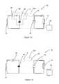
- FIGS. 8A to 8Dshow effective circuit diagrams corresponding to the different stages of operation of the receiver of FIG. 2 according to one embodiment
- FIG. 9shows a circuit diagram for an embodiment of a controller for the receiver of FIG. 2 ;
- FIG. 10shows waveforms corresponding to the operation of the receiver of FIG. 4 according to one embodiment.
- FIGS. 11A to 11Dshow effective circuit diagrams corresponding to the different stages of operation of the receiver of FIG. 4 according to one embodiment.
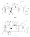
- FIG. 1is a block diagram showing a general representation of an inductive power transfer system 1 .
- the IPT systemincludes a transmitter 2 and a receiver 3 .
- the transmitterincludes a converter 4 that is connected to an appropriate power supply. In FIG. 1 this is shown as a DC-DC converter 5 that is connected to a DC power supply 5 a .
- the convertermay be a non-resonant half bridge converter or any other converter adapted for the particular IPT system, such as a push-pull converter.
- the converteris configured to output an alternating current of desired frequency and amplitude.
- the voltage of the output of the convertermay also be regulated by the converter, the DC-DC converter or combination of both.
- the converter 4is connected to transmitting coil(s) 6 .
- the convertersupplies the transmitting coil(s) with an alternating current such that the transmitting coil(s) generates a time-varying magnetic field with a suitable frequency and amplitude.
- the transmitting coil(s)may also be considered to be an integral part of the converter, but for the sake of clarity this description will refer to them as distinct.
- the transmitting coil(s) 6may be any suitable configuration of coils, depending on the characteristics of the magnetic field that are required in a particular application and the particular geometry of the transmitter.
- the transmitting coilsmay be connected to capacitors (not shown) to create a resonant circuit. Where there are multiple transmitting coils, these may be selectively energised so that only transmitting coils in proximity to suitable receiving coils are energised. In some IPT systems, it may be possible that more than one receiver may be powered simultaneously. In IPT systems, where the receivers are adapted to control the power provided to the load (as, for example, in the embodiments of the present invention described in more detail below), the multiple transmitting coils may be connected to the same converter. This has the benefit of simplifying the transmitter as it does not need to control each transmitting coil separately. Further, it may be possible to adapt the transmitter so that it regulates the power provided to the transmitting coils to a level dependent on the coupled receiver with the highest power demands.
- FIG. 1also shows a receiver 3 .
- the receiverincludes a receiving coil(s) 8 that is suitably connected to receiver circuitry 9 that in turn supplies power to the load 10 .
- the loadmay be a battery.
- the receiver circuitryis adapted to convert the induced current into a form that is appropriate for the load.
- the receiving coilsmay be connected to capacitors (not shown) to create a resonant circuit.
- Embodiments of the present inventionrelate to receivers for use in IPT systems, and for methods for detecting the phase in the receiver, which will be described in more detail below. Though these will be described with respect to certain embodiments, those skilled in the art will appreciate that changes in circuit design or method of operation may be made without departing from the general idea of the invention.
- the receiverincludes a resonant circuit 12 , having a receiving coil 13 (shown as an inductor) and a resonant capacitor 14 .
- the receiveralso includes a voltage multiplier circuit 15 .
- the voltage multiplier circuitwhich will be described in more detail below, provides a DC output to a load 16 .
- the loadmay be any suitable DC load, such as the battery charging circuit of a portable device.
- the loadis connected to a DC smoothing capacitor 17 .
- the receiverincludes a power control switch 18 , which will be described in more detail below, that regulates the power of the DC output.
- the receiveralso includes a controller 19 .
- the receiving coil 13 and resonant capacitor 14are connected in series (i.e. the resonant circuit is ‘series-resonant’).
- the resonant circuitis adapted to receive power from a time-varying magnetic field generated by a suitable transmitter.
- the resonant circuitmay be adapted to be resonant at the operating frequency of the IPT system.
- the receivermay be adapted to be ‘mis-tuned’ to the transmitter frequency, so that active tuning in the receiver can bring the system into tune.
- the values of the receiving coil and resonant capacitorwill affect the resonant frequency of the receiver, and that the receiving coil and resonant capacitor may be selected so as to resonate at the operating frequency of a transmitter or any other suitable frequency. Other considerations may also influence the type and size of the receiving coil and resonant capacitor used in the receiver, for example the dimensions of the receiver or device in which the receiver is used, or the required power.
- the resonant circuitwill produce an AC output.
- the voltage multiplier circuit 15 of the receiver 11 of FIG. 2includes the resonant capacitor 14 from the resonant circuit 12 and two asymmetric current flow devices 20 21 connected in a half-bridge configuration.
- the half-bridge configurationis such that the voltage multiplier circuit has a shared AC and DC ground.
- the rest of this descriptionwill refer to the asymmetric flow device that is generally in parallel with the resonant circuit as ‘first’ 20 and will refer to the asymmetric flow device that is generally in series with the load as ‘second’ 21 .
- the asymmetric current flow devicesare diodes. Those skilled in the art will appreciate that the position and orientation of the diodes is such that the AC input into the voltage multiplier circuit is rectified to produce a DC output.
- asymmetric current flow devicesmay be used instead of the diodes, and the invention is not limited in this respect.
- controlled switchesmay be used.
- a combination of any suitable asymmetric current flow devices(such as diodes or controlled switches) may be used in the voltage multiplier circuit. Controlled switches may provide improved performance over diodes but they must be controlled so that they are switched off when they need to prevent the flow of current. Possible controlled switches that may be used include any suitable transistors such as MOSFETs, IGBTs or BJTs.
- the power control switch 18 of the receiver 11 of FIG. 2regulates the power provided to the load 16 .
- the power control switchis shown in series with the resonant circuit 12 ; however as will be discussed in more detail below, the power control switch may also be positioned in other locations in the receiver.
- the power control switchmay be a transistor such as a MOSFET, IGBT or BJT.
- the power control switchmay include a body diode 18 a.
- the power control switch 18is controlled by the controller 19 .
- the controlleris adapted to receive inputs from parts of the receiver, which can include the current and voltage being supplied to the load 16 .
- the controllermay also be provided with the load's power requirements by inputs or any other suitable means.
- the controllerwill control the power control switch so as to regulate the power provided to the load.
- the power control switchmay be controlled in switch mode.
- the controllermay include a memory.
- the controlleris preferably a programmable logic controller that is programmed to perform different computational tasks, including controlling the power control switch.
- the receiverincludes a resonant circuit 23 , having a receiving coil 24 (shown as an inductor) and a resonant capacitor 25 .
- the receiveralso includes a voltage multiplier circuit 26 , which provides a DC output to a load 30 .
- the loadis connected to a DC smoothing capacitor 29 .
- the receiverincludes a power control switch 32 that may have a body diode 32 a .
- the receiveralso includes a controller 31 .
- This receiveris similar to the receiver 11 of FIG. 2 , however the asymmetric current flow devices used in the voltage multiplier circuit are controlled switches 27 28 .
- the controlled switchesmay have body diodes 27 a 28 a .
- the receiverincludes a resonant circuit 36 , having a receiving coil 37 (shown as an inductor) and a resonant capacitor 38 .
- the receiveralso includes a voltage multiplier circuit 39 having two asymmetric current flow devices 40 41 , which provides a DC output to a load 43 .
- the loadis connected to a DC smoothing capacitor 42 .
- the receiverincludes a power control switch 45 that may have a body diode 45 a .
- the receiveralso includes a controller 44 . This receiver is similar to the receiver 11 of FIG. 2 , however in this embodiment of the invention the power control switch 45 is located in series with the second asymmetric flow control device 41 in the voltage multiplier circuit.
- an inductive power transfer receiver 46for use in an IPT system according to another embodiment of the present invention.
- the receiverincludes a resonant circuit 47 , having a receiving coil 48 (shown as an inductor) and a resonant capacitor 49 .
- the receiveralso includes a voltage multiplier circuit 50 having two asymmetric current flow devices 51 52 , which provides a DC output to a load 54 .
- the loadis connected to a DC smoothing capacitor 53 .
- the receiverincludes a power control switch 56 that may have a body diode 56 a .
- the receiveralso includes a controller 55 . This receiver is similar to the receiver 11 of FIG. 2 , however, in this embodiment of the invention the power control switch 56 is located in series with the first asymmetric power flow device 51 in the voltage multiplier circuit 50 .
- the receivermay include more than one power control switch.
- FIG. 6there is shown an inductive power transfer receiver 57 for use in an IPT system according to another embodiment of the present invention.
- the receiverincludes a resonant circuit 58 , having a receiving coil 59 (shown as an inductor) and a resonant capacitor 60 .
- the receiveralso includes a voltage multiplier circuit 61 having two asymmetric current flow devices 62 63 , which provides a DC output to a load 65 .
- the loadis connected to a DC smoothing capacitor 64 .
- the receiverincludes a power control switch 67 that may have a body diode 67 a .
- the receiveralso includes a controller 66 .
- This receiveris similar to the receiver 11 of FIG. 2 in that it also includes a power control switch 67 in series with the power receiver coil 59 ; however in this embodiment of the invention there is a further power control switch 68 in series with the power receiver coil.
- This further power control switchmay include a body diode 68 a .
- a further power control switchmay improve the Q value for the receiver by allowing both the positive and negative half cycles of current to be controlled to produce a symmetrical current through the power receiver coil.
- FIGS. 2-6show the power control switch(es) in different positions but that it may be possible to position the power control switch in other positions without departing from the invention.
- Having the power control switch included in the resonant circuit or voltage multiplier circuit parts of the receivercan remove the requirement for additional power converter stages in the receiver. In particular, there is no further voltage regulation stage and no bulky DC inductor.
- the control of the power control switch(es)can be adapted depending on the position of the power control circuit(es) in the receiver.
- there are many suitable methods for controlling the power control switch(es)which will result in the regulation of the power provided to the load.
- the voltage multiplier circuitas shown in FIGS. 2-6 described above, is suitable in many situations where the output DC voltage provided to the load needs to be have the same or higher voltage than the input.
- the ‘voltage multiplier’ circuit described abovebecomes a ‘charge pump’ circuit which encompasses rectifiers that increase (i.e. voltage multipliers) or decrease output voltage with respect to the input voltage, where the resonant circuit and power control switch are part of the charge pump circuit.
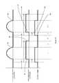
- FIG. 7(and associated FIGS. 8A-8D ), there is shown waveforms for the receiver 11 as shown in FIG. 2 .
- Thisshows how the power control switch 18 may be controlled so as to regulate the power provided to the load 16 . It will be appreciated that this is not the only possible method for regulating the power provided to the load. Further those skilled in the art will appreciate how this method may be adapted for other receiver embodiments of the present invention.
- the stepsare:
- the methoddetects the phase by sensing the occurrence of two operational transitions that may be used as indicators of the phase, and using one of these transitions to indicate a reference phase.
- the methodsenses two transitions that have differing reliability under different load conditions, and uses one as the indicator of the phase of the current.
- the first operational transitionis the change in polarity 76 of the voltage across the first diode 20 in the voltage multiplier circuit 15 .
- the voltage across the first diodewill be clamped at the output voltage. In a preferred embodiment this may be +5V.
- the first diodeConversely, when the current flows in the opposite direction through the resonant circuit, the first diode will be forward biased and so the voltage across the first diode will be near zero volts.
- the change in magnitude of the voltage across the first diode in the voltage multiplier circuitcan be used to indicate the phase of the current in the power control switch 18 . In the embodiment shown in the waveforms of FIG.
- the rising edge of the first diode voltage 76produces a more reliable signal than the falling edge 77 . It may be possible for this rising edge to be detected by a microcontroller such as Programmable System-On-Chip or any other suitable means.
- the rising edgecorresponds to the current through the power flow control switch going from positive to negative 70 .
- Such a change in diode voltage polaritywill typically produce a more reliable signal when the receiver is under a high load. Under a low load, the change in voltage polarity may have excessive noise.
- the voltage across the first diodeis a function of the current flowing through the resonant circuit and at light load; this current may be very low, non-sinusoidal and dominated by non-ideal device properties, without a clear positive and negative cycle.
- the second operational transitionis the voltage spike 78 in the power control switch that occurs when the current across the power control switch 18 reaches zero.
- This spike 78is shown in the waveforms in FIG. 7 .
- the voltage spikeis used advantageously to indicate the zero crossing 72 of the current through the power control switch.
- the signalmay be delayed for half a period 79 such that it will approximately coincide with the current going from positive to negative 74 70 .
- Such a voltage spikewill typically produce a more reliable signal when the receiver is under a low load or medium load. Under a high load, the voltage spike may not be distinguishable, because when fully loaded, the power control switch may never be turned off so as to increase power output, in which case there is no voltage spike across the switch. Alternatively, the power control switch may be turned off for such a short time (i.e. the power control time interval is short), that the voltage spike cannot be processed by the controller.
- the delay 79is necessary so that the first operational transition and the second operational transition, which are related to different parts of the waveform, can be compared. It will also be appreciated that though the delay in the embodiment described above was applied to the second operational transition for half a period, it is consistent with the invention for a delay to be applied to either operational transition (if at all) for any suitable duration.
- the phase referenceis then determined based on which of the operational transitions are detected first, either the first operational transition 76 or the second operational transition (after it has been delayed by half a period) 74 , within a detection window.
- the phase referenceis then determined based on which of the operational transitions are detected first, either the first operational transition 76 or the second operational transition (after it has been delayed by half a period) 74 , within a detection window.
- this phase reference 74is used as a reference point from which the power control time interval 73 is measured. Again, those skilled in the art will appreciate that this reference point may be suitably established at any point in the cycle, with the power control time interval adjusting accordingly, and the invention is not limited in this respect.
- This phase reference 74may also be used as a reference point from which the time when the power control switch is turned off 71 . In this embodiment, the power control switch is turned off less than half a period 80 after the reference point.
- the circuitreceives inputs from the voltage across the first diode 82 (according to the sensing of the first operational transition described above) and the voltage spike across the power control switch 83 (according to the sensing of the second operational transition described above).
- the voltage spike across the power control switchis delayed 84 by half a period. These are input into a windowed trigger 85 .
- the first input detectedis used to indicate the phase of the current.
- the length of the power control time intervalmay be controlled by a proportional-integral controller (PI) circuit 88 .
- the PI circuitmay receive inputs including the power requirements of the load 89 and the power being provided to the load 90 .
- FIG. 10there is shown waveforms for the receiver 35 as shown in FIG. 4 .
- the stepsare:
- the power control switch of the receiver 35 shown in FIG. 4is controlled so as to regulate the power provided to the load according to the following:
- This methodmay be considered to operate in an analogous manner to a bang bang controller with zero hysteresis. It may also be possible to modify the method to operate in an analogous manner to a bang bang controller with a degree of hysteresis.
- the power control switchmay be controlled to switch on or off when the current is zero (i.e. zero-current switching). This may be implemented by detecting the current phase in the resonant circuit using a current sense resistor, a current transformer or some other means. This information may be provided to a controller that controls the power control switch.
- the controllermay be possible to adapt the controller to override the normal control of the power control switch(es) in the case of a specified condition occurring.
- the specified conditionmay be the voltage being provided to the load exceeding or falling below predetermined thresholds.
- the controllermay be adapted to detect the voltage exceeding or falling below the predetermined threshold, and override the normal control of the power control switch by turning the power control switch off or on (which ever would cause the voltage to change as required) until the voltage returns to a suitable operating range.
Landscapes
- Engineering & Computer Science (AREA)
- Power Engineering (AREA)
- Computer Networks & Wireless Communication (AREA)
- Signal Processing (AREA)
- Dc-Dc Converters (AREA)
- Rectifiers (AREA)
- Control Of Electrical Variables (AREA)
- Inverter Devices (AREA)
Abstract
Description
- i. The
power control switch 18 is turned on69. This allows current to flow in the forward direction through the power control switch, so that current is provided to theresonant capacitor 14. TheDC smoothing capacitor 17 provides power to theload 16. This is shown in the effective circuit inFIG. 8A . - ii. When the current through the
power control switch 18 goes from positive to negative70, the power control switch is kept on and power from theresonant circuit 12 is provided to theDC smoothing capacitor 17 and theload 16. This is shown in the effective circuit inFIG. 8B - iii. Before the current reaches zero the
power control switch 18 is turned off71. The power control switch can be turned off at any point when the current through the power control switch is negative. Due to thebody diode 18ain the power control switch, power continues to flow to theDC smoothing capacitor 17 and theload 16. Preferably, the power control switch is kept on until just before the current though the power control switch reaches zero72 as this minimises the losses through the body diode. Since the resonant period of the resonant circuit is known, it can be estimated when the current will reach zero. As will be discussed in more detail below this requires detecting the phase of the current. This is shown in the effective circuit inFIG. 8C . - iv. When the current through the
power control switch 18 reaches zero72, the power control switch is still off, and now thebody diode 18atransitions from forward to reverse bias and will block the flow of current, leaving theresonant circuit 12 open circuited. TheDC smoothing capacitor 17 provides power to theload 16. The power control switch is kept off until the end of a powercontrol time interval 73. This power control time interval is varied according to the power requirements of the load. Essentially, the power control time interval establishes a phase delay between the voltage induced in the receiver coil and the current that flows through the receiver coil, which allows the power provided to the load to be controlled. As will be discussed in more detail below, this power control time interval may be measured from areference point 74 that precedes the current through the power control switch going from negative to zero72. This is shown in the effective circuit inFIG. 8D . - v. After the power
control time interval 73, the power control switch is turned back on75, and the current begins to flow so that power is provided to theresonant capacitor 14. This is shown in the effective circuit inFIG. 8A .
- i. The
- i. The
power control switch 45 is turned on91. This allows current to flow in the forward direction through the power control switch, so that current is provided to theDC smoothing capacitor 42 and theload 43. This is shown in the effective circuit inFIG. 11A . - ii. When the current through the
power control switch 45 reaches zero92, the power control switch is kept on and current is provided to theresonant circuit 36. TheDC smoothing capacitor 42 provides power to theload 43. This is shown in the effective circuit inFIG. 11B - iii. Before the voltage across the
first diode 40 in thevoltage multiplier circuit 39changes polarity 93 the power control switch is turned off94. The switch can be turned off at any point when the current through the power control switch is not positive. This is shown in the effective circuit inFIG. 11C . - iv. When the voltage across the
first diode 40changes polarity 93, thepower control switch 45 is still off, and now thebody diode 45atransitions from forward to reverse bias and will block the flow of current. TheDC smoothing capacitor 42 provides power to theload 43. The power control switch is kept off until the end of a powercontrol time interval 95. This power control time interval is varied according to the power requirements of the load. Essentially, the power control time interval establishes the impedance of the circuit which allows the power provided to the load to be controlled. This is shown in the effective circuit inFIG. 11D . - v. After the power
control time interval 95, thepower control switch 45 is turned back on91, and the current begins to flow so that power is provided to theDC smoothing capacitor 42 and theload 43. This is shown in the effective circuit inFIG. 11A .
- i. The
- i. If the voltage supplied to the
load 43 is less than the load's required voltage, then thepower control switch 45 is turned on so that power from theresonant circuit 36 andvoltage multiplier circuit 39 is provided to the load (see the effective circuits inFIGS. 11A and 11B for when the current through the power control switch is greater than zero and less than zero respectively); - ii. If the voltage supplied to the load is more than the load's required voltage, then the power control switch is turned off. This prevents power from being provided to the load. Also, once the resonant capacitor in the resonant circuit is fully charged, current will no longer flow in the resonant circuit.
- i. If the voltage supplied to the
Claims (22)
Priority Applications (1)
| Application Number | Priority Date | Filing Date | Title |
|---|---|---|---|
| US14/439,340US10608470B2 (en) | 2012-10-29 | 2013-10-29 | Receiver for an inductive power transfer system and a method for controlling the receiver |
Applications Claiming Priority (5)
| Application Number | Priority Date | Filing Date | Title |
|---|---|---|---|
| NZ60328712 | 2012-10-29 | ||
| NZ603287 | 2012-10-29 | ||
| US201261720108P | 2012-10-30 | 2012-10-30 | |
| US14/439,340US10608470B2 (en) | 2012-10-29 | 2013-10-29 | Receiver for an inductive power transfer system and a method for controlling the receiver |
| PCT/NZ2013/000193WO2014070025A2 (en) | 2012-10-29 | 2013-10-29 | A receiver for an inductive power transfer system and a method for controlling the receiver |
Publications (2)
| Publication Number | Publication Date |
|---|---|
| US20150295418A1 US20150295418A1 (en) | 2015-10-15 |
| US10608470B2true US10608470B2 (en) | 2020-03-31 |
Family
ID=50628218
Family Applications (1)
| Application Number | Title | Priority Date | Filing Date |
|---|---|---|---|
| US14/439,340ActiveUS10608470B2 (en) | 2012-10-29 | 2013-10-29 | Receiver for an inductive power transfer system and a method for controlling the receiver |
Country Status (6)
| Country | Link |
|---|---|
| US (1) | US10608470B2 (en) |
| EP (1) | EP2912744B1 (en) |
| JP (1) | JP6370795B2 (en) |
| KR (1) | KR102139841B1 (en) |
| CN (1) | CN104854771B (en) |
| WO (1) | WO2014070025A2 (en) |
Cited By (1)
| Publication number | Priority date | Publication date | Assignee | Title |
|---|---|---|---|---|
| US11876383B1 (en) | 2020-12-10 | 2024-01-16 | Apple Inc. | Wireless power system with voltage regulation |
Families Citing this family (23)
| Publication number | Priority date | Publication date | Assignee | Title |
|---|---|---|---|---|
| KR20210096686A (en) | 2012-11-05 | 2021-08-05 | 애플 인크. | Inductively coupled power transfer systems |
| US20140225447A1 (en)* | 2013-02-11 | 2014-08-14 | Triune Ip Llc | High-frequency wireless power system |
| EP2985846A1 (en)* | 2014-08-14 | 2016-02-17 | Nxp B.V. | Wireless power transmission |
| KR20160021613A (en)* | 2014-08-18 | 2016-02-26 | 삼성전기주식회사 | Apparatus and method for receiving wireless power, and wireless power supply system using the same |
| KR101730223B1 (en)* | 2014-10-27 | 2017-04-25 | 삼성전기주식회사 | Apparatus and method for receiving wireless power, and wireless power supply system using the same |
| CN107636931B (en)* | 2014-11-05 | 2020-12-18 | 苹果公司 | Inductive power receiver |
| DE102014019621A1 (en) | 2014-12-29 | 2016-06-30 | Markus Rehm | Coupling optimized electrical wireless power transmission |
| WO2016186522A1 (en)* | 2015-05-19 | 2016-11-24 | Powerbyproxi Limited | Inductive power receiver |
| WO2017003299A1 (en)* | 2015-06-29 | 2017-01-05 | Powerbyproxi Limited | Inductive power receiver |
| EP3118963B1 (en) | 2015-07-13 | 2019-06-12 | Nxp B.V. | Wireless power receiver |
| ES2930660T3 (en)* | 2015-12-10 | 2022-12-20 | Oreal | Composition for cleaning keratin materials with improved lightening properties |
| WO2017105256A1 (en)* | 2015-12-18 | 2017-06-22 | Powerbyproxi Limited | Inductive power receiver |
| CN106487218B (en)* | 2015-12-30 | 2018-05-04 | 无锡华润矽科微电子有限公司 | The charge pump circuit of chip is received applied to wireless charging |
| US10763698B2 (en)* | 2016-08-23 | 2020-09-01 | The Penn State Research Foundation | Self-regulated reconfigurable resonant voltage/current-mode method and device for extended-range inductive power transmission |
| WO2018048312A1 (en) | 2016-09-06 | 2018-03-15 | Powerbyproxi Limited | An inductive power transmitter |
| US10516284B2 (en)* | 2016-09-15 | 2019-12-24 | Qualcomm Incorporated | Voltage controlled charge pump and battery charger |
| US10439502B2 (en)* | 2016-09-28 | 2019-10-08 | Texas Instruments Incorporated | Resonant rectifier circuit with capacitor sensing |
| US10079548B2 (en)* | 2017-01-23 | 2018-09-18 | Dialog Semiconductor Inc. | Synchronous rectifier control with adaptive minimum off-time |
| CN107799311B (en)* | 2017-10-27 | 2019-05-03 | 温州市洞头立德电子有限公司 | A kind of time capacitor |
| US10333335B2 (en)* | 2017-10-27 | 2019-06-25 | Lear Corporation | System and method of electric vehicle wireless charger output protection using zero voltage switching |
| WO2019218162A1 (en)* | 2018-05-15 | 2019-11-21 | Oppo广东移动通信有限公司 | Device to be charged and wireless charging method and system |
| CN113300482A (en)* | 2021-04-29 | 2021-08-24 | 伏达半导体(合肥)有限公司 | Wireless power transmission apparatus, method and system |
| EP4274107A1 (en)* | 2022-05-06 | 2023-11-08 | Infineon Technologies AG | System with multiple nfc-chips |
Citations (68)
| Publication number | Priority date | Publication date | Assignee | Title |
|---|---|---|---|---|
| GB2199202A (en) | 1986-12-24 | 1988-06-29 | Ferranti Plc | Electric power regulator snubber circuit |
| US4833337A (en) | 1986-10-16 | 1989-05-23 | Sundstrand Corporation | Inductive coupled power system |
| US4914539A (en) | 1989-03-15 | 1990-04-03 | The Boeing Company | Regulator for inductively coupled power distribution system |
| US4973907A (en) | 1988-12-01 | 1990-11-27 | U.S. Philips Corporation | RF coil system having several surface coils |
| EP0609964A2 (en) | 1988-04-11 | 1994-08-10 | The University Of Western Australia | Adjustable reactance device and method |
| US5701121A (en) | 1988-04-11 | 1997-12-23 | Uniscan Ltd. | Transducer and interrogator device |
| US5702431A (en) | 1995-06-07 | 1997-12-30 | Sulzer Intermedics Inc. | Enhanced transcutaneous recharging system for battery powered implantable medical device |
| US6081084A (en)* | 1999-05-12 | 2000-06-27 | Delco Remy America, Inc. | Sensorless power angle control for a vehicle alternator |
| JP2000184625A (en) | 1998-12-21 | 2000-06-30 | Hitachi Kiden Kogyo Ltd | Non-contact power supply method for transport vehicles in transport system |
| JP2001238372A (en) | 2000-02-24 | 2001-08-31 | Nippon Telegr & Teleph Corp <Ntt> | Power transmission system, electromagnetic field generator and electromagnetic field receiver |
| US6301128B1 (en) | 2000-02-09 | 2001-10-09 | Delta Electronics, Inc. | Contactless electrical energy transmission system |
| US6515878B1 (en) | 1997-08-08 | 2003-02-04 | Meins Juergen G. | Method and apparatus for supplying contactless power |
| JP2003509991A (en) | 1999-09-09 | 2003-03-11 | オークランド ユニサービシズ リミテッド | Control of series resonance induction pickup |
| US20040218406A1 (en) | 2003-05-01 | 2004-11-04 | Yungtaek Jang | Contactless electrical energy transmission system having a primary side current feedback control and soft-switched secondary side rectifier |
| WO2004105208A1 (en) | 2003-05-23 | 2004-12-02 | Auckland Uniservices Limited | Methods and apparatus for control of inductively coupled power transfer systems |
| JP2005168246A (en) | 2003-12-05 | 2005-06-23 | Daifuku Co Ltd | Inductive receiving circuit of non-contact power supply system |
| JP2005525705A (en) | 2002-05-13 | 2005-08-25 | スプラッシュパワー リミテッド | Improvements for contactless power transmission |
| EP1609501A1 (en) | 2004-06-24 | 2005-12-28 | Ethicon Endo-Surgery, Inc. | Medical implant having closed loop transcutaneous energy transfer (TET) power transfer regulation circuity |
| US7161331B2 (en) | 2005-04-11 | 2007-01-09 | Yuan Ze University | Boost converter utilizing bi-directional magnetic energy transfer of coupling inductor |
| US20070029965A1 (en) | 2005-07-25 | 2007-02-08 | City University Of Hong Kong | Rechargeable battery circuit and structure for compatibility with a planar inductive charging platform |
| CN101023600A (en) | 2004-07-29 | 2007-08-22 | Jc科技技术株式会社 | An electromagnetic wave amplification relay device and radio electric power conversion equipment using the device |
| US20070237273A1 (en) | 2006-03-02 | 2007-10-11 | Seeteck Tan | Complex filter with automatic tuning capabilities |
| CN101138144A (en) | 2005-04-22 | 2008-03-05 | 株式会社大福 | Secondary-side power receiving circuit of noncontact power supplying equipment |
| WO2008039945A2 (en) | 2006-09-27 | 2008-04-03 | Asyst Technologies, Inc. | Series impedance matched inductive power pick up |
| JP2008104295A (en) | 2006-10-19 | 2008-05-01 | Voltex:Kk | Non-contact power supply |
| US20080157743A1 (en)* | 2005-10-31 | 2008-07-03 | Martin Gary D | Power supply and controller circuits |
| US20080235869A1 (en) | 2007-03-30 | 2008-10-02 | Steffes Jason R | Stadium bed |
| KR20080096919A (en) | 2007-04-30 | 2008-11-04 | (주)제이씨 프로텍 | Non-directional charging container and wireless power charging set for small electronic devices |
| US20090096413A1 (en) | 2006-01-31 | 2009-04-16 | Mojo Mobility, Inc. | System and method for inductive charging of portable devices |
| WO2009074207A2 (en) | 2007-12-12 | 2009-06-18 | Sew-Eurodrive Gmbh & Co. Kg | System for contactless energy transmission and corresponding method |
| WO2009091267A2 (en) | 2008-01-18 | 2009-07-23 | Telemetry Research Limited | Selectable resonant frequency transcutaneous energy transfer system |
| JP2009201211A (en) | 2008-02-20 | 2009-09-03 | Asyst Technologies Japan Inc | Power supply system |
| JP2009539343A (en) | 2006-05-30 | 2009-11-12 | オークランド ユニサービシズ リミテッド | Inductive power feeding system / pickup circuit |
| WO2010030195A1 (en) | 2008-09-11 | 2010-03-18 | Auckland Uniservices Limited | Inductively coupled ac power transfer |
| US20100171368A1 (en) | 2008-09-27 | 2010-07-08 | Schatz David A | Wireless energy transfer with frequency hopping |
| CN101902083A (en) | 2010-07-30 | 2010-12-01 | 重庆大学 | Inductive power transfer system with azimuth self-tuning function |
| WO2011004645A1 (en) | 2009-07-08 | 2011-01-13 | 日本電気株式会社 | Multi-hop wireless communication system, management apparatus, communication apparatus, and control method |
| US20110053500A1 (en) | 2009-09-02 | 2011-03-03 | Qualcomm Incorporated | De-tuning in wireless power reception |
| US20110069516A1 (en)* | 2005-10-24 | 2011-03-24 | Powercast Corporation | Method and apparatus for high efficiency rectification for various loads |
| WO2011046453A1 (en) | 2009-10-12 | 2011-04-21 | Auckland Uniservices Limited | Inductively controlled series resonant ac power transfer |
| US20110090723A1 (en) | 2008-07-07 | 2011-04-21 | Powerbyproxi Limited | Contactless power receiver and method of operation |
| US20110105023A1 (en) | 2009-10-29 | 2011-05-05 | Motorola, Inc. | Adaptive antenna tuning systems and methods |
| US20110116290A1 (en) | 2007-11-05 | 2011-05-19 | John Talbot Boys | Power control |
| US7952322B2 (en) | 2006-01-31 | 2011-05-31 | Mojo Mobility, Inc. | Inductive power source and charging system |
| JP2011205882A (en) | 2010-03-05 | 2011-10-13 | Semiconductor Energy Lab Co Ltd | Rectifying circuit, manufacturing method therefor, radio communication device, and manufacturing method therefor |
| JP2011205761A (en) | 2010-03-25 | 2011-10-13 | Panasonic Electric Works Co Ltd | Non-contact power feeding system and drive method thereof |
| US20110254379A1 (en) | 2008-11-26 | 2011-10-20 | Auckland Uniservices Limited | Bi-directional inductive power transfer |
| US20110254377A1 (en) | 2010-04-08 | 2011-10-20 | Qualcomm Incorporated | Wireless power transmission in electric vehicles |
| US20110280048A1 (en) | 2008-12-12 | 2011-11-17 | Toshikazu Fujiyoshi | Dc-dc converter circuit |
| WO2011145953A1 (en) | 2010-05-19 | 2011-11-24 | Auckland Uniservices Limited | Inductive power transfer system primary track topologies |
| US20120050931A1 (en) | 2010-08-31 | 2012-03-01 | Stephen Christopher Terry | Methods and apparatus to clamp overvoltages for alternating current systems |
| JP2012060850A (en) | 2010-09-13 | 2012-03-22 | Nippon Telegr & Teleph Corp <Ntt> | Resonance type wireless power transmission device and resonance type wireless power transmission method |
| JP2012130173A (en) | 2010-12-16 | 2012-07-05 | Aisin Aw Co Ltd | Power supply device |
| US20120170337A1 (en)* | 2010-12-29 | 2012-07-05 | Gianpaolo Lisi | Voltage multiplication in a wireless receiver |
| US8259428B2 (en) | 2008-04-25 | 2012-09-04 | Access Business Group International Llc | Input protection circuit |
| WO2012133446A1 (en) | 2011-03-30 | 2012-10-04 | Tdk株式会社 | Wireless power supplying/receiving device, and wireless power transmitting system |
| US20120267960A1 (en) | 2011-04-19 | 2012-10-25 | Qualcomm Incorporated | Wireless power transmitter tuning |
| WO2013006068A1 (en) | 2011-07-07 | 2013-01-10 | Powerbyproxi Limited | An inductively coupled power transfer receiver |
| US20130051083A1 (en)* | 2011-08-30 | 2013-02-28 | Silergy Semiconductor Technology (Hangzhou) Ltd | Magnetic coupling and contactless power transmission apparatus |
| WO2013080212A2 (en) | 2011-12-02 | 2013-06-06 | Powermat Technologies Ltd. | System and method for regulating inductive power transmission |
| US20130249479A1 (en)* | 2011-01-18 | 2013-09-26 | Mojo Mobility, Inc. | Systems and methods for wireless power transfer |
| US20140028108A1 (en) | 2012-07-24 | 2014-01-30 | PowerWow Technology Inc. | Inductively coupled power transfer system and device |
| US20140092659A1 (en)* | 2012-09-28 | 2014-04-03 | Au Optronics Corp. | Wireless power transmission device |
| US8786314B2 (en)* | 2010-11-18 | 2014-07-22 | Fuji Electric Co., Ltd. | Contactless power transfer system and control method thereof |
| CN103944388A (en) | 2013-01-22 | 2014-07-23 | 电力集成公司 | Power converter controller with multiple power sources |
| US20150207333A1 (en)* | 2012-09-11 | 2015-07-23 | Access Business Group International Llc | Wireless power control |
| US20150303824A1 (en)* | 2014-04-17 | 2015-10-22 | Linear Technology Corporation | Voltage regulation in resonant power wireless receiver |
| US20150349573A1 (en)* | 2014-05-30 | 2015-12-03 | Infineon Technologies Austria Ag | Single Stage Rectification and Regulation for Wireless Charging Systems |
- 2013
- 2013-10-29KRKR1020157010702Apatent/KR102139841B1/enactiveActive
- 2013-10-29CNCN201380056165.4Apatent/CN104854771B/enactiveActive
- 2013-10-29WOPCT/NZ2013/000193patent/WO2014070025A2/enactiveApplication Filing
- 2013-10-29JPJP2015539546Apatent/JP6370795B2/enactiveActive
- 2013-10-29USUS14/439,340patent/US10608470B2/enactiveActive
- 2013-10-29EPEP13805623.9Apatent/EP2912744B1/enactiveActive
Patent Citations (70)
| Publication number | Priority date | Publication date | Assignee | Title |
|---|---|---|---|---|
| US4833337A (en) | 1986-10-16 | 1989-05-23 | Sundstrand Corporation | Inductive coupled power system |
| GB2199202A (en) | 1986-12-24 | 1988-06-29 | Ferranti Plc | Electric power regulator snubber circuit |
| EP0609964A2 (en) | 1988-04-11 | 1994-08-10 | The University Of Western Australia | Adjustable reactance device and method |
| US5701121A (en) | 1988-04-11 | 1997-12-23 | Uniscan Ltd. | Transducer and interrogator device |
| US4973907A (en) | 1988-12-01 | 1990-11-27 | U.S. Philips Corporation | RF coil system having several surface coils |
| US4914539A (en) | 1989-03-15 | 1990-04-03 | The Boeing Company | Regulator for inductively coupled power distribution system |
| US5702431A (en) | 1995-06-07 | 1997-12-30 | Sulzer Intermedics Inc. | Enhanced transcutaneous recharging system for battery powered implantable medical device |
| US6515878B1 (en) | 1997-08-08 | 2003-02-04 | Meins Juergen G. | Method and apparatus for supplying contactless power |
| JP2000184625A (en) | 1998-12-21 | 2000-06-30 | Hitachi Kiden Kogyo Ltd | Non-contact power supply method for transport vehicles in transport system |
| US6081084A (en)* | 1999-05-12 | 2000-06-27 | Delco Remy America, Inc. | Sensorless power angle control for a vehicle alternator |
| JP2003509991A (en) | 1999-09-09 | 2003-03-11 | オークランド ユニサービシズ リミテッド | Control of series resonance induction pickup |
| US6301128B1 (en) | 2000-02-09 | 2001-10-09 | Delta Electronics, Inc. | Contactless electrical energy transmission system |
| JP2001238372A (en) | 2000-02-24 | 2001-08-31 | Nippon Telegr & Teleph Corp <Ntt> | Power transmission system, electromagnetic field generator and electromagnetic field receiver |
| JP2005525705A (en) | 2002-05-13 | 2005-08-25 | スプラッシュパワー リミテッド | Improvements for contactless power transmission |
| US20040218406A1 (en) | 2003-05-01 | 2004-11-04 | Yungtaek Jang | Contactless electrical energy transmission system having a primary side current feedback control and soft-switched secondary side rectifier |
| WO2004105208A1 (en) | 2003-05-23 | 2004-12-02 | Auckland Uniservices Limited | Methods and apparatus for control of inductively coupled power transfer systems |
| US8093758B2 (en) | 2003-05-23 | 2012-01-10 | Auckland Uniservices Limited | Method and apparatus for control of inductively coupled power transfer systems |
| JP2005168246A (en) | 2003-12-05 | 2005-06-23 | Daifuku Co Ltd | Inductive receiving circuit of non-contact power supply system |
| EP1609501A1 (en) | 2004-06-24 | 2005-12-28 | Ethicon Endo-Surgery, Inc. | Medical implant having closed loop transcutaneous energy transfer (TET) power transfer regulation circuity |
| CN101023600A (en) | 2004-07-29 | 2007-08-22 | Jc科技技术株式会社 | An electromagnetic wave amplification relay device and radio electric power conversion equipment using the device |
| US7161331B2 (en) | 2005-04-11 | 2007-01-09 | Yuan Ze University | Boost converter utilizing bi-directional magnetic energy transfer of coupling inductor |
| CN101138144A (en) | 2005-04-22 | 2008-03-05 | 株式会社大福 | Secondary-side power receiving circuit of noncontact power supplying equipment |
| US20070029965A1 (en) | 2005-07-25 | 2007-02-08 | City University Of Hong Kong | Rechargeable battery circuit and structure for compatibility with a planar inductive charging platform |
| US20110069516A1 (en)* | 2005-10-24 | 2011-03-24 | Powercast Corporation | Method and apparatus for high efficiency rectification for various loads |
| US20080157743A1 (en)* | 2005-10-31 | 2008-07-03 | Martin Gary D | Power supply and controller circuits |
| US20090096413A1 (en) | 2006-01-31 | 2009-04-16 | Mojo Mobility, Inc. | System and method for inductive charging of portable devices |
| US7952322B2 (en) | 2006-01-31 | 2011-05-31 | Mojo Mobility, Inc. | Inductive power source and charging system |
| US20070237273A1 (en) | 2006-03-02 | 2007-10-11 | Seeteck Tan | Complex filter with automatic tuning capabilities |
| JP2009539343A (en) | 2006-05-30 | 2009-11-12 | オークランド ユニサービシズ リミテッド | Inductive power feeding system / pickup circuit |
| WO2008039945A2 (en) | 2006-09-27 | 2008-04-03 | Asyst Technologies, Inc. | Series impedance matched inductive power pick up |
| JP2008104295A (en) | 2006-10-19 | 2008-05-01 | Voltex:Kk | Non-contact power supply |
| US20080235869A1 (en) | 2007-03-30 | 2008-10-02 | Steffes Jason R | Stadium bed |
| KR20080096919A (en) | 2007-04-30 | 2008-11-04 | (주)제이씨 프로텍 | Non-directional charging container and wireless power charging set for small electronic devices |
| US20110116290A1 (en) | 2007-11-05 | 2011-05-19 | John Talbot Boys | Power control |
| WO2009074207A2 (en) | 2007-12-12 | 2009-06-18 | Sew-Eurodrive Gmbh & Co. Kg | System for contactless energy transmission and corresponding method |
| WO2009091267A2 (en) | 2008-01-18 | 2009-07-23 | Telemetry Research Limited | Selectable resonant frequency transcutaneous energy transfer system |
| JP2009201211A (en) | 2008-02-20 | 2009-09-03 | Asyst Technologies Japan Inc | Power supply system |
| US8259428B2 (en) | 2008-04-25 | 2012-09-04 | Access Business Group International Llc | Input protection circuit |
| US20110090723A1 (en) | 2008-07-07 | 2011-04-21 | Powerbyproxi Limited | Contactless power receiver and method of operation |
| WO2010030195A1 (en) | 2008-09-11 | 2010-03-18 | Auckland Uniservices Limited | Inductively coupled ac power transfer |
| US20100171368A1 (en) | 2008-09-27 | 2010-07-08 | Schatz David A | Wireless energy transfer with frequency hopping |
| US20110254379A1 (en) | 2008-11-26 | 2011-10-20 | Auckland Uniservices Limited | Bi-directional inductive power transfer |
| US20110280048A1 (en) | 2008-12-12 | 2011-11-17 | Toshikazu Fujiyoshi | Dc-dc converter circuit |
| WO2011004645A1 (en) | 2009-07-08 | 2011-01-13 | 日本電気株式会社 | Multi-hop wireless communication system, management apparatus, communication apparatus, and control method |
| US20110053500A1 (en) | 2009-09-02 | 2011-03-03 | Qualcomm Incorporated | De-tuning in wireless power reception |
| WO2011046453A1 (en) | 2009-10-12 | 2011-04-21 | Auckland Uniservices Limited | Inductively controlled series resonant ac power transfer |
| US20120313444A1 (en)* | 2009-10-12 | 2012-12-13 | John Talbot Boys | Inductively controlled series resonant ac power transfer |
| US20110105023A1 (en) | 2009-10-29 | 2011-05-05 | Motorola, Inc. | Adaptive antenna tuning systems and methods |
| JP2011205882A (en) | 2010-03-05 | 2011-10-13 | Semiconductor Energy Lab Co Ltd | Rectifying circuit, manufacturing method therefor, radio communication device, and manufacturing method therefor |
| JP2011205761A (en) | 2010-03-25 | 2011-10-13 | Panasonic Electric Works Co Ltd | Non-contact power feeding system and drive method thereof |
| US20110254377A1 (en) | 2010-04-08 | 2011-10-20 | Qualcomm Incorporated | Wireless power transmission in electric vehicles |
| WO2011145953A1 (en) | 2010-05-19 | 2011-11-24 | Auckland Uniservices Limited | Inductive power transfer system primary track topologies |
| CN101902083A (en) | 2010-07-30 | 2010-12-01 | 重庆大学 | Inductive power transfer system with azimuth self-tuning function |
| US20120050931A1 (en) | 2010-08-31 | 2012-03-01 | Stephen Christopher Terry | Methods and apparatus to clamp overvoltages for alternating current systems |
| JP2012060850A (en) | 2010-09-13 | 2012-03-22 | Nippon Telegr & Teleph Corp <Ntt> | Resonance type wireless power transmission device and resonance type wireless power transmission method |
| US8786314B2 (en)* | 2010-11-18 | 2014-07-22 | Fuji Electric Co., Ltd. | Contactless power transfer system and control method thereof |
| JP2012130173A (en) | 2010-12-16 | 2012-07-05 | Aisin Aw Co Ltd | Power supply device |
| US20120170337A1 (en)* | 2010-12-29 | 2012-07-05 | Gianpaolo Lisi | Voltage multiplication in a wireless receiver |
| US20130249479A1 (en)* | 2011-01-18 | 2013-09-26 | Mojo Mobility, Inc. | Systems and methods for wireless power transfer |
| WO2012133446A1 (en) | 2011-03-30 | 2012-10-04 | Tdk株式会社 | Wireless power supplying/receiving device, and wireless power transmitting system |
| US20120267960A1 (en) | 2011-04-19 | 2012-10-25 | Qualcomm Incorporated | Wireless power transmitter tuning |
| WO2013006068A1 (en) | 2011-07-07 | 2013-01-10 | Powerbyproxi Limited | An inductively coupled power transfer receiver |
| US20130051083A1 (en)* | 2011-08-30 | 2013-02-28 | Silergy Semiconductor Technology (Hangzhou) Ltd | Magnetic coupling and contactless power transmission apparatus |
| WO2013080212A2 (en) | 2011-12-02 | 2013-06-06 | Powermat Technologies Ltd. | System and method for regulating inductive power transmission |
| US20140028108A1 (en) | 2012-07-24 | 2014-01-30 | PowerWow Technology Inc. | Inductively coupled power transfer system and device |
| US20150207333A1 (en)* | 2012-09-11 | 2015-07-23 | Access Business Group International Llc | Wireless power control |
| US20140092659A1 (en)* | 2012-09-28 | 2014-04-03 | Au Optronics Corp. | Wireless power transmission device |
| CN103944388A (en) | 2013-01-22 | 2014-07-23 | 电力集成公司 | Power converter controller with multiple power sources |
| US20150303824A1 (en)* | 2014-04-17 | 2015-10-22 | Linear Technology Corporation | Voltage regulation in resonant power wireless receiver |
| US20150349573A1 (en)* | 2014-05-30 | 2015-12-03 | Infineon Technologies Austria Ag | Single Stage Rectification and Regulation for Wireless Charging Systems |
Non-Patent Citations (17)
| Title |
|---|
| Boonyaroonate et al., "Analysis and Design of Class E Isolated DC/DC Converter Using Class E Low dv/dt PWM Synchronous Recrifier", IEEE Transactions on Power Electronics, Institute of Electrical and Electronics Engineers, USA, vol. 16, No. 4, Jul. 1, 2002 (Jul. 1, 2001), XP011043568, ISSN: 0885-8993. |
| Chinese Office Action for CN Application No. 201380056165.4 dated Jan. 22, 2017 (11 pages), translation included. |
| Chinese Office Action for CN Application No. 201380056165.4 dated Sep. 21, 2017 (5 pages). |
| HARUO TERAI, IZUO HIROTA, TAKAHIRO MIYAUCHI, HIDEKI OMORI, KOKI OGURA, MUTSUO NAKAOKA: "Comparative performance evaluations of IGBTs and MCT incorporated into voltage-source-type single-ended quasi-resonant zero-voltage soft switching inverter", ELECTRICAL ENGINEERING IN JAPAN, JOHN WILEY & SONS, INC., US, vol. 144, no. 3, 1 August 2003 (2003-08-01), US, pages 58 - 68, XP055504116, ISSN: 0424-7760, DOI: 10.1002/eej.10151 |
| Hirota et al., "Pratical evaluations of single-ended load resonant inverter using application-specific heating appliance", Power Electronics and Drive Systems, 1995., Proceedings of the 1995 Intern Ational Conference on Singapore Feb. 21-24 1, New Your, NY, USA, IEEE, Feb. 21, 1995 (Feb. 21, 1995), pp. 531-537, XP010140703, DOI: 10.1109/PEDS.1995.404866, ISBN: 987-0-8703-2423-7. |
| HIROTA I., OMORI H., CHANDRA K.A., NAKAOKA M.: "Practical evaluations of single-ended load-resonant inverter using application-specific IGBT and driver IC for induction-heating appliance", POWER ELECTRONICS AND DRIVE SYSTEMS, 1995., PROCEEDINGS OF 1995 INTERN ATIONAL CONFERENCE ON SINGAPORE 21-24 FEB. 1995, NEW YORK, NY, USA,IEEE, 21 February 1995 (1995-02-21) - 24 February 1995 (1995-02-24), pages 531 - 537, XP010140703, ISBN: 978-0-7803-2423-7, DOI: 10.1109/PEDS.1995.404866 |
| Hunter H. Wu, Grant A. Covic, John T. Boys, Daniel J. Robertson, "A Series-Tuned Inductive-Power-Transfer Pickup With a Controllable AC-Voltage Output," Jan. 2011, IEEE Transactions on Power Electronics, vol. 26, No. 1 (Year: 2011).* |
| Hunter H. Wu, Grant A. Covic, John T. Boys, Daniel J. Robertson, "A Series-Tuned Inductive-Power-Transfer Pickup With a Controllable AC-Voltage Output," Jan. 2011, IEEE Transactions on Power Electronics, vol. 26, No. 1.* |
| International Preliminary Report on Patentability for International Application No. PCT/NZ2013/000193 dated May 5, 2015 (9 pages). |
| International Search Report for International Application No. PCT/NZ2013/000193 dated Nov. 8, 2014 (4 pages). |
| ITSDA BOONYAROONATE, SHINSAKU MORI: "Analysis and Design of Class E Isolated DC/DC Converter Using Class E Low <maths><tex>$dv/dt$</tex></maths>PWM Synchronous Rectifier", IEEE TRANSACTIONS ON POWER ELECTRONICS, INSTITUTE OF ELECTRICAL AND ELECTRONICS ENGINEERS, USA, vol. 16, no. 4, 1 July 2001 (2001-07-01), USA, XP011043568, ISSN: 0885-8993 |
| Japanese Office Action for JP Application No. 2015-539546 dated Sep. 29, 2017 (4 pages). |
| Luk et al., "State-Space Modeling of a Class Ed Converter for Inductive Links", IEEE Transactions on Power Electronics. Institute of Electrical and Electronics Engineers, USA, vol. 30, No. 6, Jun. 24, 2014 (Jun. 24, 2014), pp. 3242-3251, XP011570281, ISSN: 0885-8993, DOI: 10.1103/TPEL.2014.2332451 [retrieved on Jan. 16, 2015]. |
| LUK PATRICK CHI-KWONG; ALDHAHER SAMER; FEI WEIZHONG; WHIDBORNE JAMES F.: "State-Space Modeling of a Class ${\bf E}^{\bf 2}$ Converter for Inductive Links", IEEE TRANSACTIONS ON POWER ELECTRONICS, INSTITUTE OF ELECTRICAL AND ELECTRONICS ENGINEERS, USA, vol. 30, no. 6, 1 June 2015 (2015-06-01), USA, pages 3242 - 3251, XP011570281, ISSN: 0885-8993, DOI: 10.1109/TPEL.2014.2332451 |
| Omori et el., A new resonant IPT-wireless EV charging system with single-ended quasi-resonant inverter for home use, 2013 IEEE 14th Workshop on Control and Modeling for Power Electronics (Compel). IEEE, Jun. 23, 2013 (Jun. 23, 2013), pp. 1-7, XP032500858, ISSN: 1093-5142, DOI: 10.1109/COMPEL.2013.6626448 [retrieved on Oct. 9, 2013]. |
| OMORI HIDEKI; NAKAOKA MUTSUO; IGA YUICHI: "A new resonant IPT-wireless EV charging system with single-ended quasi-resonant inverter for home use", 2013 IEEE 14TH WORKSHOP ON CONTROL AND MODELING FOR POWER ELECTRONICS (COMPEL), IEEE, 23 June 2013 (2013-06-23), pages 1 - 7, XP032500858, ISSN: 1093-5142, DOI: 10.1109/COMPEL.2013.6626448 |
| Terai et al, "Comparative performance evaluations of IGBT's and MCT incorporated into voltage-source-type single-ended quasi-resonant zero-voltage soft switching inverter", Electrical Engineering in Japan, vol. 144, No. 3, Aug. 1, 2003 (Aug. 1, 2003), pp. 58-68, XP055504116, US ISSN: 0424-7760, DOI: 10.1002/eej.10151. |
Cited By (2)
| Publication number | Priority date | Publication date | Assignee | Title |
|---|---|---|---|---|
| US11876383B1 (en) | 2020-12-10 | 2024-01-16 | Apple Inc. | Wireless power system with voltage regulation |
| US12218515B2 (en) | 2020-12-10 | 2025-02-04 | Apple Inc. | Wireless power system with voltage regulation |
Also Published As
| Publication number | Publication date |
|---|---|
| KR20150097465A (en) | 2015-08-26 |
| JP2015534448A (en) | 2015-11-26 |
| KR102139841B1 (en) | 2020-07-31 |
| EP2912744A2 (en) | 2015-09-02 |
| JP6370795B2 (en) | 2018-08-08 |
| WO2014070025A2 (en) | 2014-05-08 |
| WO2014070025A3 (en) | 2014-10-02 |
| CN104854771B (en) | 2019-07-19 |
| CN104854771A (en) | 2015-08-19 |
| US20150295418A1 (en) | 2015-10-15 |
| EP2912744B1 (en) | 2018-09-19 |
Similar Documents
| Publication | Publication Date | Title |
|---|---|---|
| US10608470B2 (en) | Receiver for an inductive power transfer system and a method for controlling the receiver | |
| US10348099B2 (en) | Wireless power communication | |
| US10923953B2 (en) | Received wireless power regulation | |
| US7738266B2 (en) | Forward power converter controllers | |
| US9742264B2 (en) | Boost inductor demagnetization detection for bridgeless boost PFC converter operating in boundary-conduction mode | |
| US9973094B2 (en) | Power converter and power conversion method | |
| US11043847B2 (en) | Wireless charging receiver | |
| JP5699470B2 (en) | Switching power supply | |
| US9787204B2 (en) | Switching power supply device | |
| TWI828647B (en) | Active clamp circuit and power apparatus | |
| US20170288554A1 (en) | Power Converter And Power Conversion Method | |
| CN109906538B (en) | Power transmitter and method for wirelessly transmitting power | |
| JP2017537588A (en) | converter | |
| US9882498B2 (en) | Switching power supply device, switching power supply control method, and electronic apparatus | |
| US20210376662A1 (en) | Transmitter and receiver circuitry for power converter systems | |
| WO2015104779A1 (en) | Wireless power supply device and wireless power supply device start-up method | |
| US10447090B1 (en) | Inductive power receiver | |
| CN114846734B (en) | Power receiving device and wireless power supply system | |
| GB2456599A (en) | Resonant discontinuous forward power converter |
Legal Events
| Date | Code | Title | Description |
|---|---|---|---|
| AS | Assignment | Owner name:POWERBYPROXI LIMITED, NEW ZEALAND Free format text:ASSIGNMENT OF ASSIGNORS INTEREST;ASSIGNORS:REN, SAINING;ROBERTSON, DANIEL;DELA CRUZ, LAWRENCE BERNARDO;SIGNING DATES FROM 20150529 TO 20150603;REEL/FRAME:036060/0052 | |
| AS | Assignment | Owner name:POWERBYPROXI LIMITED, NEW ZEALAND Free format text:ADDRESS CHANGE;ASSIGNOR:POWERBYPROXI LIMITED;REEL/FRAME:041244/0740 Effective date:20160704 | |
| AS | Assignment | Owner name:POWERBYPROXI, NEW ZEALAND Free format text:CHANGE OF NAME;ASSIGNOR:POWERBYPROXI LIMITED;REEL/FRAME:045261/0004 Effective date:20171031 Owner name:APPLE INC., CALIFORNIA Free format text:ASSIGNMENT OF ASSIGNORS INTEREST;ASSIGNOR:POWERBYPROXI;REEL/FRAME:045261/0048 Effective date:20171222 | |
| STPP | Information on status: patent application and granting procedure in general | Free format text:NOTICE OF ALLOWANCE MAILED -- APPLICATION RECEIVED IN OFFICE OF PUBLICATIONS | |
| STPP | Information on status: patent application and granting procedure in general | Free format text:DOCKETED NEW CASE - READY FOR EXAMINATION | |
| STPP | Information on status: patent application and granting procedure in general | Free format text:NON FINAL ACTION MAILED | |
| STPP | Information on status: patent application and granting procedure in general | Free format text:RESPONSE TO NON-FINAL OFFICE ACTION ENTERED AND FORWARDED TO EXAMINER | |
| STPP | Information on status: patent application and granting procedure in general | Free format text:NOTICE OF ALLOWANCE MAILED -- APPLICATION RECEIVED IN OFFICE OF PUBLICATIONS | |
| STPP | Information on status: patent application and granting procedure in general | Free format text:PUBLICATIONS -- ISSUE FEE PAYMENT RECEIVED | |
| STCF | Information on status: patent grant | Free format text:PATENTED CASE | |
| MAFP | Maintenance fee payment | Free format text:PAYMENT OF MAINTENANCE FEE, 4TH YEAR, LARGE ENTITY (ORIGINAL EVENT CODE: M1551); ENTITY STATUS OF PATENT OWNER: LARGE ENTITY Year of fee payment:4 |