US10600689B2 - Vias and conductive routing layers in semiconductor substrates - Google Patents
Vias and conductive routing layers in semiconductor substratesDownload PDFInfo
- Publication number
- US10600689B2 US10600689B2US15/687,636US201715687636AUS10600689B2US 10600689 B2US10600689 B2US 10600689B2US 201715687636 AUS201715687636 AUS 201715687636AUS 10600689 B2US10600689 B2US 10600689B2
- Authority
- US
- United States
- Prior art keywords
- dielectric
- aperture
- substrate
- conductive
- conductive material
- Prior art date
- Legal status (The legal status is an assumption and is not a legal conclusion. Google has not performed a legal analysis and makes no representation as to the accuracy of the status listed.)
- Active
Links
- 239000000758substrateSubstances0.000titleclaimsabstractdescription88
- 239000004065semiconductorSubstances0.000titleclaimsabstractdescription70
- 239000004020conductorSubstances0.000claimsabstractdescription47
- 238000012545processingMethods0.000claimsabstractdescription16
- 239000000463materialSubstances0.000claimsdescription61
- 238000002161passivationMethods0.000claimsdescription16
- 229910000679solderInorganic materials0.000claimsdescription8
- RYGMFSIKBFXOCR-UHFFFAOYSA-NCopperChemical compound[Cu]RYGMFSIKBFXOCR-UHFFFAOYSA-N0.000claimsdescription7
- 229910052802copperInorganic materials0.000claimsdescription7
- 239000010949copperSubstances0.000claimsdescription7
- 239000012774insulation materialSubstances0.000claims1
- 238000000034methodMethods0.000abstractdescription61
- 238000000151depositionMethods0.000abstractdescription14
- 238000004519manufacturing processMethods0.000abstractdescription4
- 229920002120photoresistant polymerPolymers0.000description22
- 238000007747platingMethods0.000description11
- 239000011810insulating materialSubstances0.000description10
- 238000005498polishingMethods0.000description9
- 238000005516engineering processMethods0.000description7
- 238000000059patterningMethods0.000description7
- 238000000231atomic layer depositionMethods0.000description6
- 238000005229chemical vapour depositionMethods0.000description5
- 230000008021depositionEffects0.000description5
- VYPSYNLAJGMNEJ-UHFFFAOYSA-NSilicium dioxideChemical compoundO=[Si]=OVYPSYNLAJGMNEJ-UHFFFAOYSA-N0.000description4
- XUIMIQQOPSSXEZ-UHFFFAOYSA-NSiliconChemical compound[Si]XUIMIQQOPSSXEZ-UHFFFAOYSA-N0.000description4
- 241000724291Tobacco streak virusSpecies0.000description4
- 238000007796conventional methodMethods0.000description4
- 239000003989dielectric materialSubstances0.000description4
- 229910052710siliconInorganic materials0.000description4
- 239000010703siliconSubstances0.000description4
- 229910052814silicon oxideInorganic materials0.000description4
- 229910052581Si3N4Inorganic materials0.000description3
- 239000000853adhesiveSubstances0.000description3
- 230000001070adhesive effectEffects0.000description3
- 230000004888barrier functionEffects0.000description3
- 230000007547defectEffects0.000description3
- 238000005530etchingMethods0.000description3
- 238000011049fillingMethods0.000description3
- 238000005240physical vapour depositionMethods0.000description3
- 238000001020plasma etchingMethods0.000description3
- HQVNEWCFYHHQES-UHFFFAOYSA-Nsilicon nitrideChemical compoundN12[Si]34N5[Si]62N3[Si]51N64HQVNEWCFYHHQES-UHFFFAOYSA-N0.000description3
- 238000000137annealingMethods0.000description2
- 238000004140cleaningMethods0.000description2
- 238000005553drillingMethods0.000description2
- 239000000203mixtureSubstances0.000description2
- 230000003647oxidationEffects0.000description2
- 238000007254oxidation reactionMethods0.000description2
- 238000000206photolithographyMethods0.000description2
- 230000001681protective effectEffects0.000description2
- 229910052715tantalumInorganic materials0.000description2
- GUVRBAGPIYLISA-UHFFFAOYSA-Ntantalum atomChemical compound[Ta]GUVRBAGPIYLISA-UHFFFAOYSA-N0.000description2
- BOTDANWDWHJENH-UHFFFAOYSA-NTetraethyl orthosilicateChemical compoundCCO[Si](OCC)(OCC)OCCBOTDANWDWHJENH-UHFFFAOYSA-N0.000description1
- 229910045601alloyInorganic materials0.000description1
- 239000000956alloySubstances0.000description1
- XAGFODPZIPBFFR-UHFFFAOYSA-NaluminiumChemical compound[Al]XAGFODPZIPBFFR-UHFFFAOYSA-N0.000description1
- 229910052782aluminiumInorganic materials0.000description1
- 238000013459approachMethods0.000description1
- 230000000712assemblyEffects0.000description1
- 238000000429assemblyMethods0.000description1
- 239000000919ceramicSubstances0.000description1
- 239000000470constituentSubstances0.000description1
- 238000001816coolingMethods0.000description1
- 230000008878couplingEffects0.000description1
- 238000010168coupling processMethods0.000description1
- 238000005859coupling reactionMethods0.000description1
- 238000001312dry etchingMethods0.000description1
- 238000001035dryingMethods0.000description1
- 238000007772electroless platingMethods0.000description1
- 239000011521glassSubstances0.000description1
- PCHJSUWPFVWCPO-UHFFFAOYSA-NgoldChemical compound[Au]PCHJSUWPFVWCPO-UHFFFAOYSA-N0.000description1
- 229910052737goldInorganic materials0.000description1
- 239000010931goldSubstances0.000description1
- 238000004377microelectronicMethods0.000description1
- 238000012986modificationMethods0.000description1
- 230000004048modificationEffects0.000description1
- 230000010363phase shiftEffects0.000description1
- 230000036470plasma concentrationEffects0.000description1
- 238000007639printingMethods0.000description1
- 238000004528spin coatingMethods0.000description1
- 238000004544sputter depositionMethods0.000description1
- WFKWXMTUELFFGS-UHFFFAOYSA-NtungstenChemical compound[W]WFKWXMTUELFFGS-UHFFFAOYSA-N0.000description1
- 229910052721tungstenInorganic materials0.000description1
- 239000010937tungstenSubstances0.000description1
- 238000001039wet etchingMethods0.000description1
- 238000009736wettingMethods0.000description1
Images


Classifications
- H—ELECTRICITY
- H01—ELECTRIC ELEMENTS
- H01L—SEMICONDUCTOR DEVICES NOT COVERED BY CLASS H10
- H01L21/00—Processes or apparatus adapted for the manufacture or treatment of semiconductor or solid state devices or of parts thereof
- H01L21/70—Manufacture or treatment of devices consisting of a plurality of solid state components formed in or on a common substrate or of parts thereof; Manufacture of integrated circuit devices or of parts thereof
- H01L21/71—Manufacture of specific parts of devices defined in group H01L21/70
- H01L21/768—Applying interconnections to be used for carrying current between separate components within a device comprising conductors and dielectrics
- H01L21/76898—Applying interconnections to be used for carrying current between separate components within a device comprising conductors and dielectrics formed through a semiconductor substrate
- H—ELECTRICITY
- H01—ELECTRIC ELEMENTS
- H01L—SEMICONDUCTOR DEVICES NOT COVERED BY CLASS H10
- H01L23/00—Details of semiconductor or other solid state devices
- H01L23/48—Arrangements for conducting electric current to or from the solid state body in operation, e.g. leads, terminal arrangements ; Selection of materials therefor
- H01L23/481—Internal lead connections, e.g. via connections, feedthrough structures
- H—ELECTRICITY
- H01—ELECTRIC ELEMENTS
- H01L—SEMICONDUCTOR DEVICES NOT COVERED BY CLASS H10
- H01L2224/00—Indexing scheme for arrangements for connecting or disconnecting semiconductor or solid-state bodies and methods related thereto as covered by H01L24/00
- H01L2224/01—Means for bonding being attached to, or being formed on, the surface to be connected, e.g. chip-to-package, die-attach, "first-level" interconnects; Manufacturing methods related thereto
- H01L2224/02—Bonding areas; Manufacturing methods related thereto
- H01L2224/04—Structure, shape, material or disposition of the bonding areas prior to the connecting process
- H01L2224/0401—Bonding areas specifically adapted for bump connectors, e.g. under bump metallisation [UBM]
- H—ELECTRICITY
- H01—ELECTRIC ELEMENTS
- H01L—SEMICONDUCTOR DEVICES NOT COVERED BY CLASS H10
- H01L2224/00—Indexing scheme for arrangements for connecting or disconnecting semiconductor or solid-state bodies and methods related thereto as covered by H01L24/00
- H01L2224/01—Means for bonding being attached to, or being formed on, the surface to be connected, e.g. chip-to-package, die-attach, "first-level" interconnects; Manufacturing methods related thereto
- H01L2224/02—Bonding areas; Manufacturing methods related thereto
- H01L2224/04—Structure, shape, material or disposition of the bonding areas prior to the connecting process
- H01L2224/05—Structure, shape, material or disposition of the bonding areas prior to the connecting process of an individual bonding area
- H01L2224/05001—Internal layers
- H01L2224/0502—Disposition
- H01L2224/05025—Disposition the internal layer being disposed on a via connection of the semiconductor or solid-state body
- H—ELECTRICITY
- H01—ELECTRIC ELEMENTS
- H01L—SEMICONDUCTOR DEVICES NOT COVERED BY CLASS H10
- H01L2224/00—Indexing scheme for arrangements for connecting or disconnecting semiconductor or solid-state bodies and methods related thereto as covered by H01L24/00
- H01L2224/01—Means for bonding being attached to, or being formed on, the surface to be connected, e.g. chip-to-package, die-attach, "first-level" interconnects; Manufacturing methods related thereto
- H01L2224/10—Bump connectors; Manufacturing methods related thereto
- H01L2224/12—Structure, shape, material or disposition of the bump connectors prior to the connecting process
- H01L2224/13—Structure, shape, material or disposition of the bump connectors prior to the connecting process of an individual bump connector
- H01L2224/13001—Core members of the bump connector
- H01L2224/1302—Disposition
- H01L2224/13025—Disposition the bump connector being disposed on a via connection of the semiconductor or solid-state body
- H—ELECTRICITY
- H01—ELECTRIC ELEMENTS
- H01L—SEMICONDUCTOR DEVICES NOT COVERED BY CLASS H10
- H01L24/00—Arrangements for connecting or disconnecting semiconductor or solid-state bodies; Methods or apparatus related thereto
- H01L24/01—Means for bonding being attached to, or being formed on, the surface to be connected, e.g. chip-to-package, die-attach, "first-level" interconnects; Manufacturing methods related thereto
- H01L24/10—Bump connectors ; Manufacturing methods related thereto
- H01L24/15—Structure, shape, material or disposition of the bump connectors after the connecting process
- H01L24/16—Structure, shape, material or disposition of the bump connectors after the connecting process of an individual bump connector
- H—ELECTRICITY
- H01—ELECTRIC ELEMENTS
- H01L—SEMICONDUCTOR DEVICES NOT COVERED BY CLASS H10
- H01L2924/00—Indexing scheme for arrangements or methods for connecting or disconnecting semiconductor or solid-state bodies as covered by H01L24/00
- H—ELECTRICITY
- H01—ELECTRIC ELEMENTS
- H01L—SEMICONDUCTOR DEVICES NOT COVERED BY CLASS H10
- H01L2924/00—Indexing scheme for arrangements or methods for connecting or disconnecting semiconductor or solid-state bodies as covered by H01L24/00
- H01L2924/01—Chemical elements
- H01L2924/01078—Platinum [Pt]
- H—ELECTRICITY
- H01—ELECTRIC ELEMENTS
- H01L—SEMICONDUCTOR DEVICES NOT COVERED BY CLASS H10
- H01L2924/00—Indexing scheme for arrangements or methods for connecting or disconnecting semiconductor or solid-state bodies as covered by H01L24/00
- H01L2924/01—Chemical elements
- H01L2924/01079—Gold [Au]
- H—ELECTRICITY
- H01—ELECTRIC ELEMENTS
- H01L—SEMICONDUCTOR DEVICES NOT COVERED BY CLASS H10
- H01L2924/00—Indexing scheme for arrangements or methods for connecting or disconnecting semiconductor or solid-state bodies as covered by H01L24/00
- H01L2924/095—Indexing scheme for arrangements or methods for connecting or disconnecting semiconductor or solid-state bodies as covered by H01L24/00 with a principal constituent of the material being a combination of two or more materials provided in the groups H01L2924/013 - H01L2924/0715
- H01L2924/097—Glass-ceramics, e.g. devitrified glass
- H01L2924/09701—Low temperature co-fired ceramic [LTCC]
- H—ELECTRICITY
- H01—ELECTRIC ELEMENTS
- H01L—SEMICONDUCTOR DEVICES NOT COVERED BY CLASS H10
- H01L2924/00—Indexing scheme for arrangements or methods for connecting or disconnecting semiconductor or solid-state bodies as covered by H01L24/00
- H01L2924/10—Details of semiconductor or other solid state devices to be connected
- H01L2924/11—Device type
- H01L2924/12—Passive devices, e.g. 2 terminal devices
- H01L2924/1204—Optical Diode
- H01L2924/12042—LASER
- H—ELECTRICITY
- H01—ELECTRIC ELEMENTS
- H01L—SEMICONDUCTOR DEVICES NOT COVERED BY CLASS H10
- H01L2924/00—Indexing scheme for arrangements or methods for connecting or disconnecting semiconductor or solid-state bodies as covered by H01L24/00
- H01L2924/10—Details of semiconductor or other solid state devices to be connected
- H01L2924/11—Device type
- H01L2924/14—Integrated circuits
- H—ELECTRICITY
- H01—ELECTRIC ELEMENTS
- H01L—SEMICONDUCTOR DEVICES NOT COVERED BY CLASS H10
- H01L2924/00—Indexing scheme for arrangements or methods for connecting or disconnecting semiconductor or solid-state bodies as covered by H01L24/00
- H01L2924/30—Technical effects
- H01L2924/301—Electrical effects
- H01L2924/3025—Electromagnetic shielding
Definitions
- the present disclosureis directed generally to vias and conductive routing layers in semiconductor substrates, and associated systems and devices.
- Packaged semiconductor diesincluding memory chips, microprocessor chips, and imager chips, typically include a semiconductor die mounted to a substrate and encased in a plastic protective covering.
- the dieincludes functional features, such as memory cells, processor circuits, imager devices, and interconnecting circuitry.
- the diealso typically includes bond pads electrically coupled to the functional features. The bond pads are electrically connected to pins or other types of terminals that extend outside the protective covering for connecting to busses, circuits, and/or other microelectronic assemblies.
- TSVthrough silicon vias
- TSVsConventional processes for forming TSVs include patterning a semiconductor substrate, etching the semiconductor substrate to create an aperture, and plating the aperture with a conductive material.
- Plating the aperturecan include either pattern plating with a resist mask or blanket plating without a resist mask. Both plating techniques have certain drawbacks.
- pattern platingincludes forming a resist layer, patterning the resist layer, and removing the resist layer after plating, and/or other additional processing stages.
- blanket platingdoes not require as many steps as pattern plating, blanket plating creates a large amount of excess conductive material on the surface of semiconductor substrate. The excess conductive material must be removed before subsequent processing stages, which takes time and wastes the conductive material.
- FIGS. 1A-1Dare schematic side cross-sectional views of a portion of a semiconductor die in accordance with embodiments of the technology.
- FIGS. 2A-2Hare schematic side cross-sectional views of a portion of a semiconductor substrate undergoing a process useful for forming several embodiments of the semiconductor die 100 of FIG. 1A in accordance with embodiments of the technology.
- FIGS. 3A-3Dare schematic side cross-sectional views of a portion of a semiconductor substrate undergoing a process useful for forming several embodiments of the semiconductor die 100 of FIG. 1A in accordance with additional embodiments of the technology.
- semiconductor substrateis used throughout to include a variety of articles of manufacture, including, for example, individual integrated circuit dies, imager dies, sensor dies, and/or dies having other semiconductor features.
- semiconductor substrateis used throughout to include a variety of articles of manufacture, including, for example, individual integrated circuit dies, imager dies, sensor dies, and/or dies having other semiconductor features.
- processes described belowmay be used to form through vias and conductive routing layers in an individual die, or in a plurality of dies, on a wafer or portion of a wafer.
- the wafer or wafer portione.g., wafer form
- the repopulated carrier wafercan include an adhesive material (e.g., a flexible adhesive) surrounded by a generally rigid frame having a perimeter shape comparable to that of an unsingulated wafer, and singulated elements (e.g., dies) surrounded by the adhesive.
- an adhesive materiale.g., a flexible adhesive
- singulated elementse.g., dies
- FIGS. 1A-3Many specific details of certain embodiments are set forth in FIGS. 1A-3 and the following text to provide a thorough understanding of these embodiments. Several other embodiments can have configurations, components, and/or processes different than those described in this disclosure. A person skilled in the relevant art, therefore, will appreciate that additional embodiments may be practiced without several of the details of the embodiments shown in FIGS. 1A-3 .
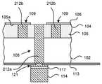
- FIG. 1Ais a schematic side cross-sectional view of a portion of a semiconductor die 100 processed in accordance with embodiments of the technology.
- the semiconductor die 100can include a substrate 102 and a routing structure 104 .
- the semiconductor die 100also includes an optional first passivation material 106 on top of the routing structure 104 and an optional second passivation material 113 on the bottom of the substrate 102 .
- the first and second passivation materials 106 and 113can include silicon oxide, silicon nitride, and/or other suitable dielectric material. In other embodiments, the first and/or second passivation materials 106 and 113 may be omitted.
- the substrate 102has a first substrate surface 102 a and a second substrate surface 102 b .
- the substrate 102can include doped or undoped silicon, TEOS, glass, ceramics, and/or other suitable material.
- the routing structure 104can include a dielectric 105 with a first dielectric surface 105 a and a second dielectric surface 105 b .
- the first dielectric surface 105 ais proximate the optional first passivation material 106
- the second dielectric surface 105 bis proximate the first substrate surface 102 a of the substrate 102 .
- the routing structure 104can also include at least one electrically conductive trace 107 (two traces 107 are shown for illustration purposes) in the dielectric 105 .
- the dielectric 105can include one or more depressions 109 , and the traces 107 can include a first conductive material portion 112 a that at least partially fills the depressions 109 .
- the individual depressions 109have a generally rectangular cross-sectional area extending from the first dielectric surface 105 a to the second dielectric surface 105 b .
- the depressions 109can have oval, scalloped, and/or other cross-sectional areas that extend from the first dielectric surface 105 a to an intermediate depth (not shown) in the dielectric 105 .
- the semiconductor die 100can also include two, three, or any other desired number of routing structures and conductive vias (not shown) electrically coupling at least some of the conductive routing structures.
- the semiconductor die 100can also include an integrated circuit 103 electrically coupled to at least one conductive through via 108 that extends through the dielectric 105 and the substrate 102 .
- the integrated circuit 103can include a processor circuit, a RAM circuit, an ASIC circuit, and/or other suitable circuits.
- the through via 108can include a second conductive material portion 112 b at least partially filling an aperture 110 in the semiconductor die 100 .
- the aperture 110extends from the first dielectric surface 105 a of the dielectric 105 to the second substrate surface 102 b of the substrate 102 .
- the aperture 110can also extend from other locations in the dielectric 105 to the second substrate surface 102 b of the substrate 102 .
- the aperture 110can be entirely contained in the substrate 102 .
- the through via 108has a first end 108 a open to the first dielectric surface 105 a and a second end 108 b proximate the second substrate surface 102 b of the substrate 102 .
- the first end 108 acan form a first bond site 119 through an opening in the optional first passivation material 106
- the second end 108 bcan form a second bond site 121 through an opening in the optional second passivation material 113 .
- the first and second bond sites 119 and 121may be configured to interconnect with other dies, substrates, and/or external devices (not shown) with an interconnect component 114 .
- the interconnect component 114includes a conductive pillar (e.g., a copper pillar) proximate to a wetting material 117 (e.g., a solder material).
- the interconnect component 114connects the second end 108 b of the semiconductor die 100 to a bond site 123 of another semiconductor die 101 (shown in phantom lines for clarity).
- the semiconductor die 101may be structurally and/or functionally similar to or different from the semiconductor die 100 .
- the interconnect component 114can also include a solder ball, a redistribution layer, a through silicon via stud, and/or other suitable interconnect devices components.
- the semiconductor die 100can be formed simultaneously without intervening processing stages.
- the first and second conductive material portions 112 a and 112 bcan be generally homogeneous.
- the homogeneity nature of the conductive material 112is believed to enhance the reliability of the traces 107 and the through via 108 , and therefore the semiconductor die 100 , because the first and second conductive material portions 112 a and 112 b may be subsequently processed together (e.g., in an annealing stage).
- Several embodiments of the semiconductor die 100can also have reduced manufacturing costs when compared to conventional processes because certain processing stages may be eliminated, as described in more detail below with reference to FIGS. 2A-3D .
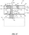
- FIG. 1Bshows another embodiment in which at least one of the traces 107 may be in contact with the through via 108 .
- the routing structure 104may optionally include a conductive wire, trace, and/or another suitable interconnect structure 111 between at least one of the traces 107 and the through via 108 , as shown in FIG. 1C .
- at least one of the traces 107may be formed directly on top of the through via 108 , as shown in FIG. 1D .
- the conductive material 112 of the traces 107 , the through via 108 , and the optional interconnect structure 111may be formed in one single processing stage.
- the portions of the conductive material 112 in these featuresmay be generally homogeneous and without any physical boundaries between one another (dash lines are shown in FIGS. 1B-1D for virtual demarcation purposes only).
- FIGS. 2A-2Hare schematic side cross-sectional views of a portion of a semiconductor substrate 200 undergoing a process useful for forming several embodiments of the semiconductor die 100 of FIG. 1A in accordance with embodiments of the technology.
- the processcan include forming the dielectric 105 on top of the substrate 102 .
- the dielectric 105can be formed by depositing a dielectric material (e.g., silicon oxide) on the substrate 102 using chemical vapor deposition (CVD), atomic layer deposition (ALD), sputtering, and/or other suitable techniques.
- the dielectric 105can be formed by thermal oxidation of the substrate 102 . Even though the dielectric 105 shown in FIG.
- the semiconductor substrate 200can also include multiple layers (not shown) of dielectric material with a physical boundary therebetween.
- the semiconductor substrate 200may also include a passivation material (e.g., silicon nitride), a barrier material (e.g., tantalum), and/or other suitable structures formed on and/or in the dielectric 105 .
- a first photoresist material 202is deposited on the dielectric 105 via spin coating or another suitable deposition technique. Subsequently, the first photoresist material 202 may be patterned to form first openings 204 in the first photoresist material 202 .
- the first openings 204can generally correspond to the pattern of the depressions 109 of FIGS. 1A-1C .
- patterningas used hereinafter generally refers to printing a desired pattern on a photoresist material and subsequently removing certain portions of the photoresist material to form the desired pattern in the photoresist material using photolithography and/or other suitable techniques.
- FIG. 2Cillustrates a first material removal stage of the process, in which the exposed portion of the dielectric 105 is at least partially removed to form the depressions 109 (illustrated as a first depression 109 a and a second depression 109 b ) before the first photoresist material 202 is removed.
- Techniques for removing the exposed portion of the dielectric 105can include wet etching, dry etching, reactive ion etching, and/or other suitable techniques.
- the removal of the dielectric 105can stop when the first substrate surface 102 a of the substrate 102 is exposed.
- the removal of the dielectric 105can stop at an intermediate depth (not shown) before reaching the first substrate surface 102 a of the substrate 102 by adjusting a removal duration (e.g., an etching period during a wet etch process), a removal intensity (e.g., a plasma concentration during a plasma etching process), and/or other suitable material removal parameters.
- a removal duratione.g., an etching period during a wet etch process
- a removal intensitye.g., a plasma concentration during a plasma etching process
- the first and second depressions 109 a and 109 bmay have a depth from about 0.3 microns to about 0.5 microns. In other embodiments, the first and second depressions 109 a and 109 b may have other suitable depths.
- the processcan include at least partially covering the semiconductor substrate 200 with a second photoresist material 208 .
- the processcan also include subsequently patterning the second photoresist material 208 using photolithography and/or other suitable techniques to form a second opening 210 generally corresponding to the aperture 110 of the through via 108 ( FIGS. 1A-1C ).
- the second photoresist material 208can have a composition that is generally similar to that of the first photoresist material 202 .
- the second photoresist material 208can have compositions and/or characteristics that are different from that of the first photoresist material 202 .
- FIG. 2Eillustrates a second material removal stage, in which a portion of the dielectric 105 and the substrate 102 exposed in the second opening 210 is removed to form the aperture 110 using anisotropic etching, reactive ion etching, and/or other suitable techniques.
- the aperture 110can have an aspect ratio from about 5:1 to about 20:1 and can extend into the substrate 102 at a depth of about 50 microns to about 200 microns. In other embodiments, the aperture 110 can have an aspect ratio of about 10:1 and can extend into the substrate material at a depth of about 100 microns.
- the processcan include removing the second photoresist material 208 from the semiconductor substrate 200 .
- the processcan also include depositing a generally conformal insulating material (e.g., silicon oxide, not shown) in the aperture 110 before the second photoresist material 208 is removed.
- the second material removal stagemay include removing a portion of the dielectric 105 and the substrate 102 via laser drilling and/or other suitable drilling techniques without patterning the semiconductor substrate 200 with the second photoresist material 208 , as discussed above with reference to FIG. 2D .
- the processcan include simultaneously filling the aperture 110 and the depressions 109 with a conductive material 212 .
- the conductive material 212includes a first portion 212 a in the aperture 110 , a second portion 212 b in the depressions 109 , and a third (or sacrificial) portion 212 c extending beyond the first dielectric surface 105 a of the dielectric 105 .
- Suitable techniques for introducing the conductive material 212 into the aperture 110 and the depressions 109can include pulsed chemical vapor deposition (pCVD), ionic physical vapor deposition (iPVD), atomic layer deposition (ALD), electro-grafting, bottom-up ECD plating, electroless plating, and/or other suitable techniques.
- the conductive material 212can include copper, aluminum, tungsten, gold and/or alloys of the foregoing constituents.
- the conductive material 212includes electrolytic copper introduced into the aperture 110 and/or the depressions 109 lined with a barrier material (e.g., tantalum).
- the electrolytic copperhas an enhanced purity when compared to electrolessly disposed materials, and when compared to solder.
- the conductive materialcan be at least 90% copper and in some cases, 99% copper.
- the third portion 212 c of the conductive material 212can be subsequently removed such that the first and second portions 212 a and 212 b of the conductive material 212 are generally flush with the first dielectric surface 105 a .
- Techniques for removing the third portion 212 c of the conductive material 212can include chemical-mechanical polishing, electrochemical-mechanical polishing, and/or other suitable techniques.
- the processcan also include subsequently processing the semiconductor substrate 200 to form additional features in and/or on the semiconductor substrate 200 .
- a portion of the substrate 102can be removed from the second substrate surface 102 b using a mechanical or chemical-mechanical technique to expose the second end 108 b of the through via 108 .
- An interconnect component 114e.g., a conductive pillar, a solder ball, a solder bump, a redistribution layer, a through silicon via stud, and/or other suitable interconnect devices
- an external componentnot shown.
- the optional first and/or second passivation materials 106 and 113can be deposited onto the dielectric 105 for insulating the traces 107 and the through via 108 .
- additional dielectric materials and/or conductive tracesmay be formed on top of the routing structure 104 and/or the optional first and second passivation materials 106 and 113 .
- Several embodiments of the processcan be more efficient than conventional techniques by reducing several processing stages.
- Conventional techniques for forming through vias and traces in a semiconductor substratetypically include two conductive material deposition stages. In a first deposition stage, the through vias are initially formed, and in a second deposition stage, the traces are formed. By simultaneously depositing the conductive material 212 into both the depressions 109 and the aperture 110 , only one deposition stage is required. As a result, the second deposition stage and any associated processing stages (e.g., polishing, cleaning, etc.) may be eliminated, thus improving the efficiency and cost-effectiveness of the fabrication process.
- any associated processing stagese.g., polishing, cleaning, etc.
- polishing defectse.g., dishing
- the exposed surface of the conductive material 212 in the through via 108only occupies a small portion of the total surface area of the semiconductor substrate 200 . If the traces 107 were not present, and the semiconductor substrate 200 was polished with only the conductive material 212 in the through via 108 , the polishing pressure on the semiconductor substrate 200 would tend to be non-uniform over the entire surface area of the substrate. Such non-uniformity is believed to result in dishing, chipping, and/or other polishing defects.
- the conductive material 212occupies more of the total surface area of the semiconductor substrate 200 because the conductive material 212 is in both the through via 108 and in the traces 107 . Without being bound by theory, it is believed that the increased surface area of the conductive material 212 can reduce the non-uniformity of the polishing pressure, and thus reducing the risk of polishing defects.
- FIGS. 3A-3Ddescribe a process that includes forming the aperture 110 before forming the depressions 109 .
- the processincludes depositing a first photoresist material 302 onto the dielectric 105 .
- the processcan also include patterning the first photoresist material 302 to form a first opening 304 generally corresponding to the aperture 110 ( FIGS. 1A-1C ).
- the processcan include a first material removal stage, in which a portion of the dielectric 105 and the substrate 102 exposed in the first opening 304 is removed to form the aperture 110 using any of the suitable techniques discussed above. Subsequently, the process can include removing the first photoresist material 302 from the semiconductor substrate 200 .
- the processcan also include depositing a layer of insulating material 306 in the aperture 110 and on the first dielectric surface 105 a of the dielectric 105 .
- the insulating material 306can include silicon oxide, silicon nitride, and/or other suitable material. Suitable techniques for depositing the insulating material 306 can include, but are not limited to, chemical vapor deposition (CVD), physical vapor deposition (PVD), atomic layer deposition (ALD), thermo oxidation, and/or other suitable techniques.
- the processincludes depositing a second photoresist material 308 onto the insulating material 306 .
- the processcan also include patterning the second photoresist material 308 to form second openings 310 generally corresponding to the depressions 109 ( FIGS. 1A-1C ).
- the processcan include a second material removal stage, in which a portion of the insulating material 306 and the dielectric 105 generally corresponding to the second openings 310 is removed to form the depressions 109 . Subsequently, the process can include removing the second photoresist material 308 from the semiconductor substrate 200 . Then the process may include processing stages as discussed above with reference to FIGS. 2F-2H to form the semiconductor die 100 of FIGS. 1A-1C .
- the processcan be more efficient in forming the insulating material 306 in the aperture 110 than conventional techniques.
- the depressions 109may need to be shielded from the insulating material 306 with a fill material (if the depressions 109 are formed before forming the aperture 110 ) or a portion of the insulating material 306 external to the aperture 110 has to be removed via costly polishing (if the depressions 109 are formed after forming the aperture 110 ).
- several embodiments of the process discussed abovemay eliminate such processing stages because the part of the insulating material 306 corresponding to the depressions 109 is simply removed during the second material removal stage.
- a barrier material, a seed material, and/or other suitable structuresmay be formed in the aperture 110 and/or the depressions 109 .
- the foregoing processing stagesmay be modified for forming several embodiments of the semiconductor die 100 ′ and 100 ′′ of FIGS. 1B and 1C , respectively.
- the depressions 109 and the aperture 110may be patterned as a single contiguous depression, as shown in FIG.
- the processcan further include at least one stage of cleaning, drying, cooling, annealing, and/or other suitable stages.
Landscapes
- Engineering & Computer Science (AREA)
- Physics & Mathematics (AREA)
- Condensed Matter Physics & Semiconductors (AREA)
- General Physics & Mathematics (AREA)
- Computer Hardware Design (AREA)
- Microelectronics & Electronic Packaging (AREA)
- Power Engineering (AREA)
- Manufacturing & Machinery (AREA)
- Internal Circuitry In Semiconductor Integrated Circuit Devices (AREA)
Abstract
Description
Claims (20)
Priority Applications (2)
| Application Number | Priority Date | Filing Date | Title |
|---|---|---|---|
| US15/687,636US10600689B2 (en) | 2009-08-21 | 2017-08-28 | Vias and conductive routing layers in semiconductor substrates |
| US16/826,651US20200294854A1 (en) | 2009-08-21 | 2020-03-23 | Vias and conductive routing layers in semiconductor substrates |
Applications Claiming Priority (2)
| Application Number | Priority Date | Filing Date | Title |
|---|---|---|---|
| US12/545,196US9799562B2 (en) | 2009-08-21 | 2009-08-21 | Vias and conductive routing layers in semiconductor substrates |
| US15/687,636US10600689B2 (en) | 2009-08-21 | 2017-08-28 | Vias and conductive routing layers in semiconductor substrates |
Related Parent Applications (1)
| Application Number | Title | Priority Date | Filing Date |
|---|---|---|---|
| US12/545,196DivisionUS9799562B2 (en) | 2009-08-21 | 2009-08-21 | Vias and conductive routing layers in semiconductor substrates |
Related Child Applications (1)
| Application Number | Title | Priority Date | Filing Date |
|---|---|---|---|
| US16/826,651ContinuationUS20200294854A1 (en) | 2009-08-21 | 2020-03-23 | Vias and conductive routing layers in semiconductor substrates |
Publications (2)
| Publication Number | Publication Date |
|---|---|
| US20170372961A1 US20170372961A1 (en) | 2017-12-28 |
| US10600689B2true US10600689B2 (en) | 2020-03-24 |
Family
ID=43604670
Family Applications (3)
| Application Number | Title | Priority Date | Filing Date |
|---|---|---|---|
| US12/545,196Active2029-11-06US9799562B2 (en) | 2009-08-21 | 2009-08-21 | Vias and conductive routing layers in semiconductor substrates |
| US15/687,636ActiveUS10600689B2 (en) | 2009-08-21 | 2017-08-28 | Vias and conductive routing layers in semiconductor substrates |
| US16/826,651PendingUS20200294854A1 (en) | 2009-08-21 | 2020-03-23 | Vias and conductive routing layers in semiconductor substrates |
Family Applications Before (1)
| Application Number | Title | Priority Date | Filing Date |
|---|---|---|---|
| US12/545,196Active2029-11-06US9799562B2 (en) | 2009-08-21 | 2009-08-21 | Vias and conductive routing layers in semiconductor substrates |
Family Applications After (1)
| Application Number | Title | Priority Date | Filing Date |
|---|---|---|---|
| US16/826,651PendingUS20200294854A1 (en) | 2009-08-21 | 2020-03-23 | Vias and conductive routing layers in semiconductor substrates |
Country Status (7)
| Country | Link |
|---|---|
| US (3) | US9799562B2 (en) |
| EP (2) | EP3792966A1 (en) |
| KR (1) | KR101427015B1 (en) |
| CN (1) | CN102484095B (en) |
| SG (3) | SG10201805279PA (en) |
| TW (1) | TWI541937B (en) |
| WO (1) | WO2011022180A2 (en) |
Families Citing this family (11)
| Publication number | Priority date | Publication date | Assignee | Title |
|---|---|---|---|---|
| US7968460B2 (en) | 2008-06-19 | 2011-06-28 | Micron Technology, Inc. | Semiconductor with through-substrate interconnect |
| US9799562B2 (en) | 2009-08-21 | 2017-10-24 | Micron Technology, Inc. | Vias and conductive routing layers in semiconductor substrates |
| US8907457B2 (en) | 2010-02-08 | 2014-12-09 | Micron Technology, Inc. | Microelectronic devices with through-substrate interconnects and associated methods of manufacturing |
| TWI424523B (en)* | 2011-10-25 | 2014-01-21 | Leading Prec Inc | Electrode of electrostatic chuck |
| CN103474394B (en)* | 2013-09-11 | 2015-07-08 | 华进半导体封装先导技术研发中心有限公司 | TSV process method without metal CMP |
| KR101666757B1 (en)* | 2015-07-13 | 2016-10-24 | 앰코 테크놀로지 코리아 주식회사 | Semiconductor package |
| US9911693B2 (en)* | 2015-08-28 | 2018-03-06 | Micron Technology, Inc. | Semiconductor devices including conductive lines and methods of forming the semiconductor devices |
| US11056443B2 (en) | 2019-08-29 | 2021-07-06 | Micron Technology, Inc. | Apparatuses exhibiting enhanced stress resistance and planarity, and related methods |
| US20210335660A1 (en)* | 2020-04-24 | 2021-10-28 | Nanya Technology Corporation | Semiconductor structure having void between bonded wafers and manufacturing method tehreof |
| TWI778406B (en)* | 2020-08-26 | 2022-09-21 | 矽品精密工業股份有限公司 | Electronic package and manufacturing method thereof |
| TWI800977B (en)* | 2020-11-11 | 2023-05-01 | 南韓商Nepes股份有限公司 | Semiconductor package and method for manufacturing the same |
Citations (53)
| Publication number | Priority date | Publication date | Assignee | Title |
|---|---|---|---|---|
| US5173442A (en) | 1990-07-23 | 1992-12-22 | Microelectronics And Computer Technology Corporation | Methods of forming channels and vias in insulating layers |
| US6107186A (en) | 1999-01-27 | 2000-08-22 | Advanced Micro Devices, Inc. | High planarity high-density in-laid metallization patterns by damascene-CMP processing |
| US6221769B1 (en) | 1999-03-05 | 2001-04-24 | International Business Machines Corporation | Method for integrated circuit power and electrical connections via through-wafer interconnects |
| US20020064729A1 (en) | 2000-11-30 | 2002-05-30 | Taiwan Semiconductor Manufacturing Co., Ltd. | Selective electroplating method employing annular edge ring cathode electrode contact |
| US6444576B1 (en) | 2000-06-16 | 2002-09-03 | Chartered Semiconductor Manufacturing, Ltd. | Three dimensional IC package module |
| US6455425B1 (en) | 2000-01-18 | 2002-09-24 | Advanced Micro Devices, Inc. | Selective deposition process for passivating top interface of damascene-type Cu interconnect lines |
| US20030113967A1 (en) | 2000-11-27 | 2003-06-19 | Derryl Allman | Metal-insulator-metal capacitor formed by damascene processes between metal interconnect layers and method of forming same |
| US6582992B2 (en) | 2001-11-16 | 2003-06-24 | Micron Technology, Inc. | Stackable semiconductor package and wafer level fabrication method |
| US20030234416A1 (en) | 2002-06-25 | 2003-12-25 | Thomas Sylvia W. | Capacitor for a semiconductor device and method for fabrication therefor |
| US20040048459A1 (en) | 2002-04-11 | 2004-03-11 | Robert Patti | Interlocking conductor method for bonding wafers to produce stacked integrated circuits |
| US20040121521A1 (en) | 2002-07-31 | 2004-06-24 | Jackson Timothy L. | Semiconductor dice having back side redistribution layer accessed using through-silicon vias, methods of fabrication and assemblies |
| US20050001326A1 (en) | 2003-05-06 | 2005-01-06 | Seiko Epson Corporation | Semiconductor device, stacked semiconductor device, methods of manufacturing the same, circuit board, and electronic instrument |
| US20050009333A1 (en) | 2002-01-14 | 2005-01-13 | Hyo-Jong Lee | Methods of forming metal layers in integrated circuit devices using selective deposition on edges of recesses |
| US20050029630A1 (en) | 2003-03-25 | 2005-02-10 | Yoshihide Matsuo | Manufacturing method for semiconductor device, semiconductor device, and electronic apparatus |
| US6903443B2 (en) | 1997-12-18 | 2005-06-07 | Micron Technology, Inc. | Semiconductor component and interconnect having conductive members and contacts on opposing sides |
| KR20050073372A (en) | 2004-01-09 | 2005-07-13 | 매그나칩 반도체 유한회사 | Methode of forming a contact hole in semiconductor device |
| TW200539244A (en) | 2004-04-16 | 2005-12-01 | Japan Science & Tech Agency | Semiconductor device, the use thereof, and method of manufacturing the same |
| TWI245379B (en) | 2004-05-19 | 2005-12-11 | Sanyo Electric Co | Semiconductor device and method for manufacturing same |
| US20060019467A1 (en) | 2004-07-23 | 2006-01-26 | In-Young Lee | Methods of fabricating integrated circuit chips for multi-chip packaging and wafers and chips formed thereby |
| US20060043599A1 (en) | 2004-09-02 | 2006-03-02 | Salman Akram | Through-wafer interconnects for photoimager and memory wafers |
| US20060046461A1 (en) | 2004-09-01 | 2006-03-02 | Benson Peter A | Method for creating electrically conductive elements for semiconductor device structures using laser ablation processes and methods of fabricating semiconductor device assemblies |
| US20060166498A1 (en) | 2005-01-26 | 2006-07-27 | Micron Technology, Inc. | Vias having varying diameters and fills for use with a semiconductor device and methods of forming semiconductor device structures including same |
| US7091124B2 (en) | 2003-11-13 | 2006-08-15 | Micron Technology, Inc. | Methods for forming vias in microelectronic devices, and methods for packaging microelectronic devices |
| US7111149B2 (en) | 2003-07-07 | 2006-09-19 | Intel Corporation | Method and apparatus for generating a device ID for stacked devices |
| US20060246699A1 (en) | 2005-03-18 | 2006-11-02 | Weidman Timothy W | Process for electroless copper deposition on a ruthenium seed |
| US20060258111A1 (en) | 2005-04-19 | 2006-11-16 | Stmicroelectronics S.A. | Process for producing an integrated circuit comprising a capacitor |
| US20060270196A1 (en) | 2003-09-29 | 2006-11-30 | Kirby Kyle K | Methods of forming semiconductor devices and electrical interconnect structures in semiconductor devices and intermediate structures formed thereby |
| US20070048896A1 (en) | 2005-08-30 | 2007-03-01 | International Business Machines Corporation | Conductive through via structure and process for electronic device carriers |
| US20070063240A1 (en) | 2005-09-12 | 2007-03-22 | Stmicroelectronics (Crolles 2) Sas | Integrated electronic circuit incorporating a capacitor |
| US20070178694A1 (en) | 2004-08-24 | 2007-08-02 | Hiatt William M | Pass through via technology for use during the manufacture of a semiconductor device |
| US20070190692A1 (en) | 2006-01-13 | 2007-08-16 | Mete Erturk | Low resistance and inductance backside through vias and methods of fabricating same |
| US7317256B2 (en) | 2005-06-01 | 2008-01-08 | Intel Corporation | Electronic packaging including die with through silicon via |
| TW200821636A (en) | 2006-09-11 | 2008-05-16 | Manabu Bonkohara | Solid-state image pickup device and method of fabricating the same |
| US20080164573A1 (en) | 2007-01-05 | 2008-07-10 | Basker Veeraraghaven S | Methods for fabricating silicon carriers with conductive through-vias with low stress and low defect density |
| US7449098B1 (en) | 1999-10-05 | 2008-11-11 | Novellus Systems, Inc. | Method for planar electroplating |
| US20080299759A1 (en) | 2007-05-29 | 2008-12-04 | Freescale Semiconductor, Inc. | Method to form a via |
| US20080299762A1 (en) | 2007-05-29 | 2008-12-04 | Freescale Semiconductor, Inc. | Method for forming interconnects for 3-D applications |
| US20080318361A1 (en) | 2007-06-20 | 2008-12-25 | Kwon Whan Han | Method for manufacturing semiconductor package |
| US20090008790A1 (en) | 2007-07-02 | 2009-01-08 | Samsung Electronics Co., Ltd. | Semiconductor device having through electrode and method of fabricating the same |
| US20090051039A1 (en) | 2007-08-24 | 2009-02-26 | Taiwan Semiconductor Manufacturing Company, Ltd. | Through-substrate via for semiconductor device |
| US20090091962A1 (en) | 2007-10-04 | 2009-04-09 | Samsung Electronics Co., Ltd. | Multi-chip memory device with stacked memory chips, method of stacking memory chips, and method of controlling operation of multi-chip package memory |
| US20090124072A1 (en) | 2007-11-14 | 2009-05-14 | Samsung Electronics Co., Ltd. | Semiconductor device having through electrode and method of fabricating the same |
| US20090127668A1 (en) | 2007-11-21 | 2009-05-21 | Samsung Electronics Co., Ltd. | Stacked semiconductor device and method of forming serial path thereof |
| US20090152602A1 (en) | 2007-12-17 | 2009-06-18 | Kazutaka Akiyama | Semiconductor device and method for manufacturing the same |
| US20090180257A1 (en) | 2008-01-15 | 2009-07-16 | Samsung Electronics Co., Ltd. | Stacked semiconductor apparatus, system and method of fabrication |
| US20090206488A1 (en) | 2008-02-16 | 2009-08-20 | International Business Machines Corporation | Through substrate annular via including plug filler |
| US20090224405A1 (en) | 2008-03-07 | 2009-09-10 | Taiwan Semiconductor Manufacturing Co., Ltd. | Through via process |
| US20090239375A1 (en) | 2008-03-19 | 2009-09-24 | Philipp Riess | Dual Damascene Process |
| US20090278237A1 (en) | 2008-05-06 | 2009-11-12 | International Business Machines Corporation | Through substrate via including variable sidewall profile |
| US20090315154A1 (en) | 2008-06-19 | 2009-12-24 | Micron Technology, Inc. | Semiconductor with through-substrate interconnect |
| US20100032764A1 (en)* | 2008-08-08 | 2010-02-11 | Paul Stephen Andry | Through silicon via and method of fabricating same |
| US7745931B2 (en) | 2003-06-09 | 2010-06-29 | Sanyo Electric Co., Ltd. | Semiconductor device and manufacturing method thereof |
| US20110042821A1 (en) | 2009-08-21 | 2011-02-24 | Micron Technology, Inc. | Vias and conductive routing layers in semiconductor substrates |
Family Cites Families (7)
| Publication number | Priority date | Publication date | Assignee | Title |
|---|---|---|---|---|
| FR2830683A1 (en)* | 2001-10-10 | 2003-04-11 | St Microelectronics Sa | REALIZATION OF INDUCTANCE AND VIA IN A MONOLITHIC CIRCUIT |
| JP4248928B2 (en)* | 2003-05-13 | 2009-04-02 | ローム株式会社 | Semiconductor chip manufacturing method, semiconductor device manufacturing method, semiconductor chip, and semiconductor device |
| KR100569590B1 (en)* | 2003-12-30 | 2006-04-10 | 매그나칩 반도체 유한회사 | High frequency semiconductor device and manufacturing method thereof |
| TWI288448B (en)* | 2004-09-10 | 2007-10-11 | Toshiba Corp | Semiconductor device and method of manufacturing the same |
| US7687397B2 (en)* | 2006-06-06 | 2010-03-30 | John Trezza | Front-end processed wafer having through-chip connections |
| KR101458958B1 (en)* | 2008-06-10 | 2014-11-13 | 삼성전자주식회사 | Semiconductor chip, semiconductor package, and method of fabricating the semiconductor chip |
| US8158456B2 (en)* | 2008-12-05 | 2012-04-17 | Taiwan Semiconductor Manufacturing Co., Ltd. | Method of forming stacked dies |
- 2009
- 2009-08-21USUS12/545,196patent/US9799562B2/enactiveActive
- 2010
- 2010-07-28CNCN201080037290.7Apatent/CN102484095B/enactiveActive
- 2010-07-28SGSG10201805279PApatent/SG10201805279PA/enunknown
- 2010-07-28EPEP20205204.9Apatent/EP3792966A1/ennot_activeWithdrawn
- 2010-07-28KRKR1020127007184Apatent/KR101427015B1/enactiveActive
- 2010-07-28EPEP10810356.5Apatent/EP2467874B1/enactiveActive
- 2010-07-28WOPCT/US2010/043563patent/WO2011022180A2/enactiveApplication Filing
- 2010-07-28SGSG10201407347RApatent/SG10201407347RA/enunknown
- 2010-07-28SGSG2012011094Apatent/SG178473A1/enunknown
- 2010-08-12TWTW099126998Apatent/TWI541937B/enactive
- 2017
- 2017-08-28USUS15/687,636patent/US10600689B2/enactiveActive
- 2020
- 2020-03-23USUS16/826,651patent/US20200294854A1/enactivePending
Patent Citations (56)
| Publication number | Priority date | Publication date | Assignee | Title |
|---|---|---|---|---|
| US5173442A (en) | 1990-07-23 | 1992-12-22 | Microelectronics And Computer Technology Corporation | Methods of forming channels and vias in insulating layers |
| US6903443B2 (en) | 1997-12-18 | 2005-06-07 | Micron Technology, Inc. | Semiconductor component and interconnect having conductive members and contacts on opposing sides |
| US6107186A (en) | 1999-01-27 | 2000-08-22 | Advanced Micro Devices, Inc. | High planarity high-density in-laid metallization patterns by damascene-CMP processing |
| US6221769B1 (en) | 1999-03-05 | 2001-04-24 | International Business Machines Corporation | Method for integrated circuit power and electrical connections via through-wafer interconnects |
| US7449098B1 (en) | 1999-10-05 | 2008-11-11 | Novellus Systems, Inc. | Method for planar electroplating |
| US6455425B1 (en) | 2000-01-18 | 2002-09-24 | Advanced Micro Devices, Inc. | Selective deposition process for passivating top interface of damascene-type Cu interconnect lines |
| US6444576B1 (en) | 2000-06-16 | 2002-09-03 | Chartered Semiconductor Manufacturing, Ltd. | Three dimensional IC package module |
| US20030113967A1 (en) | 2000-11-27 | 2003-06-19 | Derryl Allman | Metal-insulator-metal capacitor formed by damascene processes between metal interconnect layers and method of forming same |
| US20020064729A1 (en) | 2000-11-30 | 2002-05-30 | Taiwan Semiconductor Manufacturing Co., Ltd. | Selective electroplating method employing annular edge ring cathode electrode contact |
| US6582992B2 (en) | 2001-11-16 | 2003-06-24 | Micron Technology, Inc. | Stackable semiconductor package and wafer level fabrication method |
| US20050009333A1 (en) | 2002-01-14 | 2005-01-13 | Hyo-Jong Lee | Methods of forming metal layers in integrated circuit devices using selective deposition on edges of recesses |
| US20040048459A1 (en) | 2002-04-11 | 2004-03-11 | Robert Patti | Interlocking conductor method for bonding wafers to produce stacked integrated circuits |
| US20030234416A1 (en) | 2002-06-25 | 2003-12-25 | Thomas Sylvia W. | Capacitor for a semiconductor device and method for fabrication therefor |
| US6962867B2 (en) | 2002-07-31 | 2005-11-08 | Microntechnology, Inc. | Methods of fabrication of semiconductor dice having back side redistribution layer accessed using through-silicon vias and assemblies thereof |
| US20040121521A1 (en) | 2002-07-31 | 2004-06-24 | Jackson Timothy L. | Semiconductor dice having back side redistribution layer accessed using through-silicon vias, methods of fabrication and assemblies |
| US20050029630A1 (en) | 2003-03-25 | 2005-02-10 | Yoshihide Matsuo | Manufacturing method for semiconductor device, semiconductor device, and electronic apparatus |
| US20050001326A1 (en) | 2003-05-06 | 2005-01-06 | Seiko Epson Corporation | Semiconductor device, stacked semiconductor device, methods of manufacturing the same, circuit board, and electronic instrument |
| US7745931B2 (en) | 2003-06-09 | 2010-06-29 | Sanyo Electric Co., Ltd. | Semiconductor device and manufacturing method thereof |
| US7111149B2 (en) | 2003-07-07 | 2006-09-19 | Intel Corporation | Method and apparatus for generating a device ID for stacked devices |
| US20060270196A1 (en) | 2003-09-29 | 2006-11-30 | Kirby Kyle K | Methods of forming semiconductor devices and electrical interconnect structures in semiconductor devices and intermediate structures formed thereby |
| US7091124B2 (en) | 2003-11-13 | 2006-08-15 | Micron Technology, Inc. | Methods for forming vias in microelectronic devices, and methods for packaging microelectronic devices |
| KR20050073372A (en) | 2004-01-09 | 2005-07-13 | 매그나칩 반도체 유한회사 | Methode of forming a contact hole in semiconductor device |
| TW200539244A (en) | 2004-04-16 | 2005-12-01 | Japan Science & Tech Agency | Semiconductor device, the use thereof, and method of manufacturing the same |
| TWI245379B (en) | 2004-05-19 | 2005-12-11 | Sanyo Electric Co | Semiconductor device and method for manufacturing same |
| US20060019467A1 (en) | 2004-07-23 | 2006-01-26 | In-Young Lee | Methods of fabricating integrated circuit chips for multi-chip packaging and wafers and chips formed thereby |
| US20070178694A1 (en) | 2004-08-24 | 2007-08-02 | Hiatt William M | Pass through via technology for use during the manufacture of a semiconductor device |
| US20060046461A1 (en) | 2004-09-01 | 2006-03-02 | Benson Peter A | Method for creating electrically conductive elements for semiconductor device structures using laser ablation processes and methods of fabricating semiconductor device assemblies |
| US20060043599A1 (en) | 2004-09-02 | 2006-03-02 | Salman Akram | Through-wafer interconnects for photoimager and memory wafers |
| US20060166498A1 (en) | 2005-01-26 | 2006-07-27 | Micron Technology, Inc. | Vias having varying diameters and fills for use with a semiconductor device and methods of forming semiconductor device structures including same |
| US20060246699A1 (en) | 2005-03-18 | 2006-11-02 | Weidman Timothy W | Process for electroless copper deposition on a ruthenium seed |
| US20060258111A1 (en) | 2005-04-19 | 2006-11-16 | Stmicroelectronics S.A. | Process for producing an integrated circuit comprising a capacitor |
| US7317256B2 (en) | 2005-06-01 | 2008-01-08 | Intel Corporation | Electronic packaging including die with through silicon via |
| US20070048896A1 (en) | 2005-08-30 | 2007-03-01 | International Business Machines Corporation | Conductive through via structure and process for electronic device carriers |
| US20070063240A1 (en) | 2005-09-12 | 2007-03-22 | Stmicroelectronics (Crolles 2) Sas | Integrated electronic circuit incorporating a capacitor |
| US20070190692A1 (en) | 2006-01-13 | 2007-08-16 | Mete Erturk | Low resistance and inductance backside through vias and methods of fabricating same |
| TW200821636A (en) | 2006-09-11 | 2008-05-16 | Manabu Bonkohara | Solid-state image pickup device and method of fabricating the same |
| US20080164573A1 (en) | 2007-01-05 | 2008-07-10 | Basker Veeraraghaven S | Methods for fabricating silicon carriers with conductive through-vias with low stress and low defect density |
| US20080299759A1 (en) | 2007-05-29 | 2008-12-04 | Freescale Semiconductor, Inc. | Method to form a via |
| US20080299762A1 (en) | 2007-05-29 | 2008-12-04 | Freescale Semiconductor, Inc. | Method for forming interconnects for 3-D applications |
| US20080318361A1 (en) | 2007-06-20 | 2008-12-25 | Kwon Whan Han | Method for manufacturing semiconductor package |
| US20090008790A1 (en) | 2007-07-02 | 2009-01-08 | Samsung Electronics Co., Ltd. | Semiconductor device having through electrode and method of fabricating the same |
| US20090051039A1 (en) | 2007-08-24 | 2009-02-26 | Taiwan Semiconductor Manufacturing Company, Ltd. | Through-substrate via for semiconductor device |
| US20090091962A1 (en) | 2007-10-04 | 2009-04-09 | Samsung Electronics Co., Ltd. | Multi-chip memory device with stacked memory chips, method of stacking memory chips, and method of controlling operation of multi-chip package memory |
| US20090124072A1 (en) | 2007-11-14 | 2009-05-14 | Samsung Electronics Co., Ltd. | Semiconductor device having through electrode and method of fabricating the same |
| US20090127668A1 (en) | 2007-11-21 | 2009-05-21 | Samsung Electronics Co., Ltd. | Stacked semiconductor device and method of forming serial path thereof |
| US20090152602A1 (en) | 2007-12-17 | 2009-06-18 | Kazutaka Akiyama | Semiconductor device and method for manufacturing the same |
| US20090180257A1 (en) | 2008-01-15 | 2009-07-16 | Samsung Electronics Co., Ltd. | Stacked semiconductor apparatus, system and method of fabrication |
| US20090206488A1 (en) | 2008-02-16 | 2009-08-20 | International Business Machines Corporation | Through substrate annular via including plug filler |
| US20090224405A1 (en) | 2008-03-07 | 2009-09-10 | Taiwan Semiconductor Manufacturing Co., Ltd. | Through via process |
| US20090239375A1 (en) | 2008-03-19 | 2009-09-24 | Philipp Riess | Dual Damascene Process |
| US20090278237A1 (en) | 2008-05-06 | 2009-11-12 | International Business Machines Corporation | Through substrate via including variable sidewall profile |
| TW201010026A (en) | 2008-05-06 | 2010-03-01 | Ibm | Through substrate via including variable sidewall profile |
| US20110068477A1 (en) | 2008-05-06 | 2011-03-24 | International Business Machines Corporation | Through substrate via including variable sidewall profile |
| US20090315154A1 (en) | 2008-06-19 | 2009-12-24 | Micron Technology, Inc. | Semiconductor with through-substrate interconnect |
| US20100032764A1 (en)* | 2008-08-08 | 2010-02-11 | Paul Stephen Andry | Through silicon via and method of fabricating same |
| US20110042821A1 (en) | 2009-08-21 | 2011-02-24 | Micron Technology, Inc. | Vias and conductive routing layers in semiconductor substrates |
Non-Patent Citations (14)
| Title |
|---|
| International Search Report and Written Opinion dated Mar. 17, 2011 in International Application No. PCT/ US2010/043563, 10 pages. |
| Kurita, Y. et al., A 3D Stacked Memory Integrated on a Logic Device Using SMAFTI Technology, 2007 IEEE Electronic Components and Technology Conference, pp. 821-829, May 29-Jun. 1, 2007, ISBN 1-4244-0985-3. |
| Office Action dated Apr. 23, 2013 in Taiwan Application No. 099126998, 21 pages. |
| Office Action dated Feb. 5, 2015 in China App. No. 201080037290.7, 21 pages. |
| Office Action dated Jun. 22, 2016 in China Application No. 201080037290.7, 10 pages. |
| Office Action dated Jun. 28, 2013 in Korea Application No. 10-2012-7007184, 15 pages. |
| Office Action dated Mar. 10, 2015 in Taiwan App. No. 099126998, 15 pages. |
| Office Action dated May 15, 2014 in Taiwan Application No. 099126998, 15 pages. |
| Office Action dated Oct. 7, 2015 in Taiwan Application No. 099126998, 17 pages. |
| Office Action dated Oct. 9, 2015 in China Application No. 201080037290.7, 8 pages. |
| Office Action dated Sep. 3, 2013 in China Application No. 201080037290.7, 17 pages. |
| SG Patent Application No. 10201407347R-Singaporean Examination Report and Search Report, dated Apr. 18, 2018, 7 pages. |
| SG Patent Application No. 10201407347R—Singaporean Examination Report and Search Report, dated Apr. 18, 2018, 7 pages. |
| U.S. Appl. No. 12/701,800, filed Feb. 8, 2010, to Kirby et al. |
Also Published As
| Publication number | Publication date |
|---|---|
| KR101427015B1 (en) | 2014-08-05 |
| US20170372961A1 (en) | 2017-12-28 |
| TW201133708A (en) | 2011-10-01 |
| TWI541937B (en) | 2016-07-11 |
| CN102484095A (en) | 2012-05-30 |
| US9799562B2 (en) | 2017-10-24 |
| EP2467874A2 (en) | 2012-06-27 |
| SG10201407347RA (en) | 2014-12-30 |
| CN102484095B (en) | 2017-05-10 |
| EP2467874B1 (en) | 2020-11-04 |
| EP3792966A1 (en) | 2021-03-17 |
| WO2011022180A3 (en) | 2011-05-19 |
| SG178473A1 (en) | 2012-04-27 |
| US20200294854A1 (en) | 2020-09-17 |
| WO2011022180A2 (en) | 2011-02-24 |
| US20110042821A1 (en) | 2011-02-24 |
| KR20120068007A (en) | 2012-06-26 |
| SG10201805279PA (en) | 2018-07-30 |
| EP2467874A4 (en) | 2014-10-29 |
Similar Documents
| Publication | Publication Date | Title |
|---|---|---|
| US10600689B2 (en) | Vias and conductive routing layers in semiconductor substrates | |
| US12368096B2 (en) | Microelectronic devices with through-substrate interconnects and associated methods of manufacturing | |
| US12014958B2 (en) | Microfeature workpieces and methods for forming interconnects in microfeature workpieces | |
| TWI397985B (en) | Integrated circuit | |
| KR101171526B1 (en) | Carrier Wafer Modification Improves TSV Rear Interconnect Formation | |
| US8836085B2 (en) | Cost-effective TSV formation | |
| TWI411079B (en) | Semiconductor die and method for forming a conductive feature | |
| KR101334554B1 (en) | Controlling the device performance by forming a stressed backside dielectric layer | |
| TWI399843B (en) | Semiconductor component and fabrication method thereof | |
| KR20100100629A (en) | Three-dimensional system-in-package architecture | |
| US12237219B2 (en) | Contact with bronze material to mitigate undercut | |
| US20060128147A1 (en) | Method of fabricating electrically conducting vias in a silicon wafer |
Legal Events
| Date | Code | Title | Description |
|---|---|---|---|
| AS | Assignment | Owner name:MICRON TECHNOLOGY, INC., IDAHO Free format text:ASSIGNMENT OF ASSIGNORS INTEREST;ASSIGNORS:KIRBY, KYLE K.;NIROUMAND, SARAH A.;REEL/FRAME:043419/0428 Effective date:20090810 | |
| FEPP | Fee payment procedure | Free format text:ENTITY STATUS SET TO UNDISCOUNTED (ORIGINAL EVENT CODE: BIG.); ENTITY STATUS OF PATENT OWNER: LARGE ENTITY | |
| AS | Assignment | Owner name:U.S. BANK NATIONAL ASSOCIATION, AS COLLATERAL AGENT, MINNESOTA Free format text:SUPPLEMENT NO. 6 TO PATENT SECURITY AGREEMENT;ASSIGNOR:MICRON TECHNOLOGY, INC.;REEL/FRAME:044348/0253 Effective date:20171023 Owner name:MORGAN STANLEY SENIOR FUNDING, INC., AS COLLATERAL AGENT, MARYLAND Free format text:SUPPLEMENT NO. 6 TO PATENT SECURITY AGREEMENT;ASSIGNOR:MICRON TECHNOLOGY, INC.;REEL/FRAME:044653/0333 Effective date:20171023 Owner name:U.S. BANK NATIONAL ASSOCIATION, AS COLLATERAL AGEN Free format text:SUPPLEMENT NO. 6 TO PATENT SECURITY AGREEMENT;ASSIGNOR:MICRON TECHNOLOGY, INC.;REEL/FRAME:044348/0253 Effective date:20171023 Owner name:MORGAN STANLEY SENIOR FUNDING, INC., AS COLLATERAL Free format text:SUPPLEMENT NO. 6 TO PATENT SECURITY AGREEMENT;ASSIGNOR:MICRON TECHNOLOGY, INC.;REEL/FRAME:044653/0333 Effective date:20171023 | |
| AS | Assignment | Owner name:JPMORGAN CHASE BANK, N.A., AS COLLATERAL AGENT, ILLINOIS Free format text:SECURITY INTEREST;ASSIGNORS:MICRON TECHNOLOGY, INC.;MICRON SEMICONDUCTOR PRODUCTS, INC.;REEL/FRAME:047540/0001 Effective date:20180703 Owner name:JPMORGAN CHASE BANK, N.A., AS COLLATERAL AGENT, IL Free format text:SECURITY INTEREST;ASSIGNORS:MICRON TECHNOLOGY, INC.;MICRON SEMICONDUCTOR PRODUCTS, INC.;REEL/FRAME:047540/0001 Effective date:20180703 | |
| AS | Assignment | Owner name:MICRON TECHNOLOGY, INC., IDAHO Free format text:RELEASE BY SECURED PARTY;ASSIGNOR:U.S. BANK NATIONAL ASSOCIATION, AS AGENT;REEL/FRAME:046597/0333 Effective date:20180629 | |
| STPP | Information on status: patent application and granting procedure in general | Free format text:RESPONSE TO NON-FINAL OFFICE ACTION ENTERED AND FORWARDED TO EXAMINER | |
| STPP | Information on status: patent application and granting procedure in general | Free format text:FINAL REJECTION MAILED | |
| AS | Assignment | Owner name:MICRON TECHNOLOGY, INC., CALIFORNIA Free format text:RELEASE BY SECURED PARTY;ASSIGNOR:MORGAN STANLEY SENIOR FUNDING, INC., AS COLLATERAL AGENT;REEL/FRAME:050709/0838 Effective date:20190731 | |
| STPP | Information on status: patent application and granting procedure in general | Free format text:DOCKETED NEW CASE - READY FOR EXAMINATION | |
| STPP | Information on status: patent application and granting procedure in general | Free format text:NOTICE OF ALLOWANCE MAILED -- APPLICATION RECEIVED IN OFFICE OF PUBLICATIONS | |
| AS | Assignment | Owner name:MICRON SEMICONDUCTOR PRODUCTS, INC., IDAHO Free format text:RELEASE BY SECURED PARTY;ASSIGNOR:JPMORGAN CHASE BANK, N.A., AS COLLATERAL AGENT;REEL/FRAME:051028/0001 Effective date:20190731 Owner name:MICRON TECHNOLOGY, INC., IDAHO Free format text:RELEASE BY SECURED PARTY;ASSIGNOR:JPMORGAN CHASE BANK, N.A., AS COLLATERAL AGENT;REEL/FRAME:051028/0001 Effective date:20190731 | |
| STPP | Information on status: patent application and granting procedure in general | Free format text:PUBLICATIONS -- ISSUE FEE PAYMENT VERIFIED | |
| STCF | Information on status: patent grant | Free format text:PATENTED CASE | |
| MAFP | Maintenance fee payment | Free format text:PAYMENT OF MAINTENANCE FEE, 4TH YEAR, LARGE ENTITY (ORIGINAL EVENT CODE: M1551); ENTITY STATUS OF PATENT OWNER: LARGE ENTITY Year of fee payment:4 |