US10599234B2 - Executing gestures with active stylus - Google Patents
Executing gestures with active stylusDownload PDFInfo
- Publication number
- US10599234B2 US10599234B2US14/832,049US201514832049AUS10599234B2US 10599234 B2US10599234 B2US 10599234B2US 201514832049 AUS201514832049 AUS 201514832049AUS 10599234 B2US10599234 B2US 10599234B2
- Authority
- US
- United States
- Prior art keywords
- stylus
- touch
- active stylus
- movement
- distance
- Prior art date
- Legal status (The legal status is an assumption and is not a legal conclusion. Google has not performed a legal analysis and makes no representation as to the accuracy of the status listed.)
- Active, expires
Links
Images


Classifications
- G—PHYSICS
- G06—COMPUTING OR CALCULATING; COUNTING
- G06F—ELECTRIC DIGITAL DATA PROCESSING
- G06F3/00—Input arrangements for transferring data to be processed into a form capable of being handled by the computer; Output arrangements for transferring data from processing unit to output unit, e.g. interface arrangements
- G06F3/01—Input arrangements or combined input and output arrangements for interaction between user and computer
- G06F3/03—Arrangements for converting the position or the displacement of a member into a coded form
- G06F3/033—Pointing devices displaced or positioned by the user, e.g. mice, trackballs, pens or joysticks; Accessories therefor
- G06F3/0354—Pointing devices displaced or positioned by the user, e.g. mice, trackballs, pens or joysticks; Accessories therefor with detection of 2D relative movements between the device, or an operating part thereof, and a plane or surface, e.g. 2D mice, trackballs, pens or pucks
- G06F3/03545—Pens or stylus
- G—PHYSICS
- G06—COMPUTING OR CALCULATING; COUNTING
- G06F—ELECTRIC DIGITAL DATA PROCESSING
- G06F3/00—Input arrangements for transferring data to be processed into a form capable of being handled by the computer; Output arrangements for transferring data from processing unit to output unit, e.g. interface arrangements
- G06F3/01—Input arrangements or combined input and output arrangements for interaction between user and computer
- G06F3/017—Gesture based interaction, e.g. based on a set of recognized hand gestures
- G—PHYSICS
- G06—COMPUTING OR CALCULATING; COUNTING
- G06F—ELECTRIC DIGITAL DATA PROCESSING
- G06F3/00—Input arrangements for transferring data to be processed into a form capable of being handled by the computer; Output arrangements for transferring data from processing unit to output unit, e.g. interface arrangements
- G06F3/01—Input arrangements or combined input and output arrangements for interaction between user and computer
- G06F3/03—Arrangements for converting the position or the displacement of a member into a coded form
- G06F3/033—Pointing devices displaced or positioned by the user, e.g. mice, trackballs, pens or joysticks; Accessories therefor
- G06F3/0346—Pointing devices displaced or positioned by the user, e.g. mice, trackballs, pens or joysticks; Accessories therefor with detection of the device orientation or free movement in a 3D space, e.g. 3D mice, 6-DOF [six degrees of freedom] pointers using gyroscopes, accelerometers or tilt-sensors
- G—PHYSICS
- G06—COMPUTING OR CALCULATING; COUNTING
- G06F—ELECTRIC DIGITAL DATA PROCESSING
- G06F3/00—Input arrangements for transferring data to be processed into a form capable of being handled by the computer; Output arrangements for transferring data from processing unit to output unit, e.g. interface arrangements
- G06F3/01—Input arrangements or combined input and output arrangements for interaction between user and computer
- G06F3/03—Arrangements for converting the position or the displacement of a member into a coded form
- G06F3/041—Digitisers, e.g. for touch screens or touch pads, characterised by the transducing means
- G06F3/0416—Control or interface arrangements specially adapted for digitisers
- G06F3/04162—Control or interface arrangements specially adapted for digitisers for exchanging data with external devices, e.g. smart pens, via the digitiser sensing hardware
- G—PHYSICS
- G06—COMPUTING OR CALCULATING; COUNTING
- G06F—ELECTRIC DIGITAL DATA PROCESSING
- G06F3/00—Input arrangements for transferring data to be processed into a form capable of being handled by the computer; Output arrangements for transferring data from processing unit to output unit, e.g. interface arrangements
- G06F3/01—Input arrangements or combined input and output arrangements for interaction between user and computer
- G06F3/03—Arrangements for converting the position or the displacement of a member into a coded form
- G06F3/041—Digitisers, e.g. for touch screens or touch pads, characterised by the transducing means
- G06F3/044—Digitisers, e.g. for touch screens or touch pads, characterised by the transducing means by capacitive means
- G06F3/0441—Digitisers, e.g. for touch screens or touch pads, characterised by the transducing means by capacitive means using active external devices, e.g. active pens, for receiving changes in electrical potential transmitted by the digitiser, e.g. tablet driving signals
- G—PHYSICS
- G06—COMPUTING OR CALCULATING; COUNTING
- G06F—ELECTRIC DIGITAL DATA PROCESSING
- G06F3/00—Input arrangements for transferring data to be processed into a form capable of being handled by the computer; Output arrangements for transferring data from processing unit to output unit, e.g. interface arrangements
- G06F3/01—Input arrangements or combined input and output arrangements for interaction between user and computer
- G06F3/03—Arrangements for converting the position or the displacement of a member into a coded form
- G06F3/041—Digitisers, e.g. for touch screens or touch pads, characterised by the transducing means
- G06F3/044—Digitisers, e.g. for touch screens or touch pads, characterised by the transducing means by capacitive means
- G06F3/0442—Digitisers, e.g. for touch screens or touch pads, characterised by the transducing means by capacitive means using active external devices, e.g. active pens, for transmitting changes in electrical potential to be received by the digitiser
- G—PHYSICS
- G06—COMPUTING OR CALCULATING; COUNTING
- G06F—ELECTRIC DIGITAL DATA PROCESSING
- G06F3/00—Input arrangements for transferring data to be processed into a form capable of being handled by the computer; Output arrangements for transferring data from processing unit to output unit, e.g. interface arrangements
- G06F3/01—Input arrangements or combined input and output arrangements for interaction between user and computer
- G06F3/03—Arrangements for converting the position or the displacement of a member into a coded form
- G06F3/041—Digitisers, e.g. for touch screens or touch pads, characterised by the transducing means
- G06F3/046—Digitisers, e.g. for touch screens or touch pads, characterised by the transducing means by electromagnetic means
- G—PHYSICS
- G06—COMPUTING OR CALCULATING; COUNTING
- G06F—ELECTRIC DIGITAL DATA PROCESSING
- G06F3/00—Input arrangements for transferring data to be processed into a form capable of being handled by the computer; Output arrangements for transferring data from processing unit to output unit, e.g. interface arrangements
- G06F3/01—Input arrangements or combined input and output arrangements for interaction between user and computer
- G06F3/048—Interaction techniques based on graphical user interfaces [GUI]
- G06F3/0487—Interaction techniques based on graphical user interfaces [GUI] using specific features provided by the input device, e.g. functions controlled by the rotation of a mouse with dual sensing arrangements, or of the nature of the input device, e.g. tap gestures based on pressure sensed by a digitiser
- G06F3/0488—Interaction techniques based on graphical user interfaces [GUI] using specific features provided by the input device, e.g. functions controlled by the rotation of a mouse with dual sensing arrangements, or of the nature of the input device, e.g. tap gestures based on pressure sensed by a digitiser using a touch-screen or digitiser, e.g. input of commands through traced gestures
- G06F3/04883—Interaction techniques based on graphical user interfaces [GUI] using specific features provided by the input device, e.g. functions controlled by the rotation of a mouse with dual sensing arrangements, or of the nature of the input device, e.g. tap gestures based on pressure sensed by a digitiser using a touch-screen or digitiser, e.g. input of commands through traced gestures for inputting data by handwriting, e.g. gesture or text
- G—PHYSICS
- G06—COMPUTING OR CALCULATING; COUNTING
- G06F—ELECTRIC DIGITAL DATA PROCESSING
- G06F2203/00—Indexing scheme relating to G06F3/00 - G06F3/048
- G06F2203/038—Indexing scheme relating to G06F3/038
- G06F2203/0381—Multimodal input, i.e. interface arrangements enabling the user to issue commands by simultaneous use of input devices of different nature, e.g. voice plus gesture on digitizer
- G—PHYSICS
- G06—COMPUTING OR CALCULATING; COUNTING
- G06F—ELECTRIC DIGITAL DATA PROCESSING
- G06F2203/00—Indexing scheme relating to G06F3/00 - G06F3/048
- G06F2203/038—Indexing scheme relating to G06F3/038
- G06F2203/0384—Wireless input, i.e. hardware and software details of wireless interface arrangements for pointing devices
- G—PHYSICS
- G06—COMPUTING OR CALCULATING; COUNTING
- G06F—ELECTRIC DIGITAL DATA PROCESSING
- G06F2203/00—Indexing scheme relating to G06F3/00 - G06F3/048
- G06F2203/041—Indexing scheme relating to G06F3/041 - G06F3/045
- G06F2203/04104—Multi-touch detection in digitiser, i.e. details about the simultaneous detection of a plurality of touching locations, e.g. multiple fingers or pen and finger
- G—PHYSICS
- G06—COMPUTING OR CALCULATING; COUNTING
- G06F—ELECTRIC DIGITAL DATA PROCESSING
- G06F2203/00—Indexing scheme relating to G06F3/00 - G06F3/048
- G06F2203/041—Indexing scheme relating to G06F3/041 - G06F3/045
- G06F2203/04106—Multi-sensing digitiser, i.e. digitiser using at least two different sensing technologies simultaneously or alternatively, e.g. for detecting pen and finger, for saving power or for improving position detection
- G—PHYSICS
- G06—COMPUTING OR CALCULATING; COUNTING
- G06F—ELECTRIC DIGITAL DATA PROCESSING
- G06F2203/00—Indexing scheme relating to G06F3/00 - G06F3/048
- G06F2203/048—Indexing scheme relating to G06F3/048
- G06F2203/04808—Several contacts: gestures triggering a specific function, e.g. scrolling, zooming, right-click, when the user establishes several contacts with the surface simultaneously; e.g. using several fingers or a combination of fingers and pen
- G—PHYSICS
- G06—COMPUTING OR CALCULATING; COUNTING
- G06F—ELECTRIC DIGITAL DATA PROCESSING
- G06F3/00—Input arrangements for transferring data to be processed into a form capable of being handled by the computer; Output arrangements for transferring data from processing unit to output unit, e.g. interface arrangements
- G06F3/01—Input arrangements or combined input and output arrangements for interaction between user and computer
- G06F3/03—Arrangements for converting the position or the displacement of a member into a coded form
- G06F3/041—Digitisers, e.g. for touch screens or touch pads, characterised by the transducing means
- G06F3/0416—Control or interface arrangements specially adapted for digitisers
- G06F3/04164—Connections between sensors and controllers, e.g. routing lines between electrodes and connection pads
Definitions
- This disclosuregenerally relates to active styluses.
- a touch sensormay detect the presence and location of a touch or the proximity of an object (such as a user's finger or a stylus) within a touch-sensitive area of the touch sensor overlaid on a display screen, for example.
- the touch sensormay enable a user to interact directly with what is displayed on the screen, rather than indirectly with a mouse or touch pad.
- a touch sensormay be attached to or provided as part of a desktop computer, laptop computer, tablet computer, personal digital assistant (PDA), smartphone, satellite navigation device, portable media player, portable game console, kiosk computer, point-of-sale device, or other suitable device.
- a control panel on a household or other appliancemay include a touch sensor.
- touch sensorssuch as, for example, resistive touch screens, surface acoustic wave touch screens, and capacitive touch screens.
- reference to a touch sensormay encompass a touch screen, and vice versa, where appropriate.
- a touch-sensor controllermay process the change in capacitance to determine its position on the touch screen.
- FIG. 1illustrates an example touch sensor with an example touch-sensor controller.
- FIG. 2illustrates an example active stylus exterior.
- FIG. 3illustrates an example active stylus interior.
- FIG. 4illustrates an example active stylus with touch sensor device.
- FIG. 5illustrates an example active stylus capable of executing gestures.
- FIGS. 6A and 6Billustrate example embodiments of providing input directly to a touch-sensitive device by executing gestures with an active stylus.
- FIG. 7illustrates an example touch-sensitive device receiving input directly from a gesture and also receiving input relating to the same or another gesture from a component of a touch-sensor system.
- FIG. 8illustrates an example combination input using an active stylus.
- FIG. 1illustrates an example touch sensor 10 with an example touch-sensor controller 12 .
- Touch sensor 10 and touch-sensor controller 12may detect the presence and location of a touch or the proximity of an object within a touch-sensitive area of touch sensor 10 .
- reference to a touch sensormay encompass both the touch sensor and its touch-sensor controller, where appropriate.
- reference to a touch-sensor controllermay encompass both the touch-sensor controller and its touch sensor, where appropriate.
- Touch sensor 10may include one or more touch-sensitive areas, where appropriate.
- Touch sensor 10may include an array of drive and sense electrodes (or an array of electrodes of a single type) disposed on one or more substrates, which may be made of a dielectric material.
- reference to a touch sensormay encompass both the electrodes of the touch sensor and the substrate(s) that they are disposed on, where appropriate.
- reference to a touch sensormay encompass the electrodes of the touch sensor, but not the substrate(s) that they are disposed on.
- An electrodemay be an area of conductive material forming a shape, such as for example a disc, square, rectangle, thin line, other suitable shape, or suitable combination of these.
- One or more cuts in one or more layers of conductive materialmay (at least in part) create the shape of an electrode, and the area of the shape may (at least in part) be bounded by those cuts.
- the conductive material of an electrodemay occupy approximately 100% of the area of its shape.
- an electrodemay be made of indium tin oxide (ITO) and the ITO of the electrode may occupy approximately 100% of the area of its shape (sometimes referred to as a 100% fill), where appropriate.
- ITOindium tin oxide
- the conductive material of an electrodemay occupy substantially less than 100% of the area of its shape.
- an electrodemay be made of fine lines of metal or other conductive material (FLM), such as for example copper, silver, or a copper- or silver-based material, and the fine lines of conductive material may occupy approximately 5% of the area of its shape in a hatched, mesh, or other suitable pattern.
- FLMconductive material
- reference to FLMencompasses such material, where appropriate.
- the shapes of the electrodes (or other elements) of a touch sensormay constitute in whole or in part one or more macro-features of the touch sensor.
- One or more characteristics of the implementation of those shapesmay constitute in whole or in part one or more micro-features of the touch sensor.
- One or more macro-features of a touch sensormay determine one or more characteristics of its functionality, and one or more micro-features of the touch sensor may determine one or more optical features of the touch sensor, such as transmittance, refraction, or reflection.
- a mechanical stackmay contain the substrate (or multiple substrates) and the conductive material forming the drive or sense electrodes of touch sensor 10 .
- the mechanical stackmay include a first layer of optically clear adhesive (OCA) beneath a cover panel.
- OCAoptically clear adhesive
- the cover panelmay be clear and made of a resilient material suitable for repeated touching, such as for example glass, polycarbonate, or poly(methyl methacrylate) (PMMA).
- PMMApoly(methyl methacrylate)
- This disclosurecontemplates any suitable cover panel made of any suitable material.
- the first layer of OCAmay be disposed between the cover panel and the substrate with the conductive material forming the drive or sense electrodes.
- the mechanical stackmay also include a second layer of OCA and a dielectric layer (which may be made of PET or another suitable material, similar to the substrate with the conductive material forming the drive or sense electrodes).
- a thin coating of a dielectric materialmay be applied instead of the second layer of OCA and the dielectric layer.
- the second layer of OCAmay be disposed between the substrate with the conductive material making up the drive or sense electrodes and the dielectric layer, and the dielectric layer may be disposed between the second layer of OCA and an air gap to a display of a device including touch sensor 10 and touch-sensor controller 12 .
- the cover panelmay have a thickness of approximately 1 mm; the first layer of OCA may have a thickness of approximately 0.05 mm; the substrate with the conductive material forming the drive or sense electrodes may have a thickness of approximately 0.05 mm; the second layer of OCA may have a thickness of approximately 0.05 mm; and the dielectric layer may have a thickness of approximately 0.05 mm.
- this disclosuredescribes a particular mechanical stack with a particular number of particular layers made of particular materials and having particular thicknesses, this disclosure contemplates any suitable mechanical stack with any suitable number of any suitable layers made of any suitable materials and having any suitable thicknesses.
- a layer of adhesive or dielectricmay replace the dielectric layer, second layer of OCA, and air gap described above, with there being no air gap to the display.
- One or more portions of the substrate of touch sensor 10may be made of polyethylene terephthalate (PET) or another suitable material. This disclosure contemplates any suitable substrate with any suitable portions made of any suitable material.
- the drive or sense electrodes in touch sensor 10may be made of ITO in whole or in part.
- the drive or sense electrodes in touch sensor 10may be made of fine lines of metal or other conductive material.
- one or more portions of the conductive materialmay be copper or copper-based and have a thickness of approximately 5 ⁇ m or less and a width of approximately 10 ⁇ m or less.
- one or more portions of the conductive materialmay be silver or silver-based and similarly have a thickness of approximately 5 ⁇ m or less and a width of approximately 10 ⁇ m or less. This disclosure contemplates any suitable electrodes made of any suitable material.
- Touch sensor 10may implement a capacitive form of touch sensing.
- touch sensor 10may include an array of drive and sense electrodes forming an array of capacitive nodes.
- a drive electrode and a sense electrodemay form a capacitive node.
- the drive and sense electrodes forming the capacitive nodemay come near each other, but not make electrical contact with each other. Instead, the drive and sense electrodes may be capacitively coupled to each other across a space between them.
- a pulsed or alternating voltage applied to the drive electrode(by touch-sensor controller 12 ) may induce a charge on the sense electrode, and the amount of charge induced may be susceptible to external influence (such as a touch or the proximity of an object).
- touch-sensor controller 12may measure the change in capacitance. By measuring changes in capacitance throughout the array, touch-sensor controller 12 may determine the position of the touch or proximity within the touch-sensitive area(s) of touch sensor 10 .
- touch sensor 10may include an array of electrodes of a single type that may each form a capacitive node.
- controller 12may measure the change in capacitance, for example, as a change in the amount of charge needed to raise the voltage at the capacitive node by a pre-determined amount.
- controller 12may determine the position of the touch or proximity within the touch-sensitive area(s) of touch sensor 10 .
- This disclosurecontemplates any suitable form of capacitive touch sensing, where appropriate.
- one or more drive electrodesmay together form a drive line running horizontally or vertically or in any suitable orientation.
- one or more sense electrodesmay together form a sense line running horizontally or vertically or in any suitable orientation.
- drive linesmay run substantially perpendicular to sense lines.
- reference to a drive linemay encompass one or more drive electrodes making up the drive line, and vice versa, where appropriate.
- reference to a sense linemay encompass one or more sense electrodes making up the sense line, and vice versa, where appropriate.
- Touch sensor 10may have drive and sense electrodes disposed in a pattern on one side of a single substrate. In such a configuration, a pair of drive and sense electrodes capacitively coupled to each other across a space between them may form a capacitive node. For a self-capacitance implementation, electrodes of only a single type may be disposed in a pattern on a single substrate. In addition or as an alternative to having drive and sense electrodes disposed in a pattern on one side of a single substrate, touch sensor 10 may have drive electrodes disposed in a pattern on one side of a substrate and sense electrodes disposed in a pattern on another side of the substrate.
- touch sensor 10may have drive electrodes disposed in a pattern on one side of one substrate and sense electrodes disposed in a pattern on one side of another substrate.
- an intersection of a drive electrode and a sense electrodemay form a capacitive node.
- Such an intersectionmay be a location where the drive electrode and the sense electrode “cross” or come nearest each other in their respective planes.
- the drive and sense electrodesdo not make electrical contact with each other—instead they are capacitively coupled to each other across a dielectric at the intersection.
- this disclosuredescribes particular configurations of particular electrodes forming particular nodes, this disclosure contemplates any suitable configuration of any suitable electrodes forming any suitable nodes. Moreover, this disclosure contemplates any suitable electrodes disposed on any suitable number of any suitable substrates in any suitable patterns.
- a change in capacitance at a capacitive node of touch sensor 10may indicate a touch or proximity input at the position of the capacitive node.
- Touch-sensor controller 12may detect and process the change in capacitance to determine the presence and location of the touch or proximity input. Touch-sensor controller 12 may then communicate information about the touch or proximity input to one or more other components (such one or more central processing units (CPUs)) of a device that includes touch sensor 10 and touch-sensor controller 12 , which may respond to the touch or proximity input by initiating a function of the device (or an application running on the device).
- CPUscentral processing units
- Touch-sensor controller 12may be one or more integrated circuits (ICs), such as for example general-purpose microprocessors, microcontrollers, programmable logic devices (PLDs) or programmable logic arrays (PLAs), application-specific ICs (ASICs).
- touch-sensor controller 12comprises analog circuitry, digital logic, and digital non-volatile memory.
- touch-sensor controller 12is disposed on a flexible printed circuit (FPC) bonded to the substrate of touch sensor 10 , as described below.
- the FPCmay be active or passive, where appropriate.
- multiple touch-sensor controllers 12are disposed on the FPC.
- Touch-sensor controller 12may include a processor unit, a drive unit, a sense unit, and a storage unit.
- the drive unitmay supply drive signals to the drive electrodes of touch sensor 10 .
- the sense unitmay sense charge at the capacitive nodes of touch sensor 10 and provide measurement signals to the processor unit representing capacitances at the capacitive nodes.
- the processor unitmay control the supply of drive signals to the drive electrodes by the drive unit and process measurement signals from the sense unit to detect and process the presence and location of a touch or proximity input within the touch-sensitive area(s) of touch sensor 10 .
- the processor unitmay also track changes in the position of a touch or proximity input within the touch-sensitive area(s) of touch sensor 10 .
- the storage unitmay store programming for execution by the processor unit, including programming for controlling the drive unit to supply drive signals to the drive electrodes, programming for processing measurement signals from the sense unit, and other suitable programming, where appropriate.
- Tracks 14 of conductive material disposed on the substrate of touch sensor 10may couple the drive or sense electrodes of touch sensor 10 to connection pads 16 , also disposed on the substrate of touch sensor 10 . As described below, connection pads 16 facilitate coupling of tracks 14 to touch-sensor controller 12 . Tracks 14 may extend into or around (e.g. at the edges of) the touch-sensitive area(s) of touch sensor 10 . Particular tracks 14 may provide drive connections for coupling touch-sensor controller 12 to drive electrodes of touch sensor 10 , through which the drive unit of touch-sensor controller 12 may supply drive signals to the drive electrodes.
- Tracks 14may provide sense connections for coupling touch-sensor controller 12 to sense electrodes of touch sensor 10 , through which the sense unit of touch-sensor controller 12 may sense charge at the capacitive nodes of touch sensor 10 .
- Tracks 14may be made of fine lines of metal or other conductive material.
- the conductive material of tracks 14may be copper or copper-based and have a width of approximately 100 ⁇ m or less.
- the conductive material of tracks 14may be silver or silver-based and have a width of approximately 100 ⁇ m or less.
- tracks 14may be made of ITO in whole or in part in addition or as an alternative to fine lines of metal or other conductive material.
- touch sensor 10may include one or more ground lines terminating at a ground connector (which may be a connection pad 16 ) at an edge of the substrate of touch sensor 10 (similar to tracks 14 ).
- Connection pads 16may be located along one or more edges of the substrate, outside the touch-sensitive area(s) of touch sensor 10 .
- touch-sensor controller 12may be on an FPC.
- Connection pads 16may be made of the same material as tracks 14 and may be bonded to the FPC using an anisotropic conductive film (ACF).
- ACFanisotropic conductive film
- Connection 18may include conductive lines on the FPC coupling touch-sensor controller 12 to connection pads 16 , in turn coupling touch-sensor controller 12 to tracks 14 and to the drive or sense electrodes of touch sensor 10 .
- connection pads 16may be connected to an electro-mechanical connector (such as a zero insertion force wire-to-board connector); in this embodiment, connection 18 may not need to include an FPC.
- This disclosurecontemplates any suitable connection 18 between touch-sensor controller 12 and touch sensor 10 .
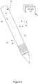
- FIG. 2illustrates an example exterior of an example active stylus 20 .
- Active stylus 20may include one or more components, such as buttons 30 or sliders 32 and 34 integrated with an outer body 22 . These external components may provide for interaction between active stylus 20 and a user or between a device and a user. As an example and not by way of limitation, interactions may include communication between active stylus 20 and a device, enabling or altering functionality of active stylus 20 or a device, or providing feedback to or accepting input from one or more users.
- the devicemay by any suitable device, such as, for example and without limitation, a desktop computer, laptop computer, tablet computer, personal digital assistant (PDA), smartphone, satellite navigation device, portable media player, portable game console, kiosk computer, point-of-sale device, or other suitable device.
- PDApersonal digital assistant
- Active stylus 20may have any suitable dimensions with outer body 22 made of any suitable material or combination of materials, such as, for example and without limitation, plastic or metal.
- exterior components (e.g. 30 or 32 ) of active stylus 20may interact with internal components or programming of active stylus 20 or may initiate one or more interactions with one or more devices or other active styluses 20 .
- buttons 30 or sliders 32 and 34may be mechanical or capacitive and may function as a roller, trackball, or wheel.
- one or more sliders 32 or 34may function as a vertical slider 34 aligned along a longitudinal axis, while one or more wheel sliders 32 may be aligned along the circumference of active stylus 20 .
- capacitive sliders 32 and 34 or buttons 30may be implemented using one or more touch-sensitive areas.
- Touch-sensitive areasmay have any suitable shape, dimensions, location, or be made from any suitable material.
- sliders 32 and 34 or buttons 30may be implemented using areas of flexible mesh formed using lines of conductive material.
- sliders 32 and 34 or buttons 30may be implemented using a FPC.
- Active stylus 20may have one or more components configured to provide feedback to or accepting feedback from a user, such as, for example and without limitation, tactile, visual, or audio feedback.
- Active stylus 20may include one or more ridges or grooves 24 on its outer body 22 . Ridges or grooves 24 may have any suitable dimensions, have any suitable spacing between ridges or grooves, or be located at any suitable area on outer body 22 of active stylus 20 . As an example and not by way of limitation, ridges 24 may enhance a user's grip on outer body 22 of active stylus 20 or provide tactile feedback to or accept tactile input from a user.
- Active stylus 20may include one or more audio components 38 capable of transmitting and receiving audio signals.
- audio component 38may contain a microphone capable of recording or transmitting one or more users' voices. As another example, audio component 38 may provide an auditory indication of a power status of active stylus 20 .
- Active stylus 20may include one or more visual feedback components 36 , such as a light-emitting diode (LED) indicator. As an example and not by way of limitation, visual feedback component 36 may indicate a power status of active stylus 20 to the user.
- LEDlight-emitting diode
- modified surface areas 40may form one or more components on outer body 22 of active stylus 20 .
- Properties of modified surface areas 40may be different than properties of the remaining surface of outer body 22 .
- modified surface area 40may be modified to have a different texture, temperature, or electromagnetic characteristic relative to the surface properties of the remainder of outer body 22 .
- Modified surface area 40may be capable of dynamically altering its properties, for example by using haptic interfaces or rendering techniques.
- a usermay interact with modified surface area 40 to provide any suitable functionally. For example and not by way of limitation, dragging a finger across modified surface area 40 may initiate an interaction, such as data transfer, between active stylus 20 and a device.
- active stylus 20may be configured to communicate data between active stylus 20 and the device.
- active stylus 20may include one or more tips 26 or nibs.
- Tip 26may include one or more electrodes configured to communicate data between active stylus 20 and one or more devices or other active styluses.
- Tip 26may be made of any suitable material, such as a conductive material, and have any suitable dimensions, such as, for example, a diameter of 1 mm or less at its terminal end.
- Active stylus 20may include one or more ports 28 located at any suitable location on outer body 22 of active stylus 20 . Port 28 may be configured to transfer signals or information between active stylus 20 and one or more devices or power sources.
- Port 28may transfer signals or information by any suitable technology, such as, for example, by universal serial bus (USB) or Ethernet connections.
- USBuniversal serial bus
- this disclosuredescribes and illustrates a particular configuration of particular components with particular locations, dimensions, composition and functionality, this disclosure contemplates any suitable configuration of suitable components with any suitable locations, dimensions, composition, and functionality with respect to active stylus 20 .
- FIG. 3illustrates example internal components of an example active stylus 20 .
- Active stylus 20may include one or more internal components, such as a controller 50 , sensors 42 , memory 44 , or power source 48 .
- one or more internal componentsmay be configured to provide for interaction between active stylus 20 and a user or between a device and a user.
- one or more internal componentsin conjunction with one or more external components described above, may be configured to provide interaction between active stylus 20 and a user or between a device and a user.
- interactionsmay include communication between active stylus 20 and a device, enabling or altering functionality of active stylus 20 or a device, or providing feedback to or accepting input from one or more users.
- Controller 50may be a microcontroller or any other type of processor suitable for controlling the operation of active stylus 20 .
- Controller 50may be one or more ICs such as, for example, general-purpose microprocessors, microcontrollers, PLDs, PLAs, or ASICs.
- Controller 50may include a processor unit, a drive unit, a sense unit, and a storage unit.
- the drive unitmay supply signals to electrodes of tip 26 through center shaft 41 .
- the drive unitmay also supply signals to control or drive sensors 42 or one or more external components of active stylus 20 .
- the sense unitmay sense signals received by electrodes of tip 26 through center shaft 41 and provide measurement signals to the processor unit representing input from a device.
- the sense unitmay also sense signals generated by sensors 42 or one or more external components and provide measurement signals to the processor unit representing input from a user.
- the processor unitmay control the supply of signals to the electrodes of tip 26 and process measurement signals from the sense unit to detect and process input from the device.
- the processor unitmay also process measurement signals from sensors 42 or one or more external components.
- the storage unitmay store programming for execution by the processor unit, including programming for controlling the drive unit to supply signals to the electrodes of tip 26 , programming for processing measurement signals from the sense unit corresponding to input from the device, programming for processing measurement signals from sensors 42 or external components to initiate a pre-determined function or gesture to be performed by active stylus 20 or the device, and other suitable programming, where appropriate.
- programming executed by controller 50may electronically filter signals received from the sense unit.
- active stylus 20may include one or more sensors 42 , such as touch sensors, gyroscopes, accelerometers, contact sensors, force sensors, pressure sensors, or any other type of sensor that detect or measure data about the environment in which active stylus 20 operates. Sensors 42 may detect and measure one or more characteristic of active stylus 20 , such as acceleration or movement, orientation, contact, pressure on outer body 22 , force on tip 26 , vibration, or any other suitable characteristic of active stylus 20 . As an example and not by way of limitation, sensors 42 may be implemented mechanically, electronically, or capacitively. As described above, data detected or measured by sensors 42 communicated to controller 50 may initiate a pre-determined function or gesture to be performed by active stylus 20 or the device.
- sensors 42such as touch sensors, gyroscopes, accelerometers, contact sensors, force sensors, pressure sensors, or any other type of sensor that detect or measure data about the environment in which active stylus 20 operates. Sensors 42 may detect and measure one or more characteristic of active stylus 20 , such as acceleration or movement
- data detected or received by sensors 42may be stored in memory 44 .
- Memory 44may be any form of memory suitable for storing data in active stylus 20 .
- controller 50may access data stored in memory 44 .
- memory 44may store programming for execution by the processor unit of controller 50 .
- data measured by sensors 42may be processed by controller 50 and stored in memory 44 .
- Power source 48may be any type of stored-energy source, including electrical or chemical-energy sources, suitable for powering the operation of active stylus 20 .
- power source 48may be charged by energy from a user or device.
- power source 48may be a rechargeable battery that may be charged by motion induced on active stylus 20 .
- power source 48 of active stylus 20may provide power to or receive power from the device.
- powermay be inductively transferred between power source 48 and a power source of the device.
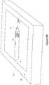
- FIG. 4illustrates an example active stylus 20 with an example device 52 .
- Device 52may have a display (not shown) and a touch sensor with a touch-sensitive area 54 .
- Device 52 displaymay be a liquid crystal display (LCD), a LED display, a LED-backlight LCD, or other suitable display and may be visible though a cover panel and substrate (and the drive and sense electrodes of the touch sensor disposed on it) of device 52 .
- LCDliquid crystal display
- LED displayLED-backlight LCD
- FIG. 4illustrates an example active stylus 20 with an example device 52 .
- Device 52may have a display (not shown) and a touch sensor with a touch-sensitive area 54 .
- Device 52 displaymay be a liquid crystal display (LCD), a LED display, a LED-backlight LCD, or other suitable display and may be visible though a cover panel and substrate (and the drive and sense electrodes of the touch sensor disposed on it) of device 52 .
- Device 52 electronicsmay provide the functionality of device 52 .
- device 52 electronicsmay include circuitry or other electronics for wireless communication to or from device 52 , execute programming on device 52 , generating graphical or other user interfaces (UIs) for device 52 display to display to a user, managing power to device 52 from a battery or other power source, taking still pictures, recording video, other suitable functionality, or any suitable combination of these.
- UIsuser interfaces
- this disclosuredescribes particular device electronics providing particular functionality of a particular device, this disclosure contemplates any suitable device electronics providing any suitable functionality of any suitable device.
- active stylus 20 and device 52may be synchronized prior to communication of data between active stylus 20 and device 52 .
- active stylus 20may be synchronized to device through a pre-determined bit sequence transmitted by the touch sensor of device 52 .
- active stylus 20may be synchronized to device by processing the drive signal transmitted by drive electrodes of the touch sensor of device 52 .
- Active stylus 20may interact or communicate with device 52 when active stylus 20 is brought in contact with or in proximity to touch-sensitive area 54 of the touch sensor of device 52 .
- interaction between active stylus 20 and device 52may be capacitive or inductive.
- measurement signal from the sensors of active stylus 20may initiate, provide for, or terminate interactions between active stylus 20 and one or more devices 52 or one or more users, as described above. Interaction between active stylus 20 and device 52 may occur when active stylus 20 is contacting or in proximity to device 52 .
- a usermay perform a gesture or sequence of gestures, such as shaking or inverting active stylus 20 , whilst active stylus 20 is hovering above touch-sensitive area 54 of device 52 .
- Active stylusmay interact with device 52 based on the gesture performed with active stylus 20 to initiate a pre-determined function, such as authenticating a user associated with active stylus 20 or device 52 .
- this disclosuredescribes particular movements providing particular types of interactions between active stylus 20 and device 52 , this disclosure contemplates any suitable movement influencing any suitable interaction in any suitable way.
- FIG. 5illustrates an example active stylus capable of executing gestures.
- a gesturemay involve a movement, such as translation in any suitable direction or rotation about any suitable axis, or any suitable combination of translations and rotations.
- active stylus 20rotates 58 about axis 60 , 62 , or 64 .
- active stylus 20moves translationally in any direction, such as along axis 60 , 62 , or 64 .
- Gesturesmay be performed on active stylus 20 .
- tapping active stylus 20 or sliding an object across active stylus 20constitutes a gesture or part of a gesture.
- a portion of active stylus 20may be textured so that sliding one object across the body of active stylus 20 may be classified as a different gesture than sliding a different object.
- a portion of active stylus 20may have ridges, and sliding a finger across these ridges may be classified as a different gesture than sliding a fingernail across the same ridges. While this disclosure provides specific examples of motion with or on an active stylus constituting a gesture or part of a gesture, this disclosure contemplates any suitable motion with or on an active stylus constituting any suitable gesture or part of a gesture.
- a gesturemay provide input, such as electromagnetic input, to or be electronically recorded by components in active stylus 20 . More specifically, in some implementations, a specific gesture may be translated into a specific electromagnetic input, and different gestures may be respectively translated into different electromagnetic inputs.
- electromagnetic inputmay be provided by one or more sensors 42 placed at any suitable locations in or on active stylus 20 .
- sensors 42one or more accelerometers sense translation, motion, and vibration of active stylus 20 .
- one or more gyroscopessense rotation of active stylus 20 .
- one or more force sensorssense force from one or more locations on active stylus 20 , such as the tip or along a portion of the body.
- one or more magnetometerssense the orientation of active stylus 20 in a magnetic field. Changes in orientation sensed by the magnetometer specify the motion of active stylus 20 .
- a global positioning systemGPS
- sensorssense the location, and changes of location, of active stylus 20 relative to the Earth. These sensors produce electromagnetic signals based on the motion, force, orientation, or location sensed.
- electromagnetic input or signalsmay take any suitable form, such as an electric field, magnetic field, electromagnetic radiation, static configuration of electric charge, or electric current. While this disclosure describes specific examples of particular embodiments of gestures providing electromagnetic input to an active stylus, this disclosure contemplates any suitable method of providing any suitable input to an active stylus by any suitable gesture or combination of gestures.
- Gestures executed with or on active stylus 20may provide electromagnetic input to a touch sensor system or associated components, such as a touch-sensitive device.
- electromagnetic signals produced by the components of active stylus 20 based on the motion of active stylus 20results in active stylus 20 providing electromagnetic input to a touch-sensitive device.
- active stylus 20includes a transmitter capable of transmitting electromagnetic signals, such as radio waves, to a touch-sensitive device.
- active stylus 20may transmit data in, for example, electromagnetic form to a touch-sensitive device through a direct connection, such as a universal serial bus cable.
- gesturesprovide electromagnetic input directly to a touch sensor system.
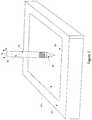
- FIGS. 6A and 6Billustrate example embodiments of providing electromagnetic input directly to a touch-sensitive device by executing gestures with an active stylus.
- active stylus 20is hovering over touch-sensitive display 54 of a touch-sensitive device 52 , and tip 26 of active stylus 20 is separated from the touch-sensitive display by a distance D 1 .
- D 1may be approximately 10 millimeters.
- Electronics in touch-sensitive device 52such as drive and sense lines, sense the location of tip 26 relative to touch-sensitive display 54 , including the distance D 1 separating tip 26 from touch-sensitive display 54 .
- tip 26outputs voltage signals that induce charge on the sense lines in the proximity of tip 26 , and the induced charge depends on the distance D 1 . Motion of tip 26 in any direction is thus detected directly by the electronics of touch-sensitive device 52 .
- active stylus 20may be oriented at any suitable angle with respect to touch-sensitive display 52 .
- FIG. 6Billustrates the body of active stylus 20 contacting touch-sensitive display 54 and tip 26 separated from touch-sensitive display 54 by a distance D 2 .
- touch-sensitive device 52may receive electromagnetic input directly from a gesture and also receive electromagnetic input relating to the same or another gesture from a component of a touch-sensor system, as illustrated in FIG. 7 .
- tip 26 of active stylus 20is in contact with touch-sensitive display 54 of touch-sensitive device 52 .
- Motion of tip 26is directly recorded by electronics, such as drive or sense lines, in touch-sensitive device 52 .
- motion of active stylus 20 relative to tip 26such as rotation 58 about axis 66 or axis 68 passing through tip 26 , is recorded by one or more sensors in active stylus 20 .
- the sensorsconvert the recorded motion into electromagnetic signals in active stylus 20 .
- Active stylus 20outputs electromagnetic signals to touch-sensitive device 52 based on the electromagnetic signals produced within the active stylus as a result of the recorded motion.
- Gestures executed on or by an active stylusmay result in a variety of functionality.
- gesturesalter the functionality of, or produce functionality in, a touch sensor system or its associated components, such as an active stylus or a touch-sensitive device.
- the functionality associated with one or more gesturesmay depend on the orientation of an active stylus. As an example, shaking an active stylus in a vertical position results in different functionality than shaking an active stylus in a horizontal position.
- the functionality associated with one or more gesturesmay depend on the location of an active stylus. As an example, rotating an active stylus near a touch-sensitive device results in different functionality than rotating the active stylus when no touch-sensitive device is near.
- the functionality associated with one or more gesturesmay depend on the user associated with an active stylus or touch-sensitive device. As an example, the functionality associated with a gesture is set by a user. In particular embodiments, the functionality associated with one or more gestures may depend on data stored on an active stylus. As an example, shaking an active stylus that has encrypted data results in a different function than shaking an active stylus that has unsecured data. In particular embodiments, the functionality associated with one or more gestures may depend on the sequence of gestures. As an example, inverting an active stylus after shaking the active stylus results in a different functionality than shaking an active stylus after inverting the active stylus.
- an active stylusmay have a tip on each end, and gestures performed with one tip near a touch-sensitive device may result in different functionality than a gesture with both tips near the touch-sensitive device.
- laying the active stylus flat on the touch-sensitive display so that both tips are hovering near the displayprovides different functionality than hovering one tip near the display.
- one or more gesturesmay affect the functionality of an active stylus.
- an active stylus that creates output on a touch-sensitive display when used with the tip proximal to the displaymay erase output on a touch-sensitive display when used with the end opposite the tip proximal to the display.
- one or more gesturesmay alter the power settings of a touch sensor system and its associated components. As an example, shaking an active stylus transitions the active stylus or associated components from one power mode, such as “off” to another power mode, such as “on”.
- one or more gesturesmay interact with output on a touch-sensitive display. As an example, encircling a group of icons with an active stylus selects the icons.
- Pressing the tip of the active stylus into the touch-sensitive displaypicks up the icons, and pressing the tip a second time onto the display drops the icons.
- sweeping the active stylus or tip of the active stylus across the touch-sensitive displayscrolls around output on a touch-sensitive display or material related to the output.
- pressing the tip of an active stylus into an icon displayed on a touch-sensitive display and sweeping or flicking the tip of the active styluscan remove or delete the icon from the display.
- sweeping the tip of an active stylus over particular output, such as textselects the text.
- pressing the tip of an active stylus into a touch-sensitive display while gesturing with the active stylusalters the typeface of characters being written on the display.
- one or more gesturesmay access specific command or menus associated with output displayed on a touch-sensitive display.
- selecting output of a touch-sensitive display and shaking the active stylusmay display a set of commands or menus associated with the output selected or displayed.
- one or more gesturesmay combine with other functionality to perform a specific function.
- shaking an active stylus while pressing a buttonmay initiate data transfer between the active stylus and a touch-sensitive device.
- separating either stylus with a finger or two or more fingers over output on a touch-sensitive displaymay zoom in on the output, and an active stylus may gesture, such as writing on the display, to interact with the zoomed-in output.
- performing a user's pre-defined gesturemay unlock the touch-sensitive display of a touch-sensitive device. While this disclosure provides specific examples of particular embodiments of the functionality associated with one or more specific gestures, this disclosure contemplates any suitable functionality associated with any suitable gestures.
- gesturesmay be performed by an active stylus on a touch-sensitive area of a device in combination with gestures performed by another object on the touch-sensitive area.
- FIG. 8illustrates an example combination input using the example stylus of FIG. 3 .
- a pre-determined function executed by device 52is initiated with a combination of interactions of active stylus 20 and a portion of human hand 70 with touch-sensitive area 54 of the touch sensor of device 52 .
- the portion of human hand 70 interacting with touch-sensitive area 54is a finger.
- the signal communicated to the controller of the touch sensorresults from interaction of one or more fingers of human hand 70 and active stylus 20 with touch-sensitive area 54 .
- the controller of the touch sensor of device 52differentiates between active stylus 20 interactions and interactions with the portion of human hand 70 .
- the controllermay differentiate an active stylus 20 interaction from a human hand 70 interaction through modulation of the touch sensor drive signal by active stylus 20 .
- the active stylus 20modulates the amplitude, frequency, or phase of the drive signal and the modulation of the drive signal is detected and processed by the controller as being an interaction from active stylus 20 .
- substantially all the electrodes (i.e. drive and sense) of the touch sensor of device 52may be sensed to detect the signal from active stylus 20 without applying a drive signal.
- the touch-sensor controllermay differentiate between an active stylus 20 interaction and the human hand 70 interaction based on signal strength and “touch” area (i.e. the size of touch-sensitive area 54 detecting a touch). Interactions of active stylus 20 and human hand 70 have differing signal strength and touch area characteristics, which may be used to differentiate between the two.
- signal strength and “touch” areai.e. the size of touch-sensitive area 54 detecting a touch.
- Interactions of active stylus 20 and human hand 70have differing signal strength and touch area characteristics, which may be used to differentiate between the two.
- the controller of the touch sensorassociates the detected combination of interaction of the portion of human hand 70 with touch-sensitive area 54 and interaction of active stylus 20 with touch-sensitive area 54 to a pre-determined function executed by device 52 .
- the controllermay determine whether interaction of the portion of the human hand 70 with touch-sensitive area 54 forms a gesture in conjunction with the interaction of active stylus 20 or forms a gesture separate from the interaction of active stylus 20 with touch-sensitive area 54 .
- substantially simultaneous interaction of one finger of human hand 70 and active stylus 20 with touch-sensitive area 54may be associated with a pre-determined function.
- substantially simultaneous interaction of one finger and active stylus 20 with touch-sensitive area 54may jointly initiate the pre-determined function, such as for example zooming in, zooming out, or rotation of an object displayed on the display of device 52 .
- interaction of two fingers of human hand 70 and active stylus 20 with touch-sensitive area 54may be associated with two or more pre-determined functions of device 52 .
- interactions of two fingers of human hand 70 with touch-sensitive area 54may be used in a “spread” gesture to expand a text area displayed on the display of device 52 and interaction of active stylus 20 with touch-sensitive area 54 may be used by the user to handwrite an input in the expanded text area.
- this disclosuredescribes detecting and processing the combination input from the active stylus interaction with the touch-sensitive area and human hand interaction with the touch-sensitive area occurring within the controller of the touch sensor, this disclosure contemplates use of any suitable controller or combination of controllers to detect and process the combination input from the active stylus interaction with the touch-sensitive area and human hand interaction with the touch-sensitive area.
- a computer-readable non-transitory storage mediumencompasses a semiconductor-based or other integrated circuit (IC) (such, as for example, a field-programmable gate array (FPGA) or an application-specific IC (ASIC)), a hard disk, an HDD, a hybrid hard drive (HHD), an optical disc, an optical disc drive (ODD), a magneto-optical disc, a magneto-optical drive, a floppy disk, a floppy disk drive (FDD), magnetic tape, a holographic storage medium, a solid-state drive (SSD), a RAM-drive, a SECURE DIGITAL card, a SECURE DIGITAL drive, or another suitable computer-readable non-transitory storage medium or a combination of two or more of these, where appropriate.
- ICsemiconductor-based or other integrated circuit
- HDDhigh-programmable gate array
- HHDhybrid hard drive
- ODDoptical disc drive
- magneto-optical discmagneto-optical drive
- FDDfloppy
Landscapes
- Engineering & Computer Science (AREA)
- General Engineering & Computer Science (AREA)
- Theoretical Computer Science (AREA)
- Physics & Mathematics (AREA)
- Human Computer Interaction (AREA)
- General Physics & Mathematics (AREA)
- Electromagnetism (AREA)
- Position Input By Displaying (AREA)
- User Interface Of Digital Computer (AREA)
Abstract
Description
Claims (19)
Priority Applications (6)
| Application Number | Priority Date | Filing Date | Title |
|---|---|---|---|
| US14/832,049US10599234B2 (en) | 2011-10-28 | 2015-08-21 | Executing gestures with active stylus |
| US16/825,686US11269429B2 (en) | 2011-10-28 | 2020-03-20 | Executing gestures with active stylus |
| US17/591,388US11520419B2 (en) | 2011-10-28 | 2022-02-02 | Executing gestures with active stylus |
| US18/055,224US11868548B2 (en) | 2011-10-28 | 2022-11-14 | Executing gestures with active stylus |
| US18/473,765US12236020B2 (en) | 2011-10-28 | 2023-09-25 | Executing gestures with active stylus |
| US19/025,755US20250155996A1 (en) | 2011-10-28 | 2025-01-16 | Executing gestures with active stylus |
Applications Claiming Priority (3)
| Application Number | Priority Date | Filing Date | Title |
|---|---|---|---|
| US201161553114P | 2011-10-28 | 2011-10-28 | |
| US13/419,087US9116558B2 (en) | 2011-10-28 | 2012-03-13 | Executing gestures with active stylus |
| US14/832,049US10599234B2 (en) | 2011-10-28 | 2015-08-21 | Executing gestures with active stylus |
Related Parent Applications (1)
| Application Number | Title | Priority Date | Filing Date |
|---|---|---|---|
| US13/419,087ContinuationUS9116558B2 (en) | 2011-10-28 | 2012-03-13 | Executing gestures with active stylus |
Related Child Applications (1)
| Application Number | Title | Priority Date | Filing Date |
|---|---|---|---|
| US16/825,686ContinuationUS11269429B2 (en) | 2011-10-28 | 2020-03-20 | Executing gestures with active stylus |
Publications (2)
| Publication Number | Publication Date |
|---|---|
| US20160091992A1 US20160091992A1 (en) | 2016-03-31 |
| US10599234B2true US10599234B2 (en) | 2020-03-24 |
Family
ID=46757277
Family Applications (7)
| Application Number | Title | Priority Date | Filing Date |
|---|---|---|---|
| US13/419,087Active2032-07-23US9116558B2 (en) | 2011-10-28 | 2012-03-13 | Executing gestures with active stylus |
| US14/832,049Active2032-05-23US10599234B2 (en) | 2011-10-28 | 2015-08-21 | Executing gestures with active stylus |
| US16/825,686ActiveUS11269429B2 (en) | 2011-10-28 | 2020-03-20 | Executing gestures with active stylus |
| US17/591,388ActiveUS11520419B2 (en) | 2011-10-28 | 2022-02-02 | Executing gestures with active stylus |
| US18/055,224ActiveUS11868548B2 (en) | 2011-10-28 | 2022-11-14 | Executing gestures with active stylus |
| US18/473,765ActiveUS12236020B2 (en) | 2011-10-28 | 2023-09-25 | Executing gestures with active stylus |
| US19/025,755PendingUS20250155996A1 (en) | 2011-10-28 | 2025-01-16 | Executing gestures with active stylus |
Family Applications Before (1)
| Application Number | Title | Priority Date | Filing Date |
|---|---|---|---|
| US13/419,087Active2032-07-23US9116558B2 (en) | 2011-10-28 | 2012-03-13 | Executing gestures with active stylus |
Family Applications After (5)
| Application Number | Title | Priority Date | Filing Date |
|---|---|---|---|
| US16/825,686ActiveUS11269429B2 (en) | 2011-10-28 | 2020-03-20 | Executing gestures with active stylus |
| US17/591,388ActiveUS11520419B2 (en) | 2011-10-28 | 2022-02-02 | Executing gestures with active stylus |
| US18/055,224ActiveUS11868548B2 (en) | 2011-10-28 | 2022-11-14 | Executing gestures with active stylus |
| US18/473,765ActiveUS12236020B2 (en) | 2011-10-28 | 2023-09-25 | Executing gestures with active stylus |
| US19/025,755PendingUS20250155996A1 (en) | 2011-10-28 | 2025-01-16 | Executing gestures with active stylus |
Country Status (2)
| Country | Link |
|---|---|
| US (7) | US9116558B2 (en) |
| DE (1) | DE202012102444U1 (en) |
Cited By (1)
| Publication number | Priority date | Publication date | Assignee | Title |
|---|---|---|---|---|
| US11269429B2 (en)* | 2011-10-28 | 2022-03-08 | Wacom Co., Ltd. | Executing gestures with active stylus |
Families Citing this family (41)
| Publication number | Priority date | Publication date | Assignee | Title |
|---|---|---|---|---|
| US9122322B2 (en) | 2011-03-17 | 2015-09-01 | Microsoft Technology Licensing, Llc | Interacting tips for a digitizer stylus |
| US9164603B2 (en) | 2011-10-28 | 2015-10-20 | Atmel Corporation | Executing gestures with active stylus |
| KR102101818B1 (en)* | 2012-07-30 | 2020-04-17 | 삼성전자주식회사 | Device and method for controlling data transfer in terminal |
| US9261985B2 (en) | 2013-03-11 | 2016-02-16 | Barnes & Noble College Booksellers, Llc | Stylus-based touch-sensitive area for UI control of computing device |
| US9766723B2 (en) | 2013-03-11 | 2017-09-19 | Barnes & Noble College Booksellers, Llc | Stylus sensitive device with hover over stylus control functionality |
| US9946365B2 (en)* | 2013-03-11 | 2018-04-17 | Barnes & Noble College Booksellers, Llc | Stylus-based pressure-sensitive area for UI control of computing device |
| US9785259B2 (en) | 2013-03-11 | 2017-10-10 | Barnes & Noble College Booksellers, Llc | Stylus-based slider functionality for UI control of computing device |
| KR102106779B1 (en)* | 2013-06-28 | 2020-05-06 | 삼성전자주식회사 | Method for processing pen input and apparatus for the same |
| EP3025434A4 (en)* | 2013-07-24 | 2017-02-22 | FiftyThree, Inc. | Apparatuses, methods and systems for authenticating a wireless connection |
| JP5839009B2 (en)* | 2013-09-10 | 2016-01-06 | コニカミノルタ株式会社 | Display device, display device control method, display device control program, and display system |
| US9513721B2 (en) | 2013-09-12 | 2016-12-06 | Microsoft Technology Licensing, Llc | Pressure sensitive stylus for a digitizer |
| US9665206B1 (en)* | 2013-09-18 | 2017-05-30 | Apple Inc. | Dynamic user interface adaptable to multiple input tools |
| TWI590148B (en) | 2013-10-25 | 2017-07-01 | 宏碁股份有限公司 | Electronic device and touch operation method thereof |
| GB2521467A (en)* | 2013-12-20 | 2015-06-24 | Univ Newcastle | Enhanced user interaction with a device |
| US9310929B2 (en)* | 2014-06-06 | 2016-04-12 | Lenovo Enterprise Solutions (Singapore) Pte. Ltd. | Unlocking touch screen devices |
| US9874951B2 (en) | 2014-11-03 | 2018-01-23 | Microsoft Technology Licensing, Llc | Stylus for operating a digitizer system |
| HK1207522A2 (en)* | 2014-12-11 | 2016-01-29 | Coco Color Company Limited | A digital stylus |
| US9785262B2 (en)* | 2015-04-20 | 2017-10-10 | Wacom Co., Ltd. | System and method for bidirectional communication between stylus and stylus sensor controller |
| US9658704B2 (en) | 2015-06-10 | 2017-05-23 | Apple Inc. | Devices and methods for manipulating user interfaces with a stylus |
| US10095347B2 (en)* | 2015-08-28 | 2018-10-09 | Wacom Co., Ltd. | Passive stylus and grip shadow recognition |
| US9740312B2 (en) | 2015-09-09 | 2017-08-22 | Microsoft Technology Licensing, Llc | Pressure sensitive stylus |
| JP2018526734A (en)* | 2015-09-11 | 2018-09-13 | タクチュアル ラブズ シーオー. | Semi-passive stylus |
| JP2017062662A (en)* | 2015-09-25 | 2017-03-30 | ソニー株式会社 | Information processor, information processing method and program |
| DE202015105665U1 (en)* | 2015-10-23 | 2017-01-24 | Stabilo International Gmbh | Active stylus for capacitive sensor surfaces with hand recognition |
| JP6532105B2 (en)* | 2015-12-17 | 2019-06-19 | 株式会社ワコム | Touch panel, signal processing apparatus and ground coupling method |
| US9841828B2 (en) | 2016-04-20 | 2017-12-12 | Microsoft Technology Licensing, Llc | Pressure sensitive stylus |
| US10203781B2 (en) | 2016-06-24 | 2019-02-12 | Microsoft Technology Licensing, Llc | Integrated free space and surface input device |
| WO2018058014A1 (en) | 2016-09-23 | 2018-03-29 | Apple Inc. | Device, method, and graphical user interface for annotating text |
| US10318022B2 (en) | 2017-01-30 | 2019-06-11 | Microsoft Technology Licensing, Llc | Pressure sensitive stylus |
| WO2018222247A1 (en) | 2017-06-02 | 2018-12-06 | Apple Inc. | Device, method, and graphical user interface for annotating content |
| US12340034B2 (en) | 2018-06-01 | 2025-06-24 | Apple Inc. | Devices, methods, and graphical user interfaces for an electronic device interacting with a stylus |
| DE102018120760B4 (en) | 2018-07-12 | 2022-11-17 | Tdk Electronics Ag | Pen-type input and/or output device and method for generating a haptic signal |
| US10990273B2 (en)* | 2019-02-26 | 2021-04-27 | Yong Wang | Ultra touch functions and systems incorporating the same |
| US11507206B2 (en) | 2019-05-13 | 2022-11-22 | Microsoft Technology Licensing, Llc | Force-sensing input device |
| CN113541852B (en)* | 2020-03-31 | 2022-06-10 | 华为技术有限公司 | Signal decoding method, decoding circuit and stylus |
| US11327571B2 (en) | 2020-09-12 | 2022-05-10 | Darrion Vinh Nguyen | Method and apparatus for computer-assisted drawing using pens with tracking marks |
| CN112269523B (en)* | 2020-10-28 | 2023-05-26 | 维沃移动通信有限公司 | Object editing processing method and device and electronic equipment |
| EP4281885A4 (en)* | 2021-02-05 | 2024-12-11 | Jonathan Siegel | SYSTEM AND METHOD FOR AN ELECTRONIC SIGNATURE DEVICE |
| EP4474942A4 (en)* | 2022-03-17 | 2025-06-04 | Samsung Electronics Co., Ltd. | ELECTRONIC DEVICE COMPRISING A SUPPORT STRUCTURE |
| CN120653173A (en) | 2022-05-10 | 2025-09-16 | 苹果公司 | Interaction between an input device and an electronic device |
| US20250093968A1 (en)* | 2023-09-20 | 2025-03-20 | Apple Inc. | Handheld Controllers with Surface Marking Capabilities |
Citations (87)
| Publication number | Priority date | Publication date | Assignee | Title |
|---|---|---|---|---|
| US4695680A (en) | 1986-06-27 | 1987-09-22 | Scriptel Corporation | Stylus for position responsive apparatus having electrographic application |
| US5007085A (en) | 1988-10-28 | 1991-04-09 | International Business Machines Corporation | Remotely sensed personal stylus |
| US5349139A (en) | 1992-10-30 | 1994-09-20 | International Business Machines | Architecture for communication of remote devices to a digitizing display |
| US5453762A (en) | 1993-01-20 | 1995-09-26 | Hitachi, Ltd. | Systems for processing information and identifying individual |
| US5478976A (en) | 1992-08-31 | 1995-12-26 | Canon Kabushiki Kaisha | Information processing method and apparatus |
| US5557076A (en) | 1993-11-12 | 1996-09-17 | Mikron Gesellschaft Fur | Cordless position detection apparatus |
| US5699084A (en) | 1994-06-29 | 1997-12-16 | Wacom Co., Ltd. | Computer system |
| US5883338A (en) | 1994-12-16 | 1999-03-16 | Hyundai Electronics America, Inc. | Telementry by digitizer stylus |
| US5973677A (en) | 1997-01-07 | 1999-10-26 | Telxon Corporation | Rechargeable, untethered electronic stylus for computer with interactive display screen |
| US6195446B1 (en) | 1994-12-16 | 2001-02-27 | Hyundai Electronics America | Digitizer stylus with memory for storing handwriting data |
| US6249276B1 (en) | 1997-01-22 | 2001-06-19 | Mitsubishi Denki Kabushiki Kaisha | Pen-inputted personal information terminal device |
| US6268857B1 (en)* | 1997-08-29 | 2001-07-31 | Xerox Corporation | Computer user interface using a physical manipulatory grammar |
| US20020175903A1 (en)* | 2001-05-11 | 2002-11-28 | Christer Fahraeus | Electronic pen |
| US20020190947A1 (en) | 2000-04-05 | 2002-12-19 | Feinstein David Y. | View navigation and magnification of a hand-held device with a display |
| US20030095115A1 (en)* | 2001-11-22 | 2003-05-22 | Taylor Brian | Stylus input device utilizing a permanent magnet |
| US6728881B1 (en) | 1999-10-01 | 2004-04-27 | The United States Of America As Represented By The Secretary Of The Army | Fingerprint and signature identification and authorization card and pen |
| US20040140965A1 (en) | 2002-10-31 | 2004-07-22 | Microsoft Corporation | Universal computing device |
| US6798907B1 (en)* | 2001-01-24 | 2004-09-28 | Advanced Digital Systems, Inc. | System, computer software product and method for transmitting and processing handwritten data |
| US20050063570A1 (en) | 2003-08-22 | 2005-03-24 | Dynasig Corporation | Method and apparatus for capturing and authenticating biometric information from a writing instrument |
| US20050110778A1 (en)* | 2000-12-06 | 2005-05-26 | Mourad Ben Ayed | Wireless handwriting input device using grafitis and bluetooth |
| US20060023922A1 (en) | 2001-05-25 | 2006-02-02 | Black Gerald R | Identity authentication device |
| US20060267966A1 (en) | 2005-05-24 | 2006-11-30 | Microsoft Corporation | Hover widgets: using the tracking state to extend capabilities of pen-operated devices |
| US20070005849A1 (en)* | 2005-06-29 | 2007-01-04 | Microsoft Corporation | Input device with audio capablities |
| US20070057763A1 (en) | 2005-09-12 | 2007-03-15 | Imation Corp. | Wireless handheld device with local biometric authentication |
| US20070220018A1 (en)* | 2006-03-15 | 2007-09-20 | Microsoft Corporation | Generator system |
| US20080074391A1 (en)* | 2006-09-27 | 2008-03-27 | Yahoo! Inc. | Zero-click activation of an application |
| US20080106523A1 (en)* | 2006-11-07 | 2008-05-08 | Conrad Richard H | Ergonomic lift-clicking method and apparatus for actuating home switches on computer input devices |
| US20080143693A1 (en) | 2000-05-24 | 2008-06-19 | Immersion Corporation | Haptic stylus utilizing an electroactive polymer |
| US20080158170A1 (en)* | 2007-01-03 | 2008-07-03 | Apple Computer, Inc. | Multi-event input system |
| US7426643B2 (en) | 2004-06-22 | 2008-09-16 | Hewlett-Packard Development Company, L.P. | Input device feature |
| US7425643B1 (en) | 2004-01-26 | 2008-09-16 | University Of Washington | Electron acceptors for nonlinear optical chromophores |
| US20080238885A1 (en) | 2007-03-29 | 2008-10-02 | N-Trig Ltd. | System and method for multiple object detection on a digitizer system |
| US20080309635A1 (en) | 2007-06-14 | 2008-12-18 | Epson Imaging Devices Corporation | Capacitive input device |
| US20080309621A1 (en)* | 2007-06-15 | 2008-12-18 | Aggarwal Akhil | Proximity based stylus and display screen, and device incorporating same |
| US20090095540A1 (en) | 2007-10-11 | 2009-04-16 | N-Trig Ltd. | Method for palm touch identification in multi-touch digitizing systems |
| US20090115725A1 (en) | 2007-11-05 | 2009-05-07 | Eldad Shemesh | Input device and method of operation thereof |
| US20090127005A1 (en) | 2007-11-14 | 2009-05-21 | N-Trig Ltd. | System and method for detection with a digitizer sensor |
| US20090153152A1 (en) | 2007-12-14 | 2009-06-18 | Cypress Semiconductor Corporation | Compensation circuit for a tx-rx capacitive sensor |
| US20090184939A1 (en) | 2008-01-23 | 2009-07-23 | N-Trig Ltd. | Graphical object manipulation with a touch sensitive screen |
| US20090219250A1 (en) | 2008-02-29 | 2009-09-03 | Ure Michael J | Interface with and communication between mobile electronic devices |
| US20090251434A1 (en) | 2008-04-03 | 2009-10-08 | N-Tring Ltd. | Multi-touch and single touch detection |
| US20090259432A1 (en)* | 2008-04-15 | 2009-10-15 | Liberty Matthew G | Tracking determination based on intensity angular gradient of a wave |
| US7612767B1 (en) | 2005-08-24 | 2009-11-03 | Griffin Technology, Inc. | Trackpad pen for use with computer touchpad |
| US20090315854A1 (en) | 2008-06-18 | 2009-12-24 | Epson Imaging Devices Corporation | Capacitance type input device and display device with input function |
| US20100006350A1 (en) | 2008-07-11 | 2010-01-14 | Elias John G | Stylus Adapted For Low Resolution Touch Sensor Panels |
| US7663607B2 (en) | 2004-05-06 | 2010-02-16 | Apple Inc. | Multipoint touchscreen |
| US7663509B2 (en)* | 2005-12-23 | 2010-02-16 | Sony Ericsson Mobile Communications Ab | Hand-held electronic equipment |
| US20100079414A1 (en) | 2008-09-30 | 2010-04-01 | Andrew Rodney Ferlitsch | Apparatus, systems, and methods for authentication on a publicly accessed shared interactive digital surface |
| US20100155153A1 (en) | 2008-12-22 | 2010-06-24 | N-Trig Ltd. | Digitizer, stylus and method of synchronization therewith |
| US20100279738A1 (en)* | 2009-04-29 | 2010-11-04 | Lg Electronics Inc. | Mobile terminal capable of recognizing fingernail touch and method of controlling the operation thereof |
| US20100292945A1 (en) | 2009-05-13 | 2010-11-18 | Joseph Kurth Reynolds | Capacitive sensor device |
| US20100308962A1 (en) | 2009-06-04 | 2010-12-09 | Foxconn Communication Technology Corp. | Method and electronic device capable of user identification |
| US20100315384A1 (en) | 2009-06-12 | 2010-12-16 | Kirk Hargreaves | Untethered active pen and a method for communicating with a capacitive sensing device using the untethered active pen |
| US7864503B2 (en) | 2007-05-11 | 2011-01-04 | Sense Pad Tech Co., Ltd | Capacitive type touch panel |
| US20110007029A1 (en) | 2009-07-08 | 2011-01-13 | Ben-David Amichai | System and method for multi-touch interactions with a touch sensitive screen |
| US7875814B2 (en) | 2005-07-21 | 2011-01-25 | Tpo Displays Corp. | Electromagnetic digitizer sensor array structure |
| US20110071394A1 (en) | 2009-09-23 | 2011-03-24 | Fedinec James J | Central venous catheter kit with line gripping and needle localizing devices |
| US7920129B2 (en) | 2007-01-03 | 2011-04-05 | Apple Inc. | Double-sided touch-sensitive panel with shield and drive combined layer |
| US20110227825A1 (en)* | 2008-07-01 | 2011-09-22 | Hillcrest Laboratories, Inc. | 3D Pointer Mapping |
| US8031174B2 (en) | 2007-01-03 | 2011-10-04 | Apple Inc. | Multi-touch surface stackup arrangement |
| US8031094B2 (en) | 2009-09-11 | 2011-10-04 | Apple Inc. | Touch controller with improved analog front end |
| US8040326B2 (en) | 2007-06-13 | 2011-10-18 | Apple Inc. | Integrated in-plane switching display and touch sensor |
| US8049732B2 (en) | 2007-01-03 | 2011-11-01 | Apple Inc. | Front-end signal compensation |
| US20120068963A1 (en) | 2006-05-03 | 2012-03-22 | Esenther Alan W | Method and System for Emulating a Mouse on a Multi-Touch Sensitive Surface |
| US8179381B2 (en) | 2008-02-28 | 2012-05-15 | 3M Innovative Properties Company | Touch screen sensor |
| US20120127110A1 (en) | 2010-11-19 | 2012-05-24 | Apple Inc. | Optical stylus |
| US8217902B2 (en) | 2007-04-27 | 2012-07-10 | Tpk Touch Solutions Inc. | Conductor pattern structure of capacitive touch panel |
| US20120179547A1 (en)* | 2011-01-06 | 2012-07-12 | General Electric Company | Added features of hem/heg using gps technology |
| US20120206330A1 (en)* | 2011-02-11 | 2012-08-16 | Microsoft Corporation | Multi-touch input device with orientation sensing |
| US20120242603A1 (en) | 2011-03-21 | 2012-09-27 | N-Trig Ltd. | System and method for authentication with a computer stylus |
| US20120242592A1 (en) | 2011-03-21 | 2012-09-27 | Rothkopf Fletcher R | Electronic devices with flexible displays |
| US20120243719A1 (en) | 2011-03-21 | 2012-09-27 | Franklin Jeremy C | Display-Based Speaker Structures for Electronic Devices |
| US20120242588A1 (en) | 2011-03-21 | 2012-09-27 | Myers Scott A | Electronic devices with concave displays |
| US20120243151A1 (en) | 2011-03-21 | 2012-09-27 | Stephen Brian Lynch | Electronic Devices With Convex Displays |
| WO2012129247A2 (en) | 2011-03-21 | 2012-09-27 | Apple Inc. | Electronic devices with flexible displays |
| US20120309376A1 (en)* | 2011-06-03 | 2012-12-06 | Apple Inc. | Baseband on-board location monitoring |
| US20120327042A1 (en)* | 2011-06-22 | 2012-12-27 | Harley Jonah A | Stylus orientation detection |
| US20120327041A1 (en) | 2011-06-22 | 2012-12-27 | Harley Jonah A | Active stylus |
| US20120331546A1 (en)* | 2011-06-22 | 2012-12-27 | Falkenburg David R | Intelligent stylus |
| US20130009907A1 (en)* | 2009-07-31 | 2013-01-10 | Rosenberg Ilya D | Magnetic Stylus |
| US20130076612A1 (en) | 2011-09-26 | 2013-03-28 | Apple Inc. | Electronic device with wrap around display |
| US20130106724A1 (en) | 2011-10-28 | 2013-05-02 | Atmel Corporation | Executing Gestures With Active Stylus |
| US20130106799A1 (en) | 2011-10-28 | 2013-05-02 | Atmel Corporation | Authenticating with Active Stylus |
| US20130120463A1 (en)* | 2009-07-10 | 2013-05-16 | Jerry G. Harris | Methods and Apparatus for Natural Media Painting Using Proximity-Based Tablet Stylus Gestures |
| US8723824B2 (en) | 2011-09-27 | 2014-05-13 | Apple Inc. | Electronic devices with sidewall displays |
| US20140196106A1 (en)* | 2000-12-19 | 2014-07-10 | At&T Intellectual Property I, L.P. | Location-Based Security Rules |
| US9116558B2 (en)* | 2011-10-28 | 2015-08-25 | Atmel Corporation | Executing gestures with active stylus |
Family Cites Families (11)
| Publication number | Priority date | Publication date | Assignee | Title |
|---|---|---|---|---|
| US20040039602A1 (en)* | 2001-11-16 | 2004-02-26 | Greenberg Robert S. | Clinician's assistant system |
| CN2568423Y (en)* | 2002-09-10 | 2003-08-27 | 彦彰企业有限公司 | Multifunctional pen |
| US7098896B2 (en)* | 2003-01-16 | 2006-08-29 | Forword Input Inc. | System and method for continuous stroke word-based text input |
| US20060093192A1 (en)* | 2004-11-03 | 2006-05-04 | Bechtel J S | Finger guide device |
| US8139028B2 (en)* | 2006-02-01 | 2012-03-20 | Synaptics Incorporated | Proximity sensor and method for indicating extended interface results |
| US8077155B2 (en)* | 2006-02-13 | 2011-12-13 | Rehm Peter H | Relative-position, absolute-orientation sketch pad and optical stylus for a personal computer |
| US8564574B2 (en)* | 2007-09-18 | 2013-10-22 | Acer Incorporated | Input apparatus with multi-mode switching function |
| US8339371B2 (en)* | 2008-09-12 | 2012-12-25 | Leapfrog Enterprises, Inc. | User interface device for controlling an audio visual system |
| KR20130128380A (en)* | 2010-09-22 | 2013-11-26 | 사이프레스 세미컨덕터 코포레이션 | Capacitive stylus for a touch screen |
| US9201520B2 (en)* | 2011-02-11 | 2015-12-01 | Microsoft Technology Licensing, Llc | Motion and context sharing for pen-based computing inputs |
| US20140344682A1 (en)* | 2013-05-17 | 2014-11-20 | United Video Properties, Inc. | Methods and systems for customizing tactilely distinguishable inputs on a user input interface based on available functions |
- 2012
- 2012-03-13USUS13/419,087patent/US9116558B2/enactiveActive
- 2012-07-03DEDE201220102444patent/DE202012102444U1/ennot_activeExpired - Lifetime
- 2015
- 2015-08-21USUS14/832,049patent/US10599234B2/enactiveActive
- 2020
- 2020-03-20USUS16/825,686patent/US11269429B2/enactiveActive
- 2022
- 2022-02-02USUS17/591,388patent/US11520419B2/enactiveActive
- 2022-11-14USUS18/055,224patent/US11868548B2/enactiveActive
- 2023
- 2023-09-25USUS18/473,765patent/US12236020B2/enactiveActive
- 2025
- 2025-01-16USUS19/025,755patent/US20250155996A1/enactivePending
Patent Citations (94)
| Publication number | Priority date | Publication date | Assignee | Title |
|---|---|---|---|---|
| US4695680A (en) | 1986-06-27 | 1987-09-22 | Scriptel Corporation | Stylus for position responsive apparatus having electrographic application |
| US5007085A (en) | 1988-10-28 | 1991-04-09 | International Business Machines Corporation | Remotely sensed personal stylus |
| US5478976A (en) | 1992-08-31 | 1995-12-26 | Canon Kabushiki Kaisha | Information processing method and apparatus |
| US5349139A (en) | 1992-10-30 | 1994-09-20 | International Business Machines | Architecture for communication of remote devices to a digitizing display |
| US5453762A (en) | 1993-01-20 | 1995-09-26 | Hitachi, Ltd. | Systems for processing information and identifying individual |
| US5612720A (en) | 1993-01-20 | 1997-03-18 | Hitachi Ltd. | Systems for processing information and identifying individual |
| US5557076A (en) | 1993-11-12 | 1996-09-17 | Mikron Gesellschaft Fur | Cordless position detection apparatus |
| US5699084A (en) | 1994-06-29 | 1997-12-16 | Wacom Co., Ltd. | Computer system |
| US6195446B1 (en) | 1994-12-16 | 2001-02-27 | Hyundai Electronics America | Digitizer stylus with memory for storing handwriting data |
| US5883338A (en) | 1994-12-16 | 1999-03-16 | Hyundai Electronics America, Inc. | Telementry by digitizer stylus |
| US6556694B2 (en) | 1994-12-16 | 2003-04-29 | Hyundai Electronics America | Digitizer stylus containing handwriting data |
| US5973677A (en) | 1997-01-07 | 1999-10-26 | Telxon Corporation | Rechargeable, untethered electronic stylus for computer with interactive display screen |
| US6249276B1 (en) | 1997-01-22 | 2001-06-19 | Mitsubishi Denki Kabushiki Kaisha | Pen-inputted personal information terminal device |
| US6268857B1 (en)* | 1997-08-29 | 2001-07-31 | Xerox Corporation | Computer user interface using a physical manipulatory grammar |
| US6728881B1 (en) | 1999-10-01 | 2004-04-27 | The United States Of America As Represented By The Secretary Of The Army | Fingerprint and signature identification and authorization card and pen |
| US20020190947A1 (en) | 2000-04-05 | 2002-12-19 | Feinstein David Y. | View navigation and magnification of a hand-held device with a display |
| US20080143693A1 (en) | 2000-05-24 | 2008-06-19 | Immersion Corporation | Haptic stylus utilizing an electroactive polymer |
| US20050110778A1 (en)* | 2000-12-06 | 2005-05-26 | Mourad Ben Ayed | Wireless handwriting input device using grafitis and bluetooth |
| US20140196106A1 (en)* | 2000-12-19 | 2014-07-10 | At&T Intellectual Property I, L.P. | Location-Based Security Rules |
| US6798907B1 (en)* | 2001-01-24 | 2004-09-28 | Advanced Digital Systems, Inc. | System, computer software product and method for transmitting and processing handwritten data |
| US20020175903A1 (en)* | 2001-05-11 | 2002-11-28 | Christer Fahraeus | Electronic pen |
| US20060023922A1 (en) | 2001-05-25 | 2006-02-02 | Black Gerald R | Identity authentication device |
| US20030095115A1 (en)* | 2001-11-22 | 2003-05-22 | Taylor Brian | Stylus input device utilizing a permanent magnet |
| US20040140965A1 (en) | 2002-10-31 | 2004-07-22 | Microsoft Corporation | Universal computing device |
| US20050063570A1 (en) | 2003-08-22 | 2005-03-24 | Dynasig Corporation | Method and apparatus for capturing and authenticating biometric information from a writing instrument |
| US7425643B1 (en) | 2004-01-26 | 2008-09-16 | University Of Washington | Electron acceptors for nonlinear optical chromophores |
| US7663607B2 (en) | 2004-05-06 | 2010-02-16 | Apple Inc. | Multipoint touchscreen |
| US7426643B2 (en) | 2004-06-22 | 2008-09-16 | Hewlett-Packard Development Company, L.P. | Input device feature |
| US20060267966A1 (en) | 2005-05-24 | 2006-11-30 | Microsoft Corporation | Hover widgets: using the tracking state to extend capabilities of pen-operated devices |
| US20070005849A1 (en)* | 2005-06-29 | 2007-01-04 | Microsoft Corporation | Input device with audio capablities |
| US7875814B2 (en) | 2005-07-21 | 2011-01-25 | Tpo Displays Corp. | Electromagnetic digitizer sensor array structure |
| US7612767B1 (en) | 2005-08-24 | 2009-11-03 | Griffin Technology, Inc. | Trackpad pen for use with computer touchpad |
| US20070057763A1 (en) | 2005-09-12 | 2007-03-15 | Imation Corp. | Wireless handheld device with local biometric authentication |
| US7663509B2 (en)* | 2005-12-23 | 2010-02-16 | Sony Ericsson Mobile Communications Ab | Hand-held electronic equipment |
| US20070220018A1 (en)* | 2006-03-15 | 2007-09-20 | Microsoft Corporation | Generator system |
| US20120068963A1 (en) | 2006-05-03 | 2012-03-22 | Esenther Alan W | Method and System for Emulating a Mouse on a Multi-Touch Sensitive Surface |
| US20080074391A1 (en)* | 2006-09-27 | 2008-03-27 | Yahoo! Inc. | Zero-click activation of an application |
| US20080106523A1 (en)* | 2006-11-07 | 2008-05-08 | Conrad Richard H | Ergonomic lift-clicking method and apparatus for actuating home switches on computer input devices |
| US20080158170A1 (en)* | 2007-01-03 | 2008-07-03 | Apple Computer, Inc. | Multi-event input system |
| US7920129B2 (en) | 2007-01-03 | 2011-04-05 | Apple Inc. | Double-sided touch-sensitive panel with shield and drive combined layer |
| US8031174B2 (en) | 2007-01-03 | 2011-10-04 | Apple Inc. | Multi-touch surface stackup arrangement |
| US8049732B2 (en) | 2007-01-03 | 2011-11-01 | Apple Inc. | Front-end signal compensation |
| US20080238885A1 (en) | 2007-03-29 | 2008-10-02 | N-Trig Ltd. | System and method for multiple object detection on a digitizer system |
| US8217902B2 (en) | 2007-04-27 | 2012-07-10 | Tpk Touch Solutions Inc. | Conductor pattern structure of capacitive touch panel |
| US7864503B2 (en) | 2007-05-11 | 2011-01-04 | Sense Pad Tech Co., Ltd | Capacitive type touch panel |
| US8040326B2 (en) | 2007-06-13 | 2011-10-18 | Apple Inc. | Integrated in-plane switching display and touch sensor |
| US20080309635A1 (en) | 2007-06-14 | 2008-12-18 | Epson Imaging Devices Corporation | Capacitive input device |
| US20080309621A1 (en)* | 2007-06-15 | 2008-12-18 | Aggarwal Akhil | Proximity based stylus and display screen, and device incorporating same |
| US20090095540A1 (en) | 2007-10-11 | 2009-04-16 | N-Trig Ltd. | Method for palm touch identification in multi-touch digitizing systems |
| US20090115725A1 (en) | 2007-11-05 | 2009-05-07 | Eldad Shemesh | Input device and method of operation thereof |
| US20090127005A1 (en) | 2007-11-14 | 2009-05-21 | N-Trig Ltd. | System and method for detection with a digitizer sensor |
| US20090153152A1 (en) | 2007-12-14 | 2009-06-18 | Cypress Semiconductor Corporation | Compensation circuit for a tx-rx capacitive sensor |
| US20090184939A1 (en) | 2008-01-23 | 2009-07-23 | N-Trig Ltd. | Graphical object manipulation with a touch sensitive screen |
| US8179381B2 (en) | 2008-02-28 | 2012-05-15 | 3M Innovative Properties Company | Touch screen sensor |
| US20090219250A1 (en) | 2008-02-29 | 2009-09-03 | Ure Michael J | Interface with and communication between mobile electronic devices |
| US20090251434A1 (en) | 2008-04-03 | 2009-10-08 | N-Tring Ltd. | Multi-touch and single touch detection |
| US20090259432A1 (en)* | 2008-04-15 | 2009-10-15 | Liberty Matthew G | Tracking determination based on intensity angular gradient of a wave |
| US20090315854A1 (en) | 2008-06-18 | 2009-12-24 | Epson Imaging Devices Corporation | Capacitance type input device and display device with input function |
| US20110227825A1 (en)* | 2008-07-01 | 2011-09-22 | Hillcrest Laboratories, Inc. | 3D Pointer Mapping |
| US20100006350A1 (en) | 2008-07-11 | 2010-01-14 | Elias John G | Stylus Adapted For Low Resolution Touch Sensor Panels |
| US20100079414A1 (en) | 2008-09-30 | 2010-04-01 | Andrew Rodney Ferlitsch | Apparatus, systems, and methods for authentication on a publicly accessed shared interactive digital surface |
| US20100155153A1 (en) | 2008-12-22 | 2010-06-24 | N-Trig Ltd. | Digitizer, stylus and method of synchronization therewith |
| US20100279738A1 (en)* | 2009-04-29 | 2010-11-04 | Lg Electronics Inc. | Mobile terminal capable of recognizing fingernail touch and method of controlling the operation thereof |
| US20100292945A1 (en) | 2009-05-13 | 2010-11-18 | Joseph Kurth Reynolds | Capacitive sensor device |
| US20100308962A1 (en) | 2009-06-04 | 2010-12-09 | Foxconn Communication Technology Corp. | Method and electronic device capable of user identification |
| US20100315384A1 (en) | 2009-06-12 | 2010-12-16 | Kirk Hargreaves | Untethered active pen and a method for communicating with a capacitive sensing device using the untethered active pen |
| US20110007029A1 (en) | 2009-07-08 | 2011-01-13 | Ben-David Amichai | System and method for multi-touch interactions with a touch sensitive screen |
| US20130120463A1 (en)* | 2009-07-10 | 2013-05-16 | Jerry G. Harris | Methods and Apparatus for Natural Media Painting Using Proximity-Based Tablet Stylus Gestures |
| US20130120281A1 (en)* | 2009-07-10 | 2013-05-16 | Jerry G. Harris | Methods and Apparatus for Natural Media Painting Using Touch-and-Stylus Combination Gestures |
| US20130009907A1 (en)* | 2009-07-31 | 2013-01-10 | Rosenberg Ilya D | Magnetic Stylus |
| US8031094B2 (en) | 2009-09-11 | 2011-10-04 | Apple Inc. | Touch controller with improved analog front end |
| US20110071394A1 (en) | 2009-09-23 | 2011-03-24 | Fedinec James J | Central venous catheter kit with line gripping and needle localizing devices |
| US20120127110A1 (en) | 2010-11-19 | 2012-05-24 | Apple Inc. | Optical stylus |
| US20120179547A1 (en)* | 2011-01-06 | 2012-07-12 | General Electric Company | Added features of hem/heg using gps technology |
| US20120206330A1 (en)* | 2011-02-11 | 2012-08-16 | Microsoft Corporation | Multi-touch input device with orientation sensing |
| WO2012129247A2 (en) | 2011-03-21 | 2012-09-27 | Apple Inc. | Electronic devices with flexible displays |
| US20120243719A1 (en) | 2011-03-21 | 2012-09-27 | Franklin Jeremy C | Display-Based Speaker Structures for Electronic Devices |
| US20120242603A1 (en) | 2011-03-21 | 2012-09-27 | N-Trig Ltd. | System and method for authentication with a computer stylus |
| US20120243151A1 (en) | 2011-03-21 | 2012-09-27 | Stephen Brian Lynch | Electronic Devices With Convex Displays |
| US20120242592A1 (en) | 2011-03-21 | 2012-09-27 | Rothkopf Fletcher R | Electronic devices with flexible displays |
| US20120242588A1 (en) | 2011-03-21 | 2012-09-27 | Myers Scott A | Electronic devices with concave displays |
| US20120309376A1 (en)* | 2011-06-03 | 2012-12-06 | Apple Inc. | Baseband on-board location monitoring |
| US8638320B2 (en) | 2011-06-22 | 2014-01-28 | Apple Inc. | Stylus orientation detection |
| US20120331546A1 (en)* | 2011-06-22 | 2012-12-27 | Falkenburg David R | Intelligent stylus |
| US20120327041A1 (en) | 2011-06-22 | 2012-12-27 | Harley Jonah A | Active stylus |
| US20120327042A1 (en)* | 2011-06-22 | 2012-12-27 | Harley Jonah A | Stylus orientation detection |
| US20130076612A1 (en) | 2011-09-26 | 2013-03-28 | Apple Inc. | Electronic device with wrap around display |
| US8723824B2 (en) | 2011-09-27 | 2014-05-13 | Apple Inc. | Electronic devices with sidewall displays |
| US20130106724A1 (en) | 2011-10-28 | 2013-05-02 | Atmel Corporation | Executing Gestures With Active Stylus |
| US20130106799A1 (en) | 2011-10-28 | 2013-05-02 | Atmel Corporation | Authenticating with Active Stylus |
| US20130106800A1 (en) | 2011-10-28 | 2013-05-02 | Atmel Corporation | Authenticating with Active Stylus |
| US9116558B2 (en)* | 2011-10-28 | 2015-08-25 | Atmel Corporation | Executing gestures with active stylus |
| US9164603B2 (en)* | 2011-10-28 | 2015-10-20 | Atmel Corporation | Executing gestures with active stylus |
| US20160091993A1 (en)* | 2011-10-28 | 2016-03-31 | Atmel Corporation | Executing Gestures with Active Stylus |
Non-Patent Citations (26)
| Title |
|---|
| Final Office Action for U.S. Appl. No. 13/363,190, dated Aug. 1, 2014. |
| Final Office Action for U.S. Appl. No. 13/419,087, dated Aug. 22, 2014. |
| Final Office Action for U.S. Appl. No. 13/419,087, dated Dec. 31, 2014. |
| Final Office Action for U.S. Appl. No. 13/419,087, dated Sep. 4, 2012. |
| Final Office Action for U.S. Appl. No. 13/556,766, dated Aug. 26, 2013. |
| Final Office Action for U.S. Appl. No. 13/556,799, dated Mar. 22, 2013. |
| Kyung, Ki-Uk et al., "wUbi-Pen : Windows Graphical User Interface Interacting with Haptic Feedback Stylus," SIGGRAPH,, Los Angeles, California, Aug. 2008. |
| Lee, Johnny C. et al., "Haptic Pen: A Tactile Feedback Stylus for Touch Screens," UIST '04, vol. 6, Issue 2, Santa Fe, New Mexico, Oct. 2004. |
| Non-Final Office Action for U.S. Appl. No. 13/363,190, dated Jan. 31, 2014. |
| Non-Final Office Action for U.S. Appl. No. 13/419,087, dated Apr. 25, 2014. |
| Non-Final Office Action for U.S. Appl. No. 13/419,087, dated May 16, 2012. |
| Non-Final Office Action for U.S. Appl. No. 13/556,766, dated Aug. 8, 2014. |
| Non-Final Office Action for U.S. Appl. No. 13/556,766, dated Jan. 30, 2013. |
| Non-Final Office Action for U.S. Appl. No. 13/556,799, dated Jul. 30, 2014. |
| Non-Final Office Action for U.S. Appl. No. 13/556,799, dated Sep. 27, 2012. |
| Non-Final Response to Office Action for U.S. Appl. No. 13/419,087, dated Aug. 16, 2012. |
| Non-Final Response to Office Action for U.S. Appl. No. 13/419,087, dated Jul. 25, 2014. |
| Non-Final Response to Office Action for U.S. Appl. No. 13/419,087, dated Mar. 31, 2015. |
| Notice of Allowance for U.S. Appl. No. 13/419,087, dated Apr. 23, 2015. |
| RCE and Amendment for U.S. Appl. No. 13/419,087, dated Jan. 4, 2013. |
| RCE and Amendment for U.S. Appl. No. 13/419,087, dated Nov. 24, 2014. |
| Song, Hyunyoung et al., "Grips and Gestures on a Multi-Touch Pen," CHI 2011, Session: Flexible Grips & Gestures, Vancouver, BC, Canada, May 2011. |
| Tan, Eng Chong et al., "Application of Capacitive Coupling to the Design of an Absolute-Coordinate Pointing Device," IEEE Transactions on Instrumentation and Measurement, vol. 54, No. 5, Oct. 2005. |
| U.S. Appl. No. 61/454,894, filed Mar. 21, 2011, Rothkopf. |
| U.S. Appl. No. 61/454,936, filed Mar. 21, 2011, Myers. |
| U.S. Appl. No. 61/454,950, filed Mar. 21, 2011, Lynch. |
Cited By (4)
| Publication number | Priority date | Publication date | Assignee | Title |
|---|---|---|---|---|
| US11269429B2 (en)* | 2011-10-28 | 2022-03-08 | Wacom Co., Ltd. | Executing gestures with active stylus |
| US11520419B2 (en) | 2011-10-28 | 2022-12-06 | Wacom Co., Ltd. | Executing gestures with active stylus |
| US11868548B2 (en) | 2011-10-28 | 2024-01-09 | Wacom Co., Ltd. | Executing gestures with active stylus |
| US12236020B2 (en) | 2011-10-28 | 2025-02-25 | Wacom Co., Ltd. | Executing gestures with active stylus |
Also Published As
| Publication number | Publication date |
|---|---|
| US11520419B2 (en) | 2022-12-06 |
| US11868548B2 (en) | 2024-01-09 |
| US20220155886A1 (en) | 2022-05-19 |
| US20200218372A1 (en) | 2020-07-09 |
| US11269429B2 (en) | 2022-03-08 |
| US20250155996A1 (en) | 2025-05-15 |
| US12236020B2 (en) | 2025-02-25 |
| US20240012494A1 (en) | 2024-01-11 |
| US20130106731A1 (en) | 2013-05-02 |
| US20230077062A1 (en) | 2023-03-09 |
| US9116558B2 (en) | 2015-08-25 |
| DE202012102444U1 (en) | 2012-07-26 |
| US20160091992A1 (en) | 2016-03-31 |
Similar Documents
| Publication | Publication Date | Title |
|---|---|---|
| US11868548B2 (en) | Executing gestures with active stylus | |
| US11782534B2 (en) | Touch-sensitive system with motion filtering | |
| US12111984B2 (en) | Multi-electrode active stylus tip | |
| US9958990B2 (en) | Authenticating with active stylus | |
| US9880645B2 (en) | Executing gestures with active stylus | |
| US9389701B2 (en) | Data transfer from active stylus | |
| US9389707B2 (en) | Active stylus with configurable touch sensor | |
| US8947379B2 (en) | Inductive charging for active stylus | |
| US9933866B2 (en) | Active stylus with high voltage | |
| US9354728B2 (en) | Active stylus with capacitive buttons and sliders | |
| US20130106912A1 (en) | Combination Touch-Sensor Input | |
| US20130106719A1 (en) | Data Transfer from Active Stylus to Configure a Device or Application | |
| US9164598B2 (en) | Active stylus with surface-modification materials | |
| US20130106771A1 (en) | Active-Stylus Nib with Rolling-Ball Tip |
Legal Events
| Date | Code | Title | Description |
|---|---|---|---|
| AS | Assignment | Owner name:ATMEL KOREA LLC, KOREA, REPUBLIC OF Free format text:ASSIGNMENT OF ASSIGNORS INTEREST;ASSIGNOR:UM, JOO YONG;REEL/FRAME:036863/0346 Effective date:20120312 Owner name:ATMEL CORPORATION, CALIFORNIA Free format text:ASSIGNMENT OF ASSIGNORS INTEREST;ASSIGNOR:ATMEL KOREA LLC;REEL/FRAME:036863/0412 Effective date:20120830 Owner name:ATMEL CORPORATION, CALIFORNIA Free format text:ASSIGNMENT OF ASSIGNORS INTEREST;ASSIGNORS:YILMAZ, ESAT;PEDERSEN, TROND JARLE;LOGAN, JOHN;AND OTHERS;SIGNING DATES FROM 20120308 TO 20120309;REEL/FRAME:036863/0155 | |
| AS | Assignment | Owner name:MORGAN STANLEY SENIOR FUNDING, INC., NEW YORK Free format text:PATENT SECURITY AGREEMENT;ASSIGNOR:ATMEL CORPORATION;REEL/FRAME:037150/0363 Effective date:20151112 | |
| AS | Assignment | Owner name:ATMEL CORPORATION, CALIFORNIA Free format text:TERMINATION AND RELEASE OF SECURITY INTEREST IN PATENT COLLATERAL;ASSIGNOR:MORGAN STANLEY SENIOR FUNDING, INC.;REEL/FRAME:038375/0001 Effective date:20160404 | |
| AS | Assignment | Owner name:ATMEL CORPORATION, CALIFORNIA Free format text:CORRECTIVE ASSIGNMENT TO CORRECT THE PATENTS ERRONEOUSLY EXCLUDED FROM TERMINATION PREVIOUSLY RECORDED ON REEL 038375 FRAME 0001. ASSIGNOR(S) HEREBY CONFIRMS THE TERMINATION AND RELEASE OF SECURITY INTEREST IN PATENT COLLATERAL;ASSIGNOR:MORGAN STANLEY SENIOR FUNDING, INC.;REEL/FRAME:040575/0567 Effective date:20160404 | |
| AS | Assignment | Owner name:JPMORGAN CHASE BANK, N.A., AS ADMINISTRATIVE AGENT, ILLINOIS Free format text:SECURITY INTEREST;ASSIGNOR:ATMEL CORPORATION;REEL/FRAME:041715/0747 Effective date:20170208 Owner name:JPMORGAN CHASE BANK, N.A., AS ADMINISTRATIVE AGENT Free format text:SECURITY INTEREST;ASSIGNOR:ATMEL CORPORATION;REEL/FRAME:041715/0747 Effective date:20170208 | |
| AS | Assignment | Owner name:JPMORGAN CHASE BANK, N.A., AS ADMINISTRATIVE AGENT, ILLINOIS Free format text:SECURITY INTEREST;ASSIGNORS:MICROCHIP TECHNOLOGY INCORPORATED;SILICON STORAGE TECHNOLOGY, INC.;ATMEL CORPORATION;AND OTHERS;REEL/FRAME:046426/0001 Effective date:20180529 Owner name:JPMORGAN CHASE BANK, N.A., AS ADMINISTRATIVE AGENT Free format text:SECURITY INTEREST;ASSIGNORS:MICROCHIP TECHNOLOGY INCORPORATED;SILICON STORAGE TECHNOLOGY, INC.;ATMEL CORPORATION;AND OTHERS;REEL/FRAME:046426/0001 Effective date:20180529 | |
| AS | Assignment | Owner name:WELLS FARGO BANK, NATIONAL ASSOCIATION, AS NOTES COLLATERAL AGENT, CALIFORNIA Free format text:SECURITY INTEREST;ASSIGNORS:MICROCHIP TECHNOLOGY INCORPORATED;SILICON STORAGE TECHNOLOGY, INC.;ATMEL CORPORATION;AND OTHERS;REEL/FRAME:047103/0206 Effective date:20180914 Owner name:WELLS FARGO BANK, NATIONAL ASSOCIATION, AS NOTES C Free format text:SECURITY INTEREST;ASSIGNORS:MICROCHIP TECHNOLOGY INCORPORATED;SILICON STORAGE TECHNOLOGY, INC.;ATMEL CORPORATION;AND OTHERS;REEL/FRAME:047103/0206 Effective date:20180914 | |
| AS | Assignment | Owner name:ATMEL CORPORATION, ARIZONA Free format text:RELEASE OF SECURITY INTEREST IN CERTAIN PATENT RIGHTS;ASSIGNOR:JPMORGAN CHASE BANK, N.A., AS ADMINISTRATIVE AGENT;REEL/FRAME:047158/0958 Effective date:20180927 Owner name:MICROSEMI CORPORATION, ARIZONA Free format text:RELEASE OF SECURITY INTEREST IN CERTAIN PATENT RIGHTS;ASSIGNOR:JPMORGAN CHASE BANK, N.A., AS ADMINISTRATIVE AGENT;REEL/FRAME:047158/0958 Effective date:20180927 Owner name:MICROSEMI STORAGE SOLUTIONS, INC., ARIZONA Free format text:RELEASE OF SECURITY INTEREST IN CERTAIN PATENT RIGHTS;ASSIGNOR:JPMORGAN CHASE BANK, N.A., AS ADMINISTRATIVE AGENT;REEL/FRAME:047158/0958 Effective date:20180927 Owner name:SILICON STORAGE TECHNOLOGY, INC., ARIZONA Free format text:RELEASE OF SECURITY INTEREST IN CERTAIN PATENT RIGHTS;ASSIGNOR:JPMORGAN CHASE BANK, N.A., AS ADMINISTRATIVE AGENT;REEL/FRAME:047158/0958 Effective date:20180927 Owner name:MICROCHIP TECHNOLOGY INCORPORATED, ARIZONA Free format text:RELEASE OF SECURITY INTEREST IN CERTAIN PATENT RIGHTS;ASSIGNOR:JPMORGAN CHASE BANK, N.A., AS ADMINISTRATIVE AGENT;REEL/FRAME:047158/0958 Effective date:20180927 Owner name:MICROSEMI CORPORATION, ARIZONA Free format text:RELEASE OF SECURITY INTEREST IN CERTAIN PATENT RIGHTS;ASSIGNOR:WELLS FARGO BANK, NATIONAL ASSOCIATION, AS NOTES COLLATERAL AGENT;REEL/FRAME:047159/0792 Effective date:20180927 Owner name:ATMEL CORPORATION, ARIZONA Free format text:RELEASE OF SECURITY INTEREST IN CERTAIN PATENT RIGHTS;ASSIGNOR:WELLS FARGO BANK, NATIONAL ASSOCIATION, AS NOTES COLLATERAL AGENT;REEL/FRAME:047159/0792 Effective date:20180927 Owner name:SILICON STORAGE TECHNOLOGY, INC., ARIZONA Free format text:RELEASE OF SECURITY INTEREST IN CERTAIN PATENT RIGHTS;ASSIGNOR:WELLS FARGO BANK, NATIONAL ASSOCIATION, AS NOTES COLLATERAL AGENT;REEL/FRAME:047159/0792 Effective date:20180927 Owner name:MICROSEMI STORAGE SOLUTIONS, INC., ARIZONA Free format text:RELEASE OF SECURITY INTEREST IN CERTAIN PATENT RIGHTS;ASSIGNOR:WELLS FARGO BANK, NATIONAL ASSOCIATION, AS NOTES COLLATERAL AGENT;REEL/FRAME:047159/0792 Effective date:20180927 Owner name:MICROCHIP TECHNOLOGY INCORPORATED, ARIZONA Free format text:RELEASE OF SECURITY INTEREST IN CERTAIN PATENT RIGHTS;ASSIGNOR:WELLS FARGO BANK, NATIONAL ASSOCIATION, AS NOTES COLLATERAL AGENT;REEL/FRAME:047159/0792 Effective date:20180927 | |
| AS | Assignment | Owner name:WACOM CO., LTD., JAPAN Free format text:ASSIGNMENT OF ASSIGNORS INTEREST;ASSIGNOR:ATMEL CORPORATION;REEL/FRAME:047640/0227 Effective date:20180925 | |
| STPP | Information on status: patent application and granting procedure in general | Free format text:DOCKETED NEW CASE - READY FOR EXAMINATION | |
| STPP | Information on status: patent application and granting procedure in general | Free format text:NON FINAL ACTION MAILED | |
| STPP | Information on status: patent application and granting procedure in general | Free format text:RESPONSE TO NON-FINAL OFFICE ACTION ENTERED AND FORWARDED TO EXAMINER | |
| STPP | Information on status: patent application and granting procedure in general | Free format text:FINAL REJECTION MAILED | |
| STPP | Information on status: patent application and granting procedure in general | Free format text:NOTICE OF ALLOWANCE MAILED -- APPLICATION RECEIVED IN OFFICE OF PUBLICATIONS | |
| STPP | Information on status: patent application and granting procedure in general | Free format text:PUBLICATIONS -- ISSUE FEE PAYMENT VERIFIED | |
| STCF | Information on status: patent grant | Free format text:PATENTED CASE | |
| AS | Assignment | Owner name:MICROSEMI STORAGE SOLUTIONS, INC., ARIZONA Free format text:RELEASE BY SECURED PARTY;ASSIGNOR:JPMORGAN CHASE BANK, N.A., AS ADMINISTRATIVE AGENT;REEL/FRAME:059333/0222 Effective date:20220218 Owner name:MICROSEMI CORPORATION, ARIZONA Free format text:RELEASE BY SECURED PARTY;ASSIGNOR:JPMORGAN CHASE BANK, N.A., AS ADMINISTRATIVE AGENT;REEL/FRAME:059333/0222 Effective date:20220218 Owner name:ATMEL CORPORATION, ARIZONA Free format text:RELEASE BY SECURED PARTY;ASSIGNOR:JPMORGAN CHASE BANK, N.A., AS ADMINISTRATIVE AGENT;REEL/FRAME:059333/0222 Effective date:20220218 Owner name:SILICON STORAGE TECHNOLOGY, INC., ARIZONA Free format text:RELEASE BY SECURED PARTY;ASSIGNOR:JPMORGAN CHASE BANK, N.A., AS ADMINISTRATIVE AGENT;REEL/FRAME:059333/0222 Effective date:20220218 Owner name:MICROCHIP TECHNOLOGY INCORPORATED, ARIZONA Free format text:RELEASE BY SECURED PARTY;ASSIGNOR:JPMORGAN CHASE BANK, N.A., AS ADMINISTRATIVE AGENT;REEL/FRAME:059333/0222 Effective date:20220218 | |
| AS | Assignment | Owner name:ATMEL CORPORATION, ARIZONA Free format text:RELEASE BY SECURED PARTY;ASSIGNOR:JPMORGAN CHASE BANK, N.A., AS ADMINISTRATIVE AGENT;REEL/FRAME:059262/0105 Effective date:20220218 | |
| AS | Assignment | Owner name:MICROSEMI STORAGE SOLUTIONS, INC., ARIZONA Free format text:RELEASE BY SECURED PARTY;ASSIGNOR:WELLS FARGO BANK, NATIONAL ASSOCIATION, AS NOTES COLLATERAL AGENT;REEL/FRAME:059358/0001 Effective date:20220228 Owner name:MICROSEMI CORPORATION, ARIZONA Free format text:RELEASE BY SECURED PARTY;ASSIGNOR:WELLS FARGO BANK, NATIONAL ASSOCIATION, AS NOTES COLLATERAL AGENT;REEL/FRAME:059358/0001 Effective date:20220228 Owner name:ATMEL CORPORATION, ARIZONA Free format text:RELEASE BY SECURED PARTY;ASSIGNOR:WELLS FARGO BANK, NATIONAL ASSOCIATION, AS NOTES COLLATERAL AGENT;REEL/FRAME:059358/0001 Effective date:20220228 Owner name:SILICON STORAGE TECHNOLOGY, INC., ARIZONA Free format text:RELEASE BY SECURED PARTY;ASSIGNOR:WELLS FARGO BANK, NATIONAL ASSOCIATION, AS NOTES COLLATERAL AGENT;REEL/FRAME:059358/0001 Effective date:20220228 Owner name:MICROCHIP TECHNOLOGY INCORPORATED, ARIZONA Free format text:RELEASE BY SECURED PARTY;ASSIGNOR:WELLS FARGO BANK, NATIONAL ASSOCIATION, AS NOTES COLLATERAL AGENT;REEL/FRAME:059358/0001 Effective date:20220228 | |
| MAFP | Maintenance fee payment | Free format text:PAYMENT OF MAINTENANCE FEE, 4TH YEAR, LARGE ENTITY (ORIGINAL EVENT CODE: M1551); ENTITY STATUS OF PATENT OWNER: LARGE ENTITY Year of fee payment:4 |