US10591687B2 - Optical interconnect modules with 3D polymer waveguide - Google Patents
Optical interconnect modules with 3D polymer waveguideDownload PDFInfo
- Publication number
- US10591687B2 US10591687B2US15/963,043US201815963043AUS10591687B2US 10591687 B2US10591687 B2US 10591687B2US 201815963043 AUS201815963043 AUS 201815963043AUS 10591687 B2US10591687 B2US 10591687B2
- Authority
- US
- United States
- Prior art keywords
- optical
- core structure
- polymer
- core
- cladding
- Prior art date
- Legal status (The legal status is an assumption and is not a legal conclusion. Google has not performed a legal analysis and makes no representation as to the accuracy of the status listed.)
- Active
Links
- 230000003287optical effectEffects0.000titleclaimsabstractdescription91
- 229920000642polymerPolymers0.000titleclaimsabstractdescription55
- 238000005253claddingMethods0.000claimsabstractdescription50
- 239000000835fiberSubstances0.000claimsabstractdescription20
- 230000005540biological transmissionEffects0.000claimsabstractdescription13
- 239000011162core materialSubstances0.000claimsdescription51
- 239000000758substrateSubstances0.000claimsdescription14
- 239000000463materialSubstances0.000claimsdescription12
- 239000013307optical fiberSubstances0.000claimsdescription9
- 239000007788liquidSubstances0.000claims1
- 239000010410layerSubstances0.000abstractdescription43
- 239000012792core layerSubstances0.000abstractdescription14
- 238000004519manufacturing processMethods0.000abstractdescription9
- 238000000059patterningMethods0.000abstractdescription6
- 238000007687exposure techniqueMethods0.000abstractdescription2
- 238000000034methodMethods0.000description20
- 238000003491arrayMethods0.000description10
- 238000005452bendingMethods0.000description5
- 238000000151depositionMethods0.000description5
- 239000004065semiconductorSubstances0.000description5
- 230000008878couplingEffects0.000description4
- 238000010168coupling processMethods0.000description4
- 238000005859coupling reactionMethods0.000description4
- 238000010586diagramMethods0.000description4
- 229910000679solderInorganic materials0.000description3
- 235000012431wafersNutrition0.000description3
- JBRZTFJDHDCESZ-UHFFFAOYSA-NAsGaChemical compound[As]#[Ga]JBRZTFJDHDCESZ-UHFFFAOYSA-N0.000description2
- 239000004642PolyimideSubstances0.000description2
- 238000004891communicationMethods0.000description2
- 238000009413insulationMethods0.000description2
- 238000005498polishingMethods0.000description2
- 229920001721polyimidePolymers0.000description2
- 239000000126substanceSubstances0.000description2
- 238000012546transferMethods0.000description2
- 229910001218Gallium arsenideInorganic materials0.000description1
- 241000699670Mus sp.Species0.000description1
- XUIMIQQOPSSXEZ-UHFFFAOYSA-NSiliconChemical compound[Si]XUIMIQQOPSSXEZ-UHFFFAOYSA-N0.000description1
- 239000012790adhesive layerSubstances0.000description1
- FTWRSWRBSVXQPI-UHFFFAOYSA-Nalumanylidynearsane;gallanylidynearsaneChemical compound[As]#[Al].[As]#[Ga]FTWRSWRBSVXQPI-UHFFFAOYSA-N0.000description1
- 230000000712assemblyEffects0.000description1
- 238000000429assemblyMethods0.000description1
- 230000015572biosynthetic processEffects0.000description1
- 238000007796conventional methodMethods0.000description1
- 238000013461designMethods0.000description1
- 238000011161developmentMethods0.000description1
- 230000018109developmental processEffects0.000description1
- 238000005516engineering processMethods0.000description1
- 239000011521glassSubstances0.000description1
- 230000010354integrationEffects0.000description1
- 238000001459lithographyMethods0.000description1
- 239000011368organic materialSubstances0.000description1
- 229910052710siliconInorganic materials0.000description1
- 239000010703siliconSubstances0.000description1
- 238000004528spin coatingMethods0.000description1
- 238000005507sprayingMethods0.000description1
Images


Classifications
- G—PHYSICS
- G02—OPTICS
- G02B—OPTICAL ELEMENTS, SYSTEMS OR APPARATUS
- G02B6/00—Light guides; Structural details of arrangements comprising light guides and other optical elements, e.g. couplings
- G02B6/24—Coupling light guides
- G02B6/42—Coupling light guides with opto-electronic elements
- G02B6/4201—Packages, e.g. shape, construction, internal or external details
- G02B6/4204—Packages, e.g. shape, construction, internal or external details the coupling comprising intermediate optical elements, e.g. lenses, holograms
- G02B6/4214—Packages, e.g. shape, construction, internal or external details the coupling comprising intermediate optical elements, e.g. lenses, holograms the intermediate optical element having redirecting reflective means, e.g. mirrors, prisms for deflecting the radiation from horizontal to down- or upward direction toward a device
- G—PHYSICS
- G02—OPTICS
- G02B—OPTICAL ELEMENTS, SYSTEMS OR APPARATUS
- G02B6/00—Light guides; Structural details of arrangements comprising light guides and other optical elements, e.g. couplings
- G02B6/10—Light guides; Structural details of arrangements comprising light guides and other optical elements, e.g. couplings of the optical waveguide type
- G02B6/12—Light guides; Structural details of arrangements comprising light guides and other optical elements, e.g. couplings of the optical waveguide type of the integrated circuit kind
- G02B6/12007—Light guides; Structural details of arrangements comprising light guides and other optical elements, e.g. couplings of the optical waveguide type of the integrated circuit kind forming wavelength selective elements, e.g. multiplexer, demultiplexer
- G02B6/12009—Light guides; Structural details of arrangements comprising light guides and other optical elements, e.g. couplings of the optical waveguide type of the integrated circuit kind forming wavelength selective elements, e.g. multiplexer, demultiplexer comprising arrayed waveguide grating [AWG] devices, i.e. with a phased array of waveguides
- G02B6/12011—Light guides; Structural details of arrangements comprising light guides and other optical elements, e.g. couplings of the optical waveguide type of the integrated circuit kind forming wavelength selective elements, e.g. multiplexer, demultiplexer comprising arrayed waveguide grating [AWG] devices, i.e. with a phased array of waveguides characterised by the arrayed waveguides, e.g. comprising a filled groove in the array section
- G—PHYSICS
- G02—OPTICS
- G02B—OPTICAL ELEMENTS, SYSTEMS OR APPARATUS
- G02B6/00—Light guides; Structural details of arrangements comprising light guides and other optical elements, e.g. couplings
- G02B6/10—Light guides; Structural details of arrangements comprising light guides and other optical elements, e.g. couplings of the optical waveguide type
- G02B6/12—Light guides; Structural details of arrangements comprising light guides and other optical elements, e.g. couplings of the optical waveguide type of the integrated circuit kind
- G02B6/122—Basic optical elements, e.g. light-guiding paths
- G02B6/1221—Basic optical elements, e.g. light-guiding paths made from organic materials
- G—PHYSICS
- G02—OPTICS
- G02B—OPTICAL ELEMENTS, SYSTEMS OR APPARATUS
- G02B6/00—Light guides; Structural details of arrangements comprising light guides and other optical elements, e.g. couplings
- G02B6/24—Coupling light guides
- G02B6/36—Mechanical coupling means
- G02B6/3628—Mechanical coupling means for mounting fibres to supporting carriers
- G02B6/3648—Supporting carriers of a microbench type, i.e. with micromachined additional mechanical structures
- G02B6/3652—Supporting carriers of a microbench type, i.e. with micromachined additional mechanical structures the additional structures being prepositioning mounting areas, allowing only movement in one dimension, e.g. grooves, trenches or vias in the microbench surface, i.e. self aligning supporting carriers
- G—PHYSICS
- G02—OPTICS
- G02B—OPTICAL ELEMENTS, SYSTEMS OR APPARATUS
- G02B6/00—Light guides; Structural details of arrangements comprising light guides and other optical elements, e.g. couplings
- G02B6/24—Coupling light guides
- G02B6/42—Coupling light guides with opto-electronic elements
- G02B6/4201—Packages, e.g. shape, construction, internal or external details
- G02B6/4204—Packages, e.g. shape, construction, internal or external details the coupling comprising intermediate optical elements, e.g. lenses, holograms
- G02B6/4206—Optical features
- G—PHYSICS
- G02—OPTICS
- G02B—OPTICAL ELEMENTS, SYSTEMS OR APPARATUS
- G02B6/00—Light guides; Structural details of arrangements comprising light guides and other optical elements, e.g. couplings
- G02B6/24—Coupling light guides
- G02B6/42—Coupling light guides with opto-electronic elements
- G02B6/4201—Packages, e.g. shape, construction, internal or external details
- G02B6/4204—Packages, e.g. shape, construction, internal or external details the coupling comprising intermediate optical elements, e.g. lenses, holograms
- G02B6/4212—Packages, e.g. shape, construction, internal or external details the coupling comprising intermediate optical elements, e.g. lenses, holograms the intermediate optical element being a coupling medium interposed therebetween, e.g. epoxy resin, refractive index matching material, index grease, matching liquid or gel
- G—PHYSICS
- G02—OPTICS
- G02B—OPTICAL ELEMENTS, SYSTEMS OR APPARATUS
- G02B6/00—Light guides; Structural details of arrangements comprising light guides and other optical elements, e.g. couplings
- G02B6/24—Coupling light guides
- G02B6/42—Coupling light guides with opto-electronic elements
- G02B6/4201—Packages, e.g. shape, construction, internal or external details
- G02B6/4249—Packages, e.g. shape, construction, internal or external details comprising arrays of active devices and fibres
- G02B6/425—Optical features
- G—PHYSICS
- G02—OPTICS
- G02B—OPTICAL ELEMENTS, SYSTEMS OR APPARATUS
- G02B6/00—Light guides; Structural details of arrangements comprising light guides and other optical elements, e.g. couplings
- G02B6/24—Coupling light guides
- G02B6/42—Coupling light guides with opto-electronic elements
- G02B6/4201—Packages, e.g. shape, construction, internal or external details
- G02B6/4256—Details of housings
- G02B6/4257—Details of housings having a supporting carrier or a mounting substrate or a mounting plate
- G02B6/4259—Details of housings having a supporting carrier or a mounting substrate or a mounting plate of the transparent type
- G—PHYSICS
- G02—OPTICS
- G02B—OPTICAL ELEMENTS, SYSTEMS OR APPARATUS
- G02B6/00—Light guides; Structural details of arrangements comprising light guides and other optical elements, e.g. couplings
- G02B6/24—Coupling light guides
- G02B6/42—Coupling light guides with opto-electronic elements
- G02B6/4201—Packages, e.g. shape, construction, internal or external details
- G02B6/4274—Electrical aspects
- G02B6/4279—Radio frequency signal propagation aspects of the electrical connection, high frequency adaptations
- G—PHYSICS
- G02—OPTICS
- G02B—OPTICAL ELEMENTS, SYSTEMS OR APPARATUS
- G02B6/00—Light guides; Structural details of arrangements comprising light guides and other optical elements, e.g. couplings
- G02B6/24—Coupling light guides
- G02B6/42—Coupling light guides with opto-electronic elements
- G02B6/4201—Packages, e.g. shape, construction, internal or external details
- G02B6/4274—Electrical aspects
- G02B6/428—Electrical aspects containing printed circuit boards [PCB]
- H—ELECTRICITY
- H01—ELECTRIC ELEMENTS
- H01S—DEVICES USING THE PROCESS OF LIGHT AMPLIFICATION BY STIMULATED EMISSION OF RADIATION [LASER] TO AMPLIFY OR GENERATE LIGHT; DEVICES USING STIMULATED EMISSION OF ELECTROMAGNETIC RADIATION IN WAVE RANGES OTHER THAN OPTICAL
- H01S5/00—Semiconductor lasers
- H01S5/10—Construction or shape of the optical resonator, e.g. extended or external cavity, coupled cavities, bent-guide, varying width, thickness or composition of the active region
- H01S5/18—Surface-emitting [SE] lasers, e.g. having both horizontal and vertical cavities
- H01S5/183—Surface-emitting [SE] lasers, e.g. having both horizontal and vertical cavities having only vertical cavities, e.g. vertical cavity surface-emitting lasers [VCSEL]
- H—ELECTRICITY
- H04—ELECTRIC COMMUNICATION TECHNIQUE
- H04B—TRANSMISSION
- H04B10/00—Transmission systems employing electromagnetic waves other than radio-waves, e.g. infrared, visible or ultraviolet light, or employing corpuscular radiation, e.g. quantum communication
- H04B10/25—Arrangements specific to fibre transmission
- H—ELECTRICITY
- H04—ELECTRIC COMMUNICATION TECHNIQUE
- H04B—TRANSMISSION
- H04B10/00—Transmission systems employing electromagnetic waves other than radio-waves, e.g. infrared, visible or ultraviolet light, or employing corpuscular radiation, e.g. quantum communication
- H04B10/60—Receivers
- H04B10/66—Non-coherent receivers, e.g. using direct detection
- H04B10/67—Optical arrangements in the receiver
- H—ELECTRICITY
- H05—ELECTRIC TECHNIQUES NOT OTHERWISE PROVIDED FOR
- H05K—PRINTED CIRCUITS; CASINGS OR CONSTRUCTIONAL DETAILS OF ELECTRIC APPARATUS; MANUFACTURE OF ASSEMBLAGES OF ELECTRICAL COMPONENTS
- H05K1/00—Printed circuits
- H05K1/02—Details
- H05K1/0274—Optical details, e.g. printed circuits comprising integral optical means
- G—PHYSICS
- G02—OPTICS
- G02B—OPTICAL ELEMENTS, SYSTEMS OR APPARATUS
- G02B6/00—Light guides; Structural details of arrangements comprising light guides and other optical elements, e.g. couplings
- G02B6/24—Coupling light guides
- G02B6/42—Coupling light guides with opto-electronic elements
- G02B6/4201—Packages, e.g. shape, construction, internal or external details
- G02B6/4204—Packages, e.g. shape, construction, internal or external details the coupling comprising intermediate optical elements, e.g. lenses, holograms
- G02B6/421—Packages, e.g. shape, construction, internal or external details the coupling comprising intermediate optical elements, e.g. lenses, holograms the intermediate optical component consisting of a short length of fibre, e.g. fibre stub
- H—ELECTRICITY
- H01—ELECTRIC ELEMENTS
- H01S—DEVICES USING THE PROCESS OF LIGHT AMPLIFICATION BY STIMULATED EMISSION OF RADIATION [LASER] TO AMPLIFY OR GENERATE LIGHT; DEVICES USING STIMULATED EMISSION OF ELECTROMAGNETIC RADIATION IN WAVE RANGES OTHER THAN OPTICAL
- H01S5/00—Semiconductor lasers
- H01S5/02—Structural details or components not essential to laser action
- H01S5/022—Mountings; Housings
- H01S5/0225—Out-coupling of light
- H01S5/02251—Out-coupling of light using optical fibres
- H—ELECTRICITY
- H01—ELECTRIC ELEMENTS
- H01S—DEVICES USING THE PROCESS OF LIGHT AMPLIFICATION BY STIMULATED EMISSION OF RADIATION [LASER] TO AMPLIFY OR GENERATE LIGHT; DEVICES USING STIMULATED EMISSION OF ELECTROMAGNETIC RADIATION IN WAVE RANGES OTHER THAN OPTICAL
- H01S5/00—Semiconductor lasers
- H01S5/02—Structural details or components not essential to laser action
- H01S5/022—Mountings; Housings
- H01S5/0225—Out-coupling of light
- H01S5/02255—Out-coupling of light using beam deflecting elements
- H01S5/02284—
- H01S5/02292—
- H—ELECTRICITY
- H04—ELECTRIC COMMUNICATION TECHNIQUE
- H04B—TRANSMISSION
- H04B10/00—Transmission systems employing electromagnetic waves other than radio-waves, e.g. infrared, visible or ultraviolet light, or employing corpuscular radiation, e.g. quantum communication
- H04B10/50—Transmitters
- H04B10/501—Structural aspects
- H04B10/506—Multiwavelength transmitters
- H—ELECTRICITY
- H04—ELECTRIC COMMUNICATION TECHNIQUE
- H04J—MULTIPLEX COMMUNICATION
- H04J14/00—Optical multiplex systems
- H04J14/02—Wavelength-division multiplex systems
- H—ELECTRICITY
- H05—ELECTRIC TECHNIQUES NOT OTHERWISE PROVIDED FOR
- H05K—PRINTED CIRCUITS; CASINGS OR CONSTRUCTIONAL DETAILS OF ELECTRIC APPARATUS; MANUFACTURE OF ASSEMBLAGES OF ELECTRICAL COMPONENTS
- H05K1/00—Printed circuits
- H05K1/18—Printed circuits structurally associated with non-printed electric components
- H05K1/189—Printed circuits structurally associated with non-printed electric components characterised by the use of a flexible or folded printed circuit
- H—ELECTRICITY
- H05—ELECTRIC TECHNIQUES NOT OTHERWISE PROVIDED FOR
- H05K—PRINTED CIRCUITS; CASINGS OR CONSTRUCTIONAL DETAILS OF ELECTRIC APPARATUS; MANUFACTURE OF ASSEMBLAGES OF ELECTRICAL COMPONENTS
- H05K2201/00—Indexing scheme relating to printed circuits covered by H05K1/00
- H05K2201/10—Details of components or other objects attached to or integrated in a printed circuit board
- H05K2201/10007—Types of components
- H05K2201/10121—Optical component, e.g. opto-electronic component
- H—ELECTRICITY
- H05—ELECTRIC TECHNIQUES NOT OTHERWISE PROVIDED FOR
- H05K—PRINTED CIRCUITS; CASINGS OR CONSTRUCTIONAL DETAILS OF ELECTRIC APPARATUS; MANUFACTURE OF ASSEMBLAGES OF ELECTRICAL COMPONENTS
- H05K2201/00—Indexing scheme relating to printed circuits covered by H05K1/00
- H05K2201/10—Details of components or other objects attached to or integrated in a printed circuit board
- H05K2201/10007—Types of components
- H05K2201/10151—Sensor
Definitions
- Embodiments described hereinrelate to optical interconnect modules, and more particularly to interconnects with polymer waveguides.
- Cloud computing, enterprise networks, and data center networkscontinue to drive increased bandwidth demand of optical waveguides for metro and long haul wires, and rack-to-rack wires within data centers to 100 Gbps and beyond. Increased bandwidth demand has motivated overall high data transmission speed on entire optical systems.
- Optical interconnect techniquescontinue to gain attention as potential solutions for high-speed data transmission between systems, and over a variety of distances.
- optical interconnect solutionshave been proposed for a variety of applications, such as between racks in a data center, between household consumer electronics, and between boards or chips within server systems.
- Optical interconnectsare particularly suitable for adoption within transmitter and receiver systems.
- a transmitter moduleincudes a transmission laser, a driver integrated circuit (IC), and a printed circuit board (PCB), while a receiver module includes a photodetector (PD), a trans-impedance amplifier (TIA), and a PCB.
- the optical path between the transmission laser (commonly a vertical cavity surface emitting laser (VCSEL)) and PDis typically an optical fiber, such as a fiber ribbon and optical waveguides.
- VCSELvertical cavity surface emitting laser
- Complex beam routersincluding a focusing lens, prism, and fiber connector are used to precisely align the optical fiber with the optical path. Mechanical structures including screws, clips, alignment pins and structural housing are commonly used to secure and align the beam routers.
- an optical interconnecttypically requires coupling of fiber assembly and lasers which involves lens alignment, adding complexity and energy loss. A less complicated assembly technique is needed to improve efficiency and reduce cost.
- an optical interconnect apparatuscomprises: an optical polymer waveguide extending in a first direction, including: a first core structure parallel to the first direction, a second core structure perpendicular to the first core structure, and a third core structure connects the first and second core structures like an elbow, which forms a surface having a 45 degree angle with the first direction; and a cladding structure surrounding the first core structure and the second core structure; the cladding structure comprises a first cladding layer comprising of a first polymer cladding material on one side of the first core structure and a second cladding layer comprising of a second polymer cladding material on another side of the first core structure; a flexible circuit structure arranged on the surface of the optical polymer waveguide; an active optical device, mounted on the flexible circuit structure, forms optical path with the second core structure; and an optical fiber cable forms optical path with the
- the first, second and third core structuresare made of a polymer core material and the cladding structure is made of a first and a second polymer cladding materials, the refractive index of the polymer core material is larger than a refractive index of the polymer cladding materials thereby providing total internal reflection along optical path.
- the active optical deviceis a vertical cavity surface emission laser (VCSEL) or a photo-detector.
- VCSELvertical cavity surface emission laser
- photo-detectora photo-detector
- the cladding structuresurrounds the 45 degree surface of the third core structure.
- the 45 degree surface of the third core structureis surrounded by air.
- a method of fabricating an optical polymer waveguidecomprises: providing a temporary substrate as a support; depositing a first polymer cladding layer on the temporary substrate; patterning the first polymer cladding layer into a horizontal trench and a 45 degree sloped side wall by applying multiple exposure techniques; depositing a first core layer on the first cladding layer and filling it into the horizontal trench and on the 45 degree side wall; planarizing the first core layer to remove excess first core layer from the top surface of the first polymer cladding layer; depositing a second cladding layer; patterning the second cladding layer to form a vertical cavity aligned with the 45 degree side wall; depositing a second core layer and filling the vertical cavity; planarizing the second core layer to remove excess of the second core layer from the second cladding layer; and removing the temporary substrate.
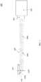
- FIG. 1includes a cross-sectional side view illustration of a flexible printed circuit (FPC)-based optical interconnect with a 3D polymer waveguide in accordance with an embodiment.
- FPCflexible printed circuit
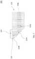
- FIG. 2is a close-up cross-sectional side view illustration of an optical interconnect with a 3D polymer waveguide in accordance with an embodiment.
- FIG. 3is a close-up cross-sectional side view illustration of an on-chip optical interconnect with a 3D polymer waveguide in accordance with an embodiment.
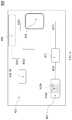
- FIG. 4is a schematic diagram illustration of a chip circuitry area for an optical interconnect with a 3D polymer waveguide in accordance with an embodiment.
- FIG. 5is a schematic diagram illustrating a fabrication method for making an optical interconnect with a 3D polymer waveguide in accordance with an embodiment.
- the terms “above”, “over”, “to”, “between”, and “on” as used hereinmay refer to a relative position of one layer with respect to other layers.
- One layer “above”, “over”, or “on” another layer or bonded “to” or in “contact” with another layermay be directly in contact with the other layer or may have one or more intervening layers.
- One layer “between” layersmay be directly in contact with the layers or may have one or more intervening layers.
- Optical interconnectis a means of communication by optical fiber cables. Compared to traditional cables, optical fibers are capable of a much higher bandwidth, from 10 Gbit/s up to 100 Gbit/s. (is this number correct?)
- Embodiments disclosed belowdescribe optical interconnects and application platforms.
- the optical interconnects and platforms in accordance with embodimentsmay be assembled without the optical lenses and fiber ribbons commonly utilized in conventional optical interconnect assemblies.
- assembly timecan be reduced compared to conventional techniques through use of semiconductor process technologies for the formation of transmission lines and flip chip integration of the active devices such as the driver IC chip, laser, PD, and receiver (e.g. TIA) chip.
- the fabrication techniquesmay allow for improved RF performance of the electrical signals and increased data rates of the optical interconnects.
- the embodiments illustrated belowmay be integrated as an optical interconnect incorporating a FPC.
- the embodimentmay be utilized to improve optical coupling with the VCSEL/PD by monolithically integrating a 3D polymer waveguide within a FPC.
- the polymer-based 3D optical waveguides terminated with 45 degree reflectorsmay be adopted to simplify the optical configuration of the module without fiber assembly and lens alignment.
- a multi-channel 3D polymer optical waveguideincludes vertically-bending cores close to 45 degree reflectors. Such a configuration may allow the optical paths to transmit optical signals from the VCSELs to fiber arrays as well as to receive optical signals from the fiber arrays to PD arrays.
- FIG. 1a cross-sectional side view illustration of a flexible printed circuit (FPC)-based optical interconnect with a multiple 3D polymer optical waveguide in accordance with an embodiment.
- An optical interconnector 100such as that illustrated in FIG. 1 includes an optical waveguide 120 which has an edge (e.g. 45 degrees) on the core layer shown as a vertical bending part 125 .
- the 3D optical waveguide 120may include a horizontal cladding layer 122 a and a 3D vertical cladding layer 122 b , a horizontal core layer 124 a surrounded by the horizontal cladding layer 122 a , and a vertical core layer 124 b surrounded by the vertical cladding layer 122 b .
- the cladding layer above(sometimes referred to as under cladding because it is an internal cladding) and the cladding layer below the straight waveguide (sometimes referred to as over cladding because it is an external cladding) can be made of different materials.
- the horizontal and vertical cladding layerscan also be made of different materials.
- the optical interconnect 100may also include a flexible chip circuit board active optical device VCSEL or PD mounted on an chip circuitry substrate 121 directly over the 3D vertical bending part 125 .
- a far end of the 3D optical waveguidemay be coupled to a multi-fiber mechanical transfer connector (MT) 127 , and a ribbon fiber cable 128 .
- MTmulti-fiber mechanical transfer connector
- multi-channel polymer waveguides terminated with 45 degree reflectorsare designed as optical paths to transmit optical signals from the vertical cavity surface emitting lasers (VCSELs) 121 to fiber arrays 128 , as well as to receive optical signals from fiber arrays to photodiode (PD) arrays.
- the polymer-based optical waveguide terminated with 45 degree reflectorsmay simplify the optical configuration of the module without fiber assembly.
- FIG. 1illustrates such a connector 127 to the fiber arrays.
- the multi-channel polymer waveguidesare terminated with a multi-channel mechanical transfer (MT) connector 127 , also referred to as a polymer mechanical transport (PMT) connector when connected with a polymer waveguide, to link with a fiber ribbon cable.
- MTmulti-channel mechanical transfer
- PMTpolymer mechanical transport
- the optical interconnectsmay be considered flexible printed circuit (FPC)-based.
- the optical interconnect module 200includes the vertical bending part 225 which has a 45 degree sloped edge mirror at one end of the optical polymer waveguide 220 along the core layer 224 a and the horizontal cladding layer 222 a .
- the horizontal cladding layer 222 a and a horizontal core layer 224 athere are also a vertical cladding layer 222 b , and a vertical core layer 224 b , both are monolithically fabricated respectively for efficient coupling through the polymer waveguide.
- Horizontal cladding layer 222 a and vertical cladder layer 222 bcan be made of different materials.
- the core structure inside the vertical bending part 225has a 45 degree sloped edge in contact with cladding, or air or another media with lower refractive index than that of the polymer core material.
- the outer interface surfaceis finely etched, maybe by a laser, to form a high reflective mirror.
- the FPC based electrical circuitry 223is placed over the vertical core 224 b , it may include an active optical device VCSEL, driver IC, or photodiode PD, TIAIC, depending on the interconnect applications.
- additional electronicslike a IC driver, trans-impedance amplifier (TIA) chip 226 , electrical traces (transmission lines) and solder bumps on bond pad 228 are formed on the FPC board next to the active device 223 , for example, VCSEL/PD, placed over the top surface of the front end of the 3D waveguide.
- TIAtrans-impedance amplifier
- the vertical-cavity surface-emitting laser, or VCSELis a type of semiconductor laser diode with laser beam emission perpendicular from the top surface, contrary to conventional edge-emitting semiconductor lasers (also in-plane lasers) which emit from surfaces formed by cleaving the individual chip out of a wafer.
- Vertical cavity self-emitting laser or VCSEL laser emitting light at wavelengths from 650 nm to 1300 nmare typically based on gallium arsenide (GaAs) wafers with diffraction Bragg reflectors (DBRs) formed from GaAs and aluminum gallium arsenide (Al x Ga (1-x) As).
- GaAsgallium arsenide
- DBRsdiffraction Bragg reflectors
- VCSELCMOS
- Oxide VCSELsCMOS-on-implanted VCSELs
- An additional adhesive layersuch as a polyimide layer or a non-conductive film (NCF) may also be applied to enhance adhesion of the components.
- the high speed electrical traces, including the RF devices 226are designed on the waveguide surface to connect the driver IC and VCSEL arrays as well as to connect trans-impedance amplifier (TIA) arrays.
- TIAtrans-impedance amplifier
- a VCSEL arrayhas four VCSEL lasers integrated in a row.
- the data rate of the optical enginecan be operated at 25 Giga-bits per second (Gbps) per channel, and can be extended to higher data rates such as 50 Gbps per channel.
- VCSEL applicationsinclude fiber optic communications, precision sensing, computer mice and laser printers.
- MEMSmicromechanically
- FIG. 4is a schematic diagram illustration of a FPC-based circuitry system 400 for an optical interconnect with the 3D polymer waveguide of FIGS. 1-3 in accordance with an embodiment.
- the circuitry system 421includes: one or more VCSELs or one or more PDs (in case of a receiver) 423 , a VCSEL driver chip or a PD receiver (e.g. TIA) chip 427 , a controller 429 , a RF chip 426 , and their connections (e.g. flip chip) to the pads 428 through the electric transmission lines such as 4231 , 4261 , 4262 , 4271 , and 4281 .
- the insulation layercan be made of organic materials such as polyimide.
- the patterns of high-speed electric transmission lines, bond pads, and solder bumpsare then formed on the insulation layer.
- the laser VCSEL 423is mounted over the vertical cladding area 422 b and vertical core area 424 b of the polymer waveguide that is directly over a 45 degree slanted edge.
- the VCSEL emission surfaceis aligned and interfaced with the top surface of the vertical core 424 b.
- the photodetectormay be mounted directly over another 45 degree slanted edge of the waveguide similarly constructed as the front end, the second FPC-based electronic circuitry board is not included in the figures because of its similarity as the system in FIG. 4 .
- the transmission lines, bond pads, and solder bumpsmay then be fabricated on a front side of the polymer waveguide using semiconductor fabrication techniques such as lithography and etch techniques.
- the active devicesmay be flip chip bonded and assembled onto the transmission lines on the front side of the vertical part of the polymer waveguide.
- a particular arrangementincludes 1 ⁇ 4 VCSEL/PD 423 , driver IC 427 , and TIA arrays (not shown here) to form the optical interconnect system
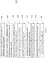
- FIG. 5is a schematic diagram illustrating a fabrication method for making an optical interconnect with a 3D polymer waveguide in accordance with an embodiment.
- the fabrication sequencemay include first step 502 , depositing a first polymer cladding layer on a temporary substrate, using a suitable technique such as spin coating or spray coating.
- first patterning process 504horizontal trenches along the axis of the polymer waveguide are wet/dry etched into the first polymer cladding layer.
- the horizontal trenchmay optionally include a sloped 45 degree sidewall, such that the trench opening that will be closest to the VCSEL/PD is larger than the opening that connects with the core trench layer.
- the 45 degree sidewallswill be used as the 45 degree reflectors.
- Another way of forming the 45 degree sidewallcan be achieved by having multiple lithographic exposures on the sidewall side in a separate step from forming the horizontal trench in the last step.
- the two exposuresapply two masks separately at the horizontal trench area and the 45 degree sidewall area.
- multiple exposures with varying mask openingscan be applied.
- the polymer core layeris then deposited on the first cladding layer, filling the horizontal trenches and the 45 degree sidewalls cavities, followed by step 508 , removing the excess core material outside the core trenches and cavities using a planarization technique such as the chemical mechanical polishing (CMP) or a selective wet/dry etch.
- CMPchemical mechanical polishing
- the second cladding layeris deposited over the planarized surface.
- a second patterning process 512 in the second cladding layeris performed to form a vertical cavity aligned with each 45 degree side wall reflector to form an optical path with the horizontal waveguide.
- the next step 514filling the vertical cavity with core material.
- Another planarization process 516is then applied to remove the excess core material outside the vertical cavities and provide a flat and clean surface to be the interface between the vertical waveguide and the active optical device exit plane.
- a planarization techniquesuch as the chemical mechanical polishing (CMP) or a selective wet/dry etch can be applied to flatten the surface and remove excess core material.
- CMPchemical mechanical polishing
- a selective wet/dry etchcan be applied to flatten the surface and remove excess core material.
- the temporary substratecan be a silicon wafer, a glass plate, or another form-factor which provides support during process.
- embodimentsare not limited to this particular sequence, and alternative fabrication sequences are envisioned.
Landscapes
- Physics & Mathematics (AREA)
- General Physics & Mathematics (AREA)
- Optics & Photonics (AREA)
- Engineering & Computer Science (AREA)
- Microelectronics & Electronic Packaging (AREA)
- Electromagnetism (AREA)
- Computer Networks & Wireless Communication (AREA)
- Signal Processing (AREA)
- Condensed Matter Physics & Semiconductors (AREA)
- Chemical & Material Sciences (AREA)
- Crystallography & Structural Chemistry (AREA)
- Optical Couplings Of Light Guides (AREA)
- Optical Integrated Circuits (AREA)
- Ceramic Engineering (AREA)
- Inorganic Chemistry (AREA)
- Computer Hardware Design (AREA)
- Power Engineering (AREA)
- Semiconductor Lasers (AREA)
- Light Receiving Elements (AREA)
Abstract
Description
Claims (10)
Priority Applications (4)
| Application Number | Priority Date | Filing Date | Title |
|---|---|---|---|
| US15/963,043US10591687B2 (en) | 2017-05-19 | 2018-04-25 | Optical interconnect modules with 3D polymer waveguide |
| PCT/US2018/031336WO2018213041A1 (en) | 2017-05-19 | 2018-05-07 | Optical interconnect modules with 3d polymer waveguide |
| JP2020514660AJP2020521188A (en) | 2017-05-19 | 2018-05-07 | Optical interconnection device and method for manufacturing optical polymer waveguide |
| CN201880047088.9ACN110998393A (en) | 2017-05-19 | 2018-05-07 | Optical interconnect module with 3D polymer waveguides |
Applications Claiming Priority (3)
| Application Number | Priority Date | Filing Date | Title |
|---|---|---|---|
| US201762508940P | 2017-05-19 | 2017-05-19 | |
| US201762509892P | 2017-05-23 | 2017-05-23 | |
| US15/963,043US10591687B2 (en) | 2017-05-19 | 2018-04-25 | Optical interconnect modules with 3D polymer waveguide |
Publications (2)
| Publication Number | Publication Date |
|---|---|
| US20180335584A1 US20180335584A1 (en) | 2018-11-22 |
| US10591687B2true US10591687B2 (en) | 2020-03-17 |
Family
ID=64271567
Family Applications (10)
| Application Number | Title | Priority Date | Filing Date |
|---|---|---|---|
| US15/963,014ActiveUS10439720B2 (en) | 2017-05-19 | 2018-04-25 | FPC-based optical interconnect module on glass interposer |
| US15/963,043ActiveUS10591687B2 (en) | 2017-05-19 | 2018-04-25 | Optical interconnect modules with 3D polymer waveguide |
| US15/963,030ActiveUS10436991B2 (en) | 2017-05-19 | 2018-04-25 | Optical interconnect modules based on glass substrate with polymer waveguide |
| US15/963,780ActiveUS10545300B2 (en) | 2017-05-19 | 2018-04-26 | Three-dimensional WDM with 1×M output ports on SOI based straight waveguides combined with wavelength filters on 45 degree reflectors |
| US15/963,815ActiveUS10585250B2 (en) | 2017-05-19 | 2018-04-26 | Optical interconnect modules with polymer waveguide on silicon substrate |
| US15/963,665ActiveUS10222564B2 (en) | 2017-05-19 | 2018-04-26 | Three-dimensional optical path with 1×m output ports using SOI-based vertically-splitting waveguides |
| US15/963,440AbandonedUS20180335587A1 (en) | 2017-05-19 | 2018-04-26 | Optical interconnect modules with 3d silicon waveguide on soi substrate |
| US15/964,701ActiveUS10670816B2 (en) | 2017-05-19 | 2018-04-27 | Polymer-based 1 x 2 vertical optical splitters on silicon substrate |
| US15/965,213ActiveUS10439721B2 (en) | 2017-05-19 | 2018-04-27 | Optical interconnect modules with AWG polymer waveguide on silicon substrate |
| US15/964,889ActiveUS10371904B2 (en) | 2017-05-19 | 2018-04-27 | Optical coupling structures |
Family Applications Before (1)
| Application Number | Title | Priority Date | Filing Date |
|---|---|---|---|
| US15/963,014ActiveUS10439720B2 (en) | 2017-05-19 | 2018-04-25 | FPC-based optical interconnect module on glass interposer |
Family Applications After (8)
| Application Number | Title | Priority Date | Filing Date |
|---|---|---|---|
| US15/963,030ActiveUS10436991B2 (en) | 2017-05-19 | 2018-04-25 | Optical interconnect modules based on glass substrate with polymer waveguide |
| US15/963,780ActiveUS10545300B2 (en) | 2017-05-19 | 2018-04-26 | Three-dimensional WDM with 1×M output ports on SOI based straight waveguides combined with wavelength filters on 45 degree reflectors |
| US15/963,815ActiveUS10585250B2 (en) | 2017-05-19 | 2018-04-26 | Optical interconnect modules with polymer waveguide on silicon substrate |
| US15/963,665ActiveUS10222564B2 (en) | 2017-05-19 | 2018-04-26 | Three-dimensional optical path with 1×m output ports using SOI-based vertically-splitting waveguides |
| US15/963,440AbandonedUS20180335587A1 (en) | 2017-05-19 | 2018-04-26 | Optical interconnect modules with 3d silicon waveguide on soi substrate |
| US15/964,701ActiveUS10670816B2 (en) | 2017-05-19 | 2018-04-27 | Polymer-based 1 x 2 vertical optical splitters on silicon substrate |
| US15/965,213ActiveUS10439721B2 (en) | 2017-05-19 | 2018-04-27 | Optical interconnect modules with AWG polymer waveguide on silicon substrate |
| US15/964,889ActiveUS10371904B2 (en) | 2017-05-19 | 2018-04-27 | Optical coupling structures |
Country Status (4)
| Country | Link |
|---|---|
| US (10) | US10439720B2 (en) |
| JP (3) | JP2020521186A (en) |
| CN (5) | CN110998393A (en) |
| WO (10) | WO2018213036A1 (en) |
Families Citing this family (48)
| Publication number | Priority date | Publication date | Assignee | Title |
|---|---|---|---|---|
| GB201617009D0 (en)* | 2016-10-06 | 2016-11-23 | University Court Of The University Of St Andrews The | Frontend integration of electronics and photonics |
| US10439720B2 (en) | 2017-05-19 | 2019-10-08 | Adolite Inc. | FPC-based optical interconnect module on glass interposer |
| US10690857B2 (en)* | 2017-06-21 | 2020-06-23 | Ii-Vi Delaware Inc. | Optical coupling systems |
| US10511400B2 (en)* | 2018-01-22 | 2019-12-17 | Electronics And Telecommunications Research Institute | Optical multiplexer for multiplexing optical signals using optical waveguide block including laminated layers |
| US11189985B2 (en)* | 2018-12-06 | 2021-11-30 | Ii-Vi Delaware, Inc. | Optoelectronic assembly |
| US12280556B2 (en) | 2019-01-18 | 2025-04-22 | Arizona Board Of Regents On Behalf Of The University Of Arizona | Assembly of flexible optical waveguides and photonic chips for optical interconnection packaging |
| US11002927B2 (en)* | 2019-02-21 | 2021-05-11 | Taiwan Semiconductor Manufacturing Company, Ltd. | Package structure |
| US12050327B2 (en) | 2019-06-04 | 2024-07-30 | Applied Materials, Inc. | Imaging system and method of manufacturing a metalens array |
| US10884191B2 (en) | 2019-06-06 | 2021-01-05 | International Business Machines Corporation | Flexible waveguide having an asymmetric optical-loss performance curve and improved worst-case optical-loss performance |
| DE102019115306A1 (en)* | 2019-06-06 | 2020-12-10 | Valeo Schalter Und Sensoren Gmbh | Manufacturing method for an optical coupling element for use in a vehicle |
| US11664902B2 (en)* | 2019-08-19 | 2023-05-30 | Nokia Solutions And Networks Oy | Planar assemblies for optical transceivers |
| CN110426797B (en)* | 2019-08-29 | 2025-04-04 | 深圳市聚力芯创投资企业(有限合伙) | Optical receiving engine based on planar waveguide chip |
| CN114503001B (en)* | 2019-09-13 | 2024-10-25 | 艾维森纳科技有限公司 | Optical interconnect using micro light emitting diodes (MICROLED) |
| KR102423085B1 (en)* | 2019-09-20 | 2022-07-21 | 주식회사 라이팩 | Ultra-small Transmitter Optical Sub-Assembly and Its Manufacturing Method Using Semiconductor Packaging Process |
| KR102725243B1 (en) | 2019-12-23 | 2024-11-01 | 삼성전자주식회사 | Electronic device comprising image sensor and method of operation thereof |
| US11824590B2 (en)* | 2020-04-13 | 2023-11-21 | Avicenatech Corp. | Interconnect networks using microLED-based optical links |
| CN111538119B (en)* | 2020-04-21 | 2022-03-08 | 东南大学 | Preparation method of three-dimensional photoelectric interconnection substrate |
| US11199671B2 (en) | 2020-04-21 | 2021-12-14 | Hewlett Packard Enterprise Development Lp | Glass-as-a-platform (GaaP)-based photonic assemblies comprising shaped glass plates |
| CN111478180B (en)* | 2020-04-23 | 2022-06-10 | 西安电子科技大学 | Semiconductor laser with on-chip integrated slow optical waveguide |
| CN111757591A (en)* | 2020-05-26 | 2020-10-09 | 维沃移动通信有限公司 | Circuit boards and electronic equipment |
| TW202217377A (en) | 2020-07-06 | 2022-05-01 | 新加坡商光子智能私人有限公司 | Integrated circuit interposer, system, apparatus, method of fabricating integrated circuit interposer, and method and system for transmitting information from nodes to destination interposer |
| KR102862830B1 (en)* | 2020-07-20 | 2025-09-19 | 어플라이드 머티어리얼스, 인코포레이티드 | Integrated conductive apertures for optical devices |
| US11567274B2 (en) | 2020-08-17 | 2023-01-31 | Molex, Llc | Optical module |
| CN112187371A (en)* | 2020-09-29 | 2021-01-05 | 中国科学院半导体研究所 | Photoelectric balance detector and receiving module and application thereof |
| US20220196914A1 (en)* | 2020-12-22 | 2022-06-23 | Intel Corporation | Waveguide with self-aligned mirror in package for long range chip-to-chip communications |
| CN112558244B (en)* | 2020-12-28 | 2022-06-17 | 武汉光迅科技股份有限公司 | Method and device for flip coupling of optical chip |
| US11909175B2 (en)* | 2021-01-13 | 2024-02-20 | Apple Inc. | Horizontal cavity surface-emitting laser (HCSEL) monolithically integrated with a photodetector |
| KR102671347B1 (en)* | 2021-03-17 | 2024-06-03 | 오프로세서 인코퍼레이티드 | Optical Device Module Package |
| KR20220139476A (en) | 2021-04-07 | 2022-10-17 | 삼성디스플레이 주식회사 | Display device and method of manufacturing the display device |
| US20220368100A1 (en)* | 2021-05-12 | 2022-11-17 | Stmicroelectronics Pte Ltd | Optical integrated circuit sensor package using a stacked configuration for the sensor die and the emitter die |
| US11768338B2 (en)* | 2021-05-27 | 2023-09-26 | Taiwan Semiconductor Manufacturing Company, Ltd. | Optical interconnect structure, package structure and fabricating method thereof |
| KR20220169981A (en) | 2021-06-21 | 2022-12-29 | 삼성디스플레이 주식회사 | Display device and manufacturing method for the same |
| CN113406745A (en)* | 2021-08-19 | 2021-09-17 | 江苏铌奥光电科技有限公司 | Waveguide-to-optical fiber three-dimensional polymer horizontal lens coupler |
| US12164158B2 (en)* | 2021-08-31 | 2024-12-10 | Taiwan Semiconductor Manufacturing Company, Ltd. | Package having prism structure and manufacturing method thereof |
| CN118202283A (en)* | 2021-10-26 | 2024-06-14 | 艾维森纳科技有限公司 | Flexible waveguide interconnection piece based on visible light LED |
| KR20230082333A (en)* | 2021-12-01 | 2023-06-08 | 삼성전기주식회사 | Printed circuit board and printed circuit board package |
| CN116263524A (en)* | 2021-12-13 | 2023-06-16 | 中兴通讯股份有限公司 | A kind of optical connector and its preparation method |
| KR102734233B1 (en)* | 2022-01-27 | 2024-11-27 | 한국과학기술원 | Optical module package using bi-angled silica waveguide |
| US11977256B2 (en) | 2022-02-25 | 2024-05-07 | Taiwan Semiconductor Manufacturing Company, Ltd. | Semiconductor package comprising optically coupled IC chips |
| CN114815089B (en) | 2022-04-18 | 2023-10-24 | 东莞立讯技术有限公司 | Optical module |
| CN115343811A (en) | 2022-04-21 | 2022-11-15 | 讯芸电子科技(中山)有限公司 | Butterfly type packaged optical transceiver |
| TWI818578B (en)* | 2022-06-09 | 2023-10-11 | 欣興電子股份有限公司 | Package structure and optical signal transmitter |
| US12412879B2 (en)* | 2022-06-09 | 2025-09-09 | Unimicron Technology Corp. | Package structure and manufacturing method thereof |
| CN115275781B (en)* | 2022-08-15 | 2024-11-15 | 济南大学 | Surface emitting laser based on polymer material and preparation method thereof |
| US20240085621A1 (en)* | 2022-09-14 | 2024-03-14 | Taiwan Semiconductor Manufacturing Co., Ltd. | Signal Communication Through Optical-Engine Based Interconnect Component |
| CN116344629B (en)* | 2023-02-24 | 2025-09-30 | 深南电路股份有限公司 | A photoelectric hybrid device based on glass waveguide and its manufacturing method |
| WO2025166053A1 (en)* | 2024-01-31 | 2025-08-07 | Snap Inc. | Stacking boards on rigid-flexes to decouple dynamic bends |
| CN119758292B (en)* | 2024-12-24 | 2025-09-09 | 华中光电技术研究所(中国船舶集团有限公司第七一七研究所) | Micro-integrated coherent balance detector and detection method |
Citations (101)
| Publication number | Priority date | Publication date | Assignee | Title |
|---|---|---|---|---|
| US5282080A (en) | 1991-12-09 | 1994-01-25 | Sdl, Inc. | Surface coupled optical amplifier |
| US5416861A (en) | 1994-04-29 | 1995-05-16 | University Of Cincinnati | Optical synchronous clock distribution network and high-speed signal distribution network |
| US5446814A (en) | 1993-11-05 | 1995-08-29 | Motorola | Molded reflective optical waveguide |
| US5485021A (en) | 1993-06-17 | 1996-01-16 | Shin-Etsu Handotai Co., Ltd. | Semiconductor device with optical waveguides to achieve signal transmission using optical means |
| US5956603A (en) | 1998-08-27 | 1999-09-21 | Ultratech Stepper, Inc. | Gas immersion laser annealing method suitable for use in the fabrication of reduced-dimension integrated circuits |
| US6036956A (en) | 1987-08-18 | 2000-03-14 | The Leland Stanford Junior University | Method and dosage form using an antagonist to gamma interferon to control MHC-associated autoimmune disease |
| US6049639A (en) | 1997-12-19 | 2000-04-11 | Intel Corporation | Method and apparatus providing optical input/output through the back side of an integrated circuit die |
| US6052498A (en) | 1997-12-19 | 2000-04-18 | Intel Corporation | Method and apparatus providing an optical input/output bus through the back side of an integrated circuit die |
| US6243508B1 (en) | 1999-06-01 | 2001-06-05 | Picolight Incorporated | Electro-opto-mechanical assembly for coupling a light source or receiver to an optical waveguide |
| US20010031109A1 (en) | 1999-01-06 | 2001-10-18 | Paniccia Mario J. | Method and apparatus for providing optical interconnection |
| US20010038737A1 (en) | 2000-04-05 | 2001-11-08 | Aya Imada | Plastic optical fiber with a lens portion, optical fiber connector, and connecting structures and methods between optical fibers and between optical fiber and light emitting/receiving device |
| US6330377B1 (en) | 1998-09-07 | 2001-12-11 | Sony Corporation | Optical transmitting/receiving method and apparatus |
| US20020018507A1 (en) | 1999-10-19 | 2002-02-14 | Deacon David A.G. | Channel-switched tunable laser for dwdm communications |
| US20020028045A1 (en)* | 1998-10-09 | 2002-03-07 | Tetsuzo Yoshimura | Optical coupling structures and the fabrication processes |
| US20020036356A1 (en) | 2000-09-28 | 2002-03-28 | Takayuki Teshima | Microstructure array, mold for forming a microstructure array, and method of fabricating the same |
| US6393169B1 (en) | 1997-12-19 | 2002-05-21 | Intel Corporation | Method and apparatus for providing optical interconnection |
| US6403393B1 (en) | 1999-09-01 | 2002-06-11 | International Business Machines Corporation | Device having integrated optical and copper conductors and method of fabricating same |
| US20020114587A1 (en) | 2001-02-21 | 2002-08-22 | Suresh Golwalkar | Apparatus for coupling a fiber optic cable to an optoelectronic device, a system including the apparatus, and a method of forming the same |
| US6456765B1 (en) | 2001-04-30 | 2002-09-24 | Raytheon Company | Apparatus for separating and/or combining optical signals, and methods of making and operating it |
| US20030015770A1 (en) | 2001-07-20 | 2003-01-23 | Motorola, Inc. | Optical waveguide trenches in composite integrated circuits |
| US6549708B2 (en) | 2000-08-21 | 2003-04-15 | Lockheed Martin Corporation | Dual-side waveguide-based wavelength demultiplexer |
| US6603915B2 (en) | 2001-02-05 | 2003-08-05 | Fujitsu Limited | Interposer and method for producing a light-guiding structure |
| US20030223673A1 (en) | 2002-03-15 | 2003-12-04 | Garito Anthony F. | Integrated optical waveguide structures |
| US20040065843A1 (en) | 2002-10-03 | 2004-04-08 | David Schut | Emitter device with focusing columns |
| US6731856B1 (en) | 1998-11-27 | 2004-05-04 | Sharp Kabushiki Kaisha | Organic waveguide and manufacturing method thereof and optical part using the same |
| US20040109654A1 (en) | 2002-12-10 | 2004-06-10 | Claudius Feger | Apparatus and methods for remakeable connections to optical waveguides |
| US20040245538A1 (en) | 2003-06-06 | 2004-12-09 | Xiaolin Wang | Double sided optoelectronic integrated circuit |
| US20040264837A1 (en) | 2002-10-24 | 2004-12-30 | Sony Corporation | Hybrid circuit substrate with optical and electrical interconnects, hybrid circuit module with optical and electrical interconnects and manufacturing methods thereof |
| US6845184B1 (en) | 1998-10-09 | 2005-01-18 | Fujitsu Limited | Multi-layer opto-electronic substrates with electrical and optical interconnections and methods for making |
| US20050031265A1 (en) | 2003-08-05 | 2005-02-10 | Jonathan Simon | Low cost optical interconnect for fiber optic system |
| US20050041906A1 (en) | 2001-02-28 | 2005-02-24 | Akio Sugama | Optical wiring substrate, method of manufacturing optical wiring substrate and multilayer optical wiring |
| US20050063636A1 (en) | 2001-10-09 | 2005-03-24 | Infinera Corporation | Method and apparatus for providing an antireflection coating on the output facet of a photonic integrated circuit (PIC) chip |
| US20050136574A1 (en) | 2003-12-17 | 2005-06-23 | Chih-Hung Shih | Thin film transistor and process for making an array panel |
| US20050141808A1 (en) | 2003-12-24 | 2005-06-30 | National Research Council Of Canada | Optical off-chip interconnects in multichannel planar waveguide devices |
| US20050185900A1 (en) | 2004-01-22 | 2005-08-25 | Finisar Corporation | Integrated optical devices and methods of making same |
| US20050201707A1 (en) | 2004-03-12 | 2005-09-15 | Alexei Glebov | Flexible optical waveguides for backplane optical interconnections |
| US20060045418A1 (en) | 2004-08-25 | 2006-03-02 | Information And Communication University Research And Industrial Cooperation Group | Optical printed circuit board and optical interconnection block using optical fiber bundle |
| US20070058976A1 (en) | 2005-09-15 | 2007-03-15 | Tatum Jimmy A | Laser drivers for closed path optical cables |
| US7218809B2 (en) | 2000-10-20 | 2007-05-15 | Seng-Tiong Ho | Integrated planar composite coupling structures for bi-directional light beam transformation between a small mode size waveguide and a large mode size waveguide |
| US20080031583A1 (en)* | 2006-08-03 | 2008-02-07 | Fuji Xerox Co., Ltd. | Flexible optical waveguide film, optical transceiver module, multi-channel optical transceiver module, and method of manufacturing flexible optical waveguide film |
| US20080037934A1 (en) | 2006-08-08 | 2008-02-14 | Fujitsu Component Limited | Optical connector |
| US20080130125A1 (en) | 2006-07-28 | 2008-06-05 | Michael Goelles | Corradiator employing a wedge-shaped cross-section |
| US20080265416A1 (en) | 2007-04-27 | 2008-10-30 | Shen-Nan Lee | Metal line formation using advaced CMP slurry |
| US20080279566A1 (en) | 2007-05-10 | 2008-11-13 | Miller Frederick W | Methods and apparatuses for measuring jitter in a transceiver module |
| US20080279557A1 (en) | 2007-05-09 | 2008-11-13 | Gwangju Institute Of Science And Technology | Wdm-pon system using self-injection locking, optical line terminal thereof, and data transmission method |
| US20090049964A1 (en) | 2007-08-24 | 2009-02-26 | Matsushita Electric Works, Ltd. | Process of forming a deflection mirror in a light waveguide |
| US20090060526A1 (en) | 2002-12-03 | 2009-03-05 | Finisar Corporation | Optical fm source based on intra-cavity phase and amplitude modulation in lasers |
| US20090072393A1 (en) | 2005-02-24 | 2009-03-19 | Agere Systems Inc. | Structure and Method for Fabricating Flip Chip Devices |
| US7529439B2 (en) | 2006-08-14 | 2009-05-05 | Samsung Electro-Mechanics Co., Ltd. | Optical printed circuit board and fabricating method thereof |
| US20090202713A1 (en) | 2008-02-13 | 2009-08-13 | Xyratex Technology Limited | method of making a waveguide and a waveguide made thereby |
| US20090218519A1 (en) | 2005-06-18 | 2009-09-03 | The Regents Of The University Of Colorado | Three-Dimensional Direct-Write Lithography |
| US7627204B1 (en) | 2007-11-02 | 2009-12-01 | National Semiconductor Corporation | Optical-electrical flex interconnect using a flexible waveguide and flexible printed circuit board substrate |
| US20100032853A1 (en) | 2008-08-11 | 2010-02-11 | Nitto Denko Corporation | Method for manufacturing optical waveguide |
| US20100104290A1 (en) | 2007-06-28 | 2010-04-29 | Fujitsu Limited | Optical subassembly manufacturing method, optical subassembly, OSA array, optical interconnecting device, WDM oscillator, and receiving circuit |
| US20100215313A1 (en) | 2009-02-20 | 2010-08-26 | Hitachi, Ltd. | Optical interconnection assembled circuit |
| US20100213561A1 (en) | 2007-10-26 | 2010-08-26 | International Business Machines Corporation | Optoelectronic Device with Germanium Photodetector |
| US20100226655A1 (en) | 2007-03-19 | 2010-09-09 | Jeong Soo Kim | Self-standing parallel plate beam splitter, method for manufacturing the same, and laser diode package structure using the same |
| US20110030778A1 (en) | 2009-08-06 | 2011-02-10 | Energy Focus, Inc. | Method of Passivating and Reducing Reflectance of a Photovoltaic Cell |
| US20110133063A1 (en) | 2009-12-03 | 2011-06-09 | Samsung Electronics Co., Ltd. | Optical waveguide and coupler apparatus and method of manufacturing the same |
| US20110229080A1 (en) | 2010-03-19 | 2011-09-22 | Gemfire Corporation | Optical device with athermal slots for temperature dependence curvature reduction |
| US8135248B2 (en) | 2008-11-26 | 2012-03-13 | Nitto Denko Corporation | Opto-electric hybrid board and manufacturing method thereof |
| US20120076454A1 (en) | 2010-09-24 | 2012-03-29 | Fujitsu Limited | Optical module and method for manufacturing the same |
| US20120163821A1 (en) | 2010-12-22 | 2012-06-28 | Electronics And Telecommunications Research Institute | Multi-wavelength optical source generator |
| US20120177381A1 (en) | 2009-09-04 | 2012-07-12 | Peter De Dobbelaere | Method And System For A Photonic Interposer |
| US20120314990A1 (en) | 2011-06-10 | 2012-12-13 | Xyratex Technology Limited | Optical waveguide and a method of fabricating an optical waveguide |
| US8368995B2 (en) | 2009-10-13 | 2013-02-05 | Skorpios Technologies, Inc. | Method and system for hybrid integration of an opto-electronic integrated circuit |
| US20130064494A1 (en) | 2011-09-09 | 2013-03-14 | Cristian BOLLE | Encapsulation of a temperature compensationing structure within an optical circuit package enclosure |
| US20130182998A1 (en) | 2012-01-18 | 2013-07-18 | International Business Machines Corporation | Silicon photonic chip optical coupling structures |
| US20130195456A1 (en) | 2010-10-08 | 2013-08-01 | Wayne V. Sorin | Optical multiplexing using laser arrays |
| US20130223789A1 (en) | 2012-02-23 | 2013-08-29 | Taiwan Semiconductor Manufacturing Company, Ltd. | Optical bench on substrate |
| US20140112616A1 (en) | 2012-10-18 | 2014-04-24 | International Business Machines Corporation | ALIGNMENT OF SINGLE-MODE POLYMER WAVEGUIDE (PWG) ARRAY AND SILICON WAVEGUIDE (SiWG) ARRAY FOR PROVIDING ADIABATIC COUPLING |
| US20140140657A1 (en) | 2012-11-20 | 2014-05-22 | Fujitsu Limited | Optical module and fabrication method |
| US20140177995A1 (en) | 2012-12-20 | 2014-06-26 | Edris M. Mohammed | Optical photonic circuit coupling |
| US20140294342A1 (en) | 2013-03-28 | 2014-10-02 | International Business Machines Corporation | Optoelectronic packaging assembly |
| US20140321804A1 (en) | 2013-04-26 | 2014-10-30 | Oracle International Corporation | Hybrid-integrated photonic chip package with an interposer |
| US20140355931A1 (en) | 2013-05-28 | 2014-12-04 | Georgia Tech Research Corporation | Glass-Polymer Optical Interposer |
| US20150043919A1 (en) | 2012-07-25 | 2015-02-12 | Doron Handelman | APPARATUS AND METHODS FOR GENERATING AND RECEIVING OPTICAL SIGNALS AT SUBSTANTIALLY 100Gb/s AND BEYOND |
| US20150117824A1 (en) | 2012-05-29 | 2015-04-30 | 3M Innovation Properties Company | Optical interconnect |
| US20150132002A1 (en) | 2013-11-13 | 2015-05-14 | Agency For Science, Technology And Research | Integrated laser and method of fabrication thereof |
| US9036956B2 (en) | 2012-02-17 | 2015-05-19 | Haynes and Boone, LLP | Method of fabricating a polymer waveguide |
| US20150168646A1 (en) | 2012-06-19 | 2015-06-18 | Sumitomo Bakelite Co., Ltd. | Optical waveguide, optical interconnection component, optical module, opto-electric hybrid board, and electronic device |
| US9086551B2 (en) | 2013-10-30 | 2015-07-21 | International Business Machines Corporation | Double mirror structure for wavelength division multiplexing with polymer waveguides |
| US20150303649A1 (en) | 2014-04-16 | 2015-10-22 | Apple Inc. | Active silicon optical bench |
| US20150333831A1 (en) | 2014-05-16 | 2015-11-19 | Qualcomm Incorporated | Electro-optical transceiver device to enable chip-to-chip interconnection |
| US20150362673A1 (en) | 2013-07-31 | 2015-12-17 | Oracle International Corporation | Surface-normal coupler for silicon-on-insulator platforms |
| US20150362676A1 (en) | 2008-10-31 | 2015-12-17 | Esi-Pyrophotonics Lasers Inc. | Laser system with doped fiber components |
| US20160011414A1 (en) | 2013-03-01 | 2016-01-14 | Saint-Gobain Glass France | Display device for transparent glazing |
| US9310575B2 (en) | 2012-05-31 | 2016-04-12 | Nippon Mektron, Ltd. | Manufacturing method of opto-electric hybrid flexible printed circuit board and opto-electric hybrid flexible printed circuit board |
| US9341797B2 (en) | 2013-10-11 | 2016-05-17 | International Business Machines Corporation | Optical module and method for manufacturing optical module |
| US20160156999A1 (en) | 2014-12-01 | 2016-06-02 | Odile Liboiron-Ladouceur | Methods and systems for board level photonic bridges |
| US20160178839A1 (en) | 2013-06-06 | 2016-06-23 | Nitto Denko Corporation | Opto-electric hybrid board |
| US20160349451A1 (en) | 2015-05-25 | 2016-12-01 | Centera Photonics Inc. | Optical connection module |
| US20170017042A1 (en) | 2014-03-07 | 2017-01-19 | Aeponyx Inc. | Methods and system for wavelength tunable optical components and sub-systems |
| US9627851B1 (en) | 2015-10-28 | 2017-04-18 | Rockley Photonics Limited | Discrete wavelength tunable laser |
| US20170230117A1 (en) | 2016-02-08 | 2017-08-10 | Skorpios Technologies, Inc. | High-speed optical transmitter with a silicon substrate |
| US9939593B2 (en) | 2013-12-26 | 2018-04-10 | Futurewei Technologies, Inc. | Light steering for silicon photonic devices |
| US9964702B1 (en) | 2016-10-13 | 2018-05-08 | Oracle International Corporation | Surface-normal optical coupling interface with thermal-optic coefficient compensation |
| US20180149815A1 (en) | 2016-11-30 | 2018-05-31 | International Business Machines Corporation | Off-axis micro-mirror arrays for optical coupling in polymer waveguides |
| US20180159627A1 (en) | 2016-12-01 | 2018-06-07 | Huawei Technologies Co., Ltd. | Systems and Methods for Reducing Adjacent Channel Leakage Ratio |
| US20180288875A1 (en) | 2017-03-30 | 2018-10-04 | Smk Corporation | Composite cable to be connected to flat panel-shaped electrical equipment |
| WO2018213043A1 (en) | 2017-05-19 | 2018-11-22 | Adolite Inc. | Optical interconnect modules based on glass substrate with polymer waveguide |
Family Cites Families (27)
| Publication number | Priority date | Publication date | Assignee | Title |
|---|---|---|---|---|
| JPH10160961A (en)* | 1996-12-03 | 1998-06-19 | Mitsubishi Gas Chem Co Inc | Optical element |
| CA2272751A1 (en)* | 1996-12-31 | 1998-07-09 | Honeywell Inc. | Flexible optic connector assembly |
| CN1206841A (en)* | 1997-07-28 | 1999-02-03 | 三星电子株式会社 | Production method of optical waveguide device |
| JP4752092B2 (en)* | 2000-07-31 | 2011-08-17 | 株式会社トッパンNecサーキットソリューションズ | Optical waveguide connection structure and optical element mounting structure |
| ATE518158T1 (en)* | 2001-09-07 | 2011-08-15 | Nhk Sales Company Ltd | ENDSURFACE TREATMENT METHOD FOR AN OPTICAL PLASTIC FIBER |
| US6904197B2 (en)* | 2002-03-04 | 2005-06-07 | Corning Incorporated | Beam bending apparatus and method of manufacture |
| KR100448968B1 (en)* | 2002-12-31 | 2004-09-18 | 삼성전자주식회사 | Method for fabricating optical coupling device, optical coupling device, optical coupling device assembly, and a lensed fiber using said optical coupling device |
| JP2005044396A (en)* | 2003-07-23 | 2005-02-17 | Tdk Corp | Optical information recording medium |
| CN1222792C (en)* | 2003-10-14 | 2005-10-12 | 武汉光迅科技有限责任公司 | 3-D optical-wave-guide structure and manufacturing method |
| JP2005292268A (en)* | 2004-03-31 | 2005-10-20 | Hitachi Chem Co Ltd | Optical waveguide device |
| WO2006014582A2 (en)* | 2004-07-08 | 2006-02-09 | Dow Corning Corporation | Short reach optical interconnect |
| CN100412587C (en)* | 2005-12-31 | 2008-08-20 | 中国科学院物理研究所 | Active alignment fixture and method for single-mode lensed fiber and slab ridge waveguide |
| FR2909229B1 (en)* | 2006-11-27 | 2009-02-06 | Centre Nat Rech Scient | LASER SYSTEM WITH PICOSECOND IMPULSE TRANSMISSION. |
| CN100523886C (en)* | 2007-09-25 | 2009-08-05 | 晶方半导体科技(苏州)有限公司 | Optical waveguide and method for manufacturing the same |
| CN101344624A (en)* | 2008-07-17 | 2009-01-14 | 华中科技大学 | Optoelectronic Hybrid Printed Circuit Board with Direct Coupling of Optical Interconnection Between Chips |
| US8611707B2 (en)* | 2009-01-09 | 2013-12-17 | Hewlett-Packard Development Company, L.P. | System and methods for routing optical signals |
| JP5750997B2 (en)* | 2010-05-17 | 2015-07-22 | 住友電気工業株式会社 | Optical connector module |
| CN102336007A (en)* | 2010-07-23 | 2012-02-01 | 鸿富锦精密工业(深圳)有限公司 | Shearing device |
| EP2693027A4 (en)* | 2011-03-31 | 2014-10-08 | Toyota Motor Co Ltd | CONTROL DEVICE FOR INTERNAL COMBUSTION ENGINE AND VEHICLE EQUIPPED WITH SAME |
| TWI686904B (en)* | 2012-03-16 | 2020-03-01 | 美商樂仕特拉公司 | Method and system for a photonic interposer |
| US9195007B2 (en)* | 2012-06-28 | 2015-11-24 | Intel Corporation | Inverted 45 degree mirror for photonic integrated circuits |
| CN102866461A (en)* | 2012-09-29 | 2013-01-09 | 武汉光迅科技股份有限公司 | Coupling method of photon chip and optical fibers |
| US9488205B2 (en)* | 2013-07-12 | 2016-11-08 | GM Global Technology Operations LLC | Alignment arrangement for mated components and method |
| US8969689B2 (en)* | 2013-07-25 | 2015-03-03 | Monsanto Technology Llc | Wheat cultivar WB6121 |
| WO2015161488A1 (en)* | 2014-04-24 | 2015-10-29 | 华为技术有限公司 | Single-mode vertical cavity surface emitting laser transceiving module and optical signal propagation method |
| JP6237691B2 (en)* | 2015-04-22 | 2017-11-29 | 富士通オプティカルコンポーネンツ株式会社 | Optical module and optical fiber assembly |
| CN106353859A (en)* | 2015-07-24 | 2017-01-25 | 中兴通讯股份有限公司 | Light interconnection intersecting back plate, transmitting equipment and signal dispatching method |
- 2018
- 2018-04-25USUS15/963,014patent/US10439720B2/enactiveActive
- 2018-04-25USUS15/963,043patent/US10591687B2/enactiveActive
- 2018-04-25USUS15/963,030patent/US10436991B2/enactiveActive
- 2018-04-26USUS15/963,780patent/US10545300B2/enactiveActive
- 2018-04-26USUS15/963,815patent/US10585250B2/enactiveActive
- 2018-04-26USUS15/963,665patent/US10222564B2/enactiveActive
- 2018-04-26USUS15/963,440patent/US20180335587A1/ennot_activeAbandoned
- 2018-04-27USUS15/964,701patent/US10670816B2/enactiveActive
- 2018-04-27USUS15/965,213patent/US10439721B2/enactiveActive
- 2018-04-27USUS15/964,889patent/US10371904B2/enactiveActive
- 2018-05-07WOPCT/US2018/031331patent/WO2018213036A1/ennot_activeCeased
- 2018-05-07WOPCT/US2018/031343patent/WO2018213043A1/ennot_activeCeased
- 2018-05-07JPJP2020514658Apatent/JP2020521186A/enactivePending
- 2018-05-07WOPCT/US2018/031345patent/WO2018213044A1/ennot_activeCeased
- 2018-05-07WOPCT/US2018/031338patent/WO2018213042A1/ennot_activeCeased
- 2018-05-07JPJP2020514659Apatent/JP2020521187A/enactivePending
- 2018-05-07WOPCT/US2018/031333patent/WO2018213038A1/ennot_activeCeased
- 2018-05-07WOPCT/US2018/031335patent/WO2018213040A1/ennot_activeCeased
- 2018-05-07CNCN201880047088.9Apatent/CN110998393A/enactivePending
- 2018-05-07CNCN201880047109.7Apatent/CN111051940A/enactivePending
- 2018-05-07WOPCT/US2018/031336patent/WO2018213041A1/ennot_activeCeased
- 2018-05-07CNCN201880047108.2Apatent/CN111033335A/enactivePending
- 2018-05-07CNCN201880047084.0Apatent/CN110998391A/enactivePending
- 2018-05-07JPJP2020514660Apatent/JP2020521188A/enactivePending
- 2018-05-07CNCN201880047089.3Apatent/CN110945976A/enactivePending
- 2018-05-07WOPCT/US2018/031334patent/WO2018213039A1/ennot_activeCeased
- 2018-05-07WOPCT/US2018/031332patent/WO2018213037A1/ennot_activeCeased
- 2018-05-07WOPCT/US2018/031328patent/WO2018213035A1/ennot_activeCeased
Patent Citations (122)
| Publication number | Priority date | Publication date | Assignee | Title |
|---|---|---|---|---|
| US6036956A (en) | 1987-08-18 | 2000-03-14 | The Leland Stanford Junior University | Method and dosage form using an antagonist to gamma interferon to control MHC-associated autoimmune disease |
| US5282080A (en) | 1991-12-09 | 1994-01-25 | Sdl, Inc. | Surface coupled optical amplifier |
| US5485021A (en) | 1993-06-17 | 1996-01-16 | Shin-Etsu Handotai Co., Ltd. | Semiconductor device with optical waveguides to achieve signal transmission using optical means |
| US5446814A (en) | 1993-11-05 | 1995-08-29 | Motorola | Molded reflective optical waveguide |
| US5416861A (en) | 1994-04-29 | 1995-05-16 | University Of Cincinnati | Optical synchronous clock distribution network and high-speed signal distribution network |
| US6049639A (en) | 1997-12-19 | 2000-04-11 | Intel Corporation | Method and apparatus providing optical input/output through the back side of an integrated circuit die |
| US6052498A (en) | 1997-12-19 | 2000-04-18 | Intel Corporation | Method and apparatus providing an optical input/output bus through the back side of an integrated circuit die |
| US6393169B1 (en) | 1997-12-19 | 2002-05-21 | Intel Corporation | Method and apparatus for providing optical interconnection |
| US5956603A (en) | 1998-08-27 | 1999-09-21 | Ultratech Stepper, Inc. | Gas immersion laser annealing method suitable for use in the fabrication of reduced-dimension integrated circuits |
| US6330377B1 (en) | 1998-09-07 | 2001-12-11 | Sony Corporation | Optical transmitting/receiving method and apparatus |
| US20020028045A1 (en)* | 1998-10-09 | 2002-03-07 | Tetsuzo Yoshimura | Optical coupling structures and the fabrication processes |
| US6845184B1 (en) | 1998-10-09 | 2005-01-18 | Fujitsu Limited | Multi-layer opto-electronic substrates with electrical and optical interconnections and methods for making |
| US6731856B1 (en) | 1998-11-27 | 2004-05-04 | Sharp Kabushiki Kaisha | Organic waveguide and manufacturing method thereof and optical part using the same |
| US20010031109A1 (en) | 1999-01-06 | 2001-10-18 | Paniccia Mario J. | Method and apparatus for providing optical interconnection |
| US6587605B2 (en) | 1999-01-06 | 2003-07-01 | Intel Corporation | Method and apparatus for providing optical interconnection |
| US6243508B1 (en) | 1999-06-01 | 2001-06-05 | Picolight Incorporated | Electro-opto-mechanical assembly for coupling a light source or receiver to an optical waveguide |
| US6403393B1 (en) | 1999-09-01 | 2002-06-11 | International Business Machines Corporation | Device having integrated optical and copper conductors and method of fabricating same |
| US20020018507A1 (en) | 1999-10-19 | 2002-02-14 | Deacon David A.G. | Channel-switched tunable laser for dwdm communications |
| US20010038737A1 (en) | 2000-04-05 | 2001-11-08 | Aya Imada | Plastic optical fiber with a lens portion, optical fiber connector, and connecting structures and methods between optical fibers and between optical fiber and light emitting/receiving device |
| US6549708B2 (en) | 2000-08-21 | 2003-04-15 | Lockheed Martin Corporation | Dual-side waveguide-based wavelength demultiplexer |
| US20020036356A1 (en) | 2000-09-28 | 2002-03-28 | Takayuki Teshima | Microstructure array, mold for forming a microstructure array, and method of fabricating the same |
| US7218809B2 (en) | 2000-10-20 | 2007-05-15 | Seng-Tiong Ho | Integrated planar composite coupling structures for bi-directional light beam transformation between a small mode size waveguide and a large mode size waveguide |
| US6603915B2 (en) | 2001-02-05 | 2003-08-05 | Fujitsu Limited | Interposer and method for producing a light-guiding structure |
| US20020114587A1 (en) | 2001-02-21 | 2002-08-22 | Suresh Golwalkar | Apparatus for coupling a fiber optic cable to an optoelectronic device, a system including the apparatus, and a method of forming the same |
| US20050041906A1 (en) | 2001-02-28 | 2005-02-24 | Akio Sugama | Optical wiring substrate, method of manufacturing optical wiring substrate and multilayer optical wiring |
| US6456765B1 (en) | 2001-04-30 | 2002-09-24 | Raytheon Company | Apparatus for separating and/or combining optical signals, and methods of making and operating it |
| US20030015770A1 (en) | 2001-07-20 | 2003-01-23 | Motorola, Inc. | Optical waveguide trenches in composite integrated circuits |
| US20050063636A1 (en) | 2001-10-09 | 2005-03-24 | Infinera Corporation | Method and apparatus for providing an antireflection coating on the output facet of a photonic integrated circuit (PIC) chip |
| US20030223673A1 (en) | 2002-03-15 | 2003-12-04 | Garito Anthony F. | Integrated optical waveguide structures |
| US20040065843A1 (en) | 2002-10-03 | 2004-04-08 | David Schut | Emitter device with focusing columns |
| US20040264837A1 (en) | 2002-10-24 | 2004-12-30 | Sony Corporation | Hybrid circuit substrate with optical and electrical interconnects, hybrid circuit module with optical and electrical interconnects and manufacturing methods thereof |
| US7266262B2 (en) | 2002-10-24 | 2007-09-04 | Sony Corporation | Hybrid circuit substrate with optical and electrical interconnects, hybrid circuit module with optical and electrical interconnects and manufacturing methods thereof |
| US20090060526A1 (en) | 2002-12-03 | 2009-03-05 | Finisar Corporation | Optical fm source based on intra-cavity phase and amplitude modulation in lasers |
| US20040109654A1 (en) | 2002-12-10 | 2004-06-10 | Claudius Feger | Apparatus and methods for remakeable connections to optical waveguides |
| US20040245538A1 (en) | 2003-06-06 | 2004-12-09 | Xiaolin Wang | Double sided optoelectronic integrated circuit |
| US20050031265A1 (en) | 2003-08-05 | 2005-02-10 | Jonathan Simon | Low cost optical interconnect for fiber optic system |
| US20050136574A1 (en) | 2003-12-17 | 2005-06-23 | Chih-Hung Shih | Thin film transistor and process for making an array panel |
| US20050141808A1 (en) | 2003-12-24 | 2005-06-30 | National Research Council Of Canada | Optical off-chip interconnects in multichannel planar waveguide devices |
| US20050185900A1 (en) | 2004-01-22 | 2005-08-25 | Finisar Corporation | Integrated optical devices and methods of making same |
| US20050201707A1 (en) | 2004-03-12 | 2005-09-15 | Alexei Glebov | Flexible optical waveguides for backplane optical interconnections |
| US6996303B2 (en) | 2004-03-12 | 2006-02-07 | Fujitsu Limited | Flexible optical waveguides for backplane optical interconnections |
| US20060045418A1 (en) | 2004-08-25 | 2006-03-02 | Information And Communication University Research And Industrial Cooperation Group | Optical printed circuit board and optical interconnection block using optical fiber bundle |
| US20090072393A1 (en) | 2005-02-24 | 2009-03-19 | Agere Systems Inc. | Structure and Method for Fabricating Flip Chip Devices |
| US20090218519A1 (en) | 2005-06-18 | 2009-09-03 | The Regents Of The University Of Colorado | Three-Dimensional Direct-Write Lithography |
| US20070058976A1 (en) | 2005-09-15 | 2007-03-15 | Tatum Jimmy A | Laser drivers for closed path optical cables |
| US20080130125A1 (en) | 2006-07-28 | 2008-06-05 | Michael Goelles | Corradiator employing a wedge-shaped cross-section |
| US20080031583A1 (en)* | 2006-08-03 | 2008-02-07 | Fuji Xerox Co., Ltd. | Flexible optical waveguide film, optical transceiver module, multi-channel optical transceiver module, and method of manufacturing flexible optical waveguide film |
| US20080037934A1 (en) | 2006-08-08 | 2008-02-14 | Fujitsu Component Limited | Optical connector |
| US7529439B2 (en) | 2006-08-14 | 2009-05-05 | Samsung Electro-Mechanics Co., Ltd. | Optical printed circuit board and fabricating method thereof |
| US20100226655A1 (en) | 2007-03-19 | 2010-09-09 | Jeong Soo Kim | Self-standing parallel plate beam splitter, method for manufacturing the same, and laser diode package structure using the same |
| US20080265416A1 (en) | 2007-04-27 | 2008-10-30 | Shen-Nan Lee | Metal line formation using advaced CMP slurry |
| US20080279557A1 (en) | 2007-05-09 | 2008-11-13 | Gwangju Institute Of Science And Technology | Wdm-pon system using self-injection locking, optical line terminal thereof, and data transmission method |
| US20080279566A1 (en) | 2007-05-10 | 2008-11-13 | Miller Frederick W | Methods and apparatuses for measuring jitter in a transceiver module |
| US20100104290A1 (en) | 2007-06-28 | 2010-04-29 | Fujitsu Limited | Optical subassembly manufacturing method, optical subassembly, OSA array, optical interconnecting device, WDM oscillator, and receiving circuit |
| US20090049964A1 (en) | 2007-08-24 | 2009-02-26 | Matsushita Electric Works, Ltd. | Process of forming a deflection mirror in a light waveguide |
| US20100213561A1 (en) | 2007-10-26 | 2010-08-26 | International Business Machines Corporation | Optoelectronic Device with Germanium Photodetector |
| US7627204B1 (en) | 2007-11-02 | 2009-12-01 | National Semiconductor Corporation | Optical-electrical flex interconnect using a flexible waveguide and flexible printed circuit board substrate |
| US20090202713A1 (en) | 2008-02-13 | 2009-08-13 | Xyratex Technology Limited | method of making a waveguide and a waveguide made thereby |
| US20100032853A1 (en) | 2008-08-11 | 2010-02-11 | Nitto Denko Corporation | Method for manufacturing optical waveguide |
| US20150362676A1 (en) | 2008-10-31 | 2015-12-17 | Esi-Pyrophotonics Lasers Inc. | Laser system with doped fiber components |
| US8135248B2 (en) | 2008-11-26 | 2012-03-13 | Nitto Denko Corporation | Opto-electric hybrid board and manufacturing method thereof |
| US20100215313A1 (en) | 2009-02-20 | 2010-08-26 | Hitachi, Ltd. | Optical interconnection assembled circuit |
| US20110030778A1 (en) | 2009-08-06 | 2011-02-10 | Energy Focus, Inc. | Method of Passivating and Reducing Reflectance of a Photovoltaic Cell |
| US20120177381A1 (en) | 2009-09-04 | 2012-07-12 | Peter De Dobbelaere | Method And System For A Photonic Interposer |
| US8368995B2 (en) | 2009-10-13 | 2013-02-05 | Skorpios Technologies, Inc. | Method and system for hybrid integration of an opto-electronic integrated circuit |
| US20110133063A1 (en) | 2009-12-03 | 2011-06-09 | Samsung Electronics Co., Ltd. | Optical waveguide and coupler apparatus and method of manufacturing the same |
| US20110229080A1 (en) | 2010-03-19 | 2011-09-22 | Gemfire Corporation | Optical device with athermal slots for temperature dependence curvature reduction |
| US20120076454A1 (en) | 2010-09-24 | 2012-03-29 | Fujitsu Limited | Optical module and method for manufacturing the same |
| US20130195456A1 (en) | 2010-10-08 | 2013-08-01 | Wayne V. Sorin | Optical multiplexing using laser arrays |
| US20120163821A1 (en) | 2010-12-22 | 2012-06-28 | Electronics And Telecommunications Research Institute | Multi-wavelength optical source generator |
| US20120314990A1 (en) | 2011-06-10 | 2012-12-13 | Xyratex Technology Limited | Optical waveguide and a method of fabricating an optical waveguide |
| US20130064494A1 (en) | 2011-09-09 | 2013-03-14 | Cristian BOLLE | Encapsulation of a temperature compensationing structure within an optical circuit package enclosure |
| US20130182998A1 (en) | 2012-01-18 | 2013-07-18 | International Business Machines Corporation | Silicon photonic chip optical coupling structures |
| US9036956B2 (en) | 2012-02-17 | 2015-05-19 | Haynes and Boone, LLP | Method of fabricating a polymer waveguide |
| US20130223789A1 (en) | 2012-02-23 | 2013-08-29 | Taiwan Semiconductor Manufacturing Company, Ltd. | Optical bench on substrate |
| US20150117824A1 (en) | 2012-05-29 | 2015-04-30 | 3M Innovation Properties Company | Optical interconnect |
| US9310575B2 (en) | 2012-05-31 | 2016-04-12 | Nippon Mektron, Ltd. | Manufacturing method of opto-electric hybrid flexible printed circuit board and opto-electric hybrid flexible printed circuit board |
| US20150168646A1 (en) | 2012-06-19 | 2015-06-18 | Sumitomo Bakelite Co., Ltd. | Optical waveguide, optical interconnection component, optical module, opto-electric hybrid board, and electronic device |
| US20150043919A1 (en) | 2012-07-25 | 2015-02-12 | Doron Handelman | APPARATUS AND METHODS FOR GENERATING AND RECEIVING OPTICAL SIGNALS AT SUBSTANTIALLY 100Gb/s AND BEYOND |
| US20140112616A1 (en) | 2012-10-18 | 2014-04-24 | International Business Machines Corporation | ALIGNMENT OF SINGLE-MODE POLYMER WAVEGUIDE (PWG) ARRAY AND SILICON WAVEGUIDE (SiWG) ARRAY FOR PROVIDING ADIABATIC COUPLING |
| US20140140657A1 (en) | 2012-11-20 | 2014-05-22 | Fujitsu Limited | Optical module and fabrication method |
| US20140177995A1 (en) | 2012-12-20 | 2014-06-26 | Edris M. Mohammed | Optical photonic circuit coupling |
| US20160011414A1 (en) | 2013-03-01 | 2016-01-14 | Saint-Gobain Glass France | Display device for transparent glazing |
| US20140294342A1 (en) | 2013-03-28 | 2014-10-02 | International Business Machines Corporation | Optoelectronic packaging assembly |
| US20140321804A1 (en) | 2013-04-26 | 2014-10-30 | Oracle International Corporation | Hybrid-integrated photonic chip package with an interposer |
| US20140355931A1 (en) | 2013-05-28 | 2014-12-04 | Georgia Tech Research Corporation | Glass-Polymer Optical Interposer |
| US20160178839A1 (en) | 2013-06-06 | 2016-06-23 | Nitto Denko Corporation | Opto-electric hybrid board |
| US20150362673A1 (en) | 2013-07-31 | 2015-12-17 | Oracle International Corporation | Surface-normal coupler for silicon-on-insulator platforms |
| US9341797B2 (en) | 2013-10-11 | 2016-05-17 | International Business Machines Corporation | Optical module and method for manufacturing optical module |
| US9086551B2 (en) | 2013-10-30 | 2015-07-21 | International Business Machines Corporation | Double mirror structure for wavelength division multiplexing with polymer waveguides |
| US20150132002A1 (en) | 2013-11-13 | 2015-05-14 | Agency For Science, Technology And Research | Integrated laser and method of fabrication thereof |
| US9939593B2 (en) | 2013-12-26 | 2018-04-10 | Futurewei Technologies, Inc. | Light steering for silicon photonic devices |
| US20170017042A1 (en) | 2014-03-07 | 2017-01-19 | Aeponyx Inc. | Methods and system for wavelength tunable optical components and sub-systems |
| US20150303649A1 (en) | 2014-04-16 | 2015-10-22 | Apple Inc. | Active silicon optical bench |
| US20150333831A1 (en) | 2014-05-16 | 2015-11-19 | Qualcomm Incorporated | Electro-optical transceiver device to enable chip-to-chip interconnection |
| US20160156999A1 (en) | 2014-12-01 | 2016-06-02 | Odile Liboiron-Ladouceur | Methods and systems for board level photonic bridges |
| US20160349451A1 (en) | 2015-05-25 | 2016-12-01 | Centera Photonics Inc. | Optical connection module |
| US9627851B1 (en) | 2015-10-28 | 2017-04-18 | Rockley Photonics Limited | Discrete wavelength tunable laser |
| US20170230117A1 (en) | 2016-02-08 | 2017-08-10 | Skorpios Technologies, Inc. | High-speed optical transmitter with a silicon substrate |
| US9964702B1 (en) | 2016-10-13 | 2018-05-08 | Oracle International Corporation | Surface-normal optical coupling interface with thermal-optic coefficient compensation |
| US20180149815A1 (en) | 2016-11-30 | 2018-05-31 | International Business Machines Corporation | Off-axis micro-mirror arrays for optical coupling in polymer waveguides |
| US20180159627A1 (en) | 2016-12-01 | 2018-06-07 | Huawei Technologies Co., Ltd. | Systems and Methods for Reducing Adjacent Channel Leakage Ratio |
| US20180288875A1 (en) | 2017-03-30 | 2018-10-04 | Smk Corporation | Composite cable to be connected to flat panel-shaped electrical equipment |
| WO2018213044A1 (en) | 2017-05-19 | 2018-11-22 | Adolite Inc. | Optical interconnect modules with 3d silicon waveguide on soi substrate |
| US20180335589A1 (en) | 2017-05-19 | 2018-11-22 | Adolite Inc. | THREE-DIMENSIONAL WDM WITH 1xM OUTPUT PORTS ON SOI BASED STRAIGHT WAVEGUIDES COMBINED WITH WAVELENGTH FILTERS ON 45 DEGREE REFLECTORS |
| WO2018213043A1 (en) | 2017-05-19 | 2018-11-22 | Adolite Inc. | Optical interconnect modules based on glass substrate with polymer waveguide |
| US20180335583A1 (en) | 2017-05-19 | 2018-11-22 | Adolite Inc. | Fpc-based optical interconnect module on glass interposer |
| WO2018213037A1 (en) | 2017-05-19 | 2018-11-22 | Adolite Inc. | THREE-DIMENSIONAL WDM WITH 1xM OUTPUT PORTS ON SOI BASED STRAIGHT WAVEGUIDES COMBINED WITH WAVELENGTH FILTERS |
| WO2018213039A1 (en) | 2017-05-19 | 2018-11-22 | Adolite Inc. | Polymer-based 1x2 vertical optical splitters on silicon substrate |
| US20180335588A1 (en) | 2017-05-19 | 2018-11-22 | Adolite Inc. | THREE-DIMENSIONAL OPTICAL PATH WITH 1 x M OUTPUT PORTS USING SOI-BASED VERTICALLY-SPLITTING WAVEGUIDES |
| WO2018213036A1 (en) | 2017-05-19 | 2018-11-22 | Adolite Inc. | Three-dimensional optical path with 1xm output ports using soi-based vertically-splitting waveguides |
| WO2018213035A1 (en) | 2017-05-19 | 2018-11-22 | Adolite Inc. | Optical coupling structures |
| US20180335586A1 (en) | 2017-05-19 | 2018-11-22 | Adolite Inc. | Optical interconnect modules based on glass substrate with polymer waveguide |
| US20180337743A1 (en) | 2017-05-19 | 2018-11-22 | Adolite Inc. | Optical Interconnect Modules with AWG Polymer Waveguide on Silicon Substrate |
| US20180335590A1 (en) | 2017-05-19 | 2018-11-22 | Adolite Inc. | Polymer-based 1 x 2 vertical optical splitters on silicon substrate |
| WO2018213038A1 (en) | 2017-05-19 | 2018-11-22 | Adolite Inc. | An optical interconnect module with polymer waveguide on silicon substrate |
| US20180335585A1 (en) | 2017-05-19 | 2018-11-22 | Adolite Inc. | Optical Coupling Structures |
| WO2018213041A1 (en) | 2017-05-19 | 2018-11-22 | Adolite Inc. | Optical interconnect modules with 3d polymer waveguide |
| US20180335587A1 (en) | 2017-05-19 | 2018-11-22 | Adolite Inc. | Optical interconnect modules with 3d silicon waveguide on soi substrate |
| WO2018213040A1 (en) | 2017-05-19 | 2018-11-22 | Adolite Inc. | Optical interconnect modules with awg polymer waveguide on silicon substrate |
| US20180337111A1 (en) | 2017-05-19 | 2018-11-22 | Adolite Inc. | Optical Interconnect Modules With Polymer Waveguide On Silicon Substrate |
| WO2018213042A1 (en) | 2017-05-19 | 2018-11-22 | Adolite Inc. | Fpc-based optical interconnect module on glass interposer |
Non-Patent Citations (41)
| Title |
|---|
| Chen et al., "Chip-Level 1 2 Optical Interconnects Using Polymer Vertical Splitter on Silieuri Substrate," IEEE Photonlcs Journal, 6:1-9 (2014).[ Retrieved from the Internet on Jun. 29, 2018 <URL:https://ieeexplore.ieee.org/stamp/stamp.jsp?tp=&arnumber=67. |
| Shen et al., "Chip-Level Optical Interconnects Using Polymer Waveguides Integrated With Laser-PD on Silicon," IEEE Photonics Technology Letters, (27):13, (2015). [Retrieved from the Internet on Mar. 7, 2018 <URL: https://ieeexplore.leee.org/abstract/docu. |
| Shen et al., "Implementation of Chip-Level Optical Interconnect With Laser and Photodetector Using SOI-Based 3-D Guided-Wave Path", IEEE Photonics Journal, 6:1-9, (2014). |
| U.S. Appl. No. 15/963,014, Non-Final Office Action dated Mar. 29, 2019. |
| U.S. Appl. No. 15/963,014, Notice of Allowance dated Jul. 2, 2019. |
| U.S. Appl. No. 15/963,030, Final Office Action dated May 15, 2019. |
| U.S. Appl. No. 15/963,030, Non-Final Office Action dated Oct. 17, 2017. |
| U.S. Appl. No. 15/963,030, Non-Final Office Action dated Oct. 17, 2018. |
| U.S. Appl. No. 15/963,030, Notice of Allowance dated Jul. 16, 2019. |
| U.S. Appl. No. 15/963,440 Requirement for Restriction-Election dated Jul. 10, 2018. |
| U.S. Appl. No. 15/963,440, Final Office Action dated Apr. 23, 2019. |
| U.S. Appl. No. 15/963,440, Final Office Action dated Oct. 3, 2019. |
| U.S. Appl. No. 15/963,440, Non-Final Office Action dated Dec. 19, 2018. |
| U.S. Appl. No. 15/963,440, Non-Final Office Action dated Jun. 6, 2019. |
| U.S. Appl. No. 15/963,665, Notice of Allowance dated Oct. 3, 2018. |
| U.S. Appl. No. 15/963,780, Non-Final Office Action dated Apr. 25, 2019. |
| U.S. Appl. No. 15/963,780, Non-Final Office Action dated Oct. 24, 2018. |
| U.S. Appl. No. 15/963,780, Notice of Allowance dated Sep. 17, 2019. |
| U.S. Appl. No. 15/963,780, Requirement for Restriction-Election dated Jul. 27, 2018. |
| U.S. Appl. No. 15/963,815, Final Office Action dated Oct. 7, 2019. |
| U.S. Appl. No. 15/963,815, Non-Final Office Action dated Jun. 17, 2019. |
| U.S. Appl. No. 15/963,815, Notice of Allowance dated Oct. 29, 2019. |
| U.S. Appl. No. 15/964,701, Final Office Action dated May 2, 2019. |
| U.S. Appl. No. 15/964,701, Non-Final Office Action dated Jun. 14, 2019. |
| U.S. Appl. No. 15/964,701, Non-Final Office Action dated Oct. 5, 2018. |
| U.S. Appl. No. 15/964,889, Final Office Action dated Jan. 2, 2019. |
| U.S. Appl. No. 15/964,889, Non-Final Office Action dated Jun. 27, 2018. |
| U.S. Appl. No. 15/964,889, Notice of Allowance dated Mar. 21, 2019. |
| U.S. Appl. No. 15/965,213, Non-Final Office Action dated Jan. 14, 2019. |
| U.S. Appl. No. 15/965,213, Notice of Allowance dated Jun. 5, 2019. |
| Vlasov "Silicon CMOS-Integrated Nano-Photonics for Computer and Data Communications Beyond 100G," IEEE Communications Magazine, 50(2):s67-s72, (2012). |
| WIPO Application No. PCT/US2018/031328, PCT International Search Report and Written Opinion of the International Searching Authority dated Jul. 26, 2018. |
| WIPO Application No. PCT/US2018/031331, PCT International Search Report and Written Opinion of the International Searching Authority dated Jul. 26, 2018. |
| WIPO Application No. PCT/US2018/031332, PCT International Search Report and Written Opinion of the International Searching Authority dated Jul. 26, 2018. |
| WIPO Application No. PCT/US2018/031333, PCT International Search Report and Written Opinion of the International Searching Authority dated Jul. 26, 2018. |
| WIPO Application No. PCT/US2018/031334, PCT International Search Report and Written Opinion of the International Searching Authority dated Jul. 26, 2018. |
| WIPO Application No. PCT/US2018/031335, PCT International Search Report and Written Opinion of the International Searching Authority dated Sep. 12, 2018. |
| WIPO Application No. PCT/US2018/031336, PCT International Search Report and Written Opinion of the International Searching Authority dated Sep. 19, 2018. |
| WIPO Application No. PCT/US2018/031338, PCT International Search Report and Written Opinion of the International Searching Authority dated Jul. 31, 2018. |
| WIPO Application No. PCT/US2018/031343, PCT International Search Report and Written Opinion of the International Searching Authority dated Jul. 31, 2018. |
| WIPO Application No. PCT/US2018/031345, PCT International Search Report and Written Opinion of the International Searching Authority dated Jul. 26, 2018. |
Also Published As
Similar Documents
| Publication | Publication Date | Title |
|---|---|---|
| US10591687B2 (en) | Optical interconnect modules with 3D polymer waveguide | |
| US10466433B2 (en) | Optical module including silicon photonics chip and coupler chip | |
| US20110299808A1 (en) | Optical Waveguide and Optical Waveguide Module | |
| US9379276B2 (en) | Optical interconnection module and optical-electrical hybrid board | |
| TWI675229B (en) | Optical module including silicon photonics chip and coupler chip | |
| CN101535859B (en) | Optical Connection Components | |
| JP6810596B2 (en) | How to Form Wavelength Division Multiplexing Devices, Wavelength Division Multiplexing Systems, and Wavelength Division Multiplexing Devices | |
| KR100476685B1 (en) | Optical Interconnection Module Assembly and Packaging Method thereof | |
| US20140205237A1 (en) | Mechanically aligned optical engine | |
| US20150212267A1 (en) | Optical Assembly |
Legal Events
| Date | Code | Title | Description |
|---|---|---|---|
| FEPP | Fee payment procedure | Free format text:ENTITY STATUS SET TO UNDISCOUNTED (ORIGINAL EVENT CODE: BIG.); ENTITY STATUS OF PATENT OWNER: SMALL ENTITY | |
| AS | Assignment | Owner name:ADOLITE INC., CALIFORNIA Free format text:ASSIGNMENT OF ASSIGNORS INTEREST;ASSIGNORS:JOU, ABRAHAM;WU, PAUL MAO-JEN;REEL/FRAME:045646/0453 Effective date:20180425 | |
| FEPP | Fee payment procedure | Free format text:ENTITY STATUS SET TO SMALL (ORIGINAL EVENT CODE: SMAL); ENTITY STATUS OF PATENT OWNER: SMALL ENTITY | |
| STPP | Information on status: patent application and granting procedure in general | Free format text:RESPONSE TO NON-FINAL OFFICE ACTION ENTERED AND FORWARDED TO EXAMINER | |
| STPP | Information on status: patent application and granting procedure in general | Free format text:NON FINAL ACTION MAILED | |
| STPP | Information on status: patent application and granting procedure in general | Free format text:RESPONSE TO NON-FINAL OFFICE ACTION ENTERED AND FORWARDED TO EXAMINER | |
| STPP | Information on status: patent application and granting procedure in general | Free format text:NOTICE OF ALLOWANCE MAILED -- APPLICATION RECEIVED IN OFFICE OF PUBLICATIONS | |
| STPP | Information on status: patent application and granting procedure in general | Free format text:AWAITING TC RESP., ISSUE FEE NOT PAID | |
| STPP | Information on status: patent application and granting procedure in general | Free format text:PUBLICATIONS -- ISSUE FEE PAYMENT VERIFIED | |
| STCF | Information on status: patent grant | Free format text:PATENTED CASE | |
| FEPP | Fee payment procedure | Free format text:SURCHARGE FOR LATE PAYMENT, SMALL ENTITY (ORIGINAL EVENT CODE: M2554); ENTITY STATUS OF PATENT OWNER: SMALL ENTITY | |
| MAFP | Maintenance fee payment | Free format text:PAYMENT OF MAINTENANCE FEE, 4TH YR, SMALL ENTITY (ORIGINAL EVENT CODE: M2551); ENTITY STATUS OF PATENT OWNER: SMALL ENTITY Year of fee payment:4 |