US10588225B2 - Casings of electronic devices - Google Patents
Casings of electronic devicesDownload PDFInfo
- Publication number
- US10588225B2 US10588225B2US16/076,502US201716076502AUS10588225B2US 10588225 B2US10588225 B2US 10588225B2US 201716076502 AUS201716076502 AUS 201716076502AUS 10588225 B2US10588225 B2US 10588225B2
- Authority
- US
- United States
- Prior art keywords
- undercut
- metallic housing
- casing
- electronic device
- conductive layer
- Prior art date
- Legal status (The legal status is an assumption and is not a legal conclusion. Google has not performed a legal analysis and makes no representation as to the accuracy of the status listed.)
- Active
Links
Images


Classifications
- H—ELECTRICITY
- H05—ELECTRIC TECHNIQUES NOT OTHERWISE PROVIDED FOR
- H05K—PRINTED CIRCUITS; CASINGS OR CONSTRUCTIONAL DETAILS OF ELECTRIC APPARATUS; MANUFACTURE OF ASSEMBLAGES OF ELECTRICAL COMPONENTS
- H05K5/00—Casings, cabinets or drawers for electric apparatus
- H05K5/02—Details
- H05K5/0217—Mechanical details of casings
- B—PERFORMING OPERATIONS; TRANSPORTING
- B29—WORKING OF PLASTICS; WORKING OF SUBSTANCES IN A PLASTIC STATE IN GENERAL
- B29C—SHAPING OR JOINING OF PLASTICS; SHAPING OF MATERIAL IN A PLASTIC STATE, NOT OTHERWISE PROVIDED FOR; AFTER-TREATMENT OF THE SHAPED PRODUCTS, e.g. REPAIRING
- B29C45/00—Injection moulding, i.e. forcing the required volume of moulding material through a nozzle into a closed mould; Apparatus therefor
- B29C45/14—Injection moulding, i.e. forcing the required volume of moulding material through a nozzle into a closed mould; Apparatus therefor incorporating preformed parts or layers, e.g. injection moulding around inserts or for coating articles
- B29C45/14336—Coating a portion of the article, e.g. the edge of the article
- B29C45/14344—Moulding in or through a hole in the article, e.g. outsert moulding
- B—PERFORMING OPERATIONS; TRANSPORTING
- B32—LAYERED PRODUCTS
- B32B—LAYERED PRODUCTS, i.e. PRODUCTS BUILT-UP OF STRATA OF FLAT OR NON-FLAT, e.g. CELLULAR OR HONEYCOMB, FORM
- B32B7/00—Layered products characterised by the relation between layers; Layered products characterised by the relative orientation of features between layers, or by the relative values of a measurable parameter between layers, i.e. products comprising layers having different physical, chemical or physicochemical properties; Layered products characterised by the interconnection of layers
- B32B7/04—Interconnection of layers
- G—PHYSICS
- G05—CONTROLLING; REGULATING
- G05B—CONTROL OR REGULATING SYSTEMS IN GENERAL; FUNCTIONAL ELEMENTS OF SUCH SYSTEMS; MONITORING OR TESTING ARRANGEMENTS FOR SUCH SYSTEMS OR ELEMENTS
- G05B19/00—Programme-control systems
- G05B19/02—Programme-control systems electric
- G05B19/18—Numerical control [NC], i.e. automatically operating machines, in particular machine tools, e.g. in a manufacturing environment, so as to execute positioning, movement or co-ordinated operations by means of programme data in numerical form
- G05B19/4093—Numerical control [NC], i.e. automatically operating machines, in particular machine tools, e.g. in a manufacturing environment, so as to execute positioning, movement or co-ordinated operations by means of programme data in numerical form characterised by part programming, e.g. entry of geometrical information as taken from a technical drawing, combining this with machining and material information to obtain control information, named part programme, for the NC machine
- G05B19/40937—Numerical control [NC], i.e. automatically operating machines, in particular machine tools, e.g. in a manufacturing environment, so as to execute positioning, movement or co-ordinated operations by means of programme data in numerical form characterised by part programming, e.g. entry of geometrical information as taken from a technical drawing, combining this with machining and material information to obtain control information, named part programme, for the NC machine concerning programming of machining or material parameters, pocket machining
- G—PHYSICS
- G06—COMPUTING OR CALCULATING; COUNTING
- G06F—ELECTRIC DIGITAL DATA PROCESSING
- G06F1/00—Details not covered by groups G06F3/00 - G06F13/00 and G06F21/00
- G06F1/16—Constructional details or arrangements
- G06F1/1613—Constructional details or arrangements for portable computers
- G—PHYSICS
- G06—COMPUTING OR CALCULATING; COUNTING
- G06F—ELECTRIC DIGITAL DATA PROCESSING
- G06F1/00—Details not covered by groups G06F3/00 - G06F13/00 and G06F21/00
- G06F1/16—Constructional details or arrangements
- G06F1/1613—Constructional details or arrangements for portable computers
- G06F1/1633—Constructional details or arrangements of portable computers not specific to the type of enclosures covered by groups G06F1/1615 - G06F1/1626
- G06F1/1656—Details related to functional adaptations of the enclosure, e.g. to provide protection against EMI, shock, water, or to host detachable peripherals like a mouse or removable expansions units like PCMCIA cards, or to provide access to internal components for maintenance or to removable storage supports like CDs or DVDs, or to mechanically mount accessories
- G—PHYSICS
- G06—COMPUTING OR CALCULATING; COUNTING
- G06F—ELECTRIC DIGITAL DATA PROCESSING
- G06F1/00—Details not covered by groups G06F3/00 - G06F13/00 and G06F21/00
- G06F1/16—Constructional details or arrangements
- G06F1/1613—Constructional details or arrangements for portable computers
- G06F1/1633—Constructional details or arrangements of portable computers not specific to the type of enclosures covered by groups G06F1/1615 - G06F1/1626
- G06F1/1684—Constructional details or arrangements related to integrated I/O peripherals not covered by groups G06F1/1635 - G06F1/1675
- G06F1/1698—Constructional details or arrangements related to integrated I/O peripherals not covered by groups G06F1/1635 - G06F1/1675 the I/O peripheral being a sending/receiving arrangement to establish a cordless communication link, e.g. radio or infrared link, integrated cellular phone
- H—ELECTRICITY
- H01—ELECTRIC ELEMENTS
- H01Q—ANTENNAS, i.e. RADIO AERIALS
- H01Q1/00—Details of, or arrangements associated with, antennas
- H01Q1/12—Supports; Mounting means
- H01Q1/22—Supports; Mounting means by structural association with other equipment or articles
- H01Q1/24—Supports; Mounting means by structural association with other equipment or articles with receiving set
- H01Q1/241—Supports; Mounting means by structural association with other equipment or articles with receiving set used in mobile communications, e.g. GSM
- H01Q1/242—Supports; Mounting means by structural association with other equipment or articles with receiving set used in mobile communications, e.g. GSM specially adapted for hand-held use
- H01Q1/243—Supports; Mounting means by structural association with other equipment or articles with receiving set used in mobile communications, e.g. GSM specially adapted for hand-held use with built-in antennas
- H—ELECTRICITY
- H04—ELECTRIC COMMUNICATION TECHNIQUE
- H04M—TELEPHONIC COMMUNICATION
- H04M1/00—Substation equipment, e.g. for use by subscribers
- H04M1/02—Constructional features of telephone sets
- H04M1/0202—Portable telephone sets, e.g. cordless phones, mobile phones or bar type handsets
- H05K5/0004—
- H—ELECTRICITY
- H05—ELECTRIC TECHNIQUES NOT OTHERWISE PROVIDED FOR
- H05K—PRINTED CIRCUITS; CASINGS OR CONSTRUCTIONAL DETAILS OF ELECTRIC APPARATUS; MANUFACTURE OF ASSEMBLAGES OF ELECTRICAL COMPONENTS
- H05K5/00—Casings, cabinets or drawers for electric apparatus
- H05K5/04—Metal casings
- H—ELECTRICITY
- H05—ELECTRIC TECHNIQUES NOT OTHERWISE PROVIDED FOR
- H05K—PRINTED CIRCUITS; CASINGS OR CONSTRUCTIONAL DETAILS OF ELECTRIC APPARATUS; MANUFACTURE OF ASSEMBLAGES OF ELECTRICAL COMPONENTS
- H05K5/00—Casings, cabinets or drawers for electric apparatus
- H05K5/10—Casings, cabinets or drawers for electric apparatus comprising several parts forming a closed casing
Definitions
- Electronic devicessuch as notebooks (NB), tablet computers, and smart phones, have been widely used in daily life along with the development of technologies. Types and functions of the electronic devices are increasingly diversified, and the electronic devices are more popular due to convenience and practicality thereof and can be used for different purposes.
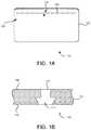
- FIG. 1Adepicts a top view of an example casing of an electronic device having a moldable material disposed in the casing;
- FIG. 1Bis a cross-sectional side-view of a portion of the example casing, such as the casing shown in FIG. 1A , that includes a metallic housing with angled undercut feature and a moldable material molded thereon;
- FIG. 2Adepicts a perspective view of an example electronic device including the casing
- FIG. 2Bis a cross-sectional side-view of a portion of the example casing of the electronic device, such as the electronic device shown in FIG. 2A , that includes a metallic housing with an undercut feature and a moldable material molded thereon;
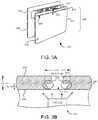
- FIG. 3Ais a perspective view of an example electronic device depicting additional features of the casing
- FIG. 3Bis a cross-sectional side-view of a portion of the example casing of the electronic device, such as the electronic device shown in FIG. 3A ;
- FIG. 4depicts a flow chart of an example method of manufacturing a casing of an electronic device.
- a casing of an electronic devicemay be manufactured with different materials by bonding metal parts and plastic parts.
- Example electronic devicesmay include notebook computers, mobile phones, personal digital assistants (PDAs), and the like.
- the metal parts and the plastic partsi.e., moldable material
- the metal parts and the plastic partsmay be bonded by using an insert molding technique or an in-mold technique.
- the metal parts and the plastic partsmay be bonded via Nano Molding Technology (NMT) process.
- NMTNano Molding Technology
- the NMT processmay be implemented in the metal part surface before performing insert molding process.
- the NMT processmay involve alkali etching, acid treatment, T-treatment, rinsing and drying of the metal parts, and insert molding the plastic onto the metal parts.
- the NMT processmay be expensive and may increase the process cycle time.
- Examples described hereinmay provide a casing of an electronic device.
- the casingmay include a metallic housing having a first surface and a second surface opposite to the first surface.
- the first surfacemay include an undercut that physically contacts the second surface.
- the undercutmay be created through the first surface such that the undercut extends through the first surface and physically contacts the second surface of the metallic housing.
- the casingmay include a moldable material that is insert molded in the undercut of the metallic housing.
- Examples described hereinmay improve a bonding force between the metallic housing and the moldable material in x, y and z directions.
- undercut feature on the metallic housingcan improve the z direction constrain of molded material against an external force and may avoid peeling of the molded material.
- Examples described hereinmay replace the NMT process with an undercut feature, thereby improving process yield rate, reducing process cycle time, and saving costs associated with the NMT process.
- the undercut featuremay solve any light leakage issue from chinks between the metallic housing and the moldable material.
- examples described hereinmay serve as an antenna region of the casing of the electronic device.
- FIG. 1Adepicts a top view of an example casing 100 of an electronic device having a moldable material 106 disposed in casing 100 .
- Casing 100may include a metallic housing 102 .
- metallic housing 102may be made of an alloy, such as magnesium alloy, aluminum alloy, titanium alloy and the like.
- Metallic housing 102may have a first surface 104 and a second surface (e.g., 110 as shown in FIG. 1B ) opposite to first surface 104 .
- First surface 104may include an undercut that is in physically contact with second surface.
- Casing 100may include a moldable material 106 that is insert molded in the undercut of metallic housing 102 .
- Example moldable materialmay include a plastic or a resin. Example undercut is explained in FIG. 1B .
- FIG. 1Bis a cross-sectional side-view of a portion 108 of example casing 100 , as shown in FIG. 1A , including metallic housing 102 with an undercut 112 (e.g., angled T shaped undercut feature) and moldable material 106 molded thereon.
- undercut 112may be created through first surface 104 such that undercut 112 extends through first surface 104 and physically contacts second surface 110 of metallic housing 102 .
- first surface 104may be a top surface and second surface 110 may be a bottom surface.
- first surface 104may be a bottom surface and second surface 110 may be a top surface.
- Undercutmay refer a slot/void having an opening that is larger at the second surface than the first surface.
- Undercut 112can be created in different shapes and sizes.
- undercut 112may be “T” shaped, mushroom shaped, or rectangular shaped.
- Undercut 112may be created using a computer numerical control (CNC) machining of metallic housing 102 , but machining of metallic housing 102 is not limited thereto.
- CNC machininga cutting apparatus can be programmed to cut “T” shaped undercut, mushroom shaped undercut, or rectangular shaped undercut.
- moldable material 106may be insert molded in metallic housing 102 such that moldable material 106 can be extended into undercut 112 to form casing 100 for the electronic device.
- moldable material 106may be bonded to metallic housing 102 using an insert molding process. Examples for attaching moldable material 106 and metallic housing 102 is not limited to insert molding, and any other process may be used for bonding moldable material 106 and metallic housing 102 such that moldable material 106 and metallic housing 102 may form a substantially flat surface.
- Moldable material 106may be insert molded to metallic housing 102 to cover undercut 112 .
- moldable material 106 insert molded in undercut 112 of metallic housing 102may provide a bonding force in z direction and may also allow transmission/reception of antenna signals associated with the electronic device.
- Example moldable material 106may be a plastic/polymer, such as liquid crystal polymer, polyphenylene sulphide, polybutylene terephthalate and the like. Due to property of the plastic/polymer to allow electromagnetic signals/radio signals, moldable material 106 may allow transmission/reception of antenna signals associated with the electronic device. An example electronic device is explained in FIG. 2A .
- FIG. 2Adepicts a perspective view of an example electronic device 200 including a casing 204 .
- Electronic device 200may include electronic components 202 , such as a battery, a circuit board, a display, an audio device, an antenna and the like.
- the electronic components of electronic device 200may be disposed in casing 204 , for instance.
- Casing 204may at least partially house the electronic components.
- Casing 204 of electronic device 200may be used to cover components for electronic device 200 , so as to form electronic device 200 .
- Casing 204may include a metallic housing 206 having a first surface 210 and a second surface (e.g., 214 as shown in FIG. 2B ) opposite to first surface 210 .
- First surface 210may include an undercut (e.g., 216 as shown in FIG. 2B ) physically contacting second surface 214 .
- FIG. 2Adepicts a single undercut, multiple undercuts can be created on first surface 210 , for example, corresponding to antenna regions.
- undercut 216may be an elongated opening created on first surface 210 .
- Casing 204may include a non-conductive layer 208 disposed in the undercut (e.g., 216 ) of metallic housing 206 .
- Example undercut 216is explained in FIG. 2B .
- FIG. 2Bis a cross-sectional side-view of a portion 212 of example casing 204 of electronic device 200 that includes metallic housing 206 with undercut 216 (e.g., angled mushroom shaped undercut feature) and non-conductive layer 208 disposed thereon.
- undercut 216may be created through first surface 210 such that undercut 216 may extend through first surface 210 and physically contact second surface 214 of metallic housing 206 .
- first surface 210may be a top surface and second surface 214 may be a bottom surface.
- Casing 204may include non-conductive layer 208 disposed in undercut 216 of metallic housing 206 to provide a bonding force (e.g., in x, y and z directions) between metallic housing 206 and non-conductive layer 208 for enhancing the mechanical strength of casing 204 .
- non-conductive layer 208may be disposed in undercut 216 using an in-mold process.
- first surface 210 of metallic housing 206may be dyed to form casing 204 of electronic device 200 .
- first surface 210 of metallic housing 206can be dyed using an anodizing process.
- FIG. 3Ais a perspective view of example electronic device 200 depicting additional features.
- Electronic device 200may include a display 302 , at least one antenna 202 , and casing 204 .
- casing 204may be a display cover.
- Example display 302may be a liquid crystal display, an organic light-emitting diode display, a plasma display, an electrophoretic display, or an electro-wetting display.
- Antenna 202may be formed on a printed circuit board 304 that can be attached to display 302 .
- Display 302can be attached to casing 204 such that printed circuit board 304 having antenna 202 is disposed between display 302 and casing 204 .
- antenna 202may be disposed internally at a top of electronic device 200 .
- non-conductive layer 208can be provided at the top of casing 204 and substantially near the antenna area.
- metallic housing 206may include a gap 306 formed on first surface 210 .
- gap 306may be a strip shaped that extends horizontally along the length of casing 204 .
- Undercute.g., 216 as shown in FIG. 3B
- Non-conductive layer 208may include a strip structure disposed in gap 306 and extended into undercut 216 formed on the inner surface of gap 306 .
- multiple undercutscan be created along gap 306 formed on first surface 210 .
- undercut 216may be an elongated opening created in gap 306 .
- Undercut 216may refer a slot/void having an opening that is larger at the second surface than the first surface. As shown in FIG. 3B , dimension 314 of the opening at the second surface is larger than dimension 312 of the opening at the first surface.
- FIG. 38is a cross-sectional side-view of a portion 212 of example casing 204 of electronic device 200 , depicting additional features.
- first surface 210 and second surface 214may define undercut 216 , for instance, around the antenna region (i.e., of antenna 202 ).
- undercut 216may be a slot that extends between first surface 210 and second surface 214 .
- Non-conductive layer 208 disposed in undercut 216may allow transmission/reception of antenna signals from antenna 202 .
- Undercut 216may include surfaces 308 which may enable moldable material 208 (i.e., non-conductive layer) to grab thereon when moldable material 208 is molded in undercut 216 .
- metallic housing 206may have a thickness of about 0.5 mm to 1 mm and undercut 216 may include a depth of about 0.2 mm to 0.4 mm. Particularly, the thickness of metallic housing 206 may include 0.7 mm to 0.8 mm and undercut 216 may include a depth of about 0.3 mm to 0.4 mm.
- undercut 216i.e., angled undercut feature
- material of non-conductive layer 208can be selected to have a good bonding ability with material of metallic housing 206 .
- non-conductive layer 208may have a low shrinkage and a similar linear expansion as that of the material of metallic housing 206 .
- Non-conductive layer 208may pass the signals (e.g., radio waves/electromagnetic waves) due to the non-metallic nature. Accordingly, the signals can be transmitted and received by antennas 202 without interference with metallic housing 206 .
- FIG. 4depicts a flow chart 400 of an example method of manufacturing a casing of an electronic device.
- Example electronic devicesmay include notebook computers, mobile phones, personal digital assistants (PDAs), and the like.
- Example casingmay include a display cover or a housing for components such as battery, keyboard, and the like.
- a metallic housingmay be provided, which may include a first surface and a second surface opposite to the first surface.
- an undercutmay be created through the first surface such that the undercut extends through the first surface and physically contacts the second surface of the metallic housing.
- a gapmay be created on the first surface of the metallic housing.
- the undercutmay be created on a surface (e.g., inner surface) of the gap of the metallic housing.
- the undercutmay be an elongated opening formed in the metallic housing.
- the undercutmay be created using a computer numerical control (CNC) treatment of the metallic housing.
- CNCcomputer numerical control
- a non-conductive layermay be disposed on the first surface of the metallic housing such that at least a part of the non-conductive layer is extended into the undercut to form the casing for the electronic device.
- the non-conductive layermay be a strip structure disposed in the gap and extended into the undercut created on the surface of the gap.
- Example material of the non-conductive layermay be plastic or resin.
- the non-conductive layermay be disposed on the first surface of the metallic housing using an insert mold process. Further, the first surface of the metallic housing may be dyed to form the casing of the electronic device. In one example, the first surface of the metallic housing can be dyed using an anodizing process.
- the undercut and the part of the non-conductive layer disposed in the undercutmay provide a bonding force in x, y and z directions and/or serve as an antenna region of the casing of the electronic device.
Landscapes
- Engineering & Computer Science (AREA)
- Computer Hardware Design (AREA)
- Theoretical Computer Science (AREA)
- General Engineering & Computer Science (AREA)
- Physics & Mathematics (AREA)
- General Physics & Mathematics (AREA)
- Human Computer Interaction (AREA)
- Microelectronics & Electronic Packaging (AREA)
- Manufacturing & Machinery (AREA)
- Geometry (AREA)
- Automation & Control Theory (AREA)
- Signal Processing (AREA)
- Mechanical Engineering (AREA)
- Computer Networks & Wireless Communication (AREA)
- Casings For Electric Apparatus (AREA)
- Telephone Set Structure (AREA)
Abstract
Description
Claims (14)
Applications Claiming Priority (1)
| Application Number | Priority Date | Filing Date | Title |
|---|---|---|---|
| PCT/US2017/014483WO2018136090A1 (en) | 2017-01-23 | 2017-01-23 | Casings of electronic devices |
Publications (2)
| Publication Number | Publication Date |
|---|---|
| US20190053390A1 US20190053390A1 (en) | 2019-02-14 |
| US10588225B2true US10588225B2 (en) | 2020-03-10 |
Family
ID=62908209
Family Applications (1)
| Application Number | Title | Priority Date | Filing Date |
|---|---|---|---|
| US16/076,502ActiveUS10588225B2 (en) | 2017-01-23 | 2017-01-23 | Casings of electronic devices |
Country Status (4)
| Country | Link |
|---|---|
| US (1) | US10588225B2 (en) |
| EP (1) | EP3504946B1 (en) |
| CN (1) | CN109845419A (en) |
| WO (1) | WO2018136090A1 (en) |
Cited By (1)
| Publication number | Priority date | Publication date | Assignee | Title |
|---|---|---|---|---|
| US11029548B2 (en)* | 2019-09-13 | 2021-06-08 | Panasonic Avionics Corporation | In-flight entertainment systems and monitor assemblies for in-flight entertainment systems |
Families Citing this family (1)
| Publication number | Priority date | Publication date | Assignee | Title |
|---|---|---|---|---|
| CN108508973B (en)* | 2018-03-30 | 2020-11-20 | 联想(北京)有限公司 | Electronic equipment |
Citations (32)
| Publication number | Priority date | Publication date | Assignee | Title |
|---|---|---|---|---|
| US5695704A (en)* | 1993-03-24 | 1997-12-09 | Nhk Spring Co., Ltd. | Method for crimping a thermoplastic resin member |
| US6865811B2 (en)* | 1994-05-19 | 2005-03-15 | Henkel Kommanditgesellschaft Auf Aktien | Method of making composite laminate automotive structures |
| US20050116870A1 (en)* | 2001-12-18 | 2005-06-02 | Hanyang Wang | Monopole slot antenna |
| US20070279297A1 (en)* | 2006-05-31 | 2007-12-06 | Nikko Co., Ltd. | Antenna for remote controlled toy, antenna cap and remote controlled toy |
| JP2008087409A (en) | 2006-10-04 | 2008-04-17 | Fore Shot Industrial Corp | Aluminum alloy casing structure and manufacturing method thereof |
| US20080316687A1 (en)* | 2007-06-06 | 2008-12-25 | Richardson Curtis R | Protective enclosure for an electronic device |
| US20090017242A1 (en) | 2007-07-13 | 2009-01-15 | Douglas Weber | Methods and systems for forming a dual layer housing |
| US20090081407A1 (en)* | 2006-05-04 | 2009-03-26 | Jean-Pierre Giraud | Injection Molding Process for Molding Mechanical Interlocks Between Molded Components |
| US20090251290A1 (en)* | 2008-04-08 | 2009-10-08 | Isao Sakama | Radio frequency identification tag and method of fabricating the same |
| US20090260871A1 (en)* | 2008-04-18 | 2009-10-22 | Douglas Weber | Perforated Substrates for Forming Housings |
| US20090303010A1 (en)* | 2008-06-05 | 2009-12-10 | Hitachi, Ltd. | Rfid thread, sheet with rfid thread, and printing machine for sheet with rfid thread |
| US20110033657A1 (en)* | 2009-08-10 | 2011-02-10 | Mao-Lien Huang | Metal shell manufacturing structure and method |
| US20110220724A1 (en)* | 2010-03-11 | 2011-09-15 | Hitachi, Ltd. | Rfid tag and method of manufacturing the same |
| US8049120B2 (en)* | 2008-09-30 | 2011-11-01 | Apple Inc. | Ultrasonic bonding of discrete plastic parts to metal |
| US20120118628A1 (en)* | 2010-11-11 | 2012-05-17 | David Pakula | Insert Molding Around Glass Members for Portable Electronic Devices |
| US20120207537A1 (en)* | 2009-08-10 | 2012-08-16 | Mao-Lien Huang | Metal-plastic coupling interface structure and manufacturing method thereof |
| US8315043B2 (en)* | 2008-01-24 | 2012-11-20 | Apple Inc. | Methods and systems for forming housings from multi-layer materials |
| US8349444B2 (en)* | 2007-03-21 | 2013-01-08 | Ashtech Industries, Llc | Utility materials incorporating a microparticle matrix |
| WO2013077277A1 (en) | 2011-11-21 | 2013-05-30 | 株式会社ダイセル | Composite molding manufacturing method |
| US20130169498A1 (en)* | 2011-12-28 | 2013-07-04 | Taiwan Lamination Industries, Inc. | Packaging material with t-shaped slot antenna |
| US20130210504A1 (en) | 2012-02-10 | 2013-08-15 | Htc Corporation | Components with mechanically-bonded plastic and methods for forming such components |
| US20130278123A1 (en)* | 2012-04-20 | 2013-10-24 | Kai-Rong Liao | Device housing and method for making the same |
| US20150111002A1 (en)* | 2013-10-18 | 2015-04-23 | Fu Tai Hua Industry (Shenzhen) Co., Ltd. | Composite of resin and other materials and method for manufacturing the same |
| US20150118479A1 (en)* | 2013-10-24 | 2015-04-30 | Hon Hai Precision Industry Co., Ltd. | Composite of metal and resin and method for manufacturing same |
| US20150183185A1 (en) | 2013-12-30 | 2015-07-02 | Hon Hai Precision Industry Co., Ltd. | Composite of metal and resin and method for manufacturing same |
| US9231640B2 (en)* | 2012-09-14 | 2016-01-05 | Samsung Electronics Co., Ltd | Protective device for mobile terminal |
| US20160043461A1 (en)* | 2014-01-30 | 2016-02-11 | Murata Manufacturing Co., Ltd. | Radio communication device |
| US9370888B2 (en)* | 2008-05-16 | 2016-06-21 | Sca Hygiene Products Ab | Method of making a dispenser or a part thereof |
| CN106102389A (en)* | 2016-08-16 | 2016-11-09 | 广东欧珀移动通信有限公司 | Shell processing method, shell and mobile terminal |
| CN205726714U (en)* | 2016-04-05 | 2016-11-23 | 东莞劲胜精密组件股份有限公司 | An electronic product case with built-in antenna |
| US20160352007A1 (en)* | 2015-05-28 | 2016-12-01 | Fu Tai Hua Industry (Shenzhen) Co., Ltd. | Housing, electronic device having the housing, and method for manufacturing the housing |
| US10207438B2 (en)* | 2014-01-31 | 2019-02-19 | Sumitomo Electric Industries, Ltd. | Composite member and composite-member manufacturing method |
Family Cites Families (13)
| Publication number | Priority date | Publication date | Assignee | Title |
|---|---|---|---|---|
| US6560119B1 (en)* | 1998-06-23 | 2003-05-06 | Fujitsu Limited | Fastening parts suitable for recycling |
| CN101119615A (en)* | 2006-08-02 | 2008-02-06 | 宏塑工业股份有限公司 | Aluminum alloy shell structure and manufacturing method thereof |
| CN101573008B (en)* | 2008-04-28 | 2012-05-16 | 富准精密工业(深圳)有限公司 | Electronic device shell and manufacturing method thereof |
| CN102006753A (en)* | 2009-08-28 | 2011-04-06 | 深圳富泰宏精密工业有限公司 | Shell making method and shell made by same |
| US8345410B2 (en)* | 2010-01-06 | 2013-01-01 | Apple Inc. | Handheld computing device |
| TW201343043A (en)* | 2012-04-11 | 2013-10-16 | Msi Electronic Kun Shan Co Ltd | Method of manufacturing an upper cover of a portable computer device and upper cover thereof |
| CN104735942A (en)* | 2013-12-20 | 2015-06-24 | 惠州比亚迪电子有限公司 | Communication equipment metal shell and manufacturing method thereof |
| JP3192627U (en)* | 2014-06-13 | 2014-08-21 | 三井化学株式会社 | Housing parts for electronic equipment |
| CN105522684B (en)* | 2014-12-25 | 2018-11-09 | 比亚迪股份有限公司 | A kind of metal-resin complex and preparation method thereof and a kind of electronic product casing |
| CN105530785B (en)* | 2014-12-26 | 2016-11-23 | 比亚迪股份有限公司 | A kind of electronic product metal shell being formed with antenna slot and preparation method thereof |
| CN105530786A (en)* | 2014-12-26 | 2016-04-27 | 比亚迪股份有限公司 | Communication equipment metal case and preparation method thereof |
| CN109121331B (en)* | 2014-12-26 | 2020-11-20 | 比亚迪股份有限公司 | Communication equipment metal casing and preparation method thereof |
| CN105979741A (en)* | 2016-06-30 | 2016-09-28 | 东莞劲胜精密组件股份有限公司 | A kind of 3C electronic product casing and preparation method thereof |
- 2017
- 2017-01-23EPEP17892660.6Apatent/EP3504946B1/enactiveActive
- 2017-01-23WOPCT/US2017/014483patent/WO2018136090A1/ennot_activeCeased
- 2017-01-23USUS16/076,502patent/US10588225B2/enactiveActive
- 2017-01-23CNCN201780060913.4Apatent/CN109845419A/enactivePending
Patent Citations (37)
| Publication number | Priority date | Publication date | Assignee | Title |
|---|---|---|---|---|
| US5695704A (en)* | 1993-03-24 | 1997-12-09 | Nhk Spring Co., Ltd. | Method for crimping a thermoplastic resin member |
| US6865811B2 (en)* | 1994-05-19 | 2005-03-15 | Henkel Kommanditgesellschaft Auf Aktien | Method of making composite laminate automotive structures |
| US20050116870A1 (en)* | 2001-12-18 | 2005-06-02 | Hanyang Wang | Monopole slot antenna |
| US20090081407A1 (en)* | 2006-05-04 | 2009-03-26 | Jean-Pierre Giraud | Injection Molding Process for Molding Mechanical Interlocks Between Molded Components |
| US20070279297A1 (en)* | 2006-05-31 | 2007-12-06 | Nikko Co., Ltd. | Antenna for remote controlled toy, antenna cap and remote controlled toy |
| JP2008087409A (en) | 2006-10-04 | 2008-04-17 | Fore Shot Industrial Corp | Aluminum alloy casing structure and manufacturing method thereof |
| US8349444B2 (en)* | 2007-03-21 | 2013-01-08 | Ashtech Industries, Llc | Utility materials incorporating a microparticle matrix |
| US20080316687A1 (en)* | 2007-06-06 | 2008-12-25 | Richardson Curtis R | Protective enclosure for an electronic device |
| US20090017242A1 (en) | 2007-07-13 | 2009-01-15 | Douglas Weber | Methods and systems for forming a dual layer housing |
| US8192815B2 (en) | 2007-07-13 | 2012-06-05 | Apple Inc. | Methods and systems for forming a dual layer housing |
| US8830665B2 (en) | 2008-01-24 | 2014-09-09 | Apple Inc. | Attachment features for housings |
| US8315043B2 (en)* | 2008-01-24 | 2012-11-20 | Apple Inc. | Methods and systems for forming housings from multi-layer materials |
| US20090251290A1 (en)* | 2008-04-08 | 2009-10-08 | Isao Sakama | Radio frequency identification tag and method of fabricating the same |
| US20090260871A1 (en)* | 2008-04-18 | 2009-10-22 | Douglas Weber | Perforated Substrates for Forming Housings |
| US9370888B2 (en)* | 2008-05-16 | 2016-06-21 | Sca Hygiene Products Ab | Method of making a dispenser or a part thereof |
| US20090303010A1 (en)* | 2008-06-05 | 2009-12-10 | Hitachi, Ltd. | Rfid thread, sheet with rfid thread, and printing machine for sheet with rfid thread |
| US8049120B2 (en)* | 2008-09-30 | 2011-11-01 | Apple Inc. | Ultrasonic bonding of discrete plastic parts to metal |
| US8546702B2 (en) | 2008-09-30 | 2013-10-01 | Apple Inc. | Ultrasonic bonding of discrete plastic parts to metal |
| US20120063115A1 (en) | 2008-09-30 | 2012-03-15 | Apple Inc. | Ultrasonic bonding of discrete plastic parts to metal |
| US20120207537A1 (en)* | 2009-08-10 | 2012-08-16 | Mao-Lien Huang | Metal-plastic coupling interface structure and manufacturing method thereof |
| US20110033657A1 (en)* | 2009-08-10 | 2011-02-10 | Mao-Lien Huang | Metal shell manufacturing structure and method |
| US20110220724A1 (en)* | 2010-03-11 | 2011-09-15 | Hitachi, Ltd. | Rfid tag and method of manufacturing the same |
| US20120118628A1 (en)* | 2010-11-11 | 2012-05-17 | David Pakula | Insert Molding Around Glass Members for Portable Electronic Devices |
| WO2013077277A1 (en) | 2011-11-21 | 2013-05-30 | 株式会社ダイセル | Composite molding manufacturing method |
| US20130169498A1 (en)* | 2011-12-28 | 2013-07-04 | Taiwan Lamination Industries, Inc. | Packaging material with t-shaped slot antenna |
| US20130210504A1 (en) | 2012-02-10 | 2013-08-15 | Htc Corporation | Components with mechanically-bonded plastic and methods for forming such components |
| US20130278123A1 (en)* | 2012-04-20 | 2013-10-24 | Kai-Rong Liao | Device housing and method for making the same |
| US9231640B2 (en)* | 2012-09-14 | 2016-01-05 | Samsung Electronics Co., Ltd | Protective device for mobile terminal |
| US20150111002A1 (en)* | 2013-10-18 | 2015-04-23 | Fu Tai Hua Industry (Shenzhen) Co., Ltd. | Composite of resin and other materials and method for manufacturing the same |
| US20150118479A1 (en)* | 2013-10-24 | 2015-04-30 | Hon Hai Precision Industry Co., Ltd. | Composite of metal and resin and method for manufacturing same |
| US20150183185A1 (en) | 2013-12-30 | 2015-07-02 | Hon Hai Precision Industry Co., Ltd. | Composite of metal and resin and method for manufacturing same |
| US20160043461A1 (en)* | 2014-01-30 | 2016-02-11 | Murata Manufacturing Co., Ltd. | Radio communication device |
| US10207438B2 (en)* | 2014-01-31 | 2019-02-19 | Sumitomo Electric Industries, Ltd. | Composite member and composite-member manufacturing method |
| US20160352007A1 (en)* | 2015-05-28 | 2016-12-01 | Fu Tai Hua Industry (Shenzhen) Co., Ltd. | Housing, electronic device having the housing, and method for manufacturing the housing |
| CN205726714U (en)* | 2016-04-05 | 2016-11-23 | 东莞劲胜精密组件股份有限公司 | An electronic product case with built-in antenna |
| CN106102389A (en)* | 2016-08-16 | 2016-11-09 | 广东欧珀移动通信有限公司 | Shell processing method, shell and mobile terminal |
| US20180053989A1 (en)* | 2016-08-16 | 2018-02-22 | Guangdong Oppo Mobile Telecommunications Corp., Ltd. | Housing, Method for Manufacturing Housing, and Mobile Terminal |
Non-Patent Citations (1)
| Title |
|---|
| Yuanqing et al., "New Solutions for Metal/plastic Hybrid Design Via Nano-molding Technology", SPE, Retrieved from Internet: http://www.4spepro.org/view.php?article=005957-2015-07-15, Jul. 16, 2015, 5 pages. |
Cited By (1)
| Publication number | Priority date | Publication date | Assignee | Title |
|---|---|---|---|---|
| US11029548B2 (en)* | 2019-09-13 | 2021-06-08 | Panasonic Avionics Corporation | In-flight entertainment systems and monitor assemblies for in-flight entertainment systems |
Also Published As
| Publication number | Publication date |
|---|---|
| EP3504946A1 (en) | 2019-07-03 |
| EP3504946A4 (en) | 2020-05-27 |
| EP3504946B1 (en) | 2022-08-10 |
| CN109845419A (en) | 2019-06-04 |
| WO2018136090A1 (en) | 2018-07-26 |
| US20190053390A1 (en) | 2019-02-14 |
Similar Documents
| Publication | Publication Date | Title |
|---|---|---|
| CN103987223B (en) | Electronic equipment and the processing method of casting of electronic device | |
| JP2009266195A (en) | Casing for electronic device, and method for manufacturing the same | |
| TWI509882B (en) | Method of forming antenna | |
| US8080995B2 (en) | Device housing | |
| CN104885584B (en) | Portable electronic device body and associated manufacturing method with laser beam perforation trepanning | |
| CN112583966B (en) | Mobile electronic device and portable communication device | |
| US8766860B2 (en) | Housing combination of electronic device and method | |
| EP2086049A1 (en) | Housing, wireless communication device using the housing, and manufacturing method thereof | |
| US20110134012A1 (en) | Housing and method for making the same | |
| US8720720B2 (en) | Housing and method for manufacturing same | |
| US8803744B2 (en) | Cover for electronic device | |
| KR20150064182A (en) | Metallization and anodization of plastic and conductive parts of the body of an apparatus | |
| KR20130106329A (en) | The manufacturing method of the built-in antenna | |
| US10861643B2 (en) | Wireless charging structure and method for forming the same | |
| US10382601B2 (en) | Housing, method for manufacturing housing, and mobile terminal having housing | |
| US9755297B2 (en) | Housing, electronic device using same, and method for making same | |
| US7518568B2 (en) | Antenna for an electronic device | |
| US20090268384A1 (en) | Housing, electronic device using the housing, and manufacturing method thereof | |
| US10588225B2 (en) | Casings of electronic devices | |
| US20120042505A1 (en) | Method for manufacturing antenna | |
| CN104780725B (en) | Housing, handheld device and manufacturing method of housing | |
| CN102412437B (en) | Antenna Manufacturing Method | |
| CN104852127A (en) | Antenna structure, electronic device employing same, and manufacturing method for antenna structure | |
| US11139553B2 (en) | Technologies for a metal chassis for an electronic device | |
| US8973261B2 (en) | Manufacturing method of object having conductive line |
Legal Events
| Date | Code | Title | Description |
|---|---|---|---|
| FEPP | Fee payment procedure | Free format text:ENTITY STATUS SET TO UNDISCOUNTED (ORIGINAL EVENT CODE: BIG.); ENTITY STATUS OF PATENT OWNER: LARGE ENTITY | |
| AS | Assignment | Owner name:HEWLETT-PACKARD DEVELOPMENT COMPANY, L.P., TEXAS Free format text:ASSIGNMENT OF ASSIGNORS INTEREST;ASSIGNORS:LIN, ARTHUR;CHIU, CHIENCHIH;TSAI, KEN;AND OTHERS;REEL/FRAME:047122/0162 Effective date:20170109 | |
| STPP | Information on status: patent application and granting procedure in general | Free format text:APPLICATION DISPATCHED FROM PREEXAM, NOT YET DOCKETED | |
| STPP | Information on status: patent application and granting procedure in general | Free format text:DOCKETED NEW CASE - READY FOR EXAMINATION | |
| STPP | Information on status: patent application and granting procedure in general | Free format text:NON FINAL ACTION MAILED | |
| STPP | Information on status: patent application and granting procedure in general | Free format text:RESPONSE TO NON-FINAL OFFICE ACTION ENTERED AND FORWARDED TO EXAMINER | |
| STPP | Information on status: patent application and granting procedure in general | Free format text:FINAL REJECTION MAILED | |
| STPP | Information on status: patent application and granting procedure in general | Free format text:NOTICE OF ALLOWANCE MAILED -- APPLICATION RECEIVED IN OFFICE OF PUBLICATIONS | |
| STPP | Information on status: patent application and granting procedure in general | Free format text:PUBLICATIONS -- ISSUE FEE PAYMENT RECEIVED | |
| STCF | Information on status: patent grant | Free format text:PATENTED CASE | |
| MAFP | Maintenance fee payment | Free format text:PAYMENT OF MAINTENANCE FEE, 4TH YEAR, LARGE ENTITY (ORIGINAL EVENT CODE: M1551); ENTITY STATUS OF PATENT OWNER: LARGE ENTITY Year of fee payment:4 |