US10580886B2 - Increased source and drain contact edge width in two-dimensional material field effect transistors by directed self-assembly - Google Patents
Increased source and drain contact edge width in two-dimensional material field effect transistors by directed self-assemblyDownload PDFInfo
- Publication number
- US10580886B2 US10580886B2US15/991,023US201815991023AUS10580886B2US 10580886 B2US10580886 B2US 10580886B2US 201815991023 AUS201815991023 AUS 201815991023AUS 10580886 B2US10580886 B2US 10580886B2
- Authority
- US
- United States
- Prior art keywords
- dimensional material
- field effect
- gate
- over
- effect transistor
- Prior art date
- Legal status (The legal status is an assumption and is not a legal conclusion. Google has not performed a legal analysis and makes no representation as to the accuracy of the status listed.)
- Expired - Fee Related
Links
- 239000000463materialSubstances0.000titleabstractdescription66
- 230000005669field effectEffects0.000titleabstractdescription12
- 238000002408directed self-assemblyMethods0.000titleabstractdescription10
- 238000000151depositionMethods0.000abstractdescription29
- 238000000034methodMethods0.000abstractdescription24
- 125000006850spacer groupChemical group0.000abstractdescription21
- 239000011229interlayerSubstances0.000abstractdescription19
- 239000010410layerSubstances0.000abstractdescription19
- 238000005530etchingMethods0.000abstractdescription18
- 239000000758substrateSubstances0.000abstractdescription15
- 239000011248coating agentSubstances0.000abstractdescription11
- 238000000576coating methodMethods0.000abstractdescription11
- 229920001577copolymerPolymers0.000abstractdescription10
- 238000000137annealingMethods0.000abstractdescription8
- 229910052751metalInorganic materials0.000abstractdescription8
- 239000002184metalSubstances0.000abstractdescription8
- 238000000059patterningMethods0.000abstractdescription6
- 229920001400block copolymerPolymers0.000description13
- 230000008569processEffects0.000description12
- 239000004065semiconductorSubstances0.000description12
- VYPSYNLAJGMNEJ-UHFFFAOYSA-NSilicium dioxideChemical compoundO=[Si]=OVYPSYNLAJGMNEJ-UHFFFAOYSA-N0.000description11
- 238000001459lithographyMethods0.000description7
- 238000005229chemical vapour depositionMethods0.000description6
- 230000008021depositionEffects0.000description6
- 235000012239silicon dioxideNutrition0.000description5
- 239000000377silicon dioxideSubstances0.000description5
- 229910052581Si3N4Inorganic materials0.000description4
- HQVNEWCFYHHQES-UHFFFAOYSA-Nsilicon nitrideChemical compoundN12[Si]34N5[Si]62N3[Si]51N64HQVNEWCFYHHQES-UHFFFAOYSA-N0.000description4
- 150000003624transition metalsChemical class0.000description4
- 238000000231atomic layer depositionMethods0.000description3
- 239000000178monomerSubstances0.000description3
- 229910052723transition metalInorganic materials0.000description3
- PZNSFCLAULLKQX-UHFFFAOYSA-NBoron nitrideChemical compoundN#BPZNSFCLAULLKQX-UHFFFAOYSA-N0.000description2
- OKTJSMMVPCPJKN-UHFFFAOYSA-NCarbonChemical compound[C]OKTJSMMVPCPJKN-UHFFFAOYSA-N0.000description2
- 239000004793PolystyreneSubstances0.000description2
- 229910021417amorphous siliconInorganic materials0.000description2
- 230000008878couplingEffects0.000description2
- 238000010168coupling processMethods0.000description2
- 238000005859coupling reactionMethods0.000description2
- 238000004070electrodepositionMethods0.000description2
- 239000010408filmSubstances0.000description2
- 229910021389grapheneInorganic materials0.000description2
- 238000004519manufacturing processMethods0.000description2
- 230000004048modificationEffects0.000description2
- 238000012986modificationMethods0.000description2
- 238000005240physical vapour depositionMethods0.000description2
- 238000001020plasma etchingMethods0.000description2
- 229920003229poly(methyl methacrylate)Polymers0.000description2
- 229920000642polymerPolymers0.000description2
- 239000004926polymethyl methacrylateSubstances0.000description2
- 229910052582BNInorganic materials0.000description1
- ZOKXTWBITQBERF-UHFFFAOYSA-NMolybdenumChemical compound[Mo]ZOKXTWBITQBERF-UHFFFAOYSA-N0.000description1
- BUGBHKTXTAQXES-UHFFFAOYSA-NSeleniumChemical compound[Se]BUGBHKTXTAQXES-UHFFFAOYSA-N0.000description1
- NINIDFKCEFEMDL-UHFFFAOYSA-NSulfurChemical compound[S]NINIDFKCEFEMDL-UHFFFAOYSA-N0.000description1
- 230000004075alterationEffects0.000description1
- 229920005603alternating copolymerPolymers0.000description1
- 230000015572biosynthetic processEffects0.000description1
- 150000001787chalcogensChemical group0.000description1
- 238000006243chemical reactionMethods0.000description1
- 239000004020conductorSubstances0.000description1
- 239000000470constituentSubstances0.000description1
- 238000007796conventional methodMethods0.000description1
- 238000007334copolymerization reactionMethods0.000description1
- 239000002178crystalline materialSubstances0.000description1
- 239000003989dielectric materialSubstances0.000description1
- 238000009792diffusion processMethods0.000description1
- 239000002019doping agentSubstances0.000description1
- 230000005684electric fieldEffects0.000description1
- 230000005672electromagnetic fieldEffects0.000description1
- 238000005516engineering processMethods0.000description1
- -1for exampleSubstances0.000description1
- 125000000524functional groupChemical group0.000description1
- CJNBYAVZURUTKZ-UHFFFAOYSA-Nhafnium(IV) oxideInorganic materialsO=[Hf]=OCJNBYAVZURUTKZ-UHFFFAOYSA-N0.000description1
- 239000011810insulating materialSubstances0.000description1
- 239000012212insulatorSubstances0.000description1
- 238000005468ion implantationMethods0.000description1
- 150000002500ionsChemical class0.000description1
- 238000004377microelectronicMethods0.000description1
- 238000001451molecular beam epitaxyMethods0.000description1
- 229910052750molybdenumInorganic materials0.000description1
- 239000011733molybdenumSubstances0.000description1
- 230000000737periodic effectEffects0.000description1
- 229910021420polycrystalline siliconInorganic materials0.000description1
- 238000006116polymerization reactionMethods0.000description1
- 229920005591polysiliconPolymers0.000description1
- 229920002223polystyrenePolymers0.000description1
- 238000004151rapid thermal annealingMethods0.000description1
- 229910052711seleniumInorganic materials0.000description1
- 239000011669seleniumSubstances0.000description1
- 229910052814silicon oxideInorganic materials0.000description1
- 238000004528spin coatingMethods0.000description1
- 238000004544sputter depositionMethods0.000description1
- 229920006301statistical copolymerPolymers0.000description1
- 239000000126substanceSubstances0.000description1
- 238000006467substitution reactionMethods0.000description1
- 229910052717sulfurInorganic materials0.000description1
- 239000011593sulfurSubstances0.000description1
- 229910052714telluriumInorganic materials0.000description1
- PORWMNRCUJJQNO-UHFFFAOYSA-Ntellurium atomChemical compound[Te]PORWMNRCUJJQNO-UHFFFAOYSA-N0.000description1
- 238000007736thin film deposition techniqueMethods0.000description1
- WFKWXMTUELFFGS-UHFFFAOYSA-NtungstenChemical compound[W]WFKWXMTUELFFGS-UHFFFAOYSA-N0.000description1
- 229910052721tungstenInorganic materials0.000description1
- 239000010937tungstenSubstances0.000description1
Images


Classifications
- H—ELECTRICITY
- H10—SEMICONDUCTOR DEVICES; ELECTRIC SOLID-STATE DEVICES NOT OTHERWISE PROVIDED FOR
- H10D—INORGANIC ELECTRIC SEMICONDUCTOR DEVICES
- H10D48/00—Individual devices not covered by groups H10D1/00 - H10D44/00
- H10D48/30—Devices controlled by electric currents or voltages
- H10D48/32—Devices controlled by only the electric current supplied, or only the electric potential applied, to an electrode which does not carry the current to be rectified, amplified or switched
- H10D48/36—Unipolar devices
- H10D48/362—Unipolar transistors having ohmic electrodes on emitter-like, base-like, and collector-like regions, e.g. hot electron transistors [HET], metal base transistors [MBT], resonant tunnelling transistors [RTT], bulk barrier transistors [BBT], planar doped barrier transistors [PDBT] or charge injection transistors [CHINT]
- H01L29/7606—
- H—ELECTRICITY
- H01—ELECTRIC ELEMENTS
- H01L—SEMICONDUCTOR DEVICES NOT COVERED BY CLASS H10
- H01L21/00—Processes or apparatus adapted for the manufacture or treatment of semiconductor or solid state devices or of parts thereof
- H01L21/02—Manufacture or treatment of semiconductor devices or of parts thereof
- H01L21/04—Manufacture or treatment of semiconductor devices or of parts thereof the devices having potential barriers, e.g. a PN junction, depletion layer or carrier concentration layer
- H01L21/18—Manufacture or treatment of semiconductor devices or of parts thereof the devices having potential barriers, e.g. a PN junction, depletion layer or carrier concentration layer the devices having semiconductor bodies comprising elements of Group IV of the Periodic Table or AIIIBV compounds with or without impurities, e.g. doping materials
- H01L21/30—Treatment of semiconductor bodies using processes or apparatus not provided for in groups H01L21/20 - H01L21/26
- H01L21/31—Treatment of semiconductor bodies using processes or apparatus not provided for in groups H01L21/20 - H01L21/26 to form insulating layers thereon, e.g. for masking or by using photolithographic techniques; After treatment of these layers; Selection of materials for these layers
- H01L21/3105—After-treatment
- H01L21/311—Etching the insulating layers by chemical or physical means
- H01L21/31144—Etching the insulating layers by chemical or physical means using masks
- H—ELECTRICITY
- H01—ELECTRIC ELEMENTS
- H01L—SEMICONDUCTOR DEVICES NOT COVERED BY CLASS H10
- H01L21/00—Processes or apparatus adapted for the manufacture or treatment of semiconductor or solid state devices or of parts thereof
- H01L21/02—Manufacture or treatment of semiconductor devices or of parts thereof
- H01L21/02104—Forming layers
- H01L21/02107—Forming insulating materials on a substrate
- H01L21/02109—Forming insulating materials on a substrate characterised by the type of layer, e.g. type of material, porous/non-porous, pre-cursors, mixtures or laminates
- H01L21/02112—Forming insulating materials on a substrate characterised by the type of layer, e.g. type of material, porous/non-porous, pre-cursors, mixtures or laminates characterised by the material of the layer
- H01L21/02118—Forming insulating materials on a substrate characterised by the type of layer, e.g. type of material, porous/non-porous, pre-cursors, mixtures or laminates characterised by the material of the layer carbon based polymeric organic or inorganic material, e.g. polyimides, poly cyclobutene or PVC
- H—ELECTRICITY
- H01—ELECTRIC ELEMENTS
- H01L—SEMICONDUCTOR DEVICES NOT COVERED BY CLASS H10
- H01L21/00—Processes or apparatus adapted for the manufacture or treatment of semiconductor or solid state devices or of parts thereof
- H01L21/02—Manufacture or treatment of semiconductor devices or of parts thereof
- H01L21/04—Manufacture or treatment of semiconductor devices or of parts thereof the devices having potential barriers, e.g. a PN junction, depletion layer or carrier concentration layer
- H01L21/18—Manufacture or treatment of semiconductor devices or of parts thereof the devices having potential barriers, e.g. a PN junction, depletion layer or carrier concentration layer the devices having semiconductor bodies comprising elements of Group IV of the Periodic Table or AIIIBV compounds with or without impurities, e.g. doping materials
- H01L21/30—Treatment of semiconductor bodies using processes or apparatus not provided for in groups H01L21/20 - H01L21/26
- H01L21/302—Treatment of semiconductor bodies using processes or apparatus not provided for in groups H01L21/20 - H01L21/26 to change their surface-physical characteristics or shape, e.g. etching, polishing, cutting
- H01L21/306—Chemical or electrical treatment, e.g. electrolytic etching
- H01L21/308—Chemical or electrical treatment, e.g. electrolytic etching using masks
- H01L21/3081—Chemical or electrical treatment, e.g. electrolytic etching using masks characterised by their composition, e.g. multilayer masks, materials
- H—ELECTRICITY
- H01—ELECTRIC ELEMENTS
- H01L—SEMICONDUCTOR DEVICES NOT COVERED BY CLASS H10
- H01L21/00—Processes or apparatus adapted for the manufacture or treatment of semiconductor or solid state devices or of parts thereof
- H01L21/70—Manufacture or treatment of devices consisting of a plurality of solid state components formed in or on a common substrate or of parts thereof; Manufacture of integrated circuit devices or of parts thereof
- H01L21/71—Manufacture of specific parts of devices defined in group H01L21/70
- H01L21/768—Applying interconnections to be used for carrying current between separate components within a device comprising conductors and dielectrics
- H01L21/76801—Applying interconnections to be used for carrying current between separate components within a device comprising conductors and dielectrics characterised by the formation and the after-treatment of the dielectrics, e.g. smoothing
- H01L21/76802—Applying interconnections to be used for carrying current between separate components within a device comprising conductors and dielectrics characterised by the formation and the after-treatment of the dielectrics, e.g. smoothing by forming openings in dielectrics
- H01L21/76816—Aspects relating to the layout of the pattern or to the size of vias or trenches
- H—ELECTRICITY
- H01—ELECTRIC ELEMENTS
- H01L—SEMICONDUCTOR DEVICES NOT COVERED BY CLASS H10
- H01L21/00—Processes or apparatus adapted for the manufacture or treatment of semiconductor or solid state devices or of parts thereof
- H01L21/70—Manufacture or treatment of devices consisting of a plurality of solid state components formed in or on a common substrate or of parts thereof; Manufacture of integrated circuit devices or of parts thereof
- H01L21/71—Manufacture of specific parts of devices defined in group H01L21/70
- H01L21/768—Applying interconnections to be used for carrying current between separate components within a device comprising conductors and dielectrics
- H01L21/76897—Formation of self-aligned vias or contact plugs, i.e. involving a lithographically uncritical step
- H01L29/04—
- H01L29/1606—
- H01L29/2003—
- H01L29/66045—
- H01L29/66446—
- H—ELECTRICITY
- H10—SEMICONDUCTOR DEVICES; ELECTRIC SOLID-STATE DEVICES NOT OTHERWISE PROVIDED FOR
- H10D—INORGANIC ELECTRIC SEMICONDUCTOR DEVICES
- H10D30/00—Field-effect transistors [FET]
- H10D30/01—Manufacture or treatment
- H—ELECTRICITY
- H10—SEMICONDUCTOR DEVICES; ELECTRIC SOLID-STATE DEVICES NOT OTHERWISE PROVIDED FOR
- H10D—INORGANIC ELECTRIC SEMICONDUCTOR DEVICES
- H10D30/00—Field-effect transistors [FET]
- H10D30/40—FETs having zero-dimensional [0D], one-dimensional [1D] or two-dimensional [2D] charge carrier gas channels
- H10D30/47—FETs having zero-dimensional [0D], one-dimensional [1D] or two-dimensional [2D] charge carrier gas channels having 2D charge carrier gas channels, e.g. nanoribbon FETs or high electron mobility transistors [HEMT]
- H—ELECTRICITY
- H10—SEMICONDUCTOR DEVICES; ELECTRIC SOLID-STATE DEVICES NOT OTHERWISE PROVIDED FOR
- H10D—INORGANIC ELECTRIC SEMICONDUCTOR DEVICES
- H10D62/00—Semiconductor bodies, or regions thereof, of devices having potential barriers
- H10D62/40—Crystalline structures
- H—ELECTRICITY
- H10—SEMICONDUCTOR DEVICES; ELECTRIC SOLID-STATE DEVICES NOT OTHERWISE PROVIDED FOR
- H10D—INORGANIC ELECTRIC SEMICONDUCTOR DEVICES
- H10D62/00—Semiconductor bodies, or regions thereof, of devices having potential barriers
- H10D62/80—Semiconductor bodies, or regions thereof, of devices having potential barriers characterised by the materials
- H10D62/82—Heterojunctions
- H—ELECTRICITY
- H10—SEMICONDUCTOR DEVICES; ELECTRIC SOLID-STATE DEVICES NOT OTHERWISE PROVIDED FOR
- H10D—INORGANIC ELECTRIC SEMICONDUCTOR DEVICES
- H10D62/00—Semiconductor bodies, or regions thereof, of devices having potential barriers
- H10D62/80—Semiconductor bodies, or regions thereof, of devices having potential barriers characterised by the materials
- H10D62/83—Semiconductor bodies, or regions thereof, of devices having potential barriers characterised by the materials being Group IV materials, e.g. B-doped Si or undoped Ge
- H10D62/8303—Diamond
- H—ELECTRICITY
- H10—SEMICONDUCTOR DEVICES; ELECTRIC SOLID-STATE DEVICES NOT OTHERWISE PROVIDED FOR
- H10D—INORGANIC ELECTRIC SEMICONDUCTOR DEVICES
- H10D62/00—Semiconductor bodies, or regions thereof, of devices having potential barriers
- H10D62/80—Semiconductor bodies, or regions thereof, of devices having potential barriers characterised by the materials
- H10D62/85—Semiconductor bodies, or regions thereof, of devices having potential barriers characterised by the materials being Group III-V materials, e.g. GaAs
- H10D62/8503—Nitride Group III-V materials, e.g. AlN or GaN
- H—ELECTRICITY
- H10—SEMICONDUCTOR DEVICES; ELECTRIC SOLID-STATE DEVICES NOT OTHERWISE PROVIDED FOR
- H10D—INORGANIC ELECTRIC SEMICONDUCTOR DEVICES
- H10D62/00—Semiconductor bodies, or regions thereof, of devices having potential barriers
- H10D62/80—Semiconductor bodies, or regions thereof, of devices having potential barriers characterised by the materials
- H10D62/881—Semiconductor bodies, or regions thereof, of devices having potential barriers characterised by the materials being a two-dimensional material
- H10D62/882—Graphene
- H—ELECTRICITY
- H10—SEMICONDUCTOR DEVICES; ELECTRIC SOLID-STATE DEVICES NOT OTHERWISE PROVIDED FOR
- H10D—INORGANIC ELECTRIC SEMICONDUCTOR DEVICES
- H10D64/00—Electrodes of devices having potential barriers
- H10D64/20—Electrodes characterised by their shapes, relative sizes or dispositions
- H10D64/23—Electrodes carrying the current to be rectified, amplified, oscillated or switched, e.g. sources, drains, anodes or cathodes
- H10D64/251—Source or drain electrodes for field-effect devices
- H10D64/256—Source or drain electrodes for field-effect devices for lateral devices wherein the source or drain electrodes are recessed in semiconductor bodies
Definitions
- the present inventionrelates to increasing source and drain contact edge width in two-dimensional material field effect transistors. More particularly, the present invention relates to increasing source and drain contact edge width in two-dimensional material field effect transistors by directed self-assembly.
- Field effect transistorsare transistors that use an electrical field to control the electrical behavior of the device. Two-dimensional materials hold potential for enabling further transistor scaling as well as other unique applications. The contact to the edge of a two-dimensional material is more efficient than to its top surface. Thus, it is preferred to have a contact structure with large total edge width.
- a method of increasing source and drain contact edge width in a two-dimensional material field effect transistorcan include patterning a two-dimensional material over an insulating substrate to define a channel width; depositing a gate dielectric over and in contact with the two-dimensional material; depositing a top gate over the gate dielectric, wherein the top gate has a hard mask thereon; forming a sidewall spacer around the top gate and the hard mask thereon; depositing an interlayer dielectric oxide over the sidewall spacer and the hard mask; removing the interlayer dielectric oxide adjacent to the sidewall spacer to form an open contact trench; depositing a cylinder-forming block copolymer coating in the contact trench region over the gate dielectric; annealing the cylinder-forming block copolymer to induce a directed self-assembly; etching over the cylinder-forming block copolymer coating to form a template; etching the gate dielectric using the template to expose the two-dimensional material underneath; performing a two-dimensional
- a two-dimensional material field effect transistorcan include a two-dimensional material disposed on an insulating substrate; a recessed gate dielectric disposed on the two-dimensional material; a top gate and a hard mask thereon disposed on the recessed gate dielectric; a sidewall spacer disposed on the recessed gate dielectric, the top gate, and the hard mask; an interlayer dielectric oxide disposed on the hard mask; and a gate metal contact layer disposed on the two-dimensional material.
- a method of increasing source and drain contact edge width in a two-dimensional material field effect transistorcan include patterning a two-dimensional material over an insulating substrate to define a channel width; depositing a gate dielectric over and in contact with the two-dimensional material; depositing a top gate over the gate dielectric, wherein the top gate has a hard mask thereon; forming a sidewall spacer around the top gate and the hard mask thereon; depositing an interlayer dielectric oxide over the top gate and the hard mask thereon; removing the interlayer dielectric oxide adjacent to the top gate, the hard mask thereon, the source region, and the drain region; depositing a lamella-forming block copolymer coating into the trench region in the interlayer dielectric oxide; annealing the lamella-forming block copolymer to induce a directed self-assembly; etching over the lamella-forming block copolymer coating; etching over the gate dielectric to expose the two-dimensional material; performing a
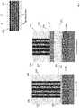
- FIG. 1illustrates a cross section view and a top down view of depositing a two-dimensional material over an insulating substrate; patterning the two-dimensional material to define a channel width; and depositing a gate dielectric over and in contact with the two-dimensional material;
- FIG. 2illustrates a cross section view and a top down view of depositing a top gate having a hard mask thereon over the gate dielectric
- FIG. 3illustrates a cross section view and a top down view of forming a sidewall spacer around the top gate having the hard mask thereon;
- FIG. 4illustrates a cross section view and a top down view of depositing an interlayer dielectric oxide over the sidewall spacer and the hard mask
- FIG. 5illustrates a cross section view and a top down view of removing the interlayer dielectric oxide adjacent to the sidewall spacer to form an open contact trench
- FIG. 6illustrates a cross section view and a top down view of depositing a cylinder-forming block copolymer into the source and drain region and annealing to induce the directed self-assembly
- FIG. 7illustrates a cross section view and a top down view of etching over the copolymer coating; etching the gate dielectric etch using a template to expose the two-dimension material; and performing a two-dimensional material etch over the two-dimensional material;
- FIG. 8illustrates a cross section view and a top down view of removing the remaining copolymer coating revealing the patterned gate dielectric in the source region and the drain region;
- FIG. 9illustrates a cross section view and a top down view of etching the exposed gate dielectric and forming a gate metal contact layer over the two-dimensional material
- FIG. 10illustrates a cross section views BB and CC, and a top down view of another embodiment of removing the interlayer dielectric oxide adjacent to the top gate and the hard mask thereon and the source and drain region;
- FIG. 11illustrates a cross section views BB and CC, and a top down view of another embodiment of depositing a lamella-forming block copolymer coating within the trench opening in interlayer dielectric oxide including the source and drain region and the region over the gate and annealing to induce the directed self-assembly.
- references in the detailed description to forming layer “A” over layer “B”include situations in which one or more intermediate layers (e.g., layer “C”) is between layer “A” and layer “B” as long as the relevant characteristics and functionalities of layer “A” and layer “B” are not substantially changed by the intermediate layer(s).
- layer “C”one or more intermediate layers
- spatially relative termse.g., “beneath,” “below,” “lower,” “above,” “upper,” and the like, can be used herein for ease of description to describe one element or feature's relationship to another element(s) or feature(s) as illustrated in the figures. It will be understood that the spatially relative terms are intended to encompass different orientations of the device in use or operation in addition to the orientation depicted in the figures. For example, if the device in the figures is turned over, elements described as “below” or “beneath” other elements or features would then be oriented “above” the other elements or features. Thus, the term “below” can encompass both an orientation of above and below. The device can be otherwise oriented (i.e., rotated 90 degrees or at other orientations), and the spatially relative descriptors used herein should be interpreted accordingly.
- Depositionis any process that grows, coats, or otherwise transfers a material onto the wafer. Available technologies include physical vapor deposition (PVD), chemical vapor deposition (CVD), electrochemical deposition (ECD), molecular beam epitaxy (MBE) and more recently, and atomic layer deposition (ALD) among others. Deposition also includes a so-called epitaxial growth process which deposits single crystalline material on a single crystalline substrate.
- embodiments of the inventionprovide a novel device structure and method for increasing source and drain contact edge width in two-dimensional field effect transistors by directed self-assembly.
- Removal/etchingis any process that removes material from the wafer. Examples include etch processes (either wet or dry), and chemical-mechanical planarization (CMP), and the like.
- a dry etch processsuch as reactive ion etching (RIE) uses chemically reactive plasma to remove a material, such as a masked pattern of semiconductor material, by exposing the material to a bombardment of ions that dislodge portions of the material from the exposed surface. The plasma is generated under low pressure (vacuum) by an electromagnetic field.
- RIEreactive ion etching
- Semiconductor dopingis the modification of electrical properties by doping, for example, transistor sources and drains, generally by diffusion and/or by ion implantation. These doping processes are followed by furnace annealing or rapid thermal annealing. Annealing serves to activate the implanted dopants. Selective doping of various layers of the semiconductor substrate allows the conductivity of the substrate to be changed with the application of voltage. By creating structures of these various components, millions of transistors can be built and wired together to form the complex circuitry of a modern microelectronic device.
- Semiconductor lithographyis the formation of three-dimensional relief images or patterns on the semiconductor substrate for subsequent transfer of the pattern to the substrate.
- the patternsare formed by a light sensitive polymer called a photo-resist.
- photo-resista light sensitive polymer
- the gate metal contact layeris electrically insulated from the main semiconductor n-channel or p-channel by a thin layer insulating material, for example, silicon dioxide or high dielectric constant (high-k) dielectrics, which makes the input resistance of the transistor relatively high.
- a thin layer insulating materialfor example, silicon dioxide or high dielectric constant (high-k) dielectrics, which makes the input resistance of the transistor relatively high.
- a monomeris a molecule that, as a unit, has chemical functional groups which can bind covalently to same or different kind of monomers to form a polymer.
- the productis called a copolymer and the process is called copolymerization.
- Copolymerscan be classified based on how their constituent or structural units are arranged. These classifications can include alternating copolymers, periodic copolymers, statistical copolymers, and block copolymers.
- FIG. 1illustrates a cross section view AA and a top down view AA of depositing a two-dimensional material 101 over an insulating substrate 100 .
- the insulating substrate 100can be a material such as silicon dioxide (SiO2).
- the insulating substrate 100can have a lateral width from about 5 nm to about 100 nm and ranges there between.
- a two-dimensional material 101can be a material such as graphene, hexagonal boron nitride (BN), and the transition metal dichalcogenides (TMDCs).
- Transition metal dichalcogenidesare atomically thin semiconductors of the type MX2 with M a transition metal atom such as molybdenum or tungsten and X as a chalcogen atom such as sulfur, selenium, or tellurium. Transition metal dichalcogenides are often combined with other two-dimensional materials 101 such as graphene and hexagonal boron nitride to make van der Waals heterostructures. Two-dimensional materials can be synthesized using a chemical vapor deposition (CVD) method. The reasoning is that CVD can provide large area, high quality, and well controlled layered growth of two-dimensional materials 101 . Alternatively, a two-dimensional material 101 can be transferred from other substrates to the insulating substrate 100 .
- CVDchemical vapor deposition
- patterningis performed on the two-dimensional material 101 to define a channel width.
- a gate dielectric 104is deposited over the two-dimensional material 101 .
- the gate dielectric 104can be composed of a material such as silicon dioxide or silicon nitride or high-k dielectric such as HfO2.
- the gate dielectric 104can have a lateral width from about 10 nm to about 100 nm and ranges there between.
- the deposition of the gate dielectric 104can be achieved through any number of well-known thin film deposition techniques, such as through atomic layer deposition, chemical vapor deposition, plasma deposition, sputtering, spin coating, etc.
- FIG. 2illustrates a cross section view AA and a top down view AA of depositing a top gate 102 having a hard mask thereon 103 over the gate dielectric 104 .
- the top gate 102can be a material such as amorphous silicon.
- the hard mask 103can be a material such as silicon nitride. Alternatively, the hard mask 103 can contain multiple materials arranged in any forms, including but not limited to silicon nitride, polysilicon, amorphous silicon, and silicon oxide.
- the hard mask 103can have a lateral width from about 5 to about 25 nm and ranges there between.
- FIG. 3illustrates a cross section view AA and a top down view AA of forming a sidewall spacer 105 around the top gate 102 having the hard mask thereon 103 .
- the sidewall spacer 105can be formed by techniques such as lithography.
- the sidewall spacer 105can be a material such as silicon nitride.
- the sidewall spacer 105can be formed by a deposition or reaction of a sidewall spacer film layer on a previous sidewall spacer pattern.
- the sidewall spacer 105can have a lateral width from about 4 nm to about 30 nm and ranges there between.
- FIG. 4illustrates a cross section view AA and a top down view AA of depositing an interlayer dielectric oxide 106 over the sidewall spacer 105 and the hard mask 103 .
- the interlayer dielectric oxide 106can have a low dielectric constant (low-k), which is a material with a small dielectric constant relative to silicon dioxide.
- FIG. 5illustrates a cross section view AA and a top down view AA of using lithography adjacent to the sidewall spacer 105 to remove the interlayer dielectric oxide 106 adjacent to the sidewall spacer 105 to create an open contact trench.
- FIG. 6illustrates a cross section view AA and a top down view AA of depositing a cylinder-forming block copolymer coating 107 within a source region and a drain region over the gate dielectric 104 using directed self-assembly.
- the copolymer microdomainscan have a lateral width from about 5 nm to about 50 nm and ranges there between.
- FIG. 8illustrates a cross section view AA and a top down view AA of removing the PS template revealing the patterned gate dielectric in the source region and the drain region.
- FIG. 9illustrates a cross section view AA and a top down view AA of etching the exposed gate dielectric 104 and forming a gate metal contact layer 108 over the two-dimensional material 101 .
- the metalcontacts both the two-dimensional material surface and the edge of the circular mesh.
- FIG. 10illustrates a cross section view BB and CC, and a top down view of another embodiment of removing the interlayer dielectric oxide 106 adjacent to the top gate 102 and the hard mask thereon 103 and the source and drain region. Lithography can be used to remove the interlayer dielectric oxide.
- FIG. 11illustrates a cross section view BB and CC, and a top down view of another embodiment of depositing a lamella-forming block copolymer coating 107 within the trench opening in interlayer dielectric oxide including the source and drain region and the region over the gate and annealing to induce the directed self-assembly.
Landscapes
- Engineering & Computer Science (AREA)
- Physics & Mathematics (AREA)
- Condensed Matter Physics & Semiconductors (AREA)
- General Physics & Mathematics (AREA)
- Manufacturing & Machinery (AREA)
- Computer Hardware Design (AREA)
- Microelectronics & Electronic Packaging (AREA)
- Power Engineering (AREA)
- Chemical & Material Sciences (AREA)
- Crystallography & Structural Chemistry (AREA)
- Insulated Gate Type Field-Effect Transistor (AREA)
Abstract
Description
Claims (9)
Priority Applications (2)
| Application Number | Priority Date | Filing Date | Title |
|---|---|---|---|
| US15/991,023US10580886B2 (en) | 2018-05-29 | 2018-05-29 | Increased source and drain contact edge width in two-dimensional material field effect transistors by directed self-assembly |
| US16/737,242US10741681B2 (en) | 2018-05-29 | 2020-01-08 | Increased source and drain contact edge width in two-dimensional material field effect transistors by directed self-assembly |
Applications Claiming Priority (1)
| Application Number | Priority Date | Filing Date | Title |
|---|---|---|---|
| US15/991,023US10580886B2 (en) | 2018-05-29 | 2018-05-29 | Increased source and drain contact edge width in two-dimensional material field effect transistors by directed self-assembly |
Related Child Applications (1)
| Application Number | Title | Priority Date | Filing Date |
|---|---|---|---|
| US16/737,242DivisionUS10741681B2 (en) | 2018-05-29 | 2020-01-08 | Increased source and drain contact edge width in two-dimensional material field effect transistors by directed self-assembly |
Publications (2)
| Publication Number | Publication Date |
|---|---|
| US20190371925A1 US20190371925A1 (en) | 2019-12-05 |
| US10580886B2true US10580886B2 (en) | 2020-03-03 |
Family
ID=68694980
Family Applications (2)
| Application Number | Title | Priority Date | Filing Date |
|---|---|---|---|
| US15/991,023Expired - Fee RelatedUS10580886B2 (en) | 2018-05-29 | 2018-05-29 | Increased source and drain contact edge width in two-dimensional material field effect transistors by directed self-assembly |
| US16/737,242Expired - Fee RelatedUS10741681B2 (en) | 2018-05-29 | 2020-01-08 | Increased source and drain contact edge width in two-dimensional material field effect transistors by directed self-assembly |
Family Applications After (1)
| Application Number | Title | Priority Date | Filing Date |
|---|---|---|---|
| US16/737,242Expired - Fee RelatedUS10741681B2 (en) | 2018-05-29 | 2020-01-08 | Increased source and drain contact edge width in two-dimensional material field effect transistors by directed self-assembly |
Country Status (1)
| Country | Link |
|---|---|
| US (2) | US10580886B2 (en) |
Families Citing this family (3)
| Publication number | Priority date | Publication date | Assignee | Title |
|---|---|---|---|---|
| US20230178597A1 (en)* | 2021-12-03 | 2023-06-08 | International Business Machines Corporation | Semiconductor structures with low top contact resistance |
| TWI820706B (en)* | 2022-05-13 | 2023-11-01 | 國立清華大學 | Two-dimensional semiconductor and manufacturing method thereof |
| CN115889141B (en)* | 2022-07-29 | 2024-03-29 | 武汉大学 | Method for improving insulation performance of metal/insulator by using two-dimensional material |
Citations (11)
| Publication number | Priority date | Publication date | Assignee | Title |
|---|---|---|---|---|
| US20020004304A1 (en)* | 1996-07-16 | 2002-01-10 | Pai-Hung Pan | Technique for elimination of pitting on silicon substrate during gate stack etch |
| US20040136866A1 (en)* | 2002-06-27 | 2004-07-15 | Nanosys, Inc. | Planar nanowire based sensor elements, devices, systems and methods for using and making same |
| US20040233714A1 (en)* | 2003-05-20 | 2004-11-25 | Yoshinao Morikawa | Semiconductor memory device and portable electronic apparatus |
| US20120199815A1 (en) | 2009-11-13 | 2012-08-09 | Fujitsu Limited | Semiconductor device and method of manufacturing the same |
| US8471237B2 (en) | 2010-01-27 | 2013-06-25 | Hitachi, Ltd. | Circuit board including a graphene film having contact region covering a recessed region and a patterned metal film covering the contact region and in direct electrical contact therewith, and device including same |
| US8884345B2 (en) | 2011-04-07 | 2014-11-11 | Samsung Electronics Co., Ltd. | Graphene electronic device and method of fabricating the same |
| US9054215B2 (en) | 2012-12-18 | 2015-06-09 | Intel Corporation | Patterning of vertical nanowire transistor channel and gate with directed self assembly |
| US9236292B2 (en) | 2013-12-18 | 2016-01-12 | Intel Corporation | Selective area deposition of metal films by atomic layer deposition (ALD) and chemical vapor deposition (CVD) |
| WO2016071317A1 (en) | 2014-11-07 | 2016-05-12 | Fraunhofer-Gesellschaft zur Förderung der angewandten Forschung e.V. | Method for producing an edge contact structure between a 2d material and a metal |
| JP2016127238A (en)* | 2015-01-08 | 2016-07-11 | 富士通株式会社 | Electronic device and method of manufacturing electronic device |
| US20180151429A1 (en)* | 2016-11-29 | 2018-05-31 | Taiwan Semiconductor Manufacturing Company, Ltd. | Methods for Forming Metal Layers in Openings and Apparatus for Forming Same |
Family Cites Families (1)
| Publication number | Priority date | Publication date | Assignee | Title |
|---|---|---|---|---|
| TW200905752A (en)* | 2007-07-18 | 2009-02-01 | Nanya Technology Corp | Semeconductor device with long channel and manufacturing method thereof |
- 2018
- 2018-05-29USUS15/991,023patent/US10580886B2/ennot_activeExpired - Fee Related
- 2020
- 2020-01-08USUS16/737,242patent/US10741681B2/ennot_activeExpired - Fee Related
Patent Citations (11)
| Publication number | Priority date | Publication date | Assignee | Title |
|---|---|---|---|---|
| US20020004304A1 (en)* | 1996-07-16 | 2002-01-10 | Pai-Hung Pan | Technique for elimination of pitting on silicon substrate during gate stack etch |
| US20040136866A1 (en)* | 2002-06-27 | 2004-07-15 | Nanosys, Inc. | Planar nanowire based sensor elements, devices, systems and methods for using and making same |
| US20040233714A1 (en)* | 2003-05-20 | 2004-11-25 | Yoshinao Morikawa | Semiconductor memory device and portable electronic apparatus |
| US20120199815A1 (en) | 2009-11-13 | 2012-08-09 | Fujitsu Limited | Semiconductor device and method of manufacturing the same |
| US8471237B2 (en) | 2010-01-27 | 2013-06-25 | Hitachi, Ltd. | Circuit board including a graphene film having contact region covering a recessed region and a patterned metal film covering the contact region and in direct electrical contact therewith, and device including same |
| US8884345B2 (en) | 2011-04-07 | 2014-11-11 | Samsung Electronics Co., Ltd. | Graphene electronic device and method of fabricating the same |
| US9054215B2 (en) | 2012-12-18 | 2015-06-09 | Intel Corporation | Patterning of vertical nanowire transistor channel and gate with directed self assembly |
| US9236292B2 (en) | 2013-12-18 | 2016-01-12 | Intel Corporation | Selective area deposition of metal films by atomic layer deposition (ALD) and chemical vapor deposition (CVD) |
| WO2016071317A1 (en) | 2014-11-07 | 2016-05-12 | Fraunhofer-Gesellschaft zur Förderung der angewandten Forschung e.V. | Method for producing an edge contact structure between a 2d material and a metal |
| JP2016127238A (en)* | 2015-01-08 | 2016-07-11 | 富士通株式会社 | Electronic device and method of manufacturing electronic device |
| US20180151429A1 (en)* | 2016-11-29 | 2018-05-31 | Taiwan Semiconductor Manufacturing Company, Ltd. | Methods for Forming Metal Layers in Openings and Apparatus for Forming Same |
Non-Patent Citations (5)
| Title |
|---|
| A. Meersha et al., "Record low metal-(CVD) graphene contact resistance using atomic orbital overlap engineering," International Electron Devices Meeting, IEDM, 2016, pp. 5.3.1-5.3.4. |
| A. Meersha et al., "Record low metal—(CVD) graphene contact resistance using atomic orbital overlap engineering," International Electron Devices Meeting, IEDM, 2016, pp. 5.3.1-5.3.4. |
| C, Ma et al., "Seamless Staircase Electrical Contact to Semiconducting Graphene Nanoribbons," Nano Letters, vol 17, No. 10, 2017, pp. 6241-6247. |
| C. T. Black et al., "High-capacity, self-assembled metal-oxide-semiconductor decoupling capacitors," IEEE Electron Device Letters, vol. 25, No. 9, 2004, pp. 622-624. |
| L. Wang et al., "One-Dimensional Electrical Contact to a Two-Dimensional Material," Science, vol. 342, 2013, pp. 614-617. |
Also Published As
| Publication number | Publication date |
|---|---|
| US20190371925A1 (en) | 2019-12-05 |
| US10741681B2 (en) | 2020-08-11 |
| US20200144406A1 (en) | 2020-05-07 |
Similar Documents
| Publication | Publication Date | Title |
|---|---|---|
| TWI752530B (en) | Asymmetric gate cut isolation for sram and method of forming the same | |
| US10573746B2 (en) | VTFET devices utilizing low temperature selective epitaxy | |
| TWI692016B (en) | Replacement metal gate patterning for nanochip devices | |
| TWI816685B (en) | Semiconductor device and manufacturing method thereof | |
| US10741681B2 (en) | Increased source and drain contact edge width in two-dimensional material field effect transistors by directed self-assembly | |
| US10615256B2 (en) | Nanosheet transistor gate structure having reduced parasitic capacitance | |
| US10680082B2 (en) | Vertical FET process with controlled gate length and self-aligned junctions | |
| US8809915B2 (en) | Gate conductor with a diffusion barrier | |
| US10297507B2 (en) | Self-aligned vertical field-effect transistor with epitaxially grown bottom and top source drain regions | |
| US9892977B2 (en) | FinFET and method of forming fin of the FinFET | |
| TW201707053A (en) | Semiconductor device and method of manufacturing same | |
| US6730588B1 (en) | Method of forming SiGe gate electrode | |
| US11355442B2 (en) | Forming self-aligned multi-metal interconnects | |
| JP7679146B2 (en) | Nanowire-core ferroelectric field-effect transistors | |
| US20200259009A1 (en) | Double gate two-dimensional material transistor | |
| US10998311B2 (en) | Fabricating gate-all-around transistors having high aspect ratio channels and reduced parasitic capacitance | |
| US8236693B2 (en) | Methods of forming silicides of different thicknesses on different structures | |
| US7573086B2 (en) | TaN integrated circuit (IC) capacitor | |
| US9929250B1 (en) | Semiconductor device including optimized gate stack profile | |
| US11501969B2 (en) | Direct extreme ultraviolet lithography on hard mask with reverse tone | |
| US20240429280A1 (en) | Integrated transistor having an over-the-channel etch-stop isolation region | |
| US20250159963A1 (en) | Reduced gate edge capacitance | |
| US20250311352A1 (en) | Semiconductor placeholder, source/drain, and contact | |
| US20240204063A1 (en) | Semiconductor device with backside u-shaped silicide | |
| CN110651368A (en) | Semiconductor device with a plurality of transistors |
Legal Events
| Date | Code | Title | Description |
|---|---|---|---|
| AS | Assignment | Owner name:INTERNATIONAL BUSINESS MACHINES CORPORATION, NEW Y Free format text:ASSIGNMENT OF ASSIGNORS INTEREST;ASSIGNORS:LIU, CHI-CHUN;YEUNG, CHUN WING;ZHANG, CHEN;REEL/FRAME:045917/0212 Effective date:20180529 Owner name:INTERNATIONAL BUSINESS MACHINES CORPORATION, NEW YORK Free format text:ASSIGNMENT OF ASSIGNORS INTEREST;ASSIGNORS:LIU, CHI-CHUN;YEUNG, CHUN WING;ZHANG, CHEN;REEL/FRAME:045917/0212 Effective date:20180529 | |
| FEPP | Fee payment procedure | Free format text:ENTITY STATUS SET TO UNDISCOUNTED (ORIGINAL EVENT CODE: BIG.); ENTITY STATUS OF PATENT OWNER: LARGE ENTITY | |
| ZAAA | Notice of allowance and fees due | Free format text:ORIGINAL CODE: NOA | |
| ZAAB | Notice of allowance mailed | Free format text:ORIGINAL CODE: MN/=. | |
| STPP | Information on status: patent application and granting procedure in general | Free format text:AWAITING TC RESP., ISSUE FEE NOT PAID | |
| STPP | Information on status: patent application and granting procedure in general | Free format text:NOTICE OF ALLOWANCE MAILED -- APPLICATION RECEIVED IN OFFICE OF PUBLICATIONS | |
| ZAAA | Notice of allowance and fees due | Free format text:ORIGINAL CODE: NOA | |
| STPP | Information on status: patent application and granting procedure in general | Free format text:PUBLICATIONS -- ISSUE FEE PAYMENT VERIFIED | |
| STCF | Information on status: patent grant | Free format text:PATENTED CASE | |
| FEPP | Fee payment procedure | Free format text:MAINTENANCE FEE REMINDER MAILED (ORIGINAL EVENT CODE: REM.); ENTITY STATUS OF PATENT OWNER: LARGE ENTITY | |
| LAPS | Lapse for failure to pay maintenance fees | Free format text:PATENT EXPIRED FOR FAILURE TO PAY MAINTENANCE FEES (ORIGINAL EVENT CODE: EXP.); ENTITY STATUS OF PATENT OWNER: LARGE ENTITY | |
| STCH | Information on status: patent discontinuation | Free format text:PATENT EXPIRED DUE TO NONPAYMENT OF MAINTENANCE FEES UNDER 37 CFR 1.362 | |
| FP | Lapsed due to failure to pay maintenance fee | Effective date:20240303 |