US10580652B2 - Alternating hardmasks for tight-pitch line formation - Google Patents
Alternating hardmasks for tight-pitch line formationDownload PDFInfo
- Publication number
- US10580652B2 US10580652B2US16/058,088US201816058088AUS10580652B2US 10580652 B2US10580652 B2US 10580652B2US 201816058088 AUS201816058088 AUS 201816058088AUS 10580652 B2US10580652 B2US 10580652B2
- Authority
- US
- United States
- Prior art keywords
- fins
- color
- fin
- forming
- layer
- Prior art date
- Legal status (The legal status is an assumption and is not a legal conclusion. Google has not performed a legal analysis and makes no representation as to the accuracy of the status listed.)
- Expired - Fee Related
Links
- 230000015572biosynthetic processEffects0.000titledescription19
- 238000000034methodMethods0.000claimsabstractdescription46
- 230000000873masking effectEffects0.000claimsabstractdescription6
- 239000000463materialSubstances0.000claimsdescription113
- 238000005530etchingMethods0.000claimsdescription26
- 229920001400block copolymerPolymers0.000claimsdescription14
- 239000004793PolystyreneSubstances0.000claimsdescription12
- 238000002408directed self-assemblyMethods0.000claimsdescription12
- 229920002223polystyrenePolymers0.000claimsdescription12
- 238000000151depositionMethods0.000claimsdescription9
- -1poly(methyl methacrylate)Polymers0.000claimsdescription8
- 229920003229poly(methyl methacrylate)Polymers0.000claimsdescription7
- 239000004926polymethyl methacrylateSubstances0.000claimsdescription7
- 239000002861polymer materialSubstances0.000claimsdescription2
- 239000010410layerSubstances0.000description86
- 238000010586diagramMethods0.000description42
- 239000004065semiconductorSubstances0.000description20
- 229920000642polymerPolymers0.000description13
- 239000000758substrateSubstances0.000description13
- 238000001020plasma etchingMethods0.000description11
- XUIMIQQOPSSXEZ-UHFFFAOYSA-NSiliconChemical compound[Si]XUIMIQQOPSSXEZ-UHFFFAOYSA-N0.000description8
- 238000004519manufacturing processMethods0.000description8
- 229910052710siliconInorganic materials0.000description8
- 239000010703siliconSubstances0.000description8
- 230000008021depositionEffects0.000description7
- KRHYYFGTRYWZRS-UHFFFAOYSA-NFluoraneChemical compoundFKRHYYFGTRYWZRS-UHFFFAOYSA-N0.000description6
- 238000000231atomic layer depositionMethods0.000description5
- 150000001875compoundsChemical class0.000description5
- 238000005137deposition processMethods0.000description5
- 238000013461designMethods0.000description5
- 239000000126substanceSubstances0.000description5
- VYPSYNLAJGMNEJ-UHFFFAOYSA-NSilicium dioxideChemical compoundO=[Si]=OVYPSYNLAJGMNEJ-UHFFFAOYSA-N0.000description4
- 229910000577Silicon-germaniumInorganic materials0.000description4
- 239000003086colorantSubstances0.000description4
- 238000006243chemical reactionMethods0.000description3
- 239000000203mixtureSubstances0.000description3
- 238000005240physical vapour depositionMethods0.000description3
- 229920002717polyvinylpyridinePolymers0.000description3
- 239000002904solventSubstances0.000description3
- 238000003860storageMethods0.000description3
- IJGRMHOSHXDMSA-UHFFFAOYSA-NAtomic nitrogenChemical compoundN#NIJGRMHOSHXDMSA-UHFFFAOYSA-N0.000description2
- OKTJSMMVPCPJKN-UHFFFAOYSA-NCarbonChemical compound[C]OKTJSMMVPCPJKN-UHFFFAOYSA-N0.000description2
- LEVVHYCKPQWKOP-UHFFFAOYSA-N[Si].[Ge]Chemical compound[Si].[Ge]LEVVHYCKPQWKOP-UHFFFAOYSA-N0.000description2
- 229910021417amorphous siliconInorganic materials0.000description2
- 239000006117anti-reflective coatingSubstances0.000description2
- 238000001505atmospheric-pressure chemical vapour depositionMethods0.000description2
- 239000007795chemical reaction productSubstances0.000description2
- 239000003989dielectric materialSubstances0.000description2
- 230000005669field effectEffects0.000description2
- 230000006870functionEffects0.000description2
- 125000000524functional groupChemical group0.000description2
- 239000007789gasSubstances0.000description2
- 238000010884ion-beam techniqueMethods0.000description2
- 238000004518low pressure chemical vapour depositionMethods0.000description2
- 229910052751metalInorganic materials0.000description2
- 239000002184metalSubstances0.000description2
- 238000000623plasma-assisted chemical vapour depositionMethods0.000description2
- 238000012545processingMethods0.000description2
- 239000000047productSubstances0.000description2
- 238000001338self-assemblyMethods0.000description2
- 235000012239silicon dioxideNutrition0.000description2
- 239000000377silicon dioxideSubstances0.000description2
- 239000002356single layerSubstances0.000description2
- 239000002002slurrySubstances0.000description2
- 239000012265solid productSubstances0.000description2
- 238000004544sputter depositionMethods0.000description2
- PFNQVRZLDWYSCW-UHFFFAOYSA-N(fluoren-9-ylideneamino) n-naphthalen-1-ylcarbamateChemical compoundC12=CC=CC=C2C2=CC=CC=C2C1=NOC(=O)NC1=CC=CC2=CC=CC=C12PFNQVRZLDWYSCW-UHFFFAOYSA-N0.000description1
- MARUHZGHZWCEQU-UHFFFAOYSA-N5-phenyl-2h-tetrazoleChemical compoundC1=CC=CC=C1C1=NNN=N1MARUHZGHZWCEQU-UHFFFAOYSA-N0.000description1
- JBRZTFJDHDCESZ-UHFFFAOYSA-NAsGaChemical compound[As]#[Ga]JBRZTFJDHDCESZ-UHFFFAOYSA-N0.000description1
- 229910002601GaNInorganic materials0.000description1
- 229910001218Gallium arsenideInorganic materials0.000description1
- JMASRVWKEDWRBT-UHFFFAOYSA-NGallium nitrideChemical compound[Ga]#NJMASRVWKEDWRBT-UHFFFAOYSA-N0.000description1
- 229910052581Si3N4Inorganic materials0.000description1
- 229910020751SixGe1-xInorganic materials0.000description1
- RTAQQCXQSZGOHL-UHFFFAOYSA-NTitaniumChemical compound[Ti]RTAQQCXQSZGOHL-UHFFFAOYSA-N0.000description1
- CFOAUMXQOCBWNJ-UHFFFAOYSA-N[B].[Si]Chemical compound[B].[Si]CFOAUMXQOCBWNJ-UHFFFAOYSA-N0.000description1
- 229910045601alloyInorganic materials0.000description1
- 239000000956alloySubstances0.000description1
- 238000013459approachMethods0.000description1
- QVGXLLKOCUKJST-UHFFFAOYSA-Natomic oxygenChemical compound[O]QVGXLLKOCUKJST-UHFFFAOYSA-N0.000description1
- 229910052799carbonInorganic materials0.000description1
- 239000000919ceramicSubstances0.000description1
- 238000003486chemical etchingMethods0.000description1
- 239000012707chemical precursorSubstances0.000description1
- 238000005229chemical vapour depositionMethods0.000description1
- 239000011248coating agentSubstances0.000description1
- 238000000576coating methodMethods0.000description1
- 239000000470constituentSubstances0.000description1
- 239000010408filmSubstances0.000description1
- 230000009969flowable effectEffects0.000description1
- 229910052732germaniumInorganic materials0.000description1
- GNPVGFCGXDBREM-UHFFFAOYSA-Ngermanium atomChemical compound[Ge]GNPVGFCGXDBREM-UHFFFAOYSA-N0.000description1
- FFUAGWLWBBFQJT-UHFFFAOYSA-NhexamethyldisilazaneChemical compoundC[Si](C)(C)N[Si](C)(C)CFFUAGWLWBBFQJT-UHFFFAOYSA-N0.000description1
- 229920001519homopolymerPolymers0.000description1
- 239000012212insulatorSubstances0.000description1
- 239000013067intermediate productSubstances0.000description1
- 238000000608laser ablationMethods0.000description1
- 238000001459lithographyMethods0.000description1
- 238000001755magnetron sputter depositionMethods0.000description1
- 238000012986modificationMethods0.000description1
- 230000004048modificationEffects0.000description1
- 229910052757nitrogenInorganic materials0.000description1
- 239000001301oxygenSubstances0.000description1
- 229910052760oxygenInorganic materials0.000description1
- 238000002294plasma sputter depositionMethods0.000description1
- 239000004033plasticSubstances0.000description1
- 229920003023plasticPolymers0.000description1
- 229910021420polycrystalline siliconInorganic materials0.000description1
- 229920005591polysiliconPolymers0.000description1
- 229920005604random copolymerPolymers0.000description1
- 239000000376reactantSubstances0.000description1
- HBMJWWWQQXIZIP-UHFFFAOYSA-Nsilicon carbideChemical compound[Si+]#[C-]HBMJWWWQQXIZIP-UHFFFAOYSA-N0.000description1
- 229910010271silicon carbideInorganic materials0.000description1
- HQVNEWCFYHHQES-UHFFFAOYSA-Nsilicon nitrideChemical compoundN12[Si]34N5[Si]62N3[Si]51N64HQVNEWCFYHHQES-UHFFFAOYSA-N0.000description1
- 125000006850spacer groupChemical group0.000description1
- 238000004528spin coatingMethods0.000description1
- 239000010409thin filmSubstances0.000description1
- 239000010936titaniumSubstances0.000description1
- 229910052719titaniumInorganic materials0.000description1
- 238000012546transferMethods0.000description1
Images


Classifications
- H—ELECTRICITY
- H01—ELECTRIC ELEMENTS
- H01L—SEMICONDUCTOR DEVICES NOT COVERED BY CLASS H10
- H01L21/00—Processes or apparatus adapted for the manufacture or treatment of semiconductor or solid state devices or of parts thereof
- H01L21/02—Manufacture or treatment of semiconductor devices or of parts thereof
- H01L21/027—Making masks on semiconductor bodies for further photolithographic processing not provided for in group H01L21/18 or H01L21/34
- H01L21/033—Making masks on semiconductor bodies for further photolithographic processing not provided for in group H01L21/18 or H01L21/34 comprising inorganic layers
- H01L21/0334—Making masks on semiconductor bodies for further photolithographic processing not provided for in group H01L21/18 or H01L21/34 comprising inorganic layers characterised by their size, orientation, disposition, behaviour, shape, in horizontal or vertical plane
- H01L21/0338—Process specially adapted to improve the resolution of the mask
- H—ELECTRICITY
- H01—ELECTRIC ELEMENTS
- H01L—SEMICONDUCTOR DEVICES NOT COVERED BY CLASS H10
- H01L21/00—Processes or apparatus adapted for the manufacture or treatment of semiconductor or solid state devices or of parts thereof
- H01L21/02—Manufacture or treatment of semiconductor devices or of parts thereof
- H01L21/027—Making masks on semiconductor bodies for further photolithographic processing not provided for in group H01L21/18 or H01L21/34
- H01L21/033—Making masks on semiconductor bodies for further photolithographic processing not provided for in group H01L21/18 or H01L21/34 comprising inorganic layers
- H01L21/0332—Making masks on semiconductor bodies for further photolithographic processing not provided for in group H01L21/18 or H01L21/34 comprising inorganic layers characterised by their composition, e.g. multilayer masks, materials
- H—ELECTRICITY
- H01—ELECTRIC ELEMENTS
- H01L—SEMICONDUCTOR DEVICES NOT COVERED BY CLASS H10
- H01L21/00—Processes or apparatus adapted for the manufacture or treatment of semiconductor or solid state devices or of parts thereof
- H01L21/02—Manufacture or treatment of semiconductor devices or of parts thereof
- H01L21/027—Making masks on semiconductor bodies for further photolithographic processing not provided for in group H01L21/18 or H01L21/34
- H01L21/033—Making masks on semiconductor bodies for further photolithographic processing not provided for in group H01L21/18 or H01L21/34 comprising inorganic layers
- H01L21/0334—Making masks on semiconductor bodies for further photolithographic processing not provided for in group H01L21/18 or H01L21/34 comprising inorganic layers characterised by their size, orientation, disposition, behaviour, shape, in horizontal or vertical plane
- H01L21/0335—Making masks on semiconductor bodies for further photolithographic processing not provided for in group H01L21/18 or H01L21/34 comprising inorganic layers characterised by their size, orientation, disposition, behaviour, shape, in horizontal or vertical plane characterised by their behaviour during the process, e.g. soluble masks, redeposited masks
- H—ELECTRICITY
- H01—ELECTRIC ELEMENTS
- H01L—SEMICONDUCTOR DEVICES NOT COVERED BY CLASS H10
- H01L21/00—Processes or apparatus adapted for the manufacture or treatment of semiconductor or solid state devices or of parts thereof
- H01L21/02—Manufacture or treatment of semiconductor devices or of parts thereof
- H01L21/027—Making masks on semiconductor bodies for further photolithographic processing not provided for in group H01L21/18 or H01L21/34
- H01L21/033—Making masks on semiconductor bodies for further photolithographic processing not provided for in group H01L21/18 or H01L21/34 comprising inorganic layers
- H01L21/0334—Making masks on semiconductor bodies for further photolithographic processing not provided for in group H01L21/18 or H01L21/34 comprising inorganic layers characterised by their size, orientation, disposition, behaviour, shape, in horizontal or vertical plane
- H01L21/0337—Making masks on semiconductor bodies for further photolithographic processing not provided for in group H01L21/18 or H01L21/34 comprising inorganic layers characterised by their size, orientation, disposition, behaviour, shape, in horizontal or vertical plane characterised by the process involved to create the mask, e.g. lift-off masks, sidewalls, or to modify the mask, e.g. pre-treatment, post-treatment
- H—ELECTRICITY
- H01—ELECTRIC ELEMENTS
- H01L—SEMICONDUCTOR DEVICES NOT COVERED BY CLASS H10
- H01L21/00—Processes or apparatus adapted for the manufacture or treatment of semiconductor or solid state devices or of parts thereof
- H01L21/02—Manufacture or treatment of semiconductor devices or of parts thereof
- H01L21/04—Manufacture or treatment of semiconductor devices or of parts thereof the devices having potential barriers, e.g. a PN junction, depletion layer or carrier concentration layer
- H01L21/18—Manufacture or treatment of semiconductor devices or of parts thereof the devices having potential barriers, e.g. a PN junction, depletion layer or carrier concentration layer the devices having semiconductor bodies comprising elements of Group IV of the Periodic Table or AIIIBV compounds with or without impurities, e.g. doping materials
- H01L21/30—Treatment of semiconductor bodies using processes or apparatus not provided for in groups H01L21/20 - H01L21/26
- H01L21/302—Treatment of semiconductor bodies using processes or apparatus not provided for in groups H01L21/20 - H01L21/26 to change their surface-physical characteristics or shape, e.g. etching, polishing, cutting
- H01L21/306—Chemical or electrical treatment, e.g. electrolytic etching
- H01L21/308—Chemical or electrical treatment, e.g. electrolytic etching using masks
- H01L21/3081—Chemical or electrical treatment, e.g. electrolytic etching using masks characterised by their composition, e.g. multilayer masks, materials
- H—ELECTRICITY
- H01—ELECTRIC ELEMENTS
- H01L—SEMICONDUCTOR DEVICES NOT COVERED BY CLASS H10
- H01L21/00—Processes or apparatus adapted for the manufacture or treatment of semiconductor or solid state devices or of parts thereof
- H01L21/02—Manufacture or treatment of semiconductor devices or of parts thereof
- H01L21/04—Manufacture or treatment of semiconductor devices or of parts thereof the devices having potential barriers, e.g. a PN junction, depletion layer or carrier concentration layer
- H01L21/18—Manufacture or treatment of semiconductor devices or of parts thereof the devices having potential barriers, e.g. a PN junction, depletion layer or carrier concentration layer the devices having semiconductor bodies comprising elements of Group IV of the Periodic Table or AIIIBV compounds with or without impurities, e.g. doping materials
- H01L21/30—Treatment of semiconductor bodies using processes or apparatus not provided for in groups H01L21/20 - H01L21/26
- H01L21/302—Treatment of semiconductor bodies using processes or apparatus not provided for in groups H01L21/20 - H01L21/26 to change their surface-physical characteristics or shape, e.g. etching, polishing, cutting
- H01L21/306—Chemical or electrical treatment, e.g. electrolytic etching
- H01L21/308—Chemical or electrical treatment, e.g. electrolytic etching using masks
- H01L21/3083—Chemical or electrical treatment, e.g. electrolytic etching using masks characterised by their size, orientation, disposition, behaviour, shape, in horizontal or vertical plane
- H01L21/3086—Chemical or electrical treatment, e.g. electrolytic etching using masks characterised by their size, orientation, disposition, behaviour, shape, in horizontal or vertical plane characterised by the process involved to create the mask, e.g. lift-off masks, sidewalls, or to modify the mask, e.g. pre-treatment, post-treatment
- H—ELECTRICITY
- H01—ELECTRIC ELEMENTS
- H01L—SEMICONDUCTOR DEVICES NOT COVERED BY CLASS H10
- H01L21/00—Processes or apparatus adapted for the manufacture or treatment of semiconductor or solid state devices or of parts thereof
- H01L21/02—Manufacture or treatment of semiconductor devices or of parts thereof
- H01L21/04—Manufacture or treatment of semiconductor devices or of parts thereof the devices having potential barriers, e.g. a PN junction, depletion layer or carrier concentration layer
- H01L21/18—Manufacture or treatment of semiconductor devices or of parts thereof the devices having potential barriers, e.g. a PN junction, depletion layer or carrier concentration layer the devices having semiconductor bodies comprising elements of Group IV of the Periodic Table or AIIIBV compounds with or without impurities, e.g. doping materials
- H01L21/30—Treatment of semiconductor bodies using processes or apparatus not provided for in groups H01L21/20 - H01L21/26
- H01L21/302—Treatment of semiconductor bodies using processes or apparatus not provided for in groups H01L21/20 - H01L21/26 to change their surface-physical characteristics or shape, e.g. etching, polishing, cutting
- H01L21/306—Chemical or electrical treatment, e.g. electrolytic etching
- H01L21/308—Chemical or electrical treatment, e.g. electrolytic etching using masks
- H01L21/3083—Chemical or electrical treatment, e.g. electrolytic etching using masks characterised by their size, orientation, disposition, behaviour, shape, in horizontal or vertical plane
- H01L21/3088—Process specially adapted to improve the resolution of the mask
- H—ELECTRICITY
- H01—ELECTRIC ELEMENTS
- H01L—SEMICONDUCTOR DEVICES NOT COVERED BY CLASS H10
- H01L21/00—Processes or apparatus adapted for the manufacture or treatment of semiconductor or solid state devices or of parts thereof
- H01L21/02—Manufacture or treatment of semiconductor devices or of parts thereof
- H01L21/04—Manufacture or treatment of semiconductor devices or of parts thereof the devices having potential barriers, e.g. a PN junction, depletion layer or carrier concentration layer
- H01L21/18—Manufacture or treatment of semiconductor devices or of parts thereof the devices having potential barriers, e.g. a PN junction, depletion layer or carrier concentration layer the devices having semiconductor bodies comprising elements of Group IV of the Periodic Table or AIIIBV compounds with or without impurities, e.g. doping materials
- H01L21/30—Treatment of semiconductor bodies using processes or apparatus not provided for in groups H01L21/20 - H01L21/26
- H01L21/31—Treatment of semiconductor bodies using processes or apparatus not provided for in groups H01L21/20 - H01L21/26 to form insulating layers thereon, e.g. for masking or by using photolithographic techniques; After treatment of these layers; Selection of materials for these layers
- H01L21/3105—After-treatment
- H01L21/311—Etching the insulating layers by chemical or physical means
- H01L21/31105—Etching inorganic layers
- H01L21/31111—Etching inorganic layers by chemical means
- H01L21/31116—Etching inorganic layers by chemical means by dry-etching
- H01L21/31122—Etching inorganic layers by chemical means by dry-etching of layers not containing Si, e.g. PZT, Al2O3
- H—ELECTRICITY
- H01—ELECTRIC ELEMENTS
- H01L—SEMICONDUCTOR DEVICES NOT COVERED BY CLASS H10
- H01L21/00—Processes or apparatus adapted for the manufacture or treatment of semiconductor or solid state devices or of parts thereof
- H01L21/02—Manufacture or treatment of semiconductor devices or of parts thereof
- H01L21/04—Manufacture or treatment of semiconductor devices or of parts thereof the devices having potential barriers, e.g. a PN junction, depletion layer or carrier concentration layer
- H01L21/18—Manufacture or treatment of semiconductor devices or of parts thereof the devices having potential barriers, e.g. a PN junction, depletion layer or carrier concentration layer the devices having semiconductor bodies comprising elements of Group IV of the Periodic Table or AIIIBV compounds with or without impurities, e.g. doping materials
- H01L21/30—Treatment of semiconductor bodies using processes or apparatus not provided for in groups H01L21/20 - H01L21/26
- H01L21/31—Treatment of semiconductor bodies using processes or apparatus not provided for in groups H01L21/20 - H01L21/26 to form insulating layers thereon, e.g. for masking or by using photolithographic techniques; After treatment of these layers; Selection of materials for these layers
- H01L21/3105—After-treatment
- H01L21/311—Etching the insulating layers by chemical or physical means
- H01L21/31144—Etching the insulating layers by chemical or physical means using masks
- H—ELECTRICITY
- H01—ELECTRIC ELEMENTS
- H01L—SEMICONDUCTOR DEVICES NOT COVERED BY CLASS H10
- H01L21/00—Processes or apparatus adapted for the manufacture or treatment of semiconductor or solid state devices or of parts thereof
- H01L21/02—Manufacture or treatment of semiconductor devices or of parts thereof
- H01L21/04—Manufacture or treatment of semiconductor devices or of parts thereof the devices having potential barriers, e.g. a PN junction, depletion layer or carrier concentration layer
- H01L21/18—Manufacture or treatment of semiconductor devices or of parts thereof the devices having potential barriers, e.g. a PN junction, depletion layer or carrier concentration layer the devices having semiconductor bodies comprising elements of Group IV of the Periodic Table or AIIIBV compounds with or without impurities, e.g. doping materials
- H01L21/30—Treatment of semiconductor bodies using processes or apparatus not provided for in groups H01L21/20 - H01L21/26
- H01L21/31—Treatment of semiconductor bodies using processes or apparatus not provided for in groups H01L21/20 - H01L21/26 to form insulating layers thereon, e.g. for masking or by using photolithographic techniques; After treatment of these layers; Selection of materials for these layers
- H01L21/3205—Deposition of non-insulating-, e.g. conductive- or resistive-, layers on insulating layers; After-treatment of these layers
- H01L21/321—After treatment
- H01L21/3213—Physical or chemical etching of the layers, e.g. to produce a patterned layer from a pre-deposited extensive layer
- H01L21/32133—Physical or chemical etching of the layers, e.g. to produce a patterned layer from a pre-deposited extensive layer by chemical means only
- H01L21/32135—Physical or chemical etching of the layers, e.g. to produce a patterned layer from a pre-deposited extensive layer by chemical means only by vapour etching only
- H01L21/32136—Physical or chemical etching of the layers, e.g. to produce a patterned layer from a pre-deposited extensive layer by chemical means only by vapour etching only using plasmas
- H01L21/32137—Physical or chemical etching of the layers, e.g. to produce a patterned layer from a pre-deposited extensive layer by chemical means only by vapour etching only using plasmas of silicon-containing layers
- H01L21/823431—
- H01L29/6656—
- H—ELECTRICITY
- H10—SEMICONDUCTOR DEVICES; ELECTRIC SOLID-STATE DEVICES NOT OTHERWISE PROVIDED FOR
- H10D—INORGANIC ELECTRIC SEMICONDUCTOR DEVICES
- H10D64/00—Electrodes of devices having potential barriers
- H10D64/01—Manufacture or treatment
- H10D64/021—Manufacture or treatment using multiple gate spacer layers, e.g. bilayered sidewall spacers
- H—ELECTRICITY
- H10—SEMICONDUCTOR DEVICES; ELECTRIC SOLID-STATE DEVICES NOT OTHERWISE PROVIDED FOR
- H10D—INORGANIC ELECTRIC SEMICONDUCTOR DEVICES
- H10D84/00—Integrated devices formed in or on semiconductor substrates that comprise only semiconducting layers, e.g. on Si wafers or on GaAs-on-Si wafers
- H10D84/01—Manufacture or treatment
- H10D84/0123—Integrating together multiple components covered by H10D12/00 or H10D30/00, e.g. integrating multiple IGBTs
- H10D84/0126—Integrating together multiple components covered by H10D12/00 or H10D30/00, e.g. integrating multiple IGBTs the components including insulated gates, e.g. IGFETs
- H10D84/0158—Integrating together multiple components covered by H10D12/00 or H10D30/00, e.g. integrating multiple IGBTs the components including insulated gates, e.g. IGFETs the components including FinFETs
- H—ELECTRICITY
- H10—SEMICONDUCTOR DEVICES; ELECTRIC SOLID-STATE DEVICES NOT OTHERWISE PROVIDED FOR
- H10D—INORGANIC ELECTRIC SEMICONDUCTOR DEVICES
- H10D84/00—Integrated devices formed in or on semiconductor substrates that comprise only semiconducting layers, e.g. on Si wafers or on GaAs-on-Si wafers
- H10D84/01—Manufacture or treatment
- H10D84/02—Manufacture or treatment characterised by using material-based technologies
- H10D84/03—Manufacture or treatment characterised by using material-based technologies using Group IV technology, e.g. silicon technology or silicon-carbide [SiC] technology
- H10D84/038—Manufacture or treatment characterised by using material-based technologies using Group IV technology, e.g. silicon technology or silicon-carbide [SiC] technology using silicon technology, e.g. SiGe
- H01L29/66795—
- H—ELECTRICITY
- H10—SEMICONDUCTOR DEVICES; ELECTRIC SOLID-STATE DEVICES NOT OTHERWISE PROVIDED FOR
- H10D—INORGANIC ELECTRIC SEMICONDUCTOR DEVICES
- H10D30/00—Field-effect transistors [FET]
- H10D30/01—Manufacture or treatment
- H10D30/021—Manufacture or treatment of FETs having insulated gates [IGFET]
- H10D30/024—Manufacture or treatment of FETs having insulated gates [IGFET] of fin field-effect transistors [FinFET]
- Y—GENERAL TAGGING OF NEW TECHNOLOGICAL DEVELOPMENTS; GENERAL TAGGING OF CROSS-SECTIONAL TECHNOLOGIES SPANNING OVER SEVERAL SECTIONS OF THE IPC; TECHNICAL SUBJECTS COVERED BY FORMER USPC CROSS-REFERENCE ART COLLECTIONS [XRACs] AND DIGESTS
- Y10—TECHNICAL SUBJECTS COVERED BY FORMER USPC
- Y10S—TECHNICAL SUBJECTS COVERED BY FORMER USPC CROSS-REFERENCE ART COLLECTIONS [XRACs] AND DIGESTS
- Y10S438/00—Semiconductor device manufacturing: process
- Y10S438/942—Masking
- Y10S438/947—Subphotolithographic processing
- Y—GENERAL TAGGING OF NEW TECHNOLOGICAL DEVELOPMENTS; GENERAL TAGGING OF CROSS-SECTIONAL TECHNOLOGIES SPANNING OVER SEVERAL SECTIONS OF THE IPC; TECHNICAL SUBJECTS COVERED BY FORMER USPC CROSS-REFERENCE ART COLLECTIONS [XRACs] AND DIGESTS
- Y10—TECHNICAL SUBJECTS COVERED BY FORMER USPC
- Y10S—TECHNICAL SUBJECTS COVERED BY FORMER USPC CROSS-REFERENCE ART COLLECTIONS [XRACs] AND DIGESTS
- Y10S438/00—Semiconductor device manufacturing: process
- Y10S438/942—Masking
- Y10S438/948—Radiation resist
- Y10S438/95—Multilayer mask including nonradiation sensitive layer
Definitions
- the present inventiongenerally relates to semiconductor fabrication and, more particularly, to the formation of hardmasks in semiconductor fabrication processes.
- Fin field effect transistorsFin field effect transistors
- FinFETsFin field effect transistors
- other fin-based devicesare frequently used in semiconductor structures to provide small-scale integrated circuit components. As these devices scale down in size, performance can be increased but fabrication becomes more difficult. In particular, errors in edge placement, critical dimension, and overlay approach the size of the structures being fabricated, making it difficult to accurately form such structures.
- One particular challenge in forming fin structuresis the selective removal of particular fins.
- a series of finscan be created using, e.g., sidewall image transfer techniques
- significant errors in masking the finsmay occur when operating near the limit of the lithographic process. Such errors may cause fins neighboring the removed fin to be damaged or removed entirely.
- a method of forming finsincludes masking a region on a three-color hardmask fin pattern, leaving a fin of a first color exposed.
- the exposed fin of the first coloris etched away with a selective etch that does not remove fins of a second color or a third color.
- the mask and all fins of a second colorare etched away. Fins are etched into a fin base layer using the fins of the first color and the fins of the third color.
- a method of forming a three-color hardmask fin patternincludes forming seed layer fins. Self-assembled fins are formed by directed self-assembly on the seed layer fins. A layer of a first color is etched using the self-assembled fins as a mask to form fins of a first color. A second-color material is deposited around the fins of the first color. Fins of the first color are etched away, leaving at least one fin of the first color. Fins of a third color are formed in gaps left by etching away fins of the first color.
- FIG. 1is a cross-sectional diagram of a step in the formation of a tri-color hardmask in accordance with one embodiment of the present invention
- FIG. 2is a cross-sectional diagram of a step in the formation of a tri-color hardmask in accordance with one embodiment of the present invention
- FIG. 3is a cross-sectional diagram of a step in the formation of a tri-color hardmask in accordance with one embodiment of the present invention
- FIG. 4is a cross-sectional diagram of a step in the formation of a tri-color hardmask in accordance with one embodiment of the present invention
- FIG. 5is a cross-sectional diagram of a step in the formation of a tri-color hardmask in accordance with one embodiment of the present invention.
- FIG. 6is a cross-sectional diagram of a step in the formation of a tri-color hardmask in accordance with one embodiment of the present invention.
- FIG. 7is a cross-sectional diagram of a step in the formation of a tri-color hardmask in accordance with one embodiment of the present invention.
- FIG. 8is a cross-sectional diagram of a step in the formation of a tri-color hardmask in accordance with one embodiment of the present invention.
- FIG. 9is a cross-sectional diagram of a step in the formation of a tri-color hardmask in accordance with one embodiment of the present invention.
- FIG. 10is a cross-sectional diagram of a step in the formation of a tri-color hardmask in accordance with one embodiment of the present invention.
- FIG. 11is a cross-sectional diagram of a step in the formation of a tri-color hardmask in accordance with one embodiment of the present invention.
- FIG. 12is a cross-sectional diagram of a step in the formation of a tri-color hardmask in accordance with one embodiment of the present invention.
- FIG. 13is a cross-sectional diagram of a step in the formation of a tri-color hardmask in accordance with one embodiment of the present invention.
- FIG. 14is a cross-sectional diagram of a step in the formation of a tri-color hardmask in accordance with one embodiment of the present invention.
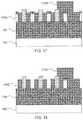
- FIG. 15is a cross-sectional diagram of a step in the selective etch of fins using a tri-color hardmask in accordance with one embodiment of the present invention.
- FIG. 16is a cross-sectional diagram of a step in the selective etch of fins using a tri-color hardmask in accordance with one embodiment of the present invention.
- FIG. 17is a cross-sectional diagram of a step in the selective etch of fins using a tri-color hardmask in accordance with one embodiment of the present invention.
- FIG. 18is a cross-sectional diagram of a step in the selective etch of fins using a tri-color hardmask in accordance with one embodiment of the present invention.
- FIG. 19is a cross-sectional diagram of a step in the selective etch of fins using a tri-color hardmask in accordance with one embodiment of the present invention.
- FIG. 20is a cross-sectional diagram of a step in the selective etch of fins using a tri-color hardmask in accordance with one embodiment of the present invention.
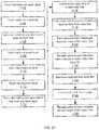
- FIG. 21is a block/flow diagram of a method of a forming tri-color hardmask in accordance with one embodiment of the present invention.
- FIG. 22is a block/flow diagram of a method of etching fins using a tri-color hardmask in accordance with one embodiment of the present invention.
- Embodiments of the present inventionprovide a hardmask fabrication process that may be used for fin formation in semiconductor fabrication.
- the present embodimentforms hardmask fins of three different compositions that have mutual etch selectivity, such that a spacing between fins of the same type is large enough that lithographic masking errors will not interfere when selectively removing fins.
- Thisprovides a tri-color alternating hardmask, where the three different “colors” represent the three different fin hardmask composition.
- the term “color”is defined herein to refer to one particular hardmask composition.
- first-color“first-color,” “second-color,” and “third-color” materials and fins.
- Each of these “colors”can be etched selectively to the other two, making it possible to remove a fin of one color without damaging nearby fins of a different color.
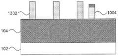
- a layer of fin base material 104is formed on a semiconductor substrate 102 .
- the semiconductor substrate 102may be a bulk-semiconductor substrate.
- the bulk-semiconductor substratemay be a silicon-containing material.
- silicon-containing materials suitable for the bulk-semiconductor substrateinclude, but are not limited to, silicon, silicon germanium, silicon germanium carbide, silicon carbide, polysilicon, epitaxial silicon, amorphous silicon, and multi-layers thereof.
- the semiconductor substrate 102may also be a semiconductor on insulator (SOI) substrate.
- SOIsemiconductor on insulator
- the fin base material 104may be any appropriate material that may be used as a hardmask for the eventual formation of semiconductor fins in the semiconductor substrate 102 .
- the layer of fin base material 104may have a thickness of about 40 nm.
- silicon nitridemay be used for the fin base material 104 , but it should be understood that any appropriate hardmask material having etch selectivity with the underlying semiconductor and the three tri-color hardmask materials may be used.
- the term “selective” in reference to a material removal processdenotes that the rate of material removal for a first material is greater than the rate of removal for at least another material of the structure to which the material removal process is being applied.
- a layer of first-color hardmask material 106is formed on the fin base material 104 . It is specifically contemplated that the first-color hardmask material 106 may be formed from amorphous silicon, but any appropriate hardmask material having etch selectivity with the fin base material 104 and the other two tri-color hardmask materials may be used instead. In one embodiment the layer of first-color hardmask material 106 may have a thickness of about 20 nm.
- a stack of layersis formed on top of the layer of first-color hardmask material 106 .
- a first stack layer 108is formed on the layer of first-color hardmask material 106 and may be formed from the same material as the fin base material 104 or any other appropriate material. In one embodiment the first stack layer 108 may have a thickness of about 5 nm.
- a second stack layer 110is formed on the first stack layer 108 . It is specifically contemplated that the second stack layer 110 may be formed from a dielectric material such as silicon boron carbonitride (SiBCN), as this material etches slowly in hydrofluoric acid, although other dielectric materials such as silicon carbonitride (SiCN) or silicon oxycarbide (SiOC) may be used instead.
- the second stack layer 110may have a thickness of about 10 nm.
- a thin seed layer of polymer material 112is formed on the stack. It is specifically contemplated that the seed layer 112 may be formed from, e.g., cross-linkable polystyrene, though it should be understood that other materials may be selected instead.
- the seed layer 112is selected for its ability to guide later self-assembly of block copolymers (BCPs). In particular, seed material should match one of the two chains of the block copolymer system. For example, if a polystyrene/poly(methyl methacrylate) (PMMA) block copolymer is used, the seed layer 112 may be cross-linkable polystyrene.
- PMMApoly(methyl methacrylate)
- the seed layer 112may be cross-linkable PVP.
- the seed layer 112may be formed to a thickness between about 5 nm and about 8 nm, though it should be understood that greater or lesser thicknesses are also contemplated.
- a protection layer 114is formed on the stack.
- the protection layerensures that the surface chemistry of the seed layer 112 is preserved through subsequent process steps, in particular in the deposition of spacer layers, which could otherwise consume or damage the seed layer 112 if a plasma-enhanced deposition process is used.
- homopolymer polystyrenemay be used for the protection layer 114 , since it is an uncrosslinked polystyrene that is very similar to the underlying crosslinked polystyrene.
- other possible materials for the protection layer 114include, without limitation, a silicon anti-reflective coating, a titanium anti-reflective coating, or a spin-on oxide material.
- the thickness of the protection layer 114should be large enough to adequately protect the surface of the underlying seed layer 112 .
- a layer of oxide 116is formed on the protection layer 114 .
- the oxide layer 116is used in later steps to help define sidewall image fins and may be formed from, e.g., silicon dioxide.
- Mandrels 118are then formed on the oxide layer 116 .
- a low-temperature adhesion promotion processis used to form the mandrels 118 , for example hexamethyldisilazane (HMDS) at a temperature of around 80° C. If higher temperatures are used, thermal expansion in the protection layer 114 can cause misalignment of, or damage to, the mandrels 118 .
- the mandrels 118have a pitch of about 80 nm and may be formed by a lithography process using, e.g., 193 nm light.
- FIG. 2a cross-sectional diagram of a step in forming tri-color alternating hardmask is shown.
- An additional layer of oxide 202is deposited over the mandrels 118 . It is specifically contemplated that the additional layer of oxide 202 may be formed from the same material as the oxide layer 116 and may have an exemplary thickness of about 25 nm to about 30 nm.
- FIG. 3a cross-sectional diagram of a step in forming tri-color alternating hardmask is shown.
- the additional layer of oxide 202is etched back to expose the mandrels 118 using, e.g., an anisotropic etch such as reactive ion etching (RIE).
- RIEreactive ion etching
- the mandrels 118are etched away using any appropriate etch including, for example, a wet or dry isotropic chemical etch.
- the remaining oxide layer 202 / 116is further etched anisotropically to remove the oxide material from horizontal surfaces, leaving behind oxide fins 302 .
- RIEis a form of plasma etching in which, during etching, the surface to be etched is placed on a radio-frequency powered electrode. Moreover, during RIE the surface to be etched takes on a potential that accelerates the etching species extracted from plasma toward the surface, in which the chemical etching reaction is taking place in the direction normal to the surface.
- anisotropic etchingthat can be used at this point include ion beam etching, plasma etching or laser ablation.
- FIG. 4a cross-sectional diagram of a step in forming tri-color alternating hardmask is shown.
- the fins 302are used as a mask to etch the seed layer 112 and the protection layer 114 .
- a directional etchsuch as RIE may be used. Remaining mask fin 302 after etch is then stripped by solvent that keeps the seed layer portions 402 intact. Portions of the protection layer 404 remain on fins of the seed layer 402 .
- the second stack layer 110is anisotropically etched down using the above fins as a mask. If SiBCN is used for the second stack layer 110 , a dry chemical etch may be used followed by, e.g., a buffered hydrofluoric acid etch to remove the oxide fins 302 . The buffered hydrofluoric acid may cause the remaining portions of the protection layer 404 to collapse.
- FIG. 6a cross-sectional diagram of a step in forming tri-color alternating hardmask is shown.
- the remaining portions of the protection layer 404are removed using an appropriate solvent.
- An optional oxygen flashmay be applied before this rinse, if needed.
- a brush polymer layer 702is applied over the first stack layer 108 .
- the brush polymer 702may be a linear polymer with a functional group at the chain end that bonds with the underlying substrate except material 204 .
- Brush material 702may be deposited using, e.g., spin coating. Limited by only one functional group per chain, a monolayer of brush is bonded to 108 and the sidewall of 502 while the excess brush can be rinsed away using solvents.
- the resulting thickness of the brush polymer layer 702depends on the molecular size of the polymer, which is typically in the range of 2-10 nm.
- the pattern composed of 502 , 402 , and 702is referred to as the guiding pattern for directed self-assembly.
- the brush polymeritself can be a random copolymer of the constituents of the block copolymer.
- a polymer (styrene-random-MMA)-“end group” brushcan be used for polystyrene-PMMA block copolymers.
- FIG. 8a cross-sectional diagram of a step in forming tri-color alternating hardmask is shown.
- a layer of block copolymers (BCP)is spin-coated over the guiding pattern and annealed between about 200 and about 280° C. for between about 5 and 100 minutes under nitrogen environment to promote the self-assembly process.
- This directed self-assembly (DSA) process of the BCPswill result in micro-domains 802 , which will align to 402 , 804 , and 806 , based on the locations of the remaining portions of seed layer 402 .
- a BCP material used in this caseis a linear polymer chain with two blocks of chemically distinct polymers covalently bonded together.
- the self-assembling BCP materialmay have one block that is polystyrene, e.g., forming fins 802 and 806 , and one block that is poly(methyl methacrylate) (PMMA), e.g., forming fins 804 .
- PMMApoly(methyl methacrylate)
- the lengths of the polymer chainscan be selected to produce micro-domains with pitch between about 10 nm and about 200 nm.
- the self-assembling materialmay have halves of equal length of about 5 nm each, forming a chain with a total length of about 10 nm.
- the resulting fins of each materialare about, e.g., 10 nm in width.
- the resulting alternating fin configurationhas fin pitch much smaller than the original fin pitch on the guiding pattern. For example, if the mandrels 118 were formed with a fin pitch of about 80 nm, the fins of first DSA material and second DSA material may have a respective fin pitch of about 20 nm.
- FIG. 9a cross-sectional diagram of a step in forming tri-color alternating hardmask is shown.
- the fins of second BCP block 804are removed by selective etching, leaving gaps 904 between the fins of first DSA material 802 / 806 .
- the etchselectively removes the second DSA material 804 with only partial consumption of the first DSA material 802 / 806 and also etches down into the brush polymer layer 702 , leaving remaining brush polymer 902 .
- selectivity between 804 and 802 / 806is about or greater than 2.
- FIG. 10a cross-sectional diagram of a step in forming tri-color alternating hardmask is shown.
- the layer of first-color hardmask material 106is etched down.
- a first breakthrough etchsuch as RIE, anisotropically etches the material of the first stack layer 108 . Because 802 / 806 domains have a material-controlled, uniform dimension, any irregularities in the caps of second stack material 202 can be trimmed and rectified during the breakthrough etch.
- a second anisotropic etchsuch as RIE, removes material from the layer of first-color hardmask material 106 , forming fins 1004 with caps of the first stack material 1002 . Caps of the second stack material 502 remain on alternating fins, providing fins of alternating heights.
- An organic planarizing layer (OPL) 1102is deposited onto the surface and recessed down below the height of the caps of second stack material 502 but above the height of the caps of first stack material 1002 .
- the OPL 1102may be formed from, e.g., spin-on carbon that forms an amorphous-like carbon structure, but any appropriate planarization material may be used instead.
- the OPL 1102is formed as a second-color hardmask material that has etch selectivity with the fin base material 104 , the fins of first-color hardmask material 1004 , and a third-color hardmask material.
- FIG. 12a cross-sectional diagram of a step in forming tri-color alternating hardmask is shown.
- the caps of second stack material 502are removed selectively using, e.g., a buffered oxide etch, and the exposed caps of the second stack material 1002 are removed by a selective etch that leaves the OPL 1102 undamaged.
- Exposed fins 1004are then removed by a selective etch, leaving behind those fins 1004 that are protected by the OPL 1102 .
- Gaps 1202remain between regions of the OPL 1102 .
- the gaps 1202are filled with a third-color hardmask material to form fins 1302 .
- the third-color hardmask materialmay be, for example, silicon dioxide and may be deposited using, e.g., atomic layer deposition (ALD), spin-on deposition, or flowable deposition.
- the third-color hardmask materialmay be any appropriate material that has etch selectivity with the fins (the first-color hardmask material) 1004 , the OPL (the second-color hardmask material) 1102 , and the base fin material 104 .
- FIG. 14a cross-sectional diagram of a step in forming tri-color alternating hardmask is shown.
- the OPL 1102is recessed below the height of the fin caps of first stack material 1002 by chemical mechanical planarization (CMP) or by RIE, separating the OPL 1102 into fins of second-color hardmask material 1402 .
- CMPchemical mechanical planarization
- RIERIE
- the resultis a series of fins which can be selectively etched with respect to their neighbors.
- the fins of first-color hardmask material 1004 and the fins of third-color hardmask material 1302have a pitch to their closest neighbor of the same material that is about half of the pitch of the original mandrels 118 (e.g., about 40 nm).
- a maskcan be reliably formed for the removal of one fin without affecting its direct neighbors.
- a mask 1504is formed, leaving exposed at least one fin 1502 . It should be noted that the mask 1504 may expose neighboring fins as well, as long as those fins are not formed from the same material as the selected fin 1502 .
- the mask 1504may be formed by, e.g., chemical vapor deposition, physical vapor deposition, ALD, spin-on deposition, gas cluster ion beam (GCIB) deposition, or any other appropriate deposition process.
- CVDis a deposition process in which a deposited species is formed as a result of chemical reaction between gaseous reactants at greater than room temperature (e.g., from about 25° C. about 900° C.).
- the solid product of the reactionis deposited on the surface on which a film, coating, or layer of the solid product is to be formed.
- Variations of CVD processesinclude, but are not limited to, Atmospheric Pressure CVD (APCVD), Low Pressure CVD (LPCVD), Plasma Enhanced CVD (PECVD), and Metal-Organic CVD (MOCVD) and combinations thereof may also be employed.
- APCVDAtmospheric Pressure CVD
- LPCVDLow Pressure CVD
- PECVDPlasma Enhanced CVD
- MOCVDMetal-Organic CVD
- a sputtering apparatusmay include direct-current diode systems, radio frequency sputtering, magnetron sputtering, or ionized metal plasma sputtering.
- ALDchemical precursors react with the surface of a material one at a time to deposit a thin film on the surface.
- GCIB depositiona high-pressure gas is allowed to expand in a vacuum, subsequently condensing into clusters. The clusters can be ionized and directed onto a surface, providing a highly anisotropic deposition.
- FIG. 16a cross-sectional diagram of a step in selectively removing a fin is shown.
- the fin 1502is etched away using any appropriate isotropic or anisotropic etch. Because the neighboring fin have etch selectivity with the selected fin 1502 , they are not affected by the removal of the selected fin 1502 .
- FIG. 17a cross-sectional diagram of a step in selectively preserving a fin is shown.
- a mask 1702is formed over a fin of a particular color to be preserved.
- the other fins of the first-color hardmask material 1004remain uncovered.
- FIG. 18a cross-sectional diagram of a step in selectively preserving a fin is shown. Those fins 1004 that are not covered by the mask 1702 are etched away using any appropriate etch. Because the pitch between the fins 1004 is large, there is little risk of the mask 1702 covering an unintended fin and preventing such a fin from being removed.
- FIG. 19a cross-sectional diagram of a step in forming semiconductor fins is shown.
- the remaining mask 1702 and the fins of the second-color hardmask material 1402are removed by any appropriate isotropic or anisotropic etch process.
- the selected fins of first-color hardmask material 1004 and fins of third-color hardmask material 1302remain on the fin base material 104 .
- FIG. 20a cross-sectional diagram of a step in forming semiconductor fins is shown.
- the remaining first-color fins 1004 and third-color fins 1302are used as masks to etch the fin base material 104 , producing a set of hardmask fins 2002 .
- An appropriate directional etchsuch as RIE may be used, stopping on the underlying semiconductor substrate 102 .
- the fins 2002may be used directly in subsequent processing steps or may, alternatively, be used to form further fins in the semiconductor substrate 102 for, e.g., fin field effect transistors (FinFETs).
- FinFETsfin field effect transistors
- the present embodimentscan include a design for an integrated circuit chip, which can be created in a graphical computer programming language, and stored in a computer storage medium (such as a disk, tape, physical hard drive, or virtual hard drive such as in a storage access network). If the designer does not fabricate chips or the photolithographic masks used to fabricate chips, the designer can transmit the resulting design by physical means (e.g., by providing a copy of the storage medium storing the design) or electronically (e.g., through the Internet) to such entities, directly or indirectly.
- the stored designis then converted into the appropriate format (e.g., GDSII) for the fabrication of photolithographic masks, which typically include multiple copies of the chip design in question that are to be formed on a wafer.
- the photolithographic masksare utilized to define areas of the wafer (and/or the layers thereon) to be etched or otherwise processed.
- the resulting integrated circuit chipscan be distributed by the fabricator in raw wafer form (that is, as a single wafer that has multiple unpackaged chips), as a bare die, or in a packaged form.
- the chipis mounted in a single chip package (such as a plastic carrier, with leads that are affixed to a motherboard or other higher level carrier) or in a multichip package (such as a ceramic carrier that has either or both surface interconnections or buried interconnections).
- the chipis then integrated with other chips, discrete circuit elements, and/or other signal processing devices as part of either (a) an intermediate product, such as a motherboard, or (b) an end product.
- the end productcan be any product that includes integrated circuit chips, ranging from toys and other low-end applications to advanced computer products having a display, a keyboard or other input device, and a central processor.
- material compoundswill be described in terms of listed elements, e.g., SiGe. These compounds include different proportions of the elements within the compound, e.g., SiGe includes Si x Ge 1 ⁇ x where x is less than or equal to 1, etc.
- SiGeincludes Si x Ge 1 ⁇ x where x is less than or equal to 1, etc.
- other elementscan be included in the compound and still function in accordance with the present principles.
- the compounds with additional elementswill be referred to herein as alloys.
- any of the following “/”, “and/or”, and “at least one of”, for example, in the cases of “A/B”, “A and/or B” and “at least one of A and B”,is intended to encompass the selection of the first listed option (A) only, or the selection of the second listed option (B) only, or the selection of both options (A and B).
- such phrasingis intended to encompass the selection of the first listed option (A) only, or the selection of the second listed option (B) only, or the selection of the third listed option (C) only, or the selection of the first and the second listed options (A and B) only, or the selection of the first and third listed options (A and C) only, or the selection of the second and third listed options (B and C) only, or the selection of all three options (A and B and C).
- Thiscan be extended, as readily apparent by one of ordinary skill in this and related arts, for as many items listed.
- spatially relative termssuch as “beneath,” “below,” “lower,” “above,” “upper,” and the like, can be used herein for ease of description to describe one element's or feature's relationship to another element(s) or feature(s) as illustrated in the FIGS. It will be understood that the spatially relative terms are intended to encompass different orientations of the device in use or operation in addition to the orientation depicted in the FIGS. For example, if the device in the FIGS. is turned over, elements described as “below” or “beneath” other elements or features would then be oriented “above” the other elements or features. Thus, the term “below” can encompass both an orientation of above and below.
- the devicecan be otherwise oriented (rotated 90 degrees or at other orientations), and the spatially relative descriptors used herein can be interpreted accordingly.
- a layeris referred to as being “between” two layers, it can be the only layer between the two layers, or one or more intervening layers can also be present.
- Block 2102forms mandrels 118 on a stack of layers.
- the stack of layersis described in detail above with respect to FIG. 1 .
- Block 2104conformally forms an oxide layer 202 over the mandrels 118 using, e.g., CVD, ALD, PVD, or any other appropriate deposition process.
- Block 2106etches back the oxide layer 202 , removes the mandrels 118 , and performs an isotropic etch of the remaining oxide layer 202 to form oxide fins 302 .
- Block 2108uses the oxide fins as a mask to etch down into the protection layer 114 and the seed layer 112 with any appropriate anisotropic etch, creating seed layer fins 402 .
- Block 2110etches down into second stack layer 110 before block 2112 forms a monolayer of polymer brush material 702 on the first stack layer 108 between the seed layer fins 402 .
- Block 2114forms alternating, self-assembled fins 802 , 804 , and 806 from the guiding pattern, using molecular chains that have one block that is attracted by the seed layer 402 and one block that sits on brush material 702 .
- Block 2116then removes one type of the fins (particularly fins 804 ) using a selective etch process.
- Block 2118etches down into a first-color hardmask material 106 to form first-color fins 1004 .
- Block 2120forms second-color hardmask material (e.g., OPL 1102 ) in the gaps between the first-color fins 1004 .
- Block 2122then recesses the second-color hardmask material down below the height of every other first-color fin, such that the second-color hardmask material has a height below the height of half of the first-color fins 1004 and above the height of the other half of the first color fins 1004 .
- Block 2124removes the exposed first-color fins using any appropriate etch to form gaps 1202 .
- Block 2126forms third-color hardmask material in the gaps 1202 .
- This materialmay be deposited by any appropriate deposition process and then polished down using, e.g., chemical mechanical planarization.
- CMPis performed using, e.g., a chemical or granular slurry and mechanical force to gradually remove upper layers of the device.
- the slurrymay be formulated to be unable to dissolve, for example, the work function metal layer material, resulting in the CMP process's inability to proceed any farther than that layer.
- Block 2128recesses the second-color material below the height of all the first-color fins 1004 .
- the resultis three sets of fins: first-color fins 1004 , second-color fins 1402 , and third-color fins 1302 .
- Each color of finshas etch selectivity with each of the others, such that positioning or size errors in a mask that covers or uncovers a particular fin are unlikely to affect neighboring fins of the same color.
- Block 2202forms a three-color hardmask fin pattern, for example in the manner described above with respect to FIG. 21 .
- the hardmask materials of the finsare formed in the sequence of Color ABCBABCBA . . . .
- Block 2204forms a mask over the three-color hardmask fins, leaving one or more fins exposed.
- Block 2206etches away one color of fin in the exposed area, leaving any other color of fin that may be exposed unharmed.
- Block 1808removes the mask.
- Block 2212then etches down into an underlying layer (e.g., fin base material 104 ) to form fins of a uniform material, but with variable spacing.
- an underlying layere.g., fin base material 104
Landscapes
- Engineering & Computer Science (AREA)
- Physics & Mathematics (AREA)
- Manufacturing & Machinery (AREA)
- Condensed Matter Physics & Semiconductors (AREA)
- General Physics & Mathematics (AREA)
- Computer Hardware Design (AREA)
- Microelectronics & Electronic Packaging (AREA)
- Power Engineering (AREA)
- Chemical & Material Sciences (AREA)
- Inorganic Chemistry (AREA)
- Chemical Kinetics & Catalysis (AREA)
- General Chemical & Material Sciences (AREA)
- Plasma & Fusion (AREA)
- Drying Of Semiconductors (AREA)
Abstract
Description
Claims (20)
Priority Applications (2)
| Application Number | Priority Date | Filing Date | Title |
|---|---|---|---|
| US16/058,088US10580652B2 (en) | 2017-03-20 | 2018-08-08 | Alternating hardmasks for tight-pitch line formation |
| US16/798,823US11171002B2 (en) | 2017-03-20 | 2020-02-24 | Alternating hardmasks for tight-pitch line formation |
Applications Claiming Priority (2)
| Application Number | Priority Date | Filing Date | Title |
|---|---|---|---|
| US15/463,659US10103022B2 (en) | 2017-03-20 | 2017-03-20 | Alternating hardmasks for tight-pitch line formation |
| US16/058,088US10580652B2 (en) | 2017-03-20 | 2018-08-08 | Alternating hardmasks for tight-pitch line formation |
Related Parent Applications (1)
| Application Number | Title | Priority Date | Filing Date |
|---|---|---|---|
| US15/463,659ContinuationUS10103022B2 (en) | 2017-03-20 | 2017-03-20 | Alternating hardmasks for tight-pitch line formation |
Related Child Applications (1)
| Application Number | Title | Priority Date | Filing Date |
|---|---|---|---|
| US16/798,823ContinuationUS11171002B2 (en) | 2017-03-20 | 2020-02-24 | Alternating hardmasks for tight-pitch line formation |
Publications (2)
| Publication Number | Publication Date |
|---|---|
| US20180350600A1 US20180350600A1 (en) | 2018-12-06 |
| US10580652B2true US10580652B2 (en) | 2020-03-03 |
Family
ID=63519478
Family Applications (3)
| Application Number | Title | Priority Date | Filing Date |
|---|---|---|---|
| US15/463,659Expired - Fee RelatedUS10103022B2 (en) | 2017-03-20 | 2017-03-20 | Alternating hardmasks for tight-pitch line formation |
| US16/058,088Expired - Fee RelatedUS10580652B2 (en) | 2017-03-20 | 2018-08-08 | Alternating hardmasks for tight-pitch line formation |
| US16/798,823ActiveUS11171002B2 (en) | 2017-03-20 | 2020-02-24 | Alternating hardmasks for tight-pitch line formation |
Family Applications Before (1)
| Application Number | Title | Priority Date | Filing Date |
|---|---|---|---|
| US15/463,659Expired - Fee RelatedUS10103022B2 (en) | 2017-03-20 | 2017-03-20 | Alternating hardmasks for tight-pitch line formation |
Family Applications After (1)
| Application Number | Title | Priority Date | Filing Date |
|---|---|---|---|
| US16/798,823ActiveUS11171002B2 (en) | 2017-03-20 | 2020-02-24 | Alternating hardmasks for tight-pitch line formation |
Country Status (1)
| Country | Link |
|---|---|
| US (3) | US10103022B2 (en) |
Cited By (1)
| Publication number | Priority date | Publication date | Assignee | Title |
|---|---|---|---|---|
| US20240030036A1 (en)* | 2017-02-28 | 2024-01-25 | Tessera Llc | Alternating hardmasks for tight-pitch line formation |
Families Citing this family (1)
| Publication number | Priority date | Publication date | Assignee | Title |
|---|---|---|---|---|
| US10103022B2 (en)* | 2017-03-20 | 2018-10-16 | International Business Machines Corporation | Alternating hardmasks for tight-pitch line formation |
Citations (33)
| Publication number | Priority date | Publication date | Assignee | Title |
|---|---|---|---|---|
| US5821169A (en) | 1996-08-05 | 1998-10-13 | Sharp Microelectronics Technology,Inc. | Hard mask method for transferring a multi-level photoresist pattern |
| US20100267328A1 (en) | 2009-04-15 | 2010-10-21 | Aronstam Peter S | Air-conditioning grill system |
| US8114306B2 (en) | 2009-05-22 | 2012-02-14 | International Business Machines Corporation | Method of forming sub-lithographic features using directed self-assembly of polymers |
| US8278221B2 (en) | 2006-10-17 | 2012-10-02 | Samsung Electronics Co., Ltd. | Method of forming a hard mask and method of forming a fine pattern of semiconductor device using the same |
| US20140284667A1 (en) | 2013-03-20 | 2014-09-25 | International Business Machines Corporation | Finfet with reduced capacitance |
| US8859433B2 (en) | 2013-03-11 | 2014-10-14 | International Business Machines Corporation | DSA grapho-epitaxy process with etch stop material |
| US20140322915A1 (en) | 2013-04-30 | 2014-10-30 | SK Hynix Inc. | Semiconductor device having hard mask structure and fine pattern and forming method thereof |
| US8900665B2 (en) | 2012-08-27 | 2014-12-02 | Globalfoundries Inc. | Method of forming hardmask layer with alternating nanolayers |
| US9099401B2 (en) | 2013-08-16 | 2015-08-04 | International Business Machines Corporation | Sidewall image transfer with a spin-on hardmask |
| US20150255542A1 (en) | 2014-03-07 | 2015-09-10 | International Business Machines Corporation | Methods of forming stressed channel regions for a finfet semiconductor device and the resulting device |
| US20160042964A1 (en) | 2013-03-11 | 2016-02-11 | Taiwan Semiconductor Manufacturing Co., Ltd. | Method for removing semiconductor fins using alternating masks |
| US9269268B2 (en) | 2013-07-31 | 2016-02-23 | Elwha Llc | Systems and methods for adaptive vehicle sensing systems |
| US20160071930A1 (en) | 2014-09-04 | 2016-03-10 | Globalfoundries Inc. | Multiple directed self-assembly material mask patterning for forming vertical nanowires |
| US9287135B1 (en) | 2015-05-26 | 2016-03-15 | International Business Machines Corporation | Sidewall image transfer process for fin patterning |
| US9337033B1 (en) | 2014-10-17 | 2016-05-10 | International Business Machines Corporation | Dielectric tone inversion materials |
| US9349604B2 (en) | 2013-10-20 | 2016-05-24 | Tokyo Electron Limited | Use of topography to direct assembly of block copolymers in grapho-epitaxial applications |
| US9368349B2 (en) | 2014-01-14 | 2016-06-14 | Taiwan Semiconductor Manufacturing Co., Ltd. | Cut last self-aligned litho-etch patterning |
| US9391141B2 (en) | 2014-02-24 | 2016-07-12 | Imec Vzw | Method for producing fin structures of a semiconductor device in a substrate |
| US20160211168A1 (en) | 2015-01-21 | 2016-07-21 | Sunhom Steve Paak | Semiconductor Devices Including Active Patterns Having Different Pitches and Methods of Fabricating the Same |
| US20160240474A1 (en) | 2012-05-31 | 2016-08-18 | Taiwan Semiconductor Manufacturing Co., Ltd. | Method, system and computer readable medium using stitching for mask assignment of patterns |
| US9425058B2 (en) | 2014-07-24 | 2016-08-23 | Applied Materials, Inc. | Simplified litho-etch-litho-etch process |
| US9431265B2 (en) | 2014-09-29 | 2016-08-30 | International Business Machines Corporation | Fin cut for tight fin pitch by two different sit hard mask materials on fin |
| US20160254369A1 (en) | 2014-07-31 | 2016-09-01 | Shanghai IC R & Center Co., Ltd. | Line-end cutting method for fin structures of finfets formed by double patterning technology |
| US9450079B2 (en) | 2014-04-09 | 2016-09-20 | International Business Machines Corporation | FinFET having highly doped source and drain regions |
| US9515089B1 (en) | 2015-05-14 | 2016-12-06 | International Business Machines Corporation | Bulk fin formation with vertical fin sidewall profile |
| US9536750B1 (en) | 2015-09-30 | 2017-01-03 | International Business Machines Corporation | Method for fin formation with a self-aligned directed self-assembly process and cut-last scheme |
| US9680018B2 (en) | 2015-09-21 | 2017-06-13 | International Business Machines Corporation | Method of forming high-germanium content silicon germanium alloy fins on insulator |
| US20170219925A1 (en) | 2016-01-29 | 2017-08-03 | Taiwan Semiconductor Manufacturing Co., Ltd. | Post Development Treatment Method and Material For Shrinking Critical Dimension of Photoresist Layer |
| US9837410B1 (en) | 2017-02-13 | 2017-12-05 | International Business Machines Corporation | Fabrication of vertical field effect transistors with uniform structural profiles |
| US9922972B1 (en) | 2017-04-19 | 2018-03-20 | Globalfoundries Inc. | Embedded silicon carbide block patterning |
| US9941164B1 (en) | 2016-12-05 | 2018-04-10 | Samsung Electronics Co., Ltd. | Self-aligned block patterning with density assist pattern |
| US20180122637A1 (en) | 2016-08-29 | 2018-05-03 | Tokyo Electron Limited | Method of anisotropic extraction of silicon nitride mandrel for fabrication of self-aligned block structures |
| US10103022B2 (en)* | 2017-03-20 | 2018-10-16 | International Business Machines Corporation | Alternating hardmasks for tight-pitch line formation |
Family Cites Families (4)
| Publication number | Priority date | Publication date | Assignee | Title |
|---|---|---|---|---|
| US8852851B2 (en)* | 2006-07-10 | 2014-10-07 | Micron Technology, Inc. | Pitch reduction technology using alternating spacer depositions during the formation of a semiconductor device and systems including same |
| KR101535227B1 (en)* | 2008-12-31 | 2015-07-08 | 삼성전자주식회사 | Method for forming fine pattern using block copolymer |
| US8455364B2 (en)* | 2009-11-06 | 2013-06-04 | International Business Machines Corporation | Sidewall image transfer using the lithographic stack as the mandrel |
| JP2016058585A (en)* | 2014-09-10 | 2016-04-21 | 株式会社東芝 | Patterning method |
- 2017
- 2017-03-20USUS15/463,659patent/US10103022B2/ennot_activeExpired - Fee Related
- 2018
- 2018-08-08USUS16/058,088patent/US10580652B2/ennot_activeExpired - Fee Related
- 2020
- 2020-02-24USUS16/798,823patent/US11171002B2/enactiveActive
Patent Citations (34)
| Publication number | Priority date | Publication date | Assignee | Title |
|---|---|---|---|---|
| US5821169A (en) | 1996-08-05 | 1998-10-13 | Sharp Microelectronics Technology,Inc. | Hard mask method for transferring a multi-level photoresist pattern |
| US8278221B2 (en) | 2006-10-17 | 2012-10-02 | Samsung Electronics Co., Ltd. | Method of forming a hard mask and method of forming a fine pattern of semiconductor device using the same |
| US20100267328A1 (en) | 2009-04-15 | 2010-10-21 | Aronstam Peter S | Air-conditioning grill system |
| US8114306B2 (en) | 2009-05-22 | 2012-02-14 | International Business Machines Corporation | Method of forming sub-lithographic features using directed self-assembly of polymers |
| US20160240474A1 (en) | 2012-05-31 | 2016-08-18 | Taiwan Semiconductor Manufacturing Co., Ltd. | Method, system and computer readable medium using stitching for mask assignment of patterns |
| US8900665B2 (en) | 2012-08-27 | 2014-12-02 | Globalfoundries Inc. | Method of forming hardmask layer with alternating nanolayers |
| US8859433B2 (en) | 2013-03-11 | 2014-10-14 | International Business Machines Corporation | DSA grapho-epitaxy process with etch stop material |
| US20160042964A1 (en) | 2013-03-11 | 2016-02-11 | Taiwan Semiconductor Manufacturing Co., Ltd. | Method for removing semiconductor fins using alternating masks |
| US20140284667A1 (en) | 2013-03-20 | 2014-09-25 | International Business Machines Corporation | Finfet with reduced capacitance |
| US20140322915A1 (en) | 2013-04-30 | 2014-10-30 | SK Hynix Inc. | Semiconductor device having hard mask structure and fine pattern and forming method thereof |
| US9269268B2 (en) | 2013-07-31 | 2016-02-23 | Elwha Llc | Systems and methods for adaptive vehicle sensing systems |
| US9099401B2 (en) | 2013-08-16 | 2015-08-04 | International Business Machines Corporation | Sidewall image transfer with a spin-on hardmask |
| US9349604B2 (en) | 2013-10-20 | 2016-05-24 | Tokyo Electron Limited | Use of topography to direct assembly of block copolymers in grapho-epitaxial applications |
| US9368349B2 (en) | 2014-01-14 | 2016-06-14 | Taiwan Semiconductor Manufacturing Co., Ltd. | Cut last self-aligned litho-etch patterning |
| US9391141B2 (en) | 2014-02-24 | 2016-07-12 | Imec Vzw | Method for producing fin structures of a semiconductor device in a substrate |
| US20150255542A1 (en) | 2014-03-07 | 2015-09-10 | International Business Machines Corporation | Methods of forming stressed channel regions for a finfet semiconductor device and the resulting device |
| US9935181B2 (en) | 2014-04-09 | 2018-04-03 | International Business Machines Corporation | FinFET having highly doped source and drain regions |
| US9450079B2 (en) | 2014-04-09 | 2016-09-20 | International Business Machines Corporation | FinFET having highly doped source and drain regions |
| US9425058B2 (en) | 2014-07-24 | 2016-08-23 | Applied Materials, Inc. | Simplified litho-etch-litho-etch process |
| US20160254369A1 (en) | 2014-07-31 | 2016-09-01 | Shanghai IC R & Center Co., Ltd. | Line-end cutting method for fin structures of finfets formed by double patterning technology |
| US20160071930A1 (en) | 2014-09-04 | 2016-03-10 | Globalfoundries Inc. | Multiple directed self-assembly material mask patterning for forming vertical nanowires |
| US9431265B2 (en) | 2014-09-29 | 2016-08-30 | International Business Machines Corporation | Fin cut for tight fin pitch by two different sit hard mask materials on fin |
| US9337033B1 (en) | 2014-10-17 | 2016-05-10 | International Business Machines Corporation | Dielectric tone inversion materials |
| US20160211168A1 (en) | 2015-01-21 | 2016-07-21 | Sunhom Steve Paak | Semiconductor Devices Including Active Patterns Having Different Pitches and Methods of Fabricating the Same |
| US9515089B1 (en) | 2015-05-14 | 2016-12-06 | International Business Machines Corporation | Bulk fin formation with vertical fin sidewall profile |
| US9287135B1 (en) | 2015-05-26 | 2016-03-15 | International Business Machines Corporation | Sidewall image transfer process for fin patterning |
| US9680018B2 (en) | 2015-09-21 | 2017-06-13 | International Business Machines Corporation | Method of forming high-germanium content silicon germanium alloy fins on insulator |
| US9536750B1 (en) | 2015-09-30 | 2017-01-03 | International Business Machines Corporation | Method for fin formation with a self-aligned directed self-assembly process and cut-last scheme |
| US20170219925A1 (en) | 2016-01-29 | 2017-08-03 | Taiwan Semiconductor Manufacturing Co., Ltd. | Post Development Treatment Method and Material For Shrinking Critical Dimension of Photoresist Layer |
| US20180122637A1 (en) | 2016-08-29 | 2018-05-03 | Tokyo Electron Limited | Method of anisotropic extraction of silicon nitride mandrel for fabrication of self-aligned block structures |
| US9941164B1 (en) | 2016-12-05 | 2018-04-10 | Samsung Electronics Co., Ltd. | Self-aligned block patterning with density assist pattern |
| US9837410B1 (en) | 2017-02-13 | 2017-12-05 | International Business Machines Corporation | Fabrication of vertical field effect transistors with uniform structural profiles |
| US10103022B2 (en)* | 2017-03-20 | 2018-10-16 | International Business Machines Corporation | Alternating hardmasks for tight-pitch line formation |
| US9922972B1 (en) | 2017-04-19 | 2018-03-20 | Globalfoundries Inc. | Embedded silicon carbide block patterning |
Non-Patent Citations (11)
| Title |
|---|
| Douglas J. Guerrero et al., Multifunctional hardmask neutral layer for directed self-assembly (DSA) patterning, Proc. SPIE 8680, (Mar. 26, 2013). |
| Final Rejection from U.S. Appl. No. 15/445,112 dated Oct. 5, 2018 (10 pages). |
| Hongyi Liu, Layout Decomposition and Synthesis for a Modular Technology to Solve the Edge-Placement Challenges by Combining Selective Etching, Direct Stitching, and Alternating-Material Self-Aligned Multiple Patterning Processes, Design-Process-Technology Co-optimization for Manufacturability X, edited by Luigi Capodieci and Jason P. Cain, Proc. of SPIE vol. 9781, Mar. 2016. |
| List of IBM Patents or Patent Applications Treated as Related dated Aug. 8, 2018, 2 pages. |
| List of IBM Patents or Patent Applications Treated as Related dated Mar. 13, 2019, 2 pages. |
| Non Final Rejection from U.S. Appl. No. 15/445,112 dated May 3, 2018 (16 pages). |
| Shengxiang Ji, Directed self-assembly of block copolymers on chemicalpatterns: A platform for nanofabrication, Progress in Polymer Science 54-55, Oct. 2015. |
| Ting Han et al., A Paradigm Shift in Patterning Foundation from Frequency Multiplication to Edge-Placement Accuracy-A Novel Processing Solution by Selective Etching and Alternating-Material Self-Aligned Multiple Patterning; Proc. SPIE 9777, Alternative Lithographic Technologies VIII, 977718 (Mar. 22, 2016). |
| Ting Han et al., A Paradigm Shift in Patterning Foundation from Frequency Multiplication to Edge-Placement Accuracy—A Novel Processing Solution by Selective Etching and Alternating-Material Self-Aligned Multiple Patterning; Proc. SPIE 9777, Alternative Lithographic Technologies VIII, 977718 (Mar. 22, 2016). |
| Ting Han, A Paradigm Shift in Patterning Foundation from Frequency Multiplication to Edge-Placement Accuracy-A Novel Processing Solution by Selective Etching and Alternating-Material Self-Aligned Multiple Patterning, Alternative Lithographic Technologies VIII, edited by Christopher Bencher, Joy Y. Cheng, Proc. of SPIE vol. 9777, 977718, Mar. 2016. |
| Ting Han, A Paradigm Shift in Patterning Foundation from Frequency Multiplication to Edge-Placement Accuracy—A Novel Processing Solution by Selective Etching and Alternating-Material Self-Aligned Multiple Patterning, Alternative Lithographic Technologies VIII, edited by Christopher Bencher, Joy Y. Cheng, Proc. of SPIE vol. 9777, 977718, Mar. 2016. |
Cited By (2)
| Publication number | Priority date | Publication date | Assignee | Title |
|---|---|---|---|---|
| US20240030036A1 (en)* | 2017-02-28 | 2024-01-25 | Tessera Llc | Alternating hardmasks for tight-pitch line formation |
| US12322601B2 (en)* | 2017-02-28 | 2025-06-03 | Adeia Semiconductor Solutions Llc | Alternating hardmasks for tight-pitch line formation |
Also Published As
| Publication number | Publication date |
|---|---|
| US20200266066A1 (en) | 2020-08-20 |
| US20180269060A1 (en) | 2018-09-20 |
| US20180350600A1 (en) | 2018-12-06 |
| US10103022B2 (en) | 2018-10-16 |
| US11171002B2 (en) | 2021-11-09 |
Similar Documents
| Publication | Publication Date | Title |
|---|---|---|
| US12322601B2 (en) | Alternating hardmasks for tight-pitch line formation | |
| US11094824B2 (en) | Forming a sacrificial liner for dual channel devices | |
| US9466534B1 (en) | Cointegration of directed self assembly and sidewall image transfer patterning for sublithographic patterning with improved design flexibility | |
| US10217634B2 (en) | Fin patterns with varying spacing without fin cut | |
| CN103325664B (en) | The forming method of semiconductor device | |
| US11171002B2 (en) | Alternating hardmasks for tight-pitch line formation | |
| US12426320B2 (en) | Vertically stacked fin semiconductor devices | |
| US11183427B2 (en) | Differing device characteristics on a single wafer by selective etch | |
| US10985025B2 (en) | Fin cut profile using fin base liner | |
| US10741452B2 (en) | Controlling fin hardmask cut profile using a sacrificial epitaxial structure |
Legal Events
| Date | Code | Title | Description |
|---|---|---|---|
| AS | Assignment | Owner name:INTERNATIONAL BUSINESS MACHINES CORPORATION, NEW YORK Free format text:ASSIGNMENT OF ASSIGNORS INTEREST;ASSIGNORS:ARNOLD, JOHN C.;DESILVA, ANUJA E.;FELIX, NELSON M.;AND OTHERS;REEL/FRAME:046583/0807 Effective date:20170317 Owner name:INTERNATIONAL BUSINESS MACHINES CORPORATION, NEW Y Free format text:ASSIGNMENT OF ASSIGNORS INTEREST;ASSIGNORS:ARNOLD, JOHN C.;DESILVA, ANUJA E.;FELIX, NELSON M.;AND OTHERS;REEL/FRAME:046583/0807 Effective date:20170317 | |
| FEPP | Fee payment procedure | Free format text:ENTITY STATUS SET TO UNDISCOUNTED (ORIGINAL EVENT CODE: BIG.); ENTITY STATUS OF PATENT OWNER: LARGE ENTITY | |
| STPP | Information on status: patent application and granting procedure in general | Free format text:DOCKETED NEW CASE - READY FOR EXAMINATION | |
| STPP | Information on status: patent application and granting procedure in general | Free format text:NON FINAL ACTION MAILED | |
| STPP | Information on status: patent application and granting procedure in general | Free format text:NOTICE OF ALLOWANCE MAILED -- APPLICATION RECEIVED IN OFFICE OF PUBLICATIONS | |
| ZAAA | Notice of allowance and fees due | Free format text:ORIGINAL CODE: NOA | |
| ZAAB | Notice of allowance mailed | Free format text:ORIGINAL CODE: MN/=. | |
| AS | Assignment | Owner name:TESSERA, INC., CALIFORNIA Free format text:ASSIGNMENT OF ASSIGNORS INTEREST;ASSIGNOR:INTERNATIONAL BUSINESS MACHINES CORPORATION;REEL/FRAME:051489/0324 Effective date:20191227 | |
| STPP | Information on status: patent application and granting procedure in general | Free format text:PUBLICATIONS -- ISSUE FEE PAYMENT VERIFIED | |
| STCF | Information on status: patent grant | Free format text:PATENTED CASE | |
| AS | Assignment | Owner name:BANK OF AMERICA, N.A., NORTH CAROLINA Free format text:SECURITY INTEREST;ASSIGNORS:ROVI SOLUTIONS CORPORATION;ROVI TECHNOLOGIES CORPORATION;ROVI GUIDES, INC.;AND OTHERS;REEL/FRAME:053468/0001 Effective date:20200601 | |
| AS | Assignment | Owner name:TESSERA, INC., CALIFORNIA Free format text:CORRECTIVE ASSIGNMENT TO CORRECT THE 16/161,111 PREVIOUSLY RECORDED ON REEL 051489 FRAME 0324. ASSIGNOR(S) HEREBY CONFIRMS THE ASSIGNMENT;ASSIGNOR:INTERNATIONAL BUSINESS MACHINES CORPORATION;REEL/FRAME:053389/0252 Effective date:20191227 | |
| FEPP | Fee payment procedure | Free format text:MAINTENANCE FEE REMINDER MAILED (ORIGINAL EVENT CODE: REM.); ENTITY STATUS OF PATENT OWNER: LARGE ENTITY | |
| LAPS | Lapse for failure to pay maintenance fees | Free format text:PATENT EXPIRED FOR FAILURE TO PAY MAINTENANCE FEES (ORIGINAL EVENT CODE: EXP.); ENTITY STATUS OF PATENT OWNER: LARGE ENTITY | |
| STCH | Information on status: patent discontinuation | Free format text:PATENT EXPIRED DUE TO NONPAYMENT OF MAINTENANCE FEES UNDER 37 CFR 1.362 | |
| FP | Lapsed due to failure to pay maintenance fee | Effective date:20240303 |