US10573540B2 - Substrate processing apparatus and substrate processing method - Google Patents
Substrate processing apparatus and substrate processing methodDownload PDFInfo
- Publication number
- US10573540B2 US10573540B2US15/468,577US201715468577AUS10573540B2US 10573540 B2US10573540 B2US 10573540B2US 201715468577 AUS201715468577 AUS 201715468577AUS 10573540 B2US10573540 B2US 10573540B2
- Authority
- US
- United States
- Prior art keywords
- liquid level
- liquid
- pipe
- gas
- tank
- Prior art date
- Legal status (The legal status is an assumption and is not a legal conclusion. Google has not performed a legal analysis and makes no representation as to the accuracy of the status listed.)
- Active
Links
- 239000000758substrateSubstances0.000titleclaimsabstractdescription52
- 238000012545processingMethods0.000titleclaimsabstractdescription40
- 238000003672processing methodMethods0.000titledescription6
- 239000007788liquidSubstances0.000claimsabstractdescription548
- 238000001514detection methodMethods0.000claimsabstractdescription81
- 230000007423decreaseEffects0.000claimsabstractdescription8
- 239000007789gasSubstances0.000description39
- 239000002244precipitateSubstances0.000description24
- 238000012360testing methodMethods0.000description19
- 238000010438heat treatmentMethods0.000description16
- 239000000654additiveSubstances0.000description11
- 230000000996additive effectEffects0.000description11
- 238000010586diagramMethods0.000description5
- 238000000151depositionMethods0.000description3
- 230000000694effectsEffects0.000description3
- 238000005530etchingMethods0.000description3
- 238000000034methodMethods0.000description3
- 239000011521glassSubstances0.000description2
- 230000000630rising effectEffects0.000description2
- 239000000126substanceSubstances0.000description2
- 235000012431wafersNutrition0.000description2
- 230000002411adverseEffects0.000description1
- 238000007599dischargingMethods0.000description1
- 238000002474experimental methodMethods0.000description1
- 239000011261inert gasSubstances0.000description1
- 230000002452interceptive effectEffects0.000description1
- 239000004973liquid crystal related substanceSubstances0.000description1
- 238000012986modificationMethods0.000description1
- 230000004048modificationEffects0.000description1
- 230000002093peripheral effectEffects0.000description1
- 238000001556precipitationMethods0.000description1
- 238000002360preparation methodMethods0.000description1
- 238000005086pumpingMethods0.000description1
- 230000003252repetitive effectEffects0.000description1
- 239000004065semiconductorSubstances0.000description1
- 238000006467substitution reactionMethods0.000description1
- 238000004381surface treatmentMethods0.000description1
Images


Classifications
- H—ELECTRICITY
- H01—ELECTRIC ELEMENTS
- H01L—SEMICONDUCTOR DEVICES NOT COVERED BY CLASS H10
- H01L21/00—Processes or apparatus adapted for the manufacture or treatment of semiconductor or solid state devices or of parts thereof
- H01L21/67—Apparatus specially adapted for handling semiconductor or electric solid state devices during manufacture or treatment thereof; Apparatus specially adapted for handling wafers during manufacture or treatment of semiconductor or electric solid state devices or components ; Apparatus not specifically provided for elsewhere
- H01L21/67005—Apparatus not specifically provided for elsewhere
- H01L21/67011—Apparatus for manufacture or treatment
- H01L21/67017—Apparatus for fluid treatment
- H01L21/67028—Apparatus for fluid treatment for cleaning followed by drying, rinsing, stripping, blasting or the like
- H01L21/6704—Apparatus for fluid treatment for cleaning followed by drying, rinsing, stripping, blasting or the like for wet cleaning or washing
- H—ELECTRICITY
- H01—ELECTRIC ELEMENTS
- H01L—SEMICONDUCTOR DEVICES NOT COVERED BY CLASS H10
- H01L21/00—Processes or apparatus adapted for the manufacture or treatment of semiconductor or solid state devices or of parts thereof
- H01L21/02—Manufacture or treatment of semiconductor devices or of parts thereof
- H01L21/04—Manufacture or treatment of semiconductor devices or of parts thereof the devices having potential barriers, e.g. a PN junction, depletion layer or carrier concentration layer
- H01L21/18—Manufacture or treatment of semiconductor devices or of parts thereof the devices having potential barriers, e.g. a PN junction, depletion layer or carrier concentration layer the devices having semiconductor bodies comprising elements of Group IV of the Periodic Table or AIIIBV compounds with or without impurities, e.g. doping materials
- H01L21/30—Treatment of semiconductor bodies using processes or apparatus not provided for in groups H01L21/20 - H01L21/26
- H01L21/302—Treatment of semiconductor bodies using processes or apparatus not provided for in groups H01L21/20 - H01L21/26 to change their surface-physical characteristics or shape, e.g. etching, polishing, cutting
- H01L21/306—Chemical or electrical treatment, e.g. electrolytic etching
- H01L21/30604—Chemical etching
- H—ELECTRICITY
- H01—ELECTRIC ELEMENTS
- H01L—SEMICONDUCTOR DEVICES NOT COVERED BY CLASS H10
- H01L21/00—Processes or apparatus adapted for the manufacture or treatment of semiconductor or solid state devices or of parts thereof
- H01L21/67—Apparatus specially adapted for handling semiconductor or electric solid state devices during manufacture or treatment thereof; Apparatus specially adapted for handling wafers during manufacture or treatment of semiconductor or electric solid state devices or components ; Apparatus not specifically provided for elsewhere
- H01L21/67005—Apparatus not specifically provided for elsewhere
- H01L21/67242—Apparatus for monitoring, sorting or marking
- H01L21/67253—Process monitoring, e.g. flow or thickness monitoring
- H—ELECTRICITY
- H01—ELECTRIC ELEMENTS
- H01L—SEMICONDUCTOR DEVICES NOT COVERED BY CLASS H10
- H01L21/00—Processes or apparatus adapted for the manufacture or treatment of semiconductor or solid state devices or of parts thereof
- H01L21/67—Apparatus specially adapted for handling semiconductor or electric solid state devices during manufacture or treatment thereof; Apparatus specially adapted for handling wafers during manufacture or treatment of semiconductor or electric solid state devices or components ; Apparatus not specifically provided for elsewhere
- H01L21/67005—Apparatus not specifically provided for elsewhere
- H01L21/67011—Apparatus for manufacture or treatment
- H01L21/67017—Apparatus for fluid treatment
- Y—GENERAL TAGGING OF NEW TECHNOLOGICAL DEVELOPMENTS; GENERAL TAGGING OF CROSS-SECTIONAL TECHNOLOGIES SPANNING OVER SEVERAL SECTIONS OF THE IPC; TECHNICAL SUBJECTS COVERED BY FORMER USPC CROSS-REFERENCE ART COLLECTIONS [XRACs] AND DIGESTS
- Y10—TECHNICAL SUBJECTS COVERED BY FORMER USPC
- Y10T—TECHNICAL SUBJECTS COVERED BY FORMER US CLASSIFICATION
- Y10T137/00—Fluid handling
- Y10T137/2931—Diverse fluid containing pressure systems
- Y10T137/3115—Gas pressure storage over or displacement of liquid
- Y10T137/3127—With gas maintenance or application
Definitions
- Embodiments described hereinrelate generally to a substrate processing apparatus and a substrate processing method.
- the substrate processing apparatusis used to apply a surface treatment (e.g., etching, rinsing, etc.) to various substrates such as semiconductor wafers, glass substrates for photomasks, and glass substrates for liquid crystal.
- the substrate processing apparatusincludes a tank for storing a treatment liquid (e.g., a chemical liquid such as an etching liquid or a rinse liquid), and supplies the treatment liquid in the tank to the surface to be treated of the substrate to process the substrate.
- a treatment liquide.g., a chemical liquid such as an etching liquid or a rinse liquid
- a heateris provided in the tank of the substrate processing apparatus for heating the treatment liquid in the tank to maintain the temperature of the treatment liquid above a desired temperature.
- an L-shaped pipe communicating with the inside of the tankis installed outside the tank to monitor the amount of liquid in the tank, and the liquid level in the pipe is detected by a sensor.
- two liquid level sensorsare provided to detect the upper limit liquid amount and the lower limit liquid amount in the tank.
- the temperature of the treatment liquid in the pipeis lower than the temperature of the treatment liquid in the tank having the heater therein. Therefore, when the temperature of the treatment liquid decreases, the saturation amount of the treatment liquid (the amount of an additive that can dissolve in the treatment liquid) decreases. As a result, the additive contained in the treatment liquid in the pipe precipitates, and adheres to the inner surface of the pipe. If the precipitated additive adheres to the inner surface of the pipe, the liquid level sensor may make an erroneous detection due to the precipitates. If the liquid level sensor make an erroneous detection, it becomes impossible to accurately figure out the desired amount of the treatment liquid in the tank, for example, the upper limit liquid amount and the lower limit liquid amount.
- the treatment liquidis not supplied to the tank. This causes the heater to heat the empty tank, and may damage the apparatus.
- the erroneous detection of the liquid level sensoris caused by the precipitates adhering to the inner surface of the pipe as described above. If the precipitates adhere to the inner surface of the pipe, for example, the liquid level sensor detects the treatment liquid even in the absence of the treatment liquid at the detection position for detecting the treatment liquid in the pipe, or keeps detecting the treatment liquid even when the treatment liquid in the pipe moves up and down around the detection position.
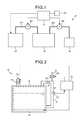
- FIG. 1is a schematic diagram illustrating a configuration of a substrate processing apparatus according to a first embodiment
- FIG. 2is a schematic diagram illustrating a configuration of a liquid supply unit of the first embodiment
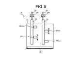
- FIG. 3is a schematic side view illustrating a configuration of the liquid supply unit of the first embodiment
- FIG. 4is a flowchart illustrating a liquid level sensor detection test according to the first embodiment
- FIG. 5is a schematic diagram illustrating a configuration of a liquid supply unit according to a second embodiment
- FIG. 6is a schematic diagram illustrating a configuration of a liquid supply unit according to a third embodiment.
- FIG. 7is a schematic diagram illustrating a configuration of a liquid supply unit according to a fourth embodiment.
- a substrate processing apparatusincludes: a tank configured to store a treatment liquid for treating a substrate; a liquid level pipe connected to the tank such that the treatment liquid stored in the tank flows therein, and configured such that the liquid level of the treatment liquid having flowed therein from the tank moves according to increase and decrease of the treatment liquid in the tank; a liquid level sensor configured to detect the liquid level in the liquid level pipe; an air supply pipe configured to supply a gas to a piping space above the liquid level in the liquid level pipe; and a controller configured to determine whether there is erroneous detection of the liquid level sensor based on a detection result obtained by the liquid level sensor in response to the movement of the liquid level in the liquid level pipe caused by the supply of the gas to the piping space from the air supply pipe.
- a substrate processing apparatusincludes: a tank configured to store a treatment liquid for treating a substrate; a liquid level pipe connected to the tank such that the treatment liquid stored in the tank flows therein, and configured such that the liquid level of the treatment liquid having flowed therein from the tank moves according to increase and decrease of the treatment liquid in the tank; a liquid level sensor configured to detect the liquid level in the liquid level pipe; an air supply pipe configured to supply a gas to a piping space above the liquid level in the liquid level pipe; an open pipe configured to discharge the gas from the piping space; and a controller configured to performs a control operation to repeatedly supply the gas to the piping space and discharge the gas from the piping space such that the liquid level repeatedly moves in the liquid level pipe.
- a substrate processing methodfor detecting the liquid level in a liquid level pipe, which is connected to a tank such that a treatment liquid stored in the tank flows therein, with a liquid level sensor.
- the substrate processing methodincludes: supplying a gas to a piping space above the liquid level in the liquid level pipe; detecting the liquid level that moves due to the supply of the gas to the piping space from the air supply pipe with the liquid level sensor; and determining whether there is erroneous detection of the liquid level sensor based on a detection result obtained by the liquid level sensor.
- a substrate processing methodfor detecting a liquid level in a liquid level pipe, which is connected to a tank such that a treatment liquid stored in the tank flows therein, with a liquid level sensor.
- the substrate processing methodincludes: repeatedly supplying a gas to a piping space above the liquid level in the liquid level pipe and discharging the gas from the piping space such that the liquid level repeatedly moves in the liquid level pipe.
- a first embodimentis described with reference to FIGS. 1 to 4 .
- a substrate processing apparatus 10 of the first embodimentincludes a substrate processing unit 20 , a liquid supply unit 30 , a liquid replenishment unit 40 , and a controller 50 .
- the treatment liquid used by the substrate processing apparatus 10include a treatment liquid containing an additive such as Si (e.g., a chemical liquid such as an etching liquid, a rinse liquid, etc.).
- the substrate processing unit 20processes a substrate by supplying the treatment liquid to its surface to be processed.
- a processing apparatussuch as a single wafer processing equipment or a batch processing equipment is used as the substrate processing unit 20 .
- the substrate processing unit 20is electrically connected to the controller 50 , and is driven under the control of the controller 50 .
- the liquid supply unit 30retains the treatment liquid and supplies the treatment liquid to the substrate processing unit 20 .
- the liquid supply unit 30is connected to the substrate processing unit 20 through a supply pipe 30 a.
- the liquid supply unit 30supplies the treatment liquid to the substrate processing unit 20 in response to the driving of a pump 30 b provided in the middle of the supply pipe 30 a.
- the pump 30 bis electrically connected to the controller 50 , and is driven under the control of the controller 50 .
- the liquid replenishment unit 40replenishes the liquid supply unit 30 with the treatment liquid according to the amount of the treatment liquid in the liquid supply unit 30 .
- the liquid replenishment unit 40is connected to the liquid supply unit 30 through a replenishment pipe 40 a.
- the liquid replenishment unitreplenishes the liquid supply unit 30 with the treatment liquid in response to the driving of a pump 40 b provided in the middle of the replenishment pipe 40 a.
- the pump 40 bis electrically connected to the controller 50 , and is driven under the control of the controller 50 .
- the controller 50includes a microcomputer for intensively controlling each unit, and a storage for storing substrate processing information and various programs related to substrate processing (both not illustrated).
- the controller 50reads the substrate processing information and the programs from the storage unit to control the operation of each unit, such as the operation of the substrate processing unit 20 for substrate processing, the operation of the liquid supply unit 30 for liquid supply, and the operation of the liquid replenishment unit 40 for liquid replenishment, based on the information and the programs.
- a notification unit 50 asuch as an alarm or a display is electrically connected to the controller 50 .
- the liquid supply unit 30includes a tank 31 , a heater 32 , a plurality of liquid level pipes 33 (two in the example of FIG. 3 ), a plurality of air supply pipes 34 (two in the example of FIG. 3 ), and a plurality of liquid level sensors 35 (four in the example of FIG. 3 ).
- the tank 31is a reservoir for storing the treatment liquid.
- An open pipe 31 ais connected to the tank 31 .
- An on-off valve 31 bsuch as an electromagnetic valve is provided in the middle of the open pipe 31 a.
- the on-off valve 31 bis electrically connected to the controller 50 , and is driven to open/close position under the control of the controller 50 .
- the heater 32is provided on the bottom surface inside the tank 31 .
- the heater 32heats the treatment liquid in the tank 31 to a temperature equal to or higher than a desired temperature, and, for example, maintains the temperature of the treatment liquid within a predetermined range according to the control of the controller 50 .
- the heater 32is electrically connected to the controller 50 , and is driven under the control of the controller 50 .
- each of the liquid level pipes 33is connected to the bottom-surface-side end of a side surface (the right side surface in the example of FIG. 2 ) of the tank 31 , and the other end is connected to the upper surface of the tank 31 . That is, each of the liquid level pipes 33 is connected to the tank 31 such that the treatment liquid stored in the tank 31 flows therein. Further, each of the liquid level pipes 33 is formed such that the liquid level M 1 (see FIG. 2 ) of the treatment liquid having flowed therein from the tank 31 moves according to an increase or decrease of the treatment liquid.
- the air supply pipes 34are each arranged with respect to each of the liquid level pipes 33 .
- Each of the air supply pipes 34is connected to the upper end of the corresponding one of the liquid level pipes 33 to supply a gas (e.g., inert gas such as N 2 , etc.) to the piping space above the liquid level M 1 in the liquid level pipe 33 .
- An on-off valve 34 asuch as an electromagnetic valve or the like is provided in the middle of each of the air supply pipes 34 .
- the on-off valve 34 ais electrically connected to the controller 50 , and is driven to open/close position under the control of the controller 50 .
- the flow rate and pressure of the gasare set such that the liquid level M 1 in the liquid level pipes 33 moves by a predetermined distance (a distance at which all the liquid level sensors 35 are turned OFF) by the gas supplied to the piping space in the liquid level pipes 33 .
- the flow rate and pressure of the gascan be appropriately changed according to factors such as the diameter of the air supply pipes 34 and the viscosity of the treatment liquid.
- the temperature of the treatment liquid in the tank 31is not changed even when the piping space in the liquid level pipes 33 is filled (supplied) with gas.
- the piping space in each of the liquid level pipes 33is connected to the tank space above the liquid level in the tank 31 .
- An orifice member 33 a(see FIG. 2 ) having a through hole H 1 is provided inside the horizontal piping portion at the upper portion of the liquid level pipe 33 .
- the diameter of the through hole H 1is smaller than the diameter of the liquid level pipe 33 .
- the orifice member 33 arestricts the gas supplied to the piping space in the liquid level pipe 33 from flowing into the tank 31 through the horizontal piping portion at the upper portion of the liquid level pipe 33 .
- the liquid level M 1 in the liquid level pipe 33descends.
- Each of the liquid level pipes 33is provided with two of the liquid level sensors 35 .
- the liquid level sensors 35each detect the liquid level M 1 in the liquid level pipe 33 .
- the liquid level sensors 35are arranged in their respective positions to detect upper limit liquid amount (HH), replenishment start liquid amount (L), replenishment stop liquid amount (H), and lower limit liquid amount (LL).
- the liquid level sensors 35are electrically connected to the controller 50 , and a detection signal thereof is input to the controller 50 .
- Examples of the liquid level sensors 35include electrostatic capacitance sensors and the like.
- the treatment liquid(the liquid level M 1 ) is detected when the electrostatic capacity sensor is ON, while the treatment liquid is not detected when it is OFF.
- the liquid level sensor 35 for the upper limit liquid amount (HH) and the liquid level sensor 35 for the lower limit liquid amount (LL)are fixed, the liquid level sensor 35 for the replenishment start liquid amount (L) and the liquid level sensor 35 for the replenishment stop liquid amount (H) are formed to be movable in the height direction. Thereby, the user can adjust the replenishment start liquid amount and the replenishment stop liquid amount by changing the height positions of the liquid level sensors 35 for the replenishment start liquid amount and the replenishment stop liquid amount as necessary.
- FIG. 3illustrates two liquid level pipes ( 33 ) each provided with two liquid level sensors ( 35 ), it is not limited thereto. There may be only one liquid level pipe 33 . However, if four liquid level sensors ( 35 ) are provided for one liquid level pipe ( 33 ), the intervals between the liquid level sensors 35 may be narrow in some cases. In other words, the interval between the upper limit liquid amount (HH) and the replenishment stop liquid amount (H), the interval between the replenishment start liquid amount (L) and the lower limit liquid amount (LL) becomes narrower, and the liquid level sensors 35 may interfere with one another at their detection positions. Therefore, in order to prevent the liquid level sensors 35 from interfering with one another, preferably, not one but a plurality of liquid level pipes ( 33 ) are used.
- the controller 50grasps the amount of the treatment liquid in the tank 31 based on the detection result obtained by each of the liquid level sensors 35 . For example, when the controller 50 determines that the liquid amount is equal to or more than the upper limit liquid amount (HH) based on the detection result obtained by each of the liquid level sensors 35 , the controller 50 notifies the user of this through the notification unit 50 a by issuing a warning. On the other hand, having determined that the liquid amount is equal to or less than the replenishment start liquid amount (L), the controller 50 drives the pump 40 b of the liquid replenishment unit 40 to supply the treatment liquid from the liquid replenishment unit 40 to the liquid supply unit 30 through the replenishment pipe 40 a.
- the controller 50drives the pump 40 b of the liquid replenishment unit 40 to supply the treatment liquid from the liquid replenishment unit 40 to the liquid supply unit 30 through the replenishment pipe 40 a.
- the controller 50stops the pump 40 b of the liquid replenishment unit 40 to stop the replenishment of the treatment liquid from the liquid replenishment unit 40 to the liquid supply unit 30 . Having determined that the liquid amount is equal to or less than the lower limit liquid amount (LL), the controller 50 notifies the user of this through the notification unit 50 a by issuing a warning, and stops the supply of the liquid to the substrate processing unit 20 and the heating by the heater 32 . After that, having determined that the liquid amount is equal to or more than the replenishment start liquid amount (L), the controller 50 restarts the heating by the heater 32 . Having determined that the liquid amount is equal to or more than the replenishment start liquid amount (L) and that the temperature of the treatment liquid becomes within a temperature range set in advance, the controller 50 restarts the supply of the liquid to the substrate processing unit 20 .
- the controller 50opens the on-off valve 34 a of each of the air supply pipes 34 to supply a gas to the piping space in each of the liquid level pipes 33 , and moves the liquid level M 1 in the liquid level pipe 33 .
- the controller 50determines whether there is erroneous detection of the liquid level sensors 35 based on the detection results obtained by the liquid level sensors 35 for each of the sensors 35 . That is, according to the movement of the liquid level M 1 in the liquid level pipe 33 , the controller 50 determines whether the liquid level sensor 35 performs the detection normally.
- the controller 50determines whether the liquid level sensor 35 is OFF (when the liquid level is not detected). When it is determined that the liquid level sensor 35 is not turned OFF, the controller 50 determines that the liquid level sensor 35 has made an erroneous detection. Further, in a state where the above-mentioned gas supply is stopped and the liquid level M 1 in the liquid level pipe 33 has risen to a position above the position of the upper limit liquid amount (HH), the controller 50 determines whether the liquid level sensor 35 is ON (when the liquid level is detected). When it is determined that the liquid level sensor 35 is not turned ON, the controller 50 determines that the liquid level sensor 35 has made an erroneous detection.
- the liquid level sensor detection testIn the liquid level sensor detection test, a warning (alarm) by the notification unit 50 a for the upper limit liquid amount (HH) and the lower limit liquid amount (LL), and a test mode in which the operation of the apparatus is not stopped are set. Besides, while the test mode is being set, the supply of the treatment liquid from the liquid supply unit 30 to the substrate processing unit 20 is stopped. In the tank 31 of the liquid supply unit 30 , the on-off valve 31 b of the open pipe 31 a is opened to the atmosphere.
- the liquid level sensor detection testis basically conducted every predetermined period except during the substrate processing, or it is executed during a standby period. However, the liquid level sensor detection test may be performed during the substrate processing as long as it does not adversely affect the substrate processing.
- step S 1the pump 40 b of the replenishment pipe 40 a is driven, and the tank 31 of the liquid supply unit 30 is replenished with the treatment liquid from the liquid replenishment unit 40 through the replenishment pipe 40 a.
- the replenishing operationis continued until the liquid level M 1 in each of the liquid level pipes 33 reaches the position of the upper limit liquid amount (HH) (see FIG. 3 ).
- the liquid level M 1 in the liquid level pipe 33reaches the position of the upper limit liquid amount (HH)
- the replenishment of the treatment liquidis stopped.
- preparationis completed for the detection test of all the liquid level sensors 35 .
- the treatment liquidis not replenished by a predetermined supply amount, but is kept being supplied until the liquid level M 1 reaches the upper limit liquid amount (HH).
- the tank 31is prefilled with a predetermined amount of treatment liquid.
- the treatment liquidis supplied to the tank 31 by a predetermined amount for a predetermined time at a constant flow rate such that the liquid surface M 1 is at the position of the upper limit liquid amount (HH).
- step S 2the on-off valves 34 a of the air supply pipes 34 are opened, and gas is supplied to the piping space in each of the liquid level pipes 33 .
- the piping space in each of the liquid level pipes 33are filled with a predetermined amount of gas, and the liquid level M 1 in the liquid level pipe 33 moves to a position below the position of the lower limit liquid amount (LL).
- the gas flow rate and pressure at this timeare set in advance such that the liquid surface M 1 in the liquid level pipe 33 moves to a position below the position of the lower limit liquid amount (LL) by the gas supplied to the piping space in the liquid level pipe 33 .
- step S 3it is determined whether all the liquid level sensors 35 are OFF in a state where the liquid surface M 1 in each of the liquid level pipes 33 is below the position of the lower limit liquid amount (LL).
- step S 4the on-off valves 34 a of the air supply pipes 34 are closed, and the supply of gas to the piping space in each of the liquid level pipes 33 is stopped. Accordingly, the gas in the piping space in each of the liquid level pipes 33 is gradually discharged into the tank through the horizontal piping portion at the upper portion of each of the liquid level pipes 33 , i.e., the through hole H 1 of the orifice member 33 a.
- the liquid level M 1 in each of the liquid level pipes 33moves slowly to the original position of the upper limit liquid amount (HH) (the rising speed is lower than the falling speed).
- step S 5after a predetermined time has elapsed from the stop of gas supply, i.e., in a state where the liquid surface M 1 in each of the liquid level pipes 33 is at or above the position of the upper limit liquid amount (HH), it is determined whether each of the liquid level sensors 35 is ON. If it is determined that all the liquid level sensors 35 are ON (YES), in step S 6 , it is determined that there is no erroneous detection of the liquid level sensors 35 .
- step S 7it is determined in step S 7 whether the number of determinations on erroneous detection of the liquid level sensor 35 (retry count) is a predetermined number (e.g., three times).
- step S 7If it is determined that the number of determinations on liquid return is not the predetermined number (e.g., three times) in step S 7 (NO), the process returns to step S 2 , and the steps from step S 2 are repeated.
- the predetermined numbere.g., three times
- step S 8when it is determined that the number of determinations on liquid return is the predetermined number (e.g., three times) in step S 7 (YES), it is determined in step S 8 that there is erroneous detection of the liquid level sensors 35 .
- the notification unit 50 ainforms the user of that there is erroneous detection of the liquid level sensors 35 .
- the controller 50can specify the liquid level sensor 35 that has made the erroneous detection, and notifies the user of the liquid level sensor 35 , in which the erroneous detection has occurred, by the notification unit 50 a.
- liquid level sensor detection testgas is supplied to the piping space in each of the liquid level pipes 33 , and the liquid level M 1 in the liquid level pipe 33 moves. Accordingly, it is determined whether there is erroneous detection with respect to each of the liquid level sensors 35 based on the detection result obtained by the liquid level sensor 35 . For example, in a state where the liquid level M 1 in the liquid level pipe 33 has been lowered to a position below the position of the lower limit liquid amount (LL), it is determined whether the liquid level sensor 35 is OFF. When it is determined that the liquid level sensor 35 is not turned OFF, it is determined that the liquid level sensor 35 has made an erroneous detection.
- LLlower limit liquid amount
- gasis supplied from the air supply pipes 34 to the piping space in the liquid level pipes 33 , and in response to the movement of the liquid level M 1 in the liquid level pipes 33 , it is possible to know whether there is erroneous detection of the liquid level sensors 35 by determining whether there is erroneous detection of the liquid level sensors 35 based on detection results obtained by the liquid level sensors 35 .
- the amount of liquid in the tankis determined based on a detection result obtained by the liquid level sensor 35 without erroneous detection. Therefore, it is possible to accurately figure out the desired liquid amount in the tank 31 that stores the treatment liquid.
- a second embodimentis described with reference to FIG. 5 .
- the second embodimentis basically similar to the first embodiment except the structure of the liquid level pipes. In the following, the difference is described, and the same explanation is not repeated.
- one end of the liquid level pipe 33is connected to the bottom-surface-side end of a side surface (the right side surface in the example of FIG. 5 ) of the tank 31 as in the first embodiment.
- the other endis not connected to the upper surface of the tank 31 (the space inside the tank 31 ), but is connected to the air supply pipe 34 .
- an open pipe 33 bis connected to the upper end of the liquid level pipe 33 .
- One end of the open pipe 33 bis connected to a position above the upper limit liquid amount (HH) in the liquid level pipe 33 , and the other end of the open pipe 33 b is open to the atmosphere.
- An on-off valve 33 csuch as, for example, an electromagnetic valve is provided in the middle of the open pipe 33 b.
- the on-off valve 33 cis electrically connected to the controller 50 , and is driven to open/close position under the control of the controller 50 .
- the on-off valve 33 cis closed when gas is supplied from the air supply pipe 34 , and is open after the gas supply is stopped.
- the liquid level M 1 in the liquid level pipe 33moves.
- the gas supplied into the liquid level pipe 33is not exhausted to the tank 31 side but acts on the liquid level M 1 in the liquid level pipe 33 . Therefore, if the flow rate and pressure of the gas are the same as in the first embodiment, the movement speed of the liquid level M 1 in the liquid level pipe 33 is faster than in the first embodiment. This results in a shorter waiting time for the movement of the liquid level M 1 in the liquid level pipe 33 in the liquid level sensor detection test. Thus, the liquid level sensor detection test requires less time.
- the second embodimentcan achieve the same effects as those of the first embodiment. Further, since one end of the liquid level pipe 33 is not connected to the space inside the tank 31 and the open pipe 33 b is connected to the liquid level pipe 33 , the gas supplied to the piping space in the liquid level pipe 33 is not exhausted to the tank 31 but acts on the liquid level M 1 in the liquid level pipe 33 . Thus, the liquid level sensor detection test requires less time.
- a third embodimentis described with reference to FIG. 6 .
- the third embodimentis basically similar to the first embodiment except the presence of a heating unit. In the following, the difference is described, and the same explanation is not repeated.
- the liquid supply unit 30 of the third embodimentincludes a heating unit 36 such as a heater.
- the heating unit 36is located on the outer periphery of the liquid level pipe 33 , and heats the treatment liquid in the liquid level pipe 33 to maintain its temperature within a predetermined range. This makes it possible to suppress the temperature decrease of the treatment liquid in the liquid level pipe 33 . Thus, precipitation of the additive can be suppressed.
- the heating unit 36is electrically connected to the controller 50 , and is driven under the control of the controller 50 .
- the controller 50increases the heating temperature of the heating unit 36 for heating the treatment liquid as compared to a case where it is determined that there is no erroneous detection of the liquid level sensor 35 .
- the treatment liquid in the liquid level pipe 33is heated with a higher temperature, which dissolves precipitates adhering to the inner surface of the liquid level pipe 33 in the treatment liquid and removes it.
- the third embodimentcan achieve the same effects as those of the first embodiment. Further, by heating the treatment liquid in the liquid level pipe 33 with the heating unit 36 provided in the liquid level pipe 33 , the temperature of the treatment liquid can be maintained within a predetermined range. This prevents the additive contained in the treatment liquid from depositing and adhering to the inner surface of the liquid level pipe 33 . Besides, when it is determined that there is erroneous detection of the liquid level sensor 35 , the heating temperature of the heating unit 36 for the treatment liquid is increased as compared to a case where it is determined that there is no erroneous detection of the liquid level sensor 35 . Thereby, the treatment liquid in the liquid level pipe 33 is heated with a higher temperature, which dissolves precipitates adhering to the inner surface of the liquid level pipe 33 in the treatment liquid and removes it.
- the heating unit 36is provided by way of example but not limitation.
- a vibrating unit(see reference numeral 36 in FIG. 6 ) may be provided in place of the heating unit 36 to vibrate the treatment liquid in the liquid level pipe 33 , or both of them can be provided.
- the controller 50vibrates the treatment liquid with the vibrating unit only when having determined that there is erroneous detection of the liquid level sensor 35 .
- the controller 50may constantly vibrate the treatment liquid with the vibrating unit to suppress precipitates from adhering to the inner surface of the liquid level pipe 33 .
- the controller 50may increase the frequency of the vibrating unit for vibrating the treatment liquid as compared to a case where it is determined that there is no erroneous detection of the liquid level sensor 35 . In this case, by vibrating the treatment liquid in the liquid level pipe 33 at a higher frequency, it is possible to reliably remove precipitates adhering to the inner surface of the liquid level pipe 33 .
- a fourth embodimentis described with reference to FIG. 7 .
- the fourth embodimentis basically similar to the first embodiment except the presence of a circulating unit. In the following, the difference is described, and the same explanation is not repeated.
- the liquid supply unit 30 of the fourth embodimentis provided with a circulating unit 37 that enables pumping.
- the circulating unit 37is, for example, a pump or the like, and is connected to the interior of the tank 31 .
- the circulating unit 37is electrically connected to the controller 50 , and is driven under the control of the controller 50 .
- the circulating unit 37pushes the treatment liquid in the sealed tank 31 to return the treatment liquid in the liquid level pipe 33 to the tank 31 for circulation.
- the treatment liquid in the tank 31flows into the liquid level pipe 33 from an opening on the lower side of the liquid level pipe 33 .
- the treatment liquidflows in a direction rising in the liquid level pipe 33 , and flows back into the tank 31 from an opening on the upper side of the liquid level pipe 33 . As a result, a flow of the treatment liquid is generated in the liquid level pipe 33 .
- Such a circulation operationis periodically performed. With this, the treatment liquid circulates regularly through the liquid level pipe 33 , and the treatment liquid in the liquid level pipe 33 moves. The flow of the treatment liquid prevents precipitates from adhering to the inner surface of the liquid level pipe 33 . Further, since the treatment liquid heated in the tank 31 flows into the liquid level pipe 33 , it is also possible to heat the interior of the liquid level pipe 33 . Thus, the precipitates in the liquid level pipe 33 can be dissolved in the treatment liquid and removed. In addition, it is also possible to prevent the additive contained in the treatment liquid in the liquid level pipe 33 from depositing and adhering to the inner surface of the liquid level pipe 33 .
- the controller 50increases the pushing force of the circulating unit 37 on the treatment liquid to increase the flow rate of the treatment liquid to be circulated as compared to when having determined that there is no erroneous detection of the liquid level sensor 35 .
- the treatment liquid in the liquid level pipe 33circulates at a higher flow rate.
- the fourth embodimentcan achieve the same effects as those of the first embodiment. Further, with the circulating unit 37 provided in the tank 31 , the treatment liquid in the liquid level pipe 33 can be flowed back into the tank 31 for circulation. This prevents the additive contained in the treatment liquid in the liquid level pipe 33 from depositing and adhering to the inner surface of the liquid level pipe 33 . Further, when it is determined that there is erroneous detection of the liquid level sensor 35 , the flow rate of the treatment liquid is increased by the circulating unit 37 as compared to a case where it is determined that there is no erroneous detection of the liquid level sensor 35 . Thereby, the treatment is circulated at a higher flow rate. Thus, it is possible to remove precipitates adhering to the inner surface of the liquid level pipe 33 .
- a plurality of the liquid level sensors 35are provided by way of example but not limitation.
- the number of sensorsis not particularly limited.
- all the liquid level sensors 35are not necessarily subjected to the detection test. The detection test may be conducted for only the liquid level sensor 35 , which is likely to make erroneous detection. In this case, the liquid replenishment in step S 1 in FIG. 4 is not always required. If the liquid level sensor 35 to be subjected to the detection test is in the ON state, the liquid replenishment in step S 1 can be omitted.
- the liquid level sensor 35it is determined whether there is erroneous detection of the liquid level sensor 35 based on ON/OFF of the liquid level sensor 35 according to the supply of gas to the piping space of the liquid level pipe 33 .
- thisis by way of example and not limitation.
- the liquid return timevaries depending on the amount of precipitates adhering to the inner surface of the liquid level pipe 33 , and becomes longer as, for example, the amount of the precipitates increases.
- the amount of the precipitatesis equal to or less than the predetermined amount (the amount of precipitates in which erroneous detection of the liquid level sensor 35 does not occur), and it is determined that there is no erroneous detection of the liquid level sensor 35 .
- the liquid return timeis not within the predetermined time, it is determined that the amount of the precipitates is larger than the predetermined amount, and there is erroneous detection of the liquid level sensor 35 .
- the correlation between the liquid return time and the amount of precipitateshas been obtained in advance by experiments or the like, and the predetermined time is set based on the correlation.
Landscapes
- Engineering & Computer Science (AREA)
- Physics & Mathematics (AREA)
- General Physics & Mathematics (AREA)
- Condensed Matter Physics & Semiconductors (AREA)
- Manufacturing & Machinery (AREA)
- Computer Hardware Design (AREA)
- Microelectronics & Electronic Packaging (AREA)
- Power Engineering (AREA)
- Chemical & Material Sciences (AREA)
- Chemical Kinetics & Catalysis (AREA)
- General Chemical & Material Sciences (AREA)
- Nonlinear Science (AREA)
- Cleaning Or Drying Semiconductors (AREA)
- Mathematical Physics (AREA)
- Crystallography & Structural Chemistry (AREA)
- Optics & Photonics (AREA)
Abstract
Description
Claims (7)
Applications Claiming Priority (4)
| Application Number | Priority Date | Filing Date | Title |
|---|---|---|---|
| JP2016069323 | 2016-03-30 | ||
| JP2016-069323 | 2016-03-30 | ||
| JP2017-012627 | 2017-01-27 | ||
| JP2017012627AJP6861039B2 (en) | 2016-03-30 | 2017-01-27 | Substrate processing equipment and substrate processing method |
Publications (2)
| Publication Number | Publication Date |
|---|---|
| US20170287744A1 US20170287744A1 (en) | 2017-10-05 |
| US10573540B2true US10573540B2 (en) | 2020-02-25 |
Family
ID=59959871
Family Applications (1)
| Application Number | Title | Priority Date | Filing Date |
|---|---|---|---|
| US15/468,577ActiveUS10573540B2 (en) | 2016-03-30 | 2017-03-24 | Substrate processing apparatus and substrate processing method |
Country Status (1)
| Country | Link |
|---|---|
| US (1) | US10573540B2 (en) |
Families Citing this family (277)
| Publication number | Priority date | Publication date | Assignee | Title |
|---|---|---|---|---|
| US20130023129A1 (en) | 2011-07-20 | 2013-01-24 | Asm America, Inc. | Pressure transmitter for a semiconductor processing environment |
| US10714315B2 (en) | 2012-10-12 | 2020-07-14 | Asm Ip Holdings B.V. | Semiconductor reaction chamber showerhead |
| US20160376700A1 (en) | 2013-02-01 | 2016-12-29 | Asm Ip Holding B.V. | System for treatment of deposition reactor |
| US11015245B2 (en) | 2014-03-19 | 2021-05-25 | Asm Ip Holding B.V. | Gas-phase reactor and system having exhaust plenum and components thereof |
| US10941490B2 (en) | 2014-10-07 | 2021-03-09 | Asm Ip Holding B.V. | Multiple temperature range susceptor, assembly, reactor and system including the susceptor, and methods of using the same |
| US10276355B2 (en) | 2015-03-12 | 2019-04-30 | Asm Ip Holding B.V. | Multi-zone reactor, system including the reactor, and method of using the same |
| JP6326387B2 (en)* | 2015-03-19 | 2018-05-16 | 東京エレクトロン株式会社 | Substrate liquid processing apparatus, substrate liquid processing method, and computer readable storage medium storing substrate liquid processing program |
| US10458018B2 (en) | 2015-06-26 | 2019-10-29 | Asm Ip Holding B.V. | Structures including metal carbide material, devices including the structures, and methods of forming same |
| US10211308B2 (en) | 2015-10-21 | 2019-02-19 | Asm Ip Holding B.V. | NbMC layers |
| US11139308B2 (en) | 2015-12-29 | 2021-10-05 | Asm Ip Holding B.V. | Atomic layer deposition of III-V compounds to form V-NAND devices |
| US10529554B2 (en) | 2016-02-19 | 2020-01-07 | Asm Ip Holding B.V. | Method for forming silicon nitride film selectively on sidewalls or flat surfaces of trenches |
| US10343920B2 (en) | 2016-03-18 | 2019-07-09 | Asm Ip Holding B.V. | Aligned carbon nanotubes |
| US10367080B2 (en) | 2016-05-02 | 2019-07-30 | Asm Ip Holding B.V. | Method of forming a germanium oxynitride film |
| US11453943B2 (en) | 2016-05-25 | 2022-09-27 | Asm Ip Holding B.V. | Method for forming carbon-containing silicon/metal oxide or nitride film by ALD using silicon precursor and hydrocarbon precursor |
| US9859151B1 (en) | 2016-07-08 | 2018-01-02 | Asm Ip Holding B.V. | Selective film deposition method to form air gaps |
| US10612137B2 (en) | 2016-07-08 | 2020-04-07 | Asm Ip Holdings B.V. | Organic reactants for atomic layer deposition |
| KR102532607B1 (en) | 2016-07-28 | 2023-05-15 | 에이에스엠 아이피 홀딩 비.브이. | Substrate processing apparatus and method of operating the same |
| US9887082B1 (en) | 2016-07-28 | 2018-02-06 | Asm Ip Holding B.V. | Method and apparatus for filling a gap |
| US9812320B1 (en) | 2016-07-28 | 2017-11-07 | Asm Ip Holding B.V. | Method and apparatus for filling a gap |
| US11532757B2 (en) | 2016-10-27 | 2022-12-20 | Asm Ip Holding B.V. | Deposition of charge trapping layers |
| US10714350B2 (en) | 2016-11-01 | 2020-07-14 | ASM IP Holdings, B.V. | Methods for forming a transition metal niobium nitride film on a substrate by atomic layer deposition and related semiconductor device structures |
| KR102546317B1 (en) | 2016-11-15 | 2023-06-21 | 에이에스엠 아이피 홀딩 비.브이. | Gas supply unit and substrate processing apparatus including the same |
| KR102762543B1 (en) | 2016-12-14 | 2025-02-05 | 에이에스엠 아이피 홀딩 비.브이. | Substrate processing apparatus |
| US11447861B2 (en) | 2016-12-15 | 2022-09-20 | Asm Ip Holding B.V. | Sequential infiltration synthesis apparatus and a method of forming a patterned structure |
| US11581186B2 (en) | 2016-12-15 | 2023-02-14 | Asm Ip Holding B.V. | Sequential infiltration synthesis apparatus |
| KR102700194B1 (en) | 2016-12-19 | 2024-08-28 | 에이에스엠 아이피 홀딩 비.브이. | Substrate processing apparatus |
| US10269558B2 (en) | 2016-12-22 | 2019-04-23 | Asm Ip Holding B.V. | Method of forming a structure on a substrate |
| US11390950B2 (en) | 2017-01-10 | 2022-07-19 | Asm Ip Holding B.V. | Reactor system and method to reduce residue buildup during a film deposition process |
| US10468261B2 (en) | 2017-02-15 | 2019-11-05 | Asm Ip Holding B.V. | Methods for forming a metallic film on a substrate by cyclical deposition and related semiconductor device structures |
| US10529563B2 (en) | 2017-03-29 | 2020-01-07 | Asm Ip Holdings B.V. | Method for forming doped metal oxide films on a substrate by cyclical deposition and related semiconductor device structures |
| US10770286B2 (en) | 2017-05-08 | 2020-09-08 | Asm Ip Holdings B.V. | Methods for selectively forming a silicon nitride film on a substrate and related semiconductor device structures |
| US12040200B2 (en) | 2017-06-20 | 2024-07-16 | Asm Ip Holding B.V. | Semiconductor processing apparatus and methods for calibrating a semiconductor processing apparatus |
| US11306395B2 (en) | 2017-06-28 | 2022-04-19 | Asm Ip Holding B.V. | Methods for depositing a transition metal nitride film on a substrate by atomic layer deposition and related deposition apparatus |
| KR20190009245A (en) | 2017-07-18 | 2019-01-28 | 에이에스엠 아이피 홀딩 비.브이. | Methods for forming a semiconductor device structure and related semiconductor device structures |
| US11018002B2 (en) | 2017-07-19 | 2021-05-25 | Asm Ip Holding B.V. | Method for selectively depositing a Group IV semiconductor and related semiconductor device structures |
| US10541333B2 (en)* | 2017-07-19 | 2020-01-21 | Asm Ip Holding B.V. | Method for depositing a group IV semiconductor and related semiconductor device structures |
| US11374112B2 (en) | 2017-07-19 | 2022-06-28 | Asm Ip Holding B.V. | Method for depositing a group IV semiconductor and related semiconductor device structures |
| US10590535B2 (en) | 2017-07-26 | 2020-03-17 | Asm Ip Holdings B.V. | Chemical treatment, deposition and/or infiltration apparatus and method for using the same |
| TWI815813B (en) | 2017-08-04 | 2023-09-21 | 荷蘭商Asm智慧財產控股公司 | Showerhead assembly for distributing a gas within a reaction chamber |
| US10770336B2 (en) | 2017-08-08 | 2020-09-08 | Asm Ip Holding B.V. | Substrate lift mechanism and reactor including same |
| US10692741B2 (en) | 2017-08-08 | 2020-06-23 | Asm Ip Holdings B.V. | Radiation shield |
| US11139191B2 (en) | 2017-08-09 | 2021-10-05 | Asm Ip Holding B.V. | Storage apparatus for storing cassettes for substrates and processing apparatus equipped therewith |
| US11769682B2 (en) | 2017-08-09 | 2023-09-26 | Asm Ip Holding B.V. | Storage apparatus for storing cassettes for substrates and processing apparatus equipped therewith |
| US11830730B2 (en) | 2017-08-29 | 2023-11-28 | Asm Ip Holding B.V. | Layer forming method and apparatus |
| US11295980B2 (en) | 2017-08-30 | 2022-04-05 | Asm Ip Holding B.V. | Methods for depositing a molybdenum metal film over a dielectric surface of a substrate by a cyclical deposition process and related semiconductor device structures |
| US11056344B2 (en) | 2017-08-30 | 2021-07-06 | Asm Ip Holding B.V. | Layer forming method |
| KR102491945B1 (en) | 2017-08-30 | 2023-01-26 | 에이에스엠 아이피 홀딩 비.브이. | Substrate processing apparatus |
| US11594430B2 (en)* | 2017-09-11 | 2023-02-28 | Tokyo Electron Limited | Substrate liquid processing apparatus, substrate liquid processing method and recording medium |
| US10658205B2 (en) | 2017-09-28 | 2020-05-19 | Asm Ip Holdings B.V. | Chemical dispensing apparatus and methods for dispensing a chemical to a reaction chamber |
| US10403504B2 (en) | 2017-10-05 | 2019-09-03 | Asm Ip Holding B.V. | Method for selectively depositing a metallic film on a substrate |
| US10490430B2 (en)* | 2017-10-30 | 2019-11-26 | Taiwan Semiconductor Manufacturing Co., Ltd. | Flexible linear sensor |
| US10923344B2 (en) | 2017-10-30 | 2021-02-16 | Asm Ip Holding B.V. | Methods for forming a semiconductor structure and related semiconductor structures |
| US11022879B2 (en) | 2017-11-24 | 2021-06-01 | Asm Ip Holding B.V. | Method of forming an enhanced unexposed photoresist layer |
| WO2019103613A1 (en) | 2017-11-27 | 2019-05-31 | Asm Ip Holding B.V. | A storage device for storing wafer cassettes for use with a batch furnace |
| CN111344522B (en) | 2017-11-27 | 2022-04-12 | 阿斯莫Ip控股公司 | Including clean mini-environment device |
| US10872771B2 (en) | 2018-01-16 | 2020-12-22 | Asm Ip Holding B. V. | Method for depositing a material film on a substrate within a reaction chamber by a cyclical deposition process and related device structures |
| TWI799494B (en) | 2018-01-19 | 2023-04-21 | 荷蘭商Asm 智慧財產控股公司 | Deposition method |
| KR102695659B1 (en) | 2018-01-19 | 2024-08-14 | 에이에스엠 아이피 홀딩 비.브이. | Method for depositing a gap filling layer by plasma assisted deposition |
| US11081345B2 (en) | 2018-02-06 | 2021-08-03 | Asm Ip Holding B.V. | Method of post-deposition treatment for silicon oxide film |
| US10896820B2 (en) | 2018-02-14 | 2021-01-19 | Asm Ip Holding B.V. | Method for depositing a ruthenium-containing film on a substrate by a cyclical deposition process |
| WO2019158960A1 (en) | 2018-02-14 | 2019-08-22 | Asm Ip Holding B.V. | A method for depositing a ruthenium-containing film on a substrate by a cyclical deposition process |
| US10731249B2 (en) | 2018-02-15 | 2020-08-04 | Asm Ip Holding B.V. | Method of forming a transition metal containing film on a substrate by a cyclical deposition process, a method for supplying a transition metal halide compound to a reaction chamber, and related vapor deposition apparatus |
| KR102636427B1 (en) | 2018-02-20 | 2024-02-13 | 에이에스엠 아이피 홀딩 비.브이. | Substrate processing method and apparatus |
| US10975470B2 (en) | 2018-02-23 | 2021-04-13 | Asm Ip Holding B.V. | Apparatus for detecting or monitoring for a chemical precursor in a high temperature environment |
| US11473195B2 (en) | 2018-03-01 | 2022-10-18 | Asm Ip Holding B.V. | Semiconductor processing apparatus and a method for processing a substrate |
| US11629406B2 (en) | 2018-03-09 | 2023-04-18 | Asm Ip Holding B.V. | Semiconductor processing apparatus comprising one or more pyrometers for measuring a temperature of a substrate during transfer of the substrate |
| US11114283B2 (en) | 2018-03-16 | 2021-09-07 | Asm Ip Holding B.V. | Reactor, system including the reactor, and methods of manufacturing and using same |
| KR102646467B1 (en) | 2018-03-27 | 2024-03-11 | 에이에스엠 아이피 홀딩 비.브이. | Method of forming an electrode on a substrate and a semiconductor device structure including an electrode |
| US11230766B2 (en) | 2018-03-29 | 2022-01-25 | Asm Ip Holding B.V. | Substrate processing apparatus and method |
| US11088002B2 (en) | 2018-03-29 | 2021-08-10 | Asm Ip Holding B.V. | Substrate rack and a substrate processing system and method |
| KR102600229B1 (en) | 2018-04-09 | 2023-11-10 | 에이에스엠 아이피 홀딩 비.브이. | Substrate supporting device, substrate processing apparatus including the same and substrate processing method |
| US12025484B2 (en) | 2018-05-08 | 2024-07-02 | Asm Ip Holding B.V. | Thin film forming method |
| TWI811348B (en) | 2018-05-08 | 2023-08-11 | 荷蘭商Asm 智慧財產控股公司 | Methods for depositing an oxide film on a substrate by a cyclical deposition process and related device structures |
| US12272527B2 (en) | 2018-05-09 | 2025-04-08 | Asm Ip Holding B.V. | Apparatus for use with hydrogen radicals and method of using same |
| KR102596988B1 (en) | 2018-05-28 | 2023-10-31 | 에이에스엠 아이피 홀딩 비.브이. | Method of processing a substrate and a device manufactured by the same |
| US11718913B2 (en) | 2018-06-04 | 2023-08-08 | Asm Ip Holding B.V. | Gas distribution system and reactor system including same |
| TWI840362B (en) | 2018-06-04 | 2024-05-01 | 荷蘭商Asm Ip私人控股有限公司 | Wafer handling chamber with moisture reduction |
| US11286562B2 (en) | 2018-06-08 | 2022-03-29 | Asm Ip Holding B.V. | Gas-phase chemical reactor and method of using same |
| KR102568797B1 (en) | 2018-06-21 | 2023-08-21 | 에이에스엠 아이피 홀딩 비.브이. | Substrate processing system |
| US10797133B2 (en) | 2018-06-21 | 2020-10-06 | Asm Ip Holding B.V. | Method for depositing a phosphorus doped silicon arsenide film and related semiconductor device structures |
| KR102854019B1 (en) | 2018-06-27 | 2025-09-02 | 에이에스엠 아이피 홀딩 비.브이. | Periodic deposition method for forming a metal-containing material and films and structures comprising the metal-containing material |
| TWI873894B (en) | 2018-06-27 | 2025-02-21 | 荷蘭商Asm Ip私人控股有限公司 | Cyclic deposition methods for forming metal-containing material and films and structures including the metal-containing material |
| US10612136B2 (en) | 2018-06-29 | 2020-04-07 | ASM IP Holding, B.V. | Temperature-controlled flange and reactor system including same |
| US10755922B2 (en) | 2018-07-03 | 2020-08-25 | Asm Ip Holding B.V. | Method for depositing silicon-free carbon-containing film as gap-fill layer by pulse plasma-assisted deposition |
| US10388513B1 (en) | 2018-07-03 | 2019-08-20 | Asm Ip Holding B.V. | Method for depositing silicon-free carbon-containing film as gap-fill layer by pulse plasma-assisted deposition |
| US11053591B2 (en) | 2018-08-06 | 2021-07-06 | Asm Ip Holding B.V. | Multi-port gas injection system and reactor system including same |
| US11430674B2 (en)* | 2018-08-22 | 2022-08-30 | Asm Ip Holding B.V. | Sensor array, apparatus for dispensing a vapor phase reactant to a reaction chamber and related methods |
| US11024523B2 (en) | 2018-09-11 | 2021-06-01 | Asm Ip Holding B.V. | Substrate processing apparatus and method |
| KR102707956B1 (en) | 2018-09-11 | 2024-09-19 | 에이에스엠 아이피 홀딩 비.브이. | Method for deposition of a thin film |
| US11049751B2 (en) | 2018-09-14 | 2021-06-29 | Asm Ip Holding B.V. | Cassette supply system to store and handle cassettes and processing apparatus equipped therewith |
| CN110970344B (en) | 2018-10-01 | 2024-10-25 | Asmip控股有限公司 | Substrate holding apparatus, system comprising the same and method of using the same |
| US11232963B2 (en) | 2018-10-03 | 2022-01-25 | Asm Ip Holding B.V. | Substrate processing apparatus and method |
| KR102592699B1 (en) | 2018-10-08 | 2023-10-23 | 에이에스엠 아이피 홀딩 비.브이. | Substrate support unit and apparatuses for depositing thin film and processing the substrate including the same |
| KR102546322B1 (en) | 2018-10-19 | 2023-06-21 | 에이에스엠 아이피 홀딩 비.브이. | Substrate processing apparatus and substrate processing method |
| KR102605121B1 (en) | 2018-10-19 | 2023-11-23 | 에이에스엠 아이피 홀딩 비.브이. | Substrate processing apparatus and substrate processing method |
| USD948463S1 (en) | 2018-10-24 | 2022-04-12 | Asm Ip Holding B.V. | Susceptor for semiconductor substrate supporting apparatus |
| US12378665B2 (en) | 2018-10-26 | 2025-08-05 | Asm Ip Holding B.V. | High temperature coatings for a preclean and etch apparatus and related methods |
| US11087997B2 (en) | 2018-10-31 | 2021-08-10 | Asm Ip Holding B.V. | Substrate processing apparatus for processing substrates |
| KR102748291B1 (en) | 2018-11-02 | 2024-12-31 | 에이에스엠 아이피 홀딩 비.브이. | Substrate support unit and substrate processing apparatus including the same |
| US11572620B2 (en) | 2018-11-06 | 2023-02-07 | Asm Ip Holding B.V. | Methods for selectively depositing an amorphous silicon film on a substrate |
| US11031242B2 (en) | 2018-11-07 | 2021-06-08 | Asm Ip Holding B.V. | Methods for depositing a boron doped silicon germanium film |
| US10847366B2 (en) | 2018-11-16 | 2020-11-24 | Asm Ip Holding B.V. | Methods for depositing a transition metal chalcogenide film on a substrate by a cyclical deposition process |
| US10818758B2 (en) | 2018-11-16 | 2020-10-27 | Asm Ip Holding B.V. | Methods for forming a metal silicate film on a substrate in a reaction chamber and related semiconductor device structures |
| US12040199B2 (en) | 2018-11-28 | 2024-07-16 | Asm Ip Holding B.V. | Substrate processing apparatus for processing substrates |
| US11217444B2 (en) | 2018-11-30 | 2022-01-04 | Asm Ip Holding B.V. | Method for forming an ultraviolet radiation responsive metal oxide-containing film |
| KR102636428B1 (en) | 2018-12-04 | 2024-02-13 | 에이에스엠 아이피 홀딩 비.브이. | A method for cleaning a substrate processing apparatus |
| US11158513B2 (en) | 2018-12-13 | 2021-10-26 | Asm Ip Holding B.V. | Methods for forming a rhenium-containing film on a substrate by a cyclical deposition process and related semiconductor device structures |
| TWI874340B (en) | 2018-12-14 | 2025-03-01 | 荷蘭商Asm Ip私人控股有限公司 | Method of forming device structure, structure formed by the method and system for performing the method |
| JP7189013B2 (en)* | 2018-12-28 | 2022-12-13 | 東京エレクトロン株式会社 | SUBSTRATE PROCESSING APPARATUS AND METHOD OF OPERATION OF SUBSTRATE PROCESSING APPARATUS |
| TWI866480B (en) | 2019-01-17 | 2024-12-11 | 荷蘭商Asm Ip 私人控股有限公司 | Methods of forming a transition metal containing film on a substrate by a cyclical deposition process |
| KR102727227B1 (en) | 2019-01-22 | 2024-11-07 | 에이에스엠 아이피 홀딩 비.브이. | Semiconductor processing device |
| CN111524788B (en) | 2019-02-01 | 2023-11-24 | Asm Ip私人控股有限公司 | Method for forming topologically selective films of silicon oxide |
| TWI873122B (en) | 2019-02-20 | 2025-02-21 | 荷蘭商Asm Ip私人控股有限公司 | Method of filling a recess formed within a surface of a substrate, semiconductor structure formed according to the method, and semiconductor processing apparatus |
| TWI845607B (en) | 2019-02-20 | 2024-06-21 | 荷蘭商Asm Ip私人控股有限公司 | Cyclical deposition method and apparatus for filling a recess formed within a substrate surface |
| TWI838458B (en) | 2019-02-20 | 2024-04-11 | 荷蘭商Asm Ip私人控股有限公司 | Apparatus and methods for plug fill deposition in 3-d nand applications |
| KR102626263B1 (en) | 2019-02-20 | 2024-01-16 | 에이에스엠 아이피 홀딩 비.브이. | Cyclical deposition method including treatment step and apparatus for same |
| TWI842826B (en) | 2019-02-22 | 2024-05-21 | 荷蘭商Asm Ip私人控股有限公司 | Substrate processing apparatus and method for processing substrate |
| KR102782593B1 (en) | 2019-03-08 | 2025-03-14 | 에이에스엠 아이피 홀딩 비.브이. | Structure Including SiOC Layer and Method of Forming Same |
| US11742198B2 (en) | 2019-03-08 | 2023-08-29 | Asm Ip Holding B.V. | Structure including SiOCN layer and method of forming same |
| KR102858005B1 (en) | 2019-03-08 | 2025-09-09 | 에이에스엠 아이피 홀딩 비.브이. | Method for Selective Deposition of Silicon Nitride Layer and Structure Including Selectively-Deposited Silicon Nitride Layer |
| JP2020167398A (en) | 2019-03-28 | 2020-10-08 | エーエスエム・アイピー・ホールディング・ベー・フェー | Door openers and substrate processing equipment provided with door openers |
| KR102809999B1 (en) | 2019-04-01 | 2025-05-19 | 에이에스엠 아이피 홀딩 비.브이. | Method of manufacturing semiconductor device |
| KR20200123380A (en) | 2019-04-19 | 2020-10-29 | 에이에스엠 아이피 홀딩 비.브이. | Layer forming method and apparatus |
| KR20200125453A (en) | 2019-04-24 | 2020-11-04 | 에이에스엠 아이피 홀딩 비.브이. | Gas-phase reactor system and method of using same |
| KR20200130121A (en) | 2019-05-07 | 2020-11-18 | 에이에스엠 아이피 홀딩 비.브이. | Chemical source vessel with dip tube |
| US11289326B2 (en) | 2019-05-07 | 2022-03-29 | Asm Ip Holding B.V. | Method for reforming amorphous carbon polymer film |
| KR20200130652A (en) | 2019-05-10 | 2020-11-19 | 에이에스엠 아이피 홀딩 비.브이. | Method of depositing material onto a surface and structure formed according to the method |
| JP7612342B2 (en) | 2019-05-16 | 2025-01-14 | エーエスエム・アイピー・ホールディング・ベー・フェー | Wafer boat handling apparatus, vertical batch furnace and method |
| JP7598201B2 (en) | 2019-05-16 | 2024-12-11 | エーエスエム・アイピー・ホールディング・ベー・フェー | Wafer boat handling apparatus, vertical batch furnace and method |
| USD947913S1 (en) | 2019-05-17 | 2022-04-05 | Asm Ip Holding B.V. | Susceptor shaft |
| USD975665S1 (en) | 2019-05-17 | 2023-01-17 | Asm Ip Holding B.V. | Susceptor shaft |
| USD935572S1 (en) | 2019-05-24 | 2021-11-09 | Asm Ip Holding B.V. | Gas channel plate |
| USD922229S1 (en) | 2019-06-05 | 2021-06-15 | Asm Ip Holding B.V. | Device for controlling a temperature of a gas supply unit |
| KR20200141002A (en) | 2019-06-06 | 2020-12-17 | 에이에스엠 아이피 홀딩 비.브이. | Method of using a gas-phase reactor system including analyzing exhausted gas |
| KR20200141931A (en) | 2019-06-10 | 2020-12-21 | 에이에스엠 아이피 홀딩 비.브이. | Method for cleaning quartz epitaxial chambers |
| KR20200143254A (en) | 2019-06-11 | 2020-12-23 | 에이에스엠 아이피 홀딩 비.브이. | Method of forming an electronic structure using an reforming gas, system for performing the method, and structure formed using the method |
| USD944946S1 (en) | 2019-06-14 | 2022-03-01 | Asm Ip Holding B.V. | Shower plate |
| USD931978S1 (en) | 2019-06-27 | 2021-09-28 | Asm Ip Holding B.V. | Showerhead vacuum transport |
| KR20210005515A (en) | 2019-07-03 | 2021-01-14 | 에이에스엠 아이피 홀딩 비.브이. | Temperature control assembly for substrate processing apparatus and method of using same |
| JP7499079B2 (en) | 2019-07-09 | 2024-06-13 | エーエスエム・アイピー・ホールディング・ベー・フェー | Plasma device using coaxial waveguide and substrate processing method |
| CN112216646A (en) | 2019-07-10 | 2021-01-12 | Asm Ip私人控股有限公司 | Substrate supporting assembly and substrate processing device comprising same |
| KR20210010307A (en) | 2019-07-16 | 2021-01-27 | 에이에스엠 아이피 홀딩 비.브이. | Substrate processing apparatus |
| KR102860110B1 (en) | 2019-07-17 | 2025-09-16 | 에이에스엠 아이피 홀딩 비.브이. | Methods of forming silicon germanium structures |
| KR20210010816A (en) | 2019-07-17 | 2021-01-28 | 에이에스엠 아이피 홀딩 비.브이. | Radical assist ignition plasma system and method |
| US11643724B2 (en) | 2019-07-18 | 2023-05-09 | Asm Ip Holding B.V. | Method of forming structures using a neutral beam |
| TWI839544B (en) | 2019-07-19 | 2024-04-21 | 荷蘭商Asm Ip私人控股有限公司 | Method of forming topology-controlled amorphous carbon polymer film |
| KR20210010817A (en) | 2019-07-19 | 2021-01-28 | 에이에스엠 아이피 홀딩 비.브이. | Method of Forming Topology-Controlled Amorphous Carbon Polymer Film |
| TWI851767B (en) | 2019-07-29 | 2024-08-11 | 荷蘭商Asm Ip私人控股有限公司 | Methods for selective deposition utilizing n-type dopants and/or alternative dopants to achieve high dopant incorporation |
| CN112309899A (en) | 2019-07-30 | 2021-02-02 | Asm Ip私人控股有限公司 | Substrate processing apparatus |
| US12169361B2 (en) | 2019-07-30 | 2024-12-17 | Asm Ip Holding B.V. | Substrate processing apparatus and method |
| CN112309900A (en) | 2019-07-30 | 2021-02-02 | Asm Ip私人控股有限公司 | Substrate processing apparatus |
| US11227782B2 (en) | 2019-07-31 | 2022-01-18 | Asm Ip Holding B.V. | Vertical batch furnace assembly |
| US11587814B2 (en) | 2019-07-31 | 2023-02-21 | Asm Ip Holding B.V. | Vertical batch furnace assembly |
| US11587815B2 (en) | 2019-07-31 | 2023-02-21 | Asm Ip Holding B.V. | Vertical batch furnace assembly |
| CN112323048B (en) | 2019-08-05 | 2024-02-09 | Asm Ip私人控股有限公司 | Liquid level sensor for chemical source container |
| CN112342526A (en) | 2019-08-09 | 2021-02-09 | Asm Ip私人控股有限公司 | Heater assembly including cooling device and method of using same |
| USD965524S1 (en) | 2019-08-19 | 2022-10-04 | Asm Ip Holding B.V. | Susceptor support |
| USD965044S1 (en) | 2019-08-19 | 2022-09-27 | Asm Ip Holding B.V. | Susceptor shaft |
| JP2021031769A (en) | 2019-08-21 | 2021-03-01 | エーエスエム アイピー ホールディング ビー.ブイ. | Production apparatus of mixed gas of film deposition raw material and film deposition apparatus |
| USD940837S1 (en) | 2019-08-22 | 2022-01-11 | Asm Ip Holding B.V. | Electrode |
| KR20210024423A (en) | 2019-08-22 | 2021-03-05 | 에이에스엠 아이피 홀딩 비.브이. | Method for forming a structure with a hole |
| USD930782S1 (en) | 2019-08-22 | 2021-09-14 | Asm Ip Holding B.V. | Gas distributor |
| USD979506S1 (en) | 2019-08-22 | 2023-02-28 | Asm Ip Holding B.V. | Insulator |
| USD949319S1 (en) | 2019-08-22 | 2022-04-19 | Asm Ip Holding B.V. | Exhaust duct |
| US11286558B2 (en) | 2019-08-23 | 2022-03-29 | Asm Ip Holding B.V. | Methods for depositing a molybdenum nitride film on a surface of a substrate by a cyclical deposition process and related semiconductor device structures including a molybdenum nitride film |
| KR20210024420A (en) | 2019-08-23 | 2021-03-05 | 에이에스엠 아이피 홀딩 비.브이. | Method for depositing silicon oxide film having improved quality by peald using bis(diethylamino)silane |
| KR102806450B1 (en) | 2019-09-04 | 2025-05-12 | 에이에스엠 아이피 홀딩 비.브이. | Methods for selective deposition using a sacrificial capping layer |
| KR102733104B1 (en) | 2019-09-05 | 2024-11-22 | 에이에스엠 아이피 홀딩 비.브이. | Substrate processing apparatus |
| US11562901B2 (en) | 2019-09-25 | 2023-01-24 | Asm Ip Holding B.V. | Substrate processing method |
| CN112593212B (en) | 2019-10-02 | 2023-12-22 | Asm Ip私人控股有限公司 | Method for forming topologically selective silicon oxide film by cyclic plasma enhanced deposition process |
| TWI846953B (en) | 2019-10-08 | 2024-07-01 | 荷蘭商Asm Ip私人控股有限公司 | Substrate processing device |
| TW202128273A (en) | 2019-10-08 | 2021-08-01 | 荷蘭商Asm Ip私人控股有限公司 | Gas injection system, reactor system, and method of depositing material on surface of substratewithin reaction chamber |
| KR20210042810A (en) | 2019-10-08 | 2021-04-20 | 에이에스엠 아이피 홀딩 비.브이. | Reactor system including a gas distribution assembly for use with activated species and method of using same |
| TWI846966B (en) | 2019-10-10 | 2024-07-01 | 荷蘭商Asm Ip私人控股有限公司 | Method of forming a photoresist underlayer and structure including same |
| US12009241B2 (en) | 2019-10-14 | 2024-06-11 | Asm Ip Holding B.V. | Vertical batch furnace assembly with detector to detect cassette |
| TWI834919B (en) | 2019-10-16 | 2024-03-11 | 荷蘭商Asm Ip私人控股有限公司 | Method of topology-selective film formation of silicon oxide |
| US11637014B2 (en) | 2019-10-17 | 2023-04-25 | Asm Ip Holding B.V. | Methods for selective deposition of doped semiconductor material |
| KR102845724B1 (en) | 2019-10-21 | 2025-08-13 | 에이에스엠 아이피 홀딩 비.브이. | Apparatus and methods for selectively etching films |
| KR20210050453A (en) | 2019-10-25 | 2021-05-07 | 에이에스엠 아이피 홀딩 비.브이. | Methods for filling a gap feature on a substrate surface and related semiconductor structures |
| US11646205B2 (en) | 2019-10-29 | 2023-05-09 | Asm Ip Holding B.V. | Methods of selectively forming n-type doped material on a surface, systems for selectively forming n-type doped material, and structures formed using same |
| KR20210054983A (en) | 2019-11-05 | 2021-05-14 | 에이에스엠 아이피 홀딩 비.브이. | Structures with doped semiconductor layers and methods and systems for forming same |
| US11501968B2 (en) | 2019-11-15 | 2022-11-15 | Asm Ip Holding B.V. | Method for providing a semiconductor device with silicon filled gaps |
| KR102861314B1 (en) | 2019-11-20 | 2025-09-17 | 에이에스엠 아이피 홀딩 비.브이. | Method of depositing carbon-containing material on a surface of a substrate, structure formed using the method, and system for forming the structure |
| CN112951697B (en) | 2019-11-26 | 2025-07-29 | Asmip私人控股有限公司 | Substrate processing apparatus |
| US11450529B2 (en) | 2019-11-26 | 2022-09-20 | Asm Ip Holding B.V. | Methods for selectively forming a target film on a substrate comprising a first dielectric surface and a second metallic surface |
| CN120432376A (en) | 2019-11-29 | 2025-08-05 | Asm Ip私人控股有限公司 | Substrate processing apparatus |
| CN112885692B (en) | 2019-11-29 | 2025-08-15 | Asmip私人控股有限公司 | Substrate processing apparatus |
| JP7527928B2 (en) | 2019-12-02 | 2024-08-05 | エーエスエム・アイピー・ホールディング・ベー・フェー | Substrate processing apparatus and substrate processing method |
| KR20210070898A (en) | 2019-12-04 | 2021-06-15 | 에이에스엠 아이피 홀딩 비.브이. | Substrate processing apparatus |
| KR20210078405A (en) | 2019-12-17 | 2021-06-28 | 에이에스엠 아이피 홀딩 비.브이. | Method of forming vanadium nitride layer and structure including the vanadium nitride layer |
| KR20210080214A (en) | 2019-12-19 | 2021-06-30 | 에이에스엠 아이피 홀딩 비.브이. | Methods for filling a gap feature on a substrate and related semiconductor structures |
| JP7730637B2 (en) | 2020-01-06 | 2025-08-28 | エーエスエム・アイピー・ホールディング・ベー・フェー | Gas delivery assembly, components thereof, and reactor system including same |
| JP7636892B2 (en) | 2020-01-06 | 2025-02-27 | エーエスエム・アイピー・ホールディング・ベー・フェー | Channeled Lift Pins |
| US11993847B2 (en) | 2020-01-08 | 2024-05-28 | Asm Ip Holding B.V. | Injector |
| KR20210093163A (en) | 2020-01-16 | 2021-07-27 | 에이에스엠 아이피 홀딩 비.브이. | Method of forming high aspect ratio features |
| KR102675856B1 (en) | 2020-01-20 | 2024-06-17 | 에이에스엠 아이피 홀딩 비.브이. | Method of forming thin film and method of modifying surface of thin film |
| TWI889744B (en) | 2020-01-29 | 2025-07-11 | 荷蘭商Asm Ip私人控股有限公司 | Contaminant trap system, and baffle plate stack |
| TW202513845A (en) | 2020-02-03 | 2025-04-01 | 荷蘭商Asm Ip私人控股有限公司 | Semiconductor structures and methods for forming the same |
| KR20210100010A (en) | 2020-02-04 | 2021-08-13 | 에이에스엠 아이피 홀딩 비.브이. | Method and apparatus for transmittance measurements of large articles |
| US11776846B2 (en) | 2020-02-07 | 2023-10-03 | Asm Ip Holding B.V. | Methods for depositing gap filling fluids and related systems and devices |
| TW202146691A (en) | 2020-02-13 | 2021-12-16 | 荷蘭商Asm Ip私人控股有限公司 | Gas distribution assembly, shower plate assembly, and method of adjusting conductance of gas to reaction chamber |
| KR20210103956A (en) | 2020-02-13 | 2021-08-24 | 에이에스엠 아이피 홀딩 비.브이. | Substrate processing apparatus including light receiving device and calibration method of light receiving device |
| TWI855223B (en) | 2020-02-17 | 2024-09-11 | 荷蘭商Asm Ip私人控股有限公司 | Method for growing phosphorous-doped silicon layer |
| CN113410160A (en) | 2020-02-28 | 2021-09-17 | Asm Ip私人控股有限公司 | System specially used for cleaning parts |
| KR20210113043A (en) | 2020-03-04 | 2021-09-15 | 에이에스엠 아이피 홀딩 비.브이. | Alignment fixture for a reactor system |
| KR20210116240A (en) | 2020-03-11 | 2021-09-27 | 에이에스엠 아이피 홀딩 비.브이. | Substrate handling device with adjustable joints |
| US11876356B2 (en) | 2020-03-11 | 2024-01-16 | Asm Ip Holding B.V. | Lockout tagout assembly and system and method of using same |
| KR102775390B1 (en) | 2020-03-12 | 2025-02-28 | 에이에스엠 아이피 홀딩 비.브이. | Method for Fabricating Layer Structure Having Target Topological Profile |
| US12173404B2 (en) | 2020-03-17 | 2024-12-24 | Asm Ip Holding B.V. | Method of depositing epitaxial material, structure formed using the method, and system for performing the method |
| KR102755229B1 (en) | 2020-04-02 | 2025-01-14 | 에이에스엠 아이피 홀딩 비.브이. | Thin film forming method |
| TWI887376B (en) | 2020-04-03 | 2025-06-21 | 荷蘭商Asm Ip私人控股有限公司 | Method for manufacturing semiconductor device |
| TWI888525B (en) | 2020-04-08 | 2025-07-01 | 荷蘭商Asm Ip私人控股有限公司 | Apparatus and methods for selectively etching silcon oxide films |
| US11821078B2 (en) | 2020-04-15 | 2023-11-21 | Asm Ip Holding B.V. | Method for forming precoat film and method for forming silicon-containing film |
| KR20210128343A (en) | 2020-04-15 | 2021-10-26 | 에이에스엠 아이피 홀딩 비.브이. | Method of forming chromium nitride layer and structure including the chromium nitride layer |
| US11996289B2 (en) | 2020-04-16 | 2024-05-28 | Asm Ip Holding B.V. | Methods of forming structures including silicon germanium and silicon layers, devices formed using the methods, and systems for performing the methods |
| KR20210130646A (en) | 2020-04-21 | 2021-11-01 | 에이에스엠 아이피 홀딩 비.브이. | Method for processing a substrate |
| KR20210132612A (en) | 2020-04-24 | 2021-11-04 | 에이에스엠 아이피 홀딩 비.브이. | Methods and apparatus for stabilizing vanadium compounds |
| KR20210132600A (en) | 2020-04-24 | 2021-11-04 | 에이에스엠 아이피 홀딩 비.브이. | Methods and systems for depositing a layer comprising vanadium, nitrogen, and a further element |
| TW202208671A (en) | 2020-04-24 | 2022-03-01 | 荷蘭商Asm Ip私人控股有限公司 | Methods of forming structures including vanadium boride and vanadium phosphide layers |
| KR102866804B1 (en) | 2020-04-24 | 2025-09-30 | 에이에스엠 아이피 홀딩 비.브이. | Vertical batch furnace assembly comprising a cooling gas supply |
| CN113555279A (en) | 2020-04-24 | 2021-10-26 | Asm Ip私人控股有限公司 | Methods of forming vanadium nitride-containing layers and structures comprising the same |
| KR102783898B1 (en) | 2020-04-29 | 2025-03-18 | 에이에스엠 아이피 홀딩 비.브이. | Solid source precursor vessel |
| KR20210134869A (en) | 2020-05-01 | 2021-11-11 | 에이에스엠 아이피 홀딩 비.브이. | Fast FOUP swapping with a FOUP handler |
| JP7726664B2 (en) | 2020-05-04 | 2025-08-20 | エーエスエム・アイピー・ホールディング・ベー・フェー | Substrate processing system for processing a substrate |
| KR102788543B1 (en) | 2020-05-13 | 2025-03-27 | 에이에스엠 아이피 홀딩 비.브이. | Laser alignment fixture for a reactor system |
| TW202146699A (en) | 2020-05-15 | 2021-12-16 | 荷蘭商Asm Ip私人控股有限公司 | Method of forming a silicon germanium layer, semiconductor structure, semiconductor device, method of forming a deposition layer, and deposition system |
| KR20210143653A (en) | 2020-05-19 | 2021-11-29 | 에이에스엠 아이피 홀딩 비.브이. | Substrate processing apparatus |
| KR102795476B1 (en) | 2020-05-21 | 2025-04-11 | 에이에스엠 아이피 홀딩 비.브이. | Structures including multiple carbon layers and methods of forming and using same |
| KR20210145079A (en) | 2020-05-21 | 2021-12-01 | 에이에스엠 아이피 홀딩 비.브이. | Flange and apparatus for processing substrates |
| TWI873343B (en) | 2020-05-22 | 2025-02-21 | 荷蘭商Asm Ip私人控股有限公司 | Reaction system for forming thin film on substrate |
| JP7433135B2 (en)* | 2020-05-25 | 2024-02-19 | 東京エレクトロン株式会社 | Storage device and storage method |
| KR20210146802A (en) | 2020-05-26 | 2021-12-06 | 에이에스엠 아이피 홀딩 비.브이. | Method for depositing boron and gallium containing silicon germanium layers |
| TWI876048B (en) | 2020-05-29 | 2025-03-11 | 荷蘭商Asm Ip私人控股有限公司 | Substrate processing device |
| TW202212620A (en) | 2020-06-02 | 2022-04-01 | 荷蘭商Asm Ip私人控股有限公司 | Apparatus for processing substrate, method of forming film, and method of controlling apparatus for processing substrate |
| TW202208659A (en) | 2020-06-16 | 2022-03-01 | 荷蘭商Asm Ip私人控股有限公司 | Method for depositing boron containing silicon germanium layers |
| TW202218133A (en) | 2020-06-24 | 2022-05-01 | 荷蘭商Asm Ip私人控股有限公司 | Method for forming a layer provided with silicon |
| TWI873359B (en) | 2020-06-30 | 2025-02-21 | 荷蘭商Asm Ip私人控股有限公司 | Substrate processing method |
| US12431354B2 (en) | 2020-07-01 | 2025-09-30 | Asm Ip Holding B.V. | Silicon nitride and silicon oxide deposition methods using fluorine inhibitor |
| TW202202649A (en) | 2020-07-08 | 2022-01-16 | 荷蘭商Asm Ip私人控股有限公司 | Substrate processing method |
| KR20220010438A (en) | 2020-07-17 | 2022-01-25 | 에이에스엠 아이피 홀딩 비.브이. | Structures and methods for use in photolithography |
| TWI878570B (en) | 2020-07-20 | 2025-04-01 | 荷蘭商Asm Ip私人控股有限公司 | Method and system for depositing molybdenum layers |
| KR20220011092A (en) | 2020-07-20 | 2022-01-27 | 에이에스엠 아이피 홀딩 비.브이. | Method and system for forming structures including transition metal layers |
| US12322591B2 (en) | 2020-07-27 | 2025-06-03 | Asm Ip Holding B.V. | Thin film deposition process |
| KR20220021863A (en) | 2020-08-14 | 2022-02-22 | 에이에스엠 아이피 홀딩 비.브이. | Method for processing a substrate |
| US12040177B2 (en) | 2020-08-18 | 2024-07-16 | Asm Ip Holding B.V. | Methods for forming a laminate film by cyclical plasma-enhanced deposition processes |
| TW202228863A (en) | 2020-08-25 | 2022-08-01 | 荷蘭商Asm Ip私人控股有限公司 | Method for cleaning a substrate, method for selectively depositing, and reaction system |
| US11725280B2 (en) | 2020-08-26 | 2023-08-15 | Asm Ip Holding B.V. | Method for forming metal silicon oxide and metal silicon oxynitride layers |
| TW202229601A (en) | 2020-08-27 | 2022-08-01 | 荷蘭商Asm Ip私人控股有限公司 | Method of forming patterned structures, method of manipulating mechanical property, device structure, and substrate processing system |
| TW202217045A (en) | 2020-09-10 | 2022-05-01 | 荷蘭商Asm Ip私人控股有限公司 | Methods for depositing gap filing fluids and related systems and devices |
| USD990534S1 (en) | 2020-09-11 | 2023-06-27 | Asm Ip Holding B.V. | Weighted lift pin |
| KR20220036866A (en) | 2020-09-16 | 2022-03-23 | 에이에스엠 아이피 홀딩 비.브이. | Silicon oxide deposition method |
| USD1012873S1 (en) | 2020-09-24 | 2024-01-30 | Asm Ip Holding B.V. | Electrode for semiconductor processing apparatus |
| TWI889903B (en) | 2020-09-25 | 2025-07-11 | 荷蘭商Asm Ip私人控股有限公司 | Semiconductor processing method |
| US12009224B2 (en) | 2020-09-29 | 2024-06-11 | Asm Ip Holding B.V. | Apparatus and method for etching metal nitrides |
| KR20220045900A (en) | 2020-10-06 | 2022-04-13 | 에이에스엠 아이피 홀딩 비.브이. | Deposition method and an apparatus for depositing a silicon-containing material |
| CN114293174A (en) | 2020-10-07 | 2022-04-08 | Asm Ip私人控股有限公司 | Gas supply unit and substrate processing apparatus including the same |
| TW202229613A (en) | 2020-10-14 | 2022-08-01 | 荷蘭商Asm Ip私人控股有限公司 | Method of depositing material on stepped structure |
| TW202232565A (en) | 2020-10-15 | 2022-08-16 | 荷蘭商Asm Ip私人控股有限公司 | Method of manufacturing semiconductor device, and substrate treatment apparatus using ether-cat |
| TW202217037A (en) | 2020-10-22 | 2022-05-01 | 荷蘭商Asm Ip私人控股有限公司 | Method of depositing vanadium metal, structure, device and a deposition assembly |
| TW202223136A (en) | 2020-10-28 | 2022-06-16 | 荷蘭商Asm Ip私人控股有限公司 | Method for forming layer on substrate, and semiconductor processing system |
| TW202229620A (en) | 2020-11-12 | 2022-08-01 | 特文特大學 | Deposition system, method for controlling reaction condition, method for depositing |
| TW202229795A (en) | 2020-11-23 | 2022-08-01 | 荷蘭商Asm Ip私人控股有限公司 | A substrate processing apparatus with an injector |
| TW202235649A (en) | 2020-11-24 | 2022-09-16 | 荷蘭商Asm Ip私人控股有限公司 | Methods for filling a gap and related systems and devices |
| TW202235675A (en) | 2020-11-30 | 2022-09-16 | 荷蘭商Asm Ip私人控股有限公司 | Injector, and substrate processing apparatus |
| US12255053B2 (en) | 2020-12-10 | 2025-03-18 | Asm Ip Holding B.V. | Methods and systems for depositing a layer |
| TW202233884A (en) | 2020-12-14 | 2022-09-01 | 荷蘭商Asm Ip私人控股有限公司 | Method of forming structures for threshold voltage control |
| US11946137B2 (en) | 2020-12-16 | 2024-04-02 | Asm Ip Holding B.V. | Runout and wobble measurement fixtures |
| TW202232639A (en) | 2020-12-18 | 2022-08-16 | 荷蘭商Asm Ip私人控股有限公司 | Wafer processing apparatus with a rotatable table |
| TW202242184A (en) | 2020-12-22 | 2022-11-01 | 荷蘭商Asm Ip私人控股有限公司 | Precursor capsule, precursor vessel, vapor deposition assembly, and method of loading solid precursor into precursor vessel |
| TW202226899A (en) | 2020-12-22 | 2022-07-01 | 荷蘭商Asm Ip私人控股有限公司 | Plasma treatment device having matching box |
| TW202231903A (en) | 2020-12-22 | 2022-08-16 | 荷蘭商Asm Ip私人控股有限公司 | Transition metal deposition method, transition metal layer, and deposition assembly for depositing transition metal on substrate |
| USD1023959S1 (en) | 2021-05-11 | 2024-04-23 | Asm Ip Holding B.V. | Electrode for substrate processing apparatus |
| USD980813S1 (en) | 2021-05-11 | 2023-03-14 | Asm Ip Holding B.V. | Gas flow control plate for substrate processing apparatus |
| USD981973S1 (en) | 2021-05-11 | 2023-03-28 | Asm Ip Holding B.V. | Reactor wall for substrate processing apparatus |
| USD980814S1 (en) | 2021-05-11 | 2023-03-14 | Asm Ip Holding B.V. | Gas distributor for substrate processing apparatus |
| USD990441S1 (en) | 2021-09-07 | 2023-06-27 | Asm Ip Holding B.V. | Gas flow control plate |
| USD1060598S1 (en) | 2021-12-03 | 2025-02-04 | Asm Ip Holding B.V. | Split showerhead cover |
Citations (7)
| Publication number | Priority date | Publication date | Assignee | Title |
|---|---|---|---|---|
| JPH06151399A (en) | 1992-11-02 | 1994-05-31 | Matsushita Electric Ind Co Ltd | Chemical solution meter |
| US6119709A (en)* | 1998-09-28 | 2000-09-19 | Tokyo Electron Ltd. | Feeding apparatus and replenishing method of processing solution |
| US7082348B1 (en)* | 1999-10-05 | 2006-07-25 | Abb Ab | Computer based method and system for controlling an industrial process |
| KR20100046836A (en) | 2008-10-28 | 2010-05-07 | 세메스 주식회사 | Apparatus for and method of supplying chemical |
| US20110071777A1 (en)* | 2008-04-28 | 2011-03-24 | Justin Duan | Apparatus And Method For Improving The Accuracy Of Measurements Taken With A Capacitance-Type Sensor |
| US9401291B2 (en)* | 2013-11-13 | 2016-07-26 | Tokyo Electron Limited | Coating apparatus |
| US10043681B2 (en)* | 2013-07-23 | 2018-08-07 | Taiwan Semiconductor Manufacturing Company, Ltd. | Fluid supply system, wafer processing system, and method of supplying fluid to wafer processing equipment |
Family Cites Families (1)
| Publication number | Priority date | Publication date | Assignee | Title |
|---|---|---|---|---|
| US43681A (en)* | 1864-08-02 | Improvement in attaching trunnions to ordnance |
- 2017
- 2017-03-24USUS15/468,577patent/US10573540B2/enactiveActive
Patent Citations (7)
| Publication number | Priority date | Publication date | Assignee | Title |
|---|---|---|---|---|
| JPH06151399A (en) | 1992-11-02 | 1994-05-31 | Matsushita Electric Ind Co Ltd | Chemical solution meter |
| US6119709A (en)* | 1998-09-28 | 2000-09-19 | Tokyo Electron Ltd. | Feeding apparatus and replenishing method of processing solution |
| US7082348B1 (en)* | 1999-10-05 | 2006-07-25 | Abb Ab | Computer based method and system for controlling an industrial process |
| US20110071777A1 (en)* | 2008-04-28 | 2011-03-24 | Justin Duan | Apparatus And Method For Improving The Accuracy Of Measurements Taken With A Capacitance-Type Sensor |
| KR20100046836A (en) | 2008-10-28 | 2010-05-07 | 세메스 주식회사 | Apparatus for and method of supplying chemical |
| US10043681B2 (en)* | 2013-07-23 | 2018-08-07 | Taiwan Semiconductor Manufacturing Company, Ltd. | Fluid supply system, wafer processing system, and method of supplying fluid to wafer processing equipment |
| US9401291B2 (en)* | 2013-11-13 | 2016-07-26 | Tokyo Electron Limited | Coating apparatus |
Also Published As
| Publication number | Publication date |
|---|---|
| US20170287744A1 (en) | 2017-10-05 |
Similar Documents
| Publication | Publication Date | Title |
|---|---|---|
| US10573540B2 (en) | Substrate processing apparatus and substrate processing method | |
| JP7042946B2 (en) | Board processing equipment and board processing method | |
| CN108666235B (en) | Substrate processing apparatus and substrate processing method | |
| US11185896B2 (en) | Substrate liquid processing apparatus, substrate liquid processing method, and computer-readable storage medium having substrate liquid processing program stored thereon | |
| KR102126116B1 (en) | Substrate processing method and substrate processing apparatus | |
| KR102603022B1 (en) | Substrate liquid processing apparatus, substrate liquid processing method, and storage medium | |
| JP2012015490A (en) | Substrate processing device, substrate processing method, and recording medium recording computer program for executing the substrate processing method | |
| KR102414348B1 (en) | Substrate liquid processing apparatus, substrate liquid processing method, and storage medium | |
| US8372299B2 (en) | Substrate treating apparatus and substrate treating method | |
| JP2016143684A (en) | Substrate liquid processing apparatus and substrate liquid processing method, and computer readable storage medium stored with substrate liquid processing program | |
| JP2018133558A (en) | Substrate liquid processing equipment | |
| KR100539187B1 (en) | Treatment liquid supply mechanism and treatment liquid supply method | |
| US10458010B2 (en) | Substrate liquid processing apparatus, substrate liquid processing method, and storage medium | |
| JP2018046263A (en) | Substrate processing apparatus and semiconductor device manufacturing method | |
| JP7101075B2 (en) | Substrate liquid processing equipment and storage medium | |
| JP2007123393A (en) | Substrate-treating device | |
| JP2018142695A (en) | Substrate liquid processing equipment | |
| JP6407764B2 (en) | Substrate processing system, control method for substrate processing system, and storage medium | |
| KR101503172B1 (en) | Apparatus for supplying liquid chemical | |
| JP6101228B2 (en) | Substrate processing apparatus and substrate processing method | |
| KR20140065334A (en) | Substrate processing apparatus and substrate processing method | |
| US10995409B2 (en) | Method and apparatus for transfer of two-dimensional materials | |
| JP5107762B2 (en) | Substrate processing equipment | |
| KR20130110815A (en) | Chemical solution bath equipment | |
| JP2009193999A (en) | Substrate processing device and substrate processing method |
Legal Events
| Date | Code | Title | Description |
|---|---|---|---|
| AS | Assignment | Owner name:SHIBAURA MECHATRONICS CORPORATION, JAPAN Free format text:ASSIGNMENT OF ASSIGNORS INTEREST;ASSIGNORS:KOBAYASHI, NOBUO;KOGAWA, TAKEKI;YAMAZAKI, KATSUHIRO;AND OTHERS;REEL/FRAME:041725/0882 Effective date:20170309 | |
| STPP | Information on status: patent application and granting procedure in general | Free format text:FINAL REJECTION MAILED | |
| STPP | Information on status: patent application and granting procedure in general | Free format text:DOCKETED NEW CASE - READY FOR EXAMINATION | |
| STPP | Information on status: patent application and granting procedure in general | Free format text:NOTICE OF ALLOWANCE MAILED -- APPLICATION RECEIVED IN OFFICE OF PUBLICATIONS | |
| STPP | Information on status: patent application and granting procedure in general | Free format text:PUBLICATIONS -- ISSUE FEE PAYMENT VERIFIED | |
| STPP | Information on status: patent application and granting procedure in general | Free format text:AWAITING TC RESP, ISSUE FEE PAYMENT VERIFIED | |
| STPP | Information on status: patent application and granting procedure in general | Free format text:PUBLICATIONS -- ISSUE FEE PAYMENT VERIFIED | |
| STCF | Information on status: patent grant | Free format text:PATENTED CASE | |
| MAFP | Maintenance fee payment | Free format text:PAYMENT OF MAINTENANCE FEE, 4TH YEAR, LARGE ENTITY (ORIGINAL EVENT CODE: M1551); ENTITY STATUS OF PATENT OWNER: LARGE ENTITY Year of fee payment:4 |