US10558837B2 - Mutual-capacitance touch sensing pattern recognition device, fabricating method thereof, related display panel, and related display apparatus - Google Patents
Mutual-capacitance touch sensing pattern recognition device, fabricating method thereof, related display panel, and related display apparatusDownload PDFInfo
- Publication number
- US10558837B2 US10558837B2US16/247,917US201916247917AUS10558837B2US 10558837 B2US10558837 B2US 10558837B2US 201916247917 AUS201916247917 AUS 201916247917AUS 10558837 B2US10558837 B2US 10558837B2
- Authority
- US
- United States
- Prior art keywords
- touch
- mutual
- recognition device
- vias
- touch electrodes
- Prior art date
- Legal status (The legal status is an assumption and is not a legal conclusion. Google has not performed a legal analysis and makes no representation as to the accuracy of the status listed.)
- Active
Links
Images


Classifications
- G—PHYSICS
- G06—COMPUTING OR CALCULATING; COUNTING
- G06F—ELECTRIC DIGITAL DATA PROCESSING
- G06F3/00—Input arrangements for transferring data to be processed into a form capable of being handled by the computer; Output arrangements for transferring data from processing unit to output unit, e.g. interface arrangements
- G06F3/01—Input arrangements or combined input and output arrangements for interaction between user and computer
- G06F3/03—Arrangements for converting the position or the displacement of a member into a coded form
- G06F3/041—Digitisers, e.g. for touch screens or touch pads, characterised by the transducing means
- G06F3/044—Digitisers, e.g. for touch screens or touch pads, characterised by the transducing means by capacitive means
- G06F3/0446—Digitisers, e.g. for touch screens or touch pads, characterised by the transducing means by capacitive means using a grid-like structure of electrodes in at least two directions, e.g. using row and column electrodes
- G—PHYSICS
- G06—COMPUTING OR CALCULATING; COUNTING
- G06V—IMAGE OR VIDEO RECOGNITION OR UNDERSTANDING
- G06V40/00—Recognition of biometric, human-related or animal-related patterns in image or video data
- G06V40/10—Human or animal bodies, e.g. vehicle occupants or pedestrians; Body parts, e.g. hands
- G06V40/12—Fingerprints or palmprints
- G06V40/13—Sensors therefor
- G06V40/1306—Sensors therefor non-optical, e.g. ultrasonic or capacitive sensing
- G06K9/0002—
- G—PHYSICS
- G06—COMPUTING OR CALCULATING; COUNTING
- G06F—ELECTRIC DIGITAL DATA PROCESSING
- G06F3/00—Input arrangements for transferring data to be processed into a form capable of being handled by the computer; Output arrangements for transferring data from processing unit to output unit, e.g. interface arrangements
- G06F3/01—Input arrangements or combined input and output arrangements for interaction between user and computer
- G06F3/03—Arrangements for converting the position or the displacement of a member into a coded form
- G06F3/041—Digitisers, e.g. for touch screens or touch pads, characterised by the transducing means
- G06F3/044—Digitisers, e.g. for touch screens or touch pads, characterised by the transducing means by capacitive means
- G06K9/0008—
- G—PHYSICS
- G06—COMPUTING OR CALCULATING; COUNTING
- G06V—IMAGE OR VIDEO RECOGNITION OR UNDERSTANDING
- G06V40/00—Recognition of biometric, human-related or animal-related patterns in image or video data
- G06V40/10—Human or animal bodies, e.g. vehicle occupants or pedestrians; Body parts, e.g. hands
- G06V40/12—Fingerprints or palmprints
- G06V40/1347—Preprocessing; Feature extraction
- G06V40/1359—Extracting features related to ridge properties; Determining the fingerprint type, e.g. whorl or loop
- G—PHYSICS
- G06—COMPUTING OR CALCULATING; COUNTING
- G06F—ELECTRIC DIGITAL DATA PROCESSING
- G06F2203/00—Indexing scheme relating to G06F3/00 - G06F3/048
- G06F2203/041—Indexing scheme relating to G06F3/041 - G06F3/045
- G06F2203/04103—Manufacturing, i.e. details related to manufacturing processes specially suited for touch sensitive devices
Definitions
- the disclosed subject mattergenerally relates to the display technologies and, more particularly, relates to a mutual-capacitance fingerprint recognition device, related fabricating method thereof, a display panel containing the same, and a display apparatus containing the same.
- a fingerprintincludes patterns, which are aggregate characteristics of ridges and valleys on the skin surface of a finger.
- the three basic patterns of fingerprint ridgesare the arch, loop, and whorl.
- a fingerprint patterncan include many minutia features, such as ridge ending, ridge bifurcation, arch, tented arch, left-handed whorl, right-handed whorl, double whorl, and other details, which can determine the uniqueness of the fingerprint pattern.
- Mutual-capacitance fingerprint recognition devicesinclude driving electrodes Tx and sensing electrodes Rx.
- the driving electrodes Tx and the sensing electrodes Rxare often linear, and they are thus often referred to as Tx lines and Rx lines, respectively.
- Mutual-capacitance fingerprint recognition devicesuse the Tx lines and Rx lines to measure the capacitance differences among various locations of a fingerprint. It is desirable to provide new mutual-capacitance fingerprint recognition devices, new fabricating method thereof, related display panel, and related display apparatus to improve the accuracy of the fingerprint recognition results.
- the disclosed subject matterprovides a mutual-capacitance touch sensing pattern recognition device, a related fabricating method, a related display panel, and a related display apparatus.
- An aspect of the present disclosureprovides a mutual-capacitance touch sensing pattern recognition device, which can recognize patterns including ridges and valleys, such as fingerprint or palmprint .comprising a plurality of sensing electrode lines and a plurality of driving electrode lines, wherein at least one set of the plurality of sensing electrode lines and the plurality of driving electrode lines have curved portions.
- both sets of the plurality of sensing electrode lines and the plurality of driving electrode lineshave curved portions.
- each of the plurality of sensing electrode lineshas a plurality of wave-shaped convexes.
- each of the plurality of driving electrode lineshas a plurality of wave-shaped convexes.
- the plurality of wave-shaped convexesare evenly spaced.
- each of the plurality of wave-shaped convexesis a hemispherical convex.
- the hemispherical convexhas a diameter of about 1 ⁇ m and 10 ⁇ m and a depth of about 1 ⁇ m and 10 ⁇ m.
- the mutual-capacitance touch sensing pattern recognition devicefurther comprises a glass substrate and a glass cover, and a first resin layer between the plurality of sensing electrode lines and the glass cover, wherein the first resin layer comprises a plurality of wave-shaped concaves that correspond with the plurality of wave-shaped convexes of the plurality of sensing electrode lines.
- the mutual-capacitance touch sensing pattern recognition devicefurther comprises a second resin layer between the plurality of sensing electrode lines and the plurality of driving electrode lines, wherein the second resin layer comprises a plurality of wave-shaped concaves that correspond with the plurality of wave-shaped convexes of the plurality of driving electrode lines.
- each of the plurality of sensing electrode linescomprises a sensing electrode main line, a first sensing electrode branch on a first side of the sensing electrode main line, and a second sensing electrode branch on a second side of the sensing electrode main line.
- the sensing electrode main lineis a wavy line.
- the first sensing electrode branch and the second sensing electrode branchare wavy lines.
- each of the plurality of driving electrode linescomprises a driving electrode main line, a first driving electrode branch on a first side of the driving electrode main line, and a second driving electrode branch on a second side of the driving electrode main line.
- the driving electrode main lineis a wavy line.
- the first driving electrode branch and the second driving electrode branchare wavy lines.
- the plurality of sensing electrode linesare parallel with each other, the plurality of driving electrode lines are parallel with each other, and the plurality of sensing electrode lines are perpendicular with the plurality of driving electrode lines.
- a distance between neighboring sensing electrode linesis between 30 ⁇ m and 120 ⁇ m, and a distance between neighboring driving electrode lines is between 30 ⁇ m and 120 ⁇ m.
- Another aspect of the present disclosureincludes a display panel comprising the disclosed mutual-capacitance touch sensing pattern recognition device.
- Another aspect of the present disclosureincludes a display apparatus comprising the disclosed display.
- Another aspect of the present disclosureincludes a method for fabricating a disclosed mutual-capacitance touch sensing pattern recognition device.
- the methodcomprises: preparing a glass substrate and a glass cover; and forming a plurality of sensing electrode lines and a plurality of driving electrode lines between the glass substrate and the glass cover; wherein at least one set of the plurality of sensing electrode lines and the plurality of driving electrode lines have curved portions.
- both sets of the plurality of sensing electrode lines and the plurality of driving electrode lineshave curved portions.
- the curved portionsare evenly spaced wave-shaped convexes.
- each of the plurality of wave-shaped convexesis a hemispherical convex that has a diameter between 1 ⁇ m and 10 ⁇ m and a depth between 1 ⁇ m and 10 ⁇ m.
- the methodfurther comprises forming a first resin layer between the plurality of sensing electrode lines and the glass cover, wherein the first resin layer comprises a plurality of wave-shaped concaves that correspond with the plurality of wave-shaped convexes of the plurality of sensing electrode lines.
- the methodfurther comprises forming a second resin layer between the plurality of sensing electrode lines and the plurality of driving electrode lines, wherein the second resin layer comprises a plurality of wave-shaped concaves that correspond with the plurality of wave-shaped convexes of the plurality of driving electrode lines.
- each of the plurality of sensing electrode linescomprising: a sensing electrode main line; a first sensing electrode branch on a first side of the sensing electrode main line; and a second sensing electrode branch on a second side of the sensing electrode main line.
- each of the plurality of driving electrode linescomprising: a driving electrode main line; a first driving electrode branch on a first side of the driving electrode main line; and a second driving electrode branch on a second side of the driving electrode main line.
- the plurality of sensing electrode linesare parallel with each other; the plurality of driving electrode lines are parallel with each other; and the plurality of sensing electrode lines are perpendicular with the plurality of driving electrode lines.
- FIG. 1is a schematic diagram illustrating basic principles of a mutual-capacitance fingerprint recognition device
- FIG. 2is a cross-sectional view of an exemplary mutual-capacitance fingerprint recognition device in accordance with some embodiments of the disclosed subject matter
- FIG. 3is a top view of an exemplary mutual-capacitance fingerprint recognition device in accordance with some embodiments of the disclosed subject matter
- FIG. 4is a cross-sectional view of a Rx line along AA′ direction of the mutual-capacitance fingerprint recognition device shown in FIG. 3 in accordance with some embodiments of the disclosed subject matter;
- FIG. 5is a projection view of the Rx line shown in FIG. 4 in accordance with some embodiments of the disclosed subject matter
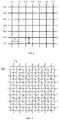
- FIG. 6is a diagram of the Rx lines and the Tx lines of the mutual-capacitance fingerprint recognition device shown in FIG. 3 in accordance with some embodiments of the disclosed subject matter;
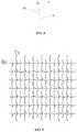
- FIG. 7is a diagram of a first exemplary structure of Rx lines and Tx lines of a mutual-capacitance fingerprint recognition device in accordance with some embodiments of the disclosed subject matter;
- FIG. 8is a diagram showing an expanded view of a partial of a Tx line illustrated in FIG. 7 in accordance with some embodiments of the disclosed subject matter;
- FIG. 9is a diagram of a second exemplary structure of Rx lines and Tx lines of a mutual-capacitance fingerprint recognition device in accordance with some embodiments of the disclosed subject matter.
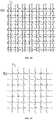
- FIG. 10is a diagram of a third exemplary structure of Rx lines and Tx lines of a mutual-capacitance fingerprint recognition device in accordance with some embodiments of the disclosed subject matter;
- FIG. 11is a diagram of a fourth exemplary structure of Rx lines and Tx lines of a mutual-capacitance fingerprint recognition device in accordance with some embodiments of the disclosed subject matter;
- FIG. 12is a diagram of a fifth exemplary structure of Rx lines and Tx lines of a mutual-capacitance fingerprint recognition device in accordance with some embodiments of the disclosed subject matter;
- FIG. 13is a diagram of a sixth exemplary structure of Rx lines and Tx lines of a mutual-capacitance fingerprint recognition device in accordance with some embodiments of the disclosed subject matter.
- FIG. 14shows an exemplary method for fabricating a mutual-capacitance fingerprint recognition device in accordance with some embodiments of the disclosed subject matter.
- An aspect of the present disclosureprovides a mutual-capacitance touch sensing pattern recognition device, which can recognize patterns including ridges and valleys, such as fingerprint or palmprint .comprising a plurality of sensing electrode lines and a plurality of driving electrode lines, wherein at least one set of the plurality of sensing electrode lines and the plurality of driving electrode lines have curved portions.
- the disclosed subject matterprovides a mutual-capacitance fingerprint recognition device, a related fabricating method, a related display panel, and a related display apparatus.
- the basic principle of a mutual capacitance fingerprint recognition devicecan be illustrated in FIG. 1 .
- the driving electrodes Txprovide low-voltage high-frequency signals, while the sensing electrodes Rx receive low-voltage high-frequency signals, so that a stable capacitance can be measured between the driving electrodes and the sensing electrodes.
- the driving electrodes Tx and the sensing electrodes Rxare often linear, and they are thus often referred to as Tx lines and Rx lines, respectively.
- the finger and the fingerprint recognition devicecan form an equivalent capacitance. If human body is grounded, the low-voltage high-frequency signals can flow into the ground through the equivalent capacitance, and capacitance between the driving electrodes and the sensing electrodes can thereby be reduced.
- the low-voltage high-frequency signals emitted from the driving electrodes Txcan be understood as electric field lines emitted from the driving electrodes, while the low-voltage high-frequency signals received by the sensing electrodes Rx can be understood as electric field lines received by the sensing electrodes.
- the valleys on a fingerprintare located relatively far away from the Tx lines and Rx lines. So few electric field lines can be absorbed by the valleys, and a large capacitance value Cmax between the Tx lines and the Rx lines can be measured at the valleys' locations.
- the ridgesare located relatively close to the Tx lines and the Rx lines. So more electric field lines can be absorbed by the ridges, and a small capacitance value Cmin between the Tx lines and Rx lines can be measured at the ridges' locations.
- ⁇ Ccan be understood as a sensitivity of fingerprint recognition.
- the difference ⁇ C between Cmax and Cminis relatively small in current fingerprint recognition devices, resulting in a lower sensitivity of fingerprint recognition, which means it is not easy to distinguish the valleys and the ridges in a fingerprint.
- FIG. 2shows a cross-sectional view of an exemplary mutual-capacitance fingerprint recognition device in accordance with some embodiments of the disclosed subject matter.
- a mutual-capacitance fingerprint recognition devicecan include glass cover 1 , first resin layer 2 , sensing electrode 3 , second resin layer 4 , driving electrode 5 , and glass substrate 6 .
- first resin layer 2is located between glass cover 1 and sensing electrode 3
- second resin layer 4is located between sensing electrode 3 and driving electrode 5 .
- First resin layer 2 and second resin layer 4can be made of any suitable resin materials, such as Optically Clear Adhesive (OCA) resin.
- OCA resinis an insulating material.
- FIG. 2is merely a schematic illustration of the structure of an exemplary mutual-capacitance fingerprint recognition device in according to the described subject matters and is not intended to limit the scope of the present disclosure.
- Sensing electrode 3 and driving electrode 5can form a capacitor group.
- the capacitorchanges due to the height differences between ridges and valleys of the fingerprint.
- the valleys and the ridgeshave different distances from the capacitor, and can cause different changes of the capacitance.
- a reconstruction of the fingerprint imagecan be obtained by arranging a two-dimensional high-density electrodes matrix.
- sensing electrode 3 and/or driving electrode 5can have any suitable curved structures.
- sensing electrode 3in a direction perpendicular to glass cover 1 , sensing electrode 3 can have wave-shaped convexes toward glass cover 1 . In a projection plane parallel to glass cover 1 , sensing electrode 3 and driving electrode 5 can have linear structures.
- driving electrode 5in a direction perpendicular to glass cover 1 , can have wave-shaped convexes toward glass cover 1 .
- sensing electrode 3 and driving electrode 5in a projection plane parallel to glass cover 1 , can have linear structures.
- sensing electrode 3 and driving electrode 5can both have wave-shaped convexes toward glass cover 1 .
- sensing electrode 3 and driving electrode 5can have linear structures.
- sensing electrode 3in a direction perpendicular to glass cover 1 , can have wave-shaped convexes toward glass cover 1 . In a projection plane parallel to glass cover 1 , sensing electrode 3 can have a wave-shaped structure.
- driving electrode 5in a direction perpendicular to glass cover 1 , driving electrode 5 can have wave-shaped convexes toward glass cover 1 .
- sensing electrode 3in a projection plane parallel to glass cover 1 , sensing electrode 3 can have a wave-shaped structure.
- sensing electrode 3 and driving electrode 5can have wave-shaped convexes toward glass cover 1 .
- sensing electrode 3can have a wave-shaped structure.
- sensing electrode 3in a direction perpendicular to glass cover 1 , sensing electrode 3 can have wave-shaped convexes toward glass cover 1 .
- driving electrode 5in a projection plane parallel to glass cover 1 , driving electrode 5 can have a wave-shaped structure.
- driving electrode 5in a direction perpendicular to glass cover 1 , driving electrode 5 can have wave-shaped convexes toward glass cover 1 . In a projection plane parallel to glass cover 1 , driving electrode 5 can have a wave-shaped structure.
- sensing electrode 3 and driving electrode 5can both have wave-shaped convexes toward glass cover 1 .
- driving electrode 5can have a wave-shaped structure.
- sensing electrode 3in a direction perpendicular to glass cover 1 , sensing electrode 3 can have wave-shaped convexes toward glass cover 1 . In a projection plane parallel to glass cover 1 , sensing electrode 3 and driving electrode 5 can both have wave-shaped structures.
- driving electrode 5in a direction perpendicular to glass cover 1 , can have wave-shaped convexes toward glass cover 1 .
- sensing electrode 3 and driving electrode 5can both have wave-shaped structures.
- sensing electrode 3 and driving electrode 5can both have wave-shaped convexes toward glass cover 1 .
- sensing electrode 3 and driving electrode 5can both have wave-shaped structures.
- sensing electrode 3 and driving electrode 5do not have wave-shaped convexes toward glass cover 1 .
- sensing electrode 3can have a wave-shaped structure.
- sensing electrode 3 and driving electrode 5do not have wave-shaped convexes toward glass cover 1 .
- driving electrode 5can have a wave-shaped structure.
- sensing electrode 3 and driving electrode 5do not have wave-shaped convexes toward glass cover 1 .
- sensing electrode 3 and driving electrode 5can both have wave-shaped structures.
- the twelfth example described abovecan have a good effective fingerprint recognition ability.
- the areas of sensing electrode 3 and driving electrode 5can be greatly increased when sensing electrode 3 and driving electrode 5 can have wave-shaped convexes toward glass cover 1 in a direction perpendicular to glass cover 1 , and have wave-shaped structures in a projection plane parallel to glass cover 1 .
- the capacitance difference value ⁇ Ccan be greatly increased, and the fingerprint recognition ability may be greatly improved.
- sensing electrode 3in a direction perpendicular to glass cover 1 , sensing electrode 3 has multiple wave-shaped convexes toward glass cover 1 .
- First resin layer 2 between glass cover 1 and sensing electrode 3has multiple wave-shaped concaves that correspond to the multiple wave-shaped convexes of sensing electrode 3 respectively.
- driving electrode 5also has wave-shaped convexes toward glass cover 1 .
- Second resin layer 4 between sensing electrode 3 and driving electrode 5has multiple wave-shaped concaves that correspond to the multiple wave-shaped convexes of driving electrode 5 respectively.
- the distances between neighboring wave-shaped convexes of sensing electrode 3 and/or driving electrode 5may be the same.
- the distancemay be between 5 ⁇ m and 10 ⁇ m.
- the wave-shaped convexescan be either cube-like convexes or hemispherical convexes.
- each of the wave-shaped convexesis a hemispherical convex.
- the hemispherical convexcan have a diameter between 1 ⁇ m and 10 ⁇ m, and a depth between 1 ⁇ m and 10 ⁇ m.
- the depth of the hemispherical convexcan be determined by a thickness of the resin layer and an etching depth of an etching process.
- sensing electrode lines Rxare arranged in the AA′ direction
- driving electrode lines Txare arranged in a direction that is perpendicular to the AA′ direction.
- Sensing electrode lines Rxhave multiple wave-shaped convexes 7 .
- Sensing electrode Rx and driving electrode lines Txcan have linear structures in a projection plane parallel to glass cover 1 .
- FIG. 4a schematic structural cross-sectional view of a Rx line along AA′ direction is shown.
- FIG. 5is a schematic projection view of the Rx line shown in FIG. 4 in a plane that is perpendicular to the glass substrate and parallel to the Rx line.
- a wave-shaped convex 7can have diameter D between 1 ⁇ m and 10 ⁇ m, and depth H between 1 ⁇ m and 10 ⁇ m.
- Distance L between neighboring wave-shaped convexes 7may be between 5 ⁇ m and 10 ⁇ m.
- the distance between valleys and ridges of a human fingerprintis about 300 ⁇ m to 400 ⁇ m.
- a distance between two adjacent driving electrode lines Tx and/or sensing electrode lines Rxwould not be greater than the distance between valleys and ridges.
- distance T 1 between adjacent Tx linesis between 30 ⁇ m and 120 ⁇ m
- distance T 2 between adjacent Rx linesis between 30 ⁇ m and 120 ⁇ m.
- FIGS. 7-13are schematic diagrams of several exemplary structures of Rx lines and Tx lines of a mutual-capacitance fingerprint recognition device in accordance with some embodiments of the disclosed subject matter.
- Tx linesare extending along a first direction
- Rx linesare extending along a second direction.
- the first direction and the second directionare perpendicular to each other.
- Each of the Tx linesincludes three parts, which are a Tx main line, a first Tx branch, and a second Tx branch.
- the Tx main lineis extending in the first direction.
- the first Tx branchis located on one side of the Tx main line and is between two adjacent Rx lines.
- the second Tx branchis located on the other side of the Tx main line and is also between the two adjacent Rx lines. Both the first Tx branch and the second Tx branch have a length larger than a half of the distance between two adjacent Tx lines.
- FIG. 8a schematic diagram showing an expanded view of a portion of a Tx line is shown in FIG. 8 .
- Each of the Tx linesincludes Tx main line 8 , first Tx branch 9 , and second Tx branch 10 .
- each of the Rx linesincludes three parts, which are a Rx main line, a first Rx branch, and a second Rx branch.
- the Rx main lineis extending in the second direction.
- the first Rx branchis located on one side of the Rx main line and is between two adjacent Tx lines.
- the second Rx branchis located on the other side of the Rx main line and is also between the two adjacent Tx lines. Both the first Rx branch and the second Rx branch have a length larger than a half of the distance between two adjacent Rx lines.
- FIG. 9A second exemplary structure of Rx lines and Tx lines is shown in FIG. 9 . Comparing to the first exemplary structure shown in FIG. 7 , in the second exemplary structure, each of the Tx lines only includes a Tx main line but no branch lines.
- each Tx lineincludes two parallel wavy lines. At one end the two parallel wavy lines are electrically connected, and at the other end the two parallel wavy lines are extending in a first direction.
- each Rx linealso includes two parallel wavy lines. At one end the two parallel wavy lines are electrically connected, and at the other end the two parallel wavy lines are extending in a second direction.
- FIG. 11A fourth exemplary structure of Rx lines and Tx lines is shown in FIG. 11 . Comparing to the first exemplary structure shown in FIG. 7 , in the fourth exemplary structure, each of the Tx lines only includes a Tx main line but no branch lines. Each of the Rx lines also includes a Rx main line only but no branch lines.
- FIG. 12A fifth exemplary structure of Rx lines and Tx lines is shown in FIG. 12 . Comparing to the first exemplary structure shown in FIG. 7 , in the fifth exemplary structure, a distance between adjacent two Rx lines and a distance between adjacent two Tx lines are shorter.
- FIG. 13A sixth exemplary structure of Rx lines and Tx lines is shown in FIG. 13 . Comparing to the second exemplary structure shown in FIG. 8 , in the sixth exemplary structure, a distance between two adjacent Rx lines and a distance between two adjacent Tx lines are shorter by 20-50 um.
- FIG. 14an exemplary method for fabricating a mutual-capacitance fingerprint recognition device described above is shown in accordance with some embodiments of the disclosed subject matter.
- the methodcan start at S 100 by forming a first resin layer on one side of a glass cover that faces a glass substrate.
- the first resin layercan be made by optically clear adhesive (OCA) material.
- OCAoptically clear adhesive
- the first resin layercan be formed by any suitable method, such as a spin-coating method.
- multiple concavescan be etched on the first resin layer.
- the multiple concavescan be wavily distributed on the first resin layer.
- the diameter of the multiple concavescan be around 3 ⁇ m, the depth of the multiple concaves can be about 4-5 ⁇ m.
- the multiple concavescan be etched by any suitable etching process.
- multiple sensing electrode linescan be formed over the first resin layer.
- the multiple sensing electrode linescan have wave-shaped convexes toward the glass cover as described above in connection with FIGS. 3-5 .
- the multiple sensing electrode linescan have any suitable structure described above in connection with FIGS. 6-13 .
- the multiple sensing electrode linescan be formed by any suitable method, such as a magnetron sputtering method.
- a second resin layer on the multiple sensing electrode linescan be made by optically clear adhesive (OCA) material.
- OCAoptically clear adhesive
- the second resin layercan be formed by any suitable method, such as a spin-coating method.
- multiple concavescan be etched on the second resin layer.
- the multiple concavescan be wavily distributed on the second resin layer.
- the diameter of the multiple concavescan be around 3 ⁇ m, the depth of the multiple concaves can be about 4-5 ⁇ m.
- the multiple concavescan be etched by any suitable etching process.
- multiple driving electrode linescan be formed over the second resin layer.
- the multiple driving electrode linescan have wave-shaped convexes toward the glass cover as described above in connection with FIGS. 3-5 .
- the multiple driveing electrode linescan have any suitable structure described above in connection with FIGS. 6-13 .
- the multiple driving electrode linescan be formed by any suitable method, such as a magnetron sputtering method.
- the glass cover and the glass substratecan be assembled together.
- FIG. 14is provided as an example only. At least some of the steps shown in the figure may be performed in a different order than represented, performed concurrently, or altogether omitted. Some additional steps not shown in the figure may be performed between any of the steps shown in the figure.
- Embodiments of the present disclosurecan be implemented to realize fingerprint recognition functions. Embodiments of the present disclosure can also be implemented to realize other image or pattern recognition functions involving sensing and distinguishing various formations (e.g., valleys or ridges) of a surface.
- a display panelcomprising a mutual-capacitance fingerprint recognition device described above is provided.
- the display panelcan be any suitable display panel, such as a twisted nematic (TN) mode liquid crystal display (LCD) panel, a fringe-field switching (FFS) mode LCD panel, an Advanced Super Dimension Switch (ADS) mode LCD panel, an organic electroluminescent display panel, or any other suitable flat display panels.
- TNtwisted nematic
- LCDliquid crystal display
- FFSfringe-field switching
- ADSAdvanced Super Dimension Switch
- organic electroluminescent display panelor any other suitable flat display panels.
- a display apparatuscomprising the display panel described above.
- the display apparatuscan be any suitable apparatus that has a display function, such as a mobile phone, a tablet computer, a television, a monitor, a notebook computer, a digital camera, a digital picture frame, a navigation system, etc.
- a mutual-capacitance fingerprint recognition devicea related fabricating method, a related display panel, and a related display apparatus are provided.
Landscapes
- Engineering & Computer Science (AREA)
- Theoretical Computer Science (AREA)
- Human Computer Interaction (AREA)
- Physics & Mathematics (AREA)
- General Physics & Mathematics (AREA)
- General Engineering & Computer Science (AREA)
- Multimedia (AREA)
- Computer Vision & Pattern Recognition (AREA)
- Measurement Of Length, Angles, Or The Like Using Electric Or Magnetic Means (AREA)
- Devices For Indicating Variable Information By Combining Individual Elements (AREA)
- Image Input (AREA)
Abstract
Description
Claims (19)
Priority Applications (1)
| Application Number | Priority Date | Filing Date | Title |
|---|---|---|---|
| US16/247,917US10558837B2 (en) | 2015-08-26 | 2019-01-15 | Mutual-capacitance touch sensing pattern recognition device, fabricating method thereof, related display panel, and related display apparatus |
Applications Claiming Priority (6)
| Application Number | Priority Date | Filing Date | Title |
|---|---|---|---|
| CN201510531622.1ACN105138988B (en) | 2015-08-26 | 2015-08-26 | Mutual capacitive fingerprint identification device and preparation method, display panel and display device |
| CN201510531622.1 | 2015-08-26 | ||
| CN201510531622 | 2015-08-26 | ||
| US15/122,904US10223570B2 (en) | 2015-08-26 | 2016-02-22 | Mutual-capacitance touch sensing pattern recognition device, fabricating method thereof, related display panel, and related display apparatus |
| PCT/CN2016/074218WO2017031965A1 (en) | 2015-08-26 | 2016-02-22 | Mutual-capacitance touch sensing pattern recognition device, fabricating method thereof, related display panel, and related display apparatus |
| US16/247,917US10558837B2 (en) | 2015-08-26 | 2019-01-15 | Mutual-capacitance touch sensing pattern recognition device, fabricating method thereof, related display panel, and related display apparatus |
Related Parent Applications (2)
| Application Number | Title | Priority Date | Filing Date |
|---|---|---|---|
| US15/122,904ContinuationUS10223570B2 (en) | 2015-08-26 | 2016-02-22 | Mutual-capacitance touch sensing pattern recognition device, fabricating method thereof, related display panel, and related display apparatus |
| PCT/CN2016/074218ContinuationWO2017031965A1 (en) | 2015-08-26 | 2016-02-22 | Mutual-capacitance touch sensing pattern recognition device, fabricating method thereof, related display panel, and related display apparatus |
Publications (2)
| Publication Number | Publication Date |
|---|---|
| US20190147212A1 US20190147212A1 (en) | 2019-05-16 |
| US10558837B2true US10558837B2 (en) | 2020-02-11 |
Family
ID=54724332
Family Applications (2)
| Application Number | Title | Priority Date | Filing Date |
|---|---|---|---|
| US15/122,904Active2036-04-06US10223570B2 (en) | 2015-08-26 | 2016-02-22 | Mutual-capacitance touch sensing pattern recognition device, fabricating method thereof, related display panel, and related display apparatus |
| US16/247,917ActiveUS10558837B2 (en) | 2015-08-26 | 2019-01-15 | Mutual-capacitance touch sensing pattern recognition device, fabricating method thereof, related display panel, and related display apparatus |
Family Applications Before (1)
| Application Number | Title | Priority Date | Filing Date |
|---|---|---|---|
| US15/122,904Active2036-04-06US10223570B2 (en) | 2015-08-26 | 2016-02-22 | Mutual-capacitance touch sensing pattern recognition device, fabricating method thereof, related display panel, and related display apparatus |
Country Status (3)
| Country | Link |
|---|---|
| US (2) | US10223570B2 (en) |
| CN (1) | CN105138988B (en) |
| WO (1) | WO2017031965A1 (en) |
Families Citing this family (14)
| Publication number | Priority date | Publication date | Assignee | Title |
|---|---|---|---|---|
| CN105138988B (en)* | 2015-08-26 | 2020-02-21 | 京东方科技集团股份有限公司 | Mutual capacitive fingerprint identification device and preparation method, display panel and display device |
| US10372961B2 (en) | 2016-03-30 | 2019-08-06 | Japan Display Inc. | Fingerprint sensor, fingerprint sensor module, and method for manufacturing fingerprint sensor |
| JP6878066B2 (en)* | 2016-03-30 | 2021-05-26 | 株式会社ジャパンディスプレイ | Fingerprint sensor and fingerprint sensor module |
| KR102618537B1 (en)* | 2016-04-29 | 2023-12-27 | 삼성전자주식회사 | On-screen type fingerprint sensor and electronic apparatus including the same |
| CN107844732A (en)* | 2016-09-18 | 2018-03-27 | 敦泰电子有限公司 | A kind of fingerprint sensing device, fingerprint sensing module and electronic equipment |
| KR102754103B1 (en)* | 2016-09-23 | 2025-01-15 | 삼성디스플레이 주식회사 | Display device and manufacturing method thereof |
| CN106503685A (en)* | 2016-10-31 | 2017-03-15 | 北京小米移动软件有限公司 | Protection film layer, display base plate and electronic equipment |
| CN107004127A (en)* | 2017-02-08 | 2017-08-01 | 深圳市飞仙智能科技有限公司 | A kind of intelligent terminal, capacitive fingerprint sensing device and its sensing module |
| CN109299630B (en)* | 2017-07-24 | 2022-07-01 | 中芯国际集成电路制造(天津)有限公司 | Semiconductor fingerprint sensor and manufacturing method thereof |
| CN109299635B (en)* | 2017-07-25 | 2021-03-09 | 中芯国际集成电路制造(上海)有限公司 | Fingerprint sensor and forming method thereof |
| CN109002214B (en) | 2018-07-26 | 2020-05-26 | 京东方科技集团股份有限公司 | A touch substrate, a driving method thereof, and a touch display device |
| CN113534975A (en)* | 2020-04-14 | 2021-10-22 | 宸美(厦门)光电有限公司 | Touch electrode, touch panel using same and touch display |
| CN212723965U (en)* | 2020-08-26 | 2021-03-16 | 敦泰电子(深圳)有限公司 | Touch screen and input device with same |
| CN112286398A (en)* | 2020-11-18 | 2021-01-29 | 武汉华星光电半导体显示技术有限公司 | Touch panel and display device |
Citations (13)
| Publication number | Priority date | Publication date | Assignee | Title |
|---|---|---|---|---|
| US20050031174A1 (en) | 2003-01-22 | 2005-02-10 | Nokia Corporation | Arrangement for authentication of a person |
| CN101281589A (en) | 2007-04-04 | 2008-10-08 | 鸿富锦精密工业(深圳)有限公司 | Fingerprint identification device and portable electronic device |
| CN103309503A (en) | 2013-05-17 | 2013-09-18 | 北京京东方光电科技有限公司 | Touch screen and display device |
| CN103530609A (en) | 2013-10-11 | 2014-01-22 | 北京京东方光电科技有限公司 | Fingerprint identification element, display screen and display device |
| US20140035864A1 (en) | 2012-08-01 | 2014-02-06 | Ili Technology Corp. | Capacitive touch-control panel and apparatus thereof |
| US20140152604A1 (en) | 2007-06-13 | 2014-06-05 | Apple Inc. | Pinch-throw and translation gestures |
| CN203773561U (en) | 2014-04-08 | 2014-08-13 | 南昌欧菲生物识别技术有限公司 | Fingerprint recognition device and electronic device including same |
| CN104182102A (en) | 2013-05-28 | 2014-12-03 | 晨星半导体股份有限公司 | Mutual Capacitive Touch Sensing Device |
| US20150091849A1 (en) | 2013-10-02 | 2015-04-02 | Synaptics Incorporated | Multi-sensor touch integrated display driver configuration for capacitive sensing devices |
| CN104794454A (en) | 2015-04-30 | 2015-07-22 | 京东方科技集团股份有限公司 | Fingerprint recognition device, display screen and display device |
| US20150242051A1 (en)* | 2014-02-21 | 2015-08-27 | Qualcomm Incorporated | Systems and methods of moisture detection and false touch rejection on touch screen devices |
| US20160342234A1 (en)* | 2014-11-14 | 2016-11-24 | Shenzhen China Star Optoelectronics Technology Co., Ltd. | Mutual capacitance one glass solution touch panel and manufacture method thereof |
| US20170308205A1 (en)* | 2012-07-20 | 2017-10-26 | Silead Inc. | Capacitive Touch Screen and Single Layer Wiring Electrode Array |
Family Cites Families (1)
| Publication number | Priority date | Publication date | Assignee | Title |
|---|---|---|---|---|
| CN105138988B (en) | 2015-08-26 | 2020-02-21 | 京东方科技集团股份有限公司 | Mutual capacitive fingerprint identification device and preparation method, display panel and display device |
- 2015
- 2015-08-26CNCN201510531622.1Apatent/CN105138988B/ennot_activeExpired - Fee Related
- 2016
- 2016-02-22WOPCT/CN2016/074218patent/WO2017031965A1/ennot_activeCeased
- 2016-02-22USUS15/122,904patent/US10223570B2/enactiveActive
- 2019
- 2019-01-15USUS16/247,917patent/US10558837B2/enactiveActive
Patent Citations (19)
| Publication number | Priority date | Publication date | Assignee | Title |
|---|---|---|---|---|
| CN1802882A (en) | 2003-01-22 | 2006-07-12 | 诺基亚公司 | Arrangement for authentication of a person |
| US20050031174A1 (en) | 2003-01-22 | 2005-02-10 | Nokia Corporation | Arrangement for authentication of a person |
| CN101281589A (en) | 2007-04-04 | 2008-10-08 | 鸿富锦精密工业(深圳)有限公司 | Fingerprint identification device and portable electronic device |
| US20080247613A1 (en) | 2007-04-04 | 2008-10-09 | Hon Hai Precision Industry Co., Ltd. | Fingerprint identification apparatus and portable electronic device having same |
| US20140152604A1 (en) | 2007-06-13 | 2014-06-05 | Apple Inc. | Pinch-throw and translation gestures |
| US20170308205A1 (en)* | 2012-07-20 | 2017-10-26 | Silead Inc. | Capacitive Touch Screen and Single Layer Wiring Electrode Array |
| US20140035864A1 (en) | 2012-08-01 | 2014-02-06 | Ili Technology Corp. | Capacitive touch-control panel and apparatus thereof |
| CN103577005A (en) | 2012-08-01 | 2014-02-12 | 奕力科技股份有限公司 | Capacitive touch panel and module thereof |
| CN103309503A (en) | 2013-05-17 | 2013-09-18 | 北京京东方光电科技有限公司 | Touch screen and display device |
| US20150060252A1 (en) | 2013-05-17 | 2015-03-05 | Boe Technology Group Co., Ltd. | Touch screen and display device |
| CN104182102A (en) | 2013-05-28 | 2014-12-03 | 晨星半导体股份有限公司 | Mutual Capacitive Touch Sensing Device |
| US20150091849A1 (en) | 2013-10-02 | 2015-04-02 | Synaptics Incorporated | Multi-sensor touch integrated display driver configuration for capacitive sensing devices |
| US20160042215A1 (en) | 2013-10-11 | 2016-02-11 | Boe Technology Group Co., Ltd. | A fingerprint recognition element, a display screen and a display device |
| CN103530609A (en) | 2013-10-11 | 2014-01-22 | 北京京东方光电科技有限公司 | Fingerprint identification element, display screen and display device |
| US20150242051A1 (en)* | 2014-02-21 | 2015-08-27 | Qualcomm Incorporated | Systems and methods of moisture detection and false touch rejection on touch screen devices |
| CN203773561U (en) | 2014-04-08 | 2014-08-13 | 南昌欧菲生物识别技术有限公司 | Fingerprint recognition device and electronic device including same |
| US20160342234A1 (en)* | 2014-11-14 | 2016-11-24 | Shenzhen China Star Optoelectronics Technology Co., Ltd. | Mutual capacitance one glass solution touch panel and manufacture method thereof |
| CN104794454A (en) | 2015-04-30 | 2015-07-22 | 京东方科技集团股份有限公司 | Fingerprint recognition device, display screen and display device |
| US20170103251A1 (en) | 2015-04-30 | 2017-04-13 | Boe Technology Group Co., Ltd. | Fingerprint recognition device, display screen and display device |
Non-Patent Citations (12)
| Title |
|---|
| Final Office Action in the U.S. Appl. No. 15/122,904, dated Apr. 12, 2018. |
| First Office Action in the Chinese Patent Application No. 2016510531622.1, dated Jan. 10, 2018; English translation attached. |
| International Search Report & Written Opinion dated May 6, 2016 regarding PCT/CN2016/074218. |
| Non-Final Office Action in the U.S. Appl. No. 15/122,904, dated Dec. 14, 2017. |
| Non-Final Office Action in the U.S. Appl. No. 15/122,904, dated Jul. 18, 2018. |
| Notice of Allowance in the U.S. Appl. No. 15/122,904, dated Nov. 5, 2018. |
| Request for Continued Examination (RCE) in the U.S. Appl. No. 15/122,904, dated Jun. 22, 2018. |
| Response to Final Office Action in the U.S. Appl. No. 15/122,904, dated Jun. 7, 2018. |
| Response to Non-Final Office Action in the U.S. Appl. No. 15/122,904, dated Mar. 12, 2018. |
| Response to Non-Final Office Action in the U.S. Appl. No. 15/122,904, dated Sep. 25, 2018. |
| Second Office Action in the Chinese Patent Application No. 2016510531622.1, dated Jun. 14, 2018; English translation attached. |
| Third Office Action in the Chinese Patent Application No. 2016510531622.1, dated Jun. 13, 2019; English translation attached. |
Also Published As
| Publication number | Publication date |
|---|---|
| CN105138988B (en) | 2020-02-21 |
| US20190147212A1 (en) | 2019-05-16 |
| US10223570B2 (en) | 2019-03-05 |
| WO2017031965A1 (en) | 2017-03-02 |
| US20170262683A1 (en) | 2017-09-14 |
| CN105138988A (en) | 2015-12-09 |
Similar Documents
| Publication | Publication Date | Title |
|---|---|---|
| US10558837B2 (en) | Mutual-capacitance touch sensing pattern recognition device, fabricating method thereof, related display panel, and related display apparatus | |
| CN103294311B (en) | Touch unit array and touch display panel | |
| US9454267B2 (en) | Touch sensing circuit and method for making the same | |
| US8624845B2 (en) | Capacitance touch screen | |
| US10203818B2 (en) | Touch screen panel including at least one dummy pattern | |
| US9063621B2 (en) | Touch sensor panel | |
| US10613689B2 (en) | Touch screen, method of manufacturing touch screen, and display device including touch screen | |
| US9830033B2 (en) | Touch sensor and method of manufacturing the same | |
| US8723818B2 (en) | Touch screen poly layer electrode distribution | |
| US10452219B2 (en) | Touch sensor | |
| KR102275619B1 (en) | Touch screen sensor, Touch screen panel of electrostatic capacitive type and image display device | |
| US10359892B2 (en) | Flexible touch sensing unit and flexible display device including flexible touch sensing unit | |
| KR20140062269A (en) | Flexible touch screen panel and flexible display device with the same | |
| US20140001024A1 (en) | Touch panel and touch display device | |
| US9798429B2 (en) | Guard electrodes in a sensing stack | |
| US20150070294A1 (en) | Randomized mesh design | |
| US20160377898A1 (en) | Ips in-cell touch display panel and manufacturing method thereof | |
| CN104407466A (en) | Display substrate, display panel and display device | |
| WO2017004846A1 (en) | Liquid crystal display with touch control function, and conducting layer structure thereof | |
| US20110221687A1 (en) | Electrode pattern structure of a capacitive touch panel and method of manufacturing the same | |
| US20150370372A1 (en) | Capacitive touch panel having dielectric structures formed therein | |
| CN204904249U (en) | Touch panel | |
| WO2020209188A1 (en) | Touch sensor | |
| KR101293165B1 (en) | Touch sensing panel | |
| TWI537789B (en) | Touch panel and decting method thereof |
Legal Events
| Date | Code | Title | Description |
|---|---|---|---|
| FEPP | Fee payment procedure | Free format text:ENTITY STATUS SET TO UNDISCOUNTED (ORIGINAL EVENT CODE: BIG.); ENTITY STATUS OF PATENT OWNER: LARGE ENTITY | |
| STPP | Information on status: patent application and granting procedure in general | Free format text:DOCKETED NEW CASE - READY FOR EXAMINATION | |
| STPP | Information on status: patent application and granting procedure in general | Free format text:NON FINAL ACTION MAILED | |
| AS | Assignment | Owner name:BOE TECHNOLOGY GROUP CO., LTD., CHINA Free format text:ASSIGNMENT OF ASSIGNORS INTEREST;ASSIGNOR:CHEN, XIAOCHUAN;REEL/FRAME:049783/0863 Effective date:20160719 Owner name:BEIJING BOE OPTOELECTRONICS TECHNOLOGY CO., LTD., Free format text:ASSIGNMENT OF ASSIGNORS INTEREST;ASSIGNOR:DONG, XUE;REEL/FRAME:049783/0818 Effective date:20160719 Owner name:BOE TECHNOLOGY GROUP CO., LTD., CHINA Free format text:ASSIGNMENT OF ASSIGNORS INTEREST;ASSIGNOR:ZHAO, WEIJIE;REEL/FRAME:049783/0883 Effective date:20160719 Owner name:BOE TECHNOLOGY GROUP CO., LTD., CHINA Free format text:ASSIGNMENT OF ASSIGNORS INTEREST;ASSIGNOR:WANG, HAISHENG;REEL/FRAME:049783/0859 Effective date:20160719 Owner name:BOE TECHNOLOGY GROUP CO., LTD., CHINA Free format text:ASSIGNMENT OF ASSIGNORS INTEREST;ASSIGNOR:LI, CHANGFENG;REEL/FRAME:049783/0850 Effective date:20160719 Owner name:BOE TECHNOLOGY GROUP CO., LTD., CHINA Free format text:ASSIGNMENT OF ASSIGNORS INTEREST;ASSIGNOR:DONG, XUE;REEL/FRAME:049783/0818 Effective date:20160719 Owner name:BEIJING BOE OPTOELECTRONICS TECHNOLOGY CO., LTD., Free format text:ASSIGNMENT OF ASSIGNORS INTEREST;ASSIGNOR:ZHAO, WEIJIE;REEL/FRAME:049783/0883 Effective date:20160719 Owner name:BEIJING BOE OPTOELECTRONICS TECHNOLOGY CO., LTD., Free format text:ASSIGNMENT OF ASSIGNORS INTEREST;ASSIGNOR:WANG, LEI;REEL/FRAME:049783/0879 Effective date:20160719 Owner name:BEIJING BOE OPTOELECTRONICS TECHNOLOGY CO., LTD., Free format text:ASSIGNMENT OF ASSIGNORS INTEREST;ASSIGNOR:WANG, HAISHENG;REEL/FRAME:049783/0859 Effective date:20160719 Owner name:BOE TECHNOLOGY GROUP CO., LTD., CHINA Free format text:ASSIGNMENT OF ASSIGNORS INTEREST;ASSIGNOR:WANG, LEI;REEL/FRAME:049783/0879 Effective date:20160719 Owner name:BEIJING BOE OPTOELECTRONICS TECHNOLOGY CO., LTD., Free format text:ASSIGNMENT OF ASSIGNORS INTEREST;ASSIGNOR:LI, CHANGFENG;REEL/FRAME:049783/0850 Effective date:20160719 Owner name:BEIJING BOE OPTOELECTRONICS TECHNOLOGY CO., LTD., Free format text:ASSIGNMENT OF ASSIGNORS INTEREST;ASSIGNOR:CHEN, XIAOCHUAN;REEL/FRAME:049783/0863 Effective date:20160719 Owner name:BOE TECHNOLOGY GROUP CO., LTD., CHINA Free format text:ASSIGNMENT OF ASSIGNORS INTEREST;ASSIGNOR:LIU, YINGMING;REEL/FRAME:049783/0912 Effective date:20160719 Owner name:BEIJING BOE OPTOELECTRONICS TECHNOLOGY CO., LTD., Free format text:ASSIGNMENT OF ASSIGNORS INTEREST;ASSIGNOR:LIU, WEI;REEL/FRAME:049783/0887 Effective date:20160719 Owner name:BOE TECHNOLOGY GROUP CO., LTD., CHINA Free format text:ASSIGNMENT OF ASSIGNORS INTEREST;ASSIGNOR:YANG, SHENGJI;REEL/FRAME:049783/0895 Effective date:20160719 Owner name:BEIJING BOE OPTOELECTRONICS TECHNOLOGY CO., LTD., Free format text:ASSIGNMENT OF ASSIGNORS INTEREST;ASSIGNOR:DING, XIAOLIANG;REEL/FRAME:049783/0891 Effective date:20160719 Owner name:BOE TECHNOLOGY GROUP CO., LTD., CHINA Free format text:ASSIGNMENT OF ASSIGNORS INTEREST;ASSIGNOR:DING, XIAOLIANG;REEL/FRAME:049783/0891 Effective date:20160719 Owner name:BEIJING BOE OPTOELECTRONICS TECHNOLOGY CO., LTD., Free format text:ASSIGNMENT OF ASSIGNORS INTEREST;ASSIGNOR:YANG, SHENGJI;REEL/FRAME:049783/0895 Effective date:20160719 Owner name:BEIJING BOE OPTOELECTRONICS TECHNOLOGY CO., LTD., Free format text:ASSIGNMENT OF ASSIGNORS INTEREST;ASSIGNOR:LIU, YINGMING;REEL/FRAME:049783/0912 Effective date:20160719 Owner name:BOE TECHNOLOGY GROUP CO., LTD., CHINA Free format text:ASSIGNMENT OF ASSIGNORS INTEREST;ASSIGNOR:LIU, WEI;REEL/FRAME:049783/0887 Effective date:20160719 Owner name:BEIJING BOE OPTOELECTRONICS TECHNOLOGY CO., LTD., CHINA Free format text:ASSIGNMENT OF ASSIGNORS INTEREST;ASSIGNOR:WANG, HAISHENG;REEL/FRAME:049783/0859 Effective date:20160719 Owner name:BEIJING BOE OPTOELECTRONICS TECHNOLOGY CO., LTD., CHINA Free format text:ASSIGNMENT OF ASSIGNORS INTEREST;ASSIGNOR:LI, CHANGFENG;REEL/FRAME:049783/0850 Effective date:20160719 Owner name:BEIJING BOE OPTOELECTRONICS TECHNOLOGY CO., LTD., CHINA Free format text:ASSIGNMENT OF ASSIGNORS INTEREST;ASSIGNOR:DONG, XUE;REEL/FRAME:049783/0818 Effective date:20160719 Owner name:BEIJING BOE OPTOELECTRONICS TECHNOLOGY CO., LTD., CHINA Free format text:ASSIGNMENT OF ASSIGNORS INTEREST;ASSIGNOR:LIU, YINGMING;REEL/FRAME:049783/0912 Effective date:20160719 Owner name:BEIJING BOE OPTOELECTRONICS TECHNOLOGY CO., LTD., CHINA Free format text:ASSIGNMENT OF ASSIGNORS INTEREST;ASSIGNOR:YANG, SHENGJI;REEL/FRAME:049783/0895 Effective date:20160719 Owner name:BEIJING BOE OPTOELECTRONICS TECHNOLOGY CO., LTD., CHINA Free format text:ASSIGNMENT OF ASSIGNORS INTEREST;ASSIGNOR:LIU, WEI;REEL/FRAME:049783/0887 Effective date:20160719 Owner name:BEIJING BOE OPTOELECTRONICS TECHNOLOGY CO., LTD., CHINA Free format text:ASSIGNMENT OF ASSIGNORS INTEREST;ASSIGNOR:ZHAO, WEIJIE;REEL/FRAME:049783/0883 Effective date:20160719 Owner name:BEIJING BOE OPTOELECTRONICS TECHNOLOGY CO., LTD., CHINA Free format text:ASSIGNMENT OF ASSIGNORS INTEREST;ASSIGNOR:CHEN, XIAOCHUAN;REEL/FRAME:049783/0863 Effective date:20160719 Owner name:BEIJING BOE OPTOELECTRONICS TECHNOLOGY CO., LTD., CHINA Free format text:ASSIGNMENT OF ASSIGNORS INTEREST;ASSIGNOR:WANG, LEI;REEL/FRAME:049783/0879 Effective date:20160719 Owner name:BEIJING BOE OPTOELECTRONICS TECHNOLOGY CO., LTD., CHINA Free format text:ASSIGNMENT OF ASSIGNORS INTEREST;ASSIGNOR:DING, XIAOLIANG;REEL/FRAME:049783/0891 Effective date:20160719 | |
| STPP | Information on status: patent application and granting procedure in general | Free format text:NOTICE OF ALLOWANCE MAILED -- APPLICATION RECEIVED IN OFFICE OF PUBLICATIONS | |
| STPP | Information on status: patent application and granting procedure in general | Free format text:PUBLICATIONS -- ISSUE FEE PAYMENT VERIFIED | |
| STCF | Information on status: patent grant | Free format text:PATENTED CASE | |
| MAFP | Maintenance fee payment | Free format text:PAYMENT OF MAINTENANCE FEE, 4TH YEAR, LARGE ENTITY (ORIGINAL EVENT CODE: M1551); ENTITY STATUS OF PATENT OWNER: LARGE ENTITY Year of fee payment:4 |