US10551896B2 - Method and apparatus for dynamic clock and voltage scaling in a computer processor based on program phase - Google Patents
Method and apparatus for dynamic clock and voltage scaling in a computer processor based on program phaseDownload PDFInfo
- Publication number
- US10551896B2 US10551896B2US15/814,361US201715814361AUS10551896B2US 10551896 B2US10551896 B2US 10551896B2US 201715814361 AUS201715814361 AUS 201715814361AUS 10551896 B2US10551896 B2US 10551896B2
- Authority
- US
- United States
- Prior art keywords
- program execution
- execution phase
- stall
- current program
- fraction
- Prior art date
- Legal status (The legal status is an assumption and is not a legal conclusion. Google has not performed a legal analysis and makes no representation as to the accuracy of the status listed.)
- Active, expires
Links
Images


Classifications
- G—PHYSICS
- G06—COMPUTING OR CALCULATING; COUNTING
- G06F—ELECTRIC DIGITAL DATA PROCESSING
- G06F1/00—Details not covered by groups G06F3/00 - G06F13/00 and G06F21/00
- G06F1/26—Power supply means, e.g. regulation thereof
- G06F1/32—Means for saving power
- G06F1/3203—Power management, i.e. event-based initiation of a power-saving mode
- G06F1/3206—Monitoring of events, devices or parameters that trigger a change in power modality
- G06F1/3228—Monitoring task completion, e.g. by use of idle timers, stop commands or wait commands
- G—PHYSICS
- G06—COMPUTING OR CALCULATING; COUNTING
- G06F—ELECTRIC DIGITAL DATA PROCESSING
- G06F1/00—Details not covered by groups G06F3/00 - G06F13/00 and G06F21/00
- G06F1/26—Power supply means, e.g. regulation thereof
- G06F1/32—Means for saving power
- G06F1/3203—Power management, i.e. event-based initiation of a power-saving mode
- G06F1/3206—Monitoring of events, devices or parameters that trigger a change in power modality
- G—PHYSICS
- G06—COMPUTING OR CALCULATING; COUNTING
- G06F—ELECTRIC DIGITAL DATA PROCESSING
- G06F1/00—Details not covered by groups G06F3/00 - G06F13/00 and G06F21/00
- G06F1/26—Power supply means, e.g. regulation thereof
- G06F1/32—Means for saving power
- G06F1/3203—Power management, i.e. event-based initiation of a power-saving mode
- G06F1/3234—Power saving characterised by the action undertaken
- G06F1/324—Power saving characterised by the action undertaken by lowering clock frequency
- G—PHYSICS
- G06—COMPUTING OR CALCULATING; COUNTING
- G06F—ELECTRIC DIGITAL DATA PROCESSING
- G06F1/00—Details not covered by groups G06F3/00 - G06F13/00 and G06F21/00
- G06F1/26—Power supply means, e.g. regulation thereof
- G06F1/32—Means for saving power
- G06F1/3203—Power management, i.e. event-based initiation of a power-saving mode
- G06F1/3234—Power saving characterised by the action undertaken
- G06F1/3296—Power saving characterised by the action undertaken by lowering the supply or operating voltage
- Y—GENERAL TAGGING OF NEW TECHNOLOGICAL DEVELOPMENTS; GENERAL TAGGING OF CROSS-SECTIONAL TECHNOLOGIES SPANNING OVER SEVERAL SECTIONS OF THE IPC; TECHNICAL SUBJECTS COVERED BY FORMER USPC CROSS-REFERENCE ART COLLECTIONS [XRACs] AND DIGESTS
- Y02—TECHNOLOGIES OR APPLICATIONS FOR MITIGATION OR ADAPTATION AGAINST CLIMATE CHANGE
- Y02D—CLIMATE CHANGE MITIGATION TECHNOLOGIES IN INFORMATION AND COMMUNICATION TECHNOLOGIES [ICT], I.E. INFORMATION AND COMMUNICATION TECHNOLOGIES AIMING AT THE REDUCTION OF THEIR OWN ENERGY USE
- Y02D10/00—Energy efficient computing, e.g. low power processors, power management or thermal management
- Y02D10/126—
- Y02D10/172—
Definitions
- DCVSdynamic clock and voltage scaling
- a synchronous digital circuitsuch as a central processing unit (CPU) or a digital signal processor (DSP), for example, requires a clock signal to coordinate timing of logic in the circuit.
- a frequency of the clock signalcontrols a switching speed or rate of the logic, and thus the performance of the circuit.
- An increase in the clock frequencycauses a corresponding increase in a minimum voltage level required to power the circuit for proper operation. Accordingly, an increase in clock frequency generally results in increased power consumption. Power consumption of the circuit can be decreased by lowering the voltage level. However, a reduction in voltage level decreases a maximum clock frequency possible for the circuit.
- DCVSdynamic clock voltage scaling
- processor-based electronic devicesincluding user-based portable electronic devices.
- DCVS circuitscontrol clock frequency and voltage level settings by predicting optimal clock frequency and voltage settings for a processor and/or other synchronously clocked components based on performance demands of the electronic device. In this manner, DCVS circuits may optimize power consumption required for a demanded performance level. Further information such as temperature, battery level, and operating system scheduler state can also be used to influence the manner in which DCVS circuits operate.
- phase behaviorsFor example, programs generally display two types of phase behaviors: (i) memory intensive phases and (ii) compute intensive phases.
- memory intensive phasesthe processor waiting on data from the memory subsystem tends to dominate execution time, whereas the processor is typically active during compute intensive phases and utilizing the available processor (non-memory-subsystem) resources to maximize computation.
- the duration of the memory intensive phases and the compute intensive phasesdepends upon program characteristics. In some workloads, there can be a long memory bound phase where the processor is primarily waiting for the data and sitting idle. In such phases, voltage and clock frequency can be scaled down to reduce power and energy consumption.
- the operating system softwaretypically makes decisions about whether and/or when to reduce voltage and frequency on a very coarse time granularity. For example, to make DCVS decisions, operating systems typically sample processor activity in the range of every tens to hundreds of milliseconds. From the operating system perspective, during program phases that last a smaller duration than the operating system sampling window, the processor is assumed to be active and doing useful work even if the processor is actually waiting on data to be retrieved from the memory subsystem. Accordingly, in reality, there may be pockets of opportunity to optimize power consumption without compromising performance where the processor is not active.
- the operating systemtends to miss these power and energy saving opportunities and therefore cannot provide fine-grained DCVS control due to having a limited resolution in terms of reaction time as well as lacking visibility into hardware behavior (e.g., when the processor is stalled due to a last-level cache miss, the processor appears to be active and doing useful work from the operating system perspective).
- a cooperative hardware and software/firmware mechanismmay be provided to detect program phases in which a processor is waiting on data from a memory subsystem and predict memory-boundedness in upcoming program phases such that dynamic clock and voltage scaling (DCVS) settings can be applied in the upcoming program phases in order to save energy and power during memory-bound program phases and optimize performance during compute-intensive program phases.
- DCVSdynamic clock and voltage scaling
- any particular workloadmay have memory intensive phases that can last from one to ten milliseconds (ms), during which time the processor may be stalled and waiting on data from a memory subsystem for a significant fraction of that time.
- the various aspects and embodiments described hereinmay advantageously scale voltage and frequency in such memory-bound phases to save power and energy while applying different voltage and frequency settings to optimize performance during compute-intensive phases.
- the various aspects and embodiments described hereinmay utilize a hardware mechanism that has visibility into underlying hardware behavior and can provide information useful to detecting memory-bound and/or compute-intensive program phases and a software/firmware mechanism that can utilize the information obtained via the hardware mechanism to predict a degree to which upcoming program phases are likely to be memory-bound according to computed memory-boundedness in preceding program phases.
- the software/firmware mechanismmay then map the predicted memory-boundedness to optimal voltage and frequency settings.
- the cooperative hardware and software/firmware mechanism used to scale voltage and frequency in a processor-based systemmay comprise a hardware mechanism that has visibility into underlying hardware behavior that can provide useful information to indicate the degree to which a current program phase is memory-bound and/or compute-intensive.
- the hardware mechanismmay comprise one or more hardware counters configured to track statistics that can be used to compute the degree to which a current program phase is memory-bound and/or compute-intensive.
- the one or more hardware countersmay comprise a first hardware counter that may be incremented whenever certain predefined conditions are met in a particular processor cycle, wherein the predefined conditions may be satisfied in each cycle where no instruction is dispatched to the execution lanes (i.e., the cycle includes a “dispatch stall”) and an oldest instruction in a load queue is a last-level cache (LLC) miss.
- the oldest instruction in the load queuecan be in a LLC miss state for multiple cycles while waiting on data to be retrieved from the memory subsystem, whereby the first hardware counter may count each cycle during which the oldest instruction in the load queue is in the LLC miss state and there is no dispatch.
- the hardware countersmay comprise a second hardware counter that counts processor cycles and a third hardware counter that counts committed instructions.
- the software/firmware mechanism to scale voltage and frequency settings in the processor-based systemmay be configured to periodically read the committed instruction counter and further read the other two counters when a value read from the committed instruction counter reaches a threshold value, at which time each hardware counter may be reset to zero.
- the software/firmwaremay then divide the value read from the first counter by the value read from the second counter to compute the percentage of the total cycles in which a dispatch stall occurred and the oldest instruction in the load queue was in a last-level cache miss state, which may indicate the degree to which the most recent execution phase was memory-bound.
- the software/firmware mechanismmay then predict the memory-boundedness in the upcoming phases based on an exponential weighted moving average based on the actual memory-boundedness computed in prior phases, which may be mapped to clock frequency and voltage settings that maximizes power savings and minimizes performance loss at the predicted memory-boundedness value and the clock frequency and voltage settings may then be adjusted accordingly.
- an apparatus for dynamic clock and voltage scalingmay comprise a first hardware counter configured to count, during a current program execution phase, each cycle in which a dispatch stall occurs and an oldest instruction in a load queue is a last-level cache miss, a second hardware counter configured to count a total number of cycles in the current program execution phase, a third hardware counter configured to count committed instructions, and a processor configured to read the first hardware counter and the second hardware counter in response to the third hardware counter reaching a threshold value, measure a stall fraction during the current program execution phase, wherein the measured stall fraction comprises a first value read from the first hardware counter during the current program execution phase divided by a second value read from the second hardware counter during the current program execution phase, predict a stall fraction in a next program execution phase based on the measured stall fraction during the current program execution phase and a predicted stall fraction for the current program execution phase, and invoke a DCVS module to apply a frequency setting and a voltage setting during the next program execution phase based on the predicted stall fraction in the next program execution phase
- an apparatusmay comprise means for counting, during a current program execution phase, a number of cycles in which a dispatch stall occurs and an oldest instruction in a load queue is a last-level cache miss, means for measuring a stall fraction during the current program execution phase, wherein the measured stall fraction comprises the number of cycles during the current program execution phase in which a dispatch stall occurred and the oldest instruction in the load queue was a last-level cache miss divided by total cycles counted in the current program execution phase, means for predicting a stall fraction in a next program execution phase based on the measured stall fraction during the current program execution phase and a predicted stall fraction for the current program execution phase, and means for invoking a DCVS module to apply a frequency setting and a voltage setting during the next program execution phase based on the predicted stall fraction in the next program execution phase.
- a method for dynamic clock and voltage scalingmay comprise counting, during a current program execution phase, a number of cycles in which a dispatch stall occurs and an oldest instruction in a load queue is a last-level cache miss, measuring a stall fraction during the current program execution phase, wherein measuring the stall fraction comprises dividing the number of cycles during the current program execution phase in which a dispatch stall occurred and the oldest instruction in the load queue was a last-level cache miss by total cycles counted in the current program execution phase, predicting a stall fraction in a next program execution phase based on the measured stall fraction during the current program execution phase and a predicted stall fraction for the current program execution phase, and invoking a DCVS module to apply a frequency setting and a voltage setting during the next program execution phase based on the predicted stall fraction in the next program execution phase.
- a computer-readable storage mediummay comprise code for causing a processor to count, during a current program execution phase, a number of cycles in which a dispatch stall occurs and an oldest instruction in a load queue is a last-level cache miss, measure a stall fraction during the current program execution phase, wherein measuring the stall fraction comprises dividing the number of cycles during the current program execution phase in which a dispatch stall occurred and the oldest instruction in the load queue was a last-level cache miss by total cycles counted in the current program execution phase, predict a stall fraction in a next program execution phase based on the measured stall fraction during the current program execution phase and a predicted stall fraction for the current program execution phase, and invoke a DCVS module to apply a frequency setting and a voltage setting during the next program execution phase based on the predicted stall fraction in the next program execution phase.
- FIG. 1illustrates an exemplary architecture that can implement dynamic clock and voltage scaling (DCVS) in a processor-based system according to a cooperative hardware and software/firmware mechanism that can detect and predict memory-bound and compute-intensive program execution phases, according to various aspects.
- DCVSdynamic clock and voltage scaling
- FIG. 2illustrates an exemplary method to initialize a cooperative hardware and software/firmware mechanism used to scale clock frequency and voltage in a processor-based system according to program execution phase, according to various aspects.
- FIG. 3illustrates an exemplary method to scale clock frequency and voltage according to whether a cooperative hardware and software/firmware mechanism predicts that an upcoming program execution phase will be a memory-bound program phase or a compute-intensive program phase, according to various aspects.
- FIG. 4illustrates an exemplary processor-based system that may implement the cooperative hardware and software/firmware DCVS mechanisms and corresponding methods described herein to scale clock frequency and voltage according to program execution phase, according to various aspects.
- aspects and/or embodimentsmay be described in terms of sequences of actions to be performed by, for example, elements of a computing device.
- Those skilled in the artwill recognize that various actions described herein can be performed by specific circuits (e.g., an application specific integrated circuit (ASIC)), by program instructions being executed by one or more processors, or by a combination of both.
- these sequence of actions described hereincan be considered to be embodied entirely within any form of computer readable storage medium having stored therein a corresponding set of computer instructions that upon execution would cause an associated processor to perform the functionality described herein.
- the various aspects described hereinmay be embodied in a number of different forms, all of which have been contemplated to be within the scope of the claimed subject matter.
- the corresponding form of any such aspectsmay be described herein as, for example, “logic configured to” and/or other structural components configured to perform the described action.
- a cooperative hardware and software/firmware mechanismcan be used to detect program phases in which a processor is waiting on data from a memory subsystem and predict memory-boundedness in upcoming program phases such that dynamic clock and voltage scaling (DCVS) settings can be applied in the upcoming program phases in order to save energy and power during memory-bound program phases and optimize performance during compute-intensive program phases.
- DCVSdynamic clock and voltage scaling
- processor-based systemsare also disclosed. For example, according to various aspects, any particular workload may have memory intensive phases that can last from one to ten milliseconds (ms), during which time the processor may be stalled and waiting on data from a memory subsystem.
- the cooperative hardware and software/firmware mechanism disclosed hereinmay advantageously scale voltage and frequency in such memory-bound phases to save power and energy while applying different voltage and frequency settings to optimize performance during compute-intensive phases.
- the hardware mechanismmay have visibility into underlying hardware behavior and can therefore provide information that can be used to detect memory-bound and/or compute-intensive program phases, while the software/firmware mechanism can be configured to utilize the information obtained via the hardware mechanism to predict a degree to which one or more upcoming program phases are likely to be memory-bound and/or compute-intensive according to actual memory-boundedness computed in one or more preceding program phases. As such, the software/firmware mechanism may then map the predicted memory-boundedness to optimal voltage and frequency settings.
- FIG. 1illustrates an exemplary architecture that can implement dynamic clock and voltage scaling (DCVS) in a processor-based system 100 using a cooperative hardware and software/firmware mechanism that can detect and predict memory-bound and compute-intensive program execution phases.
- the processor-based system 100may comprise a processor 110 (or central processing unit (CPU)) that includes one or more processor cores 120 in addition to a voltage and frequency management module 170 .
- the processor 110may be integrated on a semiconductor die or package (not shown) and the processor core(s) 120 may further include a workload execution module 150 , which may encompass one or more digital logic elements, semiconductor circuits, memory structures (e.g., a cache), among other elements.
- a workload execution module 150may encompass one or more digital logic elements, semiconductor circuits, memory structures (e.g., a cache), among other elements.
- the workload execution module 150may include a load queue, an instruction cache, a data cache, a pipeline configured to fetch instructions (e.g., load instructions or store instructions) from the instruction cache and/or the load queue and access the data cache to execute the fetched instructions, and one or more functional blocks configured to perform one or more workloads.
- the processor-based system 100may further include a memory subsystem 180 , which may generally represent off-chip memory that may include system memory, caches at a higher level than any cache on the processor 110 (i.e., caches beyond a “last-level cache” (LLC) accessible on the processor 110 ), any other system memory components that may include volatile and/or non-volatile memory, and/or combinations thereof.
- a memory subsystem 180may generally represent off-chip memory that may include system memory, caches at a higher level than any cache on the processor 110 (i.e., caches beyond a “last-level cache” (LLC) accessible on the processor 110 ), any other system memory components that may include volatile and/or non
- the processor 110(and specifically the voltage and frequency management module 170 ) may be connected to a power source 190 , which may supply voltage to a voltage converter 172 in the voltage and frequency management module 170 .
- the voltage converter 172in turn converts the voltage supplied from the power source 190 into an appropriate voltage to power the processor core(s) 120 , as shown at 166 .
- the voltage 166 output from the voltage converter 172may be determined to meet minimum voltage value requirements at the processor core(s) 120 .
- one method to determine the minimum voltage requirements at the processor core(s) 120may be based on a minimum voltage required to support a specified clock frequency at the processor core(s) 120 .
- the voltage and frequency management module 170may comprise a clock frequency synthesizer 174 configured to supply one or more clock pulses at specified clock frequencies to the processor core(s) 120 to execute computational tasks, as shown at 168 .
- the clock frequency at which the clock frequency synthesizer 174 supplies the one or more clock pulsesmay be based on an external reference clock source (not shown), such as a front side bus (FSB) clock, wherein the clock frequency synthesizer 174 may multiply the reference clock source according to a given multiplier to determine the clock frequency at which to supply the one or more clock pulses.
- an external reference clock sourcenot shown
- FSBfront side bus
- the clock frequency synthesizer 174may generate the one or more clock pulses in an independent manner without utilizing any other internal and/or external clock sources.
- the clock frequency synthesizer 174may modify the clock frequency to supply the clock pulses to the processor core(s) 120 at a lower or higher clock frequency, wherein a maximum clock frequency at which the clock pulses are supplied to the processor core(s) 120 may depend upon the voltage 166 that the voltage converter 172 supplies to the processor core(s) 120 (e.g., a higher supply voltage 166 may support a higher maximum clock frequency and vice versa).
- the processor core(s) 120may include core hardware 130 and software/firmware 140 that can cooperate with one another to optimize power consumption at the processor 110 while maintaining acceptable performance levels.
- the core hardware 130 and software/firmware 140can detect and predict memory-bound program phases in which the workload execution module 150 is and/or will likely be waiting on data from the memory subsystem 180 and communicate with the voltage and frequency management module 170 to lower the voltage 166 and clock frequency 168 supplied to the processor core(s) 120 in order to reduce energy consumed from the power source 190 during such memory-bound program phases.
- the core hardware 130 and software/firmware 140can detect and predict compute-intensive program phases in which the workload execution module 150 is and/or will likely be performing useful work, wherein the processor core(s) 120 may communicate with the voltage and frequency management module 170 to increase the voltage 166 and the clock frequency 168 supplied to the processor core(s) 120 to optimize performance during such compute-intensive program phases, as shown in FIG. 1 where the processor core(s) send a desired voltage control signal 162 and a desired frequency control signal 164 to the voltage and frequency management module 170 .
- the voltage and frequency management module 170may consider additional data sources 195 such as temperature, operating system (OS) scheduler states, and battery level to determine the optimal settings for the voltage 166 and the clock frequency 168 during any program execution phase. As such, in various embodiments, the voltage and frequency management module 170 may generate control signals to the voltage converter 172 and the clock frequency synthesizer 174 based on the additional data sources 195 in combination with the desired voltage control signal 162 and the desired frequency control signal 164 received from the processor core(s) 120 such that the voltage converter 172 and the clock frequency synthesizer 174 respectively determine the optimal settings for the voltage 166 and the clock frequency 168 based thereon.
- additional data sources 195such as temperature, operating system (OS) scheduler states, and battery level
- the voltage and frequency management module 170may generate control signals to the voltage converter 172 and the clock frequency synthesizer 174 based on the additional data sources 195 in combination with the desired voltage control signal 162 and the desired frequency control signal 164 received from the processor core(s) 120 such that
- the cooperative hardware and software/firmware mechanism used to scale voltage and frequency in the processor-based system 100may comprise the core hardware 130 that has visibility into hardware behavior and can therefore provide useful information to indicate the degree to which a current program phase is memory-bound and/or compute-intensive.
- the core hardware 130may comprise one or more hardware counters configured to track statistics that can be used to compute the degree to which a current program phase is memory-bound and/or compute-intensive.
- the hardware countersmay comprise a last-level cache (LLC) miss dispatch stall counter 132 , which may be incremented whenever certain predefined conditions are met in a particular processor cycle.
- LLClast-level cache
- the predefined conditions to increment the LLC miss dispatch stall counter 132may include (i) no instruction being dispatched to the execution lanes associated with the workload execution module 150 in the particular cycle (i.e., the cycle includes a “dispatch stall”) and (ii) an oldest instruction in the load queue is in a LLC miss state.
- the oldest instruction in the load queuecan be in a LLC miss state for multiple cycles (e.g., hundreds of cycles) until data comes back from the memory subsystem 180 , whereby the LLC miss dispatch stall counter 132 may count each cycle during which the oldest instruction in the load queue is in the LLC miss state and there is no dispatch.
- the LLC miss dispatch stall counter 132would not be incremented during cycles in which the workload execution module 150 is doing useful work in the presence of a LLC miss (e.g., the LLC miss dispatch stall counter 132 is not incremented in cycles where an instruction is dispatched even if the oldest instruction in the load queue is a LLC miss).
- the LLC miss dispatch stall counter 132is not incremented during cycles in which the oldest instruction in the load queue is not a LLC miss even if no dispatch occurs during such cycles.
- the hardware countersmay comprise a cycle counter 134 incremented in every processor cycle to count total processor cycles and a committed instruction counter 136 that counts how many instructions have been committed (or “retired”).
- the software/firmware 140 used to scale the voltage and frequency settings in the processor-based system 100may be configured to read the committed instruction counter 136 according to a suitable polling interval, which may comprise every cycle, on a periodic basis, and/or other suitable criteria to configure the polling interval.
- the software/firmware 140may read a value associated with the committed instruction counter 136 via a line 148 coupled between the software/firmware 140 and the core hardware 130 , wherein the committed instruction counter 136 may be incremented each time an instruction is committed to configure the polling interval used at the software/firmware 140 .
- the software/firmware 140may assert an interrupt line 146 and further read the LLC miss dispatch stall counter 132 and the cycle counter 134 via the line 148 , at which time the three hardware counters 132 , 134 , 136 are each reset to zero. In various embodiments, the software/firmware 140 may then divide the value read from the LLC miss dispatch stall counter 132 by the value read from the cycle counter 134 to compute a percentage of the total cycles in which a dispatch stall occurred in the presence of the oldest instruction in the load queue being a LLC miss.
- a threshold valuee.g., ten million or another suitable value
- the computed percentagemay indicate the degree to which the most recent program phase was memory-bound (e.g., a stall fraction based on the LLC miss dispatch stalls over the total cycles required to commit or otherwise retire N instructions, where N represents the threshold value that triggers reading the LLC miss dispatch stall counter 132 and the cycle counter 134 ).
- the software/firmware 140may comprise a LLC miss dispatch stall predictor 142 , which may predict the stall fraction in a next (upcoming) phase based on an exponential weighted moving average based on the stall fraction(s) computed in prior phases.
- Stall nis an actual stall fraction computed in the current program phase (i.e., the most recent phase to commit or otherwise retire N instructions)
- PredStall nis the stall fraction that was predicted for the current phase in the phase immediately prior to the current phase.
- the software/firmware 140may refer to a dispatch stall to voltage and frequency mapping 144 to determine the optimal clock frequency and voltage setting that best maximizes power savings and minimizes performance loss at the predicted stall fraction.
- the desired voltage control signal 162 and the desired frequency control signal 164 mapped to the predicted stall fractionmay then be communicated to the voltage and frequency management module 170 .
- the voltage converter 172may then adjust the voltage 166 supplied to the processor core(s) 120 based at least in part on the desired voltage control signal 162
- the clock frequency synthesizer 174may similarly adjust the clock frequency at which clock pulses 168 are supplied to the processor core(s) 120 based at least in part on the desired frequency control signal 164 .
- the predicted stall fractionmay be compared to various thresholds that each correspond to a voltage and frequency setting, wherein the thresholds may be programmed in the software/firmware 140 and have values based on extensive design space exploration with the goal to maximize power saving with minimal performance loss.
- the computed and predicted stall fractionsmay interpreted in a frequency sensitive manner because the LLC miss latency may be measured according to core cycles and depend upon core frequency.
- the predicted stall fraction in the next phasemay first be translated to a value that would have existed in the event that the processor core(s) 120 was operating at the maximum supported frequency and the translated value may then be compared with the appropriate threshold(s) provided in the dispatch stall to voltage and frequency mapping 144 .
- the threshold(s)can be translated in a frequency dependent manner to account for differences between the operating frequency and the maximum frequency in a given program phase.
- FIG. 2illustrates an exemplary method 200 to initialize the cooperative hardware and software/firmware mechanism used to scale clock frequency and voltage in the processor-based system shown in FIG. 1 and described in further detail above.
- values associated with the various hardware countersmay be initialized (e.g., set to zero) and a first program execution phase may be initiated. For example, as described above in connection with FIG.
- the hardware counters initialized at block 210may comprise a last-level cache (LLC) miss dispatch stall counter that may be incremented in each cycle where (i) a dispatch stall occurs such that no instruction is dispatched to the execution lanes in the processor-based system and (ii) an oldest load instruction in a load queue is in a LLC miss state, wherein the oldest load instruction in the load queue may be in the LLC miss state for more than one cycle.
- the initialized hardware countersmay comprise a cycle counter incremented in each processor cycle and a committed instruction counter incremented each time that an instruction is committed or retired.
- the hardware countersmay provide visibility into underlying hardware behavior, including dispatch stalls that occur in cycles where an oldest instruction in the load queue is a LLC miss, total processor cycles, and total committed instructions during the first program execution phase.
- a software/firmware mechanismmay then read the committed instruction counter (e.g., in each cycle, on a periodic basis, etc.) and then determine whether the value read from committed instruction counter has reached a threshold value at block 230 .
- the threshold valuemay comprise ten million committed instructions or another suitable value that provides a sufficient sampling window over which to assess whether the current program phase is memory-bound or compute-intensive.
- the software/firmware mechanismmay continue to read the committed instruction counter at block 220 until the value read from committed instruction counter has reached the threshold value.
- the software/firmware mechanismmay then further read the LLC miss dispatch stall counter and the cycle counter at block 240 , at which time the hardware counters may each be reset to zero.
- the value read from the LLC miss dispatch stall countermay indicate the stall behavior (or memory-boundedness) in the current program execution phase according to how many times a dispatch stall occurred in the presence of the oldest instruction in the load queue being a LLC miss over the total processor cycles needed to commit N instructions, where N represents the threshold value.
- the software/firmwaremay divide the value read from the LLC miss dispatch stall counter at block 240 according to the value read from the cycle counter at block 240 to compute a stall fraction in the first program phase, wherein the computed stall fraction may represent a percentage of the total cycles in which a dispatch stall occurred in the presence of the oldest instruction in the load queue being a LLC miss (i.e., a degree to which the first program phase was memory-bound due to the processor waiting on data from a memory subsystem without doing useful work). Accordingly, the software/firmware may further predict the stall fraction in a next (second) phase based on the computed stall fraction in the first program phase.
- the method 200is described in relation to initializing the cooperative hardware and software/firmware mechanism in a first program execution phase, there may not be any predicted stall fraction computed in a prior phase.
- the predicted stall fraction in the second phasemay be based solely on the computed stall fraction in the first program phase.
- the predicted stall fractionin response to suitably predicting the stall fraction in the second program phase, may be mapped to optimal clock frequency and voltage settings at block 260 , wherein the optimal clock frequency and voltage settings mapped to the predicted stall fraction may best maximize power savings and minimize performance loss at the predicted stall fraction.
- the mapped voltage and frequency settingsmay then be communicated to a voltage and frequency management module at block 270 , wherein the voltage and frequency management module may adjust a voltage supplied to the processor and a frequency at which clock pulses are supplied to the processors accordingly.
- the predicted stall fraction in the second program phasemay then be stored and used to predict stall fractions in subsequent program phases, as described in further detail herein.
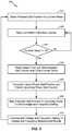
- FIG. 3illustrates an exemplary method 300 to scale clock frequency and voltage according to whether a cooperative hardware and software/firmware mechanism predicts that an upcoming program execution phase will be a memory-bound program phase or a compute-intensive program phase.
- a predicted stall fraction for the current phasemay be obtained, wherein the predicted stall fraction for the current phase may have been computed in an immediately preceding phase.
- the software/firmwaremay read the committed instruction counter at block 320 (e.g., in each cycle, on a periodic basis, etc.) and then determine whether the value read from committed instruction counter has reached the threshold value at block 330 .
- the software/firmware mechanismmay continue to read the committed instruction counter at block 320 until the value read from committed instruction counter has reached the threshold value. Once the value read from the instruction counter reaches the threshold value, as determined at block 330 , the software/firmware mechanism may then further read the LLC miss dispatch stall counter and the cycle counter at block 340 , at which time the hardware counters may again be reset to zero.
- the software/firmwaremay divide the value read from the LLC miss dispatch stall counter at block 340 according to the value read from the cycle counter at block 340 to compute a stall fraction in the current program phase, wherein the computed stall fraction may represent a percentage of the total cycles during the current program phase in which a dispatch stall occurred in the presence of the oldest instruction in the load queue being a LLC miss. Accordingly, based on the predicted stall fraction for the current phase, as obtained at block 310 , the stall fraction in a next (upcoming) phase may be predicted at block 350 based on the computed stall fraction in the current program phase and the predicted stall fraction for the current program phase, as calculated in the immediately preceding program phase.
- Stall nis the actual stall fraction in the current phase as computed at block 350
- PredStall nis the stall fraction that was predicted for the current phase and obtained at block 310 .
- the predicted stall fractionin response to suitably predicting the stall fraction in the next program phase, may be mapped to optimal clock frequency and voltage settings at block 360 , wherein the optimal clock frequency and voltage settings mapped to the predicted stall fraction may best maximize power savings and minimize performance loss at the predicted stall fraction.
- the mapped voltage and frequency settingsmay then be communicated to a voltage and frequency management module at block 370 , wherein the voltage and frequency management module may adjust a voltage supplied to the processor and a frequency at which clock pulses are supplied to the processors accordingly.
- the method 300may then return to block 310 , where the predicted stall fraction in the next program phase (as computed at block 350 ) may be obtained and used to predict stall fractions in subsequent program phases in substantially the same manner described in further detail above.
- the cooperative hardware and software/firmware DCVS mechanisms and the corresponding methods described hereincan be employed in any circuit, including but not limited to a microprocessor-based circuit, system, or others suitable electronic device.
- electronic devices that can include or otherwise employ the cooperative hardware and software/firmware DCVS mechanisms described hereincan comprise, without limitation, mobile phones, cellular phones, computers, portable computers, desktop computers, personal digital assistants (PDAs), monitors, computer monitors, televisions, tuners, radios, satellite radios, digital music players, portable music players, digital video players, digital video disc (DVD) players, portable digital video players, or the like.
- FIG. 4illustrates an example processor-based system 400 that can employ the cooperative hardware and software/firmware DCVS mechanisms and corresponding methods described in further detail above with respect to FIG. 1 through FIG. 3 .
- the processor-based system 400 shown in FIG. 4includes a central processing unit (CPU) 410 that includes a cache 416 and a processor 412 , which may include DCVS circuitry 414 configured to implement the cooperative hardware and software/firmware DCVS mechanisms and corresponding methods described in further detail above.
- CPUcentral processing unit
- processor 412which may include DCVS circuitry 414 configured to implement the cooperative hardware and software/firmware DCVS mechanisms and corresponding methods described in further detail above.
- the DCVS circuitry 414may include various hardware counters that can track statistics that may indicate a degree to which a current program execution phase is memory-bound and/or compute-intensive in addition to software/firmware that can predict memory-boundedness in upcoming program phases according to the statistics that are tracked using the various hardware counters. Furthermore, the DCVS circuitry 414 may comprise a voltage and frequency management module that can adjust a supply voltage on the CPU 410 and a frequency at which clock pulses are supplied to the CPU 410 based on desired voltage and frequency settings determined at the software/firmware according to a mapping between predicted stall fractions and optimal voltage and frequency settings at the predicted stall fractions.
- the CPU 410may be coupled to a system bus 420 , which may intercouple various other devices included in the processor-based system 400 .
- the CPU 410may exchange address, control, and data information over the system bus 420 to communicate with the other devices included in the processor-based system 400 , which can include suitable devices.
- the devices included in the processor-based system 400can include a memory subsystem 430 that can include static memory 432 and/or dynamic memory 434 , one or more input devices 422 , one or more output devices 424 , a network interface device 426 , and a display controller 440 .
- the input devices 422can include any suitable input device type, including but not limited to input keys, switches, voice processors, etc.
- the output devices 424can similarly include any suitable output device type, including but not limited to audio, video, other visual indicators, etc.
- the network interface device 426can be any device configured to allow exchange of data to and from a network 480 , which may comprise any suitable network type, including but not limited to a wired or wireless network, private or public network, a local area network (LAN), a wide local area network (WLAN), and the Internet.
- the network interface device 426can support any type of communication protocol desired.
- the CPU 410can access the memory subsystem 430 over the system bus 420 .
- the CPU 410can also access the display controller 440 over the system bus 420 to control information sent to a display 470 .
- the display controller 440can include a memory controller 442 and memory 444 to store data to be sent to the display 470 in response to communications with the CPU 410 .
- the display controller 440sends information to the display 470 to be displayed via a video processor 460 , which processes the information to be displayed into a format suitable for the display 470 .
- the display 470can include any suitable display type, including but not limited to a cathode ray tube (CRT), a liquid crystal display (LCD), a plasma display, etc.
- a general purpose processormay be a microprocessor, or in the alternative, the processor may be any conventional processor, controller, microcontroller, state machine, etc.
- the processormay also be implemented as a combination of computing devices (e.g., a combination of a DSP and a microprocessor, a plurality of microprocessors, one or more microprocessors in conjunction with a DSP core, or any other suitable configuration).
- a combination of a DSP and a microprocessore.g., a combination of a DSP and a microprocessor, a plurality of microprocessors, one or more microprocessors in conjunction with a DSP core, or any other suitable configuration.
- a software modulemay reside in RAM, flash memory, ROM, EPROM, EEPROM, registers, hard disk, a removable disk, a CD-ROM, or any other form of storage medium known in the art.
- An exemplary storage mediumis coupled to the processor such that the processor can read information from, and write information to, the storage medium.
- the storage mediummay be integral to the processor.
- the processor and the storage mediummay reside in an ASIC.
- the ASICmay reside in an IoT device.
- the processor and the storage mediummay reside as discrete components in a user terminal.
- the functions describedmay be implemented in hardware, software, firmware, or any combination thereof. If implemented in software, the functions may be stored on or transmitted over as one or more instructions or code on a computer-readable medium.
- Computer-readable mediaincludes both computer storage media and communication media including any medium that facilitates transfer of a computer program from one place to another.
- a storage mediamay be any available media that can be accessed by a computer.
- such computer-readable mediacan comprise RAM, ROM, EEPROM, CD-ROM or other optical disk storage, magnetic disk storage or other magnetic storage devices, or any other medium that can be used to carry or store desired program code in the form of instructions or data structures and that can be accessed by a computer.
- any connectionis properly termed a computer-readable medium.
- the softwareis transmitted from a website, server, or other remote source using a coaxial cable, fiber optic cable, twisted pair, DSL, or wireless technologies such as infrared, radio, and microwave
- the coaxial cable, fiber optic cable, twisted pair, DSL, or wireless technologiessuch as infrared, radio, and microwave are included in the definition of a medium.
- disk and discwhich may be used interchangeably herein, includes CD, laser disc, optical disc, DVD, floppy disk, and Blu-ray discs, which usually reproduce data magnetically and/or optically with lasers. Combinations of the above should also be included within the scope of computer-readable media.
Landscapes
- Engineering & Computer Science (AREA)
- Theoretical Computer Science (AREA)
- Physics & Mathematics (AREA)
- General Engineering & Computer Science (AREA)
- General Physics & Mathematics (AREA)
- Power Sources (AREA)
Abstract
Description
PredStalln+1=α*Stalln+(1−α)*PredStalln,
PredStalln+1=α*Stalln+(1−α)*PredStalln,
Claims (36)
PredStalln+1=α*Stalln+(1−α)*PredStalln,
PredStalln+1=α*Stalln+(1−α)*PredStalln,
PredStalln+1=α*Stalln+(1−α)*PredStalln,
PredStalln+1=α*Stalln+(1−α)*PredStalln,
Priority Applications (1)
| Application Number | Priority Date | Filing Date | Title |
|---|---|---|---|
| US15/814,361US10551896B2 (en) | 2016-01-04 | 2017-11-15 | Method and apparatus for dynamic clock and voltage scaling in a computer processor based on program phase |
Applications Claiming Priority (2)
| Application Number | Priority Date | Filing Date | Title |
|---|---|---|---|
| US14/986,738US9851774B2 (en) | 2016-01-04 | 2016-01-04 | Method and apparatus for dynamic clock and voltage scaling in a computer processor based on program phase |
| US15/814,361US10551896B2 (en) | 2016-01-04 | 2017-11-15 | Method and apparatus for dynamic clock and voltage scaling in a computer processor based on program phase |
Related Parent Applications (1)
| Application Number | Title | Priority Date | Filing Date |
|---|---|---|---|
| US14/986,738ContinuationUS9851774B2 (en) | 2016-01-04 | 2016-01-04 | Method and apparatus for dynamic clock and voltage scaling in a computer processor based on program phase |
Publications (2)
| Publication Number | Publication Date |
|---|---|
| US20180074568A1 US20180074568A1 (en) | 2018-03-15 |
| US10551896B2true US10551896B2 (en) | 2020-02-04 |
Family
ID=57681789
Family Applications (2)
| Application Number | Title | Priority Date | Filing Date |
|---|---|---|---|
| US14/986,738ActiveUS9851774B2 (en) | 2016-01-04 | 2016-01-04 | Method and apparatus for dynamic clock and voltage scaling in a computer processor based on program phase |
| US15/814,361Active2036-04-07US10551896B2 (en) | 2016-01-04 | 2017-11-15 | Method and apparatus for dynamic clock and voltage scaling in a computer processor based on program phase |
Family Applications Before (1)
| Application Number | Title | Priority Date | Filing Date |
|---|---|---|---|
| US14/986,738ActiveUS9851774B2 (en) | 2016-01-04 | 2016-01-04 | Method and apparatus for dynamic clock and voltage scaling in a computer processor based on program phase |
Country Status (3)
| Country | Link |
|---|---|
| US (2) | US9851774B2 (en) |
| TW (1) | TWI634410B (en) |
| WO (1) | WO2017119991A1 (en) |
Families Citing this family (213)
| Publication number | Priority date | Publication date | Assignee | Title |
|---|---|---|---|---|
| US9113347B2 (en) | 2012-12-05 | 2015-08-18 | At&T Intellectual Property I, Lp | Backhaul link for distributed antenna system |
| US10009065B2 (en) | 2012-12-05 | 2018-06-26 | At&T Intellectual Property I, L.P. | Backhaul link for distributed antenna system |
| US9999038B2 (en) | 2013-05-31 | 2018-06-12 | At&T Intellectual Property I, L.P. | Remote distributed antenna system |
| US9525524B2 (en) | 2013-05-31 | 2016-12-20 | At&T Intellectual Property I, L.P. | Remote distributed antenna system |
| US9209902B2 (en) | 2013-12-10 | 2015-12-08 | At&T Intellectual Property I, L.P. | Quasi-optical coupler |
| US9692101B2 (en) | 2014-08-26 | 2017-06-27 | At&T Intellectual Property I, L.P. | Guided wave couplers for coupling electromagnetic waves between a waveguide surface and a surface of a wire |
| US9768833B2 (en) | 2014-09-15 | 2017-09-19 | At&T Intellectual Property I, L.P. | Method and apparatus for sensing a condition in a transmission medium of electromagnetic waves |
| US9628854B2 (en) | 2014-09-29 | 2017-04-18 | At&T Intellectual Property I, L.P. | Method and apparatus for distributing content in a communication network |
| US9685992B2 (en) | 2014-10-03 | 2017-06-20 | At&T Intellectual Property I, L.P. | Circuit panel network and methods thereof |
| US9503189B2 (en) | 2014-10-10 | 2016-11-22 | At&T Intellectual Property I, L.P. | Method and apparatus for arranging communication sessions in a communication system |
| US9973299B2 (en) | 2014-10-14 | 2018-05-15 | At&T Intellectual Property I, L.P. | Method and apparatus for adjusting a mode of communication in a communication network |
| US9564947B2 (en) | 2014-10-21 | 2017-02-07 | At&T Intellectual Property I, L.P. | Guided-wave transmission device with diversity and methods for use therewith |
| US9653770B2 (en) | 2014-10-21 | 2017-05-16 | At&T Intellectual Property I, L.P. | Guided wave coupler, coupling module and methods for use therewith |
| US9769020B2 (en) | 2014-10-21 | 2017-09-19 | At&T Intellectual Property I, L.P. | Method and apparatus for responding to events affecting communications in a communication network |
| US9780834B2 (en) | 2014-10-21 | 2017-10-03 | At&T Intellectual Property I, L.P. | Method and apparatus for transmitting electromagnetic waves |
| US9520945B2 (en) | 2014-10-21 | 2016-12-13 | At&T Intellectual Property I, L.P. | Apparatus for providing communication services and methods thereof |
| US10340573B2 (en) | 2016-10-26 | 2019-07-02 | At&T Intellectual Property I, L.P. | Launcher with cylindrical coupling device and methods for use therewith |
| US9997819B2 (en) | 2015-06-09 | 2018-06-12 | At&T Intellectual Property I, L.P. | Transmission medium and method for facilitating propagation of electromagnetic waves via a core |
| US9742462B2 (en) | 2014-12-04 | 2017-08-22 | At&T Intellectual Property I, L.P. | Transmission medium and communication interfaces and methods for use therewith |
| US10505248B2 (en) | 2014-11-20 | 2019-12-10 | At&T Intellectual Property I, L.P. | Communication cable having a plurality of uninsulated conductors forming interstitial areas for propagating electromagnetic waves therein and method of use |
| US10516555B2 (en) | 2014-11-20 | 2019-12-24 | At&T Intellectual Property I, L.P. | Methods and apparatus for creating interstitial areas in a cable |
| US10411920B2 (en) | 2014-11-20 | 2019-09-10 | At&T Intellectual Property I, L.P. | Methods and apparatus for inducing electromagnetic waves within pathways of a cable |
| US10243784B2 (en) | 2014-11-20 | 2019-03-26 | At&T Intellectual Property I, L.P. | System for generating topology information and methods thereof |
| US10505250B2 (en) | 2014-11-20 | 2019-12-10 | At&T Intellectual Property I, L.P. | Communication system having a cable with a plurality of stranded uninsulated conductors forming interstitial areas for propagating guided wave modes therein and methods of use |
| US9680670B2 (en) | 2014-11-20 | 2017-06-13 | At&T Intellectual Property I, L.P. | Transmission device with channel equalization and control and methods for use therewith |
| US9800327B2 (en) | 2014-11-20 | 2017-10-24 | At&T Intellectual Property I, L.P. | Apparatus for controlling operations of a communication device and methods thereof |
| US11025460B2 (en) | 2014-11-20 | 2021-06-01 | At&T Intellectual Property I, L.P. | Methods and apparatus for accessing interstitial areas of a cable |
| US10505252B2 (en) | 2014-11-20 | 2019-12-10 | At&T Intellectual Property I, L.P. | Communication system having a coupler for guiding electromagnetic waves through interstitial areas formed by a plurality of stranded uninsulated conductors and method of use |
| US10009067B2 (en) | 2014-12-04 | 2018-06-26 | At&T Intellectual Property I, L.P. | Method and apparatus for configuring a communication interface |
| US10505249B2 (en) | 2014-11-20 | 2019-12-10 | At&T Intellectual Property I, L.P. | Communication system having a cable with a plurality of stranded uninsulated conductors forming interstitial areas for guiding electromagnetic waves therein and method of use |
| US10554454B2 (en) | 2014-11-20 | 2020-02-04 | At&T Intellectual Property I, L.P. | Methods and apparatus for inducing electromagnetic waves in a cable |
| US9654173B2 (en) | 2014-11-20 | 2017-05-16 | At&T Intellectual Property I, L.P. | Apparatus for powering a communication device and methods thereof |
| US10144036B2 (en) | 2015-01-30 | 2018-12-04 | At&T Intellectual Property I, L.P. | Method and apparatus for mitigating interference affecting a propagation of electromagnetic waves guided by a transmission medium |
| US9876570B2 (en) | 2015-02-20 | 2018-01-23 | At&T Intellectual Property I, Lp | Guided-wave transmission device with non-fundamental mode propagation and methods for use therewith |
| US10224981B2 (en) | 2015-04-24 | 2019-03-05 | At&T Intellectual Property I, Lp | Passive electrical coupling device and methods for use therewith |
| US9793954B2 (en) | 2015-04-28 | 2017-10-17 | At&T Intellectual Property I, L.P. | Magnetic coupling device and methods for use therewith |
| US9948354B2 (en) | 2015-04-28 | 2018-04-17 | At&T Intellectual Property I, L.P. | Magnetic coupling device with reflective plate and methods for use therewith |
| US9871282B2 (en) | 2015-05-14 | 2018-01-16 | At&T Intellectual Property I, L.P. | At least one transmission medium having a dielectric surface that is covered at least in part by a second dielectric |
| US9490869B1 (en) | 2015-05-14 | 2016-11-08 | At&T Intellectual Property I, L.P. | Transmission medium having multiple cores and methods for use therewith |
| US10714803B2 (en) | 2015-05-14 | 2020-07-14 | At&T Intellectual Property I, L.P. | Transmission medium and methods for use therewith |
| US10650940B2 (en) | 2015-05-15 | 2020-05-12 | At&T Intellectual Property I, L.P. | Transmission medium having a conductive material and methods for use therewith |
| US10679767B2 (en) | 2015-05-15 | 2020-06-09 | At&T Intellectual Property I, L.P. | Transmission medium having a conductive material and methods for use therewith |
| US9917341B2 (en) | 2015-05-27 | 2018-03-13 | At&T Intellectual Property I, L.P. | Apparatus and method for launching electromagnetic waves and for modifying radial dimensions of the propagating electromagnetic waves |
| US10756805B2 (en) | 2015-06-03 | 2020-08-25 | At&T Intellectual Property I, L.P. | Client node device with frequency conversion and methods for use therewith |
| US10154493B2 (en) | 2015-06-03 | 2018-12-11 | At&T Intellectual Property I, L.P. | Network termination and methods for use therewith |
| US9912381B2 (en) | 2015-06-03 | 2018-03-06 | At&T Intellectual Property I, Lp | Network termination and methods for use therewith |
| US9913139B2 (en) | 2015-06-09 | 2018-03-06 | At&T Intellectual Property I, L.P. | Signal fingerprinting for authentication of communicating devices |
| US9608692B2 (en) | 2015-06-11 | 2017-03-28 | At&T Intellectual Property I, L.P. | Repeater and methods for use therewith |
| US10142086B2 (en) | 2015-06-11 | 2018-11-27 | At&T Intellectual Property I, L.P. | Repeater and methods for use therewith |
| US9509415B1 (en) | 2015-06-25 | 2016-11-29 | At&T Intellectual Property I, L.P. | Methods and apparatus for inducing a fundamental wave mode on a transmission medium |
| US9640850B2 (en) | 2015-06-25 | 2017-05-02 | At&T Intellectual Property I, L.P. | Methods and apparatus for inducing a non-fundamental wave mode on a transmission medium |
| US10341142B2 (en) | 2015-07-14 | 2019-07-02 | At&T Intellectual Property I, L.P. | Apparatus and methods for generating non-interfering electromagnetic waves on an uninsulated conductor |
| US10033107B2 (en) | 2015-07-14 | 2018-07-24 | At&T Intellectual Property I, L.P. | Method and apparatus for coupling an antenna to a device |
| US10205655B2 (en) | 2015-07-14 | 2019-02-12 | At&T Intellectual Property I, L.P. | Apparatus and methods for communicating utilizing an antenna array and multiple communication paths |
| US10790593B2 (en) | 2015-07-14 | 2020-09-29 | At&T Intellectual Property I, L.P. | Method and apparatus including an antenna comprising a lens and a body coupled to a feedline having a structure that reduces reflections of electromagnetic waves |
| US10742243B2 (en) | 2015-07-14 | 2020-08-11 | At&T Intellectual Property I, L.P. | Method and apparatus for coupling an antenna to a device |
| US10044409B2 (en) | 2015-07-14 | 2018-08-07 | At&T Intellectual Property I, L.P. | Transmission medium and methods for use therewith |
| US10170840B2 (en) | 2015-07-14 | 2019-01-01 | At&T Intellectual Property I, L.P. | Apparatus and methods for sending or receiving electromagnetic signals |
| US9722318B2 (en) | 2015-07-14 | 2017-08-01 | At&T Intellectual Property I, L.P. | Method and apparatus for coupling an antenna to a device |
| US10129057B2 (en) | 2015-07-14 | 2018-11-13 | At&T Intellectual Property I, L.P. | Apparatus and methods for inducing electromagnetic waves on a cable |
| US10033108B2 (en) | 2015-07-14 | 2018-07-24 | At&T Intellectual Property I, L.P. | Apparatus and methods for generating an electromagnetic wave having a wave mode that mitigates interference |
| US10148016B2 (en) | 2015-07-14 | 2018-12-04 | At&T Intellectual Property I, L.P. | Apparatus and methods for communicating utilizing an antenna array |
| US10511346B2 (en) | 2015-07-14 | 2019-12-17 | At&T Intellectual Property I, L.P. | Apparatus and methods for inducing electromagnetic waves on an uninsulated conductor |
| US10320586B2 (en) | 2015-07-14 | 2019-06-11 | At&T Intellectual Property I, L.P. | Apparatus and methods for generating non-interfering electromagnetic waves on an insulated transmission medium |
| US9853342B2 (en) | 2015-07-14 | 2017-12-26 | At&T Intellectual Property I, L.P. | Dielectric transmission medium connector and methods for use therewith |
| US9793951B2 (en) | 2015-07-15 | 2017-10-17 | At&T Intellectual Property I, L.P. | Method and apparatus for launching a wave mode that mitigates interference |
| US9608740B2 (en) | 2015-07-15 | 2017-03-28 | At&T Intellectual Property I, L.P. | Method and apparatus for launching a wave mode that mitigates interference |
| US10090606B2 (en) | 2015-07-15 | 2018-10-02 | At&T Intellectual Property I, L.P. | Antenna system with dielectric array and methods for use therewith |
| US9749053B2 (en) | 2015-07-23 | 2017-08-29 | At&T Intellectual Property I, L.P. | Node device, repeater and methods for use therewith |
| US10784670B2 (en) | 2015-07-23 | 2020-09-22 | At&T Intellectual Property I, L.P. | Antenna support for aligning an antenna |
| US9735833B2 (en) | 2015-07-31 | 2017-08-15 | At&T Intellectual Property I, L.P. | Method and apparatus for communications management in a neighborhood network |
| US9967173B2 (en) | 2015-07-31 | 2018-05-08 | At&T Intellectual Property I, L.P. | Method and apparatus for authentication and identity management of communicating devices |
| US10009901B2 (en) | 2015-09-16 | 2018-06-26 | At&T Intellectual Property I, L.P. | Method, apparatus, and computer-readable storage medium for managing utilization of wireless resources between base stations |
| US10009063B2 (en) | 2015-09-16 | 2018-06-26 | At&T Intellectual Property I, L.P. | Method and apparatus for use with a radio distributed antenna system having an out-of-band reference signal |
| US10051629B2 (en) | 2015-09-16 | 2018-08-14 | At&T Intellectual Property I, L.P. | Method and apparatus for use with a radio distributed antenna system having an in-band reference signal |
| US10079661B2 (en) | 2015-09-16 | 2018-09-18 | At&T Intellectual Property I, L.P. | Method and apparatus for use with a radio distributed antenna system having a clock reference |
| US9769128B2 (en) | 2015-09-28 | 2017-09-19 | At&T Intellectual Property I, L.P. | Method and apparatus for encryption of communications over a network |
| US9882277B2 (en) | 2015-10-02 | 2018-01-30 | At&T Intellectual Property I, Lp | Communication device and antenna assembly with actuated gimbal mount |
| US10665942B2 (en) | 2015-10-16 | 2020-05-26 | At&T Intellectual Property I, L.P. | Method and apparatus for adjusting wireless communications |
| US10051483B2 (en) | 2015-10-16 | 2018-08-14 | At&T Intellectual Property I, L.P. | Method and apparatus for directing wireless signals |
| US9851774B2 (en) | 2016-01-04 | 2017-12-26 | Qualcomm Incorporated | Method and apparatus for dynamic clock and voltage scaling in a computer processor based on program phase |
| WO2017147131A1 (en)* | 2016-02-22 | 2017-08-31 | The Joan and Irwin Jacobs Technion-Cornell Institute | Techniques for self-tuning of computing systems |
| US20180024610A1 (en)* | 2016-07-22 | 2018-01-25 | Futurewei Technologies, Inc. | Apparatus and method for setting a clock speed/voltage of cache memory based on memory request information |
| US10034407B2 (en)* | 2016-07-22 | 2018-07-24 | Intel Corporation | Storage sled for a data center |
| US9912419B1 (en) | 2016-08-24 | 2018-03-06 | At&T Intellectual Property I, L.P. | Method and apparatus for managing a fault in a distributed antenna system |
| US9860075B1 (en) | 2016-08-26 | 2018-01-02 | At&T Intellectual Property I, L.P. | Method and communication node for broadband distribution |
| US11032819B2 (en) | 2016-09-15 | 2021-06-08 | At&T Intellectual Property I, L.P. | Method and apparatus for use with a radio distributed antenna system having a control channel reference signal |
| US10340600B2 (en) | 2016-10-18 | 2019-07-02 | At&T Intellectual Property I, L.P. | Apparatus and methods for launching guided waves via plural waveguide systems |
| US10135146B2 (en) | 2016-10-18 | 2018-11-20 | At&T Intellectual Property I, L.P. | Apparatus and methods for launching guided waves via circuits |
| US9876605B1 (en) | 2016-10-21 | 2018-01-23 | At&T Intellectual Property I, L.P. | Launcher and coupling system to support desired guided wave mode |
| US10811767B2 (en) | 2016-10-21 | 2020-10-20 | At&T Intellectual Property I, L.P. | System and dielectric antenna with convex dielectric radome |
| US10374316B2 (en) | 2016-10-21 | 2019-08-06 | At&T Intellectual Property I, L.P. | System and dielectric antenna with non-uniform dielectric |
| US9991580B2 (en) | 2016-10-21 | 2018-06-05 | At&T Intellectual Property I, L.P. | Launcher and coupling system for guided wave mode cancellation |
| US10312567B2 (en) | 2016-10-26 | 2019-06-04 | At&T Intellectual Property I, L.P. | Launcher with planar strip antenna and methods for use therewith |
| US10498044B2 (en) | 2016-11-03 | 2019-12-03 | At&T Intellectual Property I, L.P. | Apparatus for configuring a surface of an antenna |
| US10224634B2 (en) | 2016-11-03 | 2019-03-05 | At&T Intellectual Property I, L.P. | Methods and apparatus for adjusting an operational characteristic of an antenna |
| US10291334B2 (en) | 2016-11-03 | 2019-05-14 | At&T Intellectual Property I, L.P. | System for detecting a fault in a communication system |
| US10340601B2 (en) | 2016-11-23 | 2019-07-02 | At&T Intellectual Property I, L.P. | Multi-antenna system and methods for use therewith |
| US10535928B2 (en) | 2016-11-23 | 2020-01-14 | At&T Intellectual Property I, L.P. | Antenna system and methods for use therewith |
| US10305190B2 (en) | 2016-12-01 | 2019-05-28 | At&T Intellectual Property I, L.P. | Reflecting dielectric antenna system and methods for use therewith |
| US10361489B2 (en) | 2016-12-01 | 2019-07-23 | At&T Intellectual Property I, L.P. | Dielectric dish antenna system and methods for use therewith |
| US10096883B2 (en) | 2016-12-06 | 2018-10-09 | At&T Intellectual Property I, L.P. | Methods and apparatus for adjusting a wavelength electromagnetic waves |
| US10694379B2 (en) | 2016-12-06 | 2020-06-23 | At&T Intellectual Property I, L.P. | Waveguide system with device-based authentication and methods for use therewith |
| US10020844B2 (en) | 2016-12-06 | 2018-07-10 | T&T Intellectual Property I, L.P. | Method and apparatus for broadcast communication via guided waves |
| US10755542B2 (en) | 2016-12-06 | 2020-08-25 | At&T Intellectual Property I, L.P. | Method and apparatus for surveillance via guided wave communication |
| US10135145B2 (en) | 2016-12-06 | 2018-11-20 | At&T Intellectual Property I, L.P. | Apparatus and methods for generating an electromagnetic wave along a transmission medium |
| US10205212B2 (en) | 2016-12-06 | 2019-02-12 | At&T Intellectual Property I, L.P. | Methods and apparatus for adjusting a phase of electromagnetic waves |
| US10727599B2 (en) | 2016-12-06 | 2020-07-28 | At&T Intellectual Property I, L.P. | Launcher with slot antenna and methods for use therewith |
| US10819035B2 (en) | 2016-12-06 | 2020-10-27 | At&T Intellectual Property I, L.P. | Launcher with helical antenna and methods for use therewith |
| US10382976B2 (en) | 2016-12-06 | 2019-08-13 | At&T Intellectual Property I, L.P. | Method and apparatus for managing wireless communications based on communication paths and network device positions |
| US10637149B2 (en) | 2016-12-06 | 2020-04-28 | At&T Intellectual Property I, L.P. | Injection molded dielectric antenna and methods for use therewith |
| US10446936B2 (en) | 2016-12-07 | 2019-10-15 | At&T Intellectual Property I, L.P. | Multi-feed dielectric antenna system and methods for use therewith |
| US10027397B2 (en) | 2016-12-07 | 2018-07-17 | At&T Intellectual Property I, L.P. | Distributed antenna system and methods for use therewith |
| US9893795B1 (en) | 2016-12-07 | 2018-02-13 | At&T Intellectual Property I, Lp | Method and repeater for broadband distribution |
| US10359749B2 (en) | 2016-12-07 | 2019-07-23 | At&T Intellectual Property I, L.P. | Method and apparatus for utilities management via guided wave communication |
| US10389029B2 (en) | 2016-12-07 | 2019-08-20 | At&T Intellectual Property I, L.P. | Multi-feed dielectric antenna system with core selection and methods for use therewith |
| US10243270B2 (en) | 2016-12-07 | 2019-03-26 | At&T Intellectual Property I, L.P. | Beam adaptive multi-feed dielectric antenna system and methods for use therewith |
| US9998870B1 (en) | 2016-12-08 | 2018-06-12 | At&T Intellectual Property I, L.P. | Method and apparatus for proximity sensing |
| US10069535B2 (en) | 2016-12-08 | 2018-09-04 | At&T Intellectual Property I, L.P. | Apparatus and methods for launching electromagnetic waves having a certain electric field structure |
| US10601494B2 (en) | 2016-12-08 | 2020-03-24 | At&T Intellectual Property I, L.P. | Dual-band communication device and method for use therewith |
| US10411356B2 (en) | 2016-12-08 | 2019-09-10 | At&T Intellectual Property I, L.P. | Apparatus and methods for selectively targeting communication devices with an antenna array |
| US10938108B2 (en) | 2016-12-08 | 2021-03-02 | At&T Intellectual Property I, L.P. | Frequency selective multi-feed dielectric antenna system and methods for use therewith |
| US10136255B2 (en) | 2016-12-08 | 2018-11-20 | At&T Intellectual Property I, L.P. | Method and apparatus for proximity sensing on a communication device |
| US10264467B2 (en) | 2016-12-08 | 2019-04-16 | At&T Intellectual Property I, L.P. | Method and apparatus for collecting data associated with wireless communications |
| US10916969B2 (en) | 2016-12-08 | 2021-02-09 | At&T Intellectual Property I, L.P. | Method and apparatus for providing power using an inductive coupling |
| US10530505B2 (en) | 2016-12-08 | 2020-01-07 | At&T Intellectual Property I, L.P. | Apparatus and methods for launching electromagnetic waves along a transmission medium |
| US10777873B2 (en) | 2016-12-08 | 2020-09-15 | At&T Intellectual Property I, L.P. | Method and apparatus for mounting network devices |
| US10389037B2 (en) | 2016-12-08 | 2019-08-20 | At&T Intellectual Property I, L.P. | Apparatus and methods for selecting sections of an antenna array and use therewith |
| KR102670999B1 (en) | 2016-12-28 | 2024-05-30 | 삼성전자주식회사 | Application processor performing dynamic voltage and frequency scaling operation, computing system including the same, and operation method of thereof |
| US9973940B1 (en) | 2017-02-27 | 2018-05-15 | At&T Intellectual Property I, L.P. | Apparatus and methods for dynamic impedance matching of a guided wave launcher |
| US10298293B2 (en) | 2017-03-13 | 2019-05-21 | At&T Intellectual Property I, L.P. | Apparatus of communication utilizing wireless network devices |
| US10523388B2 (en) | 2017-04-17 | 2019-12-31 | At&T Intellectual Property I, L.P. | Method and apparatus for use with a radio distributed antenna having a fiber optic link |
| US10630341B2 (en) | 2017-05-11 | 2020-04-21 | At&T Intellectual Property I, L.P. | Method and apparatus for installation and alignment of radio devices |
| US10419072B2 (en) | 2017-05-11 | 2019-09-17 | At&T Intellectual Property I, L.P. | Method and apparatus for mounting and coupling radio devices |
| US11372464B2 (en)* | 2017-06-12 | 2022-06-28 | Intel Corporation | Adaptive parameterization for maximum current protection |
| US10389403B2 (en) | 2017-07-05 | 2019-08-20 | At&T Intellectual Property I, L.P. | Method and apparatus for reducing flow of currents on an outer surface of a structure |
| US10727583B2 (en) | 2017-07-05 | 2020-07-28 | At&T Intellectual Property I, L.P. | Method and apparatus for steering radiation on an outer surface of a structure |
| US10103777B1 (en) | 2017-07-05 | 2018-10-16 | At&T Intellectual Property I, L.P. | Method and apparatus for reducing radiation from an external surface of a waveguide structure |
| US10446899B2 (en) | 2017-09-05 | 2019-10-15 | At&T Intellectual Property I, L.P. | Flared dielectric coupling system and methods for use therewith |
| US10374278B2 (en) | 2017-09-05 | 2019-08-06 | At&T Intellectual Property I, L.P. | Dielectric coupling system with mode control and methods for use therewith |
| US10244408B1 (en) | 2017-10-19 | 2019-03-26 | At&T Intellectual Property I, L.P. | Dual mode communications device with null steering and methods for use therewith |
| US10374277B2 (en) | 2017-09-05 | 2019-08-06 | At&T Intellectual Property I, L.P. | Multi-arm dielectric coupling system and methods for use therewith |
| US10062970B1 (en) | 2017-09-05 | 2018-08-28 | At&T Intellectual Property I, L.P. | Dual mode communications device and methods for use therewith |
| US10051488B1 (en) | 2017-10-19 | 2018-08-14 | At&T Intellectual Property I, L.P. | Dual mode communications device with remote device feedback and methods for use therewith |
| US10714831B2 (en) | 2017-10-19 | 2020-07-14 | At&T Intellectual Property I, L.P. | Dual mode communications device with remote radio head and methods for use therewith |
| US10305179B2 (en) | 2017-09-06 | 2019-05-28 | At&T Intellectual Property I, L.P. | Antenna structure with doped antenna body |
| US10608312B2 (en) | 2017-09-06 | 2020-03-31 | At&T Intellectual Property I, L.P. | Method and apparatus for generating an electromagnetic wave that couples onto a transmission medium |
| US10230426B1 (en) | 2017-09-06 | 2019-03-12 | At&T Intellectual Property I, L.P. | Antenna structure with circularly polarized antenna beam |
| US10673116B2 (en) | 2017-09-06 | 2020-06-02 | At&T Intellectual Property I, L.P. | Method and apparatus for coupling an electromagnetic wave to a transmission medium |
| US10305197B2 (en) | 2017-09-06 | 2019-05-28 | At&T Intellectual Property I, L.P. | Multimode antenna system and methods for use therewith |
| US10291286B2 (en) | 2017-09-06 | 2019-05-14 | At&T Intellectual Property I, L.P. | Method and apparatus for guiding an electromagnetic wave to a transmission medium |
| US10205231B1 (en) | 2017-09-06 | 2019-02-12 | At&T Intellectual Property I, L.P. | Antenna structure with hollow-boresight antenna beam |
| US10469228B2 (en) | 2017-09-12 | 2019-11-05 | At&T Intellectual Property I, L.P. | Apparatus and methods for exchanging communications signals |
| US9998172B1 (en) | 2017-10-04 | 2018-06-12 | At&T Intellectual Property I, L.P. | Apparatus and methods for processing ultra-wideband electromagnetic waves |
| US10498589B2 (en) | 2017-10-04 | 2019-12-03 | At&T Intellectual Property I, L.P. | Apparatus and methods for mitigating a fault that adversely affects ultra-wideband transmissions |
| US10123217B1 (en) | 2017-10-04 | 2018-11-06 | At&T Intellectual Property I, L.P. | Apparatus and methods for communicating with ultra-wideband electromagnetic waves |
| US10764762B2 (en) | 2017-10-04 | 2020-09-01 | At&T Intellectual Property I, L.P. | Apparatus and methods for distributing a communication signal obtained from ultra-wideband electromagnetic waves |
| US10454151B2 (en) | 2017-10-17 | 2019-10-22 | At&T Intellectual Property I, L.P. | Methods and apparatus for coupling an electromagnetic wave onto a transmission medium |
| US10763916B2 (en) | 2017-10-19 | 2020-09-01 | At&T Intellectual Property I, L.P. | Dual mode antenna systems and methods for use therewith |
| US10553959B2 (en) | 2017-10-26 | 2020-02-04 | At&T Intellectual Property I, L.P. | Antenna system with planar antenna and directors and methods for use therewith |
| US10553960B2 (en) | 2017-10-26 | 2020-02-04 | At&T Intellectual Property I, L.P. | Antenna system with planar antenna and methods for use therewith |
| US10554235B2 (en) | 2017-11-06 | 2020-02-04 | At&T Intellectual Property I, L.P. | Multi-input multi-output guided wave system and methods for use therewith |
| US10555318B2 (en) | 2017-11-09 | 2020-02-04 | At&T Intellectual Property I, L.P. | Guided wave communication system with resource allocation and methods for use therewith |
| US10355745B2 (en) | 2017-11-09 | 2019-07-16 | At&T Intellectual Property I, L.P. | Guided wave communication system with interference mitigation and methods for use therewith |
| US10003364B1 (en) | 2017-11-09 | 2018-06-19 | At&T Intellectual Property I, L.P. | Guided wave communication system with interference cancellation and methods for use therewith |
| US10555249B2 (en) | 2017-11-15 | 2020-02-04 | At&T Intellectual Property I, L.P. | Access point and methods for communicating resource blocks with guided electromagnetic waves |
| US10284261B1 (en) | 2017-11-15 | 2019-05-07 | At&T Intellectual Property I, L.P. | Access point and methods for communicating with guided electromagnetic waves |
| US10230428B1 (en) | 2017-11-15 | 2019-03-12 | At&T Intellectual Property I, L.P. | Access point and methods for use in a radio distributed antenna system |
| US10389419B2 (en) | 2017-12-01 | 2019-08-20 | At&T Intellectual Property I, L.P. | Methods and apparatus for generating and receiving electromagnetic waves |
| US10374281B2 (en) | 2017-12-01 | 2019-08-06 | At&T Intellectual Property I, L.P. | Apparatus and method for guided wave communications using an absorber |
| US10469192B2 (en) | 2017-12-01 | 2019-11-05 | At&T Intellectual Property I, L.P. | Methods and apparatus for controllable coupling of an electromagnetic wave |
| US10820329B2 (en) | 2017-12-04 | 2020-10-27 | At&T Intellectual Property I, L.P. | Guided wave communication system with interference mitigation and methods for use therewith |
| US10424845B2 (en) | 2017-12-06 | 2019-09-24 | At&T Intellectual Property I, L.P. | Method and apparatus for communication using variable permittivity polyrod antenna |
| US10680308B2 (en) | 2017-12-07 | 2020-06-09 | At&T Intellectual Property I, L.P. | Methods and apparatus for bidirectional exchange of electromagnetic waves |
| US11018525B2 (en) | 2017-12-07 | 2021-05-25 | At&T Intellectual Property 1, L.P. | Methods and apparatus for increasing a transfer of energy in an inductive power supply |
| US10838647B2 (en) | 2018-03-14 | 2020-11-17 | Intel Corporation | Adaptive data migration across disaggregated memory resources |
| US10200106B1 (en) | 2018-03-26 | 2019-02-05 | At&T Intellectual Property I, L.P. | Analog surface wave multipoint repeater and methods for use therewith |
| US10686493B2 (en) | 2018-03-26 | 2020-06-16 | At&T Intellectual Property I, L.P. | Switching of data channels provided in electromagnetic waves and methods thereof |
| US10714824B2 (en) | 2018-03-26 | 2020-07-14 | At&T Intellectual Property I, L.P. | Planar surface wave launcher and methods for use therewith |
| US10340979B1 (en) | 2018-03-26 | 2019-07-02 | At&T Intellectual Property I, L.P. | Surface wave communication system and methods for use therewith |
| US10326495B1 (en) | 2018-03-26 | 2019-06-18 | At&T Intellectual Property I, L.P. | Coaxial surface wave communication system and methods for use therewith |
| US10727577B2 (en) | 2018-03-29 | 2020-07-28 | At&T Intellectual Property I, L.P. | Exchange of wireless signals guided by a transmission medium and methods thereof |
| US10581275B2 (en) | 2018-03-30 | 2020-03-03 | At&T Intellectual Property I, L.P. | Methods and apparatus for regulating a magnetic flux in an inductive power supply |
| US10547545B2 (en) | 2018-03-30 | 2020-01-28 | At&T Intellectual Property I, L.P. | Method and apparatus for switching of data channels provided in electromagnetic waves |
| US10419074B1 (en) | 2018-05-16 | 2019-09-17 | At&T Intellectual Property I, L.P. | Method and apparatus for communications using electromagnetic waves and an insulator |
| US10305192B1 (en) | 2018-08-13 | 2019-05-28 | At&T Intellectual Property I, L.P. | System and method for launching guided electromagnetic waves with impedance matching |
| US10784721B2 (en) | 2018-09-11 | 2020-09-22 | At&T Intellectual Property I, L.P. | Methods and apparatus for coupling and decoupling portions of a magnetic core |
| US10405199B1 (en) | 2018-09-12 | 2019-09-03 | At&T Intellectual Property I, L.P. | Apparatus and methods for transmitting or receiving electromagnetic waves |
| US10587310B1 (en) | 2018-10-10 | 2020-03-10 | At&T Intellectual Property I, L.P. | Methods and apparatus for selectively controlling energy consumption of a waveguide system |
| US10516197B1 (en) | 2018-10-18 | 2019-12-24 | At&T Intellectual Property I, L.P. | System and method for launching scattering electromagnetic waves |
| US10505584B1 (en) | 2018-11-14 | 2019-12-10 | At&T Intellectual Property I, L.P. | Device with resonant cavity for transmitting or receiving electromagnetic waves |
| US10686649B2 (en) | 2018-11-16 | 2020-06-16 | At&T Intellectual Property I, L.P. | Method and apparatus for managing a local area network |
| US10812139B2 (en) | 2018-11-29 | 2020-10-20 | At&T Intellectual Property I, L.P. | Method and apparatus for communication utilizing electromagnetic waves and a telecommunication line |
| US10371889B1 (en) | 2018-11-29 | 2019-08-06 | At&T Intellectual Property I, L.P. | Method and apparatus for providing power to waveguide systems |
| US10623056B1 (en) | 2018-12-03 | 2020-04-14 | At&T Intellectual Property I, L.P. | Guided wave splitter and methods for use therewith |
| US11362438B2 (en) | 2018-12-04 | 2022-06-14 | At&T Intellectual Property I, L.P. | Configurable guided wave launcher and methods for use therewith |
| US11121466B2 (en) | 2018-12-04 | 2021-09-14 | At&T Intellectual Property I, L.P. | Antenna system with dielectric antenna and methods for use therewith |
| US10581522B1 (en) | 2018-12-06 | 2020-03-03 | At&T Intellectual Property I, L.P. | Free-space, twisted light optical communication system |
| US10469156B1 (en) | 2018-12-13 | 2019-11-05 | At&T Intellectual Property I, L.P. | Methods and apparatus for measuring a signal to switch between modes of transmission |
| US11025299B2 (en) | 2019-05-15 | 2021-06-01 | At&T Intellectual Property I, L.P. | Methods and apparatus for launching and receiving electromagnetic waves |
| US11070250B2 (en) | 2019-12-03 | 2021-07-20 | At&T Intellectual Property I, L.P. | Method and apparatus for calibrating waveguide systems to manage propagation delays of electromagnetic waves |
| US10812291B1 (en) | 2019-12-03 | 2020-10-20 | At&T Intellectual Property I, L.P. | Method and apparatus for communicating between a waveguide system and a base station device |
| US10930992B1 (en) | 2019-12-03 | 2021-02-23 | At&T Intellectual Property I, L.P. | Method and apparatus for communicating between waveguide systems |
| US10804959B1 (en) | 2019-12-04 | 2020-10-13 | At&T Intellectual Property I, L.P. | Transmission device with corona discharge mitigation and methods for use therewith |
| US10812123B1 (en) | 2019-12-05 | 2020-10-20 | At&T Intellectual Property I, L.P. | Magnetic coupler for launching and receiving electromagnetic waves and methods thereof |
| KR20220079196A (en)* | 2020-12-04 | 2022-06-13 | 삼성전자주식회사 | Integrated circuit performing dynamic voltage and frequency scaling operation and operating method thereof |
| KR20220084843A (en) | 2020-12-14 | 2022-06-21 | 삼성전자주식회사 | Electronic device controlling a frequency of a clock signal and operating method thereof |
| CN116027879B (en)* | 2022-05-16 | 2023-10-20 | 荣耀终端有限公司 | Methods, electronic devices and computer-readable storage media for determining parameters |
| US20240053809A1 (en)* | 2022-08-12 | 2024-02-15 | Samsung Electronics Co., Ltd. | Integrated circuit capable of performing dynamic voltage and frequency scaling operation based on workload and operating method thereof |
| US20240303668A1 (en)* | 2023-03-08 | 2024-09-12 | Devices-Unlimited Corp. | System and method for an instrumentation node for measuring and tracking carbon footprint of manufactured goods |
| CN116540820B (en)* | 2023-07-04 | 2023-08-29 | 摩尔线程智能科技(北京)有限责任公司 | Voltage and frequency control system, method and storage medium |
| CN116931703B (en)* | 2023-09-18 | 2023-12-26 | 惠州市鑫晖源科技有限公司 | Electronic contest host power supply voltage adjusting method based on data analysis |
| CN118672662B (en)* | 2024-08-23 | 2024-12-17 | 苏州国芯科技股份有限公司 | Instruction tracking method, device, equipment and medium |
Citations (12)
| Publication number | Priority date | Publication date | Assignee | Title |
|---|---|---|---|---|
| TW343297B (en) | 1996-07-24 | 1998-10-21 | Lg Semicon Co Ltd | Charge recycling differential logic (CRDL) circuit and storage elements and devices using the same |
| US6189072B1 (en) | 1996-12-17 | 2001-02-13 | International Business Machines Corporation | Performance monitoring of cache misses and instructions completed for instruction parallelism analysis |
| US20080235364A1 (en) | 2006-03-07 | 2008-09-25 | Eugene Gorbatov | Method and apparatus for using dynamic workload characteristics to control CPU frequency and voltage scaling |
| US20090210740A1 (en)* | 2008-02-14 | 2009-08-20 | Song Huang | Off-chip access workload characterization methodology for optimizing computing efficiency |
| US20090312930A1 (en)* | 2006-05-19 | 2009-12-17 | Tomofumi Nakakita | Stall prediction apparatus, prediction method thereof, and engine control system |
| US7730340B2 (en) | 2007-02-16 | 2010-06-01 | Intel Corporation | Method and apparatus for dynamic voltage and frequency scaling |
| US7840825B2 (en) | 2006-10-24 | 2010-11-23 | International Business Machines Corporation | Method for autonomous dynamic voltage and frequency scaling of microprocessors |
| US20110093734A1 (en) | 2008-05-13 | 2011-04-21 | Artur Tadeusz Burchard | Power Manager and Method for Managing Power |
| CN102687098A (en) | 2010-01-11 | 2012-09-19 | 高通股份有限公司 | System and method of dynamically controlling a processor |
| US20120260057A1 (en)* | 2009-12-18 | 2012-10-11 | Eyerman Stijn | Counter architecture for online dvfs profitability estimation |
| US20140277815A1 (en)* | 2013-03-14 | 2014-09-18 | Arizona Board Of Regents For And On Behalf Of Arizona State University | Processor control system |
| US20170192484A1 (en) | 2016-01-04 | 2017-07-06 | Qualcomm Incorporated | Method and apparatus for dynamic clock and voltage scaling in a computer processor based on program phase |
- 2016
- 2016-01-04USUS14/986,738patent/US9851774B2/enactiveActive
- 2016-12-12WOPCT/US2016/066099patent/WO2017119991A1/ennot_activeCeased
- 2016-12-12TWTW105141098Apatent/TWI634410B/enactive
- 2017
- 2017-11-15USUS15/814,361patent/US10551896B2/enactiveActive
Patent Citations (16)
| Publication number | Priority date | Publication date | Assignee | Title |
|---|---|---|---|---|
| TW343297B (en) | 1996-07-24 | 1998-10-21 | Lg Semicon Co Ltd | Charge recycling differential logic (CRDL) circuit and storage elements and devices using the same |
| US6189072B1 (en) | 1996-12-17 | 2001-02-13 | International Business Machines Corporation | Performance monitoring of cache misses and instructions completed for instruction parallelism analysis |
| CN101379453B (en) | 2006-03-07 | 2011-05-25 | 英特尔公司 | Method and apparatus for using dynamic workload characteristics to control CPU frequency and voltage scaling |
| US20080235364A1 (en) | 2006-03-07 | 2008-09-25 | Eugene Gorbatov | Method and apparatus for using dynamic workload characteristics to control CPU frequency and voltage scaling |
| CN101379453A (en) | 2006-03-07 | 2009-03-04 | 英特尔公司 | Method and apparatus for using dynamic workload characteristics to control CPU frequency and voltage scaling |
| US20090312930A1 (en)* | 2006-05-19 | 2009-12-17 | Tomofumi Nakakita | Stall prediction apparatus, prediction method thereof, and engine control system |
| US7840825B2 (en) | 2006-10-24 | 2010-11-23 | International Business Machines Corporation | Method for autonomous dynamic voltage and frequency scaling of microprocessors |
| US7730340B2 (en) | 2007-02-16 | 2010-06-01 | Intel Corporation | Method and apparatus for dynamic voltage and frequency scaling |
| US20090210740A1 (en)* | 2008-02-14 | 2009-08-20 | Song Huang | Off-chip access workload characterization methodology for optimizing computing efficiency |
| US20110093734A1 (en) | 2008-05-13 | 2011-04-21 | Artur Tadeusz Burchard | Power Manager and Method for Managing Power |
| US20120260057A1 (en)* | 2009-12-18 | 2012-10-11 | Eyerman Stijn | Counter architecture for online dvfs profitability estimation |
| US8812808B2 (en) | 2009-12-18 | 2014-08-19 | Universiteit Gent | Counter architecture for online DVFS profitability estimation |
| CN102687098A (en) | 2010-01-11 | 2012-09-19 | 高通股份有限公司 | System and method of dynamically controlling a processor |
| CN102687098B (en) | 2010-01-11 | 2015-06-17 | 高通股份有限公司 | System and method for executing a dynamic clock and voltage scaling based on workload in wireless device |
| US20140277815A1 (en)* | 2013-03-14 | 2014-09-18 | Arizona Board Of Regents For And On Behalf Of Arizona State University | Processor control system |
| US20170192484A1 (en) | 2016-01-04 | 2017-07-06 | Qualcomm Incorporated | Method and apparatus for dynamic clock and voltage scaling in a computer processor based on program phase |
Non-Patent Citations (5)
| Title |
|---|
| International Search Report and Written Opinion—PCT/US2016/066099—ISA/EPO—dated Mar. 16, 2017. |
| KONRAD MALKOWSKI ; PADMA RAGHAVAN ; MAHMUT KANDEMIR ; MARY JANE IRWIN: "Phase-aware adaptive hardware selection for power-efficient scientific computations", LOW POWER ELECTRONICS AND DESIGN (ISLPED), 2007 ACM/IEEE INTERNATIONAL SYMPOSIUM ON, IEEE, PISCATAWAY, NJ, USA, 27 August 2007 (2007-08-27), Piscataway, NJ, USA, pages 403 - 406, XP031711253 |
| Malkowski K., et al., "Phase-aware Adaptive Hardware Selection for Power-efficient Scientific Computations", Low Power Electronics and Design (ISLPED), 2007 ACM/IEEE International Symposium on, IEEE, Piscataway, NJ, USA, Aug. 27, 2007 (Aug. 27, 2007), XP031711253, pp. 403-406. |
| Sasaki H., et al., "An Intra-Task DVFS Technique based on Statistical Analysis of Hardware Events," CF '07 Proceedings of the 4th international conference on Computing frontiers, ACM, May 7-9, 2007, pp. 123-130. |
| Taiwan Search Report—TW105141098—TIPO—dated Mar. 7, 2018. |
Also Published As
| Publication number | Publication date |
|---|---|
| US9851774B2 (en) | 2017-12-26 |
| TWI634410B (en) | 2018-09-01 |
| US20180074568A1 (en) | 2018-03-15 |
| US20170192484A1 (en) | 2017-07-06 |
| WO2017119991A1 (en) | 2017-07-13 |
| TW201727427A (en) | 2017-08-01 |
Similar Documents
| Publication | Publication Date | Title |
|---|---|---|
| US10551896B2 (en) | Method and apparatus for dynamic clock and voltage scaling in a computer processor based on program phase | |
| KR101518440B1 (en) | Dynamic performance control of processing nodes | |
| US7861068B2 (en) | Method and apparatus for using dynamic workload characteristics to control CPU frequency and voltage scaling | |
| US10372198B2 (en) | Controlling performance states of processing engines of a processor | |
| US8250395B2 (en) | Dynamic voltage and frequency scaling (DVFS) control for simultaneous multi-threading (SMT) processors | |
| US8656196B2 (en) | Hardware automatic performance state transitions in system on processor sleep and wake events | |
| US9626295B2 (en) | Systems and methods for scheduling tasks in a heterogeneous processor cluster architecture using cache demand monitoring | |
| US20120297232A1 (en) | Adjusting the clock frequency of a processing unit in real-time based on a frequency sensitivity value | |
| US20240028101A1 (en) | System, apparatus and method for globally aware reactive local power control in a processor | |
| US9753531B2 (en) | Method, apparatus, and system for energy efficiency and energy conservation including determining an optimal power state of the apparatus based on residency time of non-core domains in a power saving state | |
| TW202105177A (en) | Apparatus and system forcontrolling use of hierarchical branch predictors | |
| US9274827B2 (en) | Data processing apparatus, transmitting apparatus, transmission control method, scheduling method, and computer product | |
| US11669114B2 (en) | System, apparatus and method for sensor-driven and heuristic-based minimum energy point tracking in a processor | |
| EP3855285B1 (en) | System, apparatus and method for latency monitoring and response | |
| CN116635833A (en) | Precise timestamp or derived counter value generation on complex CPUs | |
| JPH11110063A (en) | Computer system | |
| CN119292450A (en) | Electronic device and control method |
Legal Events
| Date | Code | Title | Description |
|---|---|---|---|
| FEPP | Fee payment procedure | Free format text:ENTITY STATUS SET TO UNDISCOUNTED (ORIGINAL EVENT CODE: BIG.); ENTITY STATUS OF PATENT OWNER: LARGE ENTITY | |
| AS | Assignment | Owner name:QUALCOMM INCORPORATED, CALIFORNIA Free format text:ASSIGNMENT OF ASSIGNORS INTEREST;ASSIGNORS:PRIYADARSHI, SHIVAM;KRISHNA, ANIL;DAMODARAN, RAGURAM;AND OTHERS;SIGNING DATES FROM 20160406 TO 20160428;REEL/FRAME:044282/0499 | |
| STPP | Information on status: patent application and granting procedure in general | Free format text:DOCKETED NEW CASE - READY FOR EXAMINATION | |
| STPP | Information on status: patent application and granting procedure in general | Free format text:NON FINAL ACTION MAILED | |
| STPP | Information on status: patent application and granting procedure in general | Free format text:RESPONSE TO NON-FINAL OFFICE ACTION ENTERED AND FORWARDED TO EXAMINER | |
| STPP | Information on status: patent application and granting procedure in general | Free format text:FINAL REJECTION MAILED | |
| STPP | Information on status: patent application and granting procedure in general | Free format text:RESPONSE AFTER FINAL ACTION FORWARDED TO EXAMINER | |
| STPP | Information on status: patent application and granting procedure in general | Free format text:NOTICE OF ALLOWANCE MAILED -- APPLICATION RECEIVED IN OFFICE OF PUBLICATIONS | |
| STPP | Information on status: patent application and granting procedure in general | Free format text:PUBLICATIONS -- ISSUE FEE PAYMENT RECEIVED | |
| STPP | Information on status: patent application and granting procedure in general | Free format text:PUBLICATIONS -- ISSUE FEE PAYMENT VERIFIED | |
| STCF | Information on status: patent grant | Free format text:PATENTED CASE | |
| MAFP | Maintenance fee payment | Free format text:PAYMENT OF MAINTENANCE FEE, 4TH YEAR, LARGE ENTITY (ORIGINAL EVENT CODE: M1551); ENTITY STATUS OF PATENT OWNER: LARGE ENTITY Year of fee payment:4 |