US10547118B2 - Dielectric resonator antenna arrays - Google Patents
Dielectric resonator antenna arraysDownload PDFInfo
- Publication number
- US10547118B2 US10547118B2US14/606,715US201514606715AUS10547118B2US 10547118 B2US10547118 B2US 10547118B2US 201514606715 AUS201514606715 AUS 201514606715AUS 10547118 B2US10547118 B2US 10547118B2
- Authority
- US
- United States
- Prior art keywords
- dielectric
- array
- sheet
- holes
- portions
- Prior art date
- Legal status (The legal status is an assumption and is not a legal conclusion. Google has not performed a legal analysis and makes no representation as to the accuracy of the status listed.)
- Active, expires
Links
Images


Classifications
- H—ELECTRICITY
- H01—ELECTRIC ELEMENTS
- H01Q—ANTENNAS, i.e. RADIO AERIALS
- H01Q19/00—Combinations of primary active antenna elements and units with secondary devices, e.g. with quasi-optical devices, for giving the antenna a desired directional characteristic
- H01Q19/06—Combinations of primary active antenna elements and units with secondary devices, e.g. with quasi-optical devices, for giving the antenna a desired directional characteristic using refracting or diffracting devices, e.g. lens
- H01Q19/062—Combinations of primary active antenna elements and units with secondary devices, e.g. with quasi-optical devices, for giving the antenna a desired directional characteristic using refracting or diffracting devices, e.g. lens for focusing
- H—ELECTRICITY
- H01—ELECTRIC ELEMENTS
- H01Q—ANTENNAS, i.e. RADIO AERIALS
- H01Q15/00—Devices for reflection, refraction, diffraction or polarisation of waves radiated from an antenna, e.g. quasi-optical devices
- H01Q15/02—Refracting or diffracting devices, e.g. lens, prism
- H01Q15/08—Refracting or diffracting devices, e.g. lens, prism formed of solid dielectric material
- H—ELECTRICITY
- H01—ELECTRIC ELEMENTS
- H01Q—ANTENNAS, i.e. RADIO AERIALS
- H01Q21/00—Antenna arrays or systems
- H01Q21/06—Arrays of individually energised antenna units similarly polarised and spaced apart
- H01Q21/061—Two dimensional planar arrays
- H—ELECTRICITY
- H01—ELECTRIC ELEMENTS
- H01Q—ANTENNAS, i.e. RADIO AERIALS
- H01Q9/00—Electrically-short antennas having dimensions not more than twice the operating wavelength and consisting of conductive active radiating elements
- H01Q9/04—Resonant antennas
- H01Q9/0485—Dielectric resonator antennas
Definitions
- the present disclosurerelates generally to a design for a lens element, and in a particular embodiment, to a dielectric lens element for a dielectric resonator antenna (DRA) arrays.
- DRAdielectric resonator antenna
- Millimeter-wave frequency bands utilizing frequencies around 60 GHzcan be employed to realize the next-generation wireless short-haul high-speed microwave communication links between wireless devices.
- Millimeter-wave antenna arraysneeds to satisfy the link budget requirement.
- the path losscan be compensated by using high gain antenna arrays for transmitting and receiving electromagnetic signals.
- the antenna elements such arraysshould initially achieve acceptable gain.
- Various methodshave been proposed to increase antenna element gain, including the use of a dielectric resonating element attached on each antenna element. Examples of some dielectric resonator antenna (DRA) arrays according to the prior art are disclosed in Petosa, A.; Ittipiboon, A. “Dielectric Resonator Antennas: A Historical Review and the Current State of the Art”, Antennas and Propagation Magazine , IEEE, pages 91-116, Volume: 52, Issue: 5, October 2010.
- DPAdielectric resonator antenna
- the present disclosureprovides a dielectric lens for a dielectric resonator antenna (DRA) array having a plurality of antenna elements.
- the dielectric lenscomprises a single piece of dielectric material in the form of a generally planar sheet. The sheet is substantially coextensive with the DRA array so as to cover all of antenna elements.
- the single piece of dielectric materialcomprises a plurality of dielectric portions defined by a plurality of holes through the sheet. Each dielectric portion is positioned over one of the antenna elements. Adjacent dielectric portions are connected to each other along connecting edge portions thereof. A single hole is defined through the sheet between connecting edge portions of a group of mutually adjacent dielectric portions.
- the present disclosureprovides a dielectric resonator antenna (DRA) array having an array feeding network, a parasitic patch array with a plurality of antenna elements, and a dielectric lens made from a single piece of dielectric material in the form of a generally planar sheet.
- the sheetis substantially coextensive with the DRA array so as to cover all of the plurality of antenna elements.
- the single piece of dielectric materialcomprises a plurality of dielectric portions defined by a plurality of holes through the sheet. Each dielectric portion is positioned over one of the antenna elements. Adjacent dielectric portions are connected to each other along connecting edge portions thereof. A single hole is defined through the sheet between connecting edge portions of a group of mutually adjacent dielectric portions.
- the plurality of antenna elements and the plurality of dielectric portionsmay be arranged in rectangular arrays, with each rectangular array forming a grid of generally perpendicular rows and columns.
- the plurality of antenna elementsmay be arranged in a plurality of 2 ⁇ 2 sub arrays, and the plurality of dielectric elements may be arranged in a plurality of sub groups corresponding to the plurality of 2 ⁇ 2 sub arrays.
- the holesmay comprise a plurality of first holes, a plurality of second holes larger than the first holes, and a plurality of third holes larger than the second holes.
- Each first holemay be positioned between four dielectric elements of a single sub group
- each second holemay be positioned between four dielectric elements from two different sub groups
- each third holemay be positioned between four dielectric elements from four different sub groups.
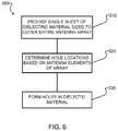
- the present disclosureprovides a method for producing a dielectric lens for a dielectric resonator antenna (DRA) array.
- the methodcomprises providing a single piece of dielectric material in the form of a generally planar sheet, the sheet being substantially coextensive with the DRA array so as to cover all of the plurality of antenna elements, determining locations for a plurality of holes through the sheet based on locations of the plurality of antenna elements, and forming the plurality of holes through the sheet to define a plurality of dielectric portions, each dielectric portion being configured to be positioned over one of the plurality of antenna elements.
- DRAdielectric resonator antenna
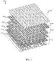
- FIG. 1is an exploded perspective view an example dielectric resonator antenna (DRA) array according to one embodiment
- FIG. 2is a perspective view of the dielectric sheet of the example DRA array of FIG. 1 .
- FIG. 3is a perspective view of an example prior art array of individual dielectric elements.
- FIG. 4is a top plan view of the dielectric sheet of the example DRA array of FIG. 1 .
- FIG. 5is a perspective view of an example dielectric sheet for a 2 ⁇ 2 sub array of the example DRA array of FIG. 1 .
- FIG. 6is a flowchart illustrating steps of an example method of forming a dielectric sheet for a DRA array according to one embodiment.
- FIG. 7is a top plan view of an example dielectric sheet for a DRA array according to another embodiment.
- FIG. 8is a top plan view of an example dielectric sheet for a DRA array according to another embodiment.
- FIG. 9is a top plan view of an example dielectric sheet for a DRA array according to another embodiment.
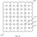
- FIG. 10is a top plan view of an example dielectric sheet for a DRA array according to another embodiment.
- the present disclosureis directed to a dielectric lens for use in a dielectric resonator array.
- the lensis in the form of a single dielectric sheet of dielectric material for a dielectric resonator antenna (DRA) array.
- the sheethas a plurality of dielectric elements defined by a plurality of holes through the sheet.
- FIG. 1shows an example of a DRA array 100 according to one embodiment.
- the DRA arraycomprises an array feeding network 110 , a parasitic patch array 120 , and a dielectric lens in the form of a single dielectric sheet 200 , which is described in further detail below.
- the array feeding network 110comprises three layers 112 , 114 , 116 configured to provide signals to and receive signals from the parasitic patch array 120 .
- the parasitic patch array 120comprises first and second layers 122 , 124 , each comprising a plurality of antenna elements (not enumerated).
- the antenna elements of the parasitic patch array 120are arranged into a plurality of sub arrays 126 of four individual antenna elements in a 2 ⁇ 2 rectangular grid, and the spacing between adjacent antenna elements within each sub array 126 is smaller than the spacing between adjacent antenna elements from different sub arrays 126 .
- the DRA arrayis configured to operate in a frequency bandwidth of about 57-66 GHz.
- the sheet 200 of FIG. 1comprises a single piece 202 of dielectric material that is generally planar and has a substantially uniform height h (also referred to as a thickness).
- the piece of dielectric materialhas a height h that is selected based on a signal wavelength A of the DRA array 100 .
- the piece of dielectric materialhas a height h in the range of 0.5 ⁇ to 0.6 ⁇ .
- the piece of dielectric materialhas a height h in the range of 100-120 mils.
- the dielectric materialhas a dielectric constant in the range of 2 to 10, depending on the dielectric constant of the array feeding network 110 .
- the single piece 202 of dielectric materialcomprises a plurality of dielectric portions 204 defined by a plurality of holes 210 , 212 , 214 through the sheet 200 .
- Each dielectric portion 204is configured to be positioned over one of the antenna elements of the parasitic patch array 120 .
- FIG. 3shows an example prior art array 10 of individual dielectric elements 12 .
- Each dielectric element 12must be individually positioned and mounted atop a corresponding antenna element.
- the sheet 200 of FIG. 2advantageously eliminates the need for individual alignment of dielectric elements, since only the single piece 202 needs to be aligned with the parasitic patch array 120 .
- the dielectric portions 204are each connected to adjacent dielectric portions 204 by connecting edge portions.
- the dielectric portions 204are generally rhombus-shaped (e.g. squares), with the connecting edge portions comprising corner portions of each square.
- a single hole 210 / 212 / 214is defined between connecting edge portions of a group of mutually adjacent dielectric portions 204 .
- the term “mutually adjacent dielectric portions”is used herein to refer to a group of dielectric portions 204 that are all either horizontally, vertically or diagonally (with reference to the orientation illustrated in FIGS. 2 and 4 ) adjacent to one another, and which surround a single hole 210 / 212 / 214 .
- all of the holesmay be the same size.
- the holes 210 / 212 / 214may have different sizes, as discussed below.
- the dielectric portions 204are arranged in sub groups 206 , with each sub group 206 configured to be positioned over a corresponding sub array 126 of the parasitic patch array 120 .
- the connecting edge portions between adjacent dielectric portions 204 within a sub group 206are more extensive than the connecting edge portions between adjacent dielectric portions 204 from adjacent sub groups 206 , due to the difference in spacing between the underlying antenna elements.
- each of the holes 210 within a sub group 206is smaller than each of the holes 212 between horizontally or vertically (with reference to the orientation illustrated in FIGS. 2 and 4 ) adjacent sub groups 206 .
- each of the holes 212 between horizontally or vertically (with reference to the orientation illustrated in FIGS. 2 and 4 ) adjacent sub groups 206is smaller than each of the holes 214 between diagonally (with reference to the orientation illustrated in FIGS. 2 and 4 ) adjacent sub groups 206 .
- the dielectric portions 204are arranged in a rectangular array comprising a grid of generally perpendicular rows 208 and columns (not enumerated).
- the holes 210 , 212 , 214are also arranged in a complementary grid, with alternating types of rows 216 / 218 and columns (not enumerated).
- the rows 216 that pass through sub groups 206comprise alternating ones of holes 210 and 212
- the rows 218 that pass between adjacent sub groups 216comprise alternating ones of holes 212 and 214 .
- FIG. 5shows an example sub group 216 in isolation.
- Each dielectric portion 204 of the sub group 206is generally square-shaped, with each of the sides of the square having a length L1.
- the corner portions of each dielectric portion 204overlap with the horizontally and vertically adjacent dielectric portions 204 to form connecting edge portions.
- the distance from the outer side of one dielectric portion 204 to the location at which the corner portion overlaps with an adjacent dielectric portion 204is W1, which is less than L1.
- each holeis has a minimum dimension of at least one half of the minimum dimension of the dielectric portions.
- each hole through the sheet of dielectric materialhas a minimum dimension in the range of 0.5-2 mm.
- minimum dimensionmeans the shortest distance from one side of the dielectric portion or hole, through the center of the dielectric portion or hole, to an opposed side of the dielectric portion or hole. For example, for a square hole, the minimum dimension is the length of one of the sides of the square. For a rectangular hole, the minimum dimension is the length of one of the shorter sides of the rectangle. For a circular hole, the minimum dimension is the diameter of the circle.
- holes 210 / 212 / 214can have different sizes. Holes 210 / 212 / 214 can also have different shapes.
- FIG. 6is a flowchart illustrating steps of an example method 300 for producing a dielectric lens for a DRA array according to one embodiment.
- a single piece of dielectric material in the form of a generally planar sheetis provided.
- the sheetmay be substantially coextensive with the DRA array such that the sheet is large enough to cover all of the plurality of antenna elements.
- locations for a plurality of holes through the sheet of dielectric materialare determined.
- the locationsmay be determined based on locations of the plurality of antenna elements of the DRA array.
- a hole size and hole shapemay also be determined.
- the holesmay all have the same size, and in other embodiments the holes may have different sizes, depending on whether or not the antenna element are regularly spaced or arranged into sub arrays.
- the holesare formed through the sheet of dielectric material.
- forming the holesmay comprise drilling through the sheet of dielectric material with a high-powered laser. Depending on the type of laser used and the thickness of the sheet, the high-powered laser may make multiple passes to drill a single hole through the sheet of dielectric material.
- forming the holesmay comprise cutting through the sheet of dielectric material with a water jet cutter. The edges of the sheet may also be shaped to conform to the pattern of holes and dielectric portions, either when the sheet is provided or when the holes are formed.
- forming the sheet and holesmay comprise defining a mask based on determined locations, sizes and shapes for the holes, and forming the sheet using a 3D printing technique.
- FIG. 7shows an example 2 ⁇ 2 sub group 206 A of a dielectric lens according another embodiment.
- each dielectric portion 204 Ais generally rectangle-shaped, and the hole 210 A within the sub group 206 A is generally square-shaped.
- FIG. 8shows an example 2 ⁇ 2 sub group 206 B of a dielectric lens according another embodiment.
- each dielectric portion 204 Bis generally rounded-rectangle-shaped (i.e., a rectangle with rounded corners), and the hole 210 B within the sub group 206 B is generally rounded-square-shaped.
- FIG. 9shows an example 2 ⁇ 2 sub group 206 C of a dielectric lens according another embodiment. In the FIG.
- each dielectric portion 204 Cis generally circle-shaped, and the hole 210 C within the sub group 206 C is generally pseudo-square-shaped with inwardly arced sides. Other shapes are also possible for the dielectric portions. As discussed above and illustrated in the Figures, holes 2101 A-C/ 212 A-C/ 214 A-C can have different sizes. Holes 210 A-C/ 212 A-C/ 214 A-C can also have different shapes.
- FIG. 10shows a dielectric lens in the form of a single dielectric sheet 200 C, comprising an 8 ⁇ 8 array of circular dielectric portions 204 C arranged in sub groups of the type shown in FIG. 9 .
- each of the holes 210 C within a sub group 206 Cis smaller than each of the holes 212 C between horizontally or vertically (with reference to the orientation illustrated in FIG. 10 ) adjacent sub groups 206 C.
- each of the holes 212 C between horizontally or vertically (with reference to the orientation illustrated in FIG. 10 ) adjacent sub groups 206 Cis smaller than each of the holes 214 C between diagonally (with reference to the orientation illustrated in FIG. 10 ) adjacent sub groups 206 C.
- a dielectric lensis provided in the form of a single sheet sized to cover all of the antenna elements of a DRA array.
- more than one dielectric sheetmay be used to cover the DRA array, for example by providing a dielectric lens in the form two sheets, with one sheet sized to cover a first plurality of antenna elements and the other sheet sized to cover a second plurality of antenna elements.
- more than two sheetsmay also be provided in some embodiments.
Landscapes
- Aerials With Secondary Devices (AREA)
- Variable-Direction Aerials And Aerial Arrays (AREA)
Abstract
Description
The present disclosure relates generally to a design for a lens element, and in a particular embodiment, to a dielectric lens element for a dielectric resonator antenna (DRA) arrays.
Millimeter-wave frequency bands utilizing frequencies around 60 GHz can be employed to realize the next-generation wireless short-haul high-speed microwave communication links between wireless devices. Millimeter-wave antenna arrays needs to satisfy the link budget requirement. The path loss can be compensated by using high gain antenna arrays for transmitting and receiving electromagnetic signals. The antenna elements such arrays should initially achieve acceptable gain. Various methods have been proposed to increase antenna element gain, including the use of a dielectric resonating element attached on each antenna element. Examples of some dielectric resonator antenna (DRA) arrays according to the prior art are disclosed in Petosa, A.; Ittipiboon, A. “Dielectric Resonator Antennas: A Historical Review and the Current State of the Art”,Antennas and Propagation Magazine, IEEE, pages 91-116, Volume: 52, Issue: 5, October 2010.
In one aspect, the present disclosure provides a dielectric lens for a dielectric resonator antenna (DRA) array having a plurality of antenna elements. The dielectric lens comprises a single piece of dielectric material in the form of a generally planar sheet. The sheet is substantially coextensive with the DRA array so as to cover all of antenna elements. The single piece of dielectric material comprises a plurality of dielectric portions defined by a plurality of holes through the sheet. Each dielectric portion is positioned over one of the antenna elements. Adjacent dielectric portions are connected to each other along connecting edge portions thereof. A single hole is defined through the sheet between connecting edge portions of a group of mutually adjacent dielectric portions.
In another aspect, the present disclosure provides a dielectric resonator antenna (DRA) array having an array feeding network, a parasitic patch array with a plurality of antenna elements, and a dielectric lens made from a single piece of dielectric material in the form of a generally planar sheet. The sheet is substantially coextensive with the DRA array so as to cover all of the plurality of antenna elements. The single piece of dielectric material comprises a plurality of dielectric portions defined by a plurality of holes through the sheet. Each dielectric portion is positioned over one of the antenna elements. Adjacent dielectric portions are connected to each other along connecting edge portions thereof. A single hole is defined through the sheet between connecting edge portions of a group of mutually adjacent dielectric portions.
The plurality of antenna elements and the plurality of dielectric portions may be arranged in rectangular arrays, with each rectangular array forming a grid of generally perpendicular rows and columns. The plurality of antenna elements may be arranged in a plurality of 2×2 sub arrays, and the plurality of dielectric elements may be arranged in a plurality of sub groups corresponding to the plurality of 2×2 sub arrays.
The holes may comprise a plurality of first holes, a plurality of second holes larger than the first holes, and a plurality of third holes larger than the second holes. Each first hole may be positioned between four dielectric elements of a single sub group, each second hole may be positioned between four dielectric elements from two different sub groups, and each third hole may be positioned between four dielectric elements from four different sub groups.
In another aspect, the present disclosure provides a method for producing a dielectric lens for a dielectric resonator antenna (DRA) array. The method comprises providing a single piece of dielectric material in the form of a generally planar sheet, the sheet being substantially coextensive with the DRA array so as to cover all of the plurality of antenna elements, determining locations for a plurality of holes through the sheet based on locations of the plurality of antenna elements, and forming the plurality of holes through the sheet to define a plurality of dielectric portions, each dielectric portion being configured to be positioned over one of the plurality of antenna elements.
Other aspects and features of the present disclosure will become apparent to those ordinarily skilled in the art upon review of the following description of specific embodiments in conjunction with the accompanying figures.
Embodiments of the present disclosure will now be described, by way of example only, with reference to the attached Figures.
Generally, the present disclosure is directed to a dielectric lens for use in a dielectric resonator array. In some disclosed embodiments, the lens is in the form of a single dielectric sheet of dielectric material for a dielectric resonator antenna (DRA) array. The sheet has a plurality of dielectric elements defined by a plurality of holes through the sheet.
As shown inFIGS. 2 and 4 , thesheet 200 ofFIG. 1 comprises a single piece202 of dielectric material that is generally planar and has a substantially uniform height h (also referred to as a thickness). In some embodiments, the piece of dielectric material has a height h that is selected based on a signal wavelength A of theDRA array 100. In some embodiments, the piece of dielectric material has a height h in the range of 0.5λ to 0.6λ. In some embodiments, the piece of dielectric material has a height h in the range of 100-120 mils. In some embodiments, the dielectric material has a dielectric constant in the range of 2 to 10, depending on the dielectric constant of thearray feeding network 110.
The single piece202 of dielectric material comprises a plurality ofdielectric portions 204 defined by a plurality ofholes sheet 200. Eachdielectric portion 204 is configured to be positioned over one of the antenna elements of theparasitic patch array 120. By way of contrast,FIG. 3 shows an example prior art array10 of individualdielectric elements 12. Eachdielectric element 12 must be individually positioned and mounted atop a corresponding antenna element. Thesheet 200 ofFIG. 2 advantageously eliminates the need for individual alignment of dielectric elements, since only the single piece202 needs to be aligned with theparasitic patch array 120.
Thedielectric portions 204 are each connected to adjacentdielectric portions 204 by connecting edge portions. In the illustrated example, thedielectric portions 204 are generally rhombus-shaped (e.g. squares), with the connecting edge portions comprising corner portions of each square. Asingle hole 210/212/214 is defined between connecting edge portions of a group of mutually adjacentdielectric portions 204. The term “mutually adjacent dielectric portions” is used herein to refer to a group ofdielectric portions 204 that are all either horizontally, vertically or diagonally (with reference to the orientation illustrated inFIGS. 2 and 4 ) adjacent to one another, and which surround asingle hole 210/212/214. In some embodiments, such as for example embodiments wherein the underlying antenna elements are all evenly spaced, all of the holes may be the same size. In other embodiments, such as for example the embodiment shown inFIGS. 2 and 4 , theholes 210/212/214 may have different sizes, as discussed below.
In the illustrated example, thedielectric portions 204 are arranged insub groups 206, with eachsub group 206 configured to be positioned over acorresponding sub array 126 of theparasitic patch array 120. The connecting edge portions between adjacentdielectric portions 204 within asub group 206 are more extensive than the connecting edge portions between adjacentdielectric portions 204 fromadjacent sub groups 206, due to the difference in spacing between the underlying antenna elements. As a consequence, in the illustrated example, each of theholes 210 within asub group 206 is smaller than each of theholes 212 between horizontally or vertically (with reference to the orientation illustrated inFIGS. 2 and 4 )adjacent sub groups 206. Similarly, each of theholes 212 between horizontally or vertically (with reference to the orientation illustrated inFIGS. 2 and 4 )adjacent sub groups 206 is smaller than each of theholes 214 between diagonally (with reference to the orientation illustrated inFIGS. 2 and 4 )adjacent sub groups 206.
With reference toFIG. 4 , in the illustrated embodiment thedielectric portions 204 are arranged in a rectangular array comprising a grid of generallyperpendicular rows 208 and columns (not enumerated). Theholes rows 216/218 and columns (not enumerated). Therows 216 that pass throughsub groups 206 comprise alternating ones ofholes rows 218 that pass betweenadjacent sub groups 216 comprise alternating ones ofholes
Experimental results obtained with a single dielectric sheet comprising an array of 16×16 dielectric portions similar to the examples illustrated inFIGS. 2 and 4 indicate a peak gain of 3 dB with a bandwidth of 14.7% at 61 GHz. With reference to the dimensions shown inFIG. 5 , in the experimental embodiment, L1=3.6 mm; W1=2.89 mm and L2=W2=1.58 mm. In the experimental embodiment, the sheet had a height h of 120 mils and the material had a dielectric constant of 2.94. The effective dielectric constant is reduced once theholes 210/212/214 are formed.
The examples discussed above contemplate generally square-shapeddielectric portions 204 andholes 210/212/214. However, it is to be understood that different sizes and shapes of the dielectric portions and holes may be utilized in other embodiments. Some examples of differently shaped dielectric portions and holes are discussed below with reference toFIGS. 7-10 .
The sizes of theholes 210/212/214 may be selected based on the sizes of the dielectric portions. In some embodiments, each hole is has a minimum dimension of at least one half of the minimum dimension of the dielectric portions. In some embodiments, each hole through the sheet of dielectric material has a minimum dimension in the range of 0.5-2 mm. The term “minimum dimension”, as used herein means the shortest distance from one side of the dielectric portion or hole, through the center of the dielectric portion or hole, to an opposed side of the dielectric portion or hole. For example, for a square hole, the minimum dimension is the length of one of the sides of the square. For a rectangular hole, the minimum dimension is the length of one of the shorter sides of the rectangle. For a circular hole, the minimum dimension is the diameter of the circle. As discussed above and illustrated in the Figures, holes210/212/214 can have different sizes.Holes 210/212/214 can also have different shapes.
At320 locations for a plurality of holes through the sheet of dielectric material are determined. The locations may be determined based on locations of the plurality of antenna elements of the DRA array. For each determined hole location, a hole size and hole shape may also be determined. As noted above, in some embodiments the holes may all have the same size, and in other embodiments the holes may have different sizes, depending on whether or not the antenna element are regularly spaced or arranged into sub arrays.
At330 the holes are formed through the sheet of dielectric material. In some embodiments, forming the holes may comprise drilling through the sheet of dielectric material with a high-powered laser. Depending on the type of laser used and the thickness of the sheet, the high-powered laser may make multiple passes to drill a single hole through the sheet of dielectric material. In some embodiments, forming the holes may comprise cutting through the sheet of dielectric material with a water jet cutter. The edges of the sheet may also be shaped to conform to the pattern of holes and dielectric portions, either when the sheet is provided or when the holes are formed. In some embodiments, forming the sheet and holes may comprise defining a mask based on determined locations, sizes and shapes for the holes, and forming the sheet using a 3D printing technique.
Any of thesub groups 206A-C shown inFIGS. 7-9 may be used to form larger a dielectric lens. For example,FIG. 10 shows a dielectric lens in the form of asingle dielectric sheet 200C, comprising an 8×8 array of circulardielectric portions 204C arranged in sub groups of the type shown inFIG. 9 . Similar to the embodiment ofFIGS. 2 and 4 , each of theholes 210C within a sub group206C is smaller than each of the holes212C between horizontally or vertically (with reference to the orientation illustrated inFIG. 10 ) adjacent sub groups206C. Similarly, each of the holes212C between horizontally or vertically (with reference to the orientation illustrated inFIG. 10 ) adjacent sub groups206C is smaller than each of the holes214C between diagonally (with reference to the orientation illustrated inFIG. 10 ) adjacent sub groups206C.
In the examples discussed above, a dielectric lens is provided in the form of a single sheet sized to cover all of the antenna elements of a DRA array. In other embodiments, more than one dielectric sheet may be used to cover the DRA array, for example by providing a dielectric lens in the form two sheets, with one sheet sized to cover a first plurality of antenna elements and the other sheet sized to cover a second plurality of antenna elements. As one skilled in the art will appreciate, more than two sheets may also be provided in some embodiments.
In the preceding description, for purposes of explanation, numerous details are set forth in order to provide a thorough understanding of the embodiments. However, it will be apparent to one skilled in the art that these specific details are not required. In other instances, well-known electrical structures and circuits are shown schematically in order not to obscure the understanding. For example, specific details are not provided as to the particular construction and mode of operation of thearray feeding network 110 and theparasitic patch array 120.
The above-described embodiments are intended to be examples only.
Alterations, modifications and variations can be effected to the particular embodiments by those of skill in the art. The scope of the claims should not be limited by the particular embodiments set forth herein, but should be construed in a manner consistent with the specification as a whole.
Claims (20)
1. A dielectric lens comprising:
a single layer of dielectric material in the form of a generally planar sheet, the sheet being sized to cover a parasitic patch array fed by an array feeding network, the parasitic patch array including a first layer comprising a plurality of first antenna elements and a second layer comprising a plurality of second antenna elements, each second antenna element being aligned with a respective first antenna element;
wherein the single layer of dielectric material comprises a plurality of dielectric portions, each defined by a plurality of holes through the sheet, each dielectric portion being configured to be positioned over a corresponding aligned second antenna element and first antenna element to form a dielectric resonator antenna (DRA) array,
and wherein adjacent dielectric portions are connected to each other along connecting edge portions thereof, and a single hole is defined through the sheet between connecting edge portions of a group of mutually adjacent dielectric portions.
2. The dielectric lens ofclaim 1 wherein the plurality of dielectric portions are arranged in a rectangular array comprising a grid of generally perpendicular rows and columns.
3. The dielectric lens ofclaim 2 wherein the single hole is defined between each group of four dielectric portions.
4. The dielectric lens ofclaim 3 wherein each dielectric portion is generally rhombus-shaped.
5. The dielectric lens ofclaim 1 wherein each dielectric portion is generally square-shaped and each of the single holes is generally square-shaped, with sides of each hole oriented at an angle of about 45 degrees to the rows and columns of the grid.
6. The dielectric lens ofclaim 5 wherein the sides of each of the single holes has a length in the range of about 0.5-2 mm.
7. The dielectric lens ofclaim 1 wherein each dielectric portion is generally rhombus-shaped.
8. The dielectric lens ofclaim 1 wherein each dielectric portion is generally square-shaped.
9. The dielectric lens ofclaim 1 wherein each dielectric portion is generally rectangle-shaped.
10. The dielectric lens ofclaim 1 wherein each dielectric portion is generally circle-shaped.
11. The dielectric lens ofclaim 1 wherein each hole has a minimum dimension in the range of 0.5-2 mm, wherein the minimum dimension is the shortest distance from one side of the hole, through the center of the hole, to an opposed side of the hole.
12. The dielectric lens ofclaim 1 wherein the sheet has a thickness in the range of about 0.5λ to 0.6λ, where λ is a signal wavelength of a DRA array into which the dielectric lens is integrated.
13. The dielectric lens ofclaim 1 where the dielectric material has a dielectric constant in the range of about 2-10.
14. A dielectric resonator antenna (DRA) array comprising:
an array feeding network being configured to provide signals to and receive signals from a parasitic patch array;
the parasitic patch array comprising a first layer comprising a plurality of first antenna elements and a second layer comprising a plurality of second antenna elements, each second antenna element being aligned with a respective first antenna element; and
a dielectric lens comprising:
a single layer of dielectric material in the form of a generally planar sheet, the sheet being of a substantially similar size to the first and second layers of the parasitic patch array so as to cover all of the plurality of second antenna elements;
wherein the single piece of dielectric material comprises a plurality of dielectric portions, each dielectric portion defined by a plurality of holes through the sheet, each dielectric portion being configured to be positioned over a corresponding aligned second antenna element and first antenna element to form the DRA array,
and wherein adjacent dielectric portions are connected to each other along connecting edge portions thereof, and a single hole is defined through the sheet between connecting edge portions of a group of mutually adjacent dielectric portions.
15. The DRA array ofclaim 14 wherein the plurality of antenna elements and the plurality of dielectric portions are arranged in rectangular arrays, each rectangular array comprising a grid of generally perpendicular rows and columns.
16. The DRA array ofclaim 15 wherein the plurality of first and second antenna elements on each layer are arranged in a plurality of 2×2 sub-arrays, and wherein the plurality of dielectric portions are arranged in a plurality of sub groups corresponding to the plurality of 2×2 sub-arrays.
17. The DRA array ofclaim 16 wherein the plurality of holes comprise a plurality of first holes, a plurality of second holes larger than the first holes, and a plurality of third holes larger than the second holes, wherein each first hole is positioned between four dielectric elements of a single sub group, each second hole is positioned between four dielectric elements from two different sub groups, and each third hole is positioned between four dielectric elements from four different sub groups.
18. A method for producing a dielectric lens for a dielectric resonator antenna (DRA) array, the method comprising:
providing a single layer of dielectric material in the form of a generally planar sheet, the sheet being of a substantially similar size to a parasitic patch array so as to cover the parasitic patch array fed by an array feeding network, wherein the parasitic patch array including first layer comprising a plurality of first antenna elements and a second layer comprising a plurality of second antenna elements that is disposed on the first layer, each second antenna element being aligned with a respective first antenna element;
determining locations for a plurality of holes through the sheet based on locations of the plurality of second antenna elements; and
forming the plurality of holes through the sheet to define a plurality of dielectric portions that are each configured to be positioned over a corresponding one of the plurality of second antenna elements and its aligned first antenna element to form the DRA array.
19. The method ofclaim 18 wherein forming the plurality of holes comprises drilling through the single piece of dielectric material with a laser.
20. The method ofclaim 18 wherein forming the plurality of holes comprises cutting through the single piece of dielectric material with a water jet.
Priority Applications (4)
| Application Number | Priority Date | Filing Date | Title |
|---|---|---|---|
| US14/606,715US10547118B2 (en) | 2015-01-27 | 2015-01-27 | Dielectric resonator antenna arrays |
| EP15879742.3AEP3248244B1 (en) | 2015-01-27 | 2015-12-23 | Dielectric resonator antenna arrays |
| PCT/CN2015/098450WO2016119544A1 (en) | 2015-01-27 | 2015-12-23 | Dielectric resonator antenna arrays |
| CN201580073928.5ACN107210535B (en) | 2015-01-27 | 2015-12-23 | Dielectric Resonant Antenna Array |
Applications Claiming Priority (1)
| Application Number | Priority Date | Filing Date | Title |
|---|---|---|---|
| US14/606,715US10547118B2 (en) | 2015-01-27 | 2015-01-27 | Dielectric resonator antenna arrays |
Publications (2)
| Publication Number | Publication Date |
|---|---|
| US20160218437A1 US20160218437A1 (en) | 2016-07-28 |
| US10547118B2true US10547118B2 (en) | 2020-01-28 |
Family
ID=56432840
Family Applications (1)
| Application Number | Title | Priority Date | Filing Date |
|---|---|---|---|
| US14/606,715Active2036-05-15US10547118B2 (en) | 2015-01-27 | 2015-01-27 | Dielectric resonator antenna arrays |
Country Status (4)
| Country | Link |
|---|---|
| US (1) | US10547118B2 (en) |
| EP (1) | EP3248244B1 (en) |
| CN (1) | CN107210535B (en) |
| WO (1) | WO2016119544A1 (en) |
Cited By (6)
| Publication number | Priority date | Publication date | Assignee | Title |
|---|---|---|---|---|
| US20200136239A1 (en)* | 2018-10-30 | 2020-04-30 | Lg Electronics Inc. | Antenna system loaded in vehicle and vehicle having the same |
| US10892549B1 (en) | 2020-02-28 | 2021-01-12 | Northrop Grumman Systems Corporation | Phased-array antenna system |
| US10944164B2 (en)* | 2019-03-13 | 2021-03-09 | Northrop Grumman Systems Corporation | Reflectarray antenna for transmission and reception at multiple frequency bands |
| US11075456B1 (en) | 2017-08-31 | 2021-07-27 | Northrop Grumman Systems Corporation | Printed board antenna system |
| US11575214B2 (en) | 2013-10-15 | 2023-02-07 | Northrop Grumman Systems Corporation | Reflectarray antenna system |
| US20230148063A1 (en)* | 2021-11-11 | 2023-05-11 | Raytheon Company | Planar metal fresnel millimeter-wave lens |
Families Citing this family (142)
| Publication number | Priority date | Publication date | Assignee | Title |
|---|---|---|---|---|
| CN103843198B (en) | 2011-07-29 | 2016-05-04 | 萨斯喀彻温大学 | Polymers resonant aerial |
| WO2014117259A1 (en)* | 2013-01-31 | 2014-08-07 | Tayfeh Aligodarz Mohammadreza | Meta-material resonator antennas |
| US9999038B2 (en) | 2013-05-31 | 2018-06-12 | At&T Intellectual Property I, L.P. | Remote distributed antenna system |
| US9525524B2 (en) | 2013-05-31 | 2016-12-20 | At&T Intellectual Property I, L.P. | Remote distributed antenna system |
| US8897697B1 (en) | 2013-11-06 | 2014-11-25 | At&T Intellectual Property I, Lp | Millimeter-wave surface-wave communications |
| EP3075028B1 (en) | 2013-12-20 | 2021-08-25 | University of Saskatchewan | Dielectric resonator antenna arrays |
| US9768833B2 (en) | 2014-09-15 | 2017-09-19 | At&T Intellectual Property I, L.P. | Method and apparatus for sensing a condition in a transmission medium of electromagnetic waves |
| US10063280B2 (en) | 2014-09-17 | 2018-08-28 | At&T Intellectual Property I, L.P. | Monitoring and mitigating conditions in a communication network |
| US9615269B2 (en) | 2014-10-02 | 2017-04-04 | At&T Intellectual Property I, L.P. | Method and apparatus that provides fault tolerance in a communication network |
| US9685992B2 (en) | 2014-10-03 | 2017-06-20 | At&T Intellectual Property I, L.P. | Circuit panel network and methods thereof |
| US9503189B2 (en) | 2014-10-10 | 2016-11-22 | At&T Intellectual Property I, L.P. | Method and apparatus for arranging communication sessions in a communication system |
| US9973299B2 (en) | 2014-10-14 | 2018-05-15 | At&T Intellectual Property I, L.P. | Method and apparatus for adjusting a mode of communication in a communication network |
| US9769020B2 (en) | 2014-10-21 | 2017-09-19 | At&T Intellectual Property I, L.P. | Method and apparatus for responding to events affecting communications in a communication network |
| US9577306B2 (en) | 2014-10-21 | 2017-02-21 | At&T Intellectual Property I, L.P. | Guided-wave transmission device and methods for use therewith |
| US9653770B2 (en) | 2014-10-21 | 2017-05-16 | At&T Intellectual Property I, L.P. | Guided wave coupler, coupling module and methods for use therewith |
| US9780834B2 (en) | 2014-10-21 | 2017-10-03 | At&T Intellectual Property I, L.P. | Method and apparatus for transmitting electromagnetic waves |
| US9627768B2 (en) | 2014-10-21 | 2017-04-18 | At&T Intellectual Property I, L.P. | Guided-wave transmission device with non-fundamental mode propagation and methods for use therewith |
| US9312919B1 (en) | 2014-10-21 | 2016-04-12 | At&T Intellectual Property I, Lp | Transmission device with impairment compensation and methods for use therewith |
| US10009067B2 (en) | 2014-12-04 | 2018-06-26 | At&T Intellectual Property I, L.P. | Method and apparatus for configuring a communication interface |
| US9742462B2 (en) | 2014-12-04 | 2017-08-22 | At&T Intellectual Property I, L.P. | Transmission medium and communication interfaces and methods for use therewith |
| US9800327B2 (en) | 2014-11-20 | 2017-10-24 | At&T Intellectual Property I, L.P. | Apparatus for controlling operations of a communication device and methods thereof |
| US10340573B2 (en) | 2016-10-26 | 2019-07-02 | At&T Intellectual Property I, L.P. | Launcher with cylindrical coupling device and methods for use therewith |
| US9997819B2 (en) | 2015-06-09 | 2018-06-12 | At&T Intellectual Property I, L.P. | Transmission medium and method for facilitating propagation of electromagnetic waves via a core |
| US9954287B2 (en) | 2014-11-20 | 2018-04-24 | At&T Intellectual Property I, L.P. | Apparatus for converting wireless signals and electromagnetic waves and methods thereof |
| US9544006B2 (en) | 2014-11-20 | 2017-01-10 | At&T Intellectual Property I, L.P. | Transmission device with mode division multiplexing and methods for use therewith |
| US9461706B1 (en) | 2015-07-31 | 2016-10-04 | At&T Intellectual Property I, Lp | Method and apparatus for exchanging communication signals |
| US10243784B2 (en) | 2014-11-20 | 2019-03-26 | At&T Intellectual Property I, L.P. | System for generating topology information and methods thereof |
| US9876570B2 (en) | 2015-02-20 | 2018-01-23 | At&T Intellectual Property I, Lp | Guided-wave transmission device with non-fundamental mode propagation and methods for use therewith |
| US9749013B2 (en) | 2015-03-17 | 2017-08-29 | At&T Intellectual Property I, L.P. | Method and apparatus for reducing attenuation of electromagnetic waves guided by a transmission medium |
| US9705561B2 (en) | 2015-04-24 | 2017-07-11 | At&T Intellectual Property I, L.P. | Directional coupling device and methods for use therewith |
| US10224981B2 (en) | 2015-04-24 | 2019-03-05 | At&T Intellectual Property I, Lp | Passive electrical coupling device and methods for use therewith |
| US9793954B2 (en) | 2015-04-28 | 2017-10-17 | At&T Intellectual Property I, L.P. | Magnetic coupling device and methods for use therewith |
| US9871282B2 (en) | 2015-05-14 | 2018-01-16 | At&T Intellectual Property I, L.P. | At least one transmission medium having a dielectric surface that is covered at least in part by a second dielectric |
| US9490869B1 (en) | 2015-05-14 | 2016-11-08 | At&T Intellectual Property I, L.P. | Transmission medium having multiple cores and methods for use therewith |
| US9748626B2 (en) | 2015-05-14 | 2017-08-29 | At&T Intellectual Property I, L.P. | Plurality of cables having different cross-sectional shapes which are bundled together to form a transmission medium |
| US10650940B2 (en) | 2015-05-15 | 2020-05-12 | At&T Intellectual Property I, L.P. | Transmission medium having a conductive material and methods for use therewith |
| US9917341B2 (en) | 2015-05-27 | 2018-03-13 | At&T Intellectual Property I, L.P. | Apparatus and method for launching electromagnetic waves and for modifying radial dimensions of the propagating electromagnetic waves |
| US9866309B2 (en) | 2015-06-03 | 2018-01-09 | At&T Intellectual Property I, Lp | Host node device and methods for use therewith |
| US9912381B2 (en) | 2015-06-03 | 2018-03-06 | At&T Intellectual Property I, Lp | Network termination and methods for use therewith |
| US10812174B2 (en) | 2015-06-03 | 2020-10-20 | At&T Intellectual Property I, L.P. | Client node device and methods for use therewith |
| US9913139B2 (en) | 2015-06-09 | 2018-03-06 | At&T Intellectual Property I, L.P. | Signal fingerprinting for authentication of communicating devices |
| US9820146B2 (en) | 2015-06-12 | 2017-11-14 | At&T Intellectual Property I, L.P. | Method and apparatus for authentication and identity management of communicating devices |
| US9667317B2 (en) | 2015-06-15 | 2017-05-30 | At&T Intellectual Property I, L.P. | Method and apparatus for providing security using network traffic adjustments |
| US9640850B2 (en) | 2015-06-25 | 2017-05-02 | At&T Intellectual Property I, L.P. | Methods and apparatus for inducing a non-fundamental wave mode on a transmission medium |
| US9509415B1 (en) | 2015-06-25 | 2016-11-29 | At&T Intellectual Property I, L.P. | Methods and apparatus for inducing a fundamental wave mode on a transmission medium |
| US9865911B2 (en) | 2015-06-25 | 2018-01-09 | At&T Intellectual Property I, L.P. | Waveguide system for slot radiating first electromagnetic waves that are combined into a non-fundamental wave mode second electromagnetic wave on a transmission medium |
| US10205655B2 (en) | 2015-07-14 | 2019-02-12 | At&T Intellectual Property I, L.P. | Apparatus and methods for communicating utilizing an antenna array and multiple communication paths |
| US9722318B2 (en) | 2015-07-14 | 2017-08-01 | At&T Intellectual Property I, L.P. | Method and apparatus for coupling an antenna to a device |
| US9882257B2 (en) | 2015-07-14 | 2018-01-30 | At&T Intellectual Property I, L.P. | Method and apparatus for launching a wave mode that mitigates interference |
| US9853342B2 (en) | 2015-07-14 | 2017-12-26 | At&T Intellectual Property I, L.P. | Dielectric transmission medium connector and methods for use therewith |
| US9628116B2 (en) | 2015-07-14 | 2017-04-18 | At&T Intellectual Property I, L.P. | Apparatus and methods for transmitting wireless signals |
| US10148016B2 (en) | 2015-07-14 | 2018-12-04 | At&T Intellectual Property I, L.P. | Apparatus and methods for communicating utilizing an antenna array |
| US10044409B2 (en) | 2015-07-14 | 2018-08-07 | At&T Intellectual Property I, L.P. | Transmission medium and methods for use therewith |
| US9847566B2 (en) | 2015-07-14 | 2017-12-19 | At&T Intellectual Property I, L.P. | Method and apparatus for adjusting a field of a signal to mitigate interference |
| US9793951B2 (en) | 2015-07-15 | 2017-10-17 | At&T Intellectual Property I, L.P. | Method and apparatus for launching a wave mode that mitigates interference |
| US10090606B2 (en) | 2015-07-15 | 2018-10-02 | At&T Intellectual Property I, L.P. | Antenna system with dielectric array and methods for use therewith |
| US9948333B2 (en) | 2015-07-23 | 2018-04-17 | At&T Intellectual Property I, L.P. | Method and apparatus for wireless communications to mitigate interference |
| US9871283B2 (en) | 2015-07-23 | 2018-01-16 | At&T Intellectual Property I, Lp | Transmission medium having a dielectric core comprised of plural members connected by a ball and socket configuration |
| US9749053B2 (en) | 2015-07-23 | 2017-08-29 | At&T Intellectual Property I, L.P. | Node device, repeater and methods for use therewith |
| US9912027B2 (en) | 2015-07-23 | 2018-03-06 | At&T Intellectual Property I, L.P. | Method and apparatus for exchanging communication signals |
| US9967173B2 (en) | 2015-07-31 | 2018-05-08 | At&T Intellectual Property I, L.P. | Method and apparatus for authentication and identity management of communicating devices |
| US9735833B2 (en) | 2015-07-31 | 2017-08-15 | At&T Intellectual Property I, L.P. | Method and apparatus for communications management in a neighborhood network |
| US9904535B2 (en) | 2015-09-14 | 2018-02-27 | At&T Intellectual Property I, L.P. | Method and apparatus for distributing software |
| US9769128B2 (en) | 2015-09-28 | 2017-09-19 | At&T Intellectual Property I, L.P. | Method and apparatus for encryption of communications over a network |
| US9729197B2 (en) | 2015-10-01 | 2017-08-08 | At&T Intellectual Property I, L.P. | Method and apparatus for communicating network management traffic over a network |
| US9876264B2 (en) | 2015-10-02 | 2018-01-23 | At&T Intellectual Property I, Lp | Communication system, guided wave switch and methods for use therewith |
| US10355367B2 (en) | 2015-10-16 | 2019-07-16 | At&T Intellectual Property I, L.P. | Antenna structure for exchanging wireless signals |
| US10374315B2 (en) | 2015-10-28 | 2019-08-06 | Rogers Corporation | Broadband multiple layer dielectric resonator antenna and method of making the same |
| US10476164B2 (en) | 2015-10-28 | 2019-11-12 | Rogers Corporation | Broadband multiple layer dielectric resonator antenna and method of making the same |
| US10601137B2 (en)* | 2015-10-28 | 2020-03-24 | Rogers Corporation | Broadband multiple layer dielectric resonator antenna and method of making the same |
| US10355361B2 (en) | 2015-10-28 | 2019-07-16 | Rogers Corporation | Dielectric resonator antenna and method of making the same |
| US11367959B2 (en) | 2015-10-28 | 2022-06-21 | Rogers Corporation | Broadband multiple layer dielectric resonator antenna and method of making the same |
| US9860075B1 (en) | 2016-08-26 | 2018-01-02 | At&T Intellectual Property I, L.P. | Method and communication node for broadband distribution |
| US10340600B2 (en) | 2016-10-18 | 2019-07-02 | At&T Intellectual Property I, L.P. | Apparatus and methods for launching guided waves via plural waveguide systems |
| US10135146B2 (en) | 2016-10-18 | 2018-11-20 | At&T Intellectual Property I, L.P. | Apparatus and methods for launching guided waves via circuits |
| US10135147B2 (en) | 2016-10-18 | 2018-11-20 | At&T Intellectual Property I, L.P. | Apparatus and methods for launching guided waves via an antenna |
| US10374316B2 (en) | 2016-10-21 | 2019-08-06 | At&T Intellectual Property I, L.P. | System and dielectric antenna with non-uniform dielectric |
| US9876605B1 (en) | 2016-10-21 | 2018-01-23 | At&T Intellectual Property I, L.P. | Launcher and coupling system to support desired guided wave mode |
| US9991580B2 (en) | 2016-10-21 | 2018-06-05 | At&T Intellectual Property I, L.P. | Launcher and coupling system for guided wave mode cancellation |
| US10811767B2 (en) | 2016-10-21 | 2020-10-20 | At&T Intellectual Property I, L.P. | System and dielectric antenna with convex dielectric radome |
| US10312567B2 (en) | 2016-10-26 | 2019-06-04 | At&T Intellectual Property I, L.P. | Launcher with planar strip antenna and methods for use therewith |
| US10498044B2 (en) | 2016-11-03 | 2019-12-03 | At&T Intellectual Property I, L.P. | Apparatus for configuring a surface of an antenna |
| US10225025B2 (en) | 2016-11-03 | 2019-03-05 | At&T Intellectual Property I, L.P. | Method and apparatus for detecting a fault in a communication system |
| US10224634B2 (en) | 2016-11-03 | 2019-03-05 | At&T Intellectual Property I, L.P. | Methods and apparatus for adjusting an operational characteristic of an antenna |
| US10291334B2 (en) | 2016-11-03 | 2019-05-14 | At&T Intellectual Property I, L.P. | System for detecting a fault in a communication system |
| US10090594B2 (en) | 2016-11-23 | 2018-10-02 | At&T Intellectual Property I, L.P. | Antenna system having structural configurations for assembly |
| US10340601B2 (en) | 2016-11-23 | 2019-07-02 | At&T Intellectual Property I, L.P. | Multi-antenna system and methods for use therewith |
| US10340603B2 (en) | 2016-11-23 | 2019-07-02 | At&T Intellectual Property I, L.P. | Antenna system having shielded structural configurations for assembly |
| US10535928B2 (en) | 2016-11-23 | 2020-01-14 | At&T Intellectual Property I, L.P. | Antenna system and methods for use therewith |
| US10178445B2 (en) | 2016-11-23 | 2019-01-08 | At&T Intellectual Property I, L.P. | Methods, devices, and systems for load balancing between a plurality of waveguides |
| US10361489B2 (en) | 2016-12-01 | 2019-07-23 | At&T Intellectual Property I, L.P. | Dielectric dish antenna system and methods for use therewith |
| US10305190B2 (en) | 2016-12-01 | 2019-05-28 | At&T Intellectual Property I, L.P. | Reflecting dielectric antenna system and methods for use therewith |
| US10755542B2 (en) | 2016-12-06 | 2020-08-25 | At&T Intellectual Property I, L.P. | Method and apparatus for surveillance via guided wave communication |
| US10637149B2 (en) | 2016-12-06 | 2020-04-28 | At&T Intellectual Property I, L.P. | Injection molded dielectric antenna and methods for use therewith |
| US10439675B2 (en) | 2016-12-06 | 2019-10-08 | At&T Intellectual Property I, L.P. | Method and apparatus for repeating guided wave communication signals |
| US9927517B1 (en) | 2016-12-06 | 2018-03-27 | At&T Intellectual Property I, L.P. | Apparatus and methods for sensing rainfall |
| US10326494B2 (en) | 2016-12-06 | 2019-06-18 | At&T Intellectual Property I, L.P. | Apparatus for measurement de-embedding and methods for use therewith |
| US10382976B2 (en) | 2016-12-06 | 2019-08-13 | At&T Intellectual Property I, L.P. | Method and apparatus for managing wireless communications based on communication paths and network device positions |
| US10135145B2 (en) | 2016-12-06 | 2018-11-20 | At&T Intellectual Property I, L.P. | Apparatus and methods for generating an electromagnetic wave along a transmission medium |
| US10727599B2 (en) | 2016-12-06 | 2020-07-28 | At&T Intellectual Property I, L.P. | Launcher with slot antenna and methods for use therewith |
| US10020844B2 (en) | 2016-12-06 | 2018-07-10 | T&T Intellectual Property I, L.P. | Method and apparatus for broadcast communication via guided waves |
| US10819035B2 (en) | 2016-12-06 | 2020-10-27 | At&T Intellectual Property I, L.P. | Launcher with helical antenna and methods for use therewith |
| US10694379B2 (en) | 2016-12-06 | 2020-06-23 | At&T Intellectual Property I, L.P. | Waveguide system with device-based authentication and methods for use therewith |
| US10243270B2 (en) | 2016-12-07 | 2019-03-26 | At&T Intellectual Property I, L.P. | Beam adaptive multi-feed dielectric antenna system and methods for use therewith |
| US10446936B2 (en) | 2016-12-07 | 2019-10-15 | At&T Intellectual Property I, L.P. | Multi-feed dielectric antenna system and methods for use therewith |
| US10027397B2 (en) | 2016-12-07 | 2018-07-17 | At&T Intellectual Property I, L.P. | Distributed antenna system and methods for use therewith |
| US10139820B2 (en) | 2016-12-07 | 2018-11-27 | At&T Intellectual Property I, L.P. | Method and apparatus for deploying equipment of a communication system |
| US10547348B2 (en) | 2016-12-07 | 2020-01-28 | At&T Intellectual Property I, L.P. | Method and apparatus for switching transmission mediums in a communication system |
| US9893795B1 (en) | 2016-12-07 | 2018-02-13 | At&T Intellectual Property I, Lp | Method and repeater for broadband distribution |
| US10168695B2 (en) | 2016-12-07 | 2019-01-01 | At&T Intellectual Property I, L.P. | Method and apparatus for controlling an unmanned aircraft |
| US10389029B2 (en) | 2016-12-07 | 2019-08-20 | At&T Intellectual Property I, L.P. | Multi-feed dielectric antenna system with core selection and methods for use therewith |
| US10359749B2 (en) | 2016-12-07 | 2019-07-23 | At&T Intellectual Property I, L.P. | Method and apparatus for utilities management via guided wave communication |
| US10411356B2 (en) | 2016-12-08 | 2019-09-10 | At&T Intellectual Property I, L.P. | Apparatus and methods for selectively targeting communication devices with an antenna array |
| US10389037B2 (en) | 2016-12-08 | 2019-08-20 | At&T Intellectual Property I, L.P. | Apparatus and methods for selecting sections of an antenna array and use therewith |
| US10601494B2 (en) | 2016-12-08 | 2020-03-24 | At&T Intellectual Property I, L.P. | Dual-band communication device and method for use therewith |
| US9911020B1 (en) | 2016-12-08 | 2018-03-06 | At&T Intellectual Property I, L.P. | Method and apparatus for tracking via a radio frequency identification device |
| US10777873B2 (en) | 2016-12-08 | 2020-09-15 | At&T Intellectual Property I, L.P. | Method and apparatus for mounting network devices |
| US10103422B2 (en) | 2016-12-08 | 2018-10-16 | At&T Intellectual Property I, L.P. | Method and apparatus for mounting network devices |
| US9998870B1 (en) | 2016-12-08 | 2018-06-12 | At&T Intellectual Property I, L.P. | Method and apparatus for proximity sensing |
| US10938108B2 (en) | 2016-12-08 | 2021-03-02 | At&T Intellectual Property I, L.P. | Frequency selective multi-feed dielectric antenna system and methods for use therewith |
| US10069535B2 (en) | 2016-12-08 | 2018-09-04 | At&T Intellectual Property I, L.P. | Apparatus and methods for launching electromagnetic waves having a certain electric field structure |
| US10530505B2 (en) | 2016-12-08 | 2020-01-07 | At&T Intellectual Property I, L.P. | Apparatus and methods for launching electromagnetic waves along a transmission medium |
| US10916969B2 (en) | 2016-12-08 | 2021-02-09 | At&T Intellectual Property I, L.P. | Method and apparatus for providing power using an inductive coupling |
| US10326689B2 (en) | 2016-12-08 | 2019-06-18 | At&T Intellectual Property I, L.P. | Method and system for providing alternative communication paths |
| US10340983B2 (en) | 2016-12-09 | 2019-07-02 | At&T Intellectual Property I, L.P. | Method and apparatus for surveying remote sites via guided wave communications |
| US10264586B2 (en) | 2016-12-09 | 2019-04-16 | At&T Mobility Ii Llc | Cloud-based packet controller and methods for use therewith |
| US9838896B1 (en) | 2016-12-09 | 2017-12-05 | At&T Intellectual Property I, L.P. | Method and apparatus for assessing network coverage |
| US9973940B1 (en) | 2017-02-27 | 2018-05-15 | At&T Intellectual Property I, L.P. | Apparatus and methods for dynamic impedance matching of a guided wave launcher |
| US10298293B2 (en) | 2017-03-13 | 2019-05-21 | At&T Intellectual Property I, L.P. | Apparatus of communication utilizing wireless network devices |
| US11876295B2 (en) | 2017-05-02 | 2024-01-16 | Rogers Corporation | Electromagnetic reflector for use in a dielectric resonator antenna system |
| US11283189B2 (en)* | 2017-05-02 | 2022-03-22 | Rogers Corporation | Connected dielectric resonator antenna array and method of making the same |
| KR102312067B1 (en) | 2017-06-07 | 2021-10-13 | 로저스코포레이션 | Dielectric Resonator Antenna System |
| US10910722B2 (en) | 2018-01-15 | 2021-02-02 | Rogers Corporation | Dielectric resonator antenna having first and second dielectric portions |
| US10892544B2 (en) | 2018-01-15 | 2021-01-12 | Rogers Corporation | Dielectric resonator antenna having first and second dielectric portions |
| US11616302B2 (en) | 2018-01-15 | 2023-03-28 | Rogers Corporation | Dielectric resonator antenna having first and second dielectric portions |
| US11552390B2 (en) | 2018-09-11 | 2023-01-10 | Rogers Corporation | Dielectric resonator antenna system |
| US11031697B2 (en) | 2018-11-29 | 2021-06-08 | Rogers Corporation | Electromagnetic device |
| WO2020117489A1 (en) | 2018-12-04 | 2020-06-11 | Rogers Corporation | Dielectric electromagnetic structure and method of making the same |
| US10715242B1 (en)* | 2019-09-25 | 2020-07-14 | Facebook, Inc. | Grouping antenna elements to enhanced an antenna array response resolution |
| NL2023908B1 (en)* | 2019-09-26 | 2021-05-27 | The Antenna Company International N V | Antenna device which is suitable for wireless communications according to a 5g network standard, rf transceiver containing an antenna device, and method for use in wireless communications according to a 5g network standard. |
| US11482790B2 (en) | 2020-04-08 | 2022-10-25 | Rogers Corporation | Dielectric lens and electromagnetic device with same |
| CN115642405A (en)* | 2022-09-19 | 2023-01-24 | 华南理工大学 | Broadband circularly polarized integrated feed source transmission array antenna covering full Ka wave band |
Citations (39)
| Publication number | Priority date | Publication date | Assignee | Title |
|---|---|---|---|---|
| US4580141A (en)* | 1983-09-19 | 1986-04-01 | The United States Of America As Represented By The Secretary Of The Army | Linear array antenna employing the summation of subarrays |
| US5262790A (en)* | 1990-05-31 | 1993-11-16 | Space Engineering S.R.L. | Antenna which assures high speed data rate transmission links between satellites and between satellites and ground stations |
| US5453754A (en)* | 1992-07-02 | 1995-09-26 | The Secretary Of State For Defence In Her Brittanic Majesty's Government Of The United Kingdom Of Great Britain And Northern Ireland | Dielectric resonator antenna with wide bandwidth |
| US5706012A (en)* | 1995-12-13 | 1998-01-06 | The United States Of America As Represented By The Secretary Of The Navy | Radar system method using virtual interferometry |
| US6081239A (en)* | 1998-10-23 | 2000-06-27 | Gradient Technologies, Llc | Planar antenna including a superstrate lens having an effective dielectric constant |
| US6198449B1 (en)* | 1994-09-01 | 2001-03-06 | E*Star, Inc. | Multiple beam antenna system for simultaneously receiving multiple satellite signals |
| US6670930B2 (en)* | 2001-12-05 | 2003-12-30 | The Boeing Company | Antenna-integrated printed wiring board assembly for a phased array antenna system |
| US20040108963A1 (en)* | 2002-08-20 | 2004-06-10 | Aerosat Corporation | Communication system with broadband antenna |
| US20040174315A1 (en)* | 2002-05-10 | 2004-09-09 | Katumasa Miyata | Array antenna |
| US20050264449A1 (en)* | 2004-06-01 | 2005-12-01 | Strickland Peter C | Dielectric-resonator array antenna system |
| US6987591B2 (en)* | 2003-07-17 | 2006-01-17 | Her Majesty The Queen In Right Of Canada, As Represented By The Minister Of Industry Through The Communications Research Centre Canada | Volume hologram |
| US20070040186A1 (en)* | 2005-08-17 | 2007-02-22 | General Electric Company | Power semiconductor packaging method and structure |
| US7253789B2 (en) | 2002-03-26 | 2007-08-07 | Antenova Ltd. | Dielectric resonator antenna |
| EP1976062A1 (en) | 2007-03-30 | 2008-10-01 | Itt Manufacturing Enterprises, Inc. | Radio frequency lens and method of suppressing side-lobes |
| CN101699659A (en) | 2009-11-04 | 2010-04-28 | 东南大学 | Lens antenna |
| US20100156754A1 (en)* | 2008-12-11 | 2010-06-24 | Denso Corporation | Dielectric loaded antenna having hollow portion therein |
| US20100328779A1 (en)* | 2009-06-30 | 2010-12-30 | California Institute Of Technolology | Dielectric covered planar antennas |
| US20110298684A1 (en)* | 2010-06-07 | 2011-12-08 | Clifton Quan | Systems and methods for providing a reconfigurable groundplane |
| US20120019423A1 (en)* | 2010-07-23 | 2012-01-26 | Vega Grieshaber Kg | Planar antenna with cover |
| CN102480050A (en) | 2011-08-31 | 2012-05-30 | 深圳光启高等理工研究院 | Antenna of base station |
| US20120306713A1 (en)* | 2009-11-02 | 2012-12-06 | Axess Europe | Dual-polarisation dielectric resonator antenna |
| US20130021203A1 (en)* | 2011-07-22 | 2013-01-24 | Raytheon Company | Antenna-Coupled Imager Having Pixels with Integrated Lenslets |
| CN203351754U (en) | 2013-06-06 | 2013-12-18 | 广州科技贸易职业学院 | Dielectric resonance antenna array based on electromagnetic band gap material technology |
| US20140132473A1 (en)* | 2012-11-12 | 2014-05-15 | Raytheon Company | Dual Polarization Current Loop Radiator With Integrated Balun |
| US20140203997A1 (en)* | 2013-01-18 | 2014-07-24 | Perriquest Defense Research Enterprises, Llc | Reflection Controller |
| US20150015453A1 (en)* | 2006-09-21 | 2015-01-15 | Raytheon Company | Transmit/Receive Daughter Card With Integral Circulator |
| US20150236428A1 (en)* | 2012-09-24 | 2015-08-20 | The Antenna Company International N.V. | Lens Antenna, Method for Manufacturing and Using such an Antenna, and Antenna System |
| US20150325925A1 (en)* | 2013-12-18 | 2015-11-12 | Telesphor Teles Kamgaing | Embedded millimeter-wave phased array module |
| US20160036529A1 (en)* | 2013-03-15 | 2016-02-04 | Bae Systems Plc | Directional multiband antenna |
| US20160111769A1 (en)* | 2014-10-15 | 2016-04-21 | Rogers Corporation | Array apparatus, circuit material, and assembly having the same |
| US20160294068A1 (en)* | 2015-03-30 | 2016-10-06 | Huawei Technologies Canada Co., Ltd. | Dielectric Resonator Antenna Element |
| US20160294066A1 (en)* | 2015-03-30 | 2016-10-06 | Huawei Technologies Canada Co., Ltd. | Apparatus and Method for a High Aperture Efficiency Broadband Antenna Element with Stable Gain |
| US20160301129A1 (en)* | 2015-04-08 | 2016-10-13 | Sony Corporation | Antennas Including Dual Radiating Elements for Wireless Electronic Devices |
| US20160322708A1 (en)* | 2013-12-20 | 2016-11-03 | Mohammadreza Tayfeh Aligodarz | Dielectric resonator antenna arrays |
| US20160322714A1 (en)* | 2015-04-29 | 2016-11-03 | Sony Corporation | Antennas including an array of dual radiating elements and power dividers for wireless electronic devices |
| US20170069958A1 (en)* | 2015-09-09 | 2017-03-09 | Samsung Electronics Co., Ltd. | Antenna device and electronic device including the same |
| US20170125901A1 (en)* | 2015-11-03 | 2017-05-04 | King Fahd University Of Petroleum And Minerals | Dielectric resonator antenna array system |
| US20170271772A1 (en)* | 2016-03-21 | 2017-09-21 | Vahid Miraftab | Multi-band single feed dielectric resonator antenna (dra) array |
| US20190051989A1 (en)* | 2017-08-11 | 2019-02-14 | Samsung Electro Mechanics Co., Ltd. | Antenna module |
- 2015
- 2015-01-27USUS14/606,715patent/US10547118B2/enactiveActive
- 2015-12-23CNCN201580073928.5Apatent/CN107210535B/enactiveActive
- 2015-12-23EPEP15879742.3Apatent/EP3248244B1/enactiveActive
- 2015-12-23WOPCT/CN2015/098450patent/WO2016119544A1/enactiveApplication Filing
Patent Citations (43)
| Publication number | Priority date | Publication date | Assignee | Title |
|---|---|---|---|---|
| US4580141A (en)* | 1983-09-19 | 1986-04-01 | The United States Of America As Represented By The Secretary Of The Army | Linear array antenna employing the summation of subarrays |
| US5262790A (en)* | 1990-05-31 | 1993-11-16 | Space Engineering S.R.L. | Antenna which assures high speed data rate transmission links between satellites and between satellites and ground stations |
| US5453754A (en)* | 1992-07-02 | 1995-09-26 | The Secretary Of State For Defence In Her Brittanic Majesty's Government Of The United Kingdom Of Great Britain And Northern Ireland | Dielectric resonator antenna with wide bandwidth |
| US6198449B1 (en)* | 1994-09-01 | 2001-03-06 | E*Star, Inc. | Multiple beam antenna system for simultaneously receiving multiple satellite signals |
| US5706012A (en)* | 1995-12-13 | 1998-01-06 | The United States Of America As Represented By The Secretary Of The Navy | Radar system method using virtual interferometry |
| US6081239A (en)* | 1998-10-23 | 2000-06-27 | Gradient Technologies, Llc | Planar antenna including a superstrate lens having an effective dielectric constant |
| US6670930B2 (en)* | 2001-12-05 | 2003-12-30 | The Boeing Company | Antenna-integrated printed wiring board assembly for a phased array antenna system |
| US7253789B2 (en) | 2002-03-26 | 2007-08-07 | Antenova Ltd. | Dielectric resonator antenna |
| US20040174315A1 (en)* | 2002-05-10 | 2004-09-09 | Katumasa Miyata | Array antenna |
| US20040108963A1 (en)* | 2002-08-20 | 2004-06-10 | Aerosat Corporation | Communication system with broadband antenna |
| US6987591B2 (en)* | 2003-07-17 | 2006-01-17 | Her Majesty The Queen In Right Of Canada, As Represented By The Minister Of Industry Through The Communications Research Centre Canada | Volume hologram |
| US20050264449A1 (en)* | 2004-06-01 | 2005-12-01 | Strickland Peter C | Dielectric-resonator array antenna system |
| US20070040186A1 (en)* | 2005-08-17 | 2007-02-22 | General Electric Company | Power semiconductor packaging method and structure |
| US20150015453A1 (en)* | 2006-09-21 | 2015-01-15 | Raytheon Company | Transmit/Receive Daughter Card With Integral Circulator |
| EP1976062A1 (en) | 2007-03-30 | 2008-10-01 | Itt Manufacturing Enterprises, Inc. | Radio frequency lens and method of suppressing side-lobes |
| US20080238810A1 (en)* | 2007-03-30 | 2008-10-02 | Robert Scott Winsor | Radio Frequency Lens and Method of Suppressing Side-Lobes |
| US20100156754A1 (en)* | 2008-12-11 | 2010-06-24 | Denso Corporation | Dielectric loaded antenna having hollow portion therein |
| US20100328779A1 (en)* | 2009-06-30 | 2010-12-30 | California Institute Of Technolology | Dielectric covered planar antennas |
| US8780012B2 (en) | 2009-06-30 | 2014-07-15 | California Institute Of Technology | Dielectric covered planar antennas |
| US20120306713A1 (en)* | 2009-11-02 | 2012-12-06 | Axess Europe | Dual-polarisation dielectric resonator antenna |
| CN101699659A (en) | 2009-11-04 | 2010-04-28 | 东南大学 | Lens antenna |
| US20110298684A1 (en)* | 2010-06-07 | 2011-12-08 | Clifton Quan | Systems and methods for providing a reconfigurable groundplane |
| CN102437424A (en) | 2010-07-23 | 2012-05-02 | Vega格里沙贝两合公司 | Planar antenna with cover plate |
| US20120019423A1 (en)* | 2010-07-23 | 2012-01-26 | Vega Grieshaber Kg | Planar antenna with cover |
| US20130021203A1 (en)* | 2011-07-22 | 2013-01-24 | Raytheon Company | Antenna-Coupled Imager Having Pixels with Integrated Lenslets |
| CN102480050A (en) | 2011-08-31 | 2012-05-30 | 深圳光启高等理工研究院 | Antenna of base station |
| US20150236428A1 (en)* | 2012-09-24 | 2015-08-20 | The Antenna Company International N.V. | Lens Antenna, Method for Manufacturing and Using such an Antenna, and Antenna System |
| US20140132473A1 (en)* | 2012-11-12 | 2014-05-15 | Raytheon Company | Dual Polarization Current Loop Radiator With Integrated Balun |
| US20140203997A1 (en)* | 2013-01-18 | 2014-07-24 | Perriquest Defense Research Enterprises, Llc | Reflection Controller |
| US20160036529A1 (en)* | 2013-03-15 | 2016-02-04 | Bae Systems Plc | Directional multiband antenna |
| CN203351754U (en) | 2013-06-06 | 2013-12-18 | 广州科技贸易职业学院 | Dielectric resonance antenna array based on electromagnetic band gap material technology |
| US20150325925A1 (en)* | 2013-12-18 | 2015-11-12 | Telesphor Teles Kamgaing | Embedded millimeter-wave phased array module |
| US20160322708A1 (en)* | 2013-12-20 | 2016-11-03 | Mohammadreza Tayfeh Aligodarz | Dielectric resonator antenna arrays |
| US20160111769A1 (en)* | 2014-10-15 | 2016-04-21 | Rogers Corporation | Array apparatus, circuit material, and assembly having the same |
| US20160294068A1 (en)* | 2015-03-30 | 2016-10-06 | Huawei Technologies Canada Co., Ltd. | Dielectric Resonator Antenna Element |
| US20160294066A1 (en)* | 2015-03-30 | 2016-10-06 | Huawei Technologies Canada Co., Ltd. | Apparatus and Method for a High Aperture Efficiency Broadband Antenna Element with Stable Gain |
| US20160301129A1 (en)* | 2015-04-08 | 2016-10-13 | Sony Corporation | Antennas Including Dual Radiating Elements for Wireless Electronic Devices |
| US20160322714A1 (en)* | 2015-04-29 | 2016-11-03 | Sony Corporation | Antennas including an array of dual radiating elements and power dividers for wireless electronic devices |
| US20170069958A1 (en)* | 2015-09-09 | 2017-03-09 | Samsung Electronics Co., Ltd. | Antenna device and electronic device including the same |
| US20170125901A1 (en)* | 2015-11-03 | 2017-05-04 | King Fahd University Of Petroleum And Minerals | Dielectric resonator antenna array system |
| US10056683B2 (en)* | 2015-11-03 | 2018-08-21 | King Fahd University Of Petroleum And Minerals | Dielectric resonator antenna array system |
| US20170271772A1 (en)* | 2016-03-21 | 2017-09-21 | Vahid Miraftab | Multi-band single feed dielectric resonator antenna (dra) array |
| US20190051989A1 (en)* | 2017-08-11 | 2019-02-14 | Samsung Electro Mechanics Co., Ltd. | Antenna module |
Non-Patent Citations (20)
| Title |
|---|
| Abdel-Wahab et al., "Millimeter-Wave High Radiation Efficiency Planar Waveguide Series—Fed Dielectric Resonator Antenna (DRA) Array: Analysis, Design, and Measurements", IEEE Transactions on Antennas and Propagation, Aug. 2011, vol. 59, No. 8, pp. 2834-2843. |
| Buerkle et al., "Fabrication of a DRA Array Using Ceramic Stereolithography", IEEE Antennas and Wireless Propagation Letters, Sep. 2006, vol. 5, pp. 479-482. |
| ESSELLE K P, BIRD T S: "A HYBRID-RESONATOR ANTENNA: EXPERIMENTAL RESULTS", IEEE TRANSACTIONS ON ANTENNAS AND PROPAGATION., IEEE SERVICE CENTER, PISCATAWAY, NJ., US, vol. 53, no. 02, 1 February 2005 (2005-02-01), US, pages 870/871, XP001225500, ISSN: 0018-926X, DOI: 10.1109/TAP.2004.841325 |
| International Search Report and Written Opinion of corresponding International Appl. No. PCT/CN2015/098450 dated Mar. 18, 2016. |
| Keller et al., "A Ka-Band Dielectric Resonator Antenna Reflectarray," European Microwave Conference 2000, Paris, France, Oct. 2000, pp. 272-275. |
| LI YUJIAN; LUK KWAI-MAN: "A 60-GHz Dense Dielectric Patch Antenna Array", IEEE TRANSACTIONS ON ANTENNAS AND PROPAGATION., IEEE SERVICE CENTER, PISCATAWAY, NJ., US, vol. 62, no. 2, 1 February 2014 (2014-02-01), US, pages 960 - 963, XP011538757, ISSN: 0018-926X, DOI: 10.1109/TAP.2013.2291558 |
| Partial translation of specification of Chinese reference 101699659A; Univ. Southeast; Apr. 28, 2010. |
| Partial translation of specification of Chinese reference 102480050A; Shenzhen Kuang Chi INST. et al.; May 30, 2012. |
| PETOSA A., ITTIPIBOON A., THIRAKOUNE S.: "Perforated dielectric resonator antennas", ELECTRONICS LETTERS, IEE STEVENAGE., GB, vol. 38, no. 24, 21 November 2002 (2002-11-21), GB, pages 1493 - 1495, XP006019364, ISSN: 0013-5194, DOI: 10.1049/el:20021074 |
| PETOSA A., THIRAKOUNC S., ZULIANI M., ITTIPIBOON A.: "Comparison between planar arrays of perforated DRAs and microstrip patches", ANTENNAS AND PROPAGATION SOCIETY SYMPOSIUM, 2005. IEEE WASHINGTON, DC, JULY 3 - 8, 2005., PISCATAWAY, NJ : IEEE., US, vol. 2A, 3 July 2005 (2005-07-03) - 8 July 2005 (2005-07-08), US, pages 168 - 175, XP010858240, ISBN: 978-0-7803-8883-3, DOI: 10.1109/APS.2005.1551764 |
| Petosa et al., "Comparison Between Planar Arrays of Perforated DRAs and Microstrip Patches," IEEE International Symposium on Antennas and Propagation, Washington, DC, 2b, Jul. 2005 , pp. 168-171. |
| Petosa et al., "Dielectric Resonator Antennas: A Historical Review and the Current State of the Art", IEEE Antennas and Propagation Magazine, Oct. 2010, vol. 52, No. 5, pp. 91-116. |
| Svedin et al., "A Micromachined 94 GHz Dielectric Resonator Antenna for Focal Plane Array Applications," IEEE International Microwave Symposium, Honolulu, Hawaii, USA, Jun. 2007, pp. 1375-1378. |
| Translation of Abstract of cited Chinese reference 101699659A; Univ. Southeast; Apr. 28, 2010. |
| Translation of Abstract of cited Chinese reference 102480050A; Shenzhen Kuang Chi INST. et al.; May 30, 2012. |
| XP001225500. Essellekp et al: "Hybrid-Resonator Antenna: Experimental Results",IEEE Transactions on Antennas and Propagation,vol. 53, No. 2, Feb. 2005. p. 870-871. |
| XP006019364. Petosa A et al: "Perforated dielectric resonator antennas", Electronics LET, IEE Stevenage, GB,vol. 38, No. 24, Nov. 21, 2002. pp. 1493-1495. |
| XP010858240. Petosa A et al: "Comparisonbetween planar arrays of perforated ORAs and microstrippatches", Antennas ANO Propagation Societysymposium, IEEE, Jul. 3, 2005. pp. 168-175. |
| XP11538757A. Yujian Li et al. A 60-GHz Dense Dielectric Patch Antenna Array, Ieeetransactions Onantennas Andpropagation, vol. 62, No. 2, Feb. 2014. pp. 960-963. |
| Zhang et al., "Analysis of Dielectric Resonator Antenna Arrays with Supporting Perforated Rods," EuCAP 2007, Edinburgh, Scotland, Nov. 2007, pp. 1-5. |
Cited By (10)
| Publication number | Priority date | Publication date | Assignee | Title |
|---|---|---|---|---|
| US11575214B2 (en) | 2013-10-15 | 2023-02-07 | Northrop Grumman Systems Corporation | Reflectarray antenna system |
| US11075456B1 (en) | 2017-08-31 | 2021-07-27 | Northrop Grumman Systems Corporation | Printed board antenna system |
| US20200136239A1 (en)* | 2018-10-30 | 2020-04-30 | Lg Electronics Inc. | Antenna system loaded in vehicle and vehicle having the same |
| US11121456B2 (en)* | 2018-10-30 | 2021-09-14 | Lg Electronics Inc. | Antenna system loaded in vehicle and vehicle having the same |
| US12062839B2 (en) | 2018-10-30 | 2024-08-13 | Lg Electronics Inc. | Antenna system loaded in vehicle and vehicle having the same |
| US10944164B2 (en)* | 2019-03-13 | 2021-03-09 | Northrop Grumman Systems Corporation | Reflectarray antenna for transmission and reception at multiple frequency bands |
| US10892549B1 (en) | 2020-02-28 | 2021-01-12 | Northrop Grumman Systems Corporation | Phased-array antenna system |
| US11251524B1 (en) | 2020-02-28 | 2022-02-15 | Northrop Grumman Systems Corporation | Phased-array antenna system |
| US20230148063A1 (en)* | 2021-11-11 | 2023-05-11 | Raytheon Company | Planar metal fresnel millimeter-wave lens |
| US11870148B2 (en)* | 2021-11-11 | 2024-01-09 | Raytheon Company | Planar metal Fresnel millimeter-wave lens |
Also Published As
| Publication number | Publication date |
|---|---|
| EP3248244A1 (en) | 2017-11-29 |
| WO2016119544A1 (en) | 2016-08-04 |
| CN107210535B (en) | 2020-12-18 |
| EP3248244B1 (en) | 2019-07-31 |
| US20160218437A1 (en) | 2016-07-28 |
| EP3248244A4 (en) | 2018-01-17 |
| CN107210535A (en) | 2017-09-26 |
Similar Documents
| Publication | Publication Date | Title |
|---|---|---|
| US10547118B2 (en) | Dielectric resonator antenna arrays | |
| US11831084B2 (en) | Dual-polarized antenna, antenna array, and communications device | |
| US9812786B2 (en) | Metamaterial-based transmitarray for multi-beam antenna array assemblies | |
| CN110034377B (en) | Antenna device | |
| US10044111B2 (en) | Wideband dual-polarized patch antenna | |
| US10236593B2 (en) | Stacked patch antenna array with castellated substrate | |
| JP6466174B2 (en) | Manufacturing method of dual-polarized antenna | |
| KR101139703B1 (en) | Mimo antenna having multi-isolation element | |
| US10186778B2 (en) | Wideband dual-polarized patch antenna array and methods useful in conjunction therewith | |
| KR101147939B1 (en) | X-band and s-band dual-polarized microstrip stacked patch array antenna | |
| JP6073713B2 (en) | Antenna device | |
| EP2493018B1 (en) | Aperture mode filter | |
| US9972899B2 (en) | Planar dual polarization antenna and complex antenna | |
| US20160197406A1 (en) | Dual-polarized antenna | |
| KR20210077808A (en) | Microstrip antenna, antenna array and method of manufacturing microstrip antenna | |
| US11283193B2 (en) | Substrate integrated waveguide antenna | |
| KR101831432B1 (en) | Base-station Antenna | |
| US20230335894A1 (en) | Low profile device comprising layers of coupled resonance structures | |
| TWI555270B (en) | Short coincident phased slot-fed dual polarized aperture | |
| JP6555358B2 (en) | Antenna device | |
| JP7171760B2 (en) | Dual polarized antennas and antenna arrays | |
| KR101445598B1 (en) | Small cell type base station antenna with multi band omni-directional array antenna structure | |
| US12155120B2 (en) | Antenna array device | |
| KR20150045303A (en) | Horn Array Antenna | |
| WO2018063152A1 (en) | Stacked patch antenna array with castellated substrate |
Legal Events
| Date | Code | Title | Description |
|---|---|---|---|
| AS | Assignment | Owner name:HUAWEI TECHNOLOGIES CO., LTD., CHINA Free format text:ASSIGNMENT OF ASSIGNORS INTEREST;ASSIGNORS:GUNTUPALLI, AJAY BABU;WU, KE;DJERAFI, TAREK;SIGNING DATES FROM 20150622 TO 20150624;REEL/FRAME:035916/0711 | |
| STPP | Information on status: patent application and granting procedure in general | Free format text:DOCKETED NEW CASE - READY FOR EXAMINATION | |
| STPP | Information on status: patent application and granting procedure in general | Free format text:NON FINAL ACTION MAILED | |
| STPP | Information on status: patent application and granting procedure in general | Free format text:RESPONSE TO NON-FINAL OFFICE ACTION ENTERED AND FORWARDED TO EXAMINER | |
| STPP | Information on status: patent application and granting procedure in general | Free format text:NOTICE OF ALLOWANCE MAILED -- APPLICATION RECEIVED IN OFFICE OF PUBLICATIONS | |
| STCF | Information on status: patent grant | Free format text:PATENTED CASE | |
| MAFP | Maintenance fee payment | Free format text:PAYMENT OF MAINTENANCE FEE, 4TH YEAR, LARGE ENTITY (ORIGINAL EVENT CODE: M1551); ENTITY STATUS OF PATENT OWNER: LARGE ENTITY Year of fee payment:4 |