US10544329B2 - Polysiloxane formulations and coatings for optoelectronic applications - Google Patents
Polysiloxane formulations and coatings for optoelectronic applicationsDownload PDFInfo
- Publication number
- US10544329B2 US10544329B2US15/522,419US201615522419AUS10544329B2US 10544329 B2US10544329 B2US 10544329B2US 201615522419 AUS201615522419 AUS 201615522419AUS 10544329 B2US10544329 B2US 10544329B2
- Authority
- US
- United States
- Prior art keywords
- amu
- formulation
- polysiloxane resin
- crack
- silicon
- Prior art date
- Legal status (The legal status is an assumption and is not a legal conclusion. Google has not performed a legal analysis and makes no representation as to the accuracy of the status listed.)
- Active
Links
- 239000000203mixtureSubstances0.000titleclaimsabstractdescription323
- -1PolysiloxanePolymers0.000titleclaimsdescription162
- 229920001296polysiloxanePolymers0.000titleclaimsdescription95
- 238000009472formulationMethods0.000titledescription215
- 238000000576coating methodMethods0.000titledescription115
- 230000005693optoelectronicsEffects0.000titledescription7
- 229920005989resinPolymers0.000claimsabstractdescription138
- 239000011347resinSubstances0.000claimsabstractdescription138
- 239000002904solventSubstances0.000claimsabstractdescription68
- 239000003054catalystSubstances0.000claimsabstractdescription56
- 125000000217alkyl groupChemical group0.000claimsabstractdescription37
- 239000000758substrateSubstances0.000claimsdescription46
- KPUWHANPEXNPJT-UHFFFAOYSA-NdisiloxaneChemical class[SiH3]O[SiH3]KPUWHANPEXNPJT-UHFFFAOYSA-N0.000claimsdescription37
- 125000003118aryl groupChemical group0.000claimsdescription36
- 229920000642polymerPolymers0.000claimsdescription30
- 125000004432carbon atomChemical groupC*0.000claimsdescription25
- 238000000034methodMethods0.000claimsdescription25
- 239000004094surface-active agentSubstances0.000claimsdescription24
- NOKUWSXLHXMAOM-UHFFFAOYSA-Nhydroxy(phenyl)siliconChemical classO[Si]C1=CC=CC=C1NOKUWSXLHXMAOM-UHFFFAOYSA-N0.000claimsdescription21
- 150000001875compoundsChemical class0.000claimsdescription17
- JCVQKRGIASEUKR-UHFFFAOYSA-Ntriethoxy(phenyl)silaneChemical compoundCCO[Si](OCC)(OCC)C1=CC=CC=C1JCVQKRGIASEUKR-UHFFFAOYSA-N0.000claimsdescription16
- 239000002318adhesion promoterSubstances0.000claimsdescription15
- YYLGKUPAFFKGRQ-UHFFFAOYSA-NdimethyldiethoxysilaneChemical compoundCCO[Si](C)(C)OCCYYLGKUPAFFKGRQ-UHFFFAOYSA-N0.000claimsdescription15
- 239000011159matrix materialSubstances0.000claimsdescription7
- 230000004888barrier functionEffects0.000claimsdescription6
- 238000000151depositionMethods0.000claimsdescription4
- 239000004973liquid crystal related substanceSubstances0.000claimsdescription3
- 238000002161passivationMethods0.000claimsdescription3
- 229910052710siliconInorganic materials0.000abstractdescription62
- 239000010703siliconSubstances0.000abstractdescription62
- XUIMIQQOPSSXEZ-UHFFFAOYSA-NSiliconChemical compound[Si]XUIMIQQOPSSXEZ-UHFFFAOYSA-N0.000abstractdescription61
- 239000011248coating agentSubstances0.000description84
- 239000010408filmSubstances0.000description63
- 239000002210silicon-based materialSubstances0.000description45
- 230000000052comparative effectEffects0.000description40
- WGTYBPLFGIVFAS-UHFFFAOYSA-Mtetramethylammonium hydroxideChemical compound[OH-].C[N+](C)(C)CWGTYBPLFGIVFAS-UHFFFAOYSA-M0.000description38
- 239000000523sampleSubstances0.000description33
- VDZOOKBUILJEDG-UHFFFAOYSA-Mtetrabutylammonium hydroxideChemical compound[OH-].CCCC[N+](CCCC)(CCCC)CCCCVDZOOKBUILJEDG-UHFFFAOYSA-M0.000description28
- LLHKCFNBLRBOGN-UHFFFAOYSA-Npropylene glycol methyl ether acetateChemical compoundCOCC(C)OC(C)=OLLHKCFNBLRBOGN-UHFFFAOYSA-N0.000description26
- 239000011521glassSubstances0.000description25
- KUCWUAFNGCMZDB-UHFFFAOYSA-N2-amino-3-nitrophenolChemical compoundNC1=C(O)C=CC=C1[N+]([O-])=OKUCWUAFNGCMZDB-UHFFFAOYSA-N0.000description20
- XLYOFNOQVPJJNP-UHFFFAOYSA-NwaterSubstancesOXLYOFNOQVPJJNP-UHFFFAOYSA-N0.000description20
- 238000006116polymerization reactionMethods0.000description18
- 239000007787solidSubstances0.000description16
- CPUDPFPXCZDNGI-UHFFFAOYSA-Ntriethoxy(methyl)silaneChemical compoundCCO[Si](C)(OCC)OCCCPUDPFPXCZDNGI-UHFFFAOYSA-N0.000description16
- 239000010410layerSubstances0.000description15
- 239000000463materialSubstances0.000description13
- 230000003287optical effectEffects0.000description13
- IJGRMHOSHXDMSA-UHFFFAOYSA-NAtomic nitrogenChemical compoundN#NIJGRMHOSHXDMSA-UHFFFAOYSA-N0.000description12
- 150000007524organic acidsChemical class0.000description12
- 238000002834transmittanceMethods0.000description11
- 238000005336crackingMethods0.000description9
- BFXIKLCIZHOAAZ-UHFFFAOYSA-NmethyltrimethoxysilaneChemical compoundCO[Si](C)(OC)OCBFXIKLCIZHOAAZ-UHFFFAOYSA-N0.000description9
- 238000012986modificationMethods0.000description9
- 230000004048modificationEffects0.000description9
- 235000005985organic acidsNutrition0.000description9
- 238000012360testing methodMethods0.000description9
- MRYQZMHVZZSQRT-UHFFFAOYSA-Mtetramethylazanium;acetateChemical compoundCC([O-])=O.C[N+](C)(C)CMRYQZMHVZZSQRT-UHFFFAOYSA-M0.000description9
- FENFUOGYJVOCRY-UHFFFAOYSA-N1-propoxypropan-2-olChemical compoundCCCOCC(C)OFENFUOGYJVOCRY-UHFFFAOYSA-N0.000description8
- 238000006243chemical reactionMethods0.000description8
- 239000008199coating compositionSubstances0.000description8
- 238000011835investigationMethods0.000description8
- 239000000126substanceSubstances0.000description8
- MCZDHTKJGDCTAE-UHFFFAOYSA-Mtetrabutylazanium;acetateChemical compoundCC([O-])=O.CCCC[N+](CCCC)(CCCC)CCCCMCZDHTKJGDCTAE-UHFFFAOYSA-M0.000description8
- 239000002253acidSubstances0.000description7
- 239000000654additiveSubstances0.000description7
- 150000001412aminesChemical class0.000description7
- KFZMGEQAYNKOFK-UHFFFAOYSA-NIsopropanolChemical compoundCC(C)OKFZMGEQAYNKOFK-UHFFFAOYSA-N0.000description6
- 229910052799carbonInorganic materials0.000description6
- 238000010438heat treatmentMethods0.000description6
- 238000011068loading methodMethods0.000description6
- 229910052757nitrogenInorganic materials0.000description6
- 241000252506CharaciformesSpecies0.000description5
- QAOWNCQODCNURD-UHFFFAOYSA-NSulfuric acidChemical compoundOS(O)(=O)=OQAOWNCQODCNURD-UHFFFAOYSA-N0.000description5
- 239000003795chemical substances by applicationSubstances0.000description5
- 238000006482condensation reactionMethods0.000description5
- 238000001816coolingMethods0.000description5
- 239000010949copperSubstances0.000description5
- 238000010943off-gassingMethods0.000description5
- 125000001997phenyl groupChemical group[H]C1=C([H])C([H])=C(*)C([H])=C1[H]0.000description5
- 239000010409thin filmSubstances0.000description5
- QTBSBXVTEAMEQO-UHFFFAOYSA-MAcetateChemical compoundCC([O-])=OQTBSBXVTEAMEQO-UHFFFAOYSA-M0.000description4
- LSNNMFCWUKXFEE-UHFFFAOYSA-MBisulfiteChemical compoundOS([O-])=OLSNNMFCWUKXFEE-UHFFFAOYSA-M0.000description4
- KRHYYFGTRYWZRS-UHFFFAOYSA-NFluoraneChemical compoundFKRHYYFGTRYWZRS-UHFFFAOYSA-N0.000description4
- VEXZGXHMUGYJMC-UHFFFAOYSA-NHydrochloric acidChemical compoundClVEXZGXHMUGYJMC-UHFFFAOYSA-N0.000description4
- GRYLNZFGIOXLOG-UHFFFAOYSA-NNitric acidChemical compoundO[N+]([O-])=OGRYLNZFGIOXLOG-UHFFFAOYSA-N0.000description4
- 229910052581Si3N4Inorganic materials0.000description4
- BLRPTPMANUNPDV-UHFFFAOYSA-NSilaneChemical compound[SiH4]BLRPTPMANUNPDV-UHFFFAOYSA-N0.000description4
- 150000007513acidsChemical class0.000description4
- RLGQACBPNDBWTB-UHFFFAOYSA-Ncetyltrimethylammonium ionChemical compoundCCCCCCCCCCCCCCCC[N+](C)(C)CRLGQACBPNDBWTB-UHFFFAOYSA-N0.000description4
- 229910052802copperInorganic materials0.000description4
- JJQZDUKDJDQPMQ-UHFFFAOYSA-Ndimethoxy(dimethyl)silaneChemical compoundCO[Si](C)(C)OCJJQZDUKDJDQPMQ-UHFFFAOYSA-N0.000description4
- LZCLXQDLBQLTDK-UHFFFAOYSA-Nethyl 2-hydroxypropanoateChemical compoundCCOC(=O)C(C)OLZCLXQDLBQLTDK-UHFFFAOYSA-N0.000description4
- 239000012535impuritySubstances0.000description4
- 238000007373indentationMethods0.000description4
- 229910052500inorganic mineralInorganic materials0.000description4
- 239000011707mineralSubstances0.000description4
- 239000000178monomerSubstances0.000description4
- 229910017604nitric acidInorganic materials0.000description4
- 239000004014plasticizerSubstances0.000description4
- 229910000077silaneInorganic materials0.000description4
- 150000004756silanesChemical class0.000description4
- 238000007764slot die coatingMethods0.000description4
- 238000004528spin coatingMethods0.000description4
- 238000002411thermogravimetryMethods0.000description4
- ZNOCGWVLWPVKAO-UHFFFAOYSA-Ntrimethoxy(phenyl)silaneChemical compoundCO[Si](OC)(OC)C1=CC=CC=C1ZNOCGWVLWPVKAO-UHFFFAOYSA-N0.000description4
- YWWDBCBWQNCYNR-UHFFFAOYSA-NtrimethylphosphineChemical compoundCP(C)CYWWDBCBWQNCYNR-UHFFFAOYSA-N0.000description4
- RIOQSEWOXXDEQQ-UHFFFAOYSA-NtriphenylphosphineChemical compoundC1=CC=CC=C1P(C=1C=CC=CC=1)C1=CC=CC=C1RIOQSEWOXXDEQQ-UHFFFAOYSA-N0.000description4
- WYTZZXDRDKSJID-UHFFFAOYSA-N(3-aminopropyl)triethoxysilaneChemical compoundCCO[Si](OCC)(OCC)CCCNWYTZZXDRDKSJID-UHFFFAOYSA-N0.000description3
- ZWEHNKRNPOVVGH-UHFFFAOYSA-N2-ButanoneChemical compoundCCC(C)=OZWEHNKRNPOVVGH-UHFFFAOYSA-N0.000description3
- JKXYOQDLERSFPT-UHFFFAOYSA-N2-[2-[2-[2-[2-[2-[2-[2-[2-[2-[2-[2-[2-[2-[2-[2-[2-[2-[2-(2-octadecoxyethoxy)ethoxy]ethoxy]ethoxy]ethoxy]ethoxy]ethoxy]ethoxy]ethoxy]ethoxy]ethoxy]ethoxy]ethoxy]ethoxy]ethoxy]ethoxy]ethoxy]ethoxy]ethoxy]ethanolChemical compoundCCCCCCCCCCCCCCCCCCOCCOCCOCCOCCOCCOCCOCCOCCOCCOCCOCCOCCOCCOCCOCCOCCOCCOCCOCCOCCOJKXYOQDLERSFPT-UHFFFAOYSA-N0.000description3
- QTBSBXVTEAMEQO-UHFFFAOYSA-NAcetic acidChemical compoundCC(O)=OQTBSBXVTEAMEQO-UHFFFAOYSA-N0.000description3
- CSCPPACGZOOCGX-UHFFFAOYSA-NAcetoneChemical compoundCC(C)=OCSCPPACGZOOCGX-UHFFFAOYSA-N0.000description3
- RYGMFSIKBFXOCR-UHFFFAOYSA-NCopperChemical compound[Cu]RYGMFSIKBFXOCR-UHFFFAOYSA-N0.000description3
- IAZDPXIOMUYVGZ-UHFFFAOYSA-NDimethylsulphoxideChemical compoundCS(C)=OIAZDPXIOMUYVGZ-UHFFFAOYSA-N0.000description3
- XYFCBTPGUUZFHI-UHFFFAOYSA-NPhosphineNatural productsPXYFCBTPGUUZFHI-UHFFFAOYSA-N0.000description3
- 230000002378acidificating effectEffects0.000description3
- 150000001298alcoholsChemical class0.000description3
- 150000003868ammonium compoundsChemical class0.000description3
- KRKNYBCHXYNGOX-UHFFFAOYSA-Ncitric acidChemical compoundOC(=O)CC(O)(C(O)=O)CC(O)=OKRKNYBCHXYNGOX-UHFFFAOYSA-N0.000description3
- 238000004132cross linkingMethods0.000description3
- 238000009792diffusion processMethods0.000description3
- FWDBOZPQNFPOLF-UHFFFAOYSA-Nethenyl(triethoxy)silaneChemical compoundCCO[Si](OCC)(OCC)C=CFWDBOZPQNFPOLF-UHFFFAOYSA-N0.000description3
- 239000007788liquidSubstances0.000description3
- 238000004519manufacturing processMethods0.000description3
- 125000002496methyl groupChemical group[H]C([H])([H])*0.000description3
- 238000001000micrographMethods0.000description3
- 239000012299nitrogen atmosphereSubstances0.000description3
- 229910000073phosphorus hydrideInorganic materials0.000description3
- 229920003217poly(methylsilsesquioxane)Polymers0.000description3
- 150000003242quaternary ammonium saltsChemical class0.000description3
- HQVNEWCFYHHQES-UHFFFAOYSA-Nsilicon nitrideChemical compoundN12[Si]34N5[Si]62N3[Si]51N64HQVNEWCFYHHQES-UHFFFAOYSA-N0.000description3
- 238000005507sprayingMethods0.000description3
- PLFJWWUZKJKIPZ-UHFFFAOYSA-N2-[2-[2-(2,6,8-trimethylnonan-4-yloxy)ethoxy]ethoxy]ethanolChemical compoundCC(C)CC(C)CC(CC(C)C)OCCOCCOCCOPLFJWWUZKJKIPZ-UHFFFAOYSA-N0.000description2
- URDOJQUSEUXVRP-UHFFFAOYSA-N3-triethoxysilylpropyl 2-methylprop-2-enoateChemical compoundCCO[Si](OCC)(OCC)CCCOC(=O)C(C)=CURDOJQUSEUXVRP-UHFFFAOYSA-N0.000description2
- LFQSCWFLJHTTHZ-UHFFFAOYSA-NEthanolChemical compoundCCOLFQSCWFLJHTTHZ-UHFFFAOYSA-N0.000description2
- MHAJPDPJQMAIIY-UHFFFAOYSA-NHydrogen peroxideChemical compoundOOMHAJPDPJQMAIIY-UHFFFAOYSA-N0.000description2
- ZOKXTWBITQBERF-UHFFFAOYSA-NMolybdenumChemical compound[Mo]ZOKXTWBITQBERF-UHFFFAOYSA-N0.000description2
- 229920003171Poly (ethylene oxide)Polymers0.000description2
- 239000004721Polyphenylene oxideSubstances0.000description2
- 229910018540Si CInorganic materials0.000description2
- VYPSYNLAJGMNEJ-UHFFFAOYSA-NSilicium dioxideChemical compoundO=[Si]=OVYPSYNLAJGMNEJ-UHFFFAOYSA-N0.000description2
- BOTDANWDWHJENH-UHFFFAOYSA-NTetraethyl orthosilicateChemical compoundCCO[Si](OCC)(OCC)OCCBOTDANWDWHJENH-UHFFFAOYSA-N0.000description2
- GSEJCLTVZPLZKY-UHFFFAOYSA-NTriethanolamineChemical compoundOCCN(CCO)CCOGSEJCLTVZPLZKY-UHFFFAOYSA-N0.000description2
- DTQVDTLACAAQTR-UHFFFAOYSA-NTrifluoroacetic acidChemical compoundOC(=O)C(F)(F)FDTQVDTLACAAQTR-UHFFFAOYSA-N0.000description2
- XLOMVQKBTHCTTD-UHFFFAOYSA-NZinc monoxideChemical compound[Zn]=OXLOMVQKBTHCTTD-UHFFFAOYSA-N0.000description2
- 239000003377acid catalystSubstances0.000description2
- 229910052782aluminiumInorganic materials0.000description2
- XAGFODPZIPBFFR-UHFFFAOYSA-NaluminiumChemical compound[Al]XAGFODPZIPBFFR-UHFFFAOYSA-N0.000description2
- 239000003945anionic surfactantSubstances0.000description2
- 150000001735carboxylic acidsChemical class0.000description2
- 238000009833condensationMethods0.000description2
- 230000005494condensationEffects0.000description2
- 230000007423decreaseEffects0.000description2
- 230000007547defectEffects0.000description2
- 235000013870dimethyl polysiloxaneNutrition0.000description2
- 238000009826distributionMethods0.000description2
- YRIUSKIDOIARQF-UHFFFAOYSA-Ndodecyl benzenesulfonateChemical compoundCCCCCCCCCCCCOS(=O)(=O)C1=CC=CC=C1YRIUSKIDOIARQF-UHFFFAOYSA-N0.000description2
- 229940071161dodecylbenzenesulfonateDrugs0.000description2
- 230000000694effectsEffects0.000description2
- 150000002170ethersChemical class0.000description2
- 229940116333ethyl lactateDrugs0.000description2
- 125000000524functional groupChemical group0.000description2
- 230000007062hydrolysisEffects0.000description2
- 238000006460hydrolysis reactionMethods0.000description2
- 238000007689inspectionMethods0.000description2
- 230000003993interactionEffects0.000description2
- BDAGIHXWWSANSR-UHFFFAOYSA-Nmethanoic acidNatural productsOC=OBDAGIHXWWSANSR-UHFFFAOYSA-N0.000description2
- 229910052750molybdenumInorganic materials0.000description2
- 239000011733molybdenumSubstances0.000description2
- XTAZYLNFDRKIHJ-UHFFFAOYSA-Nn,n-dioctyloctan-1-amineChemical compoundCCCCCCCCN(CCCCCCCC)CCCCCCCCXTAZYLNFDRKIHJ-UHFFFAOYSA-N0.000description2
- 239000002736nonionic surfactantSubstances0.000description2
- KBXJHRABGYYAFC-UHFFFAOYSA-NoctaphenylsilsesquioxaneChemical compoundO1[Si](O2)(C=3C=CC=CC=3)O[Si](O3)(C=4C=CC=CC=4)O[Si](O4)(C=5C=CC=CC=5)O[Si]1(C=1C=CC=CC=1)O[Si](O1)(C=5C=CC=CC=5)O[Si]2(C=2C=CC=CC=2)O[Si]3(C=2C=CC=CC=2)O[Si]41C1=CC=CC=C1KBXJHRABGYYAFC-UHFFFAOYSA-N0.000description2
- FDPIMTJIUBPUKL-UHFFFAOYSA-Npentan-3-oneChemical compoundCCC(=O)CCFDPIMTJIUBPUKL-UHFFFAOYSA-N0.000description2
- 229920002120photoresistant polymerPolymers0.000description2
- 229920001921poly-methyl-phenyl-siloxanePolymers0.000description2
- 229920000570polyetherPolymers0.000description2
- 239000002952polymeric resinSubstances0.000description2
- 239000000843powderSubstances0.000description2
- 238000002310reflectometryMethods0.000description2
- 150000003839saltsChemical class0.000description2
- 229910010271silicon carbideInorganic materials0.000description2
- 230000002269spontaneous effectEffects0.000description2
- 230000008961swellingEffects0.000description2
- 229920003002synthetic resinPolymers0.000description2
- HYVDRSVZYMKTKG-UHFFFAOYSA-Mtetramethylphosphanium;acetateChemical compoundCC([O-])=O.C[P+](C)(C)CHYVDRSVZYMKTKG-UHFFFAOYSA-M0.000description2
- CRUVUWATNULHFA-UHFFFAOYSA-Mtetramethylphosphanium;hydroxideChemical compound[OH-].C[P+](C)(C)CCRUVUWATNULHFA-UHFFFAOYSA-M0.000description2
- 238000005382thermal cyclingMethods0.000description2
- JOXIMZWYDAKGHI-UHFFFAOYSA-Ntoluene-4-sulfonic acidChemical compoundCC1=CC=C(S(O)(=O)=O)C=C1JOXIMZWYDAKGHI-UHFFFAOYSA-N0.000description2
- SWZDQOUHBYYPJD-UHFFFAOYSA-NtridodecylamineChemical compoundCCCCCCCCCCCCN(CCCCCCCCCCCC)CCCCCCCCCCCCSWZDQOUHBYYPJD-UHFFFAOYSA-N0.000description2
- BPSIOYPQMFLKFR-UHFFFAOYSA-Ntrimethoxy-[3-(oxiran-2-ylmethoxy)propyl]silaneChemical compoundCO[Si](OC)(OC)CCCOCC1CO1BPSIOYPQMFLKFR-UHFFFAOYSA-N0.000description2
- RMZAYIKUYWXQPB-UHFFFAOYSA-NtrioctylphosphaneChemical compoundCCCCCCCCP(CCCCCCCC)CCCCCCCCRMZAYIKUYWXQPB-UHFFFAOYSA-N0.000description2
- ODHXBMXNKOYIBV-UHFFFAOYSA-NtriphenylamineChemical compoundC1=CC=CC=C1N(C=1C=CC=CC=1)C1=CC=CC=C1ODHXBMXNKOYIBV-UHFFFAOYSA-N0.000description2
- IIZPXYDJLKNOIY-JXPKJXOSSA-N1-palmitoyl-2-arachidonoyl-sn-glycero-3-phosphocholineChemical compoundCCCCCCCCCCCCCCCC(=O)OC[C@H](COP([O-])(=O)OCC[N+](C)(C)C)OC(=O)CCC\C=C/C\C=C/C\C=C/C\C=C/CCCCCIIZPXYDJLKNOIY-JXPKJXOSSA-N0.000description1
- HZAXFHJVJLSVMW-UHFFFAOYSA-N2-Aminoethan-1-olChemical compoundNCCOHZAXFHJVJLSVMW-UHFFFAOYSA-N0.000description1
- HNUQMTZUNUBOLQ-UHFFFAOYSA-N2-[2-[2-[2-[2-[2-[2-[2-[2-(2-octadecoxyethoxy)ethoxy]ethoxy]ethoxy]ethoxy]ethoxy]ethoxy]ethoxy]ethoxy]ethanolChemical compoundCCCCCCCCCCCCCCCCCCOCCOCCOCCOCCOCCOCCOCCOCCOCCOCCOHNUQMTZUNUBOLQ-UHFFFAOYSA-N0.000description1
- NLMKTBGFQGKQEV-UHFFFAOYSA-N2-[2-[2-[2-[2-[2-[2-[2-[2-[2-[2-[2-[2-[2-[2-[2-[2-[2-[2-(2-hexadecoxyethoxy)ethoxy]ethoxy]ethoxy]ethoxy]ethoxy]ethoxy]ethoxy]ethoxy]ethoxy]ethoxy]ethoxy]ethoxy]ethoxy]ethoxy]ethoxy]ethoxy]ethoxy]ethoxy]ethanolChemical compoundCCCCCCCCCCCCCCCCOCCOCCOCCOCCOCCOCCOCCOCCOCCOCCOCCOCCOCCOCCOCCOCCOCCOCCOCCOCCONLMKTBGFQGKQEV-UHFFFAOYSA-N0.000description1
- IEQAICDLOKRSRL-UHFFFAOYSA-N2-[2-[2-[2-[2-[2-[2-[2-[2-[2-[2-[2-[2-[2-[2-[2-[2-[2-[2-[2-[2-[2-(2-dodecoxyethoxy)ethoxy]ethoxy]ethoxy]ethoxy]ethoxy]ethoxy]ethoxy]ethoxy]ethoxy]ethoxy]ethoxy]ethoxy]ethoxy]ethoxy]ethoxy]ethoxy]ethoxy]ethoxy]ethoxy]ethoxy]ethoxy]ethanolChemical compoundCCCCCCCCCCCCOCCOCCOCCOCCOCCOCCOCCOCCOCCOCCOCCOCCOCCOCCOCCOCCOCCOCCOCCOCCOCCOCCOCCOIEQAICDLOKRSRL-UHFFFAOYSA-N0.000description1
- QLKGUVGAXDXFFW-UHFFFAOYSA-M2-hydroxyethyl(trimethyl)azanium;acetateChemical compoundCC([O-])=O.C[N+](C)(C)CCOQLKGUVGAXDXFFW-UHFFFAOYSA-M0.000description1
- KQKBQJPEUWKVTG-UHFFFAOYSA-M2-hydroxyethyl(trimethyl)azanium;benzoateChemical compoundC[N+](C)(C)CCO.[O-]C(=O)C1=CC=CC=C1KQKBQJPEUWKVTG-UHFFFAOYSA-M0.000description1
- RANBUTDEKVWLAB-UHFFFAOYSA-M2-hydroxyethyl(trimethyl)azanium;formateChemical compound[O-]C=O.C[N+](C)(C)CCORANBUTDEKVWLAB-UHFFFAOYSA-M0.000description1
- KIZQNNOULOCVDM-UHFFFAOYSA-M2-hydroxyethyl(trimethyl)azanium;hydroxideChemical compound[OH-].C[N+](C)(C)CCOKIZQNNOULOCVDM-UHFFFAOYSA-M0.000description1
- LDWOOZOWGNCQRI-UHFFFAOYSA-N2-hydroxyethyl(trimethyl)azanium;nitrateChemical compound[O-][N+]([O-])=O.C[N+](C)(C)CCOLDWOOZOWGNCQRI-UHFFFAOYSA-N0.000description1
- OSWFIVFLDKOXQC-UHFFFAOYSA-N4-(3-methoxyphenyl)anilineChemical compoundCOC1=CC=CC(C=2C=CC(N)=CC=2)=C1OSWFIVFLDKOXQC-UHFFFAOYSA-N0.000description1
- QGZKDVFQNNGYKY-UHFFFAOYSA-OAmmoniumChemical compound[NH4+]QGZKDVFQNNGYKY-UHFFFAOYSA-O0.000description1
- 239000004215Carbon black (E152)Substances0.000description1
- LZZYPRNAOMGNLH-UHFFFAOYSA-MCetrimonium bromideChemical compound[Br-].CCCCCCCCCCCCCCCC[N+](C)(C)CLZZYPRNAOMGNLH-UHFFFAOYSA-M0.000description1
- 239000004971Cross linkerSubstances0.000description1
- GYHNNYVSQQEPJS-UHFFFAOYSA-NGalliumChemical compound[Ga]GYHNNYVSQQEPJS-UHFFFAOYSA-N0.000description1
- BPQQTUXANYXVAA-UHFFFAOYSA-NOrthosilicateChemical compound[O-][Si]([O-])([O-])[O-]BPQQTUXANYXVAA-UHFFFAOYSA-N0.000description1
- 229910008051Si-OHInorganic materials0.000description1
- 229910020381SiO1.5Inorganic materials0.000description1
- 229910006358Si—OHInorganic materials0.000description1
- WPMWEFXCIYCJSA-UHFFFAOYSA-NTetraethylene glycol monododecyl etherChemical compoundCCCCCCCCCCCCOCCOCCOCCOCCOWPMWEFXCIYCJSA-UHFFFAOYSA-N0.000description1
- DWDIARWKMZUTTP-UHFFFAOYSA-Nacetic acid;2-(trimethylazaniumyl)acetateChemical compoundCC(O)=O.C[N+](C)(C)CC([O-])=ODWDIARWKMZUTTP-UHFFFAOYSA-N0.000description1
- 230000003213activating effectEffects0.000description1
- 125000002252acyl groupChemical group0.000description1
- 238000007792additionMethods0.000description1
- 125000003342alkenyl groupChemical group0.000description1
- 125000002877alkyl aryl groupChemical group0.000description1
- 150000008064anhydridesChemical class0.000description1
- 125000000129anionic groupChemical group0.000description1
- 125000003710aryl alkyl groupChemical group0.000description1
- 239000012298atmosphereSubstances0.000description1
- 230000008901benefitEffects0.000description1
- HOPSCVCBEOCPJZ-UHFFFAOYSA-Ncarboxymethyl(trimethyl)azanium;chlorideChemical compound[Cl-].C[N+](C)(C)CC(O)=OHOPSCVCBEOCPJZ-UHFFFAOYSA-N0.000description1
- KVTHWAMPSRKSHI-UHFFFAOYSA-Ncarboxymethyl(trimethyl)azanium;formateChemical compound[O-]C=O.C[N+](C)(C)CC(O)=OKVTHWAMPSRKSHI-UHFFFAOYSA-N0.000description1
- 239000003093cationic surfactantSubstances0.000description1
- 150000001768cationsChemical class0.000description1
- SGMZJAMFUVOLNK-UHFFFAOYSA-Mcholine chlorideChemical compound[Cl-].C[N+](C)(C)CCOSGMZJAMFUVOLNK-UHFFFAOYSA-M0.000description1
- 239000011247coating layerSubstances0.000description1
- MRUAUOIMASANKQ-UHFFFAOYSA-Ncocamidopropyl betaineChemical compoundCCCCCCCCCCCC(=O)NCCC[N+](C)(C)CC([O-])=OMRUAUOIMASANKQ-UHFFFAOYSA-N0.000description1
- 239000000470constituentSubstances0.000description1
- 125000004122cyclic groupChemical group0.000description1
- 230000008021depositionEffects0.000description1
- 238000013461designMethods0.000description1
- 239000003989dielectric materialSubstances0.000description1
- RBSBUSKLSKHTBA-UHFFFAOYSA-Ndihydroxy-methyl-phenylsilaneChemical compoundC[Si](O)(O)C1=CC=CC=C1RBSBUSKLSKHTBA-UHFFFAOYSA-N0.000description1
- 239000004205dimethyl polysiloxaneSubstances0.000description1
- XCLIHDJZGPCUBT-UHFFFAOYSA-NdimethylsilanediolChemical compoundC[Si](C)(O)OXCLIHDJZGPCUBT-UHFFFAOYSA-N0.000description1
- XJWSAJYUBXQQDR-UHFFFAOYSA-Mdodecyltrimethylammonium bromideChemical compound[Br-].CCCCCCCCCCCC[N+](C)(C)CXJWSAJYUBXQQDR-UHFFFAOYSA-M0.000description1
- 150000002148estersChemical class0.000description1
- RSIHJDGMBDPTIM-UHFFFAOYSA-Nethoxy(trimethyl)silaneChemical compoundCCO[Si](C)(C)CRSIHJDGMBDPTIM-UHFFFAOYSA-N0.000description1
- 125000001495ethyl groupChemical group[H]C([H])([H])C([H])([H])*0.000description1
- 150000002195fatty ethersChemical class0.000description1
- 238000011049fillingMethods0.000description1
- 235000019253formic acidNutrition0.000description1
- 229910052733galliumInorganic materials0.000description1
- NJZRLXNBGZBREL-UHFFFAOYSA-Nglycine betaine hydrateChemical compound[OH-].C[N+](C)(C)CC(O)=ONJZRLXNBGZBREL-UHFFFAOYSA-N0.000description1
- 229930195733hydrocarbonNatural products0.000description1
- 150000002430hydrocarbonsChemical class0.000description1
- 230000003116impacting effectEffects0.000description1
- 229910052738indiumInorganic materials0.000description1
- APFVFJFRJDLVQX-UHFFFAOYSA-Nindium atomChemical compound[In]APFVFJFRJDLVQX-UHFFFAOYSA-N0.000description1
- 239000003999initiatorSubstances0.000description1
- 150000002576ketonesChemical class0.000description1
- 239000000787lecithinSubstances0.000description1
- 229940067606lecithinDrugs0.000description1
- 235000010445lecithinNutrition0.000description1
- 238000012417linear regressionMethods0.000description1
- 229910052751metalInorganic materials0.000description1
- 239000002184metalSubstances0.000description1
- 150000007522mineralic acidsChemical class0.000description1
- 239000012038nucleophileSubstances0.000description1
- 150000004010onium ionsChemical class0.000description1
- 239000003960organic solventSubstances0.000description1
- 239000002245particleSubstances0.000description1
- 150000003904phospholipidsChemical class0.000description1
- 230000000704physical effectEffects0.000description1
- 229920000435poly(dimethylsiloxane)Polymers0.000description1
- 229910021420polycrystalline siliconInorganic materials0.000description1
- 229920002557polyglycidol polymerPolymers0.000description1
- 229920000151polyglycolPolymers0.000description1
- 239000010695polyglycolSubstances0.000description1
- 229920005591polysiliconPolymers0.000description1
- 229920000734polysilsesquioxane polymerPolymers0.000description1
- 230000008569processEffects0.000description1
- 230000001737promoting effectEffects0.000description1
- 239000000376reactantSubstances0.000description1
- 238000009877renderingMethods0.000description1
- 238000007761roller coatingMethods0.000description1
- 239000012488sample solutionSubstances0.000description1
- 125000005372silanol groupChemical group0.000description1
- 239000000377silicon dioxideSubstances0.000description1
- 239000012453solvateSubstances0.000description1
- 239000007921spraySubstances0.000description1
- 238000007655standard test methodMethods0.000description1
- 150000003871sulfonatesChemical class0.000description1
- WWIYWFVQZQOECA-UHFFFAOYSA-Mtetramethylazanium;formateChemical compound[O-]C=O.C[N+](C)(C)CWWIYWFVQZQOECA-UHFFFAOYSA-M0.000description1
- FODHIQQNHOPUKH-UHFFFAOYSA-Ntetrapropylene-benzenesulfonic acidChemical compoundCC1CC11C2=C3S(=O)(=O)OC(C)CC3=C3C(C)CC3=C2C1CFODHIQQNHOPUKH-UHFFFAOYSA-N0.000description1
- 238000001757thermogravimetry curveMethods0.000description1
- HUZZQXYTKNNCOU-UHFFFAOYSA-Ntriethyl(methoxy)silaneChemical compoundCC[Si](CC)(CC)OCHUZZQXYTKNNCOU-UHFFFAOYSA-N0.000description1
- PQDJYEQOELDLCP-UHFFFAOYSA-NtrimethylsilaneChemical compoundC[SiH](C)CPQDJYEQOELDLCP-UHFFFAOYSA-N0.000description1
- QHUNJMXHQHHWQP-UHFFFAOYSA-Ntrimethylsilyl acetateChemical compoundCC(=O)O[Si](C)(C)CQHUNJMXHQHHWQP-UHFFFAOYSA-N0.000description1
- 230000000007visual effectEffects0.000description1
- 239000011787zinc oxideSubstances0.000description1
- 239000002888zwitterionic surfactantSubstances0.000description1
Images


Classifications
- C—CHEMISTRY; METALLURGY
- C09—DYES; PAINTS; POLISHES; NATURAL RESINS; ADHESIVES; COMPOSITIONS NOT OTHERWISE PROVIDED FOR; APPLICATIONS OF MATERIALS NOT OTHERWISE PROVIDED FOR
- C09D—COATING COMPOSITIONS, e.g. PAINTS, VARNISHES OR LACQUERS; FILLING PASTES; CHEMICAL PAINT OR INK REMOVERS; INKS; CORRECTING FLUIDS; WOODSTAINS; PASTES OR SOLIDS FOR COLOURING OR PRINTING; USE OF MATERIALS THEREFOR
- C09D183/00—Coating compositions based on macromolecular compounds obtained by reactions forming in the main chain of the macromolecule a linkage containing silicon, with or without sulfur, nitrogen, oxygen, or carbon only; Coating compositions based on derivatives of such polymers
- C09D183/04—Polysiloxanes
- C—CHEMISTRY; METALLURGY
- C08—ORGANIC MACROMOLECULAR COMPOUNDS; THEIR PREPARATION OR CHEMICAL WORKING-UP; COMPOSITIONS BASED THEREON
- C08J—WORKING-UP; GENERAL PROCESSES OF COMPOUNDING; AFTER-TREATMENT NOT COVERED BY SUBCLASSES C08B, C08C, C08F, C08G or C08H
- C08J3/00—Processes of treating or compounding macromolecular substances
- C08J3/24—Crosslinking, e.g. vulcanising, of macromolecules
- C—CHEMISTRY; METALLURGY
- C08—ORGANIC MACROMOLECULAR COMPOUNDS; THEIR PREPARATION OR CHEMICAL WORKING-UP; COMPOSITIONS BASED THEREON
- C08G—MACROMOLECULAR COMPOUNDS OBTAINED OTHERWISE THAN BY REACTIONS ONLY INVOLVING UNSATURATED CARBON-TO-CARBON BONDS
- C08G77/00—Macromolecular compounds obtained by reactions forming a linkage containing silicon with or without sulfur, nitrogen, oxygen or carbon in the main chain of the macromolecule
- C08G77/80—Siloxanes having aromatic substituents, e.g. phenyl side groups
- C—CHEMISTRY; METALLURGY
- C08—ORGANIC MACROMOLECULAR COMPOUNDS; THEIR PREPARATION OR CHEMICAL WORKING-UP; COMPOSITIONS BASED THEREON
- C08J—WORKING-UP; GENERAL PROCESSES OF COMPOUNDING; AFTER-TREATMENT NOT COVERED BY SUBCLASSES C08B, C08C, C08F, C08G or C08H
- C08J2383/00—Characterised by the use of macromolecular compounds obtained by reactions forming in the main chain of the macromolecule a linkage containing silicon with or without sulfur, nitrogen, oxygen, or carbon only; Derivatives of such polymers
- C08J2383/04—Polysiloxanes
- C—CHEMISTRY; METALLURGY
- C08—ORGANIC MACROMOLECULAR COMPOUNDS; THEIR PREPARATION OR CHEMICAL WORKING-UP; COMPOSITIONS BASED THEREON
- C08J—WORKING-UP; GENERAL PROCESSES OF COMPOUNDING; AFTER-TREATMENT NOT COVERED BY SUBCLASSES C08B, C08C, C08F, C08G or C08H
- C08J2483/00—Characterised by the use of macromolecular compounds obtained by reactions forming in the main chain of the macromolecule a linkage containing silicon with or without sulfur, nitrogen, oxygen, or carbon only; Derivatives of such polymers
- C08J2483/04—Polysiloxanes
- C—CHEMISTRY; METALLURGY
- C08—ORGANIC MACROMOLECULAR COMPOUNDS; THEIR PREPARATION OR CHEMICAL WORKING-UP; COMPOSITIONS BASED THEREON
- C08K—Use of inorganic or non-macromolecular organic substances as compounding ingredients
- C08K5/00—Use of organic ingredients
- C08K5/16—Nitrogen-containing compounds
- C—CHEMISTRY; METALLURGY
- C08—ORGANIC MACROMOLECULAR COMPOUNDS; THEIR PREPARATION OR CHEMICAL WORKING-UP; COMPOSITIONS BASED THEREON
- C08L—COMPOSITIONS OF MACROMOLECULAR COMPOUNDS
- C08L2205/00—Polymer mixtures characterised by other features
- C08L2205/02—Polymer mixtures characterised by other features containing two or more polymers of the same C08L -group
- C08L2205/025—Polymer mixtures characterised by other features containing two or more polymers of the same C08L -group containing two or more polymers of the same hierarchy C08L, and differing only in parameters such as density, comonomer content, molecular weight, structure
Definitions
- the present disclosurerelates generally to polysiloxane formulations and coatings made from those compositions, and more particularly to polysiloxane formulations and coatings for use in optoelectronic devices and applications.
- the coatingis formed from a hydrolysis and condensation reaction of silicon-based compounds, such as siloxane monomers or oligomers, often with the use of a condensation catalyst.
- silicon-based compoundssuch as siloxane monomers or oligomers
- condensation catalystoften with the use of a condensation catalyst.
- Such coating formulationsmay be associated with certain limitations, including one or more of limited shelf life, lower pH, the presence of water in the formulation, and limited film thickness.
- the polysiloxane coatingis applied to a substrate or coating that is sensitive to moisture.
- Application of a formulation containing water to the substrate or coatingmay damage the moisture sensitive material, such as siloxane materials that contain Si—H entities, which are sensitive to moisture.
- the polysiloxane coatingis applied to a substrate or coating that is sensitive to pH.
- Application of a formulation to the substrate or coatingmay damage the pH sensitive material, such as metallic patterns of interconnects that may be sensitive to acidic or basic media.
- touch-enabled high pixel density (pixel per inch or ppi) displays with increasing battery life and higher viewing pleasurerequire increasing individual pixel operation by minimizing power consumption at the thin film transistor (TFT) level.
- TFTthin film transistor
- For touch-enabled advanced displays with higher resolution individual pixelsare connected to multiple thin film transistors (TFTs) to achieve maximum resolution and maximum pleasure of viewing for consumers.
- TFTsthin film transistors Building thermally-stable oxide TFTs on a smooth substrate by applying a thermally stable planarization layer on the solid substrate, preferably glass, decreases leakage during TFT operation and lowers power consumption during switching on and off of the device.
- Oxide TFTssuch as indium gallium zinc oxide (IGZO) have low off current, providing long battery life for a display device compared to amorphous and low temperature polysilicon TFTs.
- Copper, aluminum, or molybdenum interconnectsrequire a thermally stable (350° C.-400° C., preferably 380° C.) planarizing dielectric material for oxide TFT with low out gassing.
- interconnects of copper, aluminum, or molybdenumrequire a relatively thicker barrier material, such as silicon nitride, to prevent diffusion, which generally adds to the fabrication costs.
- typical planarization materialsdo not meet the requirements to be an effective diffusion barrier or a supplementary diffusion barrier.
- the present disclosureprovides polysiloxane formulations including one or more solvents and one or more silicon-based compounds.
- the present disclosurefurther provides coatings formed from such formulations.
- a compositionin one exemplary embodiment, includes at least one silicon-based material, wherein the at least one silicon-based material comprises a percentage of carbon atoms contained in alkyl groups from greater than 20% to 100% based on the total number of carbon atoms in the silicon-based material; and at least one solvent.
- the at least one silicon-based materialcomprises a first silicon-containing resin comprising alkyl groups and aryl groups and a second silicon-containing resin comprising aryl groups.
- the first silicon-containing resincomprises methylsiloxane and phenylsiloxane and the second silicon-containing resin comprises phenylsiloxane.
- a compositionin one exemplary embodiment, includes at least one silicon-based material, wherein the at least one silicon-based material comprises a first siloxane resin comprising at least one of alkyl groups and aryl groups and a second siloxane resin comprising aryl groups; and at least one solvent.
- the first silicon-containing resinhas a weight average molecular weight from 1000 AMU to 10,000 AMU and the second silicon-containing resin has a weight average molecular weight from 900 AMU to 5000 AMU.
- the alkyl groups of the first siloxane resincomprise methyl groups.
- the first siloxane resincomprises dimethyl siloxane.
- the aryl groups of the first siloxane resincomprise phenyl groups.
- the aryl groups of the second siloxane resincomprise phenyl groups.
- the first silicon-containing resincomprises methylsiloxane and phenylsiloxane and the second silicon-containing resin comprises phenylsiloxane.
- a compositionin one exemplary embodiment, includes at least one silicon-based material, wherein the at least one silicon-based material comprises a difunctional siloxane; and at least one solvent.
- the difunctional siloxanein dimethylsiloxane.
- the silicon-based materialcomprises at least 0.1 mol. % difunctional siloxane, as a percent of the total moles of siloxane in the silicon-based material.
- the at least one silicon-based materialcomprises a first silicon-containing resin comprising alkyl groups and aryl groups and a second silicon-containing resin comprising aryl groups, and wherein the first silicon-containing resin comprises the difunctional siloxane.
- the first silicon-containing resincomprises methylsiloxane, dimethylsiloxane and phenylsiloxane and the second silicon-containing resin comprises phenylsiloxane.
- a compositionis provided.
- the compositionis a crosslinkable composition comprising a first silicon-containing resin comprising alkyl groups and aryl groups and a second silicon-containing resin comprising aryl groups; at least one solvent; and at least one heat-activated catalyst.
- the compositionfurther includes at least one surfactant.
- the compositionfurther includes at least one adhesion promoter in a more particular embodiment of any of the above embodiments the first silicon-containing resin comprises methyl siloxane and phenyl siloxane and the second silicon-containing resin comprises phenylsiloxane.
- the first silicon-containing resinfurther comprises a difunctional siloxane, such as dimethyl siloxane.
- the difunctional siloxanecomprises at least 0.1 mol. % as a percent of the total moles of siloxane in the first silicon-containing resin.
- a percentage of carbon atoms contained in alkyl groupsfrom greater than 10% to 100% based on the total number of carbon atoms in the first and second silicon-containing resins, or even more particularly from greater than 20% to 100%.
- a compositionis provided.
- the compositionis a crosslinkable composition comprising at least one silicon-based material having a weight average molecular weight from 1000 AMU to 10,000 AMU, wherein the at least one silicon-based material comprises a percentage of carbon atoms contained in alkyl groups from greater than 20% to 100% based on the total number of carbon atoms in the silicon-based material; at least one solvent; and at least one heat-activated catalyst.
- the compositionfurther includes one or more surfactants.
- the compositionfurther includes one or more adhesion promoters.
- the compositionfurther includes at least one heat-activated catalyst, such as a quaternary ammonium salts selected from tetramethylammonium acetate (TMAA), tetramethylammonium hydroxide (TMAH), tetrabutylammonium hydroxide (TBAH), tetrabutylammonium acetate (TBAA), cetyltrimethylammonium acetate (CTAA), tetramethylammonium nitrate (TMAN).
- TMAAtetramethylammonium acetate
- TMAHtetramethylammonium hydroxide
- TBAHtetrabutylammonium hydroxide
- CTAAcetyltrimethylammonium acetate
- TMANtetramethylammonium nitrate
- the compositionfurther includes at least one surfactant.
- the compositionfurther includes at least one adhesion promoter.
- the compositionfurther includes at least one plasticizer. In a more particular embodiment of any of the above embodiments, the composition further includes at least one organic acid. In a more particular embodiment of any of the above embodiments, the composition further includes at least one monofunctional silane.
- the compositionis water-free.
- a compositionin one exemplary embodiment, includes at least one silicon-based material, wherein the at least one silicon-based material comprises at least one of alkyl groups and aryl groups; at least one solvent; at least one heat-activated catalyst; and at least one surfactant, wherein the composition is water free.
- the at least one solventconsists of water-free anhydrous solvents.
- the compositionhas less than 0.2 wt. % water.
- the compositionhas 0 wt. % water.
- the compositionincludes no external water.
- the compositionfurther includes one or more additives selected from the group consisting of: adhesion promoters, endcapping agents, and organic acids.
- the compositionis a crosslinkable composition.
- a crosslinked filmis provided.
- the crosslinked filmis formed from a composition according to any of the above embodiments.
- the crosslinked filmhas a thickness of 1.5 ⁇ m or greater.
- the crosslinked filmhas a thickness of 3.0 ⁇ m or greater.
- the crosslinked filmis cured at a temperature of 350° C. or greater.
- the crosslinked filmis cured at a temperature of 390° C. or greater.
- the crosslinked filmhas a transmittance to light in the visible optical wavelength range from 400 to 1000 nm of 95% or greater.
- a device having a surfaceincludes a crosslinked film according to any of the above embodiments, or includes a crosslinked film formed from any of the above embodiments.
- the deviceis selected from the group consisting of a transistor, a light-emitting diode, a color filter, a photovoltaic cell, a flat-panel display, a curved display, a touch-screen display, an x-ray detector, an active or passive matrix OLED display, an active matrix think film liquid crystal display, an electrophoretic display, a CMOS image sensor, and combinations thereof.
- the crosslinked filmforms a passivation layer, a planarization layer, a barrier layer, or a combination thereof.
- a method of forming a compositionincludes combining a first siloxane resin, a second siloxane resin, and at least one solvent to form a crosslinkable composition, wherein the first siloxane resin comprises at least one of alkyl groups and aryl groups and the second siloxane resin comprises aryl groups.
- the alkyl groups of the first siloxane resincomprise methyl groups.
- the first siloxane resincomprise dimethyl siloxane.
- the aryl groups of the first siloxane resincomprise phenyl groups.
- the aryl groups of the second siloxane resincomprise phenyl groups in a more particular embodiment of any of the above embodiments, the composition further a total percentage of carbon atoms contained in alkyl groups from greater than 20% to 100% based on the total number of carbon atoms in alkyl and aryl groups.
- a method of forming a compositionincludes reacting a first organoalkoxysilane in a first solvent in the presence of a catalyst to produce a first silicon-based material, wherein the first silicon-based material includes at least one of alkyl groups and aryl groups; reacting a second organoalkoxysilane in a second solvent in the present of a catalyst to produce a second silicon-based material, wherein the second silicon-based material includes aryl groups; and combining the first and second silicon-based material to form a composition, wherein the composition comprises a percentage of carbon atoms contained in alkyl groups from greater than 20% to 100% based on the total number of carbon atoms in the first and second silicon-based materials.
- the first and second organoalkoxysilanesare independently selected from the group consisting of: methyltrimethoxysilane (MTMOS), methyltriethoxysilane (MTEOS), dimethyldiethoxysilane (DMDEOS), phenyl triethoxysilane (PTEOS), dimethyldimethoxysilane, phenyltrimethoxysilane, and combinations thereof.
- MTMOSmethyltrimethoxysilane
- MTEOSmethyltriethoxysilane
- DMDEOSdimethyldiethoxysilane
- PTEOSphenyl triethoxysilane
- dimethyldimethoxysilanephenyltrimethoxysilane, and combinations thereof.
- a method of forming a compositionincludes combining a first siloxane resin comprising alkyl groups and aryl groups, a second siloxane resin comprising aryl groups, a solvent, and a heat activated catalyst to form a crosslinkable composition; depositing the composition on a substrate; and curing the crosslinkable composition at a temperature of 350° C. or greater to form a crosslinked film, wherein the crosslinked film has a thickness of 1.5 ⁇ m or greater.
- the first siloxane resincomprises methylsiloxane and phenylsiloxane and the second silicon-containing resin comprises phenylsiloxane.
- the first siloxane resinfurther comprises dimethyl siloxane.
- the compositionfurther comprises at least one heat-activated catalyst and at least one surfactant.
- the crosslinkable compositionincludes no water in a more particular embodiment of any of the above embodiments, the at least one solvent consists of PGMEA and PGPE. In a more particular embodiment of any of the above embodiments, the composition is a crosslinkable composition.
- the method according any of the above embodimentsfurther includes depositing the composition on a surface; and curing the composition to form a film.
- the filmhas a thickness of 1.5 ⁇ m or greater.
- the crosslinked filmhas a thickness of 3.0 ⁇ m or greater.
- curing the crosslinkable compositionincluding curing at a temperature of 350° C. or greater.
- curing the crosslinkable compositionincluding curing at a temperature of 390° C. or greater.
- the first silicon-containing resincomprises methylsiloxane and phenylsiloxane and the second silicon-containing resin comprises phenylsiloxane
- the methodfurther comprising reacting a phenyl TEOS-based polymer having a molecular weight of at least 1000 AMU in a solvent in the presence of a catalyst to form the second silicon-containing resin.
- the catalystis a basic catalyst, such as a tetraorganoammonium compound.
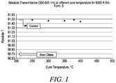
- FIG. 1is related to Example 4 and shows the absolute transmittance (350-800 nm) of the coatings.
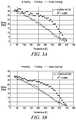
- FIG. 2Ais related to Example 4 and shows the reflectivity of the control coating at 400 nm to 1050 nm.
- FIG. 2Bis related to Example 4 and shows the reflectivity of an exemplary coating at 400 nm to 1050 nm.
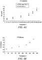
- FIG. 3Ais related to Example 6 and shows the residual stress in MPa for the control coating during a heating and cooling cycle.
- FIG. 3Bis related to Example 6 and shows the residual stress in MPa for an exemplary coating during a heating and cooling cycle.
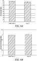
- FIG. 4Ais related to Example 6 and shows the coefficient of thermal expansion for the coatings as a function of temperature.
- FIG. 4Bis related to Example 6 and shows the difference in coefficient of thermal expansion for the coatings as a function of temperature.
- FIG. 5is related to Example 7 and shows the thermal gravimetric analysis results for the coatings.
- FIG. 6Ais related to Example 9 and shows the nanohardness in MPa for the coatings.
- FIG. 6Bis related to Example 9 and shows the Reduced Elastic Modulus in GPa for the coatings.
- FIG. 7Ais related to Example 9 and shows the depth vs. load profile for the control coating.
- FIG. 7Bis related to Example 9 and shows a scanning probe microscope image of the indentation for the control coating.
- FIG. 8Ais related to Example 9 and shows the depth vs. load profile for an exemplary coating.
- FIG. 8Bis related to Example 9 and shows a scanning probe microscope image of the indentation for an exemplary coating.
- the polysiloxane formulationincludes one or more solvents and one or more silicon-based compounds.
- the formulationfurther includes one or more catalysts.
- the formulationfurther includes one or more surfactants.
- the formulationfurther includes one or more additional additives, such as adhesion promoters, plasticizers, organic acids, and monofunctional silanes.
- the formulationincludes one or more solvents.
- Exemplary solventsinclude suitable pure organic molecules or mixtures thereof that are volatilized at a desired temperature and/or easily solvate the components discussed herein.
- the solventsmay also comprise suitable pure polar and non-polar compounds or mixtures thereof.
- puremeans a component that has a constant composition.
- pure wateris composed solely of H 2 O.
- mixturemeans a component that is not pure, including salt water.
- polarmeans that characteristic of a molecule or compound that creates an unequal charge, partial charge or spontaneous charge distribution at one point of or along the molecule or compound.
- non-polarmeans that characteristic of a molecule or compound that creates an equal charge, partial charge or spontaneous charge distribution at one point of or along the molecule or compound.
- Exemplary solventsinclude solvents that can, alone or in combination, modify the viscosity, intermolecular forces and surface energy of the solution in order to, in some cases, improve the gap-filling and planarization properties of the composition. It should be understood, however, that suitable solvents may also include solvents that influence the profile of the composition in other ways, such as by influencing the crosslinking efficiency, influencing the thermal stability, influencing the viscosity, and/or influencing the adhesion of the resulting layer or film to other layers, substrates or surfaces.
- Exemplary solventsalso include solvents that are not part of the hydrocarbon solvent family of compounds, such as ketones, including acetone, diethyl ketone, methyl ethyl ketone and the like, alcohols, esters, ethers and amines. Additional exemplary solvents include ethyl lactate, propylene glycol propylether (PGPE), propylene glycol monomethyl ether acetate (PGMEA) or a combination thereof. In one exemplary embodiment, the solvent comprises propylene glycol monomethyl ether acetate.
- formulationcomprises as little as 50 wt. %, 55 wt. %, 60 wt. %, as great as 80 wt,%, 85 wt,%, 90 wt. % of the one or more solvents, or within any range defined between any two of the foregoing values, such as 50 wt. % to 90 wt. %, 55 wt. % to 85 wt. %, or 65 wt. % to 85 wt. %.
- the determination of the appropriate amount of solvent to add to compositiondepends on a number of factors, including: a) thicknesses of the desired layers or films, b) desired concentration and molecular weight of the solids in the composition, c) application technique of the composition and/or d) spin speeds, when spin-coating techniques are utilized.
- the higher the solid concentration (or the resin or polymer) is in the formulationthe higher the viscosity.
- the solid contentmay be increased (or the solvent amount reduced) to increase the viscosity as desired for a specific coating application technique.
- the viscous formulation or formulation with higher solid contentwill typically provide a thicker film thickness such as greater than 2 ⁇ m.
- the solvents used hereinmay comprise any suitable impurity level.
- the solvents utilizedhave a relatively low level of impurities, such as less than about 1 ppm, less than about 100 ppb, less than about 10 ppb, less than about 1 ppb, less than about 100 ppt, less than about 10 ppt and in some cases, less than about 1 ppt.
- These solventsmay be purchased having impurity levels that are appropriate for use in these contemplated applications or may need to be further purified to remove additional impurities and to reach the less than about 10 ppb, less than about 1 ppb, less than about 100 ppt or lower levels that suitable and/or desired.
- the formulationincludes no water.
- the solventis an anhydrous solvent
- the silicon-based compounds, and any catalysts, surfactants, adhesion promoters, cross-linkers, initiators, or other additivesare provided in a water-free anhydrous solvent.
- water-freerefers to a composition having less than 0.2 wt. %, 0.1 wt. %, 0.05 wt. %, 0.01 wt .% water, or 0 wt. % water.
- “water-free”refers to a composition have no water.
- water-freerefers to a composition in which no external water is added, although some water may be formed from the hydrolysis-condensation reaction of the silicon-based compounds.
- the formulationincludes one or more silicon-based compounds that can be crosslinked to form the polysiloxane.
- silicon-based compoundscomprise siloxane, silsesquioxane, polysiloxane, or polysilsesquioxane, such as methylsiloxane, methylsilsesquioxane, phenylsiloxane, phenylsilsesquioxane, methylphenylsiloxane, methylphenylsilsesquioxane, dimethylsiloxane, diphenylsiloxane, methylphenylsiloxane, polyphenylsilsesquioxane, polyphenylsiloxane, polymethylphenylsiloxane, polymethylphenylsilsesquioxane, polymethylsiloxane, polymethylsiloxane, polymethylsilsesquioxane, and combinations thereof.
- the at least one silicon-based compoundcomprises polyphenylsilsesquioxane, polyphenylsiloxane, phenylsiloxane, phenylsilsesquioxane, methylphenylsiloxane, methylphenylsilsesquioxane, polymethylphenylsiloxane, polymethylphenylsilsesquioxane, polymethylsiloxane, polymethylsilsesquioxane or a combination thereof.
- the silicon-based compoundscomprise a total amount of carbon atoms divided between carbon atoms in alkyl groups, such as methyl and ethyl groups, and carbon atoms in aryl groups, such as phenyl groups.
- the number of carbon atoms contained in the alkyl groupsis greater than 10%, 12%, 15% 20%, 21%, 25%, or greater than 30%, 31%, 40%, 50%, 60%, 70%, 75%, 80%, 85%, 90%, 95%, 99%, and less than 100%, or is 100%, based on the total number of carbon atoms contained in the alkyl and aryl groups, or may be between any range defined between any two of the foregoing values, such as from greater than 10% to less than 100%, from 12% to less than 100%, from greater than 20% to 100% or greater than 30% to less than 100%.
- the silicon-based compoundsinclude a plasticizer or other suitable material to increase the flexibility of the formed polysiloxane.
- Some contemplated silicon-based compoundsinclude compositions formed from hydrolysis-condensation reactions of at least one reactant having the formula: R 1 x Si(OR 2 ) y
- R 1is an alkyl, alkenyl, aryl, or aralkyl group, and x is an integer between 0 and 2, and where R 2 is a alkyl group or acyl group and y is an integer between 1 and 4.
- Materials also contemplatedinclude silsesquioxane polymers of the general formula: (C 6 H 5 SiO 1.5 ) x
- xis an integer greater than about 4.
- the silicon-based materialincludes one or more polysiloxane resins, such as the Glass Resin polysiloxane resins available from Techneglas Technical Products, Perrysburg, Ohio.
- polysiloxane resinsare silicon-based oligomers formed from a limited hydrolysis and condensation reaction of one or more silicon-based monomers.
- Exemplary suitable silicon-based monomersinclude organoalkoxysilanes having a Si—C bond, such as methyltrimethoxysilane (MTMOS), methyltriethoxysilane (MTEOS), dimethyldiethoxysilane (DMDEOS), phenyl triethoxysilane (PTEOS), dimethyldimethoxysilane and phenyltrimethoxysilane.
- MTMOSmethyltrimethoxysilane
- MTEOSmethyltriethoxysilane
- DMDEOSdimethyldiethoxysilane
- PTEOSphenyl triethoxysilane
- dimethyldimethoxysilane and phenyltrimethoxysilanephenyltrimethoxysilane.
- Other suitable silicon-based monomerslack an Si—C bond, such as tetraethylorthosilicate (TEOS).
- TEOStetraethylorthosilicate
- Exemplary resin materialsinclude glass resins derived from organoalkoxysilanes such as methylsiloxane, dimethylsiloxane, phenylsiloxane, methylphenylsiloxane, tetraethoxysilane, and mixtures thereof.
- the polysiloxane resinshave a structure selected from the group consisting of a linear structure, a cyclic structure, a cage-type structure, a ladder-type structure, and a partial-ladder/partial-cage type structure. In a more particular embodiment, the polysiloxane resins have a partial-ladder/partial-cage type structure.
- the polysiloxane resinsinclude one or more alkyl groups and/or one or more aryl groups.
- Exemplary polysiloxane resins containing alkyl groupsinclude methylsiloxane and dimethylsiloxane.
- Exemplary polysiloxane resins containing aryl groupsinclude phenylsiloxane.
- Exemplary polysiloxane resins containing both alkyl and aryl groupsinclude methylphenylsiloxane.
- each polysiloxane resinhas a weight average molecular weight as little as 900 atomic mass unit (AMU), 950 AMU, 1000 AMU, 1100 AMU, 1150 AMU, as great as 2000 AMU, 3000 AMU, 4000 AMU, 5000 AMU, 10,000 AMU, or within any range defined between any two of the foregoing values, such as 900 AMU to 10,000 AMU, 1000 AMU to 10,000 AMU, or 900 AMU to 5000 AMU.
- AMUatomic mass unit
- the polysiloxane resininclude a first polysiloxane resin containing alkyl groups such as methylsiloxane and/or dimethylsiloxane and a second polysiloxane resin containing aryl groups such as phenylsiloxane.
- the first polysiloxane resinfurther contains aryl groups such as phenylsiloxane.
- the first polysiloxane resinhas a weight average molecular weight as little as 1000 atomic mass unit (AMU), 2000 AMU, 2200 AMU, 3000 AMU, 3800 AMU, 4000 AMU, as great as 4500 AMU, 4800 AMU, 5000 AMU, 7500 AMU, 10,000 AMU or within any range defined between any two of the foregoing values, such as 1000 AMU to 10,000 AMU, 2000 AMU to 5000 AMU, or 3800 AMU to 4800 AMU and the second polysiloxane resin has a weight average molecular weight as little as 900 atomic mass unit (AMU), 950 AMU, 1000 AMU, as great as 1150 AMU, 2000 AMU, 2500 AMU, 5000 AMU or within any range defined between any two of the foregoing values, such as 900 AMU to 5000 AMU, 900 AMU to 2000 AMU, or 950 AMU to 1150 AMU.
- AMUatomic mass unit
- the silicon-based materialincludes or is formed from one or more organoalkoxysilanes.
- organoalkoxysilanesinclude methyltrimethoxysilane (MTMOS), methyltriethoxysilane (MTEOS), dimethyldiethoxysilane (DMDEOS), phenyl triethoxysilane (PTEOS), dimethyldimethoxysilane, phenyltrimethoxysilane, and combinations of the foregoing.
- the silicon-based materialincludes a blend of two or more pre-formed polysiloxane resins.
- two or more polysiloxane resinsmay be combined to provide a total number of carbon atoms contained in the alkyl groups from greater than 10%, 12%, greater than 20%, 21%, 25%, greater than 30%, 31%, 40%, 50%, 60%, 70%, 75%, 80%, 85%, 90%, 95%, 99%, less than 100%, 100%, based on the total number of carbon atoms contained in the alkyl and aryl groups, or between any range defined between any two of the foregoing values, such as from greater than 10% to 100%, from 12% to 100% from greater than 20% to 100%, or greater than 30% to less than 100%.
- the silicon-based materialmay include one or more polysiloxane resins each including a difunctional silane.
- An exemplary difunctional slimeis dimethylsiloxane.
- the silicon-based materialmay include as little as 0%, 0.1%, 0.5%, 1%, 2%, as high as 5%, 10%, 15%, 20% difunctional siloxane, as a molar percentage of the total moles of siloxane, or between any range defined between any two of the foregoing values, such as from 0% to 20% or from 0.1% to 2%.
- the formulationincludes one or more catalysts.
- the catalystis a heat-activated catalyst.
- a heat-activated catalystrefers to a catalyst that is activated at or above a particular temperature, such as an elevated temperature. For example, at one temperature (such as room temperature) the composition maintains a low molecular weight, thus enabling good planarization ability over a surface.
- the temperatureis elevated (such as to greater than 50° C.)
- the heat-activated catalystcatalyzes a condensation reaction between two Si—OH functional groups, which results in a more dense structure and, in some cases, improved performance overall.
- Suitable condensation catalystscomprise those catalysts that can aid in maintaining a stable silicate solution.
- Exemplary metal-ion-free catalystsmay comprise onium compounds and nucleophiles, such as an ammonium compound (such as quaternary ammonium salts), an amine, a phosphonium compound or a phosphine compound.
- the catalystis not a photoacid, a photoacid generator, or a metal-based catalyst.
- the catalystis relatively molecularly “small” or is a catalyst that produces relatively small cations, such as quaternary ammonium salts.
- the one or more catalystsis selected from tetramethylammonium acetate (TMAA), tetramethylammonium hydroxide (TMAH), tetrabutylammonium hydroxide (TBAH), tetrabutylammonium acetate (TBAA), cetyltrimethylammonium acetate (CTAA), tetramethylammonium nitrate (TMAN), other ammonium-based catalysts, amine-based and/or amine-generating catalysts, and combinations thereof.
- TMAAtetramethylammonium acetate
- TMAHtetramethylammonium hydroxide
- TBAHtetrabutylammonium hydroxide
- TBAAcetyltrimethylammonium acetate
- TMANtetramethylammonium nitrate
- exemplary catalystsinclude (2-hydroxyethyl)trimethylammonium chloride, (2-hydroxyethyl)trimethylammonium hydroxide, (2-hydroxyethyl)trimethylammonium acetate, (2-hydroxyethyl)trimethylammonium formate, (2-hydroxyethyl)trimethylammonium nitrate, (2-hydroxyethyl)trimethylammonium benzoate, tetramethylammonium formate and combinations thereof.
- Other exemplary catalystsinclude (carboxymethyl)trimethylammonium chloride, (carboxymethyl)trimethylammonium hydroxide, (carboxymethyl)trimethyl-ammonium formate and (carboxymethyl)trimethylammonium acetate.
- the formulationcomprises as little as 0.001 wt. %, 0.004 wt. %, 0.01 wt. %, 0.1 wt. %, 0.3 wt. %, as great as 0.5 wt. %, 1 wt. %, 2 wt. %, 5 wt. %, or 10 wt. % of the one or more catalysts, or within any range defined between any two of the foregoing values, such as 0.1 wt. % to 10 wt. % or 1 wt. % to 2 wt. %.
- the one or more catalystscomprise TMAN.
- TMANmay be provided by either dissolving TMAN in water or in an organic solvent such as ethanol, propylene glycol propyl ether (PGPE), or by converting TMAA or TMAH to TMAN by using nitric acid.
- PGPEpropylene glycol propyl ether
- the formulationincludes one or more surfactants.
- Surfactantsmay be added to lower surface tension.
- the term “surfactant”means any compound that reduces the surface tension when dissolved in H 2 O or other liquids, or which reduces interfacial tension between two liquids, or between a liquid and a solid.
- Contemplated surfactantsmay include at least one anionic surfactant, cationic surfactant, non-ionic surfactant, Zwitterionic surfactant or a combination thereof.
- the surfactantmay be dissolved directly into the composition or may be added with one of the compositions components (the at least one silicon-based compound, the at least one catalyst, the at least one solvent) before forming the final composition.
- Contemplated surfactantsmay include: polyether modified polydimethylsiloxanes such as BYK 307 (polyether modified poly-dimethyl-siloxane, BYK-Chemie), sulfonates such as dodecylbenzene sulfonate, tetrapropylenebenzene sulfonate, dodecylbenzene sulfonate, a fluorinated anionic surfactant such as Fluorad FC-93, and L-18691 (3M), fluorinated nonionic surfactants such as FC-4430 (3M), FC-4432 (3M), and L-18242 (3M), quaternary amines, such as dodecyltrimethyl-ammonium bromide or cetyltrimethylammonium bromide, alkyl phenoxy polyethylene oxide alcohols, alkyl phenoxy polyglycidols, acetylinic alcohols, polyglycol ethers such as Tergitol
- the formulationcomprises as little as 0.001 wt. %, 0.005 wt. %, 0.01 wt. %, 0.05 wt. %, as great as 0.1 wt. %, 0.25 wt. %, 0.5 wt. %, 1 wt. % of the one or more surfactants, or within any range defined between any two of the foregoing values, such as 0.001 wt. % to 1 wt. % or 0.001 wt. % to 0.25 wt. %.
- the determination of the appropriate amount of a composition-modifying constituent to add to the compositiondepends on a number of factors, including: a) minimizing defects in the film, and/or b) balancing the film between good adhesion and desirable film properties.
- the formulationmay include one or more additional additives, such as adhesion promoters, endcapping agents, and organic acids.
- the formulationincludes one or more adhesion promoters in order to influence the ability of the layer, coating or film to adhere to surrounding substrates, layers, coatings, films and/or surfaces.
- the adhesion promotermay be at least one of: a) thermally stable after heat treatment, such as baking, at temperatures generally used for optoelectronic component manufacture, and/or b) promotes electrostatic and coulombic interactions between layers of materials, as well as promoting understood Van derWaals interactions in some embodiments.
- adhesion promotersinclude aminopropyl triethoxysilane (APTEOS) and salts of APTEOS, vinyltriethoxy silane (VTEOS), glycidoxypropyltrimethoxy silane (GLYMO), and methacryloxypropyltriethoxy silane (MPTEOS).
- APTEOSaminopropyl triethoxysilane
- VTEOSvinyltriethoxy silane
- GLYMOglycidoxypropyltrimethoxy silane
- MPTEOSmethacryloxypropyltriethoxy silane
- Other exemplary adhesion promotersinclude 3-(triethoxysilyl)propylsuccininc anhydride, dimethyldihydroxy silane, methylphenyl dihydroxysilane or combinations thereof.
- the formulationcomprises as little as 0.001 wt. %, 0.01 wt. %, 0.1 wt. %, 0.26 wt.
- %as great as 1 wt. %, 2.6 wt. %, 5 wt. %, 10 wt. %, 20 wt. % of the one or more adhesion promoters, or within any range defined between any two of the foregoing values, such as 0.001 wt. % to 20 wt. % or 0.26 wt % to 2.6 wt. %.
- the formulationincludes one or more endcapping agents such as monofunctional silanes that include a single reactive functionality that is capable of reacting with silanol groups on polysiloxane molecules.
- exemplary endcapping agentsinclude trialkylsilanes such as trimethylethoxy silane, triethylmethoxy silane, trimethylacetoxy silane, trimethylsilane.
- the formulationcomprises as little as 0.1%, 0.5%, 1%, 2%, as great as 5%, 10%, 15%, 20%, or 25% of the one or more endcapping agents as a percentage of total moles of polysiloxane, or within any range defined between any two of the foregoing values, such as 2% to 20% or 5% to 10%.
- the formulationincludes one or more organic acids.
- the organic acid additivesare volatile or decompose at high temperatures and help stabilize the formulation.
- Exemplary organic acidsinclude p-toluenesulfonic acid, citric acid, formic acid, acetic acid, and trifluoroacetic acid.
- the formulationcomprises as little as 0. 1 wt. %, 0.5 wt. %, 1 wt. %, 2 wt. %, as great as 5 wt. %, 10 wt. %, 15 wt. %, 20 wt. %, or 25 wt. % of the one or more organic acids, or within any range defined between any two of the foregoing values, such as 2 wt. % to 20 wt. % or 5 wt. % to 10 wt. %.
- the polysiloxane formulationforms a polysiloxane coating on a surface located in or on an electronic, optoelectronic, or display device.
- the polysiloxane formulationforms a light-transmissive coating.
- the light-transmissive coatinghas a transmittance to light in the visible optical wavelength range from 400 to 1000 nm.
- the optical transmittanceis as high as 80%, 85%, 90%, 95%, 97%, 98%, 99%, or higher, or within any range defined between any two of the foregoing values.
- one or polymer resinsare selected to provide a desired refractive index.
- the relative molar percentage of a resin having a relatively low refractive indexsuch as 100% methyltriethoxysilane resin, is relatively high to produce a polysiloxane coating having a relatively low refractive index.
- the relative molar percentage of a resin having a relatively high refractive indexsuch as 100% phenyl triethoxysilane, is relatively high to produce a polysiloxane coating having a relatively high refractive index.
- the relative molar proportions of a first resin having a relatively high refractive index and a second resin having a relatively low refractive indexare selected to produce a polysiloxane coating having a desired refractive index between the refractive index of the first and second resins.
- the polysiloxane formulationforms a coating having a refractive index that is as little as less than 1.4, 1.4, 1.45, as great as 1.5, 1.55, 1.56, 1.6, or within any range defined between any two of the foregoing values, such as from less than 1.4 to 1.6 or from 1.4 to 1.56.
- Exemplary devicesto which coatings of the present disclosure may be providedinclude CMOS Image Sensors, transistors, light-emitting diodes, color filters, photovoltaic cells, flat-panel displays, curved displays, touch-screen displays, x-ray detectors, active or passive matrix OLED displays, active matrix thin film liquid crystal displays, electrophoretic displays, and combinations thereof.
- the polysiloxane coatingforms a passivation layer, a barrier layer, a planarization layer, or a combination thereof.
- the polysiloxane coatinghas a thickness as little as 0.1 ⁇ m, 0.3 ⁇ m, 0.5 ⁇ m, 1 ⁇ m, 1.5 ⁇ m, as great as 2 ⁇ m, 2.5 ⁇ m, 3 ⁇ m, 3.5 ⁇ m, 4 ⁇ m, or greater, or within any range defined between any two of the foregoing values.
- the polysiloxane coatingis formed by applying the formulation to a substrate, followed by curing the formulation.
- exemplary methods of applying the formulationinclude spin coating, spray coating, slot-die coating techniques.
- Curingrefers to a polymerization process in which the silicon-based materials, such as silicon-based oligomers, react in the presence of a catalyst to hydrolyze and condense with other oligomers to form a higher molecular weight polymer or matrix.
- a baking stepis provided to remove at least part or all of the solvent.
- the baking stepis as short as 1 minute, 5 minutes, 10 minutes, 15 minutes, as long as 20 minutes, 30 minutes, 45 minutes, 60 minutes, or longer, at a temperature as low as 100° C., 200° C. 220° C., as high as 250° C., 275° C., 300° C., 320° C., 350° C., or higher.
- a curing stepis provided to polymerize the at least one silicon-based material such as by activating a heat-activated catalyst.
- the curing stepis as short as 10 minutes, 15 minutes, 20 minutes, as long as 30 minutes, 45 minutes, 60 minutes, or longer, at a temperature as low as 250° C., 275° C., 300° C., as high as 320° C., 350° C., 375° C., 380° C., 400° C. or higher.
- multiple layers of the formulationare subsequently applied and cured to form a multilayer coating.
- the multilayer coatingincludes two, three, or more polysiloxane coating layers.
- the polysiloxane coatingis resistant to multiple heating steps, such as curing or deposition of additional coatings or layers on the formed polysiloxane coating.
- the silicon-based compoundmay be formed from two or more polymerization steps.
- a first silicon-based resinsuch as an oligomeric resin, is formed from a first polymerization step of one or more organoalkoxysilanes.
- organoalkoxysilanesinclude methyltrimethoxysilane (MTMOS), methyltriethoxysilane (MTEOS), dimethyldiethoxysilane (DMDEOS), phenyl triethoxysilane (PTEOS), dimethyldimethoxysilane, phenyltrimethoxysilane, and combinations of the foregoing.
- Exemplary first polymerization stepsinclude acidic catalyzed polymerization, such as polymerization catalyzed with a mineral or organic acid, or a base catalyzed polymerization, such as polymerization catalyzed with an ammonium compound, an amine, a phosphonium compound or a phosphine compound.
- Exemplary mineral acidsinclude nitric acid, hydrochloric acid, sulfuric acid, and hydrofluoric acid.
- Exemplary organic acidsinclude sulfonic acid, trifluorosulfonic acids, and carboxylic acids, as well as thermal acid generators (TAG) capable of generating a sulfonic acid upon exposure to an elevated temperature.
- TAGthermal acid generators
- Exemplary basic catalystsinclude tetraorganoammonium compounds and tetraorganophosphonium compounds, such as tetramethylammonium acetate (TMAA), tetramethylammonium hydroxide (TMAH), tetrabutylammonium hydroxide (TBAH), tetrabutylammonium acetate (TBAA), cetyltrimethylammonium acetate (CTAA), tetramethylammonium nitrate (TMAN), triphenylamine, trioctylamine, tridodecylamine, triethanolamine, tetramethylphosphonium acetate, tetramethylphosphonium hydroxide, triphenylphosphine, trimethylphosphine, trioctylphosphine, and combinations thereof.
- the catalystis a mineral acid, such as nitric acid.
- the first silicon-based resinhas a weight average molecular weight as little as 900 atomic mass unit (AMU), 950 AMU, 1000 AMU, 1100 AMU, 1150 AMU, as great as 2000 AMU, 3000 AMU, 4000 AMU, 5000 AMU, 10,000 AMU, or within any range defined between any two of the foregoing values, such as 900 AMU to 10,000 AMU, 1000 AMU to 10,000 AMU, or 900 AMU to 5000 AMU.
- AMUatomic mass unit
- a second silicon-based resinis formed from a second polymerization of the first polymer resin.
- Exemplary second polymerization stepsinclude acidic catalyzed polymerization and base catalyzed polymerization, as described with respect to the first polymerization step, such as polymerization catalyzed with an ammonium compound, an amine, a phosphonium compound or a phosphine compound.
- Exemplary mineral acidsinclude nitric acid, hydrochloric acid, sulfuric acid, and hydrofluoric acid.
- Exemplary organic acidsinclude sulfonic acid, trifluorosulfonic acids, and carboxylic acids, as well as thermal acid generators (TAG) capable of generating a sulfonic acid upon exposure to an elevated temperature.
- Exemplary basic catalystsinclude tetraorganoammonium compounds and tetraorganophosphonium compounds, such as tetramethylammonium acetate (TMAA), tetramethylammonium hydroxide (TMAH), tetrabutylammonium hydroxide (TBAH), tetrabutylammonium acetate (TBAA), cetyltrimethylammonium acetate (CTAA), tetramethylammonium nitrate (TMAN), triphenylamine, trioctylamine, tridodecylamine, triethanolamine, tetramethylphosphonium acetate, tetramethylphosphonium hydroxide, triphenylphosphine, trimethylphosphine, triocty
- the second silicon-based resinhas a weight average molecular weight greater than the first silicon-based resin.
- the second silicon-based resinhas a weight average molecular weight as little as 1000 AMU, 1100 AMU, 1150 AMU, as great as 2000 AMU, 3000 AMU, 4000 AMU, 5000 AMU, 10,000 AMU, or within any range defined between any two of the foregoing values, such as 1000 AMU to 5000 AMU, 2000 AMU to 5000 AMU, or 2000 AMU to 4000 AMU.
- the second polymerizationis performed in a solvent, such ethyl lactate, propylene glycol propylether (PGPE), propylene glycol monomethyl ether acetate (PGMEA) or a combination thereof.
- a solventsuch ethyl lactate, propylene glycol propylether (PGPE), propylene glycol monomethyl ether acetate (PGMEA) or a combination thereof.
- the first silicon-based resinis added at a concentration as little as 10 wt. %, 20 wt. %, 30 wt. % 40 wt. %, as great as 45 wt. %, 50 wt. %, 60 wt. % or within any range defined between any two of the foregoing values, such as 10 wt. % to 60 wt. % or 30 wt. % to 45 wt. %.
- the basic catalystis added at a concentration as little as 100 ppm, 200 ppm, 250 ppm, as great as 300 ppm, 400 ppm, 500 ppm, or greater, or within any range defined between any two of the foregoing values, such as 100 ppm to 500 ppm or 200 ppm to 300 ppm.
- the second polymerizationis performed at a temperature as little as 60° C., 65° C., 70° C., 75° C., as high as 80° C., 90° C., 100° C., or within any range defined between any two of the forgoing values, such as 60° C. to 100° C. or 70° C. to 100° C.
- the second polymerization mixtureis held at the temperature for as little as 1 hour, 2 hours, 3 hours, as great as 5 hours, 8 hours, 10 hours, or within any range defined between any two of the foregoing values, such as 1 hour to 10 hours, 2 hours to 10 hours, 2 hours to 8 hours, or 2 to 3 hours.
- a polysiloxane formulation as described aboveincludes the second silicon-based resin, and one or more solvents.
- the formulationfurther includes one or more additional silicon-based material as described above.
- the formulationfurther includes one or more catalysts.
- the formulationfurther includes one or more surfactants.
- the formulationfurther includes one or more additional additives, such as adhesion promoters, plasticizers, organic acids, and monofunctional silanes.
- a coating formed from the polysiloxane formulation including the second silicon-based resinis formed by applying the polysiloxane formulation. In one exemplary embodiment, the coating is formed by curing the polysiloxane formulation at a temperature of as little as 350° C., 360° C., 370°, as high as 375° C., 380° C., 385° C., 390° C. or higher.
- the polysiloxane coatingis formed by applying the formulation to a substrate, such as a glass or Si 3 N 4 coated or capped substrate and curing the formulation.
- the coatingis formed by curing the polysiloxane formulation at a temperature of as little as 350° C., 360° C., 370°, as high as 375° C., 380° C., 385° C., 390° C. or higher.
- the polysiloxane coatinghas a thickness as little as 0.1 ⁇ m, 0.2 ⁇ m, 0.5 ⁇ m, 0.8 ⁇ m, 1 ⁇ m, 1.2 ⁇ m 1.5 ⁇ m, 2 ⁇ m, as great as, 3 ⁇ m, 4 ⁇ m, 5 ⁇ m, 10 ⁇ m or greater, or within any range defined between any two of the foregoing values, such as0.1 ⁇ m to 10 ⁇ m, 1 ⁇ m to 5 ⁇ m, 1.2 ⁇ m to 5 ⁇ m, or 4 ⁇ m or greater.
- the as little as 0.5 wt. %, as little as 0.2 wt. %, as little as 0.1 wt. %, as little as 0.09 wt. %, as little as 0.05 wt. %, or as little as 0.02 wt. %outgassing at 350° C. for 1 hour in air, or within any range defined between any two of the foregoing values, such as 0.5 wt. % to 0.02 wt. %, or 0.1 wt. % to 0.05 wt. %.
- wt. %as little as 0.09 wt. %, as little as 0.05 wt. %, or as little as 0.02 wt. % outgassing at 390° C. for 1 hour in air, or within any range defined between any two of the foregoing values, such as 0.5 wt. % to 0.02 wt. %, or 0.1 wt. % to 0.05 wt. %.
- the polysiloxane coatinghas a dielectric constant as little as about 2.8, 2.9, 3.0, as great as about 3.1, 3.2, or within any range defined between any two of the foregoing values, such as 2.8 to 3.2 or 3.0 to 3.2.
- Polymer Aphenyl TEOS was reacted in an isopropyl alcohol solvent in the presence of an acid catalyst and water for 24 h at 100° C. After the reaction, the solvent was distilled out to obtain solid polymer. The polymer then dissolved and reprecipitated from an appropriate solvent system and vacuum dried at 50° C. overnight and ground to powder.
- Polymer Bpredetermined amounts of phenyl TEOS and methyl TEOS were reacted in an isopropyl alcohol solvent in the presence of an acid catalyst and water and 0.5% DMDEOS for 24 hours at 100° C. After the reaction the solvent was distilled out to obtain solid polymer. The polymer was then dissolved and reprecipitated from an appropriate solvent system and vacuum dried at 50° C. overnight and ground to powder.
- Formulation 190% of polymer B and 10% of polymer A by weight in PGMEA in the presence of 1-5% by weight surfactant and catalysts 1-5% by weight of final solution weight.
- the formulation obtainedis diluted with PGMEA to obtain a desired thickness to be deposited by slit, roller, spray or spin coating process.
- Formulation 2The formulation was prepared as in Formulation 1, except that 95% polymer B and 5% polymer A were used.
- Formulation 3The formulation was prepared as in Formulation 1, except that 85% polymer B and 15% polymer A were used.
- Formulation 4The formulation was prepared as in Formulation 1, except that 50% polymer B and 50% polymer A were used. This formulation was found to have adhesion problems and was not resistant to chemicals.
- Comparative Formulation CA polysiloxane resin comprising equimolar proportions of MTEOS and PTEOS and about 0.3 mole % of DMDEOS, GR-150F available from Techneglas Technical Products, Perrysburg, Ohio, was dissolved in PGMEA solvent at desired % resin solids loading. Coating formulations were formed by adding PGMEA solvent, a small amount of dilute aqueous TMAN solution and BYK surfactant. Each coating was spun on a substrate at 1000-2500 rpm to deposit films of desired thicknesses and cured under similar conditions. Coatings were inspected for any micro cracks under optical microscope immediately after completely curing and after several days for any latent cracking.
- Exemplary Formulations 5-7A polysiloxane resin GR-950F, derived from PTEOS, was combined with a polysiloxane resin GR-150F, comprising equimolar proportions of MTEOS and PTEOS and about 0.3 mole % of DMDEOS. Both resins, available from Techneglas Technical Products, Perrysburg, Ohio, were dissolved in PGMEA solvent at desired weight ratios and desired % solids loading. For formulation 5, the ratio of GR-950:GR-150F was 1:9, for formulation 6, the ratio was 1:4, and for formulation 7, the ratio was 1:1. Coating formulations were formed by adding PGMEA solvent, a small amount of dilute aqueous TMAN solution and BYK surfactant. Each coating was spun on a substrate at 1000-2500 rpm to deposit films of desired thicknesses and cured under similar conditions. Coatings were inspected for any micro cracks under optical microscope immediately after completely curing and after several days for any latent cracking.
- Exemplary Formulations 8-10Polysiloxane resins comprising equimolar proportions of MTEOS and PTEOS and about 5 mol. % (Formulation 8), 10 mol. % (Formulation 9), or 15 mol. % (Formulation 10) of DMDEOS, obtained from Techneglas Technical Products, Perrysburg, Ohio, were dissolved in PGMEA solvent at desired % resin solids loading. Coating formulations of each resin were formed by adding PGMEA solvent, a small amount of dilute aqueous TMAN solution and BYK surfactant. Each coating was spun on a substrate at 1000-2500 rpm to deposit films of desired thicknesses and cured under similar conditions. Coatings were inspected for any micro cracks under optical microscope immediately after completely curing and after several days for any latent cracking.
- Exemplary Formulations 11 and 12Polysiloxane resins GR-150F was combined with the second polysiloxane resin GR-950F and a third polysiloxane resin comprising equimolar proportions of MTEOS and PTEOS and about 10 mol. % of DMDEOS, in 95/2.5/2.5 (Form. 11) and 90/5/5 (Form. 12) ratios and dissolved in PGMEA solvent at desired % resin solids loading. Coating formulations of each resin combination were formed by adding PGMEA solvent, a small amount of dilute aqueous TMAN solution and BYK surfactant. Each coating was spun on a substrate at 1000-2500 rpm to deposit films of desired thicknesses and cured under similar conditions.
- Coatingswere inspected for any micro cracks under optical microscope immediately after completely curing and after several days for any latent cracking. Coatings formed from Formulation 11 remained crack-free at up to 2.4 ⁇ m whereas those formed from Formulation 12 remained crack-free at up to 2.8 ⁇ m after curing at 400 C for 30 min.
- compositions having greater than 20% alkyl carbonwere produced. Also as shown in Table 1, compositions having varying levels of difunctional siloxane content were produced.
- Comparative Formulation C(“Comp. Form. C”) and Formulation 5 (“Form. 5) as produced in Example 1 were deposited on a silicon substrate at various thicknesses as shown in Table 2 below. Duplicate samples were then cured at 380° C. for 30 minutes in a nitrogen atmosphere, followed by a second cure at 380° C. for 10 minutes in air. Following each cure, the film was inspected to determine whether the film had cracked. The results are provided in Table 2 below.
- the comparative formulation C samplehad a crack threshold on silicon about 2.3 ⁇ m.
- the formulation 5 samplehad a crack threshold of about 3.1 ⁇ m.
- Samples of the comparative formulation C and formulation 5 as produced in Example 1were next deposited on a copper/silicon nitride substrate at various thicknesses as shown in Table 3 below. Duplicate samples were then cured at 380° C. for 30 minutes in a nitrogen atmosphere followed by a second cure at 380° C. for 10 minutes in air. Following each cure, the film was inspected to determine whether the film had cracked. The results are provided in Table 3 below.
- the comparative formulation C samplehad a crack threshold on Cu/SiN about 2.3 ⁇ m.
- the formulation 5 samplehad a crack threshold less than 3.1 ⁇ m.
- Formulation 5 films of 3.1 ⁇ m and 3.4 ⁇ m thicknesswere cured on silicon or glass as above and visually inspected for any latent cracking at 2, 7, 11, and 21 days after cure. The results are provided in Table 5.
- formulation 5did not crack over 21 days after cure at a thickness as high as 3.4 ⁇ m on either silicon or glass.
- Samples of the comparative formulation C and formulation 5 as produced in Example 1were deposited on a silicon or glass substrate at various thicknesses as shown in Table 7 below. Samples were then cured at 380° C. for 30 minutes in a nitrogen atmosphere, followed by a second identical cure. Following each cure, the film was inspected to determine whether the film had cracked. The results are provided in Table 7 below.
- Samples of the comparative formulation C and formulations 5, 6, and 7 as produced in Example 1were deposited on a silicon or glass substrate at various thicknesses as shown in Table 8 below. Samples were then cured at 350° C. for 60 minutes. Following curing, the film was visually inspected to determine whether the film had cracked. The results are provided in Table 8 below.
- the formulations 5, 6, and 7were able to form films of substantially greater thickness than the comparative formulation C without cracking on various substrates and cured under different conditions.
- the formulation 5 filmswere stable at thickness up to 3 ⁇ m or greater at cure temperatures of 380° C., and up to 3.6 ⁇ m or greater at lower cure temperatures.
- formulations 8, 9, and 10were able to form films of substantially greater thickness than the comparative formulation C without cracking when cured under different conditions.
- a 6000 ⁇ sample of the comparative formulation C and formulation 5 as produced in Example 1were each deposited on a glass substrate and cured for 1 hour at 350° C. The results are provided in FIG. 1 and Table 10 below.
- both the comparative formulation C and formulation 5had a higher transmittance than uncoated glass.
- the substantially thicker 3.1-3.4 ⁇ m samples of formulation 5had similar transmittance to the relatively thin 1.1 ⁇ m samples of the comparative formulation C.
- the control comparative formulation C and formulation 5 filmshad similar transmittance results.
- a sample of the comparative formulation C and formulation 5were deposited on a substrate, based at 230° C. for 30 minutes in air, followed by cure for 390° C. for 30 minutes in nitrogen.
- the reflectance from 400 nm to 1050 nmwas determined.
- the resultsare provided for the comparative formulation C in FIG. 2A and formulation 5 in FIG. 2B .
- the coatingshad almost identical reflectance profiles.
- the comparative formulation C and formulation 5 filmshad similar optical properties, which suggests that modifications by using resin blends and/or using higher content of dialkylsiloxane will not impact optical design considerations.
- Viscosity Sample Thickness ( ⁇ ) Viscosity at 25° C. (cP)Comp. Form. C 6005 2.7 Form. 5 6176 2.73 Form. 8 6235 2.83
- each of the three formulationshad similar viscosities, which suggests that modifications by using resin blends and/or using higher content of dialkylsiloxane will not impact processability of coating formulations by spin coating, spray coating, slot-die coating techniques.
- a sample of the comparative formulation C and formulation 5 formulations as produced in Example 1were deposited on a substrate at 1.9 ⁇ m and cured at 390° C. for 30 minutes in nitrogen.
- the coatingswere subjected to a heating and cooling cycle between room temperature and 400° C.
- the residual stress as a function of temperature for the comparative formulation C coatingis provided in FIG. 3A and for the formulation 5 in FIG. 3B .
- a linear regression of the cooling line for each coatingis also provided.
- the slope of the cooling line for the formulation 5 coating( ⁇ 0.0947 Mpa/° C.) is less than that for the comparative formulation C coating ( ⁇ 0.0989 Mpa/° C.). Without wishing to he held to any particular theory, it is believed that this contributes to the higher crack threshold of the formulation 5.
- CTEcoefficient of thermal expansion
- Example 2A sample of the comparative formulation C and formulation 5 formulations as produced in Example 1 were deposited on a substrate and cured for 30 minutes at 380° C. A thermal gravimetric analysis (TGA) was performed, heating the coating from room temperature to about 380° C. The results are presented in FIG. 5 . As shown in FIG. 5 , the coatings had almost identical TGA profiles.
- Example 2A sample of the comparative formulation C and formulation 5 formulations as produced in Example 1 were deposited on a substrate, baked for 30 minutes in air at 230° C., followed by curing for 1 hour in air at 380° C. The thickness of each coating was measured after the baking step and the curing step, and a percent shrinkage during the cure was determined. The results are provided in Table 13 below.
- Example 6-8the comparative formulation C and formulation 5 formulations had similar properties, which suggests that modifications by using resin blends and/or using higher content of dialkylsiloxane will not impact outgassing performance during downstream thermal exposure.
- a sample of the comparative formulation C and formulation 5 formulations as produced in Example 1were deposited on a substrate at 1.9 ⁇ m and cured at 390° C. for 30 minutes in nitrogen. Coating thickness was measured by ellipsometery using an N&K tool or a Nanometrics tool.
- the hardness of the coatingsis shown in FIG. 6A
- the modulus of the coatingsis shown in FIG. 6B .
- the hardness and modulus valuesare almost identical for the two coatings.
- FIG. 7AThe profile of the depth in nm against load in ⁇ N for the comparative formulation C coating is provided in FIG. 7A and for the formulation 5 coating in FIG. 8A .
- a scanning probe microscope image of the indentation for the comparative formulation C coatingis provided in FIG. 7B and for the formulation 5 coating in FIG. 8B .
- the profiles and indentationsare nearly identical for the comparative formulation C and formulation 5 coatings.
- Formulation 5was deposited on a silicon substrate and cured for 1 hour at 350° C. in either nitrogen or air.
- a tape testwas performed according to ASTM D3359-09E2, Standard Test methods for Measuring Adhesion by Tape Test to evaluate the adhesion of the coating to the base.
- the substratewas then heated to 85° C. and cooled in 15 minutes to ⁇ 20° C. three times. After each cycle, the coating was checked for cracks. After the final cycle, the tape test was again performed. The results are provided in Table 14 below.
- the formulation 5 coatinghad no cracking due to thermal cycling, and showed excellent adhesion both before and after the thermal cycling, which suggests that modifications by using resin blends and/or using higher content of dialkylsiloxane will not impact adhesion.
- the comparative formulation C and formulation 5 formulationshad similar mechanical resilience, which suggests that modifications by using resin blends and/or using higher content of dialkylsiloxane will not impact mechanical resilience.
- Example 2A sample of the comparative formulation C, formulation 5, and formulation 8 formulations as produced in Example 1 were deposited on a substrate and cured at 230° C. Each sample was exposed to either TOK-106 for 10 minutes at 70° C. or 2.38% TMAH for 10 minutes at room temperature. The results are provided in Table 15 below. Negative etch rates are the result of film swelling.
- the three formulationshave similar etch rates in TOK-106 and TMAH.
- a sample of the formulation 5 formulation as produced in Example 1was deposited on silicon and cured as indicated for 1 hour. The initial thickness was measured, followed by exposing the coating to NMP solution at 70° C. for 10 minutes. The coating was again measured, and an etch rate ( ⁇ /min) was determined. The coating was next exposed to Piranha solution, a 3:1 mixture of concentrated sulfuric acid and hydrogen peroxide, at 70° C. for 10 minutes. The coating was again measured, and an etch rate ( ⁇ /min) was determined. The coating was then exposed to 2.38% TMAH solution at room temperature for 10 minutes. The coating was again measured, and an etch rate ( ⁇ /min) was determined. The results of the wet etch testing are provided in Table 16 below. Negative etch values are due to film swelling.
- Example 2a sample of the formulation 5 formulation as produced in Example 1 was deposited was deposited a substrate and cured in air.
- the coatingwas visually inspected with an optical microscope, an initial thickness was measured, along with an initial % transmittance, and the tape test to measure adhesion.
- the coatingwas then exposed to TOK-106 photoresist stripper at 70° C. for 10 minutes.
- the TOK-106 solutionis an amine-based photoresist stripper comprising monoethanolamine and DMSO solvent available from Tokyo Ohka Kogyo America, Inc., Hillsboro, Oreg.
- the coatingwas again visually inspected under an optical microscope, the thickness was again measured, and an etch rate ( ⁇ /min) was determined.
- An after transmittance, tape adhesion, and OM inspectionwere performed. The results are provided in Table 17 below.
- the formulation 5 coatingwas resistant for 10 minutes to NMP, Piranha, and TOK-106 at 70° C. and TMAH at room temperature, which suggests that modifications by using resin blends and/or using higher content of dialkylsiloxane will not impact chemical resilience
- Example 10As shown in Example 10, the comparative formulation C, formulation 5, and formulation 8 formulations have similar chemical resilience.
- formulation 5had similar plasma etch rate to the comparative formulation C, which suggests that modifications by using resin blends and/or using higher content of dialkylsiloxane will not impact plasma etch rate.
- Formulation 13a polysiloxane resin GR-650F, derived from MTEOS, available from Techneglas Technical Products, Perrysburg, Ohio, was dissolved in PGMEA solvent at desired % solids loading and divided into two samples. To the first sample, a small amount of dilute aqueous TMAN solution was added. To the second sample, an equal amount of TMAN dissolved in PGPE solvent was added. Coating formulations were formed from each sample by adding PGMEA solvent and BYK surfactant. Each coating was spun on a substrate at 1000-1500 rpm to deposit films of desired thicknesses and cured under similar conditions. The refractive index (1.4) and adhesion performance by tape test (100% pass) were identical for the two coatings, which suggests that coating formulations can be formulated without using any external water without impacting optical or physical properties of coatings.
- Formulation 14a polysiloxane resin GR-650F, derived from MTEOS, available from Techneglas Technical Products, Perrysburg, Ohio, was dissolved in PGMEA solvent at desired % solids loading. A small amount of dilute aqueous TMAN solution, PGMEA solvent, BYK surfactant, and VTEOS were added. Coating was spun on a substrate at 1000-1500 rpm to deposit films of desired thicknesses and cured under similar conditions.
- Formulation 15a 45 wt. % solution of a phenyl TEOS based polymer with a molecular weight of 1100 AMU in PGMEA was reacted in the presence of 250 ppm of the basic catalyst TBAH for 2 hours at 100° C. Following the reaction, the resulting resin had a molecular weight of 5000 AMU. Formulation 15 was spun on a silicon substrate and cured for 1 hour at 380° C. The resulting coating had a crack threshold greater than 4 ⁇ m.
- Formulation 16a mixture of Formulation 15 and a second polymer having a molecular weight of 4200 AMU and formed of about 50% phenyl TEOS and about 50% methyl TEOS was applied by slot die coating and cured on patterned thin film transistor (FTF) and interconnect dielectric substrate. The resulting coating was tested for planarization and chemical resistance. The coating was perfectly planarized, and had complete resistance to NMP (70° C. for 10 minutes), 2.38 wt. % TMAH (room temperature for 10 minutes), TOK-106 (70° C. for 10 minutes), DHF (room temperature for 5 minutes), and Piranha (70° C. for 10 minutes) solvents. Thermal gravimetric analysis at 350° C. for 4 hours (isothermal) determined that the coating had outgassing at or below 0.09 wt. %.
- NMP70° C. for 10 minutes
- 2.38 wt. % TMAHroom temperature for 10 minutes
- TOK-10670° C. for 10 minutes
- DHFroom
- Formulation 17a 45 wt. % solution of a phenyl TEOS based polymer with a molecular weight of 1100 AMU in PGMEA was reacted in the presence of 250 ppm of the basic catalyst TBAH for 2-3 hours at 70° C. Following the reaction, the resulting resin had a molecular weight of 2500 AMU.
- Formulation 15was spun on a silicon substrate and cured for 1 hour at 380° C. The resulting coating had a crack threshold greater than 4 ⁇ m.
- Formulation 18a mixture of Formulation 17 and a second polymer having a molecular weight of 4200 AMU and formed of about 50% phenyl TEOS and about 50% methyl TEOS was applied by slot die coating and cured on patterned thin film transistor (FTF) and interconnect dielectric substrate. The resulting coating was tested for planarization and chemical resistance. The coating was perfectly planarized, and had complete resistance to NMP (70° C. for 10 minutes), 2.38 wt. % TMAH (room temperature for 10 minutes), TOK-106 (70° C. for 10 minutes), DHF (room temperature for 5 minutes), and Piranha (70° C. for 10 minutes) solvents.
- NMP70° C. for 10 minutes
- 2.38 wt. % TMAHroom temperature for 10 minutes
- TOK-10670° C. for 10 minutes
- DHFroom temperature for 5 minutes
- Piranha70° C. for 10 minutes
- Formulation 19a 30 wt. % solution of a phenyl TEOS based polymer with a molecular weight of 1100 AMU in PGMEA was reacted in the presence of 200 ppm of the basic catalyst TBAH for 8 hours at 100° C. Following the reaction, the resulting resin had a molecular weight of 6000 AMU.
- Formulation 20a 30 wt. % solution of a phenyl TEOS based polymer with a molecular weight of 1100 AMU in PGMEA was reacted in the presence of 300 ppm of the basic catalyst TBAH for 8 hours at 100° C. Following the reaction, the resulting resin had a molecular weight of 8000 AMU.
- Formulation 21a 30 wt. % solution of a phenyl TEOS based polymer with a molecular weight of 1100 AMU in PGMEA was reacted in the presence of 400 ppm of the basic catalyst TBAH for 8 hours at 100° C. Following the reaction, the resulting resin gelled and precipitated out of solution.
- Formulation 22a 30 wt. % solution of a phenyl TEOS based polymer with a molecular weight of 1100 AMU and a second polymer having a molecular weight of 4200 AMU and formed of about 50% phenyl TEOS and about 50% methyl TEOS in PGMEA was reacted in the presence of 200 ppm of the basic catalyst TBAH for 8 hours at 100° C. Following the reaction, the resulting resin gelled and precipitated out of solution at room temperature.
Landscapes
- Chemical & Material Sciences (AREA)
- Chemical Kinetics & Catalysis (AREA)
- Organic Chemistry (AREA)
- Engineering & Computer Science (AREA)
- Materials Engineering (AREA)
- Wood Science & Technology (AREA)
- Life Sciences & Earth Sciences (AREA)
- Health & Medical Sciences (AREA)
- Medicinal Chemistry (AREA)
- Polymers & Plastics (AREA)
- Paints Or Removers (AREA)
- Manufacturing & Machinery (AREA)
- Silicon Polymers (AREA)
- Compositions Of Macromolecular Compounds (AREA)
- Manufacture Of Macromolecular Shaped Articles (AREA)
Abstract
Description
R1xSi(OR2)y
(C6H5SiO1.5)x
| TABLE 1 |
| Percent alkyl and aryl carbon |
| Resin/ | MTMOS | MTEOS | DMDEOS | PTEOS | Alkyl | Aryl |
| Formulation | mol. % | mol. % | mol. % | mol. % | C % | C % |
| GR-950F | 0% | 0% | 0% | 100% | 0% | 100% |
| GR-150F | 0.00% | 49.85% | 0.30% | 49.85% | 14% | 86% |
| GR-100F | 0% | 70% | 0% | 30% | 28% | 72% |
| GR-630 | 0% | 30% | 40% | 30% | 38% | 62% |
| GR-650F | 0% | 100% | 0% | 0% | 100% | 0% |
| GR-654L | 100% | 0% | 0% | 0% | 100% | 0% |
| GR-908F | 0% | 25% | 0% | 75% | 5% | 95% |
| GR-950F + GR- | 0% | 45% | 0% | 55% | 12% | 88% |
| 150F 10/90 | ||||||
| blend | ||||||
| GR-950F + GR- | 0% | 25% | 0% | 75% | 5% | 95% |
| 150F 50/50 | ||||||
| blend | ||||||
| GR-950F + GR- | 0% | 90% | 0% | 10% | 60% | 40% |
| 650F 10/90 | ||||||
| blend | ||||||
| GR-950F + GR- | 0% | 50% | 0% | 50% | 14% | 86% |
| 650F 50/50 | ||||||
| blend | ||||||
| GR-150F + GR- | 0% | 95% | 0% | 5% | 76% | 24% |
| 650F 10/90 | ||||||
| blend | ||||||
| GR-150F + GR- | 0% | 75% | 0% | 25% | 33% | 67% |
| 650F 50/50 | ||||||
| blend | ||||||
| Polymer A | 0% | 0% | 0% | 100% | 0% | 100% |
| Polymer B | 0.00% | 49.75% | 0.50% | 49.75% | 15% | 85% |
| Comparative | 0.00% | 49.85% | 0.30% | 49.85% | 14% | 86% |
| Formulation C | ||||||
| Formulation 1 | 0.00% | 44.78% | 0.45% | 54.78% | 12% | 88% |
| Formulation 2 | 0.00% | 47.26% | 0.48% | 52.26% | 13% | 87% |
| Formulation 3 | 0.00% | 42.29% | 0.43% | 57.29% | 11% | 89% |
| Formulation 4 | 0.00% | 24.88% | 0.25% | 74.88% | 5% | 95% |
| Formulation 5 | 0% | 45% | 0% | 55% | 12% | 88% |
| Formulation 6 | 0% | 40% | 0% | 60% | 10% | 90% |
| Formulation 7 | 0% | 25% | 0% | 75% | 5% | 95% |
| Formulation 8 | 0% | 47.5% | 5% | 47.5% | 17% | 83% |
| Formulation 9 | 0% | 45% | 10% | 45% | 19% | 81% |
| Formulation 10 | 0% | 42.5% | 15% | 42.5% | 22% | 78% |
| Formulation 11 | 0% | 48.5% | 0.5% | 51.0% | 14% | 86% |
| Formulation 12 | 0% | 47.1% | 0.8% | 52.1% | 13% | 87% |
| Formulation 13 | 0% | 100% | 0% | 0% | 100% | 0% |
| Formulation 14 | 0% | 100% | 0% | 0% | 100% | 0% |
| TABLE 2 |
| Crack results - silicon substrate |
| Cured 380° C. | |||
| Thickness | for | Cured 380° C. for | |
| Material | (μm) | 30 min in | 10 min in air |
| Comp. Form. C | 2.3 | No crack | No crack |
| Comp. Form. C | |||
| Comp. Form. C | 2.7 | Cracked | Cracked |
| Comp. Form. C | |||
| Comp. Form. C | 3.1 | Cracked | Cracked |
| Comp. Form. C | |||
| Comp. Form. C | 3.5 | Cracked | Cracked |
| Comp. Form. C | |||
| Form. 5 | 2.3 | No crack | No crack |
| Form. 5 | |||
| Form. 5 | 2.7 | No crack | No crack |
| Form. 5 | |||
| Form. 5 | 3.1 | No crack | No crack |
| Form. 5 | |||
| Form. 5 | 3.5 | Marginal | Cracked |
| Form. 5 | |||
| TABLE 3 |
| Crack results - Copper/silicon nitride substrate |
| Cured 380° C. | Cured 380° C. | ||||
| Thickness | for | for | |||
| Material | (μm) | 30 min in | 10 min in air | ||
| Comp. Form. C | 2.3 | No crack | Cracked on | ||
| Comp. Form. C | particle | ||||
| Comp. Form. C | 2.7 | Cracked | Cracked | ||
| Comp. Form. C | |||||
| Comp. Form. C | 3.1 | Cracked | Cracked | ||
| Comp. Form. C | |||||
| Comp. Form. C | 3.5 | Cracked | Cracked | ||
| Comp. Form. C | |||||
| Form. 5 | 2.3 | No crack | No crack | ||
| Form. 5 | |||||
| Form. 5 | 2.7 | No crack | Ok - Minor | ||
| Form. 5 | crack on | ||||
| glass defect | |||||
| Form. 5 | 3.1 | Cracked | Cracked | ||
| Form. 5 | |||||
| Form. 5 | 3.5 | Cracked | Cracked | ||
| Form. 5 | |||||
| TABLE 4 |
| Crack results - 350° C. cure temperature |
| Thickness | |||||
| Sample | Substrate | (μm) | Result | ||
| Form. 5 | Si | 3.1 | No crack | ||
| Form. 5 | Si | 3.6 | Crack | ||
| Form. 5 | Glass | 2.6 | No crack | ||
| Form. 5 | 3 | No crack | |||
| Comp. Form. C | Si | 1.3 | Crack | ||
| TABLE 5 |
| Crack results - over |
| 2 days | 7 days | 11 days | 21 days | |||
| Sample | Substrate | Thickness (μm) | after cure | after cure | after cure | after cure |
| Form. 5 | Si | 3.1 | No crack | No crack | No crack | No crack |
| Form. 5 | Si | 3.1 | No crack | No crack | No crack | No crack |
| Form. 5 | Si | 3.4 | No crack | No crack | No crack | No crack |
| Form. 5 | Si | 3.4 | No crack | No crack | No crack | No crack |
| Form. 5 | Glass | 3.1 | No crack | No crack | No crack | No crack |
| Form. 5 | Glass | 3.1 | No crack | No crack | No crack | No crack |
| Form. 5 | Glass | 3.4 | No crack | No crack | No crack | No crack |
| Form. 5 | Glass | 3.4 | No crack | No crack | No crack | No crack |
| TABLE 6 |
| Crack results - various temperatures in air |
| Sample | Cure temperature | Thickness (μm) | Result | ||
| Form. 5 | 250° C. | 3.62 | No crack | ||
| Form. 5 | 275° C. | 3.61 | No crack | ||
| Form. 5 | 300° C. | 3.6 | Crack | ||
| Form. 5 | 150° C. | 3.6 | Crack | ||
| Form. 5 | 380° C. | 3.6 | Crack | ||
| TABLE 7 |
| Crack results |
| Thickness | Silicon- | Silicon- | Glass- | ||
| Material | RPM | (Å) | 1st | 2nd | 2ndcure |
| Form. 5 | 1100 | 35389 | Crack | — | Crack |
| Form. 5 | 1300 | 32374 | Crack | — | Crack at Edge |
| only | |||||
| Form. 5 | 1500 | 30081 | Crack | — | No Crack |
| Form. 5 | 1500 | 29715 | No Crack | No Crack | No Crack |
| Form. 5 | 1200 | 33478 | No Crack | No Crack | No Crack |
| Form. 5 | 1000 | 37156 | No Crack | No Crack | No Crack |
| Form. 5 | 800 | 42216 | No Crack | No Crack | No Crack |
| TABLE 8 |
| Crack results |
| Material | Substrate | RPM | Thickness (μm) | Result |
| Form. 7 | Silicon | 1500 | 3.08 | No crack |
| Form. 6 | Silicon | 1500 | 3.10 | No crack |
| Form. 5 | Silicon | 1500 | 3.09 | No crack |
| Comp. Form. C | Silicon | 1500 | 3.16 | Badly cracked |
| Form. 7 | Silicon | 1100 | 3.56 | No crack |
| Form. 6 | Silicon | 1100 | 3.55 | No crack |
| Form. 5 | Silicon | 1100 | 3.63 | Cracked |
| Comp. Form. 7 | Silicon | 1100 | 3.59 | Badly cracked |
| Form. 7 | Glass | 1500 | 2.6 | No crack |
| Form. 6 | Glass | 1500 | 2.6 | No crack |
| Form. 5 | Glass | 1500 | 2.6 | No crack |
| Comp. Form. C | Glass | 1500 | 2.6 | Badly cracked |
| Form. 7 | Glass | 1100 | 3 | No crack |
| Form. 6 | Glass | 1100 | 3 | No crack |
| Form. 5 | Glass | 1100 | 3 | No crack |
| Comp. Form. C | Glass | 1100 | 3 | Badly cracked |
| TABLE 9 |
| Crack threshold limit |
| Cure | Cure | Crack threshold | |||
| Sample | temperature | time | limit (μm) | ||
| Comp. | 350° C. | 60 min | 1.3 | ||
| Form. 8 | 350° C. | 60 min | 2.4 | ||
| Form. 8 | 400° C. | 30 min | 2.4 | ||
| Form. 8 | 400° C. | 60 min | 2.06 | ||
| Form. 9 | 350° C. | 60 min | 2.5 | ||
| Form. 9 | 400° C. | 30 min | 2.5 | ||
| Form. 9 | 400° C. | 60 min | 2.24 | ||
| Form. 10 | 350° C. | 60 min | 3.15 | ||
| Form. 10 | 400° C. | 30 min | 3.15 | ||
| Form. 10 | 400° C. | 60 min | 2.6 | ||
| TABLE 10 |
| Transmittance results - 350° C. in nitrogen |
| Thickness | Cure | % Absolute | |||
| Sample | (μm) | atmosphere | transmittance | ||
| Bare glass | Bare glass | None | 90.73 | ||
| Form. 5 | 3.1 | N2 | 91.31 | ||
| Form. 5 | 3.1 | Air | 91.26 | ||
| Form. 5 | 3.4 | N2 | 91.01 | ||
| Form. 5 | 3.4 | Air | 91.36 | ||
| Form. 5 | 3.1 | N2 | 91.36 | ||
| Form. 5 | 3.1 | Air | 91.34 | ||
| Comp. Form. C | 1.1 | N2 | 91.33 | ||
| Comp. Form. C | 1.1 | Air | 91.27 | ||
| TABLE 11 |
| Viscosity |
| Sample | Thickness (Å) | Viscosity at 25° C. (cP) |
| Comp. Form. C | 6005 | 2.7 |
| Form. 5 | 6176 | 2.73 |
| Form. 8 | 6235 | 2.83 |
| TABLE 12 |
| Coefficient of thermal expansion |
| CTE for Comp. | CTE for Form. 5 | Difference | |
| Temperature (° C.) | Form. C (ppm/° C.) | (ppm/° C.) | (ppm/° C.) |
| Room temp. | 52.46 | 48.27 | 4.20 |
| (Poisson 0) | |||
| 100 | 58.00 | 53.43 | 4.66 |
| 200 | 64.93 | 59.68 | 5.25 |
| 300 | 73.83 | 67.84 | 6.00 |
| 350 | 85.71 | 78.71 | 7.00 |
| 400 (Poisson 0.5) | 102.33 | 93.93 | 8.39 |
| TABLE 13 |
| Coating shrinkage |
| Thickness | Thickness after | % | |||
| Sample | after bake (Å) | cure (Å) | Shrinkage | ||
| Comp. Form. C | 6005 | 5921 | 1.399 | ||
| Form. 5 | 6554 | 6451 | 1.572 | ||
| TABLE 14 |
| Adhesion results |
| Thickness | Tape | After 1st | After 2nd | After 3rd | Tape | ||
| Sample | (μm) | Cure atm. | test | cycle | cycle | cycle | test |
| Form. 5 | 3.1 | 0% peel | No crack | No crack | No | 0% peel | |
| off | off | ||||||
| Form. 5 | 3.1 | 0% peel | No crack | No crack | No | 0% peel | |
| off | off | ||||||
| Form. 5 | 3.4 | 0% peel | No crack | No crack | No | 0% peel | |
| off | off | ||||||
| Form. 5 | 3.4 | 0% peel | No crack | No crack | No | 0% peel | |
| off | off | ||||||
| TABLE 15 |
| Chemical resistance |
| Thickness | Thickness | Etch rate | ||||
| Sample | Solution | before (Å) | after (Å) | (Å/min) | ||
| Comp. Form. | TOK- | 6005 | 6007 | −0.2 | ||
| C | 106 | |||||
| Form. 5 | TOK- | 6572 | 6581 | −0.9 | ||
| 106 | ||||||
| Form. 8 | TOK- | 7765 | 7773 | −0.8 | ||
| 106 | ||||||
| Comp. Form. | TMAH | 6005 | 6007 | −0.2 | ||
| C | ||||||
| Form. 5 | TMAH | 6554 | 6548 | 0.6 | ||
| Form. 8 | TMAH | 7751 | 7740 | 1.1 | ||
| TABLE 16 |
| Wet etch results |
| Cure | initial | NMP etch | Piranha etch | TMAH etch | |
| Sample | atm. | Thickness (Å) | rate (Å/min) | rate (Å/min) | rate (Å/min) |
| Form. 5 | N2 | 30870 | −89 | 23 | −8 |
| Form. 5 | Air | 31490 | 0 | 30 | 57 |
| Form. 5 | N2 | 33719 | −90 | 3 | −6 |
| Form. 5 | Air | 33858 | −93 | −21 | 0 |
| TABLE 17 |
| TOK-106 etch results |
| Visual | |||||
| Tape test | inspection area | ||||
| Initial | TOK-106 | area without/ | without/ | ||
| Cure | Thickness | etch rate | area with TOK- | area with TOK- | |
| Sample | atm. | (Å) | (Å/min) | 106 | 106 |
| Form. 5 | Air | 31175 | 3.7 | 0% peel off/ | Pass/ |
| 0% peel off | |||||
| TABLE 18 |
| etch results |
| Sample | RPM | Cure | Average Etch Rate (nm/min) |
| Comp. Form. C | 2000 | 380° C. in N2 | 248.9 |
| Form. 5 | 2000 | 380° C. in N2 | 257.6 |
| Comp. Form. C | 1500 | No cure | 283.2 |
Claims (20)
Priority Applications (1)
| Application Number | Priority Date | Filing Date | Title |
|---|---|---|---|
| US15/522,419US10544329B2 (en) | 2015-04-13 | 2016-03-02 | Polysiloxane formulations and coatings for optoelectronic applications |
Applications Claiming Priority (3)
| Application Number | Priority Date | Filing Date | Title |
|---|---|---|---|
| US201562146593P | 2015-04-13 | 2015-04-13 | |
| PCT/US2016/020373WO2016167892A1 (en) | 2015-04-13 | 2016-03-02 | Polysiloxane formulations and coatings for optoelectronic applications |
| US15/522,419US10544329B2 (en) | 2015-04-13 | 2016-03-02 | Polysiloxane formulations and coatings for optoelectronic applications |
Publications (2)
| Publication Number | Publication Date |
|---|---|
| US20180022957A1 US20180022957A1 (en) | 2018-01-25 |
| US10544329B2true US10544329B2 (en) | 2020-01-28 |
Family
ID=57126335
Family Applications (1)
| Application Number | Title | Priority Date | Filing Date |
|---|---|---|---|
| US15/522,419ActiveUS10544329B2 (en) | 2015-04-13 | 2016-03-02 | Polysiloxane formulations and coatings for optoelectronic applications |
Country Status (7)
| Country | Link |
|---|---|
| US (1) | US10544329B2 (en) |
| EP (1) | EP3194502A4 (en) |
| JP (1) | JP6803842B2 (en) |
| KR (1) | KR102595033B1 (en) |
| CN (1) | CN106065278B (en) |
| TW (1) | TWI716384B (en) |
| WO (1) | WO2016167892A1 (en) |
Families Citing this family (4)
| Publication number | Priority date | Publication date | Assignee | Title |
|---|---|---|---|---|
| US11015082B2 (en)* | 2017-12-19 | 2021-05-25 | Honeywell International Inc. | Crack-resistant polysiloxane dielectric planarizing compositions, methods and films |
| US10947412B2 (en) | 2017-12-19 | 2021-03-16 | Honeywell International Inc. | Crack-resistant silicon-based planarizing compositions, methods and films |
| JP7319588B2 (en)* | 2018-09-21 | 2023-08-02 | 日産化学株式会社 | Flattening film-forming resin composition for solid-state imaging device |
| KR20230154957A (en) | 2021-03-25 | 2023-11-09 | 가부시키가이샤 닛폰 쇼쿠바이 | Polysilsesquioxane composition, and cured product |
Citations (933)
| Publication number | Priority date | Publication date | Assignee | Title |
|---|---|---|---|---|
| US31987A (en) | 1861-04-09 | Machinist s instrument foe determining geometrical lines | ||
| US35239A (en) | 1862-05-13 | Improved mode of securing chimneys to lamps | ||
| US35368A (en) | 1862-05-27 | Improvement in shutter-fastenings | ||
| US35447A (en) | 1862-06-03 | Coal oil lamp chimney | ||
| US58929A (en) | 1866-10-16 | Improved keeper for bolts | ||
| US106376A (en) | 1870-08-16 | Improvement in harrow and cultivator | ||
| US172896A (en) | 1876-02-01 | Improvement in hydraulic elevators | ||
| US677386A (en) | 1900-08-10 | 1901-07-02 | Chief Husker And Shredder Company | Corn husker and shredder. |
| GB385241A (en) | 1932-08-12 | 1932-12-22 | L A Young Company | Improvements in tubular tapered steel shafts particularly for golf clubs |
| GB601288A (en) | 1945-02-19 | 1948-05-03 | Dempster Brothers Inc | Transporting and dumping equipment |
| US2783263A (en) | 1954-11-22 | 1957-02-26 | Dow Corning | Halocarboxysilanes |
| US2986548A (en) | 1956-03-26 | 1961-05-30 | Gen Electric | Organopolysiloxane resins |
| US3294737A (en) | 1963-12-23 | 1966-12-27 | Gen Electric | Organopolysiloxanes |
| US3615272A (en) | 1968-11-04 | 1971-10-26 | Dow Corning | Condensed soluble hydrogensilsesquioxane resin |
| US3635529A (en) | 1969-06-24 | 1972-01-18 | Walter R Nass | Motor vehicle wheel assembly |
| US3647508A (en) | 1968-08-27 | 1972-03-07 | King Seeley Thermos Co | Method of making patterned metal coatings by selective etching of metal |
| GB1316144A (en) | 1963-08-21 | 1973-05-09 | Mallory & Co Inc P R | Capacitor having a cooperating dielectric |
| US3784378A (en) | 1971-10-18 | 1974-01-08 | Du Pont | Double-exposure method for producing reverse images in photopolymers |
| US3873361A (en) | 1973-11-29 | 1975-03-25 | Ibm | Method of depositing thin film utilizing a lift-off mask |
| US3884702A (en) | 1972-12-14 | 1975-05-20 | Unitika Ltd | Photosensitive polyamide composition |
| US3925077A (en) | 1974-03-01 | 1975-12-09 | Horizons Inc | Photoresist for holography and laser recording with bleachout dyes |
| US3929489A (en) | 1973-09-14 | 1975-12-30 | Eastman Kodak Co | Lithographic plates having radiation sensitive elements developable with aqueous alcohol |
| US4018607A (en) | 1974-05-03 | 1977-04-19 | Eastman Kodak Company | Crystalline organic pigment sensitizers for photoconductive layers |
| US4018606A (en) | 1974-05-03 | 1977-04-19 | Eastman Kodak Company | Organic azo pigment sensitizers for photoconductive layers |
| US4043812A (en) | 1973-11-19 | 1977-08-23 | Xerox Corporation | Electrostatographic imaging member and process using anthracene functional polymers |
| US4048146A (en) | 1975-10-14 | 1977-09-13 | Eastman Kodak Company | Radiation sensitive polymers of oxygen-substituted maleimides and elements containing same |
| US4052367A (en) | 1975-10-14 | 1977-10-04 | Eastman Kodak Company | Radiation sensitive polymers of oxygen-substituted maleimides and elements containing same |
| US4053313A (en) | 1975-06-03 | 1977-10-11 | E. I. Du Pont De Nemours And Company | Process for image reproduction using multilayer photosensitive solvent processable elements |
| US4102683A (en) | 1977-02-10 | 1978-07-25 | Rca Corp. | Nonreflecting photoresist process |
| US4191571A (en) | 1974-04-26 | 1980-03-04 | Hitachi, Ltd. | Method of pattern forming in a photosensitive composition having a reciprocity law failing property |
| US4257826A (en) | 1979-10-11 | 1981-03-24 | Texas Instruments Incorporated | Photoresist masking in manufacture of semiconductor device |
| US4290896A (en) | 1980-05-27 | 1981-09-22 | Dow Corning Corporation | Dewatering fine coal slurries using organopolysiloxanes |
| US4299938A (en) | 1979-06-19 | 1981-11-10 | Ciba-Geigy Corporation | Photopolymerizable and thermally polymerizable compositions |
| US4308371A (en) | 1979-06-14 | 1981-12-29 | Daicel Chemical Industries, Ltd. | Process for preparing thermosetting organopolysiloxane |
| US4312970A (en) | 1981-02-20 | 1982-01-26 | Dow Corning Corporation | Silazane polymers from {R'3 Si}2 NH and organochlorosilanes |
| US4328262A (en) | 1979-07-31 | 1982-05-04 | Fujitsu Limited | Method of manufacturing semiconductor devices having photoresist film as a permanent layer |
| US4348471A (en) | 1981-06-15 | 1982-09-07 | Polychrome Corporation | Positive acting composition yielding pre-development high visibility image after radiation exposure comprising acid free novolak, diazo oxide and acid sensitive dyestuff |
| US4349609A (en) | 1979-06-21 | 1982-09-14 | Fujitsu Limited | Electronic device having multilayer wiring structure |
| US4351935A (en) | 1980-07-14 | 1982-09-28 | Akzo N.V. | Thermosetting coating composition containing a blocked acid catalyst |
| US4362809A (en) | 1981-03-30 | 1982-12-07 | Hewlett-Packard Company | Multilayer photoresist process utilizing an absorbant dye |
| US4363859A (en) | 1977-10-22 | 1982-12-14 | Ricoh Company, Ltd. | Electrophotographic photoconductor |
| US4369284A (en) | 1977-03-17 | 1983-01-18 | Applied Elastomerics, Incorporated | Thermoplastic elastomer gelatinous compositions |
| US4388449A (en) | 1977-07-27 | 1983-06-14 | Raychem Limited | Silicone resin |
| US4399255A (en) | 1980-12-22 | 1983-08-16 | Avtex Fibers Inc. | Alloy rayon fibers of regenerated cellulose and copolymeric acrylic acid salts |
| US4399266A (en) | 1980-08-26 | 1983-08-16 | Japan Synthetic Rubber Co., Ltd. | Laddery lower alkylpolysilsesquioxane having heat-resistant thin film-formability and process for preparing same |
| US4413052A (en) | 1981-02-04 | 1983-11-01 | Ciba-Geigy Corporation | Photopolymerization process employing compounds containing acryloyl group and anthryl group |
| US4413088A (en) | 1978-11-30 | 1983-11-01 | General Electric Co. | Silicone resin coating composition especially suited for primerless adhesion to cast acrylics |
| US4419437A (en) | 1981-02-11 | 1983-12-06 | Eastman Kodak Company | Image-forming compositions and elements containing ionic polyester dispersing agents |
| US4423135A (en) | 1981-01-28 | 1983-12-27 | E. I. Du Pont De Nemours & Co. | Preparation of photosensitive block copolymer elements |
| US4430153A (en) | 1983-06-30 | 1984-02-07 | International Business Machines Corporation | Method of forming an RIE etch barrier by in situ conversion of a silicon containing alkyl polyamide/polyimide |
| US4434127A (en) | 1982-12-09 | 1984-02-28 | Dow Corning Corporation | Heat curable polydiorganosiloxane compositions having enhanced release upon cure |
| US4442197A (en) | 1982-01-11 | 1984-04-10 | General Electric Company | Photocurable compositions |
| US4456679A (en) | 1982-08-21 | 1984-06-26 | Basf Aktiengesellschaft | Production of relief images or resist images by a positive-working method |
| US4483107A (en) | 1980-06-17 | 1984-11-20 | Konishiroku Photo Industry Co., Ltd. | Polishing method for electrophotographic photoconductive member |
| US4510283A (en) | 1982-12-16 | 1985-04-09 | Fujitsu Ltd. | Silicone-type coating resin solution |
| US4513132A (en) | 1982-04-02 | 1985-04-23 | Hitachi, Ltd. | Heat-resistant silicone block polymer |
| US4515828A (en) | 1981-01-02 | 1985-05-07 | International Business Machines Corporation | Planarization method |
| EP0144880A2 (en) | 1983-12-07 | 1985-06-19 | MERCK PATENT GmbH | Positive photoresist composition |
| US4546017A (en) | 1984-01-14 | 1985-10-08 | Dow Corning Limted | Organopolysiloxane composition curable to an elastomer and use thereof |
| US4557996A (en) | 1983-06-07 | 1985-12-10 | Photopoly Ohka Co., Ltd. | Method for providing a pattern-wise photoresist layer on a substrate plate and a surface-protected substrate plate therefor |
| US4563241A (en) | 1983-06-29 | 1986-01-07 | Hitachi, Ltd. | Method of forming patterns |
| US4587138A (en) | 1984-11-09 | 1986-05-06 | Intel Corporation | MOS rear end processing |
| US4594309A (en) | 1984-10-31 | 1986-06-10 | Allied Corporation | α,β Diketone containing polymers as positive photoresist compositions |
| US4595599A (en) | 1985-06-21 | 1986-06-17 | Advanced Chemical Technologies Company | Luminescent silane |
| US4600685A (en) | 1980-09-27 | 1986-07-15 | Fujitsu Limited | Patterning process using ladder-type organosiloxane resin and process for production of electronic devices utilizing said patterning process |
| US4603168A (en) | 1984-02-21 | 1986-07-29 | Toray Silicone Co., Ltd. | Method for curing organopolysiloxane compositions and the compositions |
| US4609614A (en) | 1985-06-24 | 1986-09-02 | Rca Corporation | Process of using absorptive layer in optical lithography with overlying photoresist layer to form relief pattern on substrate |
| US4617252A (en) | 1983-07-01 | 1986-10-14 | Philip A. Hunt Chemical Corporation | Antireflective coatings for use in the manufacture of semi-conductor devices, methods and solutions for making such coatings, and the method for using such coatings to absorb light in ultraviolet photolithography processes |
| US4618213A (en) | 1977-03-17 | 1986-10-21 | Applied Elastomerics, Incorporated | Gelatinous elastomeric optical lens, light pipe, comprising a specific block copolymer and an oil plasticizer |
| US4620986A (en) | 1984-11-09 | 1986-11-04 | Intel Corporation | MOS rear end processing |
| US4624912A (en) | 1984-02-10 | 1986-11-25 | Ciba-Geigy Corporation | Thermally transferable layers of radiation sensitive epoxy resins used to prepare protective coatings and relief images |
| US4626556A (en) | 1981-10-03 | 1986-12-02 | Japan Synthetic Rubber Co., Ltd. | Solvent-soluble organopolysilsesquioxane, process for producing the same, and semi-conductor using the same |
| US4657843A (en) | 1984-05-30 | 1987-04-14 | Fujitsu Limited | Use of polysilsesquioxane without hydroxyl group for forming mask |
| US4657965A (en) | 1984-10-22 | 1987-04-14 | Toshiba Silicone Co., Ltd. | Silicone elastomer composition |
| US4663414A (en) | 1985-05-14 | 1987-05-05 | Stauffer Chemical Company | Phospho-boro-silanol interlayer dielectric films and preparation |
| US4670299A (en) | 1984-11-01 | 1987-06-02 | Fujitsu Limited | Preparation of lower alkyl polysilsesquioxane and formation of insulating layer of silylated polymer on electronic circuit board |
| US4674176A (en) | 1985-06-24 | 1987-06-23 | The United States Of America As Represented By The United States Department Of Energy | Planarization of metal films for multilevel interconnects by pulsed laser heating |
| US4676867A (en) | 1986-06-06 | 1987-06-30 | Rockwell International Corporation | Planarization process for double metal MOS using spin-on glass as a sacrificial layer |
| US4678835A (en) | 1986-01-30 | 1987-07-07 | Ppg Industries, Inc. | Coating composition containing an ungelled reaction product as a curative |
| US4681795A (en) | 1985-06-24 | 1987-07-21 | The United States Of America As Represented By The Department Of Energy | Planarization of metal films for multilevel interconnects |
| US4687216A (en) | 1985-03-27 | 1987-08-18 | Honda Giken Kogyo Kabushiki Kaisha | Front and rear wheel steering device for vehicle |
| US4693959A (en) | 1986-03-07 | 1987-09-15 | E.I. Du Pont De Nemours And Company | Adhesion promotion in photoresist lamination and processing |
| US4702990A (en) | 1984-05-14 | 1987-10-27 | Nippon Telegraph And Telephone Corporation | Photosensitive resin composition and process for forming photo-resist pattern using the same |
| US4705739A (en) | 1984-07-16 | 1987-11-10 | Minnesota Mining And Manufacturing Company | Graphic arts imaging constructions using vapor-deposited colorant and metalloid layers with overlying photosensitive resist layer |
| US4705729A (en) | 1984-11-19 | 1987-11-10 | Hewlett-Packard Company | Method for photochemically enhancing resolution in photolithography processes |
| US4708925A (en) | 1984-12-11 | 1987-11-24 | Minnesota Mining And Manufacturing Company | Photosolubilizable compositions containing novolac phenolic resin |
| EP0152377B1 (en) | 1984-02-10 | 1987-12-09 | Ciba-Geigy Ag | Curable compositions and their use |
| US4723978A (en) | 1985-10-31 | 1988-02-09 | International Business Machines Corporation | Method for a plasma-treated polysiloxane coating |
| US4731264A (en) | 1986-10-03 | 1988-03-15 | Ppg Industries, Inc. | Sol-gel compositions containing silane and alumina |
| US4732858A (en) | 1986-09-17 | 1988-03-22 | Brewer Science, Inc. | Adhesion promoting product and process for treating an integrated circuit substrate |
| US4745169A (en) | 1985-05-10 | 1988-05-17 | Hitachi, Ltd. | Alkali-soluble siloxane polymer, silmethylene polymer, and polyorganosilsesquioxane polymer |
| US4746693A (en) | 1986-12-12 | 1988-05-24 | Rca Corporation | Polyalkylsilsesquioxane coating composition |
| US4752649A (en) | 1984-02-29 | 1988-06-21 | Bowling Green State University | Perester photoinitiators |
| US4753855A (en) | 1986-12-04 | 1988-06-28 | Dow Corning Corporation | Multilayer ceramic coatings from metal oxides for protection of electronic devices |
| US4756977A (en) | 1986-12-03 | 1988-07-12 | Dow Corning Corporation | Multilayer ceramics from hydrogen silsesquioxane |
| JPS63191868A (en) | 1987-02-05 | 1988-08-09 | Showa Denko Kk | Coating agent |
| US4762767A (en) | 1983-07-09 | 1988-08-09 | Merck Patent Gesellschaft Mit Beschrankter Haftung | Negatively operating photoresist composition, with radiation-absorbing additives |
| US4763966A (en) | 1984-07-16 | 1988-08-16 | Fuji Photo Film Co., Ltd. | Infrared absorbent |
| US4767571A (en) | 1984-06-27 | 1988-08-30 | Fuji Photo Film Co., Ltd. | Infrared absorbent |
| US4774141A (en) | 1985-06-19 | 1988-09-27 | Sumitomo Bakelite Company Limited | Polarizing film-integrated transparent electrically conductive film |
| US4778624A (en) | 1985-08-20 | 1988-10-18 | Shin-Etsu Chemical Co., Ltd. | Method for the preparation of an aqueous emulsion of poly(silsesquioxane) |
| US4782009A (en) | 1987-04-03 | 1988-11-01 | General Electric Company | Method of coating and imaging photopatternable silicone polyamic acid |
| US4783347A (en) | 1981-12-01 | 1988-11-08 | General Electric Company | Method for primerless coating of plastics |
| US4806504A (en) | 1986-09-11 | 1989-02-21 | Fairchild Semiconductor Corporation | Planarization method |
| US4808553A (en) | 1985-11-12 | 1989-02-28 | Semiconductor Energy Laboratory | Semiconductor device manufacturing method |
| US4814578A (en) | 1985-06-24 | 1989-03-21 | The United States Of America As Represented By The Department Of Energy | Planarization of metal films for multilevel interconnects |
| US4816049A (en) | 1985-07-12 | 1989-03-28 | Hoya Corporation | Process of surface treating laser glass |
| US4822697A (en) | 1986-12-03 | 1989-04-18 | Dow Corning Corporation | Platinum and rhodium catalysis of low temperature formation multilayer ceramics |
| US4822718A (en) | 1982-09-30 | 1989-04-18 | Brewer Science, Inc. | Light absorbing coating |
| US4826943A (en) | 1986-07-25 | 1989-05-02 | Oki Electric Industry Co., Ltd. | Negative resist material |
| US4831188A (en) | 1984-02-29 | 1989-05-16 | Bowling Green State University | Perester photoinitiators |
| US4839274A (en) | 1987-06-30 | 1989-06-13 | Eastman Kodak Company | Novel polymethine dyes and UV absorbers containing a triarylborylisocyano group and imaging compositions containing these dyes |
| US4839427A (en) | 1987-09-03 | 1989-06-13 | Monsanto Company | Resin systems cured with blocked acid catalysts |
| US4847162A (en) | 1987-12-28 | 1989-07-11 | Dow Corning Corporation | Multilayer ceramics coatings from the ceramification of hydrogen silsequioxane resin in the presence of ammonia |
| US4847152A (en) | 1986-10-22 | 1989-07-11 | Bayer Aktiengesellschaft | Microcapsules with improved polyurea walls |
| US4849296A (en) | 1987-12-28 | 1989-07-18 | Dow Corning Corporation | Multilayer ceramic coatings from metal oxides and hydrogen silsesquioxane resin ceramified in ammonia |
| EP0184248B1 (en) | 1984-12-06 | 1989-08-02 | BIORESEARCH S.p.A. | Salts of 5'-methylthio-5'-deoxyadenosine with long-alkyl chain sulphonic acids |
| US4855199A (en) | 1987-04-03 | 1989-08-08 | General Electric Company | Photopatterned product of silicone polyamic acid on a transparent substrate |
| US4863829A (en) | 1983-03-04 | 1989-09-05 | Sumitomo Chemical Company, Limited | Positive type high gamma-value photoresist composition with novolak resin possessing |
| US4863827A (en) | 1986-10-20 | 1989-09-05 | American Hoechst Corporation | Postive working multi-level photoresist |
| US4885262A (en) | 1989-03-08 | 1989-12-05 | Intel Corporation | Chemical modification of spin-on glass for improved performance in IC fabrication |
| US4895914A (en) | 1988-01-18 | 1990-01-23 | Toshiba Silicone Co., Ltd. | Surface treated polymethylsilsesquioxane powder |
| US4898907A (en) | 1986-12-03 | 1990-02-06 | Dow Corning Corporation | Compositions of platinum and rhodium catalyst in combination with hydrogen silsesquioxane resin |
| US4904721A (en) | 1987-01-06 | 1990-02-27 | Japan Synthetic Rubber Co., Ltd. | Organoalkoxysilane-containing coating composition |
| US4910122A (en) | 1982-09-30 | 1990-03-20 | Brewer Science, Inc. | Anti-reflective coating |
| US4911992A (en) | 1986-12-04 | 1990-03-27 | Dow Corning Corporation | Platinum or rhodium catalyzed multilayer ceramic coatings from hydrogen silsesquioxane resin and metal oxides |
| US4913846A (en) | 1986-08-05 | 1990-04-03 | Fuji Photo Film Co., Ltd. | Infrared absorbing composition |
| WO1990003598A1 (en) | 1988-09-28 | 1990-04-05 | Brewer Science, Inc. | Multifunctional photolithographic compositions |
| US4921778A (en) | 1988-07-29 | 1990-05-01 | Shipley Company Inc. | Photoresist pattern fabrication employing chemically amplified metalized material |
| US4923638A (en) | 1985-09-30 | 1990-05-08 | Fuji Photo Film Co., Ltd. | Near infrared absorbing composition |
| US4925772A (en) | 1987-11-26 | 1990-05-15 | Siemens Aktiengesellschaft | Anti-radiation covering for electronic components |
| US4926383A (en) | 1988-02-02 | 1990-05-15 | National Semiconductor Corporation | BiCMOS write-recovery circuit |
| US4927732A (en) | 1987-10-23 | 1990-05-22 | Hoechst Aktiengesellschaft | Positive-working photosensitive composition containing a dye and positive-working photosensitive recording material prepared therefrom |
| US4935583A (en) | 1980-05-30 | 1990-06-19 | Kyle James C | Insulated conductor with ceramic-connected elements |
| US4935320A (en) | 1985-09-04 | 1990-06-19 | Ciba-Geigy Corporation | Adhesively bonded photostructurable polyimide film |
| US4940651A (en) | 1988-12-30 | 1990-07-10 | International Business Machines Corporation | Method for patterning cationic curable photoresist |
| US4942083A (en) | 1988-05-16 | 1990-07-17 | Smith Novis W Jr | Abrasion resistant coatings |
| US4943511A (en) | 1988-08-05 | 1990-07-24 | Morton Thiokol, Inc. | High sensitivity mid and deep UV resist |
| US4950583A (en) | 1986-09-17 | 1990-08-21 | Brewer Science Inc. | Adhesion promoting product and process for treating an integrated circuit substrate therewith |
| US4950577A (en) | 1984-06-11 | 1990-08-21 | Minnesota Mining And Manufacturing Company | Pre-press light-sensitive color proofing article incorporating antihalation layer |
| US4954414A (en) | 1988-11-08 | 1990-09-04 | The Mead Corporation | Photosensitive composition containing a transition metal coordination complex cation and a borate anion and photosensitive materials employing the same |
| US4962996A (en) | 1987-09-11 | 1990-10-16 | Raychem Corporation | Protected fiber optic waveguide |
| US4970134A (en) | 1987-06-13 | 1990-11-13 | Basf Aktiengesellschaft | Mixture crosslinkable by photopolymerization |
| US4973526A (en) | 1990-02-15 | 1990-11-27 | Dow Corning Corporation | Method of forming ceramic coatings and resulting articles |
| US4973510A (en) | 1987-09-02 | 1990-11-27 | Teijin Limited | Coated sheet material and process for producing same |
| US4981778A (en) | 1985-03-07 | 1991-01-01 | Hughes Aircraft Company | Polysiloxane, resist for ion beam and electron beam lithography |
| US4981530A (en) | 1988-11-28 | 1991-01-01 | International Business Machines Corporation | Planarizing ladder-type silsesquioxane polymer insulation layer |
| US4999397A (en) | 1989-07-28 | 1991-03-12 | Dow Corning Corporation | Metastable silane hydrolyzates and process for their preparation |
| EP0229629B1 (en) | 1986-01-08 | 1991-03-20 | Hitachi, Ltd. | Photosensitive resin composition |
| US5004660A (en) | 1987-07-23 | 1991-04-02 | U.S. Philips Corporation | Master disc and method of manufacturing a matrix |
| US5008320A (en) | 1986-12-04 | 1991-04-16 | Dow Corning Corporation | Platinum or rhodium catalyzed multilayer ceramic coatings from hydrogen silsesquioxane resin and metal oxides |
| US5009809A (en) | 1989-05-16 | 1991-04-23 | J. M. Huber Corporation | High temperature endothermic blowing agents compositions and applications |
| US5009810A (en) | 1989-05-16 | 1991-04-23 | J. M. Huber Corporation | Endothermic blowing agents compositions and applications |
| US5009669A (en) | 1988-05-31 | 1991-04-23 | Ciba-Geigy Corporation | Aqueous dispensions of 2-(2'-hydroxyphenyl)benzotriazoles |
| US5013608A (en) | 1989-07-07 | 1991-05-07 | Swedlow, Inc. | Highly tintable abrasion resistant coatings |
| US5024923A (en) | 1987-09-09 | 1991-06-18 | Fuji Photo Film Co., Ltd. | Infrared absorbent compositions |
| US5026624A (en) | 1989-03-03 | 1991-06-25 | International Business Machines Corporation | Composition for photo imaging |
| US5034189A (en) | 1985-08-27 | 1991-07-23 | The Regents Of The University Of California | Fluorescent probe for rapid measurement of analyte concentration |
| EP0146411B1 (en) | 1983-12-20 | 1991-07-31 | Minnesota Mining And Manufacturing Company | Photosolubilisable compositions |
| US5043789A (en) | 1990-03-15 | 1991-08-27 | International Business Machines Corporation | Planarizing silsesquioxane copolymer coating |
| US5045592A (en) | 1989-07-28 | 1991-09-03 | Dow Corning Corporation | Metastable silane hydrolyzates |
| US5049414A (en) | 1987-10-24 | 1991-09-17 | Ito Optical Industrial Co., Ltd. | Antireflection solution for optical parts and method for antireflection treatment using said solution |
| US5055372A (en) | 1990-04-23 | 1991-10-08 | The Mead Corporation | Photohardenable composition containing borate salts and ketone initiators |
| US5055376A (en) | 1990-11-13 | 1991-10-08 | Eastman Kodak Company | Curable compositions containing onium salt photoinitiators which have a chromophore linked to the onium salt moiety through the 3-position and method of use |
| US5059500A (en) | 1990-10-10 | 1991-10-22 | Polaroid Corporation | Process for forming a color filter |
| US5059448A (en) | 1990-06-18 | 1991-10-22 | Dow Corning Corporation | Rapid thermal process for obtaining silica coatings |
| US5063267A (en) | 1990-11-28 | 1991-11-05 | Dow Corning Corporation | Hydrogen silsesquioxane resin fractions and their use as coating materials |
| US5063134A (en) | 1987-03-26 | 1991-11-05 | Kabushiki Kaisha Toshiba | Photosensitive composition |
| JPH03257027A (en) | 1990-03-05 | 1991-11-15 | Matsushita Electric Works Ltd | Production of transparent porous body |
| US5077085A (en) | 1987-03-06 | 1991-12-31 | Schnur Joel M | High resolution metal patterning of ultra-thin films on solid substrates |
| US5079600A (en) | 1987-03-06 | 1992-01-07 | Schnur Joel M | High resolution patterning on solid substrates |
| US5100503A (en) | 1990-09-14 | 1992-03-31 | Ncr Corporation | Silica-based anti-reflective planarizing layer |
| US5102695A (en) | 1989-07-07 | 1992-04-07 | Swedlow, Inc. | Highly tintable abrasion resistant coatings |
| EP0217137B1 (en) | 1985-08-29 | 1992-04-08 | E.I. Du Pont De Nemours And Company | Photopolymerizable composition of acrylic copolymer containing dicyclopentenyl acrylate or methacrylate |
| US5104692A (en) | 1990-04-20 | 1992-04-14 | Pilkington Visioncare Holdings, Inc. | Two-layer antireflective coating applied in solution |
| US5106534A (en) | 1989-05-16 | 1992-04-21 | J. M. Huber Corporation | Endothermic blowing agents compositions and applications |
| US5112728A (en) | 1989-10-05 | 1992-05-12 | Konica Corporation | Silver halide photographic light-sensitive material |
| US5116637A (en) | 1990-06-04 | 1992-05-26 | Dow Corning Corporation | Amine catalysts for the low temperature conversion of silica precursors to silica |
| US5116715A (en) | 1987-12-18 | 1992-05-26 | U C B S.A. | Photosensitive compositions containing aromatic fused polycyclic sulfonic acid and partial ester of phenolic resin with diazoquinonesulfonic acid or diazoquinonecarboxylic acid |
| US5126289A (en) | 1990-07-20 | 1992-06-30 | At&T Bell Laboratories | Semiconductor lithography methods using an arc of organic material |
| US5137655A (en) | 1989-05-16 | 1992-08-11 | J. M. Huber Corporation | High temperature endothermic blowing agents compositions and applications |
| US5140396A (en) | 1990-10-10 | 1992-08-18 | Polaroid Corporation | Filter and solid state imager incorporating this filter |
| US5153254A (en) | 1977-03-17 | 1992-10-06 | Applied Elastomerics, Inc. | Reusable lint remover |
| US5152834A (en) | 1990-09-14 | 1992-10-06 | Ncr Corporation | Spin-on glass composition |
| EP0159428B1 (en) | 1982-09-30 | 1992-11-19 | Brewer Science, Inc. | Anti-reflective coating |
| US5166093A (en) | 1991-07-31 | 1992-11-24 | Micron Technology, Inc. | Method to reduce the reflectivity of a semi-conductor metallic surface |
| US5173368A (en) | 1988-09-14 | 1992-12-22 | Pilkington Visioncare Holdings, Inc. | Solution-applied antireflective coatings |
| US5179185A (en) | 1990-01-10 | 1993-01-12 | Mitsubishi Denki Kabushiki Kaisha | High purity hydroxy-terminated phenyl ladder polysiloxane and method for producing the same |
| EP0204963B1 (en) | 1985-05-10 | 1993-01-13 | Hitachi, Ltd. | Use of Alkali-Soluble Polyorganosilsesquioxane Polymers in a resist for preparing electronics parts. |
| US5194364A (en) | 1988-03-16 | 1993-03-16 | Fujitsu Limited | Process for formation of resist patterns |
| JPH0570738A (en) | 1991-09-11 | 1993-03-23 | Kawaken Fine Chem Co Ltd | Coating composition |
| US5199979A (en) | 1988-11-25 | 1993-04-06 | Ppg Industries, Inc. | UV resistant, abrasion resistant coatings |
| US5212218A (en) | 1991-10-15 | 1993-05-18 | A. B. Chance Company | Hydrophobic, erodiable synthetic resin composition for electrical insulators |
| US5212046A (en) | 1989-10-17 | 1993-05-18 | Shipley Company Inc. | Near UV photoresist |
| US5219788A (en) | 1991-02-25 | 1993-06-15 | Ibm Corporation | Bilayer metallization cap for photolithography |
| US5227334A (en) | 1991-10-31 | 1993-07-13 | Micron Technology, Inc. | LPCVD process for depositing titanium nitride (tin) films and silicon substrates produced thereby |
| US5236984A (en) | 1990-11-22 | 1993-08-17 | Mitsubishi Denki Kabushiki Kaisha | Cold-curable silicone resin composition |
| US5239723A (en) | 1977-03-17 | 1993-08-31 | Applied Elastomerics, Inc. | Gelatinous elastomer swabs |
| EP0388503B1 (en) | 1989-02-03 | 1993-09-01 | Mitsubishi Materials Corporation | Method for pulling single crystals |
| US5250224A (en) | 1989-05-16 | 1993-10-05 | J. M. Huber Corporation | Foamed products containing endothermic blowing agents and processes |
| US5252618A (en) | 1989-05-16 | 1993-10-12 | J. M. Huber Corporation | Endothermic blowing agents for strengthening weld lines in molded thermoplastic resins and products |
| US5252340A (en) | 1989-12-14 | 1993-10-12 | Isolyser Company, Inc. | Method of producing an absorbent composition |
| US5256510A (en) | 1990-12-21 | 1993-10-26 | Eastman Kodak Company | Photoelectrographic imaging with near-infrared sensitizing dyes |
| US5262201A (en) | 1990-06-04 | 1993-11-16 | Dow Corning Corporation | Low temperature process for converting silica precursor coatings to ceramic silica coatings by exposure to ammonium hydroxide or an environment to which water vapor and ammonia vapor have been added |
| US5262468A (en) | 1977-03-17 | 1993-11-16 | Applied Elastomerics, Inc. | Thermoplastic elastomer gelatinous compositions |
| US5272026A (en) | 1987-12-18 | 1993-12-21 | Ucb S.A. | Negative image process utilizing photosensitive compositions containing aromatic fused polycyclic sulfonic acid and partial ester or phenolic resin with diazoquinone sulfonic acid or diazoquinone carboxylic acid, and associated imaged article |
| US5272042A (en) | 1989-03-14 | 1993-12-21 | International Business Machines Corporation | Positive photoresist system for near-UV to visible imaging |
| US5271768A (en) | 1988-02-02 | 1993-12-21 | Hitachi Chemical Co., Ltd. | Coating for forming an oxide coating |
| US5278010A (en) | 1989-03-03 | 1994-01-11 | International Business Machines Corporation | Composition for photo imaging |
| EP0458651B1 (en) | 1990-05-25 | 1994-03-09 | Matsushita Electric Industrial Co., Ltd. | Photosensitive materials comprising organic photoconductive substances in a binder polymer having aromatic rings, OH groups and bromine joined at the aromatic ring or rings |
| US5300402A (en) | 1988-12-30 | 1994-04-05 | International Business Machines Corporation | Composition for photo imaging |
| US5302849A (en) | 1993-03-01 | 1994-04-12 | Motorola, Inc. | Plastic and grid array semiconductor device and method for making the same |
| US5302198A (en) | 1990-09-14 | 1994-04-12 | Ncr Corporation | Coating solution for forming glassy layers |
| US5302455A (en) | 1989-05-16 | 1994-04-12 | J. M. Huber Corporation | Endothermic blowing agents compositions and applications |
| US5317044A (en) | 1989-05-16 | 1994-05-31 | J. M. Huber Corporation | Endothermic blowing agents for surface migration of components in foamed products, compositions and applications |
| US5320868A (en) | 1993-09-13 | 1994-06-14 | Dow Corning Corporation | Method of forming SI-O containing coatings |
| US5324222A (en) | 1977-03-17 | 1994-06-28 | Applied Elastomerics, Inc. | Ultra-soft, ultra-elastic airfoils |
| EP0225676B1 (en) | 1985-12-09 | 1994-07-06 | Nippon Paint Co., Ltd. | Photosensitive resin base printing material |
| US5328975A (en) | 1993-04-02 | 1994-07-12 | Ppg Industries, Inc. | Ultraviolet radiation absorbing coating |
| US5334646A (en) | 1977-03-17 | 1994-08-02 | Applied Elastomerics, Inc. | Thermoplastic elastomer gelatinous articles |
| US5336708A (en) | 1977-03-17 | 1994-08-09 | Applied Elastomerics, Inc. | Gelatinous elastomer articles |
| US5340644A (en) | 1990-10-05 | 1994-08-23 | Hercules Incorporated | Organosilicon compositions |
| EP0327311B1 (en) | 1988-02-02 | 1994-09-14 | Hitachi Chemical Co., Ltd. | A coating fluid for forming an oxide coating |
| US5359022A (en) | 1991-10-01 | 1994-10-25 | Wacker Chemie Gmbh | Process for the preparation of organopolysiloxane resins |
| US5360692A (en) | 1992-06-04 | 1994-11-01 | Fuji Photo Film Co., Ltd. | Positive type 1,2-naphthoquinonediazide photoresist composition containing benzotriazole light absorbing agent |
| US5380621A (en) | 1992-03-03 | 1995-01-10 | International Business Machines Corporation | Mid and deep-UV antireflection coatings and methods for use thereof |
| US5382615A (en) | 1993-10-01 | 1995-01-17 | Eastman Chemical Company | Modified polyethylene based hot-melt adhesives for use in packaging |
| US5384357A (en) | 1992-11-02 | 1995-01-24 | General Electric Company | Infrared radiation curable organopolysiloxane compositions |
| US5387480A (en) | 1993-03-08 | 1995-02-07 | Dow Corning Corporation | High dielectric constant coatings |
| US5389496A (en) | 1987-03-06 | 1995-02-14 | Rohm And Haas Company | Processes and compositions for electroless metallization |
| US5391463A (en) | 1988-04-14 | 1995-02-21 | The United States Of America As Represented By The Secretary Of The Navy | Surface modification to create regions resistant to adsorption of biomolecules |
| US5395734A (en) | 1992-11-30 | 1995-03-07 | Minnesota Mining And Manufacturing Company | Shoot and run printing materials |
| US5396311A (en) | 1992-09-18 | 1995-03-07 | Sharp Kabushiki Kaisha | Filter for projection photolithographic system |
| US5403680A (en) | 1988-08-30 | 1995-04-04 | Osaka Gas Company, Ltd. | Photolithographic and electron beam lithographic fabrication of micron and submicron three-dimensional arrays of electronically conductive polymers |
| US5414069A (en) | 1993-02-01 | 1995-05-09 | Polaroid Corporation | Electroluminescent polymers, processes for their use, and electroluminescent devices containing these polymers |
| US5418136A (en) | 1991-10-01 | 1995-05-23 | Biostar, Inc. | Devices for detection of an analyte based upon light interference |
| US5432007A (en) | 1992-10-06 | 1995-07-11 | Shizu Naito | Solvent-free organosiloxane composition and its use |
| US5439872A (en) | 1985-02-28 | 1995-08-08 | Dai Nippon Insatsu Kabushiki Kaisha | Image-receiving sheet |
| US5439766A (en) | 1988-12-30 | 1995-08-08 | International Business Machines Corporation | Composition for photo imaging |
| US5441765A (en) | 1993-09-22 | 1995-08-15 | Dow Corning Corporation | Method of forming Si-O containing coatings |
| US5449639A (en) | 1994-10-24 | 1995-09-12 | Taiwan Semiconductor Manufacturing Company Ltd. | Disposable metal anti-reflection coating process used together with metal dry/wet etch |
| US5449712A (en) | 1993-01-13 | 1995-09-12 | Thoro System Products, Inc. | Organosilicon emulsions for rendering porous substrates water repellent |
| US5455145A (en) | 1988-12-24 | 1995-10-03 | Mitsubishi Denki Kabushiki Kaisha | Method of manufacturing double layer resist pattern and double layer resist structure |
| US5455208A (en) | 1987-01-09 | 1995-10-03 | Alliedsignal Inc. | Carbon-containing black glass monoliths |
| US5457081A (en) | 1992-05-15 | 1995-10-10 | Dai Nippon Printing Co., Ltd. | Thermal transfer image receiving sheet |
| US5468591A (en) | 1994-06-14 | 1995-11-21 | Eastman Kodak Company | Barrier layer for laser ablative imaging |
| US5467626A (en) | 1993-10-01 | 1995-11-21 | The Boeing Company | Integral forming die system for superplastic metal forming |
| US5472488A (en) | 1990-09-14 | 1995-12-05 | Hyundai Electronics America | Coating solution for forming glassy layers |
| EP0401499B1 (en) | 1989-05-22 | 1995-12-13 | Shipley Company Inc. | Photoresist with copolymer binder |
| US5475890A (en) | 1977-03-17 | 1995-12-19 | Applied Elastomerics, Inc. | Gelatinous elastomer swabs |
| EP0422570B1 (en) | 1989-10-10 | 1995-12-27 | International Business Machines Corporation | Ultraviolet light sensitive photoinitiator compositions, use thereof and radiation sensitive compositions |
| US5498748A (en) | 1993-07-20 | 1996-03-12 | Wako Pure Chemical Industries, Ltd. | Anthracene derivatives |
| US5498468A (en) | 1994-09-23 | 1996-03-12 | Kimberly-Clark Corporation | Fabrics composed of ribbon-like fibrous material and method to make the same |
| US5498345A (en) | 1990-12-13 | 1996-03-12 | Ciba-Geigy Corporation | Aqueous dispersion of sparingly soluble UV absorbers |
| EP0427395B1 (en) | 1989-10-18 | 1996-04-10 | Dow Corning Corporation | Hermetic substrate coatings in an inert gas atmosphere |
| US5508334A (en) | 1977-03-17 | 1996-04-16 | Applied Elastomerics, Inc. | Thermoplastic elastomer gelatinous compositions and articles |
| US5512418A (en) | 1993-03-10 | 1996-04-30 | E. I. Du Pont De Nemours And Company | Infra-red sensitive aqueous wash-off photoimaging element |
| US5518818A (en) | 1992-02-05 | 1996-05-21 | Toray Industries, Inc. | Primer and multilayer coated article |
| US5520855A (en) | 1991-03-20 | 1996-05-28 | Kabushiki Kaisha Toshiba | Coating solution composition for forming glass gel thin film, color glass gel filter, and display device using the same |
| EP0449263B1 (en) | 1990-03-28 | 1996-06-12 | Japan Synthetic Rubber Co., Ltd. | Polysiloxane-composite polymer particles |
| US5527872A (en) | 1990-09-14 | 1996-06-18 | At&T Global Information Solutions Company | Electronic device with a spin-on glass dielectric layer |
| US5527562A (en) | 1994-10-21 | 1996-06-18 | Aluminum Company Of America | Siloxane coatings for aluminum reflectors |
| EP0725103A2 (en) | 1995-02-02 | 1996-08-07 | DOW CORNING ASIA, Ltd. | Thermosetting silicone resins |
| EP0727711A2 (en) | 1995-02-17 | 1996-08-21 | Ocg Microelectronic Materials, Inc. | Photoresist compositions containing supercritical fluid fractionated polymeric binder resins |
| US5576359A (en) | 1993-07-20 | 1996-11-19 | Wako Pure Chemical Industries, Ltd. | Deep ultraviolet absorbent composition |
| US5576247A (en) | 1992-07-31 | 1996-11-19 | Matsushita Electric Industrial Co., Ltd. | Thin layer forming method wherein hydrophobic molecular layers preventing a BPSG layer from absorbing moisture |
| US5580606A (en) | 1995-10-06 | 1996-12-03 | Singapore Institute Of Standards Etc. | Method for forming interference anti-reflective coatings by plasma surface modification |
| US5580819A (en) | 1995-03-22 | 1996-12-03 | Ppg Industries, Inc. | Coating composition, process for producing antireflective coatings, and coated articles |
| US5583195A (en) | 1995-09-29 | 1996-12-10 | General Electric Company | Photocurable epoxy silicones functionalized with fluorescent or photosensitizing marker dyes |
| US5597408A (en) | 1994-11-30 | 1997-01-28 | Samsung Electronics Co., Ltd. | Anti-reflective coating composition |
| US5624294A (en) | 1977-03-17 | 1997-04-29 | Applied Elastomerics, Inc. | Humdinger, gel spinner |
| US5629437A (en) | 1996-01-30 | 1997-05-13 | Huls America Inc. | Preparation and use of alkyleneoxysilane compositions |
| US5635240A (en) | 1995-06-19 | 1997-06-03 | Dow Corning Corporation | Electronic coating materials using mixed polymers |
| US5648201A (en) | 1991-04-25 | 1997-07-15 | The United Sates Of America As Represented By The Secretary Of The Navy | Efficient chemistry for selective modification and metallization of substrates |
| US5655947A (en) | 1977-03-17 | 1997-08-12 | Applied Elastomerics, Inc. | Ultra-soft, ultra-elastic gel airfoils |
| US5661196A (en) | 1992-12-10 | 1997-08-26 | Wacker-Chemie Gmbh | Organopolysiloxane-containing compositions which are self-dispersing in water |
| US5663286A (en) | 1995-11-09 | 1997-09-02 | H.B. Fuller Licensing And Financing, Inc. | Nonwoven web comprising water soluble polyamides and articles constructed therefrom |
| US5662109A (en) | 1990-12-14 | 1997-09-02 | Hutson; William H. | Method and system for multi-dimensional imaging and analysis for early detection of diseased tissue |
| US5670295A (en) | 1982-07-30 | 1997-09-23 | Namba; Kenryo | Optical recording medium |
| US5672243A (en) | 1995-11-28 | 1997-09-30 | Mosel Vitelic, Inc. | Antireflection coating for highly reflective photolithographic layers comprising chromium oxide or chromium suboxide |
| US5674648A (en) | 1984-08-06 | 1997-10-07 | Brewer Science, Inc. | Anti-reflective coating |
| US5674624A (en) | 1990-10-16 | 1997-10-07 | Mitsui Petrochemical Industries, Ltd. | Highly light-transmitting dust protective film, and dust protective member |
| US5679128A (en) | 1995-01-31 | 1997-10-21 | Latting; John Alvis | Dry-bonded nonionic adjuvants |
| US5683095A (en) | 1993-05-06 | 1997-11-04 | Salomon S. A. | Interface between front and rear ski bindings |
| US5693701A (en) | 1995-10-26 | 1997-12-02 | Dow Corning Corporation | Tamper-proof electronic coatings |
| US5693691A (en) | 1995-08-21 | 1997-12-02 | Brewer Science, Inc. | Thermosetting anti-reflective coatings compositions |
| US5695551A (en) | 1996-12-09 | 1997-12-09 | Dow Corning Corporation | Water repellent composition |
| US5695910A (en) | 1994-03-28 | 1997-12-09 | Wako Pure Chemical Industries, Ltd. | Resist composition for deep ultraviolet light |
| US5707883A (en) | 1992-10-23 | 1998-01-13 | Yamaha Corporation | Method for manufacturing a semiconductor device using antireflection coating |
| US5719249A (en) | 1993-11-29 | 1998-02-17 | Kanegafuchi Kagaku Kogyo Kabushiki Kaisha | Reactive silicon group-containing polyoxyalkylene-polysiloxane copolymer |
| EP0423446B1 (en) | 1989-10-17 | 1998-03-04 | Shipley Company Inc. | Near UV photoresist |
| US5729563A (en) | 1994-07-07 | 1998-03-17 | Hewlett-Packard Company | Method and apparatus for optically and thermally isolating surface emitting laser diodes |
| US5731091A (en) | 1993-11-10 | 1998-03-24 | Institut Fuer Neue Materialien Gemeinnuetzige Gmbh | Process for producing functional vitreous layers |
| US5747223A (en) | 1988-12-30 | 1998-05-05 | International Business Machines Corporation | Composition for photoimaging |
| US5747553A (en) | 1995-04-26 | 1998-05-05 | Reinforced Polymer Inc. | Low pressure acrylic molding composition with fiber reinforcement |
| US5750292A (en) | 1995-07-11 | 1998-05-12 | Fuji Photo Film Co., Ltd. | Ultraviolet absorber precursor compound, photosensitive resin composition comprising the same and image forming process |
| US5755867A (en) | 1995-12-22 | 1998-05-26 | Shin-Etsu Chemical Co., Ltd. | Photocatalytic hydrophilic coating compositions |
| US5756257A (en) | 1996-02-14 | 1998-05-26 | Imation Corp. | Color proofing article incorporating novel antihalation dye |
| US5759625A (en) | 1994-06-03 | 1998-06-02 | E. I. Du Pont De Nemours And Company | Fluoropolymer protectant layer for high temperature superconductor film and photo-definition thereof |
| US5760117A (en) | 1990-05-21 | 1998-06-02 | Applied Elastomerics, Inc. | Gelatinous composition and articles |
| US5767014A (en) | 1996-10-28 | 1998-06-16 | International Business Machines Corporation | Integrated circuit and process for its manufacture |
| US5773170A (en) | 1995-04-20 | 1998-06-30 | Minnesota Mining And Manufacturing Co. | UV-absorbing media bleachable by IR-radiation |
| US5776559A (en) | 1997-04-11 | 1998-07-07 | Woolford; Esther | Electric Christmas tree |
| EP0659904B1 (en) | 1991-05-28 | 1998-07-22 | Dow Corning Corporation | Vaporized hydrogen silsesquioxane for depositing a coating |
| US5786125A (en) | 1995-10-25 | 1998-07-28 | Fuji Photo Film Co., Ltd. | Light-sensitive lithographic printing plate requiring no fountain solution |
| US5800926A (en) | 1995-12-01 | 1998-09-01 | Nissan Chemical Industries, Ltd. | Coating film having water repellency and low refractive index |
| US5837568A (en) | 1995-12-12 | 1998-11-17 | Sanyo Electric Co., Ltd. | Manufacturing method of semiconductor devices |
| US5837801A (en) | 1995-12-05 | 1998-11-17 | Shin-Etsu Chemical Co., Ltd. | Method for preparing crosslinked polycarbodiimides |
| US5840821A (en) | 1994-03-11 | 1998-11-24 | Kawasaki Steel Corporation | Coating solution and method for preparing the coating solution, method for forming insulating films for semiconductor devices, and method for evaluating the coating solution |
| US5843617A (en) | 1996-08-20 | 1998-12-01 | Minnesota Mining & Manufacturing Company | Thermal bleaching of infrared dyes |
| EP0881678A2 (en) | 1997-05-28 | 1998-12-02 | Texas Instruments Incorporated | Improvements in or relating to porous dielectric structures |
| US5851738A (en) | 1991-11-15 | 1998-12-22 | Shipley Company, L.L.C. | Method comprising substrates coated with an antihalation layer that contains a resin binder comprising anthracene units |
| US5853808A (en) | 1995-09-12 | 1998-12-29 | Gelest Inc. | Method of using siloxane polymers |
| US5855960A (en) | 1992-09-24 | 1999-01-05 | Kansai Paint Co., Ltd. | Topcoating composition and film-forming process by use of the same |
| US5858547A (en) | 1994-07-06 | 1999-01-12 | Alliedsignal, Inc. | Novolac polymer planarization films for microelectronic structures |
| US5868597A (en) | 1990-05-21 | 1999-02-09 | Applied Elastomerics, Inc. | Ultra-soft, ultra-elastic gel airfoils |
| US5873931A (en) | 1992-10-06 | 1999-02-23 | Minnesota Mining And Manufacturing Company | Coating composition having anti-reflective and anti-fogging properties |
| US5877228A (en) | 1995-02-22 | 1999-03-02 | Dow Corning Toray Silicone Co., Ltd. | Method for curing ultraviolet-curable silicone compositions |
| US5883011A (en) | 1997-06-18 | 1999-03-16 | Vlsi Technology, Inc. | Method of removing an inorganic antireflective coating from a semiconductor substrate |
| US5884639A (en) | 1996-03-08 | 1999-03-23 | Applied Elastomerics, Inc. | Crystal gels with improved properties |
| EP0911875A2 (en) | 1997-10-23 | 1999-04-28 | Texas Instruments Incorporated | Integrated circuit dielectric and method of fabrication thereof |
| US5905109A (en) | 1996-08-14 | 1999-05-18 | Jsr Corporation | Water-type dispersion composition |
| US5910021A (en) | 1994-07-04 | 1999-06-08 | Yamaha Corporation | Manufacture of semiconductor device with fine pattens |
| US5922299A (en) | 1996-11-26 | 1999-07-13 | Battelle Memorial Institute | Mesoporous-silica films, fibers, and powders by evaporation |
| US5929159A (en) | 1996-10-25 | 1999-07-27 | Adsil Lc | Oligomeric silicon coating compositions, articles coated therewith and method for forming coating composition and coated articles based thereon |
| US5935758A (en) | 1995-04-20 | 1999-08-10 | Imation Corp. | Laser induced film transfer system |
| US5938499A (en) | 1993-11-15 | 1999-08-17 | Applied Elastomerics, Inc. | Elastic gel toy |
| US5939510A (en) | 1996-04-25 | 1999-08-17 | Tokyo Ohka Kogya Co., Ltd. | Undercoating composition for photolithographic resist |
| US5939236A (en) | 1997-02-07 | 1999-08-17 | Shipley Company, L.L.C. | Antireflective coating compositions comprising photoacid generators |
| US5944431A (en) | 1997-02-26 | 1999-08-31 | Heidelberger Druckmaschinen Ag | Sheet sensor device with light curtain |
| US5945249A (en) | 1995-04-20 | 1999-08-31 | Imation Corp. | Laser absorbable photobleachable compositions |
| US5945172A (en) | 1996-07-12 | 1999-08-31 | Shin-Etsu Chemical Co., Ltd. | Coating agent composition and articles treated with said composition |
| US5948600A (en) | 1993-09-13 | 1999-09-07 | Agfa-Gevaert N.V. | Method and material for the formation of a heat mode image |
| US5949518A (en) | 1996-02-13 | 1999-09-07 | Sola International, Inc. | Color-neutral UV blocking coating for plastic lens |
| US5953627A (en) | 1997-11-06 | 1999-09-14 | International Business Machines Corporation | Process for manufacture of integrated circuit device |
| US5962067A (en) | 1997-09-09 | 1999-10-05 | Lucent Technologies Inc. | Method for coating an article with a ladder siloxane polymer and coated article |
| US5962572A (en) | 1994-04-19 | 1999-10-05 | Applied Elastomerics, Inc. | Oriented gel and oriented gel articles |
| US5964917A (en) | 1995-01-31 | 1999-10-12 | Latting; John Alvis | Free-flowing fertilizer compositions |
| US5972616A (en) | 1998-02-20 | 1999-10-26 | The Board Of Trustees Of The University Of Arkansas | TADG-15: an extracellular serine protease overexpressed in breast and ovarian carcinomas |
| US5976666A (en) | 1994-08-29 | 1999-11-02 | Sri International | Electromagnetic radiation absorbing devices and associated methods of manufacture and use |
| US5981675A (en) | 1998-12-07 | 1999-11-09 | Bausch & Lomb Incorporated | Silicone-containing macromonomers and low water materials |
| US5986344A (en) | 1998-04-14 | 1999-11-16 | Advanced Micro Devices, Inc. | Anti-reflective coating layer for semiconductor device |
| US5985444A (en) | 1998-04-03 | 1999-11-16 | 3M Innovative Properties Company | Amide functional ultraviolet light absorbers for fluoropolymers |
| US5994431A (en) | 1996-05-03 | 1999-11-30 | 3M Innovative Properties Company | Amide functional ultraviolet light absorbers for polyolefins |
| US6020410A (en) | 1996-10-29 | 2000-02-01 | Alliedsignal Inc. | Stable solution of a silsesquioxane or siloxane resin and a silicone solvent |
| US6022812A (en) | 1998-07-07 | 2000-02-08 | Alliedsignal Inc. | Vapor deposition routes to nanoporous silica |
| US6025077A (en) | 1996-12-13 | 2000-02-15 | Matsushita Electric Works, Ltd. | Silicone emulsion coating composition and processes for the preparation thereof |
| US6033283A (en) | 1986-10-21 | 2000-03-07 | Applied Elastomerics, Inc. | Humdinger, string spinning toy |
| US6037275A (en) | 1998-08-27 | 2000-03-14 | Alliedsignal Inc. | Nanoporous silica via combined stream deposition |
| US6040053A (en) | 1996-07-19 | 2000-03-21 | Minnesota Mining And Manufacturing Company | Coating composition having anti-reflective and anti-fogging properties |
| US6040251A (en) | 1988-03-14 | 2000-03-21 | Nextec Applications Inc. | Garments of barrier webs |
| US6043330A (en) | 1997-04-21 | 2000-03-28 | Alliedsignal Inc. | Synthesis of siloxane resins |
| US6042994A (en) | 1998-01-20 | 2000-03-28 | Alliedsignal Inc. | Nanoporous silica dielectric films modified by electron beam exposure and having low dielectric constant and low water content |
| US6048804A (en) | 1997-04-29 | 2000-04-11 | Alliedsignal Inc. | Process for producing nanoporous silica thin films |
| US6051310A (en) | 1994-06-27 | 2000-04-18 | Essilor International-Compagnie Generale D'optique | Ophthalmic lens made of organic glass with a shockproof intermediate layer, and method for making same |
| US6050871A (en) | 1994-04-19 | 2000-04-18 | Applied Elastomerics, Inc. | Crystal gel airfoils with improved tear resistance and gel airfoils with profiles capable of exhibiting time delay recovery from deformation |
| US6057239A (en) | 1997-12-17 | 2000-05-02 | Advanced Micro Devices, Inc. | Dual damascene process using sacrificial spin-on materials |
| DE19852852A1 (en) | 1998-11-11 | 2000-05-18 | Inst Halbleiterphysik Gmbh | Lithographic process used in emitter structuring of bipolar transistors comprises forming photo-lacquer layer on antireflection layer on substrate and etching |
| WO2000031183A1 (en) | 1998-11-24 | 2000-06-02 | The Dow Chemical Company | A composition containing a cross-linkable matrix precursor and a poragen, and a porous matrix prepared therefrom |
| US6072018A (en) | 1996-09-30 | 2000-06-06 | Virginia Tech Intellectual Properties, Inc. | High abrasion resistant coating material |
| US6074695A (en) | 1997-03-31 | 2000-06-13 | Dow Corning Toray Silicone Co., Ltd. | Composition and process for forming electrically insulating thin films |
| EP0669010B1 (en) | 1992-11-06 | 2000-06-21 | Research Frontiers Incorporated | Light modulating film of improved clarity for a light valve |
| WO2000041231A1 (en) | 1999-01-07 | 2000-07-13 | Alliedsignal, Inc. | Dielectric films from organohydridosiloxane resins |
| US6090448A (en) | 1997-10-31 | 2000-07-18 | Alliedsignal Inc. | Polyol-based precursors for producing nanoporous silica thin films |
| US6096460A (en) | 1996-07-03 | 2000-08-01 | E. I. Du Pont De Nemours And Company | Attenuating phase shift photomasks |
| US6103770A (en) | 1995-01-18 | 2000-08-15 | Societe D'exploitation De Pruduits Pour Les Industries Chimiques - Seppic | Utilization of ethoxylated fatty acid esters as self-emulsifiable compounds |
| US6103779A (en) | 1995-04-26 | 2000-08-15 | Reinforced Polmers, Inc. | Method of preparing molding compositions with fiber reinforcement and products obtained therefrom |
| US6103456A (en) | 1998-07-22 | 2000-08-15 | Siemens Aktiengesellschaft | Prevention of photoresist poisoning from dielectric antireflective coating in semiconductor fabrication |
| US6107167A (en) | 1999-08-02 | 2000-08-22 | Advanced Micro Devices, Inc. | Simplified method of patterning polysilicon gate in a semiconductor device |
| US6117360A (en) | 1995-09-11 | 2000-09-12 | Chisso Corporation | Liquid crystal composition and liquid crystal display device |
| US6117176A (en) | 1993-11-15 | 2000-09-12 | Applied Elastomerics, Inc. | Elastic-crystal gel |
| US6124369A (en) | 1998-09-21 | 2000-09-26 | Shin-Etsu Chemical Co., Ltd. | Process for producing organosilicon resin, and process for producing polyurethane foam by using the organosilicon resin obtained by that process |
| US6126733A (en) | 1997-10-31 | 2000-10-03 | Alliedsignal Inc. | Alcohol based precursors for producing nanoporous silica thin films |
| US6137634A (en) | 1999-02-01 | 2000-10-24 | Intel Corporation | Microlens array |
| US6140254A (en) | 1998-09-18 | 2000-10-31 | Alliedsignal Inc. | Edge bead removal for nanoporous dielectric silica coatings |
| US6143855A (en) | 1997-04-21 | 2000-11-07 | Alliedsignal Inc. | Organohydridosiloxane resins with high organic content |
| US6144083A (en) | 1998-06-10 | 2000-11-07 | Micron Technology, Inc. | Method of reducing defects in anti-reflective coatings and semiconductor structures fabricated thereby |
| US6147407A (en) | 1998-03-27 | 2000-11-14 | Lucent Technologies Inc. | Article comprising fluorinated amorphous carbon and process for fabricating article |
| US6150250A (en) | 1995-07-05 | 2000-11-21 | Yamaha Corporation | Conductive layer forming method using etching mask with direction <200> |
| US6149778A (en) | 1998-03-12 | 2000-11-21 | Lucent Technologies Inc. | Article comprising fluorinated amorphous carbon and method for fabricating article |
| US6149934A (en) | 1999-04-23 | 2000-11-21 | Kimberly-Clark Worldwide, Inc. | Absorbent article having a lotionized bodyside liner |
| US6148830A (en) | 1994-04-19 | 2000-11-21 | Applied Elastomerics, Inc. | Tear resistant, multiblock copolymer gels and articles |
| US6152906A (en) | 1998-08-25 | 2000-11-28 | Kimberly-Clark Worldwide, Inc. | Absorbent article having improved breathability |
| US6161555A (en) | 1994-04-19 | 2000-12-19 | Applied Elastomerics, Inc. | Crystal gels useful as dental floss with improved high tear, high tensile, and resistance to high stress rupture properties |
| WO2000077575A1 (en) | 1999-06-10 | 2000-12-21 | Alliedsignal Inc. | Spin-on-glass anti-reflective coatings for photolithography |
| US6174631B1 (en) | 1997-02-10 | 2001-01-16 | E. I. Du Pont De Nemours And Company | Attenuating phase shift photomasks |
| US6174977B1 (en) | 1998-10-26 | 2001-01-16 | Toyo Ink Mfg. Co., Ltd. | Cold curable resin composition and base material coated with the same |
| US6177360B1 (en) | 1997-11-06 | 2001-01-23 | International Business Machines Corporation | Process for manufacture of integrated circuit device |
| US6177199B1 (en) | 1999-01-07 | 2001-01-23 | Alliedsignal Inc. | Dielectric films from organohydridosiloxane resins with low organic content |
| US6180317B1 (en) | 1988-12-30 | 2001-01-30 | International Business Machines Corporation | Composition for photoimaging |
| US6180025B1 (en) | 1998-04-17 | 2001-01-30 | Clariant Gmbh | Infrared-reflecting colorants |
| US6187505B1 (en) | 1999-02-02 | 2001-02-13 | International Business Machines Corporation | Radiation sensitive silicon-containing resists |
| US6190839B1 (en) | 1998-01-15 | 2001-02-20 | Shipley Company, L.L.C. | High conformality antireflective coating compositions |
| US6190830B1 (en) | 1998-09-29 | 2001-02-20 | Kodak Polychrome Graphics Llc | Processless direct write printing plate having heat sensitive crosslinked vinyl polymer with organoonium group and methods of imaging and printing |
| US6190955B1 (en) | 1998-01-27 | 2001-02-20 | International Business Machines Corporation | Fabrication of trench capacitors using disposable hard mask |
| US6194121B1 (en) | 1982-09-25 | 2001-02-27 | Tdk Corp. | Optical recording medium |
| US6194534B1 (en) | 1997-03-13 | 2001-02-27 | Wacker-Chemie Gmbh | Organopolysiloxanes with dye residues |
| US6204202B1 (en) | 1999-04-14 | 2001-03-20 | Alliedsignal, Inc. | Low dielectric constant porous films |
| US6208041B1 (en) | 1998-09-11 | 2001-03-27 | Mitsubishi Denki Kabushiki Kaisha | Drive control device, module and combined module |
| US6210862B1 (en) | 1989-03-03 | 2001-04-03 | International Business Machines Corporation | Composition for photoimaging |
| WO2001024244A1 (en) | 1999-09-24 | 2001-04-05 | Infineon Technologies North America Corp. | High etch selectivity etchant for doped silicate glass |
| JP2001092122A (en) | 1999-09-20 | 2001-04-06 | Tokyo Ohka Kogyo Co Ltd | Composition for forming antireflection film and resist pattern forming method |
| US6214104B1 (en) | 1995-08-07 | 2001-04-10 | Tokyo Ohka Kogyo Co., Ltd. | Coating solution for forming silica coating and method of forming silica coating |
| US6217890B1 (en) | 1998-08-25 | 2001-04-17 | Susan Carol Paul | Absorbent article which maintains or improves skin health |
| US6218020B1 (en) | 1999-01-07 | 2001-04-17 | Alliedsignal Inc. | Dielectric films from organohydridosiloxane resins with high organic content |
| US6218497B1 (en) | 1997-04-21 | 2001-04-17 | Alliedsignal Inc. | Organohydridosiloxane resins with low organic content |
| WO2001029052A1 (en) | 1999-10-18 | 2001-04-26 | Alliedsignal Inc. | Deposition of films using organosilsesquioxane-precursors |
| US6225033B1 (en) | 1998-10-07 | 2001-05-01 | Kabushiki Kaisha Toshiba | Method of forming a resist pattern |
| US6232424B1 (en) | 1999-12-13 | 2001-05-15 | Dow Corning Corporation | Soluble silicone resin compositions having good solution stability |
| US6231989B1 (en) | 1998-11-20 | 2001-05-15 | Dow Corning Corporation | Method of forming coatings |
| US6235456B1 (en) | 1998-12-09 | 2001-05-22 | Advanced Micros Devices, Inc. | Graded anti-reflective barrier films for ultra-fine lithography |
| US6238838B1 (en) | 1998-08-01 | 2001-05-29 | Afga Gevaert | Radiation-sensitive mixture comprising IR-absorbing, anionic cyanine dyes and recording material prepared therewith |
| US6238379B1 (en) | 1998-08-25 | 2001-05-29 | Kimberly-Clark Worldwide, Inc. | Absorbent article with increased wet breathability |
| JP2001152023A (en) | 1999-11-25 | 2001-06-05 | Jsr Corp | Composition for film formation |
| US6255671B1 (en) | 1998-01-05 | 2001-07-03 | International Business Machines Corporation | Metal embedded passivation layer structure for microelectronic interconnect formation, customization and repair |
| US20010006759A1 (en) | 1998-09-08 | 2001-07-05 | Charles R. Shipley Jr. | Radiation sensitive compositions |
| US6268108B1 (en) | 1997-07-16 | 2001-07-31 | Tokyo Ohka Kogyo Co., Ltd. | Composition for forming antireflective coating film and method for forming resist pattern using same |
| US6268294B1 (en) | 2000-04-04 | 2001-07-31 | Taiwan Semiconductor Manufacturing Company | Method of protecting a low-K dielectric material |
| US6268457B1 (en) | 1999-06-10 | 2001-07-31 | Allied Signal, Inc. | Spin-on glass anti-reflective coatings for photolithography |
| US6271273B1 (en) | 2000-07-14 | 2001-08-07 | Shipley Company, L.L.C. | Porous materials |
| US6277750B1 (en) | 1998-07-10 | 2001-08-21 | Clariant Finance (Bvi) Limited | Composition for bottom reflection preventive film and novel polymeric dye for use in the same |
| US6280911B1 (en) | 1998-09-10 | 2001-08-28 | Shipley Company, L.L.C. | Photoresist compositions comprising blends of ionic and non-ionic photoacid generators |
| US6284428B1 (en) | 1999-01-28 | 2001-09-04 | Tokyo Ohka Kogyo Co., Ltd, | Undercoating composition for photolithographic resist |
| US6287286B1 (en) | 1998-08-25 | 2001-09-11 | Kimberly-Clark Worldwide, Inc. | Absorbent article having a reduced viability of candida albicans |
| US6291586B2 (en) | 1996-05-03 | 2001-09-18 | 3M Innovative Properties Company | Amide functional ultraviolet light absorbers for polyurethanes and polyureas |
| US20010024685A1 (en) | 1997-06-19 | 2001-09-27 | Boulton Jonathan M. | Method for forming a protective coating and substrates coated with the same |
| US6296862B1 (en) | 1999-08-23 | 2001-10-02 | Kimberly-Clark Worldwide | Absorbent article which maintains or improves skin health |
| US6306736B1 (en) | 2000-02-04 | 2001-10-23 | The Regents Of The University Of California | Process for forming shaped group III-V semiconductor nanocrystals, and product formed using process |
| EP0851300B1 (en) | 1996-12-24 | 2001-10-24 | Fuji Photo Film Co., Ltd. | Bottom anti-reflective coating material composition and method of forming resist pattern using the same |
| US6313045B1 (en) | 1999-12-13 | 2001-11-06 | Dow Corning Corporation | Nanoporous silicone resins having low dielectric constants and method for preparation |
| US6313257B1 (en) | 1999-03-23 | 2001-11-06 | Lord Corporation | Poly (mercaptopropylaryl) curatives |
| US6315946B1 (en) | 1999-10-21 | 2001-11-13 | The United States Of America As Represented By The Secretary Of The Navy | Ultra low carbon bainitic weathering steel |
| US6316165B1 (en) | 1999-03-08 | 2001-11-13 | Shipley Company, L.L.C. | Planarizing antireflective coating compositions |
| US6316160B1 (en) | 1998-04-29 | 2001-11-13 | Brewer Science, Inc. | Fast-etching, thermosetting anti-reflective coatings derived from cellulosic binders |
| US6318124B1 (en) | 1999-08-23 | 2001-11-20 | Alliedsignal Inc. | Nanoporous silica treated with siloxane polymers for ULSI applications |
| US6319855B1 (en) | 1998-08-06 | 2001-11-20 | Alliedsignal, Inc. | Deposition of nanoporous silic films using a closed cup coater |
| US6323268B1 (en) | 2000-06-27 | 2001-11-27 | Dow Corning Corporation | Organosilicon water repellent compositions |
| US6324703B1 (en) | 1994-04-19 | 2001-12-04 | Applied Elastomerics, Inc. | Strong, soft, tear resistant insulating compositions and composites for extreme cold weather use |
| US6326231B1 (en) | 1998-12-08 | 2001-12-04 | Advanced Micro Devices, Inc. | Use of silicon oxynitride ARC for metal layers |
| US6329118B1 (en) | 1999-06-21 | 2001-12-11 | Intel Corporation | Method for patterning dual damascene interconnects using a sacrificial light absorbing material |
| US6329117B1 (en) | 1997-10-08 | 2001-12-11 | Clariant International, Ltd. | Antireflection or light-absorbing coating composition and polymer therefor |
| US6333374B1 (en) | 1990-05-21 | 2001-12-25 | Applied Elastomerics, Inc. | Fluffy, strong, solid elastic gels, articles and method of making same |
| US6335234B2 (en) | 1997-11-12 | 2002-01-01 | Micron Technology, Inc. | Methods of forming field effect transistors and related field effect transistor constructions |
| US6335235B1 (en) | 1999-08-17 | 2002-01-01 | Advanced Micro Devices, Inc. | Simplified method of patterning field dielectric regions in a semiconductor device |
| US6337089B1 (en) | 1998-02-06 | 2002-01-08 | Seiwa Kasei Company, Limited | Microcapsule containing core material and method for producing the same |
| US6340735B1 (en) | 1999-03-31 | 2002-01-22 | Shin-Etsu Chemical Co., Ltd. | Coating solution and method for forming dielectric film |
| WO2002006402A1 (en) | 2000-07-17 | 2002-01-24 | Honeywell International Inc. | Absorbing compounds for spin-on glass anti-reflective coatings for photolithography |
| US6342249B1 (en) | 1998-12-23 | 2002-01-29 | Alza Corporation | Controlled release liquid active agent formulation dosage forms |
| US6344284B1 (en) | 1998-04-10 | 2002-02-05 | Organic Display Technology | Organic electroluminescent materials and devices made from such materials |
| US6348240B1 (en) | 1991-04-25 | 2002-02-19 | The United States Of America As Represented By The Secretary Of The Navy | Methods for and products of modification and metallization of oxidizable surfaces, including diamond surfaces, by plasma oxidation |
| US20020020327A1 (en) | 2000-04-10 | 2002-02-21 | Jsr Corporation | Composition for film formation, method of film formation, and silica-based film |
| US6350818B1 (en) | 1998-12-31 | 2002-02-26 | Hyundai Electronics Industries Co., Ltd. | Anti reflective coating polymers and the preparation method thereof |
| WO2002016477A2 (en) | 2000-08-21 | 2002-02-28 | Dow Global Technologies Inc. | Organosilicate resins as hardmasks for organic polymer dielectrics in fabrication of microelectronic devices |
| US6352931B1 (en) | 1999-03-12 | 2002-03-05 | Kabushiki Kaisha Toshiba | Manufacturing method of semiconductor devices by using dry etching technology |
| US20020031729A1 (en) | 2000-07-31 | 2002-03-14 | Shipley Company, L.L.C. | Antireflective coating compositions |
| US6359096B1 (en) | 1999-10-25 | 2002-03-19 | Dow Corning Corporation | Silicone resin compositions having good solution solubility and stability |
| US20020034630A1 (en) | 1994-06-27 | 2002-03-21 | Jean-Paul Cano | Ophthalmic lens made of organic glass with a shockproof intermediate layer, and method for making same |
| US20020034626A1 (en) | 1998-12-23 | 2002-03-21 | Jun Liu | Mesoporous silica film from a solution containing a surfactant and methods of making same |
| US6365266B1 (en) | 1999-12-07 | 2002-04-02 | Air Products And Chemicals, Inc. | Mesoporous films having reduced dielectric constants |
| US6368681B1 (en) | 1996-07-10 | 2002-04-09 | Matsushita Electric Industrial Co., Ltd. | Liquid crystal alignment film, method of manufacturing the film, liquid crystal display using the film and method, and method of manufacturing the liquid crystal display |
| US6374738B1 (en) | 2000-05-03 | 2002-04-23 | Presstek, Inc. | Lithographic imaging with non-ablative wet printing members |
| US6380621B1 (en) | 1996-05-20 | 2002-04-30 | Hitachi, Ltd. | Semiconductor device and manufacturing method thereof |
| US6383466B1 (en) | 1998-12-28 | 2002-05-07 | Battelle Memorial Institute | Method of dehydroxylating a hydroxylated material and method of making a mesoporous film |
| JP2002129103A (en) | 2000-10-23 | 2002-05-09 | Jsr Corp | Composition for forming film and material for forming insulating film |
| US6387519B1 (en) | 1999-07-30 | 2002-05-14 | Ppg Industries Ohio, Inc. | Cured coatings having improved scratch resistance, coated substrates and methods thereto |
| US6391524B2 (en) | 1999-11-19 | 2002-05-21 | Kodak Polychrome Graphics Llc | Article having imagable coatings |
| US6399269B2 (en) | 1998-09-24 | 2002-06-04 | Fuji Photo Film Co., Ltd. | Bottom anti-reflective coating material composition for photoresist and method of forming resist pattern using the same |
| US6403464B1 (en) | 1999-11-03 | 2002-06-11 | Taiwan Semiconductor Manufacturing Company | Method to reduce the moisture content in an organic low dielectric constant material |
| US20020074625A1 (en) | 1999-06-09 | 2002-06-20 | Shi-Qing Wang | Process of using siloxane dielectric films in the integration of organic dielectric films in electronic devices |
| US6409883B1 (en) | 1999-04-16 | 2002-06-25 | Kimberly-Clark Worldwide, Inc. | Methods of making fiber bundles and fibrous structures |
| US6410209B1 (en) | 1998-09-15 | 2002-06-25 | Shipley Company, L.L.C. | Methods utilizing antireflective coating compositions with exposure under 200 nm |
| US6410150B1 (en) | 1999-09-29 | 2002-06-25 | Jsr Corporation | Composition for film formation, method of film formation, and insulating film |
| US6413647B1 (en) | 2000-02-28 | 2002-07-02 | Jsr Corporation | Composition for film formation, method of film formation, and silica-based film |
| US20020090519A1 (en) | 2000-10-18 | 2002-07-11 | Merck Gmbh | Aqueous coating solution for abrasion-resistant SiO2 antireflection layers |
| US6420088B1 (en) | 2000-06-23 | 2002-07-16 | International Business Machines Corporation | Antireflective silicon-containing compositions as hardmask layer |
| US6420441B1 (en) | 1999-10-01 | 2002-07-16 | Shipley Company, L.L.C. | Porous materials |
| US6420475B1 (en) | 1994-04-19 | 2002-07-16 | Applied Elastomerics, Inc. | Tear resistant elastic crystal gels gel composites and their uses |
| US20020095018A1 (en) | 1999-06-10 | 2002-07-18 | Teresa Baldwin | Spin-on-glass anti-reflective coatings for photolithography |
| US6426125B1 (en) | 1999-03-17 | 2002-07-30 | General Electric Company | Multilayer article and method of making by ARC plasma deposition |
| US20020102417A1 (en) | 2000-02-08 | 2002-08-01 | Schutt John B. | Method for improving heat efficiency using silane coatings and coated articles produced thereby |
| US6432191B2 (en) | 2000-02-28 | 2002-08-13 | John B. Schutt | Silane-based, coating compositions, coated articles obtained therefrom and methods of using same |
| JP2002235037A (en) | 2001-02-13 | 2002-08-23 | Jsr Corp | Method for producing film-forming composition, film-forming composition, film-forming method, and silica-based film |
| US6444584B1 (en) | 1998-07-16 | 2002-09-03 | Taiwan Semiconductor Manufacturing Company | Plasma etch method for forming composite silicon/dielectric/silicon stack layer |
| US20020123592A1 (en) | 2001-03-02 | 2002-09-05 | Zenastra Photonics Inc. | Organic-inorganic hybrids surface adhesion promoter |
| US6448185B1 (en) | 2001-06-01 | 2002-09-10 | Intel Corporation | Method for making a semiconductor device that has a dual damascene interconnect |
| US6448331B1 (en) | 1997-07-15 | 2002-09-10 | Asahi Kasei Kabushiki Kaisha | Alkoxysilane/organic polymer composition for thin insulating film production and use thereof |
| US6448464B1 (en) | 1999-07-30 | 2002-09-10 | Kimberly-Clark Worldwide, Inc. | Absorbent article which maintains skin temperature when wet |
| US20020127330A1 (en) | 2000-03-17 | 2002-09-12 | Jin Dan L. | Organic-inorganic hybrid polymer and method of making same |
| US6455416B1 (en) | 2000-10-24 | 2002-09-24 | Advanced Micro Devices, Inc. | Developer soluble dyed BARC for dual damascene process |
| US6456358B1 (en) | 2000-04-26 | 2002-09-24 | Ritek Display Technology Co. | Surface-treatment apparatus for forming a photoresist-isolating wall on a panel |
| US6455207B1 (en) | 1999-02-26 | 2002-09-24 | Showa Denko Kabushiki Kaisha | Color filter and a method for producing a color filter |
| US6461717B1 (en) | 2000-04-24 | 2002-10-08 | Shipley Company, L.L.C. | Aperture fill |
| US6465889B1 (en) | 2001-02-07 | 2002-10-15 | Advanced Micro Devices, Inc. | Silicon carbide barc in dual damascene processing |
| US6465358B1 (en) | 2000-10-06 | 2002-10-15 | Intel Corporation | Post etch clean sequence for making a semiconductor device |
| US6472012B2 (en) | 1999-12-14 | 2002-10-29 | Nissan Chemical Industries, Ltd. | Antireflection film, process for forming the antireflection film, and antireflection glass |
| US6472128B2 (en) | 1996-04-30 | 2002-10-29 | Shipley Company, L.L.C. | Antihalation compositions |
| US6475892B1 (en) | 1999-08-02 | 2002-11-05 | Aadvanced Micro Devices, Inc. | Simplified method of patterning polysilicon gate in a semiconductor device |
| US20020169269A1 (en) | 2001-05-01 | 2002-11-14 | Seung-Sang Hwang | Polyalkylaromaticsilsesquioxane and preparation method thereof |
| US6485368B2 (en) | 1993-03-31 | 2002-11-26 | Daniel A. Jones | Method for progressive jackpot gaming |
| US6488394B1 (en) | 1999-09-10 | 2002-12-03 | Koito Manufacturing Co., Ltd. | Method for forming coating film and vehicle lamp device formed by the method |
| EP0687004B1 (en) | 1994-06-07 | 2002-12-04 | Texas Instruments Incorporated | Porous dielectric on semiconductor device and methods for fabrication thereof |
| US6491840B1 (en) | 2000-02-14 | 2002-12-10 | The Procter & Gamble Company | Polymer compositions having specified PH for improved dispensing and improved stability of wrinkle reducing compositions and methods of use |
| US20020192981A1 (en) | 2000-07-24 | 2002-12-19 | Tokyo Ohka Kogyo Co., Ltd. | Coating liquid for forming a silica group coating film having a small dielectric constant |
| US6497893B1 (en) | 1999-06-30 | 2002-12-24 | Kimberly-Clark Worldwide, Inc. | Silk protein treatment composition and treated substrate for transfer to skin |
| US20030003176A1 (en) | 2001-02-20 | 2003-01-02 | Foreman John T. | System for preparing eyeglass lenses with filling station |
| US6503586B1 (en) | 1998-02-25 | 2003-01-07 | Arteva North America S.A.R.L. | Title improved infrared absorbing polyester packaging polymer |
| US6504525B1 (en) | 2000-05-03 | 2003-01-07 | Xerox Corporation | Rotating element sheet material with microstructured substrate and method of use |
| US6503413B2 (en) | 2000-02-14 | 2003-01-07 | The Procter & Gamble Company | Stable, aqueous compositions for treating surfaces, especially fabrics |
| US6503526B1 (en) | 2000-10-20 | 2003-01-07 | Kimberly-Clark Worldwide, Inc. | Absorbent articles enhancing skin barrier function |
| US6503233B1 (en) | 1998-10-02 | 2003-01-07 | Kimberly-Clark Worldwide, Inc. | Absorbent article having good body fit under dynamic conditions |
| US6505362B1 (en) | 2000-09-25 | 2003-01-14 | Thomas Scipio | Method and system for cushioning a mobile prone person |
| US6514677B1 (en) | 2001-08-31 | 2003-02-04 | Eastman Kodak Company | Thermally developable infrared sensitive imaging materials containing heat-bleachable antihalation composition |
| US6515073B2 (en) | 2000-03-30 | 2003-02-04 | Tokyo Ohka Kogyo Co., Ltd. | Anti-reflective coating-forming composition |
| US6517951B2 (en) | 1998-12-20 | 2003-02-11 | Honeywell International Inc. | Novolac polymer planarization films with high temperature stability |
| JP2003050459A (en) | 2001-08-07 | 2003-02-21 | Hitachi Chem Co Ltd | Photosensitive resin composition, photosensitive element, method for producing resist pattern and method for producing printed wiring board |
| US6528235B2 (en) | 1991-11-15 | 2003-03-04 | Shipley Company, L.L.C. | Antihalation compositions |
| JP2003064307A (en) | 2001-08-28 | 2003-03-05 | Hitachi Chem Co Ltd | Silica-based film, composition for forming silica-based film, method for producing silica-based film and electronic part |
| JP2003064306A (en) | 2001-08-28 | 2003-03-05 | Hitachi Chem Co Ltd | Silica-based film, composition for forming silica-based film, method for producing silica-based film and electronic part |
| US6541107B1 (en) | 1999-10-25 | 2003-04-01 | Dow Corning Corporation | Nanoporous silicone resins having low dielectric constants |
| US6544717B2 (en) | 1999-01-28 | 2003-04-08 | Tokyo Ohka Kogyo Co., Ltd. | Undercoating composition for photolithographic resist |
| US6552109B1 (en) | 1994-04-19 | 2003-04-22 | Applied Elastomerics, Inc. | Gelatinous elastomer compositions and articles |
| US6558363B2 (en) | 1999-08-23 | 2003-05-06 | Kimberly-Clark Worldwide, Inc. | Absorbent article with increased wet breathability |
| US6558880B1 (en) | 2001-06-06 | 2003-05-06 | Eastman Kodak Company | Thermally developable imaging materials containing heat-bleachable antihalation composition |
| US6559070B1 (en) | 2000-04-11 | 2003-05-06 | Applied Materials, Inc. | Mesoporous silica films with mobile ion gettering and accelerated processing |
| US6562192B1 (en) | 1998-10-02 | 2003-05-13 | Kimberly-Clark Worldwide, Inc. | Absorbent articles with absorbent free-flowing particles and methods for producing the same |
| US20030091838A1 (en) | 2000-04-10 | 2003-05-15 | Jsr Corporation | Composition for film formation, method of film formation, and silica-based film |
| US6565813B1 (en) | 1998-02-04 | 2003-05-20 | Merck & Co., Inc. | Virtual wells for use in high throughput screening assays |
| US6566479B1 (en) | 1998-01-22 | 2003-05-20 | Kettenbach Gmbh & Co. Kg | Relining for prostheses and process the manufacturing thereof |
| WO2003044077A1 (en) | 2001-11-16 | 2003-05-30 | Honeywell International Inc. | Spin-on-glass anti-reflective coatings for photolithography |
| WO2003044600A1 (en) | 2001-11-15 | 2003-05-30 | Honeywell International Inc. | Spin-on anti-reflective coatings for photolithography |
| WO2003044078A1 (en) | 2001-11-15 | 2003-05-30 | Honeywell International Inc. | Anti-reflective coatings for photolithography and methods of preparation thereof |
| US6573175B1 (en) | 2001-11-30 | 2003-06-03 | Micron Technology, Inc. | Dry low k film application for interlevel dielectric and method of cleaning etched features |
| US6573328B2 (en) | 2001-01-03 | 2003-06-03 | Loctite Corporation | Low temperature, fast curing silicone compositions |
| US20030105246A1 (en) | 2001-11-05 | 2003-06-05 | Hideki Andoh | Silicone resin compositions and molded products of silicone resins |
| US20030104225A1 (en) | 2000-02-01 | 2003-06-05 | Jsr Corporation | Process for producing silica-based film, silica-based film, insulating film, and semiconductor device |
| US6576651B2 (en) | 2001-01-25 | 2003-06-10 | Bristol-Myers Squibb Company | Pharmaceutical compositions, dosage forms and methods for oral administration of epothilones |
| US6576408B2 (en) | 1998-04-29 | 2003-06-10 | Brewer Science, Inc. | Thermosetting anti-reflective coatings comprising aryl urethanes of hydroxypropyl cellulose |
| US20030111748A1 (en) | 2001-02-20 | 2003-06-19 | Foreman John T. | Graphical interface to display mold assembly position in a lens forming apparatus |
| US6582861B2 (en) | 2001-03-16 | 2003-06-24 | Applied Materials, Inc. | Method of reshaping a patterned organic photoresist surface |
| EP1046689B1 (en) | 1999-04-19 | 2003-06-25 | Centre National D'etudes Spatiales | Composition for a non-wettable transparent coating and coated articles |
| JP2003183575A (en) | 2001-12-20 | 2003-07-03 | Mitsui Chemicals Inc | Porous silica film-forming coating having excellent storage stability, method for producing coating, and method for producing porous silica film having regularly arranged uniform mesopore, porous silica film and its use |
| US20030125430A1 (en) | 2000-03-30 | 2003-07-03 | Adeyinka Adedeji | Transparent, flame retardant poly(arylene ether) blends |
| US6592980B1 (en) | 1999-12-07 | 2003-07-15 | Air Products And Chemicals, Inc. | Mesoporous films having reduced dielectric constants |
| US6592999B1 (en) | 2001-07-31 | 2003-07-15 | Ppg Industries Ohio, Inc. | Multi-layer composites formed from compositions having improved adhesion, coating compositions, and methods related thereto |
| US6593388B2 (en) | 2000-04-04 | 2003-07-15 | Renssealer Polytechnic Institute | Oligomeric and polymeric photosensitizers comprising a polynuclear aromatic group |
| US6596404B1 (en) | 2001-07-26 | 2003-07-22 | Dow Corning Corporation | Siloxane resins |
| US6596467B2 (en) | 2000-09-13 | 2003-07-22 | Shipley Company, L.L.C. | Electronic device manufacture |
| US6602552B1 (en) | 2000-11-14 | 2003-08-05 | Basf Corporation | Low temperature cure coating composition and method therefore |
| US20030148228A1 (en) | 1998-10-05 | 2003-08-07 | Nippon Telegraph And Telephone Corporation | Photosensitive composition for manufacturing optical waveguide, production method thereof and polymer optical waveguide pattern formation method using the same |
| US6605359B2 (en) | 1998-11-23 | 2003-08-12 | Akzo Nobel N.V. | Coating compositions and coatings formed therefrom |
| US6605360B2 (en) | 2000-09-14 | 2003-08-12 | Shin-Etsu Chemical Co., Ltd. | Polyorganosiloxane compound and coating composition containing the same |
| US6607991B1 (en) | 1995-05-08 | 2003-08-19 | Electron Vision Corporation | Method for curing spin-on dielectric films utilizing electron beam radiation |
| US20030157391A1 (en) | 2002-02-05 | 2003-08-21 | Gencell Corporation | Silane coated metallic fuel cell components and methods of manufacture |
| US20030157340A1 (en) | 2000-02-01 | 2003-08-21 | Jsr Corporation | Process for producing silica-based film, silica-based film, insulating film, and semiconductor device |
| US6610457B2 (en) | 2001-08-30 | 2003-08-26 | Jun Young Kim | Organic polymers for bottom antireflective coating, process for preparing the same, and compositions containing the same |
| WO2003070809A2 (en) | 2002-02-19 | 2003-08-28 | Honeywell International Inc. | Organosiloxanes and their use in dielectric films of semiconductors |
| US6612828B2 (en) | 2001-02-20 | 2003-09-02 | Q2100, Inc. | Fill system with controller for monitoring use |
| US6613834B2 (en) | 2000-03-29 | 2003-09-02 | Fujitsu Limited | Low dielectric constant film material, film and semiconductor device using such material |
| US6617257B2 (en) | 2001-03-30 | 2003-09-09 | Lam Research Corporation | Method of plasma etching organic antireflective coating |
| US6617609B2 (en) | 2001-11-05 | 2003-09-09 | 3M Innovative Properties Company | Organic thin film transistor with siloxane polymer interface |
| JP2003253204A (en) | 2002-02-27 | 2003-09-10 | Hitachi Chem Co Ltd | Siliceous film-forming composition, method for producing siliceous film and electronic part |
| US20030171729A1 (en) | 2001-12-28 | 2003-09-11 | Kaun James Martin | Multifunctional containment sheet and system for absorbent atricles |
| JP2003257963A (en) | 2002-03-06 | 2003-09-12 | Hitachi Chem Co Ltd | Composition for forming silica-based film, and silica-based film and method of forming the same, and electronic component |
| US20030176614A1 (en) | 2000-06-30 | 2003-09-18 | Nigel Hacker | Organohydridosiloxane resins with high organic content |
| US6623791B2 (en) | 1999-07-30 | 2003-09-23 | Ppg Industries Ohio, Inc. | Coating compositions having improved adhesion, coated substrates and methods related thereto |
| US6627275B1 (en) | 1994-04-19 | 2003-09-30 | Applied Elastomerics, Incorporated | Tear resistant elastic crystal gels suitable for inflatable restraint cushions and other uses |
| US20030191269A1 (en) | 2000-09-18 | 2003-10-09 | Min-Jin Ko | Process for preparing organic silicate polymer |
| US6632535B1 (en) | 2000-06-08 | 2003-10-14 | Q2100, Inc. | Method of forming antireflective coatings |
| US20030193624A1 (en) | 2002-04-15 | 2003-10-16 | Sharp Kabushiki Kaisha | Radiation-sensitive resin composition, forming process for forming patterned insulation film, active matrix board and flat-panel display device equipped with the same, and process for producing flat-panel display device |
| US20030192638A1 (en) | 2001-11-02 | 2003-10-16 | Jie Yang | Hybrid adhesives, articles, and methods |
| US6635281B2 (en) | 1998-12-23 | 2003-10-21 | Alza Corporation | Gastric retaining oral liquid dosage form |
| US6635341B1 (en) | 2000-07-31 | 2003-10-21 | Ppg Industries Ohio, Inc. | Coating compositions comprising silyl blocked components, coating, coated substrates and methods related thereto |
| WO2003088343A1 (en) | 2002-04-10 | 2003-10-23 | Honeywell International, Inc. | New porogens for porous silica dielectric for integral circuit applications |
| US20030199633A1 (en) | 2002-04-09 | 2003-10-23 | Eastman Kodak Company | Polymer particle stabilized by dispersant and method of preparation |
| US20030198578A1 (en) | 2002-04-18 | 2003-10-23 | Dielectric Systems, Inc. | Multi-stage-heating thermal reactor for transport polymerization |
| WO2003088344A1 (en) | 2002-04-10 | 2003-10-23 | Honeywell International, Inc. | Low metal porous silica dielectric for integral circuit applications |
| WO2003089992A1 (en) | 2002-04-16 | 2003-10-30 | International Business Machines Corporation | Antireflective sio-containing compositions for hardmask layer |
| US6645685B2 (en) | 2000-09-06 | 2003-11-11 | Mitsubishi Paper Mills Limited | Process for producing printed wiring board |
| US6645881B2 (en) | 2002-01-21 | 2003-11-11 | Kabushiki Kaisha Toshiba | Method of forming coating film, method of manufacturing semiconductor device and coating solution |
| US6649741B1 (en) | 1998-02-20 | 2003-11-18 | The Board Of Trustees Of The University Of Arkansas | TADG-15: an extracellular serine protease overexpressed in carcinomas |
| US6649212B2 (en) | 2001-07-30 | 2003-11-18 | Guardian Industries Corporation | Modified silicon-based UV absorbers useful in crosslinkable polysiloxane coatings via sol-gel polymerization |
| US6655946B2 (en) | 2001-02-20 | 2003-12-02 | Q2100, Inc. | Apparatus for preparing an eyeglass lens having a controller for conveyor and curing units |
| US20030227021A1 (en) | 2002-06-07 | 2003-12-11 | Semiconductor Energy Laboratory Co., Ltd. | Light emitting device and manufacturing method thereof |
| US20030230548A1 (en) | 2002-06-18 | 2003-12-18 | Wolfgang Sievert | Acid etching mixture having reduced water content |
| US6667424B1 (en) | 1998-10-02 | 2003-12-23 | Kimberly-Clark Worldwide, Inc. | Absorbent articles with nits and free-flowing particles |
| US6674106B2 (en) | 2000-02-29 | 2004-01-06 | Sony Corporation | Display device such as electro-optic element and thin film transistor and display device manufacturing method |
| US6673982B1 (en) | 1998-10-02 | 2004-01-06 | Kimberly-Clark Worldwide, Inc. | Absorbent article with center fill performance |
| US6676398B2 (en) | 2001-02-20 | 2004-01-13 | Q2100, Inc. | Apparatus for preparing an eyeglass lens having a prescription reader |
| US6676740B2 (en) | 2000-06-08 | 2004-01-13 | Shin-Etsu Chemical Co., Ltd. | Coating composition, coating method, and coated article |
| US6677392B2 (en) | 2000-08-03 | 2004-01-13 | Ciba Specialty Chemicals Corporation | Photostable, silylated benzotriazole UV absorbers and compositions stabilized therewith |
| US6678026B2 (en) | 2001-04-10 | 2004-01-13 | Seiko Epson Corporation | Liquid crystal device and electronic apparatus |
| US20040020689A1 (en) | 2002-08-05 | 2004-02-05 | Canon Kabushiki Kaisha | Base pattern forming material for electrode and wiring material absorption, electrode and wiring forming method, and method of manufacturing image forming apparatus |
| US6689932B2 (en) | 2000-12-22 | 2004-02-10 | Kimberly-Clark Worldwide, Inc. | Absorbent articles with simplified compositions having good stability |
| US20040028915A1 (en) | 2002-07-12 | 2004-02-12 | Tokyo Ohka Kogyo Co., Ltd. | Silica-based organic film and method of manufacturing the same, and base material comprising organic film |
| US20040028918A1 (en) | 2000-10-18 | 2004-02-12 | Hans-Joachim Becker | Thermally tempered glasscomprising a non-abrasive, porous, sio2 antireflection layer |
| US6696538B2 (en) | 1999-07-27 | 2004-02-24 | Lg Chemical Ltd. | Semiconductor interlayer dielectric material and a semiconductor device using the same |
| US6699647B2 (en) | 2000-12-21 | 2004-03-02 | Eastman Kodak Company | High speed photothermographic materials containing tellurium compounds and methods of using same |
| US6703462B2 (en) | 2001-08-09 | 2004-03-09 | Dielectric Systems Inc. | Stabilized polymer film and its manufacture |
| US6703169B2 (en) | 2001-07-23 | 2004-03-09 | Applied Materials, Inc. | Method of preparing optically imaged high performance photomasks |
| US6702564B2 (en) | 2001-02-20 | 2004-03-09 | Q2100, Inc. | System for preparing an eyeglass lens using colored mold holders |
| US6709257B2 (en) | 2001-02-20 | 2004-03-23 | Q2100, Inc. | Eyeglass lens forming apparatus with sensor |
| US6712331B2 (en) | 2001-02-20 | 2004-03-30 | Q2100, Inc. | Holder for mold assemblies with indicia |
| US6716566B2 (en) | 2000-07-07 | 2004-04-06 | Fuji Photo Film Co., Ltd. | Negative planographic printing plate |
| US6717181B2 (en) | 2001-02-22 | 2004-04-06 | Semiconductor Energy Laboratory Co., Ltd. | Luminescent device having thin film transistor |
| US20040067437A1 (en) | 2002-10-06 | 2004-04-08 | Shipley Company, L.L.C. | Coating compositions for use with an overcoated photoresist |
| US20040067436A1 (en) | 2002-09-30 | 2004-04-08 | Takeshi Kinsho | Polymerizable silicon-containing compound, manufacturing method, polymer, resist composition and patterning process |
| US6720125B2 (en) | 2001-06-25 | 2004-04-13 | Fuji Photo Film Co., Ltd. | Image recording material |
| US20040072420A1 (en) | 2002-10-15 | 2004-04-15 | Brewer Science, Inc | Anti-reflective compositions comprising triazine compounds |
| US20040072436A1 (en) | 2002-10-09 | 2004-04-15 | Ramachandrarao Vijayakumar S. | Replenishment of surface carbon and surface passivation of low-k porous silicon-based dielectric materials |
| US20040077757A1 (en) | 2002-02-06 | 2004-04-22 | Toru Araki | Coating composition for use in producing an insulating thin film |
| US6726463B2 (en) | 2001-02-20 | 2004-04-27 | Q2100, Inc. | Apparatus for preparing an eyeglass lens having a dual computer system controller |
| US6730461B2 (en) | 2001-10-26 | 2004-05-04 | Eastman Kodak Company | Thermally developable imaging materials with reduced mottle providing improved image uniformity |
| US20040087184A1 (en) | 2000-04-04 | 2004-05-06 | Applied Materials Inc., A Delaware Corporation | Ionic additives for extreme low dielectric constant chemical formulations |
| US20040089238A1 (en) | 1999-10-04 | 2004-05-13 | Jerome Birnbaum | Vacuum/gas phase reactor for dehydroxylation and alkylation of porous silica |
| US20040091811A1 (en) | 2002-10-30 | 2004-05-13 | Munnelly Heidi M. | Hetero-substituted aryl acetic acid co-initiators for IR-sensitive compositions |
| US20040096666A1 (en) | 2002-11-14 | 2004-05-20 | Knox Carol L. | Photochromic article |
| US6740685B2 (en) | 2001-05-30 | 2004-05-25 | Honeywell International Inc. | Organic compositions |
| WO2004044025A2 (en) | 2002-11-12 | 2004-05-27 | Honeywell International Inc | Anti-reflective coatings for photolithography and methods of preparation thereof |
| US6743856B1 (en) | 1997-04-21 | 2004-06-01 | Honeywell International Inc. | Synthesis of siloxane resins |
| US20040110084A1 (en) | 2000-11-01 | 2004-06-10 | Jsr Corporation | Photosensitive insulating resin composition and cured product thereof |
| US6749860B2 (en) | 2000-12-22 | 2004-06-15 | Kimberly-Clark Worldwide, Inc. | Absorbent articles with non-aqueous compositions containing botanicals |
| US6752613B2 (en) | 2001-02-20 | 2004-06-22 | Q2100, Inc. | Apparatus for preparing an eyeglass lens having a controller for initiation of lens curing |
| US20040122197A1 (en) | 2001-01-26 | 2004-06-24 | Putzer Markus Alexander | Polyorganosiloxane composition |
| US6756124B2 (en) | 2000-04-13 | 2004-06-29 | Jsr Corporation | Coating composition, method for producing the same, cured product and coating film |
| US6756520B1 (en) | 2000-10-20 | 2004-06-29 | Kimberly-Clark Worldwide, Inc. | Hydrophilic compositions for use on absorbent articles to enhance skin barrier |
| US6756103B2 (en) | 2001-06-05 | 2004-06-29 | Flexplay Technologies, Inc. | Limited play optical devices with interstitial reactive layer and methods of making same |
| US6758663B2 (en) | 2001-02-20 | 2004-07-06 | Q2100, Inc. | System for preparing eyeglass lenses with a high volume curing unit |
| US20040131979A1 (en) | 2003-01-07 | 2004-07-08 | International Business Machines Corporation | Apparatus and method to improve resist line roughness in semiconductor wafer processing |
| US6767689B2 (en) | 2001-05-11 | 2004-07-27 | Shipley Company, L.L.C. | Antireflective coating compositions |
| US6770726B1 (en) | 1995-09-12 | 2004-08-03 | Gelest, Inc. | β-substituted organosilsesquioxane polymers |
| US6773864B1 (en) | 1991-11-15 | 2004-08-10 | Shipley Company, L.L.C. | Antihalation compositions |
| US6773861B2 (en) | 2001-05-30 | 2004-08-10 | Fuji Photo Film Co., Ltd. | UV absorbent and preparation method thereof, compositions and image forming method |
| US6776094B1 (en) | 1993-10-04 | 2004-08-17 | President & Fellows Of Harvard College | Kit For Microcontact Printing |
| US6777092B1 (en) | 1997-05-13 | 2004-08-17 | Kirin Beer Kabushiki Kaisha | Coating and material for forming vitreous coating film, method of coating with the same, and coater |
| US6780498B2 (en) | 2001-03-23 | 2004-08-24 | Fujitsu Limited | Silicon-based composition, low dielectric constant film, semiconductor device, and method for producing low dielectric constant film |
| US20040166434A1 (en) | 2003-02-21 | 2004-08-26 | Dammel Ralph R. | Photoresist composition for deep ultraviolet lithography |
| US6783468B2 (en) | 2002-10-24 | 2004-08-31 | Acushnet Company | Low deformation golf ball |
| US6787281B2 (en) | 2002-05-24 | 2004-09-07 | Kodak Polychrome Graphics Llc | Selected acid generating agents and their use in processes for imaging radiation-sensitive elements |
| US6790024B2 (en) | 2001-02-20 | 2004-09-14 | Q2100, Inc. | Apparatus for preparing an eyeglass lens having multiple conveyor systems |
| US20040180011A1 (en) | 2003-03-13 | 2004-09-16 | Wacker Chemical Corporation | Cosmetic formulation comprising alkyl phenyl silsesquioxane resins |
| US6794440B2 (en) | 1994-04-19 | 2004-09-21 | Applied Elastomerics, Inc. | Tear resistant gelatinous elastomer compositions and articles for use as fishing bait |
| US6797343B2 (en) | 2001-12-20 | 2004-09-28 | Dielectric Systems, Inc. | Dielectric thin films from fluorinated precursors |
| US6800330B2 (en) | 2001-03-26 | 2004-10-05 | Jsr Corporation | Composition for film formation, method of film formation, and silica-based film |
| JP2004277501A (en) | 2003-03-13 | 2004-10-07 | Hitachi Chem Co Ltd | Composition for forming silica based coating film, silica based coating film and its forming method, and electronic part having silica based coating film |
| US6803168B1 (en) | 1997-05-27 | 2004-10-12 | Clariant Finance (Bvi) Limited | Composition for anti-reflective coating or radiation absorbing coating and compounds used in the composition |
| US6803034B2 (en) | 2000-08-18 | 2004-10-12 | Procter & Gamble Company | Compositions and methods for odor and fungal control in ballistic fabric and other protective garments |
| US6803476B2 (en) | 2002-01-08 | 2004-10-12 | Silecs Oy | Methods and compounds for making coatings, waveguides and other optical devices |
| US20040201007A1 (en) | 2003-04-09 | 2004-10-14 | Shin-Etsu Chemical Co., Ltd. | Composition for forming porous film, porous film and method for forming the same, interlevel insulator film, and semiconductor device |
| US6808381B2 (en) | 2001-02-20 | 2004-10-26 | Q2100, Inc. | Apparatus for preparing an eyeglass lens having a controller |
| US6812551B2 (en) | 2001-03-14 | 2004-11-02 | International Business Machines Corporation | Defect-free dielectric coatings and preparation thereof using polymeric nitrogenous porogens |
| US20040219372A1 (en) | 2002-11-13 | 2004-11-04 | Matsushita Electric Industrial Co., Ltd. | Composition for forming porous film, porous film and method for forming the same, interlevel insulator film, and semiconductor device |
| US6819049B1 (en) | 1999-09-13 | 2004-11-16 | Koninklijke Philips Electronics N.V. | Electric lamp |
| US20040229158A1 (en) | 2003-02-24 | 2004-11-18 | Meador Jim D. | Thermally curable middle layer for 193-NM trilayer resist process |
| WO2004101651A1 (en) | 2003-05-08 | 2004-11-25 | Honeywell International Inc. | Minimization of coating defects for compositions comprising silicon-based compounds and methods of producing and processing |
| US6825303B2 (en) | 2001-02-26 | 2004-11-30 | Dielectric Systems, Inc. | Integration of low ε thin films and Ta into Cu dual damascene |
| US6824952B1 (en) | 2001-09-13 | 2004-11-30 | Microchem Corp. | Deep-UV anti-reflective resist compositions |
| US20040247900A1 (en) | 2003-06-03 | 2004-12-09 | Tsutomu Ogihara | Antireflective film material, and antireflective film and pattern formation method using the same |
| US6832064B2 (en) | 2000-12-29 | 2004-12-14 | Samsung Electronics Co., Ltd. | Seamless drying belt for electrophotographic process |
| US6831189B2 (en) | 2002-01-08 | 2004-12-14 | Silecs Oy | Methods and compounds for making coatings, waveguides and other optical devices |
| EP1142832B1 (en) | 2000-04-04 | 2004-12-15 | Applied Materials, Inc. | Ionic additives for extreme low dielectric constant chemical formulations |
| US20040253461A1 (en) | 2003-06-03 | 2004-12-16 | Tsutomu Ogihara | Antireflective film material, and antireflective film and pattern formation method using the same |
| US20040253535A1 (en) | 2002-11-20 | 2004-12-16 | Shipley Company, L.L.C. | Multilayer photoresist systems |
| US20040253532A1 (en) | 2003-06-11 | 2004-12-16 | Hengpeng Wu | Modified alginic acid of alginic acid derivatives and thermosetting anti-reflective compositions thereof |
| US20040258929A1 (en) | 2001-09-21 | 2004-12-23 | Walther Glaubitt | Glass comprising a porous anti-reflection surface coating and method for producing one such glass |
| US20050003681A1 (en) | 2003-07-01 | 2005-01-06 | Lyu Yi Yeol | Siloxane-based resin and a semiconductor interlayer insulating film using the same |
| US20050003215A1 (en) | 2000-02-16 | 2005-01-06 | Nigel Hacker | Synthesis of siloxane resins |
| US6840752B2 (en) | 2001-02-20 | 2005-01-11 | Q2100, Inc. | Apparatus for preparing multiple eyeglass lenses |
| US6844131B2 (en) | 2002-01-09 | 2005-01-18 | Clariant Finance (Bvi) Limited | Positive-working photoimageable bottom antireflective coating |
| US6846614B2 (en) | 2002-02-04 | 2005-01-25 | Kodak Polychrome Graphics Llc | On-press developable IR sensitive printing plates |
| US20050020837A1 (en) | 2002-01-18 | 2005-01-27 | Doherty George A. | N-(benzyl)aminoalkylcarboxylates, phosphinates, phosphonates and tetrazoles as edg receptor agonists |
| US20050019842A1 (en) | 2002-11-06 | 2005-01-27 | Prober James M. | Microparticle-based methods and systems and applications thereof |
| US6849209B2 (en) | 2000-02-25 | 2005-02-01 | Nippon Sheet Glass Co., Ltd. | Article having predetermined surface shape and method for production thereof |
| US6849923B2 (en) | 1999-03-12 | 2005-02-01 | Kabushiki Kaisha Toshiba | Semiconductor device and manufacturing method of the same |
| US20050026092A1 (en) | 2003-07-31 | 2005-02-03 | Fuji Photo Film Co.,Ltd. | Image-forming method and developer |
| US6852421B2 (en) | 2001-09-26 | 2005-02-08 | Shipley Company, L.L.C. | Coating compositions for use with an overcoated photoresist |
| US6852766B1 (en) | 2000-06-15 | 2005-02-08 | 3M Innovative Properties Company | Multiphoton photosensitization system |
| US20050032357A1 (en) | 2002-01-17 | 2005-02-10 | Rantala Juha T. | Dielectric materials and methods for integrated circuit applications |
| JP2005042118A (en) | 2004-09-07 | 2005-02-17 | Hitachi Chem Co Ltd | Composition for forming silica-based coating film, manufacturing method for silica-based coating film, and electronic part |
| JP2005048190A (en) | 2004-09-07 | 2005-02-24 | Hitachi Chem Co Ltd | Composition for forming silica-base coating film, silica-base film, its forming method and electronic parts equipped with silica-base film |
| US20050042538A1 (en) | 2003-08-22 | 2005-02-24 | International Business Machines Corporation | Antireflective hardmask and uses thereof |
| US6864040B2 (en) | 2001-04-11 | 2005-03-08 | Kodak Polychrome Graphics Llc | Thermal initiator system using leuco dyes and polyhalogene compounds |
| US6867253B1 (en) | 1994-04-19 | 2005-03-15 | Applied Elastomerics, Inc. | Tear resistant, crystalline midblock copolymer gels and articles |
| JP2005072615A (en) | 2004-10-29 | 2005-03-17 | Hitachi Chem Co Ltd | Silica-based film forming composition, silica-based film, method of manufacturing silica-based film, and electronic part |
| US6869747B2 (en) | 2000-02-22 | 2005-03-22 | Brewer Science Inc. | Organic polymeric antireflective coatings deposited by chemical vapor deposition |
| US20050064726A1 (en) | 2003-09-23 | 2005-03-24 | Jason Reid | Method of forming low-k dielectrics |
| US6875262B1 (en) | 1998-05-26 | 2005-04-05 | Tokyo Ohka Kogyo Co., Ltd. | Silica-based coating film on substrate and coating solution therefor |
| US6875005B2 (en) | 2001-02-20 | 2005-04-05 | Q1200, Inc. | Apparatus for preparing an eyeglass lens having a gating device |
| US20050074981A1 (en) | 2003-10-06 | 2005-04-07 | Meagley Robert P. | Increasing the etch resistance of photoresists |
| US20050074689A1 (en) | 2003-10-06 | 2005-04-07 | Marie Angelopoulos | Silicon-containing compositions for spin-on arc/hardmask materials |
| JP2005099693A (en) | 2003-09-05 | 2005-04-14 | Hitachi Chem Co Ltd | Composition for forming antireflection film, method for manufacturing antireflection film using the same, optical components and solar battery unit |
| US20050080214A1 (en) | 2003-10-09 | 2005-04-14 | Shin Hyeon Jin | Multi-functional cyclic silicate compound, siloxane-based polymer prepared from the compound and process of producing insulating film using the polymer |
| US20050077639A1 (en) | 2001-02-20 | 2005-04-14 | Foreman John T. | System for preparing eyeglass lenses with bar code reader |
| JP2005105283A (en) | 2004-10-27 | 2005-04-21 | Hitachi Chem Co Ltd | Silicious film-forming composition, silicious film and its forming method, and electronic part having silicious film |
| JP2005105284A (en) | 2004-10-29 | 2005-04-21 | Hitachi Chem Co Ltd | Compositions for forming silica-based coating film, silica-based coating film and method of manufacturing silica-based coating film, and electronic parts |
| JP2005105282A (en) | 2004-10-15 | 2005-04-21 | Hitachi Chem Co Ltd | Silicious film-forming composition, silicious film and its forming method, and electronic part having silicious film |
| JP2005105281A (en) | 2004-10-15 | 2005-04-21 | Hitachi Chem Co Ltd | Silicious film-forming composition, silicious film and its forming method, and electronic part having silicious film |
| WO2005036270A1 (en) | 2003-10-07 | 2005-04-21 | Hitachi Chemical Co., Ltd. | Radiation-curing composition, method for storing same, method for forming cured film, method for forming pattern, method for using pattern, electronic component, and optical waveguide |
| US6884568B2 (en) | 2000-10-17 | 2005-04-26 | Kodak Polychrome Graphics, Llc | Stabilized infrared-sensitive polymerizable systems |
| US20050090570A1 (en) | 2003-10-28 | 2005-04-28 | Lyu Yi Y. | Composition for forming dielectric film and method for forming dielectric film or pattern using the composition |
| WO2005037907A1 (en) | 2003-10-07 | 2005-04-28 | Honeywell International Inc. | Coatings and hard mask compositions for integrated circuit applications, methods of production and uses thereof |
| US6888174B2 (en) | 2002-03-25 | 2005-05-03 | Patent-Treuhand-Gesellschaft Fur Elektrische Gluhlampen Mbh | Opto-electronic semiconductor component |
| US6887644B1 (en) | 1997-06-23 | 2005-05-03 | Fujitsu Limited | Polymer compound for a chemical amplification resist and a fabrication process of a semiconductor device using such a chemical amplification resist |
| US20050092206A1 (en) | 2003-11-05 | 2005-05-05 | Yoshinori Sakamoto | Coating solution for forming silica film |
| US20050096408A1 (en) | 2002-06-04 | 2005-05-05 | Fujitsu Limited | Antibacterial, antifouling paint for construction materials and construction materials coated therewith |
| US6890448B2 (en) | 1999-06-11 | 2005-05-10 | Shipley Company, L.L.C. | Antireflective hard mask compositions |
| US6890855B2 (en) | 2001-06-27 | 2005-05-10 | International Business Machines Corporation | Process of removing residue material from a precision surface |
| US6890605B2 (en) | 2001-09-25 | 2005-05-10 | Jsr Corporation | Method of film formation, insulating film, and substrate for semiconductor |
| US6891237B1 (en) | 2000-06-27 | 2005-05-10 | Lucent Technologies Inc. | Organic semiconductor device having an active dielectric layer comprising silsesquioxanes |
| US6893245B2 (en) | 2001-02-20 | 2005-05-17 | Q2100, Inc. | Apparatus for preparing an eyeglass lens having a computer system controller |
| US6893797B2 (en) | 2001-11-09 | 2005-05-17 | Kodak Polychrome Graphics Llc | High speed negative-working thermal printing plates |
| US6896821B2 (en) | 2002-08-23 | 2005-05-24 | Dalsa Semiconductor Inc. | Fabrication of MEMS devices with spin-on glass |
| JP2005136429A (en) | 2004-11-12 | 2005-05-26 | Hitachi Chem Co Ltd | Silica coat formation composition, silica coat and its formation method, and electronic component having silica coat |
| US6899988B2 (en) | 2003-06-13 | 2005-05-31 | Kodak Polychrome Graphics Llc | Laser thermal metallic donors |
| WO2005049757A1 (en) | 2003-11-21 | 2005-06-02 | The University Of Queensland | Silica films and method of production thereof |
| JP2005139265A (en) | 2003-11-05 | 2005-06-02 | Tokyo Ohka Kogyo Co Ltd | Coating liquid for forming silica-based film |
| US20050119394A1 (en) | 2002-02-27 | 2005-06-02 | Haruaki Sakurai | Composition for forming silica based coating film, silica based coating film and method for preparation thereof, and electronic parts |
| US6902861B2 (en) | 2003-03-10 | 2005-06-07 | Kodak Polychrome Graphics, Llc | Infrared absorbing compounds and their use in photoimageable elements |
| US6902771B2 (en) | 2000-02-01 | 2005-06-07 | Jsr Corporation | Process for producing silica-based film, silica-based film, insulating film, and semiconductor device |
| JP2005146282A (en) | 2004-11-12 | 2005-06-09 | Hitachi Chem Co Ltd | Composition for forming silica-based coating film, silica-based coating film and its forming method, and electronic part having silica-based coating film |
| US6909220B2 (en) | 1994-04-19 | 2005-06-21 | Applied Elastomerics, Inc. | High strain tear resistant gels and gel composites for use as artificial muscle actuators |
| US6908722B2 (en) | 2001-06-29 | 2005-06-21 | Jsr Corporation | Acid generator, sulfonic acid, sulfonic acid derivatives and radiation-sensitive resin composition |
| US20050136268A1 (en) | 2003-11-24 | 2005-06-23 | Samsung Electronics Co., Ltd. | Method for forming interlayer dielectric film for semiconductor device by using polyhedral molecular silsesquioxane |
| US20050136687A1 (en) | 2003-12-19 | 2005-06-23 | Honeywell International Inc | Porous silica dielectric having improved etch selectivity towards inorganic anti-reflective coating materials for integrated circuit applications, and methods of manufacture |
| US6921578B2 (en) | 1999-12-13 | 2005-07-26 | Nippon Sheet Glass Co., Ltd. | Low-reflection glass article |
| US6924384B2 (en) | 2002-01-08 | 2005-08-02 | Silecs Oy | Methods and compounds for making coatings, waveguides and other optical devices |
| US20050171277A1 (en) | 2003-11-18 | 2005-08-04 | Bo Li | Antireflective coatings for via fill and photolithography applications and methods of preparation thereof |
| WO2005080629A2 (en) | 2004-02-19 | 2005-09-01 | Degussa Ag | SILICON COMPOUNDS FOR PRODUCING SiO2-CONTAINING INSULATING LAYERS ON CHIPS |
| US6942083B2 (en) | 2003-08-07 | 2005-09-13 | Ford Global Technologies, Llc | Viscous fan clutch actuated by a heating element and ambient air |
| US20050221225A1 (en) | 2004-03-30 | 2005-10-06 | Daisuke Kawana | Positive resist composition |
| US20050234167A1 (en) | 2004-04-06 | 2005-10-20 | Korea Advanced Institute Of Science And Technology | Dielectric/barrier rib composition for plasma display panel and manufacturing method thereof |
| US20050255326A1 (en) | 2002-02-27 | 2005-11-17 | Hitachi Chemical Co., Ltd. | Composition for forming silica based coating film, silica based coating film and method for preparation thereof, and electronic parts |
| US6974970B2 (en) | 2002-01-17 | 2005-12-13 | Silecs Oy | Semiconductor device |
| US20060027803A1 (en) | 2004-08-03 | 2006-02-09 | Honeywell International, Inc. | Low temperature curable materials for optical applications |
| JP2006045352A (en) | 2004-08-04 | 2006-02-16 | Hitachi Chem Co Ltd | Silica film-forming composition, silica film, its forming method and electronic part having silica film |
| US7001463B2 (en) | 2000-10-20 | 2006-02-21 | Reckitt Benckiser (Uk) Limited | Polish compositions |
| US20060046079A1 (en) | 2004-09-01 | 2006-03-02 | Samsung Corning Co., Ltd. | Method for preparing surfactant-templated, mesoporous low dielectric film |
| US20060047034A1 (en) | 2004-09-02 | 2006-03-02 | Haruaki Sakurai | Composition for forming silica-based film, method of forming silica-based film, and electronic component provided with silica-based film |
| US20060052566A1 (en) | 2002-02-27 | 2006-03-09 | Hitachi Chemical Co., Ltd. | Composition for forming silica based coating film, silica based coating film and method for preparation thereof, and electronic parts |
| US20060057491A1 (en) | 2004-05-18 | 2006-03-16 | Rohm And Haas Electronic Materials, L.L.C. | Coating compositions for use with an overcoated photoresist |
| US7015256B2 (en) | 2002-01-28 | 2006-03-21 | Jsr Corporation | Composition for forming photosensitive dielectric material, and transfer film, dielectric material and electronic parts using the same |
| US7026053B2 (en) | 2001-01-29 | 2006-04-11 | Jsr Corporation | Process for producing silica-based film, silica-based film, insulating film, and semiconductor device |
| US7026427B2 (en) | 2002-09-12 | 2006-04-11 | Wacker-Chemie Gmbh | Process for the preparation of organopolysiloxane resin |
| US20060115658A1 (en) | 2004-12-01 | 2006-06-01 | Samsung Corning Co., Ltd. | Method of producing porous low dielectric thin film |
| US7056989B2 (en) | 2001-05-01 | 2006-06-06 | Korea Institute Of Science And Technology | Polyalkylaromaticsilsesquioxane and preparation method thereof |
| US20060127587A1 (en) | 2002-06-27 | 2006-06-15 | Jung-Won Kang | Organic silicate polymer and insulation film comprising the same |
| US20060133756A1 (en) | 2004-12-22 | 2006-06-22 | Rohm And Haas Electronic Materials Llc | Methods of forming optical devices |
| US20060135633A1 (en) | 2004-11-03 | 2006-06-22 | Samsung Corning Co., Ltd. | Porous low-dielectric constant (k) thin film with controlled solvent diffusion |
| US20060134441A1 (en) | 2004-12-16 | 2006-06-22 | Samsung Corning Co., Ltd. | Siloxane-based polymer and method for forming dielectric film using the polymer |
| US20060132459A1 (en) | 2004-12-20 | 2006-06-22 | Huddleston Wyatt A | Interpreting an image |
| US20060141641A1 (en) | 2003-01-25 | 2006-06-29 | Wenya Fan | Repair and restoration of damaged dielectric materials and films |
| US20060141163A1 (en) | 2003-04-17 | 2006-06-29 | Bum-Gyu Choi | Organic siloxane resins and insulating film using the same |
| US20060145306A1 (en) | 2004-12-31 | 2006-07-06 | Samsung Corning Co., Ltd. | Composition for forming low dielectric thin film comprising porous nanoparticles and method of preparing low dielectric thin film using the same |
| US7074874B2 (en) | 2001-06-29 | 2006-07-11 | Dow Corning Toray Silicone Co., Ltd. | Liquid alkoxysilyl-functional silicone resins, method for their preparation, and curable silicone resin compositions |
| JP2006183028A (en) | 2004-11-30 | 2006-07-13 | Hitachi Chem Co Ltd | Silica-based coating film-forming composition, method for forming silica-based coating film, the resultant silica-based coating film, and electronic component |
| JP2006183029A (en) | 2004-11-30 | 2006-07-13 | Hitachi Chem Co Ltd | Silica-based coating film-forming composition, method for forming silica-based coating film, the resultant silica-based coating film, and electronic component |
| JP2006182811A (en) | 2004-12-24 | 2006-07-13 | Tokyo Ohka Kogyo Co Ltd | Coating liquid for forming silica-based film |
| US20060155594A1 (en) | 2005-01-13 | 2006-07-13 | Jess Almeida | Adaptive step-by-step process with guided conversation logs for improving the quality of transaction data |
| US20060159938A1 (en) | 2005-01-20 | 2006-07-20 | Samsung Corning Co., Ltd. | Composition for forming low dielectric thin film comprising polymer nanoparticles and method of preparing low dielectric thin film using the same |
| US7081272B2 (en) | 2001-12-14 | 2006-07-25 | Asahi Kasei Kabushiki Kaisha | Coating composition for forming low-refractive index thin layers |
| US20060175685A1 (en) | 2005-02-07 | 2006-08-10 | Samsung Corning Co., Ltd. | Composition for forming low-dielectric constant film comprising fullerene, low-dielectric constant film formed from the composition and method for forming the low-dielectric constant film |
| JP2006213908A (en) | 2004-12-21 | 2006-08-17 | Hitachi Chem Co Ltd | Composition for forming silica-based film, method for forming silica-based film, silica-based film and electronic part |
| US7098346B2 (en) | 2002-01-08 | 2006-08-29 | Silecs Oy | Methods and compounds for making coatings, waveguides and other optical devices |
| JP2006241407A (en) | 2005-03-07 | 2006-09-14 | Shin Etsu Chem Co Ltd | Primer composition and electrical and electronic parts using the same |
| US20060205236A1 (en) | 2003-05-12 | 2006-09-14 | Weimin Li | Intermediate semiconductor device structures using photopatternable, dielectric materials |
| US7109519B2 (en) | 2003-07-15 | 2006-09-19 | 3M Innovative Properties Company | Bis(2-acenyl)acetylene semiconductors |
| JP2006249181A (en) | 2005-03-09 | 2006-09-21 | Fuji Photo Film Co Ltd | Method for producing composition for forming insulating material, composition for forming insulating material and insulating film using the same |
| JP2006276598A (en) | 2005-03-30 | 2006-10-12 | Toray Ind Inc | Photosensitive siloxane composition, cured film formed therefrom, and device having cured film |
| US7122880B2 (en) | 2002-05-30 | 2006-10-17 | Air Products And Chemicals, Inc. | Compositions for preparing low dielectric materials |
| US7135223B2 (en) | 2000-07-25 | 2006-11-14 | Sumitomo Metal Mining Co., Ltd. | Transparent conductive layered structure and method of producing the same, and transparent coat layer forming coating liquid used in the method of producing the same, and display device to which transparent conductive layered structure is applied |
| US20060255315A1 (en) | 2004-11-19 | 2006-11-16 | Yellowaga Deborah L | Selective removal chemistries for semiconductor applications, methods of production and uses thereof |
| US20060257575A1 (en) | 2003-08-04 | 2006-11-16 | Giorgio Macor | Process for the production of strongly adherent coatings |
| US20060258146A1 (en) | 2002-01-17 | 2006-11-16 | Rantala Juha T | Integrated circuits having organic-inorganic dielectric materials and methods for forming such integrated circuits |
| US7144827B2 (en) | 2002-01-17 | 2006-12-05 | Silecs Oy | Poly(organosiloxane) materials and methods for hybrid organic-inorganic dielectrics for integrated circuit applications |
| WO2006128232A1 (en) | 2005-05-31 | 2006-12-07 | Xerocoat Pty Ltd | Control of morphology of silica films |
| US7153783B2 (en) | 2004-07-07 | 2006-12-26 | Honeywell International Inc. | Materials with enhanced properties for shallow trench isolation/premetal dielectric applications |
| US20070004587A1 (en) | 2005-06-30 | 2007-01-04 | Intel Corporation | Method of forming metal on a substrate using a Ruthenium-based catalyst |
| US7161019B2 (en) | 2002-01-08 | 2007-01-09 | Silecs Oy | Methods and compounds for making coatings, waveguides and other optical devices |
| US20070020899A1 (en) | 2005-07-20 | 2007-01-25 | Seiko Epson Corporation | Forming method for film pattern, device, electro-optical apparatus, electronic apparatus, and manufacturing method for active matrix substrate |
| US20070021025A1 (en) | 2004-09-02 | 2007-01-25 | Samsung Sdi Co., Ltd. | Organic light emitting display with circuit measuring pad and method of fabricating the same |
| US20070018926A1 (en) | 2005-07-19 | 2007-01-25 | Samsung Electronics Co., Ltd. | Display device and thin film transistor array panel |
| US7169477B2 (en) | 2002-12-03 | 2007-01-30 | Samsung Electronics Co., Ltd. | Composition for preparing porous dielectric thin films |
| US20070024783A1 (en) | 2005-07-28 | 2007-02-01 | Young-Kuil Joo | Liquid crystal display and method for making the same |
| US20070024770A1 (en) | 2002-12-23 | 2007-02-01 | Sang-Min Jang | Liquid crystal display device and method of fabricating the same |
| US20070024790A1 (en) | 2002-12-23 | 2007-02-01 | Youn-Gyoung Chang | Method of fabricating array substrate having color filter on thin film transistor structure |
| US20070024766A1 (en) | 2005-07-29 | 2007-02-01 | Samsung Electronics Co., Ltd. | Organic thin film transistor display panel |
| US20070023864A1 (en) | 2005-07-28 | 2007-02-01 | International Business Machines Corporation | Methods of fabricating bipolar transistor for improved isolation, passivation and critical dimension control |
| US20070027225A1 (en) | 2002-12-03 | 2007-02-01 | Lyu Yi Y | Composition for preparing porous dielectric thin films |
| US20070024181A1 (en) | 2005-07-30 | 2007-02-01 | Sang-Hun Oh | Flat panel display device and method of making the same |
| US20070026104A1 (en) | 2003-03-12 | 2007-02-01 | Shigeru Nakano | Alcohol dehydrogenase gene of acetic acid bacterium |
| US20070024775A1 (en) | 2005-07-30 | 2007-02-01 | Lee Myung-Sub | Liquid crystal display and method of manufacturing the same |
| US20070024788A1 (en) | 2005-06-22 | 2007-02-01 | Hiroyuki Kamiya | Liquid crystal display |
| US20070023837A1 (en) | 2005-07-27 | 2007-02-01 | Samsung Electronics Co., Ltd. | Thin film transistor substrate and method of making the same |
| US7173371B2 (en) | 2002-09-19 | 2007-02-06 | Lg.Philips Lcd Co., Ltd. | Transmissive-type organic electroluminescent display device and fabricating method of the same |
| US7173372B2 (en) | 2001-12-14 | 2007-02-06 | Samsung Sdi Co., Ltd. | Flat panel display device with power supply layer |
| US7172913B2 (en) | 2004-03-19 | 2007-02-06 | Samsung Electronics Co., Ltd. | Thin film transistor array panel and manufacturing method thereof |
| US20070029547A1 (en) | 2004-04-22 | 2007-02-08 | Parker Ian D | Process for forming organic layers, organic electronic devices,and transistors |
| US20070030434A1 (en) | 2005-08-02 | 2007-02-08 | Sanyo Epson Imaging Devices Corporation | Electro-optical device and electronic apparatus |
| US20070030428A1 (en) | 2005-08-05 | 2007-02-08 | Samsung Electronics Co., Ltd. | Liquid crystal display |
| US20070030431A1 (en) | 2005-08-05 | 2007-02-08 | Samsung Electronics Co., Ltd. | Liquid crystal display |
| US20070030437A1 (en) | 2001-12-22 | 2007-02-08 | Kim Jong W | Liquid crystal display device and method of fabricating the same |
| US20070030407A1 (en) | 2005-08-02 | 2007-02-08 | Samsung Electronics Co., Ltd. | Liquid crystal display device |
| US7176994B2 (en) | 2001-03-29 | 2007-02-13 | Nec Lcd Technologies, Ltd | Liquid crystal display panel having reflection electrodes improved in smooth surface morphology and process for fabrication thereof |
| US7176535B2 (en) | 2000-10-10 | 2007-02-13 | Lg. Philips Lcd Co., Ltd. | Thin film transistor array gate electrode for liquid crystal display device |
| US7176493B2 (en) | 2001-03-02 | 2007-02-13 | Samsung Sdi Co., Ltd. | Active matrix display device and manufacturing method thereof |
| US7177000B2 (en) | 2004-05-18 | 2007-02-13 | Automotive Systems Laboratory, Inc. | Liquid crystal display cell structure and manufacture process of a liquid crystal display comprising an opening formed through the color filter and partially the buffer layer |
| US20070034879A1 (en) | 2005-08-12 | 2007-02-15 | Hyeong-Jun Park | Liquid crystal display |
| US20070035675A1 (en) | 2005-08-09 | 2007-02-15 | Samsung Electronics Co., Ltd. | Thin film transistor array panel |
| US20070035225A1 (en) | 2005-08-12 | 2007-02-15 | Au Optronics Corp. | Organic electroluminescent display panel and method for fabricating same |
| US20070035673A1 (en) | 2000-11-30 | 2007-02-15 | Nec Lcd Technologies, Ltd | Method of making a reflection type liquid crystal display device |
| US7180198B2 (en) | 2003-05-20 | 2007-02-20 | Lg.Philips Lcd Co., Ltd. | Method of fabricating polycrystalline silicon and switching device using polycrystalline silicon |
| US7180563B2 (en) | 2001-05-21 | 2007-02-20 | Lg.Philips Co., Ltd. | Array substrate and fabrication method for in-plane switching mode liquid crystal display device having pixel electrode overlapping common line and adjacent gate line |
| US7180090B2 (en) | 2004-01-13 | 2007-02-20 | Industrial Technology Research Institute | Method of forming thin-film transistor devices with electro-static discharge protection |
| US7180565B2 (en) | 2002-10-11 | 2007-02-20 | Lg. Philips Co., Ltd. | In-plane switching mode liquid crystal display device having a storage electrode connected to the pixel electrode and under the color filter |
| US7180559B2 (en) | 2002-12-09 | 2007-02-20 | Lg.Philips Co., Ltd. | Array substrate having color filter on thin film transistor structure for LCD device and method of fabricating the same |
| US7179673B2 (en) | 2002-12-30 | 2007-02-20 | Lg.Philips Lcd Co., Ltd. | Method of fabricating liquid crystal display device |
| US20070051274A1 (en) | 2003-03-06 | 2007-03-08 | Nicca Chemical Co., Ltd. | Hydrophilic treatment composition, and hydrophilic protective film-forming method |
| US7189490B2 (en) | 2002-10-21 | 2007-03-13 | Shipley Company, L.L.C. | Photoresists containing sulfonamide component |
| US7192910B2 (en) | 2003-10-28 | 2007-03-20 | Sachem, Inc. | Cleaning solutions and etchants and methods for using same |
| US7198823B2 (en) | 2003-07-14 | 2007-04-03 | Samsung Electronics Co., Ltd. | Siloxane-based resin containing germanium and an interlayer insulating film for a semiconductor device using the same |
| US20070088144A1 (en) | 2002-04-18 | 2007-04-19 | Jung-Won Kang | Organic silicate polymer and insulation film comprising the same |
| US7211365B2 (en) | 2002-03-04 | 2007-05-01 | Shipley Company, L.L.C. | Negative photoresists for short wavelength imaging |
| US20070111014A1 (en) | 2003-08-01 | 2007-05-17 | Dow Corning Corporation | Silicone based dielectric coatings and films for photovoltaic applications |
| US20070134435A1 (en) | 2005-12-13 | 2007-06-14 | Ahn Sang H | Method to improve the ashing/wet etch damage resistance and integration stability of low dielectric constant films |
| US7244960B2 (en) | 2001-07-21 | 2007-07-17 | Covion Organic Semiconductors Gmbh | Solutions of organic semiconductors that contain additives |
| US7251405B2 (en) | 2004-12-22 | 2007-07-31 | Rohm And Haas Electronic Materials Llc | Optical dry-films and methods of forming optical devices with dry films |
| US7251404B2 (en) | 2004-12-22 | 2007-07-31 | Rohm And Haas Electronic Materials Llc | Optical dry-films and methods of forming optical devices with dry films |
| US20070197727A1 (en) | 2006-02-16 | 2007-08-23 | Laura Ann Lewin | Multi component coating composition |
| EP1829945A1 (en) | 2004-12-21 | 2007-09-05 | Hitachi Chemical Co., Ltd. | Film, silica film and method of forming the same, composition for forming silica film, and electronic part |
| JP2007254677A (en) | 2006-03-24 | 2007-10-04 | Tokyo Ohka Kogyo Co Ltd | Composition for forming silica-based film and silica-based film |
| US7303855B2 (en) | 2003-10-03 | 2007-12-04 | Shin-Etsu Chemical Co., Ltd. | Photoresist undercoat-forming material and patterning process |
| US7306892B2 (en) | 2002-11-20 | 2007-12-11 | Shipley Company, L.L.C. | Multilayer photoresist system |
| JP4021438B2 (en) | 2004-12-22 | 2007-12-12 | クラリオン株式会社 | Digital signal processing method |
| US7326442B2 (en) | 2005-07-14 | 2008-02-05 | International Business Machines Corporation | Antireflective composition and process of making a lithographic structure |
| US20080032052A1 (en) | 2006-08-04 | 2008-02-07 | Kostantinos Kourtakis | Low refractive index composition |
| JP2008033016A (en) | 2006-07-28 | 2008-02-14 | Tokyo Ohka Kogyo Co Ltd | Positive resist composition for multilayer resist and pattern forming method using the same |
| US7338689B2 (en) | 2005-02-07 | 2008-03-04 | Samsung Electronics Co., Ltd. | Composition for forming low dielectric thin film including siloxane monomer or siloxane polymer having only one type of stereoisomer and method of producing low dielectric thin film using same |
| US7358025B2 (en) | 2005-03-11 | 2008-04-15 | Shin-Etsu Chemical Co., Ltd. | Photoresist undercoat-forming material and patterning process |
| US7361444B1 (en) | 1998-02-23 | 2008-04-22 | International Business Machines Corporation | Multilayered resist systems using tuned polymer films as underlayers and methods of fabrication thereof |
| US7374812B2 (en) | 2004-12-30 | 2008-05-20 | 3M Innovative Properties Company | Low refractive index coating composition for use in antireflection polymer film coatings and manufacturing method |
| US20080157065A1 (en) | 2004-08-03 | 2008-07-03 | Ahila Krishnamoorthy | Compositions, layers and films for optoelectronic devices, methods of production and uses thereof |
| KR100845403B1 (en) | 2007-04-16 | 2008-07-10 | 유창국 | Organic / Inorganic Hybrid Coatings, Manufacturing Method and Thermosetting Method |
| US20080185041A1 (en) | 2007-02-02 | 2008-08-07 | Guardian Industries Corp. | Method of making a photovoltaic device with antireflective coating containing porous silica and resulting product |
| US20080196626A1 (en)* | 2007-02-20 | 2008-08-21 | Hengpeng Wu | Silicone coating composition |
| US20080206690A1 (en) | 2007-02-26 | 2008-08-28 | Joseph Kennedy | Compositions, coatings and films for tri-layer patterning applications and methods of preparation thereof |
| US7425347B2 (en) | 2001-10-10 | 2008-09-16 | Nissan Chemical Industries, Ltd | Composition for forming anti-reflective coating for use in lithography |
| WO2008124711A1 (en) | 2007-04-10 | 2008-10-16 | Honeywell International Inc. | Compositions, layers and films for optoelectronic devices, methods of production and uses thereof |
| US20090004606A1 (en) | 2004-07-16 | 2009-01-01 | Dow Corning Corporation | Radiation Sensitive Silicone Resin Composition |
| US20090029145A1 (en) | 2003-05-20 | 2009-01-29 | Dsm Ip Assets B.V. | Nano-structured surface coating process, nano-structured coatings and articles comprising the coating |
| US20090068377A1 (en) | 2007-09-06 | 2009-03-12 | Konica Minolta Opto, Inc. | Optical film, polarizing plate and liquid crystal display apparatus |
| WO2009038250A1 (en) | 2007-09-21 | 2009-03-26 | Chemwelltech Co., Ltd. | Photocatalytic composition for anti-reflection and the glass substrate coated with the composition |
| US20090087665A1 (en) | 2007-08-28 | 2009-04-02 | Hoya Corporation | Production method of silica aerogel film, anti-reflection coating and optical element |
| US7517917B2 (en) | 2004-10-07 | 2009-04-14 | Samsung Corning Co., Ltd. | Composition for preparing nanoporous material comprising calixarene derivative |
| US20090101203A1 (en) | 2007-10-23 | 2009-04-23 | Guardian Industries Corp. | Method of making an antireflective silica coating, resulting product, and photovoltaic device comprising same |
| US20090146175A1 (en) | 2006-01-17 | 2009-06-11 | Maneesh Bahadur | Thermal stable transparent silicone resin compositions and methods for their preparation and use |
| US7563844B2 (en) | 2005-01-24 | 2009-07-21 | Shin-Etsu Chemical Co., Ltd. | Organosilicone resin emulsion composition and article having coating thereof |
| US7582718B2 (en) | 2003-12-13 | 2009-09-01 | Samsung Electronics Co., Ltd. | Multi-functional linear siloxane compound, a siloxane polymer prepared from the compound, and a process for forming a dielectric film by using the polymer |
| US7595144B2 (en) | 2004-11-01 | 2009-09-29 | Nissan Chemical Industries, Ltd. | Sulfonate-containing anti-reflective coating forming composition for lithography |
| US7598168B2 (en) | 2004-02-06 | 2009-10-06 | Samsung Electronics Co., Ltd. | Method of fabricating dual damascene interconnection and etchant for stripping sacrificial layer |
| US20090264572A1 (en) | 2008-04-16 | 2009-10-22 | Liao Chin-Yi | Coating compositions and uses thereof |
| US20090298671A1 (en) | 2004-03-02 | 2009-12-03 | Air Products And Chemicals, Inc. | Compositions for Preparing Low Dielectric Materials Containing Solvents |
| US7645404B2 (en) | 2004-10-08 | 2010-01-12 | Volkswagen Ag | Method for coating metal surfaces |
| US7648894B2 (en) | 2003-04-09 | 2010-01-19 | Lg Chem, Ltd. | Coating composition for insulating film production, preparation method of insulation film by using the same, insulation film for semi-conductor device prepared therefrom, and semi-conductor device comprising the same |
| US20100092763A1 (en) | 2008-10-10 | 2010-04-15 | E.I. Dupont De Nemours And Company | Compositions containing multifunctional nanoparticles |
| US7709177B2 (en) | 1999-02-23 | 2010-05-04 | International Business Machines Corporation | Multilayered resist systems using tuned polymer films as underlayers and methods of fabrication thereof |
| WO2010079495A1 (en) | 2009-01-12 | 2010-07-15 | Cleansun Energy Ltd. | A substrate having a self cleaning anti-reflecting coating and method for its preparation |
| US20100255412A1 (en) | 2009-04-06 | 2010-10-07 | Sam Xunyun Sun | Photo-imaging Hardmask with Negative Tone for Microphotolithography |
| JP4563894B2 (en) | 2005-08-19 | 2010-10-13 | 富士通株式会社 | Method for producing silica-based film and method for producing semiconductor device |
| JP4564735B2 (en) | 2003-10-22 | 2010-10-20 | 旭硝子株式会社 | Polishing slurry and method for manufacturing semiconductor integrated circuit |
| US7820769B2 (en) | 2004-01-20 | 2010-10-26 | Ucl Biomedica Plc | Polymer for use in conduits, medical devices and biomedical surface modification |
| US7855043B2 (en) | 2006-06-16 | 2010-12-21 | Shin-Etsu Chemical Co., Ltd. | Silicon-containing film-forming composition, silicon-containing film, silicon-containing film-bearing substrate, and patterning method |
| EP1659423B1 (en) | 2004-11-18 | 2011-01-26 | Hitachi, Ltd. | Anti-reflecting membranes, a method for producing the membranes and their use for optical members display apparatus, optical storage media and solar energy converting devices |
| US7915353B2 (en) | 2007-02-02 | 2011-03-29 | Samsung Electronics Co., Ltd. | Silica nanocomposite, method of preparing the silica nanocomposite, composite foam and method of preparing the composite foam |
| KR101026211B1 (en) | 2003-10-10 | 2011-03-31 | 도쿄엘렉트론가부시키가이샤 | Methods and Systems for Treating Dielectric Films |
| US20110117746A1 (en) | 2008-07-24 | 2011-05-19 | Nissan Chemical Industries, Ltd. | Coating composition and pattern forming method |
| JP4697363B2 (en) | 2000-08-21 | 2011-06-08 | Jsr株式会社 | Film forming composition and insulating film forming material |
| US20110135847A1 (en) | 2007-06-15 | 2011-06-09 | Phillps Mark L F | Low k dielectric |
| KR20110074677A (en) | 2009-12-25 | 2011-07-01 | 나가세케무텍쿠스가부시키가이샤 | Thermosetting Resin Compositions and Organic Inorganic Composite Resins |
| US20110201827A1 (en) | 1999-08-04 | 2011-08-18 | Lichtenhan Joseph D | Process for continuous production of oxidized olefin polyhedral oligomeric silsesquioxane cages |
| US20110241175A1 (en) | 2008-12-17 | 2011-10-06 | Sang Ran Koh | Hardmask composition for forming resist underlayer film, process for producing a semiconductor integrated circuit device, and semiconductor integrated circuit device |
| US8080614B2 (en) | 2006-06-23 | 2011-12-20 | Dow Corning Toray Company, Ltd. | Curable organopolysiloxane composition and semiconductor device |
| JP4862217B2 (en) | 2001-01-24 | 2012-01-25 | Jsr株式会社 | Film forming composition, film forming method, and silica-based film |
| KR101113037B1 (en) | 2008-07-15 | 2012-02-27 | 주식회사 엘지화학 | Positive type photosensitive resin composition |
| JP4922292B2 (en) | 2005-06-13 | 2012-04-25 | シレクス オサケユキチュア | Process for producing polymers for semiconductor optoelectronics by polymerizing functionalized silane monomers having hydrocarbon bridging groups |
| US8188576B2 (en) | 2008-09-02 | 2012-05-29 | Cheil Industries, Inc. | Compound for filling small gaps in a semiconductor device, composition including the compound, and method of fabricating a semiconductor capacitor |
| US20120146088A1 (en) | 2010-06-24 | 2012-06-14 | Mitsuru Tanikawa | Encapsulant for optical semiconductor device and optical semiconductor device using same |
| CN102566278A (en) | 2010-09-22 | 2012-07-11 | Jsr株式会社 | Siloxane polymer composition, cured film and method for forming the cured film |
| US20120196225A1 (en) | 2011-01-27 | 2012-08-02 | Namitek Specialty Materials Corp. | Photo Patternable Coating Compositions of Silicones and Organic-Inorganic Hybrids |
| US8258502B2 (en) | 2006-02-24 | 2012-09-04 | Dow Corning Corporation | Light emitting device encapsulated with silicones and curable silicone compositions for preparing the silicones |
| US20120237676A1 (en) | 2011-03-14 | 2012-09-20 | Intermolecular, Inc. | Sol-gel based formulations and methods for preparation of hydrophobic ultra low refractive index anti-reflective coatings on glass |
| JP2012222202A (en) | 2011-04-11 | 2012-11-12 | Sekisui Chem Co Ltd | Die-bonding material for optical semiconductor device, and optical semiconductor device using the same |
| US20130071560A1 (en)* | 2011-09-21 | 2013-03-21 | Rohm And Haas Electronic Materials Llc | Compositions and antireflective coatings for photolithography |
| US20130131265A1 (en)* | 2010-11-04 | 2013-05-23 | Daicel Corporation | Curable resin composition and cured article |
| US20130164545A1 (en)* | 2011-12-21 | 2013-06-27 | Rohm And Haas Electric Materials Llc | Compositions for antireflective coatings |
| US8475666B2 (en) | 2004-09-15 | 2013-07-02 | Honeywell International Inc. | Method for making toughening agent materials |
| US20130233826A1 (en) | 2012-03-07 | 2013-09-12 | Jsr Corporation | Composition for forming resist underlayer film, and pattern-forming method |
| US20130256264A1 (en) | 2012-03-29 | 2013-10-03 | Jsr Corporation | Composition for forming resist underlayer film, and pattern-forming method |
| US8569792B2 (en) | 2011-09-21 | 2013-10-29 | Nitto Denko Corporation | Silicone resin sheet, producing method thereof, encapsulating sheet, and light emitting diode device |
| US20140011932A1 (en) | 2011-10-19 | 2014-01-09 | Samsung Display Co., Ltd. | Solution composition for passivation layer, thin film transistor array panel, and manufacturing method for thin film transistor array panel |
| US8652750B2 (en) | 2007-07-04 | 2014-02-18 | Shin-Etsu Chemical Co., Ltd. | Silicon-containing film-forming composition, silicon-containing film, silicon-containing film-bearing substrate, and patterning method |
| US8697828B2 (en) | 2010-11-02 | 2014-04-15 | Henkel Ag & Co. Kgaa | Hydrosilicone resin and preparation process thereof |
| KR101390605B1 (en) | 2006-09-25 | 2014-04-29 | 히타치가세이가부시끼가이샤 | Radiation-sensitive composition, method of forming silica-based coating film, silica-based coating film, apparatus and member having silica-based coating film and photosensitizing agent for insulating film |
| US8728710B2 (en) | 2009-03-31 | 2014-05-20 | Sam Xunyun Sun | Photo-imageable hardmask with dual tones for microphotolithography |
| WO2014152686A2 (en) | 2013-03-14 | 2014-09-25 | Momentive Performance Material Inc. | High refractive index siloxanes |
| US8846828B2 (en) | 2008-06-18 | 2014-09-30 | Dow Corning Toray Co. Ltd. | Curable organopolysiloxane composition and semiconductor device |
| US8859673B2 (en) | 2008-02-25 | 2014-10-14 | Honeywell International, Inc. | Processable inorganic and organic polymer formulations, methods of production and uses thereof |
| US8871425B2 (en) | 2012-02-09 | 2014-10-28 | Az Electronic Materials (Luxembourg) S.A.R.L. | Low dielectric photoimageable compositions and electronic devices made therefrom |
| US20140335698A1 (en) | 2013-05-07 | 2014-11-13 | Lam Research Corporation | Component of a plasma processing apparatus having a protective in situ formed layer on a plasma exposed surface |
| US8894877B2 (en) | 2011-10-19 | 2014-11-25 | Lam Research Ag | Method, apparatus and composition for wet etching |
| US8895664B2 (en) | 2011-11-25 | 2014-11-25 | Lg Chem, Ltd. | Curable composition |
| CN104177619A (en) | 2014-08-04 | 2014-12-03 | 深圳市明粤科技有限公司 | Synthetic method of organic silicon resin with core-shell structure for LED (light-emitting diode) encapsulating |
| US8906993B2 (en) | 2011-04-12 | 2014-12-09 | Az Electronic Materials Usa Corp. | Coating composition containing siloxane resin |
| US8911932B2 (en) | 2009-04-13 | 2014-12-16 | Sam Xunyun Sun | Photo-imageable hardmask with positive tone for microphotolithography |
| US8916327B2 (en) | 2003-10-30 | 2014-12-23 | Nissan Chemical Industries, Ltd. | Underlayer coating forming composition containing dextrin ester compound |
| CN104262628A (en) | 2014-09-28 | 2015-01-07 | 吉林大学 | Organo-siloxane polyethersulfone resin with linear and cage-like main chains and preparation method thereof |
| US20150041959A1 (en) | 2008-12-17 | 2015-02-12 | Samsung Sdi Co., Ltd. | Hardmask composition for forming resist underlayer film, process for producing a semiconductor integrated circuit device, and semiconductor integrated circuit device |
| KR101492251B1 (en) | 2013-05-31 | 2015-02-16 | 이근수 | Modified polysiloxane-based copolymer, coating composition comprising the same, coated plastic substrate obtainable using the same and its preparing method, and method of preparing the modified polysiloxane-based copolymer |
| US8961918B2 (en) | 2012-02-10 | 2015-02-24 | Rohm And Haas Electronic Materials Llc | Thermal annealing process |
| US20150056457A1 (en) | 2012-05-10 | 2015-02-26 | Exxonmobil Chemical Patents Inc. | Compositions and Methods for Making Them |
| WO2015026652A1 (en) | 2013-08-22 | 2015-02-26 | 3M Innovative Properties Company | Anti-corrosion coating |
| US20150073069A1 (en) | 2013-09-11 | 2015-03-12 | Evonik Industries Ag | Coating composition comprising polysiloxane quats |
| US20150079792A1 (en) | 2012-04-23 | 2015-03-19 | Nissan Chemical Industries, Ltd. | Silicon-containing euv resist underlayer film-forming composition including additive |
| US20150116827A1 (en) | 2012-06-19 | 2015-04-30 | The Dow Chemical Company | Highly miscible polymer blends and uses thereof |
| US20150218410A1 (en) | 2012-09-05 | 2015-08-06 | Shin-Etsu Polymer Co., Ltd. | Antistatic release agent and antistatic release film |
| JP2015146332A (en) | 2014-01-31 | 2015-08-13 | 国立大学法人 奈良先端科学技術大学院大学 | Thin-film transistor substrate with protection film, and method of manufacturing the same |
| US20150240126A1 (en) | 2014-02-24 | 2015-08-27 | Xerox Corporation | Wear resistant transparent coating |
| JP2015155541A (en) | 2015-02-25 | 2015-08-27 | 国立大学法人 熊本大学 | Siloxane polymer cross-linked cured product |
| US20150249167A1 (en) | 2012-10-15 | 2015-09-03 | Dow Global Technologies Llc | Conductive composition |
| US9158195B2 (en) | 2007-11-06 | 2015-10-13 | Braggone Oy | Carbosilane polymer compositions for anti-reflective coatings |
| US20150294880A1 (en) | 2012-10-30 | 2015-10-15 | Curtis Anderson | Fluorocarbon molecules for high aspect ratio oxide etch |
| US20160032147A1 (en) | 2014-07-14 | 2016-02-04 | Enki Technology, Inc. | High gain durable anti-reflective coating |
| US20160244581A1 (en) | 2015-02-19 | 2016-08-25 | International Business Machines Corporation | Hybrid topographical and chemical pre-patterns for directed self-assembly of block copolymers |
| CN106062042A (en) | 2014-02-28 | 2016-10-26 | 株式会社东进世美肯 | Silsesquioxane composite polymer and method for producing same |
| US20170260419A1 (en) | 2016-03-14 | 2017-09-14 | Honeywell International Inc. | Polysiloxane formulations and coatings for optoelectronic applications, methods of production, and uses thereof |
Family Cites Families (4)
| Publication number | Priority date | Publication date | Assignee | Title |
|---|---|---|---|---|
| US20110017144A1 (en)* | 2009-07-22 | 2011-01-27 | Calinski Michael D | Marine Nursery Habitat |
| JP5798102B2 (en)* | 2011-11-29 | 2015-10-21 | 信越化学工業株式会社 | Silicon-containing resist underlayer film forming composition and pattern forming method |
| JP5882776B2 (en)* | 2012-02-14 | 2016-03-09 | 信越化学工業株式会社 | Resist underlayer film forming composition and pattern forming method |
| CN102732153A (en)* | 2012-07-18 | 2012-10-17 | 大连交通大学 | Heat-resistant organic silicon red mark coating for railway vehicles |
- 2016
- 2016-03-02JPJP2017536545Apatent/JP6803842B2/enactiveActive
- 2016-03-02EPEP16780418.6Apatent/EP3194502A4/ennot_activeWithdrawn
- 2016-03-02USUS15/522,419patent/US10544329B2/enactiveActive
- 2016-03-02WOPCT/US2016/020373patent/WO2016167892A1/ennot_activeCeased
- 2016-03-04CNCN201610344848.5Apatent/CN106065278B/enactiveActive
- 2016-03-04KRKR1020160026610Apatent/KR102595033B1/enactiveActive
- 2016-03-04TWTW105106778Apatent/TWI716384B/enactive
Patent Citations (1110)
| Publication number | Priority date | Publication date | Assignee | Title |
|---|---|---|---|---|
| US172896A (en) | 1876-02-01 | Improvement in hydraulic elevators | ||
| US35239A (en) | 1862-05-13 | Improved mode of securing chimneys to lamps | ||
| US35368A (en) | 1862-05-27 | Improvement in shutter-fastenings | ||
| US35447A (en) | 1862-06-03 | Coal oil lamp chimney | ||
| US58929A (en) | 1866-10-16 | Improved keeper for bolts | ||
| US106376A (en) | 1870-08-16 | Improvement in harrow and cultivator | ||
| US31987A (en) | 1861-04-09 | Machinist s instrument foe determining geometrical lines | ||
| US677386A (en) | 1900-08-10 | 1901-07-02 | Chief Husker And Shredder Company | Corn husker and shredder. |
| GB385241A (en) | 1932-08-12 | 1932-12-22 | L A Young Company | Improvements in tubular tapered steel shafts particularly for golf clubs |
| GB601288A (en) | 1945-02-19 | 1948-05-03 | Dempster Brothers Inc | Transporting and dumping equipment |
| US2783263A (en) | 1954-11-22 | 1957-02-26 | Dow Corning | Halocarboxysilanes |
| US2986548A (en) | 1956-03-26 | 1961-05-30 | Gen Electric | Organopolysiloxane resins |
| GB1316144A (en) | 1963-08-21 | 1973-05-09 | Mallory & Co Inc P R | Capacitor having a cooperating dielectric |
| US3294737A (en) | 1963-12-23 | 1966-12-27 | Gen Electric | Organopolysiloxanes |
| US3647508A (en) | 1968-08-27 | 1972-03-07 | King Seeley Thermos Co | Method of making patterned metal coatings by selective etching of metal |
| US3615272A (en) | 1968-11-04 | 1971-10-26 | Dow Corning | Condensed soluble hydrogensilsesquioxane resin |
| US3635529A (en) | 1969-06-24 | 1972-01-18 | Walter R Nass | Motor vehicle wheel assembly |
| US3784378A (en) | 1971-10-18 | 1974-01-08 | Du Pont | Double-exposure method for producing reverse images in photopolymers |
| US3884702A (en) | 1972-12-14 | 1975-05-20 | Unitika Ltd | Photosensitive polyamide composition |
| US3929489A (en) | 1973-09-14 | 1975-12-30 | Eastman Kodak Co | Lithographic plates having radiation sensitive elements developable with aqueous alcohol |
| US4043812A (en) | 1973-11-19 | 1977-08-23 | Xerox Corporation | Electrostatographic imaging member and process using anthracene functional polymers |
| US3873361A (en) | 1973-11-29 | 1975-03-25 | Ibm | Method of depositing thin film utilizing a lift-off mask |
| US3925077A (en) | 1974-03-01 | 1975-12-09 | Horizons Inc | Photoresist for holography and laser recording with bleachout dyes |
| US4191571A (en) | 1974-04-26 | 1980-03-04 | Hitachi, Ltd. | Method of pattern forming in a photosensitive composition having a reciprocity law failing property |
| US4018606A (en) | 1974-05-03 | 1977-04-19 | Eastman Kodak Company | Organic azo pigment sensitizers for photoconductive layers |
| US4018607A (en) | 1974-05-03 | 1977-04-19 | Eastman Kodak Company | Crystalline organic pigment sensitizers for photoconductive layers |
| US4053313A (en) | 1975-06-03 | 1977-10-11 | E. I. Du Pont De Nemours And Company | Process for image reproduction using multilayer photosensitive solvent processable elements |
| US4053313B1 (en) | 1975-06-03 | 1987-11-03 | ||
| US4048146A (en) | 1975-10-14 | 1977-09-13 | Eastman Kodak Company | Radiation sensitive polymers of oxygen-substituted maleimides and elements containing same |
| US4052367A (en) | 1975-10-14 | 1977-10-04 | Eastman Kodak Company | Radiation sensitive polymers of oxygen-substituted maleimides and elements containing same |
| US4102683A (en) | 1977-02-10 | 1978-07-25 | Rca Corp. | Nonreflecting photoresist process |
| US5262468A (en) | 1977-03-17 | 1993-11-16 | Applied Elastomerics, Inc. | Thermoplastic elastomer gelatinous compositions |
| US5324222A (en) | 1977-03-17 | 1994-06-28 | Applied Elastomerics, Inc. | Ultra-soft, ultra-elastic airfoils |
| US5336708A (en) | 1977-03-17 | 1994-08-09 | Applied Elastomerics, Inc. | Gelatinous elastomer articles |
| US5655947A (en) | 1977-03-17 | 1997-08-12 | Applied Elastomerics, Inc. | Ultra-soft, ultra-elastic gel airfoils |
| US5475890A (en) | 1977-03-17 | 1995-12-19 | Applied Elastomerics, Inc. | Gelatinous elastomer swabs |
| US5334646B1 (en) | 1977-03-17 | 1998-09-08 | Applied Elastomerics Inc | Thermoplastic elastomer gelatinous articles |
| US5334646A (en) | 1977-03-17 | 1994-08-02 | Applied Elastomerics, Inc. | Thermoplastic elastomer gelatinous articles |
| US4618213A (en) | 1977-03-17 | 1986-10-21 | Applied Elastomerics, Incorporated | Gelatinous elastomeric optical lens, light pipe, comprising a specific block copolymer and an oil plasticizer |
| US5508334A (en) | 1977-03-17 | 1996-04-16 | Applied Elastomerics, Inc. | Thermoplastic elastomer gelatinous compositions and articles |
| US5624294A (en) | 1977-03-17 | 1997-04-29 | Applied Elastomerics, Inc. | Humdinger, gel spinner |
| US4369284A (en) | 1977-03-17 | 1983-01-18 | Applied Elastomerics, Incorporated | Thermoplastic elastomer gelatinous compositions |
| US5239723A (en) | 1977-03-17 | 1993-08-31 | Applied Elastomerics, Inc. | Gelatinous elastomer swabs |
| US5153254A (en) | 1977-03-17 | 1992-10-06 | Applied Elastomerics, Inc. | Reusable lint remover |
| US4388449A (en) | 1977-07-27 | 1983-06-14 | Raychem Limited | Silicone resin |
| US4363859A (en) | 1977-10-22 | 1982-12-14 | Ricoh Company, Ltd. | Electrophotographic photoconductor |
| US4413088A (en) | 1978-11-30 | 1983-11-01 | General Electric Co. | Silicone resin coating composition especially suited for primerless adhesion to cast acrylics |
| US4308371A (en) | 1979-06-14 | 1981-12-29 | Daicel Chemical Industries, Ltd. | Process for preparing thermosetting organopolysiloxane |
| US4299938A (en) | 1979-06-19 | 1981-11-10 | Ciba-Geigy Corporation | Photopolymerizable and thermally polymerizable compositions |
| US4349609A (en) | 1979-06-21 | 1982-09-14 | Fujitsu Limited | Electronic device having multilayer wiring structure |
| US4328262A (en) | 1979-07-31 | 1982-05-04 | Fujitsu Limited | Method of manufacturing semiconductor devices having photoresist film as a permanent layer |
| US4257826A (en) | 1979-10-11 | 1981-03-24 | Texas Instruments Incorporated | Photoresist masking in manufacture of semiconductor device |
| US4290896A (en) | 1980-05-27 | 1981-09-22 | Dow Corning Corporation | Dewatering fine coal slurries using organopolysiloxanes |
| US4935583A (en) | 1980-05-30 | 1990-06-19 | Kyle James C | Insulated conductor with ceramic-connected elements |
| US4483107A (en) | 1980-06-17 | 1984-11-20 | Konishiroku Photo Industry Co., Ltd. | Polishing method for electrophotographic photoconductive member |
| US4351935A (en) | 1980-07-14 | 1982-09-28 | Akzo N.V. | Thermosetting coating composition containing a blocked acid catalyst |
| US4399266A (en) | 1980-08-26 | 1983-08-16 | Japan Synthetic Rubber Co., Ltd. | Laddery lower alkylpolysilsesquioxane having heat-resistant thin film-formability and process for preparing same |
| US4600685A (en) | 1980-09-27 | 1986-07-15 | Fujitsu Limited | Patterning process using ladder-type organosiloxane resin and process for production of electronic devices utilizing said patterning process |
| US4399255A (en) | 1980-12-22 | 1983-08-16 | Avtex Fibers Inc. | Alloy rayon fibers of regenerated cellulose and copolymeric acrylic acid salts |
| US4515828A (en) | 1981-01-02 | 1985-05-07 | International Business Machines Corporation | Planarization method |
| US4423135A (en) | 1981-01-28 | 1983-12-27 | E. I. Du Pont De Nemours & Co. | Preparation of photosensitive block copolymer elements |
| US4413052A (en) | 1981-02-04 | 1983-11-01 | Ciba-Geigy Corporation | Photopolymerization process employing compounds containing acryloyl group and anthryl group |
| US4419437A (en) | 1981-02-11 | 1983-12-06 | Eastman Kodak Company | Image-forming compositions and elements containing ionic polyester dispersing agents |
| US4312970A (en) | 1981-02-20 | 1982-01-26 | Dow Corning Corporation | Silazane polymers from {R'3 Si}2 NH and organochlorosilanes |
| US4362809A (en) | 1981-03-30 | 1982-12-07 | Hewlett-Packard Company | Multilayer photoresist process utilizing an absorbant dye |
| US4348471A (en) | 1981-06-15 | 1982-09-07 | Polychrome Corporation | Positive acting composition yielding pre-development high visibility image after radiation exposure comprising acid free novolak, diazo oxide and acid sensitive dyestuff |
| US4626556A (en) | 1981-10-03 | 1986-12-02 | Japan Synthetic Rubber Co., Ltd. | Solvent-soluble organopolysilsesquioxane, process for producing the same, and semi-conductor using the same |
| US4783347A (en) | 1981-12-01 | 1988-11-08 | General Electric Company | Method for primerless coating of plastics |
| US4442197A (en) | 1982-01-11 | 1984-04-10 | General Electric Company | Photocurable compositions |
| US4513132A (en) | 1982-04-02 | 1985-04-23 | Hitachi, Ltd. | Heat-resistant silicone block polymer |
| US5670295A (en) | 1982-07-30 | 1997-09-23 | Namba; Kenryo | Optical recording medium |
| US5741623A (en) | 1982-07-30 | 1998-04-21 | Tdk Corporation | Optical recording medium |
| US4456679A (en) | 1982-08-21 | 1984-06-26 | Basf Aktiengesellschaft | Production of relief images or resist images by a positive-working method |
| US6194121B1 (en) | 1982-09-25 | 2001-02-27 | Tdk Corp. | Optical recording medium |
| US4910122A (en) | 1982-09-30 | 1990-03-20 | Brewer Science, Inc. | Anti-reflective coating |
| EP0159428B1 (en) | 1982-09-30 | 1992-11-19 | Brewer Science, Inc. | Anti-reflective coating |
| US4822718A (en) | 1982-09-30 | 1989-04-18 | Brewer Science, Inc. | Light absorbing coating |
| US4876165A (en) | 1982-09-30 | 1989-10-24 | Brewer Science, Inc. | Light filters for microelectronics |
| US4434127A (en) | 1982-12-09 | 1984-02-28 | Dow Corning Corporation | Heat curable polydiorganosiloxane compositions having enhanced release upon cure |
| US4510283A (en) | 1982-12-16 | 1985-04-09 | Fujitsu Ltd. | Silicone-type coating resin solution |
| US4863829A (en) | 1983-03-04 | 1989-09-05 | Sumitomo Chemical Company, Limited | Positive type high gamma-value photoresist composition with novolak resin possessing |
| US4557996A (en) | 1983-06-07 | 1985-12-10 | Photopoly Ohka Co., Ltd. | Method for providing a pattern-wise photoresist layer on a substrate plate and a surface-protected substrate plate therefor |
| US4563241A (en) | 1983-06-29 | 1986-01-07 | Hitachi, Ltd. | Method of forming patterns |
| US4430153A (en) | 1983-06-30 | 1984-02-07 | International Business Machines Corporation | Method of forming an RIE etch barrier by in situ conversion of a silicon containing alkyl polyamide/polyimide |
| US4617252A (en) | 1983-07-01 | 1986-10-14 | Philip A. Hunt Chemical Corporation | Antireflective coatings for use in the manufacture of semi-conductor devices, methods and solutions for making such coatings, and the method for using such coatings to absorb light in ultraviolet photolithography processes |
| US4762767A (en) | 1983-07-09 | 1988-08-09 | Merck Patent Gesellschaft Mit Beschrankter Haftung | Negatively operating photoresist composition, with radiation-absorbing additives |
| EP0144880A2 (en) | 1983-12-07 | 1985-06-19 | MERCK PATENT GmbH | Positive photoresist composition |
| EP0146411B1 (en) | 1983-12-20 | 1991-07-31 | Minnesota Mining And Manufacturing Company | Photosolubilisable compositions |
| US4546017A (en) | 1984-01-14 | 1985-10-08 | Dow Corning Limted | Organopolysiloxane composition curable to an elastomer and use thereof |
| US4624912A (en) | 1984-02-10 | 1986-11-25 | Ciba-Geigy Corporation | Thermally transferable layers of radiation sensitive epoxy resins used to prepare protective coatings and relief images |
| EP0152377B1 (en) | 1984-02-10 | 1987-12-09 | Ciba-Geigy Ag | Curable compositions and their use |
| US4603168A (en) | 1984-02-21 | 1986-07-29 | Toray Silicone Co., Ltd. | Method for curing organopolysiloxane compositions and the compositions |
| US4831188A (en) | 1984-02-29 | 1989-05-16 | Bowling Green State University | Perester photoinitiators |
| US4752649A (en) | 1984-02-29 | 1988-06-21 | Bowling Green State University | Perester photoinitiators |
| US4702990A (en) | 1984-05-14 | 1987-10-27 | Nippon Telegraph And Telephone Corporation | Photosensitive resin composition and process for forming photo-resist pattern using the same |
| US4657843A (en) | 1984-05-30 | 1987-04-14 | Fujitsu Limited | Use of polysilsesquioxane without hydroxyl group for forming mask |
| US4863833A (en) | 1984-05-30 | 1989-09-05 | Fujitsu Limited | Pattern-forming material and its production and use |
| US4950577A (en) | 1984-06-11 | 1990-08-21 | Minnesota Mining And Manufacturing Company | Pre-press light-sensitive color proofing article incorporating antihalation layer |
| US4767571A (en) | 1984-06-27 | 1988-08-30 | Fuji Photo Film Co., Ltd. | Infrared absorbent |
| US4705739A (en) | 1984-07-16 | 1987-11-10 | Minnesota Mining And Manufacturing Company | Graphic arts imaging constructions using vapor-deposited colorant and metalloid layers with overlying photosensitive resist layer |
| US4763966A (en) | 1984-07-16 | 1988-08-16 | Fuji Photo Film Co., Ltd. | Infrared absorbent |
| US4921317A (en) | 1984-07-16 | 1990-05-01 | Fuji Photo Film Co., Ltd. | Infrared absorbent comprising a metal complex compound containing two thiolato bidentate ligands |
| US5674648A (en) | 1984-08-06 | 1997-10-07 | Brewer Science, Inc. | Anti-reflective coating |
| US4657965A (en) | 1984-10-22 | 1987-04-14 | Toshiba Silicone Co., Ltd. | Silicone elastomer composition |
| US4594309A (en) | 1984-10-31 | 1986-06-10 | Allied Corporation | α,β Diketone containing polymers as positive photoresist compositions |
| US4670299A (en) | 1984-11-01 | 1987-06-02 | Fujitsu Limited | Preparation of lower alkyl polysilsesquioxane and formation of insulating layer of silylated polymer on electronic circuit board |
| US4988514A (en) | 1984-11-01 | 1991-01-29 | Fujitsu Limited | Preparation of lower alkyl polysilsesquioxane and formation of insulating layer of silylated polymer on electronic circuit board |
| US4587138A (en) | 1984-11-09 | 1986-05-06 | Intel Corporation | MOS rear end processing |
| US4620986A (en) | 1984-11-09 | 1986-11-04 | Intel Corporation | MOS rear end processing |
| US4705729A (en) | 1984-11-19 | 1987-11-10 | Hewlett-Packard Company | Method for photochemically enhancing resolution in photolithography processes |
| EP0184248B1 (en) | 1984-12-06 | 1989-08-02 | BIORESEARCH S.p.A. | Salts of 5'-methylthio-5'-deoxyadenosine with long-alkyl chain sulphonic acids |
| US4708925A (en) | 1984-12-11 | 1987-11-24 | Minnesota Mining And Manufacturing Company | Photosolubilizable compositions containing novolac phenolic resin |
| US5439872A (en) | 1985-02-28 | 1995-08-08 | Dai Nippon Insatsu Kabushiki Kaisha | Image-receiving sheet |
| US4981778A (en) | 1985-03-07 | 1991-01-01 | Hughes Aircraft Company | Polysiloxane, resist for ion beam and electron beam lithography |
| US4687216A (en) | 1985-03-27 | 1987-08-18 | Honda Giken Kogyo Kabushiki Kaisha | Front and rear wheel steering device for vehicle |
| EP0204963B1 (en) | 1985-05-10 | 1993-01-13 | Hitachi, Ltd. | Use of Alkali-Soluble Polyorganosilsesquioxane Polymers in a resist for preparing electronics parts. |
| US4745169A (en) | 1985-05-10 | 1988-05-17 | Hitachi, Ltd. | Alkali-soluble siloxane polymer, silmethylene polymer, and polyorganosilsesquioxane polymer |
| US4663414A (en) | 1985-05-14 | 1987-05-05 | Stauffer Chemical Company | Phospho-boro-silanol interlayer dielectric films and preparation |
| US4774141A (en) | 1985-06-19 | 1988-09-27 | Sumitomo Bakelite Company Limited | Polarizing film-integrated transparent electrically conductive film |
| US4595599A (en) | 1985-06-21 | 1986-06-17 | Advanced Chemical Technologies Company | Luminescent silane |
| US4609614A (en) | 1985-06-24 | 1986-09-02 | Rca Corporation | Process of using absorptive layer in optical lithography with overlying photoresist layer to form relief pattern on substrate |
| US4674176A (en) | 1985-06-24 | 1987-06-23 | The United States Of America As Represented By The United States Department Of Energy | Planarization of metal films for multilevel interconnects by pulsed laser heating |
| US4681795A (en) | 1985-06-24 | 1987-07-21 | The United States Of America As Represented By The Department Of Energy | Planarization of metal films for multilevel interconnects |
| US4814578A (en) | 1985-06-24 | 1989-03-21 | The United States Of America As Represented By The Department Of Energy | Planarization of metal films for multilevel interconnects |
| US4816049A (en) | 1985-07-12 | 1989-03-28 | Hoya Corporation | Process of surface treating laser glass |
| US4778624A (en) | 1985-08-20 | 1988-10-18 | Shin-Etsu Chemical Co., Ltd. | Method for the preparation of an aqueous emulsion of poly(silsesquioxane) |
| US5034189A (en) | 1985-08-27 | 1991-07-23 | The Regents Of The University Of California | Fluorescent probe for rapid measurement of analyte concentration |
| EP0217137B1 (en) | 1985-08-29 | 1992-04-08 | E.I. Du Pont De Nemours And Company | Photopolymerizable composition of acrylic copolymer containing dicyclopentenyl acrylate or methacrylate |
| US4935320A (en) | 1985-09-04 | 1990-06-19 | Ciba-Geigy Corporation | Adhesively bonded photostructurable polyimide film |
| US4923638A (en) | 1985-09-30 | 1990-05-08 | Fuji Photo Film Co., Ltd. | Near infrared absorbing composition |
| US4723978A (en) | 1985-10-31 | 1988-02-09 | International Business Machines Corporation | Method for a plasma-treated polysiloxane coating |
| US4808553A (en) | 1985-11-12 | 1989-02-28 | Semiconductor Energy Laboratory | Semiconductor device manufacturing method |
| EP0225676B1 (en) | 1985-12-09 | 1994-07-06 | Nippon Paint Co., Ltd. | Photosensitive resin base printing material |
| EP0229629B1 (en) | 1986-01-08 | 1991-03-20 | Hitachi, Ltd. | Photosensitive resin composition |
| US4678835A (en) | 1986-01-30 | 1987-07-07 | Ppg Industries, Inc. | Coating composition containing an ungelled reaction product as a curative |
| US4693959A (en) | 1986-03-07 | 1987-09-15 | E.I. Du Pont De Nemours And Company | Adhesion promotion in photoresist lamination and processing |
| US4676867A (en) | 1986-06-06 | 1987-06-30 | Rockwell International Corporation | Planarization process for double metal MOS using spin-on glass as a sacrificial layer |
| US4826943A (en) | 1986-07-25 | 1989-05-02 | Oki Electric Industry Co., Ltd. | Negative resist material |
| US4913846A (en) | 1986-08-05 | 1990-04-03 | Fuji Photo Film Co., Ltd. | Infrared absorbing composition |
| US4806504A (en) | 1986-09-11 | 1989-02-21 | Fairchild Semiconductor Corporation | Planarization method |
| US4950583A (en) | 1986-09-17 | 1990-08-21 | Brewer Science Inc. | Adhesion promoting product and process for treating an integrated circuit substrate therewith |
| US4732858A (en) | 1986-09-17 | 1988-03-22 | Brewer Science, Inc. | Adhesion promoting product and process for treating an integrated circuit substrate |
| US4731264A (en) | 1986-10-03 | 1988-03-15 | Ppg Industries, Inc. | Sol-gel compositions containing silane and alumina |
| US4863827A (en) | 1986-10-20 | 1989-09-05 | American Hoechst Corporation | Postive working multi-level photoresist |
| US6033283A (en) | 1986-10-21 | 2000-03-07 | Applied Elastomerics, Inc. | Humdinger, string spinning toy |
| US4847152A (en) | 1986-10-22 | 1989-07-11 | Bayer Aktiengesellschaft | Microcapsules with improved polyurea walls |
| US4822697A (en) | 1986-12-03 | 1989-04-18 | Dow Corning Corporation | Platinum and rhodium catalysis of low temperature formation multilayer ceramics |
| US4756977A (en) | 1986-12-03 | 1988-07-12 | Dow Corning Corporation | Multilayer ceramics from hydrogen silsesquioxane |
| US4898907A (en) | 1986-12-03 | 1990-02-06 | Dow Corning Corporation | Compositions of platinum and rhodium catalyst in combination with hydrogen silsesquioxane resin |
| US4911992A (en) | 1986-12-04 | 1990-03-27 | Dow Corning Corporation | Platinum or rhodium catalyzed multilayer ceramic coatings from hydrogen silsesquioxane resin and metal oxides |
| US4753855A (en) | 1986-12-04 | 1988-06-28 | Dow Corning Corporation | Multilayer ceramic coatings from metal oxides for protection of electronic devices |
| US5008320A (en) | 1986-12-04 | 1991-04-16 | Dow Corning Corporation | Platinum or rhodium catalyzed multilayer ceramic coatings from hydrogen silsesquioxane resin and metal oxides |
| US4746693A (en) | 1986-12-12 | 1988-05-24 | Rca Corporation | Polyalkylsilsesquioxane coating composition |
| US4904721A (en) | 1987-01-06 | 1990-02-27 | Japan Synthetic Rubber Co., Ltd. | Organoalkoxysilane-containing coating composition |
| US5455208A (en) | 1987-01-09 | 1995-10-03 | Alliedsignal Inc. | Carbon-containing black glass monoliths |
| JPS63191868A (en) | 1987-02-05 | 1988-08-09 | Showa Denko Kk | Coating agent |
| US5510628A (en) | 1987-03-06 | 1996-04-23 | Geo-Centers, Inc. | Deep ultraviolet photolithographically defined ultra-thin films for selective cell adhesion and outgrowth and method of manufacturing the same and devices containing the same |
| US5077085A (en) | 1987-03-06 | 1991-12-31 | Schnur Joel M | High resolution metal patterning of ultra-thin films on solid substrates |
| US5389496A (en) | 1987-03-06 | 1995-02-14 | Rohm And Haas Company | Processes and compositions for electroless metallization |
| US5079600A (en) | 1987-03-06 | 1992-01-07 | Schnur Joel M | High resolution patterning on solid substrates |
| US5500315A (en) | 1987-03-06 | 1996-03-19 | Rohm & Haas Company | Processes and compositions for electroless metallization |
| US5324591A (en) | 1987-03-06 | 1994-06-28 | Geo-Centers, Inc. | Deep ultraviolet photolithographically defined ultra-thin films for selective cell adhesion and outgrowth and method of manufacturing the same and devices containing the same |
| US5063134A (en) | 1987-03-26 | 1991-11-05 | Kabushiki Kaisha Toshiba | Photosensitive composition |
| US4855199A (en) | 1987-04-03 | 1989-08-08 | General Electric Company | Photopatterned product of silicone polyamic acid on a transparent substrate |
| US4782009A (en) | 1987-04-03 | 1988-11-01 | General Electric Company | Method of coating and imaging photopatternable silicone polyamic acid |
| US4970134A (en) | 1987-06-13 | 1990-11-13 | Basf Aktiengesellschaft | Mixture crosslinkable by photopolymerization |
| US4839274A (en) | 1987-06-30 | 1989-06-13 | Eastman Kodak Company | Novel polymethine dyes and UV absorbers containing a triarylborylisocyano group and imaging compositions containing these dyes |
| US5004660A (en) | 1987-07-23 | 1991-04-02 | U.S. Philips Corporation | Master disc and method of manufacturing a matrix |
| US4973510A (en) | 1987-09-02 | 1990-11-27 | Teijin Limited | Coated sheet material and process for producing same |
| US4839427A (en) | 1987-09-03 | 1989-06-13 | Monsanto Company | Resin systems cured with blocked acid catalysts |
| US5024923A (en) | 1987-09-09 | 1991-06-18 | Fuji Photo Film Co., Ltd. | Infrared absorbent compositions |
| US4962996A (en) | 1987-09-11 | 1990-10-16 | Raychem Corporation | Protected fiber optic waveguide |
| US4927732A (en) | 1987-10-23 | 1990-05-22 | Hoechst Aktiengesellschaft | Positive-working photosensitive composition containing a dye and positive-working photosensitive recording material prepared therefrom |
| US5049414A (en) | 1987-10-24 | 1991-09-17 | Ito Optical Industrial Co., Ltd. | Antireflection solution for optical parts and method for antireflection treatment using said solution |
| US4925772A (en) | 1987-11-26 | 1990-05-15 | Siemens Aktiengesellschaft | Anti-radiation covering for electronic components |
| US5272026A (en) | 1987-12-18 | 1993-12-21 | Ucb S.A. | Negative image process utilizing photosensitive compositions containing aromatic fused polycyclic sulfonic acid and partial ester or phenolic resin with diazoquinone sulfonic acid or diazoquinone carboxylic acid, and associated imaged article |
| US5116715A (en) | 1987-12-18 | 1992-05-26 | U C B S.A. | Photosensitive compositions containing aromatic fused polycyclic sulfonic acid and partial ester of phenolic resin with diazoquinonesulfonic acid or diazoquinonecarboxylic acid |
| EP0323186B1 (en) | 1987-12-28 | 1994-03-16 | Dow Corning Corporation | Multilayer ceramic coatings from metal oxides and hydrogen silsequioxane resin ceramified in ammonia |
| US4849296A (en) | 1987-12-28 | 1989-07-18 | Dow Corning Corporation | Multilayer ceramic coatings from metal oxides and hydrogen silsesquioxane resin ceramified in ammonia |
| US4847162A (en) | 1987-12-28 | 1989-07-11 | Dow Corning Corporation | Multilayer ceramics coatings from the ceramification of hydrogen silsequioxane resin in the presence of ammonia |
| US4895914A (en) | 1988-01-18 | 1990-01-23 | Toshiba Silicone Co., Ltd. | Surface treated polymethylsilsesquioxane powder |
| US4926383A (en) | 1988-02-02 | 1990-05-15 | National Semiconductor Corporation | BiCMOS write-recovery circuit |
| US5271768A (en) | 1988-02-02 | 1993-12-21 | Hitachi Chemical Co., Ltd. | Coating for forming an oxide coating |
| EP0327311B1 (en) | 1988-02-02 | 1994-09-14 | Hitachi Chemical Co., Ltd. | A coating fluid for forming an oxide coating |
| US6040251A (en) | 1988-03-14 | 2000-03-21 | Nextec Applications Inc. | Garments of barrier webs |
| US5194364A (en) | 1988-03-16 | 1993-03-16 | Fujitsu Limited | Process for formation of resist patterns |
| US5391463A (en) | 1988-04-14 | 1995-02-21 | The United States Of America As Represented By The Secretary Of The Navy | Surface modification to create regions resistant to adsorption of biomolecules |
| US5965305A (en) | 1988-04-14 | 1999-10-12 | The United States Of America As Represented By The Secretary Of The Navy | Method for surface modification to create regions resistant to adsorption of biomolecules |
| US4942083A (en) | 1988-05-16 | 1990-07-17 | Smith Novis W Jr | Abrasion resistant coatings |
| US5009669A (en) | 1988-05-31 | 1991-04-23 | Ciba-Geigy Corporation | Aqueous dispensions of 2-(2'-hydroxyphenyl)benzotriazoles |
| US4921778A (en) | 1988-07-29 | 1990-05-01 | Shipley Company Inc. | Photoresist pattern fabrication employing chemically amplified metalized material |
| US4943511A (en) | 1988-08-05 | 1990-07-24 | Morton Thiokol, Inc. | High sensitivity mid and deep UV resist |
| US5403680A (en) | 1988-08-30 | 1995-04-04 | Osaka Gas Company, Ltd. | Photolithographic and electron beam lithographic fabrication of micron and submicron three-dimensional arrays of electronically conductive polymers |
| US5173368A (en) | 1988-09-14 | 1992-12-22 | Pilkington Visioncare Holdings, Inc. | Solution-applied antireflective coatings |
| WO1990003598A1 (en) | 1988-09-28 | 1990-04-05 | Brewer Science, Inc. | Multifunctional photolithographic compositions |
| US4954414A (en) | 1988-11-08 | 1990-09-04 | The Mead Corporation | Photosensitive composition containing a transition metal coordination complex cation and a borate anion and photosensitive materials employing the same |
| US5199979A (en) | 1988-11-25 | 1993-04-06 | Ppg Industries, Inc. | UV resistant, abrasion resistant coatings |
| US4981530A (en) | 1988-11-28 | 1991-01-01 | International Business Machines Corporation | Planarizing ladder-type silsesquioxane polymer insulation layer |
| US5455145A (en) | 1988-12-24 | 1995-10-03 | Mitsubishi Denki Kabushiki Kaisha | Method of manufacturing double layer resist pattern and double layer resist structure |
| US5747223A (en) | 1988-12-30 | 1998-05-05 | International Business Machines Corporation | Composition for photoimaging |
| US5439766A (en) | 1988-12-30 | 1995-08-08 | International Business Machines Corporation | Composition for photo imaging |
| US6180317B1 (en) | 1988-12-30 | 2001-01-30 | International Business Machines Corporation | Composition for photoimaging |
| US4940651A (en) | 1988-12-30 | 1990-07-10 | International Business Machines Corporation | Method for patterning cationic curable photoresist |
| US5300402A (en) | 1988-12-30 | 1994-04-05 | International Business Machines Corporation | Composition for photo imaging |
| EP0388503B1 (en) | 1989-02-03 | 1993-09-01 | Mitsubishi Materials Corporation | Method for pulling single crystals |
| US6576382B2 (en) | 1989-03-03 | 2003-06-10 | International Business Machines Corporation | Composition for photoimaging |
| US6210862B1 (en) | 1989-03-03 | 2001-04-03 | International Business Machines Corporation | Composition for photoimaging |
| US5278010A (en) | 1989-03-03 | 1994-01-11 | International Business Machines Corporation | Composition for photo imaging |
| US5026624A (en) | 1989-03-03 | 1991-06-25 | International Business Machines Corporation | Composition for photo imaging |
| US4885262A (en) | 1989-03-08 | 1989-12-05 | Intel Corporation | Chemical modification of spin-on glass for improved performance in IC fabrication |
| US5272042A (en) | 1989-03-14 | 1993-12-21 | International Business Machines Corporation | Positive photoresist system for near-UV to visible imaging |
| US5009810A (en) | 1989-05-16 | 1991-04-23 | J. M. Huber Corporation | Endothermic blowing agents compositions and applications |
| US5137655A (en) | 1989-05-16 | 1992-08-11 | J. M. Huber Corporation | High temperature endothermic blowing agents compositions and applications |
| US5045570A (en) | 1989-05-16 | 1991-09-03 | J. M. Huber Corporation | Endothermic blowing agents for surface migration of components in foamed products, compositions and applications |
| US5009809A (en) | 1989-05-16 | 1991-04-23 | J. M. Huber Corporation | High temperature endothermic blowing agents compositions and applications |
| US5252618A (en) | 1989-05-16 | 1993-10-12 | J. M. Huber Corporation | Endothermic blowing agents for strengthening weld lines in molded thermoplastic resins and products |
| US5106534A (en) | 1989-05-16 | 1992-04-21 | J. M. Huber Corporation | Endothermic blowing agents compositions and applications |
| US5250224A (en) | 1989-05-16 | 1993-10-05 | J. M. Huber Corporation | Foamed products containing endothermic blowing agents and processes |
| US5037580A (en) | 1989-05-16 | 1991-08-06 | J. M. Huber Corporation | Endothermic blowing agents for strengthening weld lines in molded thermoplastic resins and products |
| US5302455A (en) | 1989-05-16 | 1994-04-12 | J. M. Huber Corporation | Endothermic blowing agents compositions and applications |
| US5317044A (en) | 1989-05-16 | 1994-05-31 | J. M. Huber Corporation | Endothermic blowing agents for surface migration of components in foamed products, compositions and applications |
| EP0401499B1 (en) | 1989-05-22 | 1995-12-13 | Shipley Company Inc. | Photoresist with copolymer binder |
| US5013608A (en) | 1989-07-07 | 1991-05-07 | Swedlow, Inc. | Highly tintable abrasion resistant coatings |
| US5102695A (en) | 1989-07-07 | 1992-04-07 | Swedlow, Inc. | Highly tintable abrasion resistant coatings |
| US4999397A (en) | 1989-07-28 | 1991-03-12 | Dow Corning Corporation | Metastable silane hydrolyzates and process for their preparation |
| US5045592A (en) | 1989-07-28 | 1991-09-03 | Dow Corning Corporation | Metastable silane hydrolyzates |
| US5112728A (en) | 1989-10-05 | 1992-05-12 | Konica Corporation | Silver halide photographic light-sensitive material |
| EP0422570B1 (en) | 1989-10-10 | 1995-12-27 | International Business Machines Corporation | Ultraviolet light sensitive photoinitiator compositions, use thereof and radiation sensitive compositions |
| EP0423446B1 (en) | 1989-10-17 | 1998-03-04 | Shipley Company Inc. | Near UV photoresist |
| US5212046A (en) | 1989-10-17 | 1993-05-18 | Shipley Company Inc. | Near UV photoresist |
| EP0427395B1 (en) | 1989-10-18 | 1996-04-10 | Dow Corning Corporation | Hermetic substrate coatings in an inert gas atmosphere |
| US5578318A (en) | 1989-12-14 | 1996-11-26 | Isolyser Co., Inc. | Consumable product containing absorbent composition |
| US5417977A (en) | 1989-12-14 | 1995-05-23 | Isolyser Co., Inc. | Method of producing an absorbent composition |
| US5252340A (en) | 1989-12-14 | 1993-10-12 | Isolyser Company, Inc. | Method of producing an absorbent composition |
| US5179185A (en) | 1990-01-10 | 1993-01-12 | Mitsubishi Denki Kabushiki Kaisha | High purity hydroxy-terminated phenyl ladder polysiloxane and method for producing the same |
| US4973526A (en) | 1990-02-15 | 1990-11-27 | Dow Corning Corporation | Method of forming ceramic coatings and resulting articles |
| JPH03257027A (en) | 1990-03-05 | 1991-11-15 | Matsushita Electric Works Ltd | Production of transparent porous body |
| US5043789A (en) | 1990-03-15 | 1991-08-27 | International Business Machines Corporation | Planarizing silsesquioxane copolymer coating |
| EP0449263B1 (en) | 1990-03-28 | 1996-06-12 | Japan Synthetic Rubber Co., Ltd. | Polysiloxane-composite polymer particles |
| US5104692A (en) | 1990-04-20 | 1992-04-14 | Pilkington Visioncare Holdings, Inc. | Two-layer antireflective coating applied in solution |
| US5055372A (en) | 1990-04-23 | 1991-10-08 | The Mead Corporation | Photohardenable composition containing borate salts and ketone initiators |
| US6333374B1 (en) | 1990-05-21 | 2001-12-25 | Applied Elastomerics, Inc. | Fluffy, strong, solid elastic gels, articles and method of making same |
| US5760117A (en) | 1990-05-21 | 1998-06-02 | Applied Elastomerics, Inc. | Gelatinous composition and articles |
| US5868597A (en) | 1990-05-21 | 1999-02-09 | Applied Elastomerics, Inc. | Ultra-soft, ultra-elastic gel airfoils |
| EP0458651B1 (en) | 1990-05-25 | 1994-03-09 | Matsushita Electric Industrial Co., Ltd. | Photosensitive materials comprising organic photoconductive substances in a binder polymer having aromatic rings, OH groups and bromine joined at the aromatic ring or rings |
| US5262201A (en) | 1990-06-04 | 1993-11-16 | Dow Corning Corporation | Low temperature process for converting silica precursor coatings to ceramic silica coatings by exposure to ammonium hydroxide or an environment to which water vapor and ammonia vapor have been added |
| US5116637A (en) | 1990-06-04 | 1992-05-26 | Dow Corning Corporation | Amine catalysts for the low temperature conversion of silica precursors to silica |
| US5059448A (en) | 1990-06-18 | 1991-10-22 | Dow Corning Corporation | Rapid thermal process for obtaining silica coatings |
| US5126289A (en) | 1990-07-20 | 1992-06-30 | At&T Bell Laboratories | Semiconductor lithography methods using an arc of organic material |
| US5527872A (en) | 1990-09-14 | 1996-06-18 | At&T Global Information Solutions Company | Electronic device with a spin-on glass dielectric layer |
| US5100503A (en) | 1990-09-14 | 1992-03-31 | Ncr Corporation | Silica-based anti-reflective planarizing layer |
| US5665845A (en) | 1990-09-14 | 1997-09-09 | At&T Global Information Solutions Company | Electronic device with a spin-on glass dielectric layer |
| US5302198A (en) | 1990-09-14 | 1994-04-12 | Ncr Corporation | Coating solution for forming glassy layers |
| US5152834A (en) | 1990-09-14 | 1992-10-06 | Ncr Corporation | Spin-on glass composition |
| US5472488A (en) | 1990-09-14 | 1995-12-05 | Hyundai Electronics America | Coating solution for forming glassy layers |
| US5340644A (en) | 1990-10-05 | 1994-08-23 | Hercules Incorporated | Organosilicon compositions |
| US5140396A (en) | 1990-10-10 | 1992-08-18 | Polaroid Corporation | Filter and solid state imager incorporating this filter |
| US5059500A (en) | 1990-10-10 | 1991-10-22 | Polaroid Corporation | Process for forming a color filter |
| US5674624A (en) | 1990-10-16 | 1997-10-07 | Mitsui Petrochemical Industries, Ltd. | Highly light-transmitting dust protective film, and dust protective member |
| US5055376A (en) | 1990-11-13 | 1991-10-08 | Eastman Kodak Company | Curable compositions containing onium salt photoinitiators which have a chromophore linked to the onium salt moiety through the 3-position and method of use |
| US5236984A (en) | 1990-11-22 | 1993-08-17 | Mitsubishi Denki Kabushiki Kaisha | Cold-curable silicone resin composition |
| US5063267A (en) | 1990-11-28 | 1991-11-05 | Dow Corning Corporation | Hydrogen silsesquioxane resin fractions and their use as coating materials |
| US5498345A (en) | 1990-12-13 | 1996-03-12 | Ciba-Geigy Corporation | Aqueous dispersion of sparingly soluble UV absorbers |
| US5662109A (en) | 1990-12-14 | 1997-09-02 | Hutson; William H. | Method and system for multi-dimensional imaging and analysis for early detection of diseased tissue |
| US5256510A (en) | 1990-12-21 | 1993-10-26 | Eastman Kodak Company | Photoelectrographic imaging with near-infrared sensitizing dyes |
| EP0494744B1 (en) | 1991-01-07 | 1996-09-11 | AT&T GLOBAL INFORMATION SOLUTIONS INTERNATIONAL INC. | Coating composition for forming insulating layers and masks |
| US5219788A (en) | 1991-02-25 | 1993-06-15 | Ibm Corporation | Bilayer metallization cap for photolithography |
| US5520855A (en) | 1991-03-20 | 1996-05-28 | Kabushiki Kaisha Toshiba | Coating solution composition for forming glass gel thin film, color glass gel filter, and display device using the same |
| US6348240B1 (en) | 1991-04-25 | 2002-02-19 | The United States Of America As Represented By The Secretary Of The Navy | Methods for and products of modification and metallization of oxidizable surfaces, including diamond surfaces, by plasma oxidation |
| US5648201A (en) | 1991-04-25 | 1997-07-15 | The United Sates Of America As Represented By The Secretary Of The Navy | Efficient chemistry for selective modification and metallization of substrates |
| EP0659904B1 (en) | 1991-05-28 | 1998-07-22 | Dow Corning Corporation | Vaporized hydrogen silsesquioxane for depositing a coating |
| US5166093A (en) | 1991-07-31 | 1992-11-24 | Micron Technology, Inc. | Method to reduce the reflectivity of a semi-conductor metallic surface |
| JPH0570738A (en) | 1991-09-11 | 1993-03-23 | Kawaken Fine Chem Co Ltd | Coating composition |
| US5359022A (en) | 1991-10-01 | 1994-10-25 | Wacker Chemie Gmbh | Process for the preparation of organopolysiloxane resins |
| US5418136A (en) | 1991-10-01 | 1995-05-23 | Biostar, Inc. | Devices for detection of an analyte based upon light interference |
| US5212218A (en) | 1991-10-15 | 1993-05-18 | A. B. Chance Company | Hydrophobic, erodiable synthetic resin composition for electrical insulators |
| US5227334A (en) | 1991-10-31 | 1993-07-13 | Micron Technology, Inc. | LPCVD process for depositing titanium nitride (tin) films and silicon substrates produced thereby |
| US5851730A (en) | 1991-11-15 | 1998-12-22 | Shipley Company, L.L.C. | Substrates coated with an antihalation layer that contains a resin binder comprising anthracene units |
| US7014982B2 (en) | 1991-11-15 | 2006-03-21 | Shipley Company, L.L.C. | Antihalation compositions |
| US6165697A (en) | 1991-11-15 | 2000-12-26 | Shipley Company, L.L.C. | Antihalation compositions |
| US20060110682A1 (en) | 1991-11-15 | 2006-05-25 | Shipley | Antihalation compositions |
| US5851738A (en) | 1991-11-15 | 1998-12-22 | Shipley Company, L.L.C. | Method comprising substrates coated with an antihalation layer that contains a resin binder comprising anthracene units |
| US6528235B2 (en) | 1991-11-15 | 2003-03-04 | Shipley Company, L.L.C. | Antihalation compositions |
| US6451503B1 (en) | 1991-11-15 | 2002-09-17 | Shipley Company, L.L.C. | Antihalation compositions |
| US6773864B1 (en) | 1991-11-15 | 2004-08-10 | Shipley Company, L.L.C. | Antihalation compositions |
| US5518818A (en) | 1992-02-05 | 1996-05-21 | Toray Industries, Inc. | Primer and multilayer coated article |
| US5554485A (en) | 1992-03-03 | 1996-09-10 | International Business Machines Corporation | Mid and deep-UV antireflection coatings and methods for use thereof |
| US5482817A (en) | 1992-03-03 | 1996-01-09 | International Business Machines Corporation | Mid and deep-uv antireflection coatings and methods for use thereof |
| US5380621A (en) | 1992-03-03 | 1995-01-10 | International Business Machines Corporation | Mid and deep-UV antireflection coatings and methods for use thereof |
| US5401614A (en) | 1992-03-03 | 1995-03-28 | International Business Machines Corporation | Mid and deep-UV antireflection coatings and methods for use thereof |
| US5457081A (en) | 1992-05-15 | 1995-10-10 | Dai Nippon Printing Co., Ltd. | Thermal transfer image receiving sheet |
| US5360692A (en) | 1992-06-04 | 1994-11-01 | Fuji Photo Film Co., Ltd. | Positive type 1,2-naphthoquinonediazide photoresist composition containing benzotriazole light absorbing agent |
| US5576247A (en) | 1992-07-31 | 1996-11-19 | Matsushita Electric Industrial Co., Ltd. | Thin layer forming method wherein hydrophobic molecular layers preventing a BPSG layer from absorbing moisture |
| US5396311A (en) | 1992-09-18 | 1995-03-07 | Sharp Kabushiki Kaisha | Filter for projection photolithographic system |
| US5855960A (en) | 1992-09-24 | 1999-01-05 | Kansai Paint Co., Ltd. | Topcoating composition and film-forming process by use of the same |
| US5873931A (en) | 1992-10-06 | 1999-02-23 | Minnesota Mining And Manufacturing Company | Coating composition having anti-reflective and anti-fogging properties |
| US5997621A (en) | 1992-10-06 | 1999-12-07 | Minnesota Mining And Manufacturing Co. | Coating composition having anti-reflective and anti-fogging properties |
| US5432007A (en) | 1992-10-06 | 1995-07-11 | Shizu Naito | Solvent-free organosiloxane composition and its use |
| US5998300A (en) | 1992-10-23 | 1999-12-07 | Yamaha Corporation | Method of manufacturing a semiconductor device using antireflection coating |
| US5707883A (en) | 1992-10-23 | 1998-01-13 | Yamaha Corporation | Method for manufacturing a semiconductor device using antireflection coating |
| US5384357A (en) | 1992-11-02 | 1995-01-24 | General Electric Company | Infrared radiation curable organopolysiloxane compositions |
| EP0669010B1 (en) | 1992-11-06 | 2000-06-21 | Research Frontiers Incorporated | Light modulating film of improved clarity for a light valve |
| US5552260A (en) | 1992-11-30 | 1996-09-03 | Minnesota Mining And Manufacturing Company | Shoot and run printing materials |
| US5395734A (en) | 1992-11-30 | 1995-03-07 | Minnesota Mining And Manufacturing Company | Shoot and run printing materials |
| US5661196A (en) | 1992-12-10 | 1997-08-26 | Wacker-Chemie Gmbh | Organopolysiloxane-containing compositions which are self-dispersing in water |
| US5449712A (en) | 1993-01-13 | 1995-09-12 | Thoro System Products, Inc. | Organosilicon emulsions for rendering porous substrates water repellent |
| US5414069A (en) | 1993-02-01 | 1995-05-09 | Polaroid Corporation | Electroluminescent polymers, processes for their use, and electroluminescent devices containing these polymers |
| US5302849A (en) | 1993-03-01 | 1994-04-12 | Motorola, Inc. | Plastic and grid array semiconductor device and method for making the same |
| US5387480A (en) | 1993-03-08 | 1995-02-07 | Dow Corning Corporation | High dielectric constant coatings |
| US5512418A (en) | 1993-03-10 | 1996-04-30 | E. I. Du Pont De Nemours And Company | Infra-red sensitive aqueous wash-off photoimaging element |
| US6485368B2 (en) | 1993-03-31 | 2002-11-26 | Daniel A. Jones | Method for progressive jackpot gaming |
| US5328975A (en) | 1993-04-02 | 1994-07-12 | Ppg Industries, Inc. | Ultraviolet radiation absorbing coating |
| US5683095A (en) | 1993-05-06 | 1997-11-04 | Salomon S. A. | Interface between front and rear ski bindings |
| US5498748A (en) | 1993-07-20 | 1996-03-12 | Wako Pure Chemical Industries, Ltd. | Anthracene derivatives |
| US5576359A (en) | 1993-07-20 | 1996-11-19 | Wako Pure Chemical Industries, Ltd. | Deep ultraviolet absorbent composition |
| US5677112A (en) | 1993-07-20 | 1997-10-14 | Wako Pure Chemical Industries, Ltd. | Process for forming a pattern on a semiconductor substrate using a deep ultraviolet absorbent composition |
| US5948600A (en) | 1993-09-13 | 1999-09-07 | Agfa-Gevaert N.V. | Method and material for the formation of a heat mode image |
| US5320868A (en) | 1993-09-13 | 1994-06-14 | Dow Corning Corporation | Method of forming SI-O containing coatings |
| US6008350A (en) | 1993-09-14 | 1999-12-28 | Agfa-Gevaert | Process for the production of cyanine dyes |
| US5523163A (en) | 1993-09-22 | 1996-06-04 | Dow Corning Corporation | Low dielectric constant coatings |
| US5441765A (en) | 1993-09-22 | 1995-08-15 | Dow Corning Corporation | Method of forming Si-O containing coatings |
| US5638724A (en) | 1993-10-01 | 1997-06-17 | The Boeing Company | Method of making a ceramic die |
| US5458982A (en) | 1993-10-01 | 1995-10-17 | Eastman Chemical Company | Modified polyethylene based hot-melt adhesives for use in packaging |
| US5382615A (en) | 1993-10-01 | 1995-01-17 | Eastman Chemical Company | Modified polyethylene based hot-melt adhesives for use in packaging |
| US5661992A (en) | 1993-10-01 | 1997-09-02 | The Boeing Company | Superplastic forming system |
| US5467626A (en) | 1993-10-01 | 1995-11-21 | The Boeing Company | Integral forming die system for superplastic metal forming |
| US6776094B1 (en) | 1993-10-04 | 2004-08-17 | President & Fellows Of Harvard College | Kit For Microcontact Printing |
| US5731091A (en) | 1993-11-10 | 1998-03-24 | Institut Fuer Neue Materialien Gemeinnuetzige Gmbh | Process for producing functional vitreous layers |
| US6117176A (en) | 1993-11-15 | 2000-09-12 | Applied Elastomerics, Inc. | Elastic-crystal gel |
| US5938499A (en) | 1993-11-15 | 1999-08-17 | Applied Elastomerics, Inc. | Elastic gel toy |
| US5719249A (en) | 1993-11-29 | 1998-02-17 | Kanegafuchi Kagaku Kogyo Kabushiki Kaisha | Reactive silicon group-containing polyoxyalkylene-polysiloxane copolymer |
| US5998522A (en) | 1994-03-11 | 1999-12-07 | Kawasaki Steel Corporation | Coating solution and method for preparing the coating solution, method for forming insulating films for semiconductor devices, and method for evaluating the coating solution |
| US5840821A (en) | 1994-03-11 | 1998-11-24 | Kawasaki Steel Corporation | Coating solution and method for preparing the coating solution, method for forming insulating films for semiconductor devices, and method for evaluating the coating solution |
| US5780206A (en) | 1994-03-28 | 1998-07-14 | Wako Pure Chemical Industries, Ltd. | Fine pattern forming process using a resist composition sensitive to deep ultraviolet light |
| US5695910A (en) | 1994-03-28 | 1997-12-09 | Wako Pure Chemical Industries, Ltd. | Resist composition for deep ultraviolet light |
| US6148830A (en) | 1994-04-19 | 2000-11-21 | Applied Elastomerics, Inc. | Tear resistant, multiblock copolymer gels and articles |
| US6552109B1 (en) | 1994-04-19 | 2003-04-22 | Applied Elastomerics, Inc. | Gelatinous elastomer compositions and articles |
| US6161555A (en) | 1994-04-19 | 2000-12-19 | Applied Elastomerics, Inc. | Crystal gels useful as dental floss with improved high tear, high tensile, and resistance to high stress rupture properties |
| US6794440B2 (en) | 1994-04-19 | 2004-09-21 | Applied Elastomerics, Inc. | Tear resistant gelatinous elastomer compositions and articles for use as fishing bait |
| US6627275B1 (en) | 1994-04-19 | 2003-09-30 | Applied Elastomerics, Incorporated | Tear resistant elastic crystal gels suitable for inflatable restraint cushions and other uses |
| US6050871A (en) | 1994-04-19 | 2000-04-18 | Applied Elastomerics, Inc. | Crystal gel airfoils with improved tear resistance and gel airfoils with profiles capable of exhibiting time delay recovery from deformation |
| US6909220B2 (en) | 1994-04-19 | 2005-06-21 | Applied Elastomerics, Inc. | High strain tear resistant gels and gel composites for use as artificial muscle actuators |
| US6420475B1 (en) | 1994-04-19 | 2002-07-16 | Applied Elastomerics, Inc. | Tear resistant elastic crystal gels gel composites and their uses |
| US5962572A (en) | 1994-04-19 | 1999-10-05 | Applied Elastomerics, Inc. | Oriented gel and oriented gel articles |
| US6867253B1 (en) | 1994-04-19 | 2005-03-15 | Applied Elastomerics, Inc. | Tear resistant, crystalline midblock copolymer gels and articles |
| US6324703B1 (en) | 1994-04-19 | 2001-12-04 | Applied Elastomerics, Inc. | Strong, soft, tear resistant insulating compositions and composites for extreme cold weather use |
| US5759625A (en) | 1994-06-03 | 1998-06-02 | E. I. Du Pont De Nemours And Company | Fluoropolymer protectant layer for high temperature superconductor film and photo-definition thereof |
| EP0687004B1 (en) | 1994-06-07 | 2002-12-04 | Texas Instruments Incorporated | Porous dielectric on semiconductor device and methods for fabrication thereof |
| US5468591A (en) | 1994-06-14 | 1995-11-21 | Eastman Kodak Company | Barrier layer for laser ablative imaging |
| US5576144A (en) | 1994-06-14 | 1996-11-19 | Eastman Kodak Company | Vinyl polymer binder for laser ablative imaging |
| US6051310A (en) | 1994-06-27 | 2000-04-18 | Essilor International-Compagnie Generale D'optique | Ophthalmic lens made of organic glass with a shockproof intermediate layer, and method for making same |
| US20020034630A1 (en) | 1994-06-27 | 2002-03-21 | Jean-Paul Cano | Ophthalmic lens made of organic glass with a shockproof intermediate layer, and method for making same |
| US5910021A (en) | 1994-07-04 | 1999-06-08 | Yamaha Corporation | Manufacture of semiconductor device with fine pattens |
| US6137175A (en) | 1994-07-04 | 2000-10-24 | Yamaha Corporation | Semiconductor device with multi-layer wiring |
| US6187689B1 (en) | 1994-07-04 | 2001-02-13 | Yamaha Corporation | Manufacture of semiconductor device with fine patterns |
| US5858547A (en) | 1994-07-06 | 1999-01-12 | Alliedsignal, Inc. | Novolac polymer planarization films for microelectronic structures |
| US5729563A (en) | 1994-07-07 | 1998-03-17 | Hewlett-Packard Company | Method and apparatus for optically and thermally isolating surface emitting laser diodes |
| US5976666A (en) | 1994-08-29 | 1999-11-02 | Sri International | Electromagnetic radiation absorbing devices and associated methods of manufacture and use |
| US5498468A (en) | 1994-09-23 | 1996-03-12 | Kimberly-Clark Corporation | Fabrics composed of ribbon-like fibrous material and method to make the same |
| US5527562A (en) | 1994-10-21 | 1996-06-18 | Aluminum Company Of America | Siloxane coatings for aluminum reflectors |
| US5449639A (en) | 1994-10-24 | 1995-09-12 | Taiwan Semiconductor Manufacturing Company Ltd. | Disposable metal anti-reflection coating process used together with metal dry/wet etch |
| US5597408A (en) | 1994-11-30 | 1997-01-28 | Samsung Electronics Co., Ltd. | Anti-reflective coating composition |
| US6103770A (en) | 1995-01-18 | 2000-08-15 | Societe D'exploitation De Pruduits Pour Les Industries Chimiques - Seppic | Utilization of ethoxylated fatty acid esters as self-emulsifiable compounds |
| US5679128A (en) | 1995-01-31 | 1997-10-21 | Latting; John Alvis | Dry-bonded nonionic adjuvants |
| US5964917A (en) | 1995-01-31 | 1999-10-12 | Latting; John Alvis | Free-flowing fertilizer compositions |
| US6358294B1 (en) | 1995-01-31 | 2002-03-19 | Rosen's | Free-flowing fertilizer compositions |
| EP0725103A2 (en) | 1995-02-02 | 1996-08-07 | DOW CORNING ASIA, Ltd. | Thermosetting silicone resins |
| JPH08208840A (en) | 1995-02-02 | 1996-08-13 | Dow Corning Asia Ltd | Silicone resin, composition containing the same and method for curing the same |
| EP0727711A2 (en) | 1995-02-17 | 1996-08-21 | Ocg Microelectronic Materials, Inc. | Photoresist compositions containing supercritical fluid fractionated polymeric binder resins |
| US5877228A (en) | 1995-02-22 | 1999-03-02 | Dow Corning Toray Silicone Co., Ltd. | Method for curing ultraviolet-curable silicone compositions |
| US5744243A (en) | 1995-03-22 | 1998-04-28 | Ppg Industries, Inc. | Coating composition and articles prepared therewith |
| US5580819A (en) | 1995-03-22 | 1996-12-03 | Ppg Industries, Inc. | Coating composition, process for producing antireflective coatings, and coated articles |
| US5945249A (en) | 1995-04-20 | 1999-08-31 | Imation Corp. | Laser absorbable photobleachable compositions |
| US6171766B1 (en) | 1995-04-20 | 2001-01-09 | Imation Corp. | Laser absorbable photobleachable compositions |
| US5773170A (en) | 1995-04-20 | 1998-06-30 | Minnesota Mining And Manufacturing Co. | UV-absorbing media bleachable by IR-radiation |
| US5935758A (en) | 1995-04-20 | 1999-08-10 | Imation Corp. | Laser induced film transfer system |
| US6291143B1 (en) | 1995-04-20 | 2001-09-18 | Imation Corp. | Laser absorbable photobleachable compositions |
| US6103779A (en) | 1995-04-26 | 2000-08-15 | Reinforced Polmers, Inc. | Method of preparing molding compositions with fiber reinforcement and products obtained therefrom |
| US6433037B1 (en) | 1995-04-26 | 2002-08-13 | Reinforced Polymers, Inc. | Method of preparing molding compositions with fiber reinforcement and products obtained therefrom |
| US5747553A (en) | 1995-04-26 | 1998-05-05 | Reinforced Polymer Inc. | Low pressure acrylic molding composition with fiber reinforcement |
| US6607991B1 (en) | 1995-05-08 | 2003-08-19 | Electron Vision Corporation | Method for curing spin-on dielectric films utilizing electron beam radiation |
| US5635240A (en) | 1995-06-19 | 1997-06-03 | Dow Corning Corporation | Electronic coating materials using mixed polymers |
| US6150250A (en) | 1995-07-05 | 2000-11-21 | Yamaha Corporation | Conductive layer forming method using etching mask with direction <200> |
| US5750292A (en) | 1995-07-11 | 1998-05-12 | Fuji Photo Film Co., Ltd. | Ultraviolet absorber precursor compound, photosensitive resin composition comprising the same and image forming process |
| US6214104B1 (en) | 1995-08-07 | 2001-04-10 | Tokyo Ohka Kogyo Co., Ltd. | Coating solution for forming silica coating and method of forming silica coating |
| US5693691A (en) | 1995-08-21 | 1997-12-02 | Brewer Science, Inc. | Thermosetting anti-reflective coatings compositions |
| US6117360A (en) | 1995-09-11 | 2000-09-12 | Chisso Corporation | Liquid crystal composition and liquid crystal display device |
| US6770726B1 (en) | 1995-09-12 | 2004-08-03 | Gelest, Inc. | β-substituted organosilsesquioxane polymers |
| US5853808A (en) | 1995-09-12 | 1998-12-29 | Gelest Inc. | Method of using siloxane polymers |
| US5583195A (en) | 1995-09-29 | 1996-12-10 | General Electric Company | Photocurable epoxy silicones functionalized with fluorescent or photosensitizing marker dyes |
| US5580606A (en) | 1995-10-06 | 1996-12-03 | Singapore Institute Of Standards Etc. | Method for forming interference anti-reflective coatings by plasma surface modification |
| US5786125A (en) | 1995-10-25 | 1998-07-28 | Fuji Photo Film Co., Ltd. | Light-sensitive lithographic printing plate requiring no fountain solution |
| US5744244A (en) | 1995-10-26 | 1998-04-28 | Dow Corning Corporation | Tamper-proof electronic coatings |
| US5693701A (en) | 1995-10-26 | 1997-12-02 | Dow Corning Corporation | Tamper-proof electronic coatings |
| US5663286A (en) | 1995-11-09 | 1997-09-02 | H.B. Fuller Licensing And Financing, Inc. | Nonwoven web comprising water soluble polyamides and articles constructed therefrom |
| US6043547A (en) | 1995-11-28 | 2000-03-28 | Mosel Vitelic, Inc. | Circuit structure with an anti-reflective layer |
| US5672243A (en) | 1995-11-28 | 1997-09-30 | Mosel Vitelic, Inc. | Antireflection coating for highly reflective photolithographic layers comprising chromium oxide or chromium suboxide |
| US5800926A (en) | 1995-12-01 | 1998-09-01 | Nissan Chemical Industries, Ltd. | Coating film having water repellency and low refractive index |
| US5837801A (en) | 1995-12-05 | 1998-11-17 | Shin-Etsu Chemical Co., Ltd. | Method for preparing crosslinked polycarbodiimides |
| US5837568A (en) | 1995-12-12 | 1998-11-17 | Sanyo Electric Co., Ltd. | Manufacturing method of semiconductor devices |
| US5755867A (en) | 1995-12-22 | 1998-05-26 | Shin-Etsu Chemical Co., Ltd. | Photocatalytic hydrophilic coating compositions |
| US5629437A (en) | 1996-01-30 | 1997-05-13 | Huls America Inc. | Preparation and use of alkyleneoxysilane compositions |
| US5949518A (en) | 1996-02-13 | 1999-09-07 | Sola International, Inc. | Color-neutral UV blocking coating for plastic lens |
| US5756257A (en) | 1996-02-14 | 1998-05-26 | Imation Corp. | Color proofing article incorporating novel antihalation dye |
| US5884639A (en) | 1996-03-08 | 1999-03-23 | Applied Elastomerics, Inc. | Crystal gels with improved properties |
| US6087068A (en) | 1996-04-25 | 2000-07-11 | Tokyo Ohka Kogyo Co., Ltd. | Undercoating composition for photolithographic resist |
| US5939510A (en) | 1996-04-25 | 1999-08-17 | Tokyo Ohka Kogya Co., Ltd. | Undercoating composition for photolithographic resist |
| US6472128B2 (en) | 1996-04-30 | 2002-10-29 | Shipley Company, L.L.C. | Antihalation compositions |
| US5994431A (en) | 1996-05-03 | 1999-11-30 | 3M Innovative Properties Company | Amide functional ultraviolet light absorbers for polyolefins |
| US6291586B2 (en) | 1996-05-03 | 2001-09-18 | 3M Innovative Properties Company | Amide functional ultraviolet light absorbers for polyurethanes and polyureas |
| US6150440A (en) | 1996-05-03 | 2000-11-21 | 3M Innovative Properties Company | UV light absorbing material comprising a carboxylic polymer and an amide compound, films, products, and methods of use |
| US6380621B1 (en) | 1996-05-20 | 2002-04-30 | Hitachi, Ltd. | Semiconductor device and manufacturing method thereof |
| US6096460A (en) | 1996-07-03 | 2000-08-01 | E. I. Du Pont De Nemours And Company | Attenuating phase shift photomasks |
| US6368681B1 (en) | 1996-07-10 | 2002-04-09 | Matsushita Electric Industrial Co., Ltd. | Liquid crystal alignment film, method of manufacturing the film, liquid crystal display using the film and method, and method of manufacturing the liquid crystal display |
| US5945172A (en) | 1996-07-12 | 1999-08-31 | Shin-Etsu Chemical Co., Ltd. | Coating agent composition and articles treated with said composition |
| US6040053A (en) | 1996-07-19 | 2000-03-21 | Minnesota Mining And Manufacturing Company | Coating composition having anti-reflective and anti-fogging properties |
| US5905109A (en) | 1996-08-14 | 1999-05-18 | Jsr Corporation | Water-type dispersion composition |
| US5843617A (en) | 1996-08-20 | 1998-12-01 | Minnesota Mining & Manufacturing Company | Thermal bleaching of infrared dyes |
| US6072018A (en) | 1996-09-30 | 2000-06-06 | Virginia Tech Intellectual Properties, Inc. | High abrasion resistant coating material |
| US5929159A (en) | 1996-10-25 | 1999-07-27 | Adsil Lc | Oligomeric silicon coating compositions, articles coated therewith and method for forming coating composition and coated articles based thereon |
| US5767014A (en) | 1996-10-28 | 1998-06-16 | International Business Machines Corporation | Integrated circuit and process for its manufacture |
| US6020410A (en) | 1996-10-29 | 2000-02-01 | Alliedsignal Inc. | Stable solution of a silsesquioxane or siloxane resin and a silicone solvent |
| US5922299A (en) | 1996-11-26 | 1999-07-13 | Battelle Memorial Institute | Mesoporous-silica films, fibers, and powders by evaporation |
| US5695551A (en) | 1996-12-09 | 1997-12-09 | Dow Corning Corporation | Water repellent composition |
| US6025077A (en) | 1996-12-13 | 2000-02-15 | Matsushita Electric Works, Ltd. | Silicone emulsion coating composition and processes for the preparation thereof |
| EP0851300B1 (en) | 1996-12-24 | 2001-10-24 | Fuji Photo Film Co., Ltd. | Bottom anti-reflective coating material composition and method of forming resist pattern using the same |
| US6261743B1 (en) | 1997-02-07 | 2001-07-17 | Shipley Company, L.L.C. | Antireflective coating compositions comprising photoacid generators |
| US6849373B2 (en) | 1997-02-07 | 2005-02-01 | Edward K. Pavelchek | Antireflective coating compositions comprising photoacid generators |
| US5939236A (en) | 1997-02-07 | 1999-08-17 | Shipley Company, L.L.C. | Antireflective coating compositions comprising photoacid generators |
| US6174631B1 (en) | 1997-02-10 | 2001-01-16 | E. I. Du Pont De Nemours And Company | Attenuating phase shift photomasks |
| US5944431A (en) | 1997-02-26 | 1999-08-31 | Heidelberger Druckmaschinen Ag | Sheet sensor device with light curtain |
| US6194534B1 (en) | 1997-03-13 | 2001-02-27 | Wacker-Chemie Gmbh | Organopolysiloxanes with dye residues |
| US6149966A (en) | 1997-03-31 | 2000-11-21 | Dow Corning Toray Silicone Co., Ltd. | Composition and process for forming electrically insulating thin films |
| US6074695A (en) | 1997-03-31 | 2000-06-13 | Dow Corning Toray Silicone Co., Ltd. | Composition and process for forming electrically insulating thin films |
| US5776559A (en) | 1997-04-11 | 1998-07-07 | Woolford; Esther | Electric Christmas tree |
| US6043330A (en) | 1997-04-21 | 2000-03-28 | Alliedsignal Inc. | Synthesis of siloxane resins |
| US6512071B1 (en) | 1997-04-21 | 2003-01-28 | Honeywell International Inc. | Organohydridosiloxane resins with high organic content |
| US6743856B1 (en) | 1997-04-21 | 2004-06-01 | Honeywell International Inc. | Synthesis of siloxane resins |
| US6143855A (en) | 1997-04-21 | 2000-11-07 | Alliedsignal Inc. | Organohydridosiloxane resins with high organic content |
| US6218497B1 (en) | 1997-04-21 | 2001-04-17 | Alliedsignal Inc. | Organohydridosiloxane resins with low organic content |
| US6359099B1 (en) | 1997-04-21 | 2002-03-19 | Honeywell International Inc. | Organohydridosiloxane resins with low organic content |
| US6048804A (en) | 1997-04-29 | 2000-04-11 | Alliedsignal Inc. | Process for producing nanoporous silica thin films |
| US6777092B1 (en) | 1997-05-13 | 2004-08-17 | Kirin Beer Kabushiki Kaisha | Coating and material for forming vitreous coating film, method of coating with the same, and coater |
| US6803168B1 (en) | 1997-05-27 | 2004-10-12 | Clariant Finance (Bvi) Limited | Composition for anti-reflective coating or radiation absorbing coating and compounds used in the composition |
| EP0881678A2 (en) | 1997-05-28 | 1998-12-02 | Texas Instruments Incorporated | Improvements in or relating to porous dielectric structures |
| US5883011A (en) | 1997-06-18 | 1999-03-16 | Vlsi Technology, Inc. | Method of removing an inorganic antireflective coating from a semiconductor substrate |
| US20010024685A1 (en) | 1997-06-19 | 2001-09-27 | Boulton Jonathan M. | Method for forming a protective coating and substrates coated with the same |
| US6887644B1 (en) | 1997-06-23 | 2005-05-03 | Fujitsu Limited | Polymer compound for a chemical amplification resist and a fabrication process of a semiconductor device using such a chemical amplification resist |
| US6448331B1 (en) | 1997-07-15 | 2002-09-10 | Asahi Kasei Kabushiki Kaisha | Alkoxysilane/organic polymer composition for thin insulating film production and use thereof |
| US6268108B1 (en) | 1997-07-16 | 2001-07-31 | Tokyo Ohka Kogyo Co., Ltd. | Composition for forming antireflective coating film and method for forming resist pattern using same |
| US5962067A (en) | 1997-09-09 | 1999-10-05 | Lucent Technologies Inc. | Method for coating an article with a ladder siloxane polymer and coated article |
| EP0902067B1 (en) | 1997-09-09 | 2001-07-04 | Lucent Technologies Inc. | Method for coating an article with a ladder siloxane polymer |
| US6251486B1 (en) | 1997-09-09 | 2001-06-26 | Agere Systems Guardian Corp. | Method for coating an article with a ladder siloxane polymer and coated article |
| US6329117B1 (en) | 1997-10-08 | 2001-12-11 | Clariant International, Ltd. | Antireflection or light-absorbing coating composition and polymer therefor |
| EP0911875A2 (en) | 1997-10-23 | 1999-04-28 | Texas Instruments Incorporated | Integrated circuit dielectric and method of fabrication thereof |
| US6126733A (en) | 1997-10-31 | 2000-10-03 | Alliedsignal Inc. | Alcohol based precursors for producing nanoporous silica thin films |
| US6090448A (en) | 1997-10-31 | 2000-07-18 | Alliedsignal Inc. | Polyol-based precursors for producing nanoporous silica thin films |
| US6177360B1 (en) | 1997-11-06 | 2001-01-23 | International Business Machines Corporation | Process for manufacture of integrated circuit device |
| US5953627A (en) | 1997-11-06 | 1999-09-14 | International Business Machines Corporation | Process for manufacture of integrated circuit device |
| US6335234B2 (en) | 1997-11-12 | 2002-01-01 | Micron Technology, Inc. | Methods of forming field effect transistors and related field effect transistor constructions |
| US6057239A (en) | 1997-12-17 | 2000-05-02 | Advanced Micro Devices, Inc. | Dual damascene process using sacrificial spin-on materials |
| US6255671B1 (en) | 1998-01-05 | 2001-07-03 | International Business Machines Corporation | Metal embedded passivation layer structure for microelectronic interconnect formation, customization and repair |
| US6653049B2 (en) | 1998-01-15 | 2003-11-25 | Shipley Company, L.L.C. | High conformality antireflective coating compositions |
| US6190839B1 (en) | 1998-01-15 | 2001-02-20 | Shipley Company, L.L.C. | High conformality antireflective coating compositions |
| US6042994A (en) | 1998-01-20 | 2000-03-28 | Alliedsignal Inc. | Nanoporous silica dielectric films modified by electron beam exposure and having low dielectric constant and low water content |
| US6911514B2 (en) | 1998-01-22 | 2005-06-28 | Kettenbach Gmbh & Co. Kg | Relining for prostheses and process for the manufacturing thereof |
| US6566479B1 (en) | 1998-01-22 | 2003-05-20 | Kettenbach Gmbh & Co. Kg | Relining for prostheses and process the manufacturing thereof |
| US6190955B1 (en) | 1998-01-27 | 2001-02-20 | International Business Machines Corporation | Fabrication of trench capacitors using disposable hard mask |
| US6565813B1 (en) | 1998-02-04 | 2003-05-20 | Merck & Co., Inc. | Virtual wells for use in high throughput screening assays |
| US6337089B1 (en) | 1998-02-06 | 2002-01-08 | Seiwa Kasei Company, Limited | Microcapsule containing core material and method for producing the same |
| US5972616A (en) | 1998-02-20 | 1999-10-26 | The Board Of Trustees Of The University Of Arkansas | TADG-15: an extracellular serine protease overexpressed in breast and ovarian carcinomas |
| US6649741B1 (en) | 1998-02-20 | 2003-11-18 | The Board Of Trustees Of The University Of Arkansas | TADG-15: an extracellular serine protease overexpressed in carcinomas |
| US7361444B1 (en) | 1998-02-23 | 2008-04-22 | International Business Machines Corporation | Multilayered resist systems using tuned polymer films as underlayers and methods of fabrication thereof |
| US6503586B1 (en) | 1998-02-25 | 2003-01-07 | Arteva North America S.A.R.L. | Title improved infrared absorbing polyester packaging polymer |
| US6149778A (en) | 1998-03-12 | 2000-11-21 | Lucent Technologies Inc. | Article comprising fluorinated amorphous carbon and method for fabricating article |
| US6962727B2 (en) | 1998-03-20 | 2005-11-08 | Honeywell International Inc. | Organosiloxanes |
| US7011889B2 (en) | 1998-03-20 | 2006-03-14 | Honeywell International Inc. | Organosiloxanes |
| US6147407A (en) | 1998-03-27 | 2000-11-14 | Lucent Technologies Inc. | Article comprising fluorinated amorphous carbon and process for fabricating article |
| US5985444A (en) | 1998-04-03 | 1999-11-16 | 3M Innovative Properties Company | Amide functional ultraviolet light absorbers for fluoropolymers |
| US6261676B1 (en) | 1998-04-03 | 2001-07-17 | 3M Innovative Properties Company | Amide functional ultraviolet light absorbers for fluoropolymers |
| US6344284B1 (en) | 1998-04-10 | 2002-02-05 | Organic Display Technology | Organic electroluminescent materials and devices made from such materials |
| US5986344A (en) | 1998-04-14 | 1999-11-16 | Advanced Micro Devices, Inc. | Anti-reflective coating layer for semiconductor device |
| US6191030B1 (en) | 1998-04-14 | 2001-02-20 | Advanced Micro Devices, Inc. | Anti-reflective coating layer for semiconductor device |
| US6180025B1 (en) | 1998-04-17 | 2001-01-30 | Clariant Gmbh | Infrared-reflecting colorants |
| US6576408B2 (en) | 1998-04-29 | 2003-06-10 | Brewer Science, Inc. | Thermosetting anti-reflective coatings comprising aryl urethanes of hydroxypropyl cellulose |
| US6316160B1 (en) | 1998-04-29 | 2001-11-13 | Brewer Science, Inc. | Fast-etching, thermosetting anti-reflective coatings derived from cellulosic binders |
| US6875262B1 (en) | 1998-05-26 | 2005-04-05 | Tokyo Ohka Kogyo Co., Ltd. | Silica-based coating film on substrate and coating solution therefor |
| US7135064B2 (en) | 1998-05-26 | 2006-11-14 | Tokyo Ohka Kogyo Co., Ltd. | Silica-based coating film on substrate and coating solution therefor |
| US6144083A (en) | 1998-06-10 | 2000-11-07 | Micron Technology, Inc. | Method of reducing defects in anti-reflective coatings and semiconductor structures fabricated thereby |
| US6461970B1 (en) | 1998-06-10 | 2002-10-08 | Micron Technology, Inc. | Method of reducing defects in anti-reflective coatings and semiconductor structures fabricated thereby |
| US6441452B2 (en) | 1998-06-10 | 2002-08-27 | Micron Technology, Inc. | Method of reducing defects in anti-reflective coatings and semiconductor structures fabricated thereby |
| US6225671B1 (en) | 1998-06-10 | 2001-05-01 | Micron Technology, Inc. | Method of reducing defects in anti-reflective coatings and semiconductor structures fabricated thereby |
| US6670284B2 (en) | 1998-06-10 | 2003-12-30 | Micron Technology, Inc. | Method of decontaminating process chambers, methods of reducing defects in anti-reflective coatings, and resulting semiconductor structures |
| US6022812A (en) | 1998-07-07 | 2000-02-08 | Alliedsignal Inc. | Vapor deposition routes to nanoporous silica |
| US6277750B1 (en) | 1998-07-10 | 2001-08-21 | Clariant Finance (Bvi) Limited | Composition for bottom reflection preventive film and novel polymeric dye for use in the same |
| US6444584B1 (en) | 1998-07-16 | 2002-09-03 | Taiwan Semiconductor Manufacturing Company | Plasma etch method for forming composite silicon/dielectric/silicon stack layer |
| US6103456A (en) | 1998-07-22 | 2000-08-15 | Siemens Aktiengesellschaft | Prevention of photoresist poisoning from dielectric antireflective coating in semiconductor fabrication |
| US6238838B1 (en) | 1998-08-01 | 2001-05-29 | Afga Gevaert | Radiation-sensitive mixture comprising IR-absorbing, anionic cyanine dyes and recording material prepared therewith |
| US6319855B1 (en) | 1998-08-06 | 2001-11-20 | Alliedsignal, Inc. | Deposition of nanoporous silic films using a closed cup coater |
| US6287286B1 (en) | 1998-08-25 | 2001-09-11 | Kimberly-Clark Worldwide, Inc. | Absorbent article having a reduced viability of candida albicans |
| US6238379B1 (en) | 1998-08-25 | 2001-05-29 | Kimberly-Clark Worldwide, Inc. | Absorbent article with increased wet breathability |
| US6217890B1 (en) | 1998-08-25 | 2001-04-17 | Susan Carol Paul | Absorbent article which maintains or improves skin health |
| US6152906A (en) | 1998-08-25 | 2000-11-28 | Kimberly-Clark Worldwide, Inc. | Absorbent article having improved breathability |
| US6037275A (en) | 1998-08-27 | 2000-03-14 | Alliedsignal Inc. | Nanoporous silica via combined stream deposition |
| US20010006759A1 (en) | 1998-09-08 | 2001-07-05 | Charles R. Shipley Jr. | Radiation sensitive compositions |
| US6280911B1 (en) | 1998-09-10 | 2001-08-28 | Shipley Company, L.L.C. | Photoresist compositions comprising blends of ionic and non-ionic photoacid generators |
| US6208041B1 (en) | 1998-09-11 | 2001-03-27 | Mitsubishi Denki Kabushiki Kaisha | Drive control device, module and combined module |
| US6410209B1 (en) | 1998-09-15 | 2002-06-25 | Shipley Company, L.L.C. | Methods utilizing antireflective coating compositions with exposure under 200 nm |
| US6602652B2 (en) | 1998-09-15 | 2003-08-05 | Shipley Company, L.L.C. | Antireflective coating compositions and exposure methods under 200 nm |
| US6140254A (en) | 1998-09-18 | 2000-10-31 | Alliedsignal Inc. | Edge bead removal for nanoporous dielectric silica coatings |
| US6166163A (en) | 1998-09-21 | 2000-12-26 | Shin-Etsu Chemical Co., Ltd. | Process for producing organosilicon resin and process for producing polyurethane foam by using the organosilicon resin obtained by that process |
| US6124369A (en) | 1998-09-21 | 2000-09-26 | Shin-Etsu Chemical Co., Ltd. | Process for producing organosilicon resin, and process for producing polyurethane foam by using the organosilicon resin obtained by that process |
| US6399269B2 (en) | 1998-09-24 | 2002-06-04 | Fuji Photo Film Co., Ltd. | Bottom anti-reflective coating material composition for photoresist and method of forming resist pattern using the same |
| US6190830B1 (en) | 1998-09-29 | 2001-02-20 | Kodak Polychrome Graphics Llc | Processless direct write printing plate having heat sensitive crosslinked vinyl polymer with organoonium group and methods of imaging and printing |
| US6667424B1 (en) | 1998-10-02 | 2003-12-23 | Kimberly-Clark Worldwide, Inc. | Absorbent articles with nits and free-flowing particles |
| US6503233B1 (en) | 1998-10-02 | 2003-01-07 | Kimberly-Clark Worldwide, Inc. | Absorbent article having good body fit under dynamic conditions |
| US6562192B1 (en) | 1998-10-02 | 2003-05-13 | Kimberly-Clark Worldwide, Inc. | Absorbent articles with absorbent free-flowing particles and methods for producing the same |
| US6673982B1 (en) | 1998-10-02 | 2004-01-06 | Kimberly-Clark Worldwide, Inc. | Absorbent article with center fill performance |
| US20030148228A1 (en) | 1998-10-05 | 2003-08-07 | Nippon Telegraph And Telephone Corporation | Photosensitive composition for manufacturing optical waveguide, production method thereof and polymer optical waveguide pattern formation method using the same |
| US6225033B1 (en) | 1998-10-07 | 2001-05-01 | Kabushiki Kaisha Toshiba | Method of forming a resist pattern |
| US6174977B1 (en) | 1998-10-26 | 2001-01-16 | Toyo Ink Mfg. Co., Ltd. | Cold curable resin composition and base material coated with the same |
| DE19852852A1 (en) | 1998-11-11 | 2000-05-18 | Inst Halbleiterphysik Gmbh | Lithographic process used in emitter structuring of bipolar transistors comprises forming photo-lacquer layer on antireflection layer on substrate and etching |
| US6231989B1 (en) | 1998-11-20 | 2001-05-15 | Dow Corning Corporation | Method of forming coatings |
| US6605359B2 (en) | 1998-11-23 | 2003-08-12 | Akzo Nobel N.V. | Coating compositions and coatings formed therefrom |
| WO2000031183A1 (en) | 1998-11-24 | 2000-06-02 | The Dow Chemical Company | A composition containing a cross-linkable matrix precursor and a poragen, and a porous matrix prepared therefrom |
| US5981675A (en) | 1998-12-07 | 1999-11-09 | Bausch & Lomb Incorporated | Silicone-containing macromonomers and low water materials |
| US6326231B1 (en) | 1998-12-08 | 2001-12-04 | Advanced Micro Devices, Inc. | Use of silicon oxynitride ARC for metal layers |
| US6235456B1 (en) | 1998-12-09 | 2001-05-22 | Advanced Micros Devices, Inc. | Graded anti-reflective barrier films for ultra-fine lithography |
| US6517951B2 (en) | 1998-12-20 | 2003-02-11 | Honeywell International Inc. | Novolac polymer planarization films with high temperature stability |
| US6596314B2 (en) | 1998-12-23 | 2003-07-22 | Alza Corporation | Controlled release liquid active agent formulation dosage forms |
| US6548113B1 (en) | 1998-12-23 | 2003-04-15 | Pacific Northwest Division | Vacuum/gas phase reactor for dehydroxylation and alkylation of porous silica |
| US6635281B2 (en) | 1998-12-23 | 2003-10-21 | Alza Corporation | Gastric retaining oral liquid dosage form |
| US6342249B1 (en) | 1998-12-23 | 2002-01-29 | Alza Corporation | Controlled release liquid active agent formulation dosage forms |
| US20020034626A1 (en) | 1998-12-23 | 2002-03-21 | Jun Liu | Mesoporous silica film from a solution containing a surfactant and methods of making same |
| US6383466B1 (en) | 1998-12-28 | 2002-05-07 | Battelle Memorial Institute | Method of dehydroxylating a hydroxylated material and method of making a mesoporous film |
| US6492441B2 (en) | 1998-12-31 | 2002-12-10 | Hyundai Electronics Industries Co., Ltd. | Anti reflective coating polymers and the preparation method thereof |
| US6350818B1 (en) | 1998-12-31 | 2002-02-26 | Hyundai Electronics Industries Co., Ltd. | Anti reflective coating polymers and the preparation method thereof |
| WO2000041231A1 (en) | 1999-01-07 | 2000-07-13 | Alliedsignal, Inc. | Dielectric films from organohydridosiloxane resins |
| US6177199B1 (en) | 1999-01-07 | 2001-01-23 | Alliedsignal Inc. | Dielectric films from organohydridosiloxane resins with low organic content |
| US6361820B1 (en) | 1999-01-07 | 2002-03-26 | Honeywell International Inc. | Dielectric films from organohydridosiloxane resins with high organic content |
| EP1149412B9 (en) | 1999-01-07 | 2007-09-12 | Alliedsignal, Inc. | Dielectric films from organohydridosiloxane resins |
| US6218020B1 (en) | 1999-01-07 | 2001-04-17 | Alliedsignal Inc. | Dielectric films from organohydridosiloxane resins with high organic content |
| US6358559B1 (en) | 1999-01-07 | 2002-03-19 | Honeywell International Inc. | Dielectric films from organohydridosiloxane resins with low organic content |
| US6544717B2 (en) | 1999-01-28 | 2003-04-08 | Tokyo Ohka Kogyo Co., Ltd. | Undercoating composition for photolithographic resist |
| US6284428B1 (en) | 1999-01-28 | 2001-09-04 | Tokyo Ohka Kogyo Co., Ltd, | Undercoating composition for photolithographic resist |
| US6137634A (en) | 1999-02-01 | 2000-10-24 | Intel Corporation | Microlens array |
| US6587147B1 (en) | 1999-02-01 | 2003-07-01 | Intel Corporation | Microlens array |
| US6187505B1 (en) | 1999-02-02 | 2001-02-13 | International Business Machines Corporation | Radiation sensitive silicon-containing resists |
| US6344305B1 (en) | 1999-02-02 | 2002-02-05 | International Business Machines Corporation | Radiation sensitive silicon-containing resists |
| US7709177B2 (en) | 1999-02-23 | 2010-05-04 | International Business Machines Corporation | Multilayered resist systems using tuned polymer films as underlayers and methods of fabrication thereof |
| US7736833B2 (en) | 1999-02-23 | 2010-06-15 | International Business Machines Corporation | Multilayered resist systems using tuned polymer films as underlayers and methods of fabrication thereof |
| US6455207B1 (en) | 1999-02-26 | 2002-09-24 | Showa Denko Kabushiki Kaisha | Color filter and a method for producing a color filter |
| US6855466B2 (en) | 1999-03-08 | 2005-02-15 | Shipley Company, L.L.C. | Planarizing antireflective coating compositions |
| US6316165B1 (en) | 1999-03-08 | 2001-11-13 | Shipley Company, L.L.C. | Planarizing antireflective coating compositions |
| US20030224611A1 (en) | 1999-03-12 | 2003-12-04 | Kabushiki Kaisha Toshiba | Manufacturing method of semiconductor devices by using dry etching technology |
| US6605542B2 (en) | 1999-03-12 | 2003-08-12 | Kabushiki Kaisha Toshiba | Manufacturing method of semiconductor devices by using dry etching technology |
| US6849923B2 (en) | 1999-03-12 | 2005-02-01 | Kabushiki Kaisha Toshiba | Semiconductor device and manufacturing method of the same |
| US6352931B1 (en) | 1999-03-12 | 2002-03-05 | Kabushiki Kaisha Toshiba | Manufacturing method of semiconductor devices by using dry etching technology |
| US6426125B1 (en) | 1999-03-17 | 2002-07-30 | General Electric Company | Multilayer article and method of making by ARC plasma deposition |
| US6737121B2 (en) | 1999-03-17 | 2004-05-18 | General Electric Company | Multilayer article and method of making by arc plasma deposition |
| US6313257B1 (en) | 1999-03-23 | 2001-11-06 | Lord Corporation | Poly (mercaptopropylaryl) curatives |
| US6340735B1 (en) | 1999-03-31 | 2002-01-22 | Shin-Etsu Chemical Co., Ltd. | Coating solution and method for forming dielectric film |
| US6204202B1 (en) | 1999-04-14 | 2001-03-20 | Alliedsignal, Inc. | Low dielectric constant porous films |
| US6409883B1 (en) | 1999-04-16 | 2002-06-25 | Kimberly-Clark Worldwide, Inc. | Methods of making fiber bundles and fibrous structures |
| EP1046689B1 (en) | 1999-04-19 | 2003-06-25 | Centre National D'etudes Spatiales | Composition for a non-wettable transparent coating and coated articles |
| US6149934A (en) | 1999-04-23 | 2000-11-21 | Kimberly-Clark Worldwide, Inc. | Absorbent article having a lotionized bodyside liner |
| US6509259B1 (en) | 1999-06-09 | 2003-01-21 | Alliedsignal Inc. | Process of using siloxane dielectric films in the integration of organic dielectric films in electronic devices |
| US6589862B2 (en) | 1999-06-09 | 2003-07-08 | Alliedsignal Inc. | Process of using siloxane dielectric films in the integration of organic dielectric films in electronic devices |
| US20020074625A1 (en) | 1999-06-09 | 2002-06-20 | Shi-Qing Wang | Process of using siloxane dielectric films in the integration of organic dielectric films in electronic devices |
| US20020128388A1 (en) | 1999-06-10 | 2002-09-12 | Alliedsignal Inc. | Spin-on-glass anti-reflective coatings for photolithography |
| US20030120018A1 (en) | 1999-06-10 | 2003-06-26 | Teresa Baldwin | Spin-on-glass anti-reflective coatings for photolithography |
| US6365765B1 (en) | 1999-06-10 | 2002-04-02 | Honeywell International Inc. | Spin-on-glass anti-reflective coatings for photolithography |
| US7678462B2 (en) | 1999-06-10 | 2010-03-16 | Honeywell International, Inc. | Spin-on-glass anti-reflective coatings for photolithography |
| US6969753B2 (en) | 1999-06-10 | 2005-11-29 | Honeywell International Inc. | Spin-on-glass anti-reflective coatings for photolithography |
| US20050245717A1 (en) | 1999-06-10 | 2005-11-03 | Joseph Kennedy | Spin-on-glass anti-reflective coatings for photolithography |
| WO2000077575A1 (en) | 1999-06-10 | 2000-12-21 | Alliedsignal Inc. | Spin-on-glass anti-reflective coatings for photolithography |
| US9069133B2 (en) | 1999-06-10 | 2015-06-30 | Honeywell International Inc. | Anti-reflective coating for photolithography and methods of preparation thereof |
| US7012125B2 (en) | 1999-06-10 | 2006-03-14 | Honeywell International Inc. | Spin-on-glass anti-reflective coatings for photolithography |
| US20020095018A1 (en) | 1999-06-10 | 2002-07-18 | Teresa Baldwin | Spin-on-glass anti-reflective coatings for photolithography |
| US6268457B1 (en) | 1999-06-10 | 2001-07-31 | Allied Signal, Inc. | Spin-on glass anti-reflective coatings for photolithography |
| US6956097B2 (en) | 1999-06-10 | 2005-10-18 | Honeywell International Inc. | Spin-on-glass anti-reflective coatings for photolithography |
| US6824879B2 (en) | 1999-06-10 | 2004-11-30 | Honeywell International Inc. | Spin-on-glass anti-reflective coatings for photolithography |
| US6506497B1 (en) | 1999-06-10 | 2003-01-14 | Honeywell International Inc. | Spin-on-glass anti-reflective coatings for photolithography |
| US7018717B2 (en) | 1999-06-11 | 2006-03-28 | Shipley Company, L.L.C. | Antireflective hard mask compositions |
| US6890448B2 (en) | 1999-06-11 | 2005-05-10 | Shipley Company, L.L.C. | Antireflective hard mask compositions |
| US6329118B1 (en) | 1999-06-21 | 2001-12-11 | Intel Corporation | Method for patterning dual damascene interconnects using a sacrificial light absorbing material |
| US6365529B1 (en) | 1999-06-21 | 2002-04-02 | Intel Corporation | Method for patterning dual damascene interconnects using a sacrificial light absorbing material |
| US6497893B1 (en) | 1999-06-30 | 2002-12-24 | Kimberly-Clark Worldwide, Inc. | Silk protein treatment composition and treated substrate for transfer to skin |
| US6696538B2 (en) | 1999-07-27 | 2004-02-24 | Lg Chemical Ltd. | Semiconductor interlayer dielectric material and a semiconductor device using the same |
| US6448464B1 (en) | 1999-07-30 | 2002-09-10 | Kimberly-Clark Worldwide, Inc. | Absorbent article which maintains skin temperature when wet |
| US6387519B1 (en) | 1999-07-30 | 2002-05-14 | Ppg Industries Ohio, Inc. | Cured coatings having improved scratch resistance, coated substrates and methods thereto |
| US6623791B2 (en) | 1999-07-30 | 2003-09-23 | Ppg Industries Ohio, Inc. | Coating compositions having improved adhesion, coated substrates and methods related thereto |
| US6107167A (en) | 1999-08-02 | 2000-08-22 | Advanced Micro Devices, Inc. | Simplified method of patterning polysilicon gate in a semiconductor device |
| US6475892B1 (en) | 1999-08-02 | 2002-11-05 | Aadvanced Micro Devices, Inc. | Simplified method of patterning polysilicon gate in a semiconductor device |
| US20110201827A1 (en) | 1999-08-04 | 2011-08-18 | Lichtenhan Joseph D | Process for continuous production of oxidized olefin polyhedral oligomeric silsesquioxane cages |
| US6335235B1 (en) | 1999-08-17 | 2002-01-01 | Advanced Micro Devices, Inc. | Simplified method of patterning field dielectric regions in a semiconductor device |
| US6296862B1 (en) | 1999-08-23 | 2001-10-02 | Kimberly-Clark Worldwide | Absorbent article which maintains or improves skin health |
| US6316013B1 (en) | 1999-08-23 | 2001-11-13 | Kimberly-Clark Worldwide, Inc. | Absorbent article which maintains or improves skin health |
| US6318124B1 (en) | 1999-08-23 | 2001-11-20 | Alliedsignal Inc. | Nanoporous silica treated with siloxane polymers for ULSI applications |
| US6558363B2 (en) | 1999-08-23 | 2003-05-06 | Kimberly-Clark Worldwide, Inc. | Absorbent article with increased wet breathability |
| US6503525B1 (en) | 1999-08-23 | 2003-01-07 | Kimberly-Clark Worldwide, Inc. | Absorbent article which maintains or improves skin health |
| US6488394B1 (en) | 1999-09-10 | 2002-12-03 | Koito Manufacturing Co., Ltd. | Method for forming coating film and vehicle lamp device formed by the method |
| US6819049B1 (en) | 1999-09-13 | 2004-11-16 | Koninklijke Philips Electronics N.V. | Electric lamp |
| JP2001092122A (en) | 1999-09-20 | 2001-04-06 | Tokyo Ohka Kogyo Co Ltd | Composition for forming antireflection film and resist pattern forming method |
| WO2001024244A1 (en) | 1999-09-24 | 2001-04-05 | Infineon Technologies North America Corp. | High etch selectivity etchant for doped silicate glass |
| US6410150B1 (en) | 1999-09-29 | 2002-06-25 | Jsr Corporation | Composition for film formation, method of film formation, and insulating film |
| US6420441B1 (en) | 1999-10-01 | 2002-07-16 | Shipley Company, L.L.C. | Porous materials |
| US20040089238A1 (en) | 1999-10-04 | 2004-05-13 | Jerome Birnbaum | Vacuum/gas phase reactor for dehydroxylation and alkylation of porous silica |
| WO2001029052A1 (en) | 1999-10-18 | 2001-04-26 | Alliedsignal Inc. | Deposition of films using organosilsesquioxane-precursors |
| US6315946B1 (en) | 1999-10-21 | 2001-11-13 | The United States Of America As Represented By The Secretary Of The Navy | Ultra low carbon bainitic weathering steel |
| US6359096B1 (en) | 1999-10-25 | 2002-03-19 | Dow Corning Corporation | Silicone resin compositions having good solution solubility and stability |
| US6541107B1 (en) | 1999-10-25 | 2003-04-01 | Dow Corning Corporation | Nanoporous silicone resins having low dielectric constants |
| US6403464B1 (en) | 1999-11-03 | 2002-06-11 | Taiwan Semiconductor Manufacturing Company | Method to reduce the moisture content in an organic low dielectric constant material |
| US6391524B2 (en) | 1999-11-19 | 2002-05-21 | Kodak Polychrome Graphics Llc | Article having imagable coatings |
| JP2001152023A (en) | 1999-11-25 | 2001-06-05 | Jsr Corp | Composition for film formation |
| US20020102396A1 (en) | 1999-12-07 | 2002-08-01 | Macdougall James Edward | Mesoporous films having reduced dielectric constants |
| US20030157311A1 (en) | 1999-12-07 | 2003-08-21 | Macdougall James Edward | Mesoporous films having reduced dielectric constants |
| US6365266B1 (en) | 1999-12-07 | 2002-04-02 | Air Products And Chemicals, Inc. | Mesoporous films having reduced dielectric constants |
| US6942918B2 (en) | 1999-12-07 | 2005-09-13 | Air Products And Chemicals, Inc. | Mesoporous films having reduced dielectric constants |
| US6592980B1 (en) | 1999-12-07 | 2003-07-15 | Air Products And Chemicals, Inc. | Mesoporous films having reduced dielectric constants |
| US6818289B2 (en) | 1999-12-07 | 2004-11-16 | Air Products And Chemicals, Inc. | Mesoporous films having reduced dielectric constants |
| US6313045B1 (en) | 1999-12-13 | 2001-11-06 | Dow Corning Corporation | Nanoporous silicone resins having low dielectric constants and method for preparation |
| US6232424B1 (en) | 1999-12-13 | 2001-05-15 | Dow Corning Corporation | Soluble silicone resin compositions having good solution stability |
| US6921578B2 (en) | 1999-12-13 | 2005-07-26 | Nippon Sheet Glass Co., Ltd. | Low-reflection glass article |
| US6472012B2 (en) | 1999-12-14 | 2002-10-29 | Nissan Chemical Industries, Ltd. | Antireflection film, process for forming the antireflection film, and antireflection glass |
| US20030104225A1 (en) | 2000-02-01 | 2003-06-05 | Jsr Corporation | Process for producing silica-based film, silica-based film, insulating film, and semiconductor device |
| US20030157340A1 (en) | 2000-02-01 | 2003-08-21 | Jsr Corporation | Process for producing silica-based film, silica-based film, insulating film, and semiconductor device |
| US6902771B2 (en) | 2000-02-01 | 2005-06-07 | Jsr Corporation | Process for producing silica-based film, silica-based film, insulating film, and semiconductor device |
| US6306736B1 (en) | 2000-02-04 | 2001-10-23 | The Regents Of The University Of California | Process for forming shaped group III-V semiconductor nanocrystals, and product formed using process |
| US20020102417A1 (en) | 2000-02-08 | 2002-08-01 | Schutt John B. | Method for improving heat efficiency using silane coatings and coated articles produced thereby |
| US6503413B2 (en) | 2000-02-14 | 2003-01-07 | The Procter & Gamble Company | Stable, aqueous compositions for treating surfaces, especially fabrics |
| US6652766B1 (en) | 2000-02-14 | 2003-11-25 | The Procter & Gamble Company | Articles to aid the ironing of fabrics and methods of use |
| US6491840B1 (en) | 2000-02-14 | 2002-12-10 | The Procter & Gamble Company | Polymer compositions having specified PH for improved dispensing and improved stability of wrinkle reducing compositions and methods of use |
| US20050003215A1 (en) | 2000-02-16 | 2005-01-06 | Nigel Hacker | Synthesis of siloxane resins |
| US6869747B2 (en) | 2000-02-22 | 2005-03-22 | Brewer Science Inc. | Organic polymeric antireflective coatings deposited by chemical vapor deposition |
| US6900000B2 (en) | 2000-02-22 | 2005-05-31 | Brewer Science Inc. | Organic polymeric antireflective coatings deposited by chemical vapor deposition |
| US6849209B2 (en) | 2000-02-25 | 2005-02-01 | Nippon Sheet Glass Co., Ltd. | Article having predetermined surface shape and method for production thereof |
| US6432191B2 (en) | 2000-02-28 | 2002-08-13 | John B. Schutt | Silane-based, coating compositions, coated articles obtained therefrom and methods of using same |
| US6413647B1 (en) | 2000-02-28 | 2002-07-02 | Jsr Corporation | Composition for film formation, method of film formation, and silica-based film |
| US6674106B2 (en) | 2000-02-29 | 2004-01-06 | Sony Corporation | Display device such as electro-optic element and thin film transistor and display device manufacturing method |
| US20020127330A1 (en) | 2000-03-17 | 2002-09-12 | Jin Dan L. | Organic-inorganic hybrid polymer and method of making same |
| US6613834B2 (en) | 2000-03-29 | 2003-09-02 | Fujitsu Limited | Low dielectric constant film material, film and semiconductor device using such material |
| US20030125430A1 (en) | 2000-03-30 | 2003-07-03 | Adeyinka Adedeji | Transparent, flame retardant poly(arylene ether) blends |
| US6515073B2 (en) | 2000-03-30 | 2003-02-04 | Tokyo Ohka Kogyo Co., Ltd. | Anti-reflective coating-forming composition |
| US20040087184A1 (en) | 2000-04-04 | 2004-05-06 | Applied Materials Inc., A Delaware Corporation | Ionic additives for extreme low dielectric constant chemical formulations |
| EP1142832B1 (en) | 2000-04-04 | 2004-12-15 | Applied Materials, Inc. | Ionic additives for extreme low dielectric constant chemical formulations |
| US6268294B1 (en) | 2000-04-04 | 2001-07-31 | Taiwan Semiconductor Manufacturing Company | Method of protecting a low-K dielectric material |
| US6896955B2 (en) | 2000-04-04 | 2005-05-24 | Air Products & Chemicals, Inc. | Ionic additives for extreme low dielectric constant chemical formulations |
| US6593388B2 (en) | 2000-04-04 | 2003-07-15 | Renssealer Polytechnic Institute | Oligomeric and polymeric photosensitizers comprising a polynuclear aromatic group |
| US20020020327A1 (en) | 2000-04-10 | 2002-02-21 | Jsr Corporation | Composition for film formation, method of film formation, and silica-based film |
| US7128976B2 (en) | 2000-04-10 | 2006-10-31 | Jsr Corporation | Composition for film formation, method of film formation, and silica-based film |
| US6495264B2 (en) | 2000-04-10 | 2002-12-17 | Jsr Corporation | Composition for film formation, method of film formation, and silica-based film |
| US20030091838A1 (en) | 2000-04-10 | 2003-05-15 | Jsr Corporation | Composition for film formation, method of film formation, and silica-based film |
| US6559070B1 (en) | 2000-04-11 | 2003-05-06 | Applied Materials, Inc. | Mesoporous silica films with mobile ion gettering and accelerated processing |
| US6756124B2 (en) | 2000-04-13 | 2004-06-29 | Jsr Corporation | Coating composition, method for producing the same, cured product and coating film |
| US6749765B2 (en) | 2000-04-24 | 2004-06-15 | Shipley Company, L.L.C. | Aperture fill |
| US6461717B1 (en) | 2000-04-24 | 2002-10-08 | Shipley Company, L.L.C. | Aperture fill |
| US6456358B1 (en) | 2000-04-26 | 2002-09-24 | Ritek Display Technology Co. | Surface-treatment apparatus for forming a photoresist-isolating wall on a panel |
| US6504525B1 (en) | 2000-05-03 | 2003-01-07 | Xerox Corporation | Rotating element sheet material with microstructured substrate and method of use |
| US6374738B1 (en) | 2000-05-03 | 2002-04-23 | Presstek, Inc. | Lithographic imaging with non-ablative wet printing members |
| US6632535B1 (en) | 2000-06-08 | 2003-10-14 | Q2100, Inc. | Method of forming antireflective coatings |
| US6676740B2 (en) | 2000-06-08 | 2004-01-13 | Shin-Etsu Chemical Co., Ltd. | Coating composition, coating method, and coated article |
| US6852766B1 (en) | 2000-06-15 | 2005-02-08 | 3M Innovative Properties Company | Multiphoton photosensitization system |
| US6503692B2 (en) | 2000-06-23 | 2003-01-07 | International Business Machines Corporation | Antireflective silicon-containing compositions as hardmask layer |
| US6420088B1 (en) | 2000-06-23 | 2002-07-16 | International Business Machines Corporation | Antireflective silicon-containing compositions as hardmask layer |
| US6323268B1 (en) | 2000-06-27 | 2001-11-27 | Dow Corning Corporation | Organosilicon water repellent compositions |
| US6891237B1 (en) | 2000-06-27 | 2005-05-10 | Lucent Technologies Inc. | Organic semiconductor device having an active dielectric layer comprising silsesquioxanes |
| US7189663B2 (en) | 2000-06-27 | 2007-03-13 | Lucent Technologies Inc. | Organic semiconductor device having an active dielectric layer comprising silsesquioxanes |
| US20030176614A1 (en) | 2000-06-30 | 2003-09-18 | Nigel Hacker | Organohydridosiloxane resins with high organic content |
| US6716566B2 (en) | 2000-07-07 | 2004-04-06 | Fuji Photo Film Co., Ltd. | Negative planographic printing plate |
| US6271273B1 (en) | 2000-07-14 | 2001-08-07 | Shipley Company, L.L.C. | Porous materials |
| US6368400B1 (en) | 2000-07-17 | 2002-04-09 | Honeywell International | Absorbing compounds for spin-on-glass anti-reflective coatings for photolithography |
| US6605362B2 (en) | 2000-07-17 | 2003-08-12 | Honeywell International Inc. | Absorbing compounds for spin-on-glass anti-reflective coatings for photolithography |
| WO2002006402A1 (en) | 2000-07-17 | 2002-01-24 | Honeywell International Inc. | Absorbing compounds for spin-on glass anti-reflective coatings for photolithography |
| US6914114B2 (en) | 2000-07-17 | 2005-07-05 | Honeywell International Inc. | Absorbing compounds for spin-on-glass anti-reflective coatings for photolithography |
| US20020068181A1 (en) | 2000-07-17 | 2002-06-06 | Teresa Baldwin | Absorbing compounds for spin-on-glass anti-reflective coatings for photolithography |
| US6509279B2 (en) | 2000-07-24 | 2003-01-21 | Tokyo Ohka Kogyo Co., Ltd. | Methods for processing a coating film and for manufacturing a semiconductor element |
| US6649534B2 (en) | 2000-07-24 | 2003-11-18 | Tokyo Ohka Kogyo Co., Ltd. | Methods for processing a coating film and for manufacturing a semiconductor element |
| US20020192981A1 (en) | 2000-07-24 | 2002-12-19 | Tokyo Ohka Kogyo Co., Ltd. | Coating liquid for forming a silica group coating film having a small dielectric constant |
| US6664199B2 (en) | 2000-07-24 | 2003-12-16 | Tokyo Ohka Kogyo Co., Ltd. | Coating liquid for forming a silica group coating film having a small dielectric constant |
| US7135223B2 (en) | 2000-07-25 | 2006-11-14 | Sumitomo Metal Mining Co., Ltd. | Transparent conductive layered structure and method of producing the same, and transparent coat layer forming coating liquid used in the method of producing the same, and display device to which transparent conductive layered structure is applied |
| US20020031729A1 (en) | 2000-07-31 | 2002-03-14 | Shipley Company, L.L.C. | Antireflective coating compositions |
| US6635341B1 (en) | 2000-07-31 | 2003-10-21 | Ppg Industries Ohio, Inc. | Coating compositions comprising silyl blocked components, coating, coated substrates and methods related thereto |
| US6677392B2 (en) | 2000-08-03 | 2004-01-13 | Ciba Specialty Chemicals Corporation | Photostable, silylated benzotriazole UV absorbers and compositions stabilized therewith |
| US6803034B2 (en) | 2000-08-18 | 2004-10-12 | Procter & Gamble Company | Compositions and methods for odor and fungal control in ballistic fabric and other protective garments |
| WO2002016477A2 (en) | 2000-08-21 | 2002-02-28 | Dow Global Technologies Inc. | Organosilicate resins as hardmasks for organic polymer dielectrics in fabrication of microelectronic devices |
| JP4697363B2 (en) | 2000-08-21 | 2011-06-08 | Jsr株式会社 | Film forming composition and insulating film forming material |
| US6645685B2 (en) | 2000-09-06 | 2003-11-11 | Mitsubishi Paper Mills Limited | Process for producing printed wiring board |
| US6596467B2 (en) | 2000-09-13 | 2003-07-22 | Shipley Company, L.L.C. | Electronic device manufacture |
| US6605360B2 (en) | 2000-09-14 | 2003-08-12 | Shin-Etsu Chemical Co., Ltd. | Polyorganosiloxane compound and coating composition containing the same |
| US20030191269A1 (en) | 2000-09-18 | 2003-10-09 | Min-Jin Ko | Process for preparing organic silicate polymer |
| US6505362B1 (en) | 2000-09-25 | 2003-01-14 | Thomas Scipio | Method and system for cushioning a mobile prone person |
| US6465358B1 (en) | 2000-10-06 | 2002-10-15 | Intel Corporation | Post etch clean sequence for making a semiconductor device |
| US7176535B2 (en) | 2000-10-10 | 2007-02-13 | Lg. Philips Lcd Co., Ltd. | Thin film transistor array gate electrode for liquid crystal display device |
| US6884568B2 (en) | 2000-10-17 | 2005-04-26 | Kodak Polychrome Graphics, Llc | Stabilized infrared-sensitive polymerizable systems |
| US20020090519A1 (en) | 2000-10-18 | 2002-07-11 | Merck Gmbh | Aqueous coating solution for abrasion-resistant SiO2 antireflection layers |
| US7128944B2 (en) | 2000-10-18 | 2006-10-31 | Flabeg Solarglas Gmbh & Co., Kg | Method for making thermally tempered glass comprising a non-abrasive, porous, SiO2 antireflection layer |
| US20040028918A1 (en) | 2000-10-18 | 2004-02-12 | Hans-Joachim Becker | Thermally tempered glasscomprising a non-abrasive, porous, sio2 antireflection layer |
| US6756520B1 (en) | 2000-10-20 | 2004-06-29 | Kimberly-Clark Worldwide, Inc. | Hydrophilic compositions for use on absorbent articles to enhance skin barrier |
| US7001463B2 (en) | 2000-10-20 | 2006-02-21 | Reckitt Benckiser (Uk) Limited | Polish compositions |
| US6503526B1 (en) | 2000-10-20 | 2003-01-07 | Kimberly-Clark Worldwide, Inc. | Absorbent articles enhancing skin barrier function |
| JP2002129103A (en) | 2000-10-23 | 2002-05-09 | Jsr Corp | Composition for forming film and material for forming insulating film |
| US6455416B1 (en) | 2000-10-24 | 2002-09-24 | Advanced Micro Devices, Inc. | Developer soluble dyed BARC for dual damascene process |
| US20040110084A1 (en) | 2000-11-01 | 2004-06-10 | Jsr Corporation | Photosensitive insulating resin composition and cured product thereof |
| US6602552B1 (en) | 2000-11-14 | 2003-08-05 | Basf Corporation | Low temperature cure coating composition and method therefore |
| US20070035673A1 (en) | 2000-11-30 | 2007-02-15 | Nec Lcd Technologies, Ltd | Method of making a reflection type liquid crystal display device |
| US6699647B2 (en) | 2000-12-21 | 2004-03-02 | Eastman Kodak Company | High speed photothermographic materials containing tellurium compounds and methods of using same |
| US6749860B2 (en) | 2000-12-22 | 2004-06-15 | Kimberly-Clark Worldwide, Inc. | Absorbent articles with non-aqueous compositions containing botanicals |
| US6689932B2 (en) | 2000-12-22 | 2004-02-10 | Kimberly-Clark Worldwide, Inc. | Absorbent articles with simplified compositions having good stability |
| US6832064B2 (en) | 2000-12-29 | 2004-12-14 | Samsung Electronics Co., Ltd. | Seamless drying belt for electrophotographic process |
| US6838182B2 (en) | 2001-01-03 | 2005-01-04 | Henkel Corporation | Low temperature, fast curing silicone compositions |
| US6573328B2 (en) | 2001-01-03 | 2003-06-03 | Loctite Corporation | Low temperature, fast curing silicone compositions |
| JP4862217B2 (en) | 2001-01-24 | 2012-01-25 | Jsr株式会社 | Film forming composition, film forming method, and silica-based film |
| US6576651B2 (en) | 2001-01-25 | 2003-06-10 | Bristol-Myers Squibb Company | Pharmaceutical compositions, dosage forms and methods for oral administration of epothilones |
| US20040122197A1 (en) | 2001-01-26 | 2004-06-24 | Putzer Markus Alexander | Polyorganosiloxane composition |
| US7026053B2 (en) | 2001-01-29 | 2006-04-11 | Jsr Corporation | Process for producing silica-based film, silica-based film, insulating film, and semiconductor device |
| US6465889B1 (en) | 2001-02-07 | 2002-10-15 | Advanced Micro Devices, Inc. | Silicon carbide barc in dual damascene processing |
| JP2002235037A (en) | 2001-02-13 | 2002-08-23 | Jsr Corp | Method for producing film-forming composition, film-forming composition, film-forming method, and silica-based film |
| US6752613B2 (en) | 2001-02-20 | 2004-06-22 | Q2100, Inc. | Apparatus for preparing an eyeglass lens having a controller for initiation of lens curing |
| US20030111748A1 (en) | 2001-02-20 | 2003-06-19 | Foreman John T. | Graphical interface to display mold assembly position in a lens forming apparatus |
| US6840752B2 (en) | 2001-02-20 | 2005-01-11 | Q2100, Inc. | Apparatus for preparing multiple eyeglass lenses |
| US6893245B2 (en) | 2001-02-20 | 2005-05-17 | Q2100, Inc. | Apparatus for preparing an eyeglass lens having a computer system controller |
| US6702564B2 (en) | 2001-02-20 | 2004-03-09 | Q2100, Inc. | System for preparing an eyeglass lens using colored mold holders |
| US6709257B2 (en) | 2001-02-20 | 2004-03-23 | Q2100, Inc. | Eyeglass lens forming apparatus with sensor |
| US6758663B2 (en) | 2001-02-20 | 2004-07-06 | Q2100, Inc. | System for preparing eyeglass lenses with a high volume curing unit |
| US6712331B2 (en) | 2001-02-20 | 2004-03-30 | Q2100, Inc. | Holder for mold assemblies with indicia |
| US20050077639A1 (en) | 2001-02-20 | 2005-04-14 | Foreman John T. | System for preparing eyeglass lenses with bar code reader |
| US6808381B2 (en) | 2001-02-20 | 2004-10-26 | Q2100, Inc. | Apparatus for preparing an eyeglass lens having a controller |
| US6726463B2 (en) | 2001-02-20 | 2004-04-27 | Q2100, Inc. | Apparatus for preparing an eyeglass lens having a dual computer system controller |
| US20030003176A1 (en) | 2001-02-20 | 2003-01-02 | Foreman John T. | System for preparing eyeglass lenses with filling station |
| US6676398B2 (en) | 2001-02-20 | 2004-01-13 | Q2100, Inc. | Apparatus for preparing an eyeglass lens having a prescription reader |
| US6612828B2 (en) | 2001-02-20 | 2003-09-02 | Q2100, Inc. | Fill system with controller for monitoring use |
| US6790024B2 (en) | 2001-02-20 | 2004-09-14 | Q2100, Inc. | Apparatus for preparing an eyeglass lens having multiple conveyor systems |
| US6655946B2 (en) | 2001-02-20 | 2003-12-02 | Q2100, Inc. | Apparatus for preparing an eyeglass lens having a controller for conveyor and curing units |
| US6875005B2 (en) | 2001-02-20 | 2005-04-05 | Q1200, Inc. | Apparatus for preparing an eyeglass lens having a gating device |
| US6717181B2 (en) | 2001-02-22 | 2004-04-06 | Semiconductor Energy Laboratory Co., Ltd. | Luminescent device having thin film transistor |
| US6825303B2 (en) | 2001-02-26 | 2004-11-30 | Dielectric Systems, Inc. | Integration of low ε thin films and Ta into Cu dual damascene |
| US20020123592A1 (en) | 2001-03-02 | 2002-09-05 | Zenastra Photonics Inc. | Organic-inorganic hybrids surface adhesion promoter |
| US7176493B2 (en) | 2001-03-02 | 2007-02-13 | Samsung Sdi Co., Ltd. | Active matrix display device and manufacturing method thereof |
| US6812551B2 (en) | 2001-03-14 | 2004-11-02 | International Business Machines Corporation | Defect-free dielectric coatings and preparation thereof using polymeric nitrogenous porogens |
| US6582861B2 (en) | 2001-03-16 | 2003-06-24 | Applied Materials, Inc. | Method of reshaping a patterned organic photoresist surface |
| US6780498B2 (en) | 2001-03-23 | 2004-08-24 | Fujitsu Limited | Silicon-based composition, low dielectric constant film, semiconductor device, and method for producing low dielectric constant film |
| US6800330B2 (en) | 2001-03-26 | 2004-10-05 | Jsr Corporation | Composition for film formation, method of film formation, and silica-based film |
| US7176994B2 (en) | 2001-03-29 | 2007-02-13 | Nec Lcd Technologies, Ltd | Liquid crystal display panel having reflection electrodes improved in smooth surface morphology and process for fabrication thereof |
| US6617257B2 (en) | 2001-03-30 | 2003-09-09 | Lam Research Corporation | Method of plasma etching organic antireflective coating |
| US6678026B2 (en) | 2001-04-10 | 2004-01-13 | Seiko Epson Corporation | Liquid crystal device and electronic apparatus |
| US6864040B2 (en) | 2001-04-11 | 2005-03-08 | Kodak Polychrome Graphics Llc | Thermal initiator system using leuco dyes and polyhalogene compounds |
| US6599995B2 (en) | 2001-05-01 | 2003-07-29 | Korea Institute Of Science And Technology | Polyalkylaromaticsilsesquioxane and preparation method thereof |
| US20020169269A1 (en) | 2001-05-01 | 2002-11-14 | Seung-Sang Hwang | Polyalkylaromaticsilsesquioxane and preparation method thereof |
| US7056989B2 (en) | 2001-05-01 | 2006-06-06 | Korea Institute Of Science And Technology | Polyalkylaromaticsilsesquioxane and preparation method thereof |
| US6887648B2 (en) | 2001-05-11 | 2005-05-03 | Shipley Company, L.L.C. | Antireflective coating compositions |
| US6767689B2 (en) | 2001-05-11 | 2004-07-27 | Shipley Company, L.L.C. | Antireflective coating compositions |
| US7180563B2 (en) | 2001-05-21 | 2007-02-20 | Lg.Philips Co., Ltd. | Array substrate and fabrication method for in-plane switching mode liquid crystal display device having pixel electrode overlapping common line and adjacent gate line |
| US6773861B2 (en) | 2001-05-30 | 2004-08-10 | Fuji Photo Film Co., Ltd. | UV absorbent and preparation method thereof, compositions and image forming method |
| US6740685B2 (en) | 2001-05-30 | 2004-05-25 | Honeywell International Inc. | Organic compositions |
| US6448185B1 (en) | 2001-06-01 | 2002-09-10 | Intel Corporation | Method for making a semiconductor device that has a dual damascene interconnect |
| US6756103B2 (en) | 2001-06-05 | 2004-06-29 | Flexplay Technologies, Inc. | Limited play optical devices with interstitial reactive layer and methods of making same |
| US6558880B1 (en) | 2001-06-06 | 2003-05-06 | Eastman Kodak Company | Thermally developable imaging materials containing heat-bleachable antihalation composition |
| US6720125B2 (en) | 2001-06-25 | 2004-04-13 | Fuji Photo Film Co., Ltd. | Image recording material |
| US6890855B2 (en) | 2001-06-27 | 2005-05-10 | International Business Machines Corporation | Process of removing residue material from a precision surface |
| US7074874B2 (en) | 2001-06-29 | 2006-07-11 | Dow Corning Toray Silicone Co., Ltd. | Liquid alkoxysilyl-functional silicone resins, method for their preparation, and curable silicone resin compositions |
| US6908722B2 (en) | 2001-06-29 | 2005-06-21 | Jsr Corporation | Acid generator, sulfonic acid, sulfonic acid derivatives and radiation-sensitive resin composition |
| US7244960B2 (en) | 2001-07-21 | 2007-07-17 | Covion Organic Semiconductors Gmbh | Solutions of organic semiconductors that contain additives |
| US6703169B2 (en) | 2001-07-23 | 2004-03-09 | Applied Materials, Inc. | Method of preparing optically imaged high performance photomasks |
| US6596404B1 (en) | 2001-07-26 | 2003-07-22 | Dow Corning Corporation | Siloxane resins |
| US6649212B2 (en) | 2001-07-30 | 2003-11-18 | Guardian Industries Corporation | Modified silicon-based UV absorbers useful in crosslinkable polysiloxane coatings via sol-gel polymerization |
| US6592999B1 (en) | 2001-07-31 | 2003-07-15 | Ppg Industries Ohio, Inc. | Multi-layer composites formed from compositions having improved adhesion, coating compositions, and methods related thereto |
| JP2003050459A (en) | 2001-08-07 | 2003-02-21 | Hitachi Chem Co Ltd | Photosensitive resin composition, photosensitive element, method for producing resist pattern and method for producing printed wiring board |
| US6703462B2 (en) | 2001-08-09 | 2004-03-09 | Dielectric Systems Inc. | Stabilized polymer film and its manufacture |
| JP2003064307A (en) | 2001-08-28 | 2003-03-05 | Hitachi Chem Co Ltd | Silica-based film, composition for forming silica-based film, method for producing silica-based film and electronic part |
| JP2003064306A (en) | 2001-08-28 | 2003-03-05 | Hitachi Chem Co Ltd | Silica-based film, composition for forming silica-based film, method for producing silica-based film and electronic part |
| US6610457B2 (en) | 2001-08-30 | 2003-08-26 | Jun Young Kim | Organic polymers for bottom antireflective coating, process for preparing the same, and compositions containing the same |
| US6514677B1 (en) | 2001-08-31 | 2003-02-04 | Eastman Kodak Company | Thermally developable infrared sensitive imaging materials containing heat-bleachable antihalation composition |
| US6824952B1 (en) | 2001-09-13 | 2004-11-30 | Microchem Corp. | Deep-UV anti-reflective resist compositions |
| US7575809B2 (en) | 2001-09-21 | 2009-08-18 | Flabeg Solarglas Gmbh & Co. Kg | Glass having a porous anti-reflection surface coating and method for producing such glass |
| US20040258929A1 (en) | 2001-09-21 | 2004-12-23 | Walther Glaubitt | Glass comprising a porous anti-reflection surface coating and method for producing one such glass |
| EP1296365B1 (en) | 2001-09-25 | 2010-09-22 | JSR Corporation | Method of film formation |
| US6890605B2 (en) | 2001-09-25 | 2005-05-10 | Jsr Corporation | Method of film formation, insulating film, and substrate for semiconductor |
| US8927681B2 (en) | 2001-09-26 | 2015-01-06 | Rohm And Haas Electronic Materials Llc | Coating composition for use with an overcoated photoresist |
| US7163751B2 (en) | 2001-09-26 | 2007-01-16 | Shipley Company, L.L.C. | Coating compositions for use with an overcoated photoresist |
| US7582360B2 (en) | 2001-09-26 | 2009-09-01 | Rohm And Haas Electronic Materials Llc | Coating compositions for use with an overcoated photoresist |
| US6852421B2 (en) | 2001-09-26 | 2005-02-08 | Shipley Company, L.L.C. | Coating compositions for use with an overcoated photoresist |
| US7425347B2 (en) | 2001-10-10 | 2008-09-16 | Nissan Chemical Industries, Ltd | Composition for forming anti-reflective coating for use in lithography |
| US6730461B2 (en) | 2001-10-26 | 2004-05-04 | Eastman Kodak Company | Thermally developable imaging materials with reduced mottle providing improved image uniformity |
| US20030192638A1 (en) | 2001-11-02 | 2003-10-16 | Jie Yang | Hybrid adhesives, articles, and methods |
| US20030105246A1 (en) | 2001-11-05 | 2003-06-05 | Hideki Andoh | Silicone resin compositions and molded products of silicone resins |
| US6750308B2 (en) | 2001-11-05 | 2004-06-15 | Nippon Steel Chemical Co., Ltd. | Silicone resin compositions and molded products of silicone resins |
| US6617609B2 (en) | 2001-11-05 | 2003-09-09 | 3M Innovative Properties Company | Organic thin film transistor with siloxane polymer interface |
| US6893797B2 (en) | 2001-11-09 | 2005-05-17 | Kodak Polychrome Graphics Llc | High speed negative-working thermal printing plates |
| US8889334B2 (en) | 2001-11-15 | 2014-11-18 | Honeywell International Inc. | Spin-on anti-reflective coatings for photolithography |
| US8344088B2 (en) | 2001-11-15 | 2013-01-01 | Honeywell International Inc. | Spin-on anti-reflective coatings for photolithography |
| US20050058929A1 (en) | 2001-11-15 | 2005-03-17 | Kennedy Joseph T | Spin-on anti-reflective coatings for photolithography |
| WO2003044078A1 (en) | 2001-11-15 | 2003-05-30 | Honeywell International Inc. | Anti-reflective coatings for photolithography and methods of preparation thereof |
| WO2003044600A1 (en) | 2001-11-15 | 2003-05-30 | Honeywell International Inc. | Spin-on anti-reflective coatings for photolithography |
| WO2003044077A1 (en) | 2001-11-16 | 2003-05-30 | Honeywell International Inc. | Spin-on-glass anti-reflective coatings for photolithography |
| US20090275694A1 (en) | 2001-11-16 | 2009-11-05 | Honeywell International Inc. | Spin-on-Glass Anti-Reflective Coatings for Photolithography |
| US6890865B2 (en) | 2001-11-30 | 2005-05-10 | Micron Technology, Inc. | Low k film application for interlevel dielectric and method of cleaning etched features |
| US6573175B1 (en) | 2001-11-30 | 2003-06-03 | Micron Technology, Inc. | Dry low k film application for interlevel dielectric and method of cleaning etched features |
| US7081272B2 (en) | 2001-12-14 | 2006-07-25 | Asahi Kasei Kabushiki Kaisha | Coating composition for forming low-refractive index thin layers |
| US7173372B2 (en) | 2001-12-14 | 2007-02-06 | Samsung Sdi Co., Ltd. | Flat panel display device with power supply layer |
| US6797343B2 (en) | 2001-12-20 | 2004-09-28 | Dielectric Systems, Inc. | Dielectric thin films from fluorinated precursors |
| JP2003183575A (en) | 2001-12-20 | 2003-07-03 | Mitsui Chemicals Inc | Porous silica film-forming coating having excellent storage stability, method for producing coating, and method for producing porous silica film having regularly arranged uniform mesopore, porous silica film and its use |
| US20070030437A1 (en) | 2001-12-22 | 2007-02-08 | Kim Jong W | Liquid crystal display device and method of fabricating the same |
| US20030171729A1 (en) | 2001-12-28 | 2003-09-11 | Kaun James Martin | Multifunctional containment sheet and system for absorbent atricles |
| US7161019B2 (en) | 2002-01-08 | 2007-01-09 | Silecs Oy | Methods and compounds for making coatings, waveguides and other optical devices |
| US6803476B2 (en) | 2002-01-08 | 2004-10-12 | Silecs Oy | Methods and compounds for making coatings, waveguides and other optical devices |
| US7098346B2 (en) | 2002-01-08 | 2006-08-29 | Silecs Oy | Methods and compounds for making coatings, waveguides and other optical devices |
| US6831189B2 (en) | 2002-01-08 | 2004-12-14 | Silecs Oy | Methods and compounds for making coatings, waveguides and other optical devices |
| US6924384B2 (en) | 2002-01-08 | 2005-08-02 | Silecs Oy | Methods and compounds for making coatings, waveguides and other optical devices |
| US6844131B2 (en) | 2002-01-09 | 2005-01-18 | Clariant Finance (Bvi) Limited | Positive-working photoimageable bottom antireflective coating |
| US7060634B2 (en) | 2002-01-17 | 2006-06-13 | Silecs Oy | Materials and methods for forming hybrid organic-inorganic dielectric materials for integrated circuit applications |
| US6974970B2 (en) | 2002-01-17 | 2005-12-13 | Silecs Oy | Semiconductor device |
| US20060258146A1 (en) | 2002-01-17 | 2006-11-16 | Rantala Juha T | Integrated circuits having organic-inorganic dielectric materials and methods for forming such integrated circuits |
| US7144827B2 (en) | 2002-01-17 | 2006-12-05 | Silecs Oy | Poly(organosiloxane) materials and methods for hybrid organic-inorganic dielectrics for integrated circuit applications |
| US20050032357A1 (en) | 2002-01-17 | 2005-02-10 | Rantala Juha T. | Dielectric materials and methods for integrated circuit applications |
| US20060131753A1 (en) | 2002-01-17 | 2006-06-22 | Rantala Juha T | Materials and methods for forming hybrid organic-inorganic dielectric materials for integrated circuit applications |
| US20060057801A1 (en) | 2002-01-17 | 2006-03-16 | Rantala Juha T | Thin films and methods for the preparation thereof |
| US20050020837A1 (en) | 2002-01-18 | 2005-01-27 | Doherty George A. | N-(benzyl)aminoalkylcarboxylates, phosphinates, phosphonates and tetrazoles as edg receptor agonists |
| US6645881B2 (en) | 2002-01-21 | 2003-11-11 | Kabushiki Kaisha Toshiba | Method of forming coating film, method of manufacturing semiconductor device and coating solution |
| US7015256B2 (en) | 2002-01-28 | 2006-03-21 | Jsr Corporation | Composition for forming photosensitive dielectric material, and transfer film, dielectric material and electronic parts using the same |
| US6846614B2 (en) | 2002-02-04 | 2005-01-25 | Kodak Polychrome Graphics Llc | On-press developable IR sensitive printing plates |
| US20030157391A1 (en) | 2002-02-05 | 2003-08-21 | Gencell Corporation | Silane coated metallic fuel cell components and methods of manufacture |
| US20040077757A1 (en) | 2002-02-06 | 2004-04-22 | Toru Araki | Coating composition for use in producing an insulating thin film |
| WO2003070809A2 (en) | 2002-02-19 | 2003-08-28 | Honeywell International Inc. | Organosiloxanes and their use in dielectric films of semiconductors |
| US20060052566A1 (en) | 2002-02-27 | 2006-03-09 | Hitachi Chemical Co., Ltd. | Composition for forming silica based coating film, silica based coating film and method for preparation thereof, and electronic parts |
| US20050119394A1 (en) | 2002-02-27 | 2005-06-02 | Haruaki Sakurai | Composition for forming silica based coating film, silica based coating film and method for preparation thereof, and electronic parts |
| US20050255326A1 (en) | 2002-02-27 | 2005-11-17 | Hitachi Chemical Co., Ltd. | Composition for forming silica based coating film, silica based coating film and method for preparation thereof, and electronic parts |
| US7687590B2 (en) | 2002-02-27 | 2010-03-30 | Hitachi Chemical Company, Ltd. | Composition for forming silica based coating film, silica based coating film and method for preparation thereof, and electronic parts |
| JP2003253204A (en) | 2002-02-27 | 2003-09-10 | Hitachi Chem Co Ltd | Siliceous film-forming composition, method for producing siliceous film and electronic part |
| US7682701B2 (en) | 2002-02-27 | 2010-03-23 | Hitachi Chemical Co., Ltd. | Composition for forming silica based coating film, silica based coating film and method for preparation thereof, and electronic parts |
| US7358300B2 (en) | 2002-02-27 | 2008-04-15 | Hitachi Chemical Co., Ltd. | Composition for forming silica based coating film, silica based coating film and method for preparation thereof, and electronic parts |
| US7211365B2 (en) | 2002-03-04 | 2007-05-01 | Shipley Company, L.L.C. | Negative photoresists for short wavelength imaging |
| JP2003257963A (en) | 2002-03-06 | 2003-09-12 | Hitachi Chem Co Ltd | Composition for forming silica-based film, and silica-based film and method of forming the same, and electronic component |
| US6888174B2 (en) | 2002-03-25 | 2005-05-03 | Patent-Treuhand-Gesellschaft Fur Elektrische Gluhlampen Mbh | Opto-electronic semiconductor component |
| US20030199633A1 (en) | 2002-04-09 | 2003-10-23 | Eastman Kodak Company | Polymer particle stabilized by dispersant and method of preparation |
| US7381442B2 (en) | 2002-04-10 | 2008-06-03 | Honeywell International Inc. | Porogens for porous silica dielectric for integral circuit applications |
| US20050106376A1 (en) | 2002-04-10 | 2005-05-19 | Leung Roger Y. | Low metal porous silica dielectric for integral circuit applications |
| WO2003088344A1 (en) | 2002-04-10 | 2003-10-23 | Honeywell International, Inc. | Low metal porous silica dielectric for integral circuit applications |
| US7381441B2 (en) | 2002-04-10 | 2008-06-03 | Honeywell International Inc. | Low metal porous silica dielectric for integral circuit applications |
| WO2003088343A1 (en) | 2002-04-10 | 2003-10-23 | Honeywell International, Inc. | New porogens for porous silica dielectric for integral circuit applications |
| US6984476B2 (en) | 2002-04-15 | 2006-01-10 | Sharp Kabushiki Kaisha | Radiation-sensitive resin composition, forming process for forming patterned insulation film, active matrix board and flat-panel display device equipped with the same, and process for producing flat-panel display device |
| US20030193624A1 (en) | 2002-04-15 | 2003-10-16 | Sharp Kabushiki Kaisha | Radiation-sensitive resin composition, forming process for forming patterned insulation film, active matrix board and flat-panel display device equipped with the same, and process for producing flat-panel display device |
| WO2003089992A1 (en) | 2002-04-16 | 2003-10-30 | International Business Machines Corporation | Antireflective sio-containing compositions for hardmask layer |
| US6730454B2 (en) | 2002-04-16 | 2004-05-04 | International Business Machines Corporation | Antireflective SiO-containing compositions for hardmask layer |
| US20030198578A1 (en) | 2002-04-18 | 2003-10-23 | Dielectric Systems, Inc. | Multi-stage-heating thermal reactor for transport polymerization |
| US20070088144A1 (en) | 2002-04-18 | 2007-04-19 | Jung-Won Kang | Organic silicate polymer and insulation film comprising the same |
| US6787281B2 (en) | 2002-05-24 | 2004-09-07 | Kodak Polychrome Graphics Llc | Selected acid generating agents and their use in processes for imaging radiation-sensitive elements |
| US7294585B2 (en) | 2002-05-30 | 2007-11-13 | Air Products And Chemicals, Inc. | Compositions for preparing low dielectric materials |
| EP1376671B1 (en) | 2002-05-30 | 2007-06-20 | Air Products And Chemicals, Inc. | Compositions for preparing materials with a low dielectric constant |
| US7122880B2 (en) | 2002-05-30 | 2006-10-17 | Air Products And Chemicals, Inc. | Compositions for preparing low dielectric materials |
| US20050096408A1 (en) | 2002-06-04 | 2005-05-05 | Fujitsu Limited | Antibacterial, antifouling paint for construction materials and construction materials coated therewith |
| US7157503B2 (en) | 2002-06-04 | 2007-01-02 | Fujitsu Limited | Antibacterial, antifouling paint for construction materials and construction materials coated therewith |
| US20030227021A1 (en) | 2002-06-07 | 2003-12-11 | Semiconductor Energy Laboratory Co., Ltd. | Light emitting device and manufacturing method thereof |
| US20030230548A1 (en) | 2002-06-18 | 2003-12-18 | Wolfgang Sievert | Acid etching mixture having reduced water content |
| US20060127587A1 (en) | 2002-06-27 | 2006-06-15 | Jung-Won Kang | Organic silicate polymer and insulation film comprising the same |
| US20040180223A1 (en) | 2002-07-12 | 2004-09-16 | Tokyo Ohka Kogyo Co., Ltd. | Silica-based organic film and method of manufacturing the same, and base material comprising organic film |
| US20040028915A1 (en) | 2002-07-12 | 2004-02-12 | Tokyo Ohka Kogyo Co., Ltd. | Silica-based organic film and method of manufacturing the same, and base material comprising organic film |
| US20040020689A1 (en) | 2002-08-05 | 2004-02-05 | Canon Kabushiki Kaisha | Base pattern forming material for electrode and wiring material absorption, electrode and wiring forming method, and method of manufacturing image forming apparatus |
| US6896821B2 (en) | 2002-08-23 | 2005-05-24 | Dalsa Semiconductor Inc. | Fabrication of MEMS devices with spin-on glass |
| US7026427B2 (en) | 2002-09-12 | 2006-04-11 | Wacker-Chemie Gmbh | Process for the preparation of organopolysiloxane resin |
| US7173371B2 (en) | 2002-09-19 | 2007-02-06 | Lg.Philips Lcd Co., Ltd. | Transmissive-type organic electroluminescent display device and fabricating method of the same |
| US20040067436A1 (en) | 2002-09-30 | 2004-04-08 | Takeshi Kinsho | Polymerizable silicon-containing compound, manufacturing method, polymer, resist composition and patterning process |
| US20040067437A1 (en) | 2002-10-06 | 2004-04-08 | Shipley Company, L.L.C. | Coating compositions for use with an overcoated photoresist |
| US7179757B2 (en) | 2002-10-09 | 2007-02-20 | Intel Corporation | Replenishment of surface carbon and surface passivation of low-k porous silicon-based dielectric materials |
| US20040072436A1 (en) | 2002-10-09 | 2004-04-15 | Ramachandrarao Vijayakumar S. | Replenishment of surface carbon and surface passivation of low-k porous silicon-based dielectric materials |
| US7180565B2 (en) | 2002-10-11 | 2007-02-20 | Lg. Philips Co., Ltd. | In-plane switching mode liquid crystal display device having a storage electrode connected to the pixel electrode and under the color filter |
| US20040072420A1 (en) | 2002-10-15 | 2004-04-15 | Brewer Science, Inc | Anti-reflective compositions comprising triazine compounds |
| US7189490B2 (en) | 2002-10-21 | 2007-03-13 | Shipley Company, L.L.C. | Photoresists containing sulfonamide component |
| US6783468B2 (en) | 2002-10-24 | 2004-08-31 | Acushnet Company | Low deformation golf ball |
| US20040091811A1 (en) | 2002-10-30 | 2004-05-13 | Munnelly Heidi M. | Hetero-substituted aryl acetic acid co-initiators for IR-sensitive compositions |
| US20050019842A1 (en) | 2002-11-06 | 2005-01-27 | Prober James M. | Microparticle-based methods and systems and applications thereof |
| WO2004044025A2 (en) | 2002-11-12 | 2004-05-27 | Honeywell International Inc | Anti-reflective coatings for photolithography and methods of preparation thereof |
| US20040219372A1 (en) | 2002-11-13 | 2004-11-04 | Matsushita Electric Industrial Co., Ltd. | Composition for forming porous film, porous film and method for forming the same, interlevel insulator film, and semiconductor device |
| US7132473B2 (en) | 2002-11-13 | 2006-11-07 | Matsushita Electric Industrial Co., Ltd. | Composition for forming porous film, porous film and method for forming the same, interlevel insulator film, and semiconductor device |
| US20040096666A1 (en) | 2002-11-14 | 2004-05-20 | Knox Carol L. | Photochromic article |
| US7582412B2 (en) | 2002-11-20 | 2009-09-01 | Rohm And Haas Electronic Materials Llc | Multilayer photoresist systems |
| US7306892B2 (en) | 2002-11-20 | 2007-12-11 | Shipley Company, L.L.C. | Multilayer photoresist system |
| US20040253535A1 (en) | 2002-11-20 | 2004-12-16 | Shipley Company, L.L.C. | Multilayer photoresist systems |
| US7169477B2 (en) | 2002-12-03 | 2007-01-30 | Samsung Electronics Co., Ltd. | Composition for preparing porous dielectric thin films |
| US20070027225A1 (en) | 2002-12-03 | 2007-02-01 | Lyu Yi Y | Composition for preparing porous dielectric thin films |
| US7180559B2 (en) | 2002-12-09 | 2007-02-20 | Lg.Philips Co., Ltd. | Array substrate having color filter on thin film transistor structure for LCD device and method of fabricating the same |
| US20070024790A1 (en) | 2002-12-23 | 2007-02-01 | Youn-Gyoung Chang | Method of fabricating array substrate having color filter on thin film transistor structure |
| US20070024770A1 (en) | 2002-12-23 | 2007-02-01 | Sang-Min Jang | Liquid crystal display device and method of fabricating the same |
| US7179673B2 (en) | 2002-12-30 | 2007-02-20 | Lg.Philips Lcd Co., Ltd. | Method of fabricating liquid crystal display device |
| US20040131979A1 (en) | 2003-01-07 | 2004-07-08 | International Business Machines Corporation | Apparatus and method to improve resist line roughness in semiconductor wafer processing |
| US20060141641A1 (en) | 2003-01-25 | 2006-06-29 | Wenya Fan | Repair and restoration of damaged dielectric materials and films |
| US20040166434A1 (en) | 2003-02-21 | 2004-08-26 | Dammel Ralph R. | Photoresist composition for deep ultraviolet lithography |
| US20040229158A1 (en) | 2003-02-24 | 2004-11-18 | Meador Jim D. | Thermally curable middle layer for 193-NM trilayer resist process |
| US20070051274A1 (en) | 2003-03-06 | 2007-03-08 | Nicca Chemical Co., Ltd. | Hydrophilic treatment composition, and hydrophilic protective film-forming method |
| US6902861B2 (en) | 2003-03-10 | 2005-06-07 | Kodak Polychrome Graphics, Llc | Infrared absorbing compounds and their use in photoimageable elements |
| US20070026104A1 (en) | 2003-03-12 | 2007-02-01 | Shigeru Nakano | Alcohol dehydrogenase gene of acetic acid bacterium |
| US20040180011A1 (en) | 2003-03-13 | 2004-09-16 | Wacker Chemical Corporation | Cosmetic formulation comprising alkyl phenyl silsesquioxane resins |
| JP2004277501A (en) | 2003-03-13 | 2004-10-07 | Hitachi Chem Co Ltd | Composition for forming silica based coating film, silica based coating film and its forming method, and electronic part having silica based coating film |
| US20040201007A1 (en) | 2003-04-09 | 2004-10-14 | Shin-Etsu Chemical Co., Ltd. | Composition for forming porous film, porous film and method for forming the same, interlevel insulator film, and semiconductor device |
| US7119354B2 (en) | 2003-04-09 | 2006-10-10 | Shin-Etsu Chemical Co., Ltd. | Composition for forming porous film, porous film and method for forming the same, interlevel insulator film |
| US7648894B2 (en) | 2003-04-09 | 2010-01-19 | Lg Chem, Ltd. | Coating composition for insulating film production, preparation method of insulation film by using the same, insulation film for semi-conductor device prepared therefrom, and semi-conductor device comprising the same |
| US20060289849A1 (en) | 2003-04-09 | 2006-12-28 | Shin-Etsu Chemical Co., Ltd. | Composition for forming porous film, porous film and method for forming the same, interlevel insulator film, and semiconductor device |
| US20060141163A1 (en) | 2003-04-17 | 2006-06-29 | Bum-Gyu Choi | Organic siloxane resins and insulating film using the same |
| WO2004101651A1 (en) | 2003-05-08 | 2004-11-25 | Honeywell International Inc. | Minimization of coating defects for compositions comprising silicon-based compounds and methods of producing and processing |
| US20060205236A1 (en) | 2003-05-12 | 2006-09-14 | Weimin Li | Intermediate semiconductor device structures using photopatternable, dielectric materials |
| US20090029145A1 (en) | 2003-05-20 | 2009-01-29 | Dsm Ip Assets B.V. | Nano-structured surface coating process, nano-structured coatings and articles comprising the coating |
| US7180198B2 (en) | 2003-05-20 | 2007-02-20 | Lg.Philips Lcd Co., Ltd. | Method of fabricating polycrystalline silicon and switching device using polycrystalline silicon |
| US20040253461A1 (en) | 2003-06-03 | 2004-12-16 | Tsutomu Ogihara | Antireflective film material, and antireflective film and pattern formation method using the same |
| US20040247900A1 (en) | 2003-06-03 | 2004-12-09 | Tsutomu Ogihara | Antireflective film material, and antireflective film and pattern formation method using the same |
| US7202013B2 (en) | 2003-06-03 | 2007-04-10 | Shin-Etsu Chemical Co., Ltd. | Antireflective film material, and antireflective film and pattern formation method using the same |
| US20040253532A1 (en) | 2003-06-11 | 2004-12-16 | Hengpeng Wu | Modified alginic acid of alginic acid derivatives and thermosetting anti-reflective compositions thereof |
| US6899988B2 (en) | 2003-06-13 | 2005-05-31 | Kodak Polychrome Graphics Llc | Laser thermal metallic donors |
| US20060264595A1 (en) | 2003-07-01 | 2006-11-23 | Lyu Yi Y | Siloxane-based resin and a semiconductor interlayer insulating film using the same |
| US20050003681A1 (en) | 2003-07-01 | 2005-01-06 | Lyu Yi Yeol | Siloxane-based resin and a semiconductor interlayer insulating film using the same |
| US7198823B2 (en) | 2003-07-14 | 2007-04-03 | Samsung Electronics Co., Ltd. | Siloxane-based resin containing germanium and an interlayer insulating film for a semiconductor device using the same |
| US7109519B2 (en) | 2003-07-15 | 2006-09-19 | 3M Innovative Properties Company | Bis(2-acenyl)acetylene semiconductors |
| US20050026092A1 (en) | 2003-07-31 | 2005-02-03 | Fuji Photo Film Co.,Ltd. | Image-forming method and developer |
| US20070111014A1 (en) | 2003-08-01 | 2007-05-17 | Dow Corning Corporation | Silicone based dielectric coatings and films for photovoltaic applications |
| US20060257575A1 (en) | 2003-08-04 | 2006-11-16 | Giorgio Macor | Process for the production of strongly adherent coatings |
| US6942083B2 (en) | 2003-08-07 | 2005-09-13 | Ford Global Technologies, Llc | Viscous fan clutch actuated by a heating element and ambient air |
| US20050042538A1 (en) | 2003-08-22 | 2005-02-24 | International Business Machines Corporation | Antireflective hardmask and uses thereof |
| JP2005099693A (en) | 2003-09-05 | 2005-04-14 | Hitachi Chem Co Ltd | Composition for forming antireflection film, method for manufacturing antireflection film using the same, optical components and solar battery unit |
| US20050064726A1 (en) | 2003-09-23 | 2005-03-24 | Jason Reid | Method of forming low-k dielectrics |
| US7303855B2 (en) | 2003-10-03 | 2007-12-04 | Shin-Etsu Chemical Co., Ltd. | Photoresist undercoat-forming material and patterning process |
| US20050074689A1 (en) | 2003-10-06 | 2005-04-07 | Marie Angelopoulos | Silicon-containing compositions for spin-on arc/hardmask materials |
| US20050074981A1 (en) | 2003-10-06 | 2005-04-07 | Meagley Robert P. | Increasing the etch resistance of photoresists |
| US7297464B2 (en) | 2003-10-07 | 2007-11-20 | Hitachi Chemical Co., Ltd. | Radiation curable composition, storing method thereof, forming method of cured film, patterning method, use of pattern, electronic components and optical waveguide |
| US8101015B2 (en) | 2003-10-07 | 2012-01-24 | Honeywell International Inc. | Coatings and hard mask compositions for integrated circuit applications methods of production and uses thereof |
| WO2005037907A1 (en) | 2003-10-07 | 2005-04-28 | Honeywell International Inc. | Coatings and hard mask compositions for integrated circuit applications, methods of production and uses thereof |
| US20070022909A1 (en) | 2003-10-07 | 2007-02-01 | Joseph Kennedy | Coatings and hard mask compositions for integrated circuit applications methods of production and uses thereof |
| US20120070689A1 (en) | 2003-10-07 | 2012-03-22 | Joseph Travis Kennedy | Coatings and Hard Mask Compositions for Integrated Circuit Applications, Methods of Production and Uses Thereof |
| WO2005036270A1 (en) | 2003-10-07 | 2005-04-21 | Hitachi Chemical Co., Ltd. | Radiation-curing composition, method for storing same, method for forming cured film, method for forming pattern, method for using pattern, electronic component, and optical waveguide |
| US20050080214A1 (en) | 2003-10-09 | 2005-04-14 | Shin Hyeon Jin | Multi-functional cyclic silicate compound, siloxane-based polymer prepared from the compound and process of producing insulating film using the polymer |
| KR101026211B1 (en) | 2003-10-10 | 2011-03-31 | 도쿄엘렉트론가부시키가이샤 | Methods and Systems for Treating Dielectric Films |
| JP4564735B2 (en) | 2003-10-22 | 2010-10-20 | 旭硝子株式会社 | Polishing slurry and method for manufacturing semiconductor integrated circuit |
| US7192910B2 (en) | 2003-10-28 | 2007-03-20 | Sachem, Inc. | Cleaning solutions and etchants and methods for using same |
| US20050090570A1 (en) | 2003-10-28 | 2005-04-28 | Lyu Yi Y. | Composition for forming dielectric film and method for forming dielectric film or pattern using the composition |
| US8916327B2 (en) | 2003-10-30 | 2014-12-23 | Nissan Chemical Industries, Ltd. | Underlayer coating forming composition containing dextrin ester compound |
| JP2005139265A (en) | 2003-11-05 | 2005-06-02 | Tokyo Ohka Kogyo Co Ltd | Coating liquid for forming silica-based film |
| US20050092206A1 (en) | 2003-11-05 | 2005-05-05 | Yoshinori Sakamoto | Coating solution for forming silica film |
| US8992806B2 (en) | 2003-11-18 | 2015-03-31 | Honeywell International Inc. | Antireflective coatings for via fill and photolithography applications and methods of preparation thereof |
| US20050171277A1 (en) | 2003-11-18 | 2005-08-04 | Bo Li | Antireflective coatings for via fill and photolithography applications and methods of preparation thereof |
| US8053159B2 (en) | 2003-11-18 | 2011-11-08 | Honeywell International Inc. | Antireflective coatings for via fill and photolithography applications and methods of preparation thereof |
| WO2005049757A1 (en) | 2003-11-21 | 2005-06-02 | The University Of Queensland | Silica films and method of production thereof |
| US20050136268A1 (en) | 2003-11-24 | 2005-06-23 | Samsung Electronics Co., Ltd. | Method for forming interlayer dielectric film for semiconductor device by using polyhedral molecular silsesquioxane |
| US7470634B2 (en) | 2003-11-24 | 2008-12-30 | Samsung Electronics Co., Ltd. | Method for forming interlayer dielectric film for semiconductor device by using polyhedral molecular silsesquioxane |
| US8053173B2 (en) | 2003-12-13 | 2011-11-08 | Samsung Electronics Co., Ltd. | Multi-functional linear siloxane compound, a siloxane polymer prepared from the compound, and a process for forming a dielectric film by using the polymer |
| US7582718B2 (en) | 2003-12-13 | 2009-09-01 | Samsung Electronics Co., Ltd. | Multi-functional linear siloxane compound, a siloxane polymer prepared from the compound, and a process for forming a dielectric film by using the polymer |
| US20050136687A1 (en) | 2003-12-19 | 2005-06-23 | Honeywell International Inc | Porous silica dielectric having improved etch selectivity towards inorganic anti-reflective coating materials for integrated circuit applications, and methods of manufacture |
| US7180090B2 (en) | 2004-01-13 | 2007-02-20 | Industrial Technology Research Institute | Method of forming thin-film transistor devices with electro-static discharge protection |
| US7820769B2 (en) | 2004-01-20 | 2010-10-26 | Ucl Biomedica Plc | Polymer for use in conduits, medical devices and biomedical surface modification |
| US7598168B2 (en) | 2004-02-06 | 2009-10-06 | Samsung Electronics Co., Ltd. | Method of fabricating dual damascene interconnection and etchant for stripping sacrificial layer |
| WO2005080629A2 (en) | 2004-02-19 | 2005-09-01 | Degussa Ag | SILICON COMPOUNDS FOR PRODUCING SiO2-CONTAINING INSULATING LAYERS ON CHIPS |
| US20090298671A1 (en) | 2004-03-02 | 2009-12-03 | Air Products And Chemicals, Inc. | Compositions for Preparing Low Dielectric Materials Containing Solvents |
| US7172913B2 (en) | 2004-03-19 | 2007-02-06 | Samsung Electronics Co., Ltd. | Thin film transistor array panel and manufacturing method thereof |
| US20050221225A1 (en) | 2004-03-30 | 2005-10-06 | Daisuke Kawana | Positive resist composition |
| US20050234167A1 (en) | 2004-04-06 | 2005-10-20 | Korea Advanced Institute Of Science And Technology | Dielectric/barrier rib composition for plasma display panel and manufacturing method thereof |
| US20070029547A1 (en) | 2004-04-22 | 2007-02-08 | Parker Ian D | Process for forming organic layers, organic electronic devices,and transistors |
| US20060057491A1 (en) | 2004-05-18 | 2006-03-16 | Rohm And Haas Electronic Materials, L.L.C. | Coating compositions for use with an overcoated photoresist |
| US7177000B2 (en) | 2004-05-18 | 2007-02-13 | Automotive Systems Laboratory, Inc. | Liquid crystal display cell structure and manufacture process of a liquid crystal display comprising an opening formed through the color filter and partially the buffer layer |
| US7153783B2 (en) | 2004-07-07 | 2006-12-26 | Honeywell International Inc. | Materials with enhanced properties for shallow trench isolation/premetal dielectric applications |
| US20090004606A1 (en) | 2004-07-16 | 2009-01-01 | Dow Corning Corporation | Radiation Sensitive Silicone Resin Composition |
| US20080157065A1 (en) | 2004-08-03 | 2008-07-03 | Ahila Krishnamoorthy | Compositions, layers and films for optoelectronic devices, methods of production and uses thereof |
| US20060035419A1 (en) | 2004-08-03 | 2006-02-16 | Victor Lu | Low temperature curable materials for optical applications |
| US20110171447A1 (en) | 2004-08-03 | 2011-07-14 | Ahila Krishnamoorthy | Compositions, layers and films for optoelectronic devices, methods of production and uses thereof |
| US8901268B2 (en) | 2004-08-03 | 2014-12-02 | Ahila Krishnamoorthy | Compositions, layers and films for optoelectronic devices, methods of production and uses thereof |
| US7015061B2 (en) | 2004-08-03 | 2006-03-21 | Honeywell International Inc. | Low temperature curable materials for optical applications |
| US7445953B2 (en) | 2004-08-03 | 2008-11-04 | Honeywell International Inc. | Low temperature curable materials for optical applications |
| US20060027803A1 (en) | 2004-08-03 | 2006-02-09 | Honeywell International, Inc. | Low temperature curable materials for optical applications |
| JP2006045352A (en) | 2004-08-04 | 2006-02-16 | Hitachi Chem Co Ltd | Silica film-forming composition, silica film, its forming method and electronic part having silica film |
| US20060046079A1 (en) | 2004-09-01 | 2006-03-02 | Samsung Corning Co., Ltd. | Method for preparing surfactant-templated, mesoporous low dielectric film |
| US20060047034A1 (en) | 2004-09-02 | 2006-03-02 | Haruaki Sakurai | Composition for forming silica-based film, method of forming silica-based film, and electronic component provided with silica-based film |
| US20070021025A1 (en) | 2004-09-02 | 2007-01-25 | Samsung Sdi Co., Ltd. | Organic light emitting display with circuit measuring pad and method of fabricating the same |
| JP2005042118A (en) | 2004-09-07 | 2005-02-17 | Hitachi Chem Co Ltd | Composition for forming silica-based coating film, manufacturing method for silica-based coating film, and electronic part |
| JP2005048190A (en) | 2004-09-07 | 2005-02-24 | Hitachi Chem Co Ltd | Composition for forming silica-base coating film, silica-base film, its forming method and electronic parts equipped with silica-base film |
| US8475666B2 (en) | 2004-09-15 | 2013-07-02 | Honeywell International Inc. | Method for making toughening agent materials |
| US7517917B2 (en) | 2004-10-07 | 2009-04-14 | Samsung Corning Co., Ltd. | Composition for preparing nanoporous material comprising calixarene derivative |
| US7645404B2 (en) | 2004-10-08 | 2010-01-12 | Volkswagen Ag | Method for coating metal surfaces |
| JP2005105282A (en) | 2004-10-15 | 2005-04-21 | Hitachi Chem Co Ltd | Silicious film-forming composition, silicious film and its forming method, and electronic part having silicious film |
| JP2005105281A (en) | 2004-10-15 | 2005-04-21 | Hitachi Chem Co Ltd | Silicious film-forming composition, silicious film and its forming method, and electronic part having silicious film |
| JP2005105283A (en) | 2004-10-27 | 2005-04-21 | Hitachi Chem Co Ltd | Silicious film-forming composition, silicious film and its forming method, and electronic part having silicious film |
| JP2005105284A (en) | 2004-10-29 | 2005-04-21 | Hitachi Chem Co Ltd | Compositions for forming silica-based coating film, silica-based coating film and method of manufacturing silica-based coating film, and electronic parts |
| JP2005072615A (en) | 2004-10-29 | 2005-03-17 | Hitachi Chem Co Ltd | Silica-based film forming composition, silica-based film, method of manufacturing silica-based film, and electronic part |
| US7595144B2 (en) | 2004-11-01 | 2009-09-29 | Nissan Chemical Industries, Ltd. | Sulfonate-containing anti-reflective coating forming composition for lithography |
| US20060135633A1 (en) | 2004-11-03 | 2006-06-22 | Samsung Corning Co., Ltd. | Porous low-dielectric constant (k) thin film with controlled solvent diffusion |
| JP2005146282A (en) | 2004-11-12 | 2005-06-09 | Hitachi Chem Co Ltd | Composition for forming silica-based coating film, silica-based coating film and its forming method, and electronic part having silica-based coating film |
| JP2005136429A (en) | 2004-11-12 | 2005-05-26 | Hitachi Chem Co Ltd | Silica coat formation composition, silica coat and its formation method, and electronic component having silica coat |
| EP1659423B1 (en) | 2004-11-18 | 2011-01-26 | Hitachi, Ltd. | Anti-reflecting membranes, a method for producing the membranes and their use for optical members display apparatus, optical storage media and solar energy converting devices |
| US20060255315A1 (en) | 2004-11-19 | 2006-11-16 | Yellowaga Deborah L | Selective removal chemistries for semiconductor applications, methods of production and uses thereof |
| US20060286813A1 (en) | 2004-11-22 | 2006-12-21 | Paul Meredith | Silica and silica-like films and method of production |
| JP2006183029A (en) | 2004-11-30 | 2006-07-13 | Hitachi Chem Co Ltd | Silica-based coating film-forming composition, method for forming silica-based coating film, the resultant silica-based coating film, and electronic component |
| JP2006183028A (en) | 2004-11-30 | 2006-07-13 | Hitachi Chem Co Ltd | Silica-based coating film-forming composition, method for forming silica-based coating film, the resultant silica-based coating film, and electronic component |
| US20060115658A1 (en) | 2004-12-01 | 2006-06-01 | Samsung Corning Co., Ltd. | Method of producing porous low dielectric thin film |
| US20060134441A1 (en) | 2004-12-16 | 2006-06-22 | Samsung Corning Co., Ltd. | Siloxane-based polymer and method for forming dielectric film using the polymer |
| US20060132459A1 (en) | 2004-12-20 | 2006-06-22 | Huddleston Wyatt A | Interpreting an image |
| JP2006213908A (en) | 2004-12-21 | 2006-08-17 | Hitachi Chem Co Ltd | Composition for forming silica-based film, method for forming silica-based film, silica-based film and electronic part |
| EP1829945A1 (en) | 2004-12-21 | 2007-09-05 | Hitachi Chemical Co., Ltd. | Film, silica film and method of forming the same, composition for forming silica film, and electronic part |
| JP4021438B2 (en) | 2004-12-22 | 2007-12-12 | クラリオン株式会社 | Digital signal processing method |
| EP1674904B1 (en) | 2004-12-22 | 2008-12-03 | Rohm and Haas Electronic Materials, L.L.C. | Optical dry-films and methods of forming optical devices with dry-films |
| US20060133756A1 (en) | 2004-12-22 | 2006-06-22 | Rohm And Haas Electronic Materials Llc | Methods of forming optical devices |
| US7251404B2 (en) | 2004-12-22 | 2007-07-31 | Rohm And Haas Electronic Materials Llc | Optical dry-films and methods of forming optical devices with dry films |
| US7251405B2 (en) | 2004-12-22 | 2007-07-31 | Rohm And Haas Electronic Materials Llc | Optical dry-films and methods of forming optical devices with dry films |
| JP2006182811A (en) | 2004-12-24 | 2006-07-13 | Tokyo Ohka Kogyo Co Ltd | Coating liquid for forming silica-based film |
| US7374812B2 (en) | 2004-12-30 | 2008-05-20 | 3M Innovative Properties Company | Low refractive index coating composition for use in antireflection polymer film coatings and manufacturing method |
| US20060145306A1 (en) | 2004-12-31 | 2006-07-06 | Samsung Corning Co., Ltd. | Composition for forming low dielectric thin film comprising porous nanoparticles and method of preparing low dielectric thin film using the same |
| US20060155594A1 (en) | 2005-01-13 | 2006-07-13 | Jess Almeida | Adaptive step-by-step process with guided conversation logs for improving the quality of transaction data |
| US20060159938A1 (en) | 2005-01-20 | 2006-07-20 | Samsung Corning Co., Ltd. | Composition for forming low dielectric thin film comprising polymer nanoparticles and method of preparing low dielectric thin film using the same |
| US7563844B2 (en) | 2005-01-24 | 2009-07-21 | Shin-Etsu Chemical Co., Ltd. | Organosilicone resin emulsion composition and article having coating thereof |
| US7338689B2 (en) | 2005-02-07 | 2008-03-04 | Samsung Electronics Co., Ltd. | Composition for forming low dielectric thin film including siloxane monomer or siloxane polymer having only one type of stereoisomer and method of producing low dielectric thin film using same |
| US20060175685A1 (en) | 2005-02-07 | 2006-08-10 | Samsung Corning Co., Ltd. | Composition for forming low-dielectric constant film comprising fullerene, low-dielectric constant film formed from the composition and method for forming the low-dielectric constant film |
| JP2006241407A (en) | 2005-03-07 | 2006-09-14 | Shin Etsu Chem Co Ltd | Primer composition and electrical and electronic parts using the same |
| JP2006249181A (en) | 2005-03-09 | 2006-09-21 | Fuji Photo Film Co Ltd | Method for producing composition for forming insulating material, composition for forming insulating material and insulating film using the same |
| US7358025B2 (en) | 2005-03-11 | 2008-04-15 | Shin-Etsu Chemical Co., Ltd. | Photoresist undercoat-forming material and patterning process |
| JP2006276598A (en) | 2005-03-30 | 2006-10-12 | Toray Ind Inc | Photosensitive siloxane composition, cured film formed therefrom, and device having cured film |
| WO2006128232A1 (en) | 2005-05-31 | 2006-12-07 | Xerocoat Pty Ltd | Control of morphology of silica films |
| JP4922292B2 (en) | 2005-06-13 | 2012-04-25 | シレクス オサケユキチュア | Process for producing polymers for semiconductor optoelectronics by polymerizing functionalized silane monomers having hydrocarbon bridging groups |
| US20070024788A1 (en) | 2005-06-22 | 2007-02-01 | Hiroyuki Kamiya | Liquid crystal display |
| US20070004587A1 (en) | 2005-06-30 | 2007-01-04 | Intel Corporation | Method of forming metal on a substrate using a Ruthenium-based catalyst |
| US7326442B2 (en) | 2005-07-14 | 2008-02-05 | International Business Machines Corporation | Antireflective composition and process of making a lithographic structure |
| US20070018926A1 (en) | 2005-07-19 | 2007-01-25 | Samsung Electronics Co., Ltd. | Display device and thin film transistor array panel |
| US20070020899A1 (en) | 2005-07-20 | 2007-01-25 | Seiko Epson Corporation | Forming method for film pattern, device, electro-optical apparatus, electronic apparatus, and manufacturing method for active matrix substrate |
| US20070023837A1 (en) | 2005-07-27 | 2007-02-01 | Samsung Electronics Co., Ltd. | Thin film transistor substrate and method of making the same |
| US20070023864A1 (en) | 2005-07-28 | 2007-02-01 | International Business Machines Corporation | Methods of fabricating bipolar transistor for improved isolation, passivation and critical dimension control |
| US20070024783A1 (en) | 2005-07-28 | 2007-02-01 | Young-Kuil Joo | Liquid crystal display and method for making the same |
| US20070024766A1 (en) | 2005-07-29 | 2007-02-01 | Samsung Electronics Co., Ltd. | Organic thin film transistor display panel |
| US20070024775A1 (en) | 2005-07-30 | 2007-02-01 | Lee Myung-Sub | Liquid crystal display and method of manufacturing the same |
| US20070024181A1 (en) | 2005-07-30 | 2007-02-01 | Sang-Hun Oh | Flat panel display device and method of making the same |
| US20070030407A1 (en) | 2005-08-02 | 2007-02-08 | Samsung Electronics Co., Ltd. | Liquid crystal display device |
| US20070030434A1 (en) | 2005-08-02 | 2007-02-08 | Sanyo Epson Imaging Devices Corporation | Electro-optical device and electronic apparatus |
| US20070030431A1 (en) | 2005-08-05 | 2007-02-08 | Samsung Electronics Co., Ltd. | Liquid crystal display |
| US20070030428A1 (en) | 2005-08-05 | 2007-02-08 | Samsung Electronics Co., Ltd. | Liquid crystal display |
| US20070035675A1 (en) | 2005-08-09 | 2007-02-15 | Samsung Electronics Co., Ltd. | Thin film transistor array panel |
| US20070034879A1 (en) | 2005-08-12 | 2007-02-15 | Hyeong-Jun Park | Liquid crystal display |
| US20070035225A1 (en) | 2005-08-12 | 2007-02-15 | Au Optronics Corp. | Organic electroluminescent display panel and method for fabricating same |
| JP4563894B2 (en) | 2005-08-19 | 2010-10-13 | 富士通株式会社 | Method for producing silica-based film and method for producing semiconductor device |
| US20070134435A1 (en) | 2005-12-13 | 2007-06-14 | Ahn Sang H | Method to improve the ashing/wet etch damage resistance and integration stability of low dielectric constant films |
| US20090146175A1 (en) | 2006-01-17 | 2009-06-11 | Maneesh Bahadur | Thermal stable transparent silicone resin compositions and methods for their preparation and use |
| US20070197727A1 (en) | 2006-02-16 | 2007-08-23 | Laura Ann Lewin | Multi component coating composition |
| US8258502B2 (en) | 2006-02-24 | 2012-09-04 | Dow Corning Corporation | Light emitting device encapsulated with silicones and curable silicone compositions for preparing the silicones |
| JP2007254677A (en) | 2006-03-24 | 2007-10-04 | Tokyo Ohka Kogyo Co Ltd | Composition for forming silica-based film and silica-based film |
| US7855043B2 (en) | 2006-06-16 | 2010-12-21 | Shin-Etsu Chemical Co., Ltd. | Silicon-containing film-forming composition, silicon-containing film, silicon-containing film-bearing substrate, and patterning method |
| US8080614B2 (en) | 2006-06-23 | 2011-12-20 | Dow Corning Toray Company, Ltd. | Curable organopolysiloxane composition and semiconductor device |
| JP2008033016A (en) | 2006-07-28 | 2008-02-14 | Tokyo Ohka Kogyo Co Ltd | Positive resist composition for multilayer resist and pattern forming method using the same |
| US20080032052A1 (en) | 2006-08-04 | 2008-02-07 | Kostantinos Kourtakis | Low refractive index composition |
| KR101390605B1 (en) | 2006-09-25 | 2014-04-29 | 히타치가세이가부시끼가이샤 | Radiation-sensitive composition, method of forming silica-based coating film, silica-based coating film, apparatus and member having silica-based coating film and photosensitizing agent for insulating film |
| US20080185041A1 (en) | 2007-02-02 | 2008-08-07 | Guardian Industries Corp. | Method of making a photovoltaic device with antireflective coating containing porous silica and resulting product |
| US7915353B2 (en) | 2007-02-02 | 2011-03-29 | Samsung Electronics Co., Ltd. | Silica nanocomposite, method of preparing the silica nanocomposite, composite foam and method of preparing the composite foam |
| US20080196626A1 (en)* | 2007-02-20 | 2008-08-21 | Hengpeng Wu | Silicone coating composition |
| US20080206690A1 (en) | 2007-02-26 | 2008-08-28 | Joseph Kennedy | Compositions, coatings and films for tri-layer patterning applications and methods of preparation thereof |
| WO2008124711A1 (en) | 2007-04-10 | 2008-10-16 | Honeywell International Inc. | Compositions, layers and films for optoelectronic devices, methods of production and uses thereof |
| JP2014208838A (en) | 2007-04-10 | 2014-11-06 | ハネウェル・インターナショナル・インコーポレーテッド | Compositions, layers and films for optoelectronic devices, and uses thereof |
| JP2010532792A (en) | 2007-04-10 | 2010-10-14 | ハネウェル・インターナショナル・インコーポレーテッド | Compositions, layers, and films for optoelectronic devices, and uses thereof |
| KR100845403B1 (en) | 2007-04-16 | 2008-07-10 | 유창국 | Organic / Inorganic Hybrid Coatings, Manufacturing Method and Thermosetting Method |
| US20110135847A1 (en) | 2007-06-15 | 2011-06-09 | Phillps Mark L F | Low k dielectric |
| US8932702B2 (en) | 2007-06-15 | 2015-01-13 | Sba Materials, Inc. | Low k dielectric |
| US8652750B2 (en) | 2007-07-04 | 2014-02-18 | Shin-Etsu Chemical Co., Ltd. | Silicon-containing film-forming composition, silicon-containing film, silicon-containing film-bearing substrate, and patterning method |
| US20090087665A1 (en) | 2007-08-28 | 2009-04-02 | Hoya Corporation | Production method of silica aerogel film, anti-reflection coating and optical element |
| US20090068377A1 (en) | 2007-09-06 | 2009-03-12 | Konica Minolta Opto, Inc. | Optical film, polarizing plate and liquid crystal display apparatus |
| WO2009038250A1 (en) | 2007-09-21 | 2009-03-26 | Chemwelltech Co., Ltd. | Photocatalytic composition for anti-reflection and the glass substrate coated with the composition |
| US20090101203A1 (en) | 2007-10-23 | 2009-04-23 | Guardian Industries Corp. | Method of making an antireflective silica coating, resulting product, and photovoltaic device comprising same |
| US9158195B2 (en) | 2007-11-06 | 2015-10-13 | Braggone Oy | Carbosilane polymer compositions for anti-reflective coatings |
| US8859673B2 (en) | 2008-02-25 | 2014-10-14 | Honeywell International, Inc. | Processable inorganic and organic polymer formulations, methods of production and uses thereof |
| US20090264572A1 (en) | 2008-04-16 | 2009-10-22 | Liao Chin-Yi | Coating compositions and uses thereof |
| US8846828B2 (en) | 2008-06-18 | 2014-09-30 | Dow Corning Toray Co. Ltd. | Curable organopolysiloxane composition and semiconductor device |
| KR101113037B1 (en) | 2008-07-15 | 2012-02-27 | 주식회사 엘지화학 | Positive type photosensitive resin composition |
| US20110117746A1 (en) | 2008-07-24 | 2011-05-19 | Nissan Chemical Industries, Ltd. | Coating composition and pattern forming method |
| US8188576B2 (en) | 2008-09-02 | 2012-05-29 | Cheil Industries, Inc. | Compound for filling small gaps in a semiconductor device, composition including the compound, and method of fabricating a semiconductor capacitor |
| US20100092763A1 (en) | 2008-10-10 | 2010-04-15 | E.I. Dupont De Nemours And Company | Compositions containing multifunctional nanoparticles |
| US20150041959A1 (en) | 2008-12-17 | 2015-02-12 | Samsung Sdi Co., Ltd. | Hardmask composition for forming resist underlayer film, process for producing a semiconductor integrated circuit device, and semiconductor integrated circuit device |
| US20110241175A1 (en) | 2008-12-17 | 2011-10-06 | Sang Ran Koh | Hardmask composition for forming resist underlayer film, process for producing a semiconductor integrated circuit device, and semiconductor integrated circuit device |
| WO2010079495A1 (en) | 2009-01-12 | 2010-07-15 | Cleansun Energy Ltd. | A substrate having a self cleaning anti-reflecting coating and method for its preparation |
| US8728710B2 (en) | 2009-03-31 | 2014-05-20 | Sam Xunyun Sun | Photo-imageable hardmask with dual tones for microphotolithography |
| US20100255412A1 (en) | 2009-04-06 | 2010-10-07 | Sam Xunyun Sun | Photo-imaging Hardmask with Negative Tone for Microphotolithography |
| US8911932B2 (en) | 2009-04-13 | 2014-12-16 | Sam Xunyun Sun | Photo-imageable hardmask with positive tone for microphotolithography |
| KR20110074677A (en) | 2009-12-25 | 2011-07-01 | 나가세케무텍쿠스가부시키가이샤 | Thermosetting Resin Compositions and Organic Inorganic Composite Resins |
| US20120146088A1 (en) | 2010-06-24 | 2012-06-14 | Mitsuru Tanikawa | Encapsulant for optical semiconductor device and optical semiconductor device using same |
| CN102566278A (en) | 2010-09-22 | 2012-07-11 | Jsr株式会社 | Siloxane polymer composition, cured film and method for forming the cured film |
| US8697828B2 (en) | 2010-11-02 | 2014-04-15 | Henkel Ag & Co. Kgaa | Hydrosilicone resin and preparation process thereof |
| US20130131265A1 (en)* | 2010-11-04 | 2013-05-23 | Daicel Corporation | Curable resin composition and cured article |
| US20120196225A1 (en) | 2011-01-27 | 2012-08-02 | Namitek Specialty Materials Corp. | Photo Patternable Coating Compositions of Silicones and Organic-Inorganic Hybrids |
| US20120237676A1 (en) | 2011-03-14 | 2012-09-20 | Intermolecular, Inc. | Sol-gel based formulations and methods for preparation of hydrophobic ultra low refractive index anti-reflective coatings on glass |
| JP2012222202A (en) | 2011-04-11 | 2012-11-12 | Sekisui Chem Co Ltd | Die-bonding material for optical semiconductor device, and optical semiconductor device using the same |
| US8906993B2 (en) | 2011-04-12 | 2014-12-09 | Az Electronic Materials Usa Corp. | Coating composition containing siloxane resin |
| US20130071560A1 (en)* | 2011-09-21 | 2013-03-21 | Rohm And Haas Electronic Materials Llc | Compositions and antireflective coatings for photolithography |
| US8569792B2 (en) | 2011-09-21 | 2013-10-29 | Nitto Denko Corporation | Silicone resin sheet, producing method thereof, encapsulating sheet, and light emitting diode device |
| US8890139B2 (en) | 2011-10-19 | 2014-11-18 | Samsung Display Co., Ltd. | Solution composition for passivation layer, thin film transistor array panel, and manufacturing method for thin film transistor array panel |
| US8894877B2 (en) | 2011-10-19 | 2014-11-25 | Lam Research Ag | Method, apparatus and composition for wet etching |
| US20140011932A1 (en) | 2011-10-19 | 2014-01-09 | Samsung Display Co., Ltd. | Solution composition for passivation layer, thin film transistor array panel, and manufacturing method for thin film transistor array panel |
| US20150050597A1 (en) | 2011-10-19 | 2015-02-19 | Samsung Display Co., Ltd. | Solution composition for passivation layer, thin film transistor array panel, and manufacturing method for thin film transistor array panel |
| US8895664B2 (en) | 2011-11-25 | 2014-11-25 | Lg Chem, Ltd. | Curable composition |
| US20130164545A1 (en)* | 2011-12-21 | 2013-06-27 | Rohm And Haas Electric Materials Llc | Compositions for antireflective coatings |
| US8871425B2 (en) | 2012-02-09 | 2014-10-28 | Az Electronic Materials (Luxembourg) S.A.R.L. | Low dielectric photoimageable compositions and electronic devices made therefrom |
| US8961918B2 (en) | 2012-02-10 | 2015-02-24 | Rohm And Haas Electronic Materials Llc | Thermal annealing process |
| US20130233826A1 (en) | 2012-03-07 | 2013-09-12 | Jsr Corporation | Composition for forming resist underlayer film, and pattern-forming method |
| US20130256264A1 (en) | 2012-03-29 | 2013-10-03 | Jsr Corporation | Composition for forming resist underlayer film, and pattern-forming method |
| US20150079792A1 (en) | 2012-04-23 | 2015-03-19 | Nissan Chemical Industries, Ltd. | Silicon-containing euv resist underlayer film-forming composition including additive |
| US20150056457A1 (en) | 2012-05-10 | 2015-02-26 | Exxonmobil Chemical Patents Inc. | Compositions and Methods for Making Them |
| US20150116827A1 (en) | 2012-06-19 | 2015-04-30 | The Dow Chemical Company | Highly miscible polymer blends and uses thereof |
| US20150218410A1 (en) | 2012-09-05 | 2015-08-06 | Shin-Etsu Polymer Co., Ltd. | Antistatic release agent and antistatic release film |
| US20150249167A1 (en) | 2012-10-15 | 2015-09-03 | Dow Global Technologies Llc | Conductive composition |
| US20150294880A1 (en) | 2012-10-30 | 2015-10-15 | Curtis Anderson | Fluorocarbon molecules for high aspect ratio oxide etch |
| WO2014152686A2 (en) | 2013-03-14 | 2014-09-25 | Momentive Performance Material Inc. | High refractive index siloxanes |
| US20140335698A1 (en) | 2013-05-07 | 2014-11-13 | Lam Research Corporation | Component of a plasma processing apparatus having a protective in situ formed layer on a plasma exposed surface |
| KR101492251B1 (en) | 2013-05-31 | 2015-02-16 | 이근수 | Modified polysiloxane-based copolymer, coating composition comprising the same, coated plastic substrate obtainable using the same and its preparing method, and method of preparing the modified polysiloxane-based copolymer |
| WO2015026652A1 (en) | 2013-08-22 | 2015-02-26 | 3M Innovative Properties Company | Anti-corrosion coating |
| US20150073069A1 (en) | 2013-09-11 | 2015-03-12 | Evonik Industries Ag | Coating composition comprising polysiloxane quats |
| JP2015146332A (en) | 2014-01-31 | 2015-08-13 | 国立大学法人 奈良先端科学技術大学院大学 | Thin-film transistor substrate with protection film, and method of manufacturing the same |
| US20150240126A1 (en) | 2014-02-24 | 2015-08-27 | Xerox Corporation | Wear resistant transparent coating |
| CN106062042A (en) | 2014-02-28 | 2016-10-26 | 株式会社东进世美肯 | Silsesquioxane composite polymer and method for producing same |
| US20160032147A1 (en) | 2014-07-14 | 2016-02-04 | Enki Technology, Inc. | High gain durable anti-reflective coating |
| CN104177619A (en) | 2014-08-04 | 2014-12-03 | 深圳市明粤科技有限公司 | Synthetic method of organic silicon resin with core-shell structure for LED (light-emitting diode) encapsulating |
| CN104262628A (en) | 2014-09-28 | 2015-01-07 | 吉林大学 | Organo-siloxane polyethersulfone resin with linear and cage-like main chains and preparation method thereof |
| US20160244581A1 (en) | 2015-02-19 | 2016-08-25 | International Business Machines Corporation | Hybrid topographical and chemical pre-patterns for directed self-assembly of block copolymers |
| JP2015155541A (en) | 2015-02-25 | 2015-08-27 | 国立大学法人 熊本大学 | Siloxane polymer cross-linked cured product |
| US20170260419A1 (en) | 2016-03-14 | 2017-09-14 | Honeywell International Inc. | Polysiloxane formulations and coatings for optoelectronic applications, methods of production, and uses thereof |
Non-Patent Citations (14)
| Title |
|---|
| Hogan, Zach L., et al. "Patterned Nanoporous Poly(Methylsilsesquioxane) Thin Films: A Potential High Density Substrate." Materials Science and Engineering, C 24:487-490, 2004. |
| International Preliminary Report on Patentability issued in PCT/US2016/020373, dated Oct. 26, 2017, 8 pages. |
| International Search Report and Written Opinion issued in PCT/US2016/020373, dated Jun. 17, 2016, 9 pages. |
| International Search Report and Written Opinion issued in PCT/US20171020652, dated Jul. 17, 2017, 12 pages. |
| Katayama, M. "TFT-LCD Technology." Elsevier, Thin Solid Films, 341:140-147, 1999. |
| Kim, B.R., et al. "Adhesion Properties of Polymethylsilsesquioxane Based Low Dielectric Constant Materials by the Modified Edge Lift-Off Test." Microelectronic Engineering, 85:74-80, 2008. |
| Kim, Hie-Joon, et al. "Observation of Low Molecular Weight Poly(methylsilsesquioxane)s by Graphite Plate Laser Desorption/Ionization Time-of-Flight Mass Spectrometry." Anal. Chem., 72:5673-5678, 2000. |
| Lee, Jin-Kyu, et al. "Synthetic Control of Molecular Weight and Microstructure of Processible Poly(Methylsilsesquioxane)s for Low-Dielectric Thin Film Applications." Polymer, 42:9085-9089, 2001. |
| Matsumura, Hideki. "Silicon Nitride Produced by Catalytic Chemical Vapor Deposition Method." Journal of Applied Physics, 66:3612-3617, 1989. |
| Mok, T.S., et al. "Study of Process Dependent Reliability in SiOC Dielectric Interconnects and Film." IEEE, Proceedings of 11th IPFA 2004, Taiwan, pp. 181-184. |
| Ogawa, E. T., et al. "Stress-Induced Voiding Under Vias Connected to Wide Cu Metal Leads." IEEE, 40th Annual International Reliability Physics Symposium, Dallas, Texas, 2012, pp. 312-321. |
| Ruelke, Hartmut, et al. "Implementation of CVD low-k dielectrics for high-volume production." Solid State Technology, Copper/Low-K, Jan. 2004, pp. 60-63. |
| Saviour A. Umoren et al., "Polymer Characterization: Polymer Molecular Weight Determination", Polymer Science: research advances, practical applications and educational aspects, Formatex Research Center S.L.; 1 edition (Jun. 14, 2016), pp. 412-419. |
| Supplemental European Search Report issued in EP application 16780418.6, dated Apr. 17, 2018, 7 pages. |
Also Published As
| Publication number | Publication date |
|---|---|
| CN106065278A (en) | 2016-11-02 |
| KR20160122056A (en) | 2016-10-21 |
| TWI716384B (en) | 2021-01-21 |
| JP2018516998A (en) | 2018-06-28 |
| WO2016167892A1 (en) | 2016-10-20 |
| CN106065278B (en) | 2021-08-10 |
| US20180022957A1 (en) | 2018-01-25 |
| TW201704346A (en) | 2017-02-01 |
| EP3194502A4 (en) | 2018-05-16 |
| EP3194502A1 (en) | 2017-07-26 |
| KR102595033B1 (en) | 2023-10-26 |
| JP6803842B2 (en) | 2020-12-23 |
Similar Documents
| Publication | Publication Date | Title |
|---|---|---|
| US8901268B2 (en) | Compositions, layers and films for optoelectronic devices, methods of production and uses thereof | |
| US20080157065A1 (en) | Compositions, layers and films for optoelectronic devices, methods of production and uses thereof | |
| TWI794370B (en) | Crack-resistant silicon-based planarizing compositions, methods and films | |
| US10544329B2 (en) | Polysiloxane formulations and coatings for optoelectronic applications | |
| WO2005082976A1 (en) | Polymer and process for producing the same, composition for forming insulating film, and insulating film and method of forming the same | |
| JP4834972B2 (en) | Coating composition and display device using the same | |
| JP2002060691A (en) | Film forming composition and insulating film forming material | |
| TWI798312B (en) | Crack-resistant polysiloxane dielectric planarizing compositions, methods and films | |
| WO2019082803A1 (en) | Resin composition, cured film thereof, semiconductor device equipped with same, and method for producing semicondcutor device | |
| US20240400858A1 (en) | High crack threshold planarizing coatings and processes to fill wide and deep trenches for silicone wafers | |
| JP2006183029A (en) | Silica-based coating film-forming composition, method for forming silica-based coating film, the resultant silica-based coating film, and electronic component |
Legal Events
| Date | Code | Title | Description |
|---|---|---|---|
| AS | Assignment | Owner name:HONEYWELL INTERNATIONAL INC., NEW JERSEY Free format text:ASSIGNMENT OF ASSIGNORS INTEREST;ASSIGNORS:VARAPRASAD, DESARAJU;MUKHOPADHYAY, SUDIP;XIE, SONGYUAN;AND OTHERS;REEL/FRAME:042172/0238 Effective date:20170426 | |
| STPP | Information on status: patent application and granting procedure in general | Free format text:DOCKETED NEW CASE - READY FOR EXAMINATION | |
| STPP | Information on status: patent application and granting procedure in general | Free format text:NON FINAL ACTION MAILED | |
| STPP | Information on status: patent application and granting procedure in general | Free format text:RESPONSE TO NON-FINAL OFFICE ACTION ENTERED AND FORWARDED TO EXAMINER | |
| STPP | Information on status: patent application and granting procedure in general | Free format text:NOTICE OF ALLOWANCE MAILED -- APPLICATION RECEIVED IN OFFICE OF PUBLICATIONS | |
| STPP | Information on status: patent application and granting procedure in general | Free format text:PUBLICATIONS -- ISSUE FEE PAYMENT RECEIVED | |
| STCF | Information on status: patent grant | Free format text:PATENTED CASE | |
| MAFP | Maintenance fee payment | Free format text:PAYMENT OF MAINTENANCE FEE, 4TH YEAR, LARGE ENTITY (ORIGINAL EVENT CODE: M1551); ENTITY STATUS OF PATENT OWNER: LARGE ENTITY Year of fee payment:4 |