US10541611B2 - Power converter with capacitive energy transfer and fast dynamic response - Google Patents
Power converter with capacitive energy transfer and fast dynamic responseDownload PDFInfo
- Publication number
- US10541611B2 US10541611B2US16/146,028US201816146028AUS10541611B2US 10541611 B2US10541611 B2US 10541611B2US 201816146028 AUS201816146028 AUS 201816146028AUS 10541611 B2US10541611 B2US 10541611B2
- Authority
- US
- United States
- Prior art keywords
- stage
- voltage
- output
- input
- converter
- Prior art date
- Legal status (The legal status is an assumption and is not a legal conclusion. Google has not performed a legal analysis and makes no representation as to the accuracy of the status listed.)
- Active
Links
Images


Classifications
- H—ELECTRICITY
- H02—GENERATION; CONVERSION OR DISTRIBUTION OF ELECTRIC POWER
- H02M—APPARATUS FOR CONVERSION BETWEEN AC AND AC, BETWEEN AC AND DC, OR BETWEEN DC AND DC, AND FOR USE WITH MAINS OR SIMILAR POWER SUPPLY SYSTEMS; CONVERSION OF DC OR AC INPUT POWER INTO SURGE OUTPUT POWER; CONTROL OR REGULATION THEREOF
- H02M3/00—Conversion of DC power input into DC power output
- H02M3/02—Conversion of DC power input into DC power output without intermediate conversion into AC
- H02M3/04—Conversion of DC power input into DC power output without intermediate conversion into AC by static converters
- H02M3/10—Conversion of DC power input into DC power output without intermediate conversion into AC by static converters using discharge tubes with control electrode or semiconductor devices with control electrode
- H02M3/145—Conversion of DC power input into DC power output without intermediate conversion into AC by static converters using discharge tubes with control electrode or semiconductor devices with control electrode using devices of a triode or transistor type requiring continuous application of a control signal
- H02M3/155—Conversion of DC power input into DC power output without intermediate conversion into AC by static converters using discharge tubes with control electrode or semiconductor devices with control electrode using devices of a triode or transistor type requiring continuous application of a control signal using semiconductor devices only
- H02M3/156—Conversion of DC power input into DC power output without intermediate conversion into AC by static converters using discharge tubes with control electrode or semiconductor devices with control electrode using devices of a triode or transistor type requiring continuous application of a control signal using semiconductor devices only with automatic control of output voltage or current, e.g. switching regulators
- H02M3/158—Conversion of DC power input into DC power output without intermediate conversion into AC by static converters using discharge tubes with control electrode or semiconductor devices with control electrode using devices of a triode or transistor type requiring continuous application of a control signal using semiconductor devices only with automatic control of output voltage or current, e.g. switching regulators including plural semiconductor devices as final control devices for a single load
- H—ELECTRICITY
- H02—GENERATION; CONVERSION OR DISTRIBUTION OF ELECTRIC POWER
- H02M—APPARATUS FOR CONVERSION BETWEEN AC AND AC, BETWEEN AC AND DC, OR BETWEEN DC AND DC, AND FOR USE WITH MAINS OR SIMILAR POWER SUPPLY SYSTEMS; CONVERSION OF DC OR AC INPUT POWER INTO SURGE OUTPUT POWER; CONTROL OR REGULATION THEREOF
- H02M3/00—Conversion of DC power input into DC power output
- H02M3/02—Conversion of DC power input into DC power output without intermediate conversion into AC
- H02M3/04—Conversion of DC power input into DC power output without intermediate conversion into AC by static converters
- H02M3/06—Conversion of DC power input into DC power output without intermediate conversion into AC by static converters using resistors or capacitors, e.g. potential divider
- H02M3/07—Conversion of DC power input into DC power output without intermediate conversion into AC by static converters using resistors or capacitors, e.g. potential divider using capacitors charged and discharged alternately by semiconductor devices with control electrode, e.g. charge pumps
- H—ELECTRICITY
- H02—GENERATION; CONVERSION OR DISTRIBUTION OF ELECTRIC POWER
- H02M—APPARATUS FOR CONVERSION BETWEEN AC AND AC, BETWEEN AC AND DC, OR BETWEEN DC AND DC, AND FOR USE WITH MAINS OR SIMILAR POWER SUPPLY SYSTEMS; CONVERSION OF DC OR AC INPUT POWER INTO SURGE OUTPUT POWER; CONTROL OR REGULATION THEREOF
- H02M3/00—Conversion of DC power input into DC power output
- H02M3/02—Conversion of DC power input into DC power output without intermediate conversion into AC
- H02M3/04—Conversion of DC power input into DC power output without intermediate conversion into AC by static converters
- H02M3/10—Conversion of DC power input into DC power output without intermediate conversion into AC by static converters using discharge tubes with control electrode or semiconductor devices with control electrode
- H02M3/145—Conversion of DC power input into DC power output without intermediate conversion into AC by static converters using discharge tubes with control electrode or semiconductor devices with control electrode using devices of a triode or transistor type requiring continuous application of a control signal
- H02M3/155—Conversion of DC power input into DC power output without intermediate conversion into AC by static converters using discharge tubes with control electrode or semiconductor devices with control electrode using devices of a triode or transistor type requiring continuous application of a control signal using semiconductor devices only
- H—ELECTRICITY
- H02—GENERATION; CONVERSION OR DISTRIBUTION OF ELECTRIC POWER
- H02M—APPARATUS FOR CONVERSION BETWEEN AC AND AC, BETWEEN AC AND DC, OR BETWEEN DC AND DC, AND FOR USE WITH MAINS OR SIMILAR POWER SUPPLY SYSTEMS; CONVERSION OF DC OR AC INPUT POWER INTO SURGE OUTPUT POWER; CONTROL OR REGULATION THEREOF
- H02M1/00—Details of apparatus for conversion
- H02M1/0067—Converter structures employing plural converter units, other than for parallel operation of the units on a single load
- H02M1/007—Plural converter units in cascade
- H02M2001/007—
- Y—GENERAL TAGGING OF NEW TECHNOLOGICAL DEVELOPMENTS; GENERAL TAGGING OF CROSS-SECTIONAL TECHNOLOGIES SPANNING OVER SEVERAL SECTIONS OF THE IPC; TECHNICAL SUBJECTS COVERED BY FORMER USPC CROSS-REFERENCE ART COLLECTIONS [XRACs] AND DIGESTS
- Y02—TECHNOLOGIES OR APPLICATIONS FOR MITIGATION OR ADAPTATION AGAINST CLIMATE CHANGE
- Y02B—CLIMATE CHANGE MITIGATION TECHNOLOGIES RELATED TO BUILDINGS, e.g. HOUSING, HOUSE APPLIANCES OR RELATED END-USER APPLICATIONS
- Y02B70/00—Technologies for an efficient end-user side electric power management and consumption
- Y02B70/10—Technologies improving the efficiency by using switched-mode power supplies [SMPS], i.e. efficient power electronics conversion e.g. power factor correction or reduction of losses in power supplies or efficient standby modes
Definitions
- circuits and techniques described hereinrelate generally to power converters and more particularly to power converters having a capacitive energy transfer and a fast dynamic response.
- DC-DC convertersthat can provide a low voltage output ( ⁇ 2 V) regulated at high bandwidth, while drawing energy from a higher, wide-ranging input voltage (e.g., typically about a 2:1 range) are particularly useful for supplying battery-powered portable electronics.
- the size, cost, and performance advantages of integrationmake it desirable to integrate as much of the DC-DC converter as possible, including control circuits, power switches, and even passive components.
- One common approachis the use of a switched-mode power converter in which energy is transferred from the converter input to output with the help of intermediate energy storage in the magnetic field of an inductor or transformer.
- Such magnetics based designsinclude synchronous buck converters, interleaved synchronous buck converters, and three-level buck converters. Designs of this type can efficiently provide a regulated output from a variable input voltage with high-bandwidth control of the output.
- SCswitched-capacitor
- An SC circuitincludes of a network of switches and capacitors, where the switches are turned on and off periodically to cycle the network through different topological states.
- efficient step-up or step-down power conversioncan be achieved at different conversion ratios.
- SC DC-DC convertershave been described in prior art literature for various conversion ratios and applications, and the technology has been commercialized. These types of converters have found widespread use in low-power battery-operated applications, thanks to their small physical size and excellent light-load operation.
- Switches-capacitor convertersOne means that has been used to partially address the limitations of switched-capacitor converters is to cascade a switched capacitor converter having a fixed step-down ratio with a linear regulator or with a low-frequency switching power converter having a wide input voltage range to provide efficient regulation of the output.
- Another approach that has been employedis to use a switched-capacitor topology that can provide efficient conversion for multiple specific conversion ratios (under different operating modes) and select the operating mode that gives the output voltage that is closest to the desired voltage for any given input voltage. None of these approaches, however, are entirely satisfactory in achieving the desired levels of performance and integration.
- a challengeis to achieve the small size and ease of integration often associated with SC-based power converters while maintaining the high-bandwidth output regulation and high efficiency over a wide input voltage range associated with magnetics-based designs.
- a converter circuit and related technique for providing high power density power conversionincludes a reconfigurable switched capacitor transformation stage coupled to a magnetic converter (or regulation) stage.
- One objective of the circuits and techniques described hereinis to provide high power density power conversion circuits which convert an input voltage to an output voltage.
- the circuitconverts input voltages to output voltages which are lower than the input voltages and with a fast transient response.
- the circuits and techniquescan achieve high performance over a relatively wide input voltage range.
- This type of convertercan be used to power logic devices in portable battery operated applications, for example, which often experience wide input voltage ranges. In other cases it may be desirable to operate the power converter circuit so as to provide a relatively wide range of output voltages.
- This type of convertercould be used to power digital circuits with dynamic voltage scaling, or for supplying power to polar RF power amplifiers, for example, where wide output voltage ranges are commonly required.
- a power converter circuitincludes a reconfigurable switched capacitor transformation stage adapted to accept an input voltage at input terminals thereof and provide power conversion at multiple distinct conversion ratios and provide an intermediate output voltage (or more simply, an intermediate voltage) at output terminals thereof wherein the transformation stage is controlled as a function of input voltage such that the intermediate voltage is smaller than the input voltage and varies over a much smaller range (ratio) than the input voltage.
- the power converter circuitfurther includes a regulation stage coupled to receive the intermediate output voltage provided by the reconfigurable switched capacitor transformation stage and to provide an output voltage at a pair of regulation stage output terminals.
- a reconfigurable switched capacitor converterwhich can provide efficient power conversion at multiple distinct conversion ratios.
- the transformation stageBy providing the transformation stage as a reconfigurable switched capacitor converter with multiple transformation ratios, the intermediate voltage provided to the regulation stage is smaller than the input voltage and varies over a much smaller range (ratio) than the input voltage.
- the regulation stagemay operate as a low voltage regulation stage capable of relatively high switching frequencies.
- a converter able to accept a relatively large input voltage range and provide a relatively large output current rangeis provided.
- the transformation stageprovides power conversion at multiple distinct conversion (or transformation) ratios as a function of input voltage.
- the conversion ratio of the transformation stagemay be selected from among the allowed set of conversion ratios to keep the intermediate voltage as close to a desired reference voltage or as large as possible below some specified voltage.
- the transformation ratio of the transformation stagemay also be selected based on a desired or actual system output voltage.
- the reference voltage for the intermediate voltage (at the output of the transformation stage)may be set based on the desired output system voltage.
- the conversion (i.e. the transformation) ratiosare provided as a function of input voltage such that an intermediate voltage provided at an output of the transformation stage varies over a range of voltages which is smaller (ratio) than the range of voltages over which the input voltage varies.
- the convertercan better supply a range of output voltages while maintaining high-efficiency operation.
- the range of output voltagesmay be narrower than the input voltage range while in other cases the range of output voltages may be wider than the input voltage range.
- the transformation stageprovides power conversion at multiple distinct conversion (or transformation) ratios as a function of the desired or actual output voltage.
- the conversion ratio of the transformation stagemay be selected from among an allowed or available set of conversion ratios to maintain an intermediate voltage (e.g.
- the regulation stagecan operate over a voltage conversion ratio range that is narrower than the range over which the desired output voltage varies, enabling better design of the regulation stage.
- the transformation ratio of the transformation stagemay also be selected based upon the system input voltage. In these designs, the conversion (i.e.
- the transformation ratios of the transformation stageare provided as a function of the output voltage or output voltage reference such that an intermediate voltage provided at an output of the transformation stage varies over a range of voltages which is smaller (ratio) than the range of voltages over which the desired output voltage varies.
- the circuit architecture described hereincan be used in applications where it is necessary to handle a wide-range-input voltage, the circuit architecture described herein is also valuable for handling wide-range-outputs. Modern digital electronics often operate dynamically over a range of output voltages, and thus it may be desirable to provide a single converter to handle a range of desired output voltages.
- a controller for providing control signals to switches in one or both transformation and regulation stagescan utilize either or all of an input voltage, an output voltage and an intermediate voltage to determine what control signals to provide to switching elements within transformation or regulation stages and thus control the operation of the transformation and regulation stages.
- the transformation stage and regulation stageeach include two or more switches.
- the switches in the regulation stageare selected to operate at a switching frequency which is higher than the switching frequency of the switches in said transformation stage. This benefits the efficiency, power density and control bandwidth of the converter.
- the power density of a switched capacitor convertercan be much higher than that of a magnetic converter.
- a (low-voltage) magnetic converter stagecan be efficiently switched at a much higher frequency than a (high-voltage) switched capacitor converter stage.
- SC transformation stageat low frequency and operating the magnetic regulation stage at high frequency provides the best combination of system efficiency and power density.
- increased frequency of the regulation stage as compared to the transformation stageenables provision of fast transient performance while maintaining high efficiency.
- a power converter circuitincludes a switched capacitor circuit coupled to an auxiliary high-frequency converter wherein the high-frequency switching converter switches at a switching frequency higher than that of said switched-capacitor circuit and recovers energy normally dissipated when charging capacitors of said switched capacitor circuit.
- a switched capacitor converterwhich can provide efficient power conversion at is provided.
- This switched capacitor convertermay provide efficient conversion at one conversion ratio or in other designs at multiple distinct conversion ratios.
- the high-frequency switching converterruns at a switching frequency far higher than that of the switched-capacitor circuit and recovers the energy that is normally dissipated when charging and/or discharging the capacitors.
- the high-frequency switched convertercan also provide high-bandwidth regulation of the converter system output.
- the circuitcan be configured such that the difference between the input voltage and the sum of the charging capacitor voltages appears across the input terminals of the fast switching converter. Because this voltage is substantially lower than the switched-capacitor circuit input voltage, the auxiliary regulating converter can utilize fast, low-breakdown semiconductor switches that enable fast operation and regulation.
- the first embodimentcombines a high efficiency reconfigurable switched capacitor transformation stage with a high frequency, low-voltage regulation stage.
- This type of architecturewill achieve its highest integration when implemented in a multiple voltage monolithic process, such as an extended drain process.
- the devices in the switched capacitor networkneed not block the full supply voltage, and depending upon the configuration, they need to block different fractions of the supply voltage.
- high speed low voltage devicescan be used in the switching regulator since it only sees a voltage slightly above the output voltage.
- the efficiency of the full convertercan be optimized by using different voltage devices.
- the second embodimenttightly couples a switched capacitor circuit with an auxiliary high-frequency converter (e.g. a low-voltage magnetics based converter).
- the high-frequency switching converterruns at a switching frequency far higher than that of the switched-capacitor circuit and recovers the energy that is normally dissipated in parasitic resistances when charging and/or discharging the capacitors.
- the high-frequency switched convertercan also provide high-bandwidth regulation of the converter system output.
- the circuitcan be configured such that the difference between the input voltage and the sum of the charging capacitor voltages appears across the input terminals of the fast switching converter. Because this voltage is substantially lower than the switched-capacitor circuit input voltage, the auxiliary regulating converter can utilize fast, low-breakdown semiconductor switches that enable fast operation and regulation.
- an integrated CMOS circuitincludes a reconfigurable switched capacitor transformation stage having a transformation stage input port and a transformation stage output port and comprising one or more CMOS switches and one or more discrete or integrated storage elements, said transformation stage configured to accept an input voltage at the transformation stage input port and provide an intermediate voltage at the transformation stage output port; and a regulation stage having a regulation stage input port and a regulation stage output port and comprising one or more CMOS switches implemented as base transistors of a CMOS process and one or more discrete or integrated storage elements, said regulation stage configured to accept the intermediate voltage provided by said reconfigurable switched capacitor transformation stage and configured to provide an output voltage at the regulation stage output port.
- the switches in said CMOS reconfigurable switched capacitor transformation stage and said CMOS regulation stageare provided in a single CMOS process. It should be appreciated that in some embodiments, storage elements (e.g. capacitors) in one or both of the reconfigurable switched capacitor transformation stage and/or the regulation stage may not be integrated onto the integrated circuit while in other embodiments, the storage elements in one or both of the reconfigurable switched capacitor transformation stage and the regulation stage may be integrated onto the integrated circuit along with the switches.
- storage elementse.g. capacitors
- a power converter circuitincludes a switched capacitor circuit having a switched-capacitor input port and a switched capacitor output port, said switched-capacitor circuit comprising a plurality of switches and one or more capacitors, said switched-capacitor circuit switching the capacitors between at least two states to transfer energy from the switched-capacitor input port to the switched-capacitor output port, and an auxiliary converter stage coupled to said switched capacitor circuit wherein said auxiliary converter stage switches at a switching frequency higher than that of said switched-capacitor circuit such that said auxiliary converter recovers energy normally dissipated when charging or discharging capacitors of said switched capacitor circuit.
- the auxiliary converterrecovers energy normally dissipated when charging capacitors in said switched capacitor circuit by absorbing an instantaneous difference between stacked capacitor voltages in said switched capacitor circuit and an input voltage or an output voltage of the power converter circuit.
- the auxiliary converter stagecomprises a plurality of switches, and one or more magnetic energy storage components and the regulation stage switches at a frequency which is at least five times that of the switching frequency of the switched capacitor circuit.
- the switched capacitor circuit and said auxiliary circuitsare provided as CMOS circuits.
- the switches in the CMOS switched capacitor circuit and CMOS auxiliary circuitsare provided in a single integrated process.
- the switches in the CMOS auxiliary circuitsare implemented with base transistors of a CMOS process.
- FIG. 1is a schematic diagram of a prior art switched-capacitor circuit
- FIG. 1Ais a schematic diagram of a prior art switched-capacitor circuit in a first state with capacitors charging in series;
- FIG. 1Bis a schematic diagram of a prior art switched-capacitor circuit in a second state with capacitors discharging in parallel;
- FIG. 2is a block diagram of a converter having a transformation stage and a regulation stage
- FIG. 3is a schematic diagram of a reconfigurable switched-capacitor converter having a plurality of capacitors
- FIG. 3Ais a schematic diagram of a switched-capacitor circuit operating at a conversion ratio of one-third (1 ⁇ 3);
- FIG. 3Bis a schematic diagram of a switched-capacitor circuit operating at a conversion ratio of one-half (1 ⁇ 2);
- FIG. 3Cis a schematic diagram of a switched-capacitor circuit operating at a conversion ratio of two-thirds (2 ⁇ 3);
- FIG. 4is a plot of output voltage vs. input voltage of an SC converter having three distinct step-down ratios (1 ⁇ 3, 1 ⁇ 2, 2 ⁇ 3) and a predetermined maximum output voltage;
- FIG. 5is a schematic diagram illustrating charging of a capacitor with resistive power loss
- FIG. 5Ais a schematic diagram illustrating charging of a capacitor with energy recovery by auxiliary converter
- FIG. 6is a schematic diagram of a power converter circuit which includes a switched-capacitor converter stage coupled to a regulating converter stage;
- FIG. 7is a plot of switch configuration vs. voltage
- FIG. 8is a schematic diagram of a power converter circuit which includes a switched-capacitor converter stage coupled to a regulating auxiliary converter stage which provides a separate output voltage.
- circuits having switches or capacitorshaving switches or capacitors. Its should be appreciated that any switching elements or storage elements having appropriate electrical characteristics (e.g. appropriate switching or storage characteristics) may, of course, also be used.
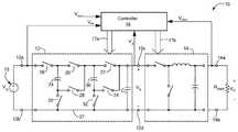
- a power converter circuit 10includes a first stage 12 (also referred to as a “reconfigurable switched capacitor transformation stage” or a “switched capacitor stage” or more simply a “transformation stage”) and a second stage 14 (also referred to as switching converter regulation stage or more simply a “regulation stage”).
- a first stage 12also referred to as a “reconfigurable switched capacitor transformation stage” or a “switched capacitor stage” or more simply a “transformation stage”
- second stage 14also referred to as switching converter regulation stage or more simply a “regulation stage”.
- a voltage source 15(here shown in phantom since it is not properly a part of the power converter circuit 10 ) is coupled between a pair of input terminals 12 a , 12 b of the transformation stage of power converter circuit 10 and a load R L (also shown in phantom since it is not properly a part of the power converter circuit 10 ) coupled to output terminals 14 a , 14 b of regulation stage 14 and across which is generated an output voltage V O .
- a controller circuit 16is coupled to receive a reference voltage V REF , as well as some or all of the input and output voltages V IN and/or V OUT and an intermediate output voltage V x (or more simply, intermediate voltage V x ). Controller 16 receives signals provided thereto (e.g.
- V IN , V OUT and/or intermediate voltage V xany or all of V IN , V OUT and/or intermediate voltage V x ) and in response thereto (and in accordance with a desired operating mode) provides control signals on paths 17 a , 17 b to either or both of the transformation and regulation stages 12 , 14 , respectively.
- Transformation stage 12receives the input voltage (e.g. V IN .) and operates to provide a transformed or intermediate voltage V X at terminals 12 C- 12 D. Thus transformed voltage V X is provided to input terminals of regulation stage 14 .
- the input voltage V INmay vary over a relatively wide voltage range.
- the particular voltage range over which the input voltage may varydepends upon the particular application. For example, in some applications the range of input voltages may be from about 1.5 volts (V) to about 5.0V. In other applications the range of input voltages may be from about 6V to about 12V. In still other applications the input voltage range may be from about 10V to about 14V. For example, in a converter circuit for battery-powered portable electronics applications, operation may be typically be required across an input voltage range from 2.4 V to 5.5 V.
- the transformation stage 12maintains transformed voltage V X over a voltage range which is relatively narrow compared with the input voltage range.
- the output voltage of the transformation stage 12may range from about 1.0V to about 1.66V.
- the transformation ratios utilized by the transformation stage 12are selected as a function of the input voltage V IN .
- the conversion ratio of the transformation stagemay be dynamically selected from among the allowed set of conversion ratios such that the intermediate voltage V x will be as large as possible while remaining below a specified maximum voltage.
- transformation stage 12can accept a wide range of input voltages while maintaining the transformed voltage over a voltage range which is relatively narrow compared with the input voltage range. For example, consider a transformation stage an input voltage range of 1.5 to 5.0 V and having allowed conversion ratios of 1 ⁇ 3, 1 ⁇ 2, and 2 ⁇ 3. It is possible to meet a goal of maximizing an intermediate voltage while at the same time keeping it below a specified maximum of approximately 1.66 V by operating at a conversion ratio of 2 ⁇ 3 for input voltages from 1.5 V to 2.5 V, operating at a conversion ratio of one half for input voltages from 2.5 V to 3.33 V, and operating at a conversion ratio of 1 ⁇ 3 for input voltages from 3.33 V to 5 V.
- the transformation stage 12 and regulation stage 14each include one or more switch components and one or more energy storage components.
- the components which provide the transformation stage 12are selected such that the transformation stage has a switching frequency which is relatively low compared with the switching frequency of the regulation stage.
- the transformation stagemay be referred to a low frequency stage while the regulation stage may be referred to as a high frequency, low voltage magnetic stage.
- the difference in switching speeds of the transformation stage and regulation stage switchesi.e.
- the frequency separation between the switching frequencies of the switchesis selected based upon a variety of factors including but not limited to the gating and switching loss characteristics of the switches It should, of course, be appreciated that a tradeoff must be made between switching frequency and the voltage levels (and/or range of voltages) which must be accepted by and provided by the transformation and regulation stages.
- Transformation stage 12includes a first plurality of coupled switches 18 , 20 , 22 coupled between terminal 12 a and a terminal 12 c.
- a first capacitor 24has a first terminal coupled to a first terminal of switch 18 and a second terminal coupled to a first terminal of a switch 26 .
- a second terminal of switch 26is coupled to an interconnect path 27 coupled between terminal 12 b and a terminal 12 d .
- interconnect path 27is coupled to a negative terminal of the voltage source 16 .
- a first terminal of a switch 28is coupled to the second terminal of capacitor 24 and a second terminal of switch 28 is coupled to a node between switches 20 and 22 .
- a second capacitor 30has a first terminal coupled to a first terminal of switch 22 and a second terminal coupled to a first terminal of a switch 32 .
- a second terminal of switch 32is coupled to the interconnect path coupled between terminal 12 b and terminal 12 d.
- a first terminal of a switch 34is coupled to the second terminal of capacitor 30 and a second terminal of switch 34 is coupled to a second terminal of switch 22 .
- capacitors 24 and 30may be selectively coupled in parallel between terminals 12 c and 12 d .
- switches 18 , 20 , 22 , 26 , 28 , 32 and 34capacitors 24 and 30 may be selectively coupled in parallel with switches 20 , 22 , respectively, creating a series stack between terminal 12 a and terminal 12 c.
- FIG. 3BAnother exemplary operating mode (or circuit configuration) is illustrated in FIG. 3B .
- the systemdynamically selects between a plurality of possible patterns and thus is said to be dynamically reconfigurable.
- the transformation stage 12corresponds to a reconfigurable switched capacitor converter. By appropriately selecting the switching patterns of the switches from among the possible patterns, the switched capacitor converter is reconfigurable and thus is able to provide efficient power conversion at multiple distinct conversion ratios.
- the operating mode of the transformation stage 12is controlled as a function of input voltage. For example, for large input voltages one can operate the circuit to follow the switching patterns in FIG. 3A , providing 3:1 conversion, while for lower input voltages one can operate the circuit to follow the switching patterns of FIG. 3 b , thus providing 2:1 conversion. In this way, transformation stage 12 can efficiently provide an intermediate voltage V x between terminals 12 c , 12 d that is smaller than the input voltage V IN and which varies over a much smaller range (ratio) than the input voltage V IN .
- the second, or regulating, stage 14corresponds to a magnetic-based switching power converter which operates from the low, narrow-range (i.e. any range less than the input voltage range; for example, if the ratio of V IN /V O equals 2:1 then anything less than that would be considered narrow-range) intermediate voltage to regulate the output voltage V o .
- this stageoperates from a relatively low, narrow input voltage range, it can be designed to operate at relatively high frequencies. Since component size is related to switching frequency (e.g. the higher the switching frequency, the smaller the component), the circuit may be implemented using passive components which are relatively small in size and which provide high-bandwidth regulation of the output.
- power converter 10converts power in two stages (i.e. the transformation stage 12 and the regulating stage 14 ) and together, the two stages can provide very small size, high efficiency, and high control bandwidth characteristics.
- the transformation or switched-capacitor stage 12is designed (e.g. by inclusion of multiple switched capacitor building blocks) to efficiently convert power at multiple distinct voltage conversion ratios.
- the number of capacitors in the converter stagedetermines both the maximum conversion ratio and the total possible number of distinct conversion ratios. It should thus be appreciated that the particular number of switches and capacitors included in the transformation stage depends upon a variety of factors including but not limited to the input voltage range for a particular application and the output voltage required for a particular application, and how many different transformation ratios are desired to reduce the intermediate voltage range.
- the power converter circuit described hereinmay be fabricated as an integrated circuit using a CMOS process.
- an integrated CMOS circuitincludes a reconfigurable switched capacitor transformation stage provided from one or more CMOS switches and one or more storage elements, in which the storage elements may be realized as either integrated capacitors or external devices.
- the regulation stagewould also be provided from one or more CMOS switches implemented and one or more storage elements. Again, the storage elements may be integrated, discrete, or provided as bond wires.
- the switches in said CMOS reconfigurable switched capacitor transformation stage and said CMOS regulation stageare fabricated in a single CMOS process. In the case where it is desirable for the switches of the regulation stage to switch at a higher frequency (in some cases a significantly higher frequency) than the switches in the transformation stage, the switches of the regulation stage may be fabricated as base transistors in the CMOS process.
- a transformation stage 30(also referred to as a switched capacitor stage) includes eight switches M 1 -M 8 and three capacitors C 1 -C 3 .
- the switchesmay be selectively opened and closed as shown in Table 1 below to provide three distinct conversion ratios (in this case, step-down ratios) of: 1 ⁇ 3; 1 ⁇ 2; and 2 ⁇ 3.
- a second signal /clkis also generated, which may simply be the complement of clk (i.e., is high when clk is low and low when clk is high), or which may be generated as a non-overlapping complement as is well known in the art.
- the elements of the first three rows of table 1indicate the switching states of the individual switches as the circuit is clocked. Each row shows operation for a different conversion ratio (i.e., operating configuration).
- An entry clkindicates that the switch is on (closed) when clk is asserted and off (open) otherwise
- an entry /clkindicates that the switch is on when the complementary signal /clk is asserted and off otherwise
- an entry offindicates that the switch is always off for that conversion ratio
- an entry onindicates that a switch is always on for that conversion ratio.
- the switched-capacitor circuit 30provides a step down ratio of one-third (1 ⁇ 3).
- the switched-capacitor circuit 30provides a step down ratio of one-half (1 ⁇ 2).
- the switched-capacitor circuit 30provides a step down ratio of two-thirds (2 ⁇ 3).
- the maximum voltage to which any of the devices in transformation stage 30 will be exposedis 2 ⁇ 3 of the input voltage (V 1 ) and some of the devices may see less (1 ⁇ 2V 1 and 1 ⁇ 3V 1 ) depending upon a selected operating mode. It should be appreciated that all of the devices in transformation stage 30 must be able to block the required voltage to realize all three step-down ratios. For example, M 1 must be rated to block 2 ⁇ 3 however it only sees 1 ⁇ 2V 1 for a step-down ratio of 1 ⁇ 2 and 2 ⁇ 3 V 1 for step-down ratios of 1 ⁇ 3 and 2 ⁇ 3. If more complicated networks are used (i.e. more switches), it may be possible to realize the same functionality at higher efficiency, but at the cost of area.
- the switched capacitor stage 30is thus controlled to maintain the intermediate voltage V x within a specified (narrow) range (or window) of voltages as the input voltage varies across a wide range of voltages.
- the size, maximum voltage and minimum voltage of the output window of the SC transformation stagecan be tailored to fit the regulation stage.
- Transformation stage 30can accept an input voltage in the range of about 1.5V to about 5.0V (3.33:1) and convert it into window of about 0.66 V ranging from about 1V to about 1.66V.
- Various control schemescan be used to accomplish this task. That is, the particular manner in which switches in transformation stage 30 ( FIG. 3 ) are selectively opened and closed to provided a desired transformation ratio may be selected based upon a variety of factors including but not limited to how charge flows in the circuit and how much loss is generated by a particular pattern.
- the circuit topology and switching patternsare selected such that charge balance is maintained on the charge storage elements (e.g. capacitors), which imposes a rational conversion ratio between the input and the output charge (and current) for a given switching pattern.
- This conversion ratiois the inverse of the ideal voltage conversion ratio of the circuit for a given switching pattern.
- a transformation ratio of 2 ⁇ 3is used while in region 34 a transformation ratio of 1 ⁇ 2 is used while in region 36 a transformation ration of 1 ⁇ 3 is used.
- the waveform of FIG. 4is selected strictly on V IN , but it should be appreciated that the selection could be made based upon both V IN and V OUT . For example, one might select the switching pattern transitions and hence the intermediate voltage window so that the regulation stage can operate near a desired conversion ratio, maximizing efficiency.
- the regulating stagecan be implemented with numerous topologies for very low output voltages (e.g. sub 1 V); good options include a synchronous buck converter, cascode-switch synchronous buck converter, interleaved synchronous buck converter, three-level synchronous buck converter, and four-switch “buck-boost” converter.
- Very fast transistorssuch as base CMOS transistors in an integrated process, can be used in the regulation stage since the input voltage is quite low. This allows the regulation stage to operate at a very high switching frequency, which in turn reduces the size of its passive components.
- One option to achieve a very high degree of integrationis to fabricate the converter in a multiple-voltage monolithic process (e.g., a process providing for extended drain transistors).
- the switched capacitor stagecan be implemented with higher voltage devices and operated at a relatively low frequency (e.g., 1 MHz) commensurate with the high-voltage devices.
- the regulating stagecan be implemented with low-voltage devices, and thus can be operated at considerably higher frequencies (e.g., 100 MHz), providing small volume for the passive components and fast regulation.
- multi-chip fabricationcan be used in which the two stages are implemented in different processes, each optimized for their respective functions.
- a converter with a large input voltage range and output current rangecan thus be realized if a reconfigurable switched capacitor converter with multiple transformation ratios is used as a transformation stage along with a high frequency, low voltage regulation stage.
- the convertercan also take advantage of state-of-the-art CMOS processes that have additional high voltage devices.
- the energy loss E L associated with charging a capacitor C from zero to a voltage V with a series connection from a dc voltage source of value Vis 1 ⁇ 2 CV 2 , and is independent of the parasitic series resistance (R). Furthermore, for a conventional SC circuit, a fixed amount of charge-up energy loss equal to 1 ⁇ 2 C ⁇ 2 will result at each switch interval, where ⁇ V corresponds to the difference between the initial and final value of the capacitor voltage. It is important to note that this fixed charge-up loss cannot be reduced by employing switches with lower on-state resistance. It is for this reason that conventional SC converters aim to minimize the variations of the voltage on the capacitors during the charging phase and only operate efficiently at certain conversion ratios.
- a second embodiment of a power converter circuitpermits more efficient use of the capacitors, enabling reduction in the required capacitor size and/or improvement in system efficiency. Furthermore, the second embodiment does not require a reconfigurable switched-capacitor network although it may use one.
- FIG. 5is used to explain an example of the charging process of a capacitor C, where a resistor R represents the combined equivalent series resistance (ESR) of the capacitor and switch on-state resistance.
- FIG. 5Aillustrates a technique to improve the charge-up efficiency of the switched capacitor circuit.
- an auxiliary converter 40operating at a much faster switching frequency than the switched capacitor stage is used to reduce the energy loss of the switched capacitor circuit.
- the switching frequency of the auxiliary convertershould be sufficiently higher than the switched capacitor stage such that the capacitor charging takes place over many switching cycles of the auxiliary converter. A factor of five in switching frequency may be sufficient for this purpose, and factors of ten or more are typical.
- the auxiliary converter 40may be the regulating converter used to supply the output, or it may be a separate converter.
- the systemis designed such that the majority of the difference between the input voltage V in and the capacitor stack voltage V c appears across the input of the auxiliary converter when the capacitor is charging. Instead of being dissipated as heat in the resistor, the energy associated with charging the capacitor stack is delivered to the output of the auxiliary converter.
- FIG. 6illustrates a possible implementation of the general embodiment discussed above in conjunction with FIG. 5 .
- a power converter 50includes a transformation stage 52 and an auxiliary converter and the regulating converter stage 54 .
- Transformation stage 52includes a plurality of capacitors C 1 , C 2 and a first group of switches (each labeled S 1 ) and a second group of switches (each labeled S 2 ).
- Auxiliary converter and the regulating converter stage 54includes a plurality of capacitors C small , C buck , a plurality of switches S 3 , S 4 and an inductive element L buck .
- a “fast regulating converter”(in this case a synchronous buck converter) serves as both the auxiliary converter and the regulating converter stage 54 for the system 50 .
- Auxiliary converter and the regulating converter stage 54operates at a switching frequency much higher than that of the switched capacitor stage 52 .
- the capacitor C smallserves only as a filter and bypass for the fast regulating converter, its numerical value can be much smaller than the capacitors C 1 and C 2 of the switched capacitor transformation stage.
- C 1 and C 2thus charge with low loss, and at a rate determined by the power drawn from the regulating converter to control the system output.
- the switched-capacitor stageis configured for discharging C 1 and C 2 in parallel (switches S 2 closed)
- the dischargeis at a rate based on the power needed to regulate the output.
- the switched capacitor stage 52can be switched (switch sets S 1 and S 2 on alternately) such that the voltage V x at the input of the fast regulating converter stays within a specified window or below a specified voltage.
- the switchescould be controlled such that the capacitor C 1 and C 2 voltages remain within a specified hysteresis band about V in /3, such that the regulating converter sees a maximum input voltage near V in /3.
- the switched capacitor stagecan be controlled to provide a specified maximum voltage V x at the input of the auxiliary converter.
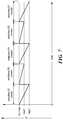
- FIG. 7a plot of switch configuration vs. voltage illustrates a control strategy utilizing the above-described technique, where two separate reference voltages are used to ensure that the input voltage of the auxiliary converter does not exceed V X,max .
- the switches designated by reference number 1 in FIG. 6are on or closed (series charging of the capacitors) until V X falls below V ref1 .
- switches 1turn off or open, and the switches designated with reference numeral 2 turn on (parallel discharging of capacitors), until V X falls below V ref2 , at which time the cycle repeats.
- the reference voltagesare set by the maximum auxiliary input voltage V X,mas , and are given by:
- the topology of the fast regulating convertercan be any type of power converter that is able to provide fast switching and efficient regulation of the output voltage for various input voltages (synchronous buck, three-level synchronous buck, SEPIC, soft switched or resonant converter, etc.).
- the switched-capacitor circuitcan be realized with a variety of topologies, depending on desired voltage transformation and permitted switch voltages.
- FIG. 8yet another embodiment of a power converter circuit is shown.
- the circuit topology shown in FIG. 8illustrates how the auxiliary converter can be used as a separate energy-recovering device, with an independent output voltage.
- two parallel switched-capacitor circuitsare employed, operating in anti-phase.
- the capacitors of step-down cell 1are charging in series (switches A closed, switches B open), the capacitors of cell 2 are discharging in parallel.
- the difference between the input voltage and the sum of the charging capacitorsappears across the input terminal of the auxiliary converter.
- the charging energycan again be recovered by this auxiliary converter, providing a means for improving overall efficiency or increasing power density.
- the output voltage of the switched-capacitor stage, V out1can be regulated using the auxiliary converter.
- the auxiliary converterperforms the regulating functions in a manner similar to some (lossy) current-controlled strategies.
- the auxiliary convertercan again be any type of fast regulating converter, just as in the example of FIG. 6 .
- the regulated output voltage V out2can be higher or lower than V out1 , depending on the choice of auxiliary converter. This voltage can be used for a variety of purposes. Examples include, but are not limited to: powering the SC transistors, fed back to the input, delivered to the output, or providing a separate output voltage for applications where that is desirable.
- R toad in this circuitcan represent the actual load, or may represent the input impedance of another converter or set of converters for regulating system outputs.
Landscapes
- Engineering & Computer Science (AREA)
- Power Engineering (AREA)
- Dc-Dc Converters (AREA)
Abstract
Description
| TABLE 1 | |||||||||
| V2/V1 | M1 | M2 | M3 | M4 | M5 | M6 | M7 | M8 | M9 |
| 1/3 | clk | clk | clk | off | off | ||||
| 1/2 | clk | clk | on | on | off | off | off | ||
| 2/3 | clk | clk | off | off | clk | clk | |||
| Vmax | ⅔V1 | ⅔V1 | ½V1 | ½V1 | ⅔V1 | ⅓V1 | ½V1 | ½V1 | ½V1 |
The SC transformation stage is provided with a digital clock signal clk. A second signal /clk is also generated, which may simply be the complement of clk (i.e., is high when clk is low and low when clk is high), or which may be generated as a non-overlapping complement as is well known in the art. The elements of the first three rows of table 1 indicate the switching states of the individual switches as the circuit is clocked. Each row shows operation for a different conversion ratio (i.e., operating configuration). An entry clk indicates that the switch is on (closed) when clk is asserted and off (open) otherwise, an entry /clk indicates that the switch is on when the complementary signal /clk is asserted and off otherwise, an entry off indicates that the switch is always off for that conversion ratio, and an entry on indicates that a switch is always on for that conversion ratio.
Claims (11)
Priority Applications (5)
| Application Number | Priority Date | Filing Date | Title |
|---|---|---|---|
| US16/146,028US10541611B2 (en) | 2008-05-08 | 2018-09-28 | Power converter with capacitive energy transfer and fast dynamic response |
| US16/697,318US10749434B2 (en) | 2008-05-08 | 2019-11-27 | Power converter with capacitive energy transfer and fast dynamic response |
| US16/915,051US11245330B2 (en) | 2008-05-08 | 2020-06-29 | Power converter with capacitive energy transfer and fast dynamic response |
| US17/566,750US11736010B2 (en) | 2008-05-08 | 2021-12-31 | Power converter with capacitive energy transfer and fast dynamic response |
| US18/215,253US12431801B2 (en) | 2008-05-08 | 2023-06-28 | Power converter with capacitive energy transfer and fast dynamic response |
Applications Claiming Priority (8)
| Application Number | Priority Date | Filing Date | Title |
|---|---|---|---|
| US5147608P | 2008-05-08 | 2008-05-08 | |
| US12/437,599US8212541B2 (en) | 2008-05-08 | 2009-05-08 | Power converter with capacitive energy transfer and fast dynamic response |
| US13/487,781US8643347B2 (en) | 2008-05-08 | 2012-06-04 | Power converter with capacitive energy transfer and fast dynamic response |
| US13/599,037US8699248B2 (en) | 2008-05-08 | 2012-08-30 | Power converter with capacitive energy transfer and fast dynamic response |
| US14/251,917US9048727B2 (en) | 2008-05-08 | 2014-04-14 | Power converter with capacitive energy transfer and fast dynamic response |
| US14/708,903US9667139B2 (en) | 2008-05-08 | 2015-05-11 | Power converter with capacitive energy transfer and fast dynamic response |
| US15/585,676US20170237351A1 (en) | 2008-05-08 | 2017-05-03 | Power Converter With Capacitive Energy Transfer And Fast Dynamic Response |
| US16/146,028US10541611B2 (en) | 2008-05-08 | 2018-09-28 | Power converter with capacitive energy transfer and fast dynamic response |
Related Parent Applications (1)
| Application Number | Title | Priority Date | Filing Date |
|---|---|---|---|
| US15/585,676ContinuationUS20170237351A1 (en) | 2008-05-08 | 2017-05-03 | Power Converter With Capacitive Energy Transfer And Fast Dynamic Response |
Related Child Applications (1)
| Application Number | Title | Priority Date | Filing Date |
|---|---|---|---|
| US16/697,318ContinuationUS10749434B2 (en) | 2008-05-08 | 2019-11-27 | Power converter with capacitive energy transfer and fast dynamic response |
Publications (2)
| Publication Number | Publication Date |
|---|---|
| US20190044443A1 US20190044443A1 (en) | 2019-02-07 |
| US10541611B2true US10541611B2 (en) | 2020-01-21 |
Family
ID=41266317
Family Applications (11)
| Application Number | Title | Priority Date | Filing Date |
|---|---|---|---|
| US12/437,599Active2030-07-21US8212541B2 (en) | 2008-05-08 | 2009-05-08 | Power converter with capacitive energy transfer and fast dynamic response |
| US13/487,781ActiveUS8643347B2 (en) | 2008-05-08 | 2012-06-04 | Power converter with capacitive energy transfer and fast dynamic response |
| US13/599,037Active2029-07-11US8699248B2 (en) | 2008-05-08 | 2012-08-30 | Power converter with capacitive energy transfer and fast dynamic response |
| US14/251,917ActiveUS9048727B2 (en) | 2008-05-08 | 2014-04-14 | Power converter with capacitive energy transfer and fast dynamic response |
| US14/708,903ActiveUS9667139B2 (en) | 2008-05-08 | 2015-05-11 | Power converter with capacitive energy transfer and fast dynamic response |
| US15/585,676AbandonedUS20170237351A1 (en) | 2008-05-08 | 2017-05-03 | Power Converter With Capacitive Energy Transfer And Fast Dynamic Response |
| US16/146,028ActiveUS10541611B2 (en) | 2008-05-08 | 2018-09-28 | Power converter with capacitive energy transfer and fast dynamic response |
| US16/697,318ActiveUS10749434B2 (en) | 2008-05-08 | 2019-11-27 | Power converter with capacitive energy transfer and fast dynamic response |
| US16/915,051Active2029-07-01US11245330B2 (en) | 2008-05-08 | 2020-06-29 | Power converter with capacitive energy transfer and fast dynamic response |
| US17/566,750Active2029-06-13US11736010B2 (en) | 2008-05-08 | 2021-12-31 | Power converter with capacitive energy transfer and fast dynamic response |
| US18/215,253ActiveUS12431801B2 (en) | 2008-05-08 | 2023-06-28 | Power converter with capacitive energy transfer and fast dynamic response |
Family Applications Before (6)
| Application Number | Title | Priority Date | Filing Date |
|---|---|---|---|
| US12/437,599Active2030-07-21US8212541B2 (en) | 2008-05-08 | 2009-05-08 | Power converter with capacitive energy transfer and fast dynamic response |
| US13/487,781ActiveUS8643347B2 (en) | 2008-05-08 | 2012-06-04 | Power converter with capacitive energy transfer and fast dynamic response |
| US13/599,037Active2029-07-11US8699248B2 (en) | 2008-05-08 | 2012-08-30 | Power converter with capacitive energy transfer and fast dynamic response |
| US14/251,917ActiveUS9048727B2 (en) | 2008-05-08 | 2014-04-14 | Power converter with capacitive energy transfer and fast dynamic response |
| US14/708,903ActiveUS9667139B2 (en) | 2008-05-08 | 2015-05-11 | Power converter with capacitive energy transfer and fast dynamic response |
| US15/585,676AbandonedUS20170237351A1 (en) | 2008-05-08 | 2017-05-03 | Power Converter With Capacitive Energy Transfer And Fast Dynamic Response |
Family Applications After (4)
| Application Number | Title | Priority Date | Filing Date |
|---|---|---|---|
| US16/697,318ActiveUS10749434B2 (en) | 2008-05-08 | 2019-11-27 | Power converter with capacitive energy transfer and fast dynamic response |
| US16/915,051Active2029-07-01US11245330B2 (en) | 2008-05-08 | 2020-06-29 | Power converter with capacitive energy transfer and fast dynamic response |
| US17/566,750Active2029-06-13US11736010B2 (en) | 2008-05-08 | 2021-12-31 | Power converter with capacitive energy transfer and fast dynamic response |
| US18/215,253ActiveUS12431801B2 (en) | 2008-05-08 | 2023-06-28 | Power converter with capacitive energy transfer and fast dynamic response |
Country Status (1)
| Country | Link |
|---|---|
| US (11) | US8212541B2 (en) |
Cited By (7)
| Publication number | Priority date | Publication date | Assignee | Title |
|---|---|---|---|---|
| US11211861B2 (en) | 2011-05-05 | 2021-12-28 | Psemi Corporation | DC-DC converter with modular stages |
| US11316424B2 (en) | 2011-05-05 | 2022-04-26 | Psemi Corporation | Dies with switches for operating a switched-capacitor power converter |
| US20220166339A1 (en)* | 2020-11-23 | 2022-05-26 | Richtek Technology Corporation | High efficiency charging system and power conversion circuit thereof |
| US11736010B2 (en) | 2008-05-08 | 2023-08-22 | Massachusetts Institute Of Technology | Power converter with capacitive energy transfer and fast dynamic response |
| TWI829170B (en)* | 2021-05-26 | 2024-01-11 | 美商茂力科技股份有限公司 | Multi-level buck converter and control circuit thereof |
| US11888398B2 (en) | 2021-06-25 | 2024-01-30 | Ge Energy Power Conversion Technology Limited | Self reconfigurable, adaptable power electronics building block (A-PEBB) |
| US12176815B2 (en) | 2011-12-19 | 2024-12-24 | Psemi Corporation | Switched-capacitor circuit control in power converters |
Families Citing this family (173)
| Publication number | Priority date | Publication date | Assignee | Title |
|---|---|---|---|---|
| US7923865B2 (en)* | 2008-06-27 | 2011-04-12 | Medtronic, Inc. | Multi-mode switched capacitor dc-dc voltage converter |
| US8089787B2 (en) | 2008-06-27 | 2012-01-03 | Medtronic, Inc. | Switched capacitor DC-DC voltage converter |
| WO2013191757A1 (en)* | 2012-06-18 | 2013-12-27 | Massachusetts Institute Of Technology | Inverter/power amplifier with capacitive energy transfer and related techniques |
| US9634577B2 (en) | 2008-11-11 | 2017-04-25 | Massachusetts Institute Of Technology | Inverter/power amplifier with capacitive energy transfer and related techniques |
| EP3447910B1 (en) | 2008-11-11 | 2020-12-16 | Massachusetts Institute Of Technology | An asymmetric multilevel outphasing architecture for rf amplifiers |
| EP2244363A1 (en)* | 2009-04-23 | 2010-10-27 | Mitsubishi Electric R&D Centre Europe B.V. | Method and an apparatus for controlling the output voltage of a boost converter |
| TWI407672B (en)* | 2009-11-30 | 2013-09-01 | Ind Tech Res Inst | Buck-store and boost-restore converter |
| US9912303B2 (en) | 2010-02-03 | 2018-03-06 | Massachusetts Institute Of Technology | RF-input / RF-output outphasing amplifier |
| US9141832B2 (en) | 2010-02-03 | 2015-09-22 | Massachusetts Institute Of Technology | Multiway lossless power combining and outphasing incorporating transmission lines |
| US8274264B2 (en)* | 2010-02-19 | 2012-09-25 | Exar Corporation | Digital control method for improving heavy-to-light (step down) load transient response of switch mode power supplies |
| US9118243B2 (en) | 2010-10-25 | 2015-08-25 | Hewlett-Packard Development Company, L.P. | Power converter dependent on a voltage range the input voltage resides in |
| US10680515B2 (en) | 2011-05-05 | 2020-06-09 | Psemi Corporation | Power converters with modular stages |
| EP4318909A3 (en) | 2011-05-05 | 2024-03-06 | PSEMI Corporation | Dc-dc converter with modular stages |
| WO2017161368A1 (en)* | 2016-03-18 | 2017-09-21 | Arctic Sand Technologies, Inc. | Power converters with modular stages |
| CN102420444B (en)* | 2011-09-15 | 2014-06-11 | 凹凸电子(武汉)有限公司 | Single wire communication system and single wire communication implementing method |
| US8743553B2 (en) | 2011-10-18 | 2014-06-03 | Arctic Sand Technologies, Inc. | Power converters with integrated capacitors |
| JP5874350B2 (en)* | 2011-11-28 | 2016-03-02 | オムロン株式会社 | Voltage conversion circuit and electronic device |
| WO2013109719A1 (en) | 2012-01-17 | 2013-07-25 | Massachusetts Institute Of Technology | Stacked switched capacitor energy buffer circuit |
| US9413257B2 (en)* | 2012-01-20 | 2016-08-09 | The Ohio State University | Enhanced flyback converter |
| US9407164B2 (en) | 2012-02-03 | 2016-08-02 | Massachusetts Institute Of Technology | Systems approach to photovoltaic energy extraction |
| WO2013134573A1 (en) | 2012-03-08 | 2013-09-12 | Massachusetts Institute Of Technology | Resonant power converters using impedance control networks and related techniques |
| US8830710B2 (en) | 2012-06-25 | 2014-09-09 | Eta Devices, Inc. | RF energy recovery system |
| US10110130B2 (en) | 2012-08-12 | 2018-10-23 | Loai Galal Bahgat Salem | Recursive DC-DC converter |
| WO2014028441A2 (en)* | 2012-08-13 | 2014-02-20 | Massachusetts Institute Of Technology | Multi-step, switched-capacitor rectifier and dc-dc converter circuits and related techniques |
| KR101315143B1 (en)* | 2012-08-22 | 2013-10-14 | 전북대학교산학협력단 | High efficiency dc/dc power converter with high conversion ratio |
| US9537456B2 (en) | 2012-10-30 | 2017-01-03 | Eta Devices, Inc. | Asymmetric multilevel backoff amplifier with radio-frequency splitter |
| US9166536B2 (en) | 2012-10-30 | 2015-10-20 | Eta Devices, Inc. | Transmitter architecture and related methods |
| US8829993B2 (en) | 2012-10-30 | 2014-09-09 | Eta Devices, Inc. | Linearization circuits and methods for multilevel power amplifier systems |
| US8824978B2 (en) | 2012-10-30 | 2014-09-02 | Eta Devices, Inc. | RF amplifier architecture and related techniques |
| US9853550B2 (en) | 2012-10-31 | 2017-12-26 | Massachusetts Institute Of Technology | Systems and methods for a variable frequency multiplier power converter |
| US8693224B1 (en) | 2012-11-26 | 2014-04-08 | Arctic Sand Technologies Inc. | Pump capacitor configuration for switched capacitor circuits |
| US20140152381A1 (en) | 2012-11-30 | 2014-06-05 | International Business Machines Corporation | Reconfigurable switched-capacitor voltage converter circuit, integrated circuit (ic) chip including the circuit and method of switching voltage on chip |
| US20140184189A1 (en)* | 2013-01-02 | 2014-07-03 | Loai Galal Bahgat Salem | Inductively assisted switched capacitor dc-dc converter |
| US9461546B2 (en)* | 2013-02-08 | 2016-10-04 | Advanced Charging Technologies, LLC | Power device and method for delivering power to electronic devices |
| US8619445B1 (en) | 2013-03-15 | 2013-12-31 | Arctic Sand Technologies, Inc. | Protection of switched capacitor power converter |
| US8724353B1 (en) | 2013-03-15 | 2014-05-13 | Arctic Sand Technologies, Inc. | Efficient gate drivers for switched capacitor converters |
| US9847712B2 (en) | 2013-03-15 | 2017-12-19 | Peregrine Semiconductor Corporation | Fault control for switched capacitor power converter |
| JP6262330B2 (en)* | 2013-03-15 | 2018-01-17 | クゥアルコム・インコーポレイテッドQualcomm Incorporated | Low power architecture |
| US9203299B2 (en) | 2013-03-15 | 2015-12-01 | Artic Sand Technologies, Inc. | Controller-driven reconfiguration of switched-capacitor power converter |
| CN103166464B (en)* | 2013-03-29 | 2016-09-07 | 株式会社村田制作所 | Power converter and method for power conversion |
| WO2014168911A1 (en) | 2013-04-09 | 2014-10-16 | Massachusetts Institute Of Technology | Power conservation with high power factor |
| CN103259402A (en)* | 2013-04-25 | 2013-08-21 | 浙江大学 | Switched capacitor voltage-multiplying type direct current source based on symmetrical structure |
| CN103441669B (en)* | 2013-07-21 | 2016-02-17 | 马东林 | Cumulative charge pump |
| KR102123517B1 (en)* | 2013-08-19 | 2020-06-16 | 에스케이하이닉스 주식회사 | Semiconductor device, semiconductor system including the same and method for operating semiconductor device |
| EP2846448B1 (en)* | 2013-09-06 | 2018-11-14 | Nxp B.V. | Switched capacitor power converter |
| JP5695782B1 (en) | 2013-09-12 | 2015-04-08 | 住友電気工業株式会社 | Transformer |
| US9742266B2 (en) | 2013-09-16 | 2017-08-22 | Arctic Sand Technologies, Inc. | Charge pump timing control |
| US9041459B2 (en) | 2013-09-16 | 2015-05-26 | Arctic Sand Technologies, Inc. | Partial adiabatic conversion |
| US10840805B2 (en) | 2013-09-24 | 2020-11-17 | Eta Devices, Inc. | Integrated power supply and modulator for radio frequency power amplifiers |
| US9755672B2 (en) | 2013-09-24 | 2017-09-05 | Eta Devices, Inc. | Integrated power supply and modulator for radio frequency power amplifiers |
| KR102247952B1 (en)* | 2013-10-07 | 2021-05-06 | 라이온 세미컨덕터 인크. | Feedback control in hybrid voltage regulators |
| US9825545B2 (en) | 2013-10-29 | 2017-11-21 | Massachusetts Institute Of Technology | Switched-capacitor split drive transformer power conversion circuit |
| US9391515B2 (en)* | 2013-11-18 | 2016-07-12 | Cisco Technology, Inc. | Buck circuit |
| WO2015123267A1 (en)* | 2014-02-12 | 2015-08-20 | Eta Devices, Inc. | Integrated power supply and modulator for radio frequency power amplifiers |
| DE112015001260T5 (en) | 2014-03-14 | 2016-12-08 | Arctic Sand Technologies, Inc. | Charge pump stability control |
| US10693368B2 (en) | 2014-03-14 | 2020-06-23 | Psemi Corporation | Charge pump stability control |
| DE112015001245T5 (en) | 2014-03-14 | 2016-12-15 | Arctic Sand Technologies, Inc. | Charge-balanced charge pump control |
| JP2017509304A (en)* | 2014-03-28 | 2017-03-30 | トムソン ライセンシングThomson Licensing | DC / DC converter and driving method of DC / DC converter |
| CN204068695U (en)* | 2014-06-13 | 2014-12-31 | 株式会社村田制作所 | Power conversion system |
| US9413232B2 (en)* | 2014-06-30 | 2016-08-09 | Texas Instruments Incorporated | Droop reduction circuit for charge pump buck converter |
| US10075064B2 (en) | 2014-07-03 | 2018-09-11 | Massachusetts Institute Of Technology | High-frequency, high density power factor correction conversion for universal input grid interface |
| US9768731B2 (en) | 2014-07-23 | 2017-09-19 | Eta Devices, Inc. | Linearity and noise improvement for multilevel power amplifier systems using multi-pulse drain transitions |
| US10348102B2 (en)* | 2014-08-20 | 2019-07-09 | Walter Lee Davis | Magnetic capacitor energy module and applications thereof |
| US9762132B2 (en) | 2014-10-28 | 2017-09-12 | Advanced Charging Technologies, LLC | Electrical circuit for delivering power to consumer electronic devices |
| US9420724B2 (en) | 2014-11-04 | 2016-08-16 | Ge Aviation Systems Llc | Power converter assembly |
| US9680385B2 (en) | 2014-11-04 | 2017-06-13 | Ge Aviation Systems Llc | Power converter |
| US9943016B2 (en)* | 2014-11-04 | 2018-04-10 | Ge Aviation Systems Llc | Cooling structure |
| JP6297963B2 (en)* | 2014-11-05 | 2018-03-20 | 住友電気工業株式会社 | Transformer |
| JP6359950B2 (en) | 2014-11-05 | 2018-07-18 | 住友電気工業株式会社 | Transformer |
| WO2016076840A1 (en) | 2014-11-11 | 2016-05-19 | Halliburton Energy Services, Inc. | Assymetric gate driver apparatus, methods, and systems |
| US10790784B2 (en) | 2014-12-19 | 2020-09-29 | Massachusetts Institute Of Technology | Generation and synchronization of pulse-width modulated (PWM) waveforms for radio-frequency (RF) applications |
| WO2016138361A1 (en)* | 2015-02-27 | 2016-09-01 | President And Fellows Of Harvard College | Device and method for hybrid feedback control of a switch-capacitor multi-unit voltage regulator |
| US9979421B2 (en) | 2015-03-02 | 2018-05-22 | Eta Devices, Inc. | Digital pre-distortion (DPD) training and calibration system and related techniques |
| CN107580748B (en)* | 2015-03-13 | 2022-12-13 | 佩里格林半导体公司 | Flexible power converter architecture with regulation circuit and switching network |
| WO2016149063A1 (en) | 2015-03-13 | 2016-09-22 | Arctic Sand Technologies, Inc. | Dc-dc transformer with inductor for the facilitation of adiabatic inter-capacitor charge transport |
| US9793807B2 (en)* | 2015-03-22 | 2017-10-17 | Boris Ablov | Lossless power conversion to DC method and device |
| US10727738B2 (en) | 2015-04-22 | 2020-07-28 | Sridhar V. Kotikalapoodi | Method and apparatus for control of switch mode power supplies utilizing magnetic and capacitive conversion means |
| US10084384B1 (en)* | 2015-04-22 | 2018-09-25 | Sridhar Kotikalapoodi | Method and apparatus for switched capacitor and inductor based-switch mode power supply |
| US9910811B2 (en)* | 2015-04-27 | 2018-03-06 | Cisco Technology, Inc. | Hot swap circuit |
| WO2017007991A1 (en)* | 2015-07-08 | 2017-01-12 | Arctic Sand Technologies, Inc. | Switched-capacitor power converters |
| US9665164B2 (en)* | 2015-08-12 | 2017-05-30 | Cisco Technology, Inc. | Hot swap circuit |
| US9853555B2 (en) | 2015-09-17 | 2017-12-26 | General Electric Company | Universal power adapter and an associated method thereof |
| PL3145069T3 (en) | 2015-09-21 | 2019-08-30 | Politechnika Gdańska | Circuit and method for canonical and adiabatic dc-dc voltage conversion |
| WO2017156532A1 (en)* | 2016-03-11 | 2017-09-14 | Arctic Sand Technologies, Inc. | Battery management system with adiabatic switched-capacitor circuit |
| US10541603B2 (en)* | 2016-04-18 | 2020-01-21 | Lion Semiconductor Inc. | Circuits for a hybrid switched capacitor converter |
| CN113472194B (en)* | 2016-04-18 | 2024-08-13 | 莱恩半导体股份有限公司 | Apparatus, system, and method for reconfigurable DICKSON STAR switched capacitor voltage regulator |
| US20200328676A1 (en) | 2016-05-31 | 2020-10-15 | The Regents Of The University Of Colorado, A Body Corporate | Smart cable and methods thereof |
| US10536093B2 (en)* | 2016-06-28 | 2020-01-14 | Massachusetts Institute Of Technology | High-frequency variable load inverter and related techniques |
| WO2018066444A1 (en)* | 2016-10-06 | 2018-04-12 | 株式会社村田製作所 | Dc-dc converter |
| US10340689B2 (en) | 2016-10-21 | 2019-07-02 | Nxp B.V. | System and method for power management |
| US10270368B2 (en)* | 2016-12-02 | 2019-04-23 | Lawrence Livermore National Security, Llc | Bi-directional, transformerless voltage system |
| US10686378B2 (en)* | 2016-12-16 | 2020-06-16 | Futurewei Technologies, Inc. | High-efficiency regulated buck-boost converter |
| DE102016225795A1 (en)* | 2016-12-21 | 2018-06-21 | Dialog Semiconductor (Uk) Limited | HYBRID-DCDC POWER CONVERTERS WITH HIGHER EFFICIENCY |
| US10361630B1 (en)* | 2016-12-23 | 2019-07-23 | Verily Life Sciences Llc | Systems and methods for a reconfigurable switched capacitor DC-DC converter |
| CN106655762B (en)* | 2017-01-11 | 2019-06-18 | 南京矽力杰半导体技术有限公司 | Isolated form Switching capacitors |
| CN106696748B (en)* | 2017-01-25 | 2019-06-28 | 华为技术有限公司 | A kind of charging pile system |
| DE102017204044A1 (en)* | 2017-02-14 | 2018-08-16 | Ellenberger & Poensgen Gmbh | Method and voltage multiplier for converting an input voltage and separation circuit |
| USRE50103E1 (en)* | 2017-04-14 | 2024-08-27 | Lion Semiconductor Inc. | Circuits for a hybrid switched capacitor converter |
| CN107124101B (en)* | 2017-05-22 | 2019-06-21 | 南京矽力杰半导体技术有限公司 | Isolated Switched Capacitor Converter |
| KR102388940B1 (en)* | 2017-05-22 | 2022-04-22 | 삼성전자 주식회사 | Voltage converter circuit, electronic device including the same and method for voltage conversion |
| US10298138B2 (en) | 2017-08-31 | 2019-05-21 | Google Llc | Programmable power adapter |
| US10277140B2 (en) | 2017-08-31 | 2019-04-30 | Google Llc | High-bandwith resonant power converters |
| US10601304B2 (en) | 2017-09-12 | 2020-03-24 | Texas Instruments Incorporated | Apparatus for a high efficiency hybrid power converter and methods to control the same |
| CN108092513B (en)* | 2017-12-26 | 2020-03-06 | 矽力杰半导体技术(杭州)有限公司 | DC-DC converter |
| WO2019143992A1 (en) | 2018-01-22 | 2019-07-25 | Transient Plasma Systems, Inc. | Inductively coupled pulsed rf voltage multiplier |
| WO2019144037A1 (en)* | 2018-01-22 | 2019-07-25 | Transient Plasma Systems, Inc. | Resonant pulsed voltage multiplier and capacitor charger |
| KR102553587B1 (en)* | 2018-02-22 | 2023-07-10 | 삼성전자 주식회사 | Power converter and method for converting power |
| US10965204B2 (en)* | 2018-03-20 | 2021-03-30 | Psemi Corporation | Adaptive control for reconfiguring a regulator and/or a charge pump for a power converter |
| US10389236B1 (en)* | 2018-03-29 | 2019-08-20 | Psemi Corporation | Disturbance quelling |
| CN108539981A (en)* | 2018-06-04 | 2018-09-14 | 南京矽力杰半导体技术有限公司 | DC-to-DC converter |
| US10340794B1 (en)* | 2018-06-21 | 2019-07-02 | Linear Technology Llc | Reverse capacitor voltage balancing for high current high voltage charge pump circuits |
| US11629860B2 (en) | 2018-07-17 | 2023-04-18 | Transient Plasma Systems, Inc. | Method and system for treating emissions using a transient pulsed plasma |
| EP3824223B1 (en) | 2018-07-17 | 2024-03-06 | Transient Plasma Systems, Inc. | Method and system for treating cooking smoke emissions using a transient pulsed plasma |
| US11223237B2 (en)* | 2018-10-05 | 2022-01-11 | Nuvolta Technologies (Hefei) Co., Ltd. | High efficiency power converting apparatus and control method |
| DE102018217445A1 (en)* | 2018-10-11 | 2020-04-16 | Dialog Semiconductor (Uk) Limited | Two-stage battery charger |
| TWI682614B (en)* | 2018-10-26 | 2020-01-11 | 緯穎科技服務股份有限公司 | Multi-phase power supply for stepdown system |
| CN111181393B (en)* | 2018-11-12 | 2021-10-26 | 台达电子企业管理(上海)有限公司 | Power supply device |
| US10523114B1 (en)* | 2018-11-29 | 2019-12-31 | Texas Instruments Incorporated | Decoupling circuits for converters |
| TWI679514B (en)* | 2018-12-04 | 2019-12-11 | 新唐科技股份有限公司 | Power converter |
| TWI689161B (en)* | 2018-12-22 | 2020-03-21 | 新唐科技股份有限公司 | Power converter |
| US10686367B1 (en) | 2019-03-04 | 2020-06-16 | Psemi Corporation | Apparatus and method for efficient shutdown of adiabatic charge pumps |
| CN113795403B (en)* | 2019-03-20 | 2024-06-21 | 理查德·赫·谢拉特和苏珊·毕·谢拉特可撤销信托基金 | High-energy capacitive conversion device using multi-wire inductor |
| WO2020206270A1 (en) | 2019-04-04 | 2020-10-08 | The Trustees Of Princeton University | System and method for modular high voltage conversion ratio power converter |
| US10790742B1 (en) | 2019-04-17 | 2020-09-29 | Dialog Semiconductor (Uk) Limited | Multi-level power converter with improved transient load response |
| US10756623B1 (en) | 2019-04-17 | 2020-08-25 | Dialog Semiconductor (Uk) Limited | Low loss power converter |
| US10811974B1 (en) | 2019-04-17 | 2020-10-20 | Dialog Semiconductor (Uk) Limited | Power converter |
| DE102019206421A1 (en)* | 2019-05-03 | 2020-11-05 | Dialog Semiconductor (Uk) Limited | Hybrid DC power converter with no voltage conversion ratio |
| US11696388B2 (en) | 2019-05-07 | 2023-07-04 | Transient Plasma Systems, Inc. | Pulsed non-thermal atmospheric pressure plasma processing system |
| CN114270293B (en) | 2019-07-08 | 2024-12-24 | 埃塔无线公司 | Multiple output supply generator for RF power amplifier with differential capacitive energy transfer |
| US11637531B1 (en) | 2019-09-05 | 2023-04-25 | Murata Manufacturing Co., Ltd. | Supply generator and associated control methods |
| US11191028B2 (en) | 2019-09-06 | 2021-11-30 | Eta Wireless, Inc. | Power management control over a transmission line for millimeter wave chip sets for cellular radios |
| CN112491269B (en) | 2019-09-11 | 2022-08-12 | 台达电子工业股份有限公司 | Power supply conversion system |
| JP7370783B2 (en)* | 2019-09-24 | 2023-10-30 | キヤノン株式会社 | Electronic equipment and control methods |
| DE102019214978A1 (en)* | 2019-09-30 | 2021-04-01 | Dialog Semiconductor (Uk) Limited | Hybrid multi-level power converter with bypassing through an inductive component |
| US10924006B1 (en)* | 2019-09-30 | 2021-02-16 | Psemi Corporation | Suppression of rebalancing currents in a switched-capacitor network |
| JP7324685B2 (en)* | 2019-11-01 | 2023-08-10 | 株式会社ミツトヨ | Encoders and encoder detection heads |
| GB201916455D0 (en)* | 2019-11-12 | 2019-12-25 | Univ Plymouth | Control arrangement |
| US11011988B1 (en) | 2019-12-05 | 2021-05-18 | Dialog Semiconductor (Uk) Limited | Implicit on-time regulated hybrid converter |
| US11011991B1 (en)* | 2019-12-05 | 2021-05-18 | Dialog Semiconductor (Uk) Limited | Regulation loop circuit |
| US11909358B1 (en) | 2020-01-22 | 2024-02-20 | Murata Manufacturing Co., Ltd. | Multilevel amplifier systems and related techniques |
| US11515784B2 (en)* | 2020-03-26 | 2022-11-29 | Lion Semiconductor Inc. | Circuits for switched capacitor voltage converters |
| CN113541472A (en)* | 2020-04-13 | 2021-10-22 | 中国移动通信集团终端有限公司 | Voltage reduction circuit and power supply chip |
| US11294438B2 (en)* | 2020-04-29 | 2022-04-05 | Dell Products L.P. | System and method of providing power from one portion of an information handling system to another portion of the information handling system |
| US11228243B2 (en) | 2020-06-12 | 2022-01-18 | Dialog Semiconductor (Uk) Limited | Power converter with reduced RMS input current |
| US11456663B2 (en) | 2020-06-12 | 2022-09-27 | Dialog Semiconductor (Uk) Limited | Power converter with reduced root mean square input current |
| KR102801622B1 (en)* | 2020-08-31 | 2025-04-29 | 한국전기연구원 | Short circuit protection for power switch |
| US11764669B2 (en)* | 2020-09-30 | 2023-09-19 | The Trustees Of Princeton University | Power converter |
| WO2022109416A1 (en)* | 2020-11-23 | 2022-05-27 | The Regents Of The University Of California | Multi-resonant switched capacitor power converter architecture |
| US11637491B2 (en)* | 2020-12-03 | 2023-04-25 | Dialog Semiconductor (Uk) Limited | Multi-stage power converter |
| US11496051B2 (en) | 2020-12-16 | 2022-11-08 | Dialog Semiconductor (Uk) Limited | Power converter |
| EP4302403A4 (en) | 2021-03-03 | 2025-04-02 | Transient Plasma Systems, Inc. | Apparatus and methods of detecting transient discharge modes and/or closed loop control of pulsed systems employing same |
| TWI778564B (en)* | 2021-03-31 | 2022-09-21 | 新唐科技股份有限公司 | Power converter |
| WO2022241035A1 (en)* | 2021-05-12 | 2022-11-17 | The Regents Of The University Of California | Multi-phase hybrid power converter architecture with large conversion ratios |
| US12136879B1 (en)* | 2021-06-15 | 2024-11-05 | Empower Semiconductor, Inc. | Dual-output switched-capacitor power converter |
| US11502619B1 (en)* | 2021-07-30 | 2022-11-15 | Texas Instruments Incorporated | Hybrid multi-level inverter and charge pump |
| US11929672B2 (en) | 2021-08-06 | 2024-03-12 | Renesas Design (UK) Limited | Inverting buck-boost converter |
| US11990831B2 (en) | 2021-08-06 | 2024-05-21 | Renesas Design (UK) Limited | Hybrid buck boost converter with reduced inductor current |
| CN117859260A (en) | 2021-08-20 | 2024-04-09 | 株式会社村田制作所 | Power generator/power modulator with switched capacitor drive power supply |
| WO2023027977A1 (en) | 2021-08-23 | 2023-03-02 | Murata Manufacturing Co., Ltd | Variable controller and associated control methods |
| US11855536B2 (en) | 2021-09-23 | 2023-12-26 | Psemi Corporation | Power converters, power systems, and switch topologies |
| CN114035635B (en)* | 2021-11-12 | 2023-04-11 | 中国电子科技集团公司第二十四研究所 | Reference voltage generating circuit and method for modulator |
| US12283884B2 (en) | 2021-11-26 | 2025-04-22 | Samsung Electronics Co., Ltd. | DC-DC converter and power device including the same |
| TWI822089B (en)* | 2021-12-08 | 2023-11-11 | 立錡科技股份有限公司 | Switched capacitor voltage converter circuit and switched capacitor voltage conversion method |
| US12136875B2 (en)* | 2021-12-08 | 2024-11-05 | Richtek Technology Corporation | Switched capacitor voltage converter circuit and switched capacitor voltage conversion method |
| US11967901B2 (en) | 2021-12-09 | 2024-04-23 | Renesas Design (UK) Limited | Hybrid multi-phase power converter with phase shedding |
| US12136873B2 (en)* | 2021-12-16 | 2024-11-05 | Safran Passenger Innovations, Llc | Systems and methods for adaptive power factor correction |
| US12136876B2 (en)* | 2022-01-11 | 2024-11-05 | Richtek Technology Corporation | Switched capacitor voltage converter circuit |
| US12136877B2 (en)* | 2022-01-28 | 2024-11-05 | Richtek Technolpgy Corporation | Switched capacitor voltage converter circuit and switched capacitor voltage conversion method |
| US12176811B2 (en)* | 2022-05-04 | 2024-12-24 | Richtek Technology Corporation | Switched capacitor voltage converter circuit and switched capacitor converter control method |
| US12199506B2 (en)* | 2022-06-01 | 2025-01-14 | Richtek Technology Corporation | Switched capacitor voltage converter circuit and control method of switched capacitor converter |
| CN115776229B (en)* | 2022-12-09 | 2025-08-26 | 浙江大学 | A reconfigurable two-stage DCDC power converter and its voltage conversion ratio adjustment method |
| US12199516B2 (en)* | 2023-01-11 | 2025-01-14 | Richtek Technology Corporation | Multi-phase switching converter and control method thereof |
| US12199507B2 (en)* | 2023-03-01 | 2025-01-14 | Richtek Technology Corporation | Multi-phase switching converter and control method thereof |
Citations (209)
| Publication number | Priority date | Publication date | Assignee | Title |
|---|---|---|---|---|
| US3370215A (en) | 1966-02-09 | 1968-02-20 | Basic Inc | Step up cycloconverter with harmonic distortion reducing means |
| US3745437A (en) | 1972-05-18 | 1973-07-10 | Lorain Prod Corp | Regulator circuit having a multi-stepped regulating wave |
| US3818360A (en) | 1972-06-23 | 1974-06-18 | Telecommunications Sa | Regenerative repeater output stage for bipolar coded message signals |
| US4214174A (en) | 1977-03-25 | 1980-07-22 | Plessey Handel Und Investments Ag | Voltage multiplier employing clock gated transistor chain |
| US4513364A (en) | 1980-08-14 | 1985-04-23 | Nilssen Ole K | Thermally controllable variable frequency inverter |
| US4812961A (en) | 1987-05-15 | 1989-03-14 | Linear Technology, Inc. | Charge pump circuitry having low saturation voltage and current-limited switch |
| US4903181A (en) | 1989-05-16 | 1990-02-20 | American Telephone And Telegraph Company, At&T Bell Laboratories | Power converter having parallel power switching systems coupled by an impedance inversion network |
| US5057986A (en) | 1990-03-12 | 1991-10-15 | Unisys Corporation | Zero-voltage resonant transition switching power converter |
| US5119283A (en) | 1991-06-10 | 1992-06-02 | General Electric Company | High power factor, voltage-doubler rectifier |
| US5132606A (en) | 1991-01-07 | 1992-07-21 | Edward Herbert | Method and apparatus for controlling the input impedance of a power converter |
| US5159539A (en) | 1989-08-17 | 1992-10-27 | Mitsubishi Denki Kabushiki Kaisha | High frequency DC/AC power converting apparatus |
| EP0513920A2 (en) | 1991-05-15 | 1992-11-19 | Matsushita Electric Works, Ltd. | Apparatus for operating discharge lamps |
| US5198970A (en) | 1988-04-27 | 1993-03-30 | Mitsubishi Denki Kabushiki Kaisha | A.C. power supply apparatus |
| US5268832A (en) | 1991-08-20 | 1993-12-07 | Kabushiki Kaisha Toshiba | DC/AC inverter controller for solar cell, including maximum power point tracking function |
| US5301097A (en) | 1992-06-10 | 1994-04-05 | Intel Corporation | Multi-staged charge-pump with staggered clock phases for providing high current capability |
| US5331303A (en) | 1992-04-21 | 1994-07-19 | Kabushiki Kaisha Toshiba | Power transformer for cycloconverters |
| US5402329A (en) | 1992-12-09 | 1995-03-28 | Ernest H. Wittenbreder, Jr. | Zero voltage switching pulse width modulated power converters |
| US5557193A (en) | 1992-10-12 | 1996-09-17 | Mitsubishi Denki Kabushiki Kaisha | Stabilized voltage generating circuit and internal voltage down converter and a method of generating an internal operating power supply voltage for a dynamically operating circuit |
| US5661348A (en) | 1995-07-18 | 1997-08-26 | Dell Usa L.P. | Method and apparatus for passive input current waveform correction for universal offline switchmode power supply |
| US5717581A (en) | 1994-06-30 | 1998-02-10 | Sgs-Thomson Microelectronics, Inc. | Charge pump circuit with feedback control |
| US5737201A (en) | 1991-07-25 | 1998-04-07 | Centre Nat Rech Scient | Electronic device for electrical energy conversion between a voltage source and a current source by means of controllable switching cells |
| US5761058A (en) | 1995-07-26 | 1998-06-02 | Matsushita Electric Works, Ltd. | Power converter apparatus for a discharge lamp |
| US5793626A (en) | 1996-05-29 | 1998-08-11 | Lucent Technologies Inc. | High efficiency bimodal power converter and method of operation thereof |
| US5801987A (en) | 1997-03-17 | 1998-09-01 | Motorola, Inc. | Automatic transition charge pump for nonvolatile memories |
| US5812017A (en) | 1994-12-05 | 1998-09-22 | Sgs-Thomson Microelectronics, S.R.L. | Charge pump voltage multiplier circuit |
| US5831846A (en) | 1997-08-22 | 1998-11-03 | Lucent Technologies Inc. | Dual mode boost converter and method of operation thereof |
| JPH10327573A (en) | 1997-05-23 | 1998-12-08 | Fuji Electric Co Ltd | Semiconductor stack of power converter |
| US5892395A (en) | 1997-05-02 | 1999-04-06 | Motorola, Inc. | Method and apparatus for efficient signal power amplification |
| US5907484A (en) | 1996-04-25 | 1999-05-25 | Programmable Microelectronics Corp. | Charge pump |
| JPH11235053A (en) | 1998-02-10 | 1999-08-27 | Takaoka Electric Mfg Co Ltd | Stack for power converter |
| US5956243A (en) | 1998-08-12 | 1999-09-21 | Lucent Technologies, Inc. | Three-level boost rectifier with voltage doubling switch |
| US5959565A (en) | 1996-11-29 | 1999-09-28 | Rohm Co., Ltd. | Switched capacitor |
| US5978283A (en) | 1998-07-02 | 1999-11-02 | Aplus Flash Technology, Inc. | Charge pump circuits |
| US5982645A (en) | 1992-08-25 | 1999-11-09 | Square D Company | Power conversion and distribution system |
| US6107864A (en) | 1998-08-24 | 2000-08-22 | Mitsubishi Denki Kabushiki Kaisha | Charge pump circuit |
| US6133788A (en) | 1998-04-02 | 2000-10-17 | Ericsson Inc. | Hybrid Chireix/Doherty amplifiers and methods |
| US6140807A (en) | 1998-10-01 | 2000-10-31 | Motorola, Inc. | Electronic device and associated method for charging an energy storage circuit with a DC-DC converter |
| US6154380A (en) | 1996-08-22 | 2000-11-28 | Telefonaktiebolaget Lm Ericsson | AC/DC boost converter |
| US6157253A (en) | 1999-09-03 | 2000-12-05 | Motorola, Inc. | High efficiency power amplifier circuit with wide dynamic backoff range |
| US6178102B1 (en) | 1998-09-16 | 2001-01-23 | Crown Audio, Inc. | Regulated DC output power supply for amplifiers |
| US6198645B1 (en) | 1998-07-02 | 2001-03-06 | National Semiconductor Corporation | Buck and boost switched capacitor gain stage with optional shared rest state |
| US6255906B1 (en) | 1999-09-30 | 2001-07-03 | Conexant Systems, Inc. | Power amplifier operated as an envelope digital to analog converter with digital pre-distortion |
| US6275018B1 (en) | 2000-06-02 | 2001-08-14 | Iwatt | Switching power converter with gated oscillator controller |
| US6327462B1 (en) | 1998-12-29 | 2001-12-04 | Conexant Systems, Inc. | System and method for dynamically varying operational parameters of an amplifier |
| US6339538B1 (en) | 1998-06-22 | 2002-01-15 | Clayton Kling Philips Handleman | Inverter circuit and method of operation |
| JP2002062858A (en) | 1995-01-11 | 2002-02-28 | Seiko Epson Corp | Power supply circuit, liquid crystal display device and electronic equipment |
| US6377117B2 (en) | 1999-07-27 | 2002-04-23 | Conexant Systems, Inc. | Method and system for efficiently transmitting energy from an RF device |
| US6396341B1 (en) | 2000-12-29 | 2002-05-28 | Ericsson Inc. | Class E Doherty amplifier topology for high efficiency signal transmitters |
| US6476666B1 (en) | 2001-05-30 | 2002-11-05 | Alliance Semiconductor Corporation | Bootstrapped charge pump |
| US6486728B2 (en) | 2001-03-16 | 2002-11-26 | Matrix Semiconductor, Inc. | Multi-stage charge pump |
| US6501325B1 (en) | 2001-01-18 | 2002-12-31 | Cypress Semiconductor Corp. | Low voltage supply higher efficiency cross-coupled high voltage charge pumps |
| US6504422B1 (en) | 2000-11-21 | 2003-01-07 | Semtech Corporation | Charge pump with current limiting circuit |
| US6507503B2 (en) | 2001-05-17 | 2003-01-14 | Abb Ab | Apparatus and a method for voltage conversion |
| US6515612B1 (en) | 2001-10-23 | 2003-02-04 | Agere Systems, Inc. | Method and system to reduce signal-dependent charge drawn from reference voltage in switched capacitor circuits |
| US6563235B1 (en) | 2000-10-03 | 2003-05-13 | National Semiconductor Corporation | Switched capacitor array circuit for use in DC-DC converter and method |
| US20030169096A1 (en) | 2000-09-15 | 2003-09-11 | Infineon Technologies North America Corp. | Method to improve charge pump reliability, efficiency and size |
| US6650552B2 (en) | 2001-05-25 | 2003-11-18 | Tdk Corporation | Switching power supply unit with series connected converter circuits |
| US20030227280A1 (en) | 2002-01-31 | 2003-12-11 | Patrizio Vinciarelli | Factorized power architecture with point of load sine amplitude converters |
| US6700803B2 (en) | 2001-08-14 | 2004-03-02 | The Board Of Trustees Of The University Of Illinois | Systems and methods for pulse width modulation |
| US20040041620A1 (en) | 2002-09-03 | 2004-03-04 | D'angelo Kevin P. | LED driver with increased efficiency |
| US6738432B2 (en) | 2001-03-21 | 2004-05-18 | Ericsson Inc. | System and method for RF signal amplification |
| US6738277B2 (en) | 2001-11-27 | 2004-05-18 | Power Integrations, Inc. | Method and apparatus for balancing active capacitor leakage current |
| US6759766B2 (en) | 2001-12-18 | 2004-07-06 | Fuji Xerox Co., Ltd. | Power supply apparatus and image forming apparatus using the same |
| US20040170030A1 (en) | 2001-05-09 | 2004-09-02 | Thomas Duerbaum | Resonant converter |
| US20040222775A1 (en) | 2003-01-23 | 2004-11-11 | Yasunori Muramatsu | Charge pump type DC/DC converter |
| US20050007184A1 (en) | 2003-06-19 | 2005-01-13 | Seiko Epson Corporation | Booster circuit, semiconductor device, and display device |
| US20050088865A1 (en) | 2003-10-24 | 2005-04-28 | Alcatel | High power switching converter |
| DE10358299A1 (en) | 2003-12-12 | 2005-07-14 | Infineon Technologies Ag | Capacitor component for integrated circuits has trench in a substrate containing alternating conductive and dielectric layers |
| US6927441B2 (en) | 2001-03-20 | 2005-08-09 | Stmicroelectronics S.R.L. | Variable stage charge pump |
| US6934167B2 (en) | 2003-05-01 | 2005-08-23 | Delta Electronics, Inc. | Contactless electrical energy transmission system having a primary side current feedback control and soft-switched secondary side rectifier |
| US20050207133A1 (en) | 2004-03-11 | 2005-09-22 | Mark Pavier | Embedded power management control circuit |
| US20050213267A1 (en) | 2004-03-25 | 2005-09-29 | Integral Wave Technologies, Inc. | Switched-capacitor power supply system and method |
| US6980181B2 (en) | 2001-02-08 | 2005-12-27 | Seiko Instruments Inc. | LED drive circuit |
| US20050286278A1 (en) | 2004-04-22 | 2005-12-29 | Perreault David J | Method and apparatus for switched-mode power conversion at radio frequencies |
| US7072195B2 (en) | 2002-02-22 | 2006-07-04 | Xantrex Technology Inc. | Modular AC voltage supply and algorithm for controlling the same |
| US7091778B2 (en) | 2003-09-19 | 2006-08-15 | M/A-Com, Inc. | Adaptive wideband digital amplifier for linearly modulated signal amplification and transmission |
| US7103114B1 (en) | 1999-09-24 | 2006-09-05 | Centre National D'etude Spatiales (C.N.E.S.) | Modulated radio signal transmitter with self-adapted amplification polarization |
| WO2006093600A2 (en) | 2005-02-28 | 2006-09-08 | Integral Wave Technologies, Inc. | Trench capacitor power supply system and method |
| US7135847B2 (en) | 2003-03-18 | 2006-11-14 | Thales | Serial connected low-loss synchronously switchable voltage chopper |
| US7145382B2 (en) | 2004-01-02 | 2006-12-05 | National Chiao Tung University | Charge pump circuit suitable for low-voltage process |
| US7157956B2 (en) | 2004-12-03 | 2007-01-02 | Silicon Laboratories, Inc. | Switched capacitor input circuit and method therefor |
| US7161816B2 (en) | 2003-06-30 | 2007-01-09 | Iwatt Inc. | System and method for input current shaping in a power converter |
| EP1750366A2 (en) | 2005-07-29 | 2007-02-07 | Mks Instruments, Inc. | High reliability RF generator architecture |
| US20070066250A1 (en) | 2005-09-22 | 2007-03-22 | Kyoichi Takahashi | Electronic parts for high frequency power amplifier and wireless communication device |
| US20070066224A1 (en) | 2005-02-28 | 2007-03-22 | Sirit, Inc. | High efficiency RF amplifier and envelope modulator |
| US20070069818A1 (en) | 2004-10-28 | 2007-03-29 | Broadcom Corporation | Multilevel power amplifier architecture using multi-tap transformer |
| US20070091655A1 (en) | 2005-09-06 | 2007-04-26 | Manabu Oyama | Switching power supply apparatus provided with series-connected charge pump circuits |
| US7224062B2 (en) | 2005-01-21 | 2007-05-29 | Via Technologies, Inc. | Chip package with embedded panel-shaped component |
| US20070123184A1 (en) | 2005-11-30 | 2007-05-31 | Kabushiki Kaisha Toshiba | Signal processor for use with a power amplifier in a wireless circuit |
| US7236542B2 (en) | 2002-09-17 | 2007-06-26 | Nokia Corporation | Multi-mode envelope restoration architecture for RF transmitters |
| US20070146090A1 (en) | 2005-12-22 | 2007-06-28 | M/A-Com Eurotec Bv | Apparatus, system, and method for digital base modulation of power amplifier in polar transmitter |
| US20070146020A1 (en) | 2005-11-29 | 2007-06-28 | Advanced Analogic Technologies, Inc | High Frequency Power MESFET Gate Drive Circuits |
| US20070159257A1 (en) | 2003-03-04 | 2007-07-12 | Lee Dong-Geun | Method and apparatus for controlling a power amplifier in a mobile communication system |
| US20070171680A1 (en) | 2006-01-12 | 2007-07-26 | Perreault David J | Methods and apparatus for a resonant converter |
| US7250810B1 (en) | 2005-12-27 | 2007-07-31 | Aimtron Technology Corp. | Multi-mode charge pump drive circuit with improved input noise at a moment of mode change |
| US7269036B2 (en) | 2003-05-12 | 2007-09-11 | Siemens Vdo Automotive Corporation | Method and apparatus for adjusting wakeup time in electrical power converter systems and transformer isolation |
| US20070210774A1 (en) | 2006-03-08 | 2007-09-13 | Matsushita Electric Industrial Co., Ltd. | Switching power supply circuitry |
| US20070230221A1 (en) | 2006-02-21 | 2007-10-04 | Lim Michele H | Method and Apparatus for Three-Dimensional Integration of Embedded Power Module |
| US20070247222A1 (en) | 2006-04-24 | 2007-10-25 | Parkervision, Inc. | Systems and methods of RF power transmission, modulation and amplification, including embodiments for amplifier class transitioning |
| WO2007136919A2 (en) | 2006-03-21 | 2007-11-29 | Leadis Technology, Inc. | Distributed class g type amplifier switching method |
| US20070281635A1 (en) | 2006-06-02 | 2007-12-06 | Crestcom, Inc. | RF transmitter with variably biased RF power amplifier and method therefor |
| US20070290747A1 (en) | 2006-05-31 | 2007-12-20 | Traylor Kevin B | System and method for polar modulation using power amplifier bias control |
| US20070291718A1 (en) | 2006-06-14 | 2007-12-20 | Research In Motion Limited | Control of switcher regulated power amplifier modules |
| US20070296383A1 (en) | 2006-06-27 | 2007-12-27 | Ming Xu | Non-Isolated Bus Converters with Voltage Divider Topology |
| US20080001660A1 (en) | 2004-06-04 | 2008-01-03 | Silicon Power Devices Aps | Power Amplifier and Pulse-Width Modulated Amplifier |
| US20080003960A1 (en) | 2006-06-29 | 2008-01-03 | Alireza Zolfaghari | Polar transmitter amplifier with variable output power |
| US20080003962A1 (en) | 2006-06-30 | 2008-01-03 | Wai Lim Ngai | Method and apparatus for providing adaptive supply voltage control of a power amplifier |
| US20080007333A1 (en) | 2003-03-04 | 2008-01-10 | Lee Dong-Geun | Method and apparatus for controlling a power amplifier in a mobile communication system |
| US20080012637A1 (en) | 2006-05-30 | 2008-01-17 | Motorola, Inc. | Radio frequency power amplifier circuit and method |
| US20080013236A1 (en) | 2006-07-17 | 2008-01-17 | Da Feng Weng | Passive switching capacitor network auxiliary voltage source for off-line IC chip and additional circuits |
| US20080019459A1 (en) | 2006-07-21 | 2008-01-24 | Mediatek Inc. | Multilevel linc transmitter |
| US20080031023A1 (en) | 2006-08-02 | 2008-02-07 | Rohm Co., Ltd. | Semiconductor Integrated Circuit Including Charge Pump and Electronic Device Including the Semiconductor Integrated Circuit |
| US7330070B2 (en) | 2005-11-10 | 2008-02-12 | Nokia Corporation | Method and arrangement for optimizing efficiency of a power amplifier |
| US20080062724A1 (en) | 2006-09-12 | 2008-03-13 | Ya-Tsung Feng | Bidirectional active power conditioner |
| US7362251B2 (en) | 2006-05-18 | 2008-04-22 | Broadcom Corporation | Method and system for digital to analog conversion for power amplifier driver amplitude modulation |
| US7375992B2 (en) | 2005-01-24 | 2008-05-20 | The Hong Kong University Of Science And Technology | Switched-capacitor regulators |
| US7382113B2 (en) | 2006-03-17 | 2008-06-03 | Yuan Ze University | High-efficiency high-voltage difference ratio bi-directional converter |
| US7382634B2 (en) | 2002-10-25 | 2008-06-03 | Nokia Corporation | Voltage multiplier with charge recovery |
| US20080150621A1 (en) | 2006-12-22 | 2008-06-26 | Lesso John P | Charge pump circuit and methods of operation thereof |
| US20080157733A1 (en) | 2006-12-30 | 2008-07-03 | Advanced Analogic Technologies, Inc. | High-efficiency DC/DC voltage converter including up inductive switching pre-regulator and capacitive switching post-converter |
| US7408330B2 (en) | 2006-06-06 | 2008-08-05 | Skyworks Solutions, Inc. | Voltage up-conversion circuit using low voltage transistors |
| US20080239772A1 (en) | 2007-03-30 | 2008-10-02 | Intel Corporation | Switched capacitor converters |
| US7443705B2 (en) | 2004-11-02 | 2008-10-28 | Nec Electronics Corporation | Apparatus and method for power conversion having diode in charging and discharging circuit |
| US20090059630A1 (en) | 2006-12-30 | 2009-03-05 | Advanced Analogic Technologies, Inc. | High-efficiency DC/DC voltage converter including capacitive switching pre-converter and down inductive switching post-regulator |
| US20090072800A1 (en) | 2007-09-13 | 2009-03-19 | Ramadass Yogesh K | Circuit and Method for a Fully Integrated Switched-Capacitor Step-Down Power Converter |
| US7511978B2 (en) | 2006-05-24 | 2009-03-31 | On-Right Electronics (Shanghai) Co., Ltd. | System and method for providing switching to power regulators |
| US7521914B2 (en) | 2005-08-10 | 2009-04-21 | Xantrex Technology, Inc. | Photovoltaic DC-to-AC power converter and control method |
| US20090102439A1 (en) | 2007-08-08 | 2009-04-23 | Advanced Analogic Technologies, Inc. | Step-up DC/DC voltage converter with improved transient current capability |
| US7535133B2 (en) | 2005-05-03 | 2009-05-19 | Massachusetts Institute Of Technology | Methods and apparatus for resistance compression networks |
| US20090147554A1 (en) | 2007-12-05 | 2009-06-11 | Solaredge, Ltd. | Parallel connected inverters |
| US20090196082A1 (en) | 2007-12-12 | 2009-08-06 | Mazumder Sudip K | Multiphase Converter Apparatus and Method |
| US7589605B2 (en) | 2006-02-15 | 2009-09-15 | Massachusetts Institute Of Technology | Method and apparatus to provide compensation for parasitic inductance of multiple capacitors |
| WO2009112900A1 (en) | 2008-03-12 | 2009-09-17 | Sony Ericsson Mobile Communications Ab | Switched mode voltage converter with low-current mode and methods of performing voltage conversion with low-current mode |
| US7595682B2 (en) | 2005-02-24 | 2009-09-29 | Macronix International Co., Ltd. | Multi-stage charge pump without threshold drop with frequency modulation between embedded mode operations |
| US20090257211A1 (en) | 2008-03-04 | 2009-10-15 | Kabushiki Kaisha Toyota Jidoshokki | Power Converter Apparatus |
| US20090273955A1 (en) | 2008-05-01 | 2009-11-05 | Tseng Tang-Kuei | Optimum structure for charge pump circuit with bipolar output |
| US7616467B2 (en) | 2007-03-13 | 2009-11-10 | Sma Technologie Ag | Circuit apparatus for transformerless conversion of an electric direct voltage into an alternating voltage |
| US20090278520A1 (en) | 2008-05-08 | 2009-11-12 | Perreault David J | Power Converter with Capacitive Energy Transfer and Fast Dynamic Response |
| US20090302686A1 (en) | 2007-11-30 | 2009-12-10 | Fishman Oleg S | Multiphase grid synchronized regulated current source inverter systems |
| US20090303753A1 (en) | 2008-06-10 | 2009-12-10 | Dianbo Fu | Multi-Element Resonant Converters |
| US20090323380A1 (en) | 2006-08-10 | 2009-12-31 | Michael John Harrison | Cyclo-converter and methods of operation |
| JP2010045943A (en) | 2008-08-18 | 2010-02-25 | Rohm Co Ltd | Voltage booster circuit and power supply apparatus using it |
| US20100073084A1 (en) | 2008-09-19 | 2010-03-25 | Samsung Electro-Mechanics Company, Ltd. | Systems and methods for a level-shifting high-efficiency linc amplifier using dynamic power supply |
| US20100085786A1 (en) | 2008-10-06 | 2010-04-08 | Ming-Cheng Chiu | Convertible charge-pump circuit |
| US7705681B2 (en) | 2008-04-17 | 2010-04-27 | Infineon Technologies Ag | Apparatus for coupling at least one of a plurality of amplified input signals to an output terminal using a directional coupler |
| US20100110741A1 (en) | 2008-10-31 | 2010-05-06 | University Of Florida Research Foundation, Inc. | Miniature high voltage/current ac switch using low voltage single supply control |
| US20100117612A1 (en) | 2007-05-10 | 2010-05-13 | Nxp B.V. | Dc-to-dc converter comprising a reconfigurable capacitor unit |
| US7724551B2 (en) | 2004-12-06 | 2010-05-25 | Rohm Co., Ltd. | Step-up circuit and portable device using it |
| US20100140736A1 (en) | 2008-12-10 | 2010-06-10 | Stats Chippac, Ltd. | Semiconductor Device and Method of Embedding Integrated Passive Devices into the Package Electrically Interconnected Using Conductive Pillars |
| US20100142239A1 (en) | 2008-12-08 | 2010-06-10 | National Semiconductor | Fully integrated multi-phase grid-tie inverter |
| US20100202161A1 (en) | 2009-02-12 | 2010-08-12 | Sims Nicholas A | Power converter with automatic mode switching |
| US20100201441A1 (en) | 2007-10-26 | 2010-08-12 | Telefonaktiebolaget Lm Ericsson (Publ) | Amplifying device |
| US20100214746A1 (en) | 2008-10-02 | 2010-08-26 | Lotfi Ashraf W | Module Having a Stacked Magnetic Device and Semiconductor Device and Method of Forming the Same |
| US20100244189A1 (en) | 2007-05-10 | 2010-09-30 | Ipdia | Integration substrate with a ultra-high-density capacitor and a through-substrate via |
| US20100244585A1 (en) | 2009-03-26 | 2010-09-30 | General Electric Company | High-temperature capacitors and methods of making the same |
| US7807499B2 (en) | 2004-09-29 | 2010-10-05 | Murata Manufacturing Co., Ltd. | Stacked module and manufacturing method thereof |
| US20100308751A1 (en) | 2009-06-05 | 2010-12-09 | General Electric Company | Led power source and dc-dc converter |
| US20110001642A1 (en) | 2004-06-07 | 2011-01-06 | Rongshan Yu | Systems and Methods For Scalably Encoding and Decoding Data |
| US20110001542A1 (en) | 2008-02-28 | 2011-01-06 | Tero Tapio Ranta | Devices and methods for improving voltage handling and/or bi-directionality of stacks of elements when connected between terminals |
| US7907430B2 (en) | 2008-12-18 | 2011-03-15 | WaikotoLink Limited | High current voltage regulator |
| US7940038B2 (en) | 2006-04-21 | 2011-05-10 | Helmholtz-Zentrum Dresden-Rossendorf E.V. | Grid sensor for the two-dimensional measurement of different components in the cross section of a multiphase flow |
| US7956572B2 (en) | 2005-10-21 | 2011-06-07 | The Regents Of The University Of Colorado, A Body Corporate | Systems and methods for receiving and managing power in wireless devices |
| US20110148518A1 (en) | 2006-11-01 | 2011-06-23 | Telefonaktiebolaget Lm Ericsson (Publ) | Dynamic range improvements of load modulated amplifiers |
| US7977921B2 (en) | 2008-08-15 | 2011-07-12 | National Semiconductor Corporation | AC-to-DC voltage conversion and charging circuitry |
| US20110181128A1 (en) | 2010-01-22 | 2011-07-28 | Massachusetts Institute Of Technology | Grid-tied power conversion circuits and related techniques |
| US8000117B2 (en) | 2008-08-13 | 2011-08-16 | Intersil Americas Inc. | Buck boost function based on a capacitor bootstrap input buck converter |
| US7999601B2 (en) | 2005-04-01 | 2011-08-16 | Freescale Semiconductor, Inc. | Charge pump and control scheme |
| US8018216B2 (en) | 2007-07-13 | 2011-09-13 | Denso Corporation | Power supply voltage booster |
| US8026763B2 (en) | 2008-11-11 | 2011-09-27 | Massachusetts Institute Of Technology | Asymmetric multilevel outphasing architecture for RF amplifiers |
| US8040174B2 (en) | 2008-06-19 | 2011-10-18 | Sandisk Il Ltd. | Charge coupled pump-efficient charge pump regulator with MOS capacitor |
| US8048766B2 (en) | 2003-06-24 | 2011-11-01 | Commissariat A L'energie Atomique | Integrated circuit on high performance chip |
| US8085524B2 (en) | 2005-11-08 | 2011-12-27 | Ipdia | Integrated capacitor arrangement for ultrahigh capacitance values |
| US8111054B2 (en) | 2007-04-30 | 2012-02-07 | Novatek Microelectronics Corp. | Voltage conversion device capable of enhancing conversion efficiency |
| US20120043818A1 (en) | 2010-08-18 | 2012-02-23 | Volterra Semiconductor Corporation | Switching Circuits For Extracting Power From An Electric Power Source And Associated Methods |
| US8130518B2 (en) | 2007-11-30 | 2012-03-06 | Rowan Technologies, Inc. | Multiphase grid synchronized regulated current source inverter systems |
| US8159091B2 (en) | 2009-04-01 | 2012-04-17 | Chimei Innolux Corporation | Switch circuit of DC/DC converter configured to conduct various modes for charging/discharging |
| US8169797B2 (en) | 2008-06-18 | 2012-05-01 | Abb Ag | AC/DC intermediate-circuit converter having a very wide AC input voltage range |
| US8193604B2 (en) | 2008-12-08 | 2012-06-05 | Stats Chippac, Ltd. | Semiconductor package with semiconductor core structure and method of forming the same |
| US20120146177A1 (en) | 2010-12-09 | 2012-06-14 | Stats Chippac, Ltd. | Semiconductor Device and Method of Forming Recesses in Substrate for Same Size or Different Sized Die with Vertical Integration |
| US20120153907A1 (en) | 2010-12-17 | 2012-06-21 | Qualcomm Incorporated | Dual-Stage Power Conversion |
| US8276002B2 (en) | 2009-11-23 | 2012-09-25 | International Business Machines Corporation | Power delivery in a heterogeneous 3-D stacked apparatus |
| WO2012151466A2 (en) | 2011-05-05 | 2012-11-08 | Arctic Sand Technologies, Inc. | Dc-dc converter with modular stages |
| US8339184B2 (en) | 2010-10-29 | 2012-12-25 | Canaan Microelectronics Corporation Limited | Gate voltage boosting element for charge pump |
| US8350549B2 (en) | 2010-10-29 | 2013-01-08 | Panasonic Corporation | Converter with switches having a diode region that is unipolar-conductive only in the reverse direction |
| US8384467B1 (en) | 2012-03-22 | 2013-02-26 | Cypress Semiconductor Corporation | Reconfigurable charge pump |
| US20130049714A1 (en) | 2011-08-28 | 2013-02-28 | Yueh Mei Chiu | PWM Control Circuit of A Converter And the Control Method Thereof |
| US20130094157A1 (en) | 2011-10-18 | 2013-04-18 | Arctic Sand Technologies, Inc. | Power converters with integrated capacitors |
| US8451053B2 (en) | 2010-02-03 | 2013-05-28 | Massachusetts Institute Of Technology | Radio-frequency (RF) amplifier circuits and related techniques |
| US8456874B2 (en) | 2009-07-15 | 2013-06-04 | Ramot At Tel Aviv University Ltd. | Partial arbitrary matrix topology (PMAT) and general transposed serial-parallel topology (GTSP) capacitive matrix converters |
| WO2013086445A1 (en) | 2011-12-09 | 2013-06-13 | The Regents Of The University Of California | Switched-capacitor isolated led driver |
| US20130154600A1 (en) | 2011-12-19 | 2013-06-20 | Arctic Sand Technologies, Inc. | Control of power converters with capacitive energy transfer |
| US20130187612A1 (en)* | 2011-03-18 | 2013-07-25 | Asahi Kasei Microdevices Corporation | Balance charging circuit for series-connected storage cells and balance charging method for series-connected storage cells |
| US8503203B1 (en)* | 2012-10-16 | 2013-08-06 | Arctic Sand Technologies, Inc. | Pre-charge of switched capacitor circuits with cascoded drivers |
| US20130241625A1 (en) | 2010-02-03 | 2013-09-19 | David J. Perreault | Multiway Lossless Power Combining and Outphasing Incorporating Transmission Lines |
| US20130343106A1 (en) | 2012-06-25 | 2013-12-26 | Eta Devices, Inc. | RF Energy Recovery System |
| US20140118065A1 (en) | 2012-10-30 | 2014-05-01 | Eta Devices, Inc. | Linearization Circuits And Methods For Multilevel Power Amplifier Systems |
| US20140120854A1 (en) | 2012-10-30 | 2014-05-01 | Eta Devices, Inc. | Transmitter Architecture and Related Methods |
| US8718188B2 (en) | 2011-04-25 | 2014-05-06 | Skyworks Solutions, Inc. | Apparatus and methods for envelope tracking |
| WO2014070998A1 (en) | 2012-10-31 | 2014-05-08 | Massachusetts Institute Of Technology | Systems and methods for a variable frequency multiplier power converter |
| US8729819B2 (en) | 2012-02-15 | 2014-05-20 | Silergy Semiconductor Technology (Hangzhou) Ltd. | Multi-output current-balancing circuit |
| US20140167513A1 (en) | 2012-02-03 | 2014-06-19 | Massachusetts Institute Of Technology | Systems Approach To Photovoltaic Energy Extraction |
| US8824978B2 (en) | 2012-10-30 | 2014-09-02 | Eta Devices, Inc. | RF amplifier architecture and related techniques |
| WO2014168911A1 (en) | 2013-04-09 | 2014-10-16 | Massachusetts Institute Of Technology | Power conservation with high power factor |
| US20140306648A1 (en)* | 2013-04-11 | 2014-10-16 | Lion Semiconductor Inc. | Apparatus, systems, and methods for providing a hybrid voltage regulator |
| US20140313781A1 (en) | 2012-01-17 | 2014-10-23 | Massachusetts Institute Of Technology | Stacked Switched Capacitor Energy Buffer Circuit Architecture |
| US20150023063A1 (en) | 2012-03-08 | 2015-01-22 | Massachusetts Institute Of Technology | Resonant Power Converters Using Impedance Control Networks And Related Techniques |
| US20150022173A1 (en) | 2013-07-16 | 2015-01-22 | Lion Semiconductor Inc. | Reconfigurable power regulator |
| US20150084701A1 (en) | 2013-09-24 | 2015-03-26 | Eta Devices, Inc. | Integrated Power Supply And Modulator For Radio Frequency Power Amplifiers |
| US20150097538A1 (en) | 2013-10-07 | 2015-04-09 | Lion Semiconductor Inc. | Feedback control in hybrid voltage regulators |
Family Cites Families (10)
| Publication number | Priority date | Publication date | Assignee | Title |
|---|---|---|---|---|
| US6791298B2 (en)* | 2001-11-05 | 2004-09-14 | Shakti Systems, Inc. | Monolithic battery charging device |
| US20070170979A1 (en)* | 2005-11-25 | 2007-07-26 | Giovanni Campardo | Charge pump systems and methods |
| WO2013191757A1 (en) | 2012-06-18 | 2013-12-27 | Massachusetts Institute Of Technology | Inverter/power amplifier with capacitive energy transfer and related techniques |
| US9634577B2 (en) | 2008-11-11 | 2017-04-25 | Massachusetts Institute Of Technology | Inverter/power amplifier with capacitive energy transfer and related techniques |
| US9912303B2 (en) | 2010-02-03 | 2018-03-06 | Massachusetts Institute Of Technology | RF-input / RF-output outphasing amplifier |
| WO2014028441A2 (en) | 2012-08-13 | 2014-02-20 | Massachusetts Institute Of Technology | Multi-step, switched-capacitor rectifier and dc-dc converter circuits and related techniques |
| US9537456B2 (en) | 2012-10-30 | 2017-01-03 | Eta Devices, Inc. | Asymmetric multilevel backoff amplifier with radio-frequency splitter |
| US9755672B2 (en) | 2013-09-24 | 2017-09-05 | Eta Devices, Inc. | Integrated power supply and modulator for radio frequency power amplifiers |
| US9647546B2 (en)* | 2013-12-05 | 2017-05-09 | Fairchild Semiconductor Corporation | Dual-mode voltage doubling buck converter with smooth mode transition |
| US10075064B2 (en) | 2014-07-03 | 2018-09-11 | Massachusetts Institute Of Technology | High-frequency, high density power factor correction conversion for universal input grid interface |
- 2009
- 2009-05-08USUS12/437,599patent/US8212541B2/enactiveActive
- 2012
- 2012-06-04USUS13/487,781patent/US8643347B2/enactiveActive
- 2012-08-30USUS13/599,037patent/US8699248B2/enactiveActive
- 2014
- 2014-04-14USUS14/251,917patent/US9048727B2/enactiveActive
- 2015
- 2015-05-11USUS14/708,903patent/US9667139B2/enactiveActive
- 2017
- 2017-05-03USUS15/585,676patent/US20170237351A1/ennot_activeAbandoned
- 2018
- 2018-09-28USUS16/146,028patent/US10541611B2/enactiveActive
- 2019
- 2019-11-27USUS16/697,318patent/US10749434B2/enactiveActive
- 2020
- 2020-06-29USUS16/915,051patent/US11245330B2/enactiveActive
- 2021
- 2021-12-31USUS17/566,750patent/US11736010B2/enactiveActive
- 2023
- 2023-06-28USUS18/215,253patent/US12431801B2/enactiveActive
Patent Citations (257)
| Publication number | Priority date | Publication date | Assignee | Title |
|---|---|---|---|---|
| US3370215A (en) | 1966-02-09 | 1968-02-20 | Basic Inc | Step up cycloconverter with harmonic distortion reducing means |
| US3745437A (en) | 1972-05-18 | 1973-07-10 | Lorain Prod Corp | Regulator circuit having a multi-stepped regulating wave |
| US3818360A (en) | 1972-06-23 | 1974-06-18 | Telecommunications Sa | Regenerative repeater output stage for bipolar coded message signals |
| US4214174A (en) | 1977-03-25 | 1980-07-22 | Plessey Handel Und Investments Ag | Voltage multiplier employing clock gated transistor chain |
| US4513364A (en) | 1980-08-14 | 1985-04-23 | Nilssen Ole K | Thermally controllable variable frequency inverter |
| US4812961A (en) | 1987-05-15 | 1989-03-14 | Linear Technology, Inc. | Charge pump circuitry having low saturation voltage and current-limited switch |
| US5198970A (en) | 1988-04-27 | 1993-03-30 | Mitsubishi Denki Kabushiki Kaisha | A.C. power supply apparatus |
| US4903181A (en) | 1989-05-16 | 1990-02-20 | American Telephone And Telegraph Company, At&T Bell Laboratories | Power converter having parallel power switching systems coupled by an impedance inversion network |
| US5159539A (en) | 1989-08-17 | 1992-10-27 | Mitsubishi Denki Kabushiki Kaisha | High frequency DC/AC power converting apparatus |
| US5057986A (en) | 1990-03-12 | 1991-10-15 | Unisys Corporation | Zero-voltage resonant transition switching power converter |
| US5132606A (en) | 1991-01-07 | 1992-07-21 | Edward Herbert | Method and apparatus for controlling the input impedance of a power converter |
| EP0513920A2 (en) | 1991-05-15 | 1992-11-19 | Matsushita Electric Works, Ltd. | Apparatus for operating discharge lamps |
| US5119283A (en) | 1991-06-10 | 1992-06-02 | General Electric Company | High power factor, voltage-doubler rectifier |
| US5737201A (en) | 1991-07-25 | 1998-04-07 | Centre Nat Rech Scient | Electronic device for electrical energy conversion between a voltage source and a current source by means of controllable switching cells |
| US5268832A (en) | 1991-08-20 | 1993-12-07 | Kabushiki Kaisha Toshiba | DC/AC inverter controller for solar cell, including maximum power point tracking function |
| US5331303A (en) | 1992-04-21 | 1994-07-19 | Kabushiki Kaisha Toshiba | Power transformer for cycloconverters |
| US5301097A (en) | 1992-06-10 | 1994-04-05 | Intel Corporation | Multi-staged charge-pump with staggered clock phases for providing high current capability |
| US5982645A (en) | 1992-08-25 | 1999-11-09 | Square D Company | Power conversion and distribution system |
| US5557193A (en) | 1992-10-12 | 1996-09-17 | Mitsubishi Denki Kabushiki Kaisha | Stabilized voltage generating circuit and internal voltage down converter and a method of generating an internal operating power supply voltage for a dynamically operating circuit |
| US5402329A (en) | 1992-12-09 | 1995-03-28 | Ernest H. Wittenbreder, Jr. | Zero voltage switching pulse width modulated power converters |
| US5717581A (en) | 1994-06-30 | 1998-02-10 | Sgs-Thomson Microelectronics, Inc. | Charge pump circuit with feedback control |
| US5812017A (en) | 1994-12-05 | 1998-09-22 | Sgs-Thomson Microelectronics, S.R.L. | Charge pump voltage multiplier circuit |
| JP2002062858A (en) | 1995-01-11 | 2002-02-28 | Seiko Epson Corp | Power supply circuit, liquid crystal display device and electronic equipment |
| US5661348A (en) | 1995-07-18 | 1997-08-26 | Dell Usa L.P. | Method and apparatus for passive input current waveform correction for universal offline switchmode power supply |
| US5761058A (en) | 1995-07-26 | 1998-06-02 | Matsushita Electric Works, Ltd. | Power converter apparatus for a discharge lamp |
| US5907484A (en) | 1996-04-25 | 1999-05-25 | Programmable Microelectronics Corp. | Charge pump |
| US5793626A (en) | 1996-05-29 | 1998-08-11 | Lucent Technologies Inc. | High efficiency bimodal power converter and method of operation thereof |
| US6154380A (en) | 1996-08-22 | 2000-11-28 | Telefonaktiebolaget Lm Ericsson | AC/DC boost converter |
| US5959565A (en) | 1996-11-29 | 1999-09-28 | Rohm Co., Ltd. | Switched capacitor |
| US5801987A (en) | 1997-03-17 | 1998-09-01 | Motorola, Inc. | Automatic transition charge pump for nonvolatile memories |
| US5892395A (en) | 1997-05-02 | 1999-04-06 | Motorola, Inc. | Method and apparatus for efficient signal power amplification |
| JPH10327573A (en) | 1997-05-23 | 1998-12-08 | Fuji Electric Co Ltd | Semiconductor stack of power converter |
| US5831846A (en) | 1997-08-22 | 1998-11-03 | Lucent Technologies Inc. | Dual mode boost converter and method of operation thereof |
| JPH11235053A (en) | 1998-02-10 | 1999-08-27 | Takaoka Electric Mfg Co Ltd | Stack for power converter |
| US6133788A (en) | 1998-04-02 | 2000-10-17 | Ericsson Inc. | Hybrid Chireix/Doherty amplifiers and methods |
| US6339538B1 (en) | 1998-06-22 | 2002-01-15 | Clayton Kling Philips Handleman | Inverter circuit and method of operation |
| US5978283A (en) | 1998-07-02 | 1999-11-02 | Aplus Flash Technology, Inc. | Charge pump circuits |
| US6198645B1 (en) | 1998-07-02 | 2001-03-06 | National Semiconductor Corporation | Buck and boost switched capacitor gain stage with optional shared rest state |
| US5956243A (en) | 1998-08-12 | 1999-09-21 | Lucent Technologies, Inc. | Three-level boost rectifier with voltage doubling switch |
| US6107864A (en) | 1998-08-24 | 2000-08-22 | Mitsubishi Denki Kabushiki Kaisha | Charge pump circuit |
| US6178102B1 (en) | 1998-09-16 | 2001-01-23 | Crown Audio, Inc. | Regulated DC output power supply for amplifiers |
| US6140807A (en) | 1998-10-01 | 2000-10-31 | Motorola, Inc. | Electronic device and associated method for charging an energy storage circuit with a DC-DC converter |
| US6327462B1 (en) | 1998-12-29 | 2001-12-04 | Conexant Systems, Inc. | System and method for dynamically varying operational parameters of an amplifier |
| US6377117B2 (en) | 1999-07-27 | 2002-04-23 | Conexant Systems, Inc. | Method and system for efficiently transmitting energy from an RF device |
| US6157253A (en) | 1999-09-03 | 2000-12-05 | Motorola, Inc. | High efficiency power amplifier circuit with wide dynamic backoff range |
| US7103114B1 (en) | 1999-09-24 | 2006-09-05 | Centre National D'etude Spatiales (C.N.E.S.) | Modulated radio signal transmitter with self-adapted amplification polarization |
| US6255906B1 (en) | 1999-09-30 | 2001-07-03 | Conexant Systems, Inc. | Power amplifier operated as an envelope digital to analog converter with digital pre-distortion |
| US6275018B1 (en) | 2000-06-02 | 2001-08-14 | Iwatt | Switching power converter with gated oscillator controller |
| US20030169096A1 (en) | 2000-09-15 | 2003-09-11 | Infineon Technologies North America Corp. | Method to improve charge pump reliability, efficiency and size |
| US6563235B1 (en) | 2000-10-03 | 2003-05-13 | National Semiconductor Corporation | Switched capacitor array circuit for use in DC-DC converter and method |
| US6504422B1 (en) | 2000-11-21 | 2003-01-07 | Semtech Corporation | Charge pump with current limiting circuit |
| US6396341B1 (en) | 2000-12-29 | 2002-05-28 | Ericsson Inc. | Class E Doherty amplifier topology for high efficiency signal transmitters |
| US6501325B1 (en) | 2001-01-18 | 2002-12-31 | Cypress Semiconductor Corp. | Low voltage supply higher efficiency cross-coupled high voltage charge pumps |
| US6980181B2 (en) | 2001-02-08 | 2005-12-27 | Seiko Instruments Inc. | LED drive circuit |
| US6486728B2 (en) | 2001-03-16 | 2002-11-26 | Matrix Semiconductor, Inc. | Multi-stage charge pump |
| US6927441B2 (en) | 2001-03-20 | 2005-08-09 | Stmicroelectronics S.R.L. | Variable stage charge pump |
| US6738432B2 (en) | 2001-03-21 | 2004-05-18 | Ericsson Inc. | System and method for RF signal amplification |
| US20040170030A1 (en) | 2001-05-09 | 2004-09-02 | Thomas Duerbaum | Resonant converter |
| US6507503B2 (en) | 2001-05-17 | 2003-01-14 | Abb Ab | Apparatus and a method for voltage conversion |
| US6650552B2 (en) | 2001-05-25 | 2003-11-18 | Tdk Corporation | Switching power supply unit with series connected converter circuits |
| US6476666B1 (en) | 2001-05-30 | 2002-11-05 | Alliance Semiconductor Corporation | Bootstrapped charge pump |
| US6700803B2 (en) | 2001-08-14 | 2004-03-02 | The Board Of Trustees Of The University Of Illinois | Systems and methods for pulse width modulation |
| US6515612B1 (en) | 2001-10-23 | 2003-02-04 | Agere Systems, Inc. | Method and system to reduce signal-dependent charge drawn from reference voltage in switched capacitor circuits |
| US20070035977A1 (en) | 2001-11-27 | 2007-02-15 | Odell Arthur B | Method and apparatus for balancing active capacitor leakage current |
| US6738277B2 (en) | 2001-11-27 | 2004-05-18 | Power Integrations, Inc. | Method and apparatus for balancing active capacitor leakage current |
| US6759766B2 (en) | 2001-12-18 | 2004-07-06 | Fuji Xerox Co., Ltd. | Power supply apparatus and image forming apparatus using the same |
| US20030227280A1 (en) | 2002-01-31 | 2003-12-11 | Patrizio Vinciarelli | Factorized power architecture with point of load sine amplitude converters |
| US7072195B2 (en) | 2002-02-22 | 2006-07-04 | Xantrex Technology Inc. | Modular AC voltage supply and algorithm for controlling the same |
| US20040041620A1 (en) | 2002-09-03 | 2004-03-04 | D'angelo Kevin P. | LED driver with increased efficiency |
| US7236542B2 (en) | 2002-09-17 | 2007-06-26 | Nokia Corporation | Multi-mode envelope restoration architecture for RF transmitters |
| US7382634B2 (en) | 2002-10-25 | 2008-06-03 | Nokia Corporation | Voltage multiplier with charge recovery |
| US20040222775A1 (en) | 2003-01-23 | 2004-11-11 | Yasunori Muramatsu | Charge pump type DC/DC converter |
| US20080007333A1 (en) | 2003-03-04 | 2008-01-10 | Lee Dong-Geun | Method and apparatus for controlling a power amplifier in a mobile communication system |
| US20070159257A1 (en) | 2003-03-04 | 2007-07-12 | Lee Dong-Geun | Method and apparatus for controlling a power amplifier in a mobile communication system |
| US7135847B2 (en) | 2003-03-18 | 2006-11-14 | Thales | Serial connected low-loss synchronously switchable voltage chopper |
| US6934167B2 (en) | 2003-05-01 | 2005-08-23 | Delta Electronics, Inc. | Contactless electrical energy transmission system having a primary side current feedback control and soft-switched secondary side rectifier |
| US7269036B2 (en) | 2003-05-12 | 2007-09-11 | Siemens Vdo Automotive Corporation | Method and apparatus for adjusting wakeup time in electrical power converter systems and transformer isolation |
| US20050007184A1 (en) | 2003-06-19 | 2005-01-13 | Seiko Epson Corporation | Booster circuit, semiconductor device, and display device |
| US8048766B2 (en) | 2003-06-24 | 2011-11-01 | Commissariat A L'energie Atomique | Integrated circuit on high performance chip |
| US7161816B2 (en) | 2003-06-30 | 2007-01-09 | Iwatt Inc. | System and method for input current shaping in a power converter |
| US7091778B2 (en) | 2003-09-19 | 2006-08-15 | M/A-Com, Inc. | Adaptive wideband digital amplifier for linearly modulated signal amplification and transmission |
| US20050088865A1 (en) | 2003-10-24 | 2005-04-28 | Alcatel | High power switching converter |
| DE10358299A1 (en) | 2003-12-12 | 2005-07-14 | Infineon Technologies Ag | Capacitor component for integrated circuits has trench in a substrate containing alternating conductive and dielectric layers |
| US7145382B2 (en) | 2004-01-02 | 2006-12-05 | National Chiao Tung University | Charge pump circuit suitable for low-voltage process |
| US20050207133A1 (en) | 2004-03-11 | 2005-09-22 | Mark Pavier | Embedded power management control circuit |
| US20050213267A1 (en) | 2004-03-25 | 2005-09-29 | Integral Wave Technologies, Inc. | Switched-capacitor power supply system and method |
| US7190210B2 (en) | 2004-03-25 | 2007-03-13 | Integral Wave Technologies, Inc. | Switched-capacitor power supply system and method |
| US7239194B2 (en) | 2004-03-25 | 2007-07-03 | Integral Wave Technologies, Inc. | Trench capacitor power supply system and method |
| US20050286278A1 (en) | 2004-04-22 | 2005-12-29 | Perreault David J | Method and apparatus for switched-mode power conversion at radio frequencies |
| US20080001660A1 (en) | 2004-06-04 | 2008-01-03 | Silicon Power Devices Aps | Power Amplifier and Pulse-Width Modulated Amplifier |
| US20110001642A1 (en) | 2004-06-07 | 2011-01-06 | Rongshan Yu | Systems and Methods For Scalably Encoding and Decoding Data |
| US7807499B2 (en) | 2004-09-29 | 2010-10-05 | Murata Manufacturing Co., Ltd. | Stacked module and manufacturing method thereof |
| US20070069818A1 (en) | 2004-10-28 | 2007-03-29 | Broadcom Corporation | Multilevel power amplifier architecture using multi-tap transformer |
| US7443705B2 (en) | 2004-11-02 | 2008-10-28 | Nec Electronics Corporation | Apparatus and method for power conversion having diode in charging and discharging circuit |
| US7157956B2 (en) | 2004-12-03 | 2007-01-02 | Silicon Laboratories, Inc. | Switched capacitor input circuit and method therefor |
| US7724551B2 (en) | 2004-12-06 | 2010-05-25 | Rohm Co., Ltd. | Step-up circuit and portable device using it |
| US7224062B2 (en) | 2005-01-21 | 2007-05-29 | Via Technologies, Inc. | Chip package with embedded panel-shaped component |
| US7633778B2 (en) | 2005-01-24 | 2009-12-15 | The Hong Kong University of Science an Technology | Switched-capacitor regulators |
| US7375992B2 (en) | 2005-01-24 | 2008-05-20 | The Hong Kong University Of Science And Technology | Switched-capacitor regulators |
| US7595682B2 (en) | 2005-02-24 | 2009-09-29 | Macronix International Co., Ltd. | Multi-stage charge pump without threshold drop with frequency modulation between embedded mode operations |
| US20070066224A1 (en) | 2005-02-28 | 2007-03-22 | Sirit, Inc. | High efficiency RF amplifier and envelope modulator |
| WO2006093600A2 (en) | 2005-02-28 | 2006-09-08 | Integral Wave Technologies, Inc. | Trench capacitor power supply system and method |
| US7999601B2 (en) | 2005-04-01 | 2011-08-16 | Freescale Semiconductor, Inc. | Charge pump and control scheme |
| US7535133B2 (en) | 2005-05-03 | 2009-05-19 | Massachusetts Institute Of Technology | Methods and apparatus for resistance compression networks |
| EP1750366A2 (en) | 2005-07-29 | 2007-02-07 | Mks Instruments, Inc. | High reliability RF generator architecture |
| EP1750366A3 (en) | 2005-07-29 | 2008-02-20 | Mks Instruments, Inc. | High reliability RF generator architecture |
| US7521914B2 (en) | 2005-08-10 | 2009-04-21 | Xantrex Technology, Inc. | Photovoltaic DC-to-AC power converter and control method |
| US20070091655A1 (en) | 2005-09-06 | 2007-04-26 | Manabu Oyama | Switching power supply apparatus provided with series-connected charge pump circuits |
| US20070066250A1 (en) | 2005-09-22 | 2007-03-22 | Kyoichi Takahashi | Electronic parts for high frequency power amplifier and wireless communication device |
| US7956572B2 (en) | 2005-10-21 | 2011-06-07 | The Regents Of The University Of Colorado, A Body Corporate | Systems and methods for receiving and managing power in wireless devices |
| US8085524B2 (en) | 2005-11-08 | 2011-12-27 | Ipdia | Integrated capacitor arrangement for ultrahigh capacitance values |
| US7330070B2 (en) | 2005-11-10 | 2008-02-12 | Nokia Corporation | Method and arrangement for optimizing efficiency of a power amplifier |
| US20070146020A1 (en) | 2005-11-29 | 2007-06-28 | Advanced Analogic Technologies, Inc | High Frequency Power MESFET Gate Drive Circuits |
| US20070123184A1 (en) | 2005-11-30 | 2007-05-31 | Kabushiki Kaisha Toshiba | Signal processor for use with a power amplifier in a wireless circuit |
| US20070247253A1 (en) | 2005-12-22 | 2007-10-25 | Eoin Carey | Apparatus, system, and method for digital modulation of power amplifier in polar transmitter |
| US20070146090A1 (en) | 2005-12-22 | 2007-06-28 | M/A-Com Eurotec Bv | Apparatus, system, and method for digital base modulation of power amplifier in polar transmitter |
| US7250810B1 (en) | 2005-12-27 | 2007-07-31 | Aimtron Technology Corp. | Multi-mode charge pump drive circuit with improved input noise at a moment of mode change |
| US20070171680A1 (en) | 2006-01-12 | 2007-07-26 | Perreault David J | Methods and apparatus for a resonant converter |
| US7889519B2 (en) | 2006-01-12 | 2011-02-15 | Massachusetts Institute Of Technology | Methods and apparatus for a resonant converter |
| US7589605B2 (en) | 2006-02-15 | 2009-09-15 | Massachusetts Institute Of Technology | Method and apparatus to provide compensation for parasitic inductance of multiple capacitors |
| US20070230221A1 (en) | 2006-02-21 | 2007-10-04 | Lim Michele H | Method and Apparatus for Three-Dimensional Integration of Embedded Power Module |
| US20070210774A1 (en) | 2006-03-08 | 2007-09-13 | Matsushita Electric Industrial Co., Ltd. | Switching power supply circuitry |
| US7382113B2 (en) | 2006-03-17 | 2008-06-03 | Yuan Ze University | High-efficiency high-voltage difference ratio bi-directional converter |
| WO2007136919A3 (en) | 2006-03-21 | 2008-05-08 | Leadis Technology Inc | Distributed class g type amplifier switching method |
| WO2007136919A2 (en) | 2006-03-21 | 2007-11-29 | Leadis Technology, Inc. | Distributed class g type amplifier switching method |
| US7940038B2 (en) | 2006-04-21 | 2011-05-10 | Helmholtz-Zentrum Dresden-Rossendorf E.V. | Grid sensor for the two-dimensional measurement of different components in the cross section of a multiphase flow |
| US20070247222A1 (en) | 2006-04-24 | 2007-10-25 | Parkervision, Inc. | Systems and methods of RF power transmission, modulation and amplification, including embodiments for amplifier class transitioning |
| US7362251B2 (en) | 2006-05-18 | 2008-04-22 | Broadcom Corporation | Method and system for digital to analog conversion for power amplifier driver amplitude modulation |
| US7511978B2 (en) | 2006-05-24 | 2009-03-31 | On-Right Electronics (Shanghai) Co., Ltd. | System and method for providing switching to power regulators |
| US20080012637A1 (en) | 2006-05-30 | 2008-01-17 | Motorola, Inc. | Radio frequency power amplifier circuit and method |
| US20070290747A1 (en) | 2006-05-31 | 2007-12-20 | Traylor Kevin B | System and method for polar modulation using power amplifier bias control |
| US20070281635A1 (en) | 2006-06-02 | 2007-12-06 | Crestcom, Inc. | RF transmitter with variably biased RF power amplifier and method therefor |
| US7408330B2 (en) | 2006-06-06 | 2008-08-05 | Skyworks Solutions, Inc. | Voltage up-conversion circuit using low voltage transistors |
| US20070291718A1 (en) | 2006-06-14 | 2007-12-20 | Research In Motion Limited | Control of switcher regulated power amplifier modules |
| US20070296383A1 (en) | 2006-06-27 | 2007-12-27 | Ming Xu | Non-Isolated Bus Converters with Voltage Divider Topology |
| US20080003960A1 (en) | 2006-06-29 | 2008-01-03 | Alireza Zolfaghari | Polar transmitter amplifier with variable output power |
| US20080003962A1 (en) | 2006-06-30 | 2008-01-03 | Wai Lim Ngai | Method and apparatus for providing adaptive supply voltage control of a power amplifier |
| US20080013236A1 (en) | 2006-07-17 | 2008-01-17 | Da Feng Weng | Passive switching capacitor network auxiliary voltage source for off-line IC chip and additional circuits |
| US20080019459A1 (en) | 2006-07-21 | 2008-01-24 | Mediatek Inc. | Multilevel linc transmitter |
| US20080031023A1 (en) | 2006-08-02 | 2008-02-07 | Rohm Co., Ltd. | Semiconductor Integrated Circuit Including Charge Pump and Electronic Device Including the Semiconductor Integrated Circuit |
| US20090323380A1 (en) | 2006-08-10 | 2009-12-31 | Michael John Harrison | Cyclo-converter and methods of operation |
| US20080062724A1 (en) | 2006-09-12 | 2008-03-13 | Ya-Tsung Feng | Bidirectional active power conditioner |
| US20110148518A1 (en) | 2006-11-01 | 2011-06-23 | Telefonaktiebolaget Lm Ericsson (Publ) | Dynamic range improvements of load modulated amplifiers |
| US20080150621A1 (en) | 2006-12-22 | 2008-06-26 | Lesso John P | Charge pump circuit and methods of operation thereof |
| US20080157732A1 (en) | 2006-12-30 | 2008-07-03 | Advanced Analogic Technologies, Inc. | High-efficiency DC/DC voltage converter including capacitive switching pre-converter and up inductive switching post-regulator |
| US7777459B2 (en) | 2006-12-30 | 2010-08-17 | Advanced Analogic Technologies, Inc. | High-efficiency DC/DC voltage converter including capacitive switching pre-converter and down inductive switching post-regulator |
| US7812579B2 (en) | 2006-12-30 | 2010-10-12 | Advanced Analogic Technologies, Inc. | High-efficiency DC/DC voltage converter including capacitive switching pre-converter and up inductive switching post-regulator |
| US7786712B2 (en) | 2006-12-30 | 2010-08-31 | Advanced Analogic Technologies, Inc. | High-efficiency DC/DC voltage converter including up inductive switching pre-regulator and capacitive switching post-converter |
| US7782027B2 (en) | 2006-12-30 | 2010-08-24 | Advanced Analogic Technologies, Inc. | High-efficiency DC/DC voltage converter including down inductive switching pre-regulator and capacitive switching post-converter |
| US20090059630A1 (en) | 2006-12-30 | 2009-03-05 | Advanced Analogic Technologies, Inc. | High-efficiency DC/DC voltage converter including capacitive switching pre-converter and down inductive switching post-regulator |
| US20080157733A1 (en) | 2006-12-30 | 2008-07-03 | Advanced Analogic Technologies, Inc. | High-efficiency DC/DC voltage converter including up inductive switching pre-regulator and capacitive switching post-converter |
| US20080158915A1 (en) | 2006-12-30 | 2008-07-03 | Advanced Analogic Technologies, Inc. | High-efficiency DC/DC voltage converter including down inductive switching pre-regulator and capacitive switching post-converter |
| US7616467B2 (en) | 2007-03-13 | 2009-11-10 | Sma Technologie Ag | Circuit apparatus for transformerless conversion of an electric direct voltage into an alternating voltage |
| US7696735B2 (en) | 2007-03-30 | 2010-04-13 | Intel Corporation | Switched capacitor converters |
| US20080239772A1 (en) | 2007-03-30 | 2008-10-02 | Intel Corporation | Switched capacitor converters |
| US8111054B2 (en) | 2007-04-30 | 2012-02-07 | Novatek Microelectronics Corp. | Voltage conversion device capable of enhancing conversion efficiency |
| US20100117612A1 (en) | 2007-05-10 | 2010-05-13 | Nxp B.V. | Dc-to-dc converter comprising a reconfigurable capacitor unit |
| US20100244189A1 (en) | 2007-05-10 | 2010-09-30 | Ipdia | Integration substrate with a ultra-high-density capacitor and a through-substrate via |
| US8395914B2 (en) | 2007-05-10 | 2013-03-12 | Nxp B.V. | DC-to-DC converter comprising a reconfigurable capacitor unit |
| US8018216B2 (en) | 2007-07-13 | 2011-09-13 | Denso Corporation | Power supply voltage booster |
| US20090102439A1 (en) | 2007-08-08 | 2009-04-23 | Advanced Analogic Technologies, Inc. | Step-up DC/DC voltage converter with improved transient current capability |
| US20090072800A1 (en) | 2007-09-13 | 2009-03-19 | Ramadass Yogesh K | Circuit and Method for a Fully Integrated Switched-Capacitor Step-Down Power Converter |
| US7907429B2 (en) | 2007-09-13 | 2011-03-15 | Texas Instruments Incorporated | Circuit and method for a fully integrated switched-capacitor step-down power converter |
| US20100201441A1 (en) | 2007-10-26 | 2010-08-12 | Telefonaktiebolaget Lm Ericsson (Publ) | Amplifying device |
| US20090302686A1 (en) | 2007-11-30 | 2009-12-10 | Fishman Oleg S | Multiphase grid synchronized regulated current source inverter systems |
| US8130518B2 (en) | 2007-11-30 | 2012-03-06 | Rowan Technologies, Inc. | Multiphase grid synchronized regulated current source inverter systems |
| US20090147554A1 (en) | 2007-12-05 | 2009-06-11 | Solaredge, Ltd. | Parallel connected inverters |
| US7768800B2 (en) | 2007-12-12 | 2010-08-03 | The Board Of Trustees Of The University Of Illinois | Multiphase converter apparatus and method |
| US20090196082A1 (en) | 2007-12-12 | 2009-08-06 | Mazumder Sudip K | Multiphase Converter Apparatus and Method |
| US20110001542A1 (en) | 2008-02-28 | 2011-01-06 | Tero Tapio Ranta | Devices and methods for improving voltage handling and/or bi-directionality of stacks of elements when connected between terminals |
| US20090257211A1 (en) | 2008-03-04 | 2009-10-15 | Kabushiki Kaisha Toyota Jidoshokki | Power Converter Apparatus |
| WO2009112900A1 (en) | 2008-03-12 | 2009-09-17 | Sony Ericsson Mobile Communications Ab | Switched mode voltage converter with low-current mode and methods of performing voltage conversion with low-current mode |
| US7928705B2 (en) | 2008-03-12 | 2011-04-19 | Sony Ericsson Mobile Communications Ab | Switched mode voltage converter with low-current mode and methods of performing voltage conversion with low-current mode |
| US7705681B2 (en) | 2008-04-17 | 2010-04-27 | Infineon Technologies Ag | Apparatus for coupling at least one of a plurality of amplified input signals to an output terminal using a directional coupler |
| US20090273955A1 (en) | 2008-05-01 | 2009-11-05 | Tseng Tang-Kuei | Optimum structure for charge pump circuit with bipolar output |
| US20090278520A1 (en) | 2008-05-08 | 2009-11-12 | Perreault David J | Power Converter with Capacitive Energy Transfer and Fast Dynamic Response |
| US8643347B2 (en) | 2008-05-08 | 2014-02-04 | Massachusetts Institute Of Technology | Power converter with capacitive energy transfer and fast dynamic response |
| US20150280553A1 (en) | 2008-05-08 | 2015-10-01 | Massachusetts Institute Of Technology | Power Converter With Capacitive Energy Transfer And Fast Dynamic Response |
| US20170237351A1 (en) | 2008-05-08 | 2017-08-17 | Massachusetts Institute Of Technology | Power Converter With Capacitive Energy Transfer And Fast Dynamic Response |
| US8212541B2 (en) | 2008-05-08 | 2012-07-03 | Massachusetts Institute Of Technology | Power converter with capacitive energy transfer and fast dynamic response |
| US20120326684A1 (en) | 2008-05-08 | 2012-12-27 | Massachusetts Institute Of Technology | Power Converter With Capacitive Energy Transfer And Fast Dynamic Response |
| US20120313602A1 (en) | 2008-05-08 | 2012-12-13 | Massachusetts Institute Of Technology | Power Converter With Capacitive Energy Transfer And Fast Dynamic Response |
| US9048727B2 (en) | 2008-05-08 | 2015-06-02 | Massachusetts Institute Of Technology | Power converter with capacitive energy transfer and fast dynamic response |
| US20140225581A1 (en) | 2008-05-08 | 2014-08-14 | Massachusetts Institute Of Technology | Power Converter With Capacitive Energy Transfer And Fast Dynamic Response |
| US20090303753A1 (en) | 2008-06-10 | 2009-12-10 | Dianbo Fu | Multi-Element Resonant Converters |
| US8169797B2 (en) | 2008-06-18 | 2012-05-01 | Abb Ag | AC/DC intermediate-circuit converter having a very wide AC input voltage range |
| US8040174B2 (en) | 2008-06-19 | 2011-10-18 | Sandisk Il Ltd. | Charge coupled pump-efficient charge pump regulator with MOS capacitor |
| US8000117B2 (en) | 2008-08-13 | 2011-08-16 | Intersil Americas Inc. | Buck boost function based on a capacitor bootstrap input buck converter |
| US7977921B2 (en) | 2008-08-15 | 2011-07-12 | National Semiconductor Corporation | AC-to-DC voltage conversion and charging circuitry |
| JP2010045943A (en) | 2008-08-18 | 2010-02-25 | Rohm Co Ltd | Voltage booster circuit and power supply apparatus using it |
| US20100073084A1 (en) | 2008-09-19 | 2010-03-25 | Samsung Electro-Mechanics Company, Ltd. | Systems and methods for a level-shifting high-efficiency linc amplifier using dynamic power supply |
| US20100214746A1 (en) | 2008-10-02 | 2010-08-26 | Lotfi Ashraf W | Module Having a Stacked Magnetic Device and Semiconductor Device and Method of Forming the Same |
| US20100085786A1 (en) | 2008-10-06 | 2010-04-08 | Ming-Cheng Chiu | Convertible charge-pump circuit |
| US20100110741A1 (en) | 2008-10-31 | 2010-05-06 | University Of Florida Research Foundation, Inc. | Miniature high voltage/current ac switch using low voltage single supply control |
| US20120176195A1 (en) | 2008-11-11 | 2012-07-12 | Massachusetts Institute Of Technology | Asymmetric Multilevel Outphasing Architecture For RF Amplifiers |
| US8659353B2 (en) | 2008-11-11 | 2014-02-25 | Massachusetts Institute Of Technology | Asymmetric multilevel outphasing architecture for RF amplifiers |
| US8026763B2 (en) | 2008-11-11 | 2011-09-27 | Massachusetts Institute Of Technology | Asymmetric multilevel outphasing architecture for RF amplifiers |
| US8957727B2 (en) | 2008-11-11 | 2015-02-17 | Massachusetts Institute Of Technology | Asymmetric multilevel outphasing architecture for RF amplifiers |
| US8164384B2 (en) | 2008-11-11 | 2012-04-24 | Massachusetts Institute Of Technology | Asymmetric multilevel outphasing architecture for RF amplifiers |
| US8193604B2 (en) | 2008-12-08 | 2012-06-05 | Stats Chippac, Ltd. | Semiconductor package with semiconductor core structure and method of forming the same |
| US20100142239A1 (en) | 2008-12-08 | 2010-06-10 | National Semiconductor | Fully integrated multi-phase grid-tie inverter |
| US20100140736A1 (en) | 2008-12-10 | 2010-06-10 | Stats Chippac, Ltd. | Semiconductor Device and Method of Embedding Integrated Passive Devices into the Package Electrically Interconnected Using Conductive Pillars |
| US20110163414A1 (en) | 2008-12-10 | 2011-07-07 | STATS ChiPAC, Ltd. | Semiconductor Device Having Embedded Integrated Passive Devices Electrically Interconnected Using Conductive Pillars |
| US7907430B2 (en) | 2008-12-18 | 2011-03-15 | WaikotoLink Limited | High current voltage regulator |
| US20100202161A1 (en) | 2009-02-12 | 2010-08-12 | Sims Nicholas A | Power converter with automatic mode switching |
| US20100244585A1 (en) | 2009-03-26 | 2010-09-30 | General Electric Company | High-temperature capacitors and methods of making the same |
| US8159091B2 (en) | 2009-04-01 | 2012-04-17 | Chimei Innolux Corporation | Switch circuit of DC/DC converter configured to conduct various modes for charging/discharging |
| US20100308751A1 (en) | 2009-06-05 | 2010-12-09 | General Electric Company | Led power source and dc-dc converter |
| US8456874B2 (en) | 2009-07-15 | 2013-06-04 | Ramot At Tel Aviv University Ltd. | Partial arbitrary matrix topology (PMAT) and general transposed serial-parallel topology (GTSP) capacitive matrix converters |
| US8276002B2 (en) | 2009-11-23 | 2012-09-25 | International Business Machines Corporation | Power delivery in a heterogeneous 3-D stacked apparatus |
| US20110181128A1 (en) | 2010-01-22 | 2011-07-28 | Massachusetts Institute Of Technology | Grid-tied power conversion circuits and related techniques |
| US8670254B2 (en) | 2010-01-22 | 2014-03-11 | Massachusetts Institute Of Technology | Grid-tied power conversion circuits and related techniques |
| US8451053B2 (en) | 2010-02-03 | 2013-05-28 | Massachusetts Institute Of Technology | Radio-frequency (RF) amplifier circuits and related techniques |
| US20130241625A1 (en) | 2010-02-03 | 2013-09-19 | David J. Perreault | Multiway Lossless Power Combining and Outphasing Incorporating Transmission Lines |
| US20120043818A1 (en) | 2010-08-18 | 2012-02-23 | Volterra Semiconductor Corporation | Switching Circuits For Extracting Power From An Electric Power Source And Associated Methods |
| US8350549B2 (en) | 2010-10-29 | 2013-01-08 | Panasonic Corporation | Converter with switches having a diode region that is unipolar-conductive only in the reverse direction |
| US8339184B2 (en) | 2010-10-29 | 2012-12-25 | Canaan Microelectronics Corporation Limited | Gate voltage boosting element for charge pump |
| US20120146177A1 (en) | 2010-12-09 | 2012-06-14 | Stats Chippac, Ltd. | Semiconductor Device and Method of Forming Recesses in Substrate for Same Size or Different Sized Die with Vertical Integration |
| US20120153907A1 (en) | 2010-12-17 | 2012-06-21 | Qualcomm Incorporated | Dual-Stage Power Conversion |
| US20130187612A1 (en)* | 2011-03-18 | 2013-07-25 | Asahi Kasei Microdevices Corporation | Balance charging circuit for series-connected storage cells and balance charging method for series-connected storage cells |
| US8718188B2 (en) | 2011-04-25 | 2014-05-06 | Skyworks Solutions, Inc. | Apparatus and methods for envelope tracking |
| WO2012151466A2 (en) | 2011-05-05 | 2012-11-08 | Arctic Sand Technologies, Inc. | Dc-dc converter with modular stages |
| US20130049714A1 (en) | 2011-08-28 | 2013-02-28 | Yueh Mei Chiu | PWM Control Circuit of A Converter And the Control Method Thereof |
| WO2013059446A1 (en) | 2011-10-18 | 2013-04-25 | Arctic Sand Technologies, Inc. | Power converters with integrated capacitors |
| US20130094157A1 (en) | 2011-10-18 | 2013-04-18 | Arctic Sand Technologies, Inc. | Power converters with integrated capacitors |
| WO2013086445A1 (en) | 2011-12-09 | 2013-06-13 | The Regents Of The University Of California | Switched-capacitor isolated led driver |
| WO2013096416A1 (en) | 2011-12-19 | 2013-06-27 | Arctic Sand Technologies, Inc. | Control of power converters with capacitive energy transfer |
| US20130154600A1 (en) | 2011-12-19 | 2013-06-20 | Arctic Sand Technologies, Inc. | Control of power converters with capacitive energy transfer |
| US20140339918A1 (en) | 2012-01-17 | 2014-11-20 | Massachusetts Institute Of Technology | Enhanced Stacked Switched Capacitor Energy Buffer Circuit |
| US20140355322A1 (en) | 2012-01-17 | 2014-12-04 | Massachusetts Institute Of Technology | Stacked Switched Capacitor Energy Buffer Circuit |
| US20140313781A1 (en) | 2012-01-17 | 2014-10-23 | Massachusetts Institute Of Technology | Stacked Switched Capacitor Energy Buffer Circuit Architecture |
| US20140167513A1 (en) | 2012-02-03 | 2014-06-19 | Massachusetts Institute Of Technology | Systems Approach To Photovoltaic Energy Extraction |
| US8729819B2 (en) | 2012-02-15 | 2014-05-20 | Silergy Semiconductor Technology (Hangzhou) Ltd. | Multi-output current-balancing circuit |
| US20150023063A1 (en) | 2012-03-08 | 2015-01-22 | Massachusetts Institute Of Technology | Resonant Power Converters Using Impedance Control Networks And Related Techniques |
| US8384467B1 (en) | 2012-03-22 | 2013-02-26 | Cypress Semiconductor Corporation | Reconfigurable charge pump |
| US20140226378A1 (en) | 2012-06-25 | 2014-08-14 | Eta Devices, Inc. | Transmission-Line Resistance Compression Networks And Related Techniques |
| US8830709B2 (en) | 2012-06-25 | 2014-09-09 | Eta Devices, Inc. | Transmission-line resistance compression networks and related techniques |
| US20130343106A1 (en) | 2012-06-25 | 2013-12-26 | Eta Devices, Inc. | RF Energy Recovery System |
| US8830710B2 (en) | 2012-06-25 | 2014-09-09 | Eta Devices, Inc. | RF energy recovery system |
| US20130343107A1 (en) | 2012-06-25 | 2013-12-26 | Eta Devices, Inc. | Transmission-Line Resistance Compression Networks And Related Techniques |
| US8503203B1 (en)* | 2012-10-16 | 2013-08-06 | Arctic Sand Technologies, Inc. | Pre-charge of switched capacitor circuits with cascoded drivers |
| US8829993B2 (en) | 2012-10-30 | 2014-09-09 | Eta Devices, Inc. | Linearization circuits and methods for multilevel power amplifier systems |
| US20140335805A1 (en) | 2012-10-30 | 2014-11-13 | Eta Devices, Inc. | RF Amplifier Architecture and Related Techniques |
| US8824978B2 (en) | 2012-10-30 | 2014-09-02 | Eta Devices, Inc. | RF amplifier architecture and related techniques |
| US20140118072A1 (en) | 2012-10-30 | 2014-05-01 | Eta Devices, Inc. | Method and apparatus for multilevel power amplification |
| US9209758B2 (en) | 2012-10-30 | 2015-12-08 | Eta Devices, Inc. | RF amplifier having discrete supply voltages |
| US20140120854A1 (en) | 2012-10-30 | 2014-05-01 | Eta Devices, Inc. | Transmitter Architecture and Related Methods |
| US20140118065A1 (en) | 2012-10-30 | 2014-05-01 | Eta Devices, Inc. | Linearization Circuits And Methods For Multilevel Power Amplifier Systems |
| US20160254754A1 (en) | 2012-10-31 | 2016-09-01 | Massachusetts Institute Of Technology | Systems and Methods for a Variable Frequency Multiplier Power Converter |
| WO2014070998A1 (en) | 2012-10-31 | 2014-05-08 | Massachusetts Institute Of Technology | Systems and methods for a variable frequency multiplier power converter |
| US20150295497A1 (en) | 2012-10-31 | 2015-10-15 | Massachusetts Institute Of Technology | Systems and Methods for a Variable Frequency Multiplier Power Converter |
| WO2014168911A1 (en) | 2013-04-09 | 2014-10-16 | Massachusetts Institute Of Technology | Power conservation with high power factor |
| US20140306673A1 (en) | 2013-04-11 | 2014-10-16 | Lion Semiconductor Inc. | Apparatus, systems, and methods for providing a hybrid power regulator |
| US20140306648A1 (en)* | 2013-04-11 | 2014-10-16 | Lion Semiconductor Inc. | Apparatus, systems, and methods for providing a hybrid voltage regulator |
| US20150022173A1 (en) | 2013-07-16 | 2015-01-22 | Lion Semiconductor Inc. | Reconfigurable power regulator |
| US20150084701A1 (en) | 2013-09-24 | 2015-03-26 | Eta Devices, Inc. | Integrated Power Supply And Modulator For Radio Frequency Power Amplifiers |
| US20150097538A1 (en) | 2013-10-07 | 2015-04-09 | Lion Semiconductor Inc. | Feedback control in hybrid voltage regulators |
Non-Patent Citations (113)
| Title |
|---|
| Abutbul, et al.; "Step-Up Switching-Mode Converter with High Voltage Gain Using a Switched-Capacitor Circuit;" IEEE Transactions on Circuits and Systems—1: Fundamental Theory and Applications; vol. 50, No. 8; Aug. 2003; pp. 1098-1102. |
| Alspach; "Solar Power Inverter Manufacturers Get Day in Sun;" Boston Business Journal; Oct. 29, 2010; 1 page. |
| Amendment to Office Action dated Apr. 7, 2011 for U.S. Appl. No. 12/680,048; 7 Pages. |
| Araghchini, et al.; "A Technology Overview of the PowerChip Development Program;" IEEE Transactions on Power Electronics; vol. 28; No. 9; Sep. 2013; 20 Pages. |
| Axelrod, et al.; "Single-Switch Single-Stage Switched-Capacitor Buck Converter;" 4th Nordic Workshop on Power and Industrial Electronics; Jun. 2004; 5 pages. |
| Bush, et al.; "A Single-Phase Current Source Solar Inverter with Reduced-Size DC Link;" Energy Conversion Congress and Exposition; IEEE; Sep. 20, 2009; 6 Pages. |
| Chen, et al.; "Stacked Switched Capacitor Energy Buffer Architecture;" IEEE Transactions on Power Electronics; Vo. 28; No. 11; Nov. 2013; 13 Pages. |
| D. Diaz, et al., "Comparison of Two Different Cell Topologies for a Multilevel Power Supply to Achieve High Efficiency Envelope Amplifier", IEEE , 2009, 6 Pages. |
| Denning; "Solar Market Is Risking Sunstroke;" Wall Street Journal; Dec. 11-12, 2010, 1 page. |
| Final Office Action dated Jan. 12, 2018 from U.S. Appl. No. 14/791,685; 15 Pages. |
| Frederick H. Raab, et al., "RF and Microwave Power Amplifier and Transmitter Technologies—Part 3", Sep. 2003, High Frequency Electronics, Summit Technical Media, LLC., 9 Pages. |
| Garcia, et al.; "Single Phase Power Factor Correction: A Survey;" IEEE Transactions on Power Electronics; vol. 18; No. 3; May 2003; 7 Pages. |
| Giuliano, et al.; "Architectures and Topologies for Power Delivery;" Biannual Review of MIT Center for Integrated Circuits; Power Point Presentation; May 9, 2007; 17 slides. |
| Han, et al.; "A New Approach to Reducing Output Ripple in Switched-Capacitor-Based Step-Down DC-DC Converters;" IEEE Transactions on Power Electronics; vol. 21; No. 6; Nov. 2006; 8 pages. |
| Huber, et al.; "Design-Oriented Analysis and Performance Evaluation of Buck PFC Front End;" IEEE Transactions on Power Electronics; vol. 25; No. 1; Jan. 2010; 10 Pages. |
| Hur, et al., "A Multi-Level and Multi-Band Class-D CMOS Power Amplifier for the LINC System in the Cognitive Radio Application;" IEEE; Feb. 2010, 3 Pages. |
| Hur, et al., "Highly Efficient and Linear Level Shifting Digital LINC Transmitter with a Phase Offset Cancellation;" IEEE; Jul. 2009; 4 Pages. |
| Hur, et al., "Highly Efficient Uneven Multi-Level LINC Transmitter;" Electronics Letter; vol. 45; No. 16; Jul. 30, 2009; 2 Pages. |
| Invitation to Pay Additional Fees dated Jul. 5, 2011 for International Application No. PCT/US2011/022056; 3 Pages. |
| Jinsung Choi, et al., "A Δ Σ—Digitized Polar RF Transmitter", IEEE Transactions on Microwave Theory and Techniques, vol. 55, No. 12, Dec. 2007, 12 Pages. |
| Kai-Yuan Jheng, et. al., "Multilevel LINC System Design for Power Efficiency Enhancement", IEEE, 2007, 4 Pages. |
| Keogh; Power Factor Correction Using the Buck Topology—Efficient Benefits and Practical Design Considerations; Texas Instruments; Reproduced from Texas Instruments Power Supply Design Seminar; SEM1900; Topic 4; TI Literature No. SLUP264; 2010; 36 Pages. |
| Kevin Tom, et al., "Load-Pull Analysis of Outphasing Class-E Power Amplifier", The 2nd International Conference on Wireless Broadband and Ultra Wideband Communications (AusWireless 2007), IEEE, 2007, 4 Pages. |
| Kjaer, et al.; "Design Optimization of a Single Phase Inverter for Photovoltaic Applications;" Power Electronics Specialist Conference; 2003; PESC 03; IEEE 34th Annual; vol. 3; Jun. 15-19, 2003; 8 Pages. |
| Krein, et al.; "Cost-Effective Hundred-Year Life for Single Phase Inverters and Rectifiers in Solar and LED Lighting Applications Based on Minimum Capacitance Requirements and a Ripple Power Port;" Applied Power Electronics Conference and Exposition; APEC 2009; Twenty-Fourth Annual IEEE; Feb. 15-19, 2009; 6 Pages. |
| Krein, et al.; "Cost-Effective Hundred-Year Life for Single-Phase Inverters and Rectifiers in Solar and LED Lighting Applications Based on Minimum Capacitance Requirements and a Ripple Power Port;" Applied Power Electronics Conference and Exposition; IEEE; Feb. 15, 2009; 6 Pages. |
| Kyritsis, et al.; "A Novel Parallel Active Filter for Current Pulsation Smoothing on Single Stage Grid-Connected AC-PV Modules;" Power Electronics and Applications; 2007 European Conference on; Sep. 2-5, 2007; 10 Pages. |
| Kyritsis, et al.; "Enhanced Current Pulsation Smoothing Parallel Active Filter for Single Stage Grid-Connected AC-PV Modules;" International Power Electronics and Motion Control Conference 2008; EPE-PEMC; 2008; 13th; 6 Pages. |
| Lam, et al.; "A Novel High-Power-Factor Single-Switch Electronic Ballast;" IEEE Transactions on Industry Applications; vol. 46; No. 6; Nov./Dec. 2010; 10 Pages. |
| Lei, et al.; "Analysis of Switched-Capacitor DC-DC Converters in Soft-Charging Operation;" 14th IEEE Workshop on Control and Modeling for Power Electronics; Jun. 23, 2013; 7 pages. |
| Li; "A Review of the Single Phase Photovoltaic Module Integrated Converter Topologies With Three Different DC Link Configurations;" IEEE Transactions on Power Electronics; vol. 23; No. 3; May 2008; 14 Pages. |
| Lim, et al.; "Power Conversion Architecture for Grid Interface at High Switching Frequency;" Applied Power Electronics Conference and Exposition (APEC); 2014 Twenty-Ninth Annual IEEE: 2014; 8 Pages. |
| Lim, et al.; "Two-Stage Power Conversion Architecture for an LED Driver Circuit;" Applied Power Electronics Conference and Exposition (APEC); 2013; Twenty-Eighth Annual IEEE; Mar. 17-21, 2013; 8 Pages. |
| Linear Technology Data Sheet for Part LTC3402; "2A, 3MHz Micropower Synchronous Boost Converter;" 2000; 16 pages. |
| M. Rodriguez, et al., "Multilevel Converter for Envelope Tracking in RF Power Amplifiers", IEEE, 2009, 8 Pages. |
| Ma, et al.; "Design and Optimization on Dynamic Power Systems for Self-Powered Integrated Wireless Sensing Nodes;" Low Power Electronics and Design, 2005; ISLPED 05; Proceedings of the 2005 International Symposium; Aug. 8-10, 2005; pp. 303-306. |
| Makowski, et al; "Performance Limits of Switched-Capacitor DC-DC Converters;" IEEE PESC'95; 26th Annual Power Electronics Specialists Conference; vol. 2; Jul. 1995; 7 pages. |
| Maxim; Triple-Output TFT-LCD DC-DC Converters; MAX1748/MAX8726; 19/3430; Rev 0; Oct. 2004; pp. 1-16. |
| Meynard, et al.; "Multi-Level Conversion: High Voltage Choppers and Voltage-Source Inverters;" 23rd Annual IEEE Power Electronics Specialists Conference; Jan. 1992; 7 pages. |
| Middlebrook; "Transformerless DC-to-DC Converters with Large Conversion Ratios;" IEEE Transactions on Power Electronics; vol. 3; No. 4; Oct. 1988; 5 pages. |
| Ng; "Switched Capacitor DC-DC Converter: Superior Where the Buck Converter Has Dominated;" PhD Thesis, UC Berkeley; Aug. 17, 2011; 138 pages. |
| Notice of Allowance dated May 10, 2018 for U.S. Appl. No. 14/791,685; 8 pages. |
| Notice of Allowance for U.S. Appl. No. 14/708,903 dated Feb. 23, 2017; 20 pages. |
| Notice of Allowance for U.S. Appl. No. 14/758,033 dated Apr. 11, 2017; 13 pages. |
| Office Action dated Dec. 16, 2016 for U.S. Appl. No. 14/791,685; 34 pages. |
| Office Action dated Jul. 1, 2016 for U.S. Appl. No. 14/708,903; 29 pages. |
| Office Action dated Jun. 15, 2017 from U.S. Appl. No. 14/791,685; 20 Pages. |
| Office Action dated Oct. 3, 2016 for U.S. Appl. No. 14/758,033; 28 pages. |
| Ottman, et al.; "Optimized Piezoelectric Energy Harvesting Circuit Using Step-Down Converter in Discontinuous Conduction Mode;" Power Electronics Specialists Conference, 2002; pesc 02. 2002; IEEE 33rd Annual; vol. 4; Jun. 23-27, 2002; pp. 1988-1994. |
| Ozpineci, et al.; "Cycloconverters;" An on-line tutorial for the IEEE Power Electronics Society; http://pels.org/Comm/Education/Tutorials/tutorials.htm; 2001: 17 Pages. |
| Partial Search Report of the ISA dated Jul. 5, 2011 for International Application No. PCT/US2011/022056; 6 Pages. |
| PCT International Preliminary Report and Written Opinion dated May 26, 2011 for International Application No. PCT/US2009/063821; 9 Pages. |
| PCT International Preliminary Report on Patentability dated Aug. 2, 2012 for International Application No. PCT/US2011/022056, 9 Pages. |
| PCT International Preliminary Report on Patentability of the ISA for PCT/US2014/033267 dated Oct. 22, 2015; 9 pages. |
| PCT International Preliminary Report on Patentability of the ISA for PCT/US2015/039197 dated Jan. 12, 2017; 7 pages. |
| PCT International Search Report and Written Opinion dated Aug. 28, 2014 for International Application No. PCT/US2014/033267; 10 Pages. |
| PCT International Search Report and Written Opinion dated May 13, 2013 for International Application No. PCT/US2013/030383; 13 Pages. |
| PCT International Search Report and Written Opinion dated Sep. 21, 2015 corresponding to International Application No. PCT/US2015/039197; 8 Pages. |
| PCT Invitation to Pay Additional Fees dated Feb. 9, 2010 for International Application No. PCT/US2009/063821; 44 Pages. |
| PCT Search Report and Written Opinion dated Apr. 13, 2010 for International Application No. PCT/US2009/063821; 16 Pages. |
| PCT Search Report and Written Opinion dated Sep. 23, 2011 for International Application No. PCT/US2011/022056; 15 Pages. |
| Perreault et al.; "Multi-Phase Grid Interface;" for U.S. Appl. No. 13/795,633, filed Mar. 12, 2013; 41 Pages. |
| Perreault, et al.; "Opportunities and Challenges in Very High Frequency Power Conversion;" Applied Power Electronics Conference and Exposition; 2009; APEC 2009; Twenty-Fourth Annual IEEE: Feb. 15-19, 2009; 14 Pages. |
| Petri Eloranta, et al., "A Multimode Transmitter in 0.13 μ m CMOS Using Direct-Digital RF Modulator", IEEE Journal of Solid-State Circuits, vol. 42, No. 12, Dec. 2007, 11 Pages. |
| Pierquet, et al.; "A Single-Phase Photovoltaic Inverter Topology With a Series-Connected Energy Buffer;" IEEE Transactions on Power Electronics; vol. 28; No. 10; Oct. 2013; 9 Pages. |
| Pierquet, et al.; "A Single-Phase Photovoltaic Inverter Topology with a Series-Connected Power Buffer;" (ECCE), IEEE, Sep. 2010, pp. 1-9. |
| Pilawa-Podgurski, et al.; "Merged Two-Stage Power Converter Architecture with Soft Charging Switched-Capacitor Energy Transfer;" 2008 IEEE Power Electronics Specialists Conference; Jun. 15-19, 2008; 8 pages. |
| Pilawa-Podgurski; et al.; "Merged Two-Stage Power Converter With Soft Charging Switched-Capacitor Stage in 180 nm CMOS;" IEEE Journal of Solid-State Circuits; vol. 47; No. 7; Jul. 2012; 11 Pages. |
| Response to Dec. 16, 2016 Office Action for U.S. Appl. No. 14/791,685, filed Mar. 9, 2017; 6 pages. |
| Response to Jul. 1, 2016 Office Action for U.S. Appl. No. 14/708,903, filed Jan. 3, 2017; 10 pages. |
| Response to Oct. 3, 2016 Office Action for U.S. Appl. No. 14/758,033, filed Jan. 3, 2017; 15 pages. |
| Response to the Office Action dated Jun. 15, 2017 from U.S. Appl. No. 14/791,685, filed Oct. 20, 2017; 7 Pages. |
| Response to U.S. Non-Final Office Action dated Jan. 12, 2018 for U.S. Appl. No. 14/791,685, filed Apr. 10, 2018; 8 pages. |
| Schlecht, et al.; "Active Power Factor Correction for Switching Power Supplies;" IEEE Transactions on Power Electronics; vol. PE-2; No. 4; Oct. 1987; 9 Pages. |
| Seeman, et al.; "Analysis and Optimization of Switched-Capacitor DC-DC Converters;" IEEE Transactions on Power Electronics; vol. 23; No. 2; Mar. 2008; 11 Pages. |
| Shimizu, et al.; "Flyback-Type Single-Phase Utility Interactive Inverter With Power Pulsation Decoupling on the DC Input for an AC Photovoltaic Module System;" IEEE Transactions on Power Electronics; vol. 21; No. 5; Sep. 2006; 9 Pages. |
| Singh, et al,; "A Review of Single-Phase Improved Power Quality AX-DC Converters;" IEEE Transactions on Industrial Electronics; vol. 50; No. 5; Oct. 2003; 20 Pages. |
| Sun, et al.; "High Power Density, High Efficiency System Two-Stage Power Architecture for Laptop Computers;" 37th IEEE Power Electronics Specialists Conference apros; 06; Jun. 18, 2006; 7 pages. |
| Sungwon Chung, et al., "Asymmetric Multilevel Outphasing Architecture for Multi-Standard Transmitters", 2009 IEEE Radio Frequency Integrated Circuits Symposium, 4 Pages. |
| Surya Musunuri, et al., "Improvement of Light-Load Efficiency Using Width-Switching Scheme for CMOS Transistors", IEEE Power Electronics Letters, vol. 3, No. 3, Sep. 2005, 6 Pages. |
| Texas Instruments Data Sheet for Part TPS54310; "3-V to 6-V Input, 3-A Output Synchronous-Buck PWM Switcher with Integrated FETs (SWIFT);" dated Jan. 2005; 19 pages. |
| Trubitsyn, et al.; High-Efficiency Inverter for Photovoltaic Applications; (ECCE), IEEE, Sep. 2010, pp. 1-9. |
| Tse, et al.; "A Family of PFC Voltage Regulator Configurations with Reduced Redundant Power Processing;" IEEE Transactions on Power Electronics; vol. 16; No. 6; Nov. 2001; 9 Pages. |
| U.S. Appl. No. 12/437,599, filed May 8, 2009. |
| U.S. Appl. No. 12/615,696. |
| U.S. Appl. No. 13/011,317. |
| U.S. Appl. No. 13/106,195. |
| U.S. Appl. No. 13/251,917, filed Apr. 14, 2014. |
| U.S. Appl. No. 13/423,909. |
| U.S. Appl. No. 13/487,781, filed Jun. 4, 2012. |
| U.S. Appl. No. 13/599,037, filed Aug. 30, 2012. |
| U.S. Appl. No. 13/798,738. |
| U.S. Appl. No. 14/401,981, filed Nov. 18, 2014, Perreault. |
| U.S. Appl. No. 14/416,654, filed Jan. 23, 2015, Perreault et al. |
| U.S. Appl. No. 14/619,737, filed Feb. 11, 2015, Perreault et al. |
| U.S. Appl. No. 14/666,965, filed Mar. 24, 2015, Briffa et al. |
| U.S. Appl. No. 14/758,033, filed Jun. 26, 2015, Perreault, et al. |
| U.S. Appl. No. 14/758,033. |
| U.S. Appl. No. 14/791,685, filed Jul. 6, 2015, Perreault, et al. |
| U.S. Appl. No. 14/791,685. |
| U.S. Appl. No. 14/823,220, filed Aug. 11, 2015, Barton, et al. |
| U.S. Appl. No. 14/837,616, filed Aug. 27, 2015, Briffa, et al. |
| U.S. Appl. No. 14/920,031, filed Oct. 22, 2015, Briffa, et al. |
| U.S. Appl. No. 14/934,760, filed Nov. 6, 2015, Briffa, et al. |
| Umeno, et al.; "A New Approach to Low Ripple-Noise Switching Converters on the Basis of Switched-Capacitor Converters;" IEEE International Symposium on Circuits and Systems; Jun. 11-14, 1991; 4 pages. |
| Vorperian; "Quasi-Square-Wave Converters: Topologies and Analysis;" IEEE Transactions on Power Electronics; vol. 3; No. 2; Apr. l1988; 9 Pages. |
| Wood, et al.; "Design, Fabrication and Initial Results of a 2g Autonomous Glider;" Industrial Electronics Society, IECON 2005; 31st Annual Conference of IEEE: Nov. 6-10, 2005; pp. 1870-1877. |
| Wu, et al.; Design Considerations of Soft-Switched Buck PFC Converter with Constant On-Time (COT) Control; IEEE Transactions on Power Electronics; vol. 26; No. 11; Nov. 2011; 9 Pages. |
| Xu, et al.; Voltage Divider and its Application in the Two-stage Power Architecture; Applied Power Electronics Conference and Exposition 2006; APEC 06; Twenty-First Annual IEEE: Mar. 19-23, 2006; pp. 499-505. |
| Xuejun Zhang, et al., "Analysis of Power Recycling Techniques for RF and Microwave Outphasing Power Amplifiers", IEEE Transactions on Circuits and Systems—II: Analog and Digital Signal Porcessing, vol. 49, No. 5, May 2002, 9 Pages. |
| Yehui Han, et al., "Resistance Compression Networks for Radio-Frequency Power Conversion", IEEE Transactions on Power Electronics, vol. 22, No. 1, Jan. 2007, 13 Pages. |
| Yuan-Jyue Chen, et al., "Multilevel LINC System Design for Wireless Transmitters", IEEE, 2007, 4 Pages. |
| Zhang et al., "Single-Stage Input-Current-Shaping Technique with Voltage-Doubler-Rectifier Front End;" Proceedings of the IEEE Transactions on Power Electronics, vol. 16, No. 1; Jan. 2001; 9 Pages. |
Cited By (11)
| Publication number | Priority date | Publication date | Assignee | Title |
|---|---|---|---|---|
| US11736010B2 (en) | 2008-05-08 | 2023-08-22 | Massachusetts Institute Of Technology | Power converter with capacitive energy transfer and fast dynamic response |
| US12431801B2 (en) | 2008-05-08 | 2025-09-30 | Massachusetts Institute Of Technology | Power converter with capacitive energy transfer and fast dynamic response |
| US11791723B2 (en) | 2010-12-30 | 2023-10-17 | Psemi Corporation | Switched-capacitor converter configurations with phase switches and stack switches |
| US11211861B2 (en) | 2011-05-05 | 2021-12-28 | Psemi Corporation | DC-DC converter with modular stages |
| US11316424B2 (en) | 2011-05-05 | 2022-04-26 | Psemi Corporation | Dies with switches for operating a switched-capacitor power converter |
| US11764670B2 (en) | 2011-05-05 | 2023-09-19 | Psemi Corporation | DC-DC converter with modular stages |
| US12176815B2 (en) | 2011-12-19 | 2024-12-24 | Psemi Corporation | Switched-capacitor circuit control in power converters |
| US20220166339A1 (en)* | 2020-11-23 | 2022-05-26 | Richtek Technology Corporation | High efficiency charging system and power conversion circuit thereof |
| US12348153B2 (en)* | 2020-11-23 | 2025-07-01 | Richtek Technology Corporation | High efficiency charging system and power conversion circuit thereof |
| TWI829170B (en)* | 2021-05-26 | 2024-01-11 | 美商茂力科技股份有限公司 | Multi-level buck converter and control circuit thereof |
| US11888398B2 (en) | 2021-06-25 | 2024-01-30 | Ge Energy Power Conversion Technology Limited | Self reconfigurable, adaptable power electronics building block (A-PEBB) |
Also Published As
| Publication number | Publication date |
|---|---|
| US20220131463A1 (en) | 2022-04-28 |
| US20120326684A1 (en) | 2012-12-27 |
| US10749434B2 (en) | 2020-08-18 |
| US9048727B2 (en) | 2015-06-02 |
| US8643347B2 (en) | 2014-02-04 |
| US11736010B2 (en) | 2023-08-22 |
| US20120313602A1 (en) | 2012-12-13 |
| US12431801B2 (en) | 2025-09-30 |
| US20090278520A1 (en) | 2009-11-12 |
| US20230353051A1 (en) | 2023-11-02 |
| US11245330B2 (en) | 2022-02-08 |
| US20150280553A1 (en) | 2015-10-01 |
| US8699248B2 (en) | 2014-04-15 |
| US8212541B2 (en) | 2012-07-03 |
| US20200328680A1 (en) | 2020-10-15 |
| US20170237351A1 (en) | 2017-08-17 |
| US20190044443A1 (en) | 2019-02-07 |
| US20140225581A1 (en) | 2014-08-14 |
| US20200177082A1 (en) | 2020-06-04 |
| US9667139B2 (en) | 2017-05-30 |
Similar Documents
| Publication | Publication Date | Title |
|---|---|---|
| US11736010B2 (en) | Power converter with capacitive energy transfer and fast dynamic response | |
| US10355591B2 (en) | Multilevel boost DC to DC converter circuit | |
| US10790742B1 (en) | Multi-level power converter with improved transient load response | |
| US10014777B1 (en) | Buck-boost DC-DC converter | |
| US8089788B2 (en) | Switched capacitor voltage regulator having multiple conversion ratios | |
| US6657875B1 (en) | Highly efficient step-down/step-up and step-up/step-down charge pump | |
| CN112997392B (en) | Multiphase buck converter and method of operating the same | |
| EP2309629B1 (en) | VDD/5 or VDD/6 fractional charge-pump | |
| Chen et al. | A 2.5-5MHz 87% peak efficiency 48V-to-1V integrated hybrid DC-DC converter adopting ladder SC network with capacitor-assisted dual-inductor filtering | |
| Salem et al. | A 45-ratio recursively sliced series-parallel switched-capacitor DC-DC converter achieving 86% efficiency | |
| US9590517B2 (en) | High bandwidth, high efficiency DC-DC multilevel converter topology | |
| CN110729887B (en) | Power management architecture and boost converter applied to same | |
| Mishra et al. | A 90.6% Peak-Efficiency 1.5 A Dual Inductor Ladder BuckConverter Achieving 0.93 W/mm 2 Active Peak Power Density for Li-ion Battery Operated PMICs | |
| Chaubey et al. | A multi-mode DC-DC converter for direct battery-to-silicon high tension power delivery in 65nm CMOS | |
| US10693370B1 (en) | Switched-capacitor converter with high step-up/step-down conversion ratio | |
| Xue et al. | A Battery to 15~ 36V Hybrid Boost Converter with 14.4 x Max VCR for LED-Lighting | |
| Li et al. | An Adaptive Dead-Time Controlled Hybrid Dual-Path Buck Converter with Inductor Current Reduction Technique and High Power Density | |
| WO2023180680A1 (en) | Dc-dc converters | |
| Prodic et al. | Hybrid and Multi‐level Converter Topologies for On‐Chip Implementation of Reduced Voltage‐Swing Converters |
Legal Events
| Date | Code | Title | Description |
|---|---|---|---|
| FEPP | Fee payment procedure | Free format text:ENTITY STATUS SET TO UNDISCOUNTED (ORIGINAL EVENT CODE: BIG.); ENTITY STATUS OF PATENT OWNER: LARGE ENTITY | |
| AS | Assignment | Owner name:MASSACHUSETTS INSTITUTE OF TECHNOLOGY, MASSACHUSET Free format text:ASSIGNMENT OF ASSIGNORS INTEREST;ASSIGNORS:PERREAULT, DAVID J.;PILAWA-PODGURSKI, ROBERT C.N.;GIULIANO, DAVID M.;REEL/FRAME:047198/0983 Effective date:20090507 Owner name:MASSACHUSETTS INSTITUTE OF TECHNOLOGY, MASSACHUSETTS Free format text:ASSIGNMENT OF ASSIGNORS INTEREST;ASSIGNORS:PERREAULT, DAVID J.;PILAWA-PODGURSKI, ROBERT C.N.;GIULIANO, DAVID M.;REEL/FRAME:047198/0983 Effective date:20090507 | |
| STPP | Information on status: patent application and granting procedure in general | Free format text:NON FINAL ACTION MAILED | |
| STPP | Information on status: patent application and granting procedure in general | Free format text:RESPONSE TO NON-FINAL OFFICE ACTION ENTERED AND FORWARDED TO EXAMINER | |
| STPP | Information on status: patent application and granting procedure in general | Free format text:NOTICE OF ALLOWANCE MAILED -- APPLICATION RECEIVED IN OFFICE OF PUBLICATIONS | |
| STPP | Information on status: patent application and granting procedure in general | Free format text:AWAITING TC RESP, ISSUE FEE PAYMENT VERIFIED | |
| STCF | Information on status: patent grant | Free format text:PATENTED CASE | |
| MAFP | Maintenance fee payment | Free format text:PAYMENT OF MAINTENANCE FEE, 4TH YEAR, LARGE ENTITY (ORIGINAL EVENT CODE: M1551); ENTITY STATUS OF PATENT OWNER: LARGE ENTITY Year of fee payment:4 |