US10529741B2 - Light-emitting device and electronic device using the same - Google Patents
Light-emitting device and electronic device using the sameDownload PDFInfo
- Publication number
- US10529741B2 US10529741B2US14/674,346US201514674346AUS10529741B2US 10529741 B2US10529741 B2US 10529741B2US 201514674346 AUS201514674346 AUS 201514674346AUS 10529741 B2US10529741 B2US 10529741B2
- Authority
- US
- United States
- Prior art keywords
- light
- layer
- insulating film
- emitting device
- color filter
- Prior art date
- Legal status (The legal status is an assumption and is not a legal conclusion. Google has not performed a legal analysis and makes no representation as to the accuracy of the status listed.)
- Expired - Fee Related
Links
Images


Classifications
- H—ELECTRICITY
- H10—SEMICONDUCTOR DEVICES; ELECTRIC SOLID-STATE DEVICES NOT OTHERWISE PROVIDED FOR
- H10D—INORGANIC ELECTRIC SEMICONDUCTOR DEVICES
- H10D86/00—Integrated devices formed in or on insulating or conducting substrates, e.g. formed in silicon-on-insulator [SOI] substrates or on stainless steel or glass substrates
- H10D86/40—Integrated devices formed in or on insulating or conducting substrates, e.g. formed in silicon-on-insulator [SOI] substrates or on stainless steel or glass substrates characterised by multiple TFTs
- H10D86/421—Integrated devices formed in or on insulating or conducting substrates, e.g. formed in silicon-on-insulator [SOI] substrates or on stainless steel or glass substrates characterised by multiple TFTs having a particular composition, shape or crystalline structure of the active layer
- H10D86/423—Integrated devices formed in or on insulating or conducting substrates, e.g. formed in silicon-on-insulator [SOI] substrates or on stainless steel or glass substrates characterised by multiple TFTs having a particular composition, shape or crystalline structure of the active layer comprising semiconductor materials not belonging to the Group IV, e.g. InGaZnO
- H01L27/1225—
- H—ELECTRICITY
- H10—SEMICONDUCTOR DEVICES; ELECTRIC SOLID-STATE DEVICES NOT OTHERWISE PROVIDED FOR
- H10K—ORGANIC ELECTRIC SOLID-STATE DEVICES
- H10K59/00—Integrated devices, or assemblies of multiple devices, comprising at least one organic light-emitting element covered by group H10K50/00
- H10K59/30—Devices specially adapted for multicolour light emission
- H10K59/38—Devices specially adapted for multicolour light emission comprising colour filters or colour changing media [CCM]
- H01L27/1214—
- H01L27/1218—
- H01L27/1266—
- H01L27/322—
- H01L27/3258—
- H01L33/507—
- H01L33/58—
- H—ELECTRICITY
- H10—SEMICONDUCTOR DEVICES; ELECTRIC SOLID-STATE DEVICES NOT OTHERWISE PROVIDED FOR
- H10D—INORGANIC ELECTRIC SEMICONDUCTOR DEVICES
- H10D30/00—Field-effect transistors [FET]
- H10D30/60—Insulated-gate field-effect transistors [IGFET]
- H10D30/67—Thin-film transistors [TFT]
- H10D30/674—Thin-film transistors [TFT] characterised by the active materials
- H10D30/6755—Oxide semiconductors, e.g. zinc oxide, copper aluminium oxide or cadmium stannate
- H—ELECTRICITY
- H10—SEMICONDUCTOR DEVICES; ELECTRIC SOLID-STATE DEVICES NOT OTHERWISE PROVIDED FOR
- H10D—INORGANIC ELECTRIC SEMICONDUCTOR DEVICES
- H10D86/00—Integrated devices formed in or on insulating or conducting substrates, e.g. formed in silicon-on-insulator [SOI] substrates or on stainless steel or glass substrates
- H10D86/01—Manufacture or treatment
- H10D86/021—Manufacture or treatment of multiple TFTs
- H10D86/0214—Manufacture or treatment of multiple TFTs using temporary substrates
- H—ELECTRICITY
- H10—SEMICONDUCTOR DEVICES; ELECTRIC SOLID-STATE DEVICES NOT OTHERWISE PROVIDED FOR
- H10D—INORGANIC ELECTRIC SEMICONDUCTOR DEVICES
- H10D86/00—Integrated devices formed in or on insulating or conducting substrates, e.g. formed in silicon-on-insulator [SOI] substrates or on stainless steel or glass substrates
- H10D86/40—Integrated devices formed in or on insulating or conducting substrates, e.g. formed in silicon-on-insulator [SOI] substrates or on stainless steel or glass substrates characterised by multiple TFTs
- H10D86/411—Integrated devices formed in or on insulating or conducting substrates, e.g. formed in silicon-on-insulator [SOI] substrates or on stainless steel or glass substrates characterised by multiple TFTs characterised by materials, geometry or structure of the substrates
- H—ELECTRICITY
- H10—SEMICONDUCTOR DEVICES; ELECTRIC SOLID-STATE DEVICES NOT OTHERWISE PROVIDED FOR
- H10D—INORGANIC ELECTRIC SEMICONDUCTOR DEVICES
- H10D86/00—Integrated devices formed in or on insulating or conducting substrates, e.g. formed in silicon-on-insulator [SOI] substrates or on stainless steel or glass substrates
- H10D86/40—Integrated devices formed in or on insulating or conducting substrates, e.g. formed in silicon-on-insulator [SOI] substrates or on stainless steel or glass substrates characterised by multiple TFTs
- H10D86/60—Integrated devices formed in or on insulating or conducting substrates, e.g. formed in silicon-on-insulator [SOI] substrates or on stainless steel or glass substrates characterised by multiple TFTs wherein the TFTs are in active matrices
- H—ELECTRICITY
- H10—SEMICONDUCTOR DEVICES; ELECTRIC SOLID-STATE DEVICES NOT OTHERWISE PROVIDED FOR
- H10H—INORGANIC LIGHT-EMITTING SEMICONDUCTOR DEVICES HAVING POTENTIAL BARRIERS
- H10H20/00—Individual inorganic light-emitting semiconductor devices having potential barriers, e.g. light-emitting diodes [LED]
- H10H20/80—Constructional details
- H10H20/85—Packages
- H10H20/851—Wavelength conversion means
- H10H20/8515—Wavelength conversion means not being in contact with the bodies
- H—ELECTRICITY
- H10—SEMICONDUCTOR DEVICES; ELECTRIC SOLID-STATE DEVICES NOT OTHERWISE PROVIDED FOR
- H10H—INORGANIC LIGHT-EMITTING SEMICONDUCTOR DEVICES HAVING POTENTIAL BARRIERS
- H10H20/00—Individual inorganic light-emitting semiconductor devices having potential barriers, e.g. light-emitting diodes [LED]
- H10H20/80—Constructional details
- H10H20/85—Packages
- H10H20/855—Optical field-shaping means, e.g. lenses
- H—ELECTRICITY
- H10—SEMICONDUCTOR DEVICES; ELECTRIC SOLID-STATE DEVICES NOT OTHERWISE PROVIDED FOR
- H10K—ORGANIC ELECTRIC SOLID-STATE DEVICES
- H10K50/00—Organic light-emitting devices
- H10K50/10—OLEDs or polymer light-emitting diodes [PLED]
- H10K50/11—OLEDs or polymer light-emitting diodes [PLED] characterised by the electroluminescent [EL] layers
- H10K50/125—OLEDs or polymer light-emitting diodes [PLED] characterised by the electroluminescent [EL] layers specially adapted for multicolour light emission, e.g. for emitting white light
- H—ELECTRICITY
- H10—SEMICONDUCTOR DEVICES; ELECTRIC SOLID-STATE DEVICES NOT OTHERWISE PROVIDED FOR
- H10K—ORGANIC ELECTRIC SOLID-STATE DEVICES
- H10K50/00—Organic light-emitting devices
- H10K50/80—Constructional details
- H—ELECTRICITY
- H10—SEMICONDUCTOR DEVICES; ELECTRIC SOLID-STATE DEVICES NOT OTHERWISE PROVIDED FOR
- H10K—ORGANIC ELECTRIC SOLID-STATE DEVICES
- H10K59/00—Integrated devices, or assemblies of multiple devices, comprising at least one organic light-emitting element covered by group H10K50/00
- H10K59/10—OLED displays
- H10K59/12—Active-matrix OLED [AMOLED] displays
- H10K59/121—Active-matrix OLED [AMOLED] displays characterised by the geometry or disposition of pixel elements
- H10K59/1213—Active-matrix OLED [AMOLED] displays characterised by the geometry or disposition of pixel elements the pixel elements being TFTs
- H—ELECTRICITY
- H10—SEMICONDUCTOR DEVICES; ELECTRIC SOLID-STATE DEVICES NOT OTHERWISE PROVIDED FOR
- H10K—ORGANIC ELECTRIC SOLID-STATE DEVICES
- H10K59/00—Integrated devices, or assemblies of multiple devices, comprising at least one organic light-emitting element covered by group H10K50/00
- H10K59/10—OLED displays
- H10K59/12—Active-matrix OLED [AMOLED] displays
- H10K59/124—Insulating layers formed between TFT elements and OLED elements
- H—ELECTRICITY
- H10—SEMICONDUCTOR DEVICES; ELECTRIC SOLID-STATE DEVICES NOT OTHERWISE PROVIDED FOR
- H10K—ORGANIC ELECTRIC SOLID-STATE DEVICES
- H10K71/00—Manufacture or treatment specially adapted for the organic devices covered by this subclass
- H10K71/80—Manufacture or treatment specially adapted for the organic devices covered by this subclass using temporary substrates
- H—ELECTRICITY
- H10—SEMICONDUCTOR DEVICES; ELECTRIC SOLID-STATE DEVICES NOT OTHERWISE PROVIDED FOR
- H10K—ORGANIC ELECTRIC SOLID-STATE DEVICES
- H10K77/00—Constructional details of devices covered by this subclass and not covered by groups H10K10/80, H10K30/80, H10K50/80 or H10K59/80
- H10K77/10—Substrates, e.g. flexible substrates
- H01L2227/323—
- H01L2227/326—
- H01L2251/5338—
- H01L29/7869—
- H01L51/5036—
- H01L51/52—
- H—ELECTRICITY
- H10—SEMICONDUCTOR DEVICES; ELECTRIC SOLID-STATE DEVICES NOT OTHERWISE PROVIDED FOR
- H10K—ORGANIC ELECTRIC SOLID-STATE DEVICES
- H10K2102/00—Constructional details relating to the organic devices covered by this subclass
- H10K2102/301—Details of OLEDs
- H10K2102/311—Flexible OLED
- H—ELECTRICITY
- H10—SEMICONDUCTOR DEVICES; ELECTRIC SOLID-STATE DEVICES NOT OTHERWISE PROVIDED FOR
- H10K—ORGANIC ELECTRIC SOLID-STATE DEVICES
- H10K50/00—Organic light-emitting devices
- H10K50/10—OLEDs or polymer light-emitting diodes [PLED]
- H10K50/11—OLEDs or polymer light-emitting diodes [PLED] characterised by the electroluminescent [EL] layers
- H10K50/125—OLEDs or polymer light-emitting diodes [PLED] characterised by the electroluminescent [EL] layers specially adapted for multicolour light emission, e.g. for emitting white light
- H10K50/13—OLEDs or polymer light-emitting diodes [PLED] characterised by the electroluminescent [EL] layers specially adapted for multicolour light emission, e.g. for emitting white light comprising stacked EL layers within one EL unit
- H—ELECTRICITY
- H10—SEMICONDUCTOR DEVICES; ELECTRIC SOLID-STATE DEVICES NOT OTHERWISE PROVIDED FOR
- H10K—ORGANIC ELECTRIC SOLID-STATE DEVICES
- H10K59/00—Integrated devices, or assemblies of multiple devices, comprising at least one organic light-emitting element covered by group H10K50/00
- H10K59/10—OLED displays
- H10K59/12—Active-matrix OLED [AMOLED] displays
- H10K59/1201—Manufacture or treatment
- Y—GENERAL TAGGING OF NEW TECHNOLOGICAL DEVELOPMENTS; GENERAL TAGGING OF CROSS-SECTIONAL TECHNOLOGIES SPANNING OVER SEVERAL SECTIONS OF THE IPC; TECHNICAL SUBJECTS COVERED BY FORMER USPC CROSS-REFERENCE ART COLLECTIONS [XRACs] AND DIGESTS
- Y02—TECHNOLOGIES OR APPLICATIONS FOR MITIGATION OR ADAPTATION AGAINST CLIMATE CHANGE
- Y02P—CLIMATE CHANGE MITIGATION TECHNOLOGIES IN THE PRODUCTION OR PROCESSING OF GOODS
- Y02P70/00—Climate change mitigation technologies in the production process for final industrial or consumer products
- Y02P70/50—Manufacturing or production processes characterised by the final manufactured product
Definitions
- the present inventionrelates to a light-emitting device which has a circuit including a thin film transistor (hereinafter referred to as a TFT). Further, the present invention relates to an electronic device on which the light-emitting device is mounted.
- a TFTthin film transistor
- Patent Document 1Japanese Patent Laid-Open No. 2003-204049.
- a flexible substrateis readily deformed and twisted due to its flexibility. Therefore, an attempt to obtain full color display using a flexible substrate possesses a difficulty in precise and selective formation of light-emitting layers and color filters in an appropriate region of a display portion.
- the foregoing problemcan be solved by forming an element formation layer comprising a color filter and a thin film transistor over a plane substrate with a plate-like shape, such as a glass substrate, and then forming a white-emissive light-emitting element after transferring the element formation layer to a plastic substrate.
- an embodiment of the inventionis a light-emitting device comprising: a plastic substrate; an insulating layer formed over the plastic substrate with an adhesive sandwiched between the plastic substrate and the insulating layer; a thin film transistor formed over the insulating layer; a protective insulating film formed over the thin film transistor; a color filter formed over the protective insulating film; an interlayer insulating film formed over the color filter; and a white-emissive light-emitting element formed over the interlayer insulating film and electrically connected to the thin film transistor.
- a light-emitting deviceis able to display a full color image with high resolution in spite of its flexibility.
- Another embodiment of the inventionis a light-emitting device comprising: a plastic substrate; an insulating layer formed over the plastic substrate with an adhesive sandwiched between the plastic substrate and the insulating layer; a thin film transistor formed over the insulating layer; a first protective insulating film formed over the thin film transistor; a color filter formed over the first protective insulating film; a second protective insulating film formed over the color filter; an interlayer insulating film formed over the second protective insulating film; and a white-emissive light-emitting element which is formed over the interlayer insulating film and electrically connected to the thin film transistor.
- the light-emitting deviceis able to display a full color image with high resolution in spite of its flexibility. Additionally, the light-emitting device having this structure possesses improved reliability since the white-emissive light-emitting element is protected by the second protective insulating film from a gas released from the color filter.
- a light-emitting deviceis also included in an embodiment of the invention in which patterning of the color filter is performed to allow the color filter to be placed in a position corresponding to a first pixel electrode of the white-emissive light-emitting element, and the first protective insulating film and the second protective insulating film are in contact with each other in a vicinity of the color filter.
- the light-emitting deviceallows the white-emissive light-emitting element and the thin film transistor to be effectively protected from contamination resulting from degasification from the color filter and so on. Thus, a light-emitting device with more improved reliability can be obtained.
- the above-mentioned protective insulating filmis a silicon nitride film because the silicon nitride film is able to more effectively block a contaminant and suppress degasification.
- An embodiment of the inventionis a light-emitting device comprising: a plastic substrate; a first insulating layer formed over the plastic substrate with an adhesive sandwiched between the plastic substrate and the first insulating layer; a color filter formed over the first insulating layer; a thin film transistor formed over a second insulating layer which is formed so as to cover the color filter; and a white-emissive light-emitting element formed over the thin film transistor and electrically connected to the thin film transistor.
- a semiconductor layer of the thin film transistoris formed of amorphous silicon, an organic semiconductor, an oxide semiconductor, or microcrystalline silicon since the thin film transistor is formed after forming the color filter.
- the light-emitting devices of the embodiments of the inventioncan display a full color image with high resolution although they are flexible light-emitting devices.
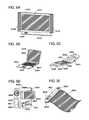
- FIGS. 1A to 1Care views each showing a light-emitting device of an embodiment of the invention.
- FIG. 2is a view showing a light-emitting device of an embodiment of the invention.
- FIGS. 3A to 3Dare diagrams showing a manufacturing process of a light-emitting device of an embodiment of the invention.
- FIGS. 4A and 4Bare views showing a light-emitting device of an embodiment of the invention.
- FIGS. 5A to 5Eare views each showing an electronic device according to an embodiment of the invention.
- FIGS. 6A to 6Care views each explaining a structure of a light-emitting layer
- FIGS. 7A and 7Bare views each explaining a structure of a light-emitting layer.
- FIG. 8is a view explaining a structure of a light-emitting element.
- a light-emitting device of an embodiment of the inventionis characterized in that an element formation layer comprising a TFT, an electrode of a light-emitting element, and the like is supported by a plastic substrate through an adhesive and that a color filter is provided between the plastic substrate and the light-emitting element.
- the light-emitting device having such a structurecan be manufactured by the following method and the like.
- the element formation layer including the TFT, the color filter, and a first pixel electrode of the light-emitting elementis formed over a substrate with low flexibility, such as a substrate formed of glass, ceramics, and the like, with a separation layer sandwiched between the element formation layer and the substrate.
- the substrate and the element formation layerare separated from each other at the separation layer, and the separated element formation layer is bonded to the plastic substrate using the adhesive.
- the color filteris formed using the substrate having low flexibility. Therefore, even in the case of a pixel arrangement directed to a full color display in high resolution, misalignment of the color filter is negligible, which allows the formation of a flexible display capable of displaying a full color image with high resolution.
- a protective insulating filmmay be provided over the color filter in order to reduce adverse influence of degasification from the color filter upon the light-emitting element.
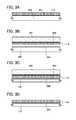
- FIGS. 1A to 1Ceach illustrate a view showing the light-emitting device of the present embodiment.
- an adhesive 111is provided over a plastic substrate 110 .
- the adhesive 111is provided so as to be in contact with an insulating layer 112 , allowing an element formation layer 113 and the plastic substrate 110 to be bonded to each other.
- a pixel TFT 114In the element formation layer 113 , a pixel TFT 114 , a TFT 115 in a driving circuit portion, a color filter 116 , a first pixel electrode 117 of a light-emitting element 121 electrically connected to the pixel TFT 114 , and a partition layer 118 are provided.
- FIG. 1Aillustrates a part of these members.
- the light-emitting element 121is formed of the first pixel electrode 117 exposed from the partition layer 118 , an EL layer 119 which overlaps at least the first pixel electrode 117 and contains a light-emitting substance, and a second pixel electrode 120 which overlaps the EL layer 119 .
- Light emitted from the light-emitting element 121is preferably red, green, blue, or white.
- the EL layer 119 and the second pixel electrode 120 of the light-emitting element 121are formed after the element formation layer 113 is bonded to the plastic substrate 110 . Note that since the EL layer 119 and the second pixel electrode 120 of the light-emitting element 121 are formed over all pixels in common, misalignment in the formation thereof does not provide a serious problem although they are formed using the plastic substrate 110 .
- the color filter 116is formed after the TFTs are formed. Note that it is preferred that the color filter 116 is formed over a first protective insulating film 122 which is provided over the TFTs since the first protective insulating film 122 is able to protect the TFTs from a contaminant released from the color filter 116 .
- FIG. 1Bshows a structure in which a second protective insulating film 123 is provided over the color filter 116 .
- This structureenables the production of a light-emitting device with higher reliability because adverse influence of degasification from the color filter 116 upon the light-emitting element 121 can be reduced.
- FIG. 1Cillustrates a structure in which the color filter 124 is patterned to be located on a position corresponding to the first pixel electrode 117 of the light-emitting element.
- the first protective insulating film 122 and the second protective insulating film 123 which covers the color filter 124are in contact with each other, which allows the color filter 124 to be completely surrounded by the protective insulating films. Therefore, diffusion of the contaminant from the color filter 124 , such as a gas, can be more effectively prevented.
- the first protective insulating film 122 and the second protective insulating film 123are formed by using the same material.
- these protective insulating filmsare preferably formed by using silicon nitride or silicon oxynitride which has a composition of nitrogen higher than that of oxygen.
- the element formation layer 113comprising the TFT, the color filter, the first pixel electrode, and the like is formed over the substrate 200 having an insulating surface with a separation layer 201 interposed between the element formation layer 113 and the substrate 200 (see, FIG. 3A ).
- the substrate 200a glass substrate, a quartz substrate, a sapphire substrate, a ceramic substrate, a metal substrate over which an insulating layer is formed, and the like can be used.
- the substrate 200can be selected as appropriate in accordance with the conditions of the process.
- the pixel TFT and the color filtercan be placed in an arrangement suitable for a high-resolution display.
- the separation layer 201is formed by a sputtering method, a plasma CVD method, a coating method, a printing method, or the like, so as to have either a single-layer structure or a stacked structure by using an element selected from tungsten (W), molybdenum (Mo), titanium (Ti), tantalum (Ta), niobium (Nb), nickel (Ni), cobalt (Co), zirconium (Zr), zinc (Zn), ruthenium (Ru), rhodium (Rh), palladium (Pd), osmium (Os), iridium (Ir), and silicon (Si); an alloy containing these elements as a main component; or a compound containing these elements as a main component.
- a crystal structure of a layer containing siliconmay be amorphous, microcrystal, or polycrystal.
- the coating methodincludes a spin-coating method, a droplet discharge method, a dispensing method, a nozzle printing method, and a slot die coating method in its category here.
- the separation layer 201has a single-layer structure, it is preferred to form a tungsten layer, a molybdenum layer, a layer containing a mixture of tungsten and molybdenum, a layer containing an oxide or an oxynitride of tungsten, a layer containing an oxide or an oxynitride of molybdenum, or a layer containing an oxide or an oxynitride of a mixture of tungsten and molybdenum as the separation layer 201 .
- the mixture of tungsten and molybdenumcorresponds to an alloy of tungsten and molybdenum, for example.
- a tungsten layer, a molybdenum layer, or a layer containing a mixture of tungsten and molybdenumis formed as a first layer, and a layer containing: an oxide, a nitride, an oxyntride, or a nitride oxide of tungsten; an oxide, a nitride, an oxyntride, or a nitride oxide of molybdenum; or an oxide, a nitride, an oxyntride, or a nitride oxide of a mixture of tungsten and molybdenum is formed as a second layer.
- the layer containing tungstenmay be formed first, which is followed by the formation of an insulating layer formed of an oxide (for example, a silicon oxide layer) over the layer containing tungsten so that a layer containing an oxide of tungsten is formed at the interface between the tungsten layer and the insulating layer. Further, a surface of the tungsten layer may be subjected to thermal oxidation treatment, oxygen plasma treatment, or treatment with a strong oxidizing solution such as water containing ozone to form the layer containing the oxide of tungsten.
- an oxidefor example, a silicon oxide layer
- plasma treatment or heat treatmentmay be performed in an atmosphere of oxygen, nitrogen, dinitrogen monoxide, or a mixed gas of these gases and another gas.
- the formation of a layer containing a nitride, an oxynitride, and a nitride oxide of tungstencan be similarly performed.
- an insulating layer formed of a nitride, an oxynitride, or a nitride oxideis preferably formed over the layer including tungsten.
- the insulating layer to be a basecan be formed as a single layer or a stacked layer by using an inorganic insulating film such as silicon oxide, silicon nitride, silicon oxynitride, silicon nitride oxide, or the like.
- an amorphous semiconductorhereinafter referred to as “AS”
- a polycrystalline semiconductora polycrystalline semiconductor
- SASmicrocrystalline semiconductor
- the semiconductor layercan be formed by a sputtering method, an LPCVD method, a plasma CVD method, or the like.
- the microcrystalline semiconductorbelongs to a metastable state which is an intermediate between an amorphous state and a single crystal state according to Gibbs free energy. That is, the microcrystalline semiconductor is a semiconductor having a third state which is stable in terms of free energy and has a short range order and lattice distortion.
- columnar-like or needle-like crystalsgrow in a normal direction with respect to a surface of a substrate.
- the Raman spectrum of microcrystalline siliconwhich is a typical example of a microcrystalline semiconductor, is shifted to a small wavenumber region below 520 cm ⁇ 1 which corresponds to the wavenumber of the Raman spectrum peak of single-crystalline silicon.
- the peak of the Raman spectrum of the microcrystalline siliconexists between 520 cm ⁇ 1 which represents single-crystalline silicon and 480 cm ⁇ 1 which represents amorphous silicon.
- the microcrystalline semiconductorincludes at least 1 at. % of hydrogen or halogen to terminate a dangling bond.
- a rare gas elementsuch as helium, argon, krypton, or neon may be included to further promote lattice distortion, so that stability is enhanced and a favorable microcrystalline semiconductor film can be obtained.
- the microcrystalline semiconductor filmcan be formed by a high-frequency plasma CVD method with a frequency of several tens to several hundreds of megahertz or a microwave plasma CVD method with a frequency of 1 GHz or more.
- the microcrystalline semiconductor filmcan be formed by using a gas obtained by diluting a silicon hydride or a silicon halide, such as SiH 4 , Si 2 H 6 , SiH 2 Cl 2 , SiHCl 3 , SiCl 4 , SiF 4 , or the like, with hydrogen.
- the microcrystalline semiconductor filmcan be formed by using a gas containing a silicon hydride and hydrogen which is diluted by rare gas elements selected from helium, argon, krypton, and neon.
- the flow rate of hydrogenis set to be greater than or equal to 5 times and less than or equal to 200 times, preferably greater than or equal to 50 time and less than or equal to 150 times, much more preferably 100 times as much as that of silicon hydride.
- a hydrogenated amorphous siliconcan be typically exemplified as the amorphous semiconductor, while a polysilicon or the like can be typically exemplified as a crystalline semiconductor layer.
- polysiliconpolycrystalline silicon
- examples of polysiliconinclude so-called high-temperature polysilicon that contains polysilicon as a main component and is formed at a process temperature greater than or equal to 800° C., so-called low-temperature polysilicon that contains polysilicon as a main component and is formed at a process temperature less than or equal to 600° C., polysilicon obtained by crystallizing amorphous silicon by using an element that promotes crystallization or the like, and the like.
- a microcrystalline semiconductor or a semiconductor containing a crystal phase in part of a semiconductor layermay be used.
- a compound semiconductorsuch as GaAs, InP, SiC, ZnSe, GaN, SiGe, or the like can be used.
- an oxide semiconductorsuch as zinc oxide, tin oxide, magnesium zinc oxide, gallium oxide, indium oxide, an oxide semiconductor formed of a plurality of the above oxide semiconductors, and the like may be used.
- an oxide semiconductor formed of zinc oxide, indium oxide, and gallium oxidemay be used.
- a gate insulating filmis preferably formed using yttrium oxide, aluminum oxide, titanium oxide, a stack of any of the above substances, or the like.
- ITO, Au, Ti, or the likeis preferably used for a gate electrode layer, a source electrode layer, and a drain electrode layer.
- ITO, Au, Ti, or the likeis preferably used for a gate electrode layer, a source electrode layer, and a drain electrode layer.
- ITO, Au, Ti, or the likeis preferably used.
- In, Ga, or the likecan be added into zinc oxide.
- the crystalline semiconductor layermay be formed by any of various methods (such as a laser crystallization method, a thermal crystallization method, a thermal crystallization method using an element promoting crystallization such as nickel), and the like.
- a microcrystalline semiconductorwhich is an SAS, can be crystallized by irradiating laser light to increase its crystallinity. In a case where an element which promotes crystallization is not used, before the amorphous silicon film is irradiated with a laser beam, the amorphous silicon film is heated at 500° C.
- a hydrogen concentration in the amorphous silicon filmto less than or equal to 1 ⁇ 10 20 atoms/cm 3 . This is because, if the amorphous silicon layer contains much hydrogen, the amorphous silicon layer may be destroyed by laser beam irradiation.
- Any methodcan be used for introducing a metal element into the amorphous semiconductor layer as long as the method allows the metal element to exist on the surface of or inside the amorphous semiconductor layer.
- a sputtering method, a CVD method, a plasma process method (including a plasma CVD method), an adsorption method, a method of applying a solution of a metal salt, or the likecan be used.
- the method using a solutionis convenient and has an advantage of easily adjusting the concentration of a metal element.
- an oxide film on the amorphous semiconductor layerby UV light irradiation in an oxygen atmosphere, a thermal oxidation treatment, treatment with ozone water or hydrogen peroxide including a hydroxyl radical, or the like in order to improve wettability of the surface of the amorphous semiconductor layer and to spread the aqueous solution over the entire surface of the amorphous semiconductor layer.
- the crystallizationmay be performed by adding an element which promotes crystallization (also referred to as a catalyst element or a metal element) to an amorphous semiconductor layer and performing a heat treatment (at 550° C. to 750° C. for 3 minutes to 24 hours) in a crystallization step in which the amorphous semiconductor layer is crystallized to form a crystalline semiconductor layer.
- an element which promotes (accelerates) the crystallizationone or more of iron (Fe), nickel (Ni), cobalt (Co), ruthenium (Ru), rhodium (Rh), palladium (Pd), osmium (Os), iridium (Ir), platinum (Pt), copper (Cu), and gold (Au) can be used.
- a semiconductor layer containing an impurity elementis formed in contact with the crystalline semiconductor layer and is made to function as a gettering sink.
- the impurity elementmay be an impurity element imparting n-type conductivity, an impurity element imparting p-type conductivity, a rare gas element, or the like.
- one or a plurality of elements selected from phosphorus (P), nitrogen (N), arsenic (As), antimony (Sb), bismuth (Bi), boron (B), helium (He), neon (Ne), argon (Ar), krypton (Kr), and xenon (Xe)can be used.
- the above-mentioned semiconductor layer containing the impurity elementis formed in contact with the crystalline semiconductor layer containing the element which promotes crystallization, and heat treatment (at temperature ranging from 550 to 750° C. for 3 minutes to 24 hours) is performed.
- the element that promotes crystallization in the crystalline semiconductor layeris transported to the semiconductor layer containing the impurity element; thus, the element that promotes crystallization in the crystalline semiconductor layer is removed or reduced. After that, the semiconductor layer containing the impurity element functioning as the gettering sink is removed.
- thermal treatment and laser light irradiationmay be combined to crystallize the amorphous semiconductor layer.
- the thermal treatment and/or the laser light irradiationmay be independently performed a plurality of times.
- a crystalline semiconductor layermay be directly formed over the substrate by a plasma treatment method.
- the crystalline semiconductor layermay be selectively formed over a substrate by using a plasma treatment method.
- a semiconductor film mainly containing an organic materiala semiconductor film mainly containing carbon can be used.
- pentacene, tetracene, thiophene oligomers, polyphenylenes, phthalocyanine compounds, polyacetylenes, polythiophenes, a cyanine dye, and the likeare given as examples.
- the gate insulating film and the gate electrodea known structure may be applied, and a known method may be used for the formation thereof.
- the gate insulating filmmay be formed according to a known structure such as a single layer of silicon oxide, a stacked structure of silicon oxide and silicon nitride, and the like.
- the gate electrodemay be formed of an element selected from Ag, Au, Cu, Ni, Pt, Pd, Ir, Rh, W, Al, Ta, Mo, Cd, Zn, Fe, Ti, Si, Ge, Zr, and Ba; or an alloy or a compound containing any of these elements as its main component by using the CVD method, the sputtering method, the droplet discharging method, or the like.
- a semiconductor film typified by a polycrystalline silicon film doped with an impurity element such as phosphorus, or AgPdCu alloymay be used. Either a single layer structure or a layered structure may be applied.
- FIGS. 1A to 1Cin which transistors with a top-gate structure are used, a transistor with a known structure such as a bottom-gate structure and the like may be used.
- the first protective insulating film 122is formed over the gate insulating film and the gate electrode.
- the first protective insulating film 122may be formed of a silicon oxide layer, a silicon oxynitride film, a silicon nitride oxide film, or a silicon nitride film, or may be formed as a stacked film in which any of these films are combined. In any case, the first protective insulating film 122 is formed of an inorganic insulating material.
- the formation of the first protective insulating film 122allows the reduction of pollution of the TFT caused by the color filter 116 formed later.
- the use of a silicon nitride film or a silicon nitride oxide film which has a composition of nitrogen higher than that of oxygenis preferred because the contaminant from the color filter 116 can be effectively blocked.
- the color filter 116is formed over the first protective insulating film 122 .
- a color filter with a single coloris shown in FIGS. 1A to 1C , a color filter which transmits red light, a color filter which transmits blue light, and a color filter which transmits green light are formed in an appropriate arrangement and shape. Any arrangement can be adopted for the arrangement of the color filter 116 , including a stripe pattern, a diagonal mosaic arrangement, a triangle mosaic arrangement, an RGBW four pixel arrangement, and the like.
- the RGBW four pixel arrangementis a pixel arrangement having: a pixel mounted with a color filter transmitting red light; a pixel mounted with a color filter transmitting blue light; a pixel mounted with a color filter transmitting green light; and a pixel without color filter, and is effective in reducing power consumption and so on.
- the color filter 116can be formed by using a known material. In the case of using a photosensitive resin as the color filter 116 , patterning of the color filter 116 may be performed by exposing the color filter 116 itself to light and then developed. It is preferred to perform patterning by dry etching when a minute pattern is formed.
- an interlayer insulating film formed using an organic insulating materialis formed over the color filter 116 .
- an acrylic, a polyimide, a polyamide, a polyimideamide, a benzocyclobutene-based resin, and the likecan be used.
- the second protective insulating film 123may be provided between the color filter 116 and the interlayer insulating film in order to suppress the influence of degasification from the color filter 116 (see FIG. 1B ).
- the second protective insulating film 123can be formed with a similar material to that of the first protective insulating film 122 . It is a preferred structure in which the second protective insulating film 123 is formed using a silicon nitride film or a silicon nitride oxide film having a composition of nitrogen higher than oxygen since degasification from the color filter 116 can be effectively suppressed.
- first protective insulating film 122 and the second protective insulating film 123are in contact with each other in a vicinity of the color filter 124 because influence of a contaminant and degasification can be more effectively suppressed (see, FIG. 1C ).
- the use of the same material for the first protective insulating film 122 and the second protective insulating film 123allows the improvement of adhesion therebetween, which contributes to further reduction of influence of the contaminant and degasification. The reduction of influence of the contaminant and degasification improves reliability of the light-emitting device.
- the first pixel electrode 117is formed using a transparent conductive film.
- indium oxide, an alloy of indium oxide and tin oxide (ITO), and the likecan be used as a material of the transparent conductive film.
- ITOindium oxide and tin oxide
- IZOindium oxide and zinc oxide
- zinc oxideis also an appropriate material, and moreover, zinc oxide (GZO) to which gallium (Ga) is added to increase conductivity and transmissivity with respect to visible light may be used.
- GZOzinc oxide
- Gagallium
- an extremely thin film of a material with a low work function such as aluminumcan be used.
- the first pixel electrode 117can be formed by a sputtering method, a vacuum evaporation method, or the like.
- etchingis performed on the interlayer insulating film, (the second protective insulating film 123 ), (the color filter 116 ), the first protective insulating film 122 , and the gate insulating film to result in formation of a contact hole which reaches the semiconductor layer of the TFT.
- a conductive metal filmis formed by a sputtering method or a vacuum evaporation method, which is followed by etching to result in an electrode of the TFT and a wiring.
- One of a source electrode and a drain electrode of the pixel TFT 114is formed so as to overlap with the first pixel electrode 117 in order to achieve electrical connection therebetween.
- an insulating filmis formed using an organic insulating material or an inorganic insulating material so that the insulating film covers the interlayer insulating film and the first pixel electrode 117 .
- the insulating filmis then processed to allow a surface of the first pixel electrode 117 to be exposed and an end portion of the first pixel electrode 117 to be covered by the insulating film, leading to the formation of the partition layer 118 .
- the element formation layer 113can be formed.
- the element formation layer 113 and a provisional supporting substrate 202are bonded to each other using a first adhesive 203 , which is followed by separation of the element formation layer 113 from the substrate 200 at the separation layer 201 .
- the element formation layer 113is placed over the provisional supporting substrate 202 (see, FIG. 3B ).
- a glass substrate, a quartz substrate, a sapphire substrate, a ceramic substrate, a metal substrate on which an insulating surface is formed, and the likecan be used. Further, a plastic substrate which can resist a temperature of the manufacturing process of this embodiment or a flexible substrate such as a film may be used.
- an adhesivewhich is soluble in a solvent such as water or is capable of plasticizing upon irradiation of UV light, and the like, is used so that the provisional supporting substrate 202 can be chemically or physically separated from the element formation layer 113 when necessary.
- any of following methodscan be applied in the transferring process from the substrate 200 to the provisional supporting substrate 202 : forming the separation layer 201 between the substrate 200 and the element formation layer 113 , forming a metal oxide film between the separation layer 201 and the element formation layer 113 , embrittling the metal oxide film by crystallizing thereof, and separating the element formation layer 113 ; forming an amorphous silicon film containing hydrogen between the substrate 200 having high thermal resistivity and the element formation layer 113 , removing the amorphous silicon film by irradiation with laser light or etching, and separating the element formation layer 113 ; forming the separation layer 201 between the substrate 200 and the element formation layer 113 , forming a metal oxide film between the separation layer 201 and the element formation layer 113 , embrittling the metal oxide film by crystallizing thereof, removing a part of the separation layer 201 by etching using a solution or a halogen fluoride gas such as NF 3 , BrF 3 , ClF
- a methodmay be used in which a film containing nitrogen, oxygen, or hydrogen (for example, an amorphous silicon film containing hydrogen, an alloy film containing hydrogen, or an alloy film containing oxygen) is used as the separation layer 201 , and the separation layer 201 is irradiated with laser light to release the nitrogen, oxygen, or hydrogen contained in the separation layer 201 , thereby promoting separation between the element formation layer 113 and the substrate 200 .
- a film containing nitrogen, oxygen, or hydrogenfor example, an amorphous silicon film containing hydrogen, an alloy film containing hydrogen, or an alloy film containing oxygen
- the transfer stepcan be conducted easily.
- separationcan be performed with physical force (by a machine and the like) after performing: laser light irradiation; etching to the separation layer 201 with a gas, a solution, or the like; and mechanical removal with a sharp knife, scalpel, or the like, so that the separation layer 201 and the element formation layer 113 can be easily peeled off from each other.
- separation of the element formation layer 113 from the substrate 200may be carried out after penetrating a liquid into an interface between the separation layer 201 and the element formation layer 113 .
- the element formation layer 113 which is separated from the substrate 200 to expose the separation layer 201 or the insulating layer 112is bonded to the plastic substrate 110 using a second adhesive 204 which is different from the first adhesive 203 (see, FIG. 3C ).
- various curable adhesivessuch as a reactive curable adhesive, a thermal curable adhesive, a photo curable adhesive such as an ultraviolet curable adhesive, an anaerobic adhesive, and the like can be used.
- the plastic substrate 110a variety of substrates having flexibility and light-transmitting ability, a film of an organic resin, and the like can be used.
- the plastic substrate 110may be a structure body comprising a fibrous body and an organic resin. It is preferred to use the structure body comprising the fibrous body and the organic resin as the plastic substrate 110 since resistivity to the breaking caused by bending is improved, and thus, reliability is increased.
- the structure body comprising the fibrous body and the organic resincan be used as a film which can simultaneously function as the second adhesive 204 and the plastic substrate 110 .
- a resinsuch as a reactive curable resin, a thermosetting resin, and a photo curable resin, and the like whose curing is promoted by an additional treatment are preferably used.
- the provisional supporting substrate 202is removed by dissolving or plasticizing the first adhesive 203 .
- the first adhesive 203is removed using a solvent such as water to allow a surface of the first pixel electrode 117 of the light-emitting element to be exposed (see, FIG. 3D ).
- the element formation layer 113which comprises the color filter 116 , the TFTs 114 and 115 , the first pixel electrode 117 of the light-emitting element, and the like, can be manufactured over the plastic substrate 110 .
- the EL layer 119is formed.
- a stacked structure of the EL layer 119is not particularly limited.
- a layer containing a substance having high electron-transporting ability, a layer containing a substance having high hole-transporting ability, a layer containing a substance having high electron injection ability, a layer containing a substance having high hole injection ability, a layer containing a bipolar substance (a substance having high electron-transporting ability and high hole transporting ability), and the likeare appropriately combined.
- an appropriate combination of a hole injecting layer, a hole-transporting layer, a light-emitting layer, an electron-transporting layer, an electron injection layer, and the likecan be performed.
- the EL layer 119comprises a hole injection layer, a hole-transporting layer, a light-emitting layer, and an electron-transporting layer. Specific materials to form each of the layers are given below.
- the hole injection layeris a layer that is provided in contact with an anode and contains a material with high hole injection ability. Specifically, molybdenum oxide, vanadium oxide, ruthenium oxide, tungsten oxide, manganese oxide, or the like can be used.
- the hole injection layercan be formed using any one of the following materials: phthalocyanine compounds such as phthalocyanine (H 2 PC) and copper phthalocyanine (CuPc); aromatic amine compounds such as 4,4′-bis[N-(4-diphenylaminophenyl)-N-phenylamino]biphenyl (DPAB) and 4,4′-bis(N- ⁇ 4-[N-(3-methylphenyl)-N-phenylamino]phenyl ⁇ -N-phenylamino)biphenyl (DNTPD); polymer compounds such as poly(3,4-ethylenedioxythiophene)/poly(styrenesulfonic acid) (PEDOT/PSS); and the like.
- phthalocyanine compoundssuch as phthalocyanine (H 2 PC) and copper phthalocyanine (CuPc)
- aromatic amine compoundssuch as 4,4′-bis[N-(4-diphenylaminophenyl)-N-phen
- a composite materialcomprising a substance with high hole-transporting ability and an acceptor substance may be used.
- a material used to form an electrodemay be selected regardless of its work function.
- a material with a high work functiona material with a low work function may also be used as the anode.
- the acceptor substance7,7,8,8-tetracyano-2,3,5,6-tetrafluoroquinodimethane (abbreviation: F 4 -TCNQ), chloranil, and the like can be given.
- F 4 -TCNQ7,7,8,8-tetracyano-2,3,5,6-tetrafluoroquinodimethane
- chloraniland the like can be given.
- a transition metal oxideis given.
- oxides of metals that belong to Group 4 to Group 8 of the periodic tablecan be given.
- vanadium oxide, niobium oxide, tantalum oxide, chromium oxide, molybdenum oxide, tungsten oxide, manganese oxide, and rhenium oxideare preferable because of a high electron accepting property.
- molybdenum oxideis especially preferable since it can be easily treated due to its stability in the air and low hygroscopic property.
- any of various organic compoundssuch as an aromatic amine compound, a carbazole derivative, an aromatic hydrocarbon, and a high-molecular compound (such as an oligomer, a dendrimer, or a polymer) can be used.
- the organic compound used for the composite materialpreferably has a hole mobility of 10 ⁇ 6 cm 2 /Vs or higher is preferably used. However, other materials than these materials may also be used as long as hole-transporting ability is higher than electron-transporting ability.
- the organic compound that can be used for the composite materialis specifically shown below.
- aromatic amine compoundsexamples include N,N′-di(p-tolyl)-N,N′-diphenyl-p-phenylenediamine (abbreviated to DTDPPA), 4,4′-bis[N-(4-diphenylaminophenyl)-N-phenylamino]biphenyl (abbreviated to DPAB), 4,4′-bis(N- ⁇ 4-[N-(3-methylphenyl)-N-phenylamino]phenyl ⁇ -N-phenylamino)biphenyl (abbreviated to DNTPD), 1,3,5-tris[N-(4-diphenylaminophenyl)-N-phenylamino]benzene (abbreviated to DPA3B), and the like.
- DTDPPA4,4′-bis[N-(4-diphenylaminophenyl)-N-phenylamino]biphenyl
- DPAB4,4′-bis
- Examples of a carbazole derivativeinclude 3-[N-(9-phenylcarbazol-3-yl)-N-phenylamino]-9-phenylcarbazole (abbreviation: PCzPCA1), 3,6-bis[N-(9-phenylcarbazol-3-yl)-N-phenylamino]-9-phenylcarbazole (abbreviation: PCzPCA2), 3-[N-(1-naphtyl)-N-(9-phenylcarbazol-3-yl)amino]-9-phenylcarbazole (abbreviation: PCzPCN1), 4,4′-di(N-carbazolyl)biphenyl (abbreviation: CBP), 1,3,5-tris[4-(N-carbazolyl)phenyl]benzene (abbreviation: TCPB), 9-[4-(10-phenyl-9-anthryl)phenyl]-9H-c
- aromatic hydrocarbonsexamples include 2-tert-butyl-9,10-di(2-naphthyl)anthracene (t-BuDNA), 2-tert-butyl-9,10-di(1-naphthyl)anthracene, 9,10-bis(3,5-diphenylphenyl)anthracene (DPPA), 2-tert-butyl-9,10-bis(4-phenylphenyl)anthracene (t-BuDBA), 9,10-di(2-naphthyl)anthracene (DNA), 9,10-diphenylanthracene (DPAnth), 2-tert-butylanthracene (t-BuAnth), 9,10-bis(4-methyl-1-naphthyl)anthracene (DMNA), 2-tert-butyl-9,10-bis[2-(1-naphthyl)phenyl]anthracene, 9,10-
- the number of the carbon atoms participating in their condensed ringpreferably ranges from 14 to 42 from the viewpoint of the evaporation behavior of the aromatic hydrocarbons and the quality of the formed film.
- the aromatic hydrocarbon that can be used for the composite materialmay have a vinyl skeleton.
- an aromatic hydrocarbon having a vinyl groupfor example, 4,4′-bis(2,2-diphenylvinyl)biphenyl (abbreviation: DPVBi), 9,10-bis[4-(2,2-diphenylvinyl)phenyl]anthracene (abbreviation: DPVPA), and the like are given.
- poly(N-vinylcarbazole)(abbreviated to PVK), poly(4-vinyltriphenylamine) (abbreviated to PVTPA), poly[N-(4- ⁇ N′-[4-(4-diphenylamino)phenyl]phenyl-N′-phenylamino ⁇ phenyl)methacrylamide] (abbreviated to PTPDMA), poly[N,N′-bis(4-butylphenyl)-N,N′-bis(phenyl)benzidine] (abbreviated to Poly-TPD), and the like.
- PVKpoly(N-vinylcarbazole)
- PVTPApoly(4-vinyltriphenylamine)
- PVTPApoly[N-(4- ⁇ N′-[4-(4-diphenylamino)phenyl]phenyl-N′-phenylamino ⁇ phenyl)methacrylamide]
- PTPDMApoly[N,N′
- the hole-transporting layeris a layer that contains a substance with high hole-transporting ability.
- the substance having high hole-transporting abilityinclude aromatic amine compounds such as 4,4′-bis[N-(1-naphthyl)-N-phenylamino]biphenyl (abbr.: NPB), N,N′-bis(3-methylphenyl)-N,N′-diphenyl-[1,1′-biphenyl]-4,4′-diamine (abbr.: TPD), 4,4′,4′′-tris(N,N-diphenylamino)triphenylamine (abbr.: TDATA), 4,4′,4′′-tris[N-(3-methylphenyl)-N-phenylamino]triphenylamine (abbr.: MTDATA), 4,4′-bis[N-(spiro-9,9′-bifluoren-2-yl)-N-phenylamino]biphenyl (abb
- the materials described hereare mainly substances having hole mobility of 10 ⁇ 6 cm 2 /Vs or more. However, a material other than the above-described substances may be used as long as it has higher hole-transporting ability than electron-transporting ability. Note that the layer containing the substance with high hole-transporting ability is not limited to a single layer, and two or more layers containing the aforementioned substances may be stacked.
- a high molecular compoundsuch as poly(N-vinylcarbazole) (abbr.: PVK) or poly(4-vinyltriphenylamine) (abbr.: PVTPA) can also be used for the hole-transporting layer.
- PVKpoly(N-vinylcarbazole)
- PVTPApoly(4-vinyltriphenylamine)
- the light-emitting layeris a layer containing a light-emitting substance.
- the light-emitting layermay be a so-called single layer light-emitting layer and a so-called host-guest type light-emitting layer in which a light-emitting substance is dispersed in a host material, as long as the emission from the light-emitting layer is located in the visible region.
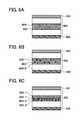
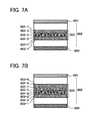
- a light-emitting layer containing a light-emitting substance having a broad emission spectrumsee, FIG. 6A
- a light-emitting layer containing a plurality of light-emitting substances having a different emission wavelength regionsee, FIG.
- a reference numeral 600represents the first pixel electrode of the light-emitting element; a reference numeral 601 represents a second pixel electrode of the light-emitting element; a reference numeral 602 represents the EL layer; reference numerals 603 , 603 - 1 , and 603 - 2 each represent the light-emitting layer; and reference numerals 604 , 604 - 1 , and 604 - 2 each represent the light-emitting substance.
- a combination of the light-emitting substances(corresponding to the light-emitting substances 604 - 1 and 604 - 2 , but being not limited to two kinds of substances) with different wavelength regions is generally exemplified by a combination of two kinds of light-emitting substances which emit light of complementary colors to each other (for example, blue light and yellow light) or by a combination of three kinds of substances with red, blue and green emission colors.
- FIG. 7Aa structure in which, as shown in FIG. 7A , a three-layer structure containing a first light-emitting layer 603 - 1 , a second light-emitting layer 603 - 2 , and a third light-emitting layer 603 - 3 in that order from a side of the first pixel electrode 600 is provided as the light-emitting layer 603 ; and a layer (the second light-emitting layer 603 - 2 ) containing a light-emitting substance 604 - 2 capable of emitting light with a long wavelength is interposed between layers (the first light-emitting layer 603 - 1 and the third light-emitting layer 603 - 3 ) each containing a light-emitting substance 604 - 1 capable of emitting light with a short wavelength.
- carrier-transporting ability of each of the light-emitting layersis tuned by appropriately selecting host materials to allow recombination of electrons and holes to occur in the vicinity of an interface of the layer (the second light-emitting layer 603 - 2 ) containing the light-emitting substance 604 - 2 which is located on the side of the second pixel electrode 601 (i.e., an interface between the second light-emitting layer 603 - 2 and the third light-emitting layer 603 - 3 ).
- the lifetime of the light-emitting elementcan be improved, and the emission from the light-emitting substance capable of emitting light with the long wavelength and that from the light-emitting substance capable of emitting light with the short wavelength can be readily balanced.
- the first pixel electrode 600 and the second pixel electrode 601are used as the anode and the cathode, respectively, “recombination of holes and electrons in the vicinity of an interface of the layer, containing the light-emitting substance capable of emitting light with the long wavelength, the interface of which is located on the side of the second pixel electrode, by tuning carrier transporting ability of each of the light-emitting layers through the appropriate selection of the host materials” can be achieved by designing the light-emitting element so that the layer (the third light-emitting layer 603 - 3 ), which is located on the side of second pixel electrode 601 and contains the light-emitting substance 604 - 1 capable of emitting light with short wavelength, has electron-transporting ability and the layer (the first light-emitting layer 603 - 1 ), which is located on the anode side and contains the light-emitting substance 604 - 1 capable of emitting light with the short wavelength, and the layer (the second light-emitting layer 60
- Energy obtained by recombination of holes and electronsis readily transferred from a substance which emits light with a short wavelength to a substance which emits light with a long wavelength.
- light emitted from the substance which emits light with the long wavelengthis enhanced, which makes it difficult to balance the intensities of emissions from the substance which emits light with the short wavelength and from the substance which emits light with the long wavelength.
- the electron which fails to participate to recombination in the vicinity of the interface between the second light-emitting layer 603 - 2 and the third light-emitting layer 603 - 3can be subjected to recombination in the layer (the first light-emitting layer 603 - 1 ) which is located on the anode side and contains the light-emitting substance capable of emitting light with the short wavelength.
- the layerthe first light-emitting layer 603 - 1
- a light-emitting layer 603is formed as a four-layer structure containing, from the side of the first pixel electrode 600 , a first light-emitting layer 603 - 1 , a second light-emitting layer 603 - 2 , a third light-emitting layer 603 - 3 , and a fourth light-emitting layer 603 - 4 and in which the layer (the third light-emitting layer 603 - 3 ) containing a green-emissive light-emitting substance 604 - 7 and the layer (the second light-emitting layer 603 - 2 ) containing a red-emissive light-emitting substance 604 - 6 are sandwiched between the layers (the first light).
- carrier-transporting ability of each of the light-emitting layersis tuned to allow the region for recombination of holes and electrons to be located in the vicinity of the interface between the cathode-side layer (the fourth light-emitting layer 603 - 4 ) containing the blue-emissive light-emitting substance 604 - 5 and the layer (the third light-emitting layer 603 - 3 ) containing the green-emissive light-emitting substance 604 - 7 .
- the lifetime of the light-emitting elementcan be improved, and the emission from the light-emitting substance capable of emitting light with the long wavelength and that from the light-emitting substance capable of emitting light with the short wavelength can be readily balanced.
- the cathode-side layer(the fourth light-emitting layer 603 - 4 ) containing the blue-emissive light-emitting substance 604 - 5 has electron-transporting ability; and the layer (the third light-emitting layer 603 - 3 ) containing the green-emissive light-emitting substance 604 - 7 , the layer (the second light-emitting layer 603 - 2 ) containing the red-emissive light-emitting substance 604 - 6 , and the anode-side layer (the first light-emitting layer 603 - 1 ) containing the blue-emissive light-emitting substance 604 -
- carrier-transporting ability of each of the light-emitting layerscan be determined by carrier-transporting ability of the substance which is contained at the highest composition in the corresponding light-emitting layers.
- Energy obtained by recombination of holes and electronsis readily transferred from a substance which emits light with a short wavelength to a substance which emits light with a long wavelength.
- light emitted from the substance which emits light with the long wavelengthis enhanced, which makes it difficult to balance the intensities of emissions from the substance which emits light with the short wavelength and from the substance which emits light with the long wavelength.
- the electron which once fails to participate to recombinationis subjected to recombination in the anode-side layer (the first light-emitting layer 603 - 1 ) containing the blue-emissive light-emitting substance 604 - 5 , giving an emission of light with the short wavelength.
- the anode-side layerthe first light-emitting layer 603 - 1
- the blue-emissive light-emitting substance 604 - 5giving an emission of light with the short wavelength.
- the light-emitting substance usedis not particularly limited, and known fluorescent substances or phosphorescent substances can be used.
- fluorescent substancesfor example, in addition to N,N′-bis[4-(9H-carbazol-9-yl)phenyl]-N,N′-diphenylstilbene-4,4′-diamine (abbreviation: YGA2S) and 4-(9H-carbazol-9-yl)-4′-(10-phenyl-9-anthryl)triphenylamine (abbreviation: YGAPA), and the like, there are fluorescent substances with an emission peak equal to or greater than 450 nm, such as 4-(9H-carbazol-9-yl)-4′-(9,10-diphenyl-2-anthryl)triphenylamine (abbreviation: 2YGAPPA), N,9-diphenyl-N-[4-(10-phenyl-9-anthryl)phenyl]-9H-carbazol-3-amine (abbre
- phosphorescent substancesfor example, in addition to bis[2-(4′,6′-difluorophenyl)pyridinato-N,C 2′ ]iridium(III)tetrakis(1-pyrazolyl)borate (abbreviation: FIr6), there are phosphorescent substances with an emission wavelength in the range of 470 nm to 500 nm, such as bis[2-(4′,6′-difluorophenyl)pyridinato-N,C 2′ ]iridium(III)picolinate (abbreviation: FIrpic), bis[2-(3′,5′bistrifluoromethylphenyl)pyridinato-N,C 2′ ]iridium(III)picolinate (abbreviation: Ir(CF 3 ppy) 2 (pic)), and bis[2-(4′,6′-difluorophenyl)pyridinato-N,C 2′ ]iridium(III)
- metal complexessuch as tris(8-quinolinolato)aluminum(III) (abbreviation: Alq), tris(4-methyl-8-quinolinolato)aluminum(III) (abbreviation: Almq 3 ): bis(10-hydroxybenzo[h]quinolinato)beryllium(II) (abbreviation: BeBq 2 ), bis(2-methyl-8-quinolinolato)(4-phenylphenolato)aluminum(III) (abbreviation: BAlq), bis(8-quinolinolato)zinc(II) (abbreviation: Znq), bis[2-(2-benzoxazolyl)phenolato]zinc(II) (abbreviation: ZnPBO), and bis[2-(2-benzothiazolyl)phenolato]zinc(II) (abbreviation: ZnBTZ); heterocyclic compounds such as tris(8-quinolinolato
- condensed polycyclic aromatic compoundssuch as anthracene derivatives, phenanthrene derivatives, pyrene derivatives, chrysene derivatives, and dibenzo[g,p]chrysene derivatives are given.
- DPAnth9,10-diphenylanthracene
- CzAlPAN,N-diphenyl-9-[4-(10-phenyl-9-anthryl)phenyl]-9H-carbazol-3-amine
- DPhPA4-(10-phenyl-9-anthryl)triphenylamine
- YGAPAN,9-diphenyl-N-[4-(10-phenyl-9-anthryl)phenyl]-9H-carbazol-3-amine
- PCAPAN,9-diphenyl-N- ⁇ 4-[4-(10-phenyl-9-anthryl)phenyl]phenyl ⁇ -9H-carbazol-3-amine
- PCAPBAN-9-diphenyl-N-(9,10-diphenyl-2-an
- the host materialmay be selected so that the host material has a larger energy gap (or a triplet energy if the light-emitting substance emits phosphorescence) than the light-emitting substance dispersed in the light-emitting layer and has carrier-transporting ability required for each of the light-emitting layers.
- the electron-transporting layeris a layer that contains a substance with high electron-transporting ability.
- a layer containing a metal complex having a quinoline skeleton or a benzoquinoline skeletonsuch as tris(8-quinolinolato)aluminum (abbreviation: Alq), tris(4-methyl-8-quinolinolato)aluminum (abbreviation: Almq 3 ), bis(10-hydroxybenzo[h]-quinolinato)beryllium (abbreviation: BeBq 2 ), or bis(2-methyl-8-quinolinolato)(4-phenylphenolato)aluminum (abbreviation: BAlq) can be used.
- Alqtris(8-quinolinolato)aluminum
- Almq 3tris(4-methyl-8-quinolinolato)aluminum
- BeBq 2bis(10-hydroxybenzo[h]-quinolinato)beryllium
- a metal complex having an oxazole-based or thiazole-based ligandsuch as bis[2-(2-hydroxyphenyl)benzoxazolato]zinc (abbreviation: Zn(BOX) 2 ) or bis[2-(2-hydroxyphenyl)-benzothiazolato]zinc (abbreviation: Zn(BTZ) 2 ) can be used.
- 2-(4-biphenylyl)-5-(4-tert-butylphenyl)-1,3,4-oxadiazole(abbreviation: PBD), 1,3-bis[5-(p-tert-butylphenyl)-1,3,4-oxadiazole-2-yl]benzene (abbreviation: OXD-7), 3-(4-biphenylyl)-4-phenyl-5-(4-tert-butylphenyl)-1,2,4-triazole (abbreviation: TAZ), bathophenanthroline (abbreviation: BPhen), bathocuproine (abbreviation: BCP), or the like can also be used.
- the substances described hereare mainly those having electron mobility of 10 ⁇ 6 cm 2 /Vs or more. It is to be noted that a substance other than the above substances may be used as long as it has higher electron-transporting ability than hole transporting ability.
- the electron-transporting layermay be formed as not only a single layer but also as a stacked layer in which two or more layers formed using the above mentioned substances are stacked.
- a layer for controlling transport of electronmay be provided between the electron-transporting layer and the light-emitting layer.
- the layer for controlling transport of electronis a layer in which a small amount of a substance having high electron-trapping ability is added to a layer containing the above-mentioned substances having high electron-transporting ability.
- the layer for controlling transport of electroncontrols transport of electron, which enables adjustment of carrier balance. Such a structure is very effective in suppressing a problem (such as shortening of element lifetime) caused by a phenomenon that electron passes through the light-emitting layer.
- an electron injection layermay be provided so as to be in contact with an electrode functioning as a cathode.
- alkali metal, alkaline earth metal, or a compound of thereofsuch as lithium fluoride (LiF), cesium fluoride (CsF), calcium fluoride (CaF 2 ), and the like can be employed.
- a layer which contains both a substance having electron-transporting ability and an alkali metal, an alkaline earth metal, or a compound thereofa layer of Alq including magnesium (Mg) for example
- Mgmagnesium
- electroncan be efficiently injected from the cathode by using, as the electron injection layer, a substance having electron-transporting ability to which an alkali metal or an alkaline earth metal is mixed.
- a metal, an alloy, an electrically conductive compound, a mixture thereof, or the like having a low work functioncan be used as a substance for the second pixel electrode 601 .
- an element belonging to Group 1 or Group 2 in the periodic tablei.e., an alkali metal such as lithium (Li) or cesium (Cs), or an alkaline earth metal such as magnesium (Mg), calcium (Ca), or strontium (Sr); an alloy containing any of these metals (such as MgAg or AlLi); a rare earth metal such as europium (Eu) or ytterbium (Yb); an alloy containing such a rare earth metal; or the like can be used.
- an alkali metalsuch as lithium (Li) or cesium (Cs)
- an alkaline earth metalsuch as magnesium (Mg), calcium (Ca), or strontium (Sr)
- MgAg or AlLimagnesium
- a rare earth metalsuch as europium (Eu) or ytterbium (Yb)
- an alloy containing such a rare earth metalor the like
- any of a variety of conductive materialssuch as Al, Ag, ITO, and indium oxide-tin oxide containing silicon or silicon oxide, and the like can be used regardless of its work function as the cathode.
- Films of these electrically conductive materialscan be formed by a sputtering method, an ink jet method, a spin coating method, or the like.
- the second pixel electrode 601is formed using a metal, an alloy, or a conductive compound, a mixture thereof, or the like having a high work function (specifically greater than or equal to 4.0 eV).
- a metal, an alloy, or a conductive compound, a mixture thereof, or the likehaving a high work function (specifically greater than or equal to 4.0 eV).
- ITOindium oxide-tin oxide
- IZOindium zinc oxide
- IWZOindium oxide containing tungsten oxide and zinc oxide
- Such conductive metal oxide filmsare usually formed by a sputtering method, but may also be formed by using a sol-gel method or the like.
- indium zinc oxidecan be formed by a sputtering method using a target in which 1 to 20 wt % of zinc oxide is added to indium oxide.
- Indium oxide containing tungsten oxide and zinc oxidecan be formed by a sputtering method using a target in which 0.5 wt % to 5 wt % of tungsten oxide and 0.1 wt % to 1 wt % of zinc oxide are contained in indium oxide.
- goldAu
- platinumPt
- nickelNi
- tungstenW
- Crchromium
- Momolybdenum
- ironFe
- Cocobalt
- Cucopper
- palladiumPd
- a nitride of a metalsuch as titanium nitride
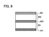
- a plurality of EL layermay be formed between the first pixel electrode 600 and the second pixel electrode 601 as shown in FIG. 8 .
- a charge generation layer 803is preferably provided between the stacked EL layers 800 and 801 .
- the charge generation layer 803can be formed by using the above-mentioned composite material.
- the charge generation layer 803may have a stacked structure comprising a layer containing the composite material and a layer containing another material.
- a layer containing an electron donating substance and a substance with high electron-transporting abilitya layer comprising a transparent conductive material, and the like can be used.
- Such a structureallows the formation of a light-emitting element with high emission efficiency and a long lifetime. Moreover, a light-emitting element which provides a phosphorescent emission from one of the EL layers and a fluorescent emission from the other of the EL layers can be readily obtained.
- this structurecan be combined with the above-mentioned structures of the EL layer. For instance, the EL layer having the structure of FIG. 6C and the EL layer having the structure of FIG. 6A can be stacked. Specifically, it is readily achieved to obtain blue and green fluorescent emissions from the EL layer 800 having the structure of FIG. 6C and simultaneously obtain a red phosphorescent emission from the EL layer 801 having the structure of FIG.
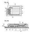
- the light-emitting elementAfter the formation of the element formation layer and the light-emitting layer, it is preferred to seal the light-emitting element with an organic resin 400 , a protective film 401 , and the like as shown in FIGS. 4A and 4B in order to prevent a substance which promotes deterioration of the EL layer from entering from the outside.
- a sealing substratemay be used instead of the organic resin 400 and the protective film 401 .
- the protective film 401is not necessarily formed over input and output terminals which are connected to an FPC and the like later.
- the light-emitting device of the present embodimentdisplays an image toward the plastic substrate 110 side through the color filter, it is possible to use the above-mentioned organic resin 400 , the protective film 401 , and the sealing substrate even if they are colored or have low transmissivity with respect to visible light.
- the organic resin 400 , the protective film 401 , and the sealing substrateeach are formed using light-transmitting materials, a monochromic image can be also supplied from the sealing substrate side if the second pixel electrode is formed by a light-transmitting material or in a shape which allows visible light to be transmitted therethrough.
- a material similar to that for the plastic substrate 110can be used for the sealing substrate.
- the FPC 402is bonded to each of electrodes of the input and output terminals with an anisotropic conductive material.
- An IC chipmay be mounted thereover if necessary.
- manufacture of a module of the light-emitting device to which the FPC 402 is connectedis completed.
- an adhesive 111is provided over a plastic substrate 110 and bonds an element formation layer formed over a first insulating layer 112 to the plastic substrate 110 .
- a color filter 300is provided over the first insulating layer 112 , and a TFT 302 is provided while a second insulating layer 301 formed over the color filter 300 is sandwiched between the color filter 300 and the TFT 302 .
- the second insulating layer 301can be formed by using an inorganic insulating material such as silicon oxide, silicon oxynitride, silicon nitride, silicon nitride oxide, and the like or an organic insulating material such as an acrylic, a polyimide, and the like.
- the use of the organic insulating materialis preferred since the organic insulating material can reduce a step caused by formation of the color filter 300 . Furthermore, it is preferred to provide a protective insulating film over the second insulating layer 301 in order to suppress an adverse influence of contaminant, such as a gas released from the color filter 300 , upon the TFT 302 .
- the protective insulating filmis preferably formed using an inorganic insulating material such as silicon oxide, silicon oxynitride, silicon nitride, silicon nitride oxide, and the like. In particular, it is preferred to use silicon nitride or silicon nitride oxide which has a composition of nitrogen higher than that of oxygen. Note that the protective insulating film is not necessarily provided in the case where the second insulating layer 301 is formed by an inorganic insulating film.
- the color filter 300 and the second insulating layer 301are formed over a substrate with low flexibility, which is followed by the formation of the TFT 302 .
- the TFT 302may have a known structure and be formed by a known method which does not require high temperature treatment. For instance, a TFT having a semiconductor such as the above-mentioned microcrystalline semiconductor, the amorphous semiconductor, the oxide semiconductor, the semiconductor containing an organic material as a main component, and the like is exemplified.
- a first pixel electrode 303 of a light-emitting element and a partition layer 304are formed. Then, the separation is carried out in a similar manner to that mentioned above to achieve the transfer to a plastic substrate 110 , leading to the formation of a light-emitting device similarly to that shown in FIGS. 1A to 1C .
- the second insulating layer 301is singly able to suppress adverse influence of a contaminant from the color filter 300 upon the TFT 302 and the light-emitting element, which contributes to reduction of manufacturing process.
- the color filteris formed using the substrate with low flexibility. Therefore, similarly to the structure shown in FIGS. 1A to 1C , the light-emitting device with the structure of FIG. 2 can display a full color image with high resolution in spite of its flexibility.
- FIGS. 4A and 4BA top view and a sectional view of a module of a light-emitting device (also referred to as an EL module) are illustrated in FIGS. 4A and 4B , respectively.
- FIG. 4Ais a top view showing the EL module
- FIG. 4Bis a view showing a part of a cross section taken along line A-A′ of FIG. 4A
- an insulating layer 501is formed over a plastic substrate 110 with an adhesive 500 (for example, the second adhesive and the like) sandwiched therebetween, over which a pixel portion 502 , a source side driving circuit 504 , and a gate side driving circuit 503 are formed.
- an adhesive 500for example, the second adhesive and the like
- Reference numerals 400 and 401denote an organic resin and a protective film, respectively, and the pixel portion 502 , the source side driving circuit 504 , and the gate side driving circuit 503 are covered by the organic resin 400 which is further covered by the protective film 401 .
- Sealing by a cover materialcan be further conducted by using an adhesive.
- the cover materialcan be bonded as a supporting base before the separation process.
- a reference numeral 508denotes a wiring for transmitting signals inputted to the source side driver circuit 504 and the gate side driver circuit 503 and receives video signals, clock signals, and the like from an FPC (Flexible Printed Circuit) 402 which functions as an external input terminal.
- FPCFlexible Printed Circuit
- FIGS. 4A and 4Ba printed wiring board (PWB) may be provided to the FPC 402 .
- the light-emitting device according to the embodiments of the inventionincludes not only a light-emitting device itself but also a state in which an FPC or a PWB is attached thereto.
- the insulating layer 501is provided over and in contact with the adhesive 500 , and the pixel portion 502 and the gate side driving circuit 503 are formed over the insulating layer 501 .
- the pixel portion 502comprises a plurality of pixels 515 , and the plurality of pixels 515 include a current control TFT 511 and a first pixel electrode 512 which is electrically connected to one of source and drain electrodes of the current control TFT 511 .
- FIG. 4Bshows only one of the plurality of pixels 515 , they are arranged in a matrix form in the pixel portion 502 .
- the gate side driver circuit 503is formed using a CMOS circuit in which a plurality of n-channel TFTs 513 and a plurality of p-channel TFTs 514 are combined.
- Examples of the electronic devices which include the light-emitting devices described in embodiments 1 or 2include cameras such as video cameras and digital cameras, goggle type displays, navigation systems, audio playback devices (e.g., car audio systems and audio systems), computers, game machines, portable information terminals (e.g., mobile computers, mobile phones, portable game machines, and electronic books), image playback devices in which a recording medium is provided (specifically, devices that are capable of playing back recording media such as digital versatile discs (DVDs) and equipped with a display unit that can display images), and the like. Specific examples of such electronic devices are shown in FIGS. 5A to 5D .
- camerassuch as video cameras and digital cameras, goggle type displays, navigation systems, audio playback devices (e.g., car audio systems and audio systems), computers, game machines, portable information terminals (e.g., mobile computers, mobile phones, portable game machines, and electronic books), image playback devices in which a recording medium is provided (specifically, devices that are capable of playing back recording media such as digital versatile discs
- FIG. 5Aillustrates a television device which includes a housing 9101 , a supporting base 9102 , a display portion 9103 , speaker portions 9104 , video input terminals 9105 , and the like.
- the television deviceis manufactured by using the light-emitting device shown in embodiment 1 or 2 in the display portion 9103 .
- the television devicein which the flexible light-emitting device capable of displaying a full color image with high resolution is mounted, allows the display portion 9103 to possess a curved shape, is lightweight, and supplies an image with high quality.
- FIG. 5Billustrates a computer which includes a main body 9201 , a housing 9202 , a display portion 9203 , a keyboard 9204 , an external connection port 9205 , a pointing device 9206 , and the like.
- the computeris manufactured by using the light-emitting device shown in embodiment 1 or 2 in the display portion 9203 .
- the computerin which the flexible light-emitting device capable of displaying a full color image with high resolution is mounted, allows the display portion 9203 to possess a curved shape, is lightweight, and supplies an image with high quality.
- FIG. 5Cillustrates a mobile phone, which includes a main body 9401 , a housing 9402 , a display portion 9403 , an audio input portion 9404 , an audio output portion 9405 , operation keys 9406 , an external connection port 9407 , an antenna 9408 , and the like.
- the mobile phoneis manufactured by using the light-emitting device shown in embodiment 1 or 2 in the display portion 9403 .
- the mobile phonein which the flexible light-emitting device capable of displaying a full color image with high resolution is mounted, allows the display portion 9403 to possess a curved shape, is lightweight, and supplies an image with high quality.
- the lightweight mobile phonecan have appropriate weight even if a variety of additional values are added thereto, and thus the mobile phone is suitable as a highly functional mobile phone.
- FIG. 5Dillustrates a camera which includes a main body 9501 , a display portion 9502 , a housing 9503 , an external connecting port 9504 , a remote control receiving portion 9505 , an image receiving portion 9506 , a battery 9507 , an audio input portion 9508 , operation keys 9509 , an eyepiece portion 9510 , and the like.
- the camerais manufactured by using the light-emitting device shown in embodiment 1 or 2 in the display portion 9502 .
- the camerain which the flexible light-emitting device capable of displaying a full color image with high resolution is mounted, allows the display portion 9502 to possess a curved shape, is lightweight, and supplies an image with high quality.
- FIG. 5Eillustrates a flexible display which includes a main body 9601 , a display portion 9602 , an insert portion of an external memory 9603 , a speaker portion 9604 , operation keys 9605 , and the like.
- a television receiving antenna, an external input, an external output terminal, a battery, and the likemay be mounted on the main body 9601 .
- the flexible displayis manufactured by using the light-emitting device shown in embodiment 1 or 2 in the display portion 9602 .
- the display portion 9602can possess a curved shape, is lightweight, and supplies an image with high quality.
- the range of application of the light-emitting device manufactured by using the light-emitting element shown in embodiment 1 or 2is extremely wide, and the light-emitting device can be applied to electronic devices in a wide variety of fields.
Landscapes
- Engineering & Computer Science (AREA)
- Microelectronics & Electronic Packaging (AREA)
- Physics & Mathematics (AREA)
- Optics & Photonics (AREA)
- Manufacturing & Machinery (AREA)
- Geometry (AREA)
- Electroluminescent Light Sources (AREA)
- Devices For Indicating Variable Information By Combining Individual Elements (AREA)
- Optical Filters (AREA)
- Thin Film Transistor (AREA)
- Control Of Motors That Do Not Use Commutators (AREA)
- Push-Button Switches (AREA)
- Control Of El Displays (AREA)
Abstract
Description
Claims (20)
Priority Applications (6)
| Application Number | Priority Date | Filing Date | Title |
|---|---|---|---|
| US14/674,346US10529741B2 (en) | 2008-07-10 | 2015-03-31 | Light-emitting device and electronic device using the same |
| US16/211,658US10483288B2 (en) | 2008-07-10 | 2018-12-06 | Light-emitting device and electronic device using the same |
| US16/732,748US10916567B2 (en) | 2008-07-10 | 2020-01-02 | Light-emitting device and electronic device using the same |
| US17/166,020US11631702B2 (en) | 2008-07-10 | 2021-02-03 | Light-emitting device and electronic device using the same |
| US18/131,905US12191312B2 (en) | 2008-07-10 | 2023-04-07 | Light-emitting device and electronic device using the same |
| US19/007,708US20250133833A1 (en) | 2008-07-10 | 2025-01-02 | Light-emitting device and electronic device using the same |
Applications Claiming Priority (5)
| Application Number | Priority Date | Filing Date | Title |
|---|---|---|---|
| JP2008180229 | 2008-07-10 | ||
| JP2008-180229 | 2008-07-10 | ||
| US12/499,271US8760046B2 (en) | 2008-07-10 | 2009-07-08 | Light-emitting device and electronic device using the same |
| US14/169,553US9006965B2 (en) | 2008-07-10 | 2014-01-31 | Light-emitting device and electronic device using the same |
| US14/674,346US10529741B2 (en) | 2008-07-10 | 2015-03-31 | Light-emitting device and electronic device using the same |
Related Parent Applications (1)
| Application Number | Title | Priority Date | Filing Date |
|---|---|---|---|
| US14/169,553ContinuationUS9006965B2 (en) | 2008-07-10 | 2014-01-31 | Light-emitting device and electronic device using the same |
Related Child Applications (2)
| Application Number | Title | Priority Date | Filing Date |
|---|---|---|---|
| US16/211,658ContinuationUS10483288B2 (en) | 2008-07-10 | 2018-12-06 | Light-emitting device and electronic device using the same |
| US16/732,748ContinuationUS10916567B2 (en) | 2008-07-10 | 2020-01-02 | Light-emitting device and electronic device using the same |
Publications (2)
| Publication Number | Publication Date |
|---|---|
| US20150214251A1 US20150214251A1 (en) | 2015-07-30 |
| US10529741B2true US10529741B2 (en) | 2020-01-07 |
Family
ID=41504328
Family Applications (8)
| Application Number | Title | Priority Date | Filing Date |
|---|---|---|---|
| US12/499,271Active2031-04-30US8760046B2 (en) | 2008-07-10 | 2009-07-08 | Light-emitting device and electronic device using the same |
| US14/169,553ActiveUS9006965B2 (en) | 2008-07-10 | 2014-01-31 | Light-emitting device and electronic device using the same |
| US14/674,346Expired - Fee RelatedUS10529741B2 (en) | 2008-07-10 | 2015-03-31 | Light-emitting device and electronic device using the same |
| US16/211,658ActiveUS10483288B2 (en) | 2008-07-10 | 2018-12-06 | Light-emitting device and electronic device using the same |
| US16/732,748ActiveUS10916567B2 (en) | 2008-07-10 | 2020-01-02 | Light-emitting device and electronic device using the same |
| US17/166,020ActiveUS11631702B2 (en) | 2008-07-10 | 2021-02-03 | Light-emitting device and electronic device using the same |
| US18/131,905ActiveUS12191312B2 (en) | 2008-07-10 | 2023-04-07 | Light-emitting device and electronic device using the same |
| US19/007,708PendingUS20250133833A1 (en) | 2008-07-10 | 2025-01-02 | Light-emitting device and electronic device using the same |
Family Applications Before (2)
| Application Number | Title | Priority Date | Filing Date |
|---|---|---|---|
| US12/499,271Active2031-04-30US8760046B2 (en) | 2008-07-10 | 2009-07-08 | Light-emitting device and electronic device using the same |
| US14/169,553ActiveUS9006965B2 (en) | 2008-07-10 | 2014-01-31 | Light-emitting device and electronic device using the same |
Family Applications After (5)
| Application Number | Title | Priority Date | Filing Date |
|---|---|---|---|
| US16/211,658ActiveUS10483288B2 (en) | 2008-07-10 | 2018-12-06 | Light-emitting device and electronic device using the same |
| US16/732,748ActiveUS10916567B2 (en) | 2008-07-10 | 2020-01-02 | Light-emitting device and electronic device using the same |
| US17/166,020ActiveUS11631702B2 (en) | 2008-07-10 | 2021-02-03 | Light-emitting device and electronic device using the same |
| US18/131,905ActiveUS12191312B2 (en) | 2008-07-10 | 2023-04-07 | Light-emitting device and electronic device using the same |
| US19/007,708PendingUS20250133833A1 (en) | 2008-07-10 | 2025-01-02 | Light-emitting device and electronic device using the same |
Country Status (5)
| Country | Link |
|---|---|
| US (8) | US8760046B2 (en) |
| JP (13) | JP2010040520A (en) |
| KR (12) | KR101910451B1 (en) |
| TW (7) | TWI635777B (en) |
| WO (1) | WO2010004944A1 (en) |
Families Citing this family (50)
| Publication number | Priority date | Publication date | Assignee | Title |
|---|---|---|---|---|
| JPH0723917B2 (en) | 1991-04-08 | 1995-03-15 | 日揮株式会社 | Treatment method of recovered nitric acid from nuclear fuel reprocessing step |
| KR101910451B1 (en) | 2008-07-10 | 2018-10-22 | 가부시키가이샤 한도오따이 에네루기 켄큐쇼 | Light-emitting device and electronic device using the same |
| JP5216716B2 (en) | 2008-08-20 | 2013-06-19 | 株式会社半導体エネルギー研究所 | Light emitting device and manufacturing method thereof |
| TWI749283B (en) | 2008-11-28 | 2021-12-11 | 日商半導體能源研究所股份有限公司 | Liquid crystal display device |
| US8441790B2 (en) | 2009-08-17 | 2013-05-14 | Apple Inc. | Electronic device housing as acoustic input device |
| KR101745747B1 (en)* | 2009-10-16 | 2017-06-27 | 가부시키가이샤 한도오따이 에네루기 켄큐쇼 | Logic circuit and semiconductor device |
| KR101082254B1 (en)* | 2009-11-04 | 2011-11-09 | 삼성모바일디스플레이주식회사 | Organic light emitting display device and method of manufacturing the same |
| KR101073272B1 (en)* | 2009-11-04 | 2011-10-12 | 삼성모바일디스플레이주식회사 | Method of manufacturing organic light emitting display device |
| KR101125570B1 (en)* | 2009-12-04 | 2012-03-22 | 삼성모바일디스플레이주식회사 | Organic light emitting diode device |
| US8624878B2 (en)* | 2010-01-20 | 2014-01-07 | Apple Inc. | Piezo-based acoustic and capacitive detection |
| US8890187B2 (en)* | 2010-04-16 | 2014-11-18 | Semiconductor Energy Laboratory Co., Ltd. | Light-emitting device with an insulating partition |
| KR101845480B1 (en)* | 2010-06-25 | 2018-04-04 | 가부시키가이샤 한도오따이 에네루기 켄큐쇼 | Method for manufacturing semiconductor device |
| US8629472B2 (en)* | 2010-12-02 | 2014-01-14 | Semiconductor Energy Laboratory Co., Ltd. | Light-emitting device, electronic device, and lighting device |
| TWI591871B (en)* | 2010-12-16 | 2017-07-11 | 半導體能源研究所股份有限公司 | Light-emitting device and lighting device |
| KR102010429B1 (en)* | 2011-02-25 | 2019-08-13 | 가부시키가이샤 한도오따이 에네루기 켄큐쇼 | Light-emitting device and electronic device using light-emitting device |
| US9866660B2 (en) | 2011-03-21 | 2018-01-09 | Apple Inc. | Electronic devices with concave displays |
| US8816977B2 (en) | 2011-03-21 | 2014-08-26 | Apple Inc. | Electronic devices with flexible displays |
| US9178970B2 (en) | 2011-03-21 | 2015-11-03 | Apple Inc. | Electronic devices with convex displays |
| JP2013012477A (en) | 2011-06-28 | 2013-01-17 | Cbrite Inc | Hybrid full-color active matrix organic light emitting display |
| US9400576B2 (en) | 2011-07-19 | 2016-07-26 | Apple Inc. | Touch sensor arrangements for organic light-emitting diode displays |
| WO2013042357A1 (en)* | 2011-09-22 | 2013-03-28 | Canon Kabushiki Kaisha | White organic el element and illuminating apparatus and display apparatus using the same |
| JP6076038B2 (en) | 2011-11-11 | 2017-02-08 | 株式会社半導体エネルギー研究所 | Method for manufacturing display device |
| US9419146B2 (en) | 2012-01-26 | 2016-08-16 | Semiconductor Energy Laboratory Co., Ltd. | Semiconductor device and method for manufacturing the same |
| JP2013251255A (en) | 2012-05-04 | 2013-12-12 | Semiconductor Energy Lab Co Ltd | Method for manufacturing light-emitting device |
| KR102091687B1 (en) | 2012-07-05 | 2020-03-20 | 가부시키가이샤 한도오따이 에네루기 켄큐쇼 | Light-emitting device and method for fabricating the same |
| KR102133158B1 (en) | 2012-08-10 | 2020-07-14 | 가부시키가이샤 한도오따이 에네루기 켄큐쇼 | Method for manufacturing light-emitting device |
| KR101908514B1 (en)* | 2012-08-22 | 2018-10-17 | 엘지디스플레이 주식회사 | Organic light emitting display device and method for fabricating the same |
| TWI596751B (en)* | 2012-08-30 | 2017-08-21 | 財團法人工業技術研究院 | Flexible display and method for fabricating the same |
| KR101962944B1 (en)* | 2012-09-14 | 2019-03-29 | 삼성디스플레이 주식회사 | Organic electro-luminescence display panel and display device including thereof |
| KR101982073B1 (en)* | 2012-10-12 | 2019-05-27 | 삼성디스플레이 주식회사 | Organic light emitting diode and organic light emitting diode display |
| US9203045B2 (en) | 2012-11-29 | 2015-12-01 | Semiconductor Energy Laboratory Co., Ltd. | Light-emitting element, light-emitting device, electronic device, and lighting device |
| TWI597849B (en)* | 2012-12-28 | 2017-09-01 | 神戶製鋼所股份有限公司 | Thin film transistor and method of manufacturing the same |
| WO2015000095A1 (en) | 2013-07-05 | 2015-01-08 | Industrial Technology Research Institute | Flexible display and method for fabricating the same |
| US9269914B2 (en) | 2013-08-01 | 2016-02-23 | Semiconductor Energy Laboratory Co., Ltd. | Light-emitting device, electronic device, and lighting device |
| KR102090276B1 (en)* | 2013-08-08 | 2020-03-18 | 삼성디스플레이 주식회사 | Organic light emitting diode display and optical film |
| US20150295134A1 (en)* | 2014-04-09 | 2015-10-15 | Adam Khan | Transparent electronic system and method |
| JP6020521B2 (en) | 2014-07-16 | 2016-11-02 | 横河電機株式会社 | Optical fiber temperature distribution measuring device |
| WO2016059497A1 (en) | 2014-10-17 | 2016-04-21 | Semiconductor Energy Laboratory Co., Ltd. | Light-emitting device, module, electronic device, and method for manufacturing light-emitting device |
| CN107851586B (en) | 2015-01-23 | 2021-07-06 | 维耶尔公司 | Selective microdevice transfer to acceptor substrates |
| US10134803B2 (en) | 2015-01-23 | 2018-11-20 | Vuereal Inc. | Micro device integration into system substrate |
| US10700120B2 (en)* | 2015-01-23 | 2020-06-30 | Vuereal Inc. | Micro device integration into system substrate |
| US12402466B2 (en) | 2015-01-23 | 2025-08-26 | Vuereal Inc. | Micro device integration into system substrate |
| TWI696108B (en) | 2015-02-13 | 2020-06-11 | 日商半導體能源研究所股份有限公司 | Functional panel, functional module, light-emitting module, display module, location data input module, light-emitting device, lighting device, display device, data processing device, and manufacturing method of functional panel |
| KR102632066B1 (en) | 2015-07-30 | 2024-02-02 | 가부시키가이샤 한도오따이 에네루기 켄큐쇼 | Manufacturing method of light-emitting device, light-emitting device, module, and electronic device |
| CN106373489A (en)* | 2015-11-16 | 2017-02-01 | 北京智谷睿拓技术服务有限公司 | Display method and display device based on curved display screen and user equipment |
| US20170215280A1 (en) | 2016-01-21 | 2017-07-27 | Vuereal Inc. | Selective transfer of micro devices |
| US10797113B2 (en)* | 2016-01-25 | 2020-10-06 | Semiconductor Energy Laboratory Co., Ltd. | Light-emitting device with layered electrode structures |
| KR102583619B1 (en) | 2018-06-29 | 2023-09-26 | 엘지디스플레이 주식회사 | Organic light emitting diodes display |
| US20230147280A1 (en)* | 2020-05-26 | 2023-05-11 | Sharp Kabushiki Kaisha | Display device and method for producing display device |
| CN113138487B (en)* | 2021-04-13 | 2022-08-05 | 深圳市华星光电半导体显示技术有限公司 | Display panel and display device |
Citations (195)
| Publication number | Priority date | Publication date | Assignee | Title |
|---|---|---|---|---|
| JPS60198861A (en) | 1984-03-23 | 1985-10-08 | Fujitsu Ltd | Thin film transistor |
| JPS63210024A (en) | 1987-02-24 | 1988-08-31 | Natl Inst For Res In Inorg Mater | Compound having a hexagonal layered structure represented by InGaZn↓5O↓8 and its manufacturing method |
| JPS63210022A (en) | 1987-02-24 | 1988-08-31 | Natl Inst For Res In Inorg Mater | Compound having hexagonal layered structure represented by InGaZn↓3O↓6 and method for producing the same |
| JPS63210023A (en) | 1987-02-24 | 1988-08-31 | Natl Inst For Res In Inorg Mater | Compound having a hexagonal layered structure represented by InGaZn↓4O↓7 and its manufacturing method |
| JPS63215519A (en) | 1987-02-27 | 1988-09-08 | Natl Inst For Res In Inorg Mater | Compound having hexagonal layered structure represented by InGaZn↓6O↓9 and method for producing the same |
| JPS63239117A (en) | 1987-01-28 | 1988-10-05 | Natl Inst For Res In Inorg Mater | Compound having hexagonal layered structure represented by InGaZn↓2O↓5 and method for producing the same |
| JPS63265818A (en) | 1987-04-22 | 1988-11-02 | Natl Inst For Res In Inorg Mater | Compound having a hexagonal layered structure represented by InGaZn↓7O↓1↓0 and its manufacturing method |
| US5055899A (en) | 1987-09-09 | 1991-10-08 | Casio Computer Co., Ltd. | Thin film transistor |
| JPH05251705A (en) | 1992-03-04 | 1993-09-28 | Fuji Xerox Co Ltd | Thin-film transistor |
| JPH08264794A (en) | 1995-03-27 | 1996-10-11 | Res Dev Corp Of Japan | Metal oxide semiconductor device in which a pn junction is formed with a thin film transistor made of a metal oxide semiconductor such as cuprous oxide, and methods for manufacturing the same |
| US5731856A (en) | 1995-12-30 | 1998-03-24 | Samsung Electronics Co., Ltd. | Methods for forming liquid crystal displays including thin film transistors and gate pads having a particular structure |
| US5744864A (en) | 1995-08-03 | 1998-04-28 | U.S. Philips Corporation | Semiconductor device having a transparent switching element |
| JPH10268269A (en) | 1997-03-24 | 1998-10-09 | Seiko Epson Corp | Liquid crystal display panel, liquid crystal display device and electronic equipment using the same |
| US5821622A (en) | 1993-03-12 | 1998-10-13 | Kabushiki Kaisha Toshiba | Liquid crystal display device |
| JPH1126733A (en) | 1997-07-03 | 1999-01-29 | Seiko Epson Corp | Transfer method of thin film device, thin film device, thin film integrated circuit device, active matrix substrate, liquid crystal display device, and electronic equipment |
| US5990542A (en) | 1995-12-14 | 1999-11-23 | Semiconductor Energy Laboratory Co., Ltd. | Semiconductor device |
| US5994721A (en) | 1995-06-06 | 1999-11-30 | Ois Optical Imaging Systems, Inc. | High aperture LCD with insulating color filters overlapping bus lines on active substrate |
| US6011274A (en) | 1997-10-20 | 2000-01-04 | Ois Optical Imaging Systems, Inc. | X-ray imager or LCD with bus lines overlapped by pixel electrodes and dual insulating layers therebetween |
| JP2000044236A (en) | 1998-07-24 | 2000-02-15 | Hoya Corp | Article having transparent conductive oxide thin film and method for producing the same |
| JP2000150900A (en) | 1998-11-17 | 2000-05-30 | Japan Science & Technology Corp | Transistor and semiconductor device |
| US6115094A (en) | 1997-02-06 | 2000-09-05 | Semiconductor Energy Laboratory, Inc. | Reflection type display device and electronic device |
| US6153893A (en) | 1993-11-05 | 2000-11-28 | Sony Corporation | Thin film semiconductor device for display |
| EP1058484A1 (en) | 1999-06-04 | 2000-12-06 | Semiconductor Energy Laboratory Co., Ltd. | Electro-optical device with an insulating layer |
| JP2000353809A (en) | 1999-03-02 | 2000-12-19 | Semiconductor Energy Lab Co Ltd | Semiconductor device and manufacture thereof |
| JP2001052873A (en) | 1999-06-04 | 2001-02-23 | Semiconductor Energy Lab Co Ltd | Opto-electronic device, its making method, and electronic device |
| JP2001175198A (en) | 1999-12-14 | 2001-06-29 | Semiconductor Energy Lab Co Ltd | Semiconductor device and manufacturing method thereof |
| EP1122794A2 (en) | 2000-02-01 | 2001-08-08 | Semiconductor Energy Laboratory Co., Ltd. | Semiconductor device and manufacturing method thereof |
| US6294478B1 (en) | 1996-02-28 | 2001-09-25 | Canon Kabushiki Kaisha | Fabrication process for a semiconductor substrate |
| US6294274B1 (en) | 1998-11-16 | 2001-09-25 | Tdk Corporation | Oxide thin film |
| JP2001290439A (en) | 2000-02-01 | 2001-10-19 | Semiconductor Energy Lab Co Ltd | Semiconductor device and manufacturing method thereof |
| US20010046027A1 (en) | 1999-09-03 | 2001-11-29 | Ya-Hsiang Tai | Liquid crystal display having stripe-shaped common electrodes formed above plate-shaped pixel electrodes |
| JP2002031818A (en) | 2000-07-17 | 2002-01-31 | Semiconductor Energy Lab Co Ltd | Method for manufacturing semiconductor device |
| US6346718B1 (en) | 1998-10-07 | 2002-02-12 | Sony Corporation | Electro-optic device, drive substrate for electro-optic device and method of manufacturing the same |
| JP2002076356A (en) | 2000-09-01 | 2002-03-15 | Japan Science & Technology Corp | Semiconductor device |
| US6372608B1 (en) | 1996-08-27 | 2002-04-16 | Seiko Epson Corporation | Separating method, method for transferring thin film device, thin film device, thin film integrated circuit device, and liquid crystal display device manufactured by using the transferring method |
| US20020056838A1 (en) | 2000-11-15 | 2002-05-16 | Matsushita Electric Industrial Co., Ltd. | Thin film transistor array, method of producing the same, and display panel using the same |
| US6392778B1 (en)* | 1999-03-17 | 2002-05-21 | Koninklijke Philips Electronics N.V. | Opto-electronic element |
| US20020132454A1 (en) | 2001-03-19 | 2002-09-19 | Fuji Xerox Co., Ltd. | Method of forming crystalline semiconductor thin film on base substrate, lamination formed with crystalline semiconductor thin film and color filter |
| JP2002289859A (en) | 2001-03-23 | 2002-10-04 | Minolta Co Ltd | Thin film transistor |
| US6492026B1 (en) | 2000-04-20 | 2002-12-10 | Battelle Memorial Institute | Smoothing and barrier layers on high Tg substrates |
| US6506664B1 (en) | 1999-04-02 | 2003-01-14 | Imec Vzw | Method of transferring ultra-thin substrates and application of the method to the manufacture of a multi-layer thin film device |
| US20030032210A1 (en) | 2001-07-16 | 2003-02-13 | Semiconductor Energy Laboratory Co., Ltd. | Semiconductor device and peeling off method and method of manufacturing semiconductor device |
| JP2003086000A (en) | 2001-09-10 | 2003-03-20 | Sharp Corp | Semiconductor memory device and test method therefor |
| JP2003086808A (en) | 2001-09-10 | 2003-03-20 | Masashi Kawasaki | Thin film transistor and matrix display device |
| JP2003115388A (en) | 2001-10-01 | 2003-04-18 | Semiconductor Energy Lab Co Ltd | Light emitting device and electronic equipment, and organic polarizing film |
| JP2003174153A (en) | 2001-07-16 | 2003-06-20 | Semiconductor Energy Lab Co Ltd | Separation method, method for manufacturing semiconductor device, and semiconductor device |
| JP2003204049A (en) | 2001-10-30 | 2003-07-18 | Semiconductor Energy Lab Co Ltd | Semiconductor device |
| US20030189401A1 (en) | 2002-03-26 | 2003-10-09 | International Manufacturing And Engineering Services Co., Ltd. | Organic electroluminescent device |
| JP2003308976A (en) | 2002-02-13 | 2003-10-31 | Semiconductor Energy Lab Co Ltd | Light-emitting device |
| US20030218222A1 (en) | 2002-05-21 | 2003-11-27 | The State Of Oregon Acting And Through The Oregon State Board Of Higher Education On Behalf Of | Transistor structures and methods for making the same |
| US20030230972A1 (en) | 2002-06-12 | 2003-12-18 | Eastman Kodak Company | Oled display having color filters for improving contrast |
| US6682963B2 (en) | 2000-09-14 | 2004-01-27 | Semiconductor Energy Laboratory Co., Ltd. | Semiconductor device and manufacturing method thereof |
| US20040038446A1 (en) | 2002-03-15 | 2004-02-26 | Sanyo Electric Co., Ltd.- | Method for forming ZnO film, method for forming ZnO semiconductor layer, method for fabricating semiconductor device, and semiconductor device |
| JP2004094236A (en) | 2002-08-09 | 2004-03-25 | Semiconductor Energy Lab Co Ltd | Semiconductor device |
| JP2004103957A (en) | 2002-09-11 | 2004-04-02 | Japan Science & Technology Corp | Transparent thin film field effect transistor using homologous thin film as active layer |
| US20040127038A1 (en) | 2002-10-11 | 2004-07-01 | Carcia Peter Francis | Transparent oxide semiconductor thin film transistors |
| WO2004061963A1 (en) | 2002-12-16 | 2004-07-22 | Eastman Kodak Company | A color oled display with improved power efficiency |
| US20040145687A1 (en) | 1999-11-15 | 2004-07-29 | Lg Philips Lcd Co., Ltd. | Liquid crystal display device and method of manufacturing the same |
| US6771028B1 (en) | 2003-04-30 | 2004-08-03 | Eastman Kodak Company | Drive circuitry for four-color organic light-emitting device |
| EP1457962A2 (en) | 2003-03-13 | 2004-09-15 | Eastman Kodak Company | Color OLED display system |
| JP2004273732A (en) | 2003-03-07 | 2004-09-30 | Sharp Corp | Active matrix substrate and manufacturing method thereof |
| JP2004273614A (en) | 2003-03-06 | 2004-09-30 | Sharp Corp | Semiconductor device and method of manufacturing the same |
| US20040195963A1 (en) | 2003-04-07 | 2004-10-07 | Samsung Electronics Co., Ltd. | Organic electro-luminescent display device |
| JP2004288624A (en) | 2003-03-03 | 2004-10-14 | Sanyo Electric Co Ltd | Electroluminescence display device |
| TW200425486A (en) | 2002-10-30 | 2004-11-16 | Semiconductor Energy Lab | Semiconductor device and manufacturing method thereof |
| US20040257500A1 (en) | 2003-06-23 | 2004-12-23 | Samsung Electronics Co., Ltd. | Liquid crystal display |
| WO2004114391A1 (en) | 2003-06-20 | 2004-12-29 | Sharp Kabushiki Kaisha | Semiconductor device, its manufacturing method, and electronic device |
| US20050017302A1 (en) | 2003-07-25 | 2005-01-27 | Randy Hoffman | Transistor including a deposited channel region having a doped portion |
| JP2005026186A (en) | 2003-07-02 | 2005-01-27 | Fuji Electric Holdings Co Ltd | Manufacturing method of organic EL display |
| JP2005063781A (en) | 2003-08-11 | 2005-03-10 | Fuji Xerox Co Ltd | Display device and its manufacturing method |
| US20050062407A1 (en) | 2003-09-22 | 2005-03-24 | Suh Min-Chul | Full color organic light-emitting device having color modulation layer |
| US20050093435A1 (en) | 2003-09-22 | 2005-05-05 | Suh Min-Chul | Full color organic light-emtting device having color modulation layer |
| WO2005041249A2 (en) | 2003-10-28 | 2005-05-06 | Semiconductor Energy Laboratory Co., Ltd. | Method of manufacturing optical film |
| JP2005140818A (en) | 2003-11-04 | 2005-06-02 | Sharp Corp | Display device and manufacturing method thereof |
| JP2005157324A (en) | 2003-10-28 | 2005-06-16 | Semiconductor Energy Lab Co Ltd | Method of manufacturing optical film |
| US6933520B2 (en) | 2002-02-13 | 2005-08-23 | Semiconductor Energy Laboratory Co., Ltd. | Light emitting device |
| US20050199959A1 (en) | 2004-03-12 | 2005-09-15 | Chiang Hai Q. | Semiconductor device |
| JP2005267990A (en) | 2004-03-18 | 2005-09-29 | Hitachi Ltd | Organic light emitting display |
| US20050212416A1 (en) | 2001-08-24 | 2005-09-29 | Semiconductor Energy Laboratory Co., Ltd. | Luminous device |
| US20050242713A1 (en) | 2004-04-28 | 2005-11-03 | Shunpei Yamazaki | Display device |
| JP2005308849A (en) | 2004-04-19 | 2005-11-04 | Sony Corp | Thin film device, manufacturing method for same, liquid crystal display apparatus and electroluminescence display device |
| WO2005107330A1 (en) | 2004-04-28 | 2005-11-10 | Semiconductor Energy Laboratory Co., Ltd. | Light-emitting element and method of manufacturing the same, and light-emitting device using the light-emitting element |
| US20060043377A1 (en) | 2004-03-12 | 2006-03-02 | Hewlett-Packard Development Company, L.P. | Semiconductor device |
| US20060091793A1 (en) | 2004-11-02 | 2006-05-04 | 3M Innovative Properties Company | Methods and displays utilizing integrated zinc oxide row and column drivers in conjunction with organic light emitting diodes |
| US20060110867A1 (en) | 2004-11-10 | 2006-05-25 | Canon Kabushiki Kaisha | Field effect transistor manufacturing method |
| US20060108529A1 (en) | 2004-11-10 | 2006-05-25 | Canon Kabushiki Kaisha | Sensor and image pickup device |
| JP2006133573A (en) | 2004-11-08 | 2006-05-25 | Kyodo Printing Co Ltd | Flexible display and manufacturing method thereof |
| US20060108636A1 (en) | 2004-11-10 | 2006-05-25 | Canon Kabushiki Kaisha | Amorphous oxide and field effect transistor |
| US20060113536A1 (en) | 2004-11-10 | 2006-06-01 | Canon Kabushiki Kaisha | Display |
| US20060113565A1 (en) | 2004-11-10 | 2006-06-01 | Canon Kabushiki Kaisha | Electric elements and circuits utilizing amorphous oxides |
| US20060113549A1 (en) | 2004-11-10 | 2006-06-01 | Canon Kabushiki Kaisha | Light-emitting device |
| US20060113539A1 (en) | 2004-11-10 | 2006-06-01 | Canon Kabushiki Kaisha | Field effect transistor |
| US7061014B2 (en) | 2001-11-05 | 2006-06-13 | Japan Science And Technology Agency | Natural-superlattice homologous single crystal thin film, method for preparation thereof, and device using said single crystal thin film |
| EP1670083A2 (en) | 2004-12-13 | 2006-06-14 | Kabushiki Kaisha Toyota Jidoshokki | Organic el device |
| WO2006062218A1 (en) | 2004-12-06 | 2006-06-15 | Semiconductor Energy Laboratory Co., Ltd. | Light-emitting element and light-emitting device using the same |
| US20060132461A1 (en) | 2004-11-08 | 2006-06-22 | Kyodo Printing Co., Ltd. | Flexible display and manufacturing method thereof |
| US7075242B2 (en) | 2002-12-16 | 2006-07-11 | Eastman Kodak Company | Color OLED display system having improved performance |
| JP2006190993A (en) | 2004-12-06 | 2006-07-20 | Semiconductor Energy Lab Co Ltd | Light emitting element and light emitting device having the same |
| US7081704B2 (en) | 2002-08-09 | 2006-07-25 | Semiconductor Energy Laboratory Co., Ltd. | Semiconductor device and manufacturing method thereof |
| US20060170111A1 (en) | 2005-01-28 | 2006-08-03 | Semiconductor Energy Laboratory Co., Ltd. | Semiconductor device, electronic device, and method of manufacturing semiconductor device |
| US20060169973A1 (en) | 2005-01-28 | 2006-08-03 | Semiconductor Energy Laboratory Co., Ltd. | Semiconductor device, electronic device, and method of manufacturing semiconductor device |
| WO2006090568A1 (en) | 2005-02-23 | 2006-08-31 | Konica Minolta Holdings, Inc. | Organic electroluminescence element, light emitting panel, liquid crystal display and illuminator |
| US20060197092A1 (en) | 2005-03-03 | 2006-09-07 | Randy Hoffman | System and method for forming conductive material on a substrate |
| US7105868B2 (en) | 2002-06-24 | 2006-09-12 | Cermet, Inc. | High-electron mobility transistor with zinc oxide |
| US20060208977A1 (en) | 2005-03-18 | 2006-09-21 | Semiconductor Energy Laboratory Co., Ltd. | Semiconductor device, and display device, driving method and electronic apparatus thereof |
| US20060228974A1 (en) | 2005-03-31 | 2006-10-12 | Theiss Steven D | Methods of making displays |
| US20060232194A1 (en) | 2005-04-13 | 2006-10-19 | Yeh-Jiun Tung | Hybrid OLED having phosphorescent and fluorescent emitters |
| US20060231882A1 (en) | 2005-03-28 | 2006-10-19 | Il-Doo Kim | Low voltage flexible organic/transparent transistor for selective gas sensing, photodetecting and CMOS device applications |
| US20060238135A1 (en) | 2005-04-20 | 2006-10-26 | Semiconductor Energy Laboratory Co., Ltd. | Semiconductor device and display device |
| US7147740B2 (en) | 2002-05-17 | 2006-12-12 | Semiconductor Energy Laboratory Co., Ltd. | Method of transferring a laminate and method of manufacturing a semiconductor device |
| US20060284171A1 (en) | 2005-06-16 | 2006-12-21 | Levy David H | Methods of making thin film transistors comprising zinc-oxide-based semiconductor materials and transistors made thereby |
| US20060284172A1 (en) | 2005-06-10 | 2006-12-21 | Casio Computer Co., Ltd. | Thin film transistor having oxide semiconductor layer and manufacturing method thereof |
| EP1737044A1 (en) | 2004-03-12 | 2006-12-27 | Japan Science and Technology Agency | Amorphous oxide and thin film transistor |
| US20060292777A1 (en) | 2005-06-27 | 2006-12-28 | 3M Innovative Properties Company | Method for making electronic devices using metal oxide nanoparticles |
| JP2007012369A (en) | 2005-06-29 | 2007-01-18 | Sony Corp | Organic luminescent element and organic luminescent device |
| JP2007012815A (en) | 2005-06-29 | 2007-01-18 | Kyodo Printing Co Ltd | Flexible display and manufacturing method thereof |
| US20070024187A1 (en) | 2005-07-28 | 2007-02-01 | Shin Hyun S | Organic light emitting display (OLED) and its method of fabrication |
| US20070046191A1 (en) | 2005-08-23 | 2007-03-01 | Canon Kabushiki Kaisha | Organic electroluminescent display device and manufacturing method thereof |
| US20070052025A1 (en) | 2005-09-06 | 2007-03-08 | Canon Kabushiki Kaisha | Oxide semiconductor thin film transistor and method of manufacturing the same |
| US20070054507A1 (en) | 2005-09-06 | 2007-03-08 | Canon Kabushiki Kaisha | Method of fabricating oxide semiconductor device |
| TW200711525A (en) | 2005-06-30 | 2007-03-16 | Sanyo Electric Co | Organic electroluminescent element and display device or luminous device having such organic electroluminescent element |
| EP1777689A1 (en) | 2005-10-18 | 2007-04-25 | Semiconductor Energy Laboratory Co., Ltd. | Semiconductor device, and display device and electronic equipment each having the same |
| US20070090365A1 (en) | 2005-10-20 | 2007-04-26 | Canon Kabushiki Kaisha | Field-effect transistor including transparent oxide and light-shielding member, and display utilizing the transistor |
| US7211825B2 (en) | 2004-06-14 | 2007-05-01 | Yi-Chi Shih | Indium oxide-based thin film transistors and circuits |
| US20070108446A1 (en) | 2005-11-15 | 2007-05-17 | Semiconductor Energy Laboratory Co., Ltd. | Semiconductor device and manufacturing method thereof |
| JP2007140490A (en) | 2005-10-18 | 2007-06-07 | Semiconductor Energy Lab Co Ltd | Semiconductor device, and display device and electronic equipment each having the same |
| US7230374B2 (en) | 2003-09-22 | 2007-06-12 | Samsung Sdi Co., Ltd. | Full color organic light-emitting device having color modulation layer |
| US7229900B2 (en) | 2003-10-28 | 2007-06-12 | Semiconductor Energy Laboratory Co., Ltd. | Semiconductor device, method of manufacturing thereof, and method of manufacturing base material |
| JP2007157470A (en) | 2005-12-05 | 2007-06-21 | Seiko Epson Corp | LIGHT EMITTING DEVICE AND ELECTRONIC DEVICE |
| EP1801881A1 (en) | 2005-12-21 | 2007-06-27 | Samsung SDI Co., Ltd. | Organic light emitting display device capable of displaying an image in one or in two surfaces |
| TW200724702A (en) | 2005-09-27 | 2007-07-01 | Idemitsu Kosan Co | Sputtering target, transparent electric conductive film, and transparent electrode for touch panel |
| US20070152217A1 (en) | 2005-12-29 | 2007-07-05 | Chih-Ming Lai | Pixel structure of active matrix organic light-emitting diode and method for fabricating the same |
| US20070172591A1 (en) | 2006-01-21 | 2007-07-26 | Samsung Electronics Co., Ltd. | METHOD OF FABRICATING ZnO FILM AND THIN FILM TRANSISTOR ADOPTING THE ZnO FILM |
| US20070187760A1 (en) | 2006-02-02 | 2007-08-16 | Kochi Industrial Promotion Center | Thin film transistor including low resistance conductive thin films and manufacturing method thereof |
| US20070187678A1 (en) | 2006-02-15 | 2007-08-16 | Kochi Industrial Promotion Center | Semiconductor device including active layer made of zinc oxide with controlled orientations and manufacturing method thereof |
| TW200730985A (en) | 2005-10-05 | 2007-08-16 | Idemitsu Kosan Co | Thin film transistor substrate and manufacturing method thereof |
| JP2007227288A (en) | 2006-02-27 | 2007-09-06 | Seiko Epson Corp | Organic EL device and electronic device |
| JP2007234431A (en) | 2006-03-01 | 2007-09-13 | Seiko Epson Corp | ORGANIC LIGHT EMITTING DEVICE, METHOD FOR MANUFACTURING ORGANIC LIGHT EMITTING DEVICE, AND ELECTRONIC DEVICE |
| WO2007108293A1 (en) | 2006-03-17 | 2007-09-27 | Canon Kabushiki Kaisha | Thin-film transistor and display device oxide semiconductor and gate dielectric having an oxygen concentration gradient |
| JP2007250984A (en) | 2006-03-17 | 2007-09-27 | Canon Inc | LIGHT EMITTING ELEMENT USING OXIDE SEMICONDUCTOR THIN FILM TRANSISTOR AND IMAGE DISPLAY DEVICE USING THE SAME |
| KR20070095555A (en) | 2006-03-21 | 2007-10-01 | 삼성전자주식회사 | Display device and manufacturing method |
| TW200740283A (en) | 2006-04-11 | 2007-10-16 | Chunghwa Picture Tubes Ltd | Method for fabricating active matrix organic light emitting diode display device and structure of such device |
| US20070252928A1 (en) | 2006-04-28 | 2007-11-01 | Toppan Printing Co., Ltd. | Structure, transmission type liquid crystal display, reflection type display and manufacturing method thereof |
| US7297977B2 (en) | 2004-03-12 | 2007-11-20 | Hewlett-Packard Development Company, L.P. | Semiconductor device |
| US20070272922A1 (en) | 2006-04-11 | 2007-11-29 | Samsung Electronics Co. Ltd. | ZnO thin film transistor and method of forming the same |
| US20070287296A1 (en) | 2006-06-13 | 2007-12-13 | Canon Kabushiki Kaisha | Dry etching method for oxide semiconductor film |
| WO2007144995A1 (en) | 2006-06-15 | 2007-12-21 | Sharp Kabushiki Kaisha | Display and process for producing the same |
| JP2007335214A (en) | 2006-06-14 | 2007-12-27 | Matsushita Electric Works Ltd | Organic light-emitting element |
| US20080006877A1 (en) | 2004-09-17 | 2008-01-10 | Peter Mardilovich | Method of Forming a Solution Processed Device |
| US7323356B2 (en) | 2002-02-21 | 2008-01-29 | Japan Science And Technology Agency | LnCuO(S,Se,Te)monocrystalline thin film, its manufacturing method, and optical device or electronic device using the monocrystalline thin film |
| US20080038882A1 (en) | 2006-08-09 | 2008-02-14 | Kazushige Takechi | Thin-film device and method of fabricating the same |
| US20080038929A1 (en) | 2006-08-09 | 2008-02-14 | Canon Kabushiki Kaisha | Method of dry etching oxide semiconductor film |
| US20080050595A1 (en) | 2006-01-11 | 2008-02-28 | Murata Manufacturing Co., Ltd. | Transparent conductive film and method for manufacturing the same |
| JP2008059824A (en) | 2006-08-30 | 2008-03-13 | Fuji Electric Holdings Co Ltd | Active matrix type organic EL panel and manufacturing method thereof |
| US20080073653A1 (en) | 2006-09-27 | 2008-03-27 | Canon Kabushiki Kaisha | Semiconductor apparatus and method of manufacturing the same |
| US20080081105A1 (en) | 2003-09-22 | 2008-04-03 | Samsung Sdi Co., Ltd. | Method of fabricating full color organic light-emtting device having color modulation layer using liti method |
| US20080083950A1 (en) | 2006-10-10 | 2008-04-10 | Alfred I-Tsung Pan | Fused nanocrystal thin film semiconductor and method |
| KR20080037538A (en) | 2006-10-26 | 2008-04-30 | 가부시키가이샤 한도오따이 에네루기 켄큐쇼 | Electronic device, display device, semiconductor device and driving method thereof |
| US20080106191A1 (en) | 2006-09-27 | 2008-05-08 | Seiko Epson Corporation | Electronic device, organic electroluminescence device, and organic thin film semiconductor device |
| US20080129195A1 (en) | 2006-12-04 | 2008-06-05 | Toppan Printing Co., Ltd. | Color el display and method for producing the same |
| US20080128689A1 (en) | 2006-11-29 | 2008-06-05 | Je-Hun Lee | Flat panel displays comprising a thin-film transistor having a semiconductive oxide in its channel and methods of fabricating the same for use in flat panel displays |
| US7385224B2 (en) | 2004-09-02 | 2008-06-10 | Casio Computer Co., Ltd. | Thin film transistor having an etching protection film and manufacturing method thereof |
| KR20080052107A (en) | 2006-12-07 | 2008-06-11 | 엘지전자 주식회사 | Thin film transistor with oxide semiconductor layer |
| US20080143247A1 (en) | 2006-12-15 | 2008-06-19 | Samsung Electronics Co., Ltd. | Organic light emitting display device and method for fabricating the same |
| US7397485B2 (en) | 2002-12-16 | 2008-07-08 | Eastman Kodak Company | Color OLED display system having improved performance |
| US20080166834A1 (en) | 2007-01-05 | 2008-07-10 | Samsung Electronics Co., Ltd. | Thin film etching method |
| US7402506B2 (en) | 2005-06-16 | 2008-07-22 | Eastman Kodak Company | Methods of making thin film transistors comprising zinc-oxide-based semiconductor materials and transistors made thereby |
| US7405432B2 (en) | 1998-11-11 | 2008-07-29 | Semiconductor Energy Laboratory Co., Ltd. | Exposure device, exposure method and method of manufacturing semiconductor device |
| US20080182358A1 (en) | 2007-01-26 | 2008-07-31 | Cowdery-Corvan Peter J | Process for atomic layer deposition |
| US7411209B2 (en) | 2006-09-15 | 2008-08-12 | Canon Kabushiki Kaisha | Field-effect transistor and method for manufacturing the same |
| US20080224133A1 (en) | 2007-03-14 | 2008-09-18 | Jin-Seong Park | Thin film transistor and organic light-emitting display device having the thin film transistor |
| US20080258140A1 (en) | 2007-04-20 | 2008-10-23 | Samsung Electronics Co., Ltd. | Thin film transistor including selectively crystallized channel layer and method of manufacturing the thin film transistor |
| US20080258139A1 (en) | 2007-04-17 | 2008-10-23 | Toppan Printing Co., Ltd. | Structure with transistor |
| US20080258141A1 (en) | 2007-04-19 | 2008-10-23 | Samsung Electronics Co., Ltd. | Thin film transistor, method of manufacturing the same, and flat panel display having the same |
| US20080258143A1 (en) | 2007-04-18 | 2008-10-23 | Samsung Electronics Co., Ltd. | Thin film transitor substrate and method of manufacturing the same |
| US7453087B2 (en) | 2005-09-06 | 2008-11-18 | Canon Kabushiki Kaisha | Thin-film transistor and thin-film diode having amorphous-oxide semiconductor layer |
| US20080296568A1 (en) | 2007-05-29 | 2008-12-04 | Samsung Electronics Co., Ltd | Thin film transistors and methods of manufacturing the same |
| US20080308805A1 (en) | 2005-09-29 | 2008-12-18 | Semiconductor Energy Laboratory Co., Ltd. | Semiconductor Device and Manufacturing Method Thereof |
| US7501293B2 (en) | 2002-06-13 | 2009-03-10 | Murata Manufacturing Co., Ltd. | Semiconductor device in which zinc oxide is used as a semiconductor material and method for manufacturing the semiconductor device |
| US20090073325A1 (en) | 2005-01-21 | 2009-03-19 | Semiconductor Energy Laboratory Co., Ltd. | Semiconductor device and method for manufacturing the same, and electric device |
| US20090096364A1 (en) | 2007-10-11 | 2009-04-16 | Gen Fujii | Display Device and Method for Manufacturing Display Device |
| US7525165B2 (en) | 2000-04-17 | 2009-04-28 | Semiconductor Energy Laboratory Co., Ltd. | Light emitting device and manufacturing method thereof |
| US20090114910A1 (en) | 2005-09-06 | 2009-05-07 | Canon Kabushiki Kaisha | Semiconductor device |
| US20090134399A1 (en) | 2005-02-18 | 2009-05-28 | Semiconductor Energy Laboratory Co., Ltd. | Semiconductor Device and Method for Manufacturing the Same |
| US20090152541A1 (en) | 2005-02-03 | 2009-06-18 | Semiconductor Energy Laboratory Co., Ltd. | Electronic device, semiconductor device and manufacturing method thereof |
| US20090155940A1 (en)* | 2007-12-18 | 2009-06-18 | Samsung Mobile Display Co., Ltd. | Method of manufacturing thin film transistor and method of manufacturing organic light emitting display having thin film transistor |
| US20090152506A1 (en) | 2007-12-17 | 2009-06-18 | Fujifilm Corporation | Process for producing oriented inorganic crystalline film, and semiconductor device using the oriented inorganic crystalline film |
| US7579203B2 (en) | 2000-04-25 | 2009-08-25 | Semiconductor Energy Laboratory Co., Ltd. | Light emitting device |
| US7651896B2 (en) | 2006-08-30 | 2010-01-26 | Semiconductor Energy Laboratory Co., Ltd. | Method for manufacturing semiconductor device |
| US20100065844A1 (en) | 2008-09-18 | 2010-03-18 | Sony Corporation | Thin film transistor and method of manufacturing thin film transistor |
| US20100092800A1 (en) | 2008-10-09 | 2010-04-15 | Canon Kabushiki Kaisha | Substrate for growing wurtzite type crystal and method for manufacturing the same and semiconductor device |
| US20100109002A1 (en) | 2007-04-25 | 2010-05-06 | Canon Kabushiki Kaisha | Oxynitride semiconductor |
| US7821065B2 (en) | 1999-03-02 | 2010-10-26 | Semiconductor Energy Laboratory Co., Ltd. | Semiconductor device comprising a thin film transistor comprising a semiconductor thin film and method of manufacturing the same |
| US7952103B2 (en) | 1999-09-17 | 2011-05-31 | Semiconductor Energy Laboratory Co., Ltd. | EL display device and method for manufacturing the same |
| US9006965B2 (en)* | 2008-07-10 | 2015-04-14 | Semiconductor Energy Laboratory Co., Ltd. | Light-emitting device and electronic device using the same |
Family Cites Families (19)
| Publication number | Priority date | Publication date | Assignee | Title |
|---|---|---|---|---|
| CN101916829B (en) | 2001-06-15 | 2012-05-09 | 佳能株式会社 | organic electroluminescent element |
| JP4035372B2 (en)* | 2001-06-15 | 2008-01-23 | キヤノン株式会社 | Light emitting element |
| SG113443A1 (en) | 2001-12-05 | 2005-08-29 | Semiconductor Energy Laboratao | Organic semiconductor element |
| JP4477400B2 (en)* | 2003-04-07 | 2010-06-09 | 株式会社半導体エネルギー研究所 | LIGHT EMITTING DEVICE AND ELECTRONIC DEVICE |
| TWI363574B (en) | 2003-04-07 | 2012-05-01 | Semiconductor Energy Lab | Electronic apparatus |
| US20050100760A1 (en) | 2003-10-24 | 2005-05-12 | Pentax Corporation | White organic electroluminescent device |
| JP2006040856A (en)* | 2003-10-24 | 2006-02-09 | Pentax Corp | White organic electroluminescence device |
| CN1965613B (en) | 2004-05-21 | 2010-06-16 | 株式会社半导体能源研究所 | Light-emitting element and light-emitting device using the same |
| JP2006127985A (en)* | 2004-10-29 | 2006-05-18 | Sanyo Electric Co Ltd | Organic electroluminescent device |
| TWI294255B (en) | 2004-10-29 | 2008-03-01 | Sanyo Electric Co | Organic electro-luminescence device |
| US20090051273A1 (en) | 2005-03-02 | 2009-02-26 | Konica Minolta Holdings, Inc. | Organic Electroluminescence Element, Image Display Device and Lighting Device |
| US8030643B2 (en)* | 2005-03-28 | 2011-10-04 | Semiconductor Energy Laboratory Co., Ltd. | Memory device and manufacturing method the same |
| JP2007059310A (en) | 2005-08-26 | 2007-03-08 | Konica Minolta Holdings Inc | Organic electroluminescence element and lighting system |
| JP5224676B2 (en)* | 2005-11-08 | 2013-07-03 | キヤノン株式会社 | Manufacturing method of display device |
| WO2007083918A1 (en) | 2006-01-18 | 2007-07-26 | Lg Chem. Ltd. | Oled having stacked organic light-emitting units |
| JP2007265973A (en)* | 2006-03-03 | 2007-10-11 | Semiconductor Energy Lab Co Ltd | Semiconductor device |
| JP4494369B2 (en)* | 2006-05-24 | 2010-06-30 | 株式会社半導体エネルギー研究所 | Liquid crystal display |
| JP5030742B2 (en)* | 2006-11-30 | 2012-09-19 | 株式会社半導体エネルギー研究所 | Light emitting element |
| JP2009129711A (en) | 2007-11-22 | 2009-06-11 | Seiko Epson Corp | LIGHT EMITTING ELEMENT, DISPLAY DEVICE, AND ELECTRONIC DEVICE |
- 2009
- 2009-06-30KRKR1020177036252Apatent/KR101910451B1/enactiveActive
- 2009-06-30KRKR1020197020466Apatent/KR102040563B1/enactiveActive
- 2009-06-30KRKR1020197032007Apatent/KR102078248B1/enactiveActive
- 2009-06-30KRKR1020207013730Apatent/KR102267235B1/enactiveActive
- 2009-06-30KRKR1020167024533Apatent/KR101811782B1/enactiveActive
- 2009-06-30KRKR1020207003871Apatent/KR102112799B1/enactiveActive
- 2009-06-30KRKR1020157011360Apatent/KR101656843B1/enactiveActive
- 2009-06-30KRKR1020187029545Apatent/KR102042037B1/enactiveActive
- 2009-06-30WOPCT/JP2009/062253patent/WO2010004944A1/enactiveApplication Filing
- 2009-06-30KRKR1020147016782Apatent/KR101553691B1/enactiveActive
- 2009-06-30KRKR1020217018172Apatent/KR102383642B1/enactiveActive
- 2009-06-30KRKR1020227010820Apatent/KR102549916B1/enactiveActive
- 2009-06-30KRKR1020117002622Apatent/KR101545647B1/enactiveActive
- 2009-07-08TWTW106115161Apatent/TWI635777B/enactive
- 2009-07-08USUS12/499,271patent/US8760046B2/enactiveActive
- 2009-07-08TWTW098123071Apatent/TWI528861B/enactive
- 2009-07-08TWTW112130767Apatent/TWI852730B/enactive
- 2009-07-08TWTW107114062Apatent/TWI688105B/enactive
- 2009-07-08TWTW109104772Apatent/TWI727661B/enactive
- 2009-07-08TWTW110115111Apatent/TWI813984B/ennot_activeIP Right Cessation
- 2009-07-08TWTW104135419Apatent/TWI613934B/enactive
- 2009-07-09JPJP2009162300Apatent/JP2010040520A/ennot_activeWithdrawn
- 2013
- 2013-10-10JPJP2013212537Apatent/JP2014041836A/ennot_activeWithdrawn
- 2014
- 2014-01-31USUS14/169,553patent/US9006965B2/enactiveActive
- 2015
- 2015-03-31USUS14/674,346patent/US10529741B2/ennot_activeExpired - Fee Related
- 2015-04-28JPJP2015091243Apatent/JP6038999B2/enactiveActive
- 2016
- 2016-11-02JPJP2016215050Apatent/JP2017022146A/ennot_activeWithdrawn
- 2018
- 2018-06-01JPJP2018105951Apatent/JP2018139225A/ennot_activeWithdrawn
- 2018-11-21JPJP2018217866Apatent/JP2019036558A/ennot_activeWithdrawn
- 2018-11-21JPJP2018217867Apatent/JP6543402B2/enactiveActive
- 2018-12-06USUS16/211,658patent/US10483288B2/enactiveActive
- 2019
- 2019-06-14JPJP2019110909Apatent/JP6616037B2/enactiveActive
- 2020
- 2020-01-02USUS16/732,748patent/US10916567B2/enactiveActive
- 2020-01-15JPJP2020004098Apatent/JP6746813B2/enactiveActive
- 2020-10-30JPJP2020182254Apatent/JP2021015806A/ennot_activeWithdrawn
- 2021
- 2021-02-03USUS17/166,020patent/US11631702B2/enactiveActive
- 2022
- 2022-09-30JPJP2022158374Apatent/JP2022173492A/ennot_activeWithdrawn
- 2023
- 2023-04-07USUS18/131,905patent/US12191312B2/enactiveActive
- 2023-12-05JPJP2023205077Apatent/JP2024015190A/ennot_activeWithdrawn
- 2024
- 2024-05-23JPJP2024084098Apatent/JP2024100953A/enactivePending
- 2025
- 2025-01-02USUS19/007,708patent/US20250133833A1/enactivePending
Patent Citations (329)
| Publication number | Priority date | Publication date | Assignee | Title |
|---|---|---|---|---|
| JPS60198861A (en) | 1984-03-23 | 1985-10-08 | Fujitsu Ltd | Thin film transistor |
| JPS63239117A (en) | 1987-01-28 | 1988-10-05 | Natl Inst For Res In Inorg Mater | Compound having hexagonal layered structure represented by InGaZn↓2O↓5 and method for producing the same |
| JPS63210024A (en) | 1987-02-24 | 1988-08-31 | Natl Inst For Res In Inorg Mater | Compound having a hexagonal layered structure represented by InGaZn↓5O↓8 and its manufacturing method |
| JPS63210022A (en) | 1987-02-24 | 1988-08-31 | Natl Inst For Res In Inorg Mater | Compound having hexagonal layered structure represented by InGaZn↓3O↓6 and method for producing the same |
| JPS63210023A (en) | 1987-02-24 | 1988-08-31 | Natl Inst For Res In Inorg Mater | Compound having a hexagonal layered structure represented by InGaZn↓4O↓7 and its manufacturing method |
| JPS63215519A (en) | 1987-02-27 | 1988-09-08 | Natl Inst For Res In Inorg Mater | Compound having hexagonal layered structure represented by InGaZn↓6O↓9 and method for producing the same |
| JPS63265818A (en) | 1987-04-22 | 1988-11-02 | Natl Inst For Res In Inorg Mater | Compound having a hexagonal layered structure represented by InGaZn↓7O↓1↓0 and its manufacturing method |
| US5055899A (en) | 1987-09-09 | 1991-10-08 | Casio Computer Co., Ltd. | Thin film transistor |
| JPH05251705A (en) | 1992-03-04 | 1993-09-28 | Fuji Xerox Co Ltd | Thin-film transistor |
| US5821622A (en) | 1993-03-12 | 1998-10-13 | Kabushiki Kaisha Toshiba | Liquid crystal display device |
| US6153893A (en) | 1993-11-05 | 2000-11-28 | Sony Corporation | Thin film semiconductor device for display |
| JPH08264794A (en) | 1995-03-27 | 1996-10-11 | Res Dev Corp Of Japan | Metal oxide semiconductor device in which a pn junction is formed with a thin film transistor made of a metal oxide semiconductor such as cuprous oxide, and methods for manufacturing the same |
| US6365916B1 (en) | 1995-06-06 | 2002-04-02 | Lg. Philips Lcd Co., Ltd. | High aperture LCD with insulating color filters overlapping bus lines on active substrate |
| US5994721A (en) | 1995-06-06 | 1999-11-30 | Ois Optical Imaging Systems, Inc. | High aperture LCD with insulating color filters overlapping bus lines on active substrate |
| JPH11505377A (en) | 1995-08-03 | 1999-05-18 | フィリップス エレクトロニクス ネムローゼ フェンノートシャップ | Semiconductor device |
| US5744864A (en) | 1995-08-03 | 1998-04-28 | U.S. Philips Corporation | Semiconductor device having a transparent switching element |
| US5990542A (en) | 1995-12-14 | 1999-11-23 | Semiconductor Energy Laboratory Co., Ltd. | Semiconductor device |
| US5731856A (en) | 1995-12-30 | 1998-03-24 | Samsung Electronics Co., Ltd. | Methods for forming liquid crystal displays including thin film transistors and gate pads having a particular structure |
| US6294478B1 (en) | 1996-02-28 | 2001-09-25 | Canon Kabushiki Kaisha | Fabrication process for a semiconductor substrate |
| US6372608B1 (en) | 1996-08-27 | 2002-04-16 | Seiko Epson Corporation | Separating method, method for transferring thin film device, thin film device, thin film integrated circuit device, and liquid crystal display device manufactured by using the transferring method |
| US6115094A (en) | 1997-02-06 | 2000-09-05 | Semiconductor Energy Laboratory, Inc. | Reflection type display device and electronic device |
| JPH10268269A (en) | 1997-03-24 | 1998-10-09 | Seiko Epson Corp | Liquid crystal display panel, liquid crystal display device and electronic equipment using the same |
| EP0924769A1 (en) | 1997-07-03 | 1999-06-23 | Seiko Epson Corporation | Method of transferring thin film devices, thin film device, thin film integrated circuit device, active matrix substrate, liquid crystal display, and electronic apparatus |
| US20030040164A1 (en) | 1997-07-03 | 2003-02-27 | Seiko Epson Corporation | Thin film device transfer method, thin film device, thin film integrated circuit device, active matrix board, liquid crystal display, and electronic apparatus |
| US6521511B1 (en) | 1997-07-03 | 2003-02-18 | Seiko Epson Corporation | Thin film device transfer method, thin film device, thin film integrated circuit device, active matrix board, liquid crystal display, and electronic apparatus |
| US6878607B2 (en) | 1997-07-03 | 2005-04-12 | Seiko Epson Corporation | Thin film device transfer method, thin film device, thin film integrated circuit device, active matrix board, liquid crystal display, and electronic apparatus |
| JPH1126733A (en) | 1997-07-03 | 1999-01-29 | Seiko Epson Corp | Transfer method of thin film device, thin film device, thin film integrated circuit device, active matrix substrate, liquid crystal display device, and electronic equipment |
| US6011274A (en) | 1997-10-20 | 2000-01-04 | Ois Optical Imaging Systems, Inc. | X-ray imager or LCD with bus lines overlapped by pixel electrodes and dual insulating layers therebetween |
| JP2000044236A (en) | 1998-07-24 | 2000-02-15 | Hoya Corp | Article having transparent conductive oxide thin film and method for producing the same |
| US6346718B1 (en) | 1998-10-07 | 2002-02-12 | Sony Corporation | Electro-optic device, drive substrate for electro-optic device and method of manufacturing the same |
| US7405432B2 (en) | 1998-11-11 | 2008-07-29 | Semiconductor Energy Laboratory Co., Ltd. | Exposure device, exposure method and method of manufacturing semiconductor device |
| US20130286372A1 (en) | 1998-11-11 | 2013-10-31 | Semiconductor Energy Laboratory Co., Ltd. | Exposure Device, Exposure Method and Method of Manufacturing Semiconductor Device |
| US8297991B2 (en) | 1998-11-11 | 2012-10-30 | Semiconductor Energy Laboratory Co., Ltd. | Exposure device, exposure method and method of manufacturing semiconductor device |
| US8476665B2 (en) | 1998-11-11 | 2013-07-02 | Semiconductor Energy Laboratory Co., Ltd. | Display device |
| US6294274B1 (en) | 1998-11-16 | 2001-09-25 | Tdk Corporation | Oxide thin film |
| US6727522B1 (en) | 1998-11-17 | 2004-04-27 | Japan Science And Technology Corporation | Transistor and semiconductor device |
| US7064346B2 (en) | 1998-11-17 | 2006-06-20 | Japan Science And Technology Agency | Transistor and semiconductor device |
| JP2000150900A (en) | 1998-11-17 | 2000-05-30 | Japan Science & Technology Corp | Transistor and semiconductor device |
| US7821065B2 (en) | 1999-03-02 | 2010-10-26 | Semiconductor Energy Laboratory Co., Ltd. | Semiconductor device comprising a thin film transistor comprising a semiconductor thin film and method of manufacturing the same |
| JP2000353809A (en) | 1999-03-02 | 2000-12-19 | Semiconductor Energy Lab Co Ltd | Semiconductor device and manufacture thereof |
| US9153604B2 (en) | 1999-03-02 | 2015-10-06 | Semiconductor Energy Laboratory Co., Ltd. | Semiconductor device and method of manufacturing the same |
| US8847316B2 (en) | 1999-03-02 | 2014-09-30 | Semiconductor Energy Laboratory Co., Ltd. | Semiconductor device and method of manufacturing the same |
| US8445962B2 (en) | 1999-03-02 | 2013-05-21 | Semiconductor Energy Laboratory Co., Ltd. | Semiconductor device and method of manufacturing the same |
| US6392778B1 (en)* | 1999-03-17 | 2002-05-21 | Koninklijke Philips Electronics N.V. | Opto-electronic element |
| US6506664B1 (en) | 1999-04-02 | 2003-01-14 | Imec Vzw | Method of transferring ultra-thin substrates and application of the method to the manufacture of a multi-layer thin film device |
| US6689492B1 (en) | 1999-06-04 | 2004-02-10 | Semiconductor Energy Laboratory Co., Ltd. | Electro-optical device and electronic device |
| US20070063646A1 (en) | 1999-06-04 | 2007-03-22 | Semiconductor Energy Laboratory Co., Ltd. | Electro-optical device and electronic device |
| JP2001052873A (en) | 1999-06-04 | 2001-02-23 | Semiconductor Energy Lab Co Ltd | Opto-electronic device, its making method, and electronic device |
| EP1058484A1 (en) | 1999-06-04 | 2000-12-06 | Semiconductor Energy Laboratory Co., Ltd. | Electro-optical device with an insulating layer |
| US7147530B2 (en) | 1999-06-04 | 2006-12-12 | Semiconductor Energy Laboratory Co., Ltd. | Electroluminescence display device and method of manufacturing the same |
| US20040061438A1 (en) | 1999-06-04 | 2004-04-01 | Semiconductor Energy Laboratory Co., Ltd. | Electro-optical device and electronic device |
| US20010046027A1 (en) | 1999-09-03 | 2001-11-29 | Ya-Hsiang Tai | Liquid crystal display having stripe-shaped common electrodes formed above plate-shaped pixel electrodes |
| US8183571B2 (en) | 1999-09-17 | 2012-05-22 | Semiconductor Energy Laboratory Co., Ltd. | EL display device and method for manufacturing the same |
| US20130313558A1 (en) | 1999-09-17 | 2013-11-28 | Semiconductor Energy Laboratory Co., Ltd. | EL Display Device and Method for Manufacturing the Same |
| US8450745B2 (en) | 1999-09-17 | 2013-05-28 | Semiconductor Energy Laboratory Co., Ltd. | EL display device |
| US7952103B2 (en) | 1999-09-17 | 2011-05-31 | Semiconductor Energy Laboratory Co., Ltd. | EL display device and method for manufacturing the same |
| US20040145687A1 (en) | 1999-11-15 | 2004-07-29 | Lg Philips Lcd Co., Ltd. | Liquid crystal display device and method of manufacturing the same |
| US7851797B2 (en) | 1999-12-14 | 2010-12-14 | Semiconductor Energy Laboratory Co., Ltd. | Display device including a color filter or color filters over a pixel portion and a driving circuit for driving the pixel portion |
| JP2001175198A (en) | 1999-12-14 | 2001-06-29 | Semiconductor Energy Lab Co Ltd | Semiconductor device and manufacturing method thereof |
| US20050040400A1 (en)* | 1999-12-14 | 2005-02-24 | Semiconductor Energy Laboratory Co., Ltd. | Semiconductor device and manufacturing method thereof |
| US6784457B2 (en) | 1999-12-14 | 2004-08-31 | Semiconductor Energy Laboratory Co., Ltd. | Semiconductor device and manufacturing method thereof |
| TW494447B (en) | 2000-02-01 | 2002-07-11 | Semiconductor Energy Lab | Semiconductor device and manufacturing method thereof |
| US20150049279A1 (en) | 2000-02-01 | 2015-02-19 | Semiconductor Energy Laboratory Co., Ltd. | Semiconductor device and manufacturing method thereof |
| US20130277679A1 (en) | 2000-02-01 | 2013-10-24 | Semiconductor Energy Laboratory Co., Ltd. | Semiconductor device and manufacturing method thereof |
| US7119364B2 (en) | 2000-02-01 | 2006-10-10 | Semiconductor Energy Laboratory Co., Ltd. | Semiconductor device and manufacturing method thereof |
| US9613989B2 (en) | 2000-02-01 | 2017-04-04 | Semiconductor Energy Laboratory Co., Ltd. | Semiconductor device and manufacturing method thereof |
| EP2261978A1 (en) | 2000-02-01 | 2010-12-15 | Semiconductor Energy Laboratory Co, Ltd. | Semiconductor device and manufacturing method thereof |
| US9263469B2 (en) | 2000-02-01 | 2016-02-16 | Semiconductor Energy Laboratory Co., Ltd. | Semiconductor device and manufacturing method thereof |
| US8039288B2 (en) | 2000-02-01 | 2011-10-18 | Semiconductor Energy Laboratory Co., Ltd. | Semiconductor device and manufacturing method thereof |
| JP2001290439A (en) | 2000-02-01 | 2001-10-19 | Semiconductor Energy Lab Co Ltd | Semiconductor device and manufacturing method thereof |
| KR20010078229A (en) | 2000-02-01 | 2001-08-20 | 야마자끼 순페이 | Semiconductor device and manufacturing method thereof |
| US6781152B2 (en) | 2000-02-01 | 2004-08-24 | Semiconductor Energy Laboratory Co., Ltd. | Semiconductor device with light emitting elements and an adhesive layer holding color filters |
| US20010040645A1 (en)* | 2000-02-01 | 2001-11-15 | Shunpei Yamazaki | Semiconductor device and manufacturing method thereof |
| US9105521B2 (en) | 2000-02-01 | 2015-08-11 | Semiconductor Energy Laboratory Co., Ltd. | Display device having light emitting elements with red color filters |
| EP1122794A2 (en) | 2000-02-01 | 2001-08-08 | Semiconductor Energy Laboratory Co., Ltd. | Semiconductor device and manufacturing method thereof |
| US8466482B2 (en) | 2000-02-01 | 2013-06-18 | Semiconductor Energy Laboratory Co., Ltd. | Semiconductor device and manufacturing method thereof |
| US7525165B2 (en) | 2000-04-17 | 2009-04-28 | Semiconductor Energy Laboratory Co., Ltd. | Light emitting device and manufacturing method thereof |
| US7820464B2 (en) | 2000-04-17 | 2010-10-26 | Semiconductor Energy Laboratory Co., Ltd. | Light emitting device and manufacturing method thereof |
| US6492026B1 (en) | 2000-04-20 | 2002-12-10 | Battelle Memorial Institute | Smoothing and barrier layers on high Tg substrates |
| US7579203B2 (en) | 2000-04-25 | 2009-08-25 | Semiconductor Energy Laboratory Co., Ltd. | Light emitting device |
| US20090298210A1 (en) | 2000-04-25 | 2009-12-03 | Semiconductor Energy Laboratory Co., Ltd. | Light emitting device |
| JP2002031818A (en) | 2000-07-17 | 2002-01-31 | Semiconductor Energy Lab Co Ltd | Method for manufacturing semiconductor device |
| JP2002076356A (en) | 2000-09-01 | 2002-03-15 | Japan Science & Technology Corp | Semiconductor device |
| US6682963B2 (en) | 2000-09-14 | 2004-01-27 | Semiconductor Energy Laboratory Co., Ltd. | Semiconductor device and manufacturing method thereof |
| US20020056838A1 (en) | 2000-11-15 | 2002-05-16 | Matsushita Electric Industrial Co., Ltd. | Thin film transistor array, method of producing the same, and display panel using the same |
| US20020132454A1 (en) | 2001-03-19 | 2002-09-19 | Fuji Xerox Co., Ltd. | Method of forming crystalline semiconductor thin film on base substrate, lamination formed with crystalline semiconductor thin film and color filter |
| JP2002289859A (en) | 2001-03-23 | 2002-10-04 | Minolta Co Ltd | Thin film transistor |
| JP2003174153A (en) | 2001-07-16 | 2003-06-20 | Semiconductor Energy Lab Co Ltd | Separation method, method for manufacturing semiconductor device, and semiconductor device |
| US20090239320A1 (en) | 2001-07-16 | 2009-09-24 | Semiconductor Energy Laboratory Co., Ltd. | Semiconductor device and peeling off method and method of manufacturing semiconductor device |
| US20030032210A1 (en) | 2001-07-16 | 2003-02-13 | Semiconductor Energy Laboratory Co., Ltd. | Semiconductor device and peeling off method and method of manufacturing semiconductor device |
| US20050212416A1 (en) | 2001-08-24 | 2005-09-29 | Semiconductor Energy Laboratory Co., Ltd. | Luminous device |
| US6563174B2 (en) | 2001-09-10 | 2003-05-13 | Sharp Kabushiki Kaisha | Thin film transistor and matrix display device |
| JP2003086000A (en) | 2001-09-10 | 2003-03-20 | Sharp Corp | Semiconductor memory device and test method therefor |
| JP2003086808A (en) | 2001-09-10 | 2003-03-20 | Masashi Kawasaki | Thin film transistor and matrix display device |
| US7800099B2 (en) | 2001-10-01 | 2010-09-21 | Semiconductor Energy Laboratory Co., Ltd. | Light emitting device, electronic equipment, and organic polarizing film |
| US7005671B2 (en) | 2001-10-01 | 2006-02-28 | Semiconductor Energy Laboratory Co., Ltd. | Light emitting device, electronic equipment, and organic polarizing film |
| JP2003115388A (en) | 2001-10-01 | 2003-04-18 | Semiconductor Energy Lab Co Ltd | Light emitting device and electronic equipment, and organic polarizing film |
| JP2003204049A (en) | 2001-10-30 | 2003-07-18 | Semiconductor Energy Lab Co Ltd | Semiconductor device |
| US7332381B2 (en) | 2001-10-30 | 2008-02-19 | Semiconductor Energy Laboratory Co., Ltd. | Semiconductor device and method of manufacturing the same |
| US7061014B2 (en) | 2001-11-05 | 2006-06-13 | Japan Science And Technology Agency | Natural-superlattice homologous single crystal thin film, method for preparation thereof, and device using said single crystal thin film |
| US7397180B2 (en) | 2002-02-13 | 2008-07-08 | Semiconductor Energy Laboratory Co., Ltd. | Light emitting device having a conductive polymer and coloring layers |
| US6933520B2 (en) | 2002-02-13 | 2005-08-23 | Semiconductor Energy Laboratory Co., Ltd. | Light emitting device |
| JP2003308976A (en) | 2002-02-13 | 2003-10-31 | Semiconductor Energy Lab Co Ltd | Light-emitting device |
| US7323356B2 (en) | 2002-02-21 | 2008-01-29 | Japan Science And Technology Agency | LnCuO(S,Se,Te)monocrystalline thin film, its manufacturing method, and optical device or electronic device using the monocrystalline thin film |
| US20040038446A1 (en) | 2002-03-15 | 2004-02-26 | Sanyo Electric Co., Ltd.- | Method for forming ZnO film, method for forming ZnO semiconductor layer, method for fabricating semiconductor device, and semiconductor device |
| US7049190B2 (en) | 2002-03-15 | 2006-05-23 | Sanyo Electric Co., Ltd. | Method for forming ZnO film, method for forming ZnO semiconductor layer, method for fabricating semiconductor device, and semiconductor device |
| US20030189401A1 (en) | 2002-03-26 | 2003-10-09 | International Manufacturing And Engineering Services Co., Ltd. | Organic electroluminescent device |
| US7147740B2 (en) | 2002-05-17 | 2006-12-12 | Semiconductor Energy Laboratory Co., Ltd. | Method of transferring a laminate and method of manufacturing a semiconductor device |
| US20030218222A1 (en) | 2002-05-21 | 2003-11-27 | The State Of Oregon Acting And Through The Oregon State Board Of Higher Education On Behalf Of | Transistor structures and methods for making the same |
| US20030230972A1 (en) | 2002-06-12 | 2003-12-18 | Eastman Kodak Company | Oled display having color filters for improving contrast |
| US7501293B2 (en) | 2002-06-13 | 2009-03-10 | Murata Manufacturing Co., Ltd. | Semiconductor device in which zinc oxide is used as a semiconductor material and method for manufacturing the semiconductor device |
| US7105868B2 (en) | 2002-06-24 | 2006-09-12 | Cermet, Inc. | High-electron mobility transistor with zinc oxide |
| JP2004094236A (en) | 2002-08-09 | 2004-03-25 | Semiconductor Energy Lab Co Ltd | Semiconductor device |
| US7329985B2 (en) | 2002-08-09 | 2008-02-12 | Semiconductor Energy Laboratory Co., Ltd. | Semiconductor device and manufacturing method thereof |
| US7081704B2 (en) | 2002-08-09 | 2006-07-25 | Semiconductor Energy Laboratory Co., Ltd. | Semiconductor device and manufacturing method thereof |
| JP2004103957A (en) | 2002-09-11 | 2004-04-02 | Japan Science & Technology Corp | Transparent thin film field effect transistor using homologous thin film as active layer |
| US20060035452A1 (en) | 2002-10-11 | 2006-02-16 | Carcia Peter F | Transparent oxide semiconductor thin film transistor |
| US20040127038A1 (en) | 2002-10-11 | 2004-07-01 | Carcia Peter Francis | Transparent oxide semiconductor thin film transistors |
| US20110312111A1 (en) | 2002-10-30 | 2011-12-22 | Semiconductor Energy Laboratory Co., Ltd. | Semiconductor device and manufacturing method thereof |
| US7189631B2 (en) | 2002-10-30 | 2007-03-13 | Semiconductor Energy Laboratory Co., Ltd. | Semiconductor device and manufacturing method thereof |
| US20090275196A1 (en) | 2002-10-30 | 2009-11-05 | Semiconductor Energy Laboratory Co., Ltd. | Semiconductor device and manufacturing method thereof |
| US20070158745A1 (en) | 2002-10-30 | 2007-07-12 | Semiconductor Energy Laboratory Co., Ltd. | Semiconductor device and manufacturing method thereof |
| US8173520B2 (en) | 2002-10-30 | 2012-05-08 | Semiconductor Energy Laboratory Co., Ltd. | Semiconductor device and manufacturing method thereof |
| US20040232413A1 (en) | 2002-10-30 | 2004-11-25 | Semiconductor Energy Laboratory Co., Ltd. | Semiconductor device and manufacturing method thereof |
| TW200425486A (en) | 2002-10-30 | 2004-11-16 | Semiconductor Energy Lab | Semiconductor device and manufacturing method thereof |
| US7923348B2 (en) | 2002-10-30 | 2011-04-12 | Semiconductor Energy Laboratory Co., Ltd. | Semiconductor device and manufacturing method thereof |
| US8012854B2 (en) | 2002-10-30 | 2011-09-06 | Semiconductor Energy Laboratory Co., Ltd. | Semiconductor device and manufacturing method thereof |
| US20130214434A1 (en) | 2002-10-30 | 2013-08-22 | Semiconductor Energy Laboratory Co., Ltd. | Semiconductor device and manufacturing method thereof |
| US20110159771A1 (en) | 2002-10-30 | 2011-06-30 | Semiconductor Energy Laboratory Co., Ltd. | Semiconductor device and manufacturing method thereof |
| US8415679B2 (en) | 2002-10-30 | 2013-04-09 | Semiconductor Energy Laboratory Co., Ltd. | Semiconductor device and manufacturing method thereof |
| US20120211874A1 (en) | 2002-10-30 | 2012-08-23 | Semiconductor Energy Laboratory Co., Ltd. | Semiconductor device and manufacturing method thereof |
| US7547612B2 (en) | 2002-10-30 | 2009-06-16 | Semiconductor Energy Laboratory Co., Ltd. | Semiconductor device and manufacturing method thereof |
| WO2004061963A1 (en) | 2002-12-16 | 2004-07-22 | Eastman Kodak Company | A color oled display with improved power efficiency |
| US7397485B2 (en) | 2002-12-16 | 2008-07-08 | Eastman Kodak Company | Color OLED display system having improved performance |
| JP2006512732A (en) | 2002-12-16 | 2006-04-13 | イーストマン コダック カンパニー | Color OLED display with improved power efficiency |
| EP3101691A1 (en) | 2002-12-16 | 2016-12-07 | Global OLED Technology LLC | A color oled display with improved power efficiency |
| EP3101647A1 (en) | 2002-12-16 | 2016-12-07 | Global OLED Technology LLC | A color oled display with improved power efficiency |
| US7075242B2 (en) | 2002-12-16 | 2006-07-11 | Eastman Kodak Company | Color OLED display system having improved performance |
| US7230594B2 (en) | 2002-12-16 | 2007-06-12 | Eastman Kodak Company | Color OLED display with improved power efficiency |
| JP2004288624A (en) | 2003-03-03 | 2004-10-14 | Sanyo Electric Co Ltd | Electroluminescence display device |
| US20040222736A1 (en) | 2003-03-03 | 2004-11-11 | Sanyo Electric Co., Ltd. | Electroluminescent display device |
| JP2004273614A (en) | 2003-03-06 | 2004-09-30 | Sharp Corp | Semiconductor device and method of manufacturing the same |
| JP2004273732A (en) | 2003-03-07 | 2004-09-30 | Sharp Corp | Active matrix substrate and manufacturing method thereof |
| US7184067B2 (en) | 2003-03-13 | 2007-02-27 | Eastman Kodak Company | Color OLED display system |
| EP1457962A2 (en) | 2003-03-13 | 2004-09-15 | Eastman Kodak Company | Color OLED display system |
| US20090072730A1 (en) | 2003-04-07 | 2009-03-19 | Beohm-Rock Choi | Organic electro-luminescent display device |
| JP2004311440A (en) | 2003-04-07 | 2004-11-04 | Samsung Electronics Co Ltd | Organic electroluminescent display device |
| US20040195963A1 (en) | 2003-04-07 | 2004-10-07 | Samsung Electronics Co., Ltd. | Organic electro-luminescent display device |
| EP1473690A2 (en) | 2003-04-30 | 2004-11-03 | Eastman Kodak Company | Drive circuitry for four-color organic light-emitting device |
| JP2004334204A (en) | 2003-04-30 | 2004-11-25 | Eastman Kodak Co | Four-color organic light-emitting device |
| US6771028B1 (en) | 2003-04-30 | 2004-08-03 | Eastman Kodak Company | Drive circuitry for four-color organic light-emitting device |
| US20060244107A1 (en) | 2003-06-20 | 2006-11-02 | Toshinori Sugihara | Semiconductor device, manufacturing method, and electronic device |
| WO2004114391A1 (en) | 2003-06-20 | 2004-12-29 | Sharp Kabushiki Kaisha | Semiconductor device, its manufacturing method, and electronic device |
| US20040257500A1 (en) | 2003-06-23 | 2004-12-23 | Samsung Electronics Co., Ltd. | Liquid crystal display |
| JP2005026186A (en) | 2003-07-02 | 2005-01-27 | Fuji Electric Holdings Co Ltd | Manufacturing method of organic EL display |
| US20050017302A1 (en) | 2003-07-25 | 2005-01-27 | Randy Hoffman | Transistor including a deposited channel region having a doped portion |
| JP2005063781A (en) | 2003-08-11 | 2005-03-10 | Fuji Xerox Co Ltd | Display device and its manufacturing method |
| US20050093435A1 (en) | 2003-09-22 | 2005-05-05 | Suh Min-Chul | Full color organic light-emtting device having color modulation layer |
| US20050062407A1 (en) | 2003-09-22 | 2005-03-24 | Suh Min-Chul | Full color organic light-emitting device having color modulation layer |
| JP2005100939A (en) | 2003-09-22 | 2005-04-14 | Samsung Sdi Co Ltd | Full color organic electroluminescent device with color control layer |
| US7339315B2 (en) | 2003-09-22 | 2008-03-04 | Samsung Sdi Co., Ltd. | Full color organic light-emitting device having color modulation layer |
| US20080081105A1 (en) | 2003-09-22 | 2008-04-03 | Samsung Sdi Co., Ltd. | Method of fabricating full color organic light-emtting device having color modulation layer using liti method |
| US7230374B2 (en) | 2003-09-22 | 2007-06-12 | Samsung Sdi Co., Ltd. | Full color organic light-emitting device having color modulation layer |
| US7229900B2 (en) | 2003-10-28 | 2007-06-12 | Semiconductor Energy Laboratory Co., Ltd. | Semiconductor device, method of manufacturing thereof, and method of manufacturing base material |
| US20120037305A1 (en) | 2003-10-28 | 2012-02-16 | Semiconductor Energy Laboratory Co., Ltd. | Method of manufacturing optical film |
| JP2005157324A (en) | 2003-10-28 | 2005-06-16 | Semiconductor Energy Lab Co Ltd | Method of manufacturing optical film |
| WO2005041249A2 (en) | 2003-10-28 | 2005-05-06 | Semiconductor Energy Laboratory Co., Ltd. | Method of manufacturing optical film |
| US8048251B2 (en) | 2003-10-28 | 2011-11-01 | Semiconductor Energy Laboratory Co., Ltd. | Method of manufacturing optical film |
| JP2005140818A (en) | 2003-11-04 | 2005-06-02 | Sharp Corp | Display device and manufacturing method thereof |
| EP1737044A1 (en) | 2004-03-12 | 2006-12-27 | Japan Science and Technology Agency | Amorphous oxide and thin film transistor |
| US7282782B2 (en) | 2004-03-12 | 2007-10-16 | Hewlett-Packard Development Company, L.P. | Combined binary oxide semiconductor device |
| US20050199959A1 (en) | 2004-03-12 | 2005-09-15 | Chiang Hai Q. | Semiconductor device |
| US20080254569A1 (en) | 2004-03-12 | 2008-10-16 | Hoffman Randy L | Semiconductor Device |
| US20060043377A1 (en) | 2004-03-12 | 2006-03-02 | Hewlett-Packard Development Company, L.P. | Semiconductor device |
| US20070194379A1 (en)* | 2004-03-12 | 2007-08-23 | Japan Science And Technology Agency | Amorphous Oxide And Thin Film Transistor |
| US20090280600A1 (en) | 2004-03-12 | 2009-11-12 | Japan Science And Technology Agency | Amorphous oxide and thin film transistor |
| US20090278122A1 (en) | 2004-03-12 | 2009-11-12 | Japan Science And Technology Agency | Amorphous oxide and thin film transistor |
| EP2226847A2 (en) | 2004-03-12 | 2010-09-08 | Japan Science And Technology Agency | Amorphous oxide and thin film transistor |
| US7297977B2 (en) | 2004-03-12 | 2007-11-20 | Hewlett-Packard Development Company, L.P. | Semiconductor device |
| US7462862B2 (en) | 2004-03-12 | 2008-12-09 | Hewlett-Packard Development Company, L.P. | Transistor using an isovalent semiconductor oxide as the active channel layer |
| JP2005267990A (en) | 2004-03-18 | 2005-09-29 | Hitachi Ltd | Organic light emitting display |
| US7525129B2 (en) | 2004-03-18 | 2009-04-28 | Hitachi Displays, Ltd. | Organic light-emitting display |
| JP2005308849A (en) | 2004-04-19 | 2005-11-04 | Sony Corp | Thin film device, manufacturing method for same, liquid crystal display apparatus and electroluminescence display device |
| US20050242713A1 (en) | 2004-04-28 | 2005-11-03 | Shunpei Yamazaki | Display device |
| WO2005107330A1 (en) | 2004-04-28 | 2005-11-10 | Semiconductor Energy Laboratory Co., Ltd. | Light-emitting element and method of manufacturing the same, and light-emitting device using the light-emitting element |
| KR20070004974A (en) | 2004-04-28 | 2007-01-09 | 가부시키가이샤 한도오따이 에네루기 켄큐쇼 | Light emitting device and manufacturing method thereof, and light emitting device using the light emitting device |
| US7772596B2 (en) | 2004-04-28 | 2010-08-10 | Semiconductor Energy Laboratory Co., Ltd | Light-emitting element and method of manufacturing the same, and light-emitting device using the light-emitting element |
| US7211825B2 (en) | 2004-06-14 | 2007-05-01 | Yi-Chi Shih | Indium oxide-based thin film transistors and circuits |
| US7385224B2 (en) | 2004-09-02 | 2008-06-10 | Casio Computer Co., Ltd. | Thin film transistor having an etching protection film and manufacturing method thereof |
| US20080006877A1 (en) | 2004-09-17 | 2008-01-10 | Peter Mardilovich | Method of Forming a Solution Processed Device |
| US20060091793A1 (en) | 2004-11-02 | 2006-05-04 | 3M Innovative Properties Company | Methods and displays utilizing integrated zinc oxide row and column drivers in conjunction with organic light emitting diodes |
| JP2006133573A (en) | 2004-11-08 | 2006-05-25 | Kyodo Printing Co Ltd | Flexible display and manufacturing method thereof |
| US20060132461A1 (en) | 2004-11-08 | 2006-06-22 | Kyodo Printing Co., Ltd. | Flexible display and manufacturing method thereof |
| US20060113536A1 (en) | 2004-11-10 | 2006-06-01 | Canon Kabushiki Kaisha | Display |
| US20060113565A1 (en) | 2004-11-10 | 2006-06-01 | Canon Kabushiki Kaisha | Electric elements and circuits utilizing amorphous oxides |
| US20060113539A1 (en) | 2004-11-10 | 2006-06-01 | Canon Kabushiki Kaisha | Field effect transistor |
| US7453065B2 (en) | 2004-11-10 | 2008-11-18 | Canon Kabushiki Kaisha | Sensor and image pickup device |
| US20060113549A1 (en) | 2004-11-10 | 2006-06-01 | Canon Kabushiki Kaisha | Light-emitting device |
| US20060110867A1 (en) | 2004-11-10 | 2006-05-25 | Canon Kabushiki Kaisha | Field effect transistor manufacturing method |
| US20060108529A1 (en) | 2004-11-10 | 2006-05-25 | Canon Kabushiki Kaisha | Sensor and image pickup device |
| US20060108636A1 (en) | 2004-11-10 | 2006-05-25 | Canon Kabushiki Kaisha | Amorphous oxide and field effect transistor |
| JP2006190993A (en) | 2004-12-06 | 2006-07-20 | Semiconductor Energy Lab Co Ltd | Light emitting element and light emitting device having the same |
| WO2006062218A1 (en) | 2004-12-06 | 2006-06-15 | Semiconductor Energy Laboratory Co., Ltd. | Light-emitting element and light-emitting device using the same |
| US8034466B2 (en) | 2004-12-06 | 2011-10-11 | Semiconductor Energy Laboratory Co., Ltd. | Light-emitting element and light-emitting device using the same |
| EP1670083A2 (en) | 2004-12-13 | 2006-06-14 | Kabushiki Kaisha Toyota Jidoshokki | Organic el device |
| JP2006172762A (en) | 2004-12-13 | 2006-06-29 | Toyota Industries Corp | Organic el element |
| US20060158104A1 (en) | 2004-12-13 | 2006-07-20 | Toshiki Iijima | Organic EL device |
| US20090073325A1 (en) | 2005-01-21 | 2009-03-19 | Semiconductor Energy Laboratory Co., Ltd. | Semiconductor device and method for manufacturing the same, and electric device |
| US20060170111A1 (en) | 2005-01-28 | 2006-08-03 | Semiconductor Energy Laboratory Co., Ltd. | Semiconductor device, electronic device, and method of manufacturing semiconductor device |
| US20060169973A1 (en) | 2005-01-28 | 2006-08-03 | Semiconductor Energy Laboratory Co., Ltd. | Semiconductor device, electronic device, and method of manufacturing semiconductor device |
| US20090152541A1 (en) | 2005-02-03 | 2009-06-18 | Semiconductor Energy Laboratory Co., Ltd. | Electronic device, semiconductor device and manufacturing method thereof |
| US20090134399A1 (en) | 2005-02-18 | 2009-05-28 | Semiconductor Energy Laboratory Co., Ltd. | Semiconductor Device and Method for Manufacturing the Same |
| WO2006090568A1 (en) | 2005-02-23 | 2006-08-31 | Konica Minolta Holdings, Inc. | Organic electroluminescence element, light emitting panel, liquid crystal display and illuminator |
| US20060197092A1 (en) | 2005-03-03 | 2006-09-07 | Randy Hoffman | System and method for forming conductive material on a substrate |
| US20060208977A1 (en) | 2005-03-18 | 2006-09-21 | Semiconductor Energy Laboratory Co., Ltd. | Semiconductor device, and display device, driving method and electronic apparatus thereof |
| US20060231882A1 (en) | 2005-03-28 | 2006-10-19 | Il-Doo Kim | Low voltage flexible organic/transparent transistor for selective gas sensing, photodetecting and CMOS device applications |
| US20060228974A1 (en) | 2005-03-31 | 2006-10-12 | Theiss Steven D | Methods of making displays |
| US20060232194A1 (en) | 2005-04-13 | 2006-10-19 | Yeh-Jiun Tung | Hybrid OLED having phosphorescent and fluorescent emitters |
| US20060238135A1 (en) | 2005-04-20 | 2006-10-26 | Semiconductor Energy Laboratory Co., Ltd. | Semiconductor device and display device |
| US20060284172A1 (en) | 2005-06-10 | 2006-12-21 | Casio Computer Co., Ltd. | Thin film transistor having oxide semiconductor layer and manufacturing method thereof |
| US20060284171A1 (en) | 2005-06-16 | 2006-12-21 | Levy David H | Methods of making thin film transistors comprising zinc-oxide-based semiconductor materials and transistors made thereby |
| US7402506B2 (en) | 2005-06-16 | 2008-07-22 | Eastman Kodak Company | Methods of making thin film transistors comprising zinc-oxide-based semiconductor materials and transistors made thereby |
| US20060292777A1 (en) | 2005-06-27 | 2006-12-28 | 3M Innovative Properties Company | Method for making electronic devices using metal oxide nanoparticles |
| JP2007012369A (en) | 2005-06-29 | 2007-01-18 | Sony Corp | Organic luminescent element and organic luminescent device |
| JP2007012815A (en) | 2005-06-29 | 2007-01-18 | Kyodo Printing Co Ltd | Flexible display and manufacturing method thereof |
| US8153275B2 (en) | 2005-06-30 | 2012-04-10 | Sanyo Electric Co., Ltd. | Organic electroluminescent element and display device or light emitting device equipped with the same |
| TW200711525A (en) | 2005-06-30 | 2007-03-16 | Sanyo Electric Co | Organic electroluminescent element and display device or luminous device having such organic electroluminescent element |
| US20070024187A1 (en) | 2005-07-28 | 2007-02-01 | Shin Hyun S | Organic light emitting display (OLED) and its method of fabrication |
| US20070046191A1 (en) | 2005-08-23 | 2007-03-01 | Canon Kabushiki Kaisha | Organic electroluminescent display device and manufacturing method thereof |
| US7453087B2 (en) | 2005-09-06 | 2008-11-18 | Canon Kabushiki Kaisha | Thin-film transistor and thin-film diode having amorphous-oxide semiconductor layer |
| US20070052025A1 (en) | 2005-09-06 | 2007-03-08 | Canon Kabushiki Kaisha | Oxide semiconductor thin film transistor and method of manufacturing the same |
| US20070054507A1 (en) | 2005-09-06 | 2007-03-08 | Canon Kabushiki Kaisha | Method of fabricating oxide semiconductor device |
| US7468304B2 (en) | 2005-09-06 | 2008-12-23 | Canon Kabushiki Kaisha | Method of fabricating oxide semiconductor device |
| US20090114910A1 (en) | 2005-09-06 | 2009-05-07 | Canon Kabushiki Kaisha | Semiconductor device |
| US8304359B2 (en) | 2005-09-27 | 2012-11-06 | Idemitsu Kosan Co., Ltd. | Sputtering target, transparent conductive film, and transparent electrode for touch panel |
| TW200724702A (en) | 2005-09-27 | 2007-07-01 | Idemitsu Kosan Co | Sputtering target, transparent electric conductive film, and transparent electrode for touch panel |
| US7732819B2 (en) | 2005-09-29 | 2010-06-08 | Semiconductor Energy Laboratory Co., Ltd. | Semiconductor device and manufacturing method thereof |
| US8274077B2 (en) | 2005-09-29 | 2012-09-25 | Semiconductor Energy Laboratory Co., Ltd. | Semiconductor device and manufacturing method thereof |
| US20110104851A1 (en) | 2005-09-29 | 2011-05-05 | Semiconductor Energy Laboratory Co., Ltd. | Semiconductor Device and Manufacturing Method Thereof |
| US20090008639A1 (en) | 2005-09-29 | 2009-01-08 | Semiconductor Energy Laboratory Co., Ltd. | Semiconductor Device and Manufacturing Method Thereof |
| US20080308796A1 (en) | 2005-09-29 | 2008-12-18 | Semiconductor Energy Laboratory Co., Ltd. | Semiconductor Device and Manufacturing Method Thereof |
| US20080308805A1 (en) | 2005-09-29 | 2008-12-18 | Semiconductor Energy Laboratory Co., Ltd. | Semiconductor Device and Manufacturing Method Thereof |
| US20110117697A1 (en) | 2005-09-29 | 2011-05-19 | Semiconductor Energy Laboratory Co., Ltd. | Semiconductor Device and Manufacturing Method Thereof |
| US7910490B2 (en) | 2005-09-29 | 2011-03-22 | Semiconductor Energy Laboratory Co., Ltd. | Semiconductor device and manufacturing method thereof |
| US20110121290A1 (en) | 2005-09-29 | 2011-05-26 | Semiconductor Energy Laboratory Co., Ltd. | Semiconductor Device and Manufacturing Method Thereof |
| US20110163311A1 (en) | 2005-09-29 | 2011-07-07 | Semiconductor Energy Laboratory Co., Ltd. | Semiconductor Device and Manufacturing Method Thereof |
| US7932521B2 (en) | 2005-09-29 | 2011-04-26 | Semiconductor Energy Laboratory Co., Ltd. | Semiconductor device and manufacturing method thereof |
| US20100136743A1 (en) | 2005-09-29 | 2010-06-03 | Semiconductor Energy Laboratory Co., Ltd. | Semiconductor Device and Manufacturing Method Thereof |
| US7674650B2 (en) | 2005-09-29 | 2010-03-09 | Semiconductor Energy Laboratory Co., Ltd. | Semiconductor device and manufacturing method thereof |
| US20090305461A1 (en) | 2005-09-29 | 2009-12-10 | Semiconductor Energy Laboratory Co,. Ltd. | Semiconductor Device And Manufacturing Method Thereof |
| EP1933293A1 (en) | 2005-10-05 | 2008-06-18 | Idemitsu Kosan Co., Ltd. | Tft substrate and method for manufacturing tft substrate |
| US7982215B2 (en) | 2005-10-05 | 2011-07-19 | Idemitsu Kosan Co., Ltd. | TFT substrate and method for manufacturing TFT substrate |
| US8030195B2 (en) | 2005-10-05 | 2011-10-04 | Idemitsu Kosan Co., Ltd. | TFT substrate and method for manufacturing TFT substrate |
| TW200730985A (en) | 2005-10-05 | 2007-08-16 | Idemitsu Kosan Co | Thin film transistor substrate and manufacturing method thereof |
| US8633872B2 (en) | 2005-10-18 | 2014-01-21 | Semiconductor Energy Laboratory Co., Ltd. | Semiconductor device, and display device and electronic equipment each having the same |
| EP1777689A1 (en) | 2005-10-18 | 2007-04-25 | Semiconductor Energy Laboratory Co., Ltd. | Semiconductor device, and display device and electronic equipment each having the same |
| JP2007140490A (en) | 2005-10-18 | 2007-06-07 | Semiconductor Energy Lab Co Ltd | Semiconductor device, and display device and electronic equipment each having the same |
| US20070090365A1 (en) | 2005-10-20 | 2007-04-26 | Canon Kabushiki Kaisha | Field-effect transistor including transparent oxide and light-shielding member, and display utilizing the transistor |
| US20070108446A1 (en) | 2005-11-15 | 2007-05-17 | Semiconductor Energy Laboratory Co., Ltd. | Semiconductor device and manufacturing method thereof |
| US20090189156A1 (en) | 2005-11-15 | 2009-07-30 | Semiconductor Energy Laboratory Co., Ltd. | Semiconductor device and manufacturing method thereof |
| US20090186445A1 (en) | 2005-11-15 | 2009-07-23 | Semiconductor Energy Laboratory Co., Ltd. | Semiconductor device and manufacturing method thereof |
| US20100003783A1 (en) | 2005-11-15 | 2010-01-07 | Semiconductor Energy Laboratory Co., Ltd. | Semiconductor device and manufacturing method thereof |
| US8158464B2 (en) | 2005-11-15 | 2012-04-17 | Semiconductor Energy Laboratory Co., Ltd. | Method of manufacturing a liquid crystal display device with a semiconductor film including zinc oxide |
| US8368079B2 (en) | 2005-11-15 | 2013-02-05 | Semicondutor Energy Laboratory Co., Ltd. | Semiconductor device including common potential line |
| US20090189155A1 (en) | 2005-11-15 | 2009-07-30 | Semiconductor Energy Laboratory Co., Ltd. | Semiconductor device and manufacturing method thereof |
| US8134156B2 (en) | 2005-11-15 | 2012-03-13 | Semiconductor Energy Laboratory Co., Ltd. | Semiconductor device including zinc oxide containing semiconductor film |
| JP2007157470A (en) | 2005-12-05 | 2007-06-21 | Seiko Epson Corp | LIGHT EMITTING DEVICE AND ELECTRONIC DEVICE |
| US7719185B2 (en) | 2005-12-21 | 2010-05-18 | Samsung Mobile Display Co., Ltd. | Flat panel display and driving method using the same |
| JP2007171932A (en) | 2005-12-21 | 2007-07-05 | Samsung Sdi Co Ltd | Organic light emitting display |
| EP1801881A1 (en) | 2005-12-21 | 2007-06-27 | Samsung SDI Co., Ltd. | Organic light emitting display device capable of displaying an image in one or in two surfaces |
| US20070152217A1 (en) | 2005-12-29 | 2007-07-05 | Chih-Ming Lai | Pixel structure of active matrix organic light-emitting diode and method for fabricating the same |
| US20090068773A1 (en) | 2005-12-29 | 2009-03-12 | Industrial Technology Research Institute | Method for fabricating pixel structure of active matrix organic light-emitting diode |
| US20080050595A1 (en) | 2006-01-11 | 2008-02-28 | Murata Manufacturing Co., Ltd. | Transparent conductive film and method for manufacturing the same |
| US20070172591A1 (en) | 2006-01-21 | 2007-07-26 | Samsung Electronics Co., Ltd. | METHOD OF FABRICATING ZnO FILM AND THIN FILM TRANSISTOR ADOPTING THE ZnO FILM |
| US20070187760A1 (en) | 2006-02-02 | 2007-08-16 | Kochi Industrial Promotion Center | Thin film transistor including low resistance conductive thin films and manufacturing method thereof |
| US20070187678A1 (en) | 2006-02-15 | 2007-08-16 | Kochi Industrial Promotion Center | Semiconductor device including active layer made of zinc oxide with controlled orientations and manufacturing method thereof |
| JP2007227288A (en) | 2006-02-27 | 2007-09-06 | Seiko Epson Corp | Organic EL device and electronic device |
| JP2007234431A (en) | 2006-03-01 | 2007-09-13 | Seiko Epson Corp | ORGANIC LIGHT EMITTING DEVICE, METHOD FOR MANUFACTURING ORGANIC LIGHT EMITTING DEVICE, AND ELECTRONIC DEVICE |
| WO2007108293A1 (en) | 2006-03-17 | 2007-09-27 | Canon Kabushiki Kaisha | Thin-film transistor and display device oxide semiconductor and gate dielectric having an oxygen concentration gradient |
| JP2007250982A (en) | 2006-03-17 | 2007-09-27 | Canon Inc | Thin film transistor and display device using oxide semiconductor |
| US7923723B2 (en) | 2006-03-17 | 2011-04-12 | Canon Kabushiki Kaisha | Thin-film transistor and display device using oxide semiconductor |
| JP2007250984A (en) | 2006-03-17 | 2007-09-27 | Canon Inc | LIGHT EMITTING ELEMENT USING OXIDE SEMICONDUCTOR THIN FILM TRANSISTOR AND IMAGE DISPLAY DEVICE USING THE SAME |
| US7696513B2 (en) | 2006-03-17 | 2010-04-13 | Canon Kabushiki Kaisha | Light-emitting device using oxide semiconductor thin-film transistor and image display apparatus using the same |
| WO2007119321A2 (en) | 2006-03-17 | 2007-10-25 | Canon Kabushiki Kaisha | Light-emitting device using oxide semiconductor thin-film transistor and image display apparatus using the same |
| US7915820B2 (en) | 2006-03-21 | 2011-03-29 | Samsung Electronics Co., Ltd. | Display device and method of manufacturing the same |
| KR20070095555A (en) | 2006-03-21 | 2007-10-01 | 삼성전자주식회사 | Display device and manufacturing method |
| TW200740283A (en) | 2006-04-11 | 2007-10-16 | Chunghwa Picture Tubes Ltd | Method for fabricating active matrix organic light emitting diode display device and structure of such device |
| US20070272922A1 (en) | 2006-04-11 | 2007-11-29 | Samsung Electronics Co. Ltd. | ZnO thin film transistor and method of forming the same |
| US20070252928A1 (en) | 2006-04-28 | 2007-11-01 | Toppan Printing Co., Ltd. | Structure, transmission type liquid crystal display, reflection type display and manufacturing method thereof |
| US20070287296A1 (en) | 2006-06-13 | 2007-12-13 | Canon Kabushiki Kaisha | Dry etching method for oxide semiconductor film |
| JP2007335214A (en) | 2006-06-14 | 2007-12-27 | Matsushita Electric Works Ltd | Organic light-emitting element |
| WO2007144995A1 (en) | 2006-06-15 | 2007-12-21 | Sharp Kabushiki Kaisha | Display and process for producing the same |
| EP2037433A1 (en) | 2006-06-15 | 2009-03-18 | Sharp Kabushiki Kaisha | Display and process for producing the same |
| US20080038882A1 (en) | 2006-08-09 | 2008-02-14 | Kazushige Takechi | Thin-film device and method of fabricating the same |
| US20080038929A1 (en) | 2006-08-09 | 2008-02-14 | Canon Kabushiki Kaisha | Method of dry etching oxide semiconductor film |
| US20110260160A1 (en) | 2006-08-30 | 2011-10-27 | Semiconductor Energy Laboratory Co., Ltd. | Method for Manufacturing Semiconductor Device |
| US7977168B2 (en) | 2006-08-30 | 2011-07-12 | Semiconductor Energy Laboratory Co., Ltd. | Method for manufacturing semiconductor device |
| US7651896B2 (en) | 2006-08-30 | 2010-01-26 | Semiconductor Energy Laboratory Co., Ltd. | Method for manufacturing semiconductor device |
| JP2008059824A (en) | 2006-08-30 | 2008-03-13 | Fuji Electric Holdings Co Ltd | Active matrix type organic EL panel and manufacturing method thereof |
| US7411209B2 (en) | 2006-09-15 | 2008-08-12 | Canon Kabushiki Kaisha | Field-effect transistor and method for manufacturing the same |
| US20080073653A1 (en) | 2006-09-27 | 2008-03-27 | Canon Kabushiki Kaisha | Semiconductor apparatus and method of manufacturing the same |
| US20080106191A1 (en) | 2006-09-27 | 2008-05-08 | Seiko Epson Corporation | Electronic device, organic electroluminescence device, and organic thin film semiconductor device |
| US20080083950A1 (en) | 2006-10-10 | 2008-04-10 | Alfred I-Tsung Pan | Fused nanocrystal thin film semiconductor and method |
| EP1918904A2 (en) | 2006-10-26 | 2008-05-07 | Semiconductor Energy Laboratory Co., Ltd. | Electronic device, display device, and semiconductor device and method for driving the same |
| KR20080037538A (en) | 2006-10-26 | 2008-04-30 | 가부시키가이샤 한도오따이 에네루기 켄큐쇼 | Electronic device, display device, semiconductor device and driving method thereof |
| US20170062483A1 (en) | 2006-10-26 | 2017-03-02 | Semiconductor Energy Laboratory Co., Ltd. | Electronic Device, Display Device, And Semiconductor Device And Method For Driving The Same |
| US20140346506A1 (en) | 2006-10-26 | 2014-11-27 | Semiconductor Energy Laboratory Co., Ltd. | Electronic device, display device, and semiconductor device and method for driving the same |
| US8803768B2 (en) | 2006-10-26 | 2014-08-12 | Semiconductor Energy Laboratory Co., Ltd. | Electronic device, display device, and semiconductor device and method for driving the same |
| US20080128689A1 (en) | 2006-11-29 | 2008-06-05 | Je-Hun Lee | Flat panel displays comprising a thin-film transistor having a semiconductive oxide in its channel and methods of fabricating the same for use in flat panel displays |
| US8098006B2 (en) | 2006-12-04 | 2012-01-17 | Toppan Printing Co., Ltd. | Color EL display and method for producing the same |
| US20080129195A1 (en) | 2006-12-04 | 2008-06-05 | Toppan Printing Co., Ltd. | Color el display and method for producing the same |
| JP2008140684A (en) | 2006-12-04 | 2008-06-19 | Toppan Printing Co Ltd | Color EL display and manufacturing method thereof |
| KR20080052107A (en) | 2006-12-07 | 2008-06-11 | 엘지전자 주식회사 | Thin film transistor with oxide semiconductor layer |
| US20080143247A1 (en) | 2006-12-15 | 2008-06-19 | Samsung Electronics Co., Ltd. | Organic light emitting display device and method for fabricating the same |
| US20080166834A1 (en) | 2007-01-05 | 2008-07-10 | Samsung Electronics Co., Ltd. | Thin film etching method |
| US20080182358A1 (en) | 2007-01-26 | 2008-07-31 | Cowdery-Corvan Peter J | Process for atomic layer deposition |
| US20080224133A1 (en) | 2007-03-14 | 2008-09-18 | Jin-Seong Park | Thin film transistor and organic light-emitting display device having the thin film transistor |
| US20080258139A1 (en) | 2007-04-17 | 2008-10-23 | Toppan Printing Co., Ltd. | Structure with transistor |
| US20080258143A1 (en) | 2007-04-18 | 2008-10-23 | Samsung Electronics Co., Ltd. | Thin film transitor substrate and method of manufacturing the same |
| US20080258141A1 (en) | 2007-04-19 | 2008-10-23 | Samsung Electronics Co., Ltd. | Thin film transistor, method of manufacturing the same, and flat panel display having the same |
| US20080258140A1 (en) | 2007-04-20 | 2008-10-23 | Samsung Electronics Co., Ltd. | Thin film transistor including selectively crystallized channel layer and method of manufacturing the thin film transistor |
| US20100109002A1 (en) | 2007-04-25 | 2010-05-06 | Canon Kabushiki Kaisha | Oxynitride semiconductor |
| US20080296568A1 (en) | 2007-05-29 | 2008-12-04 | Samsung Electronics Co., Ltd | Thin film transistors and methods of manufacturing the same |
| US20090096364A1 (en) | 2007-10-11 | 2009-04-16 | Gen Fujii | Display Device and Method for Manufacturing Display Device |
| US20090152506A1 (en) | 2007-12-17 | 2009-06-18 | Fujifilm Corporation | Process for producing oriented inorganic crystalline film, and semiconductor device using the oriented inorganic crystalline film |
| US20090155940A1 (en)* | 2007-12-18 | 2009-06-18 | Samsung Mobile Display Co., Ltd. | Method of manufacturing thin film transistor and method of manufacturing organic light emitting display having thin film transistor |
| US9006965B2 (en)* | 2008-07-10 | 2015-04-14 | Semiconductor Energy Laboratory Co., Ltd. | Light-emitting device and electronic device using the same |
| US20100065844A1 (en) | 2008-09-18 | 2010-03-18 | Sony Corporation | Thin film transistor and method of manufacturing thin film transistor |
| US20100092800A1 (en) | 2008-10-09 | 2010-04-15 | Canon Kabushiki Kaisha | Substrate for growing wurtzite type crystal and method for manufacturing the same and semiconductor device |
Non-Patent Citations (79)
| Title |
|---|
| Asakuma.N et al., "Crystallization and Reduction of Sol-Gel-Derived Zinc Oxide Films by Irradiation With Ultraviolet Lamp", Journal of Sol-Gel Science and Technology, 2003, vol. 26, pp. 181-184. |
| Asaoka.Y et al., "29.1:Polarizer-Free Reflective LCD Combined With Ultra Low-Power Driving Technology", SID Digest '09 : SID International Symposium Digest of Technical Papers, May 31, 2009, pp. 395-398. |
| Chern.H et al., "An Analytical Model for the Above-Threshold Characteristics of Polysilicon Thin-Film Transistors", IEEE Transactions on Electron Devices, Jul. 1, 1995, vol. 42, No. 7, pp. 1240-1246. |
| Cho.D et al., "21.2:Al and Sn-Doped Zinc Indium Oxide Thin Film Transistors for AMOLED Back-plane", SID Digest '09 : SID International Symposium Digest of Technical Papers, May 31, 2009, pp. 280-283. |
| Clark.S et al., "First Principles Methods Using CASTEP", Zeitschrift fur Kristallographie, 2005, vol. 220, pp. 567-570. |
| Coates.D et al., "Optical Studies of the Amorphous Liquid-Cholesteric Liquid Crystal Transition:The "Blue Phase"", Physics Letters, Sep. 10, 1973, vol. 45A, No. 2, pp. 115-116. |
| Costello.M et al., "Electron Microscopy of a Cholesteric Liquid Crystal and Its Blue Phase", Phys. Rev. A (Physical Review. A), May 1, 1984, vol. 29, No. 5, pp. 2957-2959. |
| Dembo.H et al., "RFCPUS on Glass and Plastic Substrates Fabricated by TFT Transfer Technology", IEDM 05: Technical Digest of International Electron Devices Meeting, Dec. 5, 2005, pp. 1067-1069. |
| Fortunato.E et al., "Wide-Bandgap High-Mobility ZnO Thin-Film Transistors Produced At Room Temperature", Appl. Phys. Lett. (Applied Physics Letters) , Sep. 27, 2004, vol. 85, No. 13, pp. 2541-2543. |
| Fung.T et al., "2-D Numerical Simulation of High Performance Amorphous In—Ga—Zn—O TFTs for Flat Panel Displays", AM-FPD '08 Digest of Technical Papers, Jul. 2, 2008, pp. 251-252, The Japan Society of Applied Physics. |
| Godo.H et al., "P-9:Numerical Analysis on Temperature Dependence of Characteristics of Amorphous In—Ga—Zn-Oxide TFT", SID Digest '09 : SID International Symposium Digest of Technical Papers, May 31, 2009, pp. 1110-1112. |
| Godo.H et al., "Temperature Dependence of Characteristics and Electronic Structure for Amorphous In—Ga—Zn-Oxide TFT", AM-FPD '09 Digest of Technical Papers, Jul. 1, 2009, pp. 41-44. |
| Hayashi.R et al., "42.1: Invited Paper: Improved Amorphous In—Ga—Zn—O TFTS", SID Digest '08 : SID International Symposium Digest of Technical Papers, May 20, 2008, vol. 39, pp. 621-624. |
| Hirao.T et al., "Novel Top-Gate Zinc Oxide Thin-Film Transistors (ZnO TFTs) for AMLCDS", J. Soc. Inf. Display (Journal of the Society for Information Display), 2007, vol. 15, No. 1, pp. 17-22. |
| Hosono.H et al., "Working hypothesis to explore novel wide band gap electrically conducting amorphous oxides and examples", J. Non-Cryst. Solids (Journal of Non-Crystalline Solids), 1996, vol. 198-200, pp. 165-169. |
| Hosono.H, "68.3:Invited Paper:Transparent Amorphous Oxide Semiconductors for High Performance TFT", SID Digest '07 : SID International Symposium Digest of Technical Papers, 2007, vol. 38, pp. 1830-1833. |
| Hsieh.H et al., "P-29:Modeling of Amorphous Oxide Semiconductor Thin Film Transistors and Subgap Density of States", SID Digest '08 : SID International Symposium Digest of Technical Papers, May 20, 2008, vol. 39, pp. 1277-1280. |
| Ikeda.T et al., "Full-Functional System Liquid Crystal Display Using CG-Silicon Technology", SID Digest '04 : SID International Symposium Digest of Technical Papers, 2004, vol. 35, pp. 860-863. |
| International Search Report (Application No. PCT/JP2009/062253) dated Oct. 6, 2009. |
| Janotti.A et al., "Native Point Defects in ZnO", Phys. Rev. B (Physical Review. B), Oct. 4, 2007, vol. 76, No. 16, pp. 165202-1-165202-22. |
| Janotti.A et al., "Oxygen Vacancies in ZnO", Appl. Phys. Lett. (Applied Physics Letters) , 2005, vol. 87, pp. 122102-1-122102-3. |
| Jeong.J et al., "3.1: Distinguished Paper: 12.1-Inch WXGA AMOLED Display Driven by Indium-Gallium-Zinc Oxide TFTs Array", SID Digest '08 : SID International Symposium Digest of Technical Papers, May 20, 2008, vol. 39, No. 1, pp. 1-4. |
| Jin.D et al., "65.2:Distinguished Paper:World-Largest (6.5′) Flexible Full Color Top Emission AMOLED Display on Plastic Film and Its Bending Properties", SID Digest '09 : SID International Symposium Digest of Technical Papers, May 31, 2009, pp. 983-985. |
| Kanno.H et al., "White Stacked Electrophosphorecent Organic Light-Emitting Devices Employing MOO3 As a Charge-Generation Layer", Adv. Mater. (Advanced Materials), 2006, vol. 18, No. 3, pp. 339-342. |
| Kikuchi.H et al., "39.1:Invited Paper:Optically Isotropic Nano-Structured Liquid Crystal Composites for Display Applications", SID Digest '09 : SID International Symposium Digest of Technical Papers, May 31, 2009, pp. 578-581. |
| Kikuchi.H et al., "62.2:Invited Paper:Fast Electro-Optical Switching in Polymer-Stabilized Liquid Crystalline Blue Phases for Display Application", SID Digest '07 : SID International Symposium Digest of Technical Papers, 2007, vol. 38, pp. 1737-1740. |
| Kikuchi.H et al., "Polymer-Stabilized Liquid Crystal Blue Phases", Nature Materials, Sep. 2, 2002, vol. 1, pp. 64-68. |
| Kim.S et al., "High-Performance oxide thin film transistors passivated by various gas plasmas", 214th ECS Meeting, 2008, No. 2317, ECS. |
| Kimizuka.N et al., "Spinel,YbFe2O4, and Yb2Fe3O7 Types of Structures for Compounds in the In2O3 and Sc2O3—A2O3—BO Systems [A; Fe, Ga, or Al; B: Mg, Mn, Fe, Ni, Cu,or Zn] At Temperatures Over 1000° C.", Journal of Solid State Chemistry, 1985, vol. 60, pp. 382-384. |
| Kimizuka.N. et al., "Syntheses and Single-Crystal Data of Homologous Compounds, In2O3(ZnO)m (m=3, 4, and 5), InGaO3(ZnO)3, and Ga2O3(ZnO)m (m=7, 8, 9, and 16) in the In2O3—ZnGa2O4—ZnO System", Journal of Solid State Chemistry, Apr. 1, 1995, vol. 116, No. 1, pp. 170-178. |
| Kitzerow.H et al., "Observation of Blue Phases in Chiral Networks", Liquid Crystals, 1993, vol. 14, No. 3, pp. 911-916. |
| Korean Office Action (Application No. 2011-7002622) dated Nov. 12, 2014. |
| Korean Office Action (Application No. 2014-7016782) dated Oct. 10, 2014. |
| Korean Office Action (Application No. 2015-7011360) dated Jun. 2, 2015. |
| Korean Office Action (Application No. 2016-7024533) dated Mar. 29, 2017. |
| Kurokawa.Y et al., "UHF RFCPUS on Flexible and Glass Substrates for Secure RFID Systems", Journal of Solid-State Circuits , 2008, vol. 43, No. 1, pp. 292-299. |
| Lany.S et al., "Dopability, Intrinsic Conductivity, and Nonstoichiometry of Transparent Conducting Oxides", Phys. Rev. Lett. (Physical Review Letters), Jan. 26, 2007, vol. 98, pp. 045501-1-045501-4. |
| Lee.H et al., "Current Status of, Challenges to, and Perspective View of AM-OLED", IDW '06 : Proceedings of the 13th International Display Workshops, Dec. 7, 2006, pp. 663-666. |
| Lee.J et al., "World'S Largest (15-Inch) XGA AMLCD Panel Using Igzo Oxide TFT", SID Digest '08 : SID International Symposium Digest of Technical Papers, May 20, 2008, vol. 39, pp. 625-628. |
| Lee.M et al., "15.4:Excellent Performance of Indium-Oxide-Based Thin-Film Transistors by DC Sputtering", SID Digest '09 : SID International Symposium Digest of Technical Papers, May 31, 2009, pp. 191-193. |
| Li.C et al., "Modulated Structures of Homologous Compounds InMO3(ZnO)m (M=In,Ga; m=Integer) Described by Four-Dimensional Superspace Group", Journal of Solid State Chemistry, 1998, vol. 139, pp. 347-355. |
| Masuda.S et al., "Transparent thin film transistors using ZnO as an active channel layer and their electrical properties", J. Appl. Phys. (Journal of Applied Physics) , Feb. 1, 2003, vol. 93, No. 3, pp. 1624-1630. |
| Meiboom.S et al., "Theory of the Blue Phase of Cholesteric Liquid Crystals", Phys. Rev. Lett. (Physical Review Letters), May 4, 1981, vol. 46, No. 18, pp. 1216-1219. |
| Miyasaka.M, "Suftla Flexible Microelectronics on Their Way to Business", SID Digest '07 : SID International Symposium Digest of Technical Papers, 2007, vol. 38, pp. 1673-1676. |
| Mo.Y et al., "Amorphous Oxide TFT Backplanes for Large Size AMOLED Displays", IDW '08 : Proceedings of the 6th International Display Workshops, Dec. 3, 2008, pp. 581-584. |
| Nakamura.M et al., "The phase relations in the In2O3—Ga2ZnO4—ZnO system at 1350° C.", Journal of Solid State Chemistry, Aug. 1, 1991, vol. 93, No. 2, pp. 298-315. |
| Nakamura.M, "Synthesis of Homologous Compound with New Long-Period Structure", NIRIM Newsletter, Mar. 1, 1995, vol. 150, pp. 1-4. |
| Nomura.K et al., "Amorphous Oxide Semiconductors for High-Performance Flexible Thin-Film Transistors", Jpn. J. Appl. Phys. (Japanese Journal of Applied Physics) , 2006, vol. 45, No. 5B, pp. 4303-4308. |
| Nomura.K et al., "Carrier transport in transparent oxide semiconductor with intrinsic structural randomness probed using single-crystalline InGaO3(ZnO)5 films", Appl. Phys. Lett. (Applied Physics Letters) , Sep. 13, 2004, vol. 85, No. 11, pp. 1993-1995. |
| Nomura.K et al., "Room-Temperature Fabrication of Transparent Flexible Thin-Film Transistors Using Amorphous Oxide Semiconductors", Nature, Nov. 25, 2004, vol. 432, pp. 488-492. |
| Nomura.K et al., "Thin-Film Transistor Fabricated in Single-Crystalline Transparent Oxide Semiconductor", Science, May 23, 2003, vol. 300, No. 5623, pp. 1269-1272. |
| Nowatari.H et al., "60.2: Intermediate Connector With Suppressed Voltage Loss for White Tandem OLEDS", SID Digest '09 : SID International Symposium Digest of Technical Papers, May 31, 2009, vol. 40, pp. 899-902. |
| Oba.F et al., "Defect energetics in ZnO: A hybrid Hartree-Fock density functional study", Phys. Rev. B (Physical Review. B), 2008, vol. 77, pp. 245202-1-245202-6. |
| Oh.M et al., "Improving the Gate Stability of ZnO Thin-Film Transistors With Aluminum Oxide Dielectric Layers", J. Electrochem. Soc. (Journal of the Electrochemical Society), 2008, vol. 155, No. 12, pp. H1009-H1014. |
| Ohara.H et al., "21.3:4.0 In. QVGA AMOLED Display Using In—Ga—Zn-Oxide TFTs With a Novel Passivation Layer", SID Digest '09 : SID International Symposium Digest of Technical Papers, May 31, 2009, pp. 284-287. |
| Ohara.H et al., "Amorphous In—Ga—Zn-Oxide TFTs with Suppressed Variation for 4.0 inch QVGA AMOLED Display", AM-FPD '09 Digest of Technical Papers, Jul. 1, 2009, pp. 227-230, The Japan Society of Applied Physics. |
| Orita.M et al., "Amorphous transparent conductive oxide InGaO3(ZnO)m (m <4):a Zn4s conductor", Philosophical Magazine, 2001, vol. 81, No. 5, pp. 501-515. |
| Orita.M et al., "Mechanism of Electrical Conductivity of Transparent InGaZnO4", Phys. Rev. B (Physical Review. B), Jan. 15, 2000, vol. 61, No. 3, pp. 1811-1816. |
| Osada.T et al., "Development of Driver-Integrated Panel Using Amorphous In-Ga-Zn-Oxide TFT", AM-FPD 09 Digest of Technical Papers, Jul. 1, 2009, pp. 33-36. |
| Osada.T et al., "15.2: Development of Driver-Integrated Panel using Amorphous In—Ga—Zn-Oxide TFT", SID Digest '09 : SID International Symposium Digest of Technical Papers, May 31, 2009, pp. 184-187. |
| Osada.T et al., "Development of Driver-Integrated Panel Using Amorphous In—Ga—Zn-Oxide TFT", AM-FPD 09 Digest of Technical Papers, Jul. 1, 2009, pp. 33-36. |
| Park.J et al., "Amorphous Indium-Gallium-Zinc Oxide TFTs and Their Application for Large Size AMOLED", AM-FPD '08 Digest of Technical Papers, Jul. 2, 2008, pp. 275-278. |
| Park.J et al., "Dry etching of ZnO films and plasma-induced damage to optical properties", J. Vac. Sci. Technol. B (Journal of Vacuum Science & Technology B), Mar. 1, 2003, vol. 21, No. 2, pp. 800-803. |
| Park.J et al., "Electronic Transport Properties of Amorphous Indium-Gallium-Zinc Oxide Semiconductor Upon Exposure to Water", Appl. Phys. Lett. (Applied Physics Letters) , 2008, vol. 92, pp. 072104-1-072104-3. |
| Park.J et al., "High performance amorphous oxide thin film transistors with self-aligned top-gate structure", IEDM 09: Technical Digest of International Electron Devices Meeting, Dec. 7, 2009, pp. 191-194. |
| Park.J et al., "Improvements in the Device Characteristics of Amorphous Indium Gallium Zinc Oxide Thin-Film Transistors by Ar Plasma Treatment", Appl. Phys. Lett. (Applied Physics Letters) , Jun. 26, 2007, vol. 90, No. 26, pp. 262106-1-262106-3. |
| Park.S et al., "Challenge to Future Displays: Transparent AM-OLED Driven by Peald Grown ZnO TFT", IMID '07 Digest, 2007, pp. 1249-1252. |
| Park.Sang-Hee et al., "42.3: Transparent ZnO Thin Film Transistor for the Application of High Aperture Ratio Bottom Emission AM-OLED Display", SID Digest '08 : SID International Symposium Digest of Technical Papers, May 20, 2008, vol. 39, pp. 629-632. |
| Prins.M et al., "A Ferroelectric Transparent Thin-Film Transistor", Appl. Phys. Lett. (Applied Physics Letters) , Jun. 17, 1996, vol. 68, No. 25, pp. 3650-3652. |
| Sakata.J et al., "Development of 4.0-In. AMOLED Display With Driver Circuit Using Amorphous In—Ga—Zn-Oxide TFTs", IDW '09 : Proceedings of the 16TH International Display Workshops, 2009, pp. 689-692. |
| Son.K et al., "42.4L: Late-News Paper: 4 Inch QVGA AMOLED Driven by the Threshold Voltage Controlled Amorphous GIZO (Ga2O3—In2O3—ZnO) TFT", SID Digest '08 : SID International Symposium Digest of Technical Papers, May 20, 2008, vol. 39, pp. 633-636. |
| Taiwanese Office Action (Application No. 104135419) dated Feb. 9, 2017. |
| Taiwanese Office Action (Application No. 106115161) dated Oct. 19, 2017. |
| Taiwanese Office Action (Application No. 98123071) dated Oct. 20, 2014. |
| Takahashi.M et al., "Theoretical Analysis of Igzo Transparent Amorphous Oxide Semiconductor", IDW'08 : Proceedings of the 15th International Display Workshops, Dec. 3, 2008, pp. 1637-1640. |
| Tsuda.K et al., "Ultra Low Power Consumption Technologies for Mobile TFT-LCDs", IDW '02 : Proceedings of the 9th International Display Workshops, Dec. 4, 2002, pp. 295-298. |
| Ueno.K et al., "Field-Effect Transistor on SrTiO3 With Sputtered Al2O3 Gate Insulator", Appl. Phys. Lett. (Applied Physics Letters) , Sep. 1, 2003, vol. 83, No. 9, pp. 1755-1757. |
| Van de Walle.C, "Hydrogen as a Cause of Doping in Zinc Oxide", Phys. Rev. Lett. (Physical Review Letters), Jul. 31, 2000, vol. 85, No. 5, pp. 1012-1015. |
| Written Opinion (Application No. PCT/JP2009/062253) dated Oct. 6, 2009. |
Also Published As
Similar Documents
| Publication | Publication Date | Title |
|---|---|---|
| US12191312B2 (en) | Light-emitting device and electronic device using the same | |
| US11189676B2 (en) | Light-emitting device having fluorescent and phosphorescent materials | |
| US9425371B2 (en) | Light-emitting device and electronic device |
Legal Events
| Date | Code | Title | Description |
|---|---|---|---|
| ZAAA | Notice of allowance and fees due | Free format text:ORIGINAL CODE: NOA | |
| ZAAB | Notice of allowance mailed | Free format text:ORIGINAL CODE: MN/=. | |
| STPP | Information on status: patent application and granting procedure in general | Free format text:NOTICE OF ALLOWANCE MAILED -- APPLICATION RECEIVED IN OFFICE OF PUBLICATIONS | |
| ZAAA | Notice of allowance and fees due | Free format text:ORIGINAL CODE: NOA | |
| ZAAB | Notice of allowance mailed | Free format text:ORIGINAL CODE: MN/=. | |
| STPP | Information on status: patent application and granting procedure in general | Free format text:AWAITING TC RESP., ISSUE FEE NOT PAID | |
| ZAAA | Notice of allowance and fees due | Free format text:ORIGINAL CODE: NOA | |
| ZAAA | Notice of allowance and fees due | Free format text:ORIGINAL CODE: NOA | |
| STPP | Information on status: patent application and granting procedure in general | Free format text:PUBLICATIONS -- ISSUE FEE PAYMENT VERIFIED | |
| STPP | Information on status: patent application and granting procedure in general | Free format text:DOCKETED NEW CASE - READY FOR EXAMINATION | |
| STPP | Information on status: patent application and granting procedure in general | Free format text:NOTICE OF ALLOWANCE MAILED -- APPLICATION RECEIVED IN OFFICE OF PUBLICATIONS | |
| ZAAA | Notice of allowance and fees due | Free format text:ORIGINAL CODE: NOA | |
| ZAAB | Notice of allowance mailed | Free format text:ORIGINAL CODE: MN/=. | |
| STPP | Information on status: patent application and granting procedure in general | Free format text:AWAITING TC RESP., ISSUE FEE NOT PAID | |
| ZAAA | Notice of allowance and fees due | Free format text:ORIGINAL CODE: NOA | |
| STPP | Information on status: patent application and granting procedure in general | Free format text:PUBLICATIONS -- ISSUE FEE PAYMENT RECEIVED | |
| STPP | Information on status: patent application and granting procedure in general | Free format text:PUBLICATIONS -- ISSUE FEE PAYMENT VERIFIED | |
| STCF | Information on status: patent grant | Free format text:PATENTED CASE | |
| FEPP | Fee payment procedure | Free format text:MAINTENANCE FEE REMINDER MAILED (ORIGINAL EVENT CODE: REM.); ENTITY STATUS OF PATENT OWNER: LARGE ENTITY | |
| LAPS | Lapse for failure to pay maintenance fees | Free format text:PATENT EXPIRED FOR FAILURE TO PAY MAINTENANCE FEES (ORIGINAL EVENT CODE: EXP.); ENTITY STATUS OF PATENT OWNER: LARGE ENTITY | |
| STCH | Information on status: patent discontinuation | Free format text:PATENT EXPIRED DUE TO NONPAYMENT OF MAINTENANCE FEES UNDER 37 CFR 1.362 | |
| FP | Lapsed due to failure to pay maintenance fee | Effective date:20240107 |