US10529636B2 - Fine pitch BVA using reconstituted wafer with area array accessible for testing - Google Patents
Fine pitch BVA using reconstituted wafer with area array accessible for testingDownload PDFInfo
- Publication number
- US10529636B2 US10529636B2US15/827,550US201715827550AUS10529636B2US 10529636 B2US10529636 B2US 10529636B2US 201715827550 AUS201715827550 AUS 201715827550AUS 10529636 B2US10529636 B2US 10529636B2
- Authority
- US
- United States
- Prior art keywords
- microelectronic
- connector elements
- connector
- carrier
- package
- Prior art date
- Legal status (The legal status is an assumption and is not a legal conclusion. Google has not performed a legal analysis and makes no representation as to the accuracy of the status listed.)
- Active, expires
Links
Images


Classifications
- H—ELECTRICITY
- H01—ELECTRIC ELEMENTS
- H01L—SEMICONDUCTOR DEVICES NOT COVERED BY CLASS H10
- H01L23/00—Details of semiconductor or other solid state devices
- H01L23/28—Encapsulations, e.g. encapsulating layers, coatings, e.g. for protection
- H01L23/31—Encapsulations, e.g. encapsulating layers, coatings, e.g. for protection characterised by the arrangement or shape
- H01L23/3107—Encapsulations, e.g. encapsulating layers, coatings, e.g. for protection characterised by the arrangement or shape the device being completely enclosed
- H—ELECTRICITY
- H01—ELECTRIC ELEMENTS
- H01L—SEMICONDUCTOR DEVICES NOT COVERED BY CLASS H10
- H01L21/00—Processes or apparatus adapted for the manufacture or treatment of semiconductor or solid state devices or of parts thereof
- H01L21/02—Manufacture or treatment of semiconductor devices or of parts thereof
- H01L21/04—Manufacture or treatment of semiconductor devices or of parts thereof the devices having potential barriers, e.g. a PN junction, depletion layer or carrier concentration layer
- H01L21/48—Manufacture or treatment of parts, e.g. containers, prior to assembly of the devices, using processes not provided for in a single one of the groups H01L21/18 - H01L21/326 or H10D48/04 - H10D48/07
- H01L21/4814—Conductive parts
- H01L21/4846—Leads on or in insulating or insulated substrates, e.g. metallisation
- H01L21/4853—Connection or disconnection of other leads to or from a metallisation, e.g. pins, wires, bumps
- H—ELECTRICITY
- H01—ELECTRIC ELEMENTS
- H01L—SEMICONDUCTOR DEVICES NOT COVERED BY CLASS H10
- H01L21/00—Processes or apparatus adapted for the manufacture or treatment of semiconductor or solid state devices or of parts thereof
- H01L21/02—Manufacture or treatment of semiconductor devices or of parts thereof
- H01L21/04—Manufacture or treatment of semiconductor devices or of parts thereof the devices having potential barriers, e.g. a PN junction, depletion layer or carrier concentration layer
- H01L21/50—Assembly of semiconductor devices using processes or apparatus not provided for in a single one of the groups H01L21/18 - H01L21/326 or H10D48/04 - H10D48/07 e.g. sealing of a cap to a base of a container
- H01L21/56—Encapsulations, e.g. encapsulation layers, coatings
- H01L21/561—Batch processing
- H—ELECTRICITY
- H01—ELECTRIC ELEMENTS
- H01L—SEMICONDUCTOR DEVICES NOT COVERED BY CLASS H10
- H01L21/00—Processes or apparatus adapted for the manufacture or treatment of semiconductor or solid state devices or of parts thereof
- H01L21/02—Manufacture or treatment of semiconductor devices or of parts thereof
- H01L21/04—Manufacture or treatment of semiconductor devices or of parts thereof the devices having potential barriers, e.g. a PN junction, depletion layer or carrier concentration layer
- H01L21/50—Assembly of semiconductor devices using processes or apparatus not provided for in a single one of the groups H01L21/18 - H01L21/326 or H10D48/04 - H10D48/07 e.g. sealing of a cap to a base of a container
- H01L21/56—Encapsulations, e.g. encapsulation layers, coatings
- H01L21/565—Moulds
- H01L21/566—Release layers for moulds, e.g. release layers, layers against residue during moulding
- H—ELECTRICITY
- H01—ELECTRIC ELEMENTS
- H01L—SEMICONDUCTOR DEVICES NOT COVERED BY CLASS H10
- H01L21/00—Processes or apparatus adapted for the manufacture or treatment of semiconductor or solid state devices or of parts thereof
- H01L21/02—Manufacture or treatment of semiconductor devices or of parts thereof
- H01L21/04—Manufacture or treatment of semiconductor devices or of parts thereof the devices having potential barriers, e.g. a PN junction, depletion layer or carrier concentration layer
- H01L21/50—Assembly of semiconductor devices using processes or apparatus not provided for in a single one of the groups H01L21/18 - H01L21/326 or H10D48/04 - H10D48/07 e.g. sealing of a cap to a base of a container
- H01L21/56—Encapsulations, e.g. encapsulation layers, coatings
- H01L21/568—Temporary substrate used as encapsulation process aid
- H—ELECTRICITY
- H01—ELECTRIC ELEMENTS
- H01L—SEMICONDUCTOR DEVICES NOT COVERED BY CLASS H10
- H01L21/00—Processes or apparatus adapted for the manufacture or treatment of semiconductor or solid state devices or of parts thereof
- H01L21/67—Apparatus specially adapted for handling semiconductor or electric solid state devices during manufacture or treatment thereof; Apparatus specially adapted for handling wafers during manufacture or treatment of semiconductor or electric solid state devices or components ; Apparatus not specifically provided for elsewhere
- H01L21/683—Apparatus specially adapted for handling semiconductor or electric solid state devices during manufacture or treatment thereof; Apparatus specially adapted for handling wafers during manufacture or treatment of semiconductor or electric solid state devices or components ; Apparatus not specifically provided for elsewhere for supporting or gripping
- H01L21/6835—Apparatus specially adapted for handling semiconductor or electric solid state devices during manufacture or treatment thereof; Apparatus specially adapted for handling wafers during manufacture or treatment of semiconductor or electric solid state devices or components ; Apparatus not specifically provided for elsewhere for supporting or gripping using temporarily an auxiliary support
- H—ELECTRICITY
- H01—ELECTRIC ELEMENTS
- H01L—SEMICONDUCTOR DEVICES NOT COVERED BY CLASS H10
- H01L21/00—Processes or apparatus adapted for the manufacture or treatment of semiconductor or solid state devices or of parts thereof
- H01L21/70—Manufacture or treatment of devices consisting of a plurality of solid state components formed in or on a common substrate or of parts thereof; Manufacture of integrated circuit devices or of parts thereof
- H01L21/77—Manufacture or treatment of devices consisting of a plurality of solid state components or integrated circuits formed in, or on, a common substrate
- H01L21/78—Manufacture or treatment of devices consisting of a plurality of solid state components or integrated circuits formed in, or on, a common substrate with subsequent division of the substrate into plural individual devices
- H—ELECTRICITY
- H01—ELECTRIC ELEMENTS
- H01L—SEMICONDUCTOR DEVICES NOT COVERED BY CLASS H10
- H01L23/00—Details of semiconductor or other solid state devices
- H01L23/48—Arrangements for conducting electric current to or from the solid state body in operation, e.g. leads, terminal arrangements ; Selection of materials therefor
- H01L23/488—Arrangements for conducting electric current to or from the solid state body in operation, e.g. leads, terminal arrangements ; Selection of materials therefor consisting of soldered or bonded constructions
- H01L23/498—Leads, i.e. metallisations or lead-frames on insulating substrates, e.g. chip carriers
- H01L23/49811—Additional leads joined to the metallisation on the insulating substrate, e.g. pins, bumps, wires, flat leads
- H—ELECTRICITY
- H01—ELECTRIC ELEMENTS
- H01L—SEMICONDUCTOR DEVICES NOT COVERED BY CLASS H10
- H01L24/00—Arrangements for connecting or disconnecting semiconductor or solid-state bodies; Methods or apparatus related thereto
- H01L24/01—Means for bonding being attached to, or being formed on, the surface to be connected, e.g. chip-to-package, die-attach, "first-level" interconnects; Manufacturing methods related thereto
- H01L24/10—Bump connectors ; Manufacturing methods related thereto
- H01L24/11—Manufacturing methods
- H—ELECTRICITY
- H01—ELECTRIC ELEMENTS
- H01L—SEMICONDUCTOR DEVICES NOT COVERED BY CLASS H10
- H01L24/00—Arrangements for connecting or disconnecting semiconductor or solid-state bodies; Methods or apparatus related thereto
- H01L24/01—Means for bonding being attached to, or being formed on, the surface to be connected, e.g. chip-to-package, die-attach, "first-level" interconnects; Manufacturing methods related thereto
- H01L24/10—Bump connectors ; Manufacturing methods related thereto
- H01L24/12—Structure, shape, material or disposition of the bump connectors prior to the connecting process
- H01L24/13—Structure, shape, material or disposition of the bump connectors prior to the connecting process of an individual bump connector
- H—ELECTRICITY
- H01—ELECTRIC ELEMENTS
- H01L—SEMICONDUCTOR DEVICES NOT COVERED BY CLASS H10
- H01L24/00—Arrangements for connecting or disconnecting semiconductor or solid-state bodies; Methods or apparatus related thereto
- H01L24/93—Batch processes
- H01L24/94—Batch processes at wafer-level, i.e. with connecting carried out on a wafer comprising a plurality of undiced individual devices
- H—ELECTRICITY
- H01—ELECTRIC ELEMENTS
- H01L—SEMICONDUCTOR DEVICES NOT COVERED BY CLASS H10
- H01L24/00—Arrangements for connecting or disconnecting semiconductor or solid-state bodies; Methods or apparatus related thereto
- H01L24/93—Batch processes
- H01L24/95—Batch processes at chip-level, i.e. with connecting carried out on a plurality of singulated devices, i.e. on diced chips
- H01L24/97—Batch processes at chip-level, i.e. with connecting carried out on a plurality of singulated devices, i.e. on diced chips the devices being connected to a common substrate, e.g. interposer, said common substrate being separable into individual assemblies after connecting
- H—ELECTRICITY
- H01—ELECTRIC ELEMENTS
- H01L—SEMICONDUCTOR DEVICES NOT COVERED BY CLASS H10
- H01L25/00—Assemblies consisting of a plurality of semiconductor or other solid state devices
- H01L25/03—Assemblies consisting of a plurality of semiconductor or other solid state devices all the devices being of a type provided for in a single subclass of subclasses H10B, H10D, H10F, H10H, H10K or H10N, e.g. assemblies of rectifier diodes
- H01L25/10—Assemblies consisting of a plurality of semiconductor or other solid state devices all the devices being of a type provided for in a single subclass of subclasses H10B, H10D, H10F, H10H, H10K or H10N, e.g. assemblies of rectifier diodes the devices having separate containers
- H01L25/105—Assemblies consisting of a plurality of semiconductor or other solid state devices all the devices being of a type provided for in a single subclass of subclasses H10B, H10D, H10F, H10H, H10K or H10N, e.g. assemblies of rectifier diodes the devices having separate containers the devices being integrated devices of class H10
- H—ELECTRICITY
- H01—ELECTRIC ELEMENTS
- H01L—SEMICONDUCTOR DEVICES NOT COVERED BY CLASS H10
- H01L21/00—Processes or apparatus adapted for the manufacture or treatment of semiconductor or solid state devices or of parts thereof
- H01L21/02—Manufacture or treatment of semiconductor devices or of parts thereof
- H01L21/04—Manufacture or treatment of semiconductor devices or of parts thereof the devices having potential barriers, e.g. a PN junction, depletion layer or carrier concentration layer
- H01L21/48—Manufacture or treatment of parts, e.g. containers, prior to assembly of the devices, using processes not provided for in a single one of the groups H01L21/18 - H01L21/326 or H10D48/04 - H10D48/07
- H01L21/4814—Conductive parts
- H01L21/4846—Leads on or in insulating or insulated substrates, e.g. metallisation
- H01L21/4857—Multilayer substrates
- H—ELECTRICITY
- H01—ELECTRIC ELEMENTS
- H01L—SEMICONDUCTOR DEVICES NOT COVERED BY CLASS H10
- H01L2221/00—Processes or apparatus adapted for the manufacture or treatment of semiconductor or solid state devices or of parts thereof covered by H01L21/00
- H01L2221/67—Apparatus for handling semiconductor or electric solid state devices during manufacture or treatment thereof; Apparatus for handling wafers during manufacture or treatment of semiconductor or electric solid state devices or components; Apparatus not specifically provided for elsewhere
- H01L2221/683—Apparatus for handling semiconductor or electric solid state devices during manufacture or treatment thereof; Apparatus for handling wafers during manufacture or treatment of semiconductor or electric solid state devices or components; Apparatus not specifically provided for elsewhere for supporting or gripping
- H01L2221/68304—Apparatus for handling semiconductor or electric solid state devices during manufacture or treatment thereof; Apparatus for handling wafers during manufacture or treatment of semiconductor or electric solid state devices or components; Apparatus not specifically provided for elsewhere for supporting or gripping using temporarily an auxiliary support
- H01L2221/68327—Apparatus for handling semiconductor or electric solid state devices during manufacture or treatment thereof; Apparatus for handling wafers during manufacture or treatment of semiconductor or electric solid state devices or components; Apparatus not specifically provided for elsewhere for supporting or gripping using temporarily an auxiliary support used during dicing or grinding
- H—ELECTRICITY
- H01—ELECTRIC ELEMENTS
- H01L—SEMICONDUCTOR DEVICES NOT COVERED BY CLASS H10
- H01L2221/00—Processes or apparatus adapted for the manufacture or treatment of semiconductor or solid state devices or of parts thereof covered by H01L21/00
- H01L2221/67—Apparatus for handling semiconductor or electric solid state devices during manufacture or treatment thereof; Apparatus for handling wafers during manufacture or treatment of semiconductor or electric solid state devices or components; Apparatus not specifically provided for elsewhere
- H01L2221/683—Apparatus for handling semiconductor or electric solid state devices during manufacture or treatment thereof; Apparatus for handling wafers during manufacture or treatment of semiconductor or electric solid state devices or components; Apparatus not specifically provided for elsewhere for supporting or gripping
- H01L2221/68304—Apparatus for handling semiconductor or electric solid state devices during manufacture or treatment thereof; Apparatus for handling wafers during manufacture or treatment of semiconductor or electric solid state devices or components; Apparatus not specifically provided for elsewhere for supporting or gripping using temporarily an auxiliary support
- H01L2221/68372—Apparatus for handling semiconductor or electric solid state devices during manufacture or treatment thereof; Apparatus for handling wafers during manufacture or treatment of semiconductor or electric solid state devices or components; Apparatus not specifically provided for elsewhere for supporting or gripping using temporarily an auxiliary support used to support a device or wafer when forming electrical connections thereto
- H—ELECTRICITY
- H01—ELECTRIC ELEMENTS
- H01L—SEMICONDUCTOR DEVICES NOT COVERED BY CLASS H10
- H01L2224/00—Indexing scheme for arrangements for connecting or disconnecting semiconductor or solid-state bodies and methods related thereto as covered by H01L24/00
- H01L2224/01—Means for bonding being attached to, or being formed on, the surface to be connected, e.g. chip-to-package, die-attach, "first-level" interconnects; Manufacturing methods related thereto
- H01L2224/10—Bump connectors; Manufacturing methods related thereto
- H01L2224/12—Structure, shape, material or disposition of the bump connectors prior to the connecting process
- H01L2224/12105—Bump connectors formed on an encapsulation of the semiconductor or solid-state body, e.g. bumps on chip-scale packages
- H—ELECTRICITY
- H01—ELECTRIC ELEMENTS
- H01L—SEMICONDUCTOR DEVICES NOT COVERED BY CLASS H10
- H01L2224/00—Indexing scheme for arrangements for connecting or disconnecting semiconductor or solid-state bodies and methods related thereto as covered by H01L24/00
- H01L2224/01—Means for bonding being attached to, or being formed on, the surface to be connected, e.g. chip-to-package, die-attach, "first-level" interconnects; Manufacturing methods related thereto
- H01L2224/10—Bump connectors; Manufacturing methods related thereto
- H01L2224/12—Structure, shape, material or disposition of the bump connectors prior to the connecting process
- H01L2224/13—Structure, shape, material or disposition of the bump connectors prior to the connecting process of an individual bump connector
- H01L2224/13001—Core members of the bump connector
- H01L2224/1302—Disposition
- H01L2224/13024—Disposition the bump connector being disposed on a redistribution layer on the semiconductor or solid-state body
- H—ELECTRICITY
- H01—ELECTRIC ELEMENTS
- H01L—SEMICONDUCTOR DEVICES NOT COVERED BY CLASS H10
- H01L2224/00—Indexing scheme for arrangements for connecting or disconnecting semiconductor or solid-state bodies and methods related thereto as covered by H01L24/00
- H01L2224/01—Means for bonding being attached to, or being formed on, the surface to be connected, e.g. chip-to-package, die-attach, "first-level" interconnects; Manufacturing methods related thereto
- H01L2224/10—Bump connectors; Manufacturing methods related thereto
- H01L2224/12—Structure, shape, material or disposition of the bump connectors prior to the connecting process
- H01L2224/13—Structure, shape, material or disposition of the bump connectors prior to the connecting process of an individual bump connector
- H01L2224/13001—Core members of the bump connector
- H01L2224/1302—Disposition
- H01L2224/13025—Disposition the bump connector being disposed on a via connection of the semiconductor or solid-state body
- H—ELECTRICITY
- H01—ELECTRIC ELEMENTS
- H01L—SEMICONDUCTOR DEVICES NOT COVERED BY CLASS H10
- H01L2224/00—Indexing scheme for arrangements for connecting or disconnecting semiconductor or solid-state bodies and methods related thereto as covered by H01L24/00
- H01L2224/01—Means for bonding being attached to, or being formed on, the surface to be connected, e.g. chip-to-package, die-attach, "first-level" interconnects; Manufacturing methods related thereto
- H01L2224/10—Bump connectors; Manufacturing methods related thereto
- H01L2224/12—Structure, shape, material or disposition of the bump connectors prior to the connecting process
- H01L2224/13—Structure, shape, material or disposition of the bump connectors prior to the connecting process of an individual bump connector
- H01L2224/13001—Core members of the bump connector
- H01L2224/13099—Material
- H01L2224/131—Material with a principal constituent of the material being a metal or a metalloid, e.g. boron [B], silicon [Si], germanium [Ge], arsenic [As], antimony [Sb], tellurium [Te] and polonium [Po], and alloys thereof
- H—ELECTRICITY
- H01—ELECTRIC ELEMENTS
- H01L—SEMICONDUCTOR DEVICES NOT COVERED BY CLASS H10
- H01L2224/00—Indexing scheme for arrangements for connecting or disconnecting semiconductor or solid-state bodies and methods related thereto as covered by H01L24/00
- H01L2224/01—Means for bonding being attached to, or being formed on, the surface to be connected, e.g. chip-to-package, die-attach, "first-level" interconnects; Manufacturing methods related thereto
- H01L2224/10—Bump connectors; Manufacturing methods related thereto
- H01L2224/15—Structure, shape, material or disposition of the bump connectors after the connecting process
- H01L2224/16—Structure, shape, material or disposition of the bump connectors after the connecting process of an individual bump connector
- H01L2224/161—Disposition
- H01L2224/16151—Disposition the bump connector connecting between a semiconductor or solid-state body and an item not being a semiconductor or solid-state body, e.g. chip-to-substrate, chip-to-passive
- H01L2224/16221—Disposition the bump connector connecting between a semiconductor or solid-state body and an item not being a semiconductor or solid-state body, e.g. chip-to-substrate, chip-to-passive the body and the item being stacked
- H01L2224/16225—Disposition the bump connector connecting between a semiconductor or solid-state body and an item not being a semiconductor or solid-state body, e.g. chip-to-substrate, chip-to-passive the body and the item being stacked the item being non-metallic, e.g. insulating substrate with or without metallisation
- H—ELECTRICITY
- H01—ELECTRIC ELEMENTS
- H01L—SEMICONDUCTOR DEVICES NOT COVERED BY CLASS H10
- H01L2224/00—Indexing scheme for arrangements for connecting or disconnecting semiconductor or solid-state bodies and methods related thereto as covered by H01L24/00
- H01L2224/01—Means for bonding being attached to, or being formed on, the surface to be connected, e.g. chip-to-package, die-attach, "first-level" interconnects; Manufacturing methods related thereto
- H01L2224/26—Layer connectors, e.g. plate connectors, solder or adhesive layers; Manufacturing methods related thereto
- H01L2224/28—Structure, shape, material or disposition of the layer connectors prior to the connecting process
- H01L2224/29—Structure, shape, material or disposition of the layer connectors prior to the connecting process of an individual layer connector
- H01L2224/29001—Core members of the layer connector
- H01L2224/29099—Material
- H01L2224/2919—Material with a principal constituent of the material being a polymer, e.g. polyester, phenolic based polymer, epoxy
- H—ELECTRICITY
- H01—ELECTRIC ELEMENTS
- H01L—SEMICONDUCTOR DEVICES NOT COVERED BY CLASS H10
- H01L2224/00—Indexing scheme for arrangements for connecting or disconnecting semiconductor or solid-state bodies and methods related thereto as covered by H01L24/00
- H01L2224/01—Means for bonding being attached to, or being formed on, the surface to be connected, e.g. chip-to-package, die-attach, "first-level" interconnects; Manufacturing methods related thereto
- H01L2224/26—Layer connectors, e.g. plate connectors, solder or adhesive layers; Manufacturing methods related thereto
- H01L2224/31—Structure, shape, material or disposition of the layer connectors after the connecting process
- H01L2224/32—Structure, shape, material or disposition of the layer connectors after the connecting process of an individual layer connector
- H01L2224/321—Disposition
- H01L2224/32151—Disposition the layer connector connecting between a semiconductor or solid-state body and an item not being a semiconductor or solid-state body, e.g. chip-to-substrate, chip-to-passive
- H01L2224/32221—Disposition the layer connector connecting between a semiconductor or solid-state body and an item not being a semiconductor or solid-state body, e.g. chip-to-substrate, chip-to-passive the body and the item being stacked
- H01L2224/32225—Disposition the layer connector connecting between a semiconductor or solid-state body and an item not being a semiconductor or solid-state body, e.g. chip-to-substrate, chip-to-passive the body and the item being stacked the item being non-metallic, e.g. insulating substrate with or without metallisation
- H—ELECTRICITY
- H01—ELECTRIC ELEMENTS
- H01L—SEMICONDUCTOR DEVICES NOT COVERED BY CLASS H10
- H01L2224/00—Indexing scheme for arrangements for connecting or disconnecting semiconductor or solid-state bodies and methods related thereto as covered by H01L24/00
- H01L2224/73—Means for bonding being of different types provided for in two or more of groups H01L2224/10, H01L2224/18, H01L2224/26, H01L2224/34, H01L2224/42, H01L2224/50, H01L2224/63, H01L2224/71
- H01L2224/732—Location after the connecting process
- H01L2224/73251—Location after the connecting process on different surfaces
- H01L2224/73253—Bump and layer connectors
- H—ELECTRICITY
- H01—ELECTRIC ELEMENTS
- H01L—SEMICONDUCTOR DEVICES NOT COVERED BY CLASS H10
- H01L2224/00—Indexing scheme for arrangements for connecting or disconnecting semiconductor or solid-state bodies and methods related thereto as covered by H01L24/00
- H01L2224/80—Methods for connecting semiconductor or other solid state bodies using means for bonding being attached to, or being formed on, the surface to be connected
- H01L2224/83—Methods for connecting semiconductor or other solid state bodies using means for bonding being attached to, or being formed on, the surface to be connected using a layer connector
- H01L2224/83001—Methods for connecting semiconductor or other solid state bodies using means for bonding being attached to, or being formed on, the surface to be connected using a layer connector involving a temporary auxiliary member not forming part of the bonding apparatus
- H01L2224/83005—Methods for connecting semiconductor or other solid state bodies using means for bonding being attached to, or being formed on, the surface to be connected using a layer connector involving a temporary auxiliary member not forming part of the bonding apparatus being a temporary or sacrificial substrate
- H—ELECTRICITY
- H01—ELECTRIC ELEMENTS
- H01L—SEMICONDUCTOR DEVICES NOT COVERED BY CLASS H10
- H01L2224/00—Indexing scheme for arrangements for connecting or disconnecting semiconductor or solid-state bodies and methods related thereto as covered by H01L24/00
- H01L2224/91—Methods for connecting semiconductor or solid state bodies including different methods provided for in two or more of groups H01L2224/80 - H01L2224/90
- H01L2224/92—Specific sequence of method steps
- H01L2224/922—Connecting different surfaces of the semiconductor or solid-state body with connectors of different types
- H01L2224/9222—Sequential connecting processes
- H01L2224/92242—Sequential connecting processes the first connecting process involving a layer connector
- H—ELECTRICITY
- H01—ELECTRIC ELEMENTS
- H01L—SEMICONDUCTOR DEVICES NOT COVERED BY CLASS H10
- H01L2224/00—Indexing scheme for arrangements for connecting or disconnecting semiconductor or solid-state bodies and methods related thereto as covered by H01L24/00
- H01L2224/93—Batch processes
- H01L2224/95—Batch processes at chip-level, i.e. with connecting carried out on a plurality of singulated devices, i.e. on diced chips
- H01L2224/97—Batch processes at chip-level, i.e. with connecting carried out on a plurality of singulated devices, i.e. on diced chips the devices being connected to a common substrate, e.g. interposer, said common substrate being separable into individual assemblies after connecting
- H—ELECTRICITY
- H01—ELECTRIC ELEMENTS
- H01L—SEMICONDUCTOR DEVICES NOT COVERED BY CLASS H10
- H01L2225/00—Details relating to assemblies covered by the group H01L25/00 but not provided for in its subgroups
- H01L2225/03—All the devices being of a type provided for in the same main group of the same subclass of class H10, e.g. assemblies of rectifier diodes
- H01L2225/10—All the devices being of a type provided for in the same main group of the same subclass of class H10, e.g. assemblies of rectifier diodes the devices having separate containers
- H01L2225/1005—All the devices being of a type provided for in the same main group of the same subclass of class H10, e.g. assemblies of rectifier diodes the devices having separate containers the devices being integrated devices of class H10
- H01L2225/1011—All the devices being of a type provided for in the same main group of the same subclass of class H10, e.g. assemblies of rectifier diodes the devices having separate containers the devices being integrated devices of class H10 the containers being in a stacked arrangement
- H01L2225/1017—All the devices being of a type provided for in the same main group of the same subclass of class H10, e.g. assemblies of rectifier diodes the devices having separate containers the devices being integrated devices of class H10 the containers being in a stacked arrangement the lowermost container comprising a device support
- H01L2225/1035—All the devices being of a type provided for in the same main group of the same subclass of class H10, e.g. assemblies of rectifier diodes the devices having separate containers the devices being integrated devices of class H10 the containers being in a stacked arrangement the lowermost container comprising a device support the device being entirely enclosed by the support, e.g. high-density interconnect [HDI]
- H—ELECTRICITY
- H01—ELECTRIC ELEMENTS
- H01L—SEMICONDUCTOR DEVICES NOT COVERED BY CLASS H10
- H01L2225/00—Details relating to assemblies covered by the group H01L25/00 but not provided for in its subgroups
- H01L2225/03—All the devices being of a type provided for in the same main group of the same subclass of class H10, e.g. assemblies of rectifier diodes
- H01L2225/10—All the devices being of a type provided for in the same main group of the same subclass of class H10, e.g. assemblies of rectifier diodes the devices having separate containers
- H01L2225/1005—All the devices being of a type provided for in the same main group of the same subclass of class H10, e.g. assemblies of rectifier diodes the devices having separate containers the devices being integrated devices of class H10
- H01L2225/1011—All the devices being of a type provided for in the same main group of the same subclass of class H10, e.g. assemblies of rectifier diodes the devices having separate containers the devices being integrated devices of class H10 the containers being in a stacked arrangement
- H01L2225/1041—Special adaptations for top connections of the lowermost container, e.g. redistribution layer, integral interposer
- H—ELECTRICITY
- H01—ELECTRIC ELEMENTS
- H01L—SEMICONDUCTOR DEVICES NOT COVERED BY CLASS H10
- H01L2225/00—Details relating to assemblies covered by the group H01L25/00 but not provided for in its subgroups
- H01L2225/03—All the devices being of a type provided for in the same main group of the same subclass of class H10, e.g. assemblies of rectifier diodes
- H01L2225/10—All the devices being of a type provided for in the same main group of the same subclass of class H10, e.g. assemblies of rectifier diodes the devices having separate containers
- H01L2225/1005—All the devices being of a type provided for in the same main group of the same subclass of class H10, e.g. assemblies of rectifier diodes the devices having separate containers the devices being integrated devices of class H10
- H01L2225/1011—All the devices being of a type provided for in the same main group of the same subclass of class H10, e.g. assemblies of rectifier diodes the devices having separate containers the devices being integrated devices of class H10 the containers being in a stacked arrangement
- H01L2225/1047—Details of electrical connections between containers
- H01L2225/1058—Bump or bump-like electrical connections, e.g. balls, pillars, posts
- H—ELECTRICITY
- H01—ELECTRIC ELEMENTS
- H01L—SEMICONDUCTOR DEVICES NOT COVERED BY CLASS H10
- H01L24/00—Arrangements for connecting or disconnecting semiconductor or solid-state bodies; Methods or apparatus related thereto
- H01L24/01—Means for bonding being attached to, or being formed on, the surface to be connected, e.g. chip-to-package, die-attach, "first-level" interconnects; Manufacturing methods related thereto
- H01L24/10—Bump connectors ; Manufacturing methods related thereto
- H01L24/15—Structure, shape, material or disposition of the bump connectors after the connecting process
- H01L24/16—Structure, shape, material or disposition of the bump connectors after the connecting process of an individual bump connector
- H—ELECTRICITY
- H01—ELECTRIC ELEMENTS
- H01L—SEMICONDUCTOR DEVICES NOT COVERED BY CLASS H10
- H01L24/00—Arrangements for connecting or disconnecting semiconductor or solid-state bodies; Methods or apparatus related thereto
- H01L24/01—Means for bonding being attached to, or being formed on, the surface to be connected, e.g. chip-to-package, die-attach, "first-level" interconnects; Manufacturing methods related thereto
- H01L24/26—Layer connectors, e.g. plate connectors, solder or adhesive layers; Manufacturing methods related thereto
- H01L24/31—Structure, shape, material or disposition of the layer connectors after the connecting process
- H01L24/32—Structure, shape, material or disposition of the layer connectors after the connecting process of an individual layer connector
- H—ELECTRICITY
- H01—ELECTRIC ELEMENTS
- H01L—SEMICONDUCTOR DEVICES NOT COVERED BY CLASS H10
- H01L24/00—Arrangements for connecting or disconnecting semiconductor or solid-state bodies; Methods or apparatus related thereto
- H01L24/80—Methods for connecting semiconductor or other solid state bodies using means for bonding being attached to, or being formed on, the surface to be connected
- H01L24/83—Methods for connecting semiconductor or other solid state bodies using means for bonding being attached to, or being formed on, the surface to be connected using a layer connector
- H—ELECTRICITY
- H01—ELECTRIC ELEMENTS
- H01L—SEMICONDUCTOR DEVICES NOT COVERED BY CLASS H10
- H01L24/00—Arrangements for connecting or disconnecting semiconductor or solid-state bodies; Methods or apparatus related thereto
- H01L24/91—Methods for connecting semiconductor or solid state bodies including different methods provided for in two or more of groups H01L24/80 - H01L24/90
- H01L24/92—Specific sequence of method steps
- H—ELECTRICITY
- H01—ELECTRIC ELEMENTS
- H01L—SEMICONDUCTOR DEVICES NOT COVERED BY CLASS H10
- H01L2924/00—Indexing scheme for arrangements or methods for connecting or disconnecting semiconductor or solid-state bodies as covered by H01L24/00
- H—ELECTRICITY
- H01—ELECTRIC ELEMENTS
- H01L—SEMICONDUCTOR DEVICES NOT COVERED BY CLASS H10
- H01L2924/00—Indexing scheme for arrangements or methods for connecting or disconnecting semiconductor or solid-state bodies as covered by H01L24/00
- H01L2924/013—Alloys
- H01L2924/014—Solder alloys
- H—ELECTRICITY
- H01—ELECTRIC ELEMENTS
- H01L—SEMICONDUCTOR DEVICES NOT COVERED BY CLASS H10
- H01L2924/00—Indexing scheme for arrangements or methods for connecting or disconnecting semiconductor or solid-state bodies as covered by H01L24/00
- H01L2924/15—Details of package parts other than the semiconductor or other solid state devices to be connected
- H01L2924/151—Die mounting substrate
- H01L2924/153—Connection portion
- H01L2924/1531—Connection portion the connection portion being formed only on the surface of the substrate opposite to the die mounting surface
- H01L2924/15311—Connection portion the connection portion being formed only on the surface of the substrate opposite to the die mounting surface being a ball array, e.g. BGA
- H—ELECTRICITY
- H01—ELECTRIC ELEMENTS
- H01L—SEMICONDUCTOR DEVICES NOT COVERED BY CLASS H10
- H01L2924/00—Indexing scheme for arrangements or methods for connecting or disconnecting semiconductor or solid-state bodies as covered by H01L24/00
- H01L2924/15—Details of package parts other than the semiconductor or other solid state devices to be connected
- H01L2924/151—Die mounting substrate
- H01L2924/153—Connection portion
- H01L2924/1532—Connection portion the connection portion being formed on the die mounting surface of the substrate
- H01L2924/15321—Connection portion the connection portion being formed on the die mounting surface of the substrate being a ball array, e.g. BGA
- H—ELECTRICITY
- H01—ELECTRIC ELEMENTS
- H01L—SEMICONDUCTOR DEVICES NOT COVERED BY CLASS H10
- H01L2924/00—Indexing scheme for arrangements or methods for connecting or disconnecting semiconductor or solid-state bodies as covered by H01L24/00
- H01L2924/15—Details of package parts other than the semiconductor or other solid state devices to be connected
- H01L2924/181—Encapsulation
- H—ELECTRICITY
- H01—ELECTRIC ELEMENTS
- H01L—SEMICONDUCTOR DEVICES NOT COVERED BY CLASS H10
- H01L2924/00—Indexing scheme for arrangements or methods for connecting or disconnecting semiconductor or solid-state bodies as covered by H01L24/00
- H01L2924/19—Details of hybrid assemblies other than the semiconductor or other solid state devices to be connected
- H01L2924/191—Disposition
- H01L2924/19101—Disposition of discrete passive components
- H01L2924/19107—Disposition of discrete passive components off-chip wires
Definitions
- the present technologyrelates to structures for microelectronic packaging.
- Microelectronic devicessuch as semiconductor chips typically require many input and output connections to other electronic components.
- the input and output contacts of a semiconductor chip or other comparable deviceare generally disposed in grid-like patterns that substantially cover a surface of the device (commonly referred to as an “area array”) or in elongated rows which may extend parallel to and adjacent to each edge of the device's front surface, or in the center of the front surface.
- areas arraycommonly referred to as an “area array”
- devicessuch as chips must be physically mounted on a substrate such as a printed circuit board, and the contacts of the device must be electrically connected to electrically conductive features of the circuit board.
- Semiconductor chipsare commonly provided in packages that facilitate handling of the chip during manufacture and during mounting of the chip on an external substrate such as a circuit board or other circuit panel.
- semiconductor chipsare provided in packages suitable for surface mounting.
- Numerous packages of this general typehave been proposed for various applications.
- Most commonly, such packagesinclude a dielectric element, commonly referred to as a “chip carrier” with terminals formed as plated or etched metallic structures on the dielectric. These terminals typically are connected to the contacts of the chip itself by features such as thin traces extending along the chip carrier itself and by fine leads or wires extending between the contacts of the chip and the terminals or traces.
- the packageIn a surface mounting operation, the package is placed onto a circuit board so that each terminal on the package is aligned with a corresponding contact pad on the circuit board. Solder or another bonding material is provided between the terminals and the contact pads.
- the packagecan be permanently bonded in place by heating the assembly so as to melt or “reflow” the solder or otherwise activate the bonding material.
- solder massesin the form of solder balls, typically about 0.1 mm and about 0.8 mm (5 and 30 mils) in diameter, attached to the terminals of the package.
- a package having an array of solder balls projecting from its bottom surfaceis commonly referred to as a ball grid array or “BGA” package.
- Other packagesreferred to as land grid array or “LGA” packages, are secured to the substrate by thin layers or lands formed from solder.
- Packages of this typecan be quite compact.
- Certain packages, commonly referred to as “chip scale packages,”occupy an area of the circuit board equal to, or only slightly larger than, the area of the device incorporated in the package. This is advantageous in that it reduces the overall size of the assembly and permits the use of short interconnections between various devices on the substrate, which in turn limits signal propagation time between devices and thus facilitates operation of the assembly at high speeds.
- Packaged semiconductor chipsare often provided in “stacked” arrangements, wherein one package is provided, for example, on a circuit board, and another package is mounted on top of the first package. These arrangements can allow a number of different chips to be mounted within a single footprint on a circuit board and can further facilitate high-speed operation by providing a short interconnection between packages. Often, this interconnect distance is only slightly larger than the thickness of the chip itself. For interconnection to be achieved within a stack of chip packages, it is necessary to provide structures for mechanical and electrical connection on both sides of each package (except for the topmost package). This has been done, for example, by providing contact pads or lands on both sides of the substrate to which the chip is mounted, the pads being connected through the substrate by conductive vias or the like.
- solder balls or the likehave been used to bridge the gap between the contacts on the top of a lower substrate to the contacts on the bottom of the next higher substrate.
- the solder ballsmust be higher than the height of the chip in order to connect the contacts. Examples of stacked chip arrangements and interconnect structures are provided in U.S. Patent App. Pub. No. 2010/0232129 (“the '129 Publication”), the disclosure of which is incorporated by reference herein in its entirety.
- a microelectronic packagehas a first side, a second side, a microelectronic element and an encapsulation which may overly the sidewalls of the microelectronic element.
- the microelectronic packagemay have a plurality of electrically conductive elements at its front face, which may be at the first side of the package for connection with a component external to the microelectronic package.
- the microelectronic packagecan have electrically conductive connector elements which may have ends adjacent either the first or second side of the package. The connector elements may be contacted by the encapsulation between their first and second ends and may be configured for electrically coupling a first external component below the first side with a second external component above the second side.
- a method for simultaneously making a plurality of microelectronic packagesmay include the steps of: forming an electrically conductive redistribution structure on a carrier and providing a plurality of microelectronic element attachment regions, which may be spaced apart from one another in at least a first direction parallel with a surface of the carrier.
- the methodmay include forming multiple electrically conductive connector elements between adjacent attachment regions. Each connector element may have a first end, a second end and edge surfaces, the first end may be adjacent the carrier and the second end may be at a height greater than 50 microns above the carrier.
- the methodmay also include forming a dielectric encapsulation over portions of the edge surfaces of the connector elements and subsequently singulating the assembly into a plurality of microelectronic units.
- Each of the microelectronic unitsmay include one or more microelectronic elements, either stacked upon one another or side by side.
- the surface of the microelectronic unit, opposite the redistribution structure,may have the front face of the microelectronic element and the second ends of the connector elements available for connection with a component external to the microelectronic unit.
- a method for simultaneously making a plurality of microelectronic packagesmay include the steps of: providing a carrier with a plurality of microelectronic element attachment regions spaced apart from one another. Then forming a plurality of electrically conductive connector elements, which may lie between adjacent attachment regions. Each connector element may have a first end, a second end and edge surfaces. The first end of each connector element can be adjacent the carrier and the second end of each connector element can be at a height greater than 50 microns above the carrier.
- the methodmay also include attaching a plurality of microelectronic elements to respective attachment regions on the carrier. Each microelectronic element having a front face, a rear face and sidewalls, the front face having contacts. The front face may face the carrier.
- the methodcan include forming a dielectric encapsulation over at least portions of the edge surfaces of the connector elements.
- An electrically conductive redistribution structurecan then be formed which overlies at least a surface of the encapsulation opposite from the front faces of the microelectronic element.
- the redistribution structurecan be coupled to the second ends of the connector elements, and may have traces extending in a first or lateral direction.
- Singulationtypically is performed into a plurality of microelectronic units each including a microelectronic element. In each resulting microelectronic unit, a first face of the microelectronic element and first ends of the connector elements can be available for connection with a component external to the microelectronic unit.
- FIG. 1Ais sectional view depicting a microelectronic unit according to an embodiment of the invention.
- FIG. 1Bis a sectional view depicting a microelectronic unit according to a variation of the embodiment shown in FIG. 1A .
- FIG. 2shows a top plan view of an example reconstituted assembly.
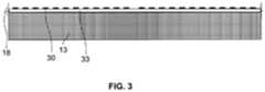
- FIG. 3illustrates a stage in a method of forming a microelectronic unit similar to FIG. 1A .
- FIG. 4further illustrates another stage in a method of forming a microelectronic unit according to FIG. 1A .
- FIG. 5further illustrates another stage in a method of forming a microelectronic unit according to FIG. 1A .
- FIG. 6further illustrates another stage in a method of forming a microelectronic unit according to FIG. 1A .
- FIG. 7illustrates a stage in a method of forming a microelectronic unit similar to FIG. 1B .
- FIG. 8further illustrates another stage in a method of forming a microelectronic unit according to FIG. 1B .
- FIG. 9further illustrates another stage in a method of forming a microelectronic unit according to FIG. 1B .
- FIG. 10is a top elevation view illustrating a microelectronic unit according to an embodiment of the invention.
- FIGS. 11A-Dare sectional views depicting variations in the connector elements and encapsulation according to an embodiment of the invention.
- FIGS. 12A-Bare sectional views illustrating one stage and another stage subsequent thereto in a method of forming an encapsulation layer of a microelectronic unit according to an embodiment of the invention.
- FIG. 12Cis an enlarged sectional view further illustrating the stage corresponding to FIG. 12B .
- FIGS. 13A-Bare sectional views depicting variations of the carrier according to an embodiment of the invention.
- FIG. 14is a sectional views depicting variations in the connector elements and encapsulation according to an embodiment of the invention.
- FIGS. 15A-Bare sectional views depicting a microelectronic unit arranged in a stacked assembly according to embodiments of the invention.
- FIG. 16is a schematic sectional view illustrating a system according to an embodiment of the invention.
- FIGS. 1A and 1Bthere are example substrate-less packages 10 that may include microelectronic element 12 (as seen in FIG. 2 ), connector elements 14 , encapsulant 16 and redistribution structure 18 .
- the microelectronic element 12may have a front face 20 or “active face,” a rear face 22 , and sidewalls 24 extending between the front and rear faces.
- the front face 20may be at a first side 11 of the microelectronic unit or package 10 .
- a statement that an element is “at” a surface of a componentindicates that, when the component is not assembled with any other element, the electrically conductive element is available for contact with a theoretical point moving in a direction perpendicular to the surface of the component toward the surface of the component from outside the component.
- a terminal or other conductive element which is at a surface of a microelectronic unit 12may project from such surface; may be flush with such surface; or may be recessed relative to such surface in a hole or depression in the substrate.
- Connector elements 14may include first ends 28 (e.g., bases), second ends 26 (e.g., tips) and edges extending vertically between the first and second ends.
- the first ends 28may comprise conductive elements 29 (e.g., pads) made of copper, nickel, aluminum, tin, palladium or other similar conductive material or combination of conductive materials.
- Connector elements 14may be arranged in a pattern to form area array 31 , which may surround microelectronic element 12 and have a grid-like appearance, such as further seen in a corresponding plan view thereof in FIG. 10 .
- Area array 31may be filled in with encapsulant 16 such that the free ends 34 of connector elements 14 are at the surface of the encapsulant 16 . As seen in FIG.
- the free ends 34 of the connector elementsmay be arranged into a grid or an array and exposed at the surface of the dielectric encapsulation 16 .
- the free ends 34 of the connector elements 14can be characterized as being “free” in that they are not electrically connected or otherwise joined to other electrically conductive features within microelectronic unit 12 that are proximate to the free ends 34 .
- free ends 34are available for electronic connection, either directly or indirectly to a conductive feature external to the microelectronic unit 12 .
- free ends 34 held in a predetermined position by, for example, encapsulation 16 or otherwise joined or electrically connected to another conductive featuredoes not mean that they are not “free” as described herein, so long as any such feature is not proximate to the free end.
- first end or the second endmay be the free end, for example in FIG. 1A the second ends 26 (e.g., tips) are the free ends, whereas in FIG. 1B the first ends (e.g., bases) are the free ends 34 .
- the free ends 34 and the front face of the microelectronic element 12may be at the same side of the package and remote from redistribution structure 18 .
- the ends of the connector elements that are adjacent the redistribution structure 18may not be free ends because they are directly or indirectly electrically coupled to the redistribution structure 18 .
- area array 31may have a plurality of rows and columns that surround the microelectronic element 12 along the perimeter portion of the microelectronic unit 12 .
- the area array 31may extend beyond the edge of the microelectronic element toward the edge of the microelectronic unit 10 .
- the area array 31may be arranged such that there are no connector elements 14 within distance 55 (e.g., less than 4 mm) extending outward from the edge of the microelectronic element 12 .
- the area array 31may also be arranged such that the connector elements 14 are subset a small distance 56 (e.g., less than 4 mm) inward from the package edge. In One example there may be no connector elements within 0.5 mm of the edge of the microelectronic element 12 and 0.5 mm of the edge of the microelectronic unit 10 .
- the quantity of connector elements 14may depend on the portion of the microelectronic unit that includes connectors as well as the density of the connector elements 14 .
- the densityrelates to the thickness of each connector as well as how close the connector elements are to one another (e.g., pitch).
- the connector elementsmay have different dimensions depending on the particular structure, for example for wirebonds the thickness may be approximately 500 ⁇ m, whereas solder material may have a larger thickness.
- the pitchmay vary from 0.05 millimeters (mm) to 4 mm and is preferably in the range of 0.1-0.6 mm. The lower the pitch the higher the density of I/O connections.
- a microelectronic unit with dimensions of 14 mm ⁇ 14 mmmay have approximately 1440 connector elements 14 by having five rows with a pitch that is approximately equal to 0.2 mm.
- the second ends 26(e.g., tips) of the connector elements 14 may be at the first side 11 of the microelectronic unit 12 .
- the second ends 26may project above the surface of the encapsulant.
- a statement that an electrically conductive element is disposed “above a surface” or “overlying a surface”means at a region which is in an orthogonal direction away from the surface.
- a statement that one element is “above” or “upward from” a reference planemeans at a region in an orthogonal direction away from the reference plane. Movement of an element in an “upward” direction means in a direction to a greater height above a reference plane defined by the surface.
- movement of an element in a “downward” directionmeans in a direction to a lower height above a reference plane defined by the surface. All such statements and meanings of the foregoing terms are not in a gravitational reference, but rather in the frame of reference defined by the element itself.
- Each of the connector elements 14may be electrically connected to the redistribution structure.
- the connector elements 14 and/or the redistribution structure 18may be free of electrical connections with the microelectronic element 12 .
- the rear face of microelectronic element 12may be attached to redistribution structure 18 at attachment region 32 , which may be covered by an adhesive layer or adhesive film.
- the attachment region 32may be located in the center portion of each microelectronic unit.
- the redistribution structure 18may be electrically coupled to or in direct contact with the first ends 28 (e.g., bases) of connector elements 14 .
- the basesmay be conductive pads.
- the connector elements' first ends 28may be at the first side 11 of the microelectronic unit and adjacent active face 20 of microelectronic element 12 .
- the second ends 26e.g., bases
- the redistribution structure 18may be separated from the microelectronic element by encapsulation 16 , which may completely cover microelectronic element 12 and surround the rear face and all the sidewalls.
- the microelectronic units discussed above as well as other variationsmay be formed according to various stages of formation seen in FIGS. 2-9 .
- the redistribution structure 18may be formed prior to the connector elements 14 and be electrically coupled to or in contact with the first ends 28 (e.g., bases), in another example, the redistribution structure 18 may be formed after the connector elements 14 and contact the second ends 26 (e.g., tips).
- the method of fabricationmay utilize a reconstituted assembly approach (e.g., reconstituted wafer).
- a reconstituted assembly 8may be formed by placing a plurality of singulated microelectronic elements 12 onto carrier 13 for further processing.
- Carrier 13may be any structure (e.g., wafer) capable of mechanically supporting a plurality of microelectronic elements while being operated on.
- Microelectronic elements 12may be placed directly on the carrier or may be placed on a layer(s) previously formed on the carrier.
- the microelectronic elements 12may be spaced apart and attached directly or indirectly to the carrier 13 by an adhesive material or vacuum.
- the plurality of microelectronic elements 12may then be processed while in form of the reconstituted wafer and then subsequently singulated to form individual packaged microelectronic units.
- a temporary attachment layer 33e.g., adhesive layer
- electrically conductive terminals 30can be provided on a carrier 13 .
- Temporary attachment layer 33may be formed by depositing an adhesive material or attaching an adhesive material over the carrier 13 .
- forming the conductive terminals 30may be formed subtractively by patterning the conductive material to form individual conductive terminals 30 .
- the conductive terminalscan be formed by additive processing, e.g., by plating, deposition, printing, etc.
- the conductive terminalsmay include copper, aluminum, nickel or any other electrically conductive material such as, without limitation, conductive matrix material, conductive ink, conductive polymer, conductive paste, etc.
- terminals 30may be in the form of conductive pads that may function as package terminals on the surface of the microelectronic unit (e.g., Ball Grid Array (BGA)).
- BGABall Grid Array
- redistribution structure 18may be created on carrier 13 by forming a dielectric layer 9 and traces 21 electrically coupled with conductive terminals 30 .
- the redistribution structure 18may be formed by a single dielectric layer (e.g., single spin coat) or may comprise multiple dielectric layers.
- conductive elements 29At a surface of the redistribution structure 18 remote from carrier 13 there may be conductive elements 29 , which in one example may be formed by forming another conductive layer and subsequently patterning it to form conductive elements 29 .
- the conductive elements 29may be pads or conductive masses (e.g., solder balls) and may function as the first ends (e.g., bases) of the Bond Via Array (BVA).
- the methodmay include forming attachment regions 32 and conductive connector elements 14 .
- Attachment regions 32may be positions overlying the carrier where microelectronic elements may be placed. The placement of the microelectronic elements may occur before or after forming the connector elements 14 , before or after forming the encapsulation or before or after singulation.
- Attachment regions 32may comprise adhesive pads and/or an adhesive film and may be formed at regions spaced apart from one another in at least a first direction parallel with the surface of the carrier.
- Connector elements 14may be formed between adjacent attachment regions 32 and may partially or fully surround each attachment region 32 .
- Each connector elementmay have a first end 28 , a second end 26 and an edge surface 27 extending vertically between the first and second ends.
- First end 28may be adjacent and electrically coupled to redistribution structure 18 and second end 26 may be a free end remote from the redistribution structure 18 .
- First ends 28may overlie and be electrically coupled (e.g., bonded or joined) with conductive elements 29 and/or the first ends may comprise the conductive elements 29 and be formed integrally therewith, as seen by first ends 28 ′.
- connector elements 14may be wire bonds that are joined to metal bonding surfaces (e.g., conductive elements 29 ) using a wire bonding tool.
- the method for forming the wirebondsmay include heating the leading end of a wire segment and pressing it against the receiving surface to which the wire segment bonds, typically forming a ball or ball-like base joined to the surface of the conductive element 29 .
- the desired length of the wire segment needed to form the wire bondis drawn out of the bonding tool, which may then sever or cut the wire bond at the desired length.
- Wedge bondingmay include dragging a portion of the a wire along the receiving surface to form a wedge that lies generally parallel to the surface.
- the wedge bonded wire bondcan then be bent upward, if necessary, and extended to the desired length or position before cutting.
- the wire used to form a wire bondcan be cylindrical in cross section. Otherwise, the wire fed from the tool to form a wire bond or wedge bonded wire bond may have a polygonal cross section such as rectangular or trapezoidal, for example.
- microelectronic elements 12may be placed at attachment regions 32 and surrounded by dielectric encapsulation 16 .
- the microelectronic elements 12may be attached before, after or during the forming of the dielectric encapsulation 16 .
- Each microelectronic element 12may have a front face 20 , rear face 22 and sidewalls 24 extending between the front and rear faces.
- the front face 20may be an active face with active or passive elements (e.g., contacts) and the rear face 22 may or may not have active or passive electrical elements (e.g., contacts).
- the attachment regionsmay be located on a surface of the redistribution structure 18 and the microelectronic elements 12 may be attached with the rear face facing toward the carrier. As such, front face 20 may be remote from and face away from the redistribution structure 18 and carrier 13 .
- the microelectronic elements 12may then be surrounded by encapsulation 16 such that the encapsulation is adjacent and overlies all of the sidewalls of microelectronic element 12 .
- the encapsulationmay also be formed over portions of the connector elements edge surfaces 27 within area arrays 31 .
- the dielectric encapsulationmay have a major surface 17 that may be parallel with the front face 20 of microelectronic element 12 and at a height that is substantially aligned with the height of the microelectronic element 12 (e.g., greater than 50 mils).
- the surface of the encapsulationmay also be at a height above, below or approximately equal to the height of the second ends 26 of connector elements 14 .
- contact elements on the front face of the microelectronic element and second ends 26may have conductive masses (e.g., solder balls) formed on them (e.g., bumped), as seen in FIG. 11C .
- the resulting reconstituted assemblymay include numerous microelectronic units as a continuous or semi-continuous structure such as a strip, tape or sheet.
- FIG. 6shows no visible borders between the individual microelectronic units, they may be subsequently singulated, for example along cut line 36 and released from the carrier 13 to form individual packaged microelectronic elements, similar to the microelectronic unit seen in FIG. 1A .
- the microelectronic unitmay be used to mechanically support and electrically connect the microelectronic element to another microelectronic structure, such as to a printed circuit board (“PCB”), or to other packaged microelectronic elements.
- PCBprinted circuit board
- connector elements 14can carry multiple electronic signals therethrough, each having a different signal potential to allow for different signals to be processed by different microelectronic elements in a single stack.
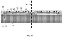
- a carrier 13may be used to form a reconstituted assembly (e.g., reconstituted wafer) and may include attachment regions 32 , microelectronic elements 12 , conductive layer 23 , conductive elements 29 , and connector elements 14 .
- the attachment regions 32may be provided directly on the carrier 13 , as opposed to on the redistribution structure 18 as seen in FIG. 4 .
- the attachment regions 32may be provided on an intermediate layer (e.g., conductive layer) disposed directly on carrier 13 .
- the microelectronic elements 12may be placed face down on the attachment regions, such that the front face is adjacent the carrier.
- rear face 22may be remote from or face away from the carrier.
- the conductive elements 29may be formed by forming an additional conductive layer (e.g., foil) and subsequently patterning the layer to form conductive elements 29 .
- conductive elements 29may be in the form of pads that may function as both package terminals for the microelectronic unit and first ends (e.g., bases) of the connector elements 14 .
- the connector elements 14may be formed via the same process discussed above with respect to FIG. 5 .
- the dielectric encapsulation 16may be formed over microelectronic elements 12 and among connector elements 14 as discussed above.
- the redistribution structure 18may be formed above the encapsulation and in direct contact with the second ends of the connector elements 14 .
- the redistribution structure 18may now be located remote from the carrier and may form the second side of the reconstituted assembly and the microelectronic units which will be singulated therefrom.
- the redistribution structure 18is accessible (e.g., exposed) while still on the carrier, which may allow the area array to be available for electrical coupling for testing at a larger pitch.
- the reconstituted assemblymay be ready for singulation, however there may also be additional or optional processing that may occur before singulation.
- conductive joining masses 35e.g., solder balls
- the reconstituted assemblymay be singulated along cut line 36 ( FIG. 9 ) and released from the carrier 13 to form individual packaged microelectronic elements, similar to the microelectronic unit seen in FIG. 1B .
- the microelectronic unitmay then be attached to a printed circuit board, or be part of a stack of microelectronic units, as discussed above.
- the microelectronic unit 10may be formed without forming a redistribution structure 18 and thus the redistribution structure can be omitted from the final structure and connector elements 14 may be at both sides of the microelectronic unit.
- microelectronic unit 12may have a first side 15 (e.g., top) and a second side 15 (e.g., bottom) opposite from the first side and a microelectronic element 12 .
- the microelectronic element 12may have an active face 20 at a second side 15 of the microelectronic unit 10 alongside the connector elements 14 .
- the connector elements 14may be formed such that they extend vertically between the first and second surfaces of the microelectronic element and stand parallel with the microelectronic element's sidewalls. Each connector element may be free of electrical connections with other connector elements and/or free of electrical connections to the microelectronic element. This may allow an underlying or overlying substrate (e.g., PCB, interposer, another microelectronic package) to supply the interconnections.
- underlying or overlying substratee.g., PCB, interposer, another microelectronic package
- the connector elements 14 H and 14 Imay comprise a single conductive mass 19 .
- the conductive massmay be rounded as seen in 14 H or it may be elongated into an elliptical shape as seen in 14 I.
- Each conductive massmay also include a series of stacked conductive masses, as seen in examples of connectors 14 J, 14 K and 14 L.
- the conductive massesmay be formed of or may include a bond metal such as tin, indium, solder, or gold.
- the conductive massesmay be formed of or may comprise a curable material. In some cases, a curable material can be allowed to cure before forming additional conductive mass above it.
- the first and second connector endsmay be the bottom and top portions respectively of a single conductive mass 19 or it may be the top and bottom conductive mass respectively when there are a plurality of conductive masses stacked.
- the microelectronic unit 10may also include a heat spreader 50 adjacent the microelectronic element 12 .
- the heat spreader 50may consist of or include a portion of conductive layer 23 .
- the heat spreader 50may be adhered directly or indirectly to the rear face of the microelectronic element 12 .
- the heat spreader 50may occupy a larger or smaller area then the rear face of the microelectronic element.
- the encapsulation 16may be formed at different regions and at different points in the procedure resulting in microelectronic units with different configurations.
- the encapsulationmay be formed prior to the placement of the microelectronic element onto the reconstituted assembly, as seen in FIG. 11C .
- the encapsulationmay be formed after the placement of the microelectronic element, which may allow the encapsulant to directly contact the microelectronic elements.
- the dielectric encapsulationmay cover a large portion of the microelectronic element and surround all of the sidewalls and the rear face of the microelectronic element (i.e., five of the six sides of the microelectronic element), as seen in 11 A.
- the encapsulationmay surround the sidewalls of the microelectronic elements but may only extend laterally outward in a horizontal direction from the microelectronic element and overly neither the front face nor the rear face of the microelectronic element 12 .
- FIG. 11Cthere may be a configuration where the encapsulant is formed such that it surrounds the microelectronic element but there is a substantial gap 7 between one or more sidewalls (e.g., all the sidewalls) of the microelectronic element and the surrounding encapsulation.
- FIG. 12A-Cthere is an example technique for forming encapsulation 16 , which may result in unencapsulated portions of the connector elements 14 projecting beyond a surface 17 of the encapsulation 16 .
- a film-assisted molding techniquemay be used by which a temporary film 42 is placed between a plate 44 of a mold and a cavity 46 in which a subassembly including the substrate, connector elements 14 joined thereto, and a component such as a microelectronic element may be joined.
- FIG. 12Afurther shows a second plate 45 of the mold which can be disposed opposite the first plate 44 .
- the film assisted molding techniquemay be well adapted for mass production.
- a portion of a continuous sheet of the temporary filmcan be applied to the mold plate.
- the encapsulation layercan be formed in a cavity 46 that is at least partially defined by the mold plate.
- a current portion of the temporary film 42 on the mold plate 44can be replaced by automated means with another portion of the continuous sheet of the temporary film.
- a water soluble filmcan be placed on an inner surface of the mold plate 44 prior to forming the encapsulation layer.
- the water soluble filmcan be removed by washing it away so as to leave the ends of the connector elements 14 projecting beyond the surface 17 of the encapsulation layer as described above.
- the encapsulationmay also be formed using an alternate techniques, for example, encapsulation 16 may be formed by completely covering connector elements 14 , including ends (e.g., ends 26 ) with the encapsulation.
- the encapsulationmay include a sacrificial portion (e.g., layer) which may be subsequently removed to expose the second ends.
- the sacrificial portionmay be removed by etching, planarizing, lapping, grinding, wet blasting (e.g., aluminum slurry), polishing or the like. This may reduce the height of the encapsulant to the desired height for connector elements 14 .
- the planarization of the sacrificial portioncan begin by reducing the height thereof to a point where the connector elements 14 become exposed at the surface of the sacrificial layer.
- the planarization processcan then also planarize the connector elements 14 simultaneously with the sacrificial layer such that, as the height of the sacrificial layer is continued to be reduced, the heights of the connector elements 14 are also reduced.
- the planarizationcan be stopped once the desired height for the connector elements 14 is reached. It is noted that in such a process the connector elements 14 can be initially formed such that their heights, while being non-uniform, are all greater than the targeted uniform height.
- the sacrificial layercan be removed such as by etching or the like.
- the sacrificial portionmay be formed from a material that is the same as the encapsulant or may be different, which may allow for removal by etching using an etchant that will not significantly affect the encapsulant material.
- the sacrificial layercan be made from a water soluble plastic material.
- the carrier used for the reconstituted assemblymay have a substantially flat surface or the surface may include recessed and/or raised attachment regions.
- the non-flat attachment regionsmay be configured to allow a previously bumped microelectronic element to be releasably attached face down on the carrier.
- the recessed portion 52may have a depth 54 that is configured to accommodate the thickness of the solder bumps 35 , for example, the depth may be larger than the thickness of the solder bumps or it may be slightly smaller which may result in a slight deformation of the bumps.
- the width 58 of the recessed portionmay be configured to be larger than the width 60 of the portion of the active face that includes electrical contacts (e.g., pads, solderbumps). Yet the recess width 58 may be smaller than the width 62 of the microelectronic element 12 , which may allow the microelectronic element to be suspended above and/or bridge the recess.
- the carrier used for the reconstituted assemblymay have a substantially flat surface or the surface may include recessed and/or raised attachment regions.
- the non-flat attachment regionsmay be configured to allow a previously bumped microelectronic element to be releasably attached face down on the carrier.
- the recessed portion 52may have a depth 54 that is configured to accommodate the thickness of the solder bumps 56 , for example, the depth may be larger than the thickness of the solder bumps or it may be slightly smaller which may result in a slight deformation of the bumps.
- the width 58 of the recessed portionmay be configured to be larger than the width 60 of the portion of the active face that includes electrical contacts (e.g., pads, solderbumps). Yet the recess width 58 may be smaller than the width 62 of the microelectronic element 12 , which may allow the microelectronic element to be suspended above and/or bridge the recess.
- connector elements 14 and terminals provided by the conductive elements 29 at ends of connector elements 14can be formed, such as described above relative to FIG. 8 .
- the encapsulation 16can be provided and further processing performed to provide a redistribution layer such as described above relative to FIG. 9 .
- the non-flat attachment regionsmay include portions that are both raised and recessed. This may allow the microelectronic element 12 to be optimally positioned within the microelectronic unit.
- the microelectronic elementmay be slightly raised a height 64 above the surface of the carrier, alternatively the microelectronic element may be position such that the active face or the bottom of the bumps on the active face are along the same plane as the free ends 34 of the connector elements.
- any or all of the microelectronic units and methods described abovemay include any combination of connector elements having various shapes leading to various relative lateral displacements between bases and ends thereof.
- connector elements 14can be substantially straight with second ends 26 positioned above their respective first ends (e.g., bases) 28 as seen in elements 14 D and examples discussed above, in this situation the pitch of the first ends and the second ends may be the same.
- connector elements 14 Acan be straight, but second ends 26 may be displaced in a lateral direction from the respective first ends 28 .
- connector elementse.g., elements 14 B
- connector elementse.g., elements 14 C
- connector elementsinclude curved portions 118 having a sweeping shape that result in second ends 26 that are laterally displaced from the the respective bases 28 at a greater distance than those seen in 14 B.
- first pitchfirst center-to-center spacing
- second pitchsecond center-to-center spacing
- the conductive terminals 30 of the microelectronic unit 10can be set at a third center-to-center pitch which can be equal to or larger than either the first and/or second pitches.
- the conductive terminals 30may be electrically coupled with all, or only a portion of the connector elements 14 .
- the conductive terminals 30may overlie the microlectronic element 12 and/or the adjacent encapsulation 16 and may span an entire side, or a large portion of a side of the microelectronic unit 10 (e.g., package).
- the pitch of the first and second endsmay have the same value (e.g., 240 micrometers) and the pitch of the conductive terminals may be larger (e.g., 400 micrometers).
- the curved portions 118 of connector elements 14may take on a variety of shapes, as needed, to achieve the desired position of the end 26 of the connector element 14 .
- the curved portions 118may be formed as S-curves of various shapes, such as included in wire bond 14 B, or of a smoother form as in wire bond 14 C. Additionally, the curved portion 118 may be positioned closer to base 28 than to end 26 or vice-versa.
- the curved portion 118may also be in the form of a spiral or loop, or may be compound including curves in multiple directions or of different shapes or characters.
- the curved portion 118may be formed during, for example, a wire bond formation process and may occur while the wire portion is being drawn out to the desired length. This step may be carried out using available wire-bonding equipment, which may include the use of a single machine.
- the connector elements 14may also include conductive joining masses 35 (e.g., stud bumps) at the free ends 34 (e.g., ends). This may assist with providing a connection to another conductive element.
- Conductive massmay be joined to the uncapsulated free ends, as seen in elements 14 D-G. In one example the conductive mass may be joined to the free end and allowed to wick along edge surface 27 and join thereto in addition to joining to free end.
- the structure 14 D- 14 Gmay include a connector element in the form of posts or micro-pillar having an end 26 and an edge surface.
- the connector element 14 F-Gmay have a frustoconical shape with tapered sidewalls.
- the connector element 14 Gmay have an end 26 wider in cross-section than a cross-section of a portion between the base 28 and end 26 , where the base 28 and end 26 are parallel and edge surfaces extend tapered toward each other from the base 28 to the end 26 .
- the base 28 of connector element 14may be formed integrally with the connector element 14 , such as seen in the case of connector elements 14 A, such that the conductive element is not a separate element to which the respective connector element 14 is joined.
- the connector elementmay be in the form of micropillar 14 G having an end 26 that is at a height that is lower than the major surface 17 of the encapsulant 16 .
- the encapsulation 16may be configured to include an area that has been etched away, molded, or otherwise formed to define an opening or cavity extending from surface 17 at least to the free end 26 .
- the cavitymay have any suitable shape to permit electrical connection at end 26 of connector element 14 G that may be formed in the cavity, such as by deposition of electrically conductive material therein.
- Conductive joining mass 35may be deposited in the cavity and extend from the end 26 to above the major surface 17 of encapsulant 16 and along portions of the surface 17 extending away from the cavity.
- the microelectronic unit 10 shown in FIG. 1A or 1Bcan be assembled with other components such as a lower component 57 below the unit 10 and another microelectronic package 110 above the unit 10 in a “package on package” (PoP) stacked assembly 100 .
- lower component 57may be a printed circuit board, interposer, microelectronic element, or microelectronic package, to which microelectronic element 12 can be flip-chip attached, and electrical connections to the terminals 30 can extend through microelectronic unit 10 via the connector elements 14 of the microelectronic unit.
- the microelectronic unit 10may have two different sets of electrical connections at different pitches.
- the first set of connectionsmay include conductive elements on the front face of the microelectronic element 12 and electrically couple the microelectronic element 12 to lower component 57 .
- the second set of connectionsmay be the connector elements 14 which may electrically couple microelectronic package 110 with lower component 57 .
- the first set of connectionsmay be the only electrical connections between the microelectronic element 12 and lower component 57 and the second set of connections may be the only electrical connections between microelectronic package 110 and lower component 57 .
- a portion of either setmay be used to electrically couple a package to the lower component 57 .
- the redistribution layer 18 and terminals 30 of microelectronic unit 10can be at a different pitch than the terminals of lower component 57 , e.g., terminals 30 may have a pitch larger than the pitch of the connector elements present around the periphery of the microelectric unit 10 outside the microelectronic element 12 . In one example, this may allow more relaxed pitch for testing the microelectronic unit 10 at the top terminals and may allow for a microelectronic package 110 or component having a more relaxed pitch to be electrically coupled with the top terminals 30 of the unit.
- the microelectronic packages and microelectronic assemblies described above with reference to FIGS. 1A +B, FIG. 10-11D and FIG. 14-15Bcan be utilized in construction of diverse electronic systems, such as the system 1100 shown in FIG. 16 .
- the system 1100 in accordance with a further embodiment of the inventionincludes a plurality of modules or components 1106 such as the microelectronic packages and/or microelectronic assemblies as described above in conjunction with other electronic components 1108 and 1110 .
- the systemcan include a circuit panel, motherboard, or riser panel 1102 such as a flexible printed circuit board, and the circuit panel can include numerous conductors 1104 , of which only one is depicted in FIG. 16 , interconnecting the modules or components 1106 with one another.
- a circuit panel 1102can transport signals to and from each of the microelectronic packages and/or microelectronic assemblies included in the system 1100 .
- thisis merely exemplary; any suitable structure for making electrical connections between the modules or components 1106 can be used.
- the system 1100can also include a processor such as the semiconductor chip 1108 , such that each module or component 1106 can be configured to transfer a number N of data bits in parallel in a clock cycle, and the processor can be configured to transfer a number M of data bits in parallel in a clock cycle, M being greater than or equal to N.
- component 1108can be a semiconductor chip and component 1110 is a display screen, but any other components can be used in the system 1100 .
- the system 1100can include any number of such components.
- Modules or components 1106 and components 1108 and 1110can be mounted in a common housing 1101 , schematically depicted in broken lines, and can be electrically interconnected with one another as necessary to form the desired circuit.
- the housing 1101is depicted as a portable housing of the type usable, for example, in a smartphone, tablet computer, television, or cellular telephone, and screen 1110 can be exposed at the surface of the housing.
- a structure 1106includes a light-sensitive element such as an imaging chip
- a lens 1111 or other optical devicealso can be provided for routing light to the structure.
- the simplified system shown in FIG. 16is merely exemplary; other systems, including systems commonly regarded as fixed structures, such as desktop computers, routers and the like can be made using the structures discussed above.
- a structuremay include other configurations by which a portion of a connector element is uncovered by an encapsulation element, such at an end surface and optionally along an edge surface thereof, which are similar to those discussed herein with respect to the variations of the configuration of the surface of the encapsulation element remote and facing away from the surface of the substrate.
Landscapes
- Engineering & Computer Science (AREA)
- Microelectronics & Electronic Packaging (AREA)
- Power Engineering (AREA)
- Computer Hardware Design (AREA)
- Physics & Mathematics (AREA)
- Condensed Matter Physics & Semiconductors (AREA)
- General Physics & Mathematics (AREA)
- Manufacturing & Machinery (AREA)
- Ceramic Engineering (AREA)
- Structures Or Materials For Encapsulating Or Coating Semiconductor Devices Or Solid State Devices (AREA)
- Structures For Mounting Electric Components On Printed Circuit Boards (AREA)
- Encapsulation Of And Coatings For Semiconductor Or Solid State Devices (AREA)
Abstract
Description
Claims (20)
Priority Applications (4)
| Application Number | Priority Date | Filing Date | Title |
|---|---|---|---|
| US15/827,550US10529636B2 (en) | 2014-01-17 | 2017-11-30 | Fine pitch BVA using reconstituted wafer with area array accessible for testing |
| US16/734,758US11404338B2 (en) | 2014-01-17 | 2020-01-06 | Fine pitch bva using reconstituted wafer with area array accessible for testing |
| US17/865,994US11990382B2 (en) | 2014-01-17 | 2022-07-15 | Fine pitch BVA using reconstituted wafer with area array accessible for testing |
| US18/610,114US20240347404A1 (en) | 2014-01-17 | 2024-03-19 | Fine pitch bva using reconstituted wafer with area array accessible for testing |
Applications Claiming Priority (3)
| Application Number | Priority Date | Filing Date | Title |
|---|---|---|---|
| US14/157,790US9583411B2 (en) | 2014-01-17 | 2014-01-17 | Fine pitch BVA using reconstituted wafer with area array accessible for testing |
| US15/422,887US9837330B2 (en) | 2014-01-17 | 2017-02-02 | Fine pitch BVA using reconstituted wafer with area array accessible for testing |
| US15/827,550US10529636B2 (en) | 2014-01-17 | 2017-11-30 | Fine pitch BVA using reconstituted wafer with area array accessible for testing |
Related Parent Applications (2)
| Application Number | Title | Priority Date | Filing Date |
|---|---|---|---|
| US14/157,790ContinuationUS9583411B2 (en) | 2014-01-17 | 2014-01-17 | Fine pitch BVA using reconstituted wafer with area array accessible for testing |
| US15/422,887ContinuationUS9837330B2 (en) | 2014-01-17 | 2017-02-02 | Fine pitch BVA using reconstituted wafer with area array accessible for testing |
Related Child Applications (1)
| Application Number | Title | Priority Date | Filing Date |
|---|---|---|---|
| US16/734,758ContinuationUS11404338B2 (en) | 2014-01-17 | 2020-01-06 | Fine pitch bva using reconstituted wafer with area array accessible for testing |
Publications (2)
| Publication Number | Publication Date |
|---|---|
| US20180082916A1 US20180082916A1 (en) | 2018-03-22 |
| US10529636B2true US10529636B2 (en) | 2020-01-07 |
Family
ID=52440889
Family Applications (6)
| Application Number | Title | Priority Date | Filing Date |
|---|---|---|---|
| US14/157,790Active2034-12-07US9583411B2 (en) | 2014-01-17 | 2014-01-17 | Fine pitch BVA using reconstituted wafer with area array accessible for testing |
| US15/422,887ActiveUS9837330B2 (en) | 2014-01-17 | 2017-02-02 | Fine pitch BVA using reconstituted wafer with area array accessible for testing |
| US15/827,550Active2034-02-13US10529636B2 (en) | 2014-01-17 | 2017-11-30 | Fine pitch BVA using reconstituted wafer with area array accessible for testing |
| US16/734,758ActiveUS11404338B2 (en) | 2014-01-17 | 2020-01-06 | Fine pitch bva using reconstituted wafer with area array accessible for testing |
| US17/865,994Active2034-02-21US11990382B2 (en) | 2014-01-17 | 2022-07-15 | Fine pitch BVA using reconstituted wafer with area array accessible for testing |
| US18/610,114PendingUS20240347404A1 (en) | 2014-01-17 | 2024-03-19 | Fine pitch bva using reconstituted wafer with area array accessible for testing |
Family Applications Before (2)
| Application Number | Title | Priority Date | Filing Date |
|---|---|---|---|
| US14/157,790Active2034-12-07US9583411B2 (en) | 2014-01-17 | 2014-01-17 | Fine pitch BVA using reconstituted wafer with area array accessible for testing |
| US15/422,887ActiveUS9837330B2 (en) | 2014-01-17 | 2017-02-02 | Fine pitch BVA using reconstituted wafer with area array accessible for testing |
Family Applications After (3)
| Application Number | Title | Priority Date | Filing Date |
|---|---|---|---|
| US16/734,758ActiveUS11404338B2 (en) | 2014-01-17 | 2020-01-06 | Fine pitch bva using reconstituted wafer with area array accessible for testing |
| US17/865,994Active2034-02-21US11990382B2 (en) | 2014-01-17 | 2022-07-15 | Fine pitch BVA using reconstituted wafer with area array accessible for testing |
| US18/610,114PendingUS20240347404A1 (en) | 2014-01-17 | 2024-03-19 | Fine pitch bva using reconstituted wafer with area array accessible for testing |
Country Status (4)
| Country | Link |
|---|---|
| US (6) | US9583411B2 (en) |
| KR (1) | KR20160110970A (en) |
| TW (1) | TW201532235A (en) |
| WO (1) | WO2015109157A1 (en) |
Cited By (4)
| Publication number | Priority date | Publication date | Assignee | Title |
|---|---|---|---|---|
| US11189595B2 (en) | 2011-10-17 | 2021-11-30 | Invensas Corporation | Package-on-package assembly with wire bond vias |
| US11257803B2 (en)* | 2018-08-25 | 2022-02-22 | Octavo Systems Llc | System in a package connectors |
| US11404338B2 (en)* | 2014-01-17 | 2022-08-02 | Invensas Corporation | Fine pitch bva using reconstituted wafer with area array accessible for testing |
| US11424211B2 (en) | 2011-05-03 | 2022-08-23 | Tessera Llc | Package-on-package assembly with wire bonds to encapsulation surface |
Families Citing this family (15)
| Publication number | Priority date | Publication date | Assignee | Title |
|---|---|---|---|---|
| KR101195786B1 (en) | 2008-05-09 | 2012-11-05 | 고쿠리츠 다이가쿠 호진 큐슈 코교 다이가쿠 | Chip-size double side connection package and method for manufacturing the same |
| US10177032B2 (en)* | 2014-06-18 | 2019-01-08 | Taiwan Semiconductor Manufacturing Company, Ltd. | Devices, packaging devices, and methods of packaging semiconductor devices |
| US9831214B2 (en)* | 2014-06-18 | 2017-11-28 | Taiwan Semiconductor Manufacturing Company, Ltd. | Semiconductor device packages, packaging methods, and packaged semiconductor devices |
| US10804185B2 (en) | 2015-12-31 | 2020-10-13 | Texas Instruments Incorporated | Integrated circuit chip with a vertical connector |
| US10181447B2 (en)* | 2017-04-21 | 2019-01-15 | Invensas Corporation | 3D-interconnect |
| US10541153B2 (en)* | 2017-08-03 | 2020-01-21 | General Electric Company | Electronics package with integrated interconnect structure and method of manufacturing thereof |
| US10541209B2 (en) | 2017-08-03 | 2020-01-21 | General Electric Company | Electronics package including integrated electromagnetic interference shield and method of manufacturing thereof |
| US11081369B2 (en)* | 2019-02-25 | 2021-08-03 | Taiwan Semiconductor Manufacturing Company, Ltd. | Package structure and manufacturing method thereof |
| DE102019119714A1 (en)* | 2019-07-22 | 2021-01-28 | Endress+Hauser Process Solutions Ag | Method for verifying the field device inventory entered in an asset management system |
| US11239168B2 (en)* | 2019-07-30 | 2022-02-01 | Industrial Technology Research Institute | Chip package structure |
| US11171127B2 (en)* | 2019-08-02 | 2021-11-09 | Amkor Technology Singapore Holding Pte. Ltd. | Semiconductor device and method of manufacturing semiconductor device |
| US12388061B2 (en) | 2019-08-02 | 2025-08-12 | Amkor Technology Singapore Holding Pte. Ltd. | Semiconductor device and method of manufacturing semiconductor device |
| KR20220049423A (en)* | 2020-10-14 | 2022-04-21 | 에스케이하이닉스 주식회사 | Methods for fabricating semiconductor packages |
| US11842946B2 (en)* | 2021-03-26 | 2023-12-12 | Taiwan Semiconductor Manufacturing Co., Ltd. | Semiconductor package having an encapsulant comprising conductive fillers and method of manufacture |
| US12040284B2 (en) | 2021-11-12 | 2024-07-16 | Invensas Llc | 3D-interconnect with electromagnetic interference (“EMI”) shield and/or antenna |
Citations (804)
| Publication number | Priority date | Publication date | Assignee | Title |
|---|---|---|---|---|
| US2230663A (en) | 1940-01-18 | 1941-02-04 | Alden Milton | Electric contact and wire assembly mechanism |
| US3289452A (en) | 1963-07-23 | 1966-12-06 | Siemens Ag | Method and device for bonding a contact wire to a semiconductor member |
| US3358897A (en) | 1964-03-31 | 1967-12-19 | Tempress Res Co | Electric lead wire bonding tools |
| US3430835A (en) | 1966-06-07 | 1969-03-04 | Westinghouse Electric Corp | Wire bonding apparatus for microelectronic components |
| US3623649A (en) | 1969-06-09 | 1971-11-30 | Gen Motors Corp | Wedge bonding tool for the attachment of semiconductor leads |
| US3795037A (en) | 1970-05-05 | 1974-03-05 | Int Computers Ltd | Electrical connector devices |
| US3900153A (en) | 1972-06-13 | 1975-08-19 | Licentia Gmbh | Formation of solder layers |
| JPS5150661A (en) | 1974-10-30 | 1976-05-04 | Hitachi Ltd | |
| US4067104A (en) | 1977-02-24 | 1978-01-10 | Rockwell International Corporation | Method of fabricating an array of flexible metallic interconnects for coupling microelectronics components |
| US4072816A (en) | 1976-12-13 | 1978-02-07 | International Business Machines Corporation | Integrated circuit package |
| US4213556A (en) | 1978-10-02 | 1980-07-22 | General Motors Corporation | Method and apparatus to detect automatic wire bonder failure |
| US4327860A (en) | 1980-01-03 | 1982-05-04 | Kulicke And Soffa Ind. Inc. | Method of making slack free wire interconnections |
| US4422568A (en) | 1981-01-12 | 1983-12-27 | Kulicke And Soffa Industries, Inc. | Method of making constant bonding wire tail lengths |
| US4437604A (en) | 1982-03-15 | 1984-03-20 | Kulicke & Soffa Industries, Inc. | Method of making fine wire interconnections |
| JPS59189069A (en) | 1983-04-12 | 1984-10-26 | Alps Electric Co Ltd | Device and method for coating solder on terminal |
| JPS61125062A (en) | 1984-11-22 | 1986-06-12 | Hitachi Ltd | Method and device for attaching pin |
| US4604644A (en) | 1985-01-28 | 1986-08-05 | International Business Machines Corporation | Solder interconnection structure for joining semiconductor devices to substrates that have improved fatigue life, and process for making |
| US4642889A (en) | 1985-04-29 | 1987-02-17 | Amp Incorporated | Compliant interconnection and method therefor |
| US4667267A (en) | 1985-01-22 | 1987-05-19 | Rogers Corporation | Decoupling capacitor for pin grid array package |
| JPS62158338A (en) | 1985-12-28 | 1987-07-14 | Tanaka Denshi Kogyo Kk | semiconductor equipment |
| US4695870A (en) | 1986-03-27 | 1987-09-22 | Hughes Aircraft Company | Inverted chip carrier |
| JPS62226307A (en) | 1986-03-28 | 1987-10-05 | Toshiba Corp | robot equipment |
| US4716049A (en) | 1985-12-20 | 1987-12-29 | Hughes Aircraft Company | Compressive pedestal for microminiature connections |
| US4725692A (en) | 1985-05-24 | 1988-02-16 | Hitachi, Ltd. | Electronic device and lead frame used thereon |
| US4771930A (en) | 1986-06-30 | 1988-09-20 | Kulicke And Soffa Industries Inc. | Apparatus for supplying uniform tail lengths |
| US4793814A (en) | 1986-07-21 | 1988-12-27 | Rogers Corporation | Electrical circuit board interconnect |
| JPS6412769A (en) | 1987-07-07 | 1989-01-17 | Sony Corp | Correction circuit for image distortion |
| US4804132A (en) | 1987-08-28 | 1989-02-14 | Difrancesco Louis | Method for cold bonding |
| JPS6471162A (en) | 1987-09-11 | 1989-03-16 | Hitachi Ltd | Semiconductor device |
| US4845354A (en) | 1988-03-08 | 1989-07-04 | International Business Machines Corporation | Process control for laser wire bonding |
| US4902600A (en) | 1986-10-14 | 1990-02-20 | Fuji Photo Film Co., Ltd. | Light-sensitive material comprising light-sensitive layer provided on support wherein the light-sensitive layer and support have specified pH values |
| US4924353A (en) | 1985-12-20 | 1990-05-08 | Hughes Aircraft Company | Connector system for coupling to an integrated circuit chip |
| US4925083A (en) | 1987-02-06 | 1990-05-15 | Emhart Deutschland Gmbh | Ball bonding method and apparatus for performing the method |
| US4955523A (en) | 1986-12-17 | 1990-09-11 | Raychem Corporation | Interconnection of electronic components |
| US4975079A (en) | 1990-02-23 | 1990-12-04 | International Business Machines Corp. | Connector assembly for chip testing |
| US4982265A (en) | 1987-06-24 | 1991-01-01 | Hitachi, Ltd. | Semiconductor integrated circuit device and method of manufacturing the same |
| US4999472A (en) | 1990-03-12 | 1991-03-12 | Neinast James E | Electric arc system for ablating a surface coating |
| US4998885A (en) | 1989-10-27 | 1991-03-12 | International Business Machines Corporation | Elastomeric area array interposer |
| US5067007A (en) | 1988-06-13 | 1991-11-19 | Hitachi, Ltd. | Semiconductor device having leads for mounting to a surface of a printed circuit board |
| US5067382A (en) | 1990-11-02 | 1991-11-26 | Cray Computer Corporation | Method and apparatus for notching a lead wire attached to an IC chip to facilitate severing the wire |
| US5083697A (en) | 1990-02-14 | 1992-01-28 | Difrancesco Louis | Particle-enhanced joining of metal surfaces |
| US5095187A (en) | 1989-12-20 | 1992-03-10 | Raychem Corporation | Weakening wire supplied through a wire bonder |
| US5133495A (en) | 1991-08-12 | 1992-07-28 | International Business Machines Corporation | Method of bonding flexible circuit to circuitized substrate to provide electrical connection therebetween |
| US5138438A (en) | 1987-06-24 | 1992-08-11 | Akita Electronics Co. Ltd. | Lead connections means for stacked tab packaged IC chips |
| US5148266A (en) | 1990-09-24 | 1992-09-15 | Ist Associates, Inc. | Semiconductor chip assemblies having interposer and flexible lead |
| US5148265A (en) | 1990-09-24 | 1992-09-15 | Ist Associates, Inc. | Semiconductor chip assemblies with fan-in leads |
| JPH04346436A (en) | 1991-05-24 | 1992-12-02 | Fujitsu Ltd | Bump manufacturing method and bump manufacturing equipment |
| US5186381A (en) | 1991-04-16 | 1993-02-16 | Samsung Electronics, Co., Ltd. | Semiconductor chip bonding process |
| US5189505A (en) | 1989-11-08 | 1993-02-23 | Hewlett-Packard Company | Flexible attachment flip-chip assembly |
| US5196726A (en) | 1990-01-23 | 1993-03-23 | Sumitomo Electric Industries, Ltd. | Substrate for packaging a semiconductor device having particular terminal and bump structure |
| US5203075A (en) | 1991-08-12 | 1993-04-20 | Inernational Business Machines | Method of bonding flexible circuit to cicuitized substrate to provide electrical connection therebetween using different solders |
| US5214308A (en) | 1990-01-23 | 1993-05-25 | Sumitomo Electric Industries, Ltd. | Substrate for packaging a semiconductor device |
| US5220489A (en) | 1991-10-11 | 1993-06-15 | Motorola, Inc. | Multicomponent integrated circuit package |
| US5222014A (en) | 1992-03-02 | 1993-06-22 | Motorola, Inc. | Three-dimensional multi-chip pad array carrier |
| US5238173A (en) | 1991-12-04 | 1993-08-24 | Kaijo Corporation | Wire bonding misattachment detection apparatus and that detection method in a wire bonder |
| US5241454A (en) | 1992-01-22 | 1993-08-31 | International Business Machines Corporation | Mutlilayered flexible circuit package |
| US5241456A (en) | 1990-07-02 | 1993-08-31 | General Electric Company | Compact high density interconnect structure |
| US5316788A (en) | 1991-07-26 | 1994-05-31 | International Business Machines Corporation | Applying solder to high density substrates |
| US5340771A (en) | 1993-03-18 | 1994-08-23 | Lsi Logic Corporation | Techniques for providing high I/O count connections to semiconductor dies |
| US5346118A (en) | 1993-09-28 | 1994-09-13 | At&T Bell Laboratories | Surface mount solder assembly of leadless integrated circuit packages to substrates |
| JPH06268015A (en) | 1993-03-10 | 1994-09-22 | Nec Corp | Integrated circuit |
| JPH06268101A (en) | 1993-03-17 | 1994-09-22 | Hitachi Ltd | Semiconductor device and manufacturing method thereof, electronic device, lead frame and mounting substrate |
| JPH06333931A (en) | 1993-05-20 | 1994-12-02 | Nippondenso Co Ltd | Manufacture of fine electrode of semiconductor device |
| US5371654A (en) | 1992-10-19 | 1994-12-06 | International Business Machines Corporation | Three dimensional high performance interconnection package |
| US5397997A (en) | 1991-08-23 | 1995-03-14 | Nchip, Inc. | Burn-in technologies for unpackaged integrated circuits |
| JPH07122787A (en) | 1993-09-06 | 1995-05-12 | Sharp Corp | Structure of chip component type LED and manufacturing method thereof |
| US5438224A (en) | 1992-04-23 | 1995-08-01 | Motorola, Inc. | Integrated circuit package having a face-to-face IC chip arrangement |
| US5455390A (en) | 1994-02-01 | 1995-10-03 | Tessera, Inc. | Microelectronics unit mounting with multiple lead bonding |
| US5468995A (en) | 1994-07-05 | 1995-11-21 | Motorola, Inc. | Semiconductor device having compliant columnar electrical connections |
| US5476211A (en) | 1993-11-16 | 1995-12-19 | Form Factor, Inc. | Method of manufacturing electrical contacts, using a sacrificial member |
| US5494667A (en) | 1992-06-04 | 1996-02-27 | Kabushiki Kaisha Hayahibara | Topically applied hair restorer containing pine extract |
| US5495667A (en) | 1994-11-07 | 1996-03-05 | Micron Technology, Inc. | Method for forming contact pins for semiconductor dice and interconnects |
| US5518964A (en) | 1994-07-07 | 1996-05-21 | Tessera, Inc. | Microelectronic mounting with multiple lead deformation and bonding |
| WO1996015458A1 (en) | 1994-11-15 | 1996-05-23 | Formfactor, Inc. | Probe card assembly and kit, and methods of using same |
| US5536909A (en) | 1992-07-24 | 1996-07-16 | Tessera, Inc. | Semiconductor connection components and methods with releasable lead support |
| US5541567A (en) | 1994-10-17 | 1996-07-30 | International Business Machines Corporation | Coaxial vias in an electronic substrate |
| US5571428A (en) | 1992-01-17 | 1996-11-05 | Hitachi, Ltd. | Semiconductor leadframe and its production method and plastic encapsulated semiconductor device |
| US5578869A (en) | 1994-03-29 | 1996-11-26 | Olin Corporation | Components for housing an integrated circuit device |
| US5615824A (en) | 1994-06-07 | 1997-04-01 | Tessera, Inc. | Soldering with resilient contacts |
| US5616952A (en) | 1995-04-27 | 1997-04-01 | Nec Corporation | Semiconductor device with structure to decrease wiring capacitance |
| JPH09505439A (en) | 1993-11-16 | 1997-05-27 | フォームファクター・インコーポレイテッド | Contact structure, interposer, semiconductor assembly and method for interconnection |
| US5656550A (en) | 1994-08-24 | 1997-08-12 | Fujitsu Limited | Method of producing a semicondutor device having a lead portion with outer connecting terminal |
| US5659952A (en) | 1994-09-20 | 1997-08-26 | Tessera, Inc. | Method of fabricating compliant interface for semiconductor chip |
| US5679977A (en) | 1990-09-24 | 1997-10-21 | Tessera, Inc. | Semiconductor chip assemblies, methods of making same and components for same |
| US5688716A (en) | 1994-07-07 | 1997-11-18 | Tessera, Inc. | Fan-out semiconductor chip assembly |
| US5718361A (en) | 1995-11-21 | 1998-02-17 | International Business Machines Corporation | Apparatus and method for forming mold for metallic material |
| JPH1065054A (en) | 1996-06-20 | 1998-03-06 | Lg Semicon Co Ltd | Chip size semiconductor package and its manufacturing method |
| US5726493A (en) | 1994-06-13 | 1998-03-10 | Fujitsu Limited | Semiconductor device and semiconductor device unit having ball-grid-array type package structure |
| US5731709A (en) | 1996-01-26 | 1998-03-24 | Motorola, Inc. | Method for testing a ball grid array semiconductor device and a device for such testing |
| US5736785A (en) | 1996-12-20 | 1998-04-07 | Industrial Technology Research Institute | Semiconductor package for improving the capability of spreading heat |
| US5736780A (en) | 1995-11-07 | 1998-04-07 | Shinko Electric Industries Co., Ltd. | Semiconductor device having circuit pattern along outer periphery of sealing resin and related processes |
| JPH10135221A (en) | 1996-10-29 | 1998-05-22 | Taiyo Yuden Co Ltd | Bump-forming method |
| JPH10135220A (en) | 1996-10-29 | 1998-05-22 | Taiyo Yuden Co Ltd | Bump-forming method |
| US5766987A (en) | 1995-09-22 | 1998-06-16 | Tessera, Inc. | Microelectronic encapsulation methods and equipment |
| US5802699A (en) | 1994-06-07 | 1998-09-08 | Tessera, Inc. | Methods of assembling microelectronic assembly with socket for engaging bump leads |
| US5811982A (en) | 1995-11-27 | 1998-09-22 | International Business Machines Corporation | High density cantilevered probe for electronic devices |
| US5831836A (en) | 1992-01-30 | 1998-11-03 | Lsi Logic | Power plane for semiconductor device |
| US5830389A (en) | 1990-02-09 | 1998-11-03 | Toranaga Technologies, Inc. | Electrically conductive compositions and methods for the preparation and use thereof |
| US5839191A (en) | 1997-01-24 | 1998-11-24 | Unisys Corporation | Vibrating template method of placing solder balls on the I/O pads of an integrated circuit package |
| US5854507A (en) | 1998-07-21 | 1998-12-29 | Hewlett-Packard Company | Multiple chip assembly |
| JPH1118364A (en) | 1997-06-27 | 1999-01-22 | Matsushita Electric Ind Co Ltd | Capstan motor |
| US5874781A (en) | 1995-08-16 | 1999-02-23 | Micron Technology, Inc. | Angularly offset stacked die multichip device and method of manufacture |
| JPH1174295A (en) | 1997-08-29 | 1999-03-16 | Citizen Electron Co Ltd | Method for packaging electronic circuit |
| US5898991A (en) | 1997-01-16 | 1999-05-04 | International Business Machines Corporation | Methods of fabrication of coaxial vias and magnetic devices |
| JPH11135663A (en) | 1997-10-28 | 1999-05-21 | Nec Kyushu Ltd | Molded bga type semiconductor device and manufacture thereof |
| JPH11145323A (en) | 1997-11-05 | 1999-05-28 | Shinko Electric Ind Co Ltd | Semiconductor device and manufacturing method therefor |
| US5908317A (en) | 1996-03-11 | 1999-06-01 | Anam Semiconductor Inc. | Method of forming chip bumps of bump chip scale semiconductor package |
| EP0920058A2 (en) | 1997-11-25 | 1999-06-02 | Matsushita Electric Industrial Co., Ltd. | Circuit component built-in module and method for producing the same |
| US5912505A (en) | 1995-11-07 | 1999-06-15 | Sumitomo Metal (Smi) Electronics Devices, Inc. | Semiconductor package and semiconductor device |
| US5948533A (en) | 1990-02-09 | 1999-09-07 | Ormet Corporation | Vertically interconnected electronic assemblies and compositions useful therefor |
| US5953624A (en) | 1997-01-13 | 1999-09-14 | Kabushiki Kaisha Shinkawa | Bump forming method |
| JPH11251350A (en) | 1998-02-27 | 1999-09-17 | Fuji Xerox Co Ltd | Method and apparatus for forming bump |
| JPH11260856A (en) | 1998-03-11 | 1999-09-24 | Matsushita Electron Corp | Semiconductor device and its manufacture and mounting structure of the device |
| US5971253A (en) | 1995-07-31 | 1999-10-26 | Tessera, Inc. | Microelectronic component mounting with deformable shell terminals |
| US5973391A (en) | 1997-12-11 | 1999-10-26 | Read-Rite Corporation | Interposer with embedded circuitry and method for using the same to package microelectronic units |
| US5977640A (en) | 1998-06-26 | 1999-11-02 | International Business Machines Corporation | Highly integrated chip-on-chip packaging |
| US5977618A (en) | 1992-07-24 | 1999-11-02 | Tessera, Inc. | Semiconductor connection components and methods with releasable lead support |
| JPH11317476A (en) | 1997-10-02 | 1999-11-16 | Internatl Business Mach Corp <Ibm> | Angled flying lead wire bonding process |
| US5989936A (en) | 1994-07-07 | 1999-11-23 | Tessera, Inc. | Microelectronic assembly fabrication with terminal formation from a conductive layer |
| US5994152A (en) | 1996-02-21 | 1999-11-30 | Formfactor, Inc. | Fabricating interconnects and tips using sacrificial substrates |
| US6000126A (en) | 1996-03-29 | 1999-12-14 | General Dynamics Information Systems, Inc. | Method and apparatus for connecting area grid arrays to printed wire board |
| US6002168A (en) | 1997-11-25 | 1999-12-14 | Tessera, Inc. | Microelectronic component with rigid interposer |
| US6032359A (en) | 1997-08-21 | 2000-03-07 | Carroll; Keith C. | Method of manufacturing a female electrical connector in a single layer flexible polymeric dielectric film substrate |
| US6038136A (en) | 1997-10-29 | 2000-03-14 | Hestia Technologies, Inc. | Chip package with molded underfill |
| US6052287A (en) | 1997-12-09 | 2000-04-18 | Sandia Corporation | Silicon ball grid array chip carrier |
| US6054337A (en) | 1996-12-13 | 2000-04-25 | Tessera, Inc. | Method of making a compliant multichip package |
| US6054756A (en) | 1992-07-24 | 2000-04-25 | Tessera, Inc. | Connection components with frangible leads and bus |
| US6077380A (en) | 1995-06-30 | 2000-06-20 | Microfab Technologies, Inc. | Method of forming an adhesive connection |
| US6117694A (en) | 1994-07-07 | 2000-09-12 | Tessera, Inc. | Flexible lead structures and methods of making same |
| KR100265563B1 (en) | 1998-06-29 | 2000-09-15 | 김영환 | Ball grid array package and fabricating method thereof |
| US6121676A (en) | 1996-12-13 | 2000-09-19 | Tessera, Inc. | Stacked microelectronic assembly and method therefor |
| US6124546A (en) | 1997-12-03 | 2000-09-26 | Advanced Micro Devices, Inc. | Integrated circuit chip package and method of making the same |
| US6133072A (en) | 1996-12-13 | 2000-10-17 | Tessera, Inc. | Microelectronic connector with planar elastomer sockets |
| US6145733A (en) | 1996-05-07 | 2000-11-14 | Herbert Streckfuss Gmbh | Process for soldering electronic components to a printed circuit board |
| JP2000323516A (en) | 1999-05-14 | 2000-11-24 | Fujitsu Ltd | Wiring board manufacturing method, wiring board and semiconductor device |
| US6157080A (en) | 1997-11-06 | 2000-12-05 | Sharp Kabushiki Kaisha | Semiconductor device using a chip scale package |
| US6158647A (en) | 1998-09-29 | 2000-12-12 | Micron Technology, Inc. | Concave face wire bond capillary |
| US6164523A (en) | 1998-07-01 | 2000-12-26 | Semiconductor Components Industries, Llc | Electronic component and method of manufacture |
| US6168965B1 (en) | 1999-08-12 | 2001-01-02 | Tower Semiconductor Ltd. | Method for making backside illuminated image sensor |
| US6177636B1 (en) | 1994-12-29 | 2001-01-23 | Tessera, Inc. | Connection components with posts |
| US6180881B1 (en) | 1998-05-05 | 2001-01-30 | Harlan Ruben Isaak | Chip stack and method of making same |
| US6194250B1 (en) | 1998-09-14 | 2001-02-27 | Motorola, Inc. | Low-profile microelectronic package |
| US6202297B1 (en) | 1995-08-28 | 2001-03-20 | Tessera, Inc. | Socket for engaging bump leads on a microelectronic device and methods therefor |
| US6208024B1 (en) | 1996-12-12 | 2001-03-27 | Tessera, Inc. | Microelectronic mounting with multiple lead deformation using restraining straps |
| US6206273B1 (en) | 1999-02-17 | 2001-03-27 | International Business Machines Corporation | Structures and processes to create a desired probetip contact geometry on a wafer test probe |
| US6211572B1 (en) | 1995-10-31 | 2001-04-03 | Tessera, Inc. | Semiconductor chip package with fan-in leads |
| US6211574B1 (en) | 1999-04-16 | 2001-04-03 | Advanced Semiconductor Engineering Inc. | Semiconductor package with wire protection and method therefor |
| US6225688B1 (en) | 1997-12-11 | 2001-05-01 | Tessera, Inc. | Stacked microelectronic assembly and method therefor |
| US6238949B1 (en) | 1999-06-18 | 2001-05-29 | National Semiconductor Corporation | Method and apparatus for forming a plastic chip on chip package module |
| US20010002607A1 (en) | 1999-12-02 | 2001-06-07 | Kazuo Sugiura | Method for forming pin-form wires and the like |
| KR20010061849A (en) | 1999-12-29 | 2001-07-07 | 박종섭 | Wafer level package |
| US6258625B1 (en) | 1999-05-18 | 2001-07-10 | International Business Machines Corporation | Method of interconnecting electronic components using a plurality of conductive studs |
| US6262482B1 (en) | 1998-02-03 | 2001-07-17 | Oki Electric Industry Co., Ltd. | Semiconductor device |
| US6260264B1 (en) | 1997-12-08 | 2001-07-17 | 3M Innovative Properties Company | Methods for making z-axis electrical connections |
| JP2001196407A (en) | 2000-01-14 | 2001-07-19 | Seiko Instruments Inc | Semiconductor device and method of forming the same |
| US6268662B1 (en) | 1998-10-14 | 2001-07-31 | Texas Instruments Incorporated | Wire bonded flip-chip assembly of semiconductor devices |
| US20010021541A1 (en) | 1999-06-28 | 2001-09-13 | Salman Akram | Wafer-level package and methods of fabricating |
| US6295729B1 (en) | 1992-10-19 | 2001-10-02 | International Business Machines Corporation | Angled flying lead wire bonding process |
| US20010028114A1 (en) | 2000-03-27 | 2001-10-11 | Kabushiki Kaisha Toshiba | Semiconductor device including memory unit and semiconductor module including memory units |
| US6303997B1 (en) | 1998-04-08 | 2001-10-16 | Anam Semiconductor, Inc. | Thin, stackable semiconductor packages |
| KR20010094894A (en) | 2000-04-07 | 2001-11-03 | 마이클 디. 오브라이언 | Semiconductor package and its manufacturing method |
| US6316838B1 (en) | 1999-10-29 | 2001-11-13 | Fujitsu Limited | Semiconductor device |
| US20010040280A1 (en) | 2000-05-15 | 2001-11-15 | Kabushiki Kaisha Toshiba | Semiconductor apparatus and manufacturing method therefor |
| JP2001326236A (en) | 2000-05-12 | 2001-11-22 | Nec Kyushu Ltd | Manufacturing method of semiconductor device |
| US20010042925A1 (en) | 1998-05-12 | 2001-11-22 | Noriaki Yamamoto | Wire bonding method and apparatus, and semiconductor device |
| US20010048151A1 (en) | 1998-05-30 | 2001-12-06 | Hyundai Electronics Industries Co., Inc. | Stackable ball grid array semiconductor package and fabrication method thereof |
| US6329224B1 (en) | 1998-04-28 | 2001-12-11 | Tessera, Inc. | Encapsulation of microelectronic assemblies |
| US6332270B2 (en) | 1998-11-23 | 2001-12-25 | International Business Machines Corporation | Method of making high density integral test probe |
| WO2002013256A1 (en) | 2000-08-08 | 2002-02-14 | Telefonaktiebolaget Lm Ericsson (Publ) | Method of securing solder balls and any components fixed to one and the same side of a substrate |
| JP2002050871A (en) | 2000-08-02 | 2002-02-15 | Casio Comput Co Ltd | Build-up circuit board and method of manufacturing the same |
| US20020027257A1 (en) | 2000-06-02 | 2002-03-07 | Kinsman Larry D. | Method for fabricating a chip scale package using wafer level processing and devices resulting therefrom |
| US6358627B2 (en) | 1999-04-03 | 2002-03-19 | International Business Machines Corporation | Rolling ball connector |
| US6362525B1 (en) | 1999-11-09 | 2002-03-26 | Cypress Semiconductor Corp. | Circuit structure including a passive element formed within a grid array substrate and method for making the same |
| US6376769B1 (en) | 1999-05-18 | 2002-04-23 | Amerasia International Technology, Inc. | High-density electronic package, and method for making same |
| US6388333B1 (en) | 1999-11-30 | 2002-05-14 | Fujitsu Limited | Semiconductor device having protruding electrodes higher than a sealed portion |
| US6395199B1 (en) | 2000-06-07 | 2002-05-28 | Graftech Inc. | Process for providing increased conductivity to a material |
| US6399426B1 (en) | 1998-07-21 | 2002-06-04 | Miguel Albert Capote | Semiconductor flip-chip package and method for the fabrication thereof |
| US20020066952A1 (en) | 2000-12-04 | 2002-06-06 | Fujitsu Limited | Semiconductor device having an interconnecting post formed on an interposer within a sealing resin |
| US6407456B1 (en) | 1996-02-20 | 2002-06-18 | Micron Technology, Inc. | Multi-chip device utilizing a flip chip and wire bond assembly |
| US6410431B2 (en) | 1998-04-07 | 2002-06-25 | International Business Machines Corporation | Through-chip conductors for low inductance chip-to-chip integration and off-chip connections |
| US6413850B1 (en) | 1999-11-18 | 2002-07-02 | Hitachi, Ltd. | Method of forming bumps |
| KR20020058216A (en) | 2000-12-29 | 2002-07-12 | 마이클 디. 오브라이언 | Stacked semiconductor package and its manufacturing method |
| US20020096787A1 (en) | 1994-12-29 | 2002-07-25 | Tessera, Inc. | Connection components with posts |
| US20020113308A1 (en) | 2001-02-22 | 2002-08-22 | Siliconware Precision Industries Co. Ltd. | Semiconductor package with heat dissipating structure |
| US20020117330A1 (en) | 1993-11-16 | 2002-08-29 | Formfactor, Inc. | Resilient contact structures formed and then attached to a substrate |
| US20020125571A1 (en) | 1998-06-30 | 2002-09-12 | Corisis David J. | Module assembly for stacked BGA packages |
| US20020125556A1 (en) | 2001-03-09 | 2002-09-12 | Oh Kwang Seok | Stacking structure of semiconductor chips and semiconductor package using it |
| US6458411B1 (en) | 2001-01-17 | 2002-10-01 | Aralight, Inc. | Method of making a mechanically compliant bump |
| JP2002289769A (en) | 2001-03-26 | 2002-10-04 | Matsushita Electric Ind Co Ltd | Stacked semiconductor device and method of manufacturing the same |
| US6469260B2 (en) | 2000-02-28 | 2002-10-22 | Shinko Electric Industries Co., Ltd. | Wiring boards, semiconductor devices and their production processes |
| US20020153602A1 (en) | 2000-05-16 | 2002-10-24 | Tay Wuu Yean | Ball grid array chip packages having improved testing and stacking characteristics |
| US6476503B1 (en) | 1999-08-12 | 2002-11-05 | Fujitsu Limited | Semiconductor device having columnar electrode and method of manufacturing same |
| US6476506B1 (en) | 2001-09-28 | 2002-11-05 | Motorola, Inc. | Packaged semiconductor with multiple rows of bond pads and method therefor |
| US6476583B2 (en) | 2000-07-21 | 2002-11-05 | Jomahip, Llc | Automatic battery charging system for a battery back-up DC power supply |
| US20020164838A1 (en) | 2001-05-02 | 2002-11-07 | Moon Ow Chee | Flexible ball grid array chip scale packages and methods of fabrication |
| US20020171152A1 (en) | 2001-05-18 | 2002-11-21 | Nec Corporation | Flip-chip-type semiconductor device and manufacturing method thereof |
| US6486545B1 (en) | 2001-07-26 | 2002-11-26 | Amkor Technology, Inc. | Pre-drilled ball grid array package |
| US6489182B2 (en) | 1999-03-09 | 2002-12-03 | Hynix Semiconductur, Inc. | Method of fabricating a wire arrayed chip size package |
| US20020185735A1 (en) | 1998-10-28 | 2002-12-12 | International Business Machines Corporation | Bump connection and method and apparatus for forming said connection |
| US6495914B1 (en) | 1997-08-19 | 2002-12-17 | Hitachi, Ltd. | Multi-chip module structure having conductive blocks to provide electrical connection between conductors on first and second sides of a conductive base substrate |
| US20020190738A1 (en) | 1993-04-30 | 2002-12-19 | Beaman Brian Samuel | Probe structure having a plurality of discrete insulated probe tips projecting from a support surface, apparatus for use thereof and methods of fabrication thereof |
| US20030002770A1 (en) | 2001-06-26 | 2003-01-02 | Chakravorty Kishore K. | Flip-chip package integrating optical and electrical devices and coupling to a waveguide on a board |
| US20030006494A1 (en) | 2001-07-03 | 2003-01-09 | Lee Sang Ho | Thin profile stackable semiconductor package and method for manufacturing |
| US6507104B2 (en) | 2000-09-07 | 2003-01-14 | Siliconware Precision Industries Co., Ltd. | Semiconductor package with embedded heat-dissipating device |
| US6509639B1 (en) | 2001-07-27 | 2003-01-21 | Charles W. C. Lin | Three-dimensional stacked semiconductor package |
| US6515355B1 (en) | 1998-09-02 | 2003-02-04 | Micron Technology, Inc. | Passivation layer for packaged integrated circuits |
| US6514847B1 (en) | 1997-11-28 | 2003-02-04 | Sony Corporation | Method for making a semiconductor device |
| US6531784B1 (en) | 2000-06-02 | 2003-03-11 | Amkor Technology, Inc. | Semiconductor package with spacer strips |
| US20030048108A1 (en) | 1993-04-30 | 2003-03-13 | Beaman Brian Samuel | Structural design and processes to control probe position accuracy in a wafer test probe assembly |
| US6538336B1 (en) | 2000-11-14 | 2003-03-25 | Rambus Inc. | Wirebond assembly for high-speed integrated circuits |
| US20030057544A1 (en) | 2001-09-13 | 2003-03-27 | Nathan Richard J. | Integrated assembly protocol |
| US6545228B2 (en) | 2000-09-05 | 2003-04-08 | Seiko Epson Corporation | Semiconductor device with a plurality of stacked boards and method of making |
| US20030068906A1 (en) | 2001-05-09 | 2003-04-10 | David Light | Connection components with anisotropic conductive material interconnection |
| US6550666B2 (en) | 2001-08-21 | 2003-04-22 | Advanpack Solutions Pte Ltd | Method for forming a flip chip on leadframe semiconductor package |
| JP2003122611A (en) | 2001-10-11 | 2003-04-25 | Oki Electric Ind Co Ltd | Data providing method and server device |
| US6555918B2 (en) | 1997-09-29 | 2003-04-29 | Hitachi, Ltd. | Stacked semiconductor device including improved lead frame arrangement |
| US6560117B2 (en) | 2000-06-28 | 2003-05-06 | Micron Technology, Inc. | Packaged microelectronic die assemblies and methods of manufacture |
| US6563205B1 (en) | 1995-08-16 | 2003-05-13 | Micron Technology, Inc. | Angularly offset and recessed stacked die multichip device and method of manufacture |
| US20030094700A1 (en) | 2001-11-16 | 2003-05-22 | Fujitsu Limited | Light signal processing system |
| US20030094685A1 (en) | 1997-09-16 | 2003-05-22 | Tsukasa Shiraishi | Semiconductor device and module of the same |
| US20030094666A1 (en) | 2001-11-16 | 2003-05-22 | R-Tec Corporation | Interposer |
| US6573458B1 (en) | 1998-09-07 | 2003-06-03 | Ngk Spark Plug Co., Ltd. | Printed circuit board |
| US20030107118A1 (en) | 2001-10-09 | 2003-06-12 | Tessera, Inc. | Stacked packages |
| US6578754B1 (en) | 2000-04-27 | 2003-06-17 | Advanpack Solutions Pte. Ltd. | Pillar connections for semiconductor chips and method of manufacture |
| JP2003174124A (en) | 2001-12-04 | 2003-06-20 | Sainekkusu:Kk | Method for forming external electrode of semiconductor device |
| US6581276B2 (en) | 2000-04-04 | 2003-06-24 | Amerasia International Technology, Inc. | Fine-pitch flexible connector, and method for making same |
| US20030124767A1 (en) | 2001-12-31 | 2003-07-03 | Jin-Yuan Lee | Integrated chip package structure using ceramic substrate and method of manufacturing the same |
| JP2003197668A (en) | 2001-12-10 | 2003-07-11 | Senmao Koochii Kofun Yugenkoshi | Bonding wire for semiconductor package and manufacturing method thereof |
| US20030162378A1 (en) | 2001-12-28 | 2003-08-28 | Seiko Epson Corporation | Bonding method and bonding apparatus |
| US20030164540A1 (en) | 2002-03-04 | 2003-09-04 | Lee Teck Kheng | Semiconductor die packages with recessed interconnecting structures and methods for assembling the same |
| US6624653B1 (en) | 2000-08-28 | 2003-09-23 | Micron Technology, Inc. | Method and system for wafer level testing and burning-in semiconductor components |
| US6630730B2 (en) | 2000-04-28 | 2003-10-07 | Micron Technology, Inc. | Semiconductor device assemblies including interposers with dams protruding therefrom |
| US6639303B2 (en) | 1996-10-29 | 2003-10-28 | Tru-Si Technolgies, Inc. | Integrated circuits and methods for their fabrication |
| JP2003307897A (en) | 2001-10-16 | 2003-10-31 | Hokushin Ind Inc | Conductive blade |
| JP2003318327A (en) | 2002-04-22 | 2003-11-07 | Mitsui Chemicals Inc | Printed wiring board and stacked package |
| US6647310B1 (en) | 2000-05-30 | 2003-11-11 | Advanced Micro Devices, Inc. | Temperature control of an integrated circuit |
| US6650013B2 (en) | 2001-08-29 | 2003-11-18 | Micron Technology, Inc. | Method of manufacturing wire bonded microelectronic device assemblies |
| US6653170B1 (en) | 2001-02-06 | 2003-11-25 | Charles W. C. Lin | Semiconductor chip assembly with elongated wire ball bonded to chip and electrolessly plated to support circuit |
| US20030234277A1 (en) | 2002-06-25 | 2003-12-25 | Rajen Dias | Microelectronic device interconnects |
| US20040014309A1 (en) | 2002-07-17 | 2004-01-22 | Texas Instruments Incorporated | Multilayer laser trim interconnect method |
| US6684007B2 (en) | 1998-10-09 | 2004-01-27 | Fujitsu Limited | Optical coupling structures and the fabrication processes |
| JP2004031754A (en) | 2002-06-27 | 2004-01-29 | Oki Electric Ind Co Ltd | Laminated multi-chip package, method of manufacturing chip constituting the same, and wire bonding method |
| US6686268B2 (en) | 1998-04-06 | 2004-02-03 | Micron Technology, Inc. | Method of forming overmolded chip scale package and resulting product |
| US6687988B1 (en) | 1999-10-20 | 2004-02-10 | Kabushiki Kaisha Shinkawa | Method for forming pin-form wires and the like |
| JP2004048048A (en) | 2003-09-16 | 2004-02-12 | Oki Electric Ind Co Ltd | Semiconductor device and method of manufacturing the same |
| JP2004047702A (en) | 2002-07-11 | 2004-02-12 | Toshiba Corp | Semiconductor device stack module |
| US6696305B2 (en) | 2002-01-23 | 2004-02-24 | Via Technologies, Inc. | Metal post manufacturing method |
| US20040038447A1 (en) | 2002-08-21 | 2004-02-26 | Corisis David J | Packaged microelectronic devices and methods for assembling microelectronic devices |
| US20040036164A1 (en) | 2001-07-31 | 2004-02-26 | Toshihiko Koike | Semiconductor device and its manufacturing method |
| US20040041757A1 (en) | 2002-09-04 | 2004-03-04 | Ming-Hsiang Yang | Light emitting diode display module with high heat-dispersion and the substrate thereof |
| US6720783B2 (en) | 1999-06-25 | 2004-04-13 | Enplas Corporation | IC socket and spring means of IC socket |
| US20040075164A1 (en) | 2002-10-18 | 2004-04-22 | Siliconware Precision Industries, Ltd. | Module device of stacked semiconductor packages and method for fabricating the same |
| US6730544B1 (en) | 1999-12-20 | 2004-05-04 | Amkor Technology, Inc. | Stackable semiconductor package and method for manufacturing same |
| US6734542B2 (en) | 2000-12-27 | 2004-05-11 | Matsushita Electric Industrial Co., Ltd. | Component built-in module and method for producing the same |
| US6733711B2 (en) | 2000-09-01 | 2004-05-11 | General Electric Company | Plastic packaging of LED arrays |
| US6734539B2 (en) | 2000-12-27 | 2004-05-11 | Lucent Technologies Inc. | Stacked module package |
| US20040090756A1 (en) | 2002-11-07 | 2004-05-13 | Kwun-Yo Ho | Chip packaging structure and manufacturing process thereof |
| US6741085B1 (en) | 1993-11-16 | 2004-05-25 | Formfactor, Inc. | Contact carriers (tiles) for populating larger substrates with spring contacts |
| US6740980B2 (en) | 2002-07-04 | 2004-05-25 | Renesas Technology Corp. | Semiconductor device |
| US6746894B2 (en) | 2001-03-30 | 2004-06-08 | Micron Technology, Inc. | Ball grid array interposer, packages and methods |
| US20040110319A1 (en) | 1994-03-18 | 2004-06-10 | Hitachi Chemical Company, Ltd. | Fabrication process of semiconductor package and semiconductor package |
| JP2004172157A (en) | 2002-11-15 | 2004-06-17 | Shinko Electric Ind Co Ltd | Semiconductor package and package stack semiconductor device |
| US20040119152A1 (en) | 2002-10-08 | 2004-06-24 | Chippac, Inc. | Semiconductor multi-package module having inverted bump chip carrier second package |
| US6759738B1 (en) | 1995-08-02 | 2004-07-06 | International Business Machines Corporation | Systems interconnected by bumps of joining material |
| US6762078B2 (en) | 1999-05-20 | 2004-07-13 | Amkor Technology, Inc. | Semiconductor package having semiconductor chip within central aperture of substrate |
| JP2004200316A (en) | 2002-12-17 | 2004-07-15 | Shinko Electric Ind Co Ltd | Semiconductor device |
| US6765287B1 (en) | 2001-07-27 | 2004-07-20 | Charles W. C. Lin | Three-dimensional stacked semiconductor package |
| US20040152292A1 (en) | 2002-09-19 | 2004-08-05 | Stephen Babinetz | Method and apparatus for forming bumps for semiconductor interconnections using a wire bonding machine |
| US6774467B2 (en) | 2000-03-24 | 2004-08-10 | Shinko Electric Industries Co., Ltd | Semiconductor device and process of production of same |
| US6774473B1 (en) | 1999-07-30 | 2004-08-10 | Ming-Tung Shen | Semiconductor chip module |
| US6774494B2 (en) | 2001-03-22 | 2004-08-10 | Renesas Technology Corp. | Semiconductor device and manufacturing method thereof |
| US6777787B2 (en) | 2000-03-28 | 2004-08-17 | Rohm Co., Ltd. | Semiconductor device with warp preventing board joined thereto |
| US20040160751A1 (en) | 1999-09-02 | 2004-08-19 | Ibiden Co., Ltd. | Printed circuit board and method of manufacturing printed circuit board |
| US20040164426A1 (en) | 2003-02-26 | 2004-08-26 | Tsung-Ming Pai | Flip-chip package and fabricating process thereof |
| US6787926B2 (en) | 2001-09-05 | 2004-09-07 | Taiwan Semiconductor Manufacturing Co., Ltd | Wire stitch bond on an integrated circuit bond pad and method of making the same |
| WO2004077525A2 (en) | 2003-02-25 | 2004-09-10 | Tessera, Inc. | Ball grid array with bumps |
| US6790757B1 (en) | 1999-12-20 | 2004-09-14 | Agere Systems Inc. | Wire bonding method for copper interconnects in semiconductor devices |
| US20040188499A1 (en) | 2003-01-14 | 2004-09-30 | Hitoshi Nosaka | Wire bonding method and wire bonding apparatus |
| JP2004281514A (en) | 2003-03-13 | 2004-10-07 | Denso Corp | Wire bonding method |
| US6812575B2 (en) | 2000-08-29 | 2004-11-02 | Nec Corporation | Semiconductor device |
| US6815257B2 (en) | 2002-03-18 | 2004-11-09 | Samsung Electro-Mechanics Co., Ltd. | Chip scale package and method of fabricating the same |
| JP2004319892A (en) | 2003-04-18 | 2004-11-11 | Renesas Technology Corp | Manufacturing method of semiconductor device |
| JP2004327855A (en) | 2003-04-25 | 2004-11-18 | Nec Electronics Corp | Semiconductor device and its manufacturing method |
| JP2004327856A (en) | 2003-04-25 | 2004-11-18 | North:Kk | Method for manufacturing wiring circuit board and method for manufacturing semiconductor integrated circuit device using the wiring circuit board |
| JP2004343030A (en) | 2003-03-31 | 2004-12-02 | North:Kk | Wiring circuit board, manufacturing method thereof, circuit module provided with this wiring circuit board |
| US6828668B2 (en) | 1994-07-07 | 2004-12-07 | Tessera, Inc. | Flexible lead structures and methods of making same |
| US20040262728A1 (en) | 2003-06-30 | 2004-12-30 | Sterrett Terry L. | Modular device assemblies |
| US20040262734A1 (en) | 2003-06-30 | 2004-12-30 | Cheol-Joon Yoo | Stack type ball grid array package and method for manufacturing the same |
| JP2005011874A (en) | 2003-06-17 | 2005-01-13 | Matsushita Electric Ind Co Ltd | Semiconductor built-in module and manufacturing method thereof |
| US6844619B2 (en) | 2000-12-01 | 2005-01-18 | Nec Corporation | Compact semiconductor device capable of mounting a plurality of semiconductor chips with high density and method of manufacturing the same |
| JP2005033141A (en) | 2003-07-11 | 2005-02-03 | Sony Corp | Semiconductor device, its manufacturing method, false wafer, its manufacturing method, and packaging structure of semiconductor device |
| US6856235B2 (en) | 1996-04-18 | 2005-02-15 | Tessera, Inc. | Methods for manufacturing resistors using a sacrificial layer |
| US20050035440A1 (en) | 2001-08-22 | 2005-02-17 | Tessera, Inc. | Stacked chip assembly with stiffening layer |
| US6864166B1 (en) | 2001-08-29 | 2005-03-08 | Micron Technology, Inc. | Method of manufacturing wire bonded microelectronic device assemblies |
| US6867499B1 (en) | 1999-09-30 | 2005-03-15 | Skyworks Solutions, Inc. | Semiconductor packaging |
| US20050062492A1 (en) | 2001-08-03 | 2005-03-24 | Beaman Brian Samuel | High density integrated circuit apparatus, test probe and methods of use thereof |
| US20050062173A1 (en) | 2000-08-16 | 2005-03-24 | Intel Corporation | Microelectronic substrates with integrated devices |
| US6874910B2 (en) | 2001-04-12 | 2005-04-05 | Matsushita Electric Works, Ltd. | Light source device using LED, and method of producing same |
| JP2005093551A (en) | 2003-09-12 | 2005-04-07 | Genusion:Kk | Package structure of semiconductor device, and packaging method |
| US20050082664A1 (en) | 2003-10-16 | 2005-04-21 | Elpida Memory, Inc. | Stacked semiconductor device and semiconductor chip control method |
| US20050095835A1 (en) | 2003-09-26 | 2005-05-05 | Tessera, Inc. | Structure and method of making capped chips having vertical interconnects |
| US6900530B1 (en) | 2003-12-29 | 2005-05-31 | Ramtek Technology, Inc. | Stacked IC |
| US20050116326A1 (en) | 2003-10-06 | 2005-06-02 | Tessera, Inc. | Formation of circuitry with modification of feature height |
| JP2005142378A (en) | 2003-11-07 | 2005-06-02 | North:Kk | Method for manufacturing member for wiring circuit |
| US6902950B2 (en) | 2000-10-18 | 2005-06-07 | Intel Corporation | Method to protect an encapsulated die package during back grinding with a solder metallization layer and devices formed thereby |
| US6902869B2 (en) | 1997-11-12 | 2005-06-07 | International Business Machines Corporation | Manufacturing methods for printed circuit boards |
| US20050121764A1 (en) | 2003-12-04 | 2005-06-09 | Debendra Mallik | Stackable integrated circuit packaging |
| US6906408B2 (en) | 2000-07-12 | 2005-06-14 | Micron Technology, Inc. | Assemblies and packages including die-to-die connections |
| US6908785B2 (en) | 2001-12-06 | 2005-06-21 | Samsung Electronics Co., Ltd. | Multi-chip package (MCP) with a conductive bar and method for manufacturing the same |
| US20050133932A1 (en) | 2003-12-19 | 2005-06-23 | Jens Pohl | Semiconductor module with a semiconductor stack, and methods for its production |
| US20050133916A1 (en) | 2003-12-17 | 2005-06-23 | Stats Chippac, Inc | Multiple chip package module having inverted package stacked over die |
| JP2005175019A (en) | 2003-12-08 | 2005-06-30 | Sharp Corp | Semiconductor device and stacked semiconductor device |
| US20050140265A1 (en) | 2003-12-26 | 2005-06-30 | Semiconductor Energy Laboratory Co., Ltd. | Display device and method for manufacturing display device |
| US20050146008A1 (en) | 1996-12-04 | 2005-07-07 | Renesas Technology Corp. | Semiconductor device |
| JP2005183923A (en) | 2003-11-28 | 2005-07-07 | Matsushita Electric Ind Co Ltd | Semiconductor device and manufacturing method thereof |
| JP2005183880A (en) | 2003-12-24 | 2005-07-07 | Fujikura Ltd | SUBSTRATE FOR MULTILAYER WIRING BOARD, DOUBLE WIRE WIRING BOARD AND METHOD FOR PRODUCING THEM |
| US20050151238A1 (en) | 2003-12-29 | 2005-07-14 | Vinu Yamunan | Three-level leadframe for no-lead packages |
| US20050151235A1 (en) | 2004-01-14 | 2005-07-14 | Tetsuya Yokoi | Semiconductor device and manufacturing method for the same |
| US20050161814A1 (en) | 2002-12-27 | 2005-07-28 | Fujitsu Limited | Method for forming bumps, semiconductor device and method for manufacturing same, substrate processing apparatus, and semiconductor manufacturing apparatus |
| US20050173805A1 (en) | 2003-12-30 | 2005-08-11 | Tessera, Inc. | Micro pin grid array with pin motion isolation |
| US20050173807A1 (en) | 2004-02-05 | 2005-08-11 | Jianbai Zhu | High density vertically stacked semiconductor device |
| US20050176233A1 (en) | 2002-11-15 | 2005-08-11 | Rajeev Joshi | Wafer-level chip scale package and method for fabricating and using the same |
| US6930256B1 (en) | 2002-05-01 | 2005-08-16 | Amkor Technology, Inc. | Integrated circuit substrate having laser-embedded conductive patterns and method therefor |
| US20050181655A1 (en) | 2003-12-30 | 2005-08-18 | Tessera, Inc. | Micro pin grid array with wiping action |
| US20050181544A1 (en) | 2003-12-30 | 2005-08-18 | Tessera, Inc. | Microelectronic packages and methods therefor |
| US6933608B2 (en) | 2002-11-21 | 2005-08-23 | Kaijo Corporation | Wire loop, semiconductor device having same, wire bonding method and wire bonding apparatus |
| US6946380B2 (en) | 2002-02-19 | 2005-09-20 | Seiko Epson Corporation | Method for forming bump, semiconductor element having bumps and method of manufacturing the same, semiconductor device and method of manufacturing the same, circuit board, and electronic equipment |
| US20050212109A1 (en) | 2004-03-23 | 2005-09-29 | Cherukuri Kalyan C | Vertically stacked semiconductor device |
| JP2005302765A (en) | 2004-04-06 | 2005-10-27 | Seiko Epson Corp | SEMICONDUCTOR DEVICE, ITS MANUFACTURING METHOD, AND ELECTRONIC DEVICE |
| US6962864B1 (en) | 2004-05-26 | 2005-11-08 | National Chung Cheng University | Wire-bonding method for chips with copper interconnects by introducing a thin layer |
| US6962282B2 (en) | 2002-03-09 | 2005-11-08 | Fujitsu Limited | System for providing an open-cavity low profile encapsulated semiconductor package |
| US20050253213A1 (en) | 2004-05-13 | 2005-11-17 | Tongbi Jiang | Covers for microelectronic imagers and methods for wafer-level packaging of microelectronics imagers |
| TW200539406A (en) | 2004-05-31 | 2005-12-01 | Via Tech Inc | Circuit carrier and manufacturing process thereof |
| US6977440B2 (en) | 2001-10-09 | 2005-12-20 | Tessera, Inc. | Stacked packages |
| US6979599B2 (en) | 2001-01-10 | 2005-12-27 | Silverbrook Research Pty Ltd | Chip with molded cap array |
| US20050285246A1 (en) | 2004-06-25 | 2005-12-29 | Tessera, Inc. | Microelectronic packages and methods therefor |
| US6987032B1 (en) | 2002-07-19 | 2006-01-17 | Asat Ltd. | Ball grid array package and process for manufacturing same |
| US6989122B1 (en) | 2002-10-17 | 2006-01-24 | National Semiconductor Corporation | Techniques for manufacturing flash-free contacts on a semiconductor package |
| US7009297B1 (en) | 2000-10-13 | 2006-03-07 | Bridge Semiconductor Corporation | Semiconductor chip assembly with embedded metal particle |
| JP2006108588A (en) | 2004-10-08 | 2006-04-20 | Oki Electric Ind Co Ltd | Manufacturing method for semiconductor device |
| US20060087013A1 (en) | 2004-10-21 | 2006-04-27 | Etron Technology, Inc. | Stacked multiple integrated circuit die package assembly |
| US7045884B2 (en) | 2002-10-04 | 2006-05-16 | International Rectifier Corporation | Semiconductor device package |
| WO2006050691A2 (en) | 2004-11-02 | 2006-05-18 | Imasys Ag | Laying device, contacting device, advancing system, laying and contacting unit, production system, method for the production and a transponder unit |
| US7053485B2 (en) | 2002-08-16 | 2006-05-30 | Tessera, Inc. | Microelectronic packages with self-aligning features |
| US7051915B2 (en) | 2002-08-29 | 2006-05-30 | Rohm Co., Ltd. | Capillary for wire bonding and method of wire bonding using it |
| US20060118641A1 (en) | 2004-12-08 | 2006-06-08 | Yi-Sung Hwang | Semiconductor device and method of manufacturing the same |
| US7061079B2 (en) | 2003-11-17 | 2006-06-13 | Advanced Semiconductor Engineering, Inc. | Chip package structure and manufacturing method thereof |
| US20060139893A1 (en) | 2004-05-20 | 2006-06-29 | Atsushi Yoshimura | Stacked electronic component and manufacturing method thereof |
| US7071547B2 (en) | 2002-09-11 | 2006-07-04 | Tessera, Inc. | Assemblies having stacked semiconductor chips and methods of making same |
| JP2006186086A (en) | 2004-12-27 | 2006-07-13 | Itoo:Kk | Method for soldering printed circuit board and guide plate for preventing bridge |
| US20060166397A1 (en) | 2002-09-30 | 2006-07-27 | Lau Daniel K | Thermal enhanced package for block mold assembly |
| US20060197220A1 (en) | 2005-02-15 | 2006-09-07 | Gottfried Beer | Semiconductor device having a plastic housing and external connections and method for producing the same |
| US20060216868A1 (en) | 2005-03-25 | 2006-09-28 | Advanced Semiconductor Engineering Inc. | Package structure and fabrication thereof |
| US7119427B2 (en) | 2003-11-13 | 2006-10-10 | Samsung Electronics Ltd., Co. | Stacked BGA packages |
| US20060228825A1 (en) | 2005-04-08 | 2006-10-12 | Micron Technology, Inc. | Method and system for fabricating semiconductor components with through wire interconnects |
| US7121891B2 (en) | 2002-03-20 | 2006-10-17 | Gabe Cherian | Interposer |
| US20060255449A1 (en) | 2005-05-12 | 2006-11-16 | Yonggill Lee | Lid used in package structure and the package structure having the same |
| CN1877824A (en) | 2005-06-10 | 2006-12-13 | 夏普株式会社 | Semiconductor device, stacked semiconductor device, and manufacturing method for semiconductor device |
| US20060278682A1 (en) | 2005-06-09 | 2006-12-14 | Texas Instruments Incorporated | Bond capillary design for ribbon wire bonding |
| US20070010086A1 (en) | 2005-07-06 | 2007-01-11 | Delta Electronics, Inc. | Circuit board with a through hole wire and manufacturing method thereof |
| US20070013067A1 (en) | 1999-01-29 | 2007-01-18 | Kazuto Nishida | Electronic component mounting method and apparatus |
| US20070015353A1 (en) | 2005-07-14 | 2007-01-18 | Craig David M | Electrically connecting substrate with electrical device |
| US20070026662A1 (en) | 2005-07-26 | 2007-02-01 | Nec Electronics Corporation | Semiconductor device and method of manufacturing the same |
| US7176506B2 (en) | 2001-08-28 | 2007-02-13 | Tessera, Inc. | High frequency chip packages with connecting elements |
| US7176559B2 (en) | 2002-08-16 | 2007-02-13 | Via Technologies, Inc. | Integrated circuit package with a balanced-part structure |
| US20070035015A1 (en) | 2005-08-15 | 2007-02-15 | Shih-Ping Hsu | Stack structure with semiconductor chip embedded in carrier |
| US20070045803A1 (en) | 2005-08-26 | 2007-03-01 | Micron Technology, Inc. | Microelectronic device packages, stacked microelectronic device packages, and methods for manufacturing microelectronic devices |
| US20070045862A1 (en) | 2005-09-01 | 2007-03-01 | Micron Technology, Inc. | Stacked microelectronic devices and methods for manufacturing microelectronic devices |
| US7190061B2 (en) | 2003-01-03 | 2007-03-13 | Samsung Electronics Co., Ltd. | stack package made of chip scale packages |
| US7198980B2 (en) | 2002-06-27 | 2007-04-03 | Micron Technology, Inc. | Methods for assembling multiple semiconductor devices |
| US7198987B1 (en) | 2004-03-04 | 2007-04-03 | Skyworks Solutions, Inc. | Overmolded semiconductor package with an integrated EMI and RFI shield |
| US20070080360A1 (en) | 2005-10-06 | 2007-04-12 | Url Mirsky | Microelectronic interconnect substrate and packaging techniques |
| US7205670B2 (en) | 2002-08-30 | 2007-04-17 | Kabushiki Kaisha Toshiba | Semiconductor device and manufacturing method therefor |
| US20070090524A1 (en) | 2005-10-26 | 2007-04-26 | Abbott Donald C | Structure and method of molded QFN device suitable for miniaturization, multiple rows and stacking |
| US7215033B2 (en) | 2003-11-19 | 2007-05-08 | Samsung Electronics Co., Ltd. | Wafer level stack structure for system-in-package and method thereof |
| JP2007123595A (en) | 2005-10-28 | 2007-05-17 | Nec Corp | Semiconductor device and its mounting structure |
| US7227095B2 (en) | 2003-08-06 | 2007-06-05 | Micron Technology, Inc. | Wire bonders and methods of wire-bonding |
| US20070126091A1 (en) | 2005-12-07 | 2007-06-07 | Wood Alan G | Semiconductor components having through wire interconnects (TWI) |
| KR20070058680A (en) | 2004-09-28 | 2007-06-08 | 프리스케일 세미컨덕터, 인크. | Method of forming semiconductor package and its structure |
| US7233057B2 (en) | 2004-05-28 | 2007-06-19 | Nokia Corporation | Integrated circuit package with optimized mold shape |
| US20070145563A1 (en) | 2005-12-28 | 2007-06-28 | Punzalan Nelson V | Stacked packages with interconnecting pins |
| US20070148822A1 (en) | 2005-12-23 | 2007-06-28 | Tessera, Inc. | Microelectronic packages and methods therefor |
| US7242081B1 (en) | 2006-04-24 | 2007-07-10 | Advanced Semiconductor Engineering Inc. | Stacked package structure |
| US20070164457A1 (en) | 2006-01-19 | 2007-07-19 | Elpida Memory Inc. | Semiconductor package, substrate with conductive post, stacked type semiconductor device, manufacturing method of semiconductor package and manufacturing method of stacked type semiconductor device |
| US7246431B2 (en) | 2002-09-06 | 2007-07-24 | Tessera, Inc. | Methods of making microelectronic packages including folded substrates |
| WO2007083351A1 (en) | 2006-01-17 | 2007-07-26 | Spansion Llc | Semiconductor device and method for manufacturing same |
| US20070181989A1 (en) | 2006-02-08 | 2007-08-09 | Micron Technology, Inc. | Microelectronic devices, stacked microelectronic devices, and methods for manufacturing such devices |
| US20070190747A1 (en) | 2006-01-23 | 2007-08-16 | Tessera Technologies Hungary Kft. | Wafer level packaging to lidded chips |
| JP2007208159A (en) | 2006-02-06 | 2007-08-16 | Hitachi Ltd | Semiconductor device |
| US7262506B2 (en) | 2001-06-21 | 2007-08-28 | Micron Technology, Inc. | Stacked mass storage flash memory package |
| US7268421B1 (en) | 2004-11-10 | 2007-09-11 | Bridge Semiconductor Corporation | Semiconductor chip assembly with welded metal pillar that includes enlarged ball bond |
| JP2007234845A (en) | 2006-03-01 | 2007-09-13 | Nec Corp | Semiconductor device |
| US7276785B2 (en) | 2002-03-07 | 2007-10-02 | Infineon Technologies Ag | Electronic module, panel having electronic modules which are to be divided up, and process for the production thereof |
| US7276799B2 (en) | 2003-08-26 | 2007-10-02 | Samsung Electronics Co., Ltd. | Chip stack package and manufacturing method thereof |
| US20070235850A1 (en) | 2006-04-07 | 2007-10-11 | Gerber Mark A | Packaged system of semiconductor chips having a semiconductor interposer |
| US20070235856A1 (en) | 2006-04-07 | 2007-10-11 | Tessera, Inc. | Substrate for a microelectronic package and method of fabricating thereof |
| US20070238289A1 (en) | 2006-04-07 | 2007-10-11 | Oki Electric Industry Co., Ltd. | Semiconductor device and method of producing the same |
| US20070241437A1 (en) | 2006-04-17 | 2007-10-18 | Elpida Memory, Inc. | Stacked semiconductor device and fabrication method for same |
| WO2007116544A1 (en) | 2006-04-10 | 2007-10-18 | Murata Manufacturing Co., Ltd. | Composite substrate and method of manufacturing composite substrate |
| US20070246819A1 (en) | 2006-04-24 | 2007-10-25 | Micron Technology, Inc. | Semiconductor components and systems having encapsulated through wire interconnects (TWI) and wafer level methods of fabrication |
| US7287322B2 (en) | 1998-12-02 | 2007-10-30 | Formfactor, Inc. | Lithographic contact elements |
| US7290448B2 (en) | 2004-09-10 | 2007-11-06 | Yamaha Corporation | Physical quantity sensor, lead frame, and manufacturing method therefor |
| US7294928B2 (en) | 2002-09-06 | 2007-11-13 | Tessera, Inc. | Components, methods and assemblies for stacked packages |
| US7294920B2 (en) | 2004-07-23 | 2007-11-13 | Industrial Technology Research Institute | Wafer-leveled chip packaging structure and method thereof |
| US7301770B2 (en) | 2004-12-10 | 2007-11-27 | International Business Machines Corporation | Cooling apparatus, cooled electronic module, and methods of fabrication thereof employing thermally conductive, wire-bonded pin fins |
| US20070290325A1 (en) | 2006-06-16 | 2007-12-20 | Lite-On Semiconductor Corporation | Surface mounting structure and packaging method thereof |
| JP2007335464A (en) | 2006-06-12 | 2007-12-27 | Nec Corp | Wiring board provided with metal post, semiconductor device, semiconductor device module, and manufacturing method therefor |
| US20080006942A1 (en) | 2006-07-06 | 2008-01-10 | Samsung Electro-Mechanics Co., Ltd. | Bottom substrate of package on package and manufacturing method thereof |
| US20080017968A1 (en) | 2006-07-18 | 2008-01-24 | Samsung Electronics Co., Ltd. | Stack type semiconductor package and method of fabricating the same |
| US7323767B2 (en) | 2002-04-25 | 2008-01-29 | Micron Technology, Inc. | Standoffs for centralizing internals in packaging process |
| US20080023805A1 (en) | 2006-07-26 | 2008-01-31 | Texas Instruments Incorporated | Array-Processed Stacked Semiconductor Packages |
| US7327038B2 (en) | 2004-12-27 | 2008-02-05 | Samsung Electronics Co., Ltd. | Semiconductor device package |
| US20080029849A1 (en) | 2006-08-01 | 2008-02-07 | Infineon Technologies Ag | Method for placing material onto a target board by means of a transfer board |
| US20080032519A1 (en) | 2006-08-03 | 2008-02-07 | Alps Electric Co., Ltd. | Semiconductor device contact resistant to deterioration due to heat and method for manufacturing contact |
| JP2008034534A (en) | 2006-07-27 | 2008-02-14 | Shinko Electric Ind Co Ltd | Stack package structure and unitized package used in manufacturing it, and manufacturing method for them |
| US20080042265A1 (en) | 2006-08-15 | 2008-02-21 | Merilo Leo A | Chip scale module package in bga semiconductor package |
| US20080048309A1 (en) | 2006-08-28 | 2008-02-28 | Corisis David J | Metal core foldover package structures, systems including same and methods of fabrication |
| KR20080020069A (en) | 2006-08-30 | 2008-03-05 | 삼성전자주식회사 | Semiconductor package and manufacturing method |
| US20080054434A1 (en) | 2006-08-31 | 2008-03-06 | Jae Myun Kim | Semiconductor stack package for optimal packaging of components having interconnections |
| US7344917B2 (en) | 2005-11-30 | 2008-03-18 | Freescale Semiconductor, Inc. | Method for packaging a semiconductor device |
| US20080076208A1 (en) | 2006-09-27 | 2008-03-27 | Yen-Yi Wu | Method of making a semiconductor package and method of making a semiconductor device |
| US20080073771A1 (en) | 2006-09-26 | 2008-03-27 | Samsung Electronics Co., Ltd | Semiconductor package and semiconductor system in package using the same |
| US7355289B2 (en) | 2005-07-29 | 2008-04-08 | Freescale Semiconductor, Inc. | Packaged integrated circuit with enhanced thermal dissipation |
| US7365416B2 (en) | 2004-12-16 | 2008-04-29 | Matsushita Electric Industrial Co., Ltd. | Multi-level semiconductor module and method for fabricating the same |
| US20080105984A1 (en) | 2006-11-03 | 2008-05-08 | Samsung Electronics Co., Ltd. | Semiconductor chip stack package with reinforcing member for preventing package warpage connected to substrate |
| US7372151B1 (en) | 2003-09-12 | 2008-05-13 | Asat Ltd. | Ball grid array package and process for manufacturing same |
| US20080110667A1 (en) | 2005-03-02 | 2008-05-15 | Samsung Electro-Mechanics Co., Ltd. | Printed circuit board with embedded capacitors therein and manufacturing process thereof |
| WO2008065896A1 (en) | 2006-11-28 | 2008-06-05 | Kyushu Institute Of Technology | Method for manufacturing semiconductor device having dual-face electrode structure and semiconductor device manufactured by the method |
| US7391105B2 (en) | 2003-08-28 | 2008-06-24 | Samsung Electronics Co., Ltd. | Unit semiconductor chip and multi chip package with center bonding pads and methods for manufacturing the same |
| US7391121B2 (en) | 2005-02-10 | 2008-06-24 | Infineon Technologies Ag | Semiconductor device with a number of bonding leads and method for producing the same |
| US20080156518A1 (en) | 2007-01-03 | 2008-07-03 | Tessera, Inc. | Alignment and cutting of microelectronic substrates |
| US20080164595A1 (en) | 2007-01-09 | 2008-07-10 | Advanced Semiconductor Engineering, Inc. | Stackable semiconductor package and the method for making the same |
| US20080169548A1 (en) | 2007-01-16 | 2008-07-17 | Samsung Electronics Co., Ltd | Semiconductor package having a semiconductor chip in a substrate and method of fabricating the same |
| JP2008166439A (en) | 2006-12-27 | 2008-07-17 | Spansion Llc | Semiconductor device and manufacturing method thereof |
| JP2008171938A (en) | 2007-01-10 | 2008-07-24 | Fujitsu Ltd | Semiconductor device and its manufacturing method |
| US20080211084A1 (en) | 2007-03-03 | 2008-09-04 | Seng Guan Chow | Integrated circuit package system with interposer |
| US20080217708A1 (en) | 2007-03-09 | 2008-09-11 | Skyworks Solutions, Inc. | Integrated passive cap in a system-in-package |
| US20080230887A1 (en) | 2007-03-23 | 2008-09-25 | Advanced Semiconductor Engineering, Inc. | Semiconductor package and the method of making the same |
| JP2008235378A (en) | 2007-03-16 | 2008-10-02 | Nec Corp | Wiring board with metal post, semiconductor device and their manufacturing methods |
| WO2008120755A1 (en) | 2007-03-30 | 2008-10-09 | Nec Corporation | Circuit board incorporating functional element, method for manufacturing the circuit board, and electronic device |
| US20080246126A1 (en) | 2007-04-04 | 2008-10-09 | Freescale Semiconductor, Inc. | Stacked and shielded die packages with interconnects |
| JP2008251794A (en) | 2007-03-30 | 2008-10-16 | Aoi Electronics Co Ltd | Semiconductor device and manufacturing method of semiconductor device |
| KR20080094251A (en) | 2007-04-19 | 2008-10-23 | 삼성전자주식회사 | Wafer level package and manufacturing method thereof |
| KR100865125B1 (en) | 2007-06-12 | 2008-10-24 | 삼성전기주식회사 | Semiconductor package and manufacturing method |
| JP2008277362A (en) | 2007-04-26 | 2008-11-13 | Spansion Llc | Semiconductor device, and manufacturing method thereof |
| US20080280393A1 (en) | 2007-05-09 | 2008-11-13 | Taiwan Semiconductor Manufacturing Co., Ltd. | Methods for forming package structures |
| US20080277772A1 (en) | 2005-11-01 | 2008-11-13 | Nxp B.V. | Methods of Packaging a Semiconductor Die and Package Formed by the Methods |
| US20080284045A1 (en) | 2007-05-18 | 2008-11-20 | Texas Instruments Incorporated | Method for Fabricating Array-Molded Package-On-Package |
| US20080284001A1 (en) | 2007-04-13 | 2008-11-20 | Nec Corporation | Semiconductor device and fabrication method |
| US7456091B2 (en) | 2005-05-20 | 2008-11-25 | Renesas Technology Corp. | Semiconductor device and method of manufacturing the same |
| US20080303132A1 (en) | 2007-04-16 | 2008-12-11 | Tessera, Inc. | Semiconductor chip packages having cavities |
| US20080303153A1 (en) | 2007-06-11 | 2008-12-11 | Shinko Electric Industries Co., Ltd. | Semiconductor device, manufacturing method thereof, and semiconductor device product |
| US20080308305A1 (en) | 2007-06-15 | 2008-12-18 | Ngk Spark Plug Co., Ltd. | Wiring substrate with reinforcing member |
| US20080315385A1 (en) | 2007-06-22 | 2008-12-25 | Texas Instruments Incorporated | Array molded package-on-package having redistribution lines |
| US20090008796A1 (en) | 2006-12-29 | 2009-01-08 | United Test And Assembly Center Ltd. | Copper on organic solderability preservative (osp) interconnect |
| JP2009004650A (en) | 2007-06-22 | 2009-01-08 | Oki Electric Ind Co Ltd | Semiconductor device and manufacturing method thereof |
| US7476962B2 (en) | 2005-03-04 | 2009-01-13 | Samsung Electronics Co., Ltd. | Stack semiconductor package formed by multiple molding and method of manufacturing the same |
| US20090014876A1 (en) | 2007-07-13 | 2009-01-15 | Samsung Electronics Co., Ltd. | Wafer level stacked package having via contact in encapsulation portion and manufacturing method thereof |
| US20090026609A1 (en) | 2006-12-27 | 2009-01-29 | Naomi Masuda | Semiconductor device and method for manufacturing the same |
| US7485562B2 (en) | 2002-08-27 | 2009-02-03 | Micron Technology, Inc. | Method of making multichip wafer level packages and computing systems incorporating same |
| US20090032913A1 (en) | 2003-02-27 | 2009-02-05 | Tessera, Inc. | Component and assemblies with ends offset downwardly |
| US20090039523A1 (en) | 2007-08-07 | 2009-02-12 | Tongbi Jiang | Packaged integrated circuit devices with through-body conductive vias, and methods of making same |
| JP2009506553A (en) | 2005-08-31 | 2009-02-12 | マイクロン テクノロジー, インク. | Microelectronic device package, stacked microelectronic device package, and method of manufacturing microelectronic device |
| US20090045497A1 (en) | 2007-08-13 | 2009-02-19 | Elpida Memory, Inc. | Semiconductor device and method of manufacturing the same |
| US7495179B2 (en) | 2003-10-06 | 2009-02-24 | Tessera, Inc. | Components with posts and pads |
| JP2009508324A (en) | 2005-08-19 | 2009-02-26 | マイクロン テクノロジー, インク. | Microelectronic device, stacked microelectronic device, and method of manufacturing microelectronic device |
| KR100886100B1 (en) | 2007-11-29 | 2009-02-27 | 앰코 테크놀로지 코리아 주식회사 | Semiconductor package and manufacturing method thereof |
| US20090079094A1 (en) | 2007-09-21 | 2009-03-26 | Stats Chippac, Ltd. | Solder Bump with Inner Core Pillar in Semiconductor Package |
| JP2009064966A (en) | 2007-09-06 | 2009-03-26 | Shinko Electric Ind Co Ltd | Multilayer wiring board and manufacturing method thereof, and semiconductor device |
| US20090085205A1 (en) | 2007-09-28 | 2009-04-02 | Kabushiki Kaisha Toshiba | Method for manufacturing an electronic component package and electronic component package |
| US20090085185A1 (en) | 2007-10-01 | 2009-04-02 | Samsung Electronics Co., Ltd. | Stack-type semiconductor package, method of forming the same and electronic system including the same |
| US20090091022A1 (en) | 2007-10-09 | 2009-04-09 | Infineon Technologies Ag | Semiconductor chip package, semiconductor chip assembly, and method for fabricating a device |
| US20090091009A1 (en) | 2007-10-03 | 2009-04-09 | Corisis David J | Stackable integrated circuit package |
| US7517733B2 (en) | 2007-03-22 | 2009-04-14 | Stats Chippac, Ltd. | Leadframe design for QFN package with top terminal leads |
| US20090104736A1 (en) | 2004-11-03 | 2009-04-23 | Tessera, Inc. | Stacked Packaging Improvements |
| US20090102063A1 (en) | 2007-10-22 | 2009-04-23 | Siliconware Precision Industries Co., Ltd. | Semiconductor package and method for fabricating the same |
| US7528474B2 (en) | 2005-05-31 | 2009-05-05 | Stats Chippac Ltd. | Stacked semiconductor package assembly having hollowed substrate |
| US20090115047A1 (en) | 2007-10-10 | 2009-05-07 | Tessera, Inc. | Robust multi-layer wiring elements and assemblies with embedded microelectronic elements |
| US20090121351A1 (en) | 2007-11-14 | 2009-05-14 | Tessera Interconnect Materials, Inc. | Process for forming a bump structure and bump structure |
| US7535090B2 (en) | 2003-12-26 | 2009-05-19 | Kabuhsiki Kaisha Toshiba | LSI package provided with interface module |
| JP2009111384A (en) | 2007-10-26 | 2009-05-21 | 3D Plus | Method for vertical interconnection of 3d electronic modules using via |
| US20090127686A1 (en) | 2007-11-21 | 2009-05-21 | Advanced Chip Engineering Technology Inc. | Stacking die package structure for semiconductor devices and method of the same |
| US7537962B2 (en) | 2006-12-22 | 2009-05-26 | Stats Chippac Ltd. | Method of fabricating a shielded stacked integrated circuit package system |
| CN101449375A (en) | 2006-06-29 | 2009-06-03 | 英特尔公司 | A device, a system and a method applied to the connection without leads in the encapsulation of an integrate circuit |
| US20090140415A1 (en) | 2007-11-29 | 2009-06-04 | Ibiden Co., Ltd | Combination substrate |
| US20090146301A1 (en) | 2007-12-11 | 2009-06-11 | Panasonic Corporation | Semiconductor device and method of manufacturing the same |
| US20090146303A1 (en) | 2007-09-28 | 2009-06-11 | Tessera, Inc. | Flip Chip Interconnection with double post |
| US7550836B2 (en) | 2006-10-27 | 2009-06-23 | Advanced Semiconductor Engineering, Inc. | Structure of package on package and method for fabricating the same |
| US20090160065A1 (en) | 2006-10-10 | 2009-06-25 | Tessera, Inc. | Reconstituted Wafer Level Stacking |
| US20090166664A1 (en) | 2007-12-28 | 2009-07-02 | Samsung Electro-Mechanics Co., Ltd. | High power light emitting diode package and manufacturing method thereof |
| US20090166873A1 (en) | 2007-12-27 | 2009-07-02 | Advanced Chip Engineering Technology Inc. | Inter-connecting structure for semiconductor device package and method of the same |
| US7560360B2 (en) | 2006-08-30 | 2009-07-14 | International Business Machines Corporation | Methods for enhancing trench capacitance and trench capacitor |
| TW200933760A (en) | 2007-08-16 | 2009-08-01 | Micron Technology Inc | Microelectronic die packages with leadframes, including leadframe-based interposer for stacked die packages, and associated systems and methods |
| US20090194829A1 (en) | 2008-01-31 | 2009-08-06 | Shine Chung | MEMS Packaging Including Integrated Circuit Dies |
| WO2009096950A1 (en) | 2008-01-30 | 2009-08-06 | Kulicke And Soffa Industries, Inc. | Wire loop and method of forming the wire loop |
| US7576415B2 (en) | 2007-06-15 | 2009-08-18 | Advanced Semiconductor Engineering, Inc. | EMI shielded semiconductor package |
| US20090206461A1 (en) | 2008-02-15 | 2009-08-20 | Qimonda Ag | Integrated circuit and method |
| US20090212418A1 (en) | 2008-02-27 | 2009-08-27 | Texas Instruments Incorporated | Thermal interface material design for enhanced thermal performance and improved package structural integrity |
| US20090212442A1 (en) | 2008-02-22 | 2009-08-27 | Seng Guan Chow | Integrated circuit package system with penetrable film adhesive |
| US7582963B2 (en) | 2005-03-29 | 2009-09-01 | Texas Instruments Incorporated | Vertically integrated system-in-a-package |
| US7589394B2 (en) | 2007-04-10 | 2009-09-15 | Ibiden Co., Ltd. | Interposer |
| US7592638B2 (en) | 2005-10-19 | 2009-09-22 | Lg Innotek Co., Ltd. | Light emitting diode package |
| US20090236753A1 (en) | 2008-03-21 | 2009-09-24 | Moon Dongsoo | Integrated circuit package system for stackable devices |
| US20090236700A1 (en) | 2007-01-31 | 2009-09-24 | Fujitsu Microelectronics Limited | Semiconductor device and manufacturing method of the same |
| US20090239336A1 (en) | 2008-03-21 | 2009-09-24 | Samsung Electronics Co., Ltd. | Semiconductor packages and methods of fabricating the same |
| US7595548B2 (en) | 2004-10-08 | 2009-09-29 | Yamaha Corporation | Physical quantity sensor and manufacturing method therefor |
| US20090256229A1 (en) | 2005-11-16 | 2009-10-15 | Sharp Kabushiki Kaisha | Semiconductor Package, Method for Manufacturing the Same, Semiconductor Module, and Electronic Device |
| US20090261466A1 (en) | 2006-11-10 | 2009-10-22 | Stats Chippac, Ltd. | Semiconductor Device and Method of Forming Vertical Interconnect Structure Using Stud Bumps |
| US7612638B2 (en) | 2006-07-14 | 2009-11-03 | Taiwan Semiconductor Manufacturing Co., Ltd. | Waveguides in integrated circuits |
| JP2009260132A (en) | 2008-04-18 | 2009-11-05 | Oki Semiconductor Co Ltd | Method for manufacturing semiconductor device |
| US7621436B2 (en) | 2005-11-14 | 2009-11-24 | Kabushiki Kaisha Shinkawa | Wire bonding method |
| KR20090123680A (en) | 2008-05-28 | 2009-12-02 | 주식회사 하이닉스반도체 | Laminated Semiconductor Packages |
| US20090302445A1 (en) | 2008-06-09 | 2009-12-10 | Stats Chippac, Ltd. | Method and Apparatus for Thermally Enhanced Semiconductor Package |
| US7633765B1 (en) | 2004-03-23 | 2009-12-15 | Amkor Technology, Inc. | Semiconductor package including a top-surface metal layer for implementing circuit features |
| US7633154B2 (en) | 2006-02-13 | 2009-12-15 | Industrial Technology Research Institute | Encapsulation and methods thereof |
| US20090316378A1 (en) | 2008-06-16 | 2009-12-24 | Tessera Research Llc | Wafer level edge stacking |
| WO2009158098A2 (en) | 2008-06-03 | 2009-12-30 | Intel Corporation | Package on package using a bump-less build up layer (bbul) package |
| US20100003822A1 (en) | 2002-12-13 | 2010-01-07 | Canon Kabushiki Kaisha | Method for producing columnar structured material |
| US20100000775A1 (en) | 2008-07-03 | 2010-01-07 | Advanced Semiconductor Engineering, Inc. | Circuit substrate and method of fabricating the same and chip package structure |
| US7646102B2 (en) | 2000-02-16 | 2010-01-12 | Micron Technology, Inc. | Wafer level pre-packaged flip chip systems |
| US20100007009A1 (en) | 2008-07-11 | 2010-01-14 | Advanced Semiconductor Engineering Inc. | Semiconductor package and method for processing and bonding a wire |
| US20100006963A1 (en) | 2008-07-09 | 2010-01-14 | Brady Frederick T | Wafer level processing for backside illuminated sensors |
| US20100007026A1 (en) | 2008-07-10 | 2010-01-14 | Mitsubishi Electric Corporation | Semiconductor device and method of manufacturing the same |
| US20100025835A1 (en) | 2008-08-01 | 2010-02-04 | Oh Jihoon | Integrated circuit package stacking system |
| WO2010014103A1 (en) | 2008-07-31 | 2010-02-04 | Skyworks Solutions, Inc. | Semiconductor package with integrated interference shielding and method of manufacture therof |
| US7659617B2 (en) | 2006-11-30 | 2010-02-09 | Tessera, Inc. | Substrate for a flexible microelectronic assembly and a method of fabricating thereof |
| US20100032822A1 (en) | 2008-08-07 | 2010-02-11 | Advanced Semiconductor Engineering, Inc. | Chip package structure |
| US7663226B2 (en) | 2007-09-28 | 2010-02-16 | Samsung Electro-Mechanics Co., Ltd. | Heat-releasing printed circuit board and semiconductor chip package |
| US20100044860A1 (en) | 2008-08-21 | 2010-02-25 | Tessera Interconnect Materials, Inc. | Microelectronic substrate or element having conductive pads and metal posts joined thereto using bond layer |
| US7670940B2 (en) | 2004-10-18 | 2010-03-02 | Fujitsu Limited | Plating method, semiconductor device fabrication method and circuit board fabrication method |
| US20100052135A1 (en) | 2007-12-26 | 2010-03-04 | Stats Chippac, Ltd. | Semiconductor Device and Method of Forming the Device Using Sacrificial Carrier |
| US20100052187A1 (en) | 2008-09-01 | 2010-03-04 | Woong Sun Lee | Stacked semiconductor package and method for fabricating the same |
| US7675152B2 (en) | 2005-09-01 | 2010-03-09 | Texas Instruments Incorporated | Package-on-package semiconductor assembly |
| CN101675516A (en) | 2007-03-05 | 2010-03-17 | 泰塞拉公司 | Has the chip that is connected to the rear side contact of front side contact by via hole |
| US7682960B2 (en) | 2007-06-04 | 2010-03-23 | Advanced Semiconductor Engineering, Inc. | Method of fabricating a wafer structure having a pad and a first protection layer and a second protection layer |
| US7683460B2 (en) | 2006-09-22 | 2010-03-23 | Infineon Technologies Ag | Module with a shielding and/or heat dissipating element |
| US20100072588A1 (en) | 2008-09-25 | 2010-03-25 | Wen-Kun Yang | Substrate structure with die embedded inside and dual build-up layers over both side surfaces and method of the same |
| KR20100033012A (en) | 2008-09-19 | 2010-03-29 | 주식회사 하이닉스반도체 | Semiconductor package and stacked semiconductor package having the same |
| US20100078789A1 (en) | 2008-09-26 | 2010-04-01 | Daesik Choi | Semiconductor package system with through silicon via interposer |
| US20100078795A1 (en) | 2005-07-01 | 2010-04-01 | Koninklijke Philips Electronics, N.V. | Electronic device |
| US7692931B2 (en) | 2006-07-17 | 2010-04-06 | Micron Technology, Inc. | Microelectronic packages with leadframes, including leadframes configured for stacked die packages, and associated systems and methods |
| US7696631B2 (en) | 2007-12-10 | 2010-04-13 | International Business Machines Corporation | Wire bonding personalization and discrete component attachment on wirebond pads |
| WO2010041630A1 (en) | 2008-10-10 | 2010-04-15 | 日本電気株式会社 | Semiconductor device and method for manufacturing same |
| US20100090330A1 (en) | 2007-03-23 | 2010-04-15 | Sanyo Electric Co., Ltd. | Semiconductor device and method of manufacturing the same |
| US7706144B2 (en) | 2007-12-17 | 2010-04-27 | Lynch Thomas W | Heat dissipation system and related method |
| JP2010103129A (en) | 2008-10-21 | 2010-05-06 | Panasonic Corp | Multilayer semiconductor device and electronic apparatus |
| US20100109138A1 (en) | 2008-11-06 | 2010-05-06 | Samsung Electronics Co., Ltd. | Wafer-level chip-on-chip package, package on package, and methods of manufacturing the same |
| US7719122B2 (en) | 2007-01-11 | 2010-05-18 | Taiwan Semiconductor Manufacturing Co., Ltd. | System-in-package packaging for minimizing bond wire contamination and yield loss |
| US20100133675A1 (en) | 2008-12-01 | 2010-06-03 | Advanced Semiconductor Engineering, Inc. | Package-on-package device, semiconductor package and method for manufacturing the same |
| KR20100062315A (en) | 2008-12-02 | 2010-06-10 | 앰코 테크놀로지 코리아 주식회사 | Semiconductor package and fabricating method thereof |
| US7737545B2 (en) | 2003-09-24 | 2010-06-15 | Interconnect Portfolio Llc | Multi-surface IC packaging structures and methods for their manufacture |
| TW201023277A (en) | 2008-07-18 | 2010-06-16 | United Test & Assembly Ct Lt | Packaging structural member |
| US20100148360A1 (en) | 2008-12-12 | 2010-06-17 | Stats Chippac, Ltd. | Semiconductor Device and Method of Forming a Vertical Interconnect Structure for 3-D FO-WLCSP |
| US20100148374A1 (en) | 2008-12-17 | 2010-06-17 | Texas Instruments Incorporated | Method for low stress flip-chip assembly of fine-pitch semiconductor devices |
| JP2010135671A (en) | 2008-12-08 | 2010-06-17 | Panasonic Corp | Semiconductor equipment and method of manufacturing the same |
| US7750483B1 (en) | 2004-11-10 | 2010-07-06 | Bridge Semiconductor Corporation | Semiconductor chip assembly with welded metal pillar and enlarged plated contact terminal |
| US20100171205A1 (en) | 2009-01-07 | 2010-07-08 | Kuang-Hsiung Chen | Stackable Semiconductor Device Packages |
| US20100193937A1 (en) | 2009-01-30 | 2010-08-05 | Sanyo Electric Co., Ltd. | Semiconductor module |
| US20100200981A1 (en) | 2009-02-09 | 2010-08-12 | Advanced Semiconductor Engineering, Inc. | Semiconductor package and method of manufacturing the same |
| US7777328B2 (en) | 2006-01-27 | 2010-08-17 | Ibiden Co., Ltd. | Substrate and multilayer circuit board |
| US7777351B1 (en) | 2007-10-01 | 2010-08-17 | Amkor Technology, Inc. | Thin stacked interposer package |
| US7777238B2 (en) | 2004-09-07 | 2010-08-17 | Hitachi Aic Inc. | Chip-type light emitting device and wiring substrate for the same |
| US7780064B2 (en) | 2006-06-02 | 2010-08-24 | Asm Technology Singapore Pte Ltd | Wire bonding method for forming low-loop profiles |
| US20100216281A1 (en) | 2008-05-27 | 2010-08-26 | Stats Chippac, Ltd. | Semiconductor Device and Method of Forming Through Vias with Reflowed Conductive Material |
| US20100213560A1 (en) | 2009-02-24 | 2010-08-26 | Taiwan Semiconductor Manufacturing Company, Ltd. | Pad design for backside illuminated image sensor |
| JP2010192928A (en) | 1999-08-12 | 2010-09-02 | Fujitsu Semiconductor Ltd | Semiconductor device, and method of manufacturing the same |
| JP2010199528A (en) | 2009-01-27 | 2010-09-09 | Tatsuta System Electronics Kk | Bonding wire |
| US20100224975A1 (en) | 2009-03-05 | 2010-09-09 | Shin Hangil | Integrated circuit packaging system with a dual board-on-chip structure and method of manufacture thereof |
| WO2010101163A1 (en) | 2009-03-04 | 2010-09-10 | 日本電気株式会社 | Substrate with built-in functional element, and electronic device using the substrate |
| US7795717B2 (en) | 2003-05-07 | 2010-09-14 | Infineon Technologies Ag | Electronic component embedded within a plastic compound and including copper columns within the plastic compound extending between upper and lower rewiring layers, and system carrier and panel for producing an electronic component |
| DE102009001461A1 (en) | 2009-03-11 | 2010-09-16 | Robert Bosch Gmbh | Method for producing an electronic assembly |
| JP2010206007A (en) | 2009-03-04 | 2010-09-16 | Nec Corp | Semiconductor device and method of manufacturing the same |
| US20100237471A1 (en) | 2009-03-17 | 2010-09-23 | Stats Chippac, Ltd. | Semiconductor Die and Method of Forming Through Organic Vias Having Varying Width in Peripheral Region of the Die |
| EP2234158A1 (en) | 2009-03-25 | 2010-09-29 | LSI Corporation | A three-dimensional electronics package |
| US20100246141A1 (en) | 2009-03-31 | 2010-09-30 | Hong Kong Applied Science and Technology Research Institute Co. Ltd. (ASTRI) | Electronic package and method of fabrication thereof |
| US7808439B2 (en) | 2007-09-07 | 2010-10-05 | University Of Tennessee Reserch Foundation | Substrate integrated waveguide antenna array |
| US20100258955A1 (en) | 2009-04-14 | 2010-10-14 | Nec Electronics Corporation | Semiconductor device and method of manufacturing the same |
| US20100289142A1 (en) | 2009-05-15 | 2010-11-18 | Il Kwon Shim | Integrated circuit packaging system with coin bonded interconnects and method of manufacture thereof |
| US7842541B1 (en) | 2008-09-24 | 2010-11-30 | Amkor Technology, Inc. | Ultra thin package and fabrication method |
| US7851259B2 (en) | 2007-08-31 | 2010-12-14 | Samsung Electronics Co., Ltd. | Stack-type semiconductor package, method of forming the same and electronic system including the same |
| US20100314748A1 (en) | 2009-06-15 | 2010-12-16 | Kun Yuan Technology Co., Ltd. | Chip packaging method and structure thereof |
| US7855462B2 (en) | 2007-07-09 | 2010-12-21 | Micron Technology, Inc. | Packaged semiconductor assemblies and methods for manufacturing such assemblies |
| US7857190B2 (en) | 2005-12-28 | 2010-12-28 | Kabushiki Kaisha Shinkawa | Wire bonding apparatus, record medium storing bonding control program, and bonding method |
| US20100327419A1 (en) | 2009-06-26 | 2010-12-30 | Sriram Muthukumar | Stacked-chip packages in package-on-package apparatus, methods of assembling same, and systems containing same |
| US7872335B2 (en) | 2007-06-08 | 2011-01-18 | Broadcom Corporation | Lead frame-BGA package with enhanced thermal performance and I/O counts |
| US7876180B2 (en) | 2006-03-09 | 2011-01-25 | Kyocera Corporation | Waveguide forming apparatus, dielectric waveguide forming apparatus, pin structure, and high frequency circuit |
| US7880290B2 (en) | 2006-12-29 | 2011-02-01 | Samsung Electronics Co., Ltd. | Flip-chip packages allowing reduced size without electrical shorts and methods of manufacturing the same |
| US20110042699A1 (en) | 2009-08-24 | 2011-02-24 | Samsung Electro-Mechanics Co., Ltd, | Substrate for light emitting diode package and light emitting diode package having the same |
| US7902644B2 (en) | 2007-12-07 | 2011-03-08 | Stats Chippac Ltd. | Integrated circuit package system for electromagnetic isolation |
| US20110057308A1 (en) | 2009-09-10 | 2011-03-10 | Daesik Choi | Integrated circuit packaging system with conductive pillars and method of manufacture thereof |
| US7911805B2 (en) | 2007-06-29 | 2011-03-22 | Tessera, Inc. | Multilayer wiring element having pin interface |
| US7910385B2 (en) | 2006-05-12 | 2011-03-22 | Micron Technology, Inc. | Method of fabricating microelectronic devices |
| US20110068453A1 (en) | 2009-09-21 | 2011-03-24 | Cho Namju | Integrated circuit packaging system with encapsulated via and method of manufacture thereof |
| US20110068478A1 (en) | 2009-03-26 | 2011-03-24 | Reza Argenty Pagaila | Integrated circuit packaging system with package stacking and method of manufacture thereof |
| US7928552B1 (en) | 2010-03-12 | 2011-04-19 | Stats Chippac Ltd. | Integrated circuit packaging system with multi-tier conductive interconnects and method of manufacture thereof |
| US7932170B1 (en) | 2008-06-23 | 2011-04-26 | Amkor Technology, Inc. | Flip chip bump structure and fabrication method |
| US7934313B1 (en) | 2009-12-28 | 2011-05-03 | Siliconware Precision Industries Co., Ltd. | Package structure fabrication method |
| US7939934B2 (en) | 2005-03-16 | 2011-05-10 | Tessera, Inc. | Microelectronic packages and methods therefor |
| US7943436B2 (en) | 2002-07-29 | 2011-05-17 | Synopsys, Inc. | Integrated circuit devices and methods and apparatuses for designing integrated circuit devices |
| US7960843B2 (en) | 2008-06-27 | 2011-06-14 | Qimonda Ag | Chip arrangement and method of manufacturing a chip arrangement |
| US20110140259A1 (en) | 2009-12-16 | 2011-06-16 | Cho Namju | Integrated circuit packaging system with stacking interconnect and method of manufacture thereof |
| US7964956B1 (en) | 2007-12-10 | 2011-06-21 | Oracle America, Inc. | Circuit packaging and connectivity |
| US20110147911A1 (en) | 2009-12-22 | 2011-06-23 | Epic Technologies, Inc. | Stackable circuit structures and methods of fabrication thereof |
| US7967062B2 (en) | 2006-06-16 | 2011-06-28 | International Business Machines Corporation | Thermally conductive composite interface, cooled electronic assemblies employing the same, and methods of fabrication thereof |
| US20110156249A1 (en) | 2005-10-26 | 2011-06-30 | Industrial Technology Research Institute | Wafer-to-wafer stack with supporting pedestal |
| US20110157834A1 (en) | 2009-12-25 | 2011-06-30 | Hsiang-Hua Wang | Heat/electricity discrete metal core-chip on board module |
| US7974099B2 (en) | 2007-11-19 | 2011-07-05 | Nexxus Lighting, Inc. | Apparatus and methods for thermal management of light emitting diodes |
| US7990711B1 (en) | 2010-02-24 | 2011-08-02 | International Business Machines Corporation | Double-face heat removal of vertically integrated chip-stacks utilizing combined symmetric silicon carrier fluid cavity and micro-channel cold plate |
| JP2011166051A (en) | 2010-02-15 | 2011-08-25 | Panasonic Corp | Semiconductor device and method of manufacturing the same |
| US8008121B2 (en) | 2009-11-04 | 2011-08-30 | Stats Chippac, Ltd. | Semiconductor package and method of mounting semiconductor die to opposite sides of TSV substrate |
| US20110209908A1 (en) | 2009-08-06 | 2011-09-01 | Advanced Chip Engineering Technology Inc. | Conductor package structure and method of the same |
| US8012797B2 (en) | 2009-01-07 | 2011-09-06 | Advanced Semiconductor Engineering, Inc. | Method for forming stackable semiconductor device packages including openings with conductive bumps of specified geometries |
| US20110215472A1 (en) | 2008-06-30 | 2011-09-08 | Qualcomm Incorporated | Through Silicon via Bridge Interconnect |
| US8018065B2 (en) | 2008-02-28 | 2011-09-13 | Atmel Corporation | Wafer-level integrated circuit package with top and bottom side electrical connections |
| US20110220395A1 (en) | 2010-03-12 | 2011-09-15 | Cho Namju | Carrier system with multi-tier conductive posts and method of manufacture thereof |
| US8020290B2 (en) | 2009-06-14 | 2011-09-20 | Jayna Sheats | Processes for IC fabrication |
| US20110237027A1 (en) | 2010-03-24 | 2011-09-29 | Samsung Electronics Co., Ltd. | Method Of Forming Package-On-Package And Device Related Thereto |
| US20110241192A1 (en) | 2010-04-02 | 2011-10-06 | Advanced Semiconductor Engineering, Inc. | Wafer-Level Semiconductor Device Packages with Stacking Functionality |
| US20110241193A1 (en) | 2010-04-02 | 2011-10-06 | Advanced Semiconductor Engineering, Inc. | Semiconductor Device Packages with Fan-Out and with Connecting Elements for Stacking and Manufacturing Methods Thereof |
| US8035213B2 (en) | 2007-10-22 | 2011-10-11 | Advanced Semiconductor Engineering, Inc. | Chip package structure and method of manufacturing the same |
| US8039316B2 (en) | 2009-04-14 | 2011-10-18 | Stats Chippac Ltd. | Integrated circuit packaging system with stacked integrated circuit and heat spreader with openings and method of manufacture thereof |
| US8039970B2 (en) | 2007-01-31 | 2011-10-18 | Kabushiki Kaisha Toshiba | Stacked semiconductor device and method of manufacturing the same |
| US8053814B2 (en) | 2009-04-08 | 2011-11-08 | International Business Machines Corporation | On-chip embedded thermal antenna for chip cooling |
| US20110272798A1 (en) | 2010-05-06 | 2011-11-10 | Hynix Semiconductor Inc. | Chip unit and stack package having the same |
| US20110272449A1 (en) | 2007-10-04 | 2011-11-10 | Texas Instruments Incorporated | Dual Capillary IC Wirebonding |
| US8071470B2 (en) | 2008-10-23 | 2011-12-06 | Carsem (M) Sdn. Bhd. | Wafer level package using stud bump coated with solder |
| US8071431B2 (en) | 2004-03-04 | 2011-12-06 | Skyworks Solutions, Inc. | Overmolded semiconductor package with a wirebond cage for EMI shielding |
| US8080445B1 (en) | 2010-09-07 | 2011-12-20 | Stats Chippac, Ltd. | Semiconductor device and method of forming WLP with semiconductor die embedded within penetrable encapsulant between TSV interposers |
| US20120001336A1 (en) | 2010-07-02 | 2012-01-05 | Texas Instruments Incorporated | Corrosion-resistant copper-to-aluminum bonds |
| US20120007232A1 (en) | 2010-07-08 | 2012-01-12 | Tessera Research Llc | Microelectronic packages with dual or multiple-etched flip-chip connectors |
| CN102324418A (en) | 2011-08-09 | 2012-01-18 | 日月光半导体制造股份有限公司 | Semiconductor element packaging structure and manufacturing method thereof |
| US20120015481A1 (en) | 2010-07-15 | 2012-01-19 | Woo-Jae Kim | Method of manufacturing stack type semiconductor package |
| US20120020026A1 (en) | 2010-07-23 | 2012-01-26 | Tessera Research Llc | Microelectronic elements with post-assembly planarization |
| US20120018885A1 (en) | 2010-07-26 | 2012-01-26 | Go Eun Lee | Semiconductor apparatus having through vias |
| US20120025365A1 (en) | 2010-07-27 | 2012-02-02 | Tessera Research Llc | Microelectronic packages with nanoparticle joining |
| US20120034777A1 (en) | 2008-03-27 | 2012-02-09 | Stats Chippac, Ltd. | Through Hole Vias at Saw Streets Including Protrusions or Recesses for Interconnection |
| US8115283B1 (en) | 2009-07-14 | 2012-02-14 | Amkor Technology, Inc. | Reversible top/bottom MEMS package |
| US8120054B2 (en) | 2007-09-04 | 2012-02-21 | Seoul Semiconductor Co., Ltd. | Light emitting diode package having heat dissipating slugs |
| US20120056312A1 (en) | 2010-09-02 | 2012-03-08 | Stats Chippac, Ltd. | Semiconductor Device and Method of Forming TSV Semiconductor Wafer with Embedded Semiconductor Die |
| US20120061814A1 (en) | 2010-09-14 | 2012-03-15 | Stats Chippac, Ltd. | Semiconductor Device and Method of Forming Leadframe Interposer Over Semiconductor Die and TSV Substrate for Vertical Electrical Interconnect |
| US20120063090A1 (en) | 2010-09-09 | 2012-03-15 | Taiwan Semiconductor Manufacturing Company, Ltd. | Cooling mechanism for stacked die package and method of manufacturing the same |
| US8143141B2 (en) | 2004-11-12 | 2012-03-27 | Hamamatsu Photonics K.K. | Laser beam machining method and semiconductor chip |
| US20120080787A1 (en) | 2010-10-05 | 2012-04-05 | Qualcomm Incorporated | Electronic Package and Method of Making an Electronic Package |
| US20120086130A1 (en) | 2010-10-12 | 2012-04-12 | Sae Magnetics (H.K.) Ltd. | Layered chip package and method of manufacturing same |
| US20120086111A1 (en) | 2010-10-12 | 2012-04-12 | Elpida Memory, Inc. | Semiconductor device |
| US20120104624A1 (en) | 2010-10-28 | 2012-05-03 | Stats Chippac, Ltd. | Semiconductor Device and Method of Stacking Semiconductor Die in Mold Laser Package Interconnected by Bumps and Conductive Vias |
| US20120104595A1 (en) | 2010-11-02 | 2012-05-03 | Tessera Research Llc | No flow underfill |
| US8174119B2 (en) | 2006-11-10 | 2012-05-08 | Stats Chippac, Ltd. | Semiconductor package with embedded die |
| US20120119380A1 (en) | 2010-11-15 | 2012-05-17 | Tessera, Inc. | Microelectronic package with terminals on dielectric mass |
| WO2012067177A1 (en) | 2010-11-17 | 2012-05-24 | 株式会社フジクラ | Wiring board and method for producing same |
| US20120126431A1 (en) | 2010-11-24 | 2012-05-24 | Samsung Electronics Co., Ltd. | Semiconductor package |
| US8198716B2 (en) | 2007-03-26 | 2012-06-12 | Intel Corporation | Die backside wire bond technology for single or stacked die package |
| US20120146235A1 (en) | 2010-12-09 | 2012-06-14 | Daesik Choi | Integrated circuit packaging system with vertical interconnection and method of manufacture thereof |
| US20120145442A1 (en) | 2010-12-10 | 2012-06-14 | Tessera Research Llc | Interconnect structure |
| US20120153444A1 (en) | 2009-06-18 | 2012-06-21 | Rohm Co., Ltd | Semiconductor device |
| US8213184B2 (en) | 2006-08-04 | 2012-07-03 | International Business Machines Corporation | Method of testing using a temporary chip attach carrier |
| KR20120075855A (en) | 2010-12-29 | 2012-07-09 | 앰코 테크놀로지 코리아 주식회사 | Semiconductor package structure and method of manufacturing the same |
| US8217502B2 (en) | 2010-06-08 | 2012-07-10 | Stats Chippac Ltd. | Integrated circuit packaging system with multipart conductive pillars and method of manufacture thereof |
| US20120184116A1 (en) | 2011-01-18 | 2012-07-19 | Tyco Electronics Corporation | Interposer |
| US8288854B2 (en) | 2010-05-19 | 2012-10-16 | Advanced Semiconductor Engineering, Inc. | Semiconductor package and method for making the same |
| US8299368B2 (en) | 2007-12-25 | 2012-10-30 | Invensas Corporation | Interconnection element for electric circuits |
| US8304900B2 (en) | 2010-08-11 | 2012-11-06 | Stats Chippac Ltd. | Integrated circuit packaging system with stacked lead and method of manufacture thereof |
| US20120280386A1 (en) | 2011-05-03 | 2012-11-08 | Tessera, Inc. | Package-on-package assembly with wire bonds to encapsulation surface |
| US20120280374A1 (en) | 2011-05-03 | 2012-11-08 | Stats Chippac, Ltd. | Semiconductor Device and Method of Mounting Cover to Semiconductor Die and Interposer with Adhesive Material |
| US20120286432A1 (en) | 2011-05-11 | 2012-11-15 | Byung Tai Do | Integrated circuit packaging system with interconnect and method of manufacture thereof |
| US8314492B2 (en) | 2009-07-30 | 2012-11-20 | Lapis Semiconductor Co., Ltd. | Semiconductor package and package-on-package semiconductor device |
| US8315060B2 (en) | 2008-03-31 | 2012-11-20 | Murata Manufacturing Co., Ltd. | Electronic component module and method of manufacturing the electronic component module |
| US8324633B2 (en) | 2007-11-08 | 2012-12-04 | Photonstar Led Limited | Ultra high thermal performance packaging for optoelectronics devices |
| US20120305916A1 (en) | 2011-06-03 | 2012-12-06 | Taiwan Semiconductor Manufacturing Company, Ltd. | Interposer Test Structures and Methods |
| TW201250979A (en) | 2011-05-03 | 2012-12-16 | Tessera Inc | Package-on-package assembly with wire bonds to encapsulation surface |
| US20120326337A1 (en) | 2011-06-23 | 2012-12-27 | Stats Chippac, Ltd. | Semiconductor Device and Method of Forming EWLB Package With Standoff Conductive Layer Over Encapsulant Bumps |
| US20130001797A1 (en) | 2011-06-28 | 2013-01-03 | Choi Yun-Seok | Package on package using through substrate vias |
| US8349735B2 (en) | 2010-09-22 | 2013-01-08 | Stats Chippac, Ltd. | Semiconductor device and method of forming conductive TSV with insulating annular ring |
| US8354297B2 (en) | 2010-09-03 | 2013-01-15 | Stats Chippac, Ltd. | Semiconductor device and method of forming different height conductive pillars to electrically interconnect stacked laterally offset semiconductor die |
| US8362620B2 (en) | 2009-08-28 | 2013-01-29 | Stmicroelectronics S.R.L. | Electronic devices with extended metallization layer on a passivation layer |
| US20130032944A1 (en) | 2011-08-01 | 2013-02-07 | Tessera, Inc. | Microelectronic package with stacked microelectronic elements and method for manufacture thereof |
| US8372741B1 (en) | 2012-02-24 | 2013-02-12 | Invensas Corporation | Method for package-on-package assembly with wire bonds to encapsulation surface |
| US20130037802A1 (en) | 2011-08-08 | 2013-02-14 | Micron Technology, Inc. | Semiconductor die assemblies, semiconductor devices including same, and methods of fabrication |
| US20130040423A1 (en) | 2011-08-10 | 2013-02-14 | Taiwan Semiconductor Manufacturing Company, Ltd. | Method of Multi-Chip Wafer Level Packaging |
| US20130049218A1 (en) | 2011-08-31 | 2013-02-28 | Zhiwei Gong | Semiconductor device packaging having pre-encapsulation through via formation |
| US20130049221A1 (en) | 2011-08-31 | 2013-02-28 | Samsung Electronics Co., Ltd. | Semiconductor package having plural semiconductor chips and method of forming the same |
| US8395259B2 (en) | 2006-08-08 | 2013-03-12 | Samsung Electronics Co., Ltd. | Multi-chip package having a stacked plurality of different sized semiconductor chips, and method of manufacturing the same |
| US20130069222A1 (en) | 2011-09-16 | 2013-03-21 | Stats Chippac, Ltd. | Semiconductor Device and Method of Forming a Reconfigured Stackable Wafer Level Package with Vertical Interconnect |
| US8404520B1 (en) | 2011-10-17 | 2013-03-26 | Invensas Corporation | Package-on-package assembly with wire bond vias |
| US20130082399A1 (en) | 2011-10-04 | 2013-04-04 | Won-keun Kim | Semiconductor package and method of manufacturing the same |
| US8415704B2 (en) | 2010-09-22 | 2013-04-09 | Ut-Battelle, Llc | Close-packed array of light emitting devices |
| US20130087915A1 (en) | 2011-10-10 | 2013-04-11 | Conexant Systems, Inc. | Copper Stud Bump Wafer Level Package |
| US8419442B2 (en) | 2010-07-20 | 2013-04-16 | Shinko Electric Industries Co., Ltd. | Socket and method of fabricating the same |
| US8420430B2 (en) | 2010-01-20 | 2013-04-16 | Siliconware Precision Industries Co., Ltd. | Fabrication method of package structure having MEMS element |
| US20130093091A1 (en) | 2010-10-12 | 2013-04-18 | Peking University | Three-Dimensional Vertical Interconnecting Structure and Manufacturing Method Thereof |
| US20130105979A1 (en) | 2011-10-31 | 2013-05-02 | Taiwan Semiconductor Manufacturing Company, Ltd. | Package on Package Devices and Methods of Packaging Semiconductor Dies |
| WO2013065895A1 (en) | 2011-11-03 | 2013-05-10 | 주식회사 네패스 | Method for manufacturing a fanout semiconductor package using a lead frame, and semiconductor package and package-on-package for same |
| US20130134588A1 (en) | 2011-11-30 | 2013-05-30 | Taiwan Semiconductor Manufacturing Company, Ltd. | Package-On-Package (PoP) Structure and Method |
| US20130153646A1 (en) | 2011-12-14 | 2013-06-20 | Yuan Ze University | Method for suppressing kirkendall voids formation at the interface between solder and copper pad |
| US8476770B2 (en) | 2011-07-07 | 2013-07-02 | Taiwan Semiconductor Manufacturing Company, Ltd. | Apparatus and methods for forming through vias |
| US8482111B2 (en) | 2010-07-19 | 2013-07-09 | Tessera, Inc. | Stackable molded microelectronic packages |
| US20130182402A1 (en) | 2012-01-18 | 2013-07-18 | Taiwan Semiconductor Manufacturing Company, Ltd. | PoP Structures Including Through-Assembly Via Modules |
| US20130200524A1 (en) | 2012-02-03 | 2013-08-08 | Samsung Electronics Co., Ltd. | Package-on-package type semiconductor packages and methods for fabricating the same |
| US8507297B2 (en) | 2008-08-06 | 2013-08-13 | Spatial Photonics, Inc. | Packaging and testing of multiple MEMS devices on a wafer |
| US8508045B2 (en) | 2011-03-03 | 2013-08-13 | Broadcom Corporation | Package 3D interconnection and method of making same |
| US8525214B2 (en) | 2008-03-25 | 2013-09-03 | Bridge Semiconductor Corporation | Semiconductor chip assembly with post/base heat spreader with thermal via |
| US8525318B1 (en) | 2010-11-10 | 2013-09-03 | Amkor Technology, Inc. | Semiconductor device and fabricating method thereof |
| US20130234317A1 (en) | 2012-03-09 | 2013-09-12 | Taiwan Semiconductor Manufacturing Company, Ltd. | Packaging Methods and Packaged Semiconductor Devices |
| US20130241083A1 (en) | 2012-03-15 | 2013-09-19 | Taiwan Semiconductor Manufacturing Company, Ltd. | Joint Structure for Substrates and Methods of Forming |
| US20130256847A1 (en) | 2012-04-02 | 2013-10-03 | Samsung Electronics Co., Ltd. | Semiconductor devices including electromagnetic interference shield |
| US8552556B1 (en) | 2011-11-22 | 2013-10-08 | Amkor Technology, Inc. | Wafer level fan out package |
| US8558392B2 (en) | 2010-05-14 | 2013-10-15 | Stats Chippac, Ltd. | Semiconductor device and method of forming interconnect structure and mounting semiconductor die in recessed encapsulant |
| US20130313716A1 (en) | 2012-05-22 | 2013-11-28 | Invensas Corporation | Substrate-less stackable package with wire-bond interconnect |
| US20130323409A1 (en) | 2012-05-31 | 2013-12-05 | Skyworks Solutions, Inc. | Systems and methods for controlling electromagnetic interference for integrated circuit modules |
| US20140021605A1 (en) | 2012-05-30 | 2014-01-23 | Taiwan Semiconductor Manufacturing Company, Ltd. | Package on Package Devices and Methods of Packaging Semiconductor Dies |
| US8642393B1 (en) | 2012-08-08 | 2014-02-04 | Taiwan Semiconductor Manufacturing Company, Ltd. | Package on package devices and methods of forming same |
| US20140036454A1 (en) | 2012-08-03 | 2014-02-06 | Invensas Corporation | Bva interposer |
| US20140035892A1 (en) | 2012-08-03 | 2014-02-06 | Qualcomm Mems Technologies, Inc. | Incorporation of passives and fine pitch through via for package on package |
| US8646508B2 (en) | 2010-10-27 | 2014-02-11 | Towa Seiko Co., Ltd. | Label peeling machine |
| US8653626B2 (en) | 2012-07-18 | 2014-02-18 | Taiwan Semiconductor Manufacturing Company, Ltd. | Package structures including a capacitor and methods of forming the same |
| US8653668B2 (en) | 2010-02-03 | 2014-02-18 | Nippon Steel & Sumikin Materials Co., Ltd. | Copper bonding wire for semiconductor device and bonding structure thereof |
| US8670261B2 (en) | 2011-10-03 | 2014-03-11 | Invensas Corporation | Stub minimization using duplicate sets of signal terminals |
| US8669646B2 (en) | 2011-05-31 | 2014-03-11 | Broadcom Corporation | Apparatus and method for grounding an IC package lid for EMI reduction |
| US8680684B2 (en) | 2012-01-09 | 2014-03-25 | Invensas Corporation | Stackable microelectronic package structures |
| US8680677B2 (en) | 2004-11-04 | 2014-03-25 | Nxp B.V. | Carbon nanotube-based conductive connections for integrated circuit devices |
| US8686570B2 (en) | 2012-01-20 | 2014-04-01 | Taiwan Semiconductor Manufacturing Company, Ltd. | Multi-dimensional integrated circuit structures and methods of forming the same |
| US20140103527A1 (en) | 2012-03-23 | 2014-04-17 | Stats Chippac, Ltd. | Semiconductor Device and Method of Forming a POP Device with Embedded Vertical Interconnect Units |
| US20140124949A1 (en) | 2012-11-06 | 2014-05-08 | Jong Sik Paek | Semiconductor device and method of manufacturing semiconductor device |
| US8729714B1 (en) | 2012-12-31 | 2014-05-20 | Intel Mobile Communications GmbH | Flip-chip wafer level package and methods thereof |
| US8742597B2 (en) | 2012-06-29 | 2014-06-03 | Intel Corporation | Package substrates with multiple dice |
| US8742576B2 (en) | 2012-02-15 | 2014-06-03 | Oracle International Corporation | Maintaining alignment in a multi-chip module using a compressible structure |
| US20140175657A1 (en) | 2012-12-21 | 2014-06-26 | Mihir A. Oka | Methods to improve laser mark contrast on die backside film in embedded die packages |
| US8766436B2 (en) | 2011-03-01 | 2014-07-01 | Lsi Corporation | Moisture barrier for a wire bond |
| US8772817B2 (en) | 2010-12-22 | 2014-07-08 | Cree, Inc. | Electronic device submounts including substrates with thermally conductive vias |
| WO2014107301A1 (en) | 2012-12-20 | 2014-07-10 | Invensas Corporation | Structure for microelectronic packaging with encapsulated bond elements |
| US8791575B2 (en) | 2010-07-23 | 2014-07-29 | Tessera, Inc. | Microelectronic elements having metallic pads overlying vias |
| US8791580B2 (en) | 2011-12-30 | 2014-07-29 | Samsung Electronics Co., Ltd. | Integrated circuit packages having redistribution structures |
| US8796135B2 (en) | 2010-07-23 | 2014-08-05 | Tessera, Inc. | Microelectronic elements with rear contacts connected with via first or via middle structures |
| US20140220744A1 (en) | 2013-02-01 | 2014-08-07 | Invensas Corporation | Method of making wire bond vias and microelectronic package having wire bond vias |
| US8802494B2 (en) | 2009-08-04 | 2014-08-12 | Amkor Technology Korea, Inc. | Method of fabricating a semiconductor device having an interposer |
| US20140225248A1 (en) | 2013-02-13 | 2014-08-14 | Qualcomm Incorporated | Power distribution and thermal solution for direct stacked integrated circuits |
| US8811055B2 (en) | 2011-09-19 | 2014-08-19 | Samsung Electronics Co., Ltd. | Semiconductor memory device |
| US8816404B2 (en) | 2011-09-16 | 2014-08-26 | Stats Chippac, Ltd. | Semiconductor device and method of forming stacked semiconductor die and conductive interconnect structure through an encapsulant |
| US8816505B2 (en) | 2011-07-29 | 2014-08-26 | Tessera, Inc. | Low stress vias |
| US20140239479A1 (en) | 2013-02-26 | 2014-08-28 | Paul R Start | Microelectronic package including an encapsulated heat spreader |
| US20140239490A1 (en) | 2013-02-26 | 2014-08-28 | Unimicron Technology Corporation | Packaging substrate and fabrication method thereof |
| US8836147B2 (en) | 2010-10-01 | 2014-09-16 | Nippon Steel & Sumikin Materials Co., Ltd. | Bonding structure of multilayer copper bonding wire |
| US20140264945A1 (en) | 2013-03-14 | 2014-09-18 | Weng F. Yap | Stacked microelectronic packages having sidewall conductors and methods for the fabrication thereof |
| US8841765B2 (en) | 2011-04-22 | 2014-09-23 | Tessera, Inc. | Multi-chip module with stacked face-down connected dies |
| US20140312503A1 (en) | 2013-04-23 | 2014-10-23 | ByoungRim SEO | Semiconductor packages and methods of fabricating the same |
| US8893380B2 (en) | 2008-12-05 | 2014-11-25 | Samsung Electro-Mechanics Co., Ltd. | Method of manufacturing a chip embedded printed circuit board |
| US8907500B2 (en) | 2013-02-04 | 2014-12-09 | Invensas Corporation | Multi-die wirebond packages with elongated windows |
| US8916781B2 (en) | 2011-11-15 | 2014-12-23 | Invensas Corporation | Cavities containing multi-wiring structures and devices |
| US8923004B2 (en) | 2008-07-31 | 2014-12-30 | Micron Technology, Inc. | Microelectronic packages with small footprints and associated methods of manufacturing |
| US8922005B2 (en) | 2012-04-11 | 2014-12-30 | Taiwan Semiconductor Manufacturing Company, Ltd. | Methods and apparatus for package on package devices with reversed stud bump through via interconnections |
| US20150017765A1 (en) | 2012-02-24 | 2015-01-15 | Invensas Corporation | Method for package-on-package assembly with wire bonds to encapsulation surface |
| US8946757B2 (en) | 2012-02-17 | 2015-02-03 | Invensas Corporation | Heat spreading substrate with embedded interconnects |
| US8948712B2 (en) | 2012-05-31 | 2015-02-03 | Skyworks Solutions, Inc. | Via density and placement in radio frequency shielding applications |
| US20150043190A1 (en) | 2013-08-07 | 2015-02-12 | Invensas Corporation | Embedded packaging with preformed vias |
| US20150044823A1 (en) | 2013-08-08 | 2015-02-12 | Invensas Corporation | Microelectronic package with integrated bearing surfaces |
| US8963339B2 (en) | 2012-10-08 | 2015-02-24 | Qualcomm Incorporated | Stacked multi-chip integrated circuit package |
| US8975726B2 (en) | 2012-10-11 | 2015-03-10 | Taiwan Semiconductor Manufacturing Company, Ltd. | POP structures and methods of forming the same |
| US8981559B2 (en) | 2012-06-25 | 2015-03-17 | Taiwan Semiconductor Manufacturing Company, Ltd. | Package on package devices and methods of packaging semiconductor dies |
| US8978247B2 (en) | 2012-05-22 | 2015-03-17 | Invensas Corporation | TSV fabrication using a removable handling structure |
| US20150076714A1 (en) | 2013-09-16 | 2015-03-19 | Invensas Corporation | Microelectronic element with bond elements to encapsulation surface |
| US8987132B2 (en) | 2012-08-30 | 2015-03-24 | International Business Machines Corporation | Double solder bumps on substrates for low temperature flip chip bonding |
| US8988895B2 (en) | 2011-08-23 | 2015-03-24 | Tessera, Inc. | Interconnection elements with encased interconnects |
| US8993376B2 (en) | 2010-08-16 | 2015-03-31 | Stats Chippac, Ltd. | Semiconductor device and method of forming wafer-level multi-row etched leadframe with base leads and embedded semiconductor die |
| US9012263B1 (en) | 2013-10-31 | 2015-04-21 | Freescale Semiconductor, Inc. | Method for treating a bond pad of a package substrate |
| US20150130054A1 (en) | 2013-11-13 | 2015-05-14 | Amkor Technology, Inc. | Semiconductor package structure and manufacturing method thereof |
| US9117811B2 (en) | 2011-06-13 | 2015-08-25 | Tessera, Inc. | Flip chip assembly and process with sintering material on metal bumps |
| US9136254B2 (en) | 2013-02-01 | 2015-09-15 | Invensas Corporation | Microelectronic package having wire bond vias and stiffening layer |
| US9196588B2 (en) | 2011-11-04 | 2015-11-24 | Invensas Corporation | EMI shield |
| US9196586B2 (en) | 2014-02-13 | 2015-11-24 | Taiwan Semiconductor Manufacturing Company, Ltd. | Semiconductor package including an embedded surface mount device and method of forming the same |
| US20150340305A1 (en) | 2014-05-20 | 2015-11-26 | Freescale Semiconductor, Inc. | Stacked die package with redistribution layer |
| US9209081B2 (en) | 2013-02-21 | 2015-12-08 | Freescale Semiconductor, Inc. | Semiconductor grid array package |
| US9224647B2 (en) | 2010-09-24 | 2015-12-29 | Stats Chippac, Ltd. | Semiconductor device and method of forming TSV interposer with semiconductor die and build-up interconnect structure on opposing surfaces of the interposer |
| US20150380376A1 (en) | 2014-06-25 | 2015-12-31 | Varughese Mathew | Surface finish for wirebonding |
| US9263394B2 (en) | 2013-11-22 | 2016-02-16 | Invensas Corporation | Multiple bond via arrays of different wire heights on a same substrate |
| US9318452B2 (en) | 2014-03-21 | 2016-04-19 | Taiwan Semiconductor Manufacturing Company, Ltd. | Semiconductor packages and methods of forming the same |
| US9318449B2 (en) | 2012-03-02 | 2016-04-19 | Robert Bosch Gmbh | Semiconductor module having an integrated waveguide for radar signals |
| US9324696B2 (en) | 2013-08-29 | 2016-04-26 | Samsung Electronics Co., Ltd. | Package-on-package devices, methods of fabricating the same, and semiconductor packages |
| US9330945B2 (en) | 2007-09-18 | 2016-05-03 | Stats Chippac Ltd. | Integrated circuit package system with multi-chip module |
| US9362161B2 (en) | 2014-03-20 | 2016-06-07 | Stats Chippac, Ltd. | Semiconductor device and method of forming 3D dual side die embedded build-up semiconductor package |
| US9379074B2 (en) | 2013-11-22 | 2016-06-28 | Invensas Corporation | Die stacks with one or more bond via arrays of wire bond wires and with one or more arrays of bump interconnects |
| US9378982B2 (en) | 2013-01-31 | 2016-06-28 | Taiwan Semiconductor Manufacturing Company, Ltd. | Die package with openings surrounding end-portions of through package vias (TPVs) and package on package (PoP) using the die package |
| US9379078B2 (en) | 2013-11-07 | 2016-06-28 | Taiwan Semiconductor Manufacturing Company, Ltd. | 3D die stacking structure with fine pitches |
| US9401338B2 (en) | 2012-11-29 | 2016-07-26 | Freescale Semiconductor, Inc. | Electronic devices with embedded die interconnect structures, and methods of manufacture thereof |
| US9405064B2 (en) | 2012-04-04 | 2016-08-02 | Texas Instruments Incorporated | Microstrip line of different widths, ground planes of different distances |
| US20160225692A1 (en) | 2015-02-04 | 2016-08-04 | Amkor Technology, Inc. | Semiconductor package and fabricating method thereof |
| US9412661B2 (en) | 2012-11-21 | 2016-08-09 | Taiwan Semiconductor Manufacturing Company, Ltd. | Method for forming package-on-package structure |
| US9418971B2 (en) | 2012-11-08 | 2016-08-16 | Taiwan Semiconductor Manufacturing Company, Ltd. | Package-on-package structure including a thermal isolation material and method of forming the same |
| US9437459B2 (en) | 2014-05-01 | 2016-09-06 | Freescale Semiconductor, Inc. | Aluminum clad copper structure of an electronic component package and a method of making an electronic component package with an aluminum clad copper structure |
| US9443797B2 (en) | 2012-09-14 | 2016-09-13 | STATS ChipPAC Pte. Ltd. | Semiconductor device having wire studs as vertical interconnect in FO-WLP |
| US9449941B2 (en) | 2011-07-07 | 2016-09-20 | Taiwan Semiconductor Manufacturing Company, Ltd. | Connecting function chips to a package to form package-on-package |
| US9461025B2 (en) | 2013-03-12 | 2016-10-04 | Taiwan Semiconductor Manfacturing Company, Ltd. | Electric magnetic shielding structure in packages |
| US9484331B2 (en) | 2014-02-04 | 2016-11-01 | Amkor Technology, Inc. | Semiconductor device and manufacturing method thereof |
| US9508622B2 (en) | 2011-04-28 | 2016-11-29 | Freescale Semiconductor, Inc. | Method for protecting copper wire bonds on aluminum pads of a semiconductor device from corrosion |
| US9559088B2 (en) | 2010-12-22 | 2017-01-31 | Intel Corporation | Multi-chip package having a substrate with a plurality of vertically embedded die and a process of forming the same |
| US9583456B2 (en) | 2013-11-22 | 2017-02-28 | Invensas Corporation | Multiple bond via arrays of different wire heights on a same substrate |
| US20170117231A1 (en) | 2015-10-12 | 2017-04-27 | Invensas Corporation | Wire bond wires for interference shielding |
| US9653428B1 (en) | 2015-04-14 | 2017-05-16 | Amkor Technology, Inc. | Semiconductor package and fabricating method thereof |
| US9653442B2 (en) | 2014-01-17 | 2017-05-16 | Taiwan Semiconductor Manufacturing Company, Ltd. | Integrated circuit package and methods of forming same |
| US9659877B2 (en) | 2006-05-12 | 2017-05-23 | Infineon Technologies Ag | Shielding device |
| US9663353B2 (en) | 2013-06-28 | 2017-05-30 | Intel IP Corporation | Microelectromechanical system (MEMS) on application specific integrated circuit (ASIC) |
| US9735084B2 (en) | 2014-12-11 | 2017-08-15 | Invensas Corporation | Bond via array for thermal conductivity |
| US9788466B2 (en) | 2013-04-16 | 2017-10-10 | Skyworks Solutions, Inc. | Apparatus and methods related to ground paths implemented with surface mount devices |
| US10181457B2 (en) | 2015-10-26 | 2019-01-15 | Invensas Corporation | Microelectronic package for wafer-level chip scale packaging with fan-out |
| JP6471162B2 (en) | 2014-07-15 | 2019-02-13 | 富士フイルム株式会社 | Detection system and detection method |
Family Cites Families (20)
| Publication number | Priority date | Publication date | Assignee | Title |
|---|---|---|---|---|
| US3004074A (en) | 1954-08-03 | 1961-10-10 | Universal Oil Prod Co | Condensation of polyhalocycloalkadienes with cyclooctatetraene |
| US3004093A (en) | 1958-06-03 | 1961-10-10 | Union Carbide Corp | Continuous process for making solid electrolyte batteries |
| JPS5338514Y2 (en) | 1974-10-17 | 1978-09-19 | ||
| JPS59189069U (en) | 1983-06-02 | 1984-12-14 | 昭和アルミニウム株式会社 | Cooling system |
| JPH07122787B2 (en) | 1986-09-30 | 1995-12-25 | カシオ計算機株式会社 | Continuous character generator |
| JPH0171162U (en) | 1987-10-29 | 1989-05-12 | ||
| JPH1012769A (en) | 1996-06-24 | 1998-01-16 | Ricoh Co Ltd | Semiconductor device and manufacturing method thereof |
| US6319764B1 (en) | 1999-08-25 | 2001-11-20 | Micron Technology, Inc. | Method of forming haze-free BST films |
| JP3895952B2 (en) | 2001-08-06 | 2007-03-22 | 日本電気株式会社 | Transflective liquid crystal display device and manufacturing method thereof |
| JP2005126392A (en) | 2003-10-27 | 2005-05-19 | Idemitsu Kosan Co Ltd | Tertiary carboxylic acid composition |
| JP2005177641A (en) | 2003-12-19 | 2005-07-07 | Nitto Denko Corp | Air filter unit, method for manufacturing the same, and air filter unit assembly |
| JP2008016688A (en) | 2006-07-07 | 2008-01-24 | Elpida Memory Inc | Manufacturing method of semiconductor device |
| US7800916B2 (en) | 2007-04-09 | 2010-09-21 | Endicott Interconnect Technologies, Inc. | Circuitized substrate with internal stacked semiconductor chips, method of making same, electrical assembly utilizing same and information handling system utilizing same |
| US7868445B2 (en) | 2007-06-25 | 2011-01-11 | Epic Technologies, Inc. | Integrated structures and methods of fabrication thereof with fan-out metallization on a chips-first chip layer |
| US9190297B2 (en) | 2011-08-11 | 2015-11-17 | Stats Chippac, Ltd. | Semiconductor device and method of forming a stackable semiconductor package with vertically-oriented discrete electrical devices as interconnect structures |
| US9373527B2 (en) | 2013-10-30 | 2016-06-21 | Taiwan Semiconductor Manufacturing Company, Ltd. | Chip on package structure and method |
| US9583411B2 (en)* | 2014-01-17 | 2017-02-28 | Invensas Corporation | Fine pitch BVA using reconstituted wafer with area array accessible for testing |
| US10490528B2 (en) | 2015-10-12 | 2019-11-26 | Invensas Corporation | Embedded wire bond wires |
| US9984992B2 (en) | 2015-12-30 | 2018-05-29 | Invensas Corporation | Embedded wire bond wires for vertical integration with separate surface mount and wire bond mounting surfaces |
| US9935075B2 (en) | 2016-07-29 | 2018-04-03 | Invensas Corporation | Wire bonding method and apparatus for electromagnetic interference shielding |
- 2014
- 2014-01-17USUS14/157,790patent/US9583411B2/enactiveActive
- 2015
- 2015-01-16WOPCT/US2015/011715patent/WO2015109157A1/enactiveApplication Filing
- 2015-01-16KRKR1020167022186Apatent/KR20160110970A/ennot_activeWithdrawn
- 2015-01-16TWTW104101608Apatent/TW201532235A/enunknown
- 2017
- 2017-02-02USUS15/422,887patent/US9837330B2/enactiveActive
- 2017-11-30USUS15/827,550patent/US10529636B2/enactiveActive
- 2020
- 2020-01-06USUS16/734,758patent/US11404338B2/enactiveActive
- 2022
- 2022-07-15USUS17/865,994patent/US11990382B2/enactiveActive
- 2024
- 2024-03-19USUS18/610,114patent/US20240347404A1/enactivePending
Patent Citations (1005)
| Publication number | Priority date | Publication date | Assignee | Title |
|---|---|---|---|---|
| US2230663A (en) | 1940-01-18 | 1941-02-04 | Alden Milton | Electric contact and wire assembly mechanism |
| US3289452A (en) | 1963-07-23 | 1966-12-06 | Siemens Ag | Method and device for bonding a contact wire to a semiconductor member |
| US3358897A (en) | 1964-03-31 | 1967-12-19 | Tempress Res Co | Electric lead wire bonding tools |
| US3430835A (en) | 1966-06-07 | 1969-03-04 | Westinghouse Electric Corp | Wire bonding apparatus for microelectronic components |
| US3623649A (en) | 1969-06-09 | 1971-11-30 | Gen Motors Corp | Wedge bonding tool for the attachment of semiconductor leads |
| US3795037A (en) | 1970-05-05 | 1974-03-05 | Int Computers Ltd | Electrical connector devices |
| US3900153A (en) | 1972-06-13 | 1975-08-19 | Licentia Gmbh | Formation of solder layers |
| JPS5150661A (en) | 1974-10-30 | 1976-05-04 | Hitachi Ltd | |
| US4072816A (en) | 1976-12-13 | 1978-02-07 | International Business Machines Corporation | Integrated circuit package |
| US4067104A (en) | 1977-02-24 | 1978-01-10 | Rockwell International Corporation | Method of fabricating an array of flexible metallic interconnects for coupling microelectronics components |
| US4213556A (en) | 1978-10-02 | 1980-07-22 | General Motors Corporation | Method and apparatus to detect automatic wire bonder failure |
| US4327860A (en) | 1980-01-03 | 1982-05-04 | Kulicke And Soffa Ind. Inc. | Method of making slack free wire interconnections |
| US4422568A (en) | 1981-01-12 | 1983-12-27 | Kulicke And Soffa Industries, Inc. | Method of making constant bonding wire tail lengths |
| US4437604A (en) | 1982-03-15 | 1984-03-20 | Kulicke & Soffa Industries, Inc. | Method of making fine wire interconnections |
| JPS59189069A (en) | 1983-04-12 | 1984-10-26 | Alps Electric Co Ltd | Device and method for coating solder on terminal |
| JPS61125062A (en) | 1984-11-22 | 1986-06-12 | Hitachi Ltd | Method and device for attaching pin |
| US4667267A (en) | 1985-01-22 | 1987-05-19 | Rogers Corporation | Decoupling capacitor for pin grid array package |
| US4604644A (en) | 1985-01-28 | 1986-08-05 | International Business Machines Corporation | Solder interconnection structure for joining semiconductor devices to substrates that have improved fatigue life, and process for making |
| US4642889A (en) | 1985-04-29 | 1987-02-17 | Amp Incorporated | Compliant interconnection and method therefor |
| US4725692A (en) | 1985-05-24 | 1988-02-16 | Hitachi, Ltd. | Electronic device and lead frame used thereon |
| US4924353A (en) | 1985-12-20 | 1990-05-08 | Hughes Aircraft Company | Connector system for coupling to an integrated circuit chip |
| US4716049A (en) | 1985-12-20 | 1987-12-29 | Hughes Aircraft Company | Compressive pedestal for microminiature connections |
| JPS62158338A (en) | 1985-12-28 | 1987-07-14 | Tanaka Denshi Kogyo Kk | semiconductor equipment |
| US4695870A (en) | 1986-03-27 | 1987-09-22 | Hughes Aircraft Company | Inverted chip carrier |
| JPS62226307A (en) | 1986-03-28 | 1987-10-05 | Toshiba Corp | robot equipment |
| US4771930A (en) | 1986-06-30 | 1988-09-20 | Kulicke And Soffa Industries Inc. | Apparatus for supplying uniform tail lengths |
| US4793814A (en) | 1986-07-21 | 1988-12-27 | Rogers Corporation | Electrical circuit board interconnect |
| US4902600A (en) | 1986-10-14 | 1990-02-20 | Fuji Photo Film Co., Ltd. | Light-sensitive material comprising light-sensitive layer provided on support wherein the light-sensitive layer and support have specified pH values |
| US4955523A (en) | 1986-12-17 | 1990-09-11 | Raychem Corporation | Interconnection of electronic components |
| US4925083A (en) | 1987-02-06 | 1990-05-15 | Emhart Deutschland Gmbh | Ball bonding method and apparatus for performing the method |
| US4982265A (en) | 1987-06-24 | 1991-01-01 | Hitachi, Ltd. | Semiconductor integrated circuit device and method of manufacturing the same |
| US5138438A (en) | 1987-06-24 | 1992-08-11 | Akita Electronics Co. Ltd. | Lead connections means for stacked tab packaged IC chips |
| JPS6412769A (en) | 1987-07-07 | 1989-01-17 | Sony Corp | Correction circuit for image distortion |
| US4804132A (en) | 1987-08-28 | 1989-02-14 | Difrancesco Louis | Method for cold bonding |
| JPS6471162A (en) | 1987-09-11 | 1989-03-16 | Hitachi Ltd | Semiconductor device |
| US4845354A (en) | 1988-03-08 | 1989-07-04 | International Business Machines Corporation | Process control for laser wire bonding |
| US5067007A (en) | 1988-06-13 | 1991-11-19 | Hitachi, Ltd. | Semiconductor device having leads for mounting to a surface of a printed circuit board |
| US4998885A (en) | 1989-10-27 | 1991-03-12 | International Business Machines Corporation | Elastomeric area array interposer |
| US5189505A (en) | 1989-11-08 | 1993-02-23 | Hewlett-Packard Company | Flexible attachment flip-chip assembly |
| US5095187A (en) | 1989-12-20 | 1992-03-10 | Raychem Corporation | Weakening wire supplied through a wire bonder |
| US5214308A (en) | 1990-01-23 | 1993-05-25 | Sumitomo Electric Industries, Ltd. | Substrate for packaging a semiconductor device |
| US5196726A (en) | 1990-01-23 | 1993-03-23 | Sumitomo Electric Industries, Ltd. | Substrate for packaging a semiconductor device having particular terminal and bump structure |
| US5948533A (en) | 1990-02-09 | 1999-09-07 | Ormet Corporation | Vertically interconnected electronic assemblies and compositions useful therefor |
| US5830389A (en) | 1990-02-09 | 1998-11-03 | Toranaga Technologies, Inc. | Electrically conductive compositions and methods for the preparation and use thereof |
| US5083697A (en) | 1990-02-14 | 1992-01-28 | Difrancesco Louis | Particle-enhanced joining of metal surfaces |
| US4975079A (en) | 1990-02-23 | 1990-12-04 | International Business Machines Corp. | Connector assembly for chip testing |
| US4999472A (en) | 1990-03-12 | 1991-03-12 | Neinast James E | Electric arc system for ablating a surface coating |
| US5241456A (en) | 1990-07-02 | 1993-08-31 | General Electric Company | Compact high density interconnect structure |
| US5148266A (en) | 1990-09-24 | 1992-09-15 | Ist Associates, Inc. | Semiconductor chip assemblies having interposer and flexible lead |
| US5679977A (en) | 1990-09-24 | 1997-10-21 | Tessera, Inc. | Semiconductor chip assemblies, methods of making same and components for same |
| US5148265A (en) | 1990-09-24 | 1992-09-15 | Ist Associates, Inc. | Semiconductor chip assemblies with fan-in leads |
| US5067382A (en) | 1990-11-02 | 1991-11-26 | Cray Computer Corporation | Method and apparatus for notching a lead wire attached to an IC chip to facilitate severing the wire |
| US5186381A (en) | 1991-04-16 | 1993-02-16 | Samsung Electronics, Co., Ltd. | Semiconductor chip bonding process |
| JPH04346436A (en) | 1991-05-24 | 1992-12-02 | Fujitsu Ltd | Bump manufacturing method and bump manufacturing equipment |
| US5316788A (en) | 1991-07-26 | 1994-05-31 | International Business Machines Corporation | Applying solder to high density substrates |
| US5133495A (en) | 1991-08-12 | 1992-07-28 | International Business Machines Corporation | Method of bonding flexible circuit to circuitized substrate to provide electrical connection therebetween |
| US5203075A (en) | 1991-08-12 | 1993-04-20 | Inernational Business Machines | Method of bonding flexible circuit to cicuitized substrate to provide electrical connection therebetween using different solders |
| US5397997A (en) | 1991-08-23 | 1995-03-14 | Nchip, Inc. | Burn-in technologies for unpackaged integrated circuits |
| US5220489A (en) | 1991-10-11 | 1993-06-15 | Motorola, Inc. | Multicomponent integrated circuit package |
| US5238173A (en) | 1991-12-04 | 1993-08-24 | Kaijo Corporation | Wire bonding misattachment detection apparatus and that detection method in a wire bonder |
| US5571428A (en) | 1992-01-17 | 1996-11-05 | Hitachi, Ltd. | Semiconductor leadframe and its production method and plastic encapsulated semiconductor device |
| US5241454A (en) | 1992-01-22 | 1993-08-31 | International Business Machines Corporation | Mutlilayered flexible circuit package |
| US5831836A (en) | 1992-01-30 | 1998-11-03 | Lsi Logic | Power plane for semiconductor device |
| US5222014A (en) | 1992-03-02 | 1993-06-22 | Motorola, Inc. | Three-dimensional multi-chip pad array carrier |
| US5438224A (en) | 1992-04-23 | 1995-08-01 | Motorola, Inc. | Integrated circuit package having a face-to-face IC chip arrangement |
| US5494667A (en) | 1992-06-04 | 1996-02-27 | Kabushiki Kaisha Hayahibara | Topically applied hair restorer containing pine extract |
| US5787581A (en) | 1992-07-24 | 1998-08-04 | Tessera, Inc. | Methods of making semiconductor connection components with releasable load support |
| US5977618A (en) | 1992-07-24 | 1999-11-02 | Tessera, Inc. | Semiconductor connection components and methods with releasable lead support |
| US6054756A (en) | 1992-07-24 | 2000-04-25 | Tessera, Inc. | Connection components with frangible leads and bus |
| US5536909A (en) | 1992-07-24 | 1996-07-16 | Tessera, Inc. | Semiconductor connection components and methods with releasable lead support |
| US20090315579A1 (en) | 1992-10-19 | 2009-12-24 | International Business Machines Corporation | High density integrated circuit apparatus, test probe and methods of use thereof |
| US20080112149A1 (en) | 1992-10-19 | 2008-05-15 | International Business Machines Corporation | High density integrated circuit apparatus, test probe and methods of use thereof |
| US7495342B2 (en) | 1992-10-19 | 2009-02-24 | International Business Machines Corporation | Angled flying lead wire bonding process |
| US20080129319A1 (en) | 1992-10-19 | 2008-06-05 | International Business Machines Corporation | High density integrated circuit apparatus, test probe and methods of use thereof |
| US5531022A (en) | 1992-10-19 | 1996-07-02 | International Business Machines Corporation | Method of forming a three dimensional high performance interconnection package |
| US7538565B1 (en) | 1992-10-19 | 2009-05-26 | International Business Machines Corporation | High density integrated circuit apparatus, test probe and methods of use thereof |
| US20080129320A1 (en) | 1992-10-19 | 2008-06-05 | International Business Machines Corporation | High density integrated circuit apparatus, test probe and methods of use thereof |
| US20090189288A1 (en) | 1992-10-19 | 2009-07-30 | Brian Samuel Beaman | Angled flying lead wire bonding process |
| US20080132094A1 (en) | 1992-10-19 | 2008-06-05 | International Business Machines Corporation | High density integrated circuit apparatus, test probe and methods of use thereof |
| US6300780B1 (en) | 1992-10-19 | 2001-10-09 | International Business Machines Corporation | High density integrated circuit apparatus, test probe and methods of use thereof |
| US20080123310A1 (en) | 1992-10-19 | 2008-05-29 | International Business Machines Corporation | High density integrated circuit apparatus, test probe and methods of use thereof |
| US20080121879A1 (en) | 1992-10-19 | 2008-05-29 | Brian Samuel Beaman | High density integrated circuit apparatus, test probe and methods of use thereof |
| US20080116914A1 (en) | 1992-10-19 | 2008-05-22 | International Business Machines Corporation | High density integrated circuit apparatus, test probe and methods of use thereof |
| US5635846A (en) | 1992-10-19 | 1997-06-03 | International Business Machines Corporation | Test probe having elongated conductor embedded in an elostomeric material which is mounted on a space transformer |
| US20040148773A1 (en) | 1992-10-19 | 2004-08-05 | Beaman Brian Samuel | Angled flying lead wire bonding process |
| US20080116916A1 (en) | 1992-10-19 | 2008-05-22 | International Business Machines Corporation | High density integrated circuit apparatus, test probe and methods of use thereof |
| US6295729B1 (en) | 1992-10-19 | 2001-10-02 | International Business Machines Corporation | Angled flying lead wire bonding process |
| US20080116912A1 (en) | 1992-10-19 | 2008-05-22 | International Business Machines Corporation | High density integrated circuit apparatus, test probe and methods of use thereof |
| US20080117613A1 (en) | 1992-10-19 | 2008-05-22 | International Business Machines Corporation | High density integrated circuit apparatus, test probe and methods of use thereof |
| US20080117612A1 (en) | 1992-10-19 | 2008-05-22 | International Business Machines Corporation | High density integrated circuit apparatus, test probe and methods of use thereof |
| US20080117611A1 (en) | 1992-10-19 | 2008-05-22 | International Business Machines Corporation | High density integrated circuit apparatus, test probe and methods of use thereof |
| US20080116913A1 (en) | 1992-10-19 | 2008-05-22 | International Business Machines Corporation | High density integrated circuit apparatus, test probe and methods of use thereof |
| US20080116915A1 (en) | 1992-10-19 | 2008-05-22 | International Business Machines Corporation | High density integrated circuit apparatus, test probe and methods of use thereof |
| US6708403B2 (en) | 1992-10-19 | 2004-03-23 | International Business Machines Corporation | Angled flying lead wire bonding process |
| US20080111570A1 (en) | 1992-10-19 | 2008-05-15 | International Business Machines Corporation | High density integrated circuit apparatus, test probe and methods of use thereof |
| US20080111568A1 (en) | 1992-10-19 | 2008-05-15 | International Business Machines Corporation | High density integrated circuit apparatus, test probe and methods of use thereof |
| US20080112146A1 (en) | 1992-10-19 | 2008-05-15 | International Business Machines Corporation | High density integrated circuit apparatus, test probe and methods of use thereof |
| US20010045012A1 (en) | 1992-10-19 | 2001-11-29 | Beaman Brian Samuel | Angled flying lead wire bonding process |
| US20080112145A1 (en) | 1992-10-19 | 2008-05-15 | International Business Machines Corporation | High density integrated circuit apparatus, test probe and methods of use thereof |
| US20080111569A1 (en) | 1992-10-19 | 2008-05-15 | International Business Machines Corporation | High density integrated circuit apparatus, test probe and methods of use thereof |
| US20080112144A1 (en) | 1992-10-19 | 2008-05-15 | International Business Machines Corporation | High density integrated circuit apparatus, test probe and methods of use thereof |
| US5821763A (en) | 1992-10-19 | 1998-10-13 | International Business Machines Corporation | Test probe for high density integrated circuits, methods of fabrication thereof and methods of use thereof |
| US5371654A (en) | 1992-10-19 | 1994-12-06 | International Business Machines Corporation | Three dimensional high performance interconnection package |
| US6334247B1 (en) | 1992-10-19 | 2002-01-01 | International Business Machines Corporation | High density integrated circuit apparatus, test probe and methods of use thereof |
| US20090128176A1 (en) | 1992-10-19 | 2009-05-21 | Brian Samuel Beaman | High density integrated circuit apparatus, test probe and methods of use thereof |
| US20080112147A1 (en) | 1992-10-19 | 2008-05-15 | International Business Machines Corporation | High density integrated circuit apparatus, test probe and methods of use thereof |
| US20080112148A1 (en) | 1992-10-19 | 2008-05-15 | International Business Machines Corporation | High density integrated circuit apparatus, test probe and methods of use thereof |
| US20020014004A1 (en) | 1992-10-19 | 2002-02-07 | Beaman Brian Samuel | High density integrated circuit apparatus, test probe and methods of use thereof |
| US20080106291A1 (en) | 1992-10-19 | 2008-05-08 | Beaman Brian S | High density integrated circuit apparatus, test probe and methods of use thereof |
| US20080106872A1 (en) | 1992-10-19 | 2008-05-08 | International Business Machines Corporation | High density integrated circuit apparatus, test probe and methods of use thereof |
| US20080106282A1 (en) | 1992-10-19 | 2008-05-08 | International Business Machines Corporation | High density integrated circuit apparatus, test probe and methods of use thereof |
| US20080106285A1 (en) | 1992-10-19 | 2008-05-08 | International Business Machines Corporation | High density integrated circuit apparatus, test probe and methods of use thereof |
| US20080106281A1 (en) | 1992-10-19 | 2008-05-08 | International Business Machines Corporation | High density integrated circuit apparatus, test probe and methods of use thereof |
| US20030106213A1 (en) | 1992-10-19 | 2003-06-12 | Beaman Brian Samuel | Angled flying lead wire bonding process |
| US20080106283A1 (en) | 1992-10-19 | 2008-05-08 | International Business Machines Corporation | High density integrated circuit apparatus, test probe and methods of use thereof |
| US20070271781A9 (en) | 1992-10-19 | 2007-11-29 | Beaman Brian S | High density integrated circuit apparatus, test probe and methods of use thereof |
| US20080106284A1 (en) | 1992-10-19 | 2008-05-08 | International Business Machines Corporation | High density integrated circuit apparatus, test probe and methods of use thereof |
| US20080100318A1 (en) | 1992-10-19 | 2008-05-01 | International Business Machines Corporation | High density integrated circuit apparatus, test probe and methods of use thereof |
| US20080100316A1 (en) | 1992-10-19 | 2008-05-01 | International Business Machines Corporation | High density integrated circuit apparatus, test probe and methods of use thereof |
| US20080100317A1 (en) | 1992-10-19 | 2008-05-01 | International Business Machines Corporation | High density integrated circuit apparatus, test probe and methods of use thereof |
| US20080100324A1 (en) | 1992-10-19 | 2008-05-01 | International Business Machines Corporation | High density integrated circuit apparatus, test probe and methods of use thereof |
| US20080048697A1 (en) | 1992-10-19 | 2008-02-28 | International Business Machines Corporation | High density integrated circuit apparatus, test probe and methods of use thereof |
| US20080048691A1 (en) | 1992-10-19 | 2008-02-28 | International Business Machines Corporation | High density integrated circuit apparatus, test probe and methods of use thereof |
| US6526655B2 (en) | 1992-10-19 | 2003-03-04 | International Business Machines Corporation | Angled flying lead wire bonding process |
| US20080048690A1 (en) | 1992-10-19 | 2008-02-28 | International Business Machines Corporation | High density integrated circuit apparatus, test probe and methods of use thereof |
| US20080047741A1 (en) | 1992-10-19 | 2008-02-28 | International Business Machines Corporation | High density integrated circuit apparatus, test probe and methods of use thereof |
| JPH06268015A (en) | 1993-03-10 | 1994-09-22 | Nec Corp | Integrated circuit |
| JPH06268101A (en) | 1993-03-17 | 1994-09-22 | Hitachi Ltd | Semiconductor device and manufacturing method thereof, electronic device, lead frame and mounting substrate |
| US5608265A (en) | 1993-03-17 | 1997-03-04 | Hitachi, Ltd. | Encapsulated semiconductor device package having holes for electrically conductive material |
| US5340771A (en) | 1993-03-18 | 1994-08-23 | Lsi Logic Corporation | Techniques for providing high I/O count connections to semiconductor dies |
| US20020190738A1 (en) | 1993-04-30 | 2002-12-19 | Beaman Brian Samuel | Probe structure having a plurality of discrete insulated probe tips projecting from a support surface, apparatus for use thereof and methods of fabrication thereof |
| US20030048108A1 (en) | 1993-04-30 | 2003-03-13 | Beaman Brian Samuel | Structural design and processes to control probe position accuracy in a wafer test probe assembly |
| JPH06333931A (en) | 1993-05-20 | 1994-12-02 | Nippondenso Co Ltd | Manufacture of fine electrode of semiconductor device |
| JPH07122787A (en) | 1993-09-06 | 1995-05-12 | Sharp Corp | Structure of chip component type LED and manufacturing method thereof |
| US5346118A (en) | 1993-09-28 | 1994-09-13 | At&T Bell Laboratories | Surface mount solder assembly of leadless integrated circuit packages to substrates |
| JPH09505439A (en) | 1993-11-16 | 1997-05-27 | フォームファクター・インコーポレイテッド | Contact structure, interposer, semiconductor assembly and method for interconnection |
| US7225538B2 (en) | 1993-11-16 | 2007-06-05 | Formfactor, Inc. | Resilient contact structures formed and then attached to a substrate |
| US5476211A (en) | 1993-11-16 | 1995-12-19 | Form Factor, Inc. | Method of manufacturing electrical contacts, using a sacrificial member |
| US20020117330A1 (en) | 1993-11-16 | 2002-08-29 | Formfactor, Inc. | Resilient contact structures formed and then attached to a substrate |
| US6778406B2 (en) | 1993-11-16 | 2004-08-17 | Formfactor, Inc. | Resilient contact structures for interconnecting electronic devices |
| US6741085B1 (en) | 1993-11-16 | 2004-05-25 | Formfactor, Inc. | Contact carriers (tiles) for populating larger substrates with spring contacts |
| US6215670B1 (en) | 1993-11-16 | 2001-04-10 | Formfactor, Inc. | Method for manufacturing raised electrical contact pattern of controlled geometry |
| US5455390A (en) | 1994-02-01 | 1995-10-03 | Tessera, Inc. | Microelectronics unit mounting with multiple lead bonding |
| US20040110319A1 (en) | 1994-03-18 | 2004-06-10 | Hitachi Chemical Company, Ltd. | Fabrication process of semiconductor package and semiconductor package |
| US5578869A (en) | 1994-03-29 | 1996-11-26 | Olin Corporation | Components for housing an integrated circuit device |
| US5980270A (en) | 1994-06-07 | 1999-11-09 | Tessera, Inc. | Soldering with resilient contacts |
| US5802699A (en) | 1994-06-07 | 1998-09-08 | Tessera, Inc. | Methods of assembling microelectronic assembly with socket for engaging bump leads |
| US5615824A (en) | 1994-06-07 | 1997-04-01 | Tessera, Inc. | Soldering with resilient contacts |
| US5726493A (en) | 1994-06-13 | 1998-03-10 | Fujitsu Limited | Semiconductor device and semiconductor device unit having ball-grid-array type package structure |
| US5468995A (en) | 1994-07-05 | 1995-11-21 | Motorola, Inc. | Semiconductor device having compliant columnar electrical connections |
| US6194291B1 (en) | 1994-07-07 | 2001-02-27 | Tessera, Inc. | Microelectronic assemblies with multiple leads |
| US5518964A (en) | 1994-07-07 | 1996-05-21 | Tessera, Inc. | Microelectronic mounting with multiple lead deformation and bonding |
| US6117694A (en) | 1994-07-07 | 2000-09-12 | Tessera, Inc. | Flexible lead structures and methods of making same |
| US6828668B2 (en) | 1994-07-07 | 2004-12-07 | Tessera, Inc. | Flexible lead structures and methods of making same |
| US5688716A (en) | 1994-07-07 | 1997-11-18 | Tessera, Inc. | Fan-out semiconductor chip assembly |
| US5989936A (en) | 1994-07-07 | 1999-11-23 | Tessera, Inc. | Microelectronic assembly fabrication with terminal formation from a conductive layer |
| US5801441A (en) | 1994-07-07 | 1998-09-01 | Tessera, Inc. | Microelectronic mounting with multiple lead deformation and bonding |
| US5656550A (en) | 1994-08-24 | 1997-08-12 | Fujitsu Limited | Method of producing a semicondutor device having a lead portion with outer connecting terminal |
| US5659952A (en) | 1994-09-20 | 1997-08-26 | Tessera, Inc. | Method of fabricating compliant interface for semiconductor chip |
| US5541567A (en) | 1994-10-17 | 1996-07-30 | International Business Machines Corporation | Coaxial vias in an electronic substrate |
| US5495667A (en) | 1994-11-07 | 1996-03-05 | Micron Technology, Inc. | Method for forming contact pins for semiconductor dice and interconnects |
| JP3157134B2 (en) | 1994-11-15 | 2001-04-16 | フォームファクター,インコーポレイテッド | Mounting electronic components on circuit boards |
| WO1996015458A1 (en) | 1994-11-15 | 1996-05-23 | Formfactor, Inc. | Probe card assembly and kit, and methods of using same |
| US6177636B1 (en) | 1994-12-29 | 2001-01-23 | Tessera, Inc. | Connection components with posts |
| US20020096787A1 (en) | 1994-12-29 | 2002-07-25 | Tessera, Inc. | Connection components with posts |
| US5616952A (en) | 1995-04-27 | 1997-04-01 | Nec Corporation | Semiconductor device with structure to decrease wiring capacitance |
| US6077380A (en) | 1995-06-30 | 2000-06-20 | Microfab Technologies, Inc. | Method of forming an adhesive connection |
| US5971253A (en) | 1995-07-31 | 1999-10-26 | Tessera, Inc. | Microelectronic component mounting with deformable shell terminals |
| US6759738B1 (en) | 1995-08-02 | 2004-07-06 | International Business Machines Corporation | Systems interconnected by bumps of joining material |
| US5874781A (en) | 1995-08-16 | 1999-02-23 | Micron Technology, Inc. | Angularly offset stacked die multichip device and method of manufacture |
| US6563205B1 (en) | 1995-08-16 | 2003-05-13 | Micron Technology, Inc. | Angularly offset and recessed stacked die multichip device and method of manufacture |
| US6202297B1 (en) | 1995-08-28 | 2001-03-20 | Tessera, Inc. | Socket for engaging bump leads on a microelectronic device and methods therefor |
| US5766987A (en) | 1995-09-22 | 1998-06-16 | Tessera, Inc. | Microelectronic encapsulation methods and equipment |
| US6211572B1 (en) | 1995-10-31 | 2001-04-03 | Tessera, Inc. | Semiconductor chip package with fan-in leads |
| US5912505A (en) | 1995-11-07 | 1999-06-15 | Sumitomo Metal (Smi) Electronics Devices, Inc. | Semiconductor package and semiconductor device |
| US5736780A (en) | 1995-11-07 | 1998-04-07 | Shinko Electric Industries Co., Ltd. | Semiconductor device having circuit pattern along outer periphery of sealing resin and related processes |
| US5718361A (en) | 1995-11-21 | 1998-02-17 | International Business Machines Corporation | Apparatus and method for forming mold for metallic material |
| US5811982A (en) | 1995-11-27 | 1998-09-22 | International Business Machines Corporation | High density cantilevered probe for electronic devices |
| US5731709A (en) | 1996-01-26 | 1998-03-24 | Motorola, Inc. | Method for testing a ball grid array semiconductor device and a device for such testing |
| US6407456B1 (en) | 1996-02-20 | 2002-06-18 | Micron Technology, Inc. | Multi-chip device utilizing a flip chip and wire bond assembly |
| US5994152A (en) | 1996-02-21 | 1999-11-30 | Formfactor, Inc. | Fabricating interconnects and tips using sacrificial substrates |
| US5908317A (en) | 1996-03-11 | 1999-06-01 | Anam Semiconductor Inc. | Method of forming chip bumps of bump chip scale semiconductor package |
| US6000126A (en) | 1996-03-29 | 1999-12-14 | General Dynamics Information Systems, Inc. | Method and apparatus for connecting area grid arrays to printed wire board |
| US6856235B2 (en) | 1996-04-18 | 2005-02-15 | Tessera, Inc. | Methods for manufacturing resistors using a sacrificial layer |
| US6145733A (en) | 1996-05-07 | 2000-11-14 | Herbert Streckfuss Gmbh | Process for soldering electronic components to a printed circuit board |
| JPH1065054A (en) | 1996-06-20 | 1998-03-06 | Lg Semicon Co Ltd | Chip size semiconductor package and its manufacturing method |
| US6639303B2 (en) | 1996-10-29 | 2003-10-28 | Tru-Si Technolgies, Inc. | Integrated circuits and methods for their fabrication |
| JPH10135221A (en) | 1996-10-29 | 1998-05-22 | Taiyo Yuden Co Ltd | Bump-forming method |
| JPH10135220A (en) | 1996-10-29 | 1998-05-22 | Taiyo Yuden Co Ltd | Bump-forming method |
| US20050146008A1 (en) | 1996-12-04 | 2005-07-07 | Renesas Technology Corp. | Semiconductor device |
| US20010007370A1 (en) | 1996-12-12 | 2001-07-12 | Distefano Thomas H. | Microelectronic mounting with multiple lead deformation using restraining straps |
| US6208024B1 (en) | 1996-12-12 | 2001-03-27 | Tessera, Inc. | Microelectronic mounting with multiple lead deformation using restraining straps |
| US6362520B2 (en) | 1996-12-12 | 2002-03-26 | Tessera, Inc. | Microelectronic mounting with multiple lead deformation using restraining straps |
| US20010006252A1 (en) | 1996-12-13 | 2001-07-05 | Young Kim | Stacked microelectronic assembly and method therefor |
| US6133072A (en) | 1996-12-13 | 2000-10-17 | Tessera, Inc. | Microelectronic connector with planar elastomer sockets |
| US6054337A (en) | 1996-12-13 | 2000-04-25 | Tessera, Inc. | Method of making a compliant multichip package |
| US6699730B2 (en) | 1996-12-13 | 2004-03-02 | Tessers, Inc. | Stacked microelectronic assembly and method therefor |
| US6313528B1 (en) | 1996-12-13 | 2001-11-06 | Tessera, Inc. | Compliant multichip package |
| US6121676A (en) | 1996-12-13 | 2000-09-19 | Tessera, Inc. | Stacked microelectronic assembly and method therefor |
| US5736785A (en) | 1996-12-20 | 1998-04-07 | Industrial Technology Research Institute | Semiconductor package for improving the capability of spreading heat |
| US5953624A (en) | 1997-01-13 | 1999-09-14 | Kabushiki Kaisha Shinkawa | Bump forming method |
| US5898991A (en) | 1997-01-16 | 1999-05-04 | International Business Machines Corporation | Methods of fabrication of coaxial vias and magnetic devices |
| US5839191A (en) | 1997-01-24 | 1998-11-24 | Unisys Corporation | Vibrating template method of placing solder balls on the I/O pads of an integrated circuit package |
| JPH1118364A (en) | 1997-06-27 | 1999-01-22 | Matsushita Electric Ind Co Ltd | Capstan motor |
| US6495914B1 (en) | 1997-08-19 | 2002-12-17 | Hitachi, Ltd. | Multi-chip module structure having conductive blocks to provide electrical connection between conductors on first and second sides of a conductive base substrate |
| US6032359A (en) | 1997-08-21 | 2000-03-07 | Carroll; Keith C. | Method of manufacturing a female electrical connector in a single layer flexible polymeric dielectric film substrate |
| JPH1174295A (en) | 1997-08-29 | 1999-03-16 | Citizen Electron Co Ltd | Method for packaging electronic circuit |
| US20030094685A1 (en) | 1997-09-16 | 2003-05-22 | Tsukasa Shiraishi | Semiconductor device and module of the same |
| US6555918B2 (en) | 1997-09-29 | 2003-04-29 | Hitachi, Ltd. | Stacked semiconductor device including improved lead frame arrangement |
| JPH11317476A (en) | 1997-10-02 | 1999-11-16 | Internatl Business Mach Corp <Ibm> | Angled flying lead wire bonding process |
| US6218728B1 (en) | 1997-10-28 | 2001-04-17 | Nec Corporation | Mold-BGA-type semiconductor device and method for making the same |
| JPH11135663A (en) | 1997-10-28 | 1999-05-21 | Nec Kyushu Ltd | Molded bga type semiconductor device and manufacture thereof |
| US6038136A (en) | 1997-10-29 | 2000-03-14 | Hestia Technologies, Inc. | Chip package with molded underfill |
| JPH11145323A (en) | 1997-11-05 | 1999-05-28 | Shinko Electric Ind Co Ltd | Semiconductor device and manufacturing method therefor |
| US6157080A (en) | 1997-11-06 | 2000-12-05 | Sharp Kabushiki Kaisha | Semiconductor device using a chip scale package |
| US6902869B2 (en) | 1997-11-12 | 2005-06-07 | International Business Machines Corporation | Manufacturing methods for printed circuit boards |
| US6002168A (en) | 1997-11-25 | 1999-12-14 | Tessera, Inc. | Microelectronic component with rigid interposer |
| EP0920058A2 (en) | 1997-11-25 | 1999-06-02 | Matsushita Electric Industrial Co., Ltd. | Circuit component built-in module and method for producing the same |
| US6514847B1 (en) | 1997-11-28 | 2003-02-04 | Sony Corporation | Method for making a semiconductor device |
| US6124546A (en) | 1997-12-03 | 2000-09-26 | Advanced Micro Devices, Inc. | Integrated circuit chip package and method of making the same |
| US6260264B1 (en) | 1997-12-08 | 2001-07-17 | 3M Innovative Properties Company | Methods for making z-axis electrical connections |
| US7170185B1 (en) | 1997-12-08 | 2007-01-30 | 3M Innovative Properties Company | Solvent assisted burnishing of pre-underfilled solder bumped wafers for flipchip bonding |
| US6052287A (en) | 1997-12-09 | 2000-04-18 | Sandia Corporation | Silicon ball grid array chip carrier |
| US6225688B1 (en) | 1997-12-11 | 2001-05-01 | Tessera, Inc. | Stacked microelectronic assembly and method therefor |
| US5973391A (en) | 1997-12-11 | 1999-10-26 | Read-Rite Corporation | Interposer with embedded circuitry and method for using the same to package microelectronic units |
| US6262482B1 (en) | 1998-02-03 | 2001-07-17 | Oki Electric Industry Co., Ltd. | Semiconductor device |
| JPH11251350A (en) | 1998-02-27 | 1999-09-17 | Fuji Xerox Co Ltd | Method and apparatus for forming bump |
| JPH11260856A (en) | 1998-03-11 | 1999-09-24 | Matsushita Electron Corp | Semiconductor device and its manufacture and mounting structure of the device |
| US6686268B2 (en) | 1998-04-06 | 2004-02-03 | Micron Technology, Inc. | Method of forming overmolded chip scale package and resulting product |
| US6410431B2 (en) | 1998-04-07 | 2002-06-25 | International Business Machines Corporation | Through-chip conductors for low inductance chip-to-chip integration and off-chip connections |
| US6303997B1 (en) | 1998-04-08 | 2001-10-16 | Anam Semiconductor, Inc. | Thin, stackable semiconductor packages |
| US6329224B1 (en) | 1998-04-28 | 2001-12-11 | Tessera, Inc. | Encapsulation of microelectronic assemblies |
| US6180881B1 (en) | 1998-05-05 | 2001-01-30 | Harlan Ruben Isaak | Chip stack and method of making same |
| US20010042925A1 (en) | 1998-05-12 | 2001-11-22 | Noriaki Yamamoto | Wire bonding method and apparatus, and semiconductor device |
| US20010048151A1 (en) | 1998-05-30 | 2001-12-06 | Hyundai Electronics Industries Co., Inc. | Stackable ball grid array semiconductor package and fabrication method thereof |
| US6407448B2 (en) | 1998-05-30 | 2002-06-18 | Hyundai Electronics Industries Co., Inc. | Stackable ball grid array semiconductor package and fabrication method thereof |
| US5977640A (en) | 1998-06-26 | 1999-11-02 | International Business Machines Corporation | Highly integrated chip-on-chip packaging |
| JP2000156461A (en) | 1998-06-26 | 2000-06-06 | Internatl Business Mach Corp <Ibm> | High-integration chip-on-chip packaging |
| KR100265563B1 (en) | 1998-06-29 | 2000-09-15 | 김영환 | Ball grid array package and fabricating method thereof |
| US20020125571A1 (en) | 1998-06-30 | 2002-09-12 | Corisis David J. | Module assembly for stacked BGA packages |
| US6164523A (en) | 1998-07-01 | 2000-12-26 | Semiconductor Components Industries, Llc | Electronic component and method of manufacture |
| US5854507A (en) | 1998-07-21 | 1998-12-29 | Hewlett-Packard Company | Multiple chip assembly |
| US6399426B1 (en) | 1998-07-21 | 2002-06-04 | Miguel Albert Capote | Semiconductor flip-chip package and method for the fabrication thereof |
| US6515355B1 (en) | 1998-09-02 | 2003-02-04 | Micron Technology, Inc. | Passivation layer for packaged integrated circuits |
| US6573458B1 (en) | 1998-09-07 | 2003-06-03 | Ngk Spark Plug Co., Ltd. | Printed circuit board |
| US6194250B1 (en) | 1998-09-14 | 2001-02-27 | Motorola, Inc. | Low-profile microelectronic package |
| US7416107B2 (en) | 1998-09-29 | 2008-08-26 | Micron Technology, Inc. | Concave face wire bond capillary and method |
| US6439450B1 (en) | 1998-09-29 | 2002-08-27 | Micron Technology, Inc. | Concave face wire bond capillary |
| US7677429B2 (en) | 1998-09-29 | 2010-03-16 | Micron Technology, Inc. | Concave face wire bond capillary and method |
| US6158647A (en) | 1998-09-29 | 2000-12-12 | Micron Technology, Inc. | Concave face wire bond capillary |
| US6684007B2 (en) | 1998-10-09 | 2004-01-27 | Fujitsu Limited | Optical coupling structures and the fabrication processes |
| US6268662B1 (en) | 1998-10-14 | 2001-07-31 | Texas Instruments Incorporated | Wire bonded flip-chip assembly of semiconductor devices |
| US20020185735A1 (en) | 1998-10-28 | 2002-12-12 | International Business Machines Corporation | Bump connection and method and apparatus for forming said connection |
| US6332270B2 (en) | 1998-11-23 | 2001-12-25 | International Business Machines Corporation | Method of making high density integral test probe |
| US7287322B2 (en) | 1998-12-02 | 2007-10-30 | Formfactor, Inc. | Lithographic contact elements |
| US20070013067A1 (en) | 1999-01-29 | 2007-01-18 | Kazuto Nishida | Electronic component mounting method and apparatus |
| US6206273B1 (en) | 1999-02-17 | 2001-03-27 | International Business Machines Corporation | Structures and processes to create a desired probetip contact geometry on a wafer test probe |
| US6489182B2 (en) | 1999-03-09 | 2002-12-03 | Hynix Semiconductur, Inc. | Method of fabricating a wire arrayed chip size package |
| US6358627B2 (en) | 1999-04-03 | 2002-03-19 | International Business Machines Corporation | Rolling ball connector |
| US6211574B1 (en) | 1999-04-16 | 2001-04-03 | Advanced Semiconductor Engineering Inc. | Semiconductor package with wire protection and method therefor |
| JP2000323516A (en) | 1999-05-14 | 2000-11-24 | Fujitsu Ltd | Wiring board manufacturing method, wiring board and semiconductor device |
| US6258625B1 (en) | 1999-05-18 | 2001-07-10 | International Business Machines Corporation | Method of interconnecting electronic components using a plurality of conductive studs |
| US6376769B1 (en) | 1999-05-18 | 2002-04-23 | Amerasia International Technology, Inc. | High-density electronic package, and method for making same |
| CN1352804A (en) | 1999-05-18 | 2002-06-05 | 阿梅拉西亚国际技术公司 | High-density electronic package and method for making same |
| US6762078B2 (en) | 1999-05-20 | 2004-07-13 | Amkor Technology, Inc. | Semiconductor package having semiconductor chip within central aperture of substrate |
| US6238949B1 (en) | 1999-06-18 | 2001-05-29 | National Semiconductor Corporation | Method and apparatus for forming a plastic chip on chip package module |
| US6720783B2 (en) | 1999-06-25 | 2004-04-13 | Enplas Corporation | IC socket and spring means of IC socket |
| US20010021541A1 (en) | 1999-06-28 | 2001-09-13 | Salman Akram | Wafer-level package and methods of fabricating |
| US6774473B1 (en) | 1999-07-30 | 2004-08-10 | Ming-Tung Shen | Semiconductor chip module |
| JP2010192928A (en) | 1999-08-12 | 2010-09-02 | Fujitsu Semiconductor Ltd | Semiconductor device, and method of manufacturing the same |
| US6168965B1 (en) | 1999-08-12 | 2001-01-02 | Tower Semiconductor Ltd. | Method for making backside illuminated image sensor |
| US6476503B1 (en) | 1999-08-12 | 2002-11-05 | Fujitsu Limited | Semiconductor device having columnar electrode and method of manufacturing same |
| US20040160751A1 (en) | 1999-09-02 | 2004-08-19 | Ibiden Co., Ltd. | Printed circuit board and method of manufacturing printed circuit board |
| US6867499B1 (en) | 1999-09-30 | 2005-03-15 | Skyworks Solutions, Inc. | Semiconductor packaging |
| US6687988B1 (en) | 1999-10-20 | 2004-02-10 | Kabushiki Kaisha Shinkawa | Method for forming pin-form wires and the like |
| US6316838B1 (en) | 1999-10-29 | 2001-11-13 | Fujitsu Limited | Semiconductor device |
| US6362525B1 (en) | 1999-11-09 | 2002-03-26 | Cypress Semiconductor Corp. | Circuit structure including a passive element formed within a grid array substrate and method for making the same |
| US6413850B1 (en) | 1999-11-18 | 2002-07-02 | Hitachi, Ltd. | Method of forming bumps |
| US6388333B1 (en) | 1999-11-30 | 2002-05-14 | Fujitsu Limited | Semiconductor device having protruding electrodes higher than a sealed portion |
| US6581283B2 (en) | 1999-12-02 | 2003-06-24 | Kabushiki Kaisha Shinkawa | Method for forming pin-form wires and the like |
| US20010002607A1 (en) | 1999-12-02 | 2001-06-07 | Kazuo Sugiura | Method for forming pin-form wires and the like |
| US6790757B1 (en) | 1999-12-20 | 2004-09-14 | Agere Systems Inc. | Wire bonding method for copper interconnects in semiconductor devices |
| US6730544B1 (en) | 1999-12-20 | 2004-05-04 | Amkor Technology, Inc. | Stackable semiconductor package and method for manufacturing same |
| KR20010061849A (en) | 1999-12-29 | 2001-07-07 | 박종섭 | Wafer level package |
| JP2001196407A (en) | 2000-01-14 | 2001-07-19 | Seiko Instruments Inc | Semiconductor device and method of forming the same |
| US7646102B2 (en) | 2000-02-16 | 2010-01-12 | Micron Technology, Inc. | Wafer level pre-packaged flip chip systems |
| US6469260B2 (en) | 2000-02-28 | 2002-10-22 | Shinko Electric Industries Co., Ltd. | Wiring boards, semiconductor devices and their production processes |
| US6774467B2 (en) | 2000-03-24 | 2004-08-10 | Shinko Electric Industries Co., Ltd | Semiconductor device and process of production of same |
| US20010028114A1 (en) | 2000-03-27 | 2001-10-11 | Kabushiki Kaisha Toshiba | Semiconductor device including memory unit and semiconductor module including memory units |
| US6777787B2 (en) | 2000-03-28 | 2004-08-17 | Rohm Co., Ltd. | Semiconductor device with warp preventing board joined thereto |
| US6581276B2 (en) | 2000-04-04 | 2003-06-24 | Amerasia International Technology, Inc. | Fine-pitch flexible connector, and method for making same |
| KR20010094894A (en) | 2000-04-07 | 2001-11-03 | 마이클 디. 오브라이언 | Semiconductor package and its manufacturing method |
| US6578754B1 (en) | 2000-04-27 | 2003-06-17 | Advanpack Solutions Pte. Ltd. | Pillar connections for semiconductor chips and method of manufacture |
| US6630730B2 (en) | 2000-04-28 | 2003-10-07 | Micron Technology, Inc. | Semiconductor device assemblies including interposers with dams protruding therefrom |
| JP2001326236A (en) | 2000-05-12 | 2001-11-22 | Nec Kyushu Ltd | Manufacturing method of semiconductor device |
| US20010040280A1 (en) | 2000-05-15 | 2001-11-15 | Kabushiki Kaisha Toshiba | Semiconductor apparatus and manufacturing method therefor |
| US20020153602A1 (en) | 2000-05-16 | 2002-10-24 | Tay Wuu Yean | Ball grid array chip packages having improved testing and stacking characteristics |
| US6522018B1 (en) | 2000-05-16 | 2003-02-18 | Micron Technology, Inc. | Ball grid array chip packages having improved testing and stacking characteristics |
| US6647310B1 (en) | 2000-05-30 | 2003-11-11 | Advanced Micro Devices, Inc. | Temperature control of an integrated circuit |
| US6531784B1 (en) | 2000-06-02 | 2003-03-11 | Amkor Technology, Inc. | Semiconductor package with spacer strips |
| US20020027257A1 (en) | 2000-06-02 | 2002-03-07 | Kinsman Larry D. | Method for fabricating a chip scale package using wafer level processing and devices resulting therefrom |
| US6395199B1 (en) | 2000-06-07 | 2002-05-28 | Graftech Inc. | Process for providing increased conductivity to a material |
| US6560117B2 (en) | 2000-06-28 | 2003-05-06 | Micron Technology, Inc. | Packaged microelectronic die assemblies and methods of manufacture |
| US6906408B2 (en) | 2000-07-12 | 2005-06-14 | Micron Technology, Inc. | Assemblies and packages including die-to-die connections |
| US6476583B2 (en) | 2000-07-21 | 2002-11-05 | Jomahip, Llc | Automatic battery charging system for a battery back-up DC power supply |
| JP2002050871A (en) | 2000-08-02 | 2002-02-15 | Casio Comput Co Ltd | Build-up circuit board and method of manufacturing the same |
| WO2002013256A1 (en) | 2000-08-08 | 2002-02-14 | Telefonaktiebolaget Lm Ericsson (Publ) | Method of securing solder balls and any components fixed to one and the same side of a substrate |
| US20050062173A1 (en) | 2000-08-16 | 2005-03-24 | Intel Corporation | Microelectronic substrates with integrated devices |
| US6624653B1 (en) | 2000-08-28 | 2003-09-23 | Micron Technology, Inc. | Method and system for wafer level testing and burning-in semiconductor components |
| US6812575B2 (en) | 2000-08-29 | 2004-11-02 | Nec Corporation | Semiconductor device |
| US6733711B2 (en) | 2000-09-01 | 2004-05-11 | General Electric Company | Plastic packaging of LED arrays |
| US6545228B2 (en) | 2000-09-05 | 2003-04-08 | Seiko Epson Corporation | Semiconductor device with a plurality of stacked boards and method of making |
| US6507104B2 (en) | 2000-09-07 | 2003-01-14 | Siliconware Precision Industries Co., Ltd. | Semiconductor package with embedded heat-dissipating device |
| US7067911B1 (en) | 2000-10-13 | 2006-06-27 | Bridge Semiconductor Corporation | Three-dimensional stacked semiconductor package with metal pillar in encapsulant aperture |
| US7071573B1 (en) | 2000-10-13 | 2006-07-04 | Bridge Semiconductor Corporation | Semiconductor chip assembly with welded metal pillar |
| US7009297B1 (en) | 2000-10-13 | 2006-03-07 | Bridge Semiconductor Corporation | Semiconductor chip assembly with embedded metal particle |
| US6902950B2 (en) | 2000-10-18 | 2005-06-07 | Intel Corporation | Method to protect an encapsulated die package during back grinding with a solder metallization layer and devices formed thereby |
| US6538336B1 (en) | 2000-11-14 | 2003-03-25 | Rambus Inc. | Wirebond assembly for high-speed integrated circuits |
| US6844619B2 (en) | 2000-12-01 | 2005-01-18 | Nec Corporation | Compact semiconductor device capable of mounting a plurality of semiconductor chips with high density and method of manufacturing the same |
| US20020066952A1 (en) | 2000-12-04 | 2002-06-06 | Fujitsu Limited | Semiconductor device having an interconnecting post formed on an interposer within a sealing resin |
| US6734542B2 (en) | 2000-12-27 | 2004-05-11 | Matsushita Electric Industrial Co., Ltd. | Component built-in module and method for producing the same |
| US6734539B2 (en) | 2000-12-27 | 2004-05-11 | Lucent Technologies Inc. | Stacked module package |
| KR100393102B1 (en) | 2000-12-29 | 2003-07-31 | 앰코 테크놀로지 코리아 주식회사 | Stacked semiconductor package |
| KR20020058216A (en) | 2000-12-29 | 2002-07-12 | 마이클 디. 오브라이언 | Stacked semiconductor package and its manufacturing method |
| US6979599B2 (en) | 2001-01-10 | 2005-12-27 | Silverbrook Research Pty Ltd | Chip with molded cap array |
| US6458411B1 (en) | 2001-01-17 | 2002-10-01 | Aralight, Inc. | Method of making a mechanically compliant bump |
| US6653170B1 (en) | 2001-02-06 | 2003-11-25 | Charles W. C. Lin | Semiconductor chip assembly with elongated wire ball bonded to chip and electrolessly plated to support circuit |
| US20020113308A1 (en) | 2001-02-22 | 2002-08-22 | Siliconware Precision Industries Co. Ltd. | Semiconductor package with heat dissipating structure |
| US20020125556A1 (en) | 2001-03-09 | 2002-09-12 | Oh Kwang Seok | Stacking structure of semiconductor chips and semiconductor package using it |
| US6774494B2 (en) | 2001-03-22 | 2004-08-10 | Renesas Technology Corp. | Semiconductor device and manufacturing method thereof |
| JP2002289769A (en) | 2001-03-26 | 2002-10-04 | Matsushita Electric Ind Co Ltd | Stacked semiconductor device and method of manufacturing the same |
| US6746894B2 (en) | 2001-03-30 | 2004-06-08 | Micron Technology, Inc. | Ball grid array interposer, packages and methods |
| US6874910B2 (en) | 2001-04-12 | 2005-04-05 | Matsushita Electric Works, Ltd. | Light source device using LED, and method of producing same |
| US20020164838A1 (en) | 2001-05-02 | 2002-11-07 | Moon Ow Chee | Flexible ball grid array chip scale packages and methods of fabrication |
| US20030068906A1 (en) | 2001-05-09 | 2003-04-10 | David Light | Connection components with anisotropic conductive material interconnection |
| US20020171152A1 (en) | 2001-05-18 | 2002-11-21 | Nec Corporation | Flip-chip-type semiconductor device and manufacturing method thereof |
| US7262506B2 (en) | 2001-06-21 | 2007-08-28 | Micron Technology, Inc. | Stacked mass storage flash memory package |
| US20030002770A1 (en) | 2001-06-26 | 2003-01-02 | Chakravorty Kishore K. | Flip-chip package integrating optical and electrical devices and coupling to a waveguide on a board |
| US20030006494A1 (en) | 2001-07-03 | 2003-01-09 | Lee Sang Ho | Thin profile stackable semiconductor package and method for manufacturing |
| US6486545B1 (en) | 2001-07-26 | 2002-11-26 | Amkor Technology, Inc. | Pre-drilled ball grid array package |
| US6509639B1 (en) | 2001-07-27 | 2003-01-21 | Charles W. C. Lin | Three-dimensional stacked semiconductor package |
| US6765287B1 (en) | 2001-07-27 | 2004-07-20 | Charles W. C. Lin | Three-dimensional stacked semiconductor package |
| US20040036164A1 (en) | 2001-07-31 | 2004-02-26 | Toshihiko Koike | Semiconductor device and its manufacturing method |
| US20050062492A1 (en) | 2001-08-03 | 2005-03-24 | Beaman Brian Samuel | High density integrated circuit apparatus, test probe and methods of use thereof |
| US6550666B2 (en) | 2001-08-21 | 2003-04-22 | Advanpack Solutions Pte Ltd | Method for forming a flip chip on leadframe semiconductor package |
| US20050035440A1 (en) | 2001-08-22 | 2005-02-17 | Tessera, Inc. | Stacked chip assembly with stiffening layer |
| US7176506B2 (en) | 2001-08-28 | 2007-02-13 | Tessera, Inc. | High frequency chip packages with connecting elements |
| US6864166B1 (en) | 2001-08-29 | 2005-03-08 | Micron Technology, Inc. | Method of manufacturing wire bonded microelectronic device assemblies |
| US6650013B2 (en) | 2001-08-29 | 2003-11-18 | Micron Technology, Inc. | Method of manufacturing wire bonded microelectronic device assemblies |
| US6787926B2 (en) | 2001-09-05 | 2004-09-07 | Taiwan Semiconductor Manufacturing Co., Ltd | Wire stitch bond on an integrated circuit bond pad and method of making the same |
| US20030057544A1 (en) | 2001-09-13 | 2003-03-27 | Nathan Richard J. | Integrated assembly protocol |
| US6476506B1 (en) | 2001-09-28 | 2002-11-05 | Motorola, Inc. | Packaged semiconductor with multiple rows of bond pads and method therefor |
| US6977440B2 (en) | 2001-10-09 | 2005-12-20 | Tessera, Inc. | Stacked packages |
| US20030107118A1 (en) | 2001-10-09 | 2003-06-12 | Tessera, Inc. | Stacked packages |
| US6897565B2 (en) | 2001-10-09 | 2005-05-24 | Tessera, Inc. | Stacked packages |
| JP2003122611A (en) | 2001-10-11 | 2003-04-25 | Oki Electric Ind Co Ltd | Data providing method and server device |
| JP2003307897A (en) | 2001-10-16 | 2003-10-31 | Hokushin Ind Inc | Conductive blade |
| US20030094666A1 (en) | 2001-11-16 | 2003-05-22 | R-Tec Corporation | Interposer |
| US20030094700A1 (en) | 2001-11-16 | 2003-05-22 | Fujitsu Limited | Light signal processing system |
| US20050017369A1 (en) | 2001-11-16 | 2005-01-27 | Gary Clayton | Interposer |
| WO2003045123A1 (en) | 2001-11-16 | 2003-05-30 | R-Tec Corporation | Interposer |
| EP1449414A1 (en) | 2001-11-16 | 2004-08-25 | R-Tec Corporation | Interposer |
| JP2003174124A (en) | 2001-12-04 | 2003-06-20 | Sainekkusu:Kk | Method for forming external electrode of semiconductor device |
| US6908785B2 (en) | 2001-12-06 | 2005-06-21 | Samsung Electronics Co., Ltd. | Multi-chip package (MCP) with a conductive bar and method for manufacturing the same |
| JP2003197668A (en) | 2001-12-10 | 2003-07-11 | Senmao Koochii Kofun Yugenkoshi | Bonding wire for semiconductor package and manufacturing method thereof |
| US20030162378A1 (en) | 2001-12-28 | 2003-08-28 | Seiko Epson Corporation | Bonding method and bonding apparatus |
| US20030124767A1 (en) | 2001-12-31 | 2003-07-03 | Jin-Yuan Lee | Integrated chip package structure using ceramic substrate and method of manufacturing the same |
| US6696305B2 (en) | 2002-01-23 | 2004-02-24 | Via Technologies, Inc. | Metal post manufacturing method |
| US6946380B2 (en) | 2002-02-19 | 2005-09-20 | Seiko Epson Corporation | Method for forming bump, semiconductor element having bumps and method of manufacturing the same, semiconductor device and method of manufacturing the same, circuit board, and electronic equipment |
| US20030164540A1 (en) | 2002-03-04 | 2003-09-04 | Lee Teck Kheng | Semiconductor die packages with recessed interconnecting structures and methods for assembling the same |
| US7276785B2 (en) | 2002-03-07 | 2007-10-02 | Infineon Technologies Ag | Electronic module, panel having electronic modules which are to be divided up, and process for the production thereof |
| US6962282B2 (en) | 2002-03-09 | 2005-11-08 | Fujitsu Limited | System for providing an open-cavity low profile encapsulated semiconductor package |
| US6815257B2 (en) | 2002-03-18 | 2004-11-09 | Samsung Electro-Mechanics Co., Ltd. | Chip scale package and method of fabricating the same |
| US7121891B2 (en) | 2002-03-20 | 2006-10-17 | Gabe Cherian | Interposer |
| JP2003318327A (en) | 2002-04-22 | 2003-11-07 | Mitsui Chemicals Inc | Printed wiring board and stacked package |
| US7323767B2 (en) | 2002-04-25 | 2008-01-29 | Micron Technology, Inc. | Standoffs for centralizing internals in packaging process |
| US7671457B1 (en) | 2002-05-01 | 2010-03-02 | Amkor Technology, Inc. | Semiconductor package including top-surface terminals for mounting another semiconductor package |
| US6930256B1 (en) | 2002-05-01 | 2005-08-16 | Amkor Technology, Inc. | Integrated circuit substrate having laser-embedded conductive patterns and method therefor |
| US7185426B1 (en) | 2002-05-01 | 2007-03-06 | Amkor Technology, Inc. | Method of manufacturing a semiconductor package |
| US20030234277A1 (en) | 2002-06-25 | 2003-12-25 | Rajen Dias | Microelectronic device interconnects |
| US6777797B2 (en) | 2002-06-27 | 2004-08-17 | Oki Electric Industry. Co., Ltd. | Stacked multi-chip package, process for fabrication of chip structuring package, and process for wire-bonding |
| JP2004031754A (en) | 2002-06-27 | 2004-01-29 | Oki Electric Ind Co Ltd | Laminated multi-chip package, method of manufacturing chip constituting the same, and wire bonding method |
| US7198980B2 (en) | 2002-06-27 | 2007-04-03 | Micron Technology, Inc. | Methods for assembling multiple semiconductor devices |
| US6740980B2 (en) | 2002-07-04 | 2004-05-25 | Renesas Technology Corp. | Semiconductor device |
| JP2004047702A (en) | 2002-07-11 | 2004-02-12 | Toshiba Corp | Semiconductor device stack module |
| US20040014309A1 (en) | 2002-07-17 | 2004-01-22 | Texas Instruments Incorporated | Multilayer laser trim interconnect method |
| US6987032B1 (en) | 2002-07-19 | 2006-01-17 | Asat Ltd. | Ball grid array package and process for manufacturing same |
| US7943436B2 (en) | 2002-07-29 | 2011-05-17 | Synopsys, Inc. | Integrated circuit devices and methods and apparatuses for designing integrated circuit devices |
| US8881086B2 (en) | 2002-07-29 | 2014-11-04 | Synopsys, Inc. | Integrated circuit devices and methods and apparatuses for designing integrated circuit devices |
| US7053485B2 (en) | 2002-08-16 | 2006-05-30 | Tessera, Inc. | Microelectronic packages with self-aligning features |
| US7176559B2 (en) | 2002-08-16 | 2007-02-13 | Via Technologies, Inc. | Integrated circuit package with a balanced-part structure |
| US20040038447A1 (en) | 2002-08-21 | 2004-02-26 | Corisis David J | Packaged microelectronic devices and methods for assembling microelectronic devices |
| US7485562B2 (en) | 2002-08-27 | 2009-02-03 | Micron Technology, Inc. | Method of making multichip wafer level packages and computing systems incorporating same |
| US7051915B2 (en) | 2002-08-29 | 2006-05-30 | Rohm Co., Ltd. | Capillary for wire bonding and method of wire bonding using it |
| US7205670B2 (en) | 2002-08-30 | 2007-04-17 | Kabushiki Kaisha Toshiba | Semiconductor device and manufacturing method therefor |
| US20040041757A1 (en) | 2002-09-04 | 2004-03-04 | Ming-Hsiang Yang | Light emitting diode display module with high heat-dispersion and the substrate thereof |
| US7294928B2 (en) | 2002-09-06 | 2007-11-13 | Tessera, Inc. | Components, methods and assemblies for stacked packages |
| US7246431B2 (en) | 2002-09-06 | 2007-07-24 | Tessera, Inc. | Methods of making microelectronic packages including folded substrates |
| US7071547B2 (en) | 2002-09-11 | 2006-07-04 | Tessera, Inc. | Assemblies having stacked semiconductor chips and methods of making same |
| US7229906B2 (en) | 2002-09-19 | 2007-06-12 | Kulicke And Soffa Industries, Inc. | Method and apparatus for forming bumps for semiconductor interconnections using a wire bonding machine |
| US20040152292A1 (en) | 2002-09-19 | 2004-08-05 | Stephen Babinetz | Method and apparatus for forming bumps for semiconductor interconnections using a wire bonding machine |
| US20060166397A1 (en) | 2002-09-30 | 2006-07-27 | Lau Daniel K | Thermal enhanced package for block mold assembly |
| US7045884B2 (en) | 2002-10-04 | 2006-05-16 | International Rectifier Corporation | Semiconductor device package |
| US20040124518A1 (en) | 2002-10-08 | 2004-07-01 | Chippac, Inc. | Semiconductor stacked multi-package module having inverted second package and electrically shielded first package |
| US20040119152A1 (en) | 2002-10-08 | 2004-06-24 | Chippac, Inc. | Semiconductor multi-package module having inverted bump chip carrier second package |
| US6989122B1 (en) | 2002-10-17 | 2006-01-24 | National Semiconductor Corporation | Techniques for manufacturing flash-free contacts on a semiconductor package |
| US20040075164A1 (en) | 2002-10-18 | 2004-04-22 | Siliconware Precision Industries, Ltd. | Module device of stacked semiconductor packages and method for fabricating the same |
| US20040090756A1 (en) | 2002-11-07 | 2004-05-13 | Kwun-Yo Ho | Chip packaging structure and manufacturing process thereof |
| US20050176233A1 (en) | 2002-11-15 | 2005-08-11 | Rajeev Joshi | Wafer-level chip scale package and method for fabricating and using the same |
| JP2004172157A (en) | 2002-11-15 | 2004-06-17 | Shinko Electric Ind Co Ltd | Semiconductor package and package stack semiconductor device |
| US6933608B2 (en) | 2002-11-21 | 2005-08-23 | Kaijo Corporation | Wire loop, semiconductor device having same, wire bonding method and wire bonding apparatus |
| US7262124B2 (en) | 2002-11-21 | 2007-08-28 | Kaijo Corporation | Wire loop, semiconductor device having same, wire bonding method and wire bonding apparatus |
| US20100003822A1 (en) | 2002-12-13 | 2010-01-07 | Canon Kabushiki Kaisha | Method for producing columnar structured material |
| JP2004200316A (en) | 2002-12-17 | 2004-07-15 | Shinko Electric Ind Co Ltd | Semiconductor device |
| US20050161814A1 (en) | 2002-12-27 | 2005-07-28 | Fujitsu Limited | Method for forming bumps, semiconductor device and method for manufacturing same, substrate processing apparatus, and semiconductor manufacturing apparatus |
| US7190061B2 (en) | 2003-01-03 | 2007-03-13 | Samsung Electronics Co., Ltd. | stack package made of chip scale packages |
| US20040188499A1 (en) | 2003-01-14 | 2004-09-30 | Hitoshi Nosaka | Wire bonding method and wire bonding apparatus |
| WO2004077525A2 (en) | 2003-02-25 | 2004-09-10 | Tessera, Inc. | Ball grid array with bumps |
| US20040164426A1 (en) | 2003-02-26 | 2004-08-26 | Tsung-Ming Pai | Flip-chip package and fabricating process thereof |
| US20090032913A1 (en) | 2003-02-27 | 2009-02-05 | Tessera, Inc. | Component and assemblies with ends offset downwardly |
| JP2004281514A (en) | 2003-03-13 | 2004-10-07 | Denso Corp | Wire bonding method |
| JP2004343030A (en) | 2003-03-31 | 2004-12-02 | North:Kk | Wiring circuit board, manufacturing method thereof, circuit module provided with this wiring circuit board |
| JP2004319892A (en) | 2003-04-18 | 2004-11-11 | Renesas Technology Corp | Manufacturing method of semiconductor device |
| JP2004327856A (en) | 2003-04-25 | 2004-11-18 | North:Kk | Method for manufacturing wiring circuit board and method for manufacturing semiconductor integrated circuit device using the wiring circuit board |
| JP2004327855A (en) | 2003-04-25 | 2004-11-18 | Nec Electronics Corp | Semiconductor device and its manufacturing method |
| US7795717B2 (en) | 2003-05-07 | 2010-09-14 | Infineon Technologies Ag | Electronic component embedded within a plastic compound and including copper columns within the plastic compound extending between upper and lower rewiring layers, and system carrier and panel for producing an electronic component |
| JP2005011874A (en) | 2003-06-17 | 2005-01-13 | Matsushita Electric Ind Co Ltd | Semiconductor built-in module and manufacturing method thereof |
| US20040262728A1 (en) | 2003-06-30 | 2004-12-30 | Sterrett Terry L. | Modular device assemblies |
| US20040262734A1 (en) | 2003-06-30 | 2004-12-30 | Cheol-Joon Yoo | Stack type ball grid array package and method for manufacturing the same |
| JP2005033141A (en) | 2003-07-11 | 2005-02-03 | Sony Corp | Semiconductor device, its manufacturing method, false wafer, its manufacturing method, and packaging structure of semiconductor device |
| US7227095B2 (en) | 2003-08-06 | 2007-06-05 | Micron Technology, Inc. | Wire bonders and methods of wire-bonding |
| US7977597B2 (en) | 2003-08-06 | 2011-07-12 | Micron Technology, Inc. | Wire bonders and methods of wire-bonding |
| US7276799B2 (en) | 2003-08-26 | 2007-10-02 | Samsung Electronics Co., Ltd. | Chip stack package and manufacturing method thereof |
| US7391105B2 (en) | 2003-08-28 | 2008-06-24 | Samsung Electronics Co., Ltd. | Unit semiconductor chip and multi chip package with center bonding pads and methods for manufacturing the same |
| US7372151B1 (en) | 2003-09-12 | 2008-05-13 | Asat Ltd. | Ball grid array package and process for manufacturing same |
| JP2005093551A (en) | 2003-09-12 | 2005-04-07 | Genusion:Kk | Package structure of semiconductor device, and packaging method |
| JP2004048048A (en) | 2003-09-16 | 2004-02-12 | Oki Electric Ind Co Ltd | Semiconductor device and method of manufacturing the same |
| US7737545B2 (en) | 2003-09-24 | 2010-06-15 | Interconnect Portfolio Llc | Multi-surface IC packaging structures and methods for their manufacture |
| US20050095835A1 (en) | 2003-09-26 | 2005-05-05 | Tessera, Inc. | Structure and method of making capped chips having vertical interconnects |
| US7495179B2 (en) | 2003-10-06 | 2009-02-24 | Tessera, Inc. | Components with posts and pads |
| US7462936B2 (en) | 2003-10-06 | 2008-12-09 | Tessera, Inc. | Formation of circuitry with modification of feature height |
| US20050116326A1 (en) | 2003-10-06 | 2005-06-02 | Tessera, Inc. | Formation of circuitry with modification of feature height |
| US20050082664A1 (en) | 2003-10-16 | 2005-04-21 | Elpida Memory, Inc. | Stacked semiconductor device and semiconductor chip control method |
| JP2005142378A (en) | 2003-11-07 | 2005-06-02 | North:Kk | Method for manufacturing member for wiring circuit |
| US7119427B2 (en) | 2003-11-13 | 2006-10-10 | Samsung Electronics Ltd., Co. | Stacked BGA packages |
| US7061079B2 (en) | 2003-11-17 | 2006-06-13 | Advanced Semiconductor Engineering, Inc. | Chip package structure and manufacturing method thereof |
| US7215033B2 (en) | 2003-11-19 | 2007-05-08 | Samsung Electronics Co., Ltd. | Wafer level stack structure for system-in-package and method thereof |
| JP2005183923A (en) | 2003-11-28 | 2005-07-07 | Matsushita Electric Ind Co Ltd | Semiconductor device and manufacturing method thereof |
| US20050121764A1 (en) | 2003-12-04 | 2005-06-09 | Debendra Mallik | Stackable integrated circuit packaging |
| JP2005175019A (en) | 2003-12-08 | 2005-06-30 | Sharp Corp | Semiconductor device and stacked semiconductor device |
| US20050133916A1 (en) | 2003-12-17 | 2005-06-23 | Stats Chippac, Inc | Multiple chip package module having inverted package stacked over die |
| US20050133932A1 (en) | 2003-12-19 | 2005-06-23 | Jens Pohl | Semiconductor module with a semiconductor stack, and methods for its production |
| JP2005183880A (en) | 2003-12-24 | 2005-07-07 | Fujikura Ltd | SUBSTRATE FOR MULTILAYER WIRING BOARD, DOUBLE WIRE WIRING BOARD AND METHOD FOR PRODUCING THEM |
| US20050140265A1 (en) | 2003-12-26 | 2005-06-30 | Semiconductor Energy Laboratory Co., Ltd. | Display device and method for manufacturing display device |
| US7535090B2 (en) | 2003-12-26 | 2009-05-19 | Kabuhsiki Kaisha Toshiba | LSI package provided with interface module |
| US6900530B1 (en) | 2003-12-29 | 2005-05-31 | Ramtek Technology, Inc. | Stacked IC |
| US20050151238A1 (en) | 2003-12-29 | 2005-07-14 | Vinu Yamunan | Three-level leadframe for no-lead packages |
| US7709968B2 (en) | 2003-12-30 | 2010-05-04 | Tessera, Inc. | Micro pin grid array with pin motion isolation |
| US20050173805A1 (en) | 2003-12-30 | 2005-08-11 | Tessera, Inc. | Micro pin grid array with pin motion isolation |
| US20050181655A1 (en) | 2003-12-30 | 2005-08-18 | Tessera, Inc. | Micro pin grid array with wiping action |
| US20050181544A1 (en) | 2003-12-30 | 2005-08-18 | Tessera, Inc. | Microelectronic packages and methods therefor |
| US8207604B2 (en) | 2003-12-30 | 2012-06-26 | Tessera, Inc. | Microelectronic package comprising offset conductive posts on compliant layer |
| CN1641832A (en) | 2004-01-14 | 2005-07-20 | 株式会社东芝 | Semiconductor device and manufacturing method for the same |
| US7061097B2 (en) | 2004-01-14 | 2006-06-13 | Kabushiki Kaisha Toshiba | Semiconductor device and manufacturing method for the same |
| JP2005203497A (en) | 2004-01-14 | 2005-07-28 | Toshiba Corp | Semiconductor device and manufacturing method thereof |
| US20050151235A1 (en) | 2004-01-14 | 2005-07-14 | Tetsuya Yokoi | Semiconductor device and manufacturing method for the same |
| US20050173807A1 (en) | 2004-02-05 | 2005-08-11 | Jianbai Zhu | High density vertically stacked semiconductor device |
| US8399972B2 (en) | 2004-03-04 | 2013-03-19 | Skyworks Solutions, Inc. | Overmolded semiconductor package with a wirebond cage for EMI shielding |
| US8071431B2 (en) | 2004-03-04 | 2011-12-06 | Skyworks Solutions, Inc. | Overmolded semiconductor package with a wirebond cage for EMI shielding |
| US7198987B1 (en) | 2004-03-04 | 2007-04-03 | Skyworks Solutions, Inc. | Overmolded semiconductor package with an integrated EMI and RFI shield |
| US7633765B1 (en) | 2004-03-23 | 2009-12-15 | Amkor Technology, Inc. | Semiconductor package including a top-surface metal layer for implementing circuit features |
| US20050212109A1 (en) | 2004-03-23 | 2005-09-29 | Cherukuri Kalyan C | Vertically stacked semiconductor device |
| JP2005302765A (en) | 2004-04-06 | 2005-10-27 | Seiko Epson Corp | SEMICONDUCTOR DEVICE, ITS MANUFACTURING METHOD, AND ELECTRONIC DEVICE |
| US20050253213A1 (en) | 2004-05-13 | 2005-11-17 | Tongbi Jiang | Covers for microelectronic imagers and methods for wafer-level packaging of microelectronics imagers |
| US8092734B2 (en) | 2004-05-13 | 2012-01-10 | Aptina Imaging Corporation | Covers for microelectronic imagers and methods for wafer-level packaging of microelectronics imagers |
| US20060139893A1 (en) | 2004-05-20 | 2006-06-29 | Atsushi Yoshimura | Stacked electronic component and manufacturing method thereof |
| US6962864B1 (en) | 2004-05-26 | 2005-11-08 | National Chung Cheng University | Wire-bonding method for chips with copper interconnects by introducing a thin layer |
| US20050266672A1 (en) | 2004-05-26 | 2005-12-01 | Yeau-Ren Jeng | Wire-bonding method for chips with copper interconnects by introducing a thin layer |
| US7233057B2 (en) | 2004-05-28 | 2007-06-19 | Nokia Corporation | Integrated circuit package with optimized mold shape |
| TW200539406A (en) | 2004-05-31 | 2005-12-01 | Via Tech Inc | Circuit carrier and manufacturing process thereof |
| US20050285246A1 (en) | 2004-06-25 | 2005-12-29 | Tessera, Inc. | Microelectronic packages and methods therefor |
| US7453157B2 (en) | 2004-06-25 | 2008-11-18 | Tessera, Inc. | Microelectronic packages and methods therefor |
| US7294920B2 (en) | 2004-07-23 | 2007-11-13 | Industrial Technology Research Institute | Wafer-leveled chip packaging structure and method thereof |
| US7777238B2 (en) | 2004-09-07 | 2010-08-17 | Hitachi Aic Inc. | Chip-type light emitting device and wiring substrate for the same |
| US7290448B2 (en) | 2004-09-10 | 2007-11-06 | Yamaha Corporation | Physical quantity sensor, lead frame, and manufacturing method therefor |
| KR20070058680A (en) | 2004-09-28 | 2007-06-08 | 프리스케일 세미컨덕터, 인크. | Method of forming semiconductor package and its structure |
| US8138584B2 (en) | 2004-09-28 | 2012-03-20 | Freescale Semiconductor, Inc. | Method of forming a semiconductor package and structure thereof |
| US20060088957A1 (en) | 2004-10-08 | 2006-04-27 | Yoshihiro Saeki | Method for manufacturing a semiconductor device |
| JP2006108588A (en) | 2004-10-08 | 2006-04-20 | Oki Electric Ind Co Ltd | Manufacturing method for semiconductor device |
| US7595548B2 (en) | 2004-10-08 | 2009-09-29 | Yamaha Corporation | Physical quantity sensor and manufacturing method therefor |
| US7459348B2 (en) | 2004-10-08 | 2008-12-02 | Oki Electric Industry Co., Ltd. | Method for manufacturing a semiconductor device |
| US7670940B2 (en) | 2004-10-18 | 2010-03-02 | Fujitsu Limited | Plating method, semiconductor device fabrication method and circuit board fabrication method |
| US20060087013A1 (en) | 2004-10-21 | 2006-04-27 | Etron Technology, Inc. | Stacked multiple integrated circuit die package assembly |
| WO2006050691A2 (en) | 2004-11-02 | 2006-05-18 | Imasys Ag | Laying device, contacting device, advancing system, laying and contacting unit, production system, method for the production and a transponder unit |
| US20090104736A1 (en) | 2004-11-03 | 2009-04-23 | Tessera, Inc. | Stacked Packaging Improvements |
| US8525314B2 (en) | 2004-11-03 | 2013-09-03 | Tessera, Inc. | Stacked packaging improvements |
| US8927337B2 (en) | 2004-11-03 | 2015-01-06 | Tessera, Inc. | Stacked packaging improvements |
| US9153562B2 (en) | 2004-11-03 | 2015-10-06 | Tessera, Inc. | Stacked packaging improvements |
| US8680677B2 (en) | 2004-11-04 | 2014-03-25 | Nxp B.V. | Carbon nanotube-based conductive connections for integrated circuit devices |
| US7750483B1 (en) | 2004-11-10 | 2010-07-06 | Bridge Semiconductor Corporation | Semiconductor chip assembly with welded metal pillar and enlarged plated contact terminal |
| US7268421B1 (en) | 2004-11-10 | 2007-09-11 | Bridge Semiconductor Corporation | Semiconductor chip assembly with welded metal pillar that includes enlarged ball bond |
| US8143141B2 (en) | 2004-11-12 | 2012-03-27 | Hamamatsu Photonics K.K. | Laser beam machining method and semiconductor chip |
| US7850087B2 (en) | 2004-12-08 | 2010-12-14 | Samsung Electronics Co. Ltd. | Semiconductor device and method of manufacturing the same |
| US20060118641A1 (en) | 2004-12-08 | 2006-06-08 | Yi-Sung Hwang | Semiconductor device and method of manufacturing the same |
| KR20060064291A (en) | 2004-12-08 | 2006-06-13 | 삼성전자주식회사 | Memory card and its manufacturing method |
| US7301770B2 (en) | 2004-12-10 | 2007-11-27 | International Business Machines Corporation | Cooling apparatus, cooled electronic module, and methods of fabrication thereof employing thermally conductive, wire-bonded pin fins |
| US7365416B2 (en) | 2004-12-16 | 2008-04-29 | Matsushita Electric Industrial Co., Ltd. | Multi-level semiconductor module and method for fabricating the same |
| JP2006186086A (en) | 2004-12-27 | 2006-07-13 | Itoo:Kk | Method for soldering printed circuit board and guide plate for preventing bridge |
| US7327038B2 (en) | 2004-12-27 | 2008-02-05 | Samsung Electronics Co., Ltd. | Semiconductor device package |
| US7391121B2 (en) | 2005-02-10 | 2008-06-24 | Infineon Technologies Ag | Semiconductor device with a number of bonding leads and method for producing the same |
| US20060197220A1 (en) | 2005-02-15 | 2006-09-07 | Gottfried Beer | Semiconductor device having a plastic housing and external connections and method for producing the same |
| US7625781B2 (en) | 2005-02-15 | 2009-12-01 | Infineon Technologies Ag | Semiconductor device having a plastic housing and external connections and method for producing the same |
| US20080110667A1 (en) | 2005-03-02 | 2008-05-15 | Samsung Electro-Mechanics Co., Ltd. | Printed circuit board with embedded capacitors therein and manufacturing process thereof |
| US7476962B2 (en) | 2005-03-04 | 2009-01-13 | Samsung Electronics Co., Ltd. | Stack semiconductor package formed by multiple molding and method of manufacturing the same |
| US7939934B2 (en) | 2005-03-16 | 2011-05-10 | Tessera, Inc. | Microelectronic packages and methods therefor |
| US20060216868A1 (en) | 2005-03-25 | 2006-09-28 | Advanced Semiconductor Engineering Inc. | Package structure and fabrication thereof |
| US7582963B2 (en) | 2005-03-29 | 2009-09-01 | Texas Instruments Incorporated | Vertically integrated system-in-a-package |
| US7682962B2 (en) | 2005-04-08 | 2010-03-23 | Micron Technology, Inc. | Method for fabricating stacked semiconductor components with through wire interconnects |
| US20060228825A1 (en) | 2005-04-08 | 2006-10-12 | Micron Technology, Inc. | Method and system for fabricating semiconductor components with through wire interconnects |
| US7757385B2 (en) | 2005-04-08 | 2010-07-20 | Micron Technology, Inc. | System for fabricating semiconductor components with through wire interconnects |
| US7728443B2 (en) | 2005-04-08 | 2010-06-01 | Micron Technology, Inc. | Semiconductor components with through wire interconnects |
| US7919846B2 (en) | 2005-04-08 | 2011-04-05 | Micron Technology, Inc. | Stacked semiconductor component having through wire interconnect |
| US7371676B2 (en) | 2005-04-08 | 2008-05-13 | Micron Technology, Inc. | Method for fabricating semiconductor components with through wire interconnects |
| US20060255449A1 (en) | 2005-05-12 | 2006-11-16 | Yonggill Lee | Lid used in package structure and the package structure having the same |
| US7456091B2 (en) | 2005-05-20 | 2008-11-25 | Renesas Technology Corp. | Semiconductor device and method of manufacturing the same |
| US7528474B2 (en) | 2005-05-31 | 2009-05-05 | Stats Chippac Ltd. | Stacked semiconductor package assembly having hollowed substrate |
| US20060278682A1 (en) | 2005-06-09 | 2006-12-14 | Texas Instruments Incorporated | Bond capillary design for ribbon wire bonding |
| US7578422B2 (en) | 2005-06-09 | 2009-08-25 | Texas Instruments Incorporated | Bond capillary design for ribbon wire bonding |
| JP2006344917A (en) | 2005-06-10 | 2006-12-21 | Sharp Corp | Semiconductor device, stacked semiconductor device, and manufacturing method of semiconductor device |
| US20060278970A1 (en) | 2005-06-10 | 2006-12-14 | Sharp Kabushiki Kaisha | Semiconductor device, stacked semiconductor device, and manufacturing method for semiconductor device |
| CN1877824A (en) | 2005-06-10 | 2006-12-13 | 夏普株式会社 | Semiconductor device, stacked semiconductor device, and manufacturing method for semiconductor device |
| US20100078795A1 (en) | 2005-07-01 | 2010-04-01 | Koninklijke Philips Electronics, N.V. | Electronic device |
| US20070010086A1 (en) | 2005-07-06 | 2007-01-11 | Delta Electronics, Inc. | Circuit board with a through hole wire and manufacturing method thereof |
| US7476608B2 (en) | 2005-07-14 | 2009-01-13 | Hewlett-Packard Development Company, L.P. | Electrically connecting substrate with electrical device |
| US7576439B2 (en) | 2005-07-14 | 2009-08-18 | Hewlett-Packard Development Company, L.P. | Electrically connecting substrate with electrical device |
| US20070015353A1 (en) | 2005-07-14 | 2007-01-18 | Craig David M | Electrically connecting substrate with electrical device |
| US7800233B2 (en) | 2005-07-26 | 2010-09-21 | Nec Electronics Corporation | Semiconductor device and method of manufacturing the same |
| US20070026662A1 (en) | 2005-07-26 | 2007-02-01 | Nec Electronics Corporation | Semiconductor device and method of manufacturing the same |
| TW200721327A (en) | 2005-07-26 | 2007-06-01 | Nec Electronics Corp | Semiconductor device and method of manufacturing the same |
| US7355289B2 (en) | 2005-07-29 | 2008-04-08 | Freescale Semiconductor, Inc. | Packaged integrated circuit with enhanced thermal dissipation |
| US20070035015A1 (en) | 2005-08-15 | 2007-02-15 | Shih-Ping Hsu | Stack structure with semiconductor chip embedded in carrier |
| JP2009508324A (en) | 2005-08-19 | 2009-02-26 | マイクロン テクノロジー, インク. | Microelectronic device, stacked microelectronic device, and method of manufacturing microelectronic device |
| US20070045803A1 (en) | 2005-08-26 | 2007-03-01 | Micron Technology, Inc. | Microelectronic device packages, stacked microelectronic device packages, and methods for manufacturing microelectronic devices |
| JP2009506553A (en) | 2005-08-31 | 2009-02-12 | マイクロン テクノロジー, インク. | Microelectronic device package, stacked microelectronic device package, and method of manufacturing microelectronic device |
| US20070045862A1 (en) | 2005-09-01 | 2007-03-01 | Micron Technology, Inc. | Stacked microelectronic devices and methods for manufacturing microelectronic devices |
| US7675152B2 (en) | 2005-09-01 | 2010-03-09 | Texas Instruments Incorporated | Package-on-package semiconductor assembly |
| US20070080360A1 (en) | 2005-10-06 | 2007-04-12 | Url Mirsky | Microelectronic interconnect substrate and packaging techniques |
| US7592638B2 (en) | 2005-10-19 | 2009-09-22 | Lg Innotek Co., Ltd. | Light emitting diode package |
| US20110156249A1 (en) | 2005-10-26 | 2011-06-30 | Industrial Technology Research Institute | Wafer-to-wafer stack with supporting pedestal |
| US20070090524A1 (en) | 2005-10-26 | 2007-04-26 | Abbott Donald C | Structure and method of molded QFN device suitable for miniaturization, multiple rows and stacking |
| JP2007123595A (en) | 2005-10-28 | 2007-05-17 | Nec Corp | Semiconductor device and its mounting structure |
| US20080277772A1 (en) | 2005-11-01 | 2008-11-13 | Nxp B.V. | Methods of Packaging a Semiconductor Die and Package Formed by the Methods |
| US7621436B2 (en) | 2005-11-14 | 2009-11-24 | Kabushiki Kaisha Shinkawa | Wire bonding method |
| US20090256229A1 (en) | 2005-11-16 | 2009-10-15 | Sharp Kabushiki Kaisha | Semiconductor Package, Method for Manufacturing the Same, Semiconductor Module, and Electronic Device |
| US7344917B2 (en) | 2005-11-30 | 2008-03-18 | Freescale Semiconductor, Inc. | Method for packaging a semiconductor device |
| US20070126091A1 (en) | 2005-12-07 | 2007-06-07 | Wood Alan G | Semiconductor components having through wire interconnects (TWI) |
| US8058101B2 (en) | 2005-12-23 | 2011-11-15 | Tessera, Inc. | Microelectronic packages and methods therefor |
| US20100232129A1 (en) | 2005-12-23 | 2010-09-16 | Tessera, Inc. | Microelectronic packages and methods therefor |
| US20070148822A1 (en) | 2005-12-23 | 2007-06-28 | Tessera, Inc. | Microelectronic packages and methods therefor |
| US8728865B2 (en) | 2005-12-23 | 2014-05-20 | Tessera, Inc. | Microelectronic packages and methods therefor |
| US8093697B2 (en) | 2005-12-23 | 2012-01-10 | Tessera, Inc. | Microelectronic packages and methods therefor |
| US7857190B2 (en) | 2005-12-28 | 2010-12-28 | Kabushiki Kaisha Shinkawa | Wire bonding apparatus, record medium storing bonding control program, and bonding method |
| US20070145563A1 (en) | 2005-12-28 | 2007-06-28 | Punzalan Nelson V | Stacked packages with interconnecting pins |
| US20080169544A1 (en) | 2006-01-17 | 2008-07-17 | Junji Tanaka | Semiconductor device and method of fabricating the same |
| WO2007083351A1 (en) | 2006-01-17 | 2007-07-26 | Spansion Llc | Semiconductor device and method for manufacturing same |
| JP2007194436A (en) | 2006-01-19 | 2007-08-02 | Elpida Memory Inc | Semiconductor package, substrate with conductive post, stacked semiconductor device, manufacturing method of semiconductor package, and manufacturing method of stacked semiconductor device |
| US20070164457A1 (en) | 2006-01-19 | 2007-07-19 | Elpida Memory Inc. | Semiconductor package, substrate with conductive post, stacked type semiconductor device, manufacturing method of semiconductor package and manufacturing method of stacked type semiconductor device |
| US20070190747A1 (en) | 2006-01-23 | 2007-08-16 | Tessera Technologies Hungary Kft. | Wafer level packaging to lidded chips |
| US7777328B2 (en) | 2006-01-27 | 2010-08-17 | Ibiden Co., Ltd. | Substrate and multilayer circuit board |
| JP2007208159A (en) | 2006-02-06 | 2007-08-16 | Hitachi Ltd | Semiconductor device |
| US7671459B2 (en) | 2006-02-08 | 2010-03-02 | Micron Technologies, Inc. | Microelectronic devices, stacked microelectronic devices, and methods for manufacturing such devices |
| US20070181989A1 (en) | 2006-02-08 | 2007-08-09 | Micron Technology, Inc. | Microelectronic devices, stacked microelectronic devices, and methods for manufacturing such devices |
| US7633154B2 (en) | 2006-02-13 | 2009-12-15 | Industrial Technology Research Institute | Encapsulation and methods thereof |
| US20100117212A1 (en) | 2006-02-28 | 2010-05-13 | Micron Technology, Inc. | Microelectronic devices, stacked microelectronic devices, and methods for manufacturing such devices |
| WO2007101251A2 (en) | 2006-02-28 | 2007-09-07 | Micron Technology, Inc. | Microelectronic devices, stacked microelectronic devices, and methods for manufacturing such devices |
| JP2009528706A (en) | 2006-02-28 | 2009-08-06 | マイクロン テクノロジー, インク. | Microelectronic device, stacked microelectronic device, and method of manufacturing such device |
| JP2007234845A (en) | 2006-03-01 | 2007-09-13 | Nec Corp | Semiconductor device |
| US7876180B2 (en) | 2006-03-09 | 2011-01-25 | Kyocera Corporation | Waveguide forming apparatus, dielectric waveguide forming apparatus, pin structure, and high frequency circuit |
| US20070235850A1 (en) | 2006-04-07 | 2007-10-11 | Gerber Mark A | Packaged system of semiconductor chips having a semiconductor interposer |
| US20070235856A1 (en) | 2006-04-07 | 2007-10-11 | Tessera, Inc. | Substrate for a microelectronic package and method of fabricating thereof |
| US20070238289A1 (en) | 2006-04-07 | 2007-10-11 | Oki Electric Industry Co., Ltd. | Semiconductor device and method of producing the same |
| US8071424B2 (en) | 2006-04-07 | 2011-12-06 | Tessera, Inc. | Substrate for a microelectronic package and method of fabricating thereof |
| WO2007116544A1 (en) | 2006-04-10 | 2007-10-18 | Murata Manufacturing Co., Ltd. | Composite substrate and method of manufacturing composite substrate |
| TW200810079A (en) | 2006-04-17 | 2008-02-16 | Elpida Memory Inc | Stacked semiconductor device and fabrication method for same |
| JP2007287922A (en) | 2006-04-17 | 2007-11-01 | Elpida Memory Inc | Multilayer semiconductor device and manufacturing method thereof |
| US7808093B2 (en) | 2006-04-17 | 2010-10-05 | Elpida Memory, Inc. | Stacked semiconductor device |
| US20070241437A1 (en) | 2006-04-17 | 2007-10-18 | Elpida Memory, Inc. | Stacked semiconductor device and fabrication method for same |
| US20070254406A1 (en) | 2006-04-24 | 2007-11-01 | Advanced Semiconductor Engineering Inc. | Method for manufacturing stacked package structure |
| US7242081B1 (en) | 2006-04-24 | 2007-07-10 | Advanced Semiconductor Engineering Inc. | Stacked package structure |
| US20070246819A1 (en) | 2006-04-24 | 2007-10-25 | Micron Technology, Inc. | Semiconductor components and systems having encapsulated through wire interconnects (TWI) and wafer level methods of fabrication |
| US9659877B2 (en) | 2006-05-12 | 2017-05-23 | Infineon Technologies Ag | Shielding device |
| US7910385B2 (en) | 2006-05-12 | 2011-03-22 | Micron Technology, Inc. | Method of fabricating microelectronic devices |
| US7780064B2 (en) | 2006-06-02 | 2010-08-24 | Asm Technology Singapore Pte Ltd | Wire bonding method for forming low-loop profiles |
| JP2007335464A (en) | 2006-06-12 | 2007-12-27 | Nec Corp | Wiring board provided with metal post, semiconductor device, semiconductor device module, and manufacturing method therefor |
| US20070290325A1 (en) | 2006-06-16 | 2007-12-20 | Lite-On Semiconductor Corporation | Surface mounting structure and packaging method thereof |
| US7967062B2 (en) | 2006-06-16 | 2011-06-28 | International Business Machines Corporation | Thermally conductive composite interface, cooled electronic assemblies employing the same, and methods of fabrication thereof |
| US8084867B2 (en) | 2006-06-29 | 2011-12-27 | Intel Corporation | Apparatus, system, and method for wireless connection in integrated circuit packages |
| CN101449375A (en) | 2006-06-29 | 2009-06-03 | 英特尔公司 | A device, a system and a method applied to the connection without leads in the encapsulation of an integrate circuit |
| US20080006942A1 (en) | 2006-07-06 | 2008-01-10 | Samsung Electro-Mechanics Co., Ltd. | Bottom substrate of package on package and manufacturing method thereof |
| US7612638B2 (en) | 2006-07-14 | 2009-11-03 | Taiwan Semiconductor Manufacturing Co., Ltd. | Waveguides in integrated circuits |
| US7692931B2 (en) | 2006-07-17 | 2010-04-06 | Micron Technology, Inc. | Microelectronic packages with leadframes, including leadframes configured for stacked die packages, and associated systems and methods |
| US20080017968A1 (en) | 2006-07-18 | 2008-01-24 | Samsung Electronics Co., Ltd. | Stack type semiconductor package and method of fabricating the same |
| US7892889B2 (en) | 2006-07-26 | 2011-02-22 | Texas Instruments Incorporated | Array-processed stacked semiconductor packages |
| US20080023805A1 (en) | 2006-07-26 | 2008-01-31 | Texas Instruments Incorporated | Array-Processed Stacked Semiconductor Packages |
| JP2008034534A (en) | 2006-07-27 | 2008-02-14 | Shinko Electric Ind Co Ltd | Stack package structure and unitized package used in manufacturing it, and manufacturing method for them |
| US20080029849A1 (en) | 2006-08-01 | 2008-02-07 | Infineon Technologies Ag | Method for placing material onto a target board by means of a transfer board |
| US20080032519A1 (en) | 2006-08-03 | 2008-02-07 | Alps Electric Co., Ltd. | Semiconductor device contact resistant to deterioration due to heat and method for manufacturing contact |
| US8213184B2 (en) | 2006-08-04 | 2012-07-03 | International Business Machines Corporation | Method of testing using a temporary chip attach carrier |
| US8395259B2 (en) | 2006-08-08 | 2013-03-12 | Samsung Electronics Co., Ltd. | Multi-chip package having a stacked plurality of different sized semiconductor chips, and method of manufacturing the same |
| US20080042265A1 (en) | 2006-08-15 | 2008-02-21 | Merilo Leo A | Chip scale module package in bga semiconductor package |
| US20080048309A1 (en) | 2006-08-28 | 2008-02-28 | Corisis David J | Metal core foldover package structures, systems including same and methods of fabrication |
| US7560360B2 (en) | 2006-08-30 | 2009-07-14 | International Business Machines Corporation | Methods for enhancing trench capacitance and trench capacitor |
| KR20080020069A (en) | 2006-08-30 | 2008-03-05 | 삼성전자주식회사 | Semiconductor package and manufacturing method |
| US20080054434A1 (en) | 2006-08-31 | 2008-03-06 | Jae Myun Kim | Semiconductor stack package for optimal packaging of components having interconnections |
| US7683460B2 (en) | 2006-09-22 | 2010-03-23 | Infineon Technologies Ag | Module with a shielding and/or heat dissipating element |
| US20080073771A1 (en) | 2006-09-26 | 2008-03-27 | Samsung Electronics Co., Ltd | Semiconductor package and semiconductor system in package using the same |
| US20080076208A1 (en) | 2006-09-27 | 2008-03-27 | Yen-Yi Wu | Method of making a semiconductor package and method of making a semiconductor device |
| US7642133B2 (en) | 2006-09-27 | 2010-01-05 | Advanced Semiconductor Engineering, Inc. | Method of making a semiconductor package and method of making a semiconductor device |
| US20080073769A1 (en) | 2006-09-27 | 2008-03-27 | Yen-Yi Wu | Semiconductor package and semiconductor device |
| US20090160065A1 (en) | 2006-10-10 | 2009-06-25 | Tessera, Inc. | Reconstituted Wafer Level Stacking |
| US7550836B2 (en) | 2006-10-27 | 2009-06-23 | Advanced Semiconductor Engineering, Inc. | Structure of package on package and method for fabricating the same |
| US20080105984A1 (en) | 2006-11-03 | 2008-05-08 | Samsung Electronics Co., Ltd. | Semiconductor chip stack package with reinforcing member for preventing package warpage connected to substrate |
| US8174119B2 (en) | 2006-11-10 | 2012-05-08 | Stats Chippac, Ltd. | Semiconductor package with embedded die |
| US20090261466A1 (en) | 2006-11-10 | 2009-10-22 | Stats Chippac, Ltd. | Semiconductor Device and Method of Forming Vertical Interconnect Structure Using Stud Bumps |
| WO2008065896A1 (en) | 2006-11-28 | 2008-06-05 | Kyushu Institute Of Technology | Method for manufacturing semiconductor device having dual-face electrode structure and semiconductor device manufactured by the method |
| US20090050994A1 (en) | 2006-11-28 | 2009-02-26 | Kyushu Institute Of Technology | Method of manufacturing semiconductor device with electrode for external connection and semiconductor device obtained by means of said method |
| US7659617B2 (en) | 2006-11-30 | 2010-02-09 | Tessera, Inc. | Substrate for a flexible microelectronic assembly and a method of fabricating thereof |
| US7537962B2 (en) | 2006-12-22 | 2009-05-26 | Stats Chippac Ltd. | Method of fabricating a shielded stacked integrated circuit package system |
| JP2008166439A (en) | 2006-12-27 | 2008-07-17 | Spansion Llc | Semiconductor device and manufacturing method thereof |
| US20090026609A1 (en) | 2006-12-27 | 2009-01-29 | Naomi Masuda | Semiconductor device and method for manufacturing the same |
| US20090008796A1 (en) | 2006-12-29 | 2009-01-08 | United Test And Assembly Center Ltd. | Copper on organic solderability preservative (osp) interconnect |
| US7880290B2 (en) | 2006-12-29 | 2011-02-01 | Samsung Electronics Co., Ltd. | Flip-chip packages allowing reduced size without electrical shorts and methods of manufacturing the same |
| US20080156518A1 (en) | 2007-01-03 | 2008-07-03 | Tessera, Inc. | Alignment and cutting of microelectronic substrates |
| US20080164595A1 (en) | 2007-01-09 | 2008-07-10 | Advanced Semiconductor Engineering, Inc. | Stackable semiconductor package and the method for making the same |
| JP2008171938A (en) | 2007-01-10 | 2008-07-24 | Fujitsu Ltd | Semiconductor device and its manufacturing method |
| US7719122B2 (en) | 2007-01-11 | 2010-05-18 | Taiwan Semiconductor Manufacturing Co., Ltd. | System-in-package packaging for minimizing bond wire contamination and yield loss |
| US20080169548A1 (en) | 2007-01-16 | 2008-07-17 | Samsung Electronics Co., Ltd | Semiconductor package having a semiconductor chip in a substrate and method of fabricating the same |
| US20090236700A1 (en) | 2007-01-31 | 2009-09-24 | Fujitsu Microelectronics Limited | Semiconductor device and manufacturing method of the same |
| US8039970B2 (en) | 2007-01-31 | 2011-10-18 | Kabushiki Kaisha Toshiba | Stacked semiconductor device and method of manufacturing the same |
| US20080211084A1 (en) | 2007-03-03 | 2008-09-04 | Seng Guan Chow | Integrated circuit package system with interposer |
| CN101675516A (en) | 2007-03-05 | 2010-03-17 | 泰塞拉公司 | Has the chip that is connected to the rear side contact of front side contact by via hole |
| US20080217708A1 (en) | 2007-03-09 | 2008-09-11 | Skyworks Solutions, Inc. | Integrated passive cap in a system-in-package |
| JP2008235378A (en) | 2007-03-16 | 2008-10-02 | Nec Corp | Wiring board with metal post, semiconductor device and their manufacturing methods |
| US7517733B2 (en) | 2007-03-22 | 2009-04-14 | Stats Chippac, Ltd. | Leadframe design for QFN package with top terminal leads |
| US20080230887A1 (en) | 2007-03-23 | 2008-09-25 | Advanced Semiconductor Engineering, Inc. | Semiconductor package and the method of making the same |
| US20100090330A1 (en) | 2007-03-23 | 2010-04-15 | Sanyo Electric Co., Ltd. | Semiconductor device and method of manufacturing the same |
| US8198716B2 (en) | 2007-03-26 | 2012-06-12 | Intel Corporation | Die backside wire bond technology for single or stacked die package |
| JP2008251794A (en) | 2007-03-30 | 2008-10-16 | Aoi Electronics Co Ltd | Semiconductor device and manufacturing method of semiconductor device |
| WO2008120755A1 (en) | 2007-03-30 | 2008-10-09 | Nec Corporation | Circuit board incorporating functional element, method for manufacturing the circuit board, and electronic device |
| US20080246126A1 (en) | 2007-04-04 | 2008-10-09 | Freescale Semiconductor, Inc. | Stacked and shielded die packages with interconnects |
| US7589394B2 (en) | 2007-04-10 | 2009-09-15 | Ibiden Co., Ltd. | Interposer |
| US20080284001A1 (en) | 2007-04-13 | 2008-11-20 | Nec Corporation | Semiconductor device and fabrication method |
| US20080303132A1 (en) | 2007-04-16 | 2008-12-11 | Tessera, Inc. | Semiconductor chip packages having cavities |
| KR20080094251A (en) | 2007-04-19 | 2008-10-23 | 삼성전자주식회사 | Wafer level package and manufacturing method thereof |
| US20090115044A1 (en) | 2007-04-26 | 2009-05-07 | Masataka Hoshino | Structures and methods for stack type semiconductor packaging |
| JP2008277362A (en) | 2007-04-26 | 2008-11-13 | Spansion Llc | Semiconductor device, and manufacturing method thereof |
| US20080280393A1 (en) | 2007-05-09 | 2008-11-13 | Taiwan Semiconductor Manufacturing Co., Ltd. | Methods for forming package structures |
| US20080284045A1 (en) | 2007-05-18 | 2008-11-20 | Texas Instruments Incorporated | Method for Fabricating Array-Molded Package-On-Package |
| US7682960B2 (en) | 2007-06-04 | 2010-03-23 | Advanced Semiconductor Engineering, Inc. | Method of fabricating a wafer structure having a pad and a first protection layer and a second protection layer |
| US7872335B2 (en) | 2007-06-08 | 2011-01-18 | Broadcom Corporation | Lead frame-BGA package with enhanced thermal performance and I/O counts |
| TW200849551A (en) | 2007-06-11 | 2008-12-16 | Shinko Electric Ind Co | Semiconductor device, manufacturing method thereof, and semiconductor device product |
| US20080303153A1 (en) | 2007-06-11 | 2008-12-11 | Shinko Electric Industries Co., Ltd. | Semiconductor device, manufacturing method thereof, and semiconductor device product |
| JP2008306128A (en) | 2007-06-11 | 2008-12-18 | Shinko Electric Ind Co Ltd | Semiconductor device and its production process |
| US20100087035A1 (en) | 2007-06-12 | 2010-04-08 | Samsung Electro-Mechanics Co., Ltd. | Method for manufacturing a semiconductor package |
| KR100865125B1 (en) | 2007-06-12 | 2008-10-24 | 삼성전기주식회사 | Semiconductor package and manufacturing method |
| US7576415B2 (en) | 2007-06-15 | 2009-08-18 | Advanced Semiconductor Engineering, Inc. | EMI shielded semiconductor package |
| US20080308305A1 (en) | 2007-06-15 | 2008-12-18 | Ngk Spark Plug Co., Ltd. | Wiring substrate with reinforcing member |
| US20080315385A1 (en) | 2007-06-22 | 2008-12-25 | Texas Instruments Incorporated | Array molded package-on-package having redistribution lines |
| JP2009004650A (en) | 2007-06-22 | 2009-01-08 | Oki Electric Ind Co Ltd | Semiconductor device and manufacturing method thereof |
| US7911805B2 (en) | 2007-06-29 | 2011-03-22 | Tessera, Inc. | Multilayer wiring element having pin interface |
| US7855462B2 (en) | 2007-07-09 | 2010-12-21 | Micron Technology, Inc. | Packaged semiconductor assemblies and methods for manufacturing such assemblies |
| US20090014876A1 (en) | 2007-07-13 | 2009-01-15 | Samsung Electronics Co., Ltd. | Wafer level stacked package having via contact in encapsulation portion and manufacturing method thereof |
| US20090039523A1 (en) | 2007-08-07 | 2009-02-12 | Tongbi Jiang | Packaged integrated circuit devices with through-body conductive vias, and methods of making same |
| US7781877B2 (en) | 2007-08-07 | 2010-08-24 | Micron Technology, Inc. | Packaged integrated circuit devices with through-body conductive vias, and methods of making same |
| US20100320585A1 (en) | 2007-08-07 | 2010-12-23 | Micron Technology, Inc. | Packaged integrated circuit devices with through-body conductive vias, and methods of making same |
| US8076770B2 (en) | 2007-08-13 | 2011-12-13 | Elpida Memory, Inc. | Semiconductor device including a first land on the wiring substrate and a second land on the sealing portion |
| JP2009044110A (en) | 2007-08-13 | 2009-02-26 | Elpida Memory Inc | Semiconductor device and its manufacturing method |
| US20090045497A1 (en) | 2007-08-13 | 2009-02-19 | Elpida Memory, Inc. | Semiconductor device and method of manufacturing the same |
| TW200933760A (en) | 2007-08-16 | 2009-08-01 | Micron Technology Inc | Microelectronic die packages with leadframes, including leadframe-based interposer for stacked die packages, and associated systems and methods |
| US7851259B2 (en) | 2007-08-31 | 2010-12-14 | Samsung Electronics Co., Ltd. | Stack-type semiconductor package, method of forming the same and electronic system including the same |
| US8120054B2 (en) | 2007-09-04 | 2012-02-21 | Seoul Semiconductor Co., Ltd. | Light emitting diode package having heat dissipating slugs |
| JP2009064966A (en) | 2007-09-06 | 2009-03-26 | Shinko Electric Ind Co Ltd | Multilayer wiring board and manufacturing method thereof, and semiconductor device |
| US7808439B2 (en) | 2007-09-07 | 2010-10-05 | University Of Tennessee Reserch Foundation | Substrate integrated waveguide antenna array |
| US9330945B2 (en) | 2007-09-18 | 2016-05-03 | Stats Chippac Ltd. | Integrated circuit package system with multi-chip module |
| US20090079094A1 (en) | 2007-09-21 | 2009-03-26 | Stats Chippac, Ltd. | Solder Bump with Inner Core Pillar in Semiconductor Package |
| US20090085205A1 (en) | 2007-09-28 | 2009-04-02 | Kabushiki Kaisha Toshiba | Method for manufacturing an electronic component package and electronic component package |
| US7663226B2 (en) | 2007-09-28 | 2010-02-16 | Samsung Electro-Mechanics Co., Ltd. | Heat-releasing printed circuit board and semiconductor chip package |
| JP2009088254A (en) | 2007-09-28 | 2009-04-23 | Toshiba Corp | Electronic component package and method of manufacturing electronic component package |
| US20090146303A1 (en) | 2007-09-28 | 2009-06-11 | Tessera, Inc. | Flip Chip Interconnection with double post |
| US7777351B1 (en) | 2007-10-01 | 2010-08-17 | Amkor Technology, Inc. | Thin stacked interposer package |
| US20090085185A1 (en) | 2007-10-01 | 2009-04-02 | Samsung Electronics Co., Ltd. | Stack-type semiconductor package, method of forming the same and electronic system including the same |
| KR20090033605A (en) | 2007-10-01 | 2009-04-06 | 삼성전자주식회사 | Multilayer semiconductor package, method for forming the same and electronic device having same |
| US8319338B1 (en) | 2007-10-01 | 2012-11-27 | Amkor Technology, Inc. | Thin stacked interposer package |
| US20090091009A1 (en) | 2007-10-03 | 2009-04-09 | Corisis David J | Stackable integrated circuit package |
| US20110272449A1 (en) | 2007-10-04 | 2011-11-10 | Texas Instruments Incorporated | Dual Capillary IC Wirebonding |
| CN101409241A (en) | 2007-10-09 | 2009-04-15 | 英飞凌科技股份有限公司 | Semiconductor chip package, semiconductor chip assembly and method of manufacturing device |
| US20090091022A1 (en) | 2007-10-09 | 2009-04-09 | Infineon Technologies Ag | Semiconductor chip package, semiconductor chip assembly, and method for fabricating a device |
| US20090115047A1 (en) | 2007-10-10 | 2009-05-07 | Tessera, Inc. | Robust multi-layer wiring elements and assemblies with embedded microelectronic elements |
| US20090102063A1 (en) | 2007-10-22 | 2009-04-23 | Siliconware Precision Industries Co., Ltd. | Semiconductor package and method for fabricating the same |
| US8035213B2 (en) | 2007-10-22 | 2011-10-11 | Advanced Semiconductor Engineering, Inc. | Chip package structure and method of manufacturing the same |
| US20090260228A1 (en) | 2007-10-26 | 2009-10-22 | 3D Plus | Process for the vertical interconnection of 3d electronic modules by vias |
| JP2009111384A (en) | 2007-10-26 | 2009-05-21 | 3D Plus | Method for vertical interconnection of 3d electronic modules using via |
| US8324633B2 (en) | 2007-11-08 | 2012-12-04 | Photonstar Led Limited | Ultra high thermal performance packaging for optoelectronics devices |
| US20090121351A1 (en) | 2007-11-14 | 2009-05-14 | Tessera Interconnect Materials, Inc. | Process for forming a bump structure and bump structure |
| US7974099B2 (en) | 2007-11-19 | 2011-07-05 | Nexxus Lighting, Inc. | Apparatus and methods for thermal management of light emitting diodes |
| US20090127686A1 (en) | 2007-11-21 | 2009-05-21 | Advanced Chip Engineering Technology Inc. | Stacking die package structure for semiconductor devices and method of the same |
| KR100886100B1 (en) | 2007-11-29 | 2009-02-27 | 앰코 테크놀로지 코리아 주식회사 | Semiconductor package and manufacturing method thereof |
| US20090140415A1 (en) | 2007-11-29 | 2009-06-04 | Ibiden Co., Ltd | Combination substrate |
| US7902644B2 (en) | 2007-12-07 | 2011-03-08 | Stats Chippac Ltd. | Integrated circuit package system for electromagnetic isolation |
| US7964956B1 (en) | 2007-12-10 | 2011-06-21 | Oracle America, Inc. | Circuit packaging and connectivity |
| US7696631B2 (en) | 2007-12-10 | 2010-04-13 | International Business Machines Corporation | Wire bonding personalization and discrete component attachment on wirebond pads |
| US20090146301A1 (en) | 2007-12-11 | 2009-06-11 | Panasonic Corporation | Semiconductor device and method of manufacturing the same |
| US7706144B2 (en) | 2007-12-17 | 2010-04-27 | Lynch Thomas W | Heat dissipation system and related method |
| US8299368B2 (en) | 2007-12-25 | 2012-10-30 | Invensas Corporation | Interconnection element for electric circuits |
| US20100052135A1 (en) | 2007-12-26 | 2010-03-04 | Stats Chippac, Ltd. | Semiconductor Device and Method of Forming the Device Using Sacrificial Carrier |
| US20090166873A1 (en) | 2007-12-27 | 2009-07-02 | Advanced Chip Engineering Technology Inc. | Inter-connecting structure for semiconductor device package and method of the same |
| US20090166664A1 (en) | 2007-12-28 | 2009-07-02 | Samsung Electro-Mechanics Co., Ltd. | High power light emitting diode package and manufacturing method thereof |
| WO2009096950A1 (en) | 2008-01-30 | 2009-08-06 | Kulicke And Soffa Industries, Inc. | Wire loop and method of forming the wire loop |
| US20090194829A1 (en) | 2008-01-31 | 2009-08-06 | Shine Chung | MEMS Packaging Including Integrated Circuit Dies |
| US20090206461A1 (en) | 2008-02-15 | 2009-08-20 | Qimonda Ag | Integrated circuit and method |
| US20090212442A1 (en) | 2008-02-22 | 2009-08-27 | Seng Guan Chow | Integrated circuit package system with penetrable film adhesive |
| US20090212418A1 (en) | 2008-02-27 | 2009-08-27 | Texas Instruments Incorporated | Thermal interface material design for enhanced thermal performance and improved package structural integrity |
| US8018065B2 (en) | 2008-02-28 | 2011-09-13 | Atmel Corporation | Wafer-level integrated circuit package with top and bottom side electrical connections |
| US20090236753A1 (en) | 2008-03-21 | 2009-09-24 | Moon Dongsoo | Integrated circuit package system for stackable devices |
| US20090239336A1 (en) | 2008-03-21 | 2009-09-24 | Samsung Electronics Co., Ltd. | Semiconductor packages and methods of fabricating the same |
| US8525214B2 (en) | 2008-03-25 | 2013-09-03 | Bridge Semiconductor Corporation | Semiconductor chip assembly with post/base heat spreader with thermal via |
| US20120034777A1 (en) | 2008-03-27 | 2012-02-09 | Stats Chippac, Ltd. | Through Hole Vias at Saw Streets Including Protrusions or Recesses for Interconnection |
| US8315060B2 (en) | 2008-03-31 | 2012-11-20 | Murata Manufacturing Co., Ltd. | Electronic component module and method of manufacturing the electronic component module |
| JP2009260132A (en) | 2008-04-18 | 2009-11-05 | Oki Semiconductor Co Ltd | Method for manufacturing semiconductor device |
| US20100216281A1 (en) | 2008-05-27 | 2010-08-26 | Stats Chippac, Ltd. | Semiconductor Device and Method of Forming Through Vias with Reflowed Conductive Material |
| KR20090123680A (en) | 2008-05-28 | 2009-12-02 | 주식회사 하이닉스반도체 | Laminated Semiconductor Packages |
| WO2009158098A2 (en) | 2008-06-03 | 2009-12-30 | Intel Corporation | Package on package using a bump-less build up layer (bbul) package |
| JP2011514015A (en) | 2008-06-03 | 2011-04-28 | インテル コーポレイション | Package on package using bumpless build-up layer (BBUL) |
| US20090302445A1 (en) | 2008-06-09 | 2009-12-10 | Stats Chippac, Ltd. | Method and Apparatus for Thermally Enhanced Semiconductor Package |
| US20090316378A1 (en) | 2008-06-16 | 2009-12-24 | Tessera Research Llc | Wafer level edge stacking |
| US7932170B1 (en) | 2008-06-23 | 2011-04-26 | Amkor Technology, Inc. | Flip chip bump structure and fabrication method |
| US7960843B2 (en) | 2008-06-27 | 2011-06-14 | Qimonda Ag | Chip arrangement and method of manufacturing a chip arrangement |
| US20110215472A1 (en) | 2008-06-30 | 2011-09-08 | Qualcomm Incorporated | Through Silicon via Bridge Interconnect |
| US20100000775A1 (en) | 2008-07-03 | 2010-01-07 | Advanced Semiconductor Engineering, Inc. | Circuit substrate and method of fabricating the same and chip package structure |
| US20100006963A1 (en) | 2008-07-09 | 2010-01-14 | Brady Frederick T | Wafer level processing for backside illuminated sensors |
| US20100007026A1 (en) | 2008-07-10 | 2010-01-14 | Mitsubishi Electric Corporation | Semiconductor device and method of manufacturing the same |
| US20100007009A1 (en) | 2008-07-11 | 2010-01-14 | Advanced Semiconductor Engineering Inc. | Semiconductor package and method for processing and bonding a wire |
| TW201023277A (en) | 2008-07-18 | 2010-06-16 | United Test & Assembly Ct Lt | Packaging structural member |
| US8923004B2 (en) | 2008-07-31 | 2014-12-30 | Micron Technology, Inc. | Microelectronic packages with small footprints and associated methods of manufacturing |
| WO2010014103A1 (en) | 2008-07-31 | 2010-02-04 | Skyworks Solutions, Inc. | Semiconductor package with integrated interference shielding and method of manufacture therof |
| US20100025835A1 (en) | 2008-08-01 | 2010-02-04 | Oh Jihoon | Integrated circuit package stacking system |
| US8507297B2 (en) | 2008-08-06 | 2013-08-13 | Spatial Photonics, Inc. | Packaging and testing of multiple MEMS devices on a wafer |
| US20100032822A1 (en) | 2008-08-07 | 2010-02-11 | Advanced Semiconductor Engineering, Inc. | Chip package structure |
| US20100044860A1 (en) | 2008-08-21 | 2010-02-25 | Tessera Interconnect Materials, Inc. | Microelectronic substrate or element having conductive pads and metal posts joined thereto using bond layer |
| US8053879B2 (en) | 2008-09-01 | 2011-11-08 | Hynix Semiconductor Inc. | Stacked semiconductor package and method for fabricating the same |
| US20100052187A1 (en) | 2008-09-01 | 2010-03-04 | Woong Sun Lee | Stacked semiconductor package and method for fabricating the same |
| KR20100033012A (en) | 2008-09-19 | 2010-03-29 | 주식회사 하이닉스반도체 | Semiconductor package and stacked semiconductor package having the same |
| US7842541B1 (en) | 2008-09-24 | 2010-11-30 | Amkor Technology, Inc. | Ultra thin package and fabrication method |
| US20100072588A1 (en) | 2008-09-25 | 2010-03-25 | Wen-Kun Yang | Substrate structure with die embedded inside and dual build-up layers over both side surfaces and method of the same |
| US20100078789A1 (en) | 2008-09-26 | 2010-04-01 | Daesik Choi | Semiconductor package system with through silicon via interposer |
| US20110175213A1 (en) | 2008-10-10 | 2011-07-21 | Kentaro Mori | Semiconductor device and manufacturing method thereof |
| WO2010041630A1 (en) | 2008-10-10 | 2010-04-15 | 日本電気株式会社 | Semiconductor device and method for manufacturing same |
| JP2010103129A (en) | 2008-10-21 | 2010-05-06 | Panasonic Corp | Multilayer semiconductor device and electronic apparatus |
| US20110115081A1 (en) | 2008-10-21 | 2011-05-19 | Panasonic Corporation | Multilayer semiconductor device and electronic equipment |
| US8071470B2 (en) | 2008-10-23 | 2011-12-06 | Carsem (M) Sdn. Bhd. | Wafer level package using stud bump coated with solder |
| US20120043655A1 (en) | 2008-10-23 | 2012-02-23 | Carsem (M) Sdn. Bhd. | Wafer-level package using stud bump coated with solder |
| US20100109138A1 (en) | 2008-11-06 | 2010-05-06 | Samsung Electronics Co., Ltd. | Wafer-level chip-on-chip package, package on package, and methods of manufacturing the same |
| US20100133675A1 (en) | 2008-12-01 | 2010-06-03 | Advanced Semiconductor Engineering, Inc. | Package-on-package device, semiconductor package and method for manufacturing the same |
| KR101011863B1 (en) | 2008-12-02 | 2011-01-31 | 앰코 테크놀로지 코리아 주식회사 | Semiconductor package and manufacturing method thereof |
| KR20100062315A (en) | 2008-12-02 | 2010-06-10 | 앰코 테크놀로지 코리아 주식회사 | Semiconductor package and fabricating method thereof |
| US8893380B2 (en) | 2008-12-05 | 2014-11-25 | Samsung Electro-Mechanics Co., Ltd. | Method of manufacturing a chip embedded printed circuit board |
| JP2010135671A (en) | 2008-12-08 | 2010-06-17 | Panasonic Corp | Semiconductor equipment and method of manufacturing the same |
| US20100148360A1 (en) | 2008-12-12 | 2010-06-17 | Stats Chippac, Ltd. | Semiconductor Device and Method of Forming a Vertical Interconnect Structure for 3-D FO-WLCSP |
| US20100148374A1 (en) | 2008-12-17 | 2010-06-17 | Texas Instruments Incorporated | Method for low stress flip-chip assembly of fine-pitch semiconductor devices |
| US20100171205A1 (en) | 2009-01-07 | 2010-07-08 | Kuang-Hsiung Chen | Stackable Semiconductor Device Packages |
| US8012797B2 (en) | 2009-01-07 | 2011-09-06 | Advanced Semiconductor Engineering, Inc. | Method for forming stackable semiconductor device packages including openings with conductive bumps of specified geometries |
| JP2010199528A (en) | 2009-01-27 | 2010-09-09 | Tatsuta System Electronics Kk | Bonding wire |
| CN101819959A (en) | 2009-01-30 | 2010-09-01 | 三洋电机株式会社 | Semiconductor module and portable set |
| US20100193937A1 (en) | 2009-01-30 | 2010-08-05 | Sanyo Electric Co., Ltd. | Semiconductor module |
| US20100200981A1 (en) | 2009-02-09 | 2010-08-12 | Advanced Semiconductor Engineering, Inc. | Semiconductor package and method of manufacturing the same |
| US20100213560A1 (en) | 2009-02-24 | 2010-08-26 | Taiwan Semiconductor Manufacturing Company, Ltd. | Pad design for backside illuminated image sensor |
| WO2010101163A1 (en) | 2009-03-04 | 2010-09-10 | 日本電気株式会社 | Substrate with built-in functional element, and electronic device using the substrate |
| JP2010206007A (en) | 2009-03-04 | 2010-09-16 | Nec Corp | Semiconductor device and method of manufacturing the same |
| US20100224975A1 (en) | 2009-03-05 | 2010-09-09 | Shin Hangil | Integrated circuit packaging system with a dual board-on-chip structure and method of manufacture thereof |
| DE102009001461A1 (en) | 2009-03-11 | 2010-09-16 | Robert Bosch Gmbh | Method for producing an electronic assembly |
| US20100232119A1 (en) | 2009-03-11 | 2010-09-16 | Manuela Schmidt | Method for producing an electronic module |
| US8520396B2 (en) | 2009-03-11 | 2013-08-27 | Robert Bosch Gmbh | Method for producing an electronic module |
| US20100237471A1 (en) | 2009-03-17 | 2010-09-23 | Stats Chippac, Ltd. | Semiconductor Die and Method of Forming Through Organic Vias Having Varying Width in Peripheral Region of the Die |
| EP2234158A1 (en) | 2009-03-25 | 2010-09-29 | LSI Corporation | A three-dimensional electronics package |
| US20110068478A1 (en) | 2009-03-26 | 2011-03-24 | Reza Argenty Pagaila | Integrated circuit packaging system with package stacking and method of manufacture thereof |
| US20100246141A1 (en) | 2009-03-31 | 2010-09-30 | Hong Kong Applied Science and Technology Research Institute Co. Ltd. (ASTRI) | Electronic package and method of fabrication thereof |
| US8053814B2 (en) | 2009-04-08 | 2011-11-08 | International Business Machines Corporation | On-chip embedded thermal antenna for chip cooling |
| US20100258955A1 (en) | 2009-04-14 | 2010-10-14 | Nec Electronics Corporation | Semiconductor device and method of manufacturing the same |
| US8039316B2 (en) | 2009-04-14 | 2011-10-18 | Stats Chippac Ltd. | Integrated circuit packaging system with stacked integrated circuit and heat spreader with openings and method of manufacture thereof |
| US20100289142A1 (en) | 2009-05-15 | 2010-11-18 | Il Kwon Shim | Integrated circuit packaging system with coin bonded interconnects and method of manufacture thereof |
| US8020290B2 (en) | 2009-06-14 | 2011-09-20 | Jayna Sheats | Processes for IC fabrication |
| US20100314748A1 (en) | 2009-06-15 | 2010-12-16 | Kun Yuan Technology Co., Ltd. | Chip packaging method and structure thereof |
| US20120153444A1 (en) | 2009-06-18 | 2012-06-21 | Rohm Co., Ltd | Semiconductor device |
| US20100327419A1 (en) | 2009-06-26 | 2010-12-30 | Sriram Muthukumar | Stacked-chip packages in package-on-package apparatus, methods of assembling same, and systems containing same |
| US8115283B1 (en) | 2009-07-14 | 2012-02-14 | Amkor Technology, Inc. | Reversible top/bottom MEMS package |
| US8314492B2 (en) | 2009-07-30 | 2012-11-20 | Lapis Semiconductor Co., Ltd. | Semiconductor package and package-on-package semiconductor device |
| US8802494B2 (en) | 2009-08-04 | 2014-08-12 | Amkor Technology Korea, Inc. | Method of fabricating a semiconductor device having an interposer |
| US20110209908A1 (en) | 2009-08-06 | 2011-09-01 | Advanced Chip Engineering Technology Inc. | Conductor package structure and method of the same |
| US20110042699A1 (en) | 2009-08-24 | 2011-02-24 | Samsung Electro-Mechanics Co., Ltd, | Substrate for light emitting diode package and light emitting diode package having the same |
| US8362620B2 (en) | 2009-08-28 | 2013-01-29 | Stmicroelectronics S.R.L. | Electronic devices with extended metallization layer on a passivation layer |
| US8232141B2 (en) | 2009-09-10 | 2012-07-31 | Stats Chippac Ltd. | Integrated circuit packaging system with conductive pillars and method of manufacture thereof |
| US20110057308A1 (en) | 2009-09-10 | 2011-03-10 | Daesik Choi | Integrated circuit packaging system with conductive pillars and method of manufacture thereof |
| US20110068453A1 (en) | 2009-09-21 | 2011-03-24 | Cho Namju | Integrated circuit packaging system with encapsulated via and method of manufacture thereof |
| US8264091B2 (en) | 2009-09-21 | 2012-09-11 | Stats Chippac Ltd. | Integrated circuit packaging system with encapsulated via and method of manufacture thereof |
| US8008121B2 (en) | 2009-11-04 | 2011-08-30 | Stats Chippac, Ltd. | Semiconductor package and method of mounting semiconductor die to opposite sides of TSV substrate |
| US20110140259A1 (en) | 2009-12-16 | 2011-06-16 | Cho Namju | Integrated circuit packaging system with stacking interconnect and method of manufacture thereof |
| US20110147911A1 (en) | 2009-12-22 | 2011-06-23 | Epic Technologies, Inc. | Stackable circuit structures and methods of fabrication thereof |
| US20110157834A1 (en) | 2009-12-25 | 2011-06-30 | Hsiang-Hua Wang | Heat/electricity discrete metal core-chip on board module |
| US7934313B1 (en) | 2009-12-28 | 2011-05-03 | Siliconware Precision Industries Co., Ltd. | Package structure fabrication method |
| US8420430B2 (en) | 2010-01-20 | 2013-04-16 | Siliconware Precision Industries Co., Ltd. | Fabrication method of package structure having MEMS element |
| US8653668B2 (en) | 2010-02-03 | 2014-02-18 | Nippon Steel & Sumikin Materials Co., Ltd. | Copper bonding wire for semiconductor device and bonding structure thereof |
| JP2011166051A (en) | 2010-02-15 | 2011-08-25 | Panasonic Corp | Semiconductor device and method of manufacturing the same |
| US7990711B1 (en) | 2010-02-24 | 2011-08-02 | International Business Machines Corporation | Double-face heat removal of vertically integrated chip-stacks utilizing combined symmetric silicon carrier fluid cavity and micro-channel cold plate |
| US7928552B1 (en) | 2010-03-12 | 2011-04-19 | Stats Chippac Ltd. | Integrated circuit packaging system with multi-tier conductive interconnects and method of manufacture thereof |
| US20110220395A1 (en) | 2010-03-12 | 2011-09-15 | Cho Namju | Carrier system with multi-tier conductive posts and method of manufacture thereof |
| US20110223721A1 (en) | 2010-03-12 | 2011-09-15 | Cho Namju | Method of manufacture of integrated circuit packaging system with multi-tier conductive interconnects |
| US20110237027A1 (en) | 2010-03-24 | 2011-09-29 | Samsung Electronics Co., Ltd. | Method Of Forming Package-On-Package And Device Related Thereto |
| US20110241193A1 (en) | 2010-04-02 | 2011-10-06 | Advanced Semiconductor Engineering, Inc. | Semiconductor Device Packages with Fan-Out and with Connecting Elements for Stacking and Manufacturing Methods Thereof |
| US8278746B2 (en) | 2010-04-02 | 2012-10-02 | Advanced Semiconductor Engineering, Inc. | Semiconductor device packages including connecting elements |
| US20110241192A1 (en) | 2010-04-02 | 2011-10-06 | Advanced Semiconductor Engineering, Inc. | Wafer-Level Semiconductor Device Packages with Stacking Functionality |
| US20110272798A1 (en) | 2010-05-06 | 2011-11-10 | Hynix Semiconductor Inc. | Chip unit and stack package having the same |
| US8558392B2 (en) | 2010-05-14 | 2013-10-15 | Stats Chippac, Ltd. | Semiconductor device and method of forming interconnect structure and mounting semiconductor die in recessed encapsulant |
| US8288854B2 (en) | 2010-05-19 | 2012-10-16 | Advanced Semiconductor Engineering, Inc. | Semiconductor package and method for making the same |
| US8217502B2 (en) | 2010-06-08 | 2012-07-10 | Stats Chippac Ltd. | Integrated circuit packaging system with multipart conductive pillars and method of manufacture thereof |
| US20120001336A1 (en) | 2010-07-02 | 2012-01-05 | Texas Instruments Incorporated | Corrosion-resistant copper-to-aluminum bonds |
| US20120007232A1 (en) | 2010-07-08 | 2012-01-12 | Tessera Research Llc | Microelectronic packages with dual or multiple-etched flip-chip connectors |
| US20120015481A1 (en) | 2010-07-15 | 2012-01-19 | Woo-Jae Kim | Method of manufacturing stack type semiconductor package |
| US8907466B2 (en) | 2010-07-19 | 2014-12-09 | Tessera, Inc. | Stackable molded microelectronic packages |
| US9123664B2 (en) | 2010-07-19 | 2015-09-01 | Tessera, Inc. | Stackable molded microelectronic packages |
| US9570382B2 (en) | 2010-07-19 | 2017-02-14 | Tessera, Inc. | Stackable molded microelectronic packages |
| US8482111B2 (en) | 2010-07-19 | 2013-07-09 | Tessera, Inc. | Stackable molded microelectronic packages |
| US8419442B2 (en) | 2010-07-20 | 2013-04-16 | Shinko Electric Industries Co., Ltd. | Socket and method of fabricating the same |
| US8796135B2 (en) | 2010-07-23 | 2014-08-05 | Tessera, Inc. | Microelectronic elements with rear contacts connected with via first or via middle structures |
| US20120020026A1 (en) | 2010-07-23 | 2012-01-26 | Tessera Research Llc | Microelectronic elements with post-assembly planarization |
| US8791575B2 (en) | 2010-07-23 | 2014-07-29 | Tessera, Inc. | Microelectronic elements having metallic pads overlying vias |
| US20120018885A1 (en) | 2010-07-26 | 2012-01-26 | Go Eun Lee | Semiconductor apparatus having through vias |
| US20120025365A1 (en) | 2010-07-27 | 2012-02-02 | Tessera Research Llc | Microelectronic packages with nanoparticle joining |
| US8304900B2 (en) | 2010-08-11 | 2012-11-06 | Stats Chippac Ltd. | Integrated circuit packaging system with stacked lead and method of manufacture thereof |
| US8993376B2 (en) | 2010-08-16 | 2015-03-31 | Stats Chippac, Ltd. | Semiconductor device and method of forming wafer-level multi-row etched leadframe with base leads and embedded semiconductor die |
| US20120056312A1 (en) | 2010-09-02 | 2012-03-08 | Stats Chippac, Ltd. | Semiconductor Device and Method of Forming TSV Semiconductor Wafer with Embedded Semiconductor Die |
| US8354297B2 (en) | 2010-09-03 | 2013-01-15 | Stats Chippac, Ltd. | Semiconductor device and method of forming different height conductive pillars to electrically interconnect stacked laterally offset semiconductor die |
| US9054095B2 (en) | 2010-09-07 | 2015-06-09 | Stats Chippac, Ltd. | Semiconductor device and method of forming WLP with semiconductor die embedded within penetrable encapsulant between TSV interposers |
| US8080445B1 (en) | 2010-09-07 | 2011-12-20 | Stats Chippac, Ltd. | Semiconductor device and method of forming WLP with semiconductor die embedded within penetrable encapsulant between TSV interposers |
| US20120063090A1 (en) | 2010-09-09 | 2012-03-15 | Taiwan Semiconductor Manufacturing Company, Ltd. | Cooling mechanism for stacked die package and method of manufacturing the same |
| US20120061814A1 (en) | 2010-09-14 | 2012-03-15 | Stats Chippac, Ltd. | Semiconductor Device and Method of Forming Leadframe Interposer Over Semiconductor Die and TSV Substrate for Vertical Electrical Interconnect |
| US8409922B2 (en) | 2010-09-14 | 2013-04-02 | Stats Chippac, Ltd. | Semiconductor device and method of forming leadframe interposer over semiconductor die and TSV substrate for vertical electrical interconnect |
| US8415704B2 (en) | 2010-09-22 | 2013-04-09 | Ut-Battelle, Llc | Close-packed array of light emitting devices |
| US8349735B2 (en) | 2010-09-22 | 2013-01-08 | Stats Chippac, Ltd. | Semiconductor device and method of forming conductive TSV with insulating annular ring |
| US9224647B2 (en) | 2010-09-24 | 2015-12-29 | Stats Chippac, Ltd. | Semiconductor device and method of forming TSV interposer with semiconductor die and build-up interconnect structure on opposing surfaces of the interposer |
| US8836147B2 (en) | 2010-10-01 | 2014-09-16 | Nippon Steel & Sumikin Materials Co., Ltd. | Bonding structure of multilayer copper bonding wire |
| US20120080787A1 (en) | 2010-10-05 | 2012-04-05 | Qualcomm Incorporated | Electronic Package and Method of Making an Electronic Package |
| US20120086111A1 (en) | 2010-10-12 | 2012-04-12 | Elpida Memory, Inc. | Semiconductor device |
| US20120086130A1 (en) | 2010-10-12 | 2012-04-12 | Sae Magnetics (H.K.) Ltd. | Layered chip package and method of manufacturing same |
| US20130093091A1 (en) | 2010-10-12 | 2013-04-18 | Peking University | Three-Dimensional Vertical Interconnecting Structure and Manufacturing Method Thereof |
| US8646508B2 (en) | 2010-10-27 | 2014-02-11 | Towa Seiko Co., Ltd. | Label peeling machine |
| US20120104624A1 (en) | 2010-10-28 | 2012-05-03 | Stats Chippac, Ltd. | Semiconductor Device and Method of Stacking Semiconductor Die in Mold Laser Package Interconnected by Bumps and Conductive Vias |
| US20120104595A1 (en) | 2010-11-02 | 2012-05-03 | Tessera Research Llc | No flow underfill |
| US8525318B1 (en) | 2010-11-10 | 2013-09-03 | Amkor Technology, Inc. | Semiconductor device and fabricating method thereof |
| US8659164B2 (en) | 2010-11-15 | 2014-02-25 | Tessera, Inc. | Microelectronic package with terminals on dielectric mass |
| US20120119380A1 (en) | 2010-11-15 | 2012-05-17 | Tessera, Inc. | Microelectronic package with terminals on dielectric mass |
| WO2012067177A1 (en) | 2010-11-17 | 2012-05-24 | 株式会社フジクラ | Wiring board and method for producing same |
| US20120126431A1 (en) | 2010-11-24 | 2012-05-24 | Samsung Electronics Co., Ltd. | Semiconductor package |
| US20120146235A1 (en) | 2010-12-09 | 2012-06-14 | Daesik Choi | Integrated circuit packaging system with vertical interconnection and method of manufacture thereof |
| US20120145442A1 (en) | 2010-12-10 | 2012-06-14 | Tessera Research Llc | Interconnect structure |
| US9559088B2 (en) | 2010-12-22 | 2017-01-31 | Intel Corporation | Multi-chip package having a substrate with a plurality of vertically embedded die and a process of forming the same |
| US8772817B2 (en) | 2010-12-22 | 2014-07-08 | Cree, Inc. | Electronic device submounts including substrates with thermally conductive vias |
| KR20120075855A (en) | 2010-12-29 | 2012-07-09 | 앰코 테크놀로지 코리아 주식회사 | Semiconductor package structure and method of manufacturing the same |
| KR101215271B1 (en) | 2010-12-29 | 2012-12-26 | 앰코 테크놀로지 코리아 주식회사 | Semiconductor package structure and method of manufacturing the same |
| US20120184116A1 (en) | 2011-01-18 | 2012-07-19 | Tyco Electronics Corporation | Interposer |
| US8766436B2 (en) | 2011-03-01 | 2014-07-01 | Lsi Corporation | Moisture barrier for a wire bond |
| US8508045B2 (en) | 2011-03-03 | 2013-08-13 | Broadcom Corporation | Package 3D interconnection and method of making same |
| US8841765B2 (en) | 2011-04-22 | 2014-09-23 | Tessera, Inc. | Multi-chip module with stacked face-down connected dies |
| US9508622B2 (en) | 2011-04-28 | 2016-11-29 | Freescale Semiconductor, Inc. | Method for protecting copper wire bonds on aluminum pads of a semiconductor device from corrosion |
| US9093435B2 (en) | 2011-05-03 | 2015-07-28 | Tessera, Inc. | Package-on-package assembly with wire bonds to encapsulation surface |
| TW201250979A (en) | 2011-05-03 | 2012-12-16 | Tessera Inc | Package-on-package assembly with wire bonds to encapsulation surface |
| US20120280386A1 (en) | 2011-05-03 | 2012-11-08 | Tessera, Inc. | Package-on-package assembly with wire bonds to encapsulation surface |
| US8618659B2 (en) | 2011-05-03 | 2013-12-31 | Tessera, Inc. | Package-on-package assembly with wire bonds to encapsulation surface |
| US9224717B2 (en) | 2011-05-03 | 2015-12-29 | Tessera, Inc. | Package-on-package assembly with wire bonds to encapsulation surface |
| US20120280374A1 (en) | 2011-05-03 | 2012-11-08 | Stats Chippac, Ltd. | Semiconductor Device and Method of Mounting Cover to Semiconductor Die and Interposer with Adhesive Material |
| US20120286432A1 (en) | 2011-05-11 | 2012-11-15 | Byung Tai Do | Integrated circuit packaging system with interconnect and method of manufacture thereof |
| US8669646B2 (en) | 2011-05-31 | 2014-03-11 | Broadcom Corporation | Apparatus and method for grounding an IC package lid for EMI reduction |
| US20120305916A1 (en) | 2011-06-03 | 2012-12-06 | Taiwan Semiconductor Manufacturing Company, Ltd. | Interposer Test Structures and Methods |
| US9117811B2 (en) | 2011-06-13 | 2015-08-25 | Tessera, Inc. | Flip chip assembly and process with sintering material on metal bumps |
| US20120326337A1 (en) | 2011-06-23 | 2012-12-27 | Stats Chippac, Ltd. | Semiconductor Device and Method of Forming EWLB Package With Standoff Conductive Layer Over Encapsulant Bumps |
| US20130001797A1 (en) | 2011-06-28 | 2013-01-03 | Choi Yun-Seok | Package on package using through substrate vias |
| US8476770B2 (en) | 2011-07-07 | 2013-07-02 | Taiwan Semiconductor Manufacturing Company, Ltd. | Apparatus and methods for forming through vias |
| US9449941B2 (en) | 2011-07-07 | 2016-09-20 | Taiwan Semiconductor Manufacturing Company, Ltd. | Connecting function chips to a package to form package-on-package |
| US8816505B2 (en) | 2011-07-29 | 2014-08-26 | Tessera, Inc. | Low stress vias |
| US20130032944A1 (en) | 2011-08-01 | 2013-02-07 | Tessera, Inc. | Microelectronic package with stacked microelectronic elements and method for manufacture thereof |
| US20130037802A1 (en) | 2011-08-08 | 2013-02-14 | Micron Technology, Inc. | Semiconductor die assemblies, semiconductor devices including same, and methods of fabrication |
| CN102324418A (en) | 2011-08-09 | 2012-01-18 | 日月光半导体制造股份有限公司 | Semiconductor element packaging structure and manufacturing method thereof |
| US20130040423A1 (en) | 2011-08-10 | 2013-02-14 | Taiwan Semiconductor Manufacturing Company, Ltd. | Method of Multi-Chip Wafer Level Packaging |
| US8988895B2 (en) | 2011-08-23 | 2015-03-24 | Tessera, Inc. | Interconnection elements with encased interconnects |
| US20130049221A1 (en) | 2011-08-31 | 2013-02-28 | Samsung Electronics Co., Ltd. | Semiconductor package having plural semiconductor chips and method of forming the same |
| US20130049218A1 (en) | 2011-08-31 | 2013-02-28 | Zhiwei Gong | Semiconductor device packaging having pre-encapsulation through via formation |
| US20130069222A1 (en) | 2011-09-16 | 2013-03-21 | Stats Chippac, Ltd. | Semiconductor Device and Method of Forming a Reconfigured Stackable Wafer Level Package with Vertical Interconnect |
| US8816404B2 (en) | 2011-09-16 | 2014-08-26 | Stats Chippac, Ltd. | Semiconductor device and method of forming stacked semiconductor die and conductive interconnect structure through an encapsulant |
| US8811055B2 (en) | 2011-09-19 | 2014-08-19 | Samsung Electronics Co., Ltd. | Semiconductor memory device |
| US8670261B2 (en) | 2011-10-03 | 2014-03-11 | Invensas Corporation | Stub minimization using duplicate sets of signal terminals |
| US20130082399A1 (en) | 2011-10-04 | 2013-04-04 | Won-keun Kim | Semiconductor package and method of manufacturing the same |
| US20130087915A1 (en) | 2011-10-10 | 2013-04-11 | Conexant Systems, Inc. | Copper Stud Bump Wafer Level Package |
| US20130095610A1 (en) | 2011-10-17 | 2013-04-18 | Invensas Corporation | Package-on-package assembly with wire bond vias |
| US9105483B2 (en) | 2011-10-17 | 2015-08-11 | Invensas Corporation | Package-on-package assembly with wire bond vias |
| US20130093087A1 (en) | 2011-10-17 | 2013-04-18 | Invensas Corporation | Package-on-package assembly with wire bond vias |
| WO2013059181A1 (en) | 2011-10-17 | 2013-04-25 | Invensas Corporation | Package-on-package assembly with wire bond vias |
| US8836136B2 (en) | 2011-10-17 | 2014-09-16 | Invensas Corporation | Package-on-package assembly with wire bond vias |
| US20130093088A1 (en) | 2011-10-17 | 2013-04-18 | Invensas Corporation | Package-on-package assembly with wire bond vias |
| US20130200533A1 (en) | 2011-10-17 | 2013-08-08 | Invensas Corporation | Package-on-package assembly with wire bond vias |
| US8404520B1 (en) | 2011-10-17 | 2013-03-26 | Invensas Corporation | Package-on-package assembly with wire bond vias |
| US20130105979A1 (en) | 2011-10-31 | 2013-05-02 | Taiwan Semiconductor Manufacturing Company, Ltd. | Package on Package Devices and Methods of Packaging Semiconductor Dies |
| WO2013065895A1 (en) | 2011-11-03 | 2013-05-10 | 주식회사 네패스 | Method for manufacturing a fanout semiconductor package using a lead frame, and semiconductor package and package-on-package for same |
| KR20130048810A (en) | 2011-11-03 | 2013-05-13 | 주식회사 네패스 | Method of manufacturing fan-out semiconductor package using lead frame, semiconductor package thereof, and package on package thereof |
| US9196588B2 (en) | 2011-11-04 | 2015-11-24 | Invensas Corporation | EMI shield |
| US8916781B2 (en) | 2011-11-15 | 2014-12-23 | Invensas Corporation | Cavities containing multi-wiring structures and devices |
| US8552556B1 (en) | 2011-11-22 | 2013-10-08 | Amkor Technology, Inc. | Wafer level fan out package |
| US9214434B1 (en) | 2011-11-22 | 2015-12-15 | Amkor Technology, Inc. | Fan-out semiconductor package |
| US20130134588A1 (en) | 2011-11-30 | 2013-05-30 | Taiwan Semiconductor Manufacturing Company, Ltd. | Package-On-Package (PoP) Structure and Method |
| US20130153646A1 (en) | 2011-12-14 | 2013-06-20 | Yuan Ze University | Method for suppressing kirkendall voids formation at the interface between solder and copper pad |
| US8791580B2 (en) | 2011-12-30 | 2014-07-29 | Samsung Electronics Co., Ltd. | Integrated circuit packages having redistribution structures |
| US8680684B2 (en) | 2012-01-09 | 2014-03-25 | Invensas Corporation | Stackable microelectronic package structures |
| US20130182402A1 (en) | 2012-01-18 | 2013-07-18 | Taiwan Semiconductor Manufacturing Company, Ltd. | PoP Structures Including Through-Assembly Via Modules |
| US8686570B2 (en) | 2012-01-20 | 2014-04-01 | Taiwan Semiconductor Manufacturing Company, Ltd. | Multi-dimensional integrated circuit structures and methods of forming the same |
| US20130200524A1 (en) | 2012-02-03 | 2013-08-08 | Samsung Electronics Co., Ltd. | Package-on-package type semiconductor packages and methods for fabricating the same |
| US8742576B2 (en) | 2012-02-15 | 2014-06-03 | Oracle International Corporation | Maintaining alignment in a multi-chip module using a compressible structure |
| US8946757B2 (en) | 2012-02-17 | 2015-02-03 | Invensas Corporation | Heat spreading substrate with embedded interconnects |
| US20150017765A1 (en) | 2012-02-24 | 2015-01-15 | Invensas Corporation | Method for package-on-package assembly with wire bonds to encapsulation surface |
| US8372741B1 (en) | 2012-02-24 | 2013-02-12 | Invensas Corporation | Method for package-on-package assembly with wire bonds to encapsulation surface |
| US8772152B2 (en) | 2012-02-24 | 2014-07-08 | Invensas Corporation | Method for package-on-package assembly with wire bonds to encapsulation surface |
| US9318449B2 (en) | 2012-03-02 | 2016-04-19 | Robert Bosch Gmbh | Semiconductor module having an integrated waveguide for radar signals |
| US20130234317A1 (en) | 2012-03-09 | 2013-09-12 | Taiwan Semiconductor Manufacturing Company, Ltd. | Packaging Methods and Packaged Semiconductor Devices |
| US20130241083A1 (en) | 2012-03-15 | 2013-09-19 | Taiwan Semiconductor Manufacturing Company, Ltd. | Joint Structure for Substrates and Methods of Forming |
| US20140103527A1 (en) | 2012-03-23 | 2014-04-17 | Stats Chippac, Ltd. | Semiconductor Device and Method of Forming a POP Device with Embedded Vertical Interconnect Units |
| US20130256847A1 (en) | 2012-04-02 | 2013-10-03 | Samsung Electronics Co., Ltd. | Semiconductor devices including electromagnetic interference shield |
| US9405064B2 (en) | 2012-04-04 | 2016-08-02 | Texas Instruments Incorporated | Microstrip line of different widths, ground planes of different distances |
| US8922005B2 (en) | 2012-04-11 | 2014-12-30 | Taiwan Semiconductor Manufacturing Company, Ltd. | Methods and apparatus for package on package devices with reversed stud bump through via interconnections |
| US8978247B2 (en) | 2012-05-22 | 2015-03-17 | Invensas Corporation | TSV fabrication using a removable handling structure |
| KR20150012285A (en) | 2012-05-22 | 2015-02-03 | 인벤사스 코포레이션 | Substrate-less stackable package with wire-bond interconnect |
| US20130313716A1 (en) | 2012-05-22 | 2013-11-28 | Invensas Corporation | Substrate-less stackable package with wire-bond interconnect |
| US9263413B2 (en) | 2012-05-22 | 2016-02-16 | Invensas Corporation | Substrate-less stackable package with wire-bond interconnect |
| US8835228B2 (en) | 2012-05-22 | 2014-09-16 | Invensas Corporation | Substrate-less stackable package with wire-bond interconnect |
| US20140021605A1 (en) | 2012-05-30 | 2014-01-23 | Taiwan Semiconductor Manufacturing Company, Ltd. | Package on Package Devices and Methods of Packaging Semiconductor Dies |
| US20130323409A1 (en) | 2012-05-31 | 2013-12-05 | Skyworks Solutions, Inc. | Systems and methods for controlling electromagnetic interference for integrated circuit modules |
| US20160043813A1 (en) | 2012-05-31 | 2016-02-11 | Skyworks Solutions, Inc. | Via density in radio frequency shielding applications |
| US8948712B2 (en) | 2012-05-31 | 2015-02-03 | Skyworks Solutions, Inc. | Via density and placement in radio frequency shielding applications |
| US8981559B2 (en) | 2012-06-25 | 2015-03-17 | Taiwan Semiconductor Manufacturing Company, Ltd. | Package on package devices and methods of packaging semiconductor dies |
| US8742597B2 (en) | 2012-06-29 | 2014-06-03 | Intel Corporation | Package substrates with multiple dice |
| US8653626B2 (en) | 2012-07-18 | 2014-02-18 | Taiwan Semiconductor Manufacturing Company, Ltd. | Package structures including a capacitor and methods of forming the same |
| US20140035892A1 (en) | 2012-08-03 | 2014-02-06 | Qualcomm Mems Technologies, Inc. | Incorporation of passives and fine pitch through via for package on package |
| US20140036454A1 (en) | 2012-08-03 | 2014-02-06 | Invensas Corporation | Bva interposer |
| US8642393B1 (en) | 2012-08-08 | 2014-02-04 | Taiwan Semiconductor Manufacturing Company, Ltd. | Package on package devices and methods of forming same |
| US8987132B2 (en) | 2012-08-30 | 2015-03-24 | International Business Machines Corporation | Double solder bumps on substrates for low temperature flip chip bonding |
| US9443797B2 (en) | 2012-09-14 | 2016-09-13 | STATS ChipPAC Pte. Ltd. | Semiconductor device having wire studs as vertical interconnect in FO-WLP |
| US8963339B2 (en) | 2012-10-08 | 2015-02-24 | Qualcomm Incorporated | Stacked multi-chip integrated circuit package |
| US8975726B2 (en) | 2012-10-11 | 2015-03-10 | Taiwan Semiconductor Manufacturing Company, Ltd. | POP structures and methods of forming the same |
| US20140124949A1 (en) | 2012-11-06 | 2014-05-08 | Jong Sik Paek | Semiconductor device and method of manufacturing semiconductor device |
| US9418971B2 (en) | 2012-11-08 | 2016-08-16 | Taiwan Semiconductor Manufacturing Company, Ltd. | Package-on-package structure including a thermal isolation material and method of forming the same |
| US9412661B2 (en) | 2012-11-21 | 2016-08-09 | Taiwan Semiconductor Manufacturing Company, Ltd. | Method for forming package-on-package structure |
| US9401338B2 (en) | 2012-11-29 | 2016-07-26 | Freescale Semiconductor, Inc. | Electronic devices with embedded die interconnect structures, and methods of manufacture thereof |
| US9095074B2 (en) | 2012-12-20 | 2015-07-28 | Invensas Corporation | Structure for microelectronic packaging with bond elements to encapsulation surface |
| WO2014107301A1 (en) | 2012-12-20 | 2014-07-10 | Invensas Corporation | Structure for microelectronic packaging with encapsulated bond elements |
| US8878353B2 (en) | 2012-12-20 | 2014-11-04 | Invensas Corporation | Structure for microelectronic packaging with bond elements to encapsulation surface |
| US20140175657A1 (en) | 2012-12-21 | 2014-06-26 | Mihir A. Oka | Methods to improve laser mark contrast on die backside film in embedded die packages |
| US8729714B1 (en) | 2012-12-31 | 2014-05-20 | Intel Mobile Communications GmbH | Flip-chip wafer level package and methods thereof |
| US9378982B2 (en) | 2013-01-31 | 2016-06-28 | Taiwan Semiconductor Manufacturing Company, Ltd. | Die package with openings surrounding end-portions of through package vias (TPVs) and package on package (PoP) using the die package |
| US20170229432A1 (en) | 2013-01-31 | 2017-08-10 | Taiwan Semiconductor Manufacturing Company, Ltd. | Die package with Openings Surrounding End-portions of Through Package Vias (TPVs) and Package on Package (PoP) Using the Die Package |
| US9136254B2 (en) | 2013-02-01 | 2015-09-15 | Invensas Corporation | Microelectronic package having wire bond vias and stiffening layer |
| US9601454B2 (en) | 2013-02-01 | 2017-03-21 | Invensas Corporation | Method of forming a component having wire bonds and a stiffening layer |
| US20140220744A1 (en) | 2013-02-01 | 2014-08-07 | Invensas Corporation | Method of making wire bond vias and microelectronic package having wire bond vias |
| US8907500B2 (en) | 2013-02-04 | 2014-12-09 | Invensas Corporation | Multi-die wirebond packages with elongated windows |
| US20140225248A1 (en) | 2013-02-13 | 2014-08-14 | Qualcomm Incorporated | Power distribution and thermal solution for direct stacked integrated circuits |
| US9209081B2 (en) | 2013-02-21 | 2015-12-08 | Freescale Semiconductor, Inc. | Semiconductor grid array package |
| US20140239490A1 (en) | 2013-02-26 | 2014-08-28 | Unimicron Technology Corporation | Packaging substrate and fabrication method thereof |
| US20140239479A1 (en) | 2013-02-26 | 2014-08-28 | Paul R Start | Microelectronic package including an encapsulated heat spreader |
| US9461025B2 (en) | 2013-03-12 | 2016-10-04 | Taiwan Semiconductor Manfacturing Company, Ltd. | Electric magnetic shielding structure in packages |
| US20140264945A1 (en) | 2013-03-14 | 2014-09-18 | Weng F. Yap | Stacked microelectronic packages having sidewall conductors and methods for the fabrication thereof |
| US9788466B2 (en) | 2013-04-16 | 2017-10-10 | Skyworks Solutions, Inc. | Apparatus and methods related to ground paths implemented with surface mount devices |
| US20140312503A1 (en) | 2013-04-23 | 2014-10-23 | ByoungRim SEO | Semiconductor packages and methods of fabricating the same |
| US9663353B2 (en) | 2013-06-28 | 2017-05-30 | Intel IP Corporation | Microelectromechanical system (MEMS) on application specific integrated circuit (ASIC) |
| US20150043190A1 (en) | 2013-08-07 | 2015-02-12 | Invensas Corporation | Embedded packaging with preformed vias |
| US9167710B2 (en) | 2013-08-07 | 2015-10-20 | Invensas Corporation | Embedded packaging with preformed vias |
| TWI605558B (en) | 2013-08-07 | 2017-11-11 | 英凡薩斯公司 | Embedded packaging with preformed vias |
| US20150044823A1 (en) | 2013-08-08 | 2015-02-12 | Invensas Corporation | Microelectronic package with integrated bearing surfaces |
| US9324696B2 (en) | 2013-08-29 | 2016-04-26 | Samsung Electronics Co., Ltd. | Package-on-package devices, methods of fabricating the same, and semiconductor packages |
| US20150076714A1 (en) | 2013-09-16 | 2015-03-19 | Invensas Corporation | Microelectronic element with bond elements to encapsulation surface |
| US9012263B1 (en) | 2013-10-31 | 2015-04-21 | Freescale Semiconductor, Inc. | Method for treating a bond pad of a package substrate |
| US9379078B2 (en) | 2013-11-07 | 2016-06-28 | Taiwan Semiconductor Manufacturing Company, Ltd. | 3D die stacking structure with fine pitches |
| US20150130054A1 (en) | 2013-11-13 | 2015-05-14 | Amkor Technology, Inc. | Semiconductor package structure and manufacturing method thereof |
| US9263394B2 (en) | 2013-11-22 | 2016-02-16 | Invensas Corporation | Multiple bond via arrays of different wire heights on a same substrate |
| US9583456B2 (en) | 2013-11-22 | 2017-02-28 | Invensas Corporation | Multiple bond via arrays of different wire heights on a same substrate |
| US9379074B2 (en) | 2013-11-22 | 2016-06-28 | Invensas Corporation | Die stacks with one or more bond via arrays of wire bond wires and with one or more arrays of bump interconnects |
| US9653442B2 (en) | 2014-01-17 | 2017-05-16 | Taiwan Semiconductor Manufacturing Company, Ltd. | Integrated circuit package and methods of forming same |
| US9484331B2 (en) | 2014-02-04 | 2016-11-01 | Amkor Technology, Inc. | Semiconductor device and manufacturing method thereof |
| US9196586B2 (en) | 2014-02-13 | 2015-11-24 | Taiwan Semiconductor Manufacturing Company, Ltd. | Semiconductor package including an embedded surface mount device and method of forming the same |
| US9362161B2 (en) | 2014-03-20 | 2016-06-07 | Stats Chippac, Ltd. | Semiconductor device and method of forming 3D dual side die embedded build-up semiconductor package |
| US9318452B2 (en) | 2014-03-21 | 2016-04-19 | Taiwan Semiconductor Manufacturing Company, Ltd. | Semiconductor packages and methods of forming the same |
| US9437459B2 (en) | 2014-05-01 | 2016-09-06 | Freescale Semiconductor, Inc. | Aluminum clad copper structure of an electronic component package and a method of making an electronic component package with an aluminum clad copper structure |
| US20150340305A1 (en) | 2014-05-20 | 2015-11-26 | Freescale Semiconductor, Inc. | Stacked die package with redistribution layer |
| US20150380376A1 (en) | 2014-06-25 | 2015-12-31 | Varughese Mathew | Surface finish for wirebonding |
| JP6471162B2 (en) | 2014-07-15 | 2019-02-13 | 富士フイルム株式会社 | Detection system and detection method |
| US9735084B2 (en) | 2014-12-11 | 2017-08-15 | Invensas Corporation | Bond via array for thermal conductivity |
| US20160225692A1 (en) | 2015-02-04 | 2016-08-04 | Amkor Technology, Inc. | Semiconductor package and fabricating method thereof |
| US9653428B1 (en) | 2015-04-14 | 2017-05-16 | Amkor Technology, Inc. | Semiconductor package and fabricating method thereof |
| US20170117231A1 (en) | 2015-10-12 | 2017-04-27 | Invensas Corporation | Wire bond wires for interference shielding |
| US10115678B2 (en) | 2015-10-12 | 2018-10-30 | Invensas Corporation | Wire bond wires for interference shielding |
| US10181457B2 (en) | 2015-10-26 | 2019-01-15 | Invensas Corporation | Microelectronic package for wafer-level chip scale packaging with fan-out |
Non-Patent Citations (72)
| Title |
|---|
| "EE Times Asia" [online]. [Retrieved Aug. 5, 2010]. Retrieved from internet. <http://www.eetasia.com/ART_8800428222_480300_nt_dec52276.HTM>, 4 pages. |
| "Wafer Level Stack—WDoD", [online]. [Retrieved Aug. 5, 2010]. Retrieved from the internet. <http://www.3d-plus.com/techno-wafer-level-stack-wdod.php>, 2 pages. |
| Bang, U.S. Appl. No. 10/656,534, filed Sep. 5, 2003. |
| Brochure, "High Performance BVA PoP Package for Mobile Systems," Invensas Corporation, May 2013, 20 pages. |
| Brochure, "Invensas BVA PoP for Mobile Computing: 100+ GB/s BVA PoP," Invensas Corporation, c. 2012, 2 pages. |
| Brochure, "Invensas BVA PoP for Mobile Computing: Ultra High IO Without TSVs," Invensas Corporation, Jun. 26, 2012, 4 pages. |
| Campos et al., "System in Package Solutions Using Fan-Out Wafer Level Packaging Technology," SEMI Networking Day, Jun. 27, 2013, 31 pages. |
| Chinese Office Action for Application No. 201180022247.8 dated Apr. 14, 2015. |
| Chinese Office Action for Application No. 201180022247.8 dated Sep. 16, 2014. |
| Chinese Office Action for Application No. 201310264264.3 dated May 12, 2015. |
| Chinese Office Action Search Report for Application No. 2014800551784 dated Jan. 23, 2018, 3 pages. |
| European Search Results under Rule 164(2)(b) EPC for Application No. 12712792 dated Feb. 27, 2018, 2 pages. |
| Extended European Search Report for Application No. EP13162975 dated Sep. 5, 2013. |
| Ghaffarian Ph.D., Reza et al., "Evaluation Methodology Guidance for Stack Packages," Jet Propulsion Laboratory, California Institute of Technology, Pasadena, CA, NASA, Oct. 2009, 44 pages. |
| IBM et al., "Method of Producing Thin-Film Wirings with Vias," IBM Technical Disclosure Bulletin, Apr. 1, 1989, IBM Corp., (Thornwood), US-ISSN 0018-8689, vol. 31, No. 11, pp. 209-210, https://priorart.ip.com. |
| International Preliminary Report on Patentability, Chapter II, for Application No. PCT/US2014/055695 dated Dec. 15, 2015. |
| International Seach Report for Application No. PCT/US2017/064437 dated Mar. 29, 2018, 5 pages. |
| International Search Report and Written Opinion for Application No. PCT/US2011/024143 dated Jan. 17, 2012. |
| International Search Report and Written Opinion for Application No. PCT/US2011/044346 dated May 11, 2012. |
| International Search Report and Written Opinion for Application No. PCT/US2012/060402 dated Apr. 2, 2013. |
| International Search Report and Written Opinion for Application No. PCT/US2013/026126 dated Jul. 25, 2013. |
| International Search Report and Written Opinion for Application No. PCT/US2013/041981 dated Nov. 13, 2013. |
| International Search Report and Written Opinion for Application No. PCT/US2013/052883 dated Oct. 21, 2013. |
| International Search Report and Written Opinion for Application No. PCT/US2013/053437 dated Nov. 25, 2013. |
| International Search Report and Written Opinion for Application No. PCT/US2013/075672 dated Apr. 22, 2014. |
| International Search Report and Written Opinion for Application No. PCT/US2014/014181 dated Jun. 13, 2014. |
| International Search Report and Written Opinion for Application No. PCT/US2014/050125 dated Feb. 4, 2015. |
| International Search Report and Written Opinion for Application No. PCT/US2014/050148 dated Feb. 9, 2015. |
| International Search Report and Written Opinion for Application No. PCT/US2014/055695 dated Mar. 20, 2015. |
| International Search Report and Written Opinion for Application No. PCT/US2015/011715 dated Apr. 20, 2015. |
| International Search Report and Written Opinion for PCT/US2011/060551 dated Apr. 18, 2012. |
| International Search Report and Written Opinion PCT/US2011/044342 dated May 7, 2012. |
| International Search Report Application No. PCT/US2011/024143, dated Sep. 14, 2011. |
| International Search Report for Application No. PCT/US2015/032679, dated Nov. 11, 2015, 2 pages. |
| International Search Report for Application No. PCT/US2016/056402, dated Jan. 31, 2017, 3 pages. |
| International Search Report for Application No. PCT/US2016/056526, dated Jan. 20, 2017, 3 pages. |
| International Search Report for Application No. PCT/US2016/068297, dated Apr. 17, 2017, 3 pages. |
| International Search Report, PCT/US2005/039716, dated Apr. 5, 2006. |
| Japanese Office Action for Application No. 2013-509325 dated Oct. 18, 2013. |
| Japanese Office Action for Application No. 2013-520776 dated Apr. 21, 2015. |
| Japanese Office Action for Application No. 2013-520777 dated May 22, 2015. |
| Jin, Yonggang et al., "STM 3D-IC Package and 3D eWLB Development," STMicroelectronics Singapore/STMicroelectronics France May 21, 2010. |
| Kim et al., "Application of Through Mold Via (TMV) as PoP base package", Electronic Components and Technology Conference, 2008. ECTC. 2008. 58th. IEEE, 2008, 6 pages. |
| Korean Office Action for Application 10-2014-7025992 dated Feb. 5, 2015. |
| Korean Office Action for Application No. 10-2011-0041843 dated Jun. 20, 2011. |
| Korean Search Report KR10-2011-0041843 dated Feb. 24, 2011. |
| Meiser S, "Klein Und Komplex", Elektronik, IRL Press Limited, DE, vol. 41, No. 1, Jan. 7, 1992 (Jan. 7, 1992), pp. 72-77, XP000277326. (International Search Report for Application No. PCT/US2012/060402 dated Feb. 21, 2013 provides concise statement of relevance.). |
| MEISER S.: "KLEIN UND KOMPLEX.", ELEKTRONIK, W E K A FACHZEITSCHRIFTEN-VERLAG GMBH, DE, vol. 41., no. 01., 7 January 1992 (1992-01-07), DE, pages 72 - 77., XP000277326, ISSN: 0013-5658 |
| Neo-Manhattan Technology, A Novel HDI Manufacturing Process, "High-Density Interconnects for Advanced Flex Substrates & 3-D Package Stacking," IPC Flex & Chips Symposium, Tempe, AZ, Feb. 11-12, 2003. |
| North Corporation, "Processed Intra-layer Interconnection Material for PWBs [Etched Copper Bump with Copper Foil]," NMBITM, Version 2001.6. |
| NTK HTCC Package General Design Guide, Communication Media Components Group, NGK Spark Plug Co., Ltd., Komaki, Aichi, Japan, Apr. 2010, 32 pages. |
| Office Action for Taiwan Application No. 100125521 dated Dec. 20, 2013. |
| Office Action from Taiwan for Application No. 100125522 dated Jan. 27, 2014. |
| Office Action from U.S. Appl. No. 12/769,930 dated May 5, 2011. |
| Partial International Search Report for Application No. PCT/US2012/060402 dated Feb. 21, 2013. |
| Partial International Search Report for Application No. PCT/US2013/026126 dated Jun. 17, 2013. |
| Partial International Search Report for Application No. PCT/US2013/075672 dated Mar. 12, 2014. |
| Partial International Search Report for Application No. PCT/US2014/014181 dated May 8, 2014. |
| Partial International Search Report for Application No. PCT/US2015/032679, dated Sep. 4, 2015, 2 pages. |
| Partial International Search Report for Application No. PCT/US2015/033004 dated Sep. 9, 2015. |
| Partial International Search Report from Invitation to Pay Additional Fees for Application No. PCT/US2012/028738 dated Jun. 6, 2012. |
| Redistributed Chip Package (RCP) Technology, Freescale Semiconductor, 2005, 6 pages. |
| Search Report from Korean Patent Applicatin No. 10-2010-0113271 dated Jan. 12, 2011. |
| Taiwanese Office Action for Application No. 100140428 dated Jan. 26, 2015. |
| Taiwanese Office Action for Application No. 100141695 dated Mar. 19, 2014. |
| Taiwanese Office Action for Application No. 101138311 dated Jun. 27, 2014. |
| Taiwanese Office Action for Application No. 102106326 dated Sep. 18, 2015. |
| Taiwanese Office Action for Application No. 103103350 dated Mar. 21, 2016. |
| Taiwanese Search Report for Application No. TW105128420 dated Sep. 26, 2017. |
| U.S. Appl. No. 13/477,532, filed May 22, 2012. |
| Written Opinion for Application No. PCT/US2014/050125 dated Jul. 15, 2015. |
| Yoon, PhD, Seung Wook, "Next Generation Wafer Level Packaging Solution for 3D integration," May 2010, STATS ChipPAC LTD. |
Cited By (5)
| Publication number | Priority date | Publication date | Assignee | Title |
|---|---|---|---|---|
| US11424211B2 (en) | 2011-05-03 | 2022-08-23 | Tessera Llc | Package-on-package assembly with wire bonds to encapsulation surface |
| US11189595B2 (en) | 2011-10-17 | 2021-11-30 | Invensas Corporation | Package-on-package assembly with wire bond vias |
| US11735563B2 (en) | 2011-10-17 | 2023-08-22 | Invensas Llc | Package-on-package assembly with wire bond vias |
| US11404338B2 (en)* | 2014-01-17 | 2022-08-02 | Invensas Corporation | Fine pitch bva using reconstituted wafer with area array accessible for testing |
| US11257803B2 (en)* | 2018-08-25 | 2022-02-22 | Octavo Systems Llc | System in a package connectors |
Also Published As
| Publication number | Publication date |
|---|---|
| US20170148696A1 (en) | 2017-05-25 |
| TW201532235A (en) | 2015-08-16 |
| US11404338B2 (en) | 2022-08-02 |
| US9837330B2 (en) | 2017-12-05 |
| US9583411B2 (en) | 2017-02-28 |
| KR20160110970A (en) | 2016-09-23 |
| US20180082916A1 (en) | 2018-03-22 |
| US20230005804A1 (en) | 2023-01-05 |
| US20200144144A1 (en) | 2020-05-07 |
| WO2015109157A1 (en) | 2015-07-23 |
| US20150206815A1 (en) | 2015-07-23 |
| US11990382B2 (en) | 2024-05-21 |
| US20240347404A1 (en) | 2024-10-17 |
Similar Documents
| Publication | Publication Date | Title |
|---|---|---|
| US11990382B2 (en) | Fine pitch BVA using reconstituted wafer with area array accessible for testing | |
| US10510659B2 (en) | Substrate-less stackable package with wire-bond interconnect | |
| US11424211B2 (en) | Package-on-package assembly with wire bonds to encapsulation surface | |
| US8618659B2 (en) | Package-on-package assembly with wire bonds to encapsulation surface | |
| JP5667381B2 (en) | Semiconductor device and manufacturing method thereof | |
| US20240203930A1 (en) | Package-on-package assembly with wire bonds to encapsulation surface |
Legal Events
| Date | Code | Title | Description |
|---|---|---|---|
| FEPP | Fee payment procedure | Free format text:ENTITY STATUS SET TO UNDISCOUNTED (ORIGINAL EVENT CODE: BIG.); ENTITY STATUS OF PATENT OWNER: LARGE ENTITY | |
| AS | Assignment | Owner name:INVENSAS CORPORATION, CALIFORNIA Free format text:ASSIGNMENT OF ASSIGNORS INTEREST;ASSIGNOR:KATKAR, RAJESH;REEL/FRAME:044274/0249 Effective date:20140117 | |
| STPP | Information on status: patent application and granting procedure in general | Free format text:NON FINAL ACTION MAILED | |
| STPP | Information on status: patent application and granting procedure in general | Free format text:RESPONSE TO NON-FINAL OFFICE ACTION ENTERED AND FORWARDED TO EXAMINER | |
| STPP | Information on status: patent application and granting procedure in general | Free format text:NOTICE OF ALLOWANCE MAILED -- APPLICATION RECEIVED IN OFFICE OF PUBLICATIONS | |
| STPP | Information on status: patent application and granting procedure in general | Free format text:PUBLICATIONS -- ISSUE FEE PAYMENT VERIFIED | |
| STCF | Information on status: patent grant | Free format text:PATENTED CASE | |
| AS | Assignment | Owner name:BANK OF AMERICA, N.A., NORTH CAROLINA Free format text:SECURITY INTEREST;ASSIGNORS:ROVI SOLUTIONS CORPORATION;ROVI TECHNOLOGIES CORPORATION;ROVI GUIDES, INC.;AND OTHERS;REEL/FRAME:053468/0001 Effective date:20200601 | |
| AS | Assignment | Owner name:INVENSAS LLC, CALIFORNIA Free format text:CERTIFICATE OF CONVERSION & CHANGE OF NAME;ASSIGNOR:INVENSAS CORPORATION;REEL/FRAME:061387/0680 Effective date:20211001 | |
| MAFP | Maintenance fee payment | Free format text:PAYMENT OF MAINTENANCE FEE, 4TH YEAR, LARGE ENTITY (ORIGINAL EVENT CODE: M1551); ENTITY STATUS OF PATENT OWNER: LARGE ENTITY Year of fee payment:4 | |
| AS | Assignment | Owner name:ADEIA SEMICONDUCTOR TECHNOLOGIES LLC, CALIFORNIA Free format text:CHANGE OF NAME;ASSIGNOR:INVENSAS LLC;REEL/FRAME:069087/0330 Effective date:20220815 |