US10529387B2 - Apparatuses and methods for performing logical operations using sensing circuitry - Google Patents
Apparatuses and methods for performing logical operations using sensing circuitryDownload PDFInfo
- Publication number
- US10529387B2 US10529387B2US16/111,085US201816111085AUS10529387B2US 10529387 B2US10529387 B2US 10529387B2US 201816111085 AUS201816111085 AUS 201816111085AUS 10529387 B2US10529387 B2US 10529387B2
- Authority
- US
- United States
- Prior art keywords
- logical operation
- coupled
- sense amplifier
- logic
- compute component
- Prior art date
- Legal status (The legal status is an assumption and is not a legal conclusion. Google has not performed a legal analysis and makes no representation as to the accuracy of the status listed.)
- Active
Links
- 238000000034methodMethods0.000titleclaimsabstractdescription15
- 238000012545processingMethods0.000claimsdescription26
- 238000002955isolationMethods0.000claimsdescription25
- 230000003213activating effectEffects0.000claimsdescription6
- 230000000295complement effectEffects0.000abstractdescription74
- 238000010586diagramMethods0.000description34
- 238000011067equilibrationMethods0.000description25
- 230000006870functionEffects0.000description19
- 239000003990capacitorSubstances0.000description7
- 230000004913activationEffects0.000description5
- 238000013459approachMethods0.000description5
- 238000010304firingMethods0.000description4
- 230000011664signalingEffects0.000description4
- 238000012546transferMethods0.000description4
- 238000003491arrayMethods0.000description3
- 230000008859changeEffects0.000description3
- 238000004891communicationMethods0.000description3
- 230000003068static effectEffects0.000description3
- 230000008901benefitEffects0.000description2
- 230000001419dependent effectEffects0.000description2
- 230000008569processEffects0.000description2
- 239000004065semiconductorSubstances0.000description2
- 230000006978adaptationEffects0.000description1
- 230000003321amplificationEffects0.000description1
- 230000002457bidirectional effectEffects0.000description1
- 230000001066destructive effectEffects0.000description1
- 238000003199nucleic acid amplification methodMethods0.000description1
- 230000000737periodic effectEffects0.000description1
- 230000002085persistent effectEffects0.000description1
- 230000001360synchronised effectEffects0.000description1
Images


Classifications
- G—PHYSICS
- G11—INFORMATION STORAGE
- G11C—STATIC STORES
- G11C7/00—Arrangements for writing information into, or reading information out from, a digital store
- G11C7/06—Sense amplifiers; Associated circuits, e.g. timing or triggering circuits
- G11C7/065—Differential amplifiers of latching type
- G—PHYSICS
- G11—INFORMATION STORAGE
- G11C—STATIC STORES
- G11C11/00—Digital stores characterised by the use of particular electric or magnetic storage elements; Storage elements therefor
- G11C11/21—Digital stores characterised by the use of particular electric or magnetic storage elements; Storage elements therefor using electric elements
- G11C11/34—Digital stores characterised by the use of particular electric or magnetic storage elements; Storage elements therefor using electric elements using semiconductor devices
- G11C11/40—Digital stores characterised by the use of particular electric or magnetic storage elements; Storage elements therefor using electric elements using semiconductor devices using transistors
- G11C11/401—Digital stores characterised by the use of particular electric or magnetic storage elements; Storage elements therefor using electric elements using semiconductor devices using transistors forming cells needing refreshing or charge regeneration, i.e. dynamic cells
- G11C11/4063—Auxiliary circuits, e.g. for addressing, decoding, driving, writing, sensing or timing
- G11C11/407—Auxiliary circuits, e.g. for addressing, decoding, driving, writing, sensing or timing for memory cells of the field-effect type
- G11C11/409—Read-write [R-W] circuits
- G11C11/4091—Sense or sense/refresh amplifiers, or associated sense circuitry, e.g. for coupled bit-line precharging, equalising or isolating
- G—PHYSICS
- G11—INFORMATION STORAGE
- G11C—STATIC STORES
- G11C7/00—Arrangements for writing information into, or reading information out from, a digital store
- G11C7/10—Input/output [I/O] data interface arrangements, e.g. I/O data control circuits, I/O data buffers
- G11C7/1006—Data managing, e.g. manipulating data before writing or reading out, data bus switches or control circuits therefor
- G—PHYSICS
- G11—INFORMATION STORAGE
- G11C—STATIC STORES
- G11C11/00—Digital stores characterised by the use of particular electric or magnetic storage elements; Storage elements therefor
- G11C11/21—Digital stores characterised by the use of particular electric or magnetic storage elements; Storage elements therefor using electric elements
- G11C11/34—Digital stores characterised by the use of particular electric or magnetic storage elements; Storage elements therefor using electric elements using semiconductor devices
- G11C11/40—Digital stores characterised by the use of particular electric or magnetic storage elements; Storage elements therefor using electric elements using semiconductor devices using transistors
- G11C11/401—Digital stores characterised by the use of particular electric or magnetic storage elements; Storage elements therefor using electric elements using semiconductor devices using transistors forming cells needing refreshing or charge regeneration, i.e. dynamic cells
- G11C11/4063—Auxiliary circuits, e.g. for addressing, decoding, driving, writing, sensing or timing
- G11C11/407—Auxiliary circuits, e.g. for addressing, decoding, driving, writing, sensing or timing for memory cells of the field-effect type
- G11C11/409—Read-write [R-W] circuits
- G11C11/4094—Bit-line management or control circuits
- G—PHYSICS
- G11—INFORMATION STORAGE
- G11C—STATIC STORES
- G11C2207/00—Indexing scheme relating to arrangements for writing information into, or reading information out from, a digital store
- G11C2207/005—Transfer gates, i.e. gates coupling the sense amplifier output to data lines, I/O lines or global bit lines
- G—PHYSICS
- G11—INFORMATION STORAGE
- G11C—STATIC STORES
- G11C7/00—Arrangements for writing information into, or reading information out from, a digital store
- G11C7/12—Bit line control circuits, e.g. drivers, boosters, pull-up circuits, pull-down circuits, precharging circuits, equalising circuits, for bit lines
Definitions
- the present disclosurerelates generally to semiconductor memory and methods, and more particularly, to apparatuses and methods related to performing logical operations using sensing circuitry.
- Memory devicesare typically provided as internal, semiconductor, integrated circuits in computers or other electronic systems. There are many different types of memory including volatile and non-volatile memory. Volatile memory can require power to maintain its data (e.g., host data, error data, etc.) and includes random access memory (RAM), dynamic random access memory (DRAM), static random access memory (SRAM), synchronous dynamic random access memory (SDRAM), and thyristor random access memory (TRAM), among others.
- RAMrandom access memory
- DRAMdynamic random access memory
- SRAMstatic random access memory
- SDRAMsynchronous dynamic random access memory
- TAMthyristor random access memory
- Non-volatile memorycan provide persistent data by retaining stored data when not powered and can include NAND flash memory, NOR flash memory, and resistance variable memory such as phase change random access memory (PCRAM), resistive random access memory (RRAM), and magnetoresistive random access memory (MRAM), such as spin torque transfer random access memory (STT RAM), among others.
- PCRAMphase change random access memory
- RRAMresistive random access memory
- MRAMmagnetoresistive random access memory
- STT RAMspin torque transfer random access memory
- a processorcan comprise a number of functional units such as arithmetic logic unit (ALU) circuitry, floating point unit (FPU) circuitry, and/or a combinatorial logic block, for example, which can be used to execute instructions by performing logical operations such as AND, OR, NOT, NAND, NOR, and XOR, and invert (e.g., inversion) logical operations on data (e.g., one or more operands).
- ALUarithmetic logic unit
- FPUfloating point unit
- a combinatorial logic blockfor example, which can be used to execute instructions by performing logical operations such as AND, OR, NOT, NAND, NOR, and XOR, and invert (e.g., inversion) logical operations on data (e.g., one or more operands).
- functional unit circuitrymay be used to perform arithmetic operations such as addition, subtraction, multiplication, and/or division on operands via a number of logical operations.
- a number of components in an electronic systemmay be involved in providing instructions to the functional unit circuitry for execution.
- the instructionsmay be generated, for instance, by a processing resource such as a controller and/or host processor.
- Datae.g., the operands on which the instructions will be executed
- the instructions and/or datamay be retrieved from the memory array and sequenced and/or buffered before the functional unit circuitry begins to execute instructions on the data.
- intermediate results of the instructions and/or datamay also be sequenced and/or buffered.
- the processing resourcesmay be external to the memory array, and data is accessed via a bus between the processing resources and the memory array to execute a set of instructions.
- Processing performancemay be improved in a processor-in-memory (PIM) device, in which a processor may be implemented internal and/or near to a memory (e.g., directly on a same chip as the memory array), which may conserve time and power in processing.
- PIMprocessor-in-memory
- FIG. 1is a block diagram of an apparatus in the form of a computing system including a memory device in accordance with a number of embodiments of the present disclosure.
- FIG. 2is a schematic diagram illustrating sensing circuitry in accordance with a number of embodiments of the present disclosure.
- FIG. 3is a schematic diagram illustrating sensing circuitry having a compute component with shift capabilities in accordance with a number of embodiments of the present disclosure.
- FIG. 4Ais a schematic diagram illustrating sensing circuitry having a compute component with shift capabilities in accordance with a number of embodiments of the present disclosure.
- FIG. 4Bis a timing diagram illustrating operation of the sensing circuitry shown in FIG. 4A in accordance with a number of embodiments of the present disclosure.
- FIG. 5is a schematic diagram illustrating sensing circuitry having selectable logical operation selection logic in accordance with a number of embodiments of the present disclosure.
- FIG. 6is a schematic diagram illustrating sensing circuitry having selectable logical operation selection logic in accordance with a number of embodiments of the present disclosure.
- FIG. 7is a logic table illustrating selectable logic operation results implemented by a sensing circuitry with a logic operation result in a compute component after a sense amplifier is enabled in accordance with a number of embodiments of the present disclosure.
- FIG. 8is a logic table illustrating selectable logic operation results implemented by a sensing circuitry with a logic operation result in a sense amplifier after the sense amplifier is enabled in accordance with a number of embodiments of the present disclosure.
- FIG. 9is a schematic diagram illustrating sensing circuitry having selectable logical operation selection logic in accordance with a number of embodiments of the present disclosure.
- FIG. 10is a logic table illustrating selectable logic operation results implemented by a sensing circuitry in accordance with a number of embodiments of the present disclosure.
- FIG. 11is a schematic diagram illustrating sensing circuitry having selectable logical operation selection logic in accordance with a number of embodiments of the present disclosure.
- FIG. 12is a schematic diagram illustrating sensing circuitry having selectable logical operation selection logic in accordance with a number of embodiments of the present disclosure.
- FIG. 13is a logic table illustrating selectable logic operation results implemented by a sensing circuitry in accordance with a number of embodiments of the present disclosure.
- FIG. 14is a schematic diagram illustrating sensing circuitry having selectable logical operation selection logic in accordance with a number of embodiments of the present disclosure.
- FIG. 15is a schematic diagram illustrating sensing circuitry having selectable logical operation selection logic in accordance with a number of embodiments of the present disclosure.
- FIG. 16illustrates a timing diagram associated with performing a logical operation and a shifting operation using the sensing circuitry in accordance with a number of embodiments of the present disclosure.
- FIG. 17illustrates a timing diagram associated with performing a logical operation and a shifting operation using the sensing circuitry in accordance with a number of embodiments of the present disclosure.
- FIG. 18illustrates a timing diagram associated with performing a logical OR operation using the sensing circuitry in accordance with a number of embodiments of the present disclosure.
- An example apparatuscomprises an array of memory cells and sensing circuitry coupled to the array.
- the sensing circuitrycan include a sense amplifier coupled to a pair of complementary sense lines and a compute component coupled to the sense amplifier via pass gates coupled to logical operation selection logic.
- the logical operation selection logiccan be configured to control pass gates based on a selected logical operation.
- sensing circuitryis configured to implement one of a plurality of selectable logic operations, including XOR and XNOR logic operations.
- a result of the selected logic operationis based on a first data value stored in a sense amplifier and a second data value stored in a compute component (e.g., an accumulator, shift circuit).
- the result of the selected logic operationis initially stored in the sense amplifier for some selected logic operations, and is initially stored in the compute component for some selected logic operations.
- Some selected logic operationscan be implemented so as to have the result stored in either the sense amplifier or the compute component.
- logical operation selection logicis configured to control pass gates (e.g., control continuity of the pass gates) based on a data value stored in the compute component and the selected logical operation. Controlling continuity of a gate (e.g., transistor) may be used herein to refer to controlling whether or not the gate is conducting (e.g., whether a channel of the transistor is in a conducting or non-conducting state).
- a number of embodiments of the present disclosurecan provide improved parallelism and/or reduced power consumption in association with performing compute functions as compared to previous systems such as previous PIM systems and systems having an external processor (e.g., a processing resource located external from a memory array, such as on a separate integrated circuit chip).
- a number of embodimentscan provide for performing fully complete compute functions such as integer add, subtract, multiply, divide, and CAM (content addressable memory) functions without transferring data out of the memory array and sensing circuitry via a bus (e.g., data bus, address bus, control bus), for instance.
- Such compute functionscan involve performing a number of logical operations (e.g., logical functions such as AND, OR, NOT, NOR, NAND, XOR, etc.).
- performing logical operationscan include performing a number of non-Boolean logic operations such as sense amplifier set, sense amplifier clear, copy, compare, destroy, etc.
- datamay be transferred from the array and sensing circuitry (e.g., via a bus comprising input/output (I/O) lines) to a processing resource such as a processor, microprocessor, and/or compute engine, which may comprise ALU circuitry and/or other functional unit circuitry configured to perform the appropriate logical operations.
- a processing resourcesuch as a processor, microprocessor, and/or compute engine, which may comprise ALU circuitry and/or other functional unit circuitry configured to perform the appropriate logical operations.
- transferring data from a memory array and sensing circuitry to such processing resource(s)can involve significant power consumption.
- a sense linewhich may be referred to herein as a digit line or data line
- I/O linese.g., local I/O lines
- Some advantages of embodiments of the present disclosure over previous approachescan include capability for implementing a greater quantity of logical operations using a same circuit configuration, and increased flexibility in implementing a plurality of logical operations.
- Logical operationscan be selected dynamically from among a number of possible logical operations. Capability to select a number of different logical operations to implement directly can result in faster operations with fewer manipulations and movements (e.g., storing intermediate results) of data. And direct implementation of a plurality of different logical operations can use less power to obtain a result due in part to less movement of intermediate results. Also, embodiments of the present disclosure can be used to directly implement XOR and XNOR logical operations (e.g., in a single operation), rather than by obtaining the result via one or more logical operations involving intermediate results.
- the circuitry of the processing resource(s)may not conform to pitch rules associated with a memory array.
- the cells of a memory arraymay have a 4F 2 or 6F 2 cell size, where “F” is a feature size corresponding to the cells.
- the devicese.g., logic gates
- ALU circuitry of previous PIM systemsmay not be capable of being formed on pitch with the memory cells, which can affect chip size and/or memory density, for example.
- a number of embodiments of the present disclosureinclude sensing circuitry formed on pitch with memory cells of the array and capable of performing compute functions such as those described herein below.
- FIG. 1is a block diagram of an apparatus in the form of a computing system 100 including a memory device 120 in accordance with a number of embodiments of the present disclosure.
- a memory device 120a memory array 130 , a controller 140 , and/or sensing circuitry 150 might also be separately considered an “apparatus.”
- System 100includes a host 110 coupled (e.g., connected) to memory device 120 , which includes a memory array 130 .
- Host 110can be a host system such as a personal laptop computer, a desktop computer, a digital camera, a smart phone, or a memory card reader, among various other types of hosts.
- Host 110can include a system motherboard and/or backplane and can include a number of processing resources (e.g., one or more processors, microprocessors, or some other type of controlling circuitry).
- the system 100can include separate integrated circuits or both the host 110 and the memory device 120 can be on the same integrated circuit.
- the system 100can be, for instance, a server system and/or a high performance computing (HPC) system and/or a portion thereof.
- HPChigh performance computing
- FIG. 1illustrates a system having a Von Neumann architecture
- embodiments of the present disclosurecan be implemented in non-Von Neumann architectures (e.g., a Turing machine), which may not include one or more components (e.g., CPU, ALU, etc.) often associated with a Von Neumann architecture.
- non-Von Neumann architecturese.g., a Turing machine
- componentse.g., CPU, ALU, etc.
- the memory array 130can be a DRAM array, SRAM array, STT RAM array, PCRAM array, TRAM array, RRAM array, NAND flash array, and/or NOR flash array, for instance.
- the array 130can comprise memory cells arranged in rows coupled by access lines (which may be referred to herein as word lines or select lines) and columns coupled by sense lines. Although a single array 130 is shown in FIG. 1 , embodiments are not so limited. For instance, memory device 120 may include a number of arrays 130 (e.g., a number of banks of DRAM cells). An example DRAM array is described in association with FIG. 2 .
- the memory device 120includes address circuitry 142 to latch address signals provided over an I/O bus 156 (e.g., a data bus) through I/O circuitry 144 . Address signals may also be received to controller 140 (e.g., via address circuitry 142 and/or via bus 154 ). Address signals are received and decoded by a row decoder 146 and a column decoder 152 to access the memory array 130 . Data can be read from memory array 130 by sensing voltage and/or current changes on the data lines using sensing circuitry 150 . The sensing circuitry 150 can read and latch a page (e.g., row) of data from the memory array 130 .
- the I/O circuitry 144can be used for bi-directional data communication with host 110 over the I/O bus 156 .
- the write circuitry 148is used to write data to the memory array 130 .
- Controller 140decodes signals provided by control bus 154 from the host 110 . These signals can include chip enable signals, write enable signals, and address latch signals that are used to control operations performed on the memory array 130 , including data read, data write, and data erase operations. In various embodiments, the controller 140 is responsible for executing instructions from the host 110 .
- the controller 140can be a state machine, a sequencer, or some other type of control circuitry. Controller 140 can be implemented in hardware, firmware, and/or software. Controller 140 can also control shifting circuitry, which can be implemented, for example, in the sensing circuitry 150 according to various embodiments.
- the sensing circuitry 150can comprise a number of sense amplifiers (e.g., sense amplifier 206 shown in FIG. 2 or sense amplifier 506 shown in FIG. 5 ) and a number of compute components (e.g., compute component 231 shown in FIG. 2 or compute component 431 shown in FIG. 4A ), which can be used to perform logical operations (e.g., on data associated with complementary data lines).
- the sense amplifiercan comprise a static latch, for example, which can be referred to herein as the primary latch.
- the compute component 231can comprise a dynamic and/or static latch, for example, which can be referred to herein as the secondary latch, and which can serve as, and be referred to as, an accumulator.
- the sensing circuitry(e.g., 150 ) can be used to perform logical operations using data stored in array 130 as inputs and store the results of the logical operations back to the array 130 without transferring data via a sense line address access (e.g., without firing a column decode signal).
- various compute functionscan be performed using, and within, sensing circuitry 150 rather than (or in association with) being performed by processing resources external to the sensing circuitry (e.g., by a processor associated with host 110 and/or other processing circuitry, such as ALU circuitry, located on device 120 (e.g., on controller 140 or elsewhere)).
- data associated with an operandwould be read from memory via sensing circuitry and provided to external ALU circuitry via I/O lines (e.g., via local I/O lines and/or global I/O lines).
- the external ALU circuitrycould include a number of registers and would perform compute functions using the operands, and the result would be transferred back to the array (e.g., 130 ) via the I/O lines.
- sensing circuitrye.g., 150
- sensing circuitryis configured to perform logical operations on data stored in memory (e.g., array 130 ) and store the result back to the memory without enabling an I/O line (e.g., a local I/O line) coupled to the sensing circuitry, which can be formed on pitch with the memory cells of the array.
- Enabling an I/O linecan include enabling (e.g., turning on) a transistor having a gate coupled to a decode signal (e.g., a column decode signal) and a source/drain coupled to the I/O line.
- decode signale.g., a column decode signal
- the sensing circuitrye.g., 150
- the sensing circuitrycan be used to perform logical operations without enabling column decode lines of the array; however, the local I/O line(s) may be enabled in order to transfer a result to a suitable location other than back to the array (e.g., to an external register).
- various circuitry external to array 130 and sensing circuitry 150is not needed to perform compute functions as the sensing circuitry 150 can perform the appropriate logical operations to perform such compute functions without the use of an external processing resource. Therefore, the sensing circuitry 150 may be used to compliment and/or to replace, at least to some extent, such an external processing resource (or at least the bandwidth of such an external processing resource).
- the sensing circuitry 150may be used to perform logical operations (e.g., to execute instructions) in addition to logical operations performed by an external processing resource (e.g., host 110 ). For instance, host 110 and/or sensing circuitry 150 may be limited to performing only certain logical operations and/or a certain number of logical operations.
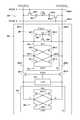
- FIG. 2is a schematic diagram illustrating sensing circuitry in accordance with a number of embodiments of the present disclosure.
- a memory cellcomprises a storage element (e.g., capacitor) and an access device (e.g., transistor).
- transistor 202 - 1 and capacitor 203 - 1comprise a memory cell
- transistor 202 - 2 and capacitor 203 - 2comprise a memory cell
- the memory array 230is a DRAM array of 1T1C (one transistor one capacitor) memory cells.
- the memory cellsmay be destructive read memory cells (e.g., reading the data stored in the cell destroys the data such that the data originally stored in the cell is refreshed after being read).
- the cells of the memory array 230can be arranged in rows coupled by word lines 204 -X (ROW X), 204 -Y (ROW Y), etc., and columns coupled by pairs of complementary sense lines (e.g., data lines DIGIT(n)/DIGIT(n)_).
- the individual sense lines corresponding to each pair of complementary sense linescan also be referred to as data lines 205 - 1 (D) and 205 - 2 (D_) respectively.
- Ddata lines 205 - 1
- D_data lines 205 - 2
- FIG. 2Although only one pair of complementary data lines (e.g., one column) are shown in FIG. 2 , embodiments of the present disclosure are not so limited, and an array of memory cells can include additional columns of memory cells and/or data lines (e.g., 4,096, 8,192, 16,384, etc.).
- Memory cellscan be coupled to different data lines and/or word lines.
- a first source/drain region of a transistor 202 - 1can be coupled to data line 205 - 1 (D)
- a second source/drain region of transistor 202 - 1can be coupled to capacitor 203 - 1
- a gate of a transistor 202 - 1can be coupled to word line 204 -Y.
- a first source/drain region of a transistor 202 - 2can be coupled to data line 205 - 2 (D_)
- a second source/drain region of transistor 202 - 2can be coupled to capacitor 203 - 2
- a gate of a transistor 202 - 2can be coupled to word line 204 -X.
- the cell plateas shown in FIG. 2 , can be coupled to each of capacitors 203 - 1 and 203 - 2 .
- the cell platecan be a common node to which a reference voltage (e.g., ground) can be applied in various memory array configurations.
- a reference voltagee.g., ground
- the memory array 230is coupled to sensing circuitry 250 in accordance with a number of embodiments of the present disclosure.
- the sensing circuitry 250comprises a sense amplifier 206 and a compute component 231 corresponding to respective columns of memory cells (e.g., coupled to respective pairs of complementary data lines).
- the sensing circuitry 250can correspond to sensing circuitry 150 shown in FIG. 1 , for example.
- the sense amplifier 206can be coupled to the pair of complementary sense lines 205 - 1 and 205 - 2 .
- the compute component 231can be coupled to the sense amplifier 206 via pass gates 207 - 1 and 207 - 2 .
- the gates of the pass gates 207 - 1 and 207 - 2can be coupled to logical operation selection logic 213 .
- the logical operation selection logic 213can be configured to include pass gate logic for controlling pass gates that couple the pair of complementary sense lines 205 - 1 and 205 - 2 un-transposed between the sense amplifier 206 and the compute component 231 (as shown in FIG. 2 ) and/or swap gate logic for controlling swap gates that couple the pair of complementary sense lines transposed between the sense amplifier 206 and the compute component 231 (as is discussed later with respect to FIGS. 11, 12, 14, and 15 , for example).
- the logical operation selection logic 213can also be coupled to the pair of complementary sense lines 205 - 1 and 205 - 2 .
- the logical operation selection logic 213can be configured to control pass gates 207 - 1 and 207 - 2 (e.g., to control whether the pass gates 207 - 1 and 207 - 2 are in a conducting state or a non-conducting state) based on a selected logical operation, as described in detail below for various configurations of the logical operation selection logic 213 .
- the sense amplifier 206can be operated to determine a data value (e.g., logic state) stored in a selected memory cell.
- the sense amplifier 206can comprise a cross coupled latch, which can be referred to herein as a primary latch.
- the circuitry corresponding to sense amplifier 206comprises a latch 215 including four transistors coupled to the pair of complementary data lines 205 - 1 and 205 - 2 .
- embodimentsare not limited to this example.
- the latch 215can be a cross coupled latch (e.g., gates of a pair of transistors, such as n-channel transistors (e.g., NMOS transistors) 227 - 1 and 227 - 2 are cross coupled with the gates of another pair of transistors, such as p-channel transistors (e.g., PMOS transistors) 229 - 1 and 229 - 2 ).
- a cross coupled latche.g., gates of a pair of transistors, such as n-channel transistors (e.g., NMOS transistors) 227 - 1 and 227 - 2 are cross coupled with the gates of another pair of transistors, such as p-channel transistors (e.g., PMOS transistors) 229 - 1 and 229 - 2 ).
- the voltage on one of the data lines 205 - 1 (D) or 205 - 2 (D_)will be slightly greater than the voltage on the other one of data lines 205 - 1 (D) or 205 - 2 (D_).
- An ACT signalcan be driven high and the RNL* signal can be driven low to enable (e.g., fire) the sense amplifier 206 .
- the data line 205 - 1 (D) or 205 - 2 (D_) having the lower voltagewill turn on one of the PMOS transistor 229 - 1 or 229 - 2 to a greater extent than the other of PMOS transistor 229 - 1 or 229 - 2 , thereby driving high the data line 205 - 1 (D) or 205 - 2 (D_) having the higher voltage to a greater extent than the other data line 205 - 1 (D) or 205 - 2 (D_) is driven high.
- the data line 205 - 1 (D) or 205 - 2 (D_) having the higher voltagewill turn on one of the NMOS transistor 227 - 1 or 227 - 2 to a greater extent than the other of the NMOS transistor 227 - 1 or 227 - 2 , thereby driving low the data line 205 - 1 (D) or 205 - 2 (D_) having the lower voltage to a greater extent than the other data line 205 - 1 (D) or 205 - 2 (D_) is driven low.
- the data line 205 - 1 (D) or 205 - 2 (D_) having the slightly greater voltageis driven to the voltage of the supply voltage V DD (e.g., through a source transistor (not shown)), and the other data line 205 - 1 (D) or 205 - 2 (D_) is driven to the voltage of the reference voltage (e.g., to ground (GND) through a sink transistor (not shown)).
- V DDsupply voltage
- the other data line 205 - 1 (D) or 205 - 2 (D_)is driven to the voltage of the reference voltage (e.g., to ground (GND) through a sink transistor (not shown)).
- the cross coupled NMOS transistors 227 - 1 and 227 - 2 and PMOS transistors 229 - 1 and 229 - 2serve as a sense amplifier pair, which amplify the differential voltage on the data lines 205 - 1 (D) and 205 - 2 (D_) and operate to latch a data value sensed from the selected memory cell.
- Embodimentsare not limited to the sense amplifier 206 configuration illustrated in FIG. 2 .
- the sense amplifier 206can be current-mode sense amplifier and/or single-ended sense amplifier (e.g., sense amplifier coupled to one data line).
- embodiments of the present disclosureare not limited to a folded data line architecture such as that shown in FIG. 2 .
- the sense amplifier 206can, in conjunction with the compute component 231 , be operated to perform various logical operations using data from an array as input.
- the result of a logical operationcan be stored back to the array without transferring the data via a data line address access (e.g., without firing a column decode signal such that data is transferred to circuitry external from the array and sensing circuitry via local I/O lines).
- a number of embodiments of the present disclosurecan enable performing logical operations and compute functions associated therewith using less power than various previous approaches.
- a number of embodimentscan eliminate the need to transfer data across I/O lines in order to perform compute functions (e.g., between memory and discrete processor), a number of embodiments can enable an increased parallel processing capability as compared to previous approaches.
- the sense amplifier 206can further include equilibration circuitry 214 , which can be configured to equilibrate the data lines 205 - 1 (D) and 205 - 2 (D_).
- the equilibration circuitry 214comprises a transistor 224 coupled between data lines 205 - 1 (D) and 205 - 2 (D_).
- the equilibration circuitry 214also comprises transistors 225 - 1 and 225 - 2 each having a first source/drain region coupled to an equilibration voltage (e.g., V DD /2), where V DD is a supply voltage associated with the array.
- a second source/drain region of transistor 225 - 1can be coupled data line 205 - 1 (D), and a second source/drain region of transistor 225 - 2 can be coupled data line 205 - 2 (D_).
- Gates of transistors 224 , 225 - 1 , and 225 - 2can be coupled together, and to an equilibration (EQ) control signal line 226 .
- activating EQenables the transistors 224 , 225 - 1 , and 225 - 2 , which effectively shorts data lines 205 - 1 (D) and 205 - 2 (D_) together and to the an equilibration voltage (e.g., V DD /2).
- FIG. 2shows sense amplifier 206 comprising the equilibration circuitry 214
- the equilibration circuitry 214may be implemented discretely from the sense amplifier 206 , implemented in a different configuration than that shown in FIG. 2 , or not implemented at all.
- the sensing circuitrye.g., sense amplifier 206 and compute component 231
- the sensing circuitrycan be operated to perform a selected logical operation and initially store the result in one of the sense amplifier 206 or the compute component 231 without transferring data from the sensing circuitry via an I/O line (e.g., without performing a data line address access via activation of a column decode signal, for instance).
- logical operationse.g., Boolean logical functions involving data values
- Boolean logical functionsare used in many higher level functions. Consequently, speed and/or power efficiencies that can be realized with improved logical operations, which can translate into speed and/or power efficiencies of higher order functionalities.
- Described hereinare apparatuses and methods for performing logical operations without transferring data via an input/output (I/O) line and/or without transferring data to a control component external to the array.
- I/Oinput/output
- the apparatuses and methods for performing the logical operationsmay not require amplification of a sense line (e.g., data line, digit line, bit line) pair.
- the compute component 231can also comprise a latch 264 , which can be referred to herein as a secondary latch.
- the secondary latch 264can be configured and operated in a manner similar to that described above with respect to the primary latch 215 , with the exception that the pair of cross coupled p-channel transistors (e.g., PMOS transistors) comprising the secondary latch can have their respective sources coupled to a supply voltage (e.g., V DD ), and the pair of cross coupled n-channel transistors (e.g., NMOS transistors) of the secondary latch can have their respective sources selectively coupled to a reference voltage (e.g., ground), such that the secondary latch is continuously enabled.
- a reference voltagee.g., ground
- FIG. 3is a schematic diagram illustrating sensing circuitry having a compute component with shift capabilities in accordance with a number of embodiments of the present disclosure.
- the compute componentcan have unidirectional shift capabilities.
- FIG. 3shows a number of sense amplifiers 306 coupled to respective pairs of complementary sense lines 305 - 1 and 305 - 2 , and a number of compute components 331 coupled to the sense amplifiers 306 via respective pass gates 307 - 1 and 307 - 2 .
- the gates of the pass gates 307 - 1 and 307 - 2can be controlled by a logical operation selection logic signal, Passd, which can be output from logical operation selection logic (not shown in FIG. 3 for clarity).
- the compute components 331can comprise respective stages (e.g., shift cells) of a loadable shift register configured to shift in one direction (e.g., right as configured in FIG. 3 ).
- the loadable shift registercan be coupled to the pairs of complementary sense lines 305 - 1 and 305 - 2 , with node ST 2 of each stage being coupled to the sense line (e.g., DIGIT(n)) communicating a true data value and with node SF 2 of each stage being coupled to the sense line (e.g., DIGIT(n)_) communicating a complementary (e.g., false) data value.
- the compute components 331e.g., stages of the loadable shift register can comprise a first right-shift transistor 381 having a gate coupled to a first right-shift control line 380 (e.g., “PHASE 1 R”), and a second right-shift transistor 386 having a gate coupled to a second right-shift control line 382 (e.g., “PHASE 2 R”).
- Node ST 2 of each stage of the loadable shift registeris coupled to an input of a first inverter 387 .
- the output of the first inverter 387(e.g., node SF 1 ) is coupled to one source/drain of the second right-shift transistor 386 , and another source/drain of the second right-shift transistor 386 is coupled to an input of a second inverter 388 (e.g., node SF 2 ).
- the output of the second inverter 388(e.g., node ST 1 ) is coupled to one source/drain of the first right-shift transistor 381 , and another source/drain of the first right-shift transistor 381 is coupled to an input of a second inverter (e.g., node SF 2 ) for an adjacent compute component 331 .
- Latch transistor 385has a gate coupled to a LATCH control signal 384 .
- One source/drain of the latch transistor 385is coupled to node ST 2
- another source/drain of the latch transistor 385is coupled to node ST 1 .
- Data values on the respective pairs of complementary sense lines 305 - 1 and 305 - 2can be loaded into the corresponding compute components 331 (e.g., loadable shift register) by causing the pass gates 307 - 1 and 307 - 2 to conduct, such as by causing the Passd control signal to go high.
- Gates that are controlled to have continuityare conducting, and can be referred to herein as being OPEN.
- Gates that are controlled to not have continuityare said to be non-conducting, and can be referred to herein as being CLOSED.
- continuityrefers to a low resistance condition in which a gate is conducting.
- the data valuescan be loaded into the respective compute components 331 by either the sense amplifier 306 overpowering the corresponding compute component 331 (e.g., to overwrite an existing data value in the compute component 331 ) and/or by turning off the PHASE 1 R and PHASE 2 R control signals 380 and 382 and the LATCH control signal 384 .
- a first latche.g., sense amplifier
- the sense amplifier 306can be configured to overpower the compute component 331 by driving the voltage on the pair of complementary sense lines 305 - 1 and 305 - 2 to the maximum power supply voltage corresponding to a data value (e.g., driving the pair of complementary sense lines 305 - 1 and 305 - 2 to the rails), which can change the data value stored in the compute component 331 .
- the compute component 331can be configured to communicate a data value to the pair of complementary sense lines 305 - 1 and 305 - 2 without driving the voltages of the pair of complementary sense lines 305 - 1 and 305 - 2 to the rails (e.g., to V DD or GND).
- the compute component 331can be configured to not overpower the sense amplifier 306 (e.g., the data values on the pair of complementary sense lines 305 - 1 and 305 - 2 from the compute component 331 will not change the data values stored in the sense amplifier 306 until the sense amplifier is enabled.
- the sense amplifier 306e.g., the data values on the pair of complementary sense lines 305 - 1 and 305 - 2 from the compute component 331 will not change the data values stored in the sense amplifier 306 until the sense amplifier is enabled.
- first inverter 387Once a data value is loaded into a compute component 331 of the loadable shift register, the true data value is separated from the complement data value by the first inverter 387 .
- the data valuecan be shifted to the right (e.g., to an adjacent compute component 331 ) by alternate operation of first right-shift transistor 381 and second right-shift transistor 386 , which can be accomplished when the first right-shift control line 380 and the second right-shift control line 382 have periodic signals that go high out-of-phase from one another (e.g., non-overlapping alternating square waves 180 degrees out of phase with one another).
- LATCH control signal 384can be activated to cause latch transistor 385 to conduct, thereby latching the data value into a corresponding compute component 331 of the loadable shift register (e.g., while signal PHASE 1 R remains low and PHASE 2 R remains high to maintain the data value latched in the compute component 331 ).
- FIG. 4Ais a schematic diagram illustrating sensing circuitry having a compute component with shift capabilities in accordance with a number of embodiments of the present disclosure.
- the compute componentcan have bidirectional shift capabilities.
- the compute components 431can comprise a loadable shift register (e.g., with each compute component 431 serving as a respective shift stage) configured to shift in multiple directions (e.g., right and left as configured in FIG. 4A ).
- FIG. 4Ashows a number of sense amplifiers 406 coupled to respective pairs of complementary sense lines 405 - 1 and 405 - 2 , and corresponding compute components 431 coupled to the sense amplifiers 406 via respective pass gates 407 - 1 and 407 - 2 .
- the gates of the pass gates 407 - 1 and 407 - 2can be controlled by respective logical operation selection logic signals, “Passd” and “Passdb,” which can be output from logical operation selection logic (not shown in FIG. 4A for clarity).
- the loadable shift register shown in FIG. 4Ais configured similar to the loadable shift register shown in FIG. 3 .
- a first left-shift transistor 489is coupled between node SF 2 of one loadable shift register to node SF 1 of a loadable shift register corresponding to an adjacent compute component 431 .
- Latch transistor 385 shown in FIG. 3has been replaced by the second left-shift transistor 490 .
- the channel of second left-shift transistor 490is coupled from node ST 2 to node ST 1 .
- the gate of the first left-shift transistor 489is coupled to a first left-shift control line 491 (e.g., “PHASE 1 L”), and the gate of the second left-shift transistor 490 is coupled to a second left-shift control line 492 (e.g., “PHASE 2 L”).
- a first left-shift control line 491e.g., “PHASE 1 L”
- a second left-shift control line 492e.g., “PHASE 2 L”.
- FIG. 4Bis a timing diagram illustrating operation of the sensing circuitry shown in FIG. 4A in accordance with a number of embodiments of the present disclosure.
- FIG. 4Bshows waveforms for signals PHASE 1 R (e.g., on first right-shift control line 480 shown in FIG. 4A ), PHASE 2 R (e.g., on second right-shift control line 481 shown in FIG. 4A ), PHASE 1 L (e.g., on first left-shift control line 491 shown in FIG. 4A ), and PHASE 2 L (e.g., on second left-shift control line 492 shown in FIG. 4A ) to accomplish shifting data left by 6 sensing circuitries (e.g., by 6 compute components 431 ).
- the first 491 and second 492 left-shift control linescan communicate control signals similar to those described with respect to FIG. 3 for the first and second right-shift control lines above.
- transistors 381 and 386 shown in FIG. 3are off (e.g., no continuity) and data moves left by a different path.
- the control signals on the first 491 and second 492 left-shift control linesoperate the loadable shift register to move data values to the left through transistors 489 and 490 , as shown in FIG. 4A .
- Data from node ST 2is inverted through inverter 387 shown in FIG. 3 to node SF 1 , as previously described.
- Activation of PHASE 1 L signalcauses the data from node SF 1 to move left through transistor 489 to node SF 2 of a left-adjacent compute component 431 .
- Data from node SF 2is inverted through inverter 388 shown in FIG. 3 to node ST 1 , as previously described.
- activation of PHASE 2 L signalcauses the data from node ST 1 to move through transistor 490 left to node ST 2 completing a left shift.
- Datacan be “bubbled” to the left by repeating the sequence multiple times (e.g., for each of the six iterations) as shown in FIG. 4B .
- Latching of the data valuecan be accomplished by maintaining the PHASE 2 L signal 492 in an activated (e.g., high) state such that second left-shift transistor 490 is conducting, by maintaining the PHASE 1 L signal 491 in a deactivated (e.g., low) state such that first left-shift transistor 489 is not conducting, by maintaining the PHASE 1 R signal 480 in a deactivated state, and by maintaining the PHASE 2 R signal 481 in an activated state, which provides feedback associated with latching the data value while electrically isolating the compute components 431 from each other.
- an activatede.g., high
- a deactivatede.g., low
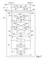
- FIG. 5is a schematic diagram illustrating sensing circuitry having selectable logical operation selection logic in accordance with a number of embodiments of the present disclosure.
- FIG. 5shows a sense amplifier 506 coupled to a pair of complementary sense lines 505 - 1 and 505 - 2 , and a compute component 531 coupled to the sense amplifier 506 via pass gates 507 - 1 and 507 - 2 .
- the gates of the pass gates 507 - 1 and 507 - 2can be controlled by a logical operation selection logic signal (e.g., Passd), which can be output from logical operation selection logic 513 - 1 .
- a logical operation selection logic signale.g., Passd
- FIG. 5shows the compute component 531 labeled “A” and the sense amplifier 506 labeled “B” to indicate that the data value stored in the compute component 531 represents the “A” data value and the data value stored in the sense amplifier 506 represents the “B” data value shown in logic tables described below.
- logical operation selection logic 513 - 1can comprise a number of logic gates configured to control pass gates 507 - 1 and 507 - 2 based on logic selection signal(s) applied to a first logic select control line 532 - 1 (e.g., FS 1 ) and applied to a second logic select control line 532 - 2 (e.g., F S 2 ). As shown in FIG. 5 , the first logic select control line 532 - 1 is one input to AND gate 534 , and the second logic select control line 532 - 2 is one input to AND gate 533 .
- a true data value from the compute component 531is a second input 505 - 3 to AND gate 534 , and the true data value is inverted via inverter 536 such that an inverted true data value (e.g., complement data value) from the compute component 531 is a second input to AND gate 533 .
- Outputs of AND gates 533 and 534are inputs to OR gate 535 , and the output of OR gate 535 , which can correspond to the Passd signal shown in FIG. 3 , is coupled to the gates of pass transistors 507 - 1 and 507 - 2 .
- FIG. 6is a schematic diagram illustrating sensing circuitry having selectable logical operation selection logic in accordance with a number of embodiments of the present disclosure.
- FIG. 6shows a sense amplifier 606 coupled to a pair of complementary sense lines 605 - 1 and 605 - 2 , and a compute component 631 coupled to the sense amplifier 606 via pass gates 607 - 1 and 607 - 2 .
- the gates of the pass gates 607 - 1 and 607 - 2can be controlled by a logical operation selection logic signal (e.g., Passd), which can be output from logical operation selection logic 613 - 2 .
- FIG. 6shows the compute component 631 labeled “A” and the sense amplifier 606 labeled “B” to correspond to the data value stored therein with respect to the logic tables shown in FIGS. 7 and 8 .
- a logical operation selection logic signale.g., Passd
- Logical operation selection logic 613 - 2comprises one portion 613 - 1 configured the same as described with respect to logical operation selection logic 513 - 1 shown in FIG. 5 .
- logical operation selection logic 613 - 2comprises logic gates that drive swap gates 642 .
- Swap gates 642comprise a pair of transistors that couple the true sense line on one side of the pass gates 607 - 1 and 607 - 2 to the complement sense line on the other side of the pass gates 607 - 1 and 607 - 2 .
- pass gates 607 - 1 and 607 - 2are CLOSED (e.g., not conducting) and swap gates 642 are OPEN (e.g., conducting)
- the true and complement data valuesare swapped in communication to the compute component 631 , such that the true data value from the sense amplifier 606 is loaded into the compute component 631 as the complement data value, and the complement data value from the sense amplifier 606 is loaded into the compute component 631 as the true data value.
- logical operation selection logic 613 - 2can comprise a number of logic gates configured to control the swap gates 642 based on additional logic selection signal(s) applied to a third logic select control line 637 (e.g., FS 3 ) and applied to a fourth logic select control line 638 (e.g., FS 4 ).
- a third logic select control line 637e.g., FS 3
- a fourth logic select control line 638e.g., FS 4
- the third logic select control line 637is one input to AND gate 640
- the fourth logic select control line 638is one input to AND gate 639 .
- a true data value from the compute component 631is a second input to AND gate 640 , and the true data value is inverted via inverter 643 such that an inverted true data value (e.g., complement data value) from the compute component 631 is a second input to AND gate 639 .
- Outputs of AND gates 639 and 640are inputs to OR gate 641 , and the output of OR gate 641 is coupled to the gates of the swap transistors 642 .
- Logic selection signals FS 1 , FS 2 , FS 3 , and FS 4can be used to select a logical operation to be implemented by the sensing circuitry 650 based on the data value stored in the compute component (e.g., the “A” data value) and the data value stored in the sense amplifier (e.g., the “B” data value).
- the results of logical operations for various combinations of the data value stored in the compute component (e.g., “A”), the data value stored in the sense amplifier (e.g., “B”), and the states of the logic selection signals FS 1 , FS 2 , FS 3 , and FS 4is shown in FIGS. 7 and 8 below.
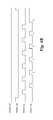
- FIG. 7is a logic table illustrating selectable logic operation results implemented by a sensing circuitry with a logic operation result in a compute component (e.g., an accumulator) after a sense amplifier is enabled in accordance with a number of embodiments of the present disclosure.
- FIG. 7shows a resultant data value that is initially stored in the compute component (e.g., 631 shown in FIG. 6 ) after the sense amplifier 606 is enabled (e.g., fired).
- Starting data valuese.g., operands
- FIGS. 16-18For instance, as described in FIGS.
- a first operand(e.g., “A”) can be read from a memory array and stored in a latch of compute component 631 , and a selected logical operation between the first operand and a second operand (e.g., “B”), which can also be read from the memory array, can be performed based on the appropriate control signals corresponding to the selected operation being provided to the operation selection control logic (e.g., 613 - 2 ).
- whether the result of a selected logical operation is initially stored in the compute component or the sense amplifiercan depend on when the operation selection logic is enabled (e.g., whether the control signals FS 1 , FS 2 , FS 3 , and FS 4 are enabled before or after the sense amplifier being enabled in association with sensing the second operand). For instance, in FIG. 7 , “RESULT IN ACCUM—(AFTER SENSE AMP FIRE)” indicates that the control signals corresponding to the selected logic operation are enabled after the sense amplifier is enabled, such that the result of the selected logic operation is initially stored in the compute component (e.g., accumulator latch). Similarly, in FIG.
- “RESULT IN SENSE AMP—(BEFORE SENSE AMP FIRE)”indicates that the control signals corresponding to the selected logic operation are enabled before the sense amplifier is enabled, such that the result of the selected logic operation is initially stored in the sense amplifier, as described further below.
- the logic table illustrated in FIG. 7shows the starting data value stored in the compute component 631 in column A at 744 , and shows the starting data value stored in the sense amplifier 606 in column B at 745 .
- the various combination of logic selection signals FS 1 , FS 2 , FS 3 , and FS 4is shown in FIG. 7 in the column headings in row 746 .
- the column heading of “0110”indicates that the results in that column correspond to logic selection signal FS 4 being a “0,” logic selection signal FS 3 being a “1,” logic selection signal FS 2 being a “1,” and logic selection signal FS 1 being a “0.”
- results for each combination of starting data values in the compute component 631 (“A”) and in the sense amplifier 606 (“B”)can be summarized by the logical operation shown for each column in row 747 .
- results for the values of FS 4 , F 3 , FS 2 , and FS 1 of “0000”are summarized as “A” since the result (initially stored in the compute component after the sense amplifier fires) is the same as the starting value in the compute component.
- Other columns of resultsare similarly annotated in row 747 , where “A*B” intends A AND B, “A+B” intends A OR B, and “AXB” intends A XOR B.
- a bar over a data value or a logical operationindicates an inverted value of the quantity shown under the bar.
- AXB barintends not A XOR B, which is also A XNOR B.
- Some combination of the values of FS 4 , F 3 , FS 2 , and FS 1may not be implementable with the circuit shown in FIG. 6 (e.g., since such combinations can result in the sense lines 605 - 1 and 605 - 2 being shorted together), and these are indicated at columns 748 by “X”s in place of binary data value results for a particular combination.
- FIG. 8is a logic table illustrating selectable logic operation results implemented by a sensing circuitry with a logic operation result in a sense amplifier after the sense amplifier is enabled in accordance with a number of embodiments of the present disclosure.
- FIG. 8shows a resultant data value that is initially stored in the sense amplifier (e.g., 606 shown in FIG. 6 ) after the sense amplifier 606 is enabled corresponding to the various combination of logic selection signals FS 4 , FS 3 , FS 2 , and FS 1 .
- the logic table illustratedis arranged similar to that described with respect to FIG. 7 , with the starting data value stored in the compute component 631 shown in column A at 844 , and the starting data value stored in the sense amplifier 606 shown in column B at 845 .
- logic selection signals FS 1 , FS 2 , FS 3 , and FS 4is shown in FIG. 8 in the column headings shown in row 846 , and the logical operation represented by each respective column of results shown in the column subheading at row 847 .
- the logical operations summarized in the logic table illustrated in FIG. 8reflects a logical operation result initially stored in the sense amplifier 606 after the sense amplifier is enabled (e.g., with the logic selection signals corresponding to the selected logic operation being provided to the selection logic before the sense amplifier is enabled).
- the logical operations summarized in the logic table illustrated in FIG. 8include several different logical operations from those shown in the logic table illustrated in FIG.
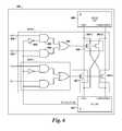
- FIG. 9is a schematic diagram illustrating sensing circuitry having selectable logical operation selection logic in accordance with a number of embodiments of the present disclosure.
- FIG. 9shows a sense amplifier 906 coupled to a pair of complementary sense lines 905 - 1 and 905 - 2 , and a compute component 931 coupled to the sense amplifier 906 via pass gates 907 - 1 and 907 - 2 .
- the gates of the pass gates 907 - 1 and 907 - 2can be controlled by a logical operation selection logic signal, PASS, which can be output from logical operation selection logic 913 - 3 .
- FIG. 9shows a sense amplifier 906 coupled to a pair of complementary sense lines 905 - 1 and 905 - 2 , and a compute component 931 coupled to the sense amplifier 906 via pass gates 907 - 1 and 907 - 2 .
- the gates of the pass gates 907 - 1 and 907 - 2can be controlled by a logical operation selection logic signal, PASS, which can
- FIG. 9shows the compute component 931 labeled “A” and the sense amplifier 906 labeled “B” to indicate that the data value stored in the compute component 931 is the “A” data value and the data value stored in the sense amplifier 906 is the “B” data value shown in the logic tables illustrated with respect to FIG. 10 .
- the sensing circuitry 950 shown in FIG. 9is similar to that shown for the sensing circuitry 250 shown in FIG. 2 with detail added with respect to the logical operation selection logic 913 - 3 .
- Logical operation selection logic 913 - 3provides another logic configuration for selecting a particular logical operation to implement.
- Logical operation selection logic 913 - 3comprises a first enable transistor 952 coupled between an AND logic signal control line and the gates of the pass transistors 907 - 1 and 907 - 2 (e.g., a first source/drain of transistor 952 is coupled to the AND signal, and a second source/drain of the transistor 952 is coupled to the gates of transistors 907 - 1 and 907 - 2 ).
- the gate of the first enable transistor 952is coupled through a first isolation transistor 950 - 1 to node “S” of the latch of compute component 931 .
- the gate of the first isolation transistor 950 - 1is coupled to an ISO control signal (e.g., to a control line to which the ISO signal is applied).
- ISOISO
- the name of a particular signale.g., “ISO”
- Logical operation selection logic 913 - 3also comprises a second enable transistor 954 coupled between an OR logic signal control line and the gates of the pass transistors 907 - 1 and 907 - 1 .
- the gate of the second enable transistor 954is coupled through a second isolation transistor 950 - 2 to node “S*” of the latch of compute component 931 .
- the gate of the second isolation transistor 950 - 2is also coupled to the ISO control signal.
- a particular logical operation to be performed(e.g., between an “A” data value in the compute component and a “B” data value in the sense amp 906 ) can be selected based on the state of the AND logic signal and the state of the OR logic signal when the ISO control signal is deactivated (e.g., brought low to isolate the gates of the enable transistors 952 and 954 from S and S*, respectively). Isolating the gates of the first enable transistor 952 and the second enable transistor 954 from the respective nodes S and S* of the compute component 931 leaves the corresponding voltages dynamically on the gates of respective transistors 952 and 954 .
- the state of the PASS signaldepends on the selected states of the AND and OR signals as well as on the value stored in compute component 931 (e.g., the voltages corresponding to S and S*) when ISO is deactivated.
- the value stored in compute component 931e.g., the voltages corresponding to S and S*
- the selection of a particular logical operation to be implementedis discussed further with respect to FIG. 10 .
- FIG. 10is a logic table illustrating selectable logic operation results implemented by a sensing circuitry in accordance with a number of embodiments of the present disclosure.
- the logic table illustrated in FIG. 10shows the starting data value stored in the compute component 931 shown in column A at 1044 , and the starting data value stored in the sense amplifier 906 shown in column B at 1045 .
- the column headings for the Logic Table 10 - 1refer to the state of the pass gates 907 - 1 and 907 - 2 , which can be controlled to be OPEN (e.g., conducting) or CLOSED (e.g., not conducting) depending on the state of the AND logic signal, the state of the OR logic signal, and the data values on the pair of complementary sense lines 905 - 1 and 905 - 2 when the ISO control signal is activated/deactivated.
- OPENe.g., conducting
- CLOSEDe.g., not conducting
- the AND logic signalhas to be activated and the data value on the true sense line has to be high, or the OR logic signal has to be activated and the data value on the complement sense line has to be high, otherwise the pass gates 907 - 1 and 907 - 2 will be CLOSED (e.g., not conducting).
- the logic tables illustrated in FIG. 10reflect a result (e.g., of a logical operation performed between a data value A and a data value B) that is initially stored in the compute component 931 . Therefore, when the pass gates 907 - 1 and 907 - 2 are controlled to be CLOSED (e.g., not conducting), the result initially stored in the compute component 931 is the same as the starting data value in the compute component 931 .
- the sense sensing circuitry 950is configured such that the sense amplifier 906 can overpower the compute component 931 as shown in the “NOT OPEN” column 1056 of the Logic Table 10 - 1 , the result initially stored in the compute component 931 is the same as the starting data value in the sense amplifier 906 when the pass gates 907 - 1 and 907 - 2 are controlled to be OPEN (e.g., conducting) as shown in the “OPEN PASS” column 1057 of the Logic Table 10 - 1 .
- OPENe.g., conducting
- each of the two columns (e.g., “NOT OPEN” and “OPEN PASS”) of the upper portion 1049 of Logic Table 10 - 1can be combined with each of the two columns of the lower portion 1050 of Logic Table 10 - 1 to provide four different result combinations, corresponding to four different logical operations, as indicated by the various connecting paths shown at 1058 , and as summarized in Logic Table 10 - 2 illustrated in FIG. 10 .
- Logic Table 10 - 2 illustrated in FIG. 10shows the various settings for the OR logic signal in row 1046 - 1 and the AND logic signal in row 1046 - 2 for the various combinations of the starting data value stored in the compute component 931 (“A”) and the starting data value stored in the sense amplifier 906 (“B”).
- the pass gates 907 - 1 and 907 - 2are controlled to be CLOSED (e.g., not conducting) and the result in the compute component 931 is the same as the starting data value in the compute component 931 .
- FIG. 11is a schematic diagram illustrating sensing circuitry having selectable logical operation selection logic in accordance with a number of embodiments of the present disclosure.
- FIG. 11shows a sense amplifier 1106 coupled to a pair of complementary sense lines 1105 - 1 and 1105 - 2 , and a compute component 1131 coupled to the sense amplifier 1106 via pass gates 1107 - 1 and 1107 - 2 .
- the gates of the pass gates 1107 - 1 and 1107 - 2can be controlled by a logical operation selection logic signal, PASS, which can be output from logical operation selection logic 1113 - 4 .
- FIG. 11shows a logical operation selection logic signal, PASS, which can be output from logical operation selection logic 1113 - 4 .
- FIG. 11shows the compute component 1131 labeled “A” and the sense amplifier 1106 labeled “B” to indicate that the data value stored in the compute component 1131 is the “A” data value and the data value stored in the sense amplifier 1106 is the “B” data value shown in the logic tables illustrated with respect to FIG. 13 .
- logical operation selection logic 1113 - 4comprises a portion configured the same as described with respect to logical operation selection logic 913 - 3 shown in FIG. 9 .
- logical operation selection logic 1113 - 4comprises swap gates 1142 .
- Swap gates 1142comprise a pair of transistors that couple the true sense line on one side of the pass gates 1107 - 1 and 1107 - 2 to the complement sense line on the other side of the pass gates 1107 - 1 and 1107 - 2 .
- pass gates 1107 - 1 and 1107 - 2are OPEN (e.g., conducting) and swap gates 1142 are CLOSED (not conducting)
- the true and complement data valuesare swapped in communication to the compute component 1131 , such that the true data value from the sense amplifier 1106 is loaded into the compute component 1131 as the complement data value, and the complement data value from the sense amplifier 1106 is loaded into the compute component 1131 as the true data value.
- the gates of swap gates 1142are coupled to an inverted PASS (e.g., “PASS*”) signal control line.
- PASS*inverted PASS
- FIG. 12is a schematic diagram illustrating sensing circuitry having selectable logical operation selection logic in accordance with a number of embodiments of the present disclosure.
- FIG. 12shows a sense amplifier 1206 coupled to a pair of complementary sense lines 1205 - 1 and 1205 - 2 , and a compute component 1231 coupled to the sense amplifier 1206 via pass gates 1207 - 1 and 1207 - 2 .
- the gates of the pass gates 1207 - 1 and 1207 - 2can be controlled by a logical operation selection logic signal, PASS, which can be output from logical operation selection logic 1213 - 5 .
- FIG. 12shows the compute component 1231 labeled “A” and the sense amplifier 1206 labeled “B” to indicate that the data value stored in the compute component 1231 is the “A” data value and the data value stored in the sense amplifier 1206 is the “B” data value shown in the logic tables illustrated with respect to FIG. 13 .
- the sensing circuitry illustrated in FIG. 12is similar to the sensing circuitry 1150 illustrated in FIG. 11 with the addition of logic to drive the swap transistors (and some relabeling of components for additional clarity).
- the logical operation selection logic 1213 - 5includes the swap gates 1242 , as well as logic to drive the swap gates 1242 .
- the logical operation selection logic 1213 - 5includes four logic selection transistors: logic selection transistor 1262 coupled between the gates of the swap transistors 1242 and a TF signal control line, logic selection transistor 1252 coupled between the gates of the pass gates 1207 - 1 and 1207 - 2 and a TT signal control line, logic selection transistor 1254 coupled between the gates of the pass gates 1207 - 1 and 1207 - 2 and a FT signal control line, and logic selection transistor 1264 coupled between the gates of the swap transistors 1242 and a FF signal control line.
- Gates of logic selection transistors 1262 and 1252are coupled to the true sense line through isolation transistor 1250 - 1 (having a gate coupled to an ISO signal control line).
- Gates of logic selection transistors 1264 and 1254are coupled to the complementary sense line through isolation transistor 1250 - 2 (also having a gate coupled to an ISO signal control line).
- Logic selection transistors 1252 and 1254are arranged similarly to transistor 952 (coupled to an AND signal control line) and transistor 954 (coupled to an OR signal control line) respectively, as shown in FIGS. 9 and 10 . Operation of logic selection transistors 1262 and 1264 are similar based on the state of the TF and FF selection signals and the data values on the respective complementary sense lines at the time the ISO signal is activated/deactivated. Logic selection transistors 1262 and 1264 also operate in a similar manner to control the swap transistors 1242 .
- the swap transistors 1242For instance, to OPEN (e.g., turn on) the swap transistors 1242 , either the TF control signal is activated (e.g., high) with data value on the true sense line being “1,” or the FF control signal is activated (e.g., high) with the data value on the complement sense line being “1.” If either the respective control signal or the data value on the corresponding sense line (e.g., sense line to which the gate of the particular logic selection transistor is coupled) is not high, then the swap transistors 1242 will not be OPENed despite conduction of a particular logic selection transistor 1262 and 1264 .
- the PASS* control signalis not necessarily complementary to the PASS control signal. It is possible for the PASS and PASS* control signals to both be activated or both be deactivated at the same time. However, activation of both the PASS and PASS* control signals at the same time shorts the pair of complementary sense lines together. Logical operations results for the sensing circuitry illustrated in FIG. 12 are summarized in the logic table illustrated in FIG. 13 .
- FIG. 13is a logic table illustrating selectable logic operation results implemented by a sensing circuitry (e.g., sensing circuitry 1250 shown in FIG. 12 ) in accordance with a number of embodiments of the present disclosure.
- the four logic selection control signalse.g., TF, TT, FT, and FF
- TF, TT, FT, and FFin conjunction with a particular data value present on the complementary sense lines, can be used to select one of a plurality of logical operations to implement involving the starting data values stored in the sense amplifier 1206 and compute component 1231 .
- the four control signals(e.g., TF, TT, FT, and FF), in conjunction with a particular data value present on the complementary sense lines (e.g., on nodes S and S*), controls the pass gates 1207 - 1 and 1207 - 2 and swap transistors 1242 , which in turn affects the data value in the compute component 1231 and/or sense amplifier 1206 before/after firing.
- the capability to selectably control the swap transistors 1242facilitates implementing logical operations involving inverse data values (e.g., inverse operands and/or inverse result), among others.
- the control signals TT, TF, FT, and FF described in FIGS. 12 and 13correspond to respective control signals FS 1 , FS 3 , FS 2 , and FS 4 described in FIGS. 6, 7, and 8 .
- Logic Table 13 - 1 illustrated in FIG. 13shows the starting data value stored in the compute component 1231 shown in column A at 1344 , and the starting data value stored in the sense amplifier 1206 shown in column B at 1345 .
- the other 3 column headings in Logic Table 13 - 1refer to the state of the pass gates 1207 - 1 and 1207 - 2 and the swap transistors 1242 , which can respectively be controlled to be OPEN or CLOSED depending on the state of the four logic selection control signals (e.g., TF, TT, FT, and FF), in conjunction with a particular data value present on the pair of complementary sense lines 1205 - 1 and 1205 - 2 when the ISO control signal is asserted.
- logic selection control signalse.g., TF, TT, FT, and FF
- the “NOT OPEN” columncorresponds to the pass gates 1207 - 1 and 1207 - 2 and the swap transistors 1242 both being in a non-conducting condition
- the “OPEN TRUE” columncorresponds to the pass gates 1207 - 1 and 1207 - 2 being in a conducting condition
- the “OPEN INVERT” columncorresponds to the swap transistors 1242 being in a conducting condition.
- the configuration corresponding to the pass gates 1207 - 1 and 1207 - 2 and the swap transistors 1242 both being in a conducting conditionis not reflected in Logic Table 13 - 1 since this results in the sense lines being shorted together.
- each of the three columns of the upper portion of Logic Table 13 - 1can be combined with each of the three columns of the lower portion of Logic Table 13 - 1 to provide nine (e.g., 3 ⁇ 3) different result combinations, corresponding to nine different logical operations, as indicated by the various connecting paths shown at 1375 .
- the nine different selectable logical operations that can be implemented by the sensing circuitry 1250are summarized in Logic Table 13 - 2 .
- the columns of Logic Table 13 - 2show a heading 1380 that includes the states of logic selection control signals (e.g., FF, FT, TF, TT).
- logic selection control signalse.g., FF, FT, TF, TT
- the state of a first logic selection control signale.g., FF
- the state of a second logic selection control signale.g., FT
- the state of a third logic selection control signale.g., TF
- the state of a fourth logic selection control signale.g., TT
- the particular logical operation corresponding to the resultsis summarized in row 1347 .
- FIG. 14is a schematic diagram illustrating sensing circuitry having selectable logical operation selection logic in accordance with a number of embodiments of the present disclosure.
- FIG. 14shows a number of sense amplifiers 1406 coupled to respective pairs of complementary sense lines 1405 - 1 and 1405 - 2 , and a corresponding number of compute component 1431 coupled to the sense amplifiers 1406 via pass gates 1407 - 1 and 1407 - 2 .
- the gates of the pass gates 1407 - 1 and 1407 - 2can be controlled by a logical operation selection logic signal, PASS.
- an output of the logical operation selection logic 1413 - 6can be coupled to the gates of the pass gates 1407 - 1 and 1407 - 2 .
- the compute components 1431can comprise respective stages (e.g., shift cells) of a loadable shift register configured to shift data values left and right as described in detail with respect to FIG. 4A .
- each compute component 1431 (e.g., stage) of the shift registercomprises a pair of right-shift transistors 1481 and 1486 (e.g., similar to respective right-shift transistors 481 and 486 shown in FIG. 3 ), a pair of left-shift transistors 1489 and 1490 (e.g., similar to respective left-shift transistors 489 and 490 shown in FIG.
- the signals PHASE 1 R, PHASE 2 R, PHASE 1 L, and PHASE 2 Lcan be applied to respective control lines 1482 , 1483 , 1491 and 1492 to enable/disable feedback on the latches of the corresponding compute components 1431 in association with performing logical operations and/or shifting data in accordance with embodiments described herein. Examples of shifting data (e.g., from a particular compute component 1431 to an adjacent compute component 1431 ) is described further below with respect to FIGS. 16 and 17 .
- the sensing circuitry illustrated in FIG. 14is configured and operates similarly to the sensing circuitry illustrated in FIG. 12 with the exception of the compute components 1431 being configured as a loadable shift register.
- the logical operation selection logic 1413 - 6includes the swap gates 1442 , as well as logic to control the pass gates 1407 - 1 and 1407 - 2 and the swap gates 1442 .
- the logical operation selection logic 1413 - 6includes four logic selection transistors: logic selection transistor 1462 coupled between the gates of the swap transistors 1442 and a TF signal control line, logic selection transistor 1452 coupled between the gates of the pass gates 1407 - 1 and 1407 - 2 and a TT signal control line, logic selection transistor 1454 coupled between the gates of the pass gates 1407 - 1 and 1407 - 2 and a FT signal control line, and logic selection transistor 1464 coupled between the gates of the swap transistors 1442 and a FF signal control line.
- Gates of logic selection transistors 1462 and 1452are coupled to the true sense line through isolation transistor 1450 - 1 (having a gate coupled to an ISO signal control line). Gates of logic selection transistors 1464 and 1454 are coupled to the complementary sense line through isolation transistor 1450 - 2 (also having a gate coupled to an ISO signal control line).
- FIGS. 16 and 17illustrate timing diagrams associated with performing logical operations and shifting operations using the sensing circuitry shown in FIG. 14 .
- FIG. 15is a schematic diagram illustrating sensing circuitry having selectable logical operation selection logic in accordance with a number of embodiments of the present disclosure.
- FIG. 15shows a number of sense amplifiers 1506 coupled to respective pairs of complementary sense lines 1505 - 1 and 1505 - 2 , and corresponding compute components 1531 coupled to the respective sense amplifiers 1506 via pass gates 1507 - 1 and 1507 - 2 .
- the compute components 1531can comprise a loadable shift register configured to shift data values left and right as described in detail with respect to FIGS. 4A, 16, and 17 .
- the pass gates 1507 - 1 and 1507 - 2can be controlled by a logical operation selection logic signal, PASS.
- the sensing circuitry shown in FIG. 15also shows a logical operation selection logic 1513 - 7 coupled to a number of logic selection control input control lines, including LOGIC 1 , LOGIC 2 , LOGIC 3 , LOGIC 4 , SFISO, and STISO. Selection of a logical operation from a plurality of logical operations is determined from the condition of logic selection control signals on the logic selection control input control lines, as well as the data values present on the pair of complementary sense lines 1505 - 1 and 1505 - 2 when the isolation transistors are enabled via the ISO control signal being activated.
- one isolation transistoris coupled between a control signal line communicating a SFISO control signal and the SF 1 node of the loadable shift register of the compute component 1531 .
- Another isolation transistoris coupled between a control signal line communicating a STISO control signal and the ST 1 node of the loadable shift register of the compute component 1531 .
- Gates of the isolation transistorsare coupled to a control signal line communicating the ISO control signal. If the SFISO control signal is activated (e.g., high) when the ISO control signal is activated to OPEN the isolation transistors, a data value corresponding to the high SFISO control signal is loaded into the complement portion of the loadable shift register of the compute component 1531 .
- STISO control signalis activated (e.g., high) when the ISO control signal is activated to OPEN the isolation transistors, a data value corresponding to the high STISO control signal is loaded into the true portion of the loadable shift register of an adjacent compute component 1531 .
- the pass gates 1507 - 1 and 1507 - 2are OPEN
- data values on the pair of complementary sense lines 1505 - 1 and 1505 - 2are passed to the compute component 1531 and thereby loaded into the loadable shift register.
- the data values on the pair of complementary sense lines 1505 - 1 and 1505 - 2can be the data value stored in the sense amplifier 1506 when the sense amplifier is fired.
- the logical operation selection logic signal, PASSis high to OPEN the pass gates 1507 - 1 and 1507 - 2 , when logic selection control signal LOGIC 1 is activated and the SFISO control signal is not activated (e.g., is low, which turns on the p-channel logic selection transistor having a gate coupled to the SFiso control signal line.
- the logical operation selection logic signal, PASSis also high to OPEN the pass gates 1507 - 1 and 1507 - 2 , when logic selection control signal LOGIC 2 is activated and the STISO control signal is not activated (e.g., is low, which turns on the p-channel logic selection transistor having a gate coupled to the STISO control signal line.
- FIG. 15Similar logic is shown in FIG. 15 coupled to the PASS* logical operation selection logic signal, which is high to OPEN the swap gates 1542 .
- the logic shown in FIG. 15 coupled to the PASS* logical operation selection logic signalmirrors the logic configuration coupled to the PASS logical operation selection logic signal.
- FIG. 15shows swap transistors 1542 configured to swap the orientation of the pair of complementary sense lines 1505 - 1 and 1505 - 2 between the sense amplifier 1506 and the compute component 1531 (in a similar manner as previously described with respect to the configuration of swap transistor 1242 illustrated in FIG. 12 ).
- swap transistors 1542When the swap transistors 1542 are OPEN, data values on the pair of complementary sense lines 1505 - 1 and 1505 - 2 on the sense amplifier 1506 side of the swap transistors 1542 are oppositely-coupled to the pair of complementary sense lines 1505 - 1 and 1505 - 2 on the compute component 1531 side of the swap transistors 1542 , and thereby loaded into the loadable shift register of the compute component 1531 .
- the logical operation selection logic signal PASS*is activated (e.g., high) to OPEN the swap transistors 1542 when logic selection control signal LOGIC 3 is activated and the STISO control signal is not activated (e.g., is low, which turns on the p-channel logic selection transistor having a gate coupled to the STISO control signal line).
- the logical operation selection logic signal PASS*is also high to OPEN the swap transistors 1542 when logic selection control signal LOGIC 4 is activated and the SFISO control signal is not activated (e.g., is low, which turns on the p-channel logic selection transistor having a gate coupled to the SFiso control signal line.
- the gates of the swap transistors 1542can also be selectably grounded to ensure the swap transistors 1542 are CLOSED via a transistor having a gate coupled to the PREFUNC control signal line and arranged to couple the logic signal PASS* to a reference potential.
- activation of the PREFUNC control signal linecauses the pass gates 1507 - 1 and 1507 - 2 and the swap transistors 1542 to be CLOSED (e.g., non-conducting).
- the PREFUNC control signalcan be activated, for example, during loadable shift register shift left/right operations.
- the LOGIC 1 , LOGIC 2 , LOGIC 3 , LOGIC 4 , SFISO, and STISO control signalscan operate to select a logical function to implement based on the data value (“B”) in the sense amplifier 1506 and the data value (“A”) in the compute component 1531 in a different manner than the TF, TT, FT, and FF control signals described with respect to FIGS. 12 and 14 .
- the LOGIC 1 , LOGIC 2 , LOGIC 3 , LOGIC 4 , SFISO, and STISO control signalsare configured to select the logical function to implement independent from the data value present on the pair of complementary sense lines 1505 - 1 and 1505 - 2 (although the result of the implemented logical operation can be dependent on the data value present on the pair of complementary sense lines 1505 - 1 and 1505 - 2 .
- the LOGIC 1 , LOGIC 2 , LOGIC 3 , LOGIC 4 , SFISO, and STISO control signalsselect the logical operation to implement directly since the data value present on the pair of complementary sense lines 1505 - 1 and 1505 - 2 is not passed through logic to operate the gates of the pass gates 1507 - 1 and 1507 - 2 .
- the sensing circuitry illustrated in FIG. 15is configured to select one of a plurality of logical operations to implement directly from the four logic selection control signals (e.g., logical operation selection is not dependent on the data value present on the pair of complementary sense lines). As was described with respect to FIG. 12 , some combinations of the logic selection control signals can cause both the pass gates 1507 - 1 and 1507 - 2 and swap transistors 1542 to be OPEN at the same time, which shorts the pair of complementary sense lines 1505 - 1 and 1505 - 2 together. According to a number of embodiments of the present disclosure, the logical operations which can be implemented by the sensing circuitry illustrated in FIG. 15 can be the logical operations summarized in the logic tables shown in FIG. 13 .
- FIG. 16illustrates a timing diagram associated with performing a logical AND operation and a shifting operation using the sensing circuitry in accordance with a number of embodiments of the present disclosure.
- FIG. 16includes waveforms corresponding to signals EQ, ROW X, ROW Y, SENSE AMP, TF, TT, FT, FF, PHASE 1 R, PHASE 2 R, PHASE 1 L, PHASE 2 L, ISO, Pass, Pass*, DIGIT, and DIGIT_.
- the EQ signalcorresponds to an equilibrate signal associated with a sense amplifier (e.g., EQ 226 shown in FIG. 2 ).
- the ROW X and ROW Y signalscorrespond to signals applied to respective access line (e.g., access lines 204 -X and 204 -Y shown in FIG. 2 ) to access a selected cell (or row of cells).
- the SENSE AMP signalcorresponds to a signal used to enable/disable a sense amplifier (e.g., sense amplifier 1406 ).
- the TF, TT, FT, and FF signalscorrespond to logic selection control signals such as those shown in FIGS. 12 and 14 (e.g., signals coupled to logic selection transistors 1262 / 1462 , 1252 / 1452 , 1254 / 1454 , and 1264 / 1464 ).
- the PHASE 1 R, PHASE 2 R, PHASE 1 L, and PHASE 2 L signalscorrespond to the control signals (e.g., clock signals) provided to respective control lines 1482 , 1483 , 1491 and 1492 shown in FIG. 14 .
- the ISO signalcorresponds to the signal coupled to the gates of the isolation transistors 1450 - 1 and 1450 - 2 shown in FIG. 14 .
- the PASS signalcorresponds to the signal coupled to the gates of pass transistors 1407 - 1 and 1407 - 2 shown in FIG. 14
- the PASS* signalcorresponds to the signal coupled to the gates of the swap transistors 1442 .
- the DIGIT and DIGIT_signalscorrespond to the signals present on the respective sense lines 1405 - 1 (e.g., DIGIT (n)) and 1405 - 2 (e.g., DIGIT (n)_).
- the timing diagram shown in FIG. 16is associated with performing a logical AND operation on a data value stored in a first memory cell and a data value stored in a second memory cell of an array.
- the memory cellscan correspond to a particular column of an array (e.g., a column comprising a complementary pair of sense lines) and can be coupled to respective access lines (e.g., ROW X and ROW Y).
- access linese.g., ROW X and ROW Y.
- the 16can include storing the data value of the ROW X memory cell (e.g., the “ROW X data value) in the latch of the corresponding compute component 1431 (e.g., the “A” data value), which can be referred to as the accumulator 1431 , storing the data value of the ROW Y memory cell (e.g., the “ROW Y data value”) in the latch of the corresponding sense amplifier 1406 (e.g., the “B” data value), and performing a selected logical operation (e.g., a logical AND operation in this example) on the ROW X data value and the ROW Y data value, with the result of the selected logical operation being stored in the latch of the compute component 1431 .
- a selected logical operatione.g., a logical AND operation in this example
- equilibration of the sense amplifier 1406is disabled (e.g., EQ goes low).
- ROW Xgoes high to access (e.g., select) the ROW X memory cell.
- the sense amplifier 1406is enabled (e.g., SENSE AMP goes high), which drives the complementary sense lines 1405 - 1 and 1405 - 2 to the appropriate rail voltages (e.g., V DD and GND) responsive to the ROW X data value (e.g., as shown by the DIGIT and DIGIT_ signals), and the ROW X data value is latched in the sense amplifier 1406 .
- the PHASE 2 R and PHASE 2 L signalsgo low, which disables feedback on the latch of the compute component 1431 (e.g., by turning off transistors 1486 and 1490 , respectively) such that the value stored in the compute component may be overwritten during the logical operation.
- ISOgoes low, which disables isolation transistors 1450 - 1 and 1450 - 2 .
- TT and FTare enabled (e.g., go high), which results in PASS going high (e.g., since either transistor 1452 or 1454 will conduct depending on which of node ST 2 (corresponding to node “S” in FIG. 12 ) or node SF 2 (corresponding to node “S*” in FIG.
- ROW Xis disabled, and PHASE 2 R, PHASE 2 L, and ISO are enabled. Enabling PHASE 2 R and PHASE 2 L at time T 7 enables feedback on the latch of the compute component 1431 such that the ROW X data value is latched therein. Enabling ISO at time T 7 again couples nodes ST 2 and SF 2 to the gates of the enable transistors 1452 , 1454 , 1462 , and 1464 .
- equilibrationis enabled (e.g., EQ goes high such that DIGIT and DIGIT_are driven to an equilibrate voltage such as V DD /2) and the sense amplifier 1406 is disabled (e.g., SENSE AMP goes low).
- equilibrationis disabled (e.g., EQ goes low at time T 9 ).
- ROW Ygoes high to access (e.g., select) the ROW Y memory cell.
- the sense amplifier 1406is enabled (e.g., SENSE AMP goes high), which drives the complementary sense lines 1405 - 1 and 1405 - 2 to the appropriate rail voltages (e.g., V DD and GND) responsive to the ROW Y data value (e.g., as shown by the DIGIT and DIGIT_signals), and the ROW Y data value is latched in the sense amplifier 1406 .
- the PHASE 2 R and PHASE 2 L signalsgo low, which disables feedback on the latch of the compute component 1431 (e.g., by turning off transistors 1486 and 1490 , respectively) such that the value stored in the compute component may be overwritten during the logical operation.
- Whether enabling TT results in PASS going highdepends on the value stored in the compute component 1431 when ISO is disabled at time T 12 . For example, enable transistor 1452 will conduct if node ST 2 was high when ISO is disabled, and enable transistor will not conduct if node ST 2 was low when ISO was disabled at time T 12 .
- the pass transistors 1407 - 1 and 1407 - 2are enabled such that the DIGIT and DIGIT_signals, which correspond to the ROW Y data value, are provided to the respective compute component nodes ST 2 and SF 2 .
- the value stored in the compute component 1431e.g., the ROW X data value
- the pass transistors 1407 - 1 and 1407 - 2are not enabled such that the DIGIT and DIGIT_signals, which correspond to the ROW Y data value, remain isolated from the nodes ST 2 and SF 2 of the compute component 1431 .
- the data value in the compute componente.g., the ROW X data value
- TTis disabled, which results in PASS going (or remaining) low, such that the pass transistors 1407 - 1 and 1407 - 2 are disabled. It is noted that PASS* remains low between time T 13 and T 14 since the TF and FF signals remain low.
- ROW Yis disabled, and PHASE 2 R, PHASE 2 L, and ISO are enabled. Enabling PHASE 2 R and PHASE 2 L at time T 15 enables feedback on the latch of the compute component 1431 such that the result of the AND operation (e.g., “A” AND “B”) is latched therein.
- Enabling ISO at time T 15again couples nodes ST 2 and SF 2 to the gates of the enable transistors 1452 , 1454 , 1462 , and 1464 .
- equilibrationis enabled (e.g., EQ goes high such that DIGIT and DIGIT_are driven to an equilibrate voltage) and the sense amplifier 1406 is disabled (e.g., SENSE AMP goes low).
- the result of the AND operationwhich is initially stored in the compute component 1431 in this example, can be transferred back to the memory array (e.g., to a memory cell coupled to ROW X, ROW Y, and/or a different row via the complementary sense lines) and/or to an external location (e.g., an external processing component) via I/O lines.
- the memory arraye.g., to a memory cell coupled to ROW X, ROW Y, and/or a different row via the complementary sense lines
- an external locatione.g., an external processing component
- FIG. 16also includes (e.g., at 1601 ) signaling associated with shifting data (e.g., from a compute component 1431 to an adjacent compute component 1431 ).
- shifting datae.g., from a compute component 1431 to an adjacent compute component 1431 .
- the example shown in FIG. 16illustrates two left shifts such that a data value stored in a compute component corresponding to column “N” is shifted left to a compute component corresponding to column “N ⁇ 2”.
- PHASE 2 R and PHASE 2 Lare disabled, which disables feedback on the compute component latches, as described above.
- PHASE 1 Lis enabled at time T 17 and disabled at time T 18 .
- Enabling PHASE 1 Lcauses transistor 1489 to conduct, which causes the data value at node SF 1 to move left to node SF 2 of a left-adjacent compute component 1431 .
- PHASE 2 Lis subsequently enabled at time T 19 and disabled at time Tao.
- Enabling PHASE 2 Lcauses transistor 1490 to conduct, which causes the data value from node ST 1 to move left to node ST 2 completing a left shift.
- the above sequence(e.g., enabling/disabling PHASE 1 L and subsequently enabling/disabling PHASE 2 L) can be repeated to achieve a desired number of left shifts. For instance, in this example, a second left shift is performed by enabling PHASE 1 L at time T 21 and disabling PHASE 1 L at time T 22 . PHASE 2 L is subsequently enabled at time T 23 to complete the second left shift. Subsequent to the second left shift, PHASE 2 L remains enabled and PHASE 2 R is enabled (e.g., at time T 24 ) such that feedback is enabled to latch the data values in the compute component latches.
- a second left shiftis performed by enabling PHASE 1 L at time T 21 and disabling PHASE 1 L at time T 22 .
- PHASE 2 Lis subsequently enabled at time T 23 to complete the second left shift.
- PHASE 2 Lremains enabled and PHASE 2 R is enabled (e.g., at time T 24 )
- FIG. 17illustrates a timing diagram associated with performing a logical XOR operation and a shifting operation using the sensing circuitry in accordance with a number of embodiments of the present disclosure.
- FIG. 17includes the same waveforms described in FIG. 16 above. However, the timing diagram shown in FIG. 17 is associated with performing a logical XOR operation on a ROW X data value and a ROW Y data value (e.g., as opposed to a logical AND operation). Reference will again be made to the sensing circuitry described in FIG. 14 .
- EQis disabled with the ROW X data value being latched in the compute component 1431 .
- ROW Ygoes high to access (e.g., select) the ROW Y memory cell.
- the sense amplifier 1406is enabled (e.g., SENSE AMP goes high), which drives the complementary sense lines 1405 - 1 and 1405 - 2 to the appropriate rail voltages (e.g., V DD and GND) responsive to the ROW Y data value (e.g., as shown by the DIGIT and DIGIT_signals), and the ROW Y data value is latched in the sense amplifier 1406 .
- the PHASE 2 R and PHASE 2 L signalsgo low, which disables feedback on the latch of the compute component 1431 (e.g., by turning off transistors 1486 and 1490 , respectively) such that the value stored in the compute component 1431 may be overwritten during the logical operation.
- enable transistor 1462will conduct if node ST 2 was high when ISO is disabled, and enable transistor 1462 will not conduct if node ST 2 was low when ISO was disabled at time T 12 .
- enable transistor 1454will conduct if node SF 2 was high when ISO is disabled, and enable transistor 1454 will not conduct if node SF 2 was low when ISO is disabled.
- the pass transistors 1407 - 1 and 1407 - 2are enabled such that the DIGIT and DIGIT_signals, which correspond to the ROW Y data value, are provided to the respective compute component nodes ST 2 and SF 2 .
- the value stored in the compute component 1431e.g., the ROW X data value
- the pass transistors 1407 - 1 and 1407 - 2are not enabled such that the DIGIT and DIGIT_signals, which correspond to the ROW Y data value, remain isolated from the nodes ST 2 and SF 2 of the compute component 1431 .
- the data value in the compute componente.g., the ROW X data value
- the swap transistors 1442are enabled such that the DIGIT and DIGIT_signals, which correspond to the ROW Y data value, are provided to the respective compute component nodes ST 2 and SF 2 in a transposed manner (e.g., the “true” data value on DIGIT(n) would be provided to node SF 2 and the “complement” data value on DIGIT(n)_would be provided to node ST 2 ).
- the value stored in the compute component 1431e.g., the ROW X data value
- DIGIT_e.g., the ROW Y data value
- the swap transistors 1442are not enabled such that the DIGIT and DIGIT_signals, which correspond to the ROW Y data value, remain isolated from the nodes ST 2 and SF 2 of the compute component 1431 .
- the data value in the compute componente.g., the ROW X data value
- TF and FTare disabled, which results in PASS and PASS* going (or remaining) low, such that the pass transistors 1407 - 1 and 1407 - 2 and swap transistors 1442 are disabled.
- ROW Yis disabled, and PHASE 2 R, PHASE 2 L, and ISO are enabled.
- Enabling PHASE 2 R and PHASE 2 L at time T 15enables feedback on the latch of the compute component 1431 such that the result of the XOR operation (e.g., “A” XOR “B”) is latched therein.
- Enabling ISO at time T 15again couples nodes ST 2 and SF 2 to the gates of the enable transistors 1452 , 1454 , 1462 , and 1464 .
- equilibrationis enabled (e.g., EQ goes high such that DIGIT and DIGIT_are driven to an equilibrate voltage) and the sense amplifier 1406 is disabled (e.g., SENSE AMP goes low).
- the result of the XOR operationwhich is initially stored in the compute component 1431 in this example, can be transferred back to the memory array (e.g., to a memory cell coupled to ROW X, ROW Y, and/or a different row via the complementary sense lines) and/or to an external location (e.g., an external processing component) via I/O lines.
- the memory arraye.g., to a memory cell coupled to ROW X, ROW Y, and/or a different row via the complementary sense lines
- an external locatione.g., an external processing component
- FIG. 17also includes (e.g., at 1701 ) signaling associated with shifting data (e.g., from a compute component 1431 to an adjacent compute component 1431 ).
- shifting datae.g., from a compute component 1431 to an adjacent compute component 1431 .
- the example shown in FIG. 17illustrates two right shifts such that a data value stored in a compute component corresponding to column “N” is shifted right to a compute component corresponding to column “N+2”.
- PHASE 2 R and PHASE 2 Lare disabled, which disables feedback on the compute component latches, as described above.
- PHASE 1 Ris enabled at time T 17 and disabled at time T 18 .
- Enabling PHASE 1 Rcauses transistor 1481 to conduct, which causes the data value at node ST 1 to move right to node ST 2 of a right-adjacent compute component 1431 .
- PHASE 2 Ris subsequently enabled at time T 19 and disabled at time Tao.
- Enabling PHASE 2 Rcauses transistor 1486 to conduct, which causes the data value from node SF 1 to move right to node SF 2 completing a right shift.
- the above sequence(e.g., enabling/disabling PHASE 1 R and subsequently enabling/disabling PHASE 2 R) can be repeated to achieve a desired number of right shifts. For instance, in this example, a second right shift is performed by enabling PHASE 1 R at time T 21 and disabling PHASE 1 R at time T 22 . PHASE 2 R is subsequently enabled at time T 23 to complete the second right shift. Subsequent to the second right shift, PHASE 1 R remains disabled, PHASE 2 R remains enabled, and PHASE 2 L is enabled (e.g., at time T 24 ) such that feedback is enabled to latch the data values in the compute component latches.
- a second right shiftis performed by enabling PHASE 1 R at time T 21 and disabling PHASE 1 R at time T 22 .
- PHASE 2 Ris subsequently enabled at time T 23 to complete the second right shift.
- PHASE 1 Rremains disabled
- PHASE 2 Rremains enabled
- sensing circuitry in accordance with embodiments described hereincan be operated to perform logical operations with the result being initially stored in the sense amplifier (e.g., as illustrated in FIG. 8 ). Also, embodiments are not limited to the “AND” and “XOR” logical operation examples described in FIGS. 16 and 17 , respectively.
- sensing circuitry in accordance with embodiments of the present disclosuree.g., 1450 shown in FIG. 14
- FIG. 18illustrates a timing diagram associated with performing a logical OR operation using the sensing circuitry in accordance with a number of embodiments of the present disclosure.
- FIG. 18includes the same waveforms described in FIGS. 16 and 17 above. However, the timing diagram shown in FIG. 18 is associated with performing a logical OR operation on a ROW X data value and a ROW Y data value with the result being initially stored in the sense amplifier (e.g., as opposed to the result of logical AND operation being initially stored in the compute component, as described in FIG. 16 ). Also, FIG. 18 does not include signals associated with shifting data as illustrated in FIGS. 16 and 17 . Reference will again be made to the sensing circuitry described in FIG. 14 .
- EQis disabled with the ROW X data value being latched in the compute component 1431 .
- ROW Ygoes high to access (e.g., select) the ROW Y memory cell, which puts a relatively small differential voltage on sense lines 1405 - 1 and 1405 - 2 .
- TFe.g., FS 3
- FTe.g., FS 2
- FFe.g., FS 4
- Whether enabling TT results in PASS going highdepends on the value stored in the compute component 1431 . For example, enable transistor 1452 will conduct if node ST 2 is high and ISO is enabled, and enable transistor 1452 will not conduct if node ST 2 is low and ISO is enabled (e.g., at time T 10 ). At time T 11 , the sense amplifier 1406 is enabled, and at time T 12 , the TT control signal is disabled. Unlike the AND example described in FIG.
- the ISO, PHASE 2 R, and PHASE 2 L signalswere disabled while the control signal TT was enabled
- the ISO, PHASE 2 R, and PHASE 2 L signalsremain disabled while the control signal TT is enabled (e.g., such that feedback on the compute component latch is enabled and such that isolation transistors 1450 - 1 and 1450 - 2 remain enabled after time T 7 ).
- the pass transistors 1407 - 1 and 1407 - 2are enabled such that the voltages on ST 2 and SF 2 are presented to the sense amplifier 1406 via sense lines 1405 - 1 and 1405 - 2 , respectively.
- the relatively larger voltage difference between nodes ST 2 and SF 2overpowers the smaller differential voltage present on sense lines 1405 - 1 and 1405 - 2 due to the data value of the ROW Y memory cell (e.g., regardless of the ROW Y data value).
- the sense amplifier 1406when the sense amplifier 1406 is enabled at time T 11 , the data value stored in the compute component 1431 (e.g., the ROW X data value) is latched in the sense amplifier 1406 (e.g., regardless of the ROW Y data value).
- the pass transistors 1407 - 1 and 1407 - 2are not enabled such that the voltages on ST 2 and SF 2 are not presented to the sense amplifier 1406 via sense lines 1405 - 1 and 1405 - 2 , respectively.
- the sense amplifier 1406when the sense amplifier 1406 is enabled at time T 11 , the data value stored in the ROW Y memory cell is latched in the sense amplifier 1406 (e.g., regardless of the ROW X data value). Therefore, in the example described in FIG. 18 , after the sense amplifier 1406 is enabled, which occurs after the selected control signal TT is enabled, the result of the OR operation (e.g., the result of ROW X OR ROW Y) is stored in the sense amplifier 1406 .
- the result of the OR operatione.g., the result of ROW X OR ROW Y
- the result of the OR operationwhich is initially stored in the sense amplifier 1406 in this example, can be transferred back to the memory array (e.g., to a memory cell coupled to ROW X, ROW Y, and/or a different row via the complementary sense lines), and/or to the compute component 1431 , and/or to an external location (e.g., an external processing component) via I/O lines.
- the memory arraye.g., to a memory cell coupled to ROW X, ROW Y, and/or a different row via the complementary sense lines
- an external locatione.g., an external processing component
- sensing circuitrysense amps, compute components, dynamic latches, isolation devices, and/or shift circuitry
- embodiments of the present disclosureare not limited to those combinations explicitly recited herein.
- Other combinations and configurations of the sensing circuitry, sense amps, compute component, dynamic latches, isolation devices, and/or shift circuitry disclosed hereinare expressly included within the scope of this disclosure.
Landscapes
- Engineering & Computer Science (AREA)
- Microelectronics & Electronic Packaging (AREA)
- Computer Hardware Design (AREA)
- Dram (AREA)
- Static Random-Access Memory (AREA)
Abstract
Description
Claims (19)
Priority Applications (1)
| Application Number | Priority Date | Filing Date | Title |
|---|---|---|---|
| US16/111,085US10529387B2 (en) | 2014-10-29 | 2018-08-23 | Apparatuses and methods for performing logical operations using sensing circuitry |
Applications Claiming Priority (4)
| Application Number | Priority Date | Filing Date | Title |
|---|---|---|---|
| US201462069944P | 2014-10-29 | 2014-10-29 | |
| US14/921,509US9779784B2 (en) | 2014-10-29 | 2015-10-23 | Apparatuses and methods for performing logical operations using sensing circuitry |
| US15/685,643US10074406B2 (en) | 2014-10-29 | 2017-08-24 | Apparatuses and methods for performing logical operations using sensing circuitry |
| US16/111,085US10529387B2 (en) | 2014-10-29 | 2018-08-23 | Apparatuses and methods for performing logical operations using sensing circuitry |
Related Parent Applications (1)
| Application Number | Title | Priority Date | Filing Date |
|---|---|---|---|
| US15/685,643ContinuationUS10074406B2 (en) | 2014-10-29 | 2017-08-24 | Apparatuses and methods for performing logical operations using sensing circuitry |
Publications (2)
| Publication Number | Publication Date |
|---|---|
| US20180366165A1 US20180366165A1 (en) | 2018-12-20 |
| US10529387B2true US10529387B2 (en) | 2020-01-07 |
Family
ID=55853382
Family Applications (3)
| Application Number | Title | Priority Date | Filing Date |
|---|---|---|---|
| US14/921,509ActiveUS9779784B2 (en) | 2014-10-29 | 2015-10-23 | Apparatuses and methods for performing logical operations using sensing circuitry |
| US15/685,643ActiveUS10074406B2 (en) | 2014-10-29 | 2017-08-24 | Apparatuses and methods for performing logical operations using sensing circuitry |
| US16/111,085ActiveUS10529387B2 (en) | 2014-10-29 | 2018-08-23 | Apparatuses and methods for performing logical operations using sensing circuitry |
Family Applications Before (2)
| Application Number | Title | Priority Date | Filing Date |
|---|---|---|---|
| US14/921,509ActiveUS9779784B2 (en) | 2014-10-29 | 2015-10-23 | Apparatuses and methods for performing logical operations using sensing circuitry |
| US15/685,643ActiveUS10074406B2 (en) | 2014-10-29 | 2017-08-24 | Apparatuses and methods for performing logical operations using sensing circuitry |
Country Status (4)
| Country | Link |
|---|---|
| US (3) | US9779784B2 (en) |
| CN (2) | CN107077877B (en) |
| TW (1) | TWI584280B (en) |
| WO (1) | WO2016069525A1 (en) |
Families Citing this family (78)
| Publication number | Priority date | Publication date | Assignee | Title |
|---|---|---|---|---|
| US9158667B2 (en)* | 2013-03-04 | 2015-10-13 | Micron Technology, Inc. | Apparatuses and methods for performing logical operations using sensing circuitry |
| US10365851B2 (en) | 2015-03-12 | 2019-07-30 | Micron Technology, Inc. | Apparatuses and methods for data movement |
| US9704541B2 (en) | 2015-06-12 | 2017-07-11 | Micron Technology, Inc. | Simulating access lines |
| US9997232B2 (en)* | 2016-03-10 | 2018-06-12 | Micron Technology, Inc. | Processing in memory (PIM) capable memory device having sensing circuitry performing logic operations |
| US10042608B2 (en) | 2016-05-11 | 2018-08-07 | Micron Technology, Inc. | Signed division in memory |
| US9659610B1 (en) | 2016-05-18 | 2017-05-23 | Micron Technology, Inc. | Apparatuses and methods for shifting data |
| FR3051960B1 (en)* | 2016-05-24 | 2019-10-18 | Commissariat A L'energie Atomique Et Aux Energies Alternatives | MEMORY CIRCUIT ADAPTED TO IMPLEMENT CALCULATION OPERATIONS |
| US10049707B2 (en) | 2016-06-03 | 2018-08-14 | Micron Technology, Inc. | Shifting data |
| US10387046B2 (en) | 2016-06-22 | 2019-08-20 | Micron Technology, Inc. | Bank to bank data transfer |
| US10074605B2 (en) | 2016-06-30 | 2018-09-11 | Taiwan Semiconductor Manufacturing Co., Ltd. | Memory cell and array structure having a plurality of bit lines |
| US10037785B2 (en) | 2016-07-08 | 2018-07-31 | Micron Technology, Inc. | Scan chain operation in sensing circuitry |
| US10388360B2 (en) | 2016-07-19 | 2019-08-20 | Micron Technology, Inc. | Utilization of data stored in an edge section of an array |
| US10387299B2 (en) | 2016-07-20 | 2019-08-20 | Micron Technology, Inc. | Apparatuses and methods for transferring data |
| US10733089B2 (en) | 2016-07-20 | 2020-08-04 | Micron Technology, Inc. | Apparatuses and methods for write address tracking |
| US9767864B1 (en) | 2016-07-21 | 2017-09-19 | Micron Technology, Inc. | Apparatuses and methods for storing a data value in a sensing circuitry element |
| US9972367B2 (en) | 2016-07-21 | 2018-05-15 | Micron Technology, Inc. | Shifting data in sensing circuitry |
| US10303632B2 (en) | 2016-07-26 | 2019-05-28 | Micron Technology, Inc. | Accessing status information |
| US10468087B2 (en) | 2016-07-28 | 2019-11-05 | Micron Technology, Inc. | Apparatuses and methods for operations in a self-refresh state |
| US9990181B2 (en) | 2016-08-03 | 2018-06-05 | Micron Technology, Inc. | Apparatuses and methods for random number generation |
| US11029951B2 (en) | 2016-08-15 | 2021-06-08 | Micron Technology, Inc. | Smallest or largest value element determination |
| US10606587B2 (en) | 2016-08-24 | 2020-03-31 | Micron Technology, Inc. | Apparatus and methods related to microcode instructions indicating instruction types |
| US10466928B2 (en) | 2016-09-15 | 2019-11-05 | Micron Technology, Inc. | Updating a register in memory |
| US10387058B2 (en) | 2016-09-29 | 2019-08-20 | Micron Technology, Inc. | Apparatuses and methods to change data category values |
| US10014034B2 (en) | 2016-10-06 | 2018-07-03 | Micron Technology, Inc. | Shifting data in sensing circuitry |
| US10529409B2 (en) | 2016-10-13 | 2020-01-07 | Micron Technology, Inc. | Apparatuses and methods to perform logical operations using sensing circuitry |
| US9805772B1 (en) | 2016-10-20 | 2017-10-31 | Micron Technology, Inc. | Apparatuses and methods to selectively perform logical operations |
| CN207637499U (en) | 2016-11-08 | 2018-07-20 | 美光科技公司 | The equipment for being used to form the computation module above memory cell array |
| US10423353B2 (en)* | 2016-11-11 | 2019-09-24 | Micron Technology, Inc. | Apparatuses and methods for memory alignment |
| US9761300B1 (en) | 2016-11-22 | 2017-09-12 | Micron Technology, Inc. | Data shift apparatuses and methods |
| KR102832894B1 (en) | 2016-12-30 | 2025-07-10 | 삼성전자주식회사 | Semiconductor device |
| US10402340B2 (en) | 2017-02-21 | 2019-09-03 | Micron Technology, Inc. | Memory array page table walk |
| US10268389B2 (en) | 2017-02-22 | 2019-04-23 | Micron Technology, Inc. | Apparatuses and methods for in-memory operations |
| US10403352B2 (en)* | 2017-02-22 | 2019-09-03 | Micron Technology, Inc. | Apparatuses and methods for compute in data path |
| US10838899B2 (en)* | 2017-03-21 | 2020-11-17 | Micron Technology, Inc. | Apparatuses and methods for in-memory data switching networks |
| US11222260B2 (en) | 2017-03-22 | 2022-01-11 | Micron Technology, Inc. | Apparatuses and methods for operating neural networks |
| US10185674B2 (en) | 2017-03-22 | 2019-01-22 | Micron Technology, Inc. | Apparatus and methods for in data path compute operations |
| US10049721B1 (en) | 2017-03-27 | 2018-08-14 | Micron Technology, Inc. | Apparatuses and methods for in-memory operations |
| US10147467B2 (en) | 2017-04-17 | 2018-12-04 | Micron Technology, Inc. | Element value comparison in memory |
| US10043570B1 (en) | 2017-04-17 | 2018-08-07 | Micron Technology, Inc. | Signed element compare in memory |
| US9997212B1 (en) | 2017-04-24 | 2018-06-12 | Micron Technology, Inc. | Accessing data in memory |
| US10942843B2 (en) | 2017-04-25 | 2021-03-09 | Micron Technology, Inc. | Storing data elements of different lengths in respective adjacent rows or columns according to memory shapes |
| US10236038B2 (en)* | 2017-05-15 | 2019-03-19 | Micron Technology, Inc. | Bank to bank data transfer |
| US10068664B1 (en) | 2017-05-19 | 2018-09-04 | Micron Technology, Inc. | Column repair in memory |
| US10013197B1 (en) | 2017-06-01 | 2018-07-03 | Micron Technology, Inc. | Shift skip |
| US10262701B2 (en) | 2017-06-07 | 2019-04-16 | Micron Technology, Inc. | Data transfer between subarrays in memory |
| US10152271B1 (en) | 2017-06-07 | 2018-12-11 | Micron Technology, Inc. | Data replication |
| US10318168B2 (en) | 2017-06-19 | 2019-06-11 | Micron Technology, Inc. | Apparatuses and methods for simultaneous in data path compute operations |
| US10162005B1 (en) | 2017-08-09 | 2018-12-25 | Micron Technology, Inc. | Scan chain operations |
| US10534553B2 (en) | 2017-08-30 | 2020-01-14 | Micron Technology, Inc. | Memory array accessibility |
| US10346092B2 (en) | 2017-08-31 | 2019-07-09 | Micron Technology, Inc. | Apparatuses and methods for in-memory operations using timing circuitry |
| US10416927B2 (en) | 2017-08-31 | 2019-09-17 | Micron Technology, Inc. | Processing in memory |
| US10741239B2 (en) | 2017-08-31 | 2020-08-11 | Micron Technology, Inc. | Processing in memory device including a row address strobe manager |
| WO2019053794A1 (en)* | 2017-09-13 | 2019-03-21 | 日本電気株式会社 | Control apparatus, array-type sensor, sensor usage method, control method, and program |
| US10409739B2 (en) | 2017-10-24 | 2019-09-10 | Micron Technology, Inc. | Command selection policy |
| US10522210B2 (en) | 2017-12-14 | 2019-12-31 | Micron Technology, Inc. | Apparatuses and methods for subarray addressing |
| US10332586B1 (en) | 2017-12-19 | 2019-06-25 | Micron Technology, Inc. | Apparatuses and methods for subrow addressing |
| US10614875B2 (en) | 2018-01-30 | 2020-04-07 | Micron Technology, Inc. | Logical operations using memory cells |
| US10437557B2 (en) | 2018-01-31 | 2019-10-08 | Micron Technology, Inc. | Determination of a match between data values stored by several arrays |
| US11194477B2 (en) | 2018-01-31 | 2021-12-07 | Micron Technology, Inc. | Determination of a match between data values stored by three or more arrays |
| US10725696B2 (en) | 2018-04-12 | 2020-07-28 | Micron Technology, Inc. | Command selection policy with read priority |
| US10440341B1 (en) | 2018-06-07 | 2019-10-08 | Micron Technology, Inc. | Image processor formed in an array of memory cells |
| US10431291B1 (en)* | 2018-08-08 | 2019-10-01 | Micron Technology, Inc. | Systems and methods for dynamic random access memory (DRAM) cell voltage boosting |
| US10797033B2 (en)* | 2018-09-04 | 2020-10-06 | Micron Technology, Inc. | Apparatuses and methods for high sensitivity TSV resistance measurement circuit |
| US11175915B2 (en) | 2018-10-10 | 2021-11-16 | Micron Technology, Inc. | Vector registers implemented in memory |
| US10769071B2 (en) | 2018-10-10 | 2020-09-08 | Micron Technology, Inc. | Coherent memory access |
| US10483978B1 (en) | 2018-10-16 | 2019-11-19 | Micron Technology, Inc. | Memory device processing |
| US11184446B2 (en) | 2018-12-05 | 2021-11-23 | Micron Technology, Inc. | Methods and apparatus for incentivizing participation in fog networks |
| US11270748B2 (en)* | 2019-02-05 | 2022-03-08 | Aspiring Sky Co., Limited | Memory structure for artificial intelligence (AI) applications |
| US12118056B2 (en) | 2019-05-03 | 2024-10-15 | Micron Technology, Inc. | Methods and apparatus for performing matrix transformations within a memory array |
| US10796734B1 (en) | 2019-05-24 | 2020-10-06 | Micron Technology, Inc. | Apparatuses including temperature-based threshold voltage compensated sense amplifiers and methods for compensating same |
| US11474788B2 (en) | 2019-06-10 | 2022-10-18 | Stmicroelectronics S.R.L. | Elements for in-memory compute |
| US10867655B1 (en) | 2019-07-08 | 2020-12-15 | Micron Technology, Inc. | Methods and apparatus for dynamically adjusting performance of partitioned memory |
| US11360768B2 (en) | 2019-08-14 | 2022-06-14 | Micron Technolgy, Inc. | Bit string operations in memory |
| US11449577B2 (en) | 2019-11-20 | 2022-09-20 | Micron Technology, Inc. | Methods and apparatus for performing video processing matrix operations within a memory array |
| US11853385B2 (en) | 2019-12-05 | 2023-12-26 | Micron Technology, Inc. | Methods and apparatus for performing diversity matrix operations within a memory array |
| US11227641B1 (en) | 2020-07-21 | 2022-01-18 | Micron Technology, Inc. | Arithmetic operations in memory |
| US12322435B2 (en)* | 2021-07-23 | 2025-06-03 | Taiwan Semiconductor Manufacturing Company, Ltd. | Sense amplifier with read circuit for compute-in-memory |
| KR20230039863A (en) | 2021-09-14 | 2023-03-22 | 삼성전자주식회사 | Sense amplifier including pre-amplifying circuit and memory device including the sense amplifier |
Citations (296)
| Publication number | Priority date | Publication date | Assignee | Title |
|---|---|---|---|---|
| US4380046A (en) | 1979-05-21 | 1983-04-12 | Nasa | Massively parallel processor computer |
| US4402043A (en)* | 1980-11-24 | 1983-08-30 | Texas Instruments Incorporated | Microprocessor with compressed control ROM |
| US4422143A (en)* | 1980-11-24 | 1983-12-20 | Texas Instruments Incorporated | Microprocessor ALU with absolute value function |
| US4435792A (en) | 1982-06-30 | 1984-03-06 | Sun Microsystems, Inc. | Raster memory manipulation apparatus |
| US4435793A (en) | 1979-07-26 | 1984-03-06 | Tokyo Shibaura Denki Kabushiki Kaisha | Semiconductor memory device with dummy word line/sense amplifier activation |
| US4445204A (en) | 1980-10-03 | 1984-04-24 | Nippon Electric Co., Ltd. | Memory device |
| EP0214718A2 (en) | 1985-07-22 | 1987-03-18 | Alliant Computer Systems Corporation | Digital computer |
| US4727474A (en) | 1983-02-18 | 1988-02-23 | Loral Corporation | Staging memory for massively parallel processor |
| US4777591A (en)* | 1984-01-03 | 1988-10-11 | Texas Instruments Incorporated | Microprocessor with integrated CPU, RAM, timer, and bus arbiter for data communications systems |
| US4780853A (en) | 1985-10-17 | 1988-10-25 | Nec Corporation | Memory device |
| US4843264A (en) | 1987-11-25 | 1989-06-27 | Visic, Inc. | Dynamic sense amplifier for CMOS static RAM |
| US4958378A (en) | 1989-04-26 | 1990-09-18 | Sun Microsystems, Inc. | Method and apparatus for detecting changes in raster data |
| US4977542A (en) | 1988-08-30 | 1990-12-11 | Mitsubishi Denki Kabushiki Kaisha | Dynamic semiconductor memory device of a twisted bit line system having improved reliability of readout |
| US5023838A (en) | 1988-12-02 | 1991-06-11 | Ncr Corporation | Random access memory device with integral logic capability |
| US5034636A (en) | 1990-06-04 | 1991-07-23 | Motorola, Inc. | Sense amplifier with an integral logic function |
| US5201039A (en) | 1987-09-30 | 1993-04-06 | Mitsubishi Denki Kabushiki Kaisha | Multiple address-space data processor with addressable register and context switching |
| US5210850A (en) | 1990-06-15 | 1993-05-11 | Compaq Computer Corporation | Memory address space determination using programmable limit registers with single-ended comparators |
| US5222047A (en) | 1987-05-15 | 1993-06-22 | Mitsubishi Denki Kabushiki Kaisha | Method and apparatus for driving word line in block access memory |
| US5253308A (en) | 1989-06-21 | 1993-10-12 | Amber Engineering, Inc. | Massively parallel digital image data processor using pixel-mapped input/output and relative indexed addressing |
| US5253197A (en) | 1989-09-14 | 1993-10-12 | Hitachi, Ltd. | Semiconductor associative memory device with current sensing |
| US5276643A (en) | 1988-08-11 | 1994-01-04 | Siemens Aktiengesellschaft | Integrated semiconductor circuit |
| US5289413A (en)* | 1990-06-08 | 1994-02-22 | Kabushiki Kaisha Toshiba | Dynamic semiconductor memory device with high-speed serial-accessing column decoder |
| US5325519A (en) | 1991-10-18 | 1994-06-28 | Texas Microsystems, Inc. | Fault tolerant computer with archival rollback capabilities |
| US5367488A (en) | 1992-03-18 | 1994-11-22 | Goldstar Electron Co., Ltd. | DRAM having bidirectional global bit lines |
| US5379257A (en) | 1990-11-16 | 1995-01-03 | Mitsubishi Denki Kabushiki Kaisha | Semiconductor integrated circuit device having a memory and an operational unit integrated therein |
| US5386379A (en) | 1992-01-03 | 1995-01-31 | France Telecom, Establissement Autonome De Droit Public | Memory cell for associative memory |
| US5398213A (en) | 1992-10-08 | 1995-03-14 | Samsung Electronics Co., Ltd. | Access time speed-up circuit for a semiconductor memory device |
| US5440482A (en) | 1993-03-25 | 1995-08-08 | Taligent, Inc. | Forward and reverse Boyer-Moore string searching of multilingual text having a defined collation order |
| US5446690A (en) | 1993-08-10 | 1995-08-29 | Hitachi, Ltd. | Semiconductor nonvolatile memory device |
| US5473576A (en) | 1993-07-27 | 1995-12-05 | Nec Corporation | Dynamic random access memory device with low-power consumption column selector |
| US5481500A (en) | 1994-07-22 | 1996-01-02 | International Business Machines Corporation | Precharged bit decoder and sense amplifier with integrated latch usable in pipelined memories |
| US5485373A (en) | 1993-03-25 | 1996-01-16 | Taligent, Inc. | Language-sensitive text searching system with modified Boyer-Moore process |
| JPH0831168A (en) | 1994-07-13 | 1996-02-02 | Hitachi Ltd | Semiconductor memory device |
| US5504919A (en)* | 1993-02-19 | 1996-04-02 | National Science Council | Sorter structure based on shiftable content memory |
| US5506811A (en) | 1993-04-20 | 1996-04-09 | Micron Technology Inc. | Dynamic memory with isolated digit lines |
| US5615404A (en) | 1994-10-31 | 1997-03-25 | Intel Corporation | System having independently addressable bus interfaces coupled to serially connected multi-ported signal distributors generating and maintaining frame based polling schedule favoring isochronous peripherals |
| US5638128A (en) | 1994-11-08 | 1997-06-10 | General Instrument Corporation Of Delaware | Pixel interpolation filters for video decompression processor |
| US5638317A (en) | 1990-08-22 | 1997-06-10 | Texas Instruments Incorporated | Hierarchical DRAM array with grouped I/O lines and high speed sensing circuit |
| US5654936A (en) | 1995-05-25 | 1997-08-05 | Samsung Electronics Co., Ltd. | Control circuit and method for controlling a data line switching circuit in a semiconductor memory device |
| US5678021A (en) | 1992-08-25 | 1997-10-14 | Texas Instruments Incorporated | Apparatus and method for a memory unit with a processor integrated therein |
| US5724366A (en) | 1995-05-16 | 1998-03-03 | Mitsubishi Denki Kabushiki Kaisha | Semiconductor memory device |
| US5724291A (en) | 1995-11-30 | 1998-03-03 | Nec Corporation | Semiconductor memory device with reduced chip area |
| US5751987A (en) | 1990-03-16 | 1998-05-12 | Texas Instruments Incorporated | Distributed processing memory chip with embedded logic having both data memory and broadcast memory |
| US5787458A (en) | 1995-08-31 | 1998-07-28 | Nec Corporation | Content addressable memory of a simple construction capable of retrieving a variable word length data |
| US5854636A (en) | 1994-04-11 | 1998-12-29 | Hitachi, Ltd. | Semiconductor IC with a plurality of processing circuits which receive parallel data via a parallel data transfer circuit |
| US5867429A (en) | 1997-11-19 | 1999-02-02 | Sandisk Corporation | High density non-volatile flash memory without adverse effects of electric field coupling between adjacent floating gates |
| US5870504A (en) | 1996-02-29 | 1999-02-09 | International Business Machines Corporation | High speed outline smoothing method and apparatus including the operation of shifting bits of the current, preceding, and succeeding lines left and right |
| US5889413A (en)* | 1996-11-22 | 1999-03-30 | Xilinx, Inc. | Lookup tables which double as shift registers |
| US5915084A (en) | 1996-09-30 | 1999-06-22 | Advanced Micro Devices, Inc. | Scannable sense amplifier circuit |
| US5935263A (en) | 1997-07-01 | 1999-08-10 | Micron Technology, Inc. | Method and apparatus for memory array compressed data testing |
| US5986942A (en) | 1998-01-20 | 1999-11-16 | Nec Corporation | Semiconductor memory device |
| US5991785A (en) | 1997-11-13 | 1999-11-23 | Lucent Technologies Inc. | Determining an extremum value and its index in an array using a dual-accumulation processor |
| US5991209A (en) | 1997-04-11 | 1999-11-23 | Raytheon Company | Split sense amplifier and staging buffer for wide memory architecture |
| US6005799A (en) | 1998-08-06 | 1999-12-21 | Silicon Aquarius | Methods and circuits for single-memory dynamic cell multivalue data storage |
| US6009020A (en) | 1998-03-13 | 1999-12-28 | Nec Corporation | Semiconductor memory device having dynamic data amplifier circuit capable of reducing power dissipation |
| US6092186A (en) | 1996-05-07 | 2000-07-18 | Lucent Technologies Inc. | Apparatus and method for aborting un-needed instruction fetches in a digital microprocessor device |
| US6091625A (en) | 1998-09-28 | 2000-07-18 | Siemens Aktiengesellschaft | Ferroelectric memory and method for preventing aging in a memory cell |
| US6122211A (en) | 1993-04-20 | 2000-09-19 | Micron Technology, Inc. | Fast, low power, write scheme for memory circuits using pulsed off isolation device |
| US6125071A (en) | 1998-04-22 | 2000-09-26 | Kabushiki Kaisha Toshiba | Semiconductor memory device with high data read rate |
| US6134164A (en) | 1999-04-22 | 2000-10-17 | International Business Machines Corp. | Sensing circuit for a memory cell array |
| US6147514A (en) | 1997-12-11 | 2000-11-14 | Kabushiki Kaisha Toshiba | Sense amplifier circuit |
| US6151244A (en) | 1998-03-17 | 2000-11-21 | Mitsubishi Denki Kabushiki Kaisha | Dynamic semiconductor memory device |
| US6157578A (en) | 1999-07-15 | 2000-12-05 | Stmicroelectronics, Inc. | Method and apparatus for accessing a memory device |
| US6163862A (en) | 1997-12-01 | 2000-12-19 | International Business Machines Corporation | On-chip test circuit for evaluating an on-chip signal using an external test signal |
| US6166990A (en)* | 1998-11-26 | 2000-12-26 | Mitsubishi Denki Kabushiki Kaisha | Clock reproduction circuit that can reproduce internal clock signal correctly in synchronization with external clock signal |
| US6166942A (en) | 1998-08-21 | 2000-12-26 | Micron Technology, Inc. | Embedded DRAM architecture with local data drivers and programmable number of data read and data write lines |
| US6172918B1 (en) | 1998-12-08 | 2001-01-09 | Mitsubishi Denki Kabushiki Kaisha | Semiconductor memory device allowing high-speed operation of internal data buses |
| US6175514B1 (en) | 1999-01-15 | 2001-01-16 | Fast-Chip, Inc. | Content addressable memory device |
| US6181698B1 (en) | 1997-07-09 | 2001-01-30 | Yoichi Hariguchi | Network routing table using content addressable memory |
| US6208544B1 (en) | 1999-09-09 | 2001-03-27 | Harris Corporation | Content addressable memory cell providing simultaneous read and compare capability |
| US6226215B1 (en) | 1998-12-30 | 2001-05-01 | Hyundai Electronics Industries Co., Ltd. | Semiconductor memory device having reduced data access time and improve speed |
| US6243309B1 (en) | 1999-04-19 | 2001-06-05 | Hyundai Electronics Industries Co., Ltd. | Semiconductor memory device having parallel test mode for simultaneously testing multiple memory cells |
| US20010007112A1 (en) | 1997-07-02 | 2001-07-05 | Porterfield A. Kent | System for implementing a graphic address remapping table as a virtual register file in system memory |
| US20010008492A1 (en) | 2000-01-18 | 2001-07-19 | Fujitsu Limited | Semiconductor memory and method for controlling the same |
| US20010010057A1 (en) | 1997-06-24 | 2001-07-26 | Matsushita Electronics Corporation | Semiconductor integrated circuit, computer system, data processor and data processing method |
| WO2001065359A2 (en) | 2000-02-29 | 2001-09-07 | Peter Petrov | Method and apparatus for building a memory image |
| US6301153B1 (en) | 1997-04-30 | 2001-10-09 | Kabushiki Kaisha Toshiba | Nonvolatile semiconductor memory device |
| US6301164B1 (en) | 2000-08-25 | 2001-10-09 | Micron Technology, Inc. | Antifuse method to repair columns in a prefetched output memory architecture |
| US20010028584A1 (en) | 2000-03-28 | 2001-10-11 | Kabushiki Kaisha Toshiba | Semiconductor memory device having replacing defective columns with redundant columns |
| US6304477B1 (en) | 2001-01-31 | 2001-10-16 | Motorola, Inc. | Content addressable magnetic random access memory |
| US6310596B1 (en)* | 1992-10-26 | 2001-10-30 | Oki Electric Industry Co., Ltd. | Serial access memory |
| US20010043089A1 (en) | 1999-05-26 | 2001-11-22 | Leonard Forbes | Dram sense amplifier for low voltages |
| US6324087B1 (en) | 2000-06-08 | 2001-11-27 | Netlogic Microsystems, Inc. | Method and apparatus for partitioning a content addressable memory device |
| US6389507B1 (en) | 1999-01-15 | 2002-05-14 | Gigabus, Inc. | Memory device search system and method |
| US20020059355A1 (en) | 1995-08-31 | 2002-05-16 | Intel Corporation | Method and apparatus for performing multiply-add operations on packed data |
| US6418498B1 (en) | 1999-12-30 | 2002-07-09 | Intel Corporation | Integrated system management memory for system management interrupt handler independent of BIOS and operating system |
| US6466509B1 (en) | 2001-08-01 | 2002-10-15 | Mitsubishi Denki Kabushiki Kaisha | Semiconductor memory device having a column select line transmitting a column select signal |
| US6466499B1 (en) | 2000-07-11 | 2002-10-15 | Micron Technology, Inc. | DRAM sense amplifier having pre-charged transistor body nodes |
| US6510098B1 (en) | 1997-05-28 | 2003-01-21 | Cirrus Logic, Inc. | Method and apparatus for transferring data in a dual port memory |
| US6563754B1 (en) | 2001-02-08 | 2003-05-13 | Integrated Device Technology, Inc. | DRAM circuit with separate refresh memory |
| US6578058B1 (en) | 1999-10-06 | 2003-06-10 | Agilent Technologies, Inc. | System and method for comparing values from target systems |
| US20030167426A1 (en) | 2001-12-20 | 2003-09-04 | Richard Slobodnik | Method and apparatus for memory self testing |
| US20030206608A1 (en)* | 2000-10-24 | 2003-11-06 | Alps Electric Co., Ltd. | Shift register circuit including first shift register having plurality of stages connected in cascade and second shift register having more stages |
| US20030222879A1 (en) | 2002-04-09 | 2003-12-04 | University Of Rochester | Multiplier-based processor-in-memory architectures for image and graphics processing |
| US20040073773A1 (en) | 2002-02-06 | 2004-04-15 | Victor Demjanenko | Vector processor architecture and methods performed therein |
| US20040073592A1 (en) | 2002-06-10 | 2004-04-15 | International Business Machines Corporation | Sense-amp based adder with source follower evaluation tree |
| US6731542B1 (en) | 2002-12-05 | 2004-05-04 | Advanced Micro Devices, Inc. | Circuit for accurate memory read operations |
| US20040085840A1 (en) | 2001-08-29 | 2004-05-06 | Micron Technology, Inc. | High voltage low power sensing device for flash memory |
| US20040095826A1 (en) | 2002-11-19 | 2004-05-20 | Frederick Perner | System and method for sensing memory cells of an array of memory cells |
| US6754746B1 (en) | 1994-07-05 | 2004-06-22 | Monolithic System Technology, Inc. | Memory array with read/write methods |
| US6768679B1 (en) | 2003-02-10 | 2004-07-27 | Advanced Micro Devices, Inc. | Selection circuit for accurate memory read operations |
| US20040154002A1 (en) | 2003-02-04 | 2004-08-05 | Ball Michael S. | System & method of linking separately compiled simulations |
| US20040205289A1 (en) | 2003-04-11 | 2004-10-14 | Sujaya Srinivasan | Reclaiming blocks in a block-alterable memory |
| US6807614B2 (en) | 2001-07-19 | 2004-10-19 | Shine C. Chung | Method and apparatus for using smart memories in computing |
| US20040221098A1 (en) | 2002-10-30 | 2004-11-04 | Yutaka Ito | Semiconductor integrated circuit device |
| US6816422B2 (en) | 2002-05-13 | 2004-11-09 | Renesas Technology Corp. | Semiconductor memory device having multi-bit testing function |
| US6819612B1 (en) | 2003-03-13 | 2004-11-16 | Advanced Micro Devices, Inc. | Apparatus and method for a sense amplifier circuit that samples and holds a reference voltage |
| US20040240251A1 (en) | 2003-05-27 | 2004-12-02 | Rohm Co., Ltd. | Memory device with function to perform operation, and method of performing operation and storage |
| US20050015557A1 (en) | 2002-12-27 | 2005-01-20 | Chih-Hung Wang | Nonvolatile memory unit with specific cache |
| US20050078514A1 (en) | 2003-09-30 | 2005-04-14 | Scheuerlein Roy E. | Multiple twin cell non-volatile memory array and logic block structure and method therefor |
| US20050097417A1 (en) | 2003-11-04 | 2005-05-05 | Agrawal Ghasi R. | Novel bisr mode to test the redundant elements and regular functional memory to avoid test escapes |
| US6894549B2 (en) | 2001-02-21 | 2005-05-17 | Ramtron International Corporation | Ferroelectric non-volatile logic elements |
| US20050141387A1 (en)* | 2003-12-31 | 2005-06-30 | Raul-Adrian Cernea | Flexible and area efficient column redundancy for non-volatile memories |
| US6943579B1 (en) | 2002-12-20 | 2005-09-13 | Altera Corporation | Variable fixed multipliers using memory blocks |
| US6948056B1 (en) | 2000-09-28 | 2005-09-20 | Intel Corporation | Maintaining even and odd array pointers to extreme values by searching and comparing multiple elements concurrently where a pointer is adjusted after processing to account for a number of pipeline stages |
| US6950771B1 (en) | 2003-12-09 | 2005-09-27 | Xilinx, Inc. | Correlation of electrical test data with physical defect data |
| US6950898B2 (en) | 2000-08-31 | 2005-09-27 | Micron Technology, Inc. | Data amplifier having reduced data lines and/or higher data rates |
| US6956770B2 (en) | 2003-09-17 | 2005-10-18 | Sandisk Corporation | Non-volatile memory and method with bit line compensation dependent on neighboring operating modes |
| US20050237798A1 (en) | 2004-03-30 | 2005-10-27 | Katsutoshi Urabe | Nonvolatile semiconductor memory device and method of rewriting data thereof |
| US6961272B2 (en) | 2002-02-15 | 2005-11-01 | Micron Technology, Inc. | Physically alternating sense amplifier activation |
| US6965648B1 (en) | 2000-05-04 | 2005-11-15 | Sun Microsystems, Inc. | Source synchronous link integrity validation |
| US6985394B2 (en) | 2002-12-05 | 2006-01-10 | Samsung Electronics Co., Ltd | Integrated circuit devices including input/output line pairs and precharge circuits and related memory devices |
| US6987693B2 (en) | 2002-09-24 | 2006-01-17 | Sandisk Corporation | Non-volatile memory and method with reduced neighboring field errors |
| US20060047937A1 (en) | 2004-08-30 | 2006-03-02 | Ati Technologies Inc. | SIMD processor and addressing method |
| US7020017B2 (en) | 2004-04-06 | 2006-03-28 | Sandisk Corporation | Variable programming of non-volatile memory |
| US20060069849A1 (en) | 2004-09-30 | 2006-03-30 | Rudelic John C | Methods and apparatus to update information in a memory |
| US7028170B2 (en) | 2000-03-08 | 2006-04-11 | Sun Microsystems, Inc. | Processing architecture having a compare capability |
| US7045834B2 (en) | 1997-08-22 | 2006-05-16 | Micron Technology, Inc. | Memory cell arrays |
| US7054178B1 (en) | 2002-09-06 | 2006-05-30 | Etron Technology, Inc. | Datapath architecture for high area efficiency |
| US7061817B2 (en) | 2004-06-30 | 2006-06-13 | Micron Technology, Inc. | Data path having grounded precharge operation and test compression capability |
| US20060143428A1 (en) | 2004-12-10 | 2006-06-29 | Renesas Technology Corp. | Semiconductor signal processing device |
| US20060149804A1 (en) | 2004-11-30 | 2006-07-06 | International Business Machines Corporation | Multiply-sum dot product instruction with mask and splat |
| US20060146623A1 (en) | 2000-02-04 | 2006-07-06 | Renesas Technology Corp. | Semiconductor device |
| US7079407B1 (en) | 2002-10-18 | 2006-07-18 | Netlogic Microsystems, Inc. | Content addressable memory (CAM) device including match line sensing |
| US20060170643A1 (en)* | 2005-02-01 | 2006-08-03 | Seiko Epson Corporation | Bidirectional shift register |
| US20060181917A1 (en) | 2005-01-28 | 2006-08-17 | Kang Hee-Bok | Semiconductor memory device for low voltage |
| US20060187718A1 (en)* | 2005-02-01 | 2006-08-24 | Seiko Epson Corporation | Shift register, method of controlling the same, electro-optical device, and electronic apparatus |
| US20060215432A1 (en) | 2005-03-28 | 2006-09-28 | Wickeraad John A | TCAM BIST with redundancy |
| US20060225072A1 (en) | 2004-05-18 | 2006-10-05 | Oracle International Corporation | Packaging multiple groups of read-only files of an application's components into multiple shared libraries |
| US20060291282A1 (en) | 2004-05-07 | 2006-12-28 | Zhizheng Liu | Flash memory cell and methods for programming and erasing |
| US20070014181A1 (en) | 2005-07-15 | 2007-01-18 | Samsung Electronics Co., Ltd. | Semiconductor memory device having connected bit lines and data shift method thereof |
| US7173857B2 (en) | 2002-05-23 | 2007-02-06 | Renesas Technology Corp. | Nonvolatile semiconductor memory device capable of uniformly inputting/outputting data |
| US7187585B2 (en) | 2005-04-05 | 2007-03-06 | Sandisk Corporation | Read operation for non-volatile storage that includes compensation for coupling |
| US7196928B2 (en) | 2005-04-05 | 2007-03-27 | Sandisk Corporation | Compensating for coupling during read operations of non-volatile memory |
| US20070171747A1 (en) | 2006-01-23 | 2007-07-26 | Freescale Semiconductor, Inc. | Memory and method for sensing data in a memory using complementary sensing scheme |
| US20070180184A1 (en) | 2005-12-13 | 2007-08-02 | Mototada Sakashita | Semiconductor device and control method therefor |
| US20070180006A1 (en) | 2006-01-31 | 2007-08-02 | Renesas Technology Corp. | Parallel operational processing device |
| US7260672B2 (en) | 2001-09-07 | 2007-08-21 | Intel Corporation | Using data stored in a destructive-read memory |
| US7260565B2 (en) | 2000-03-09 | 2007-08-21 | Broadcom Corporation | Method and apparatus for high speed table search |
| US20070195602A1 (en) | 2004-12-23 | 2007-08-23 | Yupin Fong | Reducing floating gate to floating gate coupling effect |
| US20070248204A1 (en)* | 2006-04-25 | 2007-10-25 | Mitsubishi Electric Corporation | Shift register circuit and image display apparatus equipped with the same |
| US20070285131A1 (en) | 2006-04-28 | 2007-12-13 | Young-Soo Sohn | Sense amplifier circuit and sense amplifier-based flip-flop having the same |
| US20070285979A1 (en) | 2004-03-10 | 2007-12-13 | Altera Corporation | Dynamic ram storage techniques |
| US20070291532A1 (en) | 2004-02-23 | 2007-12-20 | Renesas Technology Corp. | Semiconductor integrated circuit device and magnetic memory device capable of maintaining data integrity |
| US20080025073A1 (en) | 2006-07-14 | 2008-01-31 | Igor Arsovski | Self-Referenced Match-Line Sense Amplifier For Content Addressable Memories |
| US20080037309A1 (en) | 2006-08-08 | 2008-02-14 | Elpida Memory Inc. | Semiconductor memory device |
| US20080037333A1 (en) | 2006-04-17 | 2008-02-14 | Kyoung Ho Kim | Memory device with separate read and write gate voltage controls |
| US20080052711A1 (en) | 1998-09-09 | 2008-02-28 | Microsoft Corporation | Highly componentized system architecture with loadable virtual memory manager |
| US20080094871A1 (en)* | 2006-10-13 | 2008-04-24 | Ward Parkinson | Sequential and video access for non-volatile memory arrays |
| US7372715B2 (en) | 2006-06-14 | 2008-05-13 | Micron Technology, Inc. | Architecture and method for NAND flash memory |
| US20080137388A1 (en) | 2006-12-08 | 2008-06-12 | Krishnan Rengarajan S | Novel match mismatch emulation scheme for an addressed location in a cam |
| US20080158978A1 (en)* | 2006-12-27 | 2008-07-03 | Rohm Co., Ltd. | Memory read circuit and memory apparatus using the same |
| US20080165601A1 (en) | 2007-01-05 | 2008-07-10 | International Business Machines Corporation | eDRAM HIERARCHICAL DIFFERENTIAL SENSE AMP |
| US7400532B2 (en) | 2006-02-16 | 2008-07-15 | Micron Technology, Inc. | Programming method to reduce gate coupling interference for non-volatile memory |
| US20080178053A1 (en) | 2004-01-29 | 2008-07-24 | Gorman Kevin W | Hybrid built-in self test (bist) architecture for embedded memory arrays and an associated method |
| US7406494B2 (en) | 2002-05-14 | 2008-07-29 | Texas Instruments Incorporated | Method of generating a cycle-efficient bit-reverse index array for a wireless communication system |
| US20080215937A1 (en) | 2004-01-29 | 2008-09-04 | International Business Machines Corporation | Remote bist for high speed test and redundancy calculation |
| US20080219401A1 (en)* | 2007-03-05 | 2008-09-11 | Mitsubishi Electric Corporation | Shift register circuit and image display apparatus containing the same |
| US7447720B2 (en) | 2003-04-23 | 2008-11-04 | Micron Technology, Inc. | Method for finding global extrema of a set of bytes distributed across an array of parallel processing elements |
| US7454451B2 (en) | 2003-04-23 | 2008-11-18 | Micron Technology, Inc. | Method for finding local extrema of a set of values for a parallel processing element |
| US7457181B2 (en) | 2005-11-17 | 2008-11-25 | Samsung Electronics Co., Ltd. | Memory device and method of operating the same |
| US7463501B2 (en) | 2005-09-12 | 2008-12-09 | Renesas Technology Corp. | Semiconductor memory device |
| EP2026209A2 (en) | 2007-08-14 | 2009-02-18 | Dell Products, L.P. | System and method for using a memory mapping function to map memory defects |
| US20090067218A1 (en) | 2007-09-06 | 2009-03-12 | Philippe Graber | Sense amplifier circuitry for integrated circuit having memory cell array, and method of operating same |
| US7535769B2 (en) | 2005-06-20 | 2009-05-19 | Sandisk Corporation | Time-dependent compensation currents in non-volatile memory read operations |
| US7546438B2 (en) | 2001-07-19 | 2009-06-09 | Chung Shine C | Algorithm mapping, specialized instructions and architecture features for smart memory computing |
| US20090154273A1 (en) | 2007-12-17 | 2009-06-18 | Stmicroelectronics Sa | Memory including a performance test circuit |
| US20090154238A1 (en) | 2007-07-25 | 2009-06-18 | Micron Technology, Inc. | Programming multilevel cell memory arrays |
| US7562198B2 (en) | 2004-06-09 | 2009-07-14 | Renesas Technology Corp. | Semiconductor device and semiconductor signal processing apparatus |
| US7574466B2 (en) | 2003-04-23 | 2009-08-11 | Micron Technology, Inc. | Method for finding global extrema of a set of shorts distributed across an array of parallel processing elements |
| US7586793B2 (en) | 2001-09-17 | 2009-09-08 | Sandisk Corporation | Dynamic column block selection |
| US20090254697A1 (en) | 2008-04-02 | 2009-10-08 | Zikbit Ltd. | Memory with embedded associative section for computations |
| US7602647B2 (en) | 2006-07-20 | 2009-10-13 | Sandisk Corporation | System that compensates for coupling based on sensing a neighbor using coupling |
| JP2009259193A (en) | 2008-02-20 | 2009-11-05 | Renesas Technology Corp | Semiconductor signal processor |
| US20090303767A1 (en) | 2008-04-02 | 2009-12-10 | Avidan Akerib | System, method and apparatus for memory with embedded associative section for computations |
| US7663928B2 (en) | 2007-10-09 | 2010-02-16 | Ememory Technology Inc. | Sense amplifier circuit having current mirror architecture |
| US20100067296A1 (en) | 2006-07-20 | 2010-03-18 | Yan Li | Compensating for coupling during programming |
| US7685365B2 (en) | 2004-09-30 | 2010-03-23 | Intel Corporation | Transactional memory execution utilizing virtual memory |
| US7692466B2 (en) | 2006-08-18 | 2010-04-06 | Ati Technologies Ulc | Sense amplifier based flip-flop |
| US20100091582A1 (en) | 2008-10-09 | 2010-04-15 | Micron Technology, Inc. | Architecture and method for memory programming |
| US20100164972A1 (en) | 2008-04-02 | 2010-07-01 | Avidan Akerib | System, method and apparatus for memory with embedded associative section for computations |
| US7752417B2 (en) | 2006-06-05 | 2010-07-06 | Oracle America, Inc. | Dynamic selection of memory virtualization techniques |
| US20100172190A1 (en) | 2007-09-18 | 2010-07-08 | Zikbit, Inc. | Processor Arrays Made of Standard Memory Cells |
| US20100210076A1 (en) | 2003-04-29 | 2010-08-19 | Infineon Technologies Ag | Memory circuit arrangement and method for the production thereof |
| US20100226183A1 (en) | 2007-03-07 | 2010-09-09 | Mosaid Technologies Incorporated | Partial block erase architecture for flash memory |
| US7796453B2 (en) | 2007-06-29 | 2010-09-14 | Elpida Memory, Inc. | Semiconductor device |
| US7805587B1 (en) | 2006-11-01 | 2010-09-28 | Nvidia Corporation | Memory addressing controlled by PTE fields |
| US7808854B2 (en) | 2008-02-19 | 2010-10-05 | Kabushiki Kaisha Toshiba | Systems and methods for data transfers between memory cells |
| US7827372B2 (en) | 2003-09-04 | 2010-11-02 | Nxp B.V. | Intergrated circuit and a method of cache remapping |
| KR20100134235A (en) | 2009-06-15 | 2010-12-23 | 삼성전자주식회사 | Semiconductor memory device |
| US20100329069A1 (en) | 2009-06-26 | 2010-12-30 | Fujitsu Limited | Semiconductor memory device |
| US20100332895A1 (en) | 2009-06-30 | 2010-12-30 | Gurkirat Billing | Non-volatile memory to store memory remap information |
| US7869273B2 (en) | 2007-09-04 | 2011-01-11 | Sandisk Corporation | Reducing the impact of interference during programming |
| US7898864B2 (en) | 2009-06-24 | 2011-03-01 | Sandisk Corporation | Read operation for memory with compensation for coupling based on write-erase cycles |
| US20110051523A1 (en) | 2009-09-02 | 2011-03-03 | Micron Technology, Inc. | Small unit internal verify read in a memory device |
| US20110063919A1 (en) | 2009-09-14 | 2011-03-17 | Micron Technology, Inc. | Memory kink checking |
| US7924628B2 (en) | 2007-11-14 | 2011-04-12 | Spansion Israel Ltd | Operation of a non-volatile memory array |
| US20110093662A1 (en) | 2009-10-21 | 2011-04-21 | Micron Technology, Inc. | Memory having internal processors and data communication methods in memory |
| US7937535B2 (en) | 2007-02-22 | 2011-05-03 | Arm Limited | Managing cache coherency in a data processing apparatus |
| US20110103151A1 (en) | 2009-11-03 | 2011-05-05 | Samsung Electronics Co., Ltd. | Methods of Programming Semiconductor Memory Devices |
| US20110119467A1 (en) | 2009-11-13 | 2011-05-19 | Nec Laboratories America, Inc. | Massively parallel, smart memory based accelerator |
| US20110122695A1 (en) | 2009-11-24 | 2011-05-26 | Yan Li | Programming memory with bit line floating to reduce channel-to-floating gate coupling |
| US7957206B2 (en) | 2008-04-04 | 2011-06-07 | Micron Technology, Inc. | Read circuitry for an integrated circuit having memory cells and/or a memory cell array, and method of operating same |
| US20110140741A1 (en) | 1999-10-19 | 2011-06-16 | Zerbe Jared L | Integrating receiver with precharge circuitry |
| US7979667B2 (en) | 2007-12-10 | 2011-07-12 | Spansion Llc | Memory array search engine |
| CN102141905A (en) | 2010-01-29 | 2011-08-03 | 上海芯豪微电子有限公司 | Processor system structure |
| US7996749B2 (en) | 2007-07-03 | 2011-08-09 | Altera Corporation | Signal loss detector for high-speed serial interface of a programmable logic device |
| US20110219260A1 (en) | 2007-01-22 | 2011-09-08 | Micron Technology, Inc. | Defective memory block remapping method and system, and memory device and processor-based system using same |
| US8042082B2 (en) | 2007-09-12 | 2011-10-18 | Neal Solomon | Three dimensional memory in a system on a chip |
| US8045391B2 (en) | 2007-06-07 | 2011-10-25 | Sandisk Technologies Inc. | Non-volatile memory and method with improved sensing having bit-line lockout control |
| US20110267883A1 (en) | 2010-05-03 | 2011-11-03 | Peter Wung Lee | Dram-like nvm memory array and sense amplifier design for high temperature and high endurance operation |
| US8059438B2 (en) | 2009-08-28 | 2011-11-15 | International Business Machines Corporation | Content addressable memory array programmed to perform logic operations |
| US20110317496A1 (en) | 2010-06-23 | 2011-12-29 | International Business Machines Corporation | Jam latch for latching memory array output data |
| US20120005397A1 (en) | 2010-07-02 | 2012-01-05 | Hynix Semiconductor Inc. | Sense amplifier and semiconductor apparatus including the same |
| US8095825B2 (en) | 2006-01-16 | 2012-01-10 | Renesas Electronics Corporation | Error correction method with instruction level rollback |
| US20120017039A1 (en) | 2010-07-16 | 2012-01-19 | Plx Technology, Inc. | Caching using virtual memory |
| US20120023281A1 (en) | 1993-09-17 | 2012-01-26 | Shumpei Kawasaki | Single-chip microcomputer |
| US8117462B2 (en) | 2000-08-21 | 2012-02-14 | United States Postal Service | Delivery point validation system |
| US8164942B2 (en) | 2010-02-01 | 2012-04-24 | International Business Machines Corporation | High performance eDRAM sense amplifier |
| US20120120705A1 (en) | 2010-11-11 | 2012-05-17 | Elpida Memory, Inc. | Semiconductor device having bit lines and local i/o lines |
| US20120134216A1 (en) | 2006-06-26 | 2012-05-31 | Micron Technology, Inc. | Integrated circuit having memory array including ecc and column redundancy, and method of operating same |
| US20120134225A1 (en) | 2010-11-29 | 2012-05-31 | Chow Daniel C | Sense amplifier latch with integrated test data multiplexer |
| US20120140540A1 (en) | 2009-07-16 | 2012-06-07 | Agam Oren | Charge sharing in a tcam array |
| US8213248B2 (en) | 2009-03-06 | 2012-07-03 | Samsung Electronics Co., Ltd. | Semiconductor memory device having improved local input/output line precharge scheme |
| US8223568B2 (en) | 2008-12-19 | 2012-07-17 | Samsung Electronics Co., Ltd. | Semiconductor memory device adopting improved local input/output line precharging scheme |
| US20120182798A1 (en) | 2000-03-08 | 2012-07-19 | Kabushiki Kaisha Toshiba | Non-Volatile Semiconductor Memory |
| US20120195146A1 (en) | 2011-02-01 | 2012-08-02 | Jun In-Woo | Local sense amplifier circuit and semiconductor memory device including the same |
| US20120198310A1 (en) | 2010-09-28 | 2012-08-02 | Texas Instruments Incorporated | Configurable source based/requestor based error detection and correction for soft errors in multi-level cache memory to minimize cpu interrupt service routines |
| US8238173B2 (en) | 2009-07-16 | 2012-08-07 | Zikbit Ltd | Using storage cells to perform computation |
| US20120246380A1 (en) | 2009-10-21 | 2012-09-27 | Avidan Akerib | Neighborhood operations for parallel processing |
| US8279683B2 (en) | 2004-07-15 | 2012-10-02 | Micron Technology, Inc. | Digit line comparison circuits |
| US20120265964A1 (en) | 2011-02-22 | 2012-10-18 | Renesas Electronics Corporation | Data processing device and data processing method thereof |
| US20120281486A1 (en) | 2008-08-18 | 2012-11-08 | Elpida Memory, Inc | Semiconductor memory device and method with auxiliary i/o line assist circuit and functionality |
| US8310884B2 (en) | 2009-08-06 | 2012-11-13 | Kabushiki Kaisha Toshiba | Semiconductor memory device |
| US20120303627A1 (en) | 2011-05-23 | 2012-11-29 | Kimberly Keeton | Responding to a query in a data processing system |
| US8332367B2 (en) | 2010-10-20 | 2012-12-11 | International Business Machines Corporation | Parallel data redundancy removal |
| US8339883B2 (en) | 2009-11-18 | 2012-12-25 | Samsung Electronics Co., Ltd. | Semiconductor memory device |
| US8339824B2 (en) | 2008-07-02 | 2012-12-25 | Cooke Laurence H | Nearest neighbor serial content addressable memory |
| US8347154B2 (en) | 2010-09-21 | 2013-01-01 | International Business Machines Corporation | Use of hashing function to distinguish random and repeat errors in a memory system |
| US8351292B2 (en) | 2010-01-15 | 2013-01-08 | Elpida Memory, Inc. | Semiconductor device and data processing system |
| US8356144B2 (en) | 2005-02-10 | 2013-01-15 | Richard Hessel | Vector processor system |
| US20130061006A1 (en) | 2011-09-01 | 2013-03-07 | Elpida Memory, Inc. | Data mask encoding in data bit inversion scheme |
| US8417921B2 (en) | 2008-08-15 | 2013-04-09 | Apple Inc. | Running-min and running-max instructions for processing vectors using a base value from a key element of an input vector |
| US20130107623A1 (en) | 2011-11-01 | 2013-05-02 | Micron Technology, Inc. | Memory cell sensing |
| WO2013062596A1 (en) | 2011-10-28 | 2013-05-02 | Hewlett-Packard Development Company, L.P. | Row shifting shiftable memory |
| US20130117541A1 (en) | 2011-11-04 | 2013-05-09 | Jack Hilaire Choquette | Speculative execution and rollback |
| KR20130049421A (en) | 2011-11-04 | 2013-05-14 | 에스케이하이닉스 주식회사 | Semiconductor memory apparatus and test circuit therefor |
| US20130124783A1 (en) | 2011-11-14 | 2013-05-16 | Samsung Electronics Co., Ltd. | Method of operating nonvolatile memory devices storing randomized data generated by copyback operation |
| US20130132702A1 (en) | 2011-11-22 | 2013-05-23 | Mips Technologies, Inc. | Processor with Kernel Mode Access to User Space Virtual Addresses |
| US20130138646A1 (en) | 2010-04-27 | 2013-05-30 | Emin Gun Sirer | System and methods for mapping and searching objects in multidimensional space |
| WO2013081588A1 (en) | 2011-11-30 | 2013-06-06 | Intel Corporation | Instruction and logic to provide vector horizontal compare functionality |
| US8462532B1 (en) | 2010-08-31 | 2013-06-11 | Netlogic Microsystems, Inc. | Fast quaternary content addressable memory cell |
| WO2013095592A1 (en) | 2011-12-22 | 2013-06-27 | Intel Corporation | Apparatus and method for vector compute and accumulate |
| US20130163362A1 (en) | 2011-12-22 | 2013-06-27 | SK Hynix Inc. | Precharge circuit and non-volatile memory device |
| US20130173888A1 (en) | 1998-08-24 | 2013-07-04 | Microunity Systems Engineering, Inc. | Processor for Executing Wide Operand Operations Using a Control Register and a Results Register |
| US8484276B2 (en) | 2009-03-18 | 2013-07-09 | International Business Machines Corporation | Processing array data on SIMD multi-core processor architectures |
| US8495438B2 (en) | 2007-12-28 | 2013-07-23 | Texas Instruments Incorporated | Technique for memory imprint reliability improvement |
| US8503250B2 (en) | 2000-07-07 | 2013-08-06 | Mosaid Technologies Incorporated | High speed DRAM architecture with uniform access latency |
| US20130205114A1 (en) | 2006-12-06 | 2013-08-08 | Fusion-Io | Object-based memory storage |
| US20130201745A1 (en) | 2012-02-06 | 2013-08-08 | Shine C. Chung | Circuit and System of a Low Density One-Time Programmable Memory |
| US20130219112A1 (en) | 2007-10-19 | 2013-08-22 | Virident Systems Inc. | Managing memory systems containing components with asymmetric characteristics |
| US20130227361A1 (en) | 2009-06-30 | 2013-08-29 | Micro Technology, Inc. | Hardwired remapped memory |
| US8526239B2 (en) | 2010-04-29 | 2013-09-03 | Hynix Semiconductor Inc. | Semiconductor memory device and method of operating the same |
| US8533245B1 (en) | 2010-03-03 | 2013-09-10 | Altera Corporation | Multipliers with a reduced number of memory blocks |
| US8555037B2 (en) | 2008-08-15 | 2013-10-08 | Apple Inc. | Processing vectors using wrapping minima and maxima instructions in the macroscalar architecture |
| US20130283122A1 (en) | 2009-10-15 | 2013-10-24 | Apple Inc. | Error Correction Coding Over Multiple Memory Pages |
| US20130286705A1 (en) | 2012-04-26 | 2013-10-31 | David B. Grover | Low power content addressable memory hitline precharge and sensing circuit |
| US8599613B2 (en) | 2011-03-29 | 2013-12-03 | Kabushiki Kaisha Toshiba | Nonvolatile semiconductor memory |
| US20130326154A1 (en) | 2012-05-31 | 2013-12-05 | Samsung Electronics Co., Ltd. | Cache system optimized for cache miss detection |
| US8605015B2 (en) | 2009-12-23 | 2013-12-10 | Syndiant, Inc. | Spatial light modulator with masking-comparators |
| US20130332707A1 (en) | 2012-06-07 | 2013-12-12 | Intel Corporation | Speed up big-number multiplication using single instruction multiple data (simd) architectures |
| US8625376B2 (en) | 2010-11-02 | 2014-01-07 | Hynix Semiconductor Inc. | Semiconductor memory device and method of operation the same |
| US8650232B2 (en) | 2009-10-26 | 2014-02-11 | Via Technologies, Inc. | System and method for determination of a horizontal minimum of digital values |
| US20140146627A1 (en) | 2012-11-26 | 2014-05-29 | Oracle International Corporation | Secondary bit line equalizer |
| US20140185395A1 (en) | 2013-01-03 | 2014-07-03 | Seong-young Seo | Methods of copying a page in a memory device and methods of managing pages in a memory system |
| US20140215185A1 (en) | 2013-01-29 | 2014-07-31 | Atmel Norway | Fetching instructions of a loop routine |
| US20140250279A1 (en) | 2013-03-04 | 2014-09-04 | Micron Technology, Inc. | Apparatuses and methods for performing logical operations using sensing circuitry |
| US20140344934A1 (en) | 2013-05-17 | 2014-11-20 | Hewlett-Packard Development Company, L.P. | Bloom filter with memory element |
| US8964496B2 (en) | 2013-07-26 | 2015-02-24 | Micron Technology, Inc. | Apparatuses and methods for performing compare operations using sensing circuitry |
| US8971124B1 (en) | 2013-08-08 | 2015-03-03 | Micron Technology, Inc. | Apparatuses and methods for performing logical operations using sensing circuitry |
| US20150063013A1 (en) | 2013-09-04 | 2015-03-05 | Kabushiki Kaisha Toshiba | Semiconductor memory device |
| US9015390B2 (en) | 2003-04-25 | 2015-04-21 | Micron Technology, Inc. | Active memory data compression system and method |
| US20150134713A1 (en) | 2013-11-08 | 2015-05-14 | Micron Technology, Inc. | Divsion operations for memory |
| US9165023B2 (en) | 2011-01-31 | 2015-10-20 | Freescale Semiconductor, Inc. | Integrated circuit device and method for determining an index of an extreme value within an array of values |
| US20150325272A1 (en) | 2014-05-08 | 2015-11-12 | Richard C. Murphy | In-memory lightweight coherency |
| US20150324290A1 (en) | 2014-05-08 | 2015-11-12 | John Leidel | Hybrid memory cube system interconnect directory-based cache coherence methodology |
Family Cites Families (4)
| Publication number | Priority date | Publication date | Assignee | Title |
|---|---|---|---|---|
| US7835173B2 (en)* | 2008-10-31 | 2010-11-16 | Micron Technology, Inc. | Resistive memory |
| US20120135225A1 (en) | 2009-08-18 | 2012-05-31 | Andre Colas | Multi-layer Transdermal Patch |
| CN104246892B (en)* | 2012-07-10 | 2017-04-12 | 慧与发展有限责任合伙企业 | List Sorted Static Random Access Memory |
| US8792288B1 (en)* | 2013-01-30 | 2014-07-29 | Texas Instruments Incorporation | Nonvolatile logic array with built-in test drivers |
- 2015
- 2015-10-23USUS14/921,509patent/US9779784B2/enactiveActive
- 2015-10-27CNCN201580059645.5Apatent/CN107077877B/enactiveActive
- 2015-10-27CNCN202011253611.9Apatent/CN112349317B/enactiveActive
- 2015-10-27WOPCT/US2015/057459patent/WO2016069525A1/enactiveApplication Filing
- 2015-10-29TWTW104135647Apatent/TWI584280B/enactive
- 2017
- 2017-08-24USUS15/685,643patent/US10074406B2/enactiveActive
- 2018
- 2018-08-23USUS16/111,085patent/US10529387B2/enactiveActive
Patent Citations (309)
| Publication number | Priority date | Publication date | Assignee | Title |
|---|---|---|---|---|
| US4380046A (en) | 1979-05-21 | 1983-04-12 | Nasa | Massively parallel processor computer |
| US4435793A (en) | 1979-07-26 | 1984-03-06 | Tokyo Shibaura Denki Kabushiki Kaisha | Semiconductor memory device with dummy word line/sense amplifier activation |
| US4445204A (en) | 1980-10-03 | 1984-04-24 | Nippon Electric Co., Ltd. | Memory device |
| US4402043A (en)* | 1980-11-24 | 1983-08-30 | Texas Instruments Incorporated | Microprocessor with compressed control ROM |
| US4422143A (en)* | 1980-11-24 | 1983-12-20 | Texas Instruments Incorporated | Microprocessor ALU with absolute value function |
| US4435792A (en) | 1982-06-30 | 1984-03-06 | Sun Microsystems, Inc. | Raster memory manipulation apparatus |
| US4727474A (en) | 1983-02-18 | 1988-02-23 | Loral Corporation | Staging memory for massively parallel processor |
| US4777591A (en)* | 1984-01-03 | 1988-10-11 | Texas Instruments Incorporated | Microprocessor with integrated CPU, RAM, timer, and bus arbiter for data communications systems |
| EP0214718A2 (en) | 1985-07-22 | 1987-03-18 | Alliant Computer Systems Corporation | Digital computer |
| US4780853A (en) | 1985-10-17 | 1988-10-25 | Nec Corporation | Memory device |
| US5222047A (en) | 1987-05-15 | 1993-06-22 | Mitsubishi Denki Kabushiki Kaisha | Method and apparatus for driving word line in block access memory |
| US5201039A (en) | 1987-09-30 | 1993-04-06 | Mitsubishi Denki Kabushiki Kaisha | Multiple address-space data processor with addressable register and context switching |
| US4843264A (en) | 1987-11-25 | 1989-06-27 | Visic, Inc. | Dynamic sense amplifier for CMOS static RAM |
| US5276643A (en) | 1988-08-11 | 1994-01-04 | Siemens Aktiengesellschaft | Integrated semiconductor circuit |
| US4977542A (en) | 1988-08-30 | 1990-12-11 | Mitsubishi Denki Kabushiki Kaisha | Dynamic semiconductor memory device of a twisted bit line system having improved reliability of readout |
| US5023838A (en) | 1988-12-02 | 1991-06-11 | Ncr Corporation | Random access memory device with integral logic capability |
| US4958378A (en) | 1989-04-26 | 1990-09-18 | Sun Microsystems, Inc. | Method and apparatus for detecting changes in raster data |
| US5253308A (en) | 1989-06-21 | 1993-10-12 | Amber Engineering, Inc. | Massively parallel digital image data processor using pixel-mapped input/output and relative indexed addressing |
| US5253197A (en) | 1989-09-14 | 1993-10-12 | Hitachi, Ltd. | Semiconductor associative memory device with current sensing |
| US5751987A (en) | 1990-03-16 | 1998-05-12 | Texas Instruments Incorporated | Distributed processing memory chip with embedded logic having both data memory and broadcast memory |
| US5034636A (en) | 1990-06-04 | 1991-07-23 | Motorola, Inc. | Sense amplifier with an integral logic function |
| US5289413A (en)* | 1990-06-08 | 1994-02-22 | Kabushiki Kaisha Toshiba | Dynamic semiconductor memory device with high-speed serial-accessing column decoder |
| US5210850A (en) | 1990-06-15 | 1993-05-11 | Compaq Computer Corporation | Memory address space determination using programmable limit registers with single-ended comparators |
| US5638317A (en) | 1990-08-22 | 1997-06-10 | Texas Instruments Incorporated | Hierarchical DRAM array with grouped I/O lines and high speed sensing circuit |
| US5379257A (en) | 1990-11-16 | 1995-01-03 | Mitsubishi Denki Kabushiki Kaisha | Semiconductor integrated circuit device having a memory and an operational unit integrated therein |
| US5325519A (en) | 1991-10-18 | 1994-06-28 | Texas Microsystems, Inc. | Fault tolerant computer with archival rollback capabilities |
| US5386379A (en) | 1992-01-03 | 1995-01-31 | France Telecom, Establissement Autonome De Droit Public | Memory cell for associative memory |
| US5367488A (en) | 1992-03-18 | 1994-11-22 | Goldstar Electron Co., Ltd. | DRAM having bidirectional global bit lines |
| US5678021A (en) | 1992-08-25 | 1997-10-14 | Texas Instruments Incorporated | Apparatus and method for a memory unit with a processor integrated therein |
| US5398213A (en) | 1992-10-08 | 1995-03-14 | Samsung Electronics Co., Ltd. | Access time speed-up circuit for a semiconductor memory device |
| US6310596B1 (en)* | 1992-10-26 | 2001-10-30 | Oki Electric Industry Co., Ltd. | Serial access memory |
| US5504919A (en)* | 1993-02-19 | 1996-04-02 | National Science Council | Sorter structure based on shiftable content memory |
| US5440482A (en) | 1993-03-25 | 1995-08-08 | Taligent, Inc. | Forward and reverse Boyer-Moore string searching of multilingual text having a defined collation order |
| US5485373A (en) | 1993-03-25 | 1996-01-16 | Taligent, Inc. | Language-sensitive text searching system with modified Boyer-Moore process |
| US6122211A (en) | 1993-04-20 | 2000-09-19 | Micron Technology, Inc. | Fast, low power, write scheme for memory circuits using pulsed off isolation device |
| US5506811A (en) | 1993-04-20 | 1996-04-09 | Micron Technology Inc. | Dynamic memory with isolated digit lines |
| US5473576A (en) | 1993-07-27 | 1995-12-05 | Nec Corporation | Dynamic random access memory device with low-power consumption column selector |
| US5446690A (en) | 1993-08-10 | 1995-08-29 | Hitachi, Ltd. | Semiconductor nonvolatile memory device |
| US20120023281A1 (en) | 1993-09-17 | 2012-01-26 | Shumpei Kawasaki | Single-chip microcomputer |
| US5854636A (en) | 1994-04-11 | 1998-12-29 | Hitachi, Ltd. | Semiconductor IC with a plurality of processing circuits which receive parallel data via a parallel data transfer circuit |
| US6754746B1 (en) | 1994-07-05 | 2004-06-22 | Monolithic System Technology, Inc. | Memory array with read/write methods |
| JPH0831168A (en) | 1994-07-13 | 1996-02-02 | Hitachi Ltd | Semiconductor memory device |
| US5481500A (en) | 1994-07-22 | 1996-01-02 | International Business Machines Corporation | Precharged bit decoder and sense amplifier with integrated latch usable in pipelined memories |
| US5615404A (en) | 1994-10-31 | 1997-03-25 | Intel Corporation | System having independently addressable bus interfaces coupled to serially connected multi-ported signal distributors generating and maintaining frame based polling schedule favoring isochronous peripherals |
| US5638128A (en) | 1994-11-08 | 1997-06-10 | General Instrument Corporation Of Delaware | Pixel interpolation filters for video decompression processor |
| US5724366A (en) | 1995-05-16 | 1998-03-03 | Mitsubishi Denki Kabushiki Kaisha | Semiconductor memory device |
| US5654936A (en) | 1995-05-25 | 1997-08-05 | Samsung Electronics Co., Ltd. | Control circuit and method for controlling a data line switching circuit in a semiconductor memory device |
| US20020059355A1 (en) | 1995-08-31 | 2002-05-16 | Intel Corporation | Method and apparatus for performing multiply-add operations on packed data |
| US5787458A (en) | 1995-08-31 | 1998-07-28 | Nec Corporation | Content addressable memory of a simple construction capable of retrieving a variable word length data |
| US5724291A (en) | 1995-11-30 | 1998-03-03 | Nec Corporation | Semiconductor memory device with reduced chip area |
| KR100211482B1 (en) | 1995-11-30 | 1999-08-02 | 가네꼬 히사시 | Semiconductor memory device with reduced chip area |
| US5870504A (en) | 1996-02-29 | 1999-02-09 | International Business Machines Corporation | High speed outline smoothing method and apparatus including the operation of shifting bits of the current, preceding, and succeeding lines left and right |
| US6092186A (en) | 1996-05-07 | 2000-07-18 | Lucent Technologies Inc. | Apparatus and method for aborting un-needed instruction fetches in a digital microprocessor device |
| US5915084A (en) | 1996-09-30 | 1999-06-22 | Advanced Micro Devices, Inc. | Scannable sense amplifier circuit |
| US5889413A (en)* | 1996-11-22 | 1999-03-30 | Xilinx, Inc. | Lookup tables which double as shift registers |
| US5991209A (en) | 1997-04-11 | 1999-11-23 | Raytheon Company | Split sense amplifier and staging buffer for wide memory architecture |
| US6301153B1 (en) | 1997-04-30 | 2001-10-09 | Kabushiki Kaisha Toshiba | Nonvolatile semiconductor memory device |
| US6510098B1 (en) | 1997-05-28 | 2003-01-21 | Cirrus Logic, Inc. | Method and apparatus for transferring data in a dual port memory |
| US20010010057A1 (en) | 1997-06-24 | 2001-07-26 | Matsushita Electronics Corporation | Semiconductor integrated circuit, computer system, data processor and data processing method |
| US5935263A (en) | 1997-07-01 | 1999-08-10 | Micron Technology, Inc. | Method and apparatus for memory array compressed data testing |
| US20010007112A1 (en) | 1997-07-02 | 2001-07-05 | Porterfield A. Kent | System for implementing a graphic address remapping table as a virtual register file in system memory |
| US6181698B1 (en) | 1997-07-09 | 2001-01-30 | Yoichi Hariguchi | Network routing table using content addressable memory |
| US7045834B2 (en) | 1997-08-22 | 2006-05-16 | Micron Technology, Inc. | Memory cell arrays |
| US5991785A (en) | 1997-11-13 | 1999-11-23 | Lucent Technologies Inc. | Determining an extremum value and its index in an array using a dual-accumulation processor |
| US5867429A (en) | 1997-11-19 | 1999-02-02 | Sandisk Corporation | High density non-volatile flash memory without adverse effects of electric field coupling between adjacent floating gates |
| US6163862A (en) | 1997-12-01 | 2000-12-19 | International Business Machines Corporation | On-chip test circuit for evaluating an on-chip signal using an external test signal |
| US6147514A (en) | 1997-12-11 | 2000-11-14 | Kabushiki Kaisha Toshiba | Sense amplifier circuit |
| US5986942A (en) | 1998-01-20 | 1999-11-16 | Nec Corporation | Semiconductor memory device |
| US6009020A (en) | 1998-03-13 | 1999-12-28 | Nec Corporation | Semiconductor memory device having dynamic data amplifier circuit capable of reducing power dissipation |
| US6151244A (en) | 1998-03-17 | 2000-11-21 | Mitsubishi Denki Kabushiki Kaisha | Dynamic semiconductor memory device |
| US6125071A (en) | 1998-04-22 | 2000-09-26 | Kabushiki Kaisha Toshiba | Semiconductor memory device with high data read rate |
| US6005799A (en) | 1998-08-06 | 1999-12-21 | Silicon Aquarius | Methods and circuits for single-memory dynamic cell multivalue data storage |
| US6166942A (en) | 1998-08-21 | 2000-12-26 | Micron Technology, Inc. | Embedded DRAM architecture with local data drivers and programmable number of data read and data write lines |
| US20130173888A1 (en) | 1998-08-24 | 2013-07-04 | Microunity Systems Engineering, Inc. | Processor for Executing Wide Operand Operations Using a Control Register and a Results Register |
| US20080052711A1 (en) | 1998-09-09 | 2008-02-28 | Microsoft Corporation | Highly componentized system architecture with loadable virtual memory manager |
| US6091625A (en) | 1998-09-28 | 2000-07-18 | Siemens Aktiengesellschaft | Ferroelectric memory and method for preventing aging in a memory cell |
| US6166990A (en)* | 1998-11-26 | 2000-12-26 | Mitsubishi Denki Kabushiki Kaisha | Clock reproduction circuit that can reproduce internal clock signal correctly in synchronization with external clock signal |
| US6172918B1 (en) | 1998-12-08 | 2001-01-09 | Mitsubishi Denki Kabushiki Kaisha | Semiconductor memory device allowing high-speed operation of internal data buses |
| US6226215B1 (en) | 1998-12-30 | 2001-05-01 | Hyundai Electronics Industries Co., Ltd. | Semiconductor memory device having reduced data access time and improve speed |
| US6389507B1 (en) | 1999-01-15 | 2002-05-14 | Gigabus, Inc. | Memory device search system and method |
| US6175514B1 (en) | 1999-01-15 | 2001-01-16 | Fast-Chip, Inc. | Content addressable memory device |
| US6243309B1 (en) | 1999-04-19 | 2001-06-05 | Hyundai Electronics Industries Co., Ltd. | Semiconductor memory device having parallel test mode for simultaneously testing multiple memory cells |
| US6134164A (en) | 1999-04-22 | 2000-10-17 | International Business Machines Corp. | Sensing circuit for a memory cell array |
| US20010043089A1 (en) | 1999-05-26 | 2001-11-22 | Leonard Forbes | Dram sense amplifier for low voltages |
| US6157578A (en) | 1999-07-15 | 2000-12-05 | Stmicroelectronics, Inc. | Method and apparatus for accessing a memory device |
| US6208544B1 (en) | 1999-09-09 | 2001-03-27 | Harris Corporation | Content addressable memory cell providing simultaneous read and compare capability |
| US6578058B1 (en) | 1999-10-06 | 2003-06-10 | Agilent Technologies, Inc. | System and method for comparing values from target systems |
| US20110140741A1 (en) | 1999-10-19 | 2011-06-16 | Zerbe Jared L | Integrating receiver with precharge circuitry |
| US6418498B1 (en) | 1999-12-30 | 2002-07-09 | Intel Corporation | Integrated system management memory for system management interrupt handler independent of BIOS and operating system |
| US20010008492A1 (en) | 2000-01-18 | 2001-07-19 | Fujitsu Limited | Semiconductor memory and method for controlling the same |
| US20060146623A1 (en) | 2000-02-04 | 2006-07-06 | Renesas Technology Corp. | Semiconductor device |
| WO2001065359A2 (en) | 2000-02-29 | 2001-09-07 | Peter Petrov | Method and apparatus for building a memory image |
| US20120182798A1 (en) | 2000-03-08 | 2012-07-19 | Kabushiki Kaisha Toshiba | Non-Volatile Semiconductor Memory |
| US7028170B2 (en) | 2000-03-08 | 2006-04-11 | Sun Microsystems, Inc. | Processing architecture having a compare capability |
| US7260565B2 (en) | 2000-03-09 | 2007-08-21 | Broadcom Corporation | Method and apparatus for high speed table search |
| US20010028584A1 (en) | 2000-03-28 | 2001-10-11 | Kabushiki Kaisha Toshiba | Semiconductor memory device having replacing defective columns with redundant columns |
| US6965648B1 (en) | 2000-05-04 | 2005-11-15 | Sun Microsystems, Inc. | Source synchronous link integrity validation |
| US6324087B1 (en) | 2000-06-08 | 2001-11-27 | Netlogic Microsystems, Inc. | Method and apparatus for partitioning a content addressable memory device |
| US8503250B2 (en) | 2000-07-07 | 2013-08-06 | Mosaid Technologies Incorporated | High speed DRAM architecture with uniform access latency |
| US6466499B1 (en) | 2000-07-11 | 2002-10-15 | Micron Technology, Inc. | DRAM sense amplifier having pre-charged transistor body nodes |
| US8117462B2 (en) | 2000-08-21 | 2012-02-14 | United States Postal Service | Delivery point validation system |
| US6301164B1 (en) | 2000-08-25 | 2001-10-09 | Micron Technology, Inc. | Antifuse method to repair columns in a prefetched output memory architecture |
| US6950898B2 (en) | 2000-08-31 | 2005-09-27 | Micron Technology, Inc. | Data amplifier having reduced data lines and/or higher data rates |
| US6948056B1 (en) | 2000-09-28 | 2005-09-20 | Intel Corporation | Maintaining even and odd array pointers to extreme values by searching and comparing multiple elements concurrently where a pointer is adjusted after processing to account for a number of pipeline stages |
| US20030206608A1 (en)* | 2000-10-24 | 2003-11-06 | Alps Electric Co., Ltd. | Shift register circuit including first shift register having plurality of stages connected in cascade and second shift register having more stages |
| US6304477B1 (en) | 2001-01-31 | 2001-10-16 | Motorola, Inc. | Content addressable magnetic random access memory |
| US6563754B1 (en) | 2001-02-08 | 2003-05-13 | Integrated Device Technology, Inc. | DRAM circuit with separate refresh memory |
| US6894549B2 (en) | 2001-02-21 | 2005-05-17 | Ramtron International Corporation | Ferroelectric non-volatile logic elements |
| US6807614B2 (en) | 2001-07-19 | 2004-10-19 | Shine C. Chung | Method and apparatus for using smart memories in computing |
| US7546438B2 (en) | 2001-07-19 | 2009-06-09 | Chung Shine C | Algorithm mapping, specialized instructions and architecture features for smart memory computing |
| US6466509B1 (en) | 2001-08-01 | 2002-10-15 | Mitsubishi Denki Kabushiki Kaisha | Semiconductor memory device having a column select line transmitting a column select signal |
| US20040085840A1 (en) | 2001-08-29 | 2004-05-06 | Micron Technology, Inc. | High voltage low power sensing device for flash memory |
| US7260672B2 (en) | 2001-09-07 | 2007-08-21 | Intel Corporation | Using data stored in a destructive-read memory |
| US7586793B2 (en) | 2001-09-17 | 2009-09-08 | Sandisk Corporation | Dynamic column block selection |
| US20030167426A1 (en) | 2001-12-20 | 2003-09-04 | Richard Slobodnik | Method and apparatus for memory self testing |
| US20040073773A1 (en) | 2002-02-06 | 2004-04-15 | Victor Demjanenko | Vector processor architecture and methods performed therein |
| US6961272B2 (en) | 2002-02-15 | 2005-11-01 | Micron Technology, Inc. | Physically alternating sense amplifier activation |
| US20030222879A1 (en) | 2002-04-09 | 2003-12-04 | University Of Rochester | Multiplier-based processor-in-memory architectures for image and graphics processing |
| US6816422B2 (en) | 2002-05-13 | 2004-11-09 | Renesas Technology Corp. | Semiconductor memory device having multi-bit testing function |
| US7406494B2 (en) | 2002-05-14 | 2008-07-29 | Texas Instruments Incorporated | Method of generating a cycle-efficient bit-reverse index array for a wireless communication system |
| US7173857B2 (en) | 2002-05-23 | 2007-02-06 | Renesas Technology Corp. | Nonvolatile semiconductor memory device capable of uniformly inputting/outputting data |
| US20040073592A1 (en) | 2002-06-10 | 2004-04-15 | International Business Machines Corporation | Sense-amp based adder with source follower evaluation tree |
| US7054178B1 (en) | 2002-09-06 | 2006-05-30 | Etron Technology, Inc. | Datapath architecture for high area efficiency |
| US6987693B2 (en) | 2002-09-24 | 2006-01-17 | Sandisk Corporation | Non-volatile memory and method with reduced neighboring field errors |
| US7079407B1 (en) | 2002-10-18 | 2006-07-18 | Netlogic Microsystems, Inc. | Content addressable memory (CAM) device including match line sensing |
| US20040221098A1 (en) | 2002-10-30 | 2004-11-04 | Yutaka Ito | Semiconductor integrated circuit device |
| US20040095826A1 (en) | 2002-11-19 | 2004-05-20 | Frederick Perner | System and method for sensing memory cells of an array of memory cells |
| US6985394B2 (en) | 2002-12-05 | 2006-01-10 | Samsung Electronics Co., Ltd | Integrated circuit devices including input/output line pairs and precharge circuits and related memory devices |
| US6731542B1 (en) | 2002-12-05 | 2004-05-04 | Advanced Micro Devices, Inc. | Circuit for accurate memory read operations |
| US6943579B1 (en) | 2002-12-20 | 2005-09-13 | Altera Corporation | Variable fixed multipliers using memory blocks |
| US20050015557A1 (en) | 2002-12-27 | 2005-01-20 | Chih-Hung Wang | Nonvolatile memory unit with specific cache |
| US20040154002A1 (en) | 2003-02-04 | 2004-08-05 | Ball Michael S. | System & method of linking separately compiled simulations |
| US6768679B1 (en) | 2003-02-10 | 2004-07-27 | Advanced Micro Devices, Inc. | Selection circuit for accurate memory read operations |
| US6819612B1 (en) | 2003-03-13 | 2004-11-16 | Advanced Micro Devices, Inc. | Apparatus and method for a sense amplifier circuit that samples and holds a reference voltage |
| US20040205289A1 (en) | 2003-04-11 | 2004-10-14 | Sujaya Srinivasan | Reclaiming blocks in a block-alterable memory |
| US7447720B2 (en) | 2003-04-23 | 2008-11-04 | Micron Technology, Inc. | Method for finding global extrema of a set of bytes distributed across an array of parallel processing elements |
| US7574466B2 (en) | 2003-04-23 | 2009-08-11 | Micron Technology, Inc. | Method for finding global extrema of a set of shorts distributed across an array of parallel processing elements |
| US7454451B2 (en) | 2003-04-23 | 2008-11-18 | Micron Technology, Inc. | Method for finding local extrema of a set of values for a parallel processing element |
| US9015390B2 (en) | 2003-04-25 | 2015-04-21 | Micron Technology, Inc. | Active memory data compression system and method |
| US20100210076A1 (en) | 2003-04-29 | 2010-08-19 | Infineon Technologies Ag | Memory circuit arrangement and method for the production thereof |
| US20040240251A1 (en) | 2003-05-27 | 2004-12-02 | Rohm Co., Ltd. | Memory device with function to perform operation, and method of performing operation and storage |
| US7827372B2 (en) | 2003-09-04 | 2010-11-02 | Nxp B.V. | Intergrated circuit and a method of cache remapping |
| US6956770B2 (en) | 2003-09-17 | 2005-10-18 | Sandisk Corporation | Non-volatile memory and method with bit line compensation dependent on neighboring operating modes |
| US20050078514A1 (en) | 2003-09-30 | 2005-04-14 | Scheuerlein Roy E. | Multiple twin cell non-volatile memory array and logic block structure and method therefor |
| US20050097417A1 (en) | 2003-11-04 | 2005-05-05 | Agrawal Ghasi R. | Novel bisr mode to test the redundant elements and regular functional memory to avoid test escapes |
| US6950771B1 (en) | 2003-12-09 | 2005-09-27 | Xilinx, Inc. | Correlation of electrical test data with physical defect data |
| US20050141387A1 (en)* | 2003-12-31 | 2005-06-30 | Raul-Adrian Cernea | Flexible and area efficient column redundancy for non-volatile memories |
| US20080215937A1 (en) | 2004-01-29 | 2008-09-04 | International Business Machines Corporation | Remote bist for high speed test and redundancy calculation |
| US20080178053A1 (en) | 2004-01-29 | 2008-07-24 | Gorman Kevin W | Hybrid built-in self test (bist) architecture for embedded memory arrays and an associated method |
| US20070291532A1 (en) | 2004-02-23 | 2007-12-20 | Renesas Technology Corp. | Semiconductor integrated circuit device and magnetic memory device capable of maintaining data integrity |
| US20070285979A1 (en) | 2004-03-10 | 2007-12-13 | Altera Corporation | Dynamic ram storage techniques |
| US20050237798A1 (en) | 2004-03-30 | 2005-10-27 | Katsutoshi Urabe | Nonvolatile semiconductor memory device and method of rewriting data thereof |
| US7020017B2 (en) | 2004-04-06 | 2006-03-28 | Sandisk Corporation | Variable programming of non-volatile memory |
| US20060291282A1 (en) | 2004-05-07 | 2006-12-28 | Zhizheng Liu | Flash memory cell and methods for programming and erasing |
| US20060225072A1 (en) | 2004-05-18 | 2006-10-05 | Oracle International Corporation | Packaging multiple groups of read-only files of an application's components into multiple shared libraries |
| US20100308858A1 (en) | 2004-06-09 | 2010-12-09 | Renesas Technology Corp. | Semiconductor device and semiconductor signal processing apparatus |
| US7791962B2 (en) | 2004-06-09 | 2010-09-07 | Renesas Technology Corp. | Semiconductor device and semiconductor signal processing apparatus |
| US7562198B2 (en) | 2004-06-09 | 2009-07-14 | Renesas Technology Corp. | Semiconductor device and semiconductor signal processing apparatus |
| US7061817B2 (en) | 2004-06-30 | 2006-06-13 | Micron Technology, Inc. | Data path having grounded precharge operation and test compression capability |
| US8279683B2 (en) | 2004-07-15 | 2012-10-02 | Micron Technology, Inc. | Digit line comparison circuits |
| US20130003467A1 (en) | 2004-07-15 | 2013-01-03 | Micron Technology, Inc. | Digit line comparison circuits |
| US20060047937A1 (en) | 2004-08-30 | 2006-03-02 | Ati Technologies Inc. | SIMD processor and addressing method |
| US7685365B2 (en) | 2004-09-30 | 2010-03-23 | Intel Corporation | Transactional memory execution utilizing virtual memory |
| US20060069849A1 (en) | 2004-09-30 | 2006-03-30 | Rudelic John C | Methods and apparatus to update information in a memory |
| US20060149804A1 (en) | 2004-11-30 | 2006-07-06 | International Business Machines Corporation | Multiply-sum dot product instruction with mask and splat |
| US20060143428A1 (en) | 2004-12-10 | 2006-06-29 | Renesas Technology Corp. | Semiconductor signal processing device |
| US20070195602A1 (en) | 2004-12-23 | 2007-08-23 | Yupin Fong | Reducing floating gate to floating gate coupling effect |
| US20060181917A1 (en) | 2005-01-28 | 2006-08-17 | Kang Hee-Bok | Semiconductor memory device for low voltage |
| US20060170643A1 (en)* | 2005-02-01 | 2006-08-03 | Seiko Epson Corporation | Bidirectional shift register |
| US20060187718A1 (en)* | 2005-02-01 | 2006-08-24 | Seiko Epson Corporation | Shift register, method of controlling the same, electro-optical device, and electronic apparatus |
| US8356144B2 (en) | 2005-02-10 | 2013-01-15 | Richard Hessel | Vector processor system |
| US20060215432A1 (en) | 2005-03-28 | 2006-09-28 | Wickeraad John A | TCAM BIST with redundancy |
| US7187585B2 (en) | 2005-04-05 | 2007-03-06 | Sandisk Corporation | Read operation for non-volatile storage that includes compensation for coupling |
| US7196928B2 (en) | 2005-04-05 | 2007-03-27 | Sandisk Corporation | Compensating for coupling during read operations of non-volatile memory |
| US20070103986A1 (en) | 2005-04-05 | 2007-05-10 | Jian Chen | Compensating for coupling during read operations of non-volatile memory |
| US7535769B2 (en) | 2005-06-20 | 2009-05-19 | Sandisk Corporation | Time-dependent compensation currents in non-volatile memory read operations |
| US20070014181A1 (en) | 2005-07-15 | 2007-01-18 | Samsung Electronics Co., Ltd. | Semiconductor memory device having connected bit lines and data shift method thereof |
| US7463501B2 (en) | 2005-09-12 | 2008-12-09 | Renesas Technology Corp. | Semiconductor memory device |
| US7457181B2 (en) | 2005-11-17 | 2008-11-25 | Samsung Electronics Co., Ltd. | Memory device and method of operating the same |
| US20070180184A1 (en) | 2005-12-13 | 2007-08-02 | Mototada Sakashita | Semiconductor device and control method therefor |
| US8095825B2 (en) | 2006-01-16 | 2012-01-10 | Renesas Electronics Corporation | Error correction method with instruction level rollback |
| US20070171747A1 (en) | 2006-01-23 | 2007-07-26 | Freescale Semiconductor, Inc. | Memory and method for sensing data in a memory using complementary sensing scheme |
| US20070180006A1 (en) | 2006-01-31 | 2007-08-02 | Renesas Technology Corp. | Parallel operational processing device |
| US7400532B2 (en) | 2006-02-16 | 2008-07-15 | Micron Technology, Inc. | Programming method to reduce gate coupling interference for non-volatile memory |
| US20080037333A1 (en) | 2006-04-17 | 2008-02-14 | Kyoung Ho Kim | Memory device with separate read and write gate voltage controls |
| US20070248204A1 (en)* | 2006-04-25 | 2007-10-25 | Mitsubishi Electric Corporation | Shift register circuit and image display apparatus equipped with the same |
| US20070285131A1 (en) | 2006-04-28 | 2007-12-13 | Young-Soo Sohn | Sense amplifier circuit and sense amplifier-based flip-flop having the same |
| US7752417B2 (en) | 2006-06-05 | 2010-07-06 | Oracle America, Inc. | Dynamic selection of memory virtualization techniques |
| US7372715B2 (en) | 2006-06-14 | 2008-05-13 | Micron Technology, Inc. | Architecture and method for NAND flash memory |
| US20120134216A1 (en) | 2006-06-26 | 2012-05-31 | Micron Technology, Inc. | Integrated circuit having memory array including ecc and column redundancy, and method of operating same |
| US20080025073A1 (en) | 2006-07-14 | 2008-01-31 | Igor Arsovski | Self-Referenced Match-Line Sense Amplifier For Content Addressable Memories |
| US7602647B2 (en) | 2006-07-20 | 2009-10-13 | Sandisk Corporation | System that compensates for coupling based on sensing a neighbor using coupling |
| US20100067296A1 (en) | 2006-07-20 | 2010-03-18 | Yan Li | Compensating for coupling during programming |
| US20080037309A1 (en) | 2006-08-08 | 2008-02-14 | Elpida Memory Inc. | Semiconductor memory device |
| US7692466B2 (en) | 2006-08-18 | 2010-04-06 | Ati Technologies Ulc | Sense amplifier based flip-flop |
| US20080094871A1 (en)* | 2006-10-13 | 2008-04-24 | Ward Parkinson | Sequential and video access for non-volatile memory arrays |
| US7805587B1 (en) | 2006-11-01 | 2010-09-28 | Nvidia Corporation | Memory addressing controlled by PTE fields |
| US20130205114A1 (en) | 2006-12-06 | 2013-08-08 | Fusion-Io | Object-based memory storage |
| US20080137388A1 (en) | 2006-12-08 | 2008-06-12 | Krishnan Rengarajan S | Novel match mismatch emulation scheme for an addressed location in a cam |
| US20080158978A1 (en)* | 2006-12-27 | 2008-07-03 | Rohm Co., Ltd. | Memory read circuit and memory apparatus using the same |
| US20080165601A1 (en) | 2007-01-05 | 2008-07-10 | International Business Machines Corporation | eDRAM HIERARCHICAL DIFFERENTIAL SENSE AMP |
| US20110219260A1 (en) | 2007-01-22 | 2011-09-08 | Micron Technology, Inc. | Defective memory block remapping method and system, and memory device and processor-based system using same |
| US7937535B2 (en) | 2007-02-22 | 2011-05-03 | Arm Limited | Managing cache coherency in a data processing apparatus |
| US20080219401A1 (en)* | 2007-03-05 | 2008-09-11 | Mitsubishi Electric Corporation | Shift register circuit and image display apparatus containing the same |
| US20100226183A1 (en) | 2007-03-07 | 2010-09-09 | Mosaid Technologies Incorporated | Partial block erase architecture for flash memory |
| US8045391B2 (en) | 2007-06-07 | 2011-10-25 | Sandisk Technologies Inc. | Non-volatile memory and method with improved sensing having bit-line lockout control |
| US7796453B2 (en) | 2007-06-29 | 2010-09-14 | Elpida Memory, Inc. | Semiconductor device |
| US7996749B2 (en) | 2007-07-03 | 2011-08-09 | Altera Corporation | Signal loss detector for high-speed serial interface of a programmable logic device |
| US20090154238A1 (en) | 2007-07-25 | 2009-06-18 | Micron Technology, Inc. | Programming multilevel cell memory arrays |
| EP2026209A2 (en) | 2007-08-14 | 2009-02-18 | Dell Products, L.P. | System and method for using a memory mapping function to map memory defects |
| US7869273B2 (en) | 2007-09-04 | 2011-01-11 | Sandisk Corporation | Reducing the impact of interference during programming |
| US20090067218A1 (en) | 2007-09-06 | 2009-03-12 | Philippe Graber | Sense amplifier circuitry for integrated circuit having memory cell array, and method of operating same |
| US8042082B2 (en) | 2007-09-12 | 2011-10-18 | Neal Solomon | Three dimensional memory in a system on a chip |
| US20100172190A1 (en) | 2007-09-18 | 2010-07-08 | Zikbit, Inc. | Processor Arrays Made of Standard Memory Cells |
| US7663928B2 (en) | 2007-10-09 | 2010-02-16 | Ememory Technology Inc. | Sense amplifier circuit having current mirror architecture |
| US20130219112A1 (en) | 2007-10-19 | 2013-08-22 | Virident Systems Inc. | Managing memory systems containing components with asymmetric characteristics |
| US7924628B2 (en) | 2007-11-14 | 2011-04-12 | Spansion Israel Ltd | Operation of a non-volatile memory array |
| US7979667B2 (en) | 2007-12-10 | 2011-07-12 | Spansion Llc | Memory array search engine |
| US20090154273A1 (en) | 2007-12-17 | 2009-06-18 | Stmicroelectronics Sa | Memory including a performance test circuit |
| US8495438B2 (en) | 2007-12-28 | 2013-07-23 | Texas Instruments Incorporated | Technique for memory imprint reliability improvement |
| US7808854B2 (en) | 2008-02-19 | 2010-10-05 | Kabushiki Kaisha Toshiba | Systems and methods for data transfers between memory cells |
| US8274841B2 (en) | 2008-02-20 | 2012-09-25 | Renesas Electronics Corporation | Semiconductor signal processing device |
| JP2009259193A (en) | 2008-02-20 | 2009-11-05 | Renesas Technology Corp | Semiconductor signal processor |
| US20090303767A1 (en) | 2008-04-02 | 2009-12-10 | Avidan Akerib | System, method and apparatus for memory with embedded associative section for computations |
| US20100164972A1 (en) | 2008-04-02 | 2010-07-01 | Avidan Akerib | System, method and apparatus for memory with embedded associative section for computations |
| US20090254697A1 (en) | 2008-04-02 | 2009-10-08 | Zikbit Ltd. | Memory with embedded associative section for computations |
| US7957206B2 (en) | 2008-04-04 | 2011-06-07 | Micron Technology, Inc. | Read circuitry for an integrated circuit having memory cells and/or a memory cell array, and method of operating same |
| US8339824B2 (en) | 2008-07-02 | 2012-12-25 | Cooke Laurence H | Nearest neighbor serial content addressable memory |
| US8417921B2 (en) | 2008-08-15 | 2013-04-09 | Apple Inc. | Running-min and running-max instructions for processing vectors using a base value from a key element of an input vector |
| US8555037B2 (en) | 2008-08-15 | 2013-10-08 | Apple Inc. | Processing vectors using wrapping minima and maxima instructions in the macroscalar architecture |
| US20120281486A1 (en) | 2008-08-18 | 2012-11-08 | Elpida Memory, Inc | Semiconductor memory device and method with auxiliary i/o line assist circuit and functionality |
| US20100091582A1 (en) | 2008-10-09 | 2010-04-15 | Micron Technology, Inc. | Architecture and method for memory programming |
| US8223568B2 (en) | 2008-12-19 | 2012-07-17 | Samsung Electronics Co., Ltd. | Semiconductor memory device adopting improved local input/output line precharging scheme |
| WO2010079451A1 (en) | 2009-01-08 | 2010-07-15 | Zikbit Ltd. | Memory with smaller, faster, and/or less complex storage cells |
| US8213248B2 (en) | 2009-03-06 | 2012-07-03 | Samsung Electronics Co., Ltd. | Semiconductor memory device having improved local input/output line precharge scheme |
| US8484276B2 (en) | 2009-03-18 | 2013-07-09 | International Business Machines Corporation | Processing array data on SIMD multi-core processor architectures |
| KR20100134235A (en) | 2009-06-15 | 2010-12-23 | 삼성전자주식회사 | Semiconductor memory device |
| US8208328B2 (en) | 2009-06-15 | 2012-06-26 | Samsung Electronics Co., Ltd. | Semiconductor memory device |
| US7898864B2 (en) | 2009-06-24 | 2011-03-01 | Sandisk Corporation | Read operation for memory with compensation for coupling based on write-erase cycles |
| US20100329069A1 (en) | 2009-06-26 | 2010-12-30 | Fujitsu Limited | Semiconductor memory device |
| US20100332895A1 (en) | 2009-06-30 | 2010-12-30 | Gurkirat Billing | Non-volatile memory to store memory remap information |
| US20130227361A1 (en) | 2009-06-30 | 2013-08-29 | Micro Technology, Inc. | Hardwired remapped memory |
| US20120140540A1 (en) | 2009-07-16 | 2012-06-07 | Agam Oren | Charge sharing in a tcam array |
| US8238173B2 (en) | 2009-07-16 | 2012-08-07 | Zikbit Ltd | Using storage cells to perform computation |
| US8310884B2 (en) | 2009-08-06 | 2012-11-13 | Kabushiki Kaisha Toshiba | Semiconductor memory device |
| US8059438B2 (en) | 2009-08-28 | 2011-11-15 | International Business Machines Corporation | Content addressable memory array programmed to perform logic operations |
| US20110051523A1 (en) | 2009-09-02 | 2011-03-03 | Micron Technology, Inc. | Small unit internal verify read in a memory device |
| US20110063919A1 (en) | 2009-09-14 | 2011-03-17 | Micron Technology, Inc. | Memory kink checking |
| US20130283122A1 (en) | 2009-10-15 | 2013-10-24 | Apple Inc. | Error Correction Coding Over Multiple Memory Pages |
| US20120246380A1 (en) | 2009-10-21 | 2012-09-27 | Avidan Akerib | Neighborhood operations for parallel processing |
| US20110093662A1 (en) | 2009-10-21 | 2011-04-21 | Micron Technology, Inc. | Memory having internal processors and data communication methods in memory |
| US8650232B2 (en) | 2009-10-26 | 2014-02-11 | Via Technologies, Inc. | System and method for determination of a horizontal minimum of digital values |
| US20110103151A1 (en) | 2009-11-03 | 2011-05-05 | Samsung Electronics Co., Ltd. | Methods of Programming Semiconductor Memory Devices |
| US20110119467A1 (en) | 2009-11-13 | 2011-05-19 | Nec Laboratories America, Inc. | Massively parallel, smart memory based accelerator |
| US8339883B2 (en) | 2009-11-18 | 2012-12-25 | Samsung Electronics Co., Ltd. | Semiconductor memory device |
| US20110122695A1 (en) | 2009-11-24 | 2011-05-26 | Yan Li | Programming memory with bit line floating to reduce channel-to-floating gate coupling |
| US8605015B2 (en) | 2009-12-23 | 2013-12-10 | Syndiant, Inc. | Spatial light modulator with masking-comparators |
| US8351292B2 (en) | 2010-01-15 | 2013-01-08 | Elpida Memory, Inc. | Semiconductor device and data processing system |
| US9047193B2 (en) | 2010-01-29 | 2015-06-02 | Shanghai Xin Hao Micro Electronics Co. Ltd. | Processor-cache system and method |
| CN102141905A (en) | 2010-01-29 | 2011-08-03 | 上海芯豪微电子有限公司 | Processor system structure |
| US8164942B2 (en) | 2010-02-01 | 2012-04-24 | International Business Machines Corporation | High performance eDRAM sense amplifier |
| US8533245B1 (en) | 2010-03-03 | 2013-09-10 | Altera Corporation | Multipliers with a reduced number of memory blocks |
| US20130138646A1 (en) | 2010-04-27 | 2013-05-30 | Emin Gun Sirer | System and methods for mapping and searching objects in multidimensional space |
| US8526239B2 (en) | 2010-04-29 | 2013-09-03 | Hynix Semiconductor Inc. | Semiconductor memory device and method of operating the same |
| US20110267883A1 (en) | 2010-05-03 | 2011-11-03 | Peter Wung Lee | Dram-like nvm memory array and sense amplifier design for high temperature and high endurance operation |
| US20110317496A1 (en) | 2010-06-23 | 2011-12-29 | International Business Machines Corporation | Jam latch for latching memory array output data |
| US20120005397A1 (en) | 2010-07-02 | 2012-01-05 | Hynix Semiconductor Inc. | Sense amplifier and semiconductor apparatus including the same |
| US20120017039A1 (en) | 2010-07-16 | 2012-01-19 | Plx Technology, Inc. | Caching using virtual memory |
| US8462532B1 (en) | 2010-08-31 | 2013-06-11 | Netlogic Microsystems, Inc. | Fast quaternary content addressable memory cell |
| US8347154B2 (en) | 2010-09-21 | 2013-01-01 | International Business Machines Corporation | Use of hashing function to distinguish random and repeat errors in a memory system |
| US20120198310A1 (en) | 2010-09-28 | 2012-08-02 | Texas Instruments Incorporated | Configurable source based/requestor based error detection and correction for soft errors in multi-level cache memory to minimize cpu interrupt service routines |
| US8332367B2 (en) | 2010-10-20 | 2012-12-11 | International Business Machines Corporation | Parallel data redundancy removal |
| US8625376B2 (en) | 2010-11-02 | 2014-01-07 | Hynix Semiconductor Inc. | Semiconductor memory device and method of operation the same |
| US20120120705A1 (en) | 2010-11-11 | 2012-05-17 | Elpida Memory, Inc. | Semiconductor device having bit lines and local i/o lines |
| US20120134225A1 (en) | 2010-11-29 | 2012-05-31 | Chow Daniel C | Sense amplifier latch with integrated test data multiplexer |
| US20120134226A1 (en) | 2010-11-29 | 2012-05-31 | Chow Daniel C | Sense amplifier and sense amplifier latch having common control |
| US9165023B2 (en) | 2011-01-31 | 2015-10-20 | Freescale Semiconductor, Inc. | Integrated circuit device and method for determining an index of an extreme value within an array of values |
| US20120195146A1 (en) | 2011-02-01 | 2012-08-02 | Jun In-Woo | Local sense amplifier circuit and semiconductor memory device including the same |
| US8644101B2 (en) | 2011-02-01 | 2014-02-04 | Samsung Electronics Co., Ltd. | Local sense amplifier circuit and semiconductor memory device including the same |
| US20120265964A1 (en) | 2011-02-22 | 2012-10-18 | Renesas Electronics Corporation | Data processing device and data processing method thereof |
| US8599613B2 (en) | 2011-03-29 | 2013-12-03 | Kabushiki Kaisha Toshiba | Nonvolatile semiconductor memory |
| US20120303627A1 (en) | 2011-05-23 | 2012-11-29 | Kimberly Keeton | Responding to a query in a data processing system |
| US20130061006A1 (en) | 2011-09-01 | 2013-03-07 | Elpida Memory, Inc. | Data mask encoding in data bit inversion scheme |
| WO2013062596A1 (en) | 2011-10-28 | 2013-05-02 | Hewlett-Packard Development Company, L.P. | Row shifting shiftable memory |
| US20140247673A1 (en) | 2011-10-28 | 2014-09-04 | Naveen Muralimanohar | Row shifting shiftable memory |
| US20130107623A1 (en) | 2011-11-01 | 2013-05-02 | Micron Technology, Inc. | Memory cell sensing |
| KR20130049421A (en) | 2011-11-04 | 2013-05-14 | 에스케이하이닉스 주식회사 | Semiconductor memory apparatus and test circuit therefor |
| US8873272B2 (en) | 2011-11-04 | 2014-10-28 | SK Hynix Inc. | Semiconductor memory apparatus and test circuit therefor |
| US20130117541A1 (en) | 2011-11-04 | 2013-05-09 | Jack Hilaire Choquette | Speculative execution and rollback |
| US20130124783A1 (en) | 2011-11-14 | 2013-05-16 | Samsung Electronics Co., Ltd. | Method of operating nonvolatile memory devices storing randomized data generated by copyback operation |
| US20130132702A1 (en) | 2011-11-22 | 2013-05-23 | Mips Technologies, Inc. | Processor with Kernel Mode Access to User Space Virtual Addresses |
| WO2013081588A1 (en) | 2011-11-30 | 2013-06-06 | Intel Corporation | Instruction and logic to provide vector horizontal compare functionality |
| US20130163362A1 (en) | 2011-12-22 | 2013-06-27 | SK Hynix Inc. | Precharge circuit and non-volatile memory device |
| WO2013095592A1 (en) | 2011-12-22 | 2013-06-27 | Intel Corporation | Apparatus and method for vector compute and accumulate |
| US20130201745A1 (en) | 2012-02-06 | 2013-08-08 | Shine C. Chung | Circuit and System of a Low Density One-Time Programmable Memory |
| US20130286705A1 (en) | 2012-04-26 | 2013-10-31 | David B. Grover | Low power content addressable memory hitline precharge and sensing circuit |
| US20130326154A1 (en) | 2012-05-31 | 2013-12-05 | Samsung Electronics Co., Ltd. | Cache system optimized for cache miss detection |
| US20130332707A1 (en) | 2012-06-07 | 2013-12-12 | Intel Corporation | Speed up big-number multiplication using single instruction multiple data (simd) architectures |
| US20140146627A1 (en) | 2012-11-26 | 2014-05-29 | Oracle International Corporation | Secondary bit line equalizer |
| US20140185395A1 (en) | 2013-01-03 | 2014-07-03 | Seong-young Seo | Methods of copying a page in a memory device and methods of managing pages in a memory system |
| US20140215185A1 (en) | 2013-01-29 | 2014-07-31 | Atmel Norway | Fetching instructions of a loop routine |
| US20140250279A1 (en) | 2013-03-04 | 2014-09-04 | Micron Technology, Inc. | Apparatuses and methods for performing logical operations using sensing circuitry |
| US20140344934A1 (en) | 2013-05-17 | 2014-11-20 | Hewlett-Packard Development Company, L.P. | Bloom filter with memory element |
| US8964496B2 (en) | 2013-07-26 | 2015-02-24 | Micron Technology, Inc. | Apparatuses and methods for performing compare operations using sensing circuitry |
| US8971124B1 (en) | 2013-08-08 | 2015-03-03 | Micron Technology, Inc. | Apparatuses and methods for performing logical operations using sensing circuitry |
| US20150063013A1 (en) | 2013-09-04 | 2015-03-05 | Kabushiki Kaisha Toshiba | Semiconductor memory device |
| US20150134713A1 (en) | 2013-11-08 | 2015-05-14 | Micron Technology, Inc. | Divsion operations for memory |
| US20150325272A1 (en) | 2014-05-08 | 2015-11-12 | Richard C. Murphy | In-memory lightweight coherency |
| US20150324290A1 (en) | 2014-05-08 | 2015-11-12 | John Leidel | Hybrid memory cube system interconnect directory-based cache coherence methodology |
Non-Patent Citations (20)
| Title |
|---|
| "4.9.3 MINLOC and MAXLOC", Jun. 12, 1995, (5pgs.), Message Passing Interface Forum 1.1, retrieved from http://www.mpi-forum.org/docs/mpi-1.1/mpi-11-html/node79.html. |
| Adibi, et al., "Processing-In-Memory Technology for Knowledge Discovery Algorithms," Jun. 25, 2006, (10 pgs.), Proceeding of the Second International Workshop on Data Management on New Hardware, retrieved from: http://www.cs.cmu.edu/˜damon2006/pdf/adibi06inmemory.pdf. |
| Boyd et al., "On the General Applicability of Instruction-Set Randomization", Jul.-Sep. 2010, (14 pgs.), vol. 7, Issue 3, IEEE Transactions on Dependable and Secure Computing. |
| DEBNATH, BIPLOB, Bloomflash: Bloom Filter on Flash-Based Storage, 2011 31st Annual Conference on Distributed Computing Systems, Jun. 20-24, 2011, 10 pgs. |
| Derby, et al., "A High-Performance Embedded DSP Core with Novel SIMD Features", Apr. 6-10, 2003, (4 pgs), vol. 2, pp. 301-304, 2003 IEEE International Conference on Accoustics, Speech, and Signal Processing. |
| Draper, et al., "The Architecture of the DIVA Processing-In-Memory Chip," Jun. 22-26, 2002, (12 pgs.), ICS '02, retrieved from: http://www.isi.edu/˜draper/papers/ics02.pdf. |
| Dybdahl, et al., "Destructive-Read in Embedded DRAM, Impact on Power Consumption," Apr. 2006, (10 pgs.), vol. 2, Issue 2, Journal of Embedded Computing-Issues in embedded single-chip multicore architectures. |
| Dybdahl, et al., "Destructive-Read in Embedded DRAM, Impact on Power Consumption," Apr. 2006, (10 pgs.), vol. 2, Issue 2, Journal of Embedded Computing—Issues in embedded single-chip multicore architectures. |
| Elliot, et al., "Computational RAM: Implementing Processors in Memory", Jan.-Mar. 1999, (10 pgs.), vol. 16, Issue 1, IEEE Design and Test of Computers Magazine. |
| International Search Report and Written Opinion for PCT Application No. PCT/US2013/043702, dated Sep. 26, 2013, (11 pgs.). |
| Kogge, et al., "Processing in Memory: Chips to Petaflops," May 23, 1997, (8 pgs.), retrieved from: http://www.cs.ucf.edu/courses/cda5106/summer02/papers/kogge97PIM.pdf. |
| Office Action for related Taiwan Patent Application No. 104135647, dated Nov. 11, 2016, 8 pages. |
| Pagiamtzis, et al., "Content-Addressable Memory (CAM) Circuits and Architectures: A Tutorial and Survey", Mar. 2006, (16 pgs.), vol. 41, No. 3, IEEE Journal of Solid-State Circuits. |
| Pagiamtzis, Kostas, "Content-Addressable Memory Introduction", Jun. 25, 2007, (6 pgs.), retrieved from: http://www.pagiamtzis.com/cam/camintro. |
| Stojmenovic, "Multiplicative Circulant Networks Topological Properties and Communication Algorithms", (25 pgs.), Discrete Applied Mathematics 77 (1997) 281-305. |
| U.S. Appl. No. 13/449,082, entitled, "Methods and apparatus for pattern matching," filed Apr. 17, 2012, (37 pgs.). |
| U.S. Appl. No. 13/743,686, entitled, "Weighted Search and Compare in a Memory Device," filed Jan. 17, 2013, (25 pgs.). |
| U.S. Appl. No. 13/774,553, entitled, "Neural Network in a Memory Device," filed Feb. 22, 2013, (63 pgs.). |
| U.S. Appl. No. 13/774,636, entitled, "Memory as a Programmable Logic Device," filed Feb. 22, 2013, (30 pgs.). |
| U.S. Appl. No. 13/796,189, entitled, "Performing Complex Arithmetic Functions in a Memory Device," filed Mar. 12, 2013, (23 pgs.). |
Also Published As
| Publication number | Publication date |
|---|---|
| US20160125919A1 (en) | 2016-05-05 |
| CN107077877B (en) | 2020-11-27 |
| US20180005669A1 (en) | 2018-01-04 |
| US10074406B2 (en) | 2018-09-11 |
| CN107077877A (en) | 2017-08-18 |
| CN112349317B (en) | 2024-01-02 |
| US9779784B2 (en) | 2017-10-03 |
| US20180366165A1 (en) | 2018-12-20 |
| TW201637011A (en) | 2016-10-16 |
| WO2016069525A1 (en) | 2016-05-06 |
| CN112349317A (en) | 2021-02-09 |
| TWI584280B (en) | 2017-05-21 |
Similar Documents
| Publication | Publication Date | Title |
|---|---|---|
| US10529387B2 (en) | Apparatuses and methods for performing logical operations using sensing circuitry | |
| US10658017B2 (en) | Shifting data | |
| US9990967B2 (en) | Apparatuses and methods for performing corner turn operations using sensing circuitry | |
| US10236037B2 (en) | Data transfer in sensing components | |
| US10388334B2 (en) | Scan chain operation in sensing circuitry | |
| US12340217B2 (en) | Apparatus and methods related to microcode instructions indicating instruction types | |
| US9899064B2 (en) | Apparatuses and methods for shifting data | |
| US10789996B2 (en) | Shifting data in sensing circuitry | |
| US10971214B2 (en) | Apparatuses and methods to perform logical operations using sensing circuitry | |
| US10839870B2 (en) | Apparatuses and methods for storing a data value in a sensing circuitry element | |
| US10622034B2 (en) | Element value comparison in memory | |
| US10043570B1 (en) | Signed element compare in memory |
Legal Events
| Date | Code | Title | Description |
|---|---|---|---|
| AS | Assignment | Owner name:MICRON TECHNOLOGY, INC., IDAHO Free format text:ASSIGNMENT OF ASSIGNORS INTEREST;ASSIGNOR:HUSH, GLEN E.;REEL/FRAME:046689/0024 Effective date:20151023 | |
| FEPP | Fee payment procedure | Free format text:ENTITY STATUS SET TO UNDISCOUNTED (ORIGINAL EVENT CODE: BIG.); ENTITY STATUS OF PATENT OWNER: LARGE ENTITY | |
| AS | Assignment | Owner name:JPMORGAN CHASE BANK, N.A.., AS COLLATERAL AGENT, ILLINOIS Free format text:SUPPLEMENT NO. 1 TO PATENT SECURITY AGREEMENT;ASSIGNOR:MICRON TECHNOLOGY, INC.;REEL/FRAME:047630/0756 Effective date:20181015 Owner name:MORGAN STANLEY SENIOR FUNDING, INC., AS COLLATERAL AGENT, MARYLAND Free format text:SUPPLEMENT NO. 10 TO PATENT SECURITY AGREEMENT;ASSIGNOR:MICRON TECHNOLOGY, INC.;REEL/FRAME:048102/0420 Effective date:20181015 Owner name:JPMORGAN CHASE BANK, N.A.., AS COLLATERAL AGENT, I Free format text:SUPPLEMENT NO. 1 TO PATENT SECURITY AGREEMENT;ASSIGNOR:MICRON TECHNOLOGY, INC.;REEL/FRAME:047630/0756 Effective date:20181015 Owner name:MORGAN STANLEY SENIOR FUNDING, INC., AS COLLATERAL Free format text:SUPPLEMENT NO. 10 TO PATENT SECURITY AGREEMENT;ASSIGNOR:MICRON TECHNOLOGY, INC.;REEL/FRAME:048102/0420 Effective date:20181015 | |
| STPP | Information on status: patent application and granting procedure in general | Free format text:RESPONSE TO NON-FINAL OFFICE ACTION ENTERED AND FORWARDED TO EXAMINER | |
| STPP | Information on status: patent application and granting procedure in general | Free format text:NON FINAL ACTION MAILED | |
| STPP | Information on status: patent application and granting procedure in general | Free format text:RESPONSE TO NON-FINAL OFFICE ACTION ENTERED AND FORWARDED TO EXAMINER | |
| STPP | Information on status: patent application and granting procedure in general | Free format text:NOTICE OF ALLOWANCE MAILED -- APPLICATION RECEIVED IN OFFICE OF PUBLICATIONS | |
| AS | Assignment | Owner name:MICRON TECHNOLOGY, INC., IDAHO Free format text:RELEASE BY SECURED PARTY;ASSIGNOR:MORGAN STANLEY SENIOR FUNDING, INC., AS COLLATERAL AGENT;REEL/FRAME:050719/0550 Effective date:20190731 | |
| AS | Assignment | Owner name:MICRON TECHNOLOGY, INC., IDAHO Free format text:RELEASE BY SECURED PARTY;ASSIGNOR:JPMORGAN CHASE BANK, N.A., AS COLLATERAL AGENT;REEL/FRAME:051028/0835 Effective date:20190731 | |
| STPP | Information on status: patent application and granting procedure in general | Free format text:PUBLICATIONS -- ISSUE FEE PAYMENT VERIFIED | |
| STCF | Information on status: patent grant | Free format text:PATENTED CASE | |
| MAFP | Maintenance fee payment | Free format text:PAYMENT OF MAINTENANCE FEE, 4TH YEAR, LARGE ENTITY (ORIGINAL EVENT CODE: M1551); ENTITY STATUS OF PATENT OWNER: LARGE ENTITY Year of fee payment:4 |