US10527703B2 - Circuits and techniques for performing self-test diagnostics in a magnetic field sensor - Google Patents
Circuits and techniques for performing self-test diagnostics in a magnetic field sensorDownload PDFInfo
- Publication number
- US10527703B2 US10527703B2US14/970,949US201514970949AUS10527703B2US 10527703 B2US10527703 B2US 10527703B2US 201514970949 AUS201514970949 AUS 201514970949AUS 10527703 B2US10527703 B2US 10527703B2
- Authority
- US
- United States
- Prior art keywords
- signal
- magnetic field
- diagnostic
- field sensor
- module
- Prior art date
- Legal status (The legal status is an assumption and is not a legal conclusion. Google has not performed a legal analysis and makes no representation as to the accuracy of the status listed.)
- Active
Links
- 230000005291magnetic effectEffects0.000titleclaimsabstractdescription310
- 238000000034methodMethods0.000titleclaimsabstractdescription38
- 238000012360testing methodMethods0.000titleclaimsabstractdescription20
- 238000001514detection methodMethods0.000claimsabstractdescription31
- 238000011084recoveryMethods0.000claimsdescription43
- 230000007704transitionEffects0.000claimsdescription43
- 230000004044responseEffects0.000claimsdescription25
- 238000012545processingMethods0.000claimsdescription23
- 108010076504Protein Sorting SignalsProteins0.000claimsdescription8
- 238000002405diagnostic procedureMethods0.000claimsdescription7
- 238000012544monitoring processMethods0.000claimsdescription5
- 230000006870functionEffects0.000description13
- 230000005355Hall effectEffects0.000description9
- 230000011664signalingEffects0.000description7
- 230000005294ferromagnetic effectEffects0.000description5
- 238000010586diagramMethods0.000description4
- 230000035945sensitivityEffects0.000description4
- 239000000758substrateSubstances0.000description4
- 230000008878couplingEffects0.000description3
- 238000010168coupling processMethods0.000description3
- 238000005859coupling reactionMethods0.000description3
- WPYVAWXEWQSOGY-UHFFFAOYSA-Nindium antimonideChemical compound[Sb]#[In]WPYVAWXEWQSOGY-UHFFFAOYSA-N0.000description3
- 238000005070samplingMethods0.000description3
- 239000004065semiconductorSubstances0.000description3
- 238000009987spinningMethods0.000description3
- 239000004020conductorSubstances0.000description2
- 238000004519manufacturing processMethods0.000description2
- 239000000463materialSubstances0.000description2
- 230000005055memory storageEffects0.000description2
- 230000005641tunnelingEffects0.000description2
- JBRZTFJDHDCESZ-UHFFFAOYSA-NAsGaChemical compound[As]#[Ga]JBRZTFJDHDCESZ-UHFFFAOYSA-N0.000description1
- XUIMIQQOPSSXEZ-UHFFFAOYSA-NSiliconChemical compound[Si]XUIMIQQOPSSXEZ-UHFFFAOYSA-N0.000description1
- 239000003990capacitorSubstances0.000description1
- 230000015556catabolic processEffects0.000description1
- 230000008859changeEffects0.000description1
- 238000006243chemical reactionMethods0.000description1
- 238000006731degradation reactionMethods0.000description1
- 238000013461designMethods0.000description1
- -1e.g.Chemical compound0.000description1
- 230000005274electronic transitionsEffects0.000description1
- 229910052732germaniumInorganic materials0.000description1
- GNPVGFCGXDBREM-UHFFFAOYSA-Ngermanium atomChemical compound[Ge]GNPVGFCGXDBREM-UHFFFAOYSA-N0.000description1
- 150000002472indium compoundsChemical class0.000description1
- 230000005381magnetic domainEffects0.000description1
- 229910052751metalInorganic materials0.000description1
- 239000002184metalSubstances0.000description1
- 230000000737periodic effectEffects0.000description1
- 230000008569processEffects0.000description1
- 229910052710siliconInorganic materials0.000description1
- 239000010703siliconSubstances0.000description1
- 238000009966trimmingMethods0.000description1
Images


Classifications
- G—PHYSICS
- G01—MEASURING; TESTING
- G01R—MEASURING ELECTRIC VARIABLES; MEASURING MAGNETIC VARIABLES
- G01R35/00—Testing or calibrating of apparatus covered by the other groups of this subclass
- G01R35/005—Calibrating; Standards or reference devices, e.g. voltage or resistance standards, "golden" references
- G—PHYSICS
- G01—MEASURING; TESTING
- G01R—MEASURING ELECTRIC VARIABLES; MEASURING MAGNETIC VARIABLES
- G01R33/00—Arrangements or instruments for measuring magnetic variables
- G01R33/0023—Electronic aspects, e.g. circuits for stimulation, evaluation, control; Treating the measured signals; calibration
- G01R33/0035—Calibration of single magnetic sensors, e.g. integrated calibration
- G—PHYSICS
- G01—MEASURING; TESTING
- G01R—MEASURING ELECTRIC VARIABLES; MEASURING MAGNETIC VARIABLES
- G01R33/00—Arrangements or instruments for measuring magnetic variables
- G01R33/02—Measuring direction or magnitude of magnetic fields or magnetic flux
- G01R33/06—Measuring direction or magnitude of magnetic fields or magnetic flux using galvano-magnetic devices
- G01R33/07—Hall effect devices
- G01R33/072—Constructional adaptation of the sensor to specific applications
- G01R33/075—Hall devices configured for spinning current measurements
Definitions
- This inventionrelates generally to magnetic field sensors and, more particularly, to magnetic field sensors internally performing self-test diagnostics.
- magnetic field sensing elementsincluding, but not limited to, Hall effect elements, magnetoresistance elements, and magnetotransistors.
- Hall effect elementsfor example, planar Hall elements, vertical Hall elements, and circular Hall elements.
- magnetoresistance elementsfor example, anisotropic magnetoresistance (AMR) elements, giant magnetoresistance (GMR) elements, tunneling magnetoresistance (TMR) elements, Indium antimonide (InSb) elements, and magnetic tunnel junction (MTJ) elements.
- AMRanisotropic magnetoresistance
- GMRgiant magnetoresistance
- TMRtunneling magnetoresistance
- InSbIndium antimonide
- MTJmagnetic tunnel junction
- Hall effect elementsgenerate an output voltage proportional to a magnetic field.
- magnetoresistance elementschange resistance in proportion to a magnetic field.
- an electrical currentcan be directed through the magnetoresistance element, thereby generating a voltage output signal proportional to the magnetic field.
- Magnetic field sensorswhich use magnetic field sensing elements, are used in a variety of applications, including, but not limited to, a current sensor that senses a magnetic field generated by a current carried by a current-carrying conductor, a magnetic switch (also referred to herein as a proximity detector) that senses the proximity of a ferromagnetic or magnetic object, a rotation detector that senses passing ferromagnetic articles, for example, gear teeth, and a magnetic field sensor that senses a magnetic field density of a magnetic field.
- a current sensorthat senses a magnetic field generated by a current carried by a current-carrying conductor
- a magnetic switchalso referred to herein as a proximity detector
- a rotation detectorthat senses passing ferromagnetic articles, for example, gear teeth
- magnetic field sensorthat senses a magnetic field density of a magnetic field.
- Magnetic switchesare used as examples herein. However, the circuits and techniques described herein apply also to any magnetic field sensor.
- magnetic field sensorsmay be coupled to an externally enabled diagnostic function.
- the externally enabled diagnostic function designmay require the magnetic field sensor to stop running its primary functions in order to perform the diagnostics. Thus, it would be desirable to perform diagnostics without the need for external diagnostic functions or requests.
- the present disclosureis directed to systems and methods for performing a self-test of a magnetic field sensor using internal diagnostic components for fault detection.
- the magnetic field sensorcan perform self-test diagnostics in the background of selected ones (e.g., every other one), of a plurality of signal time periods whereby a magnetic signal occurring during magnetic signal time periods and a diagnostic signal occurring during diagnostic signal time periods occur as a time-multiplexed signal in a time-multiplexed arrangement.
- the diagnosticsmay be performed in a background protocol while the magnetic field sensor is still running its main function (i.e., to sense an external magnetic field).
- the magnetic signal and diagnostic signalmay be applied to a signal path of the magnetic field sensor, upon which the time-multiplexed signal can be carried, wherein the time-multiplexed signal transitions between the magnetic signal and diagnostic signal such that the diagnostics may be constantly running in selected ones of the plurality of signal time periods (e.g., in every other signal time period). In some embodiments, during a diagnostic signal time period, the magnetic signal may be canceled or stopped.
- a magnetic field sensorconfigured to internally perform self-diagnostic testing.
- the magnetic field sensorincludes a magnetic sensing element coupled to a sensor biasing current source and a switching network coupled to the magnetic sensing element.
- the switching networkincludes one or more diagnostics switches and one or more signal switches, and the one or more diagnostic switches are coupled to a diagnostic signal source.
- the magnetic field sensing elementis configured to generate a time-multiplexed signal comprising a magnetic signal responsive to an external magnetic field in a magnetic signal time period and a diagnostic signal responsive to the diagnostic signal source in a diagnostic signal time period.
- the diagnostic signalmay be operable to force an intermediate signal to produce a predetermined sequence between a first state and a second state in an output signal in a normal mode of operation.
- the magnetic field sensing elementis configured to generate the time-multiplexed signal such that the time-multiplexed signal alternates between the magnetic signal and the diagnostic signal in one sampling cycle.
- the diagnostic signalmay be generated first and the magnetic signal is generated second in the time-multiplexed signal. In other embodiments, the magnetic signal is generated first and the diagnostic signal is generated second in the time-multiplexed signal.
- the magnetic field sensing elementmay be coupled to the one or more signal switches of the switching network and the time-multiplexed signal may be provided to the one or more signal switches.
- the switching networkis configured to receive the sensor biasing current source and the diagnostic signal source simultaneously.
- the magnetic field sensormay further include a comparator coupled to the switching network, whereby the comparator is configured to receive the time-multiplexed signal and output an output signal in the first state or the second state responsive to the magnetic signal and the diagnostic signal.
- the magnetic field sensormay include a fault monitoring module having a diagnostic signal monitor, a resistance monitor, a logic monitor, and a memory monitor.
- the diagnostic signal monitormay be configured to compare a reference diagnostic signal to the diagnostic signal in the diagnostic signal time period to verify a quality of the diagnostic signal source.
- the magnetic field sensing elementfurther comprises a resistance element, and wherein the resistance monitor is configured to compare a resistance value of the resistance element to a predetermined range of values.
- the logic monitormay be configured to monitor an output of a clock logic module, the clock logic module configured to generate logic signals for the switching network.
- the memory monitormay be configured to monitor a memory value for the magnetic field sensor.
- the magnetic field sensorincludes a processing unit coupled to the fault detection module.
- the processing unitmay be configured to transition the magnetic field sensor between each of a normal mode, a fault mode, and a recovery mode.
- the processing unitis configured to transition the magnetic field sensor to FAULT mode in response to a fault detection.
- the processing unitmay be configured to transition the magnetic field sensor to recovery mode in response to a fault detection.
- the processing circuitmay be configured to receive a fault detection from each of the diagnostic signal monitor, the resistance monitor, the logic monitor, and the memory monitor.
- the diagnostic signal sourceis configured to provide a recovery sequence signal to the switching network during recovery mode.
- the processing unitmay be configured to transition the magnetic field sensor to normal mode in response to a pass detection, the pass detection received responsive to the recovery sequence signal.
- a method for internally performing self-diagnostic testing for a magnetic field sensorincludes providing a sensor biasing current source to a magnetic sensing element and providing a diagnostic signal source to a switching network.
- the switching networkmay include one or more diagnostics switches and one or more signal switches.
- the methodfurther includes generating a time-multiplexed signal having a magnetic signal responsive to an external magnetic field in a magnetic signal time period and a diagnostic signal responsive to the diagnostic signal source in a diagnostic signal time period.
- the time-multiplexed signalis generated by the switching network.
- the methodfurther includes forcing, by the diagnostic signal, an intermediate signal to produce a predetermine sequence of two-state transitions between a first state and a second state.
- the time-multiplexed signalis generated such that the time-multiplexed signal alternates between the magnetic signal and the diagnostic signal in one sampling cycle.
- the diagnostic signalmay be generated first and the magnetic signal may be generated second.
- the time-multiplexed signalis provided to the one or more signal switches of the switching network.
- the methodincludes receiving, by the switching network, the sensor biasing current source and the diagnostic input current source simultaneously.
- a comparator coupled to the switching networkmay generate an output signal in the first state or the second state responsive to the magnetic signal and the diagnostic signal of the time-multiplexed signal.
- a diagnostic signal monitormay compare a reference diagnostic signal to the diagnostic signal in the diagnostic signal time period to verify a quality of the diagnostic input current source.
- a resistance monitormay compare a resistance value of a resistance element of the magnetic field sensing element to a predetermined range of values.
- a logic monitormay monitor an output of a clock logic module the clock logic module configured to generate logic signals for the switching network.
- a memory monitormay monitor a memory value for the magnetic field sensor.
- a processing circuitmay be coupled to each of the diagnostic signal monitor, the resistance monitor, the logic monitor, and the memory monitor and be configured to receive a fault indication from each of them.
- the processing unittransitions the magnetic field sensor between each of a normal mode, a fault mode, and a recovery mode.
- the methodmay include transitioning the magnetic field sensor to fault mode in response to a fault detection.
- the magnetic field sensormay transition to recovery mode in response to a fault detection, whereby an input voltage to the magnetic sensing element is modified to a predetermined level.
- the methodincludes generating a recovery sequence signal to test the magnetic field sensor, providing the recovery signal sequence to the switching network, and detecting a response of the magnetic field sensor to the recovery signal sequence.
- the processing circuitmay receive the response of the magnetic field sensor to the recovery signal sequence, determine that the magnetic field sensor passed a diagnostic test responsive to the recovery signal sequence, and generate an internal reset signal. The magnetic field sensor may transition to normal mode in response to the internal reset signal.
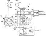
- FIG. 1is a block diagram of an example of a magnetic field sensor configured to internally perform self-diagnostic testing
- FIG. 2is a block diagram of an example of a circuit for generating a time-multiplexed signal for a magnetic field sensor, such as magnetic field sensor of FIG. 1 ;
- FIG. 3is graph showing an example of a time multiplexing diagram illustrating the transition between a magnetic signal and a diagnostic signal
- FIG. 4is a graph showing an example of a recovery signaling scheme for the circuit of FIG. 2 in response to a detected fault
- FIG. 5is a graph showing an example of a signaling scheme during a power-on phase initiated with a magnetic signal
- FIG. 6is a graph showing a signaling scheme during a power-on phase initiated with a diagnostic signal.
- magnetic signalis used to describe an electronic signal responsive to an external magnetic field.
- magnetic signal time periodis used to describe a time period, which may a plurality of time periods, during which the magnetic signal is present.
- diagnostic signalis used to describe an electronic signal responsive to an electronic diagnostic signal, and not responsive to the magnetic signal.
- diagnosis signal time periodis used to describe” is used to describe a time period, which may a plurality of time periods, during which the magnetic signal is present.
- magnetic field sensing elementis used to describe a variety of electronic elements that can sense a magnetic field.
- the magnetic field sensing elementcan be, but is not limited to, a Hall effect element, a magnetoresistance element, or a magnetotransistor.
- Hall effect elementsfor example, a planar Hall element, a vertical Hall element, and a Circular Vertical Hall (CVH) element.
- magnetoresistance elementsfor example, a semiconductor magnetoresistance element such as Indium Antimonide (InSb), a giant magnetoresistance (GMR) element, for example, a spin valve, an anisotropic magnetoresistance element (AMR), a tunneling magnetoresistance (TMR) element, and a magnetic tunnel junction (MTJ).
- the magnetic field sensing elementmay be a single element or, alternatively, may include two or more magnetic field sensing elements arranged in various configurations, e.g., a half bridge or full (Wheatstone) bridge.
- the magnetic field sensing elementmay be a device made of a type IV semiconductor material such as Silicon (Si) or Germanium (Ge), or a type III-V semiconductor material like Gallium-Arsenide (GaAs) or an Indium compound, e.g., Indium-Antimonide (InSb).
- a type IV semiconductor materialsuch as Silicon (Si) or Germanium (Ge)
- a type III-V semiconductor materiallike Gallium-Arsenide (GaAs) or an Indium compound, e.g., Indium-Antimonide (InSb).
- some of the above-described magnetic field sensing elementstend to have an axis of maximum sensitivity parallel to a substrate that supports the magnetic field sensing element, and others of the above-described magnetic field sensing elements tend to have an axis of maximum sensitivity perpendicular to a substrate that supports the magnetic field sensing element.
- planar Hall elementstend to have axes of sensitivity perpendicular to a substrate
- metal based or metallic magnetoresistance elementse.g., GMR, TMR, AMR
- vertical Hall elementstend to have axes of sensitivity parallel to a substrate.
- magnetic field sensoris used to describe a circuit that uses a magnetic field sensing element, generally in combination with other circuits.
- Magnetic field sensorsare used in a variety of applications, including, but not limited to, an angle sensor that senses an angle of a direction of a magnetic field, a current sensor that senses a magnetic field generated by a current carried by a current-carrying conductor, a magnetic switch that senses the proximity of a ferromagnetic object, a rotation detector that senses passing ferromagnetic articles, for example, magnetic domains of a ring magnet or a ferromagnetic target (e.g., gear teeth) where the magnetic field sensor is used in combination with a back-biased or other magnet, and a magnetic field sensor that senses a magnetic field density of a magnetic field.
- an angle sensorthat senses an angle of a direction of a magnetic field
- a current sensorthat senses a magnetic field generated by a current carried by a current-carrying conductor
- a magnetic switchthat
- processoris used to describe an electronic circuit that performs a function, an operation, or a sequence of operations.
- the function, operation, or sequence of operationscan be hard coded into the electronic circuit or soft coded by way of instructions held in a memory device.
- a “processor”can perform the function, operation, or sequence of operations using digital values or using analog signals.
- the “processor”can be embodied in an application specific integrated circuit (ASIC), which can be an analog ASIC or a digital ASIC. In some embodiments, the “processor” can be embodied in a microprocessor with associated program memory. In some embodiments, the “processor” can be embodied in a discrete electronic circuit, which can be an analog or digital.
- ASICapplication specific integrated circuit
- the “processor”can be embodied in a microprocessor with associated program memory.
- the “processor”can be embodied in a discrete electronic circuit, which can be an analog or digital.
- moduleis used to describe a “processor.”
- a processorcan contain internal processors or internal modules that perform portions of the function, operation, or sequence of operations of the processor.
- a modulecan contain internal processors or internal modules that perform portions of the function, operation, or sequence of operations of the module.
- a so-called comparatorcan be comprised of an analog comparator having a two state output signal indicative of an input signal being above or below a threshold level.
- the comparatorcan also be comprised of a digital circuit having an output signal with at least two states indicative of an input signal being above or below a threshold level.
- the term “predetermined,” when referring to a value or signal,is used to refer to a value or signal that is set, or fixed, in the factory at the time of manufacture, or by external means, e.g., programming, thereafter.
- the term “determined,” when referring to a value or signal,is used to refer to a value or signal that is identified by a circuit during operation, after manufacture.
- a magnetic field sensoris provided that is configured to perform the self-test diagnostics in the background, such that magnetic signals occur during magnetic signal time periods and diagnostic signals occur during diagnostic signal time periods, wherein the diagnostic signals occur periodically and automatically.
- the magnetic field sensorcan at the same time perform diagnostics and also run its main functions for sensing a magnetic field.
- the time-multiplexed signalmay be generated that transitions back and forth between magnetic signals and diagnostics signals.
- the time-multiplexed signalis generated such that initially the magnetic signal is run first.
- applicationsmay require diagnostics to be run in the initial moments of a power-up phase (e.g., integrated circuit power-up), before a first magnetic signal time period is run.
- the magnetic field sensors as described hereinmay run an installment of diagnostics prior to the first magnetic signal time period.
- the circuitry and components configured to perform the internal diagnosticsmay be self-contained within the magnetic field sensor.
- the diagnostic signalmay be electrical so that the magnetic field sensor is not affected by an external magnetic field during the diagnostic time period.
- a secondary signal pathis made available so that when one signal path is communicating diagnostics, the other signal path operates normally (i.e., communicating the magnetic signal). Furthermore this process may be reversed to allow for proper diagnosing of the second path.
- an illustrative block diagram of magnetic field sensor 2includes a signal path 10 , which includes a plurality of circuit elements described below.
- the magnetic field sensor 2can include four diagnostics modules: a resistance and biasing diagnostic module 80 , the signal diagnostic module 82 , an oscillator diagnostic module 84 , and memory diagnostic module 86 .
- magnetic field sensor 2may include various control and input modules, such as oscillator 36 , regulator and biasing module 40 , programming module 54 , and digital module 60 that are discussed in greater detail below.
- Signal path 10can include biasing and power switches circuit 12 coupled to a vertical Hall element 14 .
- the vertical Hall element 14is configured to generate an output signal 14 a , 14 b that is passed to switching circuit 16 .
- Switching circuit 16can be coupled to receive the signal 14 a , 14 b and configured to generate a chopped signal 16 a , 16 b .
- the switching circuit 16can also be switched with the clock at a frequency of fc.
- biasing and switching circuit 12 and the signal switches circuit 16can result in current spinning of the vertical Hall element 14 , thus resulting in the chopped signal 16 a , 16 b .
- Current spinningis a known technique and is not further described herein.
- An amplifier 18can be coupled to receive the chopped signal 16 a , 16 b and configured to generate an amplified signal 18 a , 18 b .
- a filter 20can be coupled to receive amplified signal 18 a , 18 b and configured to generate a filtered signal 20 a , 20 b .
- filter 20is a sin x/x (sin c) filter.
- filter 20may be a switched capacitor filter having a first notch at a frequency fc.
- the sin c filter 22is generated digitally.
- the sin c filter 22is an analog un-clocked filter.
- filter 22is a low pass filter.
- filter 20includes both a low-pass filter and a sin x/x (sin c) filter, whereby the low-pass filter generates a filtered signal and provides the filtered signal to the sin x/x (sin c) filter.
- a comparator 22can be coupled to receive the filtered signal 20 a , 20 b and configured to generate a comparison signal 22 a .
- comparator 22is a Schmitt trigger.
- Comparator 22may be configured to receive the filtered signal 20 a , 20 b and output the comparison signal 22 a in magnetic signal time periods responsive to the magnetic signal and in diagnostic signal time periods responsive to the diagnostic signal in a time-multiplexed arrangement. In an embodiment, during the diagnostic signal time periods, diagnostics may be performed on the comparison signal 22 a to test for faults or other issues with the magnetic field sensor 2 .
- the four diagnostic modules, resistance and biasing diagnostic module 80 , a signal diagnostic module 82 , an oscillator module 84 , and a memory diagnostic module 86are configured to perform self-test diagnostics on various components of magnetic field sensor 2 .
- the four diagnostic modules 80 , 82 , 84 , 86may be part of a single fault monitoring module or may be individual separate modules.
- Signal diagnostic module 82is coupled to the signal path 10 and the signal diagnostic module 82 is configured to receive the comparison signal 22 a .
- signal diagnostics module 82is configured to compare the comparison signal 22 a that occurs during one or more of the above described diagnostic signal time periods with a reference (i.e., predetermined) diagnostic signal, i.e. a replica of a diagnostic signal, to identify a passing or failing condition.
- the reference diagnostic signalmay have a predetermined sequence that can be compared with comparison signal 22 a to detect a fault condition.
- the predetermined sequencemay be based upon a desired number of transitions in an output signal.
- the reference diagnostic signalmay include a predetermined number of transitions (e.g., two or more transitions) that can be compared with a number of (or lack of) transitions in comparison signal 22 a to detect a fault condition.
- a faultmay be detected based on whether a position of a transition in an output signal is within a predetermined percentage error range of a correct position or whether a transition occurs within a predetermined time period (e.g., transitions occur within an acceptable time period).
- a diagnostic signalis described below in conjunction with FIG. 3 .
- Resistance and biasing diagnostic module 80can be coupled to biasing and power switches circuit 12 as discussed in greater detail below with respect to FIG. 2 .
- the resistance and biasing diagnostic module 80may be configured to compare a resistance value of the vertical Hall element 14 to a predetermined range of resistance values to detect a fault condition or verify that the vertical Hall effect element 14 has a resistance within the predetermined range of resistance values.
- resistance and biasing diagnostic module 80compare a resistance value of the vertical Hall element 14 to an initial set of resistance values to detect a parametric shift.
- the predetermined range of resistance valuesmay include one or more threshold levels such that each threshold level indicates a different level of quality (e.g., level of degradation) of the particular component. For example, a first threshold level may indicate damage to a component, however the component still operates in an acceptable range. While a second threshold level may indicate a complete failure of a component.
- Oscillator diagnostic module 84can be coupled to oscillator 36 and to a diagnostic bus 90 .
- oscillator diagnostic module 84is configured to receive an electronic signal produced by oscillator 36 and to verify a quality, e.g., a frequency and/or an amplitude, of the electronic signal produced by oscillator 36 . Accordingly, the oscillator diagnostic module 84 can identify a pass or fail condition associated with the oscillator 36 and can communicate the pass or fail condition upon the diagnostic bus 90 .
- the oscillator 36can be coupled to a clock logic digital module 60 configured to generate logic signals and clock signals upon a clocks bus 92 , for switching networks and switching circuits of magnetic field sensor 2 .
- memory diagnostic module 86can configured to perform a diagnostics to test memory storage capabilities of components of the magnetic field sensor 2 . In some embodiments, memory diagnostics module 86 performs a parity bit check to test memory storage devices of the magnetic field sensor 2 . In some embodiments, memory diagnostic module 86 can be configured to monitor a memory value for the magnetic field sensor 2 .
- Output circuit 30can be coupled to the diagnostic bus 90 and can be configured to receive, via the diagnostic bus 90 pass and fail conditions determined by each one of the four diagnostic modules, namely, resistance and biasing diagnostic module 80 , signal diagnostic module 82 , oscillator diagnostic module 84 , and memory diagnostic module 86 .
- Output circuit 30includes a pre-driver 32 and an output driver 34 .
- the clocks bus 92provides control signals to control the vertical Hall element 14 , the signal switches 16 , the amplifier 18 , the sin c filter 20 , the comparator 22 , the pre-driver circuit 32 , and the output driver circuit 34 .
- the output driver circuit 34generates a current output signal represented, for example, in FIG. 4 .
- Memory diagnostic module 86can be coupled to a programming module 54 .
- the programming module 54can receive an external signal to program fuses 58 within the programming module 54 . Once programmed, the fuses 58 can control a variety of operations of the magnetic field sensor 2 .
- programming module 54is coupled to digital module 60 and configured to program and control operation of the components of digital module 60 .
- Programming module 54can be coupled to memory diagnostic module 86 .
- Memory diagnostics module 86can be configured to verify a memory status of digital module 60 .
- Various parameters identified in the programmed fuses 58can be passed to the digital module 60 and communicated via a programming bus 94 throughout the magnetic field sensor 2 .
- Regulator and biasing module 40can include ESD 46 , LDO regulator 48 , POR) circuit 50 , and biasing circuit 52 .
- Regulator and biasing module 40may be coupled to receive a voltage (VCC) and ground.
- ESD 46may be an electrostatic discharge protection circuit.
- LDO regulator 48may be a low-dropout regulator and can be configured to regulate an output voltage.
- POR circuit 50may be a power-on reset circuit that is configured to a detect various voltage and currents levels in the magnetic field sensor 2 and generate a reset pulse to reset various circuits within the magnetic field sensor 2 when a power on condition is detected.
- Biasing circuit 50may be configured to generate predetermined voltages or currents at various points of the magnetic field sensor 2 on a biasing bus 96 . In some embodiments, biasing circuit 50 is used to establish proper operating conditions.
- Digital module 60can include analog signal path clocks 62 , oscillator gating 64 , trimming signals 66 , source voltage (VCC) serial protocol for programming 68 , BIST 70 , and fault detection monitor 72 .
- BIST 70may be a built-in self-test circuit and configured to perform a self-test for components of signal path 10 and/or in the digital module 60 .
- digital module 60may be referred to as a processing circuit.
- Digital module 60may be coupled to each of diagnostic modules (resistance and biasing diagnostic module 80 , signal diagnostic module 82 , oscillator diagnostic module 84 , and memory diagnostic module 86 ) via the diagnostic bus 90 .
- Diagnostic module 60may be configured to receive an indication (e.g., flag) of a fault condition within magnetic field sensor 2 from each of the diagnostic modules.
- Digital module 60may be coupled to output driver circuit 34 via diagnostic bus 90 . In response to a fault detection, digital module 60 may generate and transmit a command signal to output driver circuit 34 via diagnostic bus 90 . In an embodiment, digital module 60 is configured to command output driver circuit 34 to output a predetermined output (e.g., output signal) to indicate the fault condition within magnetic field sensor 2 .
- a predetermined outpute.g., output signal
- fault detection monitor 72receives each the indications (e.g., flags) of a fault condition within magnetic field sensor 2 from each of the diagnostic modules.
- Fault detection monitor 72may be configured to detect and coordinate fault or passing conditions of each of the four self-test modules described above.
- Fault detection monitor 72may be configured to generate and transmit a command signal to output driver circuit 34 via diagnostic bus 90 to indicate the fault condition within magnetic field sensor 2 .
- Oscillator 36may be any general electronic circuit configured to produce a periodic, oscillating signal.
- oscillator 36converts a direct current (DC) signal to an alternating current (AC) signal.
- Oscillator 36may be coupled to digital module 60 .
- a circuit 150can be the same as or similar to the vertical Hall element 14 , the biasing and power switches circuit 12 , the signal switches 16 , a diagnostic signal injector circuit within the signal diagnostic module 82 , and the resistance and biasing diagnostic module 80 of FIG. 1 .
- the above described current spinningis not shown in FIG. 2 , but will be understood.
- a signal path 120can be the same as or similar to the signal path 10 of FIG. 1 .
- the circuit 150can include a signal current source (i.e., sensor biasing current source) 110 operable to drive a current into a vertical Hall element 108 .
- signal current source 110continuously outputs a current into vertical Hall element 108 .
- the vertical Hall element 108can have five terminals, however, because two of the five terminals are conventionally coupled together, four effective terminals result, i.e., first, second, third, and fourth terminals, 108 a , 108 b , 108 c , 108 d , respectively, in a bridge arrangement.
- the signal current source 110can drive the first terminal 108 a and a differential output signal 109 b , 109 d (a magnetic signal) can result that is responsive to an external magnetic field.
- Terminals 108 b , 108 d of the Hall effect element 108can be coupled to switches 116 a , 116 b of signal switches 116 .
- the signal switches 116can generate a magnetic signal 116 c , 116 d .
- signal current source 110continuously outputs a current into vertical Hall element 108 , however signal switches 116 a , 116 b may open to allow diagnostics to be performed on various components of magnetic field sensor 2 .
- the circuit 150can also include a diagnostic current source (i.e., diagnostic input current source) 112 coupled to a first resistor 130 .
- the first resistor 130can be coupled at a junction node to a second resistor 128 , which can terminate at a reference voltage, for example, ground.
- the junction nodecan be coupled to the terminal 108 d of the vertical Hall element 108 .
- a voltage sensed across the first resistor 130can be, in-part, representative of a resistance thought the vertical Hall element 108 .
- the first resistor 130can be coupled at a first end of the first resistor 130 to a switch 114 a within diagnostic switches 114 and at a second end of the first resistor 130 to a switch 114 b within the diagnostic switches 114 .
- the diagnostic switches 114can generate a diagnostic signal 114 c , 114 d .
- the diagnostic switches 114 and the signal switches 116 taken individually or togethercan be referred to herein as a switching network.
- the diagnostic signal 114 c , 114 d provided from the diagnostic switches 114is responsive to the signal current source 110 and to the diagnostic current source 112 , but is not responsive to an external magnetic field sensed by the vertical Hall element 108 .
- the diagnostic signal 114 c , 114 dis essentially responsive to resistance of the vertical Hall element 108 .
- the diagnostic switches 114are closed when the signal switches 116 are open, and vice versa.
- a signal received by signal path 120 and generated by the signal path 120is either is the diagnostic signal 114 c , 114 d at some times and the magnetic signal 116 c , 116 d responsive to an external magnetic field at other times.
- the diagnostic module 80 and 82can coordinate the opening and closing of diagnostic switches 114 and signal switches 116 in order to either apply a magnetic signal or a diagnostic signal to the signal path 10 .
- the diagnostic switches and the signal switches 114 , 116may be configured to generate a time-multiplexed signal 152 a , 152 b comprising the magnetic signal 116 c , 116 d responsive to an external magnetic field signal in some of a plurality of time periods and the diagnostic signal 114 c , 114 d responsive to the in others of the plurality of time periods.
- the diagnostic signalmay have a predetermined transition pattern between a first state and a second state in a diagnostic mode of operation.
- diagnosticsmay constantly be running and circuit 150 may be configured to provide diagnostics in the background, for example, during every other time period of the plurality of time periods, such as a magnetic signal in a first time period and diagnostic signal in a second time period, which may be an adjacent time period to the first time period.
- Diagnostic current source 112can be coupled to first terminals of first and second diagnostic switches 114 a , 114 b .
- a diagnostic resistive element (R diag ) (first resistor) 130may be coupled between the first terminal of first diagnostic switch 114 a and the first terminal of second diagnostic switch 114 b resulting in a diagnostic signal 114 c , 114 d generated by the diagnostic switches 114 .
- diagnostic current source 112can be altered or transitioned between at least two different values to control operation (e.g., open or close) of the first terminal of first diagnostic switch 114 a and the first terminal of second diagnostic switch 114 b .
- a control portmay be coupled to the diagnostic current source 112 and the control port can be configured to control and transition the output of the diagnostic current source 112 between different values.
- a currente.g., diagnostic current source 112
- diagnostic resistive element (Rdiag) 130may be altered to control operation of the first terminal of first diagnostic switch 114 a and the first terminal of second diagnostic switch 114 b (e.g., open or close switches).
- the current though diagnostic resistive element (R diag ) 130may be altered to close diagnostic switches 114 a , 114 b .
- the current though diagnostic resistive element (R diag ) 130may be altered to open diagnostic switches 114 a , 114 b.
- diagnostic resistive element (R diag ) 130has a resistance that results in a resulting electrical signal 20 a , 20 b value in the signal path 10 of FIG. 1 crossing one of an upper or a lower threshold of the comparator 22 when a resistance of the vertical Hall element 108 is proper.
- a test of the resistance of the vertical Hall element 108can be performed.
- first and second diagnostic switches 114 a 114 bby changing positions of the first and second diagnostic switches 114 a 114 b (with other switches that are not shown), and opposite sign signal can be generated, wherein a resulting electrical signal 20 a , 20 b values in the signal path 10 of FIG. 1 crossing the other one of the upper or a lower threshold of the comparator 22 when a resistance of the vertical Hall element 108 is proper.
- the two coupling directions of the first and second diagnostic switches 114 a , 114 bresults in an effective two state signal passing through the signal path 10 of FIG. 1 . This two state signal is further described below in conjunction with FIG. 4 .
- the diagnostic current source 112can be an AC current source having two states.
- Diagnostic current source 112is coupled to ground through a common mode resistive element (R cm ) (second resistor) 128 .
- common mode resistive element (Rcm) 128may be used to set the common mode voltage in the signal path 10 to a proper voltage.
- a value of the common mode resistive element (Rcm) 128is can be selected.
- vertical Hall element 108may be a vertical Hall element, which can include internal resistive elements.
- the vertical Hall element 108can be represented as a Wheatstone bridge having four resistive elements 132 a , 132 b , 132 c , 132 d and four terminals 108 a , 108 b , 108 c , 108 d .
- the vertical Hall element 108can generate a differential output signal 109 b , 109 d at terminals 108 b , 108 d that is responsive to an external magnetic field, and which can be referred to as a magnetic signal herein.
- Hall sensor 108is configured to generate the differential output signal (magnetic signal) 109 b , 109 d at terminals 108 b , 108 d .
- the two terminals 108 b , 108 d of vertical Hall element 108are coupled to signal switches 116 .
- terminal 108 ais coupled to a first terminal of first signal switch 116 a and terminal 108 d is coupled to a first terminal of second signal switch 116 b.
- the signal switches 116receive the differential signal (magnetic signal) 109 b , 109 d and the diagnostic switches 114 receive a diagnostic signal 130 a , 130 b at the same time.
- Second terminals (i.e., outputs) of diagnostic switches 114 and signal switches 116are coupled together at an input of signal path 120 of a magnetic field sensor, such as signal path 10 of FIG. 1 .
- the first terminal of diagnostic switches 114 or signal switches 116is closed (i.e., connected to corresponding second terminal) the respective switch is closed and feeds to signal path 120 .
- signal switches 116are controlled by a clock signal
- CK signal and diagnostic signal switches 114are controlled by a clock signal, CK diag , which can originate in the clocks bus 92 of FIG. 1 .
- CK diaga clock signal
- an output of signal path 10may then be provided to output module 30 of FIG. 1 and to signal diagnostics module 82 of FIG. 1 .
- the output of signal path 10may be a time-multiplexed signal.
- the diagnostic switches 114 and signal switches 116are configured to generate the time-multiplexed signal such that the time-multiplexed signal alternates between the magnetic signal in one time period and the diagnostic signal in another time period.
- the diagnostic signalupon a first power up of the magnetic field sensor 2 , the diagnostic signal is generated first and the magnetic signal is generated second in the time-multiplexed signal.
- the magnetic signalmay be generated first and the diagnostic signal may be generated second.
- the circuit 150can include a comparison module 118 .
- Comparison module 118is configured to compare a signal voltage at terminal 108 b (via path 109 b ) of vertical Hall element 108 to a reference high voltage (REFH diag ) and to a reference low voltage (REFL diag ) to determine if the voltage at terminal 108 b is within a predetermined acceptable range.
- REFH diagreference high voltage
- REFL diagreference low voltage
- Comparison module 118can include at least two comparators 118 a , 118 b , coupled to a logic gate 119 (e.g., OR logic gate).
- First and second comparators 118 a , 118 bcan be coupled to one terminal, e.g., terminal 108 b , of Hall sensor 108 to receive signal 109 b .
- first comparator 118 acompares differential output 109 b to a reference high voltage (REFHdiag) value and second comparator 118 b compares differential output 109 b to a reference low voltage (REFL diag ).
- Outputs of first and second comparators 118 a , 118 bbcan be combined using logic gate 119 .
- Logic gate 119is illustrated as an OR gate in FIG. 2 , however it should be appreciated that any type of logic gate may be used depending on a particular application. Output of logic gate 119 is then provided to resistance and biasing diagnostics module 80 of FIG. 1 , and by passing the signal path 120 , to determine if the biasing of circuit 12 is within a predetermined acceptable. In an embodiment, signal switches 116 are in the open position when resistance and biasing diagnostics module 80 verifies a biasing or common mode voltage, or performs a test of the resistance of the vertical Hall element 108 .
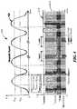
- graphs 200 , 210have vertical axes with scales in units of volts in arbitrary units and horizontal axes with scales in units of time in arbitrary units.
- FIG. 3illustrates the transition between a magnetic signal (as may be generated by the magnetic signal switches 116 of FIG. 2 ) and a diagnostic signal (as may be generated by the diagnostic signal switches 114 of FIG. 2 ).
- FIG. 3illustrates a signaling scheme of magnetic field sensor 2 of FIG. 1 .
- a plurality of time periodsmay include both a magnetic signal time period 202 and a diagnostic signal time period 204 .
- each one of the plurality of time periodsmay be about two hundred microseconds, as shown in FIG. 3 .
- the time periodsmay be greater than or less than two hundred microseconds according to a particular application.
- the signal time periodsrefers to time periods in which a magnetic signal (e.g., magnetic field signal 116 a , 116 b of FIG. 2 ) is applied to signal path 10 , resulting in a magnetic signal (e.g., 202 aa ) at the input of comparator 22 of FIG. 1 .
- the diagnostic signal time periods(e.g., 204 a ) refers to time periods in which a diagnostic signal (e.g., diagnostic signal 114 a , 114 b ) is applied to signal path 10 , resulting in a diagnostic signal 204 aa at the input of comparator 22 of FIG. 1 .
- B OPrefers to an operating point threshold of the comparator 22 of FIG. 1 .
- B RPrefers to a release point threshold of the comparator 22 .
- Comparator output 212can be the same as or similar to the comparison signal 22 a of comparator 22 of FIG. 1 .
- Letter referencese.g., A-I are further added to FIG. 3 to aid in describing the signaling scheme.
- Magnetic signals 202 aa , 202 ba and a diagnostic signal 204 aa during the time periods 202 a , 204 a , 202 bare indicative of the filtered signal 20 a , 20 b of FIG. 1 .
- an external magnetic fieldis initially received by the magnetic field sensor 2 of FIG. 1 and causes the magnetic signal 202 aa in the magnetic signal time period 202 a to rise.
- the magnetic field sensor 2may initially start in a magnetic signal time period 202 a or in a diagnostic signal time period 204 a .
- FIG. 3provides one embodiment, in which a magnetic signal time period (e.g., 202 a ) occurs first.
- a comparison signal 212(e.g., comparison signal 22 a of FIG. 1 ) is initially off and does not turn on until the magnetic signal 202 aa in the magnetic signal time period 202 a is greater than the operating point threshold, B op .
- the magnetic signal 202 aa in the magnetic signal time period 202 areaches the operating point threshold, B op , and the comparison signal 212 turns on.
- the magnetic signal 202 aa in the magnetic signal time period 202 ais above the threshold B op , and the comparison signal 212 stays on.
- a first state of a diagnostic signale.g., a square wave diagnostic signal 114 a , 114 b generated by the switches 114 of FIG. 2 or by the diagnostic current source 112
- the diagnostic time period 204 ais applied during the diagnostic time period 204 a and passes through the signal path 10 to the comparator 22 of FIG. 1 .
- the diagnostic signal 204 aabegins below the release point threshold, B RP , and turns off comparison signal 212 .
- the diagnostic signal 204 aapersists in a first state during the diagnostic time period 204 a , the diagnostic signal 204 aa transitions above the operating point threshold, Bop, and the comparison signal 212 achieves a high state.
- the diagnostic signal 114 a , 114 btransitions to a second different state during the diagnostic time period 204 a , the diagnostic signal 204 aa transitions below the release point threshold, Brp, and the comparison signal 212 achieves a low state.
- the comparison signal 212make one or more electronic transitions during the diagnostic signal time period 204 a and corresponding correct transitions of the comparison r signal 212 can be indicative of a passing condition of the signal path 10 .
- the magnetic signal 116 a , 116 b represented in the magnetic signal time period 202 ais canceled.
- a time slotmay be provided when transitioning between a magnetic signal time period (e.g., 202 a ) and a diagnostic signal time period (e.g., 204 a ) to allow for proper signal settling during both signals.
- the time slot between transitionsmay be used to prevent inter-slot coupling.
- diagnostics signal 204 aa during the diagnostic signal time period 204 ais below the operating point threshold, B op .
- comparator output 212remains off until diagnostic signal 204 aa during the diagnostic signal time period 204 a rises above the operating threshold, B op , at point D.
- diagnostic signal 204 aa during the diagnostic signal time period 204 ais configured to force two transitions (i.e., cause comparator output 212 to turn on and turn off) to verify the output of the circuit path 10 ( FIG. 1 ) in both an ON state and OFF state.
- diagnostic signal 204 aa during the diagnostic time period 204 ais configured to turn comparison signal 212 on and then off in a single one or the diagnostic signal time periods (e.g., 204 aa ).
- the channel reset (i.e., two-state transition) between time periodsmay be used to force transitions and prevent inter-slot coupling.
- diagnostic signal 204 aa during the diagnostic signal time period 204 ainitially rises above the operating point threshold, B OP and then, at point E, begins to fall until at point F it falls below the release point threshold, B RP , causing comparison signal 212 to turn off.
- Diagnostic signal 204 aa during the diagnostic signal time period 204 acontinues to fall until, at point G, the input signal transitions from diagnostic signal 204 aa during the diagnostic signal time period 204 a to magnetic signal 202 ba during the magnetic signal time period 202 b.
- comparison signal 212remains off until a signal rises above the operating point threshold B OP .
- Magnetic signal 202 ba during the magnetic signal time period 202 brises, until at point H, the magnetic signal 202 ba is greater than the operating point threshold B OP .
- comparison signal 212turns on and remains on while magnetic signal 202 ba is greater than the operating point threshold, B OP .
- a graph 400has a vertical axis with a scale in units of magnetic field in arbitrary units and a horizontal axis with a scale in units of time in arbitrary units.
- a graph 410has a vertical axis with a scale in units of volts in arbitrary units and a horizontal axis with a scale in units of time in arbitrary units.
- FIG. 4illustrates a signal 412 indicative of a detected fault in the magnetic field sensor 2 of FIG. 1 , and indicative of a recovery signaling scheme in response to a detected fault.
- the signal 412can be generated by the output driver circuit 34 of FIG. 1 .
- a digital modulemay be configured to transition the magnetic field sensor between at least one of: a normal mode, a fault mode, and a recovery mode (i.e., digital module 60 of FIG. 1 by way of the clocks bus 92 ).
- digital modulemay be configured to transition the magnetic field sensor to a FAULT mode in response to a fault detection made by one or more of the above-described four diagnostic modules.
- the digital modulemay be configured to transition the magnetic field sensor to recovery mode in response to a fault detection.
- the digital modulemay be configured to provide a recovery sequence signal to the switching network (i.e., diagnostic switches 114 and signal switches 116 of FIG. 2 ) during recovery mode and the digital module may be configured to transition the magnetic field sensor to normal mode in response to a pass detection, the pass detection received responsive to the recovery sequence signal.
- I DD(high)is a high level output current (e.g., at a drain terminal of the output diver 34 of FIG. 1 )
- I DD (low)is a low level output current (at drain terminal)
- I DD(AVG)FAULTis a still lower output current during a safe mode (i.e., during a fault condition).
- Letter referencese.g., A, B are further added to FIG. 4 to aid in describing the signaling scheme.
- a signal 406is indicative of a magnetic signal experienced by the magnetic field sensor 2 of FIG. 1 .
- the magnetic signal 406achieves a magnetic field such that the filtered signal 20 a , 20 b of FIG. 1 less than the operating point threshold, B OP , thus, the output signal 412 generated by the output driver circuit 34 is off (e.g., at I DD(low) ).
- the output signal 412turns on and goes high to I DD(high) .
- the output signal 412stays high until magnetic signal 406 achieves a magnetic field such that the filtered signal 20 a , 20 b falls below the release point threshold, at which time the output signal turns off and goes to I DD(low) .
- magnetic signal 406achieves a magnetic field such that the filtered signal 20 a , 20 b rises above operating point threshold, B OP , and the output signal 412 should turn on and rise to I DD(high) .
- the output signal 412remains off (e.g., at I DD(low) ). This indicates a fault condition and in response, the circuit goes into a recovery sequence as a new diagnostic signal time period is generated after point A.
- the magnetic field sensor 2may initiate a first recovery sequence to clear the fault condition.
- a processing unitmay be configured to transition the magnetic field sensor 2 to recovery mode in response to a fault detection and a diagnostic current source (e.g., 106 a , 106 b of FIG. 2 ) may be configured to provide a recovery sequence.
- a diagnostic current sourcee.g., 106 a , 106 b of FIG. 2
- the recovery sequenceincludes a first diagnostic signal time period, followed by waiting time period, followed by another diagnostic signal time period spanning points A and B. Magnetic signal time periods are suspended between points A and B during a recovery sequence. The recovery sequence continues with diagnostic signal time periods followed by wait time periods until the respective circuit or component of the magnetic field sensor passes the diagnostic test. In other embodiments, the recovery sequence may continue for a predetermined number of attempts.
- the magnetic field sensor 2may perform a system reset, for example, at point B.
- a processing unit of the magnetic field sensor 2is configured to thereafter transition the magnetic field sensor 2 to normal mode (in which magnetic signal time periods and diagnostic signal time periods continue in the above described time-multiplexed arrangement) in response to a pass detection, whereby the pass detection is received responsive to the recovery sequence signal.
- a diagnostic passis indicated and the circuit forces the output signal 412 high for a time period to verify the fault has been cleared and the circuit is working in both the OFF state and ON state.
- Output signal 412is forced high despite magnetic signal 406 being less than operating point threshold B OP .
- the output signal 412turns off and drops to I DD(low) to re-align with magnetic signal 406 .
- the output signal 412re-aligns with magnetic signal 406 during the next magnetic signal time period (i.e., after a diagnostic time period).
- the magnetic field sensor 2may start initially with a magnetic signal time period ( FIG. 5 ) or may initially start with a diagnostic signal time period ( FIG. 6 ).
- the first signal appliedis a magnetic signal.
- the output current I DDmay be undefined until the output voltage, V DD reaches a voltage output minimum, V DDMIN . Once the output voltage (V DD ) reaches the minimum, the first magnetic sample may be applied followed by a diagnostic sample.
- the first signal appliedis a diagnostic signal.
- FIG. 6may be similar to FIG. 5 except that diagnostics are run initially during power-on instead of after a magnetic sample has run as in FIG. 6 . Thus, before running the first magnetic sample in a sampling cycle, an installment of a diagnostics sample is run.
- the latch outputwill be measured from at the end of each a first magnetic signal time period (t sample .) For example, in FIG. 5 , the first latch output is taken at the end of the first magnetic signal time period and prior to a diagnostic sample time period. However, in FIG. 6 , the first latch output is taken after a diagnostic sample and also after a first magnetic signal time period. The decision between whether to run a magnetic signal time period or a diagnostic signal time period first may vary depending on the needs of a particular application.
Landscapes
- Physics & Mathematics (AREA)
- General Physics & Mathematics (AREA)
- Condensed Matter Physics & Semiconductors (AREA)
- Measuring Magnetic Variables (AREA)
- Hall/Mr Elements (AREA)
Abstract
Description
Claims (40)
Priority Applications (7)
| Application Number | Priority Date | Filing Date | Title |
|---|---|---|---|
| US14/970,949US10527703B2 (en) | 2015-12-16 | 2015-12-16 | Circuits and techniques for performing self-test diagnostics in a magnetic field sensor |
| CN201680070823.9ACN108474827B (en) | 2015-12-16 | 2016-12-01 | Circuit and technique for performing self-test diagnostics in a magnetic field sensor |
| KR1020187015292AKR20180094867A (en) | 2015-12-16 | 2016-12-01 | Circuits and techniques for performing self-test diagnostics in magnetic field sensors |
| KR1020237020447AKR102758141B1 (en) | 2015-12-16 | 2016-12-01 | Circuits and techniques for performing self-test diagnostics in a magnetic field sensor |
| EP16816799.7AEP3368913B1 (en) | 2015-12-16 | 2016-12-01 | Circuits and techniques for performing self-test diagnostics in a magnetic field sensor |
| JP2018529628AJP6960918B2 (en) | 2015-12-16 | 2016-12-01 | Circuits and techniques for performing self-test diagnostics within a magnetic field sensor |
| PCT/US2016/064300WO2017105847A1 (en) | 2015-12-16 | 2016-12-01 | Circuits and techniques for performing self-test diagnostics in a magnetic field sensor |
Applications Claiming Priority (1)
| Application Number | Priority Date | Filing Date | Title |
|---|---|---|---|
| US14/970,949US10527703B2 (en) | 2015-12-16 | 2015-12-16 | Circuits and techniques for performing self-test diagnostics in a magnetic field sensor |
Publications (2)
| Publication Number | Publication Date |
|---|---|
| US20170176566A1 US20170176566A1 (en) | 2017-06-22 |
| US10527703B2true US10527703B2 (en) | 2020-01-07 |
Family
ID=57610393
Family Applications (1)
| Application Number | Title | Priority Date | Filing Date |
|---|---|---|---|
| US14/970,949ActiveUS10527703B2 (en) | 2015-12-16 | 2015-12-16 | Circuits and techniques for performing self-test diagnostics in a magnetic field sensor |
Country Status (6)
| Country | Link |
|---|---|
| US (1) | US10527703B2 (en) |
| EP (1) | EP3368913B1 (en) |
| JP (1) | JP6960918B2 (en) |
| KR (2) | KR20180094867A (en) |
| CN (1) | CN108474827B (en) |
| WO (1) | WO2017105847A1 (en) |
Cited By (6)
| Publication number | Priority date | Publication date | Assignee | Title |
|---|---|---|---|---|
| US11256288B1 (en) | 2021-02-02 | 2022-02-22 | Allegro Microsystems, Llc | Clock monitoring using a switched capacitor |
| US11268998B1 (en)* | 2020-12-22 | 2022-03-08 | Allegro Microsystems, Llc | Dynamic bridge diagnostic |
| US11555868B2 (en) | 2021-04-23 | 2023-01-17 | Allegro Microsystems, Llc | Electronic circuit having vertical hall elements arranged on a substrate to reduce an orthogonality error |
| US11630130B2 (en) | 2021-03-31 | 2023-04-18 | Allegro Microsystems, Llc | Channel sensitivity matching |
| US11703898B2 (en) | 2021-07-09 | 2023-07-18 | Allegro Microsystems, Llc | Low dropout (LDO) voltage regulator |
| US12153073B2 (en) | 2022-11-09 | 2024-11-26 | Allegro Microsystems, Llc | Diagnostic circuits with duplicate resistive networks for sensor output buffers |
Families Citing this family (12)
| Publication number | Priority date | Publication date | Assignee | Title |
|---|---|---|---|---|
| EP3470862B1 (en) | 2017-10-10 | 2022-03-02 | Melexis Bulgaria Ltd. | Sensor defect diagnostic circuit |
| EP3543717A1 (en)* | 2018-03-22 | 2019-09-25 | Narda Safety Test Solutions GmbH | Personal protection measuring device |
| US10746814B2 (en)* | 2018-06-21 | 2020-08-18 | Allegro Microsystems, Llc | Diagnostic methods and apparatus for magnetic field sensors |
| EP3647741B1 (en)* | 2018-10-29 | 2022-08-03 | Melexis Bulgaria Ltd. | Sensor diagnostic device and method |
| US11327127B2 (en)* | 2019-07-10 | 2022-05-10 | Allegro Microsystems, Llc | Magnetic field sensor with reduced influence of external stray magnetic fields |
| DE102019133128B4 (en)* | 2019-12-05 | 2025-09-18 | Infineon Technologies Ag | Sensor device and method |
| DE102019134077B4 (en)* | 2019-12-12 | 2021-07-22 | Infineon Technologies Ag | Signal processing circuit for a Hall sensor and signal processing method |
| US11592511B2 (en)* | 2020-05-27 | 2023-02-28 | Texas Instruments Incorporated | Methods and systems for diagnosing magnetic sensors |
| US12146895B2 (en)* | 2020-10-06 | 2024-11-19 | Infineon Technologies Ag | Robust signal path plausibility check for functional safety of a sensor |
| US11561257B2 (en) | 2020-12-22 | 2023-01-24 | Allegro Microsystems, Llc | Signal path monitor |
| CN114076908B (en)* | 2022-01-06 | 2022-04-29 | 微传智能科技(常州)有限公司 | Magnetic switch testing system, method and device |
| CN114584114B (en)* | 2022-04-29 | 2022-08-12 | 卧安科技(深圳)有限公司 | Hall signal filtering method for uniform motion detection and curtain opening and closing device |
Citations (55)
| Publication number | Priority date | Publication date | Assignee | Title |
|---|---|---|---|---|
| US4004217A (en) | 1975-10-31 | 1977-01-18 | S.H.E. Corporation | Flux locked loop |
| US4465976A (en) | 1982-01-26 | 1984-08-14 | Sprague Electric Company | Hall element with bucking current and magnet biases |
| JPS63185555A (en) | 1986-12-19 | 1988-08-01 | ゼネラル・エレクトリック・カンパニイ | Automatic gain control for monitoring machine tool |
| JPH02271256A (en) | 1989-04-12 | 1990-11-06 | Toshiba Corp | Judgment device for rotational speed detection device |
| JPH0396809A (en) | 1989-09-08 | 1991-04-22 | Shinko Electric Co Ltd | Linear encoder |
| JPH0514196A (en) | 1991-06-28 | 1993-01-22 | Toshiba Corp | Input circuit with self-diagnostic function |
| JPH0626968A (en) | 1992-07-13 | 1994-02-04 | Kayaba Ind Co Ltd | Sensor failure detection device |
| JPH06300584A (en) | 1993-04-15 | 1994-10-28 | Nippondenso Co Ltd | Sensor signal processing device |
| JPH0766649A (en) | 1993-08-20 | 1995-03-10 | Nec Corp | Automatic output level control circuit |
| US5499526A (en) | 1991-10-14 | 1996-03-19 | Nissan Motor Co., Ltd. | Semiconductor sensor self-checking circuit |
| WO1996041415A1 (en) | 1995-06-07 | 1996-12-19 | Philips Electronics N.V. | Detection circuit with hysteresis proportional to the peak input voltage |
| US5612488A (en) | 1994-12-26 | 1997-03-18 | Mitsubishi Denki Kabushiki Kaisha | Semiconductor acceleration detecting device |
| JPH0979004A (en) | 1995-09-13 | 1997-03-25 | Toshiba Eng Co Ltd | Zero speed detector for turning device |
| US5631602A (en) | 1995-08-07 | 1997-05-20 | Delco Electronics Corporation | Wheatstone bridge amplifier circuit with integrated diagnostic testing |
| US5793778A (en) | 1997-04-11 | 1998-08-11 | National Semiconductor Corporation | Method and apparatus for testing analog and digital circuitry within a larger circuit |
| EP1032846A1 (en) | 1997-11-20 | 2000-09-06 | Siemens Aktiengesellschaft | Diagnostic device for recognizing short circuits or line interruptions of an inductive sensor |
| US6191698B1 (en) | 1998-12-21 | 2001-02-20 | Gerhard Hennig | Magnetic testing apparatus |
| US20020021126A1 (en) | 1997-02-28 | 2002-02-21 | Kazutoshi Ishibashi | Magnetic sensor with a signal processing circuit having a constant current circuit |
| US6420868B1 (en) | 2000-06-16 | 2002-07-16 | Honeywell International Inc. | Read-out electronics for DC squid magnetic measurements |
| US6545495B2 (en) | 2001-04-17 | 2003-04-08 | Ut-Battelle, Llc | Method and apparatus for self-calibration of capacitive sensors |
| JP2003195933A (en) | 2001-12-27 | 2003-07-11 | Mitsubishi Electric Corp | Monitoring and control equipment |
| US20030164711A1 (en) | 2002-03-01 | 2003-09-04 | Shoichi Ishida | Sensor output processing device having self-diagnosis function |
| US20040059959A1 (en) | 2002-09-19 | 2004-03-25 | Kazumasa Ozawa | Semiconductor integrated circuit |
| US20040193988A1 (en) | 2003-03-26 | 2004-09-30 | James Saloio | Engine speed sensor with fault detection |
| US20050038623A1 (en) | 2003-08-12 | 2005-02-17 | Infineon Technologies Ag | In-operation test of a signal path |
| US6980005B2 (en) | 2003-09-23 | 2005-12-27 | Pass & Seymar, Inc. | Circuit protection device with timed negative half-cycle self test |
| US20060066296A1 (en) | 2004-09-28 | 2006-03-30 | Denso Corporation | Rotational angle detecting device |
| JP2006105932A (en) | 2004-10-08 | 2006-04-20 | Toyota Motor Corp | Failure determination device for sensor having bridge circuit and failure determination method thereof |
| WO2006056829A1 (en) | 2004-09-16 | 2006-06-01 | Liaisons Electroniques-Mécaniques LEM S.A. | Continuously calibrated magnetic field sensor |
| US20070096759A1 (en) | 2005-11-02 | 2007-05-03 | Chananiel Weinraub | Analog built-in self-test module |
| US7271595B2 (en) | 2005-11-21 | 2007-09-18 | Fujitsu Limited | Sensor detection apparatus and sensor |
| US20080013298A1 (en) | 2006-07-14 | 2008-01-17 | Nirmal Sharma | Methods and apparatus for passive attachment of components for integrated circuits |
| US20080297181A1 (en) | 2007-05-30 | 2008-12-04 | Udo Ausserlechner | Measuring Bridge Arrangement, Method of Testing a Measuring Bridge, Test Arrangement for Testing a Measuring Bridge, Method of Producing a Tested Measuring Bridge Arrangement, and Computer Program |
| US20090019330A1 (en) | 2007-07-13 | 2009-01-15 | Friedrich Andreas P | Integrated circuit having built-in self-test features |
| US20100026281A1 (en)* | 2007-06-22 | 2010-02-04 | Rohm Co., Ltd. | Magnetic sensor circuit and electronic apparatus using same |
| JP2010071729A (en) | 2008-09-17 | 2010-04-02 | Mitsumi Electric Co Ltd | Semiconductor integrated circuit for driving motor and method for testing |
| US7694200B2 (en) | 2007-07-18 | 2010-04-06 | Allegro Microsystems, Inc. | Integrated circuit having built-in self-test features |
| US20100211347A1 (en)* | 2009-02-17 | 2010-08-19 | Allegro Microsystems, Inc. | Circuits and Methods for Generating a Self-Test of a Magnetic Field Sensor |
| US20100237890A1 (en) | 2009-03-18 | 2010-09-23 | Infineon Technologies Ag | System that measures characteristics of output signal |
| US20100308886A1 (en)* | 2009-06-08 | 2010-12-09 | Sanyo Electric Co., Ltd. | Offset cancelling circuit |
| US20110018533A1 (en) | 2009-07-22 | 2011-01-27 | Allegro Microsystems, Inc. | Circuits and Methods for Generating a Diagnostic Mode of Operation in a Magnetic Field Sensor |
| US7923996B2 (en) | 2008-02-26 | 2011-04-12 | Allegro Microsystems, Inc. | Magnetic field sensor with automatic sensitivity adjustment |
| US20110234813A1 (en) | 2010-03-23 | 2011-09-29 | Dieter Baecher | Sensor module and method for monitoring the function thereof |
| US20120165649A1 (en)* | 2009-09-14 | 2012-06-28 | Koninklijke Philips Electronics N.V. | Apparatus and method for measuring the internal pressure of an examination object |
| US8258795B2 (en) | 2009-01-23 | 2012-09-04 | Micronas Gmbh | Procedure for checking the operational capability of an electric circuit |
| WO2012164915A2 (en) | 2011-05-30 | 2012-12-06 | Kabushiki Kaisha Tokai Rika Denki Seisakusho | Detecting device and current sensor |
| US8477556B2 (en) | 2005-12-01 | 2013-07-02 | Broadcom Corporation | Memory architecture having multiple partial wordline drivers and contacted and feed-through bitlines |
| US20130214774A1 (en) | 2012-02-16 | 2013-08-22 | Allegro Microsystems, Inc. | Circuits And Methods Using Adjustable Feedback For Self-Calibrating Or Self-Testing A Magnetic Field Sensor With An Adjustable Time Constant |
| US20130300406A1 (en) | 2012-05-10 | 2013-11-14 | Allegro Microsystems Inc. | Methods and apparatus for magnetic sensor having integrated coil |
| US8680846B2 (en) | 2011-04-27 | 2014-03-25 | Allegro Microsystems, Llc | Circuits and methods for self-calibrating or self-testing a magnetic field sensor |
| US20140266181A1 (en) | 2013-03-15 | 2014-09-18 | Allegro Microsystems, Inc. | Methods and apparatus for magnetic sensor having an externally accessible coil |
| US8890518B2 (en) | 2011-06-08 | 2014-11-18 | Allegro Microsystems, Llc | Arrangements for self-testing a circular vertical hall (CVH) sensing element and/or for self-testing a magnetic field sensor that uses a circular vertical hall (CVH) sensing element |
| US20150185284A1 (en) | 2013-12-26 | 2015-07-02 | Allegro Microsystems, Llc | Methods and Apparatus for Sensor Diagnostics Including Sensing Element Operation |
| US20150276892A1 (en) | 2014-03-27 | 2015-10-01 | Texas Instruments Incorporated | Systems and methods for operating a hall-effect sensor without an applied magnetic field |
| US20150301149A1 (en) | 2014-04-17 | 2015-10-22 | Allegro Microsystems, Llc | Circuits and Methods for Self-Calibrating or Self-Testing a Magnetic Field Sensor Using Phase Discrimination |
Family Cites Families (6)
| Publication number | Priority date | Publication date | Assignee | Title |
|---|---|---|---|---|
| EP0525235B1 (en)* | 1991-07-31 | 1998-06-03 | Micronas Intermetall GmbH | Hall sensor with self-compensation |
| US20110169488A1 (en)* | 2010-01-08 | 2011-07-14 | Everspin Technologies, Inc. | Method and structure for testing and calibrating magnetic field sensing device |
| US8564285B2 (en)* | 2010-07-28 | 2013-10-22 | Allegro Microsystems, Llc | Magnetic field sensor with improved differentiation between a sensed magnetic field signal and a noise signal |
| JP5573739B2 (en)* | 2011-03-18 | 2014-08-20 | 株式会社デンソー | Starter drive |
| JP5230786B2 (en)* | 2011-11-08 | 2013-07-10 | 三菱電機株式会社 | Secondary battery state detection device, failure diagnosis method for secondary battery state detection device |
| JP5865108B2 (en)* | 2012-02-16 | 2016-02-17 | セイコーインスツル株式会社 | Magnetic sensor device |
- 2015
- 2015-12-16USUS14/970,949patent/US10527703B2/enactiveActive
- 2016
- 2016-12-01EPEP16816799.7Apatent/EP3368913B1/enactiveActive
- 2016-12-01WOPCT/US2016/064300patent/WO2017105847A1/ennot_activeCeased
- 2016-12-01CNCN201680070823.9Apatent/CN108474827B/enactiveActive
- 2016-12-01JPJP2018529628Apatent/JP6960918B2/enactiveActive
- 2016-12-01KRKR1020187015292Apatent/KR20180094867A/ennot_activeCeased
- 2016-12-01KRKR1020237020447Apatent/KR102758141B1/enactiveActive
Patent Citations (70)
| Publication number | Priority date | Publication date | Assignee | Title |
|---|---|---|---|---|
| US4004217A (en) | 1975-10-31 | 1977-01-18 | S.H.E. Corporation | Flux locked loop |
| US4465976A (en) | 1982-01-26 | 1984-08-14 | Sprague Electric Company | Hall element with bucking current and magnet biases |
| JPS63185555A (en) | 1986-12-19 | 1988-08-01 | ゼネラル・エレクトリック・カンパニイ | Automatic gain control for monitoring machine tool |
| US4764760A (en) | 1986-12-19 | 1988-08-16 | General Electric Company | Automatic gain control for machine tool monitor |
| JPH02271256A (en) | 1989-04-12 | 1990-11-06 | Toshiba Corp | Judgment device for rotational speed detection device |
| JPH0396809A (en) | 1989-09-08 | 1991-04-22 | Shinko Electric Co Ltd | Linear encoder |
| JPH0514196A (en) | 1991-06-28 | 1993-01-22 | Toshiba Corp | Input circuit with self-diagnostic function |
| US5499526A (en) | 1991-10-14 | 1996-03-19 | Nissan Motor Co., Ltd. | Semiconductor sensor self-checking circuit |
| JPH0626968A (en) | 1992-07-13 | 1994-02-04 | Kayaba Ind Co Ltd | Sensor failure detection device |
| JPH06300584A (en) | 1993-04-15 | 1994-10-28 | Nippondenso Co Ltd | Sensor signal processing device |
| JPH0766649A (en) | 1993-08-20 | 1995-03-10 | Nec Corp | Automatic output level control circuit |
| US5612488A (en) | 1994-12-26 | 1997-03-18 | Mitsubishi Denki Kabushiki Kaisha | Semiconductor acceleration detecting device |
| WO1996041415A1 (en) | 1995-06-07 | 1996-12-19 | Philips Electronics N.V. | Detection circuit with hysteresis proportional to the peak input voltage |
| JPH10504436A (en) | 1995-06-07 | 1998-04-28 | フィリップス エレクトロニクス ネムローゼ フェンノートシャップ | Detection circuit with hysteresis proportional to peak input voltage |
| US5631602A (en) | 1995-08-07 | 1997-05-20 | Delco Electronics Corporation | Wheatstone bridge amplifier circuit with integrated diagnostic testing |
| JPH0979004A (en) | 1995-09-13 | 1997-03-25 | Toshiba Eng Co Ltd | Zero speed detector for turning device |
| US20020021126A1 (en) | 1997-02-28 | 2002-02-21 | Kazutoshi Ishibashi | Magnetic sensor with a signal processing circuit having a constant current circuit |
| US5793778A (en) | 1997-04-11 | 1998-08-11 | National Semiconductor Corporation | Method and apparatus for testing analog and digital circuitry within a larger circuit |
| EP1032846A1 (en) | 1997-11-20 | 2000-09-06 | Siemens Aktiengesellschaft | Diagnostic device for recognizing short circuits or line interruptions of an inductive sensor |
| US6191698B1 (en) | 1998-12-21 | 2001-02-20 | Gerhard Hennig | Magnetic testing apparatus |
| US6420868B1 (en) | 2000-06-16 | 2002-07-16 | Honeywell International Inc. | Read-out electronics for DC squid magnetic measurements |
| US6545495B2 (en) | 2001-04-17 | 2003-04-08 | Ut-Battelle, Llc | Method and apparatus for self-calibration of capacitive sensors |
| JP2003195933A (en) | 2001-12-27 | 2003-07-11 | Mitsubishi Electric Corp | Monitoring and control equipment |
| US20030164711A1 (en) | 2002-03-01 | 2003-09-04 | Shoichi Ishida | Sensor output processing device having self-diagnosis function |
| US7096386B2 (en) | 2002-09-19 | 2006-08-22 | Oki Electric Industry Co., Ltd. | Semiconductor integrated circuit having functional modules each including a built-in self testing circuit |
| US20040059959A1 (en) | 2002-09-19 | 2004-03-25 | Kazumasa Ozawa | Semiconductor integrated circuit |
| US20040193988A1 (en) | 2003-03-26 | 2004-09-30 | James Saloio | Engine speed sensor with fault detection |
| US20050038623A1 (en) | 2003-08-12 | 2005-02-17 | Infineon Technologies Ag | In-operation test of a signal path |
| US6980005B2 (en) | 2003-09-23 | 2005-12-27 | Pass & Seymar, Inc. | Circuit protection device with timed negative half-cycle self test |
| WO2006056829A1 (en) | 2004-09-16 | 2006-06-01 | Liaisons Electroniques-Mécaniques LEM S.A. | Continuously calibrated magnetic field sensor |
| US20060066296A1 (en) | 2004-09-28 | 2006-03-30 | Denso Corporation | Rotational angle detecting device |
| JP2006098140A (en) | 2004-09-28 | 2006-04-13 | Denso Corp | Rotation angle detector |
| JP2006105932A (en) | 2004-10-08 | 2006-04-20 | Toyota Motor Corp | Failure determination device for sensor having bridge circuit and failure determination method thereof |
| US20070096759A1 (en) | 2005-11-02 | 2007-05-03 | Chananiel Weinraub | Analog built-in self-test module |
| US7327153B2 (en) | 2005-11-02 | 2008-02-05 | Texas Instruments Incorporated | Analog built-in self-test module |
| US7271595B2 (en) | 2005-11-21 | 2007-09-18 | Fujitsu Limited | Sensor detection apparatus and sensor |
| US8477556B2 (en) | 2005-12-01 | 2013-07-02 | Broadcom Corporation | Memory architecture having multiple partial wordline drivers and contacted and feed-through bitlines |
| US9228860B2 (en) | 2006-07-14 | 2016-01-05 | Allegro Microsystems, Llc | Sensor and method of providing a sensor |
| US20080013298A1 (en) | 2006-07-14 | 2008-01-17 | Nirmal Sharma | Methods and apparatus for passive attachment of components for integrated circuits |
| US20080297181A1 (en) | 2007-05-30 | 2008-12-04 | Udo Ausserlechner | Measuring Bridge Arrangement, Method of Testing a Measuring Bridge, Test Arrangement for Testing a Measuring Bridge, Method of Producing a Tested Measuring Bridge Arrangement, and Computer Program |
| US20100026281A1 (en)* | 2007-06-22 | 2010-02-04 | Rohm Co., Ltd. | Magnetic sensor circuit and electronic apparatus using same |
| US20090019330A1 (en) | 2007-07-13 | 2009-01-15 | Friedrich Andreas P | Integrated circuit having built-in self-test features |
| US7800389B2 (en) | 2007-07-13 | 2010-09-21 | Allegro Microsystems, Inc. | Integrated circuit having built-in self-test features |
| US7694200B2 (en) | 2007-07-18 | 2010-04-06 | Allegro Microsystems, Inc. | Integrated circuit having built-in self-test features |
| US7923996B2 (en) | 2008-02-26 | 2011-04-12 | Allegro Microsystems, Inc. | Magnetic field sensor with automatic sensitivity adjustment |
| US8030918B2 (en) | 2008-02-26 | 2011-10-04 | Allegro Microsystems, Inc. | Magnetic field sensor with automatic sensitivity adjustment |
| JP2010071729A (en) | 2008-09-17 | 2010-04-02 | Mitsumi Electric Co Ltd | Semiconductor integrated circuit for driving motor and method for testing |
| US8258795B2 (en) | 2009-01-23 | 2012-09-04 | Micronas Gmbh | Procedure for checking the operational capability of an electric circuit |
| US20100211347A1 (en)* | 2009-02-17 | 2010-08-19 | Allegro Microsystems, Inc. | Circuits and Methods for Generating a Self-Test of a Magnetic Field Sensor |
| US20100237890A1 (en) | 2009-03-18 | 2010-09-23 | Infineon Technologies Ag | System that measures characteristics of output signal |
| US20100308886A1 (en)* | 2009-06-08 | 2010-12-09 | Sanyo Electric Co., Ltd. | Offset cancelling circuit |
| US20110018533A1 (en) | 2009-07-22 | 2011-01-27 | Allegro Microsystems, Inc. | Circuits and Methods for Generating a Diagnostic Mode of Operation in a Magnetic Field Sensor |
| US8692546B2 (en) | 2009-07-22 | 2014-04-08 | Allegro Microsystems, Llc | Circuits and methods for generating a diagnostic mode of operation in a magnetic field sensor |
| US8542010B2 (en) | 2009-07-22 | 2013-09-24 | Allegro Microsystems, Llc | Circuits and methods for generating a diagnostic mode of operation in a magnetic field sensor |
| US20120165649A1 (en)* | 2009-09-14 | 2012-06-28 | Koninklijke Philips Electronics N.V. | Apparatus and method for measuring the internal pressure of an examination object |
| US20110234813A1 (en) | 2010-03-23 | 2011-09-29 | Dieter Baecher | Sensor module and method for monitoring the function thereof |
| US8680846B2 (en) | 2011-04-27 | 2014-03-25 | Allegro Microsystems, Llc | Circuits and methods for self-calibrating or self-testing a magnetic field sensor |
| WO2012164915A2 (en) | 2011-05-30 | 2012-12-06 | Kabushiki Kaisha Tokai Rika Denki Seisakusho | Detecting device and current sensor |
| US20140159756A1 (en)* | 2011-05-30 | 2014-06-12 | Melexis Nv | Detecting device and current sensor |
| JP2012247341A (en) | 2011-05-30 | 2012-12-13 | Tokai Rika Co Ltd | Detection apparatus and current sensor |
| US9291666B2 (en) | 2011-05-30 | 2016-03-22 | Kabushiki Kaisha Tokai Rika Denki Seisakusho | Detecting device and current sensor |
| US8890518B2 (en) | 2011-06-08 | 2014-11-18 | Allegro Microsystems, Llc | Arrangements for self-testing a circular vertical hall (CVH) sensing element and/or for self-testing a magnetic field sensor that uses a circular vertical hall (CVH) sensing element |
| US20130214774A1 (en) | 2012-02-16 | 2013-08-22 | Allegro Microsystems, Inc. | Circuits And Methods Using Adjustable Feedback For Self-Calibrating Or Self-Testing A Magnetic Field Sensor With An Adjustable Time Constant |
| US9201122B2 (en) | 2012-02-16 | 2015-12-01 | Allegro Microsystems, Llc | Circuits and methods using adjustable feedback for self-calibrating or self-testing a magnetic field sensor with an adjustable time constant |
| US20130300406A1 (en) | 2012-05-10 | 2013-11-14 | Allegro Microsystems Inc. | Methods and apparatus for magnetic sensor having integrated coil |
| US20140266181A1 (en) | 2013-03-15 | 2014-09-18 | Allegro Microsystems, Inc. | Methods and apparatus for magnetic sensor having an externally accessible coil |
| US20150185284A1 (en) | 2013-12-26 | 2015-07-02 | Allegro Microsystems, Llc | Methods and Apparatus for Sensor Diagnostics Including Sensing Element Operation |
| US20150185293A1 (en)* | 2013-12-26 | 2015-07-02 | Allegro Microsystems, Llc | Methods and Apparatus for Sensor Diagnostics |
| US20150276892A1 (en) | 2014-03-27 | 2015-10-01 | Texas Instruments Incorporated | Systems and methods for operating a hall-effect sensor without an applied magnetic field |
| US20150301149A1 (en) | 2014-04-17 | 2015-10-22 | Allegro Microsystems, Llc | Circuits and Methods for Self-Calibrating or Self-Testing a Magnetic Field Sensor Using Phase Discrimination |
Non-Patent Citations (41)
| Title |
|---|
| "Chopper-Stabilized Precision Hall-Effect Switch with Advanced Diagnostics;" Allegro Microsystems, A1160, Sep. 21, 2015; pp. 1-13 (13 pages). |
| Communication pursuant to Rules 161(1) and 162 EPC dated Jun. 19, 2018 for European Application No. 16816799.7; 3 Pages. |
| European Decision of Grant dated May 3, 2019for European Application No. 16816799.7; 2 pages. |
| European Intention of Grant dated Mar. 14, 2019 for European Application No. 16816799.7; 7 pages. |
| European Response with Amended Claims and Specifications to European Office Action dated Jul. 29, 2016 for European Application No. 14825561.5; Response filed on Feb. 7, 2017; 12 Pages. |
| Extended European Search Report dated Jul. 7, 2017 for European Application No. 17158005.3-1568; 5 Pages. |
| Final Office Action dated Nov. 19, 2018 for U.S. Appl. No. 14/578,800; 18 Pages. |
| Final Office Action dated Nov. 2, 2017 from U.S. Appl. No. 14/578,800; 26 Pages. |
| Japanese Argument and Amendment dated Nov. 28, 2012; for Japanese Pat. App. No. 2010-517046; 7 pages. |
| Japanese Claims as Filed English Translation dated Nov. 28, 2012; for Japanese Pat. App. No. 2010-517046; 6 pages. |
| Japanese Notice of Allowance (with English Reporting Letter and Allowed Claims) dated Feb. 26, 2019 for Japanese Application No. 2016-543184; 9 Pages. |
| Japanese Notice of Reasons for Rejection dated Aug. 29, 2012; for Japanese Pat. App. No. 2010-517046; 3 pages. |
| Japanese Notice of Reasons for Rejection dated Sep. 9, 2013; for Japanese Pat. App. No. 2013-088148; 2 pages. |
| Japanese Voluntary Amendment (with English Claims) filed Dec. 20, 2017 corresponding to Japanese Appl. No. 2016-543184; 12 Pages. |
| Letter to Yuasa and Hara dated Oct. 29, 2012; for Japanese Pat. App. No. 2010-517046; 4 pages. |
| Office Action dated Dec. 2, 2016 from U.S. Appl. No. 14/578,789; 23 Pages. |
| Office Action dated Nov. 26, 2018 for Japanese Application No. 2016-543184 with English Translation; 6 Pages. |
| PCT International Preliminary Report on Patentability dated Jun. 28, 2018 for International Application No. PCT/US2016/064300; 12 pages. |
| PCT International Search Report and Written Opinion dated Mar. 2, 2017 for PCT/US2016/064300; 15 Pages. |
| PCT International Search Report and Written Opinion of the ISA dated Oct. 8, 2015; for PCT Pat. App. No. PCT/US2014/071825; 19 pages. |
| PCT International Search Report and Written Opinion of the ISA dated Sep. 19, 2008; for PCT Pat. App. No. PCT/US2008/067060; 15 pages. |
| PCT Invitation to Pay Additional Fees dated Jun. 10, 2015; for PCT Pat. App. No. PCT/US2014/071825; 6 pages. |
| Request for Continued Examination from U.S. Appl. No. 14/578,789, filed Oct. 2, 2017; 3 Pages. |
| Response (with English Translation and Amended Claims) to Japanese Office Action dated Nov. 26, 2018 for Japanese Application No. 2016-543184; Response filed Feb. 18, 2019; 14 Pages. |
| Response to Final Office Action dated Jun. 30, 2017 from U.S. Appl. No. 14/578,789, filed Oct. 2, 2017; 13 Pages. |
| Response to Non-Final Office Action dated Jan. 18, 2018 for U.S. Appl. No. 14/578,789, filed Apr. 18, 2018; 15 Pages. |
| Response to Non-Final Office Action dated Jun. 1, 2018 for U.S. Appl. No. 14/578,800, filed Aug. 23, 2018; 10 Pages. |
| Response to Office Action dated Jun. 19, 2018 for European Application No. 16816799.7 as filed on Dec. 21, 2018; 21 Pages. |
| Response to Official Communication dated Aug. 14, 2017 for European Application No. EP 14158005.3; Response Filed May 3, 2018; 13 Pages. |
| Response to U.S. Final Office Action dated Nov. 19, 2018 for U.S. Appl. No. 14/578,800, filed Feb. 14, 2019; 10 Pages. |
| Response to U.S. Final Office Action dated Nov. 2, 2017 for U.S. Appl. No. 14/578,800, filed Mar. 14, 2018; 8 pages. |
| Response to U.S. Non-Final Office Action dated Apr. 21, 2017 for U.S. Appl. No. 14/578,800, filed Jul. 21, 2017; 12 Pages. |
| Response to U.S. Non-Final Office Action dated Dec. 2, 2016 for U.S. Appl. No. 14/578,789, filed Mar. 21, 2017; 20 Pages. |
| U.S. Appl. No. 11/779,354. |
| U.S. Appl. No. 14/812,313, filed Jul. 29, 2015, Cesaretti et al. |
| U.S. Final Office Action dated Jun. 30, 2017 for U.S. Appl. No. 14/578,789; 26 Pages. |
| U.S. Non-Final Office Action dated Apr. 21, 2017 for U.S. Appl. No. 14/578,800; 17 Pages. |
| U.S. Non-Final Office Action dated Jan. 18, 2018 corresponding to U.S. Appl. No. 14/578,789; 20 Pages. |
| U.S. Non-Final Office Action dated Jun. 1, 2018 for U.S. Appl. No. 14/578,800; 16 Pages. |
| U.S. Notice of Allowance dated Jul. 9, 2018 for U.S. Appl. No. 14/578,789; 9 Pages. |
| U.S. Notice of Allowance dated Oct. 9, 2019 for U.S. Appl. No. 14/578,800; 10 Pages. |
Cited By (6)
| Publication number | Priority date | Publication date | Assignee | Title |
|---|---|---|---|---|
| US11268998B1 (en)* | 2020-12-22 | 2022-03-08 | Allegro Microsystems, Llc | Dynamic bridge diagnostic |
| US11256288B1 (en) | 2021-02-02 | 2022-02-22 | Allegro Microsystems, Llc | Clock monitoring using a switched capacitor |
| US11630130B2 (en) | 2021-03-31 | 2023-04-18 | Allegro Microsystems, Llc | Channel sensitivity matching |
| US11555868B2 (en) | 2021-04-23 | 2023-01-17 | Allegro Microsystems, Llc | Electronic circuit having vertical hall elements arranged on a substrate to reduce an orthogonality error |
| US11703898B2 (en) | 2021-07-09 | 2023-07-18 | Allegro Microsystems, Llc | Low dropout (LDO) voltage regulator |
| US12153073B2 (en) | 2022-11-09 | 2024-11-26 | Allegro Microsystems, Llc | Diagnostic circuits with duplicate resistive networks for sensor output buffers |
Also Published As
| Publication number | Publication date |
|---|---|
| EP3368913A1 (en) | 2018-09-05 |
| JP6960918B2 (en) | 2021-11-05 |
| KR20230093368A (en) | 2023-06-27 |
| CN108474827A (en) | 2018-08-31 |
| US20170176566A1 (en) | 2017-06-22 |
| KR102758141B1 (en) | 2025-01-21 |
| KR20180094867A (en) | 2018-08-24 |
| CN108474827B (en) | 2020-09-08 |
| EP3368913B1 (en) | 2019-05-29 |
| WO2017105847A1 (en) | 2017-06-22 |
| JP2019500599A (en) | 2019-01-10 |
Similar Documents
| Publication | Publication Date | Title |
|---|---|---|
| US10527703B2 (en) | Circuits and techniques for performing self-test diagnostics in a magnetic field sensor | |
| US11243234B2 (en) | Methods and apparatus for monitoring a level of a regulated source | |
| US11428731B2 (en) | Sensor integrated circuit load current monitoring circuitry and associated methods | |
| KR102221278B1 (en) | Diagnosis fault communication | |
| EP3199967B1 (en) | Methods and apparatus for sensor diagnostics | |
| US11194004B2 (en) | Diagnostic circuits and methods for sensor test circuits | |
| EP2939040A2 (en) | Sensor having fault detection and self test functionality | |
| US10746814B2 (en) | Diagnostic methods and apparatus for magnetic field sensors | |
| US10001519B2 (en) | Ground reference fault detection in circuits with multiple ground references | |
| US10551439B2 (en) | Systems for diagnostic circuit testing | |
| US20220196739A1 (en) | Signal path monitor | |
| US20200409886A1 (en) | Determining an action by an electronic device based on voltage at a port of the electronic device | |
| US9575103B2 (en) | Integrated circuit and associated methods for measurement of an external impedance |
Legal Events
| Date | Code | Title | Description |
|---|---|---|---|
| AS | Assignment | Owner name:ALLEGRO MICROSYSTEMS, LLC, MASSACHUSETTS Free format text:ASSIGNMENT OF ASSIGNORS INTEREST;ASSIGNORS:MONREAL, GERARDO A.;UBERTI, BRUNO LUIS;MILESI, ALEJANDRO G.;AND OTHERS;SIGNING DATES FROM 20151207 TO 20151217;REEL/FRAME:037364/0096 | |
| STPP | Information on status: patent application and granting procedure in general | Free format text:RESPONSE AFTER FINAL ACTION FORWARDED TO EXAMINER | |
| STPP | Information on status: patent application and granting procedure in general | Free format text:ADVISORY ACTION MAILED | |
| STPP | Information on status: patent application and granting procedure in general | Free format text:DOCKETED NEW CASE - READY FOR EXAMINATION | |
| STPP | Information on status: patent application and granting procedure in general | Free format text:NOTICE OF ALLOWANCE MAILED -- APPLICATION RECEIVED IN OFFICE OF PUBLICATIONS | |
| STPP | Information on status: patent application and granting procedure in general | Free format text:PUBLICATIONS -- ISSUE FEE PAYMENT VERIFIED | |
| STCF | Information on status: patent grant | Free format text:PATENTED CASE | |
| CC | Certificate of correction | ||
| AS | Assignment | Owner name:CREDIT SUISSE AG, CAYMAN ISLANDS BRANCH, AS COLLATERAL AGENT, NEW YORK Free format text:PATENT SECURITY AGREEMENT;ASSIGNOR:ALLEGRO MICROSYSTEMS, LLC;REEL/FRAME:053957/0874 Effective date:20200930 Owner name:MIZUHO BANK LTD., AS COLLATERAL AGENT, NEW YORK Free format text:PATENT SECURITY AGREEMENT;ASSIGNOR:ALLEGRO MICROSYSTEMS, LLC;REEL/FRAME:053957/0620 Effective date:20200930 | |
| MAFP | Maintenance fee payment | Free format text:PAYMENT OF MAINTENANCE FEE, 4TH YEAR, LARGE ENTITY (ORIGINAL EVENT CODE: M1551); ENTITY STATUS OF PATENT OWNER: LARGE ENTITY Year of fee payment:4 | |
| AS | Assignment | Owner name:ALLEGRO MICROSYSTEMS, LLC, NEW HAMPSHIRE Free format text:RELEASE OF SECURITY INTEREST IN PATENTS (R/F 053957/0620);ASSIGNOR:MIZUHO BANK, LTD., AS COLLATERAL AGENT;REEL/FRAME:064068/0360 Effective date:20230621 Owner name:MORGAN STANLEY SENIOR FUNDING, INC., AS THE COLLATERAL AGENT, MARYLAND Free format text:PATENT SECURITY AGREEMENT;ASSIGNOR:ALLEGRO MICROSYSTEMS, LLC;REEL/FRAME:064068/0459 Effective date:20230621 | |
| AS | Assignment | Owner name:ALLEGRO MICROSYSTEMS, LLC, NEW HAMPSHIRE Free format text:RELEASE OF SECURITY INTEREST IN PATENTS AT REEL 053957/FRAME 0874;ASSIGNOR:CREDIT SUISSE AG, CAYMAN ISLANDS BRANCH, AS COLLATERAL AGENT;REEL/FRAME:065420/0572 Effective date:20231031 |