US10522719B2 - Color-filter device - Google Patents
Color-filter deviceDownload PDFInfo
- Publication number
- US10522719B2 US10522719B2US16/227,477US201816227477AUS10522719B2US 10522719 B2US10522719 B2US 10522719B2US 201816227477 AUS201816227477 AUS 201816227477AUS 10522719 B2US10522719 B2US 10522719B2
- Authority
- US
- United States
- Prior art keywords
- color
- filter
- led
- color filter
- micro
- Prior art date
- Legal status (The legal status is an assumption and is not a legal conclusion. Google has not performed a legal analysis and makes no representation as to the accuracy of the status listed.)
- Active
Links
Images


Classifications
- H—ELECTRICITY
- H10—SEMICONDUCTOR DEVICES; ELECTRIC SOLID-STATE DEVICES NOT OTHERWISE PROVIDED FOR
- H10H—INORGANIC LIGHT-EMITTING SEMICONDUCTOR DEVICES HAVING POTENTIAL BARRIERS
- H10H20/00—Individual inorganic light-emitting semiconductor devices having potential barriers, e.g. light-emitting diodes [LED]
- H10H20/80—Constructional details
- H10H20/85—Packages
- H10H20/851—Wavelength conversion means
- H10H20/8511—Wavelength conversion means characterised by their material, e.g. binder
- H10H20/8512—Wavelength conversion materials
- H01L33/502—
- H—ELECTRICITY
- H01—ELECTRIC ELEMENTS
- H01L—SEMICONDUCTOR DEVICES NOT COVERED BY CLASS H10
- H01L25/00—Assemblies consisting of a plurality of semiconductor or other solid state devices
- H01L25/03—Assemblies consisting of a plurality of semiconductor or other solid state devices all the devices being of a type provided for in a single subclass of subclasses H10B, H10D, H10F, H10H, H10K or H10N, e.g. assemblies of rectifier diodes
- H01L25/04—Assemblies consisting of a plurality of semiconductor or other solid state devices all the devices being of a type provided for in a single subclass of subclasses H10B, H10D, H10F, H10H, H10K or H10N, e.g. assemblies of rectifier diodes the devices not having separate containers
- H01L25/075—Assemblies consisting of a plurality of semiconductor or other solid state devices all the devices being of a type provided for in a single subclass of subclasses H10B, H10D, H10F, H10H, H10K or H10N, e.g. assemblies of rectifier diodes the devices not having separate containers the devices being of a type provided for in group H10H20/00
- H01L25/0753—Assemblies consisting of a plurality of semiconductor or other solid state devices all the devices being of a type provided for in a single subclass of subclasses H10B, H10D, H10F, H10H, H10K or H10N, e.g. assemblies of rectifier diodes the devices not having separate containers the devices being of a type provided for in group H10H20/00 the devices being arranged next to each other
- H01L27/15—
- H01L33/0095—
- H01L33/505—
- H—ELECTRICITY
- H10—SEMICONDUCTOR DEVICES; ELECTRIC SOLID-STATE DEVICES NOT OTHERWISE PROVIDED FOR
- H10H—INORGANIC LIGHT-EMITTING SEMICONDUCTOR DEVICES HAVING POTENTIAL BARRIERS
- H10H20/00—Individual inorganic light-emitting semiconductor devices having potential barriers, e.g. light-emitting diodes [LED]
- H10H20/01—Manufacture or treatment
- H—ELECTRICITY
- H10—SEMICONDUCTOR DEVICES; ELECTRIC SOLID-STATE DEVICES NOT OTHERWISE PROVIDED FOR
- H10H—INORGANIC LIGHT-EMITTING SEMICONDUCTOR DEVICES HAVING POTENTIAL BARRIERS
- H10H20/00—Individual inorganic light-emitting semiconductor devices having potential barriers, e.g. light-emitting diodes [LED]
- H10H20/80—Constructional details
- H10H20/85—Packages
- H10H20/851—Wavelength conversion means
- H10H20/8514—Wavelength conversion means characterised by their shape, e.g. plate or foil
- H—ELECTRICITY
- H10—SEMICONDUCTOR DEVICES; ELECTRIC SOLID-STATE DEVICES NOT OTHERWISE PROVIDED FOR
- H10H—INORGANIC LIGHT-EMITTING SEMICONDUCTOR DEVICES HAVING POTENTIAL BARRIERS
- H10H29/00—Integrated devices, or assemblies of multiple devices, comprising at least one light-emitting semiconductor element covered by group H10H20/00
- H10H29/10—Integrated devices comprising at least one light-emitting semiconductor component covered by group H10H20/00
- H—ELECTRICITY
- H01—ELECTRIC ELEMENTS
- H01L—SEMICONDUCTOR DEVICES NOT COVERED BY CLASS H10
- H01L24/00—Arrangements for connecting or disconnecting semiconductor or solid-state bodies; Methods or apparatus related thereto
- H01L24/93—Batch processes
- H01L24/95—Batch processes at chip-level, i.e. with connecting carried out on a plurality of singulated devices, i.e. on diced chips
- H01L2933/0016—
- H01L2933/0025—
- H01L2933/0041—
- H—ELECTRICITY
- H10—SEMICONDUCTOR DEVICES; ELECTRIC SOLID-STATE DEVICES NOT OTHERWISE PROVIDED FOR
- H10H—INORGANIC LIGHT-EMITTING SEMICONDUCTOR DEVICES HAVING POTENTIAL BARRIERS
- H10H20/00—Individual inorganic light-emitting semiconductor devices having potential barriers, e.g. light-emitting diodes [LED]
- H10H20/01—Manufacture or treatment
- H10H20/032—Manufacture or treatment of electrodes
- H—ELECTRICITY
- H10—SEMICONDUCTOR DEVICES; ELECTRIC SOLID-STATE DEVICES NOT OTHERWISE PROVIDED FOR
- H10H—INORGANIC LIGHT-EMITTING SEMICONDUCTOR DEVICES HAVING POTENTIAL BARRIERS
- H10H20/00—Individual inorganic light-emitting semiconductor devices having potential barriers, e.g. light-emitting diodes [LED]
- H10H20/01—Manufacture or treatment
- H10H20/034—Manufacture or treatment of coatings
- H—ELECTRICITY
- H10—SEMICONDUCTOR DEVICES; ELECTRIC SOLID-STATE DEVICES NOT OTHERWISE PROVIDED FOR
- H10H—INORGANIC LIGHT-EMITTING SEMICONDUCTOR DEVICES HAVING POTENTIAL BARRIERS
- H10H20/00—Individual inorganic light-emitting semiconductor devices having potential barriers, e.g. light-emitting diodes [LED]
- H10H20/01—Manufacture or treatment
- H10H20/036—Manufacture or treatment of packages
- H10H20/0361—Manufacture or treatment of packages of wavelength conversion means
Definitions
- the present inventionrelates generally to color-filter structures and devices (e.g., micro-transfer printable color-filter devices).
- Solid-state electrically controlled light emittersare widely used in the display and lighting industries. Displays often use differently colored emitters, and lighting applications require a large color rendering index (CRI). In either case, the efficient production of a variety of colors is important.
- CRIcolor rendering index
- Colored lightis produced in liquid crystal displays (LCDs) and some organic light-emitting diode (OLED) displays using white-light emitters (such as a backlight) and color filters, for example as taught in U.S. Pat. No. 6,392,340.
- LCDsliquid crystal displays
- OLEDorganic light-emitting diode
- this approachhas the disadvantage of wasting much of the white light produced by the back light.
- light emittersemit a specific desired color. Even in this case, however, improved color gamut can be achieved by combining the light emitters with color filters.
- LEDstypically light-emitting diodes
- Another technique used to provide colored lightis color conversion, in which a single kind of light emitter is used to optically stimulate (pump) a second light emitter with light having a first energy (frequency). The second light emitter absorbs the first light and then emits second light having a lower energy (frequency).
- a display or a solid-state light devicecan emit light of different colors. For example, a blue light emitter can be used to emit blue light and to optically pump yellow, red, or green light emitters.
- U.S. Pat. No. 7,990,058describes an OLED device with a color-conversion material layer.
- Phosphorsare often used as color-conversion materials.
- U.S. Pat. No. 8,450,927describes an LED lamp using a phosphor and
- U.S. Pat. No. 7,969,085discloses a color-change material layer that converts light of a second frequency range higher than a first frequency range to light of the first frequency range.
- Light-emissive inorganic core/shell nano-particlesare also used to produce optically pumped or electrically stimulated colored light, for example as taught in U.S. Pat. No. 7,919,342.
- Color conversion materialscan be deposited and formed in structures similar to those of color filters. Color filters, pigments, phosphors, and quantum dots, however, can be expensive. There remains a need, therefore, for structures and methods that improve manufacturing efficiency and performance uniformity in the production of colored light in a simple and robust structure made with fewer parts and less material.
- the present inventionprovides light-emitting, filtering, or light-converting structures and displays with reduced costs in robust structures made through efficient manufacturing processes using reduced quantities of materials.
- the term ‘color filter’can refer to: (i) A structure that filters light by absorbing at least a portion of some of the frequencies of the light and transmitting at least a portion of some of the frequencies of the light. Typically, the frequency of most of the absorbed light is different from the frequency of most of the transmitted light.
- Pigments and dyes embedded in a layer of materialare often used to form such a structure; and (ii) A structure that changes the frequency of at least some of the light by absorbing and at least a portion of some of the frequencies of the light and emitting light of a different frequency and of a lower energy thereby converting at least some of the light from a higher frequency to a lower frequency.
- Phosphors and quantum dotsare typically embedded in a layer of material, such as a transparent resin and can be used to make a light-conversion structure. Doped or undoped semiconductor crystals can also be used in light-conversion structures.
- color filterrefers to a structure that filters light or converts light, or both, and can be or include one or more of: a curable resin, a dye, a pigment, a color-conversion material, a semiconductor crystal, a phosphor, and a quantum dot.
- a micro-transfer printed color-filter structurecomprises a color filter and a fractured color-filter tether attached to the color filter.
- the fractured color-filter tethercan include at least some of the same material as the color filter or can include a portion of an encapsulation layer.
- a color-filter source wafercomprises a source wafer having a patterned sacrificial layer including sacrificial portions separated by anchors, a patterned color filter layer having a color filter disposed entirely on each sacrificial portion, and one or more color-filter tethers physically connecting each color filter to an anchor.
- the source waferis or includes a glass, a polymer, a semiconductor, or silicon
- the sacrificial portionsare a designated portion of an anisotropically etchable silicon, a selectively etchable material, or a gap between the pixel structure and the source wafer, or any combination of these.
- the fractured color-filter tetherincludes at least some of the same material as the color filter or an encapsulation layer.
- a method of making a color-filter source wafercomprises providing a source wafer having a patterned sacrificial layer including sacrificial portions separated by anchors, disposing a color filter layer on the wafer, and patterning a color filter entirely on each sacrificial portion.
- the sacrificial portionis etched to form one or more color-filter tethers physically connecting each color filter to an anchor.
- the color filteris micro-transfer printed from the color-filter source wafer to a destination substrate, such as a display substrate.
- a micro-transfer printed pixel structurecomprises an LED having a light-emitting side, a color filter disposed adjacent to the light-emitting side of the LED, and a fractured pixel tether physically attached to the LED or a fractured pixel tether physically attached to the LED or to the color filter, or both.
- the fractured pixel tethercan include at least some of the same material as the color filter, at least some of the same material as the LED, at least some of the material in an encapsulation layer, or any one or all of these.
- a pixel structure source wafercomprises a source wafer having a patterned sacrificial layer including sacrificial portions separated by anchors, an LED disposed entirely on or over each sacrificial portion, the LED having a light-emitting side, a color filter disposed adjacent to the light-emitting side of the LED, the color filter disposed entirely on or over each sacrificial portion, and one or more pixel tethers physically connecting each LED or color filter to an anchor.
- the source waferis or includes a glass, a polymer, a semiconductor, or silicon
- the sacrificial portionsare a designated portion of an anisotropically etchable silicon, a selectively etchable material, or a gap between the pixel structure and the source wafer, or any one of or combination of these.
- the fractured pixel tethercan include at least some of the same material as the color filter, can include at least some of the same material as the LED, can include a portion of an encapsulation layer, or any one or all of these.
- a method of making a pixel structure source wafercomprises providing a source wafer having a patterned sacrificial layer including sacrificial portions separated by anchors, disposing an LED entirely on or over each sacrificial portion, the LED having a light-emitting side, and providing a color filter adjacent to the light-emitting side of each LED, the color filter disposed entirely on or over each sacrificial portion to form a pixel structure.
- the color filtercan be micro-transfer printed from a color-filter source wafer onto the source wafer entirely over the sacrificial portion and an LED micro-transfer printed from an LED source wafer onto the color filter so that the color filter is disposed adjacent to the light-emitting side of the LED.
- an LEDis micro-transfer printed from an LED source wafer onto the source wafer entirely over the sacrificial portion and a color filter is micro-transfer printed from a color-filter source wafer onto the LED so that the color filter is disposed adjacent to the light-emitting side of the LED.
- an LEDis micro-transfer printed from an LED source wafer onto the source wafer entirely over the sacrificial portion and a color filter is formed over the LED so that the color filter is disposed adjacent to the light-emitting side of the LED.
- a color filteris formed on the source wafer entirely over the sacrificial portion and an LED is micro-transfer printed from an LED source wafer onto the color filter so that the color filter is disposed adjacent to the light-emitting side of the LED.
- the sacrificial portionis etched to form one or more pixel tethers physically connecting each pixel structure to an anchor or a pixel structure is micro-transfer printed from the pixel structure source wafer to a destination substrate.
- a micro-transfer printed intermediate structurecomprises an intermediate substrate, one or more pixel structures disposed on the intermediate substrate, each pixel structure including an LED having a light-emitting side, a color filter disposed adjacent to the light-emitting side of the LED, and a fractured pixel tether physically attached to the LED or to the color filter, or both, and a fractured intermediate tether physically attached to the intermediate substrate.
- the intermediate substratecan be or include a glass, a polymer, a semiconductor, or silicon, or any one or any combination of these.
- the fractured pixel tethercan include at least some of the same material as the color filter, at least some of the same material as the LED, at least some of the material in an encapsulation layer, or any one or all of these.
- the fractured intermediate tethercan include at least some of the same material as the color filter, at least some of the same material as the intermediate substrate, at least some of the material in an encapsulation layer, or any one or all of these.
- an intermediate structure source wafercomprises a source wafer having a patterned sacrificial layer including sacrificial portions separated by anchors, a patterned intermediate substrate layer disposed over the patterned sacrificial layer forming separate and independent intermediate substrates, each intermediate substrate disposed entirely over a sacrificial portion, one or more pixel structures disposed entirely on each intermediate substrate, each pixel structure including an LED, the LED having a light-emitting side, and a color filter disposed adjacent to the light-emitting side of the LED, one or more fractured pixel tethers physically attached to each pixel structure, and a fractured intermediate tether physically attached to the intermediate substrate.
- the source waferis or includes a glass, a polymer, a semiconductor, or silicon
- the intermediate substrateis or includes a glass, a polymer, a semiconductor, or silicon
- the sacrificial portionsare a designated portion of an anisotropically etchable silicon, a selectively etchable material, or a gap between the intermediate substrate and the source wafer, or any one or any combination of these.
- the fractured pixel tethercan include at least some of the same material as the color filter, at least some of the same material as the LED, at least some of the material in an encapsulation layer, or any one or all of these.
- the intermediate tethercan include at least some of the same material as the color filter, at least some of the same material as the intermediate substrate, at least some of the material in an encapsulation layer, or any one or all of these.
- the intermediate tetherincludes at least some of the same material as the source wafer or the intermediate substrate includes at least a portion of the color filter or the color filter makes up a portion of the intermediate substrate.
- a method of making an intermediate structure source wafercomprises providing a source wafer having a patterned sacrificial layer including sacrificial portions separated by anchors, disposing an intermediate substrate over the patterned sacrificial layer, and disposing one or more pixel structures on the intermediate substrate entirely on or over each sacrificial portion, each pixel structure including an LED having a light-emitting side, a color filter disposed adjacent to the light-emitting side of the LED, and a fractured pixel tether physically attached to the pixel structure to form an intermediate structure.
- each pixel structureis micro-transfer printed as a unit from a pixel structure source wafer onto the intermediate substrate entirely over the sacrificial portion.
- one or more pixel structuresare disposed on the intermediate substrate entirely on or over each sacrificial portion by micro-transfer printing a color filter from a color-filter source wafer onto the intermediate substrate of the source wafer entirely over the sacrificial portion and micro-transfer printing an LED from an LED source wafer onto the color filter so that the color filter is disposed adjacent to the light-emitting side of the LED.
- an LEDis micro-transfer printed from an LED source wafer onto the intermediate substrate of the source wafer entirely over the sacrificial portion and a color filter is micro-transfer printed from a color-filter source wafer onto the LED so that the color filter is disposed adjacent to the light-emitting side of the LED.
- an LEDis micro-transfer printed from an LED source wafer onto the source wafer entirely over the sacrificial portion and a color filter is formed over the LED so that the color filter is disposed adjacent to the light-emitting side of the LED.
- a color filteris formed on the source wafer entirely over the sacrificial portion and an LED is micro-transfer printed from an LED source wafer onto the color filter so that the color filter is disposed adjacent to the light-emitting side of the LED.
- the sacrificial portionis etched to form one or more intermediate tethers physically connecting each intermediate structure to an anchor or an intermediate structure is micro-transfer printed from the intermediate structure source wafer to a destination substrate.
- an LED displaycomprises a display substrate and a plurality of pixel structures disposed on the display substrate.
- Each pixel structureincludes one or more LEDs and a color filter corresponding to each LED.
- Each LEDhas a light-emitting side and each color filter is disposed adjacent to the light-emitting side of the corresponding LED.
- each color filteris located between the display substrate and an LED
- each LEDis located between the display substrate and a color filter
- each LEDis a micro-transfer printed LED having a fractured LED tether physically attached to the LED
- each color filteris a micro-transfer printed color filter having a fractured color-filter tether physically attached to the color filter
- each pixel structureis a micro-transfer printed pixel structure having a fractured pixel tether
- each pixel structureis a micro-transfer printed intermediate structure having a fractured intermediate tether.
- a method of making an LED displaycomprises providing a display substrate and disposing a plurality of pixel structures on the display substrate.
- Each pixel structureincludes one or more LEDs, for example inorganic LEDs, and a color filter corresponding to each LED.
- Each LEDhas a light-emitting side and each color filter is disposed adjacent to the light-emitting side of the corresponding LED.
- Each LEDcan be a micro-transfer printed LED having a fractured LED tether physically attached to the LED.
- the pixel structurecan be disposed on the display substrate by micro-transfer printing a color filter from a color-filter source wafer onto the display substrate and micro-transfer printing an LED from an LED source wafer onto the color filter so that the color filter is disposed adjacent to the light-emitting side of the LED.
- an LEDcan be micro-transfer printed from an LED source wafer onto the display substrate and a color filter micro-transfer printed from a color-filter source wafer onto the LED so that the color filter is disposed adjacent to the light-emitting side of the LED.
- an LEDcan be micro-transfer printed from an LED source wafer onto the display substrate and a color filter formed over the LED so that the color filter is disposed adjacent to the light-emitting side of the LED.
- a color filteris formed on the display substrate and an LED micro-transfer printed from an LED source wafer onto the color filter so that the color filter is disposed adjacent to the light-emitting side of the LED.
- a pixel structureis micro-transfer printed from a pixel structure source wafer onto the intermediate substrate of the source wafer entirely over the sacrificial portion.
- an intermediate structureis micro-transfer printed from an intermediate structure source wafer onto the display substrate.
- the disclosed technologyincludes a micro-transfer printed color-filter structure, including: a color filter; and a fractured color-filter tether attached to the color filter or layers formed in contact with the color filter.
- the color filteris or includes one or more of: a curable resin, a dye, a pigment, a color-conversion material, a semiconductor crystal, a phosphor, and a quantum dot.
- the fractured color-filter tetherincludes at least some of the same material as the color filter or further comprising an encapsulation layer and wherein the fractured color-filter tether includes at least some of the same material as the encapsulation layer or at least a portion of the encapsulation layer forms the color-filter tether.
- the disclosed technologyincludes a color-filter source wafer, including: a source wafer having a patterned sacrificial layer including sacrificial portions separated by anchors; a patterned color-filter layer including a color filter disposed entirely on or over each sacrificial portion; and one or more color-filter tethers physically connecting each color filter, or layers formed in contact with the color filter, to an anchor.
- the color filteris or includes one or more of: a curable resin, a dye, a pigment, a color conversion material, a semiconductor crystal, a phosphor, or a quantum dot;
- the source waferis or includes a glass, a polymer, a semiconductor, or silicon;
- the sacrificial portionsare a designated portion of an anisotropically etchable silicon, a selectively etchable material, or a gap between the color filter and the source wafer; or any one or any combination of (i), (ii), and (iii).
- the color-filter tetherincludes at least some of the same material as the color filter or comprising an encapsulation layer encapsulating the color filter and wherein the color-filter tether includes at least some of the same material as the encapsulation layer or at least a portion of the encapsulation layer forms the color-filter tether.
- the disclosed technologyincludes a method of making a color-filter source wafer, including: providing a source wafer having a patterned sacrificial layer including sacrificial portions separated by anchors; disposing a color filter layer on or over the wafer; and patterning a color filter entirely on or over each sacrificial portion.
- the methodincludes disposing an encapsulation layer encapsulating the color filter.
- the methodincludes etching the sacrificial portion to form one or more color-filter tethers physically connecting each color filter, or layers formed in contact with the color filter, to an anchor.
- the methodincludes micro-transfer printing a color filter from the color-filter source wafer to a destination substrate.
- the disclosed technologyincludes a micro-transfer printed pixel structure, including: an LED having a light-emitting side; a color filter disposed adjacent to the light-emitting side of the LED; and a fractured pixel tether physically attached to the LED or layers disposed on or in contact with the LED, or a fractured pixel tether physically attached to the color filter or layers disposed on the color filter.
- the color filteris or includes one or more of: a curable resin, a dye, a pigment, a color conversion material, a semiconductor crystal, a phosphor, and a quantum dot.
- the fractured pixel tetherincludes at least some of the same material as the color filter, wherein the fractured pixel tether includes at least some of the same material as the LED, or both, or comprising an encapsulation layer encapsulating the LED and color filter that forms the fractured pixel tether or the fractured pixel tether is a part of or is attached to the encapsulation layer.
- the disclosed technologyincludes a pixel structure source wafer, including: a source wafer having a patterned sacrificial layer including sacrificial portions separated by anchors; an LED disposed entirely on or over each sacrificial portion, the LED having a light-emitting side; a color filter disposed adjacent to the light-emitting side of the LED, the color filter disposed entirely on or over each sacrificial portion; and one or more pixel tethers physically connecting each LED or color filter to an anchor.
- the color filteris or includes one or more of: a curable resin, a dye, a pigment, a color conversion material, a semiconductor crystal, a phosphor, or a quantum dot;
- the source waferis or includes a glass, a polymer, a semiconductor, or silicon;
- the sacrificial portionsare a designated portion of an anisotropically etchable silicon, a selectively etchable material, or a gap between the pixel structure and the source wafer; or any one or any combination of (i), (ii), and (iii).
- the pixel tetherincludes at least some of the same material as the color filter or wherein the fractured pixel tether includes at least some of the same material as the LED, or both, or comprising an encapsulation layer encapsulating the color filter and LED and wherein the pixel tether includes at least some of the same material as the encapsulation layer or at least a portion of the encapsulation layer forms the pixel tether or the pixel tether is a part of or is attached to the encapsulation layer.
- the disclosed technologyincludes a method of making a pixel structure source wafer, including: providing a source wafer having a patterned sacrificial layer including sacrificial portions separated by anchors; disposing an LED entirely on or over each sacrificial portion, the LED having a light-emitting side; and disposing a color filter adjacent to the light-emitting side of each LED, the color filter disposed entirely on or over each sacrificial portion to form a pixel structure.
- the methodincludes (i) micro-transfer printing a color filter from a color-filter source wafer onto the source wafer entirely over the sacrificial portion and micro-transfer printing an LED from an LED source wafer onto the color filter so that the color filter is disposed adjacent to the light-emitting side of the LED; (ii) micro-transfer printing an LED from an LED source wafer onto the source wafer entirely over the sacrificial portion and dispose a color filter from a color-filter source wafer onto the LED so that the color filter is disposed adjacent to the light-emitting side of the LED; (iii) micro-transfer printing an LED from an LED source wafer onto the source wafer entirely over the sacrificial portion and forming a color filter over the LED so that the color filter is disposed adjacent to the light-emitting side of the LED; (iv) forming a color filter on the source wafer entirely over the sacrificial portion and micro-transfer printing an LED from an LED source wafer onto the
- the methodincludes etching the sacrificial portion to form one or more pixel tethers physically connecting each pixel structure to an anchor.
- the methodincludes micro-transfer printing a pixel structure from the pixel structure source wafer to a destination substrate.
- the disclosed technologyincludes a micro-transfer printed intermediate structure, including: an intermediate substrate; one or more pixel structures disposed on or over the intermediate substrate, each pixel structure including an LED having a light-emitting side, a color filter disposed adjacent to the light-emitting side of the LED, and a fractured pixel tether physically attached to the pixel structure; and a fractured intermediate tether physically attached to the intermediate substrate or physically attached to a layer disposed on the intermediate substrate.
- the color filteris or includes one or more of: a curable resin, a dye, a pigment, a color conversion material, a semiconductor crystal, a phosphor, or a quantum dot;
- the intermediate substrateis or includes a glass, a polymer, a semiconductor, or silicon; or any one or any combination of (i), and (ii).
- the fractured pixel tetherincludes at least some of the same material as the color filter or wherein the fractured pixel tether includes at least some of the same material as the LED, or both, or comprising an encapsulation layer encapsulating the color filter and LED and wherein the pixel tether includes at least some of the same material as the encapsulation layer or at least a portion of the encapsulation layer forms the pixel tether or the pixel tether is a part of or is attached to the encapsulation layer.
- the fractured intermediate tetherincludes at least some of the same material as the color filter or wherein the fractured intermediate tether includes at least some of the same material as the intermediate substrate, or both, or comprising an encapsulation layer encapsulating the color filter and LED and wherein the intermediate tether includes at least some of the same material as the encapsulation layer or at least a portion of the encapsulation layer forms the intermediate tether or the intermediate tether is a part of or is attached to the encapsulation layer.
- the disclosed technologyincludes an intermediate structure source wafer, including: a source wafer having a patterned sacrificial layer including sacrificial portions separated by anchors; a patterned intermediate substrate layer disposed on or over the patterned sacrificial layer forming separate and independent intermediate substrates, each intermediate substrate disposed entirely over a sacrificial portion; one or more pixel structures disposed entirely on each intermediate substrate, each pixel structure including an LED, the LED having a light-emitting side, and a color filter disposed adjacent to the light-emitting side of the LED; one or more fractured pixel tethers physically attached to each pixel structure; and an intermediate tether physically attached to the intermediate substrate or a layer on the intermediate substrate.
- the color filteris or includes one or more of: a curable resin, a dye, a pigment, a color conversion material, a semiconductor crystal, a phosphor, or a quantum dot;
- the source waferis or includes a glass, a polymer, a semiconductor, or silicon;
- the intermediate substrateis or includes a glass, a polymer, a semiconductor, or silicon;
- the sacrificial portionsare a designated portion of an anisotropically etchable silicon, a selectively etchable material, or a gap between the intermediate substrate and the source wafer; or any one or any combination of (i), (ii), (iii) and (iv).
- the fractured pixel tetherincludes at least some of the same material as the color filter or wherein the fractured pixel tether includes at least some of the same material as the LED, or both, or comprising an encapsulation layer encapsulating the color filter and LED and wherein the pixel tether includes at least some of the same material as the encapsulation layer or at least a portion of the encapsulation layer forms the pixel tether or the pixel tether is a part of or is attached to the encapsulation layer.
- the intermediate tetherincludes at least some of the same material as the color filter, wherein the intermediate tether includes at least some of the same material as the intermediate substrate, or wherein the intermediate tether includes at least some of the same material as the source wafer, or comprising an encapsulation layer encapsulating the color filter and LED and wherein the intermediate tether includes at least some of the same material as the encapsulation layer or at least a portion of the encapsulation layer forms the intermediate tether or the intermediate tether is a part of or is attached to the encapsulation layer.
- the intermediate substrateincludes at least a portion of the color filter or the color filter makes up a portion of the intermediate substrate.
- the disclosed technologyincludes a method of making an intermediate structure source wafer, including: providing a source wafer having a patterned sacrificial layer including sacrificial portions separated by anchors; disposing an intermediate substrate over the patterned sacrificial layer; and disposing one or more pixel structures on the intermediate substrate entirely on or over each sacrificial portion, each pixel structure including an LED having a light-emitting side, and a color filter disposed adjacent to the light-emitting side of the LED, and a fractured pixel tether physically attached to the pixel structure to form an intermediate structure.
- the methodincludes disposing one or more pixel structures on the intermediate substrate entirely on or over each sacrificial portion by: (i) micro-transfer printing a color filter from a color-filter source wafer onto the intermediate substrate of the source wafer entirely over the sacrificial portion and micro-transfer printing an LED from an LED source wafer onto the color filter so that the color filter is disposed adjacent to the light-emitting side of the LED; (ii) micro-transfer printing an LED from an LED source wafer onto the intermediate substrate of the source wafer entirely over the sacrificial portion and micro-transfer printing a color filter from a color-filter source wafer onto the LED so that the color filter is disposed adjacent to the light-emitting side of the LED; (iii) micro-transfer printing an LED from an LED source wafer onto the source wafer entirely over the sacrificial portion and forming a color filter over the LED so that the color filter is disposed adjacent to the light-emitting side of the LED; (iv)
- the methodincludes etching the sacrificial portion to form one or more intermediate tethers physically connecting each intermediate structure to an anchor.
- the methodincludes micro-transfer printing an intermediate structure from the intermediate structure source wafer to a destination substrate.
- the disclosed technologyincludes an LED display, including: a display substrate; and a plurality of pixel structures disposed on the display substrate, each pixel structure including one or more LEDs, each LED having a light-emitting side, and a color filter corresponding to each LED, each color filter disposed adjacent to the light-emitting side of the corresponding LED.
- each color filteris located between the display substrate and an LED.
- each LEDis located between the display substrate and a color filter.
- each LEDis a micro-transfer printed LED and a fractured LED tether is physically attached to the LED.
- each color filteris a micro-transfer printed color filter and a fractured color-filter tether is physically attached to the color filter.
- each pixel structureis a micro-transfer printed pixel structure having a fractured pixel tether.
- each pixel structureis part of an intermediate structure having a fractured intermediate tether.
- the disclosed technologyincludes a method of making an LED display, including: providing a display substrate; and disposing a plurality of pixel structures on the display substrate, each pixel structure including one or more LEDs, each LED having a light-emitting side, and a color filter corresponding to each LED, each color filter disposed adjacent to the light-emitting side of the corresponding LED.
- each LEDis a micro-transfer printed LED having a fractured LED tether physically attached to the LED or layers on, over, or in contact with the LED.
- the methodincludes disposing a pixel structure on the display substrate by: (i) micro-transfer printing a color filter from a color-filter source wafer onto the display substrate and micro-transfer printing an LED from an LED source wafer onto the color filter so that the color filter is disposed adjacent to the light-emitting side of the LED; (ii) micro-transfer printing an LED from an LED source wafer onto the display substrate and micro-transfer printing a color filter from a color-filter source wafer onto the LED so that the color filter is disposed adjacent to the light-emitting side of the LED; (iii) micro-transfer printing an LED from an LED source wafer onto the display substrate and forming a color filter over the LED so that the color filter is disposed adjacent to the light-emitting side of the LED; (iv) forming a color filter on the display substrate and micro-transfer printing an LED from an LED source wafer onto the color filter so that the color filter is disposed adjacent to the light-emitting side of the LED;
- a color-filter devicecomprises a color filter, an electrical conductor disposed in contact with the color filter, and at least a portion of a color-filter tether attached to the color filter or structures formed in contact with or supporting the color filter.
- the color filteris a variable color filter and can be electrically controlled.
- the color filtercan be or include one or more of: a phase-change material, an electrically controlled ink, a gel, a photonic crystal, or a matrix of photonic crystals.
- the color-filter materialcan be a phase-change material that can be controlled to switch from an amorphous state to a crystalline state or from a crystalline state to an amorphous state. Each of the amorphous state and a crystalline state can have a different optical attribute, such as color.
- the electrical conductorcan be a resistor that heats the color filter in response to an electrical current passed through the resistor and the color filter can change the color of light filtered by the color filter in response to heat.
- the electrical conductorcan be substantially reflective or transparent and be or comprise a metal or metal alloy.
- the color filtercan be conductive and generate heat in response to an electrical current.
- the resulting heatcan change the state of the color filter between an amorphous state or a crystalline state and thereby change the color of the color filter.
- the color filtercan have a first side and a second side opposed to the first side, the electrical conductor can be a first electrode disposed on and in direct contact with the first side of the color filter, and can comprise a second electrode disposed on and in direct contact with the second side of the color filter.
- the color filtercan change the color of light filtered by the color filter in response to an electrical current, in response to a voltage difference provided between the first and second electrodes, or in response to an electrical field provided between the first and second electrodes.
- the color filtercan be a reflective color filter or a transmissive color filter.
- the color-filter devicecan comprise a color-filter substrate on or in which the color filters and electrical conductor(s) are disposed.
- the color-filter substratecan be a semiconductor and can include circuitry such as control circuitry.
- the color-filter substrateis a dielectric, such as silicon dioxide or silicon nitride.
- the color-filter devicecomprises a capacitor and a switch forming a control circuit, the switch controllably connecting the capacitor to the electrical conductor.
- the color-filter devicecan include a color-filter substrate and the switch and the capacitor can form a control circuit that is disposed on or formed in the color-filter substrate and can be located under the color filter.
- the capacitoris charged from an external power source to a voltage appropriate for color filter material state change.
- the switchis used to connect the capacitor to the color filter and current passes from the capacitor to the color filter.
- the color filteris thereby heated in a controlled manner and the state of the color filter is changed. Different capacitor initialization voltages result in different state changes.
- the color-filter devicecomprises a plurality of color filters.
- each color filter of the plurality of color filtershas an electrically separate electrical conductor disposed in contact with the color filter.
- the color of light filtered by each color filter of the plurality of color filterscan be a different color of light from the color of light filtered by other color filters of the plurality of color filters.
- Each color-filter devicecan include a corresponding control circuit to control each color filter or a color-filter device can include multiple color filters that each have a corresponding control circuit.
- the color filterscan be stacked or provided adjacent to each other on the surface of a color-filter substrate.
- multiple color-filter deviceseach with a color-filter tether, are stacked or provided adjacent to each other on the surface of an intermediate substrate or a destination substrate.
- the intermediate substratecan have an intermediate tether and can be micro-transfer printed.
- the color filterscan include color-filter tethers that are broken by pressure from a micro-transfer stamp when the color filters are micro-transfer printed from a source wafer to a destination substrate such as an intermediate substrate or display substrate by the micro-transfer stamp.
- the color-filter devicescan include intermediate tethers that are broken when the devices are micro-transfer printed from a source wafer to a destination substrate such as a display substrate by the micro-transfer stamp.
- the color-filter devicescan be pixels and the color-filter devices can be matrix-address-controlled in a display on a display substrate.
- a color-filter device wafercomprises a wafer having a wafer substrate, the wafer substrate comprising a patterned sacrificial layer including sacrificial portions separated by anchors.
- a color-filter deviceis disposed entirely over each sacrificial portion.
- a plurality of color filters or color-filter devicesare disposed entirely over each sacrificial portion, each color filter of the plurality of color filters having an electrically separate electrical conductor disposed in contact with the color filter, wherein the color of light filtered by each color filter of the plurality of color filters is a different color of light from the color of light filtered by other color filters of the plurality of color filters.
- a color-filter device displaycomprises a display substrate, a plurality of color-filter devices disposed on the display substrate, wherein each color-filter devices comprises a plurality of color filters, each color filter of the plurality of color filters has an electrically separate electrical conductor disposed in contact with the color filter, and wherein the color of light filtered by each color filter of the plurality of color filters is a different color of light from the color of light filtered by other color filters of the plurality of color filters.
- the color-filter device displaycomprises a plurality of device substrates, each color-filter device disposed on a device substrate.
- Each color-filter devicecan be a pixel.
- a method of making a color-filter device displaycomprises providing a color-filter device source wafer, providing a display substrate, and micro-transfer printing the color-filter devices of the color-filter device source wafer from the color-filter device source wafer to the display substrate.
- a capacitor or switch, or bothis micro-transfer printed to the display substrate in correspondence with each color-filter device or a capacitor or switch, or both, is micro-transfer printed to each of the color-filter devices on the color-filter device wafer.
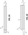
- FIGS. 1A and 1Bare cross sections of alternative color filter embodiments of the present invention.
- FIGS. 2A and 2Bare cross sections of alternative color-filter source wafer embodiments of the present invention corresponding to FIGS. 1A and 1B ;
- FIG. 3is a flow chart in accordance with embodiments of the present invention corresponding to FIGS. 1 and 2 ;
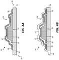
- FIGS. 4A and 4Bare cross sections of pixel structures including an LED and a color filter in embodiments of the present invention.
- FIGS. 5A and 5Bare cross sections of alternative pixel structure source wafer embodiments of the present invention corresponding to FIGS. 4B and 4A ;
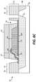
- FIGS. 6A, 6B, and 6Care cross sections of alternative pixel structure source wafer embodiments of the present invention.
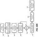
- FIG. 7is a flow chart in accordance with embodiments of the present invention corresponding to FIGS. 4, 5A, 5B, and 6A-6C ;
- FIGS. 8A and 8Bare cross sections of intermediate structures, each including an intermediate substrate, an LED, and a color filter embodiment of the present invention
- FIGS. 9A and 9Bare cross sections of intermediate structure source wafer embodiments of the present invention corresponding to FIGS. 8A and 8B ;
- FIGS. 10A and 10Bare flow charts in accordance with embodiments of the present invention corresponding to FIGS. 8 and 9 ;
- FIGS. 11 and 12are perspectives illustrating embodiments of the present invention.
- FIGS. 13 and 14are flow charts in accordance with display embodiments of the present invention.
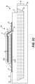
- FIGS. 15-23are cross sections illustrating various embodiments of the present invention.
- FIGS. 24A, 24B, and 25are cross sections of illustrative embodiments of the present invention that include one or more electrodes;
- FIGS. 26A, 26B, and 26Care control circuit diagrams according to illustrative embodiments of the present invention.
- FIGS. 27A and 27Bare perspectives according to illustrative embodiments of the present invention.
- FIGS. 28A and 28Bare cross sections of micro-transfer printable wafers having a color-filter device with multiple color filters and corresponding electrodes in a planar or stacked configuration according to illustrative embodiments of the present invention
- FIG. 28Cis an cross section of micro-transfer printable wafers having multiple color filters in a stacked configuration according to illustrative embodiments of the present invention.
- FIGS. 29 and 30are cross sections of a color-filter device having a single electrodes having connection posts in a micro-transfer printable wafer according to illustrative embodiments of the present invention.
- FIGS. 31-32are cross sections of a color-filter device having two electrodes on a wafer without, and with, connection posts according to illustrative embodiments of the present invention.
- FIG. 33is an cross section of a color-filter device having a control circuit on a wafer with connection posts according to illustrative embodiments of the present invention.
- FIG. 34is a flow chart according to illustrative methods of certain embodiments the present invention.
- Embodiments of the present inventionprovide methods and structures for integrating color filters and light-emitting diodes (LEDs) in displays, for example inorganic light-emitting diodes.
- the methods and structuresare suitable for micro-transfer printing and reduce the amount of color-filter material used and, in some embodiments, the number of patterning steps required.
- the term ‘color filter’refers to a structure that changes the nature or color of light that passes through the color filter.
- the term ‘color filter’can refer to a structure that filters light by absorbing at least a portion of some of the frequencies of the light and transmitting at least a portion of some of the frequencies of the light.
- the frequency of the majority of the absorbed lightis different from the frequency of the majority of the transmitted light.
- Pigments and dyes embedded in a layer of material, such as transparent resinare typically used to form such a structure.
- the term ‘color filter’can also refer to a structure that changes the frequency of at least some of the light by converting at least a portion of some of the frequencies of the light to light of a different frequency and of a lower energy.
- Phosphors and quantum dots embedded in a layer of materialsuch as a transparent resin, such as a curable resin, for example, curable by exposure to heat or electromagnetic radiation, can provide such a structure.
- the term ‘color filter’refers to a structure that filters light or converts light, or both, and can be or include one or more of: a curable resin, a dye, a pigment, a color-conversion material, a semiconductor crystal, a phosphor, and a quantum dot.
- Various embodiments of the present inventioncan include micro-transfer printable structures, source wafers on or in which micro-transfer printable structures are made, destination substrates on which micro-transfer printable structures are micro-transfer printed, or methods of making the micro-transfer printable structures, source wafers, or destination substrates.
- a source waferis a wafer from which devices or structures formed on or in the source wafer are micro-transfer printed to a destination wafer.
- a micro-transfer printed color-filter structure 20comprises a color filter 22 and a fractured color-filter tether 24 physically attached to the color filter 22 .
- a fractured tetheris a tether that is broken, fractured, or cracked by pressure from a transfer stamp in the process of micro-transfer printing.
- a tether physically attached to an elementis a tether that is attached to the element or physically attached to one or more single or multiple layers, structures, multi-layers, or multi-component structures over, on, or in contact with or supporting or protecting the element. As shown in FIG.
- the fractured color-filter tether 24can include at least some of the same material as the color filter 22 .
- the fractured color-filter tether 24 and the color filter 22are part of a common color-filter layer 28 .
- the fractured color-filter tether 24is a portion of the color-filter layer 28 and the color filter 22 is a portion of the color-filter layer 28 separate from the fractured color-filter tether 24 .
- the color-filter structure 20includes an encapsulation layer 31 that also forms the color-filter tether 24 .
- the color-filter tether 24can have a thickness that is thinner than the color filter 22 .
- the micro-transfer printed color-filter structure 20can be a resin or polymer, for example a cured resin or polymer cured by heat or electromagnetic radiation, impregnated with color-filter materials such as dyes, pigments, phosphors, or quantum dots.
- the encapsulation layer 31can be an oxide such as silicon dioxide or a nitride such as silicon nitride.
- a color-filter source wafer 26comprises a source wafer 80 having a patterned sacrificial layer 82 including sacrificial portions 84 separated by anchors 94 .
- the source wafer 80can be a semiconductor, silicon, glass, plastic, resin, or polymer substrate or wafer and can include layers formed on a substrate.
- the sacrificial portions 84can be a designated portion of an anisotropically etchable silicon or a selectively etchable material and the anchors 94 include portions of the source wafer 80 between the sacrificial portions 84 .
- the color-filter layer 28can include patterned color-filter material disposed on the patterned sacrificial layer 82 that form color filters 22 disposed entirely on each sacrificial portion 84 and provides an opening over each sacrificial portion 84 .
- the anchor 94can include portions of the color-filter layer 28 physically connected to the color-filter tethers 24 .
- the color-filter layer 28can include a cured photo-curable material.
- one or more color-filter tethers 24physically connect each color filter 22 to an anchor 94 and physically connects each color filter 22 to an anchor 94 .
- the color-filter tether 24can include at least some of the same material as the color filter 22 and can be part of a common color-filter layer 28 .
- an encapsulation layer 31encapsulates the color filter 22 . A portion of the encapsulation layer 31 forms at least a part of the color-filter tether 24 .
- the encapsulation layer 31can be an oxide such as silicon dioxide or a nitride such as silicon nitride deposited and patterned using photolithographic processes.
- a method of making a color-filter source wafer 26comprises providing a source wafer 80 having a patterned sacrificial layer 82 including sacrificial portions 84 separated by anchors 94 in step 200 , disposing a color-filter layer 28 on the source wafer 80 in step 210 , and patterning a color filter 22 entirely on each sacrificial portion 84 in step 220 .
- the color-filter layer 28can be disposed on the patterned sacrificial layer 82 in step 210 by coating, for example, spin coating or curtain coating, and patterned in step 220 by exposing the color-filter layer 28 to electromagnetic energy (for example, ultra-violet light) through a patterned mask and washing away the uncured (unexposed) photo-curable material.
- electromagnetic energyfor example, ultra-violet light
- an encapsulation layer 31is deposited, for example by sputtering or evaporation, and patterned in step 225 , using photolithographic methods and materials.
- the sacrificial portion 84is etched to form one or more color-filter tethers 24 physically connecting each color filter 22 to an anchor 94 .
- Etchingcan be accomplished, for example, by exposing the sacrificial portion 84 to an acid that selectively etches the sacrificial portion 84 material or anisotropically etches the sacrificial portion 84 in preference to the anchors 94 .
- a color filter 22is micro-transfer printed from the color-filter source wafer 26 to a destination substrate, such as a display substrate, by pressing a stamp, such as a PDMS stamp against the color-filter structure 20 to fracture the color-filter tether 24 , adhere the color-filter structure 20 to the stamp, transport the stamp and the color-filter structure 20 to the destination substrate and adhere the color-filter structure 20 to the destination substrate, and remove the stamp.
- the destination substratecan include an adhesive layer that is then cured to permanently adhere the color-filter structure 20 to the destination substrate.
- a micro-transfer printed pixel structure 30comprises a light-emitting diode (LED) 33 having a light-emitting side 39 , a color filter 22 disposed adjacent to the light-emitting side 39 of the LED 33 , and a fractured pixel tether 34 physically attached to the LED 33 or a fractured pixel tether 34 physically attached to the LED 33 and to the color filter 22 or layers disposed on the LED 33 or color filter 22 .
- LEDlight-emitting diode
- a color filter 22is adjacent to the light-emitting side 39 of the LED 33 if it is closer to the light-emitting side 39 of the LED 33 than any other side of the LED 33 and if it is located in optical association with LED 33 to absorb or transmit light emitted by the LED 33 .
- a color filter 22can be in contact with, formed on, or adhered to an LED 33 and can be physically located within 0 to 250 microns of the LED 33 .
- the color filter 22can be formed in a layer that is essentially planar or has opposing planar surfaces.
- the color filter 22can be a semiconductor crystal structure.
- the LED 33is a part of an LED structure 32 that includes a fractured LED tether 35 disposed, for example, by micro-transfer printing the LED 33 from an LED source wafer onto the color filter 22 .
- the LED structure 32can include patterned dielectric structures 37 that electrically isolate portions of the LED 33 and expose other portions of the LED 33 that are electrically connected to electrodes 38 .
- the electrodes 38can provide electrical power to the LED 33 to cause the LED 33 to emit light, for example through the light-emitting side 39 and through the color filter 22 , so that the LED structure 32 emits color-filtered light.
- the fractured pixel tether 34can be the fractured color-filter tether 24 and can include at least some of the same material as the color filter 22 , as shown in FIG. 4A .
- the color filter 22 and the color-filter tether 24can be a color-filter structure 20 .
- an encapsulation layer 31can encapsulate the LED 33 and color filter 22 and form a part of the fractured pixel tether 34 or the fractured pixel tether 34 can be a part of or attached to the encapsulation layer 31 .
- the color filter 22is attached to a color-filter tether 24 (as in FIG.
- an encapsulation layer 31encapsulates the LED 33 , the color filter 22 , and the color-filter tether 24 and also forms a part of the fractured pixel tether 34 or the fractured pixel tether 34 can be a part of or attached to the encapsulation layer 31 (i.e., the encapsulation layer 31 of FIG. 4B is applied to the structure of FIG. 4A , see FIG. 5A described below).
- a pixel structure source wafer 36comprises a source wafer 80 having a patterned sacrificial layer 82 including sacrificial portions 84 separated by anchors 94 .
- An LED 33is disposed entirely on or over each sacrificial portion 84 .
- the LED 33has a light-emitting side 39 .
- a color filter 22is disposed adjacent to the light-emitting side 39 of the LED 33 and is disposed entirely on or over each sacrificial portion 84 .
- One or more pixel tethers 34physically connects each LED 33 or color filter 22 to an anchor 94 . In the embodiment of FIG.
- an encapsulation layer 31encapsulates the LED 33 and color filter 22 and forms at least a portion of the pixel tether 34 and the color-filter structure 20 includes a color-filter tether 24 in the color-filter layer 28 .
- the pixel tether 34can be thinner than the color-filter structure 20 to facilitate fracturing.
- the encapsulation layer 31can be an oxide such as silicon dioxide or a nitride such as silicon nitride deposited and patterned using photolithographic processes.
- the color-filter layer 28forms at least a portion of the pixel tether 34 .
- the source wafer 80is or includes a glass, a polymer, a semiconductor, or silicon.
- the sacrificial portions 84can be a designated portion of an anisotropically etchable silicon or a selectively etchable material, or any one of or combination of these.
- the fractured pixel tether 34can include at least some of the same material as the color filter 22 .
- a method of making a pixel structure source wafer 36comprises providing a source wafer 80 having a patterned sacrificial layer 82 including sacrificial portions 84 separated by anchors 94 in step 300 .
- an LED 33is disposed entirely on or over each sacrificial portion 84 , the LED 33 having a light-emitting side 39 , and a color filter 22 provided adjacent to the light-emitting side 39 of each LED 33 .
- the color filter 22is also disposed entirely on or over each sacrificial portion 84 to form a pixel structure 30 .
- the sacrificial portion 84is etched in step 330 to form one or more pixel tethers 34 physically connecting each pixel structure 30 to an anchor 94 .
- the pixel structure 30is micro-transfer printed from the pixel structure source wafer 36 to a destination substrate.
- the color filter 22 and LED 33can be provided or disposed in a variety of ways according to a corresponding variety of embodiments of the present invention.
- the color filter 22is micro-transfer printed in step 301 from a color-filter source wafer 26 onto the source wafer 80 entirely over the sacrificial portion 84 and an LED 33 is micro-transfer printed from an LED source wafer onto the color filter 22 in step 302 so that the color filter 22 is disposed adjacent to the light-emitting side 39 of the LED 33 .
- the color filter 22can be part of a color-filter structure 20 with a fractured color-filter tether 24 as shown in FIG.
- An encapsulation layer 31is optionally disposed, for example by deposition using any of a variety of methods such as sputtering or evaporation, and can form at least a portion of the pixel tether 34 .
- a color-filter layer 28is disposed over the patterned sacrificial layer 82 , for example by coating, in step 303 and then patterned in step 320 , for example using photolithographic methods and materials as described above.
- the color filter 22is patterned in step 302 on the source wafer 80 entirely over the sacrificial portion 84 and the LED structure 32 is micro-transfer printed from an LED source wafer onto the color filter 22 in step 302 so that the color filter 22 is disposed adjacent to the light-emitting side 39 of the LED 33 .
- the pixel tether 34is then the same tether as the color-filter tether 24 .
- the fractured pixel tether 34can include the LED tether 35 and can include at least some of the same material as the color filter 22 .
- the pixel tether 34can also include at least some of the same material as the LED 33 .
- an optional reflective or conductive electrode 38 R or layeris disposed on the sacrificial portion 84 . Electrical power is provided to the LED 33 through the electrodes 38 , 38 R. As shown in FIGS. 6A and 6B , electrodes 38 can be contacted through vias in the color-filter layer 28 .
- the color-filter layer 28is patterned to form the vias and the color filter 22 disposed adjacent to the light-emitting side 39 of the LED 33 in the pixel structure 30 .
- the color-filter layer 28can provide the pixel tether 34 (as shown in FIG. 6A ) or an encapsulation layer 31 can be coated over the color-filter structure 20 and form at least a portion of the pixel tether 34 (as in FIG. 6B ).
- a method of making a pixel structure source wafer 36 in embodiments corresponding to FIGS. 6A and 6Bincludes micro-transfer printing an LED 33 from an LED source wafer onto the source wafer 80 entirely over the sacrificial portion 84 in step 305 .
- the LED 33can be part of an LED structure 32 including an LED tether 35 .
- a color-filter layer 28is coated over the LED 33 in step 307 .
- the color-filter layer 28is patterned in step 322 , for example using photolithography, to form a color filter 22 disposed adjacent to the light-emitting side 39 of the LED 33 .
- Viascan be formed in the same step to expose the electrodes 38 , 38 R and the color-filter layer 28 can form the pixel tether 34 so that the pixel tether 34 is a color-filter tether 24 .
- the color-filter layer 28is patterned to form the color filter 22 only and an encapsulation layer 31 is disposed, for example by deposition using any of a variety of methods such as sputtering or evaporation, to form at least a portion of the pixel tether 34 .
- the pixel tether 34can be thinner than the color filter 22 to facilitate fracturing.
- color filters 22are micro-transfer printed from a color-filter source wafer 26 onto the LED structure 32 in step 306 to form the pixel structure 30 .
- the color filters 22can be part of a color-filter structure 20 that includes a color-filter tether 24 .
- An adhesive or planarizing layer 50can be used to adhere the color-filter structure 20 to the LED structure 32 , for example an uncured curable encapsulation layer 31 , and then cured.
- a micro-transfer printed intermediate structure 40comprises an intermediate substrate 48 and one or more pixel structures 30 disposed on the intermediate substrate 48 .
- Each pixel structure 30includes an LED 33 having a light-emitting side 39 , a color filter 22 disposed adjacent to the light-emitting side 39 of the LED 33 , and a fractured pixel tether 34 physically attached to the LED 33 or physically attached to the LED 30 and to the color filter 22 .
- the pixel structure 30can be any of the pixel structures 30 described herein, for example including any of the pixel structures 30 illustrate in FIGS. 4, 5A, 5B 6 A, 6 B, and 6 C and can include encapsulation layers 31 (not shown).
- the LED 33can be a part of an LED structure 32 that also includes a fractured LED tether 35 .
- the color filter 22can be a part of a color-filter structure 20 that also includes a fractured color-filter tether 24 .
- the color filter 22is not attached to a color-filter tether 24 but is formed in place.
- the fractured pixel tether 34can be or include any of the color-filter tether 24 , the LED tether 35 , and a portion or materials of an encapsulation layer 31 (not shown).
- a fractured intermediate tether 44is physically attached to the intermediate substrate 48 to form a micro-transfer printed intermediate structure 40 .
- the intermediate substrate 48can be or include a glass, a polymer, a semiconductor, or silicon, or any one or any combination of these.
- the fractured intermediate tether 44can include at least some of the same material as the color filter 22 , or at least some of the same material as the intermediate substrate 48 , or both, or an encapsulation layer 31 (not shown) encapsulating the LED 33 and color filter 22 can form at least a part of the fractured intermediate tether 44 or the fractured intermediate tether 44 can be a part of the encapsulation layer 31 (similar to the structure of FIG. 5A ).
- an intermediate structure source wafer 46comprises a source wafer 80 having a patterned sacrificial layer 82 including sacrificial portions 84 separated by anchors 94 .
- a patterned intermediate substrate layer 42 disposed on or over the patterned sacrificial layer 82forms separate and independent intermediate substrates 48 .
- Each intermediate substrate 48is disposed entirely over a sacrificial portion 84 .
- One or more pixel structures 30are disposed entirely on each intermediate substrate 48 .
- Each pixel structure 30includes an LED structure 32 having an LED 33 with a fractured LED tether 35 , the LED 33 having a light-emitting side 39 , and a color filter 22 disposed adjacent to the light-emitting side 39 of the LED 33 .
- One or more fractured pixel tethers 34are physically attached to each pixel structure 30 and an intermediate tether 44 is physically attached to the intermediate substrate 48 .
- the source waferis or includes a glass, a polymer, a semiconductor, or silicon
- the intermediate substrate 48is or includes a glass, a polymer, a semiconductor, or silicon
- the sacrificial portions 84are a designated portion of an anisotropically etchable silicon or a selectively etchable material, or any one or any combination of these.
- the fractured pixel tether 34can include at least some of the same material as the color filter 22 , at least some of the same material as the LED 33 , or portions of or materials from an encapsulation layer 31 encapsulating the color filter 22 and LED 33 .
- the intermediate tether 44can include at least some of the same material as the color filter 22 or some of the material from an encapsulation layer 31 .
- the intermediate tether 44can include at least some of the same material as the intermediate substrate 48 .
- the intermediate tether 44includes at least some of the same material as the source wafer.
- the intermediate substrate 48includes portions of or materials from the color filter 22 .
- the color filter 22is part of a color-filter structure 22 including a color-filter tether 24 that is micro-transfer printed onto or over the intermediate substrate 48 .
- the color filter 22is coated and patterned using photolithography on the intermediate substrate 48 so that no color-filter tether 24 is present.
- a method of making an intermediate structure source wafer 46comprises providing in step 400 a source wafer having a patterned sacrificial layer 82 including sacrificial portions 84 separated by anchors 94 .
- an intermediate substrate layer 42is disposed over the patterned sacrificial layer 82 and patterned in step 409 to form an intermediate substrate 48 entirely over each sacrificial portion 84 .
- one or more pixel structures 30are disposed on each intermediate substrate 48 entirely on or over each sacrificial portion 84 and intermediate substrate 48 .
- Each pixel structure 30includes an LED 33 having a light-emitting side 39 , a color filter 22 disposed adjacent to the light-emitting side 39 of the LED 33 , and a fractured pixel tether 34 physically attached to the pixel structure 30 to form an intermediate structure 40 .
- This stepis repeated as often as desired until done in step 410 , for example to dispose a red, green, and blue pixel structure 30 on the intermediate substrate 48 .
- the pixel structurescan be electrically connected with wires on the intermediate substrate 48 in step 430 .
- the intermediate structure 40can be a full-color pixel with improved color gamut including a red LED 33 emitting red light through a red color filter 22 R, a green LED 33 emitting green light through a green color filter 22 G, and a blue LED 33 emitting blue light through a blue color filter 22 B.
- the sacrificial portion 84is etched to form one or more intermediate tethers 44 physically connecting each intermediate structure 40 to an anchor 94 in step 440 and an intermediate structure 40 is micro-transfer printed in step 450 from the intermediate structure source wafer 46 to a destination substrate, such as a display substrate.
- one or more pixel structures 30are disposed on each intermediate substrate 48 entirely on or over each sacrificial portion 84 by micro-transfer printing a pixel structure 30 from a pixel structure source wafer 36 onto the intermediate substrate 48 of the source wafer 80 entirely over the sacrificial portion 84 .
- one or more pixel structures 30are disposed on each intermediate substrate 48 entirely on or over each sacrificial portion 84 by micro-transfer printing a color filter 22 in step 401 from a color-filter source wafer 26 onto the intermediate substrate 48 of the source wafer 80 entirely over the sacrificial portion 84 and then micro-transfer printing an LED 33 from an LED source wafer onto or over the color filter 22 in step 402 so that the color filter 22 is disposed adjacent to the light-emitting side 39 of the LED 33 , for example in a bottom-emitting configuration.
- the stepsare reversed so that the color-filter structure 20 is micro-transfer printed onto the LED structure 32 .
- an LED 33is micro-transfer printed from an LED source wafer onto the intermediate substrate 48 of the source wafer 80 entirely over the sacrificial portion 84 in step 405 and a color filter 22 is micro-transfer printed from a color-filter source wafer 26 onto the LED 33 in step 406 so that the color filter 22 is disposed adjacent to the light-emitting side 39 of the LED 33 in a top-emitting configuration.
- a planarizing or adhesive layer 50can be provided to adhere the color filter 22 to the LED 33 ( FIG. 6C ).
- an LED 33is micro-transfer printed from an LED source wafer onto the source wafer 80 entirely over the sacrificial portion 84 and intermediate substrate 48 in step 405 and a color filter 22 is formed over the LED 33 by disposing the color-filter layer 28 over the LED 33 in step 407 and patterning the color-filter layer 28 in step 422 so that the color filter 22 is disposed adjacent to the light-emitting side 39 of the LED 33 .
- a color filter 22is formed on the source wafer 80 entirely over the sacrificial portion 84 by disposing the color-filter layer 28 over the LED 33 in step 403 , patterning the color-filter layer 28 in step 420 , and micro-transfer printing an LED 33 from an LED source wafer onto the color filter 22 so that the color filter 22 is disposed adjacent to the light-emitting side 39 of the LED 33 in step 402 .
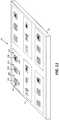
- an inorganic LED display 10includes a display substrate 12 .
- a plurality of pixel structures 30e.g., red pixel structure 30 R, green pixel structure 30 G, and blue pixel structure 30 B
- Each pixel structure 30includes one or more LEDs 33 , each LED 33 having a light-emitting side 39 ( FIG. 4 ), and a color filter 22 corresponding to each LED 33 , each color filter 22 disposed adjacent to the light-emitting side 39 of the corresponding LED 33 .
- the plurality of pixel structures 30can include a red pixel structure 30 R having a red LED 33 R emitting red light through a red color filter 22 R, a green pixel structure 30 G having a green LED 33 G emitting green light through a green color filter 22 G, and a blue pixel structure 30 B having a blue LED 33 B emitting blue light through a blue color filter 22 B.
- the red, green, and blue pixel structures 30 R, 30 G, 30 Bcan form a full-color pixel 14 having improved color gamut.
- each color filter 22can be located between the display substrate 12 and a corresponding LED 33 (a bottom-emitter configuration) or each LED 33 can be located between the display substrate 12 and a corresponding color filter 22 (a top-emitter configuration).
- Each LED 33can be part of a micro-transfer printed LED structure 32 including an LED 33 having a fractured LED tether 35 physically attached to the LED 33 .
- Each color filter 22can be part of a color-filter structure 20 having a color a micro-transfer printed color filter 22 having a fractured color-filter tether 24 physically attached to the color filter 22 .
- Each pixel structure 30can be a micro-transfer printed pixel structure 30 having a fractured pixel tether 34 . (Tethers are not shown in FIG. 11 .)
- each pixel structure 30is part of an intermediate structure 40 having an intermediate substrate 48 and a fractured intermediate tether 44 .
- the pixel structures 30can be micro-transfer printed onto the intermediate substrate 48 of the intermediate structure 40 , so that each pixel structure 30 includes a pixel tether 34 ( FIG. 4 ). (Tethers are not shown in FIG. 12 .)
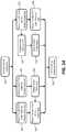
- a method of making an LED display 10comprises providing a display substrate 12 in step 500 and disposing a plurality of pixel structures 30 on the display substrate 12 in step 560 .
- Each pixel structure 30includes one or more LEDs 33 , each LED 33 having a light-emitting side 39 ( FIG. 4 ), and a color filter 22 corresponding to each LED 33 .
- Each color filter 22is disposed adjacent to the light-emitting side 39 of the corresponding LED 33 .
- the pixel structures 30can be micro-transfer printed from a pixel structure source wafer 36 to the display substrate 12 .
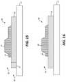
- FIG. 15is a simplified illustration of such a structure.
- substrate wiresare formed, for example photolithographically, over the display substrate 12 and electrically connected to the LEDs 33 in the pixel structures 30 .
- intermediate structures 40are micro-transfer printed to the display substrate 12 from an intermediate structure source wafer 46 in step 570 and electrically connected in step 550 .
- FIG. 19is a simplified illustration of this structure in which the color filter 22 is micro-transfer printed onto the intermediate substrate 48
- FIG. 20is a simplified illustration of this structure in which the color filter 22 is coated and patterned on the intermediate substrate 48 and the LED 33 micro-transfer printed onto or over the color filter 22 .
- FIG. 21is a simplified illustration for the case in which the color filter 22 is coated and patterned over the micro-transfer printed LED 33
- FIG. 22is a simplified illustration for the case in which the color filter 22 is micro-transfer printed over the micro-transfer printed LED 33 , for example on a planarization or adhesive layer 50 .
- an LED 33is micro-transfer printed from an LED source wafer onto the display substrate 12 in step 505 and a color filter 22 is formed over the LED 33 by disposing the color-filter layer 28 over the LED 33 in step 507 and patterning the color-filter layer 28 in step 522 so that the color filter 22 is disposed adjacent to the light-emitting side 39 of the LED 33 as shown in the simplified illustration of FIG. 17 .
- a color filter 22is micro-transfer printed on the LED 33 in step 506 as shown in the simplified illustration of FIG. 18 .
- the color filter 22is micro-transfer printed onto the display substrate 12 in step 501 and the LED 33 is micro-transfer printed from an LED source wafer onto the micro-transfer printed color filter 22 so that the color filter 22 is disposed adjacent to the light-emitting side 39 of the LED 33 in step 502 .
- FIG. 15is also a simplified illustration of this structure.
- a color filter 22is formed on the display substrate 12 by disposing the color-filter layer 28 over the display substrate 12 in step 503 , patterning the color-filter layer 28 in step 520 , and micro-transfer printing an LED 33 from an LED source wafer onto or over the patterned color filter 22 in step 502 so that the color filter 22 is disposed adjacent to the light-emitting side 39 of the LED 33 .
- FIG. 16is a simplified illustration of this structure.
- Both the intermediate structures 40 and the pixel structures 30can be constructed with connection posts.
- FIG. 23illustrates an intermediate structure source wafer 46 including connection posts 86 electrically connected to the LED 33 .
- the encapsulation layer 31forms the intermediate tether.
- the color-filter structure 20includes a color filter 20 and a fractured color-filter tether 24 that is micro-transfer printed onto the intermediate substrate 48 and the LED structure 32 is micro-transfer printed onto the color-filter structure 20 to make a pixel structure 30 .
- the present inventionprovides simple structures and methods for constructing flat-panel displays 10 that do not require large and expensive fabrication facilities.
- micro-transfer printingto dispose LEDs 33 , pixel structures 30 , or intermediate structures 40 , the need for extensive flat-panel processing tools for large substrates with high resolution are mitigated.
- High-resolution processingcan be performed on smaller wafers, for example 8-inch diameter wafers or 12-inch-diameter wafers using much smaller equipment.
- the present inventionprovides a way to greatly reduce the amount of color-filter material used in a flat-panel display.
- the following exampleis illustrative and structure sizes are chosen for simplicity.
- Photo-curable color filters and black-matrix materials in flat-panel displaysare typically deposited by coating the entire substrate and then photolithographically exposing the materials through a mask to pattern-wise cure the materials in desired pixel locations and then wash away the uncured material.
- one square meter of each material typeis deposited.
- an inorganic LED display 10 using micro-transfer printed color filters 22 , pixel structures 30 , or intermediate structures 40uses a greatly reduced quantity of color-filter material.
- a 4 k display having eight million three-color pixelsis presumed.
- Each light emitter (LED 33 )is presumed to be formed in a 20-micron by 20-micron cell area on an LED source wafer including LED tethers 35 and anchor 94 areas. Since the color filters 22 filter or process the light emitted from the LEDs 33 , they are of similar size and, to enhance micro-transfer printing efficiency, have the same spatial arrangement and pitch.
- the LEDs 33 and color filters 22are assumed to be arranged in a rectangle of four thousand by two thousand elements, occupying a space of 8 cm by 4 cm.
- the color filters 22are constructed as part of the color filter source wafer 26 and the minimum area of color-filter material necessary is 32 square centimeters.
- the conventional processrequires 10,000 square centimeters, resulting in a cost reduction of color-filter materials alone of more than 300 times (thus using 0.3% as much material). The same savings are found for the micro-transfer printed pixel structure 30 embodiments and any embodiment in which the color filters 22 are micro-transfer printed.
- the coated areais larger.
- the intermediate substrates 48are 90 microns by 90 microns, include three LEDs 33 and a controller integrated circuit, and are separated by 10 microns on the intermediate structure source wafer 46 , an area of 100 microns by 100 microns is coated for each color and each pixel.
- the minimum area of color-filter materialis 800 square centimeters, resulting in a cost reduction of color-filter materials of 12.5 (using 8 percent as much material).
- the LEDs 33can be arranged and electrically connected in rows and columns over the display substrate 12 to enable matrix addressing with electrical signals supplied by passive- or active-matrix controllers. Electrical signals from the controllers can cause the LEDs 33 to emit light.
- the display substrate 12can be polymer, plastic, resin, polyimide, PEN, PET, metal, metal foil, glass, a semiconductor, or sapphire.
- Each LED 33can be a light-emitting diode (LED), a micro-LED, a laser, a diode laser, or a vertical cavity surface emitting laser and can include known light-emitting diode materials and structures.
- the LEDs 33can comprise an inorganic solid single-crystal direct bandgap light emitter, can emit visible light, such as red, green, blue, yellow, or cyan light, violet, or ultra-violet light, and can emit either coherent or incoherent light.
- the light emitters used hereincan have at least one of a width, length, and height from 2 to 5 ⁇ m, 4 to 10 ⁇ m, 10 to 20 ⁇ m, or 20 to 50 ⁇ m.
- Light emitted from or through the color filters 22can be a very pure light and highly saturated and can have a full width half max (FWHM) less than or equal to 100 nm, 50 nm, or even less than or equal to 20 nm.
- FWHMfull width half max
- a full-color pixel 14for example in an intermediate structure 40 includes one each of a red, green, and blue LEDs 33 R, 33 G, 33 B with corresponding red, green, and blue color filters 22 R, 22 G, 22 B, as shown in FIG. 12 .
- the red pixeldoes not include a red color filter 22 R or the red and blue pixels do not include red or blue color filters 22 R, 22 B, respectively.
- a blue LED 33 Bis used for all of the pixels and the red and green pixels employ a color filter including red and green color-change materials, respectively.
- an ultra-violet LED 33is used for all of the pixels and the red, green, and blue pixels employ a color filter including red, green, and blue color-change materials, respectively.
- a color filter including red, green, and blue color-change materialsare possible and included in the present invention.
- micro-LEDs 33 and micro-LED displayscan be found in U.S. Provisional patent application Ser. No. 14/743,981, filed Jun. 18, 2015, entitled Micro Assembled LED Displays and Lighting Elements, which is hereby incorporated by reference in its entirety.
- Micro-transfer methodsare described in U.S. Pat. Nos. 8,722,458, 7,622,367 and 8,506,867, each of which is hereby incorporated by reference in its entirety.
- color filters 22are controllable color filters 22 disposed on or over a color-filter substrate 72 .
- the color filters 22can be responsive to control signals such as a voltage or electric field, for example, provided between electrodes disposed on either side of the color filter 22 or to heat provided to the color filters 22 , where the color filters 22 are at least substantially planar and have a thickness significantly less than its extent over the color-filter substrate 72 , for example length and width.
- Color filters 22can be very thin, for example having a thickness less than or equal to ten microns, less than or equal to one micron, less than or equal to 100 nm, less than or equal to 50 nm, or less than or equal to 20 nm.
- color filters 22are controlled to absorb, transmit, or reflect different colors of light.
- Color filters 22can include optical spacers to enable constructive and destructive optical interference at desired frequencies.
- Color filter 22 and optical spacerscan be deposited and patterned using photolithographic methods and materials.
- a color-filter device 99comprises a color filter 22 and at least one electrical conductor 38 disposed in contact with the color filter 22 . At least a portion of a color-filter tether 24 is attached to the color filter 22 or structures formed in contact with or supporting the color filter 22 .
- a color-filter tether 24can also be a pixel tether 34 (as shown in FIGS. 27A, 27B ) and can be broken (e.g., fractured) (as shown in FIGS. 24A, 24B, and 25 ).
- a color filter 22is or includes one or more of: a phase-change material, an ink, a gel, a metallopolymer material, or a photonic crystal.
- the color filter 22includes photonic crystals embedded within an electroactive polymer.
- Other usable color-filter materialsinclude germanium-antimony-tellurium (GST).
- GSTgermanium-antimony-tellurium
- a color-filter comprising GSTcan change phase with applied voltage of less 10 volts amplitude and a sub-millisecond duration.
- the color filter 22includes additional optical layers or structures, for example spacing layers, to optimize the optical effect of the controllable color-filter material.
- the color filter 22can include multiple layers of different materials, for example multiple layers of controllable materials and one or more optical spacer layers, to provide a wide range of potential states and colors.
- a color filter 22can be electrically controlled.
- the color-filter materialis a phase-change material that can be controlled to switch, for example, from an amorphous state to a crystalline state or from a crystalline state to an amorphous state.
- Each of the amorphous state and the crystalline statecan have a different optical attribute, such as color.
- a single color filter 22can be controlled to have a variety of colors.
- a color-filter device 99comprises the electrical conductor 38 , for example a bottom electrode 38 M ( FIG. 24A ) or top electrode 38 T ( FIG. 24B ) that is resistive or has a portion that is a resistive electrode 38 V and is heated when electrical current flows through the resistive electrode 38 V.
- the resistive electrode 38 Vcan be, for example a metal or metal alloy, such as aluminum, or a semiconductor.
- the heated resistive electrode 38 Vthen heats the color filter 22 in response to the electrical current passed through the resistive electrode 38 V.
- a color filter 22is or includes a phase-change material that changes the color of light filtered by the color filter 22 in response to heat.
- an electrical conductor 38 or resistive electrode 38 Vis substantially transparent and allows visible light to pass through.
- Light 70 A incident on the color filter 22is transmitted through the resistive electrode 38 V and passes through the color filter 22 once.
- an electrical conductor 38 or resistive electrode 38 Vis substantially reflective and reflects visible light.
- Light 70 B incident on the color filter 22is reflected by the resistive electrode 38 V, passing through the color filter 22 twice.
- a color filter 22is a reflective color filter 22 and reflects light itself.
- a color filter 22is a transmissive color filter 22 and transmits light.
- a transparent electrodetransmits more than 50% of the light incident on the transparent electrode (e.g., more than 70%, 80%, 90%, or 95%) and a reflective electrode reflects more than 50% the light incident on the reflective electrode (e.g., more than 70%, 80%, 90%, or 95%).
- a reflective electrodecan be a metal or metal alloy, such as aluminum, silver, titanium, or tin or alloys thereof.
- Transmissive electrodescan be thin metal or metal alloys or transparent metal oxides such as indium tin oxide.
- the color filter 22has a first side 21 a and a second side 21 b opposed to the first side 21 a
- the electrical conductor 38is a first electrode 38 M disposed on the first side 21 a of the color filter 22
- a second electrode 38 Tis disposed on the second side 21 b of the color filter 22 and is part of another electrical conductor 38 .
- both the first and second electrodes 38 M, 38 Tare transparent, the first electrode 38 M is transparent and the second electrode 38 T is reflective, or alternatively the second electrode 38 T is transparent and the first electrode 38 M is reflective.
- the color filter 22can alter the color of light that it transmits, reflects, or absorbs in response to an electrical current, a voltage, or an electrical field provided between the first and second electrodes 38 M, 38 T.
- the electrical current or voltagecan be provided by a controller, e.g., an electronic circuit, provided on the color-filter substrate 72 or a controller external to a color-filter device 99 or color-filter substrate 72 (e.g., a micro-transfer printable color-filter device or substrate).
- a controllere.g., an electronic circuit
- a color-filter device 99 or color-filter substrate 72e.g., a micro-transfer printable color-filter device or substrate.
- some variable and controllable color-filter materialsrequire a relatively large amount of current to change their state, for example if the color-filter material requires heating or a high current density. In large-area devices this can be a problem, since much applied power is lost via substrate interconnect wiring and therefore requires a very large drive current and voltage that result in significant substrate heating. According to some embodiments of the present invention, this problem can be mitigated by providing charge storage locally to each color filter 22 or group of color filters 22 .
- a control circuit 66comprises a switch 60 , for example a transistor, controllably connecting a capacitor 62 to an electrical conductor 38 (e.g., resistive electrode 38 V, first electrode 38 M, or second electrode 38 T).
- the capacitor 62stores charge provided through electrical connections to ground and V dd power supplies.
- the capacitor 62can be charged for a relatively long period of time at a low current rate through the interconnect wiring, then discharged relatively quickly and at high current density into the color filter 22 or a heater disposed adjacent to the color filter 22 (e.g., the resistive electrode 38 V) by a local transistor (e.g., switch 60 ) over very short interconnects inside the pixel.
- the color filter 22is converted to a crystalline state with a smaller amplitude and longer term electrical pulse and converted to an amorphous state with a larger amplitude and shorter term electrical pulse, for example at 10 volts.
- the capacitor 62when a control signal turns on the switch 60 , the capacitor 62 discharges through the resistive electrode 38 V (bottom electrode 38 M as shown in FIG. 24A ).
- the switch 60can provide power to the top electrode 38 T or bottom electrode 38 M (but not both) while the other electrode is grounded.
- a capacitor 62stores power locally to each color filter 22 on the color-filter substrate 72 .
- the instantaneous current passing through the power linesis reduced.
- local capacitors 62can be charged once per frame update rather than once per line or pixel update, reducing the current flow density through the power lines by a factor corresponding to the number of lines or pixels.
- control circuit 66is disposed underneath the bottom electrode 38 M so that the extent of the color filter 22 over the color-filter substrate 72 includes the control circuit 66 , enabling a large fill factor for the color-filter device 99 .
- an increased fill factorcan improve display contrast.
- a circuit in accordance with the illustrative embodiment of FIG. 26Acan additionally include another switch (isolation switch 61 ) that isolates the power supply from the capacitor 62 .
- the isolation switch 61can be turned on when the control switch 60 is turned off and can be turned off when the control switch 60 is turned on. This enables precise control of the amount of charge deposited in the capacitor 62 and the charge that is applied to the resistive electrode 38 V, resulting in very precise heating or other control of the characteristics of the load (e.g., resistive electrode 38 V).
- isolation switch 61enables more relaxed control and timing signals and eliminates the effect of the load from the V dd power supply and wiring thereby keeping the V dd across the array at a more stable voltage.
- the isolation switch 61 characteristicssuch as transistor width and length can be chosen to limit the current into the capacitor 62 thereby minimizing voltage drops on V dd and stabilizing the V dd across the array. A lower, more even current is applied during charging and the sharp high current impulse into the load is isolated from the V dd supply.
- two different power suppliesV dd1 and V dd2 , are provided, each with a separate isolation switch 61 , that are alternatively controlled and can provide different amounts of power or voltage to the load.
- One isolation switch 61provides a connection to a V dd1 power supply for one state transition (e.g., a transition to a crystalline state), and the other isolation switch 61 provides a connection to a V dd2 power supply for a second state transition (e.g., a transition to an amorphous state).
- thiscan be necessary in a system where selection between amorphous and crystalline states would need to be made simultaneously.
- such circuitsallow the capacitor voltage to be set appropriately for each state transition without requiring adjustment of the single V dd between the states.
- a color-filter device 99can include a readout terminal that, in some embodiments, also includes an isolation switch 61 .
- a readout circuitcan detect a change in permittivity and/or conductivity of a color-filter device 99 which is an indication of amorphous or crystalline color-filter material state. This structure already exists for a color-filter device 99 that uses the color-filter material as its own heater via current conduction through the color-filter material.
- the readout circuitscan sense a change in permittivity/conductivity of a color-filter material, for example, by measuring current through, or voltage across, a resistive electrode 38 V.
- a color filter 22has two states, a programmed crystal state and an erased amorphous state. Without wishing to be bound to any particular theory, in general, changing a color filter 22 to a crystalline state is more difficult. Therefore, if states are interpreted in an application as a valid or invalid indicator, it can be useful to consider the crystal state as valid and the amorphous state as invalid, since any unauthorized tampering can more easily convert the color filter 22 from the crystal (valid) to amorphous (invalid) state than the reverse.
- local circuitscan be added to each color-filter device 99 to detect the state of the color filter 22 .
- a color-filter device 99can comprise a plurality of color filters 22 disposed on a common color-filter substrate 72 .
- Each color filter 22 of the plurality of color filters 22can have an electrically separate electrical conductor 38 disposed in contact with the color filter 22 .
- the color of light filtered by each color filter 22 of the plurality of color filters 22is a different color of light from the color of light filtered by other color filters 22 of the plurality of color filters 22 .
- a color-filter device 99includes three color filters 22 , each controllably filtering a different color of light, for example red, green, and blue, to form a pixel in a display 10 (as shown in FIGS.
- each color filter 22can have a capacitor 62 and switch 60 .
- a common capacitor 62can be provided for the group of color filters 22 in the color-filter device 99 (e.g., as in FIG. 27A ) and controllably connected through individual switches 60 to each of the color filters 22 in the color-filter device 99 .
- a plurality of color-filter devices 99are disposed on an intermediate substrate 48 that is separate from the color-filter substrates 72 .
- the intermediate substrates 48are disposed on the display substrate 12 (as shown in FIG. 12 ).
- Each color filter 22can have an attached color-filter tether 24 so that the color filters 22 can be, but are not necessarily, micro-transfer printed from a color filter source wafer 80 to the intermediate substrate 48 .
- the intermediate substrate 48can have an intermediate tether 44 so that the intermediate substrate 48 itself can be, for example, micro-transfer printed to a destination or display substrate 12 .
- the intermediate tether 44can be a portion of or attached to the intermediate substrate 48 or a layer or structure formed on, in, over, or under the intermediate substrate 48 .
- a color-filter device 99can be formed or provided on a source wafer 80 .
- the source wafer 80has a substrate comprising a sacrificial layer 82 with patterned sacrificial portion 84 separate by anchors 94 .
- One or more micro-transfer color filters 22are disposed entirely over each sacrificial portion 82 .
- a color-filter device source wafer 80can comprise a plurality of color filters 22 disposed adjacent to each other in a common plane. Each color filter 22 of the plurality of color filters 22 has an electrically separate electrical conductor 38 disposed in contact with the color filter 22 .
- each of the different color filters 22can be made on a different color-filter device source wafer 80 , thereby simplifying the manufacturing process, reducing costs and improving quality or yield of the color filters 22 .
- a color-filter device 99can comprise a plurality of color filters 22 and electrical conductors 39 disposed in a stack entirely over each sacrificial portion 82 .
- the color filters 22are disposed in a stack entirely over each sacrificial portion 82 and have a common electrical conductor 38 .
- a micro-transfer printable color-filter device 99can include connection posts 86 on a side of the color-filter substrate 72 opposite the color filters 22 .
- the connection posts 86are electrically connected through vias in the color-filter substrate 72 to the electrical conductor 38 and are formed in a process similar to that of FIG. 23 .
- a form for each connection post 86is formed by etching material in the sacrificial portion 84 , for example, pyramidal structures having planes at an angle of 57 degrees, patterning a metal layer over the forms to make the posts, depositing and, for example, patterning the color-filter substrate 72 to make vias, and patterning a metal layer to electrically connect the connection posts 86 to the electrical conductor 38 .
- FIG. 29differs from FIG. 30 in that the vias in FIG. 30 are beneath the color filters 22 , thereby reducing the area of the color-filter device 99 that is not covered with the color filter 22 and increasing the fill factor (aperture ratio) of the color-filter device 99 .
- a large fill factor(percent of the device area covered with the color filter 22 ) is desirable to improve the contrast of a color-filter device 99 .
- micro-transfer printable color-filter devices 99 of a color-filter waferhave first and second electrodes 38 M, 38 T that are used in accordance with the electrodes of the illustrative embodiment shown in FIG. 25 .
- FIG. 32shows an illustrative embodiment in which the first and second electrodes 38 M, 38 T are electrically connected to connection posts 86 .
- an encapsulation layer 31protects the color filter 22 and a portion of the encapsulation layer 31 can serve as the color-filter tether 24 .
- a portion of a color-filter substrate 72can serve as the color-filter tether 24 .
- a color filter 22can be formed in place over sacrificial portions 84 .
- color-filter devices 99are micro-transfer printed onto an intermediate substrate 48 over a sacrificial portion 84 that, when etched forms an intermediate tether 44 .
- FIG. 32illustrates a color-filter device 99 with connection posts 86 .
- display 10comprises a display substrate 12 with a plurality of color-filter devices 99 disposed on the display substrate 12 .
- Each color-filter device 99can comprise one or more color filters 22 , each color filter 22 of the one or more color filters 22 having an electrically separate electrical conductor 38 disposed in contact with the color filter 22 , and the color of light filtered by each color filter 22 of the one or more color filters 22 is a different color of light from the color of light filtered by other color filters 22 of the plurality of color filters 22 in the color-filter devices 99 so that the color-filter devices 99 form pixels disposed on the display substrate 12 .
- color-filter devices 99are disposed on intermediate substrates 48 separate and independent of the display substrate 12 and color-filter substrates 72 .
- each color-filter device 99includes multiple color filters 22 corresponding to the different colors of a display and forming a color pixel.
- different color-filter devices 99have different color filters 22 and multiple different color-filter devices 99 form a color pixel. Different color filters 22 can be sourced from different color-filter device source wafers 80 .
- control circuits 66comprising electrical contacts 68 , for example, the control circuit 66 of FIG. 26A having a switch 60 and optional capacitor 62 , are provided on or in a color-filter substrate 72 .
- control circuit 66comprises electrical contacts 68 for providing a controlled current/voltage to the top and bottom electrodes 38 T, 38 M (i.e., through pixel control circuit 66 ) from input current/voltage from electrodes 38 and connection posts 86 .
- the color-filter substrate 72is a semiconductor substrate and the pixel control circuit 66 , for example the circuit of FIG.
- control circuits 66are provided by micro-transfer printing an integrated circuit having the pixel control circuit 66 therein onto the device substrate 48 (not shown).
- the intermediate substrate 48is a semiconductor substrate and the pixel control circuit 66 is formed in or on the intermediate substrate 48 using integrated circuit and photolithographic methods and materials. Control circuit(s) 66 can be micro-transfer printed onto the intermediate substrate 48 .
- a method of making a color-filter device display 10comprises providing a color-filter device source wafer 80 in step 600 , providing a display substrate 12 in step 610 , and micro-transfer printing the micro-transfer printable color-filter devices 99 of the color-filter device source wafer 80 from the color-filter device source wafer 80 to the display substrate 12 in step 620 .
- a capacitor 62 or switch 60are micro-transfer printed to the display substrate 12 in correspondence with each micro-transfer color-filter device 99 .
- a capacitor 62 or switch 60is micro-transfer printed to each of the micro-transfer color-filter devices 99 on the color-filter device source wafer 80 .
- the display substrate 12is a flexible substrate, for example comprising polymer or plastic.
- the intermediate or pixel structures 40 of the present inventioncan be constructed using compound micro-assembly techniques.
- a discussion of compound micro-assembly structures and methodsis provided in U.S. patent application Ser. No. 14/822,868 filed Aug. 10, 2015, entitled Compound Micro-Assembly Strategies and Devices, which is hereby incorporated by reference in its entirety.
- the display substrate 12 , LEDs 33 , and color filters 22can all be provided at the same or at different times and in any order.
- structures, features, and elements of the present inventioncan be made using photolithographic methods and materials found in the integrated circuit arts, the light-emitting diode arts, and the laser arts, for example including doped or undoped semiconductor materials, optically pumped crystals, conductors, passivation layer, electrical contacts, and controllers.
- a first layer or device on a second layerin some implementations means a first layer or device directly on and in contact with a second layer.
- a first layer or device on a second layerincludes a first layer or device and a second layer with another layer there between.
Landscapes
- Engineering & Computer Science (AREA)
- Power Engineering (AREA)
- Microelectronics & Electronic Packaging (AREA)
- Physics & Mathematics (AREA)
- Condensed Matter Physics & Semiconductors (AREA)
- General Physics & Mathematics (AREA)
- Computer Hardware Design (AREA)
- Devices For Indicating Variable Information By Combining Individual Elements (AREA)
- Led Device Packages (AREA)
Abstract
Description
- 10 display
- 12 display substrate
- 14 pixel
- 20 color-filter structure
- 21afirst side
- 21bsecond side
- 22 color filter
- 22R red color filter
- 22G green color filter
- 22B blue color filter
- 24 color-filter tether
- 26 color-filter source wafer
- 28 color-filter layer
- 30 pixel structure
- 30R red pixel structure
- 30G green pixel structure
- 30B blue pixel structure
- 31 encapsulation layer
- 32 LED structure
- 33 LED
- 33R red LED
- 33G green LED
- 33B blue LED
- 34 pixel tether
- 35 LED tether
- 36 pixel structure source wafer
- 37 dielectric structure
- 38 electrode/electrical conductor
- 38R reflective electrode
- 38M bottom electrode/first electrode
- 38T top electrode/second electrode
- 38V resistive electrode
- 39 light-emitting side
- 40 intermediate structure
- 42 intermediate substrate layer
- 44 intermediate tether
- 46 intermediate structure source wafer
- 48 intermediate substrate
- 50 planarizing layer
- 60 switch
- 61 isolation switch
- 62 capacitor
- 66 control circuit
- 68 electrical contact
- 70A,70B light
- 72 color-filter substrate
- 80 source wafer
- 82 sacrificial layer
- 84 sacrificial portion
- 86 connection post
- 94 anchor
- 99 color-filter device (e.g., micro-transfer printable color-filter device)
- 200 provide source wafer step
- 210 dispose color filter layer on source wafer step
- 220 pattern color filter layer step
- 225 optional form patterned encapsulation step
- 230 etch sacrificial portion step
- 240 micro-transfer print color filter step
- 300 provide source wafer step
- 301 micro-transfer print color filter on sacrificial portion step
- 302 micro-transfer print LED on color filter step
- 303 dispose color filter on sacrificial layer step
- 305 micro-transfer print LED on sacrificial portion step
- 306 micro-transfer print color filter on LED step
- 307 dispose color filter on LED step
- 308 micro-transfer print LED and dispose color filter step
- 320 pattern color filter layer step
- 322 pattern color filter layer step
- 330 etch sacrificial portion step
- 340 micro-transfer print color filter step
- 400 provide source wafer step
- 401 micro-transfer print color filter on sacrificial portion step
- 402 micro-transfer print LED on color filter step
- 403 dispose color filter on sacrificial layer step
- 404 dispose pixel structure on intermediate substrate step
- 405 micro-transfer print LED on sacrificial portion step
- 406 micro-transfer print color filter on LED step
- 407 dispose color filter on LED step
- 408 dispose intermediate substrate layer on source wafer step
- 409 pattern intermediate substrates step
- 410 done step
- 420 pattern color filter layer step
- 422 pattern color filter layer step
- 430 form intermediate substrate wires step
- 440 etch sacrificial portion step
- 450 micro-transfer print intermediate structure on display substrate step
- 500 provide display substrate step
- 501 micro-transfer print color filter on sacrificial portion step
- 502 micro-transfer print LED on color filter step
- 503 dispose color filter on sacrificial layer step
- 505 micro-transfer print LED on sacrificial portion step
- 506 micro-transfer print color filter on LED step
- 507 dispose color filter on LED step
- 520 pattern color filter layer step
- 522 pattern color filter layer step
- 550 micro-transfer print intermediate structure onto display substrate step
- 560 micro-transfer print pixel structure onto display substrate step
- 570 micro-transfer print intermediate substrate onto display substrate step
- 600 provide color-filter device wafer step
- 605 micro-transfer print switch onto device wafer step
- 610 provide display substrate step
- 620 micro-transfer print devices onto display substrate step
- 625 micro-transfer print switch onto display substrate step
Claims (20)
Priority Applications (1)
| Application Number | Priority Date | Filing Date | Title |
|---|---|---|---|
| US16/227,477US10522719B2 (en) | 2016-04-05 | 2018-12-20 | Color-filter device |
Applications Claiming Priority (4)
| Application Number | Priority Date | Filing Date | Title |
|---|---|---|---|
| US201662318512P | 2016-04-05 | 2016-04-05 | |
| US15/461,871US10008483B2 (en) | 2016-04-05 | 2017-03-17 | Micro-transfer printed LED and color filter structure |
| US15/663,437US10199546B2 (en) | 2016-04-05 | 2017-07-28 | Color-filter device |
| US16/227,477US10522719B2 (en) | 2016-04-05 | 2018-12-20 | Color-filter device |
Related Parent Applications (1)
| Application Number | Title | Priority Date | Filing Date |
|---|---|---|---|
| US15/663,437DivisionUS10199546B2 (en) | 2016-04-05 | 2017-07-28 | Color-filter device |
Publications (2)
| Publication Number | Publication Date |
|---|---|
| US20190148604A1 US20190148604A1 (en) | 2019-05-16 |
| US10522719B2true US10522719B2 (en) | 2019-12-31 |
Family
ID=60573041
Family Applications (2)
| Application Number | Title | Priority Date | Filing Date |
|---|---|---|---|
| US15/663,437ActiveUS10199546B2 (en) | 2016-04-05 | 2017-07-28 | Color-filter device |
| US16/227,477ActiveUS10522719B2 (en) | 2016-04-05 | 2018-12-20 | Color-filter device |
Family Applications Before (1)
| Application Number | Title | Priority Date | Filing Date |
|---|---|---|---|
| US15/663,437ActiveUS10199546B2 (en) | 2016-04-05 | 2017-07-28 | Color-filter device |
Country Status (1)
| Country | Link |
|---|---|
| US (2) | US10199546B2 (en) |
Families Citing this family (28)
| Publication number | Priority date | Publication date | Assignee | Title |
|---|---|---|---|---|
| US9444015B2 (en) | 2014-06-18 | 2016-09-13 | X-Celeprint Limited | Micro assembled LED displays and lighting elements |
| US9871345B2 (en) | 2015-06-09 | 2018-01-16 | X-Celeprint Limited | Crystalline color-conversion device |
| US11061276B2 (en) | 2015-06-18 | 2021-07-13 | X Display Company Technology Limited | Laser array display |
| US10380930B2 (en) | 2015-08-24 | 2019-08-13 | X-Celeprint Limited | Heterogeneous light emitter display system |
| US10230048B2 (en) | 2015-09-29 | 2019-03-12 | X-Celeprint Limited | OLEDs for micro transfer printing |
| US10066819B2 (en) | 2015-12-09 | 2018-09-04 | X-Celeprint Limited | Micro-light-emitting diode backlight system |
| US10193025B2 (en) | 2016-02-29 | 2019-01-29 | X-Celeprint Limited | Inorganic LED pixel structure |
| US10153257B2 (en) | 2016-03-03 | 2018-12-11 | X-Celeprint Limited | Micro-printed display |
| US10153256B2 (en) | 2016-03-03 | 2018-12-11 | X-Celeprint Limited | Micro-transfer printable electronic component |
| US10199546B2 (en) | 2016-04-05 | 2019-02-05 | X-Celeprint Limited | Color-filter device |
| US10008483B2 (en) | 2016-04-05 | 2018-06-26 | X-Celeprint Limited | Micro-transfer printed LED and color filter structure |
| US11137641B2 (en) | 2016-06-10 | 2021-10-05 | X Display Company Technology Limited | LED structure with polarized light emission |
| US9980341B2 (en) | 2016-09-22 | 2018-05-22 | X-Celeprint Limited | Multi-LED components |
| US10782002B2 (en) | 2016-10-28 | 2020-09-22 | X Display Company Technology Limited | LED optical components |
| US10347168B2 (en) | 2016-11-10 | 2019-07-09 | X-Celeprint Limited | Spatially dithered high-resolution |
| US10332868B2 (en) | 2017-01-26 | 2019-06-25 | X-Celeprint Limited | Stacked pixel structures |
| US10468391B2 (en) | 2017-02-08 | 2019-11-05 | X-Celeprint Limited | Inorganic light-emitting-diode displays with multi-ILED pixels |
| US10943946B2 (en) | 2017-07-21 | 2021-03-09 | X Display Company Technology Limited | iLED displays with substrate holes |
| US10714001B2 (en) | 2018-07-11 | 2020-07-14 | X Display Company Technology Limited | Micro-light-emitting-diode displays |
| US10796938B2 (en) | 2018-10-17 | 2020-10-06 | X Display Company Technology Limited | Micro-transfer printing with selective component removal |
| US10573544B1 (en) | 2018-10-17 | 2020-02-25 | X-Celeprint Limited | Micro-transfer printing with selective component removal |
| CN109656420B (en)* | 2019-02-27 | 2021-02-19 | 京东方科技集团股份有限公司 | Color film substrate, display device and control device thereof |
| US11398399B2 (en)* | 2019-03-08 | 2022-07-26 | X Display Company Technology Limited | Components with backside adhesive layers |
| US11637219B2 (en) | 2019-04-12 | 2023-04-25 | Google Llc | Monolithic integration of different light emitting structures on a same substrate |
| US11777065B2 (en) | 2020-05-29 | 2023-10-03 | X Display Company Technology Limited | White-light-emitting LED structures |
| US11952266B2 (en)* | 2020-10-08 | 2024-04-09 | X-Celeprint Limited | Micro-device structures with etch holes |
| US12006205B2 (en) | 2020-10-08 | 2024-06-11 | X-Celeprint Limited | Micro-device structures with etch holes |
| TWI882844B (en)* | 2024-06-20 | 2025-05-01 | 珖研科技股份有限公司 | White light-emitting device |
Citations (387)
| Publication number | Priority date | Publication date | Assignee | Title |
|---|---|---|---|---|
| US4746202A (en) | 1985-07-11 | 1988-05-24 | Coherent, Inc. | Polarization preserving reflector and method |
| US5060027A (en) | 1988-08-11 | 1991-10-22 | Plessey Overseas Limited | Light emitting diode array with aligned solder bumps |
| US5550066A (en) | 1994-12-14 | 1996-08-27 | Eastman Kodak Company | Method of fabricating a TFT-EL pixel |
| US5621555A (en) | 1993-12-31 | 1997-04-15 | Goldstar Co., Ltd. | Liquid crystal display having redundant pixel electrodes and thin film transistors and a manufacturing method thereof |
| US5625202A (en) | 1995-06-08 | 1997-04-29 | University Of Central Florida | Modified wurtzite structure oxide compounds as substrates for III-V nitride compound semiconductor epitaxial thin film growth |
| US5748161A (en) | 1996-03-04 | 1998-05-05 | Motorola, Inc. | Integrated electro-optical package with independent menu bar |
| US5751388A (en) | 1995-04-07 | 1998-05-12 | Honeywell Inc. | High efficiency polarized display |
| US5815303A (en) | 1997-06-26 | 1998-09-29 | Xerox Corporation | Fault tolerant projective display having redundant light modulators |
| US5886401A (en) | 1997-09-02 | 1999-03-23 | General Electric Company | Structure and fabrication method for interconnecting light emitting diodes with metallization extending through vias in a polymer film overlying the light emitting diodes |
| JPH11142878A (en) | 1997-11-12 | 1999-05-28 | Sharp Corp | Method of forming transistor array panel for display |
| US5917572A (en) | 1995-08-21 | 1999-06-29 | Kabushiki Kaisha Toshiba | Liquid crystal display device comprising switching elements of reverse stagger type and common electrode formed over the entire surface of the substrate including spacers that are constructed of stacked color filter layers |
| US5994722A (en) | 1996-10-31 | 1999-11-30 | Siemens Aktiengesellschaft | Image display device that emits multicolored light |
| US6025730A (en) | 1997-03-17 | 2000-02-15 | Micron Technology, Inc. | Direct connect interconnect for testing semiconductor dice and wafers |
| US6084579A (en) | 1996-11-29 | 2000-07-04 | Sanyo Electric Co., Ltd. | Display apparatus using electroluminescence elements |
| US6087680A (en) | 1997-01-31 | 2000-07-11 | Siemens Aktiengesellschaft | Led device |
| US6143672A (en) | 1998-05-22 | 2000-11-07 | Advanced Micro Devices, Inc. | Method of reducing metal voidings in 0.25 μm AL interconnect |
| US6142358A (en) | 1997-05-31 | 2000-11-07 | The Regents Of The University Of California | Wafer-to-wafer transfer of microstructures using break-away tethers |
| US6169294B1 (en) | 1998-09-08 | 2001-01-02 | Epistar Co. | Inverted light emitting diode |
| US6184477B1 (en) | 1998-12-02 | 2001-02-06 | Kyocera Corporation | Multi-layer circuit substrate having orthogonal grid ground and power planes |
| US6278242B1 (en) | 2000-03-20 | 2001-08-21 | Eastman Kodak Company | Solid state emissive display with on-demand refresh |
| US6288824B1 (en) | 1998-11-03 | 2001-09-11 | Alex Kastalsky | Display device based on grating electromechanical shutter |
| US20010022564A1 (en) | 1998-07-27 | 2001-09-20 | John S. Youngquist | Led display assembly |
| US6340999B1 (en) | 1998-09-14 | 2002-01-22 | Sharp Kabushiki Kaisha | Front light, and reflective type LCD including same |
| US6392340B2 (en) | 1998-02-27 | 2002-05-21 | Sanyo Electric Co., Ltd. | Color display apparatus having electroluminescence elements |
| US6403985B1 (en) | 1991-01-18 | 2002-06-11 | Kopin Corporation | Method of making light emitting diode displays |
| US6410942B1 (en) | 1999-12-03 | 2002-06-25 | Cree Lighting Company | Enhanced light extraction through the use of micro-LED arrays |
| US20020084952A1 (en) | 2000-12-29 | 2002-07-04 | Morley Roland M. | Flat panel color display with enhanced brightness and preferential viewing angles |
| US20020096994A1 (en) | 2000-07-18 | 2002-07-25 | Toshiaki Iwafuchi | Image display unit and method of producing image display unit |
| US20020118321A1 (en) | 1998-03-12 | 2002-08-29 | Shichao Ge | Seamless tiled active matrix liquid crystal display |
| US20020126194A1 (en)* | 1998-12-09 | 2002-09-12 | Masato Okabe | Color filter and process for producing the same |
| US20020140646A1 (en) | 2001-03-28 | 2002-10-03 | Toshihiro Sato | Display module |
| US6466281B1 (en) | 1999-08-23 | 2002-10-15 | Industrial Technology Research Institute | Integrated black matrix/color filter structure for TFT-LCD |
| US20020171801A1 (en) | 2001-05-16 | 2002-11-21 | Hannstar Display Corp. | Method of manufacturing a liquid crystal display panel |
| US20020171792A1 (en) | 2000-09-27 | 2002-11-21 | Hirofumi Kubota | Transflective liquid crystal display |
| US20030001165A1 (en) | 2001-06-13 | 2003-01-02 | Tetsuya Taki | Light-emitting element |
| US6504180B1 (en) | 1998-07-28 | 2003-01-07 | Imec Vzw And Vrije Universiteit | Method of manufacturing surface textured high-efficiency radiating devices and devices obtained therefrom |
| US6552740B1 (en) | 2000-08-01 | 2003-04-22 | Eastman Kodak Company | Method and apparatus for printing monochromatic imaging using a spatial light modulator |
| US6574032B1 (en) | 2002-01-23 | 2003-06-03 | Eastman Kodak Company | Imaging apparatus using dither to minimize pixel effects |
| US6577367B2 (en) | 2000-01-12 | 2003-06-10 | Lg. Philips Lcd Co., Ltd | Array substrate for a liquid crystal display device and method for fabricating the same |
| US6650382B1 (en) | 1999-06-15 | 2003-11-18 | Sharp Kabushiki Kaisha | Reflective LCD with front light and protective member with window |
| US6660457B1 (en) | 1998-11-26 | 2003-12-09 | Kansai Paint Co., Ltd. | Method of forming conductive pattern |
| US6703780B2 (en) | 2001-01-16 | 2004-03-09 | General Electric Company | Organic electroluminescent device with a ceramic output coupler and method of making the same |
| US6717560B2 (en) | 2000-05-15 | 2004-04-06 | Eastman Kodak Company | Self-illuminating imaging device |
| US20040080483A1 (en) | 2000-12-28 | 2004-04-29 | Yoshitaka Chosa | Touch panel-integrated reflection type lcd device and electronic device |
| US20040080941A1 (en) | 2002-10-24 | 2004-04-29 | Hongxing Jiang | Light emitting diodes for high AC voltage operation and general lighting |
| US6756576B1 (en) | 2000-08-30 | 2004-06-29 | Micron Technology, Inc. | Imaging system having redundant pixel groupings |
| US20040135160A1 (en) | 2003-01-10 | 2004-07-15 | Eastman Kodak Company | OLED device |
| US20040180476A1 (en) | 2000-04-18 | 2004-09-16 | E Ink Corporation | Flexible electronic circuits and displays |
| US20040212296A1 (en) | 2003-04-04 | 2004-10-28 | Nitto Denko Corporation | Organic electroluminescence device, planar light source and display device using the same |
| US6812637B2 (en) | 2003-03-13 | 2004-11-02 | Eastman Kodak Company | OLED display with auxiliary electrode |
| US20040227704A1 (en) | 2003-05-14 | 2004-11-18 | Wen-Chun Wang | Apparatus for improving yields and uniformity of active matrix oled panels |
| US6825559B2 (en) | 2003-01-02 | 2004-11-30 | Cree, Inc. | Group III nitride based flip-chip intergrated circuit and method for fabricating |
| US6828724B2 (en) | 2000-05-17 | 2004-12-07 | Cambridge Display Technology Limited | Light-emitting devices |
| US20040252933A1 (en) | 2003-06-13 | 2004-12-16 | Sylvester Gail M. | Light distribution apparatus |
| US20050006657A1 (en) | 2002-03-18 | 2005-01-13 | Sharp Kabushiki Kaisha | Display apparatus and method for producing the same |
| US20050012076A1 (en) | 2002-09-20 | 2005-01-20 | Sharp Kabushiki Kaisha | Fluorescent member, and illumination device and display device including the same |
| US6881946B2 (en) | 2002-06-19 | 2005-04-19 | Eastman Kodak Company | Tiled electro-optic imaging device |
| US20050116621A1 (en) | 2003-11-18 | 2005-06-02 | Erika Bellmann | Electroluminescent devices and methods of making electroluminescent devices including a color conversion element |
| US20050140275A1 (en) | 2003-12-29 | 2005-06-30 | L.G.Philips Lcd Co. Ltd. | Organic electroluminescence device |
| US20050168987A1 (en) | 1999-07-26 | 2005-08-04 | Labosphere Institute | Bulk-shaped lens, light-emitting unit, lighting equipment and optical information system |
| US6933532B2 (en) | 2003-03-28 | 2005-08-23 | Eastman Kodak Company | OLED display with photosensor |
| US20050194606A1 (en) | 2001-12-03 | 2005-09-08 | Sony Corporation | Transferring semiconductor crystal from a substrate to a resin |
| US20050202595A1 (en) | 2001-01-31 | 2005-09-15 | Canon Kabushiki Kaisha | Thin-film semiconductor device and method of manufacturing the same |
| US6969624B2 (en) | 2000-12-14 | 2005-11-29 | Sony Corporation | Method of transferring a device, a method of producing a device holding substrate, and a device holding substrate |
| US20050264472A1 (en) | 2002-09-23 | 2005-12-01 | Rast Rodger H | Display methods and systems |
| US6975369B1 (en) | 2002-12-12 | 2005-12-13 | Gelcore, Llc | Liquid crystal display with color backlighting employing light emitting diodes |
| US20050275615A1 (en) | 2004-06-09 | 2005-12-15 | Eastman Kodak Company | Display device using vertical cavity laser arrays |
| US20050285246A1 (en) | 2004-06-25 | 2005-12-29 | Tessera, Inc. | Microelectronic packages and methods therefor |
| US20060051900A1 (en) | 2004-09-09 | 2006-03-09 | Oki Electric Industry Co., Ltd. | Method of manufacturing a semiconductor device |
| US7012382B2 (en) | 2004-04-30 | 2006-03-14 | Tak Meng Cheang | Light emitting diode based light system with a redundant light source |
| WO2006027730A1 (en) | 2004-09-09 | 2006-03-16 | Philips Intellectual Property & Standards Gmbh | Light-generating body |
| US20060063309A1 (en) | 2004-09-21 | 2006-03-23 | Eiji Sugiyama | Method for manufacturing semiconductor device |
| EP1662301A1 (en) | 2004-11-30 | 2006-05-31 | Sanyo Electric Co., Ltd. | Lighting device and reflective liquid crystal display with the lighting device |
| US7091523B2 (en) | 2004-05-13 | 2006-08-15 | Eastman Kodak Company | Color OLED device having improved performance |
| US20060180818A1 (en) | 2003-07-30 | 2006-08-17 | Hideo Nagai | Semiconductor light emitting device, light emitting module and lighting apparatus |
| US7098589B2 (en) | 2003-04-15 | 2006-08-29 | Luminus Devices, Inc. | Light emitting devices with high light collimation |
| WO2006099741A1 (en) | 2005-03-24 | 2006-09-28 | Tir Systems Ltd. | Solid-state lighting device package |
| US7127810B2 (en) | 2002-04-25 | 2006-10-31 | Seiko Epson Corporation | Method of manufacturing electronic device including aligning first substrate, second substrate and mask, and transferring object from first substrate to second substrate, including irradiating object on first substrate with light through mask |
| US20060246811A1 (en) | 2005-04-28 | 2006-11-02 | Eastman Kodak Company | Encapsulating emissive portions of an OLED device |
| US20060273862A1 (en) | 2005-06-06 | 2006-12-07 | Kabushiki Kaisha Toshiba | Semiconductor thin film manufacturing method, electronic device, and liquid crystal display device |
| US20060289972A1 (en) | 2005-06-28 | 2006-12-28 | Fujitsu Limited | Semiconductor device |
| US7157838B2 (en) | 2002-10-10 | 2007-01-02 | Barco N.V. | Light emission display arrangements |
| US20070035340A1 (en) | 2005-08-12 | 2007-02-15 | Semiconductor Energy Laboratory Co., Ltd. | Semiconductor device, display device and electronic device equipped with the semiconductor device |
| US7195733B2 (en) | 2004-04-27 | 2007-03-27 | The Board Of Trustees Of The University Of Illinois | Composite patterning devices for soft lithography |
| US20070077349A1 (en) | 2005-09-30 | 2007-04-05 | Eastman Kodak Company | Patterning OLED device electrodes and optical material |
| US20070182809A1 (en) | 2006-02-07 | 2007-08-09 | Eastman Kodak Company | Printing image frames corresponding to motion pictures |
| US7259391B2 (en) | 2004-12-22 | 2007-08-21 | General Electric Company | Vertical interconnect for organic electronic devices |
| US20070201056A1 (en) | 2006-02-24 | 2007-08-30 | Eastman Kodak Company | Light-scattering color-conversion material layer |
| US7288753B2 (en) | 2004-05-05 | 2007-10-30 | Eastman Kodak Company | OLED display with composite photosensor |
| US20080108171A1 (en) | 2006-09-20 | 2008-05-08 | Rogers John A | Release strategies for making transferable semiconductor structures, devices and device components |
| US7394194B2 (en) | 2004-11-23 | 2008-07-01 | Eastman Kodak Company | Tiled display |
| US7402951B2 (en) | 2005-09-27 | 2008-07-22 | Eastman Kodak Company | OLED device having improved contrast |
| US7408296B2 (en) | 2004-11-24 | 2008-08-05 | Eastman Kodak Company | Tiled OLED display |
| US7417648B2 (en) | 2002-01-07 | 2008-08-26 | Samsung Electronics Co. Ltd., | Color flat panel display sub-pixel arrangements and layouts for sub-pixel rendering with split blue sub-pixels |
| WO2008103931A2 (en) | 2007-02-23 | 2008-08-28 | Strategic Patent Acquisitions Llc | Techniques for three dimensional displays |
| US7420221B2 (en) | 2004-09-17 | 2008-09-02 | Matsushita Electric Industrial Co., Ltd. | Semiconductor light-emitting device, lighting module, lighting device and method for manufacturing semiconductor light-emitting device |
| US20080211734A1 (en) | 2005-06-14 | 2008-09-04 | Koninklijke Philips Electronics, N.V. | Combined Single/Multiple View-Display |
| US20080296717A1 (en) | 2007-06-01 | 2008-12-04 | Tessera, Inc. | Packages and assemblies including lidded chips |
| US7466075B2 (en) | 2005-12-08 | 2008-12-16 | Eastman Kodak Company | OLED device having improved output and contrast with light-scattering layer and contrast-enhancement layer |
| US20090045420A1 (en) | 2007-08-16 | 2009-02-19 | Philips Lumileds Lighting Company, Llc | Backlight Including Side-Emitting Semiconductor Light Emitting Devices |
| US7521292B2 (en) | 2004-06-04 | 2009-04-21 | The Board Of Trustees Of The University Of Illinois | Stretchable form of single crystal silicon for high performance electronics on rubber substrates |
| US20090140630A1 (en) | 2005-03-18 | 2009-06-04 | Mitsubishi Chemical Corporation | Light-emitting device, white light-emitting device, illuminator, and image display |
| US20090146921A1 (en) | 2007-12-11 | 2009-06-11 | Nichia Corporation | Display devices |
| US7557367B2 (en) | 2004-06-04 | 2009-07-07 | The Board Of Trustees Of The University Of Illinois | Stretchable semiconductor elements and stretchable electrical circuits |
| EP2078978A2 (en) | 2004-04-26 | 2009-07-15 | Mitsubishi Chemical Corporation | LCD backlight containing a LED with adapted light emission and suitable colour filters |
| US7586497B2 (en) | 2005-12-20 | 2009-09-08 | Eastman Kodak Company | OLED display with improved power performance |
| US20090251040A1 (en) | 2005-12-13 | 2009-10-08 | Sung Kyu Kim | Transparent electric sign and chip led applied thereto |
| US7605053B2 (en) | 2003-02-18 | 2009-10-20 | Corning Incorporated | Glass-based SOI structures |
| US7614757B2 (en) | 2005-08-30 | 2009-11-10 | Samsung Electronics Co., Ltd. | Backlight unit using wire-grid polarizer and liquid crystal display apparatus employing the backlight unit |
| US20090278142A1 (en) | 2008-05-12 | 2009-11-12 | Sony Corporation | Light-emitting diode display and method for manufacturing the same |
| US20090284696A1 (en) | 2008-05-13 | 2009-11-19 | Samsung Electronics Co., Ltd. | Photonic crystal type color filter and reflective liquid crystal display device having the same |
| US20090295706A1 (en) | 2008-05-29 | 2009-12-03 | Feng Xiao-Fan | Methods and Systems for Reduced Flickering and Blur |
| US7629955B2 (en) | 2004-12-15 | 2009-12-08 | Canon Kabushiki Kaisha | Color display device |
| US20090315054A1 (en) | 2008-06-24 | 2009-12-24 | Yu-Sik Kim | Light emitting elements, light emitting devices including light emitting elements and methods of manufacturing such light emitting elements and/or devices |
| EP2148264A2 (en) | 2008-07-21 | 2010-01-27 | Samsung Mobile Display Co., Ltd. | Organic light emitting display device |
| US7662545B2 (en) | 2004-10-14 | 2010-02-16 | The Board Of Trustees Of The University Of Illinois | Decal transfer lithography |
| US20100038655A1 (en) | 2008-08-18 | 2010-02-18 | Ding-Yuan Chen | Reflective Layer for Light-Emitting Diodes |
| US20100060553A1 (en) | 2008-08-21 | 2010-03-11 | Zimmerman Scott M | LED display utilizing freestanding epitaxial LEDs |
| WO2010032603A1 (en) | 2008-09-19 | 2010-03-25 | Semiconductor Energy Laboratory Co., Ltd. | Semiconductor device and wireless tag using the same |
| US7687812B2 (en) | 2007-06-15 | 2010-03-30 | Tpo Displays Corp. | Light-emitting diode arrays and methods of manufacture |
| US20100078670A1 (en) | 2008-10-01 | 2010-04-01 | Samsung Electronics Co., Ltd. | Light emitting element with improved light extraction efficiency, light emitting device comprising the same, and fabricating method of the light emitting element and the light emitting device |
| US7704684B2 (en) | 2003-12-01 | 2010-04-27 | The Board Of Trustees Of The University Of Illinois | Methods and devices for fabricating three-dimensional nanoscale structures |
| JP2010103186A (en) | 2008-10-21 | 2010-05-06 | Sony Corp | Method of manufacturing semiconductor light emitting apparatus |
| US20100123268A1 (en) | 2008-11-19 | 2010-05-20 | Etienne Menard | Printing Semiconductor Elements by Shear-Assisted Elastomeric Stamp Transfer |
| US20100123134A1 (en) | 2008-11-18 | 2010-05-20 | Toshio Nagata | Method of producing semiconductor device and soq (silicon on quartz) substrate used in the method |
| US20100149117A1 (en) | 2008-12-11 | 2010-06-17 | Au Optronics Corporation | Color filter touch sensing substrate and display panel and manufacturing methods of the same |
| US20100148198A1 (en) | 2008-12-12 | 2010-06-17 | Kabushiki Kaisha Toshiba | Light emitting device and method for manufacturing same |
| US20100155575A1 (en) | 2008-12-19 | 2010-06-24 | Sony Ericsson Mobile Communications Ab | Arrangement and method in an electronic device for detecting a user input to a key |
| US20100190293A1 (en) | 2007-07-23 | 2010-07-29 | Lintec Corporation | Manufacturing Method of Semiconductor Device |
| US20100186883A1 (en) | 2009-01-29 | 2010-07-29 | Sony Corporation | Method of transferring a device and method of manufacturing a display apparatus |
| US20100201253A1 (en) | 2009-02-11 | 2010-08-12 | Cok Ronald S | Display device with chiplets and light shields |
| US20100207852A1 (en) | 2009-02-13 | 2010-08-19 | Cok Ronald S | Dividing pixels between chiplets in display device |
| US20100214247A1 (en) | 2009-02-20 | 2010-08-26 | Acrosense Technology Co., Ltd. | Capacitive Touch Panel |
| US20100213819A1 (en) | 2009-02-25 | 2010-08-26 | Cok Ronald S | Flexible oled display with chiplets |
| US20100214245A1 (en) | 2009-02-26 | 2010-08-26 | Seiko Epson Corporation | Input apparatus, input display apparatus, and electronic device |
| US20100220459A1 (en) | 2007-10-25 | 2010-09-02 | Koninklijke Philips Electronics N.V. | Polarized light emitting device |
| US7791271B2 (en) | 2006-02-24 | 2010-09-07 | Global Oled Technology Llc | Top-emitting OLED device with light-scattering layer and color-conversion |
| US7799699B2 (en) | 2004-06-04 | 2010-09-21 | The Board Of Trustees Of The University Of Illinois | Printable semiconductor structures and related methods of making and assembling |
| WO2010111601A2 (en) | 2009-03-26 | 2010-09-30 | Semprius, Inc. | Methods of forming printable integrated circuit devices and devices formed thereby |
| US20100258710A1 (en) | 2009-04-14 | 2010-10-14 | Intersil Americas Inc. | Optical sensors that reduce spectral reflections |
| US20100270912A1 (en) | 2009-04-28 | 2010-10-28 | Jung-Woo Ko | Organic light emitting display apparatus |
| US7834541B2 (en) | 2006-10-05 | 2010-11-16 | Global Oled Technology Llc | OLED device having improved light output |
| US20100289115A1 (en) | 2006-02-15 | 2010-11-18 | Shin-Etsu Chemical Co.,Ltd. | Soi substrate and method for manufacturing soi substrate |
| WO2010132552A1 (en) | 2009-05-12 | 2010-11-18 | The Board Of Trustees Of The University Of Illinois | Printed assemblies of ultrathin, microscale inorganic light emitting diodes for deformable and semitransparent displays |
| US20100321414A1 (en) | 2007-09-27 | 2010-12-23 | Takao Muroi | Display device |
| US20100328268A1 (en) | 2009-06-29 | 2010-12-30 | Sony Corporation | Information input device and display device |
| US7872722B2 (en) | 2006-10-31 | 2011-01-18 | Semiconductor Energy Laboratory Co., Ltd. | Liquid crystal display device and electronic device |
| US20110032277A1 (en) | 2009-05-27 | 2011-02-10 | Se-Hee Lee | Monochrome light emitting display device and method for fabricating the same |
| US7893612B2 (en) | 2008-02-27 | 2011-02-22 | Global Oled Technology Llc | LED device having improved light output |
| US20110043435A1 (en) | 2009-08-20 | 2011-02-24 | Hebenstreit Joseph J | Amalgamated Display comprising Dissimilar Display Devices |
| US7898734B2 (en) | 2008-01-28 | 2011-03-01 | Reald Inc. | Polarization preserving front projection screen |
| US20110069013A1 (en) | 2009-09-23 | 2011-03-24 | Infineon Technologies Ag | Devices and methods for controlling both led and touch sense elements via a single ic package pin |
| US7919342B2 (en) | 2007-03-05 | 2011-04-05 | Eastman Kodak Company | Patterned inorganic LED device |
| US7927976B2 (en) | 2008-07-23 | 2011-04-19 | Semprius, Inc. | Reinforced composite stamp for dry transfer printing of semiconductor elements |
| US20110108800A1 (en) | 2008-06-24 | 2011-05-12 | Pan Shaoher X | Silicon based solid state lighting |
| US7943491B2 (en) | 2004-06-04 | 2011-05-17 | The Board Of Trustees Of The University Of Illinois | Pattern transfer printing by kinetic control of adhesion to an elastomeric stamp |
| US7948172B2 (en) | 2007-09-28 | 2011-05-24 | Global Oled Technology Llc | LED device having improved light output |
| US20110120678A1 (en) | 2009-11-12 | 2011-05-26 | Autokuhler Gmbh & Co. Kg | Heat exchanger network |
| US7969085B2 (en) | 2006-08-18 | 2011-06-28 | Global Oled Technology Llc | Color-change material layer |
| US7972875B2 (en) | 2007-01-17 | 2011-07-05 | The Board Of Trustees Of The University Of Illinois | Optical systems fabricated by printing-based assembly |
| US7999454B2 (en) | 2008-08-14 | 2011-08-16 | Global Oled Technology Llc | OLED device with embedded chip driving |
| US20110205448A1 (en) | 2008-09-23 | 2011-08-25 | Sharp Kabushiki Kaisha | Lighting device, display device and television receiver |
| US20110211348A1 (en) | 2010-04-01 | 2011-09-01 | Kyong Jun Kim | Light emitting device package and lighting system |
| US8029139B2 (en) | 2008-01-29 | 2011-10-04 | Eastman Kodak Company | 2D/3D switchable color display apparatus with narrow band emitters |
| US20110242027A1 (en) | 2010-04-02 | 2011-10-06 | Arolltech Co., Ltd. | Display with in-cell touch sensor |
| US8058663B2 (en) | 2007-09-26 | 2011-11-15 | Iii-N Technology, Inc. | Micro-emitter array based full-color micro-display |
| US20110309378A1 (en) | 2009-12-09 | 2011-12-22 | Nano And Advanced Materials Institute Limited | Method for manufacturing a monolithic led micro-display on an active matrix panel using flip-chip technology and display apparatus having the monolithic led micro-display |
| US20110316008A1 (en) | 2010-06-24 | 2011-12-29 | Akira Yokogawa | Flat panel display |
| US20120018745A1 (en) | 2010-07-20 | 2012-01-26 | Epistar Corporation | Integrated lighting apparatus and method of manufacturing the same |
| US20120049222A1 (en) | 2010-08-25 | 2012-03-01 | Yoshizumi Nobuyuki | Light-emitting device and method for manufacturing light-emitting device |
| US20120056835A1 (en) | 2010-09-08 | 2012-03-08 | Lg Display Co., Ltd. | Display Device Having Touch Sensor and Method of Driving the Same |
| US20120062135A1 (en) | 2010-09-13 | 2012-03-15 | Canon Kabushiki Kaisha | Display apparatus and method of driving pixel thereof |
| US20120105518A1 (en) | 2010-11-01 | 2012-05-03 | Samsung Electronics Co., Ltd. | Display apparatus and method for improving image quality thereof |
| US8179401B2 (en) | 2009-05-21 | 2012-05-15 | Spatial Photonics, Inc. | Reducing image artifacts in a color sequential display system |
| US20120119249A1 (en) | 2010-11-15 | 2012-05-17 | Kim Tae-Hyung | Light-emitting device and method of manufacturing the same |
| US20120126229A1 (en) | 2010-11-23 | 2012-05-24 | Christopher Bower | Interconnection structures and methods for transfer-printed integrated circuit elements with improved interconnection alignment tolerance |
| US20120141799A1 (en) | 2010-12-03 | 2012-06-07 | Francis Kub | Film on Graphene on a Substrate and Method and Devices Therefor |
| US8207547B2 (en) | 2009-06-10 | 2012-06-26 | Brudgelux, Inc. | Thin-film LED with P and N contacts electrically isolated from the substrate |
| US20120193652A1 (en) | 2011-02-01 | 2012-08-02 | Ncku Research And Development Foundation | Led array formed by interconnected and surrounded led chips |
| US8243027B2 (en) | 2006-06-09 | 2012-08-14 | Apple Inc. | Touch screen liquid crystal display |
| US20120206428A1 (en) | 2011-02-16 | 2012-08-16 | Cok Ronald S | Chiplet display with electrode connectors |
| US20120206499A1 (en) | 2011-02-10 | 2012-08-16 | Cok Ronald S | Chiplet display device with serial control |
| US20120212465A1 (en) | 2011-02-17 | 2012-08-23 | White Christopher J | Electroluminescent display device with optically communicating chiplets |
| US20120223875A1 (en) | 2009-12-09 | 2012-09-06 | Nano And Advanced Materials Institute Limited | Monolithic full-color led micro-display on an active matrix panel manufactured using flip-chip technology |
| US20120223636A1 (en) | 2011-03-06 | 2012-09-06 | Myeong-Ju Shin | Silicate phosphor, method of manufacturing silicate phosphor, and light-generating device having silicate phosphor |
| US8261660B2 (en) | 2009-07-22 | 2012-09-11 | Semprius, Inc. | Vacuum coupled tool apparatus for dry transfer printing semiconductor elements |
| US20120228669A1 (en) | 2009-09-16 | 2012-09-13 | Christopher Bower | High-yield fabrication of large-format substrates with distributed, independent control elements |
| US20120236022A1 (en) | 2011-03-17 | 2012-09-20 | Fuminori Homma | Information processing apparatus, information processing method, and computer-readable storage medium |
| US20120256163A1 (en) | 2011-04-11 | 2012-10-11 | Sanghyuck Yoon | Light emitting unit and display device including the same |
| US8288843B2 (en) | 2009-11-19 | 2012-10-16 | Kabushiki Kaisha Toshiba | Semiconductor light-emitting device and method for manufacturing same |
| US20120274669A1 (en) | 2011-04-27 | 2012-11-01 | Stmicroelectronics, Inc. | Apparatus and Method for Modeling the Light Field of a Local-Dimming LED Backlight for an LCD Display |
| US20120281028A1 (en) | 2009-12-16 | 2012-11-08 | Dolby Laboratories Licensing Corporation | Method and System for Backlight Control Using Statistical Attributes of Image Data Blocks |
| US20120314388A1 (en) | 2011-06-08 | 2012-12-13 | Semprius, Inc. | Substrates with transferable chiplets |
| US8334545B2 (en) | 2010-03-24 | 2012-12-18 | Universal Display Corporation | OLED display architecture |
| US20120320566A1 (en) | 2010-02-25 | 2012-12-20 | Sharp Kabushiki Kaisha | Liquid crystal display device, and led backlight unit |
| US20120320308A1 (en) | 2011-06-20 | 2012-12-20 | Jong-Souk Yeo | Transflective displays |
| US20120320581A1 (en) | 2011-05-16 | 2012-12-20 | Rogers John A | Thermally Managed LED Arrays Assembled by Printing |
| US20120326175A1 (en) | 2011-06-24 | 2012-12-27 | Advanced Optoelectronic Technology, Inc. | Led package and method for making the same |
| US20130006524A1 (en) | 2010-12-15 | 2013-01-03 | JVC Kenwood Corporation | Navigation device |
| US20130010405A1 (en) | 2011-07-06 | 2013-01-10 | Rothkopf Fletcher R | Flexible display devices |
| US20130015483A1 (en) | 2011-07-12 | 2013-01-17 | Kabushiki Kaisha Toshiba | Semiconductor light emitting device |
| US20130016494A1 (en) | 2010-01-11 | 2013-01-17 | Ingo Speier | Package for light emitting and receiving devices |
| WO2013011415A1 (en) | 2011-07-15 | 2013-01-24 | Koninklijke Philips Electronics N.V. | Method of bonding a semiconductor device to a support substrate |
| US20130036928A1 (en) | 2011-07-14 | 2013-02-14 | John A. Rogers | Non-contact transfer printing |
| US20130069275A1 (en) | 2011-09-20 | 2013-03-21 | Etienne Menard | Printing transferable components using microstructured elastomeric surfaces with pressure modulated reversible adhesion |
| US20130088416A1 (en) | 2011-10-11 | 2013-04-11 | Cambridge Display Technology Limited | OLED Display Driver Circuits and Techniques |
| GB2496183A (en) | 2011-11-05 | 2013-05-08 | Optovate Ltd | Illumination apparatus |
| US8446081B2 (en) | 2009-05-21 | 2013-05-21 | Sheng-Hsiung Cheng | Heat dissipation device for LED lamp |
| US20130128585A1 (en) | 2011-11-18 | 2013-05-23 | LuxVue Technology Corporation | Micro device array |
| US8450927B2 (en) | 2007-09-14 | 2013-05-28 | Switch Bulb Company, Inc. | Phosphor-containing LED light bulb |
| US20130153277A1 (en) | 2010-03-29 | 2013-06-20 | Etienne Menard | Electrically bonded arrays of transfer printed active components |
| US20130153934A1 (en) | 2010-06-07 | 2013-06-20 | Matthew Meitl | Photovoltaic devices with off-axis image display |
| US8470701B2 (en) | 2008-04-03 | 2013-06-25 | Advanced Diamond Technologies, Inc. | Printable, flexible and stretchable diamond for thermal management |
| US20130161667A1 (en) | 2011-12-21 | 2013-06-27 | Phostek, Inc. | Patterned reflective layer on dielectric layer for led array |
| EP2610314A1 (en) | 2011-06-16 | 2013-07-03 | Toray Industries, Inc. | Phosphor-containing sheet, led light emitting device using same, and method for manufacturing led light emitting device |
| US20130196474A1 (en) | 2010-08-06 | 2013-08-01 | Matthew Meitl | Materials and processes for releasing printable compound semiconductor devices |
| US8502192B2 (en) | 2010-01-12 | 2013-08-06 | Varian Semiconductor Equipment Associates, Inc. | LED with uniform current spreading and method of fabrication |
| US20130207964A1 (en) | 2012-02-15 | 2013-08-15 | Rod G. Fleck | Imaging structure with embedded light sources |
| US20130221355A1 (en) | 2010-08-26 | 2013-08-29 | Christopher Bower | Structures and methods for testing printable integrated circuits |
| US8536584B2 (en) | 2007-11-14 | 2013-09-17 | Cree, Inc. | High voltage wire bond free LEDS |
| US20130248889A1 (en) | 2012-03-22 | 2013-09-26 | Kun Hsin Technology Inc. | Light emitting device |
| US20130249375A1 (en) | 2012-03-21 | 2013-09-26 | George W. Panagotacos | Anti-icing solid state aircraft lamp assembly with defroster apparatus, system, and method |
| US20130257264A1 (en) | 2012-03-28 | 2013-10-03 | Nichia Corporation | Wave-length conversion inorganic member, and method for manufacturing the same |
| US20130273695A1 (en) | 2010-03-29 | 2013-10-17 | Semprius, Inc. | Selective transfer of active components |
| US20130278513A1 (en) | 2012-04-19 | 2013-10-24 | Hyoung-Wook Jang | Touch screen panel |
| JP2013221965A (en) | 2012-04-13 | 2013-10-28 | Seiko Epson Corp | Electro-optic device |
| WO2013165124A1 (en) | 2012-04-30 | 2013-11-07 | 부경대학교 산학협력단 | Light emitting diode package and method for manufacturing same |
| US8581827B2 (en) | 2008-08-06 | 2013-11-12 | Samsung Display Co. Ltd. | Backlight unit and liquid crystal display having the same |
| US8596846B2 (en) | 2012-03-16 | 2013-12-03 | Nano-Optic Devices, Llc | Frontlight unit for enhancing illumination of a reflective display |
| US8619011B2 (en) | 2007-05-17 | 2013-12-31 | Semiconductor Energy Laboratory Co., Ltd. | Liquid crystal display device |
| US20140014960A1 (en) | 2012-07-12 | 2014-01-16 | Semiconductor Energy Laboratory Co., Ltd. | Display Device and Method for Manufacturing Display Device |
| US20140027709A1 (en) | 2012-07-30 | 2014-01-30 | John A. Higginson | Method and structure for receiving a micro device |
| EP2703969A2 (en) | 2012-09-03 | 2014-03-05 | Beijing Boe Optoelectronics Technology Co. Ltd. | Capacitive in-cell touch screen panel and display device |
| US20140070380A1 (en) | 2012-09-11 | 2014-03-13 | Chia-Pin Chiu | Bridge interconnect with air gap in package assembly |
| CN103677427A (en) | 2013-12-26 | 2014-03-26 | 京东方科技集团股份有限公司 | Touch display device driving method and touch display device |
| US20140085214A1 (en) | 2012-09-26 | 2014-03-27 | Ronal Steven Cok | Display apparatus with pixel-aligned ground micro-wire |
| US20140082934A1 (en) | 2012-08-16 | 2014-03-27 | Ronald Steven Cok | Making display device with pixel-aligned electrode |
| US20140084240A1 (en) | 2012-09-24 | 2014-03-27 | Hsin-Hua Hu | Micro device stabilization post |
| US20140084482A1 (en) | 2012-09-24 | 2014-03-27 | LuxVue Technology Corporation | Micro device stabilization post |
| US8686447B2 (en) | 2011-03-01 | 2014-04-01 | Sony Corporation | Light emitting unit and display device |
| US20140094878A1 (en) | 2012-10-01 | 2014-04-03 | Albert-Ludwigs-Universitat Freiburg | Method for producing a micro-led matrix, micro-led matrix and use of a micro-led matrix |
| US20140104157A1 (en) | 2012-10-15 | 2014-04-17 | Qualcomm Mems Technologies, Inc. | Transparent antennas on a display device |
| US20140104243A1 (en) | 2012-10-15 | 2014-04-17 | Kapil V. Sakariya | Content-Based Adaptive Refresh Schemes For Low-Power Displays |
| US20140111442A1 (en) | 2012-09-26 | 2014-04-24 | Ronald Steven Cok | Display apparatus with pixel-aligned ground mesh |
| US20140146273A1 (en) | 2012-11-23 | 2014-05-29 | Samsung Display Co., Ltd. | Display panel and display device having the same |
| US20140151715A1 (en) | 2011-08-05 | 2014-06-05 | Wostec, Inc. | Light emitting diode with nanostructured layer and methods of making and using |
| US20140159065A1 (en) | 2012-12-11 | 2014-06-12 | LuxVue Technology Corporation | Stabilization structure including sacrificial release layer and staging cavity |
| US20140159066A1 (en) | 2012-12-11 | 2014-06-12 | LuxVue Technology Corporation | Stabilization structure including sacrificial release layer and staging bollards |
| US20140159043A1 (en) | 2012-12-10 | 2014-06-12 | LuxVue Technology Corporation | Active matrix display panel with ground tie lines |
| US20140168037A1 (en) | 2012-12-17 | 2014-06-19 | LuxVue Technology Corporation | Smart pixel lighting and display microcontroller |
| US20140175498A1 (en) | 2012-12-21 | 2014-06-26 | Hon Hai Precision Industry Co., Ltd. | Led chip unit with current baffle |
| US8766970B2 (en) | 2008-05-05 | 2014-07-01 | Au Optronics Corporation | Pixel circuit, display panel, and driving method thereof |
| US20140183446A1 (en) | 2012-12-27 | 2014-07-03 | Kabushiki Kaisha Toshiba | Semiconductor light emitting device and method for manufacturing semiconductor light emitting device |
| US20140192061A1 (en) | 2013-01-09 | 2014-07-10 | Pixtronix, Inc. | Electromechanical systems having sidewall beams |
| US20140192079A1 (en) | 2013-01-04 | 2014-07-10 | Qualcomm Mems Technologies, Inc. | Adaptive temporal dither scheme for display devices |
| US20140197509A1 (en) | 2009-09-17 | 2014-07-17 | Sionyx, Inc. | Photosensitive imaging devices and associated methods |
| US20140198373A1 (en) | 2013-01-17 | 2014-07-17 | Nthdegree Technologies Worldwide Inc. | Reflective color display |
| US8791474B1 (en) | 2013-03-15 | 2014-07-29 | LuxVue Technology Corporation | Light emitting diode display with redundancy scheme |
| US20140217448A1 (en) | 2013-02-05 | 2014-08-07 | Samsung Electronics Co., Ltd. | Semiconductor light emitting device |
| WO2014121635A1 (en) | 2013-02-07 | 2014-08-14 | 厦门市三安光电科技有限公司 | White light-emitting device and manufacturing method therefor |
| US20140225938A1 (en) | 2011-11-29 | 2014-08-14 | Ignis Innovation Inc. | Structural and low-frequency non-uniformity compensation |
| US20140231851A1 (en) | 2013-02-04 | 2014-08-21 | Industrial Technology Research Institute | Light emitting diode |
| US20140231839A1 (en) | 2012-07-18 | 2014-08-21 | Semicon Light Co., Ltd. | Semiconductor Light Emitting Device |
| US8817369B2 (en) | 2009-08-31 | 2014-08-26 | Samsung Display Co., Ltd. | Three dimensional display device and method of controlling parallax barrier |
| US20140240617A1 (en) | 2013-02-22 | 2014-08-28 | Semiconductor Energy Laboratory Co., Ltd. | Display device |
| US8829663B2 (en) | 2007-07-02 | 2014-09-09 | Infineon Technologies Ag | Stackable semiconductor package with encapsulant and electrically conductive feed-through |
| US8836624B2 (en) | 2007-02-15 | 2014-09-16 | Cree, Inc. | Partially filterless and two-color subpixel liquid crystal display devices, mobile electronic devices including the same, and methods of operating the same |
| US20140264763A1 (en) | 2013-03-15 | 2014-09-18 | Semprius, Inc. | Engineered substrates for semiconductor epitaxy and methods of fabricating the same |
| US20140267683A1 (en) | 2013-03-15 | 2014-09-18 | LuxVue Technology Corporation | Method of fabricating a light emitting diode display with integrated defect detection test |
| WO2014149864A1 (en) | 2013-03-15 | 2014-09-25 | LuxVue Technology Corporation | Light emitting diode display with redundancy scheme and method of fabricating a light emitting diode display with integrated defect detection test |
| US8854294B2 (en) | 2009-03-06 | 2014-10-07 | Apple Inc. | Circuitry for independent gamma adjustment points |
| US8860051B2 (en) | 2006-11-15 | 2014-10-14 | The Regents Of The University Of California | Textured phosphor conversion layer light emitting diode |
| US20140319486A1 (en) | 2013-04-24 | 2014-10-30 | Samsung Display Co., Ltd. | Organic light-emitting display |
| US8884844B2 (en) | 2012-03-19 | 2014-11-11 | Fitipower Integrated Technology, Inc. | Stacked display device with OLED and electronic paper displays, and driving circuitry therein |
| US20140339495A1 (en) | 2013-05-14 | 2014-11-20 | LuxVue Technology Corporation | Micro led with wavelength conversion layer |
| US20140340900A1 (en) | 2013-05-14 | 2014-11-20 | LuxVue Technology Corporation | Stabilization structure including shear release posts |
| US8896505B2 (en) | 2009-06-12 | 2014-11-25 | Global Oled Technology Llc | Display with pixel arrangement |
| US8901578B2 (en) | 2011-05-10 | 2014-12-02 | Rohm Co., Ltd. | LED module having LED chips as light source |
| US8902152B2 (en) | 2007-04-30 | 2014-12-02 | Motorola Mobility Llc | Dual sided electrophoretic display |
| US8912020B2 (en) | 2011-11-23 | 2014-12-16 | International Business Machines Corporation | Integrating active matrix inorganic light emitting diodes for display devices |
| US20140367705A1 (en) | 2013-06-17 | 2014-12-18 | LuxVue Technology Corporation | Reflective bank structure and method for integrating a light emitting device |
| US20140367633A1 (en) | 2013-06-18 | 2014-12-18 | LuxVue Technology Corporation | Led display with wavelength conversion layer |
| US20150003040A1 (en) | 2011-09-16 | 2015-01-01 | Sharp Kabushiki Kaisha | Light-emitting device, display apparatus, illumination apparatus, and electricity-generating apparatus |
| US20150015517A1 (en) | 2013-05-30 | 2015-01-15 | Boe Technology Group Co., Ltd. | Touch panel and display device |
| US20150014024A1 (en) | 2013-07-12 | 2015-01-15 | Kevin Yang | Jumper Fin |
| US20150021632A1 (en) | 2013-03-14 | 2015-01-22 | Heilux, Llc | Led with multiple bonding methods on flexible transparent substrate |
| US8946760B2 (en) | 2012-04-02 | 2015-02-03 | Samsung Electronics Co., Ltd. | Semiconductor light emitting device and fabrication method thereof |
| US20150084054A1 (en) | 2013-09-25 | 2015-03-26 | Au Optronics Corp. | Pixel structure of inorganic light emitting diode |
| US9022632B2 (en) | 2008-07-03 | 2015-05-05 | Samsung Electronics Co., Ltd. | LED package and a backlight unit unit comprising said LED package |
| US9048449B2 (en) | 2010-03-02 | 2015-06-02 | Samsung Display Co., Ltd. | Organic light emitting display apparatus having a light conversion layer |
| US20150169011A1 (en) | 2013-12-17 | 2015-06-18 | LuxVue Technology Corporation | Display module and system applications |
| US20150170602A1 (en) | 2013-12-18 | 2015-06-18 | Samsung Electro-Mechanics Co., Ltd. | Apparatus and method for stabilizing image of display |
| WO2015088629A1 (en) | 2013-12-13 | 2015-06-18 | Pylemta Management Llc | Integrated touch and display architectures for self-capacitive touch sensors |
| US20150179453A1 (en) | 2013-04-19 | 2015-06-25 | International Business Machines Corporation | Defective p-n junction for backgated fully depleted silicon on insulator mosfet |
| US9105813B1 (en) | 2014-05-30 | 2015-08-11 | Mikro Mesa Technology Co., Ltd. | Micro-light-emitting diode |
| US20150255438A1 (en) | 2014-03-04 | 2015-09-10 | Nthdegree Technologies Worldwide Inc. | Multi-layer conductive backplane for led light sheet segments |
| US20150263066A1 (en) | 2014-03-13 | 2015-09-17 | LuxVue Technology Corporation | Led device with embedded nanowire leds |
| US20150263256A1 (en) | 2014-03-14 | 2015-09-17 | Epistar Corporation | Light-emitting array |
| US20150280089A1 (en) | 2014-03-27 | 2015-10-01 | Kabushiki Kaisha Toshiba | Semiconductor light-emitting device and method of manufacturing the same |
| US20150280066A1 (en) | 2014-03-27 | 2015-10-01 | Kabushiki Kaisha Toshiba | Semiconductor light emitting device |
| US20150279822A1 (en) | 2014-04-01 | 2015-10-01 | Epistar Corporation | Led display and method for manufacturing the same |
| US9161448B2 (en) | 2010-03-29 | 2015-10-13 | Semprius, Inc. | Laser assisted transfer welding process |
| US20150296580A1 (en) | 2014-04-09 | 2015-10-15 | Apple Inc. | Display With Localized Backlight Dimming |
| US20150308634A1 (en) | 2014-04-23 | 2015-10-29 | Cree, Inc. | Solid state light-emitting devices with improved contrast |
| US9178123B2 (en) | 2012-12-10 | 2015-11-03 | LuxVue Technology Corporation | Light emitting device reflective bank structure |
| US9202996B2 (en) | 2012-11-30 | 2015-12-01 | Corning Incorporated | LED lighting devices with quantum dot glass containment plates |
| US20150362165A1 (en) | 2014-06-14 | 2015-12-17 | Hiphoton Co., Ltd. | Light Engine Array |
| WO2015193434A2 (en) | 2014-06-18 | 2015-12-23 | X-Celeprint Limited | Micro assembled led displays and lighting elements |
| US20150372187A1 (en) | 2014-06-18 | 2015-12-24 | X-Celeprint Limited | Systems and methods for preparing gan and related materials for micro assembly |
| US20150370130A1 (en) | 2014-06-19 | 2015-12-24 | Kun Hsin Technology Inc. | Light-emitting modules and lighting modules |
| US9226361B2 (en) | 2010-09-29 | 2015-12-29 | European Intelligence B.V. | Intrinsically safe display device with an array of LEDs |
| US20160004123A1 (en) | 2014-07-02 | 2016-01-07 | Kabushiki Kaisha Toshiba | Image display apparatus |
| US20160057822A1 (en) | 2014-08-19 | 2016-02-25 | Abbeydorney Holdings Ltd. | Driving circuit, lighting device and method of reducing power dissipation |
| US20160057827A1 (en) | 2011-08-18 | 2016-02-25 | Lynk Labs, Inc. | Devices and systems having ac led circuits and methods of driving the same |
| US20160057832A1 (en) | 2010-05-11 | 2016-02-25 | Arkalumen Inc. | Methods and apparatus for communicating current levels within a lighting apparatus incorporating a voltage converter |
| US20160056725A1 (en) | 2014-08-21 | 2016-02-25 | Samsung Electro-Mechanics Co., Ltd. | Control voltage adjusting circuit, feedback signal generating circuit, and control circuit including the same |
| US9277618B2 (en) | 2014-06-27 | 2016-03-01 | Bridgelux, Inc. | Monolithic LED chip in an integrated control module with active circuitry |
| WO2016030422A1 (en) | 2014-08-26 | 2016-03-03 | X-Celeprint Limited | Micro assembled hybrid displays and lighting elements |
| US9293422B1 (en) | 2014-09-26 | 2016-03-22 | Texas Instruments Incorporated | Optoelectronic packages having magnetic field cancelation |
| US20160085120A1 (en) | 2014-09-23 | 2016-03-24 | Boe Technology Group Co., Ltd. | Display panel and display device |
| US20160093600A1 (en) | 2014-09-25 | 2016-03-31 | X-Celeprint Limited | Compound micro-assembly strategies and devices |
| US9308649B2 (en) | 2013-02-25 | 2016-04-12 | LuxVue Techonology Corporation | Mass transfer tool manipulator assembly |
| US20160103547A1 (en) | 2014-10-10 | 2016-04-14 | Shanghai Tianma Micro-electronics Co., Ltd. | Array substrate, display panel and display device |
| US9329430B2 (en) | 2011-04-28 | 2016-05-03 | Dolby Laboratories Licensing Corporation | Dual panel display with cross BEF collimator and polarization-preserving diffuser |
| US20160131329A1 (en) | 2014-11-07 | 2016-05-12 | Lg Innotek Co., Ltd. | Light Emitting Module, Backlight Unit Including the Module, and Display Apparatus Including the Unit |
| US9343042B2 (en) | 2008-07-14 | 2016-05-17 | Global Oled Technology Llc | Four-channel display with desaturation and luminance gain |
| US9362348B2 (en) | 2007-05-31 | 2016-06-07 | Nthdegree Technologies Worldwide Inc | Method of manufacturing a light emitting, power generating or other electronic apparatus |
| US9358775B2 (en) | 2014-07-20 | 2016-06-07 | X-Celeprint Limited | Apparatus and methods for micro-transfer-printing |
| US20160163765A1 (en) | 2014-12-08 | 2016-06-09 | Apple Inc. | Wearable display |
| US9368683B1 (en) | 2015-05-15 | 2016-06-14 | X-Celeprint Limited | Printable inorganic semiconductor method |
| US20160210895A1 (en) | 2015-01-16 | 2016-07-21 | Apple Inc. | Electro-static discharge and electric overstress protection strategy for micro-chip array on panel |
| US20160211245A1 (en) | 2013-07-09 | 2016-07-21 | Psi Co., Ltd. | Display comprising ultra-small leds and method for manufacturing same |
| US9412977B2 (en) | 2013-07-30 | 2016-08-09 | Global Oled Technology Llc | Local seal for encapsulation of electro-optical element on a flexible substrate |
| US20160260388A1 (en) | 2015-03-02 | 2016-09-08 | Japan Display Inc. | Display device |
| US20160351539A1 (en) | 2015-06-01 | 2016-12-01 | X-Celeprint Limited | Inorganic-light-emitter display with integrated black matrix |
| US20160364030A1 (en) | 2015-06-11 | 2016-12-15 | Dell Products L.P. | Touch user interface at a display edge |
| US20160370855A1 (en) | 2015-06-17 | 2016-12-22 | Microsoft Technology Licensing, Llc | Hybrid display system |
| US9537069B1 (en) | 2014-09-25 | 2017-01-03 | X-Celeprint Limited | Inorganic light-emitting diode with encapsulating reflector |
| US20170010706A1 (en) | 2014-09-25 | 2017-01-12 | X-Celeprint Limited | Active-matrix touchscreen |
| US20170025484A1 (en) | 2013-11-27 | 2017-01-26 | The Regents Of The University Of Michigan | Devices Combining Thin Film Inorganic LEDs with Organic LEDs and Fabrication Thereof |
| US20170025395A1 (en) | 2015-07-22 | 2017-01-26 | Everlight Electronics Co., Ltd. | Light Emitting Device |
| US20170025075A1 (en) | 2015-07-23 | 2017-01-26 | X-Celeprint Limited | Parallel redundant chiplet system |
| US20170048976A1 (en) | 2015-08-10 | 2017-02-16 | X-Celeprint Limited | Chiplets with connection posts |
| US20170061842A1 (en) | 2015-08-24 | 2017-03-02 | X-Celeprint Limited | Heterogeneous light emitter display system |
| US9590025B2 (en) | 2012-10-16 | 2017-03-07 | Shenzhen Royole Technologies Co., Ltd. | Tiled OLED display and manufacturing method thereof |
| US20170068362A1 (en) | 2015-06-18 | 2017-03-09 | X-Celeprint Limited | Display with micro-led front light |
| US9601356B2 (en) | 2014-06-18 | 2017-03-21 | X-Celeprint Limited | Systems and methods for controlling release of transferable semiconductor structures |
| US20170092863A1 (en) | 2015-09-29 | 2017-03-30 | X-Celeprint Limited | Oleds for micro transfer printing |
| WO2017060487A2 (en) | 2015-10-08 | 2017-04-13 | X-Celeprint Limited | Display with integrated electrodes |
| US20170133818A1 (en) | 2015-06-18 | 2017-05-11 | X-Celeprint Limited | Laser array display |
| US20170148771A1 (en) | 2015-11-19 | 2017-05-25 | Samsung Electronics Co., Ltd. | Light source module, display panel, and display apparatus including the same |
| US20170167703A1 (en) | 2015-12-09 | 2017-06-15 | X-Celeprint Limited | Micro-light-emitting diode backlight system |
| US20170187976A1 (en) | 2015-12-23 | 2017-06-29 | X-Celeprint Limited | Serial row-select matrix-addressed system |
| US20170186740A1 (en) | 2015-12-23 | 2017-06-29 | X-Celeprint Limited | Matrix-addressed device repair |
| US20170199429A1 (en) | 2016-01-13 | 2017-07-13 | Samsung Display Co., Ltd. | Display device and method of manufacturing the same |
| US20170221266A1 (en) | 2016-02-03 | 2017-08-03 | Google Inc. | Super-resolution virtual reality head-mounted displays and methods of operating the same |
| US20170250219A1 (en) | 2016-02-29 | 2017-08-31 | X-Celeprint Limited | Inorganic led pixel structure |
| US20170250167A1 (en) | 2016-02-25 | 2017-08-31 | X-Celeprint Limited | Efficiently micro-transfer printing micro-scale devices onto large-format substrates |
| US20170256521A1 (en) | 2016-03-03 | 2017-09-07 | X-Celeprint Limited | Micro-transfer printable electronic component |
| US20170256522A1 (en) | 2016-03-03 | 2017-09-07 | X-Celeprint Limited | Micro-printed display |
| US20170287882A1 (en) | 2016-04-05 | 2017-10-05 | X-Celeprint Limited | Micro-Transfer Printed LED and Color Filter Structure |
| US20170338374A1 (en) | 2015-05-21 | 2017-11-23 | Goertek, Inc. | Transferring Method, Manufacturing Method, Device and Electronic Apparatus of Micro-LED |
| US20170352647A1 (en) | 2016-06-03 | 2017-12-07 | X-Celeprint Limited | Voltage-balanced serial iled pixel and display |
| US20170352646A1 (en) | 2016-06-01 | 2017-12-07 | X-Celeprint Limited | Micro-transfer-printed light-emitting diode device |
| US20170357127A1 (en) | 2016-06-10 | 2017-12-14 | X-Celeprint Limited | Led structure with polarized light emission |
| US20170358717A1 (en) | 2016-04-05 | 2017-12-14 | X-Celeprint Limited | Color-filter device |
| US9847047B2 (en) | 2015-12-04 | 2017-12-19 | Industrial Technology Research Institute | Display pixel with redundant element and display panel |
| US9860955B2 (en) | 2015-09-02 | 2018-01-02 | Samsung Electronics Co., Ltd. | LED driving apparatus and lighting apparatus including same |
| US20180007750A1 (en) | 2016-03-21 | 2018-01-04 | X-Celeprint Limited | Electrically parallel fused leds |
| US9871345B2 (en) | 2015-06-09 | 2018-01-16 | X-Celeprint Limited | Crystalline color-conversion device |
| US20180033853A1 (en) | 2016-07-26 | 2018-02-01 | X-Celeprint Limited | Devices with a single metal layer |
| US20180084614A1 (en) | 2016-09-22 | 2018-03-22 | X-Celeprint Limited | Multi-led components |
| US9929053B2 (en) | 2014-06-18 | 2018-03-27 | X-Celeprint Limited | Systems and methods for controlling release of transferable semiconductor structures |
| US20180119931A1 (en) | 2016-10-28 | 2018-05-03 | X-Celeprint Limited | Led optical components |
| US20180130400A1 (en) | 2016-11-10 | 2018-05-10 | X-Celeprint Limited | Spatially dithered high-resolution displays |
| US9991163B2 (en) | 2014-09-25 | 2018-06-05 | X-Celeprint Limited | Small-aperture-ratio display with electrical component |
| US20180175248A1 (en) | 2016-12-16 | 2018-06-21 | Intel Corporation | Passivated micro led structures suitable for energy efficient displays |
| US20180174932A1 (en) | 2016-12-19 | 2018-06-21 | X-Celeprint Limited | Transfer printed device repair |
| US20180197471A1 (en) | 2017-01-10 | 2018-07-12 | X-Celeprint Limited | Digital-drive pulse-width-modulated output system |
| US20180211945A1 (en) | 2017-01-26 | 2018-07-26 | X-Celeprint Limited | Stacked pixel structures |
| US20180226386A1 (en) | 2017-02-08 | 2018-08-09 | X-Celeprint Limited | Inorganic light-emitting-diode displays with multi-iled pixels |
| US10050351B2 (en) | 2014-06-18 | 2018-08-14 | X-Celeprint Limited | Multilayer printed capacitors |
| US10078239B2 (en) | 2014-04-28 | 2018-09-18 | Sharp Kabushiki Kaisha | Sensor-equipped display device |
| US10103069B2 (en) | 2016-04-01 | 2018-10-16 | X-Celeprint Limited | Pressure-activated electrical interconnection by micro-transfer printing |
| US20180323180A1 (en) | 2017-05-05 | 2018-11-08 | X-Celeprint Limited | Matrix-addressed tiles and arrays |
| US20180366450A1 (en) | 2014-12-19 | 2018-12-20 | Nathan Gardner | Method of making a light emitting diode array on a backplane |
| US20190027534A1 (en) | 2017-07-21 | 2019-01-24 | X-Celeprint Limited | Iled displays with substrate holes |
- 2017
- 2017-07-28USUS15/663,437patent/US10199546B2/enactiveActive
- 2018
- 2018-12-20USUS16/227,477patent/US10522719B2/enactiveActive
Patent Citations (466)
| Publication number | Priority date | Publication date | Assignee | Title |
|---|---|---|---|---|
| US4746202A (en) | 1985-07-11 | 1988-05-24 | Coherent, Inc. | Polarization preserving reflector and method |
| US5060027A (en) | 1988-08-11 | 1991-10-22 | Plessey Overseas Limited | Light emitting diode array with aligned solder bumps |
| US6403985B1 (en) | 1991-01-18 | 2002-06-11 | Kopin Corporation | Method of making light emitting diode displays |
| US5621555A (en) | 1993-12-31 | 1997-04-15 | Goldstar Co., Ltd. | Liquid crystal display having redundant pixel electrodes and thin film transistors and a manufacturing method thereof |
| US5550066A (en) | 1994-12-14 | 1996-08-27 | Eastman Kodak Company | Method of fabricating a TFT-EL pixel |
| US5751388A (en) | 1995-04-07 | 1998-05-12 | Honeywell Inc. | High efficiency polarized display |
| US5625202A (en) | 1995-06-08 | 1997-04-29 | University Of Central Florida | Modified wurtzite structure oxide compounds as substrates for III-V nitride compound semiconductor epitaxial thin film growth |
| US5917572A (en) | 1995-08-21 | 1999-06-29 | Kabushiki Kaisha Toshiba | Liquid crystal display device comprising switching elements of reverse stagger type and common electrode formed over the entire surface of the substrate including spacers that are constructed of stacked color filter layers |
| US5748161A (en) | 1996-03-04 | 1998-05-05 | Motorola, Inc. | Integrated electro-optical package with independent menu bar |
| US5994722A (en) | 1996-10-31 | 1999-11-30 | Siemens Aktiengesellschaft | Image display device that emits multicolored light |
| US6084579A (en) | 1996-11-29 | 2000-07-04 | Sanyo Electric Co., Ltd. | Display apparatus using electroluminescence elements |
| US6087680A (en) | 1997-01-31 | 2000-07-11 | Siemens Aktiengesellschaft | Led device |
| US6025730A (en) | 1997-03-17 | 2000-02-15 | Micron Technology, Inc. | Direct connect interconnect for testing semiconductor dice and wafers |
| US6142358A (en) | 1997-05-31 | 2000-11-07 | The Regents Of The University Of California | Wafer-to-wafer transfer of microstructures using break-away tethers |
| US5815303A (en) | 1997-06-26 | 1998-09-29 | Xerox Corporation | Fault tolerant projective display having redundant light modulators |
| US5886401A (en) | 1997-09-02 | 1999-03-23 | General Electric Company | Structure and fabrication method for interconnecting light emitting diodes with metallization extending through vias in a polymer film overlying the light emitting diodes |
| JPH11142878A (en) | 1997-11-12 | 1999-05-28 | Sharp Corp | Method of forming transistor array panel for display |
| US6392340B2 (en) | 1998-02-27 | 2002-05-21 | Sanyo Electric Co., Ltd. | Color display apparatus having electroluminescence elements |
| US20020118321A1 (en) | 1998-03-12 | 2002-08-29 | Shichao Ge | Seamless tiled active matrix liquid crystal display |
| US6143672A (en) | 1998-05-22 | 2000-11-07 | Advanced Micro Devices, Inc. | Method of reducing metal voidings in 0.25 μm AL interconnect |
| US20010022564A1 (en) | 1998-07-27 | 2001-09-20 | John S. Youngquist | Led display assembly |
| US6504180B1 (en) | 1998-07-28 | 2003-01-07 | Imec Vzw And Vrije Universiteit | Method of manufacturing surface textured high-efficiency radiating devices and devices obtained therefrom |
| US6169294B1 (en) | 1998-09-08 | 2001-01-02 | Epistar Co. | Inverted light emitting diode |
| US6340999B1 (en) | 1998-09-14 | 2002-01-22 | Sharp Kabushiki Kaisha | Front light, and reflective type LCD including same |
| US6288824B1 (en) | 1998-11-03 | 2001-09-11 | Alex Kastalsky | Display device based on grating electromechanical shutter |
| US6660457B1 (en) | 1998-11-26 | 2003-12-09 | Kansai Paint Co., Ltd. | Method of forming conductive pattern |
| US6184477B1 (en) | 1998-12-02 | 2001-02-06 | Kyocera Corporation | Multi-layer circuit substrate having orthogonal grid ground and power planes |
| US20020126194A1 (en)* | 1998-12-09 | 2002-09-12 | Masato Okabe | Color filter and process for producing the same |
| US6650382B1 (en) | 1999-06-15 | 2003-11-18 | Sharp Kabushiki Kaisha | Reflective LCD with front light and protective member with window |
| US20050168987A1 (en) | 1999-07-26 | 2005-08-04 | Labosphere Institute | Bulk-shaped lens, light-emitting unit, lighting equipment and optical information system |
| US6466281B1 (en) | 1999-08-23 | 2002-10-15 | Industrial Technology Research Institute | Integrated black matrix/color filter structure for TFT-LCD |
| US6410942B1 (en) | 1999-12-03 | 2002-06-25 | Cree Lighting Company | Enhanced light extraction through the use of micro-LED arrays |
| US6577367B2 (en) | 2000-01-12 | 2003-06-10 | Lg. Philips Lcd Co., Ltd | Array substrate for a liquid crystal display device and method for fabricating the same |
| US6278242B1 (en) | 2000-03-20 | 2001-08-21 | Eastman Kodak Company | Solid state emissive display with on-demand refresh |
| US20040180476A1 (en) | 2000-04-18 | 2004-09-16 | E Ink Corporation | Flexible electronic circuits and displays |
| US6717560B2 (en) | 2000-05-15 | 2004-04-06 | Eastman Kodak Company | Self-illuminating imaging device |
| US6828724B2 (en) | 2000-05-17 | 2004-12-07 | Cambridge Display Technology Limited | Light-emitting devices |
| JP2002261335A (en) | 2000-07-18 | 2002-09-13 | Sony Corp | Image display device and method of manufacturing image display device |
| US20020096994A1 (en) | 2000-07-18 | 2002-07-25 | Toshiaki Iwafuchi | Image display unit and method of producing image display unit |
| US6552740B1 (en) | 2000-08-01 | 2003-04-22 | Eastman Kodak Company | Method and apparatus for printing monochromatic imaging using a spatial light modulator |
| US6756576B1 (en) | 2000-08-30 | 2004-06-29 | Micron Technology, Inc. | Imaging system having redundant pixel groupings |
| US7129457B2 (en) | 2000-08-30 | 2006-10-31 | Micron Technology, Inc. | Redundant imaging systems |
| US20020171792A1 (en) | 2000-09-27 | 2002-11-21 | Hirofumi Kubota | Transflective liquid crystal display |
| US6969624B2 (en) | 2000-12-14 | 2005-11-29 | Sony Corporation | Method of transferring a device, a method of producing a device holding substrate, and a device holding substrate |
| US20040080483A1 (en) | 2000-12-28 | 2004-04-29 | Yoshitaka Chosa | Touch panel-integrated reflection type lcd device and electronic device |
| US20020084952A1 (en) | 2000-12-29 | 2002-07-04 | Morley Roland M. | Flat panel color display with enhanced brightness and preferential viewing angles |
| US6703780B2 (en) | 2001-01-16 | 2004-03-09 | General Electric Company | Organic electroluminescent device with a ceramic output coupler and method of making the same |
| US20050202595A1 (en) | 2001-01-31 | 2005-09-15 | Canon Kabushiki Kaisha | Thin-film semiconductor device and method of manufacturing the same |
| US20020140646A1 (en) | 2001-03-28 | 2002-10-03 | Toshihiro Sato | Display module |
| US20020171801A1 (en) | 2001-05-16 | 2002-11-21 | Hannstar Display Corp. | Method of manufacturing a liquid crystal display panel |
| US20030001165A1 (en) | 2001-06-13 | 2003-01-02 | Tetsuya Taki | Light-emitting element |
| US7009220B2 (en) | 2001-12-03 | 2006-03-07 | Sony Corporation | Transferring semiconductor crystal from a substrate to a resin |
| US20050194606A1 (en) | 2001-12-03 | 2005-09-08 | Sony Corporation | Transferring semiconductor crystal from a substrate to a resin |
| US7417648B2 (en) | 2002-01-07 | 2008-08-26 | Samsung Electronics Co. Ltd., | Color flat panel display sub-pixel arrangements and layouts for sub-pixel rendering with split blue sub-pixels |
| US6574032B1 (en) | 2002-01-23 | 2003-06-03 | Eastman Kodak Company | Imaging apparatus using dither to minimize pixel effects |
| US20050006657A1 (en) | 2002-03-18 | 2005-01-13 | Sharp Kabushiki Kaisha | Display apparatus and method for producing the same |
| US7127810B2 (en) | 2002-04-25 | 2006-10-31 | Seiko Epson Corporation | Method of manufacturing electronic device including aligning first substrate, second substrate and mask, and transferring object from first substrate to second substrate, including irradiating object on first substrate with light through mask |
| US6881946B2 (en) | 2002-06-19 | 2005-04-19 | Eastman Kodak Company | Tiled electro-optic imaging device |
| US20050012076A1 (en) | 2002-09-20 | 2005-01-20 | Sharp Kabushiki Kaisha | Fluorescent member, and illumination device and display device including the same |
| US20050264472A1 (en) | 2002-09-23 | 2005-12-01 | Rast Rodger H | Display methods and systems |
| US7157838B2 (en) | 2002-10-10 | 2007-01-02 | Barco N.V. | Light emission display arrangements |
| US20040080941A1 (en) | 2002-10-24 | 2004-04-29 | Hongxing Jiang | Light emitting diodes for high AC voltage operation and general lighting |
| US6975369B1 (en) | 2002-12-12 | 2005-12-13 | Gelcore, Llc | Liquid crystal display with color backlighting employing light emitting diodes |
| US6825559B2 (en) | 2003-01-02 | 2004-11-30 | Cree, Inc. | Group III nitride based flip-chip intergrated circuit and method for fabricating |
| US20040135160A1 (en) | 2003-01-10 | 2004-07-15 | Eastman Kodak Company | OLED device |
| US7605053B2 (en) | 2003-02-18 | 2009-10-20 | Corning Incorporated | Glass-based SOI structures |
| US6812637B2 (en) | 2003-03-13 | 2004-11-02 | Eastman Kodak Company | OLED display with auxiliary electrode |
| US6933532B2 (en) | 2003-03-28 | 2005-08-23 | Eastman Kodak Company | OLED display with photosensor |
| US20040212296A1 (en) | 2003-04-04 | 2004-10-28 | Nitto Denko Corporation | Organic electroluminescence device, planar light source and display device using the same |
| US7098589B2 (en) | 2003-04-15 | 2006-08-29 | Luminus Devices, Inc. | Light emitting devices with high light collimation |
| US20040227704A1 (en) | 2003-05-14 | 2004-11-18 | Wen-Chun Wang | Apparatus for improving yields and uniformity of active matrix oled panels |
| US20040252933A1 (en) | 2003-06-13 | 2004-12-16 | Sylvester Gail M. | Light distribution apparatus |
| US20060180818A1 (en) | 2003-07-30 | 2006-08-17 | Hideo Nagai | Semiconductor light emitting device, light emitting module and lighting apparatus |
| US20050116621A1 (en) | 2003-11-18 | 2005-06-02 | Erika Bellmann | Electroluminescent devices and methods of making electroluminescent devices including a color conversion element |
| US7704684B2 (en) | 2003-12-01 | 2010-04-27 | The Board Of Trustees Of The University Of Illinois | Methods and devices for fabricating three-dimensional nanoscale structures |
| US20050140275A1 (en) | 2003-12-29 | 2005-06-30 | L.G.Philips Lcd Co. Ltd. | Organic electroluminescence device |
| EP2078978A2 (en) | 2004-04-26 | 2009-07-15 | Mitsubishi Chemical Corporation | LCD backlight containing a LED with adapted light emission and suitable colour filters |
| US7195733B2 (en) | 2004-04-27 | 2007-03-27 | The Board Of Trustees Of The University Of Illinois | Composite patterning devices for soft lithography |
| US7012382B2 (en) | 2004-04-30 | 2006-03-14 | Tak Meng Cheang | Light emitting diode based light system with a redundant light source |
| US7288753B2 (en) | 2004-05-05 | 2007-10-30 | Eastman Kodak Company | OLED display with composite photosensor |
| US7091523B2 (en) | 2004-05-13 | 2006-08-15 | Eastman Kodak Company | Color OLED device having improved performance |
| US8664699B2 (en) | 2004-06-04 | 2014-03-04 | The Board Of Trustees Of The University Of Illinois | Methods and devices for fabricating and assembling printable semiconductor elements |
| US8394706B2 (en) | 2004-06-04 | 2013-03-12 | The Board Of Trustees Of The University Of Illinois | Printable semiconductor structures and related methods of making and assembling |
| US7799699B2 (en) | 2004-06-04 | 2010-09-21 | The Board Of Trustees Of The University Of Illinois | Printable semiconductor structures and related methods of making and assembling |
| US7982296B2 (en) | 2004-06-04 | 2011-07-19 | The Board Of Trustees Of The University Of Illinois | Methods and devices for fabricating and assembling printable semiconductor elements |
| US8039847B2 (en) | 2004-06-04 | 2011-10-18 | The Board Of Trustees Of The University Of Illinois | Printable semiconductor structures and related methods of making and assembling |
| US8198621B2 (en) | 2004-06-04 | 2012-06-12 | The Board Of Trustees Of The University Of Illinois | Stretchable form of single crystal silicon for high performance electronics on rubber substrates |
| US7521292B2 (en) | 2004-06-04 | 2009-04-21 | The Board Of Trustees Of The University Of Illinois | Stretchable form of single crystal silicon for high performance electronics on rubber substrates |
| US8754396B2 (en) | 2004-06-04 | 2014-06-17 | The Board Of Trustees Of The University Of Illinois | Stretchable form of single crystal silicon for high performance electronics on rubber substrates |
| US7943491B2 (en) | 2004-06-04 | 2011-05-17 | The Board Of Trustees Of The University Of Illinois | Pattern transfer printing by kinetic control of adhesion to an elastomeric stamp |
| US7557367B2 (en) | 2004-06-04 | 2009-07-07 | The Board Of Trustees Of The University Of Illinois | Stretchable semiconductor elements and stretchable electrical circuits |
| US8440546B2 (en) | 2004-06-04 | 2013-05-14 | The Board Of Trustees Of The University Of Illinois | Methods and devices for fabricating and assembling printable semiconductor elements |
| US7622367B1 (en) | 2004-06-04 | 2009-11-24 | The Board Of Trustees Of The University Of Illinois | Methods and devices for fabricating and assembling printable semiconductor elements |
| US20050275615A1 (en) | 2004-06-09 | 2005-12-15 | Eastman Kodak Company | Display device using vertical cavity laser arrays |
| US20050285246A1 (en) | 2004-06-25 | 2005-12-29 | Tessera, Inc. | Microelectronic packages and methods therefor |
| US20060051900A1 (en) | 2004-09-09 | 2006-03-09 | Oki Electric Industry Co., Ltd. | Method of manufacturing a semiconductor device |
| WO2006027730A1 (en) | 2004-09-09 | 2006-03-16 | Philips Intellectual Property & Standards Gmbh | Light-generating body |
| US7420221B2 (en) | 2004-09-17 | 2008-09-02 | Matsushita Electric Industrial Co., Ltd. | Semiconductor light-emitting device, lighting module, lighting device and method for manufacturing semiconductor light-emitting device |
| US20060063309A1 (en) | 2004-09-21 | 2006-03-23 | Eiji Sugiyama | Method for manufacturing semiconductor device |
| US7662545B2 (en) | 2004-10-14 | 2010-02-16 | The Board Of Trustees Of The University Of Illinois | Decal transfer lithography |
| US7394194B2 (en) | 2004-11-23 | 2008-07-01 | Eastman Kodak Company | Tiled display |
| US7408296B2 (en) | 2004-11-24 | 2008-08-05 | Eastman Kodak Company | Tiled OLED display |
| EP1662301A1 (en) | 2004-11-30 | 2006-05-31 | Sanyo Electric Co., Ltd. | Lighting device and reflective liquid crystal display with the lighting device |
| US20060132671A1 (en) | 2004-11-30 | 2006-06-22 | Sanyo Electric Co., Ltd. | Lighting device and reflective liquid crystal display with the lighting device |
| US7629955B2 (en) | 2004-12-15 | 2009-12-08 | Canon Kabushiki Kaisha | Color display device |
| US7259391B2 (en) | 2004-12-22 | 2007-08-21 | General Electric Company | Vertical interconnect for organic electronic devices |
| US20090140630A1 (en) | 2005-03-18 | 2009-06-04 | Mitsubishi Chemical Corporation | Light-emitting device, white light-emitting device, illuminator, and image display |
| WO2006099741A1 (en) | 2005-03-24 | 2006-09-28 | Tir Systems Ltd. | Solid-state lighting device package |
| US20060246811A1 (en) | 2005-04-28 | 2006-11-02 | Eastman Kodak Company | Encapsulating emissive portions of an OLED device |
| US20060273862A1 (en) | 2005-06-06 | 2006-12-07 | Kabushiki Kaisha Toshiba | Semiconductor thin film manufacturing method, electronic device, and liquid crystal display device |
| US20080211734A1 (en) | 2005-06-14 | 2008-09-04 | Koninklijke Philips Electronics, N.V. | Combined Single/Multiple View-Display |
| US20060289972A1 (en) | 2005-06-28 | 2006-12-28 | Fujitsu Limited | Semiconductor device |
| US20070035340A1 (en) | 2005-08-12 | 2007-02-15 | Semiconductor Energy Laboratory Co., Ltd. | Semiconductor device, display device and electronic device equipped with the semiconductor device |
| US7614757B2 (en) | 2005-08-30 | 2009-11-10 | Samsung Electronics Co., Ltd. | Backlight unit using wire-grid polarizer and liquid crystal display apparatus employing the backlight unit |
| US7402951B2 (en) | 2005-09-27 | 2008-07-22 | Eastman Kodak Company | OLED device having improved contrast |
| US20070077349A1 (en) | 2005-09-30 | 2007-04-05 | Eastman Kodak Company | Patterning OLED device electrodes and optical material |
| US7466075B2 (en) | 2005-12-08 | 2008-12-16 | Eastman Kodak Company | OLED device having improved output and contrast with light-scattering layer and contrast-enhancement layer |
| US20090251040A1 (en) | 2005-12-13 | 2009-10-08 | Sung Kyu Kim | Transparent electric sign and chip led applied thereto |
| US7586497B2 (en) | 2005-12-20 | 2009-09-08 | Eastman Kodak Company | OLED display with improved power performance |
| US20070182809A1 (en) | 2006-02-07 | 2007-08-09 | Eastman Kodak Company | Printing image frames corresponding to motion pictures |
| US20100289115A1 (en) | 2006-02-15 | 2010-11-18 | Shin-Etsu Chemical Co.,Ltd. | Soi substrate and method for manufacturing soi substrate |
| US7791271B2 (en) | 2006-02-24 | 2010-09-07 | Global Oled Technology Llc | Top-emitting OLED device with light-scattering layer and color-conversion |
| US7990058B2 (en) | 2006-02-24 | 2011-08-02 | Global Oled Technology Llc | Top-emitting OLED device with light-scattering layer and color-conversion |
| US20070201056A1 (en) | 2006-02-24 | 2007-08-30 | Eastman Kodak Company | Light-scattering color-conversion material layer |
| US8243027B2 (en) | 2006-06-09 | 2012-08-14 | Apple Inc. | Touch screen liquid crystal display |
| US7969085B2 (en) | 2006-08-18 | 2011-06-28 | Global Oled Technology Llc | Color-change material layer |
| US7932123B2 (en) | 2006-09-20 | 2011-04-26 | The Board Of Trustees Of The University Of Illinois | Release strategies for making transferable semiconductor structures, devices and device components |
| US8895406B2 (en) | 2006-09-20 | 2014-11-25 | The Board Of Trustees Of The University Of Illinois | Release strategies for making transferable semiconductor structures, devices and device components |
| US20080108171A1 (en) | 2006-09-20 | 2008-05-08 | Rogers John A | Release strategies for making transferable semiconductor structures, devices and device components |
| US7834541B2 (en) | 2006-10-05 | 2010-11-16 | Global Oled Technology Llc | OLED device having improved light output |
| US7872722B2 (en) | 2006-10-31 | 2011-01-18 | Semiconductor Energy Laboratory Co., Ltd. | Liquid crystal display device and electronic device |
| US8860051B2 (en) | 2006-11-15 | 2014-10-14 | The Regents Of The University Of California | Textured phosphor conversion layer light emitting diode |
| US8722458B2 (en) | 2007-01-17 | 2014-05-13 | The Board Of Trustees Of The University Of Illinois | Optical systems fabricated by printing-based assembly |
| US7972875B2 (en) | 2007-01-17 | 2011-07-05 | The Board Of Trustees Of The University Of Illinois | Optical systems fabricated by printing-based assembly |
| US8836624B2 (en) | 2007-02-15 | 2014-09-16 | Cree, Inc. | Partially filterless and two-color subpixel liquid crystal display devices, mobile electronic devices including the same, and methods of operating the same |
| WO2008103931A2 (en) | 2007-02-23 | 2008-08-28 | Strategic Patent Acquisitions Llc | Techniques for three dimensional displays |
| US7919342B2 (en) | 2007-03-05 | 2011-04-05 | Eastman Kodak Company | Patterned inorganic LED device |
| US8902152B2 (en) | 2007-04-30 | 2014-12-02 | Motorola Mobility Llc | Dual sided electrophoretic display |
| US8619011B2 (en) | 2007-05-17 | 2013-12-31 | Semiconductor Energy Laboratory Co., Ltd. | Liquid crystal display device |
| US9362348B2 (en) | 2007-05-31 | 2016-06-07 | Nthdegree Technologies Worldwide Inc | Method of manufacturing a light emitting, power generating or other electronic apparatus |
| US20080296717A1 (en) | 2007-06-01 | 2008-12-04 | Tessera, Inc. | Packages and assemblies including lidded chips |
| US7687812B2 (en) | 2007-06-15 | 2010-03-30 | Tpo Displays Corp. | Light-emitting diode arrays and methods of manufacture |
| US8829663B2 (en) | 2007-07-02 | 2014-09-09 | Infineon Technologies Ag | Stackable semiconductor package with encapsulant and electrically conductive feed-through |
| US20100190293A1 (en) | 2007-07-23 | 2010-07-29 | Lintec Corporation | Manufacturing Method of Semiconductor Device |
| US20090045420A1 (en) | 2007-08-16 | 2009-02-19 | Philips Lumileds Lighting Company, Llc | Backlight Including Side-Emitting Semiconductor Light Emitting Devices |
| US8450927B2 (en) | 2007-09-14 | 2013-05-28 | Switch Bulb Company, Inc. | Phosphor-containing LED light bulb |
| US8058663B2 (en) | 2007-09-26 | 2011-11-15 | Iii-N Technology, Inc. | Micro-emitter array based full-color micro-display |
| US20100321414A1 (en) | 2007-09-27 | 2010-12-23 | Takao Muroi | Display device |
| US7948172B2 (en) | 2007-09-28 | 2011-05-24 | Global Oled Technology Llc | LED device having improved light output |
| US20100220459A1 (en) | 2007-10-25 | 2010-09-02 | Koninklijke Philips Electronics N.V. | Polarized light emitting device |
| US8536584B2 (en) | 2007-11-14 | 2013-09-17 | Cree, Inc. | High voltage wire bond free LEDS |
| US20090146921A1 (en) | 2007-12-11 | 2009-06-11 | Nichia Corporation | Display devices |
| US8004758B2 (en) | 2008-01-28 | 2011-08-23 | Reald Inc. | Polarization preserving front projection screen microstructures |
| US7898734B2 (en) | 2008-01-28 | 2011-03-01 | Reald Inc. | Polarization preserving front projection screen |
| US8029139B2 (en) | 2008-01-29 | 2011-10-04 | Eastman Kodak Company | 2D/3D switchable color display apparatus with narrow band emitters |
| US7893612B2 (en) | 2008-02-27 | 2011-02-22 | Global Oled Technology Llc | LED device having improved light output |
| US8470701B2 (en) | 2008-04-03 | 2013-06-25 | Advanced Diamond Technologies, Inc. | Printable, flexible and stretchable diamond for thermal management |
| US8766970B2 (en) | 2008-05-05 | 2014-07-01 | Au Optronics Corporation | Pixel circuit, display panel, and driving method thereof |
| US20090278142A1 (en) | 2008-05-12 | 2009-11-12 | Sony Corporation | Light-emitting diode display and method for manufacturing the same |
| US20090284696A1 (en) | 2008-05-13 | 2009-11-19 | Samsung Electronics Co., Ltd. | Photonic crystal type color filter and reflective liquid crystal display device having the same |
| US20090295706A1 (en) | 2008-05-29 | 2009-12-03 | Feng Xiao-Fan | Methods and Systems for Reduced Flickering and Blur |
| US20110108800A1 (en) | 2008-06-24 | 2011-05-12 | Pan Shaoher X | Silicon based solid state lighting |
| US20090315054A1 (en) | 2008-06-24 | 2009-12-24 | Yu-Sik Kim | Light emitting elements, light emitting devices including light emitting elements and methods of manufacturing such light emitting elements and/or devices |
| US9022632B2 (en) | 2008-07-03 | 2015-05-05 | Samsung Electronics Co., Ltd. | LED package and a backlight unit unit comprising said LED package |
| US9343042B2 (en) | 2008-07-14 | 2016-05-17 | Global Oled Technology Llc | Four-channel display with desaturation and luminance gain |
| EP2148264A2 (en) | 2008-07-21 | 2010-01-27 | Samsung Mobile Display Co., Ltd. | Organic light emitting display device |
| US7927976B2 (en) | 2008-07-23 | 2011-04-19 | Semprius, Inc. | Reinforced composite stamp for dry transfer printing of semiconductor elements |
| US8581827B2 (en) | 2008-08-06 | 2013-11-12 | Samsung Display Co. Ltd. | Backlight unit and liquid crystal display having the same |
| US7999454B2 (en) | 2008-08-14 | 2011-08-16 | Global Oled Technology Llc | OLED device with embedded chip driving |
| US20100038655A1 (en) | 2008-08-18 | 2010-02-18 | Ding-Yuan Chen | Reflective Layer for Light-Emitting Diodes |
| US20100060553A1 (en) | 2008-08-21 | 2010-03-11 | Zimmerman Scott M | LED display utilizing freestanding epitaxial LEDs |
| WO2010032603A1 (en) | 2008-09-19 | 2010-03-25 | Semiconductor Energy Laboratory Co., Ltd. | Semiconductor device and wireless tag using the same |
| US20110205448A1 (en) | 2008-09-23 | 2011-08-25 | Sharp Kabushiki Kaisha | Lighting device, display device and television receiver |
| US20100078670A1 (en) | 2008-10-01 | 2010-04-01 | Samsung Electronics Co., Ltd. | Light emitting element with improved light extraction efficiency, light emitting device comprising the same, and fabricating method of the light emitting element and the light emitting device |
| JP2010103186A (en) | 2008-10-21 | 2010-05-06 | Sony Corp | Method of manufacturing semiconductor light emitting apparatus |
| US20100123134A1 (en) | 2008-11-18 | 2010-05-20 | Toshio Nagata | Method of producing semiconductor device and soq (silicon on quartz) substrate used in the method |
| US20100123268A1 (en) | 2008-11-19 | 2010-05-20 | Etienne Menard | Printing Semiconductor Elements by Shear-Assisted Elastomeric Stamp Transfer |
| US8506867B2 (en) | 2008-11-19 | 2013-08-13 | Semprius, Inc. | Printing semiconductor elements by shear-assisted elastomeric stamp transfer |
| US20100149117A1 (en) | 2008-12-11 | 2010-06-17 | Au Optronics Corporation | Color filter touch sensing substrate and display panel and manufacturing methods of the same |
| US20100148198A1 (en) | 2008-12-12 | 2010-06-17 | Kabushiki Kaisha Toshiba | Light emitting device and method for manufacturing same |
| US20100155575A1 (en) | 2008-12-19 | 2010-06-24 | Sony Ericsson Mobile Communications Ab | Arrangement and method in an electronic device for detecting a user input to a key |
| US20100186883A1 (en) | 2009-01-29 | 2010-07-29 | Sony Corporation | Method of transferring a device and method of manufacturing a display apparatus |
| US20100201253A1 (en) | 2009-02-11 | 2010-08-12 | Cok Ronald S | Display device with chiplets and light shields |
| US20100207852A1 (en) | 2009-02-13 | 2010-08-19 | Cok Ronald S | Dividing pixels between chiplets in display device |
| US20100214247A1 (en) | 2009-02-20 | 2010-08-26 | Acrosense Technology Co., Ltd. | Capacitive Touch Panel |
| US20100213819A1 (en) | 2009-02-25 | 2010-08-26 | Cok Ronald S | Flexible oled display with chiplets |
| US7816856B2 (en) | 2009-02-25 | 2010-10-19 | Global Oled Technology Llc | Flexible oled display with chiplets |
| US20100214245A1 (en) | 2009-02-26 | 2010-08-26 | Seiko Epson Corporation | Input apparatus, input display apparatus, and electronic device |
| US8854294B2 (en) | 2009-03-06 | 2014-10-07 | Apple Inc. | Circuitry for independent gamma adjustment points |
| US8877648B2 (en) | 2009-03-26 | 2014-11-04 | Semprius, Inc. | Methods of forming printable integrated circuit devices by selective etching to suspend the devices from a handling substrate and devices formed thereby |
| US20100248484A1 (en) | 2009-03-26 | 2010-09-30 | Christopher Bower | Methods of Forming Printable Integrated Circuit Devices and Devices Formed Thereby |
| WO2010111601A2 (en) | 2009-03-26 | 2010-09-30 | Semprius, Inc. | Methods of forming printable integrated circuit devices and devices formed thereby |
| US20100258710A1 (en) | 2009-04-14 | 2010-10-14 | Intersil Americas Inc. | Optical sensors that reduce spectral reflections |
| US20100270912A1 (en) | 2009-04-28 | 2010-10-28 | Jung-Woo Ko | Organic light emitting display apparatus |
| WO2010132552A1 (en) | 2009-05-12 | 2010-11-18 | The Board Of Trustees Of The University Of Illinois | Printed assemblies of ultrathin, microscale inorganic light emitting diodes for deformable and semitransparent displays |
| US20100317132A1 (en) | 2009-05-12 | 2010-12-16 | Rogers John A | Printed Assemblies of Ultrathin, Microscale Inorganic Light Emitting Diodes for Deformable and Semitransparent Displays |
| US8179401B2 (en) | 2009-05-21 | 2012-05-15 | Spatial Photonics, Inc. | Reducing image artifacts in a color sequential display system |
| US8446081B2 (en) | 2009-05-21 | 2013-05-21 | Sheng-Hsiung Cheng | Heat dissipation device for LED lamp |
| US20110032277A1 (en) | 2009-05-27 | 2011-02-10 | Se-Hee Lee | Monochrome light emitting display device and method for fabricating the same |
| US8207547B2 (en) | 2009-06-10 | 2012-06-26 | Brudgelux, Inc. | Thin-film LED with P and N contacts electrically isolated from the substrate |
| US8896505B2 (en) | 2009-06-12 | 2014-11-25 | Global Oled Technology Llc | Display with pixel arrangement |
| US20100328268A1 (en) | 2009-06-29 | 2010-12-30 | Sony Corporation | Information input device and display device |
| US8261660B2 (en) | 2009-07-22 | 2012-09-11 | Semprius, Inc. | Vacuum coupled tool apparatus for dry transfer printing semiconductor elements |
| US20110043435A1 (en) | 2009-08-20 | 2011-02-24 | Hebenstreit Joseph J | Amalgamated Display comprising Dissimilar Display Devices |
| US8817369B2 (en) | 2009-08-31 | 2014-08-26 | Samsung Display Co., Ltd. | Three dimensional display device and method of controlling parallax barrier |
| US20120228669A1 (en) | 2009-09-16 | 2012-09-13 | Christopher Bower | High-yield fabrication of large-format substrates with distributed, independent control elements |
| US20140197509A1 (en) | 2009-09-17 | 2014-07-17 | Sionyx, Inc. | Photosensitive imaging devices and associated methods |
| US20110069013A1 (en) | 2009-09-23 | 2011-03-24 | Infineon Technologies Ag | Devices and methods for controlling both led and touch sense elements via a single ic package pin |
| US20110120678A1 (en) | 2009-11-12 | 2011-05-26 | Autokuhler Gmbh & Co. Kg | Heat exchanger network |
| US8288843B2 (en) | 2009-11-19 | 2012-10-16 | Kabushiki Kaisha Toshiba | Semiconductor light-emitting device and method for manufacturing same |
| US20110309378A1 (en) | 2009-12-09 | 2011-12-22 | Nano And Advanced Materials Institute Limited | Method for manufacturing a monolithic led micro-display on an active matrix panel using flip-chip technology and display apparatus having the monolithic led micro-display |
| US20120223875A1 (en) | 2009-12-09 | 2012-09-06 | Nano And Advanced Materials Institute Limited | Monolithic full-color led micro-display on an active matrix panel manufactured using flip-chip technology |
| US20120281028A1 (en) | 2009-12-16 | 2012-11-08 | Dolby Laboratories Licensing Corporation | Method and System for Backlight Control Using Statistical Attributes of Image Data Blocks |
| US20130016494A1 (en) | 2010-01-11 | 2013-01-17 | Ingo Speier | Package for light emitting and receiving devices |
| US8502192B2 (en) | 2010-01-12 | 2013-08-06 | Varian Semiconductor Equipment Associates, Inc. | LED with uniform current spreading and method of fabrication |
| US20120320566A1 (en) | 2010-02-25 | 2012-12-20 | Sharp Kabushiki Kaisha | Liquid crystal display device, and led backlight unit |
| US9048449B2 (en) | 2010-03-02 | 2015-06-02 | Samsung Display Co., Ltd. | Organic light emitting display apparatus having a light conversion layer |
| US8334545B2 (en) | 2010-03-24 | 2012-12-18 | Universal Display Corporation | OLED display architecture |
| US20150327388A1 (en) | 2010-03-29 | 2015-11-12 | Semprius, Inc. | Electrically Bonded Arrays of Transfer Printed Active Components |
| US9161448B2 (en) | 2010-03-29 | 2015-10-13 | Semprius, Inc. | Laser assisted transfer welding process |
| US20130273695A1 (en) | 2010-03-29 | 2013-10-17 | Semprius, Inc. | Selective transfer of active components |
| US20130153277A1 (en) | 2010-03-29 | 2013-06-20 | Etienne Menard | Electrically bonded arrays of transfer printed active components |
| US20110211348A1 (en) | 2010-04-01 | 2011-09-01 | Kyong Jun Kim | Light emitting device package and lighting system |
| US20110242027A1 (en) | 2010-04-02 | 2011-10-06 | Arolltech Co., Ltd. | Display with in-cell touch sensor |
| US20160057832A1 (en) | 2010-05-11 | 2016-02-25 | Arkalumen Inc. | Methods and apparatus for communicating current levels within a lighting apparatus incorporating a voltage converter |
| US20130153934A1 (en) | 2010-06-07 | 2013-06-20 | Matthew Meitl | Photovoltaic devices with off-axis image display |
| US20110316008A1 (en) | 2010-06-24 | 2011-12-29 | Akira Yokogawa | Flat panel display |
| US20120018745A1 (en) | 2010-07-20 | 2012-01-26 | Epistar Corporation | Integrated lighting apparatus and method of manufacturing the same |
| US20130196474A1 (en) | 2010-08-06 | 2013-08-01 | Matthew Meitl | Materials and processes for releasing printable compound semiconductor devices |
| US20120049222A1 (en) | 2010-08-25 | 2012-03-01 | Yoshizumi Nobuyuki | Light-emitting device and method for manufacturing light-emitting device |
| US20130221355A1 (en) | 2010-08-26 | 2013-08-29 | Christopher Bower | Structures and methods for testing printable integrated circuits |
| US20120056835A1 (en) | 2010-09-08 | 2012-03-08 | Lg Display Co., Ltd. | Display Device Having Touch Sensor and Method of Driving the Same |
| US20120062135A1 (en) | 2010-09-13 | 2012-03-15 | Canon Kabushiki Kaisha | Display apparatus and method of driving pixel thereof |
| US9226361B2 (en) | 2010-09-29 | 2015-12-29 | European Intelligence B.V. | Intrinsically safe display device with an array of LEDs |
| US20120105518A1 (en) | 2010-11-01 | 2012-05-03 | Samsung Electronics Co., Ltd. | Display apparatus and method for improving image quality thereof |
| US8735932B2 (en) | 2010-11-15 | 2014-05-27 | Samsung Electronics Co., Ltd. | Light-emitting device including a connection layer formed on a side surface thereof |
| US20120119249A1 (en) | 2010-11-15 | 2012-05-17 | Kim Tae-Hyung | Light-emitting device and method of manufacturing the same |
| US20120126229A1 (en) | 2010-11-23 | 2012-05-24 | Christopher Bower | Interconnection structures and methods for transfer-printed integrated circuit elements with improved interconnection alignment tolerance |
| US20120141799A1 (en) | 2010-12-03 | 2012-06-07 | Francis Kub | Film on Graphene on a Substrate and Method and Devices Therefor |
| US20130006524A1 (en) | 2010-12-15 | 2013-01-03 | JVC Kenwood Corporation | Navigation device |
| US20120193652A1 (en) | 2011-02-01 | 2012-08-02 | Ncku Research And Development Foundation | Led array formed by interconnected and surrounded led chips |
| US8803857B2 (en) | 2011-02-10 | 2014-08-12 | Ronald S. Cok | Chiplet display device with serial control |
| US20120206499A1 (en) | 2011-02-10 | 2012-08-16 | Cok Ronald S | Chiplet display device with serial control |
| US8599118B2 (en) | 2011-02-16 | 2013-12-03 | Global Oled Technology Llc | Chiplet display with electrode connectors |
| US20120206428A1 (en) | 2011-02-16 | 2012-08-16 | Cok Ronald S | Chiplet display with electrode connectors |
| US20120212465A1 (en) | 2011-02-17 | 2012-08-23 | White Christopher J | Electroluminescent display device with optically communicating chiplets |
| US8686447B2 (en) | 2011-03-01 | 2014-04-01 | Sony Corporation | Light emitting unit and display device |
| US20120223636A1 (en) | 2011-03-06 | 2012-09-06 | Myeong-Ju Shin | Silicate phosphor, method of manufacturing silicate phosphor, and light-generating device having silicate phosphor |
| US20120236022A1 (en) | 2011-03-17 | 2012-09-20 | Fuminori Homma | Information processing apparatus, information processing method, and computer-readable storage medium |
| US20120256163A1 (en) | 2011-04-11 | 2012-10-11 | Sanghyuck Yoon | Light emitting unit and display device including the same |
| US20120274669A1 (en) | 2011-04-27 | 2012-11-01 | Stmicroelectronics, Inc. | Apparatus and Method for Modeling the Light Field of a Local-Dimming LED Backlight for an LCD Display |
| US9329430B2 (en) | 2011-04-28 | 2016-05-03 | Dolby Laboratories Licensing Corporation | Dual panel display with cross BEF collimator and polarization-preserving diffuser |
| US8901578B2 (en) | 2011-05-10 | 2014-12-02 | Rohm Co., Ltd. | LED module having LED chips as light source |
| US20120320581A1 (en) | 2011-05-16 | 2012-12-20 | Rogers John A | Thermally Managed LED Arrays Assembled by Printing |
| US8889485B2 (en) | 2011-06-08 | 2014-11-18 | Semprius, Inc. | Methods for surface attachment of flipped active componenets |
| US20120314388A1 (en) | 2011-06-08 | 2012-12-13 | Semprius, Inc. | Substrates with transferable chiplets |
| US20150135525A1 (en) | 2011-06-08 | 2015-05-21 | Semprius, Inc. | Methods for surface attachment of flipped active components |
| EP2610314A1 (en) | 2011-06-16 | 2013-07-03 | Toray Industries, Inc. | Phosphor-containing sheet, led light emitting device using same, and method for manufacturing led light emitting device |
| US20120320308A1 (en) | 2011-06-20 | 2012-12-20 | Jong-Souk Yeo | Transflective displays |
| US20120326175A1 (en) | 2011-06-24 | 2012-12-27 | Advanced Optoelectronic Technology, Inc. | Led package and method for making the same |
| US20130010405A1 (en) | 2011-07-06 | 2013-01-10 | Rothkopf Fletcher R | Flexible display devices |
| US20130015483A1 (en) | 2011-07-12 | 2013-01-17 | Kabushiki Kaisha Toshiba | Semiconductor light emitting device |
| US20130036928A1 (en) | 2011-07-14 | 2013-02-14 | John A. Rogers | Non-contact transfer printing |
| WO2013011415A1 (en) | 2011-07-15 | 2013-01-24 | Koninklijke Philips Electronics N.V. | Method of bonding a semiconductor device to a support substrate |
| US20140151715A1 (en) | 2011-08-05 | 2014-06-05 | Wostec, Inc. | Light emitting diode with nanostructured layer and methods of making and using |
| US20160057827A1 (en) | 2011-08-18 | 2016-02-25 | Lynk Labs, Inc. | Devices and systems having ac led circuits and methods of driving the same |
| US20150003040A1 (en) | 2011-09-16 | 2015-01-01 | Sharp Kabushiki Kaisha | Light-emitting device, display apparatus, illumination apparatus, and electricity-generating apparatus |
| US20130069275A1 (en) | 2011-09-20 | 2013-03-21 | Etienne Menard | Printing transferable components using microstructured elastomeric surfaces with pressure modulated reversible adhesion |
| US20130088416A1 (en) | 2011-10-11 | 2013-04-11 | Cambridge Display Technology Limited | OLED Display Driver Circuits and Techniques |
| WO2013064800A1 (en) | 2011-11-05 | 2013-05-10 | Optovate Limited | Illumination apparatus |
| GB2496183A (en) | 2011-11-05 | 2013-05-08 | Optovate Ltd | Illumination apparatus |
| US8794501B2 (en) | 2011-11-18 | 2014-08-05 | LuxVue Technology Corporation | Method of transferring a light emitting diode |
| US20130128585A1 (en) | 2011-11-18 | 2013-05-23 | LuxVue Technology Corporation | Micro device array |
| US8912020B2 (en) | 2011-11-23 | 2014-12-16 | International Business Machines Corporation | Integrating active matrix inorganic light emitting diodes for display devices |
| US20140225938A1 (en) | 2011-11-29 | 2014-08-14 | Ignis Innovation Inc. | Structural and low-frequency non-uniformity compensation |
| US20130161667A1 (en) | 2011-12-21 | 2013-06-27 | Phostek, Inc. | Patterned reflective layer on dielectric layer for led array |
| US20130207964A1 (en) | 2012-02-15 | 2013-08-15 | Rod G. Fleck | Imaging structure with embedded light sources |
| US8596846B2 (en) | 2012-03-16 | 2013-12-03 | Nano-Optic Devices, Llc | Frontlight unit for enhancing illumination of a reflective display |
| US8884844B2 (en) | 2012-03-19 | 2014-11-11 | Fitipower Integrated Technology, Inc. | Stacked display device with OLED and electronic paper displays, and driving circuitry therein |
| US20130249375A1 (en) | 2012-03-21 | 2013-09-26 | George W. Panagotacos | Anti-icing solid state aircraft lamp assembly with defroster apparatus, system, and method |
| US20130248889A1 (en) | 2012-03-22 | 2013-09-26 | Kun Hsin Technology Inc. | Light emitting device |
| US20130257264A1 (en) | 2012-03-28 | 2013-10-03 | Nichia Corporation | Wave-length conversion inorganic member, and method for manufacturing the same |
| US8946760B2 (en) | 2012-04-02 | 2015-02-03 | Samsung Electronics Co., Ltd. | Semiconductor light emitting device and fabrication method thereof |
| JP2013221965A (en) | 2012-04-13 | 2013-10-28 | Seiko Epson Corp | Electro-optic device |
| US20130278513A1 (en) | 2012-04-19 | 2013-10-24 | Hyoung-Wook Jang | Touch screen panel |
| WO2013165124A1 (en) | 2012-04-30 | 2013-11-07 | 부경대학교 산학협력단 | Light emitting diode package and method for manufacturing same |
| US20140306248A1 (en) | 2012-04-30 | 2014-10-16 | Pukyong National University Industry- University Cooperation Foundation | Light emitting diode package and method for manufacturing the same |
| US20140014960A1 (en) | 2012-07-12 | 2014-01-16 | Semiconductor Energy Laboratory Co., Ltd. | Display Device and Method for Manufacturing Display Device |
| US20140231839A1 (en) | 2012-07-18 | 2014-08-21 | Semicon Light Co., Ltd. | Semiconductor Light Emitting Device |
| US20140027709A1 (en) | 2012-07-30 | 2014-01-30 | John A. Higginson | Method and structure for receiving a micro device |
| US20140082934A1 (en) | 2012-08-16 | 2014-03-27 | Ronald Steven Cok | Making display device with pixel-aligned electrode |
| EP2703969A2 (en) | 2012-09-03 | 2014-03-05 | Beijing Boe Optoelectronics Technology Co. Ltd. | Capacitive in-cell touch screen panel and display device |
| US20140070380A1 (en) | 2012-09-11 | 2014-03-13 | Chia-Pin Chiu | Bridge interconnect with air gap in package assembly |
| US20140084240A1 (en) | 2012-09-24 | 2014-03-27 | Hsin-Hua Hu | Micro device stabilization post |
| US20140084482A1 (en) | 2012-09-24 | 2014-03-27 | LuxVue Technology Corporation | Micro device stabilization post |
| US8835940B2 (en) | 2012-09-24 | 2014-09-16 | LuxVue Technology Corporation | Micro device stabilization post |
| US20140085214A1 (en) | 2012-09-26 | 2014-03-27 | Ronal Steven Cok | Display apparatus with pixel-aligned ground micro-wire |
| US20140111442A1 (en) | 2012-09-26 | 2014-04-24 | Ronald Steven Cok | Display apparatus with pixel-aligned ground mesh |
| US20140094878A1 (en) | 2012-10-01 | 2014-04-03 | Albert-Ludwigs-Universitat Freiburg | Method for producing a micro-led matrix, micro-led matrix and use of a micro-led matrix |
| US20140104157A1 (en) | 2012-10-15 | 2014-04-17 | Qualcomm Mems Technologies, Inc. | Transparent antennas on a display device |
| US20140104243A1 (en) | 2012-10-15 | 2014-04-17 | Kapil V. Sakariya | Content-Based Adaptive Refresh Schemes For Low-Power Displays |
| US9590025B2 (en) | 2012-10-16 | 2017-03-07 | Shenzhen Royole Technologies Co., Ltd. | Tiled OLED display and manufacturing method thereof |
| US20140146273A1 (en) | 2012-11-23 | 2014-05-29 | Samsung Display Co., Ltd. | Display panel and display device having the same |
| US9202996B2 (en) | 2012-11-30 | 2015-12-01 | Corning Incorporated | LED lighting devices with quantum dot glass containment plates |
| US9178123B2 (en) | 2012-12-10 | 2015-11-03 | LuxVue Technology Corporation | Light emitting device reflective bank structure |
| US20140159043A1 (en) | 2012-12-10 | 2014-06-12 | LuxVue Technology Corporation | Active matrix display panel with ground tie lines |
| US20140159066A1 (en) | 2012-12-11 | 2014-06-12 | LuxVue Technology Corporation | Stabilization structure including sacrificial release layer and staging bollards |
| US20140159065A1 (en) | 2012-12-11 | 2014-06-12 | LuxVue Technology Corporation | Stabilization structure including sacrificial release layer and staging cavity |
| US20170206845A1 (en) | 2012-12-17 | 2017-07-20 | Apple Inc. | Smart pixel lighting and display microcontroller |
| US9626908B2 (en) | 2012-12-17 | 2017-04-18 | Apple Inc. | Smart pixel lighting and display microcontroller |
| US9153171B2 (en) | 2012-12-17 | 2015-10-06 | LuxVue Technology Corporation | Smart pixel lighting and display microcontroller |
| US20140168037A1 (en) | 2012-12-17 | 2014-06-19 | LuxVue Technology Corporation | Smart pixel lighting and display microcontroller |
| US20140175498A1 (en) | 2012-12-21 | 2014-06-26 | Hon Hai Precision Industry Co., Ltd. | Led chip unit with current baffle |
| US20140183446A1 (en) | 2012-12-27 | 2014-07-03 | Kabushiki Kaisha Toshiba | Semiconductor light emitting device and method for manufacturing semiconductor light emitting device |
| US20140192079A1 (en) | 2013-01-04 | 2014-07-10 | Qualcomm Mems Technologies, Inc. | Adaptive temporal dither scheme for display devices |
| US20140192061A1 (en) | 2013-01-09 | 2014-07-10 | Pixtronix, Inc. | Electromechanical systems having sidewall beams |
| US20140198373A1 (en) | 2013-01-17 | 2014-07-17 | Nthdegree Technologies Worldwide Inc. | Reflective color display |
| US20140231851A1 (en) | 2013-02-04 | 2014-08-21 | Industrial Technology Research Institute | Light emitting diode |
| US20140217448A1 (en) | 2013-02-05 | 2014-08-07 | Samsung Electronics Co., Ltd. | Semiconductor light emitting device |
| WO2014121635A1 (en) | 2013-02-07 | 2014-08-14 | 厦门市三安光电科技有限公司 | White light-emitting device and manufacturing method therefor |
| US20140240617A1 (en) | 2013-02-22 | 2014-08-28 | Semiconductor Energy Laboratory Co., Ltd. | Display device |
| US9308649B2 (en) | 2013-02-25 | 2016-04-12 | LuxVue Techonology Corporation | Mass transfer tool manipulator assembly |
| US20150021632A1 (en) | 2013-03-14 | 2015-01-22 | Heilux, Llc | Led with multiple bonding methods on flexible transparent substrate |
| US20140264763A1 (en) | 2013-03-15 | 2014-09-18 | Semprius, Inc. | Engineered substrates for semiconductor epitaxy and methods of fabricating the same |
| WO2014149864A1 (en) | 2013-03-15 | 2014-09-25 | LuxVue Technology Corporation | Light emitting diode display with redundancy scheme and method of fabricating a light emitting diode display with integrated defect detection test |
| US20150318328A1 (en) | 2013-03-15 | 2015-11-05 | LuxVue Technology Corporation | Light emitting diode display with redundancy scheme |
| US20140267683A1 (en) | 2013-03-15 | 2014-09-18 | LuxVue Technology Corporation | Method of fabricating a light emitting diode display with integrated defect detection test |
| US8791474B1 (en) | 2013-03-15 | 2014-07-29 | LuxVue Technology Corporation | Light emitting diode display with redundancy scheme |
| US9252375B2 (en) | 2013-03-15 | 2016-02-02 | LuxVue Technology Corporation | Method of fabricating a light emitting diode display with integrated defect detection test |
| US20150179453A1 (en) | 2013-04-19 | 2015-06-25 | International Business Machines Corporation | Defective p-n junction for backgated fully depleted silicon on insulator mosfet |
| US20140319486A1 (en) | 2013-04-24 | 2014-10-30 | Samsung Display Co., Ltd. | Organic light-emitting display |
| US20140339495A1 (en) | 2013-05-14 | 2014-11-20 | LuxVue Technology Corporation | Micro led with wavelength conversion layer |
| US20140340900A1 (en) | 2013-05-14 | 2014-11-20 | LuxVue Technology Corporation | Stabilization structure including shear release posts |
| US20150015517A1 (en) | 2013-05-30 | 2015-01-15 | Boe Technology Group Co., Ltd. | Touch panel and display device |
| US20150137153A1 (en) | 2013-06-17 | 2015-05-21 | LuxVue Technology Corporation | Method for integrating a light emitting device |
| US20140367705A1 (en) | 2013-06-17 | 2014-12-18 | LuxVue Technology Corporation | Reflective bank structure and method for integrating a light emitting device |
| US8987765B2 (en) | 2013-06-17 | 2015-03-24 | LuxVue Technology Corporation | Reflective bank structure and method for integrating a light emitting device |
| US20140367633A1 (en) | 2013-06-18 | 2014-12-18 | LuxVue Technology Corporation | Led display with wavelength conversion layer |
| US20160211245A1 (en) | 2013-07-09 | 2016-07-21 | Psi Co., Ltd. | Display comprising ultra-small leds and method for manufacturing same |
| US20150014024A1 (en) | 2013-07-12 | 2015-01-15 | Kevin Yang | Jumper Fin |
| US9412977B2 (en) | 2013-07-30 | 2016-08-09 | Global Oled Technology Llc | Local seal for encapsulation of electro-optical element on a flexible substrate |
| US20150084054A1 (en) | 2013-09-25 | 2015-03-26 | Au Optronics Corp. | Pixel structure of inorganic light emitting diode |
| US20170025484A1 (en) | 2013-11-27 | 2017-01-26 | The Regents Of The University Of Michigan | Devices Combining Thin Film Inorganic LEDs with Organic LEDs and Fabrication Thereof |
| US10209813B2 (en) | 2013-12-13 | 2019-02-19 | Apple Inc. | Integrated touch and display architectures for self-capacitive touch sensors |
| WO2015088629A1 (en) | 2013-12-13 | 2015-06-18 | Pylemta Management Llc | Integrated touch and display architectures for self-capacitive touch sensors |
| US20150169011A1 (en) | 2013-12-17 | 2015-06-18 | LuxVue Technology Corporation | Display module and system applications |
| US20150170602A1 (en) | 2013-12-18 | 2015-06-18 | Samsung Electro-Mechanics Co., Ltd. | Apparatus and method for stabilizing image of display |
| US20160266697A1 (en) | 2013-12-26 | 2016-09-15 | Boe Technology Group Co., Ltd. | Method for driving touch display apparatus and touch display apparatus |
| CN103677427A (en) | 2013-12-26 | 2014-03-26 | 京东方科技集团股份有限公司 | Touch display device driving method and touch display device |
| US20150255438A1 (en) | 2014-03-04 | 2015-09-10 | Nthdegree Technologies Worldwide Inc. | Multi-layer conductive backplane for led light sheet segments |
| US20150263066A1 (en) | 2014-03-13 | 2015-09-17 | LuxVue Technology Corporation | Led device with embedded nanowire leds |
| US20150263256A1 (en) | 2014-03-14 | 2015-09-17 | Epistar Corporation | Light-emitting array |
| US20150280066A1 (en) | 2014-03-27 | 2015-10-01 | Kabushiki Kaisha Toshiba | Semiconductor light emitting device |
| US20150280089A1 (en) | 2014-03-27 | 2015-10-01 | Kabushiki Kaisha Toshiba | Semiconductor light-emitting device and method of manufacturing the same |
| US20150279822A1 (en) | 2014-04-01 | 2015-10-01 | Epistar Corporation | Led display and method for manufacturing the same |
| US20150296580A1 (en) | 2014-04-09 | 2015-10-15 | Apple Inc. | Display With Localized Backlight Dimming |
| US20150308634A1 (en) | 2014-04-23 | 2015-10-29 | Cree, Inc. | Solid state light-emitting devices with improved contrast |
| US10078239B2 (en) | 2014-04-28 | 2018-09-18 | Sharp Kabushiki Kaisha | Sensor-equipped display device |
| US9105813B1 (en) | 2014-05-30 | 2015-08-11 | Mikro Mesa Technology Co., Ltd. | Micro-light-emitting diode |
| US20150362165A1 (en) | 2014-06-14 | 2015-12-17 | Hiphoton Co., Ltd. | Light Engine Array |
| US20150372187A1 (en) | 2014-06-18 | 2015-12-24 | X-Celeprint Limited | Systems and methods for preparing gan and related materials for micro assembly |
| US20150371585A1 (en) | 2014-06-18 | 2015-12-24 | X-Celeprint Limited | Micro assembled led displays and lighting elements |
| US9705042B2 (en) | 2014-06-18 | 2017-07-11 | X-Celeprint Limited | Micro assembled LED displays and lighting elements |
| US20150371974A1 (en) | 2014-06-18 | 2015-12-24 | X-Celeprint Limited | Micro assembled led displays and lighting elements |
| US20170122502A1 (en) | 2014-06-18 | 2017-05-04 | X-Celeprint Limited | Display with color conversion |
| US20150372052A1 (en) | 2014-06-18 | 2015-12-24 | X-Celeprint Limited | Micro assembled led displays and lighting elements |
| US9601356B2 (en) | 2014-06-18 | 2017-03-21 | X-Celeprint Limited | Systems and methods for controlling release of transferable semiconductor structures |
| US20150373793A1 (en) | 2014-06-18 | 2015-12-24 | X-Celeprint Limited | Micro assembled led displays and lighting elements |
| US20150372051A1 (en) | 2014-06-18 | 2015-12-24 | X-Celeprint Limited | Micro assembled led displays and lighting elements |
| US9929053B2 (en) | 2014-06-18 | 2018-03-27 | X-Celeprint Limited | Systems and methods for controlling release of transferable semiconductor structures |
| US10050351B2 (en) | 2014-06-18 | 2018-08-14 | X-Celeprint Limited | Multilayer printed capacitors |
| US9444015B2 (en) | 2014-06-18 | 2016-09-13 | X-Celeprint Limited | Micro assembled LED displays and lighting elements |
| US20160018094A1 (en) | 2014-06-18 | 2016-01-21 | X-Celeprint Limited | Micro assembled led displays and lighting elements |
| US9698308B2 (en) | 2014-06-18 | 2017-07-04 | X-Celeprint Limited | Micro assembled LED displays and lighting elements |
| US20150372053A1 (en) | 2014-06-18 | 2015-12-24 | X-Celeprint Limited | Micro assembled led displays and lighting elements |
| WO2015193434A2 (en) | 2014-06-18 | 2015-12-23 | X-Celeprint Limited | Micro assembled led displays and lighting elements |
| US9520537B2 (en) | 2014-06-18 | 2016-12-13 | X-Celeprint Limited | Micro assembled LED displays and lighting elements |
| US20160343772A1 (en) | 2014-06-18 | 2016-11-24 | X-Celeprint Limited | Micro assembled led displays and lighting elements |
| US20160005721A1 (en) | 2014-06-18 | 2016-01-07 | X-Celeprint Limited | Micro assembled led displays and lighting elements |
| US9437782B2 (en) | 2014-06-18 | 2016-09-06 | X-Celeprint Limited | Micro assembled LED displays and lighting elements |
| US20150370130A1 (en) | 2014-06-19 | 2015-12-24 | Kun Hsin Technology Inc. | Light-emitting modules and lighting modules |
| US9277618B2 (en) | 2014-06-27 | 2016-03-01 | Bridgelux, Inc. | Monolithic LED chip in an integrated control module with active circuitry |
| US20160004123A1 (en) | 2014-07-02 | 2016-01-07 | Kabushiki Kaisha Toshiba | Image display apparatus |
| US9358775B2 (en) | 2014-07-20 | 2016-06-07 | X-Celeprint Limited | Apparatus and methods for micro-transfer-printing |
| US20160057822A1 (en) | 2014-08-19 | 2016-02-25 | Abbeydorney Holdings Ltd. | Driving circuit, lighting device and method of reducing power dissipation |
| US20160056725A1 (en) | 2014-08-21 | 2016-02-25 | Samsung Electro-Mechanics Co., Ltd. | Control voltage adjusting circuit, feedback signal generating circuit, and control circuit including the same |
| WO2016030422A1 (en) | 2014-08-26 | 2016-03-03 | X-Celeprint Limited | Micro assembled hybrid displays and lighting elements |
| US20160064363A1 (en) | 2014-08-26 | 2016-03-03 | X-Celeprint Limited | Micro assembled hybrid displays and lighting elements |
| US9716082B2 (en) | 2014-08-26 | 2017-07-25 | X-Celeprint Limited | Micro assembled hybrid displays and lighting elements |
| US20160085120A1 (en) | 2014-09-23 | 2016-03-24 | Boe Technology Group Co., Ltd. | Display panel and display device |
| US9991163B2 (en) | 2014-09-25 | 2018-06-05 | X-Celeprint Limited | Small-aperture-ratio display with electrical component |
| US9741785B2 (en) | 2014-09-25 | 2017-08-22 | X-Celeprint Limited | Display tile structure and tiled display |
| US20170005244A1 (en) | 2014-09-25 | 2017-01-05 | X-Celeprint Limited | Inorganic light-emitting diode with encapsulating reflector |
| US20170010706A1 (en) | 2014-09-25 | 2017-01-12 | X-Celeprint Limited | Active-matrix touchscreen |
| US9537069B1 (en) | 2014-09-25 | 2017-01-03 | X-Celeprint Limited | Inorganic light-emitting diode with encapsulating reflector |
| US20160093600A1 (en) | 2014-09-25 | 2016-03-31 | X-Celeprint Limited | Compound micro-assembly strategies and devices |
| US20170047393A1 (en) | 2014-09-25 | 2017-02-16 | X-Celeprint Limited | Display tile structure and tiled display |
| WO2016046283A2 (en) | 2014-09-25 | 2016-03-31 | X-Celeprint Limited | Compound micro-assembly strategies and devices |
| US9293422B1 (en) | 2014-09-26 | 2016-03-22 | Texas Instruments Incorporated | Optoelectronic packages having magnetic field cancelation |
| US20160103547A1 (en) | 2014-10-10 | 2016-04-14 | Shanghai Tianma Micro-electronics Co., Ltd. | Array substrate, display panel and display device |
| US20160131329A1 (en) | 2014-11-07 | 2016-05-12 | Lg Innotek Co., Ltd. | Light Emitting Module, Backlight Unit Including the Module, and Display Apparatus Including the Unit |
| US20160163765A1 (en) | 2014-12-08 | 2016-06-09 | Apple Inc. | Wearable display |
| US20180366450A1 (en) | 2014-12-19 | 2018-12-20 | Nathan Gardner | Method of making a light emitting diode array on a backplane |
| US20160210895A1 (en) | 2015-01-16 | 2016-07-21 | Apple Inc. | Electro-static discharge and electric overstress protection strategy for micro-chip array on panel |
| US20160260388A1 (en) | 2015-03-02 | 2016-09-08 | Japan Display Inc. | Display device |
| US9368683B1 (en) | 2015-05-15 | 2016-06-14 | X-Celeprint Limited | Printable inorganic semiconductor method |
| US9640715B2 (en) | 2015-05-15 | 2017-05-02 | X-Celeprint Limited | Printable inorganic semiconductor structures |
| US20170338374A1 (en) | 2015-05-21 | 2017-11-23 | Goertek, Inc. | Transferring Method, Manufacturing Method, Device and Electronic Apparatus of Micro-LED |
| US9818725B2 (en) | 2015-06-01 | 2017-11-14 | X-Celeprint Limited | Inorganic-light-emitter display with integrated black matrix |
| US20160351539A1 (en) | 2015-06-01 | 2016-12-01 | X-Celeprint Limited | Inorganic-light-emitter display with integrated black matrix |
| US20180041005A1 (en) | 2015-06-09 | 2018-02-08 | X-Celeprint Limited | Crystalline color-conversion device |
| US9871345B2 (en) | 2015-06-09 | 2018-01-16 | X-Celeprint Limited | Crystalline color-conversion device |
| US20160364030A1 (en) | 2015-06-11 | 2016-12-15 | Dell Products L.P. | Touch user interface at a display edge |
| US20160370855A1 (en) | 2015-06-17 | 2016-12-22 | Microsoft Technology Licensing, Llc | Hybrid display system |
| US20170102797A1 (en) | 2015-06-18 | 2017-04-13 | X-Celeprint Limited | Display with integrated electrodes |
| US20170133818A1 (en) | 2015-06-18 | 2017-05-11 | X-Celeprint Limited | Laser array display |
| US20170068362A1 (en) | 2015-06-18 | 2017-03-09 | X-Celeprint Limited | Display with micro-led front light |
| US20170025395A1 (en) | 2015-07-22 | 2017-01-26 | Everlight Electronics Co., Ltd. | Light Emitting Device |
| US20170025075A1 (en) | 2015-07-23 | 2017-01-26 | X-Celeprint Limited | Parallel redundant chiplet system |
| US20170048976A1 (en) | 2015-08-10 | 2017-02-16 | X-Celeprint Limited | Chiplets with connection posts |
| WO2017042252A1 (en) | 2015-08-10 | 2017-03-16 | X-Celeprint Limited | Display with micro-led front light |
| US20170061842A1 (en) | 2015-08-24 | 2017-03-02 | X-Celeprint Limited | Heterogeneous light emitter display system |
| US9860955B2 (en) | 2015-09-02 | 2018-01-02 | Samsung Electronics Co., Ltd. | LED driving apparatus and lighting apparatus including same |
| US20170092863A1 (en) | 2015-09-29 | 2017-03-30 | X-Celeprint Limited | Oleds for micro transfer printing |
| WO2017060487A2 (en) | 2015-10-08 | 2017-04-13 | X-Celeprint Limited | Display with integrated electrodes |
| US20170148771A1 (en) | 2015-11-19 | 2017-05-25 | Samsung Electronics Co., Ltd. | Light source module, display panel, and display apparatus including the same |
| US9847047B2 (en) | 2015-12-04 | 2017-12-19 | Industrial Technology Research Institute | Display pixel with redundant element and display panel |
| US20180340681A1 (en) | 2015-12-09 | 2018-11-29 | X-Celeprint Limited | Micro-light-emitting diode backlight system |
| US10066819B2 (en) | 2015-12-09 | 2018-09-04 | X-Celeprint Limited | Micro-light-emitting diode backlight system |
| US20170167703A1 (en) | 2015-12-09 | 2017-06-15 | X-Celeprint Limited | Micro-light-emitting diode backlight system |
| US20170187976A1 (en) | 2015-12-23 | 2017-06-29 | X-Celeprint Limited | Serial row-select matrix-addressed system |
| US20170186740A1 (en) | 2015-12-23 | 2017-06-29 | X-Celeprint Limited | Matrix-addressed device repair |
| US20170199429A1 (en) | 2016-01-13 | 2017-07-13 | Samsung Display Co., Ltd. | Display device and method of manufacturing the same |
| US20170221266A1 (en) | 2016-02-03 | 2017-08-03 | Google Inc. | Super-resolution virtual reality head-mounted displays and methods of operating the same |
| US20170250167A1 (en) | 2016-02-25 | 2017-08-31 | X-Celeprint Limited | Efficiently micro-transfer printing micro-scale devices onto large-format substrates |
| US20170250219A1 (en) | 2016-02-29 | 2017-08-31 | X-Celeprint Limited | Inorganic led pixel structure |
| WO2017149067A1 (en) | 2016-03-03 | 2017-09-08 | X-Celeprint Limited | Micro-transfer printable electronic component |
| US20170256522A1 (en) | 2016-03-03 | 2017-09-07 | X-Celeprint Limited | Micro-printed display |
| US20190088630A1 (en) | 2016-03-03 | 2019-03-21 | X-Celeprint Limited | Micro-transfer printable electronic component |
| US10153256B2 (en) | 2016-03-03 | 2018-12-11 | X-Celeprint Limited | Micro-transfer printable electronic component |
| US20170256521A1 (en) | 2016-03-03 | 2017-09-07 | X-Celeprint Limited | Micro-transfer printable electronic component |
| US10153257B2 (en) | 2016-03-03 | 2018-12-11 | X-Celeprint Limited | Micro-printed display |
| US20180007750A1 (en) | 2016-03-21 | 2018-01-04 | X-Celeprint Limited | Electrically parallel fused leds |
| US10103069B2 (en) | 2016-04-01 | 2018-10-16 | X-Celeprint Limited | Pressure-activated electrical interconnection by micro-transfer printing |
| US10199546B2 (en) | 2016-04-05 | 2019-02-05 | X-Celeprint Limited | Color-filter device |
| US20170358717A1 (en) | 2016-04-05 | 2017-12-14 | X-Celeprint Limited | Color-filter device |
| US20170287882A1 (en) | 2016-04-05 | 2017-10-05 | X-Celeprint Limited | Micro-Transfer Printed LED and Color Filter Structure |
| US10008483B2 (en) | 2016-04-05 | 2018-06-26 | X-Celeprint Limited | Micro-transfer printed LED and color filter structure |
| US20180277525A1 (en) | 2016-04-05 | 2018-09-27 | X-Celeprint Limited | Micro-transfer printed led and color filter structures |
| WO2017174632A1 (en) | 2016-04-05 | 2017-10-12 | X-Celeprint Limited | Micro-transfer printed led and color filter structure |
| US9997501B2 (en) | 2016-06-01 | 2018-06-12 | X-Celeprint Limited | Micro-transfer-printed light-emitting diode device |
| US20170352646A1 (en) | 2016-06-01 | 2017-12-07 | X-Celeprint Limited | Micro-transfer-printed light-emitting diode device |
| US20170352647A1 (en) | 2016-06-03 | 2017-12-07 | X-Celeprint Limited | Voltage-balanced serial iled pixel and display |
| US20170357127A1 (en) | 2016-06-10 | 2017-12-14 | X-Celeprint Limited | Led structure with polarized light emission |
| US20180033853A1 (en) | 2016-07-26 | 2018-02-01 | X-Celeprint Limited | Devices with a single metal layer |
| US9980341B2 (en) | 2016-09-22 | 2018-05-22 | X-Celeprint Limited | Multi-LED components |
| US20180084614A1 (en) | 2016-09-22 | 2018-03-22 | X-Celeprint Limited | Multi-led components |
| US20180119931A1 (en) | 2016-10-28 | 2018-05-03 | X-Celeprint Limited | Led optical components |
| US20180130400A1 (en) | 2016-11-10 | 2018-05-10 | X-Celeprint Limited | Spatially dithered high-resolution displays |
| US20180175248A1 (en) | 2016-12-16 | 2018-06-21 | Intel Corporation | Passivated micro led structures suitable for energy efficient displays |
| US20180174932A1 (en) | 2016-12-19 | 2018-06-21 | X-Celeprint Limited | Transfer printed device repair |
| US20180197471A1 (en) | 2017-01-10 | 2018-07-12 | X-Celeprint Limited | Digital-drive pulse-width-modulated output system |
| US20180211945A1 (en) | 2017-01-26 | 2018-07-26 | X-Celeprint Limited | Stacked pixel structures |
| US20180226386A1 (en) | 2017-02-08 | 2018-08-09 | X-Celeprint Limited | Inorganic light-emitting-diode displays with multi-iled pixels |
| US20180323180A1 (en) | 2017-05-05 | 2018-11-08 | X-Celeprint Limited | Matrix-addressed tiles and arrays |
| US20190027534A1 (en) | 2017-07-21 | 2019-01-24 | X-Celeprint Limited | Iled displays with substrate holes |
Non-Patent Citations (30)
| Title |
|---|
| Bower, C. A. et al., Transfer Printing: An Approach for Massively Parallel Assembly of Microscale Devices, IEEE, Electronic Components and Technology Conference, (2008). |
| Choi, H. W. et al., Efficient GaN-based Micro-LED Arrays, Mat. Res. Soc. Symp. Proc., 743:L6.28.1-L6.28.6 (2003). |
| Cok, R. S. et al., 60.3: AMOLED Displays Using Transfer-Printed Integrated Circuits, Society for Information Display, 10:902-904, (2010). |
| Cok, R. S. et al., AMOLED displays with transfer-printed integrated circuits, Journal of SID, 19(4):335-341 (2011). |
| Cok, R. S. et al., Inorganic light-emitting diode displays using micro-transfer printing, Journal of the SID, 25(10):589-609, (2017). |
| Feng, X. et al., Competing Fracture in Kinetically Controlled Transfer Printing, Langmuir, 23(25):12555-12560, (2007). |
| Gent, A.N., Adhesion and Strength of Viscoelastic Solids. Is There a Relationship between Adhesion and Bulk Properties?, American Chemical Society, Langmuir, 12(19):4492-4496, (1996). |
| International Search Report, PCT/EP2017/058066, 3 pages, dated Jul. 5, 2017. |
| Johnson, K. et al., Advances in Red VCSEL Technology, Advances in Optical Technologies, 2012:569379, 13 pages (2012). |
| Kasahara, D. et al, Nichia reports first room-temperature blue/‘green’ VCSELs with current injection, Appl. Phys. Express, 4(7):3 pages (2011). |
| Kasahara, D. et al, Nichia reports first room-temperature blue/'green' VCSELs with current injection, Appl. Phys. Express, 4(7):3 pages (2011). |
| Kim, Dae-Hyeong et al., Optimized Structural Designs for Stretchable Silicon Integrated Circuits, Small, 5(24):2841-2847, (2009). |
| Kim, Dae-Hyeong et al., Stretchable and Foldable Silicon Integrated Circuits, Science, 320:507-511, (2008). |
| Kim, S. et al., Microstructured elastomeric surfaces with reversible adhesion and examples of their use in deterministic assembly by transfer printing, PNAS, 107(40):17095-17100 (2010). |
| Kim, T. et al., Kinetically controlled, adhesiveless transfer printing using microstructured stamps, Applied Physics Letters, 94(11):113502-1-113502-3, (2009). |
| Koma, N. et al., 44.2: Novel Front-light System Using Fine-pitch Patterned OLED, SID, 08:655-658 (2008). |
| Lee, S. H. etal, Laser Lift-Offof GaN Thin Film and its Application to the Flexible Light Emitting Diodes, Proc. of SPIE, 8460:846011-1-846011-6 (2012). |
| Matioli, E. et al., High-brightness polarized light-emitting diodes, Light: Science & Applications, 1:e22:1-7 (2012). |
| Meitl, M. A. et al., Transfer printing by kinetic control of adhesion to an elastomeric stamp, Nature Material, 5:33-38, (2006). |
| Michel, B. et al., Printing meets lithography: Soft approaches to high-resolution patterning, J. Res. & Dev. 45(5):697-708, (2001). |
| Ogihara, Mitsuhiko, Latest Trend of High Definition LED Printheads, Oki Technical Review, 208(73)(4):28-31, 2006. |
| Poher, V. et al., Micro-LED arrays: a tool for two-dimensional neuron stimulation, J. Phys. D: Appl. Phys. 41:094014 (2008). |
| Roscher, H., VCSEL Arrays with Redundant Pixel Designs for 10Gbits/s 2-D Space-Parallel MMF Transmission, Annual Report, optoelectronics Department, (2005). |
| Roscher, H., VCSEL Arrays with Redundant Pixel Designs for 10Gbits/s 2-D Space—Parallel MMF Transmission, Annual Report, optoelectronics Department, (2005). |
| Seurin, J.F. et al, High-power red VCSEL arrays, Proc. of SPIE, 8639:1-9 (2013). |
| Trindade, A.J. et al., Precision transfer printing of ultra-thin AlInGaN micron-size light-emitting diodes, Crown, pp. 217-218, (2012). |
| Written Opinion, PCT/EP2017/058066, 8 pages, dated Jul. 5, 2017. |
| Yaniv et al., A 640×480 Pixel Computer Display Using Pin Diodes with Device Redundancy, 1988 International Display Research Conference, IEEE, CH-2678-1/88:152-154 (1988). |
| Yoon, J. et al., Heterogeneously Integrated Optoelectronic Devices Enabled by MicroTransfer Printing, Adv. Optical Mater., 3:1313-1335 (2015). |
| Yu, Jennifer and Bulovic, Vladimir, Micropatterning metal electrode of organic light emitting devices using rapid polydimethylsiloxane lift-off, Applied Physics Letters, 91:043102-1-043102-3, (2007). |
Also Published As
| Publication number | Publication date |
|---|---|
| US20170358717A1 (en) | 2017-12-14 |
| US20190148604A1 (en) | 2019-05-16 |
| US10199546B2 (en) | 2019-02-05 |
Similar Documents
| Publication | Publication Date | Title |
|---|---|---|
| US10522719B2 (en) | Color-filter device | |
| US10692844B2 (en) | Micro-transfer printed LED and color filter structures | |
| US9991163B2 (en) | Small-aperture-ratio display with electrical component | |
| KR102742392B1 (en) | Display device using micro led and manufacturing method thereof | |
| US12412878B2 (en) | Display device using micro LED and method for manufacturing same | |
| JP6290389B2 (en) | LED display having wavelength conversion layer | |
| US10431719B2 (en) | Display with color conversion | |
| CN109691231B (en) | Display device using semiconductor light-emitting element | |
| US20220367757A1 (en) | Display device using micro-leds and method for manufacturing same | |
| KR20200066438A (en) | Display device and method of manufacturing the same | |
| US20200058838A1 (en) | Display apparatus using semiconductor light emitting device, and manufacturing method therefor | |
| JP2012508900A (en) | Display device with chiplet and hybrid drive | |
| US20220246673A1 (en) | Display module and manufacturing method thereof | |
| KR102206782B1 (en) | Display device using semiconductor light emitting diode | |
| KR20200099037A (en) | Display device using semiconductor light emitting diode and manufacturing method thereof | |
| KR20220111809A (en) | Display module and manufacturing method as the same | |
| KR20220111513A (en) | Display module and manufacturing method as the same | |
| US11961947B2 (en) | Substrate for manufacturing display device, display device and manufacturing method thereof | |
| US20250226372A1 (en) | Display device | |
| EP3985733B1 (en) | Display device using micro-led, and manufacturing method therefor | |
| US20240006567A1 (en) | Display device and method of manufacturing the same | |
| US20250078733A1 (en) | Displays with optical backplanes | |
| US20240097073A1 (en) | Display device and method of manufacturing the same | |
| US20240006558A1 (en) | Display device and method of manufacturing the same | |
| CN116940883A (en) | Display panel and display device |
Legal Events
| Date | Code | Title | Description |
|---|---|---|---|
| FEPP | Fee payment procedure | Free format text:ENTITY STATUS SET TO UNDISCOUNTED (ORIGINAL EVENT CODE: BIG.); ENTITY STATUS OF PATENT OWNER: LARGE ENTITY | |
| AS | Assignment | Owner name:X-CELEPRINT LIMITED, IRELAND Free format text:ASSIGNMENT OF ASSIGNORS INTEREST;ASSIGNORS:COK, RONALD S.;BOWER, CHRISTOPHER ANDREW;ROTZOLL, ROBERT R.;AND OTHERS;SIGNING DATES FROM 20170815 TO 20170823;REEL/FRAME:047842/0130 | |
| STPP | Information on status: patent application and granting procedure in general | Free format text:DOCKETED NEW CASE - READY FOR EXAMINATION | |
| STPP | Information on status: patent application and granting procedure in general | Free format text:NOTICE OF ALLOWANCE MAILED -- APPLICATION RECEIVED IN OFFICE OF PUBLICATIONS | |
| STCF | Information on status: patent grant | Free format text:PATENTED CASE | |
| AS | Assignment | Owner name:X DISPLAY COMPANY TECHNOLOGY LIMITED, IRELAND Free format text:CHANGE OF NAME;ASSIGNOR:X-CELEPRINT LIMITED;REEL/FRAME:052631/0800 Effective date:20191223 | |
| AS | Assignment | Owner name:X DISPLAY COMPANY TECHNOLOGY LIMITED, IRELAND Free format text:CHANGE OF NAME;ASSIGNOR:X-CELEPRINT LIMITED;REEL/FRAME:057498/0800 Effective date:20191223 | |
| MAFP | Maintenance fee payment | Free format text:PAYMENT OF MAINTENANCE FEE, 4TH YEAR, LARGE ENTITY (ORIGINAL EVENT CODE: M1551); ENTITY STATUS OF PATENT OWNER: LARGE ENTITY Year of fee payment:4 |