US10521123B2 - Additive library for data structures in a flash memory - Google Patents
Additive library for data structures in a flash memoryDownload PDFInfo
- Publication number
- US10521123B2 US10521123B2US16/209,054US201816209054AUS10521123B2US 10521123 B2US10521123 B2US 10521123B2US 201816209054 AUS201816209054 AUS 201816209054AUS 10521123 B2US10521123 B2US 10521123B2
- Authority
- US
- United States
- Prior art keywords
- flash memory
- data
- controller
- write
- write request
- Prior art date
- Legal status (The legal status is an assumption and is not a legal conclusion. Google has not performed a legal analysis and makes no representation as to the accuracy of the status listed.)
- Active
Links
Images


Classifications
- G—PHYSICS
- G06—COMPUTING OR CALCULATING; COUNTING
- G06F—ELECTRIC DIGITAL DATA PROCESSING
- G06F3/00—Input arrangements for transferring data to be processed into a form capable of being handled by the computer; Output arrangements for transferring data from processing unit to output unit, e.g. interface arrangements
- G06F3/06—Digital input from, or digital output to, record carriers, e.g. RAID, emulated record carriers or networked record carriers
- G06F3/0601—Interfaces specially adapted for storage systems
- G06F3/0602—Interfaces specially adapted for storage systems specifically adapted to achieve a particular effect
- G06F3/061—Improving I/O performance
- G—PHYSICS
- G06—COMPUTING OR CALCULATING; COUNTING
- G06F—ELECTRIC DIGITAL DATA PROCESSING
- G06F16/00—Information retrieval; Database structures therefor; File system structures therefor
- G06F16/90—Details of database functions independent of the retrieved data types
- G06F16/901—Indexing; Data structures therefor; Storage structures
- G06F16/9014—Indexing; Data structures therefor; Storage structures hash tables
- G—PHYSICS
- G06—COMPUTING OR CALCULATING; COUNTING
- G06F—ELECTRIC DIGITAL DATA PROCESSING
- G06F16/00—Information retrieval; Database structures therefor; File system structures therefor
- G06F16/90—Details of database functions independent of the retrieved data types
- G06F16/901—Indexing; Data structures therefor; Storage structures
- G06F16/9024—Graphs; Linked lists
- G—PHYSICS
- G06—COMPUTING OR CALCULATING; COUNTING
- G06F—ELECTRIC DIGITAL DATA PROCESSING
- G06F3/00—Input arrangements for transferring data to be processed into a form capable of being handled by the computer; Output arrangements for transferring data from processing unit to output unit, e.g. interface arrangements
- G06F3/06—Digital input from, or digital output to, record carriers, e.g. RAID, emulated record carriers or networked record carriers
- G06F3/0601—Interfaces specially adapted for storage systems
- G06F3/0602—Interfaces specially adapted for storage systems specifically adapted to achieve a particular effect
- G06F3/0614—Improving the reliability of storage systems
- G06F3/0616—Improving the reliability of storage systems in relation to life time, e.g. increasing Mean Time Between Failures [MTBF]
- G—PHYSICS
- G06—COMPUTING OR CALCULATING; COUNTING
- G06F—ELECTRIC DIGITAL DATA PROCESSING
- G06F3/00—Input arrangements for transferring data to be processed into a form capable of being handled by the computer; Output arrangements for transferring data from processing unit to output unit, e.g. interface arrangements
- G06F3/06—Digital input from, or digital output to, record carriers, e.g. RAID, emulated record carriers or networked record carriers
- G06F3/0601—Interfaces specially adapted for storage systems
- G06F3/0628—Interfaces specially adapted for storage systems making use of a particular technique
- G06F3/0638—Organizing or formatting or addressing of data
- G06F3/064—Management of blocks
- G—PHYSICS
- G06—COMPUTING OR CALCULATING; COUNTING
- G06F—ELECTRIC DIGITAL DATA PROCESSING
- G06F3/00—Input arrangements for transferring data to be processed into a form capable of being handled by the computer; Output arrangements for transferring data from processing unit to output unit, e.g. interface arrangements
- G06F3/06—Digital input from, or digital output to, record carriers, e.g. RAID, emulated record carriers or networked record carriers
- G06F3/0601—Interfaces specially adapted for storage systems
- G06F3/0628—Interfaces specially adapted for storage systems making use of a particular technique
- G06F3/0655—Vertical data movement, i.e. input-output transfer; data movement between one or more hosts and one or more storage devices
- G—PHYSICS
- G06—COMPUTING OR CALCULATING; COUNTING
- G06F—ELECTRIC DIGITAL DATA PROCESSING
- G06F3/00—Input arrangements for transferring data to be processed into a form capable of being handled by the computer; Output arrangements for transferring data from processing unit to output unit, e.g. interface arrangements
- G06F3/06—Digital input from, or digital output to, record carriers, e.g. RAID, emulated record carriers or networked record carriers
- G06F3/0601—Interfaces specially adapted for storage systems
- G06F3/0668—Interfaces specially adapted for storage systems adopting a particular infrastructure
- G06F3/0671—In-line storage system
- G06F3/0673—Single storage device
- G06F3/0679—Non-volatile semiconductor memory device, e.g. flash memory, one time programmable memory [OTP]
- G—PHYSICS
- G06—COMPUTING OR CALCULATING; COUNTING
- G06F—ELECTRIC DIGITAL DATA PROCESSING
- G06F3/00—Input arrangements for transferring data to be processed into a form capable of being handled by the computer; Output arrangements for transferring data from processing unit to output unit, e.g. interface arrangements
- G06F3/06—Digital input from, or digital output to, record carriers, e.g. RAID, emulated record carriers or networked record carriers
- G06F3/0601—Interfaces specially adapted for storage systems
- G06F3/0668—Interfaces specially adapted for storage systems adopting a particular infrastructure
- G06F3/0671—In-line storage system
- G06F3/0683—Plurality of storage devices
- G06F3/0688—Non-volatile semiconductor memory arrays
- G—PHYSICS
- G11—INFORMATION STORAGE
- G11C—STATIC STORES
- G11C16/00—Erasable programmable read-only memories
- G11C16/02—Erasable programmable read-only memories electrically programmable
- G11C16/06—Auxiliary circuits, e.g. for writing into memory
- G11C16/10—Programming or data input circuits
- G—PHYSICS
- G11—INFORMATION STORAGE
- G11C—STATIC STORES
- G11C16/00—Erasable programmable read-only memories
- G11C16/02—Erasable programmable read-only memories electrically programmable
- G11C16/06—Auxiliary circuits, e.g. for writing into memory
- G11C16/10—Programming or data input circuits
- G11C16/102—External programming circuits, e.g. EPROM programmers; In-circuit programming or reprogramming; EPROM emulators
Definitions
- Embodiments of the inventionrelate to a flash memory and to systems and methods for processing datasets including large datasets and data structures. More particularly, embodiments of the invention relate to a library that support the implementation of data structures in a flash memory and methods for implementing data structures in a flash memory.
- DRAMDynamic Random Access Memory
- HDDHard Disk Drives
- Flash memoryis faster than HDDs and has the capacity to accelerate dataset analysis. Even though flash memory can improve the processing capability of computing systems, flash memory has several problems that impact performance.
- This processcauses both a performance penalty and a lifespan penalty. This process results in multiple reads and writes (thus the performance penalty).
- the lifespan penaltyoccurs because flash memory can only be written or erased a limited number of times before wearing out. Further, flash memory is typically erased in large units.
- FIG. 1illustrates an example of a computing system that is configured to perform overwrites in a flash memory
- FIG. 2illustrates an example of a flash memory that is configured to perform overwrites
- FIG. 3illustrates an example of internal logic for overwriting portions of a flash memory
- FIG. 4illustrates an example of an external interface for overwriting portions of a flash memory and for locking portions of the flash memory when performing overwrites
- FIG. 5illustrates an example of a linked list that can be implemented in a flash memory
- FIG. 6illustrates another example of a node of a linked list in a flash memory
- FIG. 7illustrates another example of a node of a linked list in a flash memory
- FIG. 8illustrates another example of a node of a linked list in a flash memory
- FIG. 9illustrates an example of a library that supports data structures implemented in a flash memory
- FIG. 10illustrates a method for performing a write request from a client to a data structure in a flash memory
- FIG. 11illustrates a method for performing a read request from a client for data from a data structure in the flash memory.
- Embodiments of the inventionrelate to systems and methods for processing large datasets. Embodiments of the invention further relate to systems and methods for processing large datasets in a flash memory (e.g., SSD (solid state drive)). Embodiments of the invention further relate to systems and methods for controlling or managing flash memory and to interfacing with flash memory. Embodiments of the invention further relate to systems and methods of interacting and/or implanting with data structures in a flash memory.
- a flash memorye.g., SSD (solid state drive)
- Embodiments of the inventionfurther relate to systems and methods for controlling or managing flash memory and to interfacing with flash memory.
- Embodiments of the inventionfurther relate to systems and methods of interacting and/or implanting with data structures in a flash memory.
- a conventional flash memorythe ability to set a bit (i.e., change from a logical 0 to a logical 1) may be supported. However, changing a bit from a logical 1 to a logical 0 (unset the bit) is not supported at the this level (e.g., the bit level). Rather, it is necessary to erase a larger unit in the flash memory. By way of example, flash memory may be erased in 1 megabyte units. As a result, it is not generally possible to overwrite existing data in flash. Instead, new data is written to a new location (which may have been previously erased) and the old location is marked for erasure.
- Embodiments of the inventionenable overwrites of existing data in some instances and in various data structures. Embodiments of the invention allow data structures to be implemented in flash while reducing the number of associated erasures by overwriting some of the data.
- a flash memorymay include a controller and an interface (e.g., API (application programming interface)) associated with the flash memory controller.
- the logic of the flash memory controlleris configured to perform writes to existing data (overwriting the existing data) rather than write the data to a new location and mark the old location for deletion. If necessary, the controller may cause the data to be simply written to a new location.
- the controllermay initially read the previous version of the page or block begin written. If the changes being written only result in the setting of more 1s (or changing 0s to 1s), then the existing page or block can be overwritten. If bits need to be unset (changed from 1s to 0s) in the flash memory, then the write may be performed normally to a new page. During this process (read-check-overwrite), the affected page or block may be locked.
- an overwritecan be achieved using calls to a flash memory API.
- Callsinclude, by way of example, a logical-OR and a Compare-and-Swap.
- a clientmay provide a block of data and an address.
- the page (or pages depending on the size of the block of data) at that addressis modified to the logical OR of its current contents with the provided block. This only requires setting additional bits.
- an overwritemay be performed on the current page or pages without the need to write to a new page or pages.
- the logical ORchanges 0s in the target block that correspond to is in the new data to be set. It may not be necessary to perform an OR operation for each bit in the overwrite operation. It may only be necessary to identify the 0s that need to be changed to 1s.
- An overwritemay occur in flash memory by performing a logical OR operation. This operation ensures that 1s located in a target block are unaffected while 0s are potentially changed to 1s. The change occurs when the data being overwritten to the target block contains a 1 where the target block contains a 0.
- a logical OR operation between bits A and Bhas the possible outcomes:
- a Compare-and-Swap callmay be used for locking and thread synchronization when performing overwrites.
- a clientprovides the previous version of the block and the new version of the block. More bits are set in the new version.
- the flash memoryin response to the call, may atomically read the page or block and compare the read page/block with the previous version provided by the client. If the previous version provided by the client matches the page/block read from the flash memory, then the page/block is overwritten with the new version provided by the client in the call using, for example, a logical OR. Other compare-and-swap operations to the same page are blocked until the current call completes.
- Embodiments of the inventionfurther implement data structures in the flash memory such that the data structure can be updated using overwrites. This prolongs the life of the flash memory by limiting or reducing the number of erasures and can improve the performance of the flash memory.
- data structuresinclude, but are not limited to, Bloom filters, linked lists, hash tables, locking data structures, trees, graphs, and the like or combinations thereof.
- FIGS. 1-4describe a flash memory and examples of logic and calls that may be used to perform an overwrite.
- FIG. 1illustrates an example of a computing system that includes a flash memory and that enables pages to be overwritten from an internal perspective and an external perspective. Overwrites to existing pages (without erasing the data first) can be achieved using internal logic.
- An external interfacewhich provides access to an API, allows similar abilities to be invoked by a client. As discussed herein changing a bit from 0 to 1 is setting a bit and changing a bit from 1 to 0 is unsetting a bit. Unsetting bits can typically only be performed by erasing an erasure unit at a time and an erasure unit may include multiple pages.
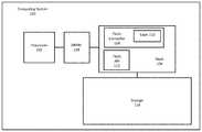
- FIG. 1illustrates a computing system 100 that includes processors 102 , DRAM 104 , flash memory 106 , and storage 114 .
- the computing system 100may be configured to provide computing services such as backup services, document management, contact management, or the like.
- the computing system 100can be formed of network connected devices or may be implemented as an integrated unit.
- the computing system 100can be connected to a computing network.
- the storage 114may include various hardware storage devices (e.g., magnetic, optical, etc.) such as HDDs.
- the storage 114can be arranged in different manners.
- the DRAM 104 and the flash 106can be used as caches in the computing system 100 .
- the DRAMwhich is the fastest memory, is typically smaller than the flash memory 106 .
- the flash memory 106is typically smaller than the storage 114 .
- the flash 106may be the primary storage and the storage 114 could be omitted.
- the flash memory 106can be large (e.g., terabytes or larger).
- the computing system 100may be configured for processing large data sets such as backup data, data lake data, or the like.
- the flash memory 106is associated with a flash controller 108 and a flash API 110 .
- the flash controller 108typically controls operations occurring within the flash 106 and may include its own processor and memory.
- the flash API 110allows clients to make specific calls to the flash memory 106 , which may be executed by the flash controller 108 .
- the clientmay be any device or component (e.g., processor, memory controller, process) that interacts with the flash memory 106 .
- the flash controller 108is associated with logic 112 that may be configured to interact with the data stored in the flash memory 106 .
- the logic 112may perform overwrites, logical-ORs, compare-and-swaps, or the like.
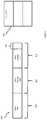
- FIG. 2illustrates an example of a flash memory and illustrates how data may be arranged in the flash memory.
- FIG. 2illustrates a flash memory 200 , which is an example of the flash memory 106 shown in FIG. 1 .
- the flash memory 200includes erasure units, such as erasure units 202 and 212 . Each erasure unit is associated with pages. Pages 204 , 206 , 208 , and 210 are associated with the erasure unit 202 and the pages 214 , 216 , 218 , and 220 are associated with the erasure unit 212 .
- erasure unitsuch as erasure units 202 and 212 .
- Pages 204 , 206 , 208 , and 210are associated with the erasure unit 202 and the pages 214 , 216 , 218 , and 220 are associated with the erasure unit 212 .
- the flash memoryis typically much larger than illustrated.
- the pages 204 , 206 , 208 , and 210are smaller than the erasure unit 202 .
- the pages 204 , 206 , 208 , and 210may be 4 KB each.
- the erasure units 202 and 212may be 1 MB each.
- Data stored in the flash memory 200may also be arranged in containers or using other storage arrangements. However, when data is written to the flash memory 200 , the data is written in pages and the pages are usually written in sequence.
- the page 208includes data. Because the page 208 contains data, a conventional flash cannot simply write new data to the page 208 . Rather, it is necessary to erase all pages 204 , 206 , 208 , and 210 in the erasure unit 202 before new data can be written to the page 212 . In fact, all pages in the erasure unit 202 would be erased because erasures are performed at the level of the erasure unit 202 . The new data could alternatively be written to a new location and the existing page or erasure unit marked for erasure.
- Embodiments of the inventionallow data to be written to the page 208 by performing an overwrite operation.
- embodiments of the inventionallow data to be written to the page 208 or any other page in the erasure unit 202 as long as the write makes no changes so specific cells (or bits) become unset, but only changes 0 bits to 1 s.
- the flash memory 200may allow more electrons to be stored in an individual cell (representing one bit) thus semantically changing the value from 0 to 1. Reducing the electrons to change a 1 to a 0, however, involves erasing an entire erasure unit due to the hardware constraints.
- data such as 0000can be overwritten as 0101 because only 0s are being changed to 1s.
- FIG. 3illustrates an example of a flash memory that includes a controller and illustrates an example of logic associated with performing an overwrite in the flash memory.
- FIG. 3illustrates that the flash memory 300 may receive a write block 302 from a client (e.g., a thread, process, or the like).
- the controllermay perform controller logic 304 to perform the write operation in the flash memory 300 .
- the write operationmay include performing a method 310 .
- the write block 302may write to more than one page in the flash memory 300 .
- the controller 320may read the target block 306 .
- the target block 306may be, by way of example, a previous version of the write block 302 .
- the target block 306may be located at a destination address included in the write request received along with the write block 302 .
- the controller 320may compare the target block 306 with the write block 302 .
- the result of the comparisondetermines, in one example, whether the target block 306 can be overwritten with the write block 302 or whether the write block is written to a new location as the new block 308 .
- the comparisonmay identify which bits need to be changed from 0s to 1s.
- the comparison in box 314determines that writing the write block 302 to the target block 306 would only set bits from 0s to 1s, then the target block 306 is overwritten with the write block 302 in box 316 . If the comparison determines that it is necessary to reset is to 0s, then the write block 302 is written to a new location as the new block 308 in box 318 .
- the target block 306may be marked for deletion or erasure.
- the logic performed in the method 310is internal to the flash memory 300 in this example.
- the client associated with the write operationmay not be aware of the overwrite method performed in the flash memory 300 .
- the page or pages associated with the target blockare locked at 320 so that another client does not interfere with the method 310 .
- a lockmay be used during the overwrite method 310 .
- the controller 320may set aside some memory to track which regions of the flash memory 300 are locked.
- FIG. 4illustrates an example of an external interface for overwrites in a flash memory.
- FIG. 4illustrates a flash memory 400 , which is an example of the flash memory 106 in FIG. 1 .
- the flash memory 400includes a controller 406 and an API 408 .
- the API 408includes calls 410 including, by way of example, a logical-OR 412 and a Compare and Swap 414 .
- the APIallows a client to explicitly call the API 408 .
- the logical-OR call 412allows a client 402 to provide a block of data and an address 404 .
- a logical ORis performed between the page or pages at the address provided in the client request 402 with the block 416 at the specified address. This call compares or performs a logical OR with each respective bit.
- a logical ORhas the property that it never changes a one to a zero, but zeros may be changed to one if they are ORed with a one. This operation is an overwrite that potentially replaces 0s in the block 416 to 1s.
- the clientmay be aware, prior to making the call, that the necessary updates to the block 416 can be achieved with the logical OR operation.
- An OR operationmay not be required for each bit. Rather, the logical OR effectively changes 0s in to the block 416 to is based on the contents of the block provided in the client request 402 . Thus, the logical OR may simply identify the bits to be changed to 1 s and make those changes. If the hardware is configures such that an entire page is written at a time, then the page is written such that the relevant 0s are changed to 1s.
- the compare and swap call 414can be used for locking and for thread synchronization when performing overwrites.
- the clientmay provide a previous version of a block and a new version of the block.
- the new versionmay have new bits set.
- the controller 406may then compare the previous version included in the request with the block 416 to insure that another client has not changed the block. If the comparison is equal, the block 416 can be overwritten (e.g., by using logical-OR operation) with the new version included in the client request 402 . Other callers attempting to impact or alter block 416 will be blocked until these compare and swap operation completes.
- the controller 406may also lock locations in the flash memory 400 that are being updated or changed in accordance with the controller logic or API calls 410 .
- the calls and logic discussed hereinmay be implemented with computer executable instructions and the controller 406 and/or the flash memory 400 are examples of a computing device.
- the calls and logic discussed hereinmay also be used when interacting (e.g., read/write/update) with data structures implemented in a flash memory.
- FIGS. 5-8illustrate examples of a data structure that may be implemented in a flash memory.
- FIG. 5illustrates an example of a linked list that may be implemented in a flash memory.
- FIG. 5illustrates a linked list 500 that includes nodes 502 , 508 and 514 .
- the data and/or the next pointer of the nodes 502 , 508 and 514may be written by overwriting the nodes or pages of the nodes as necessary.
- the node 502includes data 504 and a next pointer 506 .
- the node 502is the head or first node of the linked list 500 in this example.
- the next pointer 506points to the node 508 , which includes data 510 and a next pointer 512 .
- the next pointer 512points to the node 514 , which includes data 516 and a next pointer 516 .
- the next pointer 516may be set to a value indicating that it is the last node or that there is no other nodes.
- the next pointer 516may be NULL or may be initially set to all zeros.
- next pointer 516By setting the next pointer 516 to all zeros, adding a node at the end of the linked list is easily achieved because the next pointer 516 can easily be overwritten with the next pointer to the newly added node. Thus, the next pointer 516 to be overwritten when adding a node to the end of the linked list such that the next pointer 516 can point to the new node.
- a nodecan be inserted at any point of the linked list 500 .
- the next pointer 506points to the data 522 of the new node 520 and the next pointer 524 of the new node 520 points to the data 510 of the node 508 . If possible, the next pointer 506 is overwritten. If the next pointer 506 cannot be overwritten because some of the bits need to be unset, another procedure may be followed such as discussed below with reference to FIGS. 6-8 .
- the direct link between the node 502 and 508is no longer present in the linked list 500 .
- a nodecan also be inserted at the beginning of the linked list.
- Embodimentsadapt the linked list 500 so that the linked list can be implemented efficiently in a flash memory.
- FIG. 6illustrates a more detailed example of a node 600 in a linked list.
- the node 600includes a data portion 602 and a pointer portion 608 .
- the node 600may optionally include additional pointer portions such as the pointer portion 614 .
- the node 600 or the linked listmay also be associated with an in memory (e.g., in DRAM) table 620 (e.g., a hash table).
- the entries 622 , 624 , and 626(the table 620 may have multiple entries) are used to store pointers. More specifically, the table 620 can be used to store next pointers of various nodes when the next pointers cannot be overwritten. At various times, the table 620 can be written to the cache and the linked list or portions thereof may be rewritten. This may involve writing at least some of the nodes to new locations in the flash memory.
- the data portion 602may include data 606 and an invalid bit 604 .
- the pointer portion 608may include a next pointer 612 and an invalid bit 610 .
- the pointer portion 614may include a next pointer 618 and an invalid bit 616 .
- Embodiments of the inventionmay include less than the elements illustrated in FIG. 6 .
- a nodemay not include the invalid bit 604 or the second pointer portion 614 .
- some of the pointer portionsmay not include an invalid bit.
- the node 600 or portions thereofis an example of the nodes 502 , 508 , and 514 .
- Embodiments of the inventioncan reduce the new page writes and the erasures.
- Embodiments of the inventionallow linked lists to be implemented by making updates via an overwrite process when possible.
- the invalid bits 604 , 610 and 616have a value equivalent to a logical 0.
- the invalid bit 610can be set to indicate that the next pointer 612 is no longer valid.
- the pointer portion 614is then used to store the new next pointer. Because the next pointer 618 is initially set to all zeros, the next pointer 618 can be used as the next pointer of the node 600 by overwriting the next pointer 618 with the new next pointer. This can be done using a logical OR because the contents of the next pointer 618 are initially all zeros.
- the invalid bit 610will cause the next pointer 618 to be used as long as the invalid bit 616 is not set. If another update is necessary to the node 600 , the invalid bit 616 can be set and the new next pointer could be stored in the entry 622 , which would be associated with the node 600 . During a traversal when the invalid bits 610 and 616 are both set, the next pointer will be obtained from the entry 622 .
- FIG. 7illustrates an example of a node of a linked list.
- the node 700includes a data portion 702 storing data 704 and a pointer portion 706 that includes a next pointer 708 and 710 .
- the next pointer 708points to the node 726 or to the data of the node 726 .
- the invalid bit 710is set to 1. This indicates that the contents of the next pointer 708 are no longer valid.
- the new next pointer of the node 700is inserted in the entry 720 of the table 718 , which is in memory.
- the entry 720thus points to the data 714 of the node 712 and the next pointer 716 points to the node 726 .
- the table 718is checked to determine the next position or node in the linked list that follows the node 700 . This may not be necessary when the node is added to the end of the linked list because the next pointer of the last node can always be overwritten because it is initially set to zeros. Additionally this may not be necessary when the next pointer 708 only requires more bits to be set from 0 to 1 to become a next pointer referencing data 714 . In such a case the next pointer 708 can be overwritten with Logical-OR to become the next pointer pointing to data 714 .
- the table 718may become full of pointers.
- the linked listmay then be written by writing the updates or entries in the table 718 to the flash memory. This may require at least portions of the linked list to be written to new locations in the flash memory. In one example, the entire linked list may be written to a new location in the flash memory and the old linked list may be marked for erasure.
- Table 718may be implemented in many ways including as a hash table, tree, or array.
- the key to the tablemay be multiple possible values including the address of nodes (such as the flash location of node 700 ) or an identifier associated with data 704 . The table efficiently maps from such a key to a next pointer for updated nodes.
- FIG. 8illustrates another example of a node that includes multiple next pointers.
- the node 800includes a pointer portion 806 and a pointer portion 810 .
- the pointer portion 810includes a next pointer 814 and an invalid bit 812 .
- none of the pointer portions 806 and 810include an invalid bit.
- all bits of the next pointer 808may be set to 1s. This is another way of indicating that the next pointer 808 is invalid.
- the next pointer 814which is initially set to all zeros, is set to a value that points to the inserted node.
- next pointer 814is set to all is, or another predefined invalid value, when the next bit 812 is not present, then the new next pointer associated with the node 800 may be placed in the entry 820 of the table. In some embodiments more or fewer than 2 next pointers may be included with each node in the linked list.
- a nodemay include multiple next pointers.
- the current pointeris set to all 1s (or the invalid bit is set) and the new pointer is inserted in the next pointer portion of the node. If necessary and if all available pointer portions are used, the new pointer may be stored in the in memory table 816 .
- the pointers in memorycan be written to flash and the linked list revised accordingly at various times.
- the data portion 602may also include an invalid bit 604 .
- the invalid data bitis set, the data is skipped and the traversal proceeds to the next node in the linked list in accordance with the next pointer associated with the node.
- a pointer in a node or a data portioncan be marked invalid by setting all the bits to is or by setting the bits to a value indicating that the pointer or data is invalid. This may include setting a certain portion to is. In one example, the value may be selected so that marking the pointer or data as invalid can be accomplished via an overwrite operation.
- Invalid bitsfor example, can be performed using an overwrite operation.
- a next pointercan be set to all ones using an overwrite operation.
- the affected portions of a nodeare overwritten when possible.
- Writes to new locationsare performed when unsets are required.
- a nodecan be removed from the linked list by setting the invalid data bit in the node. This allows the linked list to be traversed while skipping the data of the effectively removed node. Alternatively, the next pointer of the previous node can be modified to point to the node that follows the node being removed. The removed node can be marked for erasure.
- a data structuresuch as a linked list implemented in flash memory can be managed or implemented using overwrites to effect writes rather than writing to a new location.
- portions of the nodes or other elements of the data structurescan be overwritten as long as the overwrite only changes 0s to 1s.
- 1scannot be changed to 0s in the flash memory unless a larger erasure unit is erased. Any changes requiring an unset (changing a 1 to a 0) may result in a write to a new location in the flash cache so that the old area can be erased.
- Embodiments of the inventionfurther associate a table in memory with the data structure. The table is configured to store or buffer certain writes.
- writes that cannot be performed via an overwritemay be stored in the table.
- the need to rewrite the affected datacan be delayed and batched, the number of writes to new locations and the number of erasures can be reduced.
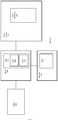
- FIG. 9illustrates an example of a library configured to interact with and manage data structures implemented in flash memory.
- FIG. 9illustrates a library 904 that allows a client 902 to interact with data structures 914 without regard to the flash memory 912 and without requiring the client 902 to know that the data structures 914 are implemented in the flash memory 912 .
- the client 902may not be required to specify between an overwrite and writing to a new location when writing to the data structures 914 .
- the library 904provides calls 906 .
- the calls 906include a write call 908 and a read call 910 .
- the library 904may be implemented as a software library that can be accessed by a program or process or thread such as the client 902 .
- the library 904allows a client that is reading from or writing to a data structure in flash memory to simply specify a write or a read.
- the read request or callis accompanied by a location, which may simply identify the data structure and an offset.
- the write request or callmay be accompanied by the location and the data to be written to the location in the data structure.
- the library 904may cooperate with the flash memory 912 to implement the write request as an overwrite or as a conventional write. More specifically, the library 904 can implement the write by performing an overwrite when possible or call logic implemented in the flash memory to perform the overwrite when possible.
- the data structures 914may each be associated with a table 918 in memory (e.g., a hash table). During the write process, the data to be written may be temporarily stored in the table. When portions of the data structure are stored in the table 918 , a read operation performed in response to a read call 910 may read the data structure and update the data with information from the table 918 in memory prior to returning a result of the read to the client 902 .
- a read operation performed in response to a read call 910may read the data structure and update the data with information from the table 918 in memory prior to returning a result of the read to the client 902 .
- the write call 908may convert the write request into an overwrite.
- the client 902is shielded from the manner in which the write request is implemented in the flash memory 912 .
- the write request from the client 902may include data to be added to the data structure.
- the datamay be a change to a node of a linked list, an entry in a Bloom filter, a node in a tree or graph, or the like and may be implemented by overwriting existing data.
- the write call 908may allow a write to any offset in the data structure.
- the write request received by the write call 908does not need to be page aligned with respect to the organization of the flash memory 912 .
- the write requestmay also include the bytes to be written (size) and the offset.
- the library 904receives the write request and may determine the page in the flash memory that corresponds to the offset identified in the write request.
- the library 904will read the data from the data structure 914 at the location corresponding to the write request and determine whether the write or update can be performed by an additive write, for example by performing a logical OR where only 0s need to be changed to 1s. If this is the case, the target data of the write request can be overwritten with the update.
- the library 904may perform a different response.
- the library 904may read the page, add the bytes included in the write request to the read page and then write the updated page to a new location in memory.
- the new data or updatemay be stored in the table 918 (e.g., a hash memory).
- the table 918e.g., a hash memory
- the entryis associated with the location of the data in the data structures 914 .
- the entry in the table 918may also store the offset or page and offset for the write data.
- changes that could not be committed to the data structures 914 in the flash memory 912 by an overwrite operationmay be accumulated in the table 918 .
- the changescan all be written to a new page at the same time. This may be performed by reading the page from the data structure, applying the updates to the page and writing the updated page to a new location in the flash memory 912 .
- the new next pointercan be maintained in memory in the table 918 .
- the new next pointer in the table 918can be replaced in memory with another next pointer. This allows changes to accumulate in the table 918 without having to write a new page in the flash memory 912 for every change to the linked list.
- the changemay be stored in the table 918 . Subsequent changes may overwrite the change in the table 918 or be added as additional entries in the table 918 . All of these changes can be applied when the node is rewritten to a new page or when the node is read.
- a read request from the client 902may require the library to access both the data structures 914 and the table 918 .
- the library 904may need to check the table 918 to determine whether updates or changes to the data being requested have been stored in the table 918 in memory 916 when performing a read operation for the client 902 .
- the library 904may reassemble the data in response to the read request.
- a pageis 4 KB, for example, a read operation may access the page.
- the table 918is then examined to determine if any bytes in the page have been updated. If so, the bytes in the retrieved page are updated with the data from the table 918 and the reconstituted or updated page is returned to the client 902 .
- Changes to a data structure such as a linked list as described previouslycan be achieved using the library 904 .
- the library 904can translate a write request or a read request to identify the appropriate location in the flash memory. Further, the write request may be converted into an overwrite operation when an overwrite operation is possible.
- the library 904may also implement a table 918 (e.g., a buffer) that allows writes to accumulate before being written to new pages. At the same time, the buffer can be used to update any data from the data structure 914 that is returned in response to a read request.
- a table 918e.g., a buffer
- Embodiments of the inventionmay be performed on many different data structures that are implemented such that at least some updates can be made via an overwrite operation or compare and swap operation or as otherwise disclosed herein.
- Example data structuresinclude, but are not limited to, linked lists, Bloom filters, locking structures, trees, graphs, and the like.
- FIG. 10illustrates an example of a method for performing a write to a data structure in a flash memory.
- the method 1000may begin in box 1002 by receiving a write request from a client.
- the write requestmay include data to be written to the data structure.
- the write requestmay also include or identify a location. For example, the write request may identify an offset into the data structure and a size of the data.
- the write requestis translated. More specifically, the container or page in the flash memory corresponding to the write request is determined from the offset. Because a flash memory may write only in certain increments (e.g., 4 KB), writing a smaller amount of data may still result in a new page.
- the librarydetermines whether or not the write request can be performed as an overwrite operation. If the data provided in the write request only changes 0s in the identified page (or pages depending on the size of the data) to 1s, then the target data of the write request may be overwritten with the data included in the write request into the flash memory. There is no need to write the page to a new location and no need to delete the old page when an overwrite is performed.
- the datamay be written to an in-memory buffer and associated with the appropriate location in the page.
- the entry in the buffermay identify a page and an offset for the data in the write request for example.
- a successis returned to the client.
- multiple write requestsmay be received from one or more clients.
- Each of the write requestsis translated to identify the page and bytes or bits within the page to be written and a determination is made as to whether an overwrite can be performed.
- some of the write requestsmay result in overwrites to appropriate pages.
- Other write requestsmay result in buffer entries. The pages may be locked as necessary. Further, changes stored in the buffer or table may be time indexed so they can be applied in order.
- the buffermay be flushed to the flash memory.
- Writing the data in the table or buffermay require multiple pages of the data structure to be written to new locations and old pages to be marked for erasure.
- the buffermay be flushed when one of several conditions is met including: the buffer's fullness has reached a threshold value, sufficient time has passed since the last buffer flush to flash, a scheduled time is configured to flush from buffer to flash.
- FIG. 11illustrates an example of a method for reading data from a data structure.
- the method 1100may begin by receiving a read request from a client in box 1102 . Multiple read requests may be received from one or more clients. The read request do not need to be page aligned and do not need to specify a page of data.
- the read requestmay include an offset into the data structure and the offset is translated to identify the page in the data structure corresponding to the read request.
- the datae.g., the page, portion of the page, or other block
- the datais retrieved from the data structure in box 1104 .
- the data retrieved from the data structureis updated, if necessary, from entries in the in-memory table. For example, because data may be associated with multiple updates, these updates may be applied, in order in one example, to the data retrieved from the data structure. Once the data is updated, returned to the client in box 1108 .
- a computermay include a processor and computer storage media carrying instructions that, when executed by the processor and/or caused to be executed by the processor, perform any one or more of the methods disclosed herein.
- embodiments within the scope of the present inventionalso include computer storage media, which are physical media for carrying or having computer-executable instructions or data structures stored thereon.
- Such computer storage mediacan be any available physical media that can be accessed by a general purpose or special purpose computer.
- such computer storage mediacan comprise hardware such as solid state disk (SSD), RAM, ROM, EEPROM, CD-ROM, flash memory, DRAM, phase-change memory (“PCM”), or other optical disk storage, magnetic disk storage or other magnetic storage devices, or any other hardware storage devices which can be used to store program code in the form of computer-executable instructions or data structures, which can be accessed and executed by a general-purpose or special-purpose computer system to implement the disclosed functionality of the invention. Combinations of the above should also be included within the scope of computer storage media.
- Such mediaare also examples of non-transitory storage media, and non-transitory storage media also embraces cloud-based storage systems and structures, although the scope of the invention is not limited to these examples of non-transitory storage media.
- Computer-executable instructionscomprise, for example, instructions and data which cause a general purpose computer, special purpose computer, or special purpose processing device to perform a certain function or group of functions.
- moduleor ‘component’ can refer to software objects or routines that execute on the computing system.
- the different components, modules, engines, and services described hereinmay be implemented as objects or processes that execute on the computing system, for example, as separate threads. While the system and methods described herein can be implemented in software, implementations in hardware or a combination of software and hardware are also possible and contemplated.
- a ‘computing entity’may be any computing system as previously defined herein, or any module or combination of modules running on a computing system.
- a hardware processoris provided that is operable to carry out executable instructions for performing a method or process, such as the methods and processes disclosed herein.
- the hardware processormay or may not comprise an element of other hardware, such as the computing devices and systems disclosed herein.
- a controllermay include a processor and memory and/or other computing chips.
- embodiments of the inventioncan be performed in client-server environments, whether network or local environments, or in any other suitable environment.
- Suitable operating environments for at least some embodiments of the inventioninclude cloud computing environments where one or more of a client, server, or target virtual machine may reside and operate in a cloud environment.
Landscapes
- Engineering & Computer Science (AREA)
- Theoretical Computer Science (AREA)
- Physics & Mathematics (AREA)
- General Engineering & Computer Science (AREA)
- General Physics & Mathematics (AREA)
- Human Computer Interaction (AREA)
- Databases & Information Systems (AREA)
- Software Systems (AREA)
- Data Mining & Analysis (AREA)
- Techniques For Improving Reliability Of Storages (AREA)
- Memory System (AREA)
Abstract
Description
| A | B | OR Result |
| 0 | 0 | 0 |
| 0 | 1 | 1 |
| 1 | 0 | 1 |
| 1 | 1 | 1 |
Claims (20)
Priority Applications (2)
| Application Number | Priority Date | Filing Date | Title |
|---|---|---|---|
| US16/209,054US10521123B2 (en) | 2016-06-29 | 2018-12-04 | Additive library for data structures in a flash memory |
| US16/707,895US11106362B2 (en) | 2016-06-29 | 2019-12-09 | Additive library for data structures in a flash memory |
Applications Claiming Priority (2)
| Application Number | Priority Date | Filing Date | Title |
|---|---|---|---|
| US15/196,283US10146438B1 (en) | 2016-06-29 | 2016-06-29 | Additive library for data structures in a flash memory |
| US16/209,054US10521123B2 (en) | 2016-06-29 | 2018-12-04 | Additive library for data structures in a flash memory |
Related Parent Applications (1)
| Application Number | Title | Priority Date | Filing Date |
|---|---|---|---|
| US15/196,283ContinuationUS10146438B1 (en) | 2016-06-29 | 2016-06-29 | Additive library for data structures in a flash memory |
Related Child Applications (1)
| Application Number | Title | Priority Date | Filing Date |
|---|---|---|---|
| US16/707,895ContinuationUS11106362B2 (en) | 2016-06-29 | 2019-12-09 | Additive library for data structures in a flash memory |
Publications (2)
| Publication Number | Publication Date |
|---|---|
| US20190107946A1 US20190107946A1 (en) | 2019-04-11 |
| US10521123B2true US10521123B2 (en) | 2019-12-31 |
Family
ID=64451930
Family Applications (3)
| Application Number | Title | Priority Date | Filing Date |
|---|---|---|---|
| US15/196,283ActiveUS10146438B1 (en) | 2016-06-29 | 2016-06-29 | Additive library for data structures in a flash memory |
| US16/209,054ActiveUS10521123B2 (en) | 2016-06-29 | 2018-12-04 | Additive library for data structures in a flash memory |
| US16/707,895ActiveUS11106362B2 (en) | 2016-06-29 | 2019-12-09 | Additive library for data structures in a flash memory |
Family Applications Before (1)
| Application Number | Title | Priority Date | Filing Date |
|---|---|---|---|
| US15/196,283ActiveUS10146438B1 (en) | 2016-06-29 | 2016-06-29 | Additive library for data structures in a flash memory |
Family Applications After (1)
| Application Number | Title | Priority Date | Filing Date |
|---|---|---|---|
| US16/707,895ActiveUS11106362B2 (en) | 2016-06-29 | 2019-12-09 | Additive library for data structures in a flash memory |
Country Status (1)
| Country | Link |
|---|---|
| US (3) | US10146438B1 (en) |
Cited By (6)
| Publication number | Priority date | Publication date | Assignee | Title |
|---|---|---|---|---|
| US10936207B2 (en) | 2016-06-29 | 2021-03-02 | EMC IP Holding Company LLC | Linked lists in flash memory |
| US11106373B2 (en) | 2016-06-29 | 2021-08-31 | EMC IP Holding Company LLC | Flash interface for processing dataset |
| US11106362B2 (en)* | 2016-06-29 | 2021-08-31 | EMC IP Holding Company LLC | Additive library for data structures in a flash memory |
| US11106586B2 (en) | 2016-06-29 | 2021-08-31 | EMC IP Holding Company LLC | Systems and methods for rebuilding a cache index |
| US11113199B2 (en) | 2016-06-29 | 2021-09-07 | EMC IP Holding Company LLC | Low-overhead index for a flash cache |
| US11182083B2 (en) | 2016-06-29 | 2021-11-23 | EMC IP Holding Company LLC | Bloom filters in a flash memory |
Families Citing this family (1)
| Publication number | Priority date | Publication date | Assignee | Title |
|---|---|---|---|---|
| TWI774245B (en)* | 2021-02-20 | 2022-08-11 | 瑞昱半導體股份有限公司 | Linked list searching method and linked list searching device |
Citations (186)
| Publication number | Priority date | Publication date | Assignee | Title |
|---|---|---|---|---|
| US4513367A (en) | 1981-03-23 | 1985-04-23 | International Business Machines Corporation | Cache locking controls in a multiprocessor |
| US4785395A (en) | 1986-06-27 | 1988-11-15 | Honeywell Bull Inc. | Multiprocessor coherent cache system including two level shared cache with separately allocated processor storage locations and inter-level duplicate entry replacement |
| US5333318A (en) | 1990-09-27 | 1994-07-26 | Motorola, Inc. | Creating and searching a quad linked list in a trunked communication system |
| US5590320A (en) | 1994-09-14 | 1996-12-31 | Smart Storage, Inc. | Computer file directory system |
| US5630093A (en) | 1990-12-31 | 1997-05-13 | Intel Corporation | Disk emulation for a non-volatile semiconductor memory utilizing a mapping table |
| US5644701A (en) | 1993-12-29 | 1997-07-01 | Kabushiki Kaisha Toshiba | Data processing system and method for executing snapshot dumps |
| US5682497A (en) | 1993-09-28 | 1997-10-28 | Intel Corporation | Managing file structures for a flash memory file system in a computer |
| US5684976A (en) | 1994-11-16 | 1997-11-04 | International Business Machines Corporation | Method and system for reduced address tags storage within a directory having a tree-like data structure |
| US5740349A (en) | 1993-02-19 | 1998-04-14 | Intel Corporation | Method and apparatus for reliably storing defect information in flash disk memories |
| US5761501A (en) | 1995-10-02 | 1998-06-02 | Digital Equipment Corporation | Stacked skip list data structures |
| US5838614A (en) | 1995-07-31 | 1998-11-17 | Lexar Microsystems, Inc. | Identification and verification of a sector within a block of mass storage flash memory |
| US5907856A (en) | 1995-07-31 | 1999-05-25 | Lexar Media, Inc. | Moving sectors within a block of information in a flash memory mass storage architecture |
| US5909694A (en) | 1997-06-12 | 1999-06-01 | International Business Machines Corporation | Multiway associative external microprocessor cache |
| US5913226A (en) | 1996-02-14 | 1999-06-15 | Oki Electric Industry Co., Ltd. | Snoop cache memory control system and method |
| US5966726A (en) | 1997-05-28 | 1999-10-12 | Western Digital Corporation | Disk drive with adaptively segmented cache |
| US6046936A (en) | 1998-02-16 | 2000-04-04 | Hitachi, Ltd. | Semiconductor, memory card, and data processing system |
| US6049672A (en) | 1996-03-08 | 2000-04-11 | Texas Instruments Incorporated | Microprocessor with circuits, systems, and methods for operating with patch micro-operation codes and patch microinstruction codes stored in multi-purpose memory structure |
| US6119209A (en) | 1998-02-03 | 2000-09-12 | International Business Machines Corporation | Backup directory for a write cache |
| US6128623A (en) | 1998-04-15 | 2000-10-03 | Inktomi Corporation | High performance object cache |
| US6192450B1 (en) | 1998-02-03 | 2001-02-20 | International Business Machines Corporation | Destage of data for write cache |
| US6216199B1 (en) | 1999-08-04 | 2001-04-10 | Lsi Logic Corporation | Hardware mechanism for managing cache structures in a data storage system |
| US6272593B1 (en) | 1998-04-10 | 2001-08-07 | Microsoft Corporation | Dynamic network cache directories |
| US6360293B1 (en) | 1998-06-24 | 2002-03-19 | Oki Electric Industry Co., Ltd. | Solid state disk system having electrically erasable and programmable read only memory |
| US20030009637A1 (en) | 2001-06-21 | 2003-01-09 | International Business Machines Corporation | Decentralized global coherency management in a multi-node computer system |
| US20030009643A1 (en) | 2001-06-21 | 2003-01-09 | International Business Machines Corp. | Two-stage request protocol for accessing remote memory data in a NUMA data processing system |
| US20030009641A1 (en) | 2001-06-21 | 2003-01-09 | International Business Machines Corp. | Dynamic history based mechanism for the granting of exclusive data ownership in a non-uniform memory access (numa) computer system |
| US20030009639A1 (en) | 2001-06-21 | 2003-01-09 | International Business Machines Corp. | Non-uniform memory access (NUMA) data processing system that provides precise notification of remote deallocation of modified data |
| US20030009623A1 (en) | 2001-06-21 | 2003-01-09 | International Business Machines Corp. | Non-uniform memory access (NUMA) data processing system having remote memory cache incorporated within system memory |
| US6510083B1 (en) | 1995-11-29 | 2003-01-21 | Intel Corporation | Electrically erasable and programmable memory that allows data update without prior erasure of the memory |
| US6594723B1 (en) | 1999-09-07 | 2003-07-15 | Microsoft Corporation | Method and apparatus for updating data in nonvolatile memory |
| US6636950B1 (en) | 1998-12-17 | 2003-10-21 | Massachusetts Institute Of Technology | Computer architecture for shared memory access |
| US20030217227A1 (en) | 2002-05-14 | 2003-11-20 | Stmicroelectronics, Inc. | Apparatus and method for implementing a ROM patch using a lockable cache |
| US20040123270A1 (en) | 2002-12-23 | 2004-06-24 | Motorola, Inc. | Method and apparatus for shared libraries on mobile devices |
| US6807615B1 (en) | 1999-04-08 | 2004-10-19 | Sun Microsystems, Inc. | Apparatus and method for providing a cyclic buffer using logical blocks |
| US6851015B2 (en) | 2001-05-22 | 2005-02-01 | Sankyo Seiki Mfg. Co., Ltd. | Method of overwriting data in nonvolatile memory and a control apparatus used for the method |
| US6901499B2 (en) | 2002-02-27 | 2005-05-31 | Microsoft Corp. | System and method for tracking data stored in a flash memory device |
| US20050120180A1 (en) | 2000-03-30 | 2005-06-02 | Stephan Schornbach | Cache time determination |
| US20050165828A1 (en) | 2001-06-12 | 2005-07-28 | Network Appliance Inc. | Caching media data using content sensitive object identifiers |
| US6965970B2 (en) | 2001-09-27 | 2005-11-15 | Intel Corporation | List based method and apparatus for selective and rapid cache flushes |
| US6978342B1 (en) | 1995-07-31 | 2005-12-20 | Lexar Media, Inc. | Moving sectors within a block of information in a flash memory mass storage architecture |
| US20060015768A1 (en) | 2004-07-16 | 2006-01-19 | Valine Craig M | Method, system, and apparatus for tracking defective cache lines |
| US20060059171A1 (en) | 2004-08-25 | 2006-03-16 | Dhrubajyoti Borthakur | System and method for chunk-based indexing of file system content |
| US20060101200A1 (en) | 2004-11-09 | 2006-05-11 | Fujitsu Limited | Library system, virtual library apparatus, cache restoring method, and computer readable recording medium recorded thereon a cache restoring program |
| US20060143390A1 (en) | 2004-12-29 | 2006-06-29 | Sailesh Kottapalli | Fair sharing of a cache in a multi-core/multi-threaded processor by dynamically partitioning of the cache |
| US20060179174A1 (en) | 2005-02-02 | 2006-08-10 | Bockhaus John W | Method and system for preventing cache lines from being flushed until data stored therein is used |
| US20060184744A1 (en) | 2005-02-11 | 2006-08-17 | International Business Machines Corporation | Method and apparatus for implementing a combined data/coherency cache |
| US20070005928A1 (en) | 2005-06-30 | 2007-01-04 | Trika Sanjeev N | Technique to write to a non-volatile memory |
| US20070061504A1 (en) | 2005-08-22 | 2007-03-15 | Woon-Kyun Lee | Apparatus and method for managing data of flash memory |
| US20070156842A1 (en) | 2005-12-29 | 2007-07-05 | Vermeulen Allan H | Distributed storage system with web services client interface |
| US20070180328A1 (en) | 2006-01-27 | 2007-08-02 | Cornwell Michael J | Monitoring health of non-volatile memory |
| US7290109B2 (en) | 2002-01-09 | 2007-10-30 | Renesas Technology Corp. | Memory system and memory card |
| US20070300037A1 (en) | 2006-06-23 | 2007-12-27 | Microsoft Corporation | Persistent flash memory mapping table |
| US20080046655A1 (en) | 2006-08-21 | 2008-02-21 | Hemant Madhav Bhanoo | Probabilistic technique for consistency checking cache entries |
| US20080065809A1 (en) | 2006-09-07 | 2008-03-13 | Eichenberger Alexandre E | Optimized software cache lookup for simd architectures |
| US20080077782A1 (en) | 2006-09-26 | 2008-03-27 | Arm Limited | Restoring a register renaming table within a processor following an exception |
| US20080120469A1 (en) | 2006-11-22 | 2008-05-22 | International Business Machines Corporation | Systems and Arrangements for Cache Management |
| US20080147714A1 (en) | 2006-12-19 | 2008-06-19 | Mauricio Breternitz | Efficient bloom filter |
| US20080177700A1 (en) | 2007-01-19 | 2008-07-24 | Wen-Syan Li | Automated and dynamic management of query views for database workloads |
| US20080183955A1 (en) | 2007-01-25 | 2008-07-31 | Genesys Logic, Inc. | Flash translation layer apparatus |
| US7433245B2 (en) | 2004-03-31 | 2008-10-07 | Matsushita Electric Industrial Co., Ltd. | Memory card able to guarantee a recoding rate and memory card system using the memory card |
| US20080263114A1 (en) | 2007-04-23 | 2008-10-23 | Microsoft Corporation | Efficient access of flash databases |
| US20080266962A1 (en) | 2007-04-27 | 2008-10-30 | Samsung Electronics Co., Ltd. | Flash memory device and flash memory system |
| US20080273400A1 (en) | 2007-05-02 | 2008-11-06 | Stmicroelectronics Sa | Fast erasable non-volatile memory |
| US20080313132A1 (en) | 2007-06-15 | 2008-12-18 | Fang Hao | High accuracy bloom filter using partitioned hashing |
| US7472205B2 (en) | 2002-04-24 | 2008-12-30 | Nec Corporation | Communication control apparatus which has descriptor cache controller that builds list of descriptors |
| US20090063508A1 (en) | 2007-08-27 | 2009-03-05 | Nec Corporation | Computer, system, storage and access control method, and access control method |
| US7533214B2 (en) | 2002-02-27 | 2009-05-12 | Microsoft Corporation | Open architecture flash driver |
| US20090216788A1 (en) | 2008-02-27 | 2009-08-27 | Ocarina Networks | Multiple file compaction for network attached storage |
| US20090222626A1 (en) | 2008-02-29 | 2009-09-03 | Qualcomm Incorporated | Systems and Methods for Cache Line Replacements |
| US20090240871A1 (en) | 2008-03-01 | 2009-09-24 | Kabushiki Kaisha Toshiba | Memory system |
| US20090300265A1 (en) | 2008-05-29 | 2009-12-03 | Dell Products L.P. | Compact Encoding Methods, Media and Systems |
| US7640262B1 (en) | 2006-06-30 | 2009-12-29 | Emc Corporation | Positional allocation |
| US20100023697A1 (en) | 2008-07-25 | 2010-01-28 | International Business Machines Corporation | Testing Real Page Number Bits in a Cache Directory |
| US7673099B1 (en) | 2006-06-30 | 2010-03-02 | Emc Corporation | Affinity caching |
| US20100070715A1 (en) | 2008-09-18 | 2010-03-18 | Waltermann Rod D | Apparatus, system and method for storage cache deduplication |
| US20100082886A1 (en) | 2008-10-01 | 2010-04-01 | University Of Seoul Industry Cooperation Foundation | Variable space page mapping method and apparatus for flash memory device |
| US7702628B1 (en) | 2003-09-29 | 2010-04-20 | Sun Microsystems, Inc. | Implementing a fully dynamic lock-free hash table without dummy nodes |
| US20100115182A1 (en) | 2008-11-06 | 2010-05-06 | Sony Corporation | Flash memory operation |
| US7720892B1 (en) | 2006-06-30 | 2010-05-18 | Emc Corporation | Bulk updates and tape synchronization |
| US20100165715A1 (en) | 2008-12-30 | 2010-07-01 | Stmicroelectronics S.R.L. | Protection register for a phase-change memory |
| US20100185807A1 (en) | 2009-01-19 | 2010-07-22 | Xiaofeng Meng | Data storage processing method, data searching method and devices thereof |
| US20100199027A1 (en) | 2007-05-04 | 2010-08-05 | Gemalto S.A. | System and method of managing indexation of flash memory |
| US20100211744A1 (en) | 2009-02-19 | 2010-08-19 | Qualcomm Incorporated | Methods and aparatus for low intrusion snoop invalidation |
| US20100229005A1 (en) | 2009-03-04 | 2010-09-09 | Apple Inc. | Data whitening for writing and reading data to and from a non-volatile memory |
| US20100306448A1 (en) | 2009-05-27 | 2010-12-02 | Richard Chen | Cache auto-flush in a solid state memory device |
| US20100332952A1 (en) | 2008-12-22 | 2010-12-30 | Industrial Technology Research Institute | Flash Memory Controller and the Method Thereof |
| US20110010698A1 (en) | 2009-07-13 | 2011-01-13 | Apple Inc. | Test partitioning for a non-volatile memory |
| US20110022778A1 (en) | 2009-07-24 | 2011-01-27 | Lsi Corporation | Garbage Collection for Solid State Disks |
| US20110072217A1 (en) | 2009-09-18 | 2011-03-24 | Chi Hoang | Distributed Consistent Grid of In-Memory Database Caches |
| US7930559B1 (en) | 2006-06-30 | 2011-04-19 | Emc Corporation | Decoupled data stream and access structures |
| US20110138132A1 (en) | 2009-12-09 | 2011-06-09 | Chris Brueggen | Rescinding ownership of a cache line in a computer system |
| US20110138105A1 (en) | 2009-12-04 | 2011-06-09 | International Business Machines Corporation | Non-volatile memories with enhanced write performance and endurance |
| US20110153953A1 (en) | 2009-12-23 | 2011-06-23 | Prakash Khemani | Systems and methods for managing large cache services in a multi-core system |
| US7996605B2 (en) | 2007-07-24 | 2011-08-09 | Hitachi, Ltd. | Storage controller and method for controlling the same |
| US20110225141A1 (en) | 2010-03-12 | 2011-09-15 | Copiun, Inc. | Distributed Catalog, Data Store, and Indexing |
| US20110264865A1 (en) | 2010-04-27 | 2011-10-27 | Symantec Corporation | Techniques for directory server integration |
| US20110276780A1 (en) | 2010-05-05 | 2011-11-10 | Microsoft Corporation | Fast and Low-RAM-Footprint Indexing for Data Deduplication |
| US20110276781A1 (en) | 2010-05-05 | 2011-11-10 | Microsoft Corporation | Fast and Low-RAM-Footprint Indexing for Data Deduplication |
| US20110296110A1 (en) | 2010-06-01 | 2011-12-01 | Lilly Brian P | Critical Word Forwarding with Adaptive Prediction |
| US20120054414A1 (en) | 2010-09-01 | 2012-03-01 | Lite-On It Corp. | Solid state drive and data control method thereof |
| US20120084484A1 (en) | 2010-09-30 | 2012-04-05 | Apple Inc. | Selectively combining commands for a system having non-volatile memory |
| US20120102268A1 (en) | 2010-10-26 | 2012-04-26 | Lsi Corporation | Methods and systems using solid-state drives as storage controller cache memory |
| US20120110247A1 (en) | 2010-10-27 | 2012-05-03 | International Business Machines Corporation | Management of cache memory in a flash cache architecture |
| US20120215970A1 (en) | 2011-02-22 | 2012-08-23 | Serge Shats | Storage Management and Acceleration of Storage Media in Clusters |
| US20120275466A1 (en) | 2010-10-21 | 2012-11-01 | Texas Instruments Incorporated | System and method for classifying packets |
| US20130036418A1 (en) | 2010-12-22 | 2013-02-07 | Vmware, Inc. | In-Place Snapshots of a Virtual Disk Configured with Sparse Extent |
| US20130103911A1 (en) | 2011-10-21 | 2013-04-25 | Nokia Corporation | Method and apparatus for synchronizing a cache |
| US20130205089A1 (en) | 2012-02-08 | 2013-08-08 | Mediatek Singapore Pte. Ltd. | Cache Device and Methods Thereof |
| US8533395B2 (en) | 2006-02-24 | 2013-09-10 | Micron Technology, Inc. | Moveable locked lines in a multi-level cache |
| US20130282964A1 (en) | 2010-05-05 | 2013-10-24 | Microsoft Corporation | Flash memory cache including for use with persistent key-value store |
| US8583854B2 (en) | 2007-12-24 | 2013-11-12 | Skymedi Corporation | Nonvolatile storage device with NCQ supported and writing method for a nonvolatile storage device |
| US8581876B1 (en)* | 2012-06-28 | 2013-11-12 | Dutch Eugene Wickes | Stand alone active storage unit for memory devices |
| US20130325817A1 (en) | 2012-05-30 | 2013-12-05 | Red Hat, Inc. | Linear sweep filesystem checking |
| US8606604B1 (en) | 2007-06-12 | 2013-12-10 | David L. Huber | Systems and methods for remote electronic transaction processing |
| US20130339576A1 (en) | 2012-06-14 | 2013-12-19 | Lite-On It Corporation | Method for constructing address mapping table of solid state drive |
| US20140013027A1 (en) | 2012-07-06 | 2014-01-09 | Seagate Technology Llc | Layered architecture for hybrid controller |
| US8634248B1 (en) | 2012-11-09 | 2014-01-21 | Sandisk Technologies Inc. | On-device data analytics using NAND flash based intelligent memory |
| US8688650B2 (en) | 2011-08-01 | 2014-04-01 | Actifio, Inc. | Data fingerprinting for copy accuracy assurance |
| US8688913B2 (en) | 2011-11-01 | 2014-04-01 | International Business Machines Corporation | Management of partial data segments in dual cache systems |
| US20140098619A1 (en) | 2012-10-10 | 2014-04-10 | Crossbar, Inc. | Non-volatile memory with overwrite capability and low write amplification |
| US20140122818A1 (en) | 2012-10-31 | 2014-05-01 | Hitachi Computer Peripherals Co., Ltd. | Storage apparatus and method for controlling storage apparatus |
| US20140136762A1 (en) | 2012-11-09 | 2014-05-15 | Sandisk Technologies Inc. | Data search using bloom filters and nand based content addressable memory |
| US20140143505A1 (en) | 2012-11-19 | 2014-05-22 | Advanced Micro Devices, Inc. | Dynamically Configuring Regions of a Main Memory in a Write-Back Mode or a Write-Through Mode |
| US8738857B1 (en) | 2011-11-30 | 2014-05-27 | Emc Corporation | System and method for improving cache performance |
| US8738841B2 (en) | 2007-12-27 | 2014-05-27 | Sandisk Enterprise IP LLC. | Flash memory controller and system including data pipelines incorporating multiple buffers |
| US20140149401A1 (en) | 2012-11-28 | 2014-05-29 | Microsoft Corporation | Per-document index for semantic searching |
| US20140173330A1 (en) | 2012-12-14 | 2014-06-19 | Lsi Corporation | Split Brain Detection and Recovery System |
| US8793543B2 (en) | 2011-11-07 | 2014-07-29 | Sandisk Enterprise Ip Llc | Adaptive read comparison signal generation for memory systems |
| US20140215129A1 (en) | 2013-01-28 | 2014-07-31 | Radian Memory Systems, LLC | Cooperative flash memory control |
| US8811074B2 (en) | 2012-04-03 | 2014-08-19 | Seagate Technology Llc | Parametric tracking to manage read disturbed data |
| US20140281167A1 (en) | 2013-03-15 | 2014-09-18 | Skyera, Inc. | Compressor resources for high density storage units |
| US20140281824A1 (en) | 2013-03-15 | 2014-09-18 | Eun Chu Oh | Nonvolatile memory device and data write method |
| US8904117B1 (en) | 2012-12-21 | 2014-12-02 | Symantec Corporation | Non-shared write-back caches in a cluster environment |
| US8910020B2 (en) | 2011-06-19 | 2014-12-09 | Sandisk Enterprise Ip Llc | Intelligent bit recovery for flash memory |
| US8917559B2 (en) | 2012-04-04 | 2014-12-23 | Sandisk Technologies Inc. | Multiple write operations without intervening erase |
| US8935446B1 (en) | 2013-09-26 | 2015-01-13 | Emc Corporation | Indexing architecture for deduplicated cache system of a storage system |
| US8943282B1 (en) | 2012-03-29 | 2015-01-27 | Emc Corporation | Managing snapshots in cache-based storage systems |
| US9026737B1 (en) | 2011-06-29 | 2015-05-05 | Emc Corporation | Enhancing memory buffering by using secondary storage |
| US20150127889A1 (en) | 2012-05-03 | 2015-05-07 | The-Aio Inc. | Nonvolatile memory system |
| US9043517B1 (en) | 2013-07-25 | 2015-05-26 | Sandisk Enterprise Ip Llc | Multipass programming in buffers implemented in non-volatile data storage systems |
| US20150205722A1 (en) | 2014-01-20 | 2015-07-23 | International Business Machines Corporation | High availability cache in server cluster |
| US9116793B2 (en) | 2012-06-12 | 2015-08-25 | International Business Machines Corporation | Maintaining versions of data in solid state memory |
| US9135123B1 (en) | 2011-12-28 | 2015-09-15 | Emc Corporation | Managing global data caches for file system |
| US20150277786A1 (en) | 2012-11-21 | 2015-10-01 | Unify Gmbh & Co. Kg | Method, device, and program for managing a flash memory for mass storage |
| US9152496B2 (en) | 2007-12-21 | 2015-10-06 | Cypress Semiconductor Corporation | High performance flash channel interface |
| US9171629B1 (en) | 2014-04-28 | 2015-10-27 | Kabushiki Kaisha Toshiba | Storage device, memory controller and memory control method |
| US9189414B1 (en) | 2013-09-26 | 2015-11-17 | Emc Corporation | File indexing using an exclusion list of a deduplicated cache system of a storage system |
| US9189402B1 (en) | 2013-09-26 | 2015-11-17 | Emc Corporation | Method for packing and storing cached data in deduplicated cache system of a storage system |
| US20150331807A1 (en) | 2014-12-10 | 2015-11-19 | Advanced Micro Devices, Inc. | Thin provisioning architecture for high seek-time devices |
| US20150347291A1 (en) | 2014-05-29 | 2015-12-03 | Samsung Electronics Co., Ltd. | Flash memory based storage system and operating method |
| US20150363285A1 (en) | 2014-06-16 | 2015-12-17 | Netapp, Inc. | Methods and systems for using a write cache in a storage system |
| US20160041927A1 (en) | 2014-08-08 | 2016-02-11 | PernixData, Inc. | Systems and Methods to Manage Cache Data Storage in Working Memory of Computing System |
| US9274954B1 (en) | 2012-12-18 | 2016-03-01 | Netapp, Inc. | Caching data using multiple cache devices |
| US9281063B2 (en) | 2012-05-25 | 2016-03-08 | Huawei Technologies Co., Ltd. | Method for processing data, flash memory, and terminal |
| US9313271B2 (en) | 2012-08-06 | 2016-04-12 | Netapp, Inc. | System and method for maintaining cache coherency |
| US9317218B1 (en) | 2013-02-08 | 2016-04-19 | Emc Corporation | Memory efficient sanitization of a deduplicated storage system using a perfect hash function |
| US20160147669A1 (en) | 2014-11-21 | 2016-05-26 | Mediatek Singapore Pte. Ltd. | Method for controlling access of cache through using programmable hashing address and related cache controller |
| US9405682B2 (en)* | 2012-06-23 | 2016-08-02 | Microsoft Technology Licensing, Llc | Storage device access using unprivileged software code |
| US9436403B1 (en) | 2012-04-03 | 2016-09-06 | Marvell International Ltd. | Memory controller with on-chip linked list memory |
| US9442662B2 (en) | 2013-10-18 | 2016-09-13 | Sandisk Technologies Llc | Device and method for managing die groups |
| US9442670B2 (en) | 2013-09-03 | 2016-09-13 | Sandisk Technologies Llc | Method and system for rebalancing data stored in flash memory devices |
| US20160274819A1 (en) | 2015-03-16 | 2016-09-22 | Samsung Electronics Co., Ltd. | Memory system including host and a plurality of storage devices and data migration method thereof |
| US9524235B1 (en) | 2013-07-25 | 2016-12-20 | Sandisk Technologies Llc | Local hash value generation in non-volatile data storage systems |
| US9535856B2 (en) | 2014-02-21 | 2017-01-03 | International Business Machines Corporation | Data access to a storage tier on a client in a multi-tiered storage system |
| US9542118B1 (en)* | 2014-09-09 | 2017-01-10 | Radian Memory Systems, Inc. | Expositive flash memory control |
| US20170060439A1 (en) | 2015-08-25 | 2017-03-02 | Kabushiki Kaisha Toshiba | Memory system that buffers data before writing to nonvolatile memory |
| US9690713B1 (en) | 2014-04-22 | 2017-06-27 | Parallel Machines Ltd. | Systems and methods for effectively interacting with a flash memory |
| US9697267B2 (en) | 2014-04-03 | 2017-07-04 | Sandisk Technologies Llc | Methods and systems for performing efficient snapshots in tiered data structures |
| US9703816B2 (en) | 2013-11-19 | 2017-07-11 | Sandisk Technologies Llc | Method and system for forward reference logging in a persistent datastore |
| US9753660B2 (en) | 2015-07-15 | 2017-09-05 | Innovium, Inc. | System and method for implementing hierarchical distributed-linked lists for network devices |
| US9811276B1 (en) | 2015-09-24 | 2017-11-07 | EMC IP Holding Company LLC | Archiving memory in memory centric architecture |
| US9870830B1 (en) | 2013-03-14 | 2018-01-16 | Sandisk Technologies Llc | Optimal multilevel sensing for reading data from a storage medium |
| US9952769B2 (en) | 2015-09-14 | 2018-04-24 | Microsoft Technology Licensing, Llc. | Data storage system with data storage devices operative to manage storage device functions specific to a particular data storage device |
| US9959058B1 (en) | 2016-03-31 | 2018-05-01 | EMC IP Holding Company LLC | Utilizing flash optimized layouts which minimize wear of internal flash memory of solid state drives |
| US10002073B2 (en) | 2015-11-06 | 2018-06-19 | SK Hynix Inc. | Selective data recycling in non-volatile memory |
| US10037164B1 (en) | 2016-06-29 | 2018-07-31 | EMC IP Holding Company LLC | Flash interface for processing datasets |
| US10055351B1 (en) | 2016-06-29 | 2018-08-21 | EMC IP Holding Company LLC | Low-overhead index for a flash cache |
| US10055150B1 (en) | 2014-04-17 | 2018-08-21 | Bitmicro Networks, Inc. | Writing volatile scattered memory metadata to flash device |
| US10089025B1 (en) | 2016-06-29 | 2018-10-02 | EMC IP Holding Company LLC | Bloom filters in a flash memory |
| US10146438B1 (en)* | 2016-06-29 | 2018-12-04 | EMC IP Holding Company LLC | Additive library for data structures in a flash memory |
| US10146851B2 (en)* | 2013-04-29 | 2018-12-04 | Moogsoft, Inc. | Decomposing events from managed infrastructures using graph entropy |
| US10169122B2 (en)* | 2013-04-29 | 2019-01-01 | Moogsoft, Inc. | Methods for decomposing events from managed infrastructures |
| US10243779B2 (en)* | 2013-04-29 | 2019-03-26 | Moogsoft, Inc. | System for decomposing events from managed infrastructures with situation room |
| US10261704B1 (en) | 2016-06-29 | 2019-04-16 | EMC IP Holding Company LLC | Linked lists in flash memory |
| US10331561B1 (en) | 2016-06-29 | 2019-06-25 | Emc Corporation | Systems and methods for rebuilding a cache index |
| US10379932B2 (en)* | 2013-04-29 | 2019-08-13 | Moogsoft, Inc. | System for decomposing events from managed infrastructures |
Family Cites Families (27)
| Publication number | Priority date | Publication date | Assignee | Title |
|---|---|---|---|---|
| US4410946A (en) | 1981-06-15 | 1983-10-18 | International Business Machines Corporation | Cache extension to processor local storage |
| US4942520A (en) | 1987-07-31 | 1990-07-17 | Prime Computer, Inc. | Method and apparatus for indexing, accessing and updating a memory |
| US4905188A (en) | 1988-02-22 | 1990-02-27 | International Business Machines Corporation | Functional cache memory chip architecture for improved cache access |
| US6351788B1 (en) | 1996-10-30 | 2002-02-26 | Hitachi, Ltd. | Data processor and data processing system |
| US6138209A (en) | 1997-09-05 | 2000-10-24 | International Business Machines Corporation | Data processing system and multi-way set associative cache utilizing class predict data structure and method thereof |
| JP3732637B2 (en) | 1997-12-26 | 2006-01-05 | 株式会社ルネサステクノロジ | STORAGE DEVICE, STORAGE DEVICE ACCESS METHOD, AND SEMICONDUCTOR DEVICE |
| US6535949B1 (en) | 1999-04-19 | 2003-03-18 | Research In Motion Limited | Portable electronic device having a log-structured file system in flash memory |
| US6397292B1 (en) | 1999-08-19 | 2002-05-28 | Emc Corporation | Asymmetrical striping of mirrored storage device arrays and concurrent access to even tracks in the first array and odd tracks in the second array to improve data access performance |
| US6356990B1 (en) | 2000-02-02 | 2002-03-12 | International Business Machines Corporation | Set-associative cache memory having a built-in set prediction array |
| US7356641B2 (en) | 2001-08-28 | 2008-04-08 | International Business Machines Corporation | Data management in flash memory |
| FR2856185A1 (en) | 2003-06-12 | 2004-12-17 | St Microelectronics Sa | WORD PROGRAMMABLE FLASH MEMORY |
| US7325097B1 (en) | 2003-06-26 | 2008-01-29 | Emc Corporation | Method and apparatus for distributing a logical volume of storage for shared access by multiple host computers |
| US7124249B1 (en) | 2003-06-26 | 2006-10-17 | Emc Corporation | Method and apparatus for implementing a software cache |
| KR100590219B1 (en) | 2004-12-01 | 2006-06-19 | 삼성전자주식회사 | Nonvolatile Memory Devices Reduce Program Time |
| JP5008845B2 (en) | 2005-09-01 | 2012-08-22 | 株式会社日立製作所 | Storage system, storage apparatus and control method thereof |
| US7428610B2 (en) | 2006-02-14 | 2008-09-23 | Atmel Corporation | Writing to flash memory |
| JP4783229B2 (en) | 2006-07-19 | 2011-09-28 | パナソニック株式会社 | Cache memory system |
| JP4920378B2 (en) | 2006-11-17 | 2012-04-18 | 株式会社東芝 | Information processing apparatus and data search method |
| CN102272730B (en) | 2008-10-09 | 2017-05-24 | 美光科技公司 | Virtualized ECC NAND |
| US8250282B2 (en) | 2009-05-14 | 2012-08-21 | Micron Technology, Inc. | PCM memories for storage bus interfaces |
| US9122582B2 (en) | 2012-06-12 | 2015-09-01 | International Business Machines Corporation | File system for maintaining data versions in solid state memory |
| US9921954B1 (en) | 2012-08-27 | 2018-03-20 | Avago Technologies General Ip (Singapore) Pte. Ltd. | Method and system for split flash memory management between host and storage controller |
| WO2014204331A1 (en) | 2013-06-17 | 2014-12-24 | Llc "Topcon Positioning Systems" | Nand flash memory interface controller with gnss receiver firmware booting capability |
| US20170017420A1 (en) | 2015-07-15 | 2017-01-19 | Innovium, Inc. | System And Method For Enabling High Read Rates To Data Element Lists |
| US10585610B1 (en)* | 2016-09-30 | 2020-03-10 | EMC IP Holding Company LLC | Locking data structures with locking structures in flash memory by setting bits in the locking structures |
| US10235397B1 (en)* | 2016-09-30 | 2019-03-19 | EMC IP Holding Company LLC | Trees and graphs in flash memory |
| US10628066B2 (en) | 2017-06-07 | 2020-04-21 | Scaleflux, Inc | Ensuring in-storage data atomicity and consistency at low cost |
- 2016
- 2016-06-29USUS15/196,283patent/US10146438B1/enactiveActive
- 2018
- 2018-12-04USUS16/209,054patent/US10521123B2/enactiveActive
- 2019
- 2019-12-09USUS16/707,895patent/US11106362B2/enactiveActive
Patent Citations (197)
| Publication number | Priority date | Publication date | Assignee | Title |
|---|---|---|---|---|
| US4513367A (en) | 1981-03-23 | 1985-04-23 | International Business Machines Corporation | Cache locking controls in a multiprocessor |
| US4785395A (en) | 1986-06-27 | 1988-11-15 | Honeywell Bull Inc. | Multiprocessor coherent cache system including two level shared cache with separately allocated processor storage locations and inter-level duplicate entry replacement |
| US5333318A (en) | 1990-09-27 | 1994-07-26 | Motorola, Inc. | Creating and searching a quad linked list in a trunked communication system |
| US5630093A (en) | 1990-12-31 | 1997-05-13 | Intel Corporation | Disk emulation for a non-volatile semiconductor memory utilizing a mapping table |
| US5740349A (en) | 1993-02-19 | 1998-04-14 | Intel Corporation | Method and apparatus for reliably storing defect information in flash disk memories |
| US5682497A (en) | 1993-09-28 | 1997-10-28 | Intel Corporation | Managing file structures for a flash memory file system in a computer |
| US5644701A (en) | 1993-12-29 | 1997-07-01 | Kabushiki Kaisha Toshiba | Data processing system and method for executing snapshot dumps |
| US5590320A (en) | 1994-09-14 | 1996-12-31 | Smart Storage, Inc. | Computer file directory system |
| US5684976A (en) | 1994-11-16 | 1997-11-04 | International Business Machines Corporation | Method and system for reduced address tags storage within a directory having a tree-like data structure |
| US6978342B1 (en) | 1995-07-31 | 2005-12-20 | Lexar Media, Inc. | Moving sectors within a block of information in a flash memory mass storage architecture |
| US20010029564A1 (en) | 1995-07-31 | 2001-10-11 | Petro Estakhri | Identification and verification of a sector within a block of mass storage flash memory |
| US5838614A (en) | 1995-07-31 | 1998-11-17 | Lexar Microsystems, Inc. | Identification and verification of a sector within a block of mass storage flash memory |
| US5907856A (en) | 1995-07-31 | 1999-05-25 | Lexar Media, Inc. | Moving sectors within a block of information in a flash memory mass storage architecture |
| US5761501A (en) | 1995-10-02 | 1998-06-02 | Digital Equipment Corporation | Stacked skip list data structures |
| US6510083B1 (en) | 1995-11-29 | 2003-01-21 | Intel Corporation | Electrically erasable and programmable memory that allows data update without prior erasure of the memory |
| US5913226A (en) | 1996-02-14 | 1999-06-15 | Oki Electric Industry Co., Ltd. | Snoop cache memory control system and method |
| US6049672A (en) | 1996-03-08 | 2000-04-11 | Texas Instruments Incorporated | Microprocessor with circuits, systems, and methods for operating with patch micro-operation codes and patch microinstruction codes stored in multi-purpose memory structure |
| US5966726A (en) | 1997-05-28 | 1999-10-12 | Western Digital Corporation | Disk drive with adaptively segmented cache |
| US5909694A (en) | 1997-06-12 | 1999-06-01 | International Business Machines Corporation | Multiway associative external microprocessor cache |
| US6119209A (en) | 1998-02-03 | 2000-09-12 | International Business Machines Corporation | Backup directory for a write cache |
| US6192450B1 (en) | 1998-02-03 | 2001-02-20 | International Business Machines Corporation | Destage of data for write cache |
| US6046936A (en) | 1998-02-16 | 2000-04-04 | Hitachi, Ltd. | Semiconductor, memory card, and data processing system |
| US6272593B1 (en) | 1998-04-10 | 2001-08-07 | Microsoft Corporation | Dynamic network cache directories |
| US6128623A (en) | 1998-04-15 | 2000-10-03 | Inktomi Corporation | High performance object cache |
| US6360293B1 (en) | 1998-06-24 | 2002-03-19 | Oki Electric Industry Co., Ltd. | Solid state disk system having electrically erasable and programmable read only memory |
| US6636950B1 (en) | 1998-12-17 | 2003-10-21 | Massachusetts Institute Of Technology | Computer architecture for shared memory access |
| US6807615B1 (en) | 1999-04-08 | 2004-10-19 | Sun Microsystems, Inc. | Apparatus and method for providing a cyclic buffer using logical blocks |
| US6216199B1 (en) | 1999-08-04 | 2001-04-10 | Lsi Logic Corporation | Hardware mechanism for managing cache structures in a data storage system |
| US6594723B1 (en) | 1999-09-07 | 2003-07-15 | Microsoft Corporation | Method and apparatus for updating data in nonvolatile memory |
| US20050120180A1 (en) | 2000-03-30 | 2005-06-02 | Stephan Schornbach | Cache time determination |
| US6851015B2 (en) | 2001-05-22 | 2005-02-01 | Sankyo Seiki Mfg. Co., Ltd. | Method of overwriting data in nonvolatile memory and a control apparatus used for the method |
| US20050165828A1 (en) | 2001-06-12 | 2005-07-28 | Network Appliance Inc. | Caching media data using content sensitive object identifiers |
| US20030009639A1 (en) | 2001-06-21 | 2003-01-09 | International Business Machines Corp. | Non-uniform memory access (NUMA) data processing system that provides precise notification of remote deallocation of modified data |
| US20030009641A1 (en) | 2001-06-21 | 2003-01-09 | International Business Machines Corp. | Dynamic history based mechanism for the granting of exclusive data ownership in a non-uniform memory access (numa) computer system |
| US20030009637A1 (en) | 2001-06-21 | 2003-01-09 | International Business Machines Corporation | Decentralized global coherency management in a multi-node computer system |
| US20030009623A1 (en) | 2001-06-21 | 2003-01-09 | International Business Machines Corp. | Non-uniform memory access (NUMA) data processing system having remote memory cache incorporated within system memory |
| US20030009643A1 (en) | 2001-06-21 | 2003-01-09 | International Business Machines Corp. | Two-stage request protocol for accessing remote memory data in a NUMA data processing system |
| US6965970B2 (en) | 2001-09-27 | 2005-11-15 | Intel Corporation | List based method and apparatus for selective and rapid cache flushes |
| US7290109B2 (en) | 2002-01-09 | 2007-10-30 | Renesas Technology Corp. | Memory system and memory card |
| US6901499B2 (en) | 2002-02-27 | 2005-05-31 | Microsoft Corp. | System and method for tracking data stored in a flash memory device |
| US7533214B2 (en) | 2002-02-27 | 2009-05-12 | Microsoft Corporation | Open architecture flash driver |
| US7472205B2 (en) | 2002-04-24 | 2008-12-30 | Nec Corporation | Communication control apparatus which has descriptor cache controller that builds list of descriptors |
| US20030217227A1 (en) | 2002-05-14 | 2003-11-20 | Stmicroelectronics, Inc. | Apparatus and method for implementing a ROM patch using a lockable cache |
| US20040123270A1 (en) | 2002-12-23 | 2004-06-24 | Motorola, Inc. | Method and apparatus for shared libraries on mobile devices |
| US7702628B1 (en) | 2003-09-29 | 2010-04-20 | Sun Microsystems, Inc. | Implementing a fully dynamic lock-free hash table without dummy nodes |
| US7433245B2 (en) | 2004-03-31 | 2008-10-07 | Matsushita Electric Industrial Co., Ltd. | Memory card able to guarantee a recoding rate and memory card system using the memory card |
| US20060015768A1 (en) | 2004-07-16 | 2006-01-19 | Valine Craig M | Method, system, and apparatus for tracking defective cache lines |
| US20060059171A1 (en) | 2004-08-25 | 2006-03-16 | Dhrubajyoti Borthakur | System and method for chunk-based indexing of file system content |
| US20060101200A1 (en) | 2004-11-09 | 2006-05-11 | Fujitsu Limited | Library system, virtual library apparatus, cache restoring method, and computer readable recording medium recorded thereon a cache restoring program |
| US20060143390A1 (en) | 2004-12-29 | 2006-06-29 | Sailesh Kottapalli | Fair sharing of a cache in a multi-core/multi-threaded processor by dynamically partitioning of the cache |
| US20060179174A1 (en) | 2005-02-02 | 2006-08-10 | Bockhaus John W | Method and system for preventing cache lines from being flushed until data stored therein is used |
| US20060184744A1 (en) | 2005-02-11 | 2006-08-17 | International Business Machines Corporation | Method and apparatus for implementing a combined data/coherency cache |
| US20070005928A1 (en) | 2005-06-30 | 2007-01-04 | Trika Sanjeev N | Technique to write to a non-volatile memory |
| US20070061504A1 (en) | 2005-08-22 | 2007-03-15 | Woon-Kyun Lee | Apparatus and method for managing data of flash memory |
| US20070156842A1 (en) | 2005-12-29 | 2007-07-05 | Vermeulen Allan H | Distributed storage system with web services client interface |
| US20070180328A1 (en) | 2006-01-27 | 2007-08-02 | Cornwell Michael J | Monitoring health of non-volatile memory |
| US8533395B2 (en) | 2006-02-24 | 2013-09-10 | Micron Technology, Inc. | Moveable locked lines in a multi-level cache |
| US20070300037A1 (en) | 2006-06-23 | 2007-12-27 | Microsoft Corporation | Persistent flash memory mapping table |
| US7711923B2 (en) | 2006-06-23 | 2010-05-04 | Microsoft Corporation | Persistent flash memory mapping table |
| US7930559B1 (en) | 2006-06-30 | 2011-04-19 | Emc Corporation | Decoupled data stream and access structures |
| US7720892B1 (en) | 2006-06-30 | 2010-05-18 | Emc Corporation | Bulk updates and tape synchronization |
| US7673099B1 (en) | 2006-06-30 | 2010-03-02 | Emc Corporation | Affinity caching |
| US7640262B1 (en) | 2006-06-30 | 2009-12-29 | Emc Corporation | Positional allocation |
| US20080046655A1 (en) | 2006-08-21 | 2008-02-21 | Hemant Madhav Bhanoo | Probabilistic technique for consistency checking cache entries |
| US20080065809A1 (en) | 2006-09-07 | 2008-03-13 | Eichenberger Alexandre E | Optimized software cache lookup for simd architectures |
| US20080077782A1 (en) | 2006-09-26 | 2008-03-27 | Arm Limited | Restoring a register renaming table within a processor following an exception |
| US20080120469A1 (en) | 2006-11-22 | 2008-05-22 | International Business Machines Corporation | Systems and Arrangements for Cache Management |
| US20080147714A1 (en) | 2006-12-19 | 2008-06-19 | Mauricio Breternitz | Efficient bloom filter |
| US20080177700A1 (en) | 2007-01-19 | 2008-07-24 | Wen-Syan Li | Automated and dynamic management of query views for database workloads |
| US20080183955A1 (en) | 2007-01-25 | 2008-07-31 | Genesys Logic, Inc. | Flash translation layer apparatus |
| US20080263114A1 (en) | 2007-04-23 | 2008-10-23 | Microsoft Corporation | Efficient access of flash databases |
| US20080266962A1 (en) | 2007-04-27 | 2008-10-30 | Samsung Electronics Co., Ltd. | Flash memory device and flash memory system |
| US8300465B2 (en) | 2007-04-27 | 2012-10-30 | Samsung Electronics Co., Ltd. | Semiconductor and flash memory systems |
| US20080273400A1 (en) | 2007-05-02 | 2008-11-06 | Stmicroelectronics Sa | Fast erasable non-volatile memory |
| US20100199027A1 (en) | 2007-05-04 | 2010-08-05 | Gemalto S.A. | System and method of managing indexation of flash memory |
| US8606604B1 (en) | 2007-06-12 | 2013-12-10 | David L. Huber | Systems and methods for remote electronic transaction processing |
| US20080313132A1 (en) | 2007-06-15 | 2008-12-18 | Fang Hao | High accuracy bloom filter using partitioned hashing |
| US7996605B2 (en) | 2007-07-24 | 2011-08-09 | Hitachi, Ltd. | Storage controller and method for controlling the same |
| US20090063508A1 (en) | 2007-08-27 | 2009-03-05 | Nec Corporation | Computer, system, storage and access control method, and access control method |
| US9152496B2 (en) | 2007-12-21 | 2015-10-06 | Cypress Semiconductor Corporation | High performance flash channel interface |
| US8583854B2 (en) | 2007-12-24 | 2013-11-12 | Skymedi Corporation | Nonvolatile storage device with NCQ supported and writing method for a nonvolatile storage device |
| US8738841B2 (en) | 2007-12-27 | 2014-05-27 | Sandisk Enterprise IP LLC. | Flash memory controller and system including data pipelines incorporating multiple buffers |
| US20090216788A1 (en) | 2008-02-27 | 2009-08-27 | Ocarina Networks | Multiple file compaction for network attached storage |
| US20090222626A1 (en) | 2008-02-29 | 2009-09-03 | Qualcomm Incorporated | Systems and Methods for Cache Line Replacements |
| US20090240871A1 (en) | 2008-03-01 | 2009-09-24 | Kabushiki Kaisha Toshiba | Memory system |
| US20090300265A1 (en) | 2008-05-29 | 2009-12-03 | Dell Products L.P. | Compact Encoding Methods, Media and Systems |
| US20100023697A1 (en) | 2008-07-25 | 2010-01-28 | International Business Machines Corporation | Testing Real Page Number Bits in a Cache Directory |
| US20100070715A1 (en) | 2008-09-18 | 2010-03-18 | Waltermann Rod D | Apparatus, system and method for storage cache deduplication |
| US20100082886A1 (en) | 2008-10-01 | 2010-04-01 | University Of Seoul Industry Cooperation Foundation | Variable space page mapping method and apparatus for flash memory device |
| US20100115182A1 (en) | 2008-11-06 | 2010-05-06 | Sony Corporation | Flash memory operation |
| US20100332952A1 (en) | 2008-12-22 | 2010-12-30 | Industrial Technology Research Institute | Flash Memory Controller and the Method Thereof |
| US20100165715A1 (en) | 2008-12-30 | 2010-07-01 | Stmicroelectronics S.R.L. | Protection register for a phase-change memory |
| US20100185807A1 (en) | 2009-01-19 | 2010-07-22 | Xiaofeng Meng | Data storage processing method, data searching method and devices thereof |
| US20100211744A1 (en) | 2009-02-19 | 2010-08-19 | Qualcomm Incorporated | Methods and aparatus for low intrusion snoop invalidation |
| US20100229005A1 (en) | 2009-03-04 | 2010-09-09 | Apple Inc. | Data whitening for writing and reading data to and from a non-volatile memory |
| US20100306448A1 (en) | 2009-05-27 | 2010-12-02 | Richard Chen | Cache auto-flush in a solid state memory device |
| US20110010698A1 (en) | 2009-07-13 | 2011-01-13 | Apple Inc. | Test partitioning for a non-volatile memory |
| US20110022778A1 (en) | 2009-07-24 | 2011-01-27 | Lsi Corporation | Garbage Collection for Solid State Disks |
| US20110072217A1 (en) | 2009-09-18 | 2011-03-24 | Chi Hoang | Distributed Consistent Grid of In-Memory Database Caches |
| US20110138105A1 (en) | 2009-12-04 | 2011-06-09 | International Business Machines Corporation | Non-volatile memories with enhanced write performance and endurance |
| US20110138132A1 (en) | 2009-12-09 | 2011-06-09 | Chris Brueggen | Rescinding ownership of a cache line in a computer system |
| US20110153953A1 (en) | 2009-12-23 | 2011-06-23 | Prakash Khemani | Systems and methods for managing large cache services in a multi-core system |
| US20110225141A1 (en) | 2010-03-12 | 2011-09-15 | Copiun, Inc. | Distributed Catalog, Data Store, and Indexing |
| US20110264865A1 (en) | 2010-04-27 | 2011-10-27 | Symantec Corporation | Techniques for directory server integration |
| US20110276780A1 (en) | 2010-05-05 | 2011-11-10 | Microsoft Corporation | Fast and Low-RAM-Footprint Indexing for Data Deduplication |
| US20130282964A1 (en) | 2010-05-05 | 2013-10-24 | Microsoft Corporation | Flash memory cache including for use with persistent key-value store |
| US20110276781A1 (en) | 2010-05-05 | 2011-11-10 | Microsoft Corporation | Fast and Low-RAM-Footprint Indexing for Data Deduplication |
| US20110296110A1 (en) | 2010-06-01 | 2011-12-01 | Lilly Brian P | Critical Word Forwarding with Adaptive Prediction |
| US20120054414A1 (en) | 2010-09-01 | 2012-03-01 | Lite-On It Corp. | Solid state drive and data control method thereof |
| US20120084484A1 (en) | 2010-09-30 | 2012-04-05 | Apple Inc. | Selectively combining commands for a system having non-volatile memory |
| US20120275466A1 (en) | 2010-10-21 | 2012-11-01 | Texas Instruments Incorporated | System and method for classifying packets |
| US20120102268A1 (en) | 2010-10-26 | 2012-04-26 | Lsi Corporation | Methods and systems using solid-state drives as storage controller cache memory |
| US20120110247A1 (en) | 2010-10-27 | 2012-05-03 | International Business Machines Corporation | Management of cache memory in a flash cache architecture |
| US20130036418A1 (en) | 2010-12-22 | 2013-02-07 | Vmware, Inc. | In-Place Snapshots of a Virtual Disk Configured with Sparse Extent |
| US20120215970A1 (en) | 2011-02-22 | 2012-08-23 | Serge Shats | Storage Management and Acceleration of Storage Media in Clusters |
| US8910020B2 (en) | 2011-06-19 | 2014-12-09 | Sandisk Enterprise Ip Llc | Intelligent bit recovery for flash memory |
| US9026737B1 (en) | 2011-06-29 | 2015-05-05 | Emc Corporation | Enhancing memory buffering by using secondary storage |
| US8688650B2 (en) | 2011-08-01 | 2014-04-01 | Actifio, Inc. | Data fingerprinting for copy accuracy assurance |
| US20130103911A1 (en) | 2011-10-21 | 2013-04-25 | Nokia Corporation | Method and apparatus for synchronizing a cache |
| US9098420B2 (en) | 2011-10-21 | 2015-08-04 | Nokia Technology Oy | Method and apparatus for synchronizing a cache |
| US8688913B2 (en) | 2011-11-01 | 2014-04-01 | International Business Machines Corporation | Management of partial data segments in dual cache systems |
| US8793543B2 (en) | 2011-11-07 | 2014-07-29 | Sandisk Enterprise Ip Llc | Adaptive read comparison signal generation for memory systems |
| US8738857B1 (en) | 2011-11-30 | 2014-05-27 | Emc Corporation | System and method for improving cache performance |
| US9135123B1 (en) | 2011-12-28 | 2015-09-15 | Emc Corporation | Managing global data caches for file system |
| US20130205089A1 (en) | 2012-02-08 | 2013-08-08 | Mediatek Singapore Pte. Ltd. | Cache Device and Methods Thereof |
| US8943282B1 (en) | 2012-03-29 | 2015-01-27 | Emc Corporation | Managing snapshots in cache-based storage systems |
| US9436403B1 (en) | 2012-04-03 | 2016-09-06 | Marvell International Ltd. | Memory controller with on-chip linked list memory |
| US8811074B2 (en) | 2012-04-03 | 2014-08-19 | Seagate Technology Llc | Parametric tracking to manage read disturbed data |
| US8917559B2 (en) | 2012-04-04 | 2014-12-23 | Sandisk Technologies Inc. | Multiple write operations without intervening erase |
| US20150127889A1 (en) | 2012-05-03 | 2015-05-07 | The-Aio Inc. | Nonvolatile memory system |
| US9281063B2 (en) | 2012-05-25 | 2016-03-08 | Huawei Technologies Co., Ltd. | Method for processing data, flash memory, and terminal |
| US20130325817A1 (en) | 2012-05-30 | 2013-12-05 | Red Hat, Inc. | Linear sweep filesystem checking |
| US9116793B2 (en) | 2012-06-12 | 2015-08-25 | International Business Machines Corporation | Maintaining versions of data in solid state memory |
| US20130339576A1 (en) | 2012-06-14 | 2013-12-19 | Lite-On It Corporation | Method for constructing address mapping table of solid state drive |
| US9405682B2 (en)* | 2012-06-23 | 2016-08-02 | Microsoft Technology Licensing, Llc | Storage device access using unprivileged software code |
| US8581876B1 (en)* | 2012-06-28 | 2013-11-12 | Dutch Eugene Wickes | Stand alone active storage unit for memory devices |
| US20140013027A1 (en) | 2012-07-06 | 2014-01-09 | Seagate Technology Llc | Layered architecture for hybrid controller |
| US9313271B2 (en) | 2012-08-06 | 2016-04-12 | Netapp, Inc. | System and method for maintaining cache coherency |
| US20140098619A1 (en) | 2012-10-10 | 2014-04-10 | Crossbar, Inc. | Non-volatile memory with overwrite capability and low write amplification |
| US20140122818A1 (en) | 2012-10-31 | 2014-05-01 | Hitachi Computer Peripherals Co., Ltd. | Storage apparatus and method for controlling storage apparatus |
| US20140136762A1 (en) | 2012-11-09 | 2014-05-15 | Sandisk Technologies Inc. | Data search using bloom filters and nand based content addressable memory |
| US8634248B1 (en) | 2012-11-09 | 2014-01-21 | Sandisk Technologies Inc. | On-device data analytics using NAND flash based intelligent memory |
| US8817541B2 (en) | 2012-11-09 | 2014-08-26 | Sandisk Technologies Inc. | Data search using bloom filters and NAND based content addressable memory |
| US20140143505A1 (en) | 2012-11-19 | 2014-05-22 | Advanced Micro Devices, Inc. | Dynamically Configuring Regions of a Main Memory in a Write-Back Mode or a Write-Through Mode |
| US20150277786A1 (en) | 2012-11-21 | 2015-10-01 | Unify Gmbh & Co. Kg | Method, device, and program for managing a flash memory for mass storage |
| US20140149401A1 (en) | 2012-11-28 | 2014-05-29 | Microsoft Corporation | Per-document index for semantic searching |
| US20140173330A1 (en) | 2012-12-14 | 2014-06-19 | Lsi Corporation | Split Brain Detection and Recovery System |
| US9274954B1 (en) | 2012-12-18 | 2016-03-01 | Netapp, Inc. | Caching data using multiple cache devices |
| US8904117B1 (en) | 2012-12-21 | 2014-12-02 | Symantec Corporation | Non-shared write-back caches in a cluster environment |
| US20140215129A1 (en) | 2013-01-28 | 2014-07-31 | Radian Memory Systems, LLC | Cooperative flash memory control |
| US9317218B1 (en) | 2013-02-08 | 2016-04-19 | Emc Corporation | Memory efficient sanitization of a deduplicated storage system using a perfect hash function |
| US9870830B1 (en) | 2013-03-14 | 2018-01-16 | Sandisk Technologies Llc | Optimal multilevel sensing for reading data from a storage medium |
| US20140281167A1 (en) | 2013-03-15 | 2014-09-18 | Skyera, Inc. | Compressor resources for high density storage units |
| US20140281824A1 (en) | 2013-03-15 | 2014-09-18 | Eun Chu Oh | Nonvolatile memory device and data write method |
| US10146851B2 (en)* | 2013-04-29 | 2018-12-04 | Moogsoft, Inc. | Decomposing events from managed infrastructures using graph entropy |
| US10243779B2 (en)* | 2013-04-29 | 2019-03-26 | Moogsoft, Inc. | System for decomposing events from managed infrastructures with situation room |
| US10169122B2 (en)* | 2013-04-29 | 2019-01-01 | Moogsoft, Inc. | Methods for decomposing events from managed infrastructures |
| US10379932B2 (en)* | 2013-04-29 | 2019-08-13 | Moogsoft, Inc. | System for decomposing events from managed infrastructures |
| US9043517B1 (en) | 2013-07-25 | 2015-05-26 | Sandisk Enterprise Ip Llc | Multipass programming in buffers implemented in non-volatile data storage systems |
| US9524235B1 (en) | 2013-07-25 | 2016-12-20 | Sandisk Technologies Llc | Local hash value generation in non-volatile data storage systems |
| US9442670B2 (en) | 2013-09-03 | 2016-09-13 | Sandisk Technologies Llc | Method and system for rebalancing data stored in flash memory devices |
| US9189402B1 (en) | 2013-09-26 | 2015-11-17 | Emc Corporation | Method for packing and storing cached data in deduplicated cache system of a storage system |
| US9189414B1 (en) | 2013-09-26 | 2015-11-17 | Emc Corporation | File indexing using an exclusion list of a deduplicated cache system of a storage system |
| US8935446B1 (en) | 2013-09-26 | 2015-01-13 | Emc Corporation | Indexing architecture for deduplicated cache system of a storage system |
| US9442662B2 (en) | 2013-10-18 | 2016-09-13 | Sandisk Technologies Llc | Device and method for managing die groups |
| US9703816B2 (en) | 2013-11-19 | 2017-07-11 | Sandisk Technologies Llc | Method and system for forward reference logging in a persistent datastore |
| US9213642B2 (en) | 2014-01-20 | 2015-12-15 | International Business Machines Corporation | High availability cache in server cluster |
| US20150205722A1 (en) | 2014-01-20 | 2015-07-23 | International Business Machines Corporation | High availability cache in server cluster |
| US9535856B2 (en) | 2014-02-21 | 2017-01-03 | International Business Machines Corporation | Data access to a storage tier on a client in a multi-tiered storage system |
| US9697267B2 (en) | 2014-04-03 | 2017-07-04 | Sandisk Technologies Llc | Methods and systems for performing efficient snapshots in tiered data structures |
| US10055150B1 (en) | 2014-04-17 | 2018-08-21 | Bitmicro Networks, Inc. | Writing volatile scattered memory metadata to flash device |
| US9690713B1 (en) | 2014-04-22 | 2017-06-27 | Parallel Machines Ltd. | Systems and methods for effectively interacting with a flash memory |
| US9171629B1 (en) | 2014-04-28 | 2015-10-27 | Kabushiki Kaisha Toshiba | Storage device, memory controller and memory control method |
| US20150347291A1 (en) | 2014-05-29 | 2015-12-03 | Samsung Electronics Co., Ltd. | Flash memory based storage system and operating method |
| US20170091054A1 (en) | 2014-06-16 | 2017-03-30 | Netapp, Inc. | Methods and Systems for Using a Write Cache in a Storage System |
| US20150363285A1 (en) | 2014-06-16 | 2015-12-17 | Netapp, Inc. | Methods and systems for using a write cache in a storage system |
| US20160041927A1 (en) | 2014-08-08 | 2016-02-11 | PernixData, Inc. | Systems and Methods to Manage Cache Data Storage in Working Memory of Computing System |
| US9542118B1 (en)* | 2014-09-09 | 2017-01-10 | Radian Memory Systems, Inc. | Expositive flash memory control |
| US20160147669A1 (en) | 2014-11-21 | 2016-05-26 | Mediatek Singapore Pte. Ltd. | Method for controlling access of cache through using programmable hashing address and related cache controller |
| US20150331807A1 (en) | 2014-12-10 | 2015-11-19 | Advanced Micro Devices, Inc. | Thin provisioning architecture for high seek-time devices |
| US20160274819A1 (en) | 2015-03-16 | 2016-09-22 | Samsung Electronics Co., Ltd. | Memory system including host and a plurality of storage devices and data migration method thereof |
| US9753660B2 (en) | 2015-07-15 | 2017-09-05 | Innovium, Inc. | System and method for implementing hierarchical distributed-linked lists for network devices |
| US20170060439A1 (en) | 2015-08-25 | 2017-03-02 | Kabushiki Kaisha Toshiba | Memory system that buffers data before writing to nonvolatile memory |
| US9952769B2 (en) | 2015-09-14 | 2018-04-24 | Microsoft Technology Licensing, Llc. | Data storage system with data storage devices operative to manage storage device functions specific to a particular data storage device |
| US9811276B1 (en) | 2015-09-24 | 2017-11-07 | EMC IP Holding Company LLC | Archiving memory in memory centric architecture |
| US10002073B2 (en) | 2015-11-06 | 2018-06-19 | SK Hynix Inc. | Selective data recycling in non-volatile memory |
| US9959058B1 (en) | 2016-03-31 | 2018-05-01 | EMC IP Holding Company LLC | Utilizing flash optimized layouts which minimize wear of internal flash memory of solid state drives |
| US10261704B1 (en) | 2016-06-29 | 2019-04-16 | EMC IP Holding Company LLC | Linked lists in flash memory |
| US10055351B1 (en) | 2016-06-29 | 2018-08-21 | EMC IP Holding Company LLC | Low-overhead index for a flash cache |
| US10037164B1 (en) | 2016-06-29 | 2018-07-31 | EMC IP Holding Company LLC | Flash interface for processing datasets |
| US10146438B1 (en)* | 2016-06-29 | 2018-12-04 | EMC IP Holding Company LLC | Additive library for data structures in a flash memory |
| US10318201B2 (en) | 2016-06-29 | 2019-06-11 | EMC IP Holding Company LLC | Flash interface for processing datasets |
| US10331561B1 (en) | 2016-06-29 | 2019-06-25 | Emc Corporation | Systems and methods for rebuilding a cache index |
| US10353820B2 (en) | 2016-06-29 | 2019-07-16 | EMC IP Holding Company LLC | Low-overhead index for a flash cache |
| US10353607B2 (en) | 2016-06-29 | 2019-07-16 | EMC IP Holding Company LLC | Bloom filters in a flash memory |
| US20190243565A1 (en) | 2016-06-29 | 2019-08-08 | EMC IP Holding Company LLC | Linked lists in flash memory |
| US10089025B1 (en) | 2016-06-29 | 2018-10-02 | EMC IP Holding Company LLC | Bloom filters in a flash memory |
Non-Patent Citations (37)
| Title |
|---|
| A comparison of adaptive radix trees and hash tables; Alvarez et al; 31st International Conference on Data Engineering; Apr. 13-17, 2015; pp. 1227-1238 (12 pages) (Year: 2015). |
| A DRAM-flash index for native flash file systems; Ho et al.; 2013 International Conference on Hardware/Software Codesign and System Synthesis, pp. 1-10; Sep. 29, 2013-Oct. 4, 2013. |
| A Forest-structured Bloom Filter with flash memory; Lu et al; IEEE 27th Symposium on Mass Storage Systems and Technologies; May 23-27, 2011 (6 pages). |
| A multi-level elaborate least frequently/recently used buffer cache for flash storage systems; Noh et al.; Proceedings of the 2009 International Conference on Hybrid Information Technology , pp. 34-41; Aug. 27-29, 2009. |
| A novel hot data identification mechanism for NAND flash memory; Liu et al.; IEEE Transactions on Consumer Electronics, vol. 61, iss. 4; Nov. 2015; pp. 463-469 (Year: 2015). |
| A performance model and file system space allocation scheme for SSDs; Hyun etal.; IEEE 26th Symposium on Mass Storage Systems and Technologies; May 3-7, 2010 (Year: 2010). |
| A self-adjusting flash translation layer for resource-limited embedded systems; Wu, Chin-Hsien; ACM Transactions on Embedded Computing Systems, vol. 9, iss. 4, Article No. 31; Mar. 2010 (Year: 2010). |
| A sequential indexing scheme for flash-based embedded systems; Yin et al.; Proceedings of the 12th International Conference on Extending Database Technology: Advances in Database Technology, pp. 588-599; Mar. 24-26, 2009. |
| A Workload-Aware Adaptive Hybrid Flash Translation Layer with an Efficient Caching Strategy; Park et al; 19th International Symposium on Modeling, Analysis & Simulation of Computer and Telecommunication Systems; Jul. 25-27, 2011; pp. 248-255 (8 pages) (Year: 2011). |
| Algorithms and data structures for flash memories; Gal et al.; ACM Computing Surveys, vol. 37, iss. 2, pp. 138-163; Jun. 2005 (Year: 2005). |
| Algorithms in Java, Third Edition; Sedgewick, Robert; ISBN 0-201-36120-5; 2003; pp. 91-94 (4 pages). |
| BloomFlash: Bloom Filter on Flash-Based Storage; Debnath et al.; 2011 31st International Conference on Distributed Computing Systems; Jun. 20-24, 2011; pp. 635-644 (Year: 2011). |
| B-tree indexes and CPU caches; Graefe et al; 17th International Conference on Data Engineering; Apr. 2-6, 2011; pp. 349-358 (10 pages) (Year: 2001). |
| CAFTL: A Content-Aware Flash Translation Layer Enhancing the Lifespan of Flash Memory based Solid State Drives; Chen et al; Proceedings of the 9th USENIX conference on File and storage technologies; Feb. 15-17, 2011; retrieved from Proceedings of the 9th USENIX conference on File and storage technologies on Jul. 15, 2017 (14 pages). |
| Design and implementation of NAND Flash files system based on the double linked list; Wang et al.; 2011 International Conference on Electrical and Control Engineering; Sep. 16-18, 2011 (Year: 2011). |
| DHash: A cache-friendly TCP lookup algorithm for fast network processing; Zhang et al; 38th Conference on Local Computer Networks; Oct. 21-24, 2013; pp. 484-491 (8 pages) (Year: 2013). |
| Dysource: a high performance and scalable NAND flash controller architecture based on source synchronous interface; Wu et al; Proceedings of the 12th ACM International Conference on Computing Frontiers, Article No. 25; May 18-21, 2015 (Year: 2015). |
| FlashStore: high throughput persistent key-value store; Debnath et al.; Proceedings of the VLDB Endowment, vol. 3, iss. 1-2, pp. 1414-1425; Sep. 2010. |
| Hardware/software architecture for flash memory storage systems; Min et al; Proceedings of the 14th international conference on Compilers, architectures and synthesis for embedded systems; Oct. 9-14, 2011; pp. 235-236 (Year: 2011). |
| History-aware page replacement algorithm for NAND flash-based consumer electronics; Lin etal.; IEEE Transactions on Consumer Electronics, vol. 62, iss. 1; Feb. 2016; pp. 23-39 (Year: 2016). |
| Hot data identification for flash-based storage systems using multiple bloom filters; Park et al.; 27th Symposium on Mass Storage Systems and Technologies; May 23-27, 2011 (Year: 2011). |
| Hydra: A Block-Mapped Parallel Flash Memory Solid-State Disk Architecture; Seong etal.; IEEE Transactions on Computers, vol. 59, iss. 7, pp. 905-921; Jul. 2010 (Year: 2010). |
| Implementing personal home controllers on smartphones for service-oriented home network; Tokuda et al.; IEEE 8th International Conference on Wireless and Mobile Computing, Networking and Communications, pp. 769-776; Oct. 8-10, 2012 (Year: 2012). |
| NAND Flash Memory: Challenges and Opportunities; Li et al; IEEE Computer, vol. 46, iss. 8; Aug. 2013; pp. 23-29 (Year: 2013). |
| RwHash: Rewritable Hash table for Fast Network Processing with Dynamic Membership Updates; Song et al.: ADM/IEEE Symposium on Architectures for Networking and Communications Systems; May 18-19, 2017. |
| SkimpyStash: RAM space skimpy key-value store on flash-based storage; Debnath et al.; Proceedings of the 2011 ACM SIGMOD International Conference on Management of data, pp. 25-36; Jun. 12-16, 2011. |
| Skip lists: a probabilistic alternative to balanced trees; Pugh, William; Communications of the ACM, vol. 33, iss. 6; 6/19990; pp. 668-676 (9 pages). |
| Software Support Inside and Outside Solid-State Devices for High Performance and High Efficiency; Chen etal.; Proceedings of the IEEE, vol. 105, iss. 3; Sep. 2017; pp. 1650-1665 (Year: 2017). |
| U.S. Appl. No. 15/196,150, filed Jun. 29, 2016, Shilane, et al. |
| U.S. Appl. No. 15/196,261, filed Jun. 29, 2016, Shilane, et al. |
| U.S. Appl. No. 16/049,891, filed Jul. 31, 2018, Wallace, et al. |
| U.S. Appl. No. 16/103,499, filed Aug. 14, 2018, Wallace, et al. |
| U.S. Appl. No. 16/146,584, filed Sep. 28, 2018, Wallace, et al. |
| U.S. Appl. No. 16/434,470, filed Jun. 7, 2019, Wallace, et al. |
| U.S. Appl. No. 16/440,457, filed Jun. 13, 2019, Shilane, et al. |
| U.S. Appl. No. 16/511,256, filed Jul. 15, 2019, Wallace, et al. |
| U.S. Appl. No. 16/511,261, filed Jul. 15, 2019, Wallace, et al. |
Cited By (6)
| Publication number | Priority date | Publication date | Assignee | Title |
|---|---|---|---|---|
| US10936207B2 (en) | 2016-06-29 | 2021-03-02 | EMC IP Holding Company LLC | Linked lists in flash memory |
| US11106373B2 (en) | 2016-06-29 | 2021-08-31 | EMC IP Holding Company LLC | Flash interface for processing dataset |
| US11106362B2 (en)* | 2016-06-29 | 2021-08-31 | EMC IP Holding Company LLC | Additive library for data structures in a flash memory |
| US11106586B2 (en) | 2016-06-29 | 2021-08-31 | EMC IP Holding Company LLC | Systems and methods for rebuilding a cache index |
| US11113199B2 (en) | 2016-06-29 | 2021-09-07 | EMC IP Holding Company LLC | Low-overhead index for a flash cache |
| US11182083B2 (en) | 2016-06-29 | 2021-11-23 | EMC IP Holding Company LLC | Bloom filters in a flash memory |
Also Published As
| Publication number | Publication date |
|---|---|
| US11106362B2 (en) | 2021-08-31 |
| US20200117359A1 (en) | 2020-04-16 |
| US10146438B1 (en) | 2018-12-04 |
| US20190107946A1 (en) | 2019-04-11 |
Similar Documents
| Publication | Publication Date | Title |
|---|---|---|
| US10936207B2 (en) | Linked lists in flash memory | |
| US11106362B2 (en) | Additive library for data structures in a flash memory | |
| US11182083B2 (en) | Bloom filters in a flash memory | |
| US11048676B2 (en) | Trees and graphs in flash memory | |
| US11106586B2 (en) | Systems and methods for rebuilding a cache index | |
| US10649910B2 (en) | Persistent memory for key-value storage | |
| US10318201B2 (en) | Flash interface for processing datasets | |
| US10649897B2 (en) | Access request processing method and apparatus, and computer device | |
| US11347417B2 (en) | Locking structures in flash memory | |
| US20200034340A1 (en) | Flash file system and data management method therof | |
| US11204880B2 (en) | Hash tables in flash memory | |
| KR101676175B1 (en) | Apparatus and method for memory storage to protect data-loss after power loss | |
| US20200272424A1 (en) | Methods and apparatuses for cacheline conscious extendible hashing | |
| KR101970874B1 (en) | Hybrid hash index for non-volatile memory storage device | |
| US12039193B2 (en) | Apparatus, method and computer program for managing memory page updates within non-volatile memory | |
| US12164493B1 (en) | Separated database management | |
| US11481143B2 (en) | Metadata management for extent-based storage system | |
| CN110096223A (en) | Tracking information related with the free space of container | |
| KR102360879B1 (en) | Methods and apparatuses for cacheline conscious extendible hashing | |
| WO2017091234A1 (en) | Providing a segmented hash map |
Legal Events
| Date | Code | Title | Description |
|---|---|---|---|
| FEPP | Fee payment procedure | Free format text:ENTITY STATUS SET TO UNDISCOUNTED (ORIGINAL EVENT CODE: BIG.); ENTITY STATUS OF PATENT OWNER: LARGE ENTITY | |
| STPP | Information on status: patent application and granting procedure in general | Free format text:DOCKETED NEW CASE - READY FOR EXAMINATION | |
| AS | Assignment | Owner name:THE BANK OF NEW YORK MELLON TRUST COMPANY, N.A., T Free format text:SECURITY AGREEMENT;ASSIGNORS:CREDANT TECHNOLOGIES, INC.;DELL INTERNATIONAL L.L.C.;DELL MARKETING L.P.;AND OTHERS;REEL/FRAME:049452/0223 Effective date:20190320 Owner name:THE BANK OF NEW YORK MELLON TRUST COMPANY, N.A., TEXAS Free format text:SECURITY AGREEMENT;ASSIGNORS:CREDANT TECHNOLOGIES, INC.;DELL INTERNATIONAL L.L.C.;DELL MARKETING L.P.;AND OTHERS;REEL/FRAME:049452/0223 Effective date:20190320 | |
| STPP | Information on status: patent application and granting procedure in general | Free format text:NON FINAL ACTION MAILED | |
| STPP | Information on status: patent application and granting procedure in general | Free format text:NOTICE OF ALLOWANCE MAILED -- APPLICATION RECEIVED IN OFFICE OF PUBLICATIONS | |
| AS | Assignment | Owner name:EMC CORPORATION, MASSACHUSETTS Free format text:ASSIGNMENT OF ASSIGNORS INTEREST;ASSIGNORS:WALLACE, GRANT R.;SHILANE, PHILIP N.;REEL/FRAME:051104/0432 Effective date:20160628 Owner name:EMC IP HOLDING COMPANY LLC, MASSACHUSETTS Free format text:ASSIGNMENT OF ASSIGNORS INTEREST;ASSIGNOR:EMC CORPORATION;REEL/FRAME:051108/0585 Effective date:20160901 | |
| STCF | Information on status: patent grant | Free format text:PATENTED CASE | |
| AS | Assignment | Owner name:CREDIT SUISSE AG, CAYMAN ISLANDS BRANCH, NORTH CAROLINA Free format text:SECURITY AGREEMENT;ASSIGNORS:DELL PRODUCTS L.P.;EMC IP HOLDING COMPANY LLC;REEL/FRAME:052243/0773 Effective date:20200326 | |
| AS | Assignment | Owner name:THE BANK OF NEW YORK MELLON TRUST COMPANY, N.A., TEXAS Free format text:SECURITY AGREEMENT;ASSIGNORS:CREDANT TECHNOLOGIES INC.;DELL INTERNATIONAL L.L.C.;DELL MARKETING L.P.;AND OTHERS;REEL/FRAME:053546/0001 Effective date:20200409 | |
| AS | Assignment | Owner name:EMC IP HOLDING COMPANY LLC, TEXAS Free format text:RELEASE OF SECURITY INTEREST AF REEL 052243 FRAME 0773;ASSIGNOR:CREDIT SUISSE AG, CAYMAN ISLANDS BRANCH;REEL/FRAME:058001/0152 Effective date:20211101 Owner name:DELL PRODUCTS L.P., TEXAS Free format text:RELEASE OF SECURITY INTEREST AF REEL 052243 FRAME 0773;ASSIGNOR:CREDIT SUISSE AG, CAYMAN ISLANDS BRANCH;REEL/FRAME:058001/0152 Effective date:20211101 | |
| AS | Assignment | Owner name:DELL MARKETING L.P. (ON BEHALF OF ITSELF AND AS SUCCESSOR-IN-INTEREST TO CREDANT TECHNOLOGIES, INC.), TEXAS Free format text:RELEASE OF SECURITY INTEREST IN PATENTS PREVIOUSLY RECORDED AT REEL/FRAME (053546/0001);ASSIGNOR:THE BANK OF NEW YORK MELLON TRUST COMPANY, N.A., AS NOTES COLLATERAL AGENT;REEL/FRAME:071642/0001 Effective date:20220329 Owner name:DELL INTERNATIONAL L.L.C., TEXAS Free format text:RELEASE OF SECURITY INTEREST IN PATENTS PREVIOUSLY RECORDED AT REEL/FRAME (053546/0001);ASSIGNOR:THE BANK OF NEW YORK MELLON TRUST COMPANY, N.A., AS NOTES COLLATERAL AGENT;REEL/FRAME:071642/0001 Effective date:20220329 Owner name:DELL PRODUCTS L.P., TEXAS Free format text:RELEASE OF SECURITY INTEREST IN PATENTS PREVIOUSLY RECORDED AT REEL/FRAME (053546/0001);ASSIGNOR:THE BANK OF NEW YORK MELLON TRUST COMPANY, N.A., AS NOTES COLLATERAL AGENT;REEL/FRAME:071642/0001 Effective date:20220329 Owner name:DELL USA L.P., TEXAS Free format text:RELEASE OF SECURITY INTEREST IN PATENTS PREVIOUSLY RECORDED AT REEL/FRAME (053546/0001);ASSIGNOR:THE BANK OF NEW YORK MELLON TRUST COMPANY, N.A., AS NOTES COLLATERAL AGENT;REEL/FRAME:071642/0001 Effective date:20220329 Owner name:EMC CORPORATION, MASSACHUSETTS Free format text:RELEASE OF SECURITY INTEREST IN PATENTS PREVIOUSLY RECORDED AT REEL/FRAME (053546/0001);ASSIGNOR:THE BANK OF NEW YORK MELLON TRUST COMPANY, N.A., AS NOTES COLLATERAL AGENT;REEL/FRAME:071642/0001 Effective date:20220329 Owner name:DELL MARKETING CORPORATION (SUCCESSOR-IN-INTEREST TO FORCE10 NETWORKS, INC. AND WYSE TECHNOLOGY L.L.C.), TEXAS Free format text:RELEASE OF SECURITY INTEREST IN PATENTS PREVIOUSLY RECORDED AT REEL/FRAME (053546/0001);ASSIGNOR:THE BANK OF NEW YORK MELLON TRUST COMPANY, N.A., AS NOTES COLLATERAL AGENT;REEL/FRAME:071642/0001 Effective date:20220329 Owner name:EMC IP HOLDING COMPANY LLC, TEXAS Free format text:RELEASE OF SECURITY INTEREST IN PATENTS PREVIOUSLY RECORDED AT REEL/FRAME (053546/0001);ASSIGNOR:THE BANK OF NEW YORK MELLON TRUST COMPANY, N.A., AS NOTES COLLATERAL AGENT;REEL/FRAME:071642/0001 Effective date:20220329 | |
| MAFP | Maintenance fee payment | Free format text:PAYMENT OF MAINTENANCE FEE, 4TH YEAR, LARGE ENTITY (ORIGINAL EVENT CODE: M1551); ENTITY STATUS OF PATENT OWNER: LARGE ENTITY Year of fee payment:4 |