US10509269B2 - Array substrate, liquid crystal display panel, and display device - Google Patents
Array substrate, liquid crystal display panel, and display deviceDownload PDFInfo
- Publication number
- US10509269B2 US10509269B2US15/525,930US201615525930AUS10509269B2US 10509269 B2US10509269 B2US 10509269B2US 201615525930 AUS201615525930 AUS 201615525930AUS 10509269 B2US10509269 B2US 10509269B2
- Authority
- US
- United States
- Prior art keywords
- gate line
- electrode
- liquid crystal
- crystal display
- display panel
- Prior art date
- Legal status (The legal status is an assumption and is not a legal conclusion. Google has not performed a legal analysis and makes no representation as to the accuracy of the status listed.)
- Expired - Fee Related
Links
- 239000000758substrateSubstances0.000titleclaimsabstractdescription111
- 239000004973liquid crystal related substanceSubstances0.000titleclaimsabstractdescription58
- 239000011159matrix materialSubstances0.000claimsdescription15
- 239000000463materialSubstances0.000claimsdescription13
- 230000005684electric fieldEffects0.000abstractdescription4
- 238000004519manufacturing processMethods0.000description8
- 230000000694effectsEffects0.000description6
- 238000012986modificationMethods0.000description3
- 230000004048modificationEffects0.000description3
- 238000005516engineering processMethods0.000description2
- 238000000034methodMethods0.000description2
- 238000001914filtrationMethods0.000description1
- AMGQUBHHOARCQH-UHFFFAOYSA-Nindium;oxotinChemical compound[In].[Sn]=OAMGQUBHHOARCQH-UHFFFAOYSA-N0.000description1
- 230000003071parasitic effectEffects0.000description1
- 238000003825pressingMethods0.000description1
- YVTHLONGBIQYBO-UHFFFAOYSA-Nzinc indium(3+) oxygen(2-)Chemical compound[O--].[Zn++].[In+3]YVTHLONGBIQYBO-UHFFFAOYSA-N0.000description1
Images


Classifications
- G—PHYSICS
- G02—OPTICS
- G02F—OPTICAL DEVICES OR ARRANGEMENTS FOR THE CONTROL OF LIGHT BY MODIFICATION OF THE OPTICAL PROPERTIES OF THE MEDIA OF THE ELEMENTS INVOLVED THEREIN; NON-LINEAR OPTICS; FREQUENCY-CHANGING OF LIGHT; OPTICAL LOGIC ELEMENTS; OPTICAL ANALOGUE/DIGITAL CONVERTERS
- G02F1/00—Devices or arrangements for the control of the intensity, colour, phase, polarisation or direction of light arriving from an independent light source, e.g. switching, gating or modulating; Non-linear optics
- G02F1/01—Devices or arrangements for the control of the intensity, colour, phase, polarisation or direction of light arriving from an independent light source, e.g. switching, gating or modulating; Non-linear optics for the control of the intensity, phase, polarisation or colour
- G02F1/13—Devices or arrangements for the control of the intensity, colour, phase, polarisation or direction of light arriving from an independent light source, e.g. switching, gating or modulating; Non-linear optics for the control of the intensity, phase, polarisation or colour based on liquid crystals, e.g. single liquid crystal display cells
- G02F1/133—Constructional arrangements; Operation of liquid crystal cells; Circuit arrangements
- G02F1/1333—Constructional arrangements; Manufacturing methods
- G02F1/1343—Electrodes
- G02F1/134309—Electrodes characterised by their geometrical arrangement
- G—PHYSICS
- G02—OPTICS
- G02F—OPTICAL DEVICES OR ARRANGEMENTS FOR THE CONTROL OF LIGHT BY MODIFICATION OF THE OPTICAL PROPERTIES OF THE MEDIA OF THE ELEMENTS INVOLVED THEREIN; NON-LINEAR OPTICS; FREQUENCY-CHANGING OF LIGHT; OPTICAL LOGIC ELEMENTS; OPTICAL ANALOGUE/DIGITAL CONVERTERS
- G02F1/00—Devices or arrangements for the control of the intensity, colour, phase, polarisation or direction of light arriving from an independent light source, e.g. switching, gating or modulating; Non-linear optics
- G02F1/01—Devices or arrangements for the control of the intensity, colour, phase, polarisation or direction of light arriving from an independent light source, e.g. switching, gating or modulating; Non-linear optics for the control of the intensity, phase, polarisation or colour
- G02F1/13—Devices or arrangements for the control of the intensity, colour, phase, polarisation or direction of light arriving from an independent light source, e.g. switching, gating or modulating; Non-linear optics for the control of the intensity, phase, polarisation or colour based on liquid crystals, e.g. single liquid crystal display cells
- G02F1/133—Constructional arrangements; Operation of liquid crystal cells; Circuit arrangements
- G02F1/1333—Constructional arrangements; Manufacturing methods
- G02F1/1335—Structural association of cells with optical devices, e.g. polarisers or reflectors
- G02F1/133509—Filters, e.g. light shielding masks
- G02F1/133512—Light shielding layers, e.g. black matrix
- G—PHYSICS
- G02—OPTICS
- G02F—OPTICAL DEVICES OR ARRANGEMENTS FOR THE CONTROL OF LIGHT BY MODIFICATION OF THE OPTICAL PROPERTIES OF THE MEDIA OF THE ELEMENTS INVOLVED THEREIN; NON-LINEAR OPTICS; FREQUENCY-CHANGING OF LIGHT; OPTICAL LOGIC ELEMENTS; OPTICAL ANALOGUE/DIGITAL CONVERTERS
- G02F1/00—Devices or arrangements for the control of the intensity, colour, phase, polarisation or direction of light arriving from an independent light source, e.g. switching, gating or modulating; Non-linear optics
- G02F1/01—Devices or arrangements for the control of the intensity, colour, phase, polarisation or direction of light arriving from an independent light source, e.g. switching, gating or modulating; Non-linear optics for the control of the intensity, phase, polarisation or colour
- G02F1/13—Devices or arrangements for the control of the intensity, colour, phase, polarisation or direction of light arriving from an independent light source, e.g. switching, gating or modulating; Non-linear optics for the control of the intensity, phase, polarisation or colour based on liquid crystals, e.g. single liquid crystal display cells
- G02F1/133—Constructional arrangements; Operation of liquid crystal cells; Circuit arrangements
- G02F1/1333—Constructional arrangements; Manufacturing methods
- G02F1/1343—Electrodes
- G02F1/13439—Electrodes characterised by their electrical, optical, physical properties; materials therefor; method of making
- G—PHYSICS
- G02—OPTICS
- G02F—OPTICAL DEVICES OR ARRANGEMENTS FOR THE CONTROL OF LIGHT BY MODIFICATION OF THE OPTICAL PROPERTIES OF THE MEDIA OF THE ELEMENTS INVOLVED THEREIN; NON-LINEAR OPTICS; FREQUENCY-CHANGING OF LIGHT; OPTICAL LOGIC ELEMENTS; OPTICAL ANALOGUE/DIGITAL CONVERTERS
- G02F1/00—Devices or arrangements for the control of the intensity, colour, phase, polarisation or direction of light arriving from an independent light source, e.g. switching, gating or modulating; Non-linear optics
- G02F1/01—Devices or arrangements for the control of the intensity, colour, phase, polarisation or direction of light arriving from an independent light source, e.g. switching, gating or modulating; Non-linear optics for the control of the intensity, phase, polarisation or colour
- G02F1/13—Devices or arrangements for the control of the intensity, colour, phase, polarisation or direction of light arriving from an independent light source, e.g. switching, gating or modulating; Non-linear optics for the control of the intensity, phase, polarisation or colour based on liquid crystals, e.g. single liquid crystal display cells
- G02F1/133—Constructional arrangements; Operation of liquid crystal cells; Circuit arrangements
- G02F1/136—Liquid crystal cells structurally associated with a semi-conducting layer or substrate, e.g. cells forming part of an integrated circuit
- G02F1/1362—Active matrix addressed cells
- G02F1/136209—Light shielding layers, e.g. black matrix, incorporated in the active matrix substrate, e.g. structurally associated with the switching element
- G—PHYSICS
- G02—OPTICS
- G02F—OPTICAL DEVICES OR ARRANGEMENTS FOR THE CONTROL OF LIGHT BY MODIFICATION OF THE OPTICAL PROPERTIES OF THE MEDIA OF THE ELEMENTS INVOLVED THEREIN; NON-LINEAR OPTICS; FREQUENCY-CHANGING OF LIGHT; OPTICAL LOGIC ELEMENTS; OPTICAL ANALOGUE/DIGITAL CONVERTERS
- G02F1/00—Devices or arrangements for the control of the intensity, colour, phase, polarisation or direction of light arriving from an independent light source, e.g. switching, gating or modulating; Non-linear optics
- G02F1/01—Devices or arrangements for the control of the intensity, colour, phase, polarisation or direction of light arriving from an independent light source, e.g. switching, gating or modulating; Non-linear optics for the control of the intensity, phase, polarisation or colour
- G02F1/13—Devices or arrangements for the control of the intensity, colour, phase, polarisation or direction of light arriving from an independent light source, e.g. switching, gating or modulating; Non-linear optics for the control of the intensity, phase, polarisation or colour based on liquid crystals, e.g. single liquid crystal display cells
- G02F1/133—Constructional arrangements; Operation of liquid crystal cells; Circuit arrangements
- G02F1/136—Liquid crystal cells structurally associated with a semi-conducting layer or substrate, e.g. cells forming part of an integrated circuit
- G02F1/1362—Active matrix addressed cells
- G02F1/136286—Wiring, e.g. gate line, drain line
- G—PHYSICS
- G02—OPTICS
- G02F—OPTICAL DEVICES OR ARRANGEMENTS FOR THE CONTROL OF LIGHT BY MODIFICATION OF THE OPTICAL PROPERTIES OF THE MEDIA OF THE ELEMENTS INVOLVED THEREIN; NON-LINEAR OPTICS; FREQUENCY-CHANGING OF LIGHT; OPTICAL LOGIC ELEMENTS; OPTICAL ANALOGUE/DIGITAL CONVERTERS
- G02F1/00—Devices or arrangements for the control of the intensity, colour, phase, polarisation or direction of light arriving from an independent light source, e.g. switching, gating or modulating; Non-linear optics
- G02F1/01—Devices or arrangements for the control of the intensity, colour, phase, polarisation or direction of light arriving from an independent light source, e.g. switching, gating or modulating; Non-linear optics for the control of the intensity, phase, polarisation or colour
- G02F1/13—Devices or arrangements for the control of the intensity, colour, phase, polarisation or direction of light arriving from an independent light source, e.g. switching, gating or modulating; Non-linear optics for the control of the intensity, phase, polarisation or colour based on liquid crystals, e.g. single liquid crystal display cells
- G02F1/133—Constructional arrangements; Operation of liquid crystal cells; Circuit arrangements
- G02F1/1333—Constructional arrangements; Manufacturing methods
- G02F1/1343—Electrodes
- G02F1/134309—Electrodes characterised by their geometrical arrangement
- G02F1/134372—Electrodes characterised by their geometrical arrangement for fringe field switching [FFS] where the common electrode is not patterned
- G—PHYSICS
- G02—OPTICS
- G02F—OPTICAL DEVICES OR ARRANGEMENTS FOR THE CONTROL OF LIGHT BY MODIFICATION OF THE OPTICAL PROPERTIES OF THE MEDIA OF THE ELEMENTS INVOLVED THEREIN; NON-LINEAR OPTICS; FREQUENCY-CHANGING OF LIGHT; OPTICAL LOGIC ELEMENTS; OPTICAL ANALOGUE/DIGITAL CONVERTERS
- G02F1/00—Devices or arrangements for the control of the intensity, colour, phase, polarisation or direction of light arriving from an independent light source, e.g. switching, gating or modulating; Non-linear optics
- G02F1/01—Devices or arrangements for the control of the intensity, colour, phase, polarisation or direction of light arriving from an independent light source, e.g. switching, gating or modulating; Non-linear optics for the control of the intensity, phase, polarisation or colour
- G02F1/13—Devices or arrangements for the control of the intensity, colour, phase, polarisation or direction of light arriving from an independent light source, e.g. switching, gating or modulating; Non-linear optics for the control of the intensity, phase, polarisation or colour based on liquid crystals, e.g. single liquid crystal display cells
- G02F1/133—Constructional arrangements; Operation of liquid crystal cells; Circuit arrangements
- G02F1/136—Liquid crystal cells structurally associated with a semi-conducting layer or substrate, e.g. cells forming part of an integrated circuit
- G02F1/1362—Active matrix addressed cells
- G02F1/136218—Shield electrodes
- G02F2001/134372—
- G02F2001/136218—
- G—PHYSICS
- G02—OPTICS
- G02F—OPTICAL DEVICES OR ARRANGEMENTS FOR THE CONTROL OF LIGHT BY MODIFICATION OF THE OPTICAL PROPERTIES OF THE MEDIA OF THE ELEMENTS INVOLVED THEREIN; NON-LINEAR OPTICS; FREQUENCY-CHANGING OF LIGHT; OPTICAL LOGIC ELEMENTS; OPTICAL ANALOGUE/DIGITAL CONVERTERS
- G02F2201/00—Constructional arrangements not provided for in groups G02F1/00 - G02F7/00
- G02F2201/40—Arrangements for improving the aperture ratio
Definitions
- the present disclosurerelates to the field of display technology, particularly to an array substrate, a liquid crystal display panel and a display device.
- a liquid crystal display devicehas developed quickly and has become a mainstream panel display device.
- the liquid crystal display devicehas developed into several types such as Twisted Nematic (TN) type, Advanced Dimension Switch (ADS) type, High-Advanced Dimension Switch (HADS) type and In-Plane Switch (IPS) type.
- TNTwisted Nematic
- ADSAdvanced Dimension Switch
- HADSHigh-Advanced Dimension Switch
- IPSIn-Plane Switch
- the driving modes and display effects thereofare not the same, and each type has its strong points.
- the ADS type and the HADS type liquid crystal display devicespresent excellent display capability and effect with their unique structure characteristics and driving principles.
- the main difference between the ADS type and the HADS type liquid crystal display devicelies in that, a slit common electrode in the HADS type liquid crystal display device is located above a plate pixel electrode, while in the ADS type liquid crystal display device, a slit pixel electrode is located above a plate common electrode.
- a slit common electrode in the HADS type liquid crystal display deviceis located above a plate pixel electrode, while in the ADS type liquid crystal display device, a slit pixel electrode is located above a plate common electrode.
- the common electrodedoes not cover a data line and a gate line, loads of the data line and the gate line are relatively small, which is more suitable for design of large dimension.
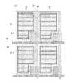
- the structure of the existing ADS type liquid crystal display devicefor example is as shown in FIG. 1 a to FIG. 1 c . It comprises an upper substrate 1 and a lower substrate 2 arranged opposite to each other, a gate line 21 , a data line 22 , a common electrode 23 and a pixel electrode 24 located on the upper substrate 2 .
- a color filtering layer(not shown in the figures) and a black matrix 11 are arranged on the upper substrate 1 .
- the black matrix 11is directly opposite to the data line 22 and the gate line 21 .
- the above ADS type liquid crystal display devicehas some shortcomings.
- the upper substratemay be shifted by pressing the display panel vigorously. If the black matrix 11 located above the gate line 21 is relatively narrow, light leakage may occur easily. Hence, in order to prevent light leakage, the black matrix 11 is required to have a relatively large width generally, however, if so, aperture ratio and light transmissivity will be reduced.
- An embodiment of the present disclosureprovides an array substrate, comprising: a base substrate; a gate line located on the base substrate; and a common electrode and a pixel electrode arranged on the base substrate in sequence and insulated from each other.
- a layer where the pixel electrode locatesis located above a layer where the gate line locates.
- the array substratefurther comprises a strip shaped shielding electrode located above the gate line, the shielding electrode being transparent and electrically conductive.
- An outer contour of a projection of the shielding electrode on the base substratesurrounds a projection of the gate line on the base substrate, and the shielding electrode is insulated from both the pixel electrode and the gate line.
- the shielding electrodeis in a same layer and of a same material as the pixel electrode and is independent of the pixel electrode.
- a layer where the common electrode locatesis located above the layer where the gate line locates, and the shielding electrode is in a same layer and of a same material as the common electrode.
- a material of the shielding electrodeis a transparent electrically conductive oxide.
- the shielding electrodehas at least one slit in an area where the shielding electrode overlaps with the gate line.
- the shielding electrodehas one slit, and an orthographic projection of the slit on the base substrate overlaps with an orthographic projection of the gate line on the base substrate.
- a width of the at least one slitis smaller than or equal to a width of the gate line.
- the common electrodeis a plate electrode
- the pixel electrodeis a slit electrode
- An embodiment of the present disclosurefurther provides a liquid crystal display panel, comprising an array substrate and a counter substrate arranged opposite to each other, and a liquid crystal layer located between the array substrate and the counter substrate.
- the array substrateis the array substrate provided by embodiments of the present disclosure.
- the liquid crystal display panelfurther comprises a black matrix located between the array substrate and the counter substrate.
- An orthographic projection of the black matrix on the base substratedoes not overlap with an orthographic projection of the gate line on the base substrate.
- An embodiment of the present disclosurefurther provides a display device, comprising the liquid crystal display panel provided by embodiments of the present disclosure.
- FIG. 1 ais a structural schematic top view of an existing ADS liquid crystal display device
- FIG. 1 bis a structural schematic sectional view of the liquid crystal display device as shown in FIG. 1 a along A-A′ direction;
- FIG. 1 cis a structural schematic sectional view of the liquid crystal display device as shown in FIG. 1 a along B-B′ direction;
- FIG. 2 ais a structural schematic view of an array substrate provided by an embodiment of the present disclosure
- FIG. 2 bis another structural schematic view of an array substrate provided by an embodiment of the present disclosure.
- FIG. 2 cis another structural schematic view of an array substrate provided by an embodiment of the present disclosure.
- FIG. 3 ais another structural schematic view of an array substrate provided by an embodiment of the present disclosure.
- FIG. 3 bis another structural schematic view of an array substrate provided by an embodiment of the present disclosure.
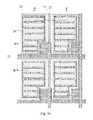
- FIG. 4 ais a structural schematic top view of a liquid crystal display panel provided by an embodiment of the present disclosure
- FIG. 4 bis a structural schematic sectional view of the liquid crystal display panel as shown in FIG. 4 a along A-A′ direction;
- FIG. 4 cis a structural schematic sectional view of the liquid crystal display panel as shown in FIG. 4 a along B-B′ direction.
- thicknesses and the shapes of filmsdo not reflect a real proportion of the array substrate, which only aims to schematically explaining the present disclosure.
- the array substrate 10can comprise a base substrate 01 , a gate line 02 located on the base substrate 01 , and a common electrode 03 and a pixel electrode 04 arranged on the base substrate 01 in sequence and insulated from each other.
- a layer where the pixel electrode 04 locatesis located above a layer where the gate line 02 locates.
- the array substrate 10can further comprise a strip shaped shielding electrode 05 located above the gate line 02 .
- the shielding electrode 05is transparent and electrically conductive.
- An outer contour of a projection of the shielding electrode 05 on the base substrate 01surrounds a projection of the gate line 02 on the base substrate 01 , and the shielding electrode 05 is insulated from both the pixel electrode 04 and the gate line 02 .
- a strip shaped transparent and electrically conductive shielding electrodeis arranged above the gate line, and an outer contour of a projection of the shielding electrode on the base substrate surrounds a projection of the gate line on the base substrate, and the shielding electrode is insulated from both the pixel electrode and the gate line.
- the shielding electrodecan shield the electrical field above the gate line.
- the shielding electrodewhen performing display, the shielding electrode for example can be applied with a common electrode signal.
- two terminals of the shielding electrodecan be electrically connected with the common electrode located within a frame area of the array substrate.
- a material of the shielding electrodeis a transparent electrically conductive oxide.
- the material of the shielding electrodecan be indium tin oxide (ITO) or indium zinc oxide (IZO) etc., which will not be defined here.
- the shielding electrode 05can be in a same layer and of a same material as the pixel electrode 04 and is independent of the pixel electrode 04 .
- a process of manufacturing the shielding electrodedoes not have to be added separately, only needing to change a pattern of original pixel electrode when manufacturing the pixel electrode. Hence, the manufacturing cost can be reduced.
- a layer where the common electrode 03 locatesis located above the layer where the gate line 02 locates.
- the layer where the common electrode 03 locatescan also be located under the layer where the gate line 02 locates.
- the common electrode 03can also be located in a same layer as the gate line 02 , which will not be defined here.
- the shielding layer 05is in the same layer and of the same material as the common electrode 03 .
- a process of manufacturing the shielding electrodedoes not have to be added separately, only needing to change a pattern of original common electrode when manufacturing the common electrode. Hence, the manufacturing cost can be reduced.
- the shielding electrode located above the gate linemay generate parasitic capacitance with the gate line so as to result in increase of a load on the gate line
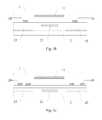
- the shielding electrode 05in order to reduce the load on the gate line, as shown in FIG. 3 a and FIG. 3 b , the shielding electrode 05 has at least one slit V in an area where the shielding electrode 05 overlaps with the gate line 02 .
- the load on the gate line 02can be reduced by reducing the overlapping area of the shielding electrode 05 and the gate line 02 .
- a width of the slitin order to have a better anti-leakage effect, can be smaller than or equal to a width of the gate line.
- the shielding electrodehas one slit, and an orthographic projection of the slit on the base substrate overlaps with an orthographic projection of the gate line on the base substrate.
- the common electrodecan be a plate electrode, and the pixel electrode can be a slit electrode. That is, the array substrate can comprise an ADS type pixel structure.
- the array substratecan further comprise a data line.
- a layer where the data line locatescan be arranged between the layer where the gate line locates and the layer where the pixel electrode locates. Insulating layers are arranged among the data line, the pixel electrode, the common electrode and the gate line.
- an embodiment of the present disclosurefurther provides a liquid crystal display panel, comprising an array substrate and a counter substrate arranged opposite to each other, and a liquid crystal layer located between the array substrate and the counter substrate.
- the array substratecan be the array substrate provided by embodiments of the present disclosure.
- the liquid crystal display panelcan further comprise a black matrix 06 located between the array substrate 10 and the counter substrate 20 .
- An orthographic projection of the black matrix 06 on the base substrate 01does not overlap with an orthographic projection of the gate line 02 on the base substrate 01 .
- the liquid crystal display panelcan further comprise a data line 07 located on the base substrate 01 of the array substrate 10 .
- a data line 07located on the base substrate 01 of the array substrate 10 .
- a strip shaped transparent and electrically conductive shielding electrodeis arranged above the gate line, and an outer contour of a projection of the shielding electrode on the base substrate of the array substrate surrounds a projection of the gate line on the base substrate, and the shielding electrode is insulated from both the pixel electrode and the gate line.
- the shielding electrodecan shield the electrical field above the gate line. Hence, even if the liquid crystal display panel is shifted due to effect of an external force, deflection of the liquid crystals will not be influenced, which can prevent light leakage.
- the shielding electrodecan prevent light leakage, in the liquid crystal display panel, arrangement of a black matrix above the gate line can be omitted, thereby increasing aperture ratio and light transmissivity of the display panel.
- an embodiment of the present disclosurefurther provides a display device, comprising the above liquid crystal display panel provided by embodiments of the present disclosure.
- the display devicecan be any product or component with display function such as a mobile phone, a tablet computer, a television, a laptop, a digital photo frame, a navigator etc.
- the implementation of the display devicecan refer to the embodiments of the liquid crystal display panel, which will not be repeated.
- a strip shaped transparent and electrically conductive shielding electrodeis arranged above the gate line, and an outer contour of a projection of the shielding electrode on the base substrate surrounds a projection of the gate line on the base substrate, and the shielding electrode is insulated from both the pixel electrode and the gate line.
- the shielding electrodecan shield the electrical field above the gate line.
Landscapes
- Physics & Mathematics (AREA)
- Nonlinear Science (AREA)
- Mathematical Physics (AREA)
- Chemical & Material Sciences (AREA)
- Crystallography & Structural Chemistry (AREA)
- General Physics & Mathematics (AREA)
- Optics & Photonics (AREA)
- Engineering & Computer Science (AREA)
- Microelectronics & Electronic Packaging (AREA)
- Geometry (AREA)
- Liquid Crystal (AREA)
- Devices For Indicating Variable Information By Combining Individual Elements (AREA)
Abstract
Description
Claims (12)
Applications Claiming Priority (4)
| Application Number | Priority Date | Filing Date | Title |
|---|---|---|---|
| CN201610034753 | 2016-01-19 | ||
| CN201610034753.3ACN105446029A (en) | 2016-01-19 | 2016-01-19 | Array substrate, liquid crystal display panel and display device |
| CN201610034753.3 | 2016-01-19 | ||
| PCT/CN2016/103933WO2017124810A1 (en) | 2016-01-19 | 2016-10-31 | Array substrate, liquid crystal display panel, and display device |
Publications (2)
| Publication Number | Publication Date |
|---|---|
| US20180081245A1 US20180081245A1 (en) | 2018-03-22 |
| US10509269B2true US10509269B2 (en) | 2019-12-17 |
Family
ID=55556394
Family Applications (1)
| Application Number | Title | Priority Date | Filing Date |
|---|---|---|---|
| US15/525,930Expired - Fee RelatedUS10509269B2 (en) | 2016-01-19 | 2016-10-31 | Array substrate, liquid crystal display panel, and display device |
Country Status (3)
| Country | Link |
|---|---|
| US (1) | US10509269B2 (en) |
| CN (1) | CN105446029A (en) |
| WO (1) | WO2017124810A1 (en) |
Families Citing this family (19)
| Publication number | Priority date | Publication date | Assignee | Title |
|---|---|---|---|---|
| CN105446029A (en)* | 2016-01-19 | 2016-03-30 | 京东方科技集团股份有限公司 | Array substrate, liquid crystal display panel and display device |
| CN106019730B (en)* | 2016-07-14 | 2019-04-02 | 京东方科技集团股份有限公司 | Array substrate and preparation method thereof, display panel and display device |
| US10558073B2 (en)* | 2016-11-04 | 2020-02-11 | Boe Technology Group Co., Ltd. | Display substrate, liquid crystal display panel and fabricating method thereof, and liquid crystal display apparatus |
| CN106405967A (en)* | 2016-11-11 | 2017-02-15 | 京东方科技集团股份有限公司 | Array substrate, LCD (Liquid Crystal Display) panel and display device |
| CN106940498B (en)* | 2017-05-09 | 2020-07-03 | 深圳市华星光电技术有限公司 | LCD panel |
| US10416516B2 (en) | 2017-06-20 | 2019-09-17 | Shenzhen China Star Optoelectronics Technology Co., Ltd | Liquid crystal display panel and liquid crystal display device |
| CN107121861A (en)* | 2017-06-20 | 2017-09-01 | 深圳市华星光电技术有限公司 | Liquid crystal display panel and liquid crystal display |
| CN109346486B (en)* | 2018-11-20 | 2021-01-08 | 京东方科技集团股份有限公司 | Array substrate and display device |
| CN111722445A (en)* | 2019-03-22 | 2020-09-29 | 咸阳彩虹光电科技有限公司 | Array substrate, liquid crystal display panel and display device |
| CN109884819A (en)* | 2019-04-15 | 2019-06-14 | 深圳市华星光电技术有限公司 | Liquid crystal display panel and liquid crystal display device |
| CN209859512U (en)* | 2019-05-24 | 2019-12-27 | 京东方科技集团股份有限公司 | Array substrate and display panel |
| CN110824795A (en)* | 2019-10-18 | 2020-02-21 | 深圳市华星光电半导体显示技术有限公司 | Substrate and liquid crystal display panel |
| KR102651717B1 (en) | 2020-01-07 | 2024-03-27 | 삼성디스플레이 주식회사 | Display device |
| CN113376904A (en)* | 2020-03-10 | 2021-09-10 | 成都京东方光电科技有限公司 | Single-color liquid crystal display panel and double-layer liquid crystal display device |
| CN111290182A (en)* | 2020-03-16 | 2020-06-16 | 深圳市华星光电半导体显示技术有限公司 | Liquid crystal display panel |
| CN111443532A (en)* | 2020-04-21 | 2020-07-24 | Tcl华星光电技术有限公司 | Liquid crystal display panel and display device |
| CN113820893B (en) | 2020-06-18 | 2022-12-20 | 京东方科技集团股份有限公司 | Display panel and display device |
| CN112068377A (en)* | 2020-09-28 | 2020-12-11 | 成都中电熊猫显示科技有限公司 | Array substrate and liquid crystal panel |
| CN114355684A (en)* | 2021-12-24 | 2022-04-15 | 滁州惠科光电科技有限公司 | Array substrate, manufacturing method and display panel |
Citations (12)
| Publication number | Priority date | Publication date | Assignee | Title |
|---|---|---|---|---|
| CN1661449A (en) | 2004-02-26 | 2005-08-31 | Nec液晶技术株式会社 | Liquid crystal display device and manufacturing method thereof |
| CN101097372A (en) | 2006-06-30 | 2008-01-02 | 三星电子株式会社 | Display substrate and display panel with same |
| CN201054061Y (en) | 2006-12-30 | 2008-04-30 | 上海广电Nec液晶显示器有限公司 | ITO common electrode and scanning line structure |
| US20090225250A1 (en) | 2008-02-22 | 2009-09-10 | Ki-Hyun Lyu | Array substrate for in-plane switching mode liquid crystal display device and method of fabricating the same |
| US20100230680A1 (en)* | 2009-03-13 | 2010-09-16 | Samsung Electronics Co., Ltd. | Liquid crystal display device including common electrode and reference electrode |
| CN203883006U (en) | 2014-06-12 | 2014-10-15 | 京东方科技集团股份有限公司 | Array substrate and display device |
| CN104597643A (en) | 2015-01-30 | 2015-05-06 | 京东方科技集团股份有限公司 | Display substrate, preparation method thereof, and display device |
| CN104656324A (en) | 2015-03-17 | 2015-05-27 | 京东方科技集团股份有限公司 | Array substrate and producing method thereof and display device |
| CN105446029A (en) | 2016-01-19 | 2016-03-30 | 京东方科技集团股份有限公司 | Array substrate, liquid crystal display panel and display device |
| CN205450519U (en) | 2016-03-31 | 2016-08-10 | 京东方科技集团股份有限公司 | Array substrate, display panel and display device |
| US20170059907A1 (en)* | 2015-09-01 | 2017-03-02 | Samsung Display Co., Ltd. | Array substrate and liquid crystal display device including the same |
| US20180136526A1 (en)* | 2016-11-11 | 2018-05-17 | Boe Technology Group Co., Ltd. | Array substrate, liquid crystal display panel and display apparatus |
- 2016
- 2016-01-19CNCN201610034753.3Apatent/CN105446029A/enactivePending
- 2016-10-31WOPCT/CN2016/103933patent/WO2017124810A1/ennot_activeCeased
- 2016-10-31USUS15/525,930patent/US10509269B2/ennot_activeExpired - Fee Related
Patent Citations (16)
| Publication number | Priority date | Publication date | Assignee | Title |
|---|---|---|---|---|
| US20050190316A1 (en) | 2004-02-26 | 2005-09-01 | Nec Lcd Technologies, Ltd | Liquid crystal display device and method of fabricating the same |
| CN1661449A (en) | 2004-02-26 | 2005-08-31 | Nec液晶技术株式会社 | Liquid crystal display device and manufacturing method thereof |
| CN101097372A (en) | 2006-06-30 | 2008-01-02 | 三星电子株式会社 | Display substrate and display panel with same |
| US20080002123A1 (en) | 2006-06-30 | 2008-01-03 | Samsung Electronics Co., Ltd. | Display substrate and display panel having the same |
| CN201054061Y (en) | 2006-12-30 | 2008-04-30 | 上海广电Nec液晶显示器有限公司 | ITO common electrode and scanning line structure |
| US20090225250A1 (en) | 2008-02-22 | 2009-09-10 | Ki-Hyun Lyu | Array substrate for in-plane switching mode liquid crystal display device and method of fabricating the same |
| US20100230680A1 (en)* | 2009-03-13 | 2010-09-16 | Samsung Electronics Co., Ltd. | Liquid crystal display device including common electrode and reference electrode |
| US20150364500A1 (en) | 2014-06-12 | 2015-12-17 | Boe Technology Group Co., Ltd. | Array substrate and display device |
| CN203883006U (en) | 2014-06-12 | 2014-10-15 | 京东方科技集团股份有限公司 | Array substrate and display device |
| CN104597643A (en) | 2015-01-30 | 2015-05-06 | 京东方科技集团股份有限公司 | Display substrate, preparation method thereof, and display device |
| CN104656324A (en) | 2015-03-17 | 2015-05-27 | 京东方科技集团股份有限公司 | Array substrate and producing method thereof and display device |
| US20170199441A1 (en)* | 2015-03-17 | 2017-07-13 | Boe Technology Group Co., Ltd. | Array Substrate And Manufacturing Method For The Same, And Display Device |
| US20170059907A1 (en)* | 2015-09-01 | 2017-03-02 | Samsung Display Co., Ltd. | Array substrate and liquid crystal display device including the same |
| CN105446029A (en) | 2016-01-19 | 2016-03-30 | 京东方科技集团股份有限公司 | Array substrate, liquid crystal display panel and display device |
| CN205450519U (en) | 2016-03-31 | 2016-08-10 | 京东方科技集团股份有限公司 | Array substrate, display panel and display device |
| US20180136526A1 (en)* | 2016-11-11 | 2018-05-17 | Boe Technology Group Co., Ltd. | Array substrate, liquid crystal display panel and display apparatus |
Non-Patent Citations (2)
| Title |
|---|
| International Search Report and Written Opinion in PCT/CN2016/103933 dated Jan. 6, 2017, with English translation. |
| Office Action received for Chinese Patent Application No. 201610034753.3, dated Mar. 5, 2018, 13 pages (6 pages of English Translation and 7 pages of Office Action). |
Also Published As
| Publication number | Publication date |
|---|---|
| CN105446029A (en) | 2016-03-30 |
| WO2017124810A1 (en) | 2017-07-27 |
| US20180081245A1 (en) | 2018-03-22 |
Similar Documents
| Publication | Publication Date | Title |
|---|---|---|
| US10509269B2 (en) | Array substrate, liquid crystal display panel, and display device | |
| US11199750B2 (en) | Display panel having black matrix comprising extension portions | |
| US10503290B2 (en) | Color filtering substrate and display apparatus | |
| US10656476B2 (en) | Liquid crystal panel | |
| US10317737B2 (en) | Array substrate, display panel and display device | |
| US20180292693A1 (en) | A display panel and an array substrate thereof | |
| US20210286206A1 (en) | Viewing angle switchable liquid crystal display device and viewing angle switching method | |
| CN106019750A (en) | Liquid crystal display panel and display device | |
| US20170220158A1 (en) | Touch Display Substrate, Touch Display Panel, Touch Display Screen and Electronic Device | |
| US9836156B2 (en) | In-cell touch panel and display device | |
| US20160283009A1 (en) | In-cell touch panel and display device | |
| US10254601B2 (en) | Liquid crystal display panel and display device including the same | |
| US10331253B2 (en) | In-cell touch screen | |
| US9041870B2 (en) | Opposed substrate, manufacturing method thereof and LCD touch panel | |
| EP2728403A1 (en) | Array substrate and display device | |
| US20190064607A1 (en) | Display panel and display device | |
| WO2016145978A1 (en) | Array substrate and method for fabrication thereof, and display device | |
| WO2019233113A1 (en) | Array substrate and display device | |
| US20180373091A1 (en) | Display panel | |
| CN103984165A (en) | Liquid crystal display panel and liquid crystal display | |
| US20150055043A1 (en) | Liquid crystal display device | |
| JP2010096796A (en) | Liquid crystal display device and electronic apparatus | |
| US11307684B2 (en) | Touch array substrate, display panel and display device | |
| US10663817B2 (en) | Array substrate comprising a blocking element stacked on a thin film transistor and first and second shielding electrodes on a side of a data line facing away from a first substrate | |
| CN111948843B (en) | Liquid crystal display panel having a light shielding layer |
Legal Events
| Date | Code | Title | Description |
|---|---|---|---|
| AS | Assignment | Owner name:BOE TECHNOLOGY GROUP CO., LTD., CHINA Free format text:ASSIGNMENT OF ASSIGNORS INTEREST;ASSIGNORS:XIAO, WENJUN;WANG, SHIJUN;CHEN, XI;AND OTHERS;REEL/FRAME:042444/0143 Effective date:20170427 Owner name:BEIJING BOE OPTOELECTRONICS TECHNOLOGY CO., LTD., Free format text:ASSIGNMENT OF ASSIGNORS INTEREST;ASSIGNORS:XIAO, WENJUN;WANG, SHIJUN;CHEN, XI;AND OTHERS;REEL/FRAME:042444/0143 Effective date:20170427 | |
| STPP | Information on status: patent application and granting procedure in general | Free format text:NON FINAL ACTION MAILED | |
| STPP | Information on status: patent application and granting procedure in general | Free format text:RESPONSE TO NON-FINAL OFFICE ACTION ENTERED AND FORWARDED TO EXAMINER | |
| STPP | Information on status: patent application and granting procedure in general | Free format text:FINAL REJECTION MAILED | |
| STPP | Information on status: patent application and granting procedure in general | Free format text:NOTICE OF ALLOWANCE MAILED -- APPLICATION RECEIVED IN OFFICE OF PUBLICATIONS | |
| STPP | Information on status: patent application and granting procedure in general | Free format text:PUBLICATIONS -- ISSUE FEE PAYMENT VERIFIED | |
| STCF | Information on status: patent grant | Free format text:PATENTED CASE | |
| FEPP | Fee payment procedure | Free format text:MAINTENANCE FEE REMINDER MAILED (ORIGINAL EVENT CODE: REM.); ENTITY STATUS OF PATENT OWNER: LARGE ENTITY | |
| LAPS | Lapse for failure to pay maintenance fees | Free format text:PATENT EXPIRED FOR FAILURE TO PAY MAINTENANCE FEES (ORIGINAL EVENT CODE: EXP.); ENTITY STATUS OF PATENT OWNER: LARGE ENTITY | |
| STCH | Information on status: patent discontinuation | Free format text:PATENT EXPIRED DUE TO NONPAYMENT OF MAINTENANCE FEES UNDER 37 CFR 1.362 | |
| FP | Lapsed due to failure to pay maintenance fee | Effective date:20231217 |