US10504700B2 - Plasma etching systems and methods with secondary plasma injection - Google Patents
Plasma etching systems and methods with secondary plasma injectionDownload PDFInfo
- Publication number
- US10504700B2 US10504700B2US14/838,086US201514838086AUS10504700B2US 10504700 B2US10504700 B2US 10504700B2US 201514838086 AUS201514838086 AUS 201514838086AUS 10504700 B2US10504700 B2US 10504700B2
- Authority
- US
- United States
- Prior art keywords
- plasma
- blocking screen
- lift plate
- planar electrode
- chuck
- Prior art date
- Legal status (The legal status is an assumption and is not a legal conclusion. Google has not performed a legal analysis and makes no representation as to the accuracy of the status listed.)
- Active, expires
Links
Images


Classifications
- H—ELECTRICITY
- H01—ELECTRIC ELEMENTS
- H01L—SEMICONDUCTOR DEVICES NOT COVERED BY CLASS H10
- H01L21/00—Processes or apparatus adapted for the manufacture or treatment of semiconductor or solid state devices or of parts thereof
- H01L21/02—Manufacture or treatment of semiconductor devices or of parts thereof
- H01L21/04—Manufacture or treatment of semiconductor devices or of parts thereof the devices having potential barriers, e.g. a PN junction, depletion layer or carrier concentration layer
- H01L21/18—Manufacture or treatment of semiconductor devices or of parts thereof the devices having potential barriers, e.g. a PN junction, depletion layer or carrier concentration layer the devices having semiconductor bodies comprising elements of Group IV of the Periodic Table or AIIIBV compounds with or without impurities, e.g. doping materials
- H01L21/30—Treatment of semiconductor bodies using processes or apparatus not provided for in groups H01L21/20 - H01L21/26
- H01L21/302—Treatment of semiconductor bodies using processes or apparatus not provided for in groups H01L21/20 - H01L21/26 to change their surface-physical characteristics or shape, e.g. etching, polishing, cutting
- H01L21/306—Chemical or electrical treatment, e.g. electrolytic etching
- H01L21/3065—Plasma etching; Reactive-ion etching
- H—ELECTRICITY
- H01—ELECTRIC ELEMENTS
- H01J—ELECTRIC DISCHARGE TUBES OR DISCHARGE LAMPS
- H01J37/00—Discharge tubes with provision for introducing objects or material to be exposed to the discharge, e.g. for the purpose of examination or processing thereof
- H01J37/32—Gas-filled discharge tubes
- H01J37/32431—Constructional details of the reactor
- H01J37/3244—Gas supply means
- H01J37/32449—Gas control, e.g. control of the gas flow
- H—ELECTRICITY
- H01—ELECTRIC ELEMENTS
- H01J—ELECTRIC DISCHARGE TUBES OR DISCHARGE LAMPS
- H01J37/00—Discharge tubes with provision for introducing objects or material to be exposed to the discharge, e.g. for the purpose of examination or processing thereof
- H01J37/32—Gas-filled discharge tubes
- H01J37/32431—Constructional details of the reactor
- H01J37/3244—Gas supply means
- H—ELECTRICITY
- H01—ELECTRIC ELEMENTS
- H01J—ELECTRIC DISCHARGE TUBES OR DISCHARGE LAMPS
- H01J37/00—Discharge tubes with provision for introducing objects or material to be exposed to the discharge, e.g. for the purpose of examination or processing thereof
- H01J37/32—Gas-filled discharge tubes
- H01J37/32009—Arrangements for generation of plasma specially adapted for examination or treatment of objects, e.g. plasma sources
- H01J37/32082—Radio frequency generated discharge
- H—ELECTRICITY
- H01—ELECTRIC ELEMENTS
- H01J—ELECTRIC DISCHARGE TUBES OR DISCHARGE LAMPS
- H01J37/00—Discharge tubes with provision for introducing objects or material to be exposed to the discharge, e.g. for the purpose of examination or processing thereof
- H01J37/32—Gas-filled discharge tubes
- H01J37/32009—Arrangements for generation of plasma specially adapted for examination or treatment of objects, e.g. plasma sources
- H01J37/32357—Generation remote from the workpiece, e.g. down-stream
- H—ELECTRICITY
- H01—ELECTRIC ELEMENTS
- H01J—ELECTRIC DISCHARGE TUBES OR DISCHARGE LAMPS
- H01J37/00—Discharge tubes with provision for introducing objects or material to be exposed to the discharge, e.g. for the purpose of examination or processing thereof
- H01J37/32—Gas-filled discharge tubes
- H01J37/32009—Arrangements for generation of plasma specially adapted for examination or treatment of objects, e.g. plasma sources
- H01J37/32422—Arrangement for selecting ions or species in the plasma
- H—ELECTRICITY
- H01—ELECTRIC ELEMENTS
- H01J—ELECTRIC DISCHARGE TUBES OR DISCHARGE LAMPS
- H01J37/00—Discharge tubes with provision for introducing objects or material to be exposed to the discharge, e.g. for the purpose of examination or processing thereof
- H01J37/32—Gas-filled discharge tubes
- H01J37/32431—Constructional details of the reactor
- H01J37/32532—Electrodes
- H—ELECTRICITY
- H01—ELECTRIC ELEMENTS
- H01J—ELECTRIC DISCHARGE TUBES OR DISCHARGE LAMPS
- H01J37/00—Discharge tubes with provision for introducing objects or material to be exposed to the discharge, e.g. for the purpose of examination or processing thereof
- H01J37/32—Gas-filled discharge tubes
- H01J37/32431—Constructional details of the reactor
- H01J37/32715—Workpiece holder
- H—ELECTRICITY
- H01—ELECTRIC ELEMENTS
- H01L—SEMICONDUCTOR DEVICES NOT COVERED BY CLASS H10
- H01L21/00—Processes or apparatus adapted for the manufacture or treatment of semiconductor or solid state devices or of parts thereof
- H01L21/02—Manufacture or treatment of semiconductor devices or of parts thereof
- H01L21/02104—Forming layers
- H01L21/02107—Forming insulating materials on a substrate
- H01L21/02296—Forming insulating materials on a substrate characterised by the treatment performed before or after the formation of the layer
- H01L21/02299—Forming insulating materials on a substrate characterised by the treatment performed before or after the formation of the layer pre-treatment
- H01L21/02312—Forming insulating materials on a substrate characterised by the treatment performed before or after the formation of the layer pre-treatment treatment by exposure to a gas or vapour
- H01L21/02315—Forming insulating materials on a substrate characterised by the treatment performed before or after the formation of the layer pre-treatment treatment by exposure to a gas or vapour treatment by exposure to a plasma
- H—ELECTRICITY
- H01—ELECTRIC ELEMENTS
- H01L—SEMICONDUCTOR DEVICES NOT COVERED BY CLASS H10
- H01L21/00—Processes or apparatus adapted for the manufacture or treatment of semiconductor or solid state devices or of parts thereof
- H01L21/02—Manufacture or treatment of semiconductor devices or of parts thereof
- H01L21/04—Manufacture or treatment of semiconductor devices or of parts thereof the devices having potential barriers, e.g. a PN junction, depletion layer or carrier concentration layer
- H01L21/18—Manufacture or treatment of semiconductor devices or of parts thereof the devices having potential barriers, e.g. a PN junction, depletion layer or carrier concentration layer the devices having semiconductor bodies comprising elements of Group IV of the Periodic Table or AIIIBV compounds with or without impurities, e.g. doping materials
- H01L21/30—Treatment of semiconductor bodies using processes or apparatus not provided for in groups H01L21/20 - H01L21/26
- H01L21/31—Treatment of semiconductor bodies using processes or apparatus not provided for in groups H01L21/20 - H01L21/26 to form insulating layers thereon, e.g. for masking or by using photolithographic techniques; After treatment of these layers; Selection of materials for these layers
- H01L21/3205—Deposition of non-insulating-, e.g. conductive- or resistive-, layers on insulating layers; After-treatment of these layers
- H01L21/321—After treatment
- H01L21/3213—Physical or chemical etching of the layers, e.g. to produce a patterned layer from a pre-deposited extensive layer
- H01L21/32133—Physical or chemical etching of the layers, e.g. to produce a patterned layer from a pre-deposited extensive layer by chemical means only
- H01L21/32135—Physical or chemical etching of the layers, e.g. to produce a patterned layer from a pre-deposited extensive layer by chemical means only by vapour etching only
- H01L21/32136—Physical or chemical etching of the layers, e.g. to produce a patterned layer from a pre-deposited extensive layer by chemical means only by vapour etching only using plasmas
- H—ELECTRICITY
- H01—ELECTRIC ELEMENTS
- H01L—SEMICONDUCTOR DEVICES NOT COVERED BY CLASS H10
- H01L21/00—Processes or apparatus adapted for the manufacture or treatment of semiconductor or solid state devices or of parts thereof
- H01L21/67—Apparatus specially adapted for handling semiconductor or electric solid state devices during manufacture or treatment thereof; Apparatus specially adapted for handling wafers during manufacture or treatment of semiconductor or electric solid state devices or components ; Apparatus not specifically provided for elsewhere
- H01L21/67005—Apparatus not specifically provided for elsewhere
- H01L21/67011—Apparatus for manufacture or treatment
- H01L21/67017—Apparatus for fluid treatment
- H01L21/67063—Apparatus for fluid treatment for etching
- H01L21/67069—Apparatus for fluid treatment for etching for drying etching
- H—ELECTRICITY
- H05—ELECTRIC TECHNIQUES NOT OTHERWISE PROVIDED FOR
- H05H—PLASMA TECHNIQUE; PRODUCTION OF ACCELERATED ELECTRICALLY-CHARGED PARTICLES OR OF NEUTRONS; PRODUCTION OR ACCELERATION OF NEUTRAL MOLECULAR OR ATOMIC BEAMS
- H05H1/00—Generating plasma; Handling plasma
- H05H1/24—Generating plasma
- H05H1/46—Generating plasma using applied electromagnetic fields, e.g. high frequency or microwave energy
Definitions
- the present disclosurerelates to plasma processing systems.
- plasmascreate ionized and/or energetically excited species for interaction with workpieces that may be, for example, semiconductor wafers.
- one or more radio frequency (RF) and/or microwave generatorstypically generate oscillating electric and/or magnetic fields.
- RFradio frequency
- a plasmais generated in the same location as one or more wafers being processed; in other cases, a plasma is generated in one location and moves to another location where the wafer(s) are processed.
- the plasmas producedoften contain highly energetic and/or corrosive species and/or highly energetic electrons, such that the equipment that produces them sometimes degrades from contact with the energetic species and/or electrons.
- materials that are exposed to highly energetic species and/or electronsmay be etched and/or sputtered, generating etched and/or sputtered material that can move about, and can react or deposit on various surfaces.
- an apparatus for plasma processingincludes a first plasma source, a first planar electrode, a gas distribution device, a plasma blocking screen and a workpiece chuck.
- the first plasma sourceproduces first plasma products.
- the first planar electrodeincludes a first plate that defines a plurality of first apertures therethrough, a first side of the first planar electrode being disposed relative to the first plasma source such that the first plasma products pass away from the first plasma source through the plurality of first apertures to a second side of the first planar electrode.
- the gas distribution deviceincludes a second plate that defines a plurality of second apertures therethrough, a first side of the gas distribution device being disposed facing the second side of the first planar electrode, such that the first plasma products continue through the plurality of second apertures to a second side of the gas distribution device.
- the plasma blocking screenincludes a third plate that defines a plurality of fourth apertures therethrough, a first side of the plasma blocking screen being disposed facing the second side of the gas distribution device such that the first plasma products pass through the plurality of fourth apertures to a second side of the plasma blocking screen.
- the workpiece chuckfaces the second side of the plasma blocking screen, such that a process chamber is defined between the plasma blocking screen and the workpiece chuck.
- the fourth aperturesare of a sufficiently small size to block a plasma generated in the process chamber from reaching the gas distribution device.
- a plasma processing chamberincludes a workpiece holder and a planar electrode.
- the planar electrodedefines parallel and opposing first and second planar surfaces, separated by a thickness, over a central region thereof.
- the second planar surfaceis disposed facing the workpiece holder.
- the planar electrodedefines a plurality of apertures therethrough.
- Each of the aperturesis characterized by a first aperture section and a second aperture section.
- the first aperture sectiondefines an aperture axis and a first aperture minor lateral dimension perpendicular to the aperture axis, the first aperture section extending from the first planar surface through at least half of the thickness.
- the second aperture sectiondefines a second aperture minor lateral dimension that is less than the first aperture minor lateral dimension, and extends from the second planar surface through less than half the thickness.
- the first and aperture sectionsadjoin axially to form a continuous one of the apertures from the first planar surface to the second planar surface.
- an apparatus for plasma processingincludes a gas source, a first planar electrode, a second planar electrode, a first power supply, a plasma blocking screen, a workpiece chuck and a second power supply.
- the first planar electrodeincludes a first plate that defines a plurality of first apertures therethrough, a first side of the first planar electrode being disposed relative to the gas source such that gases from the gas source pass through the plurality of first apertures to a second side of the first planar electrode.
- the second planar electrodeincludes a second plate that defines a plurality of second apertures therethrough, a first side of the second planar electrode being disposed facing the second side of the first planar electrode.
- the first power supplycouples radio frequency (RF) power across the first planar electrode and the second planar electrode.
- a first plasmais generated, from the gases, between the first planar electrode and the second planar electrode, and first plasma products from the first plasma pass through the plurality of second apertures to a second side of the second planar electrode.
- the plasma blocking screenincludes a third plate that defines a plurality of third apertures therethrough, a first side of the plasma blocking screen being disposed facing the second side of the second planar electrode such that the first plasma products pass through the plurality of third apertures to a second side of the plasma blocking screen.
- the workpiece chuckfaces the second side of the plasma blocking screen, defining a process chamber between the plasma blocking screen.
- the second power supplycouples radio frequency (RF) power across the plasma blocking screen and the workpiece chuck, generating a second plasma, from the gases, between the plasma blocking screen and the workpiece chuck.
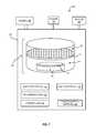
- FIG. 1schematically illustrates major elements of a plasma processing system, according to an embodiment.
- FIG. 2schematically illustrates major elements of a plasma processing system, in a cross-sectional view, according to an embodiment.
- FIG. 3illustrates a portion of a plasma blocking screen that is part of the plasma processing system of FIG. 2 , according to an embodiment.
- FIG. 4illustrates a portion of another plasma blocking screen, according to an embodiment.
- FIG. 5is a graph of modeling data related to choice of a minor lateral dimension of second aperture sections of a plasma blocking screen, according to an embodiment.
- FIG. 6schematically illustrates a region noted in FIG. 2 in an enlarged view.
- FIG. 7schematically illustrates major elements of another plasma processing system, in a cross-sectional view, according to an embodiment.
- FIG. 1schematically illustrates major elements of a plasma processing system 100 , according to an embodiment.
- System 100is depicted as a single wafer, semiconductor wafer plasma processing system, but it will be apparent to one skilled in the art that the techniques and principles herein are applicable to plasma generation systems of any type (e.g., systems that do not necessarily process wafers or semiconductors).
- Processing system 100includes a housing 110 for a wafer interface 115 , a user interface 120 , a plasma processing unit 130 , a controller 140 , one or more power supplies 150 and one or more radio frequency (RF) generators 165 .
- Processing system 100is supported by various utilities that may include gas(es) 155 , external power 170 , vacuum 160 and optionally others. Internal plumbing and electrical connections within processing system 100 are not shown, for clarity of illustration.
- Processing system 100is shown as a so-called indirect plasma processing system that generates a plasma in a first location and directs the plasma and/or plasma products (e.g., ions, molecular fragments, energized species and the like) to a second location where processing occurs.
- plasma processing unit 130includes a plasma source 132 that supplies plasma and/or plasma products for a process chamber 134 .
- Process chamber 134includes one or more workpiece holders 135 , upon which wafer interface 115 places a workpiece 50 (e.g., a semiconductor wafer, but could be a different type of workpiece) for processing.
- gas(es) 155are introduced into plasma source 132 , and at least one of the RF generators 165 supplies power to ignite a first plasma within plasma source 132 .
- Plasma and/or plasma productspass from plasma source 132 through a diffuser plate 137 to process chamber 134 . Additional gases may be added to the plasma and/or plasma products in process chamber 134 , RF power may also be provided within process chamber 134 to generate another plasma.
- Workpiece 50is processed in process chamber 134 .
- plasmasmay be ignited at one, two or more locations within a plasma processing system, and the techniques disclosed herein may be adapted to plasma processing systems that ignite and/or use plasmas formed at single or multiple locations.
- Certain electronics manufacturersmay prefer systems with the flexibility of igniting and/or using plasmas in a variety of configurations, so that each system can be adapted for a corresponding variety of processing needs.
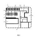
- FIG. 2schematically illustrates major elements of a plasma processing system 200 , in a cross-sectional view, according to an embodiment.
- Plasma processing system 200is an example of plasma processing unit 130 , FIG. 1 .
- Plasma processing system 200includes a plasma source 210 and a process chamber 205 that may also generate a plasma, as discussed below.
- a general direction of gas and/or plasma product flowis downwards, and this direction may be referred to as “downstream” herein, while an opposing direction upwards in the orientation of FIG. 2 , may be referred to as “upstream.”
- FIG. 2may be cylindrically symmetric about a central axis 201 , with associated directions being defined as a radial direction 202 and an azimuthal direction 203 .
- This convention of directionsmay be used herein, although one skilled in the art will understand that many of the principles described herein are not limited to cylindrically symmetric systems.
- plasma source 210may introduce gases, and/or gases that are ionized by an upstream remote plasma source, as plasma source gases 212 , through an RF electrode 215 .
- RF electrode 215is electrically tied to a first gas diffuser 220 and a face plate 225 that serve to redirect flow of the source gases so that gas flow is uniform across plasma source 210 (uniform from left to right in the view of FIG. 2 ).
- all of the diffusers or screens hereinmay be characterized as electrodes, as any such diffusers or screens may be tied to a particular electrical potential.
- An insulator 230electrically insulates RF electrode 215 , including face plate 225 , from a diffuser 235 that is held at electrical ground. Diffuser 235 serves as a second electrode counterfacing face plate 225 of RF electrode 215 . Surfaces of face plate 225 , diffuser 235 and insulator 230 define a first plasma generation cavity where a first plasma 245 may be created when plasma source gases 212 are present and RF energy is provided at face plate 225 through RF electrode 215 .
- RF electrode 215 , face plate 225 and diffuser 235may be formed of any conductor, and in embodiments are formed of aluminum (or an aluminum alloy, such as the known “6061” alloy type).
- face plate 225 and diffuser 235 that face plasma 245 directlymay be coated with ceramic layers of, for example, yttria (Y 2 O 3 ) or alumina (Al 2 O 3 ) for resistance to bombardment by energetic plasma products generated in plasma 245 .
- Other surfaces of face plate 225 and diffuser 235 that are not necessarily exposed directly to plasma, but are exposed to reactive gases and/or radicals generated by plasmas,may be coated either with ceramic layers (e.g., yttria, alumina) or with a suitable passivating layer (e.g., an anodized layer, or a chemically generated alumina layer) for chemical resistance.
- Insulator 230may be any insulator, and in embodiments is formed of ceramic.
- Plasma products generated in plasma 245pass through diffuser 235 that again helps to promote the uniform distribution of plasma products, and may assist in electron temperature control.
- the plasma productspass through an optional gas distribution device 260 that promotes uniformity.
- Optional gas distribution device 260is also held at electrical ground. Apertures that pass completely through optional gas distribution device 260 are of a diameter at least three times a diameter of apertures within diffuser 235 .
- gas distribution device 260includes further gas channels 250 that may be used to introduce one or more further gases 155 ( 2 ) to the plasma products as they enter process chamber 205 (that is, gases 155 ( 2 ) emerge only from a side of gas distribution device 260 that is distal to diffuser 235 ).
- Optional gas distribution device 260may also be made of aluminum or aluminum alloy, and like face plate 225 and diffuser 235 discussed above, may be at least coated with a passivating layer for chemical resistance, or may be coated with a ceramic layer.
- Plasma blocking screen 270 ( 1 )may form a thickness in the range of 0.15 to 1.0 inches, and forms many small apertures that are configured to allow gases and plasma products from upstream sources pass through into process chamber 205 , while substantially blocking downstream plasmas and plasma products from upstream components, as discussed in detail below.
- plasma blocking screens 270may advantageously form at least ten apertures per square inch in a central region thereof, and in certain embodiments may form thirty or more apertures per square inch.
- plasma blocking screen 270 ( 1 )is also held at electrical ground.
- surfaces of plasma blocking screen 270 ( 1 ) that are exposed directly to plasmaare advantageously coated with ceramic (e.g., alumina or yttria) while surfaces that are not exposed directly to plasma may also be coated with ceramic, and are advantageously at least coated with a passivating layer for chemical resistance to reactive gases and activated species. All of the gases and/or plasma products, generated as described above, interact with workpiece 50 within process chamber 205 , and a further plasma 275 may be generated may be generated within process chamber 205 .
- RF power to create plasma 275is applied to workpiece holder 135 .
- a DC biasmay also be applied to workpiece holder 135 to steer ions generated in plasma 275 to facilitate directional (anisotropic) etching of workpiece 50 , as discussed below.
- Workpiece holder 135may be switchably connected with RF and/or DC bias sources, so as to generate a plasma within process chamber 205 at selected times and not at other times.
- Workpiece holder 135may be connected with the same RF power supply as is used to create plasma 245 between face plate 225 and diffuser 235 , or may be connected with a different RF power supply.
- plasma blocking screen 270 ( 1 )the ability to choose whether to generate a plasma by providing RF power and/or DC bias to workpiece holder 135 , or not to generate such plasma, and other features described herein, provide application flexibility to processing system 200 .
- processing system 200may be operated in a mode wherein plasma is not generated within process chamber 205 .
- the gases and/or plasma products provided by upstream portions of processing system 200may provide isotropic etching, and workpiece holder 135 may be held at DC ground (although a DC offset may be provided across spatial portions of workpiece holder 135 , to provide electrostatic wafer chucking).
- processing system 200may be operated in a mode wherein plasma is generated within process chamber 205 , and plasma products thereof may be steered by DC bias between plasma blocking screen and workpiece holder 135 .
- the plasma products steered by the DC biasmay provide anisotropic etching, for example to remove broad surface depositions on a workpiece while leaving sidewalls, or to clear materials within deep trenches in a workpiece.
- FIGS. 3 and 4An enlarged view of a portion noted as A in FIG. 2 is illustrated in detail in FIG. 6 .
- FIG. 3illustrates a portion of a plasma blocking screen 270 , such as plasma blocking screen 270 ( 1 ), FIG. 2 .
- Plasma blocking screen 270defines parallel and opposing planar surfaces 268 and 269 , and defines a plurality of apertures 271 extending through plasma blocking screen 270 , as shown in FIG. 2 .
- First planar surface 268 and second planar surface 269characterize a central portion of plasma blocking screen 270 ; however, outside the central portion, plasma blocking screen may be thicker or thinner to provide attachment points for other structures of plasma processing system 200 .
- Apertures 271are specialized to allow significant passage of plasma products therethrough with minimal wall effects, but to block plasma from plasma 275 from other parts of plasma processing system 200 , where the plasma can damage other components.
- FIG. 1plasma blocking screen 270
- First aperture sections 272may be cylindrical, which may facilitate fabrication, but may also define other shapes, for example of rectangular or hexagonal cross-section. Any such cross-section is maintained relatively constant through a vertical depth H 1 of first aperture section 272 (given the orientation of plasma blocking screen 270 ( 1 ) as shown in FIGS. 2 and 3 ) and is considered to define an aperture axis (e.g., vertical, in FIGS. 2 and 3 ).
- a minor lateral dimension of first aperture section 272 in a lateral directionis shown as W 1 .
- Minor lateral dimensionherein means the largest of any lateral dimensions characterizing an aperture having vertical sides (e.g., if first aperture section 272 is cylindrical, minor lateral dimension W 1 is a diameter of the cylinder, if first aperture section 272 is rectangular, minor lateral dimension W 1 is the smaller of the rectangle sides, and the like).
- a vertical depth of second aperture section 273is shown as H 2
- a minor lateral dimension of second aperture section 273 in a lateral directionis shown as W 2 .
- the sum of H 1 and H 2is the thickness of plasma blocking screen 270 between planar surfaces 268 and 269 .
- dimensions H 1 , W 1 , H 2 and W 2are selected to minimize wall effects as plasma products from above (in the orientation shown in FIG. 2 ) pass through aperture 271 , but also to block products of plasma 275 from reaching optional gas distribution device 260 (when present) and/or other upstream components of plasma processing system 200 .
- Researchhas shown (see FIG. 5 ) that even when aperture 271 is provided with a second aperture section 273 that is very short in height, an appropriate width W 2 will significantly reduce electron density within first aperture section 272 and above. The electron density can be used to estimate an extent to which any plasma product will pass through aperture 271 and affect upstream components.
- width W 2is less than 0.050′′, while height H 2 is between 0.050′′ and 0.100′′.
- H 1is typically larger than H 2 , and in embodiments herein, H 1 is typically 0.10′′ or greater.
- W 1is less critical than W 2 , but a larger W 1 reduces wall effects (e.g., recombination of ions, deactivation of activated species and the like) to maintain activity of plasma products passing through aperture 271 .
- W 1may be, for example, 0.02′′ to 0.25′′.
- FIG. 4illustrates a portion of plasma blocking screen 270 ′, which is a modified case of plasma blocking screen 270 , FIG. 3 .
- Plasma blocking screen 270 ′defines a plurality of apertures 271 ′ that, like apertures 271 , are specialized to allow significant passage of plasma products therethrough with minimal wall effects, but to block plasma from plasma 275 from other parts of plasma processing system 200 .
- FIG. 4illustrates features of a single aperture 271 ′ that is characterized by a first aperture section 272 and a second aperture section 273 ′, as shown.
- First aperture sections 272are identical in character to the same feature illustrated in FIG.
- Second aperture section 273 ′defines a cylindrical upper portion 276 that adjoins first aperture section 272 , and a lower portion 277 that flares outwardly from upper portion 276 toward second planar surface 269 .
- Lower portion 277may in fact be conical, as shown in FIG. 4 , or may be simply curved outwards from the vertical.
- An angle ⁇ from the aperture axis (e.g., vertical, in FIG. 4 ) of 15 to 65 degreesmay be advantageous, as discussed below.
- upper portion 276may be characterized as having a diameter, and a diameter of lower portion 277 is greater where lower portion 277 adjoins planar surface 269 , than the diameter of upper portion 276 .
- Upper portion 276 and lower portion 277adjoin axially to complete aperture 271 ′ through plasma blocking screen 270 ′.
- Forming apertures 271 ′ to include conical lower portions 277has been found advantageous for fabricating plasma blocking screen 270 with a high quality, continuous coating of alumina or yttria on surfaces (such as second planar surface 269 and side surfaces of second aperture sections 273 , 273 ′) that face active plasma.
- First planar surface 268 and side walls of first aperture section 272are also, optionally, coated with alumina or yttria.
- certain deposition techniquessuch as sputtering tend to be highly directional, that is, the substance being deposited tends to travel in a straight line from a source and stick to the first thing that the substance encounters.
- FIG. 5shows a graph 300 of modeling data that supports the choice of the minor lateral dimension of second aperture sections 273 , 273 ′, FIGS. 3 and 4 .
- the horizontal axismodels position, with conductors (e.g., workpiece holder 135 and wafer 50 ) assumed to be present out to about 4 centimeters, a structural void (e.g., process chamber 205 with plasma 275 therein) from about four to almost 7 centimeters (noted in graph 300 as a broken line), and plasma blocking screen 270 assumed to extend from about 7 centimeters to the end of graph 300 .
- the vertical axisindicates modeled electron density within a plasma region between the solid conductor and the workpiece holder.
- Electron densities in the range of about 10 2 to low 10 3are regarded as showing regions that are essentially free of plasma, that is, a number of electrons and/or other plasma products is negligibly low. Electron density is high within the plasma region, and falls off at plasma blocking screen 270 . Using the notation shown in FIG.
- Open circle data 310is for second aperture section 273 having W 2 in the range of 0.100′′ to 0.150′′
- solid triangle data 320is for second aperture section 273 having W 2 in the range of 0.050′′ to 0.100′′
- solid rectangle data 330is for second aperture section 273 having W 2 in the range of 0.020′′ to 0.050′′.
- Data 310 and 320show that plasma blocking screens 270 having second apertures with the respective W 2 noted will decrease electron density transmitted to an adjacent region (e.g., a region extending to the right hand side of graph 300 , or above plasma blocking screen 270 ( 1 ) in FIG. 2 ), but will not effectively block it.
- Data 330shows that a plasma blocking screen 270 having W 2 in the range of 0.020′′ to 0.050′′ will block plasma almost completely from the adjacent upstream region. Although effective at blocking active plasma from the upstream region, plasma blocking screen 270 does not block plasma products from upstream plasmas, and/or gases, from passing in the downstream direction.
- FIG. 6schematically illustrates region A noted in FIG. 2 .
- a workpiece 50is shown on a workpiece holder 135 within process chamber 205 .
- Gases 155 and/or previously formed plasma productsflow through plasma blocking screen 270 ( 1 ) into process chamber 205 , where a further plasma 275 is formed.
- plasma blocking screen 270 ( 1 )is held at electrical ground.
- RF energy, and a DC bias,are applied to workpiece holder 135 to provide energy for plasma 275 .
- interior surfaces of process chamber 205are provided with materials (generally, but not limited to, ceramics) capable of resisting attack from such sources.
- workpiece holder 135may be coated with alumina or aluminum nitride, and plasma blocking screen 270 ( 1 ) may be coated with alumina or yttria.
- An optional ceramic spacer 350 and/or an optional ceramic pumping liner 370may be used to reduce lateral electric fields at the edge of workpiece holder 135 .
- Ceramic spacer 350 and ceramic pumping liner 370are ring shaped such that they extend about a periphery of process chamber 205 , but not across the central region of process chamber 205 , and are advantageously fabricated from low loss tangent materials such as high purity alumina, silicon nitride and/or silicon carbide. Materials having loss tangents within the range of 0.1 to 0.0001 provide useful results, while materials having loss tangents within the range of 0.005 to 0.001 represent a range of high performance at reasonable cost. Portions of both plasma blocking screen 270 ( 1 ) and ceramic spacer 350 are disposed atop a portion of a grounded lift plate 390 , as shown, and obtain mechanical support therefrom.
- Lift plate 390is mechanically connected with plasma blocking screen 270 ( 1 ), ceramic spacer 350 and other overlying structures so as to enable lifting of all such structures from the vicinity of workpiece holder 135 for assembly and/or maintenance purposes.
- Plasma blocking screen 270 ( 1 )is electrically grounded through contact with lift plate 390 .
- a thickness of ceramic spacer 350is controlled to leave a gap 360 between plasma blocking screen 270 ( 1 ) and ceramic spacer 350 , to ensure that ceramic spacer 350 does not interrupt continuous contact of plasma blocking screen 270 ( 1 ) with lift plate 390 in the azimuthal direction, about a periphery of process chamber 205 .
- Forming ceramic spacer 350 and ceramic pumping liner 370 of low loss tangent dielectric materialsis comparatively expensive (as compared to, for example, fabricating such items from aluminum with a ceramic coating) but reduces electric field effects at the edges of workpiece holder 135 , and reduces reflected RF power when plasma 275 is generated within process chamber 205 .
- Substituting ceramic spacer 350 and ceramic pumping liner 370also reduces ion bombardment related contamination as compared with equivalent aluminum parts used in the same locations. Use of ceramic spacer 350 and ceramic pumping liner 370 thus promotes plasma and process stability, and reduces contamination. Electric fields are schematically illustrated using dotted arrows in FIG.
- the primary electric fieldis between workpiece holder 135 /workpiece 50 and plasma blocking screen 270 ( 1 ). It is advantageous for the electric fields between workpiece holder 135 /workpiece 50 and plasma blocking screen 270 ( 1 ) be strong and uniform in direction, since the electric fields steer ions involved with anisotropic etching. That is, to clear material at the bottoms of vertical trenches, the electric fields steering the ions need to be correspondingly vertical. Weaker fields exist between workpiece holder 135 and grounded lift plate 390 , through ceramic spacer 350 and ceramic pumping liner 370 . These electric fields are weakened by the dielectric materials of ceramic spacer 350 and ceramic pumping liner 370 being interposed between workpiece holder 135 and lift plate 390 .
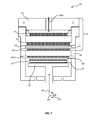
- FIG. 7schematically illustrates major elements of a plasma processing system 400 , in a cross-sectional view, according to an embodiment.
- Plasma processing system 400is an example of plasma processing unit 130 , FIG. 1 .
- plasma processing system 400enables creation of a plasma 275 adjacent to workpiece 50 .
- Plasma processing system 400includes many components identical in structure and function to those found in plasma processing system 200 , FIG. 2 , but lacks optional gas distribution device 260 shown in plasma processing system 200 .
- plasma processing system 400includes a plasma blocking screen 270 ( 2 ) configured differently from the equivalent item shown in FIG. 2 , and an insulator 280 between diffuser 235 and plasma blocking screen 270 ( 2 ).
- an insulator 230electrically insulates RF electrode 215 , including face plate 225 , from a diffuser 235 that is held at electrical ground.
- Diffuser 235serves as a second electrode counterfacing face plate 225 of RF electrode 215 .
- Surfaces of face plate 225 , diffuser 235 and insulator 230define a first plasma generation cavity where a first plasma 245 may be created when plasma source gases 212 are present and RF energy is provided at face plate 225 through RF electrode 215 .
- Plasma blocking screen 270 ( 2 )is also held at electrical ground, but insulator 280 allows plasma blocking screen 270 ( 2 ) to be isolated from diffuser 235 , providing an independent RF ground return path.
- Apertures within plasma blocking screen 270 ( 2 )are configured like those of plasma blocking screen 270 ( 1 ), that is, they form shapes like those illustrated in FIGS. 3 and 4 , with similar dimensions, so that upstream plasma products may pass through, but active plasma 275 is blocked from diffuser 235 and other upstream components.
- Embodiments hereinmay be rearranged and may form a variety of shapes.
- many components shown in FIG. 2 and FIG. 7such as RF electrode 215 , diffusers 220 and 235 , gas distribution device 260 , face plate 225 , insulator 230 , plasma blocking screens 270 and others may be substantially radially symmetric about a central axis, for processing a circular semiconductor wafer as workpiece 50 .
- such featuresmay be of any shape that is consistent with use as a plasma source.
- An exact number and placement of features for introducing and distributing gases and/or plasma products, such as diffusers, face plates and the like,may also vary.
- plasma processing system 200may be configured to add or mix gases 155 with other gases and/or plasma products as they pass through the system to process chamber 205 .
- FIG. 2 , FIG. 6 and FIG. 7many system components will form perforate planar shapes within central regions of a plasma processing unit so as to provide uniform process conditions to a planar workpiece, but may form different shapes such as flanges, thickness changes, solid imperforate surfaces, and the like at edges of the plasma processing unit for structural purposes.
- Extents of the central regionsmay vary, in embodiments, to accommodate different workpiece sizes, especially but not limited to, diameters of wafers as workpieces.
- the central regionwill generally encompass a central region that extends at least to one-half of a radius of each such system component.
Landscapes
- Engineering & Computer Science (AREA)
- Physics & Mathematics (AREA)
- Plasma & Fusion (AREA)
- Chemical & Material Sciences (AREA)
- Analytical Chemistry (AREA)
- General Physics & Mathematics (AREA)
- Condensed Matter Physics & Semiconductors (AREA)
- Manufacturing & Machinery (AREA)
- Computer Hardware Design (AREA)
- Microelectronics & Electronic Packaging (AREA)
- Power Engineering (AREA)
- Spectroscopy & Molecular Physics (AREA)
- Electromagnetism (AREA)
- Chemical Kinetics & Catalysis (AREA)
- General Chemical & Material Sciences (AREA)
- Plasma Technology (AREA)
- Drying Of Semiconductors (AREA)
Abstract
Description
The present disclosure relates to plasma processing systems.
In plasma processing, plasmas create ionized and/or energetically excited species for interaction with workpieces that may be, for example, semiconductor wafers. To create and/or maintain a plasma, one or more radio frequency (RF) and/or microwave generators typically generate oscillating electric and/or magnetic fields. In some wafer processing systems, a plasma is generated in the same location as one or more wafers being processed; in other cases, a plasma is generated in one location and moves to another location where the wafer(s) are processed. The plasmas produced often contain highly energetic and/or corrosive species and/or highly energetic electrons, such that the equipment that produces them sometimes degrades from contact with the energetic species and/or electrons. For example, materials that are exposed to highly energetic species and/or electrons may be etched and/or sputtered, generating etched and/or sputtered material that can move about, and can react or deposit on various surfaces.
In an embodiment, an apparatus for plasma processing includes a first plasma source, a first planar electrode, a gas distribution device, a plasma blocking screen and a workpiece chuck. The first plasma source produces first plasma products. The first planar electrode includes a first plate that defines a plurality of first apertures therethrough, a first side of the first planar electrode being disposed relative to the first plasma source such that the first plasma products pass away from the first plasma source through the plurality of first apertures to a second side of the first planar electrode. The gas distribution device includes a second plate that defines a plurality of second apertures therethrough, a first side of the gas distribution device being disposed facing the second side of the first planar electrode, such that the first plasma products continue through the plurality of second apertures to a second side of the gas distribution device. The plasma blocking screen includes a third plate that defines a plurality of fourth apertures therethrough, a first side of the plasma blocking screen being disposed facing the second side of the gas distribution device such that the first plasma products pass through the plurality of fourth apertures to a second side of the plasma blocking screen. The workpiece chuck faces the second side of the plasma blocking screen, such that a process chamber is defined between the plasma blocking screen and the workpiece chuck. The fourth apertures are of a sufficiently small size to block a plasma generated in the process chamber from reaching the gas distribution device.
In an embodiment, a plasma processing chamber includes a workpiece holder and a planar electrode. The planar electrode defines parallel and opposing first and second planar surfaces, separated by a thickness, over a central region thereof. The second planar surface is disposed facing the workpiece holder. The planar electrode defines a plurality of apertures therethrough. Each of the apertures is characterized by a first aperture section and a second aperture section. The first aperture section defines an aperture axis and a first aperture minor lateral dimension perpendicular to the aperture axis, the first aperture section extending from the first planar surface through at least half of the thickness. The second aperture section defines a second aperture minor lateral dimension that is less than the first aperture minor lateral dimension, and extends from the second planar surface through less than half the thickness. The first and aperture sections adjoin axially to form a continuous one of the apertures from the first planar surface to the second planar surface.
In an embodiment, an apparatus for plasma processing includes a gas source, a first planar electrode, a second planar electrode, a first power supply, a plasma blocking screen, a workpiece chuck and a second power supply. The first planar electrode includes a first plate that defines a plurality of first apertures therethrough, a first side of the first planar electrode being disposed relative to the gas source such that gases from the gas source pass through the plurality of first apertures to a second side of the first planar electrode. The second planar electrode includes a second plate that defines a plurality of second apertures therethrough, a first side of the second planar electrode being disposed facing the second side of the first planar electrode. The first power supply couples radio frequency (RF) power across the first planar electrode and the second planar electrode. A first plasma is generated, from the gases, between the first planar electrode and the second planar electrode, and first plasma products from the first plasma pass through the plurality of second apertures to a second side of the second planar electrode. The plasma blocking screen includes a third plate that defines a plurality of third apertures therethrough, a first side of the plasma blocking screen being disposed facing the second side of the second planar electrode such that the first plasma products pass through the plurality of third apertures to a second side of the plasma blocking screen. The workpiece chuck faces the second side of the plasma blocking screen, defining a process chamber between the plasma blocking screen. The second power supply couples radio frequency (RF) power across the plasma blocking screen and the workpiece chuck, generating a second plasma, from the gases, between the plasma blocking screen and the workpiece chuck.
The present disclosure may be understood by reference to the following detailed description taken in conjunction with the drawings briefly described below, wherein like reference numerals are used throughout the several drawings to refer to similar components. It is noted that, for purposes of illustrative clarity, certain elements in the drawings may not be drawn to scale. Specific instances of an item may be referred to by use of a numeral followed by a second numeral within parentheses (e.g., plasma blocking screens270(1),270(2) etc.) while numerals not followed by a dash refer to any such item (e.g., plasma blocking screens270). In instances where multiple instances of an item are shown, only some of the instances may be labeled, for clarity of illustration.
Additional embodiments and features are set forth in part in the description that follows, and in part will become apparent to those skilled in the art upon examination of the specification or may be learned by the practice of the invention. The features and advantages of the invention may be realized and attained by means of the instrumentalities, combinations, and methods described in the specification.
Therefore, generally, plasmas may be ignited at one, two or more locations within a plasma processing system, and the techniques disclosed herein may be adapted to plasma processing systems that ignite and/or use plasmas formed at single or multiple locations. Certain electronics manufacturers may prefer systems with the flexibility of igniting and/or using plasmas in a variety of configurations, so that each system can be adapted for a corresponding variety of processing needs.
As shown inFIG. 2 ,plasma source 210 may introduce gases, and/or gases that are ionized by an upstream remote plasma source, as plasma source gases212, through anRF electrode 215.RF electrode 215 is electrically tied to afirst gas diffuser 220 and aface plate 225 that serve to redirect flow of the source gases so that gas flow is uniform across plasma source210 (uniform from left to right in the view ofFIG. 2 ). It should be noted that all of the diffusers or screens herein may be characterized as electrodes, as any such diffusers or screens may be tied to a particular electrical potential. Aninsulator 230 electrically insulatesRF electrode 215, includingface plate 225, from adiffuser 235 that is held at electrical ground.Diffuser 235 serves as a second electrodecounterfacing face plate 225 ofRF electrode 215. Surfaces offace plate 225,diffuser 235 andinsulator 230 define a first plasma generation cavity where afirst plasma 245 may be created when plasma source gases212 are present and RF energy is provided atface plate 225 throughRF electrode 215.RF electrode 215,face plate 225 anddiffuser 235 may be formed of any conductor, and in embodiments are formed of aluminum (or an aluminum alloy, such as the known “6061” alloy type). Surfaces offace plate 225 anddiffuser 235 that faceplasma 245 directly may be coated with ceramic layers of, for example, yttria (Y2O3) or alumina (Al2O3) for resistance to bombardment by energetic plasma products generated inplasma 245. Other surfaces offace plate 225 anddiffuser 235 that are not necessarily exposed directly to plasma, but are exposed to reactive gases and/or radicals generated by plasmas, may be coated either with ceramic layers (e.g., yttria, alumina) or with a suitable passivating layer (e.g., an anodized layer, or a chemically generated alumina layer) for chemical resistance.Insulator 230 may be any insulator, and in embodiments is formed of ceramic.
Plasma products generated inplasma 245 pass throughdiffuser 235 that again helps to promote the uniform distribution of plasma products, and may assist in electron temperature control. Upon passing throughdiffuser 235, the plasma products pass through an optionalgas distribution device 260 that promotes uniformity. (Certain embodiments do not includegas distribution device 260; see, e.g.,FIG. 7 ) Optionalgas distribution device 260 is also held at electrical ground. Apertures that pass completely through optionalgas distribution device 260 are of a diameter at least three times a diameter of apertures withindiffuser 235. Also,gas distribution device 260 includesfurther gas channels 250 that may be used to introduce one or more further gases155(2) to the plasma products as they enter process chamber205 (that is, gases155(2) emerge only from a side ofgas distribution device 260 that is distal to diffuser235). Optionalgas distribution device 260 may also be made of aluminum or aluminum alloy, and likeface plate 225 anddiffuser 235 discussed above, may be at least coated with a passivating layer for chemical resistance, or may be coated with a ceramic layer.
Gases155(1),155(2) and/or plasma products fromplasma 245 enter aplenum cavity 265, then pass through a plasma blocking screen270(1) to processchamber 205. Plasma blocking screen270(1) may form a thickness in the range of 0.15 to 1.0 inches, and forms many small apertures that are configured to allow gases and plasma products from upstream sources pass through intoprocess chamber 205, while substantially blocking downstream plasmas and plasma products from upstream components, as discussed in detail below. In embodiments,plasma blocking screens 270 may advantageously form at least ten apertures per square inch in a central region thereof, and in certain embodiments may form thirty or more apertures per square inch. Like optionalgas distribution device 260, plasma blocking screen270(1) is also held at electrical ground. Likeface plate 225 anddiffuser 235 discussed above, surfaces of plasma blocking screen270(1) that are exposed directly to plasma are advantageously coated with ceramic (e.g., alumina or yttria) while surfaces that are not exposed directly to plasma may also be coated with ceramic, and are advantageously at least coated with a passivating layer for chemical resistance to reactive gases and activated species. All of the gases and/or plasma products, generated as described above, interact withworkpiece 50 withinprocess chamber 205, and afurther plasma 275 may be generated may be generated withinprocess chamber 205. When a plasma is desired withinprocess chamber 205, becausediffuser 235 is held at electrical ground (and, when present, optional gas distribution device260), RF power to createplasma 275 is applied toworkpiece holder 135. A DC bias may also be applied toworkpiece holder 135 to steer ions generated inplasma 275 to facilitate directional (anisotropic) etching ofworkpiece 50, as discussed below.Workpiece holder 135 may be switchably connected with RF and/or DC bias sources, so as to generate a plasma withinprocess chamber 205 at selected times and not at other times.Workpiece holder 135 may be connected with the same RF power supply as is used to createplasma 245 betweenface plate 225 anddiffuser 235, or may be connected with a different RF power supply.
The use of plasma blocking screen270(1), the ability to choose whether to generate a plasma by providing RF power and/or DC bias toworkpiece holder 135, or not to generate such plasma, and other features described herein, provide application flexibility toprocessing system 200. For example, at a first time,processing system 200 may be operated in a mode wherein plasma is not generated withinprocess chamber 205. At the first time, the gases and/or plasma products provided by upstream portions ofprocessing system 200 may provide isotropic etching, andworkpiece holder 135 may be held at DC ground (although a DC offset may be provided across spatial portions ofworkpiece holder 135, to provide electrostatic wafer chucking). At a second time,processing system 200 may be operated in a mode wherein plasma is generated withinprocess chamber 205, and plasma products thereof may be steered by DC bias between plasma blocking screen andworkpiece holder 135. At the second time, the plasma products steered by the DC bias may provide anisotropic etching, for example to remove broad surface depositions on a workpiece while leaving sidewalls, or to clear materials within deep trenches in a workpiece. Features of plasma blocking screen270(1) are illustrated in further detail inFIGS. 3 and 4 , while an enlarged view of a portion noted as A inFIG. 2 is illustrated in detail inFIG. 6 .
Referring now to bothFIG. 2 andFIG. 3 , dimensions H1, W1, H2 and W2 are selected to minimize wall effects as plasma products from above (in the orientation shown inFIG. 2 ) pass throughaperture 271, but also to block products ofplasma 275 from reaching optional gas distribution device260 (when present) and/or other upstream components ofplasma processing system 200. Research has shown (seeFIG. 5 ) that even whenaperture 271 is provided with asecond aperture section 273 that is very short in height, an appropriate width W2 will significantly reduce electron density withinfirst aperture section 272 and above. The electron density can be used to estimate an extent to which any plasma product will pass throughaperture 271 and affect upstream components. In embodiments herein, width W2 is less than 0.050″, while height H2 is between 0.050″ and 0.100″. For mechanical integrity, H1 is typically larger than H2, and in embodiments herein, H1 is typically 0.10″ or greater. W1 is less critical than W2, but a larger W1 reduces wall effects (e.g., recombination of ions, deactivation of activated species and the like) to maintain activity of plasma products passing throughaperture 271. W1 may be, for example, 0.02″ to 0.25″.
Formingapertures 271′ to include conicallower portions 277 has been found advantageous for fabricatingplasma blocking screen 270 with a high quality, continuous coating of alumina or yttria on surfaces (such as secondplanar surface 269 and side surfaces ofsecond aperture sections planar surface 268 and side walls offirst aperture section 272 are also, optionally, coated with alumina or yttria. As is known to those skilled in the art, certain deposition techniques such as sputtering tend to be highly directional, that is, the substance being deposited tends to travel in a straight line from a source and stick to the first thing that the substance encounters. This makes it difficult to provide films of uniform thickness and high density within narrow apertures (such assecond aperture section 273,FIG. 3 ). Providing a conical or otherwise tapered edge section such aslower portion 277,FIG. 4 , not only allows for improved deposition on the tapered edge, but also further back intoupper portion 276, because each point of the interior wall ofupper portion 276 “sees” a broader range of angles from which material may be deposited. For this reason, it is also appreciated that whenlower portion 277 is present, certain aspect ratios of upper portion276 (e.g., depth H3 ofupper portion 276 relative to width W2 ofupper portion 276, as shown inFIG. 4 ) and the corresponding angle θ thus created may be advantageous. Whenlower portion 277 provides relatively open access to sputtering sources, an aspect ratio within the range of 0.5 to 4.0 may advantageously provide a broad range of angles to each point on surfaces ofupper portion 276.
Formingceramic spacer 350 andceramic pumping liner 370 of low loss tangent dielectric materials is comparatively expensive (as compared to, for example, fabricating such items from aluminum with a ceramic coating) but reduces electric field effects at the edges ofworkpiece holder 135, and reduces reflected RF power whenplasma 275 is generated withinprocess chamber 205. Substitutingceramic spacer 350 andceramic pumping liner 370 also reduces ion bombardment related contamination as compared with equivalent aluminum parts used in the same locations. Use ofceramic spacer 350 andceramic pumping liner 370 thus promotes plasma and process stability, and reduces contamination. Electric fields are schematically illustrated using dotted arrows inFIG. 6 ; the primary electric field is betweenworkpiece holder 135/workpiece 50 and plasma blocking screen270(1). It is advantageous for the electric fields betweenworkpiece holder 135/workpiece 50 and plasma blocking screen270(1) be strong and uniform in direction, since the electric fields steer ions involved with anisotropic etching. That is, to clear material at the bottoms of vertical trenches, the electric fields steering the ions need to be correspondingly vertical. Weaker fields exist betweenworkpiece holder 135 and groundedlift plate 390, throughceramic spacer 350 andceramic pumping liner 370. These electric fields are weakened by the dielectric materials ofceramic spacer 350 andceramic pumping liner 370 being interposed betweenworkpiece holder 135 andlift plate 390. Weakening the sideways electric fields at edges ofworkpiece holder 135 has two benefits; (1) electric field directionality, and thus etch directionality, is maintained out to edges ofworkpiece 50, and (2) the weaker fields generate less sputtering damage than higher fields.
Similarly toplasma processing system 200, aninsulator 230 electrically insulatesRF electrode 215, includingface plate 225, from adiffuser 235 that is held at electrical ground.Diffuser 235 serves as a second electrodecounterfacing face plate 225 ofRF electrode 215. Surfaces offace plate 225,diffuser 235 andinsulator 230 define a first plasma generation cavity where afirst plasma 245 may be created when plasma source gases212 are present and RF energy is provided atface plate 225 throughRF electrode 215. Plasma blocking screen270(2) is also held at electrical ground, butinsulator 280 allows plasma blocking screen270(2) to be isolated fromdiffuser 235, providing an independent RF ground return path. Apertures within plasma blocking screen270(2) are configured like those of plasma blocking screen270(1), that is, they form shapes like those illustrated inFIGS. 3 and 4 , with similar dimensions, so that upstream plasma products may pass through, butactive plasma 275 is blocked fromdiffuser 235 and other upstream components.
Embodiments herein may be rearranged and may form a variety of shapes. For example, many components shown inFIG. 2 andFIG. 7 , such asRF electrode 215,diffusers gas distribution device 260,face plate 225,insulator 230,plasma blocking screens 270 and others may be substantially radially symmetric about a central axis, for processing a circular semiconductor wafer asworkpiece 50. However, such features may be of any shape that is consistent with use as a plasma source. An exact number and placement of features for introducing and distributing gases and/or plasma products, such as diffusers, face plates and the like, may also vary. Moreover, in a similar manner togas distribution device 260 includinggas channels 250 to add gas155(2) to plasma products fromplasma 245 as they enterprocess chamber 205, other components ofplasma processing system 200 may be configured to add or mixgases 155 with other gases and/or plasma products as they pass through the system to processchamber 205. As also suggested byFIG. 2 ,FIG. 6 andFIG. 7 , many system components will form perforate planar shapes within central regions of a plasma processing unit so as to provide uniform process conditions to a planar workpiece, but may form different shapes such as flanges, thickness changes, solid imperforate surfaces, and the like at edges of the plasma processing unit for structural purposes. Extents of the central regions may vary, in embodiments, to accommodate different workpiece sizes, especially but not limited to, diameters of wafers as workpieces. When the workpiece is a wafer, the central region will generally encompass a central region that extends at least to one-half of a radius of each such system component.
Specific details are given in the above description to provide a thorough understanding of the embodiments. However, it is understood that the embodiments may be practiced without these specific details. For example, well-known processes, structures, and techniques may be shown without unnecessary detail in order to avoid obscuring the embodiments. While the principles of the disclosure have been described above in connection with specific apparatuses and methods, it is to be clearly understood that this description is made only by way of example and not as limitation on the scope of the disclosure.
It is appreciated that the arrangements shown are exemplary only; other embodiments may differ greatly in configuration, including how source gases are introduced, how electrodes and insulators are arranged, how plasma and/or plasma products are handled after generation, and how grooves are formed in insulators. It is contemplated that the techniques and apparatus disclosed herein are applicable to these and other arrangements wherein conductive material builds up during use and thereby creates leakage and/or discharge paths.
As used herein and in the appended claims, the singular forms “a”, “an”, and “the” include plural referents unless the context clearly dictates otherwise. Thus, for example, reference to “a process” includes a plurality of such processes and reference to “the electrode” includes reference to one or more electrodes and equivalents thereof known to those skilled in the art, and so forth. Also, the words “comprise,” “comprising,” “include,” “including,” and “includes” when used in this specification and in the following claims are intended to specify the presence of stated features, integers, components, or steps, but they do not preclude the presence or addition of one or more other features, integers, components, steps, acts, or groups.
Claims (20)
1. An apparatus for plasma processing, comprising:
a gas source;
a first planar electrode comprising a first plate that defines a plurality of first apertures therethrough, a first side of the first planar electrode being configured with the gas source such that one or more gases from the gas source can pass through the plurality of first apertures to a second side of the first planar electrode;
a second planar electrode comprising a second plate that defines a plurality of second apertures therethrough, a first side of the second planar electrode being disposed facing the second side of the first planar electrode;
a first power supply configured to couple a first radio frequency (RF) power across the first planar electrode and the second planar electrode, wherein when the one or more gases pass through the plurality of first apertures and the first RF power couples across the first planar electrode and the second planar electrode,
a first plasma is generated, from the one or more gases, between the first planar electrode and the second planar electrode, and
first plasma products from the first plasma pass through the plurality of second apertures to a second side of the second planar electrode;
a plasma blocking screen comprising a third planar electrode that defines a plurality of third apertures therethrough, a first side of the plasma blocking screen being disposed facing the second side of the second planar electrode such that the first plasma products can pass through the plurality of third apertures to a second side of the plasma blocking screen;
a chuck that faces the second side of the plasma blocking screen, defining a process chamber between the plasma blocking screen and the chuck;
a lift plate that surrounds the chuck in the plane of an upper surface of the chuck, wherein:
the lift plate forms a radially inward portion, the plasma blocking screen being mechanically and electrically connected with an upward face of the radially inward portion;
the lift plate forms an uppermost surface disposed above the radially inward portion; and
the first electrode and the second electrode are supported by the uppermost surface, such that lifting the lift plate away from the chuck lifts the first, second and third electrodes away from the chuck; and
a second power supply that couples a second radio frequency (RF) power across the plasma blocking screen and the chuck, wherein when the one or more gases pass through the plurality of first apertures, the first RF power couples across the first planar electrode and the second planar electrode, and the second RF power couples across the plasma blocking screen and the chuck so that a second plasma is generated, from the one or more gases, between the plasma blocking screen and the chuck.
2. The apparatus ofclaim 1 , wherein each of the third apertures defined by the plasma blocking screen is characterized by
a first aperture section that extends from the first side of the plasma blocking screen, and defines an aperture axis and a first aperture minor lateral dimension perpendicular to the aperture axis, and
a second aperture section that extends from the second side of the plasma blocking screen, and defines a second aperture minor lateral dimension, where it adjoins the first aperture section, that is about 0.05 inches or less, and is less than the first aperture minor lateral dimension;
wherein the first and second aperture sections adjoin axially to extend from the first side to the second side of the plasma blocking screen, to form the third aperture;
at least a portion of the second aperture section flares outwardly from the aperture axis toward the second side of the plasma blocking screen; and
at least the second side of the plasma blocking screen, and surfaces of the second aperture section, include a ceramic coating.
3. The apparatus ofclaim 1 , the apparatus further comprising a ceramic spacer having:
a radial flange that rests on the upward face of the radially inward portion of the lift plate, and
a body that extends radially inward and downward from the radial flange, so as to be disposed between the chuck and the upward face of the radially inward portion of the lift plate, to reduce radial electric fields between the chuck and the lift plate.
4. The apparatus ofclaim 3 , wherein:
the plasma blocking screen forms a rim member that extends downwardly from the second side of the plasma blocking screen, wherein the rim member mechanically and electrically connects with the radially inward portion of the lift plate through surface to surface contact with the lift plate, and so that the second side of the plasma blocking screen is disposed at a clearance height above the radially inward portion of the lift plate; and
a thickness of the radial flange of the ceramic spacer is less than the clearance height, so that the radial flange does not interrupt continuous, surface to surface electrical contact of the rim member of the plasma blocking screen with the radially inward portion of the lift plate.
5. The apparatus ofclaim 3 , further comprising a ceramic pumping liner, disposed below the ceramic spacer and between the chuck and the lift plate, to further reduce the radial electric fields between the chuck and the lift plate.
6. The apparatus ofclaim 5 , wherein the ceramic pumping liner is disposed below the radially inward portion of the lift plate.
7. The apparatus ofclaim 5 , wherein the plane of the upper surface of the chuck passes through the ceramic pumping liner.
8. The apparatus ofclaim 5 , wherein:
a lowermost surface of the ceramic spacer is a horizontally planar surface;
an uppermost surface of the ceramic pumping liner is a horizontally planar surface; and
when the lift plate is in a lowered position, the lowermost surface of the ceramic spacer rests on the uppermost surface of the ceramic pumping liner, to reduce radial electric fields between the chuck and the lift plate.
9. The apparatus ofclaim 5 , wherein:
an outer edge of a gas distribution device is disposed atop the lift plate;
an outer edge of the second planar electrode is disposed atop the gas distribution device;
an insulator is disposed atop the second planar electrode; and
an outer edge of the first planar electrode is disposed atop the insulator, so that:
the lift plate is electrically connected with the gas distribution device and the second planar electrode;
the gas distribution device and the second planar electrode do not contact the lift plate directly; and
the gas distribution device and the second planar electrode are electrically isolated from the first planar electrode, so that the first RF power can be coupled across the first planar electrode and the second planar electrode.
10. The apparatus ofclaim 9 , wherein the second power supply provides RF energy with a DC bias as the second RF power across the plasma blocking screen and the chuck.
11. The apparatus ofclaim 1 , wherein at least a portion of the second plasma forms in the plane of the upward face of the radially inward portion of the lift plate.
12. The apparatus ofclaim 1 , wherein the plane of a lowermost extent of the lift plate passes through the chuck.
13. An apparatus for plasma processing, comprising:
a process chamber that is defined laterally by one or more sidewalls, wherein the one or more sidewalls extend vertically, from below a chuck disposed within the process chamber, and terminate at upwardly facing surfaces that lie in a single horizontal plane;
a plasma source configured for generating first plasma products from one or more source gases, wherein the plasma source passes the first plasma products downwardly through first apertures of a planar electrode;
a plasma blocking screen that defines a plurality of second apertures therethrough, a first side of the plasma blocking screen being disposed facing the planar electrode such that the first plasma products pass through the plurality of second apertures to a second side of the plasma blocking screen;
a lift plate that is mechanically independent from the one or more sidewalls, and is configured to lift the plasma source and the plasma blocking screen upwards and away from the sidewalls, wherein the lift plate comprises an outermost element and an inward portion, wherein:
the outermost element forms an uppermost surface and a lowermost surface;
the uppermost surface is configured to support the plasma source and to lift the plasma source away from underlying structure when the lift plate is lifted;
the lowermost surface is configured to rest upon the upwardly facing surfaces of the one or more sidewalls at the single horizontal plane;
the inward portion is integrally formed with and extends radially inward from the outermost element;
the inward portion forms
an upper surface that is lower than the uppermost surface,
radially inward face and
a lower surface, and
the plasma blocking screen rests atop, and is electrically connected with, the upper surface of the inward portion of the lift plate;
the apparatus further comprising: the chuck, wherein the chuck faces the second side of the plasma blocking screen.
14. The apparatus ofclaim 13 , wherein:
the plasma blocking screen is electrically conductive, and the plasma blocking screen is electrically connected with the lift plate by making direct contact with the upper surface of the inward portion of the lift plate.
15. The apparatus ofclaim 14 , wherein:
the plasma blocking screen forms a rim member that extends downwardly from the second side of the plasma blocking screen, wherein the rim member makes the direct contact with the upper surface of the inward portion of the lift plate.
16. The apparatus ofclaim 15 , further comprising:
a ceramic spacer, comprising:
a radial flange that rests on the upper surface of the inward portion of the lift plate, and
a body that extends downward from the radial flange, a lowermost edge of the body extending at least to the lower surface of the inward portion of the lift plate;
wherein the radial flange of the ceramic spacer rests on the upper surface of the inward portion of the lift plate at a position that is radially inward from an area of contact between the rim member of the plasma blocking screen and the upper surface of the inward portion of the lift plate.
17. The apparatus ofclaim 16 , further comprising a ceramic pumping liner that extends below the ceramic spacer, a portion of the ceramic pumping liner being disposed directly below the lower surface of the inward portion of the lift plate.
18. The apparatus ofclaim 17 , wherein:
an uppermost surface of the ceramic pumping liner is planar;
a lowermost surface of the ceramic spacer is planar; and
when the lift plate is in a lowered position, the lowermost surface of the ceramic spacer is in face to face contact with the uppermost surface of the ceramic pumping liner, to reduce radial electric fields between the chuck and the lift plate.
19. The apparatus ofclaim 17 , wherein the ceramic spacer and the ceramic pumping liner extend radially inward to a substantially identical radial position as one another, the radial position being intermediate between an innermost extent of the inward portion of the lift plate, and an outer diameter of the chuck.
20. The apparatus ofclaim 13 , wherein:
the plasma blocking screen is configured to be held at electrical ground; and
the chuck is configured to receive RF energy and a DC bias, relative to the plasma blocking screen, to provide energy for a plasma to be generated between the chuck and the plasma blocking screen.
Priority Applications (7)
| Application Number | Priority Date | Filing Date | Title |
|---|---|---|---|
| US14/838,086US10504700B2 (en) | 2015-08-27 | 2015-08-27 | Plasma etching systems and methods with secondary plasma injection |
| TW105127220ATWI720010B (en) | 2015-08-27 | 2016-08-25 | Plasma etching systems and methods with secondary plasma injection |
| CN201620945537.XUCN206225317U (en) | 2015-08-27 | 2016-08-25 | For the device and plasma process chamber of corona treatment |
| TW105212936UTWM547181U (en) | 2015-08-27 | 2016-08-25 | Plasma etching system using secondary plasma implantation |
| CN201610724716.5ACN106486335B (en) | 2015-08-27 | 2016-08-25 | Plasma etching system and method using secondary plasma implantation |
| KR1020160108133AKR102789802B1 (en) | 2015-08-27 | 2016-08-25 | Plasma etching systems and methods with secondary plasma injection |
| US16/704,387US11476093B2 (en) | 2015-08-27 | 2019-12-05 | Plasma etching systems and methods with secondary plasma injection |
Applications Claiming Priority (1)
| Application Number | Priority Date | Filing Date | Title |
|---|---|---|---|
| US14/838,086US10504700B2 (en) | 2015-08-27 | 2015-08-27 | Plasma etching systems and methods with secondary plasma injection |
Related Child Applications (1)
| Application Number | Title | Priority Date | Filing Date |
|---|---|---|---|
| US16/704,387ContinuationUS11476093B2 (en) | 2015-08-27 | 2019-12-05 | Plasma etching systems and methods with secondary plasma injection |
Publications (2)
| Publication Number | Publication Date |
|---|---|
| US20170062184A1 US20170062184A1 (en) | 2017-03-02 |
| US10504700B2true US10504700B2 (en) | 2019-12-10 |
Family
ID=58104281
Family Applications (2)
| Application Number | Title | Priority Date | Filing Date |
|---|---|---|---|
| US14/838,086Active2036-04-29US10504700B2 (en) | 2015-08-27 | 2015-08-27 | Plasma etching systems and methods with secondary plasma injection |
| US16/704,387ActiveUS11476093B2 (en) | 2015-08-27 | 2019-12-05 | Plasma etching systems and methods with secondary plasma injection |
Family Applications After (1)
| Application Number | Title | Priority Date | Filing Date |
|---|---|---|---|
| US16/704,387ActiveUS11476093B2 (en) | 2015-08-27 | 2019-12-05 | Plasma etching systems and methods with secondary plasma injection |
Country Status (4)
| Country | Link |
|---|---|
| US (2) | US10504700B2 (en) |
| KR (1) | KR102789802B1 (en) |
| CN (2) | CN206225317U (en) |
| TW (2) | TWI720010B (en) |
Cited By (1)
| Publication number | Priority date | Publication date | Assignee | Title |
|---|---|---|---|---|
| US11004661B2 (en)* | 2015-09-04 | 2021-05-11 | Applied Materials, Inc. | Process chamber for cyclic and selective material removal and etching |
Families Citing this family (101)
| Publication number | Priority date | Publication date | Assignee | Title |
|---|---|---|---|---|
| US9324576B2 (en) | 2010-05-27 | 2016-04-26 | Applied Materials, Inc. | Selective etch for silicon films |
| US10283321B2 (en) | 2011-01-18 | 2019-05-07 | Applied Materials, Inc. | Semiconductor processing system and methods using capacitively coupled plasma |
| US9064815B2 (en) | 2011-03-14 | 2015-06-23 | Applied Materials, Inc. | Methods for etch of metal and metal-oxide films |
| US8999856B2 (en) | 2011-03-14 | 2015-04-07 | Applied Materials, Inc. | Methods for etch of sin films |
| US9267739B2 (en) | 2012-07-18 | 2016-02-23 | Applied Materials, Inc. | Pedestal with multi-zone temperature control and multiple purge capabilities |
| US9373517B2 (en) | 2012-08-02 | 2016-06-21 | Applied Materials, Inc. | Semiconductor processing with DC assisted RF power for improved control |
| US9132436B2 (en) | 2012-09-21 | 2015-09-15 | Applied Materials, Inc. | Chemical control features in wafer process equipment |
| US10256079B2 (en) | 2013-02-08 | 2019-04-09 | Applied Materials, Inc. | Semiconductor processing systems having multiple plasma configurations |
| US9362130B2 (en) | 2013-03-01 | 2016-06-07 | Applied Materials, Inc. | Enhanced etching processes using remote plasma sources |
| US9773648B2 (en) | 2013-08-30 | 2017-09-26 | Applied Materials, Inc. | Dual discharge modes operation for remote plasma |
| US9299537B2 (en) | 2014-03-20 | 2016-03-29 | Applied Materials, Inc. | Radial waveguide systems and methods for post-match control of microwaves |
| US9903020B2 (en) | 2014-03-31 | 2018-02-27 | Applied Materials, Inc. | Generation of compact alumina passivation layers on aluminum plasma equipment components |
| US9309598B2 (en) | 2014-05-28 | 2016-04-12 | Applied Materials, Inc. | Oxide and metal removal |
| US9496167B2 (en) | 2014-07-31 | 2016-11-15 | Applied Materials, Inc. | Integrated bit-line airgap formation and gate stack post clean |
| US9613822B2 (en) | 2014-09-25 | 2017-04-04 | Applied Materials, Inc. | Oxide etch selectivity enhancement |
| US9966240B2 (en) | 2014-10-14 | 2018-05-08 | Applied Materials, Inc. | Systems and methods for internal surface conditioning assessment in plasma processing equipment |
| US9355922B2 (en) | 2014-10-14 | 2016-05-31 | Applied Materials, Inc. | Systems and methods for internal surface conditioning in plasma processing equipment |
| US11637002B2 (en) | 2014-11-26 | 2023-04-25 | Applied Materials, Inc. | Methods and systems to enhance process uniformity |
| US10573496B2 (en) | 2014-12-09 | 2020-02-25 | Applied Materials, Inc. | Direct outlet toroidal plasma source |
| US10224210B2 (en) | 2014-12-09 | 2019-03-05 | Applied Materials, Inc. | Plasma processing system with direct outlet toroidal plasma source |
| US11257693B2 (en) | 2015-01-09 | 2022-02-22 | Applied Materials, Inc. | Methods and systems to improve pedestal temperature control |
| US20160225652A1 (en) | 2015-02-03 | 2016-08-04 | Applied Materials, Inc. | Low temperature chuck for plasma processing systems |
| US9728437B2 (en) | 2015-02-03 | 2017-08-08 | Applied Materials, Inc. | High temperature chuck for plasma processing systems |
| US9881805B2 (en) | 2015-03-02 | 2018-01-30 | Applied Materials, Inc. | Silicon selective removal |
| US9741593B2 (en) | 2015-08-06 | 2017-08-22 | Applied Materials, Inc. | Thermal management systems and methods for wafer processing systems |
| US9691645B2 (en) | 2015-08-06 | 2017-06-27 | Applied Materials, Inc. | Bolted wafer chuck thermal management systems and methods for wafer processing systems |
| US9349605B1 (en)* | 2015-08-07 | 2016-05-24 | Applied Materials, Inc. | Oxide etch selectivity systems and methods |
| US10504700B2 (en) | 2015-08-27 | 2019-12-10 | Applied Materials, Inc. | Plasma etching systems and methods with secondary plasma injection |
| WO2017120241A1 (en)* | 2016-01-07 | 2017-07-13 | Applied Materials, Inc. | Atomic layer etching system with remote plasma source and dc electrode |
| US10204795B2 (en)* | 2016-02-04 | 2019-02-12 | Applied Materials, Inc. | Flow distribution plate for surface fluorine reduction |
| US10522371B2 (en) | 2016-05-19 | 2019-12-31 | Applied Materials, Inc. | Systems and methods for improved semiconductor etching and component protection |
| US10504754B2 (en) | 2016-05-19 | 2019-12-10 | Applied Materials, Inc. | Systems and methods for improved semiconductor etching and component protection |
| US9865484B1 (en) | 2016-06-29 | 2018-01-09 | Applied Materials, Inc. | Selective etch using material modification and RF pulsing |
| US10629473B2 (en) | 2016-09-09 | 2020-04-21 | Applied Materials, Inc. | Footing removal for nitride spacer |
| US10062575B2 (en) | 2016-09-09 | 2018-08-28 | Applied Materials, Inc. | Poly directional etch by oxidation |
| US9934942B1 (en)* | 2016-10-04 | 2018-04-03 | Applied Materials, Inc. | Chamber with flow-through source |
| US10546729B2 (en) | 2016-10-04 | 2020-01-28 | Applied Materials, Inc. | Dual-channel showerhead with improved profile |
| US10062585B2 (en) | 2016-10-04 | 2018-08-28 | Applied Materials, Inc. | Oxygen compatible plasma source |
| US10062579B2 (en) | 2016-10-07 | 2018-08-28 | Applied Materials, Inc. | Selective SiN lateral recess |
| US9947549B1 (en) | 2016-10-10 | 2018-04-17 | Applied Materials, Inc. | Cobalt-containing material removal |
| US10163696B2 (en) | 2016-11-11 | 2018-12-25 | Applied Materials, Inc. | Selective cobalt removal for bottom up gapfill |
| US9768034B1 (en) | 2016-11-11 | 2017-09-19 | Applied Materials, Inc. | Removal methods for high aspect ratio structures |
| US10242908B2 (en) | 2016-11-14 | 2019-03-26 | Applied Materials, Inc. | Airgap formation with damage-free copper |
| US10026621B2 (en) | 2016-11-14 | 2018-07-17 | Applied Materials, Inc. | SiN spacer profile patterning |
| US10566206B2 (en) | 2016-12-27 | 2020-02-18 | Applied Materials, Inc. | Systems and methods for anisotropic material breakthrough |
| US10403507B2 (en) | 2017-02-03 | 2019-09-03 | Applied Materials, Inc. | Shaped etch profile with oxidation |
| US10431429B2 (en) | 2017-02-03 | 2019-10-01 | Applied Materials, Inc. | Systems and methods for radial and azimuthal control of plasma uniformity |
| US10043684B1 (en) | 2017-02-06 | 2018-08-07 | Applied Materials, Inc. | Self-limiting atomic thermal etching systems and methods |
| US10319739B2 (en) | 2017-02-08 | 2019-06-11 | Applied Materials, Inc. | Accommodating imperfectly aligned memory holes |
| US10943834B2 (en) | 2017-03-13 | 2021-03-09 | Applied Materials, Inc. | Replacement contact process |
| US10319649B2 (en) | 2017-04-11 | 2019-06-11 | Applied Materials, Inc. | Optical emission spectroscopy (OES) for remote plasma monitoring |
| US11276559B2 (en) | 2017-05-17 | 2022-03-15 | Applied Materials, Inc. | Semiconductor processing chamber for multiple precursor flow |
| US11276590B2 (en) | 2017-05-17 | 2022-03-15 | Applied Materials, Inc. | Multi-zone semiconductor substrate supports |
| JP7176860B6 (en) | 2017-05-17 | 2022-12-16 | アプライド マテリアルズ インコーポレイテッド | Semiconductor processing chamber to improve precursor flow |
| US10497579B2 (en) | 2017-05-31 | 2019-12-03 | Applied Materials, Inc. | Water-free etching methods |
| US10049891B1 (en) | 2017-05-31 | 2018-08-14 | Applied Materials, Inc. | Selective in situ cobalt residue removal |
| US10920320B2 (en) | 2017-06-16 | 2021-02-16 | Applied Materials, Inc. | Plasma health determination in semiconductor substrate processing reactors |
| US10541246B2 (en) | 2017-06-26 | 2020-01-21 | Applied Materials, Inc. | 3D flash memory cells which discourage cross-cell electrical tunneling |
| US10727080B2 (en) | 2017-07-07 | 2020-07-28 | Applied Materials, Inc. | Tantalum-containing material removal |
| US10541184B2 (en) | 2017-07-11 | 2020-01-21 | Applied Materials, Inc. | Optical emission spectroscopic techniques for monitoring etching |
| US10354889B2 (en) | 2017-07-17 | 2019-07-16 | Applied Materials, Inc. | Non-halogen etching of silicon-containing materials |
| US10043674B1 (en) | 2017-08-04 | 2018-08-07 | Applied Materials, Inc. | Germanium etching systems and methods |
| US10170336B1 (en) | 2017-08-04 | 2019-01-01 | Applied Materials, Inc. | Methods for anisotropic control of selective silicon removal |
| US10297458B2 (en) | 2017-08-07 | 2019-05-21 | Applied Materials, Inc. | Process window widening using coated parts in plasma etch processes |
| US10128086B1 (en) | 2017-10-24 | 2018-11-13 | Applied Materials, Inc. | Silicon pretreatment for nitride removal |
| US10283324B1 (en) | 2017-10-24 | 2019-05-07 | Applied Materials, Inc. | Oxygen treatment for nitride etching |
| US20190119815A1 (en)* | 2017-10-24 | 2019-04-25 | Applied Materials, Inc. | Systems and processes for plasma filtering |
| US10256112B1 (en) | 2017-12-08 | 2019-04-09 | Applied Materials, Inc. | Selective tungsten removal |
| US10903054B2 (en) | 2017-12-19 | 2021-01-26 | Applied Materials, Inc. | Multi-zone gas distribution systems and methods |
| US11328909B2 (en) | 2017-12-22 | 2022-05-10 | Applied Materials, Inc. | Chamber conditioning and removal processes |
| US10854426B2 (en) | 2018-01-08 | 2020-12-01 | Applied Materials, Inc. | Metal recess for semiconductor structures |
| US10964512B2 (en) | 2018-02-15 | 2021-03-30 | Applied Materials, Inc. | Semiconductor processing chamber multistage mixing apparatus and methods |
| US10679870B2 (en) | 2018-02-15 | 2020-06-09 | Applied Materials, Inc. | Semiconductor processing chamber multistage mixing apparatus |
| TWI766433B (en) | 2018-02-28 | 2022-06-01 | 美商應用材料股份有限公司 | Systems and methods to form airgaps |
| US10593560B2 (en) | 2018-03-01 | 2020-03-17 | Applied Materials, Inc. | Magnetic induction plasma source for semiconductor processes and equipment |
| US10319600B1 (en) | 2018-03-12 | 2019-06-11 | Applied Materials, Inc. | Thermal silicon etch |
| US10497573B2 (en) | 2018-03-13 | 2019-12-03 | Applied Materials, Inc. | Selective atomic layer etching of semiconductor materials |
| US10573527B2 (en) | 2018-04-06 | 2020-02-25 | Applied Materials, Inc. | Gas-phase selective etching systems and methods |
| US10490406B2 (en) | 2018-04-10 | 2019-11-26 | Appled Materials, Inc. | Systems and methods for material breakthrough |
| US10699879B2 (en) | 2018-04-17 | 2020-06-30 | Applied Materials, Inc. | Two piece electrode assembly with gap for plasma control |
| US10886137B2 (en) | 2018-04-30 | 2021-01-05 | Applied Materials, Inc. | Selective nitride removal |
| US10872778B2 (en) | 2018-07-06 | 2020-12-22 | Applied Materials, Inc. | Systems and methods utilizing solid-phase etchants |
| US10755941B2 (en) | 2018-07-06 | 2020-08-25 | Applied Materials, Inc. | Self-limiting selective etching systems and methods |
| US10672642B2 (en) | 2018-07-24 | 2020-06-02 | Applied Materials, Inc. | Systems and methods for pedestal configuration |
| US11049755B2 (en) | 2018-09-14 | 2021-06-29 | Applied Materials, Inc. | Semiconductor substrate supports with embedded RF shield |
| US10892198B2 (en) | 2018-09-14 | 2021-01-12 | Applied Materials, Inc. | Systems and methods for improved performance in semiconductor processing |
| US11062887B2 (en) | 2018-09-17 | 2021-07-13 | Applied Materials, Inc. | High temperature RF heater pedestals |
| US11417534B2 (en) | 2018-09-21 | 2022-08-16 | Applied Materials, Inc. | Selective material removal |
| US11682560B2 (en) | 2018-10-11 | 2023-06-20 | Applied Materials, Inc. | Systems and methods for hafnium-containing film removal |
| US11121002B2 (en) | 2018-10-24 | 2021-09-14 | Applied Materials, Inc. | Systems and methods for etching metals and metal derivatives |
| US11437242B2 (en) | 2018-11-27 | 2022-09-06 | Applied Materials, Inc. | Selective removal of silicon-containing materials |
| US11721527B2 (en) | 2019-01-07 | 2023-08-08 | Applied Materials, Inc. | Processing chamber mixing systems |
| US10920319B2 (en) | 2019-01-11 | 2021-02-16 | Applied Materials, Inc. | Ceramic showerheads with conductive electrodes |
| US11152194B2 (en)* | 2019-05-14 | 2021-10-19 | Tokyo Electron Limited | Plasma processing apparatuses having a dielectric injector |
| US11557464B2 (en)* | 2019-06-20 | 2023-01-17 | Applied Materials, Inc. | Semiconductor chamber coatings and processes |
| US20210183620A1 (en)* | 2019-12-13 | 2021-06-17 | Applied Materials, Inc. | Chamber with inductive power source |
| CN115398601A (en)* | 2020-04-21 | 2022-11-25 | 株式会社日立高新技术 | Plasma processing apparatus |
| CN111599717B (en) | 2020-05-09 | 2024-03-26 | 北京北方华创微电子装备有限公司 | Semiconductor reaction chamber and atomic layer plasma etching machine |
| US12062526B2 (en)* | 2020-10-22 | 2024-08-13 | Applied Materials, Inc. | Semiconductor processing chamber architecture for higher throughput and faster transition time |
| US20220208514A1 (en)* | 2020-12-31 | 2022-06-30 | Mattson Technology, Inc. | Grid Assembly for Plasma Processing Apparatus |
| US20230343563A1 (en)* | 2022-04-20 | 2023-10-26 | Semes Co., Ltd. | Substrate treating apparatus |
Citations (1753)
| Publication number | Priority date | Publication date | Assignee | Title |
|---|---|---|---|---|
| US2369620A (en) | 1941-03-07 | 1945-02-13 | Battelle Development Corp | Method of coating cupreous metal with tin |
| US3401302A (en) | 1965-11-01 | 1968-09-10 | Humphreys Corp | Induction plasma generator including cooling means, gas flow means, and operating means therefor |
| US3451840A (en) | 1965-10-06 | 1969-06-24 | Us Air Force | Wire coated with boron nitride and boron |
| US3537474A (en) | 1968-02-19 | 1970-11-03 | Varian Associates | Push button vacuum control valve and vacuum system using same |
| US3756511A (en) | 1971-02-02 | 1973-09-04 | Kogyo Kaihatsu Kenyusho | Nozzle and torch for plasma jet |
| US3937857A (en) | 1974-07-22 | 1976-02-10 | Amp Incorporated | Catalyst for electroless deposition of metals |
| US3969077A (en) | 1971-12-16 | 1976-07-13 | Varian Associates | Alkali metal leak detection method and apparatus |
| US4006047A (en) | 1974-07-22 | 1977-02-01 | Amp Incorporated | Catalysts for electroless deposition of metals on comparatively low-temperature polyolefin and polyester substrates |
| US4190488A (en) | 1978-08-21 | 1980-02-26 | International Business Machines Corporation | Etching method using noble gas halides |
| US4209357A (en) | 1979-05-18 | 1980-06-24 | Tegal Corporation | Plasma reactor apparatus |
| US4214946A (en) | 1979-02-21 | 1980-07-29 | International Business Machines Corporation | Selective reactive ion etching of polysilicon against SiO2 utilizing SF6 -Cl2 -inert gas etchant |
| US4232060A (en) | 1979-01-22 | 1980-11-04 | Richardson Chemical Company | Method of preparing substrate surface for electroless plating and products produced thereby |
| US4234628A (en) | 1978-11-28 | 1980-11-18 | The Harshaw Chemical Company | Two-step preplate system for polymeric surfaces |
| US4265943A (en) | 1978-11-27 | 1981-05-05 | Macdermid Incorporated | Method and composition for continuous electroless copper deposition using a hypophosphite reducing agent in the presence of cobalt or nickel ions |
| US4340462A (en) | 1981-02-13 | 1982-07-20 | Lam Research Corporation | Adjustable electrode plasma processing chamber |
| US4341592A (en) | 1975-08-04 | 1982-07-27 | Texas Instruments Incorporated | Method for removing photoresist layer from substrate by ozone treatment |
| US4361418A (en) | 1980-05-06 | 1982-11-30 | Risdon Corporation | High vacuum processing system having improved recycle draw-down capability under high humidity ambient atmospheric conditions |
| US4364803A (en) | 1980-03-11 | 1982-12-21 | Oronzio De Nora Impianti Elettrochimici S.P.A. | Deposition of catalytic electrodes on ion-exchange membranes |
| US4368223A (en) | 1981-06-01 | 1983-01-11 | Asahi Glass Company, Ltd. | Process for preparing nickel layer |
| US4374698A (en) | 1980-07-11 | 1983-02-22 | U.S. Philips Corporation | Method of manufacturing a semiconductor device |
| US4381441A (en) | 1980-10-30 | 1983-04-26 | Western Electric Company, Inc. | Methods of and apparatus for trimming film resistors |
| US4397812A (en) | 1974-05-24 | 1983-08-09 | Richardson Chemical Company | Electroless nickel polyalloys |
| JPS59126778A (en) | 1983-01-11 | 1984-07-21 | Tokyo Denshi Kagaku Kabushiki | Method and device for plasma etching |
| US4468413A (en) | 1982-02-15 | 1984-08-28 | U.S. Philips Corporation | Method of manufacturing fluorine-doped optical fibers |
| US4565601A (en) | 1983-09-12 | 1986-01-21 | Hitachi, Ltd. | Method and apparatus for controlling sample temperature |
| US4579618A (en) | 1984-01-06 | 1986-04-01 | Tegal Corporation | Plasma reactor apparatus |
| US4585920A (en) | 1982-05-21 | 1986-04-29 | Tegal Corporation | Plasma reactor removable insert |
| US4600464A (en)* | 1985-05-01 | 1986-07-15 | International Business Machines Corporation | Plasma etching reactor with reduced plasma potential |
| US4610775A (en) | 1985-07-26 | 1986-09-09 | Westinghouse Electric Corp. | Method and apparatus for clearing short-circuited, high-voltage cathodes in a sputtering chamber |
| US4625678A (en) | 1982-05-28 | 1986-12-02 | Fujitsu Limited | Apparatus for plasma chemical vapor deposition |
| US4632857A (en) | 1974-05-24 | 1986-12-30 | Richardson Chemical Company | Electrolessly plated product having a polymetallic catalytic film underlayer |
| JPS6245119A (en) | 1985-08-23 | 1987-02-27 | Matsushita Electric Ind Co Ltd | Dry etching device |
| US4656076A (en) | 1985-04-26 | 1987-04-07 | Triquint Semiconductors, Inc. | Self-aligned recessed gate process |
| US4656052A (en) | 1984-02-13 | 1987-04-07 | Kyocera Corporation | Process for production of high-hardness boron nitride film |
| US4668335A (en) | 1985-08-30 | 1987-05-26 | Advanced Micro Devices, Inc. | Anti-corrosion treatment for patterning of metallic layers |
| US4690746A (en) | 1986-02-24 | 1987-09-01 | Genus, Inc. | Interlayer dielectric process |
| US4715937A (en) | 1986-05-05 | 1987-12-29 | The Board Of Trustees Of The Leland Stanford Junior University | Low-temperature direct nitridation of silicon in nitrogen plasma generated by microwave discharge |
| US4749440A (en) | 1985-08-28 | 1988-06-07 | Fsi Corporation | Gaseous process and apparatus for removing films from substrates |
| US4753898A (en) | 1987-07-09 | 1988-06-28 | Motorola, Inc. | LDD CMOS process |
| US4786360A (en) | 1987-03-30 | 1988-11-22 | International Business Machines Corporation | Anisotropic etch process for tungsten metallurgy |
| JPS63301051A (en) | 1987-06-01 | 1988-12-08 | Fujitsu Ltd | Manufacture of photosensitive body |
| US4792378A (en)* | 1987-12-15 | 1988-12-20 | Texas Instruments Incorporated | Gas dispersion disk for use in plasma enhanced chemical vapor deposition reactor |
| US4793897A (en) | 1987-03-20 | 1988-12-27 | Applied Materials, Inc. | Selective thin film etch process |
| US4807016A (en) | 1985-07-15 | 1989-02-21 | Texas Instruments Incorporated | Dry etch of phosphosilicate glass with selectivity to undoped oxide |
| US4810520A (en) | 1987-09-23 | 1989-03-07 | Magnetic Peripherals Inc. | Method for controlling electroless magnetic plating |
| US4816638A (en) | 1987-02-20 | 1989-03-28 | Anelva Corporation | Vacuum processing apparatus |
| US4820377A (en) | 1987-07-16 | 1989-04-11 | Texas Instruments Incorporated | Method for cleanup processing chamber and vacuum process module |
| US4828649A (en) | 1987-07-16 | 1989-05-09 | Texas Instruments Incorporated | Method for etching an aluminum film doped with silicon |
| US4838990A (en) | 1987-07-16 | 1989-06-13 | Texas Instruments Incorporated | Method for plasma etching tungsten |
| US4851370A (en) | 1987-12-28 | 1989-07-25 | American Telephone And Telegraph Company, At&T Bell Laboratories | Fabricating a semiconductor device with low defect density oxide |
| JPH01200627A (en) | 1988-02-05 | 1989-08-11 | Toshiba Corp | Apparatus and method of dry etching |
| US4857140A (en) | 1987-07-16 | 1989-08-15 | Texas Instruments Incorporated | Method for etching silicon nitride |
| US4865685A (en) | 1987-11-03 | 1989-09-12 | North Carolina State University | Dry etching of silicon carbide |
| US4867841A (en) | 1987-07-16 | 1989-09-19 | Texas Instruments Incorporated | Method for etch of polysilicon film |
| US4868071A (en) | 1987-02-24 | 1989-09-19 | Polyonics Corporation | Thermally stable dual metal coated laminate products made from textured polyimide film |
| US4872947A (en) | 1986-12-19 | 1989-10-10 | Applied Materials, Inc. | CVD of silicon oxide using TEOS decomposition and in-situ planarization process |
| US4878994A (en) | 1987-07-16 | 1989-11-07 | Texas Instruments Incorporated | Method for etching titanium nitride local interconnects |
| US4886570A (en) | 1987-07-16 | 1989-12-12 | Texas Instruments Incorporated | Processing apparatus and method |
| US4892753A (en) | 1986-12-19 | 1990-01-09 | Applied Materials, Inc. | Process for PECVD of silicon oxide using TEOS decomposition |
| US4894352A (en) | 1988-10-26 | 1990-01-16 | Texas Instruments Inc. | Deposition of silicon-containing films using organosilicon compounds and nitrogen trifluoride |
| US4904621A (en) | 1987-07-16 | 1990-02-27 | Texas Instruments Incorporated | Remote plasma generation process using a two-stage showerhead |
| US4904341A (en) | 1988-08-22 | 1990-02-27 | Westinghouse Electric Corp. | Selective silicon dioxide etchant for superconductor integrated circuits |
| US4913929A (en) | 1987-04-21 | 1990-04-03 | The Board Of Trustees Of The Leland Stanford Junior University | Thermal/microwave remote plasma multiprocessing reactor and method of use |
| US4919750A (en) | 1987-09-14 | 1990-04-24 | International Business Machines Corporation | Etching metal films with complexing chloride plasma |
| JPH02114525A (en) | 1988-10-24 | 1990-04-26 | Toshiba Corp | Organic compound film removal method and removal device |
| US4946903A (en) | 1989-03-27 | 1990-08-07 | The Research Foundation Of State University Of Ny | Oxyfluoropolymers having chemically reactive surface functionality and increased surface energies |
| US4951601A (en) | 1986-12-19 | 1990-08-28 | Applied Materials, Inc. | Multi-chamber integrated process system |
| US4960488A (en) | 1986-12-19 | 1990-10-02 | Applied Materials, Inc. | Reactor chamber self-cleaning process |
| US4980018A (en) | 1989-11-14 | 1990-12-25 | Intel Corporation | Plasma etching process for refractory metal vias |
| US4981551A (en) | 1987-11-03 | 1991-01-01 | North Carolina State University | Dry etching of silicon carbide |
| US4985372A (en) | 1989-02-17 | 1991-01-15 | Tokyo Electron Limited | Method of forming conductive layer including removal of native oxide |
| US4992136A (en) | 1987-07-29 | 1991-02-12 | Hitachi, Ltd. | Dry etching method |
| US4991542A (en) | 1987-10-14 | 1991-02-12 | The Furukawa Electric Co., Ltd. | Method of forming a thin film by plasma CVD and apapratus for forming a thin film |
| US4993358A (en) | 1989-07-28 | 1991-02-19 | Watkins-Johnson Company | Chemical vapor deposition reactor and method of operation |
| US4994404A (en) | 1989-08-28 | 1991-02-19 | Motorola, Inc. | Method for forming a lightly-doped drain (LDD) structure in a semiconductor device |
| US5000113A (en) | 1986-12-19 | 1991-03-19 | Applied Materials, Inc. | Thermal CVD/PECVD reactor and use for thermal chemical vapor deposition of silicon dioxide and in-situ multi-step planarized process |
| US5006192A (en) | 1988-06-28 | 1991-04-09 | Mitsubishi Denki Kabushiki Kaisha | Apparatus for producing semiconductor devices |
| US5010842A (en) | 1988-10-25 | 1991-04-30 | Mitsubishi Denki Kabushiki Kaisha | Apparatus for forming thin film |
| US5013691A (en) | 1989-07-31 | 1991-05-07 | At&T Bell Laboratories | Anisotropic deposition of silicon dioxide |
| US5028565A (en) | 1989-08-25 | 1991-07-02 | Applied Materials, Inc. | Process for CVD deposition of tungsten layer on semiconductor wafer |
| US5030319A (en) | 1988-12-27 | 1991-07-09 | Kabushiki Kaisha Toshiba | Method of oxide etching with condensed plasma reaction product |
| US5038713A (en) | 1988-05-25 | 1991-08-13 | Canon Kabushiki Kaisha | Microwave plasma treating apparatus |
| US5045244A (en) | 1988-05-26 | 1991-09-03 | Ethyl Corporation | Preparation of metal halide-amine complexes |
| US5061838A (en) | 1989-06-23 | 1991-10-29 | Massachusetts Institute Of Technology | Toroidal electron cyclotron resonance reactor |
| US5069938A (en) | 1990-06-07 | 1991-12-03 | Applied Materials, Inc. | Method of forming a corrosion-resistant protective coating on aluminum substrate |
| US5083030A (en) | 1990-07-18 | 1992-01-21 | Applied Photonics Research | Double-sided radiation-assisted processing apparatus |
| US5089442A (en) | 1990-09-20 | 1992-02-18 | At&T Bell Laboratories | Silicon dioxide deposition method using a magnetic field and both sputter deposition and plasma-enhanced cvd |
| US5089441A (en) | 1990-04-16 | 1992-02-18 | Texas Instruments Incorporated | Low-temperature in-situ dry cleaning process for semiconductor wafers |
| US5147692A (en) | 1990-05-08 | 1992-09-15 | Macdermid, Incorporated | Electroless plating of nickel onto surfaces such as copper or fused tungston |
| US5156881A (en) | 1987-03-18 | 1992-10-20 | Kabushiki Kaisha Toshiba | Method for forming a film on a substrate by activating a reactive gas |
| US5180435A (en) | 1987-09-24 | 1993-01-19 | Research Triangle Institute, Inc. | Remote plasma enhanced CVD method and apparatus for growing an epitaxial semiconductor layer |
| US5186718A (en) | 1989-05-19 | 1993-02-16 | Applied Materials, Inc. | Staged-vacuum wafer processing system and method |
| US5188706A (en) | 1989-03-18 | 1993-02-23 | Kabushiki Kaisha Toshiba | Method of manufacturing an x-ray exposure mask and device for controlling the internal stress of thin films |
| US5198034A (en) | 1987-03-31 | 1993-03-30 | Epsilon Technology, Inc. | Rotatable substrate supporting mechanism with temperature sensing device for use in chemical vapor deposition equipment |
| US5200016A (en) | 1990-10-12 | 1993-04-06 | Seiko Epson Corporation | Semiconductor device manufacturing apparatus |
| US5203911A (en) | 1991-06-24 | 1993-04-20 | Shipley Company Inc. | Controlled electroless plating |
| US5215787A (en) | 1991-01-23 | 1993-06-01 | Nec Corporation | Method of forming silicon oxide film containing fluorine |
| US5221427A (en) | 1990-12-31 | 1993-06-22 | Semiconductor Energy Laboratory Co., Ltd. | Plasma generating device and method of plasma processing |
| US5228501A (en) | 1986-12-19 | 1993-07-20 | Applied Materials, Inc. | Physical vapor deposition clamping mechanism and heater/cooler |
| US5231690A (en) | 1990-03-12 | 1993-07-27 | Ngk Insulators, Ltd. | Wafer heaters for use in semiconductor-producing apparatus and heating units using such wafer heaters |
| US5235139A (en) | 1990-09-12 | 1993-08-10 | Macdermid, Incorprated | Method for fabricating printed circuits |
| US5238499A (en) | 1990-07-16 | 1993-08-24 | Novellus Systems, Inc. | Gas-based substrate protection during processing |
| US5240497A (en) | 1991-10-08 | 1993-08-31 | Cornell Research Foundation, Inc. | Alkaline free electroless deposition |
| US5248371A (en) | 1992-08-13 | 1993-09-28 | General Signal Corporation | Hollow-anode glow discharge apparatus |
| US5248527A (en) | 1991-03-01 | 1993-09-28 | C. Uyemura And Company, Limited | Process for electroless plating tin, lead or tin-lead alloy |
| US5252178A (en) | 1992-06-24 | 1993-10-12 | Texas Instruments Incorporated | Multi-zone plasma processing method and apparatus |
| US5266157A (en) | 1990-10-04 | 1993-11-30 | Sony Corporation | Dry etching method |
| US5269881A (en) | 1991-09-03 | 1993-12-14 | Mitsubishi Denki Kabushiki Kaisha | Plasma processing apparatus and plasma cleaning method |
| US5270125A (en) | 1989-07-11 | 1993-12-14 | Redwood Microsystems, Inc. | Boron nutride membrane in wafer structure |
| US5271972A (en) | 1992-08-17 | 1993-12-21 | Applied Materials, Inc. | Method for depositing ozone/TEOS silicon oxide films of reduced surface sensitivity |
| US5275977A (en) | 1990-03-19 | 1994-01-04 | Hitachi, Ltd. | Insulating film forming method for semiconductor device interconnection |
| US5277750A (en) | 1991-03-05 | 1994-01-11 | Siemens Aktiengesellschaft | Method for anisotropic dry etching of metallization layers, containing aluminum or aluminum alloys, in integrated semiconductor circuits |
| US5279669A (en) | 1991-12-13 | 1994-01-18 | International Business Machines Corporation | Plasma reactor for processing substrates comprising means for inducing electron cyclotron resonance (ECR) and ion cyclotron resonance (ICR) conditions |
| US5279865A (en) | 1991-06-28 | 1994-01-18 | Digital Equipment Corporation | High throughput interlevel dielectric gap filling process |
| US5288518A (en) | 1991-06-07 | 1994-02-22 | Nec Corproation | Chemical vapor deposition method for forming fluorine containing silicon oxide film |
| US5290383A (en) | 1991-03-24 | 1994-03-01 | Tokyo Electron Limited | Plasma-process system with improved end-point detecting scheme |
| US5290382A (en) | 1991-12-13 | 1994-03-01 | Hughes Aircraft Company | Methods and apparatus for generating a plasma for "downstream" rapid shaping of surfaces of substrates and films |
| US5292682A (en) | 1993-07-06 | 1994-03-08 | Eastman Kodak Company | Method of making two-phase charge coupled device |
| US5292370A (en) | 1992-08-14 | 1994-03-08 | Martin Marietta Energy Systems, Inc. | Coupled microwave ECR and radio-frequency plasma source for plasma processing |
| US5300463A (en) | 1992-03-06 | 1994-04-05 | Micron Technology, Inc. | Method of selectively etching silicon dioxide dielectric layers on semiconductor wafers |
| US5302233A (en) | 1993-03-19 | 1994-04-12 | Micron Semiconductor, Inc. | Method for shaping features of a semiconductor structure using chemical mechanical planarization (CMP) |
| US5304250A (en) | 1991-07-11 | 1994-04-19 | Sony Corporation | Plasma system comprising hollow mesh plate electrode |
| US5306530A (en) | 1992-11-23 | 1994-04-26 | Associated Universities, Inc. | Method for producing high quality thin layer films on substrates |
| US5314724A (en) | 1991-01-08 | 1994-05-24 | Fujitsu Limited | Process for forming silicon oxide film |
| US5319247A (en) | 1990-10-30 | 1994-06-07 | Mitsubishi Denki Kabushiki Kaisha | Semiconductor device having an interlayer insulating film of high crack resistance |
| US5326427A (en) | 1992-09-11 | 1994-07-05 | Lsi Logic Corporation | Method of selectively etching titanium-containing materials on a semiconductor wafer using remote plasma generation |
| US5328558A (en) | 1992-03-25 | 1994-07-12 | Tokyo Electron Limited | Method for etching an SiO2 film |
| US5328218A (en) | 1989-03-07 | 1994-07-12 | Roltra-Morse, S.P.A. | Electric lock actuator device |
| US5330578A (en) | 1991-03-12 | 1994-07-19 | Semiconductor Energy Laboratory Co., Ltd. | Plasma treatment apparatus |
| US5334552A (en) | 1991-12-04 | 1994-08-02 | Nec Corporation | Method for fabricating a semiconductor device having a multi-layered interconnection structure |
| US5345999A (en) | 1993-03-17 | 1994-09-13 | Applied Materials, Inc. | Method and apparatus for cooling semiconductor wafers |
| US5352636A (en) | 1992-01-16 | 1994-10-04 | Applied Materials, Inc. | In situ method for cleaning silicon surface and forming layer thereon in same chamber |
| US5356478A (en) | 1992-06-22 | 1994-10-18 | Lam Research Corporation | Plasma cleaning method for removing residues in a plasma treatment chamber |
| US5366585A (en) | 1993-01-28 | 1994-11-22 | Applied Materials, Inc. | Method and apparatus for protection of conductive surfaces in a plasma processing reactor |
| US5368897A (en) | 1987-04-03 | 1994-11-29 | Fujitsu Limited | Method for arc discharge plasma vapor deposition of diamond |
| US5378316A (en) | 1991-04-03 | 1995-01-03 | Eastman Kodak Company | High durability mask for dry etch processing of GaAs |
| US5380560A (en) | 1992-07-28 | 1995-01-10 | International Business Machines Corporation | Palladium sulfate solution for the selective seeding of the metal interconnections on polyimide dielectrics for electroless metal deposition |
| US5382311A (en) | 1992-12-17 | 1995-01-17 | Tokyo Electron Limited | Stage having electrostatic chuck and plasma processing apparatus using same |
| US5384284A (en) | 1993-10-01 | 1995-01-24 | Micron Semiconductor, Inc. | Method to form a low resistant bond pad interconnect |
| US5399237A (en) | 1994-01-27 | 1995-03-21 | Applied Materials, Inc. | Etching titanium nitride using carbon-fluoride and carbon-oxide gas |
| US5399529A (en) | 1992-05-27 | 1995-03-21 | Nec Corporation | Process for producing semiconductor devices |
| US5403434A (en) | 1994-01-06 | 1995-04-04 | Texas Instruments Incorporated | Low-temperature in-situ dry cleaning process for semiconductor wafer |
| US5413967A (en) | 1991-05-16 | 1995-05-09 | Kabushiki Kaisha Toshiba | Method of manufacturing semiconductor devices |
| US5413670A (en) | 1993-07-08 | 1995-05-09 | Air Products And Chemicals, Inc. | Method for plasma etching or cleaning with diluted NF3 |
| US5416048A (en) | 1993-04-16 | 1995-05-16 | Micron Semiconductor, Inc. | Method to slope conductor profile prior to dielectric deposition to improve dielectric step-coverage |
| US5415890A (en) | 1994-01-03 | 1995-05-16 | Eaton Corporation | Modular apparatus and method for surface treatment of parts with liquid baths |
| US5420075A (en) | 1992-04-15 | 1995-05-30 | Nec Corporation | Forming multi-layered interconnections with fluorine compound treatment permitting selective deposition of insulator |
| US5429995A (en) | 1992-07-17 | 1995-07-04 | Kabushiki Kaisha Toshiba | Method of manufacturing silicon oxide film containing fluorine |
| US5439553A (en) | 1994-03-30 | 1995-08-08 | Penn State Research Foundation | Controlled etching of oxides via gas phase reactions |
| US5451259A (en) | 1994-02-17 | 1995-09-19 | Krogh; Ole D. | ECR plasma source for remote processing |
| US5464499A (en) | 1992-06-24 | 1995-11-07 | Texas Instruments Incorporated | Multi-electrode plasma processing apparatus |
| US5468342A (en) | 1994-04-28 | 1995-11-21 | Cypress Semiconductor Corp. | Method of etching an oxide layer |
| US5474589A (en) | 1990-11-28 | 1995-12-12 | Sumitomo Electric Industries, Ltd. | UV light-permeable glass and article comprising the same |
| US5478462A (en) | 1987-02-24 | 1995-12-26 | Polyonics Corporation, Inc. | Process for forming polyimide-metal laminates |
| US5478403A (en) | 1988-10-31 | 1995-12-26 | Fujitsu Limited | Process and apparatus for ashing treatment |
| US5483920A (en) | 1993-08-05 | 1996-01-16 | Board Of Governors Of Wayne State University | Method of forming cubic boron nitride films |
| JPH0831755A (en) | 1994-07-08 | 1996-02-02 | Tokyo Electron Ltd | Processing equipment |
| US5494494A (en) | 1992-06-24 | 1996-02-27 | Anelva Corporation | Integrated module multi-chamber CVD processing system and its method for processing substrates |
| US5500249A (en) | 1992-12-22 | 1996-03-19 | Applied Materials, Inc. | Uniform tungsten silicide films produced by chemical vapor deposition |
| US5505816A (en) | 1993-12-16 | 1996-04-09 | International Business Machines Corporation | Etching of silicon dioxide selectively to silicon nitride and polysilicon |
| JPH08107101A (en) | 1994-10-03 | 1996-04-23 | Fujitsu Ltd | Plasma processing apparatus and plasma processing method |
| US5510216A (en) | 1993-08-25 | 1996-04-23 | Shipley Company Inc. | Selective metallization process |
| US5516367A (en) | 1993-04-05 | 1996-05-14 | Applied Materials, Inc. | Chemical vapor deposition chamber with a purge guide |
| US5518962A (en) | 1992-11-26 | 1996-05-21 | Nec Corporation | Planarized interlayer insulating film formed of stacked BPSG film and ozone-teos NSG film in semiconductor device and method for forming the same |
| CN1124364A (en) | 1994-12-09 | 1996-06-12 | 中国科学院微电子中心 | Beam caused electrographic technology |
| US5531835A (en) | 1994-05-18 | 1996-07-02 | Applied Materials, Inc. | Patterned susceptor to reduce electrostatic force in a CVD chamber |
| US5534070A (en) | 1993-03-31 | 1996-07-09 | Canon Kabushiki Kaisha | Plasma CVD process using a very-high-frequency and plasma CVD apparatus |
| US5536360A (en) | 1993-04-09 | 1996-07-16 | International Business Machines Corporation | Method for etching boron nitride |
| US5549780A (en) | 1990-10-23 | 1996-08-27 | Semiconductor Energy Laboratory Co., Ltd. | Method for plasma processing and apparatus for plasma processing |
| US5558717A (en) | 1994-11-30 | 1996-09-24 | Applied Materials | CVD Processing chamber |
| US5560779A (en) | 1993-07-12 | 1996-10-01 | Olin Corporation | Apparatus for synthesizing diamond films utilizing an arc plasma |
| US5563105A (en) | 1994-09-30 | 1996-10-08 | International Business Machines Corporation | PECVD method of depositing fluorine doped oxide using a fluorine precursor containing a glass-forming element |
| JPH08264510A (en) | 1995-03-27 | 1996-10-11 | Toshiba Corp | Silicon nitride film etching method and etching apparatus |
| US5567243A (en) | 1994-06-03 | 1996-10-22 | Sony Corporation | Apparatus for producing thin films by low temperature plasma-enhanced chemical vapor deposition using a rotating susceptor reactor |
| US5571576A (en) | 1995-02-10 | 1996-11-05 | Watkins-Johnson | Method of forming a fluorinated silicon oxide layer using plasma chemical vapor deposition |
| US5575853A (en) | 1994-07-01 | 1996-11-19 | Tokyo Electron Limited | Vacuum exhaust system for processing apparatus |
| US5578130A (en) | 1990-12-12 | 1996-11-26 | Semiconductor Energy Laboratory Co., Ltd. | Apparatus and method for depositing a film |
| US5578161A (en) | 1991-04-30 | 1996-11-26 | International Business Machines Corporation | Method and apparatus for in-situ and on-line monitoring of trench formation process |
| US5580421A (en) | 1994-06-14 | 1996-12-03 | Fsi International | Apparatus for surface conditioning |
| US5592358A (en) | 1994-07-18 | 1997-01-07 | Applied Materials, Inc. | Electrostatic chuck for magnetic flux processing |
| US5591269A (en) | 1993-06-24 | 1997-01-07 | Tokyo Electron Limited | Vacuum processing apparatus |
| US5597439A (en) | 1994-10-26 | 1997-01-28 | Applied Materials, Inc. | Process gas inlet and distribution passages |
| US5599740A (en) | 1995-11-16 | 1997-02-04 | Taiwan Semiconductor Manufacturing Company, Ltd. | Deposit-etch-deposit ozone/teos insulator layer method |
| US5614055A (en) | 1993-08-27 | 1997-03-25 | Applied Materials, Inc. | High density plasma CVD and etching reactor |
| US5616518A (en) | 1990-09-27 | 1997-04-01 | Lucent Technologies Inc. | Process for fabricating integrating circuits |
| US5624582A (en) | 1993-01-21 | 1997-04-29 | Vlsi Technology, Inc. | Optimization of dry etching through the control of helium backside pressure |
| US5626922A (en) | 1990-09-25 | 1997-05-06 | Semiconductor Energy Laboratory Co., Ltd. | Plasma processing method |
| US5628829A (en) | 1994-06-03 | 1997-05-13 | Materials Research Corporation | Method and apparatus for low temperature deposition of CVD and PECVD films |
| US5635086A (en) | 1995-10-10 | 1997-06-03 | The Esab Group, Inc. | Laser-plasma arc metal cutting apparatus |
| US5645645A (en) | 1995-04-07 | 1997-07-08 | Board Of Trustees Operating Michigan State University | Method and apparatus for plasma treatment of a surface |
| US5648175A (en) | 1996-02-14 | 1997-07-15 | Applied Materials, Inc. | Chemical vapor deposition reactor system and integrated circuit |
| US5648125A (en) | 1995-11-16 | 1997-07-15 | Cane; Frank N. | Electroless plating process for the manufacture of printed circuit boards |
| US5656093A (en) | 1996-03-08 | 1997-08-12 | Applied Materials, Inc. | Wafer spacing mask for a substrate support chuck and method of fabricating same |
| US5661093A (en) | 1996-09-12 | 1997-08-26 | Applied Materials, Inc. | Method for the stabilization of halogen-doped films through the use of multiple sealing layers |
| US5660957A (en) | 1996-05-16 | 1997-08-26 | Fujitsu Limited | Electron-beam treatment procedure for patterned mask layers |
| US5670066A (en) | 1995-03-17 | 1997-09-23 | Lam Research Corporation | Vacuum plasma processing wherein workpiece position is detected prior to chuck being activated |
| JPH09260356A (en) | 1996-03-22 | 1997-10-03 | Toshiba Corp | Dry etching method |
| US5674787A (en) | 1996-01-16 | 1997-10-07 | Sematech, Inc. | Selective electroless copper deposited interconnect plugs for ULSI applications |
| US5676758A (en) | 1995-06-08 | 1997-10-14 | Anelva Corporation | CVD apparatus |
| US5679606A (en) | 1995-12-27 | 1997-10-21 | Taiwan Semiconductor Manufacturing Company, Ltd. | method of forming inter-metal-dielectric structure |
| US5685946A (en) | 1993-08-11 | 1997-11-11 | The United States Of America As Represented By The Administrator Of The National Aeronautics And Space Administration | Method of producing buried porous silicon-geramanium layers in monocrystalline silicon lattices |
| US5688331A (en) | 1993-05-27 | 1997-11-18 | Applied Materisls, Inc. | Resistance heated stem mounted aluminum susceptor assembly |
| US5695810A (en) | 1996-11-20 | 1997-12-09 | Cornell Research Foundation, Inc. | Use of cobalt tungsten phosphide as a barrier material for copper metallization |
| US5712185A (en) | 1996-04-23 | 1998-01-27 | United Microelectronics | Method for forming shallow trench isolation |
| US5716500A (en) | 1993-10-18 | 1998-02-10 | Surfcoat Oy | Method and an apparatus for generation of a discharge in own vapors of a radio frequency electrode for sustained self-sputtering and evaporation of the electrode |
| US5716506A (en) | 1995-10-06 | 1998-02-10 | Board Of Trustees Of The University Of Illinois | Electrochemical sensors for gas detection |
| US5719085A (en) | 1995-09-29 | 1998-02-17 | Intel Corporation | Shallow trench isolation technique |
| US5733816A (en) | 1995-12-13 | 1998-03-31 | Micron Technology, Inc. | Method for depositing a tungsten layer on silicon |
| US5747373A (en) | 1996-09-24 | 1998-05-05 | Taiwan Semiconductor Manufacturing Company Ltd. | Nitride-oxide sidewall spacer for salicide formation |
| US5753886A (en) | 1995-02-07 | 1998-05-19 | Seiko Epson Corporation | Plasma treatment apparatus and method |
| US5756400A (en) | 1995-12-08 | 1998-05-26 | Applied Materials, Inc. | Method and apparatus for cleaning by-products from plasma chamber surfaces |
| US5755859A (en) | 1995-08-24 | 1998-05-26 | International Business Machines Corporation | Cobalt-tin alloys and their applications for devices, chip interconnections and packaging |
| US5756402A (en) | 1992-12-28 | 1998-05-26 | Kabushiki Kaisha Toshiba | Method of etching silicon nitride film |
| US5772770A (en) | 1995-01-27 | 1998-06-30 | Kokusai Electric Co, Ltd. | Substrate processing apparatus |
| US5781693A (en) | 1996-07-24 | 1998-07-14 | Applied Materials, Inc. | Gas introduction showerhead for an RTP chamber with upper and lower transparent plates and gas flow therebetween |
| US5786276A (en) | 1997-03-31 | 1998-07-28 | Applied Materials, Inc. | Selective plasma etching of silicon nitride in presence of silicon or silicon oxides using mixture of CH3F or CH2F2 and CF4 and O2 |
| US5789300A (en) | 1997-02-25 | 1998-08-04 | Advanced Micro Devices, Inc. | Method of making IGFETs in densely and sparsely populated areas of a substrate |
| US5788825A (en) | 1996-12-30 | 1998-08-04 | Samsung Electronics Co., Ltd. | Vacuum pumping system for a sputtering device |
| US5792376A (en) | 1995-01-06 | 1998-08-11 | Kabushiki Kaisha Toshiba | Plasma processing apparatus and plasma processing method |
| US5804259A (en) | 1996-11-07 | 1998-09-08 | Applied Materials, Inc. | Method and apparatus for depositing a multilayered low dielectric constant film |
| US5812403A (en) | 1996-11-13 | 1998-09-22 | Applied Materials, Inc. | Methods and apparatus for cleaning surfaces in a substrate processing system |
| US5814238A (en) | 1995-10-12 | 1998-09-29 | Sandia Corporation | Method for dry etching of transition metals |
| US5814365A (en) | 1997-08-15 | 1998-09-29 | Micro C Technologies, Inc. | Reactor and method of processing a semiconductor substate |
| US5820723A (en) | 1996-06-05 | 1998-10-13 | Lam Research Corporation | Universal vacuum chamber including equipment modules such as a plasma generating source, vacuum pumping arrangement and/or cantilevered substrate support |
| US5824599A (en) | 1996-01-16 | 1998-10-20 | Cornell Research Foundation, Inc. | Protected encapsulation of catalytic layer for electroless copper interconnect |
| US5830805A (en) | 1996-11-18 | 1998-11-03 | Cornell Research Foundation | Electroless deposition equipment or apparatus and method of performing electroless deposition |
| US5835334A (en) | 1996-09-30 | 1998-11-10 | Lam Research | Variable high temperature chuck for high density plasma chemical vapor deposition |
| US5843847A (en) | 1996-04-29 | 1998-12-01 | Applied Materials, Inc. | Method for etching dielectric layers with high selectivity and low microloading |
| US5844195A (en) | 1996-11-18 | 1998-12-01 | Applied Materials, Inc. | Remote plasma source |
| US5843538A (en) | 1996-12-09 | 1998-12-01 | John L. Raymond | Method for electroless nickel plating of metal substrates |
| US5846373A (en) | 1996-06-28 | 1998-12-08 | Lam Research Corporation | Method for monitoring process endpoints in a plasma chamber and a process monitoring arrangement in a plasma chamber |
| US5846332A (en) | 1996-07-12 | 1998-12-08 | Applied Materials, Inc. | Thermally floating pedestal collar in a chemical vapor deposition chamber |
| US5846598A (en) | 1995-11-30 | 1998-12-08 | International Business Machines Corporation | Electroless plating of metallic features on nonmetallic or semiconductor layer without extraneous plating |
| US5846375A (en) | 1996-09-26 | 1998-12-08 | Micron Technology, Inc. | Area specific temperature control for electrode plates and chucks used in semiconductor processing equipment |
| US5850105A (en) | 1997-03-21 | 1998-12-15 | Advanced Micro Devices, Inc. | Substantially planar semiconductor topography using dielectrics and chemical mechanical polish |
| US5849639A (en) | 1997-11-26 | 1998-12-15 | Lucent Technologies Inc. | Method for removing etching residues and contaminants |
| US5855681A (en) | 1996-11-18 | 1999-01-05 | Applied Materials, Inc. | Ultra high throughput wafer vacuum processing system |
| US5855685A (en) | 1995-10-09 | 1999-01-05 | Anelva Corporation | Plasma enhanced CVD apparatus, plasma enhanced processing apparatus and plasma enhanced CVD method |
| US5858876A (en) | 1996-04-01 | 1999-01-12 | Chartered Semiconductor Manufacturing, Ltd. | Simultaneous deposit and etch method for forming a void-free and gap-filling insulator layer upon a patterned substrate layer |
| US5863376A (en) | 1996-06-05 | 1999-01-26 | Lam Research Corporation | Temperature controlling method and apparatus for a plasma processing chamber |
| US5866483A (en) | 1997-04-04 | 1999-02-02 | Applied Materials, Inc. | Method for anisotropically etching tungsten using SF6, CHF3, and N2 |
| US5865896A (en) | 1993-08-27 | 1999-02-02 | Applied Materials, Inc. | High density plasma CVD reactor with combined inductive and capacitive coupling |
| US5868897A (en) | 1996-07-31 | 1999-02-09 | Toyo Technologies, Inc. | Device and method for processing a plasma to alter the surface of a substrate using neutrals |
| US5872052A (en) | 1996-02-12 | 1999-02-16 | Micron Technology, Inc. | Planarization using plasma oxidized amorphous silicon |
| US5872058A (en) | 1997-06-17 | 1999-02-16 | Novellus Systems, Inc. | High aspect ratio gapfill process by using HDP |
| US5882424A (en) | 1997-01-21 | 1999-03-16 | Applied Materials, Inc. | Plasma cleaning of a CVD or etch reactor using a low or mixed frequency excitation field |
| US5882786A (en) | 1996-11-15 | 1999-03-16 | C3, Inc. | Gemstones formed of silicon carbide with diamond coating |
| US5883012A (en) | 1995-12-21 | 1999-03-16 | Motorola, Inc. | Method of etching a trench into a semiconductor substrate |
| US5885404A (en) | 1996-11-05 | 1999-03-23 | Samsung Electronics Co., Ltd. | Pedestal with self retaining sealing ring for semiconductor device etching system |
| US5885749A (en) | 1997-06-20 | 1999-03-23 | Clear Logic, Inc. | Method of customizing integrated circuits by selective secondary deposition of layer interconnect material |
| US5888906A (en) | 1996-09-16 | 1999-03-30 | Micron Technology, Inc. | Plasmaless dry contact cleaning method using interhalogen compounds |
| US5891513A (en) | 1996-01-16 | 1999-04-06 | Cornell Research Foundation | Electroless CU deposition on a barrier layer by CU contact displacement for ULSI applications |
| US5891349A (en) | 1995-10-11 | 1999-04-06 | Anelva Corporation | Plasma enhanced CVD apparatus and process, and dry etching apparatus and process |
| US5897751A (en) | 1991-03-11 | 1999-04-27 | Regents Of The University Of California | Method of fabricating boron containing coatings |
| US5900163A (en) | 1996-05-08 | 1999-05-04 | Samsung Electronics Co., Ltd. | Methods for performing plasma etching operations on microelectronic structures |
| US5899752A (en) | 1993-07-30 | 1999-05-04 | Applied Materials, Inc. | Method for in-situ cleaning of native oxide from silicon surfaces |
| US5904827A (en) | 1996-10-15 | 1999-05-18 | Reynolds Tech Fabricators, Inc. | Plating cell with rotary wiper and megasonic transducer |
| US5907790A (en) | 1993-07-15 | 1999-05-25 | Astarix Inc. | Aluminum-palladium alloy for initiation of electroless plating |
| US5910340A (en) | 1995-10-23 | 1999-06-08 | C. Uyemura & Co., Ltd. | Electroless nickel plating solution and method |
| US5913147A (en) | 1997-01-21 | 1999-06-15 | Advanced Micro Devices, Inc. | Method for fabricating copper-aluminum metallization |
| US5913978A (en) | 1995-04-20 | 1999-06-22 | Tokyo Electron Ltd. | Apparatus and method for regulating pressure in two chambers |
| US5915190A (en) | 1995-12-27 | 1999-06-22 | Lam Research Corporation | Methods for filling trenches in a semiconductor wafer |
| US5918116A (en) | 1994-11-30 | 1999-06-29 | Lucent Technologies Inc. | Process for forming gate oxides possessing different thicknesses on a semiconductor substrate |
| US5919332A (en) | 1995-06-07 | 1999-07-06 | Tokyo Electron Limited | Plasma processing apparatus |
| US5920792A (en) | 1998-03-19 | 1999-07-06 | Winbond Electronics Corp | High density plasma enhanced chemical vapor deposition process in combination with chemical mechanical polishing process for preparation and planarization of intemetal dielectric layers |
| US5926737A (en) | 1997-08-19 | 1999-07-20 | Tokyo Electron Limited | Use of TiCl4 etchback process during integrated CVD-Ti/TiN wafer processing |
| US5932077A (en) | 1998-02-09 | 1999-08-03 | Reynolds Tech Fabricators, Inc. | Plating cell with horizontal product load mechanism |
| US5933757A (en) | 1997-06-23 | 1999-08-03 | Lsi Logic Corporation | Etch process selective to cobalt silicide for formation of integrated circuit structures |
| US5935334A (en) | 1996-11-13 | 1999-08-10 | Applied Materials, Inc. | Substrate processing apparatus with bottom-mounted remote plasma system |
| US5935340A (en) | 1996-11-13 | 1999-08-10 | Applied Materials, Inc. | Method and apparatus for gettering fluorine from chamber material surfaces |
| US5937323A (en) | 1997-06-03 | 1999-08-10 | Applied Materials, Inc. | Sequencing of the recipe steps for the optimal low-k HDP-CVD processing |
| US5939831A (en) | 1996-11-13 | 1999-08-17 | Applied Materials, Inc. | Methods and apparatus for pre-stabilized plasma generation for microwave clean applications |
| US5942075A (en) | 1995-06-18 | 1999-08-24 | Tokyo Electron Limited | Plasma processing apparatus |
| US5944902A (en) | 1997-02-10 | 1999-08-31 | Applied Materials, Inc. | Plasma source for HDP-CVD chamber |
| US5944049A (en) | 1997-07-15 | 1999-08-31 | Applied Materials, Inc. | Apparatus and method for regulating a pressure in a chamber |
| US5948702A (en) | 1996-12-19 | 1999-09-07 | Texas Instruments Incorporated | Selective removal of TixNy |
| US5953591A (en) | 1995-12-28 | 1999-09-14 | Nippon Sanso Corporation | Process for laser detection of gas and contaminants in a wafer transport gas tunnel |
| US5953635A (en) | 1996-12-19 | 1999-09-14 | Intel Corporation | Interlayer dielectric with a composite dielectric stack |
| US5951776A (en) | 1996-10-25 | 1999-09-14 | Applied Materials, Inc. | Self aligning lift mechanism |
| US5951896A (en) | 1996-12-04 | 1999-09-14 | Micro C Technologies, Inc. | Rapid thermal processing heater technology and method of use |
| US5951601A (en) | 1996-03-25 | 1999-09-14 | Lesinski; S. George | Attaching an implantable hearing aid microactuator |
| US5963840A (en) | 1996-11-13 | 1999-10-05 | Applied Materials, Inc. | Methods for depositing premetal dielectric layer at sub-atmospheric and high temperature conditions |
| US5969422A (en) | 1997-05-15 | 1999-10-19 | Advanced Micro Devices, Inc. | Plated copper interconnect structure |
| US5968587A (en) | 1996-11-13 | 1999-10-19 | Applied Materials, Inc. | Systems and methods for controlling the temperature of a vapor deposition apparatus |
| US5968610A (en) | 1997-04-02 | 1999-10-19 | United Microelectronics Corp. | Multi-step high density plasma chemical vapor deposition process |
| US5976327A (en) | 1997-12-12 | 1999-11-02 | Applied Materials, Inc. | Step coverage and overhang improvement by pedestal bias voltage modulation |
| US5990000A (en) | 1997-02-20 | 1999-11-23 | Applied Materials, Inc. | Method and apparatus for improving gap-fill capability using chemical and physical etchbacks |
| US5990013A (en) | 1996-12-04 | 1999-11-23 | France Telecom | Process for treating a semiconductor substrate comprising a surface-treatment step |
| US5993916A (en) | 1996-07-12 | 1999-11-30 | Applied Materials, Inc. | Method for substrate processing with improved throughput and yield |
| US5994209A (en) | 1996-11-13 | 1999-11-30 | Applied Materials, Inc. | Methods and apparatus for forming ultra-shallow doped regions using doped silicon oxide films |
| US5997962A (en) | 1995-06-30 | 1999-12-07 | Tokyo Electron Limited | Plasma process utilizing an electrostatic chuck |
| US5997649A (en) | 1998-04-09 | 1999-12-07 | Tokyo Electron Limited | Stacked showerhead assembly for delivering gases and RF power to a reaction chamber |
| US6004884A (en) | 1996-02-15 | 1999-12-21 | Lam Research Corporation | Methods and apparatus for etching semiconductor wafers |
| US6007785A (en) | 1998-05-20 | 1999-12-28 | Academia Sinica | Apparatus for efficient ozone generation |
| US6007635A (en) | 1997-11-26 | 1999-12-28 | Micro C Technologies, Inc. | Platform for supporting a semiconductor substrate and method of supporting a substrate during rapid high temperature processing |
| US6010962A (en) | 1999-02-12 | 2000-01-04 | Taiwan Semiconductor Manufacturing Company | Copper chemical-mechanical-polishing (CMP) dishing |
| US6013191A (en) | 1997-10-27 | 2000-01-11 | Advanced Refractory Technologies, Inc. | Method of polishing CVD diamond films by oxygen plasma |
| US6013584A (en) | 1997-02-19 | 2000-01-11 | Applied Materials, Inc. | Methods and apparatus for forming HDP-CVD PSG film used for advanced pre-metal dielectric layer applications |
| US6015747A (en) | 1998-12-07 | 2000-01-18 | Advanced Micro Device | Method of metal/polysilicon gate formation in a field effect transistor |
| US6015724A (en) | 1995-11-02 | 2000-01-18 | Semiconductor Energy Laboratory Co. | Manufacturing method of a semiconductor device |
| US6017414A (en) | 1997-03-31 | 2000-01-25 | Lam Research Corporation | Method of and apparatus for detecting and controlling in situ cleaning time of vacuum processing chambers |
| US6020271A (en) | 1997-02-04 | 2000-02-01 | Sony Corporation | Manufacturing method of semiconductor device |
| US6019848A (en) | 1996-11-13 | 2000-02-01 | Applied Materials, Inc. | Lid assembly for high temperature processing chamber |
| KR20000008278A (en) | 1998-07-11 | 2000-02-07 | 황철주 | Apparatus for fabricating semiconductor |
| US6030666A (en) | 1997-03-31 | 2000-02-29 | Lam Research Corporation | Method for microwave plasma substrate heating |
| US6030881A (en) | 1998-05-05 | 2000-02-29 | Novellus Systems, Inc. | High throughput chemical vapor deposition process capable of filling high aspect ratio structures |
| US6035101A (en) | 1997-02-12 | 2000-03-07 | Applied Materials, Inc. | High temperature multi-layered alloy heater assembly and related methods |
| US6037266A (en) | 1998-09-28 | 2000-03-14 | Taiwan Semiconductor Manufacturing Company | Method for patterning a polysilicon gate with a thin gate oxide in a polysilicon etcher |
| US6037018A (en) | 1998-07-01 | 2000-03-14 | Taiwan Semiconductor Maufacturing Company | Shallow trench isolation filled by high density plasma chemical vapor deposition |
| US6036878A (en) | 1996-02-02 | 2000-03-14 | Applied Materials, Inc. | Low density high frequency process for a parallel-plate electrode plasma reactor having an inductive antenna |
| US6039851A (en) | 1995-03-22 | 2000-03-21 | Micron Technology, Inc. | Reactive sputter faceting of silicon dioxide to enhance gap fill of spaces between metal lines |
| US6039834A (en) | 1997-03-05 | 2000-03-21 | Applied Materials, Inc. | Apparatus and methods for upgraded substrate processing system with microwave plasma source |
| US6053982A (en) | 1995-09-01 | 2000-04-25 | Asm America, Inc. | Wafer support system |
| US6059643A (en) | 1997-02-21 | 2000-05-09 | Aplex, Inc. | Apparatus and method for polishing a flat surface using a belted polishing pad |
| US6063712A (en) | 1997-11-25 | 2000-05-16 | Micron Technology, Inc. | Oxide etch and method of etching |
| US6063683A (en) | 1998-07-27 | 2000-05-16 | Acer Semiconductor Manufacturing, Inc. | Method of fabricating a self-aligned crown-shaped capacitor for high density DRAM cells |
| US6065425A (en)* | 1996-03-25 | 2000-05-23 | Canon Kabushiki Kaisha | Plasma process apparatus and plasma process method |
| US6065424A (en) | 1995-12-19 | 2000-05-23 | Cornell Research Foundation, Inc. | Electroless deposition of metal films with spray processor |
| US6072147A (en) | 1996-12-05 | 2000-06-06 | Tokyo Electron Limited | Plasma processing system |
| US6072227A (en) | 1998-02-11 | 2000-06-06 | Applied Materials, Inc. | Low power method of depositing a low k dielectric with organo silane |
| US6074514A (en) | 1998-02-09 | 2000-06-13 | Applied Materials, Inc. | High selectivity etch using an external plasma discharge |
| US6074512A (en) | 1991-06-27 | 2000-06-13 | Applied Materials, Inc. | Inductively coupled RF plasma reactor having an overhead solenoidal antenna and modular confinement magnet liners |
| US6077780A (en) | 1997-12-03 | 2000-06-20 | Advanced Micro Devices, Inc. | Method for filling high aspect ratio openings of an integrated circuit to minimize electromigration failure |
| US6077384A (en) | 1994-08-11 | 2000-06-20 | Applied Materials, Inc. | Plasma reactor having an inductive antenna coupling power through a parallel plate electrode |
| US6079356A (en)* | 1997-12-02 | 2000-06-27 | Applied Materials, Inc. | Reactor optimized for chemical vapor deposition of titanium |
| US6080529A (en) | 1997-12-12 | 2000-06-27 | Applied Materials, Inc. | Method of etching patterned layers useful as masking during subsequent etching or for damascene structures |
| US6081414A (en) | 1998-05-01 | 2000-06-27 | Applied Materials, Inc. | Apparatus for improved biasing and retaining of a workpiece in a workpiece processing system |
| US6083344A (en) | 1997-05-29 | 2000-07-04 | Applied Materials, Inc. | Multi-zone RF inductively coupled source configuration |
| US6083844A (en) | 1997-12-22 | 2000-07-04 | Lam Research Corporation | Techniques for etching an oxide layer |
| US6086677A (en) | 1998-06-16 | 2000-07-11 | Applied Materials, Inc. | Dual gas faceplate for a showerhead in a semiconductor wafer processing system |
| US6087278A (en) | 1998-06-16 | 2000-07-11 | Hyundai Electronics Industries Co., Ltd. | Method for fabricating semiconductor devices having an HDP-CVD oxide layer as a passivation layer |
| US6090212A (en) | 1997-08-15 | 2000-07-18 | Micro C Technologies, Inc. | Substrate platform for a semiconductor substrate during rapid high temperature processing and method of supporting a substrate |
| US6093594A (en) | 1998-04-29 | 2000-07-25 | Advanced Micro Devices, Inc. | CMOS optimization method utilizing sacrificial sidewall spacer |
| US6093457A (en) | 1997-03-27 | 2000-07-25 | Matsushita Electric Industrial Co., Ltd. | Method for plasma processing |
| US6099697A (en) | 1999-04-13 | 2000-08-08 | Applied Materials, Inc. | Method of and apparatus for restoring a support surface in a semiconductor wafer processing system |
| US6107199A (en) | 1998-10-24 | 2000-08-22 | International Business Machines Corporation | Method for improving the morphology of refractory metal thin films |
| US6110530A (en) | 1999-06-25 | 2000-08-29 | Applied Materials, Inc. | CVD method of depositing copper films by using improved organocopper precursor blend |
| US6110832A (en) | 1999-04-28 | 2000-08-29 | International Business Machines Corporation | Method and apparatus for slurry polishing |
| US6110838A (en) | 1994-04-29 | 2000-08-29 | Texas Instruments Incorporated | Isotropic polysilicon plus nitride stripping |
| US6110836A (en) | 1999-04-22 | 2000-08-29 | Applied Materials, Inc. | Reactive plasma etch cleaning of high aspect ratio openings |
| US6114216A (en) | 1996-11-13 | 2000-09-05 | Applied Materials, Inc. | Methods for shallow trench isolation |
| US6113771A (en) | 1998-04-21 | 2000-09-05 | Applied Materials, Inc. | Electro deposition chemistry |
| US6117245A (en) | 1998-04-08 | 2000-09-12 | Applied Materials, Inc. | Method and apparatus for controlling cooling and heating fluids for a gas distribution plate |
| US6120640A (en) | 1996-12-19 | 2000-09-19 | Applied Materials, Inc. | Boron carbide parts and coatings in a plasma reactor |
| US6136685A (en) | 1997-06-03 | 2000-10-24 | Applied Materials, Inc. | High deposition rate recipe for low dielectric constant films |
| US6136163A (en) | 1999-03-05 | 2000-10-24 | Applied Materials, Inc. | Apparatus for electro-chemical deposition with thermal anneal chamber |
| US6136693A (en) | 1997-10-27 | 2000-10-24 | Chartered Semiconductor Manufacturing Ltd. | Method for planarized interconnect vias using electroless plating and CMP |
| US6136165A (en) | 1997-11-26 | 2000-10-24 | Cvc Products, Inc. | Apparatus for inductively-coupled-plasma-enhanced ionized physical-vapor deposition |
| US6140234A (en) | 1998-01-20 | 2000-10-31 | International Business Machines Corporation | Method to selectively fill recesses with conductive metal |
| KR20000064946A (en) | 1997-02-20 | 2000-11-06 | 클라우스 포스, 게오르그 뮐러 | Anisotropic Fluorine Plasma Etching Method for Silicon |
| US6144099A (en) | 1999-03-30 | 2000-11-07 | Advanced Micro Devices, Inc. | Semiconductor metalization barrier |
| US6147009A (en) | 1998-06-29 | 2000-11-14 | International Business Machines Corporation | Hydrogenated oxidized silicon carbon material |
| US6149828A (en) | 1997-05-05 | 2000-11-21 | Micron Technology, Inc. | Supercritical etching compositions and method of using same |
| US6150628A (en) | 1997-06-26 | 2000-11-21 | Applied Science And Technology, Inc. | Toroidal low-field reactive gas source |
| US6148761A (en) | 1998-06-16 | 2000-11-21 | Applied Materials, Inc. | Dual channel gas distribution plate |
| US6153935A (en) | 1999-09-30 | 2000-11-28 | International Business Machines Corporation | Dual etch stop/diffusion barrier for damascene interconnects |
| US6162370A (en) | 1998-08-28 | 2000-12-19 | Ashland Inc. | Composition and method for selectively etching a silicon nitride film |
| US6162302A (en) | 1999-11-16 | 2000-12-19 | Agilent Technologies | Method of cleaning quartz substrates using conductive solutions |
| US6161500A (en) | 1997-09-30 | 2000-12-19 | Tokyo Electron Limited | Apparatus and method for preventing the premature mixture of reactant gases in CVD and PECVD reactions |
| US6161576A (en) | 1999-06-23 | 2000-12-19 | Mks Instruments, Inc. | Integrated turbo pump and control valve system |
| US6165912A (en) | 1998-09-17 | 2000-12-26 | Cfmt, Inc. | Electroless metal deposition of electronic components in an enclosable vessel |
| US6169021B1 (en) | 1998-07-06 | 2001-01-02 | Micron Technology, Inc. | Method of making a metallized recess in a substrate |
| US6171661B1 (en) | 1998-02-25 | 2001-01-09 | Applied Materials, Inc. | Deposition of copper with increased adhesion |
| US6170428B1 (en) | 1996-07-15 | 2001-01-09 | Applied Materials, Inc. | Symmetric tunable inductively coupled HDP-CVD reactor |
| US6174450B1 (en) | 1997-04-16 | 2001-01-16 | Lam Research Corporation | Methods and apparatus for controlling ion energy and plasma density in a plasma processing system |
| US6174812B1 (en) | 1999-06-08 | 2001-01-16 | United Microelectronics Corp. | Copper damascene technology for ultra large scale integration circuits |
| US6174810B1 (en) | 1998-04-06 | 2001-01-16 | Motorola, Inc. | Copper interconnect structure and method of formation |
| US6176198B1 (en) | 1998-11-02 | 2001-01-23 | Applied Materials, Inc. | Apparatus and method for depositing low K dielectric materials |
| US6177245B1 (en) | 1994-06-16 | 2001-01-23 | Novartis Finance Corporation | Manipulation of protoporphyrinogen oxidase enzyme activity in eukaryotic organisms |
| US6176667B1 (en) | 1996-04-30 | 2001-01-23 | Applied Materials, Inc. | Multideck wafer processing system |
| US6179924B1 (en) | 1998-04-28 | 2001-01-30 | Applied Materials, Inc. | Heater for use in substrate processing apparatus to deposit tungsten |
| US6180523B1 (en) | 1998-10-13 | 2001-01-30 | Industrial Technology Research Institute | Copper metallization of USLI by electroless process |
| US6182603B1 (en) | 1998-07-13 | 2001-02-06 | Applied Komatsu Technology, Inc. | Surface-treated shower head for use in a substrate processing chamber |
| US6184121B1 (en) | 1997-07-10 | 2001-02-06 | International Business Machines Corporation | Chip interconnect wiring structure with low dielectric constant insulator and methods for fabricating the same |
| US6186091B1 (en) | 1998-02-11 | 2001-02-13 | Silicon Genesis Corporation | Shielded platen design for plasma immersion ion implantation |
| US6189483B1 (en) | 1997-05-29 | 2001-02-20 | Applied Materials, Inc. | Process kit |
| US6190233B1 (en) | 1997-02-20 | 2001-02-20 | Applied Materials, Inc. | Method and apparatus for improving gap-fill capability using chemical and physical etchbacks |
| US6194038B1 (en) | 1998-03-20 | 2001-02-27 | Applied Materials, Inc. | Method for deposition of a conformal layer on a substrate |
| US6197364B1 (en) | 1995-08-22 | 2001-03-06 | International Business Machines Corporation | Production of electroless Co(P) with designed coercivity |
| US6197680B1 (en) | 1999-01-25 | 2001-03-06 | United Semiconductor Corp. | Method for forming conductive line |
| US6198616B1 (en) | 1998-04-03 | 2001-03-06 | Applied Materials, Inc. | Method and apparatus for supplying a chucking voltage to an electrostatic chuck within a semiconductor wafer processing system |
| US6197181B1 (en) | 1998-03-20 | 2001-03-06 | Semitool, Inc. | Apparatus and method for electrolytically depositing a metal on a microelectronic workpiece |
| US6197151B1 (en)* | 1996-03-01 | 2001-03-06 | Hitachi, Ltd. | Plasma processing apparatus and plasma processing method |
| US6197688B1 (en) | 1998-02-12 | 2001-03-06 | Motorola Inc. | Interconnect structure in a semiconductor device and method of formation |
| US6197705B1 (en) | 1999-03-18 | 2001-03-06 | Chartered Semiconductor Manufacturing Ltd. | Method of silicon oxide and silicon glass films deposition |
| US6204200B1 (en) | 1997-05-05 | 2001-03-20 | Texas Instruments Incorporated | Process scheme to form controlled airgaps between interconnect lines to reduce capacitance |
| US6203863B1 (en) | 1998-11-27 | 2001-03-20 | United Microelectronics Corp. | Method of gap filling |
| US6210486B1 (en) | 1997-07-16 | 2001-04-03 | Tokyo Electron Limited | CVD film forming method in which a film formation preventing gas is supplied in a direction from a rear surface of an object to be processed |
| US6225745B1 (en) | 1999-12-17 | 2001-05-01 | Axcelis Technologies, Inc. | Dual plasma source for plasma process chamber |
| US6228758B1 (en) | 1998-10-14 | 2001-05-08 | Advanced Micro Devices, Inc. | Method of making dual damascene conductive interconnections and integrated circuit device comprising same |
| US6228751B1 (en) | 1995-09-08 | 2001-05-08 | Semiconductor Energy Laboratory Co., Ltd. | Method of manufacturing a semiconductor device |
| US6228233B1 (en) | 1998-11-30 | 2001-05-08 | Applied Materials, Inc. | Inflatable compliant bladder assembly |
| US6235643B1 (en) | 1999-08-10 | 2001-05-22 | Applied Materials, Inc. | Method for etching a trench having rounded top and bottom corners in a silicon substrate |
| US6237527B1 (en) | 1999-08-06 | 2001-05-29 | Axcelis Technologies, Inc. | System for improving energy purity and implant consistency, and for minimizing charge accumulation of an implanted substrate |
| US6238582B1 (en) | 1999-03-30 | 2001-05-29 | Veeco Instruments, Inc. | Reactive ion beam etching method and a thin film head fabricated using the method |
| US6238513B1 (en) | 1999-12-28 | 2001-05-29 | International Business Machines Corporation | Wafer lift assembly |
| US6241845B1 (en) | 1996-06-05 | 2001-06-05 | Lam Research Corporation | Apparatus for reducing process drift in inductive coupled plasma etching such as oxide layer |
| US6242349B1 (en) | 1998-12-09 | 2001-06-05 | Advanced Micro Devices, Inc. | Method of forming copper/copper alloy interconnection with reduced electromigration |
| US6245396B1 (en) | 1998-02-26 | 2001-06-12 | Anelva Corporation | CVD apparatus and method of using same |
| US6244211B1 (en) | 1999-05-19 | 2001-06-12 | Mitsubishi Denki Kabushiki Kaisha | Plasma processing apparatus |
| US6245670B1 (en) | 1999-02-19 | 2001-06-12 | Advanced Micro Devices, Inc. | Method for filling a dual damascene opening having high aspect ratio to minimize electromigration failure |
| US6251236B1 (en) | 1998-11-30 | 2001-06-26 | Applied Materials, Inc. | Cathode contact ring for electrochemical deposition |
| US6251802B1 (en) | 1998-10-19 | 2001-06-26 | Micron Technology, Inc. | Methods of forming carbon-containing layers |
| KR20010056735A (en) | 1999-12-16 | 2001-07-04 | 서평원 | System of Multiplexing and Demultiplexing Cell in the Switching System |
| US20010006093A1 (en) | 1999-12-07 | 2001-07-05 | Toshihiro Tabuchi | Surface treatment apparatus |
| US6258170B1 (en) | 1997-09-11 | 2001-07-10 | Applied Materials, Inc. | Vaporization and deposition apparatus |
| US6258220B1 (en) | 1998-11-30 | 2001-07-10 | Applied Materials, Inc. | Electro-chemical deposition system |
| US6258270B1 (en) | 1997-01-07 | 2001-07-10 | Gkss-Forschungszentrum Geesthacht Gmbh | Filtration apparatus having channeled flow guide elements |
| US6258223B1 (en) | 1999-07-09 | 2001-07-10 | Applied Materials, Inc. | In-situ electroless copper seed layer enhancement in an electroplating system |
| US6261637B1 (en) | 1995-12-15 | 2001-07-17 | Enthone-Omi, Inc. | Use of palladium immersion deposition to selectively initiate electroless plating on Ti and W alloys for wafer fabrication |
| US20010008803A1 (en) | 1998-03-17 | 2001-07-19 | Toshi Takamatsu | Plasma surface treatment method and resulting device |
| US6277733B1 (en) | 1998-10-05 | 2001-08-21 | Texas Instruments Incorporated | Oxygen-free, dry plasma process for polymer removal |
| US6277752B1 (en) | 1999-06-28 | 2001-08-21 | Taiwan Semiconductor Manufacturing Company | Multiple etch method for forming residue free patterned hard mask layer |
| US6277763B1 (en) | 1999-12-16 | 2001-08-21 | Applied Materials, Inc. | Plasma processing of tungsten using a gas mixture comprising a fluorinated gas and oxygen |
| US20010015261A1 (en) | 1997-06-04 | 2001-08-23 | Tokyo Electro Limited | Processing method and apparatus for removing oxide film |
| US20010015175A1 (en) | 2000-02-21 | 2001-08-23 | Toshio Masuda | Plasma processing system and apparatus and a sample processing method |
| US6281135B1 (en) | 1999-08-05 | 2001-08-28 | Axcelis Technologies, Inc. | Oxygen free plasma stripping process |
| US6281072B1 (en) | 1998-05-11 | 2001-08-28 | Micron Technology, Inc. | Multiple step methods for forming conformal layers |
| US6284146B1 (en) | 1996-06-13 | 2001-09-04 | Samsung Electronics Co., Ltd. | Etching gas mixture for transition metal thin film and method for etching transition metal thin film using the same |
| US6291348B1 (en) | 2000-11-30 | 2001-09-18 | Advanced Micro Devices, Inc. | Method of forming Cu-Ca-O thin films on Cu surfaces in a chemical solution and semiconductor device thereby formed |
| US6291282B1 (en) | 1999-02-26 | 2001-09-18 | Texas Instruments Incorporated | Method of forming dual metal gate structures or CMOS devices |
| US20010028922A1 (en) | 1995-06-07 | 2001-10-11 | Sandhu Gurtej S. | High throughput ILD fill process for high aspect ratio gap fill |
| US20010028093A1 (en) | 2000-03-30 | 2001-10-11 | Kazuo Yamazaki | Fabrication method for semiconductor integrated circuit devices and semiconductor integrated circuit device |
| US6303418B1 (en) | 2000-06-30 | 2001-10-16 | Chartered Semiconductor Manufacturing Ltd. | Method of fabricating CMOS devices featuring dual gate structures and a high dielectric constant gate insulator layer |
| US6302964B1 (en) | 1998-06-16 | 2001-10-16 | Applied Materials, Inc. | One-piece dual gas faceplate for a showerhead in a semiconductor wafer processing system |
| US20010030366A1 (en) | 2000-03-08 | 2001-10-18 | Hiroshi Nakano | Semiconducting system and production method |
| US20010029891A1 (en) | 2000-04-18 | 2001-10-18 | Jusung Engineering Co., Ltd. | Apparatus and method for forming ultra-thin film of semiconductor device |
| US6306772B1 (en) | 2000-03-31 | 2001-10-23 | Promos Technology, Inc | Deep trench bottle-shaped etching using Cl2 gas |
| US20010034106A1 (en) | 1999-12-22 | 2001-10-25 | Theodore Moise | Hardmask designs for dry etching FeRAM capacitor stacks |
| US20010034121A1 (en) | 1999-02-05 | 2001-10-25 | Taiwan Semiconductor Manufacturing Company | High selectivity Si-rich SiON etch-stop layer |
| US6308654B1 (en) | 1996-10-18 | 2001-10-30 | Applied Materials, Inc. | Inductively coupled parallel-plate plasma reactor with a conical dome |
| US6310755B1 (en) | 1999-05-07 | 2001-10-30 | Applied Materials, Inc. | Electrostatic chuck having gas cavity and method |
| US6308776B1 (en) | 1994-01-21 | 2001-10-30 | Fsi International, Inc. | Temperature control apparatus with recirculated coolant |
| US20010035124A1 (en) | 2000-03-02 | 2001-11-01 | Satohiro Okayama | Substrate processing apparatus and semiconductor manufacturing method |
| US20010036706A1 (en) | 2000-04-21 | 2001-11-01 | Masayuki Kitamura | Thermal processing apparatus for introducing gas between a target object and a cooling unit for cooling the target object |
| US6312995B1 (en) | 1999-03-08 | 2001-11-06 | Advanced Micro Devices, Inc. | MOS transistor with assisted-gates and ultra-shallow “Psuedo” source and drain extensions for ultra-large-scale integration |
| US6312554B1 (en) | 1996-12-05 | 2001-11-06 | Applied Materials, Inc. | Apparatus and method for controlling the ratio of reactive to non-reactive ions in a semiconductor wafer processing chamber |
| US20010037941A1 (en) | 1999-05-14 | 2001-11-08 | Thompson Donald E. | Electrostatic filter for dielectric fluid |
| US20010037856A1 (en) | 1996-12-24 | 2001-11-08 | Choul-Gue Park | Etching apparatus for manufacturing semiconductor devices |
| JP2001313282A (en) | 2000-04-28 | 2001-11-09 | Nec Corp | Method of dry etching |
| US20010041444A1 (en) | 1999-10-29 | 2001-11-15 | Jeffrey A. Shields | Tin contact barc for tungsten polished contacts |
| US20010039921A1 (en) | 1997-02-21 | 2001-11-15 | J. Brett Rolfson | Method and apparatus for controlling rate of pressure change in a vacuum process chamber |
| US6319387B1 (en) | 1998-06-30 | 2001-11-20 | Semitool, Inc. | Copper alloy electroplating bath for microelectronic applications |
| US20010042512A1 (en) | 1998-02-26 | 2001-11-22 | Ge Xu | CVD apparatus |
| US6321587B1 (en) | 1999-10-15 | 2001-11-27 | Radian International Llc | Solid state fluorine sensor system and method |
| US6323128B1 (en) | 1999-05-26 | 2001-11-27 | International Business Machines Corporation | Method for forming Co-W-P-Au films |
| US6322716B1 (en) | 1999-08-30 | 2001-11-27 | Cypress Semiconductor Corp. | Method for conditioning a plasma etch chamber |
| JP2001332608A (en) | 2000-05-25 | 2001-11-30 | Sumitomo Heavy Ind Ltd | Cooling plate for wafer chuck and wafer chuck |
| US20010047760A1 (en) | 1996-07-10 | 2001-12-06 | Moslehi Mehrdad M. | Apparatus and method for multi-zone high-density inductively-coupled plasma generation |
| US20010053610A1 (en) | 1999-09-14 | 2001-12-20 | Satish D. Athavale | Method of plasma etching thin films of difficult to dry etch materials |
| US20010053585A1 (en) | 2000-05-09 | 2001-12-20 | M-Fsi Ltd. | Cleaning process for substrate surface |
| US20010054387A1 (en) | 1996-11-14 | 2001-12-27 | Jonathan Frankel | Heater/lift assembly for high temperature processing chamber |
| US20010054381A1 (en) | 1998-12-14 | 2001-12-27 | Salvador P Umotoy | High temperature chemical vapor deposition chamber |
| US20010055842A1 (en) | 2000-03-09 | 2001-12-27 | Hyung-Soo Uh | Methods of forming self-aligned contact pads using a damascene gate process |
| US6335288B1 (en) | 2000-08-24 | 2002-01-01 | Applied Materials, Inc. | Gas chemistry cycling to achieve high aspect ratio gapfill with HDP-CVD |
| US20020001778A1 (en) | 2000-06-08 | 2002-01-03 | Applied Materials, Inc. | Photolithography scheme using a silicon containing resist |
| US20020000202A1 (en) | 2000-06-29 | 2002-01-03 | Katsuhisa Yuda | Remote plasma apparatus for processing sustrate with two types of gases |
| US6340435B1 (en) | 1998-02-11 | 2002-01-22 | Applied Materials, Inc. | Integrated low K dielectrics and etch stops |
| US20020009885A1 (en) | 1999-11-29 | 2002-01-24 | Brankner Keith J. | Method of growing surface aluminum nitride on aluminum films with low energy barrier |
| US20020009560A1 (en) | 2000-05-30 | 2002-01-24 | Kyocera Corporation | Container for treating with corrosive-gas and plasma and method for manufacturing the same |
| US6342733B1 (en) | 1999-07-27 | 2002-01-29 | International Business Machines Corporation | Reduced electromigration and stressed induced migration of Cu wires by surface coating |
| US20020011210A1 (en) | 2000-01-18 | 2002-01-31 | Kiyoshi Satoh | Semiconductor-processing device provided with a remote plasma source for self-cleaning |
| US20020011214A1 (en) | 1999-04-12 | 2002-01-31 | Mohammad Kamarehi | Remote plasma mixer |
| US20020016085A1 (en) | 2000-07-14 | 2002-02-07 | Kegang Huang | Method and apparatus for treating low k dielectric layers to reduce diffusion |
| US20020016080A1 (en) | 2000-02-25 | 2002-02-07 | Anisul Khan | Two etchant etch method |
| US6348407B1 (en) | 2001-03-15 | 2002-02-19 | Chartered Semiconductor Manufacturing Inc. | Method to improve adhesion of organic dielectrics in dual damascene interconnects |
| US6351013B1 (en) | 1999-07-13 | 2002-02-26 | Advanced Micro Devices, Inc. | Low-K sub spacer pocket formation for gate capacitance reduction |
| US6350697B1 (en) | 1999-12-22 | 2002-02-26 | Lam Research Corporation | Method of cleaning and conditioning plasma reaction chamber |
| US6350320B1 (en) | 2000-02-22 | 2002-02-26 | Applied Materials, Inc. | Heater for processing chamber |
| US20020023899A1 (en) | 2000-08-25 | 2002-02-28 | Khater Marwan H. | Transmission line based inductively coupled plasma source with stable impedance |
| US6352081B1 (en) | 1999-07-09 | 2002-03-05 | Applied Materials, Inc. | Method of cleaning a semiconductor device processing chamber after a copper etch process |
| US20020028585A1 (en) | 2000-07-18 | 2002-03-07 | Samsung Electronics Co., Ltd. | Method of removing contaminants from integrated circuit substrates using cleaning solutions |
| US20020028582A1 (en) | 2000-07-12 | 2002-03-07 | Applied Materials, Inc. | Method of etching tungsten or tungsten nitride electrode gates in semiconductor structures |
| US6355573B1 (en) | 1999-05-10 | 2002-03-12 | Matsushita Electric Industrial Co., Ltd. | Plasma processing method and apparatus |
| US20020029747A1 (en) | 1999-09-30 | 2002-03-14 | Novellus Systems, Inc. | Apparatus and method for injecting and modifying gas concentration of a meta-stable or atomic species in a downstream plasma reactor |
| JP2002075972A (en) | 2000-09-04 | 2002-03-15 | Hitachi Ltd | Method for manufacturing semiconductor device |
| US20020033233A1 (en) | 1999-06-08 | 2002-03-21 | Stephen E. Savas | Icp reactor having a conically-shaped plasma-generating section |
| JP2002083869A (en) | 2000-09-11 | 2002-03-22 | Tokyo Electron Ltd | Semiconductor device and production method therefor |
| US20020036143A1 (en) | 2000-04-10 | 2002-03-28 | Yuji Segawa | Method of electroless plating and electroless plating apparatus |
| US6364957B1 (en) | 1997-10-09 | 2002-04-02 | Applied Materials, Inc. | Support assembly with thermal expansion compensation |
| US6364949B1 (en) | 1999-10-19 | 2002-04-02 | Applied Materials, Inc. | 300 mm CVD chamber design for metal-organic thin film deposition |
| US20020040766A1 (en) | 1998-10-12 | 2002-04-11 | Kazue Takahashi | Plasma processing apparatus and a plasma processing method |
| US20020045966A1 (en) | 2000-10-18 | 2002-04-18 | Hee-Tae Lee | Chemical vapor deposition process and apparatus for performing the same |
| US20020043690A1 (en) | 1997-09-29 | 2002-04-18 | Doyle Brian S. | Fabrication of deep submicron structures and quantum wire transistors using hard-mask transistor width definition |
| US6376386B1 (en) | 1997-02-25 | 2002-04-23 | Fujitsu Limited | Method of etching silicon nitride by a mixture of CH2 F2, CH3F or CHF3 and an inert gas |
| US6375748B1 (en) | 1999-09-01 | 2002-04-23 | Applied Materials, Inc. | Method and apparatus for preventing edge deposition |
| US20020046991A1 (en) | 1997-06-26 | 2002-04-25 | Smith Donald K. | Toroidal low-field reactive gas source |
| US6379575B1 (en) | 1997-10-21 | 2002-04-30 | Applied Materials, Inc. | Treatment of etching chambers using activated cleaning gas |
| US6383896B1 (en) | 1999-09-16 | 2002-05-07 | Nissan Electric Co., Ltd. | Thin film forming method and thin film forming apparatus |
| US6383951B1 (en) | 1998-09-03 | 2002-05-07 | Micron Technology, Inc. | Low dielectric constant material for integrated circuit fabrication |
| US20020054962A1 (en) | 1999-06-18 | 2002-05-09 | Judy Huang | Plasma treatment to enhance adhesion and to minimize oxidation of carbon-containing layers |
| US6387207B1 (en) | 2000-04-28 | 2002-05-14 | Applied Materials, Inc. | Integration of remote plasma generator with semiconductor processing chamber |
| US6391753B1 (en) | 2000-06-20 | 2002-05-21 | Advanced Micro Devices, Inc. | Process for forming gate conductors |
| US6395150B1 (en) | 1998-04-01 | 2002-05-28 | Novellus Systems, Inc. | Very high aspect ratio gapfill using HDP |
| US20020062954A1 (en) | 1997-12-31 | 2002-05-30 | Getchel Paul A. | Temperature control system for a workpiece chuck |
| US20020062549A1 (en) | 2000-11-30 | 2002-05-30 | Hewson Melissa M. | Optimized metal fuse process |
| US6403491B1 (en) | 2000-11-01 | 2002-06-11 | Applied Materials, Inc. | Etch method using a dielectric etch chamber with expanded process window |
| US20020070414A1 (en) | 1999-01-14 | 2002-06-13 | Dirk Drescher | Semiconductor component and process for its fabrication |
| US20020069820A1 (en) | 2000-12-08 | 2002-06-13 | Applied Materials, Inc. | Heater with detachable ceramic top plate |
| US20020074573A1 (en) | 1998-09-29 | 2002-06-20 | Yuji Takeuchi | Semiconductor device and semiconductor integrated circuit having a conductive film on element region |
| US20020086501A1 (en) | 2000-12-29 | 2002-07-04 | O'donnell Robert J. | Diamond coatings on reactor wall and method of manufacturing thereof |
| US6415736B1 (en) | 1999-06-30 | 2002-07-09 | Lam Research Corporation | Gas distribution apparatus for semiconductor processing |
| US6416647B1 (en) | 1998-04-21 | 2002-07-09 | Applied Materials, Inc. | Electro-chemical deposition cell for face-up processing of single semiconductor substrates |
| US6416874B1 (en) | 1998-03-12 | 2002-07-09 | Xerox Corporation | Coated photographic papers |
| US20020090781A1 (en) | 2001-01-11 | 2002-07-11 | Stmicroelectronics S.A. | DRAM cell with high integration density, and associated method |
| US20020090835A1 (en) | 2001-01-08 | 2002-07-11 | Chakravarti Ashima B. | Methods and materials for depositing films on semiconductor substrates |
| US20020094591A1 (en) | 1999-06-15 | 2002-07-18 | Tokyo Electron Limited Of Tbs Broadcast Center | Apparatus and method for monitoring substrate biasing during plasma processing of a substrate |
| US20020094378A1 (en) | 2000-12-29 | 2002-07-18 | O'donnell Robert J. | Carbonitride coated component of semiconductor processing equipment and method of manufacturing thereof |
| US6423284B1 (en) | 1999-10-18 | 2002-07-23 | Advanced Technology Materials, Inc. | Fluorine abatement using steam injection in oxidation treatment of semiconductor manufacturing effluent gases |
| US20020096493A1 (en) | 2000-03-28 | 2002-07-25 | Kazuhiro Hattori | Dry etching method, microfabrication process and dry etching mask |
| US6429465B1 (en) | 1999-12-13 | 2002-08-06 | Fuji Xerox Co., Ltd. | Nitride semiconductor device and method of manufacturing the same |
| US6427623B2 (en) | 2000-06-23 | 2002-08-06 | Anelva Corporation | Chemical vapor deposition system |
| US20020106845A1 (en) | 1999-11-29 | 2002-08-08 | John Chao | Method for rounding corners and removing damaged outer surfaces of a trench |
| US6432831B2 (en) | 1999-06-30 | 2002-08-13 | Lam Research Corporation | Gas distribution apparatus for semiconductor processing |
| US6432819B1 (en) | 1999-09-27 | 2002-08-13 | Applied Materials, Inc. | Method and apparatus of forming a sputtered doped seed layer |
| US6436193B1 (en) | 1999-04-07 | 2002-08-20 | Tokyo Electron Limited | Gas processing apparatus baffle member, and gas processing method |
| US6436816B1 (en) | 1998-07-31 | 2002-08-20 | Industrial Technology Research Institute | Method of electroless plating copper on nitride barrier |
| US6441492B1 (en) | 1999-09-10 | 2002-08-27 | James A. Cunningham | Diffusion barriers for copper interconnect systems |
| US6440863B1 (en) | 1998-09-04 | 2002-08-27 | Taiwan Semiconductor Manufacturing Company | Plasma etch method for forming patterned oxygen containing plasma etchable layer |
| US6448537B1 (en) | 2000-12-11 | 2002-09-10 | Eric Anton Nering | Single-wafer process chamber thermal convection processes |
| US6446572B1 (en) | 2000-08-18 | 2002-09-10 | Tokyo Electron Limited | Embedded plasma source for plasma density improvement |
| US20020124867A1 (en) | 2001-01-08 | 2002-09-12 | Apl Co., Ltd. | Apparatus and method for surface cleaning using plasma |
| US20020129769A1 (en)* | 2001-03-19 | 2002-09-19 | Apex Co. Ltd. | Chemical vapor deposition apparatus |
| US20020129902A1 (en)* | 1999-05-14 | 2002-09-19 | Babayan Steven E. | Low-temperature compatible wide-pressure-range plasma flow device |
| US6458718B1 (en) | 2000-04-28 | 2002-10-01 | Asm Japan K.K. | Fluorine-containing materials and processes |
| US6461974B1 (en) | 2000-10-06 | 2002-10-08 | Lam Research Corporation | High temperature tungsten etching process |
| US6462371B1 (en) | 1998-11-24 | 2002-10-08 | Micron Technology Inc. | Films doped with carbon for use in integrated circuit technology |
| US6462372B1 (en) | 2001-10-09 | 2002-10-08 | Silicon-Based Technology Corp. | Scaled stack-gate flash memory device |
| US20020144657A1 (en) | 2001-04-05 | 2002-10-10 | Chiang Tony P. | ALD reactor employing electrostatic chuck |
| US6465350B1 (en) | 1999-11-29 | 2002-10-15 | Texas Instruments Incorporated | Aluminum nitride thin film formation on integrated circuits |
| US6465051B1 (en) | 1994-04-28 | 2002-10-15 | Applied Materials, Inc. | Method of operating high density plasma CVD reactor with combined inductive and capacitive coupling |
| US6465366B1 (en) | 2000-09-12 | 2002-10-15 | Applied Materials, Inc. | Dual frequency plasma enhanced chemical vapor deposition of silicon carbide layers |
| US20020153808A1 (en) | 2001-04-03 | 2002-10-24 | Thomas Skotnicki | Vibratory beam electromechanical resonator |
| US20020164885A1 (en) | 2001-05-07 | 2002-11-07 | Lill Thorsten B. | Method of making small transistor lengths |
| US6477980B1 (en) | 2000-01-20 | 2002-11-12 | Applied Materials, Inc. | Flexibly suspended gas distribution manifold for plasma chamber |
| US6479373B2 (en) | 1997-02-20 | 2002-11-12 | Infineon Technologies Ag | Method of structuring layers with a polysilicon layer and an overlying metal or metal silicide layer using a three step etching process with fluorine, chlorine, bromine containing gases |
| US20020170678A1 (en) | 2001-05-18 | 2002-11-21 | Toshio Hayashi | Plasma processing apparatus |
| US20020177322A1 (en) | 2001-03-30 | 2002-11-28 | Li Si Yi | Method of plasma etching of silicon carbide |
| US6488984B1 (en) | 1998-10-29 | 2002-12-03 | Applied Materials Inc. | Film deposition method and apparatus |
| US20020179248A1 (en) | 2000-12-22 | 2002-12-05 | Alex Kabansky | Integrated circuit fabrication dual plasma process with separate introduction of different gases into gas flow |
| US20020182878A1 (en) | 1999-12-14 | 2002-12-05 | Eiji Hirose | Pressure control method |
| US20020187655A1 (en) | 2001-05-11 | 2002-12-12 | Applied Materials, Inc. | HDP-CVD deposition process for filling high aspect ratio gaps |
| US20020187280A1 (en) | 1999-12-22 | 2002-12-12 | Tokyo Electron Limited | Method and system for reducing damage to substrates during plasma processing with a resonator source |
| US6494959B1 (en) | 2000-01-28 | 2002-12-17 | Applied Materials, Inc. | Process and apparatus for cleaning a silicon surface |
| US20020197823A1 (en) | 2001-05-18 | 2002-12-26 | Yoo Jae-Yoon | Isolation method for semiconductor device |
| US6499425B1 (en) | 1999-01-22 | 2002-12-31 | Micron Technology, Inc. | Quasi-remote plasma processing method and apparatus |
| US6500728B1 (en) | 2002-05-24 | 2002-12-31 | Taiwan Semiconductor Manufacturing Company | Shallow trench isolation (STI) module to improve contact etch process window |
| US20030000647A1 (en) | 2001-06-29 | 2003-01-02 | Applied Materials, Inc. | Substrate processing chamber |
| US6503843B1 (en) | 1999-09-21 | 2003-01-07 | Applied Materials, Inc. | Multistep chamber cleaning and film deposition process using a remote plasma that also enhances film gap fill |
| US20030007910A1 (en) | 2001-06-22 | 2003-01-09 | Stela Diamant Lazarovich | Plasma treatment of processing gases |
| US6506291B2 (en) | 2001-06-14 | 2003-01-14 | Applied Materials, Inc. | Substrate support with multilevel heat transfer mechanism |
| US20030010645A1 (en) | 2001-06-14 | 2003-01-16 | Mattson Technology, Inc. | Barrier enhancement process for copper interconnects |
| US6509283B1 (en) | 1998-05-13 | 2003-01-21 | National Semiconductor Corporation | Thermal oxidation method utilizing atomic oxygen to reduce dangling bonds in silicon dioxide grown on silicon |
| US6509623B2 (en) | 2000-06-15 | 2003-01-21 | Newport Fab, Llc | Microelectronic air-gap structures and methods of forming the same |
| US20030019580A1 (en) | 2000-03-30 | 2003-01-30 | Strang Eric J. | Method of and apparatus for tunable gas injection in a plasma processing system |
| US20030019428A1 (en)* | 2001-04-28 | 2003-01-30 | Applied Materials, Inc. | Chemical vapor deposition chamber |
| US20030026060A1 (en) | 2000-05-10 | 2003-02-06 | Yasuji Hiramatsu | Electrostatic chuck |
| US6518548B2 (en) | 1997-04-02 | 2003-02-11 | Hitachi, Ltd. | Substrate temperature control system and method for controlling temperature of substrate |
| US6516815B1 (en) | 1999-07-09 | 2003-02-11 | Applied Materials, Inc. | Edge bead removal/spin rinse dry (EBR/SRD) module |
| US20030029567A1 (en) | 2001-08-08 | 2003-02-13 | Rajinder Dhindsa | Dual frequency plasma processor |
| US20030031905A1 (en) | 2001-08-10 | 2003-02-13 | Tomohiro Saito | Fuel cell system |
| US20030029566A1 (en) | 1998-01-08 | 2003-02-13 | The University Of Tennessee Research Corporation | Remote exposure of workpieces using a plasma |
| US20030032284A1 (en) | 2001-08-07 | 2003-02-13 | Hiroyuki Enomoto | Fabrication method of semiconductor integrated circuit device |
| US20030029715A1 (en) | 2001-07-25 | 2003-02-13 | Applied Materials, Inc. | An Apparatus For Annealing Substrates In Physical Vapor Deposition Systems |
| US20030038305A1 (en) | 2001-08-21 | 2003-02-27 | Wasshuber Christoph A. | Method for manufacturing and structure of transistor with low-k spacer |
| US20030038127A1 (en) | 2001-08-23 | 2003-02-27 | Yong Liu | System and method of fast ambient switching for rapid thermal processing |
| US6528751B1 (en) | 2000-03-17 | 2003-03-04 | Applied Materials, Inc. | Plasma reactor with overhead RF electrode tuned to the plasma |
| US6528409B1 (en) | 2002-04-29 | 2003-03-04 | Advanced Micro Devices, Inc. | Interconnect structure formed in porous dielectric material with minimized degradation and electromigration |
| US6527968B1 (en) | 2000-03-27 | 2003-03-04 | Applied Materials Inc. | Two-stage self-cleaning silicon etch process |
| US20030054608A1 (en) | 2001-09-17 | 2003-03-20 | Vanguard International Semiconductor Corporation | Method for forming shallow trench isolation in semiconductor device |
| US6537707B1 (en) | 2000-03-15 | 2003-03-25 | Agilent Technologies, Inc. | Two-stage roughing and controlled deposition rates for fabricating laser ablation masks |
| US6537733B2 (en) | 2001-02-23 | 2003-03-25 | Applied Materials, Inc. | Method of depositing low dielectric constant silicon carbide layers |
| KR20030023964A (en) | 2001-09-14 | 2003-03-26 | 주성엔지니어링(주) | Remote plasma-Assisted CCP type PECVD apparatus |
| US6541671B1 (en) | 2002-02-13 | 2003-04-01 | The Regents Of The University Of California | Synthesis of 2H- and 13C-substituted dithanes |
| US6541397B1 (en) | 2002-03-29 | 2003-04-01 | Applied Materials, Inc. | Removable amorphous carbon CMP stop |
| US20030066482A1 (en) | 1999-08-17 | 2003-04-10 | Applied Materials, Inc. | Lid cooling mechanism and method for optimized deposition of low-K dielectric using TRI methylsilane-ozone based processes |
| US6547977B1 (en) | 1998-04-02 | 2003-04-15 | Applied Materials Inc. | Method for etching low k dielectrics |
| US20030071035A1 (en) | 2001-10-16 | 2003-04-17 | Brailove Adam Alexander | Induction plasma reactor |
| US20030072639A1 (en) | 2001-10-17 | 2003-04-17 | Applied Materials, Inc. | Substrate support |
| US6551924B1 (en) | 1999-11-02 | 2003-04-22 | International Business Machines Corporation | Post metalization chem-mech polishing dielectric etch |
| US20030077857A1 (en) | 1999-08-17 | 2003-04-24 | Applied Materials, Inc. | Post-deposition treatment to enhance properties of SI-O-C low films |
| US20030077909A1 (en) | 2001-10-24 | 2003-04-24 | Nobuhiro Jiwari | Etching method |
| US20030075808A1 (en) | 2001-08-13 | 2003-04-24 | Hiroaki Inoue | Semiconductor device, method for manufacturing the same, and plating solution |
| US20030079686A1 (en) | 2001-10-26 | 2003-05-01 | Ling Chen | Gas delivery apparatus and method for atomic layer deposition |
| US6558564B1 (en) | 2000-04-05 | 2003-05-06 | Applied Materials Inc. | Plasma energy control by inducing plasma instability |
| US20030087531A1 (en) | 2001-03-30 | 2003-05-08 | Lam Research Corporation | Method for etching silicon carbide |
| US20030087488A1 (en) | 2001-11-07 | 2003-05-08 | Tokyo Electron Limited | Inductively coupled plasma source for improved process uniformity |
| US20030091938A1 (en) | 2000-02-17 | 2003-05-15 | Applied Materials, Inc. | Method of depositing an amorphous carbon layer |
| US6565661B1 (en)* | 1999-06-04 | 2003-05-20 | Simplus Systems Corporation | High flow conductance and high thermal conductance showerhead system and method |
| US6565729B2 (en) | 1998-03-20 | 2003-05-20 | Semitool, Inc. | Method for electrochemically depositing metal on a semiconductor workpiece |
| US20030094134A1 (en) | 2001-11-22 | 2003-05-22 | Mitsubishi Denki Kabushiki Kaisha | Semiconductor manufacturing system with exhaust pipe, deposit elimination method for use with semiconductor manufacturing system, and method of manufacturing semiconductor device |
| US6569773B1 (en) | 1998-12-24 | 2003-05-27 | Temic Semiconductor Gmbh | Method for anisotropic plasma-chemical dry etching of silicon nitride layers using a gas mixture containing fluorine |
| US20030098125A1 (en) | 2001-11-29 | 2003-05-29 | Jae-Hyuck An | Method of and apparatus for performing sequential processes requiring different amounts of time in the manufacturing of semiconductor devices |
| US6572937B2 (en) | 1999-11-30 | 2003-06-03 | The Regents Of The University Of California | Method for producing fluorinated diamond-like carbon films |
| US6573606B2 (en) | 2001-06-14 | 2003-06-03 | International Business Machines Corporation | Chip to wiring interface with single metal alloy layer applied to surface of copper interconnect |
| US20030109143A1 (en) | 2001-12-12 | 2003-06-12 | Applied Materials, Inc. | Process for selectively etching dielectric layers |
| JP2003174020A (en) | 2001-12-07 | 2003-06-20 | Tokyo Electron Ltd | Exhaust ring mechanism used for plasma treatment device and plasma treatment device |
| US20030116087A1 (en) | 2001-12-21 | 2003-06-26 | Nguyen Anh N. | Chamber hardware design for titanium nitride atomic layer deposition |
| US20030116439A1 (en) | 2001-12-21 | 2003-06-26 | International Business Machines Corporation | Method for forming encapsulated metal interconnect structures in semiconductor integrated circuit devices |
| US6585851B1 (en) | 1997-03-07 | 2003-07-01 | Tadahiro Ohmi | Plasma etching device |
| US6586163B1 (en) | 1999-06-02 | 2003-07-01 | Semiconductor Leading Edge Technologies Inc. | Method of forming fine pattern |
| KR20030054726A (en) | 2001-12-26 | 2003-07-02 | 주성엔지니어링(주) | Method of removing native oxide film |
| US20030124465A1 (en) | 2001-12-27 | 2003-07-03 | Sung-Kwon Lee | Method for fabricating semiconductor device capable of covering facet on plug |
| US20030121609A1 (en) | 1999-11-26 | 2003-07-03 | Tadahiro Ohmi | Plasma etching device |
| US20030124842A1 (en) | 2001-12-27 | 2003-07-03 | Applied Materials, Inc. | Dual-gas delivery system for chemical vapor deposition processes |
| US20030121608A1 (en) | 2001-10-26 | 2003-07-03 | Applied Materials, Inc. | Gas delivery apparatus for atomic layer deposition |
| US20030129106A1 (en) | 2001-08-29 | 2003-07-10 | Applied Materials, Inc. | Semiconductor processing using an efficiently coupled gas source |
| US20030127049A1 (en) | 2002-01-08 | 2003-07-10 | Applied Materials, Inc. | Process chamber having component with yttrium-aluminum coating |
| US20030129850A1 (en) | 2002-01-08 | 2003-07-10 | Applied Materials,Inc. | System for planarizing metal conductive layers |
| US20030127740A1 (en) | 2001-09-28 | 2003-07-10 | Sharp Laboratories Of America, Inc. | Air gaps copper interconnect structure |
| US20030129827A1 (en) | 2001-12-14 | 2003-07-10 | Applied Materials, Inc. | Method of depositing dielectric materials in damascene applications |
| US20030132319A1 (en) | 2002-01-15 | 2003-07-17 | Hytros Mark M. | Showerhead assembly for a processing chamber |
| US6596654B1 (en) | 2001-08-24 | 2003-07-22 | Novellus Systems, Inc. | Gap fill for high aspect ratio structures |
| US6596599B1 (en) | 2001-07-16 | 2003-07-22 | Taiwan Semiconductor Manufacturing Company | Gate stack for high performance sub-micron CMOS devices |
| US20030141018A1 (en) | 2002-01-28 | 2003-07-31 | Applied Materials, Inc. | Electroless deposition apparatus |
| US20030140844A1 (en) | 2002-01-31 | 2003-07-31 | Maa Jer-Shen | Method to form thick relaxed SiGe Layer with trench structure |
| US20030143328A1 (en) | 2002-01-26 | 2003-07-31 | Applied Materials, Inc. | Apparatus and method for plasma assisted deposition |
| US6602806B1 (en) | 1999-08-17 | 2003-08-05 | Applied Materials, Inc. | Thermal CVD process for depositing a low dielectric constant carbon-doped silicon oxide film |
| US6603269B1 (en) | 2000-06-13 | 2003-08-05 | Applied Materials, Inc. | Resonant chamber applicator for remote plasma source |
| US6602434B1 (en) | 1998-03-27 | 2003-08-05 | Applied Materials, Inc. | Process for etching oxide using hexafluorobutadiene or related fluorocarbons and manifesting a wide process window |
| US20030148035A1 (en) | 2002-02-07 | 2003-08-07 | Applied Materials, Inc. | Article for use in a semiconductor processing chamber and method of fabricating same |
| US6605874B2 (en) | 2001-12-19 | 2003-08-12 | Intel Corporation | Method of making semiconductor device using an interconnect |
| US20030150530A1 (en) | 2002-02-08 | 2003-08-14 | Applied Materials, Inc. | Halogen-resistant, anodized aluminum for use in semiconductor processing apparatus |
| US20030152691A1 (en) | 2002-02-14 | 2003-08-14 | 3M Innovative Properties Company | In-line deposition processes for circuit fabrication |
| US20030159307A1 (en) | 2002-02-28 | 2003-08-28 | Anelva Corporation | Substrate processing apparatus |
| US20030164226A1 (en) | 2002-03-04 | 2003-09-04 | Seiichiro Kanno | Wafer processing apparatus and a wafer stage and a wafer processing method |
| US6616967B1 (en) | 2002-04-15 | 2003-09-09 | Texas Instruments Incorporated | Method to achieve continuous hydrogen saturation in sparingly used electroless nickel plating process |
| US20030170945A1 (en) | 2001-12-07 | 2003-09-11 | Tokyo Electron Limited | Radical processing of a sub-nanometer insulation film |
| US20030168439A1 (en) | 2002-03-05 | 2003-09-11 | Seiichiro Kanno | Wafer stage for wafer processing apparatus and wafer processing method |
| US20030173347A1 (en) | 2002-03-15 | 2003-09-18 | Guiver Harold Chris | Vacuum thermal annealer |
| US20030173675A1 (en) | 2002-03-15 | 2003-09-18 | Fujitsu Limited | Semiconductor device, method of manufacturing the same, and phase shift mask |
| US20030181040A1 (en) | 2002-03-22 | 2003-09-25 | Igor Ivanov | Apparatus and method for electroless deposition of materials on semiconductor substrates |
| US6627532B1 (en) | 1998-02-11 | 2003-09-30 | Applied Materials, Inc. | Method of decreasing the K value in SiOC layer deposited by chemical vapor deposition |
| US20030183244A1 (en) | 2002-04-02 | 2003-10-02 | Applied Materials, Inc. | Method of cleaning a semiconductor processing chamber |
| JP2003282591A (en) | 2002-03-27 | 2003-10-03 | Toshiba Corp | Method for manufacturing thin film transistor |
| US20030190426A1 (en) | 2002-04-03 | 2003-10-09 | Deenesh Padhi | Electroless deposition method |
| US6635575B1 (en) | 1999-08-17 | 2003-10-21 | Applied Materials, Inc. | Methods and apparatus to enhance properties of Si-O-C low K films |
| US6635578B1 (en) | 1998-02-09 | 2003-10-21 | Applied Materials, Inc | Method of operating a dual chamber reactor with neutral density decoupled from ion density |
| US20030196760A1 (en) | 2002-04-19 | 2003-10-23 | Nordson Corporation | Plasma treatment system |
| US6638810B2 (en) | 2000-02-22 | 2003-10-28 | Applied Materials, Inc. | Tantalum nitride CVD deposition by tantalum oxide densification |
| KR20030083663A (en) | 2003-10-04 | 2003-10-30 | 삼영플랜트주식회사 | Method and apparatus for manufacturing a sand and stone using a construction waste matter |
| US20030200929A1 (en) | 1999-12-10 | 2003-10-30 | Hayashi Otsuki | Processing apparatus with a chamber having therein a high-corrosion-resistant sprayed film |
| US20030205479A1 (en) | 2002-02-08 | 2003-11-06 | Yixing Lin | Halogen-resistant, anodized aluminium for use in semiconductor processing apparatus |
| US20030205329A1 (en) | 2000-02-28 | 2003-11-06 | Rudolf Gujer | Semiconductor wafer support lift-pin assembly |
| US6645550B1 (en) | 2000-06-22 | 2003-11-11 | Applied Materials, Inc. | Method of treating a substrate |
| US6645301B2 (en) | 2000-11-30 | 2003-11-11 | Saintech Pty Limited | Ion source |
| US20030209323A1 (en) | 2002-05-07 | 2003-11-13 | Nec Electronics Corporation | Production apparatus for manufacturing semiconductor device |
| US20030216044A1 (en) | 2002-05-16 | 2003-11-20 | Nanya Technology Corporation | Method for forming bottle trenches |
| US20030215570A1 (en) | 2002-05-16 | 2003-11-20 | Applied Materials, Inc. | Deposition of silicon nitride |
| US20030215963A1 (en) | 2002-05-17 | 2003-11-20 | Amrhein Fred | Plasma etch resistant coating and process |
| US6656837B2 (en) | 2001-10-11 | 2003-12-02 | Applied Materials, Inc. | Method of eliminating photoresist poisoning in damascene applications |
| US6656831B1 (en) | 2000-01-26 | 2003-12-02 | Applied Materials, Inc. | Plasma-enhanced chemical vapor deposition of a metal nitride layer |
| US6656848B1 (en) | 2002-02-22 | 2003-12-02 | Scientific Systems Research Limited | Plasma chamber conditioning |
| US20030224617A1 (en) | 2002-06-04 | 2003-12-04 | Eun-Kyung Baek | Method of manufacturing a semiconductor device |
| US20030221780A1 (en) | 2002-01-26 | 2003-12-04 | Lei Lawrence C. | Clamshell and small volume chamber with fixed substrate support |
| US20030224217A1 (en) | 2002-05-31 | 2003-12-04 | Applied Materials, Inc. | Metal nitride formation |
| US6663715B1 (en) | 1999-11-10 | 2003-12-16 | Nec Corporation | Plasma CVD apparatus for large area CVD film |
| US20030230385A1 (en) | 2002-06-13 | 2003-12-18 | Applied Materials, Inc. | Electro-magnetic configuration for uniformity enhancement in a dual chamber plasma processing system |
| US20040005726A1 (en) | 2002-07-03 | 2004-01-08 | Taiwan Semiconductor Manufacturing Co., Ltd. | Plasma chamber equipped with temperature-controlled focus ring and method of operating |
| US20040003828A1 (en)* | 2002-03-21 | 2004-01-08 | Jackson David P. | Precision surface treatments using dense fluids and a plasma |
| US6677242B1 (en) | 2000-08-12 | 2004-01-13 | Applied Materials Inc. | Integrated shallow trench isolation approach |
| US6679981B1 (en) | 2000-05-11 | 2004-01-20 | Applied Materials, Inc. | Inductive plasma loop enhancing magnetron sputtering |
| US20040018304A1 (en) | 2002-07-10 | 2004-01-29 | Applied Materials, Inc. | Method of film deposition using activated precursor gases |
| US20040020801A1 (en) | 2000-10-08 | 2004-02-05 | Tino Solling | Storage device for a data carrier |
| US6688375B1 (en) | 1997-10-14 | 2004-02-10 | Applied Materials, Inc. | Vacuum processing system having improved substrate heating and cooling |
| US20040026371A1 (en) | 2002-08-06 | 2004-02-12 | Tue Nguyen | Two-compartment chamber for sequential processing method |
| US20040033678A1 (en) | 2002-08-14 | 2004-02-19 | Reza Arghavani | Method and apparatus to prevent lateral oxidation in a transistor utilizing an ultra thin oxygen-diffusion barrier |
| US20040033684A1 (en) | 2002-08-13 | 2004-02-19 | Li Li | Methods for forming openings in doped silicon dioxide |
| US20040050328A1 (en) | 2002-09-17 | 2004-03-18 | Akira Kumagai | Film-forming system and film-forming method |
| JP2004508709A (en) | 2000-08-31 | 2004-03-18 | マイクロン テクノロジー インコーポレイテッド | Oxide selective etching method |
| US20040058293A1 (en) | 2002-08-06 | 2004-03-25 | Tue Nguyen | Assembly line processing system |
| US20040058070A1 (en) | 2002-09-20 | 2004-03-25 | Jun Takeuchi | Method for coating internal member having holes in vacuum processing apparatus and the internal member having holes coated by using the coating method |
| US6713356B1 (en) | 1999-06-28 | 2004-03-30 | FRANCE TéLéCOM | Method for making a semiconductor device comprising a stack alternately consisting of silicon layers and dielectric material layers |
| US6713835B1 (en) | 2003-05-22 | 2004-03-30 | International Business Machines Corporation | Method for manufacturing a multi-level interconnect structure |
| US20040060514A1 (en) | 2002-01-25 | 2004-04-01 | Applied Materials, Inc. A Delaware Corporation | Gas distribution showerhead |
| US20040061447A1 (en)* | 2002-09-30 | 2004-04-01 | Tokyo Electron Limited | Method and apparatus for an improved upper electrode plate in a plasma processing system |
| US6717189B2 (en) | 2001-06-01 | 2004-04-06 | Ebara Corporation | Electroless plating liquid and semiconductor device |
| US6720213B1 (en) | 2003-01-15 | 2004-04-13 | International Business Machines Corporation | Low-K gate spacers by fluorine implantation |
| US20040069225A1 (en) | 1996-11-18 | 2004-04-15 | Applied Materials, Inc. | Tandem process chamber |
| US20040072446A1 (en) | 2002-07-02 | 2004-04-15 | Applied Materials, Inc. | Method for fabricating an ultra shallow junction of a field effect transistor |
| US20040070346A1 (en) | 2002-10-10 | 2004-04-15 | Dae-Kyu Choi | Remote plasma generator |
| US20040076529A1 (en) | 2000-07-07 | 2004-04-22 | Peter Gnauck | Particle beam device with a particle source to be operated in high vacuum and cascade-type pump arrangement for such a particle beam device |
| US20040087139A1 (en) | 2002-11-04 | 2004-05-06 | Applied Materials, Inc. | Nitrogen-free antireflective coating for use with photolithographic patterning |
| US20040092063A1 (en) | 2002-11-12 | 2004-05-13 | Renesas Technology Corp. | Semiconductor device and manufacturing method thereof |
| US20040089420A1 (en) | 2001-07-18 | 2004-05-13 | Applied Materials, Inc. | Bypass set up for integration of remote optical endpoint for CVD chamber |
| US6736987B1 (en) | 2000-07-12 | 2004-05-18 | Techbank Corporation | Silicon etching apparatus using XeF2 |
| US6740247B1 (en) | 1999-02-05 | 2004-05-25 | Massachusetts Institute Of Technology | HF vapor phase wafer cleaning and oxide etching |
| US6740977B2 (en) | 2002-04-24 | 2004-05-25 | Samsung Electronics Co., Ltd. | Insulating layers in semiconductor devices having a multi-layer nanolaminate structure of SiNx thin film and BN thin film and methods for forming the same |
| US20040102010A1 (en) | 2002-11-25 | 2004-05-27 | Rajesh Khamankar | Reliable high voltage gate dielectric layers using a dual nitridation process |
| US20040101667A1 (en) | 2002-11-27 | 2004-05-27 | O'loughlin Jennifer | Adhesion between dielectric materials |
| US20040099285A1 (en) | 2002-11-25 | 2004-05-27 | Applied Materials, Inc. | Method of cleaning a coated process chamber component |
| US20040099378A1 (en) | 2002-11-15 | 2004-05-27 | Tae-Wan Kim | Gas injection apparatus for semiconductor processing system |
| US6743732B1 (en) | 2001-01-26 | 2004-06-01 | Taiwan Semiconductor Manufacturing Company | Organic low K dielectric etch with NH3 chemistry |
| US6743473B1 (en) | 2000-02-16 | 2004-06-01 | Applied Materials, Inc. | Chemical vapor deposition of barriers from novel precursors |
| US20040103844A1 (en) | 2002-10-18 | 2004-06-03 | Chung-Yen Chou | [gas distributing system for delivering plasma gas to a wafer reaction chamber] |
| US20040108067A1 (en) | 2002-08-02 | 2004-06-10 | Fischione Paul E. | Method and apparatus for preparing specimens for microscopy |
| US20040108068A1 (en) | 2000-05-17 | 2004-06-10 | Shigeru Senzaki | Processing device and method of maintaining the device, mechanism and method for assembling processing device part, and lock mechanism and method for locking the lock mechanism |
| US20040107908A1 (en) | 2002-06-05 | 2004-06-10 | Applied Materials, Inc. | Plasma immersion ion implantation apparatus including an inductively coupled plasma source having low dissociation and low minimum plasma voltage |
| US20040115876A1 (en) | 2002-10-10 | 2004-06-17 | Asm Japan K.K. | Method of manufacturing silicon carbide film |
| US6756235B1 (en) | 1999-08-20 | 2004-06-29 | Tokyo Electron Limited | Metal oxide film formation method and apparatus |
| US20040124280A1 (en) | 2002-11-29 | 2004-07-01 | Cheng-Lung Shih | Anti-corrosion shower head used in dry etching process and method of manufacturing the same |
| US6759261B2 (en) | 1999-05-07 | 2004-07-06 | Tokyo Institute Of Technology | Thin film-structure and a method for producing the same |
| US20040129671A1 (en) | 2002-07-18 | 2004-07-08 | Bing Ji | Method for etching high dielectric constant materials and for cleaning deposition chambers for high dielectric constant materials |
| US6762127B2 (en) | 2001-08-23 | 2004-07-13 | Yves Pierre Boiteux | Etch process for dielectric materials comprising oxidized organo silane materials |
| US6762435B2 (en) | 2000-11-20 | 2004-07-13 | Intel Corporation | Semiconductor device with boron containing carbon doped silicon oxide layer |
| US20040137161A1 (en) | 2001-04-06 | 2004-07-15 | Yuji Segawa | Device and method for electroless plating |
| US6764958B1 (en) | 2000-07-28 | 2004-07-20 | Applied Materials Inc. | Method of depositing dielectric films |
| US6765273B1 (en) | 1997-06-30 | 2004-07-20 | Intel Corporation | Device structure and method for reducing silicide encroachment |
| US20040140053A1 (en) | 2001-04-06 | 2004-07-22 | Srivastava Aseem Kumar | Method and apparatus for micro-jet enabled, low-energy ion generation and transport in plasma processing |
| US6767834B2 (en) | 2000-11-24 | 2004-07-27 | Samsung Electronics Co., Ltd. | Method of manufacturing a contact of a semiconductor device using cluster apparatus having at least one plasma pretreatment module |
| US6768079B2 (en) | 2001-11-08 | 2004-07-27 | Sumitomo Osaka Cement Co. Ltd. | Susceptor with built-in plasma generation electrode and manufacturing method therefor |
| US20040144311A1 (en) | 2002-11-14 | 2004-07-29 | Ling Chen | Apparatus and method for hybrid chemical processing |
| US20040144490A1 (en) | 2003-01-27 | 2004-07-29 | Applied Materials, Inc. | Method and apparatus for cleaning a CVD chamber |
| US20040147126A1 (en) | 2000-04-19 | 2004-07-29 | Matsushita Electric Industrial Co., Ltd. | Dry etching method, fabrication method for semiconductor device, and dry etching apparatus |
| US6770166B1 (en) | 2001-06-29 | 2004-08-03 | Lam Research Corp. | Apparatus and method for radio frequency de-coupling and bias voltage control in a plasma reactor |
| US20040149223A1 (en) | 1998-03-31 | 2004-08-05 | Lam Research Corporation | Inductively coupled plasma downstream strip module |
| US20040152342A1 (en) | 2003-02-04 | 2004-08-05 | Micron Technology, Inc. | Method of eliminating residual carbon from flowable oxide fill |
| US20040149394A1 (en) | 2003-02-03 | 2004-08-05 | Applied Materials, Inc. | Apparatus for uniformly etching a dielectric layer |
| US6772827B2 (en) | 2000-01-20 | 2004-08-10 | Applied Materials, Inc. | Suspended gas distribution manifold for plasma chamber |
| US20040154535A1 (en) | 2002-10-18 | 2004-08-12 | Applied Materials, Inc. | Modular electrochemical processing system |
| US20040157444A1 (en) | 2003-02-10 | 2004-08-12 | Taiwan Semiconductor Manufacturing Company | Photoresist intensive patterning and processing |
| US20040161921A1 (en) | 2001-10-23 | 2004-08-19 | Hynix Semiconductor Inc. | Method for forming conductive wires of semiconductor device |
| US20040163590A1 (en) | 2003-02-24 | 2004-08-26 | Applied Materials, Inc. | In-situ health check of liquid injection vaporizer |
| US20040175929A1 (en) | 2003-03-07 | 2004-09-09 | Applied Materials, Inc. | Method of improving interlayer adhesion |
| US20040175913A1 (en) | 2003-02-14 | 2004-09-09 | David Johnson | End point detection in time division multiplexed etch processes |
| US6794290B1 (en) | 2001-12-03 | 2004-09-21 | Novellus Systems, Inc. | Method of chemical modification of structure topography |
| US6792889B2 (en) | 2002-01-30 | 2004-09-21 | Alps Electric Co., Ltd. | Plasma processing apparatus and method capable of performing uniform plasma treatment by control of excitation power |
| US20040182315A1 (en) | 2003-03-17 | 2004-09-23 | Tokyo Electron Limited | Reduced maintenance chemical oxide removal (COR) processing system |
| US6797189B2 (en) | 1999-03-25 | 2004-09-28 | Hoiman (Raymond) Hung | Enhancement of silicon oxide etch rate and nitride selectivity using hexafluorobutadiene or other heavy perfluorocarbon |
| US6796314B1 (en) | 2001-09-07 | 2004-09-28 | Novellus Systems, Inc. | Using hydrogen gas in a post-etch radio frequency-plasma contact cleaning process |
| US20040187787A1 (en) | 2003-03-31 | 2004-09-30 | Dawson Keith E. | Substrate support having temperature controlled substrate support surface |
| US20040192032A1 (en) | 2002-10-17 | 2004-09-30 | Renesas Technology Corp. | Semiconductor device and manufacturing method thereof |
| US6800336B1 (en) | 1999-10-30 | 2004-10-05 | Foernsel Peter | Method and device for plasma coating surfaces |
| US6800830B2 (en) | 2000-08-18 | 2004-10-05 | Hitachi Kokusai Electric, Inc. | Chemistry for boron diffusion barrier layer and method of application in semiconductor device fabrication |
| US20040195216A1 (en) | 2001-08-29 | 2004-10-07 | Strang Eric J. | Apparatus and method for plasma processing |
| US6802944B2 (en) | 2002-10-23 | 2004-10-12 | Applied Materials, Inc. | High density plasma CVD process for gapfill into high aspect ratio features |
| US20040200499A1 (en) | 2003-04-11 | 2004-10-14 | Applied Materials, Inc. | Backflush chamber clean |
| JP2004296467A (en) | 2003-03-25 | 2004-10-21 | Hitachi Kokusai Electric Inc | Substrate processing equipment |
| US6808564B2 (en) | 1998-06-30 | 2004-10-26 | Seh America, Inc. | In-situ post epitaxial treatment process |
| US6808748B2 (en) | 2003-01-23 | 2004-10-26 | Applied Materials, Inc. | Hydrogen assisted HDP-CVD deposition process for aggressive gap-fill technology |
| US20040211357A1 (en) | 2003-04-24 | 2004-10-28 | Gadgil Pradad N. | Method of manufacturing a gap-filled structure of a semiconductor device |
| US20040219789A1 (en) | 2003-02-14 | 2004-11-04 | Applied Materials, Inc. | Cleaning of native oxide with hydrogen-containing radicals |
| US20040219723A1 (en) | 2003-04-16 | 2004-11-04 | Chia-Tien Peng | [low temperature polysilicon thin film transistor and method of manufacturing the same] |
| US20040219737A1 (en) | 2001-12-20 | 2004-11-04 | Tokyo Electron Limited | Method and apparatus for processing a workpiece with a plasma |
| US6815633B1 (en) | 1997-06-26 | 2004-11-09 | Applied Science & Technology, Inc. | Inductively-coupled toroidal plasma source |
| US20040221809A1 (en) | 1999-05-26 | 2004-11-11 | Tadahiro Ohmi | Plasma processing apparatus |
| US20040231706A1 (en) | 2003-05-22 | 2004-11-25 | Applied Materials, Inc. | Cleaning a component of a process chamber |
| US20040237897A1 (en) | 2003-05-27 | 2004-12-02 | Hiroji Hanawa | High-Frequency electrostatically shielded toroidal plasma and radical source |
| US6828241B2 (en) | 2002-01-07 | 2004-12-07 | Applied Materials, Inc. | Efficient cleaning by secondary in-situ activation of etch precursor from remote plasma source |
| US6830624B2 (en) | 2003-05-02 | 2004-12-14 | Applied Materials, Inc. | Blocker plate by-pass for remote plasma clean |
| US20040263827A1 (en) | 2003-06-26 | 2004-12-30 | Applied Materials, Inc. | Novel methodology for in-situ and real-time chamber condition monitoring and process recovery during plasma processing |
| US20050001276A1 (en) | 2003-07-03 | 2005-01-06 | The Regents Of The University Of California | Selective etching of silicon carbide films |
| US20050003676A1 (en) | 2001-02-12 | 2005-01-06 | Ho Chok W. | Use of ammonia for etching organic low-k dielectrics |
| US20050009340A1 (en) | 2003-07-07 | 2005-01-13 | Yasuhiko Saijo | Method and apparatus for forming capping film |
| US20050009358A1 (en) | 2003-07-10 | 2005-01-13 | Applied Materials, Inc. | Method of fabricating a gate structure of a field effect transistor having a metal-containing gate electrode |
| US6846745B1 (en) | 2001-08-03 | 2005-01-25 | Novellus Systems, Inc. | High-density plasma process for filling high aspect ratio structures |
| US6849854B2 (en) | 2001-01-18 | 2005-02-01 | Saintech Pty Ltd. | Ion source |
| US20050026431A1 (en) | 2003-07-30 | 2005-02-03 | Hitachi High-Technologies Corporation | LSI device etching method and apparatus thereof |
| US20050026430A1 (en) | 2003-08-01 | 2005-02-03 | Applied Materials, Inc. | Selective etching of carbon-doped low-k dielectrics |
| US6853533B2 (en) | 2000-06-09 | 2005-02-08 | Applied Materials, Inc. | Full area temperature controlled electrostatic chuck and method of fabricating same |
| US6852584B1 (en) | 2004-01-14 | 2005-02-08 | Tokyo Electron Limited | Method of trimming a gate electrode structure |
| US6852550B2 (en) | 2002-08-29 | 2005-02-08 | Micron Technology, Inc. | MRAM sense layer area control |
| US20050035455A1 (en) | 2003-08-14 | 2005-02-17 | Chenming Hu | Device with low-k dielectric in close proximity thereto and its method of fabrication |
| US20050039679A1 (en) | 2003-08-18 | 2005-02-24 | Tokyo Electron Limited | Particulate reduction using temperature-controlled chamber shield |
| US6861332B2 (en) | 2002-11-21 | 2005-03-01 | Intel Corporation | Air gap interconnect method |
| US6861097B1 (en) | 1997-10-17 | 2005-03-01 | Shipley Company, L.L.C. | Electroless plating processes |
| US20050051094A1 (en) | 2003-09-05 | 2005-03-10 | Mark Schaepkens | Replaceable plate expanded thermal plasma apparatus and method |
| US20050056218A1 (en) | 2002-02-14 | 2005-03-17 | Applied Materials, Inc. | Gas distribution plate fabricated from a solid yttrium oxide-comprising substrate |
| US6869880B2 (en) | 2002-01-24 | 2005-03-22 | Applied Materials, Inc. | In situ application of etch back for improved deposition into high-aspect-ratio features |
| US6875280B2 (en) | 2000-02-10 | 2005-04-05 | Hitachi Kokusai Electric Inc | Substrate processing apparatus and substrate processing method |
| US20050073051A1 (en) | 2003-09-24 | 2005-04-07 | Naoki Yamamoto | Semiconductor integrated circuit device and manufacturing method thereof |
| US6879981B2 (en) | 2001-01-16 | 2005-04-12 | Corigin Ltd. | Sharing live data with a non cooperative DBMS |
| US6878206B2 (en) | 2001-07-16 | 2005-04-12 | Applied Materials, Inc. | Lid assembly for a processing system to facilitate sequential deposition techniques |
| US20050079706A1 (en) | 2003-10-14 | 2005-04-14 | Kaushik Kumar | Dual damascene structure and method |
| US20050085031A1 (en) | 2003-10-15 | 2005-04-21 | Applied Materials, Inc. | Heterogeneous activation layers formed by ionic and electroless reactions used for IC interconnect capping layers |
| US20050090078A1 (en) | 2003-10-22 | 2005-04-28 | Canon Kabushiki Kaisha | Processing apparatus and method |
| US20050090120A1 (en) | 2003-10-23 | 2005-04-28 | Norio Hasegawa | Manufacturing method of semiconductor integrated circuit device |
| US20050087517A1 (en) | 2003-10-09 | 2005-04-28 | Andrew Ott | Adhesion between carbon doped oxide and etch stop layers |
| KR20050042701A (en) | 2003-11-04 | 2005-05-10 | 삼성전자주식회사 | Helical resonator type plasma processing apparatus |
| US20050101130A1 (en) | 2003-11-07 | 2005-05-12 | Applied Materials, Inc. | Method and tool of chemical doping CoW alloys with Re for increasing barrier properties of electroless capping layers for IC Cu interconnects |
| US20050098111A1 (en) | 2002-04-12 | 2005-05-12 | Asm Japan K.K. | Apparatus for single-wafer-processing type CVD |
| US6893967B1 (en) | 2004-01-13 | 2005-05-17 | Advanced Micro Devices, Inc. | L-shaped spacer incorporating or patterned using amorphous carbon or CVD organic materials |
| US20050105991A1 (en) | 2002-07-22 | 2005-05-19 | Christopher Hofmeister | Substrate processing apparatus |
| US20050103267A1 (en)* | 2003-11-14 | 2005-05-19 | Hur Gwang H. | Flat panel display manufacturing apparatus |
| US6897532B1 (en) | 2002-04-15 | 2005-05-24 | Cypress Semiconductor Corp. | Magnetic tunneling junction configuration and a method for making the same |
| US20050112876A1 (en) | 2003-11-26 | 2005-05-26 | Chih-Ta Wu | Method to form a robust TiCI4 based CVD TiN film |
| US20050109279A1 (en) | 2003-11-07 | 2005-05-26 | Shimadzu Corporation | Surface wave excitation plasma CVD system |
| US20050112901A1 (en) | 2003-09-30 | 2005-05-26 | Bing Ji | Removal of transition metal ternary and/or quaternary barrier materials from a substrate |
| KR20050049903A (en) | 2003-11-24 | 2005-05-27 | 세메스 주식회사 | Wafer edge etcher |
| US6900596B2 (en) | 2002-07-09 | 2005-05-31 | Applied Materials, Inc. | Capacitively coupled plasma reactor with uniform radial distribution of plasma |
| US6903511B2 (en) | 2003-05-06 | 2005-06-07 | Zond, Inc. | Generation of uniformly-distributed plasma |
| US20050123690A1 (en) | 2003-12-09 | 2005-06-09 | Derderian Garo J. | Atomic layer deposition method of depositing an oxide on a substrate |
| US6908862B2 (en) | 2002-05-03 | 2005-06-21 | Applied Materials, Inc. | HDP-CVD dep/etch/dep process for improved deposition into high aspect ratio features |
| US20050136188A1 (en) | 2003-12-18 | 2005-06-23 | Chris Chang | Yttria-coated ceramic components of semiconductor material processing apparatuses and methods of manufacturing the components |
| US6911401B2 (en) | 1999-12-03 | 2005-06-28 | Applied Materials, Inc. | Method for CVD process control for enhancing device performance |
| US20050145341A1 (en) | 2003-11-19 | 2005-07-07 | Masaki Suzuki | Plasma processing apparatus |
| US6916399B1 (en) | 1999-06-03 | 2005-07-12 | Applied Materials Inc | Temperature controlled window with a fluid supply system |
| US20050164479A1 (en) | 2004-01-27 | 2005-07-28 | Taiwan Semiconductor Manufacturing Co. | Zirconium oxide and hafnium oxide etching using halogen containing chemicals |
| US6924191B2 (en) | 2002-06-20 | 2005-08-02 | Applied Materials, Inc. | Method for fabricating a gate structure of a field effect transistor |
| US20050167394A1 (en) | 2004-01-30 | 2005-08-04 | Wei Liu | Techniques for the use of amorphous carbon (APF) for various etch and litho integration scheme |
| US6930047B2 (en) | 2000-10-04 | 2005-08-16 | Semiconductor Energy Laboratory Co., Ltd. | Dry etching apparatus, etching method, and method of forming a wiring |
| US20050178746A1 (en) | 2004-02-18 | 2005-08-18 | Gorin Georges J. | Higher power density downstream plasma |
| US20050181588A1 (en) | 2004-02-13 | 2005-08-18 | Kim Jeong-Ho | Method to form a contact hole |
| US20050183666A1 (en) | 2004-02-20 | 2005-08-25 | Asm Japan K.K. | Shower plate having projections and plasma CVD apparatus using same |
| US6935269B2 (en) | 2000-05-02 | 2005-08-30 | Sem Technology Co., Ltd. | Apparatus for treating the surface with neutral particle beams |
| US20050196967A1 (en) | 2004-01-20 | 2005-09-08 | Savas Stephen E. | System and method for removal of photoresist and residues following contact etch with a stop layer present |
| US20050194094A1 (en) | 2002-04-24 | 2005-09-08 | Mitsuo Yasaka | Window type probe, plasma monitoring device, and plasma processing device |
| US6942753B2 (en) | 2003-04-16 | 2005-09-13 | Applied Materials, Inc. | Gas distribution plate assembly for large area plasma enhanced chemical vapor deposition |
| US6946033B2 (en) | 2002-09-16 | 2005-09-20 | Applied Materials Inc. | Heated gas distribution plate for a processing chamber |
| US20050208215A1 (en) | 2002-06-14 | 2005-09-22 | Yuji Eguchi | Oxide film forming method and oxide film forming apparatus |
| US20050208217A1 (en)* | 2003-10-09 | 2005-09-22 | Asm Japan K.K. | Apparatus and method for forming thin film using upstream and downstream exhaust mechanisms |
| US20050205862A1 (en) | 2004-03-17 | 2005-09-22 | Lam Research Corporation | Dual doped polysilicon and silicon germanium etch |
| US20050205110A1 (en) | 2004-02-26 | 2005-09-22 | Applied Materials, Inc. | Method for front end of line fabrication |
| US20050214477A1 (en) | 2004-03-26 | 2005-09-29 | Applied Materials, Inc. | Chemical vapor deposition plasma process using an ion shower grid |
| US6951821B2 (en) | 2003-03-17 | 2005-10-04 | Tokyo Electron Limited | Processing system and method for chemically treating a substrate |
| US20050219786A1 (en) | 2004-03-31 | 2005-10-06 | Applied Materials, Inc. | Detachable electrostatic chuck |
| US20050224181A1 (en) | 2004-04-08 | 2005-10-13 | Applied Materials, Inc. | Method and apparatus for in-situ film stack processing |
| US20050229848A1 (en)* | 2004-04-15 | 2005-10-20 | Asm Japan K.K. | Thin-film deposition apparatus |
| US6958175B2 (en) | 2001-03-28 | 2005-10-25 | Kabushiki Kaisha Watanabe Shoko | Film forming method and film forming device |
| US6958286B2 (en) | 2004-01-02 | 2005-10-25 | International Business Machines Corporation | Method of preventing surface roughening during hydrogen prebake of SiGe substrates |
| US20050238807A1 (en) | 2004-04-27 | 2005-10-27 | Applied Materials, Inc. | Refurbishment of a coated chamber component |
| US20050236694A1 (en) | 2004-04-27 | 2005-10-27 | Zhen-Cheng Wu | Silicon oxycarbide and silicon carbonitride based materials for MOS devices |
| US20050239282A1 (en) | 2004-04-23 | 2005-10-27 | Meng-Hung Chen | Method for forming self-aligned contact in semiconductor device |
| US20050251990A1 (en) | 2004-05-12 | 2005-11-17 | Applied Materials, Inc. | Plasma uniformity control by gas diffuser hole design |
| US6969619B1 (en) | 2003-02-18 | 2005-11-29 | Novellus Systems, Inc. | Full spectrum endpoint detection |
| US20050266691A1 (en) | 2004-05-11 | 2005-12-01 | Applied Materials Inc. | Carbon-doped-Si oxide etch using H2 additive in fluorocarbon etch chemistry |
| US20050266650A1 (en) | 2004-05-31 | 2005-12-01 | Hynix Semiconductor Inc. | Semiconductor device with flowable insulation layer formed on capacitor and method for fabricating the same |
| US20050266622A1 (en) | 2004-05-25 | 2005-12-01 | Applied Materials, Inc., A Delaware Corporation | Method for forming a low thermal budget spacer |
| US20050269030A1 (en) | 2004-06-04 | 2005-12-08 | Tokyo Electron Limited | Processing system and method for treating a substrate |
| US20050274324A1 (en) | 2004-06-04 | 2005-12-15 | Tokyo Electron Limited | Plasma processing apparatus and mounting unit thereof |
| US20050279454A1 (en) | 2004-06-17 | 2005-12-22 | Snijders Gert J | Pressure control system |
| US20050283321A1 (en) | 2004-06-16 | 2005-12-22 | Tokyo Electron Limited | Method and apparatus for using a pressure control system to monitor a plasma processing system |
| US20050287771A1 (en) | 2004-03-05 | 2005-12-29 | Applied Materials, Inc. | Liquid precursors for the CVD deposition of amorphous carbon films |
| US20050287688A1 (en) | 2004-06-25 | 2005-12-29 | Applied Materials, Inc. | Water-barrier performance of an encapsulating film |
| US20050287755A1 (en) | 2002-12-20 | 2005-12-29 | Jens Bachmann | Capacitor assemblies |
| US20060000805A1 (en) | 2004-06-30 | 2006-01-05 | Applied Materials, Inc. | Method and apparatus for stable plasma processing |
| US20060000802A1 (en) | 2004-06-30 | 2006-01-05 | Ajay Kumar | Method and apparatus for photomask plasma etching |
| US20060008676A1 (en) | 2004-07-07 | 2006-01-12 | General Electric Company | Protective coating on a substrate and method of making thereof |
| US20060006057A1 (en) | 2002-06-28 | 2006-01-12 | Robert Bosch Gmbh | Device and method for the production of chlorotriflouride and system for etching semiconductor substrates using said device |
| US20060005930A1 (en) | 2003-03-12 | 2006-01-12 | Tokyo Electron Limited | Substrate supporting structure for semiconductor processing, and plasma processing device |
| US20060011298A1 (en) | 2004-07-15 | 2006-01-19 | Ji-Eun Lim | Showerhead with branched gas receiving channel and apparatus including the same for use in manufacturing semiconductor substrates |
| US20060011299A1 (en) | 2004-07-13 | 2006-01-19 | Condrashoff Robert S | Ultra high speed uniform plasma processing system |
| US20060019486A1 (en) | 2003-09-24 | 2006-01-26 | Novellus Systems, Inc. | Novel film for copper diffusion barrier |
| US20060019477A1 (en) | 2004-07-20 | 2006-01-26 | Hiroji Hanawa | Plasma immersion ion implantation reactor having an ion shower grid |
| US20060019456A1 (en) | 2004-07-26 | 2006-01-26 | Haowen Bu | Transistor fabrication methods using dual sidewall spacers |
| US20060024956A1 (en) | 2004-07-30 | 2006-02-02 | Lu Zhijian | Method of eliminating etch ridges in a dual damascene process |
| US20060024954A1 (en) | 2004-08-02 | 2006-02-02 | Zhen-Cheng Wu | Copper damascene barrier and capping layer |
| US20060021701A1 (en)* | 2004-07-29 | 2006-02-02 | Asm Japan K.K. | Dual-chamber plasma processing apparatus |
| US20060021703A1 (en) | 2004-07-29 | 2006-02-02 | Applied Materials, Inc. | Dual gas faceplate for a showerhead in a semiconductor wafer processing system |
| US20060021574A1 (en) | 2004-08-02 | 2006-02-02 | Veeco Instruments Inc. | Multi-gas distribution injector for chemical vapor deposition reactors |
| US6995073B2 (en) | 2003-07-16 | 2006-02-07 | Intel Corporation | Air gap integration |
| JP2006041039A (en) | 2004-07-23 | 2006-02-09 | Nec Electronics Corp | Manufacturing method of semiconductor device |
| US20060033678A1 (en) | 2004-01-26 | 2006-02-16 | Applied Materials, Inc. | Integrated electroless deposition system |
| US20060040055A1 (en) | 2002-08-06 | 2006-02-23 | Tegal Corporation | Method and system for sequential processing in a two-compartment chamber |
| US20060043066A1 (en) | 2004-08-26 | 2006-03-02 | Kamp Thomas A | Processes for pre-tapering silicon or silicon-germanium prior to etching shallow trenches |
| US20060046412A1 (en) | 2002-08-06 | 2006-03-02 | Tegal Corporation | Method and system for sequential processing in a two-compartment chamber |
| US20060046419A1 (en) | 2004-09-02 | 2006-03-02 | Sandhu Gurtej S | Double-sided container capacitors using a sacrificial layer |
| US20060046470A1 (en) | 2004-09-01 | 2006-03-02 | Becknell Alan F | Apparatus and plasma ashing process for increasing photoresist removal rate |
| JP2006066408A (en) | 2004-07-26 | 2006-03-09 | Hitachi High-Technologies Corp | Dry etching method |
| US20060051966A1 (en) | 2004-02-26 | 2006-03-09 | Applied Materials, Inc. | In-situ chamber clean process to remove by-product deposits from chemical vapor etch chamber |
| US20060051968A1 (en) | 2001-12-13 | 2006-03-09 | Joshi Ajey M | Self-aligned contact etch with high sensitivity to nitride shoulder |
| US20060057828A1 (en) | 2004-09-10 | 2006-03-16 | Mitsuhiro Omura | Method of manufacturing semiconductor device |
| US20060054184A1 (en) | 2003-05-08 | 2006-03-16 | Miran Mozetic | Plasma treatment for purifying copper or nickel |
| US20060060942A1 (en) | 2003-02-28 | 2006-03-23 | Austriamicrosystems Ag | Bipolar transistor with an improved base emitter junction and method for the production thereof |
| US7018941B2 (en) | 2004-04-21 | 2006-03-28 | Applied Materials, Inc. | Post treatment of low k dielectric films |
| US20060065629A1 (en) | 2004-09-30 | 2006-03-30 | Tokyo Electron Limited | Method for treating a substrate |
| US20060073349A1 (en) | 2004-09-30 | 2006-04-06 | Ngk Insulators, Ltd. | Ceramic member and manufacturing method for the same |
| US20060076108A1 (en) | 2004-10-07 | 2006-04-13 | John Holland | Method and apparatus for controlling temperature of a substrate |
| TW200612480A (en) | 2004-06-24 | 2006-04-16 | Lam Res Corp | Bare aluminum baffles for resist stripping chambers |
| US7030034B2 (en) | 2003-09-18 | 2006-04-18 | Micron Technology, Inc. | Methods of etching silicon nitride substantially selectively relative to an oxide of aluminum |
| US20060087644A1 (en) | 2003-10-28 | 2006-04-27 | Lam Research Corporation | Method and apparatus for etch endpoint detection |
| US20060093756A1 (en) | 2004-11-03 | 2006-05-04 | Nagarajan Rajagopalan | High-power dielectric seasoning for stable wafer-to-wafer thickness uniformity of dielectric CVD films |
| US20060090700A1 (en) | 2004-10-29 | 2006-05-04 | Asm Japan K.K. | Gas-introducing system and plasma CVD apparatus |
| US20060097397A1 (en) | 2004-11-10 | 2006-05-11 | Russell Stephen W | Method for forming a dual layer, low resistance metallization during the formation of a semiconductor device |
| US20060102076A1 (en) | 2003-11-25 | 2006-05-18 | Applied Materials, Inc. | Apparatus and method for the deposition of silicon nitride films |
| US20060102587A1 (en) | 2003-04-11 | 2006-05-18 | Yasuki Kimura | Method for etching chromium thin film and method for producing photomask |
| US7052553B1 (en) | 2004-12-01 | 2006-05-30 | Lam Research Corporation | Wet cleaning of electrostatic chucks |
| US20060113038A1 (en) | 2004-11-29 | 2006-06-01 | Applied Materials, Inc. | Gas distribution system for improved transient phase deposition |
| US20060118240A1 (en) | 2004-12-03 | 2006-06-08 | Applied Science And Technology, Inc. | Methods and apparatus for downstream dissociation of gases |
| US20060118765A1 (en) | 2003-06-11 | 2006-06-08 | Igor Lubomirsky | Pyroelectric compound and method of its preparation |
| US20060121724A1 (en) | 2004-12-02 | 2006-06-08 | Texas Instruments, Inc. | Contact resistance reduction by new barrier stack process |
| US20060118178A1 (en) | 2004-12-03 | 2006-06-08 | Alcatel | Controlling gas partial pressures for process optimization |
| US20060124242A1 (en) | 2004-10-27 | 2006-06-15 | Kanarik Keren J | Photoresist conditioning with hydrogen ramping |
| US20060124151A1 (en) | 2002-11-27 | 2006-06-15 | Tokyo Electron Limited | Method for cleaning substrate processing chamber |
| US20060130971A1 (en) | 2004-12-21 | 2006-06-22 | Applied Materials, Inc. | Apparatus for generating plasma by RF power |
| EP1675160A1 (en) | 2004-12-22 | 2006-06-28 | Shin-Etsu Chemical Co., Ltd. | Electrostatic chuck with built-in heater |
| US7071532B2 (en) | 2003-09-30 | 2006-07-04 | International Business Machines Corporation | Adjustable self-aligned air gap dielectric for low capacitance wiring |
| KR20060080509A (en) | 2005-01-05 | 2006-07-10 | 삼성전자주식회사 | Method for manufacturing a semiconductor device having a low dielectric film |
| US20060151115A1 (en) | 2005-01-11 | 2006-07-13 | Hoon-Ho Kim | Dry stripping equipment comprising plasma distribution shower head |
| US20060166515A1 (en) | 2003-09-03 | 2006-07-27 | Applied Materials, Inc. | In-situ-etch-assisted HDP deposition |
| US20060162661A1 (en) | 2005-01-22 | 2006-07-27 | Applied Materials, Inc. | Mixing energized and non-energized gases for silicon nitride deposition |
| US20060166107A1 (en) | 2005-01-27 | 2006-07-27 | Applied Materials, Inc. | Method for plasma etching a chromium layer suitable for photomask fabrication |
| US7084070B1 (en) | 2001-03-30 | 2006-08-01 | Lam Research Corporation | Treatment for corrosion in substrate processing |
| US20060169410A1 (en) | 2005-02-01 | 2006-08-03 | Kenji Maeda | Plasma processing apparatus capable of controlling plasma emission intensity |
| US20060169327A1 (en) | 2004-03-09 | 2006-08-03 | Mks Instruments, Inc. | Pressure regulation in remote zones |
| US20060178008A1 (en) | 2005-02-08 | 2006-08-10 | Taiwan Semiconductor Manufacturing Company, Ltd. | Post etch copper cleaning using dry plasma |
| US20060183270A1 (en) | 2005-02-14 | 2006-08-17 | Tessera, Inc. | Tools and methods for forming conductive bumps on microelectronic elements |
| US20060185592A1 (en) | 2005-02-18 | 2006-08-24 | Hiroyuki Matsuura | Vertical batch processing apparatus |
| US20060191637A1 (en) | 2001-06-21 | 2006-08-31 | John Zajac | Etching Apparatus and Process with Thickness and Uniformity Control |
| US20060191479A1 (en) | 1998-07-09 | 2006-08-31 | Hiroyuki Mizukami | Surface treatment apparatus |
| US20060207504A1 (en) | 2005-03-11 | 2006-09-21 | Kazuhide Hasebe | Film formation method and apparatus for semiconductor process |
| US20060207971A1 (en) | 2005-03-17 | 2006-09-21 | Tokyo Electron Limited | Atmospheric transfer chamber, processed object transfer method, program for performing the transfer method, and storage medium storing the program |
| US20060210713A1 (en) | 2005-03-21 | 2006-09-21 | Tokyo Electron Limited | Plasma enhanced atomic layer deposition system and method |
| US20060207595A1 (en) | 2003-10-06 | 2006-09-21 | Tadahiro Ohmi | Internal pressure controller of chamber and internal pressure subject -to- control type chamber |
| US20060210723A1 (en) | 2005-03-21 | 2006-09-21 | Tokyo Electron Limited | Plasma enhanced atomic layer deposition system and method |
| US20060215347A1 (en) | 2005-03-28 | 2006-09-28 | Tokyo Electron Limited | Processing apparatus and recording medium |
| US20060216878A1 (en) | 2005-03-25 | 2006-09-28 | Hynix Semiconductor Inc. | Method for fabricating semiconductor device |
| US7115525B2 (en) | 2004-09-02 | 2006-10-03 | Micron Technology, Inc. | Method for integrated circuit fabrication using pitch multiplication |
| US20060222481A1 (en) | 2002-03-08 | 2006-10-05 | Foree Michael T | Method of supporting a substrate in a gas cushion susceptor system |
| US20060219360A1 (en) | 2005-03-31 | 2006-10-05 | Tokyo Electron Limited | Device and method for controlling temperature of a mounting table, a program therefor, and a processing apparatus including same |
| US20060226121A1 (en) | 1999-01-27 | 2006-10-12 | Matsushita Electric Industrial Co., Ltd. | Etching method |
| US20060228889A1 (en) | 2005-03-31 | 2006-10-12 | Edelberg Erik A | Methods of removing resist from substrates in resist stripping chambers |
| US7122949B2 (en) | 2004-06-21 | 2006-10-17 | Neocera, Inc. | Cylindrical electron beam generating/triggering device and method for generation of electrons |
| CN1847450A (en) | 2001-03-19 | 2006-10-18 | 株式会社Ips | Chemical vapor deposition method |
| US20060240661A1 (en) | 2003-12-16 | 2006-10-26 | Rao Annapragada | Method of preventing damage to porous low-K materials during resist stripping |
| US20060244107A1 (en) | 2003-06-20 | 2006-11-02 | Toshinori Sugihara | Semiconductor device, manufacturing method, and electronic device |
| US20060246717A1 (en) | 2004-12-30 | 2006-11-02 | Jeng-Ho Wang | Method for fabricating a dual damascene and polymer removal |
| US20060245852A1 (en) | 2005-03-30 | 2006-11-02 | Tokyo Electron Limited | Load lock apparatus, load lock section, substrate processing system and substrate processing method |
| US20060252252A1 (en) | 2005-03-18 | 2006-11-09 | Zhize Zhu | Electroless deposition processes and compositions for forming interconnects |
| US20060252265A1 (en) | 2002-03-06 | 2006-11-09 | Guangxiang Jin | Etching high-kappa dielectric materials with good high-kappa foot control and silicon recess control |
| US20060254716A1 (en) | 2004-07-06 | 2006-11-16 | Tokyo Electron Limited | Processing system and method for chemically treating a tera layer |
| US7138767B2 (en) | 2004-09-30 | 2006-11-21 | Tokyo Electron Limited | Surface wave plasma processing system and method of using |
| US20060260750A1 (en) | 2004-08-30 | 2006-11-23 | Rueger Neal R | Plasma processing apparatuses and methods |
| US20060261490A1 (en) | 2003-04-15 | 2006-11-23 | Chao-Yuan Su | Apparatus and method for manufacturing a semiconductor wafer with reduced delamination and peeling |
| US20060264043A1 (en) | 2005-03-18 | 2006-11-23 | Stewart Michael P | Electroless deposition process on a silicon contact |
| US20060266288A1 (en) | 2005-05-27 | 2006-11-30 | Applied Materials, Inc. | High plasma utilization for remote plasma clean |
| US7145725B2 (en) | 2003-08-13 | 2006-12-05 | Seiko Epson Corporation | Micro lens and fabrication method of micro lens, optical device, optical transmitter, laser printer head, and laser printer |
| KR20060127173A (en) | 2004-02-09 | 2006-12-11 | 다다히로 오미 | Manufacturing Method of Semiconductor Device and Etching Method of Insulating Film |
| US7148155B1 (en) | 2004-10-26 | 2006-12-12 | Novellus Systems, Inc. | Sequential deposition/anneal film densification method |
| US20060286774A1 (en) | 2005-06-21 | 2006-12-21 | Applied Materials. Inc. | Method for forming silicon-containing materials during a photoexcitation deposition process |
| US20060289384A1 (en) | 2003-02-15 | 2006-12-28 | Applied Materials, Inc. | Method and apparatus for performing hydrogen optical emission endpoint detection for photoresist strip and residue removal |
| US20060292846A1 (en) | 2004-09-17 | 2006-12-28 | Pinto Gustavo A | Material management in substrate processing |
| US20070004201A1 (en) | 2005-03-18 | 2007-01-04 | Applied Materials, Inc. | Process for electroless copper deposition |
| KR100663668B1 (en) | 2005-12-07 | 2007-01-09 | 주식회사 뉴파워 프라즈마 | Plasma processing apparatus for parallel processing of a plurality of substrates |
| US7166233B2 (en) | 1999-08-17 | 2007-01-23 | Tokyo Electron Limited | Pulsed plasma processing method and apparatus |
| US20070024362A1 (en) | 2005-07-29 | 2007-02-01 | Mks Instruments, Inc. | High reliability rf generator architecture |
| US20070025907A1 (en) | 2005-05-18 | 2007-02-01 | National Research Council Of Canada And University Of Alberta | Nano-tip fabrication by spatially controlled etching |
| US20070022952A1 (en) | 2005-07-27 | 2007-02-01 | Ritchie Alan A | Unique passivation technique for a cvd blocker plate to prevent particle formation |
| KR100678696B1 (en) | 2006-02-08 | 2007-02-06 | 주식회사 뉴파워 프라즈마 | Self-enhanced plasma source with ferrite core assembly to form an annular plasma |
| US20070039548A1 (en) | 2005-08-18 | 2007-02-22 | David Johnson | Optical emission interferometry for PECVD using a gas injection hole |
| US7183214B2 (en) | 2005-03-29 | 2007-02-27 | Samsung Electronics Co., Lgd. | High-density plasma (HDP) chemical vapor deposition (CVD) methods and methods of fabricating semiconductor devices employing the same |
| US20070048977A1 (en) | 2005-08-24 | 2007-03-01 | Jung-Wook Lee | Method of depositing Ge-Sb-Te thin film |
| TW200709256A (en) | 2005-08-16 | 2007-03-01 | Applied Materials Inc | Active cooling substrate support |
| US20070051471A1 (en) | 2002-10-04 | 2007-03-08 | Applied Materials, Inc. | Methods and apparatus for stripping |
| US20070056925A1 (en) | 2005-09-09 | 2007-03-15 | Lam Research Corporation | Selective etch of films with high dielectric constant with H2 addition |
| US20070066084A1 (en) | 2005-09-21 | 2007-03-22 | Cory Wajda | Method and system for forming a layer with controllable spstial variation |
| US20070062453A1 (en) | 2005-06-15 | 2007-03-22 | Tokyo Electron Limited | Substrate processing method, computer readable recording medium and substrate processing apparatus |
| US7196342B2 (en) | 2004-03-10 | 2007-03-27 | Cymer, Inc. | Systems and methods for reducing the influence of plasma-generated debris on the internal components of an EUV light source |
| US20070071888A1 (en) | 2005-09-21 | 2007-03-29 | Arulkumar Shanmugasundram | Method and apparatus for forming device features in an integrated electroless deposition system |
| US20070077737A1 (en) | 2003-11-19 | 2007-04-05 | Tokyo Electron Limited | Plasma processing method and plasma processing apparatus |
| US20070079758A1 (en) | 2005-10-07 | 2007-04-12 | The Boc Group, Inc. | Wide range pressure control using turbo pump |
| US20070090325A1 (en) | 2005-10-26 | 2007-04-26 | Hwang Dong-Won | Etching solution for silicon oxide and method of manufacturing a semiconductor device using the same |
| US20070099428A1 (en) | 2005-10-28 | 2007-05-03 | Denis Shamiryan | Plasma for patterning advanced gate stacks |
| US20070099431A1 (en) | 2005-11-01 | 2007-05-03 | Micron Technology, Inc. | Process for increasing feature density during the manufacture of a semiconductor device |
| US20070099438A1 (en) | 2005-10-28 | 2007-05-03 | Applied Materials, Inc. | Thin film deposition |
| KR100712727B1 (en) | 2006-01-26 | 2007-05-04 | 주식회사 아토 | Shower head with insulator |
| US20070111519A1 (en) | 2003-10-15 | 2007-05-17 | Applied Materials, Inc. | Integrated electroless deposition system |
| US20070107750A1 (en) | 2005-11-14 | 2007-05-17 | Sawin Herbert H | Method of using NF3 for removing surface deposits from the interior of chemical vapor deposition chambers |
| US20070108404A1 (en) | 2005-10-28 | 2007-05-17 | Stewart Michael P | Method of selectively depositing a thin film material at a semiconductor interface |
| US20070117396A1 (en) | 2005-11-22 | 2007-05-24 | Dingjun Wu | Selective etching of titanium nitride with xenon difluoride |
| US20070119371A1 (en) | 2005-11-04 | 2007-05-31 | Paul Ma | Apparatus and process for plasma-enhanced atomic layer deposition |
| US20070123051A1 (en) | 2004-02-26 | 2007-05-31 | Reza Arghavani | Oxide etch with nh4-nf3 chemistry |
| US7226805B2 (en) | 2004-03-18 | 2007-06-05 | Cree, Inc. | Sequential lithographic methods to reduce stacking fault nucleation sites |
| US20070131274A1 (en) | 2001-10-12 | 2007-06-14 | Gunther Stollwerck | Photovoltaic modules with a thermoplastic hot-melt adhesive layer and a process for their production |
| US7235137B2 (en) | 2001-01-23 | 2007-06-26 | Tokyo Electron Limited | Conductor treating single-wafer type treating device and method for semi-conductor treating |
| US20070145023A1 (en) | 2003-04-16 | 2007-06-28 | Mks Instruments, Inc. | Toroidal Low-Field Reactive Gas and Plasma Source Having a Dielectric Vacuum Vessel |
| US20070154838A1 (en) | 2005-12-30 | 2007-07-05 | Hynix Semiconductor Inc. | Hard Mask Composition and Method for Manufacturing Semiconductor Device |
| US20070163440A1 (en) | 2006-01-19 | 2007-07-19 | Atto Co., Ltd. | Gas separation type showerhead |
| US20070175861A1 (en) | 2005-12-13 | 2007-08-02 | Guang-Yaw Hwang | Methods and apparatus for in-situ substrate processing |
| US7252011B2 (en) | 2002-03-11 | 2007-08-07 | Mks Instruments, Inc. | Surface area deposition trap |
| US7253123B2 (en) | 2005-01-10 | 2007-08-07 | Applied Materials, Inc. | Method for producing gate stack sidewall spacers |
| KR20070079870A (en) | 2006-02-04 | 2007-08-08 | 위순임 | Multiple output remote plasma generator and substrate processing system having same |
| US20070181057A1 (en) | 2006-02-03 | 2007-08-09 | Applied Materials, Inc. | Epitaxial deposition process and apparatus |
| US20070197028A1 (en) | 2000-06-27 | 2007-08-23 | Byun Jeong S | Formation of boride barrier layers using chemisorption techniques |
| US20070193515A1 (en) | 2006-02-17 | 2007-08-23 | Industry-University Cooperation Foundation Hanyang University | Apparatus for generating remote plasma |
| US20070207275A1 (en) | 2006-02-21 | 2007-09-06 | Applied Materials, Inc. | Enhancement of remote plasma source clean for dielectric films |
| US20070212288A1 (en) | 1996-12-31 | 2007-09-13 | Mark Holst | Effluent gas stream treatment system having utility for oxidation treatment of semiconductor manufacturing effluent gases |
| TW200735196A (en) | 2006-01-17 | 2007-09-16 | Applied Materials Inc | Remote plasma pre-clean with low hydrogen pressure |
| US7274004B2 (en) | 2001-04-30 | 2007-09-25 | Lam Research Corporation | Method and apparatus for controlling the spatial temperature distribution across the surface of a workpiece support |
| US20070221620A1 (en) | 2006-03-22 | 2007-09-27 | Palanikumaran Sakthivel | Processes for monitoring the levels of oxygen and/or nitrogen species in a substantially oxygen and nitrogen-free plasma ashing process |
| US20070231109A1 (en) | 2006-03-28 | 2007-10-04 | Pak Samuel S | Apparatus and method for processing substrates using one or more vacuum transfer chamber units |
| US20070232071A1 (en) | 2006-03-31 | 2007-10-04 | Applied Materials, Inc. | Method to improve the step coverage and pattern loading for dielectric films |
| US20070235134A1 (en) | 2006-03-28 | 2007-10-11 | Shunichi Iimuro | Multi-zone substrate temperature control system and method of operating |
| US20070238321A1 (en) | 2006-04-10 | 2007-10-11 | Takuya Futase | Method of manufacturing semiconductor device |
| US20070238199A1 (en) | 2006-03-31 | 2007-10-11 | Tokyo Electron Limited | Method for conditioning a process chamber |
| US20070243685A1 (en) | 2006-04-12 | 2007-10-18 | Semiconductor Manufacturing International (Shanghai) Corporation | Method and structure for self aligned formation of a gate polysilicon layer |
| US20070243714A1 (en) | 2006-04-18 | 2007-10-18 | Applied Materials, Inc. | Method of controlling silicon-containing polymer build up during etching by using a periodic cleaning step |
| US7288482B2 (en) | 2005-05-04 | 2007-10-30 | International Business Machines Corporation | Silicon nitride etching methods |
| US20070254169A1 (en) | 2006-04-28 | 2007-11-01 | Kamins Theodore I | Structures including organic self-assembled monolayers and methods of making the structures |
| US7291360B2 (en) | 2004-03-26 | 2007-11-06 | Applied Materials, Inc. | Chemical vapor deposition plasma process using plural ion shower grids |
| US20070259467A1 (en) | 2006-05-02 | 2007-11-08 | Sharp Laboratories Of America, Inc. | Fabrication of vertical sidewalls on (110) silicon substrates for use in si/sige photodetectors |
| US20070264820A1 (en) | 2006-05-15 | 2007-11-15 | Chartered Semiconductor Manufacturing Ltd | Protruded contact and insertion of inter-layer-dielectric material to match damascene hardmask to improve undercut for low-k interconnects |
| US20070266946A1 (en) | 2006-05-22 | 2007-11-22 | Byung-Chul Choi | Semiconductor device manufacturing apparatus and method of using the same |
| US20070280816A1 (en) | 2006-06-02 | 2007-12-06 | Shinichi Kurita | Multiple slot load lock chamber and method of operation |
| US20070281106A1 (en) | 2006-05-30 | 2007-12-06 | Applied Materials, Inc. | Process chamber for dielectric gapfill |
| US20070277734A1 (en) | 2006-05-30 | 2007-12-06 | Applied Materials, Inc. | Process chamber for dielectric gapfill |
| US20070287292A1 (en) | 2004-06-10 | 2007-12-13 | Lam Research Corporation | Preventing damage to low-k materials during resist stripping |
| US20070296967A1 (en) | 2006-06-27 | 2007-12-27 | Bhupendra Kumra Gupta | Analysis of component for presence, composition and/or thickness of coating |
| US20070298585A1 (en) | 2006-06-22 | 2007-12-27 | Applied Materials, Inc. | Dielectric deposition and etch back processes for bottom up gapfill |
| US20080003836A1 (en) | 2006-06-29 | 2008-01-03 | Tokyo Electron Limited | Substrate processing method and substrate processing apparatus |
| US20080020570A1 (en) | 2006-07-18 | 2008-01-24 | Applied Materials, Inc. | Dual damascene fabrication with low k materials |
| US20080017104A1 (en) | 2006-07-20 | 2008-01-24 | Applied Materials, Inc. | Substrate processing with rapid temperature gradient control |
| US20080029484A1 (en) | 2006-07-25 | 2008-02-07 | Applied Materials, Inc. | In-situ process diagnostics of in-film aluminum during plasma deposition |
| US7329608B2 (en) | 1999-05-14 | 2008-02-12 | The Regents Of The University Of California | Method of processing a substrate |
| US20080035608A1 (en) | 2006-08-14 | 2008-02-14 | Thomas Owain P | Surface processing apparatus |
| US20080044990A1 (en) | 2006-08-18 | 2008-02-21 | Hynix Semiconductor Inc. | Method for Fabricating A Semiconductor Device Comprising Surface Cleaning |
| US20080044593A1 (en) | 2006-08-17 | 2008-02-21 | Samsung Electronics Co., Ltd. | Method of forming a material layer |
| US20080050538A1 (en) | 2004-08-06 | 2008-02-28 | Tokyo Electron Limited | Thin Film Forming Method and Thin Film Forming Apparatus |
| US7341633B2 (en) | 2003-10-15 | 2008-03-11 | Applied Materials, Inc. | Apparatus for electroless deposition |
| US20080063810A1 (en) | 2006-08-23 | 2008-03-13 | Applied Materials, Inc. | In-situ process state monitoring of chamber |
| US7344912B1 (en) | 2005-03-01 | 2008-03-18 | Spansion Llc | Method for patterning electrically conducting poly(phenyl acetylene) and poly(diphenyl acetylene) |
| US20080075668A1 (en) | 2006-09-27 | 2008-03-27 | Goldstein Alan H | Security Device Using Reversibly Self-Assembling Systems |
| US20080081483A1 (en) | 2006-09-30 | 2008-04-03 | Semiconductor Manufacturing International (Shanghai) Corporation | Pulsed plasma etching method and apparatus |
| US20080085604A1 (en) | 2004-07-07 | 2008-04-10 | Showa Denko K.K. | Plasma Treatment Method and Plasma Etching Method |
| US7361865B2 (en) | 2003-08-27 | 2008-04-22 | Kyocera Corporation | Heater for heating a wafer and method for fabricating the same |
| US7365016B2 (en) | 2004-12-27 | 2008-04-29 | Dalsa Semiconductor Inc. | Anhydrous HF release of process for MEMS devices |
| US7364956B2 (en) | 2005-07-26 | 2008-04-29 | Hitachi High-Technologies Corporation | Method for manufacturing semiconductor devices |
| US20080102570A1 (en) | 2006-11-01 | 2008-05-01 | Micron Technology, Inc. | Fin field emission transistor apparatus and processes |
| US20080100222A1 (en) | 2006-10-30 | 2008-05-01 | Applied Materials, Inc. | Mask etch plasma reactor with cathode providing a uniform distribution of etch rate |
| US20080099876A1 (en) | 2006-10-27 | 2008-05-01 | Oki Electric Industry Co., Ltd. | Manufacturing method of semiconductor device and semiconductor device |
| US20080099147A1 (en)* | 2006-10-26 | 2008-05-01 | Nyi Oo Myo | Temperature controlled multi-gas distribution assembly |
| US20080102640A1 (en) | 2006-10-30 | 2008-05-01 | Applied Materials, Inc. | Etching oxide with high selectivity to titanium nitride |
| US20080099431A1 (en) | 2006-10-30 | 2008-05-01 | Applied Materials, Inc. | Method and apparatus for photomask plasma etching |
| US20080102646A1 (en) | 2006-10-26 | 2008-05-01 | Mark Naoshi Kawaguchi | Integrated method and apparatus for efficient removal of halogen residues from etched substrates |
| US20080105555A1 (en) | 2004-12-16 | 2008-05-08 | Yoshihide Iwazaki | Plating Device, Plating Method, Semiconductor Device, And Method For Manufacturing Semiconductor Device |
| US20080104782A1 (en) | 2006-11-02 | 2008-05-08 | Hughes Randall L | Shoe and foot cleaning and disinfecting system |
| US20080115726A1 (en) | 2004-08-27 | 2008-05-22 | Applied Materials, Inc. | gap-fill depositions introducing hydroxyl-containing precursors in the formation of silicon containing dielectric materials |
| US20080116542A1 (en) | 2003-06-24 | 2008-05-22 | Texas Instruments Incorporated | Gate Dielectric Having a Flat Nitrogen Profile and Method of Manufacture Therefor |
| US20080121970A1 (en) | 2006-08-31 | 2008-05-29 | Micron Technology, Inc. | Finned memory cells and the fabrication thereof |
| US20080124944A1 (en) | 2006-11-28 | 2008-05-29 | Applied Materials, Inc. | Gas baffle and distributor for semiconductor processing chamber |
| US20080121179A1 (en) | 2006-11-28 | 2008-05-29 | Applied Materials, Inc. | Gas baffle and distributor for semiconductor processing chamber |
| US20080124937A1 (en) | 2006-08-16 | 2008-05-29 | Songlin Xu | Selective etching method and apparatus |
| US20080142831A1 (en) | 2006-12-18 | 2008-06-19 | Lighthouse Technology Co., Ltd | Package structure |
| US20080153306A1 (en) | 2006-12-11 | 2008-06-26 | Applied Materials, Inc. | Dry photoresist stripping process and apparatus |
| US20080156631A1 (en) | 2006-12-27 | 2008-07-03 | Novellus Systems, Inc. | Methods of Producing Plasma in a Container |
| US20080156771A1 (en) | 2007-01-03 | 2008-07-03 | Samsung Electronics Co., Ltd. | Etching apparatus using neutral beam and method thereof |
| US20080160210A1 (en) | 2004-02-26 | 2008-07-03 | Haichun Yang | Passivation layer formation by plasma clean process to reduce native oxide growth |
| US20080157225A1 (en) | 2006-12-29 | 2008-07-03 | Suman Datta | SRAM and logic transistors with variable height multi-gate transistor architecture |
| KR100843236B1 (en) | 2007-02-06 | 2008-07-03 | 삼성전자주식회사 | Micro pattern formation method of semiconductor device using double patterning process |
| US7396773B1 (en) | 2002-12-06 | 2008-07-08 | Cypress Semiconductor Company | Method for cleaning a gate stack |
| US20080169588A1 (en)* | 2007-01-11 | 2008-07-17 | Lam Research Corporation | Extending lifetime of yttrium oxide as a plasma chamber material |
| US20080171407A1 (en) | 2007-01-17 | 2008-07-17 | Tokyo Electron Limited | Manufacturing method of fin-type field effect transistor |
| US20080173906A1 (en) | 2007-01-19 | 2008-07-24 | International Business Machines Corporation | Enhanced mobility cmos transistors with a v-shaped channel with self-alignment to shallow trench isolation |
| US20080176412A1 (en) | 2007-01-22 | 2008-07-24 | Elpida Memory, Inc. | Atomic layer deposition system including a plurality of exhaust tubes |
| US20080182381A1 (en) | 2006-10-20 | 2008-07-31 | Masahiro Kiyotoshi | Manufacturing method of semiconductor device using sti technique |
| US20080178805A1 (en) | 2006-12-05 | 2008-07-31 | Applied Materials, Inc. | Mid-chamber gas distribution plate, tuned plasma flow control grid and electrode |
| US20080182383A1 (en) | 2007-01-31 | 2008-07-31 | Seung-Heon Lee | Method of removing an oxide and method of filling a trench using the same |
| US20080178797A1 (en)* | 2007-01-30 | 2008-07-31 | Fodor Mark A | Processing chamber with heated chamber liner |
| US20080182382A1 (en) | 2006-12-07 | 2008-07-31 | Applied Materials, Inc. | Methods of thin film process |
| CN101236893A (en) | 2007-01-31 | 2008-08-06 | 东京毅力科创株式会社 | Substrate processing method and substrate processing device |
| US20080185284A1 (en) | 2007-02-02 | 2008-08-07 | Applied Materials, Inc. | Internal balanced coil for inductively coupled high density plasma processing chamber |
| US20080196666A1 (en) | 2007-02-20 | 2008-08-21 | Masato Toshima | Shower head and cvd apparatus using the same |
| US7416989B1 (en) | 2006-06-30 | 2008-08-26 | Novellus Systems, Inc. | Adsorption based material removal process |
| US20080202892A1 (en) | 2007-02-27 | 2008-08-28 | Smith John M | Stacked process chambers for substrate vacuum processing tool |
| US20080202688A1 (en) | 2007-02-27 | 2008-08-28 | Robert Wu | Silicon Carbide Gas Distribution Plate and RF Electrode for Plasma Etch Chamber |
| US20080216901A1 (en) | 2007-03-06 | 2008-09-11 | Mks Instruments, Inc. | Pressure control for vacuum processing system |
| US20080216958A1 (en) | 2007-03-07 | 2008-09-11 | Novellus Systems, Inc. | Plasma Reaction Apparatus Having Pre-Seasoned Showerheads and Methods for Manufacturing the Same |
| WO2008112673A2 (en) | 2007-03-12 | 2008-09-18 | Tokyo Electron Limited | Dynamic temperature backside gas control for improved within-substrate processing uniformity |
| US20080233709A1 (en) | 2007-03-22 | 2008-09-25 | Infineon Technologies North America Corp. | Method for removing material from a semiconductor |
| US20080230519A1 (en) | 2007-03-23 | 2008-09-25 | Tokyo Electron Limited | Method and system for dry etching a metal nitride |
| US20080236751A1 (en) | 2007-03-30 | 2008-10-02 | Tooru Aramaki | Plasma Processing Apparatus |
| US20080254635A1 (en) | 2005-09-30 | 2008-10-16 | Hubert Benzel | Method for Accelerated Etching of Silicon |
| US20080261404A1 (en) | 2005-12-13 | 2008-10-23 | Tokyo Electron Limited | Method of making semiconductor device |
| US20080268589A1 (en) | 2007-04-30 | 2008-10-30 | Texas Instruments Incorporated | Shallow trench divot control post |
| US20080264337A1 (en) | 2007-04-02 | 2008-10-30 | Hitachi Kokusai Electric Inc. | Substrate processing apparatus and method for manufacturing semiconductor device |
| JP2008288560A (en) | 2007-04-18 | 2008-11-27 | Sony Corp | Semiconductor device and manufacturing method thereof |
| US20080292798A1 (en) | 2007-05-23 | 2008-11-27 | Jeong-Uk Huh | Boron nitride and boron nitride-derived materials deposition method |
| US20080293248A1 (en) | 2007-05-22 | 2008-11-27 | Tes Co., Ltd. | Method of forming amorphous carbon film and method of manufacturing semiconductor device using the same |
| JP4191137B2 (en) | 2004-12-24 | 2008-12-03 | 東京エレクトロン株式会社 | Cleaning method for substrate processing apparatus |
| US20080296304A1 (en) | 2007-06-01 | 2008-12-04 | Applied Materials, Inc. | Slit valve |
| US7465953B1 (en) | 2005-01-07 | 2008-12-16 | Board Of Regents, The University Of Texas System | Positioning of nanoparticles and fabrication of single election devices |
| US7468319B2 (en) | 2004-07-20 | 2008-12-23 | Dongbu Electronics Co., Ltd. | Method for preventing a metal corrosion in a semiconductor device |
| US20090000743A1 (en) | 2007-06-27 | 2009-01-01 | Tokyo Electron Limited | Substrate processing apparatus and shower head |
| US20090004873A1 (en) | 2007-06-26 | 2009-01-01 | Intevac, Inc. | Hybrid etch chamber with decoupled plasma controls |
| US20090000550A1 (en) | 2007-06-29 | 2009-01-01 | Applied Materials, Inc. | Manifold assembly |
| US20090004849A1 (en) | 2007-06-28 | 2009-01-01 | Hynix Semiconductor Inc. | Method for fabricating an inter dielectric layer in semiconductor device |
| US20090001480A1 (en) | 2007-06-27 | 2009-01-01 | International Business Machines Corporation | HIGH-k/METAL GATE MOSFET WITH REDUCED PARASITIC CAPACITANCE |
| US20090017227A1 (en) | 2007-07-11 | 2009-01-15 | Applied Materials, Inc. | Remote Plasma Source for Pre-Treatment of Substrates Prior to Deposition |
| US20090014323A1 (en) | 2007-07-13 | 2009-01-15 | Boris Yendler | High temperature cathode for plasma etching |
| US20090014127A1 (en) | 2007-07-12 | 2009-01-15 | Applied Materials, Inc. | Systems for plasma enhanced chemical vapor deposition and bevel edge etching |
| US7479303B2 (en) | 2005-05-19 | 2009-01-20 | Piezonica Co., Ltd. | Method for chemical vapor deposition (CVD) with showerhead and method thereof |
| US20090036292A1 (en) | 2007-08-02 | 2009-02-05 | Applied Materials, Inc. | Plasma-resistant ceramics with controlled electrical resistivity |
| US20090034147A1 (en) | 2007-07-31 | 2009-02-05 | Applied Materials, Inc. | Method and apparatus for providing an electrostatic chuck with reduced plasma penetration and arcing |
| US20090034149A1 (en) | 2007-07-31 | 2009-02-05 | Applied Materials, Inc. | Method for refurbishing an electrostatic chuck with reduced plasma penetration and arcing |
| US20090034148A1 (en) | 2007-07-31 | 2009-02-05 | Applied Materials, Inc. | Method of making an electrostatic chuck with reduced plasma penetration and arcing |
| US7488688B2 (en) | 1999-10-25 | 2009-02-10 | Samsung Electronics Co., Ltd. | Method of removing oxide layer and semiconductor manufacturing apparatus for removing oxide layer |
| US20090045167A1 (en) | 2005-03-28 | 2009-02-19 | Tokyo Electron Limited | Plasma etching method and apparatus therefor |
| CN101378850A (en) | 2006-02-21 | 2009-03-04 | 应用材料股份有限公司 | Enhanced Remote Plasma Source Cleaning for Dielectric Coatings |
| US20090072401A1 (en) | 2007-09-19 | 2009-03-19 | International Business Machines Corporation | Methods to mitigate plasma damage in organosilicate dielectrics using a protective sidewall spacer |
| US20090081878A1 (en) | 2007-09-25 | 2009-03-26 | Lam Research Corporation | Temperature control modules for showerhead electrode assemblies for plasma processing apparatuses |
| US20090087960A1 (en) | 2007-09-28 | 2009-04-02 | Hynix Semiconductor Inc. | Method for fabricating recess gate in semiconductor device |
| US20090084317A1 (en) | 2007-09-28 | 2009-04-02 | Applied Materials, Inc. | Atomic layer deposition chamber and components |
| US20090087979A1 (en) | 2007-09-28 | 2009-04-02 | Usha Raghuram | Dual damascene with amorphous carbon for 3d deep via/trench application |
| US7513214B2 (en) | 1999-02-23 | 2009-04-07 | Matsushita Electric Industrial Co., Ltd. | Plasma processing method and apparatus |
| US20090098276A1 (en) | 2007-10-16 | 2009-04-16 | Applied Materials, Inc. | Multi-gas straight channel showerhead |
| US20090095222A1 (en) | 2007-10-16 | 2009-04-16 | Alexander Tam | Multi-gas spiral channel showerhead |
| US20090095221A1 (en) | 2007-10-16 | 2009-04-16 | Alexander Tam | Multi-gas concentric injection showerhead |
| US20090098706A1 (en) | 2007-10-12 | 2009-04-16 | Samsung Electronics Co., Ltd. | Methods of Forming Integrated Circuit Devices Having Ion-Cured Electrically Insulating Layers Therein |
| US20090104738A1 (en) | 2000-04-11 | 2009-04-23 | Cree, Inc. | Method of Forming Vias in Silicon Carbide and Resulting Devices and Circuits |
| US20090104789A1 (en) | 2007-10-22 | 2009-04-23 | Applied Materials, Inc. | Method and system for improving dielectric film quality for void free gap fill |
| US20090104782A1 (en) | 2007-10-22 | 2009-04-23 | Applied Materials, Inc. | Selective etching of silicon nitride |
| KR20090040869A (en) | 2007-10-22 | 2009-04-27 | 어플라이드 머티어리얼스, 인코포레이티드 | Methods and systems for forming at least one dielectric layer |
| US20090117270A1 (en) | 2005-09-26 | 2009-05-07 | Tokyo Electron Limited | Method for treating substrate and recording medium |
| US20090120464A1 (en) | 2007-11-08 | 2009-05-14 | Applied Materials, Inc. | Multi-port pumping system for substrate processing chambers |
| US20090120368A1 (en) | 2007-11-08 | 2009-05-14 | Applied Materials, Inc. | Rotating temperature controlled substrate pedestal for film uniformity |
| US20090120584A1 (en) | 2007-11-08 | 2009-05-14 | Applied Materials, Inc. | Counter-balanced substrate support |
| JP2009141343A (en) | 2007-11-12 | 2009-06-25 | Sharp Corp | Vapor growth apparatus and vapor growth method |
| US20090162647A1 (en) | 2007-12-21 | 2009-06-25 | Applied Materials, Inc. | Erosion resistant yttrium comprising metal with oxidized coating for plasma chamber components |
| US7553756B2 (en) | 2005-11-16 | 2009-06-30 | Hitachi, Ltd. | Process for producing semiconductor integrated circuit device |
| US20090170221A1 (en) | 2007-12-28 | 2009-07-02 | Texas Instruments Incorporated | Etch residue reduction by ash methodology |
| US20090170331A1 (en) | 2007-12-27 | 2009-07-02 | International Business Machines Corporation | Method of forming a bottle-shaped trench by ion implantation |
| WO2009084194A1 (en) | 2007-12-28 | 2009-07-09 | Tokyo Electron Limited | Etching method for metal film and metal oxide film, and manufacturing method for semiconductor device |
| US20090179300A1 (en) | 2008-01-14 | 2009-07-16 | Toshiba America Electronic Components, Inc. | Trench Sidewall Protection by a Carbon-Rich Layer in a Semiconductor Device |
| US20090189287A1 (en) | 2008-01-29 | 2009-07-30 | International Business Machines Corporation | Noble metal cap for interconnect structures |
| US20090191711A1 (en) | 2008-01-30 | 2009-07-30 | Ying Rui | Hardmask open process with enhanced cd space shrink and reduction |
| US20090189246A1 (en) | 2008-01-30 | 2009-07-30 | Hsiao-Che Wu | Method of forming trench isolation structures and semiconductor device produced thereby |
| US20090194810A1 (en) | 2008-01-31 | 2009-08-06 | Masahiro Kiyotoshi | Semiconductor device using element isolation region of trench isolation structure and manufacturing method thereof |
| US20090194233A1 (en) | 2005-06-23 | 2009-08-06 | Tokyo Electron Limited | Component for semicondutor processing apparatus and manufacturing method thereof |
| US20090202721A1 (en) | 2005-03-15 | 2009-08-13 | Hiroshi Nogami | Method for Thin Film Formation |
| US7575007B2 (en) | 2006-08-23 | 2009-08-18 | Applied Materials, Inc. | Chamber recovery after opening barrier over copper |
| JP2009530871A (en) | 2006-03-22 | 2009-08-27 | アプライド マテリアルズ インコーポレイテッド | Method for etching a dielectric barrier layer with high selectivity |
| US20090214825A1 (en) | 2008-02-26 | 2009-08-27 | Applied Materials, Inc. | Ceramic coating comprising yttrium which is resistant to a reducing plasma |
| US7581511B2 (en) | 2003-10-10 | 2009-09-01 | Micron Technology, Inc. | Apparatus and methods for manufacturing microfeatures on workpieces using plasma vapor processes |
| US20090223928A1 (en) | 2004-11-25 | 2009-09-10 | The European Community, Represented By The Europea N Commission | Inductively coupled plasma processing apparatus |
| US20090236314A1 (en) | 2008-03-21 | 2009-09-24 | Tokyo Electron Limited | Mono-energetic neutral beam activated chemical processing system and method of using |
| US20090258162A1 (en) | 2008-04-12 | 2009-10-15 | Applied Materials, Inc. | Plasma processing apparatus and method |
| JP2009239056A (en) | 2008-03-27 | 2009-10-15 | Tokyo Electron Ltd | Heat treatment apparatus, and treatment system |
| US20090255902A1 (en) | 2004-11-15 | 2009-10-15 | Tokyo Electron Limited | Focus ring, plasma etching apparatus and plasma etching method |
| US20090261276A1 (en) | 2008-04-22 | 2009-10-22 | Applied Materials, Inc. | Method and apparatus for excimer curing |
| US20090269934A1 (en) | 2008-04-25 | 2009-10-29 | Applied Materials, Inc. | Plasma treatment method for preventing defects in doped silicon oxide surfaces during exposure to atmosphere |
| US20090266299A1 (en) | 2008-04-24 | 2009-10-29 | Applied Materials, Inc. | Low profile process kit |
| US7611980B2 (en) | 2006-08-30 | 2009-11-03 | Micron Technology, Inc. | Single spacer process for multiplying pitch by a factor greater than two and related intermediate IC structures |
| US20090275206A1 (en) | 2008-05-05 | 2009-11-05 | Applied Materials, Inc. | Plasma process employing multiple zone gas distribution for improved uniformity of critical dimension bias |
| US20090274590A1 (en) | 2008-05-05 | 2009-11-05 | Applied Materials, Inc. | Plasma reactor electrostatic chuck having a coaxial rf feed and multizone ac heater power transmission through the coaxial feed |
| US20090275205A1 (en) | 2008-05-02 | 2009-11-05 | Micron Technology, Inc. | Methods of removing silicon oxide and gaseous mixtures for achieving same |
| US20090275146A1 (en) | 2008-04-23 | 2009-11-05 | Ulvac, Inc. | Method and apparatus for manufacturing device |
| US20090277874A1 (en) | 2008-05-09 | 2009-11-12 | Applied Materials, Inc. | Method and apparatus for removing polymer from a substrate |
| US20090280650A1 (en) | 2008-05-09 | 2009-11-12 | Applied Materials, Inc. | Flowable dielectric equipment and processes |
| US20090277587A1 (en) | 2008-05-09 | 2009-11-12 | Applied Materials, Inc. | Flowable dielectric equipment and processes |
| US20090283217A1 (en) | 2008-05-15 | 2009-11-19 | Applied Materials, Inc. | Apparatus for etching semiconductor wafers |
| US20090286400A1 (en) | 2008-05-13 | 2009-11-19 | Lam Research Corporation | Plasma process with photoresist mask pretreatment |
| US20090286405A1 (en)* | 2006-06-13 | 2009-11-19 | Tokyo Electron Limited | Shower plate, and plasma processing apparatus, plasma processing method and electronic device manufacturing method using the shower plate |
| US20090294898A1 (en) | 2008-05-30 | 2009-12-03 | Frank Feustel | Microstructure device including a metallization structure with self-aligned air gaps between closely spaced metal lines |
| US20090293809A1 (en) | 2008-05-28 | 2009-12-03 | Sang-Bum Cho | Stage unit for supporting a substrate and apparatus for processing a substrate including the same |
| US7628897B2 (en) | 2002-10-23 | 2009-12-08 | Applied Materials, Inc. | Reactive ion etching for semiconductor device feature topography modification |
| KR20090128913A (en) | 2008-06-11 | 2009-12-16 | 성균관대학교산학협력단 | Texturing device and method of silicon substrate for solar cell |
| US20090317978A1 (en) | 2008-06-19 | 2009-12-24 | Kabushiki Kaisha Toshiba | Manufacturing method of semiconductor device |
| US20090320756A1 (en) | 2008-06-25 | 2009-12-31 | Tokyo Electron Limited | Microwave plasma processing apparatus |
| US20100000683A1 (en) | 2008-07-07 | 2010-01-07 | Lam Research Corporation | Showerhead electrode |
| US20100003824A1 (en) | 2008-07-07 | 2010-01-07 | Lam Research Corporation | Clamped showerhead electrode assembly |
| US20100006543A1 (en) | 2007-01-15 | 2010-01-14 | Tokyo Electron Limited | Plasma processing apparatus, plasma processing method and storage medium |
| US20100006032A1 (en) | 2008-07-11 | 2010-01-14 | Applied Materials, Inc. | Chamber components for cvd applications |
| WO2010010706A1 (en) | 2008-07-24 | 2010-01-28 | キヤノンアネルバ株式会社 | Resist trimming method and trimming apparatus |
| US20100022030A1 (en) | 2006-03-16 | 2010-01-28 | Tegal Corporation | Dry etch stop process for eliminating electrical shorting in mram device structures |
| US20100025370A1 (en) | 2008-08-04 | 2010-02-04 | Applied Materials, Inc. | Reactive gas distributor, reactive gas treatment system, and reactive gas treatment method |
| US7658799B2 (en) | 2003-11-19 | 2010-02-09 | Tokyo Electron Limited | Plasma film-forming apparatus and plasma film-forming method |
| KR20100013980A (en) | 2008-08-01 | 2010-02-10 | 주식회사 하이닉스반도체 | Method of fabricating the trench isolation layer for semiconductor device |
| US20100041207A1 (en) | 2008-08-18 | 2010-02-18 | Applied Materials, Inc. | High density plasma gapfill deposition-etch-deposition process using fluorocarbon etchant |
| US20100039747A1 (en) | 2008-08-12 | 2010-02-18 | Applied Materials, Inc. | Electrostatic chuck assembly |
| US20100048028A1 (en) | 2008-08-20 | 2010-02-25 | Applied Materials, Inc. | Surface treated aluminum nitride baffle |
| US20100048027A1 (en) | 2008-08-21 | 2010-02-25 | International Business Machines Corporation | Smooth and vertical semiconductor fin structure |
| US20100047080A1 (en) | 2005-02-02 | 2010-02-25 | The Boc Group Plc | Method of operating a pumping system |
| US20100055408A1 (en) | 2008-08-26 | 2010-03-04 | Korea Kumho Petrochemical Co., Ltd. | Organic anti-reflective layer composition containing ring-opened phthalic anhydride and method for preparation thereof |
| US20100055917A1 (en) | 2008-09-02 | 2010-03-04 | Myung-Ok Kim | Method for forming active pillar of vertical channel transistor |
| US20100062603A1 (en) | 2008-09-11 | 2010-03-11 | Udayan Ganguly | Semiconductor devices suitable for narrow pitch applications and methods of fabrication thereof |
| US20100059889A1 (en) | 2006-12-20 | 2010-03-11 | Nxp, B.V. | Adhesion of diffusion barrier on copper-containing interconnect element |
| US20100059724A1 (en) | 2006-06-15 | 2010-03-11 | Yeda Research And Development Company Ltd. | Super-Pyroelectric Films and Process of Their Preparation |
| US7682518B2 (en) | 2003-08-28 | 2010-03-23 | Applied Materials, Inc. | Process for etching a metal layer suitable for use in photomask fabrication |
| US20100075503A1 (en) | 2008-09-19 | 2010-03-25 | Applied Materials, Inc. | Integral patterning of large features along with array using spacer mask patterning process flow |
| US20100081285A1 (en) | 2008-09-30 | 2010-04-01 | Tokyo Electron Limited | Apparatus and Method for Improving Photoresist Properties |
| US7695590B2 (en) | 2004-03-26 | 2010-04-13 | Applied Materials, Inc. | Chemical vapor deposition plasma reactor having plural ion shower grids |
| US20100093168A1 (en) | 2008-10-10 | 2010-04-15 | Mehul Naik | Air gap interconnects using carbon-based films |
| US20100096367A1 (en) | 2008-10-20 | 2010-04-22 | Industry-University Cooperation Foundation Hanyang University | Apparatus for generating remote plasma |
| US20100098882A1 (en) | 2008-10-21 | 2010-04-22 | Applied Materials, Inc. | Plasma source for chamber cleaning and process |
| US20100099236A1 (en) | 2008-10-16 | 2010-04-22 | Applied Materials, Inc. | Gapfill improvement with low etch rate dielectric liners |
| US20100099263A1 (en) | 2008-10-20 | 2010-04-22 | Applied Materials, Inc. | Nf3/h2 remote plasma process with high etch selectivity of psg/bpsg over thermal oxide and low density surface defects |
| US20100105209A1 (en) | 2008-10-23 | 2010-04-29 | Lam Research Corporation | Silicon etch with passivation using plasma enhanced oxidation |
| US20100101727A1 (en) | 2008-10-27 | 2010-04-29 | Helin Ji | Capacitively coupled remote plasma source with large operating pressure range |
| US7708859B2 (en) | 2004-04-30 | 2010-05-04 | Lam Research Corporation | Gas distribution system having fast gas switching capabilities |
| US20100119843A1 (en) | 2008-11-10 | 2010-05-13 | Applied Materials, Inc. | Plasma resistant coatings for plasma chamber components |
| US20100116788A1 (en) | 2008-11-12 | 2010-05-13 | Lam Research Corporation | Substrate temperature control by using liquid controlled multizone substrate support |
| US7722925B2 (en) | 2004-02-24 | 2010-05-25 | Applied Materials, Inc. | Showerhead mounting to accommodate thermal expansion |
| US7723221B2 (en) | 2006-05-16 | 2010-05-25 | Nec Corporation | Stacked film patterning method and gate electrode forming method |
| US20100130001A1 (en) | 2008-10-28 | 2010-05-27 | Hitachi, Ltd. | Semiconductor device and manufacturing method thereof |
| US20100129974A1 (en) | 2008-11-26 | 2010-05-27 | Renesas Technology Corp. | Method for manufacturing a semiconductor integrated circuit devicecircuit device |
| US20100144140A1 (en) | 2008-12-10 | 2010-06-10 | Novellus Systems, Inc. | Methods for depositing tungsten films having low resistivity for gapfill applications |
| US20100147219A1 (en) | 2008-12-12 | 2010-06-17 | Jui Hai Hsieh | High temperature and high voltage electrode assembly design |
| US20100151149A1 (en) | 2008-12-12 | 2010-06-17 | Ovshinsky Stanford R | Thin film deposition via a spatially-coordinated and time-synchronized process |
| US20100164422A1 (en) | 2008-12-26 | 2010-07-01 | Hitachi, Ltd. | Variable magnetic flux electric rotary machine |
| US7749326B2 (en) | 2008-05-22 | 2010-07-06 | Samsung Led Co., Ltd. | Chemical vapor deposition apparatus |
| US20100173499A1 (en) | 2003-11-05 | 2010-07-08 | Taiwan Semiconductor Manufacturing Co., Ltd. | Low k dielectric surface damage control |
| US20100178748A1 (en) | 2007-12-03 | 2010-07-15 | Micron Technology, Inc. | Methods of Etching Trenches Into Silicon of a Semiconductor Substrate, Methods of Forming Trench Isolation in Silicon of a Semiconductor Substrate, and Methods of Forming a Plurality of Diodes |
| US20100178755A1 (en) | 2009-01-14 | 2010-07-15 | Samsung Electronics Co., Ltd. | Method of fabricating nonvolatile memory device |
| US20100180819A1 (en) | 2007-04-17 | 2010-07-22 | Ulvac, Inc. | Film-forming apparatus |
| US20100183825A1 (en) | 2008-12-31 | 2010-07-22 | Cambridge Nanotech Inc. | Plasma atomic layer deposition system and method |
| US20100187694A1 (en) | 2009-01-28 | 2010-07-29 | Chen-Hua Yu | Through-Silicon Via Sidewall Isolation Structure |
| US20100187534A1 (en) | 2004-05-21 | 2010-07-29 | Semiconductor Energy Laboratory Co., Ltd. | Semiconductor device and manufacturing method thereof |
| US20100187588A1 (en) | 2009-01-29 | 2010-07-29 | Kim Gil-Sub | Semiconductor memory device including a cylinder type storage node and a method of fabricating the same |
| US20100190352A1 (en) | 2009-01-29 | 2010-07-29 | Rajneesh Jaiswal | Use of a biased precoat for reduced first wafer defects in high-density plasma process |
| US20100197143A1 (en) | 2009-02-03 | 2010-08-05 | Tokyo Electron Limited | Dry etching method for silicon nitride film |
| US20100203739A1 (en) | 2007-07-19 | 2010-08-12 | Volker Becker | Method for etching a layer on a silicon semiconductor substrate |
| JP2010180458A (en) | 2009-02-06 | 2010-08-19 | Kit:Kk | Method for forming oxide layer on aluminum surface and method for manufacturing semiconductor device |
| US20100207205A1 (en) | 2009-02-19 | 2010-08-19 | Grebs Thomas E | Structures and Methods for Improving Trench-Shielded Semiconductor Devices and Schottky Barrier Rectifier Devices |
| US7780790B2 (en) | 2007-03-28 | 2010-08-24 | Canon Anelva Corporation | Vacuum processing apparatus |
| KR20100093558A (en) | 2007-11-08 | 2010-08-25 | 에이에스엠엘 네델란즈 비.브이. | Method and system for determining a suppression factor of a suppression system and a lithographic apparatus |
| US7785672B2 (en) | 2004-04-20 | 2010-08-31 | Applied Materials, Inc. | Method of controlling the film properties of PECVD-deposited thin films |
| US7790634B2 (en) | 2006-05-30 | 2010-09-07 | Applied Materials, Inc | Method for depositing and curing low-k films for gapfill and conformal film applications |
| US20100224324A1 (en) | 2003-02-14 | 2010-09-09 | Tokyo Electron Limited | Plasma generating apparatus, plasma generating method and remote plasma processing apparatus |
| US20100240205A1 (en) | 2009-03-19 | 2010-09-23 | Samsung Electronics Co., Ltd. | Methods of fabricating three-dimensional nonvolatile memory devices using expansions |
| US20100243606A1 (en) | 2009-03-27 | 2010-09-30 | Tokyo Electron Limited | Plasma processing apparatus and plasma processing method |
| US20100244204A1 (en) | 2006-05-25 | 2010-09-30 | Tokyo Electron Limited | Film forming method, film forming apparatus, storage medium and semiconductor device |
| US20100243165A1 (en) | 2007-11-01 | 2010-09-30 | Pyung-Yong Um | Apparatus for surface-treating wafer using high-frequency inductively-coupled plasma |
| US7806078B2 (en) | 2002-08-09 | 2010-10-05 | Mitsubishi Heavy Industries, Ltd. | Plasma treatment apparatus |
| US7806077B2 (en) | 2004-07-30 | 2010-10-05 | Amarante Technologies, Inc. | Plasma nozzle array for providing uniform scalable microwave plasma generation |
| US7807578B2 (en) | 2007-06-01 | 2010-10-05 | Applied Materials, Inc. | Frequency doubling using spacer mask |
| US20100252068A1 (en) | 2003-06-27 | 2010-10-07 | Tokyo Electron Limited | Plasma Generation Method, Cleaning Method, and Substrate Processing Method |
| WO2010113946A1 (en) | 2009-03-31 | 2010-10-07 | 東京エレクトロン株式会社 | Treatment device |
| US20100258913A1 (en) | 2009-04-09 | 2010-10-14 | Macronix International Co., Ltd. | Patterning method and integrated circuit structure |
| US20100267224A1 (en) | 2009-04-20 | 2010-10-21 | Applied Materials, Inc. | Enhanced scavenging of residual fluorine radicals using silicon coating on process chamber walls |
| US20100267248A1 (en) | 2009-04-20 | 2010-10-21 | Applied Materials, Inc. | Post Treatment Methods for Oxide Layers on Semiconductor Devices |
| US20100273290A1 (en) | 2009-04-28 | 2010-10-28 | Applied Materials, Inc. | Mocvd single chamber split process for led manufacturing |
| US7825038B2 (en) | 2006-05-30 | 2010-11-02 | Applied Materials, Inc. | Chemical vapor deposition of high quality flow-like silicon dioxide using a silicon containing precursor and atomic oxygen |
| US20100288369A1 (en) | 2009-05-18 | 2010-11-18 | Taiwan Semiconductor Manufacturing Co., Ltd. | Piping System And Control For Semiconductor Processing |
| US20100294199A1 (en) | 2009-04-21 | 2010-11-25 | Applied Materials, Inc. | Cvd apparatus for improved film thickness non-uniformity and particle performance |
| US20100310785A1 (en) | 2008-06-27 | 2010-12-09 | Mitsubishi Heavy Industries, Ltd. | Vacuum processing apparatus and operating method for vacuum processing apparatus |
| US20100314005A1 (en) | 2006-12-28 | 2010-12-16 | Jtekt Corporation | Highly corrosion-resistant member and manufacturing process for the same |
| US20100330814A1 (en) | 2009-06-29 | 2010-12-30 | Applied Materials, Inc. | Methods of forming oxide layers on substrates |
| US7867926B2 (en) | 2007-06-29 | 2011-01-11 | Tokyo Electron Limited | Substrate processing apparatus and method |
| US20110008950A1 (en) | 2009-04-20 | 2011-01-13 | Applied Materials, Inc. | Remote Hydrogen Plasma With Ion Filter for Terminating Silicon Dangling Bonds |
| US20110005684A1 (en) | 2008-03-14 | 2011-01-13 | Toshihiro Hayami | Plasma processing apparatus |
| US20110011338A1 (en) | 2009-07-15 | 2011-01-20 | Applied Materials, Inc. | Flow control features of cvd chambers |
| US20110034035A1 (en) | 2009-08-06 | 2011-02-10 | Applied Materials, Inc. | Stress management for tensile films |
| US20110039407A1 (en) | 2007-08-31 | 2011-02-17 | Tokyo Electron Limited | Semiconductor device manufacturing method |
| US20110042799A1 (en) | 2009-08-19 | 2011-02-24 | Joon Seok Kang | Die package and method of manufacturing the same |
| US20110045676A1 (en) | 2009-08-18 | 2011-02-24 | Applied Materials, Inc. | Remote plasma source seasoning |
| US20110048325A1 (en) | 2009-03-03 | 2011-03-03 | Sun Hong Choi | Gas Distribution Apparatus and Substrate Processing Apparatus Having the Same |
| US20110053380A1 (en) | 2009-08-31 | 2011-03-03 | Applied Materials, Inc. | Silicon-selective dry etch for carbon-containing films |
| JP2011508436A (en) | 2007-12-21 | 2011-03-10 | アプライド マテリアルズ インコーポレイテッド | Method and apparatus for controlling the temperature of a substrate |
| US20110058303A1 (en) | 2008-02-26 | 2011-03-10 | Kyocera Corporation | Wafer Support Member, Method for Manufacturing the Same and Electrostatic Chuck Using the Same |
| WO2011027515A1 (en) | 2009-09-02 | 2011-03-10 | 積水化学工業株式会社 | Method for etching silicon-containing film |
| US20110065276A1 (en) | 2009-09-11 | 2011-03-17 | Applied Materials, Inc. | Apparatus and Methods for Cyclical Oxidation and Etching |
| WO2011031556A2 (en) | 2009-08-27 | 2011-03-17 | Applied Materials, Inc. | Gas distribution showerhead and method of cleaning |
| US20110061812A1 (en) | 2009-09-11 | 2011-03-17 | Applied Materials, Inc. | Apparatus and Methods for Cyclical Oxidation and Etching |
| US20110061810A1 (en) | 2009-09-11 | 2011-03-17 | Applied Materials, Inc. | Apparatus and Methods for Cyclical Oxidation and Etching |
| US7915139B1 (en) | 2005-12-29 | 2011-03-29 | Novellus Systems, Inc. | CVD flowable gap fill |
| US20110076401A1 (en) | 2009-09-25 | 2011-03-31 | Hermes-Epitek Corporation | Method of Making Showerhead for Semiconductor Processing Apparatus |
| US20110081782A1 (en) | 2009-10-05 | 2011-04-07 | Applied Materials, Inc. | Post-planarization densification |
| US7922863B2 (en) | 2006-12-22 | 2011-04-12 | Applied Materials, Inc. | Apparatus for integrated gas and radiation delivery |
| US7932181B2 (en) | 2006-06-20 | 2011-04-26 | Lam Research Corporation | Edge gas injection for critical dimension uniformity improvement |
| US20110100489A1 (en) | 2009-11-04 | 2011-05-05 | Tokyo Electron Limited | Substrate process apparatus, substrate process method, and computer readable storage medium |
| US20110104393A1 (en) | 2009-11-04 | 2011-05-05 | Applied Materials, Inc. | Plasma ion implantation process for patterned disc media applications |
| US20110111596A1 (en) | 2009-11-06 | 2011-05-12 | International Business Machine Corporation | Sidewall Image Transfer Using the Lithographic Stack as the Mandrel |
| US20110115378A1 (en) | 2009-11-18 | 2011-05-19 | Applied Materials, Inc. | Plasma source design |
| US20110114601A1 (en) | 2009-11-18 | 2011-05-19 | Applied Materials, Inc. | Plasma source design |
| US20110124144A1 (en) | 2009-03-17 | 2011-05-26 | Roth & Rau Ag | Substrate processing system and substrate processing method |
| US20110127156A1 (en) | 2009-11-30 | 2011-06-02 | Applied Materials, Inc. | Chamber for processing hard disk drive substrates |
| US20110136347A1 (en) | 2009-10-21 | 2011-06-09 | Applied Materials, Inc. | Point-of-use silylamine generation |
| US20110133650A1 (en) | 2009-12-09 | 2011-06-09 | Jehara Corporation | Apparatus for generating plasma |
| US20110140229A1 (en) | 2009-12-16 | 2011-06-16 | Willy Rachmady | Techniques for forming shallow trench isolation |
| US20110143542A1 (en) | 2009-12-11 | 2011-06-16 | Tokyo Electron Limited | Method to remove capping layer of insulation dielectric in interconnect structures |
| WO2011070945A1 (en) | 2009-12-11 | 2011-06-16 | 株式会社アルバック | Thin film manufacturing apparatus, thin film manufacturing method, and method for manufacturing semiconductor device |
| US20110151678A1 (en) | 2009-12-09 | 2011-06-23 | Kaihan Ashtiani | Novel gap fill integration |
| US20110151677A1 (en) | 2009-12-21 | 2011-06-23 | Applied Materials, Inc. | Wet oxidation process performed on a dielectric material formed from a flowable cvd process |
| US20110146909A1 (en) | 2004-06-09 | 2011-06-23 | Lam Research Corporation | Methods for wet cleaning quartz surfaces of components for plasma processing chambers |
| US20110147363A1 (en) | 2009-12-18 | 2011-06-23 | Applied Materials, Inc. | Multifunctional heater/chiller pedestal for wide range wafer temperature control |
| US20110151674A1 (en) | 2009-12-23 | 2011-06-23 | Applied Materials, Inc. | Smooth siconi etch for silicon-containing films |
| US7968441B2 (en) | 2008-10-08 | 2011-06-28 | Applied Materials, Inc. | Dopant activation anneal to achieve less dopant diffusion (better USJ profile) and higher activation percentage |
| US20110159690A1 (en) | 2009-08-04 | 2011-06-30 | Anand Chandrashekar | Depositing tungsten into high aspect ratio features |
| US20110155181A1 (en) | 2009-12-25 | 2011-06-30 | Tokyo Electron Limited | Substrate processing method, storage medium storing program for executing substrate processing method and substrate processing apparatus |
| US20110165057A1 (en) | 2008-07-01 | 2011-07-07 | Yuuji Honda | Plasma cvd device, dlc film, and method for depositing thin film |
| US20110165347A1 (en) | 2010-01-05 | 2011-07-07 | Applied Materials, Inc. | Dielectric film formation using inert gas excitation |
| US7977249B1 (en) | 2007-03-07 | 2011-07-12 | Novellus Systems, Inc. | Methods for removing silicon nitride and other materials during fabrication of contacts |
| US7981806B2 (en) | 2007-03-19 | 2011-07-19 | Hynix Semiconductor Inc. | Method for forming trench and method for fabricating semiconductor device using the same |
| US20110174778A1 (en) | 2008-07-11 | 2011-07-21 | Tokyo Electron Limited | Plasma processing apparatus and method |
| US20110180847A1 (en) | 2010-01-22 | 2011-07-28 | Keiji Ikeda | Semiconductor device and fabrication method thereof |
| KR20110086540A (en) | 2011-07-12 | 2011-07-28 | 조인숙 | Selective Etching Method of Film Using Fluorine Compound |
| US20110195575A1 (en) | 2010-02-11 | 2011-08-11 | Taiwan Semiconductor Manufacturing Company, Ltd. | novel hard mask removal method |
| WO2011095846A1 (en) | 2010-02-08 | 2011-08-11 | Roth & Rau Ag | Parallel plate reactor for uniform thin film deposition with reduced tool foot-print |
| US20110198034A1 (en) | 2010-02-11 | 2011-08-18 | Jennifer Sun | Gas distribution showerhead with coating material for semiconductor processing |
| US20110207332A1 (en) | 2010-02-25 | 2011-08-25 | Taiwan Semiconductor Manufacturing Co., Ltd. | Thin film coated process kits for semiconductor manufacturing tools |
| US20110204025A1 (en) | 2006-08-15 | 2011-08-25 | Tokyo Electron Limited | Substrate processing method |
| US8008166B2 (en) | 2007-07-26 | 2011-08-30 | Applied Materials, Inc. | Method and apparatus for cleaning a substrate surface |
| JP4763293B2 (en) | 2002-12-31 | 2011-08-31 | 東京エレクトロン株式会社 | Monitoring material adhesion to system components by light radiation |
| JP2011171378A (en) | 2010-02-16 | 2011-09-01 | Sekisui Chem Co Ltd | Method and device for etching silicon nitride |
| US20110217851A1 (en) | 2010-03-05 | 2011-09-08 | Applied Materials, Inc. | Conformal layers by radical-component cvd |
| US20110230008A1 (en) | 2010-03-17 | 2011-09-22 | Applied Materials, Inc. | Method and Apparatus for Silicon Film Deposition |
| US20110226734A1 (en) | 2010-03-16 | 2011-09-22 | Masahiro Sumiya | Plasma processing apparatus and plasma processing method |
| US20110227028A1 (en) | 2010-03-16 | 2011-09-22 | Deepak Chandra Sekar | Bottom electrodes for use with metal oxide resistivity switching layers |
| US20110230052A1 (en) | 2010-03-17 | 2011-09-22 | Applied Materials, Inc. | Invertable pattern loading with dry etch |
| US20110232845A1 (en)* | 2007-05-30 | 2011-09-29 | Applied Materials, Inc. | Substrate cleaning chamber and components |
| US20110232737A1 (en) | 2007-12-04 | 2011-09-29 | Parabel Ag | Multilayer solar element |
| US20110244686A1 (en) | 2010-03-31 | 2011-10-06 | Lam Research Corporation | Inorganic rapid alternating process for silicon etch |
| KR20110114538A (en) | 2008-12-19 | 2011-10-19 | 램 리써치 코포레이션 | Method and apparatus for dual confinement and ultra high pressure in adjustable gap plasma chamber |
| US20110256421A1 (en) | 2010-04-16 | 2011-10-20 | United Technologies Corporation | Metallic coating for single crystal alloys |
| US8043811B2 (en) | 2006-03-11 | 2011-10-25 | The Food & Environment Research Agency (FERA) representing the Secretary of State for Environment, Food and Rural Affairs | Purification method and kits |
| US20110265884A1 (en) | 2010-04-30 | 2011-11-03 | Applied Materials, Inc. | Twin chamber processing system with shared vacuum pump |
| US20110266252A1 (en) | 2010-04-30 | 2011-11-03 | Applied Materials, Inc. | High-temperature selective dry etch having reduced post-etch solid residue |
| US20110266256A1 (en) | 2010-04-30 | 2011-11-03 | Applied Materials, Inc. | Methods for processing substrates in process systems having shared resources |
| US20110265951A1 (en) | 2010-04-30 | 2011-11-03 | Applied Materials, Inc. | Twin chamber processing system |
| US20110265887A1 (en) | 2010-04-30 | 2011-11-03 | Applied Materials, Inc. | Apparatus for radial delivery of gas to a chamber and methods of use thereof |
| US20110266682A1 (en) | 2010-04-29 | 2011-11-03 | International Business Machines Corporation | Microelectronic structure including air gap |
| US8058179B1 (en) | 2008-12-23 | 2011-11-15 | Novellus Systems, Inc. | Atomic layer removal process with higher etch amount |
| US20110278260A1 (en) | 2010-05-14 | 2011-11-17 | Applied Materials, Inc. | Inductive plasma source with metallic shower head using b-field concentrator |
| KR20110126675A (en) | 2009-02-13 | 2011-11-23 | 어플라이드 머티어리얼스, 인코포레이티드 | RF bus and RF return bus for plasma chamber electrodes |
| US20110287633A1 (en) | 2010-05-20 | 2011-11-24 | Applied Materials, Inc. | Ultra high selectivity ashable hard mask film |
| US20110294300A1 (en) | 2010-05-27 | 2011-12-01 | Applied Materials, Inc. | Selective etch for silicon films |
| US8071482B2 (en) | 2007-05-21 | 2011-12-06 | Fuji Electric Co., Ltd. | Manufacturing method of a silicon carbide semiconductor device |
| US20110298061A1 (en) | 2010-06-08 | 2011-12-08 | International Business Machines Corporation | Structure and method for replacement gate mosfet with self-aligned contact using sacrificial mandrel dielectric |
| US8074599B2 (en) | 2004-05-12 | 2011-12-13 | Applied Materials, Inc. | Plasma uniformity control by gas diffuser curvature |
| US20110304078A1 (en) | 2010-06-14 | 2011-12-15 | Applied Materials, Inc. | Methods for removing byproducts from load lock chambers |
| US20120003782A1 (en) | 2006-08-23 | 2012-01-05 | Jeong Soo Byun | Method for forming image sensor with shield structures |
| US20120009796A1 (en) | 2010-07-09 | 2012-01-12 | Applied Materials, Inc. | Post-ash sidewall healing |
| JP2012019164A (en) | 2010-07-09 | 2012-01-26 | Nhk Spring Co Ltd | Manufacturing method of plate with passage, plate with passage, temperature adjustment plate, cold plate, and shower plate |
| JP2012019194A (en) | 2010-06-08 | 2012-01-26 | Hitachi Kokusai Electric Inc | Semiconductor device manufacturing method, cleaning method and substrate processing apparatus |
| US20120025289A1 (en) | 2010-07-28 | 2012-02-02 | Jarrett Jun Liang | Metal control gate formation in non-volatile storage |
| US20120035766A1 (en) | 2010-08-06 | 2012-02-09 | Ali Shajii | Systems, methods and apparatus for choked flow element extraction |
| US20120031559A1 (en)* | 2010-08-04 | 2012-02-09 | Lam Research Corporation | Dual Plasma Volume Processing Apparatus for Neutral/Ion Flux Control |
| US20120034786A1 (en) | 2010-08-04 | 2012-02-09 | Lam Research Corporation | Plasma Processing Chamber with Dual Axial Gas Injection and Exhaust |
| US20120037596A1 (en)* | 2010-08-12 | 2012-02-16 | Hideo Eto | Gas supply member, plasma treatment method, and method of forming yttria-containing film |
| TW201207919A (en) | 2007-12-21 | 2012-02-16 | Applied Materials Inc | Removal of surface dopants from a substrate |
| US20120040492A1 (en) | 2010-08-12 | 2012-02-16 | Ovshinsky Stanford R | Plasma Deposition of Amorphous Semiconductors at Microwave Frequencies |
| US8119530B2 (en) | 2006-12-25 | 2012-02-21 | National University Corporation Nagoya University | Pattern forming method and semiconductor device manufacturing method |
| US20120052683A1 (en) | 2007-11-08 | 2012-03-01 | Lam Research Corporation | Pitch reduction using oxide spacer |
| KR20120022251A (en) | 2010-09-01 | 2012-03-12 | 삼성전자주식회사 | Plasma etching method and apparatus thereof |
| US8133349B1 (en) | 2010-11-03 | 2012-03-13 | Lam Research Corporation | Rapid and uniform gas switching for a plasma etch process |
| US20120070982A1 (en) | 2010-09-21 | 2012-03-22 | Applied Materials, Inc. | Methods for forming layers on a substrate |
| US20120070996A1 (en)* | 2010-09-17 | 2012-03-22 | Lam Research Corporation | Polar regions for electrostatic de-chucking with lift pins |
| US20120068242A1 (en) | 2010-09-16 | 2012-03-22 | Seung-Mok Shin | Semiconductor devices and methods of fabricating the same |
| US20120074126A1 (en) | 2010-03-26 | 2012-03-29 | Applied Materials, Inc. | Wafer profile modification through hot/cold temperature zones on pedestal for semiconductor manufacturing equipment |
| TW201213594A (en) | 2010-08-16 | 2012-04-01 | Air Liquide | Etching of oxide materials |
| WO2012050321A2 (en) | 2010-10-14 | 2012-04-19 | 주식회사 유진테크 | Method and apparatus for manufacturing three-dimensional- structure memory device |
| US20120091108A1 (en) | 2010-10-14 | 2012-04-19 | Applied Materials, Inc. | Methods and apparatus for controlling substrate temperature in a process chamber |
| US20120097330A1 (en) | 2010-10-20 | 2012-04-26 | Applied Materials, Inc. | Dual delivery chamber design |
| US20120103518A1 (en) | 2010-10-29 | 2012-05-03 | Tokyo Electron Limited | Film formation apparatus |
| US20120104564A1 (en) | 2010-11-01 | 2012-05-03 | Magnachip Semiconductor, Ltd. | Semiconductor device and method of fabricating the same |
| US8173228B2 (en) | 2006-01-27 | 2012-05-08 | Applied Materials, Inc. | Particle reduction on surfaces of chemical vapor deposition processing apparatus |
| US20120122319A1 (en) | 2007-09-19 | 2012-05-17 | Hironobu Shimizu | Coating method for coating reaction tube prior to film forming process |
| US20120119225A1 (en) | 2010-06-09 | 2012-05-17 | Sumitomo Electric Industries, Ltd. | Silicon carbide substrate, epitaxial layer provided substrate, semiconductor device, and method for manufacturing silicon carbide substrate |
| US20120129354A1 (en) | 2010-11-22 | 2012-05-24 | Tokyo Electron Limited | Process for etching silicon with selectivity to silicon-germanium |
| US8187486B1 (en) | 2007-12-13 | 2012-05-29 | Novellus Systems, Inc. | Modulating etch selectivity and etch rate of silicon nitride thin films |
| US20120135576A1 (en) | 2010-11-30 | 2012-05-31 | Hyun-Jung Lee | Method of fabricating semiconductor device |
| US20120149200A1 (en) | 2010-12-13 | 2012-06-14 | International Business Machines Corporation | Nitride etch for improved spacer uniformity |
| US20120145079A1 (en) | 2010-06-16 | 2012-06-14 | Applied Materials, Inc. | Loadlock batch ozone cure |
| US20120148369A1 (en) | 2010-12-09 | 2012-06-14 | Hamilton Sundstrand Corporation | Sealing washer assembly for large diameter holes on flat surfaces |
| US20120161405A1 (en) | 2010-12-20 | 2012-06-28 | Mohn Jonathan D | System and apparatus for flowable deposition in semiconductor fabrication |
| US20120164839A1 (en) | 2010-12-24 | 2012-06-28 | Tokyo Electron Limited | Substrate processing method |
| US20120171852A1 (en) | 2009-09-04 | 2012-07-05 | Applied Materials, Inc | Remote hydrogen plasma source of silicon containing film deposition |
| US8216486B2 (en) | 2007-10-31 | 2012-07-10 | Lam Research Corporation | Temperature control module using gas pressure to control thermal conductance between liquid coolant and component body |
| US8222128B2 (en) | 2003-02-19 | 2012-07-17 | Panasonic Corporation | Method for introducing impurities and apparatus for introducing impurities |
| US20120180954A1 (en) | 2011-01-18 | 2012-07-19 | Applied Materials, Inc. | Semiconductor processing system and methods using capacitively coupled plasma |
| US20120182808A1 (en) | 2011-01-19 | 2012-07-19 | Macronix International Co., Ltd. | Memory Device, Manufacturing Method and Operating Method of the Same |
| US20120181599A1 (en) | 2011-01-19 | 2012-07-19 | Macronix International Co., Ltd. | Low cost scalable 3d memory |
| KR20120082640A (en) | 2011-01-14 | 2012-07-24 | 성균관대학교산학협력단 | Apparatus and method for treating substrate using plasma |
| US20120187844A1 (en) | 2011-01-25 | 2012-07-26 | Advanced Energy Industries, Inc. | Electrostatic remote plasma source |
| US20120196447A1 (en) | 2010-12-14 | 2012-08-02 | Applied Materials, Inc. | Uniform dry etch in two stages |
| US20120193456A1 (en) | 2011-02-01 | 2012-08-02 | Applied Materials, Inc. | Gas distribution plate with discrete protective elements |
| US20120196451A1 (en) | 2010-09-10 | 2012-08-02 | Applied Materials, Inc. | Embedded catalyst for atomic layer deposition of silicon oxide |
| TW201233842A (en) | 2011-01-07 | 2012-08-16 | Applied Materials Inc | Radical steam CVD |
| US20120208361A1 (en) | 2011-02-14 | 2012-08-16 | Samsung Electronics Co., Ltd. | Method for forming fine patterns of a semiconductor device |
| US20120211722A1 (en) | 2009-11-06 | 2012-08-23 | Kellam Mark D | Three-dimensional memory array stacking structure |
| US20120211462A1 (en) | 2011-02-22 | 2012-08-23 | Applied Materials, Inc. | Remotely-excited fluorine and water vapor etch |
| US20120222616A1 (en) | 2009-11-18 | 2012-09-06 | Wonik Ips Co., Ltd. | Shower head assembly and thin film deposition apparatus comprising same |
| US20120223048A1 (en) | 2009-08-26 | 2012-09-06 | Veeco Process Equipment Inc. | System for Fabricating a Pattern on Magnetic Recording Media |
| US20120222815A1 (en) | 2011-03-04 | 2012-09-06 | Mohamed Sabri | Hybrid ceramic showerhead |
| US20120223418A1 (en) | 2011-02-28 | 2012-09-06 | Stowers Jason K | Solution processible hardmasks for high resolution lithography |
| US20120225557A1 (en) | 2011-03-01 | 2012-09-06 | The American University In Cairo | Silicon germanium mask for deep silicon etching |
| WO2012118987A1 (en) | 2011-03-02 | 2012-09-07 | Game Changers, Llc | Air cushion transport |
| US20120228642A1 (en) | 2011-03-07 | 2012-09-13 | Michel Aube | Method of treating an oxidized layer of metal nitride |
| US20120238103A1 (en) | 2011-03-14 | 2012-09-20 | Applied Materials, Inc. | Methods for etch of metal and metal-oxide films |
| WO2012125656A2 (en) | 2011-03-14 | 2012-09-20 | Applied Materials, Inc. | Methods for etch of sin films |
| US20120238108A1 (en) | 2011-03-14 | 2012-09-20 | Applied Materials, Inc. | Two-stage ozone cure for dielectric films |
| US20120234945A1 (en) | 2011-03-18 | 2012-09-20 | Applied Materials, Inc. | Multiple level showerhead design |
| US8272346B2 (en) | 2009-04-10 | 2012-09-25 | Lam Research Corporation | Gasket with positioning feature for clamped monolithic showerhead electrode |
| US20120241411A1 (en) | 2011-03-24 | 2012-09-27 | Uchicago Argonne Llc | Sequential infiltration synthesis for advanced lithography |
| US20120247670A1 (en) | 2011-03-31 | 2012-10-04 | Iwatani Corporation | Substrate cleaning apparatus and vacuum processing system |
| US20120247671A1 (en) | 2011-03-31 | 2012-10-04 | Tokyo Electron Limited | Substrate processing apparatus |
| US20120247677A1 (en) | 2011-03-31 | 2012-10-04 | Tokyo Electron Limited | Substrate processing method |
| US20120247390A1 (en) | 2009-09-17 | 2012-10-04 | Tokyo Electron Limited | Film formation apparatus |
| US20120258600A1 (en) | 2011-04-07 | 2012-10-11 | Varian Semiconductor Equipment Associates, Inc. | Method and system for post-etch treatment of patterned substrate features |
| US20120255491A1 (en) | 2011-04-07 | 2012-10-11 | Varian Semiconductor Equipment Associates, Inc. | System and method for plasma monitoring using microwaves |
| US8295089B2 (en) | 2009-02-02 | 2012-10-23 | Samsung Electronics Co., Ltd. | Non-volatile memory device having vertical structure and method of operating the same |
| US20120269968A1 (en) | 2011-04-21 | 2012-10-25 | Kurt J. Lesker Company | Atomic Layer Deposition Apparatus and Process |
| US8298959B2 (en) | 2009-06-03 | 2012-10-30 | Applied Materials, Inc. | Method and apparatus for etching |
| US8298627B2 (en) | 2008-07-15 | 2012-10-30 | Canon Anelva Corporation | Method and apparatus of plasma treatment |
| WO2012148568A1 (en) | 2011-03-01 | 2012-11-01 | Applied Materials, Inc. | Method and apparatus for substrate transfer and radical confinement |
| US20120282779A1 (en) | 2011-05-06 | 2012-11-08 | International Business Machines Corporation | Sidewall image transfer process employing a cap material layer for a metal nitride layer |
| US20120285621A1 (en) | 2011-05-10 | 2012-11-15 | Applied Materials, Inc. | Semiconductor chamber apparatus for dielectric processing |
| US20120285619A1 (en) | 2006-04-27 | 2012-11-15 | Alexander Matyushkin | Electrostatic chuck having a plurality of heater coils |
| US8312839B2 (en) | 2009-03-24 | 2012-11-20 | Applied Materials, Inc. | Mixing frequency at multiple feeding points |
| US20120292664A1 (en) | 2011-05-16 | 2012-11-22 | International Business Machines Corporation | Integrated Circuit (IC) Chip Having Both Metal and Silicon Gate Field Effect Transistors (FETs) and Method of Manufacture |
| US20120291696A1 (en) | 2011-05-21 | 2012-11-22 | Andrew Peter Clarke | Method and apparatus for crystal growth using a membrane-assisted semi-closed reactor |
| US20120309205A1 (en) | 2011-06-03 | 2012-12-06 | Applied Materials, Inc | Capping layer for reduced outgassing |
| US20120309204A1 (en) | 2011-05-31 | 2012-12-06 | Lam Research Corporation | Gas distribution showerhead for inductively coupled plasma etch reactor |
| US8328939B2 (en) | 2004-05-12 | 2012-12-11 | Applied Materials, Inc. | Diffuser plate with slit valve compensation |
| US20120322015A1 (en) | 2011-05-31 | 2012-12-20 | Hyung Joon Kim | Apparatus and method for treating substrate |
| US8336188B2 (en) | 2008-07-17 | 2012-12-25 | Formfactor, Inc. | Thin wafer chuck |
| US20130001899A1 (en) | 2011-07-01 | 2013-01-03 | Applied Materials, Inc. | Electrostatic chuck assembly |
| US20130005103A1 (en) | 2011-06-29 | 2013-01-03 | Globalfoundries Inc. | Methods for fabricating a finfet integrated circuit on a bulk silicon substrate |
| US20130005140A1 (en) | 2011-06-30 | 2013-01-03 | Novellus Systems, Inc. | Systems and methods for controlling etch selectivity of various materials |
| US20130012032A1 (en) | 2011-07-05 | 2013-01-10 | Applied Materials, Inc. | Nh3 containing plasma nitridation of a layer on a substrate |
| US20130023124A1 (en) | 2011-07-20 | 2013-01-24 | Nemani Srinivas D | Method of patterning a low-k dielectric film |
| US20130023122A1 (en) | 2011-07-20 | 2013-01-24 | Nemani Srinivas D | Method of multiple patterning of a low-k dielectric film |
| US8361892B2 (en) | 2010-04-14 | 2013-01-29 | Applied Materials, Inc. | Multiple precursor showerhead with by-pass ports |
| US20130026135A1 (en) | 2011-07-29 | 2013-01-31 | Semes Co., Ltd. | Apparatuses, systems and methods for treating substrate |
| US8368308B2 (en) | 2009-03-05 | 2013-02-05 | Applied Materials, Inc. | Inductively coupled plasma reactor having RF phase control and methods of use thereof |
| US20130034968A1 (en) | 2011-08-01 | 2013-02-07 | Applied Materials, Inc. | Dry-etch for silicon-and-carbon-containing films |
| US20130034666A1 (en) | 2011-08-01 | 2013-02-07 | Applied Materials, Inc. | Inductive plasma sources for wafer processing and chamber cleaning |
| US20130032574A1 (en) | 2011-08-02 | 2013-02-07 | Zhongdu Liu | Capacitive-coupled plasma processing apparatus and method for processing substrate |
| US20130037919A1 (en) | 2011-08-10 | 2013-02-14 | Micron Technology, Inc. | Methods of forming trenches in silicon and a semiconductor device including same |
| US20130045605A1 (en) | 2011-08-18 | 2013-02-21 | Applied Materials, Inc. | Dry-etch for silicon-and-nitrogen-containing films |
| US20130052804A1 (en) | 2009-10-09 | 2013-02-28 | Applied Materials, Imn, | Multi-gas centrally cooled showerhead design |
| US20130052833A1 (en) | 2011-08-25 | 2013-02-28 | Tokyo Electron Limited | Method for etching high-k dielectric using pulsed bias power |
| US20130052827A1 (en) | 2011-08-26 | 2013-02-28 | Applied Materials, Inc. | Selective suppression of dry-etch rate of materials containing both silicon and oxygen |
| US20130059440A1 (en) | 2011-09-01 | 2013-03-07 | Applied Materials, Inc. | Selective suppression of dry-etch rate of materials containing both silicon and nitrogen |
| US20130065398A1 (en) | 2011-09-12 | 2013-03-14 | Tokyo Electron Limited | Dry metal etching method |
| US20130062675A1 (en) | 2004-08-19 | 2013-03-14 | Micron Technology, Inc. | Pillars for vertical transistors |
| US20130082197A1 (en) | 2011-01-18 | 2013-04-04 | Applied Materials, Inc. | Semiconductor processing system and methods using capacitively coupled plasma |
| US20130084654A1 (en) | 2011-09-30 | 2013-04-04 | Tokyo Electron Limited | Combined silicon oxide etch and contamination removal process |
| US20130087309A1 (en) | 2011-10-11 | 2013-04-11 | Applied Materials, Inc. | Substrate support with temperature control |
| US20130089988A1 (en) | 2011-10-07 | 2013-04-11 | Applied Materials, Inc. | Selective etch of silicon by way of metastable hydrogen termination |
| US8427067B2 (en) | 2005-10-04 | 2013-04-23 | Topanga Technologies, Inc. | External resonator electrode-less plasma lamp and method of exciting with radio-frequency energy |
| US20130098868A1 (en) | 2011-10-20 | 2013-04-25 | Tokyo Electron Limited | Dry etching method for metal film |
| US20130105303A1 (en)* | 2011-10-27 | 2013-05-02 | Dmitry Lubomirsky | Process chamber for etching low k and other dielectric films |
| US20130105086A1 (en) | 2011-10-28 | 2013-05-02 | Applied Materials, Inc. | High efficiency triple-coil inductively coupled plasma source with phase control |
| US20130109190A1 (en) | 2011-10-27 | 2013-05-02 | Thorsten Lill | Pulsed plasma with low wafer temperature for ultra thin layer etches |
| US20130105948A1 (en) | 2006-04-25 | 2013-05-02 | Micron Technology, Inc. | Process for improving critical dimension uniformity of integrated circuit arrays |
| US20130105085A1 (en) | 2011-10-28 | 2013-05-02 | Applied Materials, Inc. | Plasma reactor with chamber wall temperature control |
| US20130115372A1 (en) | 2011-11-08 | 2013-05-09 | Primestar Solar, Inc. | High emissivity distribution plate in vapor deposition apparatus and processes |
| US8440523B1 (en) | 2011-12-07 | 2013-05-14 | International Business Machines Corporation | Micromechanical device and methods to fabricate same using hard mask resistant to structure release etch |
| US20130119016A1 (en) | 2011-11-15 | 2013-05-16 | Hitachi High-Technologies Corporation | Plasma processing apparatus and plasma processing method |
| US20130119483A1 (en) | 2011-04-29 | 2013-05-16 | International Business Machines Corporation | Silicide contacts having different shapes on regions of a semiconductor device |
| US20130118686A1 (en)* | 2011-10-06 | 2013-05-16 | Applied Materials, Inc. | Temperature controlled chamber liner |
| US20130150303A1 (en) | 2007-07-31 | 2013-06-13 | Protaffin Biotechnologie Ag | Glycosaminoglycan-antagonising mcp-1 mutants and methods of using same |
| US20130155568A1 (en) | 2011-12-15 | 2013-06-20 | Applied Materials, Inc. | Extended and independent rf powered cathode substrate for extreme edge tunability |
| US20130161726A1 (en) | 2011-12-22 | 2013-06-27 | Min-Soo Kim | Non-volatile memory device and method for fabricating the same |
| US20130171810A1 (en) | 2011-12-30 | 2013-07-04 | Snu R&Db Foundation | Methods of fabricating semiconductor device using high-k layer for spacer etch stop and related devices |
| US20130175654A1 (en) | 2012-02-10 | 2013-07-11 | Sylvain Muckenhirn | Bulk nanohole structures for thermoelectric devices and methods for making the same |
| US8491805B2 (en) | 2010-02-05 | 2013-07-23 | Tokyo Electron Limited | Semiconductor device manufacturing method and plasma etching apparatus |
| US20130187220A1 (en) | 2012-01-20 | 2013-07-25 | Micron Technology, Inc. | Vertical memory devices, apparatuses including vertical memory devices, and methods for forming such vertical memory devices and apparatuses |
| US20130193108A1 (en) | 2012-01-27 | 2013-08-01 | Applied Materials, Inc. | Methods of end point detection for substrate fabrication processes |
| US8506713B2 (en) | 2007-09-12 | 2013-08-13 | Tokyo Electron Limited | Film deposition apparatus and film deposition method |
| WO2013118260A1 (en) | 2012-02-08 | 2013-08-15 | 岩谷産業株式会社 | Method for treating inner surface of chlorine trifluoride supply path in device using chlorine trifluoride |
| US20130207513A1 (en) | 2010-10-05 | 2013-08-15 | Igor Lubomirsky | Electromechanical effect in metal oxides |
| US8512509B2 (en) | 2007-12-19 | 2013-08-20 | Applied Materials, Inc. | Plasma reactor gas distribution plate with radially distributed path splitting manifold |
| US20130213935A1 (en) | 2009-08-07 | 2013-08-22 | Applied Materials, Inc. | Synchronized radio frequency pulsing for plasma etching |
| US20130217243A1 (en) | 2011-09-09 | 2013-08-22 | Applied Materials, Inc. | Doping of dielectric layers |
| US20130216821A1 (en) | 2012-02-22 | 2013-08-22 | Applied Materials, Inc. | Heat treated ceramic substrate having ceramic coating and heat treatment for coated ceramics |
| US20130224953A1 (en) | 2012-02-29 | 2013-08-29 | Applied Materials, Inc. | Abatement and strip process chamber in a load lock configuration |
| US20130224960A1 (en) | 2010-10-29 | 2013-08-29 | Applied Materials, Inc. | Methods for etching oxide layers using process gas pulsing |
| US8528889B2 (en) | 2009-03-31 | 2013-09-10 | Tokyo Electron Limited | Device and method for supporting a substrate |
| US8540844B2 (en) | 2008-12-19 | 2013-09-24 | Lam Research Corporation | Plasma confinement structures in plasma processing systems |
| US20130260533A1 (en) | 2011-09-26 | 2013-10-03 | Applied Materials, Inc. | Intrench profile |
| US20130260564A1 (en) | 2011-09-26 | 2013-10-03 | Applied Materials, Inc. | Insensitive dry removal process for semiconductor integration |
| US8551891B2 (en) | 2011-10-04 | 2013-10-08 | Applied Materials, Inc. | Remote plasma burn-in |
| US20130273327A1 (en) | 2012-04-16 | 2013-10-17 | Applied Materials, Inc. | Ceramic coated article and process for applying ceramic coating |
| US20130273313A1 (en) | 2012-04-13 | 2013-10-17 | Applied Materials, Inc. | Ceramic coated ring and process for applying ceramic coating |
| US20130279066A1 (en) | 2012-04-24 | 2013-10-24 | Dmitry Lubomirsky | Electrostatic chuck with advanced rf and temperature uniformity |
| US20130276980A1 (en) | 2012-04-23 | 2013-10-24 | Dmitry Lubomirsky | Esc with cooling base |
| US20130284374A1 (en) | 2012-04-26 | 2013-10-31 | Dmitry Lubomirsky | High temperature electrostatic chuck with real-time heat zone regulating capability |
| US20130288483A1 (en) | 2012-04-26 | 2013-10-31 | S.M. Reza Sadjadi | Methods and apparatus for controlling substrate uniformity |
| US20130286530A1 (en) | 2012-04-26 | 2013-10-31 | Xing Lin | Methods and apparatus toward preventing esc bonding adhesive erosion |
| US20130284373A1 (en) | 2012-04-27 | 2013-10-31 | Applied Materials, Inc. | Plasma resistant ceramic coated conductive article |
| US20130284370A1 (en) | 2012-04-26 | 2013-10-31 | Applied Materials, Inc. | Independent control of rf phases of separate coils of an inductively coupled plasma reactor |
| US20130284369A1 (en) | 2012-04-26 | 2013-10-31 | Applied Materials, Inc. | Two-phase operation of plasma chamber by phase locked loop |
| US8573152B2 (en) | 2010-09-03 | 2013-11-05 | Lam Research Corporation | Showerhead electrode |
| US20130295297A1 (en) | 2012-05-01 | 2013-11-07 | Taiwan Semiconductor Manufacturing Co., Ltd. | Semiconductor film formation apparatus and process |
| US20130298942A1 (en) | 2012-05-14 | 2013-11-14 | Applied Materials, Inc. | Etch remnant removal |
| US20130302980A1 (en) | 2009-08-04 | 2013-11-14 | Anand Chandrashekar | Tungsten feature fill |
| US20130306758A1 (en) | 2011-11-08 | 2013-11-21 | Applied Materials, Inc. | Precursor distribution features for improved deposition uniformity |
| JP2013243418A (en) | 2013-09-12 | 2013-12-05 | Lapis Semiconductor Co Ltd | Monitoring method, plasma monitoring method, monitoring system, and plasma monitoring system |
| US20130337655A1 (en) | 2011-03-01 | 2013-12-19 | Applied Materials, Inc. | Abatement and strip process chamber in a dual loadlock configuration |
| US20130343829A1 (en) | 2012-06-26 | 2013-12-26 | Steven M. Benedetti | Plastic High Heat Fastener |
| US20140004708A1 (en) | 2012-07-02 | 2014-01-02 | Novellus Systems, Inc. | Removal of native oxide with high selectivity |
| US20140004707A1 (en) | 2012-07-02 | 2014-01-02 | Novellus Systems, Inc. | Polysilicon etch with high selectivity |
| US8623148B2 (en) | 2009-09-10 | 2014-01-07 | Matheson Tri-Gas, Inc. | NF3 chamber clean additive |
| US8622021B2 (en) | 2007-10-31 | 2014-01-07 | Lam Research Corporation | High lifetime consumable silicon nitride-silicon dioxide plasma processing components |
| US20140008880A1 (en) | 2011-03-23 | 2014-01-09 | Sumitomo Osaka Cement Co., Ltd. | Electrostatic chuck device |
| US20140020708A1 (en) | 2012-07-19 | 2014-01-23 | Lam Research Corporation | Edge exclusion control with adjustable plasma exclusion zone ring |
| US20140021673A1 (en) | 2012-07-18 | 2014-01-23 | Applied Materials, Inc. | Pedestal with multi-zone temperature control and multiple purge capabilities |
| US20140030486A1 (en) | 2012-07-27 | 2014-01-30 | Applied Materials, Inc. | Chemistry compatible coating material for advanced device on-wafer particle performance |
| US20140030533A1 (en) | 2012-07-26 | 2014-01-30 | Applied Materials, Inc. | Innovative top-coat approach for advanced device on-wafer particle performance |
| US20140026813A1 (en) | 2012-07-25 | 2014-01-30 | Taiwan Semiconductor Manufacturing Company, Ltd. | Apparatus for Dielectric Deposition Process |
| US8652298B2 (en) | 2011-11-21 | 2014-02-18 | Lam Research Corporation | Triode reactor design with multiple radiofrequency powers |
| US20140053866A1 (en) | 2012-08-23 | 2014-02-27 | Applied Materials, Inc. | Method and hardware for cleaning uv chambers |
| US20140057447A1 (en) | 2012-08-02 | 2014-02-27 | Applied Materials, Inc. | Semiconductor processing with dc assisted rf power for improved control |
| US20140065842A1 (en) | 2012-08-28 | 2014-03-06 | Jeffrey W. Anthis | Methods And Apparatus For Forming Tantalum Silicate Layers On Germanium Or III-V Semiconductor Devices |
| US20140062285A1 (en) | 2012-08-29 | 2014-03-06 | Mks Instruments, Inc. | Method and Apparatus for a Large Area Inductive Plasma Source |
| US8668836B2 (en) | 2007-08-21 | 2014-03-11 | Panasonic Corporation | Plasma processing device and method of monitoring plasma discharge state in plasma processing device |
| US20140080310A1 (en) | 2012-09-20 | 2014-03-20 | Applied Materials Inc. | Silicon-carbon-nitride selective etch |
| US20140080308A1 (en) | 2012-09-18 | 2014-03-20 | Applied Materials, Inc. | Radical-component oxide etch |
| US20140080309A1 (en) | 2012-09-17 | 2014-03-20 | Applied Materials, Inc. | Differential silicon oxide etch |
| US20140087488A1 (en) | 2012-09-24 | 2014-03-27 | Lam Research Corporation | Showerhead electrode assembly in a capacitively coupled plasma processing apparatus |
| US8691023B2 (en) | 2007-06-28 | 2014-04-08 | Quantum Global Technologies, LLP | Methods and apparatus for cleaning deposition chamber parts using selective spray etch |
| US20140097270A1 (en)* | 2012-09-21 | 2014-04-10 | Applied Materials, Inc. | Chemical control features in wafer process equipment |
| US20140099794A1 (en) | 2012-09-21 | 2014-04-10 | Applied Materials, Inc. | Radical chemistry modulation and control using multiple flow pathways |
| US20140102367A1 (en) | 2011-05-23 | 2014-04-17 | Tokyo Electron Limited | Plasma processing device |
| US8702902B2 (en) | 2008-08-20 | 2014-04-22 | Vision Dynamics Holding B.V. | Device for generating a plasma discharge for patterning the surface of a substrate |
| US20140124364A1 (en) | 2011-06-09 | 2014-05-08 | Suk Jae Yoo | Plasma generation source including belt-type magnet and thin film deposition system using this |
| US20140134842A1 (en) | 2012-11-09 | 2014-05-15 | Applied Materials, Inc. | Dry etch process |
| US20140134847A1 (en) | 2012-11-09 | 2014-05-15 | Tokyo Electron Limited | Plasma etching method and plasma etching apparatus |
| US20140141621A1 (en) | 2012-11-20 | 2014-05-22 | Applied Materials, Inc. | Dry-etch selectivity |
| US20140147126A1 (en) | 2007-07-19 | 2014-05-29 | Koninklijke Philips N.V. | Method, system and device for transmitting lighting device data |
| US20140154889A1 (en) | 2012-11-30 | 2014-06-05 | Applied Materials, Inc. | Dry-etch for selective tungsten removal |
| US20140152312A1 (en) | 2012-12-03 | 2014-06-05 | Pyrophase, Inc. | Stimulating production from oil wells using an rf dipole antenna |
| US20140154668A1 (en) | 2010-05-21 | 2014-06-05 | The Trustees Of Princeton University | Structures for Enhancement of Local Electric Field, Light Absorption, Light Radiation, Material Detection and Methods for Making and Using of the Same. |
| US8747680B1 (en) | 2012-08-14 | 2014-06-10 | Everspin Technologies, Inc. | Method of manufacturing a magnetoresistive-based device |
| US8748322B1 (en) | 2013-04-16 | 2014-06-10 | Applied Materials, Inc. | Silicon oxide recess etch |
| US20140166618A1 (en) | 2012-12-14 | 2014-06-19 | The Penn State Research Foundation | Ultra-high speed anisotropic reactive ion etching |
| US20140165912A1 (en) | 2012-12-14 | 2014-06-19 | Applied Materials, Inc. | Apparatus for providing plasma to a process chamber |
| US20140166617A1 (en) | 2012-12-18 | 2014-06-19 | Applied Materials, Inc. | Non-local plasma oxide etch |
| US20140177123A1 (en) | 2012-12-21 | 2014-06-26 | Applied Materials, Inc. | Single-body electrostatic chuck |
| US20140186772A1 (en) | 2012-12-31 | 2014-07-03 | Rohm And Haas Electronic Materials Llc | Photoresist pattern trimming methods |
| US8772888B2 (en) | 2012-08-10 | 2014-07-08 | Avalanche Technology Inc. | MTJ MRAM with stud patterning |
| US20140190410A1 (en) | 2011-08-02 | 2014-07-10 | Eugene Technology Co., Ltd. | Equipment for manufacturing semiconductor |
| US20140191388A1 (en) | 2013-01-08 | 2014-07-10 | Macronix International Co., Ltd. | 3d stacking semiconductor device and manufacturing method thereof |
| US8778079B2 (en) | 2007-10-11 | 2014-07-15 | Valence Process Equipment, Inc. | Chemical vapor deposition reactor |
| US20140199851A1 (en) | 2013-01-16 | 2014-07-17 | Applied Materials, Inc. | Method of patterning a silicon nitride dielectric film |
| US20140199850A1 (en) | 2012-11-30 | 2014-07-17 | Applied Materials, Inc. | Dry-etch for selective oxidation removal |
| US20140213070A1 (en) | 2013-01-25 | 2014-07-31 | Applied Materials, Inc. | Low shrinkage dielectric films |
| US20140209245A1 (en) | 2013-01-31 | 2014-07-31 | Tokyo Electron Limited | Mounting table and plasma processing apparatus |
| US20140209027A1 (en) | 2013-01-25 | 2014-07-31 | Applied Materials, Inc. | Showerhead having a detachable gas distribution plate |
| US20140216337A1 (en) | 2010-04-15 | 2014-08-07 | Novellus Systems, Inc. | Plasma activated conformal dielectric film deposition |
| US8801952B1 (en) | 2013-03-07 | 2014-08-12 | Applied Materials, Inc. | Conformal oxide dry etch |
| US8802572B2 (en) | 2012-07-10 | 2014-08-12 | Applied Materials, Inc. | Method of patterning a low-k dielectric film |
| US20140227881A1 (en) | 2013-02-08 | 2014-08-14 | Applied Materials, Inc. | Semiconductor processing systems having multiple plasma configurations |
| US20140225504A1 (en) | 2013-02-12 | 2014-08-14 | Tokyo Electron Limited | Plasma processing apparatus, plasma processing method and high frequency generator |
| US20140234466A1 (en) | 2013-02-21 | 2014-08-21 | HGST Netherlands B.V. | Imprint mold and method for making using sidewall spacer line doubling |
| US8815720B2 (en) | 2011-04-12 | 2014-08-26 | Varian Semiconductor Equipment Associates, Inc. | Method of etching a workpiece |
| US20140248780A1 (en) | 2013-03-01 | 2014-09-04 | Applied Materials, Inc. | Enhanced etching processes using remote plasma sources |
| US20140248773A1 (en) | 2013-03-01 | 2014-09-04 | Winbond Electronics Corp. | Patterning method and method of forming memory device |
| US20140256145A1 (en) | 2013-03-11 | 2014-09-11 | International Business Machines Corporation | Dsa grapho-epitaxy process with etch stop material |
| US20140252134A1 (en) | 2013-03-08 | 2014-09-11 | Applied Materials, Inc. | Insulated semiconductor faceplate designs |
| US20140256131A1 (en) | 2013-03-05 | 2014-09-11 | Applied Materials, Inc. | Selective titanium nitride removal |
| US20140271097A1 (en) | 2013-03-15 | 2014-09-18 | Applied Materials, Inc. | Processing systems and methods for halide scavenging |
| US20140273492A1 (en) | 2013-03-13 | 2014-09-18 | Jeffrey W. Anthis | Methods Of Etching Films Comprising Transition Metals |
| US20140273496A1 (en) | 2013-03-14 | 2014-09-18 | Chia-Ling Kao | Method of removing a metal hardmask |
| US20140264507A1 (en) | 2013-03-13 | 2014-09-18 | Intermolecular, Inc. | Fluorine Passivation in CMOS Image Sensors |
| US20140273462A1 (en) | 2013-03-15 | 2014-09-18 | Micron Technology, Inc. | Methods of Fabricating Integrated Structures, and Methods of Forming Vertically-Stacked Memory Cells |
| US20140273451A1 (en) | 2013-03-13 | 2014-09-18 | Applied Materials, Inc. | Tungsten deposition sequence |
| US20140273487A1 (en) | 2013-03-13 | 2014-09-18 | Applied Materials, Inc. | Pulsed dc plasma etching process and apparatus |
| US20140264533A1 (en) | 2013-03-15 | 2014-09-18 | Micron Technology, Inc. | Cell pillar structures and integrated flows |
| US20140263272A1 (en) | 2013-03-14 | 2014-09-18 | Applied Materials, Inc. | Yttria-based material coated chemical vapor deposition chamber heater |
| US20140263173A1 (en) | 2013-03-15 | 2014-09-18 | Applied Materials, Inc. | Methods for improving etching resistance for an amorphous carbon film |
| US20140263172A1 (en) | 2013-03-14 | 2014-09-18 | Applied Materials, Inc. | Resist hardening and development processes for semiconductor device manufacturing |
| US20140273373A1 (en) | 2013-03-12 | 2014-09-18 | SanDisk Technologies, Inc. | Method of making a vertical nand device using sequential etching of multilayer stacks |
| US20140262031A1 (en) | 2013-03-12 | 2014-09-18 | Sergey G. BELOSTOTSKIY | Multi-mode etch chamber source assembly |
| US20140288528A1 (en) | 2013-03-15 | 2014-09-25 | Dr. Py Institute, Llc | Single-use needle assembly and method |
| US20140302678A1 (en) | 2013-04-05 | 2014-10-09 | Lam Research Corporation | Internal plasma grid applications for semiconductor fabrication |
| US20140302680A1 (en) | 2013-04-05 | 2014-10-09 | Lam Research Corporation | Internal plasma grid for semiconductor fabrication |
| US20140308758A1 (en) | 2013-04-10 | 2014-10-16 | Applied Materials, Inc. | Patterning magnetic memory |
| US20140311581A1 (en) | 2013-04-19 | 2014-10-23 | Applied Materials, Inc. | Pressure controller configuration for semiconductor processing applications |
| US8871651B1 (en) | 2013-07-12 | 2014-10-28 | Globalfoundries Inc. | Mask formation processing |
| US8888087B2 (en) | 2013-03-27 | 2014-11-18 | Applied Materials, Inc. | Susceptor support portion and epitaxial growth apparatus including susceptor support portion |
| US20140342532A1 (en) | 2013-05-16 | 2014-11-20 | Applied Materials, Inc. | Delicate dry clean |
| US20140342569A1 (en) | 2013-05-16 | 2014-11-20 | Applied Materials, Inc. | Near surface etch selectivity enhancement |
| US20140349477A1 (en) | 2013-05-24 | 2014-11-27 | Lam Research Corporation | Methods and apparatuses for void-free tungsten fill in three-dimensional semiconductor features |
| US8900364B2 (en) | 2011-11-29 | 2014-12-02 | Intermolecular, Inc. | High productivity vapor processing system |
| US20140357083A1 (en) | 2013-05-31 | 2014-12-04 | Applied Materials, Inc. | Directed block copolymer self-assembly patterns for advanced photolithography applications |
| US20140363979A1 (en) | 2012-10-03 | 2014-12-11 | Applied Materials, Inc. | Directional sio2 etch using low-temperature etchant deposition and plasma post-treatment |
| US20140361684A1 (en) | 2012-01-27 | 2014-12-11 | Tokyo Electron Limited | Microwave emission mechanism, microwave plasma source and surface wave plasma processing apparatus |
| US20140366953A1 (en) | 2013-06-14 | 2014-12-18 | Applied Materials, Inc. | Particle reduction via throttle gate valve purge |
| US8921234B2 (en) | 2012-12-21 | 2014-12-30 | Applied Materials, Inc. | Selective titanium nitride etching |
| US20150011096A1 (en) | 2013-07-03 | 2015-01-08 | Lam Research Corporation | Deposition apparatus including an isothermal processing zone |
| US8932947B1 (en) | 2013-07-23 | 2015-01-13 | Applied Materials, Inc. | Methods for forming a round bottom silicon trench recess for semiconductor applications |
| US20150014152A1 (en) | 2013-07-12 | 2015-01-15 | International Business Machines Corporation | Selective sputtering for pattern transfer |
| US8937017B2 (en) | 2009-01-31 | 2015-01-20 | Applied Materials, Inc. | Method and apparatus for etching |
| US8945414B1 (en) | 2013-11-13 | 2015-02-03 | Intermolecular, Inc. | Oxide removal by remote plasma treatment with fluorine and oxygen radicals |
| US20150037980A1 (en) | 2013-08-01 | 2015-02-05 | Sangho Rha | Semiconductor devices including a capping layer and methods of forming semiconductor devices including a capping layer |
| US8951429B1 (en) | 2013-10-29 | 2015-02-10 | Applied Materials, Inc. | Tungsten oxide processing |
| US8956980B1 (en) | 2013-09-16 | 2015-02-17 | Applied Materials, Inc. | Selective etch of silicon nitride |
| US20150047786A1 (en) | 2013-08-16 | 2015-02-19 | Applied Materials, Inc. | Sealing groove methods for semiconductor equipment |
| US20150050812A1 (en) | 2013-08-13 | 2015-02-19 | Globalfoundries Inc. | Wafer-less auto clean of processing chamber |
| US8970114B2 (en) | 2013-02-01 | 2015-03-03 | Lam Research Corporation | Temperature controlled window of a plasma processing chamber component |
| US20150064809A1 (en) | 2013-08-30 | 2015-03-05 | Applied Materials, Inc. | Substrate support system |
| US20150060265A1 (en) | 2013-08-30 | 2015-03-05 | Applied Materials, Inc. | Dual discharge modes operation for remote plasma |
| US20150064918A1 (en) | 2013-08-27 | 2015-03-05 | Tokyo Electron Limited | Method for Laterally Trimming a Hardmask |
| US20150072508A1 (en) | 2012-10-02 | 2015-03-12 | Applied Materials, Inc. | Directional sio2 etch using plasma pre-treatment and high-temperature etchant deposition |
| US8980758B1 (en) | 2013-09-17 | 2015-03-17 | Applied Materials, Inc. | Methods for etching an etching stop layer utilizing a cyclical etching process |
| US8980005B2 (en) | 2011-03-22 | 2015-03-17 | Applied Materials, Inc. | Liner assembly for chemical vapor deposition chamber |
| US20150076110A1 (en) | 2013-09-16 | 2015-03-19 | Applied Materials, Inc. | Boron ionization for aluminum oxide etch enhancement |
| US20150079301A1 (en) | 2013-09-13 | 2015-03-19 | Srinivas Nemani | Method of depositing thin metal-organic films |
| US20150076586A1 (en) | 2013-09-15 | 2015-03-19 | SanDisk Technologies, Inc. | Single-semiconductor-layer channel in a memory opening for a three-dimensional non-volatile memory device |
| US20150083042A1 (en) | 2013-09-26 | 2015-03-26 | Applied Materials, Inc. | Rotatable substrate support having radio frequency applicator |
| US8992733B2 (en) | 2010-02-15 | 2015-03-31 | Daikin Industries, Ltd. | Water and oil resistant agent for paper and paper treatment process |
| US20150093891A1 (en) | 2013-09-27 | 2015-04-02 | Applied Materials, Inc. | Method of enabling seamless cobalt gap-fill |
| US8999656B2 (en) | 2009-10-26 | 2015-04-07 | Atlas Antibodies Ab | PODXL protein in colorectal cancer |
| US8999839B2 (en) | 2010-02-18 | 2015-04-07 | Taiwan Semiconductor Manufacturing Company, Ltd. | Semiconductor structure having an air-gap region and a method of manufacturing the same |
| US9017481B1 (en) | 2011-10-28 | 2015-04-28 | Asm America, Inc. | Process feed management for semiconductor substrate processing |
| US20150118858A1 (en) | 2012-05-08 | 2015-04-30 | Tokyo Electron Limited | Etching method for substrate to be processed and plasma-etching device |
| US20150118822A1 (en) | 2013-10-31 | 2015-04-30 | Applied Materials, Inc. | Methods for silicon recess structures in a substrate by utilizing a doping layer |
| US20150126035A1 (en) | 2013-11-06 | 2015-05-07 | Mattson Technology, Inc. | Novel Mask Removal Process Strategy for Vertical NAND Device |
| US20150123541A1 (en) | 2013-11-06 | 2015-05-07 | Applied Materials, Inc. | Particle generation suppresspr by dc bias modulation |
| US20150126039A1 (en) | 2013-11-04 | 2015-05-07 | Applied Materials, Inc. | Etch suppression with germanium |
| US20150126040A1 (en) | 2013-11-04 | 2015-05-07 | Applied Materials, Inc. | Silicon germanium processing |
| US20150129546A1 (en) | 2013-11-12 | 2015-05-14 | Applied Materials, Inc. | Plasma-free metal etch |
| US20150132953A1 (en) | 2013-11-13 | 2015-05-14 | Intermolecular Inc. | Etching of semiconductor structures that include titanium-based layers |
| US20150152072A1 (en) | 2012-06-05 | 2015-06-04 | Commissariat A L'energie Atomique Et Aux Energies Alternatives | Method For Preparing Methylated Amines |
| US20150155177A1 (en) | 2013-12-02 | 2015-06-04 | Applied Materials, Inc. | Procedure for etch rate consistency |
| US20150170943A1 (en) | 2013-12-17 | 2015-06-18 | Applied Materials, Inc. | Semiconductor system assemblies and methods of operation |
| US20150170924A1 (en) | 2013-12-17 | 2015-06-18 | Applied Materials, Inc. | Semiconductor system assemblies and methods of operation |
| US20150170920A1 (en) | 2013-12-17 | 2015-06-18 | Applied Materials, Inc. | Dopant etch selectivity control |
| US20150170879A1 (en) | 2013-12-17 | 2015-06-18 | Applied Materials, Inc. | Semiconductor system assemblies and methods of operation |
| US20150171008A1 (en) | 2013-12-17 | 2015-06-18 | GLOBAL FOUNDRIES Singapore Ptd. Ltd. | Integrated circuits with dummy contacts and methods for producing such integrated circuits |
| US20150170926A1 (en) | 2013-12-16 | 2015-06-18 | David J. Michalak | Dielectric layers having ordered elongate pores |
| US20150170935A1 (en) | 2013-12-18 | 2015-06-18 | Applied Materials, Inc. | Even tungsten etch for high aspect ratio trenches |
| US9072158B2 (en) | 2010-01-18 | 2015-06-30 | Tokyo Electron Limited | Electromagnetic-radiation power-supply mechanism for exciting a coaxial waveguide by using first and second poles and a ring-shaped reflection portion |
| US20150187625A1 (en) | 2013-12-31 | 2015-07-02 | Matthew J. Busche | Electrostatic chuck with external flow adjustments for improved temperature distribution |
| US20150200042A1 (en) | 2014-01-10 | 2015-07-16 | Applied Materials, Inc. | Recessing ultra-low k dielectric using remote plasma source |
| US20150206764A1 (en) | 2014-01-17 | 2015-07-23 | Applied Materials, Inc. | Titanium oxide etch |
| US20150214337A1 (en) | 2014-01-27 | 2015-07-30 | Applied Materials, Inc. | Method of fin patterning |
| US20150214066A1 (en) | 2014-01-27 | 2015-07-30 | Applied Materials, Inc. | Method for material removal in dry etch reactor |
| US20150214092A1 (en) | 2014-01-27 | 2015-07-30 | Applied Materials, Inc. | Air gaps between copper lines |
| US20150221479A1 (en) | 2014-01-31 | 2015-08-06 | Applied Materials, Inc. | Rps assisted rf plasma source for semiconductor processing |
| US20150221541A1 (en) | 2014-02-03 | 2015-08-06 | Applied Materials, Inc. | Air gap process |
| US20150228456A1 (en) | 2014-02-10 | 2015-08-13 | Applied Materials, Inc. | Methods of directing magnetic fields in a plasma source, and associated systems |
| US9111907B2 (en) | 2014-01-02 | 2015-08-18 | Globalfoundries Inc. | Silicide protection during contact metallization and resulting semiconductor structures |
| US20150235860A1 (en) | 2014-02-19 | 2015-08-20 | Tokyo Electron Limited | Etching method and plasma processing apparatus |
| US20150235809A1 (en) | 2012-09-12 | 2015-08-20 | Tokyo Electron Limited | Plasma processing apparatus and filter unit |
| US9117855B2 (en) | 2013-12-04 | 2015-08-25 | Applied Materials, Inc. | Polarity control for remote plasma |
| US9114438B2 (en) | 2013-05-21 | 2015-08-25 | Applied Materials, Inc. | Copper residue chamber clean |
| US20150241362A1 (en) | 2014-02-24 | 2015-08-27 | Applied Materials, Inc. | Ceramic ring test device |
| US20150247231A1 (en) | 2014-03-03 | 2015-09-03 | Applied Materials, Inc. | Layered thin film heater and method of fabrication |
| US9136273B1 (en) | 2014-03-21 | 2015-09-15 | Applied Materials, Inc. | Flash gate air gap |
| US20150270105A1 (en) | 2014-03-20 | 2015-09-24 | Applied Materials, Inc. | Radial waveguide systems and methods for post-match control of microwaves |
| US20150270140A1 (en) | 2014-06-09 | 2015-09-24 | American Air Liquide, Inc. | Atomic layer or cyclic plasma etching chemistries and processes |
| US20150275375A1 (en) | 2014-03-31 | 2015-10-01 | Applied Materials, Inc. | Generation of compact alumina passivation layers on aluminum plasma equipment components |
| US20150279687A1 (en) | 2014-03-31 | 2015-10-01 | Applied Materials, Inc. | Halogen-free gas-phase silicon etch |
| US9159606B1 (en) | 2014-07-31 | 2015-10-13 | Applied Materials, Inc. | Metal air gap |
| US20150294980A1 (en) | 2014-04-09 | 2015-10-15 | Jaegoo Lee | Semiconductor Memory Devices Including Fine Patterns and Methods of Fabricatring the Same |
| US9165783B2 (en) | 2012-11-01 | 2015-10-20 | Applied Materials, Inc. | Method of patterning a low-k dielectric film |
| US9165786B1 (en) | 2014-08-05 | 2015-10-20 | Applied Materials, Inc. | Integrated oxide and nitride recess for better channel contact in 3D architectures |
| JP5802323B2 (en) | 2010-02-24 | 2015-10-28 | 東京エレクトロン株式会社 | Etching method |
| US20150311043A1 (en) | 2014-04-25 | 2015-10-29 | Applied Materials, Inc. | Chamber component with fluorinated thin film coating |
| US9190302B2 (en) | 2002-12-20 | 2015-11-17 | Lam Research Corporation | System and method for controlling plasma with an adjustable coupling to ground circuit |
| US20150340225A1 (en) | 2014-05-22 | 2015-11-26 | Lam Research Corporation | Back side deposition apparatus and applications |
| US9202708B1 (en) | 2014-10-24 | 2015-12-01 | Applied Materials, Inc. | Doped silicon oxide etch |
| US20150349021A1 (en) | 2014-05-30 | 2015-12-03 | Texas Insturments Incorporated | Cmos-based thermoelectric device with reduced electrical resistance |
| US20150349022A1 (en) | 2014-05-30 | 2015-12-03 | Texas Instruments Incorporated | Cmos-based thermopile with reduced thermal conductance |
| US20150366004A1 (en) | 2013-03-12 | 2015-12-17 | Applied Materials, Inc. | Multi zone heating and cooling esc for plasma process chamber |
| US20150371865A1 (en) | 2014-06-19 | 2015-12-24 | Applied Materials, Inc. | High selectivity gas phase silicon nitride removal |
| US20150371866A1 (en) | 2014-06-19 | 2015-12-24 | Applied Materials, Inc. | Highly selective doped oxide removal method |
| US20150371861A1 (en) | 2014-06-23 | 2015-12-24 | Applied Materials, Inc. | Protective silicon oxide patterning |
| US20150371864A1 (en) | 2014-06-19 | 2015-12-24 | Applied Materials, Inc. | Low temperature gas-phase carbon removal |
| US20150380431A1 (en) | 2014-06-25 | 2015-12-31 | Kohji Kanamori | Semiconductor device having vertical channel and air gap, and method of manufacturing thereof |
| US20160005833A1 (en) | 2014-07-03 | 2016-01-07 | Applied Materials, Inc. | Feol low-k spacers |
| KR20160002543A (en) | 2014-06-30 | 2016-01-08 | 세메스 주식회사 | Substrate treating apparatus |
| US9240315B1 (en) | 2014-10-10 | 2016-01-19 | Applied Materials, Inc. | CVD oxide surface pre-conditioning by inductively coupled O2 plasma |
| US20160027654A1 (en) | 2014-07-24 | 2016-01-28 | Applied Materials, Inc. | Simplified litho-etch-litho-etch process |
| US20160035586A1 (en) | 2014-07-31 | 2016-02-04 | Applied Materials, Inc. | Integrated oxide recess and floating gate fin trimming |
| US20160035614A1 (en) | 2014-07-31 | 2016-02-04 | Applied Materials, Inc. | Integrated bit-line airgap formation and gate stack post clean |
| US20160043099A1 (en) | 2014-08-05 | 2016-02-11 | Applied Materials, Inc. | Wordline 3d flash memory air gap |
| US20160042968A1 (en) | 2014-08-05 | 2016-02-11 | Applied Materials, Inc. | Integrated oxide and si etch for 3d cell channel mobility improvements |
| US9269590B2 (en) | 2014-04-07 | 2016-02-23 | Applied Materials, Inc. | Spacer formation |
| US20160056167A1 (en) | 2014-08-19 | 2016-02-25 | Applied Materials, Inc. | Tungsten separation |
| US9275834B1 (en) | 2015-02-20 | 2016-03-01 | Applied Materials, Inc. | Selective titanium nitride etch |
| US20160064212A1 (en) | 2014-08-29 | 2016-03-03 | Lam Research Corporation | Contact clean in high-aspect ratio structures |
| US20160079072A1 (en) | 2014-09-12 | 2016-03-17 | Applied Materials, Inc. | V trench dry etch |
| US20160079062A1 (en) | 2014-09-15 | 2016-03-17 | Applied Materials, Inc. | Pre-clean of silicon germanium for pre-metal contact at source and drain and pre-high k at channel |
| US20160086816A1 (en) | 2014-09-24 | 2016-03-24 | Applied Materials, Inc. | Chlorine-based hardmask removal |
| US20160086807A1 (en) | 2014-09-24 | 2016-03-24 | Applied Materials, Inc. | SILICON ETCH PROCESS WITH TUNABLE SELECTIVITY TO SiO2 AND OTHER MATERIALS |
| US20160086772A1 (en) | 2014-09-24 | 2016-03-24 | Applied Materials, Inc. | Auto frequency tuned remote plasma source |
| US9299583B1 (en) | 2014-12-05 | 2016-03-29 | Applied Materials, Inc. | Aluminum oxide selective etch |
| US9299538B2 (en) | 2014-03-20 | 2016-03-29 | Applied Materials, Inc. | Radial waveguide systems and methods for post-match control of microwaves |
| US9299575B2 (en) | 2014-03-17 | 2016-03-29 | Applied Materials, Inc. | Gas-phase tungsten etch |
| US20160093737A1 (en) | 2014-09-30 | 2016-03-31 | United Microelectronics Corporation | ETCHING METHOD FOR FORMING GROOVES IN Si-SUBSTRATE AND FIN FIELD-EFFECT TRANSISTOR |
| US20160093506A1 (en) | 2014-09-25 | 2016-03-31 | Applied Materials, Inc. | Silicon oxide selective removal |
| US9309598B2 (en) | 2014-05-28 | 2016-04-12 | Applied Materials, Inc. | Oxide and metal removal |
| US20160104606A1 (en) | 2014-10-14 | 2016-04-14 | Applied Materials, Inc. | Systems and methods for internal surface conditioning assessment in plasma processing equipment |
| US20160109863A1 (en) | 2014-10-20 | 2016-04-21 | Lam Research Corporation | System, Method and Apparatus for Improving Accuracy of RF Transmission Models for Selected Portions of an RF Transmission Path |
| US20160117425A1 (en) | 2014-10-24 | 2016-04-28 | Lam Research Corporation | System, Method and Apparatus for Refining RF Transmission System Models |
| US20160118396A1 (en) | 2014-10-22 | 2016-04-28 | SanDisk Technologies, Inc. | Three dimensional nand device containing fluorine doped layer and method of making thereof |
| US20160118227A1 (en) | 2014-10-23 | 2016-04-28 | Lam Research Corporation | System, Method and Apparatus for RF Power Compensation in a Plasma Processing System |
| US20160133480A1 (en) | 2014-11-06 | 2016-05-12 | Applied Materials, Inc. | Methods for forming a self-aligned contact via selective lateral etch |
| US9343358B1 (en) | 2015-02-23 | 2016-05-17 | Sandisk Technologies Inc. | Three-dimensional memory device with stress compensation layer within a word line stack |
| US9343272B1 (en) | 2015-01-08 | 2016-05-17 | Applied Materials, Inc. | Self-aligned process |
| US9349605B1 (en) | 2015-08-07 | 2016-05-24 | Applied Materials, Inc. | Oxide etch selectivity systems and methods |
| US20160148805A1 (en) | 2014-11-26 | 2016-05-26 | Asm Ip Holding B.V. | Cyclic aluminum oxynitride deposition |
| US20160148821A1 (en) | 2014-11-26 | 2016-05-26 | Applied Materials, Inc. | Methods and systems to enhance process uniformity |
| US9355922B2 (en) | 2014-10-14 | 2016-05-31 | Applied Materials, Inc. | Systems and methods for internal surface conditioning in plasma processing equipment |
| US9362163B2 (en) | 2013-07-30 | 2016-06-07 | Lam Research Corporation | Methods and apparatuses for atomic layer cleaning of contacts and vias |
| US20160163513A1 (en) | 2014-12-09 | 2016-06-09 | Applied Materials, Inc. | Plasma processing system with direct outlet toroidal plasma source |
| US20160163512A1 (en) | 2014-12-09 | 2016-06-09 | Applied Materials, Inc. | Direct outlet toroidal plasma source |
| US20160172216A1 (en) | 2014-12-15 | 2016-06-16 | Lam Research Corporation | Ion Energy Control By RF Pulse Shape |
| JP2016111177A (en) | 2014-12-05 | 2016-06-20 | 東京エレクトロン株式会社 | Etching method |
| US9373522B1 (en) | 2015-01-22 | 2016-06-21 | Applied Mateials, Inc. | Titanium nitride removal |
| US20160181116A1 (en) | 2014-12-18 | 2016-06-23 | Lam Research Corporation | Selective nitride etch |
| US20160181112A1 (en) | 2014-12-23 | 2016-06-23 | Applied Materials, Inc. | Anisotropic gap etch |
| US20160196985A1 (en) | 2015-01-05 | 2016-07-07 | Lam Research Corporation | Method and apparatus for anisotropic tungsten etching |
| US20160196984A1 (en) | 2015-01-05 | 2016-07-07 | Lam Research Corporation | Isotropic atomic layer etch for silicon and germanium oxides |
| US20160196969A1 (en) | 2015-01-06 | 2016-07-07 | Lam Research Corporation | Isotropic atomic layer etch for silicon oxides using no activation |
| US20160204009A1 (en) | 2015-01-09 | 2016-07-14 | Applied Materials, Inc. | Methods and systems to improve pedestal temperature control |
| US9396961B2 (en) | 2014-12-22 | 2016-07-19 | Lam Research Corporation | Integrated etch/clean for dielectric etch applications |
| US20160225652A1 (en) | 2015-02-03 | 2016-08-04 | Applied Materials, Inc. | Low temperature chuck for plasma processing systems |
| US20160225651A1 (en) | 2015-02-03 | 2016-08-04 | Applied Materials, Inc. | High temperature chuck for plasma processing systems |
| US20160237570A1 (en) | 2015-02-13 | 2016-08-18 | Applied Materials, Inc. | Gas delivery apparatus for process equipment |
| US20160260616A1 (en) | 2015-03-02 | 2016-09-08 | Applied Materials, Inc. | Silicon selective removal |
| US9443749B2 (en) | 2011-01-20 | 2016-09-13 | Tokyo Electron Limited | Vacuum processing apparatus |
| US9449846B2 (en) | 2015-01-28 | 2016-09-20 | Applied Materials, Inc. | Vertical gate separation |
| US9460959B1 (en) | 2015-10-02 | 2016-10-04 | Applied Materials, Inc. | Methods for pre-cleaning conductive interconnect structures |
| US20160293438A1 (en) | 2015-03-30 | 2016-10-06 | Applied Materials, Inc. | Cyclic spacer etching process with improved profile control |
| US9466469B2 (en) | 2015-03-13 | 2016-10-11 | Applied Materials, Inc. | Remote plasma source for controlling plasma skew |
| US20160307773A1 (en) | 2015-04-15 | 2016-10-20 | Samsung Electronics Co., Ltd. | Method of Manufacturing Semiconductor Devices |
| US20160307772A1 (en) | 2015-04-15 | 2016-10-20 | Applied Materials, Inc. | Spacer formation process with flat top profile |
| US20160314961A1 (en) | 2015-04-24 | 2016-10-27 | Applied Materials, Inc. | Cleaning high aspect ratio vias |
| US20160314985A1 (en) | 2015-04-24 | 2016-10-27 | Lam Research Corporation | Cobalt etch back |
| US20160319452A1 (en) | 2013-03-29 | 2016-11-03 | Analytical Specialties, Inc. | Method and composition for metal finishing |
| US20160343548A1 (en) | 2015-05-19 | 2016-11-24 | Lam Research Corporation | Systems and methods for providing characteristics of an impedance matching model for use with matching networks |
| US9543163B2 (en) | 2013-08-20 | 2017-01-10 | Applied Materials, Inc. | Methods for forming features in a material layer utilizing a combination of a main etching and a cyclical etching process |
| US9564338B1 (en) | 2015-09-08 | 2017-02-07 | Applied Materials, Inc. | Silicon-selective removal |
| US20170040191A1 (en) | 2015-08-06 | 2017-02-09 | Applied Materials, Inc. | Bolted wafer chuck thermal management systems and methods for wafer processing systems |
| US20170040190A1 (en) | 2015-08-06 | 2017-02-09 | Applied Materials, Inc. | Thermal management systems and methods for wafer processing systems |
| US20170040214A1 (en) | 2015-08-07 | 2017-02-09 | Lam Research Corporation | Atomic layer etching of tungsten for enhanced tungsten deposition fill |
| US20170053808A1 (en) | 2015-08-19 | 2017-02-23 | Lam Research Corporation | Self limiting lateral atomic layer etch |
| US20170110335A1 (en) | 2015-10-15 | 2017-04-20 | Lam Research Corporation | Systems and methods for ultrahigh selective nitride etch |
| US20170133202A1 (en) | 2015-11-09 | 2017-05-11 | Lam Research Corporation | Computer addressable plasma density modification for etch and deposition processes |
| US9659753B2 (en) | 2014-08-07 | 2017-05-23 | Applied Materials, Inc. | Grooved insulator to reduce leakage current |
| US9659791B2 (en) | 2015-07-16 | 2017-05-23 | Applied Materials, Inc. | Metal removal with reduced surface roughness |
| US9666449B2 (en) | 2014-06-17 | 2017-05-30 | Micron Technology, Inc. | Conductors having a variable concentration of germanium for governing removal rates of the conductor during control gate formation |
| US20170178899A1 (en) | 2015-12-18 | 2017-06-22 | Lam Research Corporation | Directional deposition on patterned structures |
| US20170178894A1 (en) | 2015-12-18 | 2017-06-22 | Applied Materials, Inc. | Cleaning method |
| US20170207088A1 (en) | 2016-01-20 | 2017-07-20 | Applied Materials, Inc. | Hybrid carbon hardmask for lateral hardmask recess reduction |
| US9721789B1 (en) | 2016-10-04 | 2017-08-01 | Applied Materials, Inc. | Saving ion-damaged spacers |
| US20170236694A1 (en) | 2016-02-12 | 2017-08-17 | Lam Research Corporation | System and method for increasing electron density levels in a plasma of a substrate processing system |
| US9768034B1 (en) | 2016-11-11 | 2017-09-19 | Applied Materials, Inc. | Removal methods for high aspect ratio structures |
| US9779956B1 (en) | 2017-02-06 | 2017-10-03 | Lam Research Corporation | Hydrogen activated atomic layer etching |
| US9822009B2 (en) | 2013-05-29 | 2017-11-21 | Tokyo Electron Limited | Method for producing graphene |
| US20170338134A1 (en) | 2016-05-19 | 2017-11-23 | Applied Materials, Inc. | Systems and methods for improved semiconductor etching and component protection |
| US20170338133A1 (en) | 2016-05-19 | 2017-11-23 | Applied Materials, Inc. | Systems and methods for improved semiconductor etching and component protection |
| US9831097B2 (en) | 2015-12-18 | 2017-11-28 | Applied Materials, Inc. | Methods for selective etching of a silicon material using HF gas without nitrogen etchants |
| US9837286B2 (en) | 2015-09-04 | 2017-12-05 | Lam Research Corporation | Systems and methods for selectively etching tungsten in a downstream reactor |
| US20180005850A1 (en) | 2016-06-29 | 2018-01-04 | Applied Materials, Inc. | Selective etch using material modification and rf pulsing |
| US20180025900A1 (en) | 2016-07-22 | 2018-01-25 | Applied Materials, Inc. | Alkali metal and alkali earth metal reduction |
| US20180069000A1 (en) | 2016-09-07 | 2018-03-08 | International Business Machines Corporation | Gate cut with integrated etch stop layer |
| US20180076031A1 (en) | 2016-09-15 | 2018-03-15 | Applied Materials, Inc. | Integrated method for wafer outgassing reduction |
| US20180076044A1 (en) | 2016-09-09 | 2018-03-15 | Applied Materials, Inc. | Poly directional etch by oxidation |
| US20180076083A1 (en) | 2016-09-09 | 2018-03-15 | Applied Materials, Inc. | Footing removal for nitride spacer |
| US9934942B1 (en) | 2016-10-04 | 2018-04-03 | Applied Materials, Inc. | Chamber with flow-through source |
| US20180096821A1 (en) | 2016-10-04 | 2018-04-05 | Applied Materials, Inc. | Dual-channel showerhead with improved profile |
| US20180096865A1 (en) | 2016-10-04 | 2018-04-05 | Applied Materials, Inc. | Oxygen compatible plasma source |
| US20180102259A1 (en) | 2016-10-10 | 2018-04-12 | Applied Materials, Inc. | Cobalt-containing material removal |
| US20180102255A1 (en) | 2016-10-07 | 2018-04-12 | Applied Materials, Inc. | SELECTIVE SiN LATERAL RECESS |
| US20180138075A1 (en) | 2016-11-14 | 2018-05-17 | Applied Materials, Inc. | Airgap formation with damage-free copper |
| US20180138049A1 (en) | 2016-11-14 | 2018-05-17 | Applied Materials, Inc. | SiN SPACER PROFILE PATTERNING |
| US20180138085A1 (en) | 2016-11-11 | 2018-05-17 | Applied Materials, Inc. | Selective cobalt removal for bottom up gapfill |
| US20180182633A1 (en) | 2016-12-27 | 2018-06-28 | Applied Materials, Inc. | Systems and methods for anisotropic material breakthrough |
| US10043674B1 (en) | 2017-08-04 | 2018-08-07 | Applied Materials, Inc. | Germanium etching systems and methods |
| US10043684B1 (en) | 2017-02-06 | 2018-08-07 | Applied Materials, Inc. | Self-limiting atomic thermal etching systems and methods |
| US20180226230A1 (en) | 2017-02-03 | 2018-08-09 | Applied Materials, Inc. | Systems and methods for radial and azimuthal control of plasma uniformity |
| US20180226259A1 (en) | 2017-02-03 | 2018-08-09 | Applied Materials, Inc. | Shaped Etch Profile with Oxidation |
| US20180226426A1 (en) | 2017-02-08 | 2018-08-09 | Applied Materials, Inc. | Accommodating imperfectly aligned memory holes |
| US10049891B1 (en) | 2017-05-31 | 2018-08-14 | Applied Materials, Inc. | Selective in situ cobalt residue removal |
| US20180261686A1 (en) | 2017-03-13 | 2018-09-13 | Applied Materials, Inc. | Transistor sidewall formation process |
| US20180261516A1 (en) | 2017-03-13 | 2018-09-13 | Applied Materials, Inc. | Replacement contact process |
Family Cites Families (424)
| Publication number | Priority date | Publication date | Assignee | Title |
|---|---|---|---|---|
| US4361441A (en) | 1979-04-17 | 1982-11-30 | Plasma Holdings N.V. | Treatment of matter in low temperature plasmas |
| JPS59222922A (en) | 1983-06-01 | 1984-12-14 | Nippon Telegr & Teleph Corp <Ntt> | Vapor growth apparatus |
| DE3324388A1 (en) | 1983-07-06 | 1985-01-17 | Kraftwerk Union AG, 4330 Mülheim | METHOD AND SYSTEM FOR REWARMING SMOKE GASES BEHIND A WET SMOKE GAS DESULFURATION SYSTEM |
| US4987856A (en) | 1989-05-22 | 1991-01-29 | Advanced Semiconductor Materials America, Inc. | High throughput multi station processor for multiple single wafers |
| US5328810A (en) | 1990-05-07 | 1994-07-12 | Micron Technology, Inc. | Method for reducing, by a factor or 2-N, the minimum masking pitch of a photolithographic process |
| US5074456A (en) | 1990-09-18 | 1991-12-24 | Lam Research Corporation | Composite electrode for plasma processes |
| US5279705A (en) | 1990-11-28 | 1994-01-18 | Dainippon Screen Mfg. Co., Ltd. | Gaseous process for selectively removing silicon nitride film |
| US5217559A (en) | 1990-12-10 | 1993-06-08 | Texas Instruments Incorporated | Apparatus and method for in-situ deep ultraviolet photon-assisted semiconductor wafer processing |
| CA2068623A1 (en) | 1991-05-28 | 1992-11-29 | David Wilson Jr. | Socket and drive assembly |
| US5318668A (en) | 1991-10-24 | 1994-06-07 | Matsushita Electric Industrial Co., Ltd. | Dry etching method |
| US5274917A (en) | 1992-06-08 | 1994-01-04 | The Whitaker Corporation | Method of making connector with monolithic multi-contact array |
| US5880036A (en) | 1992-06-15 | 1999-03-09 | Micron Technology, Inc. | Method for enhancing oxide to nitride selectivity through the use of independent heat control |
| US5453124A (en) | 1992-12-30 | 1995-09-26 | Texas Instruments Incorporated | Programmable multizone gas injector for single-wafer semiconductor processing equipment |
| US5454170A (en) | 1994-03-02 | 1995-10-03 | Vlsi Technology Inc. | Robot to pedestal alignment head |
| US5580385A (en) | 1994-06-30 | 1996-12-03 | Texas Instruments, Incorporated | Structure and method for incorporating an inductively coupled plasma source in a plasma processing chamber |
| US5605637A (en) | 1994-12-15 | 1997-02-25 | Applied Materials Inc. | Adjustable dc bias control in a plasma reactor |
| CA2208109C (en) | 1994-12-19 | 2006-06-20 | Alcan International Limited | Cleaning aluminium workpieces |
| US5556521A (en) | 1995-03-24 | 1996-09-17 | Sony Corporation | Sputter etching apparatus with plasma source having a dielectric pocket and contoured plasma source |
| JP3360098B2 (en) | 1995-04-20 | 2002-12-24 | 東京エレクトロン株式会社 | Shower head structure of processing equipment |
| US5968379A (en) | 1995-07-14 | 1999-10-19 | Applied Materials, Inc. | High temperature ceramic heater assembly with RF capability and related methods |
| US6022446A (en) | 1995-08-21 | 2000-02-08 | Shan; Hongching | Shallow magnetic fields for generating circulating electrons to enhance plasma processing |
| US6200412B1 (en) | 1996-02-16 | 2001-03-13 | Novellus Systems, Inc. | Chemical vapor deposition system including dedicated cleaning gas injection |
| US5885358A (en) | 1996-07-09 | 1999-03-23 | Applied Materials, Inc. | Gas injection slit nozzle for a plasma process reactor |
| US6209480B1 (en) | 1996-07-10 | 2001-04-03 | Mehrdad M. Moslehi | Hermetically-sealed inductively-coupled plasma source structure and method of use |
| JPH1079372A (en) | 1996-09-03 | 1998-03-24 | Matsushita Electric Ind Co Ltd | Plasma processing method and plasma processing apparatus |
| US5993594A (en)* | 1996-09-30 | 1999-11-30 | Lam Research Corporation | Particle controlling method and apparatus for a plasma processing chamber |
| DE19651646C2 (en) | 1996-12-12 | 2002-07-11 | Deutsch Zentr Luft & Raumfahrt | Method of blowing a first and second fuel component and blowing head |
| TW415970B (en) | 1997-01-08 | 2000-12-21 | Ebara Corp | Vapor-phase film growth apparatus and gas ejection head |
| US6267074B1 (en) | 1997-02-24 | 2001-07-31 | Foi Corporation | Plasma treatment systems |
| US6143158A (en) | 1997-04-25 | 2000-11-07 | Fuji Photo Film Co., Ltd. | Method for producing an aluminum support for a lithographic printing plate |
| US6037273A (en) | 1997-07-11 | 2000-03-14 | Applied Materials, Inc. | Method and apparatus for insitu vapor generation |
| US5982100A (en) | 1997-07-28 | 1999-11-09 | Pars, Inc. | Inductively coupled plasma reactor |
| US6080446A (en) | 1997-08-21 | 2000-06-27 | Anelva Corporation | Method of depositing titanium nitride thin film and CVD deposition apparatus |
| US6110556A (en) | 1997-10-17 | 2000-08-29 | Applied Materials, Inc. | Lid assembly for a process chamber employing asymmetric flow geometries |
| JP4217299B2 (en) | 1998-03-06 | 2009-01-28 | 東京エレクトロン株式会社 | Processing equipment |
| JP2976965B2 (en) | 1998-04-02 | 1999-11-10 | 日新電機株式会社 | Film forming method and film forming apparatus |
| US6184489B1 (en) | 1998-04-13 | 2001-02-06 | Nec Corporation | Particle-removing apparatus for a semiconductor device manufacturing apparatus and method of removing particles |
| US6077386A (en) | 1998-04-23 | 2000-06-20 | Sandia Corporation | Method and apparatus for monitoring plasma processing operations |
| US6126753A (en) | 1998-05-13 | 2000-10-03 | Tokyo Electron Limited | Single-substrate-processing CVD apparatus and method |
| US6170429B1 (en) | 1998-09-30 | 2001-01-09 | Lam Research Corporation | Chamber liner for semiconductor process chambers |
| US6454860B2 (en) | 1998-10-27 | 2002-09-24 | Applied Materials, Inc. | Deposition reactor having vaporizing, mixing and cleaning capabilities |
| US20030101938A1 (en) | 1998-10-27 | 2003-06-05 | Applied Materials, Inc. | Apparatus for the deposition of high dielectric constant films |
| US6178919B1 (en) | 1998-12-28 | 2001-01-30 | Lam Research Corporation | Perforated plasma confinement ring in plasma reactors |
| KR100331544B1 (en) | 1999-01-18 | 2002-04-06 | 윤종용 | Method for introducing gases into a reactor chamber and a shower head used therein |
| KR100322545B1 (en) | 1999-02-10 | 2002-03-18 | 윤종용 | Method of filling contact hole preceded by pre-dry cleaning for semiconductor device |
| TW582050B (en) | 1999-03-03 | 2004-04-01 | Ebara Corp | Apparatus and method for processing substrate |
| US6468604B1 (en) | 1999-03-17 | 2002-10-22 | Anelva Corporation | Method for manufacturing a titanium nitride thin film |
| US6450116B1 (en) | 1999-04-22 | 2002-09-17 | Applied Materials, Inc. | Apparatus for exposing a substrate to plasma radicals |
| JP3965258B2 (en) | 1999-04-30 | 2007-08-29 | 日本碍子株式会社 | Ceramic gas supply structure for semiconductor manufacturing equipment |
| US6490146B2 (en) | 1999-05-07 | 2002-12-03 | Applied Materials Inc. | Electrostatic chuck bonded to base with a bond layer and method |
| US6464795B1 (en) | 1999-05-21 | 2002-10-15 | Applied Materials, Inc. | Substrate support member for a processing chamber |
| US6242360B1 (en) | 1999-06-29 | 2001-06-05 | Lam Research Corporation | Plasma processing system apparatus, and method for delivering RF power to a plasma processing |
| US6444083B1 (en) | 1999-06-30 | 2002-09-03 | Lam Research Corporation | Corrosion resistant component of semiconductor processing equipment and method of manufacturing thereof |
| JP4285853B2 (en) | 1999-09-08 | 2009-06-24 | 東京エレクトロン株式会社 | Processing method |
| EP1083593A1 (en) | 1999-09-10 | 2001-03-14 | Interuniversitair Micro-Elektronica Centrum Vzw | Etching of silicon nitride by anhydrous halogen gas |
| JP2001164371A (en) | 1999-12-07 | 2001-06-19 | Nec Corp | Plasma cvd system and plasma cvd film deposition method |
| US6463782B1 (en) | 2000-01-13 | 2002-10-15 | Taiwan Semiconductor Manufacturing Co., Ltd. | Self-centering calibration tool and method of calibrating |
| US6306246B1 (en) | 2000-01-14 | 2001-10-23 | Advanced Micro Devices, Inc. | Dual window optical port for improved end point detection |
| US6447636B1 (en) | 2000-02-16 | 2002-09-10 | Applied Materials, Inc. | Plasma reactor with dynamic RF inductive and capacitive coupling control |
| KR100378871B1 (en) | 2000-02-16 | 2003-04-07 | 주식회사 아펙스 | showerhead apparatus for radical assisted deposition |
| EP1127957A1 (en) | 2000-02-24 | 2001-08-29 | Asm Japan K.K. | A film forming apparatus having cleaning function |
| US7220937B2 (en) | 2000-03-17 | 2007-05-22 | Applied Materials, Inc. | Plasma reactor with overhead RF source power electrode with low loss, low arcing tendency and low contamination |
| US7196283B2 (en) | 2000-03-17 | 2007-03-27 | Applied Materials, Inc. | Plasma reactor overhead source power electrode with low arcing tendency, cylindrical gas outlets and shaped surface |
| JP2001284340A (en) | 2000-03-30 | 2001-10-12 | Hitachi Kokusai Electric Inc | Semiconductor manufacturing apparatus and semiconductor device manufacturing method |
| US6329297B1 (en) | 2000-04-21 | 2001-12-11 | Applied Materials, Inc. | Dilute remote plasma clean |
| US6502530B1 (en) | 2000-04-26 | 2003-01-07 | Unaxis Balzers Aktiengesellschaft | Design of gas injection for the electrode in a capacitively coupled RF plasma reactor |
| US6779481B2 (en) | 2000-04-27 | 2004-08-24 | Tokyo Electron Limited | Electrical coupling between chamber parts in electronic device processing equipment |
| US6364958B1 (en) | 2000-05-24 | 2002-04-02 | Applied Materials, Inc. | Plasma assisted semiconductor substrate processing chamber having a plurality of ground path bridges |
| US6418874B1 (en) | 2000-05-25 | 2002-07-16 | Applied Materials, Inc. | Toroidal plasma source for plasma processing |
| TW454429B (en) | 2000-05-31 | 2001-09-11 | Nanya Technology Corp | Plasma generator |
| KR100406174B1 (en) | 2000-06-15 | 2003-11-19 | 주식회사 하이닉스반도체 | Showerhead used chemically enhanced chemical vapor deposition equipment |
| US6531069B1 (en) | 2000-06-22 | 2003-03-11 | International Business Machines Corporation | Reactive Ion Etching chamber design for flip chip interconnections |
| US6835278B2 (en) | 2000-07-07 | 2004-12-28 | Mattson Technology Inc. | Systems and methods for remote plasma clean |
| AU2001288225A1 (en) | 2000-07-24 | 2002-02-05 | The University Of Maryland College Park | Spatially programmable microelectronics process equipment using segmented gas injection showerhead with exhaust gas recirculation |
| US6815646B2 (en) | 2000-07-25 | 2004-11-09 | Ibiden Co., Ltd. | Ceramic substrate for semiconductor manufacture/inspection apparatus, ceramic heater, electrostatic clampless holder, and substrate for wafer prober |
| US20020185226A1 (en) | 2000-08-10 | 2002-12-12 | Lea Leslie Michael | Plasma processing apparatus |
| US6412437B1 (en) | 2000-08-18 | 2002-07-02 | Micron Technology, Inc. | Plasma enhanced chemical vapor deposition reactor and plasma enhanced chemical vapor deposition process |
| US6569774B1 (en) | 2000-08-31 | 2003-05-27 | Micron Technology, Inc. | Method to eliminate striations and surface roughness caused by dry etch |
| US20020038791A1 (en) | 2000-10-03 | 2002-04-04 | Tomohiro Okumura | Plasma processing method and apparatus |
| JP2002115068A (en) | 2000-10-11 | 2002-04-19 | Applied Materials Inc | Showerhead, substrate treatment apparatus, and substrate manufacturing method |
| JP4602532B2 (en) | 2000-11-10 | 2010-12-22 | 東京エレクトロン株式会社 | Plasma processing equipment |
| JP2002151473A (en) | 2000-11-13 | 2002-05-24 | Tokyo Electron Ltd | Plasma processing apparatus and its assembling method |
| US6692903B2 (en) | 2000-12-13 | 2004-02-17 | Applied Materials, Inc | Substrate cleaning apparatus and method |
| US6358827B1 (en) | 2001-01-19 | 2002-03-19 | Taiwan Semiconductor Manufacturing Company | Method of forming a squared-off, vertically oriented polysilicon spacer gate |
| JP4657473B2 (en) | 2001-03-06 | 2011-03-23 | 東京エレクトロン株式会社 | Plasma processing equipment |
| JP2002319571A (en) | 2001-04-20 | 2002-10-31 | Kawasaki Microelectronics Kk | Preprocessing method for etching tank and manufacturing method for semiconductor device |
| MXPA03008665A (en) | 2001-04-20 | 2004-02-17 | Corus Aluminium Walzprod Gmbh | Method of plating and pretreating aluminium workpieces. |
| US7161121B1 (en) | 2001-04-30 | 2007-01-09 | Lam Research Corporation | Electrostatic chuck having radial temperature control capability |
| US6974523B2 (en) | 2001-05-16 | 2005-12-13 | Lam Research Corporation | Hollow anode plasma reactor and method |
| KR100400044B1 (en) | 2001-07-16 | 2003-09-29 | 삼성전자주식회사 | Shower head of wafer treatment apparatus having gap controller |
| US20080102203A1 (en) | 2001-10-26 | 2008-05-01 | Dien-Yeh Wu | Vortex chamber lids for atomic layer deposition |
| US7017514B1 (en) | 2001-12-03 | 2006-03-28 | Novellus Systems, Inc. | Method and apparatus for plasma optimization in water processing |
| JP3969081B2 (en) | 2001-12-14 | 2007-08-29 | 東京エレクトロン株式会社 | Plasma processing equipment |
| JP2003197615A (en) | 2001-12-26 | 2003-07-11 | Tokyo Electron Ltd | Plasma treatment apparatus and method for cleaning the same |
| US6730175B2 (en) | 2002-01-22 | 2004-05-04 | Applied Materials, Inc. | Ceramic substrate support |
| US20080213496A1 (en) | 2002-02-14 | 2008-09-04 | Applied Materials, Inc. | Method of coating semiconductor processing apparatus with protective yttrium-containing coatings |
| US6730355B2 (en) | 2002-03-06 | 2004-05-04 | Micron Technology, Inc. | Chemical vapor deposition method of forming a material over at least two substrates |
| US6883733B1 (en) | 2002-03-28 | 2005-04-26 | Novellus Systems, Inc. | Tapered post, showerhead design to improve mixing on dual plenum showerheads |
| JP4330315B2 (en) | 2002-03-29 | 2009-09-16 | 東京エレクトロン株式会社 | Plasma processing equipment |
| US6818562B2 (en) | 2002-04-19 | 2004-11-16 | Applied Materials Inc | Method and apparatus for tuning an RF matching network in a plasma enhanced semiconductor wafer processing system |
| US6794889B2 (en) | 2002-04-26 | 2004-09-21 | Agilent Technologies, Inc. | Unified apparatus and method to assure probe card-to-wafer parallelism in semiconductor automatic wafer test, probe card measurement systems, and probe card manufacturing |
| JP2003338491A (en) | 2002-05-21 | 2003-11-28 | Mitsubishi Electric Corp | Plasma processing apparatus and semiconductor device manufacturing method |
| TW535991U (en) | 2002-05-24 | 2003-06-01 | Winbond Electronics Corp | Barrier device |
| US6673200B1 (en) | 2002-05-30 | 2004-01-06 | Lsi Logic Corporation | Method of reducing process plasma damage using optical spectroscopy |
| US7686918B2 (en) | 2002-06-21 | 2010-03-30 | Tokyo Electron Limited | Magnetron plasma processing apparatus |
| US7311797B2 (en) | 2002-06-27 | 2007-12-25 | Lam Research Corporation | Productivity enhancing thermal sprayed yttria-containing coating for plasma reactor |
| US6826451B2 (en) | 2002-07-29 | 2004-11-30 | Asml Holding N.V. | Lithography tool having a vacuum reticle library coupled to a vacuum chamber |
| US6818561B1 (en) | 2002-07-30 | 2004-11-16 | Advanced Micro Devices, Inc. | Control methodology using optical emission spectroscopy derived data, system for performing same |
| JP2005536042A (en) | 2002-08-08 | 2005-11-24 | トリコン テクノロジーズ リミティド | Improved shower head |
| US7192486B2 (en) | 2002-08-15 | 2007-03-20 | Applied Materials, Inc. | Clog-resistant gas delivery system |
| CN1495531B (en) | 2002-08-23 | 2010-05-26 | Asml荷兰有限公司 | Photoetching projector and particle screen for said device |
| JP3832409B2 (en) | 2002-09-18 | 2006-10-11 | 住友電気工業株式会社 | Wafer holder and semiconductor manufacturing apparatus |
| US7347901B2 (en) | 2002-11-29 | 2008-03-25 | Tokyo Electron Limited | Thermally zoned substrate holder assembly |
| US20040118519A1 (en)* | 2002-12-20 | 2004-06-24 | Applied Materials, Inc. | Blocker plate bypass design to improve clean rate at the edge of the chamber |
| KR100964398B1 (en) | 2003-01-03 | 2010-06-17 | 삼성전자주식회사 | Inductively Coupled Antenna and Plasma Processing Equipment Employing the Same |
| US7212078B2 (en) | 2003-02-25 | 2007-05-01 | Tokyo Electron Limited | Method and assembly for providing impedance matching network and network assembly |
| US20040163601A1 (en) | 2003-02-26 | 2004-08-26 | Masanori Kadotani | Plasma processing apparatus |
| US6844929B2 (en) | 2003-04-09 | 2005-01-18 | Phase Shift Technology | Apparatus and method for holding and transporting thin opaque plates |
| JP5404984B2 (en) | 2003-04-24 | 2014-02-05 | 東京エレクトロン株式会社 | Plasma monitoring method, plasma monitoring apparatus, and plasma processing apparatus |
| US7008877B2 (en) | 2003-05-05 | 2006-03-07 | Unaxis Usa Inc. | Etching of chromium layers on photomasks utilizing high density plasma and low frequency RF bias |
| US8580076B2 (en) | 2003-05-22 | 2013-11-12 | Lam Research Corporation | Plasma apparatus, gas distribution assembly for a plasma apparatus and processes therewith |
| KR100965758B1 (en) | 2003-05-22 | 2010-06-24 | 주성엔지니어링(주) | Showerhead assembly of plasma enhanced chemical vapor deposition system for liquid crystal display |
| KR100623563B1 (en) | 2003-05-27 | 2006-09-13 | 마츠시다 덴코 가부시키가이샤 | Plasma processing apparatus, method for producing reaction vessel for plasma generation, and plasma processing method |
| US7993460B2 (en) | 2003-06-30 | 2011-08-09 | Lam Research Corporation | Substrate support having dynamic temperature control |
| EP1667217A1 (en) | 2003-09-03 | 2006-06-07 | Tokyo Electron Limited | Gas treatment device and heat readiting method |
| KR100518594B1 (en) | 2003-09-09 | 2005-10-04 | 삼성전자주식회사 | Local SONOS type non-volatile memory device and manufacturing method thereof |
| JP4306403B2 (en) | 2003-10-23 | 2009-08-05 | 東京エレクトロン株式会社 | Shower head structure and film forming apparatus using the same |
| US7461614B2 (en) | 2003-11-12 | 2008-12-09 | Tokyo Electron Limited | Method and apparatus for improved baffle plate |
| KR100546401B1 (en) | 2003-12-17 | 2006-01-26 | 삼성전자주식회사 | Semiconductor memory device comprising self-aligned charge trap layer and method of manufacturing same |
| US20050136684A1 (en) | 2003-12-23 | 2005-06-23 | Applied Materials, Inc. | Gap-fill techniques |
| US20060054280A1 (en) | 2004-02-23 | 2006-03-16 | Jang Geun-Ha | Apparatus of manufacturing display substrate and showerhead assembly equipped therein |
| US20060081337A1 (en) | 2004-03-12 | 2006-04-20 | Shinji Himori | Capacitive coupling plasma processing apparatus |
| JP4761723B2 (en) | 2004-04-12 | 2011-08-31 | 日本碍子株式会社 | Substrate heating device |
| JP3998003B2 (en) | 2004-04-23 | 2007-10-24 | ソニー株式会社 | Plasma etching method |
| US7449220B2 (en) | 2004-04-30 | 2008-11-11 | Oc Oerlikon Blazers Ag | Method for manufacturing a plate-shaped workpiece |
| US20050241579A1 (en) | 2004-04-30 | 2005-11-03 | Russell Kidd | Face shield to improve uniformity of blanket CVD processes |
| US20050252449A1 (en) | 2004-05-12 | 2005-11-17 | Nguyen Son T | Control of gas flow and delivery to suppress the formation of particles in an MOCVD/ALD system |
| KR100580584B1 (en) | 2004-05-21 | 2006-05-16 | 삼성전자주식회사 | Surface cleaning method of remote plasma generating tube, substrate processing method and substrate processing apparatus using same |
| US7699932B2 (en) | 2004-06-02 | 2010-04-20 | Micron Technology, Inc. | Reactors, systems and methods for depositing thin films onto microfeature workpieces |
| US20060005856A1 (en) | 2004-06-29 | 2006-01-12 | Applied Materials, Inc. | Reduction of reactive gas attack on substrate heater |
| US20060016783A1 (en) | 2004-07-22 | 2006-01-26 | Dingjun Wu | Process for titanium nitride removal |
| US20060032833A1 (en) | 2004-08-10 | 2006-02-16 | Applied Materials, Inc. | Encapsulation of post-etch halogenic residue |
| US7244311B2 (en) | 2004-10-13 | 2007-07-17 | Lam Research Corporation | Heat transfer system for improved semiconductor processing uniformity |
| JP2006303309A (en) | 2005-04-22 | 2006-11-02 | Hitachi High-Technologies Corp | Plasma processing equipment |
| KR100676203B1 (en) | 2005-06-21 | 2007-01-30 | 삼성전자주식회사 | Cooling device of electrostatic chuck for semiconductor equipment |
| TW200721363A (en) | 2005-07-25 | 2007-06-01 | Sumitomo Electric Industries | Wafer holder, heater unit having the wafer holder, and wafer prober having the heater unit |
| US8366829B2 (en) | 2005-08-05 | 2013-02-05 | Advanced Micro-Fabrication Equipment, Inc. Asia | Multi-station decoupled reactive ion etch chamber |
| JP5213150B2 (en) | 2005-08-12 | 2013-06-19 | 国立大学法人東北大学 | Plasma processing apparatus and product manufacturing method using plasma processing apparatus |
| US20090256075A1 (en) | 2005-09-06 | 2009-10-15 | Carl Zeiss Smt Ag | Charged Particle Inspection Method and Charged Particle System |
| US7718030B2 (en) | 2005-09-23 | 2010-05-18 | Tokyo Electron Limited | Method and system for controlling radical distribution |
| US8772214B2 (en) | 2005-10-14 | 2014-07-08 | Air Products And Chemicals, Inc. | Aqueous cleaning composition for removing residues and method using same |
| US7862683B2 (en) | 2005-12-02 | 2011-01-04 | Tokyo Electron Limited | Chamber dry cleaning |
| JP4344949B2 (en) | 2005-12-27 | 2009-10-14 | セイコーエプソン株式会社 | Shower head, film forming apparatus including shower head, and method for manufacturing ferroelectric film |
| US8088248B2 (en)* | 2006-01-11 | 2012-01-03 | Lam Research Corporation | Gas switching section including valves having different flow coefficients for gas distribution system |
| US20070169703A1 (en) | 2006-01-23 | 2007-07-26 | Brent Elliot | Advanced ceramic heater for substrate processing |
| US7713430B2 (en) | 2006-02-23 | 2010-05-11 | Micron Technology, Inc. | Using positive DC offset of bias RF to neutralize charge build-up of etch features |
| US7520969B2 (en) | 2006-03-07 | 2009-04-21 | Applied Materials, Inc. | Notched deposition ring |
| US7743731B2 (en) | 2006-03-30 | 2010-06-29 | Tokyo Electron Limited | Reduced contaminant gas injection system and method of using |
| US8603252B2 (en) | 2006-04-26 | 2013-12-10 | Advanced Technology Materials, Inc. | Cleaning of semiconductor processing systems |
| US7541292B2 (en) | 2006-04-28 | 2009-06-02 | Applied Materials, Inc. | Plasma etch process with separately fed carbon-lean and carbon-rich polymerizing etch gases in independent inner and outer gas injection zones |
| US7777152B2 (en) | 2006-06-13 | 2010-08-17 | Applied Materials, Inc. | High AC current high RF power AC-RF decoupling filter for plasma reactor heated electrostatic chuck |
| US20080029032A1 (en) | 2006-08-01 | 2008-02-07 | Sun Jennifer Y | Substrate support with protective layer for plasma resistance |
| GB0615343D0 (en) | 2006-08-02 | 2006-09-13 | Point 35 Microstructures Ltd | Improved etch process |
| US20080063798A1 (en) | 2006-08-30 | 2008-03-13 | Kher Shreyas S | Precursors and hardware for cvd and ald |
| US7517804B2 (en) | 2006-08-31 | 2009-04-14 | Micron Technologies, Inc. | Selective etch chemistries for forming high aspect ratio features and associated structures |
| KR100849929B1 (en) | 2006-09-16 | 2008-08-26 | 주식회사 피에조닉스 | Chemical vapor deposition method and apparatus equipped with a shower head for actively controlling the injection speed of the reaction gas |
| US7297894B1 (en) | 2006-09-25 | 2007-11-20 | Tokyo Electron Limited | Method for multi-step temperature control of a substrate |
| US7476291B2 (en) | 2006-09-28 | 2009-01-13 | Lam Research Corporation | High chamber temperature process and chamber design for photo-resist stripping and post-metal etch passivation |
| US7589950B2 (en) | 2006-10-13 | 2009-09-15 | Applied Materials, Inc. | Detachable electrostatic chuck having sealing assembly |
| US7909961B2 (en) | 2006-10-30 | 2011-03-22 | Applied Materials, Inc. | Method and apparatus for photomask plasma etching |
| US8702866B2 (en) | 2006-12-18 | 2014-04-22 | Lam Research Corporation | Showerhead electrode assembly with gas flow modification for extended electrode life |
| US8043430B2 (en) | 2006-12-20 | 2011-10-25 | Lam Research Corporation | Methods and apparatuses for controlling gas flow conductance in a capacitively-coupled plasma processing chamber |
| JP4833890B2 (en) | 2007-03-12 | 2011-12-07 | 東京エレクトロン株式会社 | Plasma processing apparatus and plasma distribution correction method |
| US7576018B2 (en) | 2007-03-12 | 2009-08-18 | Tokyo Electron Limited | Method for flexing a substrate during processing |
| JP5317424B2 (en) | 2007-03-28 | 2013-10-16 | 東京エレクトロン株式会社 | Plasma processing equipment |
| JP2008305871A (en) | 2007-06-05 | 2008-12-18 | Spansion Llc | Semiconductor device and manufacturing method thereof |
| KR20080111627A (en) | 2007-06-19 | 2008-12-24 | 삼성전자주식회사 | Plasma processing apparatus and method thereof |
| JP5077659B2 (en) | 2007-07-20 | 2012-11-21 | ニチアス株式会社 | Catalytic converter and holding material for catalytic converter |
| JP5251033B2 (en) | 2007-08-14 | 2013-07-31 | ソニー株式会社 | Manufacturing method of semiconductor device |
| JP4160104B1 (en) | 2007-08-16 | 2008-10-01 | 株式会社アルバック | Ashing equipment |
| US8202393B2 (en) | 2007-08-29 | 2012-06-19 | Lam Research Corporation | Alternate gas delivery and evacuation system for plasma processing apparatuses |
| TWI459851B (en) | 2007-09-10 | 2014-11-01 | Ngk Insulators Ltd | Heating equipment |
| JP5148955B2 (en) | 2007-09-11 | 2013-02-20 | 東京エレクトロン株式会社 | Substrate mounting mechanism and substrate processing apparatus |
| JP5169097B2 (en) | 2007-09-14 | 2013-03-27 | 住友電気工業株式会社 | Semiconductor device manufacturing apparatus and manufacturing method |
| JP2009088229A (en) | 2007-09-28 | 2009-04-23 | Tokyo Electron Ltd | Film forming apparatus, film forming method, storage medium, and gas supply apparatus |
| US8668775B2 (en) | 2007-10-31 | 2014-03-11 | Toshiba Techno Center Inc. | Machine CVD shower head |
| JP5192214B2 (en) | 2007-11-02 | 2013-05-08 | 東京エレクトロン株式会社 | Gas supply apparatus, substrate processing apparatus, and substrate processing method |
| WO2009057223A1 (en) | 2007-11-02 | 2009-05-07 | Canon Anelva Corporation | Surface treating apparatus and method for substrate treatment |
| JP5150217B2 (en) | 2007-11-08 | 2013-02-20 | 東京エレクトロン株式会社 | Shower plate and substrate processing apparatus |
| US20090120364A1 (en) | 2007-11-09 | 2009-05-14 | Applied Materials, Inc. | Gas mixing swirl insert assembly |
| FR2924501B1 (en) | 2007-12-04 | 2010-02-05 | Commissariat Energie Atomique | METHOD FOR ADJUSTING AN EXCITATION AND DETECTION CIRCUIT FOR NUCLEAR MAGNETIC RESONANCE AND CIRCUIT FOR EXCITATION AND DETECTION ADAPTED TO THE IMPLEMENTATION OF SUCH A METHOD |
| JP5142692B2 (en) | 2007-12-11 | 2013-02-13 | 株式会社東芝 | Nonvolatile semiconductor memory device |
| US20090159213A1 (en) | 2007-12-19 | 2009-06-25 | Applied Materials, Inc. | Plasma reactor gas distribution plate having a path splitting manifold immersed within a showerhead |
| JP4974873B2 (en) | 2007-12-26 | 2012-07-11 | 新光電気工業株式会社 | Electrostatic chuck and substrate temperature control fixing device |
| JP2009170509A (en) | 2008-01-11 | 2009-07-30 | Hitachi High-Technologies Corp | Plasma processing apparatus with electrostatic chuck with built-in heater |
| CN101911253B (en) | 2008-01-31 | 2012-08-22 | 应用材料公司 | Closed loop MOCVD deposition control |
| JP5224837B2 (en) | 2008-02-01 | 2013-07-03 | 株式会社東芝 | Substrate plasma processing apparatus and plasma processing method |
| JP5250279B2 (en) | 2008-02-23 | 2013-07-31 | 東京エレクトロン株式会社 | Probe device |
| US8075728B2 (en) | 2008-02-28 | 2011-12-13 | Applied Materials, Inc. | Gas flow equalizer plate suitable for use in a substrate process chamber |
| US8066895B2 (en) | 2008-02-28 | 2011-11-29 | Applied Materials, Inc. | Method to control uniformity using tri-zone showerhead |
| US8336891B2 (en) | 2008-03-11 | 2012-12-25 | Ngk Insulators, Ltd. | Electrostatic chuck |
| US7906818B2 (en) | 2008-03-13 | 2011-03-15 | Micron Technology, Inc. | Memory array with a pair of memory-cell strings to a single conductive pillar |
| US7915597B2 (en) | 2008-03-18 | 2011-03-29 | Axcelis Technologies, Inc. | Extraction electrode system for high current ion implanter |
| JP5179389B2 (en) | 2008-03-19 | 2013-04-10 | 東京エレクトロン株式会社 | Shower head and substrate processing apparatus |
| JP5264231B2 (en) | 2008-03-21 | 2013-08-14 | 東京エレクトロン株式会社 | Plasma processing equipment |
| US20110011341A1 (en) | 2008-03-24 | 2011-01-20 | Tokyo Electron Limited | Shower plate and plasma processing device using the same |
| DE102008016425B4 (en) | 2008-03-31 | 2015-11-19 | Advanced Micro Devices, Inc. | A method of patterning a metallization layer by reducing degradation of the dielectric material caused by resist removal |
| JP5026326B2 (en) | 2008-04-04 | 2012-09-12 | 株式会社日立ハイテクノロジーズ | Method and system for determining etching process state |
| US8441640B2 (en) | 2008-05-02 | 2013-05-14 | Applied Materials, Inc. | Non-contact substrate support position sensing system and corresponding adjustments |
| WO2009133189A1 (en) | 2008-05-02 | 2009-11-05 | Oerlikon Trading Ag, Truebbach | Plasma processing apparatus and method for the plasma processing of substrates |
| KR100999182B1 (en) | 2008-05-20 | 2010-12-08 | 주식회사 뉴파워 프라즈마 | Plasma reactor with built-in transformer |
| US7754601B2 (en) | 2008-06-03 | 2010-07-13 | Taiwan Semiconductor Manufacturing Co., Ltd. | Semiconductor interconnect air gap formation process |
| US20090302005A1 (en) | 2008-06-04 | 2009-12-10 | General Electric Company | Processes for texturing a surface prior to electroless plating |
| US7699935B2 (en) | 2008-06-19 | 2010-04-20 | Applied Materials, Inc. | Method and system for supplying a cleaning gas into a process chamber |
| US8607731B2 (en) | 2008-06-23 | 2013-12-17 | Applied Materials, Inc. | Cathode with inner and outer electrodes at different heights |
| US8291857B2 (en) | 2008-07-03 | 2012-10-23 | Applied Materials, Inc. | Apparatuses and methods for atomic layer deposition |
| US20140034239A1 (en) | 2008-07-23 | 2014-02-06 | Applied Materials, Inc. | Differential counter electrode tuning in a plasma reactor with an rf-driven workpiece support electrode |
| US20100018648A1 (en) | 2008-07-23 | 2010-01-28 | Applied Marterials, Inc. | Workpiece support for a plasma reactor with controlled apportionment of rf power to a process kit ring |
| US7882808B2 (en) | 2008-08-20 | 2011-02-08 | Crazy K Poultry + Livestock, LLC | Protective hen apron |
| JP2010047818A (en) | 2008-08-25 | 2010-03-04 | Toshiba Corp | Semiconductor manufacturing equipment and semiconductor manufacturing method |
| JP5295833B2 (en) | 2008-09-24 | 2013-09-18 | 株式会社東芝 | Substrate processing apparatus and substrate processing method |
| JP2010080846A (en) | 2008-09-29 | 2010-04-08 | Tokyo Electron Ltd | Dry etching method |
| US8093116B2 (en) | 2008-10-06 | 2012-01-10 | Taiwan Semiconductor Manufacturing Company, Ltd. | Method for N/P patterning in a gate last process |
| WO2010045153A2 (en) | 2008-10-14 | 2010-04-22 | Applied Materials, Inc. | Method for depositing conformal amorphous carbon film by plasma-enhanced chemical vapor deposition (pecvd) |
| US8043933B2 (en) | 2008-11-24 | 2011-10-25 | Applied Materials, Inc. | Integration sequences with top surface profile modification |
| US8293013B2 (en) | 2008-12-30 | 2012-10-23 | Intermolecular, Inc. | Dual path gas distribution device |
| US7749917B1 (en) | 2008-12-31 | 2010-07-06 | Applied Materials, Inc. | Dry cleaning of silicon surface for solar cell applications |
| KR101566922B1 (en) | 2009-02-16 | 2015-11-09 | 삼성전자주식회사 | Method for forming metal silicide layer of semiconductor device combining just dry etching and chemical dry etching |
| US20100224322A1 (en) | 2009-03-03 | 2010-09-09 | Applied Materials, Inc. | Endpoint detection for a reactor chamber using a remote plasma chamber |
| JP5262878B2 (en) | 2009-03-17 | 2013-08-14 | 東京エレクトロン株式会社 | Mounting table structure and plasma deposition apparatus |
| US8382999B2 (en) | 2009-03-26 | 2013-02-26 | Applied Materials, Inc. | Pulsed plasma high aspect ratio dielectric process |
| US20100263588A1 (en) | 2009-04-15 | 2010-10-21 | Gan Zhiyin | Methods and apparatus for epitaxial growth of semiconductor materials |
| US8753447B2 (en) | 2009-06-10 | 2014-06-17 | Novellus Systems, Inc. | Heat shield for heater in semiconductor processing apparatus |
| US8440061B2 (en) | 2009-07-20 | 2013-05-14 | Lam Research Corporation | System and method for plasma arc detection, isolation and prevention |
| US9299539B2 (en) | 2009-08-21 | 2016-03-29 | Lam Research Corporation | Method and apparatus for measuring wafer bias potential |
| TWI430714B (en) | 2009-10-15 | 2014-03-11 | Orbotech Lt Solar Llc | Showerhead assembly for plasma processing chamber and method for fabricating gas ionization plate thereof |
| US8741097B2 (en) | 2009-10-27 | 2014-06-03 | Tokyo Electron Limited | Plasma processing apparatus and plasma processing method |
| WO2011052384A1 (en) | 2009-10-30 | 2011-05-05 | Semiconductor Energy Laboratory Co., Ltd. | Semiconductor device and method for manufacturing the same |
| US20110139748A1 (en) | 2009-12-15 | 2011-06-16 | University Of Houston | Atomic layer etching with pulsed plasmas |
| US20110303146A1 (en) | 2009-12-28 | 2011-12-15 | Osamu Nishijima | Plasma doping apparatus |
| US8946828B2 (en) | 2010-02-09 | 2015-02-03 | Taiwan Semiconductor Manufacturing Company, Ltd. | Semiconductor device having elevated structure and method of manufacturing the same |
| KR101214758B1 (en) | 2010-02-26 | 2012-12-21 | 성균관대학교산학협력단 | Etching Method |
| SG183536A1 (en) | 2010-03-12 | 2012-09-27 | Applied Materials Inc | Atomic layer deposition chamber with multi inject |
| JP5567392B2 (en) | 2010-05-25 | 2014-08-06 | 東京エレクトロン株式会社 | Plasma processing equipment |
| US8349681B2 (en) | 2010-06-30 | 2013-01-08 | Sandisk Technologies Inc. | Ultrahigh density monolithic, three dimensional vertical NAND memory device |
| US8928061B2 (en) | 2010-06-30 | 2015-01-06 | SanDisk Technologies, Inc. | Three dimensional NAND device with silicide containing floating gates |
| KR101202352B1 (en) | 2010-07-19 | 2012-11-16 | 삼성디스플레이 주식회사 | Organic light emitting display device and method for manufacturing the same |
| US8338211B2 (en) | 2010-07-27 | 2012-12-25 | Amtech Systems, Inc. | Systems and methods for charging solar cell layers |
| US20130059448A1 (en) | 2011-09-07 | 2013-03-07 | Lam Research Corporation | Pulsed Plasma Chamber in Dual Chamber Configuration |
| JP2012057251A (en) | 2010-08-13 | 2012-03-22 | Toshiba Corp | Protective film, method for forming the same, apparatus for manufacturing semiconductor, and plasma treatment apparatus |
| US20120017989A1 (en) | 2010-08-24 | 2012-01-26 | Pai-Chun Chang | Metal and metal oxide surface texturing |
| US20120088356A1 (en) | 2010-09-14 | 2012-04-12 | Applied Materials, Inc. | Integrated platform for in-situ doping and activation of substrates |
| US8183134B2 (en) | 2010-10-19 | 2012-05-22 | Taiwan Semiconductor Manufacturing Company, Ltd. | Semiconductor device and manufacturing method with improved epitaxial quality of III-V compound on silicon surfaces |
| US9123762B2 (en) | 2010-10-22 | 2015-09-01 | Applied Materials, Inc. | Substrate support with symmetrical feed structure |
| US8440571B2 (en) | 2010-11-03 | 2013-05-14 | Applied Materials, Inc. | Methods for deposition of silicon carbide and silicon carbonitride films |
| KR101246170B1 (en) | 2011-01-13 | 2013-03-25 | 국제엘렉트릭코리아 주식회사 | Injection member used in manufacturing semiconductor device and plasma processing apparatus having the same |
| US20120216955A1 (en) | 2011-02-25 | 2012-08-30 | Toshiba Materials Co., Ltd. | Plasma processing apparatus |
| US8828245B2 (en) | 2011-03-22 | 2014-09-09 | Industrial Technology Research Institute | Fabricating method of flexible circuit board |
| US20120258607A1 (en) | 2011-04-11 | 2012-10-11 | Lam Research Corporation | E-Beam Enhanced Decoupled Source for Semiconductor Processing |
| US9653327B2 (en) | 2011-05-12 | 2017-05-16 | Applied Materials, Inc. | Methods of removing a material layer from a substrate using water vapor treatment |
| CA2834809A1 (en) | 2011-05-13 | 2012-11-22 | Greencentre Canada | Group 11 mono-metallic precursor compounds and use thereof in metal deposition |
| CN103650118B (en) | 2011-05-31 | 2016-08-24 | 应用材料公司 | Dynamic Ion Radical Sieve and Ion Radical Aperture in an Inductively Coupled Plasma (ICP) Reactor |
| CN102867748B (en) | 2011-07-06 | 2015-09-23 | 中国科学院微电子研究所 | Transistor, manufacturing method thereof and semiconductor chip comprising transistor |
| JP5902896B2 (en) | 2011-07-08 | 2016-04-13 | 東京エレクトロン株式会社 | Substrate processing equipment |
| US8617411B2 (en) | 2011-07-20 | 2013-12-31 | Lam Research Corporation | Methods and apparatus for atomic layer etching |
| US8921177B2 (en) | 2011-07-22 | 2014-12-30 | Taiwan Semiconductor Manufacturing Company, Ltd. | Method of fabricating an integrated circuit device |
| JP5893864B2 (en) | 2011-08-02 | 2016-03-23 | 東京エレクトロン株式会社 | Plasma etching method |
| US20150270135A1 (en) | 2011-09-01 | 2015-09-24 | Tel Epion Inc. | Gas cluster ion beam etching process |
| WO2013033315A2 (en) | 2011-09-01 | 2013-03-07 | Veeco Instruments Inc. | Wafer carrier with thermal features |
| US9039911B2 (en) | 2012-08-27 | 2015-05-26 | Lam Research Corporation | Plasma-enhanced etching in an augmented plasma processing system |
| JP6122856B2 (en) | 2011-10-06 | 2017-04-26 | エーエスエムエル ネザーランズ ビー.ブイ. | Chuck, lithographic apparatus and method of using the chuck |
| US20130107415A1 (en) | 2011-10-28 | 2013-05-02 | Applied Materials, Inc. | Electrostatic chuck |
| US9574268B1 (en) | 2011-10-28 | 2017-02-21 | Asm America, Inc. | Pulsed valve manifold for atomic layer deposition |
| US8898889B2 (en) | 2011-11-22 | 2014-12-02 | Lam Research Corporation | Chuck assembly for plasma processing |
| WO2013078434A1 (en) | 2011-11-24 | 2013-05-30 | Lam Research Corporation | Plasma processing chamber with flexible symmetric rf return strap |
| US20130149866A1 (en) | 2011-12-12 | 2013-06-13 | Texas Instruments Incorporated | Baffle plate for semiconductor processing apparatus |
| JP5836144B2 (en) | 2012-01-31 | 2015-12-24 | 東京エレクトロン株式会社 | Microwave radiation mechanism and surface wave plasma processing equipment |
| US8747610B2 (en) | 2012-03-30 | 2014-06-10 | Tokyo Electron Limited | Plasma source pumping and gas injection baffle |
| US9162236B2 (en) | 2012-04-26 | 2015-10-20 | Applied Materials, Inc. | Proportional and uniform controlled gas flow delivery for dry plasma etch apparatus |
| JP6005579B2 (en) | 2012-04-27 | 2016-10-12 | 日本碍子株式会社 | Components for semiconductor manufacturing equipment |
| CN103377979B (en) | 2012-04-30 | 2016-06-08 | 细美事有限公司 | Adjustable plate and the device for the treatment of substrate with this adjustable plate |
| CN103388132B (en) | 2012-05-11 | 2015-11-25 | 中微半导体设备(上海)有限公司 | Gas shower head, its manufacturing method and thin film growth reactor |
| KR101917815B1 (en) | 2012-05-31 | 2018-11-13 | 에스케이하이닉스 주식회사 | Semiconductor device with air gap and method for fabricating the same |
| KR101989514B1 (en) | 2012-07-11 | 2019-06-14 | 삼성전자주식회사 | Semiconductor device and method of forming the same |
| WO2014021426A1 (en) | 2012-08-01 | 2014-02-06 | Tdk株式会社 | Ferrite magnetic material, ferrite sintered magnet, and motor |
| US20140051253A1 (en) | 2012-08-14 | 2014-02-20 | Lam Research Corporation | Plasma baffle ring for a plasma processing apparatus and method of use |
| US9121097B2 (en) | 2012-08-31 | 2015-09-01 | Novellus Systems, Inc. | Variable showerhead flow by varying internal baffle conductance |
| US9021985B2 (en) | 2012-09-12 | 2015-05-05 | Asm Ip Holdings B.V. | Process gas management for an inductively-coupled plasma deposition reactor |
| JP2014078678A (en) | 2012-09-18 | 2014-05-01 | Toyoda Gosei Co Ltd | Semiconductor light-emitting device manufacturing method |
| KR102137617B1 (en) | 2012-10-19 | 2020-07-24 | 도쿄엘렉트론가부시키가이샤 | Plasma processing apparatus |
| CN103794460B (en) | 2012-10-29 | 2016-12-21 | 中微半导体设备(上海)有限公司 | The coating improved for performance of semiconductor devices |
| JP6173684B2 (en) | 2012-12-25 | 2017-08-02 | 株式会社日立ハイテクノロジーズ | Manufacturing method of semiconductor device |
| JP5962773B2 (en) | 2012-12-28 | 2016-08-03 | ニュー パワー プラズマ カンパニー リミテッド | Plasma reactor and plasma ignition method using the same |
| JP2014157944A (en) | 2013-02-15 | 2014-08-28 | Toshiba Corp | Gas supply member and plasma processing apparatus |
| US9449795B2 (en) | 2013-02-28 | 2016-09-20 | Novellus Systems, Inc. | Ceramic showerhead with embedded RF electrode for capacitively coupled plasma reactor |
| KR102064914B1 (en) | 2013-03-06 | 2020-01-10 | 삼성전자주식회사 | Apparatus for etching process and method of the etching process |
| KR102021988B1 (en) | 2013-03-12 | 2019-09-17 | 삼성전자주식회사 | Semiconductor device and method for fabricating the same |
| US20140272184A1 (en) | 2013-03-13 | 2014-09-18 | Applied Materials, Inc. | Methods for maintaining clean etch rate and reducing particulate contamination with pecvd of amorphous silicon filims |
| US9117670B2 (en) | 2013-03-14 | 2015-08-25 | Sunedison Semiconductor Limited (Uen201334164H) | Inject insert liner assemblies for chemical vapor deposition systems and methods of using same |
| US9224583B2 (en) | 2013-03-15 | 2015-12-29 | Lam Research Corporation | System and method for heating plasma exposed surfaces |
| US10125422B2 (en) | 2013-03-27 | 2018-11-13 | Applied Materials, Inc. | High impedance RF filter for heater with impedance tuning device |
| TWI600786B (en) | 2013-05-01 | 2017-10-01 | 應用材料股份有限公司 | Cobalt removal for chamber clean or pre-clean process |
| US9449797B2 (en) | 2013-05-07 | 2016-09-20 | Lam Research Corporation | Component of a plasma processing apparatus having a protective in situ formed layer on a plasma exposed surface |
| JP6180799B2 (en) | 2013-06-06 | 2017-08-16 | 株式会社日立ハイテクノロジーズ | Plasma processing equipment |
| KR102038647B1 (en) | 2013-06-21 | 2019-10-30 | 주식회사 원익아이피에스 | Substrate support apparatus and substrate process apparatus having the same |
| US9677176B2 (en) | 2013-07-03 | 2017-06-13 | Novellus Systems, Inc. | Multi-plenum, dual-temperature showerhead |
| US9070635B2 (en) | 2013-08-09 | 2015-06-30 | United Microelectronics Corp. | Removing method |
| TW201523689A (en)* | 2013-08-28 | 2015-06-16 | Gen Co Ltd | Plasma processing apparatus for vapor phase etching and cleaning |
| FR3013503B1 (en) | 2013-11-20 | 2015-12-18 | Commissariat Energie Atomique | METHOD OF SELECTIVELY ENGRAVING A MASK PROVIDED ON A SILICY SUBSTRATE |
| US9514953B2 (en) | 2013-11-20 | 2016-12-06 | Applied Materials, Inc. | Methods for barrier layer removal |
| KR102237700B1 (en) | 2013-11-27 | 2021-04-08 | 삼성전자주식회사 | Vertical memory devices and methods of manufacturing the same |
| WO2015082083A1 (en) | 2013-12-04 | 2015-06-11 | Nec Europe Ltd. | Method and system for generating a virtual device resource accessible by an application |
| US9312168B2 (en) | 2013-12-16 | 2016-04-12 | Applied Materials, Inc. | Air gap structure integration using a processing system |
| KR102102787B1 (en) | 2013-12-17 | 2020-04-22 | 삼성전자주식회사 | Substrate treating apparatus and blocker plate assembly |
| US20170004975A1 (en) | 2013-12-27 | 2017-01-05 | Intel Corporation | Technologies for selectively etching oxide and nitride materials and products formed using the same |
| KR102128465B1 (en) | 2014-01-03 | 2020-07-09 | 삼성전자주식회사 | Vertical structure non-volatile memory device |
| US9945033B2 (en) | 2014-01-06 | 2018-04-17 | Applied Materials, Inc. | High efficiency inductively coupled plasma source with customized RF shield for plasma profile control |
| US9299577B2 (en) | 2014-01-24 | 2016-03-29 | Applied Materials, Inc. | Methods for etching a dielectric barrier layer in a dual damascene structure |
| JP6312451B2 (en) | 2014-01-29 | 2018-04-18 | 東京エレクトロン株式会社 | Power supply cover structure and semiconductor manufacturing apparatus |
| US9378975B2 (en) | 2014-02-10 | 2016-06-28 | Tokyo Electron Limited | Etching method to form spacers having multiple film layers |
| US10683571B2 (en) | 2014-02-25 | 2020-06-16 | Asm Ip Holding B.V. | Gas supply manifold and method of supplying gases to chamber using same |
| US9209031B2 (en) | 2014-03-07 | 2015-12-08 | Sandisk Technologies Inc. | Metal replacement process for low resistance source contacts in 3D NAND |
| US9177853B1 (en) | 2014-05-14 | 2015-11-03 | Sandisk Technologies Inc. | Barrier layer stack for bit line air gap formation |
| CN104392963B (en) | 2014-05-16 | 2017-07-11 | 中国科学院微电子研究所 | Three-dimensional semiconductor device manufacturing method |
| US9520485B2 (en) | 2014-05-21 | 2016-12-13 | Macronix International Co., Ltd. | 3D independent double gate flash memory on bounded conductor layer |
| US20150345029A1 (en) | 2014-05-28 | 2015-12-03 | Applied Materials, Inc. | Metal removal |
| US10077497B2 (en) | 2014-05-30 | 2018-09-18 | Lam Research Corporation | Hollow cathode discharge (HCD) suppressing capacitively coupled plasma electrode and gas distribution faceplate |
| US10269541B2 (en) | 2014-06-02 | 2019-04-23 | Applied Materials, Inc. | Workpiece processing chamber having a thermal controlled microwave window |
| US9502518B2 (en) | 2014-06-23 | 2016-11-22 | Stmicroelectronics, Inc. | Multi-channel gate-all-around FET |
| US9768270B2 (en) | 2014-06-25 | 2017-09-19 | Sandisk Technologies Llc | Method of selectively depositing floating gate material in a memory device |
| US10487399B2 (en) | 2014-06-26 | 2019-11-26 | Applied Materials, Inc. | Atomic layer deposition chamber with counter-flow multi inject |
| US9840777B2 (en) | 2014-06-27 | 2017-12-12 | Applied Materials, Inc. | Apparatus for radical-based deposition of dielectric films |
| US10196741B2 (en) | 2014-06-27 | 2019-02-05 | Applied Materials, Inc. | Wafer placement and gap control optimization through in situ feedback |
| TWI654332B (en) | 2014-07-02 | 2019-03-21 | 美商應用材料股份有限公司 | Multi-zone pedestal for plasma processing |
| US9911579B2 (en) | 2014-07-03 | 2018-03-06 | Applied Materials, Inc. | Showerhead having a detachable high resistivity gas distribution plate |
| US10192717B2 (en) | 2014-07-21 | 2019-01-29 | Applied Materials, Inc. | Conditioning remote plasma source for enhanced performance having repeatable etch and deposition rates |
| US9460898B2 (en) | 2014-08-08 | 2016-10-04 | Applied Materials, Inc. | Plasma generation chamber with smooth plasma resistant coating |
| JP6315809B2 (en) | 2014-08-28 | 2018-04-25 | 東京エレクトロン株式会社 | Etching method |
| JP5764246B1 (en) | 2014-09-24 | 2015-08-19 | 株式会社日立国際電気 | Substrate processing apparatus, gas introduction shaft and gas supply plate |
| US20160099173A1 (en) | 2014-10-03 | 2016-04-07 | Applied Materials, Inc. | Methods for etching a barrier layer for an interconnection structure for semiconductor applications |
| US10407771B2 (en) | 2014-10-06 | 2019-09-10 | Applied Materials, Inc. | Atomic layer deposition chamber with thermal lid |
| US10008404B2 (en) | 2014-10-17 | 2018-06-26 | Applied Materials, Inc. | Electrostatic chuck assembly for high temperature processes |
| JP6789932B2 (en) | 2014-10-17 | 2020-11-25 | ラム リサーチ コーポレーションLam Research Corporation | Gas supply delivery arrangement including gas separator for adjustable gas flow control |
| US9905400B2 (en) | 2014-10-17 | 2018-02-27 | Applied Materials, Inc. | Plasma reactor with non-power-absorbing dielectric gas shower plate assembly |
| US9419135B2 (en) | 2014-11-13 | 2016-08-16 | Sandisk Technologies Llc | Three dimensional NAND device having reduced wafer bowing and method of making thereof |
| US9466494B2 (en) | 2014-11-18 | 2016-10-11 | Taiwan Semiconductor Manufacturing Company, Ltd. | Selective growth for high-aspect ration metal fill |
| US9620377B2 (en) | 2014-12-04 | 2017-04-11 | Lab Research Corporation | Technique to deposit metal-containing sidewall passivation for high aspect ratio cylinder etch |
| US10781518B2 (en) | 2014-12-11 | 2020-09-22 | Applied Materials, Inc. | Gas cooled electrostatic chuck (ESC) having a gas channel formed therein and coupled to a gas box on both ends of the gas channel |
| US10134750B2 (en) | 2014-12-30 | 2018-11-20 | Toshiba Memory Corporation | Stacked type semiconductor memory device and method for manufacturing the same |
| US9779919B2 (en) | 2015-01-09 | 2017-10-03 | Hitachi High-Technologies Corporation | Plasma processing apparatus and plasma processing method |
| US10217614B2 (en) | 2015-01-12 | 2019-02-26 | Lam Research Corporation | Ceramic gas distribution plate with embedded electrode |
| JP2016134530A (en) | 2015-01-20 | 2016-07-25 | 株式会社東芝 | Processing control apparatus, processing control program, and processing control method |
| US10354860B2 (en) | 2015-01-29 | 2019-07-16 | Versum Materials Us, Llc | Method and precursors for manufacturing 3D devices |
| JP6396822B2 (en) | 2015-02-16 | 2018-09-26 | 東京エレクトロン株式会社 | Method for controlling potential of susceptor of plasma processing apparatus |
| CN107548520B (en) | 2015-02-24 | 2021-05-25 | 东芝存储器株式会社 | Semiconductor memory device and method of manufacturing the same |
| JP2018511935A (en) | 2015-02-25 | 2018-04-26 | アプライド マテリアルズ インコーポレイテッドApplied Materials,Incorporated | Method and apparatus for using alkylamines to selectively remove metal nitrides |
| US10153133B2 (en) | 2015-03-23 | 2018-12-11 | Applied Materials, Inc. | Plasma reactor having digital control over rotation frequency of a microwave field with direct up-conversion |
| JP2016184610A (en) | 2015-03-25 | 2016-10-20 | 株式会社東芝 | Upper electrode, edge ring and plasma processing apparatus |
| US20160293388A1 (en) | 2015-04-03 | 2016-10-06 | Tokyo Electron Limited | Pneumatic counterbalance for electrode gap control |
| US9502238B2 (en) | 2015-04-03 | 2016-11-22 | Lam Research Corporation | Deposition of conformal films by atomic layer deposition and atomic layer etch |
| US10049862B2 (en) | 2015-04-17 | 2018-08-14 | Lam Research Corporation | Chamber with vertical support stem for symmetric conductance and RF delivery |
| US9576815B2 (en) | 2015-04-17 | 2017-02-21 | Applied Materials, Inc. | Gas-phase silicon nitride selective etch |
| US10253412B2 (en) | 2015-05-22 | 2019-04-09 | Lam Research Corporation | Deposition apparatus including edge plenum showerhead assembly |
| US10378107B2 (en) | 2015-05-22 | 2019-08-13 | Lam Research Corporation | Low volume showerhead with faceplate holes for improved flow uniformity |
| JP6184441B2 (en) | 2015-06-01 | 2017-08-23 | キヤノンアネルバ株式会社 | Ion beam etching apparatus and ion beam generating apparatus |
| JP6295439B2 (en) | 2015-06-02 | 2018-03-20 | パナソニックIpマネジメント株式会社 | Plasma processing apparatus and method, and electronic device manufacturing method |
| CN107533978B (en) | 2015-06-04 | 2021-01-08 | 东芝存储器株式会社 | Semiconductor memory device and method of manufacturing the same |
| US9449843B1 (en) | 2015-06-09 | 2016-09-20 | Applied Materials, Inc. | Selectively etching metals and metal nitrides conformally |
| JP2017017277A (en) | 2015-07-06 | 2017-01-19 | 株式会社Screenホールディングス | Heat treatment device and heat treatment method |
| US11473826B2 (en) | 2015-07-27 | 2022-10-18 | Mitegen, Llc | Cryogenic cooling apparatus, methods, and applications |
| US9564341B1 (en) | 2015-08-04 | 2017-02-07 | Applied Materials, Inc. | Gas-phase silicon oxide selective etch |
| US10950477B2 (en) | 2015-08-07 | 2021-03-16 | Applied Materials, Inc. | Ceramic heater and esc with enhanced wafer edge performance |
| US10504700B2 (en)* | 2015-08-27 | 2019-12-10 | Applied Materials, Inc. | Plasma etching systems and methods with secondary plasma injection |
| US9659788B2 (en) | 2015-08-31 | 2017-05-23 | American Air Liquide, Inc. | Nitrogen-containing compounds for etching semiconductor structures |
| US10147736B2 (en) | 2015-09-03 | 2018-12-04 | Toshiba Memory Corporation | Semiconductor memory device and method for manufacturing same |
| US9412752B1 (en) | 2015-09-22 | 2016-08-09 | Macronix International Co., Ltd. | Reference line and bit line structure for 3D memory |
| US9853101B2 (en) | 2015-10-07 | 2017-12-26 | Taiwan Semiconductor Manufacturing Company, Ltd. | Strained nanowire CMOS device and method of forming |
| JP6868616B2 (en) | 2015-10-08 | 2021-05-12 | アプライド マテリアルズ インコーポレイテッドApplied Materials,Incorporated | Shower head with reduced plasma ignition on the back |
| JP2017098478A (en) | 2015-11-27 | 2017-06-01 | 東京エレクトロン株式会社 | Etching method |
| US9583399B1 (en) | 2015-11-30 | 2017-02-28 | Taiwan Semiconductor Manufacturing Co., Ltd. | Semiconductor device and manufacturing method thereof |
| US10043636B2 (en) | 2015-12-10 | 2018-08-07 | Lam Research Corporation | Apparatuses and methods for avoiding electrical breakdown from RF terminal to adjacent non-RF terminal |
| US10074730B2 (en) | 2016-01-28 | 2018-09-11 | International Business Machines Corporation | Forming stacked nanowire semiconductor device |
| TWI677593B (en) | 2016-04-01 | 2019-11-21 | 美商應用材料股份有限公司 | Apparatus and method for providing a uniform flow of gas |
| KR102649369B1 (en) | 2016-04-11 | 2024-03-21 | 삼성전자주식회사 | Semicondutor device and method of forming the same |
| WO2017184223A1 (en) | 2016-04-22 | 2017-10-26 | Applied Materials, Inc. | Substrate support pedestal having plasma confinement features |
| US10269566B2 (en) | 2016-04-29 | 2019-04-23 | Lam Research Corporation | Etching substrates using ale and selective deposition |
| KR101773448B1 (en) | 2016-04-29 | 2017-09-01 | 세메스 주식회사 | Antenna and apparatus for treating substrate utilizing the same |
| US10622189B2 (en) | 2016-05-11 | 2020-04-14 | Lam Research Corporation | Adjustable side gas plenum for edge rate control in a downstream reactor |
| KR102156390B1 (en) | 2016-05-20 | 2020-09-16 | 어플라이드 머티어리얼스, 인코포레이티드 | Gas distribution showerhead for semiconductor processing |
| GB201609119D0 (en) | 2016-05-24 | 2016-07-06 | Spts Technologies Ltd | A method of cleaning a plasma processing module |
| US10662527B2 (en) | 2016-06-01 | 2020-05-26 | Asm Ip Holding B.V. | Manifolds for uniform vapor deposition |
| US9812462B1 (en) | 2016-06-07 | 2017-11-07 | Sandisk Technologies Llc | Memory hole size variation in a 3D stacked memory |
| JP6792786B2 (en) | 2016-06-20 | 2020-12-02 | 東京エレクトロン株式会社 | Gas mixer and substrate processing equipment |
| US9978768B2 (en) | 2016-06-29 | 2018-05-22 | Sandisk Technologies Llc | Method of making three-dimensional semiconductor memory device having laterally undulating memory films |
| US10522377B2 (en) | 2016-07-01 | 2019-12-31 | Lam Research Corporation | System and method for substrate support feed-forward temperature control based on RF power |
| JP6994502B2 (en) | 2016-08-26 | 2022-01-14 | アプライド マテリアルズ インコーポレイテッド | Plasma screen for plasma processing chamber |
| JP2018046185A (en) | 2016-09-15 | 2018-03-22 | 東京エレクトロン株式会社 | Method for etching silicon oxide and silicon nitride mutually and selectively |
| US20180080124A1 (en) | 2016-09-19 | 2018-03-22 | Applied Materials, Inc. | Methods and systems for thermal ale and ald |
| US9960068B1 (en) | 2016-12-02 | 2018-05-01 | Lam Research Corporation | Moment cancelling pad raising mechanism in wafer positioning pedestal for semiconductor processing |
| JP6731549B2 (en) | 2016-10-28 | 2020-07-29 | シグニファイ ホールディング ビー ヴィSignify Holding B.V. | Lighting monitoring |
| KR102633031B1 (en) | 2016-11-04 | 2024-02-05 | 에스케이하이닉스 주식회사 | Semiconductor memory device |
| US10032661B2 (en) | 2016-11-18 | 2018-07-24 | Taiwan Semiconductor Manufacturing Company, Ltd. | Semiconductor device, method, and tool of manufacture |
| US10164042B2 (en) | 2016-11-29 | 2018-12-25 | Taiwan Semiconductor Manufacturing Co., Ltd. | Semiconductor device and manufacturing method thereof |
| US10141328B2 (en) | 2016-12-15 | 2018-11-27 | Macronix International Co., Ltd. | Three dimensional memory device and method for fabricating the same |
| US10692880B2 (en) | 2016-12-27 | 2020-06-23 | Applied Materials, Inc. | 3D NAND high aspect ratio structure etch |
| US10123065B2 (en) | 2016-12-30 | 2018-11-06 | Mora Global, Inc. | Digital video file generation |
| US9960045B1 (en) | 2017-02-02 | 2018-05-01 | Applied Materials, Inc. | Charge-trap layer separation and word-line isolation for enhanced 3-D NAND structure |
| US10208383B2 (en) | 2017-02-09 | 2019-02-19 | The Regents Of The University Of Colorado, A Body Corporate | Atomic layer etching processes using sequential, self-limiting thermal reactions comprising oxidation and fluorination |
| US11276559B2 (en) | 2017-05-17 | 2022-03-15 | Applied Materials, Inc. | Semiconductor processing chamber for multiple precursor flow |
| JP7176860B6 (en) | 2017-05-17 | 2022-12-16 | アプライド マテリアルズ インコーポレイテッド | Semiconductor processing chamber to improve precursor flow |
| US11447868B2 (en) | 2017-05-26 | 2022-09-20 | Applied Materials, Inc. | Method for controlling a plasma process |
| US10497579B2 (en) | 2017-05-31 | 2019-12-03 | Applied Materials, Inc. | Water-free etching methods |
| US10727080B2 (en) | 2017-07-07 | 2020-07-28 | Applied Materials, Inc. | Tantalum-containing material removal |
| US20190032211A1 (en) | 2017-07-28 | 2019-01-31 | Lam Research Corporation | Monolithic ceramic gas distribution plate |
| TWI815813B (en) | 2017-08-04 | 2023-09-21 | 荷蘭商Asm智慧財產控股公司 | Showerhead assembly for distributing a gas within a reaction chamber |
| US10297458B2 (en) | 2017-08-07 | 2019-05-21 | Applied Materials, Inc. | Process window widening using coated parts in plasma etch processes |
| US11049719B2 (en) | 2017-08-30 | 2021-06-29 | Applied Materials, Inc. | Epitaxy system integrated with high selectivity oxide removal and high temperature contaminant removal |
| JP6883495B2 (en) | 2017-09-04 | 2021-06-09 | 東京エレクトロン株式会社 | Etching method |
| US10964512B2 (en) | 2018-02-15 | 2021-03-30 | Applied Materials, Inc. | Semiconductor processing chamber multistage mixing apparatus and methods |
| US10679870B2 (en) | 2018-02-15 | 2020-06-09 | Applied Materials, Inc. | Semiconductor processing chamber multistage mixing apparatus |
| US10319600B1 (en) | 2018-03-12 | 2019-06-11 | Applied Materials, Inc. | Thermal silicon etch |
| KR20240037370A (en) | 2018-03-16 | 2024-03-21 | 램 리써치 코포레이션 | Plasma etching chemistries of high aspect ratio features in dielectrics |
| KR102641752B1 (en) | 2018-11-21 | 2024-03-04 | 삼성전자주식회사 | Gas injection module, substrate processing apparatus and method for manufacturing semiconductor device using the same |
| US11721527B2 (en) | 2019-01-07 | 2023-08-08 | Applied Materials, Inc. | Processing chamber mixing systems |
- 2015
- 2015-08-27USUS14/838,086patent/US10504700B2/enactiveActive
- 2016
- 2016-08-25KRKR1020160108133Apatent/KR102789802B1/enactiveActive
- 2016-08-25TWTW105127220Apatent/TWI720010B/enactive
- 2016-08-25TWTW105212936Upatent/TWM547181U/enunknown
- 2016-08-25CNCN201620945537.XUpatent/CN206225317U/enactiveActive
- 2016-08-25CNCN201610724716.5Apatent/CN106486335B/enactiveActive
- 2019
- 2019-12-05USUS16/704,387patent/US11476093B2/enactiveActive
Patent Citations (2035)
| Publication number | Priority date | Publication date | Assignee | Title |
|---|---|---|---|---|
| US2369620A (en) | 1941-03-07 | 1945-02-13 | Battelle Development Corp | Method of coating cupreous metal with tin |
| US3451840A (en) | 1965-10-06 | 1969-06-24 | Us Air Force | Wire coated with boron nitride and boron |
| US3401302A (en) | 1965-11-01 | 1968-09-10 | Humphreys Corp | Induction plasma generator including cooling means, gas flow means, and operating means therefor |
| US3537474A (en) | 1968-02-19 | 1970-11-03 | Varian Associates | Push button vacuum control valve and vacuum system using same |
| US3756511A (en) | 1971-02-02 | 1973-09-04 | Kogyo Kaihatsu Kenyusho | Nozzle and torch for plasma jet |
| US3969077A (en) | 1971-12-16 | 1976-07-13 | Varian Associates | Alkali metal leak detection method and apparatus |
| US4632857A (en) | 1974-05-24 | 1986-12-30 | Richardson Chemical Company | Electrolessly plated product having a polymetallic catalytic film underlayer |
| US4397812A (en) | 1974-05-24 | 1983-08-09 | Richardson Chemical Company | Electroless nickel polyalloys |
| US3937857A (en) | 1974-07-22 | 1976-02-10 | Amp Incorporated | Catalyst for electroless deposition of metals |
| US4006047A (en) | 1974-07-22 | 1977-02-01 | Amp Incorporated | Catalysts for electroless deposition of metals on comparatively low-temperature polyolefin and polyester substrates |
| US4341592A (en) | 1975-08-04 | 1982-07-27 | Texas Instruments Incorporated | Method for removing photoresist layer from substrate by ozone treatment |
| US4190488A (en) | 1978-08-21 | 1980-02-26 | International Business Machines Corporation | Etching method using noble gas halides |
| US4265943A (en) | 1978-11-27 | 1981-05-05 | Macdermid Incorporated | Method and composition for continuous electroless copper deposition using a hypophosphite reducing agent in the presence of cobalt or nickel ions |
| US4234628A (en) | 1978-11-28 | 1980-11-18 | The Harshaw Chemical Company | Two-step preplate system for polymeric surfaces |
| US4232060A (en) | 1979-01-22 | 1980-11-04 | Richardson Chemical Company | Method of preparing substrate surface for electroless plating and products produced thereby |
| US4214946A (en) | 1979-02-21 | 1980-07-29 | International Business Machines Corporation | Selective reactive ion etching of polysilicon against SiO2 utilizing SF6 -Cl2 -inert gas etchant |
| US4209357A (en) | 1979-05-18 | 1980-06-24 | Tegal Corporation | Plasma reactor apparatus |
| US4364803A (en) | 1980-03-11 | 1982-12-21 | Oronzio De Nora Impianti Elettrochimici S.P.A. | Deposition of catalytic electrodes on ion-exchange membranes |
| US4361418A (en) | 1980-05-06 | 1982-11-30 | Risdon Corporation | High vacuum processing system having improved recycle draw-down capability under high humidity ambient atmospheric conditions |
| US4374698A (en) | 1980-07-11 | 1983-02-22 | U.S. Philips Corporation | Method of manufacturing a semiconductor device |
| US4381441A (en) | 1980-10-30 | 1983-04-26 | Western Electric Company, Inc. | Methods of and apparatus for trimming film resistors |
| US4340462A (en) | 1981-02-13 | 1982-07-20 | Lam Research Corporation | Adjustable electrode plasma processing chamber |
| US4368223A (en) | 1981-06-01 | 1983-01-11 | Asahi Glass Company, Ltd. | Process for preparing nickel layer |
| US4468413A (en) | 1982-02-15 | 1984-08-28 | U.S. Philips Corporation | Method of manufacturing fluorine-doped optical fibers |
| US4585920A (en) | 1982-05-21 | 1986-04-29 | Tegal Corporation | Plasma reactor removable insert |
| US4625678A (en) | 1982-05-28 | 1986-12-02 | Fujitsu Limited | Apparatus for plasma chemical vapor deposition |
| JPS59126778A (en) | 1983-01-11 | 1984-07-21 | Tokyo Denshi Kagaku Kabushiki | Method and device for plasma etching |
| US4565601A (en) | 1983-09-12 | 1986-01-21 | Hitachi, Ltd. | Method and apparatus for controlling sample temperature |
| US4579618A (en) | 1984-01-06 | 1986-04-01 | Tegal Corporation | Plasma reactor apparatus |
| US4656052A (en) | 1984-02-13 | 1987-04-07 | Kyocera Corporation | Process for production of high-hardness boron nitride film |
| US4656076A (en) | 1985-04-26 | 1987-04-07 | Triquint Semiconductors, Inc. | Self-aligned recessed gate process |
| US4600464A (en)* | 1985-05-01 | 1986-07-15 | International Business Machines Corporation | Plasma etching reactor with reduced plasma potential |
| US4807016A (en) | 1985-07-15 | 1989-02-21 | Texas Instruments Incorporated | Dry etch of phosphosilicate glass with selectivity to undoped oxide |
| US4610775A (en) | 1985-07-26 | 1986-09-09 | Westinghouse Electric Corp. | Method and apparatus for clearing short-circuited, high-voltage cathodes in a sputtering chamber |
| JPS6245119A (en) | 1985-08-23 | 1987-02-27 | Matsushita Electric Ind Co Ltd | Dry etching device |
| US4749440A (en) | 1985-08-28 | 1988-06-07 | Fsi Corporation | Gaseous process and apparatus for removing films from substrates |
| US4668335A (en) | 1985-08-30 | 1987-05-26 | Advanced Micro Devices, Inc. | Anti-corrosion treatment for patterning of metallic layers |
| US4690746A (en) | 1986-02-24 | 1987-09-01 | Genus, Inc. | Interlayer dielectric process |
| US4715937A (en) | 1986-05-05 | 1987-12-29 | The Board Of Trustees Of The Leland Stanford Junior University | Low-temperature direct nitridation of silicon in nitrogen plasma generated by microwave discharge |
| US4951601A (en) | 1986-12-19 | 1990-08-28 | Applied Materials, Inc. | Multi-chamber integrated process system |
| US4960488A (en) | 1986-12-19 | 1990-10-02 | Applied Materials, Inc. | Reactor chamber self-cleaning process |
| US5000113A (en) | 1986-12-19 | 1991-03-19 | Applied Materials, Inc. | Thermal CVD/PECVD reactor and use for thermal chemical vapor deposition of silicon dioxide and in-situ multi-step planarized process |
| US6167834B1 (en) | 1986-12-19 | 2001-01-02 | Applied Materials, Inc. | Thermal CVD/PECVD reactor and use for thermal chemical vapor deposition of silicon dioxide and in-situ multi-step planarized process |
| US5362526A (en) | 1986-12-19 | 1994-11-08 | Applied Materials, Inc. | Plasma-enhanced CVD process using TEOS for depositing silicon oxide |
| US5228501A (en) | 1986-12-19 | 1993-07-20 | Applied Materials, Inc. | Physical vapor deposition clamping mechanism and heater/cooler |
| US4892753A (en) | 1986-12-19 | 1990-01-09 | Applied Materials, Inc. | Process for PECVD of silicon oxide using TEOS decomposition |
| US4872947A (en) | 1986-12-19 | 1989-10-10 | Applied Materials, Inc. | CVD of silicon oxide using TEOS decomposition and in-situ planarization process |
| US4816638A (en) | 1987-02-20 | 1989-03-28 | Anelva Corporation | Vacuum processing apparatus |
| US4868071A (en) | 1987-02-24 | 1989-09-19 | Polyonics Corporation | Thermally stable dual metal coated laminate products made from textured polyimide film |
| US5478462A (en) | 1987-02-24 | 1995-12-26 | Polyonics Corporation, Inc. | Process for forming polyimide-metal laminates |
| US5156881A (en) | 1987-03-18 | 1992-10-20 | Kabushiki Kaisha Toshiba | Method for forming a film on a substrate by activating a reactive gas |
| US5385763A (en) | 1987-03-18 | 1995-01-31 | Kabushiki Kaisha Toshiba | Method for forming a film on a substrate by activating a reactive gas |
| US4793897A (en) | 1987-03-20 | 1988-12-27 | Applied Materials, Inc. | Selective thin film etch process |
| US4786360A (en) | 1987-03-30 | 1988-11-22 | International Business Machines Corporation | Anisotropic etch process for tungsten metallurgy |
| US5198034A (en) | 1987-03-31 | 1993-03-30 | Epsilon Technology, Inc. | Rotatable substrate supporting mechanism with temperature sensing device for use in chemical vapor deposition equipment |
| US5368897A (en) | 1987-04-03 | 1994-11-29 | Fujitsu Limited | Method for arc discharge plasma vapor deposition of diamond |
| US4913929A (en) | 1987-04-21 | 1990-04-03 | The Board Of Trustees Of The Leland Stanford Junior University | Thermal/microwave remote plasma multiprocessing reactor and method of use |
| JPS63301051A (en) | 1987-06-01 | 1988-12-08 | Fujitsu Ltd | Manufacture of photosensitive body |
| US4753898A (en) | 1987-07-09 | 1988-06-28 | Motorola, Inc. | LDD CMOS process |
| US4886570A (en) | 1987-07-16 | 1989-12-12 | Texas Instruments Incorporated | Processing apparatus and method |
| US4878994A (en) | 1987-07-16 | 1989-11-07 | Texas Instruments Incorporated | Method for etching titanium nitride local interconnects |
| US4820377A (en) | 1987-07-16 | 1989-04-11 | Texas Instruments Incorporated | Method for cleanup processing chamber and vacuum process module |
| US4904621A (en) | 1987-07-16 | 1990-02-27 | Texas Instruments Incorporated | Remote plasma generation process using a two-stage showerhead |
| US4867841A (en) | 1987-07-16 | 1989-09-19 | Texas Instruments Incorporated | Method for etch of polysilicon film |
| US4857140A (en) | 1987-07-16 | 1989-08-15 | Texas Instruments Incorporated | Method for etching silicon nitride |
| US4828649A (en) | 1987-07-16 | 1989-05-09 | Texas Instruments Incorporated | Method for etching an aluminum film doped with silicon |
| US4838990A (en) | 1987-07-16 | 1989-06-13 | Texas Instruments Incorporated | Method for plasma etching tungsten |
| US4992136A (en) | 1987-07-29 | 1991-02-12 | Hitachi, Ltd. | Dry etching method |
| US4919750A (en) | 1987-09-14 | 1990-04-24 | International Business Machines Corporation | Etching metal films with complexing chloride plasma |
| US4810520A (en) | 1987-09-23 | 1989-03-07 | Magnetic Peripherals Inc. | Method for controlling electroless magnetic plating |
| US5180435A (en) | 1987-09-24 | 1993-01-19 | Research Triangle Institute, Inc. | Remote plasma enhanced CVD method and apparatus for growing an epitaxial semiconductor layer |
| US4991542A (en) | 1987-10-14 | 1991-02-12 | The Furukawa Electric Co., Ltd. | Method of forming a thin film by plasma CVD and apapratus for forming a thin film |
| US4981551A (en) | 1987-11-03 | 1991-01-01 | North Carolina State University | Dry etching of silicon carbide |
| US4865685A (en) | 1987-11-03 | 1989-09-12 | North Carolina State University | Dry etching of silicon carbide |
| US4792378A (en)* | 1987-12-15 | 1988-12-20 | Texas Instruments Incorporated | Gas dispersion disk for use in plasma enhanced chemical vapor deposition reactor |
| US4851370A (en) | 1987-12-28 | 1989-07-25 | American Telephone And Telegraph Company, At&T Bell Laboratories | Fabricating a semiconductor device with low defect density oxide |
| JPH01200627A (en) | 1988-02-05 | 1989-08-11 | Toshiba Corp | Apparatus and method of dry etching |
| US5038713A (en) | 1988-05-25 | 1991-08-13 | Canon Kabushiki Kaisha | Microwave plasma treating apparatus |
| US5045244A (en) | 1988-05-26 | 1991-09-03 | Ethyl Corporation | Preparation of metal halide-amine complexes |
| US5006192A (en) | 1988-06-28 | 1991-04-09 | Mitsubishi Denki Kabushiki Kaisha | Apparatus for producing semiconductor devices |
| US4904341A (en) | 1988-08-22 | 1990-02-27 | Westinghouse Electric Corp. | Selective silicon dioxide etchant for superconductor integrated circuits |
| JPH02114525A (en) | 1988-10-24 | 1990-04-26 | Toshiba Corp | Organic compound film removal method and removal device |
| US5010842A (en) | 1988-10-25 | 1991-04-30 | Mitsubishi Denki Kabushiki Kaisha | Apparatus for forming thin film |
| US4894352A (en) | 1988-10-26 | 1990-01-16 | Texas Instruments Inc. | Deposition of silicon-containing films using organosilicon compounds and nitrogen trifluoride |
| US5478403A (en) | 1988-10-31 | 1995-12-26 | Fujitsu Limited | Process and apparatus for ashing treatment |
| US5030319A (en) | 1988-12-27 | 1991-07-09 | Kabushiki Kaisha Toshiba | Method of oxide etching with condensed plasma reaction product |
| US4985372A (en) | 1989-02-17 | 1991-01-15 | Tokyo Electron Limited | Method of forming conductive layer including removal of native oxide |
| US5328218A (en) | 1989-03-07 | 1994-07-12 | Roltra-Morse, S.P.A. | Electric lock actuator device |
| US5188706A (en) | 1989-03-18 | 1993-02-23 | Kabushiki Kaisha Toshiba | Method of manufacturing an x-ray exposure mask and device for controlling the internal stress of thin films |
| US4946903A (en) | 1989-03-27 | 1990-08-07 | The Research Foundation Of State University Of Ny | Oxyfluoropolymers having chemically reactive surface functionality and increased surface energies |
| US5186718A (en) | 1989-05-19 | 1993-02-16 | Applied Materials, Inc. | Staged-vacuum wafer processing system and method |
| US5061838A (en) | 1989-06-23 | 1991-10-29 | Massachusetts Institute Of Technology | Toroidal electron cyclotron resonance reactor |
| US5270125A (en) | 1989-07-11 | 1993-12-14 | Redwood Microsystems, Inc. | Boron nutride membrane in wafer structure |
| US4993358A (en) | 1989-07-28 | 1991-02-19 | Watkins-Johnson Company | Chemical vapor deposition reactor and method of operation |
| US5013691A (en) | 1989-07-31 | 1991-05-07 | At&T Bell Laboratories | Anisotropic deposition of silicon dioxide |
| US5028565A (en) | 1989-08-25 | 1991-07-02 | Applied Materials, Inc. | Process for CVD deposition of tungsten layer on semiconductor wafer |
| US4994404A (en) | 1989-08-28 | 1991-02-19 | Motorola, Inc. | Method for forming a lightly-doped drain (LDD) structure in a semiconductor device |
| US4980018A (en) | 1989-11-14 | 1990-12-25 | Intel Corporation | Plasma etching process for refractory metal vias |
| US5231690A (en) | 1990-03-12 | 1993-07-27 | Ngk Insulators, Ltd. | Wafer heaters for use in semiconductor-producing apparatus and heating units using such wafer heaters |
| US5275977A (en) | 1990-03-19 | 1994-01-04 | Hitachi, Ltd. | Insulating film forming method for semiconductor device interconnection |
| US5089441A (en) | 1990-04-16 | 1992-02-18 | Texas Instruments Incorporated | Low-temperature in-situ dry cleaning process for semiconductor wafers |
| US5147692A (en) | 1990-05-08 | 1992-09-15 | Macdermid, Incorporated | Electroless plating of nickel onto surfaces such as copper or fused tungston |
| US5069938A (en) | 1990-06-07 | 1991-12-03 | Applied Materials, Inc. | Method of forming a corrosion-resistant protective coating on aluminum substrate |
| US5238499A (en) | 1990-07-16 | 1993-08-24 | Novellus Systems, Inc. | Gas-based substrate protection during processing |
| US5083030A (en) | 1990-07-18 | 1992-01-21 | Applied Photonics Research | Double-sided radiation-assisted processing apparatus |
| US5235139A (en) | 1990-09-12 | 1993-08-10 | Macdermid, Incorprated | Method for fabricating printed circuits |
| US5089442A (en) | 1990-09-20 | 1992-02-18 | At&T Bell Laboratories | Silicon dioxide deposition method using a magnetic field and both sputter deposition and plasma-enhanced cvd |
| US5626922A (en) | 1990-09-25 | 1997-05-06 | Semiconductor Energy Laboratory Co., Ltd. | Plasma processing method |
| US5616518A (en) | 1990-09-27 | 1997-04-01 | Lucent Technologies Inc. | Process for fabricating integrating circuits |
| US5266157A (en) | 1990-10-04 | 1993-11-30 | Sony Corporation | Dry etching method |
| US5200016A (en) | 1990-10-12 | 1993-04-06 | Seiko Epson Corporation | Semiconductor device manufacturing apparatus |
| US5549780A (en) | 1990-10-23 | 1996-08-27 | Semiconductor Energy Laboratory Co., Ltd. | Method for plasma processing and apparatus for plasma processing |
| US5319247A (en) | 1990-10-30 | 1994-06-07 | Mitsubishi Denki Kabushiki Kaisha | Semiconductor device having an interlayer insulating film of high crack resistance |
| US5474589A (en) | 1990-11-28 | 1995-12-12 | Sumitomo Electric Industries, Ltd. | UV light-permeable glass and article comprising the same |
| US5578130A (en) | 1990-12-12 | 1996-11-26 | Semiconductor Energy Laboratory Co., Ltd. | Apparatus and method for depositing a film |
| US5221427A (en) | 1990-12-31 | 1993-06-22 | Semiconductor Energy Laboratory Co., Ltd. | Plasma generating device and method of plasma processing |
| US5314724A (en) | 1991-01-08 | 1994-05-24 | Fujitsu Limited | Process for forming silicon oxide film |
| US5215787A (en) | 1991-01-23 | 1993-06-01 | Nec Corporation | Method of forming silicon oxide film containing fluorine |
| US5248527A (en) | 1991-03-01 | 1993-09-28 | C. Uyemura And Company, Limited | Process for electroless plating tin, lead or tin-lead alloy |
| US5277750A (en) | 1991-03-05 | 1994-01-11 | Siemens Aktiengesellschaft | Method for anisotropic dry etching of metallization layers, containing aluminum or aluminum alloys, in integrated semiconductor circuits |
| US5897751A (en) | 1991-03-11 | 1999-04-27 | Regents Of The University Of California | Method of fabricating boron containing coatings |
| US5330578A (en) | 1991-03-12 | 1994-07-19 | Semiconductor Energy Laboratory Co., Ltd. | Plasma treatment apparatus |
| US5290383A (en) | 1991-03-24 | 1994-03-01 | Tokyo Electron Limited | Plasma-process system with improved end-point detecting scheme |
| US5378316A (en) | 1991-04-03 | 1995-01-03 | Eastman Kodak Company | High durability mask for dry etch processing of GaAs |
| US5578161A (en) | 1991-04-30 | 1996-11-26 | International Business Machines Corporation | Method and apparatus for in-situ and on-line monitoring of trench formation process |
| US5413967A (en) | 1991-05-16 | 1995-05-09 | Kabushiki Kaisha Toshiba | Method of manufacturing semiconductor devices |
| US5288518A (en) | 1991-06-07 | 1994-02-22 | Nec Corproation | Chemical vapor deposition method for forming fluorine containing silicon oxide film |
| US5203911A (en) | 1991-06-24 | 1993-04-20 | Shipley Company Inc. | Controlled electroless plating |
| US6074512A (en) | 1991-06-27 | 2000-06-13 | Applied Materials, Inc. | Inductively coupled RF plasma reactor having an overhead solenoidal antenna and modular confinement magnet liners |
| US5279865A (en) | 1991-06-28 | 1994-01-18 | Digital Equipment Corporation | High throughput interlevel dielectric gap filling process |
| US5304250A (en) | 1991-07-11 | 1994-04-19 | Sony Corporation | Plasma system comprising hollow mesh plate electrode |
| US5269881A (en) | 1991-09-03 | 1993-12-14 | Mitsubishi Denki Kabushiki Kaisha | Plasma processing apparatus and plasma cleaning method |
| US5240497A (en) | 1991-10-08 | 1993-08-31 | Cornell Research Foundation, Inc. | Alkaline free electroless deposition |
| US5334552A (en) | 1991-12-04 | 1994-08-02 | Nec Corporation | Method for fabricating a semiconductor device having a multi-layered interconnection structure |
| US5279669A (en) | 1991-12-13 | 1994-01-18 | International Business Machines Corporation | Plasma reactor for processing substrates comprising means for inducing electron cyclotron resonance (ECR) and ion cyclotron resonance (ICR) conditions |
| US5290382A (en) | 1991-12-13 | 1994-03-01 | Hughes Aircraft Company | Methods and apparatus for generating a plasma for "downstream" rapid shaping of surfaces of substrates and films |
| US5352636A (en) | 1992-01-16 | 1994-10-04 | Applied Materials, Inc. | In situ method for cleaning silicon surface and forming layer thereon in same chamber |
| US5300463A (en) | 1992-03-06 | 1994-04-05 | Micron Technology, Inc. | Method of selectively etching silicon dioxide dielectric layers on semiconductor wafers |
| US5328558A (en) | 1992-03-25 | 1994-07-12 | Tokyo Electron Limited | Method for etching an SiO2 film |
| US5420075A (en) | 1992-04-15 | 1995-05-30 | Nec Corporation | Forming multi-layered interconnections with fluorine compound treatment permitting selective deposition of insulator |
| US5399529A (en) | 1992-05-27 | 1995-03-21 | Nec Corporation | Process for producing semiconductor devices |
| US5356478A (en) | 1992-06-22 | 1994-10-18 | Lam Research Corporation | Plasma cleaning method for removing residues in a plasma treatment chamber |
| US5464499A (en) | 1992-06-24 | 1995-11-07 | Texas Instruments Incorporated | Multi-electrode plasma processing apparatus |
| US5252178A (en) | 1992-06-24 | 1993-10-12 | Texas Instruments Incorporated | Multi-zone plasma processing method and apparatus |
| US5494494A (en) | 1992-06-24 | 1996-02-27 | Anelva Corporation | Integrated module multi-chamber CVD processing system and its method for processing substrates |
| US5429995A (en) | 1992-07-17 | 1995-07-04 | Kabushiki Kaisha Toshiba | Method of manufacturing silicon oxide film containing fluorine |
| US5380560A (en) | 1992-07-28 | 1995-01-10 | International Business Machines Corporation | Palladium sulfate solution for the selective seeding of the metal interconnections on polyimide dielectrics for electroless metal deposition |
| US5248371A (en) | 1992-08-13 | 1993-09-28 | General Signal Corporation | Hollow-anode glow discharge apparatus |
| US5292370A (en) | 1992-08-14 | 1994-03-08 | Martin Marietta Energy Systems, Inc. | Coupled microwave ECR and radio-frequency plasma source for plasma processing |
| US5271972A (en) | 1992-08-17 | 1993-12-21 | Applied Materials, Inc. | Method for depositing ozone/TEOS silicon oxide films of reduced surface sensitivity |
| US5326427A (en) | 1992-09-11 | 1994-07-05 | Lsi Logic Corporation | Method of selectively etching titanium-containing materials on a semiconductor wafer using remote plasma generation |
| US5306530A (en) | 1992-11-23 | 1994-04-26 | Associated Universities, Inc. | Method for producing high quality thin layer films on substrates |
| US5518962A (en) | 1992-11-26 | 1996-05-21 | Nec Corporation | Planarized interlayer insulating film formed of stacked BPSG film and ozone-teos NSG film in semiconductor device and method for forming the same |
| US5382311A (en) | 1992-12-17 | 1995-01-17 | Tokyo Electron Limited | Stage having electrostatic chuck and plasma processing apparatus using same |
| US5500249A (en) | 1992-12-22 | 1996-03-19 | Applied Materials, Inc. | Uniform tungsten silicide films produced by chemical vapor deposition |
| US5756402A (en) | 1992-12-28 | 1998-05-26 | Kabushiki Kaisha Toshiba | Method of etching silicon nitride film |
| US5624582A (en) | 1993-01-21 | 1997-04-29 | Vlsi Technology, Inc. | Optimization of dry etching through the control of helium backside pressure |
| US5366585A (en) | 1993-01-28 | 1994-11-22 | Applied Materials, Inc. | Method and apparatus for protection of conductive surfaces in a plasma processing reactor |
| US5345999A (en) | 1993-03-17 | 1994-09-13 | Applied Materials, Inc. | Method and apparatus for cooling semiconductor wafers |
| US5302233A (en) | 1993-03-19 | 1994-04-12 | Micron Semiconductor, Inc. | Method for shaping features of a semiconductor structure using chemical mechanical planarization (CMP) |
| US5534070A (en) | 1993-03-31 | 1996-07-09 | Canon Kabushiki Kaisha | Plasma CVD process using a very-high-frequency and plasma CVD apparatus |
| US5800686A (en) | 1993-04-05 | 1998-09-01 | Applied Materials, Inc. | Chemical vapor deposition chamber with substrate edge protection |
| US5856240A (en) | 1993-04-05 | 1999-01-05 | Applied Materials, Inc. | Chemical vapor deposition of a thin film onto a substrate |
| US5516367A (en) | 1993-04-05 | 1996-05-14 | Applied Materials, Inc. | Chemical vapor deposition chamber with a purge guide |
| US5536360A (en) | 1993-04-09 | 1996-07-16 | International Business Machines Corporation | Method for etching boron nitride |
| US5416048A (en) | 1993-04-16 | 1995-05-16 | Micron Semiconductor, Inc. | Method to slope conductor profile prior to dielectric deposition to improve dielectric step-coverage |
| US5688331A (en) | 1993-05-27 | 1997-11-18 | Applied Materisls, Inc. | Resistance heated stem mounted aluminum susceptor assembly |
| US5591269A (en) | 1993-06-24 | 1997-01-07 | Tokyo Electron Limited | Vacuum processing apparatus |
| US5292682A (en) | 1993-07-06 | 1994-03-08 | Eastman Kodak Company | Method of making two-phase charge coupled device |
| JPH07153739A (en) | 1993-07-08 | 1995-06-16 | Air Prod And Chem Inc | Plasma removal of semiconductor material |
| US5413670A (en) | 1993-07-08 | 1995-05-09 | Air Products And Chemicals, Inc. | Method for plasma etching or cleaning with diluted NF3 |
| US5560779A (en) | 1993-07-12 | 1996-10-01 | Olin Corporation | Apparatus for synthesizing diamond films utilizing an arc plasma |
| US5907790A (en) | 1993-07-15 | 1999-05-25 | Astarix Inc. | Aluminum-palladium alloy for initiation of electroless plating |
| US5899752A (en) | 1993-07-30 | 1999-05-04 | Applied Materials, Inc. | Method for in-situ cleaning of native oxide from silicon surfaces |
| US5483920A (en) | 1993-08-05 | 1996-01-16 | Board Of Governors Of Wayne State University | Method of forming cubic boron nitride films |
| US5685946A (en) | 1993-08-11 | 1997-11-11 | The United States Of America As Represented By The Administrator Of The National Aeronautics And Space Administration | Method of producing buried porous silicon-geramanium layers in monocrystalline silicon lattices |
| US5510216A (en) | 1993-08-25 | 1996-04-23 | Shipley Company Inc. | Selective metallization process |
| US6220201B1 (en) | 1993-08-27 | 2001-04-24 | Applied Materials, Inc. | High density plasma CVD reactor with combined inductive and capacitive coupling |
| US5865896A (en) | 1993-08-27 | 1999-02-02 | Applied Materials, Inc. | High density plasma CVD reactor with combined inductive and capacitive coupling |
| US5614055A (en) | 1993-08-27 | 1997-03-25 | Applied Materials, Inc. | High density plasma CVD and etching reactor |
| US5384284A (en) | 1993-10-01 | 1995-01-24 | Micron Semiconductor, Inc. | Method to form a low resistant bond pad interconnect |
| US5716500A (en) | 1993-10-18 | 1998-02-10 | Surfcoat Oy | Method and an apparatus for generation of a discharge in own vapors of a radio frequency electrode for sustained self-sputtering and evaporation of the electrode |
| US5505816A (en) | 1993-12-16 | 1996-04-09 | International Business Machines Corporation | Etching of silicon dioxide selectively to silicon nitride and polysilicon |
| US5415890A (en) | 1994-01-03 | 1995-05-16 | Eaton Corporation | Modular apparatus and method for surface treatment of parts with liquid baths |
| US5403434A (en) | 1994-01-06 | 1995-04-04 | Texas Instruments Incorporated | Low-temperature in-situ dry cleaning process for semiconductor wafer |
| US6308776B1 (en) | 1994-01-21 | 2001-10-30 | Fsi International, Inc. | Temperature control apparatus with recirculated coolant |
| US5399237A (en) | 1994-01-27 | 1995-03-21 | Applied Materials, Inc. | Etching titanium nitride using carbon-fluoride and carbon-oxide gas |
| US5451259A (en) | 1994-02-17 | 1995-09-19 | Krogh; Ole D. | ECR plasma source for remote processing |
| US5439553A (en) | 1994-03-30 | 1995-08-08 | Penn State Research Foundation | Controlled etching of oxides via gas phase reactions |
| US6465051B1 (en) | 1994-04-28 | 2002-10-15 | Applied Materials, Inc. | Method of operating high density plasma CVD reactor with combined inductive and capacitive coupling |
| US5468342A (en) | 1994-04-28 | 1995-11-21 | Cypress Semiconductor Corp. | Method of etching an oxide layer |
| US6110838A (en) | 1994-04-29 | 2000-08-29 | Texas Instruments Incorporated | Isotropic polysilicon plus nitride stripping |
| US5531835A (en) | 1994-05-18 | 1996-07-02 | Applied Materials, Inc. | Patterned susceptor to reduce electrostatic force in a CVD chamber |
| US5628829A (en) | 1994-06-03 | 1997-05-13 | Materials Research Corporation | Method and apparatus for low temperature deposition of CVD and PECVD films |
| US5567243A (en) | 1994-06-03 | 1996-10-22 | Sony Corporation | Apparatus for producing thin films by low temperature plasma-enhanced chemical vapor deposition using a rotating susceptor reactor |
| US5580421A (en) | 1994-06-14 | 1996-12-03 | Fsi International | Apparatus for surface conditioning |
| US6177245B1 (en) | 1994-06-16 | 2001-01-23 | Novartis Finance Corporation | Manipulation of protoporphyrinogen oxidase enzyme activity in eukaryotic organisms |
| US5575853A (en) | 1994-07-01 | 1996-11-19 | Tokyo Electron Limited | Vacuum exhaust system for processing apparatus |
| JPH0831755A (en) | 1994-07-08 | 1996-02-02 | Tokyo Electron Ltd | Processing equipment |
| US5592358A (en) | 1994-07-18 | 1997-01-07 | Applied Materials, Inc. | Electrostatic chuck for magnetic flux processing |
| US6077384A (en) | 1994-08-11 | 2000-06-20 | Applied Materials, Inc. | Plasma reactor having an inductive antenna coupling power through a parallel plate electrode |
| US5563105A (en) | 1994-09-30 | 1996-10-08 | International Business Machines Corporation | PECVD method of depositing fluorine doped oxide using a fluorine precursor containing a glass-forming element |
| JPH08107101A (en) | 1994-10-03 | 1996-04-23 | Fujitsu Ltd | Plasma processing apparatus and plasma processing method |
| US5597439A (en) | 1994-10-26 | 1997-01-28 | Applied Materials, Inc. | Process gas inlet and distribution passages |
| US5918116A (en) | 1994-11-30 | 1999-06-29 | Lucent Technologies Inc. | Process for forming gate oxides possessing different thicknesses on a semiconductor substrate |
| US5558717A (en) | 1994-11-30 | 1996-09-24 | Applied Materials | CVD Processing chamber |
| CN1124364A (en) | 1994-12-09 | 1996-06-12 | 中国科学院微电子中心 | Beam caused electrographic technology |
| US5792376A (en) | 1995-01-06 | 1998-08-11 | Kabushiki Kaisha Toshiba | Plasma processing apparatus and plasma processing method |
| US5772770A (en) | 1995-01-27 | 1998-06-30 | Kokusai Electric Co, Ltd. | Substrate processing apparatus |
| US5753886A (en) | 1995-02-07 | 1998-05-19 | Seiko Epson Corporation | Plasma treatment apparatus and method |
| US5571576A (en) | 1995-02-10 | 1996-11-05 | Watkins-Johnson | Method of forming a fluorinated silicon oxide layer using plasma chemical vapor deposition |
| US5670066A (en) | 1995-03-17 | 1997-09-23 | Lam Research Corporation | Vacuum plasma processing wherein workpiece position is detected prior to chuck being activated |
| US6039851A (en) | 1995-03-22 | 2000-03-21 | Micron Technology, Inc. | Reactive sputter faceting of silicon dioxide to enhance gap fill of spaces between metal lines |
| JPH08264510A (en) | 1995-03-27 | 1996-10-11 | Toshiba Corp | Silicon nitride film etching method and etching apparatus |
| US5645645A (en) | 1995-04-07 | 1997-07-08 | Board Of Trustees Operating Michigan State University | Method and apparatus for plasma treatment of a surface |
| US5913978A (en) | 1995-04-20 | 1999-06-22 | Tokyo Electron Ltd. | Apparatus and method for regulating pressure in two chambers |
| US20010028922A1 (en) | 1995-06-07 | 2001-10-11 | Sandhu Gurtej S. | High throughput ILD fill process for high aspect ratio gap fill |
| US5919332A (en) | 1995-06-07 | 1999-07-06 | Tokyo Electron Limited | Plasma processing apparatus |
| US5676758A (en) | 1995-06-08 | 1997-10-14 | Anelva Corporation | CVD apparatus |
| US5942075A (en) | 1995-06-18 | 1999-08-24 | Tokyo Electron Limited | Plasma processing apparatus |
| US5997962A (en) | 1995-06-30 | 1999-12-07 | Tokyo Electron Limited | Plasma process utilizing an electrostatic chuck |
| US6197364B1 (en) | 1995-08-22 | 2001-03-06 | International Business Machines Corporation | Production of electroless Co(P) with designed coercivity |
| US5755859A (en) | 1995-08-24 | 1998-05-26 | International Business Machines Corporation | Cobalt-tin alloys and their applications for devices, chip interconnections and packaging |
| US6053982A (en) | 1995-09-01 | 2000-04-25 | Asm America, Inc. | Wafer support system |
| US6228751B1 (en) | 1995-09-08 | 2001-05-08 | Semiconductor Energy Laboratory Co., Ltd. | Method of manufacturing a semiconductor device |
| US5719085A (en) | 1995-09-29 | 1998-02-17 | Intel Corporation | Shallow trench isolation technique |
| US5716506A (en) | 1995-10-06 | 1998-02-10 | Board Of Trustees Of The University Of Illinois | Electrochemical sensors for gas detection |
| US5855685A (en) | 1995-10-09 | 1999-01-05 | Anelva Corporation | Plasma enhanced CVD apparatus, plasma enhanced processing apparatus and plasma enhanced CVD method |
| US5635086A (en) | 1995-10-10 | 1997-06-03 | The Esab Group, Inc. | Laser-plasma arc metal cutting apparatus |
| US5891349A (en) | 1995-10-11 | 1999-04-06 | Anelva Corporation | Plasma enhanced CVD apparatus and process, and dry etching apparatus and process |
| US5814238A (en) | 1995-10-12 | 1998-09-29 | Sandia Corporation | Method for dry etching of transition metals |
| US5910340A (en) | 1995-10-23 | 1999-06-08 | C. Uyemura & Co., Ltd. | Electroless nickel plating solution and method |
| US6015724A (en) | 1995-11-02 | 2000-01-18 | Semiconductor Energy Laboratory Co. | Manufacturing method of a semiconductor device |
| US5599740A (en) | 1995-11-16 | 1997-02-04 | Taiwan Semiconductor Manufacturing Company, Ltd. | Deposit-etch-deposit ozone/teos insulator layer method |
| US5648125A (en) | 1995-11-16 | 1997-07-15 | Cane; Frank N. | Electroless plating process for the manufacture of printed circuit boards |
| US5846598A (en) | 1995-11-30 | 1998-12-08 | International Business Machines Corporation | Electroless plating of metallic features on nonmetallic or semiconductor layer without extraneous plating |
| US5756400A (en) | 1995-12-08 | 1998-05-26 | Applied Materials, Inc. | Method and apparatus for cleaning by-products from plasma chamber surfaces |
| US5733816A (en) | 1995-12-13 | 1998-03-31 | Micron Technology, Inc. | Method for depositing a tungsten layer on silicon |
| US6261637B1 (en) | 1995-12-15 | 2001-07-17 | Enthone-Omi, Inc. | Use of palladium immersion deposition to selectively initiate electroless plating on Ti and W alloys for wafer fabrication |
| US6065424A (en) | 1995-12-19 | 2000-05-23 | Cornell Research Foundation, Inc. | Electroless deposition of metal films with spray processor |
| US5883012A (en) | 1995-12-21 | 1999-03-16 | Motorola, Inc. | Method of etching a trench into a semiconductor substrate |
| US5679606A (en) | 1995-12-27 | 1997-10-21 | Taiwan Semiconductor Manufacturing Company, Ltd. | method of forming inter-metal-dielectric structure |
| US5915190A (en) | 1995-12-27 | 1999-06-22 | Lam Research Corporation | Methods for filling trenches in a semiconductor wafer |
| US5953591A (en) | 1995-12-28 | 1999-09-14 | Nippon Sanso Corporation | Process for laser detection of gas and contaminants in a wafer transport gas tunnel |
| US5674787A (en) | 1996-01-16 | 1997-10-07 | Sematech, Inc. | Selective electroless copper deposited interconnect plugs for ULSI applications |
| US5824599A (en) | 1996-01-16 | 1998-10-20 | Cornell Research Foundation, Inc. | Protected encapsulation of catalytic layer for electroless copper interconnect |
| US5891513A (en) | 1996-01-16 | 1999-04-06 | Cornell Research Foundation | Electroless CU deposition on a barrier layer by CU contact displacement for ULSI applications |
| US6036878A (en) | 1996-02-02 | 2000-03-14 | Applied Materials, Inc. | Low density high frequency process for a parallel-plate electrode plasma reactor having an inductive antenna |
| US5872052A (en) | 1996-02-12 | 1999-02-16 | Micron Technology, Inc. | Planarization using plasma oxidized amorphous silicon |
| US5648175A (en) | 1996-02-14 | 1997-07-15 | Applied Materials, Inc. | Chemical vapor deposition reactor system and integrated circuit |
| US6004884A (en) | 1996-02-15 | 1999-12-21 | Lam Research Corporation | Methods and apparatus for etching semiconductor wafers |
| US6197151B1 (en)* | 1996-03-01 | 2001-03-06 | Hitachi, Ltd. | Plasma processing apparatus and plasma processing method |
| US5656093A (en) | 1996-03-08 | 1997-08-12 | Applied Materials, Inc. | Wafer spacing mask for a substrate support chuck and method of fabricating same |
| JPH09260356A (en) | 1996-03-22 | 1997-10-03 | Toshiba Corp | Dry etching method |
| US5951601A (en) | 1996-03-25 | 1999-09-14 | Lesinski; S. George | Attaching an implantable hearing aid microactuator |
| US6065425A (en)* | 1996-03-25 | 2000-05-23 | Canon Kabushiki Kaisha | Plasma process apparatus and plasma process method |
| US5858876A (en) | 1996-04-01 | 1999-01-12 | Chartered Semiconductor Manufacturing, Ltd. | Simultaneous deposit and etch method for forming a void-free and gap-filling insulator layer upon a patterned substrate layer |
| US5712185A (en) | 1996-04-23 | 1998-01-27 | United Microelectronics | Method for forming shallow trench isolation |
| US5843847A (en) | 1996-04-29 | 1998-12-01 | Applied Materials, Inc. | Method for etching dielectric layers with high selectivity and low microloading |
| US6176667B1 (en) | 1996-04-30 | 2001-01-23 | Applied Materials, Inc. | Multideck wafer processing system |
| US5900163A (en) | 1996-05-08 | 1999-05-04 | Samsung Electronics Co., Ltd. | Methods for performing plasma etching operations on microelectronic structures |
| US5660957A (en) | 1996-05-16 | 1997-08-26 | Fujitsu Limited | Electron-beam treatment procedure for patterned mask layers |
| US5820723A (en) | 1996-06-05 | 1998-10-13 | Lam Research Corporation | Universal vacuum chamber including equipment modules such as a plasma generating source, vacuum pumping arrangement and/or cantilevered substrate support |
| US6241845B1 (en) | 1996-06-05 | 2001-06-05 | Lam Research Corporation | Apparatus for reducing process drift in inductive coupled plasma etching such as oxide layer |
| US5863376A (en) | 1996-06-05 | 1999-01-26 | Lam Research Corporation | Temperature controlling method and apparatus for a plasma processing chamber |
| US6284146B1 (en) | 1996-06-13 | 2001-09-04 | Samsung Electronics Co., Ltd. | Etching gas mixture for transition metal thin film and method for etching transition metal thin film using the same |
| US5846373A (en) | 1996-06-28 | 1998-12-08 | Lam Research Corporation | Method for monitoring process endpoints in a plasma chamber and a process monitoring arrangement in a plasma chamber |
| US20010047760A1 (en) | 1996-07-10 | 2001-12-06 | Moslehi Mehrdad M. | Apparatus and method for multi-zone high-density inductively-coupled plasma generation |
| US5846332A (en) | 1996-07-12 | 1998-12-08 | Applied Materials, Inc. | Thermally floating pedestal collar in a chemical vapor deposition chamber |
| US5993916A (en) | 1996-07-12 | 1999-11-30 | Applied Materials, Inc. | Method for substrate processing with improved throughput and yield |
| US6182602B1 (en) | 1996-07-15 | 2001-02-06 | Applied Materials, Inc. | Inductively coupled HDP-CVD reactor |
| US6170428B1 (en) | 1996-07-15 | 2001-01-09 | Applied Materials, Inc. | Symmetric tunable inductively coupled HDP-CVD reactor |
| US5781693A (en) | 1996-07-24 | 1998-07-14 | Applied Materials, Inc. | Gas introduction showerhead for an RTP chamber with upper and lower transparent plates and gas flow therebetween |
| US5868897A (en) | 1996-07-31 | 1999-02-09 | Toyo Technologies, Inc. | Device and method for processing a plasma to alter the surface of a substrate using neutrals |
| US5661093A (en) | 1996-09-12 | 1997-08-26 | Applied Materials, Inc. | Method for the stabilization of halogen-doped films through the use of multiple sealing layers |
| US5888906A (en) | 1996-09-16 | 1999-03-30 | Micron Technology, Inc. | Plasmaless dry contact cleaning method using interhalogen compounds |
| US5747373A (en) | 1996-09-24 | 1998-05-05 | Taiwan Semiconductor Manufacturing Company Ltd. | Nitride-oxide sidewall spacer for salicide formation |
| US5846375A (en) | 1996-09-26 | 1998-12-08 | Micron Technology, Inc. | Area specific temperature control for electrode plates and chucks used in semiconductor processing equipment |
| US5835334A (en) | 1996-09-30 | 1998-11-10 | Lam Research | Variable high temperature chuck for high density plasma chemical vapor deposition |
| US5904827A (en) | 1996-10-15 | 1999-05-18 | Reynolds Tech Fabricators, Inc. | Plating cell with rotary wiper and megasonic transducer |
| US6308654B1 (en) | 1996-10-18 | 2001-10-30 | Applied Materials, Inc. | Inductively coupled parallel-plate plasma reactor with a conical dome |
| US5951776A (en) | 1996-10-25 | 1999-09-14 | Applied Materials, Inc. | Self aligning lift mechanism |
| US5885404A (en) | 1996-11-05 | 1999-03-23 | Samsung Electronics Co., Ltd. | Pedestal with self retaining sealing ring for semiconductor device etching system |
| US5804259A (en) | 1996-11-07 | 1998-09-08 | Applied Materials, Inc. | Method and apparatus for depositing a multilayered low dielectric constant film |
| US5963840A (en) | 1996-11-13 | 1999-10-05 | Applied Materials, Inc. | Methods for depositing premetal dielectric layer at sub-atmospheric and high temperature conditions |
| US5994209A (en) | 1996-11-13 | 1999-11-30 | Applied Materials, Inc. | Methods and apparatus for forming ultra-shallow doped regions using doped silicon oxide films |
| US5935334A (en) | 1996-11-13 | 1999-08-10 | Applied Materials, Inc. | Substrate processing apparatus with bottom-mounted remote plasma system |
| US5935340A (en) | 1996-11-13 | 1999-08-10 | Applied Materials, Inc. | Method and apparatus for gettering fluorine from chamber material surfaces |
| US5968587A (en) | 1996-11-13 | 1999-10-19 | Applied Materials, Inc. | Systems and methods for controlling the temperature of a vapor deposition apparatus |
| US5939831A (en) | 1996-11-13 | 1999-08-17 | Applied Materials, Inc. | Methods and apparatus for pre-stabilized plasma generation for microwave clean applications |
| US6114216A (en) | 1996-11-13 | 2000-09-05 | Applied Materials, Inc. | Methods for shallow trench isolation |
| US5812403A (en) | 1996-11-13 | 1998-09-22 | Applied Materials, Inc. | Methods and apparatus for cleaning surfaces in a substrate processing system |
| US6019848A (en) | 1996-11-13 | 2000-02-01 | Applied Materials, Inc. | Lid assembly for high temperature processing chamber |
| US20010054387A1 (en) | 1996-11-14 | 2001-12-27 | Jonathan Frankel | Heater/lift assembly for high temperature processing chamber |
| US5882786A (en) | 1996-11-15 | 1999-03-16 | C3, Inc. | Gemstones formed of silicon carbide with diamond coating |
| US20040069225A1 (en) | 1996-11-18 | 2004-04-15 | Applied Materials, Inc. | Tandem process chamber |
| US5830805A (en) | 1996-11-18 | 1998-11-03 | Cornell Research Foundation | Electroless deposition equipment or apparatus and method of performing electroless deposition |
| US5844195A (en) | 1996-11-18 | 1998-12-01 | Applied Materials, Inc. | Remote plasma source |
| US5855681A (en) | 1996-11-18 | 1999-01-05 | Applied Materials, Inc. | Ultra high throughput wafer vacuum processing system |
| US5695810A (en) | 1996-11-20 | 1997-12-09 | Cornell Research Foundation, Inc. | Use of cobalt tungsten phosphide as a barrier material for copper metallization |
| US5951896A (en) | 1996-12-04 | 1999-09-14 | Micro C Technologies, Inc. | Rapid thermal processing heater technology and method of use |
| US5990013A (en) | 1996-12-04 | 1999-11-23 | France Telecom | Process for treating a semiconductor substrate comprising a surface-treatment step |
| US6072147A (en) | 1996-12-05 | 2000-06-06 | Tokyo Electron Limited | Plasma processing system |
| US6312554B1 (en) | 1996-12-05 | 2001-11-06 | Applied Materials, Inc. | Apparatus and method for controlling the ratio of reactive to non-reactive ions in a semiconductor wafer processing chamber |
| US5843538A (en) | 1996-12-09 | 1998-12-01 | John L. Raymond | Method for electroless nickel plating of metal substrates |
| US5948702A (en) | 1996-12-19 | 1999-09-07 | Texas Instruments Incorporated | Selective removal of TixNy |
| US5953635A (en) | 1996-12-19 | 1999-09-14 | Intel Corporation | Interlayer dielectric with a composite dielectric stack |
| US6808747B1 (en) | 1996-12-19 | 2004-10-26 | Hong Shih | Coating boron carbide on aluminum |
| US6120640A (en) | 1996-12-19 | 2000-09-19 | Applied Materials, Inc. | Boron carbide parts and coatings in a plasma reactor |
| US20010037856A1 (en) | 1996-12-24 | 2001-11-08 | Choul-Gue Park | Etching apparatus for manufacturing semiconductor devices |
| US5788825A (en) | 1996-12-30 | 1998-08-04 | Samsung Electronics Co., Ltd. | Vacuum pumping system for a sputtering device |
| US20070212288A1 (en) | 1996-12-31 | 2007-09-13 | Mark Holst | Effluent gas stream treatment system having utility for oxidation treatment of semiconductor manufacturing effluent gases |
| US6258270B1 (en) | 1997-01-07 | 2001-07-10 | Gkss-Forschungszentrum Geesthacht Gmbh | Filtration apparatus having channeled flow guide elements |
| US5882424A (en) | 1997-01-21 | 1999-03-16 | Applied Materials, Inc. | Plasma cleaning of a CVD or etch reactor using a low or mixed frequency excitation field |
| US5913147A (en) | 1997-01-21 | 1999-06-15 | Advanced Micro Devices, Inc. | Method for fabricating copper-aluminum metallization |
| US6020271A (en) | 1997-02-04 | 2000-02-01 | Sony Corporation | Manufacturing method of semiconductor device |
| US5944902A (en) | 1997-02-10 | 1999-08-31 | Applied Materials, Inc. | Plasma source for HDP-CVD chamber |
| US6035101A (en) | 1997-02-12 | 2000-03-07 | Applied Materials, Inc. | High temperature multi-layered alloy heater assembly and related methods |
| US6013584A (en) | 1997-02-19 | 2000-01-11 | Applied Materials, Inc. | Methods and apparatus for forming HDP-CVD PSG film used for advanced pre-metal dielectric layer applications |
| US6479373B2 (en) | 1997-02-20 | 2002-11-12 | Infineon Technologies Ag | Method of structuring layers with a polysilicon layer and an overlying metal or metal silicide layer using a three step etching process with fluorine, chlorine, bromine containing gases |
| US5990000A (en) | 1997-02-20 | 1999-11-23 | Applied Materials, Inc. | Method and apparatus for improving gap-fill capability using chemical and physical etchbacks |
| US6190233B1 (en) | 1997-02-20 | 2001-02-20 | Applied Materials, Inc. | Method and apparatus for improving gap-fill capability using chemical and physical etchbacks |
| KR20000064946A (en) | 1997-02-20 | 2000-11-06 | 클라우스 포스, 게오르그 뮐러 | Anisotropic Fluorine Plasma Etching Method for Silicon |
| US20010039921A1 (en) | 1997-02-21 | 2001-11-15 | J. Brett Rolfson | Method and apparatus for controlling rate of pressure change in a vacuum process chamber |
| US6059643A (en) | 1997-02-21 | 2000-05-09 | Aplex, Inc. | Apparatus and method for polishing a flat surface using a belted polishing pad |
| US5789300A (en) | 1997-02-25 | 1998-08-04 | Advanced Micro Devices, Inc. | Method of making IGFETs in densely and sparsely populated areas of a substrate |
| US6376386B1 (en) | 1997-02-25 | 2002-04-23 | Fujitsu Limited | Method of etching silicon nitride by a mixture of CH2 F2, CH3F or CHF3 and an inert gas |
| US6039834A (en) | 1997-03-05 | 2000-03-21 | Applied Materials, Inc. | Apparatus and methods for upgraded substrate processing system with microwave plasma source |
| US6585851B1 (en) | 1997-03-07 | 2003-07-01 | Tadahiro Ohmi | Plasma etching device |
| US5850105A (en) | 1997-03-21 | 1998-12-15 | Advanced Micro Devices, Inc. | Substantially planar semiconductor topography using dielectrics and chemical mechanical polish |
| US6093457A (en) | 1997-03-27 | 2000-07-25 | Matsushita Electric Industrial Co., Ltd. | Method for plasma processing |
| US5786276A (en) | 1997-03-31 | 1998-07-28 | Applied Materials, Inc. | Selective plasma etching of silicon nitride in presence of silicon or silicon oxides using mixture of CH3F or CH2F2 and CF4 and O2 |
| US6030666A (en) | 1997-03-31 | 2000-02-29 | Lam Research Corporation | Method for microwave plasma substrate heating |
| US6303044B1 (en) | 1997-03-31 | 2001-10-16 | Lam Research Corporation | Method of and apparatus for detecting and controlling in situ cleaning time of vacuum processing chambers |
| US6017414A (en) | 1997-03-31 | 2000-01-25 | Lam Research Corporation | Method of and apparatus for detecting and controlling in situ cleaning time of vacuum processing chambers |
| US5968610A (en) | 1997-04-02 | 1999-10-19 | United Microelectronics Corp. | Multi-step high density plasma chemical vapor deposition process |
| US6518548B2 (en) | 1997-04-02 | 2003-02-11 | Hitachi, Ltd. | Substrate temperature control system and method for controlling temperature of substrate |
| US5866483A (en) | 1997-04-04 | 1999-02-02 | Applied Materials, Inc. | Method for anisotropically etching tungsten using SF6, CHF3, and N2 |
| US6174450B1 (en) | 1997-04-16 | 2001-01-16 | Lam Research Corporation | Methods and apparatus for controlling ion energy and plasma density in a plasma processing system |
| US6204200B1 (en) | 1997-05-05 | 2001-03-20 | Texas Instruments Incorporated | Process scheme to form controlled airgaps between interconnect lines to reduce capacitance |
| US6149828A (en) | 1997-05-05 | 2000-11-21 | Micron Technology, Inc. | Supercritical etching compositions and method of using same |
| US5969422A (en) | 1997-05-15 | 1999-10-19 | Advanced Micro Devices, Inc. | Plated copper interconnect structure |
| US6189483B1 (en) | 1997-05-29 | 2001-02-20 | Applied Materials, Inc. | Process kit |
| US6083344A (en) | 1997-05-29 | 2000-07-04 | Applied Materials, Inc. | Multi-zone RF inductively coupled source configuration |
| US6217658B1 (en) | 1997-06-03 | 2001-04-17 | Applied Materials, Inc. | Sequencing of the recipe steps for the optimal low-dielectric constant HDP-CVD Processing |
| US5937323A (en) | 1997-06-03 | 1999-08-10 | Applied Materials, Inc. | Sequencing of the recipe steps for the optimal low-k HDP-CVD processing |
| US6136685A (en) | 1997-06-03 | 2000-10-24 | Applied Materials, Inc. | High deposition rate recipe for low dielectric constant films |
| US20010015261A1 (en) | 1997-06-04 | 2001-08-23 | Tokyo Electro Limited | Processing method and apparatus for removing oxide film |
| US5872058A (en) | 1997-06-17 | 1999-02-16 | Novellus Systems, Inc. | High aspect ratio gapfill process by using HDP |
| US5885749A (en) | 1997-06-20 | 1999-03-23 | Clear Logic, Inc. | Method of customizing integrated circuits by selective secondary deposition of layer interconnect material |
| US5933757A (en) | 1997-06-23 | 1999-08-03 | Lsi Logic Corporation | Etch process selective to cobalt silicide for formation of integrated circuit structures |
| US20020046991A1 (en) | 1997-06-26 | 2002-04-25 | Smith Donald K. | Toroidal low-field reactive gas source |
| US6150628A (en) | 1997-06-26 | 2000-11-21 | Applied Science And Technology, Inc. | Toroidal low-field reactive gas source |
| US6815633B1 (en) | 1997-06-26 | 2004-11-09 | Applied Science & Technology, Inc. | Inductively-coupled toroidal plasma source |
| US6765273B1 (en) | 1997-06-30 | 2004-07-20 | Intel Corporation | Device structure and method for reducing silicide encroachment |
| US6184121B1 (en) | 1997-07-10 | 2001-02-06 | International Business Machines Corporation | Chip interconnect wiring structure with low dielectric constant insulator and methods for fabricating the same |
| US5944049A (en) | 1997-07-15 | 1999-08-31 | Applied Materials, Inc. | Apparatus and method for regulating a pressure in a chamber |
| US6210486B1 (en) | 1997-07-16 | 2001-04-03 | Tokyo Electron Limited | CVD film forming method in which a film formation preventing gas is supplied in a direction from a rear surface of an object to be processed |
| US6090212A (en) | 1997-08-15 | 2000-07-18 | Micro C Technologies, Inc. | Substrate platform for a semiconductor substrate during rapid high temperature processing and method of supporting a substrate |
| USRE37546E1 (en) | 1997-08-15 | 2002-02-12 | Micro C Technologies, Inc. | Reactor and method of processing a semiconductor substrate |
| US5814365A (en) | 1997-08-15 | 1998-09-29 | Micro C Technologies, Inc. | Reactor and method of processing a semiconductor substate |
| US5926737A (en) | 1997-08-19 | 1999-07-20 | Tokyo Electron Limited | Use of TiCl4 etchback process during integrated CVD-Ti/TiN wafer processing |
| US6258170B1 (en) | 1997-09-11 | 2001-07-10 | Applied Materials, Inc. | Vaporization and deposition apparatus |
| US20020043690A1 (en) | 1997-09-29 | 2002-04-18 | Doyle Brian S. | Fabrication of deep submicron structures and quantum wire transistors using hard-mask transistor width definition |
| US6161500A (en) | 1997-09-30 | 2000-12-19 | Tokyo Electron Limited | Apparatus and method for preventing the premature mixture of reactant gases in CVD and PECVD reactions |
| US6364957B1 (en) | 1997-10-09 | 2002-04-02 | Applied Materials, Inc. | Support assembly with thermal expansion compensation |
| US6688375B1 (en) | 1997-10-14 | 2004-02-10 | Applied Materials, Inc. | Vacuum processing system having improved substrate heating and cooling |
| US6861097B1 (en) | 1997-10-17 | 2005-03-01 | Shipley Company, L.L.C. | Electroless plating processes |
| US6379575B1 (en) | 1997-10-21 | 2002-04-30 | Applied Materials, Inc. | Treatment of etching chambers using activated cleaning gas |
| US6013191A (en) | 1997-10-27 | 2000-01-11 | Advanced Refractory Technologies, Inc. | Method of polishing CVD diamond films by oxygen plasma |
| US6136693A (en) | 1997-10-27 | 2000-10-24 | Chartered Semiconductor Manufacturing Ltd. | Method for planarized interconnect vias using electroless plating and CMP |
| US6063712A (en) | 1997-11-25 | 2000-05-16 | Micron Technology, Inc. | Oxide etch and method of etching |
| US6136165A (en) | 1997-11-26 | 2000-10-24 | Cvc Products, Inc. | Apparatus for inductively-coupled-plasma-enhanced ionized physical-vapor deposition |
| US6007635A (en) | 1997-11-26 | 1999-12-28 | Micro C Technologies, Inc. | Platform for supporting a semiconductor substrate and method of supporting a substrate during rapid high temperature processing |
| US5849639A (en) | 1997-11-26 | 1998-12-15 | Lucent Technologies Inc. | Method for removing etching residues and contaminants |
| US6079356A (en)* | 1997-12-02 | 2000-06-27 | Applied Materials, Inc. | Reactor optimized for chemical vapor deposition of titanium |
| US6077780A (en) | 1997-12-03 | 2000-06-20 | Advanced Micro Devices, Inc. | Method for filling high aspect ratio openings of an integrated circuit to minimize electromigration failure |
| US6080529A (en) | 1997-12-12 | 2000-06-27 | Applied Materials, Inc. | Method of etching patterned layers useful as masking during subsequent etching or for damascene structures |
| US5976327A (en) | 1997-12-12 | 1999-11-02 | Applied Materials, Inc. | Step coverage and overhang improvement by pedestal bias voltage modulation |
| US6083844A (en) | 1997-12-22 | 2000-07-04 | Lam Research Corporation | Techniques for etching an oxide layer |
| US20020062954A1 (en) | 1997-12-31 | 2002-05-30 | Getchel Paul A. | Temperature control system for a workpiece chuck |
| US20030029566A1 (en) | 1998-01-08 | 2003-02-13 | The University Of Tennessee Research Corporation | Remote exposure of workpieces using a plasma |
| US6140234A (en) | 1998-01-20 | 2000-10-31 | International Business Machines Corporation | Method to selectively fill recesses with conductive metal |
| US5932077A (en) | 1998-02-09 | 1999-08-03 | Reynolds Tech Fabricators, Inc. | Plating cell with horizontal product load mechanism |
| US6074514A (en) | 1998-02-09 | 2000-06-13 | Applied Materials, Inc. | High selectivity etch using an external plasma discharge |
| US6635578B1 (en) | 1998-02-09 | 2003-10-21 | Applied Materials, Inc | Method of operating a dual chamber reactor with neutral density decoupled from ion density |
| US6072227A (en) | 1998-02-11 | 2000-06-06 | Applied Materials, Inc. | Low power method of depositing a low k dielectric with organo silane |
| US6186091B1 (en) | 1998-02-11 | 2001-02-13 | Silicon Genesis Corporation | Shielded platen design for plasma immersion ion implantation |
| US6627532B1 (en) | 1998-02-11 | 2003-09-30 | Applied Materials, Inc. | Method of decreasing the K value in SiOC layer deposited by chemical vapor deposition |
| US6340435B1 (en) | 1998-02-11 | 2002-01-22 | Applied Materials, Inc. | Integrated low K dielectrics and etch stops |
| US6858153B2 (en) | 1998-02-11 | 2005-02-22 | Applied Materials Inc. | Integrated low K dielectrics and etch stops |
| US6197688B1 (en) | 1998-02-12 | 2001-03-06 | Motorola Inc. | Interconnect structure in a semiconductor device and method of formation |
| US6171661B1 (en) | 1998-02-25 | 2001-01-09 | Applied Materials, Inc. | Deposition of copper with increased adhesion |
| US20010042512A1 (en) | 1998-02-26 | 2001-11-22 | Ge Xu | CVD apparatus |
| US6892669B2 (en) | 1998-02-26 | 2005-05-17 | Anelva Corporation | CVD apparatus |
| US6245396B1 (en) | 1998-02-26 | 2001-06-12 | Anelva Corporation | CVD apparatus and method of using same |
| US6416874B1 (en) | 1998-03-12 | 2002-07-09 | Xerox Corporation | Coated photographic papers |
| US20010008803A1 (en) | 1998-03-17 | 2001-07-19 | Toshi Takamatsu | Plasma surface treatment method and resulting device |
| US5920792A (en) | 1998-03-19 | 1999-07-06 | Winbond Electronics Corp | High density plasma enhanced chemical vapor deposition process in combination with chemical mechanical polishing process for preparation and planarization of intemetal dielectric layers |
| US6194038B1 (en) | 1998-03-20 | 2001-02-27 | Applied Materials, Inc. | Method for deposition of a conformal layer on a substrate |
| US6565729B2 (en) | 1998-03-20 | 2003-05-20 | Semitool, Inc. | Method for electrochemically depositing metal on a semiconductor workpiece |
| US6197181B1 (en) | 1998-03-20 | 2001-03-06 | Semitool, Inc. | Apparatus and method for electrolytically depositing a metal on a microelectronic workpiece |
| US6602434B1 (en) | 1998-03-27 | 2003-08-05 | Applied Materials, Inc. | Process for etching oxide using hexafluorobutadiene or related fluorocarbons and manifesting a wide process window |
| US20040149223A1 (en) | 1998-03-31 | 2004-08-05 | Lam Research Corporation | Inductively coupled plasma downstream strip module |
| US6395150B1 (en) | 1998-04-01 | 2002-05-28 | Novellus Systems, Inc. | Very high aspect ratio gapfill using HDP |
| US6547977B1 (en) | 1998-04-02 | 2003-04-15 | Applied Materials Inc. | Method for etching low k dielectrics |
| US6198616B1 (en) | 1998-04-03 | 2001-03-06 | Applied Materials, Inc. | Method and apparatus for supplying a chucking voltage to an electrostatic chuck within a semiconductor wafer processing system |
| US6174810B1 (en) | 1998-04-06 | 2001-01-16 | Motorola, Inc. | Copper interconnect structure and method of formation |
| US6117245A (en) | 1998-04-08 | 2000-09-12 | Applied Materials, Inc. | Method and apparatus for controlling cooling and heating fluids for a gas distribution plate |
| US5997649A (en) | 1998-04-09 | 1999-12-07 | Tokyo Electron Limited | Stacked showerhead assembly for delivering gases and RF power to a reaction chamber |
| US6416647B1 (en) | 1998-04-21 | 2002-07-09 | Applied Materials, Inc. | Electro-chemical deposition cell for face-up processing of single semiconductor substrates |
| US6113771A (en) | 1998-04-21 | 2000-09-05 | Applied Materials, Inc. | Electro deposition chemistry |
| US6179924B1 (en) | 1998-04-28 | 2001-01-30 | Applied Materials, Inc. | Heater for use in substrate processing apparatus to deposit tungsten |
| US6093594A (en) | 1998-04-29 | 2000-07-25 | Advanced Micro Devices, Inc. | CMOS optimization method utilizing sacrificial sidewall spacer |
| US6081414A (en) | 1998-05-01 | 2000-06-27 | Applied Materials, Inc. | Apparatus for improved biasing and retaining of a workpiece in a workpiece processing system |
| US6030881A (en) | 1998-05-05 | 2000-02-29 | Novellus Systems, Inc. | High throughput chemical vapor deposition process capable of filling high aspect ratio structures |
| US6281072B1 (en) | 1998-05-11 | 2001-08-28 | Micron Technology, Inc. | Multiple step methods for forming conformal layers |
| US6509283B1 (en) | 1998-05-13 | 2003-01-21 | National Semiconductor Corporation | Thermal oxidation method utilizing atomic oxygen to reduce dangling bonds in silicon dioxide grown on silicon |
| US6007785A (en) | 1998-05-20 | 1999-12-28 | Academia Sinica | Apparatus for efficient ozone generation |
| US6086677A (en) | 1998-06-16 | 2000-07-11 | Applied Materials, Inc. | Dual gas faceplate for a showerhead in a semiconductor wafer processing system |
| US6148761A (en) | 1998-06-16 | 2000-11-21 | Applied Materials, Inc. | Dual channel gas distribution plate |
| US6087278A (en) | 1998-06-16 | 2000-07-11 | Hyundai Electronics Industries Co., Ltd. | Method for fabricating semiconductor devices having an HDP-CVD oxide layer as a passivation layer |
| US6302964B1 (en) | 1998-06-16 | 2001-10-16 | Applied Materials, Inc. | One-piece dual gas faceplate for a showerhead in a semiconductor wafer processing system |
| US6147009A (en) | 1998-06-29 | 2000-11-14 | International Business Machines Corporation | Hydrogenated oxidized silicon carbon material |
| US6319387B1 (en) | 1998-06-30 | 2001-11-20 | Semitool, Inc. | Copper alloy electroplating bath for microelectronic applications |
| US6808564B2 (en) | 1998-06-30 | 2004-10-26 | Seh America, Inc. | In-situ post epitaxial treatment process |
| US6037018A (en) | 1998-07-01 | 2000-03-14 | Taiwan Semiconductor Maufacturing Company | Shallow trench isolation filled by high density plasma chemical vapor deposition |
| US6169021B1 (en) | 1998-07-06 | 2001-01-02 | Micron Technology, Inc. | Method of making a metallized recess in a substrate |
| US20060191479A1 (en) | 1998-07-09 | 2006-08-31 | Hiroyuki Mizukami | Surface treatment apparatus |
| KR20000008278A (en) | 1998-07-11 | 2000-02-07 | 황철주 | Apparatus for fabricating semiconductor |
| US6182603B1 (en) | 1998-07-13 | 2001-02-06 | Applied Komatsu Technology, Inc. | Surface-treated shower head for use in a substrate processing chamber |
| US6063683A (en) | 1998-07-27 | 2000-05-16 | Acer Semiconductor Manufacturing, Inc. | Method of fabricating a self-aligned crown-shaped capacitor for high density DRAM cells |
| US6436816B1 (en) | 1998-07-31 | 2002-08-20 | Industrial Technology Research Institute | Method of electroless plating copper on nitride barrier |
| US6162370A (en) | 1998-08-28 | 2000-12-19 | Ashland Inc. | Composition and method for selectively etching a silicon nitride film |
| US6835995B2 (en) | 1998-09-03 | 2004-12-28 | Micron Technology, Inc. | Low dielectric constant material for integrated circuit fabrication |
| US6383951B1 (en) | 1998-09-03 | 2002-05-07 | Micron Technology, Inc. | Low dielectric constant material for integrated circuit fabrication |
| US6440863B1 (en) | 1998-09-04 | 2002-08-27 | Taiwan Semiconductor Manufacturing Company | Plasma etch method for forming patterned oxygen containing plasma etchable layer |
| US6165912A (en) | 1998-09-17 | 2000-12-26 | Cfmt, Inc. | Electroless metal deposition of electronic components in an enclosable vessel |
| US6037266A (en) | 1998-09-28 | 2000-03-14 | Taiwan Semiconductor Manufacturing Company | Method for patterning a polysilicon gate with a thin gate oxide in a polysilicon etcher |
| US20020074573A1 (en) | 1998-09-29 | 2002-06-20 | Yuji Takeuchi | Semiconductor device and semiconductor integrated circuit having a conductive film on element region |
| US6277733B1 (en) | 1998-10-05 | 2001-08-21 | Texas Instruments Incorporated | Oxygen-free, dry plasma process for polymer removal |
| US20020040766A1 (en) | 1998-10-12 | 2002-04-11 | Kazue Takahashi | Plasma processing apparatus and a plasma processing method |
| US20060157449A1 (en) | 1998-10-12 | 2006-07-20 | Kazue Takahashi | Plasma processing apparatus and a plasma processing method |
| US6180523B1 (en) | 1998-10-13 | 2001-01-30 | Industrial Technology Research Institute | Copper metallization of USLI by electroless process |
| US6228758B1 (en) | 1998-10-14 | 2001-05-08 | Advanced Micro Devices, Inc. | Method of making dual damascene conductive interconnections and integrated circuit device comprising same |
| US6251802B1 (en) | 1998-10-19 | 2001-06-26 | Micron Technology, Inc. | Methods of forming carbon-containing layers |
| US6107199A (en) | 1998-10-24 | 2000-08-22 | International Business Machines Corporation | Method for improving the morphology of refractory metal thin films |
| US6488984B1 (en) | 1998-10-29 | 2002-12-03 | Applied Materials Inc. | Film deposition method and apparatus |
| US6176198B1 (en) | 1998-11-02 | 2001-01-23 | Applied Materials, Inc. | Apparatus and method for depositing low K dielectric materials |
| US6462371B1 (en) | 1998-11-24 | 2002-10-08 | Micron Technology Inc. | Films doped with carbon for use in integrated circuit technology |
| US6203863B1 (en) | 1998-11-27 | 2001-03-20 | United Microelectronics Corp. | Method of gap filling |
| US6228233B1 (en) | 1998-11-30 | 2001-05-08 | Applied Materials, Inc. | Inflatable compliant bladder assembly |
| US6258220B1 (en) | 1998-11-30 | 2001-07-10 | Applied Materials, Inc. | Electro-chemical deposition system |
| US6251236B1 (en) | 1998-11-30 | 2001-06-26 | Applied Materials, Inc. | Cathode contact ring for electrochemical deposition |
| US6015747A (en) | 1998-12-07 | 2000-01-18 | Advanced Micro Device | Method of metal/polysilicon gate formation in a field effect transistor |
| US6242349B1 (en) | 1998-12-09 | 2001-06-05 | Advanced Micro Devices, Inc. | Method of forming copper/copper alloy interconnection with reduced electromigration |
| US6364954B2 (en) | 1998-12-14 | 2002-04-02 | Applied Materials, Inc. | High temperature chemical vapor deposition chamber |
| US20010054381A1 (en) | 1998-12-14 | 2001-12-27 | Salvador P Umotoy | High temperature chemical vapor deposition chamber |
| US6569773B1 (en) | 1998-12-24 | 2003-05-27 | Temic Semiconductor Gmbh | Method for anisotropic plasma-chemical dry etching of silicon nitride layers using a gas mixture containing fluorine |
| US20020070414A1 (en) | 1999-01-14 | 2002-06-13 | Dirk Drescher | Semiconductor component and process for its fabrication |
| US6499425B1 (en) | 1999-01-22 | 2002-12-31 | Micron Technology, Inc. | Quasi-remote plasma processing method and apparatus |
| US6197680B1 (en) | 1999-01-25 | 2001-03-06 | United Semiconductor Corp. | Method for forming conductive line |
| US20060226121A1 (en) | 1999-01-27 | 2006-10-12 | Matsushita Electric Industrial Co., Ltd. | Etching method |
| US20010034121A1 (en) | 1999-02-05 | 2001-10-25 | Taiwan Semiconductor Manufacturing Company | High selectivity Si-rich SiON etch-stop layer |
| US6740247B1 (en) | 1999-02-05 | 2004-05-25 | Massachusetts Institute Of Technology | HF vapor phase wafer cleaning and oxide etching |
| US6010962A (en) | 1999-02-12 | 2000-01-04 | Taiwan Semiconductor Manufacturing Company | Copper chemical-mechanical-polishing (CMP) dishing |
| US6245670B1 (en) | 1999-02-19 | 2001-06-12 | Advanced Micro Devices, Inc. | Method for filling a dual damascene opening having high aspect ratio to minimize electromigration failure |
| US7513214B2 (en) | 1999-02-23 | 2009-04-07 | Matsushita Electric Industrial Co., Ltd. | Plasma processing method and apparatus |
| US6291282B1 (en) | 1999-02-26 | 2001-09-18 | Texas Instruments Incorporated | Method of forming dual metal gate structures or CMOS devices |
| US6136163A (en) | 1999-03-05 | 2000-10-24 | Applied Materials, Inc. | Apparatus for electro-chemical deposition with thermal anneal chamber |
| US6312995B1 (en) | 1999-03-08 | 2001-11-06 | Advanced Micro Devices, Inc. | MOS transistor with assisted-gates and ultra-shallow “Psuedo” source and drain extensions for ultra-large-scale integration |
| US6197705B1 (en) | 1999-03-18 | 2001-03-06 | Chartered Semiconductor Manufacturing Ltd. | Method of silicon oxide and silicon glass films deposition |
| US6797189B2 (en) | 1999-03-25 | 2004-09-28 | Hoiman (Raymond) Hung | Enhancement of silicon oxide etch rate and nitride selectivity using hexafluorobutadiene or other heavy perfluorocarbon |
| US6238582B1 (en) | 1999-03-30 | 2001-05-29 | Veeco Instruments, Inc. | Reactive ion beam etching method and a thin film head fabricated using the method |
| US6344410B1 (en) | 1999-03-30 | 2002-02-05 | Advanced Micro Devices, Inc. | Manufacturing method for semiconductor metalization barrier |
| US6144099A (en) | 1999-03-30 | 2000-11-07 | Advanced Micro Devices, Inc. | Semiconductor metalization barrier |
| US6436193B1 (en) | 1999-04-07 | 2002-08-20 | Tokyo Electron Limited | Gas processing apparatus baffle member, and gas processing method |
| US20020112819A1 (en) | 1999-04-12 | 2002-08-22 | Mohammad Kamarehi | Remote plasma generator with sliding short tuner |
| US20020011214A1 (en) | 1999-04-12 | 2002-01-31 | Mohammad Kamarehi | Remote plasma mixer |
| US6099697A (en) | 1999-04-13 | 2000-08-08 | Applied Materials, Inc. | Method of and apparatus for restoring a support surface in a semiconductor wafer processing system |
| US6110836A (en) | 1999-04-22 | 2000-08-29 | Applied Materials, Inc. | Reactive plasma etch cleaning of high aspect ratio openings |
| US6110832A (en) | 1999-04-28 | 2000-08-29 | International Business Machines Corporation | Method and apparatus for slurry polishing |
| US6310755B1 (en) | 1999-05-07 | 2001-10-30 | Applied Materials, Inc. | Electrostatic chuck having gas cavity and method |
| US6759261B2 (en) | 1999-05-07 | 2004-07-06 | Tokyo Institute Of Technology | Thin film-structure and a method for producing the same |
| US6355573B1 (en) | 1999-05-10 | 2002-03-12 | Matsushita Electric Industrial Co., Ltd. | Plasma processing method and apparatus |
| US20020129902A1 (en)* | 1999-05-14 | 2002-09-19 | Babayan Steven E. | Low-temperature compatible wide-pressure-range plasma flow device |
| US7329608B2 (en) | 1999-05-14 | 2008-02-12 | The Regents Of The University Of California | Method of processing a substrate |
| US20010037941A1 (en) | 1999-05-14 | 2001-11-08 | Thompson Donald E. | Electrostatic filter for dielectric fluid |
| US6244211B1 (en) | 1999-05-19 | 2001-06-12 | Mitsubishi Denki Kabushiki Kaisha | Plasma processing apparatus |
| US20040221809A1 (en) | 1999-05-26 | 2004-11-11 | Tadahiro Ohmi | Plasma processing apparatus |
| US6323128B1 (en) | 1999-05-26 | 2001-11-27 | International Business Machines Corporation | Method for forming Co-W-P-Au films |
| US6586163B1 (en) | 1999-06-02 | 2003-07-01 | Semiconductor Leading Edge Technologies Inc. | Method of forming fine pattern |
| US6916399B1 (en) | 1999-06-03 | 2005-07-12 | Applied Materials Inc | Temperature controlled window with a fluid supply system |
| US6565661B1 (en)* | 1999-06-04 | 2003-05-20 | Simplus Systems Corporation | High flow conductance and high thermal conductance showerhead system and method |
| US20020033233A1 (en) | 1999-06-08 | 2002-03-21 | Stephen E. Savas | Icp reactor having a conically-shaped plasma-generating section |
| US6174812B1 (en) | 1999-06-08 | 2001-01-16 | United Microelectronics Corp. | Copper damascene technology for ultra large scale integration circuits |
| US20020094591A1 (en) | 1999-06-15 | 2002-07-18 | Tokyo Electron Limited Of Tbs Broadcast Center | Apparatus and method for monitoring substrate biasing during plasma processing of a substrate |
| US20020054962A1 (en) | 1999-06-18 | 2002-05-09 | Judy Huang | Plasma treatment to enhance adhesion and to minimize oxidation of carbon-containing layers |
| US6821571B2 (en) | 1999-06-18 | 2004-11-23 | Applied Materials Inc. | Plasma treatment to enhance adhesion and to minimize oxidation of carbon-containing layers |
| US6161576A (en) | 1999-06-23 | 2000-12-19 | Mks Instruments, Inc. | Integrated turbo pump and control valve system |
| US6110530A (en) | 1999-06-25 | 2000-08-29 | Applied Materials, Inc. | CVD method of depositing copper films by using improved organocopper precursor blend |
| US6713356B1 (en) | 1999-06-28 | 2004-03-30 | FRANCE TéLéCOM | Method for making a semiconductor device comprising a stack alternately consisting of silicon layers and dielectric material layers |
| US6277752B1 (en) | 1999-06-28 | 2001-08-21 | Taiwan Semiconductor Manufacturing Company | Multiple etch method for forming residue free patterned hard mask layer |
| US6415736B1 (en) | 1999-06-30 | 2002-07-09 | Lam Research Corporation | Gas distribution apparatus for semiconductor processing |
| US6432831B2 (en) | 1999-06-30 | 2002-08-13 | Lam Research Corporation | Gas distribution apparatus for semiconductor processing |
| US6352081B1 (en) | 1999-07-09 | 2002-03-05 | Applied Materials, Inc. | Method of cleaning a semiconductor device processing chamber after a copper etch process |
| US6516815B1 (en) | 1999-07-09 | 2003-02-11 | Applied Materials, Inc. | Edge bead removal/spin rinse dry (EBR/SRD) module |
| US6258223B1 (en) | 1999-07-09 | 2001-07-10 | Applied Materials, Inc. | In-situ electroless copper seed layer enhancement in an electroplating system |
| US6351013B1 (en) | 1999-07-13 | 2002-02-26 | Advanced Micro Devices, Inc. | Low-K sub spacer pocket formation for gate capacitance reduction |
| US6342733B1 (en) | 1999-07-27 | 2002-01-29 | International Business Machines Corporation | Reduced electromigration and stressed induced migration of Cu wires by surface coating |
| US20020098681A1 (en) | 1999-07-27 | 2002-07-25 | Chao-Kun Hu | Reduced electromigration and stressed induced migration of Cu wires by surface coating |
| US6281135B1 (en) | 1999-08-05 | 2001-08-28 | Axcelis Technologies, Inc. | Oxygen free plasma stripping process |
| US6237527B1 (en) | 1999-08-06 | 2001-05-29 | Axcelis Technologies, Inc. | System for improving energy purity and implant consistency, and for minimizing charge accumulation of an implanted substrate |
| US6235643B1 (en) | 1999-08-10 | 2001-05-22 | Applied Materials, Inc. | Method for etching a trench having rounded top and bottom corners in a silicon substrate |
| US7166233B2 (en) | 1999-08-17 | 2007-01-23 | Tokyo Electron Limited | Pulsed plasma processing method and apparatus |
| US20030077857A1 (en) | 1999-08-17 | 2003-04-24 | Applied Materials, Inc. | Post-deposition treatment to enhance properties of SI-O-C low films |
| US6635575B1 (en) | 1999-08-17 | 2003-10-21 | Applied Materials, Inc. | Methods and apparatus to enhance properties of Si-O-C low K films |
| US20030066482A1 (en) | 1999-08-17 | 2003-04-10 | Applied Materials, Inc. | Lid cooling mechanism and method for optimized deposition of low-K dielectric using TRI methylsilane-ozone based processes |
| US6602806B1 (en) | 1999-08-17 | 2003-08-05 | Applied Materials, Inc. | Thermal CVD process for depositing a low dielectric constant carbon-doped silicon oxide film |
| US6756235B1 (en) | 1999-08-20 | 2004-06-29 | Tokyo Electron Limited | Metal oxide film formation method and apparatus |
| US6322716B1 (en) | 1999-08-30 | 2001-11-27 | Cypress Semiconductor Corp. | Method for conditioning a plasma etch chamber |
| US6375748B1 (en) | 1999-09-01 | 2002-04-23 | Applied Materials, Inc. | Method and apparatus for preventing edge deposition |
| US6441492B1 (en) | 1999-09-10 | 2002-08-27 | James A. Cunningham | Diffusion barriers for copper interconnect systems |
| US20010053610A1 (en) | 1999-09-14 | 2001-12-20 | Satish D. Athavale | Method of plasma etching thin films of difficult to dry etch materials |
| US6383896B1 (en) | 1999-09-16 | 2002-05-07 | Nissan Electric Co., Ltd. | Thin film forming method and thin film forming apparatus |
| US6503843B1 (en) | 1999-09-21 | 2003-01-07 | Applied Materials, Inc. | Multistep chamber cleaning and film deposition process using a remote plasma that also enhances film gap fill |
| US6432819B1 (en) | 1999-09-27 | 2002-08-13 | Applied Materials, Inc. | Method and apparatus of forming a sputtered doped seed layer |
| US6153935A (en) | 1999-09-30 | 2000-11-28 | International Business Machines Corporation | Dual etch stop/diffusion barrier for damascene interconnects |
| US20020029747A1 (en) | 1999-09-30 | 2002-03-14 | Novellus Systems, Inc. | Apparatus and method for injecting and modifying gas concentration of a meta-stable or atomic species in a downstream plasma reactor |
| US6321587B1 (en) | 1999-10-15 | 2001-11-27 | Radian International Llc | Solid state fluorine sensor system and method |
| US6423284B1 (en) | 1999-10-18 | 2002-07-23 | Advanced Technology Materials, Inc. | Fluorine abatement using steam injection in oxidation treatment of semiconductor manufacturing effluent gases |
| US6364949B1 (en) | 1999-10-19 | 2002-04-02 | Applied Materials, Inc. | 300 mm CVD chamber design for metal-organic thin film deposition |
| US7488688B2 (en) | 1999-10-25 | 2009-02-10 | Samsung Electronics Co., Ltd. | Method of removing oxide layer and semiconductor manufacturing apparatus for removing oxide layer |
| US20010041444A1 (en) | 1999-10-29 | 2001-11-15 | Jeffrey A. Shields | Tin contact barc for tungsten polished contacts |
| US6800336B1 (en) | 1999-10-30 | 2004-10-05 | Foernsel Peter | Method and device for plasma coating surfaces |
| US6551924B1 (en) | 1999-11-02 | 2003-04-22 | International Business Machines Corporation | Post metalization chem-mech polishing dielectric etch |
| US20040083967A1 (en) | 1999-11-10 | 2004-05-06 | Nec Corporation | Plasma CVD apparatus for large area CVD film |
| US6663715B1 (en) | 1999-11-10 | 2003-12-16 | Nec Corporation | Plasma CVD apparatus for large area CVD film |
| US6162302A (en) | 1999-11-16 | 2000-12-19 | Agilent Technologies | Method of cleaning quartz substrates using conductive solutions |
| US8114245B2 (en) | 1999-11-26 | 2012-02-14 | Tadahiro Ohmi | Plasma etching device |
| US20030121609A1 (en) | 1999-11-26 | 2003-07-03 | Tadahiro Ohmi | Plasma etching device |
| US20020106845A1 (en) | 1999-11-29 | 2002-08-08 | John Chao | Method for rounding corners and removing damaged outer surfaces of a trench |
| US6465350B1 (en) | 1999-11-29 | 2002-10-15 | Texas Instruments Incorporated | Aluminum nitride thin film formation on integrated circuits |
| US20020009885A1 (en) | 1999-11-29 | 2002-01-24 | Brankner Keith J. | Method of growing surface aluminum nitride on aluminum films with low energy barrier |
| US6572937B2 (en) | 1999-11-30 | 2003-06-03 | The Regents Of The University Of California | Method for producing fluorinated diamond-like carbon films |
| US6911401B2 (en) | 1999-12-03 | 2005-06-28 | Applied Materials, Inc. | Method for CVD process control for enhancing device performance |
| US20010006093A1 (en) | 1999-12-07 | 2001-07-05 | Toshihiro Tabuchi | Surface treatment apparatus |
| US20030200929A1 (en) | 1999-12-10 | 2003-10-30 | Hayashi Otsuki | Processing apparatus with a chamber having therein a high-corrosion-resistant sprayed film |
| US6429465B1 (en) | 1999-12-13 | 2002-08-06 | Fuji Xerox Co., Ltd. | Nitride semiconductor device and method of manufacturing the same |
| US20050176258A1 (en) | 1999-12-14 | 2005-08-11 | Tokyo Electron Limited | Pressure control method and processing device |
| US20020182878A1 (en) | 1999-12-14 | 2002-12-05 | Eiji Hirose | Pressure control method |
| US6277763B1 (en) | 1999-12-16 | 2001-08-21 | Applied Materials, Inc. | Plasma processing of tungsten using a gas mixture comprising a fluorinated gas and oxygen |
| KR20010056735A (en) | 1999-12-16 | 2001-07-04 | 서평원 | System of Multiplexing and Demultiplexing Cell in the Switching System |
| US6225745B1 (en) | 1999-12-17 | 2001-05-01 | Axcelis Technologies, Inc. | Dual plasma source for plasma process chamber |
| US20010034106A1 (en) | 1999-12-22 | 2001-10-25 | Theodore Moise | Hardmask designs for dry etching FeRAM capacitor stacks |
| US6350697B1 (en) | 1999-12-22 | 2002-02-26 | Lam Research Corporation | Method of cleaning and conditioning plasma reaction chamber |
| US20020187280A1 (en) | 1999-12-22 | 2002-12-12 | Tokyo Electron Limited | Method and system for reducing damage to substrates during plasma processing with a resonator source |
| US6238513B1 (en) | 1999-12-28 | 2001-05-29 | International Business Machines Corporation | Wafer lift assembly |
| US20070227554A1 (en) | 2000-01-18 | 2007-10-04 | Asm Japan K.K. | Semiconductor processing with a remote plasma source for self-cleaning |
| US6736147B2 (en) | 2000-01-18 | 2004-05-18 | Asm Japan K.K. | Semiconductor-processing device provided with a remote plasma source for self-cleaning |
| US20020011210A1 (en) | 2000-01-18 | 2002-01-31 | Kiyoshi Satoh | Semiconductor-processing device provided with a remote plasma source for self-cleaning |
| US6477980B1 (en) | 2000-01-20 | 2002-11-12 | Applied Materials, Inc. | Flexibly suspended gas distribution manifold for plasma chamber |
| US6772827B2 (en) | 2000-01-20 | 2004-08-10 | Applied Materials, Inc. | Suspended gas distribution manifold for plasma chamber |
| US7017269B2 (en) | 2000-01-20 | 2006-03-28 | Applied Materials, Inc. | Suspended gas distribution plate |
| US7484473B2 (en) | 2000-01-20 | 2009-02-03 | Applied Materials, Inc. | Suspended gas distribution manifold for plasma chamber |
| US20050000432A1 (en) | 2000-01-20 | 2005-01-06 | Applied Materials, Inc. | Suspended gas distribution manifold for plasma chamber |
| US6823589B2 (en) | 2000-01-20 | 2004-11-30 | Applied Materials, Inc. | Flexibly suspended gas distribution manifold for plasma chamber |
| US6656831B1 (en) | 2000-01-26 | 2003-12-02 | Applied Materials, Inc. | Plasma-enhanced chemical vapor deposition of a metal nitride layer |
| US6494959B1 (en) | 2000-01-28 | 2002-12-17 | Applied Materials, Inc. | Process and apparatus for cleaning a silicon surface |
| US6875280B2 (en) | 2000-02-10 | 2005-04-05 | Hitachi Kokusai Electric Inc | Substrate processing apparatus and substrate processing method |
| US6743473B1 (en) | 2000-02-16 | 2004-06-01 | Applied Materials, Inc. | Chemical vapor deposition of barriers from novel precursors |
| US6573030B1 (en) | 2000-02-17 | 2003-06-03 | Applied Materials, Inc. | Method for depositing an amorphous carbon layer |
| US20030091938A1 (en) | 2000-02-17 | 2003-05-15 | Applied Materials, Inc. | Method of depositing an amorphous carbon layer |
| US20010015175A1 (en) | 2000-02-21 | 2001-08-23 | Toshio Masuda | Plasma processing system and apparatus and a sample processing method |
| US6350320B1 (en) | 2000-02-22 | 2002-02-26 | Applied Materials, Inc. | Heater for processing chamber |
| US6638810B2 (en) | 2000-02-22 | 2003-10-28 | Applied Materials, Inc. | Tantalum nitride CVD deposition by tantalum oxide densification |
| US20020016080A1 (en) | 2000-02-25 | 2002-02-07 | Anisul Khan | Two etchant etch method |
| US20030205329A1 (en) | 2000-02-28 | 2003-11-06 | Rudolf Gujer | Semiconductor wafer support lift-pin assembly |
| US20010035124A1 (en) | 2000-03-02 | 2001-11-01 | Satohiro Okayama | Substrate processing apparatus and semiconductor manufacturing method |
| US20010030366A1 (en) | 2000-03-08 | 2001-10-18 | Hiroshi Nakano | Semiconducting system and production method |
| US20010055842A1 (en) | 2000-03-09 | 2001-12-27 | Hyung-Soo Uh | Methods of forming self-aligned contact pads using a damascene gate process |
| US6537707B1 (en) | 2000-03-15 | 2003-03-25 | Agilent Technologies, Inc. | Two-stage roughing and controlled deposition rates for fabricating laser ablation masks |
| US6528751B1 (en) | 2000-03-17 | 2003-03-04 | Applied Materials, Inc. | Plasma reactor with overhead RF electrode tuned to the plasma |
| US20030173333A1 (en) | 2000-03-27 | 2003-09-18 | Applied Materials, Inc. | Two-stage etching process |
| US6527968B1 (en) | 2000-03-27 | 2003-03-04 | Applied Materials Inc. | Two-stage self-cleaning silicon etch process |
| US20020096493A1 (en) | 2000-03-28 | 2002-07-25 | Kazuhiro Hattori | Dry etching method, microfabrication process and dry etching mask |
| US20030019580A1 (en) | 2000-03-30 | 2003-01-30 | Strang Eric J. | Method of and apparatus for tunable gas injection in a plasma processing system |
| US20010028093A1 (en) | 2000-03-30 | 2001-10-11 | Kazuo Yamazaki | Fabrication method for semiconductor integrated circuit devices and semiconductor integrated circuit device |
| US6306772B1 (en) | 2000-03-31 | 2001-10-23 | Promos Technology, Inc | Deep trench bottle-shaped etching using Cl2 gas |
| US6558564B1 (en) | 2000-04-05 | 2003-05-06 | Applied Materials Inc. | Plasma energy control by inducing plasma instability |
| US20020036143A1 (en) | 2000-04-10 | 2002-03-28 | Yuji Segawa | Method of electroless plating and electroless plating apparatus |
| US20090104738A1 (en) | 2000-04-11 | 2009-04-23 | Cree, Inc. | Method of Forming Vias in Silicon Carbide and Resulting Devices and Circuits |
| US20110165771A1 (en) | 2000-04-11 | 2011-07-07 | Cree, Inc. | Method of forming vias in silicon carbide and resulting devices and circuits |
| US20010029891A1 (en) | 2000-04-18 | 2001-10-18 | Jusung Engineering Co., Ltd. | Apparatus and method for forming ultra-thin film of semiconductor device |
| US20040147126A1 (en) | 2000-04-19 | 2004-07-29 | Matsushita Electric Industrial Co., Ltd. | Dry etching method, fabrication method for semiconductor device, and dry etching apparatus |
| US20010036706A1 (en) | 2000-04-21 | 2001-11-01 | Masayuki Kitamura | Thermal processing apparatus for introducing gas between a target object and a cooling unit for cooling the target object |
| JP2001313282A (en) | 2000-04-28 | 2001-11-09 | Nec Corp | Method of dry etching |
| US6387207B1 (en) | 2000-04-28 | 2002-05-14 | Applied Materials, Inc. | Integration of remote plasma generator with semiconductor processing chamber |
| US6458718B1 (en) | 2000-04-28 | 2002-10-01 | Asm Japan K.K. | Fluorine-containing materials and processes |
| US6935269B2 (en) | 2000-05-02 | 2005-08-30 | Sem Technology Co., Ltd. | Apparatus for treating the surface with neutral particle beams |
| US20010053585A1 (en) | 2000-05-09 | 2001-12-20 | M-Fsi Ltd. | Cleaning process for substrate surface |
| US20030026060A1 (en) | 2000-05-10 | 2003-02-06 | Yasuji Hiramatsu | Electrostatic chuck |
| US6679981B1 (en) | 2000-05-11 | 2004-01-20 | Applied Materials, Inc. | Inductive plasma loop enhancing magnetron sputtering |
| US20040108068A1 (en) | 2000-05-17 | 2004-06-10 | Shigeru Senzaki | Processing device and method of maintaining the device, mechanism and method for assembling processing device part, and lock mechanism and method for locking the lock mechanism |
| JP2001332608A (en) | 2000-05-25 | 2001-11-30 | Sumitomo Heavy Ind Ltd | Cooling plate for wafer chuck and wafer chuck |
| US20020009560A1 (en) | 2000-05-30 | 2002-01-24 | Kyocera Corporation | Container for treating with corrosive-gas and plasma and method for manufacturing the same |
| US20020001778A1 (en) | 2000-06-08 | 2002-01-03 | Applied Materials, Inc. | Photolithography scheme using a silicon containing resist |
| US6853533B2 (en) | 2000-06-09 | 2005-02-08 | Applied Materials, Inc. | Full area temperature controlled electrostatic chuck and method of fabricating same |
| US6603269B1 (en) | 2000-06-13 | 2003-08-05 | Applied Materials, Inc. | Resonant chamber applicator for remote plasma source |
| US6509623B2 (en) | 2000-06-15 | 2003-01-21 | Newport Fab, Llc | Microelectronic air-gap structures and methods of forming the same |
| US6391753B1 (en) | 2000-06-20 | 2002-05-21 | Advanced Micro Devices, Inc. | Process for forming gate conductors |
| US6645550B1 (en) | 2000-06-22 | 2003-11-11 | Applied Materials, Inc. | Method of treating a substrate |
| US6427623B2 (en) | 2000-06-23 | 2002-08-06 | Anelva Corporation | Chemical vapor deposition system |
| US20070197028A1 (en) | 2000-06-27 | 2007-08-23 | Byun Jeong S | Formation of boride barrier layers using chemisorption techniques |
| US20020000202A1 (en) | 2000-06-29 | 2002-01-03 | Katsuhisa Yuda | Remote plasma apparatus for processing sustrate with two types of gases |
| US6303418B1 (en) | 2000-06-30 | 2001-10-16 | Chartered Semiconductor Manufacturing Ltd. | Method of fabricating CMOS devices featuring dual gate structures and a high dielectric constant gate insulator layer |
| US20040076529A1 (en) | 2000-07-07 | 2004-04-22 | Peter Gnauck | Particle beam device with a particle source to be operated in high vacuum and cascade-type pump arrangement for such a particle beam device |
| US6736987B1 (en) | 2000-07-12 | 2004-05-18 | Techbank Corporation | Silicon etching apparatus using XeF2 |
| US20020028582A1 (en) | 2000-07-12 | 2002-03-07 | Applied Materials, Inc. | Method of etching tungsten or tungsten nitride electrode gates in semiconductor structures |
| US20030003757A1 (en) | 2000-07-12 | 2003-01-02 | Padmapani Nallan | Method of etching tungsten or tungsten nitride in semiconductor structures |
| US20020016085A1 (en) | 2000-07-14 | 2002-02-07 | Kegang Huang | Method and apparatus for treating low k dielectric layers to reduce diffusion |
| US6794311B2 (en) | 2000-07-14 | 2004-09-21 | Applied Materials Inc. | Method and apparatus for treating low k dielectric layers to reduce diffusion |
| US20020028585A1 (en) | 2000-07-18 | 2002-03-07 | Samsung Electronics Co., Ltd. | Method of removing contaminants from integrated circuit substrates using cleaning solutions |
| US6764958B1 (en) | 2000-07-28 | 2004-07-20 | Applied Materials Inc. | Method of depositing dielectric films |
| US6677242B1 (en) | 2000-08-12 | 2004-01-13 | Applied Materials Inc. | Integrated shallow trench isolation approach |
| US6800830B2 (en) | 2000-08-18 | 2004-10-05 | Hitachi Kokusai Electric, Inc. | Chemistry for boron diffusion barrier layer and method of application in semiconductor device fabrication |
| US6446572B1 (en) | 2000-08-18 | 2002-09-10 | Tokyo Electron Limited | Embedded plasma source for plasma density improvement |
| US6335288B1 (en) | 2000-08-24 | 2002-01-01 | Applied Materials, Inc. | Gas chemistry cycling to achieve high aspect ratio gapfill with HDP-CVD |
| US20020040764A1 (en) | 2000-08-24 | 2002-04-11 | Applied Materials, Inc. | Gas chemistry cycling to achieve high aspect ratio gapfill with HDP-CVD |
| US20020023899A1 (en) | 2000-08-25 | 2002-02-28 | Khater Marwan H. | Transmission line based inductively coupled plasma source with stable impedance |
| JP2004508709A (en) | 2000-08-31 | 2004-03-18 | マイクロン テクノロジー インコーポレイテッド | Oxide selective etching method |
| JP2002075972A (en) | 2000-09-04 | 2002-03-15 | Hitachi Ltd | Method for manufacturing semiconductor device |
| JP2002083869A (en) | 2000-09-11 | 2002-03-22 | Tokyo Electron Ltd | Semiconductor device and production method therefor |
| US6465366B1 (en) | 2000-09-12 | 2002-10-15 | Applied Materials, Inc. | Dual frequency plasma enhanced chemical vapor deposition of silicon carbide layers |
| US6930047B2 (en) | 2000-10-04 | 2005-08-16 | Semiconductor Energy Laboratory Co., Ltd. | Dry etching apparatus, etching method, and method of forming a wiring |
| US6461974B1 (en) | 2000-10-06 | 2002-10-08 | Lam Research Corporation | High temperature tungsten etching process |
| US20040020801A1 (en) | 2000-10-08 | 2004-02-05 | Tino Solling | Storage device for a data carrier |
| US20020045966A1 (en) | 2000-10-18 | 2002-04-18 | Hee-Tae Lee | Chemical vapor deposition process and apparatus for performing the same |
| US6403491B1 (en) | 2000-11-01 | 2002-06-11 | Applied Materials, Inc. | Etch method using a dielectric etch chamber with expanded process window |
| US6762435B2 (en) | 2000-11-20 | 2004-07-13 | Intel Corporation | Semiconductor device with boron containing carbon doped silicon oxide layer |
| US6767834B2 (en) | 2000-11-24 | 2004-07-27 | Samsung Electronics Co., Ltd. | Method of manufacturing a contact of a semiconductor device using cluster apparatus having at least one plasma pretreatment module |
| US6291348B1 (en) | 2000-11-30 | 2001-09-18 | Advanced Micro Devices, Inc. | Method of forming Cu-Ca-O thin films on Cu surfaces in a chemical solution and semiconductor device thereby formed |
| US6645301B2 (en) | 2000-11-30 | 2003-11-11 | Saintech Pty Limited | Ion source |
| US20020062549A1 (en) | 2000-11-30 | 2002-05-30 | Hewson Melissa M. | Optimized metal fuse process |
| US6544340B2 (en) | 2000-12-08 | 2003-04-08 | Applied Materials, Inc. | Heater with detachable ceramic top plate |
| US20020069820A1 (en) | 2000-12-08 | 2002-06-13 | Applied Materials, Inc. | Heater with detachable ceramic top plate |
| US6448537B1 (en) | 2000-12-11 | 2002-09-10 | Eric Anton Nering | Single-wafer process chamber thermal convection processes |
| US20020179248A1 (en) | 2000-12-22 | 2002-12-05 | Alex Kabansky | Integrated circuit fabrication dual plasma process with separate introduction of different gases into gas flow |
| US20020094378A1 (en) | 2000-12-29 | 2002-07-18 | O'donnell Robert J. | Carbonitride coated component of semiconductor processing equipment and method of manufacturing thereof |
| US20020086501A1 (en) | 2000-12-29 | 2002-07-04 | O'donnell Robert J. | Diamond coatings on reactor wall and method of manufacturing thereof |
| US20020090835A1 (en) | 2001-01-08 | 2002-07-11 | Chakravarti Ashima B. | Methods and materials for depositing films on semiconductor substrates |
| US20020124867A1 (en) | 2001-01-08 | 2002-09-12 | Apl Co., Ltd. | Apparatus and method for surface cleaning using plasma |
| US20040194799A1 (en) | 2001-01-08 | 2004-10-07 | Kim Jeong-Ho | Apparatus and method for surface cleaning using plasma |
| US20020090781A1 (en) | 2001-01-11 | 2002-07-11 | Stmicroelectronics S.A. | DRAM cell with high integration density, and associated method |
| US6879981B2 (en) | 2001-01-16 | 2005-04-12 | Corigin Ltd. | Sharing live data with a non cooperative DBMS |
| US6849854B2 (en) | 2001-01-18 | 2005-02-01 | Saintech Pty Ltd. | Ion source |
| US7235137B2 (en) | 2001-01-23 | 2007-06-26 | Tokyo Electron Limited | Conductor treating single-wafer type treating device and method for semi-conductor treating |
| US6743732B1 (en) | 2001-01-26 | 2004-06-01 | Taiwan Semiconductor Manufacturing Company | Organic low K dielectric etch with NH3 chemistry |
| US20050003676A1 (en) | 2001-02-12 | 2005-01-06 | Ho Chok W. | Use of ammonia for etching organic low-k dielectrics |
| US6537733B2 (en) | 2001-02-23 | 2003-03-25 | Applied Materials, Inc. | Method of depositing low dielectric constant silicon carbide layers |
| US6348407B1 (en) | 2001-03-15 | 2002-02-19 | Chartered Semiconductor Manufacturing Inc. | Method to improve adhesion of organic dielectrics in dual damascene interconnects |
| US20050217582A1 (en) | 2001-03-19 | 2005-10-06 | Apex Co., Ltd. | Chemical vapor deposition method |
| CN1847450A (en) | 2001-03-19 | 2006-10-18 | 株式会社Ips | Chemical vapor deposition method |
| US6886491B2 (en) | 2001-03-19 | 2005-05-03 | Apex Co. Ltd. | Plasma chemical vapor deposition apparatus |
| US20020129769A1 (en)* | 2001-03-19 | 2002-09-19 | Apex Co. Ltd. | Chemical vapor deposition apparatus |
| US6958175B2 (en) | 2001-03-28 | 2005-10-25 | Kabushiki Kaisha Watanabe Shoko | Film forming method and film forming device |
| US7084070B1 (en) | 2001-03-30 | 2006-08-01 | Lam Research Corporation | Treatment for corrosion in substrate processing |
| US20030087531A1 (en) | 2001-03-30 | 2003-05-08 | Lam Research Corporation | Method for etching silicon carbide |
| US20030199170A1 (en) | 2001-03-30 | 2003-10-23 | Li Si Yi | Plasma etching of silicon carbide |
| US20020177322A1 (en) | 2001-03-30 | 2002-11-28 | Li Si Yi | Method of plasma etching of silicon carbide |
| US20020153808A1 (en) | 2001-04-03 | 2002-10-24 | Thomas Skotnicki | Vibratory beam electromechanical resonator |
| US20020144657A1 (en) | 2001-04-05 | 2002-10-10 | Chiang Tony P. | ALD reactor employing electrostatic chuck |
| US20040140053A1 (en) | 2001-04-06 | 2004-07-22 | Srivastava Aseem Kumar | Method and apparatus for micro-jet enabled, low-energy ion generation and transport in plasma processing |
| US20040137161A1 (en) | 2001-04-06 | 2004-07-15 | Yuji Segawa | Device and method for electroless plating |
| US7037846B2 (en) | 2001-04-06 | 2006-05-02 | Axcelis Technologies, Inc. | Method and apparatus for micro-jet enabled, low energy ion generation and transport in plasma processing |
| US20030019428A1 (en)* | 2001-04-28 | 2003-01-30 | Applied Materials, Inc. | Chemical vapor deposition chamber |
| US7274004B2 (en) | 2001-04-30 | 2007-09-25 | Lam Research Corporation | Method and apparatus for controlling the spatial temperature distribution across the surface of a workpiece support |
| US20020164885A1 (en) | 2001-05-07 | 2002-11-07 | Lill Thorsten B. | Method of making small transistor lengths |
| US20020187655A1 (en) | 2001-05-11 | 2002-12-12 | Applied Materials, Inc. | HDP-CVD deposition process for filling high aspect ratio gaps |
| US20020170678A1 (en) | 2001-05-18 | 2002-11-21 | Toshio Hayashi | Plasma processing apparatus |
| US20020197823A1 (en) | 2001-05-18 | 2002-12-26 | Yoo Jae-Yoon | Isolation method for semiconductor device |
| US6717189B2 (en) | 2001-06-01 | 2004-04-06 | Ebara Corporation | Electroless plating liquid and semiconductor device |
| US20030010645A1 (en) | 2001-06-14 | 2003-01-16 | Mattson Technology, Inc. | Barrier enhancement process for copper interconnects |
| US6573606B2 (en) | 2001-06-14 | 2003-06-03 | International Business Machines Corporation | Chip to wiring interface with single metal alloy layer applied to surface of copper interconnect |
| US6506291B2 (en) | 2001-06-14 | 2003-01-14 | Applied Materials, Inc. | Substrate support with multilevel heat transfer mechanism |
| US20060191637A1 (en) | 2001-06-21 | 2006-08-31 | John Zajac | Etching Apparatus and Process with Thickness and Uniformity Control |
| US20030007910A1 (en) | 2001-06-22 | 2003-01-09 | Stela Diamant Lazarovich | Plasma treatment of processing gases |
| US6770166B1 (en) | 2001-06-29 | 2004-08-03 | Lam Research Corp. | Apparatus and method for radio frequency de-coupling and bias voltage control in a plasma reactor |
| US20030000647A1 (en) | 2001-06-29 | 2003-01-02 | Applied Materials, Inc. | Substrate processing chamber |
| US6878206B2 (en) | 2001-07-16 | 2005-04-12 | Applied Materials, Inc. | Lid assembly for a processing system to facilitate sequential deposition techniques |
| US6596599B1 (en) | 2001-07-16 | 2003-07-22 | Taiwan Semiconductor Manufacturing Company | Gate stack for high performance sub-micron CMOS devices |
| US20040089420A1 (en) | 2001-07-18 | 2004-05-13 | Applied Materials, Inc. | Bypass set up for integration of remote optical endpoint for CVD chamber |
| US20030029715A1 (en) | 2001-07-25 | 2003-02-13 | Applied Materials, Inc. | An Apparatus For Annealing Substrates In Physical Vapor Deposition Systems |
| US6740585B2 (en) | 2001-07-25 | 2004-05-25 | Applied Materials, Inc. | Barrier formation using novel sputter deposition method with PVD, CVD, or ALD |
| US6846745B1 (en) | 2001-08-03 | 2005-01-25 | Novellus Systems, Inc. | High-density plasma process for filling high aspect ratio structures |
| US20070072408A1 (en) | 2001-08-07 | 2007-03-29 | Hiroyuki Enomoto | Fabrication Method of Semiconductor Integrated Circuit Device |
| US20030032284A1 (en) | 2001-08-07 | 2003-02-13 | Hiroyuki Enomoto | Fabrication method of semiconductor integrated circuit device |
| US20030029567A1 (en) | 2001-08-08 | 2003-02-13 | Rajinder Dhindsa | Dual frequency plasma processor |
| US20030031905A1 (en) | 2001-08-10 | 2003-02-13 | Tomohiro Saito | Fuel cell system |
| US20030075808A1 (en) | 2001-08-13 | 2003-04-24 | Hiroaki Inoue | Semiconductor device, method for manufacturing the same, and plating solution |
| US20030038305A1 (en) | 2001-08-21 | 2003-02-27 | Wasshuber Christoph A. | Method for manufacturing and structure of transistor with low-k spacer |
| US6762127B2 (en) | 2001-08-23 | 2004-07-13 | Yves Pierre Boiteux | Etch process for dielectric materials comprising oxidized organo silane materials |
| US20030038127A1 (en) | 2001-08-23 | 2003-02-27 | Yong Liu | System and method of fast ambient switching for rapid thermal processing |
| US6596654B1 (en) | 2001-08-24 | 2003-07-22 | Novellus Systems, Inc. | Gap fill for high aspect ratio structures |
| US20030129106A1 (en) | 2001-08-29 | 2003-07-10 | Applied Materials, Inc. | Semiconductor processing using an efficiently coupled gas source |
| US20040195216A1 (en) | 2001-08-29 | 2004-10-07 | Strang Eric J. | Apparatus and method for plasma processing |
| US6796314B1 (en) | 2001-09-07 | 2004-09-28 | Novellus Systems, Inc. | Using hydrogen gas in a post-etch radio frequency-plasma contact cleaning process |
| KR20030023964A (en) | 2001-09-14 | 2003-03-26 | 주성엔지니어링(주) | Remote plasma-Assisted CCP type PECVD apparatus |
| KR100441297B1 (en) | 2001-09-14 | 2004-07-23 | 주성엔지니어링(주) | Remote plasma-Assisted CCP type PECVD apparatus |
| US20030054608A1 (en) | 2001-09-17 | 2003-03-20 | Vanguard International Semiconductor Corporation | Method for forming shallow trench isolation in semiconductor device |
| US20030127740A1 (en) | 2001-09-28 | 2003-07-10 | Sharp Laboratories Of America, Inc. | Air gaps copper interconnect structure |
| US6462372B1 (en) | 2001-10-09 | 2002-10-08 | Silicon-Based Technology Corp. | Scaled stack-gate flash memory device |
| US6656837B2 (en) | 2001-10-11 | 2003-12-02 | Applied Materials, Inc. | Method of eliminating photoresist poisoning in damascene applications |
| US20070131274A1 (en) | 2001-10-12 | 2007-06-14 | Gunther Stollwerck | Photovoltaic modules with a thermoplastic hot-melt adhesive layer and a process for their production |
| US20030071035A1 (en) | 2001-10-16 | 2003-04-17 | Brailove Adam Alexander | Induction plasma reactor |
| US20030072639A1 (en) | 2001-10-17 | 2003-04-17 | Applied Materials, Inc. | Substrate support |
| US20040161921A1 (en) | 2001-10-23 | 2004-08-19 | Hynix Semiconductor Inc. | Method for forming conductive wires of semiconductor device |
| US20030077909A1 (en) | 2001-10-24 | 2003-04-24 | Nobuhiro Jiwari | Etching method |
| US20030121608A1 (en) | 2001-10-26 | 2003-07-03 | Applied Materials, Inc. | Gas delivery apparatus for atomic layer deposition |
| US20030079686A1 (en) | 2001-10-26 | 2003-05-01 | Ling Chen | Gas delivery apparatus and method for atomic layer deposition |
| US20030087488A1 (en) | 2001-11-07 | 2003-05-08 | Tokyo Electron Limited | Inductively coupled plasma source for improved process uniformity |
| US6768079B2 (en) | 2001-11-08 | 2004-07-27 | Sumitomo Osaka Cement Co. Ltd. | Susceptor with built-in plasma generation electrode and manufacturing method therefor |
| US20030094134A1 (en) | 2001-11-22 | 2003-05-22 | Mitsubishi Denki Kabushiki Kaisha | Semiconductor manufacturing system with exhaust pipe, deposit elimination method for use with semiconductor manufacturing system, and method of manufacturing semiconductor device |
| US6911112B2 (en) | 2001-11-29 | 2005-06-28 | Samsung Electronics Co., Ltd. | Method of and apparatus for performing sequential processes requiring different amounts of time in the manufacturing of semiconductor devices |
| US20030098125A1 (en) | 2001-11-29 | 2003-05-29 | Jae-Hyuck An | Method of and apparatus for performing sequential processes requiring different amounts of time in the manufacturing of semiconductor devices |
| US6794290B1 (en) | 2001-12-03 | 2004-09-21 | Novellus Systems, Inc. | Method of chemical modification of structure topography |
| JP2003174020A (en) | 2001-12-07 | 2003-06-20 | Tokyo Electron Ltd | Exhaust ring mechanism used for plasma treatment device and plasma treatment device |
| KR100641762B1 (en) | 2001-12-07 | 2006-11-06 | 동경 엘렉트론 주식회사 | Nitriding method of insulating film, semiconductor device and manufacturing method of semiconductor device, substrate processing apparatus and substrate processing method |
| US20030170945A1 (en) | 2001-12-07 | 2003-09-11 | Tokyo Electron Limited | Radical processing of a sub-nanometer insulation film |
| US20030109143A1 (en) | 2001-12-12 | 2003-06-12 | Applied Materials, Inc. | Process for selectively etching dielectric layers |
| US20060051968A1 (en) | 2001-12-13 | 2006-03-09 | Joshi Ajey M | Self-aligned contact etch with high sensitivity to nitride shoulder |
| US20030129827A1 (en) | 2001-12-14 | 2003-07-10 | Applied Materials, Inc. | Method of depositing dielectric materials in damascene applications |
| US6605874B2 (en) | 2001-12-19 | 2003-08-12 | Intel Corporation | Method of making semiconductor device using an interconnect |
| US20040219737A1 (en) | 2001-12-20 | 2004-11-04 | Tokyo Electron Limited | Method and apparatus for processing a workpiece with a plasma |
| US20030116087A1 (en) | 2001-12-21 | 2003-06-26 | Nguyen Anh N. | Chamber hardware design for titanium nitride atomic layer deposition |
| US20030116439A1 (en) | 2001-12-21 | 2003-06-26 | International Business Machines Corporation | Method for forming encapsulated metal interconnect structures in semiconductor integrated circuit devices |
| KR20030054726A (en) | 2001-12-26 | 2003-07-02 | 주성엔지니어링(주) | Method of removing native oxide film |
| US20030124842A1 (en) | 2001-12-27 | 2003-07-03 | Applied Materials, Inc. | Dual-gas delivery system for chemical vapor deposition processes |
| US20030124465A1 (en) | 2001-12-27 | 2003-07-03 | Sung-Kwon Lee | Method for fabricating semiconductor device capable of covering facet on plug |
| US6828241B2 (en) | 2002-01-07 | 2004-12-07 | Applied Materials, Inc. | Efficient cleaning by secondary in-situ activation of etch precursor from remote plasma source |
| US20030127049A1 (en) | 2002-01-08 | 2003-07-10 | Applied Materials, Inc. | Process chamber having component with yttrium-aluminum coating |
| US20030129850A1 (en) | 2002-01-08 | 2003-07-10 | Applied Materials,Inc. | System for planarizing metal conductive layers |
| US20030132319A1 (en) | 2002-01-15 | 2003-07-17 | Hytros Mark M. | Showerhead assembly for a processing chamber |
| US6869880B2 (en) | 2002-01-24 | 2005-03-22 | Applied Materials, Inc. | In situ application of etch back for improved deposition into high-aspect-ratio features |
| US20040060514A1 (en) | 2002-01-25 | 2004-04-01 | Applied Materials, Inc. A Delaware Corporation | Gas distribution showerhead |
| US20030143328A1 (en) | 2002-01-26 | 2003-07-31 | Applied Materials, Inc. | Apparatus and method for plasma assisted deposition |
| US20030221780A1 (en) | 2002-01-26 | 2003-12-04 | Lei Lawrence C. | Clamshell and small volume chamber with fixed substrate support |
| US20050199489A1 (en) | 2002-01-28 | 2005-09-15 | Applied Materials, Inc. | Electroless deposition apparatus |
| US20030141018A1 (en) | 2002-01-28 | 2003-07-31 | Applied Materials, Inc. | Electroless deposition apparatus |
| US6792889B2 (en) | 2002-01-30 | 2004-09-21 | Alps Electric Co., Ltd. | Plasma processing apparatus and method capable of performing uniform plasma treatment by control of excitation power |
| US20030140844A1 (en) | 2002-01-31 | 2003-07-31 | Maa Jer-Shen | Method to form thick relaxed SiGe Layer with trench structure |
| US20030148035A1 (en) | 2002-02-07 | 2003-08-07 | Applied Materials, Inc. | Article for use in a semiconductor processing chamber and method of fabricating same |
| US20030150530A1 (en) | 2002-02-08 | 2003-08-14 | Applied Materials, Inc. | Halogen-resistant, anodized aluminum for use in semiconductor processing apparatus |
| US20030205479A1 (en) | 2002-02-08 | 2003-11-06 | Yixing Lin | Halogen-resistant, anodized aluminium for use in semiconductor processing apparatus |
| US6541671B1 (en) | 2002-02-13 | 2003-04-01 | The Regents Of The University Of California | Synthesis of 2H- and 13C-substituted dithanes |
| US20030152691A1 (en) | 2002-02-14 | 2003-08-14 | 3M Innovative Properties Company | In-line deposition processes for circuit fabrication |
| US20050056218A1 (en) | 2002-02-14 | 2005-03-17 | Applied Materials, Inc. | Gas distribution plate fabricated from a solid yttrium oxide-comprising substrate |
| US6656848B1 (en) | 2002-02-22 | 2003-12-02 | Scientific Systems Research Limited | Plasma chamber conditioning |
| US20090197418A1 (en) | 2002-02-28 | 2009-08-06 | Canon Anelva Corporation | Substrate processing apparatus |
| US20030159307A1 (en) | 2002-02-28 | 2003-08-28 | Anelva Corporation | Substrate processing apparatus |
| US20030164226A1 (en) | 2002-03-04 | 2003-09-04 | Seiichiro Kanno | Wafer processing apparatus and a wafer stage and a wafer processing method |
| US20030168439A1 (en) | 2002-03-05 | 2003-09-11 | Seiichiro Kanno | Wafer stage for wafer processing apparatus and wafer processing method |
| US20060252265A1 (en) | 2002-03-06 | 2006-11-09 | Guangxiang Jin | Etching high-kappa dielectric materials with good high-kappa foot control and silicon recess control |
| US20060222481A1 (en) | 2002-03-08 | 2006-10-05 | Foree Michael T | Method of supporting a substrate in a gas cushion susceptor system |
| US7252011B2 (en) | 2002-03-11 | 2007-08-07 | Mks Instruments, Inc. | Surface area deposition trap |
| US20030173347A1 (en) | 2002-03-15 | 2003-09-18 | Guiver Harold Chris | Vacuum thermal annealer |
| US20030173675A1 (en) | 2002-03-15 | 2003-09-18 | Fujitsu Limited | Semiconductor device, method of manufacturing the same, and phase shift mask |
| US7256370B2 (en) | 2002-03-15 | 2007-08-14 | Steed Technology, Inc. | Vacuum thermal annealer |
| US20040003828A1 (en)* | 2002-03-21 | 2004-01-08 | Jackson David P. | Precision surface treatments using dense fluids and a plasma |
| US20030181040A1 (en) | 2002-03-22 | 2003-09-25 | Igor Ivanov | Apparatus and method for electroless deposition of materials on semiconductor substrates |
| JP2003282591A (en) | 2002-03-27 | 2003-10-03 | Toshiba Corp | Method for manufacturing thin film transistor |
| US6541397B1 (en) | 2002-03-29 | 2003-04-01 | Applied Materials, Inc. | Removable amorphous carbon CMP stop |
| US20030183244A1 (en) | 2002-04-02 | 2003-10-02 | Applied Materials, Inc. | Method of cleaning a semiconductor processing chamber |
| US20030190426A1 (en) | 2002-04-03 | 2003-10-09 | Deenesh Padhi | Electroless deposition method |
| US6921556B2 (en) | 2002-04-12 | 2005-07-26 | Asm Japan K.K. | Method of film deposition using single-wafer-processing type CVD |
| US20050098111A1 (en) | 2002-04-12 | 2005-05-12 | Asm Japan K.K. | Apparatus for single-wafer-processing type CVD |
| US6897532B1 (en) | 2002-04-15 | 2005-05-24 | Cypress Semiconductor Corp. | Magnetic tunneling junction configuration and a method for making the same |
| US6616967B1 (en) | 2002-04-15 | 2003-09-09 | Texas Instruments Incorporated | Method to achieve continuous hydrogen saturation in sparingly used electroless nickel plating process |
| US8480850B2 (en) | 2002-04-19 | 2013-07-09 | Nordson Corporation | Plasma treatment system |
| US20030196760A1 (en) | 2002-04-19 | 2003-10-23 | Nordson Corporation | Plasma treatment system |
| US8623471B2 (en) | 2002-04-19 | 2014-01-07 | Nordson Corporation | Plasma treatment system |
| US20050194094A1 (en) | 2002-04-24 | 2005-09-08 | Mitsuo Yasaka | Window type probe, plasma monitoring device, and plasma processing device |
| US6740977B2 (en) | 2002-04-24 | 2004-05-25 | Samsung Electronics Co., Ltd. | Insulating layers in semiconductor devices having a multi-layer nanolaminate structure of SiNx thin film and BN thin film and methods for forming the same |
| US6528409B1 (en) | 2002-04-29 | 2003-03-04 | Advanced Micro Devices, Inc. | Interconnect structure formed in porous dielectric material with minimized degradation and electromigration |
| US6908862B2 (en) | 2002-05-03 | 2005-06-21 | Applied Materials, Inc. | HDP-CVD dep/etch/dep process for improved deposition into high aspect ratio features |
| US20030209323A1 (en) | 2002-05-07 | 2003-11-13 | Nec Electronics Corporation | Production apparatus for manufacturing semiconductor device |
| US20030215570A1 (en) | 2002-05-16 | 2003-11-20 | Applied Materials, Inc. | Deposition of silicon nitride |
| US20030216044A1 (en) | 2002-05-16 | 2003-11-20 | Nanya Technology Corporation | Method for forming bottle trenches |
| US20030215963A1 (en) | 2002-05-17 | 2003-11-20 | Amrhein Fred | Plasma etch resistant coating and process |
| US6500728B1 (en) | 2002-05-24 | 2002-12-31 | Taiwan Semiconductor Manufacturing Company | Shallow trench isolation (STI) module to improve contact etch process window |
| US20030224217A1 (en) | 2002-05-31 | 2003-12-04 | Applied Materials, Inc. | Metal nitride formation |
| US20030224617A1 (en) | 2002-06-04 | 2003-12-04 | Eun-Kyung Baek | Method of manufacturing a semiconductor device |
| US20040107908A1 (en) | 2002-06-05 | 2004-06-10 | Applied Materials, Inc. | Plasma immersion ion implantation apparatus including an inductively coupled plasma source having low dissociation and low minimum plasma voltage |
| US20030230385A1 (en) | 2002-06-13 | 2003-12-18 | Applied Materials, Inc. | Electro-magnetic configuration for uniformity enhancement in a dual chamber plasma processing system |
| US20050208215A1 (en) | 2002-06-14 | 2005-09-22 | Yuji Eguchi | Oxide film forming method and oxide film forming apparatus |
| US6924191B2 (en) | 2002-06-20 | 2005-08-02 | Applied Materials, Inc. | Method for fabricating a gate structure of a field effect transistor |
| US20060006057A1 (en) | 2002-06-28 | 2006-01-12 | Robert Bosch Gmbh | Device and method for the production of chlorotriflouride and system for etching semiconductor substrates using said device |
| US20040072446A1 (en) | 2002-07-02 | 2004-04-15 | Applied Materials, Inc. | Method for fabricating an ultra shallow junction of a field effect transistor |
| US20040005726A1 (en) | 2002-07-03 | 2004-01-08 | Taiwan Semiconductor Manufacturing Co., Ltd. | Plasma chamber equipped with temperature-controlled focus ring and method of operating |
| US6900596B2 (en) | 2002-07-09 | 2005-05-31 | Applied Materials, Inc. | Capacitively coupled plasma reactor with uniform radial distribution of plasma |
| US20040018304A1 (en) | 2002-07-10 | 2004-01-29 | Applied Materials, Inc. | Method of film deposition using activated precursor gases |
| US20040129671A1 (en) | 2002-07-18 | 2004-07-08 | Bing Ji | Method for etching high dielectric constant materials and for cleaning deposition chambers for high dielectric constant materials |
| US20050105991A1 (en) | 2002-07-22 | 2005-05-19 | Christopher Hofmeister | Substrate processing apparatus |
| US20040108067A1 (en) | 2002-08-02 | 2004-06-10 | Fischione Paul E. | Method and apparatus for preparing specimens for microscopy |
| US20060040055A1 (en) | 2002-08-06 | 2006-02-23 | Tegal Corporation | Method and system for sequential processing in a two-compartment chamber |
| US20040058293A1 (en) | 2002-08-06 | 2004-03-25 | Tue Nguyen | Assembly line processing system |
| US20040026371A1 (en) | 2002-08-06 | 2004-02-12 | Tue Nguyen | Two-compartment chamber for sequential processing method |
| US20060046412A1 (en) | 2002-08-06 | 2006-03-02 | Tegal Corporation | Method and system for sequential processing in a two-compartment chamber |
| US7806078B2 (en) | 2002-08-09 | 2010-10-05 | Mitsubishi Heavy Industries, Ltd. | Plasma treatment apparatus |
| US20040033684A1 (en) | 2002-08-13 | 2004-02-19 | Li Li | Methods for forming openings in doped silicon dioxide |
| US20040033678A1 (en) | 2002-08-14 | 2004-02-19 | Reza Arghavani | Method and apparatus to prevent lateral oxidation in a transistor utilizing an ultra thin oxygen-diffusion barrier |
| US6852550B2 (en) | 2002-08-29 | 2005-02-08 | Micron Technology, Inc. | MRAM sense layer area control |
| US6946033B2 (en) | 2002-09-16 | 2005-09-20 | Applied Materials Inc. | Heated gas distribution plate for a processing chamber |
| US20040050328A1 (en) | 2002-09-17 | 2004-03-18 | Akira Kumagai | Film-forming system and film-forming method |
| US20040058070A1 (en) | 2002-09-20 | 2004-03-25 | Jun Takeuchi | Method for coating internal member having holes in vacuum processing apparatus and the internal member having holes coated by using the coating method |
| US20040061447A1 (en)* | 2002-09-30 | 2004-04-01 | Tokyo Electron Limited | Method and apparatus for an improved upper electrode plate in a plasma processing system |
| US20070051471A1 (en) | 2002-10-04 | 2007-03-08 | Applied Materials, Inc. | Methods and apparatus for stripping |
| US20040115876A1 (en) | 2002-10-10 | 2004-06-17 | Asm Japan K.K. | Method of manufacturing silicon carbide film |
| US20040070346A1 (en) | 2002-10-10 | 2004-04-15 | Dae-Kyu Choi | Remote plasma generator |
| US20040192032A1 (en) | 2002-10-17 | 2004-09-30 | Renesas Technology Corp. | Semiconductor device and manufacturing method thereof |
| US20040103844A1 (en) | 2002-10-18 | 2004-06-03 | Chung-Yen Chou | [gas distributing system for delivering plasma gas to a wafer reaction chamber] |
| US20040154535A1 (en) | 2002-10-18 | 2004-08-12 | Applied Materials, Inc. | Modular electrochemical processing system |
| US7628897B2 (en) | 2002-10-23 | 2009-12-08 | Applied Materials, Inc. | Reactive ion etching for semiconductor device feature topography modification |
| US6802944B2 (en) | 2002-10-23 | 2004-10-12 | Applied Materials, Inc. | High density plasma CVD process for gapfill into high aspect ratio features |
| US20040087139A1 (en) | 2002-11-04 | 2004-05-06 | Applied Materials, Inc. | Nitrogen-free antireflective coating for use with photolithographic patterning |
| US20040092063A1 (en) | 2002-11-12 | 2004-05-13 | Renesas Technology Corp. | Semiconductor device and manufacturing method thereof |
| US20040144311A1 (en) | 2002-11-14 | 2004-07-29 | Ling Chen | Apparatus and method for hybrid chemical processing |
| US20040099378A1 (en) | 2002-11-15 | 2004-05-27 | Tae-Wan Kim | Gas injection apparatus for semiconductor processing system |
| US7252716B2 (en) | 2002-11-15 | 2007-08-07 | Samsung Electronics Co., Ltd. | Gas injection apparatus for semiconductor processing system |
| US6861332B2 (en) | 2002-11-21 | 2005-03-01 | Intel Corporation | Air gap interconnect method |
| US20040099285A1 (en) | 2002-11-25 | 2004-05-27 | Applied Materials, Inc. | Method of cleaning a coated process chamber component |
| US20070117331A1 (en) | 2002-11-25 | 2007-05-24 | Texas Instruments Incorporated | Reliable high voltage gate dielectric layers using a dual nitridation process |
| US20040102010A1 (en) | 2002-11-25 | 2004-05-27 | Rajesh Khamankar | Reliable high voltage gate dielectric layers using a dual nitridation process |
| US20040101667A1 (en) | 2002-11-27 | 2004-05-27 | O'loughlin Jennifer | Adhesion between dielectric materials |
| US20060124151A1 (en) | 2002-11-27 | 2006-06-15 | Tokyo Electron Limited | Method for cleaning substrate processing chamber |
| US20040124280A1 (en) | 2002-11-29 | 2004-07-01 | Cheng-Lung Shih | Anti-corrosion shower head used in dry etching process and method of manufacturing the same |
| US7396773B1 (en) | 2002-12-06 | 2008-07-08 | Cypress Semiconductor Company | Method for cleaning a gate stack |
| US20050287755A1 (en) | 2002-12-20 | 2005-12-29 | Jens Bachmann | Capacitor assemblies |
| US9190302B2 (en) | 2002-12-20 | 2015-11-17 | Lam Research Corporation | System and method for controlling plasma with an adjustable coupling to ground circuit |
| JP4763293B2 (en) | 2002-12-31 | 2011-08-31 | 東京エレクトロン株式会社 | Monitoring material adhesion to system components by light radiation |
| US6720213B1 (en) | 2003-01-15 | 2004-04-13 | International Business Machines Corporation | Low-K gate spacers by fluorine implantation |
| US6808748B2 (en) | 2003-01-23 | 2004-10-26 | Applied Materials, Inc. | Hydrogen assisted HDP-CVD deposition process for aggressive gap-fill technology |
| US20040144490A1 (en) | 2003-01-27 | 2004-07-29 | Applied Materials, Inc. | Method and apparatus for cleaning a CVD chamber |
| US7500445B2 (en) | 2003-01-27 | 2009-03-10 | Applied Materials, Inc. | Method and apparatus for cleaning a CVD chamber |
| US20040149394A1 (en) | 2003-02-03 | 2004-08-05 | Applied Materials, Inc. | Apparatus for uniformly etching a dielectric layer |
| US7316761B2 (en) | 2003-02-03 | 2008-01-08 | Applied Materials, Inc. | Apparatus for uniformly etching a dielectric layer |
| US20040152342A1 (en) | 2003-02-04 | 2004-08-05 | Micron Technology, Inc. | Method of eliminating residual carbon from flowable oxide fill |
| US20040157444A1 (en) | 2003-02-10 | 2004-08-12 | Taiwan Semiconductor Manufacturing Company | Photoresist intensive patterning and processing |
| US20040175913A1 (en) | 2003-02-14 | 2004-09-09 | David Johnson | End point detection in time division multiplexed etch processes |
| US20100224324A1 (en) | 2003-02-14 | 2010-09-09 | Tokyo Electron Limited | Plasma generating apparatus, plasma generating method and remote plasma processing apparatus |
| US7604708B2 (en) | 2003-02-14 | 2009-10-20 | Applied Materials, Inc. | Cleaning of native oxide with hydrogen-containing radicals |
| US20040219789A1 (en) | 2003-02-14 | 2004-11-04 | Applied Materials, Inc. | Cleaning of native oxide with hydrogen-containing radicals |
| US20060289384A1 (en) | 2003-02-15 | 2006-12-28 | Applied Materials, Inc. | Method and apparatus for performing hydrogen optical emission endpoint detection for photoresist strip and residue removal |
| US6969619B1 (en) | 2003-02-18 | 2005-11-29 | Novellus Systems, Inc. | Full spectrum endpoint detection |
| US8222128B2 (en) | 2003-02-19 | 2012-07-17 | Panasonic Corporation | Method for introducing impurities and apparatus for introducing impurities |
| US20040163590A1 (en) | 2003-02-24 | 2004-08-26 | Applied Materials, Inc. | In-situ health check of liquid injection vaporizer |
| US20060060942A1 (en) | 2003-02-28 | 2006-03-23 | Austriamicrosystems Ag | Bipolar transistor with an improved base emitter junction and method for the production thereof |
| US20040175929A1 (en) | 2003-03-07 | 2004-09-09 | Applied Materials, Inc. | Method of improving interlayer adhesion |
| US20060005930A1 (en) | 2003-03-12 | 2006-01-12 | Tokyo Electron Limited | Substrate supporting structure for semiconductor processing, and plasma processing device |
| US7837828B2 (en) | 2003-03-12 | 2010-11-23 | Tokyo Electron Limited | Substrate supporting structure for semiconductor processing, and plasma processing device |
| US6951821B2 (en) | 2003-03-17 | 2005-10-04 | Tokyo Electron Limited | Processing system and method for chemically treating a substrate |
| US20040182315A1 (en) | 2003-03-17 | 2004-09-23 | Tokyo Electron Limited | Reduced maintenance chemical oxide removal (COR) processing system |
| JP2004296467A (en) | 2003-03-25 | 2004-10-21 | Hitachi Kokusai Electric Inc | Substrate processing equipment |
| US20040187787A1 (en) | 2003-03-31 | 2004-09-30 | Dawson Keith E. | Substrate support having temperature controlled substrate support surface |
| US20040200499A1 (en) | 2003-04-11 | 2004-10-14 | Applied Materials, Inc. | Backflush chamber clean |
| US20060102587A1 (en) | 2003-04-11 | 2006-05-18 | Yasuki Kimura | Method for etching chromium thin film and method for producing photomask |
| US20060261490A1 (en) | 2003-04-15 | 2006-11-23 | Chao-Yuan Su | Apparatus and method for manufacturing a semiconductor wafer with reduced delamination and peeling |
| US20040219723A1 (en) | 2003-04-16 | 2004-11-04 | Chia-Tien Peng | [low temperature polysilicon thin film transistor and method of manufacturing the same] |
| US6942753B2 (en) | 2003-04-16 | 2005-09-13 | Applied Materials, Inc. | Gas distribution plate assembly for large area plasma enhanced chemical vapor deposition |
| US20070145023A1 (en) | 2003-04-16 | 2007-06-28 | Mks Instruments, Inc. | Toroidal Low-Field Reactive Gas and Plasma Source Having a Dielectric Vacuum Vessel |
| US20040211357A1 (en) | 2003-04-24 | 2004-10-28 | Gadgil Pradad N. | Method of manufacturing a gap-filled structure of a semiconductor device |
| US6830624B2 (en) | 2003-05-02 | 2004-12-14 | Applied Materials, Inc. | Blocker plate by-pass for remote plasma clean |
| US6903511B2 (en) | 2003-05-06 | 2005-06-07 | Zond, Inc. | Generation of uniformly-distributed plasma |
| US20060054184A1 (en) | 2003-05-08 | 2006-03-16 | Miran Mozetic | Plasma treatment for purifying copper or nickel |
| US6713835B1 (en) | 2003-05-22 | 2004-03-30 | International Business Machines Corporation | Method for manufacturing a multi-level interconnect structure |
| US20040231706A1 (en) | 2003-05-22 | 2004-11-25 | Applied Materials, Inc. | Cleaning a component of a process chamber |
| US20040237897A1 (en) | 2003-05-27 | 2004-12-02 | Hiroji Hanawa | High-Frequency electrostatically shielded toroidal plasma and radical source |
| US20060118765A1 (en) | 2003-06-11 | 2006-06-08 | Igor Lubomirsky | Pyroelectric compound and method of its preparation |
| US20060244107A1 (en) | 2003-06-20 | 2006-11-02 | Toshinori Sugihara | Semiconductor device, manufacturing method, and electronic device |
| US20080116542A1 (en) | 2003-06-24 | 2008-05-22 | Texas Instruments Incorporated | Gate Dielectric Having a Flat Nitrogen Profile and Method of Manufacture Therefor |
| US20040263827A1 (en) | 2003-06-26 | 2004-12-30 | Applied Materials, Inc. | Novel methodology for in-situ and real-time chamber condition monitoring and process recovery during plasma processing |
| US20100252068A1 (en) | 2003-06-27 | 2010-10-07 | Tokyo Electron Limited | Plasma Generation Method, Cleaning Method, and Substrate Processing Method |
| US20050001276A1 (en) | 2003-07-03 | 2005-01-06 | The Regents Of The University Of California | Selective etching of silicon carbide films |
| US20050009340A1 (en) | 2003-07-07 | 2005-01-13 | Yasuhiko Saijo | Method and apparatus for forming capping film |
| KR20050007143A (en) | 2003-07-10 | 2005-01-17 | 어플라이드 머티어리얼스, 인코포레이티드 | Method of fabricating a gate structure of a field effect transistor having a metal-containing gate electrode |
| US20050009358A1 (en) | 2003-07-10 | 2005-01-13 | Applied Materials, Inc. | Method of fabricating a gate structure of a field effect transistor having a metal-containing gate electrode |
| US6995073B2 (en) | 2003-07-16 | 2006-02-07 | Intel Corporation | Air gap integration |
| US20050026431A1 (en) | 2003-07-30 | 2005-02-03 | Hitachi High-Technologies Corporation | LSI device etching method and apparatus thereof |
| JP2005050908A (en) | 2003-07-30 | 2005-02-24 | Hitachi High-Technologies Corp | LSI device etching method and apparatus |
| US20050026430A1 (en) | 2003-08-01 | 2005-02-03 | Applied Materials, Inc. | Selective etching of carbon-doped low-k dielectrics |
| US7145725B2 (en) | 2003-08-13 | 2006-12-05 | Seiko Epson Corporation | Micro lens and fabrication method of micro lens, optical device, optical transmitter, laser printer head, and laser printer |
| US20050035455A1 (en) | 2003-08-14 | 2005-02-17 | Chenming Hu | Device with low-k dielectric in close proximity thereto and its method of fabrication |
| US20050039679A1 (en) | 2003-08-18 | 2005-02-24 | Tokyo Electron Limited | Particulate reduction using temperature-controlled chamber shield |
| US7361865B2 (en) | 2003-08-27 | 2008-04-22 | Kyocera Corporation | Heater for heating a wafer and method for fabricating the same |
| US7682518B2 (en) | 2003-08-28 | 2010-03-23 | Applied Materials, Inc. | Process for etching a metal layer suitable for use in photomask fabrication |
| US20060166515A1 (en) | 2003-09-03 | 2006-07-27 | Applied Materials, Inc. | In-situ-etch-assisted HDP deposition |
| US20050051094A1 (en) | 2003-09-05 | 2005-03-10 | Mark Schaepkens | Replaceable plate expanded thermal plasma apparatus and method |
| US7030034B2 (en) | 2003-09-18 | 2006-04-18 | Micron Technology, Inc. | Methods of etching silicon nitride substantially selectively relative to an oxide of aluminum |
| US20050073051A1 (en) | 2003-09-24 | 2005-04-07 | Naoki Yamamoto | Semiconductor integrated circuit device and manufacturing method thereof |
| US20060019486A1 (en) | 2003-09-24 | 2006-01-26 | Novellus Systems, Inc. | Novel film for copper diffusion barrier |
| US7071532B2 (en) | 2003-09-30 | 2006-07-04 | International Business Machines Corporation | Adjustable self-aligned air gap dielectric for low capacitance wiring |
| US20050112901A1 (en) | 2003-09-30 | 2005-05-26 | Bing Ji | Removal of transition metal ternary and/or quaternary barrier materials from a substrate |
| KR20030083663A (en) | 2003-10-04 | 2003-10-30 | 삼영플랜트주식회사 | Method and apparatus for manufacturing a sand and stone using a construction waste matter |
| US20060207595A1 (en) | 2003-10-06 | 2006-09-21 | Tadahiro Ohmi | Internal pressure controller of chamber and internal pressure subject -to- control type chamber |
| US20050087517A1 (en) | 2003-10-09 | 2005-04-28 | Andrew Ott | Adhesion between carbon doped oxide and etch stop layers |
| US20050208217A1 (en)* | 2003-10-09 | 2005-09-22 | Asm Japan K.K. | Apparatus and method for forming thin film using upstream and downstream exhaust mechanisms |
| US7581511B2 (en) | 2003-10-10 | 2009-09-01 | Micron Technology, Inc. | Apparatus and methods for manufacturing microfeatures on workpieces using plasma vapor processes |
| US20050079706A1 (en) | 2003-10-14 | 2005-04-14 | Kaushik Kumar | Dual damascene structure and method |
| US20050085031A1 (en) | 2003-10-15 | 2005-04-21 | Applied Materials, Inc. | Heterogeneous activation layers formed by ionic and electroless reactions used for IC interconnect capping layers |
| US7341633B2 (en) | 2003-10-15 | 2008-03-11 | Applied Materials, Inc. | Apparatus for electroless deposition |
| US7465358B2 (en) | 2003-10-15 | 2008-12-16 | Applied Materials, Inc. | Measurement techniques for controlling aspects of a electroless deposition process |
| US20070111519A1 (en) | 2003-10-15 | 2007-05-17 | Applied Materials, Inc. | Integrated electroless deposition system |
| US20050090078A1 (en) | 2003-10-22 | 2005-04-28 | Canon Kabushiki Kaisha | Processing apparatus and method |
| US20050090120A1 (en) | 2003-10-23 | 2005-04-28 | Norio Hasegawa | Manufacturing method of semiconductor integrated circuit device |
| US20060087644A1 (en) | 2003-10-28 | 2006-04-27 | Lam Research Corporation | Method and apparatus for etch endpoint detection |
| KR20050042701A (en) | 2003-11-04 | 2005-05-10 | 삼성전자주식회사 | Helical resonator type plasma processing apparatus |
| US20100173499A1 (en) | 2003-11-05 | 2010-07-08 | Taiwan Semiconductor Manufacturing Co., Ltd. | Low k dielectric surface damage control |
| US20050109279A1 (en) | 2003-11-07 | 2005-05-26 | Shimadzu Corporation | Surface wave excitation plasma CVD system |
| US20050101130A1 (en) | 2003-11-07 | 2005-05-12 | Applied Materials, Inc. | Method and tool of chemical doping CoW alloys with Re for increasing barrier properties of electroless capping layers for IC Cu interconnects |
| US20050103267A1 (en)* | 2003-11-14 | 2005-05-19 | Hur Gwang H. | Flat panel display manufacturing apparatus |
| US7658799B2 (en) | 2003-11-19 | 2010-02-09 | Tokyo Electron Limited | Plasma film-forming apparatus and plasma film-forming method |
| US20070077737A1 (en) | 2003-11-19 | 2007-04-05 | Tokyo Electron Limited | Plasma processing method and plasma processing apparatus |
| US20050145341A1 (en) | 2003-11-19 | 2005-07-07 | Masaki Suzuki | Plasma processing apparatus |
| KR20050049903A (en) | 2003-11-24 | 2005-05-27 | 세메스 주식회사 | Wafer edge etcher |
| US20060102076A1 (en) | 2003-11-25 | 2006-05-18 | Applied Materials, Inc. | Apparatus and method for the deposition of silicon nitride films |
| US20050112876A1 (en) | 2003-11-26 | 2005-05-26 | Chih-Ta Wu | Method to form a robust TiCI4 based CVD TiN film |
| US20050123690A1 (en) | 2003-12-09 | 2005-06-09 | Derderian Garo J. | Atomic layer deposition method of depositing an oxide on a substrate |
| US20060240661A1 (en) | 2003-12-16 | 2006-10-26 | Rao Annapragada | Method of preventing damage to porous low-K materials during resist stripping |
| US20050136188A1 (en) | 2003-12-18 | 2005-06-23 | Chris Chang | Yttria-coated ceramic components of semiconductor material processing apparatuses and methods of manufacturing the components |
| US6958286B2 (en) | 2004-01-02 | 2005-10-25 | International Business Machines Corporation | Method of preventing surface roughening during hydrogen prebake of SiGe substrates |
| US6893967B1 (en) | 2004-01-13 | 2005-05-17 | Advanced Micro Devices, Inc. | L-shaped spacer incorporating or patterned using amorphous carbon or CVD organic materials |
| US6852584B1 (en) | 2004-01-14 | 2005-02-08 | Tokyo Electron Limited | Method of trimming a gate electrode structure |
| US20050196967A1 (en) | 2004-01-20 | 2005-09-08 | Savas Stephen E. | System and method for removal of photoresist and residues following contact etch with a stop layer present |
| US20060033678A1 (en) | 2004-01-26 | 2006-02-16 | Applied Materials, Inc. | Integrated electroless deposition system |
| US20050164479A1 (en) | 2004-01-27 | 2005-07-28 | Taiwan Semiconductor Manufacturing Co. | Zirconium oxide and hafnium oxide etching using halogen containing chemicals |
| US20050167394A1 (en) | 2004-01-30 | 2005-08-04 | Wei Liu | Techniques for the use of amorphous carbon (APF) for various etch and litho integration scheme |
| KR20060127173A (en) | 2004-02-09 | 2006-12-11 | 다다히로 오미 | Manufacturing Method of Semiconductor Device and Etching Method of Insulating Film |
| US20050181588A1 (en) | 2004-02-13 | 2005-08-18 | Kim Jeong-Ho | Method to form a contact hole |
| US20050178746A1 (en) | 2004-02-18 | 2005-08-18 | Gorin Georges J. | Higher power density downstream plasma |
| US20050183666A1 (en) | 2004-02-20 | 2005-08-25 | Asm Japan K.K. | Shower plate having projections and plasma CVD apparatus using same |
| US7722925B2 (en) | 2004-02-24 | 2010-05-25 | Applied Materials, Inc. | Showerhead mounting to accommodate thermal expansion |
| US20090111280A1 (en) | 2004-02-26 | 2009-04-30 | Applied Materials, Inc. | Method for removing oxides |
| US20070123051A1 (en) | 2004-02-26 | 2007-05-31 | Reza Arghavani | Oxide etch with nh4-nf3 chemistry |
| US20090095621A1 (en) | 2004-02-26 | 2009-04-16 | Chien-Teh Kao | Support assembly |
| US7520957B2 (en) | 2004-02-26 | 2009-04-21 | Applied Materials, Inc. | Lid assembly for front end of line fabrication |
| US8846163B2 (en) | 2004-02-26 | 2014-09-30 | Applied Materials, Inc. | Method for removing oxides |
| US20050218507A1 (en) | 2004-02-26 | 2005-10-06 | Applied Materials, Inc. | Lid assembly for front end of line fabrication |
| US20050221552A1 (en) | 2004-02-26 | 2005-10-06 | Applied Materials, Inc. | Substrate support for in-situ dry clean chamber for front end of line fabrication |
| US20050230350A1 (en) | 2004-02-26 | 2005-10-20 | Applied Materials, Inc. | In-situ dry clean chamber for front end of line fabrication |
| US20120267346A1 (en) | 2004-02-26 | 2012-10-25 | Chien-Teh Kao | Support assembly |
| US20080268645A1 (en) | 2004-02-26 | 2008-10-30 | Chien-Teh Kao | Method for front end of line fabrication |
| US7396480B2 (en) | 2004-02-26 | 2008-07-08 | Applied Materials, Inc. | Method for front end of line fabrication |
| US20080160210A1 (en) | 2004-02-26 | 2008-07-03 | Haichun Yang | Passivation layer formation by plasma clean process to reduce native oxide growth |
| US20060051966A1 (en) | 2004-02-26 | 2006-03-09 | Applied Materials, Inc. | In-situ chamber clean process to remove by-product deposits from chemical vapor etch chamber |
| US20050205110A1 (en) | 2004-02-26 | 2005-09-22 | Applied Materials, Inc. | Method for front end of line fabrication |
| US20050287771A1 (en) | 2004-03-05 | 2005-12-29 | Applied Materials, Inc. | Liquid precursors for the CVD deposition of amorphous carbon films |
| US20120202408A1 (en) | 2004-03-09 | 2012-08-09 | Mks Instruments, Inc. | Pressure regulation in remote zones |
| US20060169327A1 (en) | 2004-03-09 | 2006-08-03 | Mks Instruments, Inc. | Pressure regulation in remote zones |
| US7196342B2 (en) | 2004-03-10 | 2007-03-27 | Cymer, Inc. | Systems and methods for reducing the influence of plasma-generated debris on the internal components of an EUV light source |
| US20050205862A1 (en) | 2004-03-17 | 2005-09-22 | Lam Research Corporation | Dual doped polysilicon and silicon germanium etch |
| US7226805B2 (en) | 2004-03-18 | 2007-06-05 | Cree, Inc. | Sequential lithographic methods to reduce stacking fault nucleation sites |
| US7695590B2 (en) | 2004-03-26 | 2010-04-13 | Applied Materials, Inc. | Chemical vapor deposition plasma reactor having plural ion shower grids |
| US20050214477A1 (en) | 2004-03-26 | 2005-09-29 | Applied Materials, Inc. | Chemical vapor deposition plasma process using an ion shower grid |
| US7244474B2 (en) | 2004-03-26 | 2007-07-17 | Applied Materials, Inc. | Chemical vapor deposition plasma process using an ion shower grid |
| US7291360B2 (en) | 2004-03-26 | 2007-11-06 | Applied Materials, Inc. | Chemical vapor deposition plasma process using plural ion shower grids |
| US20050219786A1 (en) | 2004-03-31 | 2005-10-06 | Applied Materials, Inc. | Detachable electrostatic chuck |
| US7358192B2 (en) | 2004-04-08 | 2008-04-15 | Applied Materials, Inc. | Method and apparatus for in-situ film stack processing |
| US20050224181A1 (en) | 2004-04-08 | 2005-10-13 | Applied Materials, Inc. | Method and apparatus for in-situ film stack processing |
| US20050229848A1 (en)* | 2004-04-15 | 2005-10-20 | Asm Japan K.K. | Thin-film deposition apparatus |
| US7785672B2 (en) | 2004-04-20 | 2010-08-31 | Applied Materials, Inc. | Method of controlling the film properties of PECVD-deposited thin films |
| US7018941B2 (en) | 2004-04-21 | 2006-03-28 | Applied Materials, Inc. | Post treatment of low k dielectric films |
| US20050239282A1 (en) | 2004-04-23 | 2005-10-27 | Meng-Hung Chen | Method for forming self-aligned contact in semiconductor device |
| US20050236694A1 (en) | 2004-04-27 | 2005-10-27 | Zhen-Cheng Wu | Silicon oxycarbide and silicon carbonitride based materials for MOS devices |
| US20050238807A1 (en) | 2004-04-27 | 2005-10-27 | Applied Materials, Inc. | Refurbishment of a coated chamber component |
| US7708859B2 (en) | 2004-04-30 | 2010-05-04 | Lam Research Corporation | Gas distribution system having fast gas switching capabilities |
| US20050266691A1 (en) | 2004-05-11 | 2005-12-01 | Applied Materials Inc. | Carbon-doped-Si oxide etch using H2 additive in fluorocarbon etch chemistry |
| US8074599B2 (en) | 2004-05-12 | 2011-12-13 | Applied Materials, Inc. | Plasma uniformity control by gas diffuser curvature |
| US8083853B2 (en) | 2004-05-12 | 2011-12-27 | Applied Materials, Inc. | Plasma uniformity control by gas diffuser hole design |
| US8328939B2 (en) | 2004-05-12 | 2012-12-11 | Applied Materials, Inc. | Diffuser plate with slit valve compensation |
| US20050251990A1 (en) | 2004-05-12 | 2005-11-17 | Applied Materials, Inc. | Plasma uniformity control by gas diffuser hole design |
| US20100187534A1 (en) | 2004-05-21 | 2010-07-29 | Semiconductor Energy Laboratory Co., Ltd. | Semiconductor device and manufacturing method thereof |
| US20050266622A1 (en) | 2004-05-25 | 2005-12-01 | Applied Materials, Inc., A Delaware Corporation | Method for forming a low thermal budget spacer |
| US7049200B2 (en) | 2004-05-25 | 2006-05-23 | Applied Materials Inc. | Method for forming a low thermal budget spacer |
| US20050266650A1 (en) | 2004-05-31 | 2005-12-01 | Hynix Semiconductor Inc. | Semiconductor device with flowable insulation layer formed on capacitor and method for fabricating the same |
| US20050269030A1 (en) | 2004-06-04 | 2005-12-08 | Tokyo Electron Limited | Processing system and method for treating a substrate |
| US20050274324A1 (en) | 2004-06-04 | 2005-12-15 | Tokyo Electron Limited | Plasma processing apparatus and mounting unit thereof |
| US20110146909A1 (en) | 2004-06-09 | 2011-06-23 | Lam Research Corporation | Methods for wet cleaning quartz surfaces of components for plasma processing chambers |
| US20070287292A1 (en) | 2004-06-10 | 2007-12-13 | Lam Research Corporation | Preventing damage to low-k materials during resist stripping |
| US20050283321A1 (en) | 2004-06-16 | 2005-12-22 | Tokyo Electron Limited | Method and apparatus for using a pressure control system to monitor a plasma processing system |
| US20050279454A1 (en) | 2004-06-17 | 2005-12-22 | Snijders Gert J | Pressure control system |
| US7122949B2 (en) | 2004-06-21 | 2006-10-17 | Neocera, Inc. | Cylindrical electron beam generating/triggering device and method for generation of electrons |
| TW200612480A (en) | 2004-06-24 | 2006-04-16 | Lam Res Corp | Bare aluminum baffles for resist stripping chambers |
| US20050287688A1 (en) | 2004-06-25 | 2005-12-29 | Applied Materials, Inc. | Water-barrier performance of an encapsulating film |
| US20060000805A1 (en) | 2004-06-30 | 2006-01-05 | Applied Materials, Inc. | Method and apparatus for stable plasma processing |
| US20060000802A1 (en) | 2004-06-30 | 2006-01-05 | Ajay Kumar | Method and apparatus for photomask plasma etching |
| US20060254716A1 (en) | 2004-07-06 | 2006-11-16 | Tokyo Electron Limited | Processing system and method for chemically treating a tera layer |
| US20060008676A1 (en) | 2004-07-07 | 2006-01-12 | General Electric Company | Protective coating on a substrate and method of making thereof |
| US20080085604A1 (en) | 2004-07-07 | 2008-04-10 | Showa Denko K.K. | Plasma Treatment Method and Plasma Etching Method |
| US20060011299A1 (en) | 2004-07-13 | 2006-01-19 | Condrashoff Robert S | Ultra high speed uniform plasma processing system |
| US7845309B2 (en) | 2004-07-13 | 2010-12-07 | Nordson Corporation | Ultra high speed uniform plasma processing system |
| US20060011298A1 (en) | 2004-07-15 | 2006-01-19 | Ji-Eun Lim | Showerhead with branched gas receiving channel and apparatus including the same for use in manufacturing semiconductor substrates |
| US7468319B2 (en) | 2004-07-20 | 2008-12-23 | Dongbu Electronics Co., Ltd. | Method for preventing a metal corrosion in a semiconductor device |
| US20060019477A1 (en) | 2004-07-20 | 2006-01-26 | Hiroji Hanawa | Plasma immersion ion implantation reactor having an ion shower grid |
| JP2006041039A (en) | 2004-07-23 | 2006-02-09 | Nec Electronics Corp | Manufacturing method of semiconductor device |
| JP2006066408A (en) | 2004-07-26 | 2006-03-09 | Hitachi High-Technologies Corp | Dry etching method |
| US20060019456A1 (en) | 2004-07-26 | 2006-01-26 | Haowen Bu | Transistor fabrication methods using dual sidewall spacers |
| US20060021703A1 (en) | 2004-07-29 | 2006-02-02 | Applied Materials, Inc. | Dual gas faceplate for a showerhead in a semiconductor wafer processing system |
| US20060021701A1 (en)* | 2004-07-29 | 2006-02-02 | Asm Japan K.K. | Dual-chamber plasma processing apparatus |
| US7806077B2 (en) | 2004-07-30 | 2010-10-05 | Amarante Technologies, Inc. | Plasma nozzle array for providing uniform scalable microwave plasma generation |
| US20060024956A1 (en) | 2004-07-30 | 2006-02-02 | Lu Zhijian | Method of eliminating etch ridges in a dual damascene process |
| US20060024954A1 (en) | 2004-08-02 | 2006-02-02 | Zhen-Cheng Wu | Copper damascene barrier and capping layer |
| US20060021574A1 (en) | 2004-08-02 | 2006-02-02 | Veeco Instruments Inc. | Multi-gas distribution injector for chemical vapor deposition reactors |
| US20080050538A1 (en) | 2004-08-06 | 2008-02-28 | Tokyo Electron Limited | Thin Film Forming Method and Thin Film Forming Apparatus |
| US20130062675A1 (en) | 2004-08-19 | 2013-03-14 | Micron Technology, Inc. | Pillars for vertical transistors |
| US20060043066A1 (en) | 2004-08-26 | 2006-03-02 | Kamp Thomas A | Processes for pre-tapering silicon or silicon-germanium prior to etching shallow trenches |
| US20080115726A1 (en) | 2004-08-27 | 2008-05-22 | Applied Materials, Inc. | gap-fill depositions introducing hydroxyl-containing precursors in the formation of silicon containing dielectric materials |
| US20060260750A1 (en) | 2004-08-30 | 2006-11-23 | Rueger Neal R | Plasma processing apparatuses and methods |
| US20060046470A1 (en) | 2004-09-01 | 2006-03-02 | Becknell Alan F | Apparatus and plasma ashing process for increasing photoresist removal rate |
| US7115525B2 (en) | 2004-09-02 | 2006-10-03 | Micron Technology, Inc. | Method for integrated circuit fabrication using pitch multiplication |
| US20060046419A1 (en) | 2004-09-02 | 2006-03-02 | Sandhu Gurtej S | Double-sided container capacitors using a sacrificial layer |
| US20060057828A1 (en) | 2004-09-10 | 2006-03-16 | Mitsuhiro Omura | Method of manufacturing semiconductor device |
| US20060292846A1 (en) | 2004-09-17 | 2006-12-28 | Pinto Gustavo A | Material management in substrate processing |
| US20060065629A1 (en) | 2004-09-30 | 2006-03-30 | Tokyo Electron Limited | Method for treating a substrate |
| US20060073349A1 (en) | 2004-09-30 | 2006-04-06 | Ngk Insulators, Ltd. | Ceramic member and manufacturing method for the same |
| US7138767B2 (en) | 2004-09-30 | 2006-11-21 | Tokyo Electron Limited | Surface wave plasma processing system and method of using |
| US20060076108A1 (en) | 2004-10-07 | 2006-04-13 | John Holland | Method and apparatus for controlling temperature of a substrate |
| US7148155B1 (en) | 2004-10-26 | 2006-12-12 | Novellus Systems, Inc. | Sequential deposition/anneal film densification method |
| US20060124242A1 (en) | 2004-10-27 | 2006-06-15 | Kanarik Keren J | Photoresist conditioning with hydrogen ramping |
| US20060090700A1 (en) | 2004-10-29 | 2006-05-04 | Asm Japan K.K. | Gas-introducing system and plasma CVD apparatus |
| US20060093756A1 (en) | 2004-11-03 | 2006-05-04 | Nagarajan Rajagopalan | High-power dielectric seasoning for stable wafer-to-wafer thickness uniformity of dielectric CVD films |
| US20060097397A1 (en) | 2004-11-10 | 2006-05-11 | Russell Stephen W | Method for forming a dual layer, low resistance metallization during the formation of a semiconductor device |
| US20090255902A1 (en) | 2004-11-15 | 2009-10-15 | Tokyo Electron Limited | Focus ring, plasma etching apparatus and plasma etching method |
| US20090223928A1 (en) | 2004-11-25 | 2009-09-10 | The European Community, Represented By The Europea N Commission | Inductively coupled plasma processing apparatus |
| US20060113038A1 (en) | 2004-11-29 | 2006-06-01 | Applied Materials, Inc. | Gas distribution system for improved transient phase deposition |
| US7052553B1 (en) | 2004-12-01 | 2006-05-30 | Lam Research Corporation | Wet cleaning of electrostatic chucks |
| US20060121724A1 (en) | 2004-12-02 | 2006-06-08 | Texas Instruments, Inc. | Contact resistance reduction by new barrier stack process |
| US20060118240A1 (en) | 2004-12-03 | 2006-06-08 | Applied Science And Technology, Inc. | Methods and apparatus for downstream dissociation of gases |
| US20060118178A1 (en) | 2004-12-03 | 2006-06-08 | Alcatel | Controlling gas partial pressures for process optimization |
| US20110005607A1 (en) | 2004-12-03 | 2011-01-13 | Jean-Pierre Desbiolles | Controlling gas partial pressures for process optimization |
| US20080105555A1 (en) | 2004-12-16 | 2008-05-08 | Yoshihide Iwazaki | Plating Device, Plating Method, Semiconductor Device, And Method For Manufacturing Semiconductor Device |
| US20060130971A1 (en) | 2004-12-21 | 2006-06-22 | Applied Materials, Inc. | Apparatus for generating plasma by RF power |
| EP1675160A1 (en) | 2004-12-22 | 2006-06-28 | Shin-Etsu Chemical Co., Ltd. | Electrostatic chuck with built-in heater |
| JP4191137B2 (en) | 2004-12-24 | 2008-12-03 | 東京エレクトロン株式会社 | Cleaning method for substrate processing apparatus |
| US7365016B2 (en) | 2004-12-27 | 2008-04-29 | Dalsa Semiconductor Inc. | Anhydrous HF release of process for MEMS devices |
| US20060246717A1 (en) | 2004-12-30 | 2006-11-02 | Jeng-Ho Wang | Method for fabricating a dual damascene and polymer removal |
| KR20060080509A (en) | 2005-01-05 | 2006-07-10 | 삼성전자주식회사 | Method for manufacturing a semiconductor device having a low dielectric film |
| US7465953B1 (en) | 2005-01-07 | 2008-12-16 | Board Of Regents, The University Of Texas System | Positioning of nanoparticles and fabrication of single election devices |
| US7253123B2 (en) | 2005-01-10 | 2007-08-07 | Applied Materials, Inc. | Method for producing gate stack sidewall spacers |
| US20060151115A1 (en) | 2005-01-11 | 2006-07-13 | Hoon-Ho Kim | Dry stripping equipment comprising plasma distribution shower head |
| US20060162661A1 (en) | 2005-01-22 | 2006-07-27 | Applied Materials, Inc. | Mixing energized and non-energized gases for silicon nitride deposition |
| US20060166107A1 (en) | 2005-01-27 | 2006-07-27 | Applied Materials, Inc. | Method for plasma etching a chromium layer suitable for photomask fabrication |
| US20060169410A1 (en) | 2005-02-01 | 2006-08-03 | Kenji Maeda | Plasma processing apparatus capable of controlling plasma emission intensity |
| US20100047080A1 (en) | 2005-02-02 | 2010-02-25 | The Boc Group Plc | Method of operating a pumping system |
| US20060178008A1 (en) | 2005-02-08 | 2006-08-10 | Taiwan Semiconductor Manufacturing Company, Ltd. | Post etch copper cleaning using dry plasma |
| US20060183270A1 (en) | 2005-02-14 | 2006-08-17 | Tessera, Inc. | Tools and methods for forming conductive bumps on microelectronic elements |
| US20060185592A1 (en) | 2005-02-18 | 2006-08-24 | Hiroyuki Matsuura | Vertical batch processing apparatus |
| US7344912B1 (en) | 2005-03-01 | 2008-03-18 | Spansion Llc | Method for patterning electrically conducting poly(phenyl acetylene) and poly(diphenyl acetylene) |
| US20060207504A1 (en) | 2005-03-11 | 2006-09-21 | Kazuhide Hasebe | Film formation method and apparatus for semiconductor process |
| US20090202721A1 (en) | 2005-03-15 | 2009-08-13 | Hiroshi Nogami | Method for Thin Film Formation |
| US20060207971A1 (en) | 2005-03-17 | 2006-09-21 | Tokyo Electron Limited | Atmospheric transfer chamber, processed object transfer method, program for performing the transfer method, and storage medium storing the program |
| US20060251801A1 (en) | 2005-03-18 | 2006-11-09 | Weidman Timothy W | In-situ silicidation metallization process |
| US20060252252A1 (en) | 2005-03-18 | 2006-11-09 | Zhize Zhu | Electroless deposition processes and compositions for forming interconnects |
| US20060251800A1 (en) | 2005-03-18 | 2006-11-09 | Weidman Timothy W | Contact metallization scheme using a barrier layer over a silicide layer |
| US20070004201A1 (en) | 2005-03-18 | 2007-01-04 | Applied Materials, Inc. | Process for electroless copper deposition |
| US20060264043A1 (en) | 2005-03-18 | 2006-11-23 | Stewart Michael P | Electroless deposition process on a silicon contact |
| US20060210723A1 (en) | 2005-03-21 | 2006-09-21 | Tokyo Electron Limited | Plasma enhanced atomic layer deposition system and method |
| US20060210713A1 (en) | 2005-03-21 | 2006-09-21 | Tokyo Electron Limited | Plasma enhanced atomic layer deposition system and method |
| US20060216878A1 (en) | 2005-03-25 | 2006-09-28 | Hynix Semiconductor Inc. | Method for fabricating semiconductor device |
| US20060215347A1 (en) | 2005-03-28 | 2006-09-28 | Tokyo Electron Limited | Processing apparatus and recording medium |
| US20090045167A1 (en) | 2005-03-28 | 2009-02-19 | Tokyo Electron Limited | Plasma etching method and apparatus therefor |
| US7183214B2 (en) | 2005-03-29 | 2007-02-27 | Samsung Electronics Co., Lgd. | High-density plasma (HDP) chemical vapor deposition (CVD) methods and methods of fabricating semiconductor devices employing the same |
| US20060245852A1 (en) | 2005-03-30 | 2006-11-02 | Tokyo Electron Limited | Load lock apparatus, load lock section, substrate processing system and substrate processing method |
| US20060219360A1 (en) | 2005-03-31 | 2006-10-05 | Tokyo Electron Limited | Device and method for controlling temperature of a mounting table, a program therefor, and a processing apparatus including same |
| US20060228889A1 (en) | 2005-03-31 | 2006-10-12 | Edelberg Erik A | Methods of removing resist from substrates in resist stripping chambers |
| US7288482B2 (en) | 2005-05-04 | 2007-10-30 | International Business Machines Corporation | Silicon nitride etching methods |
| US20070025907A1 (en) | 2005-05-18 | 2007-02-01 | National Research Council Of Canada And University Of Alberta | Nano-tip fabrication by spatially controlled etching |
| US7479303B2 (en) | 2005-05-19 | 2009-01-20 | Piezonica Co., Ltd. | Method for chemical vapor deposition (CVD) with showerhead and method thereof |
| US20060266288A1 (en) | 2005-05-27 | 2006-11-30 | Applied Materials, Inc. | High plasma utilization for remote plasma clean |
| US20070062453A1 (en) | 2005-06-15 | 2007-03-22 | Tokyo Electron Limited | Substrate processing method, computer readable recording medium and substrate processing apparatus |
| US20060286774A1 (en) | 2005-06-21 | 2006-12-21 | Applied Materials. Inc. | Method for forming silicon-containing materials during a photoexcitation deposition process |
| US20110244693A1 (en) | 2005-06-23 | 2011-10-06 | Akitake Tamura | Component for semiconductor processing apparatus and manufacturing method thereof |
| US20090194233A1 (en) | 2005-06-23 | 2009-08-06 | Tokyo Electron Limited | Component for semicondutor processing apparatus and manufacturing method thereof |
| US7364956B2 (en) | 2005-07-26 | 2008-04-29 | Hitachi High-Technologies Corporation | Method for manufacturing semiconductor devices |
| US20070022952A1 (en) | 2005-07-27 | 2007-02-01 | Ritchie Alan A | Unique passivation technique for a cvd blocker plate to prevent particle formation |
| US20070024362A1 (en) | 2005-07-29 | 2007-02-01 | Mks Instruments, Inc. | High reliability rf generator architecture |
| TW200709256A (en) | 2005-08-16 | 2007-03-01 | Applied Materials Inc | Active cooling substrate support |
| US20070039548A1 (en) | 2005-08-18 | 2007-02-22 | David Johnson | Optical emission interferometry for PECVD using a gas injection hole |
| US20070048977A1 (en) | 2005-08-24 | 2007-03-01 | Jung-Wook Lee | Method of depositing Ge-Sb-Te thin film |
| US20070056925A1 (en) | 2005-09-09 | 2007-03-15 | Lam Research Corporation | Selective etch of films with high dielectric constant with H2 addition |
| US20070066084A1 (en) | 2005-09-21 | 2007-03-22 | Cory Wajda | Method and system for forming a layer with controllable spstial variation |
| US20070071888A1 (en) | 2005-09-21 | 2007-03-29 | Arulkumar Shanmugasundram | Method and apparatus for forming device features in an integrated electroless deposition system |
| US20090117270A1 (en) | 2005-09-26 | 2009-05-07 | Tokyo Electron Limited | Method for treating substrate and recording medium |
| US20080254635A1 (en) | 2005-09-30 | 2008-10-16 | Hubert Benzel | Method for Accelerated Etching of Silicon |
| US8427067B2 (en) | 2005-10-04 | 2013-04-23 | Topanga Technologies, Inc. | External resonator electrode-less plasma lamp and method of exciting with radio-frequency energy |
| US20070079758A1 (en) | 2005-10-07 | 2007-04-12 | The Boc Group, Inc. | Wide range pressure control using turbo pump |
| US20070090325A1 (en) | 2005-10-26 | 2007-04-26 | Hwang Dong-Won | Etching solution for silicon oxide and method of manufacturing a semiconductor device using the same |
| US20070108404A1 (en) | 2005-10-28 | 2007-05-17 | Stewart Michael P | Method of selectively depositing a thin film material at a semiconductor interface |
| US20070099428A1 (en) | 2005-10-28 | 2007-05-03 | Denis Shamiryan | Plasma for patterning advanced gate stacks |
| US20070099438A1 (en) | 2005-10-28 | 2007-05-03 | Applied Materials, Inc. | Thin film deposition |
| US20070099431A1 (en) | 2005-11-01 | 2007-05-03 | Micron Technology, Inc. | Process for increasing feature density during the manufacture of a semiconductor device |
| US20070119371A1 (en) | 2005-11-04 | 2007-05-31 | Paul Ma | Apparatus and process for plasma-enhanced atomic layer deposition |
| US20070119370A1 (en) | 2005-11-04 | 2007-05-31 | Paul Ma | Apparatus and process for plasma-enhanced atomic layer deposition |
| US20070128864A1 (en) | 2005-11-04 | 2007-06-07 | Paul Ma | Apparatus and process for plasma-enhanced atomic layer deposition |
| US20070107750A1 (en) | 2005-11-14 | 2007-05-17 | Sawin Herbert H | Method of using NF3 for removing surface deposits from the interior of chemical vapor deposition chambers |
| US7553756B2 (en) | 2005-11-16 | 2009-06-30 | Hitachi, Ltd. | Process for producing semiconductor integrated circuit device |
| US20070117396A1 (en) | 2005-11-22 | 2007-05-24 | Dingjun Wu | Selective etching of titanium nitride with xenon difluoride |
| KR100663668B1 (en) | 2005-12-07 | 2007-01-09 | 주식회사 뉴파워 프라즈마 | Plasma processing apparatus for parallel processing of a plurality of substrates |
| US20070175861A1 (en) | 2005-12-13 | 2007-08-02 | Guang-Yaw Hwang | Methods and apparatus for in-situ substrate processing |
| US20080261404A1 (en) | 2005-12-13 | 2008-10-23 | Tokyo Electron Limited | Method of making semiconductor device |
| US7915139B1 (en) | 2005-12-29 | 2011-03-29 | Novellus Systems, Inc. | CVD flowable gap fill |
| US20070154838A1 (en) | 2005-12-30 | 2007-07-05 | Hynix Semiconductor Inc. | Hard Mask Composition and Method for Manufacturing Semiconductor Device |
| TW200735196A (en) | 2006-01-17 | 2007-09-16 | Applied Materials Inc | Remote plasma pre-clean with low hydrogen pressure |
| US20070163440A1 (en) | 2006-01-19 | 2007-07-19 | Atto Co., Ltd. | Gas separation type showerhead |
| KR100712727B1 (en) | 2006-01-26 | 2007-05-04 | 주식회사 아토 | Shower head with insulator |
| US8173228B2 (en) | 2006-01-27 | 2012-05-08 | Applied Materials, Inc. | Particle reduction on surfaces of chemical vapor deposition processing apparatus |
| US20070181057A1 (en) | 2006-02-03 | 2007-08-09 | Applied Materials, Inc. | Epitaxial deposition process and apparatus |
| US7494545B2 (en) | 2006-02-03 | 2009-02-24 | Applied Materials, Inc. | Epitaxial deposition process and apparatus |
| KR20070079870A (en) | 2006-02-04 | 2007-08-08 | 위순임 | Multiple output remote plasma generator and substrate processing system having same |
| KR100678696B1 (en) | 2006-02-08 | 2007-02-06 | 주식회사 뉴파워 프라즈마 | Self-enhanced plasma source with ferrite core assembly to form an annular plasma |
| US20070193515A1 (en) | 2006-02-17 | 2007-08-23 | Industry-University Cooperation Foundation Hanyang University | Apparatus for generating remote plasma |
| US20070207275A1 (en) | 2006-02-21 | 2007-09-06 | Applied Materials, Inc. | Enhancement of remote plasma source clean for dielectric films |
| CN101378850A (en) | 2006-02-21 | 2009-03-04 | 应用材料股份有限公司 | Enhanced Remote Plasma Source Cleaning for Dielectric Coatings |
| US8043811B2 (en) | 2006-03-11 | 2011-10-25 | The Food & Environment Research Agency (FERA) representing the Secretary of State for Environment, Food and Rural Affairs | Purification method and kits |
| US20100022030A1 (en) | 2006-03-16 | 2010-01-28 | Tegal Corporation | Dry etch stop process for eliminating electrical shorting in mram device structures |
| JP2009530871A (en) | 2006-03-22 | 2009-08-27 | アプライド マテリアルズ インコーポレイテッド | Method for etching a dielectric barrier layer with high selectivity |
| US20070221620A1 (en) | 2006-03-22 | 2007-09-27 | Palanikumaran Sakthivel | Processes for monitoring the levels of oxygen and/or nitrogen species in a substantially oxygen and nitrogen-free plasma ashing process |
| US20070231109A1 (en) | 2006-03-28 | 2007-10-04 | Pak Samuel S | Apparatus and method for processing substrates using one or more vacuum transfer chamber units |
| US20070235134A1 (en) | 2006-03-28 | 2007-10-11 | Shunichi Iimuro | Multi-zone substrate temperature control system and method of operating |
| US20070238199A1 (en) | 2006-03-31 | 2007-10-11 | Tokyo Electron Limited | Method for conditioning a process chamber |
| US20070232071A1 (en) | 2006-03-31 | 2007-10-04 | Applied Materials, Inc. | Method to improve the step coverage and pattern loading for dielectric films |
| US20070238321A1 (en) | 2006-04-10 | 2007-10-11 | Takuya Futase | Method of manufacturing semiconductor device |
| US20070243685A1 (en) | 2006-04-12 | 2007-10-18 | Semiconductor Manufacturing International (Shanghai) Corporation | Method and structure for self aligned formation of a gate polysilicon layer |
| US20070243714A1 (en) | 2006-04-18 | 2007-10-18 | Applied Materials, Inc. | Method of controlling silicon-containing polymer build up during etching by using a periodic cleaning step |
| US20130105948A1 (en) | 2006-04-25 | 2013-05-02 | Micron Technology, Inc. | Process for improving critical dimension uniformity of integrated circuit arrays |
| US20120285619A1 (en) | 2006-04-27 | 2012-11-15 | Alexander Matyushkin | Electrostatic chuck having a plurality of heater coils |
| US20070254169A1 (en) | 2006-04-28 | 2007-11-01 | Kamins Theodore I | Structures including organic self-assembled monolayers and methods of making the structures |
| US20070259467A1 (en) | 2006-05-02 | 2007-11-08 | Sharp Laboratories Of America, Inc. | Fabrication of vertical sidewalls on (110) silicon substrates for use in si/sige photodetectors |
| US20070264820A1 (en) | 2006-05-15 | 2007-11-15 | Chartered Semiconductor Manufacturing Ltd | Protruded contact and insertion of inter-layer-dielectric material to match damascene hardmask to improve undercut for low-k interconnects |
| US7723221B2 (en) | 2006-05-16 | 2010-05-25 | Nec Corporation | Stacked film patterning method and gate electrode forming method |
| US20070266946A1 (en) | 2006-05-22 | 2007-11-22 | Byung-Chul Choi | Semiconductor device manufacturing apparatus and method of using the same |
| US20100244204A1 (en) | 2006-05-25 | 2010-09-30 | Tokyo Electron Limited | Film forming method, film forming apparatus, storage medium and semiconductor device |
| US20070277734A1 (en) | 2006-05-30 | 2007-12-06 | Applied Materials, Inc. | Process chamber for dielectric gapfill |
| US20070281106A1 (en) | 2006-05-30 | 2007-12-06 | Applied Materials, Inc. | Process chamber for dielectric gapfill |
| US20120073501A1 (en) | 2006-05-30 | 2012-03-29 | Applied Materials, Inc. | Process chamber for dielectric gapfill |
| US7790634B2 (en) | 2006-05-30 | 2010-09-07 | Applied Materials, Inc | Method for depositing and curing low-k films for gapfill and conformal film applications |
| US20140083362A1 (en) | 2006-05-30 | 2014-03-27 | Applied Materials, Inc. | Process chamber for dielectric gapfill |
| US7825038B2 (en) | 2006-05-30 | 2010-11-02 | Applied Materials, Inc. | Chemical vapor deposition of high quality flow-like silicon dioxide using a silicon containing precursor and atomic oxygen |
| US20170226637A1 (en) | 2006-05-30 | 2017-08-10 | Applied Materials, Inc. | Process chamber for dielectric gapfill |
| US20100139889A1 (en) | 2006-06-02 | 2010-06-10 | Applied Materials, Inc. | Multiple Slot Load Lock Chamber and Method of Operation |
| US20070280816A1 (en) | 2006-06-02 | 2007-12-06 | Shinichi Kurita | Multiple slot load lock chamber and method of operation |
| US20090286405A1 (en)* | 2006-06-13 | 2009-11-19 | Tokyo Electron Limited | Shower plate, and plasma processing apparatus, plasma processing method and electronic device manufacturing method using the shower plate |
| US20100059724A1 (en) | 2006-06-15 | 2010-03-11 | Yeda Research And Development Company Ltd. | Super-Pyroelectric Films and Process of Their Preparation |
| US7932181B2 (en) | 2006-06-20 | 2011-04-26 | Lam Research Corporation | Edge gas injection for critical dimension uniformity improvement |
| US20070298585A1 (en) | 2006-06-22 | 2007-12-27 | Applied Materials, Inc. | Dielectric deposition and etch back processes for bottom up gapfill |
| US20070296967A1 (en) | 2006-06-27 | 2007-12-27 | Bhupendra Kumra Gupta | Analysis of component for presence, composition and/or thickness of coating |
| US20080003836A1 (en) | 2006-06-29 | 2008-01-03 | Tokyo Electron Limited | Substrate processing method and substrate processing apparatus |
| US7416989B1 (en) | 2006-06-30 | 2008-08-26 | Novellus Systems, Inc. | Adsorption based material removal process |
| US20080020570A1 (en) | 2006-07-18 | 2008-01-24 | Applied Materials, Inc. | Dual damascene fabrication with low k materials |
| US20080017104A1 (en) | 2006-07-20 | 2008-01-24 | Applied Materials, Inc. | Substrate processing with rapid temperature gradient control |
| US20080029484A1 (en) | 2006-07-25 | 2008-02-07 | Applied Materials, Inc. | In-situ process diagnostics of in-film aluminum during plasma deposition |
| US20080035608A1 (en) | 2006-08-14 | 2008-02-14 | Thomas Owain P | Surface processing apparatus |
| US20110204025A1 (en) | 2006-08-15 | 2011-08-25 | Tokyo Electron Limited | Substrate processing method |
| US20080124937A1 (en) | 2006-08-16 | 2008-05-29 | Songlin Xu | Selective etching method and apparatus |
| US20080044593A1 (en) | 2006-08-17 | 2008-02-21 | Samsung Electronics Co., Ltd. | Method of forming a material layer |
| US20080044990A1 (en) | 2006-08-18 | 2008-02-21 | Hynix Semiconductor Inc. | Method for Fabricating A Semiconductor Device Comprising Surface Cleaning |
| US20120003782A1 (en) | 2006-08-23 | 2012-01-05 | Jeong Soo Byun | Method for forming image sensor with shield structures |
| US7575007B2 (en) | 2006-08-23 | 2009-08-18 | Applied Materials, Inc. | Chamber recovery after opening barrier over copper |
| US20080063810A1 (en) | 2006-08-23 | 2008-03-13 | Applied Materials, Inc. | In-situ process state monitoring of chamber |
| US7611980B2 (en) | 2006-08-30 | 2009-11-03 | Micron Technology, Inc. | Single spacer process for multiplying pitch by a factor greater than two and related intermediate IC structures |
| US20080121970A1 (en) | 2006-08-31 | 2008-05-29 | Micron Technology, Inc. | Finned memory cells and the fabrication thereof |
| US20080075668A1 (en) | 2006-09-27 | 2008-03-27 | Goldstein Alan H | Security Device Using Reversibly Self-Assembling Systems |
| US20080081483A1 (en) | 2006-09-30 | 2008-04-03 | Semiconductor Manufacturing International (Shanghai) Corporation | Pulsed plasma etching method and apparatus |
| US20080182381A1 (en) | 2006-10-20 | 2008-07-31 | Masahiro Kiyotoshi | Manufacturing method of semiconductor device using sti technique |
| US20080102646A1 (en) | 2006-10-26 | 2008-05-01 | Mark Naoshi Kawaguchi | Integrated method and apparatus for efficient removal of halogen residues from etched substrates |
| US20080099147A1 (en)* | 2006-10-26 | 2008-05-01 | Nyi Oo Myo | Temperature controlled multi-gas distribution assembly |
| US20090014324A1 (en) | 2006-10-26 | 2009-01-15 | Mark Naoshi Kawaguchi | Integrated apparatus for efficient removal of halogen residues from etched substrates |
| US20080099876A1 (en) | 2006-10-27 | 2008-05-01 | Oki Electric Industry Co., Ltd. | Manufacturing method of semiconductor device and semiconductor device |
| US20080102640A1 (en) | 2006-10-30 | 2008-05-01 | Applied Materials, Inc. | Etching oxide with high selectivity to titanium nitride |
| US20080099431A1 (en) | 2006-10-30 | 2008-05-01 | Applied Materials, Inc. | Method and apparatus for photomask plasma etching |
| US20080100222A1 (en) | 2006-10-30 | 2008-05-01 | Applied Materials, Inc. | Mask etch plasma reactor with cathode providing a uniform distribution of etch rate |
| US20080102570A1 (en) | 2006-11-01 | 2008-05-01 | Micron Technology, Inc. | Fin field emission transistor apparatus and processes |
| US20080104782A1 (en) | 2006-11-02 | 2008-05-08 | Hughes Randall L | Shoe and foot cleaning and disinfecting system |
| US20080124944A1 (en) | 2006-11-28 | 2008-05-29 | Applied Materials, Inc. | Gas baffle and distributor for semiconductor processing chamber |
| US20080121179A1 (en) | 2006-11-28 | 2008-05-29 | Applied Materials, Inc. | Gas baffle and distributor for semiconductor processing chamber |
| US20090093129A1 (en) | 2006-11-28 | 2009-04-09 | Applied Materials, Inc. | Gas Baffle and Distributor for Semiconductor Processing Chamber |
| US20080178805A1 (en) | 2006-12-05 | 2008-07-31 | Applied Materials, Inc. | Mid-chamber gas distribution plate, tuned plasma flow control grid and electrode |
| US7939422B2 (en) | 2006-12-07 | 2011-05-10 | Applied Materials, Inc. | Methods of thin film process |
| US20080182382A1 (en) | 2006-12-07 | 2008-07-31 | Applied Materials, Inc. | Methods of thin film process |
| US20080153306A1 (en) | 2006-12-11 | 2008-06-26 | Applied Materials, Inc. | Dry photoresist stripping process and apparatus |
| US20080142831A1 (en) | 2006-12-18 | 2008-06-19 | Lighthouse Technology Co., Ltd | Package structure |
| US20100059889A1 (en) | 2006-12-20 | 2010-03-11 | Nxp, B.V. | Adhesion of diffusion barrier on copper-containing interconnect element |
| US7922863B2 (en) | 2006-12-22 | 2011-04-12 | Applied Materials, Inc. | Apparatus for integrated gas and radiation delivery |
| US8119530B2 (en) | 2006-12-25 | 2012-02-21 | National University Corporation Nagoya University | Pattern forming method and semiconductor device manufacturing method |
| US20080156631A1 (en) | 2006-12-27 | 2008-07-03 | Novellus Systems, Inc. | Methods of Producing Plasma in a Container |
| US20100314005A1 (en) | 2006-12-28 | 2010-12-16 | Jtekt Corporation | Highly corrosion-resistant member and manufacturing process for the same |
| US20080157225A1 (en) | 2006-12-29 | 2008-07-03 | Suman Datta | SRAM and logic transistors with variable height multi-gate transistor architecture |
| KR20080063988A (en) | 2007-01-03 | 2008-07-08 | 삼성전자주식회사 | Etching Device Using Neutral Beam |
| US20080156771A1 (en) | 2007-01-03 | 2008-07-03 | Samsung Electronics Co., Ltd. | Etching apparatus using neutral beam and method thereof |
| US20100093151A1 (en) | 2007-01-11 | 2010-04-15 | Reza Arghavani | Oxide etch with nh4-nf3 chemistry |
| US20080169588A1 (en)* | 2007-01-11 | 2008-07-17 | Lam Research Corporation | Extending lifetime of yttrium oxide as a plasma chamber material |
| US20100006543A1 (en) | 2007-01-15 | 2010-01-14 | Tokyo Electron Limited | Plasma processing apparatus, plasma processing method and storage medium |
| US20080171407A1 (en) | 2007-01-17 | 2008-07-17 | Tokyo Electron Limited | Manufacturing method of fin-type field effect transistor |
| US20080173906A1 (en) | 2007-01-19 | 2008-07-24 | International Business Machines Corporation | Enhanced mobility cmos transistors with a v-shaped channel with self-alignment to shallow trench isolation |
| US20080176412A1 (en) | 2007-01-22 | 2008-07-24 | Elpida Memory, Inc. | Atomic layer deposition system including a plurality of exhaust tubes |
| US20080178797A1 (en)* | 2007-01-30 | 2008-07-31 | Fodor Mark A | Processing chamber with heated chamber liner |
| CN101236893A (en) | 2007-01-31 | 2008-08-06 | 东京毅力科创株式会社 | Substrate processing method and substrate processing device |
| US20080182383A1 (en) | 2007-01-31 | 2008-07-31 | Seung-Heon Lee | Method of removing an oxide and method of filling a trench using the same |
| US20080185284A1 (en) | 2007-02-02 | 2008-08-07 | Applied Materials, Inc. | Internal balanced coil for inductively coupled high density plasma processing chamber |
| KR100843236B1 (en) | 2007-02-06 | 2008-07-03 | 삼성전자주식회사 | Micro pattern formation method of semiconductor device using double patterning process |
| US20080196666A1 (en) | 2007-02-20 | 2008-08-21 | Masato Toshima | Shower head and cvd apparatus using the same |
| US20080202892A1 (en) | 2007-02-27 | 2008-08-28 | Smith John M | Stacked process chambers for substrate vacuum processing tool |
| US20080202688A1 (en) | 2007-02-27 | 2008-08-28 | Robert Wu | Silicon Carbide Gas Distribution Plate and RF Electrode for Plasma Etch Chamber |
| US20080216901A1 (en) | 2007-03-06 | 2008-09-11 | Mks Instruments, Inc. | Pressure control for vacuum processing system |
| US20080216958A1 (en) | 2007-03-07 | 2008-09-11 | Novellus Systems, Inc. | Plasma Reaction Apparatus Having Pre-Seasoned Showerheads and Methods for Manufacturing the Same |
| US7977249B1 (en) | 2007-03-07 | 2011-07-12 | Novellus Systems, Inc. | Methods for removing silicon nitride and other materials during fabrication of contacts |
| WO2008112673A2 (en) | 2007-03-12 | 2008-09-18 | Tokyo Electron Limited | Dynamic temperature backside gas control for improved within-substrate processing uniformity |
| US7981806B2 (en) | 2007-03-19 | 2011-07-19 | Hynix Semiconductor Inc. | Method for forming trench and method for fabricating semiconductor device using the same |
| US20080233709A1 (en) | 2007-03-22 | 2008-09-25 | Infineon Technologies North America Corp. | Method for removing material from a semiconductor |
| US20080230519A1 (en) | 2007-03-23 | 2008-09-25 | Tokyo Electron Limited | Method and system for dry etching a metal nitride |
| US7780790B2 (en) | 2007-03-28 | 2010-08-24 | Canon Anelva Corporation | Vacuum processing apparatus |
| US20080236751A1 (en) | 2007-03-30 | 2008-10-02 | Tooru Aramaki | Plasma Processing Apparatus |
| US20080264337A1 (en) | 2007-04-02 | 2008-10-30 | Hitachi Kokusai Electric Inc. | Substrate processing apparatus and method for manufacturing semiconductor device |
| US20100180819A1 (en) | 2007-04-17 | 2010-07-22 | Ulvac, Inc. | Film-forming apparatus |
| JP2008288560A (en) | 2007-04-18 | 2008-11-27 | Sony Corp | Semiconductor device and manufacturing method thereof |
| US20080268589A1 (en) | 2007-04-30 | 2008-10-30 | Texas Instruments Incorporated | Shallow trench divot control post |
| US8071482B2 (en) | 2007-05-21 | 2011-12-06 | Fuji Electric Co., Ltd. | Manufacturing method of a silicon carbide semiconductor device |
| US20080293248A1 (en) | 2007-05-22 | 2008-11-27 | Tes Co., Ltd. | Method of forming amorphous carbon film and method of manufacturing semiconductor device using the same |
| US20080292798A1 (en) | 2007-05-23 | 2008-11-27 | Jeong-Uk Huh | Boron nitride and boron nitride-derived materials deposition method |
| US20110232845A1 (en)* | 2007-05-30 | 2011-09-29 | Applied Materials, Inc. | Substrate cleaning chamber and components |
| US20080296304A1 (en) | 2007-06-01 | 2008-12-04 | Applied Materials, Inc. | Slit valve |
| US7807578B2 (en) | 2007-06-01 | 2010-10-05 | Applied Materials, Inc. | Frequency doubling using spacer mask |
| US20090004873A1 (en) | 2007-06-26 | 2009-01-01 | Intevac, Inc. | Hybrid etch chamber with decoupled plasma controls |
| US20090000743A1 (en) | 2007-06-27 | 2009-01-01 | Tokyo Electron Limited | Substrate processing apparatus and shower head |
| US20090001480A1 (en) | 2007-06-27 | 2009-01-01 | International Business Machines Corporation | HIGH-k/METAL GATE MOSFET WITH REDUCED PARASITIC CAPACITANCE |
| US20090004849A1 (en) | 2007-06-28 | 2009-01-01 | Hynix Semiconductor Inc. | Method for fabricating an inter dielectric layer in semiconductor device |
| US8691023B2 (en) | 2007-06-28 | 2014-04-08 | Quantum Global Technologies, LLP | Methods and apparatus for cleaning deposition chamber parts using selective spray etch |
| US20090000550A1 (en) | 2007-06-29 | 2009-01-01 | Applied Materials, Inc. | Manifold assembly |
| US7867926B2 (en) | 2007-06-29 | 2011-01-11 | Tokyo Electron Limited | Substrate processing apparatus and method |
| US20090017227A1 (en) | 2007-07-11 | 2009-01-15 | Applied Materials, Inc. | Remote Plasma Source for Pre-Treatment of Substrates Prior to Deposition |
| WO2009009611A2 (en) | 2007-07-12 | 2009-01-15 | Applied Materials, Inc. | Systems for plasma enhanced chemical vapor deposition and bevel edge etching |
| US20090014127A1 (en) | 2007-07-12 | 2009-01-15 | Applied Materials, Inc. | Systems for plasma enhanced chemical vapor deposition and bevel edge etching |
| US20090014323A1 (en) | 2007-07-13 | 2009-01-15 | Boris Yendler | High temperature cathode for plasma etching |
| US20100203739A1 (en) | 2007-07-19 | 2010-08-12 | Volker Becker | Method for etching a layer on a silicon semiconductor substrate |
| US20140147126A1 (en) | 2007-07-19 | 2014-05-29 | Koninklijke Philips N.V. | Method, system and device for transmitting lighting device data |
| US8008166B2 (en) | 2007-07-26 | 2011-08-30 | Applied Materials, Inc. | Method and apparatus for cleaning a substrate surface |
| US8309440B2 (en) | 2007-07-26 | 2012-11-13 | Applied Materials, Inc. | Method and apparatus for cleaning a substrate surface |
| US20090034148A1 (en) | 2007-07-31 | 2009-02-05 | Applied Materials, Inc. | Method of making an electrostatic chuck with reduced plasma penetration and arcing |
| US20130150303A1 (en) | 2007-07-31 | 2013-06-13 | Protaffin Biotechnologie Ag | Glycosaminoglycan-antagonising mcp-1 mutants and methods of using same |
| US20090034147A1 (en) | 2007-07-31 | 2009-02-05 | Applied Materials, Inc. | Method and apparatus for providing an electrostatic chuck with reduced plasma penetration and arcing |
| US20090034149A1 (en) | 2007-07-31 | 2009-02-05 | Applied Materials, Inc. | Method for refurbishing an electrostatic chuck with reduced plasma penetration and arcing |
| US20090036292A1 (en) | 2007-08-02 | 2009-02-05 | Applied Materials, Inc. | Plasma-resistant ceramics with controlled electrical resistivity |
| US8668836B2 (en) | 2007-08-21 | 2014-03-11 | Panasonic Corporation | Plasma processing device and method of monitoring plasma discharge state in plasma processing device |
| US20150235867A1 (en) | 2007-08-31 | 2015-08-20 | Tokyo Electron Limited | Semiconductor device manufacturing method |
| US20110039407A1 (en) | 2007-08-31 | 2011-02-17 | Tokyo Electron Limited | Semiconductor device manufacturing method |
| US8506713B2 (en) | 2007-09-12 | 2013-08-13 | Tokyo Electron Limited | Film deposition apparatus and film deposition method |
| US20090072401A1 (en) | 2007-09-19 | 2009-03-19 | International Business Machines Corporation | Methods to mitigate plasma damage in organosilicate dielectrics using a protective sidewall spacer |
| US20120122319A1 (en) | 2007-09-19 | 2012-05-17 | Hironobu Shimizu | Coating method for coating reaction tube prior to film forming process |
| US20090081878A1 (en) | 2007-09-25 | 2009-03-26 | Lam Research Corporation | Temperature control modules for showerhead electrode assemblies for plasma processing apparatuses |
| US8313610B2 (en) | 2007-09-25 | 2012-11-20 | Lam Research Corporation | Temperature control modules for showerhead electrode assemblies for plasma processing apparatuses |
| US20090087960A1 (en) | 2007-09-28 | 2009-04-02 | Hynix Semiconductor Inc. | Method for fabricating recess gate in semiconductor device |
| US20090084317A1 (en) | 2007-09-28 | 2009-04-02 | Applied Materials, Inc. | Atomic layer deposition chamber and components |
| US20090087979A1 (en) | 2007-09-28 | 2009-04-02 | Usha Raghuram | Dual damascene with amorphous carbon for 3d deep via/trench application |
| US8778079B2 (en) | 2007-10-11 | 2014-07-15 | Valence Process Equipment, Inc. | Chemical vapor deposition reactor |
| US20090098706A1 (en) | 2007-10-12 | 2009-04-16 | Samsung Electronics Co., Ltd. | Methods of Forming Integrated Circuit Devices Having Ion-Cured Electrically Insulating Layers Therein |
| US20090095222A1 (en) | 2007-10-16 | 2009-04-16 | Alexander Tam | Multi-gas spiral channel showerhead |
| US20090095221A1 (en) | 2007-10-16 | 2009-04-16 | Alexander Tam | Multi-gas concentric injection showerhead |
| US20090098276A1 (en) | 2007-10-16 | 2009-04-16 | Applied Materials, Inc. | Multi-gas straight channel showerhead |
| US7976631B2 (en) | 2007-10-16 | 2011-07-12 | Applied Materials, Inc. | Multi-gas straight channel showerhead |
| KR20090040869A (en) | 2007-10-22 | 2009-04-27 | 어플라이드 머티어리얼스, 인코포레이티드 | Methods and systems for forming at least one dielectric layer |
| US20090104789A1 (en) | 2007-10-22 | 2009-04-23 | Applied Materials, Inc. | Method and system for improving dielectric film quality for void free gap fill |
| US20090104782A1 (en) | 2007-10-22 | 2009-04-23 | Applied Materials, Inc. | Selective etching of silicon nitride |
| US8622021B2 (en) | 2007-10-31 | 2014-01-07 | Lam Research Corporation | High lifetime consumable silicon nitride-silicon dioxide plasma processing components |
| US8216486B2 (en) | 2007-10-31 | 2012-07-10 | Lam Research Corporation | Temperature control module using gas pressure to control thermal conductance between liquid coolant and component body |
| US20100243165A1 (en) | 2007-11-01 | 2010-09-30 | Pyung-Yong Um | Apparatus for surface-treating wafer using high-frequency inductively-coupled plasma |
| US20090120464A1 (en) | 2007-11-08 | 2009-05-14 | Applied Materials, Inc. | Multi-port pumping system for substrate processing chambers |
| US20090120368A1 (en) | 2007-11-08 | 2009-05-14 | Applied Materials, Inc. | Rotating temperature controlled substrate pedestal for film uniformity |
| US20090120584A1 (en) | 2007-11-08 | 2009-05-14 | Applied Materials, Inc. | Counter-balanced substrate support |
| KR20100093558A (en) | 2007-11-08 | 2010-08-25 | 에이에스엠엘 네델란즈 비.브이. | Method and system for determining a suppression factor of a suppression system and a lithographic apparatus |
| US20120052683A1 (en) | 2007-11-08 | 2012-03-01 | Lam Research Corporation | Pitch reduction using oxide spacer |
| JP2009141343A (en) | 2007-11-12 | 2009-06-25 | Sharp Corp | Vapor growth apparatus and vapor growth method |
| US20100178748A1 (en) | 2007-12-03 | 2010-07-15 | Micron Technology, Inc. | Methods of Etching Trenches Into Silicon of a Semiconductor Substrate, Methods of Forming Trench Isolation in Silicon of a Semiconductor Substrate, and Methods of Forming a Plurality of Diodes |
| US20110232737A1 (en) | 2007-12-04 | 2011-09-29 | Parabel Ag | Multilayer solar element |
| US8187486B1 (en) | 2007-12-13 | 2012-05-29 | Novellus Systems, Inc. | Modulating etch selectivity and etch rate of silicon nitride thin films |
| US8512509B2 (en) | 2007-12-19 | 2013-08-20 | Applied Materials, Inc. | Plasma reactor gas distribution plate with radially distributed path splitting manifold |
| JP2011508436A (en) | 2007-12-21 | 2011-03-10 | アプライド マテリアルズ インコーポレイテッド | Method and apparatus for controlling the temperature of a substrate |
| US20090162647A1 (en) | 2007-12-21 | 2009-06-25 | Applied Materials, Inc. | Erosion resistant yttrium comprising metal with oxidized coating for plasma chamber components |
| TW201207919A (en) | 2007-12-21 | 2012-02-16 | Applied Materials Inc | Removal of surface dopants from a substrate |
| US20090170331A1 (en) | 2007-12-27 | 2009-07-02 | International Business Machines Corporation | Method of forming a bottle-shaped trench by ion implantation |
| US20090170221A1 (en) | 2007-12-28 | 2009-07-02 | Texas Instruments Incorporated | Etch residue reduction by ash methodology |
| WO2009084194A1 (en) | 2007-12-28 | 2009-07-09 | Tokyo Electron Limited | Etching method for metal film and metal oxide film, and manufacturing method for semiconductor device |
| US20090179300A1 (en) | 2008-01-14 | 2009-07-16 | Toshiba America Electronic Components, Inc. | Trench Sidewall Protection by a Carbon-Rich Layer in a Semiconductor Device |
| US20090189287A1 (en) | 2008-01-29 | 2009-07-30 | International Business Machines Corporation | Noble metal cap for interconnect structures |
| US20090191711A1 (en) | 2008-01-30 | 2009-07-30 | Ying Rui | Hardmask open process with enhanced cd space shrink and reduction |
| US20090189246A1 (en) | 2008-01-30 | 2009-07-30 | Hsiao-Che Wu | Method of forming trench isolation structures and semiconductor device produced thereby |
| US20090194810A1 (en) | 2008-01-31 | 2009-08-06 | Masahiro Kiyotoshi | Semiconductor device using element isolation region of trench isolation structure and manufacturing method thereof |
| US20090214825A1 (en) | 2008-02-26 | 2009-08-27 | Applied Materials, Inc. | Ceramic coating comprising yttrium which is resistant to a reducing plasma |
| US20110058303A1 (en) | 2008-02-26 | 2011-03-10 | Kyocera Corporation | Wafer Support Member, Method for Manufacturing the Same and Electrostatic Chuck Using the Same |
| US20110005684A1 (en) | 2008-03-14 | 2011-01-13 | Toshihiro Hayami | Plasma processing apparatus |
| US20090236314A1 (en) | 2008-03-21 | 2009-09-24 | Tokyo Electron Limited | Mono-energetic neutral beam activated chemical processing system and method of using |
| JP2011518408A (en) | 2008-03-21 | 2011-06-23 | 東京エレクトロン株式会社 | Chemical process system activated by monochromatic neutral beam and method of using the system |
| JP2009239056A (en) | 2008-03-27 | 2009-10-15 | Tokyo Electron Ltd | Heat treatment apparatus, and treatment system |
| US20090258162A1 (en) | 2008-04-12 | 2009-10-15 | Applied Materials, Inc. | Plasma processing apparatus and method |
| US20090261276A1 (en) | 2008-04-22 | 2009-10-22 | Applied Materials, Inc. | Method and apparatus for excimer curing |
| US20090275146A1 (en) | 2008-04-23 | 2009-11-05 | Ulvac, Inc. | Method and apparatus for manufacturing device |
| US20090266299A1 (en) | 2008-04-24 | 2009-10-29 | Applied Materials, Inc. | Low profile process kit |
| US20090269934A1 (en) | 2008-04-25 | 2009-10-29 | Applied Materials, Inc. | Plasma treatment method for preventing defects in doped silicon oxide surfaces during exposure to atmosphere |
| US8252194B2 (en) | 2008-05-02 | 2012-08-28 | Micron Technology, Inc. | Methods of removing silicon oxide |
| US20090275205A1 (en) | 2008-05-02 | 2009-11-05 | Micron Technology, Inc. | Methods of removing silicon oxide and gaseous mixtures for achieving same |
| US20090275206A1 (en) | 2008-05-05 | 2009-11-05 | Applied Materials, Inc. | Plasma process employing multiple zone gas distribution for improved uniformity of critical dimension bias |
| US20090274590A1 (en) | 2008-05-05 | 2009-11-05 | Applied Materials, Inc. | Plasma reactor electrostatic chuck having a coaxial rf feed and multizone ac heater power transmission through the coaxial feed |
| US8357435B2 (en) | 2008-05-09 | 2013-01-22 | Applied Materials, Inc. | Flowable dielectric equipment and processes |
| US20090277874A1 (en) | 2008-05-09 | 2009-11-12 | Applied Materials, Inc. | Method and apparatus for removing polymer from a substrate |
| US20090280650A1 (en) | 2008-05-09 | 2009-11-12 | Applied Materials, Inc. | Flowable dielectric equipment and processes |
| US20090277587A1 (en) | 2008-05-09 | 2009-11-12 | Applied Materials, Inc. | Flowable dielectric equipment and processes |
| US20090286400A1 (en) | 2008-05-13 | 2009-11-19 | Lam Research Corporation | Plasma process with photoresist mask pretreatment |
| US20090283217A1 (en) | 2008-05-15 | 2009-11-19 | Applied Materials, Inc. | Apparatus for etching semiconductor wafers |
| US7749326B2 (en) | 2008-05-22 | 2010-07-06 | Samsung Led Co., Ltd. | Chemical vapor deposition apparatus |
| US20090293809A1 (en) | 2008-05-28 | 2009-12-03 | Sang-Bum Cho | Stage unit for supporting a substrate and apparatus for processing a substrate including the same |
| US20090294898A1 (en) | 2008-05-30 | 2009-12-03 | Frank Feustel | Microstructure device including a metallization structure with self-aligned air gaps between closely spaced metal lines |
| KR20090128913A (en) | 2008-06-11 | 2009-12-16 | 성균관대학교산학협력단 | Texturing device and method of silicon substrate for solar cell |
| US20090317978A1 (en) | 2008-06-19 | 2009-12-24 | Kabushiki Kaisha Toshiba | Manufacturing method of semiconductor device |
| US20090320756A1 (en) | 2008-06-25 | 2009-12-31 | Tokyo Electron Limited | Microwave plasma processing apparatus |
| US20100310785A1 (en) | 2008-06-27 | 2010-12-09 | Mitsubishi Heavy Industries, Ltd. | Vacuum processing apparatus and operating method for vacuum processing apparatus |
| US20110165057A1 (en) | 2008-07-01 | 2011-07-07 | Yuuji Honda | Plasma cvd device, dlc film, and method for depositing thin film |
| US20100003824A1 (en) | 2008-07-07 | 2010-01-07 | Lam Research Corporation | Clamped showerhead electrode assembly |
| US20100000683A1 (en) | 2008-07-07 | 2010-01-07 | Lam Research Corporation | Showerhead electrode |
| US20110174778A1 (en) | 2008-07-11 | 2011-07-21 | Tokyo Electron Limited | Plasma processing apparatus and method |
| US20100006032A1 (en) | 2008-07-11 | 2010-01-14 | Applied Materials, Inc. | Chamber components for cvd applications |
| US8298627B2 (en) | 2008-07-15 | 2012-10-30 | Canon Anelva Corporation | Method and apparatus of plasma treatment |
| US8336188B2 (en) | 2008-07-17 | 2012-12-25 | Formfactor, Inc. | Thin wafer chuck |
| WO2010010706A1 (en) | 2008-07-24 | 2010-01-28 | キヤノンアネルバ株式会社 | Resist trimming method and trimming apparatus |
| KR20100013980A (en) | 2008-08-01 | 2010-02-10 | 주식회사 하이닉스반도체 | Method of fabricating the trench isolation layer for semiconductor device |
| US20100025370A1 (en) | 2008-08-04 | 2010-02-04 | Applied Materials, Inc. | Reactive gas distributor, reactive gas treatment system, and reactive gas treatment method |
| US8390980B2 (en) | 2008-08-12 | 2013-03-05 | Applied Materials, Inc. | Electrostatic chuck assembly |
| US20100039747A1 (en) | 2008-08-12 | 2010-02-18 | Applied Materials, Inc. | Electrostatic chuck assembly |
| US20100041207A1 (en) | 2008-08-18 | 2010-02-18 | Applied Materials, Inc. | High density plasma gapfill deposition-etch-deposition process using fluorocarbon etchant |
| US20100048028A1 (en) | 2008-08-20 | 2010-02-25 | Applied Materials, Inc. | Surface treated aluminum nitride baffle |
| US8702902B2 (en) | 2008-08-20 | 2014-04-22 | Vision Dynamics Holding B.V. | Device for generating a plasma discharge for patterning the surface of a substrate |
| US20100048027A1 (en) | 2008-08-21 | 2010-02-25 | International Business Machines Corporation | Smooth and vertical semiconductor fin structure |
| US20100055408A1 (en) | 2008-08-26 | 2010-03-04 | Korea Kumho Petrochemical Co., Ltd. | Organic anti-reflective layer composition containing ring-opened phthalic anhydride and method for preparation thereof |
| US20100055917A1 (en) | 2008-09-02 | 2010-03-04 | Myung-Ok Kim | Method for forming active pillar of vertical channel transistor |
| US20100062603A1 (en) | 2008-09-11 | 2010-03-11 | Udayan Ganguly | Semiconductor devices suitable for narrow pitch applications and methods of fabrication thereof |
| US20100075503A1 (en) | 2008-09-19 | 2010-03-25 | Applied Materials, Inc. | Integral patterning of large features along with array using spacer mask patterning process flow |
| US20100081285A1 (en) | 2008-09-30 | 2010-04-01 | Tokyo Electron Limited | Apparatus and Method for Improving Photoresist Properties |
| US7968441B2 (en) | 2008-10-08 | 2011-06-28 | Applied Materials, Inc. | Dopant activation anneal to achieve less dopant diffusion (better USJ profile) and higher activation percentage |
| US20100093168A1 (en) | 2008-10-10 | 2010-04-15 | Mehul Naik | Air gap interconnects using carbon-based films |
| US20100099236A1 (en) | 2008-10-16 | 2010-04-22 | Applied Materials, Inc. | Gapfill improvement with low etch rate dielectric liners |
| US20100099263A1 (en) | 2008-10-20 | 2010-04-22 | Applied Materials, Inc. | Nf3/h2 remote plasma process with high etch selectivity of psg/bpsg over thermal oxide and low density surface defects |
| US20100096367A1 (en) | 2008-10-20 | 2010-04-22 | Industry-University Cooperation Foundation Hanyang University | Apparatus for generating remote plasma |
| US20100098882A1 (en) | 2008-10-21 | 2010-04-22 | Applied Materials, Inc. | Plasma source for chamber cleaning and process |
| US20120100720A1 (en) | 2008-10-23 | 2012-04-26 | Lam Research Corporation | Silicon etch with passivation using plasma enhanced oxidation |
| US20100105209A1 (en) | 2008-10-23 | 2010-04-29 | Lam Research Corporation | Silicon etch with passivation using plasma enhanced oxidation |
| US20100101727A1 (en) | 2008-10-27 | 2010-04-29 | Helin Ji | Capacitively coupled remote plasma source with large operating pressure range |
| US20100130001A1 (en) | 2008-10-28 | 2010-05-27 | Hitachi, Ltd. | Semiconductor device and manufacturing method thereof |
| US20100119843A1 (en) | 2008-11-10 | 2010-05-13 | Applied Materials, Inc. | Plasma resistant coatings for plasma chamber components |
| US20100116788A1 (en) | 2008-11-12 | 2010-05-13 | Lam Research Corporation | Substrate temperature control by using liquid controlled multizone substrate support |
| US20100129974A1 (en) | 2008-11-26 | 2010-05-27 | Renesas Technology Corp. | Method for manufacturing a semiconductor integrated circuit devicecircuit device |
| US20100144140A1 (en) | 2008-12-10 | 2010-06-10 | Novellus Systems, Inc. | Methods for depositing tungsten films having low resistivity for gapfill applications |
| US20100147219A1 (en) | 2008-12-12 | 2010-06-17 | Jui Hai Hsieh | High temperature and high voltage electrode assembly design |
| JP2012512531A (en) | 2008-12-12 | 2012-05-31 | オブシンスキー イノベーション,エルエルシー | Thin film deposition through spatially coordinated and time-synchronized processes |
| US20100151149A1 (en) | 2008-12-12 | 2010-06-17 | Ovshinsky Stanford R | Thin film deposition via a spatially-coordinated and time-synchronized process |
| KR20110114538A (en) | 2008-12-19 | 2011-10-19 | 램 리써치 코포레이션 | Method and apparatus for dual confinement and ultra high pressure in adjustable gap plasma chamber |
| US8540844B2 (en) | 2008-12-19 | 2013-09-24 | Lam Research Corporation | Plasma confinement structures in plasma processing systems |
| US8058179B1 (en) | 2008-12-23 | 2011-11-15 | Novellus Systems, Inc. | Atomic layer removal process with higher etch amount |
| US20100164422A1 (en) | 2008-12-26 | 2010-07-01 | Hitachi, Ltd. | Variable magnetic flux electric rotary machine |
| US20100183825A1 (en) | 2008-12-31 | 2010-07-22 | Cambridge Nanotech Inc. | Plasma atomic layer deposition system and method |
| US20100178755A1 (en) | 2009-01-14 | 2010-07-15 | Samsung Electronics Co., Ltd. | Method of fabricating nonvolatile memory device |
| US8076198B2 (en) | 2009-01-14 | 2011-12-13 | Samsung Electronics Co., Ltd. | Method of fabricating nonvolatile memory device |
| US20100187694A1 (en) | 2009-01-28 | 2010-07-29 | Chen-Hua Yu | Through-Silicon Via Sidewall Isolation Structure |
| US20100187588A1 (en) | 2009-01-29 | 2010-07-29 | Kim Gil-Sub | Semiconductor memory device including a cylinder type storage node and a method of fabricating the same |
| US20100190352A1 (en) | 2009-01-29 | 2010-07-29 | Rajneesh Jaiswal | Use of a biased precoat for reduced first wafer defects in high-density plasma process |
| US8937017B2 (en) | 2009-01-31 | 2015-01-20 | Applied Materials, Inc. | Method and apparatus for etching |
| US8295089B2 (en) | 2009-02-02 | 2012-10-23 | Samsung Electronics Co., Ltd. | Non-volatile memory device having vertical structure and method of operating the same |
| US20100197143A1 (en) | 2009-02-03 | 2010-08-05 | Tokyo Electron Limited | Dry etching method for silicon nitride film |
| JP2010180458A (en) | 2009-02-06 | 2010-08-19 | Kit:Kk | Method for forming oxide layer on aluminum surface and method for manufacturing semiconductor device |
| KR20110126675A (en) | 2009-02-13 | 2011-11-23 | 어플라이드 머티어리얼스, 인코포레이티드 | RF bus and RF return bus for plasma chamber electrodes |
| US20100207205A1 (en) | 2009-02-19 | 2010-08-19 | Grebs Thomas E | Structures and Methods for Improving Trench-Shielded Semiconductor Devices and Schottky Barrier Rectifier Devices |
| US20110048325A1 (en) | 2009-03-03 | 2011-03-03 | Sun Hong Choi | Gas Distribution Apparatus and Substrate Processing Apparatus Having the Same |
| US8368308B2 (en) | 2009-03-05 | 2013-02-05 | Applied Materials, Inc. | Inductively coupled plasma reactor having RF phase control and methods of use thereof |
| US20110124144A1 (en) | 2009-03-17 | 2011-05-26 | Roth & Rau Ag | Substrate processing system and substrate processing method |
| US20100240205A1 (en) | 2009-03-19 | 2010-09-23 | Samsung Electronics Co., Ltd. | Methods of fabricating three-dimensional nonvolatile memory devices using expansions |
| US8312839B2 (en) | 2009-03-24 | 2012-11-20 | Applied Materials, Inc. | Mixing frequency at multiple feeding points |
| US20100243606A1 (en) | 2009-03-27 | 2010-09-30 | Tokyo Electron Limited | Plasma processing apparatus and plasma processing method |
| US20120055402A1 (en) | 2009-03-31 | 2012-03-08 | Tokyo Electron Limited | Processing apparatus |
| US8528889B2 (en) | 2009-03-31 | 2013-09-10 | Tokyo Electron Limited | Device and method for supporting a substrate |
| WO2010113946A1 (en) | 2009-03-31 | 2010-10-07 | 東京エレクトロン株式会社 | Treatment device |
| US20100258913A1 (en) | 2009-04-09 | 2010-10-14 | Macronix International Co., Ltd. | Patterning method and integrated circuit structure |
| US8272346B2 (en) | 2009-04-10 | 2012-09-25 | Lam Research Corporation | Gasket with positioning feature for clamped monolithic showerhead electrode |
| US20100267224A1 (en) | 2009-04-20 | 2010-10-21 | Applied Materials, Inc. | Enhanced scavenging of residual fluorine radicals using silicon coating on process chamber walls |
| US20100267248A1 (en) | 2009-04-20 | 2010-10-21 | Applied Materials, Inc. | Post Treatment Methods for Oxide Layers on Semiconductor Devices |
| US20110008950A1 (en) | 2009-04-20 | 2011-01-13 | Applied Materials, Inc. | Remote Hydrogen Plasma With Ion Filter for Terminating Silicon Dangling Bonds |
| US20100294199A1 (en) | 2009-04-21 | 2010-11-25 | Applied Materials, Inc. | Cvd apparatus for improved film thickness non-uniformity and particle performance |
| US20100273290A1 (en) | 2009-04-28 | 2010-10-28 | Applied Materials, Inc. | Mocvd single chamber split process for led manufacturing |
| US20100273291A1 (en) | 2009-04-28 | 2010-10-28 | Applied Materials, Inc. | Decontamination of mocvd chamber using nh3 purge after in-situ cleaning |
| US20100288369A1 (en) | 2009-05-18 | 2010-11-18 | Taiwan Semiconductor Manufacturing Co., Ltd. | Piping System And Control For Semiconductor Processing |
| US8298959B2 (en) | 2009-06-03 | 2012-10-30 | Applied Materials, Inc. | Method and apparatus for etching |
| US20100330814A1 (en) | 2009-06-29 | 2010-12-30 | Applied Materials, Inc. | Methods of forming oxide layers on substrates |
| US20110011338A1 (en) | 2009-07-15 | 2011-01-20 | Applied Materials, Inc. | Flow control features of cvd chambers |
| US8894767B2 (en) | 2009-07-15 | 2014-11-25 | Applied Materials, Inc. | Flow control features of CVD chambers |
| US20110159690A1 (en) | 2009-08-04 | 2011-06-30 | Anand Chandrashekar | Depositing tungsten into high aspect ratio features |
| US20130302980A1 (en) | 2009-08-04 | 2013-11-14 | Anand Chandrashekar | Tungsten feature fill |
| US20110034035A1 (en) | 2009-08-06 | 2011-02-10 | Applied Materials, Inc. | Stress management for tensile films |
| US20130213935A1 (en) | 2009-08-07 | 2013-08-22 | Applied Materials, Inc. | Synchronized radio frequency pulsing for plasma etching |
| US7989365B2 (en) | 2009-08-18 | 2011-08-02 | Applied Materials, Inc. | Remote plasma source seasoning |
| US20110045676A1 (en) | 2009-08-18 | 2011-02-24 | Applied Materials, Inc. | Remote plasma source seasoning |
| US20110042799A1 (en) | 2009-08-19 | 2011-02-24 | Joon Seok Kang | Die package and method of manufacturing the same |
| US20120223048A1 (en) | 2009-08-26 | 2012-09-06 | Veeco Process Equipment Inc. | System for Fabricating a Pattern on Magnetic Recording Media |
| WO2011031556A2 (en) | 2009-08-27 | 2011-03-17 | Applied Materials, Inc. | Gas distribution showerhead and method of cleaning |
| US20110053380A1 (en) | 2009-08-31 | 2011-03-03 | Applied Materials, Inc. | Silicon-selective dry etch for carbon-containing films |
| US8211808B2 (en) | 2009-08-31 | 2012-07-03 | Applied Materials, Inc. | Silicon-selective dry etch for carbon-containing films |
| WO2011027515A1 (en) | 2009-09-02 | 2011-03-10 | 積水化学工業株式会社 | Method for etching silicon-containing film |
| US20120171852A1 (en) | 2009-09-04 | 2012-07-05 | Applied Materials, Inc | Remote hydrogen plasma source of silicon containing film deposition |
| US8623148B2 (en) | 2009-09-10 | 2014-01-07 | Matheson Tri-Gas, Inc. | NF3 chamber clean additive |
| US20110065276A1 (en) | 2009-09-11 | 2011-03-17 | Applied Materials, Inc. | Apparatus and Methods for Cyclical Oxidation and Etching |
| US20110061810A1 (en) | 2009-09-11 | 2011-03-17 | Applied Materials, Inc. | Apparatus and Methods for Cyclical Oxidation and Etching |
| US20110061812A1 (en) | 2009-09-11 | 2011-03-17 | Applied Materials, Inc. | Apparatus and Methods for Cyclical Oxidation and Etching |
| US20120247390A1 (en) | 2009-09-17 | 2012-10-04 | Tokyo Electron Limited | Film formation apparatus |
| US20110076401A1 (en) | 2009-09-25 | 2011-03-31 | Hermes-Epitek Corporation | Method of Making Showerhead for Semiconductor Processing Apparatus |
| US20110081782A1 (en) | 2009-10-05 | 2011-04-07 | Applied Materials, Inc. | Post-planarization densification |
| US20130052804A1 (en) | 2009-10-09 | 2013-02-28 | Applied Materials, Imn, | Multi-gas centrally cooled showerhead design |
| US20110136347A1 (en) | 2009-10-21 | 2011-06-09 | Applied Materials, Inc. | Point-of-use silylamine generation |
| US8999656B2 (en) | 2009-10-26 | 2015-04-07 | Atlas Antibodies Ab | PODXL protein in colorectal cancer |
| US20110100489A1 (en) | 2009-11-04 | 2011-05-05 | Tokyo Electron Limited | Substrate process apparatus, substrate process method, and computer readable storage medium |
| US20110104393A1 (en) | 2009-11-04 | 2011-05-05 | Applied Materials, Inc. | Plasma ion implantation process for patterned disc media applications |
| US20120211722A1 (en) | 2009-11-06 | 2012-08-23 | Kellam Mark D | Three-dimensional memory array stacking structure |
| US20110111596A1 (en) | 2009-11-06 | 2011-05-12 | International Business Machine Corporation | Sidewall Image Transfer Using the Lithographic Stack as the Mandrel |
| US20110115378A1 (en) | 2009-11-18 | 2011-05-19 | Applied Materials, Inc. | Plasma source design |
| US20110114601A1 (en) | 2009-11-18 | 2011-05-19 | Applied Materials, Inc. | Plasma source design |
| US20120222616A1 (en) | 2009-11-18 | 2012-09-06 | Wonik Ips Co., Ltd. | Shower head assembly and thin film deposition apparatus comprising same |
| US20110127156A1 (en) | 2009-11-30 | 2011-06-02 | Applied Materials, Inc. | Chamber for processing hard disk drive substrates |
| US20110133650A1 (en) | 2009-12-09 | 2011-06-09 | Jehara Corporation | Apparatus for generating plasma |
| US20110151678A1 (en) | 2009-12-09 | 2011-06-23 | Kaihan Ashtiani | Novel gap fill integration |
| WO2011070945A1 (en) | 2009-12-11 | 2011-06-16 | 株式会社アルバック | Thin film manufacturing apparatus, thin film manufacturing method, and method for manufacturing semiconductor device |
| US20110143542A1 (en) | 2009-12-11 | 2011-06-16 | Tokyo Electron Limited | Method to remove capping layer of insulation dielectric in interconnect structures |
| US20130023062A1 (en) | 2009-12-11 | 2013-01-24 | Takeshi Masuda | Thin film manufacturing apparatus, thin film manufacturing method and method for manufacturing semiconductor device |
| US20110140229A1 (en) | 2009-12-16 | 2011-06-16 | Willy Rachmady | Techniques for forming shallow trench isolation |
| US20110147363A1 (en) | 2009-12-18 | 2011-06-23 | Applied Materials, Inc. | Multifunctional heater/chiller pedestal for wide range wafer temperature control |
| US20110151677A1 (en) | 2009-12-21 | 2011-06-23 | Applied Materials, Inc. | Wet oxidation process performed on a dielectric material formed from a flowable cvd process |
| US20110151674A1 (en) | 2009-12-23 | 2011-06-23 | Applied Materials, Inc. | Smooth siconi etch for silicon-containing films |
| US8501629B2 (en) | 2009-12-23 | 2013-08-06 | Applied Materials, Inc. | Smooth SiConi etch for silicon-containing films |
| US20110155181A1 (en) | 2009-12-25 | 2011-06-30 | Tokyo Electron Limited | Substrate processing method, storage medium storing program for executing substrate processing method and substrate processing apparatus |
| US20110165347A1 (en) | 2010-01-05 | 2011-07-07 | Applied Materials, Inc. | Dielectric film formation using inert gas excitation |
| TW201127983A (en) | 2010-01-05 | 2011-08-16 | Applied Materials Inc | Dielectric film formation using inert gas excitation |
| US8329262B2 (en) | 2010-01-05 | 2012-12-11 | Applied Materials, Inc. | Dielectric film formation using inert gas excitation |
| US9072158B2 (en) | 2010-01-18 | 2015-06-30 | Tokyo Electron Limited | Electromagnetic-radiation power-supply mechanism for exciting a coaxial waveguide by using first and second poles and a ring-shaped reflection portion |
| US20110180847A1 (en) | 2010-01-22 | 2011-07-28 | Keiji Ikeda | Semiconductor device and fabrication method thereof |
| US8491805B2 (en) | 2010-02-05 | 2013-07-23 | Tokyo Electron Limited | Semiconductor device manufacturing method and plasma etching apparatus |
| US20120304933A1 (en) | 2010-02-08 | 2012-12-06 | Roth & Rau Ag | Parallel plate reactor for uniform thin film deposition with reduced tool foot-print |
| WO2011095846A1 (en) | 2010-02-08 | 2011-08-11 | Roth & Rau Ag | Parallel plate reactor for uniform thin film deposition with reduced tool foot-print |
| US20110195575A1 (en) | 2010-02-11 | 2011-08-11 | Taiwan Semiconductor Manufacturing Company, Ltd. | novel hard mask removal method |
| US20110198034A1 (en) | 2010-02-11 | 2011-08-18 | Jennifer Sun | Gas distribution showerhead with coating material for semiconductor processing |
| US8992733B2 (en) | 2010-02-15 | 2015-03-31 | Daikin Industries, Ltd. | Water and oil resistant agent for paper and paper treatment process |
| JP2011171378A (en) | 2010-02-16 | 2011-09-01 | Sekisui Chem Co Ltd | Method and device for etching silicon nitride |
| US8999839B2 (en) | 2010-02-18 | 2015-04-07 | Taiwan Semiconductor Manufacturing Company, Ltd. | Semiconductor structure having an air-gap region and a method of manufacturing the same |
| JP5802323B2 (en) | 2010-02-24 | 2015-10-28 | 東京エレクトロン株式会社 | Etching method |
| US20110207332A1 (en) | 2010-02-25 | 2011-08-25 | Taiwan Semiconductor Manufacturing Co., Ltd. | Thin film coated process kits for semiconductor manufacturing tools |
| US20110217851A1 (en) | 2010-03-05 | 2011-09-08 | Applied Materials, Inc. | Conformal layers by radical-component cvd |
| US20110226734A1 (en) | 2010-03-16 | 2011-09-22 | Masahiro Sumiya | Plasma processing apparatus and plasma processing method |
| US20110227028A1 (en) | 2010-03-16 | 2011-09-22 | Deepak Chandra Sekar | Bottom electrodes for use with metal oxide resistivity switching layers |
| US8435902B2 (en) | 2010-03-17 | 2013-05-07 | Applied Materials, Inc. | Invertable pattern loading with dry etch |
| US20130012030A1 (en) | 2010-03-17 | 2013-01-10 | Applied Materials, Inc. | Method and apparatus for remote plasma source assisted silicon-containing film deposition |
| US20110230052A1 (en) | 2010-03-17 | 2011-09-22 | Applied Materials, Inc. | Invertable pattern loading with dry etch |
| US20110230008A1 (en) | 2010-03-17 | 2011-09-22 | Applied Materials, Inc. | Method and Apparatus for Silicon Film Deposition |
| US20120074126A1 (en) | 2010-03-26 | 2012-03-29 | Applied Materials, Inc. | Wafer profile modification through hot/cold temperature zones on pedestal for semiconductor manufacturing equipment |
| US20110244686A1 (en) | 2010-03-31 | 2011-10-06 | Lam Research Corporation | Inorganic rapid alternating process for silicon etch |
| US8361892B2 (en) | 2010-04-14 | 2013-01-29 | Applied Materials, Inc. | Multiple precursor showerhead with by-pass ports |
| US20140216337A1 (en) | 2010-04-15 | 2014-08-07 | Novellus Systems, Inc. | Plasma activated conformal dielectric film deposition |
| US20110256421A1 (en) | 2010-04-16 | 2011-10-20 | United Technologies Corporation | Metallic coating for single crystal alloys |
| US20110266682A1 (en) | 2010-04-29 | 2011-11-03 | International Business Machines Corporation | Microelectronic structure including air gap |
| US20110265884A1 (en) | 2010-04-30 | 2011-11-03 | Applied Materials, Inc. | Twin chamber processing system with shared vacuum pump |
| US20110266252A1 (en) | 2010-04-30 | 2011-11-03 | Applied Materials, Inc. | High-temperature selective dry etch having reduced post-etch solid residue |
| US20110266256A1 (en) | 2010-04-30 | 2011-11-03 | Applied Materials, Inc. | Methods for processing substrates in process systems having shared resources |
| US20110265951A1 (en) | 2010-04-30 | 2011-11-03 | Applied Materials, Inc. | Twin chamber processing system |
| US8475674B2 (en) | 2010-04-30 | 2013-07-02 | Applied Materials, Inc. | High-temperature selective dry etch having reduced post-etch solid residue |
| US20110265887A1 (en) | 2010-04-30 | 2011-11-03 | Applied Materials, Inc. | Apparatus for radial delivery of gas to a chamber and methods of use thereof |
| US20110278260A1 (en) | 2010-05-14 | 2011-11-17 | Applied Materials, Inc. | Inductive plasma source with metallic shower head using b-field concentrator |
| CN102893705A (en) | 2010-05-14 | 2013-01-23 | 应用材料公司 | Inductive plasma source with metallic shower head using b-field concentrator |
| US20110287633A1 (en) | 2010-05-20 | 2011-11-24 | Applied Materials, Inc. | Ultra high selectivity ashable hard mask film |
| US20140154668A1 (en) | 2010-05-21 | 2014-06-05 | The Trustees Of Princeton University | Structures for Enhancement of Local Electric Field, Light Absorption, Light Radiation, Material Detection and Methods for Making and Using of the Same. |
| US9324576B2 (en) | 2010-05-27 | 2016-04-26 | Applied Materials, Inc. | Selective etch for silicon films |
| US20110294300A1 (en) | 2010-05-27 | 2011-12-01 | Applied Materials, Inc. | Selective etch for silicon films |
| WO2011149638A2 (en) | 2010-05-27 | 2011-12-01 | Applied Materials, Inc. | Selective etch for silicon films |
| US20160240389A1 (en) | 2010-05-27 | 2016-08-18 | Applied Materials, Inc. | Selective etch for silicon films |
| US9754800B2 (en) | 2010-05-27 | 2017-09-05 | Applied Materials, Inc. | Selective etch for silicon films |
| JP2012019194A (en) | 2010-06-08 | 2012-01-26 | Hitachi Kokusai Electric Inc | Semiconductor device manufacturing method, cleaning method and substrate processing apparatus |
| US20110298061A1 (en) | 2010-06-08 | 2011-12-08 | International Business Machines Corporation | Structure and method for replacement gate mosfet with self-aligned contact using sacrificial mandrel dielectric |
| US20120119225A1 (en) | 2010-06-09 | 2012-05-17 | Sumitomo Electric Industries, Ltd. | Silicon carbide substrate, epitaxial layer provided substrate, semiconductor device, and method for manufacturing silicon carbide substrate |
| US20110304078A1 (en) | 2010-06-14 | 2011-12-15 | Applied Materials, Inc. | Methods for removing byproducts from load lock chambers |
| US20120145079A1 (en) | 2010-06-16 | 2012-06-14 | Applied Materials, Inc. | Loadlock batch ozone cure |
| JP2012019164A (en) | 2010-07-09 | 2012-01-26 | Nhk Spring Co Ltd | Manufacturing method of plate with passage, plate with passage, temperature adjustment plate, cold plate, and shower plate |
| US20120009796A1 (en) | 2010-07-09 | 2012-01-12 | Applied Materials, Inc. | Post-ash sidewall healing |
| US20120025289A1 (en) | 2010-07-28 | 2012-02-02 | Jarrett Jun Liang | Metal control gate formation in non-volatile storage |
| US20120034786A1 (en) | 2010-08-04 | 2012-02-09 | Lam Research Corporation | Plasma Processing Chamber with Dual Axial Gas Injection and Exhaust |
| US20120031559A1 (en)* | 2010-08-04 | 2012-02-09 | Lam Research Corporation | Dual Plasma Volume Processing Apparatus for Neutral/Ion Flux Control |
| US8869742B2 (en) | 2010-08-04 | 2014-10-28 | Lam Research Corporation | Plasma processing chamber with dual axial gas injection and exhaust |
| US20120035766A1 (en) | 2010-08-06 | 2012-02-09 | Ali Shajii | Systems, methods and apparatus for choked flow element extraction |
| US20120037596A1 (en)* | 2010-08-12 | 2012-02-16 | Hideo Eto | Gas supply member, plasma treatment method, and method of forming yttria-containing film |
| US20120040492A1 (en) | 2010-08-12 | 2012-02-16 | Ovshinsky Stanford R | Plasma Deposition of Amorphous Semiconductors at Microwave Frequencies |
| TW201213594A (en) | 2010-08-16 | 2012-04-01 | Air Liquide | Etching of oxide materials |
| KR20120022251A (en) | 2010-09-01 | 2012-03-12 | 삼성전자주식회사 | Plasma etching method and apparatus thereof |
| US8573152B2 (en) | 2010-09-03 | 2013-11-05 | Lam Research Corporation | Showerhead electrode |
| US20120196451A1 (en) | 2010-09-10 | 2012-08-02 | Applied Materials, Inc. | Embedded catalyst for atomic layer deposition of silicon oxide |
| US20120068242A1 (en) | 2010-09-16 | 2012-03-22 | Seung-Mok Shin | Semiconductor devices and methods of fabricating the same |
| US20120070996A1 (en)* | 2010-09-17 | 2012-03-22 | Lam Research Corporation | Polar regions for electrostatic de-chucking with lift pins |
| US20120070982A1 (en) | 2010-09-21 | 2012-03-22 | Applied Materials, Inc. | Methods for forming layers on a substrate |
| US20130207513A1 (en) | 2010-10-05 | 2013-08-15 | Igor Lubomirsky | Electromechanical effect in metal oxides |
| US20120091108A1 (en) | 2010-10-14 | 2012-04-19 | Applied Materials, Inc. | Methods and apparatus for controlling substrate temperature in a process chamber |
| WO2012050321A2 (en) | 2010-10-14 | 2012-04-19 | 주식회사 유진테크 | Method and apparatus for manufacturing three-dimensional- structure memory device |
| US8633423B2 (en) | 2010-10-14 | 2014-01-21 | Applied Materials, Inc. | Methods and apparatus for controlling substrate temperature in a process chamber |
| US20120097330A1 (en) | 2010-10-20 | 2012-04-26 | Applied Materials, Inc. | Dual delivery chamber design |
| US20130224960A1 (en) | 2010-10-29 | 2013-08-29 | Applied Materials, Inc. | Methods for etching oxide layers using process gas pulsing |
| US20120103518A1 (en) | 2010-10-29 | 2012-05-03 | Tokyo Electron Limited | Film formation apparatus |
| US20120104564A1 (en) | 2010-11-01 | 2012-05-03 | Magnachip Semiconductor, Ltd. | Semiconductor device and method of fabricating the same |
| US8133349B1 (en) | 2010-11-03 | 2012-03-13 | Lam Research Corporation | Rapid and uniform gas switching for a plasma etch process |
| US20120129354A1 (en) | 2010-11-22 | 2012-05-24 | Tokyo Electron Limited | Process for etching silicon with selectivity to silicon-germanium |
| US20120135576A1 (en) | 2010-11-30 | 2012-05-31 | Hyun-Jung Lee | Method of fabricating semiconductor device |
| US20120148369A1 (en) | 2010-12-09 | 2012-06-14 | Hamilton Sundstrand Corporation | Sealing washer assembly for large diameter holes on flat surfaces |
| US20120149200A1 (en) | 2010-12-13 | 2012-06-14 | International Business Machines Corporation | Nitride etch for improved spacer uniformity |
| US8741778B2 (en) | 2010-12-14 | 2014-06-03 | Applied Materials, Inc. | Uniform dry etch in two stages |
| US20120196447A1 (en) | 2010-12-14 | 2012-08-02 | Applied Materials, Inc. | Uniform dry etch in two stages |
| US20120161405A1 (en) | 2010-12-20 | 2012-06-28 | Mohn Jonathan D | System and apparatus for flowable deposition in semiconductor fabrication |
| US20120164839A1 (en) | 2010-12-24 | 2012-06-28 | Tokyo Electron Limited | Substrate processing method |
| TW201233842A (en) | 2011-01-07 | 2012-08-16 | Applied Materials Inc | Radical steam CVD |
| KR20120082640A (en) | 2011-01-14 | 2012-07-24 | 성균관대학교산학협력단 | Apparatus and method for treating substrate using plasma |
| US9144147B2 (en) | 2011-01-18 | 2015-09-22 | Applied Materials, Inc. | Semiconductor processing system and methods using capacitively coupled plasma |
| US20130153148A1 (en) | 2011-01-18 | 2013-06-20 | Applied Materials, Inc. | Semiconductor processing system and methods using capacitively coupled plasma |
| US20130082197A1 (en) | 2011-01-18 | 2013-04-04 | Applied Materials, Inc. | Semiconductor processing system and methods using capacitively coupled plasma |
| US20120180954A1 (en) | 2011-01-18 | 2012-07-19 | Applied Materials, Inc. | Semiconductor processing system and methods using capacitively coupled plasma |
| US20130119457A1 (en) | 2011-01-19 | 2013-05-16 | Macronix International Co., Ltd. | Memory device, manufacturing method and operating method of the same |
| US20120181599A1 (en) | 2011-01-19 | 2012-07-19 | Macronix International Co., Ltd. | Low cost scalable 3d memory |
| US20120182808A1 (en) | 2011-01-19 | 2012-07-19 | Macronix International Co., Ltd. | Memory Device, Manufacturing Method and Operating Method of the Same |
| US9443749B2 (en) | 2011-01-20 | 2016-09-13 | Tokyo Electron Limited | Vacuum processing apparatus |
| US20120187844A1 (en) | 2011-01-25 | 2012-07-26 | Advanced Energy Industries, Inc. | Electrostatic remote plasma source |
| US20120193456A1 (en) | 2011-02-01 | 2012-08-02 | Applied Materials, Inc. | Gas distribution plate with discrete protective elements |
| US20120208361A1 (en) | 2011-02-14 | 2012-08-16 | Samsung Electronics Co., Ltd. | Method for forming fine patterns of a semiconductor device |
| US8771539B2 (en) | 2011-02-22 | 2014-07-08 | Applied Materials, Inc. | Remotely-excited fluorine and water vapor etch |
| US20120211462A1 (en) | 2011-02-22 | 2012-08-23 | Applied Materials, Inc. | Remotely-excited fluorine and water vapor etch |
| US20120223418A1 (en) | 2011-02-28 | 2012-09-06 | Stowers Jason K | Solution processible hardmasks for high resolution lithography |
| US20120225557A1 (en) | 2011-03-01 | 2012-09-06 | The American University In Cairo | Silicon germanium mask for deep silicon etching |
| US20130337655A1 (en) | 2011-03-01 | 2013-12-19 | Applied Materials, Inc. | Abatement and strip process chamber in a dual loadlock configuration |
| WO2012148568A1 (en) | 2011-03-01 | 2012-11-01 | Applied Materials, Inc. | Method and apparatus for substrate transfer and radical confinement |
| WO2012118987A1 (en) | 2011-03-02 | 2012-09-07 | Game Changers, Llc | Air cushion transport |
| US20120222815A1 (en) | 2011-03-04 | 2012-09-06 | Mohamed Sabri | Hybrid ceramic showerhead |
| US20120228642A1 (en) | 2011-03-07 | 2012-09-13 | Michel Aube | Method of treating an oxidized layer of metal nitride |
| US20120238108A1 (en) | 2011-03-14 | 2012-09-20 | Applied Materials, Inc. | Two-stage ozone cure for dielectric films |
| US9842744B2 (en) | 2011-03-14 | 2017-12-12 | Applied Materials, Inc. | Methods for etch of SiN films |
| US10062578B2 (en) | 2011-03-14 | 2018-08-28 | Applied Materials, Inc. | Methods for etch of metal and metal-oxide films |
| US8999856B2 (en) | 2011-03-14 | 2015-04-07 | Applied Materials, Inc. | Methods for etch of sin films |
| US20150214067A1 (en) | 2011-03-14 | 2015-07-30 | Applied Materials, Inc. | Methods for etch of sin films |
| US20160260619A1 (en) | 2011-03-14 | 2016-09-08 | Applied Materials, Inc. | Methods for etch of sin films |
| US9064815B2 (en) | 2011-03-14 | 2015-06-23 | Applied Materials, Inc. | Methods for etch of metal and metal-oxide films |
| US20120238103A1 (en) | 2011-03-14 | 2012-09-20 | Applied Materials, Inc. | Methods for etch of metal and metal-oxide films |
| US20120238102A1 (en) | 2011-03-14 | 2012-09-20 | Applied Materials, Inc. | Methods for etch of sin films |
| WO2012125656A2 (en) | 2011-03-14 | 2012-09-20 | Applied Materials, Inc. | Methods for etch of sin films |
| US9343327B2 (en) | 2011-03-14 | 2016-05-17 | Applied Materials, Inc. | Methods for etch of sin films |
| US20120234945A1 (en) | 2011-03-18 | 2012-09-20 | Applied Materials, Inc. | Multiple level showerhead design |
| US8980005B2 (en) | 2011-03-22 | 2015-03-17 | Applied Materials, Inc. | Liner assembly for chemical vapor deposition chamber |
| US20140008880A1 (en) | 2011-03-23 | 2014-01-09 | Sumitomo Osaka Cement Co., Ltd. | Electrostatic chuck device |
| US20120241411A1 (en) | 2011-03-24 | 2012-09-27 | Uchicago Argonne Llc | Sequential infiltration synthesis for advanced lithography |
| US20120247671A1 (en) | 2011-03-31 | 2012-10-04 | Tokyo Electron Limited | Substrate processing apparatus |
| US20120247670A1 (en) | 2011-03-31 | 2012-10-04 | Iwatani Corporation | Substrate cleaning apparatus and vacuum processing system |
| US20120247677A1 (en) | 2011-03-31 | 2012-10-04 | Tokyo Electron Limited | Substrate processing method |
| US20120258600A1 (en) | 2011-04-07 | 2012-10-11 | Varian Semiconductor Equipment Associates, Inc. | Method and system for post-etch treatment of patterned substrate features |
| US20120255491A1 (en) | 2011-04-07 | 2012-10-11 | Varian Semiconductor Equipment Associates, Inc. | System and method for plasma monitoring using microwaves |
| US8815720B2 (en) | 2011-04-12 | 2014-08-26 | Varian Semiconductor Equipment Associates, Inc. | Method of etching a workpiece |
| US20120269968A1 (en) | 2011-04-21 | 2012-10-25 | Kurt J. Lesker Company | Atomic Layer Deposition Apparatus and Process |
| US20130119483A1 (en) | 2011-04-29 | 2013-05-16 | International Business Machines Corporation | Silicide contacts having different shapes on regions of a semiconductor device |
| US20120282779A1 (en) | 2011-05-06 | 2012-11-08 | International Business Machines Corporation | Sidewall image transfer process employing a cap material layer for a metal nitride layer |
| US20120285621A1 (en) | 2011-05-10 | 2012-11-15 | Applied Materials, Inc. | Semiconductor chamber apparatus for dielectric processing |
| US20120292664A1 (en) | 2011-05-16 | 2012-11-22 | International Business Machines Corporation | Integrated Circuit (IC) Chip Having Both Metal and Silicon Gate Field Effect Transistors (FETs) and Method of Manufacture |
| US20120291696A1 (en) | 2011-05-21 | 2012-11-22 | Andrew Peter Clarke | Method and apparatus for crystal growth using a membrane-assisted semi-closed reactor |
| US20140102367A1 (en) | 2011-05-23 | 2014-04-17 | Tokyo Electron Limited | Plasma processing device |
| US20120309204A1 (en) | 2011-05-31 | 2012-12-06 | Lam Research Corporation | Gas distribution showerhead for inductively coupled plasma etch reactor |
| US20140065827A1 (en) | 2011-05-31 | 2014-03-06 | Lam Research Corporation | Gas distribution showerhead for inductively coupled plasma etch reactor |
| US20120322015A1 (en) | 2011-05-31 | 2012-12-20 | Hyung Joon Kim | Apparatus and method for treating substrate |
| US20120309205A1 (en) | 2011-06-03 | 2012-12-06 | Applied Materials, Inc | Capping layer for reduced outgassing |
| US8466073B2 (en) | 2011-06-03 | 2013-06-18 | Applied Materials, Inc. | Capping layer for reduced outgassing |
| US20140124364A1 (en) | 2011-06-09 | 2014-05-08 | Suk Jae Yoo | Plasma generation source including belt-type magnet and thin film deposition system using this |
| US20130005103A1 (en) | 2011-06-29 | 2013-01-03 | Globalfoundries Inc. | Methods for fabricating a finfet integrated circuit on a bulk silicon substrate |
| US20130005140A1 (en) | 2011-06-30 | 2013-01-03 | Novellus Systems, Inc. | Systems and methods for controlling etch selectivity of various materials |
| US20130001899A1 (en) | 2011-07-01 | 2013-01-03 | Applied Materials, Inc. | Electrostatic chuck assembly |
| US20130012032A1 (en) | 2011-07-05 | 2013-01-10 | Applied Materials, Inc. | Nh3 containing plasma nitridation of a layer on a substrate |
| KR20110086540A (en) | 2011-07-12 | 2011-07-28 | 조인숙 | Selective Etching Method of Film Using Fluorine Compound |
| US20130023122A1 (en) | 2011-07-20 | 2013-01-24 | Nemani Srinivas D | Method of multiple patterning of a low-k dielectric film |
| US20130023124A1 (en) | 2011-07-20 | 2013-01-24 | Nemani Srinivas D | Method of patterning a low-k dielectric film |
| US20130026135A1 (en) | 2011-07-29 | 2013-01-31 | Semes Co., Ltd. | Apparatuses, systems and methods for treating substrate |
| US20130034666A1 (en) | 2011-08-01 | 2013-02-07 | Applied Materials, Inc. | Inductive plasma sources for wafer processing and chamber cleaning |
| US9236266B2 (en) | 2011-08-01 | 2016-01-12 | Applied Materials, Inc. | Dry-etch for silicon-and-carbon-containing films |
| US20130034968A1 (en) | 2011-08-01 | 2013-02-07 | Applied Materials, Inc. | Dry-etch for silicon-and-carbon-containing films |
| US8771536B2 (en) | 2011-08-01 | 2014-07-08 | Applied Materials, Inc. | Dry-etch for silicon-and-carbon-containing films |
| US20140273491A1 (en) | 2011-08-01 | 2014-09-18 | Applied Materials, Inc. | Dry-etch for silicon-and-carbon-containing films |
| US20130032574A1 (en) | 2011-08-02 | 2013-02-07 | Zhongdu Liu | Capacitive-coupled plasma processing apparatus and method for processing substrate |
| US20140190410A1 (en) | 2011-08-02 | 2014-07-10 | Eugene Technology Co., Ltd. | Equipment for manufacturing semiconductor |
| US20130037919A1 (en) | 2011-08-10 | 2013-02-14 | Micron Technology, Inc. | Methods of forming trenches in silicon and a semiconductor device including same |
| US20130045605A1 (en) | 2011-08-18 | 2013-02-21 | Applied Materials, Inc. | Dry-etch for silicon-and-nitrogen-containing films |
| US8642481B2 (en) | 2011-08-18 | 2014-02-04 | Applied Materials, Inc. | Dry-etch for silicon-and-nitrogen-containing films |
| US20130130507A1 (en) | 2011-08-18 | 2013-05-23 | Applied Materials, Inc. | Dry-etch for silicon-and-nitrogen-containing films |
| US20130052833A1 (en) | 2011-08-25 | 2013-02-28 | Tokyo Electron Limited | Method for etching high-k dielectric using pulsed bias power |
| US8679982B2 (en) | 2011-08-26 | 2014-03-25 | Applied Materials, Inc. | Selective suppression of dry-etch rate of materials containing both silicon and oxygen |
| US20130052827A1 (en) | 2011-08-26 | 2013-02-28 | Applied Materials, Inc. | Selective suppression of dry-etch rate of materials containing both silicon and oxygen |
| US8679983B2 (en) | 2011-09-01 | 2014-03-25 | Applied Materials, Inc. | Selective suppression of dry-etch rate of materials containing both silicon and nitrogen |
| US20130059440A1 (en) | 2011-09-01 | 2013-03-07 | Applied Materials, Inc. | Selective suppression of dry-etch rate of materials containing both silicon and nitrogen |
| US20130217243A1 (en) | 2011-09-09 | 2013-08-22 | Applied Materials, Inc. | Doping of dielectric layers |
| US20130065398A1 (en) | 2011-09-12 | 2013-03-14 | Tokyo Electron Limited | Dry metal etching method |
| US20130260564A1 (en) | 2011-09-26 | 2013-10-03 | Applied Materials, Inc. | Insensitive dry removal process for semiconductor integration |
| US9012302B2 (en) | 2011-09-26 | 2015-04-21 | Applied Materials, Inc. | Intrench profile |
| US20150031211A1 (en) | 2011-09-26 | 2015-01-29 | Applied Materials, Inc. | Intrench profile |
| US8927390B2 (en) | 2011-09-26 | 2015-01-06 | Applied Materials, Inc. | Intrench profile |
| US20130260533A1 (en) | 2011-09-26 | 2013-10-03 | Applied Materials, Inc. | Intrench profile |
| US20130084654A1 (en) | 2011-09-30 | 2013-04-04 | Tokyo Electron Limited | Combined silicon oxide etch and contamination removal process |
| US8551891B2 (en) | 2011-10-04 | 2013-10-08 | Applied Materials, Inc. | Remote plasma burn-in |
| US20130118686A1 (en)* | 2011-10-06 | 2013-05-16 | Applied Materials, Inc. | Temperature controlled chamber liner |
| US20130089988A1 (en) | 2011-10-07 | 2013-04-11 | Applied Materials, Inc. | Selective etch of silicon by way of metastable hydrogen termination |
| US20140308816A1 (en) | 2011-10-07 | 2014-10-16 | Applied Materials, Inc. | Selective etch of silicon by way of metastable hydrogen termination |
| US9418858B2 (en) | 2011-10-07 | 2016-08-16 | Applied Materials, Inc. | Selective etch of silicon by way of metastable hydrogen termination |
| US8808563B2 (en) | 2011-10-07 | 2014-08-19 | Applied Materials, Inc. | Selective etch of silicon by way of metastable hydrogen termination |
| US20130087309A1 (en) | 2011-10-11 | 2013-04-11 | Applied Materials, Inc. | Substrate support with temperature control |
| US20130098868A1 (en) | 2011-10-20 | 2013-04-25 | Tokyo Electron Limited | Dry etching method for metal film |
| US20130109190A1 (en) | 2011-10-27 | 2013-05-02 | Thorsten Lill | Pulsed plasma with low wafer temperature for ultra thin layer etches |
| US20130105303A1 (en)* | 2011-10-27 | 2013-05-02 | Dmitry Lubomirsky | Process chamber for etching low k and other dielectric films |
| US20130105086A1 (en) | 2011-10-28 | 2013-05-02 | Applied Materials, Inc. | High efficiency triple-coil inductively coupled plasma source with phase control |
| US9017481B1 (en) | 2011-10-28 | 2015-04-28 | Asm America, Inc. | Process feed management for semiconductor substrate processing |
| US20130105085A1 (en) | 2011-10-28 | 2013-05-02 | Applied Materials, Inc. | Plasma reactor with chamber wall temperature control |
| US20130115372A1 (en) | 2011-11-08 | 2013-05-09 | Primestar Solar, Inc. | High emissivity distribution plate in vapor deposition apparatus and processes |
| US20130306758A1 (en) | 2011-11-08 | 2013-11-21 | Applied Materials, Inc. | Precursor distribution features for improved deposition uniformity |
| US20130119016A1 (en) | 2011-11-15 | 2013-05-16 | Hitachi High-Technologies Corporation | Plasma processing apparatus and plasma processing method |
| US8652298B2 (en) | 2011-11-21 | 2014-02-18 | Lam Research Corporation | Triode reactor design with multiple radiofrequency powers |
| US8900364B2 (en) | 2011-11-29 | 2014-12-02 | Intermolecular, Inc. | High productivity vapor processing system |
| US8440523B1 (en) | 2011-12-07 | 2013-05-14 | International Business Machines Corporation | Micromechanical device and methods to fabricate same using hard mask resistant to structure release etch |
| US20130155568A1 (en) | 2011-12-15 | 2013-06-20 | Applied Materials, Inc. | Extended and independent rf powered cathode substrate for extreme edge tunability |
| US20130161726A1 (en) | 2011-12-22 | 2013-06-27 | Min-Soo Kim | Non-volatile memory device and method for fabricating the same |
| US20130171810A1 (en) | 2011-12-30 | 2013-07-04 | Snu R&Db Foundation | Methods of fabricating semiconductor device using high-k layer for spacer etch stop and related devices |
| US20130187220A1 (en) | 2012-01-20 | 2013-07-25 | Micron Technology, Inc. | Vertical memory devices, apparatuses including vertical memory devices, and methods for forming such vertical memory devices and apparatuses |
| US20140361684A1 (en) | 2012-01-27 | 2014-12-11 | Tokyo Electron Limited | Microwave emission mechanism, microwave plasma source and surface wave plasma processing apparatus |
| US20130193108A1 (en) | 2012-01-27 | 2013-08-01 | Applied Materials, Inc. | Methods of end point detection for substrate fabrication processes |
| US20150041430A1 (en) | 2012-02-08 | 2015-02-12 | Iwatani Corporation | Method for treating inner surface of chlorine trifluoride supply passage in apparatus using chlorine trifluoride |
| WO2013118260A1 (en) | 2012-02-08 | 2013-08-15 | 岩谷産業株式会社 | Method for treating inner surface of chlorine trifluoride supply path in device using chlorine trifluoride |
| US20130175654A1 (en) | 2012-02-10 | 2013-07-11 | Sylvain Muckenhirn | Bulk nanohole structures for thermoelectric devices and methods for making the same |
| US20130216821A1 (en) | 2012-02-22 | 2013-08-22 | Applied Materials, Inc. | Heat treated ceramic substrate having ceramic coating and heat treatment for coated ceramics |
| US20130224953A1 (en) | 2012-02-29 | 2013-08-29 | Applied Materials, Inc. | Abatement and strip process chamber in a load lock configuration |
| US20130273313A1 (en) | 2012-04-13 | 2013-10-17 | Applied Materials, Inc. | Ceramic coated ring and process for applying ceramic coating |
| US20130273327A1 (en) | 2012-04-16 | 2013-10-17 | Applied Materials, Inc. | Ceramic coated article and process for applying ceramic coating |
| US20130276980A1 (en) | 2012-04-23 | 2013-10-24 | Dmitry Lubomirsky | Esc with cooling base |
| US20130279066A1 (en) | 2012-04-24 | 2013-10-24 | Dmitry Lubomirsky | Electrostatic chuck with advanced rf and temperature uniformity |
| US20130286530A1 (en) | 2012-04-26 | 2013-10-31 | Xing Lin | Methods and apparatus toward preventing esc bonding adhesive erosion |
| US20130288483A1 (en) | 2012-04-26 | 2013-10-31 | S.M. Reza Sadjadi | Methods and apparatus for controlling substrate uniformity |
| US20130284374A1 (en) | 2012-04-26 | 2013-10-31 | Dmitry Lubomirsky | High temperature electrostatic chuck with real-time heat zone regulating capability |
| US20130284370A1 (en) | 2012-04-26 | 2013-10-31 | Applied Materials, Inc. | Independent control of rf phases of separate coils of an inductively coupled plasma reactor |
| US20130284369A1 (en) | 2012-04-26 | 2013-10-31 | Applied Materials, Inc. | Two-phase operation of plasma chamber by phase locked loop |
| US20130284373A1 (en) | 2012-04-27 | 2013-10-31 | Applied Materials, Inc. | Plasma resistant ceramic coated conductive article |
| US20130295297A1 (en) | 2012-05-01 | 2013-11-07 | Taiwan Semiconductor Manufacturing Co., Ltd. | Semiconductor film formation apparatus and process |
| US20150118858A1 (en) | 2012-05-08 | 2015-04-30 | Tokyo Electron Limited | Etching method for substrate to be processed and plasma-etching device |
| US20130298942A1 (en) | 2012-05-14 | 2013-11-14 | Applied Materials, Inc. | Etch remnant removal |
| US20150152072A1 (en) | 2012-06-05 | 2015-06-04 | Commissariat A L'energie Atomique Et Aux Energies Alternatives | Method For Preparing Methylated Amines |
| US20130343829A1 (en) | 2012-06-26 | 2013-12-26 | Steven M. Benedetti | Plastic High Heat Fastener |
| US20140004708A1 (en) | 2012-07-02 | 2014-01-02 | Novellus Systems, Inc. | Removal of native oxide with high selectivity |
| US20140004707A1 (en) | 2012-07-02 | 2014-01-02 | Novellus Systems, Inc. | Polysilicon etch with high selectivity |
| US8802572B2 (en) | 2012-07-10 | 2014-08-12 | Applied Materials, Inc. | Method of patterning a low-k dielectric film |
| US10062587B2 (en) | 2012-07-18 | 2018-08-28 | Applied Materials, Inc. | Pedestal with multi-zone temperature control and multiple purge capabilities |
| US20160126118A1 (en) | 2012-07-18 | 2016-05-05 | Applied Materials, Inc. | Pedestal with multi-zone temperature control and multiple purge capabilities |
| US20140021673A1 (en) | 2012-07-18 | 2014-01-23 | Applied Materials, Inc. | Pedestal with multi-zone temperature control and multiple purge capabilities |
| US20140020708A1 (en) | 2012-07-19 | 2014-01-23 | Lam Research Corporation | Edge exclusion control with adjustable plasma exclusion zone ring |
| US20140026813A1 (en) | 2012-07-25 | 2014-01-30 | Taiwan Semiconductor Manufacturing Company, Ltd. | Apparatus for Dielectric Deposition Process |
| US20140030533A1 (en) | 2012-07-26 | 2014-01-30 | Applied Materials, Inc. | Innovative top-coat approach for advanced device on-wafer particle performance |
| US20140030486A1 (en) | 2012-07-27 | 2014-01-30 | Applied Materials, Inc. | Chemistry compatible coating material for advanced device on-wafer particle performance |
| US20140057447A1 (en) | 2012-08-02 | 2014-02-27 | Applied Materials, Inc. | Semiconductor processing with dc assisted rf power for improved control |
| US10032606B2 (en) | 2012-08-02 | 2018-07-24 | Applied Materials, Inc. | Semiconductor processing with DC assisted RF power for improved control |
| US20160300694A1 (en) | 2012-08-02 | 2016-10-13 | Applied Materials, Inc. | Semiconductor processing with dc assisted rf power for improved control |
| US8772888B2 (en) | 2012-08-10 | 2014-07-08 | Avalanche Technology Inc. | MTJ MRAM with stud patterning |
| US8747680B1 (en) | 2012-08-14 | 2014-06-10 | Everspin Technologies, Inc. | Method of manufacturing a magnetoresistive-based device |
| US20140053866A1 (en) | 2012-08-23 | 2014-02-27 | Applied Materials, Inc. | Method and hardware for cleaning uv chambers |
| US20140065842A1 (en) | 2012-08-28 | 2014-03-06 | Jeffrey W. Anthis | Methods And Apparatus For Forming Tantalum Silicate Layers On Germanium Or III-V Semiconductor Devices |
| US20140062285A1 (en) | 2012-08-29 | 2014-03-06 | Mks Instruments, Inc. | Method and Apparatus for a Large Area Inductive Plasma Source |
| US20150235809A1 (en) | 2012-09-12 | 2015-08-20 | Tokyo Electron Limited | Plasma processing apparatus and filter unit |
| US20140080309A1 (en) | 2012-09-17 | 2014-03-20 | Applied Materials, Inc. | Differential silicon oxide etch |
| US9034770B2 (en) | 2012-09-17 | 2015-05-19 | Applied Materials, Inc. | Differential silicon oxide etch |
| US9887096B2 (en) | 2012-09-17 | 2018-02-06 | Applied Materials, Inc. | Differential silicon oxide etch |
| US20150249018A1 (en) | 2012-09-17 | 2015-09-03 | Applied Materials, Inc. | Differential silicon oxide etch |
| US20150235863A1 (en) | 2012-09-18 | 2015-08-20 | Applied Materials, Inc. | Radical-component oxide etch |
| US20140080308A1 (en) | 2012-09-18 | 2014-03-20 | Applied Materials, Inc. | Radical-component oxide etch |
| US9437451B2 (en) | 2012-09-18 | 2016-09-06 | Applied Materials, Inc. | Radical-component oxide etch |
| US9023734B2 (en) | 2012-09-18 | 2015-05-05 | Applied Materials, Inc. | Radical-component oxide etch |
| US20140080310A1 (en) | 2012-09-20 | 2014-03-20 | Applied Materials Inc. | Silicon-carbon-nitride selective etch |
| US20140097270A1 (en)* | 2012-09-21 | 2014-04-10 | Applied Materials, Inc. | Chemical control features in wafer process equipment |
| US20140099794A1 (en) | 2012-09-21 | 2014-04-10 | Applied Materials, Inc. | Radical chemistry modulation and control using multiple flow pathways |
| US9978564B2 (en) | 2012-09-21 | 2018-05-22 | Applied Materials, Inc. | Chemical control features in wafer process equipment |
| US20160005572A1 (en) | 2012-09-21 | 2016-01-07 | Applied Materials, Inc. | Chemical control features in wafer process equipment |
| US20170236691A1 (en) | 2012-09-21 | 2017-08-17 | Applied Materials, Inc. | Chemical control features in wafer process equipment |
| US9132436B2 (en) | 2012-09-21 | 2015-09-15 | Applied Materials, Inc. | Chemical control features in wafer process equipment |
| US20140087488A1 (en) | 2012-09-24 | 2014-03-27 | Lam Research Corporation | Showerhead electrode assembly in a capacitively coupled plasma processing apparatus |
| US20150072508A1 (en) | 2012-10-02 | 2015-03-12 | Applied Materials, Inc. | Directional sio2 etch using plasma pre-treatment and high-temperature etchant deposition |
| US20140363979A1 (en) | 2012-10-03 | 2014-12-11 | Applied Materials, Inc. | Directional sio2 etch using low-temperature etchant deposition and plasma post-treatment |
| US9165783B2 (en) | 2012-11-01 | 2015-10-20 | Applied Materials, Inc. | Method of patterning a low-k dielectric film |
| US20140134847A1 (en) | 2012-11-09 | 2014-05-15 | Tokyo Electron Limited | Plasma etching method and plasma etching apparatus |
| US20140134842A1 (en) | 2012-11-09 | 2014-05-15 | Applied Materials, Inc. | Dry etch process |
| US8765574B2 (en) | 2012-11-09 | 2014-07-01 | Applied Materials, Inc. | Dry etch process |
| US20150132968A1 (en) | 2012-11-20 | 2015-05-14 | Applied Materials, Inc. | Dry-etch selectivity |
| US20140141621A1 (en) | 2012-11-20 | 2014-05-22 | Applied Materials, Inc. | Dry-etch selectivity |
| US9384997B2 (en) | 2012-11-20 | 2016-07-05 | Applied Materials, Inc. | Dry-etch selectivity |
| US8969212B2 (en) | 2012-11-20 | 2015-03-03 | Applied Materials, Inc. | Dry-etch selectivity |
| US20140199850A1 (en) | 2012-11-30 | 2014-07-17 | Applied Materials, Inc. | Dry-etch for selective oxidation removal |
| US8980763B2 (en) | 2012-11-30 | 2015-03-17 | Applied Materials, Inc. | Dry-etch for selective tungsten removal |
| US9064816B2 (en) | 2012-11-30 | 2015-06-23 | Applied Materials, Inc. | Dry-etch for selective oxidation removal |
| US20140154889A1 (en) | 2012-11-30 | 2014-06-05 | Applied Materials, Inc. | Dry-etch for selective tungsten removal |
| US20150179464A1 (en) | 2012-11-30 | 2015-06-25 | Applied Materials, Inc. | Dry-etch for selective tungsten removal |
| US20140152312A1 (en) | 2012-12-03 | 2014-06-05 | Pyrophase, Inc. | Stimulating production from oil wells using an rf dipole antenna |
| US20140165912A1 (en) | 2012-12-14 | 2014-06-19 | Applied Materials, Inc. | Apparatus for providing plasma to a process chamber |
| US20140166618A1 (en) | 2012-12-14 | 2014-06-19 | The Penn State Research Foundation | Ultra-high speed anisotropic reactive ion etching |
| US9111877B2 (en) | 2012-12-18 | 2015-08-18 | Applied Materials, Inc. | Non-local plasma oxide etch |
| US20150357201A1 (en) | 2012-12-18 | 2015-12-10 | Applied Materials, Inc. | Non-local plasma oxide etch |
| US20140166617A1 (en) | 2012-12-18 | 2014-06-19 | Applied Materials, Inc. | Non-local plasma oxide etch |
| US8921234B2 (en) | 2012-12-21 | 2014-12-30 | Applied Materials, Inc. | Selective titanium nitride etching |
| US9449845B2 (en) | 2012-12-21 | 2016-09-20 | Applied Materials, Inc. | Selective titanium nitride etching |
| US20140177123A1 (en) | 2012-12-21 | 2014-06-26 | Applied Materials, Inc. | Single-body electrostatic chuck |
| US20140186772A1 (en) | 2012-12-31 | 2014-07-03 | Rohm And Haas Electronic Materials Llc | Photoresist pattern trimming methods |
| US20140191388A1 (en) | 2013-01-08 | 2014-07-10 | Macronix International Co., Ltd. | 3d stacking semiconductor device and manufacturing method thereof |
| US20140199851A1 (en) | 2013-01-16 | 2014-07-17 | Applied Materials, Inc. | Method of patterning a silicon nitride dielectric film |
| US9093389B2 (en) | 2013-01-16 | 2015-07-28 | Applied Materials, Inc. | Method of patterning a silicon nitride dielectric film |
| US20140213070A1 (en) | 2013-01-25 | 2014-07-31 | Applied Materials, Inc. | Low shrinkage dielectric films |
| US20140209027A1 (en) | 2013-01-25 | 2014-07-31 | Applied Materials, Inc. | Showerhead having a detachable gas distribution plate |
| US20140209245A1 (en) | 2013-01-31 | 2014-07-31 | Tokyo Electron Limited | Mounting table and plasma processing apparatus |
| US8970114B2 (en) | 2013-02-01 | 2015-03-03 | Lam Research Corporation | Temperature controlled window of a plasma processing chamber component |
| US20170229289A1 (en) | 2013-02-08 | 2017-08-10 | Applied Materials, Inc. | Semiconductor processing systems having multiple plasma configurations |
| US20140227881A1 (en) | 2013-02-08 | 2014-08-14 | Applied Materials, Inc. | Semiconductor processing systems having multiple plasma configurations |
| US20140225504A1 (en) | 2013-02-12 | 2014-08-14 | Tokyo Electron Limited | Plasma processing apparatus, plasma processing method and high frequency generator |
| US20140234466A1 (en) | 2013-02-21 | 2014-08-21 | HGST Netherlands B.V. | Imprint mold and method for making using sidewall spacer line doubling |
| US20140248780A1 (en) | 2013-03-01 | 2014-09-04 | Applied Materials, Inc. | Enhanced etching processes using remote plasma sources |
| US20140248773A1 (en) | 2013-03-01 | 2014-09-04 | Winbond Electronics Corp. | Patterning method and method of forming memory device |
| US20160284556A1 (en) | 2013-03-01 | 2016-09-29 | Applied Materials, Inc. | Enhanced etching processes using remote plasma sources |
| US20150357205A1 (en) | 2013-03-05 | 2015-12-10 | Applied Materials, Inc. | Selective titanium nitride removal |
| US9040422B2 (en) | 2013-03-05 | 2015-05-26 | Applied Materials, Inc. | Selective titanium nitride removal |
| US20140256131A1 (en) | 2013-03-05 | 2014-09-11 | Applied Materials, Inc. | Selective titanium nitride removal |
| US9607856B2 (en) | 2013-03-05 | 2017-03-28 | Applied Materials, Inc. | Selective titanium nitride removal |
| US9093390B2 (en) | 2013-03-07 | 2015-07-28 | Applied Materials, Inc. | Conformal oxide dry etch |
| US8801952B1 (en) | 2013-03-07 | 2014-08-12 | Applied Materials, Inc. | Conformal oxide dry etch |
| US20140252134A1 (en) | 2013-03-08 | 2014-09-11 | Applied Materials, Inc. | Insulated semiconductor faceplate designs |
| US20140256145A1 (en) | 2013-03-11 | 2014-09-11 | International Business Machines Corporation | Dsa grapho-epitaxy process with etch stop material |
| US20150366004A1 (en) | 2013-03-12 | 2015-12-17 | Applied Materials, Inc. | Multi zone heating and cooling esc for plasma process chamber |
| US20140273373A1 (en) | 2013-03-12 | 2014-09-18 | SanDisk Technologies, Inc. | Method of making a vertical nand device using sequential etching of multilayer stacks |
| US20140262031A1 (en) | 2013-03-12 | 2014-09-18 | Sergey G. BELOSTOTSKIY | Multi-mode etch chamber source assembly |
| US20140273492A1 (en) | 2013-03-13 | 2014-09-18 | Jeffrey W. Anthis | Methods Of Etching Films Comprising Transition Metals |
| US20140264507A1 (en) | 2013-03-13 | 2014-09-18 | Intermolecular, Inc. | Fluorine Passivation in CMOS Image Sensors |
| US20140273451A1 (en) | 2013-03-13 | 2014-09-18 | Applied Materials, Inc. | Tungsten deposition sequence |
| US20140273487A1 (en) | 2013-03-13 | 2014-09-18 | Applied Materials, Inc. | Pulsed dc plasma etching process and apparatus |
| US20140273496A1 (en) | 2013-03-14 | 2014-09-18 | Chia-Ling Kao | Method of removing a metal hardmask |
| US20140263272A1 (en) | 2013-03-14 | 2014-09-18 | Applied Materials, Inc. | Yttria-based material coated chemical vapor deposition chamber heater |
| US20140263172A1 (en) | 2013-03-14 | 2014-09-18 | Applied Materials, Inc. | Resist hardening and development processes for semiconductor device manufacturing |
| US20140273462A1 (en) | 2013-03-15 | 2014-09-18 | Micron Technology, Inc. | Methods of Fabricating Integrated Structures, and Methods of Forming Vertically-Stacked Memory Cells |
| US9093371B2 (en) | 2013-03-15 | 2015-07-28 | Applied Materials, Inc. | Processing systems and methods for halide scavenging |
| US20160027673A1 (en) | 2013-03-15 | 2016-01-28 | Applied Materials, Inc. | Processing systems and methods for halide scavenging |
| US20140288528A1 (en) | 2013-03-15 | 2014-09-25 | Dr. Py Institute, Llc | Single-use needle assembly and method |
| US20160064233A1 (en) | 2013-03-15 | 2016-03-03 | Applied Materials, Inc. | Processing systems and methods for halide scavenging |
| US20140273489A1 (en) | 2013-03-15 | 2014-09-18 | Applied Materials, Inc. | Processing systems and methods for halide scavenging |
| US9153442B2 (en) | 2013-03-15 | 2015-10-06 | Applied Materials, Inc. | Processing systems and methods for halide scavenging |
| US20150235865A1 (en) | 2013-03-15 | 2015-08-20 | Applied Materials, Inc. | Processing systems and methods for halide scavenging |
| US20140271097A1 (en) | 2013-03-15 | 2014-09-18 | Applied Materials, Inc. | Processing systems and methods for halide scavenging |
| US9991134B2 (en) | 2013-03-15 | 2018-06-05 | Applied Materials, Inc. | Processing systems and methods for halide scavenging |
| US20140263173A1 (en) | 2013-03-15 | 2014-09-18 | Applied Materials, Inc. | Methods for improving etching resistance for an amorphous carbon film |
| US9659792B2 (en) | 2013-03-15 | 2017-05-23 | Applied Materials, Inc. | Processing systems and methods for halide scavenging |
| US20140264533A1 (en) | 2013-03-15 | 2014-09-18 | Micron Technology, Inc. | Cell pillar structures and integrated flows |
| US9704723B2 (en) | 2013-03-15 | 2017-07-11 | Applied Materials, Inc. | Processing systems and methods for halide scavenging |
| US20140273406A1 (en) | 2013-03-15 | 2014-09-18 | Applied Materials, Inc. | Processing systems and methods for halide scavenging |
| US9184055B2 (en) | 2013-03-15 | 2015-11-10 | Applied Materials, Inc. | Processing systems and methods for halide scavenging |
| US20140262038A1 (en) | 2013-03-15 | 2014-09-18 | Applied Materials, Inc. | Processing systems and methods for halide scavenging |
| US20150332930A1 (en) | 2013-03-15 | 2015-11-19 | Applied Materials, Inc. | Processing systems and methods for halide scavenging |
| US9449850B2 (en) | 2013-03-15 | 2016-09-20 | Applied Materials, Inc. | Processing systems and methods for halide scavenging |
| US9023732B2 (en) | 2013-03-15 | 2015-05-05 | Applied Materials, Inc. | Processing systems and methods for halide scavenging |
| US8888087B2 (en) | 2013-03-27 | 2014-11-18 | Applied Materials, Inc. | Susceptor support portion and epitaxial growth apparatus including susceptor support portion |
| US20160319452A1 (en) | 2013-03-29 | 2016-11-03 | Analytical Specialties, Inc. | Method and composition for metal finishing |
| US20140302680A1 (en) | 2013-04-05 | 2014-10-09 | Lam Research Corporation | Internal plasma grid for semiconductor fabrication |
| US20140302678A1 (en) | 2013-04-05 | 2014-10-09 | Lam Research Corporation | Internal plasma grid applications for semiconductor fabrication |
| US20140308758A1 (en) | 2013-04-10 | 2014-10-16 | Applied Materials, Inc. | Patterning magnetic memory |
| US8748322B1 (en) | 2013-04-16 | 2014-06-10 | Applied Materials, Inc. | Silicon oxide recess etch |
| US20140311581A1 (en) | 2013-04-19 | 2014-10-23 | Applied Materials, Inc. | Pressure controller configuration for semiconductor processing applications |
| US8895449B1 (en) | 2013-05-16 | 2014-11-25 | Applied Materials, Inc. | Delicate dry clean |
| US20140342569A1 (en) | 2013-05-16 | 2014-11-20 | Applied Materials, Inc. | Near surface etch selectivity enhancement |
| US20140342532A1 (en) | 2013-05-16 | 2014-11-20 | Applied Materials, Inc. | Delicate dry clean |
| US9114438B2 (en) | 2013-05-21 | 2015-08-25 | Applied Materials, Inc. | Copper residue chamber clean |
| US20140349477A1 (en) | 2013-05-24 | 2014-11-27 | Lam Research Corporation | Methods and apparatuses for void-free tungsten fill in three-dimensional semiconductor features |
| US9822009B2 (en) | 2013-05-29 | 2017-11-21 | Tokyo Electron Limited | Method for producing graphene |
| US20140357083A1 (en) | 2013-05-31 | 2014-12-04 | Applied Materials, Inc. | Directed block copolymer self-assembly patterns for advanced photolithography applications |
| US20140366953A1 (en) | 2013-06-14 | 2014-12-18 | Applied Materials, Inc. | Particle reduction via throttle gate valve purge |
| US20150011096A1 (en) | 2013-07-03 | 2015-01-08 | Lam Research Corporation | Deposition apparatus including an isothermal processing zone |
| US9493879B2 (en) | 2013-07-12 | 2016-11-15 | Applied Materials, Inc. | Selective sputtering for pattern transfer |
| US8871651B1 (en) | 2013-07-12 | 2014-10-28 | Globalfoundries Inc. | Mask formation processing |
| US20150014152A1 (en) | 2013-07-12 | 2015-01-15 | International Business Machines Corporation | Selective sputtering for pattern transfer |
| US8932947B1 (en) | 2013-07-23 | 2015-01-13 | Applied Materials, Inc. | Methods for forming a round bottom silicon trench recess for semiconductor applications |
| US9362163B2 (en) | 2013-07-30 | 2016-06-07 | Lam Research Corporation | Methods and apparatuses for atomic layer cleaning of contacts and vias |
| US20150037980A1 (en) | 2013-08-01 | 2015-02-05 | Sangho Rha | Semiconductor devices including a capping layer and methods of forming semiconductor devices including a capping layer |
| US20150050812A1 (en) | 2013-08-13 | 2015-02-19 | Globalfoundries Inc. | Wafer-less auto clean of processing chamber |
| US20150047786A1 (en) | 2013-08-16 | 2015-02-19 | Applied Materials, Inc. | Sealing groove methods for semiconductor equipment |
| US9543163B2 (en) | 2013-08-20 | 2017-01-10 | Applied Materials, Inc. | Methods for forming features in a material layer utilizing a combination of a main etching and a cyclical etching process |
| US20150064918A1 (en) | 2013-08-27 | 2015-03-05 | Tokyo Electron Limited | Method for Laterally Trimming a Hardmask |
| US20150060265A1 (en) | 2013-08-30 | 2015-03-05 | Applied Materials, Inc. | Dual discharge modes operation for remote plasma |
| US20150064809A1 (en) | 2013-08-30 | 2015-03-05 | Applied Materials, Inc. | Substrate support system |
| US9773648B2 (en) | 2013-08-30 | 2017-09-26 | Applied Materials, Inc. | Dual discharge modes operation for remote plasma |
| JP2013243418A (en) | 2013-09-12 | 2013-12-05 | Lapis Semiconductor Co Ltd | Monitoring method, plasma monitoring method, monitoring system, and plasma monitoring system |
| US20150079301A1 (en) | 2013-09-13 | 2015-03-19 | Srinivas Nemani | Method of depositing thin metal-organic films |
| US20150076586A1 (en) | 2013-09-15 | 2015-03-19 | SanDisk Technologies, Inc. | Single-semiconductor-layer channel in a memory opening for a three-dimensional non-volatile memory device |
| US8956980B1 (en) | 2013-09-16 | 2015-02-17 | Applied Materials, Inc. | Selective etch of silicon nitride |
| US20150079797A1 (en) | 2013-09-16 | 2015-03-19 | Applied Materials, Inc. | Selective etch of silicon nitride |
| US20150076110A1 (en) | 2013-09-16 | 2015-03-19 | Applied Materials, Inc. | Boron ionization for aluminum oxide etch enhancement |
| US9209012B2 (en) | 2013-09-16 | 2015-12-08 | Applied Materials, Inc. | Selective etch of silicon nitride |
| US8980758B1 (en) | 2013-09-17 | 2015-03-17 | Applied Materials, Inc. | Methods for etching an etching stop layer utilizing a cyclical etching process |
| US20150083042A1 (en) | 2013-09-26 | 2015-03-26 | Applied Materials, Inc. | Rotatable substrate support having radio frequency applicator |
| US20150093891A1 (en) | 2013-09-27 | 2015-04-02 | Applied Materials, Inc. | Method of enabling seamless cobalt gap-fill |
| US8951429B1 (en) | 2013-10-29 | 2015-02-10 | Applied Materials, Inc. | Tungsten oxide processing |
| US20150118822A1 (en) | 2013-10-31 | 2015-04-30 | Applied Materials, Inc. | Methods for silicon recess structures in a substrate by utilizing a doping layer |
| US9236265B2 (en) | 2013-11-04 | 2016-01-12 | Applied Materials, Inc. | Silicon germanium processing |
| US9576809B2 (en) | 2013-11-04 | 2017-02-21 | Applied Materials, Inc. | Etch suppression with germanium |
| US20150126040A1 (en) | 2013-11-04 | 2015-05-07 | Applied Materials, Inc. | Silicon germanium processing |
| US20150126039A1 (en) | 2013-11-04 | 2015-05-07 | Applied Materials, Inc. | Etch suppression with germanium |
| US20150126035A1 (en) | 2013-11-06 | 2015-05-07 | Mattson Technology, Inc. | Novel Mask Removal Process Strategy for Vertical NAND Device |
| US20150123541A1 (en) | 2013-11-06 | 2015-05-07 | Applied Materials, Inc. | Particle generation suppresspr by dc bias modulation |
| US20150129545A1 (en) | 2013-11-12 | 2015-05-14 | Applied Materials, Inc. | Selective etch for metal-containing materials |
| US20160118268A1 (en) | 2013-11-12 | 2016-04-28 | Applied Materials, Inc. | Selective etch for metal-containing materials |
| US20150129546A1 (en) | 2013-11-12 | 2015-05-14 | Applied Materials, Inc. | Plasma-free metal etch |
| US9299582B2 (en) | 2013-11-12 | 2016-03-29 | Applied Materials, Inc. | Selective etch for metal-containing materials |
| US20150129541A1 (en) | 2013-11-12 | 2015-05-14 | Applied Materials, Inc. | Aluminum selective etch |
| US9520303B2 (en) | 2013-11-12 | 2016-12-13 | Applied Materials, Inc. | Aluminum selective etch |
| US9711366B2 (en) | 2013-11-12 | 2017-07-18 | Applied Materials, Inc. | Selective etch for metal-containing materials |
| US8945414B1 (en) | 2013-11-13 | 2015-02-03 | Intermolecular, Inc. | Oxide removal by remote plasma treatment with fluorine and oxygen radicals |
| US20150132953A1 (en) | 2013-11-13 | 2015-05-14 | Intermolecular Inc. | Etching of semiconductor structures that include titanium-based layers |
| US9472412B2 (en) | 2013-12-02 | 2016-10-18 | Applied Materials, Inc. | Procedure for etch rate consistency |
| US9245762B2 (en) | 2013-12-02 | 2016-01-26 | Applied Materials, Inc. | Procedure for etch rate consistency |
| US20160086808A1 (en) | 2013-12-02 | 2016-03-24 | Applied Materials, Inc. | Procedure for etch rate consistency |
| US20150155177A1 (en) | 2013-12-02 | 2015-06-04 | Applied Materials, Inc. | Procedure for etch rate consistency |
| US9117855B2 (en) | 2013-12-04 | 2015-08-25 | Applied Materials, Inc. | Polarity control for remote plasma |
| US20150170926A1 (en) | 2013-12-16 | 2015-06-18 | David J. Michalak | Dielectric layers having ordered elongate pores |
| US9287095B2 (en) | 2013-12-17 | 2016-03-15 | Applied Materials, Inc. | Semiconductor system assemblies and methods of operation |
| US9263278B2 (en) | 2013-12-17 | 2016-02-16 | Applied Materials, Inc. | Dopant etch selectivity control |
| US20150170879A1 (en) | 2013-12-17 | 2015-06-18 | Applied Materials, Inc. | Semiconductor system assemblies and methods of operation |
| US20150170920A1 (en) | 2013-12-17 | 2015-06-18 | Applied Materials, Inc. | Dopant etch selectivity control |
| US20150170924A1 (en) | 2013-12-17 | 2015-06-18 | Applied Materials, Inc. | Semiconductor system assemblies and methods of operation |
| US20150171008A1 (en) | 2013-12-17 | 2015-06-18 | GLOBAL FOUNDRIES Singapore Ptd. Ltd. | Integrated circuits with dummy contacts and methods for producing such integrated circuits |
| US20150170943A1 (en) | 2013-12-17 | 2015-06-18 | Applied Materials, Inc. | Semiconductor system assemblies and methods of operation |
| US20150170935A1 (en) | 2013-12-18 | 2015-06-18 | Applied Materials, Inc. | Even tungsten etch for high aspect ratio trenches |
| US9190293B2 (en) | 2013-12-18 | 2015-11-17 | Applied Materials, Inc. | Even tungsten etch for high aspect ratio trenches |
| US20150187625A1 (en) | 2013-12-31 | 2015-07-02 | Matthew J. Busche | Electrostatic chuck with external flow adjustments for improved temperature distribution |
| US9111907B2 (en) | 2014-01-02 | 2015-08-18 | Globalfoundries Inc. | Silicide protection during contact metallization and resulting semiconductor structures |
| US20150200042A1 (en) | 2014-01-10 | 2015-07-16 | Applied Materials, Inc. | Recessing ultra-low k dielectric using remote plasma source |
| US9287134B2 (en) | 2014-01-17 | 2016-03-15 | Applied Materials, Inc. | Titanium oxide etch |
| US20150206764A1 (en) | 2014-01-17 | 2015-07-23 | Applied Materials, Inc. | Titanium oxide etch |
| US20150214066A1 (en) | 2014-01-27 | 2015-07-30 | Applied Materials, Inc. | Method for material removal in dry etch reactor |
| US9293568B2 (en) | 2014-01-27 | 2016-03-22 | Applied Materials, Inc. | Method of fin patterning |
| US20150214092A1 (en) | 2014-01-27 | 2015-07-30 | Applied Materials, Inc. | Air gaps between copper lines |
| US20150214337A1 (en) | 2014-01-27 | 2015-07-30 | Applied Materials, Inc. | Method of fin patterning |
| US20150221479A1 (en) | 2014-01-31 | 2015-08-06 | Applied Materials, Inc. | Rps assisted rf plasma source for semiconductor processing |
| US20150221541A1 (en) | 2014-02-03 | 2015-08-06 | Applied Materials, Inc. | Air gap process |
| US20150228456A1 (en) | 2014-02-10 | 2015-08-13 | Applied Materials, Inc. | Methods of directing magnetic fields in a plasma source, and associated systems |
| US20150235860A1 (en) | 2014-02-19 | 2015-08-20 | Tokyo Electron Limited | Etching method and plasma processing apparatus |
| US20150241362A1 (en) | 2014-02-24 | 2015-08-27 | Applied Materials, Inc. | Ceramic ring test device |
| US20150247231A1 (en) | 2014-03-03 | 2015-09-03 | Applied Materials, Inc. | Layered thin film heater and method of fabrication |
| US9499898B2 (en) | 2014-03-03 | 2016-11-22 | Applied Materials, Inc. | Layered thin film heater and method of fabrication |
| US9299575B2 (en) | 2014-03-17 | 2016-03-29 | Applied Materials, Inc. | Gas-phase tungsten etch |
| US9299538B2 (en) | 2014-03-20 | 2016-03-29 | Applied Materials, Inc. | Radial waveguide systems and methods for post-match control of microwaves |
| US9299537B2 (en) | 2014-03-20 | 2016-03-29 | Applied Materials, Inc. | Radial waveguide systems and methods for post-match control of microwaves |
| US9564296B2 (en) | 2014-03-20 | 2017-02-07 | Applied Materials, Inc. | Radial waveguide systems and methods for post-match control of microwaves |
| US20170110290A1 (en) | 2014-03-20 | 2017-04-20 | Applied Materials, Inc. | Radial waveguide systems and methods for post-match control of microwaves |
| US9837249B2 (en) | 2014-03-20 | 2017-12-05 | Applied Materials, Inc. | Radial waveguide systems and methods for post-match control of microwaves |
| US20150270105A1 (en) | 2014-03-20 | 2015-09-24 | Applied Materials, Inc. | Radial waveguide systems and methods for post-match control of microwaves |
| US20160189933A1 (en) | 2014-03-20 | 2016-06-30 | Applied Materials, Inc. | Radial waveguide systems and methods for post-match control of microwaves |
| US9136273B1 (en) | 2014-03-21 | 2015-09-15 | Applied Materials, Inc. | Flash gate air gap |
| US9885117B2 (en) | 2014-03-31 | 2018-02-06 | Applied Materials, Inc. | Conditioned semiconductor system parts |
| US9190290B2 (en) | 2014-03-31 | 2015-11-17 | Applied Materials, Inc. | Halogen-free gas-phase silicon etch |
| US20150275375A1 (en) | 2014-03-31 | 2015-10-01 | Applied Materials, Inc. | Generation of compact alumina passivation layers on aluminum plasma equipment components |
| US20150275361A1 (en) | 2014-03-31 | 2015-10-01 | Applied Materials, Inc. | Conditioned semiconductor system parts |
| US9903020B2 (en) | 2014-03-31 | 2018-02-27 | Applied Materials, Inc. | Generation of compact alumina passivation layers on aluminum plasma equipment components |
| US20150279687A1 (en) | 2014-03-31 | 2015-10-01 | Applied Materials, Inc. | Halogen-free gas-phase silicon etch |
| US9269590B2 (en) | 2014-04-07 | 2016-02-23 | Applied Materials, Inc. | Spacer formation |
| US20150294980A1 (en) | 2014-04-09 | 2015-10-15 | Jaegoo Lee | Semiconductor Memory Devices Including Fine Patterns and Methods of Fabricatring the Same |
| US20150311043A1 (en) | 2014-04-25 | 2015-10-29 | Applied Materials, Inc. | Chamber component with fluorinated thin film coating |
| US20150340225A1 (en) | 2014-05-22 | 2015-11-26 | Lam Research Corporation | Back side deposition apparatus and applications |
| US9309598B2 (en) | 2014-05-28 | 2016-04-12 | Applied Materials, Inc. | Oxide and metal removal |
| US20160222522A1 (en) | 2014-05-28 | 2016-08-04 | Applied Materials, Inc. | Oxide and metal removal |
| US20150349022A1 (en) | 2014-05-30 | 2015-12-03 | Texas Instruments Incorporated | Cmos-based thermopile with reduced thermal conductance |
| US20150349021A1 (en) | 2014-05-30 | 2015-12-03 | Texas Insturments Incorporated | Cmos-based thermoelectric device with reduced electrical resistance |
| US20150270140A1 (en) | 2014-06-09 | 2015-09-24 | American Air Liquide, Inc. | Atomic layer or cyclic plasma etching chemistries and processes |
| US9666449B2 (en) | 2014-06-17 | 2017-05-30 | Micron Technology, Inc. | Conductors having a variable concentration of germanium for governing removal rates of the conductor during control gate formation |
| US20150371865A1 (en) | 2014-06-19 | 2015-12-24 | Applied Materials, Inc. | High selectivity gas phase silicon nitride removal |
| US9378969B2 (en) | 2014-06-19 | 2016-06-28 | Applied Materials, Inc. | Low temperature gas-phase carbon removal |
| US20150371866A1 (en) | 2014-06-19 | 2015-12-24 | Applied Materials, Inc. | Highly selective doped oxide removal method |
| US20150371864A1 (en) | 2014-06-19 | 2015-12-24 | Applied Materials, Inc. | Low temperature gas-phase carbon removal |
| US20150371861A1 (en) | 2014-06-23 | 2015-12-24 | Applied Materials, Inc. | Protective silicon oxide patterning |
| US20150380431A1 (en) | 2014-06-25 | 2015-12-31 | Kohji Kanamori | Semiconductor device having vertical channel and air gap, and method of manufacturing thereof |
| KR20160002543A (en) | 2014-06-30 | 2016-01-08 | 세메스 주식회사 | Substrate treating apparatus |
| US20160005833A1 (en) | 2014-07-03 | 2016-01-07 | Applied Materials, Inc. | Feol low-k spacers |
| US20160027654A1 (en) | 2014-07-24 | 2016-01-28 | Applied Materials, Inc. | Simplified litho-etch-litho-etch process |
| US9425058B2 (en) | 2014-07-24 | 2016-08-23 | Applied Materials, Inc. | Simplified litho-etch-litho-etch process |
| US20170040207A1 (en) | 2014-07-31 | 2017-02-09 | Applied Materials, Inc. | Integrated bit-line airgap formation and gate stack post clean |
| US20160035586A1 (en) | 2014-07-31 | 2016-02-04 | Applied Materials, Inc. | Integrated oxide recess and floating gate fin trimming |
| US9496167B2 (en) | 2014-07-31 | 2016-11-15 | Applied Materials, Inc. | Integrated bit-line airgap formation and gate stack post clean |
| US9159606B1 (en) | 2014-07-31 | 2015-10-13 | Applied Materials, Inc. | Metal air gap |
| US9773695B2 (en) | 2014-07-31 | 2017-09-26 | Applied Materials, Inc. | Integrated bit-line airgap formation and gate stack post clean |
| US20160035614A1 (en) | 2014-07-31 | 2016-02-04 | Applied Materials, Inc. | Integrated bit-line airgap formation and gate stack post clean |
| US20160043099A1 (en) | 2014-08-05 | 2016-02-11 | Applied Materials, Inc. | Wordline 3d flash memory air gap |
| US9165786B1 (en) | 2014-08-05 | 2015-10-20 | Applied Materials, Inc. | Integrated oxide and nitride recess for better channel contact in 3D architectures |
| US20160042968A1 (en) | 2014-08-05 | 2016-02-11 | Applied Materials, Inc. | Integrated oxide and si etch for 3d cell channel mobility improvements |
| US9659753B2 (en) | 2014-08-07 | 2017-05-23 | Applied Materials, Inc. | Grooved insulator to reduce leakage current |
| US20160056167A1 (en) | 2014-08-19 | 2016-02-25 | Applied Materials, Inc. | Tungsten separation |
| US20170110475A1 (en) | 2014-08-19 | 2017-04-20 | Applied Materials, Inc. | High aspect ratio 3-d flash memory device |
| US20160064212A1 (en) | 2014-08-29 | 2016-03-03 | Lam Research Corporation | Contact clean in high-aspect ratio structures |
| US20160079072A1 (en) | 2014-09-12 | 2016-03-17 | Applied Materials, Inc. | V trench dry etch |
| US9355856B2 (en) | 2014-09-12 | 2016-05-31 | Applied Materials, Inc. | V trench dry etch |
| US20160079062A1 (en) | 2014-09-15 | 2016-03-17 | Applied Materials, Inc. | Pre-clean of silicon germanium for pre-metal contact at source and drain and pre-high k at channel |
| US9355862B2 (en) | 2014-09-24 | 2016-05-31 | Applied Materials, Inc. | Fluorine-based hardmask removal |
| US9478434B2 (en) | 2014-09-24 | 2016-10-25 | Applied Materials, Inc. | Chlorine-based hardmask removal |
| US20160260588A1 (en) | 2014-09-24 | 2016-09-08 | Applied Materials, Inc. | SILICON ETCH PROCESS WITH TUNABLE SELECTIVITY TO SiO2 AND OTHER MATERIALS |
| US20160086772A1 (en) | 2014-09-24 | 2016-03-24 | Applied Materials, Inc. | Auto frequency tuned remote plasma source |
| US9368364B2 (en) | 2014-09-24 | 2016-06-14 | Applied Materials, Inc. | Silicon etch process with tunable selectivity to SiO2 and other materials |
| US20160086807A1 (en) | 2014-09-24 | 2016-03-24 | Applied Materials, Inc. | SILICON ETCH PROCESS WITH TUNABLE SELECTIVITY TO SiO2 AND OTHER MATERIALS |
| US20160086815A1 (en) | 2014-09-24 | 2016-03-24 | Applied Materials, Inc. | Fluorine-based hardmask removal |
| US20160086816A1 (en) | 2014-09-24 | 2016-03-24 | Applied Materials, Inc. | Chlorine-based hardmask removal |
| US9478432B2 (en) | 2014-09-25 | 2016-10-25 | Applied Materials, Inc. | Silicon oxide selective removal |
| US20160093505A1 (en) | 2014-09-25 | 2016-03-31 | Applied Materials, Inc. | Oxide etch selectivity enhancement |
| US9613822B2 (en) | 2014-09-25 | 2017-04-04 | Applied Materials, Inc. | Oxide etch selectivity enhancement |
| US20170178924A1 (en) | 2014-09-25 | 2017-06-22 | Applied Materials, Inc. | Oxide etch selectivity enhancement |
| US20160093506A1 (en) | 2014-09-25 | 2016-03-31 | Applied Materials, Inc. | Silicon oxide selective removal |
| US9837284B2 (en) | 2014-09-25 | 2017-12-05 | Applied Materials, Inc. | Oxide etch selectivity enhancement |
| US20160093737A1 (en) | 2014-09-30 | 2016-03-31 | United Microelectronics Corporation | ETCHING METHOD FOR FORMING GROOVES IN Si-SUBSTRATE AND FIN FIELD-EFFECT TRANSISTOR |
| US9240315B1 (en) | 2014-10-10 | 2016-01-19 | Applied Materials, Inc. | CVD oxide surface pre-conditioning by inductively coupled O2 plasma |
| US20170229293A1 (en) | 2014-10-14 | 2017-08-10 | Applied Materials, Inc. | Systems and methods for internal surface conditioning in plasma processing equipment |
| US20160104606A1 (en) | 2014-10-14 | 2016-04-14 | Applied Materials, Inc. | Systems and methods for internal surface conditioning assessment in plasma processing equipment |
| US9966240B2 (en) | 2014-10-14 | 2018-05-08 | Applied Materials, Inc. | Systems and methods for internal surface conditioning assessment in plasma processing equipment |
| US20160240402A1 (en) | 2014-10-14 | 2016-08-18 | Applied Materials, Inc. | Systems and methods for internal surface conditioning in plasma processing equipment |
| US9355922B2 (en) | 2014-10-14 | 2016-05-31 | Applied Materials, Inc. | Systems and methods for internal surface conditioning in plasma processing equipment |
| US20160109863A1 (en) | 2014-10-20 | 2016-04-21 | Lam Research Corporation | System, Method and Apparatus for Improving Accuracy of RF Transmission Models for Selected Portions of an RF Transmission Path |
| US20160118396A1 (en) | 2014-10-22 | 2016-04-28 | SanDisk Technologies, Inc. | Three dimensional nand device containing fluorine doped layer and method of making thereof |
| US9508529B2 (en) | 2014-10-23 | 2016-11-29 | Lam Research Corporation | System, method and apparatus for RF power compensation in a plasma processing system |
| US20160118227A1 (en) | 2014-10-23 | 2016-04-28 | Lam Research Corporation | System, Method and Apparatus for RF Power Compensation in a Plasma Processing System |
| US9202708B1 (en) | 2014-10-24 | 2015-12-01 | Applied Materials, Inc. | Doped silicon oxide etch |
| US20160117425A1 (en) | 2014-10-24 | 2016-04-28 | Lam Research Corporation | System, Method and Apparatus for Refining RF Transmission System Models |
| US20160133480A1 (en) | 2014-11-06 | 2016-05-12 | Applied Materials, Inc. | Methods for forming a self-aligned contact via selective lateral etch |
| US20170229291A1 (en) | 2014-11-26 | 2017-08-10 | Applied Materials, Inc. | Methods and systems to enhance process uniformity |
| US20160148805A1 (en) | 2014-11-26 | 2016-05-26 | Asm Ip Holding B.V. | Cyclic aluminum oxynitride deposition |
| US20160148821A1 (en) | 2014-11-26 | 2016-05-26 | Applied Materials, Inc. | Methods and systems to enhance process uniformity |
| JP2016111177A (en) | 2014-12-05 | 2016-06-20 | 東京エレクトロン株式会社 | Etching method |
| US9299583B1 (en) | 2014-12-05 | 2016-03-29 | Applied Materials, Inc. | Aluminum oxide selective etch |
| US20160163513A1 (en) | 2014-12-09 | 2016-06-09 | Applied Materials, Inc. | Plasma processing system with direct outlet toroidal plasma source |
| US20160163512A1 (en) | 2014-12-09 | 2016-06-09 | Applied Materials, Inc. | Direct outlet toroidal plasma source |
| US20160172216A1 (en) | 2014-12-15 | 2016-06-16 | Lam Research Corporation | Ion Energy Control By RF Pulse Shape |
| US20160181116A1 (en) | 2014-12-18 | 2016-06-23 | Lam Research Corporation | Selective nitride etch |
| US9396961B2 (en) | 2014-12-22 | 2016-07-19 | Lam Research Corporation | Integrated etch/clean for dielectric etch applications |
| US20160181112A1 (en) | 2014-12-23 | 2016-06-23 | Applied Materials, Inc. | Anisotropic gap etch |
| US9502258B2 (en) | 2014-12-23 | 2016-11-22 | Applied Materials, Inc. | Anisotropic gap etch |
| US20160196984A1 (en) | 2015-01-05 | 2016-07-07 | Lam Research Corporation | Isotropic atomic layer etch for silicon and germanium oxides |
| US9431268B2 (en) | 2015-01-05 | 2016-08-30 | Lam Research Corporation | Isotropic atomic layer etch for silicon and germanium oxides |
| US20160196985A1 (en) | 2015-01-05 | 2016-07-07 | Lam Research Corporation | Method and apparatus for anisotropic tungsten etching |
| US9425041B2 (en) | 2015-01-06 | 2016-08-23 | Lam Research Corporation | Isotropic atomic layer etch for silicon oxides using no activation |
| US20160196969A1 (en) | 2015-01-06 | 2016-07-07 | Lam Research Corporation | Isotropic atomic layer etch for silicon oxides using no activation |
| US9343272B1 (en) | 2015-01-08 | 2016-05-17 | Applied Materials, Inc. | Self-aligned process |
| US20160204009A1 (en) | 2015-01-09 | 2016-07-14 | Applied Materials, Inc. | Methods and systems to improve pedestal temperature control |
| US9373522B1 (en) | 2015-01-22 | 2016-06-21 | Applied Mateials, Inc. | Titanium nitride removal |
| US9449846B2 (en) | 2015-01-28 | 2016-09-20 | Applied Materials, Inc. | Vertical gate separation |
| US20170309509A1 (en) | 2015-02-03 | 2017-10-26 | Applied Materials, Inc. | High temperature chuck for plasma processing systems |
| US20170229326A1 (en) | 2015-02-03 | 2017-08-10 | Applied Materials, Inc. | Low temperature chuck for plasma processing systems |
| US20160225652A1 (en) | 2015-02-03 | 2016-08-04 | Applied Materials, Inc. | Low temperature chuck for plasma processing systems |
| US20160225651A1 (en) | 2015-02-03 | 2016-08-04 | Applied Materials, Inc. | High temperature chuck for plasma processing systems |
| US9728437B2 (en) | 2015-02-03 | 2017-08-08 | Applied Materials, Inc. | High temperature chuck for plasma processing systems |
| US20160237570A1 (en) | 2015-02-13 | 2016-08-18 | Applied Materials, Inc. | Gas delivery apparatus for process equipment |
| US9275834B1 (en) | 2015-02-20 | 2016-03-01 | Applied Materials, Inc. | Selective titanium nitride etch |
| US9343358B1 (en) | 2015-02-23 | 2016-05-17 | Sandisk Technologies Inc. | Three-dimensional memory device with stress compensation layer within a word line stack |
| US9881805B2 (en) | 2015-03-02 | 2018-01-30 | Applied Materials, Inc. | Silicon selective removal |
| US20160260616A1 (en) | 2015-03-02 | 2016-09-08 | Applied Materials, Inc. | Silicon selective removal |
| US9466469B2 (en) | 2015-03-13 | 2016-10-11 | Applied Materials, Inc. | Remote plasma source for controlling plasma skew |
| US9478433B1 (en) | 2015-03-30 | 2016-10-25 | Applied Materials, Inc. | Cyclic spacer etching process with improved profile control |
| US20160293438A1 (en) | 2015-03-30 | 2016-10-06 | Applied Materials, Inc. | Cyclic spacer etching process with improved profile control |
| US20160307772A1 (en) | 2015-04-15 | 2016-10-20 | Applied Materials, Inc. | Spacer formation process with flat top profile |
| US20160307773A1 (en) | 2015-04-15 | 2016-10-20 | Samsung Electronics Co., Ltd. | Method of Manufacturing Semiconductor Devices |
| US20160314961A1 (en) | 2015-04-24 | 2016-10-27 | Applied Materials, Inc. | Cleaning high aspect ratio vias |
| US20160314985A1 (en) | 2015-04-24 | 2016-10-27 | Lam Research Corporation | Cobalt etch back |
| US9576788B2 (en) | 2015-04-24 | 2017-02-21 | Applied Materials, Inc. | Cleaning high aspect ratio vias |
| US20160343548A1 (en) | 2015-05-19 | 2016-11-24 | Lam Research Corporation | Systems and methods for providing characteristics of an impedance matching model for use with matching networks |
| US9659791B2 (en) | 2015-07-16 | 2017-05-23 | Applied Materials, Inc. | Metal removal with reduced surface roughness |
| US20170040190A1 (en) | 2015-08-06 | 2017-02-09 | Applied Materials, Inc. | Thermal management systems and methods for wafer processing systems |
| US9691645B2 (en) | 2015-08-06 | 2017-06-27 | Applied Materials, Inc. | Bolted wafer chuck thermal management systems and methods for wafer processing systems |
| US20170229328A1 (en) | 2015-08-06 | 2017-08-10 | Applied Materials, Inc. | Bolted wafer chuck thermal management systems and methods for wafer processing systems |
| US20170040191A1 (en) | 2015-08-06 | 2017-02-09 | Applied Materials, Inc. | Bolted wafer chuck thermal management systems and methods for wafer processing systems |
| US9741593B2 (en) | 2015-08-06 | 2017-08-22 | Applied Materials, Inc. | Thermal management systems and methods for wafer processing systems |
| US9349605B1 (en) | 2015-08-07 | 2016-05-24 | Applied Materials, Inc. | Oxide etch selectivity systems and methods |
| US20170040214A1 (en) | 2015-08-07 | 2017-02-09 | Lam Research Corporation | Atomic layer etching of tungsten for enhanced tungsten deposition fill |
| US20170229287A1 (en) | 2015-08-07 | 2017-08-10 | Applied Materials, Inc. | Oxide etch selectivity systems and methods |
| US20170040175A1 (en) | 2015-08-07 | 2017-02-09 | Applied Materials, Inc. | Oxide etch selectivity systems and methods |
| US20170053808A1 (en) | 2015-08-19 | 2017-02-23 | Lam Research Corporation | Self limiting lateral atomic layer etch |
| US9837286B2 (en) | 2015-09-04 | 2017-12-05 | Lam Research Corporation | Systems and methods for selectively etching tungsten in a downstream reactor |
| US9564338B1 (en) | 2015-09-08 | 2017-02-07 | Applied Materials, Inc. | Silicon-selective removal |
| US9460959B1 (en) | 2015-10-02 | 2016-10-04 | Applied Materials, Inc. | Methods for pre-cleaning conductive interconnect structures |
| US20170110335A1 (en) | 2015-10-15 | 2017-04-20 | Lam Research Corporation | Systems and methods for ultrahigh selective nitride etch |
| US20170133202A1 (en) | 2015-11-09 | 2017-05-11 | Lam Research Corporation | Computer addressable plasma density modification for etch and deposition processes |
| US9831097B2 (en) | 2015-12-18 | 2017-11-28 | Applied Materials, Inc. | Methods for selective etching of a silicon material using HF gas without nitrogen etchants |
| US20170178894A1 (en) | 2015-12-18 | 2017-06-22 | Applied Materials, Inc. | Cleaning method |
| US20170178899A1 (en) | 2015-12-18 | 2017-06-22 | Lam Research Corporation | Directional deposition on patterned structures |
| US20170207088A1 (en) | 2016-01-20 | 2017-07-20 | Applied Materials, Inc. | Hybrid carbon hardmask for lateral hardmask recess reduction |
| US20170236694A1 (en) | 2016-02-12 | 2017-08-17 | Lam Research Corporation | System and method for increasing electron density levels in a plasma of a substrate processing system |
| US20170338133A1 (en) | 2016-05-19 | 2017-11-23 | Applied Materials, Inc. | Systems and methods for improved semiconductor etching and component protection |
| US20170338134A1 (en) | 2016-05-19 | 2017-11-23 | Applied Materials, Inc. | Systems and methods for improved semiconductor etching and component protection |
| US20180005850A1 (en) | 2016-06-29 | 2018-01-04 | Applied Materials, Inc. | Selective etch using material modification and rf pulsing |
| US20180082861A1 (en) | 2016-06-29 | 2018-03-22 | Applied Materials, Inc. | Selective etch using material modification and rf pulsing |
| US9865484B1 (en) | 2016-06-29 | 2018-01-09 | Applied Materials, Inc. | Selective etch using material modification and RF pulsing |
| US20180025900A1 (en) | 2016-07-22 | 2018-01-25 | Applied Materials, Inc. | Alkali metal and alkali earth metal reduction |
| US20180069000A1 (en) | 2016-09-07 | 2018-03-08 | International Business Machines Corporation | Gate cut with integrated etch stop layer |
| US20180076044A1 (en) | 2016-09-09 | 2018-03-15 | Applied Materials, Inc. | Poly directional etch by oxidation |
| US20180076083A1 (en) | 2016-09-09 | 2018-03-15 | Applied Materials, Inc. | Footing removal for nitride spacer |
| US20180076031A1 (en) | 2016-09-15 | 2018-03-15 | Applied Materials, Inc. | Integrated method for wafer outgassing reduction |
| US20180096819A1 (en) | 2016-10-04 | 2018-04-05 | Applied Materials, Inc. | Dual-channel showerhead with improved profile |
| US20180096818A1 (en) | 2016-10-04 | 2018-04-05 | Applied Materials, Inc. | Chamber with flow-through source |
| US9721789B1 (en) | 2016-10-04 | 2017-08-01 | Applied Materials, Inc. | Saving ion-damaged spacers |
| US9934942B1 (en) | 2016-10-04 | 2018-04-03 | Applied Materials, Inc. | Chamber with flow-through source |
| US20180226223A1 (en) | 2016-10-04 | 2018-08-09 | Applied Materials, Inc. | Chamber with flow-through source |
| US20180096821A1 (en) | 2016-10-04 | 2018-04-05 | Applied Materials, Inc. | Dual-channel showerhead with improved profile |
| US20180096865A1 (en) | 2016-10-04 | 2018-04-05 | Applied Materials, Inc. | Oxygen compatible plasma source |
| US10062585B2 (en) | 2016-10-04 | 2018-08-28 | Applied Materials, Inc. | Oxygen compatible plasma source |
| US20180102256A1 (en) | 2016-10-07 | 2018-04-12 | Applied Materials, Inc. | SELECTIVE SiN LATERAL RECESS |
| US20180102255A1 (en) | 2016-10-07 | 2018-04-12 | Applied Materials, Inc. | SELECTIVE SiN LATERAL RECESS |
| US10062579B2 (en) | 2016-10-07 | 2018-08-28 | Applied Materials, Inc. | Selective SiN lateral recess |
| US9947549B1 (en) | 2016-10-10 | 2018-04-17 | Applied Materials, Inc. | Cobalt-containing material removal |
| US20180102259A1 (en) | 2016-10-10 | 2018-04-12 | Applied Materials, Inc. | Cobalt-containing material removal |
| US20180138085A1 (en) | 2016-11-11 | 2018-05-17 | Applied Materials, Inc. | Selective cobalt removal for bottom up gapfill |
| US20180138055A1 (en) | 2016-11-11 | 2018-05-17 | Applied Materials, Inc. | Removal methods for high aspect ratio structures |
| US9768034B1 (en) | 2016-11-11 | 2017-09-19 | Applied Materials, Inc. | Removal methods for high aspect ratio structures |
| US20180138049A1 (en) | 2016-11-14 | 2018-05-17 | Applied Materials, Inc. | SiN SPACER PROFILE PATTERNING |
| US10026621B2 (en) | 2016-11-14 | 2018-07-17 | Applied Materials, Inc. | SiN spacer profile patterning |
| US20180138075A1 (en) | 2016-11-14 | 2018-05-17 | Applied Materials, Inc. | Airgap formation with damage-free copper |
| US20180182633A1 (en) | 2016-12-27 | 2018-06-28 | Applied Materials, Inc. | Systems and methods for anisotropic material breakthrough |
| US20180226259A1 (en) | 2017-02-03 | 2018-08-09 | Applied Materials, Inc. | Shaped Etch Profile with Oxidation |
| US20180226230A1 (en) | 2017-02-03 | 2018-08-09 | Applied Materials, Inc. | Systems and methods for radial and azimuthal control of plasma uniformity |
| US9779956B1 (en) | 2017-02-06 | 2017-10-03 | Lam Research Corporation | Hydrogen activated atomic layer etching |
| US10043684B1 (en) | 2017-02-06 | 2018-08-07 | Applied Materials, Inc. | Self-limiting atomic thermal etching systems and methods |
| US20180226278A1 (en) | 2017-02-06 | 2018-08-09 | Applied Materials, Inc. | Self-limiting atomic thermal etching systems and methods |
| US20180226426A1 (en) | 2017-02-08 | 2018-08-09 | Applied Materials, Inc. | Accommodating imperfectly aligned memory holes |
| US20180226425A1 (en) | 2017-02-08 | 2018-08-09 | Applied Materials, Inc. | Accommodating imperfectly aligned memory holes |
| US20180261686A1 (en) | 2017-03-13 | 2018-09-13 | Applied Materials, Inc. | Transistor sidewall formation process |
| US20180261516A1 (en) | 2017-03-13 | 2018-09-13 | Applied Materials, Inc. | Replacement contact process |
| US10049891B1 (en) | 2017-05-31 | 2018-08-14 | Applied Materials, Inc. | Selective in situ cobalt residue removal |
| US10043674B1 (en) | 2017-08-04 | 2018-08-07 | Applied Materials, Inc. | Germanium etching systems and methods |
Non-Patent Citations (15)
| Title |
|---|
| "Liang et al. Industrial Application of Plasma Process vol. 3, pp. 61-74, 2010". |
| H. Xiao, Introduction to Semiconductor Manufacturing Technology, published by Prentice Hall, 2001, ISBN 0-13-022404-9, pp. 354-356. |
| Instrument Manual: Vacuum Gauge Model MM200, Rev D. TELEVAC (website: www.televac.com), A Division of the Fredericks Company, Huntingdonvalley, PA, US. 2008. pp. 162. |
| International Search Report and Written Opinion of PCT/US2016/045543 dated Nov. 17, 2016, all pages. |
| International Search Report and Written Opinion of PCT/US2016/045551 dated Nov. 17, 2016, all pages. |
| International Search Report and Written Opinion of PCT/US2017/033362 dated Aug. 24, 2017, all pages. |
| International Search Report and Written Opinion of PCT/US2017/047209 dated Nov. 24, 2017, all pages. |
| International Search Report and Written Opinion of PCT/US2017/055431 dated Jan. 19, 2018, all pages. |
| International Search Report and Written Opinion of PCT/US2017/060696 dated Jan. 25, 2018, all pages. |
| International Search Report and Written Opinion of PCT/US2018/016261 dated May 21, 2018, all pages. |
| International Search Report and Written Opinion of PCT/US2018/016648 dated May 18, 2018, all pages. |
| J.J. Wang and et al., "Inductively coupled plasma etching of bulk 1-20 6H-SiC and thin-film SiCN in NF3 chemistries," Journal of Vacuum Science & Technology A: Vacuum, Surfaces, and Films 16, 2204 (1998). |
| Manual No. TQMA72E1. "Bayard-Alpert Pirani Gauge FRG-730: Short Operating Instructions" Mar. 2012. Agilent Technologies, Lexington, MA 02421, USA. pp. 1-45. |
| Office action dated Dec. 26, 2018 in Chinese Patent Application No. 201610724716.5, all pages. |
| Won et al. Derwent 2006-065772; Sep. 7, 2014, 10 pages. |
Cited By (3)
| Publication number | Priority date | Publication date | Assignee | Title |
|---|---|---|---|---|
| US11004661B2 (en)* | 2015-09-04 | 2021-05-11 | Applied Materials, Inc. | Process chamber for cyclic and selective material removal and etching |
| US20210217591A1 (en)* | 2015-09-04 | 2021-07-15 | Applied Materials, Inc. | Process chamber for cyclic and selective material removal and etching |
| US11728139B2 (en)* | 2015-09-04 | 2023-08-15 | Applied Materials, Inc. | Process chamber for cyclic and selective material removal and etching |
Also Published As
| Publication number | Publication date |
|---|---|
| TWI720010B (en) | 2021-03-01 |
| US20200111643A1 (en) | 2020-04-09 |
| US11476093B2 (en) | 2022-10-18 |
| CN106486335A (en) | 2017-03-08 |
| KR102789802B1 (en) | 2025-04-03 |
| TWM547181U (en) | 2017-08-11 |
| TW201714237A (en) | 2017-04-16 |
| CN206225317U (en) | 2017-06-06 |
| KR20170026216A (en) | 2017-03-08 |
| US20170062184A1 (en) | 2017-03-02 |
| CN106486335B (en) | 2020-03-17 |
Similar Documents
| Publication | Publication Date | Title |
|---|---|---|
| US11476093B2 (en) | Plasma etching systems and methods with secondary plasma injection | |
| US11728139B2 (en) | Process chamber for cyclic and selective material removal and etching | |
| KR102734217B1 (en) | Method and device for plasma process | |
| JP6967656B2 (en) | Substrate support with two embedded electrodes | |
| KR102594473B1 (en) | Semiconductor substrate supports with built-in RF shielding | |
| KR102467659B1 (en) | Chamber with flow-through source | |
| KR102478896B1 (en) | Ion-ion plasma atomic layer etching process and reactor | |
| JP2020534668A (en) | Substrate support with multiple embedded electrodes | |
| US11756807B2 (en) | Power feeding mechanism and method for controlling temperature of a stage | |
| US20080020574A1 (en) | Hybrid RF capacitively and inductively coupled plasma source using multifrequency RF powers and methods of use thereof | |
| KR20060090745A (en) | Side Rf Coils and Side Heaters for Plasma Processing Equipment | |
| KR20050103504A (en) | Antenna for producing uniform process rates | |
| US10600622B2 (en) | Focus ring with uneven pattern and plasma-processing apparatus including the same | |
| KR20200101993A (en) | Process kit for substrate support | |
| JP2018530103A (en) | Remote plasma and electron beam generation system for plasma reactor | |
| KR20250022790A (en) | Device for generating etchants for remote plasma processes |
Legal Events
| Date | Code | Title | Description |
|---|---|---|---|
| AS | Assignment | Owner name:APPLIED MATERIALS, INC., CALIFORNIA Free format text:ASSIGNMENT OF ASSIGNORS INTEREST;ASSIGNORS:TRAN, TOAN Q.;PARK, SOONAM;WENG, ZILU;AND OTHERS;REEL/FRAME:037587/0774 Effective date:20151106 | |
| STPP | Information on status: patent application and granting procedure in general | Free format text:FINAL REJECTION MAILED | |
| STCV | Information on status: appeal procedure | Free format text:NOTICE OF APPEAL FILED | |
| STPP | Information on status: patent application and granting procedure in general | Free format text:NOTICE OF ALLOWANCE MAILED -- APPLICATION RECEIVED IN OFFICE OF PUBLICATIONS | |
| STPP | Information on status: patent application and granting procedure in general | Free format text:NOTICE OF ALLOWANCE MAILED -- APPLICATION RECEIVED IN OFFICE OF PUBLICATIONS | |
| STCF | Information on status: patent grant | Free format text:PATENTED CASE | |
| CC | Certificate of correction | ||
| MAFP | Maintenance fee payment | Free format text:PAYMENT OF MAINTENANCE FEE, 4TH YEAR, LARGE ENTITY (ORIGINAL EVENT CODE: M1551); ENTITY STATUS OF PATENT OWNER: LARGE ENTITY Year of fee payment:4 |