US10497713B2 - 3D semiconductor memory device and structure - Google Patents
3D semiconductor memory device and structureDownload PDFInfo
- Publication number
- US10497713B2 US10497713B2US15/460,230US201715460230AUS10497713B2US 10497713 B2US10497713 B2US 10497713B2US 201715460230 AUS201715460230 AUS 201715460230AUS 10497713 B2US10497713 B2US 10497713B2
- Authority
- US
- United States
- Prior art keywords
- layer
- memory
- wafer
- silicon
- transistor
- Prior art date
- Legal status (The legal status is an assumption and is not a legal conclusion. Google has not performed a legal analysis and makes no representation as to the accuracy of the status listed.)
- Active - Reinstated, expires
Links
Images


Classifications
- H01L27/11582—
- H—ELECTRICITY
- H10—SEMICONDUCTOR DEVICES; ELECTRIC SOLID-STATE DEVICES NOT OTHERWISE PROVIDED FOR
- H10B—ELECTRONIC MEMORY DEVICES
- H10B43/00—EEPROM devices comprising charge-trapping gate insulators
- H10B43/40—EEPROM devices comprising charge-trapping gate insulators characterised by the peripheral circuit region
- H—ELECTRICITY
- H10—SEMICONDUCTOR DEVICES; ELECTRIC SOLID-STATE DEVICES NOT OTHERWISE PROVIDED FOR
- H10B—ELECTRONIC MEMORY DEVICES
- H10B43/00—EEPROM devices comprising charge-trapping gate insulators
- H10B43/20—EEPROM devices comprising charge-trapping gate insulators characterised by three-dimensional arrangements, e.g. with cells on different height levels
- H10B43/23—EEPROM devices comprising charge-trapping gate insulators characterised by three-dimensional arrangements, e.g. with cells on different height levels with source and drain on different levels, e.g. with sloping channels
- H10B43/27—EEPROM devices comprising charge-trapping gate insulators characterised by three-dimensional arrangements, e.g. with cells on different height levels with source and drain on different levels, e.g. with sloping channels the channels comprising vertical portions, e.g. U-shaped channels
- B—PERFORMING OPERATIONS; TRANSPORTING
- B82—NANOTECHNOLOGY
- B82Y—SPECIFIC USES OR APPLICATIONS OF NANOSTRUCTURES; MEASUREMENT OR ANALYSIS OF NANOSTRUCTURES; MANUFACTURE OR TREATMENT OF NANOSTRUCTURES
- B82Y10/00—Nanotechnology for information processing, storage or transmission, e.g. quantum computing or single electron logic
- H—ELECTRICITY
- H01—ELECTRIC ELEMENTS
- H01L—SEMICONDUCTOR DEVICES NOT COVERED BY CLASS H10
- H01L21/00—Processes or apparatus adapted for the manufacture or treatment of semiconductor or solid state devices or of parts thereof
- H01L21/67—Apparatus specially adapted for handling semiconductor or electric solid state devices during manufacture or treatment thereof; Apparatus specially adapted for handling wafers during manufacture or treatment of semiconductor or electric solid state devices or components ; Apparatus not specifically provided for elsewhere
- H01L21/683—Apparatus specially adapted for handling semiconductor or electric solid state devices during manufacture or treatment thereof; Apparatus specially adapted for handling wafers during manufacture or treatment of semiconductor or electric solid state devices or components ; Apparatus not specifically provided for elsewhere for supporting or gripping
- H01L21/6835—Apparatus specially adapted for handling semiconductor or electric solid state devices during manufacture or treatment thereof; Apparatus specially adapted for handling wafers during manufacture or treatment of semiconductor or electric solid state devices or components ; Apparatus not specifically provided for elsewhere for supporting or gripping using temporarily an auxiliary support
- H—ELECTRICITY
- H01—ELECTRIC ELEMENTS
- H01L—SEMICONDUCTOR DEVICES NOT COVERED BY CLASS H10
- H01L21/00—Processes or apparatus adapted for the manufacture or treatment of semiconductor or solid state devices or of parts thereof
- H01L21/70—Manufacture or treatment of devices consisting of a plurality of solid state components formed in or on a common substrate or of parts thereof; Manufacture of integrated circuit devices or of parts thereof
- H01L21/71—Manufacture of specific parts of devices defined in group H01L21/70
- H01L21/76—Making of isolation regions between components
- H01L21/762—Dielectric regions, e.g. EPIC dielectric isolation, LOCOS; Trench refilling techniques, SOI technology, use of channel stoppers
- H01L21/7624—Dielectric regions, e.g. EPIC dielectric isolation, LOCOS; Trench refilling techniques, SOI technology, use of channel stoppers using semiconductor on insulator [SOI] technology
- H01L21/76251—Dielectric regions, e.g. EPIC dielectric isolation, LOCOS; Trench refilling techniques, SOI technology, use of channel stoppers using semiconductor on insulator [SOI] technology using bonding techniques
- H01L21/76254—Dielectric regions, e.g. EPIC dielectric isolation, LOCOS; Trench refilling techniques, SOI technology, use of channel stoppers using semiconductor on insulator [SOI] technology using bonding techniques with separation/delamination along an ion implanted layer, e.g. Smart-cut, Unibond
- H01L21/8221—
- H01L21/823828—
- H01L21/84—
- H—ELECTRICITY
- H01—ELECTRIC ELEMENTS
- H01L—SEMICONDUCTOR DEVICES NOT COVERED BY CLASS H10
- H01L23/00—Details of semiconductor or other solid state devices
- H01L23/52—Arrangements for conducting electric current within the device in operation from one component to another, i.e. interconnections, e.g. wires, lead frames
- H01L23/522—Arrangements for conducting electric current within the device in operation from one component to another, i.e. interconnections, e.g. wires, lead frames including external interconnections consisting of a multilayer structure of conductive and insulating layers inseparably formed on the semiconductor body
- H01L23/525—Arrangements for conducting electric current within the device in operation from one component to another, i.e. interconnections, e.g. wires, lead frames including external interconnections consisting of a multilayer structure of conductive and insulating layers inseparably formed on the semiconductor body with adaptable interconnections
- H01L23/5252—Arrangements for conducting electric current within the device in operation from one component to another, i.e. interconnections, e.g. wires, lead frames including external interconnections consisting of a multilayer structure of conductive and insulating layers inseparably formed on the semiconductor body with adaptable interconnections comprising anti-fuses, i.e. connections having their state changed from non-conductive to conductive
- H—ELECTRICITY
- H01—ELECTRIC ELEMENTS
- H01L—SEMICONDUCTOR DEVICES NOT COVERED BY CLASS H10
- H01L24/00—Arrangements for connecting or disconnecting semiconductor or solid-state bodies; Methods or apparatus related thereto
- H01L27/0207—
- H01L27/0688—
- H01L27/088—
- H01L27/092—
- H01L27/10—
- H01L27/105—
- H01L27/10802—
- H01L27/10876—
- H01L27/10894—
- H01L27/10897—
- H01L27/11—
- H01L27/1108—
- H01L27/112—
- H01L27/11526—
- H01L27/11529—
- H01L27/11551—
- H01L27/11573—
- H01L27/11575—
- H01L27/11578—
- H01L27/11807—
- H01L27/11898—
- H01L27/1203—
- H01L27/2436—
- H01L27/249—
- H01L28/00—
- H01L29/04—
- H01L29/0673—
- H01L29/66272—
- H01L29/66439—
- H01L29/66825—
- H01L29/66833—
- H01L29/66901—
- H01L29/775—
- H01L29/7841—
- H01L29/785—
- H01L29/7881—
- H01L29/792—
- H—ELECTRICITY
- H10—SEMICONDUCTOR DEVICES; ELECTRIC SOLID-STATE DEVICES NOT OTHERWISE PROVIDED FOR
- H10B—ELECTRONIC MEMORY DEVICES
- H10B10/00—Static random access memory [SRAM] devices
- H—ELECTRICITY
- H10—SEMICONDUCTOR DEVICES; ELECTRIC SOLID-STATE DEVICES NOT OTHERWISE PROVIDED FOR
- H10B—ELECTRONIC MEMORY DEVICES
- H10B10/00—Static random access memory [SRAM] devices
- H10B10/12—Static random access memory [SRAM] devices comprising a MOSFET load element
- H10B10/125—Static random access memory [SRAM] devices comprising a MOSFET load element the MOSFET being a thin film transistor [TFT]
- H—ELECTRICITY
- H10—SEMICONDUCTOR DEVICES; ELECTRIC SOLID-STATE DEVICES NOT OTHERWISE PROVIDED FOR
- H10B—ELECTRONIC MEMORY DEVICES
- H10B12/00—Dynamic random access memory [DRAM] devices
- H10B12/01—Manufacture or treatment
- H10B12/02—Manufacture or treatment for one transistor one-capacitor [1T-1C] memory cells
- H10B12/05—Making the transistor
- H10B12/053—Making the transistor the transistor being at least partially in a trench in the substrate
- H—ELECTRICITY
- H10—SEMICONDUCTOR DEVICES; ELECTRIC SOLID-STATE DEVICES NOT OTHERWISE PROVIDED FOR
- H10B—ELECTRONIC MEMORY DEVICES
- H10B12/00—Dynamic random access memory [DRAM] devices
- H10B12/01—Manufacture or treatment
- H10B12/09—Manufacture or treatment with simultaneous manufacture of the peripheral circuit region and memory cells
- H—ELECTRICITY
- H10—SEMICONDUCTOR DEVICES; ELECTRIC SOLID-STATE DEVICES NOT OTHERWISE PROVIDED FOR
- H10B—ELECTRONIC MEMORY DEVICES
- H10B12/00—Dynamic random access memory [DRAM] devices
- H10B12/20—DRAM devices comprising floating-body transistors, e.g. floating-body cells
- H—ELECTRICITY
- H10—SEMICONDUCTOR DEVICES; ELECTRIC SOLID-STATE DEVICES NOT OTHERWISE PROVIDED FOR
- H10B—ELECTRONIC MEMORY DEVICES
- H10B12/00—Dynamic random access memory [DRAM] devices
- H10B12/50—Peripheral circuit region structures
- H—ELECTRICITY
- H10—SEMICONDUCTOR DEVICES; ELECTRIC SOLID-STATE DEVICES NOT OTHERWISE PROVIDED FOR
- H10B—ELECTRONIC MEMORY DEVICES
- H10B20/00—Read-only memory [ROM] devices
- H—ELECTRICITY
- H10—SEMICONDUCTOR DEVICES; ELECTRIC SOLID-STATE DEVICES NOT OTHERWISE PROVIDED FOR
- H10B—ELECTRONIC MEMORY DEVICES
- H10B41/00—Electrically erasable-and-programmable ROM [EEPROM] devices comprising floating gates
- H10B41/20—Electrically erasable-and-programmable ROM [EEPROM] devices comprising floating gates characterised by three-dimensional arrangements, e.g. with cells on different height levels
- H—ELECTRICITY
- H10—SEMICONDUCTOR DEVICES; ELECTRIC SOLID-STATE DEVICES NOT OTHERWISE PROVIDED FOR
- H10B—ELECTRONIC MEMORY DEVICES
- H10B41/00—Electrically erasable-and-programmable ROM [EEPROM] devices comprising floating gates
- H10B41/40—Electrically erasable-and-programmable ROM [EEPROM] devices comprising floating gates characterised by the peripheral circuit region
- H10B41/41—Electrically erasable-and-programmable ROM [EEPROM] devices comprising floating gates characterised by the peripheral circuit region of a memory region comprising a cell select transistor, e.g. NAND
- H—ELECTRICITY
- H10—SEMICONDUCTOR DEVICES; ELECTRIC SOLID-STATE DEVICES NOT OTHERWISE PROVIDED FOR
- H10B—ELECTRONIC MEMORY DEVICES
- H10B43/00—EEPROM devices comprising charge-trapping gate insulators
- H10B43/20—EEPROM devices comprising charge-trapping gate insulators characterised by three-dimensional arrangements, e.g. with cells on different height levels
- H—ELECTRICITY
- H10—SEMICONDUCTOR DEVICES; ELECTRIC SOLID-STATE DEVICES NOT OTHERWISE PROVIDED FOR
- H10B—ELECTRONIC MEMORY DEVICES
- H10B43/00—EEPROM devices comprising charge-trapping gate insulators
- H10B43/50—EEPROM devices comprising charge-trapping gate insulators characterised by the boundary region between the core and peripheral circuit regions
- H—ELECTRICITY
- H10—SEMICONDUCTOR DEVICES; ELECTRIC SOLID-STATE DEVICES NOT OTHERWISE PROVIDED FOR
- H10B—ELECTRONIC MEMORY DEVICES
- H10B63/00—Resistance change memory devices, e.g. resistive RAM [ReRAM] devices
- H10B63/30—Resistance change memory devices, e.g. resistive RAM [ReRAM] devices comprising selection components having three or more electrodes, e.g. transistors
- H—ELECTRICITY
- H10—SEMICONDUCTOR DEVICES; ELECTRIC SOLID-STATE DEVICES NOT OTHERWISE PROVIDED FOR
- H10B—ELECTRONIC MEMORY DEVICES
- H10B63/00—Resistance change memory devices, e.g. resistive RAM [ReRAM] devices
- H10B63/80—Arrangements comprising multiple bistable or multi-stable switching components of the same type on a plane parallel to the substrate, e.g. cross-point arrays
- H10B63/84—Arrangements comprising multiple bistable or multi-stable switching components of the same type on a plane parallel to the substrate, e.g. cross-point arrays arranged in a direction perpendicular to the substrate, e.g. 3D cell arrays
- H10B63/845—Arrangements comprising multiple bistable or multi-stable switching components of the same type on a plane parallel to the substrate, e.g. cross-point arrays arranged in a direction perpendicular to the substrate, e.g. 3D cell arrays the switching components being connected to a common vertical conductor
- H—ELECTRICITY
- H10—SEMICONDUCTOR DEVICES; ELECTRIC SOLID-STATE DEVICES NOT OTHERWISE PROVIDED FOR
- H10D—INORGANIC ELECTRIC SEMICONDUCTOR DEVICES
- H10D1/00—Resistors, capacitors or inductors
- H—ELECTRICITY
- H10—SEMICONDUCTOR DEVICES; ELECTRIC SOLID-STATE DEVICES NOT OTHERWISE PROVIDED FOR
- H10D—INORGANIC ELECTRIC SEMICONDUCTOR DEVICES
- H10D10/00—Bipolar junction transistors [BJT]
- H10D10/01—Manufacture or treatment
- H10D10/051—Manufacture or treatment of vertical BJTs
- H—ELECTRICITY
- H10—SEMICONDUCTOR DEVICES; ELECTRIC SOLID-STATE DEVICES NOT OTHERWISE PROVIDED FOR
- H10D—INORGANIC ELECTRIC SEMICONDUCTOR DEVICES
- H10D30/00—Field-effect transistors [FET]
- H10D30/01—Manufacture or treatment
- H10D30/014—Manufacture or treatment of FETs having zero-dimensional [0D] or one-dimensional [1D] channels, e.g. quantum wire FETs, single-electron transistors [SET] or Coulomb blockade transistors
- H—ELECTRICITY
- H10—SEMICONDUCTOR DEVICES; ELECTRIC SOLID-STATE DEVICES NOT OTHERWISE PROVIDED FOR
- H10D—INORGANIC ELECTRIC SEMICONDUCTOR DEVICES
- H10D30/00—Field-effect transistors [FET]
- H10D30/01—Manufacture or treatment
- H10D30/021—Manufacture or treatment of FETs having insulated gates [IGFET]
- H10D30/0411—Manufacture or treatment of FETs having insulated gates [IGFET] of FETs having floating gates
- H—ELECTRICITY
- H10—SEMICONDUCTOR DEVICES; ELECTRIC SOLID-STATE DEVICES NOT OTHERWISE PROVIDED FOR
- H10D—INORGANIC ELECTRIC SEMICONDUCTOR DEVICES
- H10D30/00—Field-effect transistors [FET]
- H10D30/01—Manufacture or treatment
- H10D30/021—Manufacture or treatment of FETs having insulated gates [IGFET]
- H10D30/0413—Manufacture or treatment of FETs having insulated gates [IGFET] of FETs having charge-trapping gate insulators, e.g. MNOS transistors
- H—ELECTRICITY
- H10—SEMICONDUCTOR DEVICES; ELECTRIC SOLID-STATE DEVICES NOT OTHERWISE PROVIDED FOR
- H10D—INORGANIC ELECTRIC SEMICONDUCTOR DEVICES
- H10D30/00—Field-effect transistors [FET]
- H10D30/01—Manufacture or treatment
- H10D30/051—Manufacture or treatment of FETs having PN junction gates
- H10D30/0512—Manufacture or treatment of FETs having PN junction gates of FETs having PN homojunction gates
- H—ELECTRICITY
- H10—SEMICONDUCTOR DEVICES; ELECTRIC SOLID-STATE DEVICES NOT OTHERWISE PROVIDED FOR
- H10D—INORGANIC ELECTRIC SEMICONDUCTOR DEVICES
- H10D30/00—Field-effect transistors [FET]
- H10D30/40—FETs having zero-dimensional [0D], one-dimensional [1D] or two-dimensional [2D] charge carrier gas channels
- H10D30/43—FETs having zero-dimensional [0D], one-dimensional [1D] or two-dimensional [2D] charge carrier gas channels having 1D charge carrier gas channels, e.g. quantum wire FETs or transistors having 1D quantum-confined channels
- H—ELECTRICITY
- H10—SEMICONDUCTOR DEVICES; ELECTRIC SOLID-STATE DEVICES NOT OTHERWISE PROVIDED FOR
- H10D—INORGANIC ELECTRIC SEMICONDUCTOR DEVICES
- H10D30/00—Field-effect transistors [FET]
- H10D30/60—Insulated-gate field-effect transistors [IGFET]
- H10D30/62—Fin field-effect transistors [FinFET]
- H—ELECTRICITY
- H10—SEMICONDUCTOR DEVICES; ELECTRIC SOLID-STATE DEVICES NOT OTHERWISE PROVIDED FOR
- H10D—INORGANIC ELECTRIC SEMICONDUCTOR DEVICES
- H10D30/00—Field-effect transistors [FET]
- H10D30/60—Insulated-gate field-effect transistors [IGFET]
- H10D30/68—Floating-gate IGFETs
- H10D30/681—Floating-gate IGFETs having only two programming levels
- H—ELECTRICITY
- H10—SEMICONDUCTOR DEVICES; ELECTRIC SOLID-STATE DEVICES NOT OTHERWISE PROVIDED FOR
- H10D—INORGANIC ELECTRIC SEMICONDUCTOR DEVICES
- H10D30/00—Field-effect transistors [FET]
- H10D30/60—Insulated-gate field-effect transistors [IGFET]
- H10D30/69—IGFETs having charge trapping gate insulators, e.g. MNOS transistors
- H—ELECTRICITY
- H10—SEMICONDUCTOR DEVICES; ELECTRIC SOLID-STATE DEVICES NOT OTHERWISE PROVIDED FOR
- H10D—INORGANIC ELECTRIC SEMICONDUCTOR DEVICES
- H10D30/00—Field-effect transistors [FET]
- H10D30/60—Insulated-gate field-effect transistors [IGFET]
- H10D30/711—Insulated-gate field-effect transistors [IGFET] having floating bodies
- H—ELECTRICITY
- H10—SEMICONDUCTOR DEVICES; ELECTRIC SOLID-STATE DEVICES NOT OTHERWISE PROVIDED FOR
- H10D—INORGANIC ELECTRIC SEMICONDUCTOR DEVICES
- H10D62/00—Semiconductor bodies, or regions thereof, of devices having potential barriers
- H10D62/10—Shapes, relative sizes or dispositions of the regions of the semiconductor bodies; Shapes of the semiconductor bodies
- H10D62/117—Shapes of semiconductor bodies
- H10D62/118—Nanostructure semiconductor bodies
- H10D62/119—Nanowire, nanosheet or nanotube semiconductor bodies
- H10D62/121—Nanowire, nanosheet or nanotube semiconductor bodies oriented parallel to substrates
- H—ELECTRICITY
- H10—SEMICONDUCTOR DEVICES; ELECTRIC SOLID-STATE DEVICES NOT OTHERWISE PROVIDED FOR
- H10D—INORGANIC ELECTRIC SEMICONDUCTOR DEVICES
- H10D62/00—Semiconductor bodies, or regions thereof, of devices having potential barriers
- H10D62/40—Crystalline structures
- H—ELECTRICITY
- H10—SEMICONDUCTOR DEVICES; ELECTRIC SOLID-STATE DEVICES NOT OTHERWISE PROVIDED FOR
- H10D—INORGANIC ELECTRIC SEMICONDUCTOR DEVICES
- H10D84/00—Integrated devices formed in or on semiconductor substrates that comprise only semiconducting layers, e.g. on Si wafers or on GaAs-on-Si wafers
- H10D84/01—Manufacture or treatment
- H10D84/0123—Integrating together multiple components covered by H10D12/00 or H10D30/00, e.g. integrating multiple IGBTs
- H10D84/0126—Integrating together multiple components covered by H10D12/00 or H10D30/00, e.g. integrating multiple IGBTs the components including insulated gates, e.g. IGFETs
- H10D84/0165—Integrating together multiple components covered by H10D12/00 or H10D30/00, e.g. integrating multiple IGBTs the components including insulated gates, e.g. IGFETs the components including complementary IGFETs, e.g. CMOS devices
- H10D84/0172—Manufacturing their gate conductors
- H—ELECTRICITY
- H10—SEMICONDUCTOR DEVICES; ELECTRIC SOLID-STATE DEVICES NOT OTHERWISE PROVIDED FOR
- H10D—INORGANIC ELECTRIC SEMICONDUCTOR DEVICES
- H10D84/00—Integrated devices formed in or on semiconductor substrates that comprise only semiconducting layers, e.g. on Si wafers or on GaAs-on-Si wafers
- H10D84/01—Manufacture or treatment
- H10D84/02—Manufacture or treatment characterised by using material-based technologies
- H10D84/03—Manufacture or treatment characterised by using material-based technologies using Group IV technology, e.g. silicon technology or silicon-carbide [SiC] technology
- H10D84/038—Manufacture or treatment characterised by using material-based technologies using Group IV technology, e.g. silicon technology or silicon-carbide [SiC] technology using silicon technology, e.g. SiGe
- H—ELECTRICITY
- H10—SEMICONDUCTOR DEVICES; ELECTRIC SOLID-STATE DEVICES NOT OTHERWISE PROVIDED FOR
- H10D—INORGANIC ELECTRIC SEMICONDUCTOR DEVICES
- H10D84/00—Integrated devices formed in or on semiconductor substrates that comprise only semiconducting layers, e.g. on Si wafers or on GaAs-on-Si wafers
- H10D84/80—Integrated devices formed in or on semiconductor substrates that comprise only semiconducting layers, e.g. on Si wafers or on GaAs-on-Si wafers characterised by the integration of at least one component covered by groups H10D12/00 or H10D30/00, e.g. integration of IGFETs
- H10D84/82—Integrated devices formed in or on semiconductor substrates that comprise only semiconducting layers, e.g. on Si wafers or on GaAs-on-Si wafers characterised by the integration of at least one component covered by groups H10D12/00 or H10D30/00, e.g. integration of IGFETs of only field-effect components
- H10D84/83—Integrated devices formed in or on semiconductor substrates that comprise only semiconducting layers, e.g. on Si wafers or on GaAs-on-Si wafers characterised by the integration of at least one component covered by groups H10D12/00 or H10D30/00, e.g. integration of IGFETs of only field-effect components of only insulated-gate FETs [IGFET]
- H10D84/85—Complementary IGFETs, e.g. CMOS
- H—ELECTRICITY
- H10—SEMICONDUCTOR DEVICES; ELECTRIC SOLID-STATE DEVICES NOT OTHERWISE PROVIDED FOR
- H10D—INORGANIC ELECTRIC SEMICONDUCTOR DEVICES
- H10D84/00—Integrated devices formed in or on semiconductor substrates that comprise only semiconducting layers, e.g. on Si wafers or on GaAs-on-Si wafers
- H10D84/90—Masterslice integrated circuits
- H10D84/903—Masterslice integrated circuits comprising field effect technology
- H10D84/907—CMOS gate arrays
- H—ELECTRICITY
- H10—SEMICONDUCTOR DEVICES; ELECTRIC SOLID-STATE DEVICES NOT OTHERWISE PROVIDED FOR
- H10D—INORGANIC ELECTRIC SEMICONDUCTOR DEVICES
- H10D84/00—Integrated devices formed in or on semiconductor substrates that comprise only semiconducting layers, e.g. on Si wafers or on GaAs-on-Si wafers
- H10D84/90—Masterslice integrated circuits
- H10D84/998—Input and output buffer/driver structures
- H—ELECTRICITY
- H10—SEMICONDUCTOR DEVICES; ELECTRIC SOLID-STATE DEVICES NOT OTHERWISE PROVIDED FOR
- H10D—INORGANIC ELECTRIC SEMICONDUCTOR DEVICES
- H10D86/00—Integrated devices formed in or on insulating or conducting substrates, e.g. formed in silicon-on-insulator [SOI] substrates or on stainless steel or glass substrates
- H10D86/01—Manufacture or treatment
- H—ELECTRICITY
- H10—SEMICONDUCTOR DEVICES; ELECTRIC SOLID-STATE DEVICES NOT OTHERWISE PROVIDED FOR
- H10D—INORGANIC ELECTRIC SEMICONDUCTOR DEVICES
- H10D86/00—Integrated devices formed in or on insulating or conducting substrates, e.g. formed in silicon-on-insulator [SOI] substrates or on stainless steel or glass substrates
- H10D86/201—Integrated devices formed in or on insulating or conducting substrates, e.g. formed in silicon-on-insulator [SOI] substrates or on stainless steel or glass substrates the substrates comprising an insulating layer on a semiconductor body, e.g. SOI
- H—ELECTRICITY
- H10—SEMICONDUCTOR DEVICES; ELECTRIC SOLID-STATE DEVICES NOT OTHERWISE PROVIDED FOR
- H10D—INORGANIC ELECTRIC SEMICONDUCTOR DEVICES
- H10D88/00—Three-dimensional [3D] integrated devices
- H—ELECTRICITY
- H10—SEMICONDUCTOR DEVICES; ELECTRIC SOLID-STATE DEVICES NOT OTHERWISE PROVIDED FOR
- H10D—INORGANIC ELECTRIC SEMICONDUCTOR DEVICES
- H10D88/00—Three-dimensional [3D] integrated devices
- H10D88/01—Manufacture or treatment
- H—ELECTRICITY
- H10—SEMICONDUCTOR DEVICES; ELECTRIC SOLID-STATE DEVICES NOT OTHERWISE PROVIDED FOR
- H10D—INORGANIC ELECTRIC SEMICONDUCTOR DEVICES
- H10D89/00—Aspects of integrated devices not covered by groups H10D84/00 - H10D88/00
- H10D89/10—Integrated device layouts
- H—ELECTRICITY
- H01—ELECTRIC ELEMENTS
- H01L—SEMICONDUCTOR DEVICES NOT COVERED BY CLASS H10
- H01L2221/00—Processes or apparatus adapted for the manufacture or treatment of semiconductor or solid state devices or of parts thereof covered by H01L21/00
- H01L2221/67—Apparatus for handling semiconductor or electric solid state devices during manufacture or treatment thereof; Apparatus for handling wafers during manufacture or treatment of semiconductor or electric solid state devices or components; Apparatus not specifically provided for elsewhere
- H01L2221/683—Apparatus for handling semiconductor or electric solid state devices during manufacture or treatment thereof; Apparatus for handling wafers during manufacture or treatment of semiconductor or electric solid state devices or components; Apparatus not specifically provided for elsewhere for supporting or gripping
- H01L2221/68304—Apparatus for handling semiconductor or electric solid state devices during manufacture or treatment thereof; Apparatus for handling wafers during manufacture or treatment of semiconductor or electric solid state devices or components; Apparatus not specifically provided for elsewhere for supporting or gripping using temporarily an auxiliary support
- H01L2221/68368—Apparatus for handling semiconductor or electric solid state devices during manufacture or treatment thereof; Apparatus for handling wafers during manufacture or treatment of semiconductor or electric solid state devices or components; Apparatus not specifically provided for elsewhere for supporting or gripping using temporarily an auxiliary support used in a transfer process involving at least two transfer steps, i.e. including an intermediate handle substrate
- H—ELECTRICITY
- H01—ELECTRIC ELEMENTS
- H01L—SEMICONDUCTOR DEVICES NOT COVERED BY CLASS H10
- H01L2223/00—Details relating to semiconductor or other solid state devices covered by the group H01L23/00
- H01L2223/544—Marks applied to semiconductor devices or parts
- H01L2223/54426—Marks applied to semiconductor devices or parts for alignment
- H—ELECTRICITY
- H01—ELECTRIC ELEMENTS
- H01L—SEMICONDUCTOR DEVICES NOT COVERED BY CLASS H10
- H01L2223/00—Details relating to semiconductor or other solid state devices covered by the group H01L23/00
- H01L2223/544—Marks applied to semiconductor devices or parts
- H01L2223/54453—Marks applied to semiconductor devices or parts for use prior to dicing
- H—ELECTRICITY
- H01—ELECTRIC ELEMENTS
- H01L—SEMICONDUCTOR DEVICES NOT COVERED BY CLASS H10
- H01L2224/00—Indexing scheme for arrangements for connecting or disconnecting semiconductor or solid-state bodies and methods related thereto as covered by H01L24/00
- H01L2224/01—Means for bonding being attached to, or being formed on, the surface to be connected, e.g. chip-to-package, die-attach, "first-level" interconnects; Manufacturing methods related thereto
- H01L2224/02—Bonding areas; Manufacturing methods related thereto
- H01L2224/04—Structure, shape, material or disposition of the bonding areas prior to the connecting process
- H01L2224/05—Structure, shape, material or disposition of the bonding areas prior to the connecting process of an individual bonding area
- H01L2224/0554—External layer
- H01L2224/05599—Material
- H—ELECTRICITY
- H01—ELECTRIC ELEMENTS
- H01L—SEMICONDUCTOR DEVICES NOT COVERED BY CLASS H10
- H01L2224/00—Indexing scheme for arrangements for connecting or disconnecting semiconductor or solid-state bodies and methods related thereto as covered by H01L24/00
- H01L2224/01—Means for bonding being attached to, or being formed on, the surface to be connected, e.g. chip-to-package, die-attach, "first-level" interconnects; Manufacturing methods related thereto
- H01L2224/10—Bump connectors; Manufacturing methods related thereto
- H01L2224/12—Structure, shape, material or disposition of the bump connectors prior to the connecting process
- H01L2224/13—Structure, shape, material or disposition of the bump connectors prior to the connecting process of an individual bump connector
- H01L2224/13001—Core members of the bump connector
- H01L2224/13099—Material
- H01L2224/131—Material with a principal constituent of the material being a metal or a metalloid, e.g. boron [B], silicon [Si], germanium [Ge], arsenic [As], antimony [Sb], tellurium [Te] and polonium [Po], and alloys thereof
- H—ELECTRICITY
- H01—ELECTRIC ELEMENTS
- H01L—SEMICONDUCTOR DEVICES NOT COVERED BY CLASS H10
- H01L2224/00—Indexing scheme for arrangements for connecting or disconnecting semiconductor or solid-state bodies and methods related thereto as covered by H01L24/00
- H01L2224/01—Means for bonding being attached to, or being formed on, the surface to be connected, e.g. chip-to-package, die-attach, "first-level" interconnects; Manufacturing methods related thereto
- H01L2224/10—Bump connectors; Manufacturing methods related thereto
- H01L2224/15—Structure, shape, material or disposition of the bump connectors after the connecting process
- H01L2224/16—Structure, shape, material or disposition of the bump connectors after the connecting process of an individual bump connector
- H01L2224/161—Disposition
- H01L2224/16151—Disposition the bump connector connecting between a semiconductor or solid-state body and an item not being a semiconductor or solid-state body, e.g. chip-to-substrate, chip-to-passive
- H01L2224/16221—Disposition the bump connector connecting between a semiconductor or solid-state body and an item not being a semiconductor or solid-state body, e.g. chip-to-substrate, chip-to-passive the body and the item being stacked
- H01L2224/16225—Disposition the bump connector connecting between a semiconductor or solid-state body and an item not being a semiconductor or solid-state body, e.g. chip-to-substrate, chip-to-passive the body and the item being stacked the item being non-metallic, e.g. insulating substrate with or without metallisation
- H01L2224/16235—Disposition the bump connector connecting between a semiconductor or solid-state body and an item not being a semiconductor or solid-state body, e.g. chip-to-substrate, chip-to-passive the body and the item being stacked the item being non-metallic, e.g. insulating substrate with or without metallisation the bump connector connecting to a via metallisation of the item
- H—ELECTRICITY
- H01—ELECTRIC ELEMENTS
- H01L—SEMICONDUCTOR DEVICES NOT COVERED BY CLASS H10
- H01L2224/00—Indexing scheme for arrangements for connecting or disconnecting semiconductor or solid-state bodies and methods related thereto as covered by H01L24/00
- H01L2224/01—Means for bonding being attached to, or being formed on, the surface to be connected, e.g. chip-to-package, die-attach, "first-level" interconnects; Manufacturing methods related thereto
- H01L2224/26—Layer connectors, e.g. plate connectors, solder or adhesive layers; Manufacturing methods related thereto
- H01L2224/31—Structure, shape, material or disposition of the layer connectors after the connecting process
- H01L2224/32—Structure, shape, material or disposition of the layer connectors after the connecting process of an individual layer connector
- H01L2224/321—Disposition
- H01L2224/32135—Disposition the layer connector connecting between different semiconductor or solid-state bodies, i.e. chip-to-chip
- H01L2224/32145—Disposition the layer connector connecting between different semiconductor or solid-state bodies, i.e. chip-to-chip the bodies being stacked
- H—ELECTRICITY
- H01—ELECTRIC ELEMENTS
- H01L—SEMICONDUCTOR DEVICES NOT COVERED BY CLASS H10
- H01L2224/00—Indexing scheme for arrangements for connecting or disconnecting semiconductor or solid-state bodies and methods related thereto as covered by H01L24/00
- H01L2224/01—Means for bonding being attached to, or being formed on, the surface to be connected, e.g. chip-to-package, die-attach, "first-level" interconnects; Manufacturing methods related thereto
- H01L2224/26—Layer connectors, e.g. plate connectors, solder or adhesive layers; Manufacturing methods related thereto
- H01L2224/31—Structure, shape, material or disposition of the layer connectors after the connecting process
- H01L2224/32—Structure, shape, material or disposition of the layer connectors after the connecting process of an individual layer connector
- H01L2224/321—Disposition
- H01L2224/32151—Disposition the layer connector connecting between a semiconductor or solid-state body and an item not being a semiconductor or solid-state body, e.g. chip-to-substrate, chip-to-passive
- H01L2224/32221—Disposition the layer connector connecting between a semiconductor or solid-state body and an item not being a semiconductor or solid-state body, e.g. chip-to-substrate, chip-to-passive the body and the item being stacked
- H01L2224/32225—Disposition the layer connector connecting between a semiconductor or solid-state body and an item not being a semiconductor or solid-state body, e.g. chip-to-substrate, chip-to-passive the body and the item being stacked the item being non-metallic, e.g. insulating substrate with or without metallisation
- H—ELECTRICITY
- H01—ELECTRIC ELEMENTS
- H01L—SEMICONDUCTOR DEVICES NOT COVERED BY CLASS H10
- H01L2224/00—Indexing scheme for arrangements for connecting or disconnecting semiconductor or solid-state bodies and methods related thereto as covered by H01L24/00
- H01L2224/01—Means for bonding being attached to, or being formed on, the surface to be connected, e.g. chip-to-package, die-attach, "first-level" interconnects; Manufacturing methods related thereto
- H01L2224/42—Wire connectors; Manufacturing methods related thereto
- H01L2224/44—Structure, shape, material or disposition of the wire connectors prior to the connecting process
- H01L2224/45—Structure, shape, material or disposition of the wire connectors prior to the connecting process of an individual wire connector
- H01L2224/45001—Core members of the connector
- H01L2224/45099—Material
- H01L2224/451—Material with a principal constituent of the material being a metal or a metalloid, e.g. boron (B), silicon (Si), germanium (Ge), arsenic (As), antimony (Sb), tellurium (Te) and polonium (Po), and alloys thereof
- H01L2224/45117—Material with a principal constituent of the material being a metal or a metalloid, e.g. boron (B), silicon (Si), germanium (Ge), arsenic (As), antimony (Sb), tellurium (Te) and polonium (Po), and alloys thereof the principal constituent melting at a temperature of greater than or equal to 400°C and less than 950°C
- H01L2224/45124—Aluminium (Al) as principal constituent
- H—ELECTRICITY
- H01—ELECTRIC ELEMENTS
- H01L—SEMICONDUCTOR DEVICES NOT COVERED BY CLASS H10
- H01L2224/00—Indexing scheme for arrangements for connecting or disconnecting semiconductor or solid-state bodies and methods related thereto as covered by H01L24/00
- H01L2224/01—Means for bonding being attached to, or being formed on, the surface to be connected, e.g. chip-to-package, die-attach, "first-level" interconnects; Manufacturing methods related thereto
- H01L2224/42—Wire connectors; Manufacturing methods related thereto
- H01L2224/44—Structure, shape, material or disposition of the wire connectors prior to the connecting process
- H01L2224/45—Structure, shape, material or disposition of the wire connectors prior to the connecting process of an individual wire connector
- H01L2224/45001—Core members of the connector
- H01L2224/45099—Material
- H01L2224/451—Material with a principal constituent of the material being a metal or a metalloid, e.g. boron (B), silicon (Si), germanium (Ge), arsenic (As), antimony (Sb), tellurium (Te) and polonium (Po), and alloys thereof
- H01L2224/45138—Material with a principal constituent of the material being a metal or a metalloid, e.g. boron (B), silicon (Si), germanium (Ge), arsenic (As), antimony (Sb), tellurium (Te) and polonium (Po), and alloys thereof the principal constituent melting at a temperature of greater than or equal to 950°C and less than 1550°C
- H01L2224/45147—Copper (Cu) as principal constituent
- H—ELECTRICITY
- H01—ELECTRIC ELEMENTS
- H01L—SEMICONDUCTOR DEVICES NOT COVERED BY CLASS H10
- H01L2224/00—Indexing scheme for arrangements for connecting or disconnecting semiconductor or solid-state bodies and methods related thereto as covered by H01L24/00
- H01L2224/01—Means for bonding being attached to, or being formed on, the surface to be connected, e.g. chip-to-package, die-attach, "first-level" interconnects; Manufacturing methods related thereto
- H01L2224/42—Wire connectors; Manufacturing methods related thereto
- H01L2224/47—Structure, shape, material or disposition of the wire connectors after the connecting process
- H01L2224/48—Structure, shape, material or disposition of the wire connectors after the connecting process of an individual wire connector
- H01L2224/4805—Shape
- H01L2224/4809—Loop shape
- H01L2224/48091—Arched
- H—ELECTRICITY
- H01—ELECTRIC ELEMENTS
- H01L—SEMICONDUCTOR DEVICES NOT COVERED BY CLASS H10
- H01L2224/00—Indexing scheme for arrangements for connecting or disconnecting semiconductor or solid-state bodies and methods related thereto as covered by H01L24/00
- H01L2224/01—Means for bonding being attached to, or being formed on, the surface to be connected, e.g. chip-to-package, die-attach, "first-level" interconnects; Manufacturing methods related thereto
- H01L2224/42—Wire connectors; Manufacturing methods related thereto
- H01L2224/47—Structure, shape, material or disposition of the wire connectors after the connecting process
- H01L2224/48—Structure, shape, material or disposition of the wire connectors after the connecting process of an individual wire connector
- H01L2224/481—Disposition
- H01L2224/48151—Connecting between a semiconductor or solid-state body and an item not being a semiconductor or solid-state body, e.g. chip-to-substrate, chip-to-passive
- H01L2224/48221—Connecting between a semiconductor or solid-state body and an item not being a semiconductor or solid-state body, e.g. chip-to-substrate, chip-to-passive the body and the item being stacked
- H01L2224/48225—Connecting between a semiconductor or solid-state body and an item not being a semiconductor or solid-state body, e.g. chip-to-substrate, chip-to-passive the body and the item being stacked the item being non-metallic, e.g. insulating substrate with or without metallisation
- H01L2224/48227—Connecting between a semiconductor or solid-state body and an item not being a semiconductor or solid-state body, e.g. chip-to-substrate, chip-to-passive the body and the item being stacked the item being non-metallic, e.g. insulating substrate with or without metallisation connecting the wire to a bond pad of the item
- H—ELECTRICITY
- H01—ELECTRIC ELEMENTS
- H01L—SEMICONDUCTOR DEVICES NOT COVERED BY CLASS H10
- H01L2224/00—Indexing scheme for arrangements for connecting or disconnecting semiconductor or solid-state bodies and methods related thereto as covered by H01L24/00
- H01L2224/73—Means for bonding being of different types provided for in two or more of groups H01L2224/10, H01L2224/18, H01L2224/26, H01L2224/34, H01L2224/42, H01L2224/50, H01L2224/63, H01L2224/71
- H01L2224/732—Location after the connecting process
- H01L2224/73201—Location after the connecting process on the same surface
- H01L2224/73203—Bump and layer connectors
- H01L2224/73204—Bump and layer connectors the bump connector being embedded into the layer connector
- H—ELECTRICITY
- H01—ELECTRIC ELEMENTS
- H01L—SEMICONDUCTOR DEVICES NOT COVERED BY CLASS H10
- H01L2224/00—Indexing scheme for arrangements for connecting or disconnecting semiconductor or solid-state bodies and methods related thereto as covered by H01L24/00
- H01L2224/73—Means for bonding being of different types provided for in two or more of groups H01L2224/10, H01L2224/18, H01L2224/26, H01L2224/34, H01L2224/42, H01L2224/50, H01L2224/63, H01L2224/71
- H01L2224/732—Location after the connecting process
- H01L2224/73251—Location after the connecting process on different surfaces
- H01L2224/73253—Bump and layer connectors
- H—ELECTRICITY
- H01—ELECTRIC ELEMENTS
- H01L—SEMICONDUCTOR DEVICES NOT COVERED BY CLASS H10
- H01L2224/00—Indexing scheme for arrangements for connecting or disconnecting semiconductor or solid-state bodies and methods related thereto as covered by H01L24/00
- H01L2224/73—Means for bonding being of different types provided for in two or more of groups H01L2224/10, H01L2224/18, H01L2224/26, H01L2224/34, H01L2224/42, H01L2224/50, H01L2224/63, H01L2224/71
- H01L2224/732—Location after the connecting process
- H01L2224/73251—Location after the connecting process on different surfaces
- H01L2224/73265—Layer and wire connectors
- H—ELECTRICITY
- H01—ELECTRIC ELEMENTS
- H01L—SEMICONDUCTOR DEVICES NOT COVERED BY CLASS H10
- H01L2224/00—Indexing scheme for arrangements for connecting or disconnecting semiconductor or solid-state bodies and methods related thereto as covered by H01L24/00
- H01L2224/80—Methods for connecting semiconductor or other solid state bodies using means for bonding being attached to, or being formed on, the surface to be connected
- H01L2224/80001—Methods for connecting semiconductor or other solid state bodies using means for bonding being attached to, or being formed on, the surface to be connected by connecting a bonding area directly to another bonding area, i.e. connectorless bonding, e.g. bumpless bonding
- H—ELECTRICITY
- H01—ELECTRIC ELEMENTS
- H01L—SEMICONDUCTOR DEVICES NOT COVERED BY CLASS H10
- H01L2224/00—Indexing scheme for arrangements for connecting or disconnecting semiconductor or solid-state bodies and methods related thereto as covered by H01L24/00
- H01L2224/80—Methods for connecting semiconductor or other solid state bodies using means for bonding being attached to, or being formed on, the surface to be connected
- H01L2224/83—Methods for connecting semiconductor or other solid state bodies using means for bonding being attached to, or being formed on, the surface to be connected using a layer connector
- H01L2224/838—Bonding techniques
- H01L2224/83894—Direct bonding, i.e. joining surfaces by means of intermolecular attracting interactions at their interfaces, e.g. covalent bonds, van der Waals forces
- H—ELECTRICITY
- H01—ELECTRIC ELEMENTS
- H01L—SEMICONDUCTOR DEVICES NOT COVERED BY CLASS H10
- H01L2225/00—Details relating to assemblies covered by the group H01L25/00 but not provided for in its subgroups
- H01L2225/03—All the devices being of a type provided for in the same main group of the same subclass of class H10, e.g. assemblies of rectifier diodes
- H01L2225/04—All the devices being of a type provided for in the same main group of the same subclass of class H10, e.g. assemblies of rectifier diodes the devices not having separate containers
- H01L2225/065—All the devices being of a type provided for in the same main group of the same subclass of class H10
- H01L2225/06503—Stacked arrangements of devices
- H01L2225/06513—Bump or bump-like direct electrical connections between devices, e.g. flip-chip connection, solder bumps
- H—ELECTRICITY
- H01—ELECTRIC ELEMENTS
- H01L—SEMICONDUCTOR DEVICES NOT COVERED BY CLASS H10
- H01L2225/00—Details relating to assemblies covered by the group H01L25/00 but not provided for in its subgroups
- H01L2225/03—All the devices being of a type provided for in the same main group of the same subclass of class H10, e.g. assemblies of rectifier diodes
- H01L2225/04—All the devices being of a type provided for in the same main group of the same subclass of class H10, e.g. assemblies of rectifier diodes the devices not having separate containers
- H01L2225/065—All the devices being of a type provided for in the same main group of the same subclass of class H10
- H01L2225/06503—Stacked arrangements of devices
- H01L2225/06541—Conductive via connections through the device, e.g. vertical interconnects, through silicon via [TSV]
- H—ELECTRICITY
- H01—ELECTRIC ELEMENTS
- H01L—SEMICONDUCTOR DEVICES NOT COVERED BY CLASS H10
- H01L2225/00—Details relating to assemblies covered by the group H01L25/00 but not provided for in its subgroups
- H01L2225/03—All the devices being of a type provided for in the same main group of the same subclass of class H10, e.g. assemblies of rectifier diodes
- H01L2225/04—All the devices being of a type provided for in the same main group of the same subclass of class H10, e.g. assemblies of rectifier diodes the devices not having separate containers
- H01L2225/065—All the devices being of a type provided for in the same main group of the same subclass of class H10
- H01L2225/06503—Stacked arrangements of devices
- H01L2225/06555—Geometry of the stack, e.g. form of the devices, geometry to facilitate stacking
- H01L2225/06558—Geometry of the stack, e.g. form of the devices, geometry to facilitate stacking the devices having passive surfaces facing each other, i.e. in a back-to-back arrangement
- H—ELECTRICITY
- H01—ELECTRIC ELEMENTS
- H01L—SEMICONDUCTOR DEVICES NOT COVERED BY CLASS H10
- H01L23/00—Details of semiconductor or other solid state devices
- H01L23/34—Arrangements for cooling, heating, ventilating or temperature compensation ; Temperature sensing arrangements
- H01L23/36—Selection of materials, or shaping, to facilitate cooling or heating, e.g. heatsinks
- H01L23/367—Cooling facilitated by shape of device
- H01L23/3677—Wire-like or pin-like cooling fins or heat sinks
- H—ELECTRICITY
- H01—ELECTRIC ELEMENTS
- H01L—SEMICONDUCTOR DEVICES NOT COVERED BY CLASS H10
- H01L23/00—Details of semiconductor or other solid state devices
- H01L23/544—Marks applied to semiconductor devices or parts, e.g. registration marks, alignment structures, wafer maps
- H—ELECTRICITY
- H01—ELECTRIC ELEMENTS
- H01L—SEMICONDUCTOR DEVICES NOT COVERED BY CLASS H10
- H01L24/00—Arrangements for connecting or disconnecting semiconductor or solid-state bodies; Methods or apparatus related thereto
- H01L24/01—Means for bonding being attached to, or being formed on, the surface to be connected, e.g. chip-to-package, die-attach, "first-level" interconnects; Manufacturing methods related thereto
- H01L24/42—Wire connectors; Manufacturing methods related thereto
- H01L24/44—Structure, shape, material or disposition of the wire connectors prior to the connecting process
- H01L24/45—Structure, shape, material or disposition of the wire connectors prior to the connecting process of an individual wire connector
- H—ELECTRICITY
- H01—ELECTRIC ELEMENTS
- H01L—SEMICONDUCTOR DEVICES NOT COVERED BY CLASS H10
- H01L24/00—Arrangements for connecting or disconnecting semiconductor or solid-state bodies; Methods or apparatus related thereto
- H01L24/01—Means for bonding being attached to, or being formed on, the surface to be connected, e.g. chip-to-package, die-attach, "first-level" interconnects; Manufacturing methods related thereto
- H01L24/42—Wire connectors; Manufacturing methods related thereto
- H01L24/47—Structure, shape, material or disposition of the wire connectors after the connecting process
- H01L24/48—Structure, shape, material or disposition of the wire connectors after the connecting process of an individual wire connector
- H—ELECTRICITY
- H01—ELECTRIC ELEMENTS
- H01L—SEMICONDUCTOR DEVICES NOT COVERED BY CLASS H10
- H01L25/00—Assemblies consisting of a plurality of semiconductor or other solid state devices
- H01L25/03—Assemblies consisting of a plurality of semiconductor or other solid state devices all the devices being of a type provided for in a single subclass of subclasses H10B, H10D, H10F, H10H, H10K or H10N, e.g. assemblies of rectifier diodes
- H01L25/04—Assemblies consisting of a plurality of semiconductor or other solid state devices all the devices being of a type provided for in a single subclass of subclasses H10B, H10D, H10F, H10H, H10K or H10N, e.g. assemblies of rectifier diodes the devices not having separate containers
- H01L25/065—Assemblies consisting of a plurality of semiconductor or other solid state devices all the devices being of a type provided for in a single subclass of subclasses H10B, H10D, H10F, H10H, H10K or H10N, e.g. assemblies of rectifier diodes the devices not having separate containers the devices being of a type provided for in group H10D89/00
- H01L25/0655—Assemblies consisting of a plurality of semiconductor or other solid state devices all the devices being of a type provided for in a single subclass of subclasses H10B, H10D, H10F, H10H, H10K or H10N, e.g. assemblies of rectifier diodes the devices not having separate containers the devices being of a type provided for in group H10D89/00 the devices being arranged next to each other
- H—ELECTRICITY
- H01—ELECTRIC ELEMENTS
- H01L—SEMICONDUCTOR DEVICES NOT COVERED BY CLASS H10
- H01L25/00—Assemblies consisting of a plurality of semiconductor or other solid state devices
- H01L25/03—Assemblies consisting of a plurality of semiconductor or other solid state devices all the devices being of a type provided for in a single subclass of subclasses H10B, H10D, H10F, H10H, H10K or H10N, e.g. assemblies of rectifier diodes
- H01L25/04—Assemblies consisting of a plurality of semiconductor or other solid state devices all the devices being of a type provided for in a single subclass of subclasses H10B, H10D, H10F, H10H, H10K or H10N, e.g. assemblies of rectifier diodes the devices not having separate containers
- H01L25/065—Assemblies consisting of a plurality of semiconductor or other solid state devices all the devices being of a type provided for in a single subclass of subclasses H10B, H10D, H10F, H10H, H10K or H10N, e.g. assemblies of rectifier diodes the devices not having separate containers the devices being of a type provided for in group H10D89/00
- H01L25/0657—Stacked arrangements of devices
- H—ELECTRICITY
- H01—ELECTRIC ELEMENTS
- H01L—SEMICONDUCTOR DEVICES NOT COVERED BY CLASS H10
- H01L25/00—Assemblies consisting of a plurality of semiconductor or other solid state devices
- H01L25/50—Multistep manufacturing processes of assemblies consisting of devices, the devices being individual devices of subclass H10D or integrated devices of class H10
- H01L27/10873—
- H01L27/11206—
- H01L27/1214—
- H01L27/1266—
- H—ELECTRICITY
- H01—ELECTRIC ELEMENTS
- H01L—SEMICONDUCTOR DEVICES NOT COVERED BY CLASS H10
- H01L2924/00—Indexing scheme for arrangements or methods for connecting or disconnecting semiconductor or solid-state bodies as covered by H01L24/00
- H—ELECTRICITY
- H01—ELECTRIC ELEMENTS
- H01L—SEMICONDUCTOR DEVICES NOT COVERED BY CLASS H10
- H01L2924/00—Indexing scheme for arrangements or methods for connecting or disconnecting semiconductor or solid-state bodies as covered by H01L24/00
- H01L2924/0001—Technical content checked by a classifier
- H01L2924/00011—Not relevant to the scope of the group, the symbol of which is combined with the symbol of this group
- H—ELECTRICITY
- H01—ELECTRIC ELEMENTS
- H01L—SEMICONDUCTOR DEVICES NOT COVERED BY CLASS H10
- H01L2924/00—Indexing scheme for arrangements or methods for connecting or disconnecting semiconductor or solid-state bodies as covered by H01L24/00
- H01L2924/0001—Technical content checked by a classifier
- H01L2924/00014—Technical content checked by a classifier the subject-matter covered by the group, the symbol of which is combined with the symbol of this group, being disclosed without further technical details
- H—ELECTRICITY
- H01—ELECTRIC ELEMENTS
- H01L—SEMICONDUCTOR DEVICES NOT COVERED BY CLASS H10
- H01L2924/00—Indexing scheme for arrangements or methods for connecting or disconnecting semiconductor or solid-state bodies as covered by H01L24/00
- H01L2924/0001—Technical content checked by a classifier
- H01L2924/00015—Technical content checked by a classifier the subject-matter covered by the group, the symbol of which is combined with the symbol of this group, being disclosed as prior art
- H—ELECTRICITY
- H01—ELECTRIC ELEMENTS
- H01L—SEMICONDUCTOR DEVICES NOT COVERED BY CLASS H10
- H01L2924/00—Indexing scheme for arrangements or methods for connecting or disconnecting semiconductor or solid-state bodies as covered by H01L24/00
- H01L2924/013—Alloys
- H01L2924/0132—Binary Alloys
- H01L2924/01322—Eutectic Alloys, i.e. obtained by a liquid transforming into two solid phases
- H—ELECTRICITY
- H01—ELECTRIC ELEMENTS
- H01L—SEMICONDUCTOR DEVICES NOT COVERED BY CLASS H10
- H01L2924/00—Indexing scheme for arrangements or methods for connecting or disconnecting semiconductor or solid-state bodies as covered by H01L24/00
- H01L2924/013—Alloys
- H01L2924/014—Solder alloys
- H—ELECTRICITY
- H01—ELECTRIC ELEMENTS
- H01L—SEMICONDUCTOR DEVICES NOT COVERED BY CLASS H10
- H01L2924/00—Indexing scheme for arrangements or methods for connecting or disconnecting semiconductor or solid-state bodies as covered by H01L24/00
- H01L2924/10—Details of semiconductor or other solid state devices to be connected
- H01L2924/102—Material of the semiconductor or solid state bodies
- H01L2924/1025—Semiconducting materials
- H01L2924/10251—Elemental semiconductors, i.e. Group IV
- H01L2924/10253—Silicon [Si]
- H—ELECTRICITY
- H01—ELECTRIC ELEMENTS
- H01L—SEMICONDUCTOR DEVICES NOT COVERED BY CLASS H10
- H01L2924/00—Indexing scheme for arrangements or methods for connecting or disconnecting semiconductor or solid-state bodies as covered by H01L24/00
- H01L2924/10—Details of semiconductor or other solid state devices to be connected
- H01L2924/102—Material of the semiconductor or solid state bodies
- H01L2924/1025—Semiconducting materials
- H01L2924/1026—Compound semiconductors
- H01L2924/1032—III-V
- H01L2924/10329—Gallium arsenide [GaAs]
- H—ELECTRICITY
- H01—ELECTRIC ELEMENTS
- H01L—SEMICONDUCTOR DEVICES NOT COVERED BY CLASS H10
- H01L2924/00—Indexing scheme for arrangements or methods for connecting or disconnecting semiconductor or solid-state bodies as covered by H01L24/00
- H01L2924/10—Details of semiconductor or other solid state devices to be connected
- H01L2924/11—Device type
- H01L2924/12—Passive devices, e.g. 2 terminal devices
- H01L2924/1203—Rectifying Diode
- H01L2924/12032—Schottky diode
- H—ELECTRICITY
- H01—ELECTRIC ELEMENTS
- H01L—SEMICONDUCTOR DEVICES NOT COVERED BY CLASS H10
- H01L2924/00—Indexing scheme for arrangements or methods for connecting or disconnecting semiconductor or solid-state bodies as covered by H01L24/00
- H01L2924/10—Details of semiconductor or other solid state devices to be connected
- H01L2924/11—Device type
- H01L2924/12—Passive devices, e.g. 2 terminal devices
- H01L2924/1203—Rectifying Diode
- H01L2924/12033—Gunn diode
- H—ELECTRICITY
- H01—ELECTRIC ELEMENTS
- H01L—SEMICONDUCTOR DEVICES NOT COVERED BY CLASS H10
- H01L2924/00—Indexing scheme for arrangements or methods for connecting or disconnecting semiconductor or solid-state bodies as covered by H01L24/00
- H01L2924/10—Details of semiconductor or other solid state devices to be connected
- H01L2924/11—Device type
- H01L2924/12—Passive devices, e.g. 2 terminal devices
- H01L2924/1203—Rectifying Diode
- H01L2924/12036—PN diode
- H—ELECTRICITY
- H01—ELECTRIC ELEMENTS
- H01L—SEMICONDUCTOR DEVICES NOT COVERED BY CLASS H10
- H01L2924/00—Indexing scheme for arrangements or methods for connecting or disconnecting semiconductor or solid-state bodies as covered by H01L24/00
- H01L2924/10—Details of semiconductor or other solid state devices to be connected
- H01L2924/11—Device type
- H01L2924/12—Passive devices, e.g. 2 terminal devices
- H01L2924/1204—Optical Diode
- H01L2924/12042—LASER
- H—ELECTRICITY
- H01—ELECTRIC ELEMENTS
- H01L—SEMICONDUCTOR DEVICES NOT COVERED BY CLASS H10
- H01L2924/00—Indexing scheme for arrangements or methods for connecting or disconnecting semiconductor or solid-state bodies as covered by H01L24/00
- H01L2924/10—Details of semiconductor or other solid state devices to be connected
- H01L2924/11—Device type
- H01L2924/13—Discrete devices, e.g. 3 terminal devices
- H01L2924/1301—Thyristor
- H—ELECTRICITY
- H01—ELECTRIC ELEMENTS
- H01L—SEMICONDUCTOR DEVICES NOT COVERED BY CLASS H10
- H01L2924/00—Indexing scheme for arrangements or methods for connecting or disconnecting semiconductor or solid-state bodies as covered by H01L24/00
- H01L2924/10—Details of semiconductor or other solid state devices to be connected
- H01L2924/11—Device type
- H01L2924/13—Discrete devices, e.g. 3 terminal devices
- H01L2924/1304—Transistor
- H01L2924/1305—Bipolar Junction Transistor [BJT]
- H—ELECTRICITY
- H01—ELECTRIC ELEMENTS
- H01L—SEMICONDUCTOR DEVICES NOT COVERED BY CLASS H10
- H01L2924/00—Indexing scheme for arrangements or methods for connecting or disconnecting semiconductor or solid-state bodies as covered by H01L24/00
- H01L2924/10—Details of semiconductor or other solid state devices to be connected
- H01L2924/11—Device type
- H01L2924/13—Discrete devices, e.g. 3 terminal devices
- H01L2924/1304—Transistor
- H01L2924/1306—Field-effect transistor [FET]
- H01L2924/13062—Junction field-effect transistor [JFET]
- H—ELECTRICITY
- H01—ELECTRIC ELEMENTS
- H01L—SEMICONDUCTOR DEVICES NOT COVERED BY CLASS H10
- H01L2924/00—Indexing scheme for arrangements or methods for connecting or disconnecting semiconductor or solid-state bodies as covered by H01L24/00
- H01L2924/10—Details of semiconductor or other solid state devices to be connected
- H01L2924/11—Device type
- H01L2924/13—Discrete devices, e.g. 3 terminal devices
- H01L2924/1304—Transistor
- H01L2924/1306—Field-effect transistor [FET]
- H01L2924/13091—Metal-Oxide-Semiconductor Field-Effect Transistor [MOSFET]
- H—ELECTRICITY
- H01—ELECTRIC ELEMENTS
- H01L—SEMICONDUCTOR DEVICES NOT COVERED BY CLASS H10
- H01L2924/00—Indexing scheme for arrangements or methods for connecting or disconnecting semiconductor or solid-state bodies as covered by H01L24/00
- H01L2924/10—Details of semiconductor or other solid state devices to be connected
- H01L2924/11—Device type
- H01L2924/14—Integrated circuits
- H01L2924/143—Digital devices
- H01L2924/1431—Logic devices
- H—ELECTRICITY
- H01—ELECTRIC ELEMENTS
- H01L—SEMICONDUCTOR DEVICES NOT COVERED BY CLASS H10
- H01L2924/00—Indexing scheme for arrangements or methods for connecting or disconnecting semiconductor or solid-state bodies as covered by H01L24/00
- H01L2924/10—Details of semiconductor or other solid state devices to be connected
- H01L2924/11—Device type
- H01L2924/14—Integrated circuits
- H01L2924/143—Digital devices
- H01L2924/1434—Memory
- H—ELECTRICITY
- H01—ELECTRIC ELEMENTS
- H01L—SEMICONDUCTOR DEVICES NOT COVERED BY CLASS H10
- H01L2924/00—Indexing scheme for arrangements or methods for connecting or disconnecting semiconductor or solid-state bodies as covered by H01L24/00
- H01L2924/10—Details of semiconductor or other solid state devices to be connected
- H01L2924/146—Mixed devices
- H01L2924/1461—MEMS
- H—ELECTRICITY
- H01—ELECTRIC ELEMENTS
- H01L—SEMICONDUCTOR DEVICES NOT COVERED BY CLASS H10
- H01L2924/00—Indexing scheme for arrangements or methods for connecting or disconnecting semiconductor or solid-state bodies as covered by H01L24/00
- H01L2924/15—Details of package parts other than the semiconductor or other solid state devices to be connected
- H01L2924/151—Die mounting substrate
- H01L2924/153—Connection portion
- H01L2924/1531—Connection portion the connection portion being formed only on the surface of the substrate opposite to the die mounting surface
- H01L2924/15311—Connection portion the connection portion being formed only on the surface of the substrate opposite to the die mounting surface being a ball array, e.g. BGA
- H—ELECTRICITY
- H01—ELECTRIC ELEMENTS
- H01L—SEMICONDUCTOR DEVICES NOT COVERED BY CLASS H10
- H01L2924/00—Indexing scheme for arrangements or methods for connecting or disconnecting semiconductor or solid-state bodies as covered by H01L24/00
- H01L2924/15—Details of package parts other than the semiconductor or other solid state devices to be connected
- H01L2924/151—Die mounting substrate
- H01L2924/156—Material
- H01L2924/1579—Material with a principal constituent of the material being a polymer, e.g. polyester, phenolic based polymer, epoxy
- H—ELECTRICITY
- H01—ELECTRIC ELEMENTS
- H01L—SEMICONDUCTOR DEVICES NOT COVERED BY CLASS H10
- H01L2924/00—Indexing scheme for arrangements or methods for connecting or disconnecting semiconductor or solid-state bodies as covered by H01L24/00
- H01L2924/15—Details of package parts other than the semiconductor or other solid state devices to be connected
- H01L2924/161—Cap
- H01L2924/1615—Shape
- H01L2924/16152—Cap comprising a cavity for hosting the device, e.g. U-shaped cap
- H—ELECTRICITY
- H01—ELECTRIC ELEMENTS
- H01L—SEMICONDUCTOR DEVICES NOT COVERED BY CLASS H10
- H01L2924/00—Indexing scheme for arrangements or methods for connecting or disconnecting semiconductor or solid-state bodies as covered by H01L24/00
- H01L2924/19—Details of hybrid assemblies other than the semiconductor or other solid state devices to be connected
- H01L2924/1901—Structure
- H01L2924/1904—Component type
- H01L2924/19041—Component type being a capacitor
- H—ELECTRICITY
- H01—ELECTRIC ELEMENTS
- H01L—SEMICONDUCTOR DEVICES NOT COVERED BY CLASS H10
- H01L2924/00—Indexing scheme for arrangements or methods for connecting or disconnecting semiconductor or solid-state bodies as covered by H01L24/00
- H01L2924/30—Technical effects
- H01L2924/301—Electrical effects
- H01L2924/30105—Capacitance
- H—ELECTRICITY
- H01—ELECTRIC ELEMENTS
- H01L—SEMICONDUCTOR DEVICES NOT COVERED BY CLASS H10
- H01L2924/00—Indexing scheme for arrangements or methods for connecting or disconnecting semiconductor or solid-state bodies as covered by H01L24/00
- H01L2924/30—Technical effects
- H01L2924/301—Electrical effects
- H01L2924/3011—Impedance
- H—ELECTRICITY
- H01—ELECTRIC ELEMENTS
- H01L—SEMICONDUCTOR DEVICES NOT COVERED BY CLASS H10
- H01L2924/00—Indexing scheme for arrangements or methods for connecting or disconnecting semiconductor or solid-state bodies as covered by H01L24/00
- H01L2924/30—Technical effects
- H01L2924/301—Electrical effects
- H01L2924/3025—Electromagnetic shielding
- H01L45/04—
- H01L45/1226—
- H01L45/146—
- H—ELECTRICITY
- H10—SEMICONDUCTOR DEVICES; ELECTRIC SOLID-STATE DEVICES NOT OTHERWISE PROVIDED FOR
- H10B—ELECTRONIC MEMORY DEVICES
- H10B12/00—Dynamic random access memory [DRAM] devices
- H10B12/01—Manufacture or treatment
- H10B12/02—Manufacture or treatment for one transistor one-capacitor [1T-1C] memory cells
- H10B12/05—Making the transistor
- H—ELECTRICITY
- H10—SEMICONDUCTOR DEVICES; ELECTRIC SOLID-STATE DEVICES NOT OTHERWISE PROVIDED FOR
- H10B—ELECTRONIC MEMORY DEVICES
- H10B20/00—Read-only memory [ROM] devices
- H10B20/20—Programmable ROM [PROM] devices comprising field-effect components
- H—ELECTRICITY
- H10—SEMICONDUCTOR DEVICES; ELECTRIC SOLID-STATE DEVICES NOT OTHERWISE PROVIDED FOR
- H10D—INORGANIC ELECTRIC SEMICONDUCTOR DEVICES
- H10D86/00—Integrated devices formed in or on insulating or conducting substrates, e.g. formed in silicon-on-insulator [SOI] substrates or on stainless steel or glass substrates
- H10D86/01—Manufacture or treatment
- H10D86/021—Manufacture or treatment of multiple TFTs
- H10D86/0214—Manufacture or treatment of multiple TFTs using temporary substrates
- H—ELECTRICITY
- H10—SEMICONDUCTOR DEVICES; ELECTRIC SOLID-STATE DEVICES NOT OTHERWISE PROVIDED FOR
- H10D—INORGANIC ELECTRIC SEMICONDUCTOR DEVICES
- H10D86/00—Integrated devices formed in or on insulating or conducting substrates, e.g. formed in silicon-on-insulator [SOI] substrates or on stainless steel or glass substrates
- H10D86/40—Integrated devices formed in or on insulating or conducting substrates, e.g. formed in silicon-on-insulator [SOI] substrates or on stainless steel or glass substrates characterised by multiple TFTs
- H10D86/60—Integrated devices formed in or on insulating or conducting substrates, e.g. formed in silicon-on-insulator [SOI] substrates or on stainless steel or glass substrates characterised by multiple TFTs wherein the TFTs are in active matrices
- H—ELECTRICITY
- H10—SEMICONDUCTOR DEVICES; ELECTRIC SOLID-STATE DEVICES NOT OTHERWISE PROVIDED FOR
- H10N—ELECTRIC SOLID-STATE DEVICES NOT OTHERWISE PROVIDED FOR
- H10N70/00—Solid-state devices having no potential barriers, and specially adapted for rectifying, amplifying, oscillating or switching
- H10N70/20—Multistable switching devices, e.g. memristors
- H—ELECTRICITY
- H10—SEMICONDUCTOR DEVICES; ELECTRIC SOLID-STATE DEVICES NOT OTHERWISE PROVIDED FOR
- H10N—ELECTRIC SOLID-STATE DEVICES NOT OTHERWISE PROVIDED FOR
- H10N70/00—Solid-state devices having no potential barriers, and specially adapted for rectifying, amplifying, oscillating or switching
- H10N70/801—Constructional details of multistable switching devices
- H10N70/821—Device geometry
- H10N70/823—Device geometry adapted for essentially horizontal current flow, e.g. bridge type devices
- H—ELECTRICITY
- H10—SEMICONDUCTOR DEVICES; ELECTRIC SOLID-STATE DEVICES NOT OTHERWISE PROVIDED FOR
- H10N—ELECTRIC SOLID-STATE DEVICES NOT OTHERWISE PROVIDED FOR
- H10N70/00—Solid-state devices having no potential barriers, and specially adapted for rectifying, amplifying, oscillating or switching
- H10N70/801—Constructional details of multistable switching devices
- H10N70/881—Switching materials
- H10N70/883—Oxides or nitrides
- H10N70/8833—Binary metal oxides, e.g. TaOx
Definitions
- This applicationrelates to the general field of Integrated Circuit (IC) devices and fabrication methods, and more particularly to multilayer or Three Dimensional Integrated Circuit (3D IC) devices and fabrication methods.
- ICIntegrated Circuit
- 3D ICThree Dimensional Integrated Circuit
- Custom Integrated Circuitscan be segmented into two groups.
- the first groupincludes devices that have all their layers custom made.
- the second groupincludes devices that have at least some generic layers used across different custom products.
- Well-known examples of the second kindmay include Gate Arrays, which use generic layers for all layers up to a contact layer that couples the silicon devices to the metal conductors, and Field Programmable Gate Array (FPGA) devices where all the layers are generic.
- the generic layers in such devicesmay mostly be a repeating pattern structure, called a Master Slice, in an array form.
- the logic array technologymay be based on a generic fabric customized for a specific design during the customization stage.
- the customizationmay be done through programming by electrical signals.
- Gate Arrayswhich in their modern form are sometimes called Structured Application Specific Integrated Circuits (or Structured ASICs)
- the customizationmay be by at least one custom layer, which might be done with Direct Write eBeam or with a custom mask.
- I/Oinput & output
- vendors of logic arrayscreate product families, each product having a different number of Master Slices covering a range of logic, memory size and I/O options. Yet, it is typically a challenge to come up with minimum set of Master Slices that can provide a good fit for the maximal number of designs because it may be quite costly to use a dedicated mask set for each product.
- the array structuremay fit the objective of variable sizing.
- the difficulty to provide variable-sized array structure devicesmay result from the need of providing I/O cells and associated pads to connect the device to the package.
- I/Ocould be constructed from the transistors also used for the general logic gates.
- Andersonalso suggested a similar approach.
- This methodmay place a potential limitation on the I/O cell to use the same type of transistors as used for the logic and; hence, may not allow the use of higher operating voltages for the I/O.
- the logic arraymay comprise a repeating core, and at least one of the area I/Os may be a configurable I/O.
- SerDesSerializer/Deserializer
- TSVThrough-silicon via
- Monolithic 3D technologyWith this approach, multiple layers of transistors and wires can be monolithically constructed.
- Some monolithic 3D approachesare described in U.S. Pat. Nos. 8,273,610, 8,557,632, 8,298,875, 8,642,416, 8,362,482, 8,378,715, 8,379,458, 8,450,804, 8,574,929, 8,581,349, 8,642,416, 8,687,399, 8,742,476, 8,754,533, 8,674,470, 8,803,206, 8,902,663, 8,994,404, 9,021,414, 9,023,688, 9,030,858, 9,117,749, 9,136,153, 9,219,005; U.S.
- the entire contents of the foregoing patents, publications, and applicationsare incorporated herein by reference.
- Electro-OpticsThere is also work done for integrated monolithic 3D including layers of different crystals, such as U.S. Pat. Nos. 8,283,215, 8,163,581, 8,753,913, 8,823,122, 9,197,804; and U.S. patent application Ser. No. 14/461,539. The entire contents of the foregoing patents, publications, and applications are incorporated herein by reference.
- 3D technologymay enable some very innovative IC alternatives with reduced development costs, increased yield, and other illustrative benefits.
- the inventionmay be directed to multilayer or Three Dimensional Integrated Circuit (3D IC) devices and fabrication methods.
- 3D ICThree Dimensional Integrated Circuit
- a semiconductor memorycomprising: a first memory cell comprising a first transistor; a second memory cell comprising a second transistor; and a memory peripherals transistor, said memory peripherals transistor is overlaying said second transistor or is underneath said first transistor, wherein said second memory cell overlays said first memory cell at a distance of less than 200 nm, and wherein said memory peripherals transistor is part of a peripherals circuit controlling said memory.
- a semiconductor memorycomprising: a first memory cell comprising a first transistor; a second memory cell comprising a second transistor; and a memory peripherals transistor, said memory peripherals transistor is overlaying said second transistor or is underneath said first transistor, wherein said second memory cell overlays said first memory cell at a distance of less than 200 nm, and wherein the misalignment between said first transistor and said memory peripherals transistor is less than 40 nm.
- a semiconductor memorycomprising: a first memory cell comprising a first transistor; a second memory cell comprising a second transistor; and a memory peripherals transistor, said memory peripherals transistor is overlaying said second transistor or is underneath said first transistor, wherein said second memory cell overlays said first memory cell at a distance of less than 200 nm, and wherein said memory peripherals transistor comprises a single crystal channel and is part of a peripherals circuit controlling said memory.
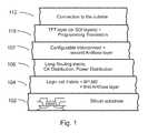
- FIG. 1is an exemplary drawing illustration of a programmable device layers structure
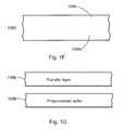
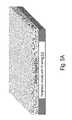
- FIG. 1Ais an exemplary drawing illustration of a programmable device layers structure
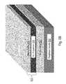
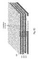
- FIGS. 1B-1Iare exemplary drawing illustrations of the preprocessed wafers and layers and generalized layer transfer
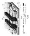
- FIG. 2is an exemplary drawing illustration of a layer transfer process flow
- FIGS. 3A-3J , 3 J 1 , 3 J 2 , 3 Kare exemplary drawing illustrations of the formation of a resistive memory transistor
- FIGS. 4A-4Gare exemplary drawing illustrations of the formation of a charge trap memory transistor
- FIGS. 5A-5J , 5 J 1 , 5 J 2 , 5 Kare exemplary drawing illustrations of the formation of a resistive memory transistor.
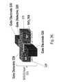
- FIGS. 6A-6Jare exemplary drawing illustrations of the formation of a resistive memory transistor with periphery on top.
- Some drawing figuresmay describe process flows for building devices. These process flows, which may be a sequence of steps for building a device, may have many structures, numerals and labels that may be common between two or more adjacent steps. In such cases, some labels, numerals and structures used for a certain step's figure may have been described in the previous steps' figures.
- Some embodiments of the inventionmay provide a new method for semiconductor device fabrication that may be highly desirable for custom products. Some embodiments of the invention may suggest the use of a re-programmable antifuse in conjunction with ‘Through Silicon Via’ to construct a new type of configurable logic, or as usually called, FPGA devices. Some embodiments of the invention may provide a solution to the challenge of high mask-set cost and low flexibility that exists in the current common methods of semiconductor fabrication. An additional illustrated advantage of some embodiments of the present invention may be that it could reduce the high cost of manufacturing the many different mask sets needed in order to provide a commercially viable logic family with a range of products each with a different set of master slices. Some embodiments of the invention may improve upon the prior art in many respects, including, for example, the structuring of the semiconductor device and methods related to the fabrication of semiconductor devices.
- Some embodiments of the inventionmay reflect the motivation to save on the cost of masks with respect to the investment that would otherwise have been necessary to put in place a commercially viable set of master slices. Some embodiments of the invention may also provide the ability to incorporate various types of memory blocks in the configurable device. Some embodiments of the invention may provide a method to construct a configurable device with the desired amount of logic, memory, I/Os, and analog functions.
- some embodiments of the inventionmay allow the use of repeating logic tiles that provide a continuous terrain of logic.
- Some embodiments of the inventionmay use a modular approach to construct various configurable systems with Through-Silicon-Via (TSV). Once a standard size and location of TSV has been defined one could build various configurable logic dies, configurable memory dies, configurable I/O dies and configurable analog dies which could be connected together to construct various configurable systems. In fact, these embodiments of the invention may allow mixing and matching among configurable dies, fixed function dies, and dies manufactured in different processes.
- TSVThrough-Silicon-Via
- an FPGA device that utilizes antifuses to configure the device functionmay include the electronic circuits to program the antifuses.
- the programming circuitsmay be used primarily to configure the device and may be mostly an overhead once the device is configured.
- the programming voltage used to program the antifusemay typically be significantly higher than the voltage used for the operating circuits of the device.
- the design of the antifuse structuremay be designed such that an unused antifuse may not accidentally get fused. Accordingly, the incorporation of the antifuse programming in the silicon substrate may entail special attention for a resulting higher voltage, and additional silicon area may, accordingly, be allocated.
- the programming circuitscould operate relatively slowly. Accordingly using a thin film transistor for the programming circuits could fit very well with the function and may reduce the needed silicon area.
- the programming circuitsmay, therefore, be constructed with thin film transistors, which may be fabricated after the fabrication of the operating circuitry, on top of the configurable interconnection layers that incorporate and use the antifuses.
- An additional illustrated advantage of such embodiments of the inventionmay be the ability to reduce cost of the high volume production.
- Onemay only need to use mask-defined links instead of the antifuses and their programming circuits.
- One custom via maskmay be used, and this may save steps associated with the fabrication of the antifuse layers, the thin film transistors, and/or the associated connection layers of the programming circuitry.
- an Integrated Circuit deviceincluding a plurality of antifuse configurable interconnect circuits and a plurality of transistors to configure at least one of said antifuses; wherein said transistors are fabricated after said antifuse.
- an Integrated Circuit deviceincluding: a plurality of antifuse configurable interconnect circuits and plurality of transistors to configure at least one of said antifuses; wherein said transistors are placed over said antifuse.
- the Integrated Circuit devicemay include second antifuse configurable logic cells and a plurality of second transistors to configure said second antifuses wherein these second transistors may be fabricated before said second antifuses.
- the Integrated Circuit devicemay also include second antifuse configurable logic cells and a plurality of second transistors to configure said second antifuses wherein said second transistors may be placed underneath said second antifuses.
- an Integrated Circuit deviceincluding: first antifuse layer, at least two metal layers over it and a second antifuse layer overlaying the two metal layers.
- a configurable logic deviceincluding: antifuse configurable look up table logic interconnected by antifuse configurable interconnect.
- a configurable logic deviceincluding: a plurality of configurable look up table logic, a plurality of configurable programmable logic array (PLA) logic, and a plurality of antifuse configurable interconnect.
- PLAconfigurable programmable logic array
- a configurable logic deviceincluding: a plurality of configurable look up table logic and a plurality of configurable drive cells wherein the drive cells may be configured by plurality of antifuses.
- a configurable logic devicemay additionally be provided, including: configurable logic cells interconnected by a plurality of antifuse configurable interconnect circuits wherein at least one of the antifuse configurable interconnect circuits may be configured as part of a non volatile memory.
- the configurable logic devicemay include at least one antifuse configurable interconnect circuit, which may also be configurable to a PLA function.
- an integrated circuit systemmay also be provided, including a configurable logic die and an I/O die wherein the configurable logic die may be connected to the I/O die by the use of Through-Silicon-Via.
- the integrated circuit systemmay include; a configurable logic die and a memory die wherein the configurable logic die and the memory die may be connected by the use of Through-Silicon-Via.
- the integrated circuit systemmay include a first configurable logic die and second configurable logic die wherein the first configurable logic die and the second configurable logic die may be connected by the use of Through-Silicon-Via.
- the integrated circuit systemmay include an I/O die that may be fabricated utilizing a different process than the process utilized to fabricate the configurable logic die.
- the integrated circuit systemmay include at least two logic dies connected by the use of Through-Silicon-Via and wherein some of the Through-Silicon-Vias may be utilized to carry the system bus signal.
- the integrated circuit systemmay include at least one configurable logic device.
- the integrated circuit systemmay include, an antifuse configurable logic die and programmer die which may be connected by the use of Through-Silicon-Via.
- interconnectsmay be now dominating IC performance and power.
- One solution to shorten interconnectmay be to use a 3D IC.
- the only known way for general logic 3D ICis to integrate finished device one on top of the other by utilizing Through-Silicon-Vias as now called TSVs.
- TSVsThrough-Silicon-Vias as now called TSVs.
- the problem with TSVsmay be that their large size, usually a few microns each, may severely limit the number of connections that can be made.
- Some embodiments of the inventionmay provide multiple alternatives to constructing a 3D IC wherein many connections may be made less than one micron in size, thus enabling the use of 3D IC technology for most device applications.
- some embodiments of the inventionmay offer new device alternatives by utilizing the proposed 3D IC technology.
- various embodiments of the present inventionsuggest constructing the programming transistors not in the base silicon diffusion layer but rather above or below the antifuse configurable interconnect circuits.
- the programming voltage used to program the antifusemay be typically significantly higher than the voltage used for the operational circuits of the device. This may be part of the design of the antifuse structure so that the antifuse may not become accidentally activated.
- extra attention, design effort, and silicon resourcesmight be needed to make sure that the programming phase may not damage the operating circuits. Accordingly the incorporation of the antifuse programming transistors in the silicon substrate may need attention and extra silicon area.
- the programming circuitscould operate relatively slowly. Accordingly, a thin film transistor for the programming circuits could provide the function and could reduce the silicon area.
- Vacuum FETbipolar, etc.
- programming circuitscould be placed not in the base silicon but rather above or below the antifuse configurable interconnect.
- the programming transistors and the programming circuitscould be fabricated on SOI wafers which may then be bonded to the configurable logic wafer and connected to it by the use of through-silicon-via (TSV), or through layer via (TLV).
- TSVthrough-silicon-via
- TLVthrough layer via
- An illustrated advantage of using an SOI wafer for the antifuse programming functionmay be that the high voltage transistors that could be built on it are very efficient and could be used for the programming circuitry including support functions such as the programming controller function.
- the programming circuitscould be fabricated by an older process on SOI wafers to further reduce cost.
- the programming circuitscould be fabricated by a different process technology than the logic wafer process technology.
- the wafer fab that the programing circuits may be fabricated atmay be different than the wafer fab that the logic circuits are fabricated at and located anywhere in the world.
- a common objectivemay be to reduce cost for high volume production without redesign and with minimal additional mask cost.
- the use of thin-film-transistors, for the programming transistors,may enable a relatively simple and direct volume cost reduction.
- a custom maskcould be used to define vias on substantially all the locations that used to have their respective antifuse activated. Accordingly the same connection between the strips that used to be programmed may now be connected by fixed vias. This may allow saving the cost associated with the fabrication of the antifuse programming layers and their programming circuits. It should be noted that there might be differences between the antifuse resistance and the mask defined via resistance.
- a conventional way to handle itmay be by providing the simulation models for both options so the designer could validate that the design may work properly in both cases.
- An additional objective for having the programming circuits above the antifuse layermay be to achieve better circuit density. Many connections may be needed to connect the programming transistors to their respective metal strips. If those connections are going upward they could reduce the circuit overhead by not blocking interconnection routes on the connection layers underneath.
- FIG. 1is a drawing illustration of a programmable device layers structure according to an alternative embodiment of the invention.
- the firstmay be designated to configure the logic terrain and, in some cases, may also configure the logic clock distribution.
- the first antifuse layercould also be used to manage some of the power distribution to save power by not providing power to unused circuits. This layer could also be used to connect some of the long routing tracks and/or connections to the inputs and outputs of the logic cells.
- the device fabrication of the example shown in FIG. 1may start with the semiconductor substrate, such as monocrystalline silicon substrate 102 , comprising the transistors used for the logic cells and also the first antifuse layer programming transistors. Thereafter, logic fabric/first antifuse layer 104 may be constructed, which may include multiple layers, such as Metal 1 , dielectric, Metal 2 , and sometimes Metal 3 . These layers may be used to construct the logic cells and often I/O and other analog cells.
- a plurality of first antifusesmay be incorporated in the isolation layer between metal 1 and metal 2 or in the isolation layer between metal 2 and metal 3 and the corresponding programming transistors could be embedded in the silicon substrate 102 being underneath the first antifuses.
- the first antifusescould be used to program logic cells and to connect individual cells to construct larger logic functions.
- the first antifusescould also be used to configure the logic clock distribution.
- the first antifuse layercould also be used to manage some of the power distribution to save power by not providing power to unused circuits. This layer could also be used to connect some of the long routing tracks and/or one or more connections to the inputs and outputs of the cells.
- Interconnection layer 106could include multiple layers of long interconnection tracks for power distribution and clock networks, or a portion thereof, in addition to structures already fabricated in the first few layers, for example, logic fabric/first antifuse layer 104 .
- Second antifuse layer 107could include many layers, including the antifuse configurable interconnection fabric. It might be called the short interconnection fabric, too. If metal 6 and metal 7 are used for the strips of this configurable interconnection fabric then the second antifuse may be embedded in the dielectric layer between metal 6 and metal 7 .
- the programming transistors and the other parts of the programming circuitcould be fabricated afterward and be on top of the configurable interconnection fabric programming transistors 110 .
- the programming elementcould be a thin film transistor or other alternatives for over oxide transistors as was mentioned previously.
- the antifuse programming transistorsmay be placed over the antifuse layer, which may thereby enable the configurable interconnect in second antifuse layer 107 or logic fabric/first antifuse layer 104 . It should be noted that in some cases it might be useful to construct part of the control logic for the second antifuse programming circuits, in the base layers such as silicon substrate 102 and logic fabric/first antifuse layer 104 .
- the final stepmay include constructing the connection to the outside 112 .
- the connectioncould be pads for wire bonding, soldering balls for flip chip, optical, or other connection structures such as those connection structures for TSV.
- the antifuse programmable interconnect structurecould be designed for multiple use.
- the same structurecould be used as a part of the interconnection fabric, or as a part of the PLA logic cell, or as part of a Read Only Memory (ROM) function.
- ROMRead Only Memory
- FPGA productit might be desirable to have an element that could be used for multiple purposes. Having resources that could be used for multiple functions could increase the utility of the FPGA device.
- FIG. 1Ais a drawing illustration of a programmable device layers structure according to another alternative embodiment of the invention.
- This underlying device of circuit of Foundation layer 114may provide the programming transistor for the logic fabric/first antifuse layer 104 .
- the programmable device substrate diffusionsuch as primary silicon layer 102 A, may not be prone to the cost penalty of the programming transistors for the logic fabric/first antifuse layer 104 .
- the programming connection of the logic fabric/first antifuse layer 104may be directed downward to connect to the underlying programming device of Foundation layer 114 while the programming connection to the second antifuse layer 107 may be directed upward to connect to the programming circuit programming transistors 110 . This could provide less congestion of the circuit internal interconnection routes.
- FIG. 1Ais a cut illustration of a programmable device, with two antifuse layers.
- the programming transistors for the first logic fabric/first antifuse layer 104could be prefabricated on Foundation layer 114 , and then, utilizing “smart-cut”, a single crystal, or mono-crystalline, transferred silicon layer 204 may be transferred on which the primary programmable logic of primary silicon layer 102 A may be fabricated with advanced logic transistors and other circuits. Then multi-metal layers are fabricated including a lower layer of antifuses in logic fabric/first antifuse layer 104 , interconnection layer 106 and second antifuse layer 107 with its configurable interconnects. For the second antifuse layer 107 the programming transistors 110 could be fabricated also utilizing a second “smart-cut” layer transfer.
- layer transferin the use herein may be defined as the technological process or method that enables the transfer of very fine layers of crystalline material onto a mechanical support, wherein the mechanical support may be another layer or substrate of crystalline material.
- the “SmartCut” processalso used herein as the term ‘ion-cut’ process, together with wafer bonding technology, may enable a “Layer Transfer” whereby a thin layer of a single or mono-crystalline silicon wafer may be transferred from one wafer or substrate to another wafer or substrate.
- Other specific layer transfer processesmay be described or referenced herein.
- monocrystalline or mono-crystalline in the use herein of, for example, monocrystalline or mono-crystalline layer, material, or siliconmay be defined as “a single crystal body of crystalline material that contains no large-angle boundaries or twin boundaries as in ASTM F1241, also called monocrystal” and “an arrangement of atoms in a solid that has perfect periodicity (that is, no defects)” as in the SEMATECH dictionary.
- single crystal and monocrystalare equivalent in the SEMATECH dictionary.
- single crystal in the use herein of, for example, single crystal silicon layer, single crystal layermay be equivalently defined as monocrystalline.
- viain the use herein may be defined as “an opening in the dielectric layer(s) through which a riser passes, or in which the walls are made conductive; an area that provides an electrical pathway [connection path] from one metal layer to the metal layer above or below,” as in the SEMATECH dictionary.
- TSVthrough silicon via
- TLVthrough layer via
- a TLVmay be defined as an opening in a layer transferred layer(s) through which an electrically conductive riser passes, wherein the riser may pass through at least one isolating region, for example, a shallow trench isolation (STI) region in the transferred layer, may typically have a riser diameter of less than 200 nm, a riser that provides an electrical pathway [connection path] from one metal layer to the metal layer above or below.
- a TLVmay additionally pass thru an electrically conductive layer, and the walls may be made isolative from the conductive layer.
- preprocessed wafer or layermay be generic and reference number 108 when used in a drawing figure to illustrate an embodiment of the present invention may represent many different preprocessed wafer or layer types including but not limited to underlying prefabricated layers, a lower layer interconnect wiring, a base layer, a substrate layer, a processed house wafer, an acceptor wafer, a logic house wafer, an acceptor wafer house, an acceptor substrate, target wafer, preprocessed circuitry, a preprocessed circuitry acceptor wafer, a base wafer layer, a lower layer, an underlying main wafer, a foundation layer, an attic layer, or a house wafer.
- FIG. 1Bis a drawing illustration of a generalized preprocessed wafer or layer 108 .
- the wafer or layer 108may have preprocessed circuitry, such as, for example, logic circuitry, microprocessors, MEMS, circuitry comprising transistors of various types, and other types of digital or analog circuitry including, but not limited to, the various embodiments described herein.
- Preprocessed wafer or layer 108may have preprocessed metal interconnects and may include copper or aluminum.
- the metal layer or layers of interconnectmay be constructed of lower (less than about 400° C.) thermal damage resistant metals such as, for example, copper or aluminum, or may be constructed with refractory metals such as tungsten to provide high temperature utility at greater than about 400° C.
- the preprocessed metal interconnectsmay be designed and prepared for layer transfer and electrical coupling from preprocessed wafer or layer 108 to the layer or layers to be transferred.
- FIG. 1Cis a drawing illustration of a generalized transfer layer 109 prior to being attached to preprocessed wafer or layer 108 .
- Transfer layer 109may be attached to a carrier wafer or substrate during layer transfer.
- Preprocessed wafer or layer 108may be called a target wafer, acceptor substrate, or acceptor wafer.
- the acceptor wafermay have acceptor wafer metal connect pads or strips designed and prepared for electrical coupling to transfer layer 109 .
- Transfer layer 109may be attached to a carrier wafer or substrate during layer transfer.
- Transfer layer 109may have metal interconnects designed and prepared for layer transfer and electrical coupling to preprocessed wafer or layer 108 .
- the metal interconnects now on transfer layer 109may include copper or aluminum.
- Transfer layer 109may be comprised of single crystal silicon, or mono-crystalline silicon, or doped mono-crystalline layer or layers, or other semiconductor, metal, and insulator materials, layers; or multiple regions of single crystal silicon, or mono-crystalline silicon, or doped mono-crystalline silicon, or other semiconductor, metal, or insulator materials.
- FIG. 1Dis a drawing illustration of a preprocessed wafer or layer 108 A created by the layer transfer of transfer layer 109 on top of preprocessed wafer or layer 108 .
- the top of preprocessed wafer or layer 108 Amay be further processed with metal interconnects designed and prepared for layer transfer and electrical coupling from preprocessed wafer or layer 108 A to the next layer or layers to be transferred.
- FIG. 1Eis a drawing illustration of a generalized transfer layer 109 A prior to being attached to preprocessed wafer or layer 108 A.
- Transfer layer 109 Amay be attached to a carrier wafer or substrate during layer transfer.
- Transfer layer 109 Amay have metal interconnects designed and prepared for layer transfer and electrical coupling to preprocessed wafer or layer 108 A.
- FIG. 1Fis a drawing illustration of a preprocessed wafer or layer 108 B created by the layer transfer of transfer layer 109 A on top of preprocessed wafer or layer 108 A.
- the top of preprocessed wafer or layer 108 Bmay be further processed with metal interconnects designed and prepared for layer transfer and electrical coupling from preprocessed wafer or layer 108 B to the next layer or layers to be transferred.
- FIG. 1Gis a drawing illustration of a generalized transfer layer 109 B prior to being attached to preprocessed wafer or layer 108 B.
- Transfer layer 109 Bmay be attached to a carrier wafer or substrate during layer transfer.
- Transfer layer 109 Bmay have metal interconnects designed and prepared for layer transfer and electrical coupling to preprocessed wafer or layer 108 B.
- FIG. 1His a drawing illustration of preprocessed wafer or layer 108 C created by the layer transfer of transfer layer 109 B on top of preprocessed wafer or layer 108 B.
- the top of preprocessed wafer or layer 108 Cmay be further processed with metal interconnect designed and prepared for layer transfer and electrical coupling from preprocessed wafer or layer 108 C to the next layer or layers to be transferred.
- FIG. 1Iis a drawing illustration of preprocessed wafer or layer 108 C, a 3D IC stack, which may comprise transferred layers 109 A and 109 B on top of the original preprocessed wafer or layer 108 .
- Transferred layers 109 A and 109 B and the original preprocessed wafer or layer 108may include transistors of one or more types in one or more layers, metallization such as, for example, copper or aluminum in one or more layers, interconnections to and between layers above and below, and interconnections within the layer.
- the transistorsmay be of various types that may be different from layer to layer or within the same layer.
- the transistorsmay be in various organized patterns.
- the transistorsmay be in various pattern repeats or bands.
- the transistorsmay be in multiple layers involved in the transfer layer.
- the transistorsmay be junction-less transistors or recessed channel array transistors.
- Transferred layers 109 A and 109 B and the original preprocessed wafer or layer 108may further comprise semiconductor devices such as resistors and capacitors and inductors, one or more programmable interconnects, memory structures and devices, sensors, radio frequency devices, or optical interconnect with associated transceivers.
- Transferred layers 109 A and 109 B and the original preprocessed wafer or layer 108may further include isolation layers, such as, for example, silicon and/or carbon containing oxides and/or low-k dielectrics and/or polymers, which may facilitate oxide to oxide wafer or substrate bonding and may electrically isolate, for example, one layer, such as transferred layer 109 A, from another layer, such as preprocessed wafer or layer 108 .
- isolation layerssuch as, for example, silicon and/or carbon containing oxides and/or low-k dielectrics and/or polymers, which may facilitate oxide to oxide wafer or substrate bonding and may electrically isolate, for example, one layer, such as transferred layer 109 A, from another layer, such as preprocessed wafer or layer 108 .
- carrier wafer or carrier substratemay also be called holder wafer or holder substrate.
- carrier wafer or substrate used hereinmay be a wafer, for example, a monocrystalline silicon wafer, or a substrate, for example, a glass substrate, used to hold, flip, or move, for example, other wafers, layers, or substrates, for further processing.
- the attachment of the carrier wafer or substrate to the carried wafer, layer, or substratemay be permanent or temporary.
- This layer transfer processcan be repeated many times, thereby creating preprocessed wafers comprising many different transferred layers which, when combined, can then become preprocessed wafers or layers for future transfers.
- This layer transfer processmay be sufficiently flexible that preprocessed wafers and transfer layers, if properly prepared, can be flipped over and processed on either side with further transfers in either direction as a matter of design choice.
- the transferred layermay be, for example, less than about 2 microns thick, less than about 1 micron thick, less than about 0.4 microns thick, less than about 200 nm thick, or less than about 100 nm thick.
- the TLV diametermay be less than about 400 nm, less than about 200 nm, less than about 80 nm, less than about 40 nm, or less than about 20 nm.
- the thickness of the layer or layers transferred according to some embodiments of the present inventionmay be designed as such to match and enable the best obtainable lithographic resolution capability of the manufacturing process employed to create the through layer vias or any other structures on the transferred layer or layers.
- the layer or layers transferredmay be of a crystalline material, for example, mono-crystalline silicon, and after layer transfer, further processing, such as, for example, plasma/RIE or wet etching, may be done on the layer or layers that may create islands or mesas of the transferred layer or layers of crystalline material, for example, mono-crystalline silicon, the crystal orientation of which has not changed
- a mono-crystalline layer or layers of a certain specific crystal orientationmay be layer transferred and then processed whereby the resultant islands or mesas of mono-crystalline silicon have the same crystal specific orientation as the layer or layers before the processing.
- the resultant islands or mesas of crystalline materialfor example, mono-crystalline silicon
- the resultant islands or mesas of crystalline materialfor example, mono-crystalline silicon
- FIGS. 1 through 1Iare exemplary only and are not drawn to scale.
- the preprocessed wafer or layer 108may act as a base or substrate layer in a wafer transfer flow, or as a preprocessed or partially preprocessed circuitry acceptor wafer in a wafer transfer process flow.
- layer transfer techniquessuch as ‘ion-cut’ that may form a layer transfer demarcation plane by ion implantation of hydrogen molecules or atoms, or any other layer transfer technique described herein or utilized in industry, may be utilized in the generalized FIG. 1 flows and applied throughout herein.
- metal interconnect stripsmay be formed on the acceptor wafer and/or transferred layer to assist the electrical coupling of circuitry between the two layers, and may utilize TLVs.
- a technology for such underlying circuitrymay be to use the “SmartCut” process.
- the “SmartCut” processis a well understood technology used for fabrication of SOI wafers.
- the “SmartCut” process, together with wafer bonding technology,may enable a “Layer Transfer” whereby a thin layer of a single or mono-crystalline silicon wafer may be transferred from one wafer to another wafer.
- the “Layer Transfer”could be done at less than about 400° C. and the resultant transferred layer could be even less than about 100 nm thick.
- the transferred layer thicknessmay typically be about 100 nm, and may be a thin as about 5 nm in currently demonstrated fully depleted SOI (FDSOI) wafer manufacturing by Soitec.
- FDSOIfully depleted SOI
- the transferred layer thicknessmay be less than about 400 nm and may be less than about 200 nm for logic applications.
- the process with some variations and under different namesmay be commercially available by two companies, namely, Soitec (Crolles, France) and SiGen—Silicon Genesis Corporation (San Jose, Calif.).
- SoitecCrolles, France
- SiGen—Silicon Genesis CorporationSiGen—Silicon Genesis Corporation
- a room temperature wafer bonding process utilizing ion-beam preparation of the wafer surfaces in a vacuumhas been recently demonstrated by Mitsubishi Heavy Industries Ltd., Tokyo, Japan. This process may allow for room temperature layer transfer.
- the IBM's layer transfer methodemploys a SOI technology and utilizes glass handle wafers.
- the donor circuitmay be high-temperature processed on an SOI wafer, temporarily bonded to a borosilicate glass handle wafer, backside thinned by chemical mechanical polishing of the silicon and then the Buried Oxide (BOX) is selectively etched off.
- the now thinned donor wafermay be subsequently aligned and low-temperature oxide-to-oxide bonded to the acceptor wafer topside.
- a low temperature release of the glass handle wafer from the thinned donor wafermay be performed, and then through bond via connections may be made.
- epitaxial liftoff (ELO) technologyas shown by P. Demeester, et. al, of IMEC in Semiconductor Science Technology 1993 may be utilized for layer transfer. ELO may make use of the selective removal of a very thin sacrificial layer between the substrate and the layer structure to be transferred.
- the to-be-transferred layer of GaAs or siliconmay be adhesively ‘rolled’ up on a cylinder or removed from the substrate by utilizing a flexible carrier, such as, for example, black wax, to bow up the to-be-transferred layer structure when the selective etch, such as, for example, diluted Hydrofluoric (HF) Acid, may etch the exposed release layer, such as, for example, silicon oxide in SOI or AlAs. After liftoff, the transferred layer may then be aligned and bonded to the acceptor substrate or wafer.
- a flexible carriersuch as, for example, black wax
- ELTRANepitaxial Layer TRANsfer from porous silicon.
- ELTRANmay be utilized.
- the Electrochemical Society Meeting abstract No. 438 from year 2000 and the JSAP International July 2001 papershow a seed wafer being anodized in an HF/ethanol solution to create pores in the top layer of silicon, the pores may be treated with a low temperature oxidation and then high temperature hydrogen annealed to seal the pores.
- Epitaxial siliconmay then be deposited on top of the porous silicon and then oxidized to form the SOI BOX.
- the seed wafermay be bonded to a handle wafer and the seed wafer may be split off by high pressure water directed at the porous silicon layer.
- the porous siliconmay then be selectively etched off leaving a uniform silicon layer.
- FIG. 2is a drawing illustration of a layer transfer process flow.
- “Layer-Transfer”may be used for construction of the underlying circuitry of Foundation layer 114 .
- Wafer 202may include a monocrystalline silicon wafer that was processed to construct the underlying circuitry. The wafer 202 could be of the most advanced process or more likely a few generations behind. It could include the programming circuits of Foundation layer 114 and other useful structures and may be a preprocessed CMOS silicon wafer, or a partially processed CMOS, or other prepared silicon or semiconductor substrate. Wafer 202 may also be called an acceptor substrate or a target wafer.
- An oxide layer 212may then be deposited on top of the wafer 202 and thereafter may be polished for better planarization and surface preparation.
- a donor wafer 206may then be brought in to be bonded to wafer 202 .
- the surfaces of both donor wafer 206 and wafer 202may be pre-processed for low temperature bonding by various surface treatments, such as an RCA pre-clean that may comprise dilute ammonium hydroxide or hydrochloric acid, and may include plasma surface preparations to lower the bonding energy and enhance the wafer to wafer bond strength.
- the donor wafer 206may be pre-prepared for “SmartCut” by an ion implant of an atomic species, such as H+ ions, at the desired depth to prepare the SmartCut line 208 .
- SmartCut line 208may also be called a layer transfer demarcation plane, shown as a dashed line.
- the SmartCut line 208 or layer transfer demarcation planemay be formed before or after other processing on the donor wafer 206 .
- Donor wafer 206may be bonded to wafer 202 by bringing the donor wafer 206 surface in physical contact with the wafer 202 surface, and then applying mechanical force and/or thermal annealing to strengthen the oxide to oxide bond. Alignment of the donor wafer 206 with the wafer 202 may be performed immediately prior to the wafer bonding. Acceptable bond strengths may be obtained with bonding thermal cycles that do not exceed about 400° C.
- a SmartCut stepmay be performed to cleave and remove the top portion 214 of the donor wafer 206 along the SmartCut line 208 .
- the cleavingmay be accomplished by various applications of energy to the SmartCut line 208 , or layer transfer demarcation plane, such as a mechanical strike by a knife or jet of liquid or jet of air, or by local laser heating, by application of ultrasonic or megasonic energy, or other suitable methods.
- the resultmay be a 3D wafer 210 which may include wafer 202 with a transferred silicon layer 204 of mono-crystalline silicon, or multiple layers of materials. Transferred silicon layer 204 may be polished chemically and mechanically to provide a suitable surface for further processing.
- Transferred silicon layer 204could be quite thin at the range of about 50-200 nm.
- the described flowmay be called “layer transfer”.
- Layer transfermay be commonly utilized in the fabrication of SOI—Silicon On Insulator—wafers.
- SOI wafersthe upper surface may be oxidized so that after “layer transfer” a buried oxide—BOX—may provide isolation between the top thin mono-crystalline silicon layer and the bulk of the wafer.
- SmartCutimplanted atomic species, such as Hydrogen or Helium or a combination, to create a cleaving plane as described above may be referred to in this document as “SmartCut” or “ion-cut” and may be generally the illustrated layer transfer method.
- FIG. 2is exemplary only and are not drawn to scale.
- a heavily doped (greater than 1e20 atoms/cm3) boron layer or silicon germanium (SiGe) layermay be utilized as an etch stop either within the ion-cut process flow, wherein the layer transfer demarcation plane may be placed within the etch stop layer or into the substrate material below, or the etch stop layers may be utilized without an implant cleave process and the donor wafer may be, for example, etched away until the etch stop layer is reached.
- the oxide layer within an SOI or GeOI donor wafermay serve as the etch stop layer, and hence one edge of the oxide layer may function as a layer transfer demarcation plane.
- the dose and energy of the implanted specie or speciesmay be uniform across the surface area of the wafer or may have a deliberate variation, including, for example, a higher dose of hydrogen at the edges of a monocrystalline silicon wafer to promote cleaving.
- a “layer transfer” processmay be used to bond a thin mono-crystalline silicon layer transferred silicon layer 204 on top of the preprocessed wafer 202 , a standard process could ensue to construct the rest of the desired circuits as illustrated in FIG. 1A , starting with primary silicon layer 102 A on the transferred silicon layer 204 .
- the lithography stepmay use alignment marks on wafer 202 so the following circuits of primary silicon layer 102 A and logic fabric/first antifuse layer 104 and so forth could be properly connected to the underlying circuits of Foundation layer 114 .
- An aspect that should be accounted foris the high temperature that may be needed for the processing of circuits of primary silicon layer 102 A.
- the pre-processed circuits on wafer 202may need to withstand this high temperature associated with the activation of the semiconductor transistors of primary silicon layer 102 A fabricated on the transferred silicon layer 204 .
- Those circuits on wafer 202may include transistors and local interconnects of poly-crystalline silicon (polysilicon or poly) and some other type of interconnection that could withstand high temperature such as tungsten.
- a processed wafer that can withstand subsequent processing of transistors on top at high temperaturesmay be a called the “Foundation” or a foundation wafer, layer or circuitry.
- An illustrated advantage of using layer transfer for the construction of the underlying circuitsmay include having the transferred silicon layer 204 be very thin which may enable the through silicon via connections 116 , or through layer vias (TLVs), to have low aspect ratios and be more like normal contacts, which could be made very small and with minimum area penalty.
- the thin transferred layermay also allow conventional direct through-layer alignment techniques to be performed, thus increasing the density of through silicon via connections 116 .
- top transistorsprecisely aligned to the underlying pre-fabricated layers such as pre-processed wafer or layer 108 , utilizing “SmartCut” layer transfer and not exceeding the temperature limit, typically about 400° C., of the underlying pre-fabricated structure, which may include low melting temperature metals or other construction materials such as, for example, aluminum or copper.
- the layer transfermay be less than about 200 nm thick, then the transistors defined on it could be aligned precisely to the top metal layer of the pre-processed wafer or layer 108 as may be needed and those transistors may have state of the art layer to layer misalignment capability, for example, less than about 40 nm misalignment or less than about 4 nm misalignment, as well as through layer via, or layer to layer metal connection, diameters of less than about 50 nm, or even less than about 20 nm.
- the thinner the transferred layerthe smaller the through layer via diameter obtainable, due to the potential limitations of manufacturable via aspect ratios.
- the transferred layermay be, for example, less than about 2 microns thick, less than about 1 micron thick, less than about 0.4 microns thick, less than about 200 nm thick, or less than about 100 nm thick.
- alignment markin the use herein may be defined as “an image selectively placed within or outside an array for either testing or aligning, or both [ASTM F127-84], also called alignment key and alignment target,” as in the SEMATECH dictionary.
- the alignment markmay, for example, be within a layer, wafer, or substrate of material processing or to be processed, and/or may be on a photomask or photoresist image, or may be a calculated position within, for example, a lithographic wafer stepper's software or memory.
- Novel monolithic 3D memory technologies utilizing material resistance changesmay be constructed in a similar manner.
- resistance-based memoriesincluding phase change memory, Metal Oxide memory, resistive RAM (RRAM), memristors, solid-electrolyte memory, ferroelectric RAM, MRAM, etc. Background information on these resistive-memory types may be given in “Overview of candidate device technologies for storage-class memory,” IBM Journal of Research and Development, vol. 52, no. 4.5, pp. 449-464, July 2008 by Burr, G. W., et. al. The contents of this document are incorporated in this specification by reference.
- a resistance-based zero additional masking steps per memory layer 3D memorymay be constructed that is suitable for 3D IC manufacturing.
- This 3D memorymay utilize junction-less transistors and may have a resistance-based memory element in series with a select or access transistor.
- a silicon substrate with peripheral circuitry 302may be constructed with high temperature (greater than about 400° C.) resistant wiring, such as, for example, Tungsten.
- the peripheral circuitry substrate 302may include memory control circuits as well as circuitry for other purposes and of various types, such as, for example, analog, digital, RF, or memory.
- the peripheral circuitry substrate 302may include peripheral circuits that can withstand an additional rapid-thermal-anneal (RTA) and still remain operational and retain good performance.
- RTArapid-thermal-anneal
- the peripheral circuitsmay be formed such that they have had a weak RTA or no RTA for activating dopants.
- the top surface of the peripheral circuitry substrate 302may be prepared for oxide wafer bonding with a deposition of a silicon oxide layer 304 , thus forming acceptor wafer 314 .
- a mono-crystalline silicon donor wafer 312may be, for example, processed to include a wafer sized layer of N+ doping (not shown) which may have a different dopant concentration than the N+ substrate 306 .
- the N+ doping layermay be formed by ion implantation and thermal anneal
- a screen oxide layer 308may be grown or deposited prior to the implant to protect the silicon from implant contamination and to provide an oxide surface for later wafer to wafer bonding
- a layer transfer demarcation plane 310(shown as a dashed line) may be formed in donor wafer 312 within the N+ substrate 306 or the N+ doping layer (not shown) by hydrogen implantation or other methods as previously described.
- Both the donor wafer 312 and acceptor wafer 314may be prepared for wafer bonding as previously described and then bonded at the surfaces of oxide layer 304 and oxide layer 308 , at a low temperature (less than about 400° C.) suitable for lowest stresses, or a moderate temperature (less than about 900° C.).
- the portion of the N+ layer (not shown) and the N+ wafer substrate 306 that are above the layer transfer demarcation plane 310may be removed by cleaving and polishing, or other processes as previously described, such as, for example, ion-cut or other methods, thus forming the remaining mono-crystalline silicon N+ layer 306 ′.
- Remaining N+ layer 306 ′ and oxide layer 308may have been layer transferred to acceptor wafer 314 .
- the top surface of N+ layer 306 ′may be chemically or mechanically polished smooth and flat.
- transistors or portions of transistorsmay be formed and aligned to the acceptor wafer 314 alignment marks (not shown).
- Oxide layer 320may be deposited to prepare the surface for later oxide to oxide bonding, leading to the formation of the first Si/SiO2 layer 323 that includes silicon oxide layer 320 , N+ silicon layer 306 ′, and oxide layer 308 .
- additional Si/SiO2 layerssuch as, for example, second Si/SiO2 layer 325 and third Si/SiO2 layer 327 , may each be formed as described in FIGS. 3A to 3C .
- Oxide layer 329may be deposited to electrically isolate the top N+ silicon layer.
- oxide layer 329 , third Si/SiO2 layer 327 , second Si/SiO2 layer 325 and first Si/SiO2 layer 323may be lithographically defined and plasma/RIE etched to form a portion of the memory cell structure, which may now include regions of N+ silicon 326 and oxide 322 .
- these transistor elements or portionsmay have been defined by a common lithography step, which also may be described as a single lithography step, same lithography step, or one lithography step.
- a gate dielectric and gate electrode materialmay be deposited, planarized with a chemical mechanical polish (CMP), and may then be lithographically defined and plasma/RIE etched to form gate dielectric regions 328 which may either be self-aligned to and covered by gate electrodes 330 (shown), or cover the entire N+ silicon 326 and oxide 322 multi-layer structure.
- CMPchemical mechanical polish
- the gate stack including gate electrode 330 and gate dielectric 328may be formed with a gate dielectric, such as, for example, thermal oxide, and a gate electrode material, such as, for example, poly-crystalline silicon.
- the gate dielectricmay be an atomic layer deposited (ALD) material that may be paired with a work function specific gate metal according to industry standard high k metal gate process schemes described previously.
- the gate dielectricmay be formed with a rapid thermal oxidation (RTO), a low temperature oxide deposition or low temperature microwave plasma oxidation of the silicon surfaces and then a gate electrode such as, for example, tungsten or aluminum may be deposited.
- the entire structuremay be covered with a gap fill oxide 332 , which may be planarized with chemical mechanical polishing.
- the oxide 332is shown transparent in the figure for clarity in illustration.
- word-line regions (WL) 350coupled with and composed of gate electrodes 330
- source-line regions (SL) 352composed of N+ silicon regions 326 .
- bit-line (BL) contacts 334may be lithographically defined, etched along with plasma/RIE through oxide 332 , the three N+ silicon regions 326 , and associated oxide vertical isolation regions to connect all memory layers vertically.
- BL contacts 334may then be processed by a photoresist removal.
- Resistive change material 338such as, for example, hafnium oxide, may then be deposited, for example, with atomic layer deposition (ALD).
- ALDatomic layer deposition
- the electrode for the resistance change memory elementmay then be deposited by ALD to form the electrode/BL contact 334 .
- the excess deposited materialmay be polished to planarity at or below the top of oxide 332 .
- Each BL contact 334 with resistive change material 338may be shared among substantially all layers of memory, shown as three layers of memory in FIG. 3H .
- BL metal lines 336may be formed and may connect to the associated BL contacts 334 with resistive change material 338 .
- Contacts and associated metal interconnect linesmay be formed for the WL and SL at the memory array edges.
- a through layer via(not shown) may be formed to electrically couple the BL, SL, and WL metallization to the acceptor wafer 314 peripheral circuitry via an acceptor wafer metal connect pad (not shown).
- FIG. 3 J 1shows a cross sectional cut II of FIG. 3J
- FIG. 3 J 2shows a cross-sectional cut III of FIG. 3J
- FIG. 3 J 1shows BL metal line 336 , oxide 332 , BL contact/electrode 334 , resistive change material 338 , WL regions 350 , gate dielectric 328 , N+ silicon regions 326 , and peripheral circuitry substrate 302 .
- the BL contact/electrode 334may couple to one side of the three levels of resistive change material 338 .
- the other side of the resistive change material 338may be coupled to N+ regions 326 .
- FIG. 3 J 1shows BL metal line 336 , oxide 332 , BL contact/electrode 334 , resistive change material 338 , WL regions 350 , gate dielectric 328 , N+ silicon regions 326 , and peripheral circuitry substrate 302 .
- the BL contact/electrode 334may couple to one side
- 3 J 2shows BL metal lines 336 , oxide 332 , gate electrode 330 , gate dielectric 328 , N+ silicon regions 326 , interlayer oxide region (‘ox’), and peripheral circuitry substrate 302 .
- the gate electrode 330may be common to substantially all six N+ silicon regions 326 and may form six two-sided gated junction-less transistors as memory select transistors.
- a single exemplary two-sided gate junction-less transistor on the first Si/SiO2 layer 323may include N+ silicon region 326 (functioning as the source, drain, and transistor channel), and two gate electrodes 330 with associated gate dielectrics 328 .
- the transistormay be electrically isolated from beneath by oxide layer 308 .
- This flowmay enable the formation of a resistance-based multi-layer or 3D memory array with zero additional masking steps per memory layer, which may utilize junction-less transistors and may have a resistance-based memory element in series with a select transistor, and may be constructed by layer transfers of wafer sized doped mono-crystalline silicon layers, and this 3D memory array may be connected to an underlying multi-metal layer semiconductor device.
- FIGS. 3A through 3Kare exemplary only and are not drawn to scale.
- the transistorsmay be of another type such as RCATs.
- doping of each N+ layermay be slightly different to compensate for interconnect resistances.
- the stacked memory layermay be connected to a periphery circuit that may be above the memory stack.
- each gate of the double gate 3D resistance based memorycan be independently controlled for better control of the memory cell.
- a charge trap based 3D memory with zero additional masking steps per memory layer 3D memorymay be constructed that may be suitable for 3D IC manufacturing.
- This 3D memorymay utilize NAND strings of charge trap junction-less transistors with junction-less select transistors constructed in mono-crystalline silicon.
- a silicon substrate with peripheral circuitry 402may be constructed with high temperature (e.g., greater than about 400° C.) resistant wiring, such as, for example, Tungsten.
- the peripheral circuitry substrate 402may include memory control circuits as well as circuitry for other purposes and of various types, such as, for example, analog, digital, RF, or memory.
- the peripheral circuitry substrate 402may include peripheral circuits that can withstand an additional rapid-thermal-anneal (RTA) or flash anneal and still remain operational and retain good performance.
- RTArapid-thermal-anneal
- the peripheral circuitsmay be formed such that they have been subject to a weak RTA or no RTA for activating dopants.
- the top surface of the peripheral circuitry substrate 402may be prepared for oxide wafer bonding with a deposition of a silicon oxide layer 404 , thus forming acceptor substrate 414 .
- a mono-crystalline silicon donor wafer 412may be processed to include a wafer sized layer of N+ doping (not shown) which may have a different dopant concentration than the N+ substrate 406 .
- the N+ doping layermay be formed by ion implantation and thermal anneal.
- a screen oxide layer 408may be grown or deposited prior to the implant to protect the silicon from implant contamination and to provide an oxide surface for later wafer to wafer bonding.
- a layer transfer demarcation plane 410(shown as a dashed line) may be formed in donor wafer 412 within the N+ substrate 406 or the N+ doping layer (not shown) by hydrogen implantation or other methods as previously described.
- Both the donor wafer 412 and acceptor substrate 414may be prepared for wafer bonding as previously described and then bonded at the surfaces of oxide layer 404 and oxide layer 408 , at a low temperature (e.g., less than about 400° C. suitable for lowest stresses), or a moderate temperature (e.g., less than about 900° C.).
- a low temperaturee.g., less than about 400° C. suitable for lowest stresses
- a moderate temperaturee.g., less than about 900° C.
- the portion of the N+ layer (not shown) and the N+ wafer substrate 406 that may be above the layer transfer demarcation plane 410may be removed by cleaving and polishing, or other processes as previously described, such as ion-cut or other methods, thus forming the remaining mono-crystalline silicon N+ layer 406 ′.
- Remaining N+ layer 406 ′ and oxide layer 408may have been layer transferred to acceptor substrate 414 .
- the top surface of N+ layer 406 ′may be chemically or mechanically polished smooth and flat.
- Oxide layer 420may be deposited to prepare the surface for later oxide to oxide bonding. This bonding may now form the first Si/SiO2 layer 423 including silicon oxide layer 420 , N+ silicon layer 406 ′, and oxide layer 408 .
- additional Si/SiO2 layerssuch as, for example, second Si/SiO2 layer 425 and third Si/SiO2 layer 427 , may each be formed as described in FIGS. 4A to 4C .
- Oxide layer 429may be deposited to electrically isolate the top N+ silicon layer.
- oxide layer 429 , third Si/SiO2 layer 427 , second Si/SiO2 layer 425 and first Si/SiO2 layer 423may be lithographically defined and plasma/RIE etched to form a portion of the memory cell structure, which may now include regions of N+ silicon 426 and oxide 422 .
- these transistor elements or portionsmay have been defined by a common lithography step, which also may be described as a single lithography step, same lithography step, or one lithography step.
- a gate stackmay be formed with growth or deposition of a charge trap gate dielectric layer, such as thermal oxide and silicon nitride layers (ONO: Oxide-Nitride-Oxide), and a gate metal electrode layer, such as doped or undoped poly-crystalline silicon.
- the gate metal electrode layermay then be planarized with chemical mechanical polishing.
- the charge trap gate dielectric layermay include silicon or III-V nano-crystals encased in an oxide.
- the select transistor area 438may include a non-charge trap dielectric.
- the gate metal electrode regions 430 and gate dielectric regions 428 of both the NAND string area 436 and select transistor area 438may be lithographically defined and plasma/RIE etched.
- the entire structuremay be covered with a gap fill oxide 432 , which may be planarized with chemical mechanical polishing.
- the gap fill oxide 432is shown transparent in the figure for clarity in illustration.
- Select metal lines 446may be formed and connected to the associated select gate contacts 434 .
- Contacts and associated metal interconnect lines(not shown) may be formed for the WL and SL at the memory array edges.
- Word-line regions (WL) 436 , gate metal electrode regions 430 , and bit-line regions (BL) 452 including indicated N+ silicon regions 426are shown.
- Source regions 444may be formed by a trench contact etch and filled to couple to the N+ silicon regions on the source end of the NAND string 436 .
- a through layer via(not shown) may be formed to electrically couple the BL, SL, and WL metallization to the acceptor substrate 414 peripheral circuitry via an acceptor wafer metal connect pad (not shown).
- This flowmay enable the formation of a charge trap based 3D memory with zero additional masking steps per memory layer constructed by layer transfers of wafer sized doped layers of mono-crystalline silicon and this 3D memory may be connected to an underlying multi-metal layer semiconductor device.
- FIGS. 4A through 4Gare exemplary only and are not drawn to scale. Such skilled persons will further appreciate that many variations may be possible such as, for example, BL or SL contacts may be constructed in a staircase manner as described previously and in the incorporated documents. Moreover, the stacked memory layer may be connected to a periphery circuit that may be above the memory stack. Additionally, each tier of memory could be configured with a slightly different donor wafer N+ layer doping profile. Further, the memory could be organized in a different manner, such as BL and SL interchanged, or where buried wiring for the memory array may be below the memory layers but above the periphery.
- Additional types of 3D charge trap memoriesmay be constructed by layer transfer of mono-crystalline silicon; for example, those found in “A Highly Scalable 8-Layer 3D Vertical-Gate (VG) TFT NAND Flash Using Junction-Free Buried Channel BE-SONOS Device,” Symposium on VLSI Technology, 2010 by Hang-Ting Lue, et al., and “Multi-layered Vertical Gate NAND Flash overcoming stacking limit for terabit density storage”, Symposium on VLSI Technology, 2009 by W. Kim, S. Choi, et al. Many other modifications within the scope of the illustrated embodiments of the invention will suggest themselves to such skilled persons after reading this specification. Thus the invention is to be limited only by the appended claims.
- a resistance-based 3D memory with zero additional masking steps per memory layermay be constructed with methods that may be suitable for 3D IC manufacturing.
- This 3D memorymay utilize poly-crystalline silicon junction-less transistors that may have either a positive or a negative threshold voltage and may have a resistance-based memory element in series with a select or access transistor.
- a silicon substrate with peripheral circuitry 502may be constructed with high temperature (greater than about 400° C.) resistant wiring, such as, for example, Tungsten.
- the peripheral circuits substrate 502may include memory control circuits as well as circuitry for other purposes and of various types, such as, for example, analog, digital, RF, or memory.
- the peripheral circuits substrate 502may include peripheral circuits that can withstand an additional rapid-thermal-anneal (RTA) or flash anneal and may still remain operational and retain good performance.
- RTArapid-thermal-anneal
- the peripheral circuitsmay be formed such that they have been subject to a partial or weak RTA or no RTA for activating dopants.
- Silicon oxide layer 504may be deposited on the top surface of the peripheral circuitry substrate.
- a layer of N+ doped poly-crystalline or amorphous silicon 506may be deposited.
- the amorphous silicon or poly-crystalline silicon layer 506may be deposited using a chemical vapor deposition process, such as LPCVD or PECVD, or other process methods, and may be deposited doped with N+ dopants, such as Arsenic or Phosphorous, or may be deposited un-doped and subsequently doped with, such as, ion implantation or PLAD (PLasma Assisted Doping) techniques.
- Silicon Oxide 520may then be deposited or grown. This oxide may now form the first Si/SiO2 layer 523 which may include N+ doped poly-crystalline or amorphous silicon layer 506 and silicon oxide layer 520 .
- additional Si/SiO2 layerssuch as, for example, second Si/SiO2 layer 525 and third Si/SiO2 layer 527 , may each be formed as described in FIG. 5B .
- Oxide layer 529may be deposited to electrically isolate the top N+ doped poly-crystalline or amorphous silicon layer.
- a Rapid Thermal Anneal (RTA) or flash annealmay be conducted to crystallize the N+ doped poly-crystalline silicon or amorphous silicon layers 506 of first Si/SiO2 layer 523 , second Si/SiO2 layer 525 , and third Si/SiO2 layer 527 , forming crystallized N+ silicon layers 516 .
- Temperatures during this RTAmay be as high as about 800° C.
- an optical annealsuch as, for example, a laser anneal, could be performed alone or in combination with the RTA or other annealing processes.
- oxide layer 529 , third Si/SiO2 layer 527 , second Si/SiO2 layer 525 and first Si/SiO2 layer 523may be lithographically defined and plasma/RIE etched to form a portion of the memory cell structure, which may now include multiple layers of regions of crystallized N+ silicon 526 (previously crystallized N+ silicon layers 516 ) and oxide 522 .
- these transistor elements or portionsmay have been defined by a common lithography step, which also may be described as a single lithography step, same lithography step, or one lithography step.
- a gate dielectric and gate electrode materialmay be deposited, planarized with a chemical mechanical polish (CMP), and then lithographically defined and plasma/RIE etched to form gate dielectric regions 528 which may either be self-aligned to and covered by gate electrodes 530 (shown), or cover the entire crystallized N+ silicon regions 526 and oxide regions 522 multi-layer structure.
- the gate stack including gate electrode 530 and gate dielectric regions 528may be formed with a gate dielectric, such as thermal oxide, and a gate electrode material, such as poly-crystalline silicon.
- the gate dielectricmay be an atomic layer deposited (ALD) material that may be paired with a work function specific gate metal according to industry standard high k metal gate process schemes described previously.
- the gate dielectricmay be formed with a rapid thermal oxidation (RTO), a low temperature oxide deposition or low temperature microwave plasma oxidation of the silicon surfaces and then a gate electrode such as tungsten or aluminum may be deposited.
- the entire structuremay be covered with a gap fill oxide 532 , which may be planarized with chemical mechanical polishing.
- the oxide 532is shown transparently in the figure for clarity in illustration.
- word-line regions (WL) 550which may be coupled with and include gate electrodes 530 , and source-line regions (SL) 552 , including crystallized N+ silicon regions 526 .
- bit-line (BL) contacts 534may be lithographically defined, etched with plasma/RIE through oxide 532 , the three crystallized N+ silicon regions 526 , and associated oxide vertical isolation regions, to connect substantially all memory layers vertically, and then photoresist may be removed.
- Resistance change material 538such as, for example, hafnium oxides or titanium oxides, may then be deposited, for example, with atomic layer deposition (ALD).
- the electrode for the resistance change memory elementmay then be deposited by ALD to form the electrode/BL contact 534 .
- the excess deposited materialmay be polished to planarity at or below the top of oxide 532 .
- Each BL contact 534 with resistive change material 538may be shared among substantially all layers of memory, shown as three layers of memory in FIG. 5H .
- BL metal lines 536may be formed and connected to the associated BL contacts 534 with resistive change material 538 .
- Contacts and associated metal interconnect linesmay be formed for the WL and SL at the memory array edges.
- a through layer via(not shown) may be formed to electrically couple the BL, SL, and WL metallization to the acceptor substrate peripheral circuitry via an acceptor wafer metal connect pad (not shown).
- FIG. 5 J 1is a cross sectional cut II view of FIG. 5J
- FIG. 5 J 2is a cross sectional cut III view of FIG. 5J
- FIG. 5 J 1shows BL metal line 536 , oxide 532 , BL contact/electrode 534 , resistive change material 538 , WL regions 550 , gate dielectric regions 528 , crystallized N+ silicon regions 526 , and peripheral circuits substrate 502 .
- the BL contact/electrode 534may couple to one side of the three levels of resistive change material 538 .
- the other side of the resistive change material 538may be coupled to crystallized N+ regions 526 .
- FIG. 5 J 1shows BL metal line 536 , oxide 532 , BL contact/electrode 534 , resistive change material 538 , WL regions 550 , gate dielectric regions 528 , crystallized N+ silicon regions 526 , and peripheral circuits substrate 502 .
- 5 J 2shows BL metal lines 536 , oxide 532 , gate electrode 530 , gate dielectric regions 528 , crystallized N+ silicon regions 526 , interlayer oxide region (‘ox’), and peripheral circuits substrate 502 .
- the gate electrode 530may be common to substantially all six crystallized N+ silicon regions 526 and may form six two-sided gated junction-less transistors as memory select transistors.
- a single exemplary two-sided gated junction-less transistor on the first Si/SiO2 layer 523may include crystallized N+ silicon region 526 (functioning as the source, drain, and transistor channel), and two gate electrodes 530 with associated gate dielectric regions 528 .
- the transistormay be electrically isolated from beneath by oxide layer 508 .
- This flowmay enable the formation of a resistance-based multi-layer or 3D memory array with zero additional masking steps per memory layer, which may utilize poly-crystalline silicon junction-less transistors and may have a resistance-based memory element in series with a select transistor, and may be constructed by layer transfer of wafer sized doped poly-crystalline silicon layers, and this 3D memory array may be connected to an underlying multi-metal layer semiconductor device.
- FIGS. 5A through 5Kare exemplary only and are not drawn to scale. Such skilled persons will further appreciate that many variations may be possible such as, for example, the RTAs and/or optical anneals of the N+ doped poly-crystalline or amorphous silicon layers 506 as described for FIG. 5D may be performed after each Si/SiO2 layer is formed in FIG. 5C . Additionally, N+ doped poly-crystalline or amorphous silicon layer 506 may be doped P+, or with a combination of dopants and other polysilicon network modifiers to enhance the RTA or optical annealing and subsequent crystallization and lower the N+ silicon layer 516 resistivity.
- each crystallized N+ layermay be slightly different to compensate for interconnect resistances.
- each gate of the double gated 3D resistance based memorymay be independently controlled for better control of the memory cell.
- an alternative embodiment of a resistance based 3D memory with zero additional masking steps per memory layermay be constructed with methods that are suitable for 3D IC manufacturing.
- This 3D memorymay utilize poly-crystalline silicon junction-less transistors that may have either a positive or a negative threshold voltage, a resistance-based memory element in series with a select or access transistor, and may have the periphery circuitry layer formed or layer transferred on top of the 3D memory array.
- a silicon oxide layer 604may be deposited or grown on top of silicon substrate 602 .
- a layer of N+ doped poly-crystalline or amorphous silicon 606may be deposited.
- the N+ doped poly-crystalline or amorphous silicon layer 606may be deposited using a chemical vapor deposition process, such as LPCVD or PECVD, or other process methods, and may be deposited doped with N+ dopants, such as, for example, Arsenic or Phosphorous, or may be deposited un-doped and subsequently doped with, such as, for example, ion implantation or PLAD (PLasma Assisted Doping) techniques.
- Silicon Oxide 620may then be deposited or grown. This oxide may now form the first Si/SiO2 layer 623 comprised of N+ doped poly-crystalline or amorphous silicon layer 606 and silicon oxide layer 620 .
- additional Si/SiO2 layerssuch as, for example, second Si/SiO2 layer 625 and third Si/SiO2 layer 627 , may each be formed as described in FIG. 6B .
- Oxide layer 629may be deposited to electrically isolate the top N+ doped poly-crystalline or amorphous silicon layer.
- a Rapid Thermal Anneal (RTA) or flash annealmay be conducted to crystallize the N+ doped poly-crystalline silicon or amorphous silicon layers 606 of first Si/SiO2 layer 623 , second Si/SiO2 layer 625 , and third Si/SiO2 layer 627 , forming crystallized N+ silicon layers 616 .
- RTARapid Thermal Anneal
- an optical annealsuch as, for example, a laser anneal, could be performed alone or in combination with the RTA or other annealing processes. Temperatures during this step could be as high as about 700° C., and could even be as high as, for example, 1400° C.
- oxide layer 629 , third Si/SiO2 layer 627 , second Si/SiO2 layer 625 and first Si/SiO2 layer 623may be lithographically defined and plasma/RIE etched to form a portion of the memory cell structure, which may now include multiple layers of regions of crystallized N+ silicon 626 (previously crystallized N+ silicon layers 616 ) and oxide 622 .
- these transistor elements or portionsmay have been defined by a common lithography step, which also may be described as a single lithography step, same lithography step, or one lithography step.
- a gate dielectric and gate electrode materialmay be deposited, planarized with a chemical mechanical polish (CMP), and then lithographically defined and plasma/RIE etched to form gate dielectric regions 628 which may either be self-aligned to and covered by gate electrodes 630 (shown), or cover the entire crystallized N+ silicon regions 626 and oxide regions 622 multi-layer structure.
- the gate stack including gate electrode 630 and gate dielectric regions 628may be formed with a gate dielectric, such as thermal oxide, and a gate electrode material, such as poly-crystalline silicon.
- the gate dielectricmay be an atomic layer deposited (ALD) material that may be paired with a work function specific gate metal according to industry standard high k metal gate process schemes described previously. Additionally, the gate dielectric may be formed with a rapid thermal oxidation (RTO), a low temperature oxide deposition or low temperature microwave plasma oxidation of the silicon surfaces and then a gate electrode such as tungsten or aluminum may be deposited.
- ALDatomic layer deposited
- the entire structuremay be covered with a gap fill oxide 632 , which may be planarized with chemical mechanical polishing.
- the oxide 632is shown transparently in the figure for clarity in illustration.
- word-line regions (WL) 650which may be coupled with and include gate electrodes 630 , and source-line regions (SL) 652 , including crystallized N+ silicon regions 626 .
- bit-line (BL) contacts 634may be lithographically defined, etched with, for example, plasma/RIE, through oxide 632 , the three crystallized N+ silicon regions 626 , and the associated oxide vertical isolation regions to connect substantially all memory layers vertically.
- BL contacts 634may then be processed by a photoresist removal.
- Resistance change material 638such as hafnium oxides or titanium oxides, may then be deposited, for example, with atomic layer deposition (ALD).
- the electrode for the resistance change memory elementmay then be deposited by ALD to form the electrode/BL contact 634 .
- the excess deposited materialmay be polished to planarity at or below the top of oxide 632 .
- Each BL contact 634 with resistive change material 638may be shared among substantially all layers of memory, shown as three layers of memory in FIG. 6H .
- BL metal lines 636may be formed and connected to the associated BL contacts 634 with resistive change material 638 .
- Contacts and associated metal interconnect linesmay be formed for the WL and SL at the memory array edges.
- peripheral circuits 678may be constructed and then layer transferred, using methods described previously such as, for example, ion-cut with replacement gates, to the memory array.
- Thru layer viasmay be formed to electrically couple the periphery circuitry to the memory array BL, WL, SL and other connections such as, for example, power and ground.
- the periphery circuitrymay be formed and directly aligned to the memory array and silicon substrate 602 utilizing the layer transfer of wafer sized doped layers and subsequent processing, such as, for example, the junction-less, Recess Channel Array Transistor (RCAT), V-groove, or bipolar transistor formation flows as previously described in incorporated documents.
- RCATRecess Channel Array Transistor
- This flowmay enable the formation of a resistance-based multi-layer or 3D memory array with zero additional masking steps per memory layer, which may utilize poly-crystalline silicon junction-less transistors and may have a resistance-based memory element in series with a select transistor, and may be constructed by layer transfers of wafer sized doped poly-crystalline silicon layers, and this 3D memory array may be connected to an overlying multi-metal layer semiconductor device or periphery circuitry.
- FIGS. 6A through 6Jare exemplary only and are not drawn to scale. Such skilled persons will further appreciate that many variations may be possible such as, for example, the RTAs and/or optical anneals of the N+ doped poly-crystalline or amorphous silicon layers 606 as described for FIG. 6D may be performed after each Si/SiO2 layer may be formed in FIG. 6C . Additionally, N+ doped poly-crystalline or amorphous silicon layer 606 may be doped P+, or with a combination of dopants and other polysilicon network modifiers to enhance the RTA or optical annealing crystallization and subsequent crystallization, and lower the N+ silicon layer 616 resistivity.
- each crystallized N+ layermay be slightly different to compensate for interconnect resistances.
- each gate of the double gated 3D resistance based memorymay be independently controlled for better control of the memory cell.
- standard CMOS transistorsmay be processed at high temperatures (e.g., greater than about 400° C.) to form the periphery circuits 678 .
- housemay refer to the first mono-crystalline layer with its transistors and metal interconnection layer or layers.
- This first mono-crystalline layermay have also been referred to as the main wafer and sometimes as the acceptor wafer and sometimes as the base wafer.
- Some embodiments of the inventionmay include alternative techniques to build IC (Integrated Circuit) devices including techniques and methods to construct 3D IC systems. Some embodiments of the invention may enable device solutions with far less power consumption than prior art. These device solutions could be very useful for the growing application of mobile electronic devices and mobile systems, such as, for example, mobile phones, smart phone, and cameras. For example, incorporating the 3D IC semiconductor devices according to some embodiments of the invention within these mobile electronic devices and mobile systems could provide superior mobile units that could operate much more efficiently and for a much longer time than with prior art technology.
- Smart mobile systemsmay be greatly enhanced by complex electronics at a limited power budget.
- the 3D technology described in the multiple embodiments of the inventionwould allow the construction of low power high complexity mobile electronic systems. For example, it would be possible to integrate into a small form function a complex logic circuit with high density high speed memory utilizing some of the 3D DRAM embodiments of the invention and add some non-volatile 3D NAND charge trap or RRAM described in some embodiments of the invention.
- the 3D image sensor described in the Ser. No. 12/903,862 applicationwould be very effective for day/night and multi-spectrum surveillance applications.
- the 3D image sensorcould be supported by integrated logic and memory such as, for example, a monolithic 3D IC with a combination of image processing and image compression logic and memory, both high speed memory such as 3D DRAM and high density non-volatile memory such as 3D NAND or RRAM or other memory, and other combinations.
- This street corner camera applicationwould require low power, low cost, and low size or any combination of these features, and could be highly benefited from the 3D technologies described herein.
- 3D ICs according to some embodiments of the inventioncould enable electronic and semiconductor devices with much a higher performance as a result from the shorter interconnect as well as semiconductor devices with far more complexity via multiple levels of logic and providing the ability to repair or use redundancy.
- the achievable complexity of the semiconductor devices according to some embodiments of the inventioncould far exceed what may be practical with the prior art technology.
- Some embodiments of the inventionmay enable the design of state of the art electronic systems at a greatly reduced non-recurring engineering (NRE) cost by the use of high density 3D FPGAs or various forms of 3D array base ICs with reduced custom masks as described previously. These systems could be deployed in many products and in many market segments. Reduction of the NRE may enable new product family or application development and deployment early in the product lifecycle by lowering the risk of upfront investment prior to a market being developed. The above potential advantages may also be provided by various mixes such as reduced NRE using generic masks for layers of logic and other generic masks for layers of memories and building a very complex system using the repair technology to overcome the inherent yield limitation.
- NREnon-recurring engineering
- Another form of mixcould be building a 3D FPGA and add on it 3D layers of customizable logic and memory so the end system could have field programmable logic on top of the factory customized logic.
- An end systemcould benefit from a memory device utilizing embodiments of the invention 3D memory integrated together with a high performance 3D FPGA integrated together with high density 3D logic, and so forth.
- Using devices that can use one or multiple elements according to some embodiments of the inventionmay allow for better performance or lower power and other illustrative advantages resulting from the use of some embodiments of the invention to provide the end system with a competitive edge.
- Such end systemcould be electronic based products or other types of systems that may include some level of embedded electronics, such as, for example, cars, and remote controlled vehicles.
- the mobile wireless terminal devicehas become part of our life, as well as the Internet, and the mobile wireless terminal device may continue to have a more important role on a worldwide basis.
- the mobile phone networkis a network such as a GSM, GPRS, or WCDMA, 3G and 4G standards, and the network may allow mobile phones to communicate with each other.
- the base stationmay be for transmitting (and receiving) information to the mobile phone.
- a typical mobile phone systemmay include, for example, a processor, a flash memory, a static random access memory, a display, a removable memory, a radio frequency (RF) receiver/transmitter, an analog base band (ABB), a digital base band (DBB), an image sensor, a high-speed bi-directional interface, a keypad, a microphone, and a speaker.
- RFradio frequency
- ABBanalog base band
- DBBdigital base band
- a typical mobile phone systemmay include a multiplicity of an element, for example, two or more static random access memories, two or more displays, two or more RF receiver/transmitters, and so on.
- radios used in wireless communicationstypically may include several discrete RF circuit components.
- Some receiver architecturesmay employ superhetrodyne techniques.
- a superheterodyne architecturean incoming signal may be frequency translated from its radio frequency (RF) to a lower intermediate frequency (IF).
- the signal at IFmay be subsequently translated to baseband where further digital signal processing or demodulation may take place.
- Receiver designsmay have multiple IF stages. The reason for using such a frequency translation scheme is that circuit design at the lower IF frequency may be more manageable for signal processing. It is at these IF frequencies that the selectivity of the receiver may be implemented, automatic gain control (AGC) may be introduced, etc.
- AGCautomatic gain control
- GSMGlobal System for Mobile communications
- GPRSGeneral Packet Radio Service
- EDGEEnhanced Data for GSM Evolution
- 4th Generation (4G) mobile systemsaim to provide broadband wireless access with nominal data rates of 100 Mbit/s.
- 4G systemsmay be based on the 3GPP LTE (Long Term Evolution) cellular standard, WiMax or Flash-OFDM wireless metropolitan area network technologies.
- the radio interface in these systemsmay be based on all-IP packet switching, MIMO diversity, multi-carrier modulation schemes, Dynamic Channel Assignment (DCA) and channel-dependent scheduling.
- DCADynamic Channel Assignment
- MCDMobile computing/communication device
- MCDis a device that may be a mobile communication device, such as a cell phone, or a mobile computer that performs wired and/or wireless communication via a connected wireless/wired network.
- the MCDmay include a combination of the functionality associated with both types of devices within a single standard device (e.g., a smart phones or personal digital assistant (PDA)) for use as both a communication device and a computing device.
- PDApersonal digital assistant
- Some embodiments of the inventionmay include alternative techniques to build IC (Integrated Circuit) devices including techniques and methods to construct 3D IC systems. Some embodiments of the invention may enable device solutions with far less power consumption than prior art, or with more functionality in a smaller physical footprint. These device solutions could be very useful for the growing application of Autonomous in vivo Electronic Medical (AEM) devices and AEM systems such as ingestible “camera pills,” implantable insulin dispensers, implantable heart monitoring and stimulating devices, and the like. One such ingestible “camera pill” is the Philips' remote control “iPill”.
- AEMAutonomous in vivo Electronic Medical
- incorporating the 3D IC semiconductor devices according to some embodiments of the invention within these AEM devices and systemscould provide superior autonomous units that could operate much more effectively and for a much longer time than with prior art technology.
- Sophisticated AEM systemsmay be greatly enhanced by complex electronics with limited power budget.
- the 3D technology described in many of the embodiments of the inventionwould allow the construction of a low power high complexity AEM system.
- 3D ICs according to some embodiments of the inventioncould also enable electronic and semiconductor devices with a much higher performance due to the shorter interconnect as well as semiconductor devices with far more complexity via multiple levels of logic and providing the ability to repair or use redundancy.
- the achievable complexity of the semiconductor devices according to some embodiments of the inventioncould far exceed what may be practical with the prior art technology.
Landscapes
- Engineering & Computer Science (AREA)
- Physics & Mathematics (AREA)
- Power Engineering (AREA)
- Computer Hardware Design (AREA)
- Manufacturing & Machinery (AREA)
- Microelectronics & Electronic Packaging (AREA)
- Condensed Matter Physics & Semiconductors (AREA)
- General Physics & Mathematics (AREA)
- Chemical & Material Sciences (AREA)
- Nanotechnology (AREA)
- Crystallography & Structural Chemistry (AREA)
- Theoretical Computer Science (AREA)
- Mathematical Physics (AREA)
- Design And Manufacture Of Integrated Circuits (AREA)
- General Engineering & Computer Science (AREA)
Abstract
Description
Claims (7)
Priority Applications (71)
| Application Number | Priority Date | Filing Date | Title |
|---|---|---|---|
| US15/460,230US10497713B2 (en) | 2010-11-18 | 2017-03-16 | 3D semiconductor memory device and structure |
| US16/101,489US11121021B2 (en) | 2010-11-18 | 2018-08-12 | 3D semiconductor device and structure |
| US16/537,564US12362219B2 (en) | 2010-11-18 | 2019-08-10 | 3D semiconductor memory device and structure |
| US17/140,130US11211279B2 (en) | 2010-11-18 | 2021-01-03 | Method for processing a 3D integrated circuit and structure |
| US17/140,972US20210159110A1 (en) | 2010-11-18 | 2021-01-04 | 3d semiconductor device and structure |
| US17/140,381US20210159109A1 (en) | 2010-11-18 | 2021-01-04 | 3d semiconductor device and structure |
| US17/141,453US20210125852A1 (en) | 2010-11-18 | 2021-01-05 | 3d semiconductor device and structure |
| US17/145,296US11018042B1 (en) | 2010-11-18 | 2021-01-09 | 3D semiconductor memory device and structure |
| US17/145,338US11107721B2 (en) | 2010-11-18 | 2021-01-10 | 3D semiconductor device and structure with NAND logic |
| US17/145,678US11031275B2 (en) | 2010-11-18 | 2021-01-11 | 3D semiconductor device and structure with memory |
| US17/146,416US11443971B2 (en) | 2010-11-18 | 2021-01-11 | 3D semiconductor device and structure with memory |
| US17/147,320US11004719B1 (en) | 2010-11-18 | 2021-01-12 | Methods for producing a 3D semiconductor memory device and structure |
| US17/195,628US20210193498A1 (en) | 2010-12-16 | 2021-03-08 | 3d semiconductor device and structure |
| US17/214,806US20210217643A1 (en) | 2010-12-16 | 2021-03-27 | 3d semiconductor device and structure |
| US17/232,129US20210257244A1 (en) | 2010-12-16 | 2021-04-15 | 3d semiconductor device and structure |
| US17/232,122US20210249296A1 (en) | 2010-12-16 | 2021-04-15 | 3d semiconductor device and structure |
| US17/233,503US11217472B2 (en) | 2010-12-16 | 2021-04-18 | 3D semiconductor device and structure with multiple isolation layers |
| US17/234,207US20210242068A1 (en) | 2010-12-16 | 2021-04-19 | 3d semiconductor device and structure |
| US17/246,639US11094576B1 (en) | 2010-11-18 | 2021-05-01 | Methods for producing a 3D semiconductor memory device and structure |
| US17/306,627US20210272835A1 (en) | 2010-12-16 | 2021-05-03 | Semiconductor device and structure |
| US17/340,004US11482438B2 (en) | 2010-11-18 | 2021-06-05 | Methods for producing a 3D semiconductor memory device and structure |
| US17/340,477US20210296155A1 (en) | 2010-11-18 | 2021-06-07 | 3d semiconductor device and structure |
| US17/347,593US20210320026A1 (en) | 2010-11-18 | 2021-06-15 | 3d semiconductor memory device and structure |
| US17/372,776US11164770B1 (en) | 2010-11-18 | 2021-07-12 | Method for producing a 3D semiconductor memory device and structure |
| US17/377,042US11482439B2 (en) | 2010-11-18 | 2021-07-15 | Methods for producing a 3D semiconductor memory device comprising charge trap junction-less transistors |
| US17/384,793US20210358794A1 (en) | 2010-11-18 | 2021-07-25 | 3d semiconductor device and structure with nand logic |
| US17/473,224US11355380B2 (en) | 2010-11-18 | 2021-09-13 | Methods for producing 3D semiconductor memory device and structure utilizing alignment marks |
| US17/536,097US11521888B2 (en) | 2010-11-18 | 2021-11-29 | 3D semiconductor device and structure with high-k metal gate transistors |
| US17/542,492US11482440B2 (en) | 2010-12-16 | 2021-12-05 | 3D semiconductor device and structure with a built-in test circuit for repairing faulty circuits |
| US17/543,510US11355381B2 (en) | 2010-11-18 | 2021-12-06 | 3D semiconductor memory device and structure |
| US17/566,690US11495484B2 (en) | 2010-11-18 | 2021-12-31 | 3D semiconductor devices and structures with at least two single-crystal layers |
| US17/670,455US20220165602A1 (en) | 2010-11-18 | 2022-02-12 | Methods for producing a 3d semiconductor memory device |
| US17/676,179US20220181186A1 (en) | 2010-11-18 | 2022-02-20 | 3d semiconductor memory device and structure |
| US17/679,058US20220181187A1 (en) | 2010-10-07 | 2022-02-23 | 3d semiconductor device and structure with replacement gates |
| US17/692,146US11342214B1 (en) | 2010-11-18 | 2022-03-10 | Methods for producing a 3D semiconductor memory device and structure |
| US17/693,282US20230170243A1 (en) | 2010-10-07 | 2022-03-11 | 3d semiconductor device and structure with replacement gates |
| US17/699,098US20220208594A1 (en) | 2010-11-18 | 2022-03-19 | Various 3d semiconductor devices and structures with memory cells |
| US17/704,464US20220223458A1 (en) | 2010-11-18 | 2022-03-25 | 3d semiconductor memory devices and structures with a single-crystal layer |
| US17/705,390US20220223459A1 (en) | 2010-11-18 | 2022-03-28 | Method for producing 3d semiconductor memory devices and structures with a single-crystal layer |
| US17/716,274US20220230906A1 (en) | 2010-11-18 | 2022-04-08 | 3d semiconductor device and structure with nand logic |
| US17/718,324US20220238367A1 (en) | 2010-11-18 | 2022-04-12 | 3d semiconductor devices and structures with logic gates |
| US17/734,867US11508605B2 (en) | 2010-11-18 | 2022-05-02 | 3D semiconductor memory device and structure |
| US17/846,012US11610802B2 (en) | 2010-11-18 | 2022-06-22 | Method for producing a 3D semiconductor device and structure with single crystal transistors and metal gate electrodes |
| US17/855,775US11569117B2 (en) | 2010-11-18 | 2022-06-30 | 3D semiconductor device and structure with single-crystal layers |
| US17/880,653US11901210B2 (en) | 2010-11-18 | 2022-08-04 | 3D semiconductor device and structure with memory |
| US17/942,109US12154817B1 (en) | 2010-11-18 | 2022-09-09 | Methods for producing a 3D semiconductor memory device and structure |
| US17/945,579US20230104210A1 (en) | 2010-12-16 | 2022-09-15 | 3d semiconductor device and structure with redundancy |
| US17/945,459US11615977B2 (en) | 2010-11-18 | 2022-09-15 | 3D semiconductor memory device and structure |
| US17/945,671US20230352333A1 (en) | 2010-11-18 | 2022-09-15 | 3d semiconductor devices and structures with at least two single-crystal layers |
| US18/088,602US11735462B2 (en) | 2010-11-18 | 2022-12-25 | 3D semiconductor device and structure with single-crystal layers |
| US18/092,337US11784082B2 (en) | 2010-11-18 | 2023-01-01 | 3D semiconductor device and structure with bonding |
| US18/106,757US11862503B2 (en) | 2010-11-18 | 2023-02-07 | Method for producing a 3D semiconductor device and structure with memory cells and multiple metal layers |
| US18/200,387US11804396B2 (en) | 2010-11-18 | 2023-05-22 | Methods for producing a 3D semiconductor device and structure with memory cells and multiple metal layers |
| US18/215,062US11876011B2 (en) | 2010-11-18 | 2023-06-27 | 3D semiconductor device and structure with single-crystal layers |
| US18/228,675US11830757B1 (en) | 2010-11-18 | 2023-08-01 | 3D semiconductor device and structure with bonding |
| US18/241,990US11854857B1 (en) | 2010-11-18 | 2023-09-04 | Methods for producing a 3D semiconductor device and structure with memory cells and multiple metal layers |
| US18/382,468US11923230B1 (en) | 2010-11-18 | 2023-10-20 | 3D semiconductor device and structure with bonding |
| US18/389,577US12100611B2 (en) | 2010-11-18 | 2023-11-14 | Methods for producing a 3D semiconductor device and structure with memory cells and multiple metal layers |
| US18/527,269US12136562B2 (en) | 2010-11-18 | 2023-12-02 | 3D semiconductor device and structure with single-crystal layers |
| US18/534,475US20240105490A1 (en) | 2010-11-18 | 2023-12-08 | 3d semiconductor device and structure with memory |
| US18/542,761US20240128116A1 (en) | 2010-11-18 | 2023-12-17 | 3d semiconductor device and structure with memory |
| US18/542,757US12272586B2 (en) | 2010-11-18 | 2023-12-17 | 3D semiconductor memory device and structure with memory and metal layers |
| US18/542,983US12033884B2 (en) | 2010-11-18 | 2023-12-18 | Methods for producing a 3D semiconductor device and structure with memory cells and multiple metal layers |
| US18/424,790US12068187B2 (en) | 2010-11-18 | 2024-01-27 | 3D semiconductor device and structure with bonding and DRAM memory cells |
| US18/677,553US12144190B2 (en) | 2010-11-18 | 2024-05-29 | 3D semiconductor device and structure with bonding and memory cells preliminary class |
| US18/736,423US12125737B1 (en) | 2010-11-18 | 2024-06-06 | 3D semiconductor device and structure with metal layers and memory cells |
| US18/798,708US20240404866A1 (en) | 2010-11-18 | 2024-08-08 | 3d semiconductor device and structure with memory cells and multiple metal layers |
| US18/829,107US20240429086A1 (en) | 2010-11-18 | 2024-09-09 | 3d semiconductor device and structure with single-crystal layers |
| US18/829,079US12243765B2 (en) | 2010-11-18 | 2024-09-09 | 3D semiconductor device and structure with metal layers and memory cells |
| US18/991,504US20250132187A1 (en) | 2010-11-18 | 2024-12-21 | 3d semiconductor device and structure with metal layers and memory cells |
| US19/234,514US20250308970A1 (en) | 2010-11-18 | 2025-06-11 | 3d semiconductor memory device and structure with memory control circuits |
Applications Claiming Priority (7)
| Application Number | Priority Date | Filing Date | Title |
|---|---|---|---|
| US12/949,617US8754533B2 (en) | 2009-04-14 | 2010-11-18 | Monolithic three-dimensional semiconductor device and structure |
| US12/970,602US9711407B2 (en) | 2009-04-14 | 2010-12-16 | Method of manufacturing a three dimensional integrated circuit by transfer of a mono-crystalline layer |
| US13/016,313US8362482B2 (en) | 2009-04-14 | 2011-01-28 | Semiconductor device and structure |
| US13/273,712US8273610B2 (en) | 2010-11-18 | 2011-10-14 | Method of constructing a semiconductor device and structure |
| US13/492,395US9136153B2 (en) | 2010-11-18 | 2012-06-08 | 3D semiconductor device and structure with back-bias |
| US14/821,683US9613844B2 (en) | 2010-11-18 | 2015-08-07 | 3D semiconductor device having two layers of transistors |
| US15/460,230US10497713B2 (en) | 2010-11-18 | 2017-03-16 | 3D semiconductor memory device and structure |
Related Parent Applications (1)
| Application Number | Title | Priority Date | Filing Date |
|---|---|---|---|
| US14/821,683Continuation-In-PartUS9613844B2 (en) | 2010-10-07 | 2015-08-07 | 3D semiconductor device having two layers of transistors |
Related Child Applications (3)
| Application Number | Title | Priority Date | Filing Date |
|---|---|---|---|
| US16/101,489Continuation-In-PartUS11121021B2 (en) | 2010-11-18 | 2018-08-12 | 3D semiconductor device and structure |
| US16/537,564Continuation-In-PartUS12362219B2 (en) | 2010-10-07 | 2019-08-10 | 3D semiconductor memory device and structure |
| US16/537,564ContinuationUS12362219B2 (en) | 2010-10-07 | 2019-08-10 | 3D semiconductor memory device and structure |
Publications (2)
| Publication Number | Publication Date |
|---|---|
| US20170186770A1 US20170186770A1 (en) | 2017-06-29 |
| US10497713B2true US10497713B2 (en) | 2019-12-03 |
Family
ID=59087435
Family Applications (1)
| Application Number | Title | Priority Date | Filing Date |
|---|---|---|---|
| US15/460,230Active - Reinstated2030-12-03US10497713B2 (en) | 2010-10-07 | 2017-03-16 | 3D semiconductor memory device and structure |
Country Status (1)
| Country | Link |
|---|---|
| US (1) | US10497713B2 (en) |
Cited By (2)
| Publication number | Priority date | Publication date | Assignee | Title |
|---|---|---|---|---|
| US11443971B2 (en)* | 2010-11-18 | 2022-09-13 | Monolithic 3D Inc. | 3D semiconductor device and structure with memory |
| US20220375779A1 (en)* | 2010-11-18 | 2022-11-24 | Monolithic 3D Inc. | 3d semiconductor device and structure with memory |
Families Citing this family (7)
| Publication number | Priority date | Publication date | Assignee | Title |
|---|---|---|---|---|
| US10497713B2 (en)* | 2010-11-18 | 2019-12-03 | Monolithic 3D Inc. | 3D semiconductor memory device and structure |
| JP6430302B2 (en)* | 2015-03-13 | 2018-11-28 | 東芝メモリ株式会社 | Nonvolatile semiconductor memory device |
| US10586765B2 (en) | 2017-06-22 | 2020-03-10 | Tokyo Electron Limited | Buried power rails |
| EP3709894A4 (en)* | 2017-11-15 | 2021-08-04 | Butterfly Network, Inc. | ULTRASONIC DEVICES AND METHOD FOR MANUFACTURING ULTRASONIC DEVICES |
| CN109950250B (en)* | 2017-12-20 | 2022-03-01 | 晟碟信息科技(上海)有限公司 | Data center 3D solid state drive with matrix cooling |
| FR3076292B1 (en)* | 2017-12-28 | 2020-01-03 | Commissariat A L'energie Atomique Et Aux Energies Alternatives | METHOD FOR TRANSFERRING A USEFUL LAYER ONTO A SUPPORT SUBSTRATE |
| US11398453B2 (en)* | 2018-01-09 | 2022-07-26 | Samsung Electronics Co., Ltd. | HBM silicon photonic TSV architecture for lookup computing AI accelerator |
Citations (792)
| Publication number | Priority date | Publication date | Assignee | Title |
|---|---|---|---|---|
| US3007090A (en) | 1957-09-04 | 1961-10-31 | Ibm | Back resistance control for junction semiconductor devices |
| US3819959A (en) | 1970-12-04 | 1974-06-25 | Ibm | Two phase charge-coupled semiconductor device |
| US4009483A (en) | 1974-04-04 | 1977-02-22 | Motorola, Inc. | Implementation of surface sensitive semiconductor devices |
| US4197555A (en) | 1975-12-29 | 1980-04-08 | Fujitsu Limited | Semiconductor device |
| US4213139A (en) | 1978-05-18 | 1980-07-15 | Texas Instruments Incorporated | Double level polysilicon series transistor cell |
| US4400715A (en) | 1980-11-19 | 1983-08-23 | International Business Machines Corporation | Thin film semiconductor device and method for manufacture |
| US4487635A (en) | 1982-03-25 | 1984-12-11 | Director-General Of The Agency Of Industrial Science & Technology | Method of fabricating a multi-layer type semiconductor device including crystal growth by spirally directing energy beam |
| US4510670A (en) | 1982-03-30 | 1985-04-16 | Siemens Aktiengesellschaft | Method for the manufacture of integrated MOS-field effect transistor circuits silicon gate technology having diffusion zones coated with silicide as low-impedance printed conductors |
| US4522657A (en) | 1983-10-20 | 1985-06-11 | Westinghouse Electric Corp. | Low temperature process for annealing shallow implanted N+/P junctions |
| US4612083A (en) | 1984-07-20 | 1986-09-16 | Nec Corporation | Process of fabricating three-dimensional semiconductor device |
| US4643950A (en) | 1985-05-09 | 1987-02-17 | Agency Of Industrial Science And Technology | Semiconductor device |
| US4704785A (en) | 1986-08-01 | 1987-11-10 | Texas Instruments Incorporated | Process for making a buried conductor by fusing two wafers |
| US4711858A (en) | 1985-07-12 | 1987-12-08 | International Business Machines Corporation | Method of fabricating a self-aligned metal-semiconductor FET having an insulator spacer |
| US4721885A (en) | 1987-02-11 | 1988-01-26 | Sri International | Very high speed integrated microelectronic tubes |
| US4733288A (en) | 1982-06-30 | 1988-03-22 | Fujitsu Limited | Gate-array chip |
| US4732312A (en) | 1986-11-10 | 1988-03-22 | Grumman Aerospace Corporation | Method for diffusion bonding of alloys having low solubility oxides |
| US4829018A (en) | 1986-06-27 | 1989-05-09 | Wahlstrom Sven E | Multilevel integrated circuits employing fused oxide layers |
| US4854986A (en) | 1987-05-13 | 1989-08-08 | Harris Corporation | Bonding technique to join two or more silicon wafers |
| US4866304A (en) | 1988-05-23 | 1989-09-12 | Motorola, Inc. | BICMOS NAND gate |
| US4939568A (en) | 1986-03-20 | 1990-07-03 | Fujitsu Limited | Three-dimensional integrated circuit and manufacturing method thereof |
| US4956307A (en) | 1988-11-10 | 1990-09-11 | Texas Instruments, Incorporated | Thin oxide sidewall insulators for silicon-over-insulator transistors |
| US5012153A (en) | 1989-12-22 | 1991-04-30 | Atkinson Gary M | Split collector vacuum field effect transistor |
| US5032007A (en) | 1988-04-07 | 1991-07-16 | Honeywell, Inc. | Apparatus and method for an electronically controlled color filter for use in information display applications |
| US5047979A (en) | 1990-06-15 | 1991-09-10 | Integrated Device Technology, Inc. | High density SRAM circuit with ratio independent memory cells |
| US5087585A (en) | 1989-07-11 | 1992-02-11 | Nec Corporation | Method of stacking semiconductor substrates for fabrication of three-dimensional integrated circuit |
| US5093704A (en) | 1986-09-26 | 1992-03-03 | Canon Kabushiki Kaisha | Semiconductor device having a semiconductor region in which a band gap being continuously graded |
| US5106775A (en) | 1987-12-10 | 1992-04-21 | Hitachi, Ltd. | Process for manufacturing vertical dynamic random access memories |
| US5152857A (en) | 1990-03-29 | 1992-10-06 | Shin-Etsu Handotai Co., Ltd. | Method for preparing a substrate for semiconductor devices |
| US5162879A (en) | 1990-04-06 | 1992-11-10 | Texas Instruments Incorporated | Diffusionless conductor/oxide semiconductor field effect transistor and methods for making and using the same |
| US5189500A (en) | 1989-09-22 | 1993-02-23 | Mitsubishi Denki Kabushiki Kaisha | Multi-layer type semiconductor device with semiconductor element layers stacked in opposite directions and manufacturing method thereof |
| US5217916A (en) | 1989-10-03 | 1993-06-08 | Trw Inc. | Method of making an adaptive configurable gate array |
| US5250460A (en) | 1991-10-11 | 1993-10-05 | Canon Kabushiki Kaisha | Method of producing semiconductor substrate |
| US5258643A (en) | 1991-07-25 | 1993-11-02 | Massachusetts Institute Of Technology | Electrically programmable link structures and methods of making same |
| US5265047A (en) | 1992-03-09 | 1993-11-23 | Monolithic System Technology | High density SRAM circuit with single-ended memory cells |
| US5266511A (en) | 1991-10-02 | 1993-11-30 | Fujitsu Limited | Process for manufacturing three dimensional IC's |
| US5277748A (en) | 1992-01-31 | 1994-01-11 | Canon Kabushiki Kaisha | Semiconductor device substrate and process for preparing the same |
| US5286670A (en) | 1991-05-08 | 1994-02-15 | Korea Electronics And Telecommunications Research Institute | Method of manufacturing a semiconductor device having buried elements with electrical characteristic |
| US5294556A (en) | 1990-07-20 | 1994-03-15 | Fujitsu Limited | Method for fabricating an SOI device in alignment with a device region formed in a semiconductor substrate |
| US5308782A (en) | 1992-03-02 | 1994-05-03 | Motorola | Semiconductor memory device and method of formation |
| US5312771A (en) | 1990-03-24 | 1994-05-17 | Canon Kabushiki Kaisha | Optical annealing method for semiconductor layer and method for producing semiconductor device employing the same semiconductor layer |
| US5317236A (en) | 1990-12-31 | 1994-05-31 | Kopin Corporation | Single crystal silicon arrayed devices for display panels |
| US5355022A (en) | 1991-09-10 | 1994-10-11 | Mitsubishi Denki Kabushiki Kaisha | Stacked-type semiconductor device |
| US5371037A (en) | 1990-08-03 | 1994-12-06 | Canon Kabushiki Kaisha | Semiconductor member and process for preparing semiconductor member |
| US5374564A (en) | 1991-09-18 | 1994-12-20 | Commissariat A L'energie Atomique | Process for the production of thin semiconductor material films |
| US5374581A (en) | 1991-07-31 | 1994-12-20 | Canon Kabushiki Kaisha | Method for preparing semiconductor member |
| US5424560A (en) | 1994-05-31 | 1995-06-13 | Motorola, Inc. | Integrated multicolor organic led array |
| US5475280A (en) | 1992-03-04 | 1995-12-12 | Mcnc | Vertical microelectronic field emission devices |
| US5478762A (en) | 1995-03-16 | 1995-12-26 | Taiwan Semiconductor Manufacturing Company | Method for producing patterning alignment marks in oxide |
| US5485031A (en) | 1993-11-22 | 1996-01-16 | Actel Corporation | Antifuse structure suitable for VLSI application |
| US5498978A (en) | 1993-05-07 | 1996-03-12 | Kabushiki Kaisha Toshiba | Field programmable gate array |
| US5527423A (en) | 1994-10-06 | 1996-06-18 | Cabot Corporation | Chemical mechanical polishing slurry for metal layers |
| US5535342A (en) | 1992-11-05 | 1996-07-09 | Giga Operations Corporation | Pld connector for module having configuration of either first PLD or second PLD and reconfigurable bus for communication of two different bus protocols |
| US5554870A (en) | 1994-02-04 | 1996-09-10 | Motorola, Inc. | Integrated circuit having both vertical and horizontal devices and process for making the same |
| US5563084A (en) | 1994-09-22 | 1996-10-08 | Fraunhofer-Gesellschaft zur F orderung der angewandten Forschung e.V. | Method of making a three-dimensional integrated circuit |
| US5583349A (en) | 1995-11-02 | 1996-12-10 | Motorola | Full color light emitting diode display |
| US5583350A (en) | 1995-11-02 | 1996-12-10 | Motorola | Full color light emitting diode display assembly |
| US5586291A (en) | 1994-12-23 | 1996-12-17 | Emc Corporation | Disk controller with volatile and non-volatile cache memories |
| US5594563A (en) | 1994-05-31 | 1997-01-14 | Honeywell Inc. | High resolution subtractive color projection system |
| US5604137A (en) | 1991-09-25 | 1997-02-18 | Semiconductor Energy Laboratory Co., Ltd. | Method for forming a multilayer integrated circuit |
| US5617991A (en) | 1995-12-01 | 1997-04-08 | Advanced Micro Devices, Inc. | Method for electrically conductive metal-to-metal bonding |
| US5627106A (en) | 1994-05-06 | 1997-05-06 | United Microelectronics Corporation | Trench method for three dimensional chip connecting during IC fabrication |
| US5656553A (en) | 1994-08-22 | 1997-08-12 | International Business Machines Corporation | Method for forming a monolithic electronic module by dicing wafer stacks |
| US5656548A (en) | 1993-09-30 | 1997-08-12 | Kopin Corporation | Method for forming three dimensional processor using transferred thin film circuits |
| US5659194A (en) | 1994-01-28 | 1997-08-19 | Mitsubishi Denki Kabushiki Kaisha | Semiconductor device having metal silicide film |
| US5670411A (en) | 1992-01-31 | 1997-09-23 | Canon Kabushiki Kaisha | Process of making semiconductor-on-insulator substrate |
| US5695557A (en) | 1993-12-28 | 1997-12-09 | Canon Kabushiki Kaisha | Process for producing a semiconductor substrate |
| US5701027A (en) | 1991-04-26 | 1997-12-23 | Quicklogic Corporation | Programmable interconnect structures and programmable integrated circuits |
| US5707745A (en) | 1994-12-13 | 1998-01-13 | The Trustees Of Princeton University | Multicolor organic light emitting devices |
| US5714395A (en) | 1995-09-13 | 1998-02-03 | Commissariat A L'energie Atomique | Process for the manufacture of thin films of semiconductor material |
| US5737748A (en) | 1995-03-15 | 1998-04-07 | Texas Instruments Incorporated | Microprocessor unit having a first level write-through cache memory and a smaller second-level write-back cache memory |
| US5739552A (en) | 1994-10-24 | 1998-04-14 | Mitsubishi Denki Kabushiki Kaisha | Semiconductor light emitting diode producing visible light |
| US5744979A (en) | 1992-07-23 | 1998-04-28 | Xilinx, Inc. | FPGA having logic cells configured by SRAM memory cells and interconnect configured by antifuses |
| US5748161A (en) | 1996-03-04 | 1998-05-05 | Motorola, Inc. | Integrated electro-optical package with independent menu bar |
| US5770881A (en) | 1996-09-12 | 1998-06-23 | International Business Machines Coproration | SOI FET design to reduce transient bipolar current |
| US5770483A (en) | 1996-10-08 | 1998-06-23 | Advanced Micro Devices, Inc. | Multi-level transistor fabrication method with high performance drain-to-gate connection |
| US5781031A (en) | 1995-11-21 | 1998-07-14 | International Business Machines Corporation | Programmable logic array |
| US5817574A (en) | 1993-12-29 | 1998-10-06 | Intel Corporation | Method of forming a high surface area interconnection structure |
| US5829026A (en) | 1994-11-22 | 1998-10-27 | Monolithic System Technology, Inc. | Method and structure for implementing a cache memory using a DRAM array |
| US5835396A (en) | 1996-10-17 | 1998-11-10 | Zhang; Guobiao | Three-dimensional read-only memory |
| US5854123A (en) | 1995-10-06 | 1998-12-29 | Canon Kabushiki Kaisha | Method for producing semiconductor substrate |
| US5861929A (en) | 1990-12-31 | 1999-01-19 | Kopin Corporation | Active matrix color display with multiple cells and connection through substrate |
| US5877070A (en) | 1997-05-31 | 1999-03-02 | Max-Planck Society | Method for the transfer of thin layers of monocrystalline material to a desirable substrate |
| US5877034A (en) | 1994-09-22 | 1999-03-02 | Fraunhofer Gesellschaft Zur Foerderung Der Angwandten Forschung E.V. | Method of making a three-dimensional integrated circuit |
| US5883525A (en) | 1994-04-01 | 1999-03-16 | Xilinx, Inc. | FPGA architecture with repeatable titles including routing matrices and logic matrices |
| US5882987A (en) | 1997-08-26 | 1999-03-16 | International Business Machines Corporation | Smart-cut process for the production of thin semiconductor material films |
| US5889903A (en) | 1996-12-31 | 1999-03-30 | Intel Corporation | Method and apparatus for distributing an optical clock in an integrated circuit |
| US5893721A (en) | 1997-03-24 | 1999-04-13 | Motorola, Inc. | Method of manufacture of active matrix LED array |
| US5915167A (en) | 1997-04-04 | 1999-06-22 | Elm Technology Corporation | Three dimensional structure memory |
| US5920788A (en) | 1995-06-07 | 1999-07-06 | Micron Technology, Inc. | Chalcogenide memory cell with a plurality of chalcogenide electrodes |
| US5920500A (en)* | 1996-08-23 | 1999-07-06 | Motorola, Inc. | Magnetic random access memory having stacked memory cells and fabrication method therefor |
| US5937312A (en) | 1995-03-23 | 1999-08-10 | Sibond L.L.C. | Single-etch stop process for the manufacture of silicon-on-insulator wafers |
| US5943574A (en) | 1998-02-23 | 1999-08-24 | Motorola, Inc. | Method of fabricating 3D multilayer semiconductor circuits |
| US5952681A (en) | 1997-11-24 | 1999-09-14 | Chen; Hsing | Light emitting diode emitting red, green and blue light |
| US5952680A (en) | 1994-10-11 | 1999-09-14 | International Business Machines Corporation | Monolithic array of light emitting diodes for the generation of light at multiple wavelengths and its use for multicolor display applications |
| US5965875A (en) | 1998-04-24 | 1999-10-12 | Foveon, Inc. | Color separation in an active pixel cell imaging array using a triple-well structure |
| US5977961A (en) | 1996-06-19 | 1999-11-02 | Sun Microsystems, Inc. | Method and apparatus for amplitude band enabled addressing arrayed elements |
| US5977579A (en) | 1998-12-03 | 1999-11-02 | Micron Technology, Inc. | Trench dram cell with vertical device and buried word lines |
| US5981335A (en)* | 1997-11-20 | 1999-11-09 | Vanguard International Semiconductor Corporation | Method of making stacked gate memory cell structure |
| US5985742A (en) | 1997-05-12 | 1999-11-16 | Silicon Genesis Corporation | Controlled cleavage process and device for patterned films |
| US5994746A (en) | 1998-01-15 | 1999-11-30 | Siemens Aktiengesellschaft | Memory cell configuration and method for its fabrication |
| US5998808A (en) | 1997-06-27 | 1999-12-07 | Sony Corporation | Three-dimensional integrated circuit device and its manufacturing method |
| US6001693A (en) | 1994-10-06 | 1999-12-14 | Yeouchung; Yen | Method of making a metal to metal antifuse |
| US6009496A (en) | 1997-10-30 | 1999-12-28 | Winbond Electronics Corp. | Microcontroller with programmable embedded flash memory |
| US6020263A (en) | 1996-10-31 | 2000-02-01 | Taiwan Semiconductor Manufacturing Company, Ltd. | Method of recovering alignment marks after chemical mechanical polishing of tungsten |
| US6020252A (en) | 1996-05-15 | 2000-02-01 | Commissariat A L'energie Atomique | Method of producing a thin layer of semiconductor material |
| US6027958A (en) | 1996-07-11 | 2000-02-22 | Kopin Corporation | Transferred flexible integrated circuit |
| US6034882A (en)* | 1998-11-16 | 2000-03-07 | Matrix Semiconductor, Inc. | Vertically stacked field programmable nonvolatile memory and method of fabrication |
| US6052498A (en) | 1997-12-19 | 2000-04-18 | Intel Corporation | Method and apparatus providing an optical input/output bus through the back side of an integrated circuit die |
| US6054370A (en) | 1998-06-30 | 2000-04-25 | Intel Corporation | Method of delaminating a pre-fabricated transistor layer from a substrate for placement on another wafer |
| US6057212A (en) | 1998-05-04 | 2000-05-02 | International Business Machines Corporation | Method for making bonded metal back-plane substrates |
| US6071795A (en) | 1998-01-23 | 2000-06-06 | The Regents Of The University Of California | Separation of thin films from transparent substrates by selective optical processing |
| US6075268A (en) | 1996-11-07 | 2000-06-13 | Advanced Micro Devices, Inc. | Ultra high density inverter using a stacked transistor arrangement |
| US6103597A (en) | 1996-04-11 | 2000-08-15 | Commissariat A L'energie Atomique | Method of obtaining a thin film of semiconductor material |
| US6111260A (en) | 1997-06-10 | 2000-08-29 | Advanced Micro Devices, Inc. | Method and apparatus for in situ anneal during ion implant |
| US6125217A (en) | 1998-06-26 | 2000-09-26 | Intel Corporation | Clock distribution network |
| US6153495A (en) | 1998-03-09 | 2000-11-28 | Intersil Corporation | Advanced methods for making semiconductor devices by low temperature direct bonding |
| US6169689B1 (en)* | 1999-12-08 | 2001-01-02 | Motorola, Inc. | MTJ stacked cell memory sensing method and apparatus |
| US6191007B1 (en) | 1997-04-28 | 2001-02-20 | Denso Corporation | Method for manufacturing a semiconductor substrate |
| US6200878B1 (en) | 1997-12-26 | 2001-03-13 | Canon Kabushiki Kaisha | SOI substrate processing method |
| US20010000005A1 (en) | 1994-12-13 | 2001-03-15 | Forrest Stephen R. | Transparent contacts for organic devices |
| US6222203B1 (en) | 1996-06-18 | 2001-04-24 | Sony Corporation | Selfluminous display device having light emission sources having substantially non-overlapping spectra levels |
| US6226197B1 (en) | 1998-10-23 | 2001-05-01 | Canon Kabushiki Kaisha | Magnetic thin film memory, method of writing information in it, and me |
| US6229161B1 (en) | 1998-06-05 | 2001-05-08 | Stanford University | Semiconductor capacitively-coupled NDR device and its applications in high-density high-speed memories and in power switches |
| US6242778B1 (en) | 1998-09-22 | 2001-06-05 | International Business Machines Corporation | Cooling method for silicon on insulator devices |
| US6242324B1 (en) | 1999-08-10 | 2001-06-05 | The United States Of America As Represented By The Secretary Of The Navy | Method for fabricating singe crystal materials over CMOS devices |
| US6252465B1 (en) | 1999-06-25 | 2001-06-26 | Mitsubishi Denki Kabushiki Kaisha | Data phase locked loop circuit |
| US6259623B1 (en) | 1999-06-17 | 2001-07-10 | Nec Corporation | Static random access memory (SRAM) circuit |
| US6261935B1 (en) | 1999-12-13 | 2001-07-17 | Chartered Semiconductor Manufacturing Ltd. | Method of forming contact to polysilicon gate for MOS devices |
| US6264805B1 (en) | 1994-12-13 | 2001-07-24 | The Trustees Of Princeton University | Method of fabricating transparent contacts for organic devices |
| US6281102B1 (en) | 2000-01-13 | 2001-08-28 | Integrated Device Technology, Inc. | Cobalt silicide structure for improving gate oxide integrity and method for fabricating same |
| US6294018B1 (en) | 1999-09-15 | 2001-09-25 | Lucent Technologies | Alignment techniques for epitaxial growth processes |
| US20010028059A1 (en) | 1997-12-08 | 2001-10-11 | Emma Philip George | Merged logic and memory combining thin film and bulk Si transistors |
| US6306705B1 (en) | 1997-07-03 | 2001-10-23 | Micron Technology, Inc. | Methods of forming capacitors, DRAM arrays, and monolithic integrated circuits |
| US6321134B1 (en) | 1997-07-29 | 2001-11-20 | Silicon Genesis Corporation | Clustertool system software using plasma immersion ion implantation |
| US6322903B1 (en) | 1999-12-06 | 2001-11-27 | Tru-Si Technologies, Inc. | Package of integrated circuits and vertical integration |
| US6331468B1 (en) | 1998-05-11 | 2001-12-18 | Lsi Logic Corporation | Formation of integrated circuit structure using one or more silicon layers for implantation and out-diffusion in formation of defect-free source/drain regions and also for subsequent formation of silicon nitride spacers |
| US6331790B1 (en) | 2000-03-10 | 2001-12-18 | Easic Corporation | Customizable and programmable cell array |
| US6331943B1 (en) | 2000-08-28 | 2001-12-18 | Motorola, Inc. | MTJ MRAM series-parallel architecture |
| US20020025604A1 (en) | 2000-08-30 | 2002-02-28 | Sandip Tiwari | Low temperature semiconductor layering and three-dimensional electronic circuits using the layering |
| US20020024140A1 (en) | 2000-03-31 | 2002-02-28 | Takashi Nakajima | Semiconductor device |
| US6353492B2 (en) | 1997-08-27 | 2002-03-05 | The Microoptical Corporation | Method of fabrication of a torsional micro-mechanical mirror system |
| US6355976B1 (en) | 1992-05-14 | 2002-03-12 | Reveo, Inc | Three-dimensional packaging technology for multi-layered integrated circuits |
| US6355501B1 (en) | 2000-09-21 | 2002-03-12 | International Business Machines Corporation | Three-dimensional chip stacking assembly |
| US6358631B1 (en) | 1994-12-13 | 2002-03-19 | The Trustees Of Princeton University | Mixed vapor deposited films for electroluminescent devices |
| US6377504B1 (en) | 2000-12-12 | 2002-04-23 | Tachuon Semiconductor Corp | High-density memory utilizing multiplexers to reduce bit line pitch constraints |
| US6376337B1 (en) | 1997-11-10 | 2002-04-23 | Nanodynamics, Inc. | Epitaxial SiOx barrier/insulation layer |
| US6380046B1 (en) | 1998-06-22 | 2002-04-30 | Semiconductor Energy Laboratory Co., Ltd. | Method of manufacturing a semiconductor device |
| US6392253B1 (en) | 1998-08-10 | 2002-05-21 | Arjun J. Saxena | Semiconductor device with single crystal films grown on arrayed nucleation sites on amorphous and/or non-single crystal surfaces |
| US6404043B1 (en) | 2000-06-21 | 2002-06-11 | Dense-Pac Microsystems, Inc. | Panel stacking of BGA devices to form three-dimensional modules |
| US20020074668A1 (en) | 2000-12-14 | 2002-06-20 | International Business Machines Corporation | Multi-chip integrated circuit module |
| US6417108B1 (en) | 1998-02-04 | 2002-07-09 | Canon Kabushiki Kaisha | Semiconductor substrate and method of manufacturing the same |
| US20020090758A1 (en) | 2000-09-19 | 2002-07-11 | Silicon Genesis Corporation | Method and resulting device for manufacturing for double gated transistors |
| US6420215B1 (en) | 2000-04-28 | 2002-07-16 | Matrix Semiconductor, Inc. | Three-dimensional memory array and method of fabrication |
| US6423614B1 (en) | 1998-06-30 | 2002-07-23 | Intel Corporation | Method of delaminating a thin film using non-thermal techniques |
| US20020096681A1 (en) | 1997-12-15 | 2002-07-25 | Semiconductor Energy Laboratory Co., Ltd. | Semiconductor device and method of manufacturing the semiconductor device |
| US6429481B1 (en) | 1997-11-14 | 2002-08-06 | Fairchild Semiconductor Corporation | Field effect transistor and method of its manufacture |
| US6429484B1 (en) | 2000-08-07 | 2002-08-06 | Advanced Micro Devices, Inc. | Multiple active layer structure and a method of making such a structure |
| US6430734B1 (en) | 1999-04-15 | 2002-08-06 | Sycon Design, Inc. | Method for determining bus line routing for components of an integrated circuit |
| US20020113289A1 (en) | 2000-02-04 | 2002-08-22 | Cordes Michael James | Method and apparatus for thermal management of integrated circuits |
| US6448615B1 (en) | 1998-02-26 | 2002-09-10 | Micron Technology, Inc. | Methods, structures, and circuits for transistors with gate-to-body capacitive coupling |
| US20020132465A1 (en) | 1997-04-04 | 2002-09-19 | Elm Technology Corporation | Reconfigurable integrated circuit memory |
| US20020140091A1 (en) | 1999-07-15 | 2002-10-03 | Callahan John M. | Dual die memory |
| US20020141233A1 (en) | 2001-03-29 | 2002-10-03 | Keiji Hosotani | Semiconductor memory device including memory cell portion and peripheral circuit portion |
| US20020153569A1 (en) | 2001-03-23 | 2002-10-24 | Seiko Epson Corporation | Electrooptical substrate device and manufacturing method for same, electrooptical apparatus, electronic apparatus and manufacturing method for a substrate device |
| US6476493B2 (en) | 1999-08-10 | 2002-11-05 | Easic Corp | Semiconductor device |
| US6475869B1 (en) | 2001-02-26 | 2002-11-05 | Advanced Micro Devices, Inc. | Method of forming a double gate transistor having an epitaxial silicon/germanium channel region |
| US6479821B1 (en) | 2000-09-11 | 2002-11-12 | Ultratech Stepper, Inc. | Thermally induced phase switch for laser thermal processing |
| US6483736B2 (en)* | 1998-11-16 | 2002-11-19 | Matrix Semiconductor, Inc. | Vertically stacked field programmable nonvolatile memory and method of fabrication |
| US6483707B1 (en) | 2001-06-07 | 2002-11-19 | Loctite Corporation | Heat sink and thermal interface having shielding to attenuate electromagnetic interference |
| US6483734B1 (en)* | 2001-11-26 | 2002-11-19 | Hewlett Packard Company | Memory device having memory cells capable of four states |
| US20020175401A1 (en) | 2001-05-25 | 2002-11-28 | Siliconware Precision Industries Co., Ltd. | Semiconductor package with stacked chips |
| US20020180069A1 (en) | 1996-05-24 | 2002-12-05 | Houston Theodore W. | SOI DRAM having P-doped poly gate for a memory pass transistor |
| EP1267594A2 (en) | 2000-02-09 | 2002-12-18 | Matsushita Electric Industrial Co., Ltd. | Transfer material, method for producing the same and wiring substrate produced by using the same |
| US20020190232A1 (en) | 2001-06-18 | 2002-12-19 | Motorola, Inc. | Structure and method for fabricating semiconductor structures and devices for detecting smoke |
| US20020199110A1 (en) | 2001-06-13 | 2002-12-26 | Algotronix Ltd. | Method of protecting intellectual property cores on field programmable gate array |
| US20030015713A1 (en) | 2001-07-17 | 2003-01-23 | Yoo Myung Cheol | Diode having high brightness and method thereof |
| US6515511B2 (en) | 2000-02-17 | 2003-02-04 | Nec Corporation | Semiconductor integrated circuit and semiconductor integrated circuit device |
| US6515334B2 (en) | 1997-01-18 | 2003-02-04 | Semiconductor Energy Laboratory Co., Ltd. | Hybrid circuit and electronic device using same |
| US20030032262A1 (en) | 2000-08-29 | 2003-02-13 | Dennison Charles H. | Silicon on insulator DRAM process utilizing both fully and partially depleted devices |
| US6526559B2 (en) | 2001-04-13 | 2003-02-25 | Interface & Control Systems, Inc. | Method for creating circuit redundancy in programmable logic devices |
| US6534352B1 (en) | 2000-06-21 | 2003-03-18 | Hynix Semiconductor Inc. | Method for fabricating a MOSFET device |
| US6534382B1 (en) | 1996-12-18 | 2003-03-18 | Canon Kabushiki Kaisha | Process for producing semiconductor article |
| US20030060034A1 (en) | 1999-04-02 | 2003-03-27 | Imec Vzw, A Research Center In The Country Of Belgium | Method of transferring ultra-thin substrates and application of the method to the manufacture of a multi-layer thin film device |
| US20030059999A1 (en) | 2000-06-12 | 2003-03-27 | Fernando Gonzalez | Methods of forming semiconductor constructions |
| US20030061555A1 (en) | 2001-09-25 | 2003-03-27 | Kabushiki Kaisha Toshiba | Semiconductor integrated circuit |
| US6545314B2 (en) | 1997-11-13 | 2003-04-08 | Micron Technology, Inc. | Memory using insulator traps |
| US6544837B1 (en) | 2000-03-17 | 2003-04-08 | International Business Machines Corporation | SOI stacked DRAM logic |
| US20030067043A1 (en) | 2001-10-07 | 2003-04-10 | Guobiao Zhang | Three-dimensional memory |
| US20030076706A1 (en) | 2001-10-22 | 2003-04-24 | Nec Corporation | Semiconductor device |
| US6555901B1 (en) | 1996-10-04 | 2003-04-29 | Denso Corporation | Semiconductor device including eutectic bonding portion and method for manufacturing the same |
| US6563139B2 (en) | 2001-09-11 | 2003-05-13 | Chang Hsiu Hen | Package structure of full color LED form by overlap cascaded die bonding |
| US20030102079A1 (en) | 2000-01-17 | 2003-06-05 | Edvard Kalvesten | Method of joining components |
| US20030107117A1 (en) | 2000-08-21 | 2003-06-12 | Agere Systems Inc. | Semiconductor manufacturing using modular substrates |
| US6580289B2 (en) | 2001-06-08 | 2003-06-17 | Viasic, Inc. | Cell architecture to reduce customization in a semiconductor device |
| US6580124B1 (en) | 2000-08-14 | 2003-06-17 | Matrix Semiconductor Inc. | Multigate semiconductor device with vertical channel current and method of fabrication |
| US20030113963A1 (en) | 2001-07-24 | 2003-06-19 | Helmut Wurzer | Method for fabricating an integrated semiconductor circuit |
| US20030119212A1 (en)* | 2000-05-26 | 2003-06-26 | Toshiyuki Nishihara | Ferroelectric-type nonvolatile semiconductor memory and operation method thereof |
| US20030119279A1 (en) | 2000-03-22 | 2003-06-26 | Ziptronix | Three dimensional device integration method and integrated device |
| US20030153163A1 (en) | 2001-12-21 | 2003-08-14 | Fabrice Letertre | Support-integrated donor wafers for repeated thin donor layer separation |
| US20030157748A1 (en) | 2002-02-20 | 2003-08-21 | Kim Sarah E. | Process of vertically stacking multiple wafers supporting different active integrated circuit (IC) devices |
| US20030160888A1 (en) | 2002-02-26 | 2003-08-28 | Kazuo Yoshikawa | Autofocus adapter |
| US6617694B2 (en) | 2000-09-08 | 2003-09-09 | Seiko Epson Corporation | Semiconductor chip, semiconductor device, methods of fabricating thereof, circuit board and electronic device |
| US20030173631A1 (en) | 2000-06-30 | 2003-09-18 | Tadamasa Murakami | Semiconductor device for providing a noise shield |
| US6627985B2 (en) | 2001-12-05 | 2003-09-30 | Arbor Company Llp | Reconfigurable processor module comprising hybrid stacked integrated circuit die elements |
| US6627518B1 (en) | 1998-02-27 | 2003-09-30 | Seiko Epson Corporation | Method for making three-dimensional device |
| US6630713B2 (en) | 1998-11-10 | 2003-10-07 | Micron Technology, Inc. | Low temperature silicon wafer bond process with bulk material bond strength |
| US6635588B1 (en) | 2000-06-12 | 2003-10-21 | Ultratech Stepper, Inc. | Method for laser thermal processing using thermally induced reflectivity switch |
| US20030206036A1 (en) | 2000-03-10 | 2003-11-06 | Easic Corporation | Customizable and programmable cell array |
| US6653209B1 (en) | 1999-09-30 | 2003-11-25 | Canon Kabushiki Kaisha | Method of producing silicon thin film, method of constructing SOI substrate and semiconductor device |
| US6653712B2 (en) | 2000-04-28 | 2003-11-25 | Matrix Semiconductor, Inc. | Three-dimensional memory array and method of fabrication |
| US20030223292A1 (en)* | 2002-05-16 | 2003-12-04 | Hasan Nejad | Stacked 1T-nmemory cell structure |
| US20030224582A1 (en) | 1996-08-27 | 2003-12-04 | Seiko Epson Corporation | Exfoliating method, transferring method of thin film device, and thin film device, thin film integrated circuit device, and liquid crystal display device produced by the same |
| US20030224596A1 (en) | 2002-05-29 | 2003-12-04 | Gerd Marxsen | Method and system for improving the manufacturing of metal damascene structures |
| US6661085B2 (en) | 2002-02-06 | 2003-12-09 | Intel Corporation | Barrier structure against corrosion and contamination in three-dimensional (3-D) wafer-to-wafer vertical stack |
| US20040007376A1 (en) | 2002-07-09 | 2004-01-15 | Eric Urdahl | Integrated thermal vias |
| US20040014299A1 (en) | 2000-11-06 | 2004-01-22 | Hubert Moriceau | Method for making a stacked structure comprising a thin film adhering to a target substrate |
| US6686253B2 (en) | 1999-10-28 | 2004-02-03 | Easic Corporation | Method for design and manufacture of semiconductors |
| US6689660B1 (en) | 1997-07-08 | 2004-02-10 | Micron Technology, Inc. | 4 F2 folded bit line DRAM cell structure having buried bit and word lines |
| US20040033676A1 (en) | 2002-04-23 | 2004-02-19 | Stmicroelectronics S.A. | Electronic components and method of fabricating the same |
| US20040036126A1 (en) | 2002-08-23 | 2004-02-26 | Chau Robert S. | Tri-gate devices and methods of fabrication |
| US6701071B2 (en) | 2000-01-11 | 2004-03-02 | Minolta Co., Ltd. | Lens barrel with built-in blur correction mechanism |
| US6703328B2 (en) | 2001-01-31 | 2004-03-09 | Renesas Technology Corporation | Semiconductor device manufacturing method |
| US20040047539A1 (en) | 1998-10-27 | 2004-03-11 | Akihiko Okubora | Optical waveguide and method for producing same |
| US20040061176A1 (en) | 2002-09-25 | 2004-04-01 | Yutaka Takafuji | Single-crystal silicon substrate, SOI substrate, semiconductor device, display device, and manufacturing method of semiconductor device |
| US20040113207A1 (en) | 2002-12-11 | 2004-06-17 | International Business Machines Corporation | Vertical MOSFET SRAM cell |
| US6756633B2 (en) | 2001-12-27 | 2004-06-29 | Silicon Storage Technology, Inc. | Semiconductor memory array of floating gate memory cells with horizontally oriented floating gate edges |
| US6759282B2 (en) | 2001-06-12 | 2004-07-06 | International Business Machines Corporation | Method and structure for buried circuits and devices |
| US20040143797A1 (en) | 2003-01-17 | 2004-07-22 | Infineon Technologies North America Corp. | 7-Tracks standard cell library |
| US20040150070A1 (en) | 2003-02-03 | 2004-08-05 | Nec Electronics Corporation | Semiconductor device and method for manufacturing the same |
| US20040152272A1 (en) | 2001-03-23 | 2004-08-05 | Denis Fladre | Fabrication method of so1 semiconductor devices |
| US20040150068A1 (en) | 1992-04-08 | 2004-08-05 | Elm Technology Corporation | Membrane 3D IC fabrication |
| US6774010B2 (en) | 2001-01-25 | 2004-08-10 | International Business Machines Corporation | Transferable device-containing layer for silicon-on-insulator applications |
| US20040156233A1 (en) | 2003-02-10 | 2004-08-12 | Arup Bhattacharyya | TFT-based random access memory cells comprising thyristors |
| US20040156172A1 (en) | 2003-02-07 | 2004-08-12 | Siliconware Precision Industries, Ltd., Taiwan | Thermally enhanced semicoductor package with emi shielding |
| US20040166649A1 (en) | 2003-01-24 | 2004-08-26 | Soitec & Cea | Layer transfer method |
| US20040164425A1 (en) | 2001-07-10 | 2004-08-26 | Yukihiro Urakawa | Memory chip and semiconductor device using the memory chip and manufacturing method of those |
| US20040174732A1 (en) | 2003-03-06 | 2004-09-09 | Sharp Kabushiki Kaisha | Non-volatile semiconductor memory device |
| US20040175902A1 (en) | 2001-08-14 | 2004-09-09 | Olivier Rayssac | Method of obtaining a self-supported thin semiconductor layer for electronic circuits |
| US20040178819A1 (en) | 2003-03-12 | 2004-09-16 | Xilinx, Inc. | Multi-chip programmable logic device having configurable logic circuitry and configuration data storage on different dice |
| US20040195572A1 (en) | 2003-02-12 | 2004-10-07 | Kiyoshi Kato | Semiconductor device |
| US6805979B2 (en) | 2001-05-18 | 2004-10-19 | Sharp Kabushiki Kaisha | Transfer film and process for producing organic electroluminescent device using the same |
| US6806171B1 (en) | 2001-08-24 | 2004-10-19 | Silicon Wafer Technologies, Inc. | Method of producing a thin layer of crystalline material |
| US20040219765A1 (en) | 2002-12-31 | 2004-11-04 | Rafael Reif | Method of forming a multi-layer semiconductor structure incorporating a processing handle member |
| US6815781B2 (en) | 2001-09-25 | 2004-11-09 | Matrix Semiconductor, Inc. | Inverted staggered thin film transistor with salicided source/drain structures and method of making same |
| US20040229444A1 (en) | 2003-02-18 | 2004-11-18 | Couillard James G. | Glass-based SOI structures |
| US6821826B1 (en) | 2003-09-30 | 2004-11-23 | International Business Machines Corporation | Three dimensional CMOS integrated circuits having device layers built on different crystal oriented wafers |
| US20040259312A1 (en) | 2001-05-29 | 2004-12-23 | Till Schlosser | DRAM cell arrangement with vertical MOS transistors, and method for its fabrication |
| US20040262772A1 (en) | 2003-06-30 | 2004-12-30 | Shriram Ramanathan | Methods for bonding wafers using a metal interlayer |
| US20040262635A1 (en) | 2003-06-24 | 2004-12-30 | Sang-Yun Lee | Three-dimensional integrated circuit structure and method of making same |
| US20050003592A1 (en) | 2003-06-18 | 2005-01-06 | Jones A. Brooke | All-around MOSFET gate and methods of manufacture thereof |
| US6841813B2 (en)* | 2001-08-13 | 2005-01-11 | Matrix Semiconductor, Inc. | TFT mask ROM and method for making same |
| US20050010725A1 (en) | 2003-07-07 | 2005-01-13 | Eilert Sean E. | Method and apparatus for generating a device ID for stacked devices |
| US20050023656A1 (en) | 2002-08-08 | 2005-02-03 | Leedy Glenn J. | Vertical system integration |
| US20050045919A1 (en) | 2003-08-27 | 2005-03-03 | Nec Corporation | Semiconductor device |
| US6864534B2 (en) | 2000-10-25 | 2005-03-08 | Renesas Technology Corp. | Semiconductor wafer |
| US20050067625A1 (en) | 2003-09-29 | 2005-03-31 | Sanyo Electric Co., Ltd. | Semiconductor light-emitting device |
| US6875671B2 (en) | 2001-09-12 | 2005-04-05 | Reveo, Inc. | Method of fabricating vertical integrated circuits |
| US20050073060A1 (en) | 2003-10-02 | 2005-04-07 | Suman Datta | Method and apparatus for improving stability of a 6T CMOS SRAM cell |
| US20050082526A1 (en) | 2003-10-15 | 2005-04-21 | International Business Machines Corporation | Techniques for layer transfer processing |
| US6888375B2 (en) | 2000-09-02 | 2005-05-03 | Actel Corporation | Tileable field-programmable gate array architecture |
| US20050098822A1 (en) | 2003-11-10 | 2005-05-12 | Leo Mathew | Transistor having three electrically isolated electrodes and method of formation |
| US20050110041A1 (en) | 2001-05-08 | 2005-05-26 | Boutros Karim S. | Integrated semiconductor circuits on photo-active Germanium substrates |
| US20050122771A1 (en)* | 2003-12-05 | 2005-06-09 | Bomy Chen | Memory device and method of operating same |
| US20050121789A1 (en) | 2003-12-04 | 2005-06-09 | Madurawe Raminda U. | Programmable structured arrays |
| US20050121676A1 (en) | 2001-12-04 | 2005-06-09 | Fried David M. | FinFET SRAM cell using low mobility plane for cell stability and method for forming |
| US20050130429A1 (en) | 2003-12-10 | 2005-06-16 | Soitec | Surface treatment for multi-layer wafers formed from layers of materials chosen from among semiconducting materials |
| US20050130351A1 (en) | 1992-04-08 | 2005-06-16 | Elm Technology Corporation | Methods for maskless lithography |
| US20050148137A1 (en) | 2003-12-30 | 2005-07-07 | Brask Justin K. | Nonplanar transistors with metal gate electrodes |
| US6927431B2 (en) | 2001-02-28 | 2005-08-09 | Micron Technology, Inc. | Semiconductor circuit constructions |
| US6943067B2 (en) | 2002-01-08 | 2005-09-13 | Advanced Micro Devices, Inc. | Three-dimensional integrated semiconductor devices |
| US6943407B2 (en) | 2003-06-17 | 2005-09-13 | International Business Machines Corporation | Low leakage heterojunction vertical transistors and high performance devices thereof |
| US6949421B1 (en) | 2002-11-06 | 2005-09-27 | National Semiconductor Corporation | Method of forming a vertical MOS transistor |
| US20050218521A1 (en) | 2004-06-21 | 2005-10-06 | Sang-Yun Lee | Electronic circuit with embedded memory |
| US6953956B2 (en) | 2002-12-18 | 2005-10-11 | Easic Corporation | Semiconductor device having borderless logic array and flexible I/O |
| US20050225237A1 (en) | 2004-04-08 | 2005-10-13 | Eastman Kodak Company | Oled microcavity subpixels and color filter elements |
| US6967149B2 (en) | 2003-11-20 | 2005-11-22 | Hewlett-Packard Development Company, L.P. | Storage structure with cleaved layer |
| US20050266659A1 (en) | 2002-01-23 | 2005-12-01 | S.O.I.Tec Silicon On Insulator Technologies S.A. | Methods for transferring a useful layer of silicon carbide to a receiving substrate |
| US20050273749A1 (en) | 2004-06-04 | 2005-12-08 | Kirk Robert S | Structured ASIC device with configurable die size and selectable embedded functions |
| US20050280154A1 (en) | 2004-06-21 | 2005-12-22 | Sang-Yun Lee | Semiconductor memory device |
| US20050280156A1 (en) | 2004-06-21 | 2005-12-22 | Sang-Yun Lee | Semiconductor device with base support structure |
| US20050280090A1 (en) | 2003-11-05 | 2005-12-22 | Anderson Brent A | Method of fabricating a FinFET |
| US20050280155A1 (en) | 2004-06-21 | 2005-12-22 | Sang-Yun Lee | Semiconductor bonding and layer transfer method |
| US20050280061A1 (en) | 2004-06-21 | 2005-12-22 | Sang-Yun Lee | Vertical memory device structures |
| US20050282019A1 (en) | 2004-06-18 | 2005-12-22 | Sharp Kabushiki Kaisha | Method for manufacturing semiconductor substrate and semiconductor substrate |
| US20060014331A1 (en) | 2004-06-30 | 2006-01-19 | Intel Corporation | Floating-body DRAM in tri-gate technology |
| US20060024923A1 (en) | 2004-08-02 | 2006-02-02 | Chandrasekhar Sarma | Deep alignment marks on edge chips for subsequent alignment of opaque layers |
| US6995456B2 (en) | 2004-03-12 | 2006-02-07 | International Business Machines Corporation | High-performance CMOS SOI devices on hybrid crystal-oriented substrates |
| US6995430B2 (en) | 2002-06-07 | 2006-02-07 | Amberwave Systems Corporation | Strained-semiconductor-on-insulator device structures |
| US20060033110A1 (en) | 2004-08-16 | 2006-02-16 | Alam Syed M | Three dimensional integrated circuit and method of design |
| US20060043367A1 (en) | 2004-09-01 | 2006-03-02 | Mao-Yi Chang | Semiconductor device and method of fabricating a low temperature poly-silicon layer |
| US20060049449A1 (en) | 2004-09-06 | 2006-03-09 | Kabushiki Kaisha Toshiba | Non-volatile semiconductor memory and method for fabricating a non-volatile semiconductor memory |
| US7016569B2 (en) | 2002-07-31 | 2006-03-21 | Georgia Tech Research Corporation | Back-side-of-die, through-wafer guided-wave optical clock distribution networks, method of fabrication thereof, and uses thereof |
| US7015719B1 (en) | 2000-09-02 | 2006-03-21 | Actel Corporation | Tileable field-programmable gate array architecture |
| US7018875B2 (en) | 2002-07-08 | 2006-03-28 | Viciciv Technology | Insulated-gate field-effect thin film transistors |
| US7019557B2 (en) | 2003-12-24 | 2006-03-28 | Viciciv Technology | Look-up table based logic macro-cells |
| US20060065953A1 (en) | 2004-09-30 | 2006-03-30 | Sun-Joon Kim | Semiconductor die with protective layer and related method of processing a semiconductor wafer |
| US20060067122A1 (en) | 2004-09-29 | 2006-03-30 | Martin Verhoeven | Charge-trapping memory cell |
| US20060071074A1 (en)* | 2004-09-29 | 2006-04-06 | Matrix Semiconductor, Inc. | Doped polysilicon via connecting polysilicon layers |
| US20060071332A1 (en) | 2004-09-29 | 2006-04-06 | Actel Corporation | Face-to-face bonded I/O circuit die and functional logic circuit die system |
| US20060071322A1 (en) | 2004-10-05 | 2006-04-06 | Tamotsu Kitamura | Automatic trace determination method and apparatus for automatically determining optimal trace positions on substrate using computation |
| US20060083280A1 (en) | 2004-10-19 | 2006-04-20 | Commissariat A L'energie Atomique | Method for producing multilayers on a substrate |
| US7043106B2 (en) | 2002-07-22 | 2006-05-09 | Applied Materials, Inc. | Optical ready wafers |
| US20060108627A1 (en)* | 2004-11-24 | 2006-05-25 | Samsung Electronics Co., Ltd. | NAND flash memory devices including multi-layer memory cell transistor structures and methods of fabricating the same |
| US20060108613A1 (en) | 2004-11-25 | 2006-05-25 | Young Joo Song | CMOS image sensor |
| US20060113522A1 (en) | 2003-06-23 | 2006-06-01 | Sharp Laboratories Of America, Inc. | Strained silicon fin structure |
| US20060118935A1 (en) | 2003-04-02 | 2006-06-08 | Eiji Kamiyama | Laminated semiconductor substrate process for producing the same |
| US20060121690A1 (en) | 2002-12-20 | 2006-06-08 | Pogge H B | Three-dimensional device fabrication method |
| US20060125017A1 (en)* | 2001-12-21 | 2006-06-15 | Synopsys, Inc. | Stacked memory cell utilizing negative differential resistance devices |
| US7064579B2 (en) | 2002-07-08 | 2006-06-20 | Viciciv Technology | Alterable application specific integrated circuit (ASIC) |
| US7068072B2 (en) | 2003-06-30 | 2006-06-27 | Xilinx, Inc. | Integrated circuit with interface tile for coupling to a stacked-die second integrated circuit |
| US20060150137A1 (en) | 2002-07-08 | 2006-07-06 | Madurawe Raminda U | Three dimensional integrated circuits |
| US7078739B1 (en) | 2003-11-12 | 2006-07-18 | T-Ram Semiconductor, Inc. | Thyristor-based memory and its method of operation |
| US20060158511A1 (en) | 2003-07-10 | 2006-07-20 | Ocuity Limited | Alignment of elements of a display apparatus |
| US20060171224A1 (en)* | 2002-08-08 | 2006-08-03 | Hasan Nejad | 1T-nmemory cell structure and its method of formation and operation |
| US20060170046A1 (en) | 2005-01-31 | 2006-08-03 | Fujitsu Limited | Semiconductor device and manufacturing method thereof |
| US20060181202A1 (en) | 2004-02-06 | 2006-08-17 | Liang-Sheng Liao | Color organic OLED device |
| US7094667B1 (en) | 2000-12-28 | 2006-08-22 | Bower Robert W | Smooth thin film layers produced by low temperature hydrogen ion cut |
| US20060189095A1 (en) | 2000-11-27 | 2006-08-24 | S.O.I.Tec Silicon on Insulator Technologies S.A., a French company | Semiconductor substrates having useful and transfer layers |
| US7098691B2 (en) | 2004-07-27 | 2006-08-29 | Easic Corporation | Structured integrated circuit device |
| US20060195729A1 (en) | 2001-12-05 | 2006-08-31 | Arbor Company Llp | Reconfigurable processor module comprising hybrid stacked integrated circuit die elements |
| US20060194401A1 (en) | 2005-02-28 | 2006-08-31 | Texas Instruments, Incorporated | Method for manufacturing a semiconductor device having an alignment feature formed using an N-type dopant and a wet oxidation process |
| US7110629B2 (en) | 2002-07-22 | 2006-09-19 | Applied Materials, Inc. | Optical ready substrates |
| US7109092B2 (en) | 2003-05-19 | 2006-09-19 | Ziptronix, Inc. | Method of room temperature covalent bonding |
| US20060207087A1 (en) | 2005-03-21 | 2006-09-21 | Honeywell International, Inc. | Method of manufacturing vibrating micromechanical structures |
| US7112815B2 (en) | 2004-02-25 | 2006-09-26 | Micron Technology, Inc. | Multi-layer memory arrays |
| US7115966B2 (en) | 2002-10-29 | 2006-10-03 | Renesas Technology Corp. | Semiconductor device |
| US20060224814A1 (en) | 2005-02-28 | 2006-10-05 | Sung-Hoon Kim | Semiconductor memory devices having controllable input/output bit architectures and related methods |
| US20060237777A1 (en) | 2005-04-22 | 2006-10-26 | Yang-Kyu Choi | Multi-bit non-volatile memory device having a dual-gate and method of manufacturing the same, and method of multi-bit cell operation |
| US20060249859A1 (en) | 2005-05-05 | 2006-11-09 | Eiles Travis M | Metrology system and method for stacked wafer alignment |
| US7148119B1 (en) | 1994-03-10 | 2006-12-12 | Canon Kabushiki Kaisha | Process for production of semiconductor substrate |
| US20070004150A1 (en) | 2005-07-04 | 2007-01-04 | System General Corp. | Electrostatic discharge protection semiconductor structure |
| US20070014508A1 (en) | 2005-07-13 | 2007-01-18 | Young-Kai Chen | Monlithically coupled waveguide and phototransistor |
| US7166520B1 (en) | 2005-08-08 | 2007-01-23 | Silicon Genesis Corporation | Thin handle substrate method and structure for fabricating devices using one or more films provided by a layer transfer process |
| US7170807B2 (en) | 2002-04-18 | 2007-01-30 | Innovative Silicon S.A. | Data storage device and refreshing method for use with such device |
| US20070023833A1 (en)* | 2005-07-28 | 2007-02-01 | Serguei Okhonin | Method for reading a memory cell having an electrically floating body transistor, and memory cell and array implementing same |
| US7180091B2 (en) | 2001-08-01 | 2007-02-20 | Semiconductor Energy Laboratory Co., Ltd. | Semiconductor device and manufacturing method thereof |
| US7180379B1 (en) | 2004-05-03 | 2007-02-20 | National Semiconductor Corporation | Laser powered clock circuit with a substantially reduced clock skew |
| US7183611B2 (en) | 2003-06-03 | 2007-02-27 | Micron Technology, Inc. | SRAM constructions, and electronic systems comprising SRAM constructions |
| US7189489B2 (en) | 2001-06-11 | 2007-03-13 | Ciba Specialty Chemicals Corporation | Oxime ester photoiniators having a combined structure |
| US20070063259A1 (en) | 2004-09-02 | 2007-03-22 | Micron Technology, Inc. | Floating-gate memory cell |
| US20070072391A1 (en) | 2003-12-23 | 2007-03-29 | Commissariat A L'energie Atomique | Method of sealing two plates with the formation of an ohmic contact therebetween |
| US20070077743A1 (en) | 2005-09-30 | 2007-04-05 | Rao Rajesh A | Multiple fin formation |
| US20070076509A1 (en) | 2002-08-28 | 2007-04-05 | Guobiao Zhang | Three-Dimensional Mask-Programmable Read-Only Memory |
| US20070077694A1 (en) | 2003-06-24 | 2007-04-05 | Sang-Yun Lee | Three-dimensional integrated circuit structure |
| US7205204B2 (en) | 2003-10-22 | 2007-04-17 | Sharp Kabushiki Kaisha | Semiconductor device and fabrication method for the same |
| US7209384B1 (en) | 2005-12-08 | 2007-04-24 | Juhan Kim | Planar capacitor memory cell and its applications |
| US20070090416A1 (en) | 2005-09-28 | 2007-04-26 | Doyle Brian S | CMOS devices with a single work function gate electrode and method of fabrication |
| US20070102737A1 (en) | 2003-09-19 | 2007-05-10 | Mitsuhiro Kashiwabara | Display unit, method of manufacturing same, organic light emitting unit, and method of manufacturing same |
| US20070103191A1 (en) | 2002-04-03 | 2007-05-10 | Sony Corporation | Semiconductor-integrated circuit utilizing magnetoresistive effect elements |
| US7217636B1 (en) | 2005-02-09 | 2007-05-15 | Translucent Inc. | Semiconductor-on-insulator silicon wafer |
| US20070109831A1 (en) | 2005-11-15 | 2007-05-17 | Siva Raghuram | Semiconductor product and method for forming a semiconductor product |
| US20070111406A1 (en) | 2003-07-21 | 2007-05-17 | Joshi Rajiv V | FET Channel Having a Strained Lattice Structure Along Multiple Surfaces |
| US7223612B2 (en) | 2004-07-26 | 2007-05-29 | Infineon Technologies Ag | Alignment of MTJ stack to conductive lines in the absence of topography |
| US20070135013A1 (en) | 2001-09-12 | 2007-06-14 | Faris Sadeg M | Microchannel plate and method of manufacturing microchannel plate |
| US20070132049A1 (en) | 2005-12-12 | 2007-06-14 | Stipe Barry C | Unipolar resistance random access memory (RRAM) device and vertically stacked architecture |
| US20070141781A1 (en) | 2005-12-20 | 2007-06-21 | Samsung Electronics Co., Ltd. | Multi-bit non-volatile memory devices and methods of fabricating the same |
| US20070158659A1 (en) | 2004-01-29 | 2007-07-12 | Rwe Space Solar Power Gmbh | Semiconductor Structure Comprising Active Zones |
| US20070158831A1 (en) | 2006-01-10 | 2007-07-12 | Samsung Electronics Co., Ltd. | Methods of manufacturing a three-dimensional semiconductor device and semiconductor devices fabricated thereby |
| US7256104B2 (en) | 2003-05-21 | 2007-08-14 | Canon Kabushiki Kaisha | Substrate manufacturing method and substrate processing apparatus |
| US20070187775A1 (en) | 2006-02-16 | 2007-08-16 | Serguei Okhonin | Multi-bit memory cell having electrically floating body transistor, and method of programming and reading same |
| US7259091B2 (en) | 2004-07-30 | 2007-08-21 | Advanced Micro Devices, Inc. | Technique for forming a passivation layer prior to depositing a barrier layer in a copper metallization layer |
| US20070194453A1 (en) | 2006-01-27 | 2007-08-23 | Kanad Chakraborty | Integrated circuit architecture for reducing interconnect parasitics |
| US20070206408A1 (en) | 2006-03-02 | 2007-09-06 | Schwerin Ulrike G | Phase change memory fabricated using self-aligned processing |
| US20070210336A1 (en) | 2002-07-08 | 2007-09-13 | Madurawe Raminda U | Semiconductor devices fabricated with different processing options |
| US7271420B2 (en) | 2004-07-07 | 2007-09-18 | Cao Group, Inc. | Monolitholic LED chip to emit multiple colors |
| US20070218622A1 (en) | 2006-03-15 | 2007-09-20 | Sharp Laboratories Of America, Inc. | Method of fabricating local interconnects on a silicon-germanium 3D CMOS |
| US20070215903A1 (en) | 2006-03-15 | 2007-09-20 | Kozo Sakamoto | Power semiconductor device |
| US20070228383A1 (en) | 2006-03-31 | 2007-10-04 | Kerry Bernstein | 3-dimensional integrated circuit architecture, structure and method for fabrication thereof |
| US7284226B1 (en) | 2004-10-01 | 2007-10-16 | Xilinx, Inc. | Methods and structures of providing modular integrated circuits |
| US20070252203A1 (en) | 2004-09-30 | 2007-11-01 | International Business Machines Corporation | Structure and method for manufacturing mosfet with super-steep retrograded island |
| US20070252201A1 (en) | 2006-03-27 | 2007-11-01 | Masaru Kito | Nonvolatile semiconductor memory device and manufacturing method thereof |
| US7296201B2 (en) | 2005-10-29 | 2007-11-13 | Dafca, Inc. | Method to locate logic errors and defects in digital circuits |
| US20070262457A1 (en) | 1998-12-21 | 2007-11-15 | Mou-Shiung Lin | Top layers of metal for high performance IC's |
| US20070275520A1 (en) | 2006-05-25 | 2007-11-29 | Elpida Memory, Inc. | Method of manufacturing semiconductor device |
| US20070283298A1 (en) | 2006-03-31 | 2007-12-06 | Kerry Bernstein | Structure comprising 3-dimensional integrated circuit architecture, circuit structure, and instructions for fabrication thereof |
| US7312109B2 (en) | 2002-07-08 | 2007-12-25 | Viciciv, Inc. | Methods for fabricating fuse programmable three dimensional integrated circuits |
| US20070296073A1 (en) | 2006-06-27 | 2007-12-27 | Taiwan Semiconductor Manufacturing Co., Ltd. | Three dimensional integrated circuit and method of making the same |
| US20070297232A1 (en) | 2006-06-22 | 2007-12-27 | Kabushiki Kaisha Toshiba | Nonvolatile semiconductor memory |
| US7314788B2 (en) | 2003-09-04 | 2008-01-01 | Taiwan Semiconductor Manufacturing Company, Ltd. | Standard cell back bias architecture |
| US20080001204A1 (en) | 2006-06-29 | 2008-01-03 | Samsung Electronics Co., Ltd. | Non-volatile memory device and method for fabricating the same |
| US20080003818A1 (en) | 2006-06-30 | 2008-01-03 | Robert Seidel | Nano imprint technique with increased flexibility with respect to alignment and feature shaping |
| US20080030228A1 (en) | 2006-08-03 | 2008-02-07 | Lior Amarilio | Cells of a customizable logic array device having independently accessible circuit elements |
| US7335573B2 (en) | 2001-11-30 | 2008-02-26 | Semiconductor Energy Laboratory Co., Ltd. | Vehicle, display device and manufacturing method for a semiconductor device |
| US20080048239A1 (en) | 2006-08-23 | 2008-02-28 | Zong-Liang Huo | Semiconductor memory device having DRAM cell mode and non-volatile memory cell mode and operation method thereof |
| US7338884B2 (en) | 2001-09-03 | 2008-03-04 | Nec Corporation | Interconnecting substrate for carrying semiconductor device, method of producing thereof and package of semiconductor device |
| US20080054359A1 (en) | 2006-08-31 | 2008-03-06 | International Business Machines Corporation | Three-dimensional semiconductor structure and method for fabrication thereof |
| US7342415B2 (en) | 2004-11-08 | 2008-03-11 | Tabula, Inc. | Configurable IC with interconnect circuits that also perform storage operations |
| US20080070340A1 (en) | 2006-09-14 | 2008-03-20 | Nicholas Francis Borrelli | Image sensor using thin-film SOI |
| US20080072182A1 (en) | 2006-09-19 | 2008-03-20 | The Regents Of The University Of California | Structured and parameterized model order reduction |
| US20080067573A1 (en)* | 2006-09-14 | 2008-03-20 | Young-Chul Jang | Stacked memory and method for forming the same |
| US20080099819A1 (en) | 2006-10-17 | 2008-05-01 | Kabushiki Kaisha Toshiba | Nonvolatile semiconductor storage apparatus and method for manufacturing the same |
| US20080099780A1 (en) | 2006-10-26 | 2008-05-01 | Anh Chuong Tran | Method for producing group iii - group v vertical light-emitting diodes |
| US7369435B2 (en) | 2002-06-21 | 2008-05-06 | Micron Technology, Inc. | Write once read only memory employing floating gates |
| US20080108171A1 (en) | 2006-09-20 | 2008-05-08 | Rogers John A | Release strategies for making transferable semiconductor structures, devices and device components |
| US20080124845A1 (en) | 2006-11-28 | 2008-05-29 | Taiwan Semiconductor Manufacturing Co., Ltd. | Stacked structures and methods of fabricating stacked structures |
| US7381989B2 (en) | 2005-03-07 | 2008-06-03 | Samsung Electronics Co., Ltd. | Semiconductor device including upper and lower transistors and interconnection between upper and lower transistors |
| US20080128745A1 (en) | 2006-12-04 | 2008-06-05 | Mastro Michael A | Group iii-nitride growth on silicon or silicon germanium substrates and method and devices therefor |
| US20080128780A1 (en) | 2006-11-30 | 2008-06-05 | Kiyohito Nishihara | Non-volatile semiconductor storage device |
| US20080136455A1 (en) | 2005-01-21 | 2008-06-12 | Novatrans Group Sa | Electronic Device and Method and Performing Logic Functions |
| US20080135949A1 (en) | 2006-12-08 | 2008-06-12 | Agency For Science, Technology And Research | Stacked silicon-germanium nanowire structure and method of forming the same |
| US20080143379A1 (en) | 2006-12-15 | 2008-06-19 | Richard Norman | Reprogrammable circuit board with alignment-insensitive support for multiple component contact types |
| US20080142959A1 (en) | 2005-10-11 | 2008-06-19 | Demulder Edward M | Method and Structure for Optimizing Yield of 3-D Chip Manufacture |
| US20080142937A1 (en) | 2006-12-18 | 2008-06-19 | Mediatek Inc. | Leadframe on heat sink (lohs) semiconductor packages and fabrication methods thereof |
| US7393722B1 (en) | 2001-10-02 | 2008-07-01 | Actel Corporation | Reprogrammable metal-to-metal antifuse employing carbon-containing antifuse material |
| US20080160431A1 (en) | 2006-11-22 | 2008-07-03 | Jeffrey Scott | Apparatus and method for conformal mask manufacturing |
| US20080160726A1 (en) | 2006-12-27 | 2008-07-03 | Samsung Electronics Co., Ltd. | Methods of fabricating semiconductor devices including channel layers having improved defect density and surface roughness characteristics |
| US20080165521A1 (en) | 2007-01-09 | 2008-07-10 | Kerry Bernstein | Three-dimensional architecture for self-checking and self-repairing integrated circuits |
| US7402483B2 (en) | 2004-07-30 | 2008-07-22 | Samsung Electronics Co., Ltd. | Methods of forming a multi-bridge-channel MOSFET |
| US20080175032A1 (en) | 2007-01-23 | 2008-07-24 | Kabushiki Kaisha Toshiba | Semiconductor memory and method for manufacturing the same |
| US20080180132A1 (en) | 2007-01-25 | 2008-07-31 | Nec Electronics Corporation | Semiconductor device and method of fabricating the same |
| US20080179678A1 (en) | 2007-01-26 | 2008-07-31 | International Business Machines Corporation | Two-sided semiconductor-on-insulator structures and methods of manufacturing the same |
| US20080185648A1 (en) | 2007-02-02 | 2008-08-07 | Samsung Electronics Co., Ltd. | One Transistor DRAM Device and Method of Forming the Same |
| US20080194068A1 (en) | 2007-02-13 | 2008-08-14 | Qimonda Ag | Method of manufacturing a 3-d channel field-effect transistor and an integrated circuit |
| US20080191247A1 (en) | 2007-02-12 | 2008-08-14 | Samsung Electronics Co., Ltd. | Nonvolatile memory transistor having poly-silicon fin, stacked nonvolatile memory device having the transistor, method of fabricating the transistor, and method of fabricating the device |
| US20080191312A1 (en) | 2003-06-24 | 2008-08-14 | Oh Choonsik | Semiconductor circuit |
| US20080203452A1 (en) | 2007-02-26 | 2008-08-28 | Samsung Electronics Co., Ltd. | Cmos image sensors including backside illumination structure and method of manufacturing image sensor |
| US7419844B2 (en) | 2006-03-17 | 2008-09-02 | Sharp Laboratories Of America, Inc. | Real-time CMOS imager having stacked photodiodes fabricated on SOI wafer |
| US20080213982A1 (en) | 2007-03-02 | 2008-09-04 | Samsung Electronics Co., Ltd. | Method of fabricating semiconductor wafer |
| US20080220565A1 (en) | 2007-03-09 | 2008-09-11 | Chao-Shun Hsu | Design techniques for stacking identical memory dies |
| US20080220558A1 (en) | 2007-03-08 | 2008-09-11 | Integrated Photovoltaics, Inc. | Plasma spraying for semiconductor grade silicon |
| US20080224260A1 (en) | 2007-03-13 | 2008-09-18 | Easic Corporation | Programmable Vias for Structured ASICs |
| US20080242028A1 (en) | 2007-03-27 | 2008-10-02 | Sandisk 3D Llc | Method of making three dimensional nand memory |
| US20080239818A1 (en) | 2007-03-27 | 2008-10-02 | Sandisk 3D Llc | Three dimensional nand memory |
| US7432185B2 (en) | 2005-04-18 | 2008-10-07 | Samsung Electronics Co., Ltd. | Method of forming semiconductor device having stacked transistors |
| US20080248618A1 (en) | 2005-02-10 | 2008-10-09 | Micron Technology, Inc. | ATOMIC LAYER DEPOSITION OF CeO2/Al2O3 FILMS AS GATE DIELECTRICS |
| US20080254561A2 (en) | 2003-06-04 | 2008-10-16 | Myung Yoo | Method of fabricating vertical structure compound semiconductor devices |
| US20080251862A1 (en) | 2007-04-12 | 2008-10-16 | Fonash Stephen J | Accumulation field effect microelectronic device and process for the formation thereof |
| US20080254623A1 (en) | 2001-05-22 | 2008-10-16 | Novellus Systems, Inc. | Methods for growing low-resistivity tungsten for high aspect ratio and small features |
| US7439773B2 (en) | 2005-10-11 | 2008-10-21 | Casic Corporation | Integrated circuit communication techniques |
| US20080261378A1 (en) | 2005-04-04 | 2008-10-23 | Tohoku Techno Arch Co., Ltd. | Method for Growth of Gan Single Crystal, Method for Preparation of Gan Substrate, Process for Producing Gan-Based Element, and Gan-Based Element |
| US20080266960A1 (en) | 2007-04-30 | 2008-10-30 | Macronix International Co., Ltd. | Non-volatile memory and manufacturing method and operating method thereof and circuit system including the non-volatile memory |
| US20080272492A1 (en) | 2007-05-01 | 2008-11-06 | Freescale Semiconductor, Inc. | Method of blocking a void during contact formation process and device having the same |
| US20080277778A1 (en) | 2007-05-10 | 2008-11-13 | Furman Bruce K | Layer Transfer Process and Functionally Enhanced Integrated Circuits Products Thereby |
| US20080283875A1 (en) | 2005-06-14 | 2008-11-20 | Koichi Mukasa | Field effect transistor, biosensor provided with it, and detecting method |
| US20080283873A1 (en) | 2007-05-14 | 2008-11-20 | Samsung Electronics Co., Ltd. | Semiconductor device and method of manufacturing the same |
| US7459752B2 (en) | 2004-06-30 | 2008-12-02 | International Business Machines Corporation | Ultra thin body fully-depleted SOI MOSFETs |
| US20080296681A1 (en) | 2007-05-30 | 2008-12-04 | Infineon Technologies Agam Campeon | Contact structure for finfet device |
| US7463062B2 (en) | 2004-07-27 | 2008-12-09 | Easic Corporation | Structured integrated circuit device |
| US7463502B2 (en) | 2003-06-03 | 2008-12-09 | Hitachi Global Storage Technologies Netherlands B.V. | Ultra low-cost solid-state memory |
| US20080315351A1 (en) | 2007-06-20 | 2008-12-25 | Semiconductor Energy Laboratory Co., Ltd. | Semiconductor substrate and maehtod for manufacturing the same |
| US20080315253A1 (en) | 2006-02-13 | 2008-12-25 | Wisconsin Alumni Research Foundation | Front and backside processed thin film electronic devices |
| US7470598B2 (en) | 2004-06-21 | 2008-12-30 | Sang-Yun Lee | Semiconductor layer structure and method of making the same |
| US7470142B2 (en) | 2004-06-21 | 2008-12-30 | Sang-Yun Lee | Wafer bonding method |
| US20090001504A1 (en) | 2006-03-28 | 2009-01-01 | Michiko Takei | Method for Transferring Semiconductor Element, Method for Manufacturing Semiconductor Device, and Semiconductor Device |
| US20090001469A1 (en) | 2007-06-29 | 2009-01-01 | Yasunori Yoshida | Display device and method for manufacturing the same |
| US7476939B2 (en) | 2004-11-04 | 2009-01-13 | Innovative Silicon Isi Sa | Memory cell having an electrically floating body transistor and programming technique therefor |
| US7477540B2 (en) | 2004-12-22 | 2009-01-13 | Innovative Silicon Isi Sa | Bipolar reading technique for a memory cell having an electrically floating body transistor |
| US20090016716A1 (en) | 2007-07-12 | 2009-01-15 | Aidi Corporation | Fiber array unit with integrated optical power monitor |
| US20090026541A1 (en) | 2007-07-27 | 2009-01-29 | Hynix Semiconductor Inc. | Vertical floating body cell of a semiconductor device and method for fabricating the same |
| US20090026618A1 (en) | 2007-07-25 | 2009-01-29 | Samsung Electronics Co., Ltd. | Semiconductor device including interlayer interconnecting structures and methods of forming the same |
| US7485968B2 (en) | 2005-08-11 | 2009-02-03 | Ziptronix, Inc. | 3D IC method and device |
| US7486563B2 (en) | 2004-12-13 | 2009-02-03 | Innovative Silicon Isi Sa | Sense amplifier circuitry and architecture to write data into and/or read from memory cells |
| US20090032899A1 (en) | 2007-07-31 | 2009-02-05 | Nec Electronics Corporation | Integrated circuit design based on scan design technology |
| US20090032951A1 (en) | 2007-08-02 | 2009-02-05 | International Business Machines Corporation | Small Area, Robust Silicon Via Structure and Process |
| US7488980B2 (en) | 2003-09-18 | 2009-02-10 | Sharp Kabushiki Kaisha | Thin film semiconductor device and fabrication method therefor |
| US7492632B2 (en) | 2006-04-07 | 2009-02-17 | Innovative Silicon Isi Sa | Memory array having a programmable word length, and method of operating same |
| US20090046501A1 (en)* | 2006-04-27 | 2009-02-19 | Yadav Technology, Inc. | Low-cost non-volatile flash-ram memory |
| US7495473B2 (en) | 2004-12-29 | 2009-02-24 | Actel Corporation | Non-volatile look-up table for an FPGA |
| US20090052827A1 (en) | 2006-10-09 | 2009-02-26 | Colorado School Of Mines | Silicon-Compatible Surface Plasmon Optical Elements |
| US20090055789A1 (en) | 2005-07-26 | 2009-02-26 | Mcilrath Lisa G | Methods and systems for computer aided design of 3d integrated circuits |
| US7498675B2 (en) | 2003-03-31 | 2009-03-03 | Micron Technology, Inc. | Semiconductor component having plate, stacked dice and conductive vias |
| US7499352B2 (en) | 2006-05-19 | 2009-03-03 | Innovative Silicon Isi Sa | Integrated circuit having memory array including row redundancy, and method of programming, controlling and/or operating same |
| US7499358B2 (en) | 2005-09-19 | 2009-03-03 | Innovative Silicon Isi Sa | Method and circuitry to generate a reference current for reading a memory cell, and device implementing same |
| US20090057879A1 (en) | 2007-08-28 | 2009-03-05 | Reseach Triangle Institute | Structure and process for electrical interconnect and thermal management |
| US20090061572A1 (en) | 2003-06-27 | 2009-03-05 | Intel Corporation | Nonplanar semiconductor device with partially or fully wrapped around gate electrode and methods of fabrication |
| US20090065827A1 (en) | 2007-09-07 | 2009-03-12 | Joon Hwang | Image Sensor and Manufacturing Method Thereof |
| US20090070721A1 (en) | 2007-09-12 | 2009-03-12 | Solomon Research Llc | Three dimensional memory in a system on a chip |
| US20090066365A1 (en) | 2007-09-12 | 2009-03-12 | Solomon Research Llc | Reprogrammable three dimensional field programmable gate arrays |
| US20090070727A1 (en) | 2007-09-12 | 2009-03-12 | Solomon Research Llc | Three dimensional integrated circuits and methods of fabrication |
| US20090066366A1 (en) | 2007-09-12 | 2009-03-12 | Solomon Research Llc | Reprogrammable three dimensional intelligent system on a chip |
| US20090081848A1 (en) | 2007-09-21 | 2009-03-26 | Varian Semiconductor Equipment Associates, Inc. | Wafer bonding activated by ion implantation |
| US20090078970A1 (en) | 2007-09-21 | 2009-03-26 | Semiconductor Energy Laboratory Co., Ltd | Semiconductor device |
| US20090079000A1 (en) | 2007-09-21 | 2009-03-26 | Semiconductor Energy Laboratory Co., Ltd. | Semiconductor device |
| US20090087759A1 (en) | 2005-12-01 | 2009-04-02 | Akira Matsumoto | Oxime Ester Photoinitiators |
| US7514748B2 (en) | 2002-04-18 | 2009-04-07 | Innovative Silicon Isi Sa | Semiconductor device |
| US20090096024A1 (en) | 2007-10-16 | 2009-04-16 | Semiconductor Energy Laboratory Co., Ltd. | Semiconductor device and manufacturing method thereof |
| US20090096009A1 (en) | 2007-10-16 | 2009-04-16 | Promos Technologies Pte. Ltd. | Nonvolatile memories which combine a dielectric, charge-trapping layer with a floating gate |
| US7521806B2 (en) | 2005-06-14 | 2009-04-21 | John Trezza | Chip spanning connection |
| US7525186B2 (en) | 2006-09-30 | 2009-04-28 | Hynix Semiconductor Inc. | Stack package having guard ring which insulates through-via interconnection plug and method for manufacturing the same |
| US20090108318A1 (en) | 2007-10-24 | 2009-04-30 | Samsung Electronics Co., Ltd. | Integrated Circuit Semiconductor Device Including Stacked Level Transistors and Fabrication Method Thereof |
| US20090115042A1 (en) | 2004-06-04 | 2009-05-07 | Zycube Co., Ltd. | Semiconductor device having three-dimensional stacked structure and method of fabricating the same |
| US7535089B2 (en) | 2005-11-01 | 2009-05-19 | Massachusetts Institute Of Technology | Monolithically integrated light emitting devices |
| US20090128189A1 (en) | 2007-11-19 | 2009-05-21 | Raminda Udaya Madurawe | Three dimensional programmable devices |
| US20090134397A1 (en) | 2007-11-27 | 2009-05-28 | Semiconductor Energy Laboratory Co., Ltd. | Method for manufacturing semiconductor device, semiconductor device and electronic appliance |
| US7541616B2 (en) | 2001-06-18 | 2009-06-02 | Innovative Silicon Isi Sa | Semiconductor device |
| US20090144669A1 (en) | 2007-11-29 | 2009-06-04 | International Business Machines Corporation | Method and arrangement for enhancing process variability and lifetime reliability through 3d integration |
| US20090144678A1 (en) | 2007-11-30 | 2009-06-04 | International Business Machines Corporation | Method and on-chip control apparatus for enhancing process reliability and process variability through 3d integration |
| US20090146172A1 (en) | 2007-12-05 | 2009-06-11 | Luminus Devices, Inc. | Component Attach Methods and Related Device Structures |
| US7547589B2 (en) | 2003-05-15 | 2009-06-16 | Seiko Epson Corporation | Method for fabricating semiconductor device, and electro-optical device, integrated circuit and electronic apparatus including the semiconductor device |
| US20090160482A1 (en) | 2007-12-20 | 2009-06-25 | Xilinx, Inc. | Formation of a hybrid integrated circuit device |
| US20090159870A1 (en) | 2007-12-20 | 2009-06-25 | Hung-Cheng Lin | Light emitting diode element and method for fabricating the same |
| US20090161401A1 (en) | 2007-12-24 | 2009-06-25 | Christoph Bilger | Multi-die Memory, Apparatus and Multi-die Memory Stack |
| US20090162993A1 (en) | 2005-11-24 | 2009-06-25 | Hajime Yui | Method for fabricating semiconductor device |
| US7553611B2 (en)* | 2005-03-31 | 2009-06-30 | Sandisk 3D Llc | Masking of repeated overlay and alignment marks to allow reuse of photomasks in a vertical structure |
| US7553745B2 (en) | 2005-01-27 | 2009-06-30 | Infineon Technologies Ag | Integrated circuit package, panel and methods of manufacturing the same |
| US20090166627A1 (en) | 2007-12-27 | 2009-07-02 | Chang-Hun Han | Image sensor and method for manufacturing the same |
| US7557367B2 (en) | 2004-06-04 | 2009-07-07 | The Board Of Trustees Of The University Of Illinois | Stretchable semiconductor elements and stretchable electrical circuits |
| US7558141B2 (en) | 2007-01-05 | 2009-07-07 | Kabushiki Kaisha Toshiba | Memory system, semiconductor memory device and method of driving same |
| US20090174018A1 (en) | 2008-01-09 | 2009-07-09 | Micron Technology, Inc. | Construction methods for backside illuminated image sensors |
| US20090179268A1 (en) | 2008-01-11 | 2009-07-16 | International Business Machines Corporation | Design structures for high-voltage integrated circuits |
| US7563659B2 (en) | 2003-12-06 | 2009-07-21 | Samsung Electronics Co., Ltd. | Method of fabricating poly-crystalline silicon thin film and method of fabricating transistor using the same |
| US20090185407A1 (en) | 2005-07-28 | 2009-07-23 | Samsung Electronics Co., Ltd. | Semiconductor Memory Device Having Transistors of Stacked Structure |
| US7566855B2 (en) | 2005-08-25 | 2009-07-28 | Richard Ian Olsen | Digital camera with integrated infrared (IR) response |
| US20090194829A1 (en) | 2008-01-31 | 2009-08-06 | Shine Chung | MEMS Packaging Including Integrated Circuit Dies |
| US20090194836A1 (en) | 2007-12-27 | 2009-08-06 | Kim Jong-Man | Image sensor and method for manufacturing the same |
| US20090194152A1 (en) | 2008-02-04 | 2009-08-06 | National Taiwan University | Thin-film solar cell having hetero-junction of semiconductor and method for fabricating the same |
| US20090204933A1 (en) | 2008-01-28 | 2009-08-13 | Actel Corporation | Single event transient mitigation and measurement in integrated circuits |
| US20090212317A1 (en) | 2008-02-27 | 2009-08-27 | Lumination Llc | Circuit board for direct flip chip attachment |
| US20090221110A1 (en) | 2006-10-23 | 2009-09-03 | Samsung Electro-Mechanics Co., Ltd. | Vertical light emitting diode and method of manufacturing the same |
| US20090218627A1 (en) | 2008-02-28 | 2009-09-03 | International Business Machines Corporation | Field effect device structure including self-aligned spacer shaped contact |
| US7586778B2 (en) | 2006-10-24 | 2009-09-08 | Macronix International Co., Ltd. | Methods of operating a bistable resistance random access memory with multiple memory layers and multilevel memory states |
| US20090224364A1 (en) | 2003-06-24 | 2009-09-10 | Oh Choonsik | Semiconductor circuit and method of fabricating the same |
| US20090224330A1 (en) | 2005-07-28 | 2009-09-10 | Hong Chang Min | Semiconductor Memory Device and Method for Arranging and Manufacturing the Same |
| US7589375B2 (en)* | 2005-03-22 | 2009-09-15 | Samsung Electronics Co., Ltd. | Non-volatile memory devices including etching protection layers and methods of forming the same |
| US20090234331A1 (en) | 2004-11-29 | 2009-09-17 | Koninklijke Philips Electronics, N.V. | Electronically controlled pill and system having at least one sensor for delivering at least one medicament |
| US20090230462A1 (en) | 2008-03-17 | 2009-09-17 | Kabushiki Kaisha Toshiba | Non-volatile semiconductor storage device and method of manufacturing the same |
| US20090236749A1 (en) | 2008-03-18 | 2009-09-24 | Infineon Technologies Ag | Electronic device and manufacturing thereof |
| US20090242893A1 (en) | 2005-09-05 | 2009-10-01 | Kazuhide Tomiyasu | Semiconductor device, production method thereof, and display device |
| US20090250686A1 (en) | 2008-04-04 | 2009-10-08 | The Regents Of The University Of California | METHOD FOR FABRICATION OF SEMIPOLAR (Al, In, Ga, B)N BASED LIGHT EMITTING DIODES |
| US20090262583A1 (en) | 2008-04-18 | 2009-10-22 | Macronix International Co., Ltd. | Floating gate memory device with interpoly charge trapping structure |
| US20090263942A1 (en) | 2008-04-18 | 2009-10-22 | Semiconductor Energy Laboratory Co., Ltd. | Semiconductor device and method for manufacturing the same |
| US20090262572A1 (en) | 2008-04-22 | 2009-10-22 | International Business Machines Corporation | Multilayer storage class memory using externally heated phase change material |
| US7608848B2 (en) | 2006-05-09 | 2009-10-27 | Macronix International Co., Ltd. | Bridge resistance random access memory device with a singular contact structure |
| US20090268983A1 (en) | 2005-07-25 | 2009-10-29 | The Regents Of The University Of California | Digital imaging system and method using multiple digital image sensors to produce large high-resolution gapless mosaic images |
| US20090267233A1 (en) | 1996-11-04 | 2009-10-29 | Sang-Yun Lee | Bonded semiconductor structure and method of making the same |
| US7612411B2 (en) | 2005-08-03 | 2009-11-03 | Walker Andrew J | Dual-gate device and method |
| US20090272989A1 (en) | 2008-05-01 | 2009-11-05 | Frank Shum | Light emitting device having stacked multiple leds |
| US20090290434A1 (en) | 2006-12-22 | 2009-11-26 | Sidense Corp. | Dual function data register |
| US20090294836A1 (en) | 2008-06-03 | 2009-12-03 | Kabushiki Kaisha Toshiba | Nonvolatile semiconductor storage device and method for manufacturing same |
| US20090294822A1 (en) | 2008-06-02 | 2009-12-03 | Commissariat A L'energie Atomique | Circuit with transistors integrated in three dimensions and having a dynamically adjustable threshold voltage vt |
| US20090294861A1 (en) | 2008-06-02 | 2009-12-03 | Commissariat A L'energie Atomique | Sram memory cell having transistors integrated at several levels and the threshold voltage vt of which is dynamically adjustable |
| US20090302394A1 (en) | 2008-06-10 | 2009-12-10 | Toshiba America Research, Inc. | Cmos integrated circuits with bonded layers containing functional electronic devices |
| US20090302294A1 (en) | 2008-06-05 | 2009-12-10 | Kim Hyoung-Joon | Multi-bit phase-change memory device |
| US20090302387A1 (en) | 2006-04-07 | 2009-12-10 | International Business Machines Corporation | Integrated circuit chip with fets having mixed body thicknesses and method of manufacture thereof |
| US7632738B2 (en) | 2003-06-24 | 2009-12-15 | Sang-Yun Lee | Wafer bonding method |
| US20090309152A1 (en) | 2008-06-11 | 2009-12-17 | Roman Knoefler | Integrated Circuits Having a Contact Region and Methods for Manufacturing the Same |
| US20090317950A1 (en) | 2008-06-24 | 2009-12-24 | Oki Semiconductor Co., Ltd. | Method of manufacturing semiconductor device |
| US20090315095A1 (en) | 2008-06-20 | 2009-12-24 | Samsung Electronics Co., Ltd. | Multiple-layer non-volatile memory devices, memory systems employing such devices, and methods of fabrication thereof |
| US20090321948A1 (en) | 2008-06-27 | 2009-12-31 | Taiwan Semiconductor Manufacturing Company, Ltd. | Method for stacking devices |
| US20090321830A1 (en) | 2006-05-15 | 2009-12-31 | Carnegie Mellon University | Integrated circuit device, system, and method of fabrication |
| US20090325343A1 (en) | 2003-06-24 | 2009-12-31 | Sang-Yun Lee | Bonded semiconductor structure and method of fabricating the same |
| US20090321853A1 (en) | 2007-06-27 | 2009-12-31 | International Business Machines Corporation | HIGH-k/METAL GATE MOSFET WITH REDUCED PARASITIC CAPACITANCE |
| US20100001282A1 (en) | 2008-07-03 | 2010-01-07 | Semiconductor Manufacturing International (Shanghai) Corporation | Tft floating gate memory cell structures |
| US20100013049A1 (en) | 2008-07-18 | 2010-01-21 | Kabushiki Kaisha Toshiba | Semiconductor memory device and method for manufacturing same |
| US20100031217A1 (en) | 2008-07-30 | 2010-02-04 | Synopsys, Inc. | Method and system for facilitating floorplanning for 3d ic |
| US20100025766A1 (en) | 2006-12-15 | 2010-02-04 | Nxp, B.V. | Transistor device and method of manufacturing such a transistor device |
| US20100025825A1 (en) | 2008-08-04 | 2010-02-04 | Degraw Danielle L | Metal adhesion by induced surface roughness |
| US20100032635A1 (en) | 2008-08-08 | 2010-02-11 | Qimonda Ag | Array of low resistive vertical diodes and method of production |
| US20100038699A1 (en) | 2008-08-18 | 2010-02-18 | Kabushiki Kaisha Toshiba | Nonvolatile semiconductor memory device and method for manufacturing same |
| US20100038743A1 (en) | 2003-06-24 | 2010-02-18 | Sang-Yun Lee | Information storage system which includes a bonded semiconductor structure |
| US7666723B2 (en) | 2007-02-22 | 2010-02-23 | International Business Machines Corporation | Methods of forming wiring to transistor and related transistor |
| US20100045849A1 (en) | 2008-08-25 | 2010-02-25 | Canon Kabushiki Kaisha | Image sensing apparatus, image sensing system and focus detection method |
| US7671460B2 (en) | 2006-01-25 | 2010-03-02 | Teledyne Licensing, Llc | Buried via technology for three dimensional integrated circuits |
| US20100052134A1 (en) | 2008-08-29 | 2010-03-04 | Thomas Werner | 3-d integrated semiconductor device comprising intermediate heat spreading capabilities |
| US7674687B2 (en) | 2005-07-27 | 2010-03-09 | Silicon Genesis Corporation | Method and structure for fabricating multiple tiled regions onto a plate using a controlled cleaving process |
| US20100058580A1 (en) | 2008-09-06 | 2010-03-11 | Farhang Yazdani | Stacking Integrated Circuits containing Serializer and Deserializer Blocks using Through Silicon Via |
| US20100059796A1 (en) | 2008-09-09 | 2010-03-11 | Sandisk 3D Llc | Shared masks for x-lines and shared masks for y-lines for fabrication of 3D memory arrays |
| US7687872B2 (en) | 2006-07-24 | 2010-03-30 | Stmicroelectronics (Crolles) 2 Sas | Back-lit image sensor with a uniform substrate temperature |
| US7687372B2 (en) | 2005-04-08 | 2010-03-30 | Versatilis Llc | System and method for manufacturing thick and thin film devices using a donee layer cleaved from a crystalline donor |
| US7688619B2 (en) | 2005-11-28 | 2010-03-30 | Macronix International Co., Ltd. | Phase change memory cell and manufacturing method |
| US20100078770A1 (en) | 2008-09-26 | 2010-04-01 | International Business Machines Corporation | Lock and Key Through-Via Method for Wafer Level 3 D Integration and Structures Produced |
| US7697316B2 (en) | 2006-12-07 | 2010-04-13 | Macronix International Co., Ltd. | Multi-level cell resistance random access memory with metal oxides |
| US20100090188A1 (en) | 2008-10-15 | 2010-04-15 | Takuya Futatsuyama | Semiconductor device |
| US20100089627A1 (en) | 2008-10-13 | 2010-04-15 | Unimicron Technology Corp. | Multilayer three-dimensional circuit structure and manufacturing method thereof |
| US7709932B2 (en) | 2003-07-01 | 2010-05-04 | Renesas Technology Corp. | Semiconductor wafer having a separation portion on a peripheral area |
| US20100112753A1 (en) | 2003-06-24 | 2010-05-06 | Sang-Yun Lee | Semiconductor memory device |
| US20100112810A1 (en) | 2007-09-13 | 2010-05-06 | Macronix International Co., Ltd. | Resistive random access memory and method for manufacturing the same |
| US20100117048A1 (en) | 2008-11-07 | 2010-05-13 | Macronix International Co., Ltd. | Memory cell access device having a pn-junction with polycrystalline and single-crystal semiconductor regions |
| US20100121994A1 (en)* | 2008-11-10 | 2010-05-13 | International Business Machines Corporation | Stacked memory array |
| US7719876B2 (en) | 2008-07-31 | 2010-05-18 | Unity Semiconductor Corporation | Preservation circuit and methods to maintain values representing data in one or more layers of memory |
| US20100123480A1 (en) | 2006-12-20 | 2010-05-20 | Fujitsu Limited | Semiconductor device, method of manufacturing same, and apparatus for designing same |
| US20100123202A1 (en) | 2008-11-14 | 2010-05-20 | Qimonda Ag | Integrated circuit with stacked devices |
| US7728326B2 (en) | 2001-06-20 | 2010-06-01 | Semiconductor Energy Laboratory Co., Ltd. | Light emitting device and electronic apparatus |
| US20100133695A1 (en) | 2003-01-12 | 2010-06-03 | Sang-Yun Lee | Electronic circuit with embedded memory |
| US20100133704A1 (en) | 2008-12-01 | 2010-06-03 | Stats Chippac, Ltd. | Semiconductor Device and Method of Forming an Interposer Package with Through Silicon Vias |
| US20100137143A1 (en) | 2008-10-22 | 2010-06-03 | Ion Torrent Systems Incorporated | Methods and apparatus for measuring analytes |
| US7732301B1 (en) | 2007-04-20 | 2010-06-08 | Pinnington Thomas Henry | Bonded intermediate substrate and method of making same |
| US20100140790A1 (en) | 2008-12-05 | 2010-06-10 | Seagate Technology Llc | Chip having thermal vias and spreaders of cvd diamond |
| US20100139836A1 (en) | 2007-08-10 | 2010-06-10 | Takahiro Horikoshi | Substrate Bonding Apparatus and Substrate Bonding Method |
| US7741673B2 (en) | 2006-12-13 | 2010-06-22 | Samsung Electronics Co., Ltd. | Floating body memory and method of fabricating the same |
| US7742331B2 (en) | 2007-03-29 | 2010-06-22 | Kabushiki Kaisha Toshiba | Nonvolatile semiconductor memory device and data erase/write method thereof |
| US20100159650A1 (en) | 2008-12-18 | 2010-06-24 | Song Ho-Ju | Methods of fabricating semiconductor device having capacitorless one-transistor memory cell |
| US20100155932A1 (en) | 2008-12-24 | 2010-06-24 | International Business Machines Corporation | Bonded semiconductor substrate including a cooling mechanism |
| US20100157117A1 (en) | 2008-12-18 | 2010-06-24 | Yu Wang | Vertical stack of image sensors with cutoff color filters |
| US7745250B2 (en) | 2006-12-27 | 2010-06-29 | Dongbu Hitek Co., Ltd. | Image sensor and method for manufacturing the same |
| US7750669B2 (en) | 2005-01-06 | 2010-07-06 | Justin Martin Spangaro | Reprogrammable integrated circuit |
| US7749884B2 (en) | 2008-05-06 | 2010-07-06 | Astrowatt, Inc. | Method of forming an electronic device using a separation-enhancing species |
| US7755622B2 (en) | 2005-12-16 | 2010-07-13 | Jean-Mark Yvon | Flattening a three-dimensional wire harness representation to two dimensions |
| US7759043B2 (en) | 2004-08-18 | 2010-07-20 | Ciba Specialty Chemicals Corp. | Oxime ester photoinitiators |
| US20100181600A1 (en) | 2009-01-22 | 2010-07-22 | Law Oscar M K | Programmable Transistor Array Design Methodology |
| US20100190334A1 (en) | 2003-06-24 | 2010-07-29 | Sang-Yun Lee | Three-dimensional semiconductor structure and method of manufacturing the same |
| US7768115B2 (en) | 2006-01-26 | 2010-08-03 | Samsung Electronics Co., Ltd. | Stack chip and stack chip package having the same |
| US20100193964A1 (en) | 2009-02-03 | 2010-08-05 | International Business Machines Corporation | method of making 3d integrated circuits and structures formed thereby |
| US20100193884A1 (en) | 2009-02-02 | 2010-08-05 | Woo Tae Park | Method of Fabricating High Aspect Ratio Transducer Using Metal Compression Bonding |
| US7772039B2 (en) | 2004-06-04 | 2010-08-10 | Infineon Technologies Ag | Procedure for arranging chips of a first substrate on a second substrate |
| US7772096B2 (en) | 2008-07-10 | 2010-08-10 | International Machines Corporation | Formation of SOI by oxidation of silicon with engineered porosity gradient |
| US7774735B1 (en) | 2007-03-07 | 2010-08-10 | Cadence Design Systems, Inc | Integrated circuit netlist migration |
| US7776715B2 (en) | 2005-07-26 | 2010-08-17 | Micron Technology, Inc. | Reverse construction memory cell |
| US7777330B2 (en) | 2008-02-05 | 2010-08-17 | Freescale Semiconductor, Inc. | High bandwidth cache-to-processing unit communication in a multiple processor/cache system |
| US7786460B2 (en) | 2005-11-15 | 2010-08-31 | Macronix International Co., Ltd. | Phase change memory device and manufacturing method |
| US20100219392A1 (en) | 2009-02-27 | 2010-09-02 | Nobuyoshi Awaya | Nonvolatile semiconductor memory device and manufacturing method for same |
| US20100221867A1 (en) | 2009-05-06 | 2010-09-02 | International Business Machines Corporation | Low cost soi substrates for monolithic solar cells |
| US7790524B2 (en) | 2008-01-11 | 2010-09-07 | International Business Machines Corporation | Device and design structures for memory cells in a non-volatile random access memory and methods of fabricating such device structures |
| US20100225002A1 (en) | 2009-03-06 | 2010-09-09 | Taiwan Semiconductor Manufacturing Company, Ltd. | Three-Dimensional System-in-Package Architecture |
| US20100224876A1 (en) | 2009-03-05 | 2010-09-09 | International Business Machines Corporation | Two-Sided Semiconductor Structure |
| US20100224915A1 (en) | 2006-01-16 | 2010-09-09 | Matsushita Electric Industrial Co., Ltd. | Method for producing semiconductor chip, and field effect transistor and method for manufacturing same |
| US20100232200A1 (en) | 2009-03-10 | 2010-09-16 | Shepard Daniel R | Vertical switch three-dimensional memory array |
| US7800163B2 (en) | 2007-10-05 | 2010-09-21 | Kabushiki Kaisha Toshiba | Non-volatile semiconductor storage device |
| US7800099B2 (en) | 2001-10-01 | 2010-09-21 | Semiconductor Energy Laboratory Co., Ltd. | Light emitting device, electronic equipment, and organic polarizing film |
| US20100252934A1 (en) | 2009-04-07 | 2010-10-07 | Taiwan Semiconductor Manufacturing Company, Ltd. | Three-Dimensional Semiconductor Architecture |
| US7812390B2 (en)* | 2006-07-25 | 2010-10-12 | Samsung Electronics Co., Ltd. | Semiconductor memory device with memory cells on multiple layers |
| US7816721B2 (en) | 2004-11-11 | 2010-10-19 | Semiconductor Energy Laboratory Co., Ltd. | Transmission/reception semiconductor device with memory element and antenna on same side of conductive adhesive |
| US20100264551A1 (en) | 2009-04-20 | 2010-10-21 | International Business Machines Corporation | Three dimensional integrated circuit integration using dielectric bonding first and through via formation last |
| US20100276662A1 (en) | 2008-09-05 | 2010-11-04 | University College Cork, National University Of Ireland | Junctionless metal-oxide-semiconductor transistor |
| US20100289144A1 (en) | 2009-05-14 | 2010-11-18 | International Business Machines Corporation | 3d integration structure and method using bonded metal planes |
| US20100297844A1 (en) | 2009-05-21 | 2010-11-25 | Chartered Semiconductor Manufacturing Ltd. | Integrated circuit system with through silicon via and method of manufacture thereof |
| US7843718B2 (en) | 2007-07-26 | 2010-11-30 | Samsung Electronics Co., Ltd. | Non-volatile memory devices including stacked NAND-type resistive memory cell strings and methods of fabricating the same |
| US20100307572A1 (en) | 2009-06-09 | 2010-12-09 | International Business Machines Corporation | Heterojunction III-V Photovoltaic Cell Fabrication |
| US20100308211A1 (en) | 2009-06-04 | 2010-12-09 | Samsung Electronics Co., Ltd. | Optoelectronic shutter, method of operating the same and optical apparatus including the optoelectronic shutter |
| US20100308863A1 (en) | 2004-03-24 | 2010-12-09 | Gliese Joerg | Architecture of Function Blocks and Wirings in a Structured ASIC and Configurable Driver Cell of a Logic Cell Zone |
| US20100320514A1 (en) | 2009-06-19 | 2010-12-23 | Tredwell Timothy J | Digital radiography imager with buried interconnect layer in silicon-on-glass and method of fabricating same |
| US20100320526A1 (en) | 2009-06-22 | 2010-12-23 | Kabushiki Kaisha Toshiba | Nonvolatile semiconductor memory device and method for manufacturing same |
| US20100330728A1 (en) | 2009-06-26 | 2010-12-30 | Mccarten John P | Method of aligning elements in a back-illuminated image sensor |
| US7864568B2 (en) | 2006-12-07 | 2011-01-04 | Renesas Electronics Corporation | Semiconductor storage device |
| US7863095B2 (en) | 2008-06-30 | 2011-01-04 | Headway Technologies, Inc. | Method of manufacturing layered chip package |
| US20110003438A1 (en) | 2005-03-29 | 2011-01-06 | Sang-Yun Lee | Three-dimensional integrated circuit structure |
| US20110001172A1 (en) | 2005-03-29 | 2011-01-06 | Sang-Yun Lee | Three-dimensional integrated circuit structure |
| US20110027967A1 (en) | 2009-07-08 | 2011-02-03 | Imec | Method for insertion bonding and device thus obtained |
| US20110026263A1 (en) | 2008-06-27 | 2011-02-03 | Bridgelux, Inc. | Surface-textured encapsulations for use with light emitting diodes |
| US20110024724A1 (en) | 2008-02-21 | 2011-02-03 | Sunlight Photonics Inc. | Multi-layered electro-optic devices |
| US20110037052A1 (en) | 2006-12-11 | 2011-02-17 | The Regents Of The University Of California | Metalorganic chemical vapor deposition (mocvd) growth of high performance non-polar iii-nitride optical devices |
| US20110042696A1 (en) | 2004-08-04 | 2011-02-24 | Cambridge Display Technology Limited | Organic Electroluminescent Device |
| US20110049336A1 (en) | 2009-08-28 | 2011-03-03 | Sony Corporation | Solid-state imaging device, manufacturing method therefor, and electronic device |
| US20110053332A1 (en) | 2003-06-24 | 2011-03-03 | Sang-Yun Lee | Semiconductor circuit |
| US20110050125A1 (en) | 2005-01-10 | 2011-03-03 | Cree, Inc. | Multi-chip light emitting device lamps for providing high-cri warm white light and light fixtures including the same |
| US20110101537A1 (en) | 2009-10-29 | 2011-05-05 | International Business Machines Corporation | Hybrid bonding interface for 3-dimensional chip integration |
| US20110111560A1 (en) | 2008-09-26 | 2011-05-12 | International Business Machines Corporation | Lock and Key Through-Via Method for Wafer Level 3D Integration and Structures Produced Thereby |
| US20110115023A1 (en) | 2009-11-18 | 2011-05-19 | International Business Machines Corporation | HYBRID FinFET/PLANAR SOI FETs |
| US20110128777A1 (en) | 2009-11-27 | 2011-06-02 | Semiconductor Energy Laboratory Co., Ltd. | Semiconductor device |
| US20110134683A1 (en) | 2009-11-06 | 2011-06-09 | Semiconductor Energy Laboratory Co., Ltd. | Semiconductor device |
| US20110143506A1 (en) | 2009-12-10 | 2011-06-16 | Sang-Yun Lee | Method for fabricating a semiconductor memory device |
| US7965102B1 (en) | 2006-10-02 | 2011-06-21 | Xilinx, Inc. | Formation of columnar application specific circuitry using a columnar programmable device |
| US20110147849A1 (en) | 2009-09-07 | 2011-06-23 | Commiss. A L'energie Atom. Et Aux Energ. Alterna. | Integrated circuit with electrostatically coupled mos transistors and method for producing such an integrated circuit |
| US20110147791A1 (en) | 2009-12-21 | 2011-06-23 | Alliance For Sustainable Energy, Llc | Growth of coincident site lattice matched semiconductor layers and devices on crystalline substrates |
| US7969193B1 (en) | 2010-07-06 | 2011-06-28 | National Tsing Hua University | Differential sensing and TSV timing control scheme for 3D-IC |
| US7968965B2 (en) | 2007-12-21 | 2011-06-28 | Dongbu Hitek Co., Ltd. | Semiconductor device and method for fabricating the same |
| US20110159635A1 (en) | 2009-12-30 | 2011-06-30 | Doan Hung Q | Method for forming deep isolation in imagers |
| US20110170331A1 (en) | 2010-01-08 | 2011-07-14 | Jeong-Hoon Oh | Semiconductor devices and methods of driving the same |
| US20110204917A1 (en) | 2010-02-25 | 2011-08-25 | Avago Technologies Enterprise IP (Singapore) Pte. Ltd. | Configurable memory sheet and package assembly |
| US8008732B2 (en) | 2006-09-21 | 2011-08-30 | Kabushiki Kaisha Toshiba | Semiconductor memory and method of manufacturing the same |
| US8014195B2 (en) | 2008-02-06 | 2011-09-06 | Micron Technology, Inc. | Single transistor memory cell |
| US20110222356A1 (en) | 2010-03-15 | 2011-09-15 | Innovative Silicon Isi Sa | Techniques for providing a semiconductor memory device |
| US20110221022A1 (en) | 2007-06-04 | 2011-09-15 | Sony Corporation | Optical member, solid-state imaging device, and manufacturing method |
| US8022493B2 (en) | 2007-09-27 | 2011-09-20 | Dongbu Hitek Co., Ltd. | Image sensor and manufacturing method thereof |
| US20110227158A1 (en) | 2009-12-04 | 2011-09-22 | Institute of Microelectronics, Chinese Academy of Sciences | 3d integrated circuit structure, semiconductor device and method of manufacturing same |
| US8026504B2 (en)* | 2008-02-28 | 2011-09-27 | Samsung Electronics Co., Ltd. | Semiconductor device and method of forming the same |
| US8030780B2 (en) | 2008-10-16 | 2011-10-04 | Micron Technology, Inc. | Semiconductor substrates with unitary vias and via terminals, and associated systems and methods |
| US8031544B2 (en) | 2008-01-15 | 2011-10-04 | Samsung Electronics Co., Ltd. | Semiconductor memory device with three-dimensional array and repair method thereof |
| US20110241082A1 (en) | 2006-05-16 | 2011-10-06 | International Business Machines Corporation | Double-sided integrated circuit chips |
| US8044448B2 (en) | 2008-07-25 | 2011-10-25 | Kabushiki Kaisha Toshiba | Nonvolatile semiconductor memory device |
| US20110280076A1 (en)* | 2010-05-17 | 2011-11-17 | Sandisk Corporation | Junctionless tft nand flash memory |
| US20110286283A1 (en) | 2010-05-21 | 2011-11-24 | Macronix International Co., Ltd. | 3d two-bit-per-cell nand flash memory |
| US20110284946A1 (en) | 2008-03-26 | 2011-11-24 | Kabushiki Kaisha Toshiba | Semiconductor memory and method for manufacturing same |
| US20110284992A1 (en) | 2010-05-24 | 2011-11-24 | Institute of Microelectronics, Chinese Academy of Sciences | 3d integrated circuit and method of manufacturing the same |
| US8068364B2 (en) | 2008-04-23 | 2011-11-29 | Kabushiki Kaisha Toshiba | Three dimensional stacked nonvolatile semiconductor memory |
| US20110304765A1 (en) | 2009-02-18 | 2011-12-15 | Yogo Takanori | Imaging apparatus |
| US20110309432A1 (en) | 2010-06-22 | 2011-12-22 | Kabushiki Kaisha Toshiba | Nonvolatile semiconductor memory device and method for manufacturing the same |
| US20120001184A1 (en) | 2010-07-02 | 2012-01-05 | Jae-Heung Ha | Organic light-emitting display device |
| US20120003815A1 (en) | 2010-07-02 | 2012-01-05 | Besang Inc. | Semiconductor structure and method of fabricating the same |
| US20120013013A1 (en) | 2010-07-19 | 2012-01-19 | Mariam Sadaka | Temporary semiconductor structure bonding methods and related bonded semiconductor structures |
| US8107276B2 (en) | 2009-12-04 | 2012-01-31 | International Business Machines Corporation | Resistive memory devices having a not-and (NAND) structure |
| US8106520B2 (en) | 2008-09-11 | 2012-01-31 | Micron Technology, Inc. | Signal delivery in stacked device |
| US20120025388A1 (en) | 2010-07-29 | 2012-02-02 | Taiwan Semiconductor Manufacturing Company, Ltd. | Three-dimensional integrated circuit structure having improved power and thermal management |
| US20120034759A1 (en) | 2009-04-06 | 2012-02-09 | Canon Kabushiki Kaisha | Method of manufacturing semiconductor device |
| US20120032250A1 (en) | 2010-07-13 | 2012-02-09 | Samsung Electronics Co., Ltd. | Semiconductor devices |
| US8130547B2 (en) | 2007-11-29 | 2012-03-06 | Zeno Semiconductor, Inc. | Method of maintaining the state of semiconductor memory having electrically floating body transistor |
| US8129258B2 (en) | 2009-12-23 | 2012-03-06 | Xerox Corporation | Method for dicing a semiconductor wafer, a chip diced from a semiconductor wafer, and an array of chips diced from a semiconductor wafer |
| US8129256B2 (en) | 2008-08-19 | 2012-03-06 | International Business Machines Corporation | 3D integrated circuit device fabrication with precisely controllable substrate removal |
| US20120063090A1 (en) | 2010-09-09 | 2012-03-15 | Taiwan Semiconductor Manufacturing Company, Ltd. | Cooling mechanism for stacked die package and method of manufacturing the same |
| US8138502B2 (en) | 2005-08-05 | 2012-03-20 | Semiconductor Energy Laboratory Co., Ltd. | Light-emitting device and manufacturing method thereof |
| US20120074466A1 (en) | 2010-09-28 | 2012-03-29 | Seagate Technology Llc | 3d memory array with vertical transistor |
| US8153520B1 (en) | 2009-08-03 | 2012-04-10 | Novellus Systems, Inc. | Thinning tungsten layer after through silicon via filling |
| US20120086100A1 (en) | 2010-10-06 | 2012-04-12 | International Business Machines Corporation | Cmos structure and method of manufacture |
| US8179711B2 (en)* | 2004-10-26 | 2012-05-15 | Samsung Electronics Co., Ltd. | Semiconductor memory device with stacked memory cell and method of manufacturing the stacked memory cell |
| US8184463B2 (en) | 2008-12-18 | 2012-05-22 | Hitachi, Ltd. | Semiconductor apparatus |
| US8185685B2 (en) | 2007-12-14 | 2012-05-22 | Hitachi Global Storage Technologies Netherlands B.V. | NAND flash module replacement for DRAM module |
| US20120126197A1 (en) | 2010-11-19 | 2012-05-24 | National Chiao Tung University | Structure and process of basic complementary logic gate made by junctionless transistors |
| US8203187B2 (en) | 2009-03-03 | 2012-06-19 | Macronix International Co., Ltd. | 3D memory array arranged for FN tunneling program and erase |
| US8208279B2 (en) | 2009-03-03 | 2012-06-26 | Macronix International Co., Ltd. | Integrated circuit self aligned 3D memory array and manufacturing method |
| US20120161310A1 (en) | 2010-12-24 | 2012-06-28 | Io Semiconductor, Inc. | Trap Rich Layer for Semiconductor Devices |
| US20120169319A1 (en) | 2009-04-13 | 2012-07-05 | International Business Machines Corporation | Voltage conversion and integrated circuits with stacked voltage domains |
| US20120178211A1 (en) | 2008-12-23 | 2012-07-12 | Intersil Americas Inc. | Co-packaging approach for power converters based on planar devices, structure and method |
| US20120182801A1 (en) | 2011-01-19 | 2012-07-19 | Macronix International Co., Ltd. | Memory Architecture of 3D NOR Array |
| US20120181654A1 (en) | 2011-01-19 | 2012-07-19 | Macronix International Co., Ltd. | Multi-Layer Single Crystal 3D Stackable Memory |
| US8228684B2 (en) | 2007-05-08 | 2012-07-24 | Stmicroelectronics S.R.L. | Multi chip electronic system |
| US20120187444A1 (en) | 2011-01-04 | 2012-07-26 | Semimaterials Co., Ltd. | Template, method for manufacturing the template and method for manufacturing vertical type nitride-based semiconductor light emitting device using the template |
| US20120193785A1 (en) | 2011-02-01 | 2012-08-02 | Megica Corporation | Multichip Packages |
| US8264065B2 (en) | 2009-10-23 | 2012-09-11 | Synopsys, Inc. | ESD/antenna diodes for through-silicon vias |
| US8273610B2 (en)* | 2010-11-18 | 2012-09-25 | Monolithic 3D Inc. | Method of constructing a semiconductor device and structure |
| US20120241919A1 (en) | 2009-12-11 | 2012-09-27 | Sharp Kabushiki Kaisha | Method for manufacturing semiconductor device, and semiconductor device |
| US8288816B2 (en) | 2010-03-05 | 2012-10-16 | Kabushiki Kaisha Toshiba | Semiconductor memory device and method for manufacturing same |
| US20120286822A1 (en) | 2008-09-14 | 2012-11-15 | Raminda Udaya Madurawe | Automated metal pattern generation for integrated cirucits |
| US20120304142A1 (en) | 2010-12-09 | 2012-11-29 | Panasonic Corporation | Design support device of three-dimensional integrated circuit and method thereof |
| US8338882B2 (en) | 2010-03-10 | 2012-12-25 | Kabushiki Kaisha Toshiba | Semiconductor memory device and method for manufacturing same |
| US8343851B2 (en) | 2008-09-18 | 2013-01-01 | Samsung Electronics Co., Ltd. | Wafer temporary bonding method using silicon direct bonding |
| US8355273B2 (en) | 2007-09-19 | 2013-01-15 | Micron Technology, Inc. | Variable-resistance material memories, processes of forming same, and methods of using same |
| US8354308B2 (en) | 2010-08-30 | 2013-01-15 | Samsung Electronics Co., Ltd. | Conductive layer buried-type substrate, method of forming the conductive layer buried-type substrate, and method of fabricating semiconductor device using the conductive layer buried-type substrate |
| US8362482B2 (en)* | 2009-04-14 | 2013-01-29 | Monolithic 3D Inc. | Semiconductor device and structure |
| US20130026663A1 (en) | 2011-07-28 | 2013-01-31 | Soitec | Method for curing defects in a semiconductor layer |
| US8374033B2 (en) | 2009-07-06 | 2013-02-12 | Kabushiki Kaisha Toshiba | Nonvolatile semiconductor memory device |
| US20130037802A1 (en) | 2011-08-08 | 2013-02-14 | Micron Technology, Inc. | Semiconductor die assemblies, semiconductor devices including same, and methods of fabrication |
| US20130049796A1 (en) | 2011-08-25 | 2013-02-28 | International Business Machines Corporation | Programming the behavior of individual chips or strata in a 3d stack of integrated circuits |
| US20130070506A1 (en) | 2011-09-15 | 2013-03-21 | Elpida Memory Inc. | Semiconductor device having stacked layers |
| US20130082235A1 (en) | 2011-10-04 | 2013-04-04 | Qualcomm Incorporated | Monolithic 3-d integration using graphene |
| US20130097574A1 (en) | 2011-10-18 | 2013-04-18 | National Taiwan University | Method of analytical placement with weighted-average wirelength model |
| US20130100743A1 (en) | 2011-05-02 | 2013-04-25 | Macronix International Co., Ltd. | Method for operating a semiconductor structure |
| US8432751B2 (en) | 2010-12-22 | 2013-04-30 | Intel Corporation | Memory cell using BTI effects in high-k metal gate MOS |
| US8432719B2 (en) | 2011-01-18 | 2013-04-30 | Macronix International Co., Ltd. | Three-dimensional stacked and-type flash memory structure and methods of manufacturing and operating the same hydride |
| US20130128666A1 (en) | 2011-11-21 | 2013-05-23 | Chris Avila | Scrub Techniques for Use with Dynamic Read |
| US8470689B2 (en) | 2010-11-10 | 2013-06-25 | Commissariat A L'energie Atomique Et Aux Energies Alternatives | Method for forming a multilayer structure |
| US20130187720A1 (en) | 2012-01-23 | 2013-07-25 | Nihon Dempa Kogyo Co., Ltd. | Temperature compensation type oscillator |
| US20130196500A1 (en) | 2012-01-31 | 2013-08-01 | Commissariat A L'energie Atomique Et Aux Energies Alternatives | Method for forming a via contacting several levels of semiconductor layers |
| US20130193550A1 (en) | 2012-02-01 | 2013-08-01 | Commissariat A L'energie Atomique Et Aux Energies Alternatives | 3d integrated circuit |
| US8501564B2 (en) | 2009-12-04 | 2013-08-06 | Semiconductor Energy Laboratory Co., Ltd. | Semiconductor element, semiconductor device, and method for manufacturing the same |
| US20130203248A1 (en) | 2010-06-07 | 2013-08-08 | Commissariat A L'energie Atomique Et Aux Energies Alternatives | Integrated circuit having a junctionless depletion-mode fet device |
| US8508994B2 (en) | 2009-04-30 | 2013-08-13 | Micron Technology, Inc. | Semiconductor device with floating gate and electrically floating body |
| US8513725B2 (en) | 2010-09-21 | 2013-08-20 | Kabushiki Kaisha Toshiba | Nonvolatile semiconductor memory device and method of manufacturing the same |
| US8525342B2 (en) | 2010-04-12 | 2013-09-03 | Qualcomm Incorporated | Dual-side interconnected CMOS for stacked integrated circuits |
| US8546956B2 (en) | 2011-11-03 | 2013-10-01 | International Business Machines Corporation | Three-dimensional (3D) integrated circuit with enhanced copper-to-copper bonding |
| US20130263393A1 (en) | 2010-12-07 | 2013-10-10 | Trustees Of Boston University | Self-cleaning solar panels and concentrators with transparent electrodynamic screens |
| US8566762B2 (en) | 2011-03-09 | 2013-10-22 | Panasonic Corportion | Three-dimensional integrated circuit design device, three-dimensional integrated circuit design, method, and program |
| US20130337601A1 (en) | 2012-02-29 | 2013-12-19 | Solexel, Inc. | Structures and methods for high efficiency compound semiconductor solar cells |
| US8619490B2 (en) | 2010-06-10 | 2013-12-31 | Samsung Electronics Co., Ltd. | Semiconductor memory devices |
| US8624300B2 (en)* | 2010-12-16 | 2014-01-07 | Intel Corporation | Contact integration for three-dimensional stacking semiconductor devices |
| US20140015136A1 (en) | 2012-07-12 | 2014-01-16 | Zhenghao Gan | Ic device including package structure and method of forming the same |
| US8634242B2 (en)* | 2010-04-20 | 2014-01-21 | Micron Technology, Inc. | Flash memory having multi-level architecture |
| US8643162B2 (en) | 2007-11-19 | 2014-02-04 | Raminda Udaya Madurawe | Pads and pin-outs in three dimensional integrated circuits |
| US20140048867A1 (en) | 2012-08-20 | 2014-02-20 | Globalfoundries Singapore Pte. Ltd. | Multi-time programmable memory |
| US8679861B2 (en) | 2007-11-29 | 2014-03-25 | International Business Machines Corporation | Semiconductor chip repair by stacking of a base semiconductor chip and a repair semiconductor chip |
| US20140099761A1 (en) | 2010-12-15 | 2014-04-10 | Samsung Electronics Co., Ltd. | Three dimensional semiconductor memory devices and methods of forming the same |
| US20140103959A1 (en) | 2012-10-11 | 2014-04-17 | Easic Corporation | Architectural Floorplan for a Structured ASIC Manufactured on a 28 NM CMOS Process Lithographic Node or Smaller |
| US20140120695A1 (en) | 2011-05-11 | 2014-05-01 | Shin-Etsu Handotai Co., Ltd. | Method for manufacturing bonded substrate having an insulator layer in part of bonded substrate |
| US20140131885A1 (en) | 2012-11-14 | 2014-05-15 | Qualcomm Incorporated | Hard macro having blockage sites, integrated circuit including same and method of routing through a hard macro |
| US20140149958A1 (en) | 2012-11-28 | 2014-05-29 | Qualcomm Incorporated | 3d floorplanning using 2d and 3d blocks |
| US20140146630A1 (en) | 2012-11-28 | 2014-05-29 | Qualcomm Incorporated | Data transfer across power domains |
| US20140151774A1 (en) | 2012-12-04 | 2014-06-05 | Mosaid Technologies Incorporated | Nand flash memory with vertical cell stack structure and method for manufacturing same |
| US8754533B2 (en)* | 2009-04-14 | 2014-06-17 | Monolithic 3D Inc. | Monolithic three-dimensional semiconductor device and structure |
| US8773562B1 (en) | 2013-01-31 | 2014-07-08 | Apple Inc. | Vertically stacked image sensor |
| US20140191357A1 (en) | 2011-08-08 | 2014-07-10 | Siliconfile Technologies Inc. | Multi-substrate image sensor having a dual detection function |
| US20140225235A1 (en) | 2013-02-12 | 2014-08-14 | Qualcomm Incorporated | Three-dimensional (3-d) integrated circuits (3dics) with graphene shield, and related components and methods |
| US20140225218A1 (en) | 2013-02-12 | 2014-08-14 | Qualcomm Incorporated | Ion reduced, ion cut-formed three-dimensional (3d) integrated circuits (ic) (3dics), and related methods and systems |
| US20140253196A1 (en) | 2013-03-05 | 2014-09-11 | Qualcomm Incorporated | Flip-flops in a monolithic three-dimensional (3d) integrated circuit (ic) (3dic) and related methods |
| US20140252306A1 (en) | 2013-03-07 | 2014-09-11 | Qualcomm Incorporated | Monolithic three dimensional integration of semiconductor integrated circuits |
| US20140252451A1 (en)* | 2013-03-09 | 2014-09-11 | Jin-Woo Han | Memory device comprising electrically floating body transistor |
| US20140264228A1 (en) | 2013-03-12 | 2014-09-18 | Globalfoundries Singapore Pte. Ltd. | Fin selector with gated rram |
| US8841777B2 (en) | 2010-01-12 | 2014-09-23 | International Business Machines Corporation | Bonded structure employing metal semiconductor alloy bonding |
| US8971114B2 (en) | 2011-02-09 | 2015-03-03 | Samsung Electronics Co., Ltd. | Nonvolatile memory devices and driving methods thereof |
| US9013917B2 (en)* | 2012-05-04 | 2015-04-21 | SK Hynix Inc. | Semiconductor memory device |
| US20150243887A1 (en) | 2014-02-25 | 2015-08-27 | Kabushiki Kaisha Toshiba | Semiconductor memory device and a method of manufacturing the same |
| US20150255418A1 (en) | 2014-03-04 | 2015-09-10 | General Electric Company | Ultra-thin embedded semiconductor device package and method of manufacturing thereof |
| US9172008B2 (en) | 2013-01-24 | 2015-10-27 | Samsung Electronics Co., Ltd. | Semiconductor light emitting device |
| US20150340369A1 (en) | 2014-05-21 | 2015-11-26 | Macronix International Co., Ltd. | 3d independent double gate flash memory |
| US9227456B2 (en) | 2010-12-14 | 2016-01-05 | Sandisk 3D Llc | Memories with cylindrical read/write stacks |
| US9230973B2 (en) | 2013-09-17 | 2016-01-05 | Sandisk Technologies Inc. | Methods of fabricating a three-dimensional non-volatile memory device |
| US20160049201A1 (en) | 2014-08-12 | 2016-02-18 | Macronix International Co., Ltd. | Sub-block erase |
| US20160104780A1 (en) | 2010-09-30 | 2016-04-14 | Infineon Technologies Ag | Semiconductor Devices and Methods of Manufacturing Thereof |
| US9334582B2 (en) | 2014-02-17 | 2016-05-10 | Samsung Electronics Co., Ltd. | Apparatus for evaluating quality of crystal, and method and apparatus for manufacturing semiconductor light-emitting device including the apparatus |
| US20160133603A1 (en) | 2013-05-15 | 2016-05-12 | Siliconfile Technologies Inc. | Stack memory |
| US20160141334A1 (en) | 2014-11-14 | 2016-05-19 | Sandisk 3D Llc | Monolithic three dimensional memory arrays with staggered vertical bit line select transistors and methods therfor |
| US20160141299A1 (en) | 2014-11-19 | 2016-05-19 | Macronix International Co., Ltd. | Vertical and 3d memory devices and methods of manufacturing the same |
| US20160307952A1 (en) | 2015-04-17 | 2016-10-20 | Taiwan Semiconductor Manufacturing Company Ltd. | Image sensing device and manufacturing method thereof |
| US20160343687A1 (en) | 2015-05-19 | 2016-11-24 | Micron Technology, Inc. | Semiconductor device assembly with heat transfer structure formed from semiconductor material |
| US9570683B1 (en) | 2011-06-30 | 2017-02-14 | Crossbar, Inc. | Three-dimensional two-terminal memory with enhanced electric field and segmented interconnects |
| US9589982B1 (en) | 2015-09-15 | 2017-03-07 | Macronix International Co., Ltd. | Structure and method of operation for improved gate capacity for 3D NOR flash memory |
| US20170069601A1 (en) | 2015-09-09 | 2017-03-09 | Samsung Electronics Co., Ltd. | Memory device with separated capacitors |
| US9595530B1 (en) | 2016-07-07 | 2017-03-14 | Sandisk Technologies Llc | Methods and apparatus for vertical bit line structures in three-dimensional nonvolatile memory |
| US20170092371A1 (en) | 2015-09-30 | 2017-03-30 | Eli Harari | Capacitive-coupled non-volatile thin-film transistor strings in three dimensional arrays |
| US9613844B2 (en)* | 2010-11-18 | 2017-04-04 | Monolithic 3D Inc. | 3D semiconductor device having two layers of transistors |
| US20170098596A1 (en) | 2013-11-12 | 2017-04-06 | Taiwan Semiconductor Manufacturing Co., Ltd. | Apparatus and method of three dimensional conductive lines |
| US20170133395A1 (en)* | 2015-11-07 | 2017-05-11 | Monolithic 3D Inc. | Novel semiconductor memory device and structure |
| US20170133432A1 (en)* | 2009-10-12 | 2017-05-11 | Monolithic 3D Inc. | Semiconductor memory device and structure |
| US20170148517A1 (en) | 2015-11-25 | 2017-05-25 | Eli Harari | Three-dimensional vertical nor flash thin film transistor strings |
| US9673257B1 (en) | 2016-06-03 | 2017-06-06 | Sandisk Technologies Llc | Vertical thin film transistors with surround gates |
| US20170179146A1 (en) | 2013-11-15 | 2017-06-22 | Samsung Electronics Co., Ltd. | Three-dimensional semiconductor devices and fabricating methods thereof |
| US20170186770A1 (en)* | 2010-11-18 | 2017-06-29 | Monolithic 3D Inc. | 3d semiconductor memory device and structure |
| US9711407B2 (en)* | 2009-04-14 | 2017-07-18 | Monolithic 3D Inc. | Method of manufacturing a three dimensional integrated circuit by transfer of a mono-crystalline layer |
| US20180090368A1 (en) | 2015-12-23 | 2018-03-29 | SK Hynix Inc. | Isolation structure and method for manufacturing the same |
| US9997530B2 (en) | 2014-06-23 | 2018-06-12 | Samsung Electronics Co., Ltd. | Three-dimensional semiconductor memory device and method of fabricating the same |
| US20180190619A1 (en)* | 2009-10-12 | 2018-07-05 | Monolithic 3D Inc. | 3d semiconductor device and structure |
| US20180204835A1 (en)* | 2009-10-12 | 2018-07-19 | Monolithic 3D Inc. | Semiconductor memory device and structure |
| US20180261600A1 (en)* | 2015-11-07 | 2018-09-13 | Monolithic 3D Inc. | Semiconductor memory device and structure |
| US20180294284A1 (en) | 2017-04-11 | 2018-10-11 | Ahmad Tarakji | Approach to the manufacturing of monolithic 3-dimensional high-rise integrated-circuits with vertically-stacked double-sided fully-depleted silicon-on-insulator transistors |
- 2017
- 2017-03-16USUS15/460,230patent/US10497713B2/enactiveActive - Reinstated
Patent Citations (936)
| Publication number | Priority date | Publication date | Assignee | Title |
|---|---|---|---|---|
| US3007090A (en) | 1957-09-04 | 1961-10-31 | Ibm | Back resistance control for junction semiconductor devices |
| US3819959A (en) | 1970-12-04 | 1974-06-25 | Ibm | Two phase charge-coupled semiconductor device |
| US4009483A (en) | 1974-04-04 | 1977-02-22 | Motorola, Inc. | Implementation of surface sensitive semiconductor devices |
| US4197555A (en) | 1975-12-29 | 1980-04-08 | Fujitsu Limited | Semiconductor device |
| US4213139A (en) | 1978-05-18 | 1980-07-15 | Texas Instruments Incorporated | Double level polysilicon series transistor cell |
| US4400715A (en) | 1980-11-19 | 1983-08-23 | International Business Machines Corporation | Thin film semiconductor device and method for manufacture |
| US4487635A (en) | 1982-03-25 | 1984-12-11 | Director-General Of The Agency Of Industrial Science & Technology | Method of fabricating a multi-layer type semiconductor device including crystal growth by spirally directing energy beam |
| US4510670A (en) | 1982-03-30 | 1985-04-16 | Siemens Aktiengesellschaft | Method for the manufacture of integrated MOS-field effect transistor circuits silicon gate technology having diffusion zones coated with silicide as low-impedance printed conductors |
| US4733288A (en) | 1982-06-30 | 1988-03-22 | Fujitsu Limited | Gate-array chip |
| US4522657A (en) | 1983-10-20 | 1985-06-11 | Westinghouse Electric Corp. | Low temperature process for annealing shallow implanted N+/P junctions |
| US4612083A (en) | 1984-07-20 | 1986-09-16 | Nec Corporation | Process of fabricating three-dimensional semiconductor device |
| US4643950A (en) | 1985-05-09 | 1987-02-17 | Agency Of Industrial Science And Technology | Semiconductor device |
| US4711858A (en) | 1985-07-12 | 1987-12-08 | International Business Machines Corporation | Method of fabricating a self-aligned metal-semiconductor FET having an insulator spacer |
| US4939568A (en) | 1986-03-20 | 1990-07-03 | Fujitsu Limited | Three-dimensional integrated circuit and manufacturing method thereof |
| US4829018A (en) | 1986-06-27 | 1989-05-09 | Wahlstrom Sven E | Multilevel integrated circuits employing fused oxide layers |
| US4704785A (en) | 1986-08-01 | 1987-11-10 | Texas Instruments Incorporated | Process for making a buried conductor by fusing two wafers |
| US5093704A (en) | 1986-09-26 | 1992-03-03 | Canon Kabushiki Kaisha | Semiconductor device having a semiconductor region in which a band gap being continuously graded |
| US4732312A (en) | 1986-11-10 | 1988-03-22 | Grumman Aerospace Corporation | Method for diffusion bonding of alloys having low solubility oxides |
| US4721885A (en) | 1987-02-11 | 1988-01-26 | Sri International | Very high speed integrated microelectronic tubes |
| US4854986A (en) | 1987-05-13 | 1989-08-08 | Harris Corporation | Bonding technique to join two or more silicon wafers |
| US5106775A (en) | 1987-12-10 | 1992-04-21 | Hitachi, Ltd. | Process for manufacturing vertical dynamic random access memories |
| US5032007A (en) | 1988-04-07 | 1991-07-16 | Honeywell, Inc. | Apparatus and method for an electronically controlled color filter for use in information display applications |
| US4866304A (en) | 1988-05-23 | 1989-09-12 | Motorola, Inc. | BICMOS NAND gate |
| US4956307A (en) | 1988-11-10 | 1990-09-11 | Texas Instruments, Incorporated | Thin oxide sidewall insulators for silicon-over-insulator transistors |
| US5087585A (en) | 1989-07-11 | 1992-02-11 | Nec Corporation | Method of stacking semiconductor substrates for fabrication of three-dimensional integrated circuit |
| US5189500A (en) | 1989-09-22 | 1993-02-23 | Mitsubishi Denki Kabushiki Kaisha | Multi-layer type semiconductor device with semiconductor element layers stacked in opposite directions and manufacturing method thereof |
| US5324980A (en) | 1989-09-22 | 1994-06-28 | Mitsubishi Denki Kabushiki Kaisha | Multi-layer type semiconductor device with semiconductor element layers stacked in opposite direction and manufacturing method thereof |
| US5217916A (en) | 1989-10-03 | 1993-06-08 | Trw Inc. | Method of making an adaptive configurable gate array |
| US5012153A (en) | 1989-12-22 | 1991-04-30 | Atkinson Gary M | Split collector vacuum field effect transistor |
| US5312771A (en) | 1990-03-24 | 1994-05-17 | Canon Kabushiki Kaisha | Optical annealing method for semiconductor layer and method for producing semiconductor device employing the same semiconductor layer |
| US5152857A (en) | 1990-03-29 | 1992-10-06 | Shin-Etsu Handotai Co., Ltd. | Method for preparing a substrate for semiconductor devices |
| US5162879A (en) | 1990-04-06 | 1992-11-10 | Texas Instruments Incorporated | Diffusionless conductor/oxide semiconductor field effect transistor and methods for making and using the same |
| US5047979A (en) | 1990-06-15 | 1991-09-10 | Integrated Device Technology, Inc. | High density SRAM circuit with ratio independent memory cells |
| US5294556A (en) | 1990-07-20 | 1994-03-15 | Fujitsu Limited | Method for fabricating an SOI device in alignment with a device region formed in a semiconductor substrate |
| US5371037A (en) | 1990-08-03 | 1994-12-06 | Canon Kabushiki Kaisha | Semiconductor member and process for preparing semiconductor member |
| US5861929A (en) | 1990-12-31 | 1999-01-19 | Kopin Corporation | Active matrix color display with multiple cells and connection through substrate |
| US5317236A (en) | 1990-12-31 | 1994-05-31 | Kopin Corporation | Single crystal silicon arrayed devices for display panels |
| US5701027A (en) | 1991-04-26 | 1997-12-23 | Quicklogic Corporation | Programmable interconnect structures and programmable integrated circuits |
| US5286670A (en) | 1991-05-08 | 1994-02-15 | Korea Electronics And Telecommunications Research Institute | Method of manufacturing a semiconductor device having buried elements with electrical characteristic |
| US5258643A (en) | 1991-07-25 | 1993-11-02 | Massachusetts Institute Of Technology | Electrically programmable link structures and methods of making same |
| US5374581A (en) | 1991-07-31 | 1994-12-20 | Canon Kabushiki Kaisha | Method for preparing semiconductor member |
| US5355022A (en) | 1991-09-10 | 1994-10-11 | Mitsubishi Denki Kabushiki Kaisha | Stacked-type semiconductor device |
| US5374564A (en) | 1991-09-18 | 1994-12-20 | Commissariat A L'energie Atomique | Process for the production of thin semiconductor material films |
| US5604137A (en) | 1991-09-25 | 1997-02-18 | Semiconductor Energy Laboratory Co., Ltd. | Method for forming a multilayer integrated circuit |
| US5266511A (en) | 1991-10-02 | 1993-11-30 | Fujitsu Limited | Process for manufacturing three dimensional IC's |
| US5250460A (en) | 1991-10-11 | 1993-10-05 | Canon Kabushiki Kaisha | Method of producing semiconductor substrate |
| US5277748A (en) | 1992-01-31 | 1994-01-11 | Canon Kabushiki Kaisha | Semiconductor device substrate and process for preparing the same |
| US5670411A (en) | 1992-01-31 | 1997-09-23 | Canon Kabushiki Kaisha | Process of making semiconductor-on-insulator substrate |
| US5308782A (en) | 1992-03-02 | 1994-05-03 | Motorola | Semiconductor memory device and method of formation |
| US5475280A (en) | 1992-03-04 | 1995-12-12 | Mcnc | Vertical microelectronic field emission devices |
| US5265047A (en) | 1992-03-09 | 1993-11-23 | Monolithic System Technology | High density SRAM circuit with single-ended memory cells |
| US7242012B2 (en) | 1992-04-08 | 2007-07-10 | Elm Technology Corporation | Lithography device for semiconductor circuit pattern generator |
| US20050130351A1 (en) | 1992-04-08 | 2005-06-16 | Elm Technology Corporation | Methods for maskless lithography |
| US20050176174A1 (en) | 1992-04-08 | 2005-08-11 | Elm Technology Corporation | Methodof making an integrated circuit |
| US20040150068A1 (en) | 1992-04-08 | 2004-08-05 | Elm Technology Corporation | Membrane 3D IC fabrication |
| US6355976B1 (en) | 1992-05-14 | 2002-03-12 | Reveo, Inc | Three-dimensional packaging technology for multi-layered integrated circuits |
| US5744979A (en) | 1992-07-23 | 1998-04-28 | Xilinx, Inc. | FPGA having logic cells configured by SRAM memory cells and interconnect configured by antifuses |
| US5535342A (en) | 1992-11-05 | 1996-07-09 | Giga Operations Corporation | Pld connector for module having configuration of either first PLD or second PLD and reconfigurable bus for communication of two different bus protocols |
| US5498978A (en) | 1993-05-07 | 1996-03-12 | Kabushiki Kaisha Toshiba | Field programmable gate array |
| US6624046B1 (en) | 1993-09-30 | 2003-09-23 | Kopin Corporation | Three dimensional processor using transferred thin film circuits |
| US5656548A (en) | 1993-09-30 | 1997-08-12 | Kopin Corporation | Method for forming three dimensional processor using transferred thin film circuits |
| US5485031A (en) | 1993-11-22 | 1996-01-16 | Actel Corporation | Antifuse structure suitable for VLSI application |
| US5695557A (en) | 1993-12-28 | 1997-12-09 | Canon Kabushiki Kaisha | Process for producing a semiconductor substrate |
| US5980633A (en) | 1993-12-28 | 1999-11-09 | Canon Kabushiki Kaisha | Process for producing a semiconductor substrate |
| US5817574A (en) | 1993-12-29 | 1998-10-06 | Intel Corporation | Method of forming a high surface area interconnection structure |
| US5659194A (en) | 1994-01-28 | 1997-08-19 | Mitsubishi Denki Kabushiki Kaisha | Semiconductor device having metal silicide film |
| US5554870A (en) | 1994-02-04 | 1996-09-10 | Motorola, Inc. | Integrated circuit having both vertical and horizontal devices and process for making the same |
| US7148119B1 (en) | 1994-03-10 | 2006-12-12 | Canon Kabushiki Kaisha | Process for production of semiconductor substrate |
| US5883525A (en) | 1994-04-01 | 1999-03-16 | Xilinx, Inc. | FPGA architecture with repeatable titles including routing matrices and logic matrices |
| US5627106A (en) | 1994-05-06 | 1997-05-06 | United Microelectronics Corporation | Trench method for three dimensional chip connecting during IC fabrication |
| US5424560A (en) | 1994-05-31 | 1995-06-13 | Motorola, Inc. | Integrated multicolor organic led array |
| US5681756A (en) | 1994-05-31 | 1997-10-28 | Motorola | Method of fabricating an integrated multicolor organic led array |
| US5594563A (en) | 1994-05-31 | 1997-01-14 | Honeywell Inc. | High resolution subtractive color projection system |
| US5656553A (en) | 1994-08-22 | 1997-08-12 | International Business Machines Corporation | Method for forming a monolithic electronic module by dicing wafer stacks |
| US5563084A (en) | 1994-09-22 | 1996-10-08 | Fraunhofer-Gesellschaft zur F orderung der angewandten Forschung e.V. | Method of making a three-dimensional integrated circuit |
| US5877034A (en) | 1994-09-22 | 1999-03-02 | Fraunhofer Gesellschaft Zur Foerderung Der Angwandten Forschung E.V. | Method of making a three-dimensional integrated circuit |
| US6001693A (en) | 1994-10-06 | 1999-12-14 | Yeouchung; Yen | Method of making a metal to metal antifuse |
| US5527423A (en) | 1994-10-06 | 1996-06-18 | Cabot Corporation | Chemical mechanical polishing slurry for metal layers |
| US5952680A (en) | 1994-10-11 | 1999-09-14 | International Business Machines Corporation | Monolithic array of light emitting diodes for the generation of light at multiple wavelengths and its use for multicolor display applications |
| US5739552A (en) | 1994-10-24 | 1998-04-14 | Mitsubishi Denki Kabushiki Kaisha | Semiconductor light emitting diode producing visible light |
| US5829026A (en) | 1994-11-22 | 1998-10-27 | Monolithic System Technology, Inc. | Method and structure for implementing a cache memory using a DRAM array |
| US20010014391A1 (en) | 1994-12-13 | 2001-08-16 | Stephen Ross Forrest | Organic light emitting devices |
| US6365270B2 (en) | 1994-12-13 | 2002-04-02 | The Trustees Of Princeton University | Organic light emitting devices |
| US20010000005A1 (en) | 1994-12-13 | 2001-03-15 | Forrest Stephen R. | Transparent contacts for organic devices |
| US5721160A (en) | 1994-12-13 | 1998-02-24 | The Trustees Of Princeton University | Multicolor organic light emitting devices |
| US7173369B2 (en) | 1994-12-13 | 2007-02-06 | The Trustees Of Princeton University | Transparent contacts for organic devices |
| US6264805B1 (en) | 1994-12-13 | 2001-07-24 | The Trustees Of Princeton University | Method of fabricating transparent contacts for organic devices |
| US20070132369A1 (en) | 1994-12-13 | 2007-06-14 | Forrest Stephen R | Transparent contacts for organic devices |
| US6030700A (en) | 1994-12-13 | 2000-02-29 | The Trustees Of Princeton University | Organic light emitting devices |
| US5707745A (en) | 1994-12-13 | 1998-01-13 | The Trustees Of Princeton University | Multicolor organic light emitting devices |
| US20020153243A1 (en) | 1994-12-13 | 2002-10-24 | Stephen R Forrest | Method of fabricating transparent contacts for organic devices |
| US20030213967A1 (en) | 1994-12-13 | 2003-11-20 | Forrest Stephen R. | Transparent contacts for organic devices |
| US6358631B1 (en) | 1994-12-13 | 2002-03-19 | The Trustees Of Princeton University | Mixed vapor deposited films for electroluminescent devices |
| US5757026A (en) | 1994-12-13 | 1998-05-26 | The Trustees Of Princeton University | Multicolor organic light emitting devices |
| US5586291A (en) | 1994-12-23 | 1996-12-17 | Emc Corporation | Disk controller with volatile and non-volatile cache memories |
| US5737748A (en) | 1995-03-15 | 1998-04-07 | Texas Instruments Incorporated | Microprocessor unit having a first level write-through cache memory and a smaller second-level write-back cache memory |
| US5478762A (en) | 1995-03-16 | 1995-12-26 | Taiwan Semiconductor Manufacturing Company | Method for producing patterning alignment marks in oxide |
| US5937312A (en) | 1995-03-23 | 1999-08-10 | Sibond L.L.C. | Single-etch stop process for the manufacture of silicon-on-insulator wafers |
| US5920788A (en) | 1995-06-07 | 1999-07-06 | Micron Technology, Inc. | Chalcogenide memory cell with a plurality of chalcogenide electrodes |
| US5714395A (en) | 1995-09-13 | 1998-02-03 | Commissariat A L'energie Atomique | Process for the manufacture of thin films of semiconductor material |
| US5854123A (en) | 1995-10-06 | 1998-12-29 | Canon Kabushiki Kaisha | Method for producing semiconductor substrate |
| US5583350A (en) | 1995-11-02 | 1996-12-10 | Motorola | Full color light emitting diode display assembly |
| US5583349A (en) | 1995-11-02 | 1996-12-10 | Motorola | Full color light emitting diode display |
| US5781031A (en) | 1995-11-21 | 1998-07-14 | International Business Machines Corporation | Programmable logic array |
| US5617991A (en) | 1995-12-01 | 1997-04-08 | Advanced Micro Devices, Inc. | Method for electrically conductive metal-to-metal bonding |
| US5748161A (en) | 1996-03-04 | 1998-05-05 | Motorola, Inc. | Integrated electro-optical package with independent menu bar |
| US6103597A (en) | 1996-04-11 | 2000-08-15 | Commissariat A L'energie Atomique | Method of obtaining a thin film of semiconductor material |
| US7067396B2 (en) | 1996-05-15 | 2006-06-27 | Commissariat A L'energie Atomique | Method of producing a thin layer of semiconductor material |
| US6809009B2 (en) | 1996-05-15 | 2004-10-26 | Commissariat A L'energie Atomique | Method of producing a thin layer of semiconductor material |
| US6020252A (en) | 1996-05-15 | 2000-02-01 | Commissariat A L'energie Atomique | Method of producing a thin layer of semiconductor material |
| US20020180069A1 (en) | 1996-05-24 | 2002-12-05 | Houston Theodore W. | SOI DRAM having P-doped poly gate for a memory pass transistor |
| US6222203B1 (en) | 1996-06-18 | 2001-04-24 | Sony Corporation | Selfluminous display device having light emission sources having substantially non-overlapping spectra levels |
| US5977961A (en) | 1996-06-19 | 1999-11-02 | Sun Microsystems, Inc. | Method and apparatus for amplitude band enabled addressing arrayed elements |
| US6027958A (en) | 1996-07-11 | 2000-02-22 | Kopin Corporation | Transferred flexible integrated circuit |
| US5920500A (en)* | 1996-08-23 | 1999-07-06 | Motorola, Inc. | Magnetic random access memory having stacked memory cells and fabrication method therefor |
| US20030224582A1 (en) | 1996-08-27 | 2003-12-04 | Seiko Epson Corporation | Exfoliating method, transferring method of thin film device, and thin film device, thin film integrated circuit device, and liquid crystal display device produced by the same |
| US5770881A (en) | 1996-09-12 | 1998-06-23 | International Business Machines Coproration | SOI FET design to reduce transient bipolar current |
| US6555901B1 (en) | 1996-10-04 | 2003-04-29 | Denso Corporation | Semiconductor device including eutectic bonding portion and method for manufacturing the same |
| US5770483A (en) | 1996-10-08 | 1998-06-23 | Advanced Micro Devices, Inc. | Multi-level transistor fabrication method with high performance drain-to-gate connection |
| US5835396A (en) | 1996-10-17 | 1998-11-10 | Zhang; Guobiao | Three-dimensional read-only memory |
| US6020263A (en) | 1996-10-31 | 2000-02-01 | Taiwan Semiconductor Manufacturing Company, Ltd. | Method of recovering alignment marks after chemical mechanical polishing of tungsten |
| US20090267233A1 (en) | 1996-11-04 | 2009-10-29 | Sang-Yun Lee | Bonded semiconductor structure and method of making the same |
| US6075268A (en) | 1996-11-07 | 2000-06-13 | Advanced Micro Devices, Inc. | Ultra high density inverter using a stacked transistor arrangement |
| US6534382B1 (en) | 1996-12-18 | 2003-03-18 | Canon Kabushiki Kaisha | Process for producing semiconductor article |
| US5889903A (en) | 1996-12-31 | 1999-03-30 | Intel Corporation | Method and apparatus for distributing an optical clock in an integrated circuit |
| US6515334B2 (en) | 1997-01-18 | 2003-02-04 | Semiconductor Energy Laboratory Co., Ltd. | Hybrid circuit and electronic device using same |
| US5893721A (en) | 1997-03-24 | 1999-04-13 | Motorola, Inc. | Method of manufacture of active matrix LED array |
| US5915167A (en) | 1997-04-04 | 1999-06-22 | Elm Technology Corporation | Three dimensional structure memory |
| US20020132465A1 (en) | 1997-04-04 | 2002-09-19 | Elm Technology Corporation | Reconfigurable integrated circuit memory |
| US8928119B2 (en) | 1997-04-04 | 2015-01-06 | Glenn J. Leedy | Three dimensional structure memory |
| US6191007B1 (en) | 1997-04-28 | 2001-02-20 | Denso Corporation | Method for manufacturing a semiconductor substrate |
| US7371660B2 (en) | 1997-05-12 | 2008-05-13 | Silicon Genesis Corporation | Controlled cleaving process |
| US5985742A (en) | 1997-05-12 | 1999-11-16 | Silicon Genesis Corporation | Controlled cleavage process and device for patterned films |
| US6528391B1 (en) | 1997-05-12 | 2003-03-04 | Silicon Genesis, Corporation | Controlled cleavage process and device for patterned films |
| US20020081823A1 (en) | 1997-05-12 | 2002-06-27 | Silicon Genesis Corporation | Generic layer transfer methodology by controlled cleavage process |
| US5877070A (en) | 1997-05-31 | 1999-03-02 | Max-Planck Society | Method for the transfer of thin layers of monocrystalline material to a desirable substrate |
| US6111260A (en) | 1997-06-10 | 2000-08-29 | Advanced Micro Devices, Inc. | Method and apparatus for in situ anneal during ion implant |
| US5998808A (en) | 1997-06-27 | 1999-12-07 | Sony Corporation | Three-dimensional integrated circuit device and its manufacturing method |
| US6306705B1 (en) | 1997-07-03 | 2001-10-23 | Micron Technology, Inc. | Methods of forming capacitors, DRAM arrays, and monolithic integrated circuits |
| US6689660B1 (en) | 1997-07-08 | 2004-02-10 | Micron Technology, Inc. | 4 F2 folded bit line DRAM cell structure having buried bit and word lines |
| US6321134B1 (en) | 1997-07-29 | 2001-11-20 | Silicon Genesis Corporation | Clustertool system software using plasma immersion ion implantation |
| US5882987A (en) | 1997-08-26 | 1999-03-16 | International Business Machines Corporation | Smart-cut process for the production of thin semiconductor material films |
| US6353492B2 (en) | 1997-08-27 | 2002-03-05 | The Microoptical Corporation | Method of fabrication of a torsional micro-mechanical mirror system |
| US6009496A (en) | 1997-10-30 | 1999-12-28 | Winbond Electronics Corp. | Microcontroller with programmable embedded flash memory |
| US6376337B1 (en) | 1997-11-10 | 2002-04-23 | Nanodynamics, Inc. | Epitaxial SiOx barrier/insulation layer |
| US6545314B2 (en) | 1997-11-13 | 2003-04-08 | Micron Technology, Inc. | Memory using insulator traps |
| US6429481B1 (en) | 1997-11-14 | 2002-08-06 | Fairchild Semiconductor Corporation | Field effect transistor and method of its manufacture |
| US5981335A (en)* | 1997-11-20 | 1999-11-09 | Vanguard International Semiconductor Corporation | Method of making stacked gate memory cell structure |
| US5952681A (en) | 1997-11-24 | 1999-09-14 | Chen; Hsing | Light emitting diode emitting red, green and blue light |
| US20010028059A1 (en) | 1997-12-08 | 2001-10-11 | Emma Philip George | Merged logic and memory combining thin film and bulk Si transistors |
| US6620659B2 (en) | 1997-12-08 | 2003-09-16 | International Business Machines Corporation | Merged logic and memory combining thin film and bulk Si transistors |
| US20020096681A1 (en) | 1997-12-15 | 2002-07-25 | Semiconductor Energy Laboratory Co., Ltd. | Semiconductor device and method of manufacturing the semiconductor device |
| US6052498A (en) | 1997-12-19 | 2000-04-18 | Intel Corporation | Method and apparatus providing an optical input/output bus through the back side of an integrated circuit die |
| US6200878B1 (en) | 1997-12-26 | 2001-03-13 | Canon Kabushiki Kaisha | SOI substrate processing method |
| US5994746A (en) | 1998-01-15 | 1999-11-30 | Siemens Aktiengesellschaft | Memory cell configuration and method for its fabrication |
| US6071795A (en) | 1998-01-23 | 2000-06-06 | The Regents Of The University Of California | Separation of thin films from transparent substrates by selective optical processing |
| US6417108B1 (en) | 1998-02-04 | 2002-07-09 | Canon Kabushiki Kaisha | Semiconductor substrate and method of manufacturing the same |
| US7245002B2 (en) | 1998-02-04 | 2007-07-17 | Canon Kabushiki Kaisha | Semiconductor substrate having a stepped profile |
| US5943574A (en) | 1998-02-23 | 1999-08-24 | Motorola, Inc. | Method of fabricating 3D multilayer semiconductor circuits |
| US6448615B1 (en) | 1998-02-26 | 2002-09-10 | Micron Technology, Inc. | Methods, structures, and circuits for transistors with gate-to-body capacitive coupling |
| US6627518B1 (en) | 1998-02-27 | 2003-09-30 | Seiko Epson Corporation | Method for making three-dimensional device |
| US6153495A (en) | 1998-03-09 | 2000-11-28 | Intersil Corporation | Advanced methods for making semiconductor devices by low temperature direct bonding |
| US5965875A (en) | 1998-04-24 | 1999-10-12 | Foveon, Inc. | Color separation in an active pixel cell imaging array using a triple-well structure |
| US6057212A (en) | 1998-05-04 | 2000-05-02 | International Business Machines Corporation | Method for making bonded metal back-plane substrates |
| US6331468B1 (en) | 1998-05-11 | 2001-12-18 | Lsi Logic Corporation | Formation of integrated circuit structure using one or more silicon layers for implantation and out-diffusion in formation of defect-free source/drain regions and also for subsequent formation of silicon nitride spacers |
| US6229161B1 (en) | 1998-06-05 | 2001-05-08 | Stanford University | Semiconductor capacitively-coupled NDR device and its applications in high-density high-speed memories and in power switches |
| US6380046B1 (en) | 1998-06-22 | 2002-04-30 | Semiconductor Energy Laboratory Co., Ltd. | Method of manufacturing a semiconductor device |
| US6125217A (en) | 1998-06-26 | 2000-09-26 | Intel Corporation | Clock distribution network |
| US6423614B1 (en) | 1998-06-30 | 2002-07-23 | Intel Corporation | Method of delaminating a thin film using non-thermal techniques |
| US6054370A (en) | 1998-06-30 | 2000-04-25 | Intel Corporation | Method of delaminating a pre-fabricated transistor layer from a substrate for placement on another wafer |
| US6392253B1 (en) | 1998-08-10 | 2002-05-21 | Arjun J. Saxena | Semiconductor device with single crystal films grown on arrayed nucleation sites on amorphous and/or non-single crystal surfaces |
| US6242778B1 (en) | 1998-09-22 | 2001-06-05 | International Business Machines Corporation | Cooling method for silicon on insulator devices |
| US6226197B1 (en) | 1998-10-23 | 2001-05-01 | Canon Kabushiki Kaisha | Magnetic thin film memory, method of writing information in it, and me |
| US20040047539A1 (en) | 1998-10-27 | 2004-03-11 | Akihiko Okubora | Optical waveguide and method for producing same |
| US6630713B2 (en) | 1998-11-10 | 2003-10-07 | Micron Technology, Inc. | Low temperature silicon wafer bond process with bulk material bond strength |
| US6483736B2 (en)* | 1998-11-16 | 2002-11-19 | Matrix Semiconductor, Inc. | Vertically stacked field programmable nonvolatile memory and method of fabrication |
| US6034882A (en)* | 1998-11-16 | 2000-03-07 | Matrix Semiconductor, Inc. | Vertically stacked field programmable nonvolatile memory and method of fabrication |
| US5977579A (en) | 1998-12-03 | 1999-11-02 | Micron Technology, Inc. | Trench dram cell with vertical device and buried word lines |
| US20070262457A1 (en) | 1998-12-21 | 2007-11-15 | Mou-Shiung Lin | Top layers of metal for high performance IC's |
| US20030060034A1 (en) | 1999-04-02 | 2003-03-27 | Imec Vzw, A Research Center In The Country Of Belgium | Method of transferring ultra-thin substrates and application of the method to the manufacture of a multi-layer thin film device |
| US6430734B1 (en) | 1999-04-15 | 2002-08-06 | Sycon Design, Inc. | Method for determining bus line routing for components of an integrated circuit |
| US6259623B1 (en) | 1999-06-17 | 2001-07-10 | Nec Corporation | Static random access memory (SRAM) circuit |
| US6252465B1 (en) | 1999-06-25 | 2001-06-26 | Mitsubishi Denki Kabushiki Kaisha | Data phase locked loop circuit |
| US20020140091A1 (en) | 1999-07-15 | 2002-10-03 | Callahan John M. | Dual die memory |
| US6476493B2 (en) | 1999-08-10 | 2002-11-05 | Easic Corp | Semiconductor device |
| US6242324B1 (en) | 1999-08-10 | 2001-06-05 | The United States Of America As Represented By The Secretary Of The Navy | Method for fabricating singe crystal materials over CMOS devices |
| US6294018B1 (en) | 1999-09-15 | 2001-09-25 | Lucent Technologies | Alignment techniques for epitaxial growth processes |
| US6653209B1 (en) | 1999-09-30 | 2003-11-25 | Canon Kabushiki Kaisha | Method of producing silicon thin film, method of constructing SOI substrate and semiconductor device |
| US6686253B2 (en) | 1999-10-28 | 2004-02-03 | Easic Corporation | Method for design and manufacture of semiconductors |
| US6322903B1 (en) | 1999-12-06 | 2001-11-27 | Tru-Si Technologies, Inc. | Package of integrated circuits and vertical integration |
| US6169689B1 (en)* | 1999-12-08 | 2001-01-02 | Motorola, Inc. | MTJ stacked cell memory sensing method and apparatus |
| US6261935B1 (en) | 1999-12-13 | 2001-07-17 | Chartered Semiconductor Manufacturing Ltd. | Method of forming contact to polysilicon gate for MOS devices |
| US6701071B2 (en) | 2000-01-11 | 2004-03-02 | Minolta Co., Ltd. | Lens barrel with built-in blur correction mechanism |
| US6281102B1 (en) | 2000-01-13 | 2001-08-28 | Integrated Device Technology, Inc. | Cobalt silicide structure for improving gate oxide integrity and method for fabricating same |
| US20030102079A1 (en) | 2000-01-17 | 2003-06-05 | Edvard Kalvesten | Method of joining components |
| US20020113289A1 (en) | 2000-02-04 | 2002-08-22 | Cordes Michael James | Method and apparatus for thermal management of integrated circuits |
| EP1267594A2 (en) | 2000-02-09 | 2002-12-18 | Matsushita Electric Industrial Co., Ltd. | Transfer material, method for producing the same and wiring substrate produced by using the same |
| US6515511B2 (en) | 2000-02-17 | 2003-02-04 | Nec Corporation | Semiconductor integrated circuit and semiconductor integrated circuit device |
| US20030206036A1 (en) | 2000-03-10 | 2003-11-06 | Easic Corporation | Customizable and programmable cell array |
| US6985012B2 (en) | 2000-03-10 | 2006-01-10 | Easic Corporation | Customizable and programmable cell array |
| US6642744B2 (en) | 2000-03-10 | 2003-11-04 | Easic Corporation | Customizable and programmable cell array |
| US6989687B2 (en) | 2000-03-10 | 2006-01-24 | Easic Corporation | Customizable and programmable cell array |
| US7068070B2 (en) | 2000-03-10 | 2006-06-27 | Easic Corporation | Customizable and programmable cell array |
| US6331790B1 (en) | 2000-03-10 | 2001-12-18 | Easic Corporation | Customizable and programmable cell array |
| US6819136B2 (en) | 2000-03-10 | 2004-11-16 | Easic Corporation | Customizable and programmable cell array |
| US6930511B2 (en) | 2000-03-10 | 2005-08-16 | Easic Corporation | Array of programmable cells with customized interconnections |
| US6756811B2 (en) | 2000-03-10 | 2004-06-29 | Easic Corporation | Customizable and programmable cell array |
| US6544837B1 (en) | 2000-03-17 | 2003-04-08 | International Business Machines Corporation | SOI stacked DRAM logic |
| US20030119279A1 (en) | 2000-03-22 | 2003-06-26 | Ziptronix | Three dimensional device integration method and integrated device |
| US20020024140A1 (en) | 2000-03-31 | 2002-02-28 | Takashi Nakajima | Semiconductor device |
| US6653712B2 (en) | 2000-04-28 | 2003-11-25 | Matrix Semiconductor, Inc. | Three-dimensional memory array and method of fabrication |
| US6420215B1 (en) | 2000-04-28 | 2002-07-16 | Matrix Semiconductor, Inc. | Three-dimensional memory array and method of fabrication |
| US20030119212A1 (en)* | 2000-05-26 | 2003-06-26 | Toshiyuki Nishihara | Ferroelectric-type nonvolatile semiconductor memory and operation method thereof |
| US20030059999A1 (en) | 2000-06-12 | 2003-03-27 | Fernando Gonzalez | Methods of forming semiconductor constructions |
| US6844243B1 (en) | 2000-06-12 | 2005-01-18 | Micron Technology, Inc. | Methods of forming semiconductor constructions |
| US6635552B1 (en) | 2000-06-12 | 2003-10-21 | Micron Technology, Inc. | Methods of forming semiconductor constructions |
| US6638834B2 (en) | 2000-06-12 | 2003-10-28 | Micron Technology, Inc. | Methods of forming semiconductor constructions |
| US6635588B1 (en) | 2000-06-12 | 2003-10-21 | Ultratech Stepper, Inc. | Method for laser thermal processing using thermally induced reflectivity switch |
| US6404043B1 (en) | 2000-06-21 | 2002-06-11 | Dense-Pac Microsystems, Inc. | Panel stacking of BGA devices to form three-dimensional modules |
| US6534352B1 (en) | 2000-06-21 | 2003-03-18 | Hynix Semiconductor Inc. | Method for fabricating a MOSFET device |
| US20030173631A1 (en) | 2000-06-30 | 2003-09-18 | Tadamasa Murakami | Semiconductor device for providing a noise shield |
| US6429484B1 (en) | 2000-08-07 | 2002-08-06 | Advanced Micro Devices, Inc. | Multiple active layer structure and a method of making such a structure |
| US6580124B1 (en) | 2000-08-14 | 2003-06-17 | Matrix Semiconductor Inc. | Multigate semiconductor device with vertical channel current and method of fabrication |
| US6677204B2 (en) | 2000-08-14 | 2004-01-13 | Matrix Semiconductor, Inc. | Multigate semiconductor device with vertical channel current and method of fabrication |
| US20030139011A1 (en) | 2000-08-14 | 2003-07-24 | Matrix Semiconductor, Inc. | Multigate semiconductor device with vertical channel current and method of fabrication |
| US20030107117A1 (en) | 2000-08-21 | 2003-06-12 | Agere Systems Inc. | Semiconductor manufacturing using modular substrates |
| US6331943B1 (en) | 2000-08-28 | 2001-12-18 | Motorola, Inc. | MTJ MRAM series-parallel architecture |
| US20030032262A1 (en) | 2000-08-29 | 2003-02-13 | Dennison Charles H. | Silicon on insulator DRAM process utilizing both fully and partially depleted devices |
| US6600173B2 (en) | 2000-08-30 | 2003-07-29 | Cornell Research Foundation, Inc. | Low temperature semiconductor layering and three-dimensional electronic circuits using the layering |
| US20020025604A1 (en) | 2000-08-30 | 2002-02-28 | Sandip Tiwari | Low temperature semiconductor layering and three-dimensional electronic circuits using the layering |
| US6888375B2 (en) | 2000-09-02 | 2005-05-03 | Actel Corporation | Tileable field-programmable gate array architecture |
| US7015719B1 (en) | 2000-09-02 | 2006-03-21 | Actel Corporation | Tileable field-programmable gate array architecture |
| US6617694B2 (en) | 2000-09-08 | 2003-09-09 | Seiko Epson Corporation | Semiconductor chip, semiconductor device, methods of fabricating thereof, circuit board and electronic device |
| US6479821B1 (en) | 2000-09-11 | 2002-11-12 | Ultratech Stepper, Inc. | Thermally induced phase switch for laser thermal processing |
| US20020090758A1 (en) | 2000-09-19 | 2002-07-11 | Silicon Genesis Corporation | Method and resulting device for manufacturing for double gated transistors |
| US6355501B1 (en) | 2000-09-21 | 2002-03-12 | International Business Machines Corporation | Three-dimensional chip stacking assembly |
| US6864534B2 (en) | 2000-10-25 | 2005-03-08 | Renesas Technology Corp. | Semiconductor wafer |
| US20040014299A1 (en) | 2000-11-06 | 2004-01-22 | Hubert Moriceau | Method for making a stacked structure comprising a thin film adhering to a target substrate |
| US20060189095A1 (en) | 2000-11-27 | 2006-08-24 | S.O.I.Tec Silicon on Insulator Technologies S.A., a French company | Semiconductor substrates having useful and transfer layers |
| US6377504B1 (en) | 2000-12-12 | 2002-04-23 | Tachuon Semiconductor Corp | High-density memory utilizing multiplexers to reduce bit line pitch constraints |
| US20020074668A1 (en) | 2000-12-14 | 2002-06-20 | International Business Machines Corporation | Multi-chip integrated circuit module |
| US6507115B2 (en) | 2000-12-14 | 2003-01-14 | International Business Machines Corporation | Multi-chip integrated circuit module |
| US7094667B1 (en) | 2000-12-28 | 2006-08-22 | Bower Robert W | Smooth thin film layers produced by low temperature hydrogen ion cut |
| US6774010B2 (en) | 2001-01-25 | 2004-08-10 | International Business Machines Corporation | Transferable device-containing layer for silicon-on-insulator applications |
| US6703328B2 (en) | 2001-01-31 | 2004-03-09 | Renesas Technology Corporation | Semiconductor device manufacturing method |
| US6475869B1 (en) | 2001-02-26 | 2002-11-05 | Advanced Micro Devices, Inc. | Method of forming a double gate transistor having an epitaxial silicon/germanium channel region |
| US6927431B2 (en) | 2001-02-28 | 2005-08-09 | Micron Technology, Inc. | Semiconductor circuit constructions |
| US20040152272A1 (en) | 2001-03-23 | 2004-08-05 | Denis Fladre | Fabrication method of so1 semiconductor devices |
| US20020153569A1 (en) | 2001-03-23 | 2002-10-24 | Seiko Epson Corporation | Electrooptical substrate device and manufacturing method for same, electrooptical apparatus, electronic apparatus and manufacturing method for a substrate device |
| US20020141233A1 (en) | 2001-03-29 | 2002-10-03 | Keiji Hosotani | Semiconductor memory device including memory cell portion and peripheral circuit portion |
| US6526559B2 (en) | 2001-04-13 | 2003-02-25 | Interface & Control Systems, Inc. | Method for creating circuit redundancy in programmable logic devices |
| US20050110041A1 (en) | 2001-05-08 | 2005-05-26 | Boutros Karim S. | Integrated semiconductor circuits on photo-active Germanium substrates |
| US6805979B2 (en) | 2001-05-18 | 2004-10-19 | Sharp Kabushiki Kaisha | Transfer film and process for producing organic electroluminescent device using the same |
| US20080254623A1 (en) | 2001-05-22 | 2008-10-16 | Novellus Systems, Inc. | Methods for growing low-resistivity tungsten for high aspect ratio and small features |
| US20020175401A1 (en) | 2001-05-25 | 2002-11-28 | Siliconware Precision Industries Co., Ltd. | Semiconductor package with stacked chips |
| US20040259312A1 (en) | 2001-05-29 | 2004-12-23 | Till Schlosser | DRAM cell arrangement with vertical MOS transistors, and method for its fabrication |
| US6483707B1 (en) | 2001-06-07 | 2002-11-19 | Loctite Corporation | Heat sink and thermal interface having shielding to attenuate electromagnetic interference |
| US6580289B2 (en) | 2001-06-08 | 2003-06-17 | Viasic, Inc. | Cell architecture to reduce customization in a semiconductor device |
| US7189489B2 (en) | 2001-06-11 | 2007-03-13 | Ciba Specialty Chemicals Corporation | Oxime ester photoiniators having a combined structure |
| US6759282B2 (en) | 2001-06-12 | 2004-07-06 | International Business Machines Corporation | Method and structure for buried circuits and devices |
| US7141853B2 (en) | 2001-06-12 | 2006-11-28 | International Business Machines Corporation | Method and structure for buried circuits and devices |
| US20020199110A1 (en) | 2001-06-13 | 2002-12-26 | Algotronix Ltd. | Method of protecting intellectual property cores on field programmable gate array |
| US7541616B2 (en) | 2001-06-18 | 2009-06-02 | Innovative Silicon Isi Sa | Semiconductor device |
| US20020190232A1 (en) | 2001-06-18 | 2002-12-19 | Motorola, Inc. | Structure and method for fabricating semiconductor structures and devices for detecting smoke |
| US7728326B2 (en) | 2001-06-20 | 2010-06-01 | Semiconductor Energy Laboratory Co., Ltd. | Light emitting device and electronic apparatus |
| US20040164425A1 (en) | 2001-07-10 | 2004-08-26 | Yukihiro Urakawa | Memory chip and semiconductor device using the memory chip and manufacturing method of those |
| US20030015713A1 (en) | 2001-07-17 | 2003-01-23 | Yoo Myung Cheol | Diode having high brightness and method thereof |
| US20030113963A1 (en) | 2001-07-24 | 2003-06-19 | Helmut Wurzer | Method for fabricating an integrated semiconductor circuit |
| US7180091B2 (en) | 2001-08-01 | 2007-02-20 | Semiconductor Energy Laboratory Co., Ltd. | Semiconductor device and manufacturing method thereof |
| US6841813B2 (en)* | 2001-08-13 | 2005-01-11 | Matrix Semiconductor, Inc. | TFT mask ROM and method for making same |
| US20040175902A1 (en) | 2001-08-14 | 2004-09-09 | Olivier Rayssac | Method of obtaining a self-supported thin semiconductor layer for electronic circuits |
| US6806171B1 (en) | 2001-08-24 | 2004-10-19 | Silicon Wafer Technologies, Inc. | Method of producing a thin layer of crystalline material |
| US7338884B2 (en) | 2001-09-03 | 2008-03-04 | Nec Corporation | Interconnecting substrate for carrying semiconductor device, method of producing thereof and package of semiconductor device |
| US6563139B2 (en) | 2001-09-11 | 2003-05-13 | Chang Hsiu Hen | Package structure of full color LED form by overlap cascaded die bonding |
| US20070135013A1 (en) | 2001-09-12 | 2007-06-14 | Faris Sadeg M | Microchannel plate and method of manufacturing microchannel plate |
| US6875671B2 (en) | 2001-09-12 | 2005-04-05 | Reveo, Inc. | Method of fabricating vertical integrated circuits |
| US20030061555A1 (en) | 2001-09-25 | 2003-03-27 | Kabushiki Kaisha Toshiba | Semiconductor integrated circuit |
| US6815781B2 (en) | 2001-09-25 | 2004-11-09 | Matrix Semiconductor, Inc. | Inverted staggered thin film transistor with salicided source/drain structures and method of making same |
| US7800099B2 (en) | 2001-10-01 | 2010-09-21 | Semiconductor Energy Laboratory Co., Ltd. | Light emitting device, electronic equipment, and organic polarizing film |
| US7459763B1 (en) | 2001-10-02 | 2008-12-02 | Actel Corporation | Reprogrammable metal-to-metal antifuse employing carbon-containing antifuse material |
| US7393722B1 (en) | 2001-10-02 | 2008-07-01 | Actel Corporation | Reprogrammable metal-to-metal antifuse employing carbon-containing antifuse material |
| US20030067043A1 (en) | 2001-10-07 | 2003-04-10 | Guobiao Zhang | Three-dimensional memory |
| US7304355B2 (en) | 2001-10-07 | 2007-12-04 | Guobiao Zhang | Three-dimensional-memory-based self-test integrated circuits and methods |
| US20040155301A1 (en) | 2001-10-07 | 2004-08-12 | Guobiao Zhang | Three-dimensional-memory-based self-test integrated circuits and methods |
| US20030076706A1 (en) | 2001-10-22 | 2003-04-24 | Nec Corporation | Semiconductor device |
| US6483734B1 (en)* | 2001-11-26 | 2002-11-19 | Hewlett Packard Company | Memory device having memory cells capable of four states |
| US7335573B2 (en) | 2001-11-30 | 2008-02-26 | Semiconductor Energy Laboratory Co., Ltd. | Vehicle, display device and manufacturing method for a semiconductor device |
| US20050121676A1 (en) | 2001-12-04 | 2005-06-09 | Fried David M. | FinFET SRAM cell using low mobility plane for cell stability and method for forming |
| US7282951B2 (en) | 2001-12-05 | 2007-10-16 | Arbor Company Llp | Reconfigurable processor module comprising hybrid stacked integrated circuit die elements |
| US6627985B2 (en) | 2001-12-05 | 2003-09-30 | Arbor Company Llp | Reconfigurable processor module comprising hybrid stacked integrated circuit die elements |
| US20060195729A1 (en) | 2001-12-05 | 2006-08-31 | Arbor Company Llp | Reconfigurable processor module comprising hybrid stacked integrated circuit die elements |
| US20060125017A1 (en)* | 2001-12-21 | 2006-06-15 | Synopsys, Inc. | Stacked memory cell utilizing negative differential resistance devices |
| US20030153163A1 (en) | 2001-12-21 | 2003-08-14 | Fabrice Letertre | Support-integrated donor wafers for repeated thin donor layer separation |
| US6756633B2 (en) | 2001-12-27 | 2004-06-29 | Silicon Storage Technology, Inc. | Semiconductor memory array of floating gate memory cells with horizontally oriented floating gate edges |
| US6882572B2 (en) | 2001-12-27 | 2005-04-19 | Silicon Storage Technology, Inc. | Method of operating a semiconductor memory array of floating gate memory cells with horizontally oriented edges |
| US6943067B2 (en) | 2002-01-08 | 2005-09-13 | Advanced Micro Devices, Inc. | Three-dimensional integrated semiconductor devices |
| US20050266659A1 (en) | 2002-01-23 | 2005-12-01 | S.O.I.Tec Silicon On Insulator Technologies S.A. | Methods for transferring a useful layer of silicon carbide to a receiving substrate |
| US6661085B2 (en) | 2002-02-06 | 2003-12-09 | Intel Corporation | Barrier structure against corrosion and contamination in three-dimensional (3-D) wafer-to-wafer vertical stack |
| US20030157748A1 (en) | 2002-02-20 | 2003-08-21 | Kim Sarah E. | Process of vertically stacking multiple wafers supporting different active integrated circuit (IC) devices |
| US6762076B2 (en) | 2002-02-20 | 2004-07-13 | Intel Corporation | Process of vertically stacking multiple wafers supporting different active integrated circuit (IC) devices |
| US20070111386A1 (en) | 2002-02-20 | 2007-05-17 | Kim Sarah E | Process of vertically stacking multiple wafers supporting different active integrated circuit (IC) devices |
| US7157787B2 (en) | 2002-02-20 | 2007-01-02 | Intel Corporation | Process of vertically stacking multiple wafers supporting different active integrated circuit (IC) devices |
| US20030160888A1 (en) | 2002-02-26 | 2003-08-28 | Kazuo Yoshikawa | Autofocus adapter |
| US20070103191A1 (en) | 2002-04-03 | 2007-05-10 | Sony Corporation | Semiconductor-integrated circuit utilizing magnetoresistive effect elements |
| US7274207B2 (en) | 2002-04-03 | 2007-09-25 | Sony Corporation | Semiconductor-integrated circuit utilizing magnetoresistive effect elements |
| US7514748B2 (en) | 2002-04-18 | 2009-04-07 | Innovative Silicon Isi Sa | Semiconductor device |
| US7170807B2 (en) | 2002-04-18 | 2007-01-30 | Innovative Silicon S.A. | Data storage device and refreshing method for use with such device |
| US20040033676A1 (en) | 2002-04-23 | 2004-02-19 | Stmicroelectronics S.A. | Electronic components and method of fabricating the same |
| US20030223292A1 (en)* | 2002-05-16 | 2003-12-04 | Hasan Nejad | Stacked 1T-nmemory cell structure |
| US20030224596A1 (en) | 2002-05-29 | 2003-12-04 | Gerd Marxsen | Method and system for improving the manufacturing of metal damascene structures |
| US6995430B2 (en) | 2002-06-07 | 2006-02-07 | Amberwave Systems Corporation | Strained-semiconductor-on-insulator device structures |
| US7369435B2 (en) | 2002-06-21 | 2008-05-06 | Micron Technology, Inc. | Write once read only memory employing floating gates |
| US7018875B2 (en) | 2002-07-08 | 2006-03-28 | Viciciv Technology | Insulated-gate field-effect thin film transistors |
| US7362133B2 (en) | 2002-07-08 | 2008-04-22 | Viciciv Technology, Inc. | Three dimensional integrated circuits |
| US7064579B2 (en) | 2002-07-08 | 2006-06-20 | Viciciv Technology | Alterable application specific integrated circuit (ASIC) |
| US20110102014A1 (en) | 2002-07-08 | 2011-05-05 | Raminda Udaya Madurawe | Three dimensional integrated circuits |
| US7446563B2 (en) | 2002-07-08 | 2008-11-04 | Tier Logic | Three dimensional integrated circuits |
| US7265421B2 (en) | 2002-07-08 | 2007-09-04 | Viciciv Technology | Insulated-gate field-effect thin film transistors |
| US20070210336A1 (en) | 2002-07-08 | 2007-09-13 | Madurawe Raminda U | Semiconductor devices fabricated with different processing options |
| US20060150137A1 (en) | 2002-07-08 | 2006-07-06 | Madurawe Raminda U | Three dimensional integrated circuits |
| US20060179417A1 (en) | 2002-07-08 | 2006-08-10 | Madurawe Raminda U | Alterable application specific integrated circuit (ASIC) |
| US7312109B2 (en) | 2002-07-08 | 2007-12-25 | Viciciv, Inc. | Methods for fabricating fuse programmable three dimensional integrated circuits |
| US20090039918A1 (en) | 2002-07-08 | 2009-02-12 | Raminda Udaya Madurawe | Three dimensional integrated circuits |
| US20080150579A1 (en) | 2002-07-08 | 2008-06-26 | Raminda Udaya Madurawe | Alterable Application Specific Integrated Circuit (ASIC) |
| US20040007376A1 (en) | 2002-07-09 | 2004-01-15 | Eric Urdahl | Integrated thermal vias |
| US7043106B2 (en) | 2002-07-22 | 2006-05-09 | Applied Materials, Inc. | Optical ready wafers |
| US7110629B2 (en) | 2002-07-22 | 2006-09-19 | Applied Materials, Inc. | Optical ready substrates |
| US7016569B2 (en) | 2002-07-31 | 2006-03-21 | Georgia Tech Research Corporation | Back-side-of-die, through-wafer guided-wave optical clock distribution networks, method of fabrication thereof, and uses thereof |
| US20080237591A1 (en) | 2002-08-08 | 2008-10-02 | Elm Technology Corporation | Vertical system integration |
| US20060171224A1 (en)* | 2002-08-08 | 2006-08-03 | Hasan Nejad | 1T-nmemory cell structure and its method of formation and operation |
| US20080254572A1 (en) | 2002-08-08 | 2008-10-16 | Elm Technology Corporation | Vertical system integration |
| US7402897B2 (en) | 2002-08-08 | 2008-07-22 | Elm Technology Corporation | Vertical system integration |
| US20080284611A1 (en) | 2002-08-08 | 2008-11-20 | Elm Technology Corporation | Vertical system integration |
| US20050023656A1 (en) | 2002-08-08 | 2005-02-03 | Leedy Glenn J. | Vertical system integration |
| US20090194768A1 (en) | 2002-08-08 | 2009-08-06 | Leedy Glenn J | Vertical system integration |
| US20040036126A1 (en) | 2002-08-23 | 2004-02-26 | Chau Robert S. | Tri-gate devices and methods of fabrication |
| US20070076509A1 (en) | 2002-08-28 | 2007-04-05 | Guobiao Zhang | Three-Dimensional Mask-Programmable Read-Only Memory |
| US7508034B2 (en) | 2002-09-25 | 2009-03-24 | Sharp Kabushiki Kaisha | Single-crystal silicon substrate, SOI substrate, semiconductor device, display device, and manufacturing method of semiconductor device |
| US20040061176A1 (en) | 2002-09-25 | 2004-04-01 | Yutaka Takafuji | Single-crystal silicon substrate, SOI substrate, semiconductor device, display device, and manufacturing method of semiconductor device |
| US20140117413A1 (en) | 2002-10-08 | 2014-05-01 | Yakimishu Co. Ltd. L.L.C. | Pads and pin-outs in three dimensional integrated circuits |
| US7115966B2 (en) | 2002-10-29 | 2006-10-03 | Renesas Technology Corp. | Semiconductor device |
| US6949421B1 (en) | 2002-11-06 | 2005-09-27 | National Semiconductor Corporation | Method of forming a vertical MOS transistor |
| US20040113207A1 (en) | 2002-12-11 | 2004-06-17 | International Business Machines Corporation | Vertical MOSFET SRAM cell |
| US6953956B2 (en) | 2002-12-18 | 2005-10-11 | Easic Corporation | Semiconductor device having borderless logic array and flexible I/O |
| US20060033124A1 (en) | 2002-12-18 | 2006-02-16 | Easic Corporation | Method for fabrication of semiconductor device |
| US7105871B2 (en) | 2002-12-18 | 2006-09-12 | Easic Corporation | Semiconductor device |
| US20060121690A1 (en) | 2002-12-20 | 2006-06-08 | Pogge H B | Three-dimensional device fabrication method |
| US20040219765A1 (en) | 2002-12-31 | 2004-11-04 | Rafael Reif | Method of forming a multi-layer semiconductor structure incorporating a processing handle member |
| US7067909B2 (en) | 2002-12-31 | 2006-06-27 | Massachusetts Institute Of Technology | Multi-layer integrated semiconductor structure having an electrical shielding portion |
| US20100133695A1 (en) | 2003-01-12 | 2010-06-03 | Sang-Yun Lee | Electronic circuit with embedded memory |
| US20040143797A1 (en) | 2003-01-17 | 2004-07-22 | Infineon Technologies North America Corp. | 7-Tracks standard cell library |
| US20040166649A1 (en) | 2003-01-24 | 2004-08-26 | Soitec & Cea | Layer transfer method |
| US20040150070A1 (en) | 2003-02-03 | 2004-08-05 | Nec Electronics Corporation | Semiconductor device and method for manufacturing the same |
| US20040156172A1 (en) | 2003-02-07 | 2004-08-12 | Siliconware Precision Industries, Ltd., Taiwan | Thermally enhanced semicoductor package with emi shielding |
| US20040156233A1 (en) | 2003-02-10 | 2004-08-12 | Arup Bhattacharyya | TFT-based random access memory cells comprising thyristors |
| US20040195572A1 (en) | 2003-02-12 | 2004-10-07 | Kiyoshi Kato | Semiconductor device |
| US20040229444A1 (en) | 2003-02-18 | 2004-11-18 | Couillard James G. | Glass-based SOI structures |
| US20040174732A1 (en) | 2003-03-06 | 2004-09-09 | Sharp Kabushiki Kaisha | Non-volatile semiconductor memory device |
| US20040178819A1 (en) | 2003-03-12 | 2004-09-16 | Xilinx, Inc. | Multi-chip programmable logic device having configurable logic circuitry and configuration data storage on different dice |
| US6917219B2 (en) | 2003-03-12 | 2005-07-12 | Xilinx, Inc. | Multi-chip programmable logic device having configurable logic circuitry and configuration data storage on different dice |
| US7498675B2 (en) | 2003-03-31 | 2009-03-03 | Micron Technology, Inc. | Semiconductor component having plate, stacked dice and conductive vias |
| US20060118935A1 (en) | 2003-04-02 | 2006-06-08 | Eiji Kamiyama | Laminated semiconductor substrate process for producing the same |
| US7547589B2 (en) | 2003-05-15 | 2009-06-16 | Seiko Epson Corporation | Method for fabricating semiconductor device, and electro-optical device, integrated circuit and electronic apparatus including the semiconductor device |
| US7109092B2 (en) | 2003-05-19 | 2006-09-19 | Ziptronix, Inc. | Method of room temperature covalent bonding |
| US20070190746A1 (en) | 2003-05-21 | 2007-08-16 | Canon Kabushiki Kaisha | Substrate processing apparatus |
| US7256104B2 (en) | 2003-05-21 | 2007-08-14 | Canon Kabushiki Kaisha | Substrate manufacturing method and substrate processing apparatus |
| US7183611B2 (en) | 2003-06-03 | 2007-02-27 | Micron Technology, Inc. | SRAM constructions, and electronic systems comprising SRAM constructions |
| US7463502B2 (en) | 2003-06-03 | 2008-12-09 | Hitachi Global Storage Technologies Netherlands B.V. | Ultra low-cost solid-state memory |
| US20080254561A2 (en) | 2003-06-04 | 2008-10-16 | Myung Yoo | Method of fabricating vertical structure compound semiconductor devices |
| US6943407B2 (en) | 2003-06-17 | 2005-09-13 | International Business Machines Corporation | Low leakage heterojunction vertical transistors and high performance devices thereof |
| US20050003592A1 (en) | 2003-06-18 | 2005-01-06 | Jones A. Brooke | All-around MOSFET gate and methods of manufacture thereof |
| US7115945B2 (en) | 2003-06-23 | 2006-10-03 | Sharp Laboratories Of America, Inc. | Strained silicon fin structure |
| US20060113522A1 (en) | 2003-06-23 | 2006-06-01 | Sharp Laboratories Of America, Inc. | Strained silicon fin structure |
| US20110053332A1 (en) | 2003-06-24 | 2011-03-03 | Sang-Yun Lee | Semiconductor circuit |
| US7800199B2 (en) | 2003-06-24 | 2010-09-21 | Oh Choonsik | Semiconductor circuit |
| US20100190334A1 (en) | 2003-06-24 | 2010-07-29 | Sang-Yun Lee | Three-dimensional semiconductor structure and method of manufacturing the same |
| US20060275962A1 (en) | 2003-06-24 | 2006-12-07 | Sang-Yun Lee | Three-dimensional integrated circuit structure and method of making same |
| US7052941B2 (en) | 2003-06-24 | 2006-05-30 | Sang-Yun Lee | Method for making a three-dimensional integrated circuit structure |
| US20040262635A1 (en) | 2003-06-24 | 2004-12-30 | Sang-Yun Lee | Three-dimensional integrated circuit structure and method of making same |
| US7632738B2 (en) | 2003-06-24 | 2009-12-15 | Sang-Yun Lee | Wafer bonding method |
| US20100038743A1 (en) | 2003-06-24 | 2010-02-18 | Sang-Yun Lee | Information storage system which includes a bonded semiconductor structure |
| US7799675B2 (en) | 2003-06-24 | 2010-09-21 | Sang-Yun Lee | Bonded semiconductor structure and method of fabricating the same |
| US7888764B2 (en) | 2003-06-24 | 2011-02-15 | Sang-Yun Lee | Three-dimensional integrated circuit structure |
| US20080191312A1 (en) | 2003-06-24 | 2008-08-14 | Oh Choonsik | Semiconductor circuit |
| US20100112753A1 (en) | 2003-06-24 | 2010-05-06 | Sang-Yun Lee | Semiconductor memory device |
| US20070077694A1 (en) | 2003-06-24 | 2007-04-05 | Sang-Yun Lee | Three-dimensional integrated circuit structure |
| US20090224364A1 (en) | 2003-06-24 | 2009-09-10 | Oh Choonsik | Semiconductor circuit and method of fabricating the same |
| US20090325343A1 (en) | 2003-06-24 | 2009-12-31 | Sang-Yun Lee | Bonded semiconductor structure and method of fabricating the same |
| US7867822B2 (en) | 2003-06-24 | 2011-01-11 | Sang-Yun Lee | Semiconductor memory device |
| US20090061572A1 (en) | 2003-06-27 | 2009-03-05 | Intel Corporation | Nonplanar semiconductor device with partially or fully wrapped around gate electrode and methods of fabrication |
| US20040262772A1 (en) | 2003-06-30 | 2004-12-30 | Shriram Ramanathan | Methods for bonding wafers using a metal interlayer |
| US7068072B2 (en) | 2003-06-30 | 2006-06-27 | Xilinx, Inc. | Integrated circuit with interface tile for coupling to a stacked-die second integrated circuit |
| US7709932B2 (en) | 2003-07-01 | 2010-05-04 | Renesas Technology Corp. | Semiconductor wafer having a separation portion on a peripheral area |
| US20050010725A1 (en) | 2003-07-07 | 2005-01-13 | Eilert Sean E. | Method and apparatus for generating a device ID for stacked devices |
| US7111149B2 (en) | 2003-07-07 | 2006-09-19 | Intel Corporation | Method and apparatus for generating a device ID for stacked devices |
| US20060158511A1 (en) | 2003-07-10 | 2006-07-20 | Ocuity Limited | Alignment of elements of a display apparatus |
| US20070111406A1 (en) | 2003-07-21 | 2007-05-17 | Joshi Rajiv V | FET Channel Having a Strained Lattice Structure Along Multiple Surfaces |
| US20050045919A1 (en) | 2003-08-27 | 2005-03-03 | Nec Corporation | Semiconductor device |
| US7314788B2 (en) | 2003-09-04 | 2008-01-01 | Taiwan Semiconductor Manufacturing Company, Ltd. | Standard cell back bias architecture |
| US7488980B2 (en) | 2003-09-18 | 2009-02-10 | Sharp Kabushiki Kaisha | Thin film semiconductor device and fabrication method therefor |
| US20070102737A1 (en) | 2003-09-19 | 2007-05-10 | Mitsuhiro Kashiwabara | Display unit, method of manufacturing same, organic light emitting unit, and method of manufacturing same |
| US20050067625A1 (en) | 2003-09-29 | 2005-03-31 | Sanyo Electric Co., Ltd. | Semiconductor light-emitting device |
| US20050067620A1 (en) | 2003-09-30 | 2005-03-31 | International Business Machines Corporation | Three dimensional CMOS integrated circuits having device layers built on different crystal oriented wafers |
| US6821826B1 (en) | 2003-09-30 | 2004-11-23 | International Business Machines Corporation | Three dimensional CMOS integrated circuits having device layers built on different crystal oriented wafers |
| US20050073060A1 (en) | 2003-10-02 | 2005-04-07 | Suman Datta | Method and apparatus for improving stability of a 6T CMOS SRAM cell |
| US20070281439A1 (en) | 2003-10-15 | 2007-12-06 | International Business Machines Corporation | Techniques for Layer Transfer Processing |
| US20050082526A1 (en) | 2003-10-15 | 2005-04-21 | International Business Machines Corporation | Techniques for layer transfer processing |
| US20070108523A1 (en) | 2003-10-22 | 2007-05-17 | Sharp Kabushiki Kaisha | Semiconductor device and fabrication method for the same |
| US7436027B2 (en) | 2003-10-22 | 2008-10-14 | Sharp Kabushiki Kaisha | Semiconductor device and fabrication method for the same |
| US7205204B2 (en) | 2003-10-22 | 2007-04-17 | Sharp Kabushiki Kaisha | Semiconductor device and fabrication method for the same |
| US20050280090A1 (en) | 2003-11-05 | 2005-12-22 | Anderson Brent A | Method of fabricating a FinFET |
| US20050098822A1 (en) | 2003-11-10 | 2005-05-12 | Leo Mathew | Transistor having three electrically isolated electrodes and method of formation |
| US7078739B1 (en) | 2003-11-12 | 2006-07-18 | T-Ram Semiconductor, Inc. | Thyristor-based memory and its method of operation |
| US6967149B2 (en) | 2003-11-20 | 2005-11-22 | Hewlett-Packard Development Company, L.P. | Storage structure with cleaved layer |
| US20050121789A1 (en) | 2003-12-04 | 2005-06-09 | Madurawe Raminda U. | Programmable structured arrays |
| US20120319728A1 (en) | 2003-12-04 | 2012-12-20 | Raminda Udaya Madurawe | Programmable structured arrays |
| US20050122771A1 (en)* | 2003-12-05 | 2005-06-09 | Bomy Chen | Memory device and method of operating same |
| US7563659B2 (en) | 2003-12-06 | 2009-07-21 | Samsung Electronics Co., Ltd. | Method of fabricating poly-crystalline silicon thin film and method of fabricating transistor using the same |
| US20050130429A1 (en) | 2003-12-10 | 2005-06-16 | Soitec | Surface treatment for multi-layer wafers formed from layers of materials chosen from among semiconducting materials |
| US20070072391A1 (en) | 2003-12-23 | 2007-03-29 | Commissariat A L'energie Atomique | Method of sealing two plates with the formation of an ohmic contact therebetween |
| US20070035329A1 (en) | 2003-12-24 | 2007-02-15 | Madurawe Raminda U | Look-up table based logic macro-cells |
| US7019557B2 (en) | 2003-12-24 | 2006-03-28 | Viciciv Technology | Look-up table based logic macro-cells |
| US7105390B2 (en) | 2003-12-30 | 2006-09-12 | Intel Corporation | Nonplanar transistors with metal gate electrodes |
| US20050148137A1 (en) | 2003-12-30 | 2005-07-07 | Brask Justin K. | Nonplanar transistors with metal gate electrodes |
| US7692202B2 (en) | 2004-01-29 | 2010-04-06 | Azur Space Solar Power Gmbh | Semiconductor structure comprising active zones |
| US20070158659A1 (en) | 2004-01-29 | 2007-07-12 | Rwe Space Solar Power Gmbh | Semiconductor Structure Comprising Active Zones |
| US20060181202A1 (en) | 2004-02-06 | 2006-08-17 | Liang-Sheng Liao | Color organic OLED device |
| US7112815B2 (en) | 2004-02-25 | 2006-09-26 | Micron Technology, Inc. | Multi-layer memory arrays |
| US6995456B2 (en) | 2004-03-12 | 2006-02-07 | International Business Machines Corporation | High-performance CMOS SOI devices on hybrid crystal-oriented substrates |
| US20100308863A1 (en) | 2004-03-24 | 2010-12-09 | Gliese Joerg | Architecture of Function Blocks and Wirings in a Structured ASIC and Configurable Driver Cell of a Logic Cell Zone |
| US20050225237A1 (en) | 2004-04-08 | 2005-10-13 | Eastman Kodak Company | Oled microcavity subpixels and color filter elements |
| US7180379B1 (en) | 2004-05-03 | 2007-02-20 | National Semiconductor Corporation | Laser powered clock circuit with a substantially reduced clock skew |
| US20090115042A1 (en) | 2004-06-04 | 2009-05-07 | Zycube Co., Ltd. | Semiconductor device having three-dimensional stacked structure and method of fabricating the same |
| US7337425B2 (en) | 2004-06-04 | 2008-02-26 | Ami Semiconductor, Inc. | Structured ASIC device with configurable die size and selectable embedded functions |
| US7772039B2 (en) | 2004-06-04 | 2010-08-10 | Infineon Technologies Ag | Procedure for arranging chips of a first substrate on a second substrate |
| US20050273749A1 (en) | 2004-06-04 | 2005-12-08 | Kirk Robert S | Structured ASIC device with configurable die size and selectable embedded functions |
| US7622367B1 (en) | 2004-06-04 | 2009-11-24 | The Board Of Trustees Of The University Of Illinois | Methods and devices for fabricating and assembling printable semiconductor elements |
| US7557367B2 (en) | 2004-06-04 | 2009-07-07 | The Board Of Trustees Of The University Of Illinois | Stretchable semiconductor elements and stretchable electrical circuits |
| US20050282019A1 (en) | 2004-06-18 | 2005-12-22 | Sharp Kabushiki Kaisha | Method for manufacturing semiconductor substrate and semiconductor substrate |
| US20050280156A1 (en) | 2004-06-21 | 2005-12-22 | Sang-Yun Lee | Semiconductor device with base support structure |
| US20050280061A1 (en) | 2004-06-21 | 2005-12-22 | Sang-Yun Lee | Vertical memory device structures |
| US20050218521A1 (en) | 2004-06-21 | 2005-10-06 | Sang-Yun Lee | Electronic circuit with embedded memory |
| US7846814B2 (en) | 2004-06-21 | 2010-12-07 | Sang-Yun Lee | Semiconductor layer structure and method of making the same |
| US7718508B2 (en) | 2004-06-21 | 2010-05-18 | Sang-Yun Lee | Semiconductor bonding and layer transfer method |
| US7470598B2 (en) | 2004-06-21 | 2008-12-30 | Sang-Yun Lee | Semiconductor layer structure and method of making the same |
| US7378702B2 (en) | 2004-06-21 | 2008-05-27 | Sang-Yun Lee | Vertical memory device structures |
| US20080032463A1 (en) | 2004-06-21 | 2008-02-07 | Sang-Yun Lee | Semiconductor memory device |
| US20080038902A1 (en) | 2004-06-21 | 2008-02-14 | Sang-Yun Lee | Semiconductor bonding and layer transfer method |
| US7671371B2 (en) | 2004-06-21 | 2010-03-02 | Sang-Yun Lee | Semiconductor layer structure and method of making the same |
| US7633162B2 (en) | 2004-06-21 | 2009-12-15 | Sang-Yun Lee | Electronic circuit with embedded memory |
| US20080048327A1 (en) | 2004-06-21 | 2008-02-28 | Sang-Yun Lee | Electronic circuit with embedded memory |
| US20050280155A1 (en) | 2004-06-21 | 2005-12-22 | Sang-Yun Lee | Semiconductor bonding and layer transfer method |
| US20050280154A1 (en) | 2004-06-21 | 2005-12-22 | Sang-Yun Lee | Semiconductor memory device |
| US7470142B2 (en) | 2004-06-21 | 2008-12-30 | Sang-Yun Lee | Wafer bonding method |
| US7459752B2 (en) | 2004-06-30 | 2008-12-02 | International Business Machines Corporation | Ultra thin body fully-depleted SOI MOSFETs |
| US20060014331A1 (en) | 2004-06-30 | 2006-01-19 | Intel Corporation | Floating-body DRAM in tri-gate technology |
| US7271420B2 (en) | 2004-07-07 | 2007-09-18 | Cao Group, Inc. | Monolitholic LED chip to emit multiple colors |
| US7223612B2 (en) | 2004-07-26 | 2007-05-29 | Infineon Technologies Ag | Alignment of MTJ stack to conductive lines in the absence of topography |
| US7157937B2 (en) | 2004-07-27 | 2007-01-02 | Easic Corporation | Structured integrated circuit device |
| US7098691B2 (en) | 2004-07-27 | 2006-08-29 | Easic Corporation | Structured integrated circuit device |
| US7463062B2 (en) | 2004-07-27 | 2008-12-09 | Easic Corporation | Structured integrated circuit device |
| US7402483B2 (en) | 2004-07-30 | 2008-07-22 | Samsung Electronics Co., Ltd. | Methods of forming a multi-bridge-channel MOSFET |
| US7259091B2 (en) | 2004-07-30 | 2007-08-21 | Advanced Micro Devices, Inc. | Technique for forming a passivation layer prior to depositing a barrier layer in a copper metallization layer |
| US20060024923A1 (en) | 2004-08-02 | 2006-02-02 | Chandrasekhar Sarma | Deep alignment marks on edge chips for subsequent alignment of opaque layers |
| US20110042696A1 (en) | 2004-08-04 | 2011-02-24 | Cambridge Display Technology Limited | Organic Electroluminescent Device |
| US20060033110A1 (en) | 2004-08-16 | 2006-02-16 | Alam Syed M | Three dimensional integrated circuit and method of design |
| US7723207B2 (en) | 2004-08-16 | 2010-05-25 | International Business Machines Corporation | Three dimensional integrated circuit and method of design |
| US7312487B2 (en) | 2004-08-16 | 2007-12-25 | International Business Machines Corporation | Three dimensional integrated circuit |
| US20070287224A1 (en) | 2004-08-16 | 2007-12-13 | International Business Machines Corperation | Three dimensional integrated circuit and method of design |
| US7759043B2 (en) | 2004-08-18 | 2010-07-20 | Ciba Specialty Chemicals Corp. | Oxime ester photoinitiators |
| US20060043367A1 (en) | 2004-09-01 | 2006-03-02 | Mao-Yi Chang | Semiconductor device and method of fabricating a low temperature poly-silicon layer |
| US20070063259A1 (en) | 2004-09-02 | 2007-03-22 | Micron Technology, Inc. | Floating-gate memory cell |
| US20060049449A1 (en) | 2004-09-06 | 2006-03-09 | Kabushiki Kaisha Toshiba | Non-volatile semiconductor memory and method for fabricating a non-volatile semiconductor memory |
| US7566974B2 (en) | 2004-09-29 | 2009-07-28 | Sandisk 3D, Llc | Doped polysilicon via connecting polysilicon layers |
| US7459772B2 (en) | 2004-09-29 | 2008-12-02 | Actel Corporation | Face-to-face bonded I/O circuit die and functional logic circuit die system |
| US20060067122A1 (en) | 2004-09-29 | 2006-03-30 | Martin Verhoeven | Charge-trapping memory cell |
| US7358601B1 (en) | 2004-09-29 | 2008-04-15 | Actel Corporation | Architecture for face-to-face bonding between substrate and multiple daughter chips |
| US20060071332A1 (en) | 2004-09-29 | 2006-04-06 | Actel Corporation | Face-to-face bonded I/O circuit die and functional logic circuit die system |
| US20060071074A1 (en)* | 2004-09-29 | 2006-04-06 | Matrix Semiconductor, Inc. | Doped polysilicon via connecting polysilicon layers |
| US7915164B2 (en) | 2004-09-29 | 2011-03-29 | Sandisk 3D Llc | Method for forming doped polysilicon via connecting polysilicon layers |
| US20070252203A1 (en) | 2004-09-30 | 2007-11-01 | International Business Machines Corporation | Structure and method for manufacturing mosfet with super-steep retrograded island |
| US20060065953A1 (en) | 2004-09-30 | 2006-03-30 | Sun-Joon Kim | Semiconductor die with protective layer and related method of processing a semiconductor wafer |
| US7284226B1 (en) | 2004-10-01 | 2007-10-16 | Xilinx, Inc. | Methods and structures of providing modular integrated circuits |
| US20060071322A1 (en) | 2004-10-05 | 2006-04-06 | Tamotsu Kitamura | Automatic trace determination method and apparatus for automatically determining optimal trace positions on substrate using computation |
| US20060083280A1 (en) | 2004-10-19 | 2006-04-20 | Commissariat A L'energie Atomique | Method for producing multilayers on a substrate |
| US8179711B2 (en)* | 2004-10-26 | 2012-05-15 | Samsung Electronics Co., Ltd. | Semiconductor memory device with stacked memory cell and method of manufacturing the stacked memory cell |
| US7476939B2 (en) | 2004-11-04 | 2009-01-13 | Innovative Silicon Isi Sa | Memory cell having an electrically floating body transistor and programming technique therefor |
| US7342415B2 (en) | 2004-11-08 | 2008-03-11 | Tabula, Inc. | Configurable IC with interconnect circuits that also perform storage operations |
| US7816721B2 (en) | 2004-11-11 | 2010-10-19 | Semiconductor Energy Laboratory Co., Ltd. | Transmission/reception semiconductor device with memory element and antenna on same side of conductive adhesive |
| US20060108627A1 (en)* | 2004-11-24 | 2006-05-25 | Samsung Electronics Co., Ltd. | NAND flash memory devices including multi-layer memory cell transistor structures and methods of fabricating the same |
| US20060108613A1 (en) | 2004-11-25 | 2006-05-25 | Young Joo Song | CMOS image sensor |
| US20090234331A1 (en) | 2004-11-29 | 2009-09-17 | Koninklijke Philips Electronics, N.V. | Electronically controlled pill and system having at least one sensor for delivering at least one medicament |
| US7486563B2 (en) | 2004-12-13 | 2009-02-03 | Innovative Silicon Isi Sa | Sense amplifier circuitry and architecture to write data into and/or read from memory cells |
| US7477540B2 (en) | 2004-12-22 | 2009-01-13 | Innovative Silicon Isi Sa | Bipolar reading technique for a memory cell having an electrically floating body transistor |
| US7495473B2 (en) | 2004-12-29 | 2009-02-24 | Actel Corporation | Non-volatile look-up table for an FPGA |
| US7750669B2 (en) | 2005-01-06 | 2010-07-06 | Justin Martin Spangaro | Reprogrammable integrated circuit |
| US20110050125A1 (en) | 2005-01-10 | 2011-03-03 | Cree, Inc. | Multi-chip light emitting device lamps for providing high-cri warm white light and light fixtures including the same |
| US20080136455A1 (en) | 2005-01-21 | 2008-06-12 | Novatrans Group Sa | Electronic Device and Method and Performing Logic Functions |
| US7553745B2 (en) | 2005-01-27 | 2009-06-30 | Infineon Technologies Ag | Integrated circuit package, panel and methods of manufacturing the same |
| US7795619B2 (en) | 2005-01-31 | 2010-09-14 | Fujitsu Semiconductor Limited | Semiconductor device |
| US20060170046A1 (en) | 2005-01-31 | 2006-08-03 | Fujitsu Limited | Semiconductor device and manufacturing method thereof |
| US7217636B1 (en) | 2005-02-09 | 2007-05-15 | Translucent Inc. | Semiconductor-on-insulator silicon wafer |
| US20080248618A1 (en) | 2005-02-10 | 2008-10-09 | Micron Technology, Inc. | ATOMIC LAYER DEPOSITION OF CeO2/Al2O3 FILMS AS GATE DIELECTRICS |
| US20060194401A1 (en) | 2005-02-28 | 2006-08-31 | Texas Instruments, Incorporated | Method for manufacturing a semiconductor device having an alignment feature formed using an N-type dopant and a wet oxidation process |
| US20060224814A1 (en) | 2005-02-28 | 2006-10-05 | Sung-Hoon Kim | Semiconductor memory devices having controllable input/output bit architectures and related methods |
| US7381989B2 (en) | 2005-03-07 | 2008-06-03 | Samsung Electronics Co., Ltd. | Semiconductor device including upper and lower transistors and interconnection between upper and lower transistors |
| US20060207087A1 (en) | 2005-03-21 | 2006-09-21 | Honeywell International, Inc. | Method of manufacturing vibrating micromechanical structures |
| US7589375B2 (en)* | 2005-03-22 | 2009-09-15 | Samsung Electronics Co., Ltd. | Non-volatile memory devices including etching protection layers and methods of forming the same |
| US20110001172A1 (en) | 2005-03-29 | 2011-01-06 | Sang-Yun Lee | Three-dimensional integrated circuit structure |
| US20110003438A1 (en) | 2005-03-29 | 2011-01-06 | Sang-Yun Lee | Three-dimensional integrated circuit structure |
| US7553611B2 (en)* | 2005-03-31 | 2009-06-30 | Sandisk 3D Llc | Masking of repeated overlay and alignment marks to allow reuse of photomasks in a vertical structure |
| US20080261378A1 (en) | 2005-04-04 | 2008-10-23 | Tohoku Techno Arch Co., Ltd. | Method for Growth of Gan Single Crystal, Method for Preparation of Gan Substrate, Process for Producing Gan-Based Element, and Gan-Based Element |
| US7687372B2 (en) | 2005-04-08 | 2010-03-30 | Versatilis Llc | System and method for manufacturing thick and thin film devices using a donee layer cleaved from a crystalline donor |
| US7432185B2 (en) | 2005-04-18 | 2008-10-07 | Samsung Electronics Co., Ltd. | Method of forming semiconductor device having stacked transistors |
| US20060237777A1 (en) | 2005-04-22 | 2006-10-26 | Yang-Kyu Choi | Multi-bit non-volatile memory device having a dual-gate and method of manufacturing the same, and method of multi-bit cell operation |
| US20060249859A1 (en) | 2005-05-05 | 2006-11-09 | Eiles Travis M | Metrology system and method for stacked wafer alignment |
| US20080283875A1 (en) | 2005-06-14 | 2008-11-20 | Koichi Mukasa | Field effect transistor, biosensor provided with it, and detecting method |
| US7521806B2 (en) | 2005-06-14 | 2009-04-21 | John Trezza | Chip spanning connection |
| US20070004150A1 (en) | 2005-07-04 | 2007-01-04 | System General Corp. | Electrostatic discharge protection semiconductor structure |
| US20070014508A1 (en) | 2005-07-13 | 2007-01-18 | Young-Kai Chen | Monlithically coupled waveguide and phototransistor |
| US20090268983A1 (en) | 2005-07-25 | 2009-10-29 | The Regents Of The University Of California | Digital imaging system and method using multiple digital image sensors to produce large high-resolution gapless mosaic images |
| US20090055789A1 (en) | 2005-07-26 | 2009-02-26 | Mcilrath Lisa G | Methods and systems for computer aided design of 3d integrated circuits |
| US20110314437A1 (en) | 2005-07-26 | 2011-12-22 | R3 Logic, Inc. | Methods and systems for computer aided design of 3d integrated circuits |
| US20120317528A1 (en) | 2005-07-26 | 2012-12-13 | R3 Logic, Inc. | Methods and systems for computer aided design of 3d integrated circuits |
| US8209649B2 (en) | 2005-07-26 | 2012-06-26 | R3 Logic, Inc | Methods and systems for computer aided design of 3D integrated circuits |
| US8650516B2 (en) | 2005-07-26 | 2014-02-11 | Lisa G. McIlrath | Methods and systems for computer aided design of 3D integrated circuits |
| US7776715B2 (en) | 2005-07-26 | 2010-08-17 | Micron Technology, Inc. | Reverse construction memory cell |
| US8266560B2 (en) | 2005-07-26 | 2012-09-11 | R3 Logic, Inc. | Methods and systems for computer aided design of 3D integrated circuits |
| US8032857B2 (en) | 2005-07-26 | 2011-10-04 | R3 Logic, Inc. | Methods and systems for computer aided design of 3D integrated circuits |
| US20090064058A1 (en) | 2005-07-26 | 2009-03-05 | Mcilrath Lisa G | Methods and systems for computer aided design of 3d integrated circuits |
| US20140137061A1 (en) | 2005-07-26 | 2014-05-15 | R3 Logic, Inc. | Methods and systems for computer aided design of 3d integrated circuits |
| US7674687B2 (en) | 2005-07-27 | 2010-03-09 | Silicon Genesis Corporation | Method and structure for fabricating multiple tiled regions onto a plate using a controlled cleaving process |
| US20090185407A1 (en) | 2005-07-28 | 2009-07-23 | Samsung Electronics Co., Ltd. | Semiconductor Memory Device Having Transistors of Stacked Structure |
| US20090224330A1 (en) | 2005-07-28 | 2009-09-10 | Hong Chang Min | Semiconductor Memory Device and Method for Arranging and Manufacturing the Same |
| US20070023833A1 (en)* | 2005-07-28 | 2007-02-01 | Serguei Okhonin | Method for reading a memory cell having an electrically floating body transistor, and memory cell and array implementing same |
| US7612411B2 (en) | 2005-08-03 | 2009-11-03 | Walker Andrew J | Dual-gate device and method |
| US8138502B2 (en) | 2005-08-05 | 2012-03-20 | Semiconductor Energy Laboratory Co., Ltd. | Light-emitting device and manufacturing method thereof |
| US8497512B2 (en) | 2005-08-05 | 2013-07-30 | Semiconductor Energy Laboratory Co., Ltd. | Light-emitting device and manufacturing method thereof |
| US7351644B2 (en) | 2005-08-08 | 2008-04-01 | Silicon Genesis Corporation | Thin handle substrate method and structure for fabricating devices using one or more films provided by a layer transfer process |
| US7166520B1 (en) | 2005-08-08 | 2007-01-23 | Silicon Genesis Corporation | Thin handle substrate method and structure for fabricating devices using one or more films provided by a layer transfer process |
| US7485968B2 (en) | 2005-08-11 | 2009-02-03 | Ziptronix, Inc. | 3D IC method and device |
| US7566855B2 (en) | 2005-08-25 | 2009-07-28 | Richard Ian Olsen | Digital camera with integrated infrared (IR) response |
| US20090242893A1 (en) | 2005-09-05 | 2009-10-01 | Kazuhide Tomiyasu | Semiconductor device, production method thereof, and display device |
| US7499358B2 (en) | 2005-09-19 | 2009-03-03 | Innovative Silicon Isi Sa | Method and circuitry to generate a reference current for reading a memory cell, and device implementing same |
| US20070090416A1 (en) | 2005-09-28 | 2007-04-26 | Doyle Brian S | CMOS devices with a single work function gate electrode and method of fabrication |
| US20070077743A1 (en) | 2005-09-30 | 2007-04-05 | Rao Rajesh A | Multiple fin formation |
| US20080142959A1 (en) | 2005-10-11 | 2008-06-19 | Demulder Edward M | Method and Structure for Optimizing Yield of 3-D Chip Manufacture |
| US7439773B2 (en) | 2005-10-11 | 2008-10-21 | Casic Corporation | Integrated circuit communication techniques |
| US7296201B2 (en) | 2005-10-29 | 2007-11-13 | Dafca, Inc. | Method to locate logic errors and defects in digital circuits |
| US20090242935A1 (en) | 2005-11-01 | 2009-10-01 | Massachusetts Institute Of Technology | Monolithically integrated photodetectors |
| US7535089B2 (en) | 2005-11-01 | 2009-05-19 | Massachusetts Institute Of Technology | Monolithically integrated light emitting devices |
| US7786460B2 (en) | 2005-11-15 | 2010-08-31 | Macronix International Co., Ltd. | Phase change memory device and manufacturing method |
| US20070109831A1 (en) | 2005-11-15 | 2007-05-17 | Siva Raghuram | Semiconductor product and method for forming a semiconductor product |
| US20090162993A1 (en) | 2005-11-24 | 2009-06-25 | Hajime Yui | Method for fabricating semiconductor device |
| US7688619B2 (en) | 2005-11-28 | 2010-03-30 | Macronix International Co., Ltd. | Phase change memory cell and manufacturing method |
| US20090087759A1 (en) | 2005-12-01 | 2009-04-02 | Akira Matsumoto | Oxime Ester Photoinitiators |
| US20070211535A1 (en) | 2005-12-08 | 2007-09-13 | Juhan Kim | Dynamic random access memory |
| US7209384B1 (en) | 2005-12-08 | 2007-04-24 | Juhan Kim | Planar capacitor memory cell and its applications |
| US20070132049A1 (en) | 2005-12-12 | 2007-06-14 | Stipe Barry C | Unipolar resistance random access memory (RRAM) device and vertically stacked architecture |
| US7755622B2 (en) | 2005-12-16 | 2010-07-13 | Jean-Mark Yvon | Flattening a three-dimensional wire harness representation to two dimensions |
| US20070141781A1 (en) | 2005-12-20 | 2007-06-21 | Samsung Electronics Co., Ltd. | Multi-bit non-volatile memory devices and methods of fabricating the same |
| US20070158831A1 (en) | 2006-01-10 | 2007-07-12 | Samsung Electronics Co., Ltd. | Methods of manufacturing a three-dimensional semiconductor device and semiconductor devices fabricated thereby |
| US20100224915A1 (en) | 2006-01-16 | 2010-09-09 | Matsushita Electric Industrial Co., Ltd. | Method for producing semiconductor chip, and field effect transistor and method for manufacturing same |
| US7671460B2 (en) | 2006-01-25 | 2010-03-02 | Teledyne Licensing, Llc | Buried via technology for three dimensional integrated circuits |
| US7768115B2 (en) | 2006-01-26 | 2010-08-03 | Samsung Electronics Co., Ltd. | Stack chip and stack chip package having the same |
| US20070194453A1 (en) | 2006-01-27 | 2007-08-23 | Kanad Chakraborty | Integrated circuit architecture for reducing interconnect parasitics |
| US20080315253A1 (en) | 2006-02-13 | 2008-12-25 | Wisconsin Alumni Research Foundation | Front and backside processed thin film electronic devices |
| US20070187775A1 (en) | 2006-02-16 | 2007-08-16 | Serguei Okhonin | Multi-bit memory cell having electrically floating body transistor, and method of programming and reading same |
| US20070206408A1 (en) | 2006-03-02 | 2007-09-06 | Schwerin Ulrike G | Phase change memory fabricated using self-aligned processing |
| US20070215903A1 (en) | 2006-03-15 | 2007-09-20 | Kozo Sakamoto | Power semiconductor device |
| US20070218622A1 (en) | 2006-03-15 | 2007-09-20 | Sharp Laboratories Of America, Inc. | Method of fabricating local interconnects on a silicon-germanium 3D CMOS |
| US7419844B2 (en) | 2006-03-17 | 2008-09-02 | Sharp Laboratories Of America, Inc. | Real-time CMOS imager having stacked photodiodes fabricated on SOI wafer |
| US7800148B2 (en) | 2006-03-17 | 2010-09-21 | Sharp Laboratories Of America, Inc. | CMOS active pixel sensor |
| US20070252201A1 (en) | 2006-03-27 | 2007-11-01 | Masaru Kito | Nonvolatile semiconductor memory device and manufacturing method thereof |
| US20090001504A1 (en) | 2006-03-28 | 2009-01-01 | Michiko Takei | Method for Transferring Semiconductor Element, Method for Manufacturing Semiconductor Device, and Semiconductor Device |
| US20070283298A1 (en) | 2006-03-31 | 2007-12-06 | Kerry Bernstein | Structure comprising 3-dimensional integrated circuit architecture, circuit structure, and instructions for fabrication thereof |
| US7692944B2 (en) | 2006-03-31 | 2010-04-06 | International Business Machines Corporation | 3-dimensional integrated circuit architecture, structure and method for fabrication thereof |
| US20070228383A1 (en) | 2006-03-31 | 2007-10-04 | Kerry Bernstein | 3-dimensional integrated circuit architecture, structure and method for fabrication thereof |
| US20090302387A1 (en) | 2006-04-07 | 2009-12-10 | International Business Machines Corporation | Integrated circuit chip with fets having mixed body thicknesses and method of manufacture thereof |
| US7492632B2 (en) | 2006-04-07 | 2009-02-17 | Innovative Silicon Isi Sa | Memory array having a programmable word length, and method of operating same |
| US20090046501A1 (en)* | 2006-04-27 | 2009-02-19 | Yadav Technology, Inc. | Low-cost non-volatile flash-ram memory |
| US7608848B2 (en) | 2006-05-09 | 2009-10-27 | Macronix International Co., Ltd. | Bridge resistance random access memory device with a singular contact structure |
| US20090321830A1 (en) | 2006-05-15 | 2009-12-31 | Carnegie Mellon University | Integrated circuit device, system, and method of fabrication |
| US20110241082A1 (en) | 2006-05-16 | 2011-10-06 | International Business Machines Corporation | Double-sided integrated circuit chips |
| US7499352B2 (en) | 2006-05-19 | 2009-03-03 | Innovative Silicon Isi Sa | Integrated circuit having memory array including row redundancy, and method of programming, controlling and/or operating same |
| US20070275520A1 (en) | 2006-05-25 | 2007-11-29 | Elpida Memory, Inc. | Method of manufacturing semiconductor device |
| US20070297232A1 (en) | 2006-06-22 | 2007-12-27 | Kabushiki Kaisha Toshiba | Nonvolatile semiconductor memory |
| US7385283B2 (en) | 2006-06-27 | 2008-06-10 | Taiwan Semiconductor Manufacturing Co., Ltd. | Three dimensional integrated circuit and method of making the same |
| US20070296073A1 (en) | 2006-06-27 | 2007-12-27 | Taiwan Semiconductor Manufacturing Co., Ltd. | Three dimensional integrated circuit and method of making the same |
| US20080001204A1 (en) | 2006-06-29 | 2008-01-03 | Samsung Electronics Co., Ltd. | Non-volatile memory device and method for fabricating the same |
| US20080003818A1 (en) | 2006-06-30 | 2008-01-03 | Robert Seidel | Nano imprint technique with increased flexibility with respect to alignment and feature shaping |
| US7687872B2 (en) | 2006-07-24 | 2010-03-30 | Stmicroelectronics (Crolles) 2 Sas | Back-lit image sensor with a uniform substrate temperature |
| US7812390B2 (en)* | 2006-07-25 | 2010-10-12 | Samsung Electronics Co., Ltd. | Semiconductor memory device with memory cells on multiple layers |
| US20080030228A1 (en) | 2006-08-03 | 2008-02-07 | Lior Amarilio | Cells of a customizable logic array device having independently accessible circuit elements |
| US20080048239A1 (en) | 2006-08-23 | 2008-02-28 | Zong-Liang Huo | Semiconductor memory device having DRAM cell mode and non-volatile memory cell mode and operation method thereof |
| US20080054359A1 (en) | 2006-08-31 | 2008-03-06 | International Business Machines Corporation | Three-dimensional semiconductor structure and method for fabrication thereof |
| US20080070340A1 (en) | 2006-09-14 | 2008-03-20 | Nicholas Francis Borrelli | Image sensor using thin-film SOI |
| US20080067573A1 (en)* | 2006-09-14 | 2008-03-20 | Young-Chul Jang | Stacked memory and method for forming the same |
| US20080072182A1 (en) | 2006-09-19 | 2008-03-20 | The Regents Of The University Of California | Structured and parameterized model order reduction |
| US20080108171A1 (en) | 2006-09-20 | 2008-05-08 | Rogers John A | Release strategies for making transferable semiconductor structures, devices and device components |
| US8008732B2 (en) | 2006-09-21 | 2011-08-30 | Kabushiki Kaisha Toshiba | Semiconductor memory and method of manufacturing the same |
| US7525186B2 (en) | 2006-09-30 | 2009-04-28 | Hynix Semiconductor Inc. | Stack package having guard ring which insulates through-via interconnection plug and method for manufacturing the same |
| US7965102B1 (en) | 2006-10-02 | 2011-06-21 | Xilinx, Inc. | Formation of columnar application specific circuitry using a columnar programmable device |
| US20090052827A1 (en) | 2006-10-09 | 2009-02-26 | Colorado School Of Mines | Silicon-Compatible Surface Plasmon Optical Elements |
| US20080099819A1 (en) | 2006-10-17 | 2008-05-01 | Kabushiki Kaisha Toshiba | Nonvolatile semiconductor storage apparatus and method for manufacturing the same |
| US20090221110A1 (en) | 2006-10-23 | 2009-09-03 | Samsung Electro-Mechanics Co., Ltd. | Vertical light emitting diode and method of manufacturing the same |
| US7586778B2 (en) | 2006-10-24 | 2009-09-08 | Macronix International Co., Ltd. | Methods of operating a bistable resistance random access memory with multiple memory layers and multilevel memory states |
| US20080099780A1 (en) | 2006-10-26 | 2008-05-01 | Anh Chuong Tran | Method for producing group iii - group v vertical light-emitting diodes |
| US20080160431A1 (en) | 2006-11-22 | 2008-07-03 | Jeffrey Scott | Apparatus and method for conformal mask manufacturing |
| US20080124845A1 (en) | 2006-11-28 | 2008-05-29 | Taiwan Semiconductor Manufacturing Co., Ltd. | Stacked structures and methods of fabricating stacked structures |
| US20080128780A1 (en) | 2006-11-30 | 2008-06-05 | Kiyohito Nishihara | Non-volatile semiconductor storage device |
| US20080128745A1 (en) | 2006-12-04 | 2008-06-05 | Mastro Michael A | Group iii-nitride growth on silicon or silicon germanium substrates and method and devices therefor |
| US7864568B2 (en) | 2006-12-07 | 2011-01-04 | Renesas Electronics Corporation | Semiconductor storage device |
| US7697316B2 (en) | 2006-12-07 | 2010-04-13 | Macronix International Co., Ltd. | Multi-level cell resistance random access memory with metal oxides |
| US20080135949A1 (en) | 2006-12-08 | 2008-06-12 | Agency For Science, Technology And Research | Stacked silicon-germanium nanowire structure and method of forming the same |
| US20110037052A1 (en) | 2006-12-11 | 2011-02-17 | The Regents Of The University Of California | Metalorganic chemical vapor deposition (mocvd) growth of high performance non-polar iii-nitride optical devices |
| US7741673B2 (en) | 2006-12-13 | 2010-06-22 | Samsung Electronics Co., Ltd. | Floating body memory and method of fabricating the same |
| US20100025766A1 (en) | 2006-12-15 | 2010-02-04 | Nxp, B.V. | Transistor device and method of manufacturing such a transistor device |
| US20080143379A1 (en) | 2006-12-15 | 2008-06-19 | Richard Norman | Reprogrammable circuit board with alignment-insensitive support for multiple component contact types |
| US20080142937A1 (en) | 2006-12-18 | 2008-06-19 | Mediatek Inc. | Leadframe on heat sink (lohs) semiconductor packages and fabrication methods thereof |
| US20100123480A1 (en) | 2006-12-20 | 2010-05-20 | Fujitsu Limited | Semiconductor device, method of manufacturing same, and apparatus for designing same |
| US20090290434A1 (en) | 2006-12-22 | 2009-11-26 | Sidense Corp. | Dual function data register |
| US20080160726A1 (en) | 2006-12-27 | 2008-07-03 | Samsung Electronics Co., Ltd. | Methods of fabricating semiconductor devices including channel layers having improved defect density and surface roughness characteristics |
| US7745250B2 (en) | 2006-12-27 | 2010-06-29 | Dongbu Hitek Co., Ltd. | Image sensor and method for manufacturing the same |
| US7558141B2 (en) | 2007-01-05 | 2009-07-07 | Kabushiki Kaisha Toshiba | Memory system, semiconductor memory device and method of driving same |
| US20080165521A1 (en) | 2007-01-09 | 2008-07-10 | Kerry Bernstein | Three-dimensional architecture for self-checking and self-repairing integrated circuits |
| US20080175032A1 (en) | 2007-01-23 | 2008-07-24 | Kabushiki Kaisha Toshiba | Semiconductor memory and method for manufacturing the same |
| US20080180132A1 (en) | 2007-01-25 | 2008-07-31 | Nec Electronics Corporation | Semiconductor device and method of fabricating the same |
| US20080179678A1 (en) | 2007-01-26 | 2008-07-31 | International Business Machines Corporation | Two-sided semiconductor-on-insulator structures and methods of manufacturing the same |
| US20100330752A1 (en) | 2007-02-02 | 2010-12-30 | Jae-Hun Jeong | Methods of Forming One Transistor DRAM Devices |
| US20080185648A1 (en) | 2007-02-02 | 2008-08-07 | Samsung Electronics Co., Ltd. | One Transistor DRAM Device and Method of Forming the Same |
| US20080191247A1 (en) | 2007-02-12 | 2008-08-14 | Samsung Electronics Co., Ltd. | Nonvolatile memory transistor having poly-silicon fin, stacked nonvolatile memory device having the transistor, method of fabricating the transistor, and method of fabricating the device |
| US20080194068A1 (en) | 2007-02-13 | 2008-08-14 | Qimonda Ag | Method of manufacturing a 3-d channel field-effect transistor and an integrated circuit |
| US7666723B2 (en) | 2007-02-22 | 2010-02-23 | International Business Machines Corporation | Methods of forming wiring to transistor and related transistor |
| US20080203452A1 (en) | 2007-02-26 | 2008-08-28 | Samsung Electronics Co., Ltd. | Cmos image sensors including backside illumination structure and method of manufacturing image sensor |
| US20080213982A1 (en) | 2007-03-02 | 2008-09-04 | Samsung Electronics Co., Ltd. | Method of fabricating semiconductor wafer |
| US7774735B1 (en) | 2007-03-07 | 2010-08-10 | Cadence Design Systems, Inc | Integrated circuit netlist migration |
| US20080220558A1 (en) | 2007-03-08 | 2008-09-11 | Integrated Photovoltaics, Inc. | Plasma spraying for semiconductor grade silicon |
| US20080220565A1 (en) | 2007-03-09 | 2008-09-11 | Chao-Shun Hsu | Design techniques for stacking identical memory dies |
| US20080224260A1 (en) | 2007-03-13 | 2008-09-18 | Easic Corporation | Programmable Vias for Structured ASICs |
| US20080242028A1 (en) | 2007-03-27 | 2008-10-02 | Sandisk 3D Llc | Method of making three dimensional nand memory |
| US20080239818A1 (en) | 2007-03-27 | 2008-10-02 | Sandisk 3D Llc | Three dimensional nand memory |
| US7742331B2 (en) | 2007-03-29 | 2010-06-22 | Kabushiki Kaisha Toshiba | Nonvolatile semiconductor memory device and data erase/write method thereof |
| US20080251862A1 (en) | 2007-04-12 | 2008-10-16 | Fonash Stephen J | Accumulation field effect microelectronic device and process for the formation thereof |
| US7732301B1 (en) | 2007-04-20 | 2010-06-08 | Pinnington Thomas Henry | Bonded intermediate substrate and method of making same |
| US20080266960A1 (en) | 2007-04-30 | 2008-10-30 | Macronix International Co., Ltd. | Non-volatile memory and manufacturing method and operating method thereof and circuit system including the non-volatile memory |
| US20080272492A1 (en) | 2007-05-01 | 2008-11-06 | Freescale Semiconductor, Inc. | Method of blocking a void during contact formation process and device having the same |
| US8228684B2 (en) | 2007-05-08 | 2012-07-24 | Stmicroelectronics S.R.L. | Multi chip electronic system |
| US20100081232A1 (en) | 2007-05-10 | 2010-04-01 | International Business Machines Corporation | Layer transfer process and functionally enhanced integrated circuits produced thereby |
| US20080277778A1 (en) | 2007-05-10 | 2008-11-13 | Furman Bruce K | Layer Transfer Process and Functionally Enhanced Integrated Circuits Products Thereby |
| US20080283873A1 (en) | 2007-05-14 | 2008-11-20 | Samsung Electronics Co., Ltd. | Semiconductor device and method of manufacturing the same |
| US7973314B2 (en) | 2007-05-14 | 2011-07-05 | Samsung Electronics Co., Ltd. | Semiconductor device and method of manufacturing the same |
| US20080296681A1 (en) | 2007-05-30 | 2008-12-04 | Infineon Technologies Agam Campeon | Contact structure for finfet device |
| US20110221022A1 (en) | 2007-06-04 | 2011-09-15 | Sony Corporation | Optical member, solid-state imaging device, and manufacturing method |
| US20080315351A1 (en) | 2007-06-20 | 2008-12-25 | Semiconductor Energy Laboratory Co., Ltd. | Semiconductor substrate and maehtod for manufacturing the same |
| US20090321853A1 (en) | 2007-06-27 | 2009-12-31 | International Business Machines Corporation | HIGH-k/METAL GATE MOSFET WITH REDUCED PARASITIC CAPACITANCE |
| US20090001469A1 (en) | 2007-06-29 | 2009-01-01 | Yasunori Yoshida | Display device and method for manufacturing the same |
| US20090016716A1 (en) | 2007-07-12 | 2009-01-15 | Aidi Corporation | Fiber array unit with integrated optical power monitor |
| US20090026618A1 (en) | 2007-07-25 | 2009-01-29 | Samsung Electronics Co., Ltd. | Semiconductor device including interlayer interconnecting structures and methods of forming the same |
| US7843718B2 (en) | 2007-07-26 | 2010-11-30 | Samsung Electronics Co., Ltd. | Non-volatile memory devices including stacked NAND-type resistive memory cell strings and methods of fabricating the same |
| US20090026541A1 (en) | 2007-07-27 | 2009-01-29 | Hynix Semiconductor Inc. | Vertical floating body cell of a semiconductor device and method for fabricating the same |
| US20090032899A1 (en) | 2007-07-31 | 2009-02-05 | Nec Electronics Corporation | Integrated circuit design based on scan design technology |
| US20090032951A1 (en) | 2007-08-02 | 2009-02-05 | International Business Machines Corporation | Small Area, Robust Silicon Via Structure and Process |
| US20100139836A1 (en) | 2007-08-10 | 2010-06-10 | Takahiro Horikoshi | Substrate Bonding Apparatus and Substrate Bonding Method |
| US20090057879A1 (en) | 2007-08-28 | 2009-03-05 | Reseach Triangle Institute | Structure and process for electrical interconnect and thermal management |
| US20090065827A1 (en) | 2007-09-07 | 2009-03-12 | Joon Hwang | Image Sensor and Manufacturing Method Thereof |
| US20090066365A1 (en) | 2007-09-12 | 2009-03-12 | Solomon Research Llc | Reprogrammable three dimensional field programmable gate arrays |
| US20090070727A1 (en) | 2007-09-12 | 2009-03-12 | Solomon Research Llc | Three dimensional integrated circuits and methods of fabrication |
| US7692448B2 (en) | 2007-09-12 | 2010-04-06 | Neal Solomon | Reprogrammable three dimensional field programmable gate arrays |
| US20090070721A1 (en) | 2007-09-12 | 2009-03-12 | Solomon Research Llc | Three dimensional memory in a system on a chip |
| US8136071B2 (en) | 2007-09-12 | 2012-03-13 | Neal Solomon | Three dimensional integrated circuits and methods of fabrication |
| US20090066366A1 (en) | 2007-09-12 | 2009-03-12 | Solomon Research Llc | Reprogrammable three dimensional intelligent system on a chip |
| US20100112810A1 (en) | 2007-09-13 | 2010-05-06 | Macronix International Co., Ltd. | Resistive random access memory and method for manufacturing the same |
| US8355273B2 (en) | 2007-09-19 | 2013-01-15 | Micron Technology, Inc. | Variable-resistance material memories, processes of forming same, and methods of using same |
| US8603888B2 (en) | 2007-09-19 | 2013-12-10 | Micron Technology, Inc. | Variable-resistance material memories, processes of forming same, and methods of using same |
| US8044464B2 (en) | 2007-09-21 | 2011-10-25 | Semiconductor Energy Laboratory Co., Ltd. | Semiconductor device |
| US20090078970A1 (en) | 2007-09-21 | 2009-03-26 | Semiconductor Energy Laboratory Co., Ltd | Semiconductor device |
| US20090081848A1 (en) | 2007-09-21 | 2009-03-26 | Varian Semiconductor Equipment Associates, Inc. | Wafer bonding activated by ion implantation |
| US7982250B2 (en) | 2007-09-21 | 2011-07-19 | Semiconductor Energy Laboratory Co., Ltd. | Semiconductor device |
| US20090079000A1 (en) | 2007-09-21 | 2009-03-26 | Semiconductor Energy Laboratory Co., Ltd. | Semiconductor device |
| US8022493B2 (en) | 2007-09-27 | 2011-09-20 | Dongbu Hitek Co., Ltd. | Image sensor and manufacturing method thereof |
| US7800163B2 (en) | 2007-10-05 | 2010-09-21 | Kabushiki Kaisha Toshiba | Non-volatile semiconductor storage device |
| US8324680B2 (en) | 2007-10-05 | 2012-12-04 | Kabushiki Kaisha Toshiba | Non-volatile semiconductor storage device with laminated vertical memory cell and select transistors |
| US20090096009A1 (en) | 2007-10-16 | 2009-04-16 | Promos Technologies Pte. Ltd. | Nonvolatile memories which combine a dielectric, charge-trapping layer with a floating gate |
| US20090096024A1 (en) | 2007-10-16 | 2009-04-16 | Semiconductor Energy Laboratory Co., Ltd. | Semiconductor device and manufacturing method thereof |
| US20090108318A1 (en) | 2007-10-24 | 2009-04-30 | Samsung Electronics Co., Ltd. | Integrated Circuit Semiconductor Device Including Stacked Level Transistors and Fabrication Method Thereof |
| US8643162B2 (en) | 2007-11-19 | 2014-02-04 | Raminda Udaya Madurawe | Pads and pin-outs in three dimensional integrated circuits |
| US20090128189A1 (en) | 2007-11-19 | 2009-05-21 | Raminda Udaya Madurawe | Three dimensional programmable devices |
| US20090134397A1 (en) | 2007-11-27 | 2009-05-28 | Semiconductor Energy Laboratory Co., Ltd. | Method for manufacturing semiconductor device, semiconductor device and electronic appliance |
| US8130547B2 (en) | 2007-11-29 | 2012-03-06 | Zeno Semiconductor, Inc. | Method of maintaining the state of semiconductor memory having electrically floating body transistor |
| US20170221900A1 (en) | 2007-11-29 | 2017-08-03 | Zeno Semiconductor, Inc. | Method of Maintaining the State of Semiconductor Memory Having Electrically Floating Body Transistor |
| US20090144669A1 (en) | 2007-11-29 | 2009-06-04 | International Business Machines Corporation | Method and arrangement for enhancing process variability and lifetime reliability through 3d integration |
| US8514623B2 (en) | 2007-11-29 | 2013-08-20 | Zeno Semiconductor, Inc. | Method of maintaining the state of semiconductor memory having electrically floating body transistor |
| US8679861B2 (en) | 2007-11-29 | 2014-03-25 | International Business Machines Corporation | Semiconductor chip repair by stacking of a base semiconductor chip and a repair semiconductor chip |
| US20090144678A1 (en) | 2007-11-30 | 2009-06-04 | International Business Machines Corporation | Method and on-chip control apparatus for enhancing process reliability and process variability through 3d integration |
| US20090146172A1 (en) | 2007-12-05 | 2009-06-11 | Luminus Devices, Inc. | Component Attach Methods and Related Device Structures |
| US8185685B2 (en) | 2007-12-14 | 2012-05-22 | Hitachi Global Storage Technologies Netherlands B.V. | NAND flash module replacement for DRAM module |
| US7919845B2 (en) | 2007-12-20 | 2011-04-05 | Xilinx, Inc. | Formation of a hybrid integrated circuit device |
| US20090159870A1 (en) | 2007-12-20 | 2009-06-25 | Hung-Cheng Lin | Light emitting diode element and method for fabricating the same |
| US20090160482A1 (en) | 2007-12-20 | 2009-06-25 | Xilinx, Inc. | Formation of a hybrid integrated circuit device |
| US7968965B2 (en) | 2007-12-21 | 2011-06-28 | Dongbu Hitek Co., Ltd. | Semiconductor device and method for fabricating the same |
| US20090161401A1 (en) | 2007-12-24 | 2009-06-25 | Christoph Bilger | Multi-die Memory, Apparatus and Multi-die Memory Stack |
| US20090194836A1 (en) | 2007-12-27 | 2009-08-06 | Kim Jong-Man | Image sensor and method for manufacturing the same |
| US20090166627A1 (en) | 2007-12-27 | 2009-07-02 | Chang-Hun Han | Image sensor and method for manufacturing the same |
| US20090174018A1 (en) | 2008-01-09 | 2009-07-09 | Micron Technology, Inc. | Construction methods for backside illuminated image sensors |
| US7790524B2 (en) | 2008-01-11 | 2010-09-07 | International Business Machines Corporation | Device and design structures for memory cells in a non-volatile random access memory and methods of fabricating such device structures |
| US20090179268A1 (en) | 2008-01-11 | 2009-07-16 | International Business Machines Corporation | Design structures for high-voltage integrated circuits |
| US7786535B2 (en) | 2008-01-11 | 2010-08-31 | International Business Machines Corporation | Design structures for high-voltage integrated circuits |
| US8031544B2 (en) | 2008-01-15 | 2011-10-04 | Samsung Electronics Co., Ltd. | Semiconductor memory device with three-dimensional array and repair method thereof |
| US20090204933A1 (en) | 2008-01-28 | 2009-08-13 | Actel Corporation | Single event transient mitigation and measurement in integrated circuits |
| US20090194829A1 (en) | 2008-01-31 | 2009-08-06 | Shine Chung | MEMS Packaging Including Integrated Circuit Dies |
| US20090194152A1 (en) | 2008-02-04 | 2009-08-06 | National Taiwan University | Thin-film solar cell having hetero-junction of semiconductor and method for fabricating the same |
| US7777330B2 (en) | 2008-02-05 | 2010-08-17 | Freescale Semiconductor, Inc. | High bandwidth cache-to-processing unit communication in a multiple processor/cache system |
| US8014195B2 (en) | 2008-02-06 | 2011-09-06 | Micron Technology, Inc. | Single transistor memory cell |
| US20110024724A1 (en) | 2008-02-21 | 2011-02-03 | Sunlight Photonics Inc. | Multi-layered electro-optic devices |
| US20090212317A1 (en) | 2008-02-27 | 2009-08-27 | Lumination Llc | Circuit board for direct flip chip attachment |
| US8026504B2 (en)* | 2008-02-28 | 2011-09-27 | Samsung Electronics Co., Ltd. | Semiconductor device and method of forming the same |
| US20090218627A1 (en) | 2008-02-28 | 2009-09-03 | International Business Machines Corporation | Field effect device structure including self-aligned spacer shaped contact |
| US7910432B2 (en) | 2008-03-17 | 2011-03-22 | Kabushiki Kaisha Toshiba | Non-volatile semiconductor storage device and method of manufacturing the same |
| US20090230462A1 (en) | 2008-03-17 | 2009-09-17 | Kabushiki Kaisha Toshiba | Non-volatile semiconductor storage device and method of manufacturing the same |
| US20090236749A1 (en) | 2008-03-18 | 2009-09-24 | Infineon Technologies Ag | Electronic device and manufacturing thereof |
| US20110284946A1 (en) | 2008-03-26 | 2011-11-24 | Kabushiki Kaisha Toshiba | Semiconductor memory and method for manufacturing same |
| US20090250686A1 (en) | 2008-04-04 | 2009-10-08 | The Regents Of The University Of California | METHOD FOR FABRICATION OF SEMIPOLAR (Al, In, Ga, B)N BASED LIGHT EMITTING DIODES |
| US20090263942A1 (en) | 2008-04-18 | 2009-10-22 | Semiconductor Energy Laboratory Co., Ltd. | Semiconductor device and method for manufacturing the same |
| US20090262583A1 (en) | 2008-04-18 | 2009-10-22 | Macronix International Co., Ltd. | Floating gate memory device with interpoly charge trapping structure |
| US20090262572A1 (en) | 2008-04-22 | 2009-10-22 | International Business Machines Corporation | Multilayer storage class memory using externally heated phase change material |
| US8068364B2 (en) | 2008-04-23 | 2011-11-29 | Kabushiki Kaisha Toshiba | Three dimensional stacked nonvolatile semiconductor memory |
| US20090272989A1 (en) | 2008-05-01 | 2009-11-05 | Frank Shum | Light emitting device having stacked multiple leds |
| US7749884B2 (en) | 2008-05-06 | 2010-07-06 | Astrowatt, Inc. | Method of forming an electronic device using a separation-enhancing species |
| US8183630B2 (en) | 2008-06-02 | 2012-05-22 | Commissariat A L'energie Atomique | Circuit with transistors integrated in three dimensions and having a dynamically adjustable threshold voltage VT |
| US20090294822A1 (en) | 2008-06-02 | 2009-12-03 | Commissariat A L'energie Atomique | Circuit with transistors integrated in three dimensions and having a dynamically adjustable threshold voltage vt |
| US20090294861A1 (en) | 2008-06-02 | 2009-12-03 | Commissariat A L'energie Atomique | Sram memory cell having transistors integrated at several levels and the threshold voltage vt of which is dynamically adjustable |
| US8013399B2 (en) | 2008-06-02 | 2011-09-06 | Commissariat A L'energie Atomique | SRAM memory cell having transistors integrated at several levels and the threshold voltage VT of which is dynamically adjustable |
| US20090294836A1 (en) | 2008-06-03 | 2009-12-03 | Kabushiki Kaisha Toshiba | Nonvolatile semiconductor storage device and method for manufacturing same |
| US20090302294A1 (en) | 2008-06-05 | 2009-12-10 | Kim Hyoung-Joon | Multi-bit phase-change memory device |
| US20090302394A1 (en) | 2008-06-10 | 2009-12-10 | Toshiba America Research, Inc. | Cmos integrated circuits with bonded layers containing functional electronic devices |
| US20090309152A1 (en) | 2008-06-11 | 2009-12-17 | Roman Knoefler | Integrated Circuits Having a Contact Region and Methods for Manufacturing the Same |
| US20090315095A1 (en) | 2008-06-20 | 2009-12-24 | Samsung Electronics Co., Ltd. | Multiple-layer non-volatile memory devices, memory systems employing such devices, and methods of fabrication thereof |
| US20090317950A1 (en) | 2008-06-24 | 2009-12-24 | Oki Semiconductor Co., Ltd. | Method of manufacturing semiconductor device |
| US20110026263A1 (en) | 2008-06-27 | 2011-02-03 | Bridgelux, Inc. | Surface-textured encapsulations for use with light emitting diodes |
| US20090321948A1 (en) | 2008-06-27 | 2009-12-31 | Taiwan Semiconductor Manufacturing Company, Ltd. | Method for stacking devices |
| US7863095B2 (en) | 2008-06-30 | 2011-01-04 | Headway Technologies, Inc. | Method of manufacturing layered chip package |
| US20100001282A1 (en) | 2008-07-03 | 2010-01-07 | Semiconductor Manufacturing International (Shanghai) Corporation | Tft floating gate memory cell structures |
| US7772096B2 (en) | 2008-07-10 | 2010-08-10 | International Machines Corporation | Formation of SOI by oxidation of silicon with engineered porosity gradient |
| US20100013049A1 (en) | 2008-07-18 | 2010-01-21 | Kabushiki Kaisha Toshiba | Semiconductor memory device and method for manufacturing same |
| US8044448B2 (en) | 2008-07-25 | 2011-10-25 | Kabushiki Kaisha Toshiba | Nonvolatile semiconductor memory device |
| US20100031217A1 (en) | 2008-07-30 | 2010-02-04 | Synopsys, Inc. | Method and system for facilitating floorplanning for 3d ic |
| US7719876B2 (en) | 2008-07-31 | 2010-05-18 | Unity Semiconductor Corporation | Preservation circuit and methods to maintain values representing data in one or more layers of memory |
| US20100025825A1 (en) | 2008-08-04 | 2010-02-04 | Degraw Danielle L | Metal adhesion by induced surface roughness |
| US20100032635A1 (en) | 2008-08-08 | 2010-02-11 | Qimonda Ag | Array of low resistive vertical diodes and method of production |
| US20100038699A1 (en) | 2008-08-18 | 2010-02-18 | Kabushiki Kaisha Toshiba | Nonvolatile semiconductor memory device and method for manufacturing same |
| US8129256B2 (en) | 2008-08-19 | 2012-03-06 | International Business Machines Corporation | 3D integrated circuit device fabrication with precisely controllable substrate removal |
| US20100045849A1 (en) | 2008-08-25 | 2010-02-25 | Canon Kabushiki Kaisha | Image sensing apparatus, image sensing system and focus detection method |
| US20100052134A1 (en) | 2008-08-29 | 2010-03-04 | Thomas Werner | 3-d integrated semiconductor device comprising intermediate heat spreading capabilities |
| US20100276662A1 (en) | 2008-09-05 | 2010-11-04 | University College Cork, National University Of Ireland | Junctionless metal-oxide-semiconductor transistor |
| US8014166B2 (en) | 2008-09-06 | 2011-09-06 | Broadpak Corporation | Stacking integrated circuits containing serializer and deserializer blocks using through silicon via |
| US20100058580A1 (en) | 2008-09-06 | 2010-03-11 | Farhang Yazdani | Stacking Integrated Circuits containing Serializer and Deserializer Blocks using Through Silicon Via |
| US20100059796A1 (en) | 2008-09-09 | 2010-03-11 | Sandisk 3D Llc | Shared masks for x-lines and shared masks for y-lines for fabrication of 3D memory arrays |
| US8106520B2 (en) | 2008-09-11 | 2012-01-31 | Micron Technology, Inc. | Signal delivery in stacked device |
| US20120286822A1 (en) | 2008-09-14 | 2012-11-15 | Raminda Udaya Madurawe | Automated metal pattern generation for integrated cirucits |
| US8343851B2 (en) | 2008-09-18 | 2013-01-01 | Samsung Electronics Co., Ltd. | Wafer temporary bonding method using silicon direct bonding |
| US20110111560A1 (en) | 2008-09-26 | 2011-05-12 | International Business Machines Corporation | Lock and Key Through-Via Method for Wafer Level 3D Integration and Structures Produced Thereby |
| US20100078770A1 (en) | 2008-09-26 | 2010-04-01 | International Business Machines Corporation | Lock and Key Through-Via Method for Wafer Level 3 D Integration and Structures Produced |
| US20100089627A1 (en) | 2008-10-13 | 2010-04-15 | Unimicron Technology Corp. | Multilayer three-dimensional circuit structure and manufacturing method thereof |
| US20100090188A1 (en) | 2008-10-15 | 2010-04-15 | Takuya Futatsuyama | Semiconductor device |
| US8030780B2 (en) | 2008-10-16 | 2011-10-04 | Micron Technology, Inc. | Semiconductor substrates with unitary vias and via terminals, and associated systems and methods |
| US20100137143A1 (en) | 2008-10-22 | 2010-06-03 | Ion Torrent Systems Incorporated | Methods and apparatus for measuring analytes |
| US20100117048A1 (en) | 2008-11-07 | 2010-05-13 | Macronix International Co., Ltd. | Memory cell access device having a pn-junction with polycrystalline and single-crystal semiconductor regions |
| US20100121994A1 (en)* | 2008-11-10 | 2010-05-13 | International Business Machines Corporation | Stacked memory array |
| US20100123202A1 (en) | 2008-11-14 | 2010-05-20 | Qimonda Ag | Integrated circuit with stacked devices |
| US20100133704A1 (en) | 2008-12-01 | 2010-06-03 | Stats Chippac, Ltd. | Semiconductor Device and Method of Forming an Interposer Package with Through Silicon Vias |
| US20100140790A1 (en) | 2008-12-05 | 2010-06-10 | Seagate Technology Llc | Chip having thermal vias and spreaders of cvd diamond |
| US20100159650A1 (en) | 2008-12-18 | 2010-06-24 | Song Ho-Ju | Methods of fabricating semiconductor device having capacitorless one-transistor memory cell |
| US20100157117A1 (en) | 2008-12-18 | 2010-06-24 | Yu Wang | Vertical stack of image sensors with cutoff color filters |
| US8184463B2 (en) | 2008-12-18 | 2012-05-22 | Hitachi, Ltd. | Semiconductor apparatus |
| US20120178211A1 (en) | 2008-12-23 | 2012-07-12 | Intersil Americas Inc. | Co-packaging approach for power converters based on planar devices, structure and method |
| US20100155932A1 (en) | 2008-12-24 | 2010-06-24 | International Business Machines Corporation | Bonded semiconductor substrate including a cooling mechanism |
| US20100181600A1 (en) | 2009-01-22 | 2010-07-22 | Law Oscar M K | Programmable Transistor Array Design Methodology |
| US20100193884A1 (en) | 2009-02-02 | 2010-08-05 | Woo Tae Park | Method of Fabricating High Aspect Ratio Transducer Using Metal Compression Bonding |
| US8158515B2 (en) | 2009-02-03 | 2012-04-17 | International Business Machines Corporation | Method of making 3D integrated circuits |
| US20100193964A1 (en) | 2009-02-03 | 2010-08-05 | International Business Machines Corporation | method of making 3d integrated circuits and structures formed thereby |
| US20110304765A1 (en) | 2009-02-18 | 2011-12-15 | Yogo Takanori | Imaging apparatus |
| US20100219392A1 (en) | 2009-02-27 | 2010-09-02 | Nobuyoshi Awaya | Nonvolatile semiconductor memory device and manufacturing method for same |
| US8208279B2 (en) | 2009-03-03 | 2012-06-26 | Macronix International Co., Ltd. | Integrated circuit self aligned 3D memory array and manufacturing method |
| US8203187B2 (en) | 2009-03-03 | 2012-06-19 | Macronix International Co., Ltd. | 3D memory array arranged for FN tunneling program and erase |
| US20100224876A1 (en) | 2009-03-05 | 2010-09-09 | International Business Machines Corporation | Two-Sided Semiconductor Structure |
| US20100225002A1 (en) | 2009-03-06 | 2010-09-09 | Taiwan Semiconductor Manufacturing Company, Ltd. | Three-Dimensional System-in-Package Architecture |
| US20100232200A1 (en) | 2009-03-10 | 2010-09-16 | Shepard Daniel R | Vertical switch three-dimensional memory array |
| US20120034759A1 (en) | 2009-04-06 | 2012-02-09 | Canon Kabushiki Kaisha | Method of manufacturing semiconductor device |
| US20100252934A1 (en) | 2009-04-07 | 2010-10-07 | Taiwan Semiconductor Manufacturing Company, Ltd. | Three-Dimensional Semiconductor Architecture |
| US20120169319A1 (en) | 2009-04-13 | 2012-07-05 | International Business Machines Corporation | Voltage conversion and integrated circuits with stacked voltage domains |
| US9711407B2 (en)* | 2009-04-14 | 2017-07-18 | Monolithic 3D Inc. | Method of manufacturing a three dimensional integrated circuit by transfer of a mono-crystalline layer |
| US8362482B2 (en)* | 2009-04-14 | 2013-01-29 | Monolithic 3D Inc. | Semiconductor device and structure |
| US8754533B2 (en)* | 2009-04-14 | 2014-06-17 | Monolithic 3D Inc. | Monolithic three-dimensional semiconductor device and structure |
| US20100264551A1 (en) | 2009-04-20 | 2010-10-21 | International Business Machines Corporation | Three dimensional integrated circuit integration using dielectric bonding first and through via formation last |
| US8508994B2 (en) | 2009-04-30 | 2013-08-13 | Micron Technology, Inc. | Semiconductor device with floating gate and electrically floating body |
| US20100221867A1 (en) | 2009-05-06 | 2010-09-02 | International Business Machines Corporation | Low cost soi substrates for monolithic solar cells |
| US20100289144A1 (en) | 2009-05-14 | 2010-11-18 | International Business Machines Corporation | 3d integration structure and method using bonded metal planes |
| US20100297844A1 (en) | 2009-05-21 | 2010-11-25 | Chartered Semiconductor Manufacturing Ltd. | Integrated circuit system with through silicon via and method of manufacture thereof |
| US20100308211A1 (en) | 2009-06-04 | 2010-12-09 | Samsung Electronics Co., Ltd. | Optoelectronic shutter, method of operating the same and optical apparatus including the optoelectronic shutter |
| US20100307572A1 (en) | 2009-06-09 | 2010-12-09 | International Business Machines Corporation | Heterojunction III-V Photovoltaic Cell Fabrication |
| US20100320514A1 (en) | 2009-06-19 | 2010-12-23 | Tredwell Timothy J | Digital radiography imager with buried interconnect layer in silicon-on-glass and method of fabricating same |
| US20100320526A1 (en) | 2009-06-22 | 2010-12-23 | Kabushiki Kaisha Toshiba | Nonvolatile semiconductor memory device and method for manufacturing same |
| US20100330728A1 (en) | 2009-06-26 | 2010-12-30 | Mccarten John P | Method of aligning elements in a back-illuminated image sensor |
| US8374033B2 (en) | 2009-07-06 | 2013-02-12 | Kabushiki Kaisha Toshiba | Nonvolatile semiconductor memory device |
| US20110027967A1 (en) | 2009-07-08 | 2011-02-03 | Imec | Method for insertion bonding and device thus obtained |
| US8153520B1 (en) | 2009-08-03 | 2012-04-10 | Novellus Systems, Inc. | Thinning tungsten layer after through silicon via filling |
| US20110049336A1 (en) | 2009-08-28 | 2011-03-03 | Sony Corporation | Solid-state imaging device, manufacturing method therefor, and electronic device |
| US20110147849A1 (en) | 2009-09-07 | 2011-06-23 | Commiss. A L'energie Atom. Et Aux Energ. Alterna. | Integrated circuit with electrostatically coupled mos transistors and method for producing such an integrated circuit |
| US8853785B2 (en) | 2009-09-07 | 2014-10-07 | Commissariat A L'energie Atomique Et Aux Energies Alternatives | Integrated circuit with electrostatically coupled MOS transistors and method for producing such an integrated circuit |
| US20180190619A1 (en)* | 2009-10-12 | 2018-07-05 | Monolithic 3D Inc. | 3d semiconductor device and structure |
| US20170133432A1 (en)* | 2009-10-12 | 2017-05-11 | Monolithic 3D Inc. | Semiconductor memory device and structure |
| US20180204835A1 (en)* | 2009-10-12 | 2018-07-19 | Monolithic 3D Inc. | Semiconductor memory device and structure |
| US10354995B2 (en)* | 2009-10-12 | 2019-07-16 | Monolithic 3D Inc. | Semiconductor memory device and structure |
| US9941332B2 (en)* | 2009-10-12 | 2018-04-10 | Monolithic 3D Inc. | Semiconductor memory device and structure |
| US8264065B2 (en) | 2009-10-23 | 2012-09-11 | Synopsys, Inc. | ESD/antenna diodes for through-silicon vias |
| US20110101537A1 (en) | 2009-10-29 | 2011-05-05 | International Business Machines Corporation | Hybrid bonding interface for 3-dimensional chip integration |
| US20110134683A1 (en) | 2009-11-06 | 2011-06-09 | Semiconductor Energy Laboratory Co., Ltd. | Semiconductor device |
| US20110115023A1 (en) | 2009-11-18 | 2011-05-19 | International Business Machines Corporation | HYBRID FinFET/PLANAR SOI FETs |
| US20110128777A1 (en) | 2009-11-27 | 2011-06-02 | Semiconductor Energy Laboratory Co., Ltd. | Semiconductor device |
| US8501564B2 (en) | 2009-12-04 | 2013-08-06 | Semiconductor Energy Laboratory Co., Ltd. | Semiconductor element, semiconductor device, and method for manufacturing the same |
| US8107276B2 (en) | 2009-12-04 | 2012-01-31 | International Business Machines Corporation | Resistive memory devices having a not-and (NAND) structure |
| US20110227158A1 (en) | 2009-12-04 | 2011-09-22 | Institute of Microelectronics, Chinese Academy of Sciences | 3d integrated circuit structure, semiconductor device and method of manufacturing same |
| US20110143506A1 (en) | 2009-12-10 | 2011-06-16 | Sang-Yun Lee | Method for fabricating a semiconductor memory device |
| US20120241919A1 (en) | 2009-12-11 | 2012-09-27 | Sharp Kabushiki Kaisha | Method for manufacturing semiconductor device, and semiconductor device |
| US20110147791A1 (en) | 2009-12-21 | 2011-06-23 | Alliance For Sustainable Energy, Llc | Growth of coincident site lattice matched semiconductor layers and devices on crystalline substrates |
| US8129258B2 (en) | 2009-12-23 | 2012-03-06 | Xerox Corporation | Method for dicing a semiconductor wafer, a chip diced from a semiconductor wafer, and an array of chips diced from a semiconductor wafer |
| US20110159635A1 (en) | 2009-12-30 | 2011-06-30 | Doan Hung Q | Method for forming deep isolation in imagers |
| US20110170331A1 (en) | 2010-01-08 | 2011-07-14 | Jeong-Hoon Oh | Semiconductor devices and methods of driving the same |
| US8841777B2 (en) | 2010-01-12 | 2014-09-23 | International Business Machines Corporation | Bonded structure employing metal semiconductor alloy bonding |
| US20110204917A1 (en) | 2010-02-25 | 2011-08-25 | Avago Technologies Enterprise IP (Singapore) Pte. Ltd. | Configurable memory sheet and package assembly |
| US8288816B2 (en) | 2010-03-05 | 2012-10-16 | Kabushiki Kaisha Toshiba | Semiconductor memory device and method for manufacturing same |
| US8338882B2 (en) | 2010-03-10 | 2012-12-25 | Kabushiki Kaisha Toshiba | Semiconductor memory device and method for manufacturing same |
| US20110222356A1 (en) | 2010-03-15 | 2011-09-15 | Innovative Silicon Isi Sa | Techniques for providing a semiconductor memory device |
| US8525342B2 (en) | 2010-04-12 | 2013-09-03 | Qualcomm Incorporated | Dual-side interconnected CMOS for stacked integrated circuits |
| US8634242B2 (en)* | 2010-04-20 | 2014-01-21 | Micron Technology, Inc. | Flash memory having multi-level architecture |
| US20110280076A1 (en)* | 2010-05-17 | 2011-11-17 | Sandisk Corporation | Junctionless tft nand flash memory |
| US20110286283A1 (en) | 2010-05-21 | 2011-11-24 | Macronix International Co., Ltd. | 3d two-bit-per-cell nand flash memory |
| US20110284992A1 (en) | 2010-05-24 | 2011-11-24 | Institute of Microelectronics, Chinese Academy of Sciences | 3d integrated circuit and method of manufacturing the same |
| US20130203248A1 (en) | 2010-06-07 | 2013-08-08 | Commissariat A L'energie Atomique Et Aux Energies Alternatives | Integrated circuit having a junctionless depletion-mode fet device |
| US8619490B2 (en) | 2010-06-10 | 2013-12-31 | Samsung Electronics Co., Ltd. | Semiconductor memory devices |
| US20110309432A1 (en) | 2010-06-22 | 2011-12-22 | Kabushiki Kaisha Toshiba | Nonvolatile semiconductor memory device and method for manufacturing the same |
| US20120003815A1 (en) | 2010-07-02 | 2012-01-05 | Besang Inc. | Semiconductor structure and method of fabricating the same |
| US20120001184A1 (en) | 2010-07-02 | 2012-01-05 | Jae-Heung Ha | Organic light-emitting display device |
| US7969193B1 (en) | 2010-07-06 | 2011-06-28 | National Tsing Hua University | Differential sensing and TSV timing control scheme for 3D-IC |
| US20120032250A1 (en) | 2010-07-13 | 2012-02-09 | Samsung Electronics Co., Ltd. | Semiconductor devices |
| US20140357054A1 (en) | 2010-07-13 | 2014-12-04 | Samsung Electronics Co., Ltd. | Methods for fabricating semiconductor devices |
| US20120013013A1 (en) | 2010-07-19 | 2012-01-19 | Mariam Sadaka | Temporary semiconductor structure bonding methods and related bonded semiconductor structures |
| US20120025388A1 (en) | 2010-07-29 | 2012-02-02 | Taiwan Semiconductor Manufacturing Company, Ltd. | Three-dimensional integrated circuit structure having improved power and thermal management |
| US8354308B2 (en) | 2010-08-30 | 2013-01-15 | Samsung Electronics Co., Ltd. | Conductive layer buried-type substrate, method of forming the conductive layer buried-type substrate, and method of fabricating semiconductor device using the conductive layer buried-type substrate |
| US20120063090A1 (en) | 2010-09-09 | 2012-03-15 | Taiwan Semiconductor Manufacturing Company, Ltd. | Cooling mechanism for stacked die package and method of manufacturing the same |
| US8513725B2 (en) | 2010-09-21 | 2013-08-20 | Kabushiki Kaisha Toshiba | Nonvolatile semiconductor memory device and method of manufacturing the same |
| US9564450B2 (en) | 2010-09-21 | 2017-02-07 | Kabushiki Kaisha Toshiba | Nonvolatile semiconductor memory device and method of manufacturing the same |
| US8896054B2 (en) | 2010-09-21 | 2014-11-25 | Kabushiki Kaisha Toshiba | Nonvolatile semiconductor memory device and method of manufacturing the same |
| US20120074466A1 (en) | 2010-09-28 | 2012-03-29 | Seagate Technology Llc | 3d memory array with vertical transistor |
| US20160104780A1 (en) | 2010-09-30 | 2016-04-14 | Infineon Technologies Ag | Semiconductor Devices and Methods of Manufacturing Thereof |
| US20120086100A1 (en) | 2010-10-06 | 2012-04-12 | International Business Machines Corporation | Cmos structure and method of manufacture |
| US8470689B2 (en) | 2010-11-10 | 2013-06-25 | Commissariat A L'energie Atomique Et Aux Energies Alternatives | Method for forming a multilayer structure |
| US9613844B2 (en)* | 2010-11-18 | 2017-04-04 | Monolithic 3D Inc. | 3D semiconductor device having two layers of transistors |
| US9136153B2 (en)* | 2010-11-18 | 2015-09-15 | Monolithic 3D Inc. | 3D semiconductor device and structure with back-bias |
| US8273610B2 (en)* | 2010-11-18 | 2012-09-25 | Monolithic 3D Inc. | Method of constructing a semiconductor device and structure |
| US20170186770A1 (en)* | 2010-11-18 | 2017-06-29 | Monolithic 3D Inc. | 3d semiconductor memory device and structure |
| US20120126197A1 (en) | 2010-11-19 | 2012-05-24 | National Chiao Tung University | Structure and process of basic complementary logic gate made by junctionless transistors |
| US20130263393A1 (en) | 2010-12-07 | 2013-10-10 | Trustees Of Boston University | Self-cleaning solar panels and concentrators with transparent electrodynamic screens |
| US20120304142A1 (en) | 2010-12-09 | 2012-11-29 | Panasonic Corporation | Design support device of three-dimensional integrated circuit and method thereof |
| US8775998B2 (en) | 2010-12-09 | 2014-07-08 | Panasonic Corporation | Support device of three-dimensional integrated circuit and method thereof |
| US9227456B2 (en) | 2010-12-14 | 2016-01-05 | Sandisk 3D Llc | Memories with cylindrical read/write stacks |
| US20140099761A1 (en) | 2010-12-15 | 2014-04-10 | Samsung Electronics Co., Ltd. | Three dimensional semiconductor memory devices and methods of forming the same |
| US8624300B2 (en)* | 2010-12-16 | 2014-01-07 | Intel Corporation | Contact integration for three-dimensional stacking semiconductor devices |
| US8432751B2 (en) | 2010-12-22 | 2013-04-30 | Intel Corporation | Memory cell using BTI effects in high-k metal gate MOS |
| US20120161310A1 (en) | 2010-12-24 | 2012-06-28 | Io Semiconductor, Inc. | Trap Rich Layer for Semiconductor Devices |
| US20120187444A1 (en) | 2011-01-04 | 2012-07-26 | Semimaterials Co., Ltd. | Template, method for manufacturing the template and method for manufacturing vertical type nitride-based semiconductor light emitting device using the template |
| US8432719B2 (en) | 2011-01-18 | 2013-04-30 | Macronix International Co., Ltd. | Three-dimensional stacked and-type flash memory structure and methods of manufacturing and operating the same hydride |
| US20120181654A1 (en) | 2011-01-19 | 2012-07-19 | Macronix International Co., Ltd. | Multi-Layer Single Crystal 3D Stackable Memory |
| US20120182801A1 (en) | 2011-01-19 | 2012-07-19 | Macronix International Co., Ltd. | Memory Architecture of 3D NOR Array |
| US20120193785A1 (en) | 2011-02-01 | 2012-08-02 | Megica Corporation | Multichip Packages |
| US8971114B2 (en) | 2011-02-09 | 2015-03-03 | Samsung Electronics Co., Ltd. | Nonvolatile memory devices and driving methods thereof |
| US8566762B2 (en) | 2011-03-09 | 2013-10-22 | Panasonic Corportion | Three-dimensional integrated circuit design device, three-dimensional integrated circuit design, method, and program |
| US20130100743A1 (en) | 2011-05-02 | 2013-04-25 | Macronix International Co., Ltd. | Method for operating a semiconductor structure |
| US20140120695A1 (en) | 2011-05-11 | 2014-05-01 | Shin-Etsu Handotai Co., Ltd. | Method for manufacturing bonded substrate having an insulator layer in part of bonded substrate |
| US9570683B1 (en) | 2011-06-30 | 2017-02-14 | Crossbar, Inc. | Three-dimensional two-terminal memory with enhanced electric field and segmented interconnects |
| US20130026663A1 (en) | 2011-07-28 | 2013-01-31 | Soitec | Method for curing defects in a semiconductor layer |
| US20130037802A1 (en) | 2011-08-08 | 2013-02-14 | Micron Technology, Inc. | Semiconductor die assemblies, semiconductor devices including same, and methods of fabrication |
| US20140191357A1 (en) | 2011-08-08 | 2014-07-10 | Siliconfile Technologies Inc. | Multi-substrate image sensor having a dual detection function |
| US20130049796A1 (en) | 2011-08-25 | 2013-02-28 | International Business Machines Corporation | Programming the behavior of individual chips or strata in a 3d stack of integrated circuits |
| US20130070506A1 (en) | 2011-09-15 | 2013-03-21 | Elpida Memory Inc. | Semiconductor device having stacked layers |
| US20130082235A1 (en) | 2011-10-04 | 2013-04-04 | Qualcomm Incorporated | Monolithic 3-d integration using graphene |
| US20130097574A1 (en) | 2011-10-18 | 2013-04-18 | National Taiwan University | Method of analytical placement with weighted-average wirelength model |
| US8546956B2 (en) | 2011-11-03 | 2013-10-01 | International Business Machines Corporation | Three-dimensional (3D) integrated circuit with enhanced copper-to-copper bonding |
| US20130128666A1 (en) | 2011-11-21 | 2013-05-23 | Chris Avila | Scrub Techniques for Use with Dynamic Read |
| US20130187720A1 (en) | 2012-01-23 | 2013-07-25 | Nihon Dempa Kogyo Co., Ltd. | Temperature compensation type oscillator |
| US20130196500A1 (en) | 2012-01-31 | 2013-08-01 | Commissariat A L'energie Atomique Et Aux Energies Alternatives | Method for forming a via contacting several levels of semiconductor layers |
| US20130193550A1 (en) | 2012-02-01 | 2013-08-01 | Commissariat A L'energie Atomique Et Aux Energies Alternatives | 3d integrated circuit |
| US20130337601A1 (en) | 2012-02-29 | 2013-12-19 | Solexel, Inc. | Structures and methods for high efficiency compound semiconductor solar cells |
| US9013917B2 (en)* | 2012-05-04 | 2015-04-21 | SK Hynix Inc. | Semiconductor memory device |
| US20140015136A1 (en) | 2012-07-12 | 2014-01-16 | Zhenghao Gan | Ic device including package structure and method of forming the same |
| US20140048867A1 (en) | 2012-08-20 | 2014-02-20 | Globalfoundries Singapore Pte. Ltd. | Multi-time programmable memory |
| US20140103959A1 (en) | 2012-10-11 | 2014-04-17 | Easic Corporation | Architectural Floorplan for a Structured ASIC Manufactured on a 28 NM CMOS Process Lithographic Node or Smaller |
| US20140131885A1 (en) | 2012-11-14 | 2014-05-15 | Qualcomm Incorporated | Hard macro having blockage sites, integrated circuit including same and method of routing through a hard macro |
| US20140149958A1 (en) | 2012-11-28 | 2014-05-29 | Qualcomm Incorporated | 3d floorplanning using 2d and 3d blocks |
| US20140146630A1 (en) | 2012-11-28 | 2014-05-29 | Qualcomm Incorporated | Data transfer across power domains |
| US20140145347A1 (en) | 2012-11-28 | 2014-05-29 | Qualcomm Incorporated | Clock distribution network for 3d integrated circuit |
| US20140151774A1 (en) | 2012-12-04 | 2014-06-05 | Mosaid Technologies Incorporated | Nand flash memory with vertical cell stack structure and method for manufacturing same |
| US9172008B2 (en) | 2013-01-24 | 2015-10-27 | Samsung Electronics Co., Ltd. | Semiconductor light emitting device |
| US8773562B1 (en) | 2013-01-31 | 2014-07-08 | Apple Inc. | Vertically stacked image sensor |
| US20140225218A1 (en) | 2013-02-12 | 2014-08-14 | Qualcomm Incorporated | Ion reduced, ion cut-formed three-dimensional (3d) integrated circuits (ic) (3dics), and related methods and systems |
| US20140225235A1 (en) | 2013-02-12 | 2014-08-14 | Qualcomm Incorporated | Three-dimensional (3-d) integrated circuits (3dics) with graphene shield, and related components and methods |
| US20140253196A1 (en) | 2013-03-05 | 2014-09-11 | Qualcomm Incorporated | Flip-flops in a monolithic three-dimensional (3d) integrated circuit (ic) (3dic) and related methods |
| US20140252306A1 (en) | 2013-03-07 | 2014-09-11 | Qualcomm Incorporated | Monolithic three dimensional integration of semiconductor integrated circuits |
| US20140252451A1 (en)* | 2013-03-09 | 2014-09-11 | Jin-Woo Han | Memory device comprising electrically floating body transistor |
| US20140264228A1 (en) | 2013-03-12 | 2014-09-18 | Globalfoundries Singapore Pte. Ltd. | Fin selector with gated rram |
| US20160133603A1 (en) | 2013-05-15 | 2016-05-12 | Siliconfile Technologies Inc. | Stack memory |
| US9230973B2 (en) | 2013-09-17 | 2016-01-05 | Sandisk Technologies Inc. | Methods of fabricating a three-dimensional non-volatile memory device |
| US20170098596A1 (en) | 2013-11-12 | 2017-04-06 | Taiwan Semiconductor Manufacturing Co., Ltd. | Apparatus and method of three dimensional conductive lines |
| US20170179146A1 (en) | 2013-11-15 | 2017-06-22 | Samsung Electronics Co., Ltd. | Three-dimensional semiconductor devices and fabricating methods thereof |
| US9334582B2 (en) | 2014-02-17 | 2016-05-10 | Samsung Electronics Co., Ltd. | Apparatus for evaluating quality of crystal, and method and apparatus for manufacturing semiconductor light-emitting device including the apparatus |
| US20150243887A1 (en) | 2014-02-25 | 2015-08-27 | Kabushiki Kaisha Toshiba | Semiconductor memory device and a method of manufacturing the same |
| US20150255418A1 (en) | 2014-03-04 | 2015-09-10 | General Electric Company | Ultra-thin embedded semiconductor device package and method of manufacturing thereof |
| US20150340369A1 (en) | 2014-05-21 | 2015-11-26 | Macronix International Co., Ltd. | 3d independent double gate flash memory |
| US9997530B2 (en) | 2014-06-23 | 2018-06-12 | Samsung Electronics Co., Ltd. | Three-dimensional semiconductor memory device and method of fabricating the same |
| US20160049201A1 (en) | 2014-08-12 | 2016-02-18 | Macronix International Co., Ltd. | Sub-block erase |
| US20160141334A1 (en) | 2014-11-14 | 2016-05-19 | Sandisk 3D Llc | Monolithic three dimensional memory arrays with staggered vertical bit line select transistors and methods therfor |
| US20160141299A1 (en) | 2014-11-19 | 2016-05-19 | Macronix International Co., Ltd. | Vertical and 3d memory devices and methods of manufacturing the same |
| US20160307952A1 (en) | 2015-04-17 | 2016-10-20 | Taiwan Semiconductor Manufacturing Company Ltd. | Image sensing device and manufacturing method thereof |
| US20160343687A1 (en) | 2015-05-19 | 2016-11-24 | Micron Technology, Inc. | Semiconductor device assembly with heat transfer structure formed from semiconductor material |
| US20170069601A1 (en) | 2015-09-09 | 2017-03-09 | Samsung Electronics Co., Ltd. | Memory device with separated capacitors |
| US9589982B1 (en) | 2015-09-15 | 2017-03-07 | Macronix International Co., Ltd. | Structure and method of operation for improved gate capacity for 3D NOR flash memory |
| US20180108416A1 (en) | 2015-09-30 | 2018-04-19 | Sunrise Memory Corporation | Three-dimensional vertical nor flash thin-film transistor strings |
| US20170092371A1 (en) | 2015-09-30 | 2017-03-30 | Eli Harari | Capacitive-coupled non-volatile thin-film transistor strings in three dimensional arrays |
| US20170133395A1 (en)* | 2015-11-07 | 2017-05-11 | Monolithic 3D Inc. | Novel semiconductor memory device and structure |
| US20180261600A1 (en)* | 2015-11-07 | 2018-09-13 | Monolithic 3D Inc. | Semiconductor memory device and structure |
| US20170148517A1 (en) | 2015-11-25 | 2017-05-25 | Eli Harari | Three-dimensional vertical nor flash thin film transistor strings |
| US20180090368A1 (en) | 2015-12-23 | 2018-03-29 | SK Hynix Inc. | Isolation structure and method for manufacturing the same |
| US9673257B1 (en) | 2016-06-03 | 2017-06-06 | Sandisk Technologies Llc | Vertical thin film transistors with surround gates |
| US9595530B1 (en) | 2016-07-07 | 2017-03-14 | Sandisk Technologies Llc | Methods and apparatus for vertical bit line structures in three-dimensional nonvolatile memory |
| US20180294284A1 (en) | 2017-04-11 | 2018-10-11 | Ahmad Tarakji | Approach to the manufacturing of monolithic 3-dimensional high-rise integrated-circuits with vertically-stacked double-sided fully-depleted silicon-on-insulator transistors |
Non-Patent Citations (282)
| Title |
|---|
| Ababei, C., et al., "Exploring Potential Benefits of 3D FPGA Integration", in book by Becker, J.et al. Eds., "Field Programmable Logic 2004", LNCS 3203, pp. 874-880, 2004, Springer-Verlag Berlin Heidelberg. |
| Abramovici, Breuer and Friedman, Digital Systems Testing and Testable Design, Computer Science Press, 1990, pp. 432-447. |
| Abramovici, M., "In-system silicon validation and debug", (2008) IEEE Design and Test of Computers, 25 (3), pp. 216-223. |
| Abrmovici, M., et al., A reconfigurable design-for-debug infrastructure for SoCs, (2006) Proceedings-Design Automation Conference, pp. 7-12. |
| Abrmovici, M., et al., A reconfigurable design-for-debug infrastructure for SoCs, (2006) Proceedings—Design Automation Conference, pp. 7-12. |
| Agarwal, A., et al., "Efficient production of silicon-on-insulator films by co-implantation of He+ with H+" Applied Physics Letters, vol. 72, No. 9, Mar. 1998, pp. 1086-1088. |
| Agoura Technologies white paper, "Wire Grid Polarizers: a New High Contrast Polarizer Technology for Liquid Crystal Displays", 2008, pp. 1-12. |
| Ahn, J., et al., "High-quality MOSFET's with ultrathin LPCVD gate SiO2," IEEE Electron Device Lett., vol. 13, No. 4, pp. 186-188, Apr. 1992. |
| Ahn, S.W., "Fabrication of a 50 nm half-pitch wire grid polarizer using nanoimprint lithography," Nanotechnology, 2005, pp. 1874-1877, vol. 16, No. 9. |
| Akasaka, Y., "Three Dimensional IC Trends," Proceedings of the IEEE, vol. 24, No. 12, Dec. 1986. |
| Anis, E., et al., "Low cost debug architecture using lossy compression for silicon debug", (2007) Proceedings of the IEEE/ACM Design, pp. 225-230. |
| Anis, E., et al., "On using lossless compression of debug data in embedded logic analysis", (2007) Proceedings of the IEEE International Test Conference, paper 18.3, pp. 1-10. |
| Aspar, B., et al., "Transfer of structured and patterned thin silicon films using the Smart-Cut process", Electronics Letters, Oct. 10, 1996, vol. 32, No. 21, pp. 1985-1986. |
| Austin, T., et al., "Reliable Systems on Unreliable Fabrics", IEEE Design & Test of Computers, Jul./Aug. 2008, vol. 25, issue 4, pp. 322-332. |
| Auth, C., et al., "45nm High-k + Metal Gate Strain-Enchanced Transistors," Symposium on VLSI Technology Digest of Technical Papers, 2008, pp. 128-129. |
| Awano, M., et al., "Advanced DSS MOSFET Technology for Ultrahigh Performance Applications", 2008 Symposium on VLSI Technology Digest of Technical Papers, pp. 24-25. |
| Azevedo, I. L., et al., "The Transition to Solid-State Lighting", Proc. IEEE, vol. 97, No. 3, Mar. 2009, pp. 481-510. |
| Bae, Y.-D., "A Single-Chip Programmable Platform Based on a Multithreaded Processor and Configurable Logic Clusters," 2002 IEEE International Solid-State Circuits Conference, Feb. 3-7, 2002, Digest of Technical Papers, ISSCC, vol. 1, pp. 336-337. |
| Bakir and Meindl, "Integrated Interconnect Technologies for 3D Nanoelectronic Systems", Artech House, 2009, Chapter 13, pp. 389-419. |
| Bakir M., et al., "3D Device-Stacking Technology for Memory," Chptr. 13.4, pp. 407-410, in "Integrated Interconnect Technologies for 3D Nano Electronic Systems", 2009, Artech House. |
| Bangsaruntip, S., et al., "Gate-all-around Silicon Nanowire 25-Stage CMOS Ring Oscillators with Diameter Down to 3 nm", 2010 Symposium on VLSI Technology Digest of papers, pp. 21-22. |
| Bangsaruntip, S., et al., "High performance and highly uniform gate-all-around silicon nanowire MOSFETs with wire size dependent scaling," Electron Devices Meeting (IEDM), 2009 IEEE International, pp. 297-300, Dec. 7-9, 2009. |
| Batude, P., et al., "3D Monolithic Integration," ISCAS 2011 pp. 2233-2236. |
| Batude, P., et al., "3D Sequential Integration: A Key Enabling Technology for Heterogeneous C-Integration of New Function With CMOS," IEEE Journal on Emerging and Selected Topics in Circuits and Systems (JETCAS), vol. 2, No. 4, Dec. 2012, pp. 714-722. |
| Batude, P., et al., "Advances in 3D CMOS Sequential Integration," 2009 IEEE International Electron Devices Meeting (Baltimore, Maryland), Dec. 7-9, 2009, pp. 345-348. |
| Batude, P., et al., "Advances, Challenges and Opportunties in 3D CMOS Sequential Integration," 2011 IEEE International Electron Devices Meeting, paper 7.3, Dec. 2011, pp. 151-154. |
| Batude, P., et al., "Demonstration of low temperature 3D sequential FDSOI integration down to 50nm gate length," 2011 Symposium on VLSI Technology Digest of Technical Papers, pp. 158-159. |
| Bernard, E., et al., "Novel integration process and performances analysis of Low STandby Power (LSTP) 3D Multi-Channel CMOSFET (MCFET) on SOI with Metal / High-K Gate stack", 2008 Symposium on VLSI Technology Digest of Technical Papers, pp. 16-17. |
| Bernstein, K., et al., "Interconnects in the Third Dimension: Design Challenges for 3DICs," Design Automation Conference, 2007, DAC'07, 44th ACM/IEEE, vol., No., pp. 562-567, Jun. 4-8, 2007. |
| Bez, R., et al., "Introduction to Flash memory," Proceedings IEEE, 91(4), 489-502 (2003). |
| Bobba, S. et al., "CELONCEL: Effective Design Technique for 3-D Monolithic Integration targeting High Performance Integrated Circuits", Asia pacific DAC 2011, paper 4A-4. |
| Bobba, S., et al., "Performance Analysis of 3-D Monolithic Integrated Circuits," 2010 IEEE International 3D Systems Integration Conference (3DIC), Nov. 2010, Munich, pp. 1-4. |
| Borkar, S., "Designing Reliable Systems from Unreliable Components: The Challenges of Transistor Variability and Degradation", IEEE Micro, IEEE Computer Society, Nov.-Dec. 2005, pp. 10-16. |
| Borland, J.O., "Low Temperature Activation of Ion Implanted Dopants: A Review", International Workshop on Junction technology 2002, S7-3, Japan Society of Applied Physics, pp. 85-88. |
| Boule, M., et al., "Adding debug enhancements to assertion checkers for hardware emulation and silicon debug", (2006) Proceedings of the IEEE International Conference on Computer Design, pp. 294-299. |
| Boule, M., et al., "Assertion checkers in verification, silicon debug and in-field diagnosis", (2007) Proceedings-Eighth International Symposium on Quality Electronic Design, ISQED 2007, pp. 613-618. |
| Boule, M., et al., "Assertion checkers in verification, silicon debug and in-field diagnosis", (2007) Proceedings—Eighth International Symposium on Quality Electronic Design, ISQED 2007, pp. 613-618. |
| Brebner, G., "Tooling up for Reconfigurable System Design," IEE Colloquium on Reconfigurable Systems, 1999, Ref. No. 1999/061, pp. 2/1-2/4. |
| Brillouet, M., "Emerging Technologies on Silicon", IEDM 2004, pp. 17-24. |
| Brumfiel, G., "Solar cells sliced and diced", May 19, 2010, Nature News. |
| Brunschweiler, T., et al., "Forced Convective Interlayer Cooling in Vertically Integrated Packages," Proc. Intersoc. Conference on Thermal Management (ITHERM), 2008, pp. 1114-1125. |
| Burr, G. W., et al., "Overview of candidate device technologies for storage-class memory," IBM Journal of Research and Development, vol. 52, No. 4.5, pp. 449-464, Jul. 2008. |
| Burtscher, M., et al., "The VPC trace-compression algorithms", (2005) IEEE Transactions on Computers, 54(11), Nov. 2005, pp. 1329-1344. |
| Celler, G.K. et al., "Frontiers of silicon-on-insulator," J. App. Phys., May 1, 2003, pp. 4955-4978, vol. 93, No. 9. |
| Chan, M., et al., "3-Dimensional Integration for Interconnect Reduction in for Nano-CMOS Technologies", IEEE Tencon, Nov. 23, 2006, Hong Kong. |
| Chen, H. Y., et al., "HfOx Based Vertical Resistive Random Access Memory for Cost Effective 3D Cross-Point Architecture without Cell Selector," Proceedings IEDM 2012, pp. 497-499. |
| Chen, P., et al., "Effects of Hydrogen Implantation Damage on the Performance of InP/InGaAs/InP p-i-n Photodiodes, Transferred on Silicon," Applied Physics Letters, vol. 94, No. 1, Jan. 2009, pp. 012101-1 to 012101-3. |
| Chen, W., et al., "InP Layer Transfer with Masked Implantation," Electrochemical and Solid-State Letters, Issue 12, No. 4, Apr. 2009, H149-H150. |
| Chin, Y.K., et al., "Excimer Laser-Annealed Dopant Segregated Schottky (ELA-DSS) Si Nanowire Gate-All-Around (GAA) pFET with Near Zero Effective Schottky Barrier Height (SBH)", IEDM 2009, pp. 935-938. |
| Choi, S.-J. et al., "High Speed Flash Memory and 1T-DRAM on Dopant Segregated Schottky Barrier (DSSB) FinFET SONOS Device for Multi-functional SoC Applications", 2008 IEDM, pp. 223-226. |
| Choi, S.-J., "A Novel TFT with a Laterally Engineered Bandgap for of 3D Logic and Flash Memory", 2010 Symposium of VLSI Technology Digest, pp. 111-112. |
| Choi, S.-J., et al., "Performance Breakthrough in NOR Flash Memory with Dopant-Segregated Schottky-Barrier (DSSB) SONOS Devices", 2009 Symposium of VLSI Technology Digest, pp. 222-223. |
| Choudhury, D., "3D Integration Technologies for Emerging Microsystems", IEEE Proceedings of the IMS 2010, pp. 1-4. |
| Chuai, D. X., et al., "A Trichromatic Phosphor-Free White Light-Emitting Diode by Using Adhesive Bonding Scheme," Proc. SPIE, 2009, vol. 7635. |
| Chung, S.-W., et al., "Highly Scalable Saddle-Fin (S-Fin) Transistor for Sub-50nm DRAM Technology," 2006 Symposium on VLSI Technology Digest of Technical Papers, pp. 32-33. |
| Clavelier, L., et al., "Engineered Substrates for Future More Moore and More Than Moore Integrated Devices", IEDM 2010, paper 2.6.1, pp. 42-45. |
| Colinge, J. P., et al., "Nanowire transistors without Junctions", Nature Nanotechnology, Feb. 21, 2010, pp. 1-5. |
| Cong, J., et al., "Quantitative Studies of Impact of 3D IC Design on Repeater Usage", Proceedings of International VLSI/ULSI Multilevel Interconnection Conference, pp. 344-348, 2008. |
| Cook III, G. O., et al., "Overview of transient liquid phase and partial transient liquid phase bonding," Journal of Material Science, vol. 46, 2011, pp. 5305-5323. |
| Coudrain, P. et al., "Setting up 3D Sequential Integration for Back-Illuminated CMOS Image Sensors with Highly Miniaturized Pixels with Low Temperature Fully-Depleted SOI Transistors," IEDM, 2008, pp. 1-4. |
| Crawford, M.H., "LEDs for Solid-State Lighting: Performance Challenges and Recent Advances", IEEE Journal of Selected Topics in Quantum Electronics, vol. 15, No. 4, Jul./Aug. 2009, pp. 1028-1040. |
| Crnogorac, F., et al., "Nano-graphoepitaxy of semiconductors for 3D integration", Microelectronic Engineering 84 (2007) 891-894. |
| Crnogorac, F., et al., "Semiconductor crystal islands for three-dimensional integration", J. Vac. Sci. Technol. B 28(6), Nov./Dec. 2010, pp. C6P53-C6P58. |
| Davis, J.A., et. al., "Interconnect Limits on Gigascale Integration(GSI) in the 21st Century", Proc. IEEE, vol. 89, No. 3, pp. 305-324, Mar. 2001. |
| Davis, W.R., et al., "Demystifying 3D Ics: Pros and Cons of Going Vertical", IEEE Design and Test of Computers, Nov.-Dec. 2005, pp. 498-510. |
| Delhougne, R., et al., "First Demonstration of Monocrystalline Silicon Macaroni Channel for 3-D NAND Memory Devices" IEEE VLSI Tech Digest, 2018, pp. 203-204. |
| Demeester, P. et al., "Epitaxial lift-off and its applications," Semicond. Sci. Technol., 1993, pp. 1124-1135, vol. 8. |
| Derakhshandeh, J., et al., "A Study of the CMP Effect on the Quality of Thin Silicon Films Crystallized by Using the u-Czochralski Process," Journal of the Korean Physical Society, vol. 54, No. 1, 2009, pp. 432-436. |
| Diamant, G., et al., "Integrated Circuits based on Nanoscale Vacuum Phototubes", Applied Physics Letters 92, 262903-1 to 262903-3 (2008). |
| Dicioccio, L., et. al., "Direct bonding for wafer level 3D integration", ICICDT 2010, pp. 110-113. |
| Dong, C. et al., "Reconfigurable Circuit Design with Nanomaterials," Design, Automation & Test in Europe Conference & Exhibition, Apr. 20-24, 2009, pp. 442-447. |
| Dong, C., et al., "3-D nFPGA: A Reconfigurable Architecture for 3-D CMOS/Nanomaterial Hybrid Digital Circuits", IEEE Transactions on Circuits and Systems, vol. 54, No. 11, Nov. 2007, pp. 2489-2501. |
| Dong, C., et al., "Performance and Power Evaluation of a 3D CMOS/Nanomaterial Reconfigurable Architecture", ICCAD 2007, pp. 758-764. |
| Dong, X., et al., "Chapter 10: System-Level 3D IC Cost Analysis and Design Exploration", in Xie, Y., et al., "Three-Dimensional Integrated Circuit Design", book in series "Integrated Circuits and Systems" ed. A. Andrakasan, Springer 2010. |
| Doucette, P., "Integrating Photonics: Hitachi, Oki Put LEDs on Silicon," Solid State Technology, Jan. 2007, p. 22, vol. 50, No. 1. |
| Dragoi, et al., "Plasma-activated wafer bonding: the new low-temperature tool for MEMS fabrication", Proc. SPIE, vol. 6589, 65890T (2007). |
| El-Gamal, A., "Trends in CMOS Image Sensor Technology and Design," International Electron Devices Meeting Digest of Technical Papers, Dec. 2002. |
| El-Maleh, A. H., et al., "Transistor-Level Defect Tolerant Digital System Design at the Nanoscale", Research Proposal Submitted to Internal Track Research Grant Programs, 2007. Internal Track Research Grant Programs. |
| En, W. G., et al., "The Genesis Process: A New SOI wafer fabrication method", Proceedings 1998 IEEE International SOI Conference, Oct. 1998, pp. 163-164. |
| Faynot, O. et al., "Planar Fully depleted SOI technology: A Powerful architecture for the 20nm node and beyond," Electron Devices Meeting (IEDM), 2010 IEEE International, vol., No., pp. 3.2.1, 3.2.4, Dec. 6-8, 2010. |
| Feng, J., et al., "Integration of Germanium-on-Insulator and Silicon MOSFETs on a Silicon Substrate," IEEE Electron Device Letters, vol. 27, No. 11, Nov. 2006, pp. 911-913. |
| Flamand, G. et al., "Towards Highly Efficient 4-Terminal Mechanical Photovoltaic Stacks," III-Vs Review, Sep.-Oct. 2006, pp. 24-27, vol. 19, Issue 7. |
| Franzon, P.D. et al., "Design and CAD for 3D Integrated Circuits," 45th ACM/IEEE Design, Automation Conference (DAC), Jun. 8-13, 2008, pp. 668-673. |
| Frieden, B., "Trace port on powerPC 405 cores", (2007) Electronic Product Design, 28 (6), pp. 12-14. |
| Froment, B., et. al., "Nickel vs. Cobalt Silicide integration for sub-50nm CMOS", IMEC ESS Circuits, 2003. pp. 215-219. |
| Gaillardon, P-E., et al., "Can We Go Towards True 3-D Architectures?," DAC 2011, paper 58, pp. 282-283. |
| Gaudin, G., et al., "Low temperature direct wafer to wafer bonding for 3D integration", 3D Systems Integration Conference (3DIC), IEEE, 2010, Munich, Nov. 16-18, 2010, pp. 1-4. |
| Gawlik, G., et al., "GaAs on Si: towards a low-temperature "smart-cut" technology", Vacuum, vol. 70, pp. 103-107 (2003). |
| Gojman, B., et al., "3D Nanowire-Based Programmable Logic", International Conference on Nano-Networks (Nanonets 2006), Sep. 14-16, 2006. |
| Golshani, N., et al., "Monolithic 3D Integration of SRAM and Image Sensor Using Two Layers of Single Grain Silicon", 2010 IEEE International 3D Systems Integration Conference (3DIC), Nov. 16-18, 2010, pp. 1-4. |
| Goplen, B., et al., "Thermal via Placement in 3DICs," Proceedings of the International Symposium on Physical Design, Apr. 3-6, 2005, San Francisco. |
| Gosele, U., et al., "Semiconductor Wafer Bonding," Annual Review of Materials Science, Aug. 1998, pp. 215-241, vol. 28. |
| Guarini, K. W., et al., "Electrical Integrity of State-of-the-Art 0.13um SOI Device and Circuits Transferred for Three-Dimensional (3D) Integrated Circuit (IC) Fabrication," IEDM 2002, paper 16.6, pp. 943-945. |
| Guo, X. et al., "Cascade single-chip phosphor-free white light emitting diodes," Applied Physics Letters, 2008, pp. 013507-1-013507-3, vol. 92. |
| Guseynov, N. A., et al., "Ultrasonic Treatment Restores the Photoelectric Parameters of Silicon Solar Cells Degraded under the Action of 60Cobalt Gamma Radiation," Technical Physics Letters, vol. 33, No. 1, pp. 18-21 (2007). |
| Gutmann, R.J., et al., "Wafer-Level Three-Dimensional Monolithic Integration for Intelligent Wireless Terminals", Journal of Semiconductor Technology and Science, vol. 4, No. 3, Sep. 2004, pp. 196-203. |
| Hamamoto, T., et al., "Overview and future challenges of floating body RAM (FBRAM) technology for 32 nm technology node and beyond", Solid-State Electronics, vol. 53, Issue 7, Papers Selected from the 38th European Solid-State Device Research Conference-ESSDERC'08, Jul. 2009, pp. 676-683. |
| Hamamoto, T., et al., "Overview and future challenges of floating body RAM (FBRAM) technology for 32 nm technology node and beyond", Solid-State Electronics, vol. 53, Issue 7, Papers Selected from the 38th European Solid-State Device Research Conference—ESSDERC'08, Jul. 2009, pp. 676-683. |
| Hayashi, Y., et al., "A New Three Dimensional IC Fabrication Technology Stacking Thin Film Dual-CMOS Layers", IEDM 1991, paper 25.6.1, pp. 657-660. |
| Hayashi, Y., et al., "Fabrication of Three Dimensional IC Using "Cumulatively Bonded IC" (CUBIC) Technology", 1990 Symposium on VLSI Technology, pp. 95-96. |
| He T., et al., "Controllable Molecular Modulation of Conductivity in Silicon-Based Devices", J. Am. Chem. Soc. 2009, 131, 10023-10030. |
| He, M., et al., "Large Polycrystalline Silicon Grains Prepared by Excimer Laser Crystallization of Sputtered Amorphous Silicon Film with Process Temperature at 100 C," Japanese Journal of Applied Physics, vol. 46, No. 3B, 2007, pp. 1245-1249. |
| Henley, F., "Engineered Substrates Using the Nanocleave Process", SemiconWest, TechXPOT Conference-Challenges in Device Scaling, Jul. 19, 2006, San Francisco. |
| Henley, F., "Engineered Substrates Using the Nanocleave Process", SemiconWest, TechXPOT Conference—Challenges in Device Scaling, Jul. 19, 2006, San Francisco. |
| Henttinen, K. et al., "Cold ion-cutting of hydrogen implanted Si," J. Nucl. Instr. and Meth. in Phys. Res. B, 2002, pp. 761-766, vol. 190. |
| Henttinen, K. et al., "Mechanically Induced Si Layer Transfer in Hydrogen-Implanted Si Wafers," Applied Physics Letters, Apr. 24, 2000, p. 2370-2372, vol. 76, No. 17. |
| Hoechbauer, T., et al., "Comparison of thermally and mechanically induced Si layer transfer in hydrogen-implanted Si wafers", Nuclear Instruments and Methods in Physics Research B, vol. 216 (2004), pp. 257-263. |
| Hopkins, A.B.T., et al., "Debug support for complex systems on-chip: A review", (2006) IEEE Proceedings: Computers and Digital Techniques, 153 (4), Jul. 2006, pp. 197-207. |
| Hsu, Y.-C., et al., "Visibility enhancement for silicon debug", (2006) Proceedings-Design Automation Conference, Jul. 24-28, 2006, San Francisco, pp. 13-18. |
| Hsu, Y.-C., et al., "Visibility enhancement for silicon debug", (2006) Proceedings—Design Automation Conference, Jul. 24-28, 2006, San Francisco, pp. 13-18. |
| Hubert, A., et al., "A Stacked SONOS Technology, Up to 4 Levels and 6nm Crystalline Nanowires, with Gate-All-Around or Independent Gates (ΦFlash), Suitable for Full 3D Integration", International Electron Devices Meeting, 2009, pp. 637-640. |
| Huet, K., "Ultra Low Thermal Budget Laser Thermal Annealing for 3D Semiconductor and Photovoltaic Applications," NCCAVS 2012 Junction Technology Group, Semicon West, San Francisco, Jul. 12, 2012. |
| Huet, K., et al., "Ultra Low Thermal Budget Anneals for 3D Memories: Access Device Formation," Ion Implantation Technology 2012, AIP Conf Proceedings 1496, 135-138 (2012). |
| Hui, K. N., et al., "Design of vertically-stacked polychromatic light-emitting diodes," Optics Express, Jun. 8, 2009, pp. 9873-9878, vol. 17, No. 12. |
| Ishihara, R., et al., "Monolithic 3D-ICs with single grain Si thin film transistors," Solid-State Electronics 71 (2012) pp. 80-87. |
| Iwai, H., et. al., "NiSi Salicide Technology for Scaled CMOS," Microelectronic Engineering, 60 (2002), pp. 157-169. |
| James, D., "65 and 45-nm Devices-an Overview", Semicon West, Jul. 2008, paper No. ctr_024377. |
| James, D., "65 and 45-nm Devices—an Overview", Semicon West, Jul. 2008, paper No. ctr_024377. |
| Jan, C. H., et al., "A 32nm SoC Platform Technology with 2nd Generation High-k/Metal Gate Transistors Optimized for Ultra Low Power, High Performance, and High Density Product Applications," IEEE International Electronic Devices Meeting (IEDM), Dec. 7-9, 2009, pp. 1-4. |
| Johnson, R.C., "Switching LEDs on and off to enlighten wireless communications," EE Times, Jun. 2010, last accessed Oct. 11, 2010, <http://www.embeddedinternetdesign.com/design/225402094>. |
| Josephson, D., et al., "The crazy mixed up world of silicon debug", (2004) Proceedings of the Custom Integrated Circuits Conference, paper 30-1, pp. 665-670. |
| Josephson, D.D., "The manic depression of microprocessor debug", (2002) IEEE International Test Conference (TC), paper 23.4, pp. 657-663. |
| Joyner, J.W., "Opportunities and Limitations of Three-dimensional Integration for Interconnect Design", PhD Thesis, Georgia Institute of Technology, Jul. 2003. |
| Jung, S.-M., et al., ""Three Dimensionally Stacked NAND Flash Memory Technology Using Stacking Single Crystal Si Layers on ILD and TANOS Structure for Beyond 30nm Node"", IEDM 2006, Dec. 11-13, 2006. |
| Jung, S.-M., et al., "Highly Area Efficient and Cost Effective Double Stacked S3( Stacked Single-crystal Si ) Peripheral CMOS SSTFT and SRAM Cell Technology for 512M bit density SRAM", IEDM 2003, pp. 265-268. |
| Jung, S.-M., et al., "Highly Cost Effective and High Performance 65nm S3( Stacked Single-crystal Si ) SRAM Technology with 25F2, 0.16um2 cell and doubly Stacked SSTFT Cell Transistors for Ultra High Density and High Speed Applications", 2005 Symposium on VLSI Technology Digest of Technical papers, pp. 220-221. |
| Jung, S.-M., et al., "Soft Error Immune 0.46pm2 SRAM Cell with MIM Node Capacitor by 65nm CMOS Technology for Ultra High Speed SRAM", IEDM 2003, pp. 289-292. |
| Jung, S.-M., et al., "The revolutionary and truly 3-dimensional 25F2 SRAM technology with the smallest S3 (stacked single-crystal Si) cell, 0.16um2, and SSTFT (stacked single-crystal thin film transistor) for ultra high density SRAM," VLSI Technology, 2004. Digest of Technical Papers, pp. 228-229, Jun. 15-17, 2004. |
| Kada, M., "Development of functionally innovative 3D-integrated circuit (dream chip) technology / high-density 3D-integration technology for multifunctional devices", (2009) IEEE International Conference on 3D System Integration, 3DIC 2009. |
| Kada, M., "Updated results of R&D on functionally innovative 3D-integrated circuit (dream chip) technology in FY2009", (2010) International Microsystems Packaging Assembly and Circuits Technology Conference, IMPACT 2010 and International 3D IC Conference, Proceedings. |
| Kaneko, A., et al., "High-Performance FinFET with Dopant-Segregated Schottky Source/Drain", IEDM 2006. |
| Kawaguchi, N., et al., "Pulsed Green-Laser Annealing for Single-Crystalline Silicon Film Transferred onto Silicon wafer and Non-alkaline Glass by Hydrogen-Induced Exfoliation," Japanese Journal of Appl,ied Physics, vol. 46, No. 1, 2007, pp. 21-23. |
| Khakifirooz, A., "ETSOI Technology for 20nm and Beyond", SOI Consortium Workshop: Fully Depleted SOI, Apr. 28, 2011, Hsinchu Taiwan. |
| Khater, M.H., et al., "High-k/Metal-Gate Fully Depleted SOI CMOS With Single-Silicide Schottky Source/Drain With Sub-30-nm Gate Length", IEEE Electron Device Letters, vol. 31, No. 4, Apr. 2010, pp. 275-277. |
| Kim, G.-S., et al., "A 25-mV-sensitivity 2-Gb/s optimum-logic-threshold capacitive-coupling receiver for wireless wafer probing systems", (2009) IEEE Transactions on Circuits and Systems II: Express Briefs, 56 (9), pp. 709-713. |
| Kim, I.-K., et al.,"Advanced Integration Technology for a Highly Scalable SOI DRAM with SOC (Silicon-On-Capacitors)", IEDM 1996, pp. 96-605-608, 22.5.4. |
| Kim, J., et al., "A Stacked Memory Device on Logic 3D Technology for Ultra-high-density Data Storage," Nanotechnology, vol. 22, 254006 (2011). |
| Kim, J.Y., et al., "S-RCAT (sphere-shaped-recess-channel-array transistor) technology for 70nm DRAM feature size and beyond," 2005 Symposium on VLSI Technology Digest of Technical Papers, 2005 pp. 34-35, Jun. 14-16, 2005. |
| Kim, J.Y., et al., "The breakthrough in data retention time of DRAM using Recess-Channel-Array Transistor (RCAT) for 88 nm feature size and beyond," 2003 Symposium on VLSI Technology Digest of Technical Papers, pp. 11-12, Jun. 10-12, 2003. |
| Kim, J.Y., et al., "The excellent scalability of the RCAT (recess-channel-array-transistor) technology for sub-70nm DRAM feature size and beyond," 2005 IEEE VLSI-TSA International Symposium, pp. 33-34, Apr. 25-27, 2005. |
| Kim, K., "From the Future Si Technology Perspective: Challenges and Opportunities", IEDM 2010, pp. 1.1.1-1.1.9. |
| Kim, S.D., et al., "Advanced source/drain engineering for box-shaped ultra shallow junction formation using laser annealing and pre-amorphization implantation in sub-100-nm SOI CMOS," IEEE Trans. Electron Devices, vol. 49, No. 10, pp. 1748-1754, Oct. 2002. |
| Kim, W., et al., "Multi-layered Vertical Gate NAND Flash overcoming stacking limit for terabit density storage", Symposium on VLSI Technology Digest of Technical Papers, 2009, pp. 188-189. |
| Kim, W., et al., "Multi-Layered Vertical Gate NAND Flash Overcoming Stacking Limit for Terabit Density Storage," Symposium on VLSI Technology, 2009, pp. 188-189. |
| Kim, Y., et al., "Three-Dimensional NAND Flash Architecture Design Based on Single-Crystalline Stacked Array," IEEE Transactions on Electron Devices, vol. 59, No. 1, Jan. 2012, pp. 35-45. |
| Kinoshita, A., et al., "Comprehensive Study on Injection Velocity Enhancement in Dopant-Segregated Schottky MOSFETs", IEDM 2006. |
| Kinoshita, A., et al., "High-performance 50-nm-Gate-Length Schottky-Source/Drain MOSFETs with Dopant-Segregation Junctions", 2005 Symposium on VLSI Technology Digest of Technical Papers, pp. 158-159. |
| Kinoshita, A., et al., "Solution for High-Performance Schottky-Source/Drain MOSFETs: Schottky Barrier Height Engineering with Dopant Segregation Technique", 2004 Symposium on VLSI Technology Digest of Technical Papers, pp. 168-169. |
| Kinoshita, A., et al., "Ultra Low Voltage Operations in Bulk CMOS Logic Circuits with Dopant Segregated Schottky Source/Drain Transistors", IEDM 2006. |
| Ko, C.H. et al., "NiSi Schottky Barrier Process-Strained Si (SB-PSS) CMOS Technology for High Performance Applications", 2006 Symposium on VLSI Technology Digest of Technical Papers. |
| Ko, H.F., et al., "Algorithms for state restoration and trace-signal selection for data acquisition in silicon debug", (2009) IEEE Transactions on Computer-Aided Design of Integrated Circuits and Systems, 28 (2), pp. 285-297. |
| Ko, H.F., et al., "Distributed embedded logic analysis for post-silicon validation of SOCs", (2008) Proceedings of the IEEE International Test Conference, paper 16.3, pp. 755-763. |
| Ko, H.F., et al., "Functional scan chain design at RTL for skewed-load delay fault testing", (2004) Proceedings of the Asian Test Symposium, pp. 454-459. |
| Ko, H.F., et al., "Resource-efficient programmable trigger units for post-silicon validation", (2009) Proceedings of the 14th IEEE European Test Symposium, ETS 2009, pp. 17-22. |
| Koyanagi, M, "Different Approaches to 3D Chips", 3D IC Review, Stanford University, May 2005. |
| Koyanagi, M, "Three-Dimensional Integration Technology and Integrated Systems", ASPDAC 2009 presentation. |
| Koyanagi, M., et al., "Three-Dimensional Integration Technology and Integrated Systems", ASPDAC 2009, paper 4D-1, pp. 409-415. |
| Kunio, T., et al., "Three Dimensional Ics, Having Four Stacked Active Device Layers," IEDM 1989, paper 34.6, pp. 837-840. |
| Kuroda, T., "ThruChip Interface for Heterogeneous Chip Stacking," ElectroChemicalSociety Transactions, 50(14) 63-68 (2012). |
| Kuroda, T., "Wireless Proximity Communications for 3D System Integration," Future Directions in IC and Package Design Workshop, Oct. 29, 2007. |
| Lajevardi, P., "Design of a 3-Dimension FPGA," Thesis paper, University of British Columbia, Submitted to Dept. of Electrical Engineering and Computer Science, Massachusetts Institute of Technology, Jul. 2005, pp. 1-71. |
| Landesberger, C., et al., "Carrier techniques for thin wafer processing", CS MANTECH Conference, May 14-17, 2007 Austin, Texas, pp. 33-36. |
| Larrieu, G., et al., "Arsenic-Segregated Rare-Earth Silicide Junctions: Reduction of Schottky Barrier and Integration in Metallic n-MOSFETs on SOI", IEEE Electron Device Letters, vol. 30, No. 12, Dec. 2009, pp. 1266-1268. |
| Larrieu, G., et al., "Low Temperature Implementation of Dopant-Segregated Band-edger Metallic S/D junctions in Thin-Body SOI p-MOSFETs", Proceedings IEDM, 2007, pp. 147-150. |
| Lee, B.H., et al., "A Novel CMP Method for cost-effective Bonded SOI Wafer Fabrication," Proceedings 1995 IEEE International SOI Conference, Oct. 1995, pp. 60-61. |
| Lee, B.H., et al., "A Novel Pattern Transfer Process for Bonded SOI Giga-bit DRAMs," Proceedings 1996 IEEE International SOI Conference, Oct. 1996, pp. 114-115. |
| Lee, C.-W., et al., "Junctionless multigate field-effect transistor," Applied Physics Letters, vol. 94, pp. 053511-1 to 053511-2, 2009. |
| Lee, D., et al., "Single-Crystalline Silicon Micromirrors Actuated by Self-Aligned Vertical Electrostatic Combdrives with Piston-Motion and Rotation Capability," Sensors and Actuators A114, 2004, pp. 423-428. |
| Lee, K. W., et al., "Three-dimensional shared memory fabricated using wafer stacking technology," IEDM Tech. Dig., 2000, pp. 165-168. |
| Lee, M. J., et al., "A Proposal on an Optimized Device Structure With Experimental Studies on Recent Devices for the DRAM Cell Transistor," IEEE Transactions on Electron Devices, vol. 54, No. 12, pp. 3325-3335, Dec. 2007. |
| Lee, R. T.P., et al., "Novel Epitaxial Nickel Aluminide-Silicide with Low Schottky-Barrier and Series Resistance for Enhanced Performance of Dopant-Segregated Source/Drain N-channel MuGFETs", 2007 Symposium on VLSI Technology Digest of Technical Papers, pp. 108-109. |
| Lee, S. Y., et al., "3D IC Architecture for High Density Memories," IEEE International Memory Workshop, p. 1-6, May 2010. |
| Lee, S. Y., et al., "Architecture of 3D Memory Cell Array on 3D IC," IEEE International Memory Workshop, May 20, 2012, Monterey, CA. |
| Lee, Y.-J., et. al, "3D 65nm CMOS with 320° C. Microwave Dopant Activation", IEDM 2010, pp. 1-4. |
| Li, Y. A., et al., "Surface Roughness of Hydrogen Ion Cut Low Temperature Bonded Thin Film Layers", Japan Journal of Applied Physics, vol. 39 (2000), Part 1, No. 1, pp. 275-276. |
| Lin, M., et al., "Performance Benefits of Monolithically Stacked 3DFPGA", FPGA06, Feb. 22-24, 2006, Monterey, California, pp. 113-122. |
| Lin, X., et al., "Local Clustering 3-D Stacked CMOS Technology for Interconnect Loading Reduction", IEEE Transactions on electron Devices, vol. 53, No. 6, Jun. 2006, pp. 1405-1410. |
| Liu, X., et al., "On reusing test access mechanisms for debug data transfer in SoC post-silicon validation", (2008) Proceedings of the Asian Test Symposium, pp. 303-308. |
| Liu, X., et al., "Trace signal selection for visibility enhancement in post-silicon validation", (2009) Proceedings DATE, pp. 1338-1343. |
| Lu, N.C.C., et al., "A Buried-Trench DRAM Cell Using a Self-aligned Epitaxy Over Trench Technology," Electron Devices Meeting, IEDM '88 Technical Digest, International, 1988, pp. 588-591. |
| Lue, H.-T., et al., "A Highly Scalable 8-Layer 3D Vertical-Gate (VG) TFT NAND Flash Using Junction-Free Buried Channel BE-SONOS Device," Symposium on VLSI Technology, 2010, pp. 131-132. |
| Luo, Z.S. et al., "Enhancement of (In, Ga)N Light-emitting Diode Performance by Laser Liftoff and Transfer from Sapphire to Silicon," Photonics Technology Letters, Oct. 2002, pp. 1400-1402, vol. 14, No. 10. |
| Ma, X., et al., "A high-quality SOI structure fabricated by low-temperature technology with B+/H+ co-implantation and plasma bonding", Semiconductor Science and Technology, vol. 21, 2006, pp. 959-963. |
| Madan, N., et al., "Leveraging 3D Technology for Improved Reliability," Proceedings of the 40th Annual IEEE/ACM International Symposium on Microarchitecture (MICRO 2007), IEEE Computer Society. |
| Maeda, N., et al., "Development of Sub 10-μm Ultra-Thinning Technology using Device Wafers for 3D Manufacturing of Terabit Memory", 2010 Symposium on VLSI Technology Digest of Technical Papers, pp. 105-106. |
| Marchal, P., et al., "3-D technology assessment: Path-finding the technology/design sweet-spot", (2009) Proceedings of the IEEE, 97 (1), pp. 96-107. |
| McLaughlin, R., et al., "Automated debug of speed path failures using functional tests", (2009) Proceedings of the IEEE VLSI Test Symposium, pp. 91-96. |
| Meindl, J. D., "Beyond Moore's Law: The Interconnect Era", IEEE Computing in Science & Engineering, Jan./Feb. 2003, pp. 20-24. |
| Miller, D.A.B., "Optical interconnects to electronic chips," Applied Optics, vol. 49, No. 25, Sep. 1, 2010, pp. F59-F70. |
| Mistry, K., "A 45nm Logic Technology With High-K+Metal Gate Transistors, Strained Silicon, 9 Cu Interconnect Layers, 193nm Dry Patterning, and 100% Pb-Free Packaging," Electron Devices Meeting, 2007, IEDM 2007, IEEE International, Dec. 10-12, 2007, p. 247. |
| Miura, N., et al., "A Scalable 3D Heterogeneous Multi-Core Processor with Inductive-Coupling ThruChip Interface," IEEE Micro Cool Chips XVI, Yokohama, Apr. 17-19, 2013, pp. 1-3(2013). |
| Moore, B., et al., "High Throughput Non-contact SiP Testing", (2007) Proceedings-International Test Conference, paper 12.3. |
| Moore, B., et al., "High Throughput Non-contact SiP Testing", (2007) Proceedings—International Test Conference, paper 12.3. |
| Morris, K., "On-Chip Debugging-Built-in Logic Analyzers on your FPGA", (2004) Journal of FPGA and Structured ASIC, 2 (3). |
| Morris, K., "On-Chip Debugging—Built-in Logic Analyzers on your FPGA", (2004) Journal of FPGA and Structured ASIC, 2 (3). |
| Motoyoshi, M., "3D-IC Integration," 3rd Stanford and Tohoku University Joint Open Workshop, Dec. 4, 2009, pp. 1-52. |
| Moustris, G. P., et al., "Evolution of autonomous and semi-autonomous robotic surgical systems: a review of the literature," International Journal of Medical Robotics and Computer Assisted Surgery, Wiley Online Library, 2011, DOI: 10.10002/rcs.408. |
| Naito, T., et al., "World's first monolithic 3D-FPGA with TFT SRAM over 90nm 9 layer Cu CMOS", 2010 Symposium on VLSI Technology Digest of Technical Papers, pp. 219-220. |
| Nguyen, P., et al., "Systematic study of the splitting kinetic of H/He co-implanted substrate", SOI Conference, 2003, pp. 132-134. |
| Nicolici, N., et al., "Design-for-debug for post-silicon validation: Can high-level descriptions help?", (2009) Proceedings-IEEE International High-Level Design Validation and Test Workshop, HLDVT, pp. 172-175. |
| Nicolici, N., et al., "Design-for-debug for post-silicon validation: Can high-level descriptions help?", (2009) Proceedings—IEEE International High-Level Design Validation and Test Workshop, HLDVT, pp. 172-175. |
| Oh, H.J., et al., "High-density low-power-operating DRAM device adopting 6F2 cell scheme with novel S-RCAT structure on 80nm feature size and beyond," Solid-State Device Research Conference, ESSDERC 2005. Proceedings of 35th European, pp. 177-180, Sep. 12-16, 2005. |
| Ohsawa, et al., "Autonomous Refresh of Floating Body Cell (FBC)", International Electron Device Meeting, 2008, pp. 801-804. |
| Okhonin, S., et al., "New Generation of Z-RAM", Electron Devices Meeting, 2007. IEDM 2007. IEEE International, pp. 925-928, Dec. 10-12, 2007. |
| Park, J.-H., et al., "N-Channel Germanium MOSFET Fabricated Below 360° C. by Cobalt-Induced Dopant Activation for Monolithic Three-Dimensional-ICs", IEEE Electron Device Letters, vol. 32, No. 3, Mar. 2011, pp. 234-236. |
| Park, S. G., et al., "Implementation of HfSiON gate dielectric for sub-60nm DRAM dual gate oxide with recess channel array transistor (RCAT) and tungsten gate," International Electron Devices Meeting, IEDM 2004, pp. 515-518, Dec. 13-15, 2004. |
| Park, S.-B., et al., "IFRA: Instruction Footprint Recording and Analysis for Post-Silicon Bug Localization", (2008) Design Automation Conference (DAC08), Jun. 8-13, 2008, Anaheim, CA, USA, pp. 373-378. |
| Park, S.-B., et al., "Post-silicon bug localization in processors using instruction footprint recording and analysis (IFRA)", (2009) IEEE Transactions on Computer-Aided Design of Integrated Circuits and Systems, 28 (10), pp. 1545-1558. |
| Qiang, J-Q, "3-D Hyperintegration and Packaging Technologies for Micro-Nano Systems," Proceedings of the IEEE, 97.1 (2009) pp. 18-30. |
| Qui, Z., et al., "A Comparative Study of Two Different Schemes to Dopant Segregation at NiSi/Si and PtSi/Si Interfaces for Schottky Barrier Height Lowering", IEEE Transactions on Electron Devices, vol. 55, No. 1, Jan. 2008, pp. 396-403. |
| Radu, I., et al., "Recent Developments of Cu-Cu non-thermo compression bonding for wafer-to-wafer 3D stacking", IEEE 3D Systems Integration Conference (3DIC), Nov. 16-18, 2010. |
| Ragnarsson, L., et al., "Ultralow-EOT (5 Å) Gate-First and Gate-Last High Performance CMOS Achieved by Gate-Electrode Optimization," IEDM Tech. Dig., pp. 663-666, 2009. |
| Rajendran, B., "Sequential 3D IC Fabrication: Challenges and Prospects", Proceedings of VLSI Multi Level Interconnect Conference 2006, pp. 57-64. |
| Rajendran, B., et al., "CMOS transistor processing compatible with monolithic 3-D Integration," Proceedings VMIC 2005. |
| Rajendran, B., et al., "Electrical Integrity of MOS Devices in Laser Annealed 3D IC Structures", proceedings VLSI Multi Level Interconnect Conference 2004, pp. 73-74. |
| Rajendran, B., et al., "Thermal Simulation of laser Annealing for 3D Integration", Proceedings VMIC 2003. |
| Ramaswami, S., "3D TSV IC Processing", 3DIC Technology Forum Semicon Taiwan 2010, Sep. 9, 2010. |
| Razavi, S.A., et al., "A Tileable Switch Module Architecture for Homogeneous 3D FPGAs," IEEE International Conference on 3D System Integration (3DIC), Sep. 28-30, 2009, 4 pages. |
| Riley, M.W., et al., "Cell broadband engine debugging for unknown events", (2007) IEEE Design and Test of Computers, 24 (5), pp. 486-493. |
| Sadaka, M., et al., "Building Blocks for wafer level 3D integration",www.electroiq.com, Aug. 18, 2010, last accessed Aug. 18, 2010. |
| Saxena, P., et al., "Repeater Scaling and Its Impact on CAD", IEEE Transactions on Computer-Aided Design of Integrated Circuits and Systems, vol. 23, No. 4, Apr. 2004. |
| Sekar, D. C., et al., "A 3D-IC Technology with Integrated Microchannel Cooling", Proc. Intl. Interconnect Technology Conference, 2008, pp. 13-15. |
| Sellathamby, C.V., et al., "Non-contact wafer probe using wireless probe cards", (2005) Proceedings-International Test Conference, 2005, pp. 447-452. |
| Sellathamby, C.V., et al., "Non-contact wafer probe using wireless probe cards", (2005) Proceedings—International Test Conference, 2005, pp. 447-452. |
| Sen, P & Kim, C.J., "A Fast Liquid-Metal Droplet Microswitch Using EWOD-Driven Contact-Line Sliding", Journal of Microelectromechanical Systems, vol. 18, No. 1, Feb. 2009, pp. 174-185. |
| Shen, W., et al., "Mercury Droplet Micro switch for Re-configurable Circuit Interconnect", The 12th International Conference on Solid State Sensors, Actuators and Microsystems. Boston, Jun. 8-12, 2003, pp. 464-467. |
| Shi, X., et al., "Characterization of Low-Temperature Processed Single-Crystalline Silicon Thin-Film Transistor on Glass," IEEE Electron Device Letters, vol. 24, No. 9, Sep. 2003, pp. 574-576. |
| Shino, T., et al., "Floating Body RAM Technology and its Scalability to 32nm Node and Beyond," Electron Devices Meeting, 2006, IEDM '06, International, pp. 1-4, Dec. 11-13, 2006. |
| Souri, S. J., "Interconnect Performance in 3-Dimensional Integrated Circuits", PhD Thesis, Stanford, Jul. 2003. |
| Souri, S., et al., "Multiple Si layers ICs: motivation, performance analysis, and design Implications", (2000) Proceedings-Design Automation Conference, pp. 213-220. |
| Souri, S., et al., "Multiple Si layers ICs: motivation, performance analysis, and design Implications", (2000) Proceedings—Design Automation Conference, pp. 213-220. |
| Spangler, L.J. et al., "A Technology for High Performance Single-Crystal Silicon-on-Insulator Transistors," IEEE Electron Device Letters, Apr. 1987, pp. 137-139, vol. 8, No. 4. |
| Srivastava, P. et al., "Silicon Substrate Removal of GaN DHFETs for enhanced (>1100V) Breakdown Voltage," Aug. 2010, IEEE Electron Device Letters, vol. 31, No. 8, pp. 851-852. |
| Steen, S.E., et al., "Overlay as the key to drive wafer scale 3D integration", Microelectronic Engineering 84 (2007) 1412-1415. |
| Subbarao, M., et al., "Depth from Defocus: A Spatial Domain Approach," International Journal of Computer Vision, vol. 13, No. 3, pp. 271-294 (1994). |
| Subbarao, M., et al., "Focused Image Recovery from Two Defocused Images Recorded with Different Camera Settings," IEEE Transactions on Image Processing, vol. 4, No. 12, Dec. 1995, pp. 1613-1628. |
| Suk, S. D., et al., "High performance 5 nm radius twin silicon nanowire MOSFET(TSNWFET): Fabrication on bulk Si wafer, characteristics, and reliability," in Proc. IEDM Tech. Dig., 2005, pp. 717-720. |
| Suntharalingam, V. et al., "Megapixel CMOS Image Sensor Fabricated in Three-Dimensional Integrated Circuit Technology," Solid-State Circuits Conference, Digest of Technical Papers, ISSCC, Aug. 29, 2005, pp. 356-357, vol. 1. |
| Takafuji, Y. et al., "Integration of Single Crystal Si TFTs and Circuits on a Large Glass Substrate," IEEE International Electron Devices Meeting (IEDM), Dec. 7-9, 2009, pp. 1-4. |
| Tan, C.S., et al., "Wafer Level 3-D ICs Process Technology," ISBN-10: 0387765328, Springer, 1st Ed., Sep. 19, 2008, pp. v-xii, 34, 58, and 59. |
| Tanaka, H., et al., "Bit Cost Scalable Technology with Punch and Plug Process for Ultra High Density Flash Memory," VLSI Technology, 2007 IEEE Symposium on , vol., No., pp. 14-15, Jun. 12-14, 2007. |
| Tong, Q.-Y., et al., "A "smarter-cut" approach to low temperature silicon layer transfer", Applied Physics Letters, vol. 72, No. 1, Jan. 5, 1998, pp. 49-51. |
| Tong, Q.-Y., et al., "Low Temperature Si Layer Splitting", Proceedings 1997 IEEE International SOI Conference, Oct. 1997, pp. 126-127. |
| Topol, A.W., et al., "Enabling SOI-Based Assembly Technology for Three-Dimensional (3D) Integrated Circuits (ICs)," IEDM Tech. Digest, Dec. 5, 2005, pp. 363-366. |
| Uchikoga, S., et al., "Low temperature poly-Si TFT-LCD by excimer laser anneal," Thin Solid Films, vol. 383 (2001), pp. 19-24. |
| Uemoto, Y., et al., "A High-Performance Stacked-CMOS SRAM Cell by Solid Phase Growth Technique", Symposium on VLSI Technology, 2010, pp. 21-22. |
| Unipixel Displays, Inc. white paper, "Time Multi-plexed Optical Shutter (TMOS) Displays", Jun. 2007, pp. 1-49. |
| Valsamakis, E.A., "Generator for a Custom Statistical Bipolar Transistor Model," IEEE Journal of Solid-State Circuits, Apr. 1985, pp. 586-589, vol. SC-20, No. 2. |
| Vanrootselaar, G. J., et al., "Silicon debug: scan chains alone are not enough", (1999) IEEE International Test Conference (TC), pp. 892-902. |
| Vengurlekar, A., et al., "Hydrogen Plasma Enhancement of Boron Activation in Shallow Junctions", Applied Physics Letters, vol. 85, No. 18, Nov. 1, 2004, pp. 4052-4054. |
| Vengurlekar, A., et al., "Mechanism of Dopant Activation Enhancement in Shallow Junctions by Hydrogen", Proceedings of the Materials Research Society, vol. 864, Spring 2005, E9.28.1-6. |
| Vermeulen, B., "Functional debug techniques for embedded systems", (2008) IEEE Design and Test of Computers, 25 (3), pp. 208-215. |
| Vermeulen, B., et al., "Automatic Generation of Breakpoint Hardware for Silicon Debug", Proceeding of the 41st Design Automation Conference, Jun. 7-11, 2004, p. 514-517. |
| Vermeulen, B., et al., "Core-based scan architecture for silicon debug", (2002) IEEE International Test Conference (TC), pp. 638-647. |
| Vermeulen, B., et al., "Design for debug: Catching design errors in digital chips", (2002) IEEE Design and Test of Computers, 19 (3), pp. 37-45. |
| Vinet, M., et.al., "3D monolithic integration: Technological challenges and electrical results", Microelectronic Engineering Apr. 2011 vol. 88, Issue 4, pp. 331-335. |
| Vinet, M., et.al., "Germanium on Insulator and new 3D architectures opportunities for integration", International Journal of Nanotechnology, vol. 7, No. 4, (Aug. 2010) pp. 304-319. |
| Walker, A. J., "Sub-50nm Dual-Gate Thin-Film Transistors for Monolithic 3-D Flash", IEEE Trans. Elect. Dev., vol. 56, No. 11, pp. 2703-2710, Nov. 2009. |
| Weis, M. et al., "Stacked 3-Dimensional 6T SRAM Cell with Independent Double Gate Transistors," IC Design and Technology, May 18-20, 2009. |
| Weldon, M. K., et al., "Mechanism of Silicon Exfoliation Induced by Hydrogen/Helium Co-implantation," Applied Physics Letters, vol. 73, No. 25, pp. 3721-3723 (1998). |
| Wierer, J.J. et al., "High-power AlGaInN flip-chip light-emitting diodes," Applied Physics Letters, May 28, 2001, pp. 3379-3381, vol. 78, No. 22. |
| Wong, S., et al., "Monolithic 3D Integrated Circuits," VLSI Technology, Systems and Applications, 2007, International Symposium on VLSI-TSA 2007, pp. 1-4. |
| Woo, H.-J., et al., "Hydrogen Ion Implantation Mechanism in GaAs-on-insulator Wafer Formation by Ion-cut Process", Journal of Semiconductor Technology and Science, vol. 6, No. 2, Jun. 2006, pp. 95-100. |
| Wu, B., et al., "Extreme ultraviolet lithography and three dimensional circuits," Applied Phyisics Reviews, 1, 011104 (2014). |
| Xie, Y., et al., "Design space exploration for 3D architectures", (2006) ACM Journal on Emerging Technologies in Computing Systems, 2 (2), Apr. 2006, pp. 65-103. |
| Yamada, M. et al., "Phosphor Free High-Luminous-Efficiency White Light-Emitting Diodes Composed of InGaN Multi-Quantum Well," Japanese Journal of Applied Physics, 2002, pp. L246-L248, vol. 41. |
| Yang, M., et al., "High Performance CMOS Fabricated on Hybrid Substrate with Different Crystal Orientation," Proceedings IEDM 2003. |
| Yin, H., et al., "Scalable 3-D finlike poly-Si TFT and its nonvolatile memory application," IEEE Trans. Electron Devices, vol. 55, No. 2, pp. 578-584, Feb. 2008. |
| Yonehara, T. et al., "Eltran®, Novel SOI Wafer Technology," JSAP International, Jul. 2001, pp. 10-16, No. 4. |
| Yonehara, T., et al., "ELTRAN: SOI-Epi Wafer by Epitaxial Layer transfer from porous Silicon", the 198th Electrochemical Society Meeting, abstract No. 438 (2000). |
| Yoon, J., et al., "GaAs Photovoltaics and optoelectronics using releasable multilayer epitaxial assemblies", Nature, vol. 465, May 20, 2010, pp. 329-334. |
| Yoon, S.W. et al., "Fabrication and Packaging of Microbump Interconnections for 3D TSV," IEEE International Conference on 3D System Integration (3DIC), Sep. 28-30, 2009, pp. 1-5. |
| Yu, C.Y., et al., "Low-temperature fabrication and characterization of Ge-on-insulator structures", Applied Physics Letters, vol. 89, 101913-1 to 101913-2 (2006). |
| Yu, H., et al., "Allocating Power Ground Vias in 3D ICs for Simultaneous Power and Thermal Integrity" ACM Transactions on Design Automation of Electronic Systems (TODAES), vol. 14, No. 3, Article 41, May 2009, pp. 41.1-41.31. |
| Yun, C. H., et al., "Transfer of patterned ion-cut silicon layers", Applied Physics Letters, vol. 73, No. 19, Nov. 1998, pp. 2772-2774. |
| Yun, J-G., et al., "Single-Crystalline Si Stacked Array (STAR) NAND Flash Memory," IEEE Transactions on Electron Devices, vol. 58, No. 4, Apr. 2011, pp. 1006-1014. |
| Zahler, J.M. et al., "Wafer Bonding and Layer Transfer Processes for High Efficiency Solar Cells," NCPV and Solar Program Review Meeting, 2003, pp. 723-726. |
| Zahler, J.M. et al., "Wafer Bonding and Layer Transfer Processes for High Efficiency Solar Cells," Photovoltaic Specialists Conference, Conference Record of the Twenty-Ninth IEEE, May 19-24, 2002, pp. 1039-1042. |
| Zhang, M., et al., "Schottky barrier height modulation using dopant segregation in Schottky-barrier SOI-MOSFETs", Proceeding of ESSDERC, Grenoble, France, 2005, pp. 457-460. |
| Zhang, S., et al., "Stacked CMOS Technology on SOI Substrate," IEEE Electron Device Letters, vol. 25, No. 9, Sep. 2004, pp. 661-663. |
| Zhang, Z., et al., "Sharp Reduction of Contact Resistivities by Effective Schottky Barrier Lowering With Silicides as Diffusion Sources," IEEE Electron Device Letters, vol. 31, No. 7, Jul. 2010, pp. 731-733. |
| Zhu, S., et al., "N-Type Schottky Barrier Source/Drain MOSFET Using Ytterbium Silicide", IEEE Electron Device Letters, vol. 25, No. 8, Aug. 2004, pp. 565-567. |
Cited By (3)
| Publication number | Priority date | Publication date | Assignee | Title |
|---|---|---|---|---|
| US11443971B2 (en)* | 2010-11-18 | 2022-09-13 | Monolithic 3D Inc. | 3D semiconductor device and structure with memory |
| US20220375779A1 (en)* | 2010-11-18 | 2022-11-24 | Monolithic 3D Inc. | 3d semiconductor device and structure with memory |
| US11901210B2 (en)* | 2010-11-18 | 2024-02-13 | Monolithic 3D Inc. | 3D semiconductor device and structure with memory |
Also Published As
| Publication number | Publication date |
|---|---|
| US20170186770A1 (en) | 2017-06-29 |
Similar Documents
| Publication | Publication Date | Title |
|---|---|---|
| US10497713B2 (en) | 3D semiconductor memory device and structure | |
| US9613844B2 (en) | 3D semiconductor device having two layers of transistors | |
| US12362219B2 (en) | 3D semiconductor memory device and structure | |
| US9691869B2 (en) | Semiconductor devices and structures | |
| US20220028759A1 (en) | 3d semiconductor device with isolation layers | |
| US20180350685A1 (en) | 3d semiconductor device and system | |
| EP3460845A1 (en) | A 3d semiconductor device and system | |
| US10354995B2 (en) | Semiconductor memory device and structure | |
| US10388568B2 (en) | 3D semiconductor device and system | |
| US20200335399A1 (en) | 3d semiconductor device and structure | |
| US11830757B1 (en) | 3D semiconductor device and structure with bonding | |
| US20230087787A1 (en) | 3d semiconductor device and structure with metal layers and a connective path | |
| US20190067110A1 (en) | 3d semiconductor device and system | |
| US20240055291A1 (en) | 3d semiconductor device and structure with bonding | |
| US20190109049A1 (en) | 3d semiconductor device and system | |
| US20190057903A1 (en) | 3d semiconductor device and system | |
| US11694944B1 (en) | 3D semiconductor device and structure with metal layers and a connective path | |
| US20190074222A1 (en) | 3d semiconductor device and system | |
| US10038073B1 (en) | 3D integrated circuit device | |
| US20180350689A1 (en) | 3d semiconductor device and system | |
| US20190006240A1 (en) | 3d semiconductor device and system | |
| US20180350688A1 (en) | 3d semiconductor device and system | |
| US9853089B2 (en) | Semiconductor device and structure | |
| US12144190B2 (en) | 3D semiconductor device and structure with bonding and memory cells preliminary class | |
| US12080630B2 (en) | 3D semiconductor device and structure with metal layers and a connective path |
Legal Events
| Date | Code | Title | Description |
|---|---|---|---|
| AS | Assignment | Owner name:MONOLITHIC 3D INC., CALIFORNIA Free format text:ASSIGNMENT OF ASSIGNORS INTEREST;ASSIGNORS:OR-BACH, ZVI;SEKAR, DEEPAK;CRONQUIST, BRIAN;AND OTHERS;SIGNING DATES FROM 20170320 TO 20170520;REEL/FRAME:044203/0324 | |
| STPP | Information on status: patent application and granting procedure in general | Free format text:NON FINAL ACTION MAILED | |
| STPP | Information on status: patent application and granting procedure in general | Free format text:RESPONSE TO NON-FINAL OFFICE ACTION ENTERED AND FORWARDED TO EXAMINER | |
| STPP | Information on status: patent application and granting procedure in general | Free format text:NOTICE OF ALLOWANCE MAILED -- APPLICATION RECEIVED IN OFFICE OF PUBLICATIONS | |
| STPP | Information on status: patent application and granting procedure in general | Free format text:NOTICE OF ALLOWANCE MAILED -- APPLICATION RECEIVED IN OFFICE OF PUBLICATIONS | |
| STPP | Information on status: patent application and granting procedure in general | Free format text:PUBLICATIONS -- ISSUE FEE PAYMENT VERIFIED | |
| STCF | Information on status: patent grant | Free format text:PATENTED CASE | |
| FEPP | Fee payment procedure | Free format text:MAINTENANCE FEE REMINDER MAILED (ORIGINAL EVENT CODE: REM.); ENTITY STATUS OF PATENT OWNER: SMALL ENTITY | |
| LAPS | Lapse for failure to pay maintenance fees | Free format text:PATENT EXPIRED FOR FAILURE TO PAY MAINTENANCE FEES (ORIGINAL EVENT CODE: EXP.); ENTITY STATUS OF PATENT OWNER: SMALL ENTITY | |
| STCH | Information on status: patent discontinuation | Free format text:PATENT EXPIRED DUE TO NONPAYMENT OF MAINTENANCE FEES UNDER 37 CFR 1.362 | |
| FP | Lapsed due to failure to pay maintenance fee | Effective date:20231203 | |
| PRDP | Patent reinstated due to the acceptance of a late maintenance fee | Effective date:20250613 | |
| FEPP | Fee payment procedure | Free format text:PETITION RELATED TO MAINTENANCE FEES FILED (ORIGINAL EVENT CODE: PMFP); ENTITY STATUS OF PATENT OWNER: SMALL ENTITY Free format text:PETITION RELATED TO MAINTENANCE FEES GRANTED (ORIGINAL EVENT CODE: PMFG); ENTITY STATUS OF PATENT OWNER: SMALL ENTITY Free format text:SURCHARGE, PETITION TO ACCEPT PYMT AFTER EXP, UNINTENTIONAL. (ORIGINAL EVENT CODE: M2558); ENTITY STATUS OF PATENT OWNER: SMALL ENTITY | |
| MAFP | Maintenance fee payment | Free format text:PAYMENT OF MAINTENANCE FEE, 4TH YR, SMALL ENTITY (ORIGINAL EVENT CODE: M2551); ENTITY STATUS OF PATENT OWNER: SMALL ENTITY Year of fee payment:4 | |
| STCF | Information on status: patent grant | Free format text:PATENTED CASE |