US10476521B2 - Ratio-metric self-capacitance-to-code convertor - Google Patents
Ratio-metric self-capacitance-to-code convertorDownload PDFInfo
- Publication number
- US10476521B2 US10476521B2US15/730,456US201715730456AUS10476521B2US 10476521 B2US10476521 B2US 10476521B2US 201715730456 AUS201715730456 AUS 201715730456AUS 10476521 B2US10476521 B2US 10476521B2
- Authority
- US
- United States
- Prior art keywords
- capacitance
- capacitor
- charge transfer
- circuit
- integration capacitor
- Prior art date
- Legal status (The legal status is an assumption and is not a legal conclusion. Google has not performed a legal analysis and makes no representation as to the accuracy of the status listed.)
- Active, expires
Links
Images


Classifications
- G—PHYSICS
- G01—MEASURING; TESTING
- G01R—MEASURING ELECTRIC VARIABLES; MEASURING MAGNETIC VARIABLES
- G01R27/00—Arrangements for measuring resistance, reactance, impedance, or electric characteristics derived therefrom
- G01R27/02—Measuring real or complex resistance, reactance, impedance, or other two-pole characteristics derived therefrom, e.g. time constant
- G01R27/26—Measuring inductance or capacitance; Measuring quality factor, e.g. by using the resonance method; Measuring loss factor; Measuring dielectric constants ; Measuring impedance or related variables
- G01R27/2605—Measuring capacitance
- H—ELECTRICITY
- H03—ELECTRONIC CIRCUITRY
- H03M—CODING; DECODING; CODE CONVERSION IN GENERAL
- H03M11/00—Coding in connection with keyboards or like devices, i.e. coding of the position of operated keys
- H03M11/20—Dynamic coding, i.e. by key scanning
- H—ELECTRICITY
- H03—ELECTRONIC CIRCUITRY
- H03K—PULSE TECHNIQUE
- H03K17/00—Electronic switching or gating, i.e. not by contact-making and –breaking
- H03K17/94—Electronic switching or gating, i.e. not by contact-making and –breaking characterised by the way in which the control signals are generated
- H03K17/96—Touch switches
- H03K17/962—Capacitive touch switches
- H—ELECTRICITY
- H03—ELECTRONIC CIRCUITRY
- H03M—CODING; DECODING; CODE CONVERSION IN GENERAL
- H03M11/00—Coding in connection with keyboards or like devices, i.e. coding of the position of operated keys
- H03M11/02—Details
- H—ELECTRICITY
- H03—ELECTRONIC CIRCUITRY
- H03M—CODING; DECODING; CODE CONVERSION IN GENERAL
- H03M3/00—Conversion of analogue values to or from differential modulation
- H03M3/30—Delta-sigma modulation
- H03M3/39—Structural details of delta-sigma modulators, e.g. incremental delta-sigma modulators
- H—ELECTRICITY
- H03—ELECTRONIC CIRCUITRY
- H03K—PULSE TECHNIQUE
- H03K2217/00—Indexing scheme related to electronic switching or gating, i.e. not by contact-making or -breaking covered by H03K17/00
- H03K2217/94—Indexing scheme related to electronic switching or gating, i.e. not by contact-making or -breaking covered by H03K17/00 characterised by the way in which the control signal is generated
- H03K2217/96—Touch switches
- H03K2217/9607—Capacitive touch switches
- H03K2217/96071—Capacitive touch switches characterised by the detection principle
- H03K2217/960725—Charge-transfer
Definitions
- the present disclosurerelates generally to sensing systems, and more particularly to capacitance-sensing systems configurable to measure self capacitance or convert self capacitance to digital values representative of the capacitance.
- Capacitance sensing systemscan sense electrical signals generated on electrodes that reflect changes in capacitance. Such changes in capacitance can indicate a touch event (i.e., the proximity of an object to particular electrodes).
- Capacitive sense elementsmay be used to replace mechanical buttons, knobs and other similar mechanical user interface controls. The use of a capacitive sense element allows for the elimination of complicated mechanical switches and buttons, providing reliable operation under harsh conditions. In addition, capacitive sense elements are widely used in modern customer applications, providing new user interface options in existing products. Capacitive sense elements can range from a single button to a large number arranged in the form of a capacitive sense array for a touch-sensing surface.
- Arrays of capacitive sense elementswork by measuring the capacitance of a capacitive sense element, and looking for a delta (change) in capacitance indicating a touch or presence of a conductive object.
- a conductive objecte.g., a finger, hand, or other object
- the capacitance changes of the capacitive touch sense elementscan be measured by an electrical circuit.
- the electrical circuitconverts the measured capacitances of the capacitive sense elements into digital values.
- a touch panelhas a distributed load of capacitance of both types (1) and (2) and some touch solutions sense both capacitances either uniquely or in hybrid form with its various sense modes.
- FIG. 1illustrates a capacitance measurement system, according to one embodiment.
- FIG. 2illustrates a ratiometric capacitance to code converter, according to one embodiment.
- FIG. 3illustrates voltage waveforms for a ratiometric capacitance to code converter, according to one embodiment.
- FIG. 4illustrates accumulated voltage waveforms for varied proportions of sensor, modulation, and integration capacitances, according to one embodiment.
- FIG. 5illustrates a ratiometric capacitance to code converter with different clock sources, according to one embodiment
- FIG. 1illustrates a capacitance sensing system 100 that may incorporate the proposed ratiometric capacitance to code converter of the present application.
- System 100may include at least one capacitance sensing electrode 101 coupled to a sensing circuit 110 .
- sensing circuit 110may include circuitry integrated into a single device. In another embodiment, the various components of sensing circuit 110 may be distributed amongst several discrete components. For ease of explanation, sensing circuit 110 will be described herein as a single integrated circuit device.
- Sensing electrodes 101may be coupled to sensing circuit 110 through inputs 105 .
- Inputs 105may be coupled to inputs of a receive channel 120 .
- Receive channel 120may be configured to convert capacitance to a digital value, such as with the proposed ratiometric capacitance to code converter.
- Receive channel 120may be coupled to external components 125 as such may be necessary for the conversion. External components may be coupled to sensing circuit 110 through inputs 106 .
- Receive channel 120may be coupled to decision logic 130 and to MCU 140
- Decision logic 130may be configured to process the output of receive channel 120 to determine whether a change in digital values representative of capacitance is associated with a touch or other action. Decision logic 130 may also be configured to track baseline or background capacitance values for use in touch detection. MCU 140 may be used to configure receive channel 120 based on system or application requirements. The configuration of receive channel 120 and MCU 140 may be at startup, during runtime, or based on some interrupt of host-generated commands. MCU 140 may also be configured to execute functions similar to decision logic 130 and used to make decisions regarding the presence of an object on the capacitance sensing electrodes 101 or for baseline or background capacitance tracking. MCU 140 and decision logic 130 may be coupled to memory unit 150 for storing values associated with touch detection.
- Memory unit 150may also store program files and commands that are executed by MCU 140 .
- MCU 140may also be coupled to external components, as necessary, through inputs 107 .
- MCU 140may also be coupled to communication interface 160 , which may be used to output status to host 180 or another external device.
- Communication interface 160may also be configured to receive commands from an external device.
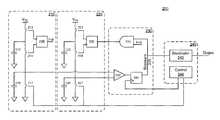
- FIG. 2illustrates an embodiment of a capacitance-to-code converter 200 that may be implemented as receive channel 120 of sensing circuit 110 of FIG. 1 .
- Capacitance-to-code converter 200may include a first charge transfer circuit 210 including a sensor capacitor 212 (see capacitance sensing electrode 101 of FIG. 1 ).
- Sensor capacitor 212may have a first plate alternately coupled to a source voltage and an integration capacitor 216 .
- Sensor capacitor 212may have a second plate coupled to a ground potential.
- Sensor capacitor 212alternates between the source voltage and integration capacitor 216 through deadband switches 213 and 214 .
- Deadband switches 213 and 214may be clocked by clock signal Fclk.
- a first phasewhen switch 213 is closed, a voltage potential is produced on sensor capacitor 212 .
- switch 214In a second phase, when switch 214 is closed, charge accumulated on sensor capacitor 212 during the first phase is transferred to integration capacitor 216 .
- Capacitor to code converter 200includes a second charge transfer circuit 220 including a modulation capacitor 222 .
- Modulation capacitor 222may have a first plate alternately coupled to an integration capacitor 226 and a source voltage.
- Modulation capacitor 222may have a second plate coupled to a ground potential.
- Modulation capacitor 222alternates between the source voltage and integration capacitor 226 through deadband switches 223 and 224 .
- Deadband switches 223 and 224may be clocked by an output of sigma-delta modulator 230 . Switches 223 and 224 may couple modulation capacitor 222 to integration capacitor 226 and the source voltage at opposite phases as modulation capacitor 222 is coupled to integration capacitor 226 and the source voltage.
- modulation capacitor 222is coupled to integration capacitor 226 , transferring charge accumulated on the modulation capacitor 222 to integration capacitor 226 .
- modulation capacitor 222is coupled to the source voltage, allowing charge to accumulate on modulation capacitor 222 .
- Integration capacitors 216 and 226may be coupled to inputs of comparator 232 .
- integration capacitor 216is coupled to an inverting input of comparator 232 .
- integration capacitor 226may be coupled to an inverting input instead.
- Bit stream output 238may be a synchronized output of comparator 232 and a control clock from control block 244 through latch 234 .
- the bit stream output of comparator 232may be digitized by decimator and control logic 240 .
- the bit stream output 238may also be used to provide a clock frequency to charge transfer circuit 220 through AND gate 236 , which may have a second input coupled to Fclk.
- capacitance-to-code converter 200has a reset phase, wherein integration capacitors 216 and 226 are reset to a ground potential by switches 217 and 227 , respectively.
- reset switches 217 and 227may be configured to reset integration capacitors to voltages that are not a zero potential.
- switches 217 and 227are opened and the charge transfer from sensor capacitor 212 and modulation capacitor 222 begins.
- Integration capacitors 216 and 226have charge accumulated on them by the repeated transfer of charge from sensor capacitor 212 and modulation capacitor 222 , respectively.
- the duty cycle (DC) of the bit stream output of comparator 232based on the inputs from the integration capacitor 216 and modulation integration capacitor 226 is given by:
- the duty cycle outputdepends on the capacitive relationship between the sensor capacitor 212 and the reference capacitors (modulation capacitor 222 and integration capacitors 216 and 226 , wherein Cint 1 is integration capacitor 216 and Cint 2 is integration capacitor 226 ).
- reference capacitorsmay be sensors but configured as reference capacitors for measurement of other sensor capacitors. As long as the capacitance values of the reference capacitors (either discrete or on-chip capacitors, or sensor capacitors) remain relatively constant over the measurement of the sensor capacitor under test, capacitance-to-code converter 200 operates as expected. If a sensor capacitor not under test is used as the modulation capacitor 222 , the temperature coefficients of the sensor capacitor 212 under test and the modulation capacitor 222 will be similar, providing temperature insensitivity. This temperature insensitivity may be particularly useful in wake-on-touch and low-power applications.
- each integration capacitor 216 and 226is considerable larger than its respective sensor capacitor 212 or modulation capacitor 222 .
- the values of integration capacitors 216 and 226may be 1000 times greater than the capacitance of the sensor capacitor 212 and modulation capacitor 222 .
- a digital timercounts the number of charge transfer cycles (the operation of switches 213 / 214 and 223 / 224 ) and terminates the measurement cycle when the required number of charge transfer cycles has been reached.
- the output of the capacitance-to-code converter 200is not dependent on the clock frequency, Fclk, only the number of clock pulses for the desired measurement count.
- the output of capacitance-to-code converter 200is not dependent on supply voltage (V DD ).
- This architectureallows the use of spread-spectrum, random, pseudo-random, or fixed frequency clock sequencers. Fclk may be any of these clock types.
- I s1_avgV swing_avg ⁇ F clk ⁇ C s1 , where V swing_avg is the average difference between the voltage on integration capacitor 216 and the supply voltage of charge transfer circuit 210 over the measurement interval.
- Decimator and logic block 240may include a decimator 242 and a module 244 .
- Decimator 242may be a digital filter configured to reduce the input sample rate received from the output of latch 234 and provide a reduced data rate as the output of decimator and logic block 240 .
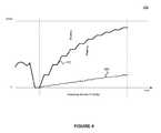
- FIG. 3illustrates voltage waveforms at various nodes of the capacitance to code converter 200 .
- the voltage on sensor capacitor 212increases according to waveform 312 . Note, this is an exponential increase, but one of ordinary skill in the art would understand that charge transfer circuit 210 may be configured to generate a linear response as charge is shared with integration capacitor 216 . As charge is accumulated on integration capacitor 216 and modulation capacitor 226 , the voltage on each increases as shown by wave forms 316 and 326 .
- Fclkprovides the clock signal to the charge transfer operation as well as the comparator 232 , which generates the bitstream output waveform 332 , which is converted to the digital value used in making determinations on the state of sensor capacitor 212 .
- the proportionate capacitance of sensor capacitor 212 and modulation capacitor 222 to integration capacitors 216 and 226determines the effective resolution and the external noise immunity of capacitance to code converter 200 .
- Proportionately larger integration capacitorsmay provide greater resolution and noise immunity.
- noise immunitythe greater the average value of V swing , the greater the immunity.
- V swingis the difference between the voltage on the integration capacitor at each charge transfer cycle and the supply voltage.
- FIG. 4illustrates example V swing values for sensor-to-integration capacitance ratios of 1:10 ( 410 ) and 1:100 ( 420 ).
- the voltage increase across the integration capacitor with each charge transfer cycleis greater. For example, if ten charge transfer cycles are used for the conversion measurement window, the average V swing value at each cycle is greater.
- FIG. 5illustrates another embodiment of capacitance to code converter 500 , which is similar to capacitance to code converter 200 of FIG. 2 , but wherein the clock frequency, F mod, of the modulation capacitor charge transfer circuit 220 is greater than the clock frequency, Fsw, of the sensor capacitor charge transfer circuit 210 .
- the duty cycle output of capacitance to code converter 500is therefore given by:
- D ⁇ ⁇ CC i ⁇ ⁇ n ⁇ ⁇ t ⁇ ⁇ 2 C i ⁇ ⁇ n ⁇ ⁇ t ⁇ ⁇ 1 ⁇ C s N ⁇ C m .
- Increasing the F mod relative to Fswallows for smaller modulation capacitors ( 212 and 222 ), which may allow them to be integrated on-chip far easier.
- the embodiments described hereinmay be used in various designs of mutual-capacitance sensing arrays of the capacitance sensing system, or in self-capacitance sensing arrays.
- the capacitance sensing systemdetects multiple sense elements that are activated in the array, and can analyze a signal pattern on the neighboring sense elements to separate noise from actual signal.
- the embodiments described hereinare not tied to a particular capacitive sensing solution and can be used as well with other sensing solutions, including optical sensing solutions, as would be appreciated by one of ordinary skill in the art having the benefit of this disclosure.
- exampleor “exemplary” are used herein to mean serving as an example, instance or illustration. Any aspect or design described herein as “example’ or “exemplary” is not necessarily to be construed as preferred or advantageous over other aspects or designs. Rather, use of the words “example” or “exemplary” is intended to present concepts in a concrete fashion.
- the term “or”is intended to mean an inclusive “or” rather than an exclusive “or.” That is, unless specified otherwise, or clear from context, “X includes A or B” is intended to mean any of the natural inclusive permutations. That is, if X includes A; X includes B; or X includes both A and B, then “X includes A or B” is satisfied under any of the foregoing instances.
- Embodiments described hereinmay also relate to an apparatus for performing the operations herein.
- This apparatusmay be specially constructed for the required purposes, or it may comprise a general-purpose computer selectively activated or reconfigured by a computer program stored in the computer.
- a computer programmay be stored in a non-transitory computer-readable storage medium, such as, but not limited to, any type of disk including floppy disks, optical disks, CD-ROMs and magnetic-optical disks, read-only memories (ROMs), random access memories (RAMs), EPROMs, EEPROMs, magnetic or optical cards, flash memory, or any type of media suitable for storing electronic instructions.
- computer-readable storage mediumshould be taken to include a single medium or multiple media (e.g., a centralized or distributed database and/or associated caches and servers) that store one or more sets of instructions.
- the term “computer-readable medium”shall also be taken to include any medium that is capable of storing, encoding or carrying a set of instructions for execution by the machine and that causes the machine to perform any one or more of the methodologies of the present embodiments.
- the term “computer-readable storage medium”shall accordingly be taken to include, but not be limited to, solid-state memories, optical media, magnetic media, any medium that is capable of storing a set of instructions for execution by the machine and that causes the machine to perform any one or more of the methodologies of the present embodiments.
Landscapes
- Engineering & Computer Science (AREA)
- Theoretical Computer Science (AREA)
- Physics & Mathematics (AREA)
- General Physics & Mathematics (AREA)
- Measurement Of Resistance Or Impedance (AREA)
- Measuring Fluid Pressure (AREA)
- Electronic Switches (AREA)
Abstract
Description
RawData=DC·NRES,
where NRESis the number of Fclk cycles during the measurement time. In one embodiment, NRESis selected from the order of two:
NRES=2n−1,
where n is a whole, positive integer. The average excitation current, Is1_avg, which defines the noise immunity to external noise is given by:
Is1_avg=Vswing_avg·Fclk·Cs1,
where Vswing_avgis the average difference between the voltage on
Fmod=N·FSW,
where N is a positive integer. The duty cycle output of capacitance to code
Increasing the F mod relative to Fsw allows for smaller modulation capacitors (212 and222), which may allow them to be integrated on-chip far easier.
Claims (20)
Priority Applications (1)
| Application Number | Priority Date | Filing Date | Title |
|---|---|---|---|
| US15/730,456US10476521B2 (en) | 2016-04-29 | 2017-10-11 | Ratio-metric self-capacitance-to-code convertor |
Applications Claiming Priority (3)
| Application Number | Priority Date | Filing Date | Title |
|---|---|---|---|
| US201662329937P | 2016-04-29 | 2016-04-29 | |
| US15/199,559US9819360B1 (en) | 2016-04-29 | 2016-06-30 | Ratio-metric self-capacitance-to-code convertor |
| US15/730,456US10476521B2 (en) | 2016-04-29 | 2017-10-11 | Ratio-metric self-capacitance-to-code convertor |
Related Parent Applications (1)
| Application Number | Title | Priority Date | Filing Date |
|---|---|---|---|
| US15/199,559ContinuationUS9819360B1 (en) | 2016-04-29 | 2016-06-30 | Ratio-metric self-capacitance-to-code convertor |
Publications (2)
| Publication Number | Publication Date |
|---|---|
| US20180083650A1 US20180083650A1 (en) | 2018-03-22 |
| US10476521B2true US10476521B2 (en) | 2019-11-12 |
Family
ID=60157014
Family Applications (2)
| Application Number | Title | Priority Date | Filing Date |
|---|---|---|---|
| US15/199,559ActiveUS9819360B1 (en) | 2016-04-29 | 2016-06-30 | Ratio-metric self-capacitance-to-code convertor |
| US15/730,456Active2036-08-26US10476521B2 (en) | 2016-04-29 | 2017-10-11 | Ratio-metric self-capacitance-to-code convertor |
Family Applications Before (1)
| Application Number | Title | Priority Date | Filing Date |
|---|---|---|---|
| US15/199,559ActiveUS9819360B1 (en) | 2016-04-29 | 2016-06-30 | Ratio-metric self-capacitance-to-code convertor |
Country Status (5)
| Country | Link |
|---|---|
| US (2) | US9819360B1 (en) |
| KR (3) | KR102041423B1 (en) |
| CN (2) | CN111220853B (en) |
| DE (1) | DE112017002244T5 (en) |
| WO (1) | WO2017189107A1 (en) |
Families Citing this family (3)
| Publication number | Priority date | Publication date | Assignee | Title |
|---|---|---|---|---|
| US10162467B2 (en)* | 2017-03-08 | 2018-12-25 | Cypress Semiconductor Corporation | Ratiometric mutual-capacitance-to-code converter |
| US11442578B2 (en)* | 2020-08-31 | 2022-09-13 | Cypress Semiconductor Corporation | Ratio-metric multi-sensing convertor |
| US11467693B1 (en)* | 2021-08-06 | 2022-10-11 | Cypress Semiconductor Corporation | Impedance sensing methods |
Citations (19)
| Publication number | Priority date | Publication date | Assignee | Title |
|---|---|---|---|---|
| US4136508A (en) | 1977-01-07 | 1979-01-30 | Allis-Chalmers Corporation | Closed-loop combine header height control |
| US5579247A (en) | 1991-02-15 | 1996-11-26 | Crystal Semiconductor Corporation | Method and apparatus for decreasing the interference and noise sensitivity of a ratiometric converter type of circuit |
| US5990578A (en)* | 1996-12-06 | 1999-11-23 | Zentrum Mikroelektronik Dresden Gmbh | Capacitive sensor arrangement |
| US6037887A (en)* | 1996-03-06 | 2000-03-14 | Burr-Brown Corporation | Programmable gain for delta sigma analog-to-digital converter |
| US6452531B1 (en) | 1999-08-27 | 2002-09-17 | Analog Devices, Inc. | Jitter and load insensitive charge transfer |
| US20050099188A1 (en) | 2002-07-02 | 2005-05-12 | Baxter Larry K. | Capacitive measurement system |
| US7235983B2 (en) | 2005-03-09 | 2007-06-26 | Analog Devices, Inc. | One terminal capacitor interface circuit |
| US20080111714A1 (en) | 2006-11-14 | 2008-05-15 | Viktor Kremin | Capacitance to code converter with sigma-delta modulator |
| US7495589B1 (en) | 2007-09-17 | 2009-02-24 | Texas Instruments Incorporated | Circuit and method for gain error correction in ADC |
| US7902842B2 (en) | 2005-06-03 | 2011-03-08 | Synaptics Incorporated | Methods and systems for switched charge transfer capacitance measuring using shared components |
| US20110163901A1 (en) | 2009-07-16 | 2011-07-07 | Microchip Technology Incorporated | 2-phase gain calibration and scaling scheme for switched capacitor sigma-delta modulator using a chopper voltage reference |
| US20120043971A1 (en)* | 2008-02-27 | 2012-02-23 | Cypress Semiconductor Corporation | Methods and circuits for measuring mutual and self capacitance |
| US8169238B1 (en)* | 2007-07-03 | 2012-05-01 | Cypress Semiconductor Corporation | Capacitance to frequency converter |
| US20120268145A1 (en) | 2011-04-20 | 2012-10-25 | Lokesh Chandra | Current sensing apparatus and method for a capacitance-sensing device |
| US8564313B1 (en) | 2007-07-03 | 2013-10-22 | Cypress Semiconductor Corporation | Capacitive field sensor with sigma-delta modulator |
| US8570052B1 (en) | 2008-02-27 | 2013-10-29 | Cypress Semiconductor Corporation | Methods and circuits for measuring mutual and self capacitance |
| US20140218223A1 (en) | 2013-02-06 | 2014-08-07 | Microsemi Corp. - Analog Mixed Signal Group, Ltd. | Multiplexed sigma delta modulator |
| US8952838B2 (en) | 2011-08-19 | 2015-02-10 | Lumedyne Technologies, Inc. | Time domain switched analog-to-digital converter apparatus and methods |
| US9100043B2 (en)* | 2013-10-31 | 2015-08-04 | Mathias Krauβ | Method and circuit for an analog digital capacitance converter |
Family Cites Families (1)
| Publication number | Priority date | Publication date | Assignee | Title |
|---|---|---|---|---|
| US199559A (en) | 1878-01-22 | Improvement in top-spinning devices |
- 2016
- 2016-06-30USUS15/199,559patent/US9819360B1/enactiveActive
- 2017
- 2017-03-10KRKR1020187033899Apatent/KR102041423B1/enactiveActive
- 2017-03-10WOPCT/US2017/021872patent/WO2017189107A1/ennot_activeCeased
- 2017-03-10CNCN202010135649.XApatent/CN111220853B/enactiveActive
- 2017-03-10DEDE112017002244.4Tpatent/DE112017002244T5/enactivePending
- 2017-03-10CNCN201780036328.0Apatent/CN109313227B/enactiveActive
- 2017-03-10KRKR1020207026912Apatent/KR20200118209A/ennot_activeWithdrawn
- 2017-03-10KRKR1020197032231Apatent/KR102159341B1/enactiveActive
- 2017-10-11USUS15/730,456patent/US10476521B2/enactiveActive
Patent Citations (21)
| Publication number | Priority date | Publication date | Assignee | Title |
|---|---|---|---|---|
| US4136508A (en) | 1977-01-07 | 1979-01-30 | Allis-Chalmers Corporation | Closed-loop combine header height control |
| US5579247A (en) | 1991-02-15 | 1996-11-26 | Crystal Semiconductor Corporation | Method and apparatus for decreasing the interference and noise sensitivity of a ratiometric converter type of circuit |
| US6037887A (en)* | 1996-03-06 | 2000-03-14 | Burr-Brown Corporation | Programmable gain for delta sigma analog-to-digital converter |
| US5990578A (en)* | 1996-12-06 | 1999-11-23 | Zentrum Mikroelektronik Dresden Gmbh | Capacitive sensor arrangement |
| US6452531B1 (en) | 1999-08-27 | 2002-09-17 | Analog Devices, Inc. | Jitter and load insensitive charge transfer |
| US20050099188A1 (en) | 2002-07-02 | 2005-05-12 | Baxter Larry K. | Capacitive measurement system |
| US7235983B2 (en) | 2005-03-09 | 2007-06-26 | Analog Devices, Inc. | One terminal capacitor interface circuit |
| US7902842B2 (en) | 2005-06-03 | 2011-03-08 | Synaptics Incorporated | Methods and systems for switched charge transfer capacitance measuring using shared components |
| US20080111714A1 (en) | 2006-11-14 | 2008-05-15 | Viktor Kremin | Capacitance to code converter with sigma-delta modulator |
| US9166621B2 (en) | 2006-11-14 | 2015-10-20 | Cypress Semiconductor Corporation | Capacitance to code converter with sigma-delta modulator |
| US8564313B1 (en) | 2007-07-03 | 2013-10-22 | Cypress Semiconductor Corporation | Capacitive field sensor with sigma-delta modulator |
| US8169238B1 (en)* | 2007-07-03 | 2012-05-01 | Cypress Semiconductor Corporation | Capacitance to frequency converter |
| US7495589B1 (en) | 2007-09-17 | 2009-02-24 | Texas Instruments Incorporated | Circuit and method for gain error correction in ADC |
| US20120043971A1 (en)* | 2008-02-27 | 2012-02-23 | Cypress Semiconductor Corporation | Methods and circuits for measuring mutual and self capacitance |
| US8570052B1 (en) | 2008-02-27 | 2013-10-29 | Cypress Semiconductor Corporation | Methods and circuits for measuring mutual and self capacitance |
| US20110163901A1 (en) | 2009-07-16 | 2011-07-07 | Microchip Technology Incorporated | 2-phase gain calibration and scaling scheme for switched capacitor sigma-delta modulator using a chopper voltage reference |
| US20120268145A1 (en) | 2011-04-20 | 2012-10-25 | Lokesh Chandra | Current sensing apparatus and method for a capacitance-sensing device |
| WO2012145034A1 (en) | 2011-04-20 | 2012-10-26 | Cypress Semiconductor Corporation | Current sensing apparatus and method for a capacitance- sensing device |
| US8952838B2 (en) | 2011-08-19 | 2015-02-10 | Lumedyne Technologies, Inc. | Time domain switched analog-to-digital converter apparatus and methods |
| US20140218223A1 (en) | 2013-02-06 | 2014-08-07 | Microsemi Corp. - Analog Mixed Signal Group, Ltd. | Multiplexed sigma delta modulator |
| US9100043B2 (en)* | 2013-10-31 | 2015-08-04 | Mathias Krauβ | Method and circuit for an analog digital capacitance converter |
Non-Patent Citations (10)
| Title |
|---|
| Arup K. George, A 0.8-V Supply- and Temperature-Insensiive Capacitance-to-Digital Converter in 0.18-\mu CMOS, IEEE Sensors Journal, vol. 16, Issue 13, Apr. 27, 2016, pp. 5354-5364; 10 pages. |
| China National Intellectual Property Administration (CNIPA) Office Action for Application No. 201780036328.0 dated Aug. 27, 2019; 3 pages. |
| International Search Report for International Application No. PCT/US17/21872 dated May 24, 2017; 2 pages. |
| KIPO Office Action for Application No. 10-2018-7033899 dated Feb. 19, 2019; 3 pages. |
| SIPO Office Action for Application No. 201780036328.0 dated Mar. 29, 2019; 5 pages. |
| USPTO Advisory Action for U.S. Appl. No. 15/199,559 dated Jan. 31, 2017; 3 pages. |
| USPTO Final Rejection for U.S. Appl. No. 15/199,559 dated Nov. 22, 2016; 11 pages. |
| USPTO Non-Final Rejection for U.S. Appl. No. 15/199,559 dated Sep. 1, 2016; 13 pages. |
| USPTO Notice of Allowance for U.S. Appl. No. 15/199,559 dated Mar. 29, 2017; 11 pages. |
| Written Opinion of the International Searching Authority for International Application No. PCT/US17/21872 dated May 24, 2017; 5 pages. |
Also Published As
| Publication number | Publication date |
|---|---|
| US20180083650A1 (en) | 2018-03-22 |
| WO2017189107A1 (en) | 2017-11-02 |
| KR20200118209A (en) | 2020-10-14 |
| CN109313227A (en) | 2019-02-05 |
| KR20190125545A (en) | 2019-11-06 |
| KR102159341B1 (en) | 2020-09-24 |
| CN111220853B (en) | 2022-11-25 |
| US9819360B1 (en) | 2017-11-14 |
| CN109313227B (en) | 2020-03-27 |
| DE112017002244T5 (en) | 2019-01-31 |
| KR20180130584A (en) | 2018-12-07 |
| CN111220853A (en) | 2020-06-02 |
| US20170317690A1 (en) | 2017-11-02 |
| KR102041423B1 (en) | 2019-11-06 |
Similar Documents
| Publication | Publication Date | Title |
|---|---|---|
| US11442578B2 (en) | Ratio-metric multi-sensing convertor | |
| US7301350B2 (en) | Methods and systems for detecting a capacitance using sigma-delta measurement techniques | |
| US7288946B2 (en) | Methods and systems for detecting a capacitance using sigma-delta measurement techniques | |
| US10088510B2 (en) | Capacitance detection apparatus and input apparatus | |
| CN103064566A (en) | Low power capacitive touch detector | |
| US10162467B2 (en) | Ratiometric mutual-capacitance-to-code converter | |
| US10476521B2 (en) | Ratio-metric self-capacitance-to-code convertor | |
| US11853498B2 (en) | System, method, and apparatus for passive shielding of a capacitive sensing button | |
| US8797277B1 (en) | Method for multiple touch position estimation | |
| US9923572B2 (en) | Delta modulator receive channel for capacitance measurement circuits | |
| US12176909B2 (en) | Nano-power architecture enhancements | |
| US11467693B1 (en) | Impedance sensing methods | |
| TWI427514B (en) | Control device for touch panel and signal processing method thereof | |
| US12124653B1 (en) | Ratio-metric multi-sensing convertor |
Legal Events
| Date | Code | Title | Description |
|---|---|---|---|
| FEPP | Fee payment procedure | Free format text:ENTITY STATUS SET TO UNDISCOUNTED (ORIGINAL EVENT CODE: BIG.); ENTITY STATUS OF PATENT OWNER: LARGE ENTITY | |
| AS | Assignment | Owner name:CYPRESS SEMICONDUCTOR CORPORATION, CALIFORNIA Free format text:ASSIGNMENT OF ASSIGNORS INTEREST;ASSIGNOR:MAHARYTA, ANDRIY;REEL/FRAME:044009/0071 Effective date:20160701 | |
| AS | Assignment | Owner name:MORGAN STANLEY SENIOR FUNDING, INC., AS COLLATERAL AGENT, MARYLAND Free format text:PATENT SECURITY AGREEMENT;ASSIGNOR:CYPRESS SEMICONDUCTOR CORPORATION;REEL/FRAME:046402/0277 Effective date:20180620 Owner name:MORGAN STANLEY SENIOR FUNDING, INC., AS COLLATERAL Free format text:PATENT SECURITY AGREEMENT;ASSIGNOR:CYPRESS SEMICONDUCTOR CORPORATION;REEL/FRAME:046402/0277 Effective date:20180620 | |
| STPP | Information on status: patent application and granting procedure in general | Free format text:NON FINAL ACTION MAILED | |
| STPP | Information on status: patent application and granting procedure in general | Free format text:RESPONSE TO NON-FINAL OFFICE ACTION ENTERED AND FORWARDED TO EXAMINER | |
| STPP | Information on status: patent application and granting procedure in general | Free format text:NOTICE OF ALLOWANCE MAILED -- APPLICATION RECEIVED IN OFFICE OF PUBLICATIONS | |
| STPP | Information on status: patent application and granting procedure in general | Free format text:PUBLICATIONS -- ISSUE FEE PAYMENT RECEIVED | |
| STPP | Information on status: patent application and granting procedure in general | Free format text:PUBLICATIONS -- ISSUE FEE PAYMENT VERIFIED | |
| STPP | Information on status: patent application and granting procedure in general | Free format text:AWAITING TC RESP., ISSUE FEE NOT PAID | |
| STCF | Information on status: patent grant | Free format text:PATENTED CASE | |
| AS | Assignment | Owner name:MUFG UNION BANK, N.A., CALIFORNIA Free format text:ASSIGNMENT AND ASSUMPTION OF SECURITY INTEREST IN INTELLECTUAL PROPERTY;ASSIGNOR:MORGAN STANLEY SENIOR FUNDING, INC.;REEL/FRAME:050896/0366 Effective date:20190731 | |
| AS | Assignment | Owner name:SPANSION LLC, CALIFORNIA Free format text:RELEASE BY SECURED PARTY;ASSIGNOR:MUFG UNION BANK, N.A.;REEL/FRAME:059410/0438 Effective date:20200416 Owner name:CYPRESS SEMICONDUCTOR CORPORATION, CALIFORNIA Free format text:RELEASE BY SECURED PARTY;ASSIGNOR:MUFG UNION BANK, N.A.;REEL/FRAME:059410/0438 Effective date:20200416 | |
| MAFP | Maintenance fee payment | Free format text:PAYMENT OF MAINTENANCE FEE, 4TH YEAR, LARGE ENTITY (ORIGINAL EVENT CODE: M1551); ENTITY STATUS OF PATENT OWNER: LARGE ENTITY Year of fee payment:4 |