US10475958B2 - Fluidic assembly top-contact LED disk - Google Patents
Fluidic assembly top-contact LED diskDownload PDFInfo
- Publication number
- US10475958B2 US10475958B2US15/674,339US201715674339AUS10475958B2US 10475958 B2US10475958 B2US 10475958B2US 201715674339 AUS201715674339 AUS 201715674339AUS 10475958 B2US10475958 B2US 10475958B2
- Authority
- US
- United States
- Prior art keywords
- disk
- led
- layer
- well
- contact
- Prior art date
- Legal status (The legal status is an assumption and is not a legal conclusion. Google has not performed a legal analysis and makes no representation as to the accuracy of the status listed.)
- Active
Links
Images


Classifications
- H—ELECTRICITY
- H10—SEMICONDUCTOR DEVICES; ELECTRIC SOLID-STATE DEVICES NOT OTHERWISE PROVIDED FOR
- H10H—INORGANIC LIGHT-EMITTING SEMICONDUCTOR DEVICES HAVING POTENTIAL BARRIERS
- H10H20/00—Individual inorganic light-emitting semiconductor devices having potential barriers, e.g. light-emitting diodes [LED]
- H10H20/80—Constructional details
- H10H20/81—Bodies
- H10H20/819—Bodies characterised by their shape, e.g. curved or truncated substrates
- H01L33/20—
- H—ELECTRICITY
- H01—ELECTRIC ELEMENTS
- H01L—SEMICONDUCTOR DEVICES NOT COVERED BY CLASS H10
- H01L25/00—Assemblies consisting of a plurality of semiconductor or other solid state devices
- H01L25/03—Assemblies consisting of a plurality of semiconductor or other solid state devices all the devices being of a type provided for in a single subclass of subclasses H10B, H10D, H10F, H10H, H10K or H10N, e.g. assemblies of rectifier diodes
- H01L25/04—Assemblies consisting of a plurality of semiconductor or other solid state devices all the devices being of a type provided for in a single subclass of subclasses H10B, H10D, H10F, H10H, H10K or H10N, e.g. assemblies of rectifier diodes the devices not having separate containers
- H01L25/075—Assemblies consisting of a plurality of semiconductor or other solid state devices all the devices being of a type provided for in a single subclass of subclasses H10B, H10D, H10F, H10H, H10K or H10N, e.g. assemblies of rectifier diodes the devices not having separate containers the devices being of a type provided for in group H10H20/00
- H01L25/0753—Assemblies consisting of a plurality of semiconductor or other solid state devices all the devices being of a type provided for in a single subclass of subclasses H10B, H10D, H10F, H10H, H10K or H10N, e.g. assemblies of rectifier diodes the devices not having separate containers the devices being of a type provided for in group H10H20/00 the devices being arranged next to each other
- H01L33/005—
- H—ELECTRICITY
- H10—SEMICONDUCTOR DEVICES; ELECTRIC SOLID-STATE DEVICES NOT OTHERWISE PROVIDED FOR
- H10H—INORGANIC LIGHT-EMITTING SEMICONDUCTOR DEVICES HAVING POTENTIAL BARRIERS
- H10H20/00—Individual inorganic light-emitting semiconductor devices having potential barriers, e.g. light-emitting diodes [LED]
- H10H20/01—Manufacture or treatment
- H—ELECTRICITY
- H01—ELECTRIC ELEMENTS
- H01L—SEMICONDUCTOR DEVICES NOT COVERED BY CLASS H10
- H01L2224/00—Indexing scheme for arrangements for connecting or disconnecting semiconductor or solid-state bodies and methods related thereto as covered by H01L24/00
- H01L2224/93—Batch processes
- H01L2224/95—Batch processes at chip-level, i.e. with connecting carried out on a plurality of singulated devices, i.e. on diced chips
- H01L2224/951—Supplying the plurality of semiconductor or solid-state bodies
- H01L2224/95101—Supplying the plurality of semiconductor or solid-state bodies in a liquid medium
- H—ELECTRICITY
- H01—ELECTRIC ELEMENTS
- H01L—SEMICONDUCTOR DEVICES NOT COVERED BY CLASS H10
- H01L2924/00—Indexing scheme for arrangements or methods for connecting or disconnecting semiconductor or solid-state bodies as covered by H01L24/00
- H—ELECTRICITY
- H01—ELECTRIC ELEMENTS
- H01L—SEMICONDUCTOR DEVICES NOT COVERED BY CLASS H10
- H01L2924/00—Indexing scheme for arrangements or methods for connecting or disconnecting semiconductor or solid-state bodies as covered by H01L24/00
- H01L2924/0001—Technical content checked by a classifier
- H01L2924/0002—Not covered by any one of groups H01L24/00, H01L24/00 and H01L2224/00
- H01L2933/0033—
- H01L33/32—
- H—ELECTRICITY
- H10—SEMICONDUCTOR DEVICES; ELECTRIC SOLID-STATE DEVICES NOT OTHERWISE PROVIDED FOR
- H10H—INORGANIC LIGHT-EMITTING SEMICONDUCTOR DEVICES HAVING POTENTIAL BARRIERS
- H10H20/00—Individual inorganic light-emitting semiconductor devices having potential barriers, e.g. light-emitting diodes [LED]
- H10H20/01—Manufacture or treatment
- H10H20/036—Manufacture or treatment of packages
- H—ELECTRICITY
- H10—SEMICONDUCTOR DEVICES; ELECTRIC SOLID-STATE DEVICES NOT OTHERWISE PROVIDED FOR
- H10H—INORGANIC LIGHT-EMITTING SEMICONDUCTOR DEVICES HAVING POTENTIAL BARRIERS
- H10H20/00—Individual inorganic light-emitting semiconductor devices having potential barriers, e.g. light-emitting diodes [LED]
- H10H20/80—Constructional details
- H10H20/81—Bodies
- H10H20/822—Materials of the light-emitting regions
- H10H20/824—Materials of the light-emitting regions comprising only Group III-V materials, e.g. GaP
- H10H20/825—Materials of the light-emitting regions comprising only Group III-V materials, e.g. GaP containing nitrogen, e.g. GaN
Definitions
- This inventiongenerally relates to integrated circuit (IC) fabrication and, more particularly, to a fluidic assembly process for the placement of top-contact light emitting diodes on a transparent display substrate.
- ICintegrated circuit
- GaNgallium nitride
- ⁇ LEDmicro light emitting diode
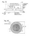
- FIGS. 1A and 1Bare plan views of a top-contact LED disk located in a substrate well (prior art).
- D ddenotes the diameter of the LED (e.g., gallium nitride (GaN)) disk
- D rdenotes the diameter of the micro-cavity or well into which the ⁇ LED disk has been distributed
- D pdenotes the diameter of the p-doped GaN (p-GaN) area, assuming the p-GaN is formed on the top of the disk.
- Area 100is the n-GaN contact, where the p-GaN 102 and MQW have been removed by a reactive ion etch (RIE).
- RIEreactive ion etch
- the inner circular area 102is the full LED stack with p-GaN on top.
- a layer of nickel oxide (NiOx)/indium tin oxide (ITO)may be formed on the surface of area 102 .
- the circular area 102is off the GaN disk center by 2 ⁇ m. Since only the area 102 can emit light, the emission area fill factor is only about 70.6%. Nearly 30% of emission area is lost due to the n-GaN opening 100 .
- FIG. 1Bshows the working area for anode end connection 104 (Dpc). Connects made outside of the 24 ⁇ m diameter area 104 are likely to result in either a short circuit or open circuit. Conventional metal interconnection to the n-GaN area 102 further reduces the emission area fill factor. Only 31.4% area of the GaN disk will emit light in this example.
- FIG. 2is a partial cross-sectional view of a bottom cathode contact architecture (prior art). This option avoids the significant emission area fill factor loss associated with a conventional top-contact LED disk.
- a bottom interconnection electrode 200is first evaporated and patterned on a substrate 202 , followed by micro-cavity (well) 204 formation.
- a thin layer low melting temperature metal film 206is then coated on the bottom electrode surface inside the micro-cavity 204 .
- the GaN disk 208(n-GaN 210 /p-GaN 212 ) is then distributed into the micro-cavity 204 .
- the top interconnection electrode 216is evaporated and patterned to complete the whole process flow.
- the process flow described by FIG. 2is relatively simple.
- the front-side emission area fill factorcan possible reach a maximum of 85% with a carefully top metal wiring design.
- Major challenges of this flowinclude the bottom contact yield, uniformity, reliability and repeatability, and the tradeoff between the bottom contact yield and the bottom electrode area if a backside emission opening is needed.
- LEDlight emitting diode
- Top connections for both cathode and anodeA interconnection process flow that is at least as simple as the bottom contact flow process; A minimum number of interlayer dielectric (ILD) and metal layers; and, A limited fill factor loss.
- ILDinterlayer dielectric
- the architecturestarts with a new LED ⁇ disk structure.
- Two featureshelp to enable the new approach.
- Oneis a center contact opening to the lower (e.g., n-doped) disk of the LED and a dielectric (e.g., tetraethyl orthosilicate (TEOS) SiO.sub.2) isolation pattern in the form of a ring overlying the LED disk, exposing an upper (e.g., n-doped) disk contact region.
- TEOStetraethyl orthosilicate
- a methodfor forming a direct emission display.
- the methodprovides a transparent substrate with an array of wells or micro-cavities formed in its top surface.
- a fluid streamis supplied to the substrate top surface comprising a plurality of top-contact light emitting diode (LED) disks.
- the wellsare filled with the LED disks.
- a first array of electrically conductive linesis formed over the substrate top surface to connect with a first (e.g., lower disk) contact of each LED disk, and a second array of electrically conductive lines is formed over the substrate top surface to connect with a second (e.g., upper disk) contact of each LED disk.
- Each LED diskis made up of a lower disk of material with either a p-dopant or an n-dopant, having a bottom surface, and a top surface.
- a multiple quantum well (MQW) diskoverlies the lower disk.
- An upper diskmade from a material with the opposite of the dopant used in the lower disk, and has a bottom surface overlying the MQW disk, a top surface, and a first diameter.
- An electrical insulator diskoverlies the upper disk top surface, having a second diameter smaller than the first diameter, exposing an upper disk contact region.
- a viais formed through the electrical insulator disk, upper disk, and MQW disk, exposing a center contact region of the lower disk top surface.
- the first array of electrically conductive linesform a pair of opposing top disk contact arms overlying each well to form a connection with the upper disk, with each top-contact arm having a length of x extending over the well, where x greater than (the third diameter-first diameter)/2.
- the second array of electrically conductive linesform a bottom disk contact arm overlying each well.
- Each bottom disk contact armhas a length of y extending over the well and dielectric extension, where y is greater than (the third diameter+the fourth diameter)/2.
- top-contact LEDand direct emission display made from top-contact LEDs are provided below.
- FIGS. 1A and 1Bare plan views of a top-contact LED disk located in a substrate well (prior art).
- FIG. 2is a partial cross-sectional view of a bottom cathode contact architecture (prior art).
- FIGS. 3A and 3Bare partial cross-sectional and plan views, respectively, of a top-contact LED.
- FIG. 4Ais a partial cross-sectional view
- FIGS. 4B and 4Care plan views of a direct emission display.
- FIGS. 5A through 5Fare partial cross-section views summarizing the major process steps in an exemplary display fabrication process.
- FIG. 6is another plan view depicting of the LED disk situated is a substrate well.
- FIGS. 7A through 7Hare plan views illustrating eight worst-case positions for an LED disk inside a micro-cavity.
- FIG. 8is a flowchart illustrating a method for forming a direct emission display.
- FIGS. 3A and 3Bare partial cross-sectional and plan views, respectively, of a top-contact LED.
- the LED 300comprises a lower disk 302 comprising a material with either a p-dopant or an n-dopant, having a bottom surface 304 and a top surface 306 .
- a multiple quantum well (MQW) disk 308overlies the lower disk top surface 306 .
- the MQW layer 308may typically be a series of quantum well shells (typically 5 layers—e.g., alternating 5 nm of indium gallium nitride (InGaN) with 9 nm of n-doped GaN (n-GaN)) not shown.
- InGaNindium gallium nitride
- n-GaNn-doped GaN
- AlGaNaluminum gallium nitride
- the outer shellmay be p-doped GaN (Mg doping) about 200 nm thick.
- a high-brightness blue LEDcan be formed, or a green LED if a higher indium content is used in the MQW.
- An upper disk 310comprises a material with the opposite dopant that is used in the lower disk. If the lower click 302 is p-doped then the upper disk 310 is n-doped. Likewise, if the lower disk 302 is n-doped, the upper disk 310 is p-doped.
- the upper disk 310has a bottom surface 312 overlying the MQW disk 308 , a top surface 314 , and a first diameter 316 .
- the lower diskmay be a material such as p-GaN, p-doped aluminum gallium indium phosphide (p-AlGaInP), n-GaN, or n-AlGaInP.
- the upper disk 310could be made of the same materials, but oppositely doped. Note: this is not an exhaustive list of material types.
- An electrical insulator disk 318overlies the upper disk top surface 314 , having a second diameter 320 smaller than the first diameter 316 , exposing an upper disk contact region 322 .
- the electrical insulator disk 318is transparent, and may be a dielectric material such as TEOS silicon dioxide.
- a via 324is formed through the electrical insulator disk 318 , upper disk 310 , and MQW disk 308 , exposing a center contact region 326 of the lower disk top surface.
- the electrical insulator disk 318has a center 328 overlying the upper disk center 330 .
- the upper disk contact region 322is formed around a circumference of the upper disk top surface 314 .
- FIG. 4Ais a partial cross-sectional view
- FIGS. 4B and 4Care plan views of a direct emission display.
- FIG. 4Bdepicts an exemplary layout design of a 2.times.3 LED disk direct emission display pixel array.
- Each pixel 430is composed of four LED disks 300 for brightness and redundancy management.
- the serpentine extensions of the second array 410 wiringare designed for trimming off “dead” LED disks from the array.
- the designis not dependent upon any particular grouping of LEDs or the shape of the wiring interconnects.
- the display 400comprises a transparent substrate 402 with a top surface 404 comprising an array of wells or micro-cavities 406 .
- a top-contact LED 300is formed in each well 406 . Details of the top-contact LED 300 have been provided above in the explanation of FIGS. 3A and 3B , and are not repeated here in the interest of brevity.
- a first array of electrically conductive lines 408is connected to the LED lower disk contact regions 326 .
- a second array of electrically conductive lines 410is connected to the LED upper disk contact regions 322 .
- a dielectric material 412is interposed between the first array 408 and second array 410 of electrically conductive lines. It should be understood that the overlying order of the conductive arrays is arbitrary.
- the electrical insulator disk (see FIG. 3A ) and the dielectric 412are transparent to visible spectrums of light.
- Each well 406has a third diameter 414 .
- the first array of electrically conductive linesforms a pair of opposing top disk contact arms 416 overlying each well 406 .
- Each top disk contact arm 416has a length 418 of x extending over the well 406 , where x greater than (the third diameter 414 -first diameter 316 )/2.
- the lower disk contact region 326has a fourth diameter 420 .
- the second array of electrically conductive linesforms a bottom disk contact arm 422 overlying each well 406 .
- Each bottom disk contact arm 422has a length 424 of y extending over the well 406 and a dielectric extension 426 , where y is greater than (the third diameter 414 +the fourth diameter 420 )/2.
- the bottom disk contact arm 422is typically orthogonal to both top disk contact arms 416 in each well 406 .
- the fabrication process flowis very similar to the bottom contact option, which has the advantage of simplicity.
- the fabrication processdoes not use any more dielectric film or metal film layers than the bottom contact process, and no additional photolithography steps are needed.
- the top-contact fabrication processeliminates a low melting temperature metal film coating step (see reference designator 206 of FIG. 2 ) that is needed for the bottom contact process.
- a display fabrication process using the LED disks disclosed hereinpermits top connections for both cathode and anode of each LED.
- the interconnection flowis as least as simple as a bottom contact flow process, with a minimum number of ILD and metal layers, and a limited fill factor loss.
- FIGS. 5A through 5Fare partial cross-section views summarizing the major process steps in an exemplary display fabrication process.
- FIG. 5Adepicts a transparent substrate and in FIG. 5B the first array of electrical connections 408 (bottom electrode) is formed. Typically, the array is formed using a conformal deposition, followed by patterning. The size of the cell or pixel may, for example, be 500 microns by 500 microns.
- FIG. 5Ca dry film 500 is deposited and patterned to form a well 406 . In other processes, the well may be formed by etching cavities in the substrate top surface.
- the LED disk 300is situated in the well 406 , typically through a fluidic distribution process.
- FIG. 5Adepicts a transparent substrate and in FIG. 5B the first array of electrical connections 408 (bottom electrode) is formed. Typically, the array is formed using a conformal deposition, followed by patterning. The size of the cell or pixel may, for example, be 500 microns by 500 microns.
- a dielectric 426such as polyimide is deposited and patterned around the edges of the LED, also forming the dielectric extension over the upper disk contact region, as shown in FIG. 4C .
- top metallizationforms the bottom disk contact arm 422 .
- the top disk contact armsmay be formed at this time or in a separate step.
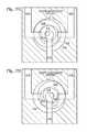
- FIG. 6is another plan view depicting of the LED disk situated is a substrate well.
- the center low disk contactmay be 5 um and a TEOS SiO2 insulation disk 318 may have outer (second) diameter 320 of 30 ⁇ m. Comparing the edge circular opening to the n-GaN in FIG. 1A (reference designator 100 ), on the same 50 ⁇ m diameter GaN disk with 30% fill factor loss, the small center opening depicted here causes as little as a 3% emission area fill factor loss.
- the dielectric (e.g., polyimide) extension 426works together with the built-in TEOS SiO.sub.2 insulation circular disk 318 to form an electrical isolation bridge for a top metal wiring (bottom disk contact arm 422 ) to reach the contact 326 in the center of the GaN ⁇ disk.
- the polyimide extension 426 and the SiO.sub.2 ring 318 on the diskare designed so that no matter how the GaN ⁇ disk is distributed inside the micro-cavity, short circuits are prevented while guaranteeing valid contacts to the LED disk.
- Two upper disk contact arms 416are used. If the LED ⁇ disk is located on-center in the micro-cavity, as shown, both arms 416 form a valid contact to the upper disk 310 . Even if the LED disk is located off-center, at least one arm 416 contacts the upper disk 310 to guarantee a connection.
- emission area fill factorfor backside emission applications there is no fill factor loss.
- the lossis just the total non-transparent metal wiring areas, which in this design is about 18%.
- This new designhas an emission area fill factor similar to the bottom contact architecture for front-side emission, and a significantly superior emission area fill factor for backside emission. This enables more freedom in light management by enabling the use of dummy metal patterns on the bottom, or on the top, or on both.
- FIGS. 7A through 7Hare plan views illustrating eight worst-case positions for an LED disk inside a micro-cavity.
- wiring contactis always made with each lower disk contact region 326 of the LED.
- the dielectric extension 426 and insulation disk 318prevent short circuits.
- at least one upper disk contact arm 416connects to the upper disk contact region 322 of each LED.
- FIG. 8is a flowchart illustrating a method for forming a direct emission display. Although the method is depicted as a sequence of numbered steps for clarity, the numbering does not necessarily dictate the order of the steps. It should be understood that some of these steps may be skipped, performed in parallel, or performed without the requirement of maintaining a strict order of sequence. Generally however, the method follows the numeric order of the depicted steps and can be better appreciated in context of the explanation of FIGS. 3A through 7H . The method starts at Step 800 .
- Step 802provides a transparent substrate with an array of wells formed in a top surface.
- the wells or micro-cavitiescan be formed by patterned deposition or etching.
- Step 804supplies a fluid stream to the substrate top surface comprising a plurality of top-contact LED disks. Otherwise, Step 804 can be enabled using a pick-and-place process.
- Step 806fills the wells with the LED disks.
- Step 808forms a dielectric extension overlying a portion of an upper disk contact region of the LEDs.
- Step 810forms a first array of electrically conductive lines over the substrate top surface to connect with a first contact of each LED disk.
- Step 812forms a second array of electrically conductive lines over the substrate top surface to connect with a second contact of each LED disk. Note: Step 812 may be performed before Step 810 in some aspects.
- Supplying the LED disks in Step 804may include supplying LED disks as described above in the description of FIGS. 3A and 3B . That is, the LED disks comprise a lower disk comprising a material with a dopant selected to be either a p-dopant or an n-dopant, having a bottom surface and a top surface.
- a MQW diskoverlies the lower disk.
- An upper diskcomprises a material with the unselected dopant, having a bottom surface that overlies the MQW disk, a top surface, and a first diameter. Specific upper and lower disk materials have been mentioned above.
- An electrical insulator (e.g. transparent) diskoverlies the upper disk top surface, having a second diameter smaller than the first diameter. In one aspect, the electrical insulating disk is centered on the upper disk.
- a viais formed through the electrical insulator disk, upper disk, and MQW disk, exposing a center contact region of the lower disk top surface.
- providing the transparent substrate in Step 802includes providing a substrate with wells having a third diameter. Then, forming the first array of electrically conductive lines in Step 810 includes forming a pair of opposing top disk contact arms overlying each well. Each top disk contact arm has a length of x extending over the well, where x greater than (the third diameter-first diameter)/2.
- supplying the LED disks in Step 804includes the lower disk contact region having a fourth diameter.
- forming the second array of electrically conductive lines in Step 812includes forming a bottom disk contact arm overlying each well.
- Each bottom disk contact armhas a length of y extending over the well and dielectric extension, where y is greater than (the third diameter+the fourth diameter)/2.
Landscapes
- Engineering & Computer Science (AREA)
- Power Engineering (AREA)
- Microelectronics & Electronic Packaging (AREA)
- Physics & Mathematics (AREA)
- Condensed Matter Physics & Semiconductors (AREA)
- General Physics & Mathematics (AREA)
- Computer Hardware Design (AREA)
- Led Devices (AREA)
- Led Device Packages (AREA)
- Devices For Indicating Variable Information By Combining Individual Elements (AREA)
Abstract
Description
Claims (31)
Priority Applications (1)
| Application Number | Priority Date | Filing Date | Title |
|---|---|---|---|
| US15/674,339US10475958B2 (en) | 2011-12-27 | 2017-08-10 | Fluidic assembly top-contact LED disk |
Applications Claiming Priority (6)
| Application Number | Priority Date | Filing Date | Title |
|---|---|---|---|
| US13/337,843US8685774B2 (en) | 2011-12-27 | 2011-12-27 | Method for fabricating three-dimensional gallium nitride structures with planar surfaces |
| US13/367,120US8648328B2 (en) | 2011-12-27 | 2012-02-06 | Light emitting diode (LED) using three-dimensional gallium nitride (GaN) pillar structures with planar surfaces |
| US14/088,374US9018081B2 (en) | 2011-12-27 | 2013-11-23 | Light emitting diode (LED) using three-dimensional gallium nitride (GaN) pillar structures |
| US14/530,230US20150155445A1 (en) | 2011-12-27 | 2014-10-31 | Counterbore Pocket Structure for Fluidic Assembly |
| US14/680,618US10115862B2 (en) | 2011-12-27 | 2015-04-07 | Fluidic assembly top-contact LED disk |
| US15/674,339US10475958B2 (en) | 2011-12-27 | 2017-08-10 | Fluidic assembly top-contact LED disk |
Related Parent Applications (1)
| Application Number | Title | Priority Date | Filing Date |
|---|---|---|---|
| US14/680,618ContinuationUS10115862B2 (en) | 2011-12-27 | 2015-04-07 | Fluidic assembly top-contact LED disk |
Publications (2)
| Publication Number | Publication Date |
|---|---|
| US20170338379A1 US20170338379A1 (en) | 2017-11-23 |
| US10475958B2true US10475958B2 (en) | 2019-11-12 |
Family
ID=53679848
Family Applications (2)
| Application Number | Title | Priority Date | Filing Date |
|---|---|---|---|
| US14/680,618Active2032-07-19US10115862B2 (en) | 2011-12-27 | 2015-04-07 | Fluidic assembly top-contact LED disk |
| US15/674,339ActiveUS10475958B2 (en) | 2011-12-27 | 2017-08-10 | Fluidic assembly top-contact LED disk |
Family Applications Before (1)
| Application Number | Title | Priority Date | Filing Date |
|---|---|---|---|
| US14/680,618Active2032-07-19US10115862B2 (en) | 2011-12-27 | 2015-04-07 | Fluidic assembly top-contact LED disk |
Country Status (1)
| Country | Link |
|---|---|
| US (2) | US10115862B2 (en) |
Cited By (3)
| Publication number | Priority date | Publication date | Assignee | Title |
|---|---|---|---|---|
| US12249673B2 (en) | 2021-02-03 | 2025-03-11 | Samsung Electronics Co., Ltd. | Light-emitting device and display apparatus including the same |
| US12382756B2 (en) | 2021-12-27 | 2025-08-05 | Samsung Electronics Co., Ltd. | Micro light-emitting element, micro light-emitting element array including the micro light-emitting element, and display device including the micro light-emitting element array |
| US12446356B2 (en) | 2021-04-01 | 2025-10-14 | Samsung Electronics Co., Ltd. | Display transfer structure and method of manufacturing the same |
Families Citing this family (31)
| Publication number | Priority date | Publication date | Assignee | Title |
|---|---|---|---|---|
| US10115862B2 (en) | 2011-12-27 | 2018-10-30 | eLux Inc. | Fluidic assembly top-contact LED disk |
| US9755110B1 (en)* | 2016-07-27 | 2017-09-05 | Sharp Laboratories Of America, Inc. | Substrate with topological features for steering fluidic assembly LED disks |
| US10242977B2 (en) | 2014-10-31 | 2019-03-26 | eLux, Inc. | Fluid-suspended microcomponent harvest, distribution, and reclamation |
| US10543486B2 (en) | 2014-10-31 | 2020-01-28 | eLux Inc. | Microperturbation assembly system and method |
| US9892944B2 (en) | 2016-06-23 | 2018-02-13 | Sharp Kabushiki Kaisha | Diodes offering asymmetric stability during fluidic assembly |
| US10418527B2 (en)* | 2014-10-31 | 2019-09-17 | eLux, Inc. | System and method for the fluidic assembly of emissive displays |
| US10319878B2 (en) | 2014-10-31 | 2019-06-11 | eLux, Inc. | Stratified quantum dot phosphor structure |
| US9985190B2 (en) | 2016-05-18 | 2018-05-29 | eLux Inc. | Formation and structure of post enhanced diodes for orientation control |
| US10446728B2 (en)* | 2014-10-31 | 2019-10-15 | eLux, Inc. | Pick-and remove system and method for emissive display repair |
| US9917226B1 (en) | 2016-09-15 | 2018-03-13 | Sharp Kabushiki Kaisha | Substrate features for enhanced fluidic assembly of electronic devices |
| US10535640B2 (en) | 2014-10-31 | 2020-01-14 | eLux Inc. | System and method for the fluidic assembly of micro-LEDs utilizing negative pressure |
| US10249599B2 (en) | 2016-06-29 | 2019-04-02 | eLux, Inc. | Laminated printed color conversion phosphor sheets |
| CN105528969B (en) | 2016-03-03 | 2019-03-15 | 京东方科技集团股份有限公司 | Display substrate, manufacturing method thereof, and display device |
| US9627437B1 (en) | 2016-06-30 | 2017-04-18 | Sharp Laboratories Of America, Inc. | Patterned phosphors in through hole via (THV) glass |
| WO2018039085A1 (en)* | 2016-08-23 | 2018-03-01 | Sharp Kabushiki Kaisha | Fluidic assembly process using piezoelectric plates |
| US10243097B2 (en) | 2016-09-09 | 2019-03-26 | eLux Inc. | Fluidic assembly using tunable suspension flow |
| CN107833954B (en)* | 2016-09-15 | 2020-01-24 | 伊乐视有限公司 | Displays with Surface Mount Light Emitting Elements |
| KR102019252B1 (en)* | 2016-09-15 | 2019-11-14 | 일룩스 아이엔씨. | Emissive display with light management system |
| US9837390B1 (en) | 2016-11-07 | 2017-12-05 | Corning Incorporated | Systems and methods for creating fluidic assembly structures on a substrate |
| EP3352210A1 (en)* | 2017-01-19 | 2018-07-25 | eLux Inc. | Light emitting diodes adapted for the fluidic assembly of emissive displays |
| TWI785052B (en) | 2017-06-01 | 2022-12-01 | 美商康寧公司 | Assembly substrates including through hole vias and methods for making such |
| KR102430018B1 (en) | 2017-12-20 | 2022-08-05 | 엘지디스플레이 주식회사 | Transfer head assembly and light emitting device transfer apparatus |
| US10424606B1 (en) | 2018-04-05 | 2019-09-24 | Corning Incorporated | Systems and methods for reducing substrate surface disruption during via formation |
| CN109256361B (en)* | 2018-08-02 | 2020-06-09 | 江苏长电科技股份有限公司 | A selective back gold chip package structure and process method thereof |
| KR102147443B1 (en) | 2018-10-25 | 2020-08-28 | 엘지전자 주식회사 | Display device using semiconductor light emitting device and method for manufacturing the same |
| US11152553B2 (en)* | 2019-01-15 | 2021-10-19 | Seoul Viosys Co., Ltd. | Light emitting device package and display device having the same |
| KR102686364B1 (en)* | 2019-02-20 | 2024-07-19 | 엘지전자 주식회사 | Display device using semiconductor light emitting device and method for manufacturing the same |
| US12355011B2 (en) | 2020-11-05 | 2025-07-08 | Samsung Electronics Co., Ltd. | Micro-light-emitting-diode array and method of manufacturing the same |
| US12183719B2 (en) | 2020-12-15 | 2024-12-31 | Samsung Electronics Co., Ltd. | Display transferring structure and display device including the same |
| KR102830285B1 (en) | 2021-11-16 | 2025-07-04 | 삼성전자주식회사 | chip wetting alignment apparatus |
| KR102767853B1 (en) | 2022-05-20 | 2025-02-14 | 삼성전자주식회사 | Driving circuit board, electronic apparatus including the driving circuit board, and method for fabricating the electronic apparatus |
Citations (32)
| Publication number | Priority date | Publication date | Assignee | Title |
|---|---|---|---|---|
| US5117749A (en) | 1990-11-28 | 1992-06-02 | Rykaart, Inc. | Machine for the automated preparation of pizzas |
| US5696389A (en) | 1994-03-15 | 1997-12-09 | Kabushiki Kaisha Toshiba | Light-emitting semiconductor device |
| US5904545A (en) | 1993-12-17 | 1999-05-18 | The Regents Of The University Of California | Apparatus for fabricating self-assembling microstructures |
| JPH11186590A (en) | 1997-12-25 | 1999-07-09 | Rohm Co Ltd | Chip-type led |
| US6623579B1 (en) | 1999-11-02 | 2003-09-23 | Alien Technology Corporation | Methods and apparatus for fluidic self assembly |
| US6788376B2 (en) | 2000-01-27 | 2004-09-07 | Sharp Kabushiki Kaisha | Active matrix substrate, method for fabricating the substrate and liquid crystal display device |
| US6835426B2 (en) | 2001-01-19 | 2004-12-28 | Potomac Photonics, Inc. | Method and apparatus for pulse-position synchronization in miniature structures manufacturing processes |
| US6864570B2 (en) | 1993-12-17 | 2005-03-08 | The Regents Of The University Of California | Method and apparatus for fabricating self-assembling microstructures |
| US20050273739A1 (en) | 2004-06-02 | 2005-12-08 | Matsushita Electric Industrial Co., Ltd. | Pattern analysis method, pattern analysis apparatus, yield calculation method and yield calculation apparatus |
| US7116042B2 (en) | 2000-05-17 | 2006-10-03 | Micron Technology, Inc. | Flow-fill structures |
| JP2006278511A (en) | 2005-03-28 | 2006-10-12 | Matsushita Electric Works Ltd | Light emitting device and its manufacturing method |
| US20060269689A1 (en) | 2002-02-28 | 2006-11-30 | Craig Gordon S W | Method and apparatus for moving blocks |
| US20070031992A1 (en) | 2005-08-05 | 2007-02-08 | Schatz Kenneth D | Apparatuses and methods facilitating functional block deposition |
| US7198978B2 (en) | 2004-01-23 | 2007-04-03 | Matsushita Electric Industrial Co., Ltd. | Method for fabricating semiconductor device and apparatus for fabricating the same |
| US7251883B2 (en) | 2002-09-30 | 2007-08-07 | Sony Corporation | Electronic-component alignment method and apparatus therefor |
| JP2007294566A (en) | 2006-04-24 | 2007-11-08 | Nichia Chem Ind Ltd | Semiconductor light emitting device and method for manufacturing semiconductor light emitting device |
| US7321159B2 (en) | 2000-09-12 | 2008-01-22 | Alien Technology Corporation | Method and apparatus for self-assembly of functional blocks on a substrate facilitated by electrode pairs |
| US7353598B2 (en) | 2004-11-08 | 2008-04-08 | Alien Technology Corporation | Assembly comprising functional devices and method of making same |
| US7589355B2 (en) | 2005-06-10 | 2009-09-15 | Sony Corporation | Light emitting diode, method of manufacturing light emitting diode, light emitting diode backlight, light emitting diode illuminating device, light emitting diode display, and electronic apparatus |
| US20100163895A1 (en) | 2006-02-08 | 2010-07-01 | Mitsubishi Chemical Corporation | Light emitting device |
| US20110133221A1 (en)* | 2009-02-19 | 2011-06-09 | Choi Jeong Hyeon | Led and led package |
| US20120161195A1 (en)* | 2007-05-31 | 2012-06-28 | Nthdegree Technologies Worldwide Inc. | Printable Composition of a Liquid or Gel Suspension of Diodes |
| US20120214290A1 (en) | 2009-07-21 | 2012-08-23 | Isao Sugaya | Substrate holder, pair of substrate holders, substrate bonding apparatus and method for manufacturing devices |
| US20130161643A1 (en) | 2011-12-27 | 2013-06-27 | Mark Albert Crowder | Method for Fabricating Three-Dimensional Gallium Nitride Structures with Planar Surfaces |
| US20130161584A1 (en) | 2011-12-27 | 2013-06-27 | Mark Albert Crowder | Light Emitting Diode (LED) Using Three-Dimensional Gallium Nitride (GaN) Pillar Structures with Planar Surfaces |
| US8552436B2 (en) | 2011-11-18 | 2013-10-08 | LuxVue Technology Corporation | Light emitting diode structure |
| US20140360554A1 (en) | 2012-01-05 | 2014-12-11 | Dow Global Technologies Llc | Method of producing two or more thin-film-based interconnected photovoltaic cells |
| US20150214430A1 (en) | 2011-12-27 | 2015-07-30 | Sharp Laboratories Of America, Inc. | Fluidic Assembly Top-Contact LED Disk |
| US9371982B2 (en) | 2013-08-15 | 2016-06-21 | Maxim Integrated Products, Inc. | Glass based multichip package |
| US9534772B2 (en) | 2007-05-31 | 2017-01-03 | Nthdegree Technologies Worldwide Inc | Apparatus with light emitting diodes |
| US9574050B2 (en) | 2010-03-23 | 2017-02-21 | Asahi Rubber Inc. | Silicone resin reflective substrate, manufacturing method for same, and base material composition used in reflective substrate |
| US9892944B2 (en) | 2016-06-23 | 2018-02-13 | Sharp Kabushiki Kaisha | Diodes offering asymmetric stability during fluidic assembly |
Family Cites Families (4)
| Publication number | Priority date | Publication date | Assignee | Title |
|---|---|---|---|---|
| US5234850A (en)* | 1990-09-04 | 1993-08-10 | Industrial Technology Research Institute | Method of fabricating a nitride capped MOSFET for integrated circuits |
| US8415879B2 (en)* | 2007-05-31 | 2013-04-09 | Nthdegree Technologies Worldwide Inc | Diode for a printable composition |
| US20120016119A1 (en)* | 2009-01-22 | 2012-01-19 | Yasunori Tsuboi | NOVEL PYRROLO(2,3-d)PYRIMIDINE COMPOUND |
| US8259423B2 (en)* | 2009-07-14 | 2012-09-04 | Ford Global Technologies, Llc | Automotive vehicle charge port with fault interrupt circuit |
- 2015
- 2015-04-07USUS14/680,618patent/US10115862B2/enactiveActive
- 2017
- 2017-08-10USUS15/674,339patent/US10475958B2/enactiveActive
Patent Citations (34)
| Publication number | Priority date | Publication date | Assignee | Title |
|---|---|---|---|---|
| US5117749A (en) | 1990-11-28 | 1992-06-02 | Rykaart, Inc. | Machine for the automated preparation of pizzas |
| US6864570B2 (en) | 1993-12-17 | 2005-03-08 | The Regents Of The University Of California | Method and apparatus for fabricating self-assembling microstructures |
| US5904545A (en) | 1993-12-17 | 1999-05-18 | The Regents Of The University Of California | Apparatus for fabricating self-assembling microstructures |
| US5696389A (en) | 1994-03-15 | 1997-12-09 | Kabushiki Kaisha Toshiba | Light-emitting semiconductor device |
| JPH11186590A (en) | 1997-12-25 | 1999-07-09 | Rohm Co Ltd | Chip-type led |
| US6623579B1 (en) | 1999-11-02 | 2003-09-23 | Alien Technology Corporation | Methods and apparatus for fluidic self assembly |
| US6788376B2 (en) | 2000-01-27 | 2004-09-07 | Sharp Kabushiki Kaisha | Active matrix substrate, method for fabricating the substrate and liquid crystal display device |
| US7116042B2 (en) | 2000-05-17 | 2006-10-03 | Micron Technology, Inc. | Flow-fill structures |
| US7321159B2 (en) | 2000-09-12 | 2008-01-22 | Alien Technology Corporation | Method and apparatus for self-assembly of functional blocks on a substrate facilitated by electrode pairs |
| US6835426B2 (en) | 2001-01-19 | 2004-12-28 | Potomac Photonics, Inc. | Method and apparatus for pulse-position synchronization in miniature structures manufacturing processes |
| US20060269689A1 (en) | 2002-02-28 | 2006-11-30 | Craig Gordon S W | Method and apparatus for moving blocks |
| US7251883B2 (en) | 2002-09-30 | 2007-08-07 | Sony Corporation | Electronic-component alignment method and apparatus therefor |
| US7198978B2 (en) | 2004-01-23 | 2007-04-03 | Matsushita Electric Industrial Co., Ltd. | Method for fabricating semiconductor device and apparatus for fabricating the same |
| US20050273739A1 (en) | 2004-06-02 | 2005-12-08 | Matsushita Electric Industrial Co., Ltd. | Pattern analysis method, pattern analysis apparatus, yield calculation method and yield calculation apparatus |
| US7353598B2 (en) | 2004-11-08 | 2008-04-08 | Alien Technology Corporation | Assembly comprising functional devices and method of making same |
| JP2006278511A (en) | 2005-03-28 | 2006-10-12 | Matsushita Electric Works Ltd | Light emitting device and its manufacturing method |
| US7589355B2 (en) | 2005-06-10 | 2009-09-15 | Sony Corporation | Light emitting diode, method of manufacturing light emitting diode, light emitting diode backlight, light emitting diode illuminating device, light emitting diode display, and electronic apparatus |
| US20070031992A1 (en) | 2005-08-05 | 2007-02-08 | Schatz Kenneth D | Apparatuses and methods facilitating functional block deposition |
| US20100163895A1 (en) | 2006-02-08 | 2010-07-01 | Mitsubishi Chemical Corporation | Light emitting device |
| JP2007294566A (en) | 2006-04-24 | 2007-11-08 | Nichia Chem Ind Ltd | Semiconductor light emitting device and method for manufacturing semiconductor light emitting device |
| US9534772B2 (en) | 2007-05-31 | 2017-01-03 | Nthdegree Technologies Worldwide Inc | Apparatus with light emitting diodes |
| US20120161195A1 (en)* | 2007-05-31 | 2012-06-28 | Nthdegree Technologies Worldwide Inc. | Printable Composition of a Liquid or Gel Suspension of Diodes |
| US20110133221A1 (en)* | 2009-02-19 | 2011-06-09 | Choi Jeong Hyeon | Led and led package |
| US20120214290A1 (en) | 2009-07-21 | 2012-08-23 | Isao Sugaya | Substrate holder, pair of substrate holders, substrate bonding apparatus and method for manufacturing devices |
| US9574050B2 (en) | 2010-03-23 | 2017-02-21 | Asahi Rubber Inc. | Silicone resin reflective substrate, manufacturing method for same, and base material composition used in reflective substrate |
| US8552436B2 (en) | 2011-11-18 | 2013-10-08 | LuxVue Technology Corporation | Light emitting diode structure |
| US20130161584A1 (en) | 2011-12-27 | 2013-06-27 | Mark Albert Crowder | Light Emitting Diode (LED) Using Three-Dimensional Gallium Nitride (GaN) Pillar Structures with Planar Surfaces |
| US20150155445A1 (en) | 2011-12-27 | 2015-06-04 | Sharp Laboratories Of America, Inc. | Counterbore Pocket Structure for Fluidic Assembly |
| US20150214430A1 (en) | 2011-12-27 | 2015-07-30 | Sharp Laboratories Of America, Inc. | Fluidic Assembly Top-Contact LED Disk |
| US20140077158A1 (en) | 2011-12-27 | 2014-03-20 | Sharp Laboratories Of America, Inc. | Light Emitting Diode (LED) using Three-Dimensional Gallium Nitride (GaN) Pillar Structures |
| US20130161643A1 (en) | 2011-12-27 | 2013-06-27 | Mark Albert Crowder | Method for Fabricating Three-Dimensional Gallium Nitride Structures with Planar Surfaces |
| US20140360554A1 (en) | 2012-01-05 | 2014-12-11 | Dow Global Technologies Llc | Method of producing two or more thin-film-based interconnected photovoltaic cells |
| US9371982B2 (en) | 2013-08-15 | 2016-06-21 | Maxim Integrated Products, Inc. | Glass based multichip package |
| US9892944B2 (en) | 2016-06-23 | 2018-02-13 | Sharp Kabushiki Kaisha | Diodes offering asymmetric stability during fluidic assembly |
Non-Patent Citations (2)
| Title |
|---|
| Park, S.C. et al, "A First Implementation of an Automated Reel-toReel Fluidic Self-Assembly Machine", Advanced Materials, 2014 26 (34), 5942-5949. |
| Park, S.I. et al, "Printed Assemblies of Inorganic Light-Emitting Diodes for Deformable and Semitransparent Displays", Science 2009, 325 (5943), 977-981. |
Cited By (3)
| Publication number | Priority date | Publication date | Assignee | Title |
|---|---|---|---|---|
| US12249673B2 (en) | 2021-02-03 | 2025-03-11 | Samsung Electronics Co., Ltd. | Light-emitting device and display apparatus including the same |
| US12446356B2 (en) | 2021-04-01 | 2025-10-14 | Samsung Electronics Co., Ltd. | Display transfer structure and method of manufacturing the same |
| US12382756B2 (en) | 2021-12-27 | 2025-08-05 | Samsung Electronics Co., Ltd. | Micro light-emitting element, micro light-emitting element array including the micro light-emitting element, and display device including the micro light-emitting element array |
Also Published As
| Publication number | Publication date |
|---|---|
| US20170338379A1 (en) | 2017-11-23 |
| US20150214430A1 (en) | 2015-07-30 |
| US10115862B2 (en) | 2018-10-30 |
Similar Documents
| Publication | Publication Date | Title |
|---|---|---|
| US10475958B2 (en) | Fluidic assembly top-contact LED disk | |
| US11329207B2 (en) | Emissive display device comprising LEDs | |
| US10749083B2 (en) | Method for encapsulating emissive elements for fluidic assembly | |
| US10748881B2 (en) | Light emitting device with LED stack for display and display apparatus having the same | |
| TWI552387B (en) | Method for fabricating light emitting diode package structure and light emitting diode package structure | |
| WO2019053923A1 (en) | Led unit, image display element and production method therefor | |
| US20140034976A1 (en) | Light-emitting diode structure and method for manufacturing the same | |
| US20250063877A1 (en) | Led display panel and led display apparatus having the same | |
| JP7460650B2 (en) | Light-emitting element for display and display device having same | |
| US12176378B2 (en) | LED display panel and led display apparatus having the same | |
| CN111446343B (en) | A semiconductor light-emitting device | |
| WO2016163101A1 (en) | Fluidic assembly top-contact led disk | |
| US20240282803A1 (en) | Light emitting device for display and display apparatus having the same | |
| US12046587B2 (en) | Light emitting device for display and display apparatus having the same | |
| TWI740488B (en) | Planar surface mount micro-led for fluidic assembly and method for making same | |
| CN110429098B (en) | A display panel, its manufacturing method, and display device | |
| JP7447304B2 (en) | monolithic electronic device | |
| US20230197693A1 (en) | Micro led display apparatus and method of manufacturing the same | |
| CN119300581B (en) | Micro-LED structure capable of improving light extraction efficiency and manufacturing method thereof | |
| CN115428133B (en) | Monolithic electronic devices | |
| US11626391B2 (en) | Light emitting device and display apparatus having the same | |
| US20240405056A1 (en) | Vertically-stacked rgb micro-light-emitting diode having corner mesa contact structures and manufacturing method thereof | |
| KR20250121654A (en) | Unit Sub-Pixel Structure of Micro-LED and Method of manufacturing the same |
Legal Events
| Date | Code | Title | Description |
|---|---|---|---|
| AS | Assignment | Owner name:SHARP LABORATORIES OF AMERICA, INC., WASHINGTON Free format text:ASSIGNMENT OF ASSIGNORS INTEREST;ASSIGNORS:KICZENSKI, TIMOTHY JAMES;GARNER, SEAN MATHEW;SIGNING DATES FROM 20170104 TO 20170109;REEL/FRAME:043264/0148 | |
| AS | Assignment | Owner name:SHARP LABORATORIES OF AMERICA, INC., WASHINGTON Free format text:ASSIGNMENT OF ASSIGNORS INTEREST;ASSIGNORS:ZHAN, CHANGQUING;SCHUELE, PAUL J.;CROWDER, MARK ALBERT;REEL/FRAME:043278/0353 Effective date:20150402 | |
| AS | Assignment | Owner name:SHARP KABUSHIKI KAISHA, JAPAN Free format text:ASSIGNMENT OF ASSIGNORS INTEREST;ASSIGNOR:SHARP LABORATORIES OF AMERICA, INC.;REEL/FRAME:043607/0359 Effective date:20170915 | |
| AS | Assignment | Owner name:ELUX INC., WASHINGTON Free format text:ASSIGNMENT OF ASSIGNORS INTEREST;ASSIGNOR:SHARP KABUSHIKI KAISHA;REEL/FRAME:045576/0204 Effective date:20180330 | |
| STPP | Information on status: patent application and granting procedure in general | Free format text:RESPONSE TO NON-FINAL OFFICE ACTION ENTERED AND FORWARDED TO EXAMINER | |
| STPP | Information on status: patent application and granting procedure in general | Free format text:NOTICE OF ALLOWANCE MAILED -- APPLICATION RECEIVED IN OFFICE OF PUBLICATIONS | |
| STCF | Information on status: patent grant | Free format text:PATENTED CASE | |
| FEPP | Fee payment procedure | Free format text:ENTITY STATUS SET TO SMALL (ORIGINAL EVENT CODE: SMAL); ENTITY STATUS OF PATENT OWNER: SMALL ENTITY | |
| MAFP | Maintenance fee payment | Free format text:PAYMENT OF MAINTENANCE FEE, 4TH YR, SMALL ENTITY (ORIGINAL EVENT CODE: M2551); ENTITY STATUS OF PATENT OWNER: SMALL ENTITY Year of fee payment:4 |