US10458942B2 - Chemical sensor array having multiple sensors per well - Google Patents
Chemical sensor array having multiple sensors per wellDownload PDFInfo
- Publication number
- US10458942B2 US10458942B2US14/293,247US201414293247AUS10458942B2US 10458942 B2US10458942 B2US 10458942B2US 201414293247 AUS201414293247 AUS 201414293247AUS 10458942 B2US10458942 B2US 10458942B2
- Authority
- US
- United States
- Prior art keywords
- chemically
- field effect
- sensitive field
- effect transistors
- row
- Prior art date
- Legal status (The legal status is an assumption and is not a legal conclusion. Google has not performed a legal analysis and makes no representation as to the accuracy of the status listed.)
- Active
Links
Images


Classifications
- G—PHYSICS
- G01—MEASURING; TESTING
- G01N—INVESTIGATING OR ANALYSING MATERIALS BY DETERMINING THEIR CHEMICAL OR PHYSICAL PROPERTIES
- G01N27/00—Investigating or analysing materials by the use of electric, electrochemical, or magnetic means
- G01N27/26—Investigating or analysing materials by the use of electric, electrochemical, or magnetic means by investigating electrochemical variables; by using electrolysis or electrophoresis
- G01N27/403—Cells and electrode assemblies
- G01N27/414—Ion-sensitive or chemical field-effect transistors, i.e. ISFETS or CHEMFETS
- G01N27/4145—Ion-sensitive or chemical field-effect transistors, i.e. ISFETS or CHEMFETS specially adapted for biomolecules, e.g. gate electrode with immobilised receptors
- C—CHEMISTRY; METALLURGY
- C12—BIOCHEMISTRY; BEER; SPIRITS; WINE; VINEGAR; MICROBIOLOGY; ENZYMOLOGY; MUTATION OR GENETIC ENGINEERING
- C12Q—MEASURING OR TESTING PROCESSES INVOLVING ENZYMES, NUCLEIC ACIDS OR MICROORGANISMS; COMPOSITIONS OR TEST PAPERS THEREFOR; PROCESSES OF PREPARING SUCH COMPOSITIONS; CONDITION-RESPONSIVE CONTROL IN MICROBIOLOGICAL OR ENZYMOLOGICAL PROCESSES
- C12Q1/00—Measuring or testing processes involving enzymes, nucleic acids or microorganisms; Compositions therefor; Processes of preparing such compositions
- C12Q1/68—Measuring or testing processes involving enzymes, nucleic acids or microorganisms; Compositions therefor; Processes of preparing such compositions involving nucleic acids
- C12Q1/6869—Methods for sequencing
- C12Q1/6874—Methods for sequencing involving nucleic acid arrays, e.g. sequencing by hybridisation
- G—PHYSICS
- G01—MEASURING; TESTING
- G01N—INVESTIGATING OR ANALYSING MATERIALS BY DETERMINING THEIR CHEMICAL OR PHYSICAL PROPERTIES
- G01N27/00—Investigating or analysing materials by the use of electric, electrochemical, or magnetic means
- G01N27/26—Investigating or analysing materials by the use of electric, electrochemical, or magnetic means by investigating electrochemical variables; by using electrolysis or electrophoresis
- G01N27/403—Cells and electrode assemblies
- G01N27/414—Ion-sensitive or chemical field-effect transistors, i.e. ISFETS or CHEMFETS
- H01L29/66825—
- H—ELECTRICITY
- H10—SEMICONDUCTOR DEVICES; ELECTRIC SOLID-STATE DEVICES NOT OTHERWISE PROVIDED FOR
- H10D—INORGANIC ELECTRIC SEMICONDUCTOR DEVICES
- H10D30/00—Field-effect transistors [FET]
- H10D30/01—Manufacture or treatment
- H10D30/021—Manufacture or treatment of FETs having insulated gates [IGFET]
- H10D30/0411—Manufacture or treatment of FETs having insulated gates [IGFET] of FETs having floating gates
- G—PHYSICS
- G01—MEASURING; TESTING
- G01N—INVESTIGATING OR ANALYSING MATERIALS BY DETERMINING THEIR CHEMICAL OR PHYSICAL PROPERTIES
- G01N27/00—Investigating or analysing materials by the use of electric, electrochemical, or magnetic means
- G01N27/26—Investigating or analysing materials by the use of electric, electrochemical, or magnetic means by investigating electrochemical variables; by using electrolysis or electrophoresis
- G01N27/403—Cells and electrode assemblies
- G01N27/414—Ion-sensitive or chemical field-effect transistors, i.e. ISFETS or CHEMFETS
- G01N27/4148—Integrated circuits therefor, e.g. fabricated by CMOS processing
Definitions
- the present disclosurerelates to sensors for chemical analysis, and to methods for manufacturing such sensors.
- a variety of types of chemical sensorshave been used in the detection of chemical processes.
- One typeis a chemically-sensitive field effect transistor (chemFET).
- a chemFETincludes a source and a drain separated by a channel region, and a chemically sensitive area coupled to the channel region.
- the operation of the chemFETis based on the modulation of channel conductance, caused by changes in charge at the sensitive area due to a chemical reaction occurring nearby.
- the modulation of the channel conductancechanges the threshold voltage of the chemFET, which can be measured to detect and/or determine characteristics of the chemical reaction.
- the threshold voltagemay for example be measured by applying appropriate bias voltages to the source and drain, and measuring a resulting current flowing through the chemFET.
- the threshold voltagemay be measured by driving a known current through the chemFET, and measuring a resulting voltage at the source or drain.
- ISFETion-sensitive field effect transistor
- An ion-sensitive field effect transistoris a type of chemFET that includes an ion-sensitive layer at the sensitive area.
- the presence of ions in an analyte solutionalters the surface potential at the interface between the ion-sensitive layer and the analyte solution, due to the protonation or deprotonation of surface charge groups caused by the ions present in the analyte solution.
- the change in surface potential at the sensitive area of the ISFETaffects the threshold voltage of the device, which can be measured to indicate the presence and/or concentration of ions within the solution.
- Arrays of ISFETsmay be used for monitoring chemical reactions, such as DNA sequencing reactions, based on the detection of ions present, generated, or used during the reactions. See, for example, U.S. Pat. No. 7,948,015 to Rothberg et al., which is incorporated by reference herein. More generally, large arrays of chemFETs or other types of chemical sensors may be employed to detect and measure static and/or dynamic amounts or concentrations of a variety of analytes (e.g. hydrogen ions, other ions, compounds, etc.) in a variety of processes. The processes may for example be biological or chemical reactions, cell or tissue cultures or monitoring neural activity, nucleic acid sequencing, etc.
- analytese.g. hydrogen ions, other ions, compounds, etc.
- a devicein one embodiment, includes a material defining a reaction region.
- the devicealso includes a plurality of chemically-sensitive field effect transistors have a common floating gate in communication with the reaction region.
- the devicealso includes a circuit to obtain individual output signals from the chemically-sensitive field effect transistors indicating an analyte within the reaction region.
- a method for manufacturing a deviceincludes forming a material defining a reaction region.
- the methodfurther includes forming a plurality of chemically-sensitive field effect transistors having a common floating gate in communication with the reaction region.
- the methodfurther includes forming a circuit to obtain individual output signals from the chemically-sensitive field effect transistors indicating an analyte within the reaction region.
- FIG. 1illustrates a block diagram of components of a system for nucleic acid sequencing.
- FIG. 2illustrates cross-sectional and expanded views of a portion of an integrated circuit device and flow cell.
- FIG. 3illustrates a schematic diagram of a portion of the integrated circuit device 100 including a sensor array having multiple chemical sensors coupled to the same reaction region.
- FIG. 4is a flow chart of an example process for calculating a resultant output signal for a group of chemical sensors coupled to a single reaction region.
- FIG. 5illustrates a cross-sectional view of portions of two groups of chemical sensors and their corresponding reaction regions according to a first embodiment.
- FIGS. 6 to 10illustrate stages in a manufacturing process for forming a device including multiple chemical sensors coupled to the same reaction region according to a first embodiment.
- FIG. 11illustrates a cross-sectional view of portions of two groups of chemical sensors and their corresponding reaction regions according to a second embodiment.
- FIGS. 12 to 14illustrate stages in a manufacturing process for forming a device including multiple chemical sensors coupled to the same reaction region according to a second embodiment.
- FIGS. 15 to 18illustrate stages in a manufacturing process for forming a device including multiple chemical sensors coupled to the same reaction region according to a third embodiment.
- FIGS. 19 to 21illustrate stages in a manufacturing process for forming a device including multiple chemical sensors coupled to the same reaction region according to a fourth embodiment.
- a chemical detection deviceincludes multiple chemical sensors for concurrently detecting a chemical reaction within the same, operationally associated reaction region.
- the multiple sensorscan provide redundancy, as well as improved accuracy in detecting characteristics of the chemical reaction.
- the individual output signalscan be combined or otherwise processed to produce a resultant, low noise output signal.
- the individual output signalscan be averaged, such that the signal-to-noise ratio (SNR) of the resultant output signal is increased by as much as the square root of the number of individual output signals.
- the resultant output signalcan compensate for differences among the values of the individual output signals, caused by variations in chemical sensor performance which could otherwise complicate the downstream signal processing.
- low-noise chemical sensor output signalscan be provided, such that the characteristics of reactions can be accurately detected.
- FIG. 1illustrates a block diagram of components of a system for nucleic acid sequencing according to an exemplary embodiment.
- the componentsinclude a flow cell 101 on an integrated circuit device 100 , a reference electrode 108 , a plurality of reagents 114 for sequencing, a valve block 116 , a wash solution 110 , a valve 112 , a fluidics controller 118 , lines 120 / 122 / 126 , passages 104 / 109 / 111 , a waste container 106 , an array controller 124 , and a user interface 128 .
- the integrated circuit device 100includes a microwell array 107 of reaction regions overlying groups of chemical sensors of a sensor array as described herein.
- the flow cell 101includes an inlet 102 , an outlet 103 , and a flow chamber 105 defining a flow path of reagents over the microwell array 107 .
- the reference electrode 108may be of any suitable type or shape, including a concentric cylinder with a fluid passage or a wire inserted into a lumen of passage 111 .
- the reagents 114may be driven through the fluid pathways, valves, and flow cell 101 by pumps, gas pressure, or other suitable methods, and may be discarded into the waste container 106 after exiting the outlet 103 of the flow cell 101 .
- the fluidics controller 118may control driving forces for the reagents 114 and the operation of valve 112 and valve block 116 with suitable software.
- the microwell array 107includes reaction regions, also referred to herein as microwells, which are operationally associated with chemical sensors of the sensor array. As described in more detail below, each reaction region is operationally associated with multiple chemical sensors suitable for detecting an analyte or reaction of interest within that reaction region. These multiple chemical sensors can provide redundancy, as well as improved detection accuracy.
- the microwell array 107may be integrated in the integrated circuit device 100 , so that the microwell array 107 and the sensor array are part of a single device or chip.
- groups of four chemical sensorsare coupled to each of the reaction regions.
- the number of chemical sensors operationally associated with a single reaction regionmay be different than four. More generally, two or more chemical sensors may be operationally associated with a single reaction region.
- the flow cell 101may have a variety of configurations for controlling the path and flow rate of reagents 114 over the microwell array 107 .
- the array controller 124provides bias voltages and timing and control signals to the integrated circuit device 100 for reading the chemical sensors of the sensor array as described herein.
- the array controller 124also provides a reference bias voltage to the reference electrode 108 to bias the reagents 114 flowing over the microwell array 107 .
- the array controller 124collects and processes individual output signals from the chemical sensors of the sensor array through output ports on the integrated circuit device 100 via bus 127 . As described in more detail below, this processing can include calculating a resultant output signal for a group of sensors as a function of the individual output signals from the chemical sensors in the group.
- the array controller 124may be a computer or other computing means.
- the array controller 124may include memory for storage of data and software applications, a processor for accessing data and executing applications, and components that facilitate communication with the various components of the system in FIG. 1 .
- the array controller 124is external to the integrated circuit device 100 . In some alternative embodiments, some or all of the functions performed by the array controller 124 are carried out by a controller or other data processor on the integrated circuit device 100 . In yet other embodiments, a combination of resources internal and external to the integrated circuit device 100 is used to obtain the individual output signals and calculate the resultant output signal for a group of sensors using the techniques described herein.
- the value of a resultant output signal for a group of chemical sensorsindicates physical and/or chemical characteristics of one or more reactions taking place in the corresponding reaction region.
- the values of the resultant output signalsmay be further processed using the techniques disclosed in Rearick et al., U.S. patent application Ser. No. 13/339,846, filed Dec. 29, 2011, based on U.S. Prov. Pat. Appl. Nos. 61/428,743, filed Dec. 30, 2010, and 61/429,328, filed Jan. 3, 2011, and in Hubbell, U.S. patent application Ser. No. 13/339,753, filed Dec. 29, 2011, based on U.S. Prov. Pat. Appl. No. 61/428,097, filed Dec. 29, 2010, each of which are incorporated by reference herein.
- the user interface 128may display information about the flow cell 101 and the output signals received from chemical sensors of the sensor array on the integrated circuit device 100 .
- the user interface 128may also display instrument settings and controls, and allow a user to enter or set instrument settings and controls.
- the fluidics controller 118may control delivery of the individual reagents 114 to the flow cell 101 and integrated circuit device 100 in a predetermined sequence, for predetermined durations, at predetermined flow rates.
- the array controller 124can then collect and analyze the output signals of the chemical sensors indicating chemical reactions occurring in response to the delivery of the reagents 114 .
- the systemmay also monitor and control the temperature of the integrated circuit device 100 , so that reactions take place and measurements are made at a known predetermined temperature.
- the systemmay be configured to let a single fluid or reagent contact the reference electrode 108 throughout an entire multi-step reaction during operation.
- the valve 112may be shut to prevent any wash solution 110 from flowing into passage 109 as the reagents 114 are flowing. Although the flow of wash solution may be stopped, there may still be uninterrupted fluid and electrical communication between the reference electrode 108 , passage 109 , and the microwell array 107 .
- the distance between the reference electrode 108 and the junction between passages 109 and 111may be selected so that little or no amount of the reagents flowing in passage 109 and possibly diffusing into passage 111 reach the reference electrode 108 .
- the wash solution 110may be selected as being in continuous contact with the reference electrode 108 , which may be especially useful for multi-step reactions using frequent wash steps.
- FIG. 2illustrates cross-sectional and expanded views of a portion of the integrated circuit device 100 and flow cell 101 .
- the integrated circuit device 100includes the microwell array 107 of reaction regions operationally associated with sensor array 205 .
- the flow chamber 105 of the flow cell 101confines a reagent flow 208 of delivered reagents across open ends of the reaction regions in the microwell array 107 .
- the volume, shape, aspect ratio (such as base width-to-well depth ratio), and other dimensional characteristics of the reaction regionsmay be selected based on the nature of the reaction taking place, as well as the reagents, byproducts, or labeling techniques (if any) that are employed.
- the chemical sensors of the sensor array 205are responsive to (and generate output signals related to) chemical reactions within associated reaction regions in the microwell array 107 to detect an analyte of interest.
- the chemical sensors of the sensor array 205may for example be chemically sensitive field-effect transistors (chemFETs), such as ion-sensitive field effect transistors (ISFETs). Examples of chemical sensors and array configurations that may be used in embodiments are described in U.S. Patent Application Publication No. 2010/0300559, No. 2010/0197507, No. 2010/0301398, No. 2010/0300895, No. 2010/0137143, and No. 2009/0026082, and U.S. Pat. No. 7,575,865, each which are incorporated by reference herein.
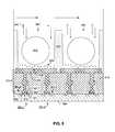
- FIG. 3illustrates a schematic diagram of a portion of the integrated circuit device 100 including sensor array 205 having multiple chemical sensors coupled to the same reaction region.
- sixteen chemical sensors and four reaction regionsare illustrated, representing a small section of the sensor array 205 and microwell array 107 that can include millions of chemical sensors and reaction regions.
- the integrated circuit device 100includes an access circuit for accessing the chemical sensors of the sensor array 205 .
- the access circuitincludes a row select circuit 310 coupled to the sensor array 205 via row lines 311 - 314 .
- the access circuitalso includes column output circuit 320 coupled to the sensor array 205 via column lines 321 - 328 .
- the row select circuit 310 and the column output circuit 320are responsive to timing and control signals provided by the array controller 124 in FIG. 1 to select the various chemical sensors and operate the sensor array 205 as described below.
- the array controller 124also provides a reference bias voltage to the reference electrode (See, FIG. 1 , reference numeral 108 ) to bias the reagents flowing across open ends of the reaction regions 380 , 382 , 384 , 386 of the microwell array 107 during operation.
- groups of four chemical sensorsare operationally associated with each of the reaction regions 380 , 382 , 384 , 386 .
- the number of chemical sensors operationally associated with a single reaction regionmay be different than four. More generally, two or more chemical sensors may be operationally associated with a single reaction region. In some embodiments, the number of chemical sensors operationally associated with a single reaction region may be greater than four, such as sixteen or more.
- the group containing chemical sensors 331 . 1 - 331 . 4is representative of the groups of sensors of the sensor array 205 .
- each chemical sensor 331 . 1 - 331 . 4includes a chemically-sensitive field effect transistor 341 . 1 - 341 . 5 and a row select switch 351 . 1 - 351 . 4 .
- the chemically-sensitive field effect transistors 341 . 1 - 341 . 4have a common floating gate 370 in communication with the reaction region 380 . That is, the common floating gate 370 is coupled to channels of each of the chemically-sensitive field effect transistors 341 . 1 - 341 . 5 .
- the chemically-sensitive field effect transistors 341 . 1 - 341 . 5may each include multiple patterned layers of conductive elements within layers of dielectric material.
- the common floating gate 370may for example include an uppermost conductive element (referred to herein as a sensor plate) that defines a surface (e.g. a bottom surface) of the reaction region 380 . That is, there is no intervening deposited material layer between the uppermost electrical conductor and the surface of the reaction region 380 .
- the uppermost conductive element of the common floating gate 370is separated from the reaction region 380 by a deposited sensing material (discussed in more detail below).
- reactants, wash solutions, and other reagentsmay move in and out of the reaction region 380 by a diffusion mechanism.
- the chemical sensors 331 . 1 - 331 . 4are each responsive to (and generate individual output signals related to) chemical reactions within the reaction region 380 to detect an analyte or reaction property of interest. Changes in the charge within the reaction region 380 cause changes in the voltage on the common floating gate 370 , which in turn changes the individual threshold voltages of each of the chemically-sensitive field effect transistors 341 . 1 - 341 . 4 of the sensors 331 . 1 - 331 . 4 .
- the row select circuit 310facilitates providing a bias voltage to row line 311 sufficient to turn on row select transistor 351 . 1 .
- Turning on the row select transistor 351 . 1couples the drain terminal of the chemically-sensitive transistor 341 . 1 to the column line 321 .
- the column output circuit 320facilitates providing a bias voltage to the column line 321 , and providing a bias current on the column line 321 that flows through the chemically-sensitive transistor 341 . 1 . This in turn establishes a voltage at the source terminal of the chemically-sensitive transistor 341 . 1 , which is coupled to the column line 322 .
- the voltage on the column line 322is based on the threshold voltage of the chemically-sensitive transistor 341 . 1 , and thus based on the amount of charge within the reaction region 380 .
- other techniquesmay be used to read the selected chemical sensor 331 . 1 .
- the column output circuit 320produces an individual output signal for the chemically-sensitive transistor 341 . 1 based on the voltage on the column line 322 .
- the column output circuit 320may include switches, sample and hold capacitors, current sources, buffers, and other circuitry used to operate and read the chemical sensors, depending upon the array configuration and read out technique.
- the column output circuit 320may include circuits such as those described in U.S. Patent Application Publication No. 2010/0300559, No. 2010/0197507, No. 2010/0301398, No. 2010/0300895, No. 2010/0137143, and No. 2009/0026082, and U.S. Pat. No. 7,575,865, which were incorporated by reference above.
- the individual output signals of the other chemical sensors 331 . 2 - 331 . 4 coupled to the reaction region 380can be read out in a similar fashion. In doing so, the column output circuit 320 produces individual output signals for each of the chemical sensors 331 . 1 - 331 . 4 .
- the individual output signals for each of the chemical sensors 331 . 1 - 331 . 4can then be combined or otherwise processed by the array controller 124 (or other data processor) to calculate a resultant, low noise output signal for the group of chemical sensors 331 . 1 - 331 . 4 .
- the resultant output signalmay be an average of the individual output signals.
- the SNR of the resultant output signalcan be increased by as much as the square root of the number of individual output signals.
- the resultant output signalcan compensate for differences among the values of the individual output signals, caused by variations in performance of the chemical sensors 331 . 1 - 331 . 4 which could otherwise complicate the downstream signal processing.
- FIG. 4is a flow chart of an example process for calculating a resultant output signal for a group of chemical sensors coupled to a single reaction region. Other embodiments may perform different or additional steps than the ones illustrated in FIG. 4 .
- FIG. 4will be described with reference to a system that performs a process. The system can be for example, the system of FIG. 1 .
- a chemical reactionis initiated within a reaction region coupled to a group of two or more chemical sensors.
- the group of chemical sensorsmay for example include respective chemically-sensitive field effect transistors having a common floating gate in communication with the reaction region, as described above with respect to FIG. 3 .
- the chemical reactionmay be a sequencing reaction, as described above.
- individual output signalsare obtained from the chemical sensors in the group.
- the individual output signalsmay for example be obtained by selecting and reading out the individual chemical sensors using the techniques described above.
- flowing of reagent(s)causes chemical reactions within the reaction region that release hydrogen ions, and the amplitude of the individual output signals from the chemical sensors is related to the amount of hydrogen ions detected.
- a resultant output signal for the groupis calculated based on one or more of the individual output signals.
- the resultant output signalmay for example be an average of the individual output signals. Alternatively, other techniques may be used to calculate the resultant output signal.
- a characteristic of the chemical reactionis determined based on the resultant output signal.
- the characteristic of the chemical reactionmay be determined based on the value of the resultant output signal using the techniques disclosed in Rearick et al., U.S. patent application Ser. No. 13/339,846, filed Dec. 29, 2011, based on U.S. Prov. Pat. Appl. Nos. 61/428,743, filed Dec. 30, 2010, and 61/429,328, filed Jan. 3, 2011, and in Hubbell, U.S. patent application Ser. No. 13/339,753, filed Dec. 29, 2011, based on U.S. Prov. Pat. Appl. No. 61/428,097, filed Dec. 29, 2010, each of which were incorporated by reference above.
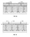
- FIG. 5illustrates a cross-sectional view of portions of two groups of chemical sensors and their corresponding reaction regions according to a first embodiment.
- the chemically-sensitive field effect transistors 341 . 1 , 341 . 2 of the chemical sensors 331 . 1 , 331 . 2 in the group of sensors 331 . 1 - 331 . 4 coupled to the reaction region 380are visible.
- the chemically-sensitive field effect transistors 341 . 3 , 341 . 4 of the other chemical sensors 331 . 3 , 331 . 4 in the grouplie behind this cross-section.
- the cross-section of FIG. 5shows the chemically-sensitive field effect transistors of two chemical sensors in the group of chemical sensors that is coupled to the adjacent reaction region 382 .
- the select switches of the chemical sensors, access lines and other connectionsare omitted for simplicity.
- the chemical sensor 331 . 1is representative of the group of chemical sensors 331 . 1 - 331 . 4 .
- the chemically-sensitive field effect transistor 341 . 1 of the chemical sensor 331 . 1is a chemically-sensitive field effect transistor (chemFET), more specifically an ion-sensitive field effect transistor (ISFET) in this example.
- chemFETchemically-sensitive field effect transistor
- ISFETion-sensitive field effect transistor
- the chemically-sensitive field effect transistor 341 . 1includes common floating gate 370 having a conductive element 520 coupled to the reaction region 380 .
- the conductive element 520is the uppermost floating gate conductor (also referred to herein as a sensor plate) in the common floating gate 370 .
- the common floating gate 370includes multiple patterned layers of conductive material within layers of dielectric material 519 .
- the conductive element 520electrically connects individual multi-layer floating gate structures that extend over the channel regions of each of the chemically-sensitive field effect transistors 341 . 1 - 341 . 4 of the group of chemical sensors 331 . 1 - 331 . 4 .
- the common floating gate 370is shared among the chemical sensors 331 . 1 - 331 . 4 .
- the chemically-sensitive field effect transistor 341 . 1includes a source region 521 and a drain region 522 within a semiconductor substrate 354 .
- the source region 521 and the drain region 522comprise doped semiconductor material having a conductivity type different from the conductivity type of the substrate 554 .
- the source region 521 and the drain region 522may comprise doped P-type semiconductor material, and the substrate may comprise doped N-type semiconductor material.
- the common floating gate 370includes a conductive element 551 separated from the channel region 523 by a gate dielectric 552 .
- the gate dielectric 552may be for example silicon dioxide. Alternatively, other dielectrics may be used for the gate dielectric 552 .
- the reaction region 380is within an opening extending through dielectric material 510 to the upper surface of the conductive element 520 .
- the dielectric material 510may comprise one or more layers of material, such as silicon dioxide or silicon nitride.
- the opening in the dielectric material 510may for example have a circular cross-section. Alternatively, the opening may be non-circular. For example, the cross-section may be square, rectangular, hexagonal, or irregularly shaped.
- the dimensions of the openings within the dielectric material 510 , and their pitch,can vary from embodiment to embodiment.
- the upper surface 530 of the conductive element 520is the bottom surface of the reaction region 380 . That is, there is no intervening deposited material layer between the upper surface 530 of the conductive element 520 and the reaction region 380 . As a result of this structure, the upper surface 530 of the conductive element 520 acts as the sensing surface for the group of chemical sensors 331 . 1 - 331 . 4 .
- the conductive element 520may comprise one or more of a variety of different materials to facilitate sensitivity to particular ions (e.g. hydrogen ions).
- a thin oxide of the electrically conductive material of the conductive element 520may be grown on the upper surface 530 which acts as a sensing material (e.g. an ion-sensitive sensing material) for the group of chemical sensors 331 . 1 - 331 . 4 .
- the conductive element 520may be titanium nitride, and titanium oxide or titanium oxynitride may be grown on the upper surface 530 during manufacturing and/or during exposure to solutions during use. Whether an oxide is formed depends on the conductive material, the manufacturing processes performed, and the conditions under which the device is operated.
- the conductive element 520is shown as a single layer of material. More generally, the conductive element 520 may comprise one or more layers of a variety of electrically conductive materials, such as metals or ceramics, depending upon the embodiment.
- the conductive materialcan be for example a metallic material or alloy thereof, or can be a ceramic material, or a combination thereof.
- An exemplary metallic materialincludes one of aluminum, copper, nickel, titanium, silver, gold, platinum, hafnium, lanthanum, tantalum, tungsten, iridium, zirconium, palladium, or a combination thereof.
- An exemplary ceramic materialincludes one of titanium nitride, titanium aluminum nitride, titanium oxynitride, tantalum nitride, or a combination thereof.
- an additional conformal sensing material(not shown) is deposited on the sidewall of the opening in the dielectric material 510 and on the upper surface 530 of the sensor plate 520 .
- an inner surface of the deposited sensing materialdefines the reaction region 380 .
- the sensing materialmay comprise one or more of a variety of different materials to facilitate sensitivity to particular ions.
- silicon nitride or silicon oxynitride, as well as metal oxides such as silicon oxide, aluminum or tantalum oxidesgenerally provide sensitivity to hydrogen ions
- sensing materials comprising polyvinyl chloride containing valinomycinprovide sensitivity to potassium ions.
- Materials sensitive to other ionssuch as sodium, silver, iron, bromine, iodine, calcium, and nitrate may also be used, depending upon the embodiment.
- reactants, wash solutions, and other reagentsmay move in and out of the reaction region 580 by a diffusion mechanism 540 .
- Each of the chemical sensors 331 . 1 - 331 . 4are responsive to (and generates an output signal related to) the amount of charge 524 proximate to the conductive element 520 .
- the presence of charge 524 in an analyte solutionalters the surface potential at the interface between the analyte solution and the conductive element 520 , due to the protonation or deprotonation of surface charge groups. Changes in the charge 524 cause changes in the voltage on the floating gate structure 518 , which in turn changes in the threshold voltages of the chemically-sensitive transistors 341 . 1 - 341 .
- each of the chemical sensors 331 . 1 - 331 . 4can be operated to provide individual current-based or voltage-based output signals on an array line connected to its corresponding source region or drain region.
- reactions carried out in the reaction region 380can be analytical reactions to identify or determine characteristics or properties of an analyte of interest. Such reactions can directly or indirectly generate byproducts that affect the amount of charge 524 adjacent to the conductive element 520 . If such byproducts are produced in small amounts or rapidly decay or react with other constituents, multiple copies of the same analyte may be analyzed in the reaction region 380 at the same time in order to increase the individual output signals generated by the group of chemical sensors 331 . 1 - 331 . 4 . In an embodiment, multiple copies of an analyte may be attached to a solid phase support 512 , either before or after deposition into the reaction region 380 .
- the solid phase support 512may be microparticles, nanoparticles, beads, solid or porous gels, or the like. For simplicity and ease of explanation, solid phase support 512 is also referred herein as a particle.
- a nucleic acid analytemultiple, connected copies may be made by rolling circle amplification (RCA), exponential RCA, Recombinase Polymerase Amplification (RPA), Polymerase Chain Reaction amplification (PCR), emulsion PCR amplification, or like techniques, to produce an amplicon without the need of a solid support.
- RCArolling circle amplification
- RPARecombinase Polymerase Amplification
- PCRPolymerase Chain Reaction amplification
- emulsion PCR amplificationor like techniques
- a nucleotide incorporation eventmay be determined by detecting ions (e.g., hydrogen ions) that are generated as natural by-products of polymerase-catalyzed nucleotide extension reactions. This may be used to sequence a sample or template nucleic acid, which may be a fragment of a nucleic acid sequence of interest, for example, and which may be directly or indirectly attached as a clonal population to a solid support, such as a particle, microparticle, bead, etc.
- ionse.g., hydrogen ions
- the sample or template nucleic acidmay be operably associated to a primer and polymerase and may be subjected to repeated cycles or “flows” of deoxynucleoside triphosphate (“dNTP”) addition (which may be referred to herein as “nucleotide flows” from which nucleotide incorporations may result) and washing.
- dNTPdeoxynucleoside triphosphate
- the primermay be annealed to the sample or template so that the primer's 3 ′ end can be extended by a polymerase whenever dNTPs complementary to the next base in the template are added.
- the identity of the type, sequence and number of nucleotide(s) associated with a sample nucleic acid present in a reaction region coupled to a group of chemical sensorscan be determined.
- FIGS. 6 to 10illustrate stages in a manufacturing process for forming a device including multiple chemical sensors coupled to the same reaction region according to a first embodiment.
- FIG. 6illustrates a structure 600 formed in a first stage.
- the structure 600includes partially completed floating gate structures for the field effect transistors of the chemical sensors.
- the structure 600includes partially completed floating gate structure 618 for the chemically-sensitive field effect transistor 341 . 1 of the chemical sensor 331 . 1 .
- the structure 600can be formed by depositing a layer of gate dielectric material on the semiconductor substrate 554 , and depositing a layer of polysilicon (or other electrically conductive material) on the layer of gate dielectric material.
- the layer of polysilicon and the layer gate dielectric materialcan then be etched using an etch mask to form the gate dielectric elements (e.g. gate dielectric 552 ) and the lowermost conductive material element (e.g. conductive element 551 ) of the floating gate structures.
- ion implantationcan then be performed to form the source and drain regions (e.g. source region 521 and a drain region 522 ) of the chemical sensors.
- a first layer of the dielectric material 519can then be deposited over the lowermost conductive material elements. Conductive plugs can then be formed within vias etched in the first layer of dielectric material 519 to contact the lowermost conductive material elements of the floating gate structures. A layer of conductive material can then be deposited on the first layer of the dielectric material 519 and patterned to form second conductive material elements electrically connected to the conductive plugs. This process can then be repeated multiple times to form the partially completed floating gate structures shown in FIG. 6 . Alternatively, other and/or additional techniques may be performed to form the structure.
- Forming the structure 600 in FIG. 6can also include forming additional elements such as array lines (e.g. row lines, column lines, etc.) for accessing the chemical sensors, additional doped regions in the substrate 554 , and other circuitry (e.g. select switches, access circuitry, bias circuitry etc.) used to operate the chemical sensors, depending upon the device and array configuration in which the chemical sensors are implemented.
- array linese.g. row lines, column lines, etc.
- additional doped regions in the substrate 554e.g. select switches, access circuitry, bias circuitry etc.
- conductive material 700is formed on the structure illustrated in FIG. 6 to contact the partially completed floating gate structures.
- An etch mask including mask elements 720 , 722is then formed on the conductive material 700 , resulting in the structure illustrated in FIG. 7 .
- the conductive material 700includes one or more layers of electrically conductive material.
- the conductive material 700may include a layer of titanium nitride formed on a layer of aluminum, or a layer of titanium nitride formed on a layer of copper.
- the number of layersmay be different than two, and other and/or additional conductive materials may be used.
- Examples of conductive materials that can be used in some embodimentsinclude tantalum, aluminum, lanthanum, titanium, zirconium, hafnium, tungsten, palladium, iridium, etc., and combinations thereof.
- the locations of the mask elements 720 , 722define the locations of the sensor plates for the chemically-sensitive field effect transistors of the corresponding groups of chemical sensors.
- the mask elements 720 , 722comprise photoresist material which has been patterned using a lithographic process. Alternatively, other techniques and materials may be used.
- the conductive material 700is etched using the mask elements 700 , 722 as a mask, resulting in the structure illustrated in FIG. 8 .
- the etching processforms conductive elements 520 , 810 in electrical contact with the partially completed floating gate structures of a corresponding group of sensors.
- the conductive element 520electrically connects the partially completed floating gate structures for a group of sensors 331 . 1 - 331 . 4 , to complete the common floating gate 370 for this group of sensors.
- the conductive material element 810completes the common floating gate for the adjacent group of sensors.
- the dielectric material 510may comprise one or more layers of deposited dielectric material, such as silicon dioxide or silicon nitride.
- the dielectric material 510is etched to form openings defining reaction regions 380 , 382 extending to upper surfaces of the conductive material elements 520 , 810 , resulting in the structure illustrated in FIG. 10 .
- FIG. 11illustrates a cross-sectional view of portions of two groups of chemical sensors and their corresponding reaction regions according to a second embodiment.
- the common floating gate for each group of chemical sensorsincludes a sensor plate that is smaller than the bottom surface of the corresponding reaction region.
- the floating gate structure 1118 for the group of chemical sensors 331 . 1 - 331 . 4includes conductive element 1120 coupled to the reaction region 380 .
- the conductive element 1120is coupled to the conductive element 520 by conductive plug 1130 .
- the conductive element 1120is the uppermost floating gate conductor in the floating gate structure 1118 , and thus acts as the sensor plate for the group of chemical sensors 331 . 1 - 331 . 4 .
- an upper surface 1122 of the conductive element 1120is a portion of the bottom surface of the reaction region 380 . That is, there is no intervening deposited material layer between the upper surface 1122 of the conductive element 1120 and the reaction region 380 .
- the upper surface 1122 of the conductive element 1120acts as the sensing surface for the group of chemical sensors 331 . 1 - 331 . 4 .
- the conductive element 1120is within the dielectric material 1160 , such that the upper surface 1122 of the conductive element 1120 is co-planar with the upper surface of the dielectric material 1160 .
- the conductive element 1120may be formed on the upper surface of dielectric material 1160 , and thus protrude slightly into the reaction region 380 .
- the upper surface 1122 of the conductive element 1120has a width 1125 that is the less than the width of the bottom surface of the reaction region 380 .
- SNRsignal-to-noise ratio
- the amplitude of the desired signal detected by the chemical sensors 331 . 1 - 331 . 4 in response to the charge 524 in an analyte solutionis a superposition of the charge concentration along the interface between the conductive element 1120 and the analyte solution. Because the charge 524 is more highly concentrated at the bottom and middle of the reaction region 380 , the width 1125 of the conductive element 1120 is a tradeoff between the amplitude of the desired signal detected in response to the charge 524 , and the fluidic noise due to random fluctuation between the conductive element 1120 and the analyte solution. Increasing the width 1125 of the conductive element 1120 increases the fluidic interface area for the chemical sensors 331 . 1 - 331 .
- the conductive element 1120detects a greater proportion of the signal from areas having lower charge concentration, which can reduce the overall amplitude of the detected signal.
- decreasing the width 1122 of the conductive element 1120reduces the sensing surface area and thus increases the fluidic noise, but also increases the overall amplitude of the detected signal.
- the optimal width 1125can vary from embodiment to embodiment depending on the material characteristics of the conductive element 1120 and the dielectric materials 510 , 1160 , the volume, shape, aspect ratio (such as base width-to-well depth ratio), and other dimensional characteristics of the reaction regions, the nature of the reaction taking place, as well as the reagents, byproducts, or labeling techniques (if any) that are employed.
- the optimal widthmay for example be determined empirically.
- FIGS. 12 to 14illustrate stages in a manufacturing process for forming a device including multiple chemical sensors coupled to the same reaction region according to a second embodiment.
- FIG. 12illustrates a first stage of forming conductive plugs 1210 , 1220 extending through dielectric material 1200 to contact the conductive elements 520 , 810 of the structure illustrated in FIG. 8 .
- the structure in FIG. 12can be formed by removing the mask elements 720 , 722 in FIG. 8 and forming dielectric material 1200 on the resulting structure. Vias can then be etched through the dielectric material 1200 , and metal deposited within the vias. A planarization process (e.g. chemical mechanical polishing) can then be performed to remove the deposited metal from the upper surface of the dielectric material 1200 and form the plugs 1210 , 1220 . Alternatively, other techniques may be used.
- a planarization processe.g. chemical mechanical polishing
- conductive material 1300is formed on the structure illustrated in FIG. 12 .
- An etch mask including mask elements 1320 , 1322is then formed on the conductive material 1300 , resulting in the structure illustrated in FIG. 13 .
- the conductive material 1300may comprise one or more layers of conductive material, such as those described above with respect the conductive material 700 of FIG. 7 .
- the locations of the mask elements 1320 , 1322define the locations of the sensor plates of the field effect transistors of the corresponding groups of chemical sensors.
- the mask elements 1320 , 1322comprise photoresist material which has been patterned using a lithographic process. Alternatively, other techniques and materials may be used.
- the conductive material 1300is etched using the mask elements 1320 , 1322 as a mask to form the conductive elements 1120 , 1400 .
- Dielectric material 1160is then formed between the conductive elements 1120 , 1400 , resulting in the structure illustrated in FIG. 14 .
- dielectric material 510is formed on the structure illustrated in FIG. 14 .
- the dielectric material 510is then be etched to form openings defining reaction regions 380 , 382 extending to upper surfaces of the conductive elements 1120 , 1400 , resulting in the structure illustrated in FIG. 11 .
- the dielectric material 1160may comprise material different than that of dielectric material 510 .
- the dielectric material 510may comprise material (e.g. silicon oxide) which can be selectively etched relative to the material (e.g. silicon nitride) of the dielectric material 1160 when subjected to a chosen etch process.
- the dielectric material 1160can act as an etch stop during the etching process used to form the reaction regions 380 , 382 . In doing so, the dielectric material 1160 can prevent etching past the conductive elements 1120 , 1400 , and thus can define and maintain the desired shape of the reaction regions 380 , 382 .
- FIGS. 15 to 18illustrate stages in a manufacturing process for forming a device including multiple chemical sensors coupled to the same reaction region according to a third embodiment.
- FIG. 15illustrates a first stage of forming dielectric material 1160 on the structure illustrated in FIG. 12 .
- An etch mask including mask elements 1510 , 1520 , 1530is then formed on the dielectric material 1160 , resulting in the structure illustrated in FIG. 15 .
- openings between the mask elements 1510 , 1520 , 1530define the locations of the sensor plates of the field effect transistors of the corresponding groups of chemical sensors.
- the dielectric material 1160is etched using the mask elements 1510 , 1520 , 1530 as an etch mask to form openings 1610 , 1620 within the dielectric material 1160 , resulting in the structure illustrated in FIG. 16 . As shown in FIG. 16 , the openings extend to the upper surfaces of the conductive plugs 1210 , 1220 .
- the conductive material 1800may comprise one or more layers of conductive material, such as those described above with respect the conductive material 700 of FIG. 7 .
- a planarization process(e.g. CMP) is performed to remove the conductive material 1800 from the upper surface of the dielectric material 1160 , resulting in the structure illustrated in FIG. 18 .
- the planarization processleaves remaining conductive material within the openings 1610 , 1620 to form the conductive elements 1120 , 1400 .
- dielectric material 510is formed on the structure illustrated in FIG. 18 .
- the dielectric material 510can then be etched to form openings defining reaction regions 380 , 382 extending to upper surfaces of the conductive elements 1120 , 1400 , resulting in the structure illustrated in FIG. 11 .
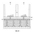
- FIGS. 19 to 21illustrate stages in a manufacturing process for forming a device including multiple chemical sensors coupled to the same reaction region according to a fourth embodiment.
- FIG. 19illustrates a first stage of forming conductive plugs 1210 , 1220 extending through dielectric material 1900 to contact the conductive elements 520 , 810 of the structure illustrated in FIG. 8 .
- the dielectric material 1900comprising one or more layers of dielectric material, acts an etch stop during the subsequent formation of the reaction regions 380 , 382 .
- the structure in FIG. 19can be formed by removing the mask elements 720 , 722 illustrated in FIG. 8 and forming the dielectric material 1900 on the resulting structure.
- the plugs 1210 , 1220can then be formed using the techniques described above with reference to FIG. 12 . Alternatively, other techniques may be used.
- conductive elements 1120 , 1400are formed on the upper surface of the dielectric material 1900 , resulting in the structure illustrated in FIG. 20 .
- the conductive elements 1120 , 1400may be formed by depositing conductive material, forming an etch mask including mask elements defining the locations of the conductive elements 1120 , 1400 , and etching the conductive material using the mask elements as an etch mask.
- dielectric material 510is formed on the structure illustrated in FIG. 20 .
- the dielectric material 510is then be etched to form openings defining reaction regions 380 , 382 extending to upper surfaces of the conductive elements 1120 , 1400 , resulting in the structure illustrated in FIG. 21 .
- the reaction regions 380 , 382extend below the upper surfaces of the conductive elements 1120 , 1400 to expose their side surfaces.
- the dielectric material 1900may comprise material different than that of dielectric material 510 .
- the dielectric material 510may comprise material (e.g. silicon oxide) which can be selectively etched relative to the material (e.g. silicon nitride) of the dielectric material 1900 when subjected to a chosen etch process.
- the dielectric material 1900can act as an etch stop during the etching process used to form the reaction regions 380 , 382 . In doing so, the dielectric material 1900 can prevent etching below the conductive elements 1120 , 1400 , and thus can define and maintain the shape of the reaction regions 380 , 382 .
- Various embodimentsmay be implemented using hardware elements, software elements, or a combination of both.
- hardware elementsmay include processors, microprocessors, circuits, circuit elements (e.g., transistors, resistors, capacitors, inductors, and so forth), integrated circuits, application specific integrated circuits (ASIC), programmable logic devices (PLD), digital signal processors (DSP), field programmable gate array (FPGA), logic gates, registers, semiconductor device, chips, microchips, chip sets, and so forth.
- Examples of softwaremay include software components, programs, applications, computer programs, application programs, system programs, machine programs, operating system software, middleware, firmware, software modules, routines, subroutines, functions, methods, procedures, software interfaces, application program interfaces (API), instruction sets, computing code, computer code, code segments, computer code segments, words, values, symbols, or any combination thereof. Determining whether an embodiment is implemented using hardware elements and/or software elements may vary in accordance with any number of factors, such as desired computational rate, power levels, heat tolerances, processing cycle budget, input data rates, output data rates, memory resources, data bus speeds and other design or performance constraints.
- Some embodimentsmay be implemented, for example, using a computer-readable medium or article which may store an instruction or a set of instructions that, if executed by a machine, may cause the machine to perform a method and/or operations in accordance with the embodiments.
- a machinemay include, for example, any suitable processing platform, computing platform, computing device, processing device, computing system, processing system, computer, processor, or the like, and may be implemented using any suitable combination of hardware and/or software.
- the computer-readable medium or articlemay include, for example, any suitable type of memory unit, memory device, memory article, memory medium, storage device, storage article, storage medium and/or storage unit, for example, memory, removable or non-removable media, erasable or non-erasable media, writeable or re-writeable media, digital or analog media, hard disk, floppy disk, read-only memory compact disc (CD-ROM), recordable compact disc (CD-R), rewriteable compact disc (CD-RW), optical disk, magnetic media, magneto-optical media, removable memory cards or disks, various types of Digital Versatile Disc (DVD), a tape, a cassette, or the like.
- any suitable type of memory unitfor example, memory, removable or non-removable media, erasable or non-erasable media, writeable or re-writeable media, digital or analog media, hard disk, floppy disk, read-only memory compact disc (CD-ROM), recordable compact disc (CD-R), rewriteable compact disc (CD
- the instructionsmay include any suitable type of code, such as source code, compiled code, interpreted code, executable code, static code, dynamic code, encrypted code, and the like, implemented using any suitable high-level, low-level, object-oriented, visual, compiled and/or interpreted programming language.
Landscapes
- Life Sciences & Earth Sciences (AREA)
- Chemical & Material Sciences (AREA)
- Health & Medical Sciences (AREA)
- Molecular Biology (AREA)
- Engineering & Computer Science (AREA)
- Physics & Mathematics (AREA)
- Proteomics, Peptides & Aminoacids (AREA)
- Immunology (AREA)
- Analytical Chemistry (AREA)
- Biochemistry (AREA)
- General Health & Medical Sciences (AREA)
- Organic Chemistry (AREA)
- Pathology (AREA)
- Microelectronics & Electronic Packaging (AREA)
- Electrochemistry (AREA)
- General Physics & Mathematics (AREA)
- Chemical Kinetics & Catalysis (AREA)
- Zoology (AREA)
- Wood Science & Technology (AREA)
- Biotechnology (AREA)
- Microbiology (AREA)
- Biophysics (AREA)
- Spectroscopy & Molecular Physics (AREA)
- Bioinformatics & Cheminformatics (AREA)
- General Engineering & Computer Science (AREA)
- Genetics & Genomics (AREA)
- Investigating Or Analyzing Materials By The Use Of Electric Means (AREA)
- Apparatus Associated With Microorganisms And Enzymes (AREA)
Abstract
Description
Claims (16)
Priority Applications (4)
| Application Number | Priority Date | Filing Date | Title |
|---|---|---|---|
| US14/293,247US10458942B2 (en) | 2013-06-10 | 2014-06-02 | Chemical sensor array having multiple sensors per well |
| US16/663,052US10816504B2 (en) | 2013-06-10 | 2019-10-24 | Chemical sensor array having multiple sensors per well |
| US17/070,142US11499938B2 (en) | 2013-06-10 | 2020-10-14 | Chemical sensor array having multiple sensors per well |
| US18/045,106US11774401B2 (en) | 2013-06-10 | 2022-10-07 | Chemical sensor array having multiple sensors per well |
Applications Claiming Priority (2)
| Application Number | Priority Date | Filing Date | Title |
|---|---|---|---|
| US201361833375P | 2013-06-10 | 2013-06-10 | |
| US14/293,247US10458942B2 (en) | 2013-06-10 | 2014-06-02 | Chemical sensor array having multiple sensors per well |
Related Child Applications (1)
| Application Number | Title | Priority Date | Filing Date |
|---|---|---|---|
| US16/663,052DivisionUS10816504B2 (en) | 2013-06-10 | 2019-10-24 | Chemical sensor array having multiple sensors per well |
Publications (2)
| Publication Number | Publication Date |
|---|---|
| US20140364320A1 US20140364320A1 (en) | 2014-12-11 |
| US10458942B2true US10458942B2 (en) | 2019-10-29 |
Family
ID=51023193
Family Applications (4)
| Application Number | Title | Priority Date | Filing Date |
|---|---|---|---|
| US14/293,247ActiveUS10458942B2 (en) | 2013-06-10 | 2014-06-02 | Chemical sensor array having multiple sensors per well |
| US16/663,052ActiveUS10816504B2 (en) | 2013-06-10 | 2019-10-24 | Chemical sensor array having multiple sensors per well |
| US17/070,142Active2034-12-25US11499938B2 (en) | 2013-06-10 | 2020-10-14 | Chemical sensor array having multiple sensors per well |
| US18/045,106ActiveUS11774401B2 (en) | 2013-06-10 | 2022-10-07 | Chemical sensor array having multiple sensors per well |
Family Applications After (3)
| Application Number | Title | Priority Date | Filing Date |
|---|---|---|---|
| US16/663,052ActiveUS10816504B2 (en) | 2013-06-10 | 2019-10-24 | Chemical sensor array having multiple sensors per well |
| US17/070,142Active2034-12-25US11499938B2 (en) | 2013-06-10 | 2020-10-14 | Chemical sensor array having multiple sensors per well |
| US18/045,106ActiveUS11774401B2 (en) | 2013-06-10 | 2022-10-07 | Chemical sensor array having multiple sensors per well |
Country Status (4)
| Country | Link |
|---|---|
| US (4) | US10458942B2 (en) |
| EP (2) | EP3008461B1 (en) |
| CN (2) | CN105452856B (en) |
| WO (1) | WO2014200775A1 (en) |
Families Citing this family (16)
| Publication number | Priority date | Publication date | Assignee | Title |
|---|---|---|---|---|
| US8262900B2 (en)* | 2006-12-14 | 2012-09-11 | Life Technologies Corporation | Methods and apparatus for measuring analytes using large scale FET arrays |
| CA2672315A1 (en) | 2006-12-14 | 2008-06-26 | Ion Torrent Systems Incorporated | Methods and apparatus for measuring analytes using large scale fet arrays |
| US11339430B2 (en) | 2007-07-10 | 2022-05-24 | Life Technologies Corporation | Methods and apparatus for measuring analytes using large scale FET arrays |
| US20100301398A1 (en) | 2009-05-29 | 2010-12-02 | Ion Torrent Systems Incorporated | Methods and apparatus for measuring analytes |
| JP2013540259A (en) | 2010-06-30 | 2013-10-31 | ライフ テクノロジーズ コーポレーション | Array column integrator |
| WO2012003363A1 (en) | 2010-06-30 | 2012-01-05 | Life Technologies Corporation | Ion-sensing charge-accumulation circuits and methods |
| EP2972280B1 (en) | 2013-03-15 | 2021-09-29 | Life Technologies Corporation | Chemical sensor with consistent sensor surface areas |
| US20150097214A1 (en)* | 2013-10-09 | 2015-04-09 | Taiwan Semiconductor Manufacturing Company Limited | Structures, apparatuses and methods for fabricating sensors in multi-layer structures |
| CN107407656B (en)* | 2014-12-18 | 2020-04-07 | 生命科技公司 | Method and apparatus for measuring analytes using large scale FET arrays |
| KR102593647B1 (en)* | 2014-12-18 | 2023-10-26 | 라이프 테크놀로지스 코포레이션 | High data rate integrated circuit with transmitter configuration |
| US10077472B2 (en) | 2014-12-18 | 2018-09-18 | Life Technologies Corporation | High data rate integrated circuit with power management |
| CN107090404B (en)* | 2017-04-21 | 2019-08-13 | 京东方科技集团股份有限公司 | A kind of gene sequencing chip and gene order surveying method, gene sequencing device |
| CN107884460B (en)* | 2017-10-19 | 2020-10-23 | 中国科学院半导体研究所 | Method for manufacturing ISFET device sensitive film based on standard CMOS process |
| US20210033563A1 (en)* | 2018-09-13 | 2021-02-04 | Chun-Lung LIEN | Nucleotide sequencing element and chip, and sequencing analysis method |
| CN112986357A (en)* | 2019-12-13 | 2021-06-18 | 成都今是科技有限公司 | Microelectrode of gene sequencing chip, preparation method thereof and gene sequencing chip |
| WO2025024598A1 (en)* | 2023-07-24 | 2025-01-30 | The Regents Of The University Of California | Biomarker detection using graphene field effect transistor sensor arrays and multichannel data acquisition |
Citations (492)
| Publication number | Priority date | Publication date | Assignee | Title |
|---|---|---|---|---|
| US4086642A (en) | 1975-01-16 | 1978-04-25 | Hitachi, Ltd. | Protective circuit and device for metal-oxide-semiconductor field effect transistor and method for fabricating the device |
| JPS5870155A (en) | 1981-07-24 | 1983-04-26 | フオンダシヨン・スイス・プ−ル・ラ・レシエルシユ・アン・ミクロテクニク | Semiconductor device responding to ion |
| US4411741A (en) | 1982-01-12 | 1983-10-25 | University Of Utah | Apparatus and method for measuring the concentration of components in fluids |
| US4437969A (en) | 1981-04-09 | 1984-03-20 | Corning Glass Works | Offset-gate chemical-sensitive field-effect transistors (OG-CHEMFETS) with electrolytically-programmable selectivity |
| US4438354A (en) | 1981-08-14 | 1984-03-20 | American Microsystems, Incorporated | Monolithic programmable gain-integrator stage |
| US4444644A (en) | 1981-02-17 | 1984-04-24 | Sumitomo Electric Industries, Ltd. | PH Electrode |
| US4490678A (en) | 1981-05-15 | 1984-12-25 | Licentia Patent-Verwaltungs-G.M.B.H. | Method of and an apparatus for measuring ion concentrations in solutions |
| US4641084A (en) | 1983-12-15 | 1987-02-03 | Olympus Optical Co., Ltd. | Ion concentration measuring apparatus |
| US4660063A (en) | 1985-03-18 | 1987-04-21 | General Electric Company | Immersion type ISFET |
| EP0223618A2 (en) | 1985-07-18 | 1987-05-27 | New York Medical College | Automatable process for nucleotide sequencing |
| US4691167A (en) | 1983-08-24 | 1987-09-01 | Sentron V.O.F. | Apparatus for determining the activity of an ion (pIon) in a liquid |
| JPS62237349A (en) | 1986-04-08 | 1987-10-17 | Nec Corp | Instrument for measuring distribution of hydrogen ion concentration |
| US4701253A (en) | 1983-11-03 | 1987-10-20 | Sentron V.O.F. | ISFET-based measuring device and method for correcting drift |
| US4722830A (en) | 1986-05-05 | 1988-02-02 | General Electric Company | Automated multiple stream analysis system |
| US4743954A (en) | 1985-06-07 | 1988-05-10 | University Of Utah | Integrated circuit for a chemical-selective sensor with voltage output |
| US4764797A (en) | 1985-09-14 | 1988-08-16 | Thorn Emi Plc | Chemical-sensitive semiconductor device |
| US4777019A (en) | 1985-04-12 | 1988-10-11 | Thomas Dandekar | Biosensor |
| US4822566A (en) | 1985-11-19 | 1989-04-18 | The Johns Hopkins University | Optimized capacitive sensor for chemical analysis and measurement |
| US4864229A (en) | 1986-05-03 | 1989-09-05 | Integrated Ionics, Inc. | Method and apparatus for testing chemical and ionic sensors |
| WO1989009283A1 (en) | 1988-03-25 | 1989-10-05 | Edward David Hyman | Pyrophosphate-based method and apparatus for sequencing nucleic acids |
| US4874499A (en) | 1988-05-23 | 1989-10-17 | Massachusetts Institute Of Technology | Electrochemical microsensors and method of making such sensors |
| US4893088A (en) | 1988-11-16 | 1990-01-09 | Harris Corporation | Transimpedance focal plane processor |
| US4927736A (en) | 1987-07-21 | 1990-05-22 | Hoechst Celanese Corporation | Hydroxy polyimides and high temperature positive photoresists therefrom |
| WO1990005910A1 (en) | 1988-11-14 | 1990-05-31 | I Stat Corp | Wholly microfabricated biosensors and process for the manufacture and use thereof |
| JPH02250331A (en) | 1989-03-24 | 1990-10-08 | Hitachi Ltd | Semiconductor device and its manufacture |
| JPH02310931A (en) | 1989-05-25 | 1990-12-26 | Mitsubishi Electric Corp | Semiconductor device and its manufacturing method |
| US5009766A (en) | 1988-02-08 | 1991-04-23 | I-Stat Corporation | Metal oxide electrodes |
| JPH03122558A (en) | 1989-10-04 | 1991-05-24 | Olympus Optical Co Ltd | Sensor structure and manufacture thereof |
| US5038192A (en) | 1989-04-28 | 1991-08-06 | International Business Machines Corporation | Gate array cell having FETs of different and optimized sizes |
| US5110441A (en) | 1989-12-14 | 1992-05-05 | Monsanto Company | Solid state ph sensor |
| US5113870A (en) | 1987-05-01 | 1992-05-19 | Rossenfeld Joel P | Method and apparatus for the analysis, display and classification of event related potentials by interpretation of P3 responses |
| US5126759A (en) | 1990-06-26 | 1992-06-30 | Eastman Kodak Company | Non-impact printer with token bit control of data and current regulation signals |
| US5140393A (en) | 1985-10-08 | 1992-08-18 | Sharp Kabushiki Kaisha | Sensor device |
| US5142236A (en) | 1989-10-16 | 1992-08-25 | Marelli Autronica Spa | Switched-capacitor circuit having a full-wave-rectifying and integrating function |
| US5151587A (en) | 1990-01-10 | 1992-09-29 | Seiko Instruments Inc. | Image sensor having an array of operative and dummy bipolar transistors and pairs of pixel selecting switches connected thereto |
| US5151759A (en) | 1989-03-02 | 1992-09-29 | Thunderbird Technologies, Inc. | Fermi threshold silicon-on-insulator field effect transistor |
| US5164319A (en) | 1985-08-22 | 1992-11-17 | Molecular Devices Corporation | Multiple chemically modulated capacitance determination |
| JPH0580115A (en) | 1991-09-19 | 1993-04-02 | Fujitsu Ltd | Nonvolatile random access memory device and method of detecting floating gate voltage level in nonvolatile random access memory device |
| US5202576A (en) | 1990-08-29 | 1993-04-13 | Texas Instruments Incorporated | Asymmetrical non-volatile memory cell, arrays and methods for fabricating same |
| US5284566A (en) | 1993-01-04 | 1994-02-08 | Bacharach, Inc. | Electrochemical gas sensor with wraparound reference electrode |
| US5317407A (en) | 1991-03-11 | 1994-05-31 | General Electric Company | Fixed-pattern noise correction circuitry for solid-state imager |
| US5319226A (en) | 1991-09-06 | 1994-06-07 | Dong Jin Kim | Method of fabricating an ion sensitive field effect transistor with a Ta2 O5 hydrogen ion sensing membrane |
| US5407854A (en) | 1994-01-19 | 1995-04-18 | General Signal Corporation | ESD protection of ISFET sensors |
| US5436149A (en) | 1993-02-19 | 1995-07-25 | Barnes; Wayne M. | Thermostable DNA polymerase with enhanced thermostability and enhanced length and efficiency of primer extension |
| US5439839A (en) | 1994-07-13 | 1995-08-08 | Winbond Electronics Corporation | Self-aligned source/drain MOS process |
| DE4430811C1 (en) | 1994-08-30 | 1995-09-07 | Fraunhofer Ges Forschung | Ion-sensitive FET prodn., useful for mfg. integrated liq. sensor circuit |
| US5466348A (en) | 1991-10-21 | 1995-11-14 | Holm-Kennedy; James W. | Methods and devices for enhanced biochemical sensing |
| US5475337A (en) | 1992-07-24 | 1995-12-12 | Nec Corporation | Switched capacitor amplifier circuit |
| US5490971A (en) | 1994-10-25 | 1996-02-13 | Sippican, Inc. | Chemical detector |
| DE19512117A1 (en) | 1995-04-04 | 1996-10-10 | Itt Ind Gmbh Deutsche | Measuring device |
| US5583462A (en) | 1993-04-26 | 1996-12-10 | Unifet Incorporated | Method and apparatus for multiplexing devices having long thermal time constants |
| US5587894A (en) | 1994-03-28 | 1996-12-24 | Matsushita Electric Works, Ltd. | Power source device |
| US5593838A (en) | 1994-11-10 | 1997-01-14 | David Sarnoff Research Center, Inc. | Partitioned microelectronic device array |
| US5600451A (en) | 1993-08-12 | 1997-02-04 | Sony Corporation | Charge transfer device and output circuit thereof |
| US5627403A (en) | 1993-05-31 | 1997-05-06 | Sgs-Thomson Microelectronics S.R.L. | Adhesion between dielectric layers in an integrated circuit |
| US5631704A (en) | 1994-10-14 | 1997-05-20 | Lucent Technologies, Inc. | Active pixel sensor and imaging system having differential mode |
| US5637469A (en) | 1992-05-01 | 1997-06-10 | Trustees Of The University Of Pennsylvania | Methods and apparatus for the detection of an analyte utilizing mesoscale flow systems |
| US5646558A (en) | 1995-09-27 | 1997-07-08 | Intel Corporation | Plurality of distinct multiplexers that operate as a single multiplexer |
| US5702964A (en) | 1995-10-17 | 1997-12-30 | Lg Semicon, Co., Ltd. | Method for forming a semiconductor device having a floating gate |
| JPH1078827A (en) | 1996-09-02 | 1998-03-24 | Yokogawa Electric Corp | IC start circuit |
| WO1998013523A1 (en) | 1996-09-27 | 1998-04-02 | Pyrosequencing Ab | Method of sequencing dna |
| US5793230A (en) | 1997-02-26 | 1998-08-11 | Sandia Corporation | Sensor readout detector circuit |
| WO1998046797A1 (en) | 1997-04-16 | 1998-10-22 | Immunological Associates Of Denver | Nucleic acid archiving |
| US5846708A (en) | 1991-11-19 | 1998-12-08 | Massachusetts Institiute Of Technology | Optical and electrical methods and apparatus for molecule detection |
| US5894284A (en) | 1996-12-02 | 1999-04-13 | Motorola, Inc. | Common-mode output sensing circuit |
| US5907765A (en) | 1995-06-30 | 1999-05-25 | Motorola, Inc. | Method for forming a semiconductor sensor device |
| US5912560A (en) | 1997-02-25 | 1999-06-15 | Waferscale Integration Inc. | Charge pump circuit for voltage boosting in integrated semiconductor circuits |
| US5911873A (en) | 1997-05-02 | 1999-06-15 | Rosemount Analytical Inc. | Apparatus and method for operating an ISFET at multiple drain currents and gate-source voltages allowing for diagnostics and control of isopotential points |
| US5922591A (en) | 1995-06-29 | 1999-07-13 | Affymetrix, Inc. | Integrated nucleic acid diagnostic device |
| US5923421A (en) | 1997-07-24 | 1999-07-13 | Lockheed Martin Energy Research Corporation | Chemical detection using calorimetric spectroscopy |
| US5944970A (en) | 1997-04-29 | 1999-08-31 | Honeywell Inc. | Solid state electrochemical sensors |
| US5958703A (en) | 1996-12-03 | 1999-09-28 | Glaxo Group Limited | Use of modified tethers in screening compound libraries |
| US5965452A (en) | 1996-07-09 | 1999-10-12 | Nanogen, Inc. | Multiplexed active biologic array |
| US6002299A (en) | 1997-06-10 | 1999-12-14 | Cirrus Logic, Inc. | High-order multipath operational amplifier with dynamic offset reduction, controlled saturation current limiting, and current feedback for enhanced conditional stability |
| US6021172A (en) | 1994-01-28 | 2000-02-01 | California Institute Of Technology | Active pixel sensor having intra-pixel charge transfer with analog-to-digital converter |
| JP2000055874A (en) | 1998-08-03 | 2000-02-25 | Horiba Ltd | Isfet array |
| US6107032A (en) | 1996-12-20 | 2000-08-22 | Roche Diagnostics Gmbh | Method for the direct, exponential amplification and sequencing of DNA molecules and its application |
| US6191444B1 (en) | 1998-09-03 | 2001-02-20 | Micron Technology, Inc. | Mini flash process and circuit |
| US6195585B1 (en) | 1998-06-26 | 2001-02-27 | Advanced Bionics Corporation | Remote monitoring of implantable cochlear stimulator |
| WO2001020039A2 (en) | 1999-09-16 | 2001-03-22 | Curagen Corporation | Method of sequencing a nucleic acid |
| WO2001042498A1 (en) | 1999-12-10 | 2001-06-14 | Toyo Boseki Kabushiki Kaisha | Method of detecting nucleotide polymorphism |
| US6255678B1 (en) | 1997-05-29 | 2001-07-03 | Horiba, Ltd. | Apparatus for measuring physical and chemical phenomena |
| WO2001047804A1 (en) | 1999-12-28 | 2001-07-05 | Merck Patent Gmbh | Method for producing high-purity sulphuric acid |
| US6262568B1 (en) | 1999-12-14 | 2001-07-17 | Matsushita Electric Industrial Co., Ltd. | Common mode bias generator |
| US6275061B1 (en) | 1998-09-25 | 2001-08-14 | Kabushiki Kaisha Toshiba | Testing method for a substrate of active matrix display panel |
| US6294133B1 (en) | 1998-01-14 | 2001-09-25 | Horiba, Ltd. | Multiple detecting apparatus for physical phenomenon and/or chemical phenomenon |
| US20010024790A1 (en) | 2000-03-17 | 2001-09-27 | Hitachi, Ltd. | DNA base sequencing system |
| WO2001081896A1 (en) | 2000-04-24 | 2001-11-01 | Eagle Research & Development, Llc | An ultra-fast nucleic acid sequencing device and a method for making and using the same |
| US6327410B1 (en) | 1997-03-14 | 2001-12-04 | The Trustees Of Tufts College | Target analyte sensors utilizing Microspheres |
| US20020001801A1 (en) | 2000-02-16 | 2002-01-03 | Jian-Bing Fan | Parallel genotyping of multiple patient samples |
| US20020012930A1 (en) | 1999-09-16 | 2002-01-31 | Rothberg Jonathan M. | Method of sequencing a nucleic acid |
| US20020012937A1 (en) | 2000-06-23 | 2002-01-31 | Tender Leonard M. | Microelectronic device and method for label-free detection and quantification of biological and chemical molecules |
| US6353324B1 (en) | 1998-11-06 | 2002-03-05 | Bridge Semiconductor Corporation | Electronic circuit |
| US6355431B1 (en) | 1999-04-20 | 2002-03-12 | Illumina, Inc. | Detection of nucleic acid amplification reactions using bead arrays |
| US6361671B1 (en) | 1999-01-11 | 2002-03-26 | The Regents Of The University Of California | Microfabricated capillary electrophoresis chip and method for simultaneously detecting multiple redox labels |
| US20020042059A1 (en) | 1997-03-05 | 2002-04-11 | The Regents Of The University Of Michigan | Compositions and methods for analysis of nucleic acids |
| US20020042388A1 (en) | 2001-05-01 | 2002-04-11 | Cooper Mark J. | Lyophilizable and enhanced compacted nucleic acids |
| US6372291B1 (en) | 1999-12-23 | 2002-04-16 | Applied Materials, Inc. | In situ deposition and integration of silicon nitride in a high density plasma reactor |
| US6376256B1 (en) | 1996-08-21 | 2002-04-23 | Smithkline Beecham Corporation | Rapid process for arraying and synthesizing bead-based combinatorial libraries |
| US20020050611A1 (en) | 1999-02-22 | 2002-05-02 | Yissum Research Development Company Of The Hebrew University Of Jerusalem | Hybrid electrical device with biological components |
| US6384684B1 (en) | 1999-11-13 | 2002-05-07 | U.S. Philips Corporation | Amplifier |
| US6403957B1 (en) | 1989-06-07 | 2002-06-11 | Affymetrix, Inc. | Nucleic acid reading and analysis system |
| US6406848B1 (en) | 1997-05-23 | 2002-06-18 | Lynx Therapeutics, Inc. | Planar arrays of microparticle-bound polynucleotides |
| US20020081714A1 (en) | 2000-05-05 | 2002-06-27 | Maneesh Jain | Devices and methods to form a randomly ordered array of magnetic beads and uses thereof |
| US6413792B1 (en) | 2000-04-24 | 2002-07-02 | Eagle Research Development, Llc | Ultra-fast nucleic acid sequencing device and a method for making and using the same |
| US20020086318A1 (en) | 2000-11-17 | 2002-07-04 | Manalis Scott R. | Direct DNA sequencing with a transcription protein and a nanometer scale electrometer |
| US20020085136A1 (en) | 2000-12-29 | 2002-07-04 | Hong-Man Moon | Array substrate for IPS mode liquid crystal display device |
| US20020094533A1 (en) | 2000-10-10 | 2002-07-18 | Hess Robert A. | Apparatus for assay, synthesis and storage, and methods of manufacture, use, and manipulation thereof |
| US6429027B1 (en) | 1998-12-28 | 2002-08-06 | Illumina, Inc. | Composite arrays utilizing microspheres |
| JP2002221510A (en) | 2001-01-26 | 2002-08-09 | Japan Science & Technology Corp | Storage type chemical / physical phenomenon detection device |
| US6433386B1 (en) | 1997-10-20 | 2002-08-13 | Samsung Electronics Co., Ltd. | Sense FET having a selectable sense current ratio and method of manufacturing the same |
| US6432360B1 (en) | 1997-10-10 | 2002-08-13 | President And Fellows Of Harvard College | Replica amplification of nucleic acid arrays |
| US20020117694A1 (en) | 2000-12-22 | 2002-08-29 | Seiko Epson Corporation | Sensor cell |
| JP2002272463A (en) | 2001-03-22 | 2002-09-24 | Olympus Optical Co Ltd | Method for judging form of monobasic polymorphism |
| EP1243925A2 (en) | 2001-03-21 | 2002-09-25 | Olympus Optical Co., Ltd. | Biochemical examination method |
| US6459398B1 (en) | 1999-07-20 | 2002-10-01 | D.S.P.C. Technologies Ltd. | Pulse modulated digital to analog converter (DAC) |
| US6465178B2 (en) | 1997-09-30 | 2002-10-15 | Surmodics, Inc. | Target molecule attachment to surfaces |
| US20020150909A1 (en) | 1999-02-09 | 2002-10-17 | Stuelpnagel John R. | Automated information processing in randomly ordered arrays |
| WO2002086162A1 (en) | 2001-04-23 | 2002-10-31 | Samsung Electronics Co., Ltd. | Molecular detection chip including mosfet, molecular detection device employing the chip, and molecular detection method using the device |
| US6475728B1 (en) | 1997-06-11 | 2002-11-05 | Ecole Centrale De Lyon | Method for identifying and/or analyzing biological substances, present in a conductive liquid, device and affinity sensor used for implementing said method |
| US20020168678A1 (en) | 2000-06-07 | 2002-11-14 | Li-Cor, Inc. | Flowcell system for nucleic acid sequencing |
| US20020172963A1 (en) | 2001-01-10 | 2002-11-21 | Kelley Shana O. | DNA-bridged carbon nanotube arrays |
| US6485944B1 (en) | 1997-10-10 | 2002-11-26 | President And Fellows Of Harvard College | Replica amplification of nucleic acid arrays |
| US6490220B1 (en) | 2001-08-13 | 2002-12-03 | Micron Technology, Inc. | Method for reliably shutting off oscillator pulses to a charge-pump |
| US6499499B2 (en) | 2001-04-20 | 2002-12-31 | Nanostream, Inc. | Flow control in multi-stream microfluidic devices |
| US6511803B1 (en) | 1997-10-10 | 2003-01-28 | President And Fellows Of Harvard College | Replica amplification of nucleic acid arrays |
| US20030020334A1 (en) | 2001-07-19 | 2003-01-30 | Nisshinbo Industries, Inc. | Capacitor unit with electric double layer capacitors, control method and control apparatus for the same, and accumulator system for motor vehicles |
| US6518146B1 (en) | 2002-01-09 | 2003-02-11 | Motorola, Inc. | Semiconductor device structure and method for forming |
| US6518024B2 (en) | 1999-12-13 | 2003-02-11 | Motorola, Inc. | Electrochemical detection of single base extension |
| US20030032052A1 (en) | 1999-08-02 | 2003-02-13 | Molecular Dynamics, Inc. | Methods and apparatus for template capture and normalization for submicroliter reaction |
| US20030044833A1 (en) | 2001-09-06 | 2003-03-06 | Randox Laboratories Ltd. | Biomolecule array |
| US20030044799A1 (en) | 2001-08-31 | 2003-03-06 | Matson Robert S. | Analysis using a distributed sample |
| US6535824B1 (en) | 1998-12-11 | 2003-03-18 | Symyx Technologies, Inc. | Sensor array-based system and method for rapid materials characterization |
| US20030054396A1 (en) | 2001-09-07 | 2003-03-20 | Weiner Michael P. | Enzymatic light amplification |
| US6537881B1 (en) | 2000-10-16 | 2003-03-25 | Advanced Micro Devices, Inc. | Process for fabricating a non-volatile memory device |
| US6538593B2 (en) | 1997-10-30 | 2003-03-25 | The Board Of Trustees Of The Leland Stanford Junior University | Method and apparatus for converting a low dynamic range analog signal to a large dynamic range floating-point digital representation |
| US20030064366A1 (en) | 2000-07-07 | 2003-04-03 | Susan Hardin | Real-time sequence determination |
| US6545620B2 (en) | 2000-02-14 | 2003-04-08 | Koninklijke Philips Electronics N.V. | Current-to-voltage converter with controllable gain, and signal processing circuit comprising such a converter |
| US6571189B2 (en) | 2001-05-14 | 2003-05-27 | Hewlett-Packard Company | System and method for scanner calibration |
| US20030108867A1 (en) | 1999-04-20 | 2003-06-12 | Chee Mark S | Nucleic acid sequencing using microsphere arrays |
| US20030119020A1 (en) | 2001-07-17 | 2003-06-26 | Stevens Priscilla Wilkins | Solid-phase reactions |
| US20030124599A1 (en) | 2001-11-14 | 2003-07-03 | Shiping Chen | Biochemical analysis system with combinatorial chemistry applications |
| US20030124572A1 (en) | 2001-07-30 | 2003-07-03 | Favor Of Meso Scale Technologies, Llc. | Assay electrode having immobilized lipid/protein layers, methods of making the same and methods of using the same for luminescence test measurements |
| US20030141928A1 (en) | 2002-01-26 | 2003-07-31 | Samsung Electronics Co., Ltd. | Power amplifier clipping circuit for minimizing output distortion |
| US20030141929A1 (en) | 2002-01-31 | 2003-07-31 | Intel Corporation | Differential amplifier offset adjustment |
| US6602702B1 (en) | 1999-07-16 | 2003-08-05 | The University Of Texas System | Detection system based on an analyte reactive particle |
| US20030148301A1 (en) | 1999-12-10 | 2003-08-07 | Toshiya Aono | Method of detecting nucleotide polymorphism |
| US6605428B2 (en) | 1996-12-20 | 2003-08-12 | Roche Diagnostics Gmbh | Method for the direct, exponential amplification and sequencing of DNA molecules and its application |
| US20030152994A1 (en) | 1996-04-03 | 2003-08-14 | Applera Corporation | Device and method for multiple analyte detection |
| US20030152929A1 (en) | 2002-02-11 | 2003-08-14 | Matsushita Electric Industrial Co., Ltd. | Method and apparatus for detecting DNA hybridization |
| US20030155942A1 (en) | 2000-03-30 | 2003-08-21 | Roland Thewes | Sensor array and method for detecting the condition of a transistor in a sensor array |
| US6613513B1 (en) | 1999-02-23 | 2003-09-02 | Caliper Technologies Corp. | Sequencing by incorporation |
| WO2003073088A2 (en) | 2001-03-09 | 2003-09-04 | Christofer Toumazou | Apparatus and method for the detection of localised fluctuactions of ionic charge by ion sensitive field effect transistors during a chemical reaction |
| US6618083B1 (en) | 1997-12-31 | 2003-09-09 | Texas Instruments Incorporated | Mismatch-independent reset sensing for CMOS area array sensors |
| US20030175990A1 (en) | 2002-03-14 | 2003-09-18 | Hayenga Jon W. | Microfluidic channel network device |
| US6624637B1 (en) | 1998-12-16 | 2003-09-23 | Endress + Hauser Conducta Gesellschaft für Mess - und Regeltechnik mbH + Co. | Device for measuring the concentrations in a measuring liquid |
| US6627154B1 (en) | 1998-04-09 | 2003-09-30 | Cyrano Sciences Inc. | Electronic techniques for analyte detection |
| JP2003279532A (en) | 2002-03-22 | 2003-10-02 | Horiba Ltd | Chemical concentration sensor and method for measuring the same |
| US20030186262A1 (en) | 2000-03-01 | 2003-10-02 | Fabrice Cailloux | Novel dna chips |
| US20030211502A1 (en) | 2000-04-24 | 2003-11-13 | Sauer Jon R. | Ultra-fast nucleic acid sequencing device and a method for making and using the same |
| JP2003322633A (en) | 2002-05-01 | 2003-11-14 | Seiko Epson Corp | Sensor cell, biosensor, and manufacturing method thereof |
| US20030215791A1 (en) | 2002-05-20 | 2003-11-20 | Applied Spectral Imaging Ltd. | Method of and system for multiplexed analysis by spectral imaging |
| US20030215857A1 (en) | 1996-12-20 | 2003-11-20 | Roche Diagnostics Gmbh | Method for the direct, exponential amplification and sequencing of DNA molecules and its application |
| US6654505B2 (en) | 1994-10-13 | 2003-11-25 | Lynx Therapeutics, Inc. | System and apparatus for sequential processing of analytes |
| US20030224419A1 (en) | 1997-05-23 | 2003-12-04 | Lynx Therapeutics, Inc. | Data analysis and display system for ligation-based DNA sequencing |
| US20030227296A1 (en) | 2002-06-07 | 2003-12-11 | Samsung Electronics Co., Ltd. | Skewed bus driving method and circuit |
| EP1371974A1 (en) | 2001-02-14 | 2003-12-17 | Akihiko Tanioka | Apparatus for detecting interaction between biopolymer and ligand and method thereof |
| US20030231531A1 (en) | 2002-03-19 | 2003-12-18 | Baxter Gregory T. | Electronic gain cell based charge sensor |
| US6671341B1 (en) | 1999-09-17 | 2003-12-30 | Agere Systems, Inc. | Glitch-free phase switching synthesizer |
| US20040002470A1 (en) | 2000-04-13 | 2004-01-01 | Tim Keith | Novel human gene relating to respiratory diseases, obesity, and inflammatory bowel disease |
| JP2004500033A (en) | 1999-07-26 | 2004-01-08 | クリニカル・マイクロ・センサーズ・インコーポレイテッド | Nucleic acid sequencing using electronic detection |
| US20040012998A1 (en) | 2002-06-19 | 2004-01-22 | Sandisk Corporation | Deep wordline trench to shield cross coupling between adjacent cells for scaled NAND |
| US6682899B2 (en) | 1996-12-12 | 2004-01-27 | Prolume, Ltd. | Apparatus and method for detecting and identifying infectious agents |
| US6686638B2 (en) | 2000-12-23 | 2004-02-03 | Robert Bosch Gmbh | Micromechanical component including function components suspended movably above a substrate |
| US20040023253A1 (en) | 2001-06-11 | 2004-02-05 | Sandeep Kunwar | Device structure for closely spaced electrodes |
| US20040038420A1 (en) | 2002-08-20 | 2004-02-26 | Nanogen, Inc. | Programmable multiplexed active biologic array |
| WO2004017068A1 (en) | 2002-08-12 | 2004-02-26 | Hitachi High-Technologies Corporation | Method of detecting nucleic acid by using dna microarrays and nucleic acid detection apparatus |
| US6700814B1 (en) | 2002-10-30 | 2004-03-02 | Motorola, Inc. | Sense amplifier bias circuit for a memory having at least two distinct resistance states |
| US20040079636A1 (en) | 2002-10-25 | 2004-04-29 | Chin Hsia | Biomedical ion sensitive semiconductor sensor and sensor array |
| WO2004040291A1 (en) | 2002-10-29 | 2004-05-13 | Cornell Research Foundation, Inc. | Chemical-sensitive floating gate field effect transistor |
| US20040106211A1 (en) | 2000-02-18 | 2004-06-03 | Trustees Of Tufts College | Intelligent electro-optical sensor array and method for analyte detection |
| WO2004048962A1 (en) | 2002-11-28 | 2004-06-10 | Christian Schneider | Integrated electronic circuit comprising field effect sensors for detecting biomolecules |
| US20040121354A1 (en) | 2002-09-06 | 2004-06-24 | Hitachi Ltd. | System and method for detecting biological and chemical material |
| EP1432818A1 (en) | 2001-08-31 | 2004-06-30 | Xtrana, Inc. | Nucleic acid archiving |
| US20040130377A1 (en) | 2002-11-26 | 2004-07-08 | Akira Takeda | Switched capacitor amplifier circuit and electronic device |
| US20040136866A1 (en) | 2002-06-27 | 2004-07-15 | Nanosys, Inc. | Planar nanowire based sensor elements, devices, systems and methods for using and making same |
| US20040146849A1 (en) | 2002-01-24 | 2004-07-29 | Mingxian Huang | Biochips including ion transport detecting structures and methods of use |
| KR100442838B1 (en) | 2001-12-11 | 2004-08-02 | 삼성전자주식회사 | Method for detecting immobilization of probes and method for detecting binding degree between the probes and target samples |
| US6780591B2 (en) | 1998-05-01 | 2004-08-24 | Arizona Board Of Regents | Method of determining the nucleotide sequence of oligonucleotides and DNA molecules |
| US6795006B1 (en) | 2003-07-18 | 2004-09-21 | Zarlink Semiconductor Ab | Integrator reset mechanism |
| WO2004081234A2 (en) | 2003-03-10 | 2004-09-23 | Casio Computer Co., Ltd. | Dna analyzing apparatus, dna sensor, and analyzing method |
| US20040185591A1 (en) | 2003-03-19 | 2004-09-23 | Hsiung Stephen S.K. | Method for fabricating a titanium nitride sensing membrane on an EGFET |
| US20040185484A1 (en) | 2003-01-29 | 2004-09-23 | Costa Gina L. | Method for preparing single-stranded DNA libraries |
| JP2004271384A (en) | 2003-03-10 | 2004-09-30 | Casio Comput Co Ltd | DNA analyzer and analysis method |
| US20040197803A1 (en) | 2002-12-06 | 2004-10-07 | Hidenobu Yaku | Method, primer and kit for determining base type |
| KR100455283B1 (en) | 2001-04-23 | 2004-11-08 | 삼성전자주식회사 | Molecular detection chip including MOSFET fabricated in the sidewall of molecular flux channel, molecular detection apparatus having the same, fabrication method for the same, and method for molecular detection using the molecular detection apparatus |
| US20040235216A1 (en) | 2000-08-28 | 2004-11-25 | Rhodes Howard E. | Multi-trench region for accumulation of photo-generated charge in a CMOS imager |
| JP2004343441A (en) | 2003-05-15 | 2004-12-02 | Denso Corp | Light receiving circuit and distance measuring unit |
| US6828100B1 (en) | 1999-01-22 | 2004-12-07 | Biotage Ab | Method of DNA sequencing |
| US20040248161A1 (en) | 1999-09-16 | 2004-12-09 | Rothberg Jonathan M. | Method of sequencing a nucleic acid |
| US20050009022A1 (en) | 2001-07-06 | 2005-01-13 | Weiner Michael P. | Method for isolation of independent, parallel chemical micro-reactions using a porous filter |
| US20050006234A1 (en) | 2003-02-13 | 2005-01-13 | Arjang Hassibi | Semiconductor electrochemical bio-sensor array |
| US20050017190A1 (en) | 2001-10-16 | 2005-01-27 | Infineon Technologies Ag | Biosensor circuit and sensor array consisting of a plurality of said biosensor circuits and biosensor array |
| US20050031490A1 (en) | 2001-03-09 | 2005-02-10 | Walter Gumbrecht | Module for an analysis device, applicator as an exchange part of the analysis device and analysis device associated therewith |
| US20050032075A1 (en) | 2002-10-01 | 2005-02-10 | Hidenobu Yaku | Method of detecting primer extension reaction, method of discriminating base type, device for discriminating base type, device for detecting pyrophosphate, method of detecting nucleic acid and tip for introducing sample solution |
| CN1582334A (en) | 2001-12-19 | 2005-02-16 | 株式会社日立高新技术 | Potentionmetric DNA microarray, Process for producing same and method of analyzig nucleuic acid |
| WO2005015156A2 (en) | 2003-08-04 | 2005-02-17 | Idaho Research Foundation, Inc. | Molecular detector |
| CN1585896A (en) | 2001-11-16 | 2005-02-23 | 株式会社Bio-X | FET type sensor, method for detecting ion concentration using same, and method for detecting base sequence |
| WO2005022142A1 (en) | 2003-08-29 | 2005-03-10 | National Institute For Materials Science | Biomolecule detecting element and method for analyzing nucleic acid using the same |
| US20050058990A1 (en) | 2001-03-24 | 2005-03-17 | Antonio Guia | Biochip devices for ion transport measurement, methods of manufacture, and methods of use |
| US6878255B1 (en) | 1999-11-05 | 2005-04-12 | Arrowhead Center, Inc. | Microfluidic devices with thick-film electrochemical detection |
| US6888194B2 (en) | 2002-02-27 | 2005-05-03 | Nec Electronics Corporation | Nonvolatile semiconductor memory device, manufacturing method thereof, and operating method thereof |
| US20050093645A1 (en) | 2003-09-24 | 2005-05-05 | Toru Watanabe | Impedance circuit, and filter circuit, amplifier circuit, semiconductor integrated circuit, electronic component, and wireless communications device using the same |
| US20050093072A1 (en) | 2003-11-04 | 2005-05-05 | International Business Machines Corporation | Method of assessing potential for charging damage in soi designs and structures for eliminating potential for damage |
| WO2005043160A2 (en) | 2003-10-31 | 2005-05-12 | University Of Hawaii | Ultrasensitive biochemical sensing platform |
| US20050106587A1 (en) | 2001-12-21 | 2005-05-19 | Micronas Gmbh | Method for determining of nucleic acid analytes |
| JP2005515475A (en) | 2002-01-21 | 2005-05-26 | サントル ナショナル ドゥ ラ ルシェルシュ シアンティフィク | Detection of molecular probes immobilized in the reactive zone of the sensor |
| WO2005047878A1 (en) | 2003-11-11 | 2005-05-26 | Endress+Hauser Conducta Gesellschaft Für Mess- Und Regeltechnik Mbh + Co. Kg | Sensor arrangement provided with several potentiometric sensors |
| US6906524B2 (en) | 2003-05-09 | 2005-06-14 | Chung-Yuan Christian University | Electronic circuit for ion sensor |
| WO2005054431A2 (en) | 2003-12-01 | 2005-06-16 | 454 Corporation | Method for isolation of independent, parallel chemical micro-reactions using a porous filter |
| US20050142033A1 (en) | 2003-11-04 | 2005-06-30 | Meso Scale Technologies, Llc. | Modular assay plates, reader systems and methods for test measurements |
| WO2005062049A2 (en) | 2003-12-22 | 2005-07-07 | Interuniversitair Microelektronica Centrum (Imec) | The use of microelectronic structures for patterned deposition of molecules onto surfaces |
| US20050151181A1 (en) | 2004-01-09 | 2005-07-14 | International Business Machines Corporation | Nitrided sti liner oxide for reduced corner device impact on vertical device performance |
| US6919211B1 (en) | 1989-06-07 | 2005-07-19 | Affymetrix, Inc. | Polypeptide arrays |
| US20050156207A1 (en) | 2004-01-21 | 2005-07-21 | Yoshiaki Yazawa | Examination apparatus for biological sample and chemical sample |
| US20050156584A1 (en) | 2004-01-21 | 2005-07-21 | Rosemount Analytical Inc. | Ion sensitive field effect transistor (ISFET) sensor with improved gate configuration |
| JP2005218310A (en) | 2004-02-03 | 2005-08-18 | National Institute For Materials Science | Gene detection field effect device and gene polymorphism analysis method using the same |
| US20050181440A1 (en) | 1999-04-20 | 2005-08-18 | Illumina, Inc. | Nucleic acid sequencing using microsphere arrays |
| US20050189960A1 (en) | 2004-02-26 | 2005-09-01 | Agilent Technologies, Inc. | Method for testing a thin film transistor array |
| US6939451B2 (en) | 2000-09-19 | 2005-09-06 | Aclara Biosciences, Inc. | Microfluidic chip having integrated electrodes |
| WO2005084367A2 (en) | 2004-03-03 | 2005-09-15 | The Trustees Of Columbia University In The City Of New York | Photocleavable fluorescent nucleotides for dna sequencing on chip constructed by site-specific coupling chemistry |
| US20050202582A1 (en) | 2002-07-31 | 2005-09-15 | Infineon Technologies Ag | Sensor arrangement with improved spatial and temporal resolution |
| US20050206548A1 (en) | 2004-02-23 | 2005-09-22 | Yoshinori Muramatsu | Method and apparatus for AD conversion, semiconductor device for detecting distribution of physical quantity, and electronic apparatus |
| US20050212016A1 (en) | 2004-03-23 | 2005-09-29 | Fujitsu Limited | On-chip integrated detector for analyzing fluids |
| WO2005090961A1 (en) | 2004-03-24 | 2005-09-29 | Japan Science And Technology Agency | Measuring method in which biomolecule configuration and information are detected using is-fet and system therefor |
| US20050221473A1 (en) | 2004-03-30 | 2005-10-06 | Intel Corporation | Sensor array integrated circuits |
| US20050233318A1 (en) | 1998-06-24 | 2005-10-20 | Chee Mark S | Decoding of array sensors with microspheres |
| US20050230245A1 (en) | 2004-04-16 | 2005-10-20 | Technion Research & Development Foundation Ltd. | Ion concentration sensor |
| US20050230271A1 (en) | 2004-01-12 | 2005-10-20 | Kalle Levon | Floating gate field effect transistors for chemical and/or biological sensing |
| US20050239132A1 (en) | 2002-11-05 | 2005-10-27 | Holger Klapproth | Method and device for determining a concentration of ligands in an analysed sample |
| US6969488B2 (en) | 1998-05-22 | 2005-11-29 | Solexa, Inc. | System and apparatus for sequential processing of analytes |
| US20050266456A1 (en) | 2004-04-30 | 2005-12-01 | Li-Cor, Inc. | Field-switch sequencing |
| US20050282224A1 (en) | 1999-07-28 | 2005-12-22 | Serono Genetics Institute S.A. | Method for carrying out a biochemical protocol in continuous flow in a microreactor |
| US20050285155A1 (en) | 2004-06-28 | 2005-12-29 | Nitronex Corporation | Semiconductor device-based sensors and methods associated with the same |
| US20060000772A1 (en) | 2002-11-29 | 2006-01-05 | Toru Sano | Separation apparatus and separation method |
| WO2006005967A1 (en) | 2004-07-13 | 2006-01-19 | Dna Electronics Limited | Signal processing circuit comprising ion sensitive field effect transistor and method of monitoring a property of a fluid |
| US20060024711A1 (en) | 2004-07-02 | 2006-02-02 | Helicos Biosciences Corporation | Methods for nucleic acid amplification and sequence determination |
| US20060035400A1 (en) | 2004-08-10 | 2006-02-16 | Industrial Technology Research Institute | Apparatus of ion sensitive thin film transistor and method of manufacturing of the same |
| US20060040297A1 (en) | 2003-01-29 | 2006-02-23 | Leamon John H | Methods of amplifying and sequencing nucleic acids |
| US20060038601A1 (en) | 2003-08-26 | 2006-02-23 | Shawn Giguere | Clock signal generators having programmable full-period clock skew control |
| WO2006022370A1 (en) | 2004-08-27 | 2006-03-02 | National Institute For Materials Science | Method of analyzing dna sequence using field-effect device, and base sequence analyzer |
| US7008550B2 (en) | 2003-09-25 | 2006-03-07 | Hitachi Global Storage Technologies Netherlands B.V. | Method for forming a read transducer by ion milling and chemical mechanical polishing to eliminate nonuniformity near the MR sensor |
| US20060057604A1 (en) | 2004-03-15 | 2006-03-16 | Thinkfar Nanotechnology Corporation | Method for electrically detecting oligo-nucleotides with nano-particles |
| US20060057025A1 (en) | 2002-10-14 | 2006-03-16 | Bjorn-Oliver Eversmann | Sensor arrangement and method for operating a sensor arrangement |
| DE102004044299A1 (en) | 2004-09-10 | 2006-03-30 | Forschungszentrum Jülich GmbH | Apparatus and method for detecting charged macromolecules |
| US7022288B1 (en) | 2002-11-13 | 2006-04-04 | The United States Of America As Represented By The Secretary Of The Navy | Chemical detection sensor system |
| US7037687B2 (en) | 1998-05-01 | 2006-05-02 | Arizona Board Of Regents | Method of determining the nucleotide sequence of oligonucleotides and DNA molecules |
| WO2006056226A1 (en) | 2004-11-26 | 2006-06-01 | Micronas Gmbh | Electric component |
| JP2006138846A (en) | 2004-10-14 | 2006-06-01 | Toshiba Corp | Nucleic acid detection sensor, nucleic acid detection chip and nucleic acid detection apparatus |
| EP1669749A1 (en) | 2004-12-10 | 2006-06-14 | Horiba, Ltd. | FET based method and apparatus for measuring physical or chemical phenomena |
| US20060154399A1 (en) | 2000-04-24 | 2006-07-13 | Sauer Jon R | Ultra-fast nucleic acid sequencing device and a method for making and using the same |
| US20060166203A1 (en) | 2002-09-27 | 2006-07-27 | Nigel Tooke | New sequencing method for sequencing rna molecules |
| US7085502B2 (en) | 2002-07-30 | 2006-08-01 | Amplification Technologies, Inc. | High sensitivity, high resolution detection of signals |
| US7084641B2 (en) | 2001-07-10 | 2006-08-01 | Infineon Technologies Ag | Measuring cell and measuring field comprising measuring cells of this type, use of a measuring and use of a measuring field |
| US7092757B2 (en) | 2002-07-12 | 2006-08-15 | Cardiac Pacemakers, Inc. | Minute ventilation sensor with dynamically adjusted excitation current |
| US7090975B2 (en) | 1998-03-13 | 2006-08-15 | Promega Corporation | Pyrophosphorolysis and incorporation of nucleotide method for nucleic acid detection |
| US20060182664A1 (en) | 2005-02-14 | 2006-08-17 | Peck Bill J | Flow cell devices, systems and methods of using the same |
| US7097973B1 (en) | 1999-06-14 | 2006-08-29 | Alpha Mos | Method for monitoring molecular species within a medium |
| US20060197118A1 (en) | 2003-09-19 | 2006-09-07 | Piero Migliorato | Detection of molecular interactions using a field effect transistor |
| US20060199493A1 (en) | 2005-02-04 | 2006-09-07 | Hartmann Richard Jr | Vent assembly |
| US20060199193A1 (en) | 2005-03-04 | 2006-09-07 | Tae-Woong Koo | Sensor arrays and nucleic acid sequencing applications |
| US7106089B2 (en) | 2003-05-21 | 2006-09-12 | International Business Machines Corporation | Inspection device and inspection method for active matrix panel, and manufacturing method for active matrix organic light emitting diode panel |
| US20060205061A1 (en) | 2004-11-24 | 2006-09-14 | California Institute Of Technology | Biosensors based upon actuated desorption |
| US20060216812A1 (en) | 2004-03-18 | 2006-09-28 | Jun Okada | Nucleic acid detection cassette and nucleic acid detection device |
| US20060219558A1 (en) | 2005-04-05 | 2006-10-05 | Hafeman Dean G | Improved Methods and Devices for Concentration and Fractionation of Analytes for Chemical Analysis including Matrix-Assisted Laser Desorption/Ionization (MALDI) Mass Spectrometry (MS) |
| US20060228721A1 (en) | 2005-04-12 | 2006-10-12 | Leamon John H | Methods for determining sequence variants using ultra-deep sequencing |
| JP2006284225A (en) | 2005-03-31 | 2006-10-19 | Horiba Ltd | Potential measuring method and measuring instrument |
| US7129554B2 (en) | 2000-12-11 | 2006-10-31 | President & Fellows Of Harvard College | Nanosensors |
| US20060246497A1 (en) | 2005-04-27 | 2006-11-02 | Jung-Tang Huang | Ultra-rapid DNA sequencing method with nano-transistors array based devices |
| US20060269927A1 (en) | 2005-05-25 | 2006-11-30 | Lieber Charles M | Nanoscale sensors |
| US20060266946A1 (en) | 2004-12-22 | 2006-11-30 | Michel Defrise | Fourier re-binning of time-of- flight positron emission tomography data |
| US20060289726A1 (en) | 2005-06-13 | 2006-12-28 | Christian Paulus | Circuit arrangement |
| WO2007002204A2 (en) | 2005-06-21 | 2007-01-04 | The Trustees Of Columbia University In The City Of New York | Pyrosequencing methods and related compostions |
| US7169560B2 (en) | 2003-11-12 | 2007-01-30 | Helicos Biosciences Corporation | Short cycle methods for sequencing polynucleotides |
| US7173445B2 (en) | 2001-08-27 | 2007-02-06 | Oht Inc. | Sensor for inspection instrument and inspection instrument |
| US20070031291A1 (en) | 2005-08-08 | 2007-02-08 | Piech Garrett A | Optical interrogation system and method for increasing a read-out speed of a spectrometer |
| US7190026B2 (en) | 2004-08-23 | 2007-03-13 | Enpirion, Inc. | Integrated circuit employable with a power converter |
| US20070059741A1 (en) | 2005-09-15 | 2007-03-15 | Hitachi, Ltd. | Deoxyribonucleic acid measuring apparatus and method of measuring deoxyribonucleic acid |
| US7193453B2 (en) | 2005-06-29 | 2007-03-20 | Leadtrend Technology Corp. | Dual loop voltage regulation circuit of power supply chip |
| US7192745B2 (en) | 2001-03-02 | 2007-03-20 | Roche Molecular Systems, Inc. | Method for the determination of a nucleic acid using a control |
| US20070069291A1 (en) | 2005-07-11 | 2007-03-29 | Stuber Michael A | Method and apparatus improving gate oxide reliability by controlling accumulated charge |
| US20070087401A1 (en) | 2003-10-17 | 2007-04-19 | Andy Neilson | Analysis of metabolic activity in cells using extracellular flux rate measurements |
| US20070099208A1 (en) | 2005-06-15 | 2007-05-03 | Radoje Drmanac | Single molecule arrays for genetic and chemical analysis |
| US20070095663A1 (en) | 2005-11-01 | 2007-05-03 | National Yunlin University Of Science And Technology | Preparation of a PH sensor, the prepared PH sensor, system comprising the same and measurement using the system |
| US20070099173A1 (en) | 2003-06-10 | 2007-05-03 | Yissum Research Development Company Of The Hebrew University Of Jerusalem | Electronic device for communication with living cells |
| US20070096164A1 (en) | 2005-10-31 | 2007-05-03 | Peters Kevin F | Sensing system |
| US7220550B2 (en) | 1997-05-14 | 2007-05-22 | Keensense, Inc. | Molecular wire injection sensors |
| JP2007512810A (en) | 2003-11-10 | 2007-05-24 | ジーンオーム サイエンシーズ、インク. | Nucleic acid detection method with increased sensitivity |
| US20070117099A1 (en) | 2005-11-18 | 2007-05-24 | Mei Technologies, Inc. | Process and apparatus for combinatorial synthesis |
| US7223540B2 (en) | 2000-10-20 | 2007-05-29 | The Board Of Trustees Of The Leland Stanford Junior University | Transient electrical signal based methods and devices for characterizing molecular interaction and/or motion in a sample |
| US7229799B2 (en) | 1998-12-14 | 2007-06-12 | Li-Cor, Inc. | System and method for nucleic acid sequencing by polymerase synthesis |
| US20070138132A1 (en) | 2003-06-12 | 2007-06-21 | Barth Phillip W | Nanopore with resonant tunneling electrodes |
| US7238323B2 (en) | 1997-04-04 | 2007-07-03 | Caliper Life Sciences, Inc. | Microfluidic sequencing systems |
| US7239188B1 (en) | 2005-11-01 | 2007-07-03 | Integrated Device Technology, Inc. | Locked-loop integrated circuits having speed tracking circuits therein |
| US7265929B2 (en) | 2005-06-14 | 2007-09-04 | Matsushita Electric Industrial Co., Ltd. | Method of controlling an actuator, and disk apparatus using the same method |
| US7264934B2 (en) | 2004-06-10 | 2007-09-04 | Ge Healthcare Bio-Sciences Corp. | Rapid parallel nucleic acid analysis |
| US20070212681A1 (en) | 2004-08-30 | 2007-09-13 | Benjamin Shapiro | Cell canaries for biochemical pathogen detection |
| US20070217963A1 (en) | 2005-09-29 | 2007-09-20 | Elizarov Arkadij M | Microfluidic chip capable of synthesizing radioactively labeled molecules on a scale suitable for human imaging with positron emission tomography |
| US7276749B2 (en) | 2002-02-05 | 2007-10-02 | E-Phocus, Inc. | Image sensor with microcrystalline germanium photodiode layer |
| US20070233477A1 (en) | 2006-03-30 | 2007-10-04 | Infima Ltd. | Lossless Data Compression Using Adaptive Context Modeling |
| US7279588B2 (en) | 2003-12-02 | 2007-10-09 | Seoul National University Foundation | Dinuclear metal complex and pyrophosphate assay using the same |
| US20070250274A1 (en) | 2006-02-06 | 2007-10-25 | Visigen Biotechnologies, Inc. | Method for analyzing dynamic detectable events at the single molecule level |
| US20070247170A1 (en) | 2004-06-09 | 2007-10-25 | Massimo Barbaro | Field-Effect Device for the Detection of Small Quantities of Electric Charge, Such as Those Generated in Bio-Molecular Process, Bound in the Vicinity of the Surface |
| US20070252176A1 (en) | 2006-04-26 | 2007-11-01 | Samsung Electronics Co., Ltd., | Field effect transistor for detecting ionic material and method of detecting ionic material using the same |
| US7291496B2 (en) | 2003-05-22 | 2007-11-06 | University Of Hawaii | Ultrasensitive biochemical sensor |
| US20070262363A1 (en) | 2003-02-28 | 2007-11-15 | Board Of Regents, University Of Texas System | Low temperature fabrication of discrete silicon-containing substrates and devices |
| US7297518B2 (en) | 2001-03-12 | 2007-11-20 | California Institute Of Technology | Methods and apparatus for analyzing polynucleotide sequences by asynchronous base extension |
| US7298475B2 (en) | 2002-08-22 | 2007-11-20 | The Secretary Of State For Defence | Method and apparatus for stand-off chemical detection |
| US7303875B1 (en) | 2002-10-10 | 2007-12-04 | Nanosys, Inc. | Nano-chem-FET based biosensors |
| US20070278488A1 (en) | 2006-06-01 | 2007-12-06 | Epson Imaging Devices Corporation | Electro-optical device and electronic apparatus |
| EP1870703A1 (en) | 2005-03-11 | 2007-12-26 | National University Corporation Toyohashi University of Technology | Cumulative chemical/physical phenomenon detecting apparatus |
| US20080003142A1 (en) | 2006-05-11 | 2008-01-03 | Link Darren R | Microfluidic devices |
| US7317484B2 (en) | 2003-02-26 | 2008-01-08 | Digital Imaging Systems Gmbh | CMOS APS readout scheme that combines reset drain current and the source follower output |
| US20080012007A1 (en) | 2004-04-01 | 2008-01-17 | Nanyang Technological University | Addressable Transistor Chip For Conducting Assays |
| WO2008007716A1 (en) | 2006-07-13 | 2008-01-17 | National University Corporation Nagoya University | Material detection device |
| US20080035494A1 (en) | 2006-03-17 | 2008-02-14 | Gomez Romel D R | Apparatus for microarray binding sensors having biological probe materials using carbon nanotube transistors |
| US7335526B2 (en) | 2005-10-31 | 2008-02-26 | Hewlett-Packard Development Company, L.P. | Sensing system |
| US20080047836A1 (en) | 2002-12-05 | 2008-02-28 | David Strand | Configurable Microfluidic Substrate Assembly |
| US20080063566A1 (en) | 2004-09-03 | 2008-03-13 | Mitsubishi Chemical Corporation | Sensor Unit and Reaction Field Cell Unit and Analyzer |
| US20080085219A1 (en) | 2006-10-05 | 2008-04-10 | Beebe David J | Microfluidic platform and method |
| US7359058B2 (en) | 2004-11-18 | 2008-04-15 | Morgan Research Corporation | Miniature fourier transform spectrophotometer |
| US20080094074A1 (en) | 2006-09-27 | 2008-04-24 | Myongseob Kim | Transistor with floating gate and electret |
| US20080096216A1 (en) | 1999-06-28 | 2008-04-24 | California Institute Of Technology | Methods and apparatuses for analyzing polynucleotide sequences |
| US7363717B2 (en) | 2004-04-13 | 2008-04-29 | Gyrodata, Incorporated | System and method for using rotation sensors within a borehole |
| WO2008058282A2 (en) | 2006-11-09 | 2008-05-15 | Complete Genomics, Inc. | Methods and compositions for large-scale analysis of nucleic acids using dna deletions |
| US20080111161A1 (en) | 2006-11-09 | 2008-05-15 | Fraunhofer-Gesellschaft Zur Forderung Der Angewandten Forschung E.V. | Protective structure for semiconductor sensors |
| US20080115361A1 (en) | 2000-03-02 | 2008-05-22 | Microchips, Inc. | Method for Making Reservoir-Based Sensor Device |
| US20080121946A1 (en) | 2006-08-31 | 2008-05-29 | Youn Doo Hyeb | Method of forming sensor for detecting gases and biochemical materials, integrated circuit having the sensor, and method of manufacturing the integrated circuit |
| US7381936B2 (en) | 2004-10-29 | 2008-06-03 | Ess Technology, Inc. | Self-calibrating anti-blooming circuit for CMOS image sensor having a spillover protection performance in response to a spillover condition |
| US20080136933A1 (en) | 2006-12-11 | 2008-06-12 | Digital Imaging Systems Gmbh | Apparatus for controlling operation of a multiple photosensor pixel image sensor |
| WO2008076406A2 (en) | 2006-12-14 | 2008-06-26 | Ion Torrent Systems Incorporated | Methods and apparatus for measuring analytes using large scale fet arrays |
| US20080164917A1 (en) | 2007-01-10 | 2008-07-10 | Floyd Brian A | Circuits and methods for implementing sub-integer-n frequency dividers using phase rotators |
| US20080176271A1 (en) | 2000-05-15 | 2008-07-24 | Silver James H | Sensors for detecting substances indicative of stroke, ischemia, infection or inflammation |
| US20080178692A1 (en) | 2007-01-29 | 2008-07-31 | Searete Llc, A Limited Liability Corporation Of The State Of Delaware | Fluidic methods |
| US20080197022A1 (en) | 2007-02-20 | 2008-08-21 | Denso Corporation | Gas sensor control apparatus designed to ensure accuracy of measurement in gas sensor |
| US20080205559A1 (en) | 2007-02-28 | 2008-08-28 | Seiko Epson Corporation | Template pulse generating circuit, communication device, and communication method |
| US20080204048A1 (en) | 2002-12-03 | 2008-08-28 | James Stasiak | Free-standing nanowire sensor and method for detecting an analyte in a fluid |
| US7419636B2 (en) | 2000-10-17 | 2008-09-02 | Nomadics, Inc. | Vapor sensing instruments for ultra trace chemical detection |
| US20080210931A1 (en) | 2004-08-10 | 2008-09-04 | Nugent Truong | Methods for forming an undercut region and electronic devices incorporating the same |
| WO2008107014A1 (en) | 2007-03-02 | 2008-09-12 | Dna Electronics Ltd | Qpcr using solid-state ph sensing |
| US7425431B2 (en) | 2004-02-27 | 2008-09-16 | President And Fellows Of Harvard College | Polony fluorescent in situ sequencing beads |
| JP2008215974A (en) | 2007-03-02 | 2008-09-18 | Citizen Holdings Co Ltd | Field effect transistor type ion sensor |
| US20080230386A1 (en) | 2006-04-18 | 2008-09-25 | Vijay Srinivasan | Sample Processing Droplet Actuator, System and Method |
| EP1975246A1 (en) | 2007-03-29 | 2008-10-01 | Micronas Holding GmbH | Label free sequencing on a solid surface using a field effect transistor |
| US7466258B1 (en) | 2005-10-07 | 2008-12-16 | Cornell Research Foundation, Inc. | Asynchronous analog-to-digital converter and method |
| US7465512B2 (en) | 2003-10-03 | 2008-12-16 | Rolls-Royce Plc | Solid oxide fuel cell stack |
| US7470352B2 (en) | 2001-10-16 | 2008-12-30 | Infineon Technologies Ag | Sensor arrangement |
| US7476504B2 (en) | 2005-01-31 | 2009-01-13 | Pacific Biosciences Of California, Inc. | Use of reversible extension terminator in nucleic acid sequencing |
| WO2009012112A1 (en) | 2007-07-13 | 2009-01-22 | The Board Of Trustees Of The Leland Stanford Junior University | Method and apparatus using electric field for improved biological assays |
| US7482677B2 (en) | 2005-01-25 | 2009-01-27 | Samsung Electronics Co., Ltd. | Dielectric structures having high dielectric constants, and non-volatile semiconductor memory devices having the dielectric structures |
| WO2009014155A1 (en) | 2007-07-25 | 2009-01-29 | Semiconductor Energy Laboratory Co., Ltd. | Photoelectric conversion device and electronic device having the same |
| US20090026082A1 (en) | 2006-12-14 | 2009-01-29 | Ion Torrent Systems Incorporated | Methods and apparatus for measuring analytes using large scale FET arrays |
| US20090030117A1 (en) | 2003-08-08 | 2009-01-29 | Boston Scientific Scimed, Inc. | Porous polymeric particle comprising polyvinyl alcohol and having interior to surface porosity-gradient |
| US20090033370A1 (en) | 2007-08-03 | 2009-02-05 | Tower Semiconductor Ltd. | Comparator with low supplies current spike and input offset cancellation |
| US7499513B1 (en) | 2004-12-23 | 2009-03-03 | Xilinx, Inc. | Method and apparatus for providing frequency synthesis and phase alignment in an integrated circuit |
| US20090062132A1 (en) | 2007-08-29 | 2009-03-05 | Borner Scott R | Alternative nucleic acid sequencing methods |
| US20090075383A1 (en) | 2005-11-04 | 2009-03-19 | Bio Syntech Canada Inc. | Composition and method for efficient delivery of nucleic acids to cells using chitosan |
| WO2009041917A1 (en) | 2007-09-28 | 2009-04-02 | Agency For Science, Technology And Research | Method of electrically detecting a nucleic acid molecule |
| US7515124B2 (en) | 2004-05-24 | 2009-04-07 | Rohm Co., Ltd. | Organic EL drive circuit and organic EL display device using the same organic EL drive circuit |
| US20090120905A1 (en) | 2002-11-01 | 2009-05-14 | Georgia Tech Research Corporation | Sacrificial Compositions And Methods Of Fabricating A Structure Using Sacrificial Compositions |
| US20090121258A1 (en) | 2007-11-13 | 2009-05-14 | International Business Machines Corporation | Field effect transistor containing a wide band gap semiconductor material in a drain |
| US7534097B2 (en) | 2004-10-15 | 2009-05-19 | Nanyang Technological University | Method and apparatus for controlling multi-fluid flow in a micro channel |
| US20090127689A1 (en) | 2005-08-26 | 2009-05-21 | Micron Technology, Inc. | Microelectronic device packages, stacked microelectronic device packages, and methods for manufacturing microelectronic devices |
| US7538827B2 (en) | 2005-11-17 | 2009-05-26 | Chunghwa Picture Tubes, Ltd. | Pixel structure |
| US20090140763A1 (en) | 2007-12-03 | 2009-06-04 | Yeo-Hwang Kim | Method of measuring on-resistance in backside drain wafer |
| US20090149607A1 (en) | 2005-05-06 | 2009-06-11 | Khalku Karim | Synthetic receptor |
| US20090156425A1 (en) | 1997-03-14 | 2009-06-18 | Walt David R | Methods for detecting target analytes and enzymatic reactions |
| WO2009074926A1 (en) | 2007-12-13 | 2009-06-18 | Nxp B.V. | A biosensor device and a method of sequencing biological particles |
| WO2009081890A1 (en) | 2007-12-20 | 2009-07-02 | National University Corporation Toyohashi University Of Technology | Combined detector |
| US20090194416A1 (en) | 2008-01-31 | 2009-08-06 | Chung Yuan Christian University | Potentiometric biosensor for detection of creatinine and forming method thereof |
| US20090201032A1 (en) | 2005-12-19 | 2009-08-13 | Alison Burdett | Sensor circuits |
| DE102008012899A1 (en) | 2008-03-06 | 2009-09-10 | Robert Bosch Gmbh | Method for operating a gas sensor |
| US7590211B1 (en) | 2006-04-07 | 2009-09-15 | Altera Corporation | Programmable logic device integrated circuit with communications channels having sharing phase-locked-loop circuitry |
| US7595883B1 (en) | 2002-09-16 | 2009-09-29 | The Board Of Trustees Of The Leland Stanford Junior University | Biological analysis arrangement and approach therefor |
| US7605650B2 (en) | 2005-08-19 | 2009-10-20 | Micron Technology, Inc. | Switched capacitor amplifier with higher gain and improved closed-loop gain accuracy |
| US7609303B1 (en) | 2004-10-12 | 2009-10-27 | Melexis Tessenderlo Nv | Low noise active pixel image sensor using a modified reset value |
| US7608810B2 (en) | 2005-07-22 | 2009-10-27 | Rohm Co., Ltd. | Semiconductor device, module, and electronic device including a conversion circuit having a second switch rendered conductive together with a first switch |
| US7612369B2 (en) | 2002-06-14 | 2009-11-03 | Hewlett-Packard Development Company, L.P. | Memory device having a semiconducting polymer film |
| US7612817B2 (en) | 2001-11-06 | 2009-11-03 | Hiok Nam Tay | CMOS image sensor with noise cancellation |
| US20090273386A1 (en) | 2008-05-01 | 2009-11-05 | Custom One Design, Inc | Apparatus for current-to-voltage integration for current-to-digital converter |
| TW200946904A (en) | 2008-05-08 | 2009-11-16 | Univ Nat Yunlin Sci & Tech | Method for forming an extended gate field effect transistor (EGFET) based sensor and the sensor formed thereby |
| US20090299138A1 (en) | 2008-06-03 | 2009-12-03 | Olympus Medical Systems Corp. | Imaging apparatus and in-vivo image obtaining apparatus |
| GB2461127A (en) | 2008-06-25 | 2009-12-30 | Ion Torrent Systems Inc | A chemFET with PPi receptor |
| WO2009158006A2 (en) | 2008-06-26 | 2009-12-30 | Ion Torrent Systems Incorporated | Methods and apparatus for detecting molecular interactions using fet arrays |
| WO2010008480A2 (en) | 2008-06-25 | 2010-01-21 | Ion Torrent Systems Incorporated | Methods and apparatus for measuring analytes using large scale fet arrays |
| US20100026814A1 (en) | 2006-06-30 | 2010-02-04 | Sony Corporation | Solid-state image pick-up device, data transmission method, and image pickup apparatus |
| US20100039146A1 (en) | 2008-08-13 | 2010-02-18 | Sung Bae Park | High-Speed Multiplexer and Semiconductor Device Including the Same |
| US7667501B2 (en) | 2008-03-19 | 2010-02-23 | Texas Instruments Incorporated | Correlated double sampling technique |
| US20100052765A1 (en) | 2008-09-03 | 2010-03-04 | Nec Electronics Corporation | Semiconductor integrated circuit and method of leveling switching noise thereof |
| CN101676714A (en) | 2008-09-16 | 2010-03-24 | 中研应用感测科技股份有限公司 | integrated ion sensor |
| US20100105373A1 (en) | 2008-10-28 | 2010-04-29 | Qualcomm Incorporated | Location Information For Control of Mode/Technology |
| WO2010047804A1 (en) | 2008-10-22 | 2010-04-29 | Ion Torrent Systems Incorporated | Integrated sensor arrays for biological and chemical analysis |
| US20100137143A1 (en) | 2008-10-22 | 2010-06-03 | Ion Torrent Systems Incorporated | Methods and apparatus for measuring analytes |
| US20100133547A1 (en) | 2005-08-08 | 2010-06-03 | Mike Kunze | Semiconductor Sensor |
| US7733401B2 (en) | 2004-08-06 | 2010-06-08 | Canon Kabushiki Kaisha | Image capturing apparatus |
| US20100156454A1 (en) | 2008-12-24 | 2010-06-24 | Agere Systems, Inc. | Hot-Electron Injection Testing of Transistors on a Wafer |
| US20100176463A1 (en) | 2007-07-19 | 2010-07-15 | Renesas Technology Corp. | Semiconductor device and manufacturing method of the same |
| US7772383B2 (en) | 2002-01-25 | 2010-08-10 | The Trustees Of Princeton University | Chemical PCR: Compositions for enhancing polynucleotide amplification reactions |
| US7785785B2 (en) | 2004-11-12 | 2010-08-31 | The Board Of Trustees Of The Leland Stanford Junior University | Charge perturbation detection system for DNA and other molecules |
| US7794584B2 (en) | 2005-10-12 | 2010-09-14 | The Research Foundation Of State University Of New York | pH-change sensor and method |
| US20100244106A1 (en) | 2009-03-27 | 2010-09-30 | National Semiconductor Corporation | Fabrication and structure of asymmetric field-effect transistors using L-shaped spacers |
| US7821806B2 (en) | 2008-06-18 | 2010-10-26 | Nscore Inc. | Nonvolatile semiconductor memory circuit utilizing a MIS transistor as a memory cell |
| US20100282617A1 (en) | 2006-12-14 | 2010-11-11 | Ion Torrent Systems Incorporated | Methods and apparatus for detecting molecular interactions using fet arrays |
| WO2010138188A1 (en) | 2009-05-29 | 2010-12-02 | Ion Torrent Systems Incorporated | Apparatus and methods for performing electrochemical reactions |
| WO2010138182A2 (en) | 2009-05-29 | 2010-12-02 | Ion Torrent Systems Incorporated | Methods and apparatus for measuring analytes |
| WO2010138186A1 (en) | 2009-05-29 | 2010-12-02 | Ion Torrent Systems Incorporated | Fluidics system for sequential delivery of reagents |
| US7859029B2 (en) | 2006-01-09 | 2010-12-28 | Samsung Electronics Co., Ltd. | FET-based sensor for detecting ionic material, ionic material detecting device using the FET-based sensor, and method of detecting ionic material using the FET-based sensor |
| US7875440B2 (en) | 1998-05-01 | 2011-01-25 | Arizona Board Of Regents | Method of determining the nucleotide sequence of oligonucleotides and DNA molecules |
| US7885490B2 (en) | 2008-03-10 | 2011-02-08 | Octrolix Bv | Optical chemical detector and method |
| US20110037121A1 (en) | 2009-08-16 | 2011-02-17 | Tung-Hsing Lee | Input/output electrostatic discharge device with reduced junction breakdown voltage |
| US20110062972A1 (en) | 2009-09-11 | 2011-03-17 | Agency For Science, Technology And Research | Method of determining a sensitivity of a biosensor arrangement, and biosensor sensitivity determining system |
| US7923240B2 (en) | 2006-03-31 | 2011-04-12 | Intel Corporation | Photo-activated field effect transistor for bioanalyte detection |
| US7927797B2 (en) | 2004-01-28 | 2011-04-19 | 454 Life Sciences Corporation | Nucleic acid amplification with continuous flow emulsion |
| US7932034B2 (en) | 2006-12-20 | 2011-04-26 | The Board Of Trustees Of The Leland Stanford Junior University | Heat and pH measurement for sequencing of DNA |
| US20110114827A1 (en) | 2009-08-18 | 2011-05-19 | Panasonic Corporation | Voltage generator circuit, digital-to-analog converter, ramp generator circuit, analog-to-digital converter, image sensor system, and method for generating voltage |
| US7955995B2 (en) | 2006-05-26 | 2011-06-07 | Semiconductor Energy Laboratory Co., Ltd. | Nonvolatile semiconductor memory device and manufacturing method thereof, semiconductor device and manufacturing method thereof, and manufacturing method of insulating film |
| US7972828B2 (en) | 2006-12-19 | 2011-07-05 | Sigma-Aldrich Co. | Stabilized compositions of thermostable DNA polymerase and anionic or zwitterionic detergent |
| US20110165557A1 (en) | 2008-09-10 | 2011-07-07 | Electronics And Telecommunications Research Institute | Apparatus and method for detecting biomolecules |
| US20110169056A1 (en) | 2010-01-11 | 2011-07-14 | National Chip Implementation Center National Applied Research Laboratories. | Hydrogen ion-sensitive field effect transistor and manufacturing method thereof |
| US20110181253A1 (en) | 2010-01-27 | 2011-07-28 | Intersil Americas Inc. | System and method for high precision current sensing |
| US20110262903A1 (en) | 2010-02-26 | 2011-10-27 | Life Technologies Corporation | Modified Proteins and Methods of Making and Using Same |
| US8067731B2 (en) | 2008-03-08 | 2011-11-29 | Scott Technologies, Inc. | Chemical detection method and system |
| US8072188B2 (en) | 2008-03-19 | 2011-12-06 | Sansha Electric Manufacturing Co., Ltd. | Power supply device for charge/discharge device, and charge/discharge device |
| US20110299337A1 (en) | 2010-06-04 | 2011-12-08 | Freescale Semiconductor, Inc. | Methods and apparatus for an isfet |
| US20120001779A1 (en) | 2010-06-30 | 2012-01-05 | Life Technologies Corporation | Serializer circuit |
| US20120001646A1 (en) | 2010-06-30 | 2012-01-05 | Life Technologies Corporation | Methods and apparatus for testing isfet arrays |
| WO2012003363A1 (en) | 2010-06-30 | 2012-01-05 | Life Technologies Corporation | Ion-sensing charge-accumulation circuits and methods |
| US20120001235A1 (en) | 2010-07-03 | 2012-01-05 | Life Technologies Corporation | Chemically sensitive sensor with lightly doped drains |
| US20120012900A1 (en) | 2010-07-14 | 2012-01-19 | Macronix International Co., Ltd. | Semiconductor bio-sensors and methods of manufacturing the same |
| US8114591B2 (en) | 2001-03-09 | 2012-02-14 | Dna Electronics Ltd. | Sensing apparatus and method |
| US20120045368A1 (en) | 2010-08-18 | 2012-02-23 | Life Technologies Corporation | Chemical Coating of Microwell for Electrochemical Detection Device |
| US8124936B1 (en) | 2007-12-13 | 2012-02-28 | The United States Of America As Represented By The Secretary Of The Army | Stand-off chemical detector |
| US20120060587A1 (en) | 2010-09-13 | 2012-03-15 | Babcock Jeffrey A | Gas Detector that Utilizes an Electric Field to Assist in the Collection and Removal of Gas Molecules |
| WO2012046137A1 (en) | 2010-10-08 | 2012-04-12 | Dna Electronics Ltd. | Isfet device |
| US20120143531A1 (en) | 2010-01-07 | 2012-06-07 | Life Technologies Corporation | Fluidics interface systems and methods |
| US8199859B2 (en) | 1999-10-19 | 2012-06-12 | Rambus Inc. | Integrating receiver with precharge circuitry |
| US20120154018A1 (en) | 2010-12-20 | 2012-06-21 | Samsung Electro-Mechanics Co., Ltd. | High frequency semiconductor switch |
| US20120161207A1 (en) | 2009-11-23 | 2012-06-28 | Homyk Andrew P | Chemical sensing and/or measuring devices and methods |
| US20120173159A1 (en) | 2010-12-30 | 2012-07-05 | Life Technologies Corporation | Methods, systems, and computer readable media for nucleic acid sequencing |
| US8231831B2 (en) | 2006-10-06 | 2012-07-31 | Sharp Laboratories Of America, Inc. | Micro-pixelated fluid-assay structure |
| US8248356B2 (en) | 2008-10-24 | 2012-08-21 | Au Optronics Corp. | Driving circuit for detecting line short defects |
| US20120249192A1 (en) | 2011-03-28 | 2012-10-04 | Renesas Electronics Corporation | Clock generation circuit, processor system using same, and clock frequency control method |
| US20120261274A1 (en) | 2009-05-29 | 2012-10-18 | Life Technologies Corporation | Methods and apparatus for measuring analytes |
| WO2012152308A1 (en) | 2011-05-06 | 2012-11-15 | X-Fab Semiconductor Foundries Ag | Ion sensitive field effect transistor |
| US8340914B2 (en) | 2004-11-08 | 2012-12-25 | Gatewood Joe M | Methods and systems for compressing and comparing genomic data |
| US8343856B2 (en) | 2005-12-02 | 2013-01-01 | International Rectifier Corporation | Method for forming gallium nitride devices with conductive regions |
| US20130027594A1 (en) | 2008-05-01 | 2013-01-31 | Alexander Krymski | Image sensors and methods with pipelined readout |
| US8383896B2 (en) | 2010-07-28 | 2013-02-26 | Monsanto Technology Llc | Soybean variety A1023758 |
| US20130056353A1 (en)* | 2011-09-07 | 2013-03-07 | Technion Research And Development Foundation Ltd. | Ion sensitive detector |
| US20130105868A1 (en) | 2011-10-31 | 2013-05-02 | Taiwan Semiconductor Manufacturing Company, Ltd., ("Tsmc") | Cmos compatible biofet |
| US8449824B2 (en) | 2002-09-09 | 2013-05-28 | Yizhong Sun | Sensor instrument system including method for detecting analytes in fluids |
| US20130135018A1 (en) | 2011-11-30 | 2013-05-30 | Taiwan Semiconductor Manufacturing Company, Ltd. | Phase-locked loops that share a loop filter |
| US20130189790A1 (en) | 2012-01-19 | 2013-07-25 | Life Technologies Corporation | Sensor arrays and methods for making same |
| US8552771B1 (en) | 2012-05-29 | 2013-10-08 | Life Technologies Corporation | System for reducing noise in a chemical sensor array |
| US20130281307A1 (en) | 2010-12-17 | 2013-10-24 | Life Technologies Corporation | Nucleic acid amplification |
| US20130341734A1 (en) | 2012-06-21 | 2013-12-26 | Nxp B.V. | Integrated circuit with sensors and manufacturing method |
| US20140075237A1 (en) | 2011-05-17 | 2014-03-13 | Frederick A. Ware | Memory system using asymmetric source-synchronous clocking |
| US20140080717A1 (en) | 2010-12-17 | 2014-03-20 | Life Technologies Corporation | Nucleic acid amplification |
| US8685298B2 (en) | 2009-06-05 | 2014-04-01 | Boehler Schmiedetechnik Gmbh & Co Kg | Method for hot shaping a workpiece and agent for reducing the heat emission |
| US8728844B1 (en) | 2012-12-05 | 2014-05-20 | Taiwan Semiconductor Manufacturing Company, Ltd. | Backside CMOS compatible bioFET with no plasma induced damage |
| US8747748B2 (en) | 2012-01-19 | 2014-06-10 | Life Technologies Corporation | Chemical sensor with conductive cup-shaped sensor surface |
| US8776573B2 (en) | 2009-05-29 | 2014-07-15 | Life Technologies Corporation | Methods and apparatus for measuring analytes |
| US8796036B2 (en) | 2010-09-24 | 2014-08-05 | Life Technologies Corporation | Method and system for delta double sampling |
| US20140235452A1 (en) | 2010-09-15 | 2014-08-21 | Life Technologies Corporation | Methods and apparatus for measuring analytes |
| US20140234981A1 (en) | 2011-09-30 | 2014-08-21 | Stc.Unm | Double gate ion sensitive field effect transistor |
| US8821798B2 (en) | 2012-01-19 | 2014-09-02 | Life Technologies Corporation | Titanium nitride as sensing layer for microwell structure |
| US8841217B1 (en) | 2013-03-13 | 2014-09-23 | Life Technologies Corporation | Chemical sensor with protruded sensor surface |
| US8847637B1 (en) | 2012-05-24 | 2014-09-30 | Massachusetts Institute Of Technology | Time-interleaved multi-modulus frequency divider |
| US20140308752A1 (en) | 2013-04-10 | 2014-10-16 | Taiwan Semiconductor Manufacturing Company, Ltd. | Biosensing well array by self-alignment and selective etching |
| US20140367748A1 (en) | 2013-06-14 | 2014-12-18 | International Business Machines Corporation | EXTENDED GATE SENSOR FOR pH SENSING |
| US8945912B2 (en) | 2008-09-29 | 2015-02-03 | The Board Of Trustees Of The University Of Illinois | DNA sequencing and amplification systems using nanoscale field effect sensor arrays |
| US8962366B2 (en) | 2013-01-28 | 2015-02-24 | Life Technologies Corporation | Self-aligned well structures for low-noise chemical sensors |
| US8963216B2 (en) | 2013-03-13 | 2015-02-24 | Life Technologies Corporation | Chemical sensor with sidewall spacer sensor surface |
| JP2015506557A (en) | 2012-01-09 | 2015-03-02 | プランゼー エスエー | X-ray rotating anode having a grinding structure that is at least partially radially oriented |
| US20150097214A1 (en) | 2013-10-09 | 2015-04-09 | Taiwan Semiconductor Manufacturing Company Limited | Structures, apparatuses and methods for fabricating sensors in multi-layer structures |
| US9023674B2 (en) | 2013-09-20 | 2015-05-05 | Taiwan Semiconductor Manufacturing Company, Ltd. | Biosensing well array with protective layer |
| US20160178568A1 (en) | 2014-12-17 | 2016-06-23 | Taiwan Semiconductor Manufacturing Co., Ltd. | Integrated biosensor |
| US9389199B2 (en) | 2013-03-14 | 2016-07-12 | Taiwan Semiconductor Manufacturing Company, Ltd. | Backside sensing bioFET with enhanced performance |
| US20170038334A1 (en) | 2011-10-03 | 2017-02-09 | Life Technologies Corporation | Electric field directed loading of microwell array |
| US20170059514A1 (en) | 2014-12-18 | 2017-03-02 | Agilome, Inc. | Chemically-sensitive field effect transistors, systems, and methods for manufacturing and using the same |
| US20170102356A1 (en) | 2015-10-08 | 2017-04-13 | Taiwan Semiconductor Manufacturing Company Ltd. | Semiconductor device and method of manufacturing the same |
| US9671363B2 (en) | 2013-03-15 | 2017-06-06 | Life Technologies Corporation | Chemical sensor with consistent sensor surface areas |
Family Cites Families (3)
| Publication number | Priority date | Publication date | Assignee | Title |
|---|---|---|---|---|
| DE4232532A1 (en) | 1992-09-29 | 1994-04-28 | Ct Fuer Intelligente Sensorik | Ion-sensitive field effect transistor mfr. for higher reliability - involves electrostatic protection by diodes within well and substrate of CMOS structure in conjunction with pseudo-reference electrode |
| US6515534B2 (en) | 1999-12-30 | 2003-02-04 | Intel Corporation | Enhanced conductivity body biased PMOS driver |
| CN105973686A (en)* | 2009-10-02 | 2016-09-28 | 生命科技公司 | Sample preparation devices and methods |
- 2014
- 2014-06-02USUS14/293,247patent/US10458942B2/enactiveActive
- 2014-06-04EPEP14733930.3Apatent/EP3008461B1/enactiveActive
- 2014-06-04WOPCT/US2014/040923patent/WO2014200775A1/enactiveApplication Filing
- 2014-06-04CNCN201480044626.0Apatent/CN105452856B/enactiveActive
- 2014-06-04CNCN201911172624.0Apatent/CN110873750A/enactivePending
- 2014-06-04EPEP22167438.5Apatent/EP4130730B1/enactiveActive
- 2019
- 2019-10-24USUS16/663,052patent/US10816504B2/enactiveActive
- 2020
- 2020-10-14USUS17/070,142patent/US11499938B2/enactiveActive
- 2022
- 2022-10-07USUS18/045,106patent/US11774401B2/enactiveActive
Patent Citations (748)
| Publication number | Priority date | Publication date | Assignee | Title |
|---|---|---|---|---|
| US4086642A (en) | 1975-01-16 | 1978-04-25 | Hitachi, Ltd. | Protective circuit and device for metal-oxide-semiconductor field effect transistor and method for fabricating the device |
| US4444644A (en) | 1981-02-17 | 1984-04-24 | Sumitomo Electric Industries, Ltd. | PH Electrode |
| US4437969A (en) | 1981-04-09 | 1984-03-20 | Corning Glass Works | Offset-gate chemical-sensitive field-effect transistors (OG-CHEMFETS) with electrolytically-programmable selectivity |
| US4490678A (en) | 1981-05-15 | 1984-12-25 | Licentia Patent-Verwaltungs-G.M.B.H. | Method of and an apparatus for measuring ion concentrations in solutions |
| JPS5870155A (en) | 1981-07-24 | 1983-04-26 | フオンダシヨン・スイス・プ−ル・ラ・レシエルシユ・アン・ミクロテクニク | Semiconductor device responding to ion |
| US4438354A (en) | 1981-08-14 | 1984-03-20 | American Microsystems, Incorporated | Monolithic programmable gain-integrator stage |
| US4411741A (en) | 1982-01-12 | 1983-10-25 | University Of Utah | Apparatus and method for measuring the concentration of components in fluids |
| US4691167A (en) | 1983-08-24 | 1987-09-01 | Sentron V.O.F. | Apparatus for determining the activity of an ion (pIon) in a liquid |
| US4701253A (en) | 1983-11-03 | 1987-10-20 | Sentron V.O.F. | ISFET-based measuring device and method for correcting drift |
| US4641084A (en) | 1983-12-15 | 1987-02-03 | Olympus Optical Co., Ltd. | Ion concentration measuring apparatus |
| US4660063A (en) | 1985-03-18 | 1987-04-21 | General Electric Company | Immersion type ISFET |
| US4777019A (en) | 1985-04-12 | 1988-10-11 | Thomas Dandekar | Biosensor |
| US4743954A (en) | 1985-06-07 | 1988-05-10 | University Of Utah | Integrated circuit for a chemical-selective sensor with voltage output |
| US4863849A (en) | 1985-07-18 | 1989-09-05 | New York Medical College | Automatable process for sequencing nucleotide |
| EP0223618A2 (en) | 1985-07-18 | 1987-05-27 | New York Medical College | Automatable process for nucleotide sequencing |
| US5164319A (en) | 1985-08-22 | 1992-11-17 | Molecular Devices Corporation | Multiple chemically modulated capacitance determination |
| US4764797A (en) | 1985-09-14 | 1988-08-16 | Thorn Emi Plc | Chemical-sensitive semiconductor device |
| US5140393A (en) | 1985-10-08 | 1992-08-18 | Sharp Kabushiki Kaisha | Sensor device |
| US4822566A (en) | 1985-11-19 | 1989-04-18 | The Johns Hopkins University | Optimized capacitive sensor for chemical analysis and measurement |
| JPS62237349A (en) | 1986-04-08 | 1987-10-17 | Nec Corp | Instrument for measuring distribution of hydrogen ion concentration |
| US4864229A (en) | 1986-05-03 | 1989-09-05 | Integrated Ionics, Inc. | Method and apparatus for testing chemical and ionic sensors |
| US4722830A (en) | 1986-05-05 | 1988-02-02 | General Electric Company | Automated multiple stream analysis system |
| US5113870A (en) | 1987-05-01 | 1992-05-19 | Rossenfeld Joel P | Method and apparatus for the analysis, display and classification of event related potentials by interpretation of P3 responses |
| US4927736A (en) | 1987-07-21 | 1990-05-22 | Hoechst Celanese Corporation | Hydroxy polyimides and high temperature positive photoresists therefrom |
| US5009766A (en) | 1988-02-08 | 1991-04-23 | I-Stat Corporation | Metal oxide electrodes |
| WO1989009283A1 (en) | 1988-03-25 | 1989-10-05 | Edward David Hyman | Pyrophosphate-based method and apparatus for sequencing nucleic acids |
| US4971903A (en) | 1988-03-25 | 1990-11-20 | Edward Hyman | Pyrophosphate-based method and apparatus for sequencing nucleic acids |
| US4874499A (en) | 1988-05-23 | 1989-10-17 | Massachusetts Institute Of Technology | Electrochemical microsensors and method of making such sensors |
| US5554339A (en) | 1988-11-14 | 1996-09-10 | I-Stat Corporation | Process for the manufacture of wholly microfabricated biosensors |
| WO1990005910A1 (en) | 1988-11-14 | 1990-05-31 | I Stat Corp | Wholly microfabricated biosensors and process for the manufacture and use thereof |
| US4893088A (en) | 1988-11-16 | 1990-01-09 | Harris Corporation | Transimpedance focal plane processor |
| US5151759A (en) | 1989-03-02 | 1992-09-29 | Thunderbird Technologies, Inc. | Fermi threshold silicon-on-insulator field effect transistor |
| JPH02250331A (en) | 1989-03-24 | 1990-10-08 | Hitachi Ltd | Semiconductor device and its manufacture |
| US5038192A (en) | 1989-04-28 | 1991-08-06 | International Business Machines Corporation | Gate array cell having FETs of different and optimized sizes |
| JPH02310931A (en) | 1989-05-25 | 1990-12-26 | Mitsubishi Electric Corp | Semiconductor device and its manufacturing method |
| US6919211B1 (en) | 1989-06-07 | 2005-07-19 | Affymetrix, Inc. | Polypeptide arrays |
| US6403957B1 (en) | 1989-06-07 | 2002-06-11 | Affymetrix, Inc. | Nucleic acid reading and analysis system |
| US5138251A (en) | 1989-10-04 | 1992-08-11 | Olympus Optical Co., Ltd. | Fet sensor apparatus of flow-cell adaptive type and method of manufacturing the same |
| JPH03122558A (en) | 1989-10-04 | 1991-05-24 | Olympus Optical Co Ltd | Sensor structure and manufacture thereof |
| US5142236A (en) | 1989-10-16 | 1992-08-25 | Marelli Autronica Spa | Switched-capacitor circuit having a full-wave-rectifying and integrating function |
| US5110441A (en) | 1989-12-14 | 1992-05-05 | Monsanto Company | Solid state ph sensor |
| US5151587A (en) | 1990-01-10 | 1992-09-29 | Seiko Instruments Inc. | Image sensor having an array of operative and dummy bipolar transistors and pairs of pixel selecting switches connected thereto |
| US5126759A (en) | 1990-06-26 | 1992-06-30 | Eastman Kodak Company | Non-impact printer with token bit control of data and current regulation signals |
| US5202576A (en) | 1990-08-29 | 1993-04-13 | Texas Instruments Incorporated | Asymmetrical non-volatile memory cell, arrays and methods for fabricating same |
| US5317407A (en) | 1991-03-11 | 1994-05-31 | General Electric Company | Fixed-pattern noise correction circuitry for solid-state imager |
| US5319226A (en) | 1991-09-06 | 1994-06-07 | Dong Jin Kim | Method of fabricating an ion sensitive field effect transistor with a Ta2 O5 hydrogen ion sensing membrane |
| JPH0580115A (en) | 1991-09-19 | 1993-04-02 | Fujitsu Ltd | Nonvolatile random access memory device and method of detecting floating gate voltage level in nonvolatile random access memory device |
| US5466348A (en) | 1991-10-21 | 1995-11-14 | Holm-Kennedy; James W. | Methods and devices for enhanced biochemical sensing |
| US5846708A (en) | 1991-11-19 | 1998-12-08 | Massachusetts Institiute Of Technology | Optical and electrical methods and apparatus for molecule detection |
| US5637469A (en) | 1992-05-01 | 1997-06-10 | Trustees Of The University Of Pennsylvania | Methods and apparatus for the detection of an analyte utilizing mesoscale flow systems |
| US5475337A (en) | 1992-07-24 | 1995-12-12 | Nec Corporation | Switched capacitor amplifier circuit |
| US5284566A (en) | 1993-01-04 | 1994-02-08 | Bacharach, Inc. | Electrochemical gas sensor with wraparound reference electrode |
| US5436149A (en) | 1993-02-19 | 1995-07-25 | Barnes; Wayne M. | Thermostable DNA polymerase with enhanced thermostability and enhanced length and efficiency of primer extension |
| US5583462A (en) | 1993-04-26 | 1996-12-10 | Unifet Incorporated | Method and apparatus for multiplexing devices having long thermal time constants |
| US5627403A (en) | 1993-05-31 | 1997-05-06 | Sgs-Thomson Microelectronics S.R.L. | Adhesion between dielectric layers in an integrated circuit |
| US5600451A (en) | 1993-08-12 | 1997-02-04 | Sony Corporation | Charge transfer device and output circuit thereof |
| US5407854A (en) | 1994-01-19 | 1995-04-18 | General Signal Corporation | ESD protection of ISFET sensors |
| US6021172A (en) | 1994-01-28 | 2000-02-01 | California Institute Of Technology | Active pixel sensor having intra-pixel charge transfer with analog-to-digital converter |
| US5587894A (en) | 1994-03-28 | 1996-12-24 | Matsushita Electric Works, Ltd. | Power source device |
| US5439839A (en) | 1994-07-13 | 1995-08-08 | Winbond Electronics Corporation | Self-aligned source/drain MOS process |
| DE4430811C1 (en) | 1994-08-30 | 1995-09-07 | Fraunhofer Ges Forschung | Ion-sensitive FET prodn., useful for mfg. integrated liq. sensor circuit |
| US6654505B2 (en) | 1994-10-13 | 2003-11-25 | Lynx Therapeutics, Inc. | System and apparatus for sequential processing of analytes |
| US5631704A (en) | 1994-10-14 | 1997-05-20 | Lucent Technologies, Inc. | Active pixel sensor and imaging system having differential mode |
| US5490971A (en) | 1994-10-25 | 1996-02-13 | Sippican, Inc. | Chemical detector |
| US5593838A (en) | 1994-11-10 | 1997-01-14 | David Sarnoff Research Center, Inc. | Partitioned microelectronic device array |
| DE19512117A1 (en) | 1995-04-04 | 1996-10-10 | Itt Ind Gmbh Deutsche | Measuring device |
| US6280586B1 (en) | 1995-04-04 | 2001-08-28 | Micronas Gmbh | Measuring device using biological cells or chemical biologically active substances contained in an analyte |
| US5922591A (en) | 1995-06-29 | 1999-07-13 | Affymetrix, Inc. | Integrated nucleic acid diagnostic device |
| US5907765A (en) | 1995-06-30 | 1999-05-25 | Motorola, Inc. | Method for forming a semiconductor sensor device |
| US5646558A (en) | 1995-09-27 | 1997-07-08 | Intel Corporation | Plurality of distinct multiplexers that operate as a single multiplexer |
| US5702964A (en) | 1995-10-17 | 1997-12-30 | Lg Semicon, Co., Ltd. | Method for forming a semiconductor device having a floating gate |
| US20030152994A1 (en) | 1996-04-03 | 2003-08-14 | Applera Corporation | Device and method for multiple analyte detection |
| US7045097B2 (en) | 1996-07-09 | 2006-05-16 | Nanogen, Inc. | Biologic electrode array with integrated optical detector |
| US5965452A (en) | 1996-07-09 | 1999-10-12 | Nanogen, Inc. | Multiplexed active biologic array |
| US20020029971A1 (en) | 1996-07-09 | 2002-03-14 | Nanogen, Inc. | Multiplexed active biologic array |
| US6682936B2 (en) | 1996-07-09 | 2004-01-27 | Nanogen, Inc. | Addressable biologic electrode array |
| US6376256B1 (en) | 1996-08-21 | 2002-04-23 | Smithkline Beecham Corporation | Rapid process for arraying and synthesizing bead-based combinatorial libraries |
| JPH1078827A (en) | 1996-09-02 | 1998-03-24 | Yokogawa Electric Corp | IC start circuit |
| WO1998013523A1 (en) | 1996-09-27 | 1998-04-02 | Pyrosequencing Ab | Method of sequencing dna |
| US6210891B1 (en) | 1996-09-27 | 2001-04-03 | Pyrosequencing Ab | Method of sequencing DNA |
| US5894284A (en) | 1996-12-02 | 1999-04-13 | Motorola, Inc. | Common-mode output sensing circuit |
| US5958703A (en) | 1996-12-03 | 1999-09-28 | Glaxo Group Limited | Use of modified tethers in screening compound libraries |
| US6682899B2 (en) | 1996-12-12 | 2004-01-27 | Prolume, Ltd. | Apparatus and method for detecting and identifying infectious agents |
| US6107032A (en) | 1996-12-20 | 2000-08-22 | Roche Diagnostics Gmbh | Method for the direct, exponential amplification and sequencing of DNA molecules and its application |
| US20030215857A1 (en) | 1996-12-20 | 2003-11-20 | Roche Diagnostics Gmbh | Method for the direct, exponential amplification and sequencing of DNA molecules and its application |
| US6605428B2 (en) | 1996-12-20 | 2003-08-12 | Roche Diagnostics Gmbh | Method for the direct, exponential amplification and sequencing of DNA molecules and its application |
| US5912560A (en) | 1997-02-25 | 1999-06-15 | Waferscale Integration Inc. | Charge pump circuit for voltage boosting in integrated semiconductor circuits |
| US5793230A (en) | 1997-02-26 | 1998-08-11 | Sandia Corporation | Sensor readout detector circuit |
| US20020042059A1 (en) | 1997-03-05 | 2002-04-11 | The Regents Of The University Of Michigan | Compositions and methods for analysis of nucleic acids |
| US6762022B2 (en) | 1997-03-05 | 2004-07-13 | The Regents Of The University Of Michigan | Compositions and methods for analysis of nucleic acids |
| US7622294B2 (en) | 1997-03-14 | 2009-11-24 | Trustees Of Tufts College | Methods for detecting target analytes and enzymatic reactions |
| US20090170728A1 (en) | 1997-03-14 | 2009-07-02 | Walt David R | Methods for detecting target analytes and enzymatic reactions |
| US6859570B2 (en) | 1997-03-14 | 2005-02-22 | Trustees Of Tufts College, Tufts University | Target analyte sensors utilizing microspheres |
| US6327410B1 (en) | 1997-03-14 | 2001-12-04 | The Trustees Of Tufts College | Target analyte sensors utilizing Microspheres |
| US20090156425A1 (en) | 1997-03-14 | 2009-06-18 | Walt David R | Methods for detecting target analytes and enzymatic reactions |
| US7238323B2 (en) | 1997-04-04 | 2007-07-03 | Caliper Life Sciences, Inc. | Microfluidic sequencing systems |
| WO1998046797A1 (en) | 1997-04-16 | 1998-10-22 | Immunological Associates Of Denver | Nucleic acid archiving |
| US7087387B2 (en) | 1997-04-16 | 2006-08-08 | Applera Corporation | Nucleic acid archiving |
| US5944970A (en) | 1997-04-29 | 1999-08-31 | Honeywell Inc. | Solid state electrochemical sensors |
| US5911873A (en) | 1997-05-02 | 1999-06-15 | Rosemount Analytical Inc. | Apparatus and method for operating an ISFET at multiple drain currents and gate-source voltages allowing for diagnostics and control of isopotential points |
| US7220550B2 (en) | 1997-05-14 | 2007-05-22 | Keensense, Inc. | Molecular wire injection sensors |
| US7282370B2 (en) | 1997-05-23 | 2007-10-16 | Solexa, Inc. | System and apparatus for sequential processing of analytes |
| US6406848B1 (en) | 1997-05-23 | 2002-06-18 | Lynx Therapeutics, Inc. | Planar arrays of microparticle-bound polynucleotides |
| US20030224419A1 (en) | 1997-05-23 | 2003-12-04 | Lynx Therapeutics, Inc. | Data analysis and display system for ligation-based DNA sequencing |
| US6806052B2 (en) | 1997-05-23 | 2004-10-19 | Lynx Therapeutics, Inc. | Planar arrays of microparticle-bound polynucleotides |
| US6831994B2 (en) | 1997-05-23 | 2004-12-14 | Lynx Therapeutics, Inc. | System and apparatus for sequential processing of analytes |
| US8361713B2 (en) | 1997-05-23 | 2013-01-29 | Illumina, Inc. | System and apparatus for sequential processing of analytes |
| US6255678B1 (en) | 1997-05-29 | 2001-07-03 | Horiba, Ltd. | Apparatus for measuring physical and chemical phenomena |
| US6002299A (en) | 1997-06-10 | 1999-12-14 | Cirrus Logic, Inc. | High-order multipath operational amplifier with dynamic offset reduction, controlled saturation current limiting, and current feedback for enhanced conditional stability |
| US6475728B1 (en) | 1997-06-11 | 2002-11-05 | Ecole Centrale De Lyon | Method for identifying and/or analyzing biological substances, present in a conductive liquid, device and affinity sensor used for implementing said method |
| US5923421A (en) | 1997-07-24 | 1999-07-13 | Lockheed Martin Energy Research Corporation | Chemical detection using calorimetric spectroscopy |
| US6465178B2 (en) | 1997-09-30 | 2002-10-15 | Surmodics, Inc. | Target molecule attachment to surfaces |
| US6432360B1 (en) | 1997-10-10 | 2002-08-13 | President And Fellows Of Harvard College | Replica amplification of nucleic acid arrays |
| US6511803B1 (en) | 1997-10-10 | 2003-01-28 | President And Fellows Of Harvard College | Replica amplification of nucleic acid arrays |
| US7785790B1 (en) | 1997-10-10 | 2010-08-31 | President And Fellows Of Harvard College | Replica amplification of nucleic acid arrays |
| US6485944B1 (en) | 1997-10-10 | 2002-11-26 | President And Fellows Of Harvard College | Replica amplification of nucleic acid arrays |
| US6433386B1 (en) | 1997-10-20 | 2002-08-13 | Samsung Electronics Co., Ltd. | Sense FET having a selectable sense current ratio and method of manufacturing the same |
| US6538593B2 (en) | 1997-10-30 | 2003-03-25 | The Board Of Trustees Of The Leland Stanford Junior University | Method and apparatus for converting a low dynamic range analog signal to a large dynamic range floating-point digital representation |
| US6618083B1 (en) | 1997-12-31 | 2003-09-09 | Texas Instruments Incorporated | Mismatch-independent reset sensing for CMOS area array sensors |
| US6294133B1 (en) | 1998-01-14 | 2001-09-25 | Horiba, Ltd. | Multiple detecting apparatus for physical phenomenon and/or chemical phenomenon |
| US7090975B2 (en) | 1998-03-13 | 2006-08-15 | Promega Corporation | Pyrophosphorolysis and incorporation of nucleotide method for nucleic acid detection |
| US6627154B1 (en) | 1998-04-09 | 2003-09-30 | Cyrano Sciences Inc. | Electronic techniques for analyte detection |
| US6780591B2 (en) | 1998-05-01 | 2004-08-24 | Arizona Board Of Regents | Method of determining the nucleotide sequence of oligonucleotides and DNA molecules |
| US20050032076A1 (en) | 1998-05-01 | 2005-02-10 | Arizona Board Of Regents | Method of determining the nucleotide sequence of oligonucleotides and dna molecules |
| US7037687B2 (en) | 1998-05-01 | 2006-05-02 | Arizona Board Of Regents | Method of determining the nucleotide sequence of oligonucleotides and DNA molecules |
| US7875440B2 (en) | 1998-05-01 | 2011-01-25 | Arizona Board Of Regents | Method of determining the nucleotide sequence of oligonucleotides and DNA molecules |
| US7645596B2 (en) | 1998-05-01 | 2010-01-12 | Arizona Board Of Regents | Method of determining the nucleotide sequence of oligonucleotides and DNA molecules |
| US6969488B2 (en) | 1998-05-22 | 2005-11-29 | Solexa, Inc. | System and apparatus for sequential processing of analytes |
| US20070231824A1 (en) | 1998-06-24 | 2007-10-04 | Illumina, Inc. | Multiplex decoding of array sensors with microspheres |
| US7226734B2 (en) | 1998-06-24 | 2007-06-05 | Illumina, Inc. | Multiplex decoding of array sensors with microspheres |
| US20050233318A1 (en) | 1998-06-24 | 2005-10-20 | Chee Mark S | Decoding of array sensors with microspheres |
| US7033754B2 (en) | 1998-06-24 | 2006-04-25 | Illumina, Inc. | Decoding of array sensors with microspheres |
| US7060431B2 (en) | 1998-06-24 | 2006-06-13 | Illumina, Inc. | Method of making and decoding of array sensors with microspheres |
| US20060073513A1 (en) | 1998-06-24 | 2006-04-06 | Chee Mark S | Multiplex decoding of array sensors with microspheres |
| US7455971B2 (en) | 1998-06-24 | 2008-11-25 | Illumina, Inc. | Multiplex decoding of array sensors with microspheres |
| US6195585B1 (en) | 1998-06-26 | 2001-02-27 | Advanced Bionics Corporation | Remote monitoring of implantable cochlear stimulator |
| JP2000055874A (en) | 1998-08-03 | 2000-02-25 | Horiba Ltd | Isfet array |
| US6191444B1 (en) | 1998-09-03 | 2001-02-20 | Micron Technology, Inc. | Mini flash process and circuit |
| US6275061B1 (en) | 1998-09-25 | 2001-08-14 | Kabushiki Kaisha Toshiba | Testing method for a substrate of active matrix display panel |
| US6353324B1 (en) | 1998-11-06 | 2002-03-05 | Bridge Semiconductor Corporation | Electronic circuit |
| US6535824B1 (en) | 1998-12-11 | 2003-03-18 | Symyx Technologies, Inc. | Sensor array-based system and method for rapid materials characterization |
| US7229799B2 (en) | 1998-12-14 | 2007-06-12 | Li-Cor, Inc. | System and method for nucleic acid sequencing by polymerase synthesis |
| US6624637B1 (en) | 1998-12-16 | 2003-09-23 | Endress + Hauser Conducta Gesellschaft für Mess - und Regeltechnik mbH + Co. | Device for measuring the concentrations in a measuring liquid |
| US6998274B2 (en) | 1998-12-28 | 2006-02-14 | Illumina, Inc. | Composite arrays utilizing microspheres |
| US6429027B1 (en) | 1998-12-28 | 2002-08-06 | Illumina, Inc. | Composite arrays utilizing microspheres |
| US6361671B1 (en) | 1999-01-11 | 2002-03-26 | The Regents Of The University Of California | Microfabricated capillary electrophoresis chip and method for simultaneously detecting multiple redox labels |
| US6828100B1 (en) | 1999-01-22 | 2004-12-07 | Biotage Ab | Method of DNA sequencing |
| US20020150909A1 (en) | 1999-02-09 | 2002-10-17 | Stuelpnagel John R. | Automated information processing in randomly ordered arrays |
| US20020050611A1 (en) | 1999-02-22 | 2002-05-02 | Yissum Research Development Company Of The Hebrew University Of Jerusalem | Hybrid electrical device with biological components |
| US6703660B2 (en) | 1999-02-22 | 2004-03-09 | Yissum Research Development Company Of The Hebrew University Of Jerusalem | Hybrid electrical device with biological components |
| US7105300B2 (en) | 1999-02-23 | 2006-09-12 | Caliper Life Sciences, Inc. | Sequencing by incorporation |
| US6613513B1 (en) | 1999-02-23 | 2003-09-02 | Caliper Technologies Corp. | Sequencing by incorporation |
| US20050181440A1 (en) | 1999-04-20 | 2005-08-18 | Illumina, Inc. | Nucleic acid sequencing using microsphere arrays |
| US20030108867A1 (en) | 1999-04-20 | 2003-06-12 | Chee Mark S | Nucleic acid sequencing using microsphere arrays |
| US20050191698A1 (en) | 1999-04-20 | 2005-09-01 | Illumina, Inc. | Nucleic acid sequencing using microsphere arrays |
| US6355431B1 (en) | 1999-04-20 | 2002-03-12 | Illumina, Inc. | Detection of nucleic acid amplification reactions using bead arrays |
| US7097973B1 (en) | 1999-06-14 | 2006-08-29 | Alpha Mos | Method for monitoring molecular species within a medium |
| US20080096216A1 (en) | 1999-06-28 | 2008-04-24 | California Institute Of Technology | Methods and apparatuses for analyzing polynucleotide sequences |
| US6602702B1 (en) | 1999-07-16 | 2003-08-05 | The University Of Texas System | Detection system based on an analyte reactive particle |
| US6459398B1 (en) | 1999-07-20 | 2002-10-01 | D.S.P.C. Technologies Ltd. | Pulse modulated digital to analog converter (DAC) |
| JP2004500033A (en) | 1999-07-26 | 2004-01-08 | クリニカル・マイクロ・センサーズ・インコーポレイテッド | Nucleic acid sequencing using electronic detection |
| US20050282224A1 (en) | 1999-07-28 | 2005-12-22 | Serono Genetics Institute S.A. | Method for carrying out a biochemical protocol in continuous flow in a microreactor |
| US20030032052A1 (en) | 1999-08-02 | 2003-02-13 | Molecular Dynamics, Inc. | Methods and apparatus for template capture and normalization for submicroliter reaction |
| US6927045B2 (en) | 1999-08-02 | 2005-08-09 | Amersham Biosciences (Sv) Corp | Methods and apparatus for template capture and normalization for submicroliter reaction |
| US20020012933A1 (en) | 1999-09-16 | 2002-01-31 | Curagen Corporation | Method of sequencing a nucleic acid |
| US20070092872A1 (en) | 1999-09-16 | 2007-04-26 | Rothberg Jonathan M | Apparatus and method for sequencing a nucleic acid |
| US20030100102A1 (en) | 1999-09-16 | 2003-05-29 | Rothberg Jonathan M. | Apparatus and method for sequencing a nucleic acid |
| US7264929B2 (en) | 1999-09-16 | 2007-09-04 | 454 Life Sciences Corporation | Method of sequencing a nucleic acid |
| US6274320B1 (en) | 1999-09-16 | 2001-08-14 | Curagen Corporation | Method of sequencing a nucleic acid |
| US20020012930A1 (en) | 1999-09-16 | 2002-01-31 | Rothberg Jonathan M. | Method of sequencing a nucleic acid |
| US7244559B2 (en) | 1999-09-16 | 2007-07-17 | 454 Life Sciences Corporation | Method of sequencing a nucleic acid |
| US20040248161A1 (en) | 1999-09-16 | 2004-12-09 | Rothberg Jonathan M. | Method of sequencing a nucleic acid |
| US7211390B2 (en) | 1999-09-16 | 2007-05-01 | 454 Life Sciences Corporation | Method of sequencing a nucleic acid |
| US20030148344A1 (en) | 1999-09-16 | 2003-08-07 | Rothberg Jonathan M. | Method of sequencing a nucleic acid |
| WO2001020039A2 (en) | 1999-09-16 | 2001-03-22 | Curagen Corporation | Method of sequencing a nucleic acid |
| US7335762B2 (en) | 1999-09-16 | 2008-02-26 | 454 Life Sciences Corporation | Apparatus and method for sequencing a nucleic acid |
| US6671341B1 (en) | 1999-09-17 | 2003-12-30 | Agere Systems, Inc. | Glitch-free phase switching synthesizer |
| US8199859B2 (en) | 1999-10-19 | 2012-06-12 | Rambus Inc. | Integrating receiver with precharge circuitry |
| US6878255B1 (en) | 1999-11-05 | 2005-04-12 | Arrowhead Center, Inc. | Microfluidic devices with thick-film electrochemical detection |
| US6384684B1 (en) | 1999-11-13 | 2002-05-07 | U.S. Philips Corporation | Amplifier |
| US20030148301A1 (en) | 1999-12-10 | 2003-08-07 | Toshiya Aono | Method of detecting nucleotide polymorphism |
| WO2001042498A1 (en) | 1999-12-10 | 2001-06-14 | Toyo Boseki Kabushiki Kaisha | Method of detecting nucleotide polymorphism |
| US6518024B2 (en) | 1999-12-13 | 2003-02-11 | Motorola, Inc. | Electrochemical detection of single base extension |
| US6262568B1 (en) | 1999-12-14 | 2001-07-17 | Matsushita Electric Industrial Co., Ltd. | Common mode bias generator |
| US6372291B1 (en) | 1999-12-23 | 2002-04-16 | Applied Materials, Inc. | In situ deposition and integration of silicon nitride in a high density plasma reactor |
| WO2001047804A1 (en) | 1999-12-28 | 2001-07-05 | Merck Patent Gmbh | Method for producing high-purity sulphuric acid |
| US6545620B2 (en) | 2000-02-14 | 2003-04-08 | Koninklijke Philips Electronics N.V. | Current-to-voltage converter with controllable gain, and signal processing circuit comprising such a converter |
| US7285384B2 (en) | 2000-02-16 | 2007-10-23 | Illuminia, Inc. | Parallel genotyping of multiple patient samples |
| US20020001801A1 (en) | 2000-02-16 | 2002-01-03 | Jian-Bing Fan | Parallel genotyping of multiple patient samples |
| US20040106211A1 (en) | 2000-02-18 | 2004-06-03 | Trustees Of Tufts College | Intelligent electro-optical sensor array and method for analyte detection |
| US20030186262A1 (en) | 2000-03-01 | 2003-10-02 | Fabrice Cailloux | Novel dna chips |
| US7614135B2 (en) | 2000-03-02 | 2009-11-10 | Microchips, Inc. | Method for making reservoir-based sensor device |
| US20080115361A1 (en) | 2000-03-02 | 2008-05-22 | Microchips, Inc. | Method for Making Reservoir-Based Sensor Device |
| US20010024790A1 (en) | 2000-03-17 | 2001-09-27 | Hitachi, Ltd. | DNA base sequencing system |
| US6841128B2 (en) | 2000-03-17 | 2005-01-11 | Hitachi, Ltd. | DNA base sequencing system |
| US20030155942A1 (en) | 2000-03-30 | 2003-08-21 | Roland Thewes | Sensor array and method for detecting the condition of a transistor in a sensor array |
| US20040002470A1 (en) | 2000-04-13 | 2004-01-01 | Tim Keith | Novel human gene relating to respiratory diseases, obesity, and inflammatory bowel disease |
| WO2001081896A1 (en) | 2000-04-24 | 2001-11-01 | Eagle Research & Development, Llc | An ultra-fast nucleic acid sequencing device and a method for making and using the same |
| US20030211502A1 (en) | 2000-04-24 | 2003-11-13 | Sauer Jon R. | Ultra-fast nucleic acid sequencing device and a method for making and using the same |
| US20060154399A1 (en) | 2000-04-24 | 2006-07-13 | Sauer Jon R | Ultra-fast nucleic acid sequencing device and a method for making and using the same |
| US6413792B1 (en) | 2000-04-24 | 2002-07-02 | Eagle Research Development, Llc | Ultra-fast nucleic acid sequencing device and a method for making and using the same |
| US20020081714A1 (en) | 2000-05-05 | 2002-06-27 | Maneesh Jain | Devices and methods to form a randomly ordered array of magnetic beads and uses thereof |
| US20080176271A1 (en) | 2000-05-15 | 2008-07-24 | Silver James H | Sensors for detecting substances indicative of stroke, ischemia, infection or inflammation |
| US8133698B2 (en) | 2000-05-15 | 2012-03-13 | Silver James H | Sensors for detecting substances indicative of stroke, ischemia, infection or inflammation |
| US20020168678A1 (en) | 2000-06-07 | 2002-11-14 | Li-Cor, Inc. | Flowcell system for nucleic acid sequencing |
| US20020012937A1 (en) | 2000-06-23 | 2002-01-31 | Tender Leonard M. | Microelectronic device and method for label-free detection and quantification of biological and chemical molecules |
| US6482639B2 (en) | 2000-06-23 | 2002-11-19 | The United States Of America As Represented By The Secretary Of The Navy | Microelectronic device and method for label-free detection and quantification of biological and chemical molecules |
| US20070172865A1 (en) | 2000-07-07 | 2007-07-26 | Susan Hardin | Sequence determination in confined regions |
| US20030064366A1 (en) | 2000-07-07 | 2003-04-03 | Susan Hardin | Real-time sequence determination |
| US20040235216A1 (en) | 2000-08-28 | 2004-11-25 | Rhodes Howard E. | Multi-trench region for accumulation of photo-generated charge in a CMOS imager |
| US7091059B2 (en) | 2000-08-28 | 2006-08-15 | Micron Technology, Inc. | Method of forming a photosensor comprising a plurality of trenches |
| US6939451B2 (en) | 2000-09-19 | 2005-09-06 | Aclara Biosciences, Inc. | Microfluidic chip having integrated electrodes |
| US20020094533A1 (en) | 2000-10-10 | 2002-07-18 | Hess Robert A. | Apparatus for assay, synthesis and storage, and methods of manufacture, use, and manipulation thereof |
| US6716629B2 (en) | 2000-10-10 | 2004-04-06 | Biotrove, Inc. | Apparatus for assay, synthesis and storage, and methods of manufacture, use, and manipulation thereof |
| US6537881B1 (en) | 2000-10-16 | 2003-03-25 | Advanced Micro Devices, Inc. | Process for fabricating a non-volatile memory device |
| US7419636B2 (en) | 2000-10-17 | 2008-09-02 | Nomadics, Inc. | Vapor sensing instruments for ultra trace chemical detection |
| US7223540B2 (en) | 2000-10-20 | 2007-05-29 | The Board Of Trustees Of The Leland Stanford Junior University | Transient electrical signal based methods and devices for characterizing molecular interaction and/or motion in a sample |
| US6770472B2 (en) | 2000-11-17 | 2004-08-03 | The Board Of Trustees Of The Leland Stanford Junior University | Direct DNA sequencing with a transcription protein and a nanometer scale electrometer |
| US20020086318A1 (en) | 2000-11-17 | 2002-07-04 | Manalis Scott R. | Direct DNA sequencing with a transcription protein and a nanometer scale electrometer |
| US7129554B2 (en) | 2000-12-11 | 2006-10-31 | President & Fellows Of Harvard College | Nanosensors |
| US6657269B2 (en) | 2000-12-22 | 2003-12-02 | Seiko Epson Corporation | Sensor cell |
| US20020117694A1 (en) | 2000-12-22 | 2002-08-29 | Seiko Epson Corporation | Sensor cell |
| US6686638B2 (en) | 2000-12-23 | 2004-02-03 | Robert Bosch Gmbh | Micromechanical component including function components suspended movably above a substrate |
| US20020085136A1 (en) | 2000-12-29 | 2002-07-04 | Hong-Man Moon | Array substrate for IPS mode liquid crystal display device |
| US20020172963A1 (en) | 2001-01-10 | 2002-11-21 | Kelley Shana O. | DNA-bridged carbon nanotube arrays |
| US6958216B2 (en) | 2001-01-10 | 2005-10-25 | The Trustees Of Boston College | DNA-bridged carbon nanotube arrays |
| JP2002221510A (en) | 2001-01-26 | 2002-08-09 | Japan Science & Technology Corp | Storage type chemical / physical phenomenon detection device |
| EP1371974A1 (en) | 2001-02-14 | 2003-12-17 | Akihiko Tanioka | Apparatus for detecting interaction between biopolymer and ligand and method thereof |
| US7192745B2 (en) | 2001-03-02 | 2007-03-20 | Roche Molecular Systems, Inc. | Method for the determination of a nucleic acid using a control |
| US7462709B2 (en) | 2001-03-02 | 2008-12-09 | Roche Molecular Systems, Inc. | Method for the determination of a nucleic acid using a control |
| US20040134798A1 (en) | 2001-03-09 | 2004-07-15 | Christofer Toumazou | Sensing apparatus and method |
| US20050031490A1 (en) | 2001-03-09 | 2005-02-10 | Walter Gumbrecht | Module for an analysis device, applicator as an exchange part of the analysis device and analysis device associated therewith |
| US7888015B2 (en) | 2001-03-09 | 2011-02-15 | Dna Electronics Ltd. | qPCR using solid-state sensing |
| US8114591B2 (en) | 2001-03-09 | 2012-02-14 | Dna Electronics Ltd. | Sensing apparatus and method |
| JP2005518541A (en) | 2001-03-09 | 2005-06-23 | クリストファー トマゾウ, | Detection apparatus and detection method |
| WO2003073088A2 (en) | 2001-03-09 | 2003-09-04 | Christofer Toumazou | Apparatus and method for the detection of localised fluctuactions of ionic charge by ion sensitive field effect transistors during a chemical reaction |
| US7686929B2 (en) | 2001-03-09 | 2010-03-30 | Dna Electronics Limited | Sensing apparatus and method |
| US7297518B2 (en) | 2001-03-12 | 2007-11-20 | California Institute Of Technology | Methods and apparatus for analyzing polynucleotide sequences by asynchronous base extension |
| EP1243925A2 (en) | 2001-03-21 | 2002-09-25 | Olympus Optical Co., Ltd. | Biochemical examination method |
| WO2002077287A1 (en) | 2001-03-21 | 2002-10-03 | Curagen Corporation | Apparatus and method for sequencing a nucleic acid |
| US20030068629A1 (en) | 2001-03-21 | 2003-04-10 | Rothberg Jonathan M. | Apparatus and method for sequencing a nucleic acid |
| JP2002272463A (en) | 2001-03-22 | 2002-09-24 | Olympus Optical Co Ltd | Method for judging form of monobasic polymorphism |
| US20050058990A1 (en) | 2001-03-24 | 2005-03-17 | Antonio Guia | Biochip devices for ion transport measurement, methods of manufacture, and methods of use |
| US6499499B2 (en) | 2001-04-20 | 2002-12-31 | Nanostream, Inc. | Flow control in multi-stream microfluidic devices |
| KR100455283B1 (en) | 2001-04-23 | 2004-11-08 | 삼성전자주식회사 | Molecular detection chip including MOSFET fabricated in the sidewall of molecular flux channel, molecular detection apparatus having the same, fabrication method for the same, and method for molecular detection using the molecular detection apparatus |
| WO2002086162A1 (en) | 2001-04-23 | 2002-10-31 | Samsung Electronics Co., Ltd. | Molecular detection chip including mosfet, molecular detection device employing the chip, and molecular detection method using the device |
| US7235389B2 (en) | 2001-04-23 | 2007-06-26 | Samsung Electronics Co., Ltd. | Molecular detection device and chip including MOSFET |
| US20030102510A1 (en) | 2001-04-23 | 2003-06-05 | Lim Geun-Bae | Molecular detection chip including mosfet , molecular detection device employing the chip, and molecular detection method using the device |
| US20020042388A1 (en) | 2001-05-01 | 2002-04-11 | Cooper Mark J. | Lyophilizable and enhanced compacted nucleic acids |
| US6571189B2 (en) | 2001-05-14 | 2003-05-27 | Hewlett-Packard Company | System and method for scanner calibration |
| US20040023253A1 (en) | 2001-06-11 | 2004-02-05 | Sandeep Kunwar | Device structure for closely spaced electrodes |
| US20050009022A1 (en) | 2001-07-06 | 2005-01-13 | Weiner Michael P. | Method for isolation of independent, parallel chemical micro-reactions using a porous filter |
| US7084641B2 (en) | 2001-07-10 | 2006-08-01 | Infineon Technologies Ag | Measuring cell and measuring field comprising measuring cells of this type, use of a measuring and use of a measuring field |
| US20030119020A1 (en) | 2001-07-17 | 2003-06-26 | Stevens Priscilla Wilkins | Solid-phase reactions |
| US20030020334A1 (en) | 2001-07-19 | 2003-01-30 | Nisshinbo Industries, Inc. | Capacitor unit with electric double layer capacitors, control method and control apparatus for the same, and accumulator system for motor vehicles |
| US20030124572A1 (en) | 2001-07-30 | 2003-07-03 | Favor Of Meso Scale Technologies, Llc. | Assay electrode having immobilized lipid/protein layers, methods of making the same and methods of using the same for luminescence test measurements |
| US6490220B1 (en) | 2001-08-13 | 2002-12-03 | Micron Technology, Inc. | Method for reliably shutting off oscillator pulses to a charge-pump |
| US7173445B2 (en) | 2001-08-27 | 2007-02-06 | Oht Inc. | Sensor for inspection instrument and inspection instrument |
| US6929944B2 (en) | 2001-08-31 | 2005-08-16 | Beckman Coulter, Inc. | Analysis using a distributed sample |
| EP1432818A1 (en) | 2001-08-31 | 2004-06-30 | Xtrana, Inc. | Nucleic acid archiving |
| US20030044799A1 (en) | 2001-08-31 | 2003-03-06 | Matson Robert S. | Analysis using a distributed sample |
| US20030044833A1 (en) | 2001-09-06 | 2003-03-06 | Randox Laboratories Ltd. | Biomolecule array |
| US20030054396A1 (en) | 2001-09-07 | 2003-03-20 | Weiner Michael P. | Enzymatic light amplification |
| US7019305B2 (en) | 2001-10-16 | 2006-03-28 | Infineon Technologies Ag | Biosensor circuit and sensor array consisting of a plurality of said biosensor circuits and biosensor array |
| US7470352B2 (en) | 2001-10-16 | 2008-12-30 | Infineon Technologies Ag | Sensor arrangement |
| US20050017190A1 (en) | 2001-10-16 | 2005-01-27 | Infineon Technologies Ag | Biosensor circuit and sensor array consisting of a plurality of said biosensor circuits and biosensor array |
| US7612817B2 (en) | 2001-11-06 | 2009-11-03 | Hiok Nam Tay | CMOS image sensor with noise cancellation |
| US20030124599A1 (en) | 2001-11-14 | 2003-07-03 | Shiping Chen | Biochemical analysis system with combinatorial chemistry applications |
| US7049645B2 (en) | 2001-11-16 | 2006-05-23 | Bio-X Inc. | FET type sensor, ion density detecting method comprising this sensor, and base sequence detecting method |
| US20050062093A1 (en) | 2001-11-16 | 2005-03-24 | Kazuaki Sawada | Fet type sensor, ion density detecting method comprising this sensor, and base sequence detecting method |
| CN1585896A (en) | 2001-11-16 | 2005-02-23 | 株式会社Bio-X | FET type sensor, method for detecting ion concentration using same, and method for detecting base sequence |
| KR100442838B1 (en) | 2001-12-11 | 2004-08-02 | 삼성전자주식회사 | Method for detecting immobilization of probes and method for detecting binding degree between the probes and target samples |
| CN1582334A (en) | 2001-12-19 | 2005-02-16 | 株式会社日立高新技术 | Potentionmetric DNA microarray, Process for producing same and method of analyzig nucleuic acid |
| US20050106587A1 (en) | 2001-12-21 | 2005-05-19 | Micronas Gmbh | Method for determining of nucleic acid analytes |
| US6518146B1 (en) | 2002-01-09 | 2003-02-11 | Motorola, Inc. | Semiconductor device structure and method for forming |
| JP2005515475A (en) | 2002-01-21 | 2005-05-26 | サントル ナショナル ドゥ ラ ルシェルシュ シアンティフィク | Detection of molecular probes immobilized in the reactive zone of the sensor |
| US20040146849A1 (en) | 2002-01-24 | 2004-07-29 | Mingxian Huang | Biochips including ion transport detecting structures and methods of use |
| US7772383B2 (en) | 2002-01-25 | 2010-08-10 | The Trustees Of Princeton University | Chemical PCR: Compositions for enhancing polynucleotide amplification reactions |
| US20030141928A1 (en) | 2002-01-26 | 2003-07-31 | Samsung Electronics Co., Ltd. | Power amplifier clipping circuit for minimizing output distortion |
| US20030141929A1 (en) | 2002-01-31 | 2003-07-31 | Intel Corporation | Differential amplifier offset adjustment |
| US7276749B2 (en) | 2002-02-05 | 2007-10-02 | E-Phocus, Inc. | Image sensor with microcrystalline germanium photodiode layer |
| US6926865B2 (en) | 2002-02-11 | 2005-08-09 | Matsushita Electric Industrial Co., Ltd. | Method and apparatus for detecting DNA hybridization |
| US20030152929A1 (en) | 2002-02-11 | 2003-08-14 | Matsushita Electric Industrial Co., Ltd. | Method and apparatus for detecting DNA hybridization |
| US6888194B2 (en) | 2002-02-27 | 2005-05-03 | Nec Electronics Corporation | Nonvolatile semiconductor memory device, manufacturing method thereof, and operating method thereof |
| US20030175990A1 (en) | 2002-03-14 | 2003-09-18 | Hayenga Jon W. | Microfluidic channel network device |
| US6953958B2 (en) | 2002-03-19 | 2005-10-11 | Cornell Research Foundation, Inc. | Electronic gain cell based charge sensor |
| US20030231531A1 (en) | 2002-03-19 | 2003-12-18 | Baxter Gregory T. | Electronic gain cell based charge sensor |
| JP2003279532A (en) | 2002-03-22 | 2003-10-02 | Horiba Ltd | Chemical concentration sensor and method for measuring the same |
| JP2003322633A (en) | 2002-05-01 | 2003-11-14 | Seiko Epson Corp | Sensor cell, biosensor, and manufacturing method thereof |
| US20030215791A1 (en) | 2002-05-20 | 2003-11-20 | Applied Spectral Imaging Ltd. | Method of and system for multiplexed analysis by spectral imaging |
| US20030227296A1 (en) | 2002-06-07 | 2003-12-11 | Samsung Electronics Co., Ltd. | Skewed bus driving method and circuit |
| US7612369B2 (en) | 2002-06-14 | 2009-11-03 | Hewlett-Packard Development Company, L.P. | Memory device having a semiconducting polymer film |
| US6898121B2 (en) | 2002-06-19 | 2005-05-24 | Sandisk Corporation | Deep wordline trench to shield cross coupling between adjacent cells for scaled NAND |
| US20040012998A1 (en) | 2002-06-19 | 2004-01-22 | Sandisk Corporation | Deep wordline trench to shield cross coupling between adjacent cells for scaled NAND |
| US20040136866A1 (en) | 2002-06-27 | 2004-07-15 | Nanosys, Inc. | Planar nanowire based sensor elements, devices, systems and methods for using and making same |
| US7092757B2 (en) | 2002-07-12 | 2006-08-15 | Cardiac Pacemakers, Inc. | Minute ventilation sensor with dynamically adjusted excitation current |
| US7085502B2 (en) | 2002-07-30 | 2006-08-01 | Amplification Technologies, Inc. | High sensitivity, high resolution detection of signals |
| US20050202582A1 (en) | 2002-07-31 | 2005-09-15 | Infineon Technologies Ag | Sensor arrangement with improved spatial and temporal resolution |
| EP1542009A1 (en) | 2002-08-12 | 2005-06-15 | Hitachi High-Technologies Corporation | Method of detecting nucleic acid by using dna microarrays and nucleic acid detection apparatus |
| WO2004017068A1 (en) | 2002-08-12 | 2004-02-26 | Hitachi High-Technologies Corporation | Method of detecting nucleic acid by using dna microarrays and nucleic acid detection apparatus |
| CN1703623A (en) | 2002-08-12 | 2005-11-30 | 株式会社日立高新技术 | Nucleic acid detection method and nucleic acid detection device using DNA microarray |
| US7267751B2 (en) | 2002-08-20 | 2007-09-11 | Nanogen, Inc. | Programmable multiplexed active biologic array |
| US20040038420A1 (en) | 2002-08-20 | 2004-02-26 | Nanogen, Inc. | Programmable multiplexed active biologic array |
| US7298475B2 (en) | 2002-08-22 | 2007-11-20 | The Secretary Of State For Defence | Method and apparatus for stand-off chemical detection |
| US20040121354A1 (en) | 2002-09-06 | 2004-06-24 | Hitachi Ltd. | System and method for detecting biological and chemical material |
| US8449824B2 (en) | 2002-09-09 | 2013-05-28 | Yizhong Sun | Sensor instrument system including method for detecting analytes in fluids |
| US7595883B1 (en) | 2002-09-16 | 2009-09-29 | The Board Of Trustees Of The Leland Stanford Junior University | Biological analysis arrangement and approach therefor |
| US20060166203A1 (en) | 2002-09-27 | 2006-07-27 | Nigel Tooke | New sequencing method for sequencing rna molecules |
| US20050032075A1 (en) | 2002-10-01 | 2005-02-10 | Hidenobu Yaku | Method of detecting primer extension reaction, method of discriminating base type, device for discriminating base type, device for detecting pyrophosphate, method of detecting nucleic acid and tip for introducing sample solution |
| US7303875B1 (en) | 2002-10-10 | 2007-12-04 | Nanosys, Inc. | Nano-chem-FET based biosensors |
| US20060057025A1 (en) | 2002-10-14 | 2006-03-16 | Bjorn-Oliver Eversmann | Sensor arrangement and method for operating a sensor arrangement |
| US20040079636A1 (en) | 2002-10-25 | 2004-04-29 | Chin Hsia | Biomedical ion sensitive semiconductor sensor and sensor array |
| WO2004040291A1 (en) | 2002-10-29 | 2004-05-13 | Cornell Research Foundation, Inc. | Chemical-sensitive floating gate field effect transistor |
| US6700814B1 (en) | 2002-10-30 | 2004-03-02 | Motorola, Inc. | Sense amplifier bias circuit for a memory having at least two distinct resistance states |
| US20090120905A1 (en) | 2002-11-01 | 2009-05-14 | Georgia Tech Research Corporation | Sacrificial Compositions And Methods Of Fabricating A Structure Using Sacrificial Compositions |
| US20050239132A1 (en) | 2002-11-05 | 2005-10-27 | Holger Klapproth | Method and device for determining a concentration of ligands in an analysed sample |
| US7022288B1 (en) | 2002-11-13 | 2006-04-04 | The United States Of America As Represented By The Secretary Of The Navy | Chemical detection sensor system |
| US20040130377A1 (en) | 2002-11-26 | 2004-07-08 | Akira Takeda | Switched capacitor amplifier circuit and electronic device |
| WO2004048962A1 (en) | 2002-11-28 | 2004-06-10 | Christian Schneider | Integrated electronic circuit comprising field effect sensors for detecting biomolecules |
| US20060000772A1 (en) | 2002-11-29 | 2006-01-05 | Toru Sano | Separation apparatus and separation method |
| US20080204048A1 (en) | 2002-12-03 | 2008-08-28 | James Stasiak | Free-standing nanowire sensor and method for detecting an analyte in a fluid |
| US20080047836A1 (en) | 2002-12-05 | 2008-02-28 | David Strand | Configurable Microfluidic Substrate Assembly |
| US20040197803A1 (en) | 2002-12-06 | 2004-10-07 | Hidenobu Yaku | Method, primer and kit for determining base type |
| US20050079510A1 (en) | 2003-01-29 | 2005-04-14 | Jan Berka | Bead emulsion nucleic acid amplification |
| US7842457B2 (en) | 2003-01-29 | 2010-11-30 | 454 Life Sciences Corporation | Bead emulsion nucleic acid amplification |
| US20080132693A1 (en) | 2003-01-29 | 2008-06-05 | Jan Berka | Bead emulsion nucleic acid amplification |
| US7575865B2 (en) | 2003-01-29 | 2009-08-18 | 454 Life Sciences Corporation | Methods of amplifying and sequencing nucleic acids |
| US20060040297A1 (en) | 2003-01-29 | 2006-02-23 | Leamon John H | Methods of amplifying and sequencing nucleic acids |
| US20040185484A1 (en) | 2003-01-29 | 2004-09-23 | Costa Gina L. | Method for preparing single-stranded DNA libraries |
| US20060134633A1 (en) | 2003-01-29 | 2006-06-22 | Yi-Ju Chen | Double ended sequencing |
| US7244567B2 (en) | 2003-01-29 | 2007-07-17 | 454 Life Sciences Corporation | Double ended sequencing |
| US7323305B2 (en) | 2003-01-29 | 2008-01-29 | 454 Life Sciences Corporation | Methods of amplifying and sequencing nucleic acids |
| US20090048124A1 (en) | 2003-01-29 | 2009-02-19 | Leamon John H | Methods of amplifying and sequencing nucleic acids |
| US8012690B2 (en) | 2003-01-29 | 2011-09-06 | 454 Life Sciences Corporation | Bead emulsion nucleic acid amplification |
| US20050006234A1 (en) | 2003-02-13 | 2005-01-13 | Arjang Hassibi | Semiconductor electrochemical bio-sensor array |
| US7317484B2 (en) | 2003-02-26 | 2008-01-08 | Digital Imaging Systems Gmbh | CMOS APS readout scheme that combines reset drain current and the source follower output |
| US20070262363A1 (en) | 2003-02-28 | 2007-11-15 | Board Of Regents, University Of Texas System | Low temperature fabrication of discrete silicon-containing substrates and devices |
| JP2004271384A (en) | 2003-03-10 | 2004-09-30 | Casio Comput Co Ltd | DNA analyzer and analysis method |
| US7824900B2 (en) | 2003-03-10 | 2010-11-02 | Casio Computer Co., Ltd. | DNA analyzing apparatus, DNA sensor, and analyzing method |
| WO2004081234A2 (en) | 2003-03-10 | 2004-09-23 | Casio Computer Co., Ltd. | Dna analyzing apparatus, dna sensor, and analyzing method |
| US20040185591A1 (en) | 2003-03-19 | 2004-09-23 | Hsiung Stephen S.K. | Method for fabricating a titanium nitride sensing membrane on an EGFET |
| US6906524B2 (en) | 2003-05-09 | 2005-06-14 | Chung-Yuan Christian University | Electronic circuit for ion sensor |
| JP2004343441A (en) | 2003-05-15 | 2004-12-02 | Denso Corp | Light receiving circuit and distance measuring unit |
| US7106089B2 (en) | 2003-05-21 | 2006-09-12 | International Business Machines Corporation | Inspection device and inspection method for active matrix panel, and manufacturing method for active matrix organic light emitting diode panel |
| US7291496B2 (en) | 2003-05-22 | 2007-11-06 | University Of Hawaii | Ultrasensitive biochemical sensor |
| US20070099173A1 (en) | 2003-06-10 | 2007-05-03 | Yissum Research Development Company Of The Hebrew University Of Jerusalem | Electronic device for communication with living cells |
| US20070138132A1 (en) | 2003-06-12 | 2007-06-21 | Barth Phillip W | Nanopore with resonant tunneling electrodes |
| US6795006B1 (en) | 2003-07-18 | 2004-09-21 | Zarlink Semiconductor Ab | Integrator reset mechanism |
| WO2005015156A2 (en) | 2003-08-04 | 2005-02-17 | Idaho Research Foundation, Inc. | Molecular detector |
| US20090030117A1 (en) | 2003-08-08 | 2009-01-29 | Boston Scientific Scimed, Inc. | Porous polymeric particle comprising polyvinyl alcohol and having interior to surface porosity-gradient |
| US7842377B2 (en) | 2003-08-08 | 2010-11-30 | Boston Scientific Scimed, Inc. | Porous polymeric particle comprising polyvinyl alcohol and having interior to surface porosity-gradient |
| US20060038601A1 (en) | 2003-08-26 | 2006-02-23 | Shawn Giguere | Clock signal generators having programmable full-period clock skew control |
| JP2005077210A (en) | 2003-08-29 | 2005-03-24 | National Institute For Materials Science | Biomolecule detection element and nucleic acid analysis method using the same |
| US20060141474A1 (en) | 2003-08-29 | 2006-06-29 | Yuji Miyahara | Biomolecule detecting element and method for analyzing nucleic acid using the same |
| WO2005022142A1 (en) | 2003-08-29 | 2005-03-10 | National Institute For Materials Science | Biomolecule detecting element and method for analyzing nucleic acid using the same |
| CN1826525A (en) | 2003-08-29 | 2006-08-30 | 独立行政法人物质·材料研究机构 | Biomolecular detection element and method for analyzing nucleic acid using it |
| US20060197118A1 (en) | 2003-09-19 | 2006-09-07 | Piero Migliorato | Detection of molecular interactions using a field effect transistor |
| US20050093645A1 (en) | 2003-09-24 | 2005-05-05 | Toru Watanabe | Impedance circuit, and filter circuit, amplifier circuit, semiconductor integrated circuit, electronic component, and wireless communications device using the same |
| US7008550B2 (en) | 2003-09-25 | 2006-03-07 | Hitachi Global Storage Technologies Netherlands B.V. | Method for forming a read transducer by ion milling and chemical mechanical polishing to eliminate nonuniformity near the MR sensor |
| US7465512B2 (en) | 2003-10-03 | 2008-12-16 | Rolls-Royce Plc | Solid oxide fuel cell stack |
| US20070087401A1 (en) | 2003-10-17 | 2007-04-19 | Andy Neilson | Analysis of metabolic activity in cells using extracellular flux rate measurements |
| WO2005043160A2 (en) | 2003-10-31 | 2005-05-12 | University Of Hawaii | Ultrasensitive biochemical sensing platform |
| US7317216B2 (en) | 2003-10-31 | 2008-01-08 | University Of Hawaii | Ultrasensitive biochemical sensing platform |
| US20050142033A1 (en) | 2003-11-04 | 2005-06-30 | Meso Scale Technologies, Llc. | Modular assay plates, reader systems and methods for test measurements |
| US7981362B2 (en) | 2003-11-04 | 2011-07-19 | Meso Scale Technologies, Llc | Modular assay plates, reader systems and methods for test measurements |
| US7067886B2 (en) | 2003-11-04 | 2006-06-27 | International Business Machines Corporation | Method of assessing potential for charging damage in SOI designs and structures for eliminating potential for damage |
| US20050093072A1 (en) | 2003-11-04 | 2005-05-05 | International Business Machines Corporation | Method of assessing potential for charging damage in soi designs and structures for eliminating potential for damage |
| JP2007512810A (en) | 2003-11-10 | 2007-05-24 | ジーンオーム サイエンシーズ、インク. | Nucleic acid detection method with increased sensitivity |
| WO2005047878A1 (en) | 2003-11-11 | 2005-05-26 | Endress+Hauser Conducta Gesellschaft Für Mess- Und Regeltechnik Mbh + Co. Kg | Sensor arrangement provided with several potentiometric sensors |
| US7394263B2 (en) | 2003-11-11 | 2008-07-01 | Endress + Hauser Conducta Gesellschaft Fur Mess-U. Regeltechnik Mbh +Co. Kg | Sensor arrangement with a plurality of potentiometric sensors |
| US7169560B2 (en) | 2003-11-12 | 2007-01-30 | Helicos Biosciences Corporation | Short cycle methods for sequencing polynucleotides |
| WO2005054431A2 (en) | 2003-12-01 | 2005-06-16 | 454 Corporation | Method for isolation of independent, parallel chemical micro-reactions using a porous filter |
| US7279588B2 (en) | 2003-12-02 | 2007-10-09 | Seoul National University Foundation | Dinuclear metal complex and pyrophosphate assay using the same |
| WO2005062049A2 (en) | 2003-12-22 | 2005-07-07 | Interuniversitair Microelektronica Centrum (Imec) | The use of microelectronic structures for patterned deposition of molecules onto surfaces |
| US20050151181A1 (en) | 2004-01-09 | 2005-07-14 | International Business Machines Corporation | Nitrided sti liner oxide for reduced corner device impact on vertical device performance |
| US20050230271A1 (en) | 2004-01-12 | 2005-10-20 | Kalle Levon | Floating gate field effect transistors for chemical and/or biological sensing |
| US7462512B2 (en) | 2004-01-12 | 2008-12-09 | Polytechnic University | Floating gate field effect transistors for chemical and/or biological sensing |
| EP1557884A2 (en) | 2004-01-21 | 2005-07-27 | Hitachi, Ltd. | Examination apparatus for biological sample and chemical sample |
| US20050156584A1 (en) | 2004-01-21 | 2005-07-21 | Rosemount Analytical Inc. | Ion sensitive field effect transistor (ISFET) sensor with improved gate configuration |
| JP2005207797A (en) | 2004-01-21 | 2005-08-04 | Hitachi Ltd | Biological and chemical sample inspection equipment |
| US7888708B2 (en) | 2004-01-21 | 2011-02-15 | Hitachi, Ltd. | Examination apparatus for biological sample and chemical sample |
| US20050156207A1 (en) | 2004-01-21 | 2005-07-21 | Yoshiaki Yazawa | Examination apparatus for biological sample and chemical sample |
| US7927797B2 (en) | 2004-01-28 | 2011-04-19 | 454 Life Sciences Corporation | Nucleic acid amplification with continuous flow emulsion |
| JP2005218310A (en) | 2004-02-03 | 2005-08-18 | National Institute For Materials Science | Gene detection field effect device and gene polymorphism analysis method using the same |
| US7695907B2 (en) | 2004-02-03 | 2010-04-13 | National Institute For Materials Science | Gene detection field-effect device and method of analyzing gene polymorphism therewith |
| US20080286762A1 (en) | 2004-02-03 | 2008-11-20 | National Institute For Materials Science | Gene Detection Field-Effect Device And Method Of Analyzing Gene Polymorphism Therewith |
| US20050206548A1 (en) | 2004-02-23 | 2005-09-22 | Yoshinori Muramatsu | Method and apparatus for AD conversion, semiconductor device for detecting distribution of physical quantity, and electronic apparatus |
| US20050189960A1 (en) | 2004-02-26 | 2005-09-01 | Agilent Technologies, Inc. | Method for testing a thin film transistor array |
| US7425431B2 (en) | 2004-02-27 | 2008-09-16 | President And Fellows Of Harvard College | Polony fluorescent in situ sequencing beads |
| WO2005084367A2 (en) | 2004-03-03 | 2005-09-15 | The Trustees Of Columbia University In The City Of New York | Photocleavable fluorescent nucleotides for dna sequencing on chip constructed by site-specific coupling chemistry |
| US20060057604A1 (en) | 2004-03-15 | 2006-03-16 | Thinkfar Nanotechnology Corporation | Method for electrically detecting oligo-nucleotides with nano-particles |
| US7482153B2 (en) | 2004-03-18 | 2009-01-27 | Kabushiki Kaisha Toshiba | Nucleic acid detection cassette and nucleic acid detection device |
| US20060216812A1 (en) | 2004-03-18 | 2006-09-28 | Jun Okada | Nucleic acid detection cassette and nucleic acid detection device |
| US20050212016A1 (en) | 2004-03-23 | 2005-09-29 | Fujitsu Limited | On-chip integrated detector for analyzing fluids |
| WO2005090961A1 (en) | 2004-03-24 | 2005-09-29 | Japan Science And Technology Agency | Measuring method in which biomolecule configuration and information are detected using is-fet and system therefor |
| US20050221473A1 (en) | 2004-03-30 | 2005-10-06 | Intel Corporation | Sensor array integrated circuits |
| US8138496B2 (en) | 2004-04-01 | 2012-03-20 | Nanyang Technological University | Addressable transistor chip for conducting assays |
| US20080012007A1 (en) | 2004-04-01 | 2008-01-17 | Nanyang Technological University | Addressable Transistor Chip For Conducting Assays |
| US7363717B2 (en) | 2004-04-13 | 2008-04-29 | Gyrodata, Incorporated | System and method for using rotation sensors within a borehole |
| US20050230245A1 (en) | 2004-04-16 | 2005-10-20 | Technion Research & Development Foundation Ltd. | Ion concentration sensor |
| US7462452B2 (en) | 2004-04-30 | 2008-12-09 | Pacific Biosciences Of California, Inc. | Field-switch sequencing |
| US20050266456A1 (en) | 2004-04-30 | 2005-12-01 | Li-Cor, Inc. | Field-switch sequencing |
| US7515124B2 (en) | 2004-05-24 | 2009-04-07 | Rohm Co., Ltd. | Organic EL drive circuit and organic EL display device using the same organic EL drive circuit |
| US20070247170A1 (en) | 2004-06-09 | 2007-10-25 | Massimo Barbaro | Field-Effect Device for the Detection of Small Quantities of Electric Charge, Such as Those Generated in Bio-Molecular Process, Bound in the Vicinity of the Surface |
| US7264934B2 (en) | 2004-06-10 | 2007-09-04 | Ge Healthcare Bio-Sciences Corp. | Rapid parallel nucleic acid analysis |
| US20080185616A1 (en) | 2004-06-28 | 2008-08-07 | Nitronex Corporation | Semiconductor device-based sensors and methods associated with the same |
| US7361946B2 (en) | 2004-06-28 | 2008-04-22 | Nitronex Corporation | Semiconductor device-based sensors |
| US20050285155A1 (en) | 2004-06-28 | 2005-12-29 | Nitronex Corporation | Semiconductor device-based sensors and methods associated with the same |
| US20060024711A1 (en) | 2004-07-02 | 2006-02-02 | Helicos Biosciences Corporation | Methods for nucleic acid amplification and sequence determination |
| WO2006005967A1 (en) | 2004-07-13 | 2006-01-19 | Dna Electronics Limited | Signal processing circuit comprising ion sensitive field effect transistor and method of monitoring a property of a fluid |
| US7649358B2 (en) | 2004-07-13 | 2010-01-19 | Dna Electronics Ltd. | Signal processing circuit comprising ion sensitive field effect transistor and method of monitoring a property of a fluid |
| US7733401B2 (en) | 2004-08-06 | 2010-06-08 | Canon Kabushiki Kaisha | Image capturing apparatus |
| US20060035400A1 (en) | 2004-08-10 | 2006-02-16 | Industrial Technology Research Institute | Apparatus of ion sensitive thin film transistor and method of manufacturing of the same |
| US20080210931A1 (en) | 2004-08-10 | 2008-09-04 | Nugent Truong | Methods for forming an undercut region and electronic devices incorporating the same |
| US7190026B2 (en) | 2004-08-23 | 2007-03-13 | Enpirion, Inc. | Integrated circuit employable with a power converter |
| US7888013B2 (en) | 2004-08-27 | 2011-02-15 | National Institute For Materials Science | Method of analyzing DNA sequence using field-effect device, and base sequence analyzer |
| WO2006022370A1 (en) | 2004-08-27 | 2006-03-02 | National Institute For Materials Science | Method of analyzing dna sequence using field-effect device, and base sequence analyzer |
| US20070212681A1 (en) | 2004-08-30 | 2007-09-13 | Benjamin Shapiro | Cell canaries for biochemical pathogen detection |
| US20080063566A1 (en) | 2004-09-03 | 2008-03-13 | Mitsubishi Chemical Corporation | Sensor Unit and Reaction Field Cell Unit and Analyzer |
| DE102004044299A1 (en) | 2004-09-10 | 2006-03-30 | Forschungszentrum Jülich GmbH | Apparatus and method for detecting charged macromolecules |
| US7609303B1 (en) | 2004-10-12 | 2009-10-27 | Melexis Tessenderlo Nv | Low noise active pixel image sensor using a modified reset value |
| JP2006138846A (en) | 2004-10-14 | 2006-06-01 | Toshiba Corp | Nucleic acid detection sensor, nucleic acid detection chip and nucleic acid detection apparatus |
| US7534097B2 (en) | 2004-10-15 | 2009-05-19 | Nanyang Technological University | Method and apparatus for controlling multi-fluid flow in a micro channel |
| US7381936B2 (en) | 2004-10-29 | 2008-06-03 | Ess Technology, Inc. | Self-calibrating anti-blooming circuit for CMOS image sensor having a spillover protection performance in response to a spillover condition |
| US8340914B2 (en) | 2004-11-08 | 2012-12-25 | Gatewood Joe M | Methods and systems for compressing and comparing genomic data |
| US7785785B2 (en) | 2004-11-12 | 2010-08-31 | The Board Of Trustees Of The Leland Stanford Junior University | Charge perturbation detection system for DNA and other molecules |
| US7359058B2 (en) | 2004-11-18 | 2008-04-15 | Morgan Research Corporation | Miniature fourier transform spectrophotometer |
| US20060205061A1 (en) | 2004-11-24 | 2006-09-14 | California Institute Of Technology | Biosensors based upon actuated desorption |
| WO2006056226A1 (en) | 2004-11-26 | 2006-06-01 | Micronas Gmbh | Electric component |
| EP1669749A1 (en) | 2004-12-10 | 2006-06-14 | Horiba, Ltd. | FET based method and apparatus for measuring physical or chemical phenomena |
| US20060266946A1 (en) | 2004-12-22 | 2006-11-30 | Michel Defrise | Fourier re-binning of time-of- flight positron emission tomography data |
| US7499513B1 (en) | 2004-12-23 | 2009-03-03 | Xilinx, Inc. | Method and apparatus for providing frequency synthesis and phase alignment in an integrated circuit |
| US20090079414A1 (en) | 2005-01-11 | 2009-03-26 | Kalle Levon | Using floating gate field effect transistors for chemical and/or biological sensing |
| US7884398B2 (en) | 2005-01-11 | 2011-02-08 | Polytechnic Institute Of New York University | Floating gate field effect transistors for chemical and/or biological sensing |
| US7482677B2 (en) | 2005-01-25 | 2009-01-27 | Samsung Electronics Co., Ltd. | Dielectric structures having high dielectric constants, and non-volatile semiconductor memory devices having the dielectric structures |
| US7476504B2 (en) | 2005-01-31 | 2009-01-13 | Pacific Biosciences Of California, Inc. | Use of reversible extension terminator in nucleic acid sequencing |
| US20060199493A1 (en) | 2005-02-04 | 2006-09-07 | Hartmann Richard Jr | Vent assembly |
| US20060182664A1 (en) | 2005-02-14 | 2006-08-17 | Peck Bill J | Flow cell devices, systems and methods of using the same |
| US20060199193A1 (en) | 2005-03-04 | 2006-09-07 | Tae-Woong Koo | Sensor arrays and nucleic acid sequencing applications |
| EP1870703A1 (en) | 2005-03-11 | 2007-12-26 | National University Corporation Toyohashi University of Technology | Cumulative chemical/physical phenomenon detecting apparatus |
| JP2006284225A (en) | 2005-03-31 | 2006-10-19 | Horiba Ltd | Potential measuring method and measuring instrument |
| US20060219558A1 (en) | 2005-04-05 | 2006-10-05 | Hafeman Dean G | Improved Methods and Devices for Concentration and Fractionation of Analytes for Chemical Analysis including Matrix-Assisted Laser Desorption/Ionization (MALDI) Mass Spectrometry (MS) |
| US20060228721A1 (en) | 2005-04-12 | 2006-10-12 | Leamon John H | Methods for determining sequence variants using ultra-deep sequencing |
| US20060246497A1 (en) | 2005-04-27 | 2006-11-02 | Jung-Tang Huang | Ultra-rapid DNA sequencing method with nano-transistors array based devices |
| US20090149607A1 (en) | 2005-05-06 | 2009-06-11 | Khalku Karim | Synthetic receptor |
| US20060269927A1 (en) | 2005-05-25 | 2006-11-30 | Lieber Charles M | Nanoscale sensors |
| US20060289726A1 (en) | 2005-06-13 | 2006-12-28 | Christian Paulus | Circuit arrangement |
| US7265929B2 (en) | 2005-06-14 | 2007-09-04 | Matsushita Electric Industrial Co., Ltd. | Method of controlling an actuator, and disk apparatus using the same method |
| US8445194B2 (en) | 2005-06-15 | 2013-05-21 | Callida Genomics, Inc. | Single molecule arrays for genetic and chemical analysis |
| US20070099208A1 (en) | 2005-06-15 | 2007-05-03 | Radoje Drmanac | Single molecule arrays for genetic and chemical analysis |
| WO2007002204A2 (en) | 2005-06-21 | 2007-01-04 | The Trustees Of Columbia University In The City Of New York | Pyrosequencing methods and related compostions |
| US7193453B2 (en) | 2005-06-29 | 2007-03-20 | Leadtrend Technology Corp. | Dual loop voltage regulation circuit of power supply chip |
| US20070069291A1 (en) | 2005-07-11 | 2007-03-29 | Stuber Michael A | Method and apparatus improving gate oxide reliability by controlling accumulated charge |
| US7890891B2 (en) | 2005-07-11 | 2011-02-15 | Peregrine Semiconductor Corporation | Method and apparatus improving gate oxide reliability by controlling accumulated charge |
| US7608810B2 (en) | 2005-07-22 | 2009-10-27 | Rohm Co., Ltd. | Semiconductor device, module, and electronic device including a conversion circuit having a second switch rendered conductive together with a first switch |
| WO2007086935A2 (en) | 2005-08-01 | 2007-08-02 | 454 Life Sciences Corporation | Methods of amplifying and sequencing nucleic acids |
| US20070031291A1 (en) | 2005-08-08 | 2007-02-08 | Piech Garrett A | Optical interrogation system and method for increasing a read-out speed of a spectrometer |
| US20100133547A1 (en) | 2005-08-08 | 2010-06-03 | Mike Kunze | Semiconductor Sensor |
| US7605650B2 (en) | 2005-08-19 | 2009-10-20 | Micron Technology, Inc. | Switched capacitor amplifier with higher gain and improved closed-loop gain accuracy |
| US20090127689A1 (en) | 2005-08-26 | 2009-05-21 | Micron Technology, Inc. | Microelectronic device packages, stacked microelectronic device packages, and methods for manufacturing microelectronic devices |
| US20070059741A1 (en) | 2005-09-15 | 2007-03-15 | Hitachi, Ltd. | Deoxyribonucleic acid measuring apparatus and method of measuring deoxyribonucleic acid |
| US7838226B2 (en) | 2005-09-15 | 2010-11-23 | Hitachi, Ltd. | Deoxyribonucleic acid measuring apparatus and method of measuring deoxyribonucleic acid |
| US20070217963A1 (en) | 2005-09-29 | 2007-09-20 | Elizarov Arkadij M | Microfluidic chip capable of synthesizing radioactively labeled molecules on a scale suitable for human imaging with positron emission tomography |
| US7466258B1 (en) | 2005-10-07 | 2008-12-16 | Cornell Research Foundation, Inc. | Asynchronous analog-to-digital converter and method |
| US7794584B2 (en) | 2005-10-12 | 2010-09-14 | The Research Foundation Of State University Of New York | pH-change sensor and method |
| US20070096164A1 (en) | 2005-10-31 | 2007-05-03 | Peters Kevin F | Sensing system |
| US7335526B2 (en) | 2005-10-31 | 2008-02-26 | Hewlett-Packard Development Company, L.P. | Sensing system |
| US7239188B1 (en) | 2005-11-01 | 2007-07-03 | Integrated Device Technology, Inc. | Locked-loop integrated circuits having speed tracking circuits therein |
| US20070095663A1 (en) | 2005-11-01 | 2007-05-03 | National Yunlin University Of Science And Technology | Preparation of a PH sensor, the prepared PH sensor, system comprising the same and measurement using the system |
| US20090075383A1 (en) | 2005-11-04 | 2009-03-19 | Bio Syntech Canada Inc. | Composition and method for efficient delivery of nucleic acids to cells using chitosan |
| US7538827B2 (en) | 2005-11-17 | 2009-05-26 | Chunghwa Picture Tubes, Ltd. | Pixel structure |
| US7576037B2 (en) | 2005-11-18 | 2009-08-18 | Mei Technologies, Inc. | Process and apparatus for combinatorial synthesis |
| US20070117099A1 (en) | 2005-11-18 | 2007-05-24 | Mei Technologies, Inc. | Process and apparatus for combinatorial synthesis |
| US8343856B2 (en) | 2005-12-02 | 2013-01-01 | International Rectifier Corporation | Method for forming gallium nitride devices with conductive regions |
| US8232813B2 (en) | 2005-12-19 | 2012-07-31 | Toumaz Technology Limited | Sensor circuits |
| US20090201032A1 (en) | 2005-12-19 | 2009-08-13 | Alison Burdett | Sensor circuits |
| US7859029B2 (en) | 2006-01-09 | 2010-12-28 | Samsung Electronics Co., Ltd. | FET-based sensor for detecting ionic material, ionic material detecting device using the FET-based sensor, and method of detecting ionic material using the FET-based sensor |
| US20070250274A1 (en) | 2006-02-06 | 2007-10-25 | Visigen Biotechnologies, Inc. | Method for analyzing dynamic detectable events at the single molecule level |
| US20080035494A1 (en) | 2006-03-17 | 2008-02-14 | Gomez Romel D R | Apparatus for microarray binding sensors having biological probe materials using carbon nanotube transistors |
| US8017938B2 (en) | 2006-03-17 | 2011-09-13 | The United States Of America As Represented By The Department Of Health And Human Services | Apparatus for microarray binding sensors having biological probe materials using carbon nanotube transistors |
| US20070233477A1 (en) | 2006-03-30 | 2007-10-04 | Infima Ltd. | Lossless Data Compression Using Adaptive Context Modeling |
| US7923240B2 (en) | 2006-03-31 | 2011-04-12 | Intel Corporation | Photo-activated field effect transistor for bioanalyte detection |
| US7590211B1 (en) | 2006-04-07 | 2009-09-15 | Altera Corporation | Programmable logic device integrated circuit with communications channels having sharing phase-locked-loop circuitry |
| US20080230386A1 (en) | 2006-04-18 | 2008-09-25 | Vijay Srinivasan | Sample Processing Droplet Actuator, System and Method |
| US8035175B2 (en) | 2006-04-26 | 2011-10-11 | Samsung Electronics Co., Ltd. | Field effect transistor for detecting ionic material and method of detecting ionic material using the same |
| US20070252176A1 (en) | 2006-04-26 | 2007-11-01 | Samsung Electronics Co., Ltd., | Field effect transistor for detecting ionic material and method of detecting ionic material using the same |
| US20080003142A1 (en) | 2006-05-11 | 2008-01-03 | Link Darren R | Microfluidic devices |
| US20080014589A1 (en) | 2006-05-11 | 2008-01-17 | Link Darren R | Microfluidic devices and methods of use thereof |
| US7955995B2 (en) | 2006-05-26 | 2011-06-07 | Semiconductor Energy Laboratory Co., Ltd. | Nonvolatile semiconductor memory device and manufacturing method thereof, semiconductor device and manufacturing method thereof, and manufacturing method of insulating film |
| US20070278488A1 (en) | 2006-06-01 | 2007-12-06 | Epson Imaging Devices Corporation | Electro-optical device and electronic apparatus |
| US20100026814A1 (en) | 2006-06-30 | 2010-02-04 | Sony Corporation | Solid-state image pick-up device, data transmission method, and image pickup apparatus |
| US20100007326A1 (en) | 2006-07-13 | 2010-01-14 | Kazuo Nakazato | Material Detector |
| WO2008007716A1 (en) | 2006-07-13 | 2008-01-17 | National University Corporation Nagoya University | Material detection device |
| US20080121946A1 (en) | 2006-08-31 | 2008-05-29 | Youn Doo Hyeb | Method of forming sensor for detecting gases and biochemical materials, integrated circuit having the sensor, and method of manufacturing the integrated circuit |
| US7960776B2 (en) | 2006-09-27 | 2011-06-14 | Cornell Research Foundation, Inc. | Transistor with floating gate and electret |
| US20080094074A1 (en) | 2006-09-27 | 2008-04-24 | Myongseob Kim | Transistor with floating gate and electret |
| US20080085219A1 (en) | 2006-10-05 | 2008-04-10 | Beebe David J | Microfluidic platform and method |
| US8231831B2 (en) | 2006-10-06 | 2012-07-31 | Sharp Laboratories Of America, Inc. | Micro-pixelated fluid-assay structure |
| WO2008058282A2 (en) | 2006-11-09 | 2008-05-15 | Complete Genomics, Inc. | Methods and compositions for large-scale analysis of nucleic acids using dna deletions |
| US20080111161A1 (en) | 2006-11-09 | 2008-05-15 | Fraunhofer-Gesellschaft Zur Forderung Der Angewandten Forschung E.V. | Protective structure for semiconductor sensors |
| US20080136933A1 (en) | 2006-12-11 | 2008-06-12 | Digital Imaging Systems Gmbh | Apparatus for controlling operation of a multiple photosensor pixel image sensor |
| US20120286332A1 (en) | 2006-12-14 | 2012-11-15 | Life Technologies Corporation | Chemically sensitive sensors with sample and hold capacitors |
| US20120280286A1 (en) | 2006-12-14 | 2012-11-08 | Life Technologies Corporation | Chemically-sensitive sample and hold sensors |
| US8441044B2 (en) | 2006-12-14 | 2013-05-14 | Life Technologies Corporation | Methods for manufacturing low noise chemically-sensitive field effect transistors |
| US8435395B2 (en) | 2006-12-14 | 2013-05-07 | Life Technologies Corporation | Methods and apparatus for measuring analytes using large scale FET arrays |
| US8426899B2 (en) | 2006-12-14 | 2013-04-23 | Life Technologies Corporation | Methods and apparatus for measuring analytes using large scale FET arrays |
| US8426898B2 (en) | 2006-12-14 | 2013-04-23 | Life Technologies Corporation | Methods and apparatus for measuring analytes using large scale FET arrays |
| US20100188073A1 (en) | 2006-12-14 | 2010-07-29 | Ion Torrent Systems Incorporated | Methods and apparatus for measuring analytes using large scale fet arrays |
| US20100197507A1 (en) | 2006-12-14 | 2010-08-05 | Ion Torrent Systems Incorporated | Methods and apparatus for measuring analytes using large scale fet arrays |
| US8415716B2 (en) | 2006-12-14 | 2013-04-09 | Life Technologies Corporation | Chemically sensitive sensors with feedback circuits |
| US20130015506A1 (en) | 2006-12-14 | 2013-01-17 | Life Technologies Corporation | Methods and apparatus for measuring analytes using large scale fet arrays |
| US20130015505A1 (en) | 2006-12-14 | 2013-01-17 | Life Technologies Corporation | Methods and apparatus for measuring analytes using large scale fet arrays |
| US20130017959A1 (en) | 2006-12-14 | 2013-01-17 | Life Technologies Corporation | Methods and apparatus for measuring analytes using large scale fet arrays |
| US8349167B2 (en) | 2006-12-14 | 2013-01-08 | Life Technologies Corporation | Methods and apparatus for detecting molecular interactions using FET arrays |
| GB2457851A (en) | 2006-12-14 | 2009-09-02 | Ion Torrent Systems Inc | Methods and apparatus for measuring analytes using large scale fet arrays |
| US20120322054A1 (en) | 2006-12-14 | 2012-12-20 | Life Technologies Corporation | Methods and Apparatus for Measuring Analytes Using Large Scale FET Arrays |
| US8317999B2 (en) | 2006-12-14 | 2012-11-27 | Life Technologies Corporation | Methods and apparatus for measuring analytes using large scale FET arrays |
| US20100282617A1 (en) | 2006-12-14 | 2010-11-11 | Ion Torrent Systems Incorporated | Methods and apparatus for detecting molecular interactions using fet arrays |
| WO2008076406A2 (en) | 2006-12-14 | 2008-06-26 | Ion Torrent Systems Incorporated | Methods and apparatus for measuring analytes using large scale fet arrays |
| JP2010513869A (en) | 2006-12-14 | 2010-04-30 | イオン トーレント システムズ インコーポレーテッド | Method and apparatus for analyte measurement using large-scale FET arrays |
| US8450781B2 (en) | 2006-12-14 | 2013-05-28 | Life Technologies Corporation | Methods and apparatus for measuring analytes using large scale FET arrays |
| US20120293158A1 (en) | 2006-12-14 | 2012-11-22 | Life Technologies Corporation | Methods and apparatus for high-speed operation of a chemically-sensitive sensor array |
| US20120295795A1 (en) | 2006-12-14 | 2012-11-22 | Life Technologies Corporation | Methods for operating chemically-sensitive sample and hold sensors |
| US8313625B2 (en) | 2006-12-14 | 2012-11-20 | Life Technologies Corporation | Methods and apparatus for measuring analytes using large scale FET arrays |
| US8313639B2 (en) | 2006-12-14 | 2012-11-20 | Life Technologies Corporation | Methods and apparatus for measuring analytes using large scale FET arrays |
| US20120034607A1 (en) | 2006-12-14 | 2012-02-09 | Life Technologies Corporation | Methods and apparatus for measuring analytes using large scale fet arrays |
| US20120286333A1 (en) | 2006-12-14 | 2012-11-15 | Life Technologies Corporation | Low noise chemically-sensitive field effect transistors |
| US20120286771A1 (en) | 2006-12-14 | 2012-11-15 | Life Technologies Corporation | Methods for calibrating an array of chemically-sensitive sensors |
| US8492800B2 (en) | 2006-12-14 | 2013-07-23 | Life Technologies Corporation | Chemically sensitive sensors with sample and hold capacitors |
| US20120288976A1 (en) | 2006-12-14 | 2012-11-15 | Life Technologies Corporation | Methods for manufacturing low noise chemically-sensitive field effect transistors |
| US8496802B2 (en) | 2006-12-14 | 2013-07-30 | Life Technologies Corporation | Methods for operating chemically-sensitive sample and hold sensors |
| US8502278B2 (en) | 2006-12-14 | 2013-08-06 | Life Technologies Corporation | Chemically-sensitive sample and hold sensors |
| CN101669026A (en) | 2006-12-14 | 2010-03-10 | 离子流系统有限公司 | Utilize the method and apparatus of large-scale F ET array measurement analyte |
| US20120288853A1 (en) | 2006-12-14 | 2012-11-15 | Life Technologies Corporation | Methods for operating chemically sensitive sensors with sample and hold capacitors |
| US20120289413A1 (en) | 2006-12-14 | 2012-11-15 | Life Technologies Corporation | Methods for operating an array of chemically-sensitive sensors |
| US20120279859A1 (en) | 2006-12-14 | 2012-11-08 | Life Technologies Corporation | Chemically-sensitive array with active and reference sensors |
| US8445945B2 (en) | 2006-12-14 | 2013-05-21 | Life Technologies Corporation | Low noise chemically-sensitive field effect transistors |
| US20120283146A1 (en) | 2006-12-14 | 2012-11-08 | Life Technologies Corporation | Chemically-sensitive sensor array calibration circuitry |
| US20130210641A1 (en) | 2006-12-14 | 2013-08-15 | Life Technologies Corporation | Methods and apparatus for measuring analytes using large scale fet arrays |
| US20120280285A1 (en) | 2006-12-14 | 2012-11-08 | Life Technologies Corporation | Chemically sensitive sensors with feedback circuits |
| US20130217587A1 (en) | 2006-12-14 | 2013-08-22 | Life Technologies Corporation | High density sensor array without wells |
| US8306757B2 (en) | 2006-12-14 | 2012-11-06 | Life Technologies Corporation | Methods and apparatus for measuring analytes using large scale FET arrays |
| US8293082B2 (en) | 2006-12-14 | 2012-10-23 | Life Technologies Corporation | Methods and apparatus for measuring analytes using large scale FET arrays |
| US7948015B2 (en) | 2006-12-14 | 2011-05-24 | Life Technologies Corporation | Methods and apparatus for measuring analytes using large scale FET arrays |
| US8519448B2 (en) | 2006-12-14 | 2013-08-27 | Life Technologies Corporation | Chemically-sensitive array with active and reference sensors |
| US8530941B2 (en) | 2006-12-14 | 2013-09-10 | Life Technologies Corporation | Methods and apparatus for measuring analytes using large scale FET arrays |
| US8269261B2 (en) | 2006-12-14 | 2012-09-18 | Life Technologies Corporation | Methods and apparatus for measuring analytes using large scale FET arrays |
| US8262900B2 (en) | 2006-12-14 | 2012-09-11 | Life Technologies Corporation | Methods and apparatus for measuring analytes using large scale FET arrays |
| US8264014B2 (en) | 2006-12-14 | 2012-09-11 | Life Technologies Corporation | Methods and apparatus for measuring analytes using large scale FET arrays |
| US8535513B2 (en) | 2006-12-14 | 2013-09-17 | Life Technologies Corporation | Methods and apparatus for measuring analytes using large scale FET arrays |
| US8558288B2 (en) | 2006-12-14 | 2013-10-15 | Life Technologies Corporation | Methods and apparatus for measuring analytes using large scale FET arrays |
| US8575664B2 (en) | 2006-12-14 | 2013-11-05 | Life Technologies Corporation | Chemically-sensitive sensor array calibration circuitry |
| US8658017B2 (en) | 2006-12-14 | 2014-02-25 | Life Technologies Corporation | Methods for operating an array of chemically-sensitive sensors |
| US8685230B2 (en) | 2006-12-14 | 2014-04-01 | Life Technologies Corporation | Methods and apparatus for high-speed operation of a chemically-sensitive sensor array |
| US20110230375A1 (en) | 2006-12-14 | 2011-09-22 | Life Technologies Corporation | Methods and apparatus for measuring analytes using large scale fet arrays |
| US8742472B2 (en) | 2006-12-14 | 2014-06-03 | Life Technologies Corporation | Chemically sensitive sensors with sample and hold capacitors |
| US8764969B2 (en) | 2006-12-14 | 2014-07-01 | Life Technologies Corporation | Methods for operating chemically sensitive sensors with sample and hold capacitors |
| US20120135870A1 (en) | 2006-12-14 | 2012-05-31 | Life Technologies Corporation | Methods and Apparatus for Measuring Analytes Using Large Scale FET Arrays |
| US20120129728A1 (en) | 2006-12-14 | 2012-05-24 | Life Technologies Corporation | Methods and Apparatus for Measuring Analytes Using Large Scale FET Arrays |
| US20110247933A1 (en) | 2006-12-14 | 2011-10-13 | Life Technologies Corporation | Methods and apparatus for measuring analytes using large scale fet arrays |
| US20120129732A1 (en) | 2006-12-14 | 2012-05-24 | Life Technologies Corporation | Methods and Apparatus for Measuring Analytes Using Large Scale FET Arrays |
| US20120129703A1 (en) | 2006-12-14 | 2012-05-24 | Life Technologies Corporation | Methods and Apparatus for Measuring Analytes Using Large Scale FET Arrays |
| US20090127589A1 (en) | 2006-12-14 | 2009-05-21 | Ion Torrent Systems Incorporated | Methods and apparatus for measuring analytes using large scale FET arrays |
| US20090026082A1 (en) | 2006-12-14 | 2009-01-29 | Ion Torrent Systems Incorporated | Methods and apparatus for measuring analytes using large scale FET arrays |
| US20120055813A1 (en) | 2006-12-14 | 2012-03-08 | Life Technologies Corporation | Methods and Apparatus for Measuring Analytes Using Large Scale FET Arrays |
| US20120055811A1 (en) | 2006-12-14 | 2012-03-08 | Life Technologies Corporation | Methods and Apparatus for Measuring Analytes Using Large Scale FET Arrays |
| US20120045844A1 (en) | 2006-12-14 | 2012-02-23 | Life Technologies Corporation | Methods and apparatus for measuring analytes using large scale fet arrays |
| US20110287945A1 (en) | 2006-12-14 | 2011-11-24 | Life Technologies Corporation | Methods and Apparatus for Measuring Analytes Using Large Scale FET Arrays |
| US20120040844A1 (en) | 2006-12-14 | 2012-02-16 | Life Technologies Corporation | Methods and Apparatus for Measuring Analytes Using Large Scale FET Arrays |
| US20120037961A1 (en) | 2006-12-14 | 2012-02-16 | Life Technologies Corporation | Methods and Apparatus for Measuring Analytes Using Large Scale FET Arrays |
| US8766328B2 (en) | 2006-12-14 | 2014-07-01 | Life Technologies Corporation | Chemically-sensitive sample and hold sensors |
| US7972828B2 (en) | 2006-12-19 | 2011-07-05 | Sigma-Aldrich Co. | Stabilized compositions of thermostable DNA polymerase and anionic or zwitterionic detergent |
| US7932034B2 (en) | 2006-12-20 | 2011-04-26 | The Board Of Trustees Of The Leland Stanford Junior University | Heat and pH measurement for sequencing of DNA |
| US20080164917A1 (en) | 2007-01-10 | 2008-07-10 | Floyd Brian A | Circuits and methods for implementing sub-integer-n frequency dividers using phase rotators |
| US20080178692A1 (en) | 2007-01-29 | 2008-07-31 | Searete Llc, A Limited Liability Corporation Of The State Of Delaware | Fluidic methods |
| US8052863B2 (en) | 2007-02-20 | 2011-11-08 | Denso Corporation | Gas sensor control apparatus designed to ensure accuracy of measurement in gas sensor |
| US20080197022A1 (en) | 2007-02-20 | 2008-08-21 | Denso Corporation | Gas sensor control apparatus designed to ensure accuracy of measurement in gas sensor |
| US20080205559A1 (en) | 2007-02-28 | 2008-08-28 | Seiko Epson Corporation | Template pulse generating circuit, communication device, and communication method |
| JP2008215974A (en) | 2007-03-02 | 2008-09-18 | Citizen Holdings Co Ltd | Field effect transistor type ion sensor |
| WO2008107014A1 (en) | 2007-03-02 | 2008-09-12 | Dna Electronics Ltd | Qpcr using solid-state ph sensing |
| EP1975246A1 (en) | 2007-03-29 | 2008-10-01 | Micronas Holding GmbH | Label free sequencing on a solid surface using a field effect transistor |
| WO2009012112A1 (en) | 2007-07-13 | 2009-01-22 | The Board Of Trustees Of The Leland Stanford Junior University | Method and apparatus using electric field for improved biological assays |
| US8277628B2 (en) | 2007-07-13 | 2012-10-02 | The Board Of Trustees Of The Leland Stanford Junior University | Method and apparatus using electric field for improved biological assays |
| US20100176463A1 (en) | 2007-07-19 | 2010-07-15 | Renesas Technology Corp. | Semiconductor device and manufacturing method of the same |
| US8154480B2 (en) | 2007-07-25 | 2012-04-10 | Semiconductor Energy Laboratory Co., Ltd. | Photoelectric conversion device and electronic device having the same |
| WO2009014155A1 (en) | 2007-07-25 | 2009-01-29 | Semiconductor Energy Laboratory Co., Ltd. | Photoelectric conversion device and electronic device having the same |
| US7609093B2 (en) | 2007-08-03 | 2009-10-27 | Tower Semiconductor Ltd. | Comparator with low supply current spike and input offset cancellation |
| US20090033370A1 (en) | 2007-08-03 | 2009-02-05 | Tower Semiconductor Ltd. | Comparator with low supplies current spike and input offset cancellation |
| US20090062132A1 (en) | 2007-08-29 | 2009-03-05 | Borner Scott R | Alternative nucleic acid sequencing methods |
| WO2009041917A1 (en) | 2007-09-28 | 2009-04-02 | Agency For Science, Technology And Research | Method of electrically detecting a nucleic acid molecule |
| US20090121258A1 (en) | 2007-11-13 | 2009-05-14 | International Business Machines Corporation | Field effect transistor containing a wide band gap semiconductor material in a drain |
| US20090140763A1 (en) | 2007-12-03 | 2009-06-04 | Yeo-Hwang Kim | Method of measuring on-resistance in backside drain wafer |
| US7859291B2 (en) | 2007-12-03 | 2010-12-28 | Dongbu Hitek Co., Ltd. | Method of measuring on-resistance in backside drain wafer |
| US8124936B1 (en) | 2007-12-13 | 2012-02-28 | The United States Of America As Represented By The Secretary Of The Army | Stand-off chemical detector |
| US20100273166A1 (en) | 2007-12-13 | 2010-10-28 | Nxp B.V. | biosensor device and method of sequencing biological particles |
| WO2009074926A1 (en) | 2007-12-13 | 2009-06-18 | Nxp B.V. | A biosensor device and a method of sequencing biological particles |
| WO2009081890A1 (en) | 2007-12-20 | 2009-07-02 | National University Corporation Toyohashi University Of Technology | Combined detector |
| US20110236263A1 (en) | 2007-12-20 | 2011-09-29 | National University Corporation Toyohashi University Of Technology | Combined Detector |
| US20090194416A1 (en) | 2008-01-31 | 2009-08-06 | Chung Yuan Christian University | Potentiometric biosensor for detection of creatinine and forming method thereof |
| DE102008012899A1 (en) | 2008-03-06 | 2009-09-10 | Robert Bosch Gmbh | Method for operating a gas sensor |
| US8067731B2 (en) | 2008-03-08 | 2011-11-29 | Scott Technologies, Inc. | Chemical detection method and system |
| US7885490B2 (en) | 2008-03-10 | 2011-02-08 | Octrolix Bv | Optical chemical detector and method |
| US8072188B2 (en) | 2008-03-19 | 2011-12-06 | Sansha Electric Manufacturing Co., Ltd. | Power supply device for charge/discharge device, and charge/discharge device |
| US7667501B2 (en) | 2008-03-19 | 2010-02-23 | Texas Instruments Incorporated | Correlated double sampling technique |
| US20090273386A1 (en) | 2008-05-01 | 2009-11-05 | Custom One Design, Inc | Apparatus for current-to-voltage integration for current-to-digital converter |
| US20130027594A1 (en) | 2008-05-01 | 2013-01-31 | Alexander Krymski | Image sensors and methods with pipelined readout |
| TW200946904A (en) | 2008-05-08 | 2009-11-16 | Univ Nat Yunlin Sci & Tech | Method for forming an extended gate field effect transistor (EGFET) based sensor and the sensor formed thereby |
| US20090299138A1 (en) | 2008-06-03 | 2009-12-03 | Olympus Medical Systems Corp. | Imaging apparatus and in-vivo image obtaining apparatus |
| US7821806B2 (en) | 2008-06-18 | 2010-10-26 | Nscore Inc. | Nonvolatile semiconductor memory circuit utilizing a MIS transistor as a memory cell |
| EP2307577A2 (en) | 2008-06-25 | 2011-04-13 | Life Technologies Corporation | Methods and apparatus for measuring analytes using large scale fet arrays |
| US20130324421A1 (en) | 2008-06-25 | 2013-12-05 | Life Technologies Corporation | Methods and apparatus for measuring analytes using large scale fet arrays |
| GB2461127A (en) | 2008-06-25 | 2009-12-30 | Ion Torrent Systems Inc | A chemFET with PPi receptor |
| CN102203282A (en) | 2008-06-25 | 2011-09-28 | 生命技术公司 | Methods and apparatus for measuring analytes using large scale fet arrays |
| JP2011525810A (en) | 2008-06-25 | 2011-09-29 | ライフ テクノロジーズ コーポレーション | Method and apparatus for measuring analytes using large-scale FET arrays |
| US20110217697A1 (en) | 2008-06-25 | 2011-09-08 | Life Technologies Corporation | Methods and apparatus for measuring analytes using large scale fet arrays |
| US8470164B2 (en) | 2008-06-25 | 2013-06-25 | Life Technologies Corporation | Methods and apparatus for measuring analytes using large scale FET arrays |
| US20120247977A1 (en) | 2008-06-25 | 2012-10-04 | Life Technologies Corporation | Methods and apparatus for measuring analytes using large scale fet arrays |
| WO2010008480A2 (en) | 2008-06-25 | 2010-01-21 | Ion Torrent Systems Incorporated | Methods and apparatus for measuring analytes using large scale fet arrays |
| US8524057B2 (en) | 2008-06-25 | 2013-09-03 | Life Technologies Corporation | Methods and apparatus for measuring analytes using large scale FET arrays |
| WO2009158006A2 (en) | 2008-06-26 | 2009-12-30 | Ion Torrent Systems Incorporated | Methods and apparatus for detecting molecular interactions using fet arrays |
| US20100039146A1 (en) | 2008-08-13 | 2010-02-18 | Sung Bae Park | High-Speed Multiplexer and Semiconductor Device Including the Same |
| US20100052765A1 (en) | 2008-09-03 | 2010-03-04 | Nec Electronics Corporation | Semiconductor integrated circuit and method of leveling switching noise thereof |
| US20110165557A1 (en) | 2008-09-10 | 2011-07-07 | Electronics And Telecommunications Research Institute | Apparatus and method for detecting biomolecules |
| CN101676714A (en) | 2008-09-16 | 2010-03-24 | 中研应用感测科技股份有限公司 | integrated ion sensor |
| US8945912B2 (en) | 2008-09-29 | 2015-02-03 | The Board Of Trustees Of The University Of Illinois | DNA sequencing and amplification systems using nanoscale field effect sensor arrays |
| US20110275522A1 (en) | 2008-10-22 | 2011-11-10 | Life Technologies Corporation | Method and Apparatus for Rapid Nucleic Acid Sequencing |
| CN102301228A (en) | 2008-10-22 | 2011-12-28 | 生命技术公司 | Integrated Sensor Arrays for Biological and Chemical Analysis |
| US20100137143A1 (en) | 2008-10-22 | 2010-06-03 | Ion Torrent Systems Incorporated | Methods and apparatus for measuring analytes |
| WO2010047804A1 (en) | 2008-10-22 | 2010-04-29 | Ion Torrent Systems Incorporated | Integrated sensor arrays for biological and chemical analysis |
| US20110281741A1 (en) | 2008-10-22 | 2011-11-17 | Life Technologies Corporation | Method and Apparatus for Rapid Nucleic Acid Sequencing |
| US20130210128A1 (en) | 2008-10-22 | 2013-08-15 | Life Technologies Corporation | Methods and apparatus for measuring analytes |
| US20130210182A1 (en) | 2008-10-22 | 2013-08-15 | Life Technologies Corporation | Methods and apparatus for measuring analytes |
| JP2012506557A (en) | 2008-10-22 | 2012-03-15 | ライフ テクノロジーズ コーポレーション | Integrated sensor arrays for biological and chemical analysis |
| US20110263463A1 (en) | 2008-10-22 | 2011-10-27 | Life Technologies Corporation | Integrated sensor arrays for biological and chemical analysis |
| US20110281737A1 (en) | 2008-10-22 | 2011-11-17 | Life Technologies Corporation | Method and Apparatus for Rapid Nucleic Acid Sequencing |
| US20130217004A1 (en) | 2008-10-22 | 2013-08-22 | Life Technologies Corporation | Methods and apparatus for measuring analytes |
| US8248356B2 (en) | 2008-10-24 | 2012-08-21 | Au Optronics Corp. | Driving circuit for detecting line short defects |
| US20100105373A1 (en) | 2008-10-28 | 2010-04-29 | Qualcomm Incorporated | Location Information For Control of Mode/Technology |
| US7898277B2 (en) | 2008-12-24 | 2011-03-01 | Agere Systems Inc. | Hot-electronic injection testing of transistors on a wafer |
| US20100156454A1 (en) | 2008-12-24 | 2010-06-24 | Agere Systems, Inc. | Hot-Electron Injection Testing of Transistors on a Wafer |
| US20100244106A1 (en) | 2009-03-27 | 2010-09-30 | National Semiconductor Corporation | Fabrication and structure of asymmetric field-effect transistors using L-shaped spacers |
| US8673627B2 (en) | 2009-05-29 | 2014-03-18 | Life Technologies Corporation | Apparatus and methods for performing electrochemical reactions |
| US20120329192A1 (en) | 2009-05-29 | 2012-12-27 | Life Technologies Corporation | Methods for manufacturing microwell structures of chemically-sensitive sensor arrays |
| US20100301398A1 (en) | 2009-05-29 | 2010-12-02 | Ion Torrent Systems Incorporated | Methods and apparatus for measuring analytes |
| WO2010138182A2 (en) | 2009-05-29 | 2010-12-02 | Ion Torrent Systems Incorporated | Methods and apparatus for measuring analytes |
| WO2010138188A1 (en) | 2009-05-29 | 2010-12-02 | Ion Torrent Systems Incorporated | Apparatus and methods for performing electrochemical reactions |
| US8263336B2 (en) | 2009-05-29 | 2012-09-11 | Life Technologies Corporation | Methods and apparatus for measuring analytes |
| US20130004949A1 (en) | 2009-05-29 | 2013-01-03 | Life Technologies Corporation | Methods and apparatus for high speed operation of a chemically-sensitive sensor array |
| CN102484267A (en) | 2009-05-29 | 2012-05-30 | 生命技术公司 | Apparatus and methods for performing electrochemical reactions |
| US20130001653A1 (en) | 2009-05-29 | 2013-01-03 | Life Technologies Corporation | Chemically-sensitive field effect transistor based pixel array with protection diodes |
| US20120326767A1 (en) | 2009-05-29 | 2012-12-27 | Life Technologies Corporation | Active chemically-sensitive sensors |
| US20120329044A1 (en) | 2009-05-29 | 2012-12-27 | Life Technologies Corporation | Active chemically-sensitive sensors with correlated double sampling |
| US20120326213A1 (en) | 2009-05-29 | 2012-12-27 | Life Technologies Corporation | Microwell structures for chemically-sensitive sensor arrays |
| US8776573B2 (en) | 2009-05-29 | 2014-07-15 | Life Technologies Corporation | Methods and apparatus for measuring analytes |
| US8766327B2 (en) | 2009-05-29 | 2014-07-01 | Life Technologies Corporation | Active chemically-sensitive sensors with in-sensor current sources |
| WO2010138186A1 (en) | 2009-05-29 | 2010-12-02 | Ion Torrent Systems Incorporated | Fluidics system for sequential delivery of reagents |
| US20100300895A1 (en) | 2009-05-29 | 2010-12-02 | Ion Torrent Systems, Inc. | Apparatus and methods for performing electrochemical reactions |
| US20110248320A1 (en) | 2009-05-29 | 2011-10-13 | Life Technologies Corporation | Methods and apparatus for measuring analytes |
| US20130009214A1 (en) | 2009-05-29 | 2013-01-10 | Life Technologies Corporation | Microwell structures for chemically-sensitive sensor arrays |
| US8748947B2 (en) | 2009-05-29 | 2014-06-10 | Life Technologies Corporation | Active chemically-sensitive sensors with reset switch |
| US8592154B2 (en) | 2009-05-29 | 2013-11-26 | Life Technologies Corporation | Methods and apparatus for high speed operation of a chemically-sensitive sensor array |
| US20120013392A1 (en) | 2009-05-29 | 2012-01-19 | Life Technologies Corporation | Methods and apparatus for measuring analytes |
| US20120261274A1 (en) | 2009-05-29 | 2012-10-18 | Life Technologies Corporation | Methods and apparatus for measuring analytes |
| US20120329043A1 (en) | 2009-05-29 | 2012-12-27 | Life Technologies Corporation | Active chemically-sensitive sensors with source follower amplifier |
| US8742469B2 (en) | 2009-05-29 | 2014-06-03 | Life Technologies Corporation | Active chemically-sensitive sensors with correlated double sampling |
| US8685298B2 (en) | 2009-06-05 | 2014-04-01 | Boehler Schmiedetechnik Gmbh & Co Kg | Method for hot shaping a workpiece and agent for reducing the heat emission |
| US20110037121A1 (en) | 2009-08-16 | 2011-02-17 | Tung-Hsing Lee | Input/output electrostatic discharge device with reduced junction breakdown voltage |
| US20110114827A1 (en) | 2009-08-18 | 2011-05-19 | Panasonic Corporation | Voltage generator circuit, digital-to-analog converter, ramp generator circuit, analog-to-digital converter, image sensor system, and method for generating voltage |
| US20110062972A1 (en) | 2009-09-11 | 2011-03-17 | Agency For Science, Technology And Research | Method of determining a sensitivity of a biosensor arrangement, and biosensor sensitivity determining system |
| US20120161207A1 (en) | 2009-11-23 | 2012-06-28 | Homyk Andrew P | Chemical sensing and/or measuring devices and methods |
| US20120143531A1 (en) | 2010-01-07 | 2012-06-07 | Life Technologies Corporation | Fluidics interface systems and methods |
| US20110169056A1 (en) | 2010-01-11 | 2011-07-14 | National Chip Implementation Center National Applied Research Laboratories. | Hydrogen ion-sensitive field effect transistor and manufacturing method thereof |
| US20110181253A1 (en) | 2010-01-27 | 2011-07-28 | Intersil Americas Inc. | System and method for high precision current sensing |
| US20110262903A1 (en) | 2010-02-26 | 2011-10-27 | Life Technologies Corporation | Modified Proteins and Methods of Making and Using Same |
| US20110299337A1 (en) | 2010-06-04 | 2011-12-08 | Freescale Semiconductor, Inc. | Methods and apparatus for an isfet |
| US20120001236A1 (en) | 2010-06-30 | 2012-01-05 | Life Technologies Corporation | One-transistor pixel array with cascoded column circuit |
| WO2012003380A2 (en) | 2010-06-30 | 2012-01-05 | Life Technologies Corporation | Array column integrator |
| WO2012003368A2 (en) | 2010-06-30 | 2012-01-05 | Life Technologies Corporation | Transistor circuits for detection and measurement of chemical reactions and compounds |
| US9164070B2 (en) | 2010-06-30 | 2015-10-20 | Life Technologies Corporation | Column adc |
| US8983783B2 (en) | 2010-06-30 | 2015-03-17 | Life Technologies Corporation | Chemical detection device having multiple flow channels |
| US8487790B2 (en) | 2010-06-30 | 2013-07-16 | Life Technologies Corporation | Chemical detection circuit including a serializer circuit |
| US20120001646A1 (en) | 2010-06-30 | 2012-01-05 | Life Technologies Corporation | Methods and apparatus for testing isfet arrays |
| US20120001237A1 (en) | 2010-06-30 | 2012-01-05 | Life Technologies Corporation | Two-transistor pixel array |
| US20120228136A1 (en) | 2010-06-30 | 2012-09-13 | Life Technologies Corporation | Array Column Integrator |
| US8247849B2 (en) | 2010-06-30 | 2012-08-21 | Life Technologies Corporation | Two-transistor pixel array |
| US20120056248A1 (en) | 2010-06-30 | 2012-03-08 | Life Technologies Corporation | One-transistor pixel array |
| WO2012003359A1 (en) | 2010-06-30 | 2012-01-05 | Life Technologies Corporation | Methods and apparatus for testing isfet arrays |
| US8217433B1 (en) | 2010-06-30 | 2012-07-10 | Life Technologies Corporation | One-transistor pixel array |
| US8823380B2 (en) | 2010-06-30 | 2014-09-02 | Life Technologies Corporation | Capacitive charge pump |
| US20120001056A1 (en) | 2010-06-30 | 2012-01-05 | Life Technologies Corporation | Ccd-based multi-transistor active pixel sensor array |
| US8731847B2 (en) | 2010-06-30 | 2014-05-20 | Life Technologies Corporation | Array configuration and readout scheme |
| US20120000274A1 (en) | 2010-06-30 | 2012-01-05 | Life Technologies Corporation | Ion-sensing charge-accumulation circuits and methods |
| WO2012003363A1 (en) | 2010-06-30 | 2012-01-05 | Life Technologies Corporation | Ion-sensing charge-accumulation circuits and methods |
| US20120001779A1 (en) | 2010-06-30 | 2012-01-05 | Life Technologies Corporation | Serializer circuit |
| US20120022795A1 (en) | 2010-06-30 | 2012-01-26 | Life Technologies Corporation | Array configuration and readout scheme |
| US8421437B2 (en) | 2010-06-30 | 2013-04-16 | Life Technologies Corporation | Array column integrator |
| US20120001615A1 (en) | 2010-06-30 | 2012-01-05 | Life Technologies Corporation | Array column integrator |
| US8653567B2 (en) | 2010-07-03 | 2014-02-18 | Life Technologies Corporation | Chemically sensitive sensor with lightly doped drains |
| WO2012006222A1 (en) | 2010-07-03 | 2012-01-12 | Life Technologies Corporation | Chemically sensitive sensor with lightly doped drains |
| US20120001235A1 (en) | 2010-07-03 | 2012-01-05 | Life Technologies Corporation | Chemically sensitive sensor with lightly doped drains |
| US20120012900A1 (en) | 2010-07-14 | 2012-01-19 | Macronix International Co., Ltd. | Semiconductor bio-sensors and methods of manufacturing the same |
| US8357547B2 (en) | 2010-07-14 | 2013-01-22 | Macronix International Co., Ltd. | Semiconductor bio-sensors and methods of manufacturing the same |
| US8227877B2 (en) | 2010-07-14 | 2012-07-24 | Macronix International Co., Ltd. | Semiconductor bio-sensors and methods of manufacturing the same |
| US8383896B2 (en) | 2010-07-28 | 2013-02-26 | Monsanto Technology Llc | Soybean variety A1023758 |
| US20120045368A1 (en) | 2010-08-18 | 2012-02-23 | Life Technologies Corporation | Chemical Coating of Microwell for Electrochemical Detection Device |
| US20120060587A1 (en) | 2010-09-13 | 2012-03-15 | Babcock Jeffrey A | Gas Detector that Utilizes an Electric Field to Assist in the Collection and Removal of Gas Molecules |
| US20140235452A1 (en) | 2010-09-15 | 2014-08-21 | Life Technologies Corporation | Methods and apparatus for measuring analytes |
| US9618475B2 (en) | 2010-09-15 | 2017-04-11 | Life Technologies Corporation | Methods and apparatus for measuring analytes |
| US20140235463A1 (en) | 2010-09-15 | 2014-08-21 | Life Technologies Corporation | Methods and apparatus for measuring analytes |
| US8912005B1 (en) | 2010-09-24 | 2014-12-16 | Life Technologies Corporation | Method and system for delta double sampling |
| US8796036B2 (en) | 2010-09-24 | 2014-08-05 | Life Technologies Corporation | Method and system for delta double sampling |
| WO2012046137A1 (en) | 2010-10-08 | 2012-04-12 | Dna Electronics Ltd. | Isfet device |
| US20140148345A1 (en) | 2010-12-17 | 2014-05-29 | Life Technologies Corporation | Nucleic acid amplification |
| US20140080717A1 (en) | 2010-12-17 | 2014-03-20 | Life Technologies Corporation | Nucleic acid amplification |
| US20130281307A1 (en) | 2010-12-17 | 2013-10-24 | Life Technologies Corporation | Nucleic acid amplification |
| US20120154018A1 (en) | 2010-12-20 | 2012-06-21 | Samsung Electro-Mechanics Co., Ltd. | High frequency semiconductor switch |
| US20120173159A1 (en) | 2010-12-30 | 2012-07-05 | Life Technologies Corporation | Methods, systems, and computer readable media for nucleic acid sequencing |
| US20120249192A1 (en) | 2011-03-28 | 2012-10-04 | Renesas Electronics Corporation | Clock generation circuit, processor system using same, and clock frequency control method |
| WO2012152308A1 (en) | 2011-05-06 | 2012-11-15 | X-Fab Semiconductor Foundries Ag | Ion sensitive field effect transistor |
| US20140075237A1 (en) | 2011-05-17 | 2014-03-13 | Frederick A. Ware | Memory system using asymmetric source-synchronous clocking |
| US20130056353A1 (en)* | 2011-09-07 | 2013-03-07 | Technion Research And Development Foundation Ltd. | Ion sensitive detector |
| US20140234981A1 (en) | 2011-09-30 | 2014-08-21 | Stc.Unm | Double gate ion sensitive field effect transistor |
| US20170038334A1 (en) | 2011-10-03 | 2017-02-09 | Life Technologies Corporation | Electric field directed loading of microwell array |
| US20130105868A1 (en) | 2011-10-31 | 2013-05-02 | Taiwan Semiconductor Manufacturing Company, Ltd., ("Tsmc") | Cmos compatible biofet |
| US20130135018A1 (en) | 2011-11-30 | 2013-05-30 | Taiwan Semiconductor Manufacturing Company, Ltd. | Phase-locked loops that share a loop filter |
| JP2015506557A (en) | 2012-01-09 | 2015-03-02 | プランゼー エスエー | X-ray rotating anode having a grinding structure that is at least partially radially oriented |
| US8747748B2 (en) | 2012-01-19 | 2014-06-10 | Life Technologies Corporation | Chemical sensor with conductive cup-shaped sensor surface |
| US8821798B2 (en) | 2012-01-19 | 2014-09-02 | Life Technologies Corporation | Titanium nitride as sensing layer for microwell structure |
| US20130189790A1 (en) | 2012-01-19 | 2013-07-25 | Life Technologies Corporation | Sensor arrays and methods for making same |
| US8847637B1 (en) | 2012-05-24 | 2014-09-30 | Massachusetts Institute Of Technology | Time-interleaved multi-modulus frequency divider |
| US8552771B1 (en) | 2012-05-29 | 2013-10-08 | Life Technologies Corporation | System for reducing noise in a chemical sensor array |
| US8786331B2 (en) | 2012-05-29 | 2014-07-22 | Life Technologies Corporation | System for reducing noise in a chemical sensor array |
| US9270264B2 (en) | 2012-05-29 | 2016-02-23 | Life Technologies Corporation | System for reducing noise in a chemical sensor array |
| US20130341734A1 (en) | 2012-06-21 | 2013-12-26 | Nxp B.V. | Integrated circuit with sensors and manufacturing method |
| US8728844B1 (en) | 2012-12-05 | 2014-05-20 | Taiwan Semiconductor Manufacturing Company, Ltd. | Backside CMOS compatible bioFET with no plasma induced damage |
| US8962366B2 (en) | 2013-01-28 | 2015-02-24 | Life Technologies Corporation | Self-aligned well structures for low-noise chemical sensors |
| US8841217B1 (en) | 2013-03-13 | 2014-09-23 | Life Technologies Corporation | Chemical sensor with protruded sensor surface |
| US8963216B2 (en) | 2013-03-13 | 2015-02-24 | Life Technologies Corporation | Chemical sensor with sidewall spacer sensor surface |
| US9389199B2 (en) | 2013-03-14 | 2016-07-12 | Taiwan Semiconductor Manufacturing Company, Ltd. | Backside sensing bioFET with enhanced performance |
| US9671363B2 (en) | 2013-03-15 | 2017-06-06 | Life Technologies Corporation | Chemical sensor with consistent sensor surface areas |
| US20140308752A1 (en) | 2013-04-10 | 2014-10-16 | Taiwan Semiconductor Manufacturing Company, Ltd. | Biosensing well array by self-alignment and selective etching |
| US9201041B2 (en) | 2013-06-14 | 2015-12-01 | Globalfoundries Inc | Extended gate sensor for pH sensing |
| US20140367748A1 (en) | 2013-06-14 | 2014-12-18 | International Business Machines Corporation | EXTENDED GATE SENSOR FOR pH SENSING |
| US9023674B2 (en) | 2013-09-20 | 2015-05-05 | Taiwan Semiconductor Manufacturing Company, Ltd. | Biosensing well array with protective layer |
| US20150097214A1 (en) | 2013-10-09 | 2015-04-09 | Taiwan Semiconductor Manufacturing Company Limited | Structures, apparatuses and methods for fabricating sensors in multi-layer structures |
| US20160178568A1 (en) | 2014-12-17 | 2016-06-23 | Taiwan Semiconductor Manufacturing Co., Ltd. | Integrated biosensor |
| US20170059514A1 (en) | 2014-12-18 | 2017-03-02 | Agilome, Inc. | Chemically-sensitive field effect transistors, systems, and methods for manufacturing and using the same |
| US20170102356A1 (en) | 2015-10-08 | 2017-04-13 | Taiwan Semiconductor Manufacturing Company Ltd. | Semiconductor device and method of manufacturing the same |
Non-Patent Citations (277)
| Title |
|---|
| [No Author Listed], "ISFET Wikipedia article", Wikipedia, Last modified Nov. 7, 2006. |
| 0V5640 Datasheet Product Specification 1/4″ color CMOS QSXGA (5 megapixel) image sensor with OmniBSI technology, May 1, 2011, p. 1, line 9 and pp. 2-7, paragraph 1. |
| Ahmadian, A. et al., "Single-nucleotide polymorphism analysis by pyrosequencing", Anal Biochem. vol. 280, 2000, pp. 103-110. |
| Akiyama, T. et al., "Ion-Sensitive Field-Effect Transistors with Inorganic Gate Oxide for pH Sensing", IEE Transactions on Electron Devices, vol. ED-29 (12), 1982, pp. 1936-1941. |
| AU2011226767 Search Information Statement Mailed Oct. 26, 2011. |
| Bandettini et al., "Processing Strategies for Time-Course Data Sets in Functional MRI of the Human Brain," MRM, vol. 30, 1993, 161-172. |
| Bandiera, L. et al., "A fully electronic sensor for the measurement of cDNA hybridization kinetics", Biosens Bioelectron, vol. 22, 2007, pp. 2108-2114. |
| Barbaro, M. et al., "A Charge-Modulated FET for Detection of Biomolecular Processes: Conception, Modeling, and Simulation", IEEE Transactions on Electron Devices, vol. 53(1), 2006, pp. 158-166. |
| Barbaro, M. et al., "A CMOS, Fully Integrated Sensor for Electronic Detection of DNA Hybridization", IEEE Electron Device Letters, vol. 27(7), 2006, pp. 595-597. |
| Barbaro, M. et al., "Fully electronic DNA hybridization detection by a standard CMOS biochip", Sensors and Actuators B Chemical, vol. 118, 2006, pp. 41-46. |
| Bashford, G. et al., "Automated bead-trapping apparatus and control system for single-molecule DNA sequencing", Optics Express, vol. 16(5), 2008, pp. 3445-3455. |
| Baumann, W. et al., "Microelectronic sensor system for microphysiological application on living cells", Sensors and Actuators B, vol. 55(1), 1999, pp. 77-89. |
| Bausells, J. et al., "Ion-sensitive field-effect transistors fabricated in a commercial CMOS technology", Sensors and Actuators B Chemical, vol. 57(1-3), 1999, pp. 56-62. |
| Bergveld, P., "ISFET, Theory and Practice", IEEE Sensor Conference, Toronto, Oct. 2003, 2003, pp. 1-26. |
| Bergveld, P., "Thirty years of ISFETOLOGY What happened in the past 30 years and what may happen in the next 30 years", Sensors and Actuators B, vol. 88(1), 2003, pp. 1-20. |
| Besselink, G. et al., "ISFET Affinity Sensor", Methods in Biotechnology, vol. 7: Affinity Biosensors: Techniques and Protocols, 1998, pp. 173-185. |
| Bobrov, P. et al., "Chemical sensitivity of an ISFET with Ta2O5 membrane in strong acid and alkaline solutions", Sensors and Actuators B, vol. 3, 1991, pp. 75-81. |
| Bockelmann, U. et al., "Detecting DNA by field effect transistor arrays", Proceedings of the 2006 IFIP International Conference on Very Large Scale Integration, 2006, 164-168. |
| Bousse, L. et al., "A process for the combined fabrication of ion sensors and CMOS circuits", IEEE Electron Device Letters, vol. 9(1), 1988, pp. 44-46. |
| Bousse, L. et al., "Zeta potential measurements of Ta2O5 and SiO2 thin films", J. Colloid Interface Sci., vol. 147(1), 1991, pp. 22-32. |
| Chan, Wai P. et al., "An Integrated ISFETs Instrumentation System in Standard CMOS Technology", IEEE Journal of Solid-State Circuits, vol. 45, No. 9, 2010, pp. 1923-1934. |
| Chen, Y. et al., "Nanoscale field effect transistor for biomolecular signal amplification", App Phys Letter, vol. 91(24), 2007, pp. 243511-1-243511-3. |
| Chen, Y. et al., "Silicon-based nanoelectronic field-effect pH sensor with local gate control", App Phys Letter, vol. 89, 2006, pp. 223512-1-223512-3. |
| Chin, Yuan-Lung et al., "Titanium Nitride Membrane Application to Extended Gate Field Effect Transistor pH Sensor Using VLSI Technology", Jpn. J. Appl. Phys. vol. 40, Part 1, No. 11, Nov. 2001, pp. 6311-6315. |
| Chou, J. et al., "Simulation of Ta2O5 gate ISFET temperature characteristics", Sensor and Actuators B, vol. 71, Letter to the Editor, 2000, pp. 73-76. |
| Chou, J. et al., Letter to the Editor on "Simulation of Ta2O5 gate ISFET temperature characteristics", Sensors and Actuators B, vol. 80, 2001, pp. 290-291. |
| Chung, W-Y. et al., "ISFET interface circuit embedded with noise rejection capability", Electronics Letters, vol. 40(18), e-pub, 2004, 1115-1116. |
| Chung, W-Y. et al., "ISFET performance enhancement by using the improved circuit techniques", Sensors and Actuators B, vol. 113, 2006, pp. 555-562. |
| Chung, W-Y. et al., "New ISFET Interface Circuit Design with Temperature Compensation", Microelectronics Journal, vol. 37(10), 2006, pp. 1105-1114. |
| Chung, W-Y. et al., "Temperature Compensation Electronics for ISFET Readout Applications", Biomedical Circuits and Systems, IEEE International Workshop Singapore, 2004, pp. 305-308. |
| Dahl et al., "Circle-to-circle amplification for precise and sensitive DNA analysis," Proceedings of the National Academy of Sciences, vol. 101, No. 13, Mar. 2004, pp. 4548-4553. |
| Dazhong, Z. et al. "Research of CMOS Biosensor IC for Extracellular Electrophysiological Signal Recording and pH value Measuring" Solid-State and Integrated Circuit Technology, 9th International Conference, Oct. 20, 2008, pp. 2557-2560. |
| Dorf, Richard C. , "The Electrical Engineering Handbook", University of California, Davis, CRC Press, 2 edition, Chapter 3-Linear Circuit Analysis, Jun. 25, 2004, pp. 3-1 to 3-66. |
| Dorf, Richard C. , "The Electrical Engineering Handbook", University of California, Davis, CRC Press, 2 edition, Chapter 3—Linear Circuit Analysis, Jun. 25, 2004, pp. 3-1 to 3-66. |
| Eastman Kodak Company, , "Image Sensor Solutions-Full-Frame CCD Image Sensor Performance Specification", www.physics.csbsju.edu/370/photometry/manuals/kaf-1001e.pdf, Feb. 19, 2001. |
| Eijkel, J. et al., "Measuring Donnan-related phenomena using a solid-state ion sensor and a concentration-step method", J. Membrane Sci., vol. 127, 1997, pp. 203-221. |
| Eijkel, J., "Potentiometric detection and characterization of adsorbed protein using stimulus-response measurement techniques", Thesis, Sep. 3, 1955, pp. 1-147; 160-192. |
| Eltoukhy, H. et al., "A 0.18um CMOS 10-6 lux Bioluminescence Detection System-on-Chip", ISSCC 2004/Session12/Biomicrosystems/12.3, 2004, pp. 1-3. |
| Eltoukhy, H. et al., "A. 0.18-um CMOS Bioluminescence Detection Lab-on-Chip", IEEE J Solid-State Circuits, vol. 41(3), 2006, pp. 651-662. |
| EP09798251.6 EP Extended Search Report dated Aug. 27, 2013. |
| EP11801437.2 EP Extended Search Report dated Jul. 25, 2013. |
| EP11801437.2 EP Search Report dated Jul. 8, 2014. |
| EP11801439.8 EP Extended Search Report dated Mar. 7, 2014. |
| EP11804218.3 EP Extended Search Report dated Jul. 11, 2013. |
| EP11827128.7 EP Search Report dated Aug. 1, 2013. |
| EP13161312.7 EP Extended Search Report dated Oct. 15, 2013. |
| EP13163995.7 EP Extended Search Report dated Aug. 20, 2013. |
| EP13163995.7 EP Search Report dated Jul. 9, 2014. |
| EP13164768.7 EP Extended Search Report dated Aug. 20, 2013. |
| EP13174555.6 EP Extended Search Report dated Dec. 12, 2013. |
| EP13174555.6 EP Search Report dated Nov. 21, 2013. |
| EP13177039.8 EP Search Report dated Nov. 21, 2013. |
| EP13177590.0 EP Search Report dated Nov. 20, 2013. |
| EP13177590.0, "European Examination Notification", dated Sep. 8, 2014, 9 pages. |
| EP14152861.2 EP Search Report dated Jul. 7, 2014. |
| EP17167536.6, European Search Report, dated Nov. 7, 2017, 1-13. |
| EP7867780.4 EP Examination Report dated Jul. 3, 2012. |
| Eriksson, J. et al. "Pyrosequencing Technology at Elevated Temperature" Electrophoresis, vol. 25, 2004, pp. 20-27. |
| Esfandyarpour, H. et al., "Gate-controlled microfluidic chamber with magnetic bead for DNA sequencing-by-synthesis technology", Proc 5th Intl Conf Nanochannels, Microchannels and Minichannels, Puebla, Mexico, Jun. 18-20, 2007, pp. 1-5. |
| European Extended Search Report for European Application No. EP09822323.3 dated May 27, 2015, 8 pages. |
| European Search Report for European Application No. EP10780930 dated Jun. 15, 2015, 3 pages. |
| European Search Report for European Application No. EP10780935 dated Jun. 9, 2015, 5 pages. |
| European Search Report for European Application No. EP10857377 dated Jun. 26, 2015, 3 pages. |
| European Search Report for European Application No. EP15170247.9 dated Nov. 10, 2015, 4 pages. |
| Eversmann, B. et al., "A 128×128 CMOS Biosensor Array for Extracellular Recording of Neural Activity", IEEE J. Solid-State Circ., vol. 38(12), 2003, pp. 2306-2317. |
| Faramarzpour, N. et al., "CMOS-Based Active Pixel for Low-Light Level Detection: Analysis and Measurements", IEEE Trans Electron Devices, vol. 54(12), 2007, pp. 3229-3237. |
| Finn, A. et al., "Towards an Optimization of FET-Based Bio-Sensors", European Cells and Materials, vol. 4, Sup 2, 2002, pp. 21-23. |
| Fraden, J., "Handbook of Modern Sensors-Physics, Designs, and Applications", 17.3.2 CHEMFET Sensors, 1996, pp. 499-501. |
| Fritz, J. et al., "Electronic detection of DNA by its intrinsic molecular charge", PNAS, vol. 99(22), 2002, pp. 14142-14146. |
| Gardner, J.W. et al., "Enhancing electronic nose performance by sensor selection using a new integer-based genetic algorithm approach", Science Direct, Sensors and Actuators B, vol. 106, 2005, pp. 114-121. |
| GB0811656.8 Search and Examination Report dated Mar. 12, 2010. |
| GB0811656.8 Search Report dated Sep. 21, 2009. |
| GB0811657.6 Examination Report dated Jun. 30, 2010. |
| GB0811657.6 Search Report under Section 17 dated Oct. 26, 2009. |
| Gracia, I. et al., "Test Structures for ISFET Chemical Sensors", Proc IEEE 1992 Intl Conf Microelec Test Struct, 1992, pp. 156-159. |
| Hammond, et al., "Performance and System-On-Chip Integration of an Unmodified CMOS ISFET", Science Direct, Sensors and Actuators vol. 111-112, 2005, pp. 254-258. |
| Hammond, P. et al., "A System-on-Chip Digital pH Meter for Use in a Wireless Diagnostic Capsule", IEEE Trans Biomedical Eng., vol. 52(4), 2005, pp. 687-694. |
| Hammond, P. et al., "Design of a Single-Chip pH Sensor Using a Conventional 0.6-μm CMOS Process", IEEE Sensors Journal, vol. 4(6), 2004, pp. 706-712. |
| Hammond, P. et al., "Encapsulation of a liquid-sensing microchip using SU-8 photoresist", MicoElectronic Engineering, vol. 73-74, 2004, pp. 893-897. |
| Hammond, S. et al., "Genomic sequencing and analysis of a Chinese Hamster ovary cell line using Illumina sequencing technology", BMC Genomics, vol. 12:67, 2011, pp. 1-8. |
| Han, Y., "Label-free detection of biomolecules by a field-effect transistor microarray biosensor with bio-functionalized gate surfaces", Aachen, Techn. Hochsch., Diss., 2006, pp. 1-63. |
| Hanshaw, R. et al., "An indicator displacement system for fluorescent detection of phosphate oxyanions under physiological conditions" Science Direct, Tetrahedron Ltrs., vol. 45, 2004, pp. 8721-8724. |
| Hara, H. et al., "Dynamic response of a Ta2O5-gate pH-sensitive field-effect transistor", Sensors Actuators B, vol. 32, 1996, pp. 115-119. |
| Hermon, Z. et al., "Miniaturized bio-electronic hybrid for chemical sensing applications", Tech Connect News, 2008, p. 1. |
| Hideshima, S. et al., "Detection of tumor marker in blood serum using antibody-modified field effect transistor with optimized BSA blocking", Sensors and Actuations B: Chemical, vol. 161, 2012, pp. 146-150. |
| Hijikata, M. et al., "Identification of a Single Nucleotide Polymorphism in the MXA Gene Promoter (T/T at nt-88) Correlated with the Response of Hepatitis C Patients to Interferon", Intervirology, vol. 43, 2000, pp. 124-127. |
| Hizawa, et al. "Sensing Characteristics of Charge Transfer Type pH Sensor by Accumulative Operation" IEEE Sensors, EXCO, Daegu, Korea, 2006, pp. 144-147. |
| Hizawa, T. et al., "32×32 pH Image Sensors for Real Time Observation of Biochemical Phenomena", Solid-State Sensors, Actuators and Microsystems Conference, 2007, Transducers 2007. International, 2007, pp. 1311-1312. |
| Hizawa, T. et al., "Fabrication of a two-dimensional pH image sensor using a charge transfer technique", Sensors and Actuators B Chemical, vol. 117, 2006, pp. 509-515. |
| Ingebrandt, Sven et al., "Label-free Detection of DNA using Field-Effect Transistors", Phys. stat. sol. (a) 203, No. 14, 2006, pp. 3399-3411. |
| International Preliminary Amendment on Patentability for International Application No. PCT/US2014/020887 dated Sep. 15, 2015, 8 pages. |
| International Preliminary Report on Patentability for International Application No. PCT/US2014/040923 dated Dec. 15, 2015, 8 pages. |
| International Search Report and Written Opinion of the International Searching Authority for International Application No. PCT/US2015/066052 dated Apr. 7, 2016, 19 pages. |
| Izuru, Shinmura, "Kojien", published by Owanami, Fourth Edition, 1991, p. 2683. |
| Jakobson, C. et al., "Low frequency noise and drift in Ion Sensitive Field Effect Transistors", Sensors Actuators B, vol. 68, 2000, pp. 134-139. |
| Ji, H. et al., "A CMOS contact imager for locating individual cells", ISCAS, 2006, pp. 3357-3360. |
| Ji, H. et al., "Contact Imaging: Simulation and Experiment", IEEE Trans Circuits Systems-I: Regular Papers, vol. 54(8), 2007, pp. 1698-1710. |
| JP2017-030653, Office Action, dated Feb. 15, 2018, 1-4. |
| Kim, D. et al., "An FET-type charger sensor for highly sensitive detection of DNA sequence", Biosens Bioelectron, vol. 20(1), 2004, pp. 69-74. |
| Klein, M., "Time effects of ion-sensitive field-effect transistors", Sensors and Actuators B, vol. 17(1-2), 1989, pp. 203-208. |
| Koch, S. et al., "Protein detection with a novel ISFET-based zeta potential analyzer", Biosensors & Bioelectronics, vol. 14, 1999, pp. 413-421. |
| Krause, M. et al., "Extended Gate Electrode Arrays for Extracellular Signal Recordings", Sensors and Actuators B, vol. 70, 2000, pp. 101-107. |
| Kruise, J. et al., "Detection of protein concentrations using a pH-step titration method", Sensors Actuators B, vol. 44, 1997, pp. 297-303. |
| Leamon, J. et al., "A Massively Parallel PicoTiterPlate Based Platform for Discrete Picoliter-Scale Polymerase Chain Reactions", Electrophoresis, vol. 24, 2003, pp. 3769-3777. |
| Leamon, J. et al., "Cramming More Sequencing Reactions onto Microreactor Chips", Chemical Reviews, vol. 107, 2007, pp. 3367-3376. |
| Lee, C-S. et al., "Ion-sensitive Field-Effect Transistor for Biological Sensing", Sensors, vol. 9, 2009, pp. 7111-7131. |
| Lee, S. et al. "An Enhanced Glucose Biosensor Using Charge Transfer Techniques" Biosensors and Bioelectronics, vol. 24, 2008, pp. 650-656. |
| Li, et al., "Sequence-Specific Label-Free DNA Sensors Based on Silico Nanowires", Nano Letters,, vol. 4(2), 2004, pp. 245-247. |
| Ligler, Frances S. et al., "Array biosensor for detection of toxins", Anal. Bioanal Chem vol. 377, 2003, pp. 469-477. |
| Lin, B.J. et al., "Practicing the Novolac deep-UV portable conformable masking technique", Journal of Vacuum Science and Technology, Vo. 19, No. 4, 1981, 1313-1319. |
| Liu, Yan et al., "An ISFET based sensing array with sensor offset compensation and pH sensitivity enhancement", Proc. of 2010 IEEE Int. Symp. on Circuits and Systems (ISCAS), ISBN:978-1-4244-5308-5, Jun. 2, 2010, pp. 2283-2286. |
| Lohrengel, M. et al., "A new microcell or microreactor for material surface investigations at large current densities", Electrochimica Acta, vol. 49, 2004, pp. 2863-2870. |
| Lui, A. et al., "A Test Chip for ISFET/CMNOS Technology Development", Proc. of the 1996 IEEE Intl. Conf. on Microelectronic Test Structures, vol. 9, 1996, pp. 123-128. |
| Maki, W et al., "Nanowire-transistor based ultra-sensitive DNA methylation detection", Biosensors & Bioelectronics, vol. 23, 2008, pp. 780-787. |
| Margulies, M. et al., "Genome sequencing in microfabricated high-density picolitre reactors", Nature, vol. 437(7057), 2005, pp. 376-380. |
| Marshall, A. et al., "DNA chips: an array of possibilities", Nature Biotechnology, vol. 16, 1998, pp. 27-31. |
| Martinoia, S. et al., "A behavioral macromodel of the ISFET in SPICE", Sensors Actuators B, vol. 62, 2000, pp. 182-189. |
| Martinoia, S. et al., "Development of ISFET Array-Based Microsystems for Bioelectrochemical measurements of cell populations", Biosensors & Bioelectronics, vol. 16, 2001, pp. 1043-1050. |
| Matsuo, J. et al. "Charge Transfer Type pH Sensor with Super High Sensitivity" 14th International Conference on Solid-State Sensors Actuators and Microsystems, France, Jun. 10-14, 2007, pp. 1881-1884. |
| Matula, Richard A., "Electrical Resistivity of Copper, Gold, Palladium, and Silver", Journal of Physical and Chemical Reference Data, vol. 8.4, 1979, pp. 1147-1298. |
| Medoro, G. et al., "A Lab-on-a-Chip for Cell Detection and Manipulation", IEEE Sensors J, vol. 3(3), 2003, pp. 317-325. |
| Meyburg, S. et al., "N-Channel field-effect transistors with floating gates for extracellular recordings", Biosens Bioelectron, vol. 21(7), 2006, pp. 1037-1044. |
| Milgrew, M. et al. "A Proton Camera Array Technology for Direct Extracellular Ion Imaging" IEEE International Symposium on Industrial Electronics, 2008, pp. 2051-255. |
| Milgrew, M. et al., "A 16×16 CMOS proton camera array for direct extracellular imaging of hydrogen-ion activity", IEEE Intl Solid-State Circuits Conf, Session 32:24, 2008, pp. 590-638. |
| Milgrew, M. et al., "A large transistor based sensor array chip for direct extracellular imaging", Sensors and Actuators B Chemical, vol. 111-112, 2005, pp. 347-353. |
| Milgrew, M. et al., "Matching the transconductance characteristics of CMOS ESFET arrays by removing trapped charge", IEEE Trans Electron Devices, vol. 55(4), 2008, pp. 1074-1079. |
| Milgrew, M. et al., "Microsensor Array Technology for Direct Extracellular Imaging", Dept Electronic and EE, University of Glasgow, 2006, pp. 1-23. |
| Milgrew, M. et al., "The development of scalable sensor arrays using standard CMOS technology", Sensors and Actuators B, vol. 103, 2004, pp. 37-42. |
| Milgrew, M. et al., "The fabrication of scalable multi-sensor arrays using standard CMOS technology", 2003 IEEE Custom Integrated Circuits Conference, 2003, pp. 513-516. |
| Miyahara, Y. et al., "Biochip Using Micromachining Technology", J. Institute of Electrostatics, Japan, vol. 27(6), (Translation Included), 2003, pp. 268-272. |
| Miyahara, Y. et al., "Direct Transduction of Primer Extension into Electrical Signal Using Genetic Field Effect Transistor", Micro Total Analysis Systems 2004, vol. 1, 2004, pp. 303-305. |
| Miyahara, Y. et al., "Potentiometric Detection of DNA Molecules Using Field Effect Transistor", The Japan Society of Applied Physics, No. 3 (Translation included), 2003, pp. 1180. |
| Morgenshtein, Arkadiy et al., "Wheatstone-Bridge readout interface for ISFET/REFET applications", Sensors and Actuators B: Chemical, vol. 98, No. 1, Mar. 2004, pp. 18-27. |
| Moriizumi, Toyosaka , "Biosensors", Oyo Buturi (monthly publication of the Japan Society of Applied Physics), vol. 54, No. 2, Feb. 10, 1985, pp. 98-114. |
| Naidu, M. S., et al., "Introduction to Electrical Engineering", Chapter 1-Fundamental Concepts of Electricity, McGraw Hill Education (India) Private Limited, 1995, pp. 1-10. |
| Naidu, M. S., et al., "Introduction to Electrical Engineering", Chapter 1—Fundamental Concepts of Electricity, McGraw Hill Education (India) Private Limited, 1995, pp. 1-10. |
| Nakazato, Kazuo , "An Integrated ISFET Sensor Array", Sensors, vol. 9, No. 11, 2009, 8831-8851. |
| Nakazato, Kazuro , "An Integrated ISFET Sensor Array", Sensors, Nov. 2009, vol. 9, No. 11, ISSN:1424-8220, [online], Internet, URL, http://www.mdpi.com/1424-8220/9/11/8831/pdf, Nov. 2009, pp. 8831-8851. |
| Nakazato, Kazuro et al., "28p-Y-7 ISFET sensor array integrated circuits based on CMOS process", The 55th annual meeting of the Japan Society of Applied Physics, book of Abstracts, ISBN:978-4-903968-44-5, Mar. 27, 2008, p. 70. |
| Neaman, Donald A. , "Electronic Circuit Analysis and Design", McGraw Hill Higher Education, 2nd Edition, Chapter 6-Basic FET Amplifiers, (reference will be uploaded in 2 parts due to size) part 1 of 2, Dec. 1, 2000, pp. 313-345. |
| Neaman, Donald A. , "Electronic Circuit Analysis and Design", McGraw Hill Higher Education, 2nd Edition, Chapter 6-Basic FET Amplifiers, (reference will be uploaded in 2 parts due to size) part 2 of 2, Dec. 1, 2000, pp. 346-381. |
| Neaman, Donald A. , "Electronic Circuit Analysis and Design", McGraw Hill Higher Education, 2nd Edition, Chapter 6—Basic FET Amplifiers, (reference will be uploaded in 2 parts due to size) part 1 of 2, Dec. 1, 2000, pp. 313-345. |
| Neaman, Donald A. , "Electronic Circuit Analysis and Design", McGraw Hill Higher Education, 2nd Edition, Chapter 6—Basic FET Amplifiers, (reference will be uploaded in 2 parts due to size) part 2 of 2, Dec. 1, 2000, pp. 346-381. |
| Nishiguchi, K. et al. "Si nanowire ion-sensitive field-effect transistors with a shared floating gate" Applied Physics Letters vol. 94, 2009 pp. 163106-1 to 163106-3. |
| Nyren, P. et al., "Enzymatic Method for Continuous Monitoring of Inorganic Pyrophosphate Synthesis", Analytical Biochemistry, vol. 151, 1985, pp. 504-509. |
| Oelbner, W. et al., "Encapsulation of ESFET sensor chips", Sensors Actuators B, vol. 105, 2005, pp. 104-117. |
| Oelbner, W. et al., "Investigation of the dynamic response behaviour of ISFET pH sensors by means of laser Doppler velocimetry (LDV)", Sensors Actuators B, vol. 26-27, 1995, pp. 345-348. |
| Offenhausser, A. et al., "Field-Effect transistor array for monitoring electrical activity from mammalian neurons in culture", Biosensors & Bioelectronics, vol. 12(8), 1997, pp. 819-826. |
| Ohno, Y. et al., "Electrolyte-Gated Graphene Field-Effect Transistors for Detecting pH and Protein Adsorption", Nano Letters, vol. 9(9), Jul. 28, 2009, pp. 3318-3322. |
| Palan, B. et al., "New ISFET sensor interface circuit for biomedical applications", Sensors and Actuators B: Chemical: International Journal Devoted to Research and Development of Physical and Chemical Transducers, Elsevier S.A. Ch., vol. 57, No. 1-3, 1999, pp. 63-68. |
| Park, K-Y. et al., "ISFET Glucose Sensor System With Fast Recovery Characteristics by Employing Electrolysis", Sensors and Actuators B: Chemical, vol. 83 (1-3), 2002, pp. 90-97. |
| Patolsky, F. et al., "Nanowire-Based Biosensors", Analyt Chem 1, vol. 78(13), 2006, pp. 4261-4269. |
| PCT/JP2005/001987, "International Search Report", dated Apr. 5, 2005. |
| PCT/JP2005/015522, "International Preliminary Report on Patentability", dated Mar. 19, 2007. |
| PCT/JP2005/015522, "International Search Report", (includes English translation), dated Sep. 27, 2005. |
| PCT/US2007/025721 International Preliminary Report and Written Opinion on Patentability dated Jun. 16, 2009. |
| PCT/US2007/025721, "Declaration of Non-Establishment of International Search Report", dated Jul. 15, 2008. |
| PCT/US2009/003766 International Preliminary Report on Patentability dated Jan. 5, 2011. |
| PCT/US2009/003766 International Search Report and Written Opinion dated Apr. 8, 2010. |
| PCT/US2009/003766, "Written Opinion", dated Apr. 8, 2010. |
| PCT/US2009/003797 International Search Report and Written Opinion dated Mar. 12, 2010. |
| PCT/US2009/005745 International Preliminary Report on Patentability dated Apr. 26, 2011. |
| PCT/US2009/005745 International Search Report and Written Opinion dated Dec. 11, 2009. |
| PCT/US2010/001543 International Preliminary Report on Patentability dated Nov. 29, 2011. |
| PCT/US2010/001543 International Search Report and Written Opinion dated Oct. 13, 2010. |
| PCT/US2010/001553, "International Preliminary Report on Patentability", dated Dec. 8, 2011, pp. 1-10. |
| PCT/US2010/001553, "International Search Report", dated Jul. 28, 2010, pp. 1-2. |
| PCT/US2010/001553, "Written Opinion", dated Jul. 14, 2010, pp. 1-6. |
| PCT/US2010/048835 International Preliminary Report on Patentability dated Mar. 19, 2013. |
| PCT/US2010/048835 International Search Report and Written Opinion dated Dec. 16, 2010. |
| PCT/US2011/042655 International Search Report and Written Opinion dated Oct. 21, 2011. |
| PCT/US2011/042660 International Search Report and Written Opinion dated Nov. 2, 2011. |
| PCT/US2011/042665 International Search Report and Written Opinion dated Nov. 2, 2011. |
| PCT/US2011/042668 International Preliminary Report on Patentability dated Mar. 26, 2013. |
| PCT/US2011/042668 International Search Report and Written Opinion dated Oct. 28, 2011. |
| PCT/US2011/042669 International Search Report and Written Opinion dated Jan. 9, 2012. |
| PCT/US2011/042683 International Preliminary Report on Patentability dated Jun. 4, 2013. |
| PCT/US2011/042683 International Search Report and Written Opinion dated Feb. 16, 2012. |
| PCT/US2012/058996 International Search Report and Written Opinion dated Jan. 22, 2013. |
| PCT/US2012/071471 International Preliminary Report on Patentability dated Jun. 24, 2014. |
| PCT/US2012/071471 International Search Report and Written Opinion dated Apr. 24, 2013. |
| PCT/US2012/071482 International Search Report and Written Opinion dated May 23, 2013. |
| PCT/US2012/071482, "International Preliminary Amendment", dated Jun. 24, 2014, 7 pages. |
| PCT/US2013/022129 International Preliminary Report on Patentability dated Jul. 22, 2014. |
| PCT/US2013/022129 International Search Report and Written Opinion dated Aug. 9, 2013. |
| PCT/US2013/022140 International Preliminary Report on Patentability dated Jul. 22, 2014. |
| PCT/US2013/022140 International Search Report and Written Opinion dated May 2, 2013. |
| PCT/US2014/020887 International Search Report and Written Opinion dated May 30, 2014. |
| PCT/US2014/020892 International Search Report and Written Opinion dated Jun. 3, 2014. |
| PCT/US2014/040923 International Search Report and Written Opinion dated Sep. 1, 2014. |
| PCT/US2015/066052, International Preliminary Report on Patentability dated Jun. 29, 2017, 1-16. |
| Poghossian, A. et al., "Functional testing and characterization of ISFETs on wafer level by means of a micro-droplet cell", Sensors, vol. 6, 2006, pp. 397-404. |
| Pollack, J. et al., "Genome-Wide Analysis of DNA copy-number changes using cDNA Microarrays", Nature Genetics, vol. 23, 1999, pp. 41-46. |
| Pourmand, N. et al., "Direct electrical detection of DNA synthesis", PNAS, vol. 103(17), 2006, pp. 6466-6470. |
| Pouthas, F. et al., "Spatially resolved electronic detection of biopolymers", Phys Rev, vol. 70, 2004, pp. 031906-1-031906-8. |
| Premanode, B. et al. "Drift Reduction in Ion-Sensitive FETs Using Correlated Double Sampling", Electronics Letters, IEEE Stevenage, GB, vol. 43 (16) Aug. 2, 2007. |
| Premanode, B. et al., "A composite ISFED readout circuit employing current feedback", Sensors Actuators B, vol. 127, 2007, pp. 486-490. |
| Premanode, B. et al., "A novel, low power biosensor for real time monitoring of creatine and urea in peritoneal dialysis", Sensors Actuators B, vol. 120, 2007, pp. 732-735. |
| Premanode, B. et al., "Ultra-low power precision ISFET readout using global current feedback", Electronic Let, vol. 42(22), 2006, pp. 1264-1265. |
| Purushothaman, S. et al., "Protons and single nucleotide polymorphism detection: A simple use for the Ion Sensitive Field Effect Transistor", Sensors and Actuators B Chemical, vol. 114(2), 2006, pp. 964-968. |
| Purushothaman, S. et al., "Towards Fast Solid State DNA Sequencing", IEEE ISCAS 2002 Proceedings, Circuits and Systems, vol. 4, 2002, pp. IV-169-IV-172. |
| Rodriguez-Villegas, E., "Solution to trapped charge in FGMOS transistors", Electronics Letters, vol. 39(19), 2003. |
| Ronaghi, M. et al., "A Sequencing Method Based on Real-Time Pyrophosphate", Science, vol. 281, 1998, 363-365. |
| Rothberg, J. et al., "An integrated semiconductor device enabling non-optical genome sequencing" Nature, vol. 475, No. 7356, 2011, pp. 348-352. |
| Rowe, Chris A. et al., "An Array Immunosensor for Simultaneous Detection of Clinical Analytes", Anal. Chem. vol. 71, 1999, pp. 433-439. |
| Sakata, T. et al., "Cell-based field effect devices for cell adhesion analysis", Intl. Conf. on Microtechnologies in Medicine and Biology, May 9-12, 2006, Okinawa, Japan, pp. 177-179. |
| Sakata, T. et al., "Detection of DNA recognition events using multi-well field effect transistor", Biosensors and Bioelectronics vol. 21, 2005, pp. 827-832. |
| Sakata, T. et al., "Detection sensitivity of genetic field effect transistor combined with charged nanoparticle-DNA conjugate", Proc. of 2006 Intl. Conf. on Microtechnologies in Medicine and Biology, May 9-12, 2006, Okinawa, Japan, pp. 97-100. |
| Sakata, T. et al., "Direct detection of single nucleotide polymorphism using genetic field effect transistor", Digest of Papers Microprocesses and Nanotechnology 2004, Osaka, Japan, 2004 International Microprocesses and Nanotechnology Conference, 2004, pp. 226-227. |
| Sakata, T. et al., "Direct Detection of Single-Base Extension Reaction Using Genetic Field Effect Transistor", Proc. of 3rd Ann. Intl. IEEE EMBS Special Topic Conf. on Microtechnologies in Medicine and Biology, Kahuku, Oahu, HI, May 12-15, 2005, pp. 219-222. |
| Sakata, T. et al., "Direct transduction of allele-specific primer extension into electrical signal using genetic field effect transistor", Biosensors and Bioelectronics, vol. 22, 2007, pp. 1311-1316. |
| Sakata, T. et al., "DNA Analysis Chip Based on Field-Effect Transistors", Japanese Journal of Applied Physics, vol. 44(4B), 2005, pp. 2854-2859. |
| Sakata, T. et al., "DNA Sequencing Based on Intrinsic Molecular Charges", Angewandte Chemie International Edition 2006, vol. 45, 2006, pp. 2225-2228. |
| Sakata, T. et al., "DNA Sequencing Using Genetic Field Effect Transistor", Solid-State Sensors, Actuators and Microsystems, vol. 2, 2005, pp. 1676-1679. |
| Sakata, T. et al., "Immobilization of oligonucleotide probes on Si3N4 surface and its application to genetic field effect transistor", Materials Science and Engineering: C, vol. 24, 2004, pp. 827-832. |
| Sakata, T. et al., "Potential Behavior of Biochemically Modified Gold Electrode for Extended-Gate Field-Effect Transistor", Japanese Journal of Applied Physics, vol. 44(4B), 2005, pp. 2860-2863. |
| Sakata, T. et al., "Potential Response of Genetic Field Effect Transistor to Charged Nanoparticle-DNA Conjugate", Digest of Papers Microprocesses and Nanotechnology 2005, Tokyo, Japan, 2005 Intl Microprocesses and Nanotech Conf., Hotel Bellclassic, 2005, pp. 42-43. |
| Sakata, T. et al., "Potentiometric Detection of Allele Specific Oligonucleotide Hybridization Using Genetic Field Effect Transistor", Micro Total Analysis Systems, 8th Intl. Conf. on Miniaturized Systems for Chemistry and Life Sciences, 2004, pp. 300-302. |
| Sakata, T. et al., "Potentiometric detection of DNA molecules hybridization using gene field effect transistor and intercalator" Materials Research Society Symposium Proceedings, vol. 782, 2004, pp. 393-400. |
| Sakata, T. et al., "Potentiometric Detection of DNA Using Genetic Transistor", Denki Gakkai Kenkyukai Shiryo Chemical Sensor Kenkyukai, CHS-03-51-55, 2003, pp. 1-5. |
| Sakata, T. et al., "Potentiometric Detection of Single Nucleotide Polymorphism by Using a Genetic Field-effect transistor", ChemBioChem, vol. 6, 2005, pp. 703-710. |
| Sakurai, T. et al., "Real-Time Monitoring of DNA Polymerase Reactions by a Micro ISFET pH Sensor", Anal Chem, vol. 64(17), 1992, pp. 1996-1997. |
| Salama, K., "CMOS luminescence detection lab-on-chip: modeling, design, and characterization", Thesis, Presented at Stanford University, 2005, pp. ii-78. |
| Salama, K., "Modeling and simulation of luminescence detection platforms", Biosensors & Bioelectronics, 2004, pp. 1377-1386. |
| Sawada, K. et al., "A novel fused sensor for photo- and ion-sensing", Sensors Actuators B, vol. 106, 2005, pp. 614-618. |
| Sawada, K. et al., "Highly sensitive ion sensors using charge transfer technique", Sensors Actuators B, vol. 98, 2004, pp. 69-72. |
| Schasfoort, R. et al., "A new approach to immunoFET operation", Biosensors & Bioelectronics, vol. 5, 1990, pp. 103-124. |
| Schasfoort, R. et al., "Field-effect flow control for microfabricated fluidic networks", Science, vol. 286(5441), 1999, pp. 942-945. |
| Schoning, M. et al., "Bio FEDs (Field-Effect Devices): State-of-the-Art and New Directions", Electroanalysis, vol. 18(19-20), 2006, pp. 1893-1900. |
| Schroder, Dieter K., "6. Oxide and Interface Trapped Charges, Oxide Thickness", Semiconductor Material and Device Characterization, John Wiley & Sons, ISBN: 978-0-471-73906-7, Feb. 17, 2006, pp. 319-387. |
| Seong-Jin, K. et al. "Label-Free CMOS DNA Quantification With On-Chip Noise Reduction Schemes" Solid-State Sensors, Actuators and Microsystems Conference, IEEE, Jun. 10, 2013, pp. 947-950. |
| SG200903992-6 Search and Examination Report dated Jan. 20, 2011. |
| Shah, N., "Microfabrication of a parallel-array DNA pyrosequencing chip", NNIN REU Research Accomplishments, 2005, pp. 130-131. |
| Shepherd, L. et al., "A biochemical translinear principle with weak inversion ISFETs", IEEE Trans Circuits Syst-I, vol. 52(12), 2005, pp. 2614-2619. |
| Shepherd, L. et al., "A novel voltage-clamped CMOS ISFET sensor interface", IEEE, 2007, pp. 3331-3334. |
| Shepherd, L. et al., "Towards direct biochemical analysis with weak inversion ISFETS", Intl Workshop on Biomedical, 2004, S1.5-5-S1.5-8. |
| Shepherd, L. et al., "Weak inversion ISFETs for ultra-low power biochemical sensing and real-time analysis", Sensors Actuators B, vol. 107, 2005, pp. 468-473. |
| Shi, Y. et al., "Radical Capillary Array Electrophoresis Microplace and Scanner for High-Performance Nucleic Acid Analysis", Anal. Chem., vol. 71(23), 1999, pp. 5354-5361. |
| Simonian, A. L. et al., "FET based biosensors for the direct detection of organophosphate neurotoxins", Electroanalysis, vol. 16(22), 2004, pp. 1896-1906. |
| Souteyrand, E. et al., "Direct detection of the hybridization of synthetic homo-oligomer DNA sequences by field effect", J Phys Chem B, vol. 101(15), 1997, pp. 2980-2985. |
| Starodub, N. et al., "Immunosensor for the determination of the herbicide simazine based on an ion-selective field-effect transistor", Analytica Chimica Acta, vol. 424, 2000, pp. 37-43. |
| Supplementary European Search Report for European Application No. EP10780935 dated Sep. 30, 2015, 6 pages. |
| Takenaka, S. et al., "DNA Sensing on a DNA Probe-Modified Electrode Using Ferrocenylnaphthalene Dimide as the Electrochemically Active Ligand", Anal. Chem., vol. 72(6), 2000, pp. 1334-1341. |
| Temes, G.C. et al., "A Tutorial Discussion of the Oversampling Method for A/D and D/A Conversion", 1990 IEEE International Symposium on Circuits and Systems, vol. 2 of 4, 1990, 5 pages. |
| Thewes, R. et al., "CMOS-based Biosencor Arrays", Proceedings of the Design, Automation and Test in Europe Conderence and Exhibition, 2005, 2 pages. |
| Tokuda, T. et al., "A CMOS image sensor with optical and potential dual imaging function for on-chip bioscientific applications", Sensors and Actuators A, vol. 125, No. 2, 2006, 273-280. |
| Tomaszewski, D. et al., "Electrical characterization of ISFETs", J Telecomm Info Technol, 2007, pp. 55-60. |
| Toumazou, C. et al., "Using transistors to linearase biochemistry", Elect Let, vol. 43(2), 2007, p. 3. |
| Truman, P. et al. "Monitoring liquid transport and chemical composition in lab on a chip systems using ion sensitive FET devices", Lab on a Chip, vol. 6, 2006, pp. 1220-1228. |
| TW106101966, Taiwan Search Report, dated Jan. 2, 2018, 1 page. |
| Uslu, F. et al., "Label free fully electronic nucleic acid detection system based on a field-effect transistor device", Biosens & Bioelectron, vol. 19(12), 2004, pp. 1723-1731. |
| Van Der Schoot, Bart et al., "The Use of a Multi-ISFET Sensor Fabricated in a Single Substrate", Letters to the Editors, Sensors and Actuators, vol. 12, 1987, pp. 463-468. |
| Van Der Wouden, E. et al., "Directional flow induced by synchronized longitudinal and zeta-potential controlling AC-electrical fields", Lab Chip, vol. 6(10), 2006, pp. 1300-1305. |
| Van Hal, R.E.G. et al., "A general model to describe the electrostatic potential at electrolyte oxide interfaces", Advances in Colloid and Interface Science, vol. 69, 1996, pp. 31-62. |
| Van Kerkhof, , "The Development of an ISFET-based Heparin Sensor", Thesis, 1994. |
| Van Kerkhof, J. et al., "ISFET Responses on a stepwise change in electrolyte concentration at constant pH", Sensors Actuators B: Chemical, vol. 18-19, 1994, pp. 56-59. |
| Van Kerkhof, J. et al., "The ISFET based heparin sensor with a monolayer of protamine as affinity ligand", Biosensors & Bioelectronics, vol. 10(3), 1995, pp. 269-282. |
| Van Kerkhof, J., "The Development of an ISFET based heparin sensor using the ion-step measuring method", Biosensors and Bioelectronics, 8 (9-10). pp. 463-472. |
| Vardalas, John , "Twists and Turns in the Development of the Transistor", IEEE-USA Today's Engineer Online, May 2003, 6 pages. |
| Voigt, H. et al. "Diamond-like carbon-gate pH-ISFET" Sensors and Actuators B., vol. 44, 1997, pp. 441-445. |
| Wagner, T. et al., "All-in-one solid-state device based on a light-addressable potentiometric sensor platform", Sensors and Actuators B, vol. 117, 2006, pp. 472-479. |
| Wang, W. et al., "Label-free detection of small-molecule-protein interactions by using nanowire nanosensors", Proc. of the Natl. Acad. of Sciences (PNAS), vol. 102(9), 2005, pp. 3208-3212. |
| Wen-Yaw, Chung A. et al., "New ISFET interface circuit design with temperature Compensation", CiteSeerx-URL: http://citeseerx.ist.psu.edu/viewdoc/download?doi=10.1.1.95.2321&rep=rep1&type=pdf, 2006, 1. |
| Wen-Yaw, Chung A. et al., "New ISFET interface circuit design with temperature Compensation", CiteSeerx—URL: http://citeseerx.ist.psu.edu/viewdoc/download?doi=10.1.1.95.2321&rep=rep1&type=pdf, 2006, 1. |
| Wilhelm, D. et al., "pH Sensor Based on Differential Measurements on One pH-FET Chip", Sensors and Actuators B, vol. 4, 1991, pp. 145-149. |
| Woias, P. et al., "Slow pH response effects of silicon nitride ISFET sensors", Sensors and Actuators B, vol. 48, 1998, pp. 501-504. |
| Woias, P., "Modeling the short time response of ISFET sensors", Sensors and Actuators B, vol. 24-25, 1995, pp. 211-217. |
| Wood, et al. "Base composition-independent hybridization in tetramethylammonium chloride: a method for oligonucleotide screening of highly complex gene libraries" Proc. Nat. Acad. Sci., 1985, pp. 1585-1588. |
| Wu, P. et al., "DNA and protein microarray printing on silicon nitride waveguide surfaces", Biosensens Bioelectron, vol. 21(7), 2006, pp. 1252-1263. |
| Xu, J. et al., "Analytical Aspects of FET-Based Biosensors", Frontiers in Bioscience, vol. 10, 2005, pp. 420-430. |
| Yeow, T.C.W. et al., "A very large integrated pH-ISFET sensor array chip compatible with standard CMOS processes", Sensor and Actuators B, vol. 44, 1997, pp. 434-440. |
| Yoshida, Shoji et al., "Development of a Wide Range pH Sensor based on Electrolyte-Insulator-Semiconductor Structure with Corrosion-Resistant Al2O3-Ta2O5 and Al2O3-ZrO2", Journal of the Electrochemical Society vol. 151(3), 2004, pp. H53-H58. |
| Yoshida, Shoji et al., "Development of a Wide Range pH Sensor based on Electrolyte-Insulator-Semiconductor Structure with Corrosion-Resistant Al2O3—Ta2O5 and Al2O3—ZrO2", Journal of the Electrochemical Society vol. 151(3), 2004, pp. H53-H58. |
| Yuqing, M. et al., "Ion sensitive field effect transducer-based biosensors", Biotechnology Advances, vol. 21, 2003, pp. 527-534. |
| Zhang, X. et al., "32-Channel Full Customized CMOS Biosensor Chip for Extracellular neural Signal Recording", Proc. of the 2nd Intl. IEEE EMBs Conf. on Neural Engineering, Arlington, Virginia, 2005, pp. v-viii. |
| Zhao, B. et al., "Floating-Gate Ion Sensitive Field-Effect Transistor for Chemical and Biological Sensing", MRS Proceedings, vol. 828, 2004, pp. 349-354. |
| Zhou, G. et al., "Quantitative detection of single nucleotide polymorphisms for a pooled sample by a bioluminometric assay coupled with modified primer extension reactions (BAMPER)", Nuc. Acids Res., vol. 29(19), e93, 2001, pp. 1-11. |
Also Published As
| Publication number | Publication date |
|---|---|
| US11499938B2 (en) | 2022-11-15 |
| EP4130730B1 (en) | 2025-08-27 |
| US20210140918A1 (en) | 2021-05-13 |
| CN105452856B (en) | 2019-12-20 |
| CN105452856A (en) | 2016-03-30 |
| US20140364320A1 (en) | 2014-12-11 |
| US11774401B2 (en) | 2023-10-03 |
| CN110873750A (en) | 2020-03-10 |
| US20200057021A1 (en) | 2020-02-20 |
| US10816504B2 (en) | 2020-10-27 |
| WO2014200775A9 (en) | 2015-07-30 |
| WO2014200775A1 (en) | 2014-12-18 |
| EP4130730A1 (en) | 2023-02-08 |
| EP3008461B1 (en) | 2022-04-27 |
| EP3008461A1 (en) | 2016-04-20 |
| US20230125333A1 (en) | 2023-04-27 |
Similar Documents
| Publication | Publication Date | Title |
|---|---|---|
| US11774401B2 (en) | Chemical sensor array having multiple sensors per well | |
| US10422767B2 (en) | Chemical sensor with consistent sensor surface areas | |
| US9995708B2 (en) | Chemical sensor with sidewall spacer sensor surface | |
| US8841217B1 (en) | Chemical sensor with protruded sensor surface | |
| US10481124B2 (en) | Chemical device with thin conductive element | |
| US9116117B2 (en) | Chemical sensor with sidewall sensor surface | |
| US9128044B2 (en) | Chemical sensors with consistent sensor surface areas | |
| US9835585B2 (en) | Chemical sensor with protruded sensor surface | |
| US20140264465A1 (en) | Chemical sensors with partially extended sensor surfaces | |
| US20140273324A1 (en) | Methods for manufacturing chemical sensors with extended sensor surfaces |
Legal Events
| Date | Code | Title | Description |
|---|---|---|---|
| AS | Assignment | Owner name:LIFE TECHNOLOGIES CORPORATION, CALIFORNIA Free format text:ASSIGNMENT OF ASSIGNORS INTEREST;ASSIGNORS:ROTHBERG, JONATHAN;FIFE, KEITH;BUSTILLO, JAMES M.;AND OTHERS;SIGNING DATES FROM 20130806 TO 20131205;REEL/FRAME:038513/0026 | |
| STPP | Information on status: patent application and granting procedure in general | Free format text:DOCKETED NEW CASE - READY FOR EXAMINATION | |
| STPP | Information on status: patent application and granting procedure in general | Free format text:NOTICE OF ALLOWANCE MAILED -- APPLICATION RECEIVED IN OFFICE OF PUBLICATIONS | |
| STPP | Information on status: patent application and granting procedure in general | Free format text:AWAITING TC RESP., ISSUE FEE NOT PAID | |
| STPP | Information on status: patent application and granting procedure in general | Free format text:NOTICE OF ALLOWANCE MAILED -- APPLICATION RECEIVED IN OFFICE OF PUBLICATIONS | |
| STPP | Information on status: patent application and granting procedure in general | Free format text:PUBLICATIONS -- ISSUE FEE PAYMENT VERIFIED | |
| STCF | Information on status: patent grant | Free format text:PATENTED CASE | |
| MAFP | Maintenance fee payment | Free format text:PAYMENT OF MAINTENANCE FEE, 4TH YEAR, LARGE ENTITY (ORIGINAL EVENT CODE: M1551); ENTITY STATUS OF PATENT OWNER: LARGE ENTITY Year of fee payment:4 |