US10454377B2 - Resonant power converter - Google Patents
Resonant power converterDownload PDFInfo
- Publication number
- US10454377B2 US10454377B2US13/945,465US201313945465AUS10454377B2US 10454377 B2US10454377 B2US 10454377B2US 201313945465 AUS201313945465 AUS 201313945465AUS 10454377 B2US10454377 B2US 10454377B2
- Authority
- US
- United States
- Prior art keywords
- switches
- controller
- converter
- voltage
- capacitors
- Prior art date
- Legal status (The legal status is an assumption and is not a legal conclusion. Google has not performed a legal analysis and makes no representation as to the accuracy of the status listed.)
- Active
Links
Images


Classifications
- H—ELECTRICITY
- H02—GENERATION; CONVERSION OR DISTRIBUTION OF ELECTRIC POWER
- H02M—APPARATUS FOR CONVERSION BETWEEN AC AND AC, BETWEEN AC AND DC, OR BETWEEN DC AND DC, AND FOR USE WITH MAINS OR SIMILAR POWER SUPPLY SYSTEMS; CONVERSION OF DC OR AC INPUT POWER INTO SURGE OUTPUT POWER; CONTROL OR REGULATION THEREOF
- H02M3/00—Conversion of DC power input into DC power output
- H02M3/22—Conversion of DC power input into DC power output with intermediate conversion into AC
- H02M3/24—Conversion of DC power input into DC power output with intermediate conversion into AC by static converters
- H02M3/28—Conversion of DC power input into DC power output with intermediate conversion into AC by static converters using discharge tubes with control electrode or semiconductor devices with control electrode to produce the intermediate AC
- H02M3/325—Conversion of DC power input into DC power output with intermediate conversion into AC by static converters using discharge tubes with control electrode or semiconductor devices with control electrode to produce the intermediate AC using devices of a triode or a transistor type requiring continuous application of a control signal
- H02M3/335—Conversion of DC power input into DC power output with intermediate conversion into AC by static converters using discharge tubes with control electrode or semiconductor devices with control electrode to produce the intermediate AC using devices of a triode or a transistor type requiring continuous application of a control signal using semiconductor devices only
- H02M3/33507—Conversion of DC power input into DC power output with intermediate conversion into AC by static converters using discharge tubes with control electrode or semiconductor devices with control electrode to produce the intermediate AC using devices of a triode or a transistor type requiring continuous application of a control signal using semiconductor devices only with automatic control of the output voltage or current, e.g. flyback converters
- H—ELECTRICITY
- H02—GENERATION; CONVERSION OR DISTRIBUTION OF ELECTRIC POWER
- H02M—APPARATUS FOR CONVERSION BETWEEN AC AND AC, BETWEEN AC AND DC, OR BETWEEN DC AND DC, AND FOR USE WITH MAINS OR SIMILAR POWER SUPPLY SYSTEMS; CONVERSION OF DC OR AC INPUT POWER INTO SURGE OUTPUT POWER; CONTROL OR REGULATION THEREOF
- H02M3/00—Conversion of DC power input into DC power output
- H02M3/01—Resonant DC/DC converters
- H—ELECTRICITY
- H02—GENERATION; CONVERSION OR DISTRIBUTION OF ELECTRIC POWER
- H02M—APPARATUS FOR CONVERSION BETWEEN AC AND AC, BETWEEN AC AND DC, OR BETWEEN DC AND DC, AND FOR USE WITH MAINS OR SIMILAR POWER SUPPLY SYSTEMS; CONVERSION OF DC OR AC INPUT POWER INTO SURGE OUTPUT POWER; CONTROL OR REGULATION THEREOF
- H02M3/00—Conversion of DC power input into DC power output
- H02M3/22—Conversion of DC power input into DC power output with intermediate conversion into AC
- H02M3/24—Conversion of DC power input into DC power output with intermediate conversion into AC by static converters
- H02M3/28—Conversion of DC power input into DC power output with intermediate conversion into AC by static converters using discharge tubes with control electrode or semiconductor devices with control electrode to produce the intermediate AC
- H02M3/325—Conversion of DC power input into DC power output with intermediate conversion into AC by static converters using discharge tubes with control electrode or semiconductor devices with control electrode to produce the intermediate AC using devices of a triode or a transistor type requiring continuous application of a control signal
- H02M3/335—Conversion of DC power input into DC power output with intermediate conversion into AC by static converters using discharge tubes with control electrode or semiconductor devices with control electrode to produce the intermediate AC using devices of a triode or a transistor type requiring continuous application of a control signal using semiconductor devices only
- H02M3/33569—Conversion of DC power input into DC power output with intermediate conversion into AC by static converters using discharge tubes with control electrode or semiconductor devices with control electrode to produce the intermediate AC using devices of a triode or a transistor type requiring continuous application of a control signal using semiconductor devices only having several active switching elements
- H02M3/33571—Half-bridge at primary side of an isolation transformer
- H—ELECTRICITY
- H02—GENERATION; CONVERSION OR DISTRIBUTION OF ELECTRIC POWER
- H02M—APPARATUS FOR CONVERSION BETWEEN AC AND AC, BETWEEN AC AND DC, OR BETWEEN DC AND DC, AND FOR USE WITH MAINS OR SIMILAR POWER SUPPLY SYSTEMS; CONVERSION OF DC OR AC INPUT POWER INTO SURGE OUTPUT POWER; CONTROL OR REGULATION THEREOF
- H02M3/00—Conversion of DC power input into DC power output
- H02M3/22—Conversion of DC power input into DC power output with intermediate conversion into AC
- H02M3/24—Conversion of DC power input into DC power output with intermediate conversion into AC by static converters
- H02M3/28—Conversion of DC power input into DC power output with intermediate conversion into AC by static converters using discharge tubes with control electrode or semiconductor devices with control electrode to produce the intermediate AC
- H02M3/325—Conversion of DC power input into DC power output with intermediate conversion into AC by static converters using discharge tubes with control electrode or semiconductor devices with control electrode to produce the intermediate AC using devices of a triode or a transistor type requiring continuous application of a control signal
- H02M3/335—Conversion of DC power input into DC power output with intermediate conversion into AC by static converters using discharge tubes with control electrode or semiconductor devices with control electrode to produce the intermediate AC using devices of a triode or a transistor type requiring continuous application of a control signal using semiconductor devices only
- H02M3/33569—Conversion of DC power input into DC power output with intermediate conversion into AC by static converters using discharge tubes with control electrode or semiconductor devices with control electrode to produce the intermediate AC using devices of a triode or a transistor type requiring continuous application of a control signal using semiconductor devices only having several active switching elements
- H02M3/33573—Full-bridge at primary side of an isolation transformer
- H—ELECTRICITY
- H02—GENERATION; CONVERSION OR DISTRIBUTION OF ELECTRIC POWER
- H02M—APPARATUS FOR CONVERSION BETWEEN AC AND AC, BETWEEN AC AND DC, OR BETWEEN DC AND DC, AND FOR USE WITH MAINS OR SIMILAR POWER SUPPLY SYSTEMS; CONVERSION OF DC OR AC INPUT POWER INTO SURGE OUTPUT POWER; CONTROL OR REGULATION THEREOF
- H02M3/00—Conversion of DC power input into DC power output
- H02M3/22—Conversion of DC power input into DC power output with intermediate conversion into AC
- H02M3/24—Conversion of DC power input into DC power output with intermediate conversion into AC by static converters
- H02M3/28—Conversion of DC power input into DC power output with intermediate conversion into AC by static converters using discharge tubes with control electrode or semiconductor devices with control electrode to produce the intermediate AC
- H02M3/325—Conversion of DC power input into DC power output with intermediate conversion into AC by static converters using discharge tubes with control electrode or semiconductor devices with control electrode to produce the intermediate AC using devices of a triode or a transistor type requiring continuous application of a control signal
- H02M3/335—Conversion of DC power input into DC power output with intermediate conversion into AC by static converters using discharge tubes with control electrode or semiconductor devices with control electrode to produce the intermediate AC using devices of a triode or a transistor type requiring continuous application of a control signal using semiconductor devices only
- H02M3/337—Conversion of DC power input into DC power output with intermediate conversion into AC by static converters using discharge tubes with control electrode or semiconductor devices with control electrode to produce the intermediate AC using devices of a triode or a transistor type requiring continuous application of a control signal using semiconductor devices only in push-pull configuration
- H02M3/3376—Conversion of DC power input into DC power output with intermediate conversion into AC by static converters using discharge tubes with control electrode or semiconductor devices with control electrode to produce the intermediate AC using devices of a triode or a transistor type requiring continuous application of a control signal using semiconductor devices only in push-pull configuration with automatic control of output voltage or current
- H—ELECTRICITY
- H02—GENERATION; CONVERSION OR DISTRIBUTION OF ELECTRIC POWER
- H02M—APPARATUS FOR CONVERSION BETWEEN AC AND AC, BETWEEN AC AND DC, OR BETWEEN DC AND DC, AND FOR USE WITH MAINS OR SIMILAR POWER SUPPLY SYSTEMS; CONVERSION OF DC OR AC INPUT POWER INTO SURGE OUTPUT POWER; CONTROL OR REGULATION THEREOF
- H02M1/00—Details of apparatus for conversion
- H02M1/0048—Circuits or arrangements for reducing losses
- H02M1/0054—Transistor switching losses
- H02M1/0058—Transistor switching losses by employing soft switching techniques, i.e. commutation of transistors when applied voltage is zero or when current flow is zero
- H02M2001/0058—
- H02M2007/4815—
- H—ELECTRICITY
- H02—GENERATION; CONVERSION OR DISTRIBUTION OF ELECTRIC POWER
- H02M—APPARATUS FOR CONVERSION BETWEEN AC AND AC, BETWEEN AC AND DC, OR BETWEEN DC AND DC, AND FOR USE WITH MAINS OR SIMILAR POWER SUPPLY SYSTEMS; CONVERSION OF DC OR AC INPUT POWER INTO SURGE OUTPUT POWER; CONTROL OR REGULATION THEREOF
- H02M7/00—Conversion of AC power input into DC power output; Conversion of DC power input into AC power output
- H02M7/42—Conversion of DC power input into AC power output without possibility of reversal
- H02M7/44—Conversion of DC power input into AC power output without possibility of reversal by static converters
- H02M7/48—Conversion of DC power input into AC power output without possibility of reversal by static converters using discharge tubes with control electrode or semiconductor devices with control electrode
- H02M7/4815—Resonant converters
- Y—GENERAL TAGGING OF NEW TECHNOLOGICAL DEVELOPMENTS; GENERAL TAGGING OF CROSS-SECTIONAL TECHNOLOGIES SPANNING OVER SEVERAL SECTIONS OF THE IPC; TECHNICAL SUBJECTS COVERED BY FORMER USPC CROSS-REFERENCE ART COLLECTIONS [XRACs] AND DIGESTS
- Y02—TECHNOLOGIES OR APPLICATIONS FOR MITIGATION OR ADAPTATION AGAINST CLIMATE CHANGE
- Y02B—CLIMATE CHANGE MITIGATION TECHNOLOGIES RELATED TO BUILDINGS, e.g. HOUSING, HOUSE APPLIANCES OR RELATED END-USER APPLICATIONS
- Y02B70/00—Technologies for an efficient end-user side electric power management and consumption
- Y02B70/10—Technologies improving the efficiency by using switched-mode power supplies [SMPS], i.e. efficient power electronics conversion e.g. power factor correction or reduction of losses in power supplies or efficient standby modes
- Y02B70/1433—
- Y02B70/1491—
Definitions
- the present disclosurerelates to a resonant power converter. More particularly, the present disclosure relates to a resonant converter that operates with low switching losses under varying operating conditions.
- Power convertersare used to transfer electrical energy from one circuit to another. For example, energy is transformed from the power grid to a load while converting voltage and current characteristics.
- Switching power convertersare increasingly used to replace linear regulators and transformers because they offer high efficiency, small size and reduced weight.
- a resonant converter of the type indicated abovehas been described by A. Sokolow “100-kW DC-DC Converter Employs Resonant-Filter”, published on the Internet site Power Electronics in December 2010. Such converters are particularly attractive for high power applications, i.e., for a power in the order of magnitude of 10-100 kW.
- Known resonant convertersmay be operated at a fixed source voltage and under stable load conditions, so that it is possible to configure the converter such that a Zero Voltage Switching mode of operation (ZVS) is reached or at least approximated.
- ZVSZero Voltage Switching mode of operation
- each switchshould be switched to the ON state at a timing when the voltage drop across this switch crosses zero or at least reaches a minimum (valley switching), so that switching losses are reduced to minimum.
- An exemplary embodiment of the present disclosureprovides a resonant power converter which includes a resonance tank formed by a capacitance component and an inductance component, and at least two switches connected to the resonance tank and a voltage source in a bridge configuration.
- the exemplary resonant power converterincludes a plurality of snubber capacitors connected in parallel to each of the switches, and a controller configured to control ON and OFF timings of the at least two switches so as to excite the resonance tank.
- the exemplary resonant power converteralso includes a voltage sensor configured to sense a voltage drop across at least one of the switches. The controller is configured to switch the at least one of the switches to the ON state when the absolute value of the sensed voltage drop reaches a minimum.
- FIG. 1is a circuit diagram of a power converter according to an exemplary embodiment of the present disclosure
- FIGS. 2(A) -(D)show waveforms for explaining the function of the power converter shown in FIG. 1 ;
- FIGS. 3(A) -(C)show waveforms illustrating a mode of operation with reduced output current
- FIG. 4is a block diagram of a controller for controlling switches of the converter shown in FIG. 1 , according to an exemplary embodiment of the present disclosure
- FIGS. 5 and 6show waveforms illustrating different modes of operation of the converter.
- FIGS. 7 and 8are circuit diagrams of resonant converters according to exemplary embodiments of the present disclosure.
- Exemplary embodiments of the present disclosureprovide a resonant converter that operates with low switching losses under varying operating conditions.
- An exemplary embodiment of the present disclosureprovides a resonant power converter which includes a resonance tank formed by a capacitance component and an inductance component, and at least two switches connected to the resonance tank and a voltage source in a bridge configuration.
- the resonant power converterincludes a plurality of snubber capacitors connected in parallel to each of the switches, and a controller configured to control ON and OFF timings of the at least two switches so as to excite the resonance tank.
- the exemplary resonant power converteralso includes a voltage sensor for sensing a voltage drop across at least one of the switches. The controller is configured to switch the at least one of the switches to the ON state when the absolute value of the sensed voltage drop reaches a minimum.
- the converter according to the disclosurewill automatically adapt to the changed conditions.
- output current controlis achieved by varying the switching frequency of the switches.
- the switching frequencyis slightly above the resonance frequency of the resonant tank when the converter operates at full power. When the switching frequency is increased further, the converted power and the output current will drop.
- control of the input currentallows for maintaining an approximately sinusoidal input current curve to thereby effect a power factor correction.
- the two capacitors C 2 and C 3 with equal capacityare connected in series between the plus and minus poles of the voltage source 12 , in parallel with the resonance tank 14 .
- a voltage U r at the point connecting the inductor L r to the capacitors C 2 and C 3will oscillate around a center voltage that is defined by the mid-point between the capacitors C 2 and C 3 .
- This voltage U rdrives the primary side of a transformer T whose secondary side is connected to a rectifier 20 formed by a diode full bridge D and capacitor C 4 .
- the voltage drop across the capacitor C 4forms the output voltage U out .
- a discharge circuit for the capacitor C 4is closed, and an output current I out may flow in this discharge circuit.
- the switch Q 1is switched OFF and switch Q 2 is switched ON, so that the capacitors C r1 and C r2 will be discharged via the inductor L r and the switch Q 2 .
- the currentwill increase until the capacitor C r2 is discharged, and the current will gradually drop to zero while the voltage U r becomes negative relative to the minus pole of the voltage source 12 .
- the switch Q 2will be switched off and switch Q 1 will be switched ON again, so that another cycle may start. In this way, a primary current in the transformer T is kept oscillating, and when the switching frequency of the switches Q 1 and Q 2 is close to the resonance frequency of the resonance tank 14 , a maximum of power will be transferred.
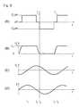
- FIG. 2(A)illustrates the sequence of ON and OFF periods of the switches Q 1 and Q 2 .
- the ON periodsare separated by dead times T d which, for reasons that will become clear below, are larger than the minimum dead time mentioned above.
- FIG. 2(B)illustrates a waveform of a voltage U s that is sensed by a voltage sensor 22 ( FIG. 1 ) at the junction point between the two switches Q 1 and Q 2 .
- the voltage U scorresponds to the voltage drop across the switch Q 2 whereas U in -U s represents the voltage drop across the switch Q 1 .
- the waveform of the voltage U s shown in FIG. 2(B)is point-symmetric.
- FIG. 2(C)shows the voltage U r of the resonance tank. In resonance, this voltage is delayed by 90° relative to the voltage U s .
- FIG. 2(D)shows the current I r in the resonance tank. This current is 90° ahead of the voltage U r and is thus at least approximately in phase with the (non-sinusoidal) waveform of the voltage U s .
- the switch Q 1is ON, while the switch Q 2 is OFF.
- the current I ris supplied by the closed switch Q 1 , and the voltage U r increases.
- the voltage U rhas reached its maximum and, accordingly, the current I r crosses zero.
- the switch Q 1is switched OFF. This zero current switching of the switch Q 1 has the advantage that the detrimental effects of tail currents in the IGBT switch Q 1 are largely avoided.
- the dead time T dshould be selected such that the switch Q 2 is switched ON in the very moment when U s reaches zero because, then, no energy that has been stored in the capacitor C s2 would be dissipated when this capacitor is short-circuited.
- U smay not always reach exactly zero, because the oscillating circuit is subject to external influences such as fluctuations of the input voltage U in and changes of the load conditions. This is why the desirable zero voltage switching cannot always be achieved. What can be achieved, however, is a so-called valley switching, i.e. the switch Q 2 is switched ON when U s (the absolute value thereof) reaches a minimum.
- the exact timing t 3 when this condition is fulfilledwill also depend upon the external influences mentioned above and may therefore vary for varying operating conditions of the converter.
- the switch Q 2will be switched OFF again (zero current switching at resonance), and the discharge process of the capacitor C s1 between t 4 and t 5 is the mirror image of the process between t 2 and t 3 .
- the switch Q 1is switched ON again (valley switching) and another cycle will start.
- the controller 18(see FIG. 4 ) is configured to determine the ON switching timings t 3 and t 5 on the basis of the actual value of the voltage U s as measured by the voltage sensor 22 , so that the ZVS condition or at least the valley switching condition can be fulfilled even under varying operating conditions of the converter.
- the switching frequency of the switches Q 1 and Q 2is varied in order to comply with varying demands for output current I out .
- the switching frequencymay vary in an a range between 25 kHz and 50 kHz.
- FIG. 3(A) -(C)show waveforms for a mode of operation in which the converter operates above resonance. Since the dead times T d are determined by the valley switching condition, an increase of the switching frequency means that the duty cycle of the ON periods of the switches Q 1 and Q 2 becomes shorter, as has been shown in FIG. 3(B) .
- the switching frequencyis determined by a clock signal CLK whose waveform is shown in FIG. 3(A) .
- the timings of the clock pulsescorrespond to the OFF switching timings t 2 and t 4 in FIG. 2 , i.e. the clock pulses alternatingly trigger the OFF switching operations of the switches Q 1 and Q 2 .
- the ON-switching operationswill then be determined by the valley switching criterion.
- FIG. 3(C)shows the voltage U r of the resonance tank for the off-resonance mode. Since the switching frequency is higher than the resonance frequency, the phase delay of the voltage U r is larger than 90°, and the amplitude is smaller, so that less power is transferred to the output side. The shortened duty cycles of the switches Q 1 and Q 2 will also contribute to the reduced power transfer (and also to a decrease of the input current I in ).
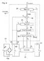
- the converter 10is current controlled, i.e. the output current I out is controlled to a given target value designated by a demand signal I out setpoint that is supplied to the controller 18 .
- the actual output current I outis measured by a current sensor 24 and is delivered to the controller 18 as a feedback signal.
- a main unit 26 of the controller 18compares the output current I out to the demand signal I out setpoint and generates a command signal Cmd that is supplied to a multiplier 28 .
- a voltage sensor 30detects the input voltage U in and sends a signal representing this input voltage to another input of the multiplier 28 .
- the product of the command signal Cmd and the input voltage U inis supplied to a sub-unit 32 of the controller 18 as a reference signal I in ref .
- the sub-unit 32compares this reference signal to the input current I in that is detected by a current sensor 34 .
- the sub-unit 32outputs a frequency signal f to a clock generator 36 .
- This clock generatorfurther receives a synchronizing signal sync that is derived from the input voltage U in and generates the clock signal CLK with the frequency f and synchronized with the pulsating input voltage U in and, indirectly, with the grid voltage U grid .
- the amplitude of the half waves of I inis determined by the command signal Cmd which is varied in an outer feedback loop comprising the main unit 26 and causing the output current I out to follow the demand as specified by the demand signal I out setpoint .
- the switch controller 38has different modes of operation selectable by means of a mode signal Mod which the main unit 26 delivers to the switch controller 38 .
- a mode signal Modwhich the main unit 26 delivers to the switch controller 38 .
- the clock signal CLKdetermines only the OFF timings of the switches Q 1 and Q 2 and the ON timings are determined by the valley switching criterion, it is clear that a start mode should be provided for delivering the first or the first few ON pulses to the switches Q 1 and Q 2 until the converter has started to resonate and a meaningful voltage U s can be derived.
- valley switchingis only allowed in a pre-defined time window. If valley switching fails, outside the normal operation conditions, the switches are forced to switch on.
- the switching frequency fmay be increased so as to reduce the output current I out accordingly.
- the setpointis decreased further, a point will be reached where the switching frequency must be so high that even with the converter that is proposed here the residual switching losses would become predominant. This is why the switch controller 38 has additional modes of operation which permit to reduce the output current even beyond this point.
- FIG. 5illustrates, on a reduced time scale, the sequence of ON and OFF pulses of the switches Q 1 and Q 2 for a mode of operation in which the power transfer is reduced by periodically skipping isolated ones of the ON pulses of both switches.
- one out of four ON-pulses of both switchesis skipped, so that the power transfer will be reduced by 25%.
- the timings at which the ON-pulses of the two switches are skippedare offset relative to one another, which helps the resonance tank to stay in the resonant mode.
- random pulse skippingwould be possible, it is conceived to use pre-defined regular pulse skipping patterns in order avoid random pulse cancellation and sub-harmonic output current variations.
- the pulse skipping mode of FIG. 5with the burst mode of FIG. 6 in order to reduce the power transfer even further.
- the converter frequencymay be set to a pre-defined value, based on a frequency table or a suitable algorithm, so as to prevent a momentary step in the output current during the transition.
- FIG. 7shows a resonant converter 10 ′ according to an exemplary embodiment of the present disclosure.
- the resonance tankhas only a single capacitor C r , so that the circuit is less symmetric than in the embodiment shown in FIG. 1 .
- the function principles explained abovecan be applied.
- the diode full bridge D that had been shown in FIG. 1has been replaced by a half bridge of diodes D 1 , D 2 and an output inductor L f .
- the output capacitor C 4is connected to a centre tap of the secondary winding of the transformer T.
- FIG. 8shows an exemplary embodiment of a converter 10 ′′, wherein four switches Q 1 , Q 2 , Q 3 and Q 4 form a full bridge, so that the converter can be powered directly by an AC input voltage U.
- the switches Q 1 and Q 4will always be switched simultaneously, just as the switches Q 2 and Q 3 .
- the resonance tankis formed by the inductor L r and a single capacitor C r , and the voltage drop across the capacitor C r is rectified by a diode full bridge D 3 and a capacitor C 4 , so that a DC output voltage is applied to a load R.
Landscapes
- Engineering & Computer Science (AREA)
- Power Engineering (AREA)
- Dc-Dc Converters (AREA)
- Inverter Devices (AREA)
Abstract
Description
Claims (13)
Applications Claiming Priority (4)
| Application Number | Priority Date | Filing Date | Title |
|---|---|---|---|
| EP11151382AEP2479879A1 (en) | 2011-01-19 | 2011-01-19 | Resonat power converter |
| EP11151382.6 | 2011-01-19 | ||
| EP11151382 | 2011-01-19 | ||
| PCT/EP2012/050811WO2012098201A1 (en) | 2011-01-19 | 2012-01-19 | Resonant power converter |
Related Parent Applications (1)
| Application Number | Title | Priority Date | Filing Date |
|---|---|---|---|
| PCT/EP2012/050811ContinuationWO2012098201A1 (en) | 2011-01-19 | 2012-01-19 | Resonant power converter |
Publications (2)
| Publication Number | Publication Date |
|---|---|
| US20130301307A1 US20130301307A1 (en) | 2013-11-14 |
| US10454377B2true US10454377B2 (en) | 2019-10-22 |
Family
ID=44063673
Family Applications (1)
| Application Number | Title | Priority Date | Filing Date |
|---|---|---|---|
| US13/945,465ActiveUS10454377B2 (en) | 2011-01-19 | 2013-07-18 | Resonant power converter |
Country Status (7)
| Country | Link |
|---|---|
| US (1) | US10454377B2 (en) |
| EP (2) | EP2479879A1 (en) |
| CN (2) | CN108631598A (en) |
| BR (1) | BR112013018430B8 (en) |
| CA (1) | CA2824892C (en) |
| ES (1) | ES2656342T3 (en) |
| WO (1) | WO2012098201A1 (en) |
Cited By (1)
| Publication number | Priority date | Publication date | Assignee | Title |
|---|---|---|---|---|
| TWI810892B (en)* | 2021-04-15 | 2023-08-01 | 愛爾蘭商艾塞爾西斯科技有限公司 | Resonant converter circuit, power supply unit, and system of resonant converter |
Families Citing this family (6)
| Publication number | Priority date | Publication date | Assignee | Title |
|---|---|---|---|---|
| US9143043B2 (en)* | 2012-03-01 | 2015-09-22 | Infineon Technologies Ag | Multi-mode operation and control of a resonant converter |
| JP6196954B2 (en)* | 2014-09-22 | 2017-09-13 | コーセル株式会社 | Switching power supply |
| CN106685242B (en)* | 2015-11-09 | 2018-11-09 | 光宝科技股份有限公司 | Single-stage AC-DC converter |
| US11031873B2 (en) | 2016-12-30 | 2021-06-08 | Texas Instruments Incorporated | Primary side burst mode controller for LLC converter |
| EP3658403B1 (en) | 2017-07-26 | 2022-04-20 | ABB Schweiz AG | Electrical vehicle charging device for charging an electrical vehicle with a dc voltage |
| EP3719982B8 (en) | 2019-04-02 | 2022-12-21 | ABB E-mobility B.V. | Three-phase ac to dc power converter |
Citations (21)
| Publication number | Priority date | Publication date | Assignee | Title |
|---|---|---|---|---|
| US4876635A (en)* | 1988-12-23 | 1989-10-24 | General Electric Company | Series resonant inverter with lossless snubber-resetting components |
| US5200887A (en) | 1991-06-28 | 1993-04-06 | Daihen Corporation | Power supply unit for arc processing |
| EP0595091A2 (en) | 1992-10-26 | 1994-05-04 | Hughes Aircraft Company | Active three phase power conditioner |
| US5341083A (en) | 1991-09-27 | 1994-08-23 | Electric Power Research Institute, Inc. | Contactless battery charging system |
| US5644214A (en)* | 1993-11-16 | 1997-07-01 | Samsung Electronics Co., Ltd. | Power factor correction circuit |
| US20060291117A1 (en)* | 2005-06-23 | 2006-12-28 | Sanken Electric Co., Ltd. | Switching power supply device |
| US7313004B1 (en)* | 2006-12-21 | 2007-12-25 | System General Corp. | Switching controller for resonant power converter |
| US20080130324A1 (en) | 2006-11-30 | 2008-06-05 | Hang-Seok Choi | Switch mode power supply and driving method thereof |
| US20080224681A1 (en)* | 2002-11-12 | 2008-09-18 | O2Micro, Inc. | Controller for a DC to DC Converter |
| US20080310194A1 (en)* | 2007-06-13 | 2008-12-18 | Pei-Lun Huang | Method and apparatus for improving the light load efficiency of a switching mode converter |
| US20090091955A1 (en) | 2007-03-28 | 2009-04-09 | Hang-Seok Choi | Quasi resonant switching mode power supply |
| US20090310387A1 (en)* | 2008-06-16 | 2009-12-17 | Lu wei-chun | Duty-cycle-controlled half-bridge resonant converter |
| US20100001581A1 (en) | 2006-08-04 | 2010-01-07 | Bayerische Motoren Werke Aktiengesellschaft | System for Supplying Voltage to Electrical Loads of a Motor Vehicle |
| US20100020569A1 (en)* | 2008-07-25 | 2010-01-28 | Melanson John L | Resonant switching power converter with adaptive dead time control |
| US20100079085A1 (en)* | 2007-03-13 | 2010-04-01 | Koninklijke Philips Electronics N.V. | Supply circuit |
| WO2010086788A2 (en) | 2009-01-29 | 2010-08-05 | Brusa Elektronik Ag | Converter for single-phase and three-phase operation, d.c. voltage supply and battery charger |
| EP2218607A1 (en) | 2007-11-29 | 2010-08-18 | Toyota Jidosha Kabushiki Kaisha | Electric charging system and its operation method |
| CN101820222A (en)* | 2010-06-18 | 2010-09-01 | 陶顺祝 | Full voltage range llc resonant converter and control method thereof |
| US20110085354A1 (en)* | 2009-10-08 | 2011-04-14 | Acbel Polytech Inc. | Burst mode resonant power converter with high conversion efficiency |
| US8184456B1 (en)* | 2008-08-26 | 2012-05-22 | International Rectifier Corporation | Adaptive power converter and related circuitry |
| US9312758B2 (en)* | 2010-02-25 | 2016-04-12 | Dialog Semiconductor Gmbh | DC-DC converter efficiency improvement and area reduction using a novel switching technique |
Family Cites Families (3)
| Publication number | Priority date | Publication date | Assignee | Title |
|---|---|---|---|---|
| US5550442A (en)* | 1993-12-16 | 1996-08-27 | Matsushita Electric Industrial Co., Ltd. | Horizontal deflection circuit |
| JP2005151608A (en)* | 2003-11-11 | 2005-06-09 | Hitachi Ltd | Resonant converter and control method thereof |
| CN100583615C (en)* | 2005-04-01 | 2010-01-20 | Nxp股份有限公司 | Resonant converter, controller of a resonant converter and control method |
- 2011
- 2011-01-19EPEP11151382Apatent/EP2479879A1/ennot_activeWithdrawn
- 2012
- 2012-01-19ESES12700410.9Tpatent/ES2656342T3/enactiveActive
- 2012-01-19WOPCT/EP2012/050811patent/WO2012098201A1/enactiveApplication Filing
- 2012-01-19CNCN201810425614.2Apatent/CN108631598A/enactivePending
- 2012-01-19BRBR112013018430Apatent/BR112013018430B8/enactiveIP Right Grant
- 2012-01-19CNCN2012800058567Apatent/CN103460584A/enactivePending
- 2012-01-19CACA2824892Apatent/CA2824892C/enactiveActive
- 2012-01-19EPEP12700410.9Apatent/EP2666236B1/enactiveActive
- 2013
- 2013-07-18USUS13/945,465patent/US10454377B2/enactiveActive
Patent Citations (26)
| Publication number | Priority date | Publication date | Assignee | Title |
|---|---|---|---|---|
| US4876635A (en)* | 1988-12-23 | 1989-10-24 | General Electric Company | Series resonant inverter with lossless snubber-resetting components |
| US5200887A (en) | 1991-06-28 | 1993-04-06 | Daihen Corporation | Power supply unit for arc processing |
| US5341083A (en) | 1991-09-27 | 1994-08-23 | Electric Power Research Institute, Inc. | Contactless battery charging system |
| US5321600A (en) | 1992-10-26 | 1994-06-14 | Hughes Aircraft Company | Delta connected three phase AC-DC converter with power factor correction circuits |
| EP0595091A2 (en) | 1992-10-26 | 1994-05-04 | Hughes Aircraft Company | Active three phase power conditioner |
| US5644214A (en)* | 1993-11-16 | 1997-07-01 | Samsung Electronics Co., Ltd. | Power factor correction circuit |
| US20080224681A1 (en)* | 2002-11-12 | 2008-09-18 | O2Micro, Inc. | Controller for a DC to DC Converter |
| US20060291117A1 (en)* | 2005-06-23 | 2006-12-28 | Sanken Electric Co., Ltd. | Switching power supply device |
| US20100001581A1 (en) | 2006-08-04 | 2010-01-07 | Bayerische Motoren Werke Aktiengesellschaft | System for Supplying Voltage to Electrical Loads of a Motor Vehicle |
| US20080130324A1 (en) | 2006-11-30 | 2008-06-05 | Hang-Seok Choi | Switch mode power supply and driving method thereof |
| US7313004B1 (en)* | 2006-12-21 | 2007-12-25 | System General Corp. | Switching controller for resonant power converter |
| US20100079085A1 (en)* | 2007-03-13 | 2010-04-01 | Koninklijke Philips Electronics N.V. | Supply circuit |
| US20090091955A1 (en) | 2007-03-28 | 2009-04-09 | Hang-Seok Choi | Quasi resonant switching mode power supply |
| US20080310194A1 (en)* | 2007-06-13 | 2008-12-18 | Pei-Lun Huang | Method and apparatus for improving the light load efficiency of a switching mode converter |
| EP2218607A1 (en) | 2007-11-29 | 2010-08-18 | Toyota Jidosha Kabushiki Kaisha | Electric charging system and its operation method |
| US20100225274A1 (en) | 2007-11-29 | 2010-09-09 | Toyota Jidosha Kabushiki Kaisha | Charging system and method for operating the same |
| US20090310387A1 (en)* | 2008-06-16 | 2009-12-17 | Lu wei-chun | Duty-cycle-controlled half-bridge resonant converter |
| US20100020569A1 (en)* | 2008-07-25 | 2010-01-28 | Melanson John L | Resonant switching power converter with adaptive dead time control |
| US8184456B1 (en)* | 2008-08-26 | 2012-05-22 | International Rectifier Corporation | Adaptive power converter and related circuitry |
| WO2010086788A2 (en) | 2009-01-29 | 2010-08-05 | Brusa Elektronik Ag | Converter for single-phase and three-phase operation, d.c. voltage supply and battery charger |
| US20100220501A1 (en) | 2009-01-29 | 2010-09-02 | Brusa Elektronik Ag | Dc/dc converter and ac/dc converter |
| US20110261591A1 (en) | 2009-01-29 | 2011-10-27 | Brusa Elektronik Ag | Converter for single-phase and three-phase operation, d.c. voltage supply and battery charger |
| US20110085354A1 (en)* | 2009-10-08 | 2011-04-14 | Acbel Polytech Inc. | Burst mode resonant power converter with high conversion efficiency |
| US9312758B2 (en)* | 2010-02-25 | 2016-04-12 | Dialog Semiconductor Gmbh | DC-DC converter efficiency improvement and area reduction using a novel switching technique |
| CN101820222A (en)* | 2010-06-18 | 2010-09-01 | 陶顺祝 | Full voltage range llc resonant converter and control method thereof |
| US8681520B2 (en)* | 2010-06-18 | 2014-03-25 | Shunzhu Tao | Kind of LLC resonant converter for full voltage range and its control method |
Non-Patent Citations (15)
| Title |
|---|
| Colak et al., "High current, low voltage modular power converter for lead acid battery charging", Sustainable Energy Technologies, IEEE, Nov. 2008, pp. 1042-1046. |
| Egan et al., "Corrected Single-Stage Inductive Charger for Electric Vehicle Batteries", Industrial Electronics, IEEE Transaction, Apr. 2007, pp. 1217-1226, vol. 54, No. 2. |
| Huber et al., "Effect of Valley Switching and Switching-Frequency Limitation on Line-Current Distortions of DCM/CCM Boundary Boost PFC Converters", IEEE Transactions on Power Electronics, Feb. 2009, pp. 339-347, vol. 24, No. 2. |
| International Search Report (PCT/ISA/210) dated Jun. 8, 2012, by the European Patent Office as the International Searching Authority for International Application No. PCT/EP2012/050811. |
| International Search Report (PCT/ISA/210) dated Mar. 4, 2013, by the European Patent Office as the International Searching Authority for International Application No. PCT/EP2012/050813. |
| Kim et al., "A New Zero Voltage Switching High Frequency Dc-to-dc Converter", Dept. of Electrical Engineering, Korea Advanced Institute of Science and Technology (KAIST), Aug. 1991, pp. 217-221. |
| Notification Concerning Transmittal of International Preliminary Report on Patentability (Chapter 1 of the Patent Cooperation Treaty) (Form PCT/IB/326 and PCT/IB/373) and the Written Opinion of the International Searching Authority (Form PCT/ISA 237) dated Aug. 1, 2013, issued in corresponding International Application No. PCT/EP2012/050811. (7 PGS). |
| Notification Concerning Transmittal of International Preliminary Report on Patentability (Forms PCT/IB/326 and PCT/IB/373) and the Written Opinion of the International Searching Authority ( Form PCT/ISA 237) dated Aug. 1, 2013, issued in corresponding International Application No. PCT/EP2012/050813. (9 pgs.). |
| Pothana et al., "Parallel Operation of Power Factor Corrected AC-DC Converter Modules With Two Power Stages", Power Electronics and Drive Systems, Nov. 2007, pp. 953-960. |
| Ridley et al., "Design and control of a full-wave, quasi-resonant flyback converter", Virginia Power Electronics Center, Virginia Polytechnic Institute and State University, Feb. 1988, pp. 41-49. |
| Search Report dated Jul. 28, 2011, by the European Patent Office for Application No. 11151395.8. |
| Search Report dated Jun. 14, 2011, by the European Patent Office for Application No. 11151382.6. |
| Sumiyoshi et al., "High-Frequency Transformer Isolated Soft-Switching DC-DC Converter for Fuel Cell Cogeneration System", Power Electronics and Motion Control Conference, IEEE, Aug. 2006, pp. 746-748. |
| Written Opinion (PCT/ISA/237) dated Jun. 8, 2012, by the European Patent Office as the International Searching Authority for International Application No. PCT/EP2012/050811. |
| Written Opinion (PCT/ISA/237) dated Mar. 4, 2013, by the European Patent Office as the International Searching Authority for International Application No. PCT/EP2012/050813. |
Cited By (1)
| Publication number | Priority date | Publication date | Assignee | Title |
|---|---|---|---|---|
| TWI810892B (en)* | 2021-04-15 | 2023-08-01 | 愛爾蘭商艾塞爾西斯科技有限公司 | Resonant converter circuit, power supply unit, and system of resonant converter |
Also Published As
| Publication number | Publication date |
|---|---|
| BR112013018430B1 (en) | 2020-04-07 |
| EP2479879A1 (en) | 2012-07-25 |
| US20130301307A1 (en) | 2013-11-14 |
| CN103460584A (en) | 2013-12-18 |
| WO2012098201A1 (en) | 2012-07-26 |
| BR112013018430A2 (en) | 2016-10-11 |
| CA2824892A1 (en) | 2012-07-26 |
| CA2824892C (en) | 2020-04-28 |
| BR112013018430B8 (en) | 2023-02-28 |
| EP2666236B1 (en) | 2017-10-25 |
| ES2656342T3 (en) | 2018-02-26 |
| EP2666236A1 (en) | 2013-11-27 |
| CN108631598A (en) | 2018-10-09 |
Similar Documents
| Publication | Publication Date | Title |
|---|---|---|
| US10454377B2 (en) | Resonant power converter | |
| US11005361B2 (en) | Control circuit and method of a switching power supply | |
| CN103326580B (en) | DC-to-DC converter, power converter and control method thereof | |
| US20130088899A1 (en) | Multi-phase converter | |
| JP2007104872A (en) | Power converter | |
| EP2269293A1 (en) | Method of operating a resonant power converter and a controller therefor | |
| JP6667750B1 (en) | DC-DC converter | |
| JP6483914B2 (en) | Power supply | |
| US7821239B2 (en) | Switching power supply | |
| JP2018520634A (en) | Battery charger | |
| JP2011130577A (en) | Dc power supply unit | |
| EP3210294A1 (en) | A converter | |
| US11038430B2 (en) | LLCC secondary overtone resonant power converter | |
| JP5457204B2 (en) | Full bridge composite resonance type DC-DC converter | |
| JP5713171B2 (en) | AC-DC converter | |
| KR100966966B1 (en) | Dc/dc converter with multi-output | |
| KR100966965B1 (en) | Multi-Output DC / DC Converters | |
| JP5239917B2 (en) | Power factor correction converter and power factor correction converter controller | |
| JP4649729B2 (en) | Power supply device and discharge lamp lighting device | |
| JP4879556B2 (en) | High voltage charger | |
| JP4780547B2 (en) | Partially resonant separately excited switching power supply | |
| JP3256423B2 (en) | Power supply | |
| JP2002315315A (en) | Ac/dc converter | |
| JP2006211881A (en) | Ac-dc converter | |
| JP2001231256A (en) | High-power-factor switching power device |
Legal Events
| Date | Code | Title | Description |
|---|---|---|---|
| AS | Assignment | Owner name:ABB B.V., NETHERLANDS Free format text:ASSIGNMENT OF ASSIGNORS INTEREST;ASSIGNORS:KARDOLUS, MENNO;SCHIJFFELEN, JOS H.;GRONINGER, MARK;AND OTHERS;SIGNING DATES FROM 20130724 TO 20130812;REEL/FRAME:036533/0042 | |
| STPP | Information on status: patent application and granting procedure in general | Free format text:RESPONSE TO NON-FINAL OFFICE ACTION ENTERED AND FORWARDED TO EXAMINER | |
| STPP | Information on status: patent application and granting procedure in general | Free format text:NOTICE OF ALLOWANCE MAILED -- APPLICATION RECEIVED IN OFFICE OF PUBLICATIONS | |
| STPP | Information on status: patent application and granting procedure in general | Free format text:PUBLICATIONS -- ISSUE FEE PAYMENT VERIFIED | |
| STCF | Information on status: patent grant | Free format text:PATENTED CASE | |
| AS | Assignment | Owner name:ABB SCHWEIZ AG, SWITZERLAND Free format text:ASSIGNMENT OF ASSIGNORS INTEREST;ASSIGNOR:ABB B.V.;REEL/FRAME:059385/0360 Effective date:20210501 | |
| AS | Assignment | Owner name:ABB B.V., NETHERLANDS Free format text:ASSIGNMENT OF ASSIGNORS INTEREST;ASSIGNOR:ABB SCHWEIZ AG;REEL/FRAME:062205/0860 Effective date:20221010 | |
| AS | Assignment | Owner name:ABB E-MOBILITY B.V., NETHERLANDS Free format text:CHANGE OF NAME;ASSIGNOR:ABB B.V.;REEL/FRAME:062320/0490 Effective date:20220101 | |
| MAFP | Maintenance fee payment | Free format text:PAYMENT OF MAINTENANCE FEE, 4TH YEAR, LARGE ENTITY (ORIGINAL EVENT CODE: M1551); ENTITY STATUS OF PATENT OWNER: LARGE ENTITY Year of fee payment:4 |