US10446665B2 - Method and structure for protecting gates during epitaxial growth - Google Patents
Method and structure for protecting gates during epitaxial growthDownload PDFInfo
- Publication number
- US10446665B2 US10446665B2US15/904,982US201815904982AUS10446665B2US 10446665 B2US10446665 B2US 10446665B2US 201815904982 AUS201815904982 AUS 201815904982AUS 10446665 B2US10446665 B2US 10446665B2
- Authority
- US
- United States
- Prior art keywords
- inner spacer
- transistor gate
- semiconductor structure
- gate
- spacer
- Prior art date
- Legal status (The legal status is an assumption and is not a legal conclusion. Google has not performed a legal analysis and makes no representation as to the accuracy of the status listed.)
- Active
Links
- 238000000034methodMethods0.000titleabstractdescription35
- 125000006850spacer groupChemical group0.000claimsabstractdescription88
- 239000000463materialSubstances0.000claimsabstractdescription28
- 239000004065semiconductorSubstances0.000claimsdescription61
- 239000000758substrateSubstances0.000claimsdescription25
- 229910052581Si3N4Inorganic materials0.000claimsdescription9
- HQVNEWCFYHHQES-UHFFFAOYSA-Nsilicon nitrideChemical compoundN12[Si]34N5[Si]62N3[Si]51N64HQVNEWCFYHHQES-UHFFFAOYSA-N0.000claimsdescription9
- VYPSYNLAJGMNEJ-UHFFFAOYSA-NSilicium dioxideChemical compoundO=[Si]=OVYPSYNLAJGMNEJ-UHFFFAOYSA-N0.000claimsdescription7
- XUIMIQQOPSSXEZ-UHFFFAOYSA-NSiliconChemical compound[Si]XUIMIQQOPSSXEZ-UHFFFAOYSA-N0.000claimsdescription6
- 229910052710siliconInorganic materials0.000claimsdescription6
- 239000010703siliconSubstances0.000claimsdescription6
- 229910052814silicon oxideInorganic materials0.000claimsdescription5
- 229910000577Silicon-germaniumInorganic materials0.000claimsdescription4
- HMDDXIMCDZRSNE-UHFFFAOYSA-N[C].[Si]Chemical compound[C].[Si]HMDDXIMCDZRSNE-UHFFFAOYSA-N0.000claimsdescription4
- LEVVHYCKPQWKOP-UHFFFAOYSA-N[Si].[Ge]Chemical compound[Si].[Ge]LEVVHYCKPQWKOP-UHFFFAOYSA-N0.000claimsdescription3
- 229910021420polycrystalline siliconInorganic materials0.000claimsdescription2
- 229920005591polysiliconPolymers0.000claimsdescription2
- 210000005069earsAnatomy0.000abstractdescription2
- 238000005229chemical vapour depositionMethods0.000description5
- 230000005669field effectEffects0.000description5
- 238000000231atomic layer depositionMethods0.000description4
- 230000015572biosynthetic processEffects0.000description4
- 238000000151depositionMethods0.000description4
- 230000002401inhibitory effectEffects0.000description4
- 230000008021depositionEffects0.000description3
- 230000000873masking effectEffects0.000description3
- 240000001307Myosotis scorpioidesSpecies0.000description2
- 230000000295complement effectEffects0.000description2
- 239000003989dielectric materialSubstances0.000description2
- 239000012212insulatorSubstances0.000description2
- 150000002500ionsChemical class0.000description2
- 230000000670limiting effectEffects0.000description2
- 238000004518low pressure chemical vapour depositionMethods0.000description2
- 238000004519manufacturing processMethods0.000description2
- 239000002184metalSubstances0.000description2
- 229910044991metal oxideInorganic materials0.000description2
- 150000004706metal oxidesChemical class0.000description2
- 238000012986modificationMethods0.000description2
- 230000004048modificationEffects0.000description2
- 230000003647oxidationEffects0.000description2
- 238000007254oxidation reactionMethods0.000description2
- 238000005240physical vapour depositionMethods0.000description2
- 238000000623plasma-assisted chemical vapour depositionMethods0.000description2
- 238000001289rapid thermal chemical vapour depositionMethods0.000description2
- 239000000126substanceSubstances0.000description2
- 238000000038ultrahigh vacuum chemical vapour depositionMethods0.000description2
- 230000002411adverseEffects0.000description1
- 238000006243chemical reactionMethods0.000description1
- 229910052681coesiteInorganic materials0.000description1
- 229910052906cristobaliteInorganic materials0.000description1
- 238000000313electron-beam-induced depositionMethods0.000description1
- 238000001704evaporationMethods0.000description1
- 230000008020evaporationEffects0.000description1
- 238000007737ion beam depositionMethods0.000description1
- 238000002955isolationMethods0.000description1
- 238000001451molecular beam epitaxyMethods0.000description1
- 208000001491myopiaDiseases0.000description1
- 150000004767nitridesChemical class0.000description1
- 238000000059patterningMethods0.000description1
- 238000005268plasma chemical vapour depositionMethods0.000description1
- 238000007747platingMethods0.000description1
- 239000000377silicon dioxideSubstances0.000description1
- 235000012239silicon dioxideNutrition0.000description1
- 238000004544sputter depositionMethods0.000description1
- 229910052682stishoviteInorganic materials0.000description1
- 229910052905tridymiteInorganic materials0.000description1
Images


Classifications
- H—ELECTRICITY
- H10—SEMICONDUCTOR DEVICES; ELECTRIC SOLID-STATE DEVICES NOT OTHERWISE PROVIDED FOR
- H10D—INORGANIC ELECTRIC SEMICONDUCTOR DEVICES
- H10D64/00—Electrodes of devices having potential barriers
- H10D64/01—Manufacture or treatment
- H10D64/021—Manufacture or treatment using multiple gate spacer layers, e.g. bilayered sidewall spacers
- H01L29/6656—
- H01L21/823814—
- H01L21/823821—
- H01L21/823864—
- H01L27/092—
- H01L29/6653—
- H01L29/66636—
- H01L29/66795—
- H01L29/7848—
- H—ELECTRICITY
- H10—SEMICONDUCTOR DEVICES; ELECTRIC SOLID-STATE DEVICES NOT OTHERWISE PROVIDED FOR
- H10D—INORGANIC ELECTRIC SEMICONDUCTOR DEVICES
- H10D30/00—Field-effect transistors [FET]
- H10D30/01—Manufacture or treatment
- H10D30/021—Manufacture or treatment of FETs having insulated gates [IGFET]
- H10D30/024—Manufacture or treatment of FETs having insulated gates [IGFET] of fin field-effect transistors [FinFET]
- H—ELECTRICITY
- H10—SEMICONDUCTOR DEVICES; ELECTRIC SOLID-STATE DEVICES NOT OTHERWISE PROVIDED FOR
- H10D—INORGANIC ELECTRIC SEMICONDUCTOR DEVICES
- H10D30/00—Field-effect transistors [FET]
- H10D30/60—Insulated-gate field-effect transistors [IGFET]
- H10D30/791—Arrangements for exerting mechanical stress on the crystal lattice of the channel regions
- H10D30/797—Arrangements for exerting mechanical stress on the crystal lattice of the channel regions being in source or drain regions, e.g. SiGe source or drain
- H—ELECTRICITY
- H10—SEMICONDUCTOR DEVICES; ELECTRIC SOLID-STATE DEVICES NOT OTHERWISE PROVIDED FOR
- H10D—INORGANIC ELECTRIC SEMICONDUCTOR DEVICES
- H10D62/00—Semiconductor bodies, or regions thereof, of devices having potential barriers
- H10D62/01—Manufacture or treatment
- H10D62/021—Forming source or drain recesses by etching e.g. recessing by etching and then refilling
- H—ELECTRICITY
- H10—SEMICONDUCTOR DEVICES; ELECTRIC SOLID-STATE DEVICES NOT OTHERWISE PROVIDED FOR
- H10D—INORGANIC ELECTRIC SEMICONDUCTOR DEVICES
- H10D64/00—Electrodes of devices having potential barriers
- H10D64/01—Manufacture or treatment
- H10D64/015—Manufacture or treatment removing at least parts of gate spacers, e.g. disposable spacers
- H—ELECTRICITY
- H10—SEMICONDUCTOR DEVICES; ELECTRIC SOLID-STATE DEVICES NOT OTHERWISE PROVIDED FOR
- H10D—INORGANIC ELECTRIC SEMICONDUCTOR DEVICES
- H10D84/00—Integrated devices formed in or on semiconductor substrates that comprise only semiconducting layers, e.g. on Si wafers or on GaAs-on-Si wafers
- H10D84/01—Manufacture or treatment
- H10D84/0123—Integrating together multiple components covered by H10D12/00 or H10D30/00, e.g. integrating multiple IGBTs
- H10D84/0126—Integrating together multiple components covered by H10D12/00 or H10D30/00, e.g. integrating multiple IGBTs the components including insulated gates, e.g. IGFETs
- H10D84/0165—Integrating together multiple components covered by H10D12/00 or H10D30/00, e.g. integrating multiple IGBTs the components including insulated gates, e.g. IGFETs the components including complementary IGFETs, e.g. CMOS devices
- H10D84/017—Manufacturing their source or drain regions, e.g. silicided source or drain regions
- H—ELECTRICITY
- H10—SEMICONDUCTOR DEVICES; ELECTRIC SOLID-STATE DEVICES NOT OTHERWISE PROVIDED FOR
- H10D—INORGANIC ELECTRIC SEMICONDUCTOR DEVICES
- H10D84/00—Integrated devices formed in or on semiconductor substrates that comprise only semiconducting layers, e.g. on Si wafers or on GaAs-on-Si wafers
- H10D84/01—Manufacture or treatment
- H10D84/0123—Integrating together multiple components covered by H10D12/00 or H10D30/00, e.g. integrating multiple IGBTs
- H10D84/0126—Integrating together multiple components covered by H10D12/00 or H10D30/00, e.g. integrating multiple IGBTs the components including insulated gates, e.g. IGFETs
- H10D84/0165—Integrating together multiple components covered by H10D12/00 or H10D30/00, e.g. integrating multiple IGBTs the components including insulated gates, e.g. IGFETs the components including complementary IGFETs, e.g. CMOS devices
- H10D84/0184—Manufacturing their gate sidewall spacers
- H—ELECTRICITY
- H10—SEMICONDUCTOR DEVICES; ELECTRIC SOLID-STATE DEVICES NOT OTHERWISE PROVIDED FOR
- H10D—INORGANIC ELECTRIC SEMICONDUCTOR DEVICES
- H10D84/00—Integrated devices formed in or on semiconductor substrates that comprise only semiconducting layers, e.g. on Si wafers or on GaAs-on-Si wafers
- H10D84/01—Manufacture or treatment
- H10D84/0123—Integrating together multiple components covered by H10D12/00 or H10D30/00, e.g. integrating multiple IGBTs
- H10D84/0126—Integrating together multiple components covered by H10D12/00 or H10D30/00, e.g. integrating multiple IGBTs the components including insulated gates, e.g. IGFETs
- H10D84/0165—Integrating together multiple components covered by H10D12/00 or H10D30/00, e.g. integrating multiple IGBTs the components including insulated gates, e.g. IGFETs the components including complementary IGFETs, e.g. CMOS devices
- H10D84/0193—Integrating together multiple components covered by H10D12/00 or H10D30/00, e.g. integrating multiple IGBTs the components including insulated gates, e.g. IGFETs the components including complementary IGFETs, e.g. CMOS devices the components including FinFETs
- H—ELECTRICITY
- H10—SEMICONDUCTOR DEVICES; ELECTRIC SOLID-STATE DEVICES NOT OTHERWISE PROVIDED FOR
- H10D—INORGANIC ELECTRIC SEMICONDUCTOR DEVICES
- H10D84/00—Integrated devices formed in or on semiconductor substrates that comprise only semiconducting layers, e.g. on Si wafers or on GaAs-on-Si wafers
- H10D84/01—Manufacture or treatment
- H10D84/02—Manufacture or treatment characterised by using material-based technologies
- H10D84/03—Manufacture or treatment characterised by using material-based technologies using Group IV technology, e.g. silicon technology or silicon-carbide [SiC] technology
- H10D84/038—Manufacture or treatment characterised by using material-based technologies using Group IV technology, e.g. silicon technology or silicon-carbide [SiC] technology using silicon technology, e.g. SiGe
- H—ELECTRICITY
- H10—SEMICONDUCTOR DEVICES; ELECTRIC SOLID-STATE DEVICES NOT OTHERWISE PROVIDED FOR
- H10D—INORGANIC ELECTRIC SEMICONDUCTOR DEVICES
- H10D84/00—Integrated devices formed in or on semiconductor substrates that comprise only semiconducting layers, e.g. on Si wafers or on GaAs-on-Si wafers
- H10D84/80—Integrated devices formed in or on semiconductor substrates that comprise only semiconducting layers, e.g. on Si wafers or on GaAs-on-Si wafers characterised by the integration of at least one component covered by groups H10D12/00 or H10D30/00, e.g. integration of IGFETs
- H10D84/82—Integrated devices formed in or on semiconductor substrates that comprise only semiconducting layers, e.g. on Si wafers or on GaAs-on-Si wafers characterised by the integration of at least one component covered by groups H10D12/00 or H10D30/00, e.g. integration of IGFETs of only field-effect components
- H10D84/83—Integrated devices formed in or on semiconductor substrates that comprise only semiconducting layers, e.g. on Si wafers or on GaAs-on-Si wafers characterised by the integration of at least one component covered by groups H10D12/00 or H10D30/00, e.g. integration of IGFETs of only field-effect components of only insulated-gate FETs [IGFET]
- H10D84/85—Complementary IGFETs, e.g. CMOS
- H01L21/823418—
- H01L21/823468—
- H01L29/165—
- H—ELECTRICITY
- H10—SEMICONDUCTOR DEVICES; ELECTRIC SOLID-STATE DEVICES NOT OTHERWISE PROVIDED FOR
- H10D—INORGANIC ELECTRIC SEMICONDUCTOR DEVICES
- H10D62/00—Semiconductor bodies, or regions thereof, of devices having potential barriers
- H10D62/80—Semiconductor bodies, or regions thereof, of devices having potential barriers characterised by the materials
- H10D62/82—Heterojunctions
- H10D62/822—Heterojunctions comprising only Group IV materials heterojunctions, e.g. Si/Ge heterojunctions
- H—ELECTRICITY
- H10—SEMICONDUCTOR DEVICES; ELECTRIC SOLID-STATE DEVICES NOT OTHERWISE PROVIDED FOR
- H10D—INORGANIC ELECTRIC SEMICONDUCTOR DEVICES
- H10D84/00—Integrated devices formed in or on semiconductor substrates that comprise only semiconducting layers, e.g. on Si wafers or on GaAs-on-Si wafers
- H10D84/01—Manufacture or treatment
- H10D84/0123—Integrating together multiple components covered by H10D12/00 or H10D30/00, e.g. integrating multiple IGBTs
- H10D84/0126—Integrating together multiple components covered by H10D12/00 or H10D30/00, e.g. integrating multiple IGBTs the components including insulated gates, e.g. IGFETs
- H10D84/013—Manufacturing their source or drain regions, e.g. silicided source or drain regions
- H—ELECTRICITY
- H10—SEMICONDUCTOR DEVICES; ELECTRIC SOLID-STATE DEVICES NOT OTHERWISE PROVIDED FOR
- H10D—INORGANIC ELECTRIC SEMICONDUCTOR DEVICES
- H10D84/00—Integrated devices formed in or on semiconductor substrates that comprise only semiconducting layers, e.g. on Si wafers or on GaAs-on-Si wafers
- H10D84/01—Manufacture or treatment
- H10D84/0123—Integrating together multiple components covered by H10D12/00 or H10D30/00, e.g. integrating multiple IGBTs
- H10D84/0126—Integrating together multiple components covered by H10D12/00 or H10D30/00, e.g. integrating multiple IGBTs the components including insulated gates, e.g. IGFETs
- H10D84/0147—Manufacturing their gate sidewall spacers
Definitions
- the present inventionrelates generally to semiconductor fabrication, and more particularly, to methods and structures for protecting gates during epitaxial growth.
- CMOS field-effect transistorsare used in many integrated circuit applications, such as signal processing, computing, and wireless communications.
- CMOS chips in manufacturingcomprise planar thick-body devices on bulk Si substrates or silicon-on-insulator (SOI) substrates.
- Fin type field effect transistor (finFET) devicesare becoming more popular as critical dimensions continue to reduce.
- stressor regionsmay be formed adjacent the gate and channel of the transistor.
- the deposition of stressor regionscan cause problems that can adversely affect product yield. It is therefore desirable to have improvements in methods and structures to mitigate these problems.
- Embodiments of the present inventionprovide methods and structures for protecting gates during epitaxial growth.
- An inner spacer of a first materialis deposited adjacent a transistor gate.
- An outer spacer of a different materialis deposited adjacent the inner spacer.
- Stressor cavitiesare formed adjacent the transistor gate.
- the inner spaceris recessed, forming a divot.
- the divotis filled with a material to protect the transistor gate.
- the stressor cavitiesare then filled. As the gate is safely protected, unwanted epitaxial growth (“mouse ears”) on the transistor gate is prevented.
- embodiments of the present inventionprovide a method of forming a semiconductor structure, comprising: forming a first gate and a second gate on a semiconductor structure; forming a hardmask layer on the first gate and the second gate; forming inner spacers adjacent the first gate and the second gate; forming outer spacers adjacent the inner spacers; masking the first gate; forming stressor cavities adjacent the second gate; recessing a portion of the inner spacers of the second gate to form divots; filling the divots with a dielectric material; and filling the stressor cavities with a stressor material.
- embodiments of the present inventionprovide a semiconductor structure, comprising: a semiconductor substrate; a transistor gate disposed on the semiconductor substrate; a lower inner spacer disposed adjacent a lower portion of the transistor gate; an upper inner spacer disposed adjacent an upper portion of the transistor gate and in contact with the lower inner spacer; and an outer spacer disposed adjacent to the lower inner spacer and the upper inner spacer.
- embodiments of the present inventionprovide a semiconductor structure, comprising: a semiconductor substrate; a first transistor gate and a second transistor gate disposed on the semiconductor substrate; a full inner spacer disposed adjacent the first transistor gate; an outer spacer disposed adjacent the full inner spacer; a lower inner spacer disposed adjacent a lower portion of the second transistor gate; an upper inner spacer disposed adjacent an upper portion of the second transistor gate and in contact with the lower inner spacer; and an outer spacer disposed adjacent the lower inner spacer and upper inner spacer of the second transistor gate.
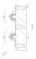
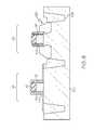
- FIG. 1shows a semiconductor structure at a starting point for embodiments of the present invention.
- FIG. 2shows a semiconductor structure after a subsequent process step of masking a transistor.
- FIG. 3shows a semiconductor structure after a subsequent process step of forming stressor cavities.
- FIG. 4shows a semiconductor structure after a subsequent process step of forming divots.
- FIG. 5shows a semiconductor structure after a subsequent process step of filling the divots.
- FIG. 6shows a semiconductor structure after a subsequent process step of filling the stressor cavities.
- FIG. 7shows a semiconductor structure after a subsequent process step of forming sigma stressor cavities in accordance with an alternative embodiment.
- FIG. 8shows a semiconductor structure after a subsequent process step of filling sigma stressor cavities in accordance with an alternative embodiment.
- FIG. 9is a flowchart indicating process steps for embodiments of the present invention.
- first elementsuch as a first structure, e.g., a first layer
- second elementsuch as a second structure, e.g. a second layer
- intervening elementssuch as an interface structure, e.g. interface layer
- “depositing” or “filling”may include any now known or later developed techniques appropriate for the material to be deposited including, but not limited to, for example: chemical vapor deposition (CVD), low-pressure CVD (LPCVD), plasma-enhanced CVD (PECVD), semi-atmosphere CVD (SACVD) and high density plasma CVD (HDPCVD), rapid thermal CVD (RTCVD), ultra-high vacuum CVD (UHVCVD), limited reaction processing CVD (LRPCVD), metal-organic CVD (MOCVD), sputtering deposition, ion beam deposition, electron beam deposition, laser assisted deposition, thermal oxidation, thermal nitridation, spin-on methods, physical vapor deposition (PVD), atomic layer deposition (ALD), chemical oxidation, molecular beam epitaxy (MBE), plating, evaporation.
- CVDchemical vapor deposition
- LPCVDlow-pressure CVD
- PECVDplasma-enhanced
- FIG. 1shows a semiconductor structure at a starting point for embodiments of the present invention.
- the semiconductor structure 100is a complementary metal oxide semiconductor (CMOS), comprising an N-type field effect transistor (NFET) 118 and a P-type field effect transistor (PFET) 120 .
- CMOScomplementary metal oxide semiconductor
- NFETN-type field effect transistor
- PFETP-type field effect transistor
- embodiments of the present inventionmay include planar devices in addition to fin type field effect transistors (finFETs).
- the semiconductor structure 100comprises a substrate 102 .
- substrateas used herein is intended to include a semiconductor substrate, a semiconductor epitaxial layer deposited or otherwise formed on a semiconductor substrate, and/or any other suitable type of semiconductor body, and all such structures are contemplated as falling within the scope of the present invention.
- the semiconductor substratemay comprise a semiconductor wafer (e.g., silicon, silicon germanium (SiGe), or a silicon-on-insulator (SOI) wafer) or one or more die on a wafer, and any epitaxial layers or other type semiconductor layers formed thereover or associated therewith.
- the semiconductor substratemay be doped, undoped, or contain doped regions and undoped regions therein.
- the semiconductor substratemay contain regions with strain and regions without strain therein, or contain regions of tensile strain and compressive strain.
- a first gate 104 and a second gate 106are each formed on the substrate 102 of the semiconductor structure 100 .
- the gatesmay be polysilicon gates. “Transistor gate” and “gate” shall have the same meaning, and are used interchangeably herein.
- the gatesmay be metal gates formed by a replacement metal gate (RMG) process.
- Shallow trench isolation (STI) regions 108may be formed in the substrate 102 .
- the STIs 108may be silicon oxide or other suitable material.
- a liner 109may be formed on the sides of the gates 104 and 106 .
- the liner 109may be comprised of silicon nitride.
- Inner spacers 112are formed adjacent the first gate 104 and the second gate 106 .
- inner spacers 112are silicon oxide, or other suitable material.
- Outer spacers 114are formed adjacent the inner spacers 112 .
- outer spacers 114may be silicon nitride, or other suitable material.
- a pad nitride layer 110is disposed on the gates 104 and 106 .
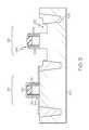
- FIG. 2shows a semiconductor structure after a subsequent process step of masking a transistor.
- a mask 122is deposited over the NFET transistor 118 .
- mask 122may be SiO2, or other suitable material.
- Mask 122may be formed by standard lithographic/patterning techniques. In other embodiments, mask 122 could be deposited over PFET transistor 120 , and the process proceeds with respect to the first gate 104 instead of the second gate 106 as described herein. The mask 122 is later removed once processing on the non-masked transistor is completed.
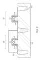
- FIG. 3shows a semiconductor structure after a subsequent process step of forming stressor cavities.
- Stressor cavities 130are formed in the substrate 102 adjacent the second gate 106 .
- stressor cavities 130may be formed by reactive ion etch (RIE), wet etch techniques, or a combination thereof.
- RIEreactive ion etch
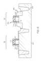
- FIG. 4shows a semiconductor structure after a subsequent process step of forming divots.
- a portion of the inner spacers 112 of the second gate 106is recessed to form divots 132 .
- the outer spacers 114remain intact during this process.
- Any of a number of processesmay be used to form the divots 132 , including, but not limited to, reactive ion etch (RIE), wet etch, chemical oxide removal (COR) process, or SiconiTM etch process.
- RIEreactive ion etch
- CORchemical oxide removal
- SiconiTM etch processSiconiTM etch process.
- the recess techniqueis typically selective such that only the material of the inner spacer 112 is recessed.
- D 1may range from about 100 nanometers to about 200 nanometers.
- D 2may range from about 5 to 50 percent of D 1 , and the sum of D 2 and D 3 equals D 1 .
- FIG. 5shows a semiconductor structure after a subsequent process step of filling the divots.
- the divots 132are filled with a dielectric material to form an upper spacer 134 .
- the divots 132are filled with an epitaxial growth inhibiting material to form an upper spacer 134 .
- the epitaxial growth inhibiting materialmay include a dielectric, for example, but not limited to silicon nitride, silicon carbon nitride, and/or silicon oxycarbide.
- atomic layer depositionALD may be used to fill divots 132 with the epitaxial growth inhibiting material, such as silicon nitride (or, in some embodiments, SiCN or SiOC).
- a recess(etch back) is performed to make the upper spacer 134 substantially of similar height to outer spacers 114 , and expose the silicon substrate 102 of the PFET transistor 120 for stressor region growth.
- FIG. 6shows a semiconductor structure after a subsequent process step of filling the stressor cavities.
- the stressor cavities 130are filled with a stressor material 136 .
- stressor material 136may be epitaxially-grown silicon germanium (eSiGe), or other suitable material.
- the second gate 106is now safely protected during formation of stressor region (i.e., 136 ), thus preventing unwanted growth of the stressor region 136 .
- This unwanted growthis also known as “mouse ear”. This occurs when a portion of a gate is exposed during formation of an epitaxial stressor region. Embodiments of the present invention prevent such exposure of the gate, thereby preventing the unwanted growth (mouse ear).
- an embodiment of the inventioncomprises a semiconductor substrate 102 , having a transistor gate 106 .
- a portion of inner spacer 112remains, comprising a (lower) inner spacer 112 , disposed adjacent a lower portion of the transistor gate 106 .
- Filled divotis an upper inner spacer 134 that is disposed adjacent to an upper portion of the transistor gate 106 and in contact with the lower inner spacer 112 .
- An outer spacer 114is disposed adjacent the upper inner spacer 134 and the lower inner spacer 112 .
- an embodiment of the inventionmay comprise another transistor gate 104 disposed on the semiconductor substrate 102 .
- a full inner spacer 112is disposed adjacent the transistor gate 104 .
- An outer spacer 114is disposed adjacent the full inner spacer.
- the lower inner spacercomprises silicon oxide.
- the upper inner spacermay be silicon nitride, silicon carbon nitride, silicon oxycarbide, and/or another suitable material.
- the outer spacermay be silicon nitride or other suitable material.
- FIG. 7shows a semiconductor structure after a subsequent process step of forming sigma stressor cavities in accordance with an alternative embodiment.
- the stressor cavitiesare sigma cavities 140 .
- the sigma cavities 140may be formed in the substrate 102 under the second gate 106 of the PFET transistor 120 .
- the sigma cavities 140may be formed by a wet etch, RIE, or combination thereof.
- FIG. 8shows a semiconductor structure after a subsequent process step of filling sigma stressor cavities in accordance with the alternative embodiment.
- the stressor material 136e.g., eSiGe
- the gate 106is now safely protected during formation of stressor region 136 .
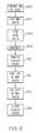
- FIG. 9is a flowchart indicating process steps for embodiments of the present invention.
- a first gate and a second gateare formed on a semiconductor structure.
- a hardmask layeris formed on the first gate and the second gate.
- inner spacersare formed adjacent the first gate and the second gate.
- outer spacersare formed adjacent the inner spacers.
- the first gateis masked.
- stressor cavitiesare formed adjacent the second gate. In some embodiments, the cavities can be sigma cavities as illustrated at FIG. 7 .
- a portion of the inner spacers of the second gateare recessed to form divots.
- the divotsare filled with an epitaxial growth inhibiting material to form an upper spacer.
- stressor cavitiesare filled with a stressor material.
Landscapes
- Insulated Gate Type Field-Effect Transistor (AREA)
- Metal-Oxide And Bipolar Metal-Oxide Semiconductor Integrated Circuits (AREA)
- Element Separation (AREA)
Abstract
Description
Claims (14)
Priority Applications (1)
| Application Number | Priority Date | Filing Date | Title |
|---|---|---|---|
| US15/904,982US10446665B2 (en) | 2014-06-19 | 2018-02-26 | Method and structure for protecting gates during epitaxial growth |
Applications Claiming Priority (2)
| Application Number | Priority Date | Filing Date | Title |
|---|---|---|---|
| US14/309,096US9941388B2 (en) | 2014-06-19 | 2014-06-19 | Method and structure for protecting gates during epitaxial growth |
| US15/904,982US10446665B2 (en) | 2014-06-19 | 2018-02-26 | Method and structure for protecting gates during epitaxial growth |
Related Parent Applications (1)
| Application Number | Title | Priority Date | Filing Date |
|---|---|---|---|
| US14/309,096DivisionUS9941388B2 (en) | 2014-06-19 | 2014-06-19 | Method and structure for protecting gates during epitaxial growth |
Publications (2)
| Publication Number | Publication Date |
|---|---|
| US20180190787A1 US20180190787A1 (en) | 2018-07-05 |
| US10446665B2true US10446665B2 (en) | 2019-10-15 |
Family
ID=54870411
Family Applications (2)
| Application Number | Title | Priority Date | Filing Date |
|---|---|---|---|
| US14/309,096Active2035-07-14US9941388B2 (en) | 2014-06-19 | 2014-06-19 | Method and structure for protecting gates during epitaxial growth |
| US15/904,982ActiveUS10446665B2 (en) | 2014-06-19 | 2018-02-26 | Method and structure for protecting gates during epitaxial growth |
Family Applications Before (1)
| Application Number | Title | Priority Date | Filing Date |
|---|---|---|---|
| US14/309,096Active2035-07-14US9941388B2 (en) | 2014-06-19 | 2014-06-19 | Method and structure for protecting gates during epitaxial growth |
Country Status (1)
| Country | Link |
|---|---|
| US (2) | US9941388B2 (en) |
Families Citing this family (5)
| Publication number | Priority date | Publication date | Assignee | Title |
|---|---|---|---|---|
| US9941388B2 (en)* | 2014-06-19 | 2018-04-10 | Globalfoundries Inc. | Method and structure for protecting gates during epitaxial growth |
| KR102202753B1 (en)* | 2014-08-11 | 2021-01-14 | 삼성전자주식회사 | Semiconductor device and method for fabricating the same |
| CN106684041B (en)* | 2015-11-10 | 2020-12-08 | 联华电子股份有限公司 | Semiconductor device and method of making the same |
| CN107919368B (en)* | 2016-10-09 | 2020-03-10 | 中芯国际集成电路制造(上海)有限公司 | Semiconductor device, manufacturing method thereof and electronic device |
| US10867860B2 (en)* | 2018-08-30 | 2020-12-15 | Taiwan Semiconductor Manufacturing Company, Ltd. | Methods of forming FinFET device |
Citations (120)
| Publication number | Priority date | Publication date | Assignee | Title |
|---|---|---|---|---|
| US5015598A (en)* | 1989-11-03 | 1991-05-14 | U.S. Philips Corporation | Method of manufacturing a device comprising MIS transistors having a gate electrode in the form of an inverted "T" |
| US5710450A (en)* | 1994-12-23 | 1998-01-20 | Intel Corporation | Transistor with ultra shallow tip and method of fabrication |
| US5998248A (en)* | 1999-01-25 | 1999-12-07 | International Business Machines Corporation | Fabrication of semiconductor device having shallow junctions with tapered spacer in isolation region |
| US5998273A (en)* | 1999-01-25 | 1999-12-07 | International Business Machines Corporation | Fabrication of semiconductor device having shallow junctions |
| US6251802B1 (en)* | 1998-10-19 | 2001-06-26 | Micron Technology, Inc. | Methods of forming carbon-containing layers |
| US6287924B1 (en)* | 1998-09-21 | 2001-09-11 | Texas Instruments Incorporated | Integrated circuit and method |
| US20020102430A1 (en)* | 2001-01-31 | 2002-08-01 | Mitsubishi Denki Kabushiki Kaisha | Semiconductor device manufacturing method and semiconductor device |
| US6462371B1 (en)* | 1998-11-24 | 2002-10-08 | Micron Technology Inc. | Films doped with carbon for use in integrated circuit technology |
| US20030011080A1 (en)* | 2001-07-11 | 2003-01-16 | International Business Machines Corporation | Method of fabricating sio2 spacers and annealing caps |
| US6512273B1 (en)* | 2000-01-28 | 2003-01-28 | Advanced Micro Devices, Inc. | Method and structure for improving hot carrier immunity for devices with very shallow junctions |
| US20030045061A1 (en)* | 2001-08-31 | 2003-03-06 | Samsung Electronics Co., Ltd. | Method of forming a spacer |
| US20040004424A1 (en)* | 2002-04-04 | 2004-01-08 | Shinji Sakurai | Radiating member,illuminating device, electro-optical device, and electronic device |
| US6720601B2 (en)* | 2001-12-10 | 2004-04-13 | Renesas Technology Corp. | Semiconductor device comprising a gate conductive layer with a stress mitigating film thereon |
| US6753242B2 (en)* | 2002-03-19 | 2004-06-22 | Motorola, Inc. | Integrated circuit device and method therefor |
| US20040132258A1 (en)* | 2003-01-07 | 2004-07-08 | You-Seung Jin | MOSFET and method of fabricating the same |
| US20050064635A1 (en)* | 2003-09-22 | 2005-03-24 | International Business Machines Corporation | METHOD FOR AVOIDING OXIDE UNDERCUT DURING PRE-SILICIDE CLEAN FOR THIN SPACER FETs |
| US20050093075A1 (en)* | 2003-10-31 | 2005-05-05 | Bentum Ralf V. | Advanced technique for forming a transistor having raised drain and source regions |
| US20050112817A1 (en)* | 2003-11-25 | 2005-05-26 | Taiwan Semiconductor Manufacturing Company, Ltd. | Semiconductor device having high drive current and method of manufacture thereof |
| US20050236694A1 (en)* | 2004-04-27 | 2005-10-27 | Zhen-Cheng Wu | Silicon oxycarbide and silicon carbonitride based materials for MOS devices |
| US6974752B2 (en)* | 2002-05-15 | 2005-12-13 | Samsung Electronics Co., Ltd. | Methods of fabricating integrated circuit devices having uniform silicide junctions |
| US20050279997A1 (en)* | 2004-06-17 | 2005-12-22 | Samsung Electronics Co., Ltd. | Methods of selectively forming epitaxial semiconductor layer on single crystalline semiconductor and semiconductor devices fabricated using the same |
| US20060003533A1 (en)* | 2004-06-30 | 2006-01-05 | Thorsten Kammler | Method of forming an epitaxial layer for raised drain and source regions by removing surface defects of the initial crystal surface |
| US7033895B2 (en)* | 2003-05-14 | 2006-04-25 | Samsung Electronics Co., Ltd. | Method of fabricating a MOS transistor with elevated source/drain structure using a selective epitaxial growth process |
| WO2006060528A2 (en) | 2004-12-03 | 2006-06-08 | Advanced Micro Devices, Inc. | A method for forming a semiconductor device with gate sidewall apacers of specific dimensions |
| US7064085B2 (en)* | 2004-07-20 | 2006-06-20 | Taiwan Semiconductor Manufacturing Company | Feed forward spacer width control in semiconductor manufacturing |
| US7064071B2 (en)* | 2003-08-29 | 2006-06-20 | Advanced Micro Devices, Inc. | Method of forming a conformal spacer adjacent to a gate electrode structure |
| US7067881B2 (en)* | 2003-01-15 | 2006-06-27 | Renesas Technology Corp. | Semiconductor device |
| US20060246641A1 (en)* | 2005-04-29 | 2006-11-02 | Thorsten Kammler | Technique for forming a contact insulation layer with enhanced stress transfer efficiency |
| US20060289856A1 (en)* | 2005-06-22 | 2006-12-28 | Fujitsu Limited | Semiconductor device and production method thereof |
| US7176110B2 (en)* | 2003-10-31 | 2007-02-13 | Advanced Micro Devices, Inc. | Technique for forming transistors having raised drain and source regions with different heights |
| US20070077736A1 (en)* | 2005-10-04 | 2007-04-05 | Renesas Technology Corp. | Method of manufacturing semiconductor device carrying out ion implantation before silicide process |
| US20080061366A1 (en)* | 2006-09-11 | 2008-03-13 | United Microelectronics Corp. | Complementary metal-oxide-semiconductor device and fabricating method thereof |
| US7381623B1 (en)* | 2007-01-17 | 2008-06-03 | International Business Machines Corporation | Pre-epitaxial disposable spacer integration scheme with very low temperature selective epitaxy for enhanced device performance |
| US20080142838A1 (en)* | 2006-12-13 | 2008-06-19 | Fujitsu Limited | Semiconductor device and method of manufacturing semiconductor device |
| US20080157091A1 (en)* | 2004-06-17 | 2008-07-03 | Samsung Electronics Co., Ltd. | Methods of fabricating a semiconductor device using a cyclic selective epitaxial growth technique and semiconductor devices formed using the same |
| US20080224212A1 (en)* | 2007-03-16 | 2008-09-18 | Hynix Semiconductor Inc. | Semiconductor device and method for fabricating the same |
| US20080272438A1 (en)* | 2007-05-02 | 2008-11-06 | Doris Bruce B | CMOS Circuits with High-K Gate Dielectric |
| US7511331B2 (en)* | 2003-10-23 | 2009-03-31 | Fujitsu Microelectronics Limited | Semiconductor device having side wall spacers |
| US20090152634A1 (en)* | 2006-04-11 | 2009-06-18 | Freescale Semiconductor, Inc. | Method of forming a semiconductor device and semiconductor device |
| US20090256178A1 (en)* | 2008-04-10 | 2009-10-15 | Kouji Matsuo | Semiconductor device having misfets and manufacturing method thereof |
| US20090267119A1 (en)* | 2007-02-22 | 2009-10-29 | Fujitsu Microelectronics Limited | Semiconductor device and method of manufacturing semiconductor device |
| US7618856B2 (en)* | 2005-12-06 | 2009-11-17 | United Microelectronics Corp. | Method for fabricating strained-silicon CMOS transistors |
| US20100136762A1 (en)* | 2008-11-28 | 2010-06-03 | Sven Beyer | Enhancing integrity of a high-k gate stack by protecting a liner at the gate bottom during gate head exposure |
| US7732288B2 (en)* | 2004-11-22 | 2010-06-08 | International Business Machines Corporation | Method for fabricating a semiconductor structure |
| US7745296B2 (en)* | 2005-06-08 | 2010-06-29 | Globalfoundries Inc. | Raised source and drain process with disposable spacers |
| US20100244155A1 (en)* | 2009-03-31 | 2010-09-30 | Richard Carter | Maintaining integrity of a high-k gate stack by an offset spacer used to determine an offset of a strain-inducing semiconductor alloy |
| US20100301350A1 (en)* | 2008-01-25 | 2010-12-02 | Fujitsu Semiconductor Limited | Semiconductor device and manufacturing method thereof |
| US20100320503A1 (en)* | 2006-05-17 | 2010-12-23 | Chartered Semiconductor Manufacturing Ltd. | Strained channel transistor and method of fabrication thereof |
| US7932143B1 (en)* | 2009-10-22 | 2011-04-26 | Globalfoundries Inc. | Methods for protecting gate stacks during fabrication of semiconductor devices and semiconductor devices fabricated from such methods |
| US20110151674A1 (en)* | 2009-12-23 | 2011-06-23 | Applied Materials, Inc. | Smooth siconi etch for silicon-containing films |
| US20110159657A1 (en)* | 2009-12-31 | 2011-06-30 | Uwe Griebenow | Enhanced integrity of a high-k metal gate electrode structure by using a sacrificial spacer for cap removal |
| US7989296B2 (en)* | 2004-06-28 | 2011-08-02 | Samsung Electronics Co., Ltd. | Semiconductor device and method of manufacturing same |
| US20110195550A1 (en)* | 2010-02-11 | 2011-08-11 | Chong-Kwang Chang | Method of manufacturing semiconductor device |
| US20110198675A1 (en)* | 2010-02-16 | 2011-08-18 | Taiwan Semiconductor Manufacturing Company, Ltd. | Spacer structure of a field effect transistor |
| US20110201164A1 (en)* | 2010-02-12 | 2011-08-18 | Taiwan Semiconductor Manufacturing Company, Ltd. | Method of Dual EPI Process For Semiconductor Device |
| US8003470B2 (en)* | 2005-09-13 | 2011-08-23 | Infineon Technologies Ag | Strained semiconductor device and method of making the same |
| US20110316087A1 (en)* | 2010-06-23 | 2011-12-29 | Fujitsu Semiconductor Limited | Mos transistor, manufacturing method thereof, and semiconductor device |
| US8106467B2 (en)* | 2006-02-22 | 2012-01-31 | Fujitsu Semiconductor Limited | Semiconductor device having carrier mobility raised by generating strain in channel region |
| US20120025329A1 (en)* | 2008-07-24 | 2012-02-02 | Taiwan Semiconductor Manufacturing Company, Ltd. | Spacer Shape Engineering for Void-Free Gap-Filling Process |
| US20120112281A1 (en)* | 2009-09-17 | 2012-05-10 | Globalfoundries Inc. | Fabrication of semiconductors with high-k/metal gate electrodes |
| US20120119307A1 (en)* | 2010-11-11 | 2012-05-17 | International Business Machines Corporation | Self-aligned contact employing a dielectric metal oxide spacer |
| US8183115B2 (en)* | 2007-10-11 | 2012-05-22 | Renesas Electronics Corporation | Method of manufacturing a semiconductor device having elevated layers of differing thickness |
| US20120161243A1 (en)* | 2010-12-22 | 2012-06-28 | Globalfoundries Inc. | High-K Metal Gate Electrode Structures Formed by Cap Layer Removal Without Sacrificial Spacer |
| US20120213940A1 (en)* | 2010-10-04 | 2012-08-23 | Applied Materials, Inc. | Atomic layer deposition of silicon nitride using dual-source precursor and interleaved plasma |
| US20120223364A1 (en)* | 2011-03-02 | 2012-09-06 | Samsung Electronics Co., Ltd. | Transistors and methods of manufacturing the same |
| US20120267683A1 (en)* | 2011-04-19 | 2012-10-25 | Globalfoundries Inc. | Early embedded silicon germanium with insitu boron doping and oxide/nitride proximity spacer |
| US20130032887A1 (en)* | 2011-08-03 | 2013-02-07 | Semiconductor Manufacturing International (Beijing) Corporation | Semiconductor device and manufacturing method thereof |
| US20130037866A1 (en)* | 2011-08-12 | 2013-02-14 | Globalfoundries Inc. | Method of forming a semiconductor device |
| US20130052779A1 (en)* | 2011-08-26 | 2013-02-28 | Globalfoundries Inc. | Fabrication of a semiconductor device with extended epitaxial semiconductor regions |
| US20130196495A1 (en)* | 2012-01-27 | 2013-08-01 | Globalfoundries Inc. | Methods for fabricating mos devices with stress memorization |
| US20130248950A1 (en)* | 2012-03-20 | 2013-09-26 | Samsung Electronics Co., Ltd. | Semiconductor devices and method of manufacturing the same |
| US8574970B2 (en)* | 2010-09-15 | 2013-11-05 | International Business Machines Corporation | Method of forming an extremely thin semiconductor insulator (ETSOI) FET having a stair-shaped raised source/drain |
| US8592911B2 (en)* | 2010-03-17 | 2013-11-26 | Institute of Microelectronics, Chinese Academy of Sciences | Asymmetric semiconductor device having a high-k/metal gate and method of manufacturing the same |
| US20130320550A1 (en)* | 2012-05-31 | 2013-12-05 | Jun Ki Kim | Semiconductor device with air gap and method for fabricating the same |
| US20130328112A1 (en)* | 2012-06-11 | 2013-12-12 | Globalfoundries Inc. | Semiconductor devices having improved gate height uniformity and methods for fabricating same |
| US8642415B2 (en)* | 2012-05-03 | 2014-02-04 | International Business Machines Corporation | Semiconductor substrate with transistors having different threshold voltages |
| US8644068B1 (en)* | 2008-03-27 | 2014-02-04 | Marvell International Ltd. | Method and system for programming multi-state memory |
| US8647954B2 (en)* | 2011-03-03 | 2014-02-11 | International Business Machines Corporation | Two-step silicide formation |
| US20140070285A1 (en)* | 2012-09-12 | 2014-03-13 | International Business Machines Corporation | Methods of forming semiconductor devices with self-aligned contacts and the resulting devices |
| US20140087535A1 (en)* | 2012-09-21 | 2014-03-27 | Samsung Electronics Co., Ltd. | Semiconductor devices and methods of forming the same |
| US20140099767A1 (en)* | 2012-10-05 | 2014-04-10 | Renesas Elcectronics Corporation | Manufacturing method of semiconductor device |
| US8697528B2 (en)* | 2007-10-17 | 2014-04-15 | International Business Machines Corporation | Method of forming a planar field effect transistor structure with recesses for epitaxially deposited source/drain regions |
| US20140106522A1 (en)* | 2010-06-16 | 2014-04-17 | Taiwan Semiconductor Manufacturing Company, Ltd. | Integrated circuit device with well controlled surface proximity and method of manufacturing same |
| US20140131804A1 (en)* | 2012-11-12 | 2014-05-15 | United Microelectronics Corp. | Semiconductor structure |
| US20140141589A1 (en)* | 2012-11-22 | 2014-05-22 | Dong-Suk Shin | Semiconductor devices including a stressor in a recess and methods of forming the same |
| US20140151759A1 (en)* | 2012-12-03 | 2014-06-05 | Stmicroelectronics, Inc. | Facet-free strained silicon transistor |
| US20140175562A1 (en)* | 2012-12-26 | 2014-06-26 | GlobalFoundries, Inc. | Spacer divot sealing method and semiconductor device incorporating same |
| US8765559B2 (en)* | 2011-01-31 | 2014-07-01 | Globalfoundries Inc. | Sophisticated gate electrode structures formed by cap layer removal with reduced loss of embedded strain-inducing semiconductor material |
| US20140183663A1 (en)* | 2012-12-28 | 2014-07-03 | Texas Instruments Incorporated | Raised Source/Drain MOS Transistor and Method of Forming the Transistor with an Implant Spacer and an Epitaxial Spacer |
| US20140239939A1 (en)* | 2011-10-19 | 2014-08-28 | Schneider Electric Industries Sas | Method and device for analysing the quality of the electrical energy in a three-phase electric network |
| US8829576B2 (en)* | 2012-10-11 | 2014-09-09 | Institute of Microelectronics, Chinese Academy of Sciences | Semiconductor structure and method of manufacturing the same |
| US8835244B2 (en)* | 2013-02-21 | 2014-09-16 | GlobalFoundries, Inc. | Integrated circuits and methods for fabricating integrated circuits having metal gate electrodes |
| US8835995B2 (en)* | 2010-09-07 | 2014-09-16 | Samsung Electronics Co., Ltd. | Semiconductor devices including silicide regions and methods of fabricating the same |
| US8847315B2 (en)* | 2012-05-07 | 2014-09-30 | Qualcomm Incorporated | Complementary metal-oxide-semiconductor (CMOS) device and method |
| US20150028399A1 (en)* | 2013-07-23 | 2015-01-29 | Samsung Electronics Co., Ltd. | Semiconductor Devices and Methods of Manufacturing the Same |
| US20150035074A1 (en)* | 2013-07-30 | 2015-02-05 | Borna J. Obradovic | Finfet devices including recessed source/drain regions having optimized depths and methods of forming the same |
| US8987860B2 (en)* | 2012-12-10 | 2015-03-24 | Samsung Electronics Co., Ltd. | Semiconductor device |
| US20150084102A1 (en)* | 2013-09-24 | 2015-03-26 | Samsung Electronics Co., Ltd. | Semiconductor device |
| US20150126012A1 (en)* | 2013-11-05 | 2015-05-07 | Samsung Electronics Co., Ltd. | Semiconductor device and method for fabricating the same |
| US20150179654A1 (en)* | 2013-12-19 | 2015-06-25 | Texas Instruments Incorporated | Epitaxial source/drain differential spacers |
| US20150187660A1 (en)* | 2013-12-30 | 2015-07-02 | Globalfoundries Inc. | Balancing asymmetric spacers |
| US20150228754A1 (en)* | 2014-02-12 | 2015-08-13 | SK Hynix Inc. | Semiconductor device with air gap and method for fabricating the same |
| US20150228546A1 (en)* | 2014-02-11 | 2015-08-13 | United Microelectronics Corp. | Semiconductor device and method of removing spacers on semiconductor device |
| US20150372108A1 (en)* | 2014-06-19 | 2015-12-24 | Globalfoundries Inc. | Method and structure for protecting gates during epitaxial growth |
| US20160056262A1 (en)* | 2014-08-20 | 2016-02-25 | Taiwan Semiconductor Manufacturing Company Ltd. | Metal gate and manufuacturing process thereof |
| US20160079420A1 (en)* | 2014-09-11 | 2016-03-17 | Taiwan Semiconductor Manufacturing Company Ltd. | Semiconductor structure and manufacturing method thereof |
| US20160126146A1 (en)* | 2014-10-29 | 2016-05-05 | Globalfoundries Inc. | Efficient main spacer pull back process for advanced vlsi cmos technologies |
| US20160133728A1 (en)* | 2014-11-07 | 2016-05-12 | Sunguk JANG | Methods of forming semiconductor device having gate electrode |
| US9349833B1 (en)* | 2014-12-26 | 2016-05-24 | United Microelectronics Corp. | Semiconductor device and method of forming the same |
| US20160149017A1 (en)* | 2014-11-26 | 2016-05-26 | Taiwan Semiconductor Manufacturing Company, Ltd. | Gate Spacers and Methods of Forming |
| US20160163601A1 (en)* | 2014-12-04 | 2016-06-09 | Globalfoundries Inc. | Methods of forming replacement gate structures for semiconductor devices and the resulting devices |
| US20160204258A1 (en)* | 2012-09-18 | 2016-07-14 | Renesas Electronics Corporation | Semiconductor device and method of manufacturing the same |
| US9437418B2 (en)* | 2013-11-25 | 2016-09-06 | Commissariat A L'energie Atomique Et Aux Energies Alternatives | Method for forming spacers for a transistor gate |
| US20160293715A1 (en)* | 2015-01-29 | 2016-10-06 | Globalfoundries Inc. | Semiconductor structure having source/drain gouging immunity |
| US9691899B2 (en)* | 2012-11-02 | 2017-06-27 | Institute of Microelectronics, Chinese Academy of Sciences | Semiconductor structure and method for manufacturing the same |
| US20170231885A1 (en)* | 2014-10-14 | 2017-08-17 | Sculpt B.V. | Body Sculpting |
| US20170365604A1 (en)* | 2016-06-21 | 2017-12-21 | Samsung Electronics Co., Ltd. | Semiconductor device |
| US20180151716A1 (en)* | 2016-11-28 | 2018-05-31 | Taiwan Semiconductor Manufacturing Co., Ltd. | Semiconductor device and forming method thereof |
| FR3060850A1 (en)* | 2016-12-15 | 2018-06-22 | Commissariat A L'energie Atomique Et Aux Energies Alternatives | PROCESS FOR MANUFACTURING A VERTICAL CHANNEL NANOCOUCHES TRANSISTOR |
| US20180190785A1 (en)* | 2016-12-30 | 2018-07-05 | United Microelectronics Corp. | Semiconductor device having asymmetric spacer structures |
- 2014
- 2014-06-19USUS14/309,096patent/US9941388B2/enactiveActive
- 2018
- 2018-02-26USUS15/904,982patent/US10446665B2/enactiveActive
Patent Citations (140)
| Publication number | Priority date | Publication date | Assignee | Title |
|---|---|---|---|---|
| US5015598A (en)* | 1989-11-03 | 1991-05-14 | U.S. Philips Corporation | Method of manufacturing a device comprising MIS transistors having a gate electrode in the form of an inverted "T" |
| US5710450A (en)* | 1994-12-23 | 1998-01-20 | Intel Corporation | Transistor with ultra shallow tip and method of fabrication |
| US6287924B1 (en)* | 1998-09-21 | 2001-09-11 | Texas Instruments Incorporated | Integrated circuit and method |
| US6251802B1 (en)* | 1998-10-19 | 2001-06-26 | Micron Technology, Inc. | Methods of forming carbon-containing layers |
| US6462371B1 (en)* | 1998-11-24 | 2002-10-08 | Micron Technology Inc. | Films doped with carbon for use in integrated circuit technology |
| US5998248A (en)* | 1999-01-25 | 1999-12-07 | International Business Machines Corporation | Fabrication of semiconductor device having shallow junctions with tapered spacer in isolation region |
| US5998273A (en)* | 1999-01-25 | 1999-12-07 | International Business Machines Corporation | Fabrication of semiconductor device having shallow junctions |
| US6512273B1 (en)* | 2000-01-28 | 2003-01-28 | Advanced Micro Devices, Inc. | Method and structure for improving hot carrier immunity for devices with very shallow junctions |
| US20020102430A1 (en)* | 2001-01-31 | 2002-08-01 | Mitsubishi Denki Kabushiki Kaisha | Semiconductor device manufacturing method and semiconductor device |
| US20030011080A1 (en)* | 2001-07-11 | 2003-01-16 | International Business Machines Corporation | Method of fabricating sio2 spacers and annealing caps |
| US20030045061A1 (en)* | 2001-08-31 | 2003-03-06 | Samsung Electronics Co., Ltd. | Method of forming a spacer |
| US6720601B2 (en)* | 2001-12-10 | 2004-04-13 | Renesas Technology Corp. | Semiconductor device comprising a gate conductive layer with a stress mitigating film thereon |
| US6753242B2 (en)* | 2002-03-19 | 2004-06-22 | Motorola, Inc. | Integrated circuit device and method therefor |
| US20040124450A1 (en)* | 2002-03-19 | 2004-07-01 | Yeap Geoffrey C-F | Integrated circuit device and method therefor |
| US20040004424A1 (en)* | 2002-04-04 | 2004-01-08 | Shinji Sakurai | Radiating member,illuminating device, electro-optical device, and electronic device |
| US6974752B2 (en)* | 2002-05-15 | 2005-12-13 | Samsung Electronics Co., Ltd. | Methods of fabricating integrated circuit devices having uniform silicide junctions |
| US20040132258A1 (en)* | 2003-01-07 | 2004-07-08 | You-Seung Jin | MOSFET and method of fabricating the same |
| US7067881B2 (en)* | 2003-01-15 | 2006-06-27 | Renesas Technology Corp. | Semiconductor device |
| US7033895B2 (en)* | 2003-05-14 | 2006-04-25 | Samsung Electronics Co., Ltd. | Method of fabricating a MOS transistor with elevated source/drain structure using a selective epitaxial growth process |
| US7064071B2 (en)* | 2003-08-29 | 2006-06-20 | Advanced Micro Devices, Inc. | Method of forming a conformal spacer adjacent to a gate electrode structure |
| US20050064635A1 (en)* | 2003-09-22 | 2005-03-24 | International Business Machines Corporation | METHOD FOR AVOIDING OXIDE UNDERCUT DURING PRE-SILICIDE CLEAN FOR THIN SPACER FETs |
| US7511331B2 (en)* | 2003-10-23 | 2009-03-31 | Fujitsu Microelectronics Limited | Semiconductor device having side wall spacers |
| US20050093075A1 (en)* | 2003-10-31 | 2005-05-05 | Bentum Ralf V. | Advanced technique for forming a transistor having raised drain and source regions |
| US7176110B2 (en)* | 2003-10-31 | 2007-02-13 | Advanced Micro Devices, Inc. | Technique for forming transistors having raised drain and source regions with different heights |
| US7176522B2 (en)* | 2003-11-25 | 2007-02-13 | Taiwan Semiconductor Manufacturing Company, Ltd. | Semiconductor device having high drive current and method of manufacturing thereof |
| US20050112817A1 (en)* | 2003-11-25 | 2005-05-26 | Taiwan Semiconductor Manufacturing Company, Ltd. | Semiconductor device having high drive current and method of manufacture thereof |
| US20050236694A1 (en)* | 2004-04-27 | 2005-10-27 | Zhen-Cheng Wu | Silicon oxycarbide and silicon carbonitride based materials for MOS devices |
| US20050279997A1 (en)* | 2004-06-17 | 2005-12-22 | Samsung Electronics Co., Ltd. | Methods of selectively forming epitaxial semiconductor layer on single crystalline semiconductor and semiconductor devices fabricated using the same |
| US20080157091A1 (en)* | 2004-06-17 | 2008-07-03 | Samsung Electronics Co., Ltd. | Methods of fabricating a semiconductor device using a cyclic selective epitaxial growth technique and semiconductor devices formed using the same |
| US7989296B2 (en)* | 2004-06-28 | 2011-08-02 | Samsung Electronics Co., Ltd. | Semiconductor device and method of manufacturing same |
| US20060003533A1 (en)* | 2004-06-30 | 2006-01-05 | Thorsten Kammler | Method of forming an epitaxial layer for raised drain and source regions by removing surface defects of the initial crystal surface |
| US7064085B2 (en)* | 2004-07-20 | 2006-06-20 | Taiwan Semiconductor Manufacturing Company | Feed forward spacer width control in semiconductor manufacturing |
| US7732288B2 (en)* | 2004-11-22 | 2010-06-08 | International Business Machines Corporation | Method for fabricating a semiconductor structure |
| US7279386B2 (en)* | 2004-12-03 | 2007-10-09 | Advanced Micro Devices, Inc. | Method for forming a semiconductor arrangement with gate sidewall spacers of specific dimensions |
| WO2006060528A2 (en) | 2004-12-03 | 2006-06-08 | Advanced Micro Devices, Inc. | A method for forming a semiconductor device with gate sidewall apacers of specific dimensions |
| US20060246641A1 (en)* | 2005-04-29 | 2006-11-02 | Thorsten Kammler | Technique for forming a contact insulation layer with enhanced stress transfer efficiency |
| US7354838B2 (en)* | 2005-04-29 | 2008-04-08 | Advanced Micro Devices, Inc. | Technique for forming a contact insulation layer with enhanced stress transfer efficiency |
| US7745296B2 (en)* | 2005-06-08 | 2010-06-29 | Globalfoundries Inc. | Raised source and drain process with disposable spacers |
| US20060289856A1 (en)* | 2005-06-22 | 2006-12-28 | Fujitsu Limited | Semiconductor device and production method thereof |
| US8003470B2 (en)* | 2005-09-13 | 2011-08-23 | Infineon Technologies Ag | Strained semiconductor device and method of making the same |
| US20070077736A1 (en)* | 2005-10-04 | 2007-04-05 | Renesas Technology Corp. | Method of manufacturing semiconductor device carrying out ion implantation before silicide process |
| US7618856B2 (en)* | 2005-12-06 | 2009-11-17 | United Microelectronics Corp. | Method for fabricating strained-silicon CMOS transistors |
| US8106467B2 (en)* | 2006-02-22 | 2012-01-31 | Fujitsu Semiconductor Limited | Semiconductor device having carrier mobility raised by generating strain in channel region |
| US20090152634A1 (en)* | 2006-04-11 | 2009-06-18 | Freescale Semiconductor, Inc. | Method of forming a semiconductor device and semiconductor device |
| US20100320503A1 (en)* | 2006-05-17 | 2010-12-23 | Chartered Semiconductor Manufacturing Ltd. | Strained channel transistor and method of fabrication thereof |
| US20080061366A1 (en)* | 2006-09-11 | 2008-03-13 | United Microelectronics Corp. | Complementary metal-oxide-semiconductor device and fabricating method thereof |
| US20110136307A1 (en)* | 2006-12-13 | 2011-06-09 | Fujitsu Semiconductor Limited | Semiconductor device having buffer layer between sidewall insulating film and semiconductor substrate |
| US20080142838A1 (en)* | 2006-12-13 | 2008-06-19 | Fujitsu Limited | Semiconductor device and method of manufacturing semiconductor device |
| US7381623B1 (en)* | 2007-01-17 | 2008-06-03 | International Business Machines Corporation | Pre-epitaxial disposable spacer integration scheme with very low temperature selective epitaxy for enhanced device performance |
| US20090267119A1 (en)* | 2007-02-22 | 2009-10-29 | Fujitsu Microelectronics Limited | Semiconductor device and method of manufacturing semiconductor device |
| US20080224212A1 (en)* | 2007-03-16 | 2008-09-18 | Hynix Semiconductor Inc. | Semiconductor device and method for fabricating the same |
| US20080272438A1 (en)* | 2007-05-02 | 2008-11-06 | Doris Bruce B | CMOS Circuits with High-K Gate Dielectric |
| US8183115B2 (en)* | 2007-10-11 | 2012-05-22 | Renesas Electronics Corporation | Method of manufacturing a semiconductor device having elevated layers of differing thickness |
| US8697528B2 (en)* | 2007-10-17 | 2014-04-15 | International Business Machines Corporation | Method of forming a planar field effect transistor structure with recesses for epitaxially deposited source/drain regions |
| US20100301350A1 (en)* | 2008-01-25 | 2010-12-02 | Fujitsu Semiconductor Limited | Semiconductor device and manufacturing method thereof |
| US8644068B1 (en)* | 2008-03-27 | 2014-02-04 | Marvell International Ltd. | Method and system for programming multi-state memory |
| US20090256178A1 (en)* | 2008-04-10 | 2009-10-15 | Kouji Matsuo | Semiconductor device having misfets and manufacturing method thereof |
| US20120025329A1 (en)* | 2008-07-24 | 2012-02-02 | Taiwan Semiconductor Manufacturing Company, Ltd. | Spacer Shape Engineering for Void-Free Gap-Filling Process |
| US8932930B2 (en)* | 2008-11-28 | 2015-01-13 | Advanced Micro Devices, Inc. | Enhancing integrity of a high-K gate stack by protecting a liner at the gate bottom during gate head exposure |
| US20100136762A1 (en)* | 2008-11-28 | 2010-06-03 | Sven Beyer | Enhancing integrity of a high-k gate stack by protecting a liner at the gate bottom during gate head exposure |
| US20130157432A1 (en)* | 2008-11-28 | 2013-06-20 | Advanced Micro Devices, Inc. | Enhancing integrity of a high-k gate stack by protecting a liner at the gate bottom during gate head exposure |
| US20100244155A1 (en)* | 2009-03-31 | 2010-09-30 | Richard Carter | Maintaining integrity of a high-k gate stack by an offset spacer used to determine an offset of a strain-inducing semiconductor alloy |
| US20120112281A1 (en)* | 2009-09-17 | 2012-05-10 | Globalfoundries Inc. | Fabrication of semiconductors with high-k/metal gate electrodes |
| US7932143B1 (en)* | 2009-10-22 | 2011-04-26 | Globalfoundries Inc. | Methods for protecting gate stacks during fabrication of semiconductor devices and semiconductor devices fabricated from such methods |
| US20110151674A1 (en)* | 2009-12-23 | 2011-06-23 | Applied Materials, Inc. | Smooth siconi etch for silicon-containing films |
| US20110159657A1 (en)* | 2009-12-31 | 2011-06-30 | Uwe Griebenow | Enhanced integrity of a high-k metal gate electrode structure by using a sacrificial spacer for cap removal |
| US20110195550A1 (en)* | 2010-02-11 | 2011-08-11 | Chong-Kwang Chang | Method of manufacturing semiconductor device |
| US8900956B2 (en)* | 2010-02-12 | 2014-12-02 | Taiwan Semiconductor Manufacturing Company, Ltd. | Method of dual EPI process for semiconductor device |
| US20140073097A1 (en)* | 2010-02-12 | 2014-03-13 | Taiwan Semiconductor Manufacturing Company, Ltd. | Method of dual epi process for semicondcutor device |
| US8900957B2 (en)* | 2010-02-12 | 2014-12-02 | Taiwan Semiconductor Manufacturing Company, Ltd. | Method of dual epi process for semiconductor device |
| US20110201164A1 (en)* | 2010-02-12 | 2011-08-18 | Taiwan Semiconductor Manufacturing Company, Ltd. | Method of Dual EPI Process For Semiconductor Device |
| US20140073096A1 (en)* | 2010-02-12 | 2014-03-13 | Taiwan Semiconductor Manufacturing Company, Ltd. | Method of dual epi process for semiconductor device |
| US20110198675A1 (en)* | 2010-02-16 | 2011-08-18 | Taiwan Semiconductor Manufacturing Company, Ltd. | Spacer structure of a field effect transistor |
| US8592911B2 (en)* | 2010-03-17 | 2013-11-26 | Institute of Microelectronics, Chinese Academy of Sciences | Asymmetric semiconductor device having a high-k/metal gate and method of manufacturing the same |
| US20140106522A1 (en)* | 2010-06-16 | 2014-04-17 | Taiwan Semiconductor Manufacturing Company, Ltd. | Integrated circuit device with well controlled surface proximity and method of manufacturing same |
| US20110316087A1 (en)* | 2010-06-23 | 2011-12-29 | Fujitsu Semiconductor Limited | Mos transistor, manufacturing method thereof, and semiconductor device |
| US8835995B2 (en)* | 2010-09-07 | 2014-09-16 | Samsung Electronics Co., Ltd. | Semiconductor devices including silicide regions and methods of fabricating the same |
| US8574970B2 (en)* | 2010-09-15 | 2013-11-05 | International Business Machines Corporation | Method of forming an extremely thin semiconductor insulator (ETSOI) FET having a stair-shaped raised source/drain |
| US20120213940A1 (en)* | 2010-10-04 | 2012-08-23 | Applied Materials, Inc. | Atomic layer deposition of silicon nitride using dual-source precursor and interleaved plasma |
| US20130178053A1 (en)* | 2010-11-11 | 2013-07-11 | International Business Machines Corporation | Self-aligned contact employing a dielectric metal oxide spacer |
| US20120119307A1 (en)* | 2010-11-11 | 2012-05-17 | International Business Machines Corporation | Self-aligned contact employing a dielectric metal oxide spacer |
| US20120161243A1 (en)* | 2010-12-22 | 2012-06-28 | Globalfoundries Inc. | High-K Metal Gate Electrode Structures Formed by Cap Layer Removal Without Sacrificial Spacer |
| US8765559B2 (en)* | 2011-01-31 | 2014-07-01 | Globalfoundries Inc. | Sophisticated gate electrode structures formed by cap layer removal with reduced loss of embedded strain-inducing semiconductor material |
| US20120223364A1 (en)* | 2011-03-02 | 2012-09-06 | Samsung Electronics Co., Ltd. | Transistors and methods of manufacturing the same |
| US8652914B2 (en)* | 2011-03-03 | 2014-02-18 | International Business Machines Corporation | Two-step silicide formation |
| US8647954B2 (en)* | 2011-03-03 | 2014-02-11 | International Business Machines Corporation | Two-step silicide formation |
| US20120267683A1 (en)* | 2011-04-19 | 2012-10-25 | Globalfoundries Inc. | Early embedded silicon germanium with insitu boron doping and oxide/nitride proximity spacer |
| US20130032887A1 (en)* | 2011-08-03 | 2013-02-07 | Semiconductor Manufacturing International (Beijing) Corporation | Semiconductor device and manufacturing method thereof |
| US20130037866A1 (en)* | 2011-08-12 | 2013-02-14 | Globalfoundries Inc. | Method of forming a semiconductor device |
| US20130052779A1 (en)* | 2011-08-26 | 2013-02-28 | Globalfoundries Inc. | Fabrication of a semiconductor device with extended epitaxial semiconductor regions |
| US20140239939A1 (en)* | 2011-10-19 | 2014-08-28 | Schneider Electric Industries Sas | Method and device for analysing the quality of the electrical energy in a three-phase electric network |
| US20130196495A1 (en)* | 2012-01-27 | 2013-08-01 | Globalfoundries Inc. | Methods for fabricating mos devices with stress memorization |
| US20130248950A1 (en)* | 2012-03-20 | 2013-09-26 | Samsung Electronics Co., Ltd. | Semiconductor devices and method of manufacturing the same |
| US8642415B2 (en)* | 2012-05-03 | 2014-02-04 | International Business Machines Corporation | Semiconductor substrate with transistors having different threshold voltages |
| US8847315B2 (en)* | 2012-05-07 | 2014-09-30 | Qualcomm Incorporated | Complementary metal-oxide-semiconductor (CMOS) device and method |
| US20130320550A1 (en)* | 2012-05-31 | 2013-12-05 | Jun Ki Kim | Semiconductor device with air gap and method for fabricating the same |
| US20130328112A1 (en)* | 2012-06-11 | 2013-12-12 | Globalfoundries Inc. | Semiconductor devices having improved gate height uniformity and methods for fabricating same |
| US20140070285A1 (en)* | 2012-09-12 | 2014-03-13 | International Business Machines Corporation | Methods of forming semiconductor devices with self-aligned contacts and the resulting devices |
| US20160204258A1 (en)* | 2012-09-18 | 2016-07-14 | Renesas Electronics Corporation | Semiconductor device and method of manufacturing the same |
| US9660079B2 (en)* | 2012-09-18 | 2017-05-23 | Renesas Electronics Corporation | Semiconductor device and method of manufacturing the same |
| US20140087535A1 (en)* | 2012-09-21 | 2014-03-27 | Samsung Electronics Co., Ltd. | Semiconductor devices and methods of forming the same |
| US9252235B2 (en)* | 2012-09-21 | 2016-02-02 | Samsung Electronics Co., Ltd. | Semiconductor devices and methods of forming the same |
| US20160111538A1 (en)* | 2012-09-21 | 2016-04-21 | Samsung Electronics Co., Ltd. | Semiconductor devices and methods of forming the same |
| US20170092769A1 (en)* | 2012-09-21 | 2017-03-30 | Samsung Electronics Co., Ltd. | Semiconductor devices and methods of forming the same |
| US20140099767A1 (en)* | 2012-10-05 | 2014-04-10 | Renesas Elcectronics Corporation | Manufacturing method of semiconductor device |
| US20160218040A1 (en)* | 2012-10-05 | 2016-07-28 | Renesas Electronics Corporation | Manufacturing method of semiconductor device |
| US8829576B2 (en)* | 2012-10-11 | 2014-09-09 | Institute of Microelectronics, Chinese Academy of Sciences | Semiconductor structure and method of manufacturing the same |
| US9691899B2 (en)* | 2012-11-02 | 2017-06-27 | Institute of Microelectronics, Chinese Academy of Sciences | Semiconductor structure and method for manufacturing the same |
| US20140131804A1 (en)* | 2012-11-12 | 2014-05-15 | United Microelectronics Corp. | Semiconductor structure |
| US20140141589A1 (en)* | 2012-11-22 | 2014-05-22 | Dong-Suk Shin | Semiconductor devices including a stressor in a recess and methods of forming the same |
| US20140151759A1 (en)* | 2012-12-03 | 2014-06-05 | Stmicroelectronics, Inc. | Facet-free strained silicon transistor |
| US8987860B2 (en)* | 2012-12-10 | 2015-03-24 | Samsung Electronics Co., Ltd. | Semiconductor device |
| US20140175562A1 (en)* | 2012-12-26 | 2014-06-26 | GlobalFoundries, Inc. | Spacer divot sealing method and semiconductor device incorporating same |
| US20140183663A1 (en)* | 2012-12-28 | 2014-07-03 | Texas Instruments Incorporated | Raised Source/Drain MOS Transistor and Method of Forming the Transistor with an Implant Spacer and an Epitaxial Spacer |
| US8835244B2 (en)* | 2013-02-21 | 2014-09-16 | GlobalFoundries, Inc. | Integrated circuits and methods for fabricating integrated circuits having metal gate electrodes |
| US20150028399A1 (en)* | 2013-07-23 | 2015-01-29 | Samsung Electronics Co., Ltd. | Semiconductor Devices and Methods of Manufacturing the Same |
| US20150035074A1 (en)* | 2013-07-30 | 2015-02-05 | Borna J. Obradovic | Finfet devices including recessed source/drain regions having optimized depths and methods of forming the same |
| US20150084102A1 (en)* | 2013-09-24 | 2015-03-26 | Samsung Electronics Co., Ltd. | Semiconductor device |
| US20150126012A1 (en)* | 2013-11-05 | 2015-05-07 | Samsung Electronics Co., Ltd. | Semiconductor device and method for fabricating the same |
| US9437418B2 (en)* | 2013-11-25 | 2016-09-06 | Commissariat A L'energie Atomique Et Aux Energies Alternatives | Method for forming spacers for a transistor gate |
| US20150179654A1 (en)* | 2013-12-19 | 2015-06-25 | Texas Instruments Incorporated | Epitaxial source/drain differential spacers |
| US20150187660A1 (en)* | 2013-12-30 | 2015-07-02 | Globalfoundries Inc. | Balancing asymmetric spacers |
| US20150228546A1 (en)* | 2014-02-11 | 2015-08-13 | United Microelectronics Corp. | Semiconductor device and method of removing spacers on semiconductor device |
| US20150228754A1 (en)* | 2014-02-12 | 2015-08-13 | SK Hynix Inc. | Semiconductor device with air gap and method for fabricating the same |
| US9941388B2 (en)* | 2014-06-19 | 2018-04-10 | Globalfoundries Inc. | Method and structure for protecting gates during epitaxial growth |
| US20150372108A1 (en)* | 2014-06-19 | 2015-12-24 | Globalfoundries Inc. | Method and structure for protecting gates during epitaxial growth |
| US20160056262A1 (en)* | 2014-08-20 | 2016-02-25 | Taiwan Semiconductor Manufacturing Company Ltd. | Metal gate and manufuacturing process thereof |
| US20160079420A1 (en)* | 2014-09-11 | 2016-03-17 | Taiwan Semiconductor Manufacturing Company Ltd. | Semiconductor structure and manufacturing method thereof |
| US20170231885A1 (en)* | 2014-10-14 | 2017-08-17 | Sculpt B.V. | Body Sculpting |
| US20160126146A1 (en)* | 2014-10-29 | 2016-05-05 | Globalfoundries Inc. | Efficient main spacer pull back process for advanced vlsi cmos technologies |
| US20160133728A1 (en)* | 2014-11-07 | 2016-05-12 | Sunguk JANG | Methods of forming semiconductor device having gate electrode |
| US20160149017A1 (en)* | 2014-11-26 | 2016-05-26 | Taiwan Semiconductor Manufacturing Company, Ltd. | Gate Spacers and Methods of Forming |
| US20160163601A1 (en)* | 2014-12-04 | 2016-06-09 | Globalfoundries Inc. | Methods of forming replacement gate structures for semiconductor devices and the resulting devices |
| US9349833B1 (en)* | 2014-12-26 | 2016-05-24 | United Microelectronics Corp. | Semiconductor device and method of forming the same |
| US20160293715A1 (en)* | 2015-01-29 | 2016-10-06 | Globalfoundries Inc. | Semiconductor structure having source/drain gouging immunity |
| US20170365604A1 (en)* | 2016-06-21 | 2017-12-21 | Samsung Electronics Co., Ltd. | Semiconductor device |
| US20180151716A1 (en)* | 2016-11-28 | 2018-05-31 | Taiwan Semiconductor Manufacturing Co., Ltd. | Semiconductor device and forming method thereof |
| FR3060850A1 (en)* | 2016-12-15 | 2018-06-22 | Commissariat A L'energie Atomique Et Aux Energies Alternatives | PROCESS FOR MANUFACTURING A VERTICAL CHANNEL NANOCOUCHES TRANSISTOR |
| US20180190785A1 (en)* | 2016-12-30 | 2018-07-05 | United Microelectronics Corp. | Semiconductor device having asymmetric spacer structures |
| US20180350937A1 (en)* | 2016-12-30 | 2018-12-06 | United Microelectronics Corp. | Method for fabricating a semiconductor device |
Non-Patent Citations (4)
| Title |
|---|
| Final Office Action dated Feb. 23, 2017 in U.S. Appl. No. 14/309,096; now issued as U.S. Pat. No. 9,941,388. |
| Final Office Action dated Oct. 4, 2017 in U.S. Appl. No. 14/309,096; now issued as U.S. Pat. No. 9,941,388. |
| Non-Final Office Action dated Jun. 19, 2017 in U.S. Appl. No. 14/309,096; now issued as U.S. Pat. No. 9,941,388. |
| Office Action dated Sep. 2, 2016 in U.S. Appl. No. 14/309,096; now issued as U.S. Pat. No. 9,941,388. |
Also Published As
| Publication number | Publication date |
|---|---|
| US20180190787A1 (en) | 2018-07-05 |
| US20150372108A1 (en) | 2015-12-24 |
| US9941388B2 (en) | 2018-04-10 |
Similar Documents
| Publication | Publication Date | Title |
|---|---|---|
| US11694924B2 (en) | Semiconductor device having contact plug | |
| US10446665B2 (en) | Method and structure for protecting gates during epitaxial growth | |
| US8492210B2 (en) | Transistor, semiconductor device comprising the transistor and method for manufacturing the same | |
| US9343300B1 (en) | Methods of forming source/drain regions for a PMOS transistor device with a germanium-containing channel region | |
| US9735271B2 (en) | Semiconductor device | |
| US8741717B2 (en) | Methods for fabricating integrated circuits having improved metal gate structures | |
| US10541253B2 (en) | FinFETs with various fin height | |
| US9142673B2 (en) | Devices and methods of forming bulk FinFETS with lateral seg for source and drain on dielectrics | |
| US20140167186A1 (en) | Semiconductor device structures including strained transistor channels | |
| US9564488B2 (en) | Strained isolation regions | |
| US9385126B2 (en) | Silicon-on-insulator finFET with bulk source and drain | |
| US20160211373A1 (en) | Methods for preventing oxidation damage during finfet fabrication | |
| US9356019B2 (en) | Integrated circuit with on chip planar diode and CMOS devices | |
| US9437740B2 (en) | Epitaxially forming a set of fins in a semiconductor device | |
| US9059323B2 (en) | Method of forming fin-field effect transistor (finFET) structure | |
| US20150001628A1 (en) | Semiconductor structure with improved isolation and method of fabrication to enable fine pitch transistor arrays | |
| US9905475B2 (en) | Self-aligned hard mask for epitaxy protection |
Legal Events
| Date | Code | Title | Description |
|---|---|---|---|
| FEPP | Fee payment procedure | Free format text:ENTITY STATUS SET TO UNDISCOUNTED (ORIGINAL EVENT CODE: BIG.); ENTITY STATUS OF PATENT OWNER: LARGE ENTITY | |
| AS | Assignment | Owner name:GLOBALFOUNDRIES INC., CAYMAN ISLANDS Free format text:ASSIGNMENT OF ASSIGNORS INTEREST;ASSIGNORS:CAI, XIUYU;HSIEH, YING HAO;SIGNING DATES FROM 20140602 TO 20140618;REEL/FRAME:045066/0992 | |
| AS | Assignment | Owner name:WILMINGTON TRUST, NATIONAL ASSOCIATION, DELAWARE Free format text:SECURITY AGREEMENT;ASSIGNOR:GLOBALFOUNDRIES INC.;REEL/FRAME:049490/0001 Effective date:20181127 | |
| STPP | Information on status: patent application and granting procedure in general | Free format text:NON FINAL ACTION MAILED | |
| STPP | Information on status: patent application and granting procedure in general | Free format text:RESPONSE TO NON-FINAL OFFICE ACTION ENTERED AND FORWARDED TO EXAMINER | |
| STPP | Information on status: patent application and granting procedure in general | Free format text:NOTICE OF ALLOWANCE MAILED -- APPLICATION RECEIVED IN OFFICE OF PUBLICATIONS | |
| STPP | Information on status: patent application and granting procedure in general | Free format text:PUBLICATIONS -- ISSUE FEE PAYMENT VERIFIED | |
| STCF | Information on status: patent grant | Free format text:PATENTED CASE | |
| AS | Assignment | Owner name:GLOBALFOUNDRIES U.S. INC., CALIFORNIA Free format text:ASSIGNMENT OF ASSIGNORS INTEREST;ASSIGNOR:GLOBALFOUNDRIES INC.;REEL/FRAME:054633/0001 Effective date:20201022 | |
| AS | Assignment | Owner name:GLOBALFOUNDRIES INC., CAYMAN ISLANDS Free format text:RELEASE BY SECURED PARTY;ASSIGNOR:WILMINGTON TRUST, NATIONAL ASSOCIATION;REEL/FRAME:054636/0001 Effective date:20201117 | |
| AS | Assignment | Owner name:GLOBALFOUNDRIES U.S. INC., NEW YORK Free format text:RELEASE BY SECURED PARTY;ASSIGNOR:WILMINGTON TRUST, NATIONAL ASSOCIATION;REEL/FRAME:056987/0001 Effective date:20201117 | |
| MAFP | Maintenance fee payment | Free format text:PAYMENT OF MAINTENANCE FEE, 4TH YEAR, LARGE ENTITY (ORIGINAL EVENT CODE: M1551); ENTITY STATUS OF PATENT OWNER: LARGE ENTITY Year of fee payment:4 |