US10446653B2 - Transistor-based semiconductor device with air-gap spacers and gate contact over active area - Google Patents
Transistor-based semiconductor device with air-gap spacers and gate contact over active areaDownload PDFInfo
- Publication number
- US10446653B2 US10446653B2US15/351,893US201615351893AUS10446653B2US 10446653 B2US10446653 B2US 10446653B2US 201615351893 AUS201615351893 AUS 201615351893AUS 10446653 B2US10446653 B2US 10446653B2
- Authority
- US
- United States
- Prior art keywords
- air
- gate
- source
- contact
- drain
- Prior art date
- Legal status (The legal status is an assumption and is not a legal conclusion. Google has not performed a legal analysis and makes no representation as to the accuracy of the status listed.)
- Active, expires
Links
- 125000006850spacer groupChemical group0.000titleclaimsabstractdescription97
- 239000004065semiconductorSubstances0.000titleclaimsabstractdescription61
- 239000000758substrateSubstances0.000claimsabstractdescription24
- 238000000034methodMethods0.000claimsdescription36
- 229910052751metalInorganic materials0.000claimsdescription19
- 239000002184metalSubstances0.000claimsdescription19
- 239000000463materialSubstances0.000claimsdescription15
- 238000005530etchingMethods0.000claimsdescription4
- 238000004519manufacturing processMethods0.000abstractdescription4
- 230000008569processEffects0.000description16
- 230000008901benefitEffects0.000description6
- 229910052721tungstenInorganic materials0.000description5
- WFKWXMTUELFFGS-UHFFFAOYSA-NtungstenChemical compound[W]WFKWXMTUELFFGS-UHFFFAOYSA-N0.000description4
- 239000010937tungstenSubstances0.000description4
- 238000005229chemical vapour depositionMethods0.000description3
- 230000006870functionEffects0.000description3
- 229910052581Si3N4Inorganic materials0.000description2
- VYPSYNLAJGMNEJ-UHFFFAOYSA-NSilicium dioxideChemical compoundO=[Si]=OVYPSYNLAJGMNEJ-UHFFFAOYSA-N0.000description2
- XUIMIQQOPSSXEZ-UHFFFAOYSA-NSiliconChemical compound[Si]XUIMIQQOPSSXEZ-UHFFFAOYSA-N0.000description2
- 229910017052cobaltInorganic materials0.000description2
- 239000010941cobaltSubstances0.000description2
- GUTLYIVDDKVIGB-UHFFFAOYSA-Ncobalt atomChemical compound[Co]GUTLYIVDDKVIGB-UHFFFAOYSA-N0.000description2
- 239000002131composite materialSubstances0.000description2
- 230000002349favourable effectEffects0.000description2
- 239000012212insulatorSubstances0.000description2
- 150000002739metalsChemical class0.000description2
- 238000000059patterningMethods0.000description2
- 229910052710siliconInorganic materials0.000description2
- 239000010703siliconSubstances0.000description2
- HQVNEWCFYHHQES-UHFFFAOYSA-Nsilicon nitrideChemical compoundN12[Si]34N5[Si]62N3[Si]51N64HQVNEWCFYHHQES-UHFFFAOYSA-N0.000description2
- JBRZTFJDHDCESZ-UHFFFAOYSA-NAsGaChemical compound[As]#[Ga]JBRZTFJDHDCESZ-UHFFFAOYSA-N0.000description1
- 229910000530Gallium indium arsenideInorganic materials0.000description1
- GPXJNWSHGFTCBW-UHFFFAOYSA-NIndium phosphideChemical compound[In]#PGPXJNWSHGFTCBW-UHFFFAOYSA-N0.000description1
- 229910000577Silicon-germaniumInorganic materials0.000description1
- 229910004166TaNInorganic materials0.000description1
- 229910010038TiAlInorganic materials0.000description1
- 229910010041TiAlCInorganic materials0.000description1
- 229910034327TiCInorganic materials0.000description1
- ATJFFYVFTNAWJD-UHFFFAOYSA-NTinChemical compound[Sn]ATJFFYVFTNAWJD-UHFFFAOYSA-N0.000description1
- LEVVHYCKPQWKOP-UHFFFAOYSA-N[Si].[Ge]Chemical compound[Si].[Ge]LEVVHYCKPQWKOP-UHFFFAOYSA-N0.000description1
- 238000007792additionMethods0.000description1
- 229910045601alloyInorganic materials0.000description1
- 239000000956alloySubstances0.000description1
- 229910021417amorphous siliconInorganic materials0.000description1
- -1but not limited toSubstances0.000description1
- 230000008859changeEffects0.000description1
- 229910052681coesiteInorganic materials0.000description1
- 150000001875compoundsChemical class0.000description1
- 229910052906cristobaliteInorganic materials0.000description1
- 239000013078crystalSubstances0.000description1
- HZXMRANICFIONG-UHFFFAOYSA-Ngallium phosphideChemical compound[Ga]#PHZXMRANICFIONG-UHFFFAOYSA-N0.000description1
- 229910052732germaniumInorganic materials0.000description1
- GNPVGFCGXDBREM-UHFFFAOYSA-Ngermanium atomChemical compound[Ge]GNPVGFCGXDBREM-UHFFFAOYSA-N0.000description1
- WPYVAWXEWQSOGY-UHFFFAOYSA-Nindium antimonideChemical compound[Sb]#[In]WPYVAWXEWQSOGY-UHFFFAOYSA-N0.000description1
- RPQDHPTXJYYUPQ-UHFFFAOYSA-Nindium arsenideChemical compound[In]#[As]RPQDHPTXJYYUPQ-UHFFFAOYSA-N0.000description1
- 230000003993interactionEffects0.000description1
- 238000002955isolationMethods0.000description1
- 238000005259measurementMethods0.000description1
- 238000012986modificationMethods0.000description1
- 230000004048modificationEffects0.000description1
- 229910021421monocrystalline siliconInorganic materials0.000description1
- 229910021420polycrystalline siliconInorganic materials0.000description1
- 230000009467reductionEffects0.000description1
- 238000005389semiconductor device fabricationMethods0.000description1
- 229910021332silicideInorganic materials0.000description1
- FVBUAEGBCNSCDD-UHFFFAOYSA-Nsilicide(4-)Chemical compound[Si-4]FVBUAEGBCNSCDD-UHFFFAOYSA-N0.000description1
- HBMJWWWQQXIZIP-UHFFFAOYSA-Nsilicon carbideChemical compound[Si+]#[C-]HBMJWWWQQXIZIP-UHFFFAOYSA-N0.000description1
- 239000000377silicon dioxideSubstances0.000description1
- 229910052682stishoviteInorganic materials0.000description1
- 238000006467substitution reactionMethods0.000description1
- 229910052718tinInorganic materials0.000description1
- 229910052905tridymiteInorganic materials0.000description1
Images


Classifications
- H—ELECTRICITY
- H10—SEMICONDUCTOR DEVICES; ELECTRIC SOLID-STATE DEVICES NOT OTHERWISE PROVIDED FOR
- H10D—INORGANIC ELECTRIC SEMICONDUCTOR DEVICES
- H10D64/00—Electrodes of devices having potential barriers
- H10D64/20—Electrodes characterised by their shapes, relative sizes or dispositions
- H10D64/23—Electrodes carrying the current to be rectified, amplified, oscillated or switched, e.g. sources, drains, anodes or cathodes
- H10D64/251—Source or drain electrodes for field-effect devices
- H10D64/258—Source or drain electrodes for field-effect devices characterised by the relative positions of the source or drain electrodes with respect to the gate electrode
- H01L29/41775—
- H—ELECTRICITY
- H10—SEMICONDUCTOR DEVICES; ELECTRIC SOLID-STATE DEVICES NOT OTHERWISE PROVIDED FOR
- H10D—INORGANIC ELECTRIC SEMICONDUCTOR DEVICES
- H10D30/00—Field-effect transistors [FET]
- H10D30/60—Insulated-gate field-effect transistors [IGFET]
- H10D30/62—Fin field-effect transistors [FinFET]
- H—ELECTRICITY
- H01—ELECTRIC ELEMENTS
- H01L—SEMICONDUCTOR DEVICES NOT COVERED BY CLASS H10
- H01L21/00—Processes or apparatus adapted for the manufacture or treatment of semiconductor or solid state devices or of parts thereof
- H01L21/02—Manufacture or treatment of semiconductor devices or of parts thereof
- H01L21/04—Manufacture or treatment of semiconductor devices or of parts thereof the devices having potential barriers, e.g. a PN junction, depletion layer or carrier concentration layer
- H01L21/18—Manufacture or treatment of semiconductor devices or of parts thereof the devices having potential barriers, e.g. a PN junction, depletion layer or carrier concentration layer the devices having semiconductor bodies comprising elements of Group IV of the Periodic Table or AIIIBV compounds with or without impurities, e.g. doping materials
- H01L21/28—Manufacture of electrodes on semiconductor bodies using processes or apparatus not provided for in groups H01L21/20 - H01L21/268
- H—ELECTRICITY
- H01—ELECTRIC ELEMENTS
- H01L—SEMICONDUCTOR DEVICES NOT COVERED BY CLASS H10
- H01L21/00—Processes or apparatus adapted for the manufacture or treatment of semiconductor or solid state devices or of parts thereof
- H01L21/70—Manufacture or treatment of devices consisting of a plurality of solid state components formed in or on a common substrate or of parts thereof; Manufacture of integrated circuit devices or of parts thereof
- H01L21/71—Manufacture of specific parts of devices defined in group H01L21/70
- H01L21/768—Applying interconnections to be used for carrying current between separate components within a device comprising conductors and dielectrics
- H01L21/76897—Formation of self-aligned vias or contact plugs, i.e. involving a lithographically uncritical step
- H01L29/4991—
- H01L29/6653—
- H01L29/6656—
- H01L29/772—
- H01L29/78—
- H—ELECTRICITY
- H10—SEMICONDUCTOR DEVICES; ELECTRIC SOLID-STATE DEVICES NOT OTHERWISE PROVIDED FOR
- H10D—INORGANIC ELECTRIC SEMICONDUCTOR DEVICES
- H10D30/00—Field-effect transistors [FET]
- H—ELECTRICITY
- H10—SEMICONDUCTOR DEVICES; ELECTRIC SOLID-STATE DEVICES NOT OTHERWISE PROVIDED FOR
- H10D—INORGANIC ELECTRIC SEMICONDUCTOR DEVICES
- H10D30/00—Field-effect transistors [FET]
- H10D30/01—Manufacture or treatment
- H10D30/021—Manufacture or treatment of FETs having insulated gates [IGFET]
- H10D30/024—Manufacture or treatment of FETs having insulated gates [IGFET] of fin field-effect transistors [FinFET]
- H—ELECTRICITY
- H10—SEMICONDUCTOR DEVICES; ELECTRIC SOLID-STATE DEVICES NOT OTHERWISE PROVIDED FOR
- H10D—INORGANIC ELECTRIC SEMICONDUCTOR DEVICES
- H10D30/00—Field-effect transistors [FET]
- H10D30/60—Insulated-gate field-effect transistors [IGFET]
- H—ELECTRICITY
- H10—SEMICONDUCTOR DEVICES; ELECTRIC SOLID-STATE DEVICES NOT OTHERWISE PROVIDED FOR
- H10D—INORGANIC ELECTRIC SEMICONDUCTOR DEVICES
- H10D64/00—Electrodes of devices having potential barriers
- H10D64/01—Manufacture or treatment
- H10D64/015—Manufacture or treatment removing at least parts of gate spacers, e.g. disposable spacers
- H—ELECTRICITY
- H10—SEMICONDUCTOR DEVICES; ELECTRIC SOLID-STATE DEVICES NOT OTHERWISE PROVIDED FOR
- H10D—INORGANIC ELECTRIC SEMICONDUCTOR DEVICES
- H10D64/00—Electrodes of devices having potential barriers
- H10D64/01—Manufacture or treatment
- H10D64/021—Manufacture or treatment using multiple gate spacer layers, e.g. bilayered sidewall spacers
- H—ELECTRICITY
- H10—SEMICONDUCTOR DEVICES; ELECTRIC SOLID-STATE DEVICES NOT OTHERWISE PROVIDED FOR
- H10D—INORGANIC ELECTRIC SEMICONDUCTOR DEVICES
- H10D64/00—Electrodes of devices having potential barriers
- H10D64/20—Electrodes characterised by their shapes, relative sizes or dispositions
- H—ELECTRICITY
- H10—SEMICONDUCTOR DEVICES; ELECTRIC SOLID-STATE DEVICES NOT OTHERWISE PROVIDED FOR
- H10D—INORGANIC ELECTRIC SEMICONDUCTOR DEVICES
- H10D64/00—Electrodes of devices having potential barriers
- H10D64/20—Electrodes characterised by their shapes, relative sizes or dispositions
- H10D64/27—Electrodes not carrying the current to be rectified, amplified, oscillated or switched, e.g. gates
- H10D64/311—Gate electrodes for field-effect devices
- H10D64/411—Gate electrodes for field-effect devices for FETs
- H10D64/511—Gate electrodes for field-effect devices for FETs for IGFETs
- H10D64/512—Disposition of the gate electrodes, e.g. buried gates
- H—ELECTRICITY
- H10—SEMICONDUCTOR DEVICES; ELECTRIC SOLID-STATE DEVICES NOT OTHERWISE PROVIDED FOR
- H10D—INORGANIC ELECTRIC SEMICONDUCTOR DEVICES
- H10D64/00—Electrodes of devices having potential barriers
- H10D64/60—Electrodes characterised by their materials
- H10D64/66—Electrodes having a conductor capacitively coupled to a semiconductor by an insulator, e.g. MIS electrodes
- H10D64/675—Gate sidewall spacers
- H10D64/679—Gate sidewall spacers comprising air gaps
- H—ELECTRICITY
- H01—ELECTRIC ELEMENTS
- H01L—SEMICONDUCTOR DEVICES NOT COVERED BY CLASS H10
- H01L21/00—Processes or apparatus adapted for the manufacture or treatment of semiconductor or solid state devices or of parts thereof
- H01L21/70—Manufacture or treatment of devices consisting of a plurality of solid state components formed in or on a common substrate or of parts thereof; Manufacture of integrated circuit devices or of parts thereof
- H01L21/71—Manufacture of specific parts of devices defined in group H01L21/70
- H01L21/768—Applying interconnections to be used for carrying current between separate components within a device comprising conductors and dielectrics
- H01L21/76801—Applying interconnections to be used for carrying current between separate components within a device comprising conductors and dielectrics characterised by the formation and the after-treatment of the dielectrics, e.g. smoothing
- H01L21/7682—Applying interconnections to be used for carrying current between separate components within a device comprising conductors and dielectrics characterised by the formation and the after-treatment of the dielectrics, e.g. smoothing the dielectric comprising air gaps
Definitions
- the present inventiongenerally relates to semiconductor device fabrication strategies with favorable downward scaling. More particularly, the present invention relates to favorably incorporating both air-gap spacers and gate contact placement over the active area of transistor-based semiconductor devices.
- the shortcomings of the prior artare overcome and additional advantages are provided through the provision, in one aspect, of a method of fabricating transistors.
- the methodcomprises providing a starting semiconductor structure, the starting semiconductor structure comprising a semiconductor substrate, a fin on the substrate, an active region having a source/drain pair with a channel region therebetween, a lower contact portion above a source and a drain of the source/drain pair, and a gate electrode over the channel region.
- the methodfurther comprises forming an air-gap spacer pair adjacent opposite sidewalls of the gate electrode, each air-gap spacer of the air-gap spacer pair comprising an air gap that is surrounded on all sides, top and bottom by a same spacer material.
- the methodfurther comprises forming a lower gate contact over the gate electrode, and forming an upper gate contact over the lower gate contact, the upper gate contact being situated above the active region.
- a semiconductor structurecomprising a semiconductor substrate, a semiconductor fin on the semiconductor substrate, a transistor integrated with the semiconductor fin at a top portion thereof, the transistor comprising an active region comprising a source, a drain and a channel region therebetween, a gate structure over the channel region, the gate structure comprising a gate electrode, an air-gap spacer pair on opposite sidewalls of the gate electrode, each air-gap spacer of the air-gap spacer pair comprising an air gap that is surrounded on all sides, top and bottom by a same spacer material, and a gate contact for the gate electrode.
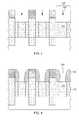
- FIG. 1is a cross-sectional view, taken across a fin, of one example of a starting semiconductor structure, the starting semiconductor structure including a semiconductor substrate, at least one fin over the substrate, source/drain regions, one or more gate structures including one or more gate electrodes, one or more spacer pairs and one or more gate caps, the one or more gate structures being separated by lower source/drain contacts, with one or more dielectric caps thereover, in accordance with one or more aspects of the present invention.
- FIG. 2depicts one example of the structure of FIG. 1 after removing each gate cap and upper spacer pair portions of each spacer pair, resulting in remaining lower spacer pair portions, in accordance with one or more aspects of the present invention.
- FIG. 3depicts one example of the structure of FIG. 2 after forming at least one air-gap spacer pair, each of the at least one air-gap spacer pair including air gaps therein, a gate cap for each gate electrode, each gate cap having a trench therein, in accordance with one or more aspects of the present invention.
- FIG. 4depicts one example of the structure of FIG. 3 after exposing the gate electrode of each of the one or more gate structures under each corresponding trench ( FIG. 3 ), the exposing resulting in exposed gate electrodes, upwardly extended and sloped spacer sidewalls above the air gaps and gate contact openings, in accordance with one or more aspects of the present invention.
- FIG. 5depicts one example of the structure of FIG. 4 after selectively filling a bottom portion of the gate contact openings ( FIG. 4 ) with metal on the gate electrodes (e.g., tungsten on tungsten or cobalt), filling a remaining portion of the gate contact openings with a hard mask material (e.g., silicon nitride), resulting in gate caps, and planarizing the structure, in accordance with one or more aspects of the present invention.
- metal on the gate electrodese.g., tungsten on tungsten or cobalt
- a hard mask materiale.g., silicon nitride
- FIG. 6depicts one example of the structure of FIG. 5 after forming a dielectric layer over the planarized structure, removing portions of the dielectric layer to form contact openings, forming source/drain contacts and gate contacts in the contact openings, and planarizing the structure, in accordance with one or more aspects of the present invention.
- FIG. 7depicts one example of the structure of FIG. 1 after recessing the gate structures down to (i.e., stopping on) a top surface of the gate electrodes, in accordance with one or more aspects of the present invention.
- FIG. 8depicts one example of the structure of FIG. 7 after forming inner spacers similar to that of FIG. 4 using, for example, a process similar to that described with regard to FIGS. 3 and 4 , resulting in gate contact openings above the gate electrodes, in accordance with one or more aspects of the present invention.
- FIG. 9depicts one example of the structure of FIG. 8 after partially filling the gate contact openings with metal, in accordance with one or more aspects of the present invention.
- FIG. 10depicts one example of the structure of FIG. 9 after removing all spacers ( FIG. 8 ) from the gate structures and leaving the metal formed with the inner spacers, in accordance with one or more aspects of the present invention.
- FIG. 11depicts one example of the structure of FIG. 10 after forming air-gap spacers adjacent opposite sidewalls of the gate electrodes and metal, forming gate caps and planarizing the structure, in accordance with one or more aspects of the present invention.
- FIG. 12depicts one example of the structure of FIG. 11 after forming a dielectric layer over the planarized structure, removing portions of the dielectric layer forming contact openings, forming source/drain contacts and gate contacts and planarizing the structure, in accordance with one or more aspects of the present invention.
- Approximating languagemay be applied to modify any quantitative representation that could permissibly vary without resulting in a change in the basic function to which it is related. Accordingly, a value modified by a term or terms, such as “about,” is not limited to the precise value specified. In some instances, the approximating language may correspond to the precision of an instrument for measuring the value.
- a method or device that “comprises,” “has,” “includes” or “contains” one or more steps or elementspossesses those one or more steps or elements, but is not limited to possessing only those one or more steps or elements.
- a step of a method or an element of a device that “comprises,” “has,” “includes” or “contains” one or more featurespossesses those one or more features, but is not limited to possessing only those one or more features.
- a device or structure that is configured in a certain wayis configured in at least that way, but may also be configured in ways that are not listed.
- connectionwhen used to refer to two physical elements, means a direct connection between the two physical elements.
- coupledcan mean a direct connection or a connection through one or more intermediary elements.
- the terms “may” and “may be”indicate a possibility of an occurrence within a set of circumstances; a possession of a specified property, characteristic or function; and/or qualify another verb by expressing one or more of an ability, capability, or possibility associated with the qualified verb. Accordingly, usage of “may” and “may be” indicates that a modified term is apparently appropriate, capable, or suitable for an indicated capacity, function, or usage, while taking into account that in some circumstances the modified term may sometimes not be appropriate, capable or suitable. For example, in some circumstances, an event or capacity can be expected, while in other circumstances the event or capacity cannot occur—this distinction is captured by the terms “may” and “may be.”
- the term “about” used with a value, such as measurement, size, etc.means a possible variation of plus or minus five percent of the value.
- the term “low-k dielectric”refers to a dielectric with a dielectric constant k ⁇ 3.9.
- air-gap spacerrefers to a spacer for a gate electrode having therein an air gap encased by the material of the spacer.
- FIG. 1is a cross-sectional view, taken along a fin, and across gates, of one example of a starting semiconductor structure 100 , the starting semiconductor structure including a semiconductor substrate 102 , at least one fin 104 over the substrate, source/drain regions 106 , one or more gate structures 108 including one or more gate electrodes 110 , one or more spacer pairs 112 and one or more gate caps 114 , the one or more gate structures being separated by lower source/drain contacts 116 , with one or more dielectric caps 118 thereover, in accordance with one or more aspects of the present invention.
- the material(s) of the gate electrode(s) 110may include, for example, one or more work-function-altering metals and/or composites.
- the work-function-altering metals and/or compositesmay include, for example, one or more of TiN, TaN, TiAl, TiAlC, TiC, W and/or Co.
- the material of the gate caps 114may include, for example, SiN, SiBCN, SiOCN or SiOC.
- the material of the lower source/drain contacts 116may include, for example, a bottom portion of silicide with a top portion of a conductive metal (e.g., Co or W).
- the material of the dielectric caps 118 over the lower source/drain contactsmay include, for example, an oxide (e.g., SiO 2 ).
- the starting structuremay be conventionally fabricated, for example, using known processes and techniques. However, although only a portion is shown for simplicity, it will be understood that, in practice, many such structures are typically included on the same substrate.
- substrate 102may include any silicon-containing substrate including, but not limited to, silicon (Si), single crystal silicon, polycrystalline Si, amorphous Si, silicon-on-nothing (SON), silicon-on-insulator (SOI) or silicon-on-replacement insulator (SRI) or silicon germanium substrates and the like.
- substrate 102may in addition or instead include various isolations, dopings and/or device features.
- the substratemay include other suitable elementary semiconductors, such as, for example, germanium (Ge) in crystal, a compound semiconductor, such as silicon carbide (SiC), gallium arsenide (GaAs), gallium phosphide (GaP), indium phosphide (InP), indium arsenide (InAs), and/or indium antimonide (InSb) or combinations thereof; an alloy semiconductor including GaAsP, AlInAs, GaInAs, GaInP, or GaInAsP or combinations thereof.
- germaniumgermanium
- SiCsilicon carbide
- GaAsgallium arsenide
- GaPgallium phosphide
- InPindium phosphide
- InAsindium arsenide
- InSbindium antimonide
- FIG. 2depicts one example of the structure of FIG. 1 after removing each gate cap 114 and upper spacer pair portions 111 of each spacer pair 112 , resulting in remaining lower spacer pair portions 120 , in accordance with one or more aspects of the present invention.
- the spacer pairs 112are fully removed. However, in practice, fully removing the spacer pairs carries a risk of damaging fin 104 , so a remaining portion of the spacer pairs is shown.
- FIG. 3depicts one example of the structure of FIG. 2 after forming at least one air-gap spacer pair 122 , each of the at least one air-gap spacer pair including air gaps 124 therein, a gate cap 126 for each gate electrode 110 , each gate cap having a trench 128 therein, in accordance with one or more aspects of the present invention.
- the air-gap spacer pairsmay be realized using a chemical-vapor deposition (CVD) process and pinch-off.
- CVDchemical-vapor deposition
- pinch-off with an air gap inside using the CVD processwill happen relatively quickly as compared to the area above the gate cap, which is left not fully filled, such that the trenches are unfilled portions of that area.
- FIG. 4depicts one example of the structure of FIG. 3 after exposing the gate electrode 110 of each of the one or more gate structures under each corresponding trench 128 ( FIG. 3 ).
- exposing the gate electrode(s)may be accomplished by applying an anisotropic etch process to material 126 , the exposing resulting in exposed gate electrodes 110 , upwardly extended and sloped spacer sidewalls 130 above the air gaps 124 and gate contact openings 132 , in accordance with one or more aspects of the present invention.
- FIG. 5depicts one example of the structure of FIG. 4 after selectively filling a bottom portion 133 of the gate contact openings ( 132 , FIG. 4 ) with metal 134 on the gate electrodes 110 (e.g., tungsten on tungsten or cobalt), filling a remaining portion 135 of the gate contact openings with a hard mask material (e.g., silicon nitride), resulting in gate caps 136 , and planarizing the structure, in accordance with one or more aspects of the present invention.
- metal 134 on the gate electrodes 110e.g., tungsten on tungsten or cobalt
- a hard mask materiale.g., silicon nitride
- FIG. 6depicts one example of the structure of FIG. 5 after forming a dielectric layer 142 over the planarized structure, removing portions of the dielectric layer to form upper source/drain contact openings 139 , forming upper source/drain contacts 138 and gate contacts 140 in the contact openings, and planarizing the structure, in accordance with one or more aspects of the present invention.
- etch processesare used for upper source/drain contacts 138 and gate contact(s) 140 .
- the source/drain contactsmay be formed using an etching process for dielectric layer 142 , exposing the lower source/drain contacts ( FIG. 1, 116 ) and stopping on a top surface of the lower source/drain contacts.
- the gate contact(s)may be realized by, for example, using a selective gate cap open process that does not damage the dielectric caps ( FIG. 1, 118 ) over the lower source/drain contacts. This prevents an electrical short between the gate contact and the bottom source/drain contact.
- the upper source/drain contact openingsmay be realized using, for example, a selective etch process for the openings in dielectric layer 142 and the lower source/drain contacts, selective to the material(s) of the gate cap(s) and spacers (e.g., SiN).
- the upper source/drain contacts 138 and gate contact(s) 140are effectively kept away from the air gaps 124 .
- the lower source/drain contactswould need to be recessed relatively deeply to prevent gate contact(s) 140 from electrically shorting with the lower source/drain contacts, as well as preventing contact of the upper source/drain contacts and the gate contact with the air gaps.
- FIG. 6is to illustrate that both the gate contact(s) and the upper source/drain contacts can be situated above the active region, without resulting in an electrical short therebetween or an electrical short with the gate or lower source/drain contacts.
- FIG. 7depicts one example of the structure of FIG. 1 after recessing 150 the gate structures 108 down to (i.e., stopping on) a top surface of the gate electrodes 110 , in accordance with one or more aspects of the present invention.
- FIG. 8depicts one example of the structure of FIG. 7 after forming inner spacers 152 similar to that of FIG. 4 using, for example, a process similar to that described with regard to FIGS. 3 and 4 , resulting in gate contact openings 154 above the gate electrodes 110 , in accordance with one or more aspects of the present invention.
- FIG. 9depicts one example of the structure of FIG. 8 after partially filling the gate contact openings 154 with metal 134 , in accordance with one or more aspects of the present invention.
- FIG. 10depicts one example of the structure of FIG. 9 after removing all spacers ( 112 and 152 , FIG. 8 ) from the gate structures and leaving the metal 134 formed with the inner spacers, in accordance with one or more aspects of the present invention.
- FIG. 11depicts one example of the structure of FIG. 10 after forming air-gap spacers 156 adjacent opposite sidewalls of the gate electrodes 110 and metal 134 , forming gate caps 158 and planarizing the structure, in accordance with one or more aspects of the present invention.
- FIG. 12depicts one example of the structure of FIG. 11 after forming a dielectric layer 164 over the planarized structure, removing portions of the dielectric layer forming contact openings 165 , forming source/drain contacts 160 and gate contacts 162 and planarizing the structure, in accordance with one or more aspects of the present invention.
- etch processesare used for upper source/drain contacts 160 and gate contact(s) 162 .
- the source/drain contactsmay be formed using an etching process for dielectric layer 164 , exposing the lower source/drain contacts ( FIG. 1, 116 ) and stopping on a top surface of the lower source/drain contacts.
- the gate contact(s)may be realized by, for example, using a selective gate cap open process that does not damage the dielectric caps ( FIG. 1, 118 ) over the lower source/drain contacts. This prevent an electrical short between the gate contact and the bottom source/drain contact.
- the upper source/drain contact openingsmay be realized using, for example, a selective etch process for the openings in dielectric layer 164 and the lower source/drain contacts, selective to the material(s) of the gate cap(s) and spacers (e.g., SiN). Note also, that the benefits of using the selective growth for metal 134 described with respect to FIG. 6 also apply to FIG. 12 .
- (upper) gate contact 162requires a patterning/mask process
- metal 134 above the gate electrode(s)covers much of the surface of the gate electrode(s) without the need for a patterning/mask process.
- the methodincludes providing a starting semiconductor structure, the starting semiconductor structure including a semiconductor substrate, a fin on the substrate, an active region having a source/drain pair with a channel region therebetween, a lower contact portion above a source and a drain of the source/drain pair, and a gate electrode over the channel region.
- the methodfurther includes forming an air-gap spacer pair adjacent opposite sidewalls of the gate electrode, forming a lower gate contact over the gate electrode, and forming an upper gate contact over the lower gate contact, the upper gate contact being situated above the active region.
- the air-gap spacer pairmay be, for example, formed prior to the lower gate contact.
- the starting semiconductor structuremay include, for example, a gate structure, the gate structure including the gate electrode and lower spacer portions adjacent opposite sidewalls of the gate electrode.
- forming the air-gap spacer pairmay include, for example, forming the air-gap spacer pair over the lower spacer portions, the air-gap spacer pair extending to a height of the gate electrode.
- forming the lower gate contactmay include, for example, forming an upwardly tapered top spacer pair over the air-gap spacer pair, resulting in a tapered gate contact opening, and forming the lower gate contact in the tapered gate contact opening.
- forming the upper gate contactmay include forming a dielectric layer over the structure after forming the lower gate contact, removing portions of the dielectric layer above the active region to expose the lower gate contact, resulting in an upper gate contact opening, and filling the upper gate contact opening with metal.
- the lower contact portion for each source and each drainmay have, for example, a dielectric cap thereon, and exposing the lower gate contact includes etching the dielectric layer over the structure selective to the dielectric cap.
- forming the lower gate contact in the method of the first aspectmay be, for example, formed prior to the air-gap spacer pair.
- the starting semiconductor structuremay further include, for example, a spacer pair adjacent opposite sidewalls of the gate electrode, the spacer pair extending to a height of the gate electrode, the method further including forming an upwardly tapered top spacer pair over the spacer pair, resulting in a lower gate contact opening, and forming the lower gate contact in the lower gate contact opening.
- forming the air-gap spacer pairmay include, for example, removing the upwardly tapered top spacer pair and the spacer pair thereunder, resulting in a spacer pair opening adjacent the opposite sidewalls of the gate electrode and opposite sidewalls of the lower gate contact, and forming the pair of air-gap spacers in the spacer pair opening.
- forming the upper gate contactmay include, for example, forming a dielectric layer above the structure with the pair of air-gap spacers, removing a portion of the dielectric layer above the active region, exposing the lower gate contact and the air-gap spacer pair, resulting in an upper gate contact opening, and filling the upper gate contact opening with metal.
- forming the lower gate contact in the method of the first aspectmay be accomplished, for example, without using a mask.
- the semiconductor structureincludes a semiconductor substrate, a semiconductor fin on the semiconductor substrate, a transistor integrated with the semiconductor fin at a top portion thereof, the transistor including an active region including a source, a drain and a channel region therebetween.
- the semiconductor structurefurther includes a gate structure over the channel region, the gate structure including a gate electrode, an air-gap spacer pair adjacent opposite sidewalls of the gate electrode, and a gate contact for the gate electrode.
- the gate contactmay include, for example, a lower gate contact portion and an upper gate contact portion.
- an air gap of the air-gap spacer pairmay, for example, span less than a height of the gate electrode. In another example, an air gap of the air-gap spacer pair may, for example, span more than a height of the gate electrode.
- the semiconductor structure having upper and lower gate contact portionsmay further include, for example, a lower source/drain contact portion above each of the source and the drain, each source/drain contact portion being adjacent an air gap of the air-gap spacer pair.
- the semiconductor structuremay further include, for example, an upper source/drain contact portion above each lower source/drain contact portion.
- the semiconductor structuremay further include, for example, a dielectric cap above each lower source/drain contact portion.
Landscapes
- Engineering & Computer Science (AREA)
- Physics & Mathematics (AREA)
- Condensed Matter Physics & Semiconductors (AREA)
- General Physics & Mathematics (AREA)
- Manufacturing & Machinery (AREA)
- Computer Hardware Design (AREA)
- Microelectronics & Electronic Packaging (AREA)
- Power Engineering (AREA)
- Insulated Gate Type Field-Effect Transistor (AREA)
- Electrodes Of Semiconductors (AREA)
- Junction Field-Effect Transistors (AREA)
Abstract
Description
Claims (13)
Priority Applications (3)
| Application Number | Priority Date | Filing Date | Title |
|---|---|---|---|
| US15/351,893US10446653B2 (en) | 2016-11-15 | 2016-11-15 | Transistor-based semiconductor device with air-gap spacers and gate contact over active area |
| TW106120890ATWI677096B (en) | 2016-11-15 | 2017-06-22 | Transistor-based semiconductor device with air-gap spacers and gate contact over active area |
| CN201711128692.8ACN108074972A (en) | 2016-11-15 | 2017-11-15 | There is the semiconductor device based on transistor of air gap separation part and gate contact above active region |
Applications Claiming Priority (1)
| Application Number | Priority Date | Filing Date | Title |
|---|---|---|---|
| US15/351,893US10446653B2 (en) | 2016-11-15 | 2016-11-15 | Transistor-based semiconductor device with air-gap spacers and gate contact over active area |
Publications (2)
| Publication Number | Publication Date |
|---|---|
| US20180138279A1 US20180138279A1 (en) | 2018-05-17 |
| US10446653B2true US10446653B2 (en) | 2019-10-15 |
Family
ID=62106359
Family Applications (1)
| Application Number | Title | Priority Date | Filing Date |
|---|---|---|---|
| US15/351,893Active2036-12-03US10446653B2 (en) | 2016-11-15 | 2016-11-15 | Transistor-based semiconductor device with air-gap spacers and gate contact over active area |
Country Status (3)
| Country | Link |
|---|---|
| US (1) | US10446653B2 (en) |
| CN (1) | CN108074972A (en) |
| TW (1) | TWI677096B (en) |
Cited By (1)
| Publication number | Priority date | Publication date | Assignee | Title |
|---|---|---|---|---|
| US11876114B2 (en) | 2021-09-07 | 2024-01-16 | International Business Machines Corporation | Airgap gate spacer |
Families Citing this family (24)
| Publication number | Priority date | Publication date | Assignee | Title |
|---|---|---|---|---|
| US10211100B2 (en)* | 2017-03-27 | 2019-02-19 | Globalfoundries Inc. | Methods of forming an air gap adjacent a gate of a transistor and a gate contact above the active region of the transistor |
| US10269983B2 (en)* | 2017-05-09 | 2019-04-23 | Globalfoundries Inc. | Stacked nanosheet field-effect transistor with air gap spacers |
| US10388770B1 (en)* | 2018-03-19 | 2019-08-20 | Globalfoundries Inc. | Gate and source/drain contact structures positioned above an active region of a transistor device |
| US10388747B1 (en) | 2018-03-28 | 2019-08-20 | Globalfoundries Inc. | Gate contact structure positioned above an active region with air gaps positioned adjacent the gate structure |
| US10608096B2 (en)* | 2018-06-11 | 2020-03-31 | International Business Machines Corporation | Formation of air gap spacers for reducing parasitic capacitance |
| US10854503B2 (en)* | 2018-07-16 | 2020-12-01 | Taiwan Semiconductor Manufacturing Co., Ltd. | Semiconductor structure with air gap and method sealing the air gap |
| US11038059B2 (en)* | 2018-07-31 | 2021-06-15 | Taiwan Semiconductor Manufacturing Company, Ltd. | Semiconductor device and method of forming the same |
| US10714342B2 (en)* | 2018-07-31 | 2020-07-14 | Taiwan Semiconductor Manufacturing Co., Ltd. | Semiconductor device and method of forming the same |
| US10529826B1 (en) | 2018-08-13 | 2020-01-07 | Globalfoundries Inc. | Forming self-aligned gate and source/drain contacts using sacrificial gate cap spacer and resulting devices |
| US10950692B2 (en)* | 2018-09-04 | 2021-03-16 | Globalfoundries U.S. Inc. | Methods of forming air gaps between source/drain contacts and the resulting devices |
| US10892338B2 (en) | 2018-10-24 | 2021-01-12 | Globalfoundries Inc. | Scaled gate contact and source/drain cap |
| US10886378B2 (en) | 2019-01-02 | 2021-01-05 | Globalfoundries Inc. | Method of forming air-gap spacers and gate contact over active region and the resulting device |
| US10903331B2 (en)* | 2019-03-25 | 2021-01-26 | International Business Machines Corporation | Positioning air-gap spacers in a transistor for improved control of parasitic capacitance |
| US11011638B2 (en)* | 2019-08-26 | 2021-05-18 | International Business Machines Corporation | Transistor having airgap spacer around gate structure |
| US11282920B2 (en)* | 2019-09-16 | 2022-03-22 | Taiwan Semiconductor Manufacturing Co., Ltd. | Semiconductor device with air gap on gate structure and method for forming the same |
| CN111106160B (en) | 2019-12-06 | 2023-12-19 | 中国科学院微电子研究所 | Semiconductor device and manufacturing method thereof and electronic equipment including the device |
| US11233136B2 (en) | 2019-12-20 | 2022-01-25 | Taiwan Semiconductor Manufacturing Co., Ltd. | Silicon carbide oxide hard mask for reducing dishing effects |
| US11302814B2 (en)* | 2020-01-23 | 2022-04-12 | Nanya Technology Corp. | Semiconductor device with porous dielectric structure and method for fabricating the same |
| CN113257783B (en)* | 2020-02-10 | 2024-05-10 | 华邦电子股份有限公司 | Memory device and method of manufacturing the same |
| US20210249310A1 (en)* | 2020-02-11 | 2021-08-12 | Nanya Technology Corporation | Semiconductor device with porous dielectric structure and method for fabricating the same |
| US11264278B1 (en)* | 2020-08-11 | 2022-03-01 | Nanya Technology Corporation | Transistor with reduced gate resistance and improved process margin of forming self-aligned contact |
| CN112466847B (en)* | 2020-11-25 | 2025-08-12 | 福建省晋华集成电路有限公司 | Semiconductor device and semiconductor device manufacturing method |
| CN114823894A (en)* | 2021-01-18 | 2022-07-29 | 中芯国际集成电路制造(上海)有限公司 | Semiconductor structure and method of forming the same |
| KR20220158340A (en)* | 2021-05-24 | 2022-12-01 | 삼성전자주식회사 | Semiconductor devices including gate structure and method of forming the same |
Citations (12)
| Publication number | Priority date | Publication date | Assignee | Title |
|---|---|---|---|---|
| US5915182A (en)* | 1997-10-17 | 1999-06-22 | Texas Instruments - Acer Incorporated | MOSFET with self-aligned silicidation and gate-side air-gap structure |
| US6297109B1 (en)* | 1999-08-19 | 2001-10-02 | Chartered Semiconductor Manufacturing Ltd. | Method to form shallow junction transistors while eliminating shorts due to junction spiking |
| US6596599B1 (en)* | 2001-07-16 | 2003-07-22 | Taiwan Semiconductor Manufacturing Company | Gate stack for high performance sub-micron CMOS devices |
| US20070184615A1 (en)* | 2005-12-30 | 2007-08-09 | Stmicroelectronics S.R.L. | Process for Manufacturing a Non-Volatile Memory Electronic Device Integrated on a Semiconductor Substrate and Corresponding Device |
| US20100055904A1 (en) | 2008-08-29 | 2010-03-04 | Novellus Systems Inc. | Method for reducing tungsten roughness and improving reflectivity |
| US20100102363A1 (en) | 2008-10-24 | 2010-04-29 | Advanced Micro Devices, Inc. | Air gap spacer formation |
| US8124531B2 (en) | 2009-08-04 | 2012-02-28 | Novellus Systems, Inc. | Depositing tungsten into high aspect ratio features |
| US20120104512A1 (en)* | 2010-10-28 | 2012-05-03 | International Business Machines Corporation | Sealed air gap for semiconductor chip |
| US20130049132A1 (en)* | 2011-08-24 | 2013-02-28 | International Business Machines Corporation | Parasitic capacitance reduction in mosfet by airgap ild |
| US20130093019A1 (en)* | 2011-10-13 | 2013-04-18 | International Business Machines Corporation | Finfet parasitic capacitance reduction using air gap |
| US20130307032A1 (en) | 2012-05-16 | 2013-11-21 | Globalfoundries Inc. | Methods of forming conductive contacts for a semiconductor device |
| US20140138779A1 (en)* | 2012-11-20 | 2014-05-22 | GlobalFoundries, Inc. | Integrated circuits and methods for fabricating integrated circuits with reduced parasitic capacitance |
- 2016
- 2016-11-15USUS15/351,893patent/US10446653B2/enactiveActive
- 2017
- 2017-06-22TWTW106120890Apatent/TWI677096B/enactive
- 2017-11-15CNCN201711128692.8Apatent/CN108074972A/enactivePending
Patent Citations (14)
| Publication number | Priority date | Publication date | Assignee | Title |
|---|---|---|---|---|
| US5915182A (en)* | 1997-10-17 | 1999-06-22 | Texas Instruments - Acer Incorporated | MOSFET with self-aligned silicidation and gate-side air-gap structure |
| US6297109B1 (en)* | 1999-08-19 | 2001-10-02 | Chartered Semiconductor Manufacturing Ltd. | Method to form shallow junction transistors while eliminating shorts due to junction spiking |
| US6596599B1 (en)* | 2001-07-16 | 2003-07-22 | Taiwan Semiconductor Manufacturing Company | Gate stack for high performance sub-micron CMOS devices |
| US20070184615A1 (en)* | 2005-12-30 | 2007-08-09 | Stmicroelectronics S.R.L. | Process for Manufacturing a Non-Volatile Memory Electronic Device Integrated on a Semiconductor Substrate and Corresponding Device |
| US20100055904A1 (en) | 2008-08-29 | 2010-03-04 | Novellus Systems Inc. | Method for reducing tungsten roughness and improving reflectivity |
| US7741663B2 (en) | 2008-10-24 | 2010-06-22 | Globalfoundries Inc. | Air gap spacer formation |
| US20100102363A1 (en) | 2008-10-24 | 2010-04-29 | Advanced Micro Devices, Inc. | Air gap spacer formation |
| US8124531B2 (en) | 2009-08-04 | 2012-02-28 | Novellus Systems, Inc. | Depositing tungsten into high aspect ratio features |
| US20120104512A1 (en)* | 2010-10-28 | 2012-05-03 | International Business Machines Corporation | Sealed air gap for semiconductor chip |
| US20130049132A1 (en)* | 2011-08-24 | 2013-02-28 | International Business Machines Corporation | Parasitic capacitance reduction in mosfet by airgap ild |
| US20130093019A1 (en)* | 2011-10-13 | 2013-04-18 | International Business Machines Corporation | Finfet parasitic capacitance reduction using air gap |
| US8637930B2 (en)* | 2011-10-13 | 2014-01-28 | International Business Machines Company | FinFET parasitic capacitance reduction using air gap |
| US20130307032A1 (en) | 2012-05-16 | 2013-11-21 | Globalfoundries Inc. | Methods of forming conductive contacts for a semiconductor device |
| US20140138779A1 (en)* | 2012-11-20 | 2014-05-22 | GlobalFoundries, Inc. | Integrated circuits and methods for fabricating integrated circuits with reduced parasitic capacitance |
Cited By (1)
| Publication number | Priority date | Publication date | Assignee | Title |
|---|---|---|---|---|
| US11876114B2 (en) | 2021-09-07 | 2024-01-16 | International Business Machines Corporation | Airgap gate spacer |
Also Published As
| Publication number | Publication date |
|---|---|
| CN108074972A (en) | 2018-05-25 |
| TWI677096B (en) | 2019-11-11 |
| TW201834245A (en) | 2018-09-16 |
| US20180138279A1 (en) | 2018-05-17 |
Similar Documents
| Publication | Publication Date | Title |
|---|---|---|
| US10446653B2 (en) | Transistor-based semiconductor device with air-gap spacers and gate contact over active area | |
| US9691897B2 (en) | Three-dimensional semiconductor transistor with gate contact in active region | |
| US10199480B2 (en) | Controlling self-aligned gate length in vertical transistor replacement gate flow | |
| US9000522B2 (en) | FinFET with dielectric isolation by silicon-on-nothing and method of fabrication | |
| US9147680B2 (en) | Integrated circuits having replacement metal gates with improved threshold voltage performance and methods for fabricating the same | |
| US9559000B1 (en) | Hybrid logic and SRAM contacts | |
| US10002932B2 (en) | Self-aligned contact protection using reinforced gate cap and spacer portions | |
| US9685537B1 (en) | Gate length control for vertical transistors and integration with replacement gate flow | |
| KR20150003806A (en) | Preventing shorting of adjacent devices | |
| US10290634B2 (en) | Multiple threshold voltages using fin pitch and profile | |
| US20160049488A1 (en) | Semiconductor gate with wide top or bottom | |
| US9666709B2 (en) | Non-planar semiconductor structure with preserved isolation region | |
| US10038096B2 (en) | Three-dimensional finFET transistor with portion(s) of the fin channel removed in gate-last flow | |
| US9691787B2 (en) | Co-fabricated bulk devices and semiconductor-on-insulator devices | |
| US9236308B1 (en) | Methods of fabricating fin structures of uniform height | |
| US9401408B2 (en) | Confined early epitaxy with local interconnect capability | |
| US12324207B2 (en) | Channel protection of gate-all-around devices for performance optimization | |
| US9362279B1 (en) | Contact formation for semiconductor device | |
| US10446399B2 (en) | Hard mask layer to reduce loss of isolation material during dummy gate removal | |
| US9601512B2 (en) | SOI-based semiconductor device with dynamic threshold voltage | |
| US20160111514A1 (en) | Ultra-low resistance gate structure for non-planar device via minimized work function material | |
| US20170069753A1 (en) | Integrated circuits having tunnel transistors and methods for fabricating the same | |
| US20170207118A1 (en) | Self-aligned source/drain contact in replacement metal gate process | |
| US9972620B2 (en) | Preventing shorting between source and/or drain contacts and gate | |
| US20200312725A1 (en) | Method of forming a semiconductor device |
Legal Events
| Date | Code | Title | Description |
|---|---|---|---|
| AS | Assignment | Owner name:GLOBALFOUNDRIES INC., CAYMAN ISLANDS Free format text:ASSIGNMENT OF ASSIGNORS INTEREST;ASSIGNORS:XIE, RUILONG;SUNG, MIN GYU;PARK, CHANRO;AND OTHERS;SIGNING DATES FROM 20161110 TO 20161114;REEL/FRAME:040327/0668 | |
| AS | Assignment | Owner name:WILMINGTON TRUST, NATIONAL ASSOCIATION, DELAWARE Free format text:SECURITY AGREEMENT;ASSIGNOR:GLOBALFOUNDRIES INC.;REEL/FRAME:049490/0001 Effective date:20181127 | |
| STPP | Information on status: patent application and granting procedure in general | Free format text:FINAL REJECTION MAILED | |
| STPP | Information on status: patent application and granting procedure in general | Free format text:RESPONSE AFTER FINAL ACTION FORWARDED TO EXAMINER | |
| STPP | Information on status: patent application and granting procedure in general | Free format text:NOTICE OF ALLOWANCE MAILED -- APPLICATION RECEIVED IN OFFICE OF PUBLICATIONS | |
| STPP | Information on status: patent application and granting procedure in general | Free format text:PUBLICATIONS -- ISSUE FEE PAYMENT VERIFIED | |
| STCF | Information on status: patent grant | Free format text:PATENTED CASE | |
| AS | Assignment | Owner name:GLOBALFOUNDRIES U.S. INC., CALIFORNIA Free format text:ASSIGNMENT OF ASSIGNORS INTEREST;ASSIGNOR:GLOBALFOUNDRIES INC.;REEL/FRAME:054633/0001 Effective date:20201022 | |
| AS | Assignment | Owner name:GLOBALFOUNDRIES INC., CAYMAN ISLANDS Free format text:RELEASE BY SECURED PARTY;ASSIGNOR:WILMINGTON TRUST, NATIONAL ASSOCIATION;REEL/FRAME:054636/0001 Effective date:20201117 | |
| AS | Assignment | Owner name:GLOBALFOUNDRIES U.S. INC., NEW YORK Free format text:RELEASE BY SECURED PARTY;ASSIGNOR:WILMINGTON TRUST, NATIONAL ASSOCIATION;REEL/FRAME:056987/0001 Effective date:20201117 | |
| MAFP | Maintenance fee payment | Free format text:PAYMENT OF MAINTENANCE FEE, 4TH YEAR, LARGE ENTITY (ORIGINAL EVENT CODE: M1551); ENTITY STATUS OF PATENT OWNER: LARGE ENTITY Year of fee payment:4 |