US10446532B2 - Systems and methods for efficient transfer of semiconductor elements - Google Patents
Systems and methods for efficient transfer of semiconductor elementsDownload PDFInfo
- Publication number
- US10446532B2 US10446532B2US15/389,157US201615389157AUS10446532B2US 10446532 B2US10446532 B2US 10446532B2US 201615389157 AUS201615389157 AUS 201615389157AUS 10446532 B2US10446532 B2US 10446532B2
- Authority
- US
- United States
- Prior art keywords
- film
- support structure
- dies
- elements
- die
- Prior art date
- Legal status (The legal status is an assumption and is not a legal conclusion. Google has not performed a legal analysis and makes no representation as to the accuracy of the status listed.)
- Active
Links
Images


Classifications
- H—ELECTRICITY
- H01—ELECTRIC ELEMENTS
- H01L—SEMICONDUCTOR DEVICES NOT COVERED BY CLASS H10
- H01L21/00—Processes or apparatus adapted for the manufacture or treatment of semiconductor or solid state devices or of parts thereof
- H01L21/67—Apparatus specially adapted for handling semiconductor or electric solid state devices during manufacture or treatment thereof; Apparatus specially adapted for handling wafers during manufacture or treatment of semiconductor or electric solid state devices or components ; Apparatus not specifically provided for elsewhere
- H01L21/67005—Apparatus not specifically provided for elsewhere
- H01L21/67011—Apparatus for manufacture or treatment
- H—ELECTRICITY
- H01—ELECTRIC ELEMENTS
- H01L—SEMICONDUCTOR DEVICES NOT COVERED BY CLASS H10
- H01L21/00—Processes or apparatus adapted for the manufacture or treatment of semiconductor or solid state devices or of parts thereof
- H01L21/67—Apparatus specially adapted for handling semiconductor or electric solid state devices during manufacture or treatment thereof; Apparatus specially adapted for handling wafers during manufacture or treatment of semiconductor or electric solid state devices or components ; Apparatus not specifically provided for elsewhere
- H01L21/683—Apparatus specially adapted for handling semiconductor or electric solid state devices during manufacture or treatment thereof; Apparatus specially adapted for handling wafers during manufacture or treatment of semiconductor or electric solid state devices or components ; Apparatus not specifically provided for elsewhere for supporting or gripping
- H01L21/6835—Apparatus specially adapted for handling semiconductor or electric solid state devices during manufacture or treatment thereof; Apparatus specially adapted for handling wafers during manufacture or treatment of semiconductor or electric solid state devices or components ; Apparatus not specifically provided for elsewhere for supporting or gripping using temporarily an auxiliary support
- H—ELECTRICITY
- H01—ELECTRIC ELEMENTS
- H01L—SEMICONDUCTOR DEVICES NOT COVERED BY CLASS H10
- H01L25/00—Assemblies consisting of a plurality of semiconductor or other solid state devices
- H01L25/50—Multistep manufacturing processes of assemblies consisting of devices, the devices being individual devices of subclass H10D or integrated devices of class H10
- H—ELECTRICITY
- H01—ELECTRIC ELEMENTS
- H01L—SEMICONDUCTOR DEVICES NOT COVERED BY CLASS H10
- H01L21/00—Processes or apparatus adapted for the manufacture or treatment of semiconductor or solid state devices or of parts thereof
- H01L21/02—Manufacture or treatment of semiconductor devices or of parts thereof
- H01L21/04—Manufacture or treatment of semiconductor devices or of parts thereof the devices having potential barriers, e.g. a PN junction, depletion layer or carrier concentration layer
- H01L21/50—Assembly of semiconductor devices using processes or apparatus not provided for in a single one of the groups H01L21/18 - H01L21/326 or H10D48/04 - H10D48/07 e.g. sealing of a cap to a base of a container
- H—ELECTRICITY
- H01—ELECTRIC ELEMENTS
- H01L—SEMICONDUCTOR DEVICES NOT COVERED BY CLASS H10
- H01L21/00—Processes or apparatus adapted for the manufacture or treatment of semiconductor or solid state devices or of parts thereof
- H01L21/67—Apparatus specially adapted for handling semiconductor or electric solid state devices during manufacture or treatment thereof; Apparatus specially adapted for handling wafers during manufacture or treatment of semiconductor or electric solid state devices or components ; Apparatus not specifically provided for elsewhere
- H01L21/67005—Apparatus not specifically provided for elsewhere
- H01L21/67011—Apparatus for manufacture or treatment
- H01L21/67121—Apparatus for making assemblies not otherwise provided for, e.g. package constructions
- H—ELECTRICITY
- H01—ELECTRIC ELEMENTS
- H01L—SEMICONDUCTOR DEVICES NOT COVERED BY CLASS H10
- H01L21/00—Processes or apparatus adapted for the manufacture or treatment of semiconductor or solid state devices or of parts thereof
- H01L21/67—Apparatus specially adapted for handling semiconductor or electric solid state devices during manufacture or treatment thereof; Apparatus specially adapted for handling wafers during manufacture or treatment of semiconductor or electric solid state devices or components ; Apparatus not specifically provided for elsewhere
- H01L21/67005—Apparatus not specifically provided for elsewhere
- H01L21/67011—Apparatus for manufacture or treatment
- H01L21/67132—Apparatus for placing on an insulating substrate, e.g. tape
- H—ELECTRICITY
- H01—ELECTRIC ELEMENTS
- H01L—SEMICONDUCTOR DEVICES NOT COVERED BY CLASS H10
- H01L21/00—Processes or apparatus adapted for the manufacture or treatment of semiconductor or solid state devices or of parts thereof
- H01L21/67—Apparatus specially adapted for handling semiconductor or electric solid state devices during manufacture or treatment thereof; Apparatus specially adapted for handling wafers during manufacture or treatment of semiconductor or electric solid state devices or components ; Apparatus not specifically provided for elsewhere
- H01L21/67005—Apparatus not specifically provided for elsewhere
- H01L21/67011—Apparatus for manufacture or treatment
- H01L21/67144—Apparatus for mounting on conductive members, e.g. leadframes or conductors on insulating substrates
- H—ELECTRICITY
- H01—ELECTRIC ELEMENTS
- H01L—SEMICONDUCTOR DEVICES NOT COVERED BY CLASS H10
- H01L21/00—Processes or apparatus adapted for the manufacture or treatment of semiconductor or solid state devices or of parts thereof
- H01L21/67—Apparatus specially adapted for handling semiconductor or electric solid state devices during manufacture or treatment thereof; Apparatus specially adapted for handling wafers during manufacture or treatment of semiconductor or electric solid state devices or components ; Apparatus not specifically provided for elsewhere
- H01L21/677—Apparatus specially adapted for handling semiconductor or electric solid state devices during manufacture or treatment thereof; Apparatus specially adapted for handling wafers during manufacture or treatment of semiconductor or electric solid state devices or components ; Apparatus not specifically provided for elsewhere for conveying, e.g. between different workstations
- H—ELECTRICITY
- H01—ELECTRIC ELEMENTS
- H01L—SEMICONDUCTOR DEVICES NOT COVERED BY CLASS H10
- H01L21/00—Processes or apparatus adapted for the manufacture or treatment of semiconductor or solid state devices or of parts thereof
- H01L21/67—Apparatus specially adapted for handling semiconductor or electric solid state devices during manufacture or treatment thereof; Apparatus specially adapted for handling wafers during manufacture or treatment of semiconductor or electric solid state devices or components ; Apparatus not specifically provided for elsewhere
- H01L21/68—Apparatus specially adapted for handling semiconductor or electric solid state devices during manufacture or treatment thereof; Apparatus specially adapted for handling wafers during manufacture or treatment of semiconductor or electric solid state devices or components ; Apparatus not specifically provided for elsewhere for positioning, orientation or alignment
- H01L21/682—Mask-wafer alignment
- H—ELECTRICITY
- H01—ELECTRIC ELEMENTS
- H01L—SEMICONDUCTOR DEVICES NOT COVERED BY CLASS H10
- H01L21/00—Processes or apparatus adapted for the manufacture or treatment of semiconductor or solid state devices or of parts thereof
- H01L21/67—Apparatus specially adapted for handling semiconductor or electric solid state devices during manufacture or treatment thereof; Apparatus specially adapted for handling wafers during manufacture or treatment of semiconductor or electric solid state devices or components ; Apparatus not specifically provided for elsewhere
- H01L21/683—Apparatus specially adapted for handling semiconductor or electric solid state devices during manufacture or treatment thereof; Apparatus specially adapted for handling wafers during manufacture or treatment of semiconductor or electric solid state devices or components ; Apparatus not specifically provided for elsewhere for supporting or gripping
- H01L21/6835—Apparatus specially adapted for handling semiconductor or electric solid state devices during manufacture or treatment thereof; Apparatus specially adapted for handling wafers during manufacture or treatment of semiconductor or electric solid state devices or components ; Apparatus not specifically provided for elsewhere for supporting or gripping using temporarily an auxiliary support
- H01L21/6836—Wafer tapes, e.g. grinding or dicing support tapes
- H—ELECTRICITY
- H01—ELECTRIC ELEMENTS
- H01L—SEMICONDUCTOR DEVICES NOT COVERED BY CLASS H10
- H01L21/00—Processes or apparatus adapted for the manufacture or treatment of semiconductor or solid state devices or of parts thereof
- H01L21/67—Apparatus specially adapted for handling semiconductor or electric solid state devices during manufacture or treatment thereof; Apparatus specially adapted for handling wafers during manufacture or treatment of semiconductor or electric solid state devices or components ; Apparatus not specifically provided for elsewhere
- H01L21/683—Apparatus specially adapted for handling semiconductor or electric solid state devices during manufacture or treatment thereof; Apparatus specially adapted for handling wafers during manufacture or treatment of semiconductor or electric solid state devices or components ; Apparatus not specifically provided for elsewhere for supporting or gripping
- H01L21/687—Apparatus specially adapted for handling semiconductor or electric solid state devices during manufacture or treatment thereof; Apparatus specially adapted for handling wafers during manufacture or treatment of semiconductor or electric solid state devices or components ; Apparatus not specifically provided for elsewhere for supporting or gripping using mechanical means, e.g. chucks, clamps or pinches
- H01L21/68714—Apparatus specially adapted for handling semiconductor or electric solid state devices during manufacture or treatment thereof; Apparatus specially adapted for handling wafers during manufacture or treatment of semiconductor or electric solid state devices or components ; Apparatus not specifically provided for elsewhere for supporting or gripping using mechanical means, e.g. chucks, clamps or pinches the wafers being placed on a susceptor, stage or support
- H01L21/68785—Apparatus specially adapted for handling semiconductor or electric solid state devices during manufacture or treatment thereof; Apparatus specially adapted for handling wafers during manufacture or treatment of semiconductor or electric solid state devices or components ; Apparatus not specifically provided for elsewhere for supporting or gripping using mechanical means, e.g. chucks, clamps or pinches the wafers being placed on a susceptor, stage or support characterised by the mechanical construction of the susceptor, stage or support
- H—ELECTRICITY
- H01—ELECTRIC ELEMENTS
- H01L—SEMICONDUCTOR DEVICES NOT COVERED BY CLASS H10
- H01L21/00—Processes or apparatus adapted for the manufacture or treatment of semiconductor or solid state devices or of parts thereof
- H01L21/70—Manufacture or treatment of devices consisting of a plurality of solid state components formed in or on a common substrate or of parts thereof; Manufacture of integrated circuit devices or of parts thereof
- H01L21/77—Manufacture or treatment of devices consisting of a plurality of solid state components or integrated circuits formed in, or on, a common substrate
- H01L21/78—Manufacture or treatment of devices consisting of a plurality of solid state components or integrated circuits formed in, or on, a common substrate with subsequent division of the substrate into plural individual devices
- H—ELECTRICITY
- H01—ELECTRIC ELEMENTS
- H01L—SEMICONDUCTOR DEVICES NOT COVERED BY CLASS H10
- H01L22/00—Testing or measuring during manufacture or treatment; Reliability measurements, i.e. testing of parts without further processing to modify the parts as such; Structural arrangements therefor
- H01L22/10—Measuring as part of the manufacturing process
- H01L22/14—Measuring as part of the manufacturing process for electrical parameters, e.g. resistance, deep-levels, CV, diffusions by electrical means
- H—ELECTRICITY
- H01—ELECTRIC ELEMENTS
- H01L—SEMICONDUCTOR DEVICES NOT COVERED BY CLASS H10
- H01L24/00—Arrangements for connecting or disconnecting semiconductor or solid-state bodies; Methods or apparatus related thereto
- H01L24/74—Apparatus for manufacturing arrangements for connecting or disconnecting semiconductor or solid-state bodies
- H01L24/75—Apparatus for connecting with bump connectors or layer connectors
- H—ELECTRICITY
- H01—ELECTRIC ELEMENTS
- H01L—SEMICONDUCTOR DEVICES NOT COVERED BY CLASS H10
- H01L24/00—Arrangements for connecting or disconnecting semiconductor or solid-state bodies; Methods or apparatus related thereto
- H01L24/80—Methods for connecting semiconductor or other solid state bodies using means for bonding being attached to, or being formed on, the surface to be connected
- H01L24/81—Methods for connecting semiconductor or other solid state bodies using means for bonding being attached to, or being formed on, the surface to be connected using a bump connector
- H—ELECTRICITY
- H01—ELECTRIC ELEMENTS
- H01L—SEMICONDUCTOR DEVICES NOT COVERED BY CLASS H10
- H01L25/00—Assemblies consisting of a plurality of semiconductor or other solid state devices
- H01L25/03—Assemblies consisting of a plurality of semiconductor or other solid state devices all the devices being of a type provided for in a single subclass of subclasses H10B, H10D, H10F, H10H, H10K or H10N, e.g. assemblies of rectifier diodes
- H01L25/10—Assemblies consisting of a plurality of semiconductor or other solid state devices all the devices being of a type provided for in a single subclass of subclasses H10B, H10D, H10F, H10H, H10K or H10N, e.g. assemblies of rectifier diodes the devices having separate containers
- H01L25/105—Assemblies consisting of a plurality of semiconductor or other solid state devices all the devices being of a type provided for in a single subclass of subclasses H10B, H10D, H10F, H10H, H10K or H10N, e.g. assemblies of rectifier diodes the devices having separate containers the devices being integrated devices of class H10
- H—ELECTRICITY
- H01—ELECTRIC ELEMENTS
- H01L—SEMICONDUCTOR DEVICES NOT COVERED BY CLASS H10
- H01L2221/00—Processes or apparatus adapted for the manufacture or treatment of semiconductor or solid state devices or of parts thereof covered by H01L21/00
- H01L2221/67—Apparatus for handling semiconductor or electric solid state devices during manufacture or treatment thereof; Apparatus for handling wafers during manufacture or treatment of semiconductor or electric solid state devices or components; Apparatus not specifically provided for elsewhere
- H01L2221/683—Apparatus for handling semiconductor or electric solid state devices during manufacture or treatment thereof; Apparatus for handling wafers during manufacture or treatment of semiconductor or electric solid state devices or components; Apparatus not specifically provided for elsewhere for supporting or gripping
- H01L2221/68304—Apparatus for handling semiconductor or electric solid state devices during manufacture or treatment thereof; Apparatus for handling wafers during manufacture or treatment of semiconductor or electric solid state devices or components; Apparatus not specifically provided for elsewhere for supporting or gripping using temporarily an auxiliary support
- H01L2221/68318—Auxiliary support including means facilitating the separation of a device or wafer from the auxiliary support
- H01L2221/68322—Auxiliary support including means facilitating the selective separation of some of a plurality of devices from the auxiliary support
- H—ELECTRICITY
- H01—ELECTRIC ELEMENTS
- H01L—SEMICONDUCTOR DEVICES NOT COVERED BY CLASS H10
- H01L2221/00—Processes or apparatus adapted for the manufacture or treatment of semiconductor or solid state devices or of parts thereof covered by H01L21/00
- H01L2221/67—Apparatus for handling semiconductor or electric solid state devices during manufacture or treatment thereof; Apparatus for handling wafers during manufacture or treatment of semiconductor or electric solid state devices or components; Apparatus not specifically provided for elsewhere
- H01L2221/683—Apparatus for handling semiconductor or electric solid state devices during manufacture or treatment thereof; Apparatus for handling wafers during manufacture or treatment of semiconductor or electric solid state devices or components; Apparatus not specifically provided for elsewhere for supporting or gripping
- H01L2221/68304—Apparatus for handling semiconductor or electric solid state devices during manufacture or treatment thereof; Apparatus for handling wafers during manufacture or treatment of semiconductor or electric solid state devices or components; Apparatus not specifically provided for elsewhere for supporting or gripping using temporarily an auxiliary support
- H01L2221/68327—Apparatus for handling semiconductor or electric solid state devices during manufacture or treatment thereof; Apparatus for handling wafers during manufacture or treatment of semiconductor or electric solid state devices or components; Apparatus not specifically provided for elsewhere for supporting or gripping using temporarily an auxiliary support used during dicing or grinding
- H—ELECTRICITY
- H01—ELECTRIC ELEMENTS
- H01L—SEMICONDUCTOR DEVICES NOT COVERED BY CLASS H10
- H01L2221/00—Processes or apparatus adapted for the manufacture or treatment of semiconductor or solid state devices or of parts thereof covered by H01L21/00
- H01L2221/67—Apparatus for handling semiconductor or electric solid state devices during manufacture or treatment thereof; Apparatus for handling wafers during manufacture or treatment of semiconductor or electric solid state devices or components; Apparatus not specifically provided for elsewhere
- H01L2221/683—Apparatus for handling semiconductor or electric solid state devices during manufacture or treatment thereof; Apparatus for handling wafers during manufacture or treatment of semiconductor or electric solid state devices or components; Apparatus not specifically provided for elsewhere for supporting or gripping
- H01L2221/68304—Apparatus for handling semiconductor or electric solid state devices during manufacture or treatment thereof; Apparatus for handling wafers during manufacture or treatment of semiconductor or electric solid state devices or components; Apparatus not specifically provided for elsewhere for supporting or gripping using temporarily an auxiliary support
- H01L2221/68354—Apparatus for handling semiconductor or electric solid state devices during manufacture or treatment thereof; Apparatus for handling wafers during manufacture or treatment of semiconductor or electric solid state devices or components; Apparatus not specifically provided for elsewhere for supporting or gripping using temporarily an auxiliary support used to support diced chips prior to mounting
- H—ELECTRICITY
- H01—ELECTRIC ELEMENTS
- H01L—SEMICONDUCTOR DEVICES NOT COVERED BY CLASS H10
- H01L2224/00—Indexing scheme for arrangements for connecting or disconnecting semiconductor or solid-state bodies and methods related thereto as covered by H01L24/00
- H01L2224/01—Means for bonding being attached to, or being formed on, the surface to be connected, e.g. chip-to-package, die-attach, "first-level" interconnects; Manufacturing methods related thereto
- H01L2224/02—Bonding areas; Manufacturing methods related thereto
- H01L2224/07—Structure, shape, material or disposition of the bonding areas after the connecting process
- H01L2224/08—Structure, shape, material or disposition of the bonding areas after the connecting process of an individual bonding area
- H01L2224/081—Disposition
- H01L2224/0812—Disposition the bonding area connecting directly to another bonding area, i.e. connectorless bonding, e.g. bumpless bonding
- H01L2224/08135—Disposition the bonding area connecting directly to another bonding area, i.e. connectorless bonding, e.g. bumpless bonding the bonding area connecting between different semiconductor or solid-state bodies, i.e. chip-to-chip
- H01L2224/08145—Disposition the bonding area connecting directly to another bonding area, i.e. connectorless bonding, e.g. bumpless bonding the bonding area connecting between different semiconductor or solid-state bodies, i.e. chip-to-chip the bodies being stacked
- H—ELECTRICITY
- H01—ELECTRIC ELEMENTS
- H01L—SEMICONDUCTOR DEVICES NOT COVERED BY CLASS H10
- H01L2224/00—Indexing scheme for arrangements for connecting or disconnecting semiconductor or solid-state bodies and methods related thereto as covered by H01L24/00
- H01L2224/74—Apparatus for manufacturing arrangements for connecting or disconnecting semiconductor or solid-state bodies and for methods related thereto
- H01L2224/75—Apparatus for connecting with bump connectors or layer connectors
- H01L2224/7525—Means for applying energy, e.g. heating means
- H01L2224/753—Means for applying energy, e.g. heating means by means of pressure
- H01L2224/75301—Bonding head
- H01L2224/75314—Auxiliary members on the pressing surface
- H01L2224/75317—Removable auxiliary member
- H—ELECTRICITY
- H01—ELECTRIC ELEMENTS
- H01L—SEMICONDUCTOR DEVICES NOT COVERED BY CLASS H10
- H01L2224/00—Indexing scheme for arrangements for connecting or disconnecting semiconductor or solid-state bodies and methods related thereto as covered by H01L24/00
- H01L2224/74—Apparatus for manufacturing arrangements for connecting or disconnecting semiconductor or solid-state bodies and for methods related thereto
- H01L2224/75—Apparatus for connecting with bump connectors or layer connectors
- H01L2224/7598—Apparatus for connecting with bump connectors or layer connectors specially adapted for batch processes
- H—ELECTRICITY
- H01—ELECTRIC ELEMENTS
- H01L—SEMICONDUCTOR DEVICES NOT COVERED BY CLASS H10
- H01L25/00—Assemblies consisting of a plurality of semiconductor or other solid state devices
- H01L25/03—Assemblies consisting of a plurality of semiconductor or other solid state devices all the devices being of a type provided for in a single subclass of subclasses H10B, H10D, H10F, H10H, H10K or H10N, e.g. assemblies of rectifier diodes
- H01L25/04—Assemblies consisting of a plurality of semiconductor or other solid state devices all the devices being of a type provided for in a single subclass of subclasses H10B, H10D, H10F, H10H, H10K or H10N, e.g. assemblies of rectifier diodes the devices not having separate containers
- H01L25/075—Assemblies consisting of a plurality of semiconductor or other solid state devices all the devices being of a type provided for in a single subclass of subclasses H10B, H10D, H10F, H10H, H10K or H10N, e.g. assemblies of rectifier diodes the devices not having separate containers the devices being of a type provided for in group H10H20/00
- H01L25/0753—Assemblies consisting of a plurality of semiconductor or other solid state devices all the devices being of a type provided for in a single subclass of subclasses H10B, H10D, H10F, H10H, H10K or H10N, e.g. assemblies of rectifier diodes the devices not having separate containers the devices being of a type provided for in group H10H20/00 the devices being arranged next to each other
Definitions
- the fieldrelates generally to systems and methods for the efficient transfer of semiconductor elements to a support structure, and in particular, for the efficient transfer of integrated devices dies from a film to a support structure.
- Integrated device diesare typically built on a semiconductor wafer, which is placed on a film (e.g., a tape or other adhesive film) and diced to define a plurality of separate integrated device dies.
- the diced integrated device diesare removed individually from the dicing tape and placed onto an intermediate carrier, such as a die tray, waffle pack or other processing apparatus.
- an intermediate carriersuch as a die tray, waffle pack or other processing apparatus.
- a robotic armis used to individually pick and place the dies from the die tray to the intermediate carrier.
- the device diesmay undergo further processing and/or may be moved from the intermediate carrier to other processing stations, and ultimately to a packaging platform, such as a package substrate (e.g., printed circuit board, leadframe, etc.).
- a reel-to-reel tape machinemay be used to move dies from a dicing tape to an intermediate carrier.
- reel-to-reel machinesonly move and array dies in one dimension (i.e., from one reel directly to another in a linear direction).
- a method for mounting dies on a support structurecan include providing a film which supports a plurality of singulated elements or integrated device dies, the plurality of singulated elements or integrated device dies disposed adjacent one another along a surface of the film.
- the methodcan comprise positioning the film adjacent the support structure such that the surface of the film faces a support surface of the support structure.
- the methodcan include selectively positioning the film laterally relative to the support structure such that a selected first element or die is aligned with a first location of the support structure.
- the methodcan include applying a force in a direction nonparallel to the surface of the film to cause the selected first die to be directly transferred from the film to the support structure.
- a method for bonding integrated device diescan include providing a film which supports a first plurality of singulated integrated device dies, the first plurality of singulated integrated device dies disposed adjacent one another along a first surface of the film.
- the methodcan include providing a support structure which supports a second plurality of integrated device dies, the second plurality of integrated device dies disposed adjacent one another along a second surface of the support structure.
- the methodcan also include positioning the film adjacent the support structure such that a selected first die from the first plurality of singulated integrated device dies or elements is aligned with and faces a second die from the second plurality of singulated integrated device dies.
- the methodcan include applying a force in a direction nonparallel to the first surface of the film to cause the first die to contact the second die.
- the methodcan include directly bonding the first die with the second die, or a first element with a second element.
- the methodcan also include removing the first die from the film.
- the embodiments disclosed hereincan be used to transfer any suitable type of element.
- the elementcan comprise a semiconductor element or an element that does not include a semiconductor material.
- the elementsmay comprise a component that can be attached to a surface of a support structure for any suitable purpose, including electrical and/or non-electrical functions. Electrical circuits may be fabricated into, over, or around the element after attachment to the support structure.
- the singulated elementsmay comprise a plurality of singulated integrated device dies in some embodiments.
- the methods disclosed hereincan further comprise selecting a first known good element (e.g., a first known good die) from the plurality of singulated elements, the first known good element having properly-functioning non-electrical characteristics, the selected first element comprising the first known good element.
- a first known good elemente.g., a first known good die
- a semiconductor processing systemcan include a control system configured to select a first die from a plurality of singulated integrated device dies or element on a surface of a film which supports the plurality of singulated integrated device dies.
- the control systemcan be configured to send instructions to a movable apparatus to cause the movable apparatus to position the film adjacent a support structure such that the surface of the film faces a support surface of the support structure.
- the control systemcan be configured to send instructions to the movable apparatus to cause the movable apparatus to selectively position the film laterally relative to the support structure such that a selected first die is aligned with a first location of the support structure.
- the control systemcan be configured to send instructions to a die release assembly to cause the die release assembly to apply a force to at least one of the support structure and the film in a direction nonparallel to the surface of the film to cause the selected first die to be transferred from the film to the support structure.
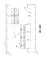
- FIG. 1is a schematic top plan view of a packaging support structure and a wafer mount, according to one embodiment.
- FIG. 2is a top plan view of the wafer mount of FIG. 1 disposed vertically over the support surface of the support structure.
- FIG. 3is a top plan view of a die release assembly disposed over the wafer mount, according to some embodiments.
- FIG. 4is a top plan view of the support structure at various stages of a wafer-level packaging process.
- FIG. 5is a schematic side view of a die release assembly comprising one or more fluid actuators disposed over and in close proximity to the wafer mount, according to various embodiments.
- FIG. 6Ais a schematic side view of a die release assembly disposed over a wafer mount and packaging support surface, according to some embodiments.
- FIG. 6Bis a schematic side view of a die release assembly disposed over a wafer mount and packaging support surface, according to some embodiments.
- FIG. 6Cis a schematic top plan view of a fluid actuator with nozzles comprising a plurality of polygonal orifices arranged adjacent one another along the fluid actuator.
- FIG. 6Dis a schematic top plan view of a fluid actuator with nozzles arranged in a two dimensional array of rectangular or square orifices.
- FIG. 6Eis a schematic top plan view of a fluid actuator with rounded nozzles arranged in a two-dimensional array.
- FIG. 6Fis a schematic top plan view of a fluid actuator with polygonal nozzles arranged adjacent one another, according to various embodiments.
- FIG. 6Gis a schematic top plan view of a fluid actuator with rounded nozzles arranged in a two-dimensional array, according to various embodiments.
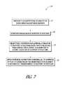
- FIG. 7is a flowchart illustrating a method for mounting dies on a packaging support structure, according to one embodiment.
- FIG. 8Ais a schematic side cross-sectional view of a wafer comprising a substrate, a nonconductive layer deposited on the substrate, and a plurality of conductive contacts formed in the nonconductive layer.
- FIG. 8Bis a schematic side cross-sectional view of a handle wafer attached to the substrate over the nonconductive layer and the contacts.
- FIG. 8Cis a schematic side cross-sectional view of the substrate that is thinned to a desired thickness.
- FIG. 8Dis a schematic side cross-sectional view of the wafer with another nonconductive layer and another set of contacts formed on the polished backside of the wafer.
- FIG. 8Eis a schematic side cross-sectional view of the wafer mounted on a wafer mount.
- FIG. 8Fis a schematic side cross-sectional view of the wafer after dicing into a plurality of integrated device dies.
- FIG. 8Gis a schematic side cross-sectional view of the structure after a temporary adhesive is removed from backsides of the dies.
- FIG. 8His a schematic side cross-sectional view of integrated device dies with bonding surfaces being exposed to a nitrogen-containing plasma.
- FIG. 8Iis a schematic side cross-sectional view of integrated device dies after being transferred from the film directly to a support structure.
- FIG. 8Jis a schematic side cross-sectional view of a plurality of bonded dies which are stacked and directly bonded to one another.
- FIG. 8Kis a schematic side cross-sectional view of the exposed active surface of the bonded dies being prepared for direct bonding to another set of device dies.
- FIG. 8Lis a schematic side cross-sectional view of a third set of dies directly bonded to the stack of bonded dies.
- FIG. 8Mis a schematic side cross-sectional view of dies that are transferred from a film to a waffle pack, according to various embodiments.
- FIG. 8Nis a schematic side cross-sectional view of dies that are exposed to a nitrogen-containing plasma while disposed in the waffle pack.
- FIG. 8Ois a schematic side cross-sectional view of dies after being flipped over into another waffle pack.
- FIG. 9is a flowchart illustrating a method for bonding integrated device dies, according to one embodiment.
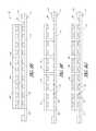
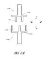
- FIG. 10Ais a schematic side view of various systems and methods for the efficient transfer of integrated device dies from a film to a support structure using a pair of cooperating collets.
- FIG. 10Bis a schematic side view of the system of FIG. 10A , with the collets being moved towards one another.
- FIG. 10Cis a schematic side view of the system of FIG. 10B , with the collets engaging the dies and film.
- FIG. 10Dis a schematic side view of the system of FIG. 10C after the collets are moved away from one another.
- FIG. 10Eis a schematic side view of the collets, according to various embodiments.
- Various embodiments disclosed hereinrelate to the efficient transfer of elements (e.g., semiconductor elements such as integrated device dies) from a film, such as an adhesive film or tape, to a support structure for packaging.
- elementse.g., semiconductor elements such as integrated device dies
- conventional systemsmay use pick-or-place machines to individually move elements or dies or other semiconductor elements to intermediate carriers with a robotic arm, and/or reel-to-reel tape systems.
- Such systemscan be inefficient, leading to increased manufacturing costs.
- the embodiments disclosed hereinadvantageously improve the efficiency of transferring dies (or other types of elements or semiconductor elements) from dicing tape to a support structure for packaging.
- the systems and methods described hereincan identify known good dies (KGDs), which are dies that have been tested to confirm proper electrical functionality.
- the systems and methods disclosed hereincan advantageously place selected dies at a desired location on a two-dimensional support surface using two-dimensional indexing and actuation.
- a wafer comprising a plurality of elementscan be diced or singulated on a dicing film, and KGDs (or other selected dies) of the wafer can be selectively transferred to a selected location on a two-dimensional support surface.
- the dicing filmcan be stretched or maintained in tension when supporting the dies.
- the KGDs or selected diescan be transferred directly from the dicing film to a packaging platform, which can comprise a package substrate (such as a printed circuit board, or PCB, leadframe, ceramic substrate, interposer etc.), another integrated device die (e.g., by way of stacking and direct bonding), an adhesive film for reconstitution of a wafer for packaging, a panel or any other suitable platforms.
- a packaging platformcan comprise a package substrate (such as a printed circuit board, or PCB, leadframe, ceramic substrate, interposer etc.), another integrated device die (e.g., by way of stacking and direct bonding), an adhesive film for reconstitution of a wafer for packaging, a panel or any other suitable platforms.
- a packaging platformwhich can comprise a package substrate (such as a printed circuit board, or PCB, leadframe, ceramic substrate, interposer etc.), another integrated device die (e.g., by way of stacking and direct bonding), an adhesive film for reconstitution of a wafer for packaging, a panel
- selected singulated or diced integrated device dies or elements from a substrate or the wafercan be directly and selectively placed on the ultimate packaging platform from the dicing film without intervening structures, while unselected dies or elements can be left behind on the dicing film.
- handling of the diesis minimized and surfaces can be prepared for direct bonding in a packaging structure (e.g., die stack) with fewer steps for protecting the prepared surface before bonding.
- the selected singulated or diced integrated device diescan be selectively placed on an intermediate carrier (such as an adhesive sheet or tape), which can be employed for intervening packaging steps (e.g., molding for reconstituting a wafer for fan-out metallization) and/or subsequently mount the selected dies to the packaging platform.
- an intermediate carriersuch as an adhesive sheet or tape
- the embodiments disclosed hereindescribe various ways to efficiently transfer integrated device dies to a packaging structure.
- the methods and systems disclosed hereincan be used to efficiently transfer any suitable type of element (such as a semiconductor element, including integrated device dies, etc.) to a packaging structure.
- the embodiments disclosed hereincan be used to transfer semiconductor elements such as integrated device dies, interposers (e.g., semiconductor elements with integrated conductive traces or vias for transferring signals to and from other elements), reconstituted dies, etc.
- other types of elements(which may or may not comprise a semiconductor material) can be transferred to a packaging structure.
- the embodiments disclosed hereincan transfer optical devices, such as lenses, filters, waveguides, etc.
- the elementse.g., semiconductor elements
- the elementscan be processed for direct bonding while mounted on the dicing film, such that most or all of the direct bonding processes can be conducted with the semiconductor elements mounted on the dicing film. Processing the elements for direct bonding on the dicing film can improve the overall efficiency of bonding, as intermediate transfer of the elements to other structures between singulation and direct bonding can thereby be avoided.
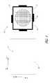
- FIG. 1is a schematic top plan view of a support structure or surface 10 and a wafer mount 12 .
- the wafer mount 12can comprise an assembly configured to support a semiconductor wafer 18 during various semiconductor processing techniques.
- the wafer mount 12can be configured to support the wafer 18 during a singulating or dicing operation.
- the wafer mount 12can comprise a frame 14 and a film 15 mounted to the frame 14 .
- the film 15can comprise an adhesive sheet, e.g., a sheet of tape.
- the film 15can be secured to the frame 14 about the periphery of the film 15 such that the film 15 is in tension.
- the frame 14is illustrated as a polygonal frame in FIG. 1 , it should be appreciated that the frame can take any suitable physical form that is configured to support the film 15 .
- the wafer 18can comprise a semiconductor material (such as silicon or any other suitable Group elements) that is patterned with a plurality of integrated devices organized into multiple associated integrated device dies 16 .
- the wafer 18may be patterned to define integrated circuits such as processors or memory, microelectromechanical systems (MEMS) device dies or any other suitable type of integrated device known to the skilled artisan.
- MEMSmicroelectromechanical systems
- each integrated devicecan be tested on the wafer 18 prior to singulating or dicing to identify which device dies 16 are electronically functional, referred to herein as known good dies (KGDs), and which device dies 16 are damaged or otherwise dysfunctional, and to generate a map locating KGDs.
- KGDsknown good dies
- electrical testingmay be performed after singulating or dicing. Testing the electrical and/or electronic characteristics of the device dies 16 before the dies 16 are moved to the subsequent support structure 10 can advantageously reduce the amount of real estate on the support structure 10 which is used for dysfunctional or damage dies. Thus, in various embodiments disclosed herein, only KGDs may be selected and placed on the support structure 10 , which can reduce manufacturing costs associated with processing and placing damaged or dysfunctional dies.
- the wafer 18can be mounted to the wafer mount 12 prior to singulating or dicing, such that the wafer 18 is adhered to an adhesive surface of the film 15 .
- the backside of the wafercan be mounted to an adhesive surface of the film 15 .
- the wafer 18can be diced or singulated using a suitable dicing or singulation technique to divide the wafer 18 into a plurality of separate, diced integrated device dies 16 .
- the wafer 18can be sawed or otherwise singulated to create the individual dies 16 .
- the dicing operationcan be conducted such that only the wafer 18 is diced and the film 15 remains continuously connected (even though there may be saw or other marks on the film 15 as a result of the dicing operation) to support the dies 16 .
- the intact film 15can be used to keep the singulated dies 16 aggregated adjacent one another on an adhesive surface of the film 15 .
- the film 15 and/or the singulated dies 16can be cleaned using any suitable type of cleaning method.
- the wafer 18 of FIG. 1includes integrated device dies 16 or element, in other embodiments, other types of semiconductor elements (such as interposers, reconstituted dies, etc.) may be provided on the wafer 18 .
- the support structure 10can be any suitable structure or surface configured to support the diced integrated device dies 16 transferred from the wafer mount 12 .
- the support structure 10can comprise a support surface 11 coupled to, formed with, and/or mounted on a movable apparatus, such as a movable table.
- the support surface 11can comprise a packaging platform, such as a package substrate (e.g., PCB, plastic, glass, leadframe, ceramic substrate, etc.), a wafer or stack of wafers, an interposer, a reconstituted wafer, panel, or reconstituted panel, or one or more other integrated device dies.
- a package substratee.g., PCB, plastic, glass, leadframe, ceramic substrate, etc.
- interposere.g., a reconstituted wafer, panel, or reconstituted panel, or one or more other integrated device dies.
- the support surface to which the dies are transferredmay be die or wafer surfaces prepared for direct bonding, without any intervening adhesive.
- the support surface 11 and/or the support structure 10may comprise an intermediate carrier, such as an adhesive sheet or mechanical die carrier, which can be used to transport the integrated device dies 16 to the ultimate packaging platform.
- the support surface 11may be an adhesive layer upon with a reconstituted wafer is formed, such that the relative positions of dies 16 and other packaging materials (e.g., mold or encapsulating material) are fixed on the support surface 11 .
- the support structure 10 and wafer mount 12can move relative to each other.
- the support structure 10 and support surface 11can be movable in two dimensions, i.e., movable in the +x, ⁇ x and +y, ⁇ y directions.
- a control system(see the control system 100 of FIGS. 5-6B ) comprising one or more processors and associated memory devices can be configured to accurately and precisely control the movement of the support structure 10 in two dimensions.
- the control systemcan be electrically coupled to a motor and gear system which can move or index the support structure 10 so as to align selected locations of the support surface 11 with selected integrated device dies 16 on the wafer mount 12 .
- FIG. 2is a top plan view of the wafer mount 12 of FIG. 1 disposed vertically over the support surface 11 of the support structure 10 .
- the wafer mount 12 with diced integrated device dies 16can be positioned over the support surface 11 using any suitable mechanism, such as a robotic arm assembly.
- the wafer mount 12 with diced integrated device dies 16may remain stationary, and the support structure 10 may be movable in two dimensions. In other embodiments, the support structure 10 may remain stationary, and the wafer mount 12 with dies 16 may be movable in two dimensions (i.e., the ⁇ x, +x and ⁇ y, +y directions).
- both the support structure 10 and the wafer mount 12 with diced die 16may be movable in two dimensions.
- the support surface 10 and/or the wafer mount 12may be moved vertically relative to one another such that the diced integrated device dies 16 are disposed in close proximity to the support surface 11 of the support structure 10 .
- the diced dies 16can be spaced vertically from the support surface 11 by a distance in a range of 10 microns to 1000 microns, or more particularly, by a distance in a range of 10 microns to 100 microns.
- the support structure 10may be moved laterally in two dimensions to align a desired location of the support surface 11 with a selected integrated device die 16 .
- the support structure 10can be moved such that a selected KGD of the integrated device dies 16 (previously mapped after wafer-level testing) is aligned laterally (i.e., in the x and y directions) with the desired location of the support surface 11 .
- FIG. 3is a top plan view of a die release assembly 20 disposed over the wafer mount 12 , according to some embodiments.
- the die release assembly 20can be movable in two dimensions, i.e., the x and y directions, parallel to the surface of the film.
- the die release assembly 20can be moved over a selected die from the plurality of diced dies 16 .
- the die release assembly 20can comprise one or more actuators (not shown in FIG.
- the die release assembly 20can include one actuator to release a corresponding device die 16 from the film 15 .
- the support structure 10can be moved so as to position the selected die directly over a desired location on the support surface 11 .
- the die release assembly 20can be moved laterally (e.g., rotationally and/or linearly in the x and/or y directions) to be positioned over the selected device die.
- the actuatorcan be activated to cause the corresponding selected die to be transferred directly to the support surface 11 .
- the die release assembly 20can comprise an array of multiple actuators configured to cause multiple corresponding dies to be released from the film 15 and transferred to the support structure 10 .
- the die release assembly 20can comprise a linear array of N ⁇ 1 actuators arranged in a line, where N is any suitable positive integer.
- the die release assembly 20can be moved along the x direction to be positioned over one or more dies to be released from the die mount 12 .
- the die release assembly 20can comprise a two-dimensional array of N ⁇ M actuators arranged so as to cause multiple dies across an area of the film 15 to be released. It should be appreciated that, in die release assemblies that have multiple actuators, the actuators can be activated together or individually.
- all the actuators of the assembly 20can be activated, e.g., simultaneously or sequentially (with or without intervening indexed motion). In other arrangements, only selected actuators of the assembly 20 can be activated simultaneously. For example, actuators of the assembly 20 which are disposed over KGDs (as determined from prior wafer-level testing and mapping) may be activated such that only KGDs are transferred to the support structure 10 .
- a trailing armsimilar to the die release assembly 20 may apply additional momentary pressure pneumatically to the KGD that is transferred to the support structure.
- additional momentary pressuremay be particularly desirable for embodiments in which the support surface 11 comprises an adhesive material.
- the additional momentary pressurecan be omitted, or if applied such pressure need not be high (e.g., less than or equal to about 2 atm), and may be applied for on the order of 1 millisecond to 1 second in view of prior preparation of surfaces for direct bonding.
- the additional pneumatically applied pressuremay be applied to every die on the support structure 10 simultaneously in another supporting chamber with or without heat (not shown).
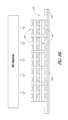
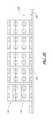
- FIG. 4is a top plan view of the support structure 10 at various stages of a wafer-level packaging process.
- multiple dies A-Dcan be mounted within corresponding package regions 21 of the support structure 10 .
- the corresponding package regions 21may be associated with the components that are ultimately packaged together in an integrated device package.
- the components of each packagecan be assembled on the support structure 10 , which may comprise a wafer or wafer stack, or an intermediate carrier such as an adhesive sheet or die carrier, directly from a first adhesive (e.g., wafer dicing tape).
- Die Amay be associated with Map A, which can identify locations on the support surface 11 at which Die A should be mounted.
- the control systemsee the control system 100 of FIGS.
- each Die Acan be mounted to a corresponding package region 21 in the upper left corner of the package region 21 .
- prior wafer-level die testing and mappingmay confirm that each Die A is a known good die, or KGD, such that only KGDs are disposed within each package region 21 .
- the die release assembly 20can move parallel to the surface of the film 15 to place additional dies on the support structure 10 .
- the systemcan place each Die B at associated locations on the support surface 11 as indicated by Map B (i.e., at the upper right corner of each package region 21 ), each die C at associated locations on the support surface 11 as indicated by Map C (i.e., at the lower left corner of each package region 21 ), and each die D at associated locations on the support surface 11 as indicated by Map D (i.e., at the lower right corner of each package region 21 ).
- Map Bi.e., at the upper right corner of each package region 21
- Map Ci.e., at the lower left corner of each package region 21
- each die Dat associated locations on the support surface 11 as indicated by Map D (i.e., at the lower right corner of each package region 21 ).
- Map Di.e., at the lower right corner of each package region 21
- each die A-D mounted to the package regions 21can be KGDs, so as to improve the package yield, speed up the package assembly process, and reduce waste.
- the use of a movable support structure 10 for moving the support surface 11 relative to the wafer mount 12 (or vice versa) in two dimensionscan advantageously enable the accurate placement of KGDs at a desired packaging location of the support structure 10 .
- the support structure 10can comprise any suitable structure.
- the support structure 10comprises a packaging platform, such as a package substrate (e.g., PCB, plastic, glass, ceramic, lead frame, interposer, etc.).
- the support structure 10comprises a wafer or wafer stack, a die or die stack, or a reconstituted wafer.
- the support structure 10comprises an intermediate carrier, such as an adhesive sheet, upon which further packaging steps can be taken (e.g., molding for forming a reconstituted wafer).
- a packaging platformsuch as a package substrate (e.g., PCB, plastic, glass, ceramic, lead frame, interposer, etc.).
- the support structure 10comprises a wafer or wafer stack, a die or die stack, or a reconstituted wafer.
- the support structure 10comprises an intermediate carrier, such as an adhesive sheet, upon which further packaging steps can be taken (e.g., molding for forming a reconstituted wafer).
- FIGS. 8A-8Lillustrates several selected dies A-D being mounted side-by-side within corresponding package regions 21 , in some embodiments, the selected dies (or some of the dies) may be stacked on top of one another, as will be clear from the example of FIGS. 8A-8L .
- One advantage of the disclosed embodimentsis that binned devices with desired characteristic within the KGDs mapped on the wafer 18 can be selectively clustered at selected locations on the support structure 10 . KGDs with lower performances can be clustered and segregated to other known locations on the support structure 10 . However, such a clustering protocol may be more time consuming and expensive to implement as compared with dies that are mounted on a tape in a spool.
- FIG. 5is a schematic side view of a die release assembly 20 comprising one or more fluid actuators 24 disposed over and in close proximity to the wafer mount 12 .
- the die release assembly 20can be configured to apply a force to a backside of the film 15 directly opposite a selected die 16 A to cause the selected die 16 A to be transferred directly from the film 15 to the support surface 11 .
- the back side of the singulated diesmay be exposed to a radiation source, such as an ultraviolet (UV) source, to weaken the adhesion between the die 16 A and the dicing tape 15 prior to the transfer operation.
- the fluid actuator 24can comprise one or more nozzles which direct a high velocity fluid against the backside of the film 15 .
- the high velocity fluidcan cause the film 15 with the die 16 A to flex away from the die release assembly 20 such that the die 16 A contacts the support surface 11 .
- the pressure applied by the high velocity fluidcan also cause the die 16 A to be released from the film 15 and transferred directly to the support surface 11 .
- the nozzle(s) of the actuator 24can be sized and shaped so as to apply a force to a localized region of the backside of the film 15 such that only the selected die is transferred from the film 15 to the support structure 10 .
- the fluid supplied by the fluid actuator 24can comprise air or any other suitable gas, such as nitrogen.
- the fluidmay comprise a liquid such as water.
- the fluidmay be cooled or heated prior to or during the transfer of the die 16 A to the support structure 10 .
- the fluidmay be heated to a temperature above 50° C., e.g., in a range of 50° C. to 150° C.
- heating the fluidmay advantageously enhance the adhesion of the selected die 16 A to the support surface 11 (e.g., directly bonding to another die) and/or may help delaminate or remove the die 16 A from the film 15 .
- the support surface 11may be disposed on any suitable type of movable platform, such as a movable table or support (see FIGS. 1-3 and attendant description).
- the support surface 11is supported by a movable support 22 comprising a rotating chuck assembly, which is configured to rotate the support surface 11 about a z axis, which is perpendicular to the x and y directions.
- the movable support 22can be moved (i.e., rotated) to accurately align a desired location on the support surface 11 (e.g., a desired location within a particular package region 21 as explained in FIG. 4 ) with a selected die 16 A.
- the fluid actuator 24can be activated to cause the die 16 A to be transferred from the film 15 to the support surface 11 .
- the die release assembly 20uses fluid actuators 24 to cause the dies to be released from the film 15 and transferred to the support surface 11
- the die release assembly 20can comprise a plunger or other type of mechanical device which can apply a force in a direction nonparallel to the film.
- Other non-mechanical or non-contact approachessuch as magnetic devices, sonic devices or radiation devices, can be used to apply a force in a direction nonparallel to the film to transfer the die 16 A to the support structure 10 .
- a radiation devicesuch as a laser source may be used to debond the die 16 A from the film 15 in a direction nonparallel to the film. Also heat from the radiation source may improve the attachment and the adhesion of the die 16 A to the surface of the support structure 10 .
- a control system 100can be programmed to control the operation of the movable support 22 (and thereby the support structure 10 and support surface 11 ) and/or the operation of the die release assembly 20 .
- the control system 100can comprise one or more processors and memory devices which are programmed with software that, when executed, sends instructions to a motor (or other device) which causes the movable support 22 to rotate to a desired orientation.
- the control system 100may store in memory information regarding which dies of the wafer 18 (see FIG. 3 ) are KGDs, and may also store information regarding the target location of the dies on the support surface 11 (including, e.g., the wafer-level package maps shown in FIG. 4 ).
- the control system 100can instruct the movable support 22 to move to a desired orientation for each die, or at least each KGD or a binned die, on the wafer 18 (see FIG. 3 ).
- the control system 100can also be programmed to send instructions to a motor or other device to cause the die release assembly 20 to be positioned over the die to be transferred.
- the control system 100can instruct the die release assembly 20 to apply a suitable force against the backside of the film 15 to cause the dies to be transferred to the support structure 10 .
- the control system 100can instruct the die release assembly 20 to apply a suitable force against the backside of the film 15 to cause the binned dies to be transferred to the support structure 10 in a clustered configuration, such that dies with desirable higher performance attributes (for example, lower power, high frequencies) may be segregated to portions of the support layer where the beneficial process outcomes are expected.
- desirable higher performance attributesfor example, lower power, high frequencies
- FIG. 6Ais a schematic side view of a die release assembly 20 disposed over a wafer mount 12 and support surface 11 , according to some embodiments.
- reference numerals used in FIG. 6Arepresent components that are similar to or the same as components illustrated in FIGS. 1-5 .
- the wafer mount 12 with integrated device dies 16can be disposed in close proximity relative to the support surface 11 .
- the support surface 11can be aligned vertically (in the z direction) and laterally (e.g., rotationally and/or linearly in the x and/or y directions) such that selected dies 16 A are laterally aligned with a desired location on the support surface 11 (which may correspond to a desired location within a package region 21 ).
- the control system 100 of FIG. 6Amay operate in a manner similar to that of the control system 100 illustrated in FIG. 5 .
- the die release assembly 20comprises a fluid actuator 24 having a plurality of nozzles.
- FIGS. 6C-6Eare schematic top plan views of a fluid actuator 24 with nozzles 26 arranged in nozzle patterns that can be used with the embodiment of FIG. 6A .
- the fluid actuator 24 of the die release assembly 20can be activated to inject a high velocity fluid (e.g., a gas such as air, nitrogen, etc.) against the backside of the film 15 .
- the nozzles 26 of the fluid actuator 24can be sized and shaped asymmetrically to cause an edge 23 of a selected die 16 A to contact the support surface 11 before other regions of the die 16 A. For example, as shown in FIG.
- the nozzles 26can comprise a plurality of polygonal (e.g., rectangular) orifices arranged adjacent one another along the fluid actuator 24 .
- the nozzles 26can be wider near a first end 23 a than at a second end 23 b .
- the nozzles 26are arranged in a single row of adjacent rectangular orifices.
- the nozzles 26are wider near a first end 23 a than a second end 23 b , however, the nozzles 26 are arranged in a two dimensional array of rectangular or square orifices in which the width or major dimension of the nozzles 26 decreases from the first end 23 a to the second end 23 b .
- the nozzles 26are similarly wider near a first end 23 a , but the nozzles 26 are arranged in a two-dimensional array of rounded orifices (e.g., circular or elliptical) in which the width or major dimension of the nozzles 26 decreases from the first end 23 a to the second end 23 b.
- rounded orificese.g., circular or elliptical
- the wider orifices near the first end 23 acan create fluid streams against the film 15 to cause the film 15 to move towards the support surface 11 .
- the orifices of the nozzles 26 nearer the first end 23 aare wider than at the second end 23 b , a higher flowrate of fluid is injected against the edge 23 of the die 16 A as compared to other regions of the die 16 A.
- the higher flowrate of fluid (and therefore a higher applied force) at the edge 23 of the die 16 Acan cause the edge 23 of the die 16 A to contact the support surface 11 before other regions of the die 16 A.
- Sufficient fluid pressurecan be applied to cause the dies 16 A to delaminate from the film 15 and transfer to the support surface 11 .
- FIG. 6Bis a schematic side view of a die release assembly 20 disposed over a wafer mount 12 and support surface 11 , according to some embodiments.
- reference numerals used in FIG. 6Brepresent components that are similar to or the same as components illustrated in FIGS. 1-6A .
- the wafer mount 12 with integrated device dies 16can be disposed in close proximity relative to the support surface 11 .
- the support surface 11can be aligned vertically (in the z direction) and laterally (to mapped x and y positions) such that selected dies 16 A are laterally aligned with a desired location on the support surface 11 (which may correspond to a desired location within a package region 21 or intermediate carrier surface).
- the control system 100 of FIG. 6Bmay operate in a manner similar to that of the control system 100 illustrated in FIGS. 5-6A .
- the die release assembly 20 of FIG. 6Bcomprises a fluid actuator 24 having a plurality of nozzles.
- FIGS. 6F and 6Gare schematic top plan views of a fluid actuator 24 with nozzles 26 arranged in a nozzle pattern that can be used with the embodiment of FIG. 6B .
- the nozzles 26 of the fluid actuator 24 of FIG. 6Bcan be sized and shaped to cause a central region 25 of a selected die 16 A to contact the support surface 11 before other regions of the die 16 A, such as the edge 23 of the die 16 A.
- the central region 25 of the die 16 Amay bend or flex so as to contact the support surface 11 before the edge 23 of the die 16 A.
- the fluid actuator 24can comprise a plurality of nozzles 26 with rectangular-shaped orifices.
- the orificesmay be widest at a central region of the actuator 24 and narrower at the end regions.
- the nozzles 26can comprise rounded (e.g., circular or elliptical) orifices arranged in a two-dimensional array in which the larger orifices are arranged near the central region and smaller orifices are arranged near the ends of the actuator 24 .
- the nozzles 26 near the center of the actuator 24may supply a greater flowrate (and hence a greater force) than nozzles 26 near the edges of the actuator 24 .
- the increased flowrate at the center of the actuator 24may apply sufficient force at the central region 25 of the die 16 A to cause the central region 25 to bow or flex towards the support surface 11 .
- the central region 25can contact the support surface 11 before other regions of the die 16 A.
- the selected die 16 Acan be removed from the film 15 and directly transferred to the support surface 11 .
- FIG. 7is a flowchart illustrating a method 30 for mounting dies on a support structure, according to one embodiment.
- the method 30begins at a block 32 in which a film supporting a plurality of diced elements (e.g., semiconductor elements such as diced integrated device dies) is provided.
- a wafercan be mounted to a film of a wafer mount.
- the waferhas been previously processed to have a plurality of integrated devices, which can be diced or separated using any suitable method, such as sawing.
- the filme.g., a tape
- the diesor other elements or semiconductor elements
- the device diescan be tested before dicing to determine and map which dies are electronically functional, i.e., which dies are known good dies, or KGDs.
- each integrated device diemay comprise a plurality of contact pads formed thereon.
- the contact padsmay be covered with a passivation film or exposed; however, the pads may be devoid of external contact bumps (such as solder balls).
- the film with the diced integrated devicesis positioned adjacent a support structure such that an adhesive surface of the film faces a support surface of the support structure.
- the support structurecan comprise any suitable type of surface, including, e.g., a packaging platform (such as a package substrate, interposer, one or more device dies, one or more wafers) or an intermediate carrier (such as an adhesive sheet).
- the filmcan be selectively positioned laterally relative to the support structure such that a selected first die (or other type of element or semiconductor element) is aligned with a first location of the support structure.
- the support structure and/or the wafer mountmay be indexed to move in two-dimensions.
- a control systemcan be programmed to position the support structure relative to the film such that a selected die (e.g., a KGD) is aligned with a selected location on the support surface, such as a corresponding package region of the support surface.
- a selected diee.g., a KGD
- a forcecan be applied in a direction nonparallel to the adhesive surface of the film to cause the selected die (or other type of element or semiconductor element) to be directly transferred from the film to the support structure.
- a die release assemblycan be moved over the selected die and an actuator can be activated to cause the die to be released from the film and transferred to the support structure.
- the actuatorcan comprise a fluid actuator having one or more nozzles configured to inject a high velocity fluid (e.g., a gas such as air or nitrogen, or a liquid) against the backside of the film to cause the die to be transferred to the support structure.
- the nozzlescan be arranged in any suitable pattern.
- the nozzlescan be arranged so as to cause an edge of the die to contact the support surface before other regions of the die.
- the nozzlescan be arranged so as to cause a central region of the die to bow and contact the support surface before other regions of the die.
- the actuatorcan comprise a plunger or other mechanical actuator configured to apply a force nonparallel to the film.
- the embodiments disclosed herein with respect to FIGS. 1-7can be used to efficiently transfer dies or other elements from a dicing film directly to a support structure, which may be an intermediate carrier or a final packaging platform.
- a support structurewhich may be an intermediate carrier or a final packaging platform.
- the embodiments disclosed in FIGS. 1-7can enable package assemblers to utilize only KGDs in packages, which can improve package yield and reduce costs associated with using dysfunctional device dies.
- the two-dimensional selective placement of selected dies on the support structurecan enable the use of accurate and efficient wafer-level packaging in which KGDs are accurately and directly mounted to a surface in which the die has a fixed relationship with other components of the package, such as another die or die stack, a wafer or wafer stack, a package substrate, encapsulating or mold material to be formed after transfer onto the support structure, etc.
- the support surfaceWhen the dies are assembled on the corresponding package regions of the support surface, the support surface can be molded by a filling material or encapsulant which is applied over portions of the dies and/or in gaps between adjacent dies. In some arrangements, the backsides of the dies can be thinned.
- the support surface(which may comprise a wafer or a web of substrate material, such as PCB or lead frame) may be subsequently singulated to yield a plurality of singulated device packages.
- FIGS. 8A-8Lare schematic side cross-sectional views of various stages of a method for bonding integrated device dies, according to some embodiments. It should be appreciated that the fluid actuator and relative motion embodiments disclosed above with respect to FIGS. 1-7 may also apply to the embodiment shown in FIGS. 8A-8L . For example, the flowchart in FIG. 7 illustrates steps of a manufacturing method which also apply to FIGS. 8A-8L . Moreover, although FIGS. 8A-8L illustrate direct bonding of integrated device dies, it should be appreciated that the methods can alternatively be used to direct bond other types of semiconductor elements, such as interposers, reconstituted dies, etc. FIG.
- the 8Aillustrates a wafer 18 comprising a substrate 40 , a nonconductive layer 42 deposited on the substrate 40 , and a plurality of conductive contacts 44 formed in the nonconductive layer 42 .
- the substrate 40can comprise silicon or any other suitable semiconductor material, glass, ceramic, or a polymeric layer or panel.
- the nonconductive layer 42can comprise a suitable nonconductive material, such as, for example, inorganic or organic dielectric material, such as silicon dioxide, silicon carbide, diamond-like carbon, a polymeric layer, a composite material or various combinations of these materials, etc.
- portions of the conductor 44may be formed by damascene and non-damascene metallization methods.
- the conductive contacts 44can be defined by a damascene process, in which the contacts 44 are filled inside trenches formed in the nonconductive layer 42 , and may be coplanar with, slightly protrude above (e.g., 2-20 nm), or maybe slightly recessed below (e.g., 2-20 nm) below the surface of the nonconductive layer 42 .
- the contacts 44can comprise any suitable conductor, such as copper, gold, etc.
- the surfaces of the contacts 44 and the nonconductive layer 42can be prepared for direct bonding with another wafer or other structure. For example, the surfaces of the contacts 44 and/or the nonconductive layer 42 may be polished (using, e.g., chemical-mechanical polishing techniques) so as to ensure that the bonding surfaces are extremely smooth.
- a handle wafer 48can be attached to the substrate 40 over the nonconductive layer 42 and the contacts 44 by way of an adhesive 46 .
- the handle wafer 48can comprise silicon or another semiconductor material that is sufficiently thick so as to act as a handle for moving or otherwise manipulating the wafer 18 .
- the backside of the substrate 40can be thinned to a desired thickness suitable for the integrated device dies ultimately formed from the wafer 18 .
- the substrate 40can be thinned to a thickness in a range of 10 microns to 200 microns, in a range of 10 microns to 100 microns, in a range of 20 microns to 75 microns, in a range of 25 microns to 50 microns, or any other suitable thickness.
- the backside of the thinned wafer 18can be polished or otherwise planarized in a manner similar to the front side of the wafer 18 .
- another nonconductive layer 52 and another set of contacts 54can be formed on the polished backside of the wafer 18 in a manner similar to the contacts 44 and nonconductive layer 42 .
- the second set of contacts 54may communicate with integrated circuitry within the substrate 40 by way, for example, of through-silicon vias (TSVs) and/or back-end-of-line (BEOL) metallization.
- TSVsthrough-silicon vias
- BEOLback-end-of-line
- the nonconductive layer 52 and contacts 54may also be polished and prepared for bonding as explained above.
- the wafer 18can be mounted on a wafer mount 12 , similar to the wafer mount 12 described above in connection with FIGS. 1-7 .
- the wafer mount 12can comprise a frame 14 and a film 15 supported by the frame 14 .
- the wafer 18can be adhered to an adhesive surface 55 of the film 15 .
- the wafer 18can be coated with a protective polymer to protect the active surface of the wafer 18 from the film 15 . In other embodiments, no protective coating may be used, and any residue from the film 15 may be subsequently cleaned.
- the handle wafer 48can be removed from the adhesive 46 .
- the wafer 18can be diced into a plurality of integrated device dies 16 .
- the wafer 18can be sawed, punched, or otherwise singulated so as to form the diced integrated device dies 16 .
- the device dies 16can comprise any suitable type of die, such as an integrated circuit, such as memory or processor, a MEMS die, etc.
- the dicing operationmay fully dice or singulate the dies 16 , but leave the film 15 intact and continuous, although the dicing saw may leave scorings or markings on the film 15 .
- the intact film 15can support the diced dies 16 and maintain their relative positions on the film 15 .
- the adhesive 46can be removed by any suitable method, such as by exposure to electromagnetic radiation (e.g., ultraviolet radiation) and/or a solvent.
- bonding surfaces 56 of the integrated device dies 16can be planarized (e.g., polished by chemical mechanical polishing), activated (e.g., very slightly etched) and/or terminated with a suitable species.
- the bonding surfaces 56(which may comprise silicon oxide) can be exposed to nitrogen-containing plasma in a plasma chamber.
- the plasma processcan comprise a reactive ion etching process in some embodiments. The very slight etch can result in a root-mean-square micro-roughness of less than 0.5 nm, e.g., in a range of 0.1 nm to 3 nm.
- the processes disclosed hereincan be performed while the dies 16 are mounted to the film 15 , which can improve the efficiency of the direct bonding processes.
- the processes disclosed hereinmay be conducted at relatively low temperatures (e.g., in a range of 50° C. to 100° C.), which may be a sufficiently low temperature and/or may be for sufficiently low processing times (e.g., less than 10 minutes, or less than 6 minutes) such that the film 15 can accommodate the direct bonding processes without degrading or melting.
- the bonding surfaces 56can be exposed to a nitrogen-containing solution, e.g., an ammonia-based solution.
- Terminating the bonding surfaces 56 with nitrogen-containing speciescan advantageously enhance the direct bonding of the dies 16 to other semiconductor elements. Additional details of activation and termination processes are disclosed throughout U.S. Pat. No. 6,902,987, the entire contents of which are incorporated by reference herein in their entirety and for all purposes.
- the integrated device dies 16 shown in FIGS. 8F-8Hcan be transferred from the film 15 directly to a support structure 10 .
- the support structure 10 for the dies 16comprises a second set of dies 16 B mounted on a second wafer mount 12 B comprising a second frame 14 B which supports a second film 15 B.
- the support structure 10 for the dies 16comprises a second set of dies 16 B mounted on a second wafer mount 12 B comprising a second frame 14 B which supports a second film 15 B.
- the support structure 10can comprise any suitable type of structure, including, e.g., a packaging platform, such as a package substrate (e.g., PCB, glass, plastic, leadframe, ceramic substrate, silicon interposer, etc.), a wafer or stack of wafers, a reconstituted wafer, panel, or reconstituted panel, etc.
- a packaging platformsuch as a package substrate (e.g., PCB, glass, plastic, leadframe, ceramic substrate, silicon interposer, etc.), a wafer or stack of wafers, a reconstituted wafer, panel, or reconstituted panel, etc.
- the support structure 10may comprise an intermediate carrier, such as an adhesive sheet or mechanical die carrier, which can be used for further packaging steps (e.g., molding for wafer reconstitution) or to transport the integrated device dies 16 to the ultimate packaging platform.
- the first film 15 and dies 16can be mounted to a first platform 62 . As shown in FIG. 8I , the first film 15 and dies 16 can be inverted in preparation for direct bonding with the second dies 16 B. The second film 15 B to which the second dies 16 B are adhered can be mounted to a second platform 64 .
- the first and second platforms 62 , 64can comprise any suitable structure for supporting the respective wafer mounts 12 , 12 B. In the illustrated embodiment, for example, the first and second platforms 62 , 64 can comprise vacuum chucks which apply a negative pressure to each film 15 , 15 B so as to secure the films 15 , 15 B to the respective platforms 62 , 64 .
- FIGS. 8F-8Hare illustrated in an inverted configuration, i.e., disposed over the second set of dies 16 B. It should be appreciated, however, that in other arrangements, the dies 16 from FIGS. 8F-8H may instead be disposed on the second platform 64 , and the dies 16 B can be disposed on the first platform 62 . Further, although the processing steps described above in connection with FIGS. 8A-8H are described with reference to the dies 16 , the same processing steps may also be applied to the surfaces of the second set of dies 16 B in preparation for direct bonding, such as planarization, activation and termination.
- the control system 100can store information regarding each die 16 , 16 B that is to be bonded. For example, the control system 100 can determine which dies 16 on the first film are KGDs. The control system 100 can also be configured to identify which individual dies 16 from the first set are to be bonded to which individual dies 16 B from the second set. The control system 100 can instruct a motor or other suitable apparatus to cause the first platform 62 to move relative to the second platform 64 (or vice versa) so as to laterally align a selected die 16 with a corresponding selected die 16 B from the second set.
- the first platform 62can be moved laterally in two dimensions (i.e., in the x and y dimensions, e.g., rotationally and/or linearly in the x and/or y directions) to align the selected die 16 with the corresponding die 16 B in the lateral direction.
- a die release assembly 24can apply a force against the backside of the film 15 to cause the die 16 to be transferred from the film 15 to the support surface 11 , which can also comprise a bonding surface 56 B of the corresponding second die 16 B.
- the die release assembly 24can comprise a plunger 60 which is driven along the z direction to apply a contact force against the backside of the film 15 .
- the plunger 60can apply an initial downward force (which may include pressure sensing) against the film 15 in the ⁇ z direction to cause one die 16 to be disposed below the other dies 16 .
- the plunger arrangementcan comprise a displacement and/or pressure sensor with a feedback control system to accurately control the amount of force and/or displacement applied by the plunger 60 .
- An alignment systemcan be activated (by the control system 100 and/or a user) to estimate the degree of misalignment in the x, y, and/or z directions of the die 16 relative to the second die 16 B.
- the alignment systemcan communicate with the control system 100 to provide feedback with respect to the degree of misalignment.
- the alignment systemcan comprise an optical measurement system in some arrangements.
- the alignment systemcan comprise one or more cameras in some embodiments.
- an interferometric alignment systemcomprising one or more lasers can be used.
- the control system 100can iteratively send commands to cause the first platform 62 to move align the selected die 16 relative to the second die 16 B in two dimensions.
- Precision movement of the plunger 60 (and/or the second platform 64 ) along the z-directioncan cause the bonding surface 56 of the first die to contact and directly bond with the corresponding bonding surface 56 B of the second die 16 B.
- the direct bond between the dies 16 , 16 Bcan comprise a chemical (e.g., covalent) bond in which the nonconductive layers 42 and the contacts 44 of the respective dies 16 , 16 B are bonded to one another without an intervening adhesive.
- the direct bonding processmay be conducted at room temperature in some embodiments. The high degree of smoothness of the dies prior to bonding can improve the strength of the direct bond.
- the bonding surfaces of the diesmay have planarized surfaces with a surface roughness (RMS) in a range of 0.5 and 1.5 nm.
- RMSsurface roughness
- a post-bonding annealmay be performed (at a temperature in a range of 100° C. to 400° C.) to further enhance the bonding.
- the direct bondcan have a bond strength of at least 400 mJ/m 2 (e.g., at least 2000 mJ/m 2 ). Additional details of direct bonding processes may be found in U.S. Pat. Nos.
- the plunger 60may comprise one or more internal channels through which a fluid may be supplied.
- the fluidmay comprise a heated or cooled fluid which can enhance the bonding process during the transfer of the dies 16 .
- the plunger 60can be retracted along the +z direction.
- the bonding force between the dies 16 , 16 Bmay be greater than the adhesive force between the die 16 and the film 15 , such that retraction of the plunger 60 can cause the die 16 to release from the film 15 .
- the adhesion between the die 16 and film 15may have been reduced by exposing the back side of the film 15 to a radiation source, such as, for example, a UV light or laser.
- the control system 100can instruct the plunger 60 and the first platform 62 to move to another pair of dies to be bonded until each die 16 (or each KGD) on the first wafer mount 12 is transferred and bonded to an associated die 16 B (which may also be a KGD) on the second wafer mount 12 B.
- FIG. 8Jillustrates a plurality of bonded dies 16 C which are stacked and directly bonded to one another. The bonded dies 16 C can remain attached to the second film 15 B and/or to the second platform 64 (not shown in FIG. 8J ). Each die can be bonded sufficiently to allow release from the film 15 in much shorter time frames than, e.g., thermocompression bonding.
- the bondmay include non-conductive to non-conductive (e.g., oxide) surface chemical bonding. Subsequent heating may enhance the non-conductive surface bonding, and may also enhance or cause bonding of conductive surfaces of aligned contacts 44 of the dies 16 , 16 B. Furthermore, the techniques described herein facilitate direct bonding of thinned dies 16 , such as may be difficult to handle by conventional pick-and-place robots.
- non-conductive to non-conductivee.g., oxide
- the exposed active surface of the bonded dies 16 Ccan comprise bonding surfaces 56 C which can be prepared for direct bonding to another set of device dies, in some embodiments.
- the bonding surfaces 56 Ccan be activated (e.g., by very slight etching) and/or terminated with a suitable species while the dies 16 C are mounted on the film 15 . Activation and termination can be conducted sequentially or in a single process.
- the bonding surfaces 56 Ccan be exposed to nitrogen-containing plasma in a plasma chamber.
- the bonding surfaces 56can be exposed to a nitrogen-containing solution, e.g., an ammonia-based solution, as explained above.
- FIG. 8Lillustrates a third set of dies 16 D directly bonded to the dies 16 C.
- the bonding of the third dies 16 D to the bonded dies 16 Cmay be performed as explained above with respect to FIG. 8I .
- the processcan continue until the desired number of dies are stacked and directly bonded to one another.
- the stacked diescan be packaged in any suitable manner.
- the diescan be encapsulated at least in part by a molding or filling material which fills gaps between adjacent dies.
- the encapsulated diescan be singulated and mounted to a package substrate, such as a PCB, leadframe, ceramic substrate, etc.
- a package substratesuch as a PCB, leadframe, ceramic substrate, etc.
- the die stacksmay already be mounted on a packaging substrate or large process die, in place of the second film 15 B, during the bonding process.
- semiconductor elementse.g., device dies 16
- the dies 16can be diced on the film 15 , polished on the film 15 , and activated and/or terminated on the film 15 .
- the efficiency and efficacy of the direct bonding techniquescan be improved.
- FIGS. 8M-8Oillustrate an alternative embodiment, which can be used in conjunction with, or as an alternative to, various steps of the process illustrated in FIGS. 8A-8L .
- the dies 16can be transferred from the film 15 to a waffle pack 105 that has a plurality of recesses 106 formed therein.
- the dies 16can be inverted and placed in the corresponding recesses 106 with the bonding surfaces 56 facing upward.
- various processing stepscan be performed on the dies 16 in the waffle pack 105 , such as polishing, termination, and/or activation. As shown in FIG.
- the bonding surface 56can be exposed to a nitrogen plasma to both activate and terminate for direct bonding.
- the waffle pack 105can be made of a material which can undergo higher temperature processing for longer periods of time than the processes used in conjunction with the film 15 .
- the dies 16can be heated to 300° C. to 400° C. when positioned in the waffle pack 105 .
- the processed dies 16can be positioned (e.g., via a pick and place machine, or other system) in corresponding recesses of a waffle pack 105 A, which may be different from the waffle pack 105 .
- the waffle pack 105 of FIGS. 8M and 8Nmay be flipped over so as to transfer the dies 16 to the waffle pack 105 A.
- the dies 16 in FIG. 8Ocan be processed for stacking of additional dies or other semiconductor elements, as explained above.
- FIG. 9is a flowchart illustrating a method 90 for bonding elements (e.g., semiconductor elements such as integrated device dies), according to one embodiment.
- a film which supports a plurality of diced semiconductor elementse.g., diced integrated device dies
- the semiconductor elementscan comprise any suitable type of device die, such as a processor die, MEMS die, memory die, etc., or may comprise an interposer, a reconstituted die, or any other suitable type of semiconductor element.
- the elementsmay comprise other types of devices or substrates, including elements that may or may not comprise a semiconductor material.
- the diced semiconductor elementscan be disposed adjacent one another along a first surface of the film. In embodiments in which the semiconductor elements comprise device dies, the dies may be tested for electrical and/or electronic functionality prior to dicing to identify KGDs.
- the semiconductor elementscan be diced using any suitable technique, such as sawing, punching, etc.
- a support structure which supports a second plurality of diced semiconductor elementse.g., integrated device dies
- the second plurality of semiconductor elementse.g., diced dies
- the semiconductor elements of the second pluralitycan comprise any suitable type of device die, such as a processor die, MEMS die, memory die, etc., or can comprise an interposer, a reconstituted die, or other type of semiconductor element.
- the semiconductor elementscomprise device dies
- the dies of the second pluralitymay be tested for electrical and/or electronic functionality prior to dicing to identify KGDs.
- the semiconductor elementscan be diced using any suitable technique, such as sawing, punching, etc.
- the filmcan be positioned adjacent the support structure such that a selected first semiconductor element (which may be a KGD) from the first plurality of semiconductor elements is aligned with and faces a second semiconductor element (which may also be a KGD) from the second plurality of diced semiconductor elements.
- the filmcan be selectively positioned laterally in two dimensions so as to align the first and second semiconductor elements.
- Various types of alignment systemssuch as optical alignment systems may be used to measure the degree of misalignment between the two semiconductor elements.
- a forcecan be applied in a direction nonparallel to the first or second surfaces to cause the first semiconductor element to contact the second semiconductor element.
- the forcecan be applied by a plunger which contacts the backside of the film.
- the forcecan be applied by a high velocity fluid which is passed through one or more nozzles. The applied force can cause the first semiconductor element to be transferred to the second semiconductor element.
- the first semiconductor elementcan be directly bonded with the second semiconductor element.
- respective bonding surfaces of first and second device diescan be prepared for bonding.
- the bonding surfacesmay be polished, activated, and terminated with a desired species as explained herein.
- the bonding surfacesare brought into contact (e.g., at room temperature), covalent bonds form between the two semiconductor elements without an intervening adhesive.
- the first semiconductor elementcan be removed from the film.
- the plungercan be retracted, which may cause the film to pull away from the first semiconductor element due to the stronger chemical bonds between the two dies.
- the stacked and bonded semiconductor elementscan be packaged in any suitable way for subsequent incorporation into a larger electronic device or system.
- an encapsulant or molding materialcan be applied over at least part of a surface of the semiconductor elements and/or in gaps between adjacent semiconductor elements.
- the semiconductor elementscan be singulated and mounted to a package substrate.
- FIGS. 10A-10Eillustrate yet another embodiment of systems and methods for the efficient transfer of semiconductor elements (e.g., integrated device dies) from a film 15 , such as an adhesive film or tape, to a support structure 10 for packaging.
- semiconductor elementse.g., integrated device dies
- a film 15such as an adhesive film or tape
- FIGS. 10A-10Erefer to components that are the same as or generally similar to like-numbered components of FIGS. 1-8L .
- the features described in connection with FIGS. 10A-10Emay be used in combination with any of the features described and illustrated in connection with the embodiments of FIGS. 1-9 .
- FIGS. 10A-10Eillustrate yet another embodiment of systems and methods for the efficient transfer of semiconductor elements (e.g., integrated device dies) from a film 15 , such as an adhesive film or tape, to a support structure 10 for packaging.
- reference numerals in FIGS. 10A-10Erefer to components that are the same as or generally similar to like-numbered components of FIGS. 1
- the die release assembly 24comprises a pair of collets 110 A, 110 B that cooperate to hold or support two dies 16 , 16 B on respective films 15 , 15 B that are to be bonded together.
- the collets 110 A, 110 Bcan cooperate to hold or support a single die that is to be placed on a support structure 10 .
- one or more dies 16(which may comprise KGDs and potentially also bad dies, which can be identified in wafer-level testing) may be supported on the film 15
- one or more dies 16 B(which may also comprise KGDs and potentially also bad dies) may be supported on the film 15 B.
- the films 15 , 15 Bcan be oriented relative to one another such that bonding surfaces 56 of the dies 16 face corresponding bonding surfaces 56 B (and support surfaces 11 ) of the dies 16 B.
- the die release assembly 24can be activated to apply respective forces F 1 , F 2 to a first collet 110 A and a second collet 110 B to cause the collets 110 A, 110 B to move towards one another along the z-axis.
- one colletmay remain stationary while the other collet is moved.
- the collets 110 A, 110 Bcan be controlled by a control system, which may be the same as or generally similar to the control system 100 disclosed herein. As shown in FIG.
- the collets 110 A, 110 Bcan pierce the films 15 , 15 B around the periphery of the dies 16 , 16 B such that a portion of each collet 110 A, 110 B is disposed about the periphery of the dies 16 , 16 B to support the dies 16 , 16 B.
- the collets 110 A, 110 Bcan comprise any suitable mechanism which holds and supports the dies 16 , 16 B for bonding to one another and/or for placement on the support structure 10 .
- FIG. 10Eis a schematic side view of exemplary collets 110 A, 110 B, according to some embodiments.
- the first collet 110 Acan comprise a plurality of fingers 112 A spaced apart by one or more corresponding gaps 114 A.
- the second collet 110 Bcan similarly comprise a plurality of fingers 112 B spaced apart by one or more corresponding gaps 114 B. As shown in FIG.
- the colletsare oriented with respect to one another such that the fingers 112 A of the first collet 110 A can be staggered along the y-axis relative to the fingers 112 B of the second collet 110 B such that, when the collets 110 A, 110 B are brought together along the z-axis, the fingers 112 A of the first collet are received in the gaps 114 B of the second collet, and the fingers 112 B of the second collet are received in the gaps 114 A of the first collet. While only one side of the collets is shown in FIG. 10E , it will be understood that fingers can be similarly staggered on all four sides of the collets for surrounding rectangular dies.
- Staggering the fingers 112 A, 112 B relative to one anothercan advantageously enable the collets 110 A, 110 B to mate in order to hold and/or support the dies 16 , 16 B.
- the fingers 112 A, 112 Bcan pierce the films 15 , 15 B so that the fingers 112 A, 112 B are disposed about the periphery of the dies 16 , 16 B, while still leaving the films 15 , 15 B continuous and intact but with perforations.
- the collets 110 A, 110 Bcan be further brought together by application of the forces F 1 , F 2 until the two dies 16 , 16 B contact and bond together, for example, by direct bonding using the processing techniques described herein.
- the second collet 110 Bmay remain stationary, or may move only slightly, and the first collet 110 A may move along the ⁇ z axis, which can cause the film 14 to stretch or bend at a deformable portion 116 of the film 15 .
- a bond 113can form at an interface between the two dies 16 , 16 B.
- the two collets 110 A, 110 Bcan be moved away from one another after bonding by application of respective forces F 3 , F 4 to the collets 110 A, 110 B.
- one colletsuch as collet 110 B
- the other collete.g., collet 110 A
- one film 15may release from the die 16 , while the other die 16 B remains attached to the other film 15 B.
- the strength of the direct bondmay exceed the adhesive strength between the die 16 and the film 15 such that, when the collets 110 A, 110 B are separated, the die 16 detaches from the film 15 .
- a pre-release treatment(such as exposure to UV radiation) may be applied to the film 15 that is to be released.
- the use of the collets 110 A, 110 B in FIGS. 10A-10Ecan provide a reliable mechanism for holding and supporting the dies 16 , 16 B before and during the bonding process.
- the collets 110 A, 110 Bcan provide a simple alignment feature for accurately aligning the two dies prior to bonding, as machining and location of the fingers can supply sufficient mechanical alignment of the dies for bonding, possibly with the aid of inexpensive optical alignment with respect to one edge of a die.
- more sophisticated optical sensorse.g., cameras may be used to align markers on the dies 16 , 16 B to ensure that the dies 16 , 16 B are aligned before bonding.
- the collets 110 A, 110 Bmay provide a simpler solution than such more sophisticated optical sensors, since the collets 110 A, 110 B can be accurately machined to fit snugly around the periphery of the dies 16 , 16 B and to mate with one another to align the dies 16 , 16 B for bonding.
Landscapes
- Engineering & Computer Science (AREA)
- Microelectronics & Electronic Packaging (AREA)
- Power Engineering (AREA)
- Computer Hardware Design (AREA)
- Manufacturing & Machinery (AREA)
- Physics & Mathematics (AREA)
- Condensed Matter Physics & Semiconductors (AREA)
- General Physics & Mathematics (AREA)
- Container, Conveyance, Adherence, Positioning, Of Wafer (AREA)
- Die Bonding (AREA)
Abstract
Description
Claims (23)
Priority Applications (9)
| Application Number | Priority Date | Filing Date | Title |
|---|---|---|---|
| US15/389,157US10446532B2 (en) | 2016-01-13 | 2016-12-22 | Systems and methods for efficient transfer of semiconductor elements |
| CN202310666706.0ACN116631914A (en) | 2016-01-13 | 2016-12-23 | System and method for transporting semiconductor components |
| CN202310664298.5ACN116845001A (en) | 2016-01-13 | 2016-12-23 | System and method for transporting semiconductor components |
| PCT/US2016/068577WO2017123407A1 (en) | 2016-01-13 | 2016-12-23 | Systems and methods for efficient transfer of semiconductor elements |
| KR1020187022007AKR102465110B1 (en) | 2016-01-13 | 2016-12-23 | Systems and Methods for Efficient Delivery of Semiconductor Elements |
| CN201680078729.8ACN108701638B (en) | 2016-01-13 | 2016-12-23 | Systems and methods for transporting semiconductor components |
| EP16885431.3AEP3403276B1 (en) | 2016-01-13 | 2016-12-23 | Systems and methods for efficient transfer of semiconductor elements |
| TW105144126ATW201735234A (en) | 2016-01-13 | 2016-12-30 | Systems and methods for efficient transfer of semiconductor elements |
| US16/599,744US10896902B2 (en) | 2016-01-13 | 2019-10-11 | Systems and methods for efficient transfer of semiconductor elements |
Applications Claiming Priority (3)
| Application Number | Priority Date | Filing Date | Title |
|---|---|---|---|
| US201662278354P | 2016-01-13 | 2016-01-13 | |
| US201662303930P | 2016-03-04 | 2016-03-04 | |
| US15/389,157US10446532B2 (en) | 2016-01-13 | 2016-12-22 | Systems and methods for efficient transfer of semiconductor elements |
Related Child Applications (1)
| Application Number | Title | Priority Date | Filing Date |
|---|---|---|---|
| US16/599,744DivisionUS10896902B2 (en) | 2016-01-13 | 2019-10-11 | Systems and methods for efficient transfer of semiconductor elements |
Publications (2)
| Publication Number | Publication Date |
|---|---|
| US20170200711A1 US20170200711A1 (en) | 2017-07-13 |
| US10446532B2true US10446532B2 (en) | 2019-10-15 |
Family
ID=59275832
Family Applications (2)
| Application Number | Title | Priority Date | Filing Date |
|---|---|---|---|
| US15/389,157ActiveUS10446532B2 (en) | 2016-01-13 | 2016-12-22 | Systems and methods for efficient transfer of semiconductor elements |
| US16/599,744ActiveUS10896902B2 (en) | 2016-01-13 | 2019-10-11 | Systems and methods for efficient transfer of semiconductor elements |
Family Applications After (1)
| Application Number | Title | Priority Date | Filing Date |
|---|---|---|---|
| US16/599,744ActiveUS10896902B2 (en) | 2016-01-13 | 2019-10-11 | Systems and methods for efficient transfer of semiconductor elements |
Country Status (6)
| Country | Link |
|---|---|
| US (2) | US10446532B2 (en) |
| EP (1) | EP3403276B1 (en) |
| KR (1) | KR102465110B1 (en) |
| CN (3) | CN108701638B (en) |
| TW (1) | TW201735234A (en) |
| WO (1) | WO2017123407A1 (en) |
Cited By (78)
| Publication number | Priority date | Publication date | Assignee | Title |
|---|---|---|---|---|
| US10840205B2 (en) | 2017-09-24 | 2020-11-17 | Invensas Bonding Technologies, Inc. | Chemical mechanical polishing for hybrid bonding |
| WO2020251779A1 (en) | 2019-06-12 | 2020-12-17 | Invensas Bonding Technologies, Inc. | Sealed bonded structures and methods for forming the same |
| US10896902B2 (en) | 2016-01-13 | 2021-01-19 | Invensas Bonding Technologies, Inc. | Systems and methods for efficient transfer of semiconductor elements |
| US11011494B2 (en) | 2018-08-31 | 2021-05-18 | Invensas Bonding Technologies, Inc. | Layer structures for making direct metal-to-metal bonds at low temperatures in microelectronics |
| US11158573B2 (en) | 2018-10-22 | 2021-10-26 | Invensas Bonding Technologies, Inc. | Interconnect structures |
| US11195748B2 (en) | 2017-09-27 | 2021-12-07 | Invensas Corporation | Interconnect structures and methods for forming same |
| US11205600B2 (en) | 2014-03-12 | 2021-12-21 | Invensas Corporation | Integrated circuits protected by substrates with cavities, and methods of manufacture |
| US11205625B2 (en) | 2019-04-12 | 2021-12-21 | Invensas Bonding Technologies, Inc. | Wafer-level bonding of obstructive elements |
| US11244920B2 (en) | 2018-12-18 | 2022-02-08 | Invensas Bonding Technologies, Inc. | Method and structures for low temperature device bonding |
| US11257727B2 (en) | 2017-03-21 | 2022-02-22 | Invensas Bonding Technologies, Inc. | Seal for microelectronic assembly |
| WO2022051104A1 (en) | 2020-09-04 | 2022-03-10 | Invensas Bonding Technologies, Inc. | Bonded structure with interconnect structure |
| WO2022051103A1 (en) | 2020-09-04 | 2022-03-10 | Invensas Bonding Technologies, Inc. | Bonded structure with interconnect structure |
| US11373963B2 (en) | 2019-04-12 | 2022-06-28 | Invensas Bonding Technologies, Inc. | Protective elements for bonded structures |
| US11380597B2 (en) | 2017-12-22 | 2022-07-05 | Invensas Bonding Technologies, Inc. | Bonded structures |
| US11385278B2 (en) | 2019-05-23 | 2022-07-12 | Invensas Bonding Technologies, Inc. | Security circuitry for bonded structures |
| US11393779B2 (en) | 2018-06-13 | 2022-07-19 | Invensas Bonding Technologies, Inc. | Large metal pads over TSV |
| US11440307B2 (en) | 2018-12-28 | 2022-09-13 | Palo Alto Research Center Incorporated | Method and system for mass assembly of thin-film materials |
| US11515279B2 (en) | 2018-04-11 | 2022-11-29 | Adeia Semiconductor Bonding Technologies Inc. | Low temperature bonded structures |
| US11600542B2 (en) | 2017-12-22 | 2023-03-07 | Adeia Semiconductor Bonding Technologies Inc. | Cavity packages |
| US11610846B2 (en) | 2019-04-12 | 2023-03-21 | Adeia Semiconductor Bonding Technologies Inc. | Protective elements for bonded structures including an obstructive element |
| US11621246B2 (en) | 2019-03-29 | 2023-04-04 | Adeia Semiconductor Technologies Llc | Diffused bitline replacement in stacked wafer memory |
| US11631586B2 (en) | 2012-08-30 | 2023-04-18 | Adeia Semiconductor Bonding Technologies Inc. | Heterogeneous annealing method |
| US11664357B2 (en) | 2018-07-03 | 2023-05-30 | Adeia Semiconductor Bonding Technologies Inc. | Techniques for joining dissimilar materials in microelectronics |
| US20230170266A1 (en)* | 2021-11-29 | 2023-06-01 | International Business Machines Corporation | Probe pad with built-in interconnect structure |
| US11670615B2 (en) | 2016-12-21 | 2023-06-06 | Adeia Semiconductor Bonding Technologies Inc. | Bonded structures |
| US11694925B2 (en) | 2017-10-06 | 2023-07-04 | Adeia Semiconductor Bonding Technologies Inc. | Diffusion barrier collar for interconnects |
| US11710718B2 (en) | 2015-07-10 | 2023-07-25 | Adeia Semiconductor Technologies Llc | Structures and methods for low temperature bonding using nanoparticles |
| US11715730B2 (en) | 2017-03-16 | 2023-08-01 | Adeia Semiconductor Technologies Llc | Direct-bonded LED arrays including optical elements configured to transmit optical signals from LED elements |
| US11721653B2 (en) | 2019-12-23 | 2023-08-08 | Adeia Semiconductor Bonding Technologies Inc. | Circuitry for electrical redundancy in bonded structures |
| US11728313B2 (en) | 2018-06-13 | 2023-08-15 | Adeia Semiconductor Bonding Technologies Inc. | Offset pads over TSV |
| US11735523B2 (en) | 2020-05-19 | 2023-08-22 | Adeia Semiconductor Bonding Technologies Inc. | Laterally unconfined structure |
| US11742315B2 (en) | 2017-04-21 | 2023-08-29 | Adeia Semiconductor Bonding Technologies Inc. | Die processing |
| US11742314B2 (en) | 2020-03-31 | 2023-08-29 | Adeia Semiconductor Bonding Technologies Inc. | Reliable hybrid bonded apparatus |
| US11762200B2 (en) | 2019-12-17 | 2023-09-19 | Adeia Semiconductor Bonding Technologies Inc. | Bonded optical devices |
| US11760059B2 (en) | 2003-05-19 | 2023-09-19 | Adeia Semiconductor Bonding Technologies Inc. | Method of room temperature covalent bonding |
| US11791307B2 (en) | 2018-04-20 | 2023-10-17 | Adeia Semiconductor Bonding Technologies Inc. | DBI to SI bonding for simplified handle wafer |
| US11790219B2 (en) | 2017-08-03 | 2023-10-17 | Adeia Semiconductor Inc. | Three dimensional circuit implementing machine trained network |
| US11804377B2 (en) | 2018-04-05 | 2023-10-31 | Adeia Semiconductor Bonding Technologies, Inc. | Method for preparing a surface for direct-bonding |
| US11842894B2 (en) | 2019-12-23 | 2023-12-12 | Adeia Semiconductor Bonding Technologies Inc. | Electrical redundancy for bonded structures |
| US11855064B2 (en) | 2018-02-15 | 2023-12-26 | Adeia Semiconductor Bonding Technologies Inc. | Techniques for processing devices |
| US11862602B2 (en) | 2019-11-07 | 2024-01-02 | Adeia Semiconductor Technologies Llc | Scalable architecture for reduced cycles across SOC |
| US11860415B2 (en) | 2018-02-26 | 2024-01-02 | Adeia Semiconductor Bonding Technologies Inc. | Integrated optical waveguides, direct-bonded waveguide interface joints, optical routing and interconnects |
| US11862604B2 (en) | 2018-06-22 | 2024-01-02 | Adeia Semiconductor Inc. | Systems and methods for releveled bump planes for chiplets |
| US11876076B2 (en) | 2019-12-20 | 2024-01-16 | Adeia Semiconductor Technologies Llc | Apparatus for non-volatile random access memory stacks |
| US11881454B2 (en) | 2016-10-07 | 2024-01-23 | Adeia Semiconductor Inc. | Stacked IC structure with orthogonal interconnect layers |
| US11894326B2 (en) | 2017-03-17 | 2024-02-06 | Adeia Semiconductor Bonding Technologies Inc. | Multi-metal contact structure |
| US11894345B2 (en) | 2018-08-28 | 2024-02-06 | Adeia Semiconductor Inc. | Integrated voltage regulator and passive components |
| US11908739B2 (en) | 2017-06-05 | 2024-02-20 | Adeia Semiconductor Technologies Llc | Flat metal features for microelectronics applications |
| US11916054B2 (en) | 2018-05-15 | 2024-02-27 | Adeia Semiconductor Bonding Technologies Inc. | Stacked devices and methods of fabrication |
| US11929347B2 (en) | 2020-10-20 | 2024-03-12 | Adeia Semiconductor Technologies Llc | Mixed exposure for large die |
| US11955393B2 (en) | 2018-05-14 | 2024-04-09 | Adeia Semiconductor Bonding Technologies Inc. | Structures for bonding elements including conductive interface features |
| US11955463B2 (en) | 2019-06-26 | 2024-04-09 | Adeia Semiconductor Bonding Technologies Inc. | Direct bonded stack structures for increased reliability and improved yield in microelectronics |
| US11967575B2 (en) | 2018-08-29 | 2024-04-23 | Adeia Semiconductor Bonding Technologies Inc. | Bond enhancement structure in microelectronics for trapping contaminants during direct-bonding processes |
| US11973056B2 (en) | 2016-10-27 | 2024-04-30 | Adeia Semiconductor Technologies Llc | Methods for low temperature bonding using nanoparticles |
| US11978681B2 (en) | 2019-04-22 | 2024-05-07 | Adeia Semiconductor Bonding Technologies Inc. | Mitigating surface damage of probe pads in preparation for direct bonding of a substrate |
| US12009338B2 (en) | 2020-03-19 | 2024-06-11 | Adeia Semiconductor Bonding Technologies Inc. | Dimension compensation control for directly bonded structures |
| US12046482B2 (en) | 2018-07-06 | 2024-07-23 | Adeia Semiconductor Bonding Technologies, Inc. | Microelectronic assemblies |
| US12046569B2 (en) | 2020-06-30 | 2024-07-23 | Adeia Semiconductor Bonding Technologies Inc. | Integrated device packages with integrated device die and dummy element |
| US12051621B2 (en) | 2016-12-28 | 2024-07-30 | Adeia Semiconductor Bonding Technologies Inc. | Microelectronic assembly from processed substrate |
| US12068278B2 (en) | 2017-05-11 | 2024-08-20 | Adeia Semiconductor Bonding Technologies Inc. | Processed stacked dies |
| US12074092B2 (en) | 2018-05-30 | 2024-08-27 | Adeia Semiconductor Inc. | Hard IP blocks with physically bidirectional passageways |
| US12100676B2 (en) | 2018-04-11 | 2024-09-24 | Adeia Semiconductor Bonding Technologies Inc. | Low temperature bonded structures |
| US12113056B2 (en) | 2016-05-19 | 2024-10-08 | Adeia Semiconductor Bonding Technologies Inc. | Stacked dies and methods for forming bonded structures |
| US12113054B2 (en) | 2019-10-21 | 2024-10-08 | Adeia Semiconductor Technologies Llc | Non-volatile dynamic random access memory |
| US12142528B2 (en) | 2016-10-07 | 2024-11-12 | Adeia Semiconductor Inc. | 3D chip with shared clock distribution network |
| US12191267B2 (en) | 2019-03-01 | 2025-01-07 | Adeia Semiconductor Technologies, LLC | Nanowire bonding interconnect for fine-pitch microelectronics |
| US12211809B2 (en) | 2020-12-30 | 2025-01-28 | Adeia Semiconductor Bonding Technologies Inc. | Structure with conductive feature and method of forming same |
| US12266640B2 (en) | 2018-07-06 | 2025-04-01 | Adeia Semiconductor Bonding Technologies Inc. | Molded direct bonded and interconnected stack |
| US12270970B2 (en) | 2018-03-20 | 2025-04-08 | Adeia Semiconductor Bonding Technologies Inc. | Direct-bonded lamination for improved image clarity in optical devices |
| US12272730B2 (en) | 2018-03-29 | 2025-04-08 | Adeia Semiconductor Inc. | Transistor level interconnection methodologies utilizing 3D interconnects |
| US12300634B2 (en) | 2021-08-02 | 2025-05-13 | Adeia Semiconductor Bonding Technologies Inc. | Protective semiconductor elements for bonded structures |
| US12334377B2 (en) | 2023-01-17 | 2025-06-17 | Xerox Corporation | Chiplet loader for microassembler |
| US12341083B2 (en) | 2023-02-08 | 2025-06-24 | Adeia Semiconductor Bonding Technologies Inc. | Electronic device cooling structures bonded to semiconductor elements |
| US12374556B2 (en) | 2016-12-28 | 2025-07-29 | Adeia Semiconductor Bonding Technologies Inc. | Processing stacked substrates |
| US12374656B2 (en) | 2017-06-15 | 2025-07-29 | Adeia Semiconductor Bonding Technologies Inc. | Multi-chip modules formed using wafer-level processing of a reconstituted wafer |
| US12381128B2 (en) | 2020-12-28 | 2025-08-05 | Adeia Semiconductor Bonding Technologies Inc. | Structures with through-substrate vias and methods for forming the same |
| US12406959B2 (en) | 2018-07-26 | 2025-09-02 | Adeia Semiconductor Bonding Technologies Inc. | Post CMP processing for hybrid bonding |
| US12424584B2 (en) | 2020-10-29 | 2025-09-23 | Adeia Semiconductor Bonding Technologies Inc. | Direct bonding methods and structures |
Families Citing this family (38)
| Publication number | Priority date | Publication date | Assignee | Title |
|---|---|---|---|---|
| US6984571B1 (en) | 1999-10-01 | 2006-01-10 | Ziptronix, Inc. | Three dimensional device integration method and integrated device |
| US6962835B2 (en) | 2003-02-07 | 2005-11-08 | Ziptronix, Inc. | Method for room temperature metal direct bonding |
| US7485968B2 (en) | 2005-08-11 | 2009-02-03 | Ziptronix, Inc. | 3D IC method and device |
| US11069734B2 (en) | 2014-12-11 | 2021-07-20 | Invensas Corporation | Image sensor device |
| US9741620B2 (en) | 2015-06-24 | 2017-08-22 | Invensas Corporation | Structures and methods for reliable packages |
| US9953941B2 (en) | 2015-08-25 | 2018-04-24 | Invensas Bonding Technologies, Inc. | Conductive barrier direct hybrid bonding |
| US9852988B2 (en) | 2015-12-18 | 2017-12-26 | Invensas Bonding Technologies, Inc. | Increased contact alignment tolerance for direct bonding |
| US10446487B2 (en) | 2016-09-30 | 2019-10-15 | Invensas Bonding Technologies, Inc. | Interface structures and methods for forming same |
| TWI837879B (en) | 2016-12-29 | 2024-04-01 | 美商艾德亞半導體接合科技有限公司 | Bonded structures with integrated passive component |
| US10276909B2 (en) | 2016-12-30 | 2019-04-30 | Invensas Bonding Technologies, Inc. | Structure comprising at least a first element bonded to a carrier having a closed metallic channel waveguide formed therein |
| EP3580166A4 (en) | 2017-02-09 | 2020-09-02 | Invensas Bonding Technologies, Inc. | Bonded structures |
| US10784191B2 (en) | 2017-03-31 | 2020-09-22 | Invensas Bonding Technologies, Inc. | Interface structures and methods for forming same |
| TWI713131B (en)* | 2017-10-13 | 2020-12-11 | 久元電子股份有限公司 | Crystal grain transfer equipment and method for transferring crystal grains using the equipment |
| US10847419B2 (en)* | 2018-03-14 | 2020-11-24 | Raytheon Company | Stress compensation and relief in bonded wafers |
| US10490525B1 (en) | 2018-05-10 | 2019-11-26 | International Business Machines Corporation | High speed handling of ultra-small chips by selective laser bonding and debonding |
| KR102225956B1 (en)* | 2018-10-19 | 2021-03-12 | 세메스 주식회사 | Apparatus and method for bonding die and substrate |
| CN113330557A (en) | 2019-01-14 | 2021-08-31 | 伊文萨思粘合技术公司 | Bonding structure |
| TWI711088B (en)* | 2019-01-31 | 2020-11-21 | 惠特科技股份有限公司 | Semiconductor element bonding device |
| US11901281B2 (en) | 2019-03-11 | 2024-02-13 | Adeia Semiconductor Bonding Technologies Inc. | Bonded structures with integrated passive component |
| CN110329775B (en)* | 2019-04-26 | 2021-02-26 | 重庆天辉能源科技有限公司 | Cylindrical lithium ion battery production is with lid charging tray |
| DE102019118270B4 (en)* | 2019-07-05 | 2021-10-07 | X-Fab Semiconductor Foundries Gmbh | Process for the production of semiconductor components to increase the yield in microtransfer printing |
| US12080672B2 (en) | 2019-09-26 | 2024-09-03 | Adeia Semiconductor Bonding Technologies Inc. | Direct gang bonding methods including directly bonding first element to second element to form bonded structure without adhesive |
| WO2021068225A1 (en)* | 2019-10-12 | 2021-04-15 | Yangtze Memory Technologies Co., Ltd. | Methods and structures for die-to-die bonding |
| DE102019132332B3 (en) | 2019-11-28 | 2021-01-28 | Infineon Technologies Ag | A method for producing a module, solder bodies with a raised edge for producing a module, and using the solder body to produce a power module |
| EP4107775A1 (en)* | 2020-02-18 | 2022-12-28 | EV Group E. Thallner GmbH | Method and device for transferring components |
| WO2021183101A1 (en)* | 2020-03-09 | 2021-09-16 | Hewlett-Packard Development Company, L.P. | Fluidic die with bond pads having different heights |
| KR102295435B1 (en)* | 2020-03-12 | 2021-08-31 | 에이엠티 주식회사 | The align of the device having micro pitch and testing device and align method of device |
| US11911904B2 (en)* | 2020-07-15 | 2024-02-27 | Micron Technology, Inc. | Apparatus and methods for enhanced microelectronic device handling |
| US12412802B2 (en)* | 2021-07-15 | 2025-09-09 | Taiwan Semiconductor Manufacturing Co., Ltd. | Heat dissipation structures for integrated circuit packages and methods of forming the same |
| CN113972143A (en)* | 2021-10-18 | 2022-01-25 | 长鑫存储技术有限公司 | Bonding method of semiconductor structure and semiconductor device |
| KR20240128928A (en)* | 2021-12-23 | 2024-08-27 | 아데이아 세미컨덕터 본딩 테크놀로지스 인코포레이티드 | Device and method for die bonding control |
| US20230245988A1 (en)* | 2022-01-28 | 2023-08-03 | Apple Inc. | Harvested Reconstitution Bumping |
| US20230274987A1 (en)* | 2022-02-25 | 2023-08-31 | Applied Materials, Inc. | Machine learning & integrated metrology for run-to-run optimization of chip-to-wafer alignment accuracy |
| JP7733602B2 (en)* | 2022-03-28 | 2025-09-03 | 東レエンジニアリング株式会社 | Transfer device and transfer method |
| EP4394851A1 (en)* | 2022-12-30 | 2024-07-03 | ASML Netherlands B.V. | Recess-based pick and place for heterogeneous integration |
| CN115775775A (en)* | 2023-01-03 | 2023-03-10 | 长鑫存储技术有限公司 | Packaging structure and manufacturing method thereof |
| EP4435837A1 (en)* | 2023-03-20 | 2024-09-25 | Nexperia B.V. | Pick-and-place apparatus and method |
| WO2024204455A1 (en)* | 2023-03-29 | 2024-10-03 | 東レエンジニアリング株式会社 | Element transfer device and element transfer method |
Citations (55)
| Publication number | Priority date | Publication date | Assignee | Title |
|---|---|---|---|---|
| US4998665A (en) | 1988-09-07 | 1991-03-12 | Nec Corporation | Bonding structure of substrates and method for bonding substrates |
| US5019673A (en) | 1990-08-22 | 1991-05-28 | Motorola, Inc. | Flip-chip package for integrated circuits |
| US5087585A (en) | 1989-07-11 | 1992-02-11 | Nec Corporation | Method of stacking semiconductor substrates for fabrication of three-dimensional integrated circuit |
| JPH04337694A (en) | 1991-05-15 | 1992-11-25 | Nec Yamagata Ltd | Resin film protecting electronic component |
| US5322593A (en) | 1991-11-21 | 1994-06-21 | Nec Corporation | Method for manufacturing polyimide multilayer wiring substrate |
| US5956605A (en) | 1996-09-20 | 1999-09-21 | Micron Technology, Inc. | Use of nitrides for flip-chip encapsulation |
| US5985739A (en) | 1994-09-19 | 1999-11-16 | Fraunhofer-Gesellschaft Zur Forderung Der Angewandten Forschung E.V. | Semiconductor structures having advantageous high-frequency characteristics and processes for producing such semiconductor structures |
| US5998808A (en) | 1997-06-27 | 1999-12-07 | Sony Corporation | Three-dimensional integrated circuit device and its manufacturing method |
| US6008126A (en) | 1992-04-08 | 1999-12-28 | Elm Technology Corporation | Membrane dielectric isolation IC fabrication |
| JP2000100679A (en) | 1998-09-22 | 2000-04-07 | Canon Inc | Micro-region solid-state bonding method between substrates by thinning and device structure |
| US6080640A (en) | 1997-07-11 | 2000-06-27 | Advanced Micro Devices, Inc. | Metal attachment method and structure for attaching substrates at low temperatures |
| US6121688A (en) | 1996-01-19 | 2000-09-19 | Shinko Electric Industries Co., Ltd. | Anisotropic conductive sheet and printed circuit board |
| KR20010023171A (en) | 1997-08-22 | 2001-03-26 | 로데릭 더블류 루이스 | Selective power distribution circuit for an integrated circuit |
| JP2001102479A (en) | 1999-09-27 | 2001-04-13 | Toshiba Corp | Semiconductor integrated circuit device and method of manufacturing the same |
| US6265775B1 (en) | 1997-01-24 | 2001-07-24 | Micron Technology, Inc. | Flip chip technique for chip assembly |
| KR20010104643A (en) | 2000-04-28 | 2001-11-26 | 이데이 노부유끼 | Chip-like electronic components, a method of manufacturing the same, a pseudo wafer therefor and a method of manufacturing thereof |
| US20020000328A1 (en)* | 2000-06-22 | 2002-01-03 | Kabushiki Kaisha Toshiba | Printed wiring board and manufacturing method thereof |
| US20020003307A1 (en) | 2000-07-05 | 2002-01-10 | Tadatomo Suga | Semiconductor device and method for fabricating the device |
| US6374770B1 (en) | 1995-10-26 | 2002-04-23 | Applied Materials, Inc. | Apparatus for improving film stability of halogen-doped silicon oxide films |
| JP2002353416A (en) | 2001-05-25 | 2002-12-06 | Sony Corp | Semiconductor storage device and method of manufacturing the same |
| US6582991B1 (en) | 2000-12-14 | 2003-06-24 | Matsushita Electric Industrial Co., Ltd. | Semiconductor device and method for fabricating the same |
| JP2004193493A (en) | 2002-12-13 | 2004-07-08 | Nec Machinery Corp | Method and device for picking up die |
| US20050040530A1 (en) | 2003-07-31 | 2005-02-24 | Fong Shi | Near hermetic power chip on board device and manufacturing method therefor |
| US6887769B2 (en) | 2002-02-06 | 2005-05-03 | Intel Corporation | Dielectric recess for wafer-to-wafer and die-to-die metal bonding and method of fabricating the same |
| US20050153522A1 (en) | 2004-01-09 | 2005-07-14 | Hyeon Hwang | Wafer level chip stack method |
| US7102524B2 (en) | 2002-08-02 | 2006-09-05 | Symbol Technologies, Inc. | Die frame apparatus and method of transferring dies therewith |
| US7126212B2 (en) | 1999-10-01 | 2006-10-24 | Ziptronix, Inc. | Three dimensional device integration method and integrated device |
| US20070158024A1 (en) | 2006-01-11 | 2007-07-12 | Symbol Technologies, Inc. | Methods and systems for removing multiple die(s) from a surface |
| US7354798B2 (en) | 2002-12-20 | 2008-04-08 | International Business Machines Corporation | Three-dimensional device fabrication method |
| US20080265421A1 (en) | 2007-04-30 | 2008-10-30 | Infineon Technologies Ag | Structure for Electrostatic Discharge in Embedded Wafer Level Packages |
| US7498241B2 (en) | 2005-01-21 | 2009-03-03 | Renesas Technology Corp. | Semiconductor manufacturing method of die pick-up from wafer |
| US20090068831A1 (en) | 2005-08-11 | 2009-03-12 | Ziptronix | 3d ic method and device |
| WO2010024678A1 (en) | 2008-09-01 | 2010-03-04 | Nederlandse Organisatie Voor Toegepast-Natuurwetenschappelijk Onderzoek Tno | Chip die clamping device and transfer method |
| US20100123268A1 (en) | 2008-11-19 | 2010-05-20 | Etienne Menard | Printing Semiconductor Elements by Shear-Assisted Elastomeric Stamp Transfer |
| US8183127B2 (en) | 2006-07-10 | 2012-05-22 | Tezzaron Semiconductor, Inc. | Method for bonding wafers to produce stacked integrated circuits |
| US8241961B2 (en) | 2008-12-09 | 2012-08-14 | Young Hae KIM | Method for manufacturing hetero-bonded wafer |
| US8314007B2 (en) | 2009-12-23 | 2012-11-20 | Soitec | Process for fabricating a heterostructure with minimized stress |
| US8476146B2 (en) | 2010-12-03 | 2013-07-02 | Taiwan Semiconductor Manufacturing Company, Ltd. | Reducing wafer distortion through a low CTE layer |
| US20140154839A1 (en) | 2011-05-02 | 2014-06-05 | Jung-seok Ahn | Method of manufacturing chip-stacked semiconductor package |
| US8841002B2 (en) | 2003-05-19 | 2014-09-23 | Ziptronix, Inc. | Method of room temperature covalent bonding |
| US20140299981A1 (en)* | 2013-04-05 | 2014-10-09 | Infineon Technologies Ag | High Power Single-Die Semiconductor Package |
| US20140370658A1 (en)* | 2003-02-07 | 2014-12-18 | Ziptronix, Inc. | Room temperature metal direct bonding |
| US20150179481A1 (en) | 2013-12-23 | 2015-06-25 | Stats Chippac, Ltd. | Semiconductor Device and Method of Making Embedded Wafer Level Chip Scale Packages |
| US9184125B2 (en) | 2012-08-30 | 2015-11-10 | Ziptronix, Inc. | Heterogeneous annealing method and device |
| US9331149B2 (en) | 2000-02-16 | 2016-05-03 | Ziptronix, Inc. | Method for low temperature bonding and bonded structure |
| US9496239B1 (en) | 2015-12-11 | 2016-11-15 | International Business Machines Corporation | Nitride-enriched oxide-to-oxide 3D wafer bonding |
| US20170062366A1 (en) | 2015-08-25 | 2017-03-02 | Ziptronix, Inc. | Conductive barrier direct hybrid bonding |
| US20170179029A1 (en) | 2015-12-18 | 2017-06-22 | Ziptronix, Inc. | Increased contact alignment tolerance for direct bonding |
| US20170338214A1 (en) | 2016-05-19 | 2017-11-23 | Ziptronix, Inc. | Stacked dies and methods for forming bonded structures |
| US20180096931A1 (en) | 2016-09-30 | 2018-04-05 | Invensas Bonding Technologies, Inc. | Interface structures and methods for forming same |
| US20180174995A1 (en) | 2016-12-21 | 2018-06-21 | Invensas Bonding Technologies Inc. | Bonded structures |
| US20180191047A1 (en) | 2016-12-30 | 2018-07-05 | Invensas Bonding Technologies, Inc. | Structure with integrated metallic waveguide |
| US20180190583A1 (en) | 2016-12-29 | 2018-07-05 | Invensas Bonding Technologies, Inc. | Bonded structures with integrated passive component |
| US20180190580A1 (en) | 2016-12-29 | 2018-07-05 | Invensas Bonding Technologies, Inc. | Bonded structures with integrated passive component |
| US20180226375A1 (en) | 2017-02-09 | 2018-08-09 | Invensas Bonding Technologies, Inc. | Bonded structures |
Family Cites Families (103)
| Publication number | Priority date | Publication date | Assignee | Title |
|---|---|---|---|---|
| EP0651449B1 (en) | 1993-11-01 | 2002-02-13 | Matsushita Electric Industrial Co., Ltd. | Electronic component and method for producing the same |
| KR960009074A (en) | 1994-08-29 | 1996-03-22 | 모리시다 요이치 | Semiconductor device and manufacturing method thereof |
| JP3532788B2 (en) | 1999-04-13 | 2004-05-31 | 唯知 須賀 | Semiconductor device and manufacturing method thereof |
| JP4598224B2 (en) | 2000-03-30 | 2010-12-15 | シャープ株式会社 | Heterojunction bipolar gun effect four-terminal device |
| US6423640B1 (en) | 2000-08-09 | 2002-07-23 | Taiwan Semiconductor Manufacturing Co., Ltd. | Headless CMP process for oxide planarization |
| JP4491948B2 (en)* | 2000-10-06 | 2010-06-30 | ソニー株式会社 | Device mounting method and image display device manufacturing method |
| US6762076B2 (en) | 2002-02-20 | 2004-07-13 | Intel Corporation | Process of vertically stacking multiple wafers supporting different active integrated circuit (IC) devices |
| US7105980B2 (en) | 2002-07-03 | 2006-09-12 | Sawtek, Inc. | Saw filter device and method employing normal temperature bonding for producing desirable filter production and performance characteristics |
| JP4083502B2 (en) | 2002-08-19 | 2008-04-30 | 株式会社フジミインコーポレーテッド | Polishing method and polishing composition used therefor |
| US7023093B2 (en) | 2002-10-24 | 2006-04-04 | International Business Machines Corporation | Very low effective dielectric constant interconnect Structures and methods for fabricating the same |
| US6908027B2 (en) | 2003-03-31 | 2005-06-21 | Intel Corporation | Complete device layer transfer without edge exclusion via direct wafer bonding and constrained bond-strengthening process |
| TWI275168B (en) | 2003-06-06 | 2007-03-01 | Sanyo Electric Co | Semiconductor device and method for making the same |
| US6867073B1 (en) | 2003-10-21 | 2005-03-15 | Ziptronix, Inc. | Single mask via method and device |
| US20060057945A1 (en) | 2004-09-16 | 2006-03-16 | Chia-Lin Hsu | Chemical mechanical polishing process |
| US20060076634A1 (en) | 2004-09-27 | 2006-04-13 | Lauren Palmateer | Method and system for packaging MEMS devices with incorporated getter |
| GB0505680D0 (en) | 2005-03-22 | 2005-04-27 | Cambridge Display Tech Ltd | Apparatus and method for increased device lifetime in an organic electro-luminescent device |
| DE112006001493A5 (en)* | 2005-04-08 | 2008-03-20 | Pac Tech-Packaging Technologies Gmbh | Method and device for transferring a chip to a contact substrate |
| US20070003737A1 (en)* | 2005-06-30 | 2007-01-04 | Rami Khalaf | Polymer to gold adhesion improvement by chemical and mechanical gold surface roughening |
| US7193423B1 (en) | 2005-12-12 | 2007-03-20 | International Business Machines Corporation | Wafer-to-wafer alignments |
| TWI299552B (en) | 2006-03-24 | 2008-08-01 | Advanced Semiconductor Eng | Package structure |
| US7972683B2 (en) | 2006-03-28 | 2011-07-05 | Innovative Micro Technology | Wafer bonding material with embedded conductive particles |
| US7803693B2 (en) | 2007-02-15 | 2010-09-28 | John Trezza | Bowed wafer hybridization compensation |
| US8367471B2 (en)* | 2007-06-15 | 2013-02-05 | Micron Technology, Inc. | Semiconductor assemblies, stacked semiconductor devices, and methods of manufacturing semiconductor assemblies and stacked semiconductor devices |
| US8349635B1 (en) | 2008-05-20 | 2013-01-08 | Silicon Laboratories Inc. | Encapsulated MEMS device and method to form the same |
| US11302617B2 (en)* | 2008-09-06 | 2022-04-12 | Broadpak Corporation | Scalable semiconductor interposer integration |
| US9893004B2 (en) | 2011-07-27 | 2018-02-13 | Broadpak Corporation | Semiconductor interposer integration |
| US8476165B2 (en) | 2009-04-01 | 2013-07-02 | Tokyo Electron Limited | Method for thinning a bonding wafer |
| JP5444798B2 (en)* | 2009-04-10 | 2014-03-19 | ソニー株式会社 | Device transfer method |
| US8482132B2 (en) | 2009-10-08 | 2013-07-09 | International Business Machines Corporation | Pad bonding employing a self-aligned plated liner for adhesion enhancement |
| US20110151588A1 (en)* | 2009-12-17 | 2011-06-23 | Cooledge Lighting, Inc. | Method and magnetic transfer stamp for transferring semiconductor dice using magnetic transfer printing techniques |
| JP5517800B2 (en)* | 2010-07-09 | 2014-06-11 | キヤノン株式会社 | Member for solid-state imaging device and method for manufacturing solid-state imaging device |
| FR2966283B1 (en) | 2010-10-14 | 2012-11-30 | Soi Tec Silicon On Insulator Tech Sa | METHOD FOR PRODUCING A COLLAGE STRUCTURE |
| US8377798B2 (en) | 2010-11-10 | 2013-02-19 | Taiwan Semiconductor Manufacturing Co., Ltd | Method and structure for wafer to wafer bonding in semiconductor packaging |
| US8620164B2 (en) | 2011-01-20 | 2013-12-31 | Intel Corporation | Hybrid III-V silicon laser formed by direct bonding |
| US8988299B2 (en) | 2011-02-17 | 2015-03-24 | International Business Machines Corporation | Integrated antenna for RFIC package applications |
| US8716105B2 (en) | 2011-03-31 | 2014-05-06 | Soitec | Methods for bonding semiconductor structures involving annealing processes, and bonded semiconductor structures and intermediate structures formed using such methods |
| US8501537B2 (en) | 2011-03-31 | 2013-08-06 | Soitec | Methods for bonding semiconductor structures involving annealing processes, and bonded semiconductor structures formed using such methods |
| EP2717300B1 (en) | 2011-05-24 | 2020-03-18 | Sony Corporation | Semiconductor device |
| JP5982748B2 (en) | 2011-08-01 | 2016-08-31 | ソニー株式会社 | SEMICONDUCTOR DEVICE, SEMICONDUCTOR DEVICE MANUFACTURING METHOD, AND ELECTRONIC DEVICE |
| US8697493B2 (en) | 2011-07-18 | 2014-04-15 | Soitec | Bonding surfaces for direct bonding of semiconductor structures |
| US9306117B2 (en)* | 2011-07-25 | 2016-04-05 | Industrial Technology Research Institute | Transfer-bonding method for light emitting devices |
| US8441131B2 (en) | 2011-09-12 | 2013-05-14 | Globalfoundries Inc. | Strain-compensating fill patterns for controlling semiconductor chip package interactions |
| CN103377911B (en) | 2012-04-16 | 2016-09-21 | 中国科学院微电子研究所 | Method for Improving Uniformity of Chemical Mechanical Planarization Process |
| US20130285259A1 (en)* | 2012-04-30 | 2013-10-31 | Caleb C. Han | Method and system for wafer and strip level batch die attach assembly |
| US8809123B2 (en) | 2012-06-05 | 2014-08-19 | Taiwan Semiconductor Manufacturing Company, Ltd. | Three dimensional integrated circuit structures and hybrid bonding methods for semiconductor wafers |
| US9142517B2 (en) | 2012-06-05 | 2015-09-22 | Taiwan Semiconductor Manufacturing Company, Ltd. | Hybrid bonding mechanisms for semiconductor wafers |
| US8759961B2 (en) | 2012-07-16 | 2014-06-24 | International Business Machines Corporation | Underfill material dispensing for stacked semiconductor chips |
| US9162880B2 (en)* | 2012-09-07 | 2015-10-20 | LuxVue Technology Corporation | Mass transfer tool |
| US20140070405A1 (en) | 2012-09-13 | 2014-03-13 | Globalfoundries Inc. | Stacked semiconductor devices with a glass window wafer having an engineered coefficient of thermal expansion and methods of making same |
| DE102012224310A1 (en) | 2012-12-21 | 2014-06-26 | Tesa Se | Gettermaterial containing adhesive tape |
| US20140175655A1 (en) | 2012-12-22 | 2014-06-26 | Industrial Technology Research Institute | Chip bonding structure and manufacturing method thereof |
| TWI518991B (en) | 2013-02-08 | 2016-01-21 | Sj Antenna Design | Integrated antenna and integrated circuit components of the shielding module |
| US8946784B2 (en) | 2013-02-18 | 2015-02-03 | Taiwan Semiconductor Manufacturing Company, Ltd. | Method and apparatus for image sensor packaging |
| US9443796B2 (en) | 2013-03-15 | 2016-09-13 | Taiwan Semiconductor Manufacturing Company, Ltd. | Air trench in packages incorporating hybrid bonding |
| US8802538B1 (en) | 2013-03-15 | 2014-08-12 | Taiwan Semiconductor Manufacturing Company, Ltd. | Methods for hybrid wafer bonding |
| US9064937B2 (en) | 2013-05-30 | 2015-06-23 | International Business Machines Corporation | Substrate bonding with diffusion barrier structures |
| US9929050B2 (en) | 2013-07-16 | 2018-03-27 | Taiwan Semiconductor Manufacturing Company, Ltd. | Mechanisms for forming three-dimensional integrated circuit (3DIC) stacking structure |
| US9723716B2 (en) | 2013-09-27 | 2017-08-01 | Infineon Technologies Ag | Contact pad structure, an electronic component, and a method for manufacturing a contact pad structure |
| US9257399B2 (en) | 2013-10-17 | 2016-02-09 | Taiwan Semiconductor Manufacturing Company, Ltd. | 3D integrated circuit and methods of forming the same |
| JP2015115446A (en) | 2013-12-11 | 2015-06-22 | 株式会社東芝 | Manufacturing method of semiconductor device |
| US9437572B2 (en) | 2013-12-18 | 2016-09-06 | Taiwan Semiconductor Manufacturing Company, Ltd. | Conductive pad structure for hybrid bonding and methods of forming same |
| US20150262902A1 (en)* | 2014-03-12 | 2015-09-17 | Invensas Corporation | Integrated circuits protected by substrates with cavities, and methods of manufacture |
| US9299736B2 (en) | 2014-03-28 | 2016-03-29 | Taiwan Semiconductor Manufacturing Company, Ltd. | Hybrid bonding with uniform pattern density |
| US9230941B2 (en) | 2014-03-28 | 2016-01-05 | Taiwan Semiconductor Manufacturing Company, Ltd. | Bonding structure for stacked semiconductor devices |
| US9472458B2 (en) | 2014-06-04 | 2016-10-18 | Semiconductor Components Industries, Llc | Method of reducing residual contamination in singulated semiconductor die |
| KR102275705B1 (en) | 2014-07-11 | 2021-07-09 | 삼성전자주식회사 | Wafer-to-wafer bonding structure |
| US9536848B2 (en) | 2014-10-16 | 2017-01-03 | Globalfoundries Inc. | Bond pad structure for low temperature flip chip bonding |
| US9394161B2 (en) | 2014-11-14 | 2016-07-19 | Taiwan Semiconductor Manufacturing Co., Ltd. | MEMS and CMOS integration with low-temperature bonding |
| US9633982B2 (en)* | 2015-02-17 | 2017-04-25 | Chun Yen Chang | Method of manufacturing semiconductor device array |
| DE102015103274A1 (en) | 2015-03-06 | 2016-09-08 | HARTING Electronics GmbH | cable seal |
| US9741620B2 (en)* | 2015-06-24 | 2017-08-22 | Invensas Corporation | Structures and methods for reliable packages |
| US9656852B2 (en) | 2015-07-06 | 2017-05-23 | Taiwan Semiconductor Manufacturing Company Ltd. | CMOS-MEMS device structure, bonding mesa structure and associated method |
| US10075657B2 (en) | 2015-07-21 | 2018-09-11 | Fermi Research Alliance, Llc | Edgeless large area camera system |
| US9728521B2 (en) | 2015-07-23 | 2017-08-08 | Taiwan Semiconductor Manufacturing Co., Ltd. | Hybrid bond using a copper alloy for yield improvement |
| US9559081B1 (en) | 2015-08-21 | 2017-01-31 | Apple Inc. | Independent 3D stacking |
| US9881882B2 (en) | 2016-01-06 | 2018-01-30 | Mediatek Inc. | Semiconductor package with three-dimensional antenna |
| US9923011B2 (en)* | 2016-01-12 | 2018-03-20 | Taiwan Semiconductor Manufacturing Co., Ltd. | Semiconductor device structure with stacked semiconductor dies |
| US10446532B2 (en) | 2016-01-13 | 2019-10-15 | Invensas Bonding Technologies, Inc. | Systems and methods for efficient transfer of semiconductor elements |
| US10636767B2 (en) | 2016-02-29 | 2020-04-28 | Invensas Corporation | Correction die for wafer/die stack |
| US10026716B2 (en) | 2016-04-15 | 2018-07-17 | Taiwan Semiconductor Manufacturing Company, Ltd. | 3DIC formation with dies bonded to formed RDLs |
| KR102505856B1 (en) | 2016-06-09 | 2023-03-03 | 삼성전자 주식회사 | wafer-to-wafer bonding structure |
| US9941241B2 (en) | 2016-06-30 | 2018-04-10 | International Business Machines Corporation | Method for wafer-wafer bonding |
| US10163750B2 (en) | 2016-12-05 | 2018-12-25 | Taiwan Semiconductor Manufacturing Company, Ltd. | Package structure for heat dissipation |
| US10453832B2 (en) | 2016-12-15 | 2019-10-22 | Taiwan Semiconductor Manufacturing Co., Ltd. | Seal ring structures and methods of forming same |
| US20180182665A1 (en) | 2016-12-28 | 2018-06-28 | Invensas Bonding Technologies, Inc. | Processed Substrate |
| CN117878055A (en) | 2016-12-28 | 2024-04-12 | 艾德亚半导体接合科技有限公司 | Stacking substrate processing |
| US10431614B2 (en) | 2017-02-01 | 2019-10-01 | Semiconductor Components Industries, Llc | Edge seals for semiconductor packages |
| US10508030B2 (en) | 2017-03-21 | 2019-12-17 | Invensas Bonding Technologies, Inc. | Seal for microelectronic assembly |
| JP6640780B2 (en) | 2017-03-22 | 2020-02-05 | キオクシア株式会社 | Semiconductor device manufacturing method and semiconductor device |
| US10784191B2 (en) | 2017-03-31 | 2020-09-22 | Invensas Bonding Technologies, Inc. | Interface structures and methods for forming same |
| US10269756B2 (en) | 2017-04-21 | 2019-04-23 | Invensas Bonding Technologies, Inc. | Die processing |
| US10580823B2 (en) | 2017-05-03 | 2020-03-03 | United Microelectronics Corp. | Wafer level packaging method |
| US10879212B2 (en) | 2017-05-11 | 2020-12-29 | Invensas Bonding Technologies, Inc. | Processed stacked dies |
| US10840205B2 (en) | 2017-09-24 | 2020-11-17 | Invensas Bonding Technologies, Inc. | Chemical mechanical polishing for hybrid bonding |
| US11195748B2 (en) | 2017-09-27 | 2021-12-07 | Invensas Corporation | Interconnect structures and methods for forming same |
| US11251157B2 (en) | 2017-11-01 | 2022-02-15 | Taiwan Semiconductor Manufacturing Company, Ltd. | Die stack structure with hybrid bonding structure and method of fabricating the same and package |
| US10923408B2 (en) | 2017-12-22 | 2021-02-16 | Invensas Bonding Technologies, Inc. | Cavity packages |
| US11380597B2 (en) | 2017-12-22 | 2022-07-05 | Invensas Bonding Technologies, Inc. | Bonded structures |
| US11004757B2 (en) | 2018-05-14 | 2021-05-11 | Invensas Bonding Technologies, Inc. | Bonded structures |
| US11393779B2 (en) | 2018-06-13 | 2022-07-19 | Invensas Bonding Technologies, Inc. | Large metal pads over TSV |
| US11462419B2 (en) | 2018-07-06 | 2022-10-04 | Invensas Bonding Technologies, Inc. | Microelectronic assemblies |
| US11011494B2 (en) | 2018-08-31 | 2021-05-18 | Invensas Bonding Technologies, Inc. | Layer structures for making direct metal-to-metal bonds at low temperatures in microelectronics |
| CN113330557A (en) | 2019-01-14 | 2021-08-31 | 伊文萨思粘合技术公司 | Bonding structure |
- 2016
- 2016-12-22USUS15/389,157patent/US10446532B2/enactiveActive
- 2016-12-23CNCN201680078729.8Apatent/CN108701638B/enactiveActive
- 2016-12-23EPEP16885431.3Apatent/EP3403276B1/enactiveActive
- 2016-12-23WOPCT/US2016/068577patent/WO2017123407A1/ennot_activeCeased
- 2016-12-23CNCN202310666706.0Apatent/CN116631914A/enactivePending
- 2016-12-23KRKR1020187022007Apatent/KR102465110B1/enactiveActive
- 2016-12-23CNCN202310664298.5Apatent/CN116845001A/enactivePending
- 2016-12-30TWTW105144126Apatent/TW201735234A/enunknown
- 2019
- 2019-10-11USUS16/599,744patent/US10896902B2/enactiveActive
Patent Citations (59)
| Publication number | Priority date | Publication date | Assignee | Title |
|---|---|---|---|---|
| US4998665A (en) | 1988-09-07 | 1991-03-12 | Nec Corporation | Bonding structure of substrates and method for bonding substrates |
| US5087585A (en) | 1989-07-11 | 1992-02-11 | Nec Corporation | Method of stacking semiconductor substrates for fabrication of three-dimensional integrated circuit |
| US5019673A (en) | 1990-08-22 | 1991-05-28 | Motorola, Inc. | Flip-chip package for integrated circuits |
| JPH04337694A (en) | 1991-05-15 | 1992-11-25 | Nec Yamagata Ltd | Resin film protecting electronic component |
| US5322593A (en) | 1991-11-21 | 1994-06-21 | Nec Corporation | Method for manufacturing polyimide multilayer wiring substrate |
| US6008126A (en) | 1992-04-08 | 1999-12-28 | Elm Technology Corporation | Membrane dielectric isolation IC fabrication |
| US5985739A (en) | 1994-09-19 | 1999-11-16 | Fraunhofer-Gesellschaft Zur Forderung Der Angewandten Forschung E.V. | Semiconductor structures having advantageous high-frequency characteristics and processes for producing such semiconductor structures |
| US6374770B1 (en) | 1995-10-26 | 2002-04-23 | Applied Materials, Inc. | Apparatus for improving film stability of halogen-doped silicon oxide films |
| US6121688A (en) | 1996-01-19 | 2000-09-19 | Shinko Electric Industries Co., Ltd. | Anisotropic conductive sheet and printed circuit board |
| US5956605A (en) | 1996-09-20 | 1999-09-21 | Micron Technology, Inc. | Use of nitrides for flip-chip encapsulation |
| US6265775B1 (en) | 1997-01-24 | 2001-07-24 | Micron Technology, Inc. | Flip chip technique for chip assembly |
| US5998808A (en) | 1997-06-27 | 1999-12-07 | Sony Corporation | Three-dimensional integrated circuit device and its manufacturing method |
| US6080640A (en) | 1997-07-11 | 2000-06-27 | Advanced Micro Devices, Inc. | Metal attachment method and structure for attaching substrates at low temperatures |
| KR20010023171A (en) | 1997-08-22 | 2001-03-26 | 로데릭 더블류 루이스 | Selective power distribution circuit for an integrated circuit |
| JP2000100679A (en) | 1998-09-22 | 2000-04-07 | Canon Inc | Micro-region solid-state bonding method between substrates by thinning and device structure |
| JP2001102479A (en) | 1999-09-27 | 2001-04-13 | Toshiba Corp | Semiconductor integrated circuit device and method of manufacturing the same |
| US7126212B2 (en) | 1999-10-01 | 2006-10-24 | Ziptronix, Inc. | Three dimensional device integration method and integrated device |
| US9331149B2 (en) | 2000-02-16 | 2016-05-03 | Ziptronix, Inc. | Method for low temperature bonding and bonded structure |
| KR20010104643A (en) | 2000-04-28 | 2001-11-26 | 이데이 노부유끼 | Chip-like electronic components, a method of manufacturing the same, a pseudo wafer therefor and a method of manufacturing thereof |
| US20020000328A1 (en)* | 2000-06-22 | 2002-01-03 | Kabushiki Kaisha Toshiba | Printed wiring board and manufacturing method thereof |
| US20020003307A1 (en) | 2000-07-05 | 2002-01-10 | Tadatomo Suga | Semiconductor device and method for fabricating the device |
| US7078811B2 (en) | 2000-07-05 | 2006-07-18 | Tadatomo Suga | Semiconductor device and method for fabricating the device |
| US6582991B1 (en) | 2000-12-14 | 2003-06-24 | Matsushita Electric Industrial Co., Ltd. | Semiconductor device and method for fabricating the same |
| JP2002353416A (en) | 2001-05-25 | 2002-12-06 | Sony Corp | Semiconductor storage device and method of manufacturing the same |
| US6887769B2 (en) | 2002-02-06 | 2005-05-03 | Intel Corporation | Dielectric recess for wafer-to-wafer and die-to-die metal bonding and method of fabricating the same |
| US7102524B2 (en) | 2002-08-02 | 2006-09-05 | Symbol Technologies, Inc. | Die frame apparatus and method of transferring dies therewith |
| JP2004193493A (en) | 2002-12-13 | 2004-07-08 | Nec Machinery Corp | Method and device for picking up die |
| US7354798B2 (en) | 2002-12-20 | 2008-04-08 | International Business Machines Corporation | Three-dimensional device fabrication method |
| US9385024B2 (en) | 2003-02-07 | 2016-07-05 | Ziptronix, Inc. | Room temperature metal direct bonding |
| US20140370658A1 (en)* | 2003-02-07 | 2014-12-18 | Ziptronix, Inc. | Room temperature metal direct bonding |
| US8841002B2 (en) | 2003-05-19 | 2014-09-23 | Ziptronix, Inc. | Method of room temperature covalent bonding |
| US20050040530A1 (en) | 2003-07-31 | 2005-02-24 | Fong Shi | Near hermetic power chip on board device and manufacturing method therefor |
| US20050153522A1 (en) | 2004-01-09 | 2005-07-14 | Hyeon Hwang | Wafer level chip stack method |
| US7498241B2 (en) | 2005-01-21 | 2009-03-03 | Renesas Technology Corp. | Semiconductor manufacturing method of die pick-up from wafer |
| US20090068831A1 (en) | 2005-08-11 | 2009-03-12 | Ziptronix | 3d ic method and device |
| US20150340285A1 (en)* | 2005-08-11 | 2015-11-26 | Ziptronix, Inc. | 3d ic method and device |
| US9171756B2 (en) | 2005-08-11 | 2015-10-27 | Ziptronix, Inc. | 3D IC method and device |
| US20070158024A1 (en) | 2006-01-11 | 2007-07-12 | Symbol Technologies, Inc. | Methods and systems for removing multiple die(s) from a surface |
| US8183127B2 (en) | 2006-07-10 | 2012-05-22 | Tezzaron Semiconductor, Inc. | Method for bonding wafers to produce stacked integrated circuits |
| US20080265421A1 (en) | 2007-04-30 | 2008-10-30 | Infineon Technologies Ag | Structure for Electrostatic Discharge in Embedded Wafer Level Packages |
| WO2010024678A1 (en) | 2008-09-01 | 2010-03-04 | Nederlandse Organisatie Voor Toegepast-Natuurwetenschappelijk Onderzoek Tno | Chip die clamping device and transfer method |
| US20100123268A1 (en) | 2008-11-19 | 2010-05-20 | Etienne Menard | Printing Semiconductor Elements by Shear-Assisted Elastomeric Stamp Transfer |
| US8241961B2 (en) | 2008-12-09 | 2012-08-14 | Young Hae KIM | Method for manufacturing hetero-bonded wafer |
| US8314007B2 (en) | 2009-12-23 | 2012-11-20 | Soitec | Process for fabricating a heterostructure with minimized stress |
| US8476146B2 (en) | 2010-12-03 | 2013-07-02 | Taiwan Semiconductor Manufacturing Company, Ltd. | Reducing wafer distortion through a low CTE layer |
| US20140154839A1 (en) | 2011-05-02 | 2014-06-05 | Jung-seok Ahn | Method of manufacturing chip-stacked semiconductor package |
| US9184125B2 (en) | 2012-08-30 | 2015-11-10 | Ziptronix, Inc. | Heterogeneous annealing method and device |
| US20140299981A1 (en)* | 2013-04-05 | 2014-10-09 | Infineon Technologies Ag | High Power Single-Die Semiconductor Package |
| US20150179481A1 (en) | 2013-12-23 | 2015-06-25 | Stats Chippac, Ltd. | Semiconductor Device and Method of Making Embedded Wafer Level Chip Scale Packages |
| US20170062366A1 (en) | 2015-08-25 | 2017-03-02 | Ziptronix, Inc. | Conductive barrier direct hybrid bonding |
| US9496239B1 (en) | 2015-12-11 | 2016-11-15 | International Business Machines Corporation | Nitride-enriched oxide-to-oxide 3D wafer bonding |
| US20170179029A1 (en) | 2015-12-18 | 2017-06-22 | Ziptronix, Inc. | Increased contact alignment tolerance for direct bonding |
| US20170338214A1 (en) | 2016-05-19 | 2017-11-23 | Ziptronix, Inc. | Stacked dies and methods for forming bonded structures |
| US20180096931A1 (en) | 2016-09-30 | 2018-04-05 | Invensas Bonding Technologies, Inc. | Interface structures and methods for forming same |
| US20180174995A1 (en) | 2016-12-21 | 2018-06-21 | Invensas Bonding Technologies Inc. | Bonded structures |
| US20180190583A1 (en) | 2016-12-29 | 2018-07-05 | Invensas Bonding Technologies, Inc. | Bonded structures with integrated passive component |
| US20180190580A1 (en) | 2016-12-29 | 2018-07-05 | Invensas Bonding Technologies, Inc. | Bonded structures with integrated passive component |
| US20180191047A1 (en) | 2016-12-30 | 2018-07-05 | Invensas Bonding Technologies, Inc. | Structure with integrated metallic waveguide |
| US20180226375A1 (en) | 2017-02-09 | 2018-08-09 | Invensas Bonding Technologies, Inc. | Bonded structures |
Non-Patent Citations (73)
| Title |
|---|
| Amirfeiz et al., "Formation of silicon structures by plasma-activated wafer bonding," Journal of The Electrochemical Society, 2000, vol. 147, No. 7, pp. 2693-2698. |
| Ceramic Microstructures: Control at the Atomic Level, Recent Progress in Surface Activated Bonding, 1998, pp. 385-389. |
| Chung et al., "Room temperature GaAseu + Si and InPeu + Si wafer direct bonding by the surface activate bonding method," Nuclear Instruments and Methods in Physics Research Section B: Beam Interactions with Materials and Atoms, Jan. 2, 1997, vol. 121, Issues 1-4, pp. 203-206. |
| Chung et al., "Wafer direct bonding of compound semiconductors and silicon at room temperature by the surface activated bonding method," Applied Surface Science, Jun. 2, 1997, vols. 117-118, pp. 808-812. |
| Farrens et al., "Chemical free room temperature wafer to wafer direct bonding," J. Electrochem. Soc., The Electrochemical Society, Inc., Nov. 1995, vol. 142, No. 11. pp. 3949-3955. |
| Farrens et al., "Chemical free wafer bonding of silicon to glass and sapphire," Electrochemical Society Proceedings vol. 95-7, 1995, pp. 72-77. |
| Gösele et al., "Semiconductor Wafer Bonding: A flexible approach to materials combinations in microelectronics; micromechanics and optoelectronics," IEEE, 1997, pp. 23-32. |
| Hosoda et al., "Effect of the surface treatment on the room-temperature bonding of Al to Si and SiO2," Journal of Materials Science, Jan. 1, 1998, vol. 33, Issue 1, pp. 253-258. |
| Hosoda et al., "Room temperature GaAs-Si and InP-Si wafer direct bonding by the surface activated bonding method," Nuclear Inst. and Methods in Physics Research B, 1997, vol. 121, Nos. 1-4, pp. 203-206. |
| Hosoda et al., "Room temperature GaAs—Si and InP—Si wafer direct bonding by the surface activated bonding method," Nuclear Inst. and Methods in Physics Research B, 1997, vol. 121, Nos. 1-4, pp. 203-206. |
| Howlader et al., "A novel method for bonding of ionic wafers," Electronics Components and Technology Conference, 2006, IEEE, pp. 7-pp. |
| Howlader et al., "Bonding of p-Si/n-InP wafers through surface activated bonding method at room temperature," Indium Phosphide and Related Materials, 2001, IEEE International Conference On, pp. 272-275. |
| Howlader et al., "Characterization of the bonding strength and interface current of p-Si/ n-InP wafers bonded by surface activated bonding method at room temperature," Journal of Applied Physics, Mar. 1, 2002, vol. 91, No. 5, pp. 3062-3066. |
| Howlader et al., "Investigation of the bonding strength and interface current of p-SionGaAs wafers bonded by surface activated bonding at room temperature," J. Vac. Sci. Technol. B 19, Nov./Dec. 2001, pp. 2114-2118. |
| International Search Report and Written Opinion dated Apr. 17, 2017, issued in International Application No. PCT/US2016/068577, 16 pages. |
| International Search Report and Written Opinion dated Sep. 22, 2017, issued in International Application No. PCT/US2017/029187, 20 pages. |
| Itoh et al., "Characteristics of fritting contacts utilized for micromachined wafer probe cards," 2000 American Institute of Physics, AIP Review of Scientific Instruments, vol. 71, 2000, pp. 2224. |
| Itoh et al., "Characteristics of low force contact process for MEMS probe cards," Sensors and Actuators A: Physical, Apr. 1, 2002, vols. 97-98, pp. 462-467. |
| Itoh et al., "Development of MEMS IC probe card utilizing fritting contact," Initiatives of Precision Engineering at the Beginning of a Millennium: 10th International Conference on Precision Engineering (ICPE) Jul. 18-20, 2001, Yokohama, Japan, 2002, Book Part 1, pp. 314-318. |
| Itoh et al., "Room temperature vacuum sealing using surface activated bonding method," The 12th International Conference on Solid State Sensors, Actuators and Microsystems, Boston, Jun. 8-12, 2003, 2003 IEEE, pp. 1828-1831. |
| Kim et al., "Low temperature direct Cu-Cu bonding with low energy ion activation method," Electronic Materials and Packaging, 2001, IEEE, pp. 193-195. |
| Kim et al., "Room temperature Cu-Cu direct bonding using surface activated bonding method," J. Vac. Sci. Technol., 2003 American Vacuum Society, Mar./Apr. 2003, vol. 21, No. 2, pp. 449-453. |
| Kim et al., "Wafer-scale activated bonding of Cu-Cu, Cu-Si, and Cu-SiO2 at low temperature," Proceedings-Electrochemical Society, 2003, vol. 19, pp. 239-247. |
| Kim et al., "Low temperature direct Cu—Cu bonding with low energy ion activation method," Electronic Materials and Packaging, 2001, IEEE, pp. 193-195. |
| Kim et al., "Room temperature Cu—Cu direct bonding using surface activated bonding method," J. Vac. Sci. Technol., 2003 American Vacuum Society, Mar./Apr. 2003, vol. 21, No. 2, pp. 449-453. |
| Kim et al., "Wafer-scale activated bonding of Cu—Cu, Cu—Si, and Cu—SiO2 at low temperature," Proceedings—Electrochemical Society, 2003, vol. 19, pp. 239-247. |
| Marinov, Val et al., "Laser-enabled advanced packaging of ultrathin bare dice in flexible substrates," IEEE Transactions on Components, Packaging and Manufacturing Technology, Apr. 2012, vol. 2, No. 4, pp. 569-577. |
| Matsuzawa et al., "Room-temperature interconnection of electroplated Au microbump by means of surface activated bonding method," Electornic Components and Technology Confererence, 2001, 51st Proceedings, IEEE, pp. 384-387. |
| Office Action for U.S. Appl. No. 15/159,649, dated Sep. 14, 2017, 9 pages. |
| Onodera et al., "The effect of prebonding heat treatment on the separability of Au wire from Ag-plated Cu alloy substrate," Electronics Packaging Manufacturing, IEEE Transactions, Jan. 2002, vol. 25, Issue 1, pp. 5-12. |
| Reiche et al., "The effect of a plasma pretreatment on the Si/Si bonding behaviouir," Electrochemical Society Proceedings, 1998, vol. 97-36, pp. 437-444. |
| Roberds et al., "Low temperature , in situ, plasma activated wafer bonding," Electrochecmical Society Proceedings, 1997, vol. 97-36, pp. 598-606. |
| Shigetou et al., "Room temperature bonding of ultra-fine pitch and low-profiled Cu electrodes for bump-less interconnect," 2003 Electronic Components and Technology Conference, pp. 848-852. |
| Shigetou et al., "Room-temperature direct bonding of CMP-Cu film for bumpless interconnection," Electronic Components and Technology Confererence, 51st Proceedings, 2001, IEEE, pp. 755-760. |
| Shingo et al., "Design and fabrication of an electrostatically actuated MEMS probe card," Tranducers, Solid-State Sensors, Actuators and Microsystems, 12th International Conference, Jun. 8-12, 2003, vol. 2, pp. 1522-1525. |
| Suga et al., "A new approach to Cu-Cu direct bump bonding," IEMT/IMC Symposium, 1997, Joint International Electronic Manufacturing Symposium and the International Microelectronics Conference, Apr. 16-18, 1997, IEEE, pp. 146-151. |
| Suga et al., "A new bumping process using lead-free solder paste," Electronics Packaging Manufacturing, IEEE Transactions on (vol. 25, Issue 4), IEEE, Oct. 2002, pp. 253-256. |
| Suga et al., "A new wafer-bonder of ultra-high precision using surface activated bonding (SAB) concept," Electronic Components and Technology Conference, 2001, IEEE, pp. 1013-1018. |
| Suga et al., "Bump-less interconnect for next generation system packaging," Electronic Components and Technology Conference, 2001, IEEE, pp. 1003-1008. |
| Suga et al., "Surface activated bonding for new flip chip and bumpless interconnect systems," Electronic Components and Technology Conference, 2002, IEEE, pp. 105-111. |
| Suga et al., "Surface activated bonding-an approach to joining at room temperature," Ceramic Transactions: Structural Ceramics Joining II, The American Ceramic Society, 1993, pp. 323-331. |
| Suga et al., "A new approach to Cu—Cu direct bump bonding," IEMT/IMC Symposium, 1997, Joint International Electronic Manufacturing Symposium and the International Microelectronics Conference, Apr. 16-18, 1997, IEEE, pp. 146-151. |
| Suga et al., "Surface activated bonding—an approach to joining at room temperature," Ceramic Transactions: Structural Ceramics Joining II, The American Ceramic Society, 1993, pp. 323-331. |
| Suga, "UHV room temperature joining by the surface activated bonding method," Advances in science and technology, Techna, Faenza, Italie, 1999, pp. C1079-C1089. |
| Suga, T., "Feasibility of surface activated bonding for ultra-fine pitch interconnection-A new concept of bump-less direct bonding for system level packaging," The University of Tokyo, Research Center for Science and Technology, 2000 Electronic Components and Technology Conference, 2000 IEEE, pp. 702-705. |
| Suga, T., "Room-temperature bonding on metals and ceramics," Proceedings of the Second International Symposium on Semiconductor Wafer Bonding: Science, Technology and Applications, The Electrochemical Society Proceedings, vol. 93-29 (1993), pp. 71-80. |
| Suga, T., "Feasibility of surface activated bonding for ultra-fine pitch interconnection—A new concept of bump-less direct bonding for system level packaging," The University of Tokyo, Research Center for Science and Technology, 2000 Electronic Components and Technology Conference, 2000 IEEE, pp. 702-705. |
| Takagi et al, "Wafer-scale room-temperature bonding between silicon and ceramic wafers by means of argon-beam surface activation," Micro Electro Mechanical Systems, 2001, MEMS 2001, The 14th IEEE International Conference, Jan. 25, 2001, IEEE, pp. 60-63. |
| Takagi et al., "Effect of surface roughness on room-temperature wafer bonding by Ar beam surface activation," Japanese Journal of Applied Physics, 1998, vol. 37, Part 1, No. 1, pp. 4197. |
| Takagi et al., "Low temperature direct bonding of silicon and silicon dioxide by the surface activation method," Solid State Sensors and Actuators, 1997, Transducers '97 Chicago, 1997 International Conference, vol. 1, pp. 657-660. |
| Takagi et al., "Room temperature silicon wafer direct bonding in vacuum by Ar beam irradiation," Micro Electro Mehcanical Systems, MEMS '97 Proceedings, 1997, IEEE, pp. 191-196. |
| Takagi et al., "Room-temperature bonding of lithium niobate and silicon wafers by argon-beam surface activation," Appl. Phys. Lett., 1999. vol. 74, pp. 2387. |
| Takagi et al., "Room-temperature wafer bonding of Si to LiNbO3, LiTaO3 and Gd3Ga5O12 by Ar-beam surface activation," Journal of Micromechanics and Microengineering, 2001, vol. 11, No. 4, pp. 348. |
| Takagi et al., "Room-temperature wafer bonding of silicon and lithium niobate by means of arbon-beam surface activation," Integrated Ferroelectrics: An International Journal, 2002, vol. 50, Issue 1, pp. 53-59. |
| Takagi et al., "Surface activated bonding silicon wafers at room temperature," Appl. Phys. Lett. 68, 2222 (1996). |
| Takagi et al., "Wafer-scale spontaneous bonding of silicon wafers by argon-beam surface activation at room temperature," Sensors and Actuators A: Physical, Jun. 15, 2003, vol. 105, Issue 1, pp. 98-102. |
| Tong et al., "Low temperature wafer direct bonding," Journal of Microelectomechanical systems, Mar. 1994, vol. 3, No. 1, pp. 29-35. |
| Topol et al., "Enabling technologies for wafer-level bonding of 3D MEMS and integrated circuit structures," 2004 Electronics Components and Technology Conference, 2004 IEEE, pp. 931-938. |
| U.S. Appl. No. 15/159,649, filed May 19, 2016, Uzoh et al. |
| U.S. Appl. No. 15/379,942, filed Dec. 15, 2016, Enquist et al. |
| U.S. Appl. No. 15/387,385, filed Dec. 21, 2016, Wang et al. |
| U.S. Appl. No. 15/395,197, filed Dec. 30, 2016, Huang et al. |
| U.S. Appl. No. 15/426,942, filed Feb. 7, 2017, DeLaCruz et al. |
| U.S. Appl. No. 15/849,383, filed Dec. 20, 2017, Enquist et al. |
| U.S. Appl. No. 15/856,391, filed Dec. 28, 2017, Haba et al. |
| U.S. Appl. No. 15/940,273, filed Mar. 29, 2018, Huang et al. |
| Wang et al., "Reliability and microstructure of Au-Al and Au-Cu direct bonding fabricated by the Surface Activated Bonding," Electronic Components and Technology Conference, 2002, IEEE, pp. 915-919. |
| Wang et al., "Reliability of Au bump-Cu direct interconnections fabricated by means of surface activated bonding method," Microelectronics Reliability, May 2003, vol. 43, Issue 5, pp. 751-756. |
| Wang et al., "Reliability and microstructure of Au—Al and Au—Cu direct bonding fabricated by the Surface Activated Bonding," Electronic Components and Technology Conference, 2002, IEEE, pp. 915-919. |
| Wang et al., "Reliability of Au bump—Cu direct interconnections fabricated by means of surface activated bonding method," Microelectronics Reliability, May 2003, vol. 43, Issue 5, pp. 751-756. |
| Weldon et al., "Physics and chemistry of silicon wafer bonding investigated by infrared absorption spectroscopy," Journal of Vacuum Science & Technology B, Jul./Aug. 1996, vol. 14, No. 4, pp. 3095-3106. |
| Xu et al., "New Au-Al interconnect technology and its reliability by surface activated bonding," Electronic Packaging Technology Proceedings, Oct. 28-30, 2003, Shanghai, China, pp. 479-483. |
| Xu et al., "New Au—Al interconnect technology and its reliability by surface activated bonding," Electronic Packaging Technology Proceedings, Oct. 28-30, 2003, Shanghai, China, pp. 479-483. |
Cited By (137)
| Publication number | Priority date | Publication date | Assignee | Title |
|---|---|---|---|---|
| US11760059B2 (en) | 2003-05-19 | 2023-09-19 | Adeia Semiconductor Bonding Technologies Inc. | Method of room temperature covalent bonding |
| US12199069B2 (en) | 2012-08-30 | 2025-01-14 | Adeia Semiconductor Bonding Technologies Inc. | Heterogeneous annealing method and device |
| US11631586B2 (en) | 2012-08-30 | 2023-04-18 | Adeia Semiconductor Bonding Technologies Inc. | Heterogeneous annealing method |
| US11205600B2 (en) | 2014-03-12 | 2021-12-21 | Invensas Corporation | Integrated circuits protected by substrates with cavities, and methods of manufacture |
| US11710718B2 (en) | 2015-07-10 | 2023-07-25 | Adeia Semiconductor Technologies Llc | Structures and methods for low temperature bonding using nanoparticles |
| US10896902B2 (en) | 2016-01-13 | 2021-01-19 | Invensas Bonding Technologies, Inc. | Systems and methods for efficient transfer of semiconductor elements |
| US12113056B2 (en) | 2016-05-19 | 2024-10-08 | Adeia Semiconductor Bonding Technologies Inc. | Stacked dies and methods for forming bonded structures |
| US12266650B2 (en) | 2016-05-19 | 2025-04-01 | Adeia Semiconductor Bonding Technologies Inc. | Stacked dies and methods for forming bonded structures |
| US12218059B2 (en) | 2016-10-07 | 2025-02-04 | Adeia Semiconductor Inc. | Stacked IC structure with orthogonal interconnect layers |
| US11881454B2 (en) | 2016-10-07 | 2024-01-23 | Adeia Semiconductor Inc. | Stacked IC structure with orthogonal interconnect layers |
| US12142528B2 (en) | 2016-10-07 | 2024-11-12 | Adeia Semiconductor Inc. | 3D chip with shared clock distribution network |
| US11973056B2 (en) | 2016-10-27 | 2024-04-30 | Adeia Semiconductor Technologies Llc | Methods for low temperature bonding using nanoparticles |
| US12027487B2 (en) | 2016-10-27 | 2024-07-02 | Adeia Semiconductor Technologies Llc | Structures for low temperature bonding using nanoparticles |
| US11670615B2 (en) | 2016-12-21 | 2023-06-06 | Adeia Semiconductor Bonding Technologies Inc. | Bonded structures |
| US12100684B2 (en) | 2016-12-21 | 2024-09-24 | Adeia Semiconductor Bonding Technologies Inc. | Bonded structures |
| US12374556B2 (en) | 2016-12-28 | 2025-07-29 | Adeia Semiconductor Bonding Technologies Inc. | Processing stacked substrates |
| US12051621B2 (en) | 2016-12-28 | 2024-07-30 | Adeia Semiconductor Bonding Technologies Inc. | Microelectronic assembly from processed substrate |
| US12199082B2 (en) | 2017-03-16 | 2025-01-14 | Adeia Semiconductor Technologies Llc | Method of direct-bonded optoelectronic devices |
| US12166024B2 (en) | 2017-03-16 | 2024-12-10 | Adeia Semiconductor Technologies Llc | Direct-bonded LED arrays drivers |
| US11715730B2 (en) | 2017-03-16 | 2023-08-01 | Adeia Semiconductor Technologies Llc | Direct-bonded LED arrays including optical elements configured to transmit optical signals from LED elements |
| US11894326B2 (en) | 2017-03-17 | 2024-02-06 | Adeia Semiconductor Bonding Technologies Inc. | Multi-metal contact structure |
| US12381119B2 (en) | 2017-03-21 | 2025-08-05 | Adeia Semiconductor Bonding Technologies Inc. | Seal for microelectronic assembly |
| US11257727B2 (en) | 2017-03-21 | 2022-02-22 | Invensas Bonding Technologies, Inc. | Seal for microelectronic assembly |
| US11417576B2 (en) | 2017-03-21 | 2022-08-16 | Invensas Bonding Technologies, Inc. | Seal for microelectronic assembly |
| US12322667B2 (en) | 2017-03-21 | 2025-06-03 | Adeia Semiconductor Bonding Technologies Inc. | Seal for microelectronic assembly |
| US12431460B2 (en) | 2017-04-21 | 2025-09-30 | Adeia Semiconductor Bonding Technologies Inc. | Die processing |
| US11742315B2 (en) | 2017-04-21 | 2023-08-29 | Adeia Semiconductor Bonding Technologies Inc. | Die processing |
| US12068278B2 (en) | 2017-05-11 | 2024-08-20 | Adeia Semiconductor Bonding Technologies Inc. | Processed stacked dies |
| US11908739B2 (en) | 2017-06-05 | 2024-02-20 | Adeia Semiconductor Technologies Llc | Flat metal features for microelectronics applications |
| US12374656B2 (en) | 2017-06-15 | 2025-07-29 | Adeia Semiconductor Bonding Technologies Inc. | Multi-chip modules formed using wafer-level processing of a reconstituted wafer |
| US12248869B2 (en) | 2017-08-03 | 2025-03-11 | Adeia Semiconductor Inc. | Three dimensional circuit implementing machine trained network |
| US11790219B2 (en) | 2017-08-03 | 2023-10-17 | Adeia Semiconductor Inc. | Three dimensional circuit implementing machine trained network |
| US10840205B2 (en) | 2017-09-24 | 2020-11-17 | Invensas Bonding Technologies, Inc. | Chemical mechanical polishing for hybrid bonding |
| US11552041B2 (en) | 2017-09-24 | 2023-01-10 | Adeia Semiconductor Bonding Technologies Inc. | Chemical mechanical polishing for hybrid bonding |
| US12381173B2 (en) | 2017-09-24 | 2025-08-05 | Adeia Semiconductor Bonding Technologies Inc. | Direct hybrid bonding of substrates having microelectronic components with different profiles and/or pitches at the bonding interface |
| US11195748B2 (en) | 2017-09-27 | 2021-12-07 | Invensas Corporation | Interconnect structures and methods for forming same |
| US11694925B2 (en) | 2017-10-06 | 2023-07-04 | Adeia Semiconductor Bonding Technologies Inc. | Diffusion barrier collar for interconnects |
| US12322650B2 (en) | 2017-10-06 | 2025-06-03 | Adeia Semiconductor Bonding Technologies Inc. | Diffusion barrier for interconnects |
| US12198981B2 (en) | 2017-10-06 | 2025-01-14 | Adeia Semiconductor Bonding Technologies Inc. | Diffusion barrier collar for interconnects |
| US11380597B2 (en) | 2017-12-22 | 2022-07-05 | Invensas Bonding Technologies, Inc. | Bonded structures |
| US11948847B2 (en) | 2017-12-22 | 2024-04-02 | Adeia Semiconductor Bonding Technologies Inc. | Bonded structures |
| US11600542B2 (en) | 2017-12-22 | 2023-03-07 | Adeia Semiconductor Bonding Technologies Inc. | Cavity packages |
| US11855064B2 (en) | 2018-02-15 | 2023-12-26 | Adeia Semiconductor Bonding Technologies Inc. | Techniques for processing devices |
| US12406975B2 (en) | 2018-02-15 | 2025-09-02 | Adeia Semiconductor Bonding Technologies Inc. | Techniques for processing devices |
| US11860415B2 (en) | 2018-02-26 | 2024-01-02 | Adeia Semiconductor Bonding Technologies Inc. | Integrated optical waveguides, direct-bonded waveguide interface joints, optical routing and interconnects |
| US12271032B2 (en) | 2018-02-26 | 2025-04-08 | Adeia Semiconductor Bonding Technologies Inc. | Integrated optical waveguides, direct-bonded waveguide interface joints, optical routing and interconnects |
| US12270970B2 (en) | 2018-03-20 | 2025-04-08 | Adeia Semiconductor Bonding Technologies Inc. | Direct-bonded lamination for improved image clarity in optical devices |
| US12272730B2 (en) | 2018-03-29 | 2025-04-08 | Adeia Semiconductor Inc. | Transistor level interconnection methodologies utilizing 3D interconnects |
| US12341018B2 (en) | 2018-04-05 | 2025-06-24 | Adeia Semiconductor Bonding Technologies Inc. | Method for preparing a surface for direct-bonding |
| US11804377B2 (en) | 2018-04-05 | 2023-10-31 | Adeia Semiconductor Bonding Technologies, Inc. | Method for preparing a surface for direct-bonding |
| US12046571B2 (en) | 2018-04-11 | 2024-07-23 | Adeia Semiconductor Bonding Technologies Inc. | Low temperature bonded structures |
| US12132020B2 (en) | 2018-04-11 | 2024-10-29 | Adeia Semiconductor Bonding Technologies Inc. | Low temperature bonded structures |
| US12100676B2 (en) | 2018-04-11 | 2024-09-24 | Adeia Semiconductor Bonding Technologies Inc. | Low temperature bonded structures |
| US11515279B2 (en) | 2018-04-11 | 2022-11-29 | Adeia Semiconductor Bonding Technologies Inc. | Low temperature bonded structures |
| US12300662B2 (en) | 2018-04-20 | 2025-05-13 | Adeia Semiconductor Bonding Technologies Inc. | DBI to SI bonding for simplified handle wafer |
| US11791307B2 (en) | 2018-04-20 | 2023-10-17 | Adeia Semiconductor Bonding Technologies Inc. | DBI to SI bonding for simplified handle wafer |
| US12438122B2 (en) | 2018-04-20 | 2025-10-07 | Adeia Semiconductor Bonding Technologies Inc. | DBI to Si bonding for simplified handle wafer |
| US11955393B2 (en) | 2018-05-14 | 2024-04-09 | Adeia Semiconductor Bonding Technologies Inc. | Structures for bonding elements including conductive interface features |
| US11916054B2 (en) | 2018-05-15 | 2024-02-27 | Adeia Semiconductor Bonding Technologies Inc. | Stacked devices and methods of fabrication |
| US12347820B2 (en) | 2018-05-15 | 2025-07-01 | Adeia Semiconductor Bonding Technologies Inc. | Stacked devices and methods of fabrication |
| US12401011B2 (en) | 2018-05-15 | 2025-08-26 | Adeia Semiconductor Bonding Technologies Inc. | Stacked devices and methods of fabrication |
| US12074092B2 (en) | 2018-05-30 | 2024-08-27 | Adeia Semiconductor Inc. | Hard IP blocks with physically bidirectional passageways |
| US11728313B2 (en) | 2018-06-13 | 2023-08-15 | Adeia Semiconductor Bonding Technologies Inc. | Offset pads over TSV |
| US12243851B2 (en) | 2018-06-13 | 2025-03-04 | Adeia Semiconductor Bonding Technologies Inc. | Offset pads over TSV |
| US11749645B2 (en) | 2018-06-13 | 2023-09-05 | Adeia Semiconductor Bonding Technologies Inc. | TSV as pad |
| US12205926B2 (en) | 2018-06-13 | 2025-01-21 | Adeia Semiconductor Bonding Technologies Inc. | TSV as pad |
| US11393779B2 (en) | 2018-06-13 | 2022-07-19 | Invensas Bonding Technologies, Inc. | Large metal pads over TSV |
| US11955445B2 (en) | 2018-06-13 | 2024-04-09 | Adeia Semiconductor Bonding Technologies Inc. | Metal pads over TSV |
| US11862604B2 (en) | 2018-06-22 | 2024-01-02 | Adeia Semiconductor Inc. | Systems and methods for releveled bump planes for chiplets |
| US11664357B2 (en) | 2018-07-03 | 2023-05-30 | Adeia Semiconductor Bonding Technologies Inc. | Techniques for joining dissimilar materials in microelectronics |
| US12341025B2 (en) | 2018-07-06 | 2025-06-24 | Adeia Semiconductor Bonding Technologies Inc. | Microelectronic assemblies |
| US12266640B2 (en) | 2018-07-06 | 2025-04-01 | Adeia Semiconductor Bonding Technologies Inc. | Molded direct bonded and interconnected stack |
| US12046482B2 (en) | 2018-07-06 | 2024-07-23 | Adeia Semiconductor Bonding Technologies, Inc. | Microelectronic assemblies |
| US12406959B2 (en) | 2018-07-26 | 2025-09-02 | Adeia Semiconductor Bonding Technologies Inc. | Post CMP processing for hybrid bonding |
| US12278215B2 (en) | 2018-08-28 | 2025-04-15 | Adeia Semiconductor Inc. | Integrated voltage regulator and passive components |
| US11894345B2 (en) | 2018-08-28 | 2024-02-06 | Adeia Semiconductor Inc. | Integrated voltage regulator and passive components |
| US11967575B2 (en) | 2018-08-29 | 2024-04-23 | Adeia Semiconductor Bonding Technologies Inc. | Bond enhancement structure in microelectronics for trapping contaminants during direct-bonding processes |
| US12136605B2 (en) | 2018-08-31 | 2024-11-05 | Adeia Semiconductor Bonding Technologies Inc. | Layer structures for making direct metal-to-metal bonds at low temperatures in microelectronics and method for forming the same |
| US11011494B2 (en) | 2018-08-31 | 2021-05-18 | Invensas Bonding Technologies, Inc. | Layer structures for making direct metal-to-metal bonds at low temperatures in microelectronics |
| US12125784B2 (en) | 2018-10-22 | 2024-10-22 | Adeia Semiconductor Bonding Technologies Inc. | Interconnect structures |
| US11158573B2 (en) | 2018-10-22 | 2021-10-26 | Invensas Bonding Technologies, Inc. | Interconnect structures |
| US11756880B2 (en) | 2018-10-22 | 2023-09-12 | Adeia Semiconductor Bonding Technologies Inc. | Interconnect structures |
| US11244920B2 (en) | 2018-12-18 | 2022-02-08 | Invensas Bonding Technologies, Inc. | Method and structures for low temperature device bonding |
| US12154880B2 (en) | 2018-12-18 | 2024-11-26 | Adeia Semiconductor Bonding Technologies Inc. | Method and structures for low temperature device bonding |
| US11648762B2 (en) | 2018-12-28 | 2023-05-16 | Palo Alto Research Center Incorporated | Method and system for mass assembly of thin-film materials |
| US11440307B2 (en) | 2018-12-28 | 2022-09-13 | Palo Alto Research Center Incorporated | Method and system for mass assembly of thin-film materials |
| US12191267B2 (en) | 2019-03-01 | 2025-01-07 | Adeia Semiconductor Technologies, LLC | Nanowire bonding interconnect for fine-pitch microelectronics |
| US11621246B2 (en) | 2019-03-29 | 2023-04-04 | Adeia Semiconductor Technologies Llc | Diffused bitline replacement in stacked wafer memory |
| US12170268B2 (en) | 2019-03-29 | 2024-12-17 | Adeia Semiconductor Technologies Llc | Embedded metal lines |
| US11978724B2 (en) | 2019-03-29 | 2024-05-07 | Adeia Semiconductor Technologies Llc | Diffused bitline replacement in memory |
| US11728287B2 (en) | 2019-04-12 | 2023-08-15 | Adeia Semiconductor Bonding Technologies Inc. | Wafer-level bonding of obstructive elements |
| US11205625B2 (en) | 2019-04-12 | 2021-12-21 | Invensas Bonding Technologies, Inc. | Wafer-level bonding of obstructive elements |
| US11848284B2 (en) | 2019-04-12 | 2023-12-19 | Adeia Semiconductor Bonding Technologies Inc. | Protective elements for bonded structures |
| US11610846B2 (en) | 2019-04-12 | 2023-03-21 | Adeia Semiconductor Bonding Technologies Inc. | Protective elements for bonded structures including an obstructive element |
| US12176303B2 (en) | 2019-04-12 | 2024-12-24 | Adeia Semiconductor Bonding Technologies Inc. | Wafer-level bonding of obstructive elements |
| US11373963B2 (en) | 2019-04-12 | 2022-06-28 | Invensas Bonding Technologies, Inc. | Protective elements for bonded structures |
| US12417950B2 (en) | 2019-04-22 | 2025-09-16 | Adeia Semiconductor Bonding Technologies Inc. | Mitigating surface damage of probe pads in preparation for direct bonding of a substrate |
| US11978681B2 (en) | 2019-04-22 | 2024-05-07 | Adeia Semiconductor Bonding Technologies Inc. | Mitigating surface damage of probe pads in preparation for direct bonding of a substrate |
| US11385278B2 (en) | 2019-05-23 | 2022-07-12 | Invensas Bonding Technologies, Inc. | Security circuitry for bonded structures |
| US12174246B2 (en) | 2019-05-23 | 2024-12-24 | Adeia Semiconductor Bonding Technologies Inc. | Security circuitry for bonded structures |
| US12374641B2 (en) | 2019-06-12 | 2025-07-29 | Adeia Semiconductor Bonding Technologies Inc. | Sealed bonded structures and methods for forming the same |
| WO2020251779A1 (en) | 2019-06-12 | 2020-12-17 | Invensas Bonding Technologies, Inc. | Sealed bonded structures and methods for forming the same |
| US11955463B2 (en) | 2019-06-26 | 2024-04-09 | Adeia Semiconductor Bonding Technologies Inc. | Direct bonded stack structures for increased reliability and improved yield in microelectronics |
| US12272677B2 (en) | 2019-06-26 | 2025-04-08 | Adeia Semiconductor Bonding Technologies Inc. | Direct bonded stack structures for increased reliability and improved yield in microelectronics |
| US12113054B2 (en) | 2019-10-21 | 2024-10-08 | Adeia Semiconductor Technologies Llc | Non-volatile dynamic random access memory |
| US12255176B2 (en) | 2019-11-07 | 2025-03-18 | Adeia Semiconductor Technologies Llc | Scalable architecture for reduced cycles across SOC |
| US11862602B2 (en) | 2019-11-07 | 2024-01-02 | Adeia Semiconductor Technologies Llc | Scalable architecture for reduced cycles across SOC |
| US12153222B2 (en) | 2019-12-17 | 2024-11-26 | Adeia Semiconductor Bonding Technologies Inc. | Bonded optical devices |
| US11762200B2 (en) | 2019-12-17 | 2023-09-19 | Adeia Semiconductor Bonding Technologies Inc. | Bonded optical devices |
| US11876076B2 (en) | 2019-12-20 | 2024-01-16 | Adeia Semiconductor Technologies Llc | Apparatus for non-volatile random access memory stacks |
| US12288771B2 (en) | 2019-12-20 | 2025-04-29 | Adeia Semiconductor Technologies Llc | Apparatus for non-volatile random access memory stacks |
| US11721653B2 (en) | 2019-12-23 | 2023-08-08 | Adeia Semiconductor Bonding Technologies Inc. | Circuitry for electrical redundancy in bonded structures |
| US11842894B2 (en) | 2019-12-23 | 2023-12-12 | Adeia Semiconductor Bonding Technologies Inc. | Electrical redundancy for bonded structures |
| US12431449B2 (en) | 2019-12-23 | 2025-09-30 | Adeia Semiconductor Bonding Technologies Inc. | Circuitry for electrical redundancy in bonded structures |
| US12308332B2 (en) | 2019-12-23 | 2025-05-20 | Adeia Semiconductor Bonding Technologies Inc. | Circuitry for electrical redundancy in bonded structures |
| US12218107B2 (en) | 2019-12-23 | 2025-02-04 | Adeia Semiconductor Bonding Technologies Inc. | Electrical redundancy for bonded structures |
| US12046583B2 (en) | 2019-12-23 | 2024-07-23 | Adeia Semiconductor Bonding Technologies Inc. | Electrical redundancy for bonded structures |
| US12009338B2 (en) | 2020-03-19 | 2024-06-11 | Adeia Semiconductor Bonding Technologies Inc. | Dimension compensation control for directly bonded structures |
| US12341125B2 (en) | 2020-03-19 | 2025-06-24 | Adeia Semiconductor Bonding Technologies Inc. | Dimension compensation control for directly bonded structures |
| US12300661B2 (en) | 2020-03-31 | 2025-05-13 | Adeia Semiconductor Bonding Technologies Inc. | Reliable hybrid bonded apparatus |
| US11742314B2 (en) | 2020-03-31 | 2023-08-29 | Adeia Semiconductor Bonding Technologies Inc. | Reliable hybrid bonded apparatus |
| US12033943B2 (en) | 2020-05-19 | 2024-07-09 | Adeia Semiconductor Bonding Technologies Inc. | Laterally unconfined structure |
| US11735523B2 (en) | 2020-05-19 | 2023-08-22 | Adeia Semiconductor Bonding Technologies Inc. | Laterally unconfined structure |
| US12046569B2 (en) | 2020-06-30 | 2024-07-23 | Adeia Semiconductor Bonding Technologies Inc. | Integrated device packages with integrated device die and dummy element |
| WO2022051103A1 (en) | 2020-09-04 | 2022-03-10 | Invensas Bonding Technologies, Inc. | Bonded structure with interconnect structure |
| US12322718B2 (en) | 2020-09-04 | 2025-06-03 | Adeia Semiconductor Bonding Technologies Inc. | Bonded structure with interconnect structure |
| WO2022051104A1 (en) | 2020-09-04 | 2022-03-10 | Invensas Bonding Technologies, Inc. | Bonded structure with interconnect structure |
| US12176294B2 (en) | 2020-09-04 | 2024-12-24 | Adeia Semiconductor Bonding Technologies, Inc. | Bonded structure with interconnect structure |
| US11929347B2 (en) | 2020-10-20 | 2024-03-12 | Adeia Semiconductor Technologies Llc | Mixed exposure for large die |
| US12424584B2 (en) | 2020-10-29 | 2025-09-23 | Adeia Semiconductor Bonding Technologies Inc. | Direct bonding methods and structures |
| US12381128B2 (en) | 2020-12-28 | 2025-08-05 | Adeia Semiconductor Bonding Technologies Inc. | Structures with through-substrate vias and methods for forming the same |
| US12211809B2 (en) | 2020-12-30 | 2025-01-28 | Adeia Semiconductor Bonding Technologies Inc. | Structure with conductive feature and method of forming same |
| US12300634B2 (en) | 2021-08-02 | 2025-05-13 | Adeia Semiconductor Bonding Technologies Inc. | Protective semiconductor elements for bonded structures |
| US12327770B2 (en)* | 2021-11-29 | 2025-06-10 | International Business Machines Corporation | Probe pad with built-in interconnect structure |
| US20230170266A1 (en)* | 2021-11-29 | 2023-06-01 | International Business Machines Corporation | Probe pad with built-in interconnect structure |
| US12334377B2 (en) | 2023-01-17 | 2025-06-17 | Xerox Corporation | Chiplet loader for microassembler |
| US12341083B2 (en) | 2023-02-08 | 2025-06-24 | Adeia Semiconductor Bonding Technologies Inc. | Electronic device cooling structures bonded to semiconductor elements |
Also Published As
| Publication number | Publication date |
|---|---|
| US20200043910A1 (en) | 2020-02-06 |
| EP3403276A1 (en) | 2018-11-21 |
| CN108701638B (en) | 2023-06-20 |
| CN108701638A (en) | 2018-10-23 |
| EP3403276B1 (en) | 2021-04-14 |
| WO2017123407A1 (en) | 2017-07-20 |
| CN116631914A (en) | 2023-08-22 |
| US20170200711A1 (en) | 2017-07-13 |
| CN116845001A (en) | 2023-10-03 |
| EP3403276A4 (en) | 2019-08-21 |
| KR102465110B1 (en) | 2022-11-08 |
| KR20180094105A (en) | 2018-08-22 |
| US10896902B2 (en) | 2021-01-19 |
| TW201735234A (en) | 2017-10-01 |
Similar Documents
| Publication | Publication Date | Title |
|---|---|---|
| US10896902B2 (en) | Systems and methods for efficient transfer of semiconductor elements | |
| KR102203790B1 (en) | Small or ultra-thin individual component placement | |
| US6514790B1 (en) | Method for handling a plurality of circuit chips | |
| US12412772B2 (en) | Setting up ultra-small or ultra-thin discrete components for easy assembly | |
| KR101851829B1 (en) | Die bonder and methods of using the same | |
| KR101939013B1 (en) | Method and apparatus for separating a microchip from a wafer and placing the microchip on the substrate | |
| CN108206161B (en) | Semiconductor Device Including Corner Recess | |
| US20250219012A1 (en) | Chip bonding apparatus for semiconductor packaging and semiconductor packaging method using the same | |
| KR101944355B1 (en) | Apparatus for fabricating semi-conductor | |
| KR101946851B1 (en) | Apparatus for fabricating semi-conductor | |
| KR101939347B1 (en) | Apparatus for fabricating semi-conductor | |
| US20250140588A1 (en) | Die bonding apparatus and die bonding method using the same | |
| KR20250103406A (en) | Chip bonding apparatus for semiconductor packaging and semiconductor packaging method using the same | |
| US20250069918A1 (en) | Method of bonding chips and a system for performing the method | |
| US20240203764A1 (en) | Wafer-level die-transfer tool and method | |
| KR20170113774A (en) | Vision Sensor of Apparatus for fabricating semi-conductor | |
| KR101946843B1 (en) | Apparatus for fabricating semi-conductor | |
| KR101939343B1 (en) | Apparatus for fabricating semi-conductor |
Legal Events
| Date | Code | Title | Description |
|---|---|---|---|
| AS | Assignment | Owner name:ZIPTRONIX, INC., CALIFORNIA Free format text:ASSIGNMENT OF ASSIGNORS INTEREST;ASSIGNORS:UZOH, CYPRIAN EMEKA;ENQUIST, PAUL M.;FOUNTAIN, GAIUS GILLMAN, JR.;SIGNING DATES FROM 20161220 TO 20161221;REEL/FRAME:040956/0105 | |
| AS | Assignment | Owner name:INVENSAS BONDING TECHNOLOGIES, INC., CALIFORNIA Free format text:CHANGE OF NAME;ASSIGNOR:ZIPTRONIX , INC.;REEL/FRAME:043029/0657 Effective date:20170526 | |
| STPP | Information on status: patent application and granting procedure in general | Free format text:NOTICE OF ALLOWANCE MAILED -- APPLICATION RECEIVED IN OFFICE OF PUBLICATIONS | |
| STPP | Information on status: patent application and granting procedure in general | Free format text:DOCKETED NEW CASE - READY FOR EXAMINATION | |
| STPP | Information on status: patent application and granting procedure in general | Free format text:NOTICE OF ALLOWANCE MAILED -- APPLICATION RECEIVED IN OFFICE OF PUBLICATIONS | |
| STPP | Information on status: patent application and granting procedure in general | Free format text:PUBLICATIONS -- ISSUE FEE PAYMENT VERIFIED | |
| STCF | Information on status: patent grant | Free format text:PATENTED CASE | |
| AS | Assignment | Owner name:BANK OF AMERICA, N.A., NORTH CAROLINA Free format text:SECURITY INTEREST;ASSIGNORS:ROVI SOLUTIONS CORPORATION;ROVI TECHNOLOGIES CORPORATION;ROVI GUIDES, INC.;AND OTHERS;REEL/FRAME:053468/0001 Effective date:20200601 | |
| AS | Assignment | Owner name:INVENSAS BONDING TECHNOLOGIES, INC., CALIFORNIA Free format text:CHANGE OF NAME;ASSIGNOR:ZIPTRONIX, INC.;REEL/FRAME:062439/0177 Effective date:20170526 | |
| AS | Assignment | Owner name:ADEIA SEMICONDUCTOR BONDING TECHNOLOGIES INC., CALIFORNIA Free format text:CHANGE OF NAME;ASSIGNOR:INVENSAS BONDING TECHNOLOGIES, INC.;REEL/FRAME:062449/0777 Effective date:20220815 | |
| MAFP | Maintenance fee payment | Free format text:PAYMENT OF MAINTENANCE FEE, 4TH YEAR, LARGE ENTITY (ORIGINAL EVENT CODE: M1551); ENTITY STATUS OF PATENT OWNER: LARGE ENTITY Year of fee payment:4 |