US10445692B2 - Monitoring device and method of operating a monitoring device to transmit data - Google Patents
Monitoring device and method of operating a monitoring device to transmit dataDownload PDFInfo
- Publication number
- US10445692B2 US10445692B2US15/451,036US201715451036AUS10445692B2US 10445692 B2US10445692 B2US 10445692B2US 201715451036 AUS201715451036 AUS 201715451036AUS 10445692 B2US10445692 B2US 10445692B2
- Authority
- US
- United States
- Prior art keywords
- light emitting
- emitting device
- monitoring device
- substrate
- state
- Prior art date
- Legal status (The legal status is an assumption and is not a legal conclusion. Google has not performed a legal analysis and makes no representation as to the accuracy of the status listed.)
- Active, expires
Links
Images


Classifications
- G—PHYSICS
- G06—COMPUTING OR CALCULATING; COUNTING
- G06Q—INFORMATION AND COMMUNICATION TECHNOLOGY [ICT] SPECIALLY ADAPTED FOR ADMINISTRATIVE, COMMERCIAL, FINANCIAL, MANAGERIAL OR SUPERVISORY PURPOSES; SYSTEMS OR METHODS SPECIALLY ADAPTED FOR ADMINISTRATIVE, COMMERCIAL, FINANCIAL, MANAGERIAL OR SUPERVISORY PURPOSES, NOT OTHERWISE PROVIDED FOR
- G06Q10/00—Administration; Management
- G06Q10/08—Logistics, e.g. warehousing, loading or distribution; Inventory or stock management
- G06Q10/087—Inventory or stock management, e.g. order filling, procurement or balancing against orders
- H—ELECTRICITY
- H04—ELECTRIC COMMUNICATION TECHNIQUE
- H04B—TRANSMISSION
- H04B10/00—Transmission systems employing electromagnetic waves other than radio-waves, e.g. infrared, visible or ultraviolet light, or employing corpuscular radiation, e.g. quantum communication
- H04B10/11—Arrangements specific to free-space transmission, i.e. transmission through air or vacuum
- H04B10/114—Indoor or close-range type systems
- H04B10/1141—One-way transmission
- H—ELECTRICITY
- H04—ELECTRIC COMMUNICATION TECHNIQUE
- H04B—TRANSMISSION
- H04B10/00—Transmission systems employing electromagnetic waves other than radio-waves, e.g. infrared, visible or ultraviolet light, or employing corpuscular radiation, e.g. quantum communication
- H04B10/50—Transmitters
- H04B10/501—Structural aspects
- H04B10/502—LED transmitters
Definitions
- the present subject matterrelates to a monitoring device and a method of operating the monitoring device to transmit data, and more particularly, to a monitoring device that uses light-based communications to transmit data.
- An objectmay be exposed to one or more ambient environmental conditions that can damage or otherwise adversely affect the object.
- a partysuch as an owner or other having an interest in the object, may wish to determine whether the object was so exposed.
- Some goodsmay be particularly susceptible to damage from external forces or environmental extremes. For example, glassware, electronic instruments, mechanical parts, and the like may be damaged if dropped or subjected to excessive acceleration. Similarly, electronics, liquids, and pharmaceuticals may be harmed if exposed to temperatures and/or humidity outside of predetermined ranges.
- damage to a goodmay not be apparent simply by inspecting the good. Exposure to forces or extremes in temperature may not cause visually perceptible changes, but may affect the operating characteristics, effectiveness, and/or longevity of the good. For example, the effectiveness of a pharmaceutical or an electronic component may be altered if exposed to extreme temperatures. Similarly, electronic boards in a device may become unseated from connectors if such device is subjected to excessive acceleration, as may occur from being dropped or jostled.
- Monitoring deviceshave been developed that can monitor the environmental conditions to which the good is exposed during storage and/or shipment.
- Typical monitoring devicesinclude a processor, memory, and one or more sensors.
- Such a devicemay include an accelerometer to measure any forces acting on the device, an environmental sensor that measures, for example, the temperature and/or humidity in the environment surrounding the device, a chemical sensor to detect the presence of certain chemicals, and the like.
- Such a devicemay be affixed to a package to be shipped, and a processor in the device periodically polls the one or more sensors to acquire therefrom measurements associated with forces acting on the package and/or the environmental conditions. The processor then records such measurements and a timestamp of when such measurement was acquired in the memory, creating a log that can later be analyzed to determine if the good was subjected to extraordinary forces and/or environmental conditions.
- the monitoring devicemay include a Radio Frequency Identification Device (RFID) transceiver.
- RFIDRadio Frequency Identification Device
- the processortransfers such data from the memory to a buffer memory associated with the RFID transceiver and directs the RFID transceiver to transmit the data from the buffer memory.
- An RFID reading devicereceives such data and provides the data to the user. Such data may be analyzed to determine if the package encountered extraordinary forces and/or environmental conditions.
- the capacity of the buffer memory of an RFID transceivermay be substantially less than the amount of data to be transmitted.
- the processormust divide such data into segments, and repeatedly fill the buffer memory with data associated with a segment and direct the RFID transceiver to send the data in the buffer. Repeatedly filling and sending segments in this manner decreases the overall communications rate of the RFID transceiver.
- WiFiWireless Fidelity
- BluetoothOther types of communications technologies such as WiFi or Bluetooth may be used that efficiently transfer large amounts of data.
- such technologiestypically require expensive components and/or a battery with sufficient capacity, which may add to the bulk and/or cost of the monitoring device, and thus may not be commercially feasible.
- a monitoring deviceincludes a first substrate adapted to be secured to a structure, a second substrate, and a third substrate disposed between the first and the second substrates.
- the monitoring devicefurther includes an electronic circuit affixed to the third substrate, wherein the electronic circuit comprises at least one light emitting device and a processor, and the at least one light emitting device is positioned such that light emitted thereby is directed outwardly through the second substrate.
- the processoris adapted to select a plurality of binary values to transmit, and in response, to operate the at least one light emitting device in one of an on state and off state in accordance with each binary value.
- a method of operating a monitoring devicethat includes an electronic circuit affixed to a substrate, wherein the electronic circuit comprises at least one light emitting device and a processor, includes the steps of selecting a plurality of binary values to transmit, and operating the at least one light emitting device in one of an on state and an off state in accordance with each binary value.
- FIG. 1is an isometric view of a monitoring device disposed on a surface and a receiving device
- FIG. 2Ais an isometric view of the monitoring device of FIG. 1 disposed on an external surface of a structure;
- FIG. 2Bis an isometric view of the monitoring device of FIG. 1 disposed on an internal surface of a structure;
- FIG. 3is an isometric view of the monitoring device of FIG. 1 ;
- FIG. 4is an exploded isometric view of the monitoring device of FIG. 1 ;
- FIGS. 5A and 5Bare timing diagrams to illustrate operation of the monitoring device of FIG. 1 ;
- FIG. 6is a state diagram of operating states of the monitoring device of FIG. 1 ;
- FIG. 7is a flowchart of processing undertaken by a processor of the monitoring device of FIG. 1 to transmit data;
- FIG. 8Ais an isometric view of an embodiment of the receiving device of FIG. 1 ;
- FIG. 8Bis a plan view of the receiving device of FIG. 8A ;
- FIG. 9is a plan view of an embodiment of the monitoring device of FIG. 1 ;
- FIG. 10is a plan view of another embodiment of the receiving device of FIG. 1 ;
- FIG. 11is a flowchart of processing undertaken by a processor of the monitoring device of FIG. 9 to transmit data;
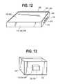
- FIG. 12is an isometric view of the monitoring device of FIG. 1 disposed on top of the receiving device of FIG. 1 ;
- FIG. 13is an isometric view of the monitoring device of FIG. 1 disposed on an object, and the receiving device of FIG. 1 positioned over the monitoring device.
- a monitoring device as disclosed hereinmonitors the environment in which an object is disposed at least at a particular point in time, and more preferably, over a period of time.
- the monitoring deviceincludes a processor, memory, one or more sensor(s), one or more actuator(s), and one or more indicator(s) such as one or more light emitting device(s) such as light emitting diodes (LEDs).
- the one or more sensor(s)can measure, for example, the presence of airborne pollutants and/or odors, the temperature and/or the humidity in the ambient environment surrounding the device, the acceleration to which the monitoring device is subjected, and the like.
- Such a devicemay be affixed or placed on a surface of an object (e.g., an interior surface of a room or vehicle, an interior of a package, an exterior surface of a package, etc.) and activated using the one or more actuator(s).
- the processor in the deviceperiodically polls the sensor(s) to acquire measurements therefrom associated with one or more ambient condition(s).
- the processorrecords in the memory such measurements and a timestamp of when each such measurement was acquired to create a log.
- the processormay evaluate such measurement to determine if the monitoring device has been subjected to an environmental condition or action that is above or below a particular limit defining, for example, an acceptable range.
- the processormay actuate the one or more light emitting device(s) to indicate the result of such evaluation. Further, as described in detail below, the one or more light emitting devices may be used to transmit data representing the log to another device.
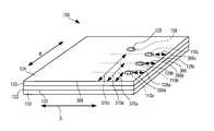
- a monitoring device 100is disposed on a surface 102 .
- the monitoring device 100may be temporarily placed on the surface 102 or the monitoring device 100 may be temporarily or permanently affixed to the surface 102 .
- the surface 102may be, for example, an outer surface 102 ( FIG. 2A ) of an object 104 , an inner surface 102 ( FIG. 2B ) of an object 106 , or any other portion thereof.
- the object 102 or 106may be a vehicle, a package, a wall or other surface in a room or other environment, a finished or an unfinished good or goods, whether packaged or not, or any other article or articles.
- the monitoring device 100may be configured to store data representing a log of exposure of the device 100 , and therefore the surface 102 , to one or more ambient influences or a lack of such exposure at one or more points in time in a memory of the device 102 or in another device (whether local or remote from the device 102 ).
- the ambient influence(s)may include an environmental condition, a force, disposition of the object 100 in one or more particular orientations, or any other influence that can be detected as noted in greater detail hereinafter.
- the monitoring device 100includes an actuator 108 that when actuated directs the processor to begin collecting data regarding the ambient influence(s) to which the monitoring device 100 is exposed (or not exposed), and record such data in the memory of the monitoring device 100 .
- the monitoring device 100also includes one or more indicator(s) 110 such as light emitting devices (LEDs) disclosed hereinafter that may be actuated by the processor to indicate whether the monitoring device 100 , and therefore the surface 102 , has been exposed to an ambient influence and, in some cases, the degree or amount of such influence.
- LEDslight emitting devices
- an operatormay actuate the actuator 108 in a predetermined pattern to cause the processor to illuminate the one or more light emitting devices 110 in a sequence that represents the data recorded in the memory, and in this manner, transmit the recorded data to a receiving device 112 .
- the receiving device 112interprets the sequence of illumination of the one or more light emitting devices 110 to reconstruct the transmitted data and stores such reconstructed data in a memory associated with the receiving device or another device, whether local or remote.
- the receiving device 112may be computer with a camera operating an application program operable to receive and interpret the transmitted data.
- a computermay include a desktop computer, a handheld tablet computer, a smartphone, and the like.
- the receiving device 112may be a dedicated receiving device 112 operable to communicate with the monitoring device 100 .
- the monitoring device 100comprises a first substrate 120 and a second substrate 122 secured to one another.
- An outer surface 124 of the first substratemay be imprinted using conventional printing processes including lithography, intaglio, flexography, foil transfer, ink jet, xerography, and the like. Such imprinting may be used to print one or more of an advertisement, instructions, terms and conditions, and the like.
- the actuator 108may be manually actuated by the user from the outer surface 124 by, for example, pressing on a portion 126 of the outer surface 124 associated with the actuator 108 .
- the outer surface 124also includes a region 128 associated with each light emitting device 110 .
- region 126comprises a transparent or translucent material through which at least a portion of the light emitted by the light emitting device 110 associated with the region 126 passes.
- the region 126comprises an orifice formed in the outer surface 124 to expose at least a portion of the light emitting device 110 associated with the region 126 .
- a removable liner 130may be affixed to an outer surface 132 of the second carrier.
- the substrates 120 and 122 , and the removable liner 130may comprise coated or uncoated paper, textiles, woven materials, plastic, films, gels, epoxies, fiberglass, and combinations thereof.
- the substrates 120 and 122 , and the removable liner 130 , that comprise the monitoring device 102may be manufacturing from identical or different materials.
- the removable liner 130when the removable liner 130 is in place, the removable liner 130 is affixed to the outer surface 132 of the second carrier 122 by an adhesive layer 134 disposed therebetween.
- the adhesive layer 134comprises an inner surface 136 secured to the outer surface 132 of the second carrier 122 and an outer surface 138 secured to an inner surface 140 of the removable liner 130 .
- the adhesive layer 134may be formed by applying an adhesive material to the outer surface 132 of the second carrier 122 and/or an inner surface 140 of the removable liner 130
- the inner surface 140 of the removable liner 130comprises a gloss finish so that such inner surface 136 may be separated from the outer surface 138 of the adhesive layer 134 without substantially removing or damaging the adhesive material that comprises the adhesive layer 134 .
- Removal of the removable liner 130exposes the outer surface 138 of the adhesive layer 134 , and such outer surface 138 may be used to secure the monitoring device 100 to the surface 102 ( FIG. 1 ).
- a third substrate 142Disposed between the first substrate 120 and the second substrate 122 is a third substrate 142 having one or more circuit trace(s) 144 disposed thereon.
- the circuit trace(s) 144interconnect components disposed on the circuit trace ( 144 ) and/or the third substrate 142 .
- Such componentsinclude one or more actuator(s) 108 , one or more light emitting device(s) 110 , a processor 146 , a memory 148 associated with the processor 146 , one or more sensor(s) 150 , and a battery or another power source 152 .
- the circuit trace(s) 144 and the components 108 , 110 , 146 , 148 , 150 , and 152may be disposed directly on an inner surface 154 of the second substrate 122 .
- the third substrate 142may not be necessary and may be omitted.
- the first substrate 120 and the second substrate 122are larger than the third substrate 142 , so that a margin portion 156 of the inner surface 154 of the second surface can brought into contact and affixed to a corresponding margin portion 158 of an inner surface 160 of the first substrate 120 .
- the third substrate 142is substantially enclosed between the first substrate 120 and the third substrate 122 .
- the third substrate 142may be adhesively or otherwise affixed to one or both of the inner substrate 154 of the second substrate 122 and the inner surface 160 of the first substrate 120 to prevent movement of the third substrate 142 .
- An additional protective coveringmay be affixed to an outer surface 162 of the first substrate 120 to prevent damage of such outer surface 162 and any imprinting thereon during use.
- the processor 146may actuate the one or more light emitting devices 110 to transmit data stored in the memory 148 .
- the processor 146operates one of the light emitting devices (e.g., 110 a ) to signal (or gate) that valid data is available on the remaining light emitting devices (e.g., 110 b and 110 c ).
- the state of each remaining light emitting device 110 b or 110 cindicates a bit value associated with the data being transmitted.
- turning on the data light emitting device 110 b or 110 cindicates a bit value of one and turning off such light emitting device 110 b or 110 c indicates a bit value of zero.
- the processor 146transitions the signal light emitting device 110 a from an on to an off state to indicate data are ready for transmission by the light emitting devices 110 b and 110 c .
- the maximum frequency at which the processor 146 transitions the signal light emitting device 110 a from an on to an off stateis preferably at most one-half of the frequency at which the reading device samples or senses the light emitting device 110 a . If, for example, the reading device 112 includes a camera that captures images at a frame rate of 240 frames-per-second, the frequency at which the light emitting device 110 a transitions from an on state to a subsequent off state is 120 cycles-per-second or less.
- Such an arrangementis adapted to the case in which the reading device 112 is capable of sensing only a single transition per frame. If, however, the reading device can sense more than one transition per frame, then a greater data transmission rate could be used as should be evident to one of ordinary skill in the art.
- the reading deviceuses known image processing techniques to identify the light emitting device in images captured thereby.
- image processing technique(s)may include edge detection, color analysis, and the like.
- the reading devicemay include information regarding the positions of the light emitting devices 110 relative to the edges of the monitoring device 100 , and the positions of the light emitting devices 110 relative to one another.
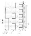
- a sample timing diagram 200illustrates how the processor may control the light emitting devices 110 to transmit information.
- the timing diagram 200includes a horizontal time axis 202 that represents time and three graphs 204 a , 204 b , and 204 c that indicate the on or off state of the light emitting devices 110 a , 110 b , and 110 c relative to the time axis 202 .
- Vertical dashed linesare displayed for each time t 0 , t 1 , . . . , t 19 that indicate when the reading device senses the state of the light emitting devices 110 a , 110 b , and 110 c.
- the receiving device 112records data only when the receiving device 112 detects that the state of the signal light emitting device 110 a has changed in consecutive image captures from an on state to an off state.
- the processor 146sets the state of each light emitting device 110 b and 110 c in accordance with a bit value to be transmitted (i.e., two bits are to be transmitted simultaneously), then transitions the state of the light emitting device 110 a from an on state to an off state.
- the processor 146holds the light emitting device 110 a in an on state for a duration at least equal to two capture cycles of the receiving device 112 . Subsequently, the processor 146 holds the light emitting device 110 a in an off state for at least two capture cycles of the receiving device 112 . Also, during at least the time the light emitting device 110 a is held in the off state and for at least two capture cycles of the receiving device 112 , the light emitting devices 110 b and 110 c are maintained in states in accordance with bit values to be transmitted.
- the receiving device 112will successfully capture data represented by the light emitting devices 110 b and 110 c at times t 1 , t 5 , t 9 , t 14 , t 18 and so on.
- the values shown in the box 205are two-bit values transmitted at these times in accordance with the states of the light emitting devices 110 b and 110 c as shown in the graphs 204 b and 204 c , respectively.
- the receiving device 112may record the values indicated by the light emitting devices 110 b and 110 c when the receiving device 112 detects that the state of the light emitting device 110 a in subsequent captures has changed from an off state to an on state.
- the receiving device 112records the values indicated by the light emitting devices 110 b and 110 c when receiving device 112 detects any or every change in the state of the light emitting device 110 a .
- valid dataare transmitted by light emitting devices 110 b and 110 c whenever the light emitting device 110 a transitions either from an on state to an off state and/or from an off state to an on state.
- FIG. 5Bshows a timing diagram 206 that includes an axis 208 and three graphs 210 a , 210 b , and 210 c to indicate the states of the light emitting devices 110 a , 110 b , and 110 c .
- Vertical dashed linesare displayed for each time t 0 , t 1 , . . . , and t 19 and indicate times when the reading device senses the state of the light emitting devices 110 a , 110 b , and 110 c .
- the processor 146sets the on or off state of the light emitting devices 110 b and 110 c in accordance with bit values to be transmitted, and changes the state of light emitting device 110 a from on-to-off or off-to-on to indicate that the states of light emitting devices 110 b and 110 c are associated with valid data values to be transmitted.
- the receiving device 112will successfully capture two-bits of data represented by the light emitting devices 110 b and 110 c at times t 1 , t 3 , t 5 , t 7 , t 9 and so on.
- the values shown in the box 212indicate the transmitted bits at these times in accordance with the states of the light emitting devices 110 b and 110 c as shown in the graphs 210 b and 210 c , respectively.
- the processor 146transmits the data in bursts of a predetermined number of bits at a predetermined frequency.
- each burstis preceded by a training period during which at least one of the light emitting device 110 is modulated between an on state and an off state at the predetermined frequency for a predetermined number of cycles.
- the receiving device 112samples the state of the modulated light emitting device 110 at a frequency higher than the frequency at which the light emitting device 110 is modulate.
- the receiving device 112analyzes such samples using conventional techniques to estimate a frequency and a phase at which the light emitting device 100 is being modulated, and synchronizes the sampling frequency and phase thereof with that of the light emitting device 100 .
- the receiving device 112samples all of the light emitting devices 110 at the estimated sampling frequency.
- this techniqueeliminates the need for having one of the light emitting devices 110 a provide a gating or clock signal as described above, and the such light emitting device 110 a may be used to transmit an additional bit of data per cycle.
- the datais sent in bursts as described above with a gap of no data transmission between bursts. It should be apparent to those who have skill in the art that when this transmission method is used, the sampling frequency of the receiving device 112 should be greater than the frequency at which the light emitting devices 110 are modulated.
- processor 146transmits the data in bursts of approximately 16 bytes, if the receiving device 112 uses a camera to receive the data, for example, if the receiving device 112 is smartphone. It should be apparent that the number of bytes in a burst may be selected in accordance with the capabilities of the receiving device 112 or any other criterion.
- FIG. 6is a state diagram 300 that illustrates operation of the processor 146 of the monitoring device 100 according to one embodiment.
- the processor 146initially operates in a low-power idle state 302 . If the actuator 108 is actuated, for example, by the user depressing the actuator 108 , the processor 146 transitions into a determine operation state 304 .
- the processor 146determines if the actuation was associated with predetermined actuation types such as a single actuation of less than a first predetermined amount of time, a single actuation that lasted at least as long as the predetermined amount of time, at least a predetermined number of actuations within a second predetermined amount of time, and the like. As described below, the processor 146 may be configured to undertake different operations in response to different types of actuations.
- the processor 146operates in the activate device state 306 .
- the processor 146reads configuration information stored in the memory 148 and configures the sensor(s) 150 in accordance with such information.
- the configuration informationmay specify, for example, whether the sensor should generate an interrupt when a magnitude of an environmental condition monitored by the sensor is exceeded, and the configuration information may be supplied with any initialization signals that need to be provided to the sensor 150 to begin operation thereof, and the like.
- the configuration information stored in the memory 148 that is used to configure the sensor(s) 150may be stored in such memory 148 when the monitoring device 100 is manufactured or may be communicated to the monitoring device 100 using light-based communications as described below, or an additional configuration circuit (not shown).
- Such configuration circuitmay include one or more additional actuator(s), a Radio Frequency Communication module and an antenna, a serial port, and the like.
- the processor 146may also initialize other components of the monitoring device 100 .
- the processor 146returns to the idle state 302 after the components have been initialized.
- the processor 146transitions to a transmit log state 308 .
- the processor 146operates the light emitting devices 110 to transmit a log stored in the memory 148 , as described herein. After transmission of the log is completed, the processor 146 returns to the idle state 302 .
- the processor 146When in the idle state 302 , if the processor 146 receives a clock interrupt and/or an interrupt generated by the sensor 150 , the processor 146 transitions to a read sensor state 310 .
- the processor 146obtains a reading of the sensed condition, for example, one or more environmental condition(s) sensed by the sensor(s) 150 , and records such condition(s) and an optional timestamp in the memory 148 .
- the processormay record the environmental condition(s) in the memory 148 only if magnitude of such condition(s) exceed a preset threshold magnitude(s) associated with such condition(s).
- the processor 146transitions to an actuate indicator state 312 and actuates the light emitting devices 110 in accordance with the environmental condition(s) sensed by the sensor(s) 150 .
- the actuations of the light emitting devices 110are to provide an indication to an observer of the monitoring device regarding environmental condition(s) sensed by the sensor(s). Even though the same light emitting devices 110 are actuated, these actuations are for a different purpose than transmitting data using light-based communications described above.
- the processor 146may turn on only the light emitting device 110 a if the magnitude of the sensed condition is less than a first predetermined magnitude, only the light emitting device 110 b if the magnitude of the sensed condition is between the first predetermined magnitude and a second predetermined magnitude, and the light emitting device 110 c if the magnitude of the sensed condition is greater than the second predetermined magnitude.
- the processor 146waits a predetermined amount of time, and then turns off the one or more light emitting devices 110 . Thereafter, the processor 146 transitions to the idle state 302 .
- FIG. 7shows a flowchart of the steps undertaken by the processor when in the transmit log state 308 .
- the processor 146checks to see if any data remains to be transmitted. If there is no data remaining, the processor 146 exits (and transitions to a state 302 ).
- the processor 146sets the state of the signal light emitting device (e.g., light emitting device 110 a ) to on.
- the processor 146waits for a predetermined amount of time, for example, enough time for the receiver 112 to undertake two capture cycles.
- the processor 146selects bits to transmit.
- the processor 146selects a number of bits identical to the number of light emitting device light emitting devices 110 available to transmit data values.
- the number of light emitting devices 110 available to transmit data valuesis two (light emitting devices 110 b and 110 c ), and hence, in such embodiment, the processor 146 selects two bits.
- the processor 146sets the states of the light emitting devices 110 that are used to transmit data values in accordance with the values of the bits selected.
- the processor 146sets the state of the signal light emitting device (e.g., light emitting device 110 a ) to an off state to indicate that valid data is indicated by light emitting devices 110 b and 110 c . Then, at a block 328 , the processor waits a predetermined amount of time equal to at least two capture cycles of the receiving device 112 . Thereafter, the processor 146 returns to the block 320 to determine if any additional data bits remain to be transferred. The processor 146 undertakes the actions of the blocks 320 - 332 until all of the data in the memory 148 to be communicated to the receiving device 112 have been transmitted. After all of the data has been communicated, the processor 146 , at a block 334 , actuates the light emitting devices with a predetermined pattern of pulses or data to indicate that transmission is completed.
- the processor 146at a block 334 , actuates the light emitting devices with a predetermined pattern of pulses or data to indicate that transmission is completed.
- the receiving device 112may be a dedicated device that operates with the monitoring device 100 .
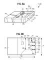
- one embodiment 350 of the receiving device 112includes a housing 352 .
- the housing 352includes a recessed portion 354 and a compartment 356 .
- Disposed on a bottom surface 358 of the recessed portion 354are a plurality of light sensors 360 .
- the recessed portion 354includes a first interior edge 362 and a second interior edge 364 and the monitoring device 100 includes edges 366 and 368 (see FIG. 3 ).
- the light sensors 360are disposed in the receiving device 112 such that a distance 369 a , 369 b , and 369 c , when measured along a direction A, from the first interior edge 362 to each light sensor 360 a , 360 b , and 360 c , respectively, is substantially identical to a distance 369 a ′, 369 b ′, and 369 c ′, when measured along a direction A′, from the edge 366 to each light emitting device 110 a , 110 b , and 110 c , respectively.
- a distance 370 a , 370 b , and 370 cwhen measured along a direction B, of each light sensor 360 a , 360 b , and 360 c , respectively, from the second interior edge 364 is substantially identical to a distance 370 a ′, 370 b ′, and 370 c ′, measured along a direction B′, of each light emitting device 110 a , 110 b , 110 c from the edge 368 of the monitoring device 100 .
- This arrangement of the light sensors 360facilitates alignment of each light sensor 360 a , 360 b , and 360 c with the corresponding light emitting device 110 a , 110 b , and 110 c , respectively, when the edges 362 and 364 of the receiving device are abutted against the edges 366 and 368 , respectively, of the monitoring device 100 .
- the receiving device 350also includes an actuator (e.g., a switch) 371 , an light emitting device 372 , and a communications port 374 .
- an actuatore.g., a switch
- the processor 146FIG. 4
- the receiving device 350is positioned relative to the monitoring device 100 so that the light sensors 360 are aligned with the light emitting devices 110 as described above.
- the actuator 371is actuated. It should be apparent, that the processor 146 may wait a period of time after entering the transmit log state 308 and before initiating transmission to allow the receiving device 350 to be positioned over the monitoring device 100 .
- a processor 376 of the receiving device 350is coupled to the light sensors 360 a , 360 b , and 360 c and captures light signals emitted by the light emitting devices 110 , as described above and sensed by the light sensors 360 , and decodes such signals into a data stream.
- the processor 376may store such data stream in a memory associated therewith or transmit the data stream through the communications port 374 .
- Such data streammay be transmitted to another computer or device using any communication means apparent to one of ordinary skill in the art including USB, RS-232, Ethernet, or a wireless means such as Bluetooth, 802.11, and the like.
- the processor 376may illuminate the light emitting device 372 to indicate successful receipt of the transmitted data.
- the compartment 354 of the housing 352may be used to hold a battery or another energy source (not shown) that supplies power to the various components of the receiving device 350 , and may further hold accessories (not shown), e.g., a communications cable, that may be used with the receiving device 356 . Further, structure(s) disposed in the compartment 354 may support the monitoring device 100 when such device is placed on top of the receiving device 350 .
- both the monitoring device and the receiving deviceinclude both one or more light emitting device(s) and one or more light sensor(s).
- the monitoring device and the receiving deviceare able to both transmit data to each other and receive data from each other.
- light emitting devicemay not have to provide the signal that indicates that data is available at the other light emitting devices, and also to allow the receiving device 112 to download data, e.g. configuration information, to the monitoring device 100 .
- a monitoring device 400is substantially identical to the monitoring device 100 described above, except the monitoring device 400 further includes a light sensor 402 .
- the top surface 124 of the monitoring device 400includes a portion 404 that allows at least a portion of light directed at the portion 404 to be transmitted to and sensed by the light sensor 402 .
- a receiving device 406is substantially identical to the receiving device 350 described above, except the receiving device 406 further includes a light emitting device 408 disposed on the bottom surface 358 .
- the light sensor 402 of the monitoring device 400is positioned with respect to the edges 366 and 368
- the light emitting device 408 of the receiving device 406is positioned with respect to the edges 362 and 364 , such that when the edge 362 is abutted with the 366 and the edge 364 is abutted with the edge 368 , the light sensor 402 and the light emitting device 408 are aligned with one another and at least a portion of light transmitted by the light emitting device 408 is sensed by the light sensor 402 .
- the actuator 108 of the monitoring device 400is actuated, then the receiving device 406 is positioned over the monitoring device 400 so that the light sensors 360 and the light emitting device 408 are aligned with the light emitting devices 110 and the light sensor 404 , respectively.
- the actuator 371 of the receiving deviceis then actuated to initiate two-way communications between the monitoring device 400 and the receiving device 406 .
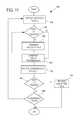
- FIG. 11is a flowchart 450 of the processing undertaken by the processor 146 of the monitoring device 400 in response to the actuation of the actuator 108 .
- the processor 146 of the monitoring device 400waits at a block 452 to receive via the light sensor 408 a predefined sequence of one or more light pulses generated by the light emitting device 408 of the receiving device.
- Such one or more light pulsesmay simply be a single pulse of predetermined duration, a sequence of a predetermined number of pulses of identical duration, or a sequence of a predetermined number of pulses wherein each pulse is of a predetermined duration that may be the same or different than the duration of other pulses.
- the processor 146determines if there is any data remaining in the memory 148 to transmit. If there is, the processor proceeds to a block 456 , otherwise, the processor proceeds to a block 458 .
- the processor 146transmits a predetermined number of bits of data using the light emitting devices 110 of the monitoring device 400 .
- the processor 146sets the state of the light emitting devices 110 b and 110 c in accordance with two bits of data to transmit and the state of the light emitting device 110 a to signal that states of the light emitting devices 110 b and 110 c represent valid data.
- the processor 146uses all of the light emitting devices 110 to transmit data by setting the state of each of the light emitting devices 110 in accordance with a bit to be transmitted for a predetermined amount of time. In still other embodiments, the processor 146 sets the state of all of the light emitting devices 110 in accordance with bits to be transmitted, then waits until a light pulse is detected by the light sensor 404 . In such embodiments, the processor 376 of the receiving device 406 actuates the light emitting device 408 each time data are received using the light sensors 360 .
- the receiving device 400may transmit, in addition to the predefined sequence pulses, the number of bytes to transmit in a burst or a packet. In other embodiments, such packet size is predefined. In some of these embodiments, the monitoring device 400 transmits a number of bytes that is specified by the packet size (or fewer bytes if there are not sufficient data to transmit), then waits for acknowledgement of receipt of the packet from the receiving device 400 before transmitting another packet of data. Such acknowledgement of receipt may be one or more predefined pulses of the light emitting device 408 actuated by the processor 376 of the receiving device 400 .
- the computer or device to which the receiving device 400 transmits the data via the communications port 374 , or other means of communicationsspecifies (e.g., via a transmission to the receiving device 400 ) the maximum number of bytes each packet should contain.
- each packet sizeis 1 kilobytes of unencoded (raw) data. In other embodiments, the packet size if 2 kilobytes of ASCII encoded data.
- the processor 146may send a predefined sequence of bits to indicate the start of a block of data, then send the block of data, and then send another predefined sequence of bits to indicate that the block of data has been sent. It should be apparent that the block of data transmitted may include error checking and correction data that the receiving device 112 may use to validate the integrity of the data received and decoded thereby.
- the processorAfter the block of the data has been transmitted at the block 456 , the processor returns to the block 454 to determine if any additional data is to be transmitted.
- the processor 146After all of the data has been transmitted, the processor 146 , at a block 458 operates the light emitting devices 110 to generate a predefined sequence of pulses that indicate to the receiving device 406 that all of the data has been transmitted.
- the processor 146waits until a predefined sequence of pulses is transmitted by the receiving device 406 and is sensed by the light sensor 402 .
- the predefined sequence of pulsesmay be selected from a plurality of predefined sequences and may indicate that the transmitted data was successfully received and that the receiving device 406 does not have any further data to transmit to the monitoring device 400 , or that the transmitted data was successfully received and that the receiving device 406 has data to transmit to the monitoring device 400 , or that there was an error in communications.
- the processor 146determines whether the predefined sequence of pulses indicates that the receiving device 406 has data to transmit to the monitoring device 400 . If so, the processor 146 , at a block 464 receives the data via the light sensor 402 , and then exits.
- the processor 376 of the receiving device 406undertakes processing similar to that described in connection with the blocks 452 - 458 to transmit data, except such data is transmitted one bit at a time and without use of a signal light emitting device.
- Data transmitted by the receiving device 406may include for example, program code and/or configuration parameters to be stored in particular locations in the memory 148 of the monitoring device 400 . Such data may also include a command to, for example, restart the monitoring device 400 or reload configuration parameters from the memory 148 , or to reset the sensor(s) 150 of the monitoring device 400 .
- the processor 146determines that the predefined sequence of pulses received at the block 460 do not indicate that the receiving device 406 has data to transmit, the processor 146 proceeds to a block 466 .
- the processordetermines if the predefined sequence of pulses indicates an error in the receipt of data by the receiving device 406 , and if so, proceeds to the block 452 to retransmit the data. Otherwise, the processor 146 exits.
- the dimensions of the receiving device 112 , 350 , 406are selected so that the monitoring device 100 , 400 may be placed thereon for communications therebetween.
- the receiving device 112 , 350 , 406is contemplated to be a portable device that may be used to receive data from the monitoring device 100 , 400 , even when such monitoring device is affixed to an object.
- the monitoring device 100 , 400may be affixed to the surface 102 of the object 104 , as described in connection with FIG. 2 .
- the receiving device 112 , 350 , 406may be placed over such monitoring device 100 , 400 to receive data therefrom as described above without having to first remove the monitoring device 100 , 400 from the surface 102 .
- the receiving device 112 , 350 , 406may include a lanyard or other carrying device (not shown) to enable a user to securely hold the receiving device 112 , 350 , 406 when used in this manner.
- the embodiments of the monitoring device 100 , 400 and the receiving device 112 , 350 , 406 described aboveuse binary light emitting devices 110 , 408 , that are operated in an on state or an off state, it should be apparent that one or more of these binary light emitting devices 110 , 408 may be replaced with light emitting device(s) that are operated in multiple discrete levels of intensity. For example, operating such light emitting device(s) in four states (e.g., 0%, 25%, 50%, and 100% intensity) would allow transmission of two bits of data with each such light emitting device.
- light emitting devicesmay be used that produce different hues and intensities of light, and that discrete combinations of a selected hue and a selected intensity represent different data values, thereby further increasing number of bits that may be transmitted by an individual light emitting device at a particular time.
- the data that is transmitted by the monitoring device 100 , 400may be compressed and/or encoded using various techniques known to those who have skill in the art. Such techniques may include Huffman encoding, LZW, and tar, and the like. Further, although the present disclosure notes that light-based communication may be used to transmit digital data using the light emitting device 110 , it should be apparent that other types of data can be encoded and transmitted using other data encoding and/or transmission techniques.
- monitoring devices 100 and 400may be combined to receive and/or transmit data therebetween using light-based communications. Further the various combinations of the receiving device 112 , 350 , and 406 may be combined to receive data using light-based communications.
Landscapes
- Engineering & Computer Science (AREA)
- Business, Economics & Management (AREA)
- Physics & Mathematics (AREA)
- Economics (AREA)
- Electromagnetism (AREA)
- Computer Networks & Wireless Communication (AREA)
- Signal Processing (AREA)
- General Physics & Mathematics (AREA)
- Theoretical Computer Science (AREA)
- Quality & Reliability (AREA)
- Finance (AREA)
- Human Resources & Organizations (AREA)
- Marketing (AREA)
- Operations Research (AREA)
- Development Economics (AREA)
- Strategic Management (AREA)
- Tourism & Hospitality (AREA)
- General Business, Economics & Management (AREA)
- Entrepreneurship & Innovation (AREA)
- Accounting & Taxation (AREA)
- Health & Medical Sciences (AREA)
- Toxicology (AREA)
- Arrangements For Transmission Of Measured Signals (AREA)
- Medical Informatics (AREA)
- Computer Security & Cryptography (AREA)
- General Health & Medical Sciences (AREA)
- Artificial Intelligence (AREA)
- Computer Vision & Pattern Recognition (AREA)
- Infusion, Injection, And Reservoir Apparatuses (AREA)
Abstract
Description
Claims (26)
Priority Applications (1)
| Application Number | Priority Date | Filing Date | Title |
|---|---|---|---|
| US15/451,036US10445692B2 (en) | 2017-03-06 | 2017-03-06 | Monitoring device and method of operating a monitoring device to transmit data |
Applications Claiming Priority (1)
| Application Number | Priority Date | Filing Date | Title |
|---|---|---|---|
| US15/451,036US10445692B2 (en) | 2017-03-06 | 2017-03-06 | Monitoring device and method of operating a monitoring device to transmit data |
Publications (2)
| Publication Number | Publication Date |
|---|---|
| US20180252554A1 US20180252554A1 (en) | 2018-09-06 |
| US10445692B2true US10445692B2 (en) | 2019-10-15 |
Family
ID=63355077
Family Applications (1)
| Application Number | Title | Priority Date | Filing Date |
|---|---|---|---|
| US15/451,036Active2037-10-19US10445692B2 (en) | 2017-03-06 | 2017-03-06 | Monitoring device and method of operating a monitoring device to transmit data |
Country Status (1)
| Country | Link |
|---|---|
| US (1) | US10445692B2 (en) |
Citations (79)
| Publication number | Priority date | Publication date | Assignee | Title |
|---|---|---|---|---|
| US4012552A (en) | 1975-03-10 | 1977-03-15 | Dennison Manufacturing Company | Decorative metal film heat transfer decalcomania |
| US4368281A (en) | 1980-09-15 | 1983-01-11 | Amp Incorporated | Printed circuits |
| US4515653A (en) | 1983-04-30 | 1985-05-07 | Sharp Kabushiki Kaisha | Method for production of a moisture sensor |
| US4632879A (en) | 1983-04-30 | 1986-12-30 | Sharp Kabushiki Kaisha | Moisture sensor |
| US5581065A (en) | 1993-08-02 | 1996-12-03 | Dai Nippon Printing Co., Ltd. | Sheet-framed IC carrier, method for producing the same, and IC carrier case |
| US5790020A (en) | 1995-04-07 | 1998-08-04 | Alps Electric Co., Ltd. | E.A.S. system with selective disabling |
| US5802015A (en) | 1997-05-05 | 1998-09-01 | Rothschild Technology, L.L.C. | Intelligent label |
| US6019865A (en) | 1998-01-21 | 2000-02-01 | Moore U.S.A. Inc. | Method of forming labels containing transponders |
| US6043745A (en) | 1997-11-13 | 2000-03-28 | Micron Technology, Inc. | Electronic devices and methods of forming electronic devices |
| EP1019715A1 (en) | 1997-08-08 | 2000-07-19 | California Institute Of Technology | Techniques and systems for analyte detection |
| WO2000073082A1 (en) | 1999-06-01 | 2000-12-07 | 3M Innovative Properties Company | Random microembossed receptor media |
| US6420096B1 (en) | 1999-04-03 | 2002-07-16 | Koninklijke Philips Electronics N.V. | Method of manufacturing electronic stripline components |
| US6421013B1 (en) | 1999-10-04 | 2002-07-16 | Amerasia International Technology, Inc. | Tamper-resistant wireless article including an antenna |
| WO2003006736A1 (en) | 2001-07-13 | 2003-01-23 | Foto-Wear, Inc. | Sublimation dye thermal transfer paper and transfer method |
| US6544864B2 (en) | 2000-05-19 | 2003-04-08 | Micron Technology, Inc. | Methods employing hybrid adhesive materials to secure components of semiconductor device assemblies and packages to one another and assemblies and packages including components secured to one another with such hybrid adhesive materials |
| JP2003277653A (en) | 2002-03-20 | 2003-10-02 | Seiko Epson Corp | Aqueous ink composition set and recording method |
| US20040066296A1 (en) | 2001-11-15 | 2004-04-08 | Atherton Peter S. | Tamper indicating radio frequency identification label with tracking capability |
| US6853087B2 (en) | 2000-09-19 | 2005-02-08 | Nanopierce Technologies, Inc. | Component and antennae assembly in radio frequency identification devices |
| US6888509B2 (en) | 2000-03-21 | 2005-05-03 | Mikoh Corporation | Tamper indicating radio frequency identification label |
| US6886745B2 (en) | 1999-12-15 | 2005-05-03 | Store Electronic Systems Technologies | Electronic label system for displaying prices in a sale outlet |
| US6924781B1 (en) | 1998-09-11 | 2005-08-02 | Visible Tech-Knowledgy, Inc. | Smart electronic label employing electronic ink |
| US20060062108A1 (en)* | 2002-12-20 | 2006-03-23 | Koninklijke Philips Electronics | Sensing light emitted from multiple light sources |
| US7042357B2 (en) | 2003-03-26 | 2006-05-09 | Proximities, Inc. | Non-reusable identification device |
| US7057495B2 (en) | 2002-10-17 | 2006-06-06 | Paksense, Llc | Perishable product electronic label including time and temperature measurement |
| US7168626B2 (en) | 2004-10-08 | 2007-01-30 | Proximities, Inc. | Identification band using shorting wire for enabling/disabling an RFID transponder contained thereon |
| US7174277B2 (en) | 2000-12-15 | 2007-02-06 | Phatrat Technology Llc | Product integrity systems and associated methods |
| US7204425B2 (en) | 2002-03-18 | 2007-04-17 | Precision Dynamics Corporation | Enhanced identification appliance |
| US7248147B2 (en) | 2002-10-17 | 2007-07-24 | Paksense, Llc | Perishable product electronic label including time and temperature measurement |
| US7295115B2 (en) | 2002-10-18 | 2007-11-13 | Aeroscout, Ltd. | Radio-frequency identification (RFID) tag employing unique reception window and method therefor |
| US7316358B2 (en) | 2002-03-18 | 2008-01-08 | Precision Dynamics Corporation | Identification band with adhesively attached coupling elements |
| US7323360B2 (en) | 2001-10-26 | 2008-01-29 | Intel Corporation | Electronic assemblies with filled no-flow underfill |
| US7377447B2 (en) | 2005-12-05 | 2008-05-27 | Rcd Technology, Inc. | Tuned radio frequency identification (RFID) circuit used as a security device for wristbands and package security |
| US7417541B2 (en) | 2004-10-08 | 2008-08-26 | Bartronics America, Inc. | Identification band with regions having electro-magnetically detectable regions |
| US7586412B2 (en) | 2005-04-25 | 2009-09-08 | Nec Corporation | Wireless tag, wireless tag reader/writer, wireless tag information provision method, and wireless tag system |
| US7639135B2 (en) | 2004-10-28 | 2009-12-29 | Microstrain, Inc. | Identifying substantially related objects in a wireless sensor network |
| US7737839B1 (en) | 2008-01-24 | 2010-06-15 | Sprint Communications Company L.P. | System and method for protecting pocket-portable electronic devices |
| US20100176950A1 (en) | 2009-01-15 | 2010-07-15 | Joel Bartholf | Vending enclosure recovery method and system |
| US7802222B2 (en) | 2006-09-25 | 2010-09-21 | Cadence Design Systems, Inc. | Generalized constraint collection management method |
| US7856339B2 (en) | 2000-12-15 | 2010-12-21 | Phatrat Technology, Llc | Product integrity tracking shipping label, system and associated method |
| US7895739B2 (en) | 2002-09-28 | 2011-03-01 | Muehlbauer Ag | Apparatus for applying semiconductor chip to substrates comprising a moveable curing device and method of use thereof |
| US7945320B2 (en) | 2007-08-17 | 2011-05-17 | Isis Biopolymer, Inc. | Iontophoretic drug delivery system |
| US20110131854A1 (en) | 2009-12-09 | 2011-06-09 | Wristband Resources, Inc. | Sheet of wristbands |
| JP2011151259A (en) | 2010-01-22 | 2011-08-04 | Sony Chemical & Information Device Corp | Method of manufacturing packaging body and device of packaging |
| US7993055B2 (en) | 2008-03-28 | 2011-08-09 | Lloyd Cleveland Nurse | Method and apparatus for alerting a person at medicine dosing times |
| US20120038461A1 (en) | 2010-08-13 | 2012-02-16 | Avery Dennison Corporation | Sensing Radio Frequency Identification Device with Reactive Strap Attachment |
| US20120071742A1 (en)* | 2010-09-22 | 2012-03-22 | Nellcor Puritan Bennett Llc | Remanufacturing a stacked adhesive medical sensor |
| US8203446B2 (en) | 2008-09-30 | 2012-06-19 | Fujifilm Corporation | Radio communication terminal |
| US20120162945A1 (en) | 2010-12-23 | 2012-06-28 | Schreiner Group Gmbh & Co. Kg | Label having an electronic functional element |
| US8219466B2 (en) | 2002-08-05 | 2012-07-10 | John Yupeng Gui | System and method for providing asset management and tracking capabilities |
| US20120274470A1 (en)* | 2009-12-11 | 2012-11-01 | Sandvick Warren J | Food safety indicator |
| US8317084B2 (en) | 2009-09-17 | 2012-11-27 | Nokia Corporation | Package content control |
| US8354927B2 (en) | 2002-06-11 | 2013-01-15 | Intelligent Technologies International, Inc. | Shipping container monitoring based on door status |
| US8590799B2 (en) | 2010-04-30 | 2013-11-26 | Jun Liu | Systems, methods, apparatus of a secure RFID record |
| US8618914B2 (en) | 2010-01-05 | 2013-12-31 | The Regents Of The University Of California | MEMS sensor enabled RFID system and method for operating the same |
| US8640259B2 (en) | 2005-01-20 | 2014-01-28 | The Invention Science Fund I, Llc | Notarizable electronic paper |
| FR2997218A1 (en) | 2012-10-23 | 2014-04-25 | Jackel Internat Europ | MULTILAYER LIGHT LABEL AND BOTTLE EQUIPPED WITH AT LEAST ONE LIGHT LABEL AS PRECEDED |
| WO2014067578A1 (en) | 2012-10-31 | 2014-05-08 | Hewlett-Packard Indigo B.V. | Method and apparatus for forming on a substrate a pattern of a material |
| US8762212B2 (en) | 1995-07-31 | 2014-06-24 | Information Planning & Management Service, Inc. | Electronic product information display system |
| US20140196847A1 (en) | 2013-01-15 | 2014-07-17 | Rainforest Technologies, Llc | Conductive aqueous-based adhesive compositions and methods of use thereof |
| US8870083B2 (en) | 2012-02-27 | 2014-10-28 | L&P Property Management Company | Mattress age indicator |
| US8914090B2 (en)* | 2006-09-27 | 2014-12-16 | The University Of Connecticut | Implantable biosensor and methods of use thereof |
| WO2015004830A1 (en) | 2013-07-08 | 2015-01-15 | ソニー株式会社 | Method for determining curing conditions, method for producing circuit device, and circuit device |
| US20150079697A1 (en) | 2010-09-10 | 2015-03-19 | The Trustees Of Dartmouth College | Devices For Detecting Airborne Contaminants, And Associated Methods |
| US9030724B2 (en) | 2008-07-03 | 2015-05-12 | Chromera, Inc. | Flexible and printable electrooptic devices |
| US9047437B2 (en) | 2011-10-31 | 2015-06-02 | Taiwan Semiconductor Manufacturing Co., Ltd. | Method, system and software for accessing design rules and library of design features while designing semiconductor device layout |
| US9077183B2 (en) | 2011-09-06 | 2015-07-07 | Portland State University | Distributed low-power wireless monitoring |
| US9087318B1 (en) | 2013-11-08 | 2015-07-21 | Sprint Communications Company L.P. | Visually readable electronic label |
| US20150269518A1 (en)* | 2012-10-12 | 2015-09-24 | Ander GRAY OLARAN | System and method for monitoring the cold chain integrity of environmentally sensitive packaged goods |
| WO2015160830A1 (en) | 2014-04-15 | 2015-10-22 | Chemisense, Inc. | Crowdsourced wearable sensor system |
| US20160050762A1 (en) | 2014-08-13 | 2016-02-18 | R.R. Donnelley & Sons Company | Method and apparatus for producing an electronic device |
| US20160249840A1 (en) | 2015-02-26 | 2016-09-01 | Medtronic Minimed, Inc. | Ph microsensor for glucose and other analyte sensor fault detection |
| US9495498B2 (en) | 2009-04-28 | 2016-11-15 | Globalfoundries Inc. | Universal inter-layer interconnect for multi-layer semiconductor stacks |
| US20160352423A1 (en)* | 2014-02-21 | 2016-12-01 | 3M Innovative Properties Company | Method, apparatus and system for visible light communication |
| US9514432B2 (en) | 2014-08-19 | 2016-12-06 | R.R. Donnelley & Sons Company | Apparatus and method for monitoring a package during transit |
| US20170076642A1 (en) | 2015-09-14 | 2017-03-16 | R.R. Donnelley & Sons Company | Electronic label having a timer function |
| US20170138922A1 (en) | 2006-11-16 | 2017-05-18 | General Electric Company | Sensing system and method |
| US20170191953A1 (en) | 2011-03-14 | 2017-07-06 | Anastasia Rigas | Breath analyzer and breath test methods |
| US20170229000A1 (en)* | 2014-08-04 | 2017-08-10 | Avery Dennison Corporation | Time-Temperature Tracking Label |
| US20170354372A1 (en) | 2011-03-08 | 2017-12-14 | Nanowear Inc. | Smart materials, dry textile sensors, and electronics integration in clothing, bed sheets, and pillow cases for neurological, cardiac and/or pulmonary monitoring |
- 2017
- 2017-03-06USUS15/451,036patent/US10445692B2/enactiveActive
Patent Citations (87)
| Publication number | Priority date | Publication date | Assignee | Title |
|---|---|---|---|---|
| US4012552A (en) | 1975-03-10 | 1977-03-15 | Dennison Manufacturing Company | Decorative metal film heat transfer decalcomania |
| US4368281A (en) | 1980-09-15 | 1983-01-11 | Amp Incorporated | Printed circuits |
| US4515653A (en) | 1983-04-30 | 1985-05-07 | Sharp Kabushiki Kaisha | Method for production of a moisture sensor |
| US4632879A (en) | 1983-04-30 | 1986-12-30 | Sharp Kabushiki Kaisha | Moisture sensor |
| US5581065A (en) | 1993-08-02 | 1996-12-03 | Dai Nippon Printing Co., Ltd. | Sheet-framed IC carrier, method for producing the same, and IC carrier case |
| US5790020A (en) | 1995-04-07 | 1998-08-04 | Alps Electric Co., Ltd. | E.A.S. system with selective disabling |
| US8762212B2 (en) | 1995-07-31 | 2014-06-24 | Information Planning & Management Service, Inc. | Electronic product information display system |
| US5802015A (en) | 1997-05-05 | 1998-09-01 | Rothschild Technology, L.L.C. | Intelligent label |
| EP1019715A1 (en) | 1997-08-08 | 2000-07-19 | California Institute Of Technology | Techniques and systems for analyte detection |
| US6043745A (en) | 1997-11-13 | 2000-03-28 | Micron Technology, Inc. | Electronic devices and methods of forming electronic devices |
| US6019865A (en) | 1998-01-21 | 2000-02-01 | Moore U.S.A. Inc. | Method of forming labels containing transponders |
| US6924781B1 (en) | 1998-09-11 | 2005-08-02 | Visible Tech-Knowledgy, Inc. | Smart electronic label employing electronic ink |
| US6420096B1 (en) | 1999-04-03 | 2002-07-16 | Koninklijke Philips Electronics N.V. | Method of manufacturing electronic stripline components |
| WO2000073082A1 (en) | 1999-06-01 | 2000-12-07 | 3M Innovative Properties Company | Random microembossed receptor media |
| US6421013B1 (en) | 1999-10-04 | 2002-07-16 | Amerasia International Technology, Inc. | Tamper-resistant wireless article including an antenna |
| US6886745B2 (en) | 1999-12-15 | 2005-05-03 | Store Electronic Systems Technologies | Electronic label system for displaying prices in a sale outlet |
| US6888509B2 (en) | 2000-03-21 | 2005-05-03 | Mikoh Corporation | Tamper indicating radio frequency identification label |
| US6544864B2 (en) | 2000-05-19 | 2003-04-08 | Micron Technology, Inc. | Methods employing hybrid adhesive materials to secure components of semiconductor device assemblies and packages to one another and assemblies and packages including components secured to one another with such hybrid adhesive materials |
| US6853087B2 (en) | 2000-09-19 | 2005-02-08 | Nanopierce Technologies, Inc. | Component and antennae assembly in radio frequency identification devices |
| US7174277B2 (en) | 2000-12-15 | 2007-02-06 | Phatrat Technology Llc | Product integrity systems and associated methods |
| US7856339B2 (en) | 2000-12-15 | 2010-12-21 | Phatrat Technology, Llc | Product integrity tracking shipping label, system and associated method |
| US7627451B2 (en) | 2000-12-15 | 2009-12-01 | Apple Inc. | Movement and event systems and associated methods |
| US8126675B2 (en) | 2000-12-15 | 2012-02-28 | Phatrat Technology, Llc | Product integrity tracking shipping label, and associated method |
| US8280682B2 (en) | 2000-12-15 | 2012-10-02 | Tvipr, Llc | Device for monitoring movement of shipped goods |
| US8428904B2 (en) | 2000-12-15 | 2013-04-23 | Tvipr, Llc | Product integrity tracking system, shipping label, and associated method |
| WO2003006736A1 (en) | 2001-07-13 | 2003-01-23 | Foto-Wear, Inc. | Sublimation dye thermal transfer paper and transfer method |
| US7323360B2 (en) | 2001-10-26 | 2008-01-29 | Intel Corporation | Electronic assemblies with filled no-flow underfill |
| US20040066296A1 (en) | 2001-11-15 | 2004-04-08 | Atherton Peter S. | Tamper indicating radio frequency identification label with tracking capability |
| US7204425B2 (en) | 2002-03-18 | 2007-04-17 | Precision Dynamics Corporation | Enhanced identification appliance |
| US7316358B2 (en) | 2002-03-18 | 2008-01-08 | Precision Dynamics Corporation | Identification band with adhesively attached coupling elements |
| JP2003277653A (en) | 2002-03-20 | 2003-10-02 | Seiko Epson Corp | Aqueous ink composition set and recording method |
| US8354927B2 (en) | 2002-06-11 | 2013-01-15 | Intelligent Technologies International, Inc. | Shipping container monitoring based on door status |
| US8219466B2 (en) | 2002-08-05 | 2012-07-10 | John Yupeng Gui | System and method for providing asset management and tracking capabilities |
| US7895739B2 (en) | 2002-09-28 | 2011-03-01 | Muehlbauer Ag | Apparatus for applying semiconductor chip to substrates comprising a moveable curing device and method of use thereof |
| US7248147B2 (en) | 2002-10-17 | 2007-07-24 | Paksense, Llc | Perishable product electronic label including time and temperature measurement |
| US7057495B2 (en) | 2002-10-17 | 2006-06-06 | Paksense, Llc | Perishable product electronic label including time and temperature measurement |
| US7675424B2 (en)* | 2002-10-17 | 2010-03-09 | Paksense, Inc. | Perishable product electronic label including time and temperature measurement |
| US7295115B2 (en) | 2002-10-18 | 2007-11-13 | Aeroscout, Ltd. | Radio-frequency identification (RFID) tag employing unique reception window and method therefor |
| US20060062108A1 (en)* | 2002-12-20 | 2006-03-23 | Koninklijke Philips Electronics | Sensing light emitted from multiple light sources |
| US7042357B2 (en) | 2003-03-26 | 2006-05-09 | Proximities, Inc. | Non-reusable identification device |
| US7283054B2 (en) | 2003-03-26 | 2007-10-16 | Proximities, Inc. | Tamper-resistant RFID disabling apparatus and method of manufacturing |
| US7168626B2 (en) | 2004-10-08 | 2007-01-30 | Proximities, Inc. | Identification band using shorting wire for enabling/disabling an RFID transponder contained thereon |
| US7417541B2 (en) | 2004-10-08 | 2008-08-26 | Bartronics America, Inc. | Identification band with regions having electro-magnetically detectable regions |
| US7639135B2 (en) | 2004-10-28 | 2009-12-29 | Microstrain, Inc. | Identifying substantially related objects in a wireless sensor network |
| US8640259B2 (en) | 2005-01-20 | 2014-01-28 | The Invention Science Fund I, Llc | Notarizable electronic paper |
| US7586412B2 (en) | 2005-04-25 | 2009-09-08 | Nec Corporation | Wireless tag, wireless tag reader/writer, wireless tag information provision method, and wireless tag system |
| US7377447B2 (en) | 2005-12-05 | 2008-05-27 | Rcd Technology, Inc. | Tuned radio frequency identification (RFID) circuit used as a security device for wristbands and package security |
| US7802222B2 (en) | 2006-09-25 | 2010-09-21 | Cadence Design Systems, Inc. | Generalized constraint collection management method |
| US8914090B2 (en)* | 2006-09-27 | 2014-12-16 | The University Of Connecticut | Implantable biosensor and methods of use thereof |
| US20170138922A1 (en) | 2006-11-16 | 2017-05-18 | General Electric Company | Sensing system and method |
| US7945320B2 (en) | 2007-08-17 | 2011-05-17 | Isis Biopolymer, Inc. | Iontophoretic drug delivery system |
| US7737839B1 (en) | 2008-01-24 | 2010-06-15 | Sprint Communications Company L.P. | System and method for protecting pocket-portable electronic devices |
| US7993055B2 (en) | 2008-03-28 | 2011-08-09 | Lloyd Cleveland Nurse | Method and apparatus for alerting a person at medicine dosing times |
| US9030724B2 (en) | 2008-07-03 | 2015-05-12 | Chromera, Inc. | Flexible and printable electrooptic devices |
| US8203446B2 (en) | 2008-09-30 | 2012-06-19 | Fujifilm Corporation | Radio communication terminal |
| US20100176950A1 (en) | 2009-01-15 | 2010-07-15 | Joel Bartholf | Vending enclosure recovery method and system |
| US9495498B2 (en) | 2009-04-28 | 2016-11-15 | Globalfoundries Inc. | Universal inter-layer interconnect for multi-layer semiconductor stacks |
| US8317084B2 (en) | 2009-09-17 | 2012-11-27 | Nokia Corporation | Package content control |
| US20110131854A1 (en) | 2009-12-09 | 2011-06-09 | Wristband Resources, Inc. | Sheet of wristbands |
| US20120274470A1 (en)* | 2009-12-11 | 2012-11-01 | Sandvick Warren J | Food safety indicator |
| US8618914B2 (en) | 2010-01-05 | 2013-12-31 | The Regents Of The University Of California | MEMS sensor enabled RFID system and method for operating the same |
| JP2011151259A (en) | 2010-01-22 | 2011-08-04 | Sony Chemical & Information Device Corp | Method of manufacturing packaging body and device of packaging |
| US8590799B2 (en) | 2010-04-30 | 2013-11-26 | Jun Liu | Systems, methods, apparatus of a secure RFID record |
| US20120038461A1 (en) | 2010-08-13 | 2012-02-16 | Avery Dennison Corporation | Sensing Radio Frequency Identification Device with Reactive Strap Attachment |
| US20150079697A1 (en) | 2010-09-10 | 2015-03-19 | The Trustees Of Dartmouth College | Devices For Detecting Airborne Contaminants, And Associated Methods |
| US20120071742A1 (en)* | 2010-09-22 | 2012-03-22 | Nellcor Puritan Bennett Llc | Remanufacturing a stacked adhesive medical sensor |
| US20120162945A1 (en) | 2010-12-23 | 2012-06-28 | Schreiner Group Gmbh & Co. Kg | Label having an electronic functional element |
| US20170354372A1 (en) | 2011-03-08 | 2017-12-14 | Nanowear Inc. | Smart materials, dry textile sensors, and electronics integration in clothing, bed sheets, and pillow cases for neurological, cardiac and/or pulmonary monitoring |
| US20170191953A1 (en) | 2011-03-14 | 2017-07-06 | Anastasia Rigas | Breath analyzer and breath test methods |
| US9077183B2 (en) | 2011-09-06 | 2015-07-07 | Portland State University | Distributed low-power wireless monitoring |
| US9047437B2 (en) | 2011-10-31 | 2015-06-02 | Taiwan Semiconductor Manufacturing Co., Ltd. | Method, system and software for accessing design rules and library of design features while designing semiconductor device layout |
| US8870083B2 (en) | 2012-02-27 | 2014-10-28 | L&P Property Management Company | Mattress age indicator |
| US20150269518A1 (en)* | 2012-10-12 | 2015-09-24 | Ander GRAY OLARAN | System and method for monitoring the cold chain integrity of environmentally sensitive packaged goods |
| FR2997218A1 (en) | 2012-10-23 | 2014-04-25 | Jackel Internat Europ | MULTILAYER LIGHT LABEL AND BOTTLE EQUIPPED WITH AT LEAST ONE LIGHT LABEL AS PRECEDED |
| WO2014067578A1 (en) | 2012-10-31 | 2014-05-08 | Hewlett-Packard Indigo B.V. | Method and apparatus for forming on a substrate a pattern of a material |
| US20140196847A1 (en) | 2013-01-15 | 2014-07-17 | Rainforest Technologies, Llc | Conductive aqueous-based adhesive compositions and methods of use thereof |
| US20160148899A1 (en) | 2013-07-08 | 2016-05-26 | Sony Corporation | Method of determining curing conditions, method of producing circuit device, and circuit device |
| WO2015004830A1 (en) | 2013-07-08 | 2015-01-15 | ソニー株式会社 | Method for determining curing conditions, method for producing circuit device, and circuit device |
| US9087318B1 (en) | 2013-11-08 | 2015-07-21 | Sprint Communications Company L.P. | Visually readable electronic label |
| US20160352423A1 (en)* | 2014-02-21 | 2016-12-01 | 3M Innovative Properties Company | Method, apparatus and system for visible light communication |
| WO2015160830A1 (en) | 2014-04-15 | 2015-10-22 | Chemisense, Inc. | Crowdsourced wearable sensor system |
| US20170229000A1 (en)* | 2014-08-04 | 2017-08-10 | Avery Dennison Corporation | Time-Temperature Tracking Label |
| US20160050762A1 (en) | 2014-08-13 | 2016-02-18 | R.R. Donnelley & Sons Company | Method and apparatus for producing an electronic device |
| US9514432B2 (en) | 2014-08-19 | 2016-12-06 | R.R. Donnelley & Sons Company | Apparatus and method for monitoring a package during transit |
| US20170053235A1 (en) | 2014-08-19 | 2017-02-23 | R.R. Donnelley & Sons Company | Apparatus and method for monitoring a package during transit |
| US20160249840A1 (en) | 2015-02-26 | 2016-09-01 | Medtronic Minimed, Inc. | Ph microsensor for glucose and other analyte sensor fault detection |
| US20170076642A1 (en) | 2015-09-14 | 2017-03-16 | R.R. Donnelley & Sons Company | Electronic label having a timer function |
Non-Patent Citations (14)
| Title |
|---|
| Duck, A., Dispensing SMD Adhesives: Rotary Pump Technology vs. Stencil Printing Technology, Electronic Packaging and Production, Aug. 1, 1996, pp. 41-44, vol. 36, No. 9, Cahners Publishing Co, Newton Massachusetts, U.S. (4 pages). |
| Final Office action dated Oct. 25, 2017, for U.S. Appl. No. 14/825,986, Applicant, R.R. Donnelley & Sons Company (7 pages). |
| International Search Report and Written Opinion dated Apr. 12, 2017, for International Application No. PCT/US2017/012178, Applicant, R.R. Donnelley & Sons Company (18 pages). |
| International Search Report and Written Opinion dated Apr. 6, 2017, for International Application No. PCT/US2017/013464, Applicant, R.R. Donnelley & Sons Company (14 pages). |
| International Search Report and Written Opinion dated Aug. 23, 2018, for International Application No. PCT/US2018/035403, Applicant, R.R. Donnelley & Sons Company (15 pages). |
| International Search Report and Written Opinion dated Nov. 25, 2015, for International Application No. PCT/US2015/045922, Applicant R.R. Donnelley & Sons Company (11 pages). |
| International Search Report and Written Opinion dated Oct. 20, 2015, for International Application No. PCT/US2015/045128, Applicant, R.R. Donnelley & Sons Company (10 pages). |
| International Search Report and Written Opinion dated Oct. 8, 2015, for International Application No. PCT/US2015/045089, Applicant, R.R. Donnelley & Sons Company (10 pages). |
| Non-Final Office Action dated Dec. 2, 2016, for U.S. Appl. No. 15/043,885, Applicant, R.R. Donnelley & Sons Company (8 pages). |
| Non-Final Office action dated Jun. 8, 2017, for U.S. Appl. No. 14/825,986, Applicant, R.R. Donnelley & Sons Company (9 pages). |
| Non-final Office action dated Oct. 12, 2016, for U.S. Appl. No. 14/853,563, Applicant, R.R. Donnelley & Sons Company (9 pages). |
| U.S. Appl. No. 14/996,413, R.R. Donnelley & Sons Company. |
| U.S. Appl. No. 15/043,885, R.R. Donnelley & Sons Company. |
| U.S. Appl. No. 15/398,510, R.R. Donnelley & Sons Company. |
Also Published As
| Publication number | Publication date |
|---|---|
| US20180252554A1 (en) | 2018-09-06 |
Similar Documents
| Publication | Publication Date | Title |
|---|---|---|
| CN100592104C (en) | wireless monitoring equipment | |
| US7760084B2 (en) | Redundant monitoring | |
| EP1994518B1 (en) | Environmental sensing | |
| EP2350888B1 (en) | Environmental data collection | |
| CA2741407C (en) | Environmental sensing and communication | |
| CA2507385A1 (en) | Diagnosis of programmable modules | |
| US20120256732A1 (en) | Systems, methods, and devices for commissioning wireless sensors | |
| CA2456728A1 (en) | A printing cartridge with capacitive sensor identification | |
| WO2008021164A3 (en) | System for transferring calibration data | |
| WO2007002407A3 (en) | Intelligent container | |
| WO2017120226A1 (en) | Multiple detector apparatus and method for monitoring an environment | |
| CA2835114A1 (en) | Sensing and derived information conveyance | |
| KR20190036756A (en) | carriage data logging device and carriage system for article | |
| US10445692B2 (en) | Monitoring device and method of operating a monitoring device to transmit data | |
| KR20180047713A (en) | Sensor device, and system including same | |
| CN108382729A (en) | Have the packing box and its control method of NFC chip | |
| US11942005B2 (en) | Sensor label printer and sensor label feeder | |
| WO2008089189A2 (en) | Monitoring moisture inside a container | |
| US20230415961A1 (en) | Event activated controls and display for a shipping container | |
| KR102421413B1 (en) | carriage system for article | |
| US9460324B2 (en) | Generation of trigger events by RFID labels | |
| CN107977046A (en) | Data logger and data are transferred to the method for external data processing device from it | |
| US11947845B2 (en) | Printer with integrated wireless bridge | |
| EP3471504B1 (en) | Device for interconnecting sensors, system for transmitting information between sensors and method for interconnecting sensors | |
| JP2004152918A (en) | Component to be inspected, body to be inspected, and stockout inspecting apparatus and method |
Legal Events
| Date | Code | Title | Description |
|---|---|---|---|
| AS | Assignment | Owner name:R.R. DONNELLEY & SONS COMPANY, ILLINOIS Free format text:ASSIGNMENT OF ASSIGNORS INTEREST;ASSIGNORS:CYMAN, THEODORE F., JR.;PALMER, ERIC V.;CAMERON, ALI K.;AND OTHERS;SIGNING DATES FROM 20170728 TO 20170731;REEL/FRAME:043187/0301 | |
| STPP | Information on status: patent application and granting procedure in general | Free format text:NON FINAL ACTION MAILED | |
| STPP | Information on status: patent application and granting procedure in general | Free format text:NOTICE OF ALLOWANCE MAILED -- APPLICATION RECEIVED IN OFFICE OF PUBLICATIONS | |
| AS | Assignment | Owner name:CRYOVAC, LLC, NORTH CAROLINA Free format text:ASSIGNMENT OF ASSIGNORS INTEREST;ASSIGNOR:R. R. DONNELLEY & SONS COMPANY;REEL/FRAME:050210/0329 Effective date:20190508 | |
| STPP | Information on status: patent application and granting procedure in general | Free format text:PUBLICATIONS -- ISSUE FEE PAYMENT VERIFIED | |
| STCF | Information on status: patent grant | Free format text:PATENTED CASE | |
| MAFP | Maintenance fee payment | Free format text:PAYMENT OF MAINTENANCE FEE, 4TH YEAR, LARGE ENTITY (ORIGINAL EVENT CODE: M1551); ENTITY STATUS OF PATENT OWNER: LARGE ENTITY Year of fee payment:4 |