US10439159B2 - Electrode contacts - Google Patents
Electrode contactsDownload PDFInfo
- Publication number
- US10439159B2 US10439159B2US15/973,696US201815973696AUS10439159B2US 10439159 B2US10439159 B2US 10439159B2US 201815973696 AUS201815973696 AUS 201815973696AUS 10439159 B2US10439159 B2US 10439159B2
- Authority
- US
- United States
- Prior art keywords
- layer
- side wall
- conductive
- material layer
- conductive layer
- Prior art date
- Legal status (The legal status is an assumption and is not a legal conclusion. Google has not performed a legal analysis and makes no representation as to the accuracy of the status listed.)
- Active
Links
- 239000004065semiconductorSubstances0.000claimsabstractdescription44
- 239000000463materialSubstances0.000claimsdescription39
- 238000000034methodMethods0.000claimsdescription22
- 238000000151depositionMethods0.000claimsdescription15
- 238000007639printingMethods0.000claimsdescription5
- 238000000465mouldingMethods0.000claimsdescription4
- 238000000623plasma-assisted chemical vapour depositionMethods0.000claimsdescription4
- 229920000642polymerPolymers0.000claimsdescription4
- 238000007740vapor depositionMethods0.000claimsdescription4
- 229910052581Si3N4Inorganic materials0.000claimsdescription3
- 238000001459lithographyMethods0.000claimsdescription3
- 238000004519manufacturing processMethods0.000claimsdescription3
- 230000000873masking effectEffects0.000claimsdescription3
- HQVNEWCFYHHQES-UHFFFAOYSA-Nsilicon nitrideChemical compoundN12[Si]34N5[Si]62N3[Si]51N64HQVNEWCFYHHQES-UHFFFAOYSA-N0.000claimsdescription3
- 238000004528spin coatingMethods0.000claimsdescription3
- 238000005507sprayingMethods0.000claimsdescription3
- 238000004544sputter depositionMethods0.000claimsdescription3
- 238000005304joiningMethods0.000claims2
- 239000010410layerSubstances0.000description193
- 239000004020conductorSubstances0.000description12
- 230000008021depositionEffects0.000description6
- 238000000059patterningMethods0.000description4
- 238000012986modificationMethods0.000description3
- 230000004048modificationEffects0.000description3
- 239000012044organic layerSubstances0.000description3
- 230000008901benefitEffects0.000description2
- 238000005229chemical vapour depositionMethods0.000description2
- 238000000206photolithographyMethods0.000description2
- 239000011248coating agentSubstances0.000description1
- 238000000576coating methodMethods0.000description1
- 238000010276constructionMethods0.000description1
- 238000010586diagramMethods0.000description1
- 239000000203mixtureSubstances0.000description1
- 239000011368organic materialSubstances0.000description1
- 239000007921spraySubstances0.000description1
- 239000000758substrateSubstances0.000description1
- 239000010409thin filmSubstances0.000description1
Images


Classifications
- H01L51/5212—
- H—ELECTRICITY
- H10—SEMICONDUCTOR DEVICES; ELECTRIC SOLID-STATE DEVICES NOT OTHERWISE PROVIDED FOR
- H10K—ORGANIC ELECTRIC SOLID-STATE DEVICES
- H10K71/00—Manufacture or treatment specially adapted for the organic devices covered by this subclass
- H10K71/60—Forming conductive regions or layers, e.g. electrodes
- H01L27/3248—
- H01L51/0021—
- H01L51/5209—
- H01L51/5215—
- H01L51/5225—
- H01L51/5228—
- H01L51/5234—
- H—ELECTRICITY
- H10—SEMICONDUCTOR DEVICES; ELECTRIC SOLID-STATE DEVICES NOT OTHERWISE PROVIDED FOR
- H10K—ORGANIC ELECTRIC SOLID-STATE DEVICES
- H10K50/00—Organic light-emitting devices
- H10K50/80—Constructional details
- H10K50/805—Electrodes
- H10K50/81—Anodes
- H10K50/813—Anodes characterised by their shape
- H—ELECTRICITY
- H10—SEMICONDUCTOR DEVICES; ELECTRIC SOLID-STATE DEVICES NOT OTHERWISE PROVIDED FOR
- H10K—ORGANIC ELECTRIC SOLID-STATE DEVICES
- H10K50/00—Organic light-emitting devices
- H10K50/80—Constructional details
- H10K50/805—Electrodes
- H10K50/81—Anodes
- H10K50/814—Anodes combined with auxiliary electrodes, e.g. ITO layer combined with metal lines
- H—ELECTRICITY
- H10—SEMICONDUCTOR DEVICES; ELECTRIC SOLID-STATE DEVICES NOT OTHERWISE PROVIDED FOR
- H10K—ORGANIC ELECTRIC SOLID-STATE DEVICES
- H10K50/00—Organic light-emitting devices
- H10K50/80—Constructional details
- H10K50/805—Electrodes
- H10K50/81—Anodes
- H10K50/816—Multilayers, e.g. transparent multilayers
- H—ELECTRICITY
- H10—SEMICONDUCTOR DEVICES; ELECTRIC SOLID-STATE DEVICES NOT OTHERWISE PROVIDED FOR
- H10K—ORGANIC ELECTRIC SOLID-STATE DEVICES
- H10K50/00—Organic light-emitting devices
- H10K50/80—Constructional details
- H10K50/805—Electrodes
- H10K50/82—Cathodes
- H10K50/822—Cathodes characterised by their shape
- H—ELECTRICITY
- H10—SEMICONDUCTOR DEVICES; ELECTRIC SOLID-STATE DEVICES NOT OTHERWISE PROVIDED FOR
- H10K—ORGANIC ELECTRIC SOLID-STATE DEVICES
- H10K50/00—Organic light-emitting devices
- H10K50/80—Constructional details
- H10K50/805—Electrodes
- H10K50/82—Cathodes
- H10K50/824—Cathodes combined with auxiliary electrodes
- H—ELECTRICITY
- H10—SEMICONDUCTOR DEVICES; ELECTRIC SOLID-STATE DEVICES NOT OTHERWISE PROVIDED FOR
- H10K—ORGANIC ELECTRIC SOLID-STATE DEVICES
- H10K50/00—Organic light-emitting devices
- H10K50/80—Constructional details
- H10K50/805—Electrodes
- H10K50/82—Cathodes
- H10K50/828—Transparent cathodes, e.g. comprising thin metal layers
- H—ELECTRICITY
- H10—SEMICONDUCTOR DEVICES; ELECTRIC SOLID-STATE DEVICES NOT OTHERWISE PROVIDED FOR
- H10K—ORGANIC ELECTRIC SOLID-STATE DEVICES
- H10K59/00—Integrated devices, or assemblies of multiple devices, comprising at least one organic light-emitting element covered by group H10K50/00
- H10K59/10—OLED displays
- H10K59/12—Active-matrix OLED [AMOLED] displays
- H10K59/123—Connection of the pixel electrodes to the thin film transistors [TFT]
- H01L2251/5315—
- H—ELECTRICITY
- H10—SEMICONDUCTOR DEVICES; ELECTRIC SOLID-STATE DEVICES NOT OTHERWISE PROVIDED FOR
- H10K—ORGANIC ELECTRIC SOLID-STATE DEVICES
- H10K2102/00—Constructional details relating to the organic devices covered by this subclass
- H10K2102/301—Details of OLEDs
- H10K2102/302—Details of OLEDs of OLED structures
- H10K2102/3023—Direction of light emission
- H10K2102/3026—Top emission
Definitions
- the resistance of the common electrodecan affect the quality of the device performance.
- the top electrodeIn the case of top emission displays, the top electrode needs to be transparent.
- One method to fabricate a transparent electrodeis to use very thin electrodes. However, this results in higher resistivity which can be an issue for large area devices.
- the top electrodecan be contacted to a conductive layer. However, developing a contact opening is very challenging since a shadow mask needs to be used to remove the semiconductor layer from the opening.
- a device structureproviding contact to conductive layers via a deep trench structure.
- the device structureincludes a first dielectric layer including a first opening. The first opening has walls on the first dielectric layer.
- a first conductive layeris deposited over the first dielectric layer and the first opening.
- a second dielectric layeris deposited on the first conductive layer.
- the second dielectric layerincludes a second opening having walls on the second dielectric layer.
- a second conductive layeris deposited over the second dielectric layer and the first and second openings.
- a semiconductor layeris deposited on the second dielectric layer such that the semiconductor layer is not continuous on at least part of the walls of the first or second openings.
- a top electrode layeris deposited on the semiconductor layer. The top electrode layer is in contact with the second conductive layer on at least part of the walls of the first or second openings.
- Another exampleis a method of method of fabricating a device structure providing contact to conductive layers via a deep trench structure.
- the methodincludes depositing a first dielectric layer and creating a first opening in the first dielectric layer. The first opening has walls on the first dielectric layer.
- a first conductive layeris deposited over the first dielectric layer and the first opening.
- a second dielectric layeris deposited on the first conductive layer.
- a second openingis created on the second dielectric layer.
- the second openinghas walls on the second dielectric layer.
- a second conductive layeris deposited over the second dielectric layer and the first and second openings.
- a semiconductor layeris deposited on the second dielectric layers such that the semiconductor layer is not continuous on at least part of the walls of the first or second opening.
- a top electrode layeris deposited on the semiconductor layer. The top electrode is in contact with the second conductive layer on at least part of the walls of the first or second opening.
- Another exampleis a low resistance device including a backplane layer and a low resistance conductor layer having a pattern with a plurality of edges on the backplane layer.
- a semiconductor layeris deposited on the low resistance conductor layer.
- a high-resistance top conductor layeris deposited on the semiconductor layer. The high-resistance top conductor layer is in contact with the low resistance conductor layer on at least one of the plurality of edges.
- Another exampleis a method of forming a low resistance device.
- the methodincludes forming a backplane and depositing a low-resistance conductive layer on the backplane.
- the low-resistance conductive layeris patterned to create a plurality of edges in the low-resistance conductive layer.
- a semiconductor layeris deposited on the low resistance conductor layer.
- a high-resistance top conductor layeris deposited on the semiconductor layer. The high-resistance top conductor layer is in contact with the low resistance conductor layer on at least one of the plurality of edges.
- FIG. 1is a cross-sectional view of a semiconductor device structure with contacts to a common electrode.
- FIGS. 2A-2Gare diagrams showing the process of fabricating the device structure in FIG. 1 ;
- FIG. 3is a top plan view of the common electrodes in several of the devices having a structure as shown in FIG. 1 , showing the contact areas to the conductive layers in each device.
- FIG. 4is a sectional view of a crossing structure for improving the resistance of an electrode.
- FIG. 5Ais a side elevation of a crossing structure for improving the resistance with strip patterning.
- FIG. 5Bis a side elevation of another crossing structure for improving the resistance with mesh patterning.
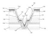
- FIG. 1is a cross-section view of an example structure to allow connection of a top electrode to electrodes.
- the structure 100 in FIG. 1may be part of a semi-conductor device including transistors and other components requiring electrical connection.
- the structure 100includes a first dielectric layer 102 .
- a first conductive layer 104is formed on the first dielectric layer 102 .
- a second dielectric layer 106is formed on the first conductive layer 104 .
- a deep trench 110is formed in the dielectric layers 102 and 106 .
- a second conductive layer 108is formed over the second dielectric layer 106 .
- the trench 110bisects the first dielectric layer 102 and the conductive layer 102 is located over sidewalls 120 of the first dielectric layer 102 .
- the second conductive layer 108is located over sidewalls 122 of the second dielectric layer 106 and also may be in contact with the first conductive layer 104 .
- a semiconductor layer 130may be fabricated over the second conductive layer 108 and partially over the walls of the trench 110 that are covered by the second conductive layer 108 .
- a top electrode layer 140is formed over the semiconductor layer 130 .
- the electrode layer 140is formed on the walls of the trench 110 .
- the electrode layer 140contacts the second conductive layer 108 at certain points on the walls of the trench 110 such as at contact points 150 a , 150 b , 150 c and 150 d in this example.
- one of the dielectric layers 102 or 106can be used as the deep trench 110 .
- a deep openingis created by the trench 110 so it causes a discontinuity in the semiconductor (or selected dielectric) layer 130 .
- one of the dielectric layersacts as a planarization layer which needs to be very thick as shown by the second dielectric layer 106 .
- this layeris a good candidate for the deep trench structure.
- multiple stacked openings in the backplanecan be used.
- FIG. 1shows a deep trench created in the backplane by using two openings.
- different patterning techniquessuch lithography, liftoff, or molding, shadow masking and/or other techniques can be used.
- PECVDplasma enhanced chemical vapor deposition
- CVDchemical vapor deposition
- sputteringvapor deposition
- printingspin coating
- spray coatingspray coating
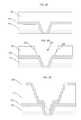
- FIGS. 2A-2Fshow the deposition of the dielectric layer 102 .
- the dielectric layer 102may be a material such as Silicon-Nitride which is deposited on top of existing structure on the backplane. This may be one of the backplane dielectric layers or an extra layer.
- the conductive layer 104is then deposited over the remaining dielectric layer 102 as shown in FIG. 2B .
- the conductive layer 104is deposited over the flat top surfaces of the dielectric layer 102 and the sidewalls 202 .
- the conductive layer 104may be one of the backplane conductive layers or an extra layer.
- the conductive layer 104is patterned as required by the design (a pattern should be left on top of the opening 200 ).
- FIG. 2Cshows the deposition of the second dielectric layer 106 over the conductive layer 104 .
- the second dielectric layer 106may be a polymer layer deposited by spin (spray or printing) coating, or it may be a stack of non-organic and polymer layers or non-organic only). This layer can be one of the layers required for the display structure such as planarization layer, or it can be an extra layer added only for the trench development. In this example, the second dielectric layer 106 is relatively thick, thus allowing the creating of the deep trench 110 .
- the second dielectric layer 106may be patterned using conventional photolithography (molding or other techniques can be used as well). The pattern of the second dielectric layer 106 includes a second opening in the position of the deep trench 110 .
- FIG. 2Dshows the creation of a second opening 240 which is formed through patterning the second dielectric layer 106 .
- the second opening 240allows sidewalls 242 to be formed in the second dielectric layer 106 .
- the second opening 240allows the second dielectric layer 106 to be removed so the conductive layer 104 is exposed.
- the second opening 240thus creates trench walls 122 shown in FIG. 1 .
- the combination of the first opening 200 and the second opening 240create the deep trench 110 and corresponding side walls 120 and 122 in FIG. 1 .
- FIG. 2Eshows the deposition of the second conductive layer 108 over the trench created in the second dielectric layer 106 .
- the second conductive layer 108may be one of the display conductive layers such as the OLED anode layer or an extra layer added for the deep trench development.
- the conductive layer 108is patterned as required by the design of the device structure. The pattern of the conductive layer 108 includes leaving the conductive layer 108 on the first opening 200 .
- FIG. 2Fshows the deposition of the semiconductor layer 130 on the second conductive layer 108 .
- the semiconductor layer 130may be an OLED structure or other thin film device structure.
- the semiconductor layer 130may be deposited with different techniques such as vapor deposition, printing, etc. Since the semiconductor layer 130 is very thin compared to the depth of the trench 110 and the walls 122 of the trench are steep, there will be a discontinuity such as the contact point 150 a in the semiconductor layer 130 on the walls 122 and edge of the trench 110 .
- FIG. 2Gshows the deposition of the top electrode 140 .
- the top electrode 140connects to the second conductive layer 108 at the discontinuity areas of the semiconductor layer 130 .
- FIG. 1shows a number of discontinuity areas 150 a , 150 b , 150 c and 150 d which allow contact between the top electrode 140 and the second conductive layer 108 .
- the semiconductor (or a dielectric) layer 130is discontinued at the edges (or walls of the trench). Therefore, after depositing the top electrode 140 , the top electrode 140 is connected to the conductive layers 108 at the walls of the trench 110 . In this manner, a shadow mask may be avoided to create the contact since the semiconductor layer has discontinuities due to the trench that allows contact.
- FIG. 3demonstrates a top view of a device 300 that includes top electrodes 302 , 304 , 306 and 308 .
- the top electrode 302includes an outer contact area 310 which corresponds to the trench walls in FIG. 1 .
- the outer contact area 310is at the edge of the trench structure where there is a discontinuity of the semiconductor layer 130 in FIG. 1 .
- An inner contact area 320also provides contact to the electrode 108 at a discontinuity of the semiconductor layer 130 in FIG. 1 .
- the top electrodes 302 , 304 , 306 and 308are connected to the conductive layers at the discontinuity areas of the semiconductor layers in a trench 110 .
- a dielectric layeris used to cover the edge of the bottom conductive layer.
- an OLEDcan consist of thin organic layers (with a total thickness of a few 100 nm) which are sandwiched between two conductive layers (at least one of which is transparent). Since the thickness of the bottom conductive layer is significantly more than that of the organic layers, to avoid any short, a dielectric is deposited on the bottom electrode and is patterned in a way that covers the edge of the bottom electrode and leaves the center of the electrode exposed for organic layers.
- the resistance for one of the conductive layersis high, causing a significant voltage drop in the case of an array structure.
- the top electrodeis transparent and is made of very thin conductive layers.
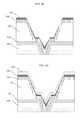
- FIG. 4shows a cross section of a device structure 400 that avoids a significant voltage drop from resistance of one of the conductive layers.
- a substrate 402supports a dielectric layer 404 which serves as a backplane of the device structure 400 .
- the dielectric layer 404may have numerous other layers that make up the backplane of the device.
- a series of lower resistance conductive strips 406is formed on the dielectric layer 404 .
- the lower resistance conductive strips 406are patterned such that they have numerous edges.
- a dielectric layer 408is formed on some of the conductive strips 406 .
- a thin semiconductor layer 410which may be an organic material is formed over the horizontal surfaces of the low resistance conductive strips 406 and the dielectric layers 408 . As may be seen in FIG. 4 , the edges of the lower resistance conductive strips 406 remain exposed and not covered by the semiconductor layer.
- a top conductive layer 412is then applied which in this example is transparent but has a high resistance. The top conductive layer 412 is in contact with the lower resistance conductive strips 406 on an edge such as on edges 414 thus shorting out the top conductive layer 412 and lowering the resistance of the contact.
- the process of creating the structure in FIG. 4is based on using lower resistance conductive material for the conductive strips 406 before depositing the semiconductor (dielectric) layers.
- a low-resistance conductive layer(or stack of conductive layers) is deposited which is thicker than the main semiconductor (dielectric) layers being deposited on top of it. This may be one of the conductive layers existing in the device or a new one added just for this reason.
- the low resistance conductive layeris then patterned.
- the patternshould create more edges. For example, stripes such as shown in FIGS. 4 and 5A or a mesh shown in FIG. 5B may create numerous edges.
- the dielectric layers 408are patterned on the low resistance conductive strips 406 .
- the main semiconductor (dielectric) layer 410is then deposited and patterned as needed by the design.
- the high-resistance conductive layer 412is then deposited and patterned as needed. The pattern covers the low-resistance area of the conductive strips 406 and, more importantly, at least one of its edges. The fabrication of device is continued until all the other required layers after this high-resistance conductive layer are deposited and patterned.
- the edge or low-resistance conductive materialcannot be covered by the main semiconductor (dielectric) since the thickness of the conductive layer is greater than that of the main layer.
- the high-resistance conductive layerwill be shorted to the exposed edge of the low-resistance conductive layer.
- FIGS. 5A and 5Bare top plan views of examples of the structure that incorporates the low resistance conductive layers.
- FIG. 5Ashows a top view of the device structure 400 in FIG. 4 .
- the top conductive layer 412is a transparent layer with high resistance. Since the top conductive layer 412 is deposited over the low resistance conductive strips 406 , it contacts the edges of the strips 406 and is shorted to prevent high resistance.
- the semiconductor layer 410is fabricated over the conductive strips as well as other layers 408 .
- FIG. 5Bis a top view of another device structure 500 that has the same top conductive layer 412 , semiconductor layer 410 and other layers 408 as the structure 400 in FIG. 4 .
- a low resistive conductive layer 450is patterned in a mesh structure.
- the low resistive conductive layer 450has a series of openings 452 that have multiple edges to create contact with the high resistance top conductive layer 412 thus shorting the top conductive layer 412 .
Landscapes
- Physics & Mathematics (AREA)
- Optics & Photonics (AREA)
- Engineering & Computer Science (AREA)
- Manufacturing & Machinery (AREA)
- Microelectronics & Electronic Packaging (AREA)
- Devices For Indicating Variable Information By Combining Individual Elements (AREA)
- Electroluminescent Light Sources (AREA)
- Internal Circuitry In Semiconductor Integrated Circuit Devices (AREA)
Abstract
Description
Claims (16)
Priority Applications (3)
| Application Number | Priority Date | Filing Date | Title |
|---|---|---|---|
| US15/973,696US10439159B2 (en) | 2013-12-25 | 2018-05-08 | Electrode contacts |
| US16/550,896US10847743B2 (en) | 2013-12-25 | 2019-08-26 | Electrode contacts |
| US17/075,251US11050036B2 (en) | 2013-12-25 | 2020-10-20 | Electrode contacts |
Applications Claiming Priority (6)
| Application Number | Priority Date | Filing Date | Title |
|---|---|---|---|
| US201361920732P | 2013-12-25 | 2013-12-25 | |
| US201461929699P | 2014-01-21 | 2014-01-21 | |
| US14/581,193US9502653B2 (en) | 2013-12-25 | 2014-12-23 | Electrode contacts |
| US15/296,424US9831462B2 (en) | 2013-12-25 | 2016-10-18 | Electrode contacts |
| US15/793,032US20180047934A1 (en) | 2013-12-25 | 2017-10-25 | Electrode contacts |
| US15/973,696US10439159B2 (en) | 2013-12-25 | 2018-05-08 | Electrode contacts |
Related Parent Applications (1)
| Application Number | Title | Priority Date | Filing Date |
|---|---|---|---|
| US15/793,032ContinuationUS20180047934A1 (en) | 2013-12-25 | 2017-10-25 | Electrode contacts |
Related Child Applications (1)
| Application Number | Title | Priority Date | Filing Date |
|---|---|---|---|
| US16/550,896ContinuationUS10847743B2 (en) | 2013-12-25 | 2019-08-26 | Electrode contacts |
Publications (2)
| Publication Number | Publication Date |
|---|---|
| US20180261795A1 US20180261795A1 (en) | 2018-09-13 |
| US10439159B2true US10439159B2 (en) | 2019-10-08 |
Family
ID=53401070
Family Applications (6)
| Application Number | Title | Priority Date | Filing Date |
|---|---|---|---|
| US14/581,193Expired - Fee RelatedUS9502653B2 (en) | 2013-12-25 | 2014-12-23 | Electrode contacts |
| US15/296,424ActiveUS9831462B2 (en) | 2013-12-25 | 2016-10-18 | Electrode contacts |
| US15/793,032AbandonedUS20180047934A1 (en) | 2013-12-25 | 2017-10-25 | Electrode contacts |
| US15/973,696ActiveUS10439159B2 (en) | 2013-12-25 | 2018-05-08 | Electrode contacts |
| US16/550,896Expired - Fee RelatedUS10847743B2 (en) | 2013-12-25 | 2019-08-26 | Electrode contacts |
| US17/075,251ActiveUS11050036B2 (en) | 2013-12-25 | 2020-10-20 | Electrode contacts |
Family Applications Before (3)
| Application Number | Title | Priority Date | Filing Date |
|---|---|---|---|
| US14/581,193Expired - Fee RelatedUS9502653B2 (en) | 2013-12-25 | 2014-12-23 | Electrode contacts |
| US15/296,424ActiveUS9831462B2 (en) | 2013-12-25 | 2016-10-18 | Electrode contacts |
| US15/793,032AbandonedUS20180047934A1 (en) | 2013-12-25 | 2017-10-25 | Electrode contacts |
Family Applications After (2)
| Application Number | Title | Priority Date | Filing Date |
|---|---|---|---|
| US16/550,896Expired - Fee RelatedUS10847743B2 (en) | 2013-12-25 | 2019-08-26 | Electrode contacts |
| US17/075,251ActiveUS11050036B2 (en) | 2013-12-25 | 2020-10-20 | Electrode contacts |
Country Status (1)
| Country | Link |
|---|---|
| US (6) | US9502653B2 (en) |
Cited By (1)
| Publication number | Priority date | Publication date | Assignee | Title |
|---|---|---|---|---|
| US11050036B2 (en)* | 2013-12-25 | 2021-06-29 | Ignis Innovation Inc. | Electrode contacts |
Families Citing this family (16)
| Publication number | Priority date | Publication date | Assignee | Title |
|---|---|---|---|---|
| US9799246B2 (en) | 2011-05-20 | 2017-10-24 | Ignis Innovation Inc. | System and methods for extraction of threshold and mobility parameters in AMOLED displays |
| US10013907B2 (en) | 2004-12-15 | 2018-07-03 | Ignis Innovation Inc. | Method and system for programming, calibrating and/or compensating, and driving an LED display |
| US8576217B2 (en) | 2011-05-20 | 2013-11-05 | Ignis Innovation Inc. | System and methods for extraction of threshold and mobility parameters in AMOLED displays |
| US20140313111A1 (en) | 2010-02-04 | 2014-10-23 | Ignis Innovation Inc. | System and methods for extracting correlation curves for an organic light emitting device |
| US10089921B2 (en) | 2010-02-04 | 2018-10-02 | Ignis Innovation Inc. | System and methods for extracting correlation curves for an organic light emitting device |
| US9881532B2 (en) | 2010-02-04 | 2018-01-30 | Ignis Innovation Inc. | System and method for extracting correlation curves for an organic light emitting device |
| CA2692097A1 (en) | 2010-02-04 | 2011-08-04 | Ignis Innovation Inc. | Extracting correlation curves for light emitting device |
| US9466240B2 (en) | 2011-05-26 | 2016-10-11 | Ignis Innovation Inc. | Adaptive feedback system for compensating for aging pixel areas with enhanced estimation speed |
| US9773439B2 (en) | 2011-05-27 | 2017-09-26 | Ignis Innovation Inc. | Systems and methods for aging compensation in AMOLED displays |
| US10089924B2 (en) | 2011-11-29 | 2018-10-02 | Ignis Innovation Inc. | Structural and low-frequency non-uniformity compensation |
| US8937632B2 (en) | 2012-02-03 | 2015-01-20 | Ignis Innovation Inc. | Driving system for active-matrix displays |
| US8922544B2 (en) | 2012-05-23 | 2014-12-30 | Ignis Innovation Inc. | Display systems with compensation for line propagation delay |
| EP3043338A1 (en) | 2013-03-14 | 2016-07-13 | Ignis Innovation Inc. | Re-interpolation with edge detection for extracting an aging pattern for amoled displays |
| CA2892714A1 (en) | 2015-05-27 | 2016-11-27 | Ignis Innovation Inc | Memory bandwidth reduction in compensation system |
| CA2900170A1 (en) | 2015-08-07 | 2017-02-07 | Gholamreza Chaji | Calibration of pixel based on improved reference values |
| CN109727998A (en)* | 2019-01-02 | 2019-05-07 | 京东方科技集团股份有限公司 | Array substrate and preparation method thereof, and display device |
Citations (600)
| Publication number | Priority date | Publication date | Assignee | Title |
|---|---|---|---|---|
| US3506851A (en) | 1966-12-14 | 1970-04-14 | North American Rockwell | Field effect transistor driver using capacitor feedback |
| US3774055A (en) | 1972-01-24 | 1973-11-20 | Nat Semiconductor Corp | Clocked bootstrap inverter circuit |
| US4090096A (en) | 1976-03-31 | 1978-05-16 | Nippon Electric Co., Ltd. | Timing signal generator circuit |
| US4160934A (en) | 1977-08-11 | 1979-07-10 | Bell Telephone Laboratories, Incorporated | Current control circuit for light emitting diode |
| US4295091A (en) | 1978-10-12 | 1981-10-13 | Vaisala Oy | Circuit for measuring low capacitances |
| US4354162A (en) | 1981-02-09 | 1982-10-12 | National Semiconductor Corporation | Wide dynamic range control amplifier with offset correction |
| EP0158366A2 (en) | 1984-04-13 | 1985-10-16 | Sharp Kabushiki Kaisha | Color liquid-crystal display apparatus |
| JPH01272298A (en) | 1988-04-25 | 1989-10-31 | Yamaha Corp | Driving device |
| US4943956A (en) | 1988-04-25 | 1990-07-24 | Yamaha Corporation | Driving apparatus |
| US4996523A (en) | 1988-10-20 | 1991-02-26 | Eastman Kodak Company | Electroluminescent storage display with improved intensity driver circuits |
| CA1294034C (en) | 1985-01-09 | 1992-01-07 | Hiromu Hosokawa | Color uniformity compensation apparatus for cathode ray tubes |
| JPH0442619A (en) | 1990-06-08 | 1992-02-13 | Fujitsu Ltd | DA converter |
| JPH04158570A (en) | 1990-10-22 | 1992-06-01 | Seiko Epson Corp | Structure of semiconductor device and manufacture thereof |
| US5153420A (en) | 1990-11-28 | 1992-10-06 | Xerox Corporation | Timing independent pixel-scale light sensing apparatus |
| CA2109951A1 (en) | 1991-05-24 | 1992-11-26 | Robert Hotto | Dc integrating display driver employing pixel status memories |
| US5198803A (en) | 1990-06-06 | 1993-03-30 | Opto Tech Corporation | Large scale movie display system with multiple gray levels |
| US5204661A (en) | 1990-12-13 | 1993-04-20 | Xerox Corporation | Input/output pixel circuit and array of such circuits |
| US5266515A (en) | 1992-03-02 | 1993-11-30 | Motorola, Inc. | Fabricating dual gate thin film transistors |
| TW223092B (en) | 1990-09-25 | 1994-05-01 | Sumitomo Chemical Co | |
| JPH06314977A (en) | 1993-04-28 | 1994-11-08 | Nec Ic Microcomput Syst Ltd | Current output type d/a converter circuit |
| US5489918A (en) | 1991-06-14 | 1996-02-06 | Rockwell International Corporation | Method and apparatus for dynamically and adjustably generating active matrix liquid crystal display gray level voltages |
| US5498880A (en) | 1995-01-12 | 1996-03-12 | E. I. Du Pont De Nemours And Company | Image capture panel using a solid state device |
| US5557342A (en) | 1993-07-06 | 1996-09-17 | Hitachi, Ltd. | Video display apparatus for displaying a plurality of video signals having different scanning frequencies and a multi-screen display system using the video display apparatus |
| US5561381A (en) | 1989-12-13 | 1996-10-01 | International Business Machines Corporation | Method for testing a partially constructed electronic circuit |
| US5572444A (en) | 1992-08-19 | 1996-11-05 | Mtl Systems, Inc. | Method and apparatus for automatic performance evaluation of electronic display devices |
| JPH08340243A (en) | 1995-06-14 | 1996-12-24 | Canon Inc | Bias circuit |
| US5589847A (en) | 1991-09-23 | 1996-12-31 | Xerox Corporation | Switched capacitor analog circuits using polysilicon thin film technology |
| JPH0990405A (en) | 1995-09-21 | 1997-04-04 | Sharp Corp | Thin film transistor |
| US5619033A (en) | 1995-06-07 | 1997-04-08 | Xerox Corporation | Layered solid state photodiode sensor array |
| US5648276A (en) | 1993-05-27 | 1997-07-15 | Sony Corporation | Method and apparatus for fabricating a thin film semiconductor device |
| US5670973A (en) | 1993-04-05 | 1997-09-23 | Cirrus Logic, Inc. | Method and apparatus for compensating crosstalk in liquid crystal displays |
| US5684365A (en) | 1994-12-14 | 1997-11-04 | Eastman Kodak Company | TFT-el display panel using organic electroluminescent media |
| US5691783A (en) | 1993-06-30 | 1997-11-25 | Sharp Kabushiki Kaisha | Liquid crystal display device and method for driving the same |
| US5714968A (en) | 1994-08-09 | 1998-02-03 | Nec Corporation | Current-dependent light-emitting element drive circuit for use in active matrix display device |
| US5723950A (en) | 1996-06-10 | 1998-03-03 | Motorola | Pre-charge driver for light emitting devices and method |
| US5745660A (en) | 1995-04-26 | 1998-04-28 | Polaroid Corporation | Image rendering system and method for generating stochastic threshold arrays for use therewith |
| US5744824A (en) | 1994-06-15 | 1998-04-28 | Sharp Kabushiki Kaisha | Semiconductor device method for producing the same and liquid crystal display including the same |
| US5748160A (en) | 1995-08-21 | 1998-05-05 | Mororola, Inc. | Active driven LED matrices |
| CA2249592A1 (en) | 1997-01-28 | 1998-07-30 | Casio Computer Co., Ltd. | Active matrix electroluminescent display device and a driving method thereof |
| JPH10254410A (en) | 1997-03-12 | 1998-09-25 | Pioneer Electron Corp | Organic electroluminescent display device, and driving method therefor |
| US5815303A (en) | 1997-06-26 | 1998-09-29 | Xerox Corporation | Fault tolerant projective display having redundant light modulators |
| TW342486B (en) | 1994-07-18 | 1998-10-11 | Toshiba Co Ltd | LED dot matrix display device and method for dimming thereof |
| WO1998048403A1 (en) | 1997-04-23 | 1998-10-29 | Sarnoff Corporation | Active matrix light emitting diode pixel structure and method |
| US5870071A (en) | 1995-09-07 | 1999-02-09 | Frontec Incorporated | LCD gate line drive circuit |
| US5874803A (en) | 1997-09-09 | 1999-02-23 | The Trustees Of Princeton University | Light emitting device with stack of OLEDS and phosphor downconverter |
| US5880582A (en) | 1996-09-04 | 1999-03-09 | Sumitomo Electric Industries, Ltd. | Current mirror circuit and reference voltage generating and light emitting element driving circuits using the same |
| US5903248A (en) | 1997-04-11 | 1999-05-11 | Spatialight, Inc. | Active matrix display having pixel driving circuits with integrated charge pumps |
| US5917280A (en) | 1997-02-03 | 1999-06-29 | The Trustees Of Princeton University | Stacked organic light emitting devices |
| US5923794A (en) | 1996-02-06 | 1999-07-13 | Polaroid Corporation | Current-mediated active-pixel image sensing device with current reset |
| JPH11202295A (en) | 1998-01-09 | 1999-07-30 | Seiko Epson Corp | Driving circuit for electro-optical device, electro-optical device, and electronic apparatus |
| JPH11219146A (en) | 1997-09-29 | 1999-08-10 | Mitsubishi Chemical Corp | Active matrix light emitting diode pixel structure and method |
| JPH11231805A (en) | 1998-02-10 | 1999-08-27 | Sanyo Electric Co Ltd | Display device |
| US5945972A (en) | 1995-11-30 | 1999-08-31 | Kabushiki Kaisha Toshiba | Display device |
| US5949398A (en) | 1996-04-12 | 1999-09-07 | Thomson Multimedia S.A. | Select line driver for a display matrix with toggling backplane |
| US5952991A (en) | 1996-11-14 | 1999-09-14 | Kabushiki Kaisha Toshiba | Liquid crystal display |
| US5952789A (en) | 1997-04-14 | 1999-09-14 | Sarnoff Corporation | Active matrix organic light emitting diode (amoled) display pixel structure and data load/illuminate circuit therefor |
| WO1999048079A1 (en) | 1998-03-19 | 1999-09-23 | Holloman Charles J | Analog driver for led or similar display element |
| JPH11282419A (en) | 1998-03-31 | 1999-10-15 | Nec Corp | Element driving device and method and image display device |
| US5982104A (en) | 1995-12-26 | 1999-11-09 | Pioneer Electronic Corporation | Driver for capacitive light-emitting device with degradation compensated brightness control |
| US6023259A (en) | 1997-07-11 | 2000-02-08 | Fed Corporation | OLED active matrix using a single transistor current mode pixel design |
| JP2000056847A (en) | 1998-08-14 | 2000-02-25 | Nec Corp | Constant current driving circuit |
| JP2000081607A (en) | 1998-09-04 | 2000-03-21 | Denso Corp | Matrix type liquid crystal display device |
| CA2242720C (en) | 1998-07-09 | 2000-05-16 | Ibm Canada Limited-Ibm Canada Limitee | Programmable led driver |
| US6069365A (en) | 1997-11-25 | 2000-05-30 | Alan Y. Chow | Optical processor based imaging system |
| CA2354018A1 (en) | 1998-12-14 | 2000-06-22 | Alan Richard | Portable microdisplay system |
| EP1028471A2 (en) | 1999-02-09 | 2000-08-16 | SANYO ELECTRIC Co., Ltd. | Electroluminescence display device |
| US6177915B1 (en) | 1990-06-11 | 2001-01-23 | International Business Machines Corporation | Display system having section brightness control and method of operating system |
| WO2001006484A1 (en) | 1999-07-14 | 2001-01-25 | Sony Corporation | Current drive circuit and display comprising the same, pixel circuit, and drive method |
| US6197181B1 (en)* | 1998-03-20 | 2001-03-06 | Semitool, Inc. | Apparatus and method for electrolytically depositing a metal on a microelectronic workpiece |
| WO2001027910A1 (en) | 1999-10-12 | 2001-04-19 | Koninklijke Philips Electronics N.V. | Led display device |
| US6229506B1 (en) | 1997-04-23 | 2001-05-08 | Sarnoff Corporation | Active matrix light emitting diode pixel structure and concomitant method |
| JP2001134217A (en) | 1999-11-09 | 2001-05-18 | Tdk Corp | Driving device for organic el element |
| US20010002703A1 (en) | 1999-11-30 | 2001-06-07 | Jun Koyama | Electric device |
| US6246180B1 (en) | 1999-01-29 | 2001-06-12 | Nec Corporation | Organic el display device having an improved image quality |
| US6252248B1 (en) | 1998-06-08 | 2001-06-26 | Sanyo Electric Co., Ltd. | Thin film transistor and display |
| EP1111577A2 (en) | 1999-12-24 | 2001-06-27 | Sanyo Electric Co., Ltd. | Improvements in power consumption of display apparatus during still image display mode |
| US6259424B1 (en) | 1998-03-04 | 2001-07-10 | Victor Company Of Japan, Ltd. | Display matrix substrate, production method of the same and display matrix circuit |
| US6262589B1 (en) | 1998-05-25 | 2001-07-17 | Asia Electronics, Inc. | TFT array inspection method and device |
| JP2001195014A (en) | 2000-01-14 | 2001-07-19 | Tdk Corp | Driving device for organic el element |
| US20010009283A1 (en) | 2000-01-26 | 2001-07-26 | Tatsuya Arao | Semiconductor device and method of manufacturing the semiconductor device |
| US6271825B1 (en) | 1996-04-23 | 2001-08-07 | Rainbow Displays, Inc. | Correction methods for brightness in electronic display |
| WO2001063587A2 (en) | 2000-02-22 | 2001-08-30 | Sarnoff Corporation | A method and apparatus for calibrating display devices and automatically compensating for loss in their efficiency over time |
| US20010024181A1 (en) | 2000-01-17 | 2001-09-27 | Ibm | Liquid-crystal display, liquid-crystal control circuit, flicker inhibition method, and liquid-crystal driving method |
| US20010026257A1 (en) | 2000-03-27 | 2001-10-04 | Hajime Kimura | Electro-optical device |
| US6304039B1 (en) | 2000-08-08 | 2001-10-16 | E-Lite Technologies, Inc. | Power supply for illuminating an electro-luminescent panel |
| US20010030323A1 (en) | 2000-03-29 | 2001-10-18 | Sony Corporation | Thin film semiconductor apparatus and method for driving the same |
| US6307322B1 (en) | 1999-12-28 | 2001-10-23 | Sarnoff Corporation | Thin-film transistor circuitry with reduced sensitivity to variance in transistor threshold voltage |
| US6310962B1 (en) | 1997-08-20 | 2001-10-30 | Samsung Electronics Co., Ltd. | MPEG2 moving picture encoding/decoding system |
| US20010035863A1 (en) | 2000-04-26 | 2001-11-01 | Hajime Kimura | Electronic device and driving method thereof |
| US20010038367A1 (en) | 2000-05-08 | 2001-11-08 | Kazutaka Inukai | Light emitting device |
| US20010040541A1 (en) | 1997-09-08 | 2001-11-15 | Kiyoshi Yoneda | Semiconductor device having laser-annealed semiconductor device, display device and liquid crystal display device |
| US6320325B1 (en) | 2000-11-06 | 2001-11-20 | Eastman Kodak Company | Emissive display with luminance feedback from a representative pixel |
| US20010043173A1 (en) | 1997-09-04 | 2001-11-22 | Ronald Roy Troutman | Field sequential gray in active matrix led display using complementary transistor pixel circuits |
| US6323631B1 (en) | 2001-01-18 | 2001-11-27 | Sunplus Technology Co., Ltd. | Constant current driver with auto-clamped pre-charge function |
| US20010045929A1 (en) | 2000-01-21 | 2001-11-29 | Prache Olivier F. | Gray scale pixel driver for electronic display and method of operation therefor |
| US6329971B2 (en) | 1996-12-19 | 2001-12-11 | Zight Corporation | Display system having electrode modulation to alter a state of an electro-optic layer |
| US20010052940A1 (en) | 2000-02-01 | 2001-12-20 | Yoshio Hagihara | Solid-state image-sensing device |
| US20010052606A1 (en) | 2000-05-22 | 2001-12-20 | Koninklijke Philips Electronics N.V. | Display device |
| US20020000576A1 (en) | 2000-06-22 | 2002-01-03 | Kazutaka Inukai | Display device |
| US20020011799A1 (en) | 2000-04-06 | 2002-01-31 | Semiconductor Energy Laboratory Co., Ltd. | Electronic device and driving method |
| US20020011796A1 (en) | 2000-05-08 | 2002-01-31 | Semiconductor Energy Laboratory Co., Ltd. | Light-emitting device, and electric device using the same |
| US20020012057A1 (en) | 2000-05-26 | 2002-01-31 | Hajime Kimura | MOS sensor and drive method thereof |
| US20020014851A1 (en) | 2000-06-05 | 2002-02-07 | Ya-Hsiang Tai | Apparatus and method of testing an organic light emitting diode array |
| US20020018034A1 (en) | 2000-07-31 | 2002-02-14 | Shigeru Ohki | Display color temperature corrected lighting apparatus and flat plane display apparatus |
| JP2002055654A (en) | 2000-08-10 | 2002-02-20 | Nec Corp | Electroluminescence display |
| US6356029B1 (en) | 1999-10-02 | 2002-03-12 | U.S. Philips Corporation | Active matrix electroluminescent display device |
| US20020030190A1 (en) | 1998-12-03 | 2002-03-14 | Hisashi Ohtani | Electro-optical device and semiconductor circuit |
| JP2002091376A (en) | 2000-06-27 | 2002-03-27 | Hitachi Ltd | Image display device and driving method thereof |
| EP1194013A1 (en) | 2000-09-29 | 2002-04-03 | Eastman Kodak Company | A flat-panel display with luminance feedback |
| US6373454B1 (en) | 1998-06-12 | 2002-04-16 | U.S. Philips Corporation | Active matrix electroluminescent display devices |
| US6377237B1 (en) | 2000-01-07 | 2002-04-23 | Agilent Technologies, Inc. | Method and system for illuminating a layer of electro-optical material with pulses of light |
| US20020047565A1 (en) | 2000-07-28 | 2002-04-25 | Wintest Corporation | Apparatus and method for evaluating organic EL display |
| US20020052086A1 (en) | 2000-10-31 | 2002-05-02 | Mitsubishi Denki Kabushiki Kaisha | Semiconductor device and method of manufacturing same |
| US6392617B1 (en) | 1999-10-27 | 2002-05-21 | Agilent Technologies, Inc. | Active matrix light emitting diode display |
| US6404139B1 (en) | 1999-07-02 | 2002-06-11 | Seiko Instruments Inc. | Circuit for driving a light emitting elements display device |
| US20020084463A1 (en) | 2001-01-04 | 2002-07-04 | International Business Machines Corporation | Low-power organic light emitting diode pixel circuit |
| US6417825B1 (en) | 1998-09-29 | 2002-07-09 | Sarnoff Corporation | Analog active matrix emissive display |
| US20020101172A1 (en) | 2001-01-02 | 2002-08-01 | Bu Lin-Kai | Oled active driving system with current feedback |
| US20020101152A1 (en) | 2001-01-30 | 2002-08-01 | Semiconductor Energy Laboratory Co., Ltd. | Light emitting device |
| US20020105279A1 (en) | 2001-02-08 | 2002-08-08 | Hajime Kimura | Light emitting device and electronic equipment using the same |
| CA2436451A1 (en) | 2001-02-05 | 2002-08-15 | International Business Machines Corporation | Liquid crystal display device |
| JP2002229513A (en) | 2001-02-06 | 2002-08-16 | Tohoku Pioneer Corp | Device for driving organic el display panel |
| US6437106B1 (en) | 1999-06-24 | 2002-08-20 | Abbott Laboratories | Process for preparing 6-o-substituted erythromycin derivatives |
| US20020117722A1 (en) | 1999-05-12 | 2002-08-29 | Kenichi Osada | Semiconductor integrated circuit device |
| CA2438577A1 (en) | 2001-02-16 | 2002-08-29 | Ignis Innovation Inc. | Pixel current driver for organic light emitting diode displays |
| WO2002067327A2 (en) | 2001-02-16 | 2002-08-29 | Ignis Innovation Inc. | Pixel current driver for organic light emitting diode displays |
| US6445369B1 (en) | 1998-02-20 | 2002-09-03 | The University Of Hong Kong | Light emitting diode dot matrix display system with audio output |
| US20020122308A1 (en) | 2001-03-05 | 2002-09-05 | Fuji Xerox Co., Ltd. | Apparatus for driving light emitting element and system for driving light emitting element |
| TW502233B (en) | 1999-06-17 | 2002-09-11 | Sony Corp | Image display apparatus |
| JP2002278513A (en) | 2001-03-19 | 2002-09-27 | Sharp Corp | Electro-optical device |
| US20020158823A1 (en) | 1997-10-31 | 2002-10-31 | Matthew Zavracky | Portable microdisplay system |
| US20020158666A1 (en) | 2001-04-27 | 2002-10-31 | Munehiro Azami | Semiconductor device |
| US20020158587A1 (en) | 2001-02-15 | 2002-10-31 | Naoaki Komiya | Organic EL pixel circuit |
| US20020167471A1 (en) | 2001-05-09 | 2002-11-14 | Everitt James W. | System for providing pulse amplitude modulation for oled display drivers |
| US20020169575A1 (en) | 2001-05-09 | 2002-11-14 | James Everitt | Matrix element voltage sensing for precharge |
| JP2002333862A (en) | 2001-02-21 | 2002-11-22 | Semiconductor Energy Lab Co Ltd | Light emission device and electronic equipment |
| US20020181276A1 (en) | 2001-06-01 | 2002-12-05 | Semiconductor Energy Laboratory Co., Ltd. | Method of repairing a light-emitting device, and method of manufacturing a light -emitting device |
| US20020180369A1 (en) | 2001-02-21 | 2002-12-05 | Jun Koyama | Light emitting device and electronic appliance |
| US20020180721A1 (en) | 1997-03-12 | 2002-12-05 | Mutsumi Kimura | Pixel circuit display apparatus and electronic apparatus equipped with current driving type light-emitting device |
| US20020186214A1 (en) | 2001-06-05 | 2002-12-12 | Eastman Kodak Company | Method for saving power in an organic electroluminescent display using white light emitting elements |
| US20020190971A1 (en) | 2001-04-27 | 2002-12-19 | Kabushiki Kaisha Toshiba | Display apparatus, digital-to-analog conversion circuit and digital-to-analog conversion method |
| US20020190924A1 (en) | 2001-01-19 | 2002-12-19 | Mitsuru Asano | Active matrix display |
| US20020195967A1 (en) | 2001-06-22 | 2002-12-26 | Kim Sung Ki | Electro-luminescence panel |
| US20020195968A1 (en) | 2001-06-22 | 2002-12-26 | International Business Machines Corporation | Oled current drive pixel circuit |
| US6501466B1 (en) | 1999-11-18 | 2002-12-31 | Sony Corporation | Active matrix type display apparatus and drive circuit thereof |
| US6501098B2 (en) | 1998-11-25 | 2002-12-31 | Semiconductor Energy Laboratory Co, Ltd. | Semiconductor device |
| US20030020413A1 (en) | 2001-07-27 | 2003-01-30 | Masanobu Oomura | Active matrix display |
| US20030030603A1 (en) | 2001-08-09 | 2003-02-13 | Nec Corporation | Drive circuit for display device |
| US6522315B2 (en) | 1997-02-17 | 2003-02-18 | Seiko Epson Corporation | Display apparatus |
| US6525683B1 (en) | 2001-09-19 | 2003-02-25 | Intel Corporation | Nonlinearly converting a signal to compensate for non-uniformities and degradations in a display |
| US20030043088A1 (en) | 2001-08-31 | 2003-03-06 | Booth Lawrence A. | Compensating organic light emitting device displays for color variations |
| JP2003076331A (en) | 2001-08-31 | 2003-03-14 | Seiko Epson Corp | Display device and electronic equipment |
| US20030057895A1 (en) | 2001-09-07 | 2003-03-27 | Semiconductor Energy Laboratory Co., Ltd. | Light emitting device and method of driving the same |
| US20030058226A1 (en) | 1994-08-22 | 2003-03-27 | Bertram William K. | Reduced noise touch screen apparatus and method |
| US6541921B1 (en) | 2001-10-17 | 2003-04-01 | Sierra Design Group | Illumination intensity control in electroluminescent display |
| US6542138B1 (en) | 1999-09-11 | 2003-04-01 | Koninklijke Philips Electronics N.V. | Active matrix electroluminescent display device |
| US20030062524A1 (en) | 2001-08-29 | 2003-04-03 | Hajime Kimura | Light emitting device, method of driving a light emitting device, element substrate, and electronic equipment |
| US20030071821A1 (en) | 2001-10-11 | 2003-04-17 | Sundahl Robert C. | Luminance compensation for emissive displays |
| WO2003034389A2 (en) | 2001-10-19 | 2003-04-24 | Clare Micronix Integrated Systems, Inc. | System and method for providing pulse amplitude modulation for oled display drivers |
| US20030076048A1 (en) | 2001-10-23 | 2003-04-24 | Rutherford James C. | Organic electroluminescent display device driving method and apparatus |
| JP2003124519A (en) | 2001-10-11 | 2003-04-25 | Sharp Corp | Light emitting diode drive circuit and optical transmission device using the same |
| US6555420B1 (en) | 1998-08-31 | 2003-04-29 | Semiconductor Energy Laboratory Co., Ltd. | Semiconductor device and process for producing semiconductor device |
| US20030090447A1 (en) | 2001-09-21 | 2003-05-15 | Hajime Kimura | Display device and driving method thereof |
| US20030090481A1 (en) | 2001-11-13 | 2003-05-15 | Hajime Kimura | Display device and method for driving the same |
| US6577302B2 (en) | 2000-03-31 | 2003-06-10 | Koninklijke Philips Electronics N.V. | Display device having current-addressed pixels |
| US20030107560A1 (en) | 2001-01-15 | 2003-06-12 | Akira Yumoto | Active-matrix display, active-matrix organic electroluminescent display, and methods of driving them |
| US6580408B1 (en) | 1999-06-03 | 2003-06-17 | Lg. Philips Lcd Co., Ltd. | Electro-luminescent display including a current mirror |
| US20030111966A1 (en) | 2001-12-19 | 2003-06-19 | Yoshiro Mikami | Image display apparatus |
| TW538650B (en) | 2000-09-29 | 2003-06-21 | Seiko Epson Corp | Driving method for electro-optical device, electro-optical device, and electronic apparatus |
| US6583398B2 (en) | 1999-12-14 | 2003-06-24 | Koninklijke Philips Electronics N.V. | Image sensor |
| JP2003177709A (en) | 2001-12-13 | 2003-06-27 | Seiko Epson Corp | Pixel circuit for light emitting element |
| US20030122749A1 (en) | 2001-12-31 | 2003-07-03 | Booth Lawrence A. | Energy sensing light emitting diode display |
| US20030122813A1 (en) | 2001-12-28 | 2003-07-03 | Pioneer Corporation | Panel display driving device and driving method |
| JP2003195813A (en) | 2001-09-07 | 2003-07-09 | Semiconductor Energy Lab Co Ltd | Light emitting device |
| WO2003063124A1 (en) | 2002-01-17 | 2003-07-31 | Nec Corporation | Semiconductor device incorporating matrix type current load driving circuits, and driving method thereof |
| US20030142088A1 (en) | 2001-10-19 | 2003-07-31 | Lechevalier Robert | Method and system for precharging OLED/PLED displays with a precharge latency |
| US20030146897A1 (en) | 2002-02-07 | 2003-08-07 | Hunter Robert J. | Method and apparatus to reduce power consumption of a computer system display screen |
| US20030146693A1 (en)* | 2002-02-06 | 2003-08-07 | Shingo Ishihara | Organic light-emitting display device |
| EP1335430A1 (en) | 2002-02-12 | 2003-08-13 | Eastman Kodak Company | A flat-panel light emitting pixel with luminance feedback |
| US20030169241A1 (en) | 2001-10-19 | 2003-09-11 | Lechevalier Robert E. | Method and system for ramp control of precharge voltage |
| WO2003077231A2 (en) | 2002-03-13 | 2003-09-18 | Koninklijke Philips Electronics N.V. | Two sided display device |
| US20030174152A1 (en) | 2002-02-04 | 2003-09-18 | Yukihiro Noguchi | Display apparatus with function which makes gradiation control easier |
| JP2003271095A (en) | 2002-03-14 | 2003-09-25 | Nec Corp | Driving circuit for current control element and image display device |
| US20030185438A1 (en) | 1997-09-16 | 2003-10-02 | Olympus Optical Co., Ltd. | Color image processing apparatus |
| CN1448908A (en) | 2002-03-29 | 2003-10-15 | 精工爱普生株式会社 | Electronic device, method for driving electronic device, electrooptical device and electronic apparatus |
| US20030197663A1 (en) | 2001-12-27 | 2003-10-23 | Lee Han Sang | Electroluminescent display panel and method for operating the same |
| US6639244B1 (en) | 1999-01-11 | 2003-10-28 | Semiconductor Energy Laboratory Co., Ltd. | Semiconductor device and method of fabricating the same |
| JP2003308046A (en) | 2002-02-18 | 2003-10-31 | Sanyo Electric Co Ltd | Display device |
| JP2003317944A (en) | 2002-04-26 | 2003-11-07 | Seiko Epson Corp | Electro-optical devices and electronic equipment |
| US20030210256A1 (en) | 2002-03-25 | 2003-11-13 | Yukio Mori | Display method and display apparatus |
| US20030227253A1 (en) | 2002-01-25 | 2003-12-11 | Semiconductor Energy Laboratory Co., Ltd. | Display device and method for manufacturing thereof |
| EP1372136A1 (en) | 2002-06-12 | 2003-12-17 | Seiko Epson Corporation | Scan driver and a column driver for active matrix display device and corresponding method |
| US20030230980A1 (en) | 2002-06-18 | 2003-12-18 | Forrest Stephen R | Very low voltage, high efficiency phosphorescent oled in a p-i-n structure |
| US20030231148A1 (en) | 2002-06-14 | 2003-12-18 | Chun-Hsu Lin | Brightness correction apparatus and method for plasma display |
| US20030230141A1 (en) | 2002-06-18 | 2003-12-18 | Gilmour Daniel A. | Optical fuel level sensor |
| GB2389951A (en) | 2002-06-18 | 2003-12-24 | Cambridge Display Tech Ltd | Display driver circuits for active matrix OLED displays |
| JP2004004675A (en) | 2002-03-29 | 2004-01-08 | Seiko Epson Corp | Electronic device, method of driving electronic device, electro-optical device, and electronic apparatus |
| WO2004003877A2 (en) | 2002-06-27 | 2004-01-08 | Casio Computer Co., Ltd. | Current drive apparatus and drive method thereof, and electroluminescent display apparatus using the circuit |
| US6677713B1 (en) | 2002-08-28 | 2004-01-13 | Au Optronics Corporation | Driving circuit and method for light emitting device |
| EP1381019A1 (en) | 2002-07-10 | 2004-01-14 | Pioneer Corporation | Automatic luminance adjustment device and method |
| CA2463653A1 (en) | 2002-07-09 | 2004-01-15 | Casio Computer Co., Ltd. | Driving device, display apparatus using the same, and driving method therefor |
| US6680580B1 (en) | 2002-09-16 | 2004-01-20 | Au Optronics Corporation | Driving circuit and method for light emitting device |
| US6687266B1 (en) | 2002-11-08 | 2004-02-03 | Universal Display Corporation | Organic light emitting materials and devices |
| US6690000B1 (en) | 1998-12-02 | 2004-02-10 | Nec Corporation | Image sensor |
| US6690344B1 (en) | 1999-05-14 | 2004-02-10 | Ngk Insulators, Ltd. | Method and apparatus for driving device and display |
| JP2004045648A (en) | 2002-07-10 | 2004-02-12 | Pioneer Electronic Corp | Method and device for driving display panel |
| US6697057B2 (en) | 2000-10-27 | 2004-02-24 | Semiconductor Energy Laboratory Co., Ltd. | Display device and method of driving the same |
| US20040041750A1 (en) | 2001-08-29 | 2004-03-04 | Katsumi Abe | Current load device and method for driving the same |
| CA2498136A1 (en) | 2002-09-09 | 2004-03-18 | Matthew Stevenson | Organic electronic device having improved homogeneity |
| WO2004025615A1 (en) | 2002-09-16 | 2004-03-25 | Koninklijke Philips Electronics N.V. | Display device |
| US20040066357A1 (en) | 2002-09-02 | 2004-04-08 | Canon Kabushiki Kaisha | Drive circuit, display apparatus, and information display apparatus |
| US20040070557A1 (en) | 2002-10-11 | 2004-04-15 | Mitsuru Asano | Active-matrix display device and method of driving the same |
| US20040070565A1 (en) | 2001-12-05 | 2004-04-15 | Nayar Shree K | Method and apparatus for displaying images |
| US6724151B2 (en) | 2001-11-06 | 2004-04-20 | Lg. Philips Lcd Co., Ltd. | Apparatus and method of driving electro luminescence panel |
| WO2004034364A1 (en) | 2002-10-08 | 2004-04-22 | Koninklijke Philips Electronics N.V. | Electroluminescent display devices |
| EP1418566A2 (en) | 2002-11-08 | 2004-05-12 | Tohoku Pioneer Corporation | Drive methods and drive devices for active type light emitting display panel |
| US20040090400A1 (en) | 2002-11-05 | 2004-05-13 | Yoo Juhn Suk | Data driving apparatus and method of driving organic electro luminescence display panel |
| US6738034B2 (en) | 2000-06-27 | 2004-05-18 | Hitachi, Ltd. | Picture image display device and method of driving the same |
| US6738035B1 (en) | 1997-09-22 | 2004-05-18 | Nongqiang Fan | Active matrix LCD based on diode switches and methods of improving display uniformity of same |
| US20040095297A1 (en) | 2002-11-20 | 2004-05-20 | International Business Machines Corporation | Nonlinear voltage controlled current source with feedback circuit |
| JP2004145197A (en) | 2002-10-28 | 2004-05-20 | Mitsubishi Electric Corp | Display device and display panel |
| US20040100427A1 (en) | 2002-08-07 | 2004-05-27 | Seiko Epson Corporation | Electronic circuit, electro-optical device, method for driving electro-optical device and electronic apparatus |
| WO2004047058A2 (en) | 2002-11-21 | 2004-06-03 | Koninklijke Philips Electronics N.V. | Method of improving the output uniformity of a display device |
| EP1429312A2 (en) | 2002-12-12 | 2004-06-16 | Seiko Epson Corporation | Electro-optical device, method of driving electro optical device, and electronic apparatus |
| US6753834B2 (en) | 2001-03-30 | 2004-06-22 | Hitachi, Ltd. | Display device and driving method thereof |
| US6753655B2 (en) | 2002-09-19 | 2004-06-22 | Industrial Technology Research Institute | Pixel structure for an active matrix OLED |
| US6756958B2 (en) | 2000-11-30 | 2004-06-29 | Hitachi, Ltd. | Liquid crystal display device |
| US6756741B2 (en) | 2002-07-12 | 2004-06-29 | Au Optronics Corp. | Driving circuit for unit pixel of organic light emitting displays |
| US6756952B1 (en) | 1998-03-05 | 2004-06-29 | Jean-Claude Decaux | Light display panel control |
| US20040135749A1 (en) | 2003-01-14 | 2004-07-15 | Eastman Kodak Company | Compensating for aging in OLED devices |
| US6765549B1 (en) | 1999-11-08 | 2004-07-20 | Semiconductor Energy Laboratory Co., Ltd. | Active matrix display with pixel memory |
| US20040140982A1 (en) | 2003-01-21 | 2004-07-22 | Pate Michael A. | Image projection with display-condition compensation |
| US20040145547A1 (en) | 2003-01-21 | 2004-07-29 | Oh Choon-Yul | Luminescent display, and driving method and pixel circuit thereof, and display device |
| US6771028B1 (en) | 2003-04-30 | 2004-08-03 | Eastman Kodak Company | Drive circuitry for four-color organic light-emitting device |
| WO2004066249A1 (en) | 2003-01-24 | 2004-08-05 | Koninklijke Philips Electronics N.V. | Active matrix display devices |
| US20040150592A1 (en) | 2003-01-10 | 2004-08-05 | Eastman Kodak Company | Correction of pixels in an organic EL display device |
| US20040150594A1 (en) | 2002-07-25 | 2004-08-05 | Semiconductor Energy Laboratory Co., Ltd. | Display device and drive method therefor |
| US20040155841A1 (en) | 2002-11-27 | 2004-08-12 | Seiko Epson Corporation | Electro-optical device, method of driving electro-optical device, and electronic apparatus |
| US6777888B2 (en) | 2001-03-21 | 2004-08-17 | Canon Kabushiki Kaisha | Drive circuit to be used in active matrix type light-emitting element array |
| US6781306B2 (en) | 2001-06-29 | 2004-08-24 | Lg.Philips Lcd Co., Ltd. | Organic electro-luminescence device and fabricating method thereof |
| US6781567B2 (en) | 2000-09-29 | 2004-08-24 | Seiko Epson Corporation | Driving method for electro-optical device, electro-optical device, and electronic apparatus |
| EP1450341A1 (en) | 2001-09-25 | 2004-08-25 | Matsushita Electric Industrial Co., Ltd. | El display panel and el display apparatus comprising it |
| US20040174347A1 (en) | 2003-03-07 | 2004-09-09 | Wein-Town Sun | Data driver and related method used in a display device for saving space |
| US20040174354A1 (en) | 2003-02-24 | 2004-09-09 | Shinya Ono | Display apparatus controlling brightness of current-controlled light emitting element |
| US20040174349A1 (en) | 2003-03-04 | 2004-09-09 | Libsch Frank Robert | Driving circuits for displays |
| US20040178743A1 (en) | 2002-12-16 | 2004-09-16 | Eastman Kodak Company | Color OLED display system having improved performance |
| US20040178974A1 (en) | 2002-12-16 | 2004-09-16 | Eastman Kodak Company | Color OLED display system having improved performance |
| EP1465143A2 (en) | 2003-04-01 | 2004-10-06 | Samsung SDI Co., Ltd. | Light emitting display, display panel, and driving method thereof |
| JP2004287345A (en) | 2003-03-25 | 2004-10-14 | Casio Comput Co Ltd | Display drive device, display device, and drive control method thereof |
| US6806638B2 (en) | 2002-12-27 | 2004-10-19 | Au Optronics Corporation | Display of active matrix organic light emitting diode and fabricating method |
| EP1469448A1 (en) | 2001-12-28 | 2004-10-20 | Sanyo Electric Co., Ltd. | Organic el display luminance control method and luminance control circuit |
| CN1538377A (en) | 2003-03-13 | 2004-10-20 | ��˹���´﹫˾ | Color OLED display system |
| US20040207615A1 (en) | 1999-07-14 | 2004-10-21 | Akira Yumoto | Current drive circuit and display device using same pixel circuit, and drive method |
| US6815975B2 (en) | 2002-05-21 | 2004-11-09 | Wintest Corporation | Inspection method and inspection device for active matrix substrate, inspection program used therefor, and information storage medium |
| CA2522396A1 (en) | 2003-04-25 | 2004-11-11 | Visioneered Image Systems, Inc. | Led illumination source/display with individual led brightness monitoring capability and calibration method |
| US20040227697A1 (en) | 2003-05-14 | 2004-11-18 | Canon Kabushiki Kaisha | Signal processing apparatus, signal processing method, correction value generation apparatus, correction value generation method, and display apparatus manufacturing method |
| US20040233125A1 (en) | 2003-05-23 | 2004-11-25 | Gino Tanghe | Method for displaying images on a large-screen organic light-emitting diode display, and display used therefore |
| US20040239596A1 (en) | 2003-02-19 | 2004-12-02 | Shinya Ono | Image display apparatus using current-controlled light emitting element |
| KR20040100887A (en) | 2003-05-19 | 2004-12-02 | 세이코 엡슨 가부시키가이샤 | Electrooptical device and driving device thereof |
| WO2004104975A1 (en) | 2003-05-23 | 2004-12-02 | Sony Corporation | Pixel circuit, display unit, and pixel circuit drive method |
| US6828950B2 (en) | 2000-08-10 | 2004-12-07 | Semiconductor Energy Laboratory Co., Ltd. | Display device and method of driving the same |
| US20040246246A1 (en) | 2003-06-09 | 2004-12-09 | Mitsubishi Denki Kabushiki Kaisha | Image display device with increased margin for writing image signal |
| US20040252089A1 (en) | 2003-05-16 | 2004-12-16 | Shinya Ono | Image display apparatus controlling brightness of current-controlled light emitting element |
| US20040256620A1 (en) | 2003-06-17 | 2004-12-23 | Shunpei Yamazaki | Display device and electronic apparatus |
| US20040257355A1 (en) | 2003-06-18 | 2004-12-23 | Nuelight Corporation | Method and apparatus for controlling an active matrix display |
| US20040257313A1 (en) | 2003-04-15 | 2004-12-23 | Samsung Oled Co., Ltd. | Method and apparatus for driving electro-luminescence display panel designed to perform efficient booting |
| US20040263445A1 (en) | 2001-01-29 | 2004-12-30 | Semiconductor Energy Laboratory Co., Ltd, A Japan Corporation | Light emitting device |
| US20040263541A1 (en) | 2003-06-30 | 2004-12-30 | Fujitsu Hitachi Plasma Display Limited | Display apparatus and display driving method for effectively eliminating the occurrence of a moving image false contour |
| US20050007357A1 (en) | 2003-05-19 | 2005-01-13 | Sony Corporation | Pixel circuit, display device, and driving method of pixel circuit |
| US20050007392A1 (en) | 2003-05-28 | 2005-01-13 | Seiko Epson Corporation | Electro-optical device, method of driving electro-optical device, and electronic apparatus |
| US20050007355A1 (en) | 2003-05-26 | 2005-01-13 | Seiko Epson Corporation | Display apparatus, display method and method of manufacturing a display apparatus |
| US20050017650A1 (en) | 2003-07-24 | 2005-01-27 | Fryer Christopher James Newton | Control of electroluminescent displays |
| US20050024393A1 (en) | 2003-07-28 | 2005-02-03 | Canon Kabushiki Kaisha | Image forming apparatus and method of controlling image forming apparatus |
| US20050024081A1 (en) | 2003-07-29 | 2005-02-03 | Kuo Kuang I. | Testing apparatus and method for thin film transistor display array |
| US6853371B2 (en) | 2000-09-18 | 2005-02-08 | Sanyo Electric Co., Ltd. | Display device |
| US20050030267A1 (en) | 2003-08-07 | 2005-02-10 | Gino Tanghe | Method and system for measuring and controlling an OLED display element for improved lifetime and light output |
| JP2005057217A (en) | 2003-08-07 | 2005-03-03 | Renesas Technology Corp | Semiconductor integrated circuit device |
| WO2005022498A2 (en) | 2003-09-02 | 2005-03-10 | Koninklijke Philips Electronics N.V. | Active matrix display devices |
| WO2005022500A1 (en) | 2003-08-29 | 2005-03-10 | Koninklijke Philips Electronics N.V. | Data signal driver for light emitting display |
| US20050057484A1 (en) | 2003-09-15 | 2005-03-17 | Diefenbaugh Paul S. | Automatic image luminance control with backlight adjustment |
| CA2443206A1 (en) | 2003-09-23 | 2005-03-23 | Ignis Innovation Inc. | Amoled display backplanes - pixel driver circuits, array architecture, and external compensation |
| US6873117B2 (en) | 2002-09-30 | 2005-03-29 | Pioneer Corporation | Display panel and display device |
| US20050068275A1 (en) | 2003-09-29 | 2005-03-31 | Kane Michael Gillis | Driver circuit, as for an OLED display |
| US20050067970A1 (en) | 2003-09-26 | 2005-03-31 | International Business Machines Corporation | Active-matrix light emitting display and method for obtaining threshold voltage compensation for same |
| US20050067971A1 (en) | 2003-09-29 | 2005-03-31 | Michael Gillis Kane | Pixel circuit for an active matrix organic light-emitting diode display |
| US20050068270A1 (en) | 2003-09-17 | 2005-03-31 | Hiroki Awakura | Display apparatus and display control method |
| WO2005029456A1 (en) | 2003-09-23 | 2005-03-31 | Ignis Innovation Inc. | Circuit and method for driving an array of light emitting pixels |
| US6876346B2 (en) | 2000-09-29 | 2005-04-05 | Sanyo Electric Co., Ltd. | Thin film transistor for supplying power to element to be driven |
| EP1521203A2 (en) | 2003-10-02 | 2005-04-06 | Alps Electric Co., Ltd. | Capacitance detector circuit, capacitance detector method and fingerprint sensor using the same |
| US20050074968A1 (en)* | 2000-11-01 | 2005-04-07 | Ling Chen | Tantalum barrier layer for copper metallization |
| US20050073264A1 (en) | 2003-09-29 | 2005-04-07 | Shoichiro Matsumoto | Organic EL panel |
| WO2005034072A1 (en) | 2003-10-02 | 2005-04-14 | Pioneer Corporation | Display apparatus having active matrix display panel, and method for driving the same |
| US20050083323A1 (en) | 2003-10-21 | 2005-04-21 | Tohoku Pioneer Corporation | Light emitting display device |
| US6885356B2 (en) | 2000-07-18 | 2005-04-26 | Nec Electronics Corporation | Active-matrix type display device |
| US20050088103A1 (en) | 2003-10-28 | 2005-04-28 | Hitachi., Ltd. | Image display device |
| US20050105031A1 (en) | 2003-11-13 | 2005-05-19 | Po-Sheng Shih | [pixel structure of display and driving method thereof] |
| US20050110420A1 (en) | 2003-11-25 | 2005-05-26 | Eastman Kodak Company | OLED display with aging compensation |
| US20050110807A1 (en) | 2003-11-21 | 2005-05-26 | Au Optronics Company, Ltd. | Method for displaying images on electroluminescence devices with stressed pixels |
| US6900485B2 (en) | 2003-04-30 | 2005-05-31 | Hynix Semiconductor Inc. | Unit pixel in CMOS image sensor with enhanced reset efficiency |
| US6903734B2 (en) | 2000-12-22 | 2005-06-07 | Lg.Philips Lcd Co., Ltd. | Discharging apparatus for liquid crystal display |
| US20050122294A1 (en) | 2002-04-11 | 2005-06-09 | Ilan Ben-David | Color display devices and methods with enhanced attributes |
| WO2005055185A1 (en) | 2003-11-25 | 2005-06-16 | Eastman Kodak Company | Aceing compensation in an oled display |
| US6909243B2 (en) | 2002-05-17 | 2005-06-21 | Semiconductor Energy Laboratory Co., Ltd. | Light-emitting device and method of driving the same |
| US6911964B2 (en) | 2002-11-07 | 2005-06-28 | Duke University | Frame buffer pixel circuit for liquid crystal display |
| US6911960B1 (en) | 1998-11-30 | 2005-06-28 | Sanyo Electric Co., Ltd. | Active-type electroluminescent display |
| US20050140598A1 (en) | 2003-12-30 | 2005-06-30 | Kim Chang Y. | Electro-luminescence display device and driving method thereof |
| US20050140610A1 (en) | 2002-03-14 | 2005-06-30 | Smith Euan C. | Display driver circuits |
| US6914448B2 (en) | 2002-03-15 | 2005-07-05 | Sanyo Electric Co., Ltd. | Transistor circuit |
| US20050156831A1 (en) | 2002-04-23 | 2005-07-21 | Semiconductor Energy Laboratory Co., Ltd. | Light emitting device and production system of the same |
| US20050162079A1 (en) | 2003-02-13 | 2005-07-28 | Fujitsu Limited | Display device and manufacturing method thereof |
| US20050168416A1 (en) | 2004-01-30 | 2005-08-04 | Nec Electronics Corporation | Display apparatus, and driving circuit for the same |
| US20050179626A1 (en) | 2004-02-12 | 2005-08-18 | Canon Kabushiki Kaisha | Drive circuit and image forming apparatus using the same |
| US20050185200A1 (en) | 2003-05-15 | 2005-08-25 | Zih Corp | Systems, methods, and computer program products for converting between color gamuts associated with different image processing devices |
| US6937215B2 (en) | 2003-11-03 | 2005-08-30 | Wintek Corporation | Pixel driving circuit of an organic light emitting diode display panel |
| US6937220B2 (en) | 2001-09-25 | 2005-08-30 | Sharp Kabushiki Kaisha | Active matrix display panel and image display device adapting same |
| US20050200575A1 (en) | 2004-03-10 | 2005-09-15 | Yang-Wan Kim | Light emission display, display panel, and driving method thereof |
| US6947022B2 (en) | 2002-02-11 | 2005-09-20 | National Semiconductor Corporation | Display line drivers and method for signal propagation delay compensation |
| US20050206590A1 (en) | 2002-03-05 | 2005-09-22 | Nec Corporation | Image display and Its control method |
| US20050212787A1 (en) | 2004-03-24 | 2005-09-29 | Sanyo Electric Co., Ltd. | Display apparatus that controls luminance irregularity and gradation irregularity, and method for controlling said display apparatus |
| US20050219184A1 (en) | 1999-04-30 | 2005-10-06 | E Ink Corporation | Methods for driving electro-optic displays, and apparatus for use therein |
| US6954194B2 (en) | 2002-04-04 | 2005-10-11 | Sanyo Electric Co., Ltd. | Semiconductor device and display apparatus |
| US20050225683A1 (en) | 2004-04-12 | 2005-10-13 | Seiko Epson Corporation | Electro-optical device and electronic apparatus |
| US6956547B2 (en) | 2001-06-30 | 2005-10-18 | Lg.Philips Lcd Co., Ltd. | Driving circuit and method of driving an organic electroluminescence device |
| US20050248515A1 (en) | 2004-04-28 | 2005-11-10 | Naugler W E Jr | Stabilized active matrix emissive display |
| US20050269959A1 (en) | 2004-06-02 | 2005-12-08 | Sony Corporation | Pixel circuit, active matrix apparatus and display apparatus |
| US20050269960A1 (en) | 2004-06-07 | 2005-12-08 | Kyocera Corporation | Display with current controlled light-emitting device |
| US6975332B2 (en) | 2004-03-08 | 2005-12-13 | Adobe Systems Incorporated | Selecting a transfer function for a display device |
| US20050280615A1 (en) | 2004-06-16 | 2005-12-22 | Eastman Kodak Company | Method and apparatus for uniformity and brightness correction in an oled display |
| CA2472671A1 (en) | 2004-06-29 | 2005-12-29 | Ignis Innovation Inc. | Voltage-programming scheme for current-driven amoled displays |
| US20050285822A1 (en) | 2004-06-29 | 2005-12-29 | Damoder Reddy | High-performance emissive display device for computers, information appliances, and entertainment systems |
| US20050285825A1 (en) | 2004-06-29 | 2005-12-29 | Ki-Myeong Eom | Light emitting display and driving method thereof |
| CA2567076A1 (en) | 2004-06-29 | 2006-01-05 | Ignis Innovation Inc. | Voltage-programming scheme for current-driven amoled displays |
| US20060001613A1 (en) | 2002-06-18 | 2006-01-05 | Routley Paul R | Display driver circuits for electroluminescent displays, using constant current generators |
| US20060007072A1 (en) | 2004-06-02 | 2006-01-12 | Samsung Electronics Co., Ltd. | Display device and driving method thereof |
| US20060012310A1 (en) | 2004-07-16 | 2006-01-19 | Zhining Chen | Circuit for driving an electronic component and method of operating an electronic device having the circuit |
| US20060015272A1 (en) | 2002-11-06 | 2006-01-19 | Andrea Giraldo | Inspecting method and apparatus for a led matrix display |
| US20060012311A1 (en) | 2004-07-12 | 2006-01-19 | Sanyo Electric Co., Ltd. | Organic electroluminescent display device |
| US20060022305A1 (en) | 2004-07-30 | 2006-02-02 | Atsuhiro Yamashita | Active-matrix-driven display device |
| US20060022907A1 (en) | 2004-07-05 | 2006-02-02 | Sony Corporation | Pixel circuit, display device, driving method of pixel circuit, and driving method of display device |
| US6995510B2 (en) | 2001-12-07 | 2006-02-07 | Hitachi Cable, Ltd. | Light-emitting unit and method for producing same as well as lead frame used for producing light-emitting unit |
| US20060030084A1 (en) | 2002-08-24 | 2006-02-09 | Koninklijke Philips Electronics, N.V. | Manufacture of electronic devices comprising thin-film circuit elements |
| US20060038762A1 (en) | 2004-08-21 | 2006-02-23 | Chen-Jean Chou | Light emitting device display circuit and drive method thereof |
| US20060038501A1 (en) | 2004-08-23 | 2006-02-23 | Jun Koyama | Display device, driving method of the same, and electronic device |
| CA2526436A1 (en) | 2004-12-07 | 2006-02-28 | Ignis Innovation Inc. | Method and system for programming and driving active matrix light emitting device pixel |
| US20060044227A1 (en) | 2004-06-18 | 2006-03-02 | Eastman Kodak Company | Selecting adjustment for OLED drive voltage |
| US20060061248A1 (en) | 2004-09-22 | 2006-03-23 | Eastman Kodak Company | Uniformity and brightness measurement in OLED displays |
| US20060066533A1 (en) | 2004-09-27 | 2006-03-30 | Toshihiro Sato | Display device and the driving method of the same |
| US7023408B2 (en) | 2003-03-21 | 2006-04-04 | Industrial Technology Research Institute | Pixel circuit for active matrix OLED and driving method |
| US7027078B2 (en) | 2002-10-31 | 2006-04-11 | Oce Printing Systems Gmbh | Method, control circuit, computer program product and printing device for an electrophotographic process with temperature-compensated discharge depth regulation |
| CN1758309A (en) | 2004-10-08 | 2006-04-12 | 三星Sdi株式会社 | Digital/analog converter, display device using the same, and display panel and driving method thereof |
| US20060077135A1 (en) | 2004-10-08 | 2006-04-13 | Eastman Kodak Company | Method for compensating an OLED device for aging |
| CN1760945A (en) | 2004-08-02 | 2006-04-19 | 冲电气工业株式会社 | Display panel driving circuit and driving method |
| CA2526782A1 (en) | 2004-12-15 | 2006-04-20 | Ignis Innovation Inc. | Method and system for programming, calibrating and driving a light emitting device display |
| US20060082523A1 (en) | 2004-10-18 | 2006-04-20 | Hong-Ru Guo | Active organic electroluminescence display panel module and driving module thereof |
| US7034793B2 (en) | 2001-05-23 | 2006-04-25 | Au Optronics Corporation | Liquid crystal display device |
| US20060092185A1 (en) | 2004-10-19 | 2006-05-04 | Seiko Epson Corporation | Electro-optical device, method of driving the same, and electronic apparatus |
| US20060097628A1 (en) | 2004-11-08 | 2006-05-11 | Mi-Sook Suh | Flat panel display |
| US20060097631A1 (en) | 2004-11-10 | 2006-05-11 | Samsung Sdi Co., Ltd. | Double-sided light emitting organic electroluminescence display device and fabrication method thereof |
| US20060103324A1 (en) | 2004-11-15 | 2006-05-18 | Ji-Hoon Kim | Display device and driving method thereof |
| US20060103611A1 (en) | 2004-11-17 | 2006-05-18 | Choi Sang M | Organic light emitting display and method of driving the same |
| WO2006053424A1 (en) | 2004-11-16 | 2006-05-26 | Ignis Innovation Inc. | System and driving method for active matrix light emitting device display |
| US20060113900A1 (en) | 2004-11-29 | 2006-06-01 | Sang-Hun Oh | Organic electroluminescence display device having auxiliary electrode line and method of manufacturing the same |
| US7057359B2 (en) | 2003-10-28 | 2006-06-06 | Au Optronics Corporation | Method and apparatus for controlling driving current of illumination source in a display system |
| US7061451B2 (en) | 2001-02-21 | 2006-06-13 | Semiconductor Energy Laboratory Co., Ltd, | Light emitting device and electronic device |
| US20060125740A1 (en) | 2004-12-13 | 2006-06-15 | Casio Computer Co., Ltd. | Light emission drive circuit and its drive control method and display unit and its display drive method |
| WO2006063448A1 (en) | 2004-12-15 | 2006-06-22 | Ignis Innovation Inc. | Method and system for programming, calibrating and driving a light emitting device display |
| US7071932B2 (en) | 2001-11-20 | 2006-07-04 | Toppoly Optoelectronics Corporation | Data voltage current drive amoled pixel circuit |
| US20060149493A1 (en) | 2004-12-01 | 2006-07-06 | Sanjiv Sambandan | Method and system for calibrating a light emitting device display |
| CA2541531A1 (en) | 2005-04-12 | 2006-07-19 | Ignis Innovation Inc. | Method and system for compensation of non-uniformities in light emitting device displays |
| US20060170623A1 (en) | 2004-12-15 | 2006-08-03 | Naugler W E Jr | Feedback based apparatus, systems and methods for controlling emissive pixels using pulse width modulation and voltage modulation techniques |
| US7088051B1 (en) | 2005-04-08 | 2006-08-08 | Eastman Kodak Company | OLED display with control |
| WO2006084360A1 (en) | 2005-02-10 | 2006-08-17 | Ignis Innovation Inc. | Driving circuit for current programmed organic light-emitting diode displays |
| CA2550102A1 (en) | 2005-07-06 | 2006-09-18 | Ignis Innovation Inc. | Method and system for driving a pixel circuit in an active matrix display |
| US20060208971A1 (en) | 2003-05-02 | 2006-09-21 | Deane Steven C | Active matrix oled display device with threshold voltage drift compensation |
| US7112820B2 (en) | 2003-06-20 | 2006-09-26 | Au Optronics Corp. | Stacked capacitor having parallel interdigitized structure for use in thin film transistor liquid crystal display |
| US20060214888A1 (en) | 2004-09-20 | 2006-09-28 | Oliver Schneider | Method and circuit arrangement for the ageing compensation of an organic light-emitting diode and circuit arrangement |
| US7116058B2 (en) | 2004-11-30 | 2006-10-03 | Wintek Corporation | Method of improving the stability of active matrix OLED displays driven by amorphous silicon thin-film transistors |
| US20060220543A1 (en) | 2005-03-30 | 2006-10-05 | Seiko Epson Corporation | Organic electro luminescent device and method of manufacturing organic electro luminescent device |
| US7122835B1 (en) | 1999-04-07 | 2006-10-17 | Semiconductor Energy Laboratory Co., Ltd. | Electrooptical device and a method of manufacturing the same |
| US20060232522A1 (en) | 2005-04-14 | 2006-10-19 | Roy Philippe L | Active-matrix display, the emitters of which are supplied by voltage-controlled current generators |
| US20060231740A1 (en) | 2005-04-19 | 2006-10-19 | Seiko Epson Corporation | Electronic circuit, method of driving electronic circuit, electro-optical device, and electronic apparatus |
| US7127380B1 (en) | 2000-11-07 | 2006-10-24 | Alliant Techsystems Inc. | System for performing coupled finite analysis |
| US7129914B2 (en) | 2001-12-20 | 2006-10-31 | Koninklijke Philips Electronics N. V. | Active matrix electroluminescent display device |
| US20060244697A1 (en) | 2005-04-28 | 2006-11-02 | Lee Jae S | Light emitting display device and method of driving the same |
| US20060261841A1 (en) | 2004-08-20 | 2006-11-23 | Koninklijke Philips Electronics N.V. | Data signal driver for light emitting display |
| US20060273997A1 (en) | 2005-04-12 | 2006-12-07 | Ignis Innovation, Inc. | Method and system for compensation of non-uniformities in light emitting device displays |
| US20060279481A1 (en) | 2005-05-26 | 2006-12-14 | Fumio Haruna | Image displaying apparatus |
| US20060284802A1 (en) | 2005-06-15 | 2006-12-21 | Makoto Kohno | Assuring uniformity in the output of an oled |
| US20060284895A1 (en) | 2005-06-15 | 2006-12-21 | Marcu Gabriel G | Dynamic gamma correction |
| US20060284801A1 (en) | 2005-06-20 | 2006-12-21 | Lg Philips Lcd Co., Ltd. | Driving circuit for organic light emitting diode, display device using the same and driving method of organic light emitting diode display device |
| US20060290618A1 (en) | 2003-09-05 | 2006-12-28 | Masaharu Goto | Display panel conversion data deciding method and measuring apparatus |
| US20060290614A1 (en) | 2005-06-08 | 2006-12-28 | Arokia Nathan | Method and system for driving a light emitting device display |
| US20070001937A1 (en) | 2005-06-30 | 2007-01-04 | Lg. Philips Lcd Co., Ltd. | Organic light emitting diode display |
| US7161566B2 (en) | 2003-01-31 | 2007-01-09 | Eastman Kodak Company | OLED display with aging compensation |
| US20070008251A1 (en) | 2005-07-07 | 2007-01-11 | Makoto Kohno | Method of correcting nonuniformity of pixels in an oled |
| WO2007003877A2 (en) | 2005-06-30 | 2007-01-11 | Dry Ice Limited | Cooling receptacle |
| US20070008297A1 (en) | 2005-04-20 | 2007-01-11 | Bassetti Chester F | Method and apparatus for image based power control of drive circuitry of a display pixel |
| US20070008268A1 (en) | 2005-06-25 | 2007-01-11 | Lg. Philips Lcd Co., Ltd. | Organic light emitting diode display |
| US7164417B2 (en) | 2001-03-26 | 2007-01-16 | Eastman Kodak Company | Dynamic controller for active-matrix displays |
| CN1897093A (en) | 2005-07-08 | 2007-01-17 | 三星电子株式会社 | Display device and control method thereof |
| JP2007065015A (en) | 2005-08-29 | 2007-03-15 | Seiko Epson Corp | LIGHT EMITTING CONTROL DEVICE, LIGHT EMITTING DEVICE AND ITS CONTROL METHOD |
| US20070057874A1 (en) | 2003-07-03 | 2007-03-15 | Thomson Licensing S.A. | Display device and control circuit for a light modulator |
| US20070076226A1 (en) | 2003-11-04 | 2007-04-05 | Koninklijke Philips Electronics N.V. | Smart clipper for mobile displays |
| US20070075727A1 (en) | 2003-05-21 | 2007-04-05 | International Business Machines Corporation | Inspection device and inspection method for active matrix panel, and manufacturing method for active matrix organic light emitting diode panel |
| US20070080905A1 (en) | 2003-05-07 | 2007-04-12 | Toshiba Matsushita Display Technology Co., Ltd. | El display and its driving method |
| US20070097038A1 (en) | 2001-09-28 | 2007-05-03 | Shunpei Yamazaki | Light emitting device and electronic apparatus using the same |
| US20070097041A1 (en) | 2005-10-28 | 2007-05-03 | Samsung Electronics Co., Ltd | Display device and driving method thereof |
| EP1784055A2 (en) | 2005-10-17 | 2007-05-09 | Semiconductor Energy Laboratory Co., Ltd. | Lighting system |
| US20070103411A1 (en) | 2005-11-07 | 2007-05-10 | Eastman Kodak Company | OLED display with aging compensation |
| US20070115221A1 (en) | 2003-11-13 | 2007-05-24 | Dirk Buchhauser | Full-color organic display with color filter technology and suitable white emissive material and applications thereof |
| US7227519B1 (en) | 1999-10-04 | 2007-06-05 | Matsushita Electric Industrial Co., Ltd. | Method of driving display panel, luminance correction device for display panel, and driving device for display panel |
| US20070126672A1 (en) | 2005-11-25 | 2007-06-07 | Sony Corporation | Self-luminous display apparatus, peak luminance adjustment apparatus, electronic apparatus, peak luminance adjustment method and program |
| JP2007155754A (en) | 2005-11-30 | 2007-06-21 | Kyocera Corp | Image display device and driving method thereof |
| TW200727247A (en) | 2005-10-07 | 2007-07-16 | Sony Corp | Pixel circuit and display apparatus |
| US20070164664A1 (en) | 2006-01-19 | 2007-07-19 | Eastman Kodak Company | OLED device with improved power consumption |
| US20070164938A1 (en) | 2006-01-16 | 2007-07-19 | Samsung Electronics Co., Ltd. | Display device and driving method thereof |
| WO2007079572A1 (en) | 2006-01-09 | 2007-07-19 | Ignis Innovation Inc. | Method and system for driving an active matrix display circuit |
| US7246912B2 (en) | 2003-10-03 | 2007-07-24 | Nokia Corporation | Electroluminescent lighting system |
| US7248236B2 (en) | 2001-02-16 | 2007-07-24 | Ignis Innovation Inc. | Organic light emitting diode display having shield electrodes |
| JP2007206590A (en) | 2006-02-06 | 2007-08-16 | Seiko Epson Corp | Pixel circuit, driving method thereof, display device, and electronic apparatus |
| WO2007090287A1 (en) | 2006-02-10 | 2007-08-16 | Ignis Innovation Inc. | Method and system for light emitting device displays |
| US20070236134A1 (en) | 2006-04-07 | 2007-10-11 | Industrial Technology Research Institute | OLED pixel structure and method for manufacturing the same |
| US20070236440A1 (en) | 2006-04-06 | 2007-10-11 | Emagin Corporation | OLED active matrix cell designed for optimal uniformity |
| US20070236517A1 (en) | 2004-04-15 | 2007-10-11 | Tom Kimpe | Method and Device for Improving Spatial and Off-Axis Display Standard Conformance |
| US20070241999A1 (en) | 2006-04-14 | 2007-10-18 | Toppoly Optoelectronics Corp. | Systems for displaying images involving reduced mura |
| WO2007120849A2 (en) | 2006-04-13 | 2007-10-25 | Leadis Technology, Inc. | Method and apparatus for managing and uniformly maintaining pixel circuitry in a flat panel display |
| US20070273294A1 (en) | 2006-05-23 | 2007-11-29 | Canon Kabushiki Kaisha | Organic elecroluminescence display apparatus, method of producing the same, and method of repairing a defect |
| US20070285359A1 (en) | 2006-05-16 | 2007-12-13 | Shinya Ono | Display apparatus |
| US7310092B2 (en) | 2002-04-24 | 2007-12-18 | Seiko Epson Corporation | Electronic apparatus, electronic system, and driving method for electronic apparatus |
| US20070290958A1 (en) | 2006-06-16 | 2007-12-20 | Eastman Kodak Company | Method and apparatus for averaged luminance and uniformity correction in an amoled display |
| US20070290957A1 (en) | 2006-06-16 | 2007-12-20 | Eastman Kodak Company | Method and apparatus for compensating aging of oled display |
| US20070296672A1 (en) | 2006-06-22 | 2007-12-27 | Lg.Philips Lcd Co., Ltd. | Organic light-emitting diode display device and driving method thereof |
| US7315295B2 (en) | 2000-09-29 | 2008-01-01 | Seiko Epson Corporation | Driving method for electro-optical device, electro-optical device, and electronic apparatus |
| US20080001544A1 (en) | 2002-12-11 | 2008-01-03 | Hitachi Displays, Ltd. | Organic Light-Emitting Display Device |
| US20080001525A1 (en) | 2006-06-30 | 2008-01-03 | Au Optronics Corporation | Arrangements of color pixels for full color OLED |
| EP1879172A1 (en) | 2006-07-14 | 2008-01-16 | Barco NV | Aging compensation for display boards comprising light emitting elements |
| EP1879169A1 (en) | 2006-07-14 | 2008-01-16 | Barco N.V. | Aging compensation for display boards comprising light emitting elements |
| US7321348B2 (en) | 2000-05-24 | 2008-01-22 | Eastman Kodak Company | OLED display with aging compensation |
| US20080030518A1 (en) | 2004-04-09 | 2008-02-07 | Clairvoyante, Inc | Systems and Methods for Selecting a White Point for Image Displays |
| US20080036708A1 (en) | 2006-08-10 | 2008-02-14 | Casio Computer Co., Ltd. | Display apparatus and method for driving the same, and display driver and method for driving the same |
| US20080036706A1 (en) | 2006-08-09 | 2008-02-14 | Seiko Epson Corporation | Active-matrix-type light-emitting device, electronic apparatus, and pixel driving method for active-matrix-type light-emitting device |
| US20080042942A1 (en) | 2006-04-19 | 2008-02-21 | Seiko Epson Corporation | Electro-optical device, method for driving electro-optical device, and electronic apparatus |
| US20080042948A1 (en) | 2006-08-17 | 2008-02-21 | Sony Corporation | Display device and electronic equipment |
| US7339560B2 (en) | 2004-02-12 | 2008-03-04 | Au Optronics Corporation | OLED pixel |
| US20080055211A1 (en) | 2006-09-04 | 2008-03-06 | Sanyo Electric Co., Ltd. | Method of inspecting defect for electroluminescence display apparatus, defect inspection apparatus, and method of manufacturing electroluminescence display apparatus using defect inspection method and apparatus |
| US20080055209A1 (en) | 2006-08-30 | 2008-03-06 | Eastman Kodak Company | Method and apparatus for uniformity and brightness correction in an amoled display |
| US20080074413A1 (en) | 2006-09-26 | 2008-03-27 | Casio Computer Co., Ltd. | Display apparatus, display driving apparatus and method for driving same |
| US7355574B1 (en) | 2007-01-24 | 2008-04-08 | Eastman Kodak Company | OLED display with aging and efficiency compensation |
| US20080088648A1 (en) | 2006-08-15 | 2008-04-17 | Ignis Innovation Inc. | Oled luminance degradation compensation |
| JP2008102335A (en) | 2006-10-19 | 2008-05-01 | Seiko Epson Corp | Active matrix substrate, electro-optical device, inspection method, and electro-optical device manufacturing method |
| US20080111766A1 (en) | 2006-11-13 | 2008-05-15 | Sony Corporation | Display device, method for driving the same, and electronic apparatus |
| US20080116787A1 (en) | 2006-11-17 | 2008-05-22 | Au Optronics Corporation | Pixel structure of active matrix organic light emitting display and fabrication method thereof |
| US20080136770A1 (en) | 2006-12-07 | 2008-06-12 | Microsemi Corp. - Analog Mixed Signal Group Ltd. | Thermal Control for LED Backlight |
| US20080150847A1 (en) | 2006-12-21 | 2008-06-26 | Hyung-Soo Kim | Organic light emitting display |
| US20080150845A1 (en) | 2006-10-20 | 2008-06-26 | Masato Ishii | Display device |
| US20080158115A1 (en) | 2005-04-04 | 2008-07-03 | Koninklijke Philips Electronics, N.V. | Led Display System |
| US20080158648A1 (en) | 2006-12-29 | 2008-07-03 | Cummings William J | Peripheral switches for MEMS display test |
| US7411571B2 (en) | 2004-08-13 | 2008-08-12 | Lg Display Co., Ltd. | Organic light emitting display |
| US20080198103A1 (en) | 2007-02-20 | 2008-08-21 | Sony Corporation | Display device and driving method thereof |
| US20080211749A1 (en) | 2004-04-27 | 2008-09-04 | Thomson Licensing Sa | Method for Grayscale Rendition in Am-Oled |
| US20080218451A1 (en) | 2007-03-07 | 2008-09-11 | Hitachi Displays, Ltd. | Organic electroluminescence display |
| US20080231625A1 (en) | 2007-03-22 | 2008-09-25 | Sony Corporation | Display apparatus and drive method thereof and electronic device |
| US20080231562A1 (en) | 2007-03-22 | 2008-09-25 | Oh-Kyong Kwon | Organic light emitting display and driving method thereof |
| US20080231558A1 (en) | 2007-03-20 | 2008-09-25 | Leadis Technology, Inc. | Emission control in aged active matrix oled display using voltage ratio or current ratio with temperature compensation |
| US20080246713A1 (en) | 2007-04-04 | 2008-10-09 | Samsung Electronics Co., Ltd. | Display apparatus and control method thereof |
| US20080252571A1 (en) | 2005-09-29 | 2008-10-16 | Koninklijke Philips Electronics, N.V. | Method of Compensating an Aging Process of an Illumination Device |
| US20080252223A1 (en) | 2007-03-16 | 2008-10-16 | Hironori Toyoda | Organic EL Display Device |
| US20080259020A1 (en) | 2004-05-14 | 2008-10-23 | Koninklijke Philips Electronics, N.V. | Scanning Backlight For a Matrix Display |
| US7453054B2 (en) | 2005-08-23 | 2008-11-18 | Aptina Imaging Corporation | Method and apparatus for calibrating parallel readout paths in imagers |
| US20080284768A1 (en) | 2007-05-18 | 2008-11-20 | Semiconductor Energy Laboratory Co., Ltd. | Method for driving liquid crystal display device |
| US20080290805A1 (en) | 2002-06-07 | 2008-11-27 | Casio Computer Co., Ltd. | Display device and its driving method |
| US20080297055A1 (en) | 2007-05-30 | 2008-12-04 | Sony Corporation | Cathode potential controller, self light emission display device, electronic apparatus, and cathode potential controlling method |
| US20080311692A1 (en) | 2004-04-07 | 2008-12-18 | Kwan-Hee Lee | Top Emission Organic Light Emitting Diode Display Using Auxiliary Electrode to Prevent Voltage Drop of Upper Electrode and Method of Fabricating the Same |
| US7474285B2 (en) | 2002-05-17 | 2009-01-06 | Semiconductor Energy Laboratory Co., Ltd. | Display apparatus and driving method thereof |
| US20090015148A1 (en) | 2007-07-13 | 2009-01-15 | Jun Hanari | Display device |
| US20090033598A1 (en) | 2007-08-03 | 2009-02-05 | Misook Suh | Organic light emitting display |
| US20090058772A1 (en) | 2007-09-04 | 2009-03-05 | Samsung Electronics Co., Ltd. | Organic light emitting display and method for driving the same |
| WO2009048618A1 (en) | 2007-10-11 | 2009-04-16 | Veraconnex, Llc | Probe card test apparatus and method |
| US20090109142A1 (en) | 2007-03-29 | 2009-04-30 | Toshiba Matsushita Display Technology Co., Ltd. | El display device |
| US7528812B2 (en) | 2001-09-07 | 2009-05-05 | Panasonic Corporation | EL display apparatus, driving circuit of EL display apparatus, and image display apparatus |
| WO2009055920A1 (en) | 2007-10-29 | 2009-05-07 | Ignis Innovation Inc. | High aperture ratio pixel layout for display device |
| US20090121994A1 (en) | 2005-03-15 | 2009-05-14 | Hidekazu Miyata | Display Device, Liquid Crystal Monitor, Liquid Crystal Television Receiver, and Display Method |
| US7535449B2 (en) | 2003-02-12 | 2009-05-19 | Seiko Epson Corporation | Method of driving electro-optical device and electronic apparatus |
| CN101449311A (en) | 2006-02-10 | 2009-06-03 | 伊格尼斯创新有限公司 | Method and system for light emitting device displays |
| US20090146930A1 (en) | 2007-11-22 | 2009-06-11 | Etsuko Nishimura | Organic electro-luminescent display apparatus |
| US20090146926A1 (en) | 2007-12-05 | 2009-06-11 | Si-Duk Sung | Driving apparatus and driving method for an organic light emitting device |
| US20090160743A1 (en) | 2007-12-21 | 2009-06-25 | Sony Corporation | Self-luminous display device and driving method of the same |
| US20090174628A1 (en) | 2008-01-04 | 2009-07-09 | Tpo Display Corp. | OLED display, information device, and method for displaying an image in OLED display |
| US20090184901A1 (en) | 2008-01-18 | 2009-07-23 | Samsung Sdi Co., Ltd. | Organic light emitting display and driving method thereof |
| US7569849B2 (en) | 2001-02-16 | 2009-08-04 | Ignis Innovation Inc. | Pixel driver circuit and pixel circuit having the pixel driver circuit |
| US20090195483A1 (en) | 2008-02-06 | 2009-08-06 | Leadis Technology, Inc. | Using standard current curves to correct non-uniformity in active matrix emissive displays |
| US20090201281A1 (en) | 2005-09-12 | 2009-08-13 | Cambridge Display Technology Limited | Active Matrix Display Drive Control Systems |
| US7576718B2 (en) | 2003-11-28 | 2009-08-18 | Seiko Epson Corporation | Display apparatus and method of driving the same |
| US20090206764A1 (en) | 2006-05-18 | 2009-08-20 | Thomson Licensing | Driver for Controlling a Light Emitting Element, in Particular an Organic Light Emitting Diode |
| US20090207160A1 (en) | 2008-02-15 | 2009-08-20 | Casio Computer Co., Ltd. | Display drive apparatus, display apparatus and drive control method thereof |
| US7580012B2 (en) | 2004-11-22 | 2009-08-25 | Samsung Mobile Display Co., Ltd. | Pixel and light emitting display using the same |
| US20090213046A1 (en) | 2008-02-22 | 2009-08-27 | Lg Display Co., Ltd. | Organic light emitting diode display and method of driving the same |
| US7589707B2 (en) | 2004-09-24 | 2009-09-15 | Chen-Jean Chou | Active matrix light emitting device display pixel circuit and drive method |
| US20090244046A1 (en) | 2008-03-26 | 2009-10-01 | Fujifilm Corporation | Pixel circuit, display apparatus, and pixel circuit drive control method |
| US7605792B2 (en) | 2005-06-28 | 2009-10-20 | Korea Advanced Institute Of Science And Technology | Driving method and circuit for automatic voltage output of active matrix organic light emitting device and data drive circuit using the same |
| WO2009127065A1 (en) | 2008-04-18 | 2009-10-22 | Ignis Innovation Inc. | System and driving method for light emitting device display |
| US20090262047A1 (en) | 2008-03-23 | 2009-10-22 | Sony Corporation | EL display panel and electronic apparatus |
| US7609239B2 (en) | 2006-03-16 | 2009-10-27 | Princeton Technology Corporation | Display control system of a display panel and control method thereof |
| US7619594B2 (en) | 2005-05-23 | 2009-11-17 | Au Optronics Corp. | Display unit, array display and display panel utilizing the same and control method thereof |
| CN101615376A (en) | 2008-06-25 | 2009-12-30 | 索尼株式会社 | Display device |
| US20100004891A1 (en) | 2006-03-07 | 2010-01-07 | The Boeing Company | Method of analysis of effects of cargo fire on primary aircraft structure temperatures |
| US20100026725A1 (en) | 2006-08-31 | 2010-02-04 | Cambridge Display Technology Limited | Display Drive Systems |
| US20100039422A1 (en) | 2008-08-18 | 2010-02-18 | Fujifilm Corporation | Display apparatus and drive control method for the same |
| US20100045650A1 (en) | 2006-11-28 | 2010-02-25 | Koninklijke Philips Electronics N.V. | Active matrix display device with optical feedback and driving method thereof |
| US20100045646A1 (en) | 2007-03-08 | 2010-02-25 | Noritaka Kishi | Display device and its driving method |
| WO2010023270A1 (en) | 2008-09-01 | 2010-03-04 | Barco N.V. | Method and system for compensating ageing effects in light emitting diode display devices |
| US7675485B2 (en) | 2002-10-08 | 2010-03-09 | Koninklijke Philips Electronics N.V. | Electroluminescent display devices |
| US20100060911A1 (en) | 2008-09-11 | 2010-03-11 | Apple Inc. | Methods and apparatus for color uniformity |
| US20100060153A1 (en) | 2008-09-09 | 2010-03-11 | Seiko Epson Corporation | Organic electroluminescence device, method for manufacturing the same, and electronic apparatus |
| US20100073335A1 (en) | 2008-09-24 | 2010-03-25 | Samsung Electronics Co., Ltd. | Display device and method of driving the same |
| US20100073357A1 (en) | 2008-09-24 | 2010-03-25 | Samsung Electronics Co., Ltd. | Display device and method of driving the same |
| US20100079419A1 (en) | 2008-09-30 | 2010-04-01 | Makoto Shibusawa | Active matrix display |
| US20100085282A1 (en) | 2008-10-07 | 2010-04-08 | Sangho Yu | Organic light emitting diode display |
| US20100103160A1 (en) | 2008-10-28 | 2010-04-29 | Changhoon Jeon | Organic light emitting diode display |
| US20100134469A1 (en) | 2008-11-28 | 2010-06-03 | Casio Computer Co., Ltd. | Light emitting device and a drive control method for driving a light emitting device |
| US20100134475A1 (en) | 2008-11-28 | 2010-06-03 | Casio Computer Co., Ltd. | Pixel driving device, light emitting device, and property parameter acquisition method in a pixel driving device |
| US20100165002A1 (en) | 2008-12-26 | 2010-07-01 | Jiyoung Ahn | Liquid crystal display |
| US20100207960A1 (en) | 2009-02-13 | 2010-08-19 | Tom Kimpe | Devices and methods for reducing artefacts in display devices by the use of overdrive |
| US20100225630A1 (en) | 2009-03-03 | 2010-09-09 | Levey Charles I | Electroluminescent subpixel compensated drive signal |
| US20100251295A1 (en) | 2009-03-31 | 2010-09-30 | At&T Intellectual Property I, L.P. | System and Method to Create a Media Content Summary Based on Viewer Annotations |
| US20100277400A1 (en) | 2009-05-01 | 2010-11-04 | Leadis Technology, Inc. | Correction of aging in amoled display |
| US7847764B2 (en) | 2007-03-15 | 2010-12-07 | Global Oled Technology Llc | LED device compensation method |
| US20100315319A1 (en) | 2009-06-12 | 2010-12-16 | Cok Ronald S | Display with pixel arrangement |
| CN101923828A (en) | 2009-06-16 | 2010-12-22 | 伊格尼斯创新公司 | Compensation Techniques for Color Shifts in Displays |
| WO2010146707A1 (en) | 2009-06-19 | 2010-12-23 | パイオニア株式会社 | Active matrix type organic el display device and method for driving the same |
| US20110032232A1 (en) | 2007-10-05 | 2011-02-10 | Cambridge Display Technology Ltd. | Pixel Circuit |
| US20110050870A1 (en) | 2009-09-03 | 2011-03-03 | Jun Hanari | Organic el display device |
| US20110063197A1 (en) | 2009-09-14 | 2011-03-17 | Bo-Yong Chung | Pixel circuit and organic light emitting display apparatus including the same |
| US20110069051A1 (en) | 2009-09-18 | 2011-03-24 | Sony Corporation | Display |
| US20110069089A1 (en) | 2009-09-23 | 2011-03-24 | Microsoft Corporation | Power management for organic light-emitting diode (oled) displays |
| US20110069096A1 (en) | 2009-09-09 | 2011-03-24 | Ignis Innovation Inc. | Driving System For Active-Matrix Displays |
| US20110069094A1 (en) | 2008-09-05 | 2011-03-24 | Knapp David J | Illumination devices and related systems and methods |
| US20110074750A1 (en) | 2009-09-29 | 2011-03-31 | Leon Felipe A | Electroluminescent device aging compensation with reference subpixels |
| US20110074762A1 (en) | 2009-09-30 | 2011-03-31 | Casio Computer Co., Ltd. | Light-emitting apparatus and drive control method thereof as well as electronic device |
| US7932883B2 (en) | 2005-04-21 | 2011-04-26 | Koninklijke Philips Electronics N.V. | Sub-pixel mapping |
| US20110109610A1 (en) | 2009-11-09 | 2011-05-12 | Sony Corporation | Display device and electronic apparatus |
| WO2011064761A1 (en) | 2009-11-30 | 2011-06-03 | Ignis Innovation Inc. | System and methods for aging compensation in amoled displays |
| WO2011067729A2 (en) | 2009-12-01 | 2011-06-09 | Ignis Innovation Inc. | High resolution pixel architecture |
| US20110149166A1 (en) | 2009-12-23 | 2011-06-23 | Anthony Botzas | Color correction to compensate for displays' luminance and chrominance transfer characteristics |
| US7969390B2 (en) | 2005-09-15 | 2011-06-28 | Semiconductor Energy Laboratory Co., Ltd. | Display device and driving method thereof |
| US20110169798A1 (en) | 2009-09-08 | 2011-07-14 | Au Optronics Corp. | Active Matrix Organic Light Emitting Diode (OLED) Display, Pixel Circuit and Data Current Writing Method Thereof |
| US20110175895A1 (en) | 2010-01-20 | 2011-07-21 | Semiconductor Energy Laboratory Co., Ltd. | Method for driving display device and liquid crystal display device |
| US20110181630A1 (en) | 2008-08-15 | 2011-07-28 | Cambridge Display Technology Limited | Active Matrix Displays |
| US7994712B2 (en) | 2008-04-22 | 2011-08-09 | Samsung Electronics Co., Ltd. | Organic light emitting display device having one or more color presenting pixels each with spaced apart color characteristics |
| US20110227964A1 (en) | 2010-03-17 | 2011-09-22 | Ignis Innovation Inc. | Lifetime uniformity parameter extraction methods |
| US8031180B2 (en) | 2001-08-22 | 2011-10-04 | Sharp Kabushiki Kaisha | Touch sensor, display with touch sensor, and method for generating position data |
| US8049420B2 (en) | 2008-12-19 | 2011-11-01 | Samsung Electronics Co., Ltd. | Organic emitting device |
| US20110273399A1 (en) | 2010-05-04 | 2011-11-10 | Samsung Electronics Co., Ltd. | Method and apparatus controlling touch sensing system and touch sensing system employing same |
| US20110292006A1 (en) | 2010-05-25 | 2011-12-01 | Samsung Mobile Display Co. Ltd. | Display device and driving method thereof |
| US20110293480A1 (en) | 2006-10-06 | 2011-12-01 | Ric Investments, Llc | Sensor that compensates for deterioration of a luminescable medium |
| EP2395499A1 (en) | 2008-07-23 | 2011-12-14 | Qualcomm Mems Technologies, Inc | Calibration of pixel elements by determination of white light luminance and compensation of shifts in the colour spectrum |
| US20120056558A1 (en) | 2010-09-02 | 2012-03-08 | Chimei Innolux Corporation | Display device and electronic device using the same |
| US20120062565A1 (en) | 2009-03-06 | 2012-03-15 | Henry Fuchs | Methods, systems, and computer readable media for generating autostereo three-dimensional views of a scene for a plurality of viewpoints using a pseudo-random hole barrier |
| US8208084B2 (en) | 2008-07-16 | 2012-06-26 | Au Optronics Corporation | Array substrate with test shorting bar and display panel thereof |
| US8223177B2 (en) | 2005-07-06 | 2012-07-17 | Ignis Innovation Inc. | Method and system for driving a pixel circuit in an active matrix display |
| CN102656621A (en) | 2009-11-12 | 2012-09-05 | 伊格尼斯创新公司 | Efficient programming and fast calibration schemes for light-emitting displays and stable current source/sinks for the same |
| US8264431B2 (en) | 2003-10-23 | 2012-09-11 | Massachusetts Institute Of Technology | LED array with photodetector |
| CN102741910A (en) | 2010-02-04 | 2012-10-17 | 伊格尼斯创新公司 | System and methods for extracting correlation curves for an organic light emitting device |
| US20120262184A1 (en) | 2011-04-14 | 2012-10-18 | Au Optronics Corporation | Display panel and testing method thereof |
| US20120299973A1 (en) | 2011-05-26 | 2012-11-29 | Ignis Innovation Inc. | Adaptive Feedback System For Compensating For Aging Pixel Areas With Enhanced Estimation Speed |
| US20120299970A1 (en) | 2011-05-24 | 2012-11-29 | Apple Inc. | Application of voltage to data lines during vcom toggling |
| US20120299978A1 (en) | 2011-05-27 | 2012-11-29 | Ignis Innovation Inc. | Systems and methods for aging compensation in amoled displays |
| WO2012160471A1 (en) | 2011-05-20 | 2012-11-29 | Ignis Innovation Inc. | System and methods for extraction of threshold and mobility parameters in amoled displays |
| WO2012164474A2 (en) | 2011-05-28 | 2012-12-06 | Ignis Innovation Inc. | System and method for fast compensation programming of pixels in a display |
| US20130002527A1 (en) | 2011-06-28 | 2013-01-03 | Samsung Mobile Display Co., Ltd. | Display devices and methods of manufacturing display devices |
| US20130112960A1 (en) | 2009-12-01 | 2013-05-09 | Ignis Innovation Inc. | High resolution pixel architecture |
| US8441206B2 (en) | 2007-05-08 | 2013-05-14 | Cree, Inc. | Lighting devices and methods for lighting |
| US20130135272A1 (en) | 2011-11-25 | 2013-05-30 | Jaeyeol Park | System and method for calibrating display device using transfer functions |
| US20130162617A1 (en) | 2011-12-26 | 2013-06-27 | Lg Display Co., Ltd. | Organic light emitting diode display device and method for sensing characteristic parameters of pixel driving circuits |
| US20130201223A1 (en) | 2012-02-03 | 2013-08-08 | Ignis Innovation Inc. | Driving system for active-matrix displays |
| US20130221381A1 (en)* | 2012-02-23 | 2013-08-29 | Aram Shin | Organic light emitting diode display device and method of manufacturing the same |
| CN103280162A (en) | 2013-05-10 | 2013-09-04 | 京东方科技集团股份有限公司 | Display substrate and driving method thereof and display device |
| US20130241813A1 (en) | 2000-07-31 | 2013-09-19 | Semiconductor Energy Laboratory Co., Ltd. | Driving method of an electric circuit |
| CA2773699A1 (en) | 2012-04-10 | 2013-10-10 | Ignis Innovation Inc | External calibration system for amoled displays |
| US20130309821A1 (en) | 2009-06-03 | 2013-11-21 | Samsung Display Co., Ltd. | Thin film transistor array substrate for a display panel and a method for manufacturing a thin film transistor array substrate for a display panel |
| US20130321671A1 (en) | 2012-05-31 | 2013-12-05 | Apple Inc. | Systems and method for reducing fixed pattern noise in image data |
| US20130328040A1 (en) | 2011-02-28 | 2013-12-12 | Hodogaya Chemical Co., Ltd. | Organic electroluminescent device |
| US20140022289A1 (en) | 2012-07-19 | 2014-01-23 | Lg Display Co., Ltd. | Organic Light Emitting Diode Display Device for Sensing Pixel Current and Pixel Current Sensing Method Thereof |
| US20140043316A1 (en) | 2009-12-06 | 2014-02-13 | Ignis Innovation Inc. | System and methods for power conservation for amoled pixel drivers |
| US8654114B2 (en) | 2007-08-10 | 2014-02-18 | Canon Kabushiki Kaisha | Thin film transistor circuit, light emitting display apparatus, and driving method thereof |
| US20140055500A1 (en) | 2012-08-23 | 2014-02-27 | Research In Motion Limited | Organic light emitting diode based display aging monitoring |
| US20140111567A1 (en) | 2005-04-12 | 2014-04-24 | Ignis Innovation Inc. | System and method for compensation of non-uniformities in light emitting device displays |
| TWM485337U (en) | 2014-05-29 | 2014-09-01 | Jin-Yu Guo | Bellows coupling device |
| US20140346484A1 (en) | 2011-12-02 | 2014-11-27 | Panasonic Corporation | Organic electroluminescence display panel and method of manufacturing same |
| US9368063B2 (en) | 2012-05-23 | 2016-06-14 | Ignis Innovation Inc. | Display systems with compensation for line propagation delay |
| US20160275860A1 (en) | 2014-08-22 | 2016-09-22 | Boe Technology Group Co., Ltd. | Pixel circuit, organic light emitting display panel and display apparatus |
| US9489891B2 (en) | 2006-01-09 | 2016-11-08 | Ignis Innovation Inc. | Method and system for driving an active matrix display circuit |
| US9489897B2 (en) | 2010-12-02 | 2016-11-08 | Ignis Innovation Inc. | System and methods for thermal compensation in AMOLED displays |
| US9502653B2 (en)* | 2013-12-25 | 2016-11-22 | Ignis Innovation Inc. | Electrode contacts |
| US9530349B2 (en) | 2011-05-20 | 2016-12-27 | Ignis Innovations Inc. | Charged-based compensation and parameter extraction in AMOLED displays |
| US9536465B2 (en) | 2013-03-14 | 2017-01-03 | Ignis Innovation Inc. | Re-interpolation with edge detection for extracting an aging pattern for AMOLED displays |
| US9633597B2 (en) | 2006-04-19 | 2017-04-25 | Ignis Innovation Inc. | Stable driving scheme for active matrix displays |
| US9721512B2 (en) | 2013-03-15 | 2017-08-01 | Ignis Innovation Inc. | AMOLED displays with multiple readout circuits |
| US9741282B2 (en) | 2013-12-06 | 2017-08-22 | Ignis Innovation Inc. | OLED display system and method |
| US9761170B2 (en) | 2013-12-06 | 2017-09-12 | Ignis Innovation Inc. | Correction for localized phenomena in an image array |
Family Cites Families (147)
| Publication number | Priority date | Publication date | Assignee | Title |
|---|---|---|---|---|
| JPS61110198A (en) | 1984-11-05 | 1986-05-28 | 株式会社東芝 | Matrix type display device |
| EP0269744B1 (en) | 1986-05-13 | 1994-12-14 | Sanyo Electric Co., Ltd | Circuit for driving an image display device |
| JP2623087B2 (en) | 1986-09-27 | 1997-06-25 | 潤一 西澤 | Color display device |
| US6323832B1 (en) | 1986-09-27 | 2001-11-27 | Junichi Nishizawa | Color display device |
| US4975691A (en) | 1987-06-16 | 1990-12-04 | Interstate Electronics Corporation | Scan inversion symmetric drive |
| US4963860A (en) | 1988-02-01 | 1990-10-16 | General Electric Company | Integrated matrix display circuitry |
| US5222082A (en) | 1991-02-28 | 1993-06-22 | Thomson Consumer Electronics, S.A. | Shift register useful as a select line scanner for liquid crystal display |
| JP3163637B2 (en) | 1991-03-19 | 2001-05-08 | 株式会社日立製作所 | Driving method of liquid crystal display device |
| JPH06347753A (en) | 1993-04-30 | 1994-12-22 | Prime View Hk Ltd | Method and equipment to recover threshold voltage of amorphous silicon thin-film transistor device |
| US5712653A (en) | 1993-12-27 | 1998-01-27 | Sharp Kabushiki Kaisha | Image display scanning circuit with outputs from sequentially switched pulse signals |
| US5747928A (en) | 1994-10-07 | 1998-05-05 | Iowa State University Research Foundation, Inc. | Flexible panel display having thin film transistors driving polymer light-emitting diodes |
| US5686935A (en) | 1995-03-06 | 1997-11-11 | Thomson Consumer Electronics, S.A. | Data line drivers with column initialization transistor |
| US5790234A (en) | 1995-12-27 | 1998-08-04 | Canon Kabushiki Kaisha | Eyeball detection apparatus |
| JP3027126B2 (en) | 1996-11-26 | 2000-03-27 | 松下電器産業株式会社 | Liquid crystal display |
| JPH10209854A (en) | 1997-01-23 | 1998-08-07 | Mitsubishi Electric Corp | Body voltage control type semiconductor integrated circuit |
| KR100242244B1 (en) | 1997-08-09 | 2000-02-01 | 구본준 | Scanning circuit |
| JP3580092B2 (en) | 1997-08-21 | 2004-10-20 | セイコーエプソン株式会社 | Active matrix display |
| US6300944B1 (en) | 1997-09-12 | 2001-10-09 | Micron Technology, Inc. | Alternative power for a portable computer via solar cells |
| TW491954B (en) | 1997-11-10 | 2002-06-21 | Hitachi Device Eng | Liquid crystal display device |
| JP3552500B2 (en) | 1997-11-12 | 2004-08-11 | セイコーエプソン株式会社 | Logic amplitude level conversion circuit, liquid crystal device and electronic equipment |
| JPH11251059A (en) | 1998-02-27 | 1999-09-17 | Sanyo Electric Co Ltd | Color display |
| US6316786B1 (en) | 1998-08-29 | 2001-11-13 | International Business Machines Corporation | Organic opto-electronic devices |
| JP3644830B2 (en) | 1998-09-01 | 2005-05-11 | パイオニア株式会社 | Organic electroluminescence panel and manufacturing method thereof |
| JP3648999B2 (en) | 1998-09-11 | 2005-05-18 | セイコーエプソン株式会社 | Liquid crystal display device, electronic apparatus, and voltage detection method for liquid crystal layer |
| US6166489A (en) | 1998-09-15 | 2000-12-26 | The Trustees Of Princeton University | Light emitting device using dual light emitting stacks to achieve full-color emission |
| US6274887B1 (en) | 1998-11-02 | 2001-08-14 | Semiconductor Energy Laboratory Co., Ltd. | Semiconductor device and manufacturing method therefor |
| US6617644B1 (en) | 1998-11-09 | 2003-09-09 | Semiconductor Energy Laboratory Co., Ltd. | Semiconductor device and method of manufacturing the same |
| US7141821B1 (en) | 1998-11-10 | 2006-11-28 | Semiconductor Energy Laboratory Co., Ltd. | Semiconductor device having an impurity gradient in the impurity regions and method of manufacture |
| US7022556B1 (en) | 1998-11-11 | 2006-04-04 | Semiconductor Energy Laboratory Co., Ltd. | Exposure device, exposure method and method of manufacturing semiconductor device |
| US6518594B1 (en) | 1998-11-16 | 2003-02-11 | Semiconductor Energy Laboratory Co., Ltd. | Semiconductor devices |
| US6512271B1 (en) | 1998-11-16 | 2003-01-28 | Semiconductor Energy Laboratory Co., Ltd. | Semiconductor device |
| US6909114B1 (en) | 1998-11-17 | 2005-06-21 | Semiconductor Energy Laboratory Co., Ltd. | Semiconductor device having LDD regions |
| US6489952B1 (en) | 1998-11-17 | 2002-12-03 | Semiconductor Energy Laboratory Co., Ltd. | Active matrix type semiconductor display device |
| US6420758B1 (en) | 1998-11-17 | 2002-07-16 | Semiconductor Energy Laboratory Co., Ltd. | Semiconductor device having an impurity region overlapping a gate electrode |
| US6365917B1 (en) | 1998-11-25 | 2002-04-02 | Semiconductor Energy Laboratory Co., Ltd. | Semiconductor device |
| US7235810B1 (en) | 1998-12-03 | 2007-06-26 | Semiconductor Energy Laboratory Co., Ltd. | Semiconductor device and method of fabricating the same |
| US6420988B1 (en) | 1998-12-03 | 2002-07-16 | Semiconductor Energy Laboratory Co., Ltd. | Digital analog converter and electronic device using the same |
| US6524895B2 (en) | 1998-12-25 | 2003-02-25 | Semiconductor Energy Laboratory Co., Ltd. | Semiconductor device and method of fabricating the same |
| US6573195B1 (en) | 1999-01-26 | 2003-06-03 | Semiconductor Energy Laboratory Co., Ltd. | Method for manufacturing a semiconductor device by performing a heat-treatment in a hydrogen atmosphere |
| US7697052B1 (en) | 1999-02-17 | 2010-04-13 | Semiconductor Energy Laboratory Co., Ltd. | Electronic view finder utilizing an organic electroluminescence display |
| US6576926B1 (en) | 1999-02-23 | 2003-06-10 | Semiconductor Energy Laboratory Co., Ltd. | Semiconductor device and fabrication method thereof |
| US6157583A (en) | 1999-03-02 | 2000-12-05 | Motorola, Inc. | Integrated circuit memory having a fuse detect circuit and method therefor |
| US6306694B1 (en) | 1999-03-12 | 2001-10-23 | Semiconductor Energy Laboratory Co., Ltd. | Process of fabricating a semiconductor device |
| US6468638B2 (en) | 1999-03-16 | 2002-10-22 | Alien Technology Corporation | Web process interconnect in electronic assemblies |
| US6531713B1 (en) | 1999-03-19 | 2003-03-11 | Semiconductor Energy Laboratory Co., Ltd. | Electro-optical device and manufacturing method thereof |
| US6399988B1 (en) | 1999-03-26 | 2002-06-04 | Semiconductor Energy Laboratory Co., Ltd. | Thin film transistor having lightly doped regions |
| US7402467B1 (en) | 1999-03-26 | 2008-07-22 | Semiconductor Energy Laboratory Co., Ltd. | Method of manufacturing a semiconductor device |
| US6861670B1 (en) | 1999-04-01 | 2005-03-01 | Semiconductor Energy Laboratory Co., Ltd. | Semiconductor device having multi-layer wiring |
| US6878968B1 (en) | 1999-05-10 | 2005-04-12 | Semiconductor Energy Laboratory Co., Ltd. | Semiconductor device |
| JP3289276B2 (en) | 1999-05-27 | 2002-06-04 | 日本電気株式会社 | Semiconductor device |
| JP4337171B2 (en) | 1999-06-14 | 2009-09-30 | ソニー株式会社 | Display device |
| JP4173307B2 (en)* | 1999-06-24 | 2008-10-29 | 株式会社ルネサステクノロジ | Manufacturing method of semiconductor integrated circuit |
| US6641933B1 (en) | 1999-09-24 | 2003-11-04 | Semiconductor Energy Laboratory Co., Ltd. | Light-emitting EL display device |
| US7105434B2 (en)* | 1999-10-02 | 2006-09-12 | Uri Cohen | Advanced seed layery for metallic interconnects |
| US6398929B1 (en)* | 1999-10-08 | 2002-06-04 | Applied Materials, Inc. | Plasma reactor and shields generating self-ionized plasma for sputtering |
| US6587086B1 (en) | 1999-10-26 | 2003-07-01 | Semiconductor Energy Laboratory Co., Ltd. | Electro-optical device |
| US6384427B1 (en) | 1999-10-29 | 2002-05-07 | Semiconductor Energy Laboratory Co., Ltd. | Electronic device |
| US6573584B1 (en) | 1999-10-29 | 2003-06-03 | Kyocera Corporation | Thin film electronic device and circuit board mounting the same |
| KR100685307B1 (en) | 1999-11-05 | 2007-02-22 | 엘지.필립스 엘시디 주식회사 | Shift register |
| JP4727029B2 (en) | 1999-11-29 | 2011-07-20 | 株式会社半導体エネルギー研究所 | EL display device, electric appliance, and semiconductor element substrate for EL display device |
| TW511298B (en) | 1999-12-15 | 2002-11-21 | Semiconductor Energy Lab | EL display device |
| US20030147017A1 (en) | 2000-02-15 | 2003-08-07 | Jean-Daniel Bonny | Display device with multiple row addressing |
| US6780687B2 (en) | 2000-01-28 | 2004-08-24 | Semiconductor Energy Laboratory Co., Ltd. | Method of manufacturing a semiconductor device having a heat absorbing layer |
| US6856307B2 (en) | 2000-02-01 | 2005-02-15 | Semiconductor Energy Laboratory Co., Ltd. | Semiconductor display device and method of driving the same |
| US6559594B2 (en) | 2000-02-03 | 2003-05-06 | Semiconductor Energy Laboratory Co., Ltd. | Light-emitting device |
| JP3523139B2 (en) | 2000-02-07 | 2004-04-26 | 日本電気株式会社 | Variable gain circuit |
| JP2001230664A (en) | 2000-02-15 | 2001-08-24 | Mitsubishi Electric Corp | Semiconductor integrated circuit |
| WO2001063310A1 (en) | 2000-02-23 | 2001-08-30 | Koninklijke Philips Electronics N.V. | Integrated circuit with test interface |
| JP2001318627A (en) | 2000-02-29 | 2001-11-16 | Semiconductor Energy Lab Co Ltd | Light emitting device |
| JP3495311B2 (en) | 2000-03-24 | 2004-02-09 | Necエレクトロニクス株式会社 | Clock control circuit |
| TW484238B (en) | 2000-03-27 | 2002-04-21 | Semiconductor Energy Lab | Light emitting device and a method of manufacturing the same |
| US6706544B2 (en) | 2000-04-19 | 2004-03-16 | Semiconductor Energy Laboratory Co., Ltd. | Light emitting device and fabricating method thereof |
| US6605993B2 (en) | 2000-05-16 | 2003-08-12 | Fujitsu Limited | Operational amplifier circuit |
| US20020030647A1 (en) | 2000-06-06 | 2002-03-14 | Michael Hack | Uniform active matrix oled displays |
| JP2001356741A (en) | 2000-06-14 | 2001-12-26 | Sanyo Electric Co Ltd | Level shifter and active matrix type display device using the same |
| JP3723747B2 (en) | 2000-06-16 | 2005-12-07 | 松下電器産業株式会社 | Display device and driving method thereof |
| TW502854U (en) | 2000-07-20 | 2002-09-11 | Koninkl Philips Electronics Nv | Display device |
| JP4123711B2 (en) | 2000-07-24 | 2008-07-23 | セイコーエプソン株式会社 | Electro-optical panel driving method, electro-optical device, and electronic apparatus |
| US6760005B2 (en) | 2000-07-25 | 2004-07-06 | Semiconductor Energy Laboratory Co., Ltd. | Driver circuit of a display device |
| JP4014831B2 (en) | 2000-09-04 | 2007-11-28 | 株式会社半導体エネルギー研究所 | EL display device and driving method thereof |
| KR100467990B1 (en) | 2000-09-05 | 2005-01-24 | 가부시끼가이샤 도시바 | Display device |
| JP3695308B2 (en) | 2000-10-27 | 2005-09-14 | 日本電気株式会社 | Active matrix organic EL display device and manufacturing method thereof |
| JP3902938B2 (en) | 2000-10-31 | 2007-04-11 | キヤノン株式会社 | Organic light emitting device manufacturing method, organic light emitting display manufacturing method, organic light emitting device, and organic light emitting display |
| JP3620490B2 (en) | 2000-11-22 | 2005-02-16 | ソニー株式会社 | Active matrix display device |
| JP2002268576A (en) | 2000-12-05 | 2002-09-20 | Matsushita Electric Ind Co Ltd | Image display device, method of manufacturing image display device, and image display driver IC |
| TW518532B (en) | 2000-12-26 | 2003-01-21 | Hannstar Display Corp | Driving circuit of gate control line and method |
| SG143946A1 (en) | 2001-02-19 | 2008-07-29 | Semiconductor Energy Lab | Light emitting device and method of manufacturing the same |
| US6597203B2 (en) | 2001-03-14 | 2003-07-22 | Micron Technology, Inc. | CMOS gate array with vertical transistors |
| US6661180B2 (en) | 2001-03-22 | 2003-12-09 | Semiconductor Energy Laboratory Co., Ltd. | Light emitting device, driving method for the same and electronic apparatus |
| JP3788916B2 (en) | 2001-03-30 | 2006-06-21 | 株式会社日立製作所 | Light-emitting display device |
| KR100437765B1 (en) | 2001-06-15 | 2004-06-26 | 엘지전자 주식회사 | production method of Thin Film Transistor using high-temperature substrate and, production method of display device using the Thin Film Transistor |
| JP2003022035A (en) | 2001-07-10 | 2003-01-24 | Sharp Corp | Organic EL panel and manufacturing method thereof |
| DE10140991C2 (en) | 2001-08-21 | 2003-08-21 | Osram Opto Semiconductors Gmbh | Organic light-emitting diode with energy supply, manufacturing process therefor and applications |
| SG120888A1 (en) | 2001-09-28 | 2006-04-26 | Semiconductor Energy Lab | A light emitting device and electronic apparatus using the same |
| US20030169219A1 (en) | 2001-10-19 | 2003-09-11 | Lechevalier Robert | System and method for exposure timing compensation for row resistance |
| TW518543B (en) | 2001-11-14 | 2003-01-21 | Ind Tech Res Inst | Integrated current driving framework of active matrix OLED |
| JP4251801B2 (en) | 2001-11-15 | 2009-04-08 | パナソニック株式会社 | EL display device and driving method of EL display device |
| JP4050503B2 (en) | 2001-11-29 | 2008-02-20 | 株式会社日立製作所 | Display device |
| JP2003195810A (en) | 2001-12-28 | 2003-07-09 | Casio Comput Co Ltd | Driving circuit, driving device, and driving method of optical element |
| US20030140958A1 (en) | 2002-01-28 | 2003-07-31 | Cheng-Chieh Yang | Solar photoelectric module |
| TW594617B (en) | 2002-03-13 | 2004-06-21 | Sanyo Electric Co | Organic EL display panel and method for making the same |
| DE10221301B4 (en) | 2002-05-14 | 2004-07-29 | Junghans Uhren Gmbh | Device with solar cell arrangement and liquid crystal display |
| CA2483645C (en) | 2002-06-21 | 2008-11-25 | Josuke Nakata | Light-receiving or light-emitting device and its production method |
| DE10234735A1 (en)* | 2002-07-30 | 2004-02-12 | Infineon Technologies Ag | Structurization of process area inclined or perpendicular to substrate surface, used in trench in semiconductor, especially in capacitor production, involves depositing liner of uniform thickness from precursors only in upper part |
| TW569173B (en) | 2002-08-05 | 2004-01-01 | Etoms Electronics Corp | Driver for controlling display cycle of OLED and its method |
| KR100460210B1 (en) | 2002-10-29 | 2004-12-04 | 엘지.필립스 엘시디 주식회사 | Dual Panel Type Organic Electroluminescent Device and Method for Fabricating the same |
| JP3873149B2 (en) | 2002-12-11 | 2007-01-24 | 株式会社日立製作所 | Display device |
| JP2004246320A (en) | 2003-01-20 | 2004-09-02 | Sanyo Electric Co Ltd | Active matrix drive type display device |
| CA2419704A1 (en) | 2003-02-24 | 2004-08-24 | Ignis Innovation Inc. | Method of manufacturing a pixel with organic light-emitting diode |
| JP3925435B2 (en) | 2003-03-05 | 2007-06-06 | カシオ計算機株式会社 | Light emission drive circuit, display device, and drive control method thereof |
| KR100965176B1 (en)* | 2003-04-07 | 2010-06-24 | 삼성전자주식회사 | Array panel for digital x-ray detector and manufacturing method thereof |
| JP3991003B2 (en) | 2003-04-09 | 2007-10-17 | 松下電器産業株式会社 | Display device and source drive circuit |
| US7026597B2 (en) | 2003-04-09 | 2006-04-11 | Eastman Kodak Company | OLED display with integrated elongated photosensor |
| JP4530622B2 (en) | 2003-04-10 | 2010-08-25 | Okiセミコンダクタ株式会社 | Display panel drive device |
| JP4342870B2 (en) | 2003-08-11 | 2009-10-14 | 株式会社 日立ディスプレイズ | Organic EL display device |
| JP2005099715A (en) | 2003-08-29 | 2005-04-14 | Seiko Epson Corp | Electronic circuit driving method, electronic circuit, electronic device, electro-optical device, electronic apparatus, and electronic device driving method |
| JP4895490B2 (en) | 2003-09-30 | 2012-03-14 | 三洋電機株式会社 | Organic EL panel |
| US7339636B2 (en) | 2003-12-02 | 2008-03-04 | Motorola, Inc. | Color display and solar cell device |
| US20060264143A1 (en) | 2003-12-08 | 2006-11-23 | Ritdisplay Corporation | Fabricating method of an organic electroluminescent device having solar cells |
| KR20070003784A (en) | 2003-12-15 | 2007-01-05 | 코닌클리케 필립스 일렉트로닉스 엔.브이. | Active Matrix Pixel Device with Light Sensor |
| JP4622389B2 (en) | 2004-08-30 | 2011-02-02 | ソニー株式会社 | Display device and driving method thereof |
| CA2495726A1 (en) | 2005-01-28 | 2006-07-28 | Ignis Innovation Inc. | Locally referenced voltage programmed pixel for amoled displays |
| US7608549B2 (en)* | 2005-03-15 | 2009-10-27 | Asm America, Inc. | Method of forming non-conformal layers |
| JP2006302556A (en) | 2005-04-18 | 2006-11-02 | Seiko Epson Corp | Semiconductor element manufacturing method, semiconductor element, electronic device, and electronic apparatus |
| WO2006137337A1 (en) | 2005-06-23 | 2006-12-28 | Tpo Hong Kong Holding Limited | Liquid crystal display having photoelectric converting function |
| TWI281360B (en) | 2005-08-31 | 2007-05-11 | Univision Technology Inc | Full color organic electroluminescent display device and method for fabricating the same |
| CN101076452B (en) | 2005-11-28 | 2011-05-04 | 三菱电机株式会社 | Printing mask and solar cell |
| DE202006005427U1 (en) | 2006-04-04 | 2006-06-08 | Emde, Thomas | lighting device |
| US8094129B2 (en) | 2006-11-27 | 2012-01-10 | Microsoft Corporation | Touch sensing using shadow and reflective modes |
| CN101636856A (en) | 2007-03-22 | 2010-01-27 | 日本先锋公司 | Organic electroluminescent device, display device including the same, and power generation device |
| US7859188B2 (en) | 2007-08-21 | 2010-12-28 | Global Oled Technology Llc | LED device having improved contrast |
| KR100976422B1 (en)* | 2007-12-28 | 2010-08-18 | 주식회사 하이닉스반도체 | Device Separator Formation Method of Semiconductor Device |
| EP2252991A1 (en) | 2008-02-11 | 2010-11-24 | QUALCOMM MEMS Technologies, Inc. | Method and apparatus for sensing, measurement or characterization of display elements integrated with the display drive scheme, and system and applications using the same |
| JP2009282158A (en) | 2008-05-20 | 2009-12-03 | Samsung Electronics Co Ltd | Display device |
| JP2010044118A (en) | 2008-08-08 | 2010-02-25 | Sony Corp | Display, and its manufacturing method |
| JP5117326B2 (en) | 2008-08-29 | 2013-01-16 | 富士フイルム株式会社 | Color display device and manufacturing method thereof |
| US8368654B2 (en) | 2008-09-30 | 2013-02-05 | Apple Inc. | Integrated touch sensor and solar assembly |
| KR20100043437A (en) | 2008-10-20 | 2010-04-29 | 삼성전자주식회사 | Apparatus and method for determining input in a computiing equipment with touch screen |
| KR101582937B1 (en) | 2008-12-02 | 2016-01-08 | 삼성디스플레이 주식회사 | Organic light emitting diode display and method for manufacturing the same |
| US20100237374A1 (en) | 2009-03-20 | 2010-09-23 | Electronics And Telecommunications Research Institute | Transparent Organic Light Emitting Diode Lighting Device |
| KR101320655B1 (en) | 2009-08-05 | 2013-10-23 | 엘지디스플레이 주식회사 | Organic Light Emitting Display Device |
| KR101100947B1 (en) | 2009-10-09 | 2011-12-29 | 삼성모바일디스플레이주식회사 | Organic light emitting display device and driving method thereof |
| KR101182442B1 (en) | 2010-01-27 | 2012-09-12 | 삼성디스플레이 주식회사 | OLED display apparatus and Method thereof |
| US8569810B2 (en)* | 2010-12-07 | 2013-10-29 | International Business Machines Corporation | Metal semiconductor alloy contact with low resistance |
| KR101860934B1 (en) | 2011-07-08 | 2018-05-25 | 삼성디스플레이 주식회사 | Display device and driving method thereof |
| US8901579B2 (en) | 2011-08-03 | 2014-12-02 | Ignis Innovation Inc. | Organic light emitting diode and method of manufacturing |
| US9013472B2 (en) | 2011-11-08 | 2015-04-21 | Innolux Corporation | Stereophonic display devices |
- 2014
- 2014-12-23USUS14/581,193patent/US9502653B2/ennot_activeExpired - Fee Related
- 2016
- 2016-10-18USUS15/296,424patent/US9831462B2/enactiveActive
- 2017
- 2017-10-25USUS15/793,032patent/US20180047934A1/ennot_activeAbandoned
- 2018
- 2018-05-08USUS15/973,696patent/US10439159B2/enactiveActive
- 2019
- 2019-08-26USUS16/550,896patent/US10847743B2/ennot_activeExpired - Fee Related
- 2020
- 2020-10-20USUS17/075,251patent/US11050036B2/enactiveActive
Patent Citations (760)
| Publication number | Priority date | Publication date | Assignee | Title |
|---|---|---|---|---|
| US3506851A (en) | 1966-12-14 | 1970-04-14 | North American Rockwell | Field effect transistor driver using capacitor feedback |
| US3774055A (en) | 1972-01-24 | 1973-11-20 | Nat Semiconductor Corp | Clocked bootstrap inverter circuit |
| US4090096A (en) | 1976-03-31 | 1978-05-16 | Nippon Electric Co., Ltd. | Timing signal generator circuit |
| US4160934A (en) | 1977-08-11 | 1979-07-10 | Bell Telephone Laboratories, Incorporated | Current control circuit for light emitting diode |
| US4295091A (en) | 1978-10-12 | 1981-10-13 | Vaisala Oy | Circuit for measuring low capacitances |
| US4295091B1 (en) | 1978-10-12 | 1995-08-15 | Vaisala Oy | Circuit for measuring low capacitances |
| US4354162A (en) | 1981-02-09 | 1982-10-12 | National Semiconductor Corporation | Wide dynamic range control amplifier with offset correction |
| EP0158366A2 (en) | 1984-04-13 | 1985-10-16 | Sharp Kabushiki Kaisha | Color liquid-crystal display apparatus |
| CA1294034C (en) | 1985-01-09 | 1992-01-07 | Hiromu Hosokawa | Color uniformity compensation apparatus for cathode ray tubes |
| JPH01272298A (en) | 1988-04-25 | 1989-10-31 | Yamaha Corp | Driving device |
| US4943956A (en) | 1988-04-25 | 1990-07-24 | Yamaha Corporation | Driving apparatus |
| US4996523A (en) | 1988-10-20 | 1991-02-26 | Eastman Kodak Company | Electroluminescent storage display with improved intensity driver circuits |
| US5561381A (en) | 1989-12-13 | 1996-10-01 | International Business Machines Corporation | Method for testing a partially constructed electronic circuit |
| US5198803A (en) | 1990-06-06 | 1993-03-30 | Opto Tech Corporation | Large scale movie display system with multiple gray levels |
| JPH0442619A (en) | 1990-06-08 | 1992-02-13 | Fujitsu Ltd | DA converter |
| US6177915B1 (en) | 1990-06-11 | 2001-01-23 | International Business Machines Corporation | Display system having section brightness control and method of operating system |
| TW223092B (en) | 1990-09-25 | 1994-05-01 | Sumitomo Chemical Co | |
| JPH04158570A (en) | 1990-10-22 | 1992-06-01 | Seiko Epson Corp | Structure of semiconductor device and manufacture thereof |
| US5153420A (en) | 1990-11-28 | 1992-10-06 | Xerox Corporation | Timing independent pixel-scale light sensing apparatus |
| US5204661A (en) | 1990-12-13 | 1993-04-20 | Xerox Corporation | Input/output pixel circuit and array of such circuits |
| CA2109951A1 (en) | 1991-05-24 | 1992-11-26 | Robert Hotto | Dc integrating display driver employing pixel status memories |
| US5489918A (en) | 1991-06-14 | 1996-02-06 | Rockwell International Corporation | Method and apparatus for dynamically and adjustably generating active matrix liquid crystal display gray level voltages |
| US5589847A (en) | 1991-09-23 | 1996-12-31 | Xerox Corporation | Switched capacitor analog circuits using polysilicon thin film technology |
| US5266515A (en) | 1992-03-02 | 1993-11-30 | Motorola, Inc. | Fabricating dual gate thin film transistors |
| US5572444A (en) | 1992-08-19 | 1996-11-05 | Mtl Systems, Inc. | Method and apparatus for automatic performance evaluation of electronic display devices |
| US5670973A (en) | 1993-04-05 | 1997-09-23 | Cirrus Logic, Inc. | Method and apparatus for compensating crosstalk in liquid crystal displays |
| JPH06314977A (en) | 1993-04-28 | 1994-11-08 | Nec Ic Microcomput Syst Ltd | Current output type d/a converter circuit |
| US5648276A (en) | 1993-05-27 | 1997-07-15 | Sony Corporation | Method and apparatus for fabricating a thin film semiconductor device |
| US5691783A (en) | 1993-06-30 | 1997-11-25 | Sharp Kabushiki Kaisha | Liquid crystal display device and method for driving the same |
| US5557342A (en) | 1993-07-06 | 1996-09-17 | Hitachi, Ltd. | Video display apparatus for displaying a plurality of video signals having different scanning frequencies and a multi-screen display system using the video display apparatus |
| US5744824A (en) | 1994-06-15 | 1998-04-28 | Sharp Kabushiki Kaisha | Semiconductor device method for producing the same and liquid crystal display including the same |
| TW342486B (en) | 1994-07-18 | 1998-10-11 | Toshiba Co Ltd | LED dot matrix display device and method for dimming thereof |
| US5714968A (en) | 1994-08-09 | 1998-02-03 | Nec Corporation | Current-dependent light-emitting element drive circuit for use in active matrix display device |
| US20030058226A1 (en) | 1994-08-22 | 2003-03-27 | Bertram William K. | Reduced noise touch screen apparatus and method |
| US5684365A (en) | 1994-12-14 | 1997-11-04 | Eastman Kodak Company | TFT-el display panel using organic electroluminescent media |
| US5498880A (en) | 1995-01-12 | 1996-03-12 | E. I. Du Pont De Nemours And Company | Image capture panel using a solid state device |
| US5745660A (en) | 1995-04-26 | 1998-04-28 | Polaroid Corporation | Image rendering system and method for generating stochastic threshold arrays for use therewith |
| US5619033A (en) | 1995-06-07 | 1997-04-08 | Xerox Corporation | Layered solid state photodiode sensor array |
| JPH08340243A (en) | 1995-06-14 | 1996-12-24 | Canon Inc | Bias circuit |
| US5748160A (en) | 1995-08-21 | 1998-05-05 | Mororola, Inc. | Active driven LED matrices |
| US5870071A (en) | 1995-09-07 | 1999-02-09 | Frontec Incorporated | LCD gate line drive circuit |
| JPH0990405A (en) | 1995-09-21 | 1997-04-04 | Sharp Corp | Thin film transistor |
| US5945972A (en) | 1995-11-30 | 1999-08-31 | Kabushiki Kaisha Toshiba | Display device |
| US5982104A (en) | 1995-12-26 | 1999-11-09 | Pioneer Electronic Corporation | Driver for capacitive light-emitting device with degradation compensated brightness control |
| US5923794A (en) | 1996-02-06 | 1999-07-13 | Polaroid Corporation | Current-mediated active-pixel image sensing device with current reset |
| US5949398A (en) | 1996-04-12 | 1999-09-07 | Thomson Multimedia S.A. | Select line driver for a display matrix with toggling backplane |
| US6271825B1 (en) | 1996-04-23 | 2001-08-07 | Rainbow Displays, Inc. | Correction methods for brightness in electronic display |
| US5723950A (en) | 1996-06-10 | 1998-03-03 | Motorola | Pre-charge driver for light emitting devices and method |
| US5880582A (en) | 1996-09-04 | 1999-03-09 | Sumitomo Electric Industries, Ltd. | Current mirror circuit and reference voltage generating and light emitting element driving circuits using the same |
| US5952991A (en) | 1996-11-14 | 1999-09-14 | Kabushiki Kaisha Toshiba | Liquid crystal display |
| US6329971B2 (en) | 1996-12-19 | 2001-12-11 | Zight Corporation | Display system having electrode modulation to alter a state of an electro-optic layer |
| US5990629A (en) | 1997-01-28 | 1999-11-23 | Casio Computer Co., Ltd. | Electroluminescent display device and a driving method thereof |
| CA2249592A1 (en) | 1997-01-28 | 1998-07-30 | Casio Computer Co., Ltd. | Active matrix electroluminescent display device and a driving method thereof |
| US5917280A (en) | 1997-02-03 | 1999-06-29 | The Trustees Of Princeton University | Stacked organic light emitting devices |
| US6522315B2 (en) | 1997-02-17 | 2003-02-18 | Seiko Epson Corporation | Display apparatus |
| US6518962B2 (en) | 1997-03-12 | 2003-02-11 | Seiko Epson Corporation | Pixel circuit display apparatus and electronic apparatus equipped with current driving type light-emitting device |
| US20030063081A1 (en) | 1997-03-12 | 2003-04-03 | Seiko Epson Corporation | Pixel circuit, display apparatus and electronic apparatus equipped with current driving type light-emitting device |
| JPH10254410A (en) | 1997-03-12 | 1998-09-25 | Pioneer Electron Corp | Organic electroluminescent display device, and driving method therefor |
| US20020180721A1 (en) | 1997-03-12 | 2002-12-05 | Mutsumi Kimura | Pixel circuit display apparatus and electronic apparatus equipped with current driving type light-emitting device |
| US5903248A (en) | 1997-04-11 | 1999-05-11 | Spatialight, Inc. | Active matrix display having pixel driving circuits with integrated charge pumps |
| US5952789A (en) | 1997-04-14 | 1999-09-14 | Sarnoff Corporation | Active matrix organic light emitting diode (amoled) display pixel structure and data load/illuminate circuit therefor |
| WO1998048403A1 (en) | 1997-04-23 | 1998-10-29 | Sarnoff Corporation | Active matrix light emitting diode pixel structure and method |
| JP2002514320A (en) | 1997-04-23 | 2002-05-14 | サーノフ コーポレイション | Active matrix light emitting diode pixel structure and method |
| US6229506B1 (en) | 1997-04-23 | 2001-05-08 | Sarnoff Corporation | Active matrix light emitting diode pixel structure and concomitant method |
| US5815303A (en) | 1997-06-26 | 1998-09-29 | Xerox Corporation | Fault tolerant projective display having redundant light modulators |
| US6023259A (en) | 1997-07-11 | 2000-02-08 | Fed Corporation | OLED active matrix using a single transistor current mode pixel design |
| US6310962B1 (en) | 1997-08-20 | 2001-10-30 | Samsung Electronics Co., Ltd. | MPEG2 moving picture encoding/decoding system |
| US20010043173A1 (en) | 1997-09-04 | 2001-11-22 | Ronald Roy Troutman | Field sequential gray in active matrix led display using complementary transistor pixel circuits |
| US20010040541A1 (en) | 1997-09-08 | 2001-11-15 | Kiyoshi Yoneda | Semiconductor device having laser-annealed semiconductor device, display device and liquid crystal display device |
| US5874803A (en) | 1997-09-09 | 1999-02-23 | The Trustees Of Princeton University | Light emitting device with stack of OLEDS and phosphor downconverter |
| US20030185438A1 (en) | 1997-09-16 | 2003-10-02 | Olympus Optical Co., Ltd. | Color image processing apparatus |
| US6738035B1 (en) | 1997-09-22 | 2004-05-18 | Nongqiang Fan | Active matrix LCD based on diode switches and methods of improving display uniformity of same |
| US6229508B1 (en) | 1997-09-29 | 2001-05-08 | Sarnoff Corporation | Active matrix light emitting diode pixel structure and concomitant method |
| US6618030B2 (en) | 1997-09-29 | 2003-09-09 | Sarnoff Corporation | Active matrix light emitting diode pixel structure and concomitant method |
| JPH11219146A (en) | 1997-09-29 | 1999-08-10 | Mitsubishi Chemical Corp | Active matrix light emitting diode pixel structure and method |
| US20010024186A1 (en) | 1997-09-29 | 2001-09-27 | Sarnoff Corporation | Active matrix light emitting diode pixel structure and concomitant method |
| US6909419B2 (en) | 1997-10-31 | 2005-06-21 | Kopin Corporation | Portable microdisplay system |
| US20020158823A1 (en) | 1997-10-31 | 2002-10-31 | Matthew Zavracky | Portable microdisplay system |
| US6069365A (en) | 1997-11-25 | 2000-05-30 | Alan Y. Chow | Optical processor based imaging system |
| JPH11202295A (en) | 1998-01-09 | 1999-07-30 | Seiko Epson Corp | Driving circuit for electro-optical device, electro-optical device, and electronic apparatus |
| JPH11231805A (en) | 1998-02-10 | 1999-08-27 | Sanyo Electric Co Ltd | Display device |
| US6445369B1 (en) | 1998-02-20 | 2002-09-03 | The University Of Hong Kong | Light emitting diode dot matrix display system with audio output |
| US6259424B1 (en) | 1998-03-04 | 2001-07-10 | Victor Company Of Japan, Ltd. | Display matrix substrate, production method of the same and display matrix circuit |
| US6756952B1 (en) | 1998-03-05 | 2004-06-29 | Jean-Claude Decaux | Light display panel control |
| CA2368386A1 (en) | 1998-03-19 | 1999-09-23 | Charles J. Holloman | Analog driver for led or similar display element |
| WO1999048079A1 (en) | 1998-03-19 | 1999-09-23 | Holloman Charles J | Analog driver for led or similar display element |
| US6288696B1 (en) | 1998-03-19 | 2001-09-11 | Charles J Holloman | Analog driver for led or similar display element |
| US6097360A (en) | 1998-03-19 | 2000-08-01 | Holloman; Charles J | Analog driver for LED or similar display element |
| US6197181B1 (en)* | 1998-03-20 | 2001-03-06 | Semitool, Inc. | Apparatus and method for electrolytically depositing a metal on a microelectronic workpiece |
| JPH11282419A (en) | 1998-03-31 | 1999-10-15 | Nec Corp | Element driving device and method and image display device |
| US6091203A (en) | 1998-03-31 | 2000-07-18 | Nec Corporation | Image display device with element driving device for matrix drive of multiple active elements |
| US6262589B1 (en) | 1998-05-25 | 2001-07-17 | Asia Electronics, Inc. | TFT array inspection method and device |
| TW473622B (en) | 1998-05-25 | 2002-01-21 | Asia Electronics Inc | TFT array inspection method and apparatus |
| US6252248B1 (en) | 1998-06-08 | 2001-06-26 | Sanyo Electric Co., Ltd. | Thin film transistor and display |
| US6373454B1 (en) | 1998-06-12 | 2002-04-16 | U.S. Philips Corporation | Active matrix electroluminescent display devices |
| US6144222A (en) | 1998-07-09 | 2000-11-07 | International Business Machines Corporation | Programmable LED driver |
| CA2242720C (en) | 1998-07-09 | 2000-05-16 | Ibm Canada Limited-Ibm Canada Limitee | Programmable led driver |
| JP2000056847A (en) | 1998-08-14 | 2000-02-25 | Nec Corp | Constant current driving circuit |
| US6555420B1 (en) | 1998-08-31 | 2003-04-29 | Semiconductor Energy Laboratory Co., Ltd. | Semiconductor device and process for producing semiconductor device |
| JP2000081607A (en) | 1998-09-04 | 2000-03-21 | Denso Corp | Matrix type liquid crystal display device |
| US6417825B1 (en) | 1998-09-29 | 2002-07-09 | Sarnoff Corporation | Analog active matrix emissive display |
| US6501098B2 (en) | 1998-11-25 | 2002-12-31 | Semiconductor Energy Laboratory Co, Ltd. | Semiconductor device |
| US6911960B1 (en) | 1998-11-30 | 2005-06-28 | Sanyo Electric Co., Ltd. | Active-type electroluminescent display |
| US6690000B1 (en) | 1998-12-02 | 2004-02-10 | Nec Corporation | Image sensor |
| US20020030190A1 (en) | 1998-12-03 | 2002-03-14 | Hisashi Ohtani | Electro-optical device and semiconductor circuit |
| CA2354018A1 (en) | 1998-12-14 | 2000-06-22 | Alan Richard | Portable microdisplay system |
| US6639244B1 (en) | 1999-01-11 | 2003-10-28 | Semiconductor Energy Laboratory Co., Ltd. | Semiconductor device and method of fabricating the same |
| US6246180B1 (en) | 1999-01-29 | 2001-06-12 | Nec Corporation | Organic el display device having an improved image quality |
| US6940214B1 (en) | 1999-02-09 | 2005-09-06 | Sanyo Electric Co., Ltd. | Electroluminescence display device |
| EP1028471A2 (en) | 1999-02-09 | 2000-08-16 | SANYO ELECTRIC Co., Ltd. | Electroluminescence display device |
| US7122835B1 (en) | 1999-04-07 | 2006-10-17 | Semiconductor Energy Laboratory Co., Ltd. | Electrooptical device and a method of manufacturing the same |
| US20050219184A1 (en) | 1999-04-30 | 2005-10-06 | E Ink Corporation | Methods for driving electro-optic displays, and apparatus for use therein |
| US20020117722A1 (en) | 1999-05-12 | 2002-08-29 | Kenichi Osada | Semiconductor integrated circuit device |
| US6690344B1 (en) | 1999-05-14 | 2004-02-10 | Ngk Insulators, Ltd. | Method and apparatus for driving device and display |
| US6580408B1 (en) | 1999-06-03 | 2003-06-17 | Lg. Philips Lcd Co., Ltd. | Electro-luminescent display including a current mirror |
| TW502233B (en) | 1999-06-17 | 2002-09-11 | Sony Corp | Image display apparatus |
| US6583775B1 (en) | 1999-06-17 | 2003-06-24 | Sony Corporation | Image display apparatus |
| US6437106B1 (en) | 1999-06-24 | 2002-08-20 | Abbott Laboratories | Process for preparing 6-o-substituted erythromycin derivatives |
| US6404139B1 (en) | 1999-07-02 | 2002-06-11 | Seiko Instruments Inc. | Circuit for driving a light emitting elements display device |
| US6859193B1 (en) | 1999-07-14 | 2005-02-22 | Sony Corporation | Current drive circuit and display device using the same, pixel circuit, and drive method |
| WO2001006484A1 (en) | 1999-07-14 | 2001-01-25 | Sony Corporation | Current drive circuit and display comprising the same, pixel circuit, and drive method |
| US20040207615A1 (en) | 1999-07-14 | 2004-10-21 | Akira Yumoto | Current drive circuit and display device using same pixel circuit, and drive method |
| EP1130565A1 (en) | 1999-07-14 | 2001-09-05 | Sony Corporation | Current drive circuit and display comprising the same, pixel circuit, and drive method |
| US6542138B1 (en) | 1999-09-11 | 2003-04-01 | Koninklijke Philips Electronics N.V. | Active matrix electroluminescent display device |
| US6693610B2 (en) | 1999-09-11 | 2004-02-17 | Koninklijke Philips Electronics N.V. | Active matrix electroluminescent display device |
| US6356029B1 (en) | 1999-10-02 | 2002-03-12 | U.S. Philips Corporation | Active matrix electroluminescent display device |
| US7227519B1 (en) | 1999-10-04 | 2007-06-05 | Matsushita Electric Industrial Co., Ltd. | Method of driving display panel, luminance correction device for display panel, and driving device for display panel |
| WO2001027910A1 (en) | 1999-10-12 | 2001-04-19 | Koninklijke Philips Electronics N.V. | Led display device |
| US6392617B1 (en) | 1999-10-27 | 2002-05-21 | Agilent Technologies, Inc. | Active matrix light emitting diode display |
| US6765549B1 (en) | 1999-11-08 | 2004-07-20 | Semiconductor Energy Laboratory Co., Ltd. | Active matrix display with pixel memory |
| JP2001134217A (en) | 1999-11-09 | 2001-05-18 | Tdk Corp | Driving device for organic el element |
| US6501466B1 (en) | 1999-11-18 | 2002-12-31 | Sony Corporation | Active matrix type display apparatus and drive circuit thereof |
| US20010002703A1 (en) | 1999-11-30 | 2001-06-07 | Jun Koyama | Electric device |
| US6583398B2 (en) | 1999-12-14 | 2003-06-24 | Koninklijke Philips Electronics N.V. | Image sensor |
| EP1111577A2 (en) | 1999-12-24 | 2001-06-27 | Sanyo Electric Co., Ltd. | Improvements in power consumption of display apparatus during still image display mode |
| US6307322B1 (en) | 1999-12-28 | 2001-10-23 | Sarnoff Corporation | Thin-film transistor circuitry with reduced sensitivity to variance in transistor threshold voltage |
| US6377237B1 (en) | 2000-01-07 | 2002-04-23 | Agilent Technologies, Inc. | Method and system for illuminating a layer of electro-optical material with pulses of light |
| JP2001195014A (en) | 2000-01-14 | 2001-07-19 | Tdk Corp | Driving device for organic el element |
| US20010024181A1 (en) | 2000-01-17 | 2001-09-27 | Ibm | Liquid-crystal display, liquid-crystal control circuit, flicker inhibition method, and liquid-crystal driving method |
| US20010045929A1 (en) | 2000-01-21 | 2001-11-29 | Prache Olivier F. | Gray scale pixel driver for electronic display and method of operation therefor |
| US20010009283A1 (en) | 2000-01-26 | 2001-07-26 | Tatsuya Arao | Semiconductor device and method of manufacturing the semiconductor device |
| US20010052940A1 (en) | 2000-02-01 | 2001-12-20 | Yoshio Hagihara | Solid-state image-sensing device |
| US6414661B1 (en) | 2000-02-22 | 2002-07-02 | Sarnoff Corporation | Method and apparatus for calibrating display devices and automatically compensating for loss in their efficiency over time |
| WO2001063587A2 (en) | 2000-02-22 | 2001-08-30 | Sarnoff Corporation | A method and apparatus for calibrating display devices and automatically compensating for loss in their efficiency over time |
| US6475845B2 (en) | 2000-03-27 | 2002-11-05 | Semiconductor Energy Laboratory Co., Ltd. | Electro-optical device |
| US20010026257A1 (en) | 2000-03-27 | 2001-10-04 | Hajime Kimura | Electro-optical device |
| US20010030323A1 (en) | 2000-03-29 | 2001-10-18 | Sony Corporation | Thin film semiconductor apparatus and method for driving the same |
| US6577302B2 (en) | 2000-03-31 | 2003-06-10 | Koninklijke Philips Electronics N.V. | Display device having current-addressed pixels |
| US20020011799A1 (en) | 2000-04-06 | 2002-01-31 | Semiconductor Energy Laboratory Co., Ltd. | Electronic device and driving method |
| US20010035863A1 (en) | 2000-04-26 | 2001-11-01 | Hajime Kimura | Electronic device and driving method thereof |
| US20010038367A1 (en) | 2000-05-08 | 2001-11-08 | Kazutaka Inukai | Light emitting device |
| US20020011796A1 (en) | 2000-05-08 | 2002-01-31 | Semiconductor Energy Laboratory Co., Ltd. | Light-emitting device, and electric device using the same |
| US6806857B2 (en) | 2000-05-22 | 2004-10-19 | Koninklijke Philips Electronics N.V. | Display device |
| CN1381032A (en) | 2000-05-22 | 2002-11-20 | 皇家菲利浦电子有限公司 | Active matrix electroluminescent display device |
| US20010052606A1 (en) | 2000-05-22 | 2001-12-20 | Koninklijke Philips Electronics N.V. | Display device |
| US7321348B2 (en) | 2000-05-24 | 2008-01-22 | Eastman Kodak Company | OLED display with aging compensation |
| US20020012057A1 (en) | 2000-05-26 | 2002-01-31 | Hajime Kimura | MOS sensor and drive method thereof |
| US20020014851A1 (en) | 2000-06-05 | 2002-02-07 | Ya-Hsiang Tai | Apparatus and method of testing an organic light emitting diode array |
| US20020000576A1 (en) | 2000-06-22 | 2002-01-03 | Kazutaka Inukai | Display device |
| US6738034B2 (en) | 2000-06-27 | 2004-05-18 | Hitachi, Ltd. | Picture image display device and method of driving the same |
| JP2002091376A (en) | 2000-06-27 | 2002-03-27 | Hitachi Ltd | Image display device and driving method thereof |
| US6885356B2 (en) | 2000-07-18 | 2005-04-26 | Nec Electronics Corporation | Active-matrix type display device |
| US20020047565A1 (en) | 2000-07-28 | 2002-04-25 | Wintest Corporation | Apparatus and method for evaluating organic EL display |
| US20020018034A1 (en) | 2000-07-31 | 2002-02-14 | Shigeru Ohki | Display color temperature corrected lighting apparatus and flat plane display apparatus |
| US20130241813A1 (en) | 2000-07-31 | 2013-09-19 | Semiconductor Energy Laboratory Co., Ltd. | Driving method of an electric circuit |
| US6304039B1 (en) | 2000-08-08 | 2001-10-16 | E-Lite Technologies, Inc. | Power supply for illuminating an electro-luminescent panel |
| US6531827B2 (en) | 2000-08-10 | 2003-03-11 | Nec Corporation | Electroluminescence display which realizes high speed operation and high contrast |
| JP2002055654A (en) | 2000-08-10 | 2002-02-20 | Nec Corp | Electroluminescence display |
| US6828950B2 (en) | 2000-08-10 | 2004-12-07 | Semiconductor Energy Laboratory Co., Ltd. | Display device and method of driving the same |
| US20020067134A1 (en) | 2000-08-10 | 2002-06-06 | Shingo Kawashima | Electroluminescence display which realizes high speed operation and high contrast |
| US6853371B2 (en) | 2000-09-18 | 2005-02-08 | Sanyo Electric Co., Ltd. | Display device |
| US7315295B2 (en) | 2000-09-29 | 2008-01-01 | Seiko Epson Corporation | Driving method for electro-optical device, electro-optical device, and electronic apparatus |
| TW538650B (en) | 2000-09-29 | 2003-06-21 | Seiko Epson Corp | Driving method for electro-optical device, electro-optical device, and electronic apparatus |
| US6781567B2 (en) | 2000-09-29 | 2004-08-24 | Seiko Epson Corporation | Driving method for electro-optical device, electro-optical device, and electronic apparatus |
| US20040032382A1 (en) | 2000-09-29 | 2004-02-19 | Cok Ronald S. | Flat-panel display with luminance feedback |
| US7064733B2 (en) | 2000-09-29 | 2006-06-20 | Eastman Kodak Company | Flat-panel display with luminance feedback |
| US6876346B2 (en) | 2000-09-29 | 2005-04-05 | Sanyo Electric Co., Ltd. | Thin film transistor for supplying power to element to be driven |
| EP1194013A1 (en) | 2000-09-29 | 2002-04-03 | Eastman Kodak Company | A flat-panel display with luminance feedback |
| US6697057B2 (en) | 2000-10-27 | 2004-02-24 | Semiconductor Energy Laboratory Co., Ltd. | Display device and method of driving the same |
| US20020052086A1 (en) | 2000-10-31 | 2002-05-02 | Mitsubishi Denki Kabushiki Kaisha | Semiconductor device and method of manufacturing same |
| US20050074968A1 (en)* | 2000-11-01 | 2005-04-07 | Ling Chen | Tantalum barrier layer for copper metallization |
| US6320325B1 (en) | 2000-11-06 | 2001-11-20 | Eastman Kodak Company | Emissive display with luminance feedback from a representative pixel |
| US7127380B1 (en) | 2000-11-07 | 2006-10-24 | Alliant Techsystems Inc. | System for performing coupled finite analysis |
| US6756958B2 (en) | 2000-11-30 | 2004-06-29 | Hitachi, Ltd. | Liquid crystal display device |
| US6903734B2 (en) | 2000-12-22 | 2005-06-07 | Lg.Philips Lcd Co., Ltd. | Discharging apparatus for liquid crystal display |
| US6433488B1 (en) | 2001-01-02 | 2002-08-13 | Chi Mei Optoelectronics Corp. | OLED active driving system with current feedback |
| US20020101172A1 (en) | 2001-01-02 | 2002-08-01 | Bu Lin-Kai | Oled active driving system with current feedback |
| CA2432530A1 (en) | 2001-01-04 | 2002-07-11 | International Business Machines Corporation | Low-power organic light emitting diode pixel circuit |
| US20020084463A1 (en) | 2001-01-04 | 2002-07-04 | International Business Machines Corporation | Low-power organic light emitting diode pixel circuit |
| US6580657B2 (en) | 2001-01-04 | 2003-06-17 | International Business Machines Corporation | Low-power organic light emitting diode pixel circuit |
| US6777712B2 (en) | 2001-01-04 | 2004-08-17 | International Business Machines Corporation | Low-power organic light emitting diode pixel circuit |
| US20030179626A1 (en) | 2001-01-04 | 2003-09-25 | International Business Machines Corporation | Low-power organic light emitting diode pixel circuit |
| US20030107560A1 (en) | 2001-01-15 | 2003-06-12 | Akira Yumoto | Active-matrix display, active-matrix organic electroluminescent display, and methods of driving them |
| US6323631B1 (en) | 2001-01-18 | 2001-11-27 | Sunplus Technology Co., Ltd. | Constant current driver with auto-clamped pre-charge function |
| US20020190924A1 (en) | 2001-01-19 | 2002-12-19 | Mitsuru Asano | Active matrix display |
| US20040263445A1 (en) | 2001-01-29 | 2004-12-30 | Semiconductor Energy Laboratory Co., Ltd, A Japan Corporation | Light emitting device |
| US20020101152A1 (en) | 2001-01-30 | 2002-08-01 | Semiconductor Energy Laboratory Co., Ltd. | Light emitting device |
| CA2436451A1 (en) | 2001-02-05 | 2002-08-15 | International Business Machines Corporation | Liquid crystal display device |
| JP2002229513A (en) | 2001-02-06 | 2002-08-16 | Tohoku Pioneer Corp | Device for driving organic el display panel |
| US20020105279A1 (en) | 2001-02-08 | 2002-08-08 | Hajime Kimura | Light emitting device and electronic equipment using the same |
| US20040263444A1 (en) | 2001-02-08 | 2004-12-30 | Semiconductor Energy Laboratory Co., Ltd. | Light emitting device and electronic equipment using the same |
| US20020158587A1 (en) | 2001-02-15 | 2002-10-31 | Naoaki Komiya | Organic EL pixel circuit |
| US6924602B2 (en) | 2001-02-15 | 2005-08-02 | Sanyo Electric Co., Ltd. | Organic EL pixel circuit |
| US7569849B2 (en) | 2001-02-16 | 2009-08-04 | Ignis Innovation Inc. | Pixel driver circuit and pixel circuit having the pixel driver circuit |
| US7248236B2 (en) | 2001-02-16 | 2007-07-24 | Ignis Innovation Inc. | Organic light emitting diode display having shield electrodes |
| WO2002067327A2 (en) | 2001-02-16 | 2002-08-29 | Ignis Innovation Inc. | Pixel current driver for organic light emitting diode displays |
| US7414600B2 (en) | 2001-02-16 | 2008-08-19 | Ignis Innovation Inc. | Pixel current driver for organic light emitting diode displays |
| CA2438577A1 (en) | 2001-02-16 | 2002-08-29 | Ignis Innovation Inc. | Pixel current driver for organic light emitting diode displays |
| US20060027807A1 (en) | 2001-02-16 | 2006-02-09 | Arokia Nathan | Pixel current driver for organic light emitting diode displays |
| US7061451B2 (en) | 2001-02-21 | 2006-06-13 | Semiconductor Energy Laboratory Co., Ltd, | Light emitting device and electronic device |
| JP2002333862A (en) | 2001-02-21 | 2002-11-22 | Semiconductor Energy Lab Co Ltd | Light emission device and electronic equipment |
| US20020180369A1 (en) | 2001-02-21 | 2002-12-05 | Jun Koyama | Light emitting device and electronic appliance |
| US20020122308A1 (en) | 2001-03-05 | 2002-09-05 | Fuji Xerox Co., Ltd. | Apparatus for driving light emitting element and system for driving light emitting element |
| JP2002278513A (en) | 2001-03-19 | 2002-09-27 | Sharp Corp | Electro-optical device |
| US6777888B2 (en) | 2001-03-21 | 2004-08-17 | Canon Kabushiki Kaisha | Drive circuit to be used in active matrix type light-emitting element array |
| US7164417B2 (en) | 2001-03-26 | 2007-01-16 | Eastman Kodak Company | Dynamic controller for active-matrix displays |
| US6753834B2 (en) | 2001-03-30 | 2004-06-22 | Hitachi, Ltd. | Display device and driving method thereof |
| US20020190971A1 (en) | 2001-04-27 | 2002-12-19 | Kabushiki Kaisha Toshiba | Display apparatus, digital-to-analog conversion circuit and digital-to-analog conversion method |
| US20020158666A1 (en) | 2001-04-27 | 2002-10-31 | Munehiro Azami | Semiconductor device |
| US6975142B2 (en) | 2001-04-27 | 2005-12-13 | Semiconductor Energy Laboratory Co., Ltd. | Semiconductor device |
| US20020167474A1 (en) | 2001-05-09 | 2002-11-14 | Everitt James W. | Method of providing pulse amplitude modulation for OLED display drivers |
| US20020169575A1 (en) | 2001-05-09 | 2002-11-14 | James Everitt | Matrix element voltage sensing for precharge |
| US20020183945A1 (en) | 2001-05-09 | 2002-12-05 | Everitt James W. | Method of sensing voltage for precharge |
| US20020167471A1 (en) | 2001-05-09 | 2002-11-14 | Everitt James W. | System for providing pulse amplitude modulation for oled display drivers |
| US6594606B2 (en) | 2001-05-09 | 2003-07-15 | Clare Micronix Integrated Systems, Inc. | Matrix element voltage sensing for precharge |
| US7034793B2 (en) | 2001-05-23 | 2006-04-25 | Au Optronics Corporation | Liquid crystal display device |
| US20020181276A1 (en) | 2001-06-01 | 2002-12-05 | Semiconductor Energy Laboratory Co., Ltd. | Method of repairing a light-emitting device, and method of manufacturing a light -emitting device |
| US20020186214A1 (en) | 2001-06-05 | 2002-12-12 | Eastman Kodak Company | Method for saving power in an organic electroluminescent display using white light emitting elements |
| US6734636B2 (en) | 2001-06-22 | 2004-05-11 | International Business Machines Corporation | OLED current drive pixel circuit |
| US20020195967A1 (en) | 2001-06-22 | 2002-12-26 | Kim Sung Ki | Electro-luminescence panel |
| US20020195968A1 (en) | 2001-06-22 | 2002-12-26 | International Business Machines Corporation | Oled current drive pixel circuit |
| WO2003001496A1 (en) | 2001-06-22 | 2003-01-03 | Ibm Corporation | Oled current drive pixel circuit |
| US6781306B2 (en) | 2001-06-29 | 2004-08-24 | Lg.Philips Lcd Co., Ltd. | Organic electro-luminescence device and fabricating method thereof |
| US6956547B2 (en) | 2001-06-30 | 2005-10-18 | Lg.Philips Lcd Co., Ltd. | Driving circuit and method of driving an organic electroluminescence device |
| US20030020413A1 (en) | 2001-07-27 | 2003-01-30 | Masanobu Oomura | Active matrix display |
| US6693388B2 (en) | 2001-07-27 | 2004-02-17 | Canon Kabushiki Kaisha | Active matrix display |
| US20030030603A1 (en) | 2001-08-09 | 2003-02-13 | Nec Corporation | Drive circuit for display device |
| US6809706B2 (en) | 2001-08-09 | 2004-10-26 | Nec Corporation | Drive circuit for display device |
| US8031180B2 (en) | 2001-08-22 | 2011-10-04 | Sharp Kabushiki Kaisha | Touch sensor, display with touch sensor, and method for generating position data |
| US20040041750A1 (en) | 2001-08-29 | 2004-03-04 | Katsumi Abe | Current load device and method for driving the same |
| US20030062524A1 (en) | 2001-08-29 | 2003-04-03 | Hajime Kimura | Light emitting device, method of driving a light emitting device, element substrate, and electronic equipment |
| US20030043088A1 (en) | 2001-08-31 | 2003-03-06 | Booth Lawrence A. | Compensating organic light emitting device displays for color variations |
| JP2003076331A (en) | 2001-08-31 | 2003-03-14 | Seiko Epson Corp | Display device and electronic equipment |
| US7027015B2 (en) | 2001-08-31 | 2006-04-11 | Intel Corporation | Compensating organic light emitting device displays for color variations |
| US7088052B2 (en) | 2001-09-07 | 2006-08-08 | Semiconductor Energy Laboratory Co., Ltd. | Light emitting device and method of driving the same |
| US20050179628A1 (en) | 2001-09-07 | 2005-08-18 | Semiconductor Energy Laboratory Co., Ltd. | Light emitting device and method of driving the same |
| US7528812B2 (en) | 2001-09-07 | 2009-05-05 | Panasonic Corporation | EL display apparatus, driving circuit of EL display apparatus, and image display apparatus |
| TWI221268B (en) | 2001-09-07 | 2004-09-21 | Semiconductor Energy Lab | Light emitting device and method of driving the same |
| US20030057895A1 (en) | 2001-09-07 | 2003-03-27 | Semiconductor Energy Laboratory Co., Ltd. | Light emitting device and method of driving the same |
| JP2003195813A (en) | 2001-09-07 | 2003-07-09 | Semiconductor Energy Lab Co Ltd | Light emitting device |
| US6525683B1 (en) | 2001-09-19 | 2003-02-25 | Intel Corporation | Nonlinearly converting a signal to compensate for non-uniformities and degradations in a display |
| US20030090447A1 (en) | 2001-09-21 | 2003-05-15 | Hajime Kimura | Display device and driving method thereof |
| EP1450341A1 (en) | 2001-09-25 | 2004-08-25 | Matsushita Electric Industrial Co., Ltd. | El display panel and el display apparatus comprising it |
| US20050057580A1 (en) | 2001-09-25 | 2005-03-17 | Atsuhiro Yamano | El display panel and el display apparatus comprising it |
| US6937220B2 (en) | 2001-09-25 | 2005-08-30 | Sharp Kabushiki Kaisha | Active matrix display panel and image display device adapting same |
| US20070097038A1 (en) | 2001-09-28 | 2007-05-03 | Shunpei Yamazaki | Light emitting device and electronic apparatus using the same |
| CN1623180A (en) | 2001-10-11 | 2005-06-01 | 英特尔公司 | Method and apparatus for brightness compensation of emissive displays |
| JP2003124519A (en) | 2001-10-11 | 2003-04-25 | Sharp Corp | Light emitting diode drive circuit and optical transmission device using the same |
| US20030071821A1 (en) | 2001-10-11 | 2003-04-17 | Sundahl Robert C. | Luminance compensation for emissive displays |
| US6541921B1 (en) | 2001-10-17 | 2003-04-01 | Sierra Design Group | Illumination intensity control in electroluminescent display |
| US20030142088A1 (en) | 2001-10-19 | 2003-07-31 | Lechevalier Robert | Method and system for precharging OLED/PLED displays with a precharge latency |
| US6943500B2 (en) | 2001-10-19 | 2005-09-13 | Clare Micronix Integrated Systems, Inc. | Matrix element precharge voltage adjusting apparatus and method |
| WO2003034389A2 (en) | 2001-10-19 | 2003-04-24 | Clare Micronix Integrated Systems, Inc. | System and method for providing pulse amplitude modulation for oled display drivers |
| US20030156101A1 (en) | 2001-10-19 | 2003-08-21 | Lechevalier Robert | Adaptive control boost current method and apparatus |
| US20030169241A1 (en) | 2001-10-19 | 2003-09-11 | Lechevalier Robert E. | Method and system for ramp control of precharge voltage |
| US20030076048A1 (en) | 2001-10-23 | 2003-04-24 | Rutherford James C. | Organic electroluminescent display device driving method and apparatus |
| US6724151B2 (en) | 2001-11-06 | 2004-04-20 | Lg. Philips Lcd Co., Ltd. | Apparatus and method of driving electro luminescence panel |
| US20030090481A1 (en) | 2001-11-13 | 2003-05-15 | Hajime Kimura | Display device and method for driving the same |
| US7071932B2 (en) | 2001-11-20 | 2006-07-04 | Toppoly Optoelectronics Corporation | Data voltage current drive amoled pixel circuit |
| US20040070565A1 (en) | 2001-12-05 | 2004-04-15 | Nayar Shree K | Method and apparatus for displaying images |
| US6995510B2 (en) | 2001-12-07 | 2006-02-07 | Hitachi Cable, Ltd. | Light-emitting unit and method for producing same as well as lead frame used for producing light-emitting unit |
| US20030122745A1 (en) | 2001-12-13 | 2003-07-03 | Seiko Epson Corporation | Pixel circuit for light emitting element |
| JP2003177709A (en) | 2001-12-13 | 2003-06-27 | Seiko Epson Corp | Pixel circuit for light emitting element |
| US20030111966A1 (en) | 2001-12-19 | 2003-06-19 | Yoshiro Mikami | Image display apparatus |
| US7129914B2 (en) | 2001-12-20 | 2006-10-31 | Koninklijke Philips Electronics N. V. | Active matrix electroluminescent display device |
| US20030197663A1 (en) | 2001-12-27 | 2003-10-23 | Lee Han Sang | Electroluminescent display panel and method for operating the same |
| US7274363B2 (en) | 2001-12-28 | 2007-09-25 | Pioneer Corporation | Panel display driving device and driving method |
| US20030122813A1 (en) | 2001-12-28 | 2003-07-03 | Pioneer Corporation | Panel display driving device and driving method |
| EP1469448A1 (en) | 2001-12-28 | 2004-10-20 | Sanyo Electric Co., Ltd. | Organic el display luminance control method and luminance control circuit |
| WO2003058594A1 (en) | 2001-12-28 | 2003-07-17 | Pioneer Corporation | Panel display driving device and driving method |
| US20030122749A1 (en) | 2001-12-31 | 2003-07-03 | Booth Lawrence A. | Energy sensing light emitting diode display |
| US20050145891A1 (en) | 2002-01-17 | 2005-07-07 | Nec Corporation | Semiconductor device provided with matrix type current load driving circuits, and driving method thereof |
| WO2003063124A1 (en) | 2002-01-17 | 2003-07-31 | Nec Corporation | Semiconductor device incorporating matrix type current load driving circuits, and driving method thereof |
| US20030227253A1 (en) | 2002-01-25 | 2003-12-11 | Semiconductor Energy Laboratory Co., Ltd. | Display device and method for manufacturing thereof |
| US20030174152A1 (en) | 2002-02-04 | 2003-09-18 | Yukihiro Noguchi | Display apparatus with function which makes gradiation control easier |
| US20030146693A1 (en)* | 2002-02-06 | 2003-08-07 | Shingo Ishihara | Organic light-emitting display device |
| US20030146897A1 (en) | 2002-02-07 | 2003-08-07 | Hunter Robert J. | Method and apparatus to reduce power consumption of a computer system display screen |
| US6947022B2 (en) | 2002-02-11 | 2005-09-20 | National Semiconductor Corporation | Display line drivers and method for signal propagation delay compensation |
| EP1335430A1 (en) | 2002-02-12 | 2003-08-13 | Eastman Kodak Company | A flat-panel light emitting pixel with luminance feedback |
| US6720942B2 (en) | 2002-02-12 | 2004-04-13 | Eastman Kodak Company | Flat-panel light emitting pixel with luminance feedback |
| US20030151569A1 (en) | 2002-02-12 | 2003-08-14 | Eastman Kodak Company | Flat-panel light emitting pixel with luminance feedback |
| JP2003308046A (en) | 2002-02-18 | 2003-10-31 | Sanyo Electric Co Ltd | Display device |
| US20050206590A1 (en) | 2002-03-05 | 2005-09-22 | Nec Corporation | Image display and Its control method |
| US7876294B2 (en) | 2002-03-05 | 2011-01-25 | Nec Corporation | Image display and its control method |
| WO2003077231A2 (en) | 2002-03-13 | 2003-09-18 | Koninklijke Philips Electronics N.V. | Two sided display device |
| JP2003271095A (en) | 2002-03-14 | 2003-09-25 | Nec Corp | Driving circuit for current control element and image display device |
| US20050140610A1 (en) | 2002-03-14 | 2005-06-30 | Smith Euan C. | Display driver circuits |
| US6914448B2 (en) | 2002-03-15 | 2005-07-05 | Sanyo Electric Co., Ltd. | Transistor circuit |
| US20030210256A1 (en) | 2002-03-25 | 2003-11-13 | Yukio Mori | Display method and display apparatus |
| US6806497B2 (en) | 2002-03-29 | 2004-10-19 | Seiko Epson Corporation | Electronic device, method for driving the electronic device, electro-optical device, and electronic equipment |
| JP2004004675A (en) | 2002-03-29 | 2004-01-08 | Seiko Epson Corp | Electronic device, method of driving electronic device, electro-optical device, and electronic apparatus |
| CN1448908A (en) | 2002-03-29 | 2003-10-15 | 精工爱普生株式会社 | Electronic device, method for driving electronic device, electrooptical device and electronic apparatus |
| US20040108518A1 (en) | 2002-03-29 | 2004-06-10 | Seiko Epson Corporation | Electronic device, method for driving the electronic device, electro-optical device, and electronic equipment |
| US6954194B2 (en) | 2002-04-04 | 2005-10-11 | Sanyo Electric Co., Ltd. | Semiconductor device and display apparatus |
| US20050122294A1 (en) | 2002-04-11 | 2005-06-09 | Ilan Ben-David | Color display devices and methods with enhanced attributes |
| US20050156831A1 (en) | 2002-04-23 | 2005-07-21 | Semiconductor Energy Laboratory Co., Ltd. | Light emitting device and production system of the same |
| US7310092B2 (en) | 2002-04-24 | 2007-12-18 | Seiko Epson Corporation | Electronic apparatus, electronic system, and driving method for electronic apparatus |
| JP2003317944A (en) | 2002-04-26 | 2003-11-07 | Seiko Epson Corp | Electro-optical devices and electronic equipment |
| US7474285B2 (en) | 2002-05-17 | 2009-01-06 | Semiconductor Energy Laboratory Co., Ltd. | Display apparatus and driving method thereof |
| US6909243B2 (en) | 2002-05-17 | 2005-06-21 | Semiconductor Energy Laboratory Co., Ltd. | Light-emitting device and method of driving the same |
| US6815975B2 (en) | 2002-05-21 | 2004-11-09 | Wintest Corporation | Inspection method and inspection device for active matrix substrate, inspection program used therefor, and information storage medium |
| US20080117144A1 (en) | 2002-05-21 | 2008-05-22 | Daiju Nakano | Inspection device and inspection method for active matrix panel, and manufacturing method for active matrix organic light emitting diode panel |
| US20080290805A1 (en) | 2002-06-07 | 2008-11-27 | Casio Computer Co., Ltd. | Display device and its driving method |
| EP1372136A1 (en) | 2002-06-12 | 2003-12-17 | Seiko Epson Corporation | Scan driver and a column driver for active matrix display device and corresponding method |
| US20030231148A1 (en) | 2002-06-14 | 2003-12-18 | Chun-Hsu Lin | Brightness correction apparatus and method for plasma display |
| US20060001613A1 (en) | 2002-06-18 | 2006-01-05 | Routley Paul R | Display driver circuits for electroluminescent displays, using constant current generators |
| US20030230980A1 (en) | 2002-06-18 | 2003-12-18 | Forrest Stephen R | Very low voltage, high efficiency phosphorescent oled in a p-i-n structure |
| US20030230141A1 (en) | 2002-06-18 | 2003-12-18 | Gilmour Daniel A. | Optical fuel level sensor |
| GB2389951A (en) | 2002-06-18 | 2003-12-24 | Cambridge Display Tech Ltd | Display driver circuits for active matrix OLED displays |
| US6668645B1 (en) | 2002-06-18 | 2003-12-30 | Ti Group Automotive Systems, L.L.C. | Optical fuel level sensor |
| US7800558B2 (en) | 2002-06-18 | 2010-09-21 | Cambridge Display Technology Limited | Display driver circuits for electroluminescent displays, using constant current generators |
| US20060038758A1 (en) | 2002-06-18 | 2006-02-23 | Routley Paul R | Display driver circuits |
| US20040263437A1 (en) | 2002-06-27 | 2004-12-30 | Casio Computer Co., Ltd. | Current drive circuit and drive method thereof, and electroluminescent display apparatus using the circuit |
| WO2004003877A2 (en) | 2002-06-27 | 2004-01-08 | Casio Computer Co., Ltd. | Current drive apparatus and drive method thereof, and electroluminescent display apparatus using the circuit |
| US20040196275A1 (en) | 2002-07-09 | 2004-10-07 | Casio Computer Co., Ltd. | Driving device, display apparatus using the same, and driving method therefor |
| CA2463653A1 (en) | 2002-07-09 | 2004-01-15 | Casio Computer Co., Ltd. | Driving device, display apparatus using the same, and driving method therefor |
| EP1381019A1 (en) | 2002-07-10 | 2004-01-14 | Pioneer Corporation | Automatic luminance adjustment device and method |
| US7245277B2 (en) | 2002-07-10 | 2007-07-17 | Pioneer Corporation | Display panel and display device |
| JP2004045648A (en) | 2002-07-10 | 2004-02-12 | Pioneer Electronic Corp | Method and device for driving display panel |
| US6756741B2 (en) | 2002-07-12 | 2004-06-29 | Au Optronics Corp. | Driving circuit for unit pixel of organic light emitting displays |
| US20040150594A1 (en) | 2002-07-25 | 2004-08-05 | Semiconductor Energy Laboratory Co., Ltd. | Display device and drive method therefor |
| US20040100427A1 (en) | 2002-08-07 | 2004-05-27 | Seiko Epson Corporation | Electronic circuit, electro-optical device, method for driving electro-optical device and electronic apparatus |
| US20060030084A1 (en) | 2002-08-24 | 2006-02-09 | Koninklijke Philips Electronics, N.V. | Manufacture of electronic devices comprising thin-film circuit elements |
| US6677713B1 (en) | 2002-08-28 | 2004-01-13 | Au Optronics Corporation | Driving circuit and method for light emitting device |
| US20040066357A1 (en) | 2002-09-02 | 2004-04-08 | Canon Kabushiki Kaisha | Drive circuit, display apparatus, and information display apparatus |
| US20040183759A1 (en) | 2002-09-09 | 2004-09-23 | Matthew Stevenson | Organic electronic device having improved homogeneity |
| CA2498136A1 (en) | 2002-09-09 | 2004-03-18 | Matthew Stevenson | Organic electronic device having improved homogeneity |
| CN1682267A (en) | 2002-09-16 | 2005-10-12 | 皇家飞利浦电子股份有限公司 | Display device |
| WO2004025615A1 (en) | 2002-09-16 | 2004-03-25 | Koninklijke Philips Electronics N.V. | Display device |
| US20050280766A1 (en) | 2002-09-16 | 2005-12-22 | Koninkiljke Phillips Electronics Nv | Display device |
| US6680580B1 (en) | 2002-09-16 | 2004-01-20 | Au Optronics Corporation | Driving circuit and method for light emitting device |
| US6753655B2 (en) | 2002-09-19 | 2004-06-22 | Industrial Technology Research Institute | Pixel structure for an active matrix OLED |
| US6873117B2 (en) | 2002-09-30 | 2005-03-29 | Pioneer Corporation | Display panel and display device |
| US7554512B2 (en) | 2002-10-08 | 2009-06-30 | Tpo Displays Corp. | Electroluminescent display devices |
| US7675485B2 (en) | 2002-10-08 | 2010-03-09 | Koninklijke Philips Electronics N.V. | Electroluminescent display devices |
| WO2004034364A1 (en) | 2002-10-08 | 2004-04-22 | Koninklijke Philips Electronics N.V. | Electroluminescent display devices |
| US20040070557A1 (en) | 2002-10-11 | 2004-04-15 | Mitsuru Asano | Active-matrix display device and method of driving the same |
| JP2004145197A (en) | 2002-10-28 | 2004-05-20 | Mitsubishi Electric Corp | Display device and display panel |
| US7027078B2 (en) | 2002-10-31 | 2006-04-11 | Oce Printing Systems Gmbh | Method, control circuit, computer program product and printing device for an electrophotographic process with temperature-compensated discharge depth regulation |
| US20040090400A1 (en) | 2002-11-05 | 2004-05-13 | Yoo Juhn Suk | Data driving apparatus and method of driving organic electro luminescence display panel |
| US7423617B2 (en) | 2002-11-06 | 2008-09-09 | Tpo Displays Corp. | Light emissive element having pixel sensing circuit |
| US20060015272A1 (en) | 2002-11-06 | 2006-01-19 | Andrea Giraldo | Inspecting method and apparatus for a led matrix display |
| US6911964B2 (en) | 2002-11-07 | 2005-06-28 | Duke University | Frame buffer pixel circuit for liquid crystal display |
| EP1418566A2 (en) | 2002-11-08 | 2004-05-12 | Tohoku Pioneer Corporation | Drive methods and drive devices for active type light emitting display panel |
| US6687266B1 (en) | 2002-11-08 | 2004-02-03 | Universal Display Corporation | Organic light emitting materials and devices |
| US7193589B2 (en) | 2002-11-08 | 2007-03-20 | Tohoku Pioneer Corporation | Drive methods and drive devices for active type light emitting display panel |
| US20040090186A1 (en) | 2002-11-08 | 2004-05-13 | Tohoku Pioneer Corporation | Drive methods and drive devices for active type light emitting display panel |
| US20040095297A1 (en) | 2002-11-20 | 2004-05-20 | International Business Machines Corporation | Nonlinear voltage controlled current source with feedback circuit |
| WO2004047058A2 (en) | 2002-11-21 | 2004-06-03 | Koninklijke Philips Electronics N.V. | Method of improving the output uniformity of a display device |
| US20040155841A1 (en) | 2002-11-27 | 2004-08-12 | Seiko Epson Corporation | Electro-optical device, method of driving electro-optical device, and electronic apparatus |
| US20080001544A1 (en) | 2002-12-11 | 2008-01-03 | Hitachi Displays, Ltd. | Organic Light-Emitting Display Device |
| US20040150595A1 (en) | 2002-12-12 | 2004-08-05 | Seiko Epson Corporation | Electro-optical device, method of driving electro-optical device, and electronic apparatus |
| EP1429312A2 (en) | 2002-12-12 | 2004-06-16 | Seiko Epson Corporation | Electro-optical device, method of driving electro optical device, and electronic apparatus |
| US7397485B2 (en) | 2002-12-16 | 2008-07-08 | Eastman Kodak Company | Color OLED display system having improved performance |
| US20040178974A1 (en) | 2002-12-16 | 2004-09-16 | Eastman Kodak Company | Color OLED display system having improved performance |
| US20040178743A1 (en) | 2002-12-16 | 2004-09-16 | Eastman Kodak Company | Color OLED display system having improved performance |
| US6806638B2 (en) | 2002-12-27 | 2004-10-19 | Au Optronics Corporation | Display of active matrix organic light emitting diode and fabricating method |
| US20040150592A1 (en) | 2003-01-10 | 2004-08-05 | Eastman Kodak Company | Correction of pixels in an organic EL display device |
| US20040135749A1 (en) | 2003-01-14 | 2004-07-15 | Eastman Kodak Company | Compensating for aging in OLED devices |
| US20040145547A1 (en) | 2003-01-21 | 2004-07-29 | Oh Choon-Yul | Luminescent display, and driving method and pixel circuit thereof, and display device |
| US20040140982A1 (en) | 2003-01-21 | 2004-07-22 | Pate Michael A. | Image projection with display-condition compensation |
| WO2004066249A1 (en) | 2003-01-24 | 2004-08-05 | Koninklijke Philips Electronics N.V. | Active matrix display devices |
| US20060077134A1 (en) | 2003-01-24 | 2006-04-13 | Koninklijke Philips Electronics N.V. | Active matrix display devices |
| US7161566B2 (en) | 2003-01-31 | 2007-01-09 | Eastman Kodak Company | OLED display with aging compensation |
| US7535449B2 (en) | 2003-02-12 | 2009-05-19 | Seiko Epson Corporation | Method of driving electro-optical device and electronic apparatus |
| US20050162079A1 (en) | 2003-02-13 | 2005-07-28 | Fujitsu Limited | Display device and manufacturing method thereof |
| EP1594347A1 (en) | 2003-02-13 | 2005-11-09 | Fujitsu Limited | Display apparatus and manufacturing method thereof |
| US7368868B2 (en) | 2003-02-13 | 2008-05-06 | Fujifilm Corporation | Active matrix organic EL display panel |
| US20040239596A1 (en) | 2003-02-19 | 2004-12-02 | Shinya Ono | Image display apparatus using current-controlled light emitting element |
| US7358941B2 (en) | 2003-02-19 | 2008-04-15 | Kyocera Corporation | Image display apparatus using current-controlled light emitting element |
| US20040174354A1 (en) | 2003-02-24 | 2004-09-09 | Shinya Ono | Display apparatus controlling brightness of current-controlled light emitting element |
| US20040174349A1 (en) | 2003-03-04 | 2004-09-09 | Libsch Frank Robert | Driving circuits for displays |
| US20040174347A1 (en) | 2003-03-07 | 2004-09-09 | Wein-Town Sun | Data driver and related method used in a display device for saving space |
| CN1538377A (en) | 2003-03-13 | 2004-10-20 | ��˹���´﹫˾ | Color OLED display system |
| US7023408B2 (en) | 2003-03-21 | 2006-04-04 | Industrial Technology Research Institute | Pixel circuit for active matrix OLED and driving method |
| JP2004287345A (en) | 2003-03-25 | 2004-10-14 | Casio Comput Co Ltd | Display drive device, display device, and drive control method thereof |
| US6919871B2 (en) | 2003-04-01 | 2005-07-19 | Samsung Sdi Co., Ltd. | Light emitting display, display panel, and driving method thereof |
| EP1465143A2 (en) | 2003-04-01 | 2004-10-06 | Samsung SDI Co., Ltd. | Light emitting display, display panel, and driving method thereof |
| US20040257313A1 (en) | 2003-04-15 | 2004-12-23 | Samsung Oled Co., Ltd. | Method and apparatus for driving electro-luminescence display panel designed to perform efficient booting |
| CA2522396A1 (en) | 2003-04-25 | 2004-11-11 | Visioneered Image Systems, Inc. | Led illumination source/display with individual led brightness monitoring capability and calibration method |
| US6900485B2 (en) | 2003-04-30 | 2005-05-31 | Hynix Semiconductor Inc. | Unit pixel in CMOS image sensor with enhanced reset efficiency |
| US6771028B1 (en) | 2003-04-30 | 2004-08-03 | Eastman Kodak Company | Drive circuitry for four-color organic light-emitting device |
| US20060208971A1 (en) | 2003-05-02 | 2006-09-21 | Deane Steven C | Active matrix oled display device with threshold voltage drift compensation |
| US20070080905A1 (en) | 2003-05-07 | 2007-04-12 | Toshiba Matsushita Display Technology Co., Ltd. | El display and its driving method |
| US20040227697A1 (en) | 2003-05-14 | 2004-11-18 | Canon Kabushiki Kaisha | Signal processing apparatus, signal processing method, correction value generation apparatus, correction value generation method, and display apparatus manufacturing method |
| US20050185200A1 (en) | 2003-05-15 | 2005-08-25 | Zih Corp | Systems, methods, and computer program products for converting between color gamuts associated with different image processing devices |
| US20040252089A1 (en) | 2003-05-16 | 2004-12-16 | Shinya Ono | Image display apparatus controlling brightness of current-controlled light emitting element |
| KR20040100887A (en) | 2003-05-19 | 2004-12-02 | 세이코 엡슨 가부시키가이샤 | Electrooptical device and driving device thereof |
| US20040257353A1 (en) | 2003-05-19 | 2004-12-23 | Seiko Epson Corporation | Electro-optical device and driving device thereof |
| US20050007357A1 (en) | 2003-05-19 | 2005-01-13 | Sony Corporation | Pixel circuit, display device, and driving method of pixel circuit |
| US20070075727A1 (en) | 2003-05-21 | 2007-04-05 | International Business Machines Corporation | Inspection device and inspection method for active matrix panel, and manufacturing method for active matrix organic light emitting diode panel |
| US20040233125A1 (en) | 2003-05-23 | 2004-11-25 | Gino Tanghe | Method for displaying images on a large-screen organic light-emitting diode display, and display used therefore |
| WO2004104975A1 (en) | 2003-05-23 | 2004-12-02 | Sony Corporation | Pixel circuit, display unit, and pixel circuit drive method |
| US20070057873A1 (en) | 2003-05-23 | 2007-03-15 | Sony Corporation | Pixel circuit, display unit, and pixel circuit drive method |
| US20050007355A1 (en) | 2003-05-26 | 2005-01-13 | Seiko Epson Corporation | Display apparatus, display method and method of manufacturing a display apparatus |
| CN100375141C (en) | 2003-05-28 | 2008-03-12 | 精工爱普生株式会社 | Electro-optical device, driving method of electro-optical device, and electronic device |
| US20050007392A1 (en) | 2003-05-28 | 2005-01-13 | Seiko Epson Corporation | Electro-optical device, method of driving electro-optical device, and electronic apparatus |
| US20040246246A1 (en) | 2003-06-09 | 2004-12-09 | Mitsubishi Denki Kabushiki Kaisha | Image display device with increased margin for writing image signal |
| US20040256620A1 (en) | 2003-06-17 | 2004-12-23 | Shunpei Yamazaki | Display device and electronic apparatus |
| US7106285B2 (en) | 2003-06-18 | 2006-09-12 | Nuelight Corporation | Method and apparatus for controlling an active matrix display |
| US20040257355A1 (en) | 2003-06-18 | 2004-12-23 | Nuelight Corporation | Method and apparatus for controlling an active matrix display |
| US20070069998A1 (en) | 2003-06-18 | 2007-03-29 | Naugler W Edward Jr | Method and apparatus for controlling pixel emission |
| US7112820B2 (en) | 2003-06-20 | 2006-09-26 | Au Optronics Corp. | Stacked capacitor having parallel interdigitized structure for use in thin film transistor liquid crystal display |
| US20040263541A1 (en) | 2003-06-30 | 2004-12-30 | Fujitsu Hitachi Plasma Display Limited | Display apparatus and display driving method for effectively eliminating the occurrence of a moving image false contour |
| US20070057874A1 (en) | 2003-07-03 | 2007-03-15 | Thomson Licensing S.A. | Display device and control circuit for a light modulator |
| US20050017650A1 (en) | 2003-07-24 | 2005-01-27 | Fryer Christopher James Newton | Control of electroluminescent displays |
| US7119493B2 (en) | 2003-07-24 | 2006-10-10 | Pelikon Limited | Control of electroluminescent displays |
| US20050024393A1 (en) | 2003-07-28 | 2005-02-03 | Canon Kabushiki Kaisha | Image forming apparatus and method of controlling image forming apparatus |
| US20050024081A1 (en) | 2003-07-29 | 2005-02-03 | Kuo Kuang I. | Testing apparatus and method for thin film transistor display array |
| US7102378B2 (en) | 2003-07-29 | 2006-09-05 | Primetech International Corporation | Testing apparatus and method for thin film transistor display array |
| US20050030267A1 (en) | 2003-08-07 | 2005-02-10 | Gino Tanghe | Method and system for measuring and controlling an OLED display element for improved lifetime and light output |
| JP2005057217A (en) | 2003-08-07 | 2005-03-03 | Renesas Technology Corp | Semiconductor integrated circuit device |
| US7262753B2 (en) | 2003-08-07 | 2007-08-28 | Barco N.V. | Method and system for measuring and controlling an OLED display element for improved lifetime and light output |
| WO2005022500A1 (en) | 2003-08-29 | 2005-03-10 | Koninklijke Philips Electronics N.V. | Data signal driver for light emitting display |
| US20060256048A1 (en) | 2003-09-02 | 2006-11-16 | Koninklijke Philips Electronics N.V. | Active matrix display devices |
| WO2005022498A2 (en) | 2003-09-02 | 2005-03-10 | Koninklijke Philips Electronics N.V. | Active matrix display devices |
| US20060290618A1 (en) | 2003-09-05 | 2006-12-28 | Masaharu Goto | Display panel conversion data deciding method and measuring apparatus |
| US20050057484A1 (en) | 2003-09-15 | 2005-03-17 | Diefenbaugh Paul S. | Automatic image luminance control with backlight adjustment |
| US20050068270A1 (en) | 2003-09-17 | 2005-03-31 | Hiroki Awakura | Display apparatus and display control method |
| US20070182671A1 (en) | 2003-09-23 | 2007-08-09 | Arokia Nathan | Pixel driver circuit |
| CA2443206A1 (en) | 2003-09-23 | 2005-03-23 | Ignis Innovation Inc. | Amoled display backplanes - pixel driver circuits, array architecture, and external compensation |
| US20070080908A1 (en) | 2003-09-23 | 2007-04-12 | Arokia Nathan | Circuit and method for driving an array of light emitting pixels |
| WO2005029456A1 (en) | 2003-09-23 | 2005-03-31 | Ignis Innovation Inc. | Circuit and method for driving an array of light emitting pixels |
| US9472139B2 (en) | 2003-09-23 | 2016-10-18 | Ignis Innovation Inc. | Circuit and method for driving an array of light emitting pixels |
| WO2005029455A1 (en) | 2003-09-23 | 2005-03-31 | Ignis Innovation Inc. | Pixel driver circuit |
| US7978187B2 (en) | 2003-09-23 | 2011-07-12 | Ignis Innovation Inc. | Circuit and method for driving an array of light emitting pixels |
| US7038392B2 (en) | 2003-09-26 | 2006-05-02 | International Business Machines Corporation | Active-matrix light emitting display and method for obtaining threshold voltage compensation for same |
| US20050067970A1 (en) | 2003-09-26 | 2005-03-31 | International Business Machines Corporation | Active-matrix light emitting display and method for obtaining threshold voltage compensation for same |
| US20050073264A1 (en) | 2003-09-29 | 2005-04-07 | Shoichiro Matsumoto | Organic EL panel |
| US20050068275A1 (en) | 2003-09-29 | 2005-03-31 | Kane Michael Gillis | Driver circuit, as for an OLED display |
| US20050067971A1 (en) | 2003-09-29 | 2005-03-31 | Michael Gillis Kane | Pixel circuit for an active matrix organic light-emitting diode display |
| US7633470B2 (en) | 2003-09-29 | 2009-12-15 | Michael Gillis Kane | Driver circuit, as for an OLED display |
| WO2005034072A1 (en) | 2003-10-02 | 2005-04-14 | Pioneer Corporation | Display apparatus having active matrix display panel, and method for driving the same |
| US20070080906A1 (en) | 2003-10-02 | 2007-04-12 | Pioneer Corporation | Display apparatus with active matrix display panel, and method for driving same |
| EP1521203A2 (en) | 2003-10-02 | 2005-04-06 | Alps Electric Co., Ltd. | Capacitance detector circuit, capacitance detector method and fingerprint sensor using the same |
| US7246912B2 (en) | 2003-10-03 | 2007-07-24 | Nokia Corporation | Electroluminescent lighting system |
| US20050083323A1 (en) | 2003-10-21 | 2005-04-21 | Tohoku Pioneer Corporation | Light emitting display device |
| US8264431B2 (en) | 2003-10-23 | 2012-09-11 | Massachusetts Institute Of Technology | LED array with photodetector |
| US20050088103A1 (en) | 2003-10-28 | 2005-04-28 | Hitachi., Ltd. | Image display device |
| US7057359B2 (en) | 2003-10-28 | 2006-06-06 | Au Optronics Corporation | Method and apparatus for controlling driving current of illumination source in a display system |
| US6937215B2 (en) | 2003-11-03 | 2005-08-30 | Wintek Corporation | Pixel driving circuit of an organic light emitting diode display panel |
| US20070076226A1 (en) | 2003-11-04 | 2007-04-05 | Koninklijke Philips Electronics N.V. | Smart clipper for mobile displays |
| US20050105031A1 (en) | 2003-11-13 | 2005-05-19 | Po-Sheng Shih | [pixel structure of display and driving method thereof] |
| US20070115221A1 (en) | 2003-11-13 | 2007-05-24 | Dirk Buchhauser | Full-color organic display with color filter technology and suitable white emissive material and applications thereof |
| US20050110807A1 (en) | 2003-11-21 | 2005-05-26 | Au Optronics Company, Ltd. | Method for displaying images on electroluminescence devices with stressed pixels |
| US6995519B2 (en) | 2003-11-25 | 2006-02-07 | Eastman Kodak Company | OLED display with aging compensation |
| CN1886774A (en) | 2003-11-25 | 2006-12-27 | 伊斯曼柯达公司 | OLED display with aging compensation |
| US20050110420A1 (en) | 2003-11-25 | 2005-05-26 | Eastman Kodak Company | OLED display with aging compensation |
| WO2005055185A1 (en) | 2003-11-25 | 2005-06-16 | Eastman Kodak Company | Aceing compensation in an oled display |
| US7224332B2 (en) | 2003-11-25 | 2007-05-29 | Eastman Kodak Company | Method of aging compensation in an OLED display |
| US7576718B2 (en) | 2003-11-28 | 2009-08-18 | Seiko Epson Corporation | Display apparatus and method of driving the same |
| US20050140598A1 (en) | 2003-12-30 | 2005-06-30 | Kim Chang Y. | Electro-luminescence display device and driving method thereof |
| US20050168416A1 (en) | 2004-01-30 | 2005-08-04 | Nec Electronics Corporation | Display apparatus, and driving circuit for the same |
| US20070001939A1 (en) | 2004-01-30 | 2007-01-04 | Nec Electronics Corporation | Display apparatus, and driving circuit for the same |
| US7502000B2 (en) | 2004-02-12 | 2009-03-10 | Canon Kabushiki Kaisha | Drive circuit and image forming apparatus using the same |
| US20050179626A1 (en) | 2004-02-12 | 2005-08-18 | Canon Kabushiki Kaisha | Drive circuit and image forming apparatus using the same |
| US7339560B2 (en) | 2004-02-12 | 2008-03-04 | Au Optronics Corporation | OLED pixel |
| US6975332B2 (en) | 2004-03-08 | 2005-12-13 | Adobe Systems Incorporated | Selecting a transfer function for a display device |
| US20050200575A1 (en) | 2004-03-10 | 2005-09-15 | Yang-Wan Kim | Light emission display, display panel, and driving method thereof |
| US20050212787A1 (en) | 2004-03-24 | 2005-09-29 | Sanyo Electric Co., Ltd. | Display apparatus that controls luminance irregularity and gradation irregularity, and method for controlling said display apparatus |
| US20080311692A1 (en) | 2004-04-07 | 2008-12-18 | Kwan-Hee Lee | Top Emission Organic Light Emitting Diode Display Using Auxiliary Electrode to Prevent Voltage Drop of Upper Electrode and Method of Fabricating the Same |
| US20080030518A1 (en) | 2004-04-09 | 2008-02-07 | Clairvoyante, Inc | Systems and Methods for Selecting a White Point for Image Displays |
| US20050225683A1 (en) | 2004-04-12 | 2005-10-13 | Seiko Epson Corporation | Electro-optical device and electronic apparatus |
| US20070236517A1 (en) | 2004-04-15 | 2007-10-11 | Tom Kimpe | Method and Device for Improving Spatial and Off-Axis Display Standard Conformance |
| US20080211749A1 (en) | 2004-04-27 | 2008-09-04 | Thomson Licensing Sa | Method for Grayscale Rendition in Am-Oled |
| US20050248515A1 (en) | 2004-04-28 | 2005-11-10 | Naugler W E Jr | Stabilized active matrix emissive display |
| US20080259020A1 (en) | 2004-05-14 | 2008-10-23 | Koninklijke Philips Electronics, N.V. | Scanning Backlight For a Matrix Display |
| US20050269959A1 (en) | 2004-06-02 | 2005-12-08 | Sony Corporation | Pixel circuit, active matrix apparatus and display apparatus |
| US20060007072A1 (en) | 2004-06-02 | 2006-01-12 | Samsung Electronics Co., Ltd. | Display device and driving method thereof |
| US20070103419A1 (en) | 2004-06-02 | 2007-05-10 | Sony Corporation | Pixel circuit, active matrix apparatus and display apparatus |
| US20050269960A1 (en) | 2004-06-07 | 2005-12-08 | Kyocera Corporation | Display with current controlled light-emitting device |
| US20050280615A1 (en) | 2004-06-16 | 2005-12-22 | Eastman Kodak Company | Method and apparatus for uniformity and brightness correction in an oled display |
| US20060044227A1 (en) | 2004-06-18 | 2006-03-02 | Eastman Kodak Company | Selecting adjustment for OLED drive voltage |
| US20060007249A1 (en) | 2004-06-29 | 2006-01-12 | Damoder Reddy | Method for operating and individually controlling the luminance of each pixel in an emissive active-matrix display device |
| US8115707B2 (en) | 2004-06-29 | 2012-02-14 | Ignis Innovation Inc. | Voltage-programming scheme for current-driven AMOLED displays |
| CA2472671A1 (en) | 2004-06-29 | 2005-12-29 | Ignis Innovation Inc. | Voltage-programming scheme for current-driven amoled displays |
| US20050285825A1 (en) | 2004-06-29 | 2005-12-29 | Ki-Myeong Eom | Light emitting display and driving method thereof |
| US20080191976A1 (en) | 2004-06-29 | 2008-08-14 | Arokia Nathan | Voltage-Programming Scheme for Current-Driven Arnoled Displays |
| US20060007206A1 (en) | 2004-06-29 | 2006-01-12 | Damoder Reddy | Device and method for operating a self-calibrating emissive pixel |
| US8232939B2 (en) | 2004-06-29 | 2012-07-31 | Ignis Innovation, Inc. | Voltage-programming scheme for current-driven AMOLED displays |
| WO2006000101A1 (en) | 2004-06-29 | 2006-01-05 | Ignis Innovation Inc. | Voltage-programming scheme for current-driven amoled displays |
| US20050285822A1 (en) | 2004-06-29 | 2005-12-29 | Damoder Reddy | High-performance emissive display device for computers, information appliances, and entertainment systems |
| CA2567076A1 (en) | 2004-06-29 | 2006-01-05 | Ignis Innovation Inc. | Voltage-programming scheme for current-driven amoled displays |
| US20060022907A1 (en) | 2004-07-05 | 2006-02-02 | Sony Corporation | Pixel circuit, display device, driving method of pixel circuit, and driving method of display device |
| US20060012311A1 (en) | 2004-07-12 | 2006-01-19 | Sanyo Electric Co., Ltd. | Organic electroluminescent display device |
| US20060012310A1 (en) | 2004-07-16 | 2006-01-19 | Zhining Chen | Circuit for driving an electronic component and method of operating an electronic device having the circuit |
| US20060022305A1 (en) | 2004-07-30 | 2006-02-02 | Atsuhiro Yamashita | Active-matrix-driven display device |
| CN1760945A (en) | 2004-08-02 | 2006-04-19 | 冲电气工业株式会社 | Display panel driving circuit and driving method |
| US7411571B2 (en) | 2004-08-13 | 2008-08-12 | Lg Display Co., Ltd. | Organic light emitting display |
| US20060261841A1 (en) | 2004-08-20 | 2006-11-23 | Koninklijke Philips Electronics N.V. | Data signal driver for light emitting display |
| US20060038762A1 (en) | 2004-08-21 | 2006-02-23 | Chen-Jean Chou | Light emitting device display circuit and drive method thereof |
| US7053875B2 (en) | 2004-08-21 | 2006-05-30 | Chen-Jean Chou | Light emitting device display circuit and drive method thereof |
| US20060038501A1 (en) | 2004-08-23 | 2006-02-23 | Jun Koyama | Display device, driving method of the same, and electronic device |
| US20060214888A1 (en) | 2004-09-20 | 2006-09-28 | Oliver Schneider | Method and circuit arrangement for the ageing compensation of an organic light-emitting diode and circuit arrangement |
| US7656370B2 (en) | 2004-09-20 | 2010-02-02 | Novaled Ag | Method and circuit arrangement for the ageing compensation of an organic light-emitting diode and circuit arrangement |
| US20060061248A1 (en) | 2004-09-22 | 2006-03-23 | Eastman Kodak Company | Uniformity and brightness measurement in OLED displays |
| US7589707B2 (en) | 2004-09-24 | 2009-09-15 | Chen-Jean Chou | Active matrix light emitting device display pixel circuit and drive method |
| US20060066533A1 (en) | 2004-09-27 | 2006-03-30 | Toshihiro Sato | Display device and the driving method of the same |
| US20060077135A1 (en) | 2004-10-08 | 2006-04-13 | Eastman Kodak Company | Method for compensating an OLED device for aging |
| US20060077142A1 (en) | 2004-10-08 | 2006-04-13 | Oh-Kyong Kwon | Digital/analog converter, display device using the same, and display panel and driving method thereof |
| CN1758309A (en) | 2004-10-08 | 2006-04-12 | 三星Sdi株式会社 | Digital/analog converter, display device using the same, and display panel and driving method thereof |
| US20060082523A1 (en) | 2004-10-18 | 2006-04-20 | Hong-Ru Guo | Active organic electroluminescence display panel module and driving module thereof |
| US20060092185A1 (en) | 2004-10-19 | 2006-05-04 | Seiko Epson Corporation | Electro-optical device, method of driving the same, and electronic apparatus |
| US20060097628A1 (en) | 2004-11-08 | 2006-05-11 | Mi-Sook Suh | Flat panel display |
| US20060097631A1 (en) | 2004-11-10 | 2006-05-11 | Samsung Sdi Co., Ltd. | Double-sided light emitting organic electroluminescence display device and fabrication method thereof |
| US20060103324A1 (en) | 2004-11-15 | 2006-05-18 | Ji-Hoon Kim | Display device and driving method thereof |
| WO2006053424A1 (en) | 2004-11-16 | 2006-05-26 | Ignis Innovation Inc. | System and driving method for active matrix light emitting device display |
| US20060103611A1 (en) | 2004-11-17 | 2006-05-18 | Choi Sang M | Organic light emitting display and method of driving the same |
| US7580012B2 (en) | 2004-11-22 | 2009-08-25 | Samsung Mobile Display Co., Ltd. | Pixel and light emitting display using the same |
| US20060113900A1 (en) | 2004-11-29 | 2006-06-01 | Sang-Hun Oh | Organic electroluminescence display device having auxiliary electrode line and method of manufacturing the same |
| US7116058B2 (en) | 2004-11-30 | 2006-10-03 | Wintek Corporation | Method of improving the stability of active matrix OLED displays driven by amorphous silicon thin-film transistors |
| US20060149493A1 (en) | 2004-12-01 | 2006-07-06 | Sanjiv Sambandan | Method and system for calibrating a light emitting device display |
| US8314783B2 (en) | 2004-12-01 | 2012-11-20 | Ignis Innovation Inc. | Method and system for calibrating a light emitting device display |
| US20060176250A1 (en) | 2004-12-07 | 2006-08-10 | Arokia Nathan | Method and system for programming and driving active matrix light emitting devcie pixel |
| CA2526436A1 (en) | 2004-12-07 | 2006-02-28 | Ignis Innovation Inc. | Method and system for programming and driving active matrix light emitting device pixel |
| US20060125740A1 (en) | 2004-12-13 | 2006-06-15 | Casio Computer Co., Ltd. | Light emission drive circuit and its drive control method and display unit and its display drive method |
| US20060170623A1 (en) | 2004-12-15 | 2006-08-03 | Naugler W E Jr | Feedback based apparatus, systems and methods for controlling emissive pixels using pulse width modulation and voltage modulation techniques |
| US8259044B2 (en) | 2004-12-15 | 2012-09-04 | Ignis Innovation Inc. | Method and system for programming, calibrating and driving a light emitting device display |
| WO2006063448A1 (en) | 2004-12-15 | 2006-06-22 | Ignis Innovation Inc. | Method and system for programming, calibrating and driving a light emitting device display |
| CA2526782A1 (en) | 2004-12-15 | 2006-04-20 | Ignis Innovation Inc. | Method and system for programming, calibrating and driving a light emitting device display |
| US7619597B2 (en) | 2004-12-15 | 2009-11-17 | Ignis Innovation Inc. | Method and system for programming, calibrating and driving a light emitting device display |
| US20130027381A1 (en) | 2004-12-15 | 2013-01-31 | Ignis Innovation Inc. | Method and system for programming, calibrating and driving a light emitting device display |
| US20060208961A1 (en) | 2005-02-10 | 2006-09-21 | Arokia Nathan | Driving circuit for current programmed organic light-emitting diode displays |
| EP1854338A1 (en) | 2005-02-10 | 2007-11-14 | Ignis Innovation Inc. | Driving circuit for current programmed organic light-emitting diode displays |
| WO2006084360A1 (en) | 2005-02-10 | 2006-08-17 | Ignis Innovation Inc. | Driving circuit for current programmed organic light-emitting diode displays |
| US20090121994A1 (en) | 2005-03-15 | 2009-05-14 | Hidekazu Miyata | Display Device, Liquid Crystal Monitor, Liquid Crystal Television Receiver, and Display Method |
| US20060220543A1 (en) | 2005-03-30 | 2006-10-05 | Seiko Epson Corporation | Organic electro luminescent device and method of manufacturing organic electro luminescent device |
| US20080158115A1 (en) | 2005-04-04 | 2008-07-03 | Koninklijke Philips Electronics, N.V. | Led Display System |
| US7088051B1 (en) | 2005-04-08 | 2006-08-08 | Eastman Kodak Company | OLED display with control |
| US20110199395A1 (en) | 2005-04-12 | 2011-08-18 | Ignis Innovation Inc. | System and method for compensation of non-uniformities in light emitting device displays |
| US20060273997A1 (en) | 2005-04-12 | 2006-12-07 | Ignis Innovation, Inc. | Method and system for compensation of non-uniformities in light emitting device displays |
| CA2541531A1 (en) | 2005-04-12 | 2006-07-19 | Ignis Innovation Inc. | Method and system for compensation of non-uniformities in light emitting device displays |
| US20140111567A1 (en) | 2005-04-12 | 2014-04-24 | Ignis Innovation Inc. | System and method for compensation of non-uniformities in light emitting device displays |
| CN101194300A (en) | 2005-04-12 | 2008-06-04 | 伊格尼斯创新有限公司 | Method and system for compensation of non-uniformities in light emitting device displays |
| US20060232522A1 (en) | 2005-04-14 | 2006-10-19 | Roy Philippe L | Active-matrix display, the emitters of which are supplied by voltage-controlled current generators |
| US20060231740A1 (en) | 2005-04-19 | 2006-10-19 | Seiko Epson Corporation | Electronic circuit, method of driving electronic circuit, electro-optical device, and electronic apparatus |
| US20070008297A1 (en) | 2005-04-20 | 2007-01-11 | Bassetti Chester F | Method and apparatus for image based power control of drive circuitry of a display pixel |
| US7932883B2 (en) | 2005-04-21 | 2011-04-26 | Koninklijke Philips Electronics N.V. | Sub-pixel mapping |
| US20060244697A1 (en) | 2005-04-28 | 2006-11-02 | Lee Jae S | Light emitting display device and method of driving the same |
| US7619594B2 (en) | 2005-05-23 | 2009-11-17 | Au Optronics Corp. | Display unit, array display and display panel utilizing the same and control method thereof |
| US20060279481A1 (en) | 2005-05-26 | 2006-12-14 | Fumio Haruna | Image displaying apparatus |
| US20060290614A1 (en) | 2005-06-08 | 2006-12-28 | Arokia Nathan | Method and system for driving a light emitting device display |
| US20060284895A1 (en) | 2005-06-15 | 2006-12-21 | Marcu Gabriel G | Dynamic gamma correction |
| US7859492B2 (en) | 2005-06-15 | 2010-12-28 | Global Oled Technology Llc | Assuring uniformity in the output of an OLED |
| US20060284802A1 (en) | 2005-06-15 | 2006-12-21 | Makoto Kohno | Assuring uniformity in the output of an oled |
| US20060284801A1 (en) | 2005-06-20 | 2006-12-21 | Lg Philips Lcd Co., Ltd. | Driving circuit for organic light emitting diode, display device using the same and driving method of organic light emitting diode display device |
| US20070008268A1 (en) | 2005-06-25 | 2007-01-11 | Lg. Philips Lcd Co., Ltd. | Organic light emitting diode display |
| US7605792B2 (en) | 2005-06-28 | 2009-10-20 | Korea Advanced Institute Of Science And Technology | Driving method and circuit for automatic voltage output of active matrix organic light emitting device and data drive circuit using the same |
| WO2007003877A2 (en) | 2005-06-30 | 2007-01-11 | Dry Ice Limited | Cooling receptacle |
| US20070001937A1 (en) | 2005-06-30 | 2007-01-04 | Lg. Philips Lcd Co., Ltd. | Organic light emitting diode display |
| CA2550102A1 (en) | 2005-07-06 | 2006-09-18 | Ignis Innovation Inc. | Method and system for driving a pixel circuit in an active matrix display |
| US8223177B2 (en) | 2005-07-06 | 2012-07-17 | Ignis Innovation Inc. | Method and system for driving a pixel circuit in an active matrix display |
| US20070008251A1 (en) | 2005-07-07 | 2007-01-11 | Makoto Kohno | Method of correcting nonuniformity of pixels in an oled |
| CN1897093A (en) | 2005-07-08 | 2007-01-17 | 三星电子株式会社 | Display device and control method thereof |
| US20070164937A1 (en) | 2005-07-08 | 2007-07-19 | Jung Kwang-Chui | Display device and control method thereof |
| US7453054B2 (en) | 2005-08-23 | 2008-11-18 | Aptina Imaging Corporation | Method and apparatus for calibrating parallel readout paths in imagers |
| JP2007065015A (en) | 2005-08-29 | 2007-03-15 | Seiko Epson Corp | LIGHT EMITTING CONTROL DEVICE, LIGHT EMITTING DEVICE AND ITS CONTROL METHOD |
| US20090201281A1 (en) | 2005-09-12 | 2009-08-13 | Cambridge Display Technology Limited | Active Matrix Display Drive Control Systems |
| US7969390B2 (en) | 2005-09-15 | 2011-06-28 | Semiconductor Energy Laboratory Co., Ltd. | Display device and driving method thereof |
| US20080252571A1 (en) | 2005-09-29 | 2008-10-16 | Koninklijke Philips Electronics, N.V. | Method of Compensating an Aging Process of an Illumination Device |
| TW200727247A (en) | 2005-10-07 | 2007-07-16 | Sony Corp | Pixel circuit and display apparatus |
| EP1784055A2 (en) | 2005-10-17 | 2007-05-09 | Semiconductor Energy Laboratory Co., Ltd. | Lighting system |
| US20070097041A1 (en) | 2005-10-28 | 2007-05-03 | Samsung Electronics Co., Ltd | Display device and driving method thereof |
| US20070103411A1 (en) | 2005-11-07 | 2007-05-10 | Eastman Kodak Company | OLED display with aging compensation |
| US20070126672A1 (en) | 2005-11-25 | 2007-06-07 | Sony Corporation | Self-luminous display apparatus, peak luminance adjustment apparatus, electronic apparatus, peak luminance adjustment method and program |
| JP2007155754A (en) | 2005-11-30 | 2007-06-21 | Kyocera Corp | Image display device and driving method thereof |
| US9489891B2 (en) | 2006-01-09 | 2016-11-08 | Ignis Innovation Inc. | Method and system for driving an active matrix display circuit |
| US20080088549A1 (en) | 2006-01-09 | 2008-04-17 | Arokia Nathan | Method and system for driving an active matrix display circuit |
| WO2007079572A1 (en) | 2006-01-09 | 2007-07-19 | Ignis Innovation Inc. | Method and system for driving an active matrix display circuit |
| US20070164938A1 (en) | 2006-01-16 | 2007-07-19 | Samsung Electronics Co., Ltd. | Display device and driving method thereof |
| US20070164664A1 (en) | 2006-01-19 | 2007-07-19 | Eastman Kodak Company | OLED device with improved power consumption |
| JP2007206590A (en) | 2006-02-06 | 2007-08-16 | Seiko Epson Corp | Pixel circuit, driving method thereof, display device, and electronic apparatus |
| CN101449311A (en) | 2006-02-10 | 2009-06-03 | 伊格尼斯创新有限公司 | Method and system for light emitting device displays |
| US7924249B2 (en) | 2006-02-10 | 2011-04-12 | Ignis Innovation Inc. | Method and system for light emitting device displays |
| WO2007090287A1 (en) | 2006-02-10 | 2007-08-16 | Ignis Innovation Inc. | Method and system for light emitting device displays |
| US20070195020A1 (en) | 2006-02-10 | 2007-08-23 | Ignis Innovation, Inc. | Method and System for Light Emitting Device Displays |
| US20100004891A1 (en) | 2006-03-07 | 2010-01-07 | The Boeing Company | Method of analysis of effects of cargo fire on primary aircraft structure temperatures |
| US7609239B2 (en) | 2006-03-16 | 2009-10-27 | Princeton Technology Corporation | Display control system of a display panel and control method thereof |
| US20070236440A1 (en) | 2006-04-06 | 2007-10-11 | Emagin Corporation | OLED active matrix cell designed for optimal uniformity |
| US20070236134A1 (en) | 2006-04-07 | 2007-10-11 | Industrial Technology Research Institute | OLED pixel structure and method for manufacturing the same |
| WO2007120849A2 (en) | 2006-04-13 | 2007-10-25 | Leadis Technology, Inc. | Method and apparatus for managing and uniformly maintaining pixel circuitry in a flat panel display |
| US20080048951A1 (en) | 2006-04-13 | 2008-02-28 | Naugler Walter E Jr | Method and apparatus for managing and uniformly maintaining pixel circuitry in a flat panel display |
| US20070241999A1 (en) | 2006-04-14 | 2007-10-18 | Toppoly Optoelectronics Corp. | Systems for displaying images involving reduced mura |
| US9633597B2 (en) | 2006-04-19 | 2017-04-25 | Ignis Innovation Inc. | Stable driving scheme for active matrix displays |
| US20080042942A1 (en) | 2006-04-19 | 2008-02-21 | Seiko Epson Corporation | Electro-optical device, method for driving electro-optical device, and electronic apparatus |
| US20070285359A1 (en) | 2006-05-16 | 2007-12-13 | Shinya Ono | Display apparatus |
| US20090206764A1 (en) | 2006-05-18 | 2009-08-20 | Thomson Licensing | Driver for Controlling a Light Emitting Element, in Particular an Organic Light Emitting Diode |
| US20070273294A1 (en) | 2006-05-23 | 2007-11-29 | Canon Kabushiki Kaisha | Organic elecroluminescence display apparatus, method of producing the same, and method of repairing a defect |
| US20100194670A1 (en) | 2006-06-16 | 2010-08-05 | Cok Ronald S | OLED Display System Compensating for Changes Therein |
| US20070290957A1 (en) | 2006-06-16 | 2007-12-20 | Eastman Kodak Company | Method and apparatus for compensating aging of oled display |
| US20070290958A1 (en) | 2006-06-16 | 2007-12-20 | Eastman Kodak Company | Method and apparatus for averaged luminance and uniformity correction in an amoled display |
| US20070296672A1 (en) | 2006-06-22 | 2007-12-27 | Lg.Philips Lcd Co., Ltd. | Organic light-emitting diode display device and driving method thereof |
| US20080001525A1 (en) | 2006-06-30 | 2008-01-03 | Au Optronics Corporation | Arrangements of color pixels for full color OLED |
| EP1879169A1 (en) | 2006-07-14 | 2008-01-16 | Barco N.V. | Aging compensation for display boards comprising light emitting elements |
| EP1879172A1 (en) | 2006-07-14 | 2008-01-16 | Barco NV | Aging compensation for display boards comprising light emitting elements |
| US20080036706A1 (en) | 2006-08-09 | 2008-02-14 | Seiko Epson Corporation | Active-matrix-type light-emitting device, electronic apparatus, and pixel driving method for active-matrix-type light-emitting device |
| US20080036708A1 (en) | 2006-08-10 | 2008-02-14 | Casio Computer Co., Ltd. | Display apparatus and method for driving the same, and display driver and method for driving the same |
| US8279143B2 (en) | 2006-08-15 | 2012-10-02 | Ignis Innovation Inc. | OLED luminance degradation compensation |
| US20110279488A1 (en) | 2006-08-15 | 2011-11-17 | Ignis Innovation Inc. | Oled luminance degradation compensation |
| US20080088648A1 (en) | 2006-08-15 | 2008-04-17 | Ignis Innovation Inc. | Oled luminance degradation compensation |
| US8026876B2 (en) | 2006-08-15 | 2011-09-27 | Ignis Innovation Inc. | OLED luminance degradation compensation |
| US9530352B2 (en) | 2006-08-15 | 2016-12-27 | Ignis Innovations Inc. | OLED luminance degradation compensation |
| US9125278B2 (en) | 2006-08-15 | 2015-09-01 | Ignis Innovation Inc. | OLED luminance degradation compensation |
| US20130057595A1 (en) | 2006-08-15 | 2013-03-07 | Ignis Innovation Inc. | Oled luminance degradation compensation |
| US8581809B2 (en) | 2006-08-15 | 2013-11-12 | Ignis Innovation Inc. | OLED luminance degradation compensation |
| US20080042948A1 (en) | 2006-08-17 | 2008-02-21 | Sony Corporation | Display device and electronic equipment |
| US20080055209A1 (en) | 2006-08-30 | 2008-03-06 | Eastman Kodak Company | Method and apparatus for uniformity and brightness correction in an amoled display |
| US20100026725A1 (en) | 2006-08-31 | 2010-02-04 | Cambridge Display Technology Limited | Display Drive Systems |
| US20080055211A1 (en) | 2006-09-04 | 2008-03-06 | Sanyo Electric Co., Ltd. | Method of inspecting defect for electroluminescence display apparatus, defect inspection apparatus, and method of manufacturing electroluminescence display apparatus using defect inspection method and apparatus |
| US8493296B2 (en) | 2006-09-04 | 2013-07-23 | Sanyo Semiconductor Co., Ltd. | Method of inspecting defect for electroluminescence display apparatus, defect inspection apparatus, and method of manufacturing electroluminescence display apparatus using defect inspection method and apparatus |
| US20080074413A1 (en) | 2006-09-26 | 2008-03-27 | Casio Computer Co., Ltd. | Display apparatus, display driving apparatus and method for driving same |
| US20110293480A1 (en) | 2006-10-06 | 2011-12-01 | Ric Investments, Llc | Sensor that compensates for deterioration of a luminescable medium |
| JP2008102335A (en) | 2006-10-19 | 2008-05-01 | Seiko Epson Corp | Active matrix substrate, electro-optical device, inspection method, and electro-optical device manufacturing method |
| US20080150845A1 (en) | 2006-10-20 | 2008-06-26 | Masato Ishii | Display device |
| US20080111766A1 (en) | 2006-11-13 | 2008-05-15 | Sony Corporation | Display device, method for driving the same, and electronic apparatus |
| US20080116787A1 (en) | 2006-11-17 | 2008-05-22 | Au Optronics Corporation | Pixel structure of active matrix organic light emitting display and fabrication method thereof |
| US20100045650A1 (en) | 2006-11-28 | 2010-02-25 | Koninklijke Philips Electronics N.V. | Active matrix display device with optical feedback and driving method thereof |
| US20080136770A1 (en) | 2006-12-07 | 2008-06-12 | Microsemi Corp. - Analog Mixed Signal Group Ltd. | Thermal Control for LED Backlight |
| US20080150847A1 (en) | 2006-12-21 | 2008-06-26 | Hyung-Soo Kim | Organic light emitting display |
| US20080158648A1 (en) | 2006-12-29 | 2008-07-03 | Cummings William J | Peripheral switches for MEMS display test |
| US7355574B1 (en) | 2007-01-24 | 2008-04-08 | Eastman Kodak Company | OLED display with aging and efficiency compensation |
| US20080198103A1 (en) | 2007-02-20 | 2008-08-21 | Sony Corporation | Display device and driving method thereof |
| US20080218451A1 (en) | 2007-03-07 | 2008-09-11 | Hitachi Displays, Ltd. | Organic electroluminescence display |
| US20100045646A1 (en) | 2007-03-08 | 2010-02-25 | Noritaka Kishi | Display device and its driving method |
| US7847764B2 (en) | 2007-03-15 | 2010-12-07 | Global Oled Technology Llc | LED device compensation method |
| US20080252223A1 (en) | 2007-03-16 | 2008-10-16 | Hironori Toyoda | Organic EL Display Device |
| US8077123B2 (en) | 2007-03-20 | 2011-12-13 | Leadis Technology, Inc. | Emission control in aged active matrix OLED display using voltage ratio or current ratio with temperature compensation |
| US20080231558A1 (en) | 2007-03-20 | 2008-09-25 | Leadis Technology, Inc. | Emission control in aged active matrix oled display using voltage ratio or current ratio with temperature compensation |
| US20080231625A1 (en) | 2007-03-22 | 2008-09-25 | Sony Corporation | Display apparatus and drive method thereof and electronic device |
| US20080231562A1 (en) | 2007-03-22 | 2008-09-25 | Oh-Kyong Kwon | Organic light emitting display and driving method thereof |
| US20090109142A1 (en) | 2007-03-29 | 2009-04-30 | Toshiba Matsushita Display Technology Co., Ltd. | El display device |
| US20080246713A1 (en) | 2007-04-04 | 2008-10-09 | Samsung Electronics Co., Ltd. | Display apparatus and control method thereof |
| US8441206B2 (en) | 2007-05-08 | 2013-05-14 | Cree, Inc. | Lighting devices and methods for lighting |
| US20080284768A1 (en) | 2007-05-18 | 2008-11-20 | Semiconductor Energy Laboratory Co., Ltd. | Method for driving liquid crystal display device |
| US20080297055A1 (en) | 2007-05-30 | 2008-12-04 | Sony Corporation | Cathode potential controller, self light emission display device, electronic apparatus, and cathode potential controlling method |
| US20090015148A1 (en) | 2007-07-13 | 2009-01-15 | Jun Hanari | Display device |
| US20090033598A1 (en) | 2007-08-03 | 2009-02-05 | Misook Suh | Organic light emitting display |
| US8654114B2 (en) | 2007-08-10 | 2014-02-18 | Canon Kabushiki Kaisha | Thin film transistor circuit, light emitting display apparatus, and driving method thereof |
| US20090058772A1 (en) | 2007-09-04 | 2009-03-05 | Samsung Electronics Co., Ltd. | Organic light emitting display and method for driving the same |
| US20110032232A1 (en) | 2007-10-05 | 2011-02-10 | Cambridge Display Technology Ltd. | Pixel Circuit |
| WO2009048618A1 (en) | 2007-10-11 | 2009-04-16 | Veraconnex, Llc | Probe card test apparatus and method |
| WO2009055920A1 (en) | 2007-10-29 | 2009-05-07 | Ignis Innovation Inc. | High aperture ratio pixel layout for display device |
| US20090146930A1 (en) | 2007-11-22 | 2009-06-11 | Etsuko Nishimura | Organic electro-luminescent display apparatus |
| US20090146926A1 (en) | 2007-12-05 | 2009-06-11 | Si-Duk Sung | Driving apparatus and driving method for an organic light emitting device |
| US20090160743A1 (en) | 2007-12-21 | 2009-06-25 | Sony Corporation | Self-luminous display device and driving method of the same |
| US7868859B2 (en) | 2007-12-21 | 2011-01-11 | Sony Corporation | Self-luminous display device and driving method of the same |
| US20090174628A1 (en) | 2008-01-04 | 2009-07-09 | Tpo Display Corp. | OLED display, information device, and method for displaying an image in OLED display |
| US20090184901A1 (en) | 2008-01-18 | 2009-07-23 | Samsung Sdi Co., Ltd. | Organic light emitting display and driving method thereof |
| US20090195483A1 (en) | 2008-02-06 | 2009-08-06 | Leadis Technology, Inc. | Using standard current curves to correct non-uniformity in active matrix emissive displays |
| US20090207160A1 (en) | 2008-02-15 | 2009-08-20 | Casio Computer Co., Ltd. | Display drive apparatus, display apparatus and drive control method thereof |
| US20090213046A1 (en) | 2008-02-22 | 2009-08-27 | Lg Display Co., Ltd. | Organic light emitting diode display and method of driving the same |
| US20090262047A1 (en) | 2008-03-23 | 2009-10-22 | Sony Corporation | EL display panel and electronic apparatus |
| US20090244046A1 (en) | 2008-03-26 | 2009-10-01 | Fujifilm Corporation | Pixel circuit, display apparatus, and pixel circuit drive control method |
| WO2009127065A1 (en) | 2008-04-18 | 2009-10-22 | Ignis Innovation Inc. | System and driving method for light emitting device display |
| US20100039458A1 (en) | 2008-04-18 | 2010-02-18 | Ignis Innovation Inc. | System and driving method for light emitting device display |
| US7994712B2 (en) | 2008-04-22 | 2011-08-09 | Samsung Electronics Co., Ltd. | Organic light emitting display device having one or more color presenting pixels each with spaced apart color characteristics |
| CN101615376A (en) | 2008-06-25 | 2009-12-30 | 索尼株式会社 | Display device |
| US8208084B2 (en) | 2008-07-16 | 2012-06-26 | Au Optronics Corporation | Array substrate with test shorting bar and display panel thereof |
| EP2395499A1 (en) | 2008-07-23 | 2011-12-14 | Qualcomm Mems Technologies, Inc | Calibration of pixel elements by determination of white light luminance and compensation of shifts in the colour spectrum |
| US20110181630A1 (en) | 2008-08-15 | 2011-07-28 | Cambridge Display Technology Limited | Active Matrix Displays |
| US20100039422A1 (en) | 2008-08-18 | 2010-02-18 | Fujifilm Corporation | Display apparatus and drive control method for the same |
| US20110242074A1 (en) | 2008-09-01 | 2011-10-06 | Tom Bert | Method and system for compensating ageing effects in light emitting diode display devices |
| WO2010023270A1 (en) | 2008-09-01 | 2010-03-04 | Barco N.V. | Method and system for compensating ageing effects in light emitting diode display devices |
| US20110069094A1 (en) | 2008-09-05 | 2011-03-24 | Knapp David J | Illumination devices and related systems and methods |
| US20100060153A1 (en) | 2008-09-09 | 2010-03-11 | Seiko Epson Corporation | Organic electroluminescence device, method for manufacturing the same, and electronic apparatus |
| US20100060911A1 (en) | 2008-09-11 | 2010-03-11 | Apple Inc. | Methods and apparatus for color uniformity |
| US20100073335A1 (en) | 2008-09-24 | 2010-03-25 | Samsung Electronics Co., Ltd. | Display device and method of driving the same |
| US20100073357A1 (en) | 2008-09-24 | 2010-03-25 | Samsung Electronics Co., Ltd. | Display device and method of driving the same |
| US8294696B2 (en) | 2008-09-24 | 2012-10-23 | Samsung Display Co., Ltd. | Display device and method of driving the same |
| US20100079419A1 (en) | 2008-09-30 | 2010-04-01 | Makoto Shibusawa | Active matrix display |
| US20100085282A1 (en) | 2008-10-07 | 2010-04-08 | Sangho Yu | Organic light emitting diode display |
| US20100103160A1 (en) | 2008-10-28 | 2010-04-29 | Changhoon Jeon | Organic light emitting diode display |
| US20100134469A1 (en) | 2008-11-28 | 2010-06-03 | Casio Computer Co., Ltd. | Light emitting device and a drive control method for driving a light emitting device |
| US20100134475A1 (en) | 2008-11-28 | 2010-06-03 | Casio Computer Co., Ltd. | Pixel driving device, light emitting device, and property parameter acquisition method in a pixel driving device |
| US8049420B2 (en) | 2008-12-19 | 2011-11-01 | Samsung Electronics Co., Ltd. | Organic emitting device |
| US20100165002A1 (en) | 2008-12-26 | 2010-07-01 | Jiyoung Ahn | Liquid crystal display |
| US20100207960A1 (en) | 2009-02-13 | 2010-08-19 | Tom Kimpe | Devices and methods for reducing artefacts in display devices by the use of overdrive |
| US20100225630A1 (en) | 2009-03-03 | 2010-09-09 | Levey Charles I | Electroluminescent subpixel compensated drive signal |
| CN102414737A (en) | 2009-03-03 | 2012-04-11 | 全球Oled科技有限责任公司 | Electroluminescent subpixel compensated drive signal |
| US20120062565A1 (en) | 2009-03-06 | 2012-03-15 | Henry Fuchs | Methods, systems, and computer readable media for generating autostereo three-dimensional views of a scene for a plurality of viewpoints using a pseudo-random hole barrier |
| US20100251295A1 (en) | 2009-03-31 | 2010-09-30 | At&T Intellectual Property I, L.P. | System and Method to Create a Media Content Summary Based on Viewer Annotations |
| US20100277400A1 (en) | 2009-05-01 | 2010-11-04 | Leadis Technology, Inc. | Correction of aging in amoled display |
| US20130309821A1 (en) | 2009-06-03 | 2013-11-21 | Samsung Display Co., Ltd. | Thin film transistor array substrate for a display panel and a method for manufacturing a thin film transistor array substrate for a display panel |
| US20100315319A1 (en) | 2009-06-12 | 2010-12-16 | Cok Ronald S | Display with pixel arrangement |
| CN101923828A (en) | 2009-06-16 | 2010-12-22 | 伊格尼斯创新公司 | Compensation Techniques for Color Shifts in Displays |
| US9418587B2 (en) | 2009-06-16 | 2016-08-16 | Ignis Innovation Inc. | Compensation technique for color shift in displays |
| WO2010146707A1 (en) | 2009-06-19 | 2010-12-23 | パイオニア株式会社 | Active matrix type organic el display device and method for driving the same |
| US20110050870A1 (en) | 2009-09-03 | 2011-03-03 | Jun Hanari | Organic el display device |
| US20110169798A1 (en) | 2009-09-08 | 2011-07-14 | Au Optronics Corp. | Active Matrix Organic Light Emitting Diode (OLED) Display, Pixel Circuit and Data Current Writing Method Thereof |
| US20110069096A1 (en) | 2009-09-09 | 2011-03-24 | Ignis Innovation Inc. | Driving System For Active-Matrix Displays |
| US20110063197A1 (en) | 2009-09-14 | 2011-03-17 | Bo-Yong Chung | Pixel circuit and organic light emitting display apparatus including the same |
| US20110069051A1 (en) | 2009-09-18 | 2011-03-24 | Sony Corporation | Display |
| US20110069089A1 (en) | 2009-09-23 | 2011-03-24 | Microsoft Corporation | Power management for organic light-emitting diode (oled) displays |
| WO2011041224A1 (en) | 2009-09-29 | 2011-04-07 | Global Oled Technology Llc | Electroluminescent device aging compensation with reference subpixels |
| US20110074750A1 (en) | 2009-09-29 | 2011-03-31 | Leon Felipe A | Electroluminescent device aging compensation with reference subpixels |
| US8339386B2 (en) | 2009-09-29 | 2012-12-25 | Global Oled Technology Llc | Electroluminescent device aging compensation with reference subpixels |
| US20110074762A1 (en) | 2009-09-30 | 2011-03-31 | Casio Computer Co., Ltd. | Light-emitting apparatus and drive control method thereof as well as electronic device |
| US20110109610A1 (en) | 2009-11-09 | 2011-05-12 | Sony Corporation | Display device and electronic apparatus |
| CN102656621A (en) | 2009-11-12 | 2012-09-05 | 伊格尼斯创新公司 | Efficient programming and fast calibration schemes for light-emitting displays and stable current source/sinks for the same |
| CN102725786A (en) | 2009-11-30 | 2012-10-10 | 伊格尼斯创新公司 | System and methods for aging compensation in AMOLED displays |
| US9786209B2 (en) | 2009-11-30 | 2017-10-10 | Ignis Innovation Inc. | System and methods for aging compensation in AMOLED displays |
| WO2011064761A1 (en) | 2009-11-30 | 2011-06-03 | Ignis Innovation Inc. | System and methods for aging compensation in amoled displays |
| WO2011067729A2 (en) | 2009-12-01 | 2011-06-09 | Ignis Innovation Inc. | High resolution pixel architecture |
| US20130112960A1 (en) | 2009-12-01 | 2013-05-09 | Ignis Innovation Inc. | High resolution pixel architecture |
| US20140043316A1 (en) | 2009-12-06 | 2014-02-13 | Ignis Innovation Inc. | System and methods for power conservation for amoled pixel drivers |
| US20110149166A1 (en) | 2009-12-23 | 2011-06-23 | Anthony Botzas | Color correction to compensate for displays' luminance and chrominance transfer characteristics |
| US20110175895A1 (en) | 2010-01-20 | 2011-07-21 | Semiconductor Energy Laboratory Co., Ltd. | Method for driving display device and liquid crystal display device |
| US9773441B2 (en) | 2010-02-04 | 2017-09-26 | Ignis Innovation Inc. | System and methods for extracting correlation curves for an organic light emitting device |
| US20140015824A1 (en) | 2010-02-04 | 2014-01-16 | Ignis Innovation Inc. | System and methods for extracting correlation curves for an organic light emitting device |
| US9430958B2 (en) | 2010-02-04 | 2016-08-30 | Ignis Innovation Inc. | System and methods for extracting correlation curves for an organic light emitting device |
| CN102741910A (en) | 2010-02-04 | 2012-10-17 | 伊格尼斯创新公司 | System and methods for extracting correlation curves for an organic light emitting device |
| US20110227964A1 (en) | 2010-03-17 | 2011-09-22 | Ignis Innovation Inc. | Lifetime uniformity parameter extraction methods |
| US20110273399A1 (en) | 2010-05-04 | 2011-11-10 | Samsung Electronics Co., Ltd. | Method and apparatus controlling touch sensing system and touch sensing system employing same |
| US20110292006A1 (en) | 2010-05-25 | 2011-12-01 | Samsung Mobile Display Co. Ltd. | Display device and driving method thereof |
| US20120056558A1 (en) | 2010-09-02 | 2012-03-08 | Chimei Innolux Corporation | Display device and electronic device using the same |
| US9489897B2 (en) | 2010-12-02 | 2016-11-08 | Ignis Innovation Inc. | System and methods for thermal compensation in AMOLED displays |
| US20130328040A1 (en) | 2011-02-28 | 2013-12-12 | Hodogaya Chemical Co., Ltd. | Organic electroluminescent device |
| US20120262184A1 (en) | 2011-04-14 | 2012-10-18 | Au Optronics Corporation | Display panel and testing method thereof |
| US9589490B2 (en) | 2011-05-20 | 2017-03-07 | Ignis Innovation Inc. | System and methods for extraction of threshold and mobility parameters in AMOLED displays |
| WO2012160471A1 (en) | 2011-05-20 | 2012-11-29 | Ignis Innovation Inc. | System and methods for extraction of threshold and mobility parameters in amoled displays |
| US9530349B2 (en) | 2011-05-20 | 2016-12-27 | Ignis Innovations Inc. | Charged-based compensation and parameter extraction in AMOLED displays |
| US20120299970A1 (en) | 2011-05-24 | 2012-11-29 | Apple Inc. | Application of voltage to data lines during vcom toggling |
| US20120299973A1 (en) | 2011-05-26 | 2012-11-29 | Ignis Innovation Inc. | Adaptive Feedback System For Compensating For Aging Pixel Areas With Enhanced Estimation Speed |
| WO2012160424A1 (en) | 2011-05-26 | 2012-11-29 | Ignis Innovation Inc. | Adaptive feedback system for compensating for aging pixel areas with enhanced estimation speed |
| US9640112B2 (en) | 2011-05-26 | 2017-05-02 | Ignis Innovation Inc. | Adaptive feedback system for compensating for aging pixel areas with enhanced estimation speed |
| US20120299978A1 (en) | 2011-05-27 | 2012-11-29 | Ignis Innovation Inc. | Systems and methods for aging compensation in amoled displays |
| WO2012164475A2 (en) | 2011-05-27 | 2012-12-06 | Ignis Innovation Inc. | Systems and methods for aging compensation in amoled displays |
| US9773439B2 (en) | 2011-05-27 | 2017-09-26 | Ignis Innovation Inc. | Systems and methods for aging compensation in AMOLED displays |
| WO2012164474A2 (en) | 2011-05-28 | 2012-12-06 | Ignis Innovation Inc. | System and method for fast compensation programming of pixels in a display |
| US20130002527A1 (en) | 2011-06-28 | 2013-01-03 | Samsung Mobile Display Co., Ltd. | Display devices and methods of manufacturing display devices |
| US20130135272A1 (en) | 2011-11-25 | 2013-05-30 | Jaeyeol Park | System and method for calibrating display device using transfer functions |
| US20140346484A1 (en) | 2011-12-02 | 2014-11-27 | Panasonic Corporation | Organic electroluminescence display panel and method of manufacturing same |
| US20130162617A1 (en) | 2011-12-26 | 2013-06-27 | Lg Display Co., Ltd. | Organic light emitting diode display device and method for sensing characteristic parameters of pixel driving circuits |
| US20130201223A1 (en) | 2012-02-03 | 2013-08-08 | Ignis Innovation Inc. | Driving system for active-matrix displays |
| US20130221381A1 (en)* | 2012-02-23 | 2013-08-29 | Aram Shin | Organic light emitting diode display device and method of manufacturing the same |
| CA2773699A1 (en) | 2012-04-10 | 2013-10-10 | Ignis Innovation Inc | External calibration system for amoled displays |
| US9741279B2 (en) | 2012-05-23 | 2017-08-22 | Ignis Innovation Inc. | Display systems with compensation for line propagation delay |
| US9368063B2 (en) | 2012-05-23 | 2016-06-14 | Ignis Innovation Inc. | Display systems with compensation for line propagation delay |
| US9536460B2 (en) | 2012-05-23 | 2017-01-03 | Ignis Innovation Inc. | Display systems with compensation for line propagation delay |
| US20130321671A1 (en) | 2012-05-31 | 2013-12-05 | Apple Inc. | Systems and method for reducing fixed pattern noise in image data |
| US20140022289A1 (en) | 2012-07-19 | 2014-01-23 | Lg Display Co., Ltd. | Organic Light Emitting Diode Display Device for Sensing Pixel Current and Pixel Current Sensing Method Thereof |
| US20140055500A1 (en) | 2012-08-23 | 2014-02-27 | Research In Motion Limited | Organic light emitting diode based display aging monitoring |
| US9536465B2 (en) | 2013-03-14 | 2017-01-03 | Ignis Innovation Inc. | Re-interpolation with edge detection for extracting an aging pattern for AMOLED displays |
| US9721512B2 (en) | 2013-03-15 | 2017-08-01 | Ignis Innovation Inc. | AMOLED displays with multiple readout circuits |
| CN103280162A (en) | 2013-05-10 | 2013-09-04 | 京东方科技集团股份有限公司 | Display substrate and driving method thereof and display device |
| US9741282B2 (en) | 2013-12-06 | 2017-08-22 | Ignis Innovation Inc. | OLED display system and method |
| US9761170B2 (en) | 2013-12-06 | 2017-09-12 | Ignis Innovation Inc. | Correction for localized phenomena in an image array |
| US9502653B2 (en)* | 2013-12-25 | 2016-11-22 | Ignis Innovation Inc. | Electrode contacts |
| TWM485337U (en) | 2014-05-29 | 2014-09-01 | Jin-Yu Guo | Bellows coupling device |
| US20160275860A1 (en) | 2014-08-22 | 2016-09-22 | Boe Technology Group Co., Ltd. | Pixel circuit, organic light emitting display panel and display apparatus |
Non-Patent Citations (134)
| Title |
|---|
| Ahnood : "Effect of threshold voltage instability on field effect mobility in thin film transistors deduced from constant current measurements"; dated Aug. 2009. |
| Alexander : "Pixel circuits and drive schemes for glass and elastic AMOLED displays"; dated Jul. 2005 (9 pages). |
| Alexander : "Unique Electrical Measurement Technology for Compensation Inspection and Process Diagnostics of AMOLED HDTV"; dated May 2010 (4 pages). |
| Ashtiani : "AMOLED Pixel Circuit With Electronic Compensation of Luminance Degradation"; dated Mar. 2007 (4 pages). |
| Chaji : "A Current-Mode Comparator for Digital Calibration of Amorphous Silicon Amoled Displays"; dated Jul. 2008 (5 pages). |
| Chaji : "A fast settling current driver based on the CCII for AMOLED displays"; dated Dec. 2009 (6 pages). |
| Chaji : "A Low-Cost Stable Amorphous Silicon AMOLED Display with Full V˜T- and V˜O˜L˜E˜D Shift Compensation"; dated May 2007 (4 pages). |
| Chaji : "A low-power driving scheme for a-Si:H active-matrix organic light-emitting diode displays"; dated Jun. 2005 (4 pages). |
| Chaji : "A low-power high-performance digital circuit for deep submicron technologies"; dated Jun. 2005 (4 pages). |
| Chaji : "A novel a-Si:H AMOLED pixel circuit based on short-term stress stability of a-Si:H TFTs"; dated Oct. 2005 (3 pages). |
| Chaji : "A Novel Driving Scheme and Pixel Circuit for AMOLED Displays"; dated Jun. 2006 (4 pages). |
| Chaji : "A Novel Driving Scheme for High Resolution Large-area a-Si:H AMOLED displays"; dated Aug. 2005 (3 pages). |
| Chaji : "A Stable Voltage-Programmed Pixel Circuit for a-Si:H AMOLED Displays"; dated Dec. 2006 (12 pages). |
| Chaji : "A Sub-μA fast-settling current-programmed pixel circuit for AMOLED displays"; dated Sep. 2007. |
| Chaji : "An Enhanced and Simplified Optical Feedback Pixel Circuit for AMOLED Displays"; dated Oct. 2006. |
| Chaji : "Compensation technique for DC and transient instability of thin film transistor circuits for large-area devices"; dated Aug. 2008. |
| Chaji : "Driving scheme for stable operation of 2-TFT a-Si AMOLED pixel"; dated Apr. 2005 (2 pages). |
| Chaji : "Dynamic-effect compensating technique for stable a-Si:H AMOLED displays";dated Aug. 2005 (4 pages). |
| Chaji : "Electrical Compensation of OLED Luminance Degradation"; dated Dec. 2007 (3 pages). |
| Chaji : "eUTDSP: a design study of a new VLIW-based DSP architecture"; dated May 2003 (4 pages). |
| Chaji : "Fast and Offset-Leakage Insensitive Current-Mode Line Driver for Active Matrix Displays and Sensors"; dated Feb. 2009 (8 pages). |
| Chaji : "High Speed Low Power Adder Design With a New Logic Style: Pseudo Dynamic Logic (SDL)"; dated Oct. 2001 (4 pages). |
| Chaji : "High-precision fast current source for large-area current-programmed a-Si flat panels"; dated Sep. 2006 (4 pages). |
| Chaji : "Low-Cost AMOLED Television with IGNIS Compensating Technology"; dated May 2008 (4 pages). |
| Chaji : "Low-Cost Stable a-Si:H AMOLED Display for Portable Applications"; dated Jun. 2006 (4 pages). |
| Chaji : "Low-Power Low-Cost Voltage-Programmed a-Si:H AMOLED Display"; dated Jun. 2008 (5 pages). |
| Chaji : "Merged phototransistor pixel with enhanced near infrared response and flicker noise reduction for biomolecular imaging"; dated Nov. 2008 (3 pages). |
| Chaji : "Parallel Addressing Scheme for Voltage-Programmed Active-Matrix OLED Displays"; dated May 2007 (6 pages). |
| Chaji : "Pseudo dynamic logic (SDL): a high-speed and low-power dynamic logic family"; dated 2002 (4 pages). |
| Chaji : "Stable a-Si:H circuits based on short-term stress stability of amorphous silicon thin film transistors"; dated May 2006 (4 pages). |
| Chaji : "Stable Pixel Circuit for Small-Area High- Resolution a-Si:H AMOLED Displays"; dated Oct. 2008 (6 pages). |
| Chaji : "Stable RGBW AMOLED display with OLED degradation compensation using electrical feedback"; dated Feb. 2010 (2 pages). |
| Chaji : "Thin-Film Transistor Integration for Biomedical Imaging and AMOLED Displays"; dated 2008 (177 pages). |
| European Search Report for Application No. EP 04 78 6661 dated Mar. 9, 2009. |
| European Search Report for Application No. EP 05 75 9141 dated Oct. 30, 2009 (2 pages). |
| European Search Report for Application No. EP 05 81 9617 dated Jan. 30, 2009. |
| European Search Report for Application No. EP 06 70 5133 dated Jul. 18, 2008. |
| European Search Report for Application No. EP 06 72 1798 dated Nov. 12, 2009 (2 pages). |
| European Search Report for Application No. EP 07 71 0608.6 dated Mar. 19, 2010 (7 pages). |
| European Search Report for Application No. EP 07 71 9579 dated May 20, 2009. |
| European Search Report for Application No. EP 07 81 5784 dated Jul. 20, 2010 (2 pages). |
| European Search Report for Application No. EP 10 16 6143 dated Sep. 3, 2010 (2 pages). |
| European Search Report for Application No. EP 10 83 4294.0-1903 dated Apr. 8, 2013 (9 pages). |
| European Supplementary Search Report for Application No. EP 04 78 6662 dated Jan. 19, 2007 (2 pages). |
| Extended European Search Report for Application No. 11 73 9485.8 dated Aug. 6, 2013 (14 pages). |
| Extended European Search Report for Application No. EP 09 73 3076.5 dated Apr. 27, 2011 (13 pages). |
| Extended European Search Report for Application No. EP 10834297 dated Oct. 27, 2014 (6 pages). |
| Extended European Search Report for Application No. EP 11 16 8677.0 dated Nov. 29, 2012 (13 page). |
| Extended European Search Report for Application No. EP 11 19 1641.7 dated Jul. 11, 2012 (14 pages). |
| Extended European Search Report for Application No. EP 11866291.5 dated Mar. 9, 2015 (9 pages). |
| Extended European Search Report for Application No. EP 13794695.0 dated Dec. 18, 2015 (9 pages). |
| Extended European Search Report for Application No. EP 14158051.4 dated Jul. 29, 2014 (4 pages). |
| Extended European Search Report for Application No. EP 14181848.4 dated Mar. 5, 2015 (8 pages). |
| Extended European Search Report for Application No. EP 16157746.5 dated Apr. 8, 2016 (11 pages). |
| Extended European Search Report for Application No. EP 16192749.6 dated Dec. 15, 2016 (17 pages). |
| Extended European Search Report for Application No. EP 17195377.1 dated Feb. 12, 2018 (8 pages). |
| Extended European Search Report for Application No. EP 18150300.4 dated Mar. 14, 2018 (11 pages). |
| Fossum Eric R.. "Active Pixel Sensors: Are CCD's Dinosaurs?" SPIE: Symposium on Electronic Imaging. Feb. 1, 1993 (13 pages). |
| GOH "A New a-Si:H Thin-Film Transistor Pixel Circuit for Active-Matrix Organic Light-Emitting Diodes" IEEE Electron Device Letters vol. 24 No. 9 Sep. 2003 pp. 583-585. |
| International Preliminary Report on Patentability for Application No. PCT/CA2005/001007 dated Oct. 16, 2006 4 pages. |
| International Search Report for Application No. PCT/CA2004/001741 dated Feb. 21, 2005. |
| International Search Report for Application No. PCT/CA2004/001742 Canadian Patent Office dated Feb. 21, 2005 (2 pages). |
| International Search Report for Application No. PCT/CA2005/001007 dated Oct. 18, 2005. |
| International Search Report for Application No. PCT/CA2005/001897 dated Mar. 21, 2006 (2 pages). |
| International Search Report for Application No. PCT/CA2007/000652 dated Jul. 25, 2007. |
| International Search Report for Application No. PCT/CA2009/000501 dated Jul. 30, 2009 (4 pages). |
| International Search Report for Application No. PCT/CA2009/001769 dated Apr. 8, 2010 (3 pages). |
| International Search Report for Application No. PCT/IB/2014/066932 dated Mar. 24, 2015. |
| International Search Report for Application No. PCT/IB/2016/054763 dated Nov. 25, 2016 (4 pages). |
| International Search Report for Application No. PCT/IB2010/055481 dated Apr. 7, 2011 3 pages. |
| International Search Report for Application No. PCT/IB2010/055486 dated Apr. 19, 2011 5 pages. |
| International Search Report for Application No. PCT/IB2010/055541 filed Dec. 1, 2010 dated May 26, 2011; 5 pages |
| International Search Report for Application No. PCT/IB2011/050502 dated Jun. 27, 2011 (6 pages). |
| International Search Report for Application No. PCT/IB2011/051103 dated Jul. 8, 2011 3 pages. |
| International Search Report for Application No. PCT/IB2011/055135 Canadian Patent Office dated Apr. 16, 2012 (5 pages). |
| International Search Report for Application No. PCT/IB2012/052372 dated Sep. 12, 2012 (3 pages). |
| International Search Report for Application No. PCT/IB2013/054251 Canadian Intellectual Property Office dated Sep. 11, 2013; (4 pages). |
| International Search Report for Application No. PCT/IB2014/058244 Canadian Intellectual Property Office dated Apr. 11, 2014; (6 pages). |
| International Search Report for Application No. PCT/IB2014/059753 Canadian Intellectual Property Office dated Jun. 23, 2014; (6 pages). |
| International Search Report for Application No. PCT/IB2014/060879 Canadian Intellectual Property Office dated Jul. 17, 2014 (3 pages). |
| International Search Report for Application No. PCT/IB2014/060959 dated Aug. 28, 2014 5 pages. |
| International Search Report for Application No. PCT/JP02/09668 dated Dec. 3, 2002 (4 pages). |
| International Written Opinion for Application No. PCT/CA2004/001742 Canadian Patent Office dated Feb. 21, 2005 (5 pages). |
| International Written Opinion for Application No. PCT/CA2005/001897 dated Mar. 21, 2006 (4 pages). |
| International Written Opinion for Application No. PCT/CA2009/000501 dated Jul. 30, 2009 (6 pages). |
| International Written Opinion for Application No. PCT/IB2010/055481 dated Apr. 7, 2011 6 pages. |
| International Written Opinion for Application No. PCT/IB2010/055486 dated Apr. 19, 2011 8 pages. |
| International Written Opinion for Application No. PCT/IB2010/055541 dated May 26, 2011; 6 pages. |
| International Written Opinion for Application No. PCT/IB2011/050502 dated Jun. 27, 2011 (7 pages). |
| International Written Opinion for Application No. PCT/IB2011/051103 dated Jul. 8, 2011 6 pages. |
| International Written Opinion for Application No. PCT/IB2011/055135 Canadian Patent Office dated Apr. 16, 2012 (5 pages). |
| International Written Opinion for Application No. PCT/IB2012/052372 dated Sep. 12, 2012 (6 pages). |
| International Written Opinion for Application No. PCT/IB2013/054251 Canadian Intellectual Property Office dated Sep. 11, 2013; (5 pages). |
| Jafarabadiashtiani : "A New Driving Method for a-Si AMOLED Displays Based on Voltage Feedback"; dated 2005 (4 pages). |
| Kanicki J. "Amorphous Silicon Thin-Film Transistors Based Active-Matrix Organic Light-Emitting Displays." Asia Display: International Display Workshops Sep. 2001 (pp. 315-318). |
| Karim K. S. "Amorphous Silicon Active Pixel Sensor Readout Circuit for Digital Imaging." IEEE: Transactions on Electron Devices. vol. 50 No. 1 Jan. 2003 (pp. 200208). |
| Lee : "Ambipolar Thin-Film Transistors Fabricated by PECVD Nanocrystalline Silicon"; dated 2006. |
| Lee Wonbok: "Thermal Management in Microprocessor Chips and Dynamic Backlight Control in Liquid Crystal Displays" Ph.D. Dissertation University of Southern California (124 pages). |
| Liu P. Innovative Voltage Driving Pixel Circuit Using Organic Thin-Film Transistor for AMOLEDs Journal of Display Technology vol. 5 Issue 6 Jun. 2009 (pp. 224-227). |
| Ma E Y: "organic light emitting diode/thin film transistor integration for foldable displays" dated Sep. 15 1997(4 pages). |
| Matsueda y : "35.1: 2.5-in. AMOLED with Integrated 6-bit Gamma Compensated Digital Data Driver"; dated May 2004. |
| Mendes E. "A High Resolution Switch-Current Memory Base Cell." IEEE: Circuits and Systems. vol. 2 Aug. 1999 (pp. 718-721). |
| Nathan "Amorphous Silicon Thin Film Transistor Circuit Integration for Organic LED Displays on Glass and Plastic" IEEE Journal of Solid-State Circuits vol. 39 No. 9 Sep. 2004 pp. 1477-1486. |
| Nathan : "Backplane Requirements for active Matrix Organic Light Emitting Diode Displays"; dated 2006 (16 pages). |
| Nathan : "Call for papers second international workshop on compact thin-film transistor (TFT) modeling for circuit simulation"; dated Sep. 2009 (1 page). |
| Nathan : "Driving schemes for a-Si and LTPS AMOLED displays"; dated Dec. 2005 (11 pages). |
| Nathan : "Invited Paper: a-Si for AMOLED-Meeting the Performance and Cost Demands of Display Applications (Cell Phone to HDTV)"; dated 2006 (4 pages). |
| Nathan : "Invited Paper: a-Si for AMOLED—Meeting the Performance and Cost Demands of Display Applications (Cell Phone to HDTV)"; dated 2006 (4 pages). |
| Nathan A. "Thin Film imaging technology on glass and plastic" ICM 2000 proceedings of the 12 international conference on microelectronics dated Oct. 31, 2001 (4 pages). |
| Office Action in Chinese Patent Invention No. 201180008188.9 dated Jun. 4, 2014 (17 pages) (w/English translation). |
| Office Action in Chinese Patent Invention No. 201280022957.5 dated Jun. 26, 2015 (7 pages). |
| Office Action in Japanese patent application No. JP2012-541612 dated Jul. 15, 2014. (3 pages). |
| Partial European Search Report for Application No. EP 11 168 677.0 dated Sep. 22, 2011 (5 pages). |
| Partial European Search Report for Application No. EP 11 19 1641.7 dated Mar. 20, 2012 (8 pages). |
| Philipp: "Charge transfer sensing" SENSOR Review vol. 19 No. 2 Dec. 31, 1999 (Dec. 31, 1999) 10 pages. |
| Rafati : "Comparison of a 17 b multiplier in Dual-rail domino and in Dual-rail D L (D L) logic styles"; dated 2002 (4 pages). |
| Safavian : "3-TFT active pixel sensor with correlated double sampling readout circuit for real-time medical x-ray imaging"; dated Jun. 2006 (4 pages). |
| Safavian : "A novel current scaling active pixel sensor with correlated double sampling readout circuit for real time medical x-ray imaging"; dated May 2007 (7 pages). |
| Safavian : "A novel hybrid active-passive pixel with correlated double sampling CMOS readout circuit for medical x-ray imaging"; dated May 2008 (4 pages). |
| Safavian : "Self-compensated a-Si:H detector with current-mode readout circuit for digital X-ray fluoroscopy"; dated Aug. 2005 (4 pages). |
| Safavian : "TFT active image sensor with current-mode readout circuit for digital x-ray fluoroscopy [5969D-82]"; dated Sep. 2005 (9 pages). |
| Safavian : "Three-TFT image sensor for real-time digital X-ray imaging"; dated Feb. 2, 2006 (2 pages). |
| Singh "Current Conveyor: Novel Universal Active Block" Samriddhi S-JPSET vol. I Issue 1 2010 pp. 41-48 (12EPPT). |
| Smith Lindsay I. "A tutorial on Principal Components Analysis" dated Feb. 26, 2001 (27 pages). |
| Snorre Aunet: "switched capacitors circuits" University of Oslo Mar. 7, 2011 (Mar. 7, 2011) XP002729694 Retrieved from the Internet: URL:http://www.uio.no/studier/emner/matnat/ifi/INF4420/v11/undervisningsmateriale/INF4420_V11_0308_1.pdf [retrieved on Sep. 9, 2014]. |
| Spindler System Considerations for RGBW OLED Displays Journal of the SID 14/1 2006 pp. 37-48. |
| Stewart M. "polysilicon TFT technology for active matrix oled displays" IEEE transactions on electron devices vol. 48 No. 5 dated May 2001 (7 pages). |
| Vygranenko : "Stability of indium-oxide thin-film transistors by reactive ion beam assisted deposition"; dated 2009. |
| Wang : "Indium oxides by reactive ion beam assisted evaporation: From material study to device application"; dated Mar. 2009 (6 pages). |
| Written Opinion for Application No. PCT/IB/2014/066932 dated Mar. 24, 2015. |
| Written Opinion for Application No. PCT/IB/2016/054763 dated Nov. 25, 2016 (9 pages). |
| Written Opinion for Application No. PCT/IB2014/059753 Canadian Intellectual Property Office dated Jun. 12, 2014 (6 pages). |
| Yi He "Current-Source a-Si:H Thin Film Transistor Circuit for Active-Matrix Organic Light-Emitting Displays" IEEE Electron Device Letters vol. 21 No. 12 Dec. 2000 pp. 590-592. |
| Yu Jennifer: "Improve OLED Technology for Display" Ph.D. Dissertation Massachusetts Institute of Technology Sep. 2008 (151 pages). |
Cited By (1)
| Publication number | Priority date | Publication date | Assignee | Title |
|---|---|---|---|---|
| US11050036B2 (en)* | 2013-12-25 | 2021-06-29 | Ignis Innovation Inc. | Electrode contacts |
Also Published As
| Publication number | Publication date |
|---|---|
| US9831462B2 (en) | 2017-11-28 |
| US11050036B2 (en) | 2021-06-29 |
| US10847743B2 (en) | 2020-11-24 |
| US20180261795A1 (en) | 2018-09-13 |
| US20170040564A1 (en) | 2017-02-09 |
| US20180047934A1 (en) | 2018-02-15 |
| US20210036258A1 (en) | 2021-02-04 |
| US9502653B2 (en) | 2016-11-22 |
| US20150179972A1 (en) | 2015-06-25 |
| US20190379004A1 (en) | 2019-12-12 |
Similar Documents
| Publication | Publication Date | Title |
|---|---|---|
| US11050036B2 (en) | Electrode contacts | |
| CN108493228B (en) | Array substrate, manufacturing method thereof, and display panel | |
| US9024305B2 (en) | Organic light emitting diode display and method for manufacturing the same | |
| TWI573262B (en) | Organic light emitting diode display device and method of manufacturing same | |
| US6948993B2 (en) | Method of fabricating organic electroluminescent displays having a stacked insulating layer with halftone pattern | |
| JP6257964B2 (en) | Organic light emitting diode, touch display, and manufacturing method thereof | |
| KR102263261B1 (en) | Organic light emitting display device and method for manufacturing the same | |
| US20140346468A1 (en) | Organic light emitting display device having a channel in pixel defining layer | |
| CN101064335A (en) | Organic electroluminescent device and its method of manufacture | |
| JP4684592B2 (en) | Method for manufacturing organic electroluminescent device | |
| CN114141849B (en) | Display panel, manufacturing method thereof and display device | |
| US11088347B2 (en) | Light emitting device | |
| JPWO2022123383A5 (en) | ||
| US10573843B2 (en) | Light-emitting device having an electrode with varying sheet resistance | |
| KR20160064363A (en) | Light emitting device and method for manufacturing the same | |
| RU2603434C2 (en) | Improved masking for patterns on light-emitting devices | |
| JP5540503B2 (en) | Electronic device manufacturing method and short-circuit body | |
| KR100612117B1 (en) | An organic electroluminescent device having an insulating film covering the auxiliary electrode and a method of manufacturing the same | |
| US20180301666A1 (en) | Method of making an electronic device | |
| CN107808932A (en) | A kind of OLED and preparation method thereof, display device | |
| CN104835918A (en) | Electro-optic device and method for manufacturing the same | |
| KR100570991B1 (en) | Manufacturing method of organic electroluminescent device panel | |
| JP2000068071A (en) | Light emitting device and manufacturing method thereof | |
| JP2015046263A (en) | Light emitting device | |
| JP6003460B2 (en) | Method for manufacturing vertical transistor |
Legal Events
| Date | Code | Title | Description |
|---|---|---|---|
| AS | Assignment | Owner name:IGNIS INNOVATION INC., CANADA Free format text:ASSIGNMENT OF ASSIGNORS INTEREST;ASSIGNOR:CHAJI, GHOLAMREZA;REEL/FRAME:045740/0246 Effective date:20140122 | |
| FEPP | Fee payment procedure | Free format text:ENTITY STATUS SET TO UNDISCOUNTED (ORIGINAL EVENT CODE: BIG.); ENTITY STATUS OF PATENT OWNER: LARGE ENTITY | |
| STPP | Information on status: patent application and granting procedure in general | Free format text:NON FINAL ACTION MAILED | |
| STPP | Information on status: patent application and granting procedure in general | Free format text:NOTICE OF ALLOWANCE MAILED -- APPLICATION RECEIVED IN OFFICE OF PUBLICATIONS | |
| STPP | Information on status: patent application and granting procedure in general | Free format text:PUBLICATIONS -- ISSUE FEE PAYMENT RECEIVED | |
| STPP | Information on status: patent application and granting procedure in general | Free format text:PUBLICATIONS -- ISSUE FEE PAYMENT VERIFIED | |
| STCF | Information on status: patent grant | Free format text:PATENTED CASE | |
| MAFP | Maintenance fee payment | Free format text:PAYMENT OF MAINTENANCE FEE, 4TH YEAR, LARGE ENTITY (ORIGINAL EVENT CODE: M1551); ENTITY STATUS OF PATENT OWNER: LARGE ENTITY Year of fee payment:4 | |
| AS | Assignment | Owner name:IGNIS INNOVATION INC., VIRGIN ISLANDS, BRITISH Free format text:ASSIGNMENT OF ASSIGNORS INTEREST;ASSIGNOR:IGNIS INNOVATION INC.;REEL/FRAME:063706/0406 Effective date:20230331 |