US10438839B2 - Methods of forming electromagnetic radiation conduits - Google Patents
Methods of forming electromagnetic radiation conduitsDownload PDFInfo
- Publication number
- US10438839B2 US10438839B2US15/687,499US201715687499AUS10438839B2US 10438839 B2US10438839 B2US 10438839B2US 201715687499 AUS201715687499 AUS 201715687499AUS 10438839 B2US10438839 B2US 10438839B2
- Authority
- US
- United States
- Prior art keywords
- substrate
- silicon
- elemental
- openings
- view
- Prior art date
- Legal status (The legal status is an assumption and is not a legal conclusion. Google has not performed a legal analysis and makes no representation as to the accuracy of the status listed.)
- Active, expires
Links
Images


Classifications
- H—ELECTRICITY
- H01—ELECTRIC ELEMENTS
- H01L—SEMICONDUCTOR DEVICES NOT COVERED BY CLASS H10
- H01L21/00—Processes or apparatus adapted for the manufacture or treatment of semiconductor or solid state devices or of parts thereof
- H01L21/70—Manufacture or treatment of devices consisting of a plurality of solid state components formed in or on a common substrate or of parts thereof; Manufacture of integrated circuit devices or of parts thereof
- H01L21/71—Manufacture of specific parts of devices defined in group H01L21/70
- H01L21/76—Making of isolation regions between components
- H01L21/764—Air gaps
- H—ELECTRICITY
- H01—ELECTRIC ELEMENTS
- H01L—SEMICONDUCTOR DEVICES NOT COVERED BY CLASS H10
- H01L21/00—Processes or apparatus adapted for the manufacture or treatment of semiconductor or solid state devices or of parts thereof
- H01L21/02—Manufacture or treatment of semiconductor devices or of parts thereof
- H01L21/02104—Forming layers
- H01L21/02365—Forming inorganic semiconducting materials on a substrate
- H01L21/02367—Substrates
- H01L21/0237—Materials
- H01L21/02373—Group 14 semiconducting materials
- H01L21/02381—Silicon, silicon germanium, germanium
- H—ELECTRICITY
- H01—ELECTRIC ELEMENTS
- H01L—SEMICONDUCTOR DEVICES NOT COVERED BY CLASS H10
- H01L21/00—Processes or apparatus adapted for the manufacture or treatment of semiconductor or solid state devices or of parts thereof
- H01L21/02—Manufacture or treatment of semiconductor devices or of parts thereof
- H01L21/02104—Forming layers
- H01L21/02365—Forming inorganic semiconducting materials on a substrate
- H01L21/02436—Intermediate layers between substrates and deposited layers
- H01L21/02439—Materials
- H01L21/02488—Insulating materials
- H—ELECTRICITY
- H01—ELECTRIC ELEMENTS
- H01L—SEMICONDUCTOR DEVICES NOT COVERED BY CLASS H10
- H01L21/00—Processes or apparatus adapted for the manufacture or treatment of semiconductor or solid state devices or of parts thereof
- H01L21/02—Manufacture or treatment of semiconductor devices or of parts thereof
- H01L21/02104—Forming layers
- H01L21/02365—Forming inorganic semiconducting materials on a substrate
- H01L21/02518—Deposited layers
- H01L21/02521—Materials
- H01L21/02524—Group 14 semiconducting materials
- H01L21/02532—Silicon, silicon germanium, germanium
- H—ELECTRICITY
- H01—ELECTRIC ELEMENTS
- H01L—SEMICONDUCTOR DEVICES NOT COVERED BY CLASS H10
- H01L21/00—Processes or apparatus adapted for the manufacture or treatment of semiconductor or solid state devices or of parts thereof
- H01L21/02—Manufacture or treatment of semiconductor devices or of parts thereof
- H01L21/02104—Forming layers
- H01L21/02365—Forming inorganic semiconducting materials on a substrate
- H01L21/02612—Formation types
- H01L21/02617—Deposition types
- H01L21/02636—Selective deposition, e.g. simultaneous growth of mono- and non-monocrystalline semiconductor materials
- H01L21/02639—Preparation of substrate for selective deposition
- H—ELECTRICITY
- H01—ELECTRIC ELEMENTS
- H01L—SEMICONDUCTOR DEVICES NOT COVERED BY CLASS H10
- H01L21/00—Processes or apparatus adapted for the manufacture or treatment of semiconductor or solid state devices or of parts thereof
- H01L21/02—Manufacture or treatment of semiconductor devices or of parts thereof
- H01L21/02104—Forming layers
- H01L21/02365—Forming inorganic semiconducting materials on a substrate
- H01L21/02612—Formation types
- H01L21/02617—Deposition types
- H01L21/02636—Selective deposition, e.g. simultaneous growth of mono- and non-monocrystalline semiconductor materials
- H01L21/02647—Lateral overgrowth
- H01L21/0265—Pendeoepitaxy
- H—ELECTRICITY
- H01—ELECTRIC ELEMENTS
- H01L—SEMICONDUCTOR DEVICES NOT COVERED BY CLASS H10
- H01L21/00—Processes or apparatus adapted for the manufacture or treatment of semiconductor or solid state devices or of parts thereof
- H01L21/02—Manufacture or treatment of semiconductor devices or of parts thereof
- H01L21/04—Manufacture or treatment of semiconductor devices or of parts thereof the devices having potential barriers, e.g. a PN junction, depletion layer or carrier concentration layer
- H01L21/18—Manufacture or treatment of semiconductor devices or of parts thereof the devices having potential barriers, e.g. a PN junction, depletion layer or carrier concentration layer the devices having semiconductor bodies comprising elements of Group IV of the Periodic Table or AIIIBV compounds with or without impurities, e.g. doping materials
- H01L21/20—Deposition of semiconductor materials on a substrate, e.g. epitaxial growth solid phase epitaxy
- H01L21/2003—Deposition of semiconductor materials on a substrate, e.g. epitaxial growth solid phase epitaxy characterised by the substrate
- H01L21/2015—Deposition of semiconductor materials on a substrate, e.g. epitaxial growth solid phase epitaxy characterised by the substrate the substrate being of crystalline semiconductor material, e.g. lattice adaptation, heteroepitaxy
Definitions
- Embodiments disclosed hereinpertain to methods of forming one or more covered voids in semiconductor substrates, to methods of forming field effect transistors, to methods of forming semiconductor-on-insulator substrates, to methods of forming spans comprising silicon dioxide, to methods of forming electromagnetic radiation emitters and conduits, to methods of forming imager systems, to methods of forming nanofluidic channels, to fluorimetry methods, to methods of cooling semiconductor devices, and to integrated circuitry.
- a continuing goal in semiconductor device fabricationis to make the devices smaller and positioned closer to one another while maintaining the integrity and desired performance characteristics of the individual devices.
- various semiconductor constructionsincluding, for example, recessed access devices (RADs), semiconductor-on-insulator constructions, partial and/or pseudo semiconductor-on-insulator constructions, fin field effect transistors (FinFET) and others.
- RADsrecessed access devices
- FinFETfin field effect transistors
- Suchmay be used in logic, memory, or other circuitry, for example for use in dynamic random access memory (DRAM), NOR, NAND, FLASH memory, and floating body memory, among other semiconductor devices and circuitry.
- DRAMdynamic random access memory
- NORNOR
- NANDNAND
- FLASH memoryFLASH memory
- floating body memoryamong other semiconductor devices and circuitry.
- Semiconductor device fabricationhas also been applied to the development of a diversity of micro-structures. For example, such include the development of optical wave guides fabricated in semiconductor materials and the development of micro-electro-
- circuitry or micro-structuresmay be formed to have voids formed therein. Such may be wholly or partially filled with one or more materials during subsequent processing, left empty, or evacuated, and any remaining voids may be used for various purposes. Regardless, forming desired voids may be a challenge in achieving desired position and size of the voids.
- a continuing goal of analytical sciencesis to develop tools and methods for rapid separation and/or characterization of materials.
- tools for rapid separation and/or characterization of biomaterialssuch as nucleotide sequences and amino acid sequences.
- biomaterialssuch as nucleotide sequences and amino acid sequences.
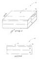
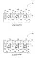
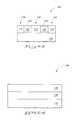
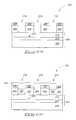
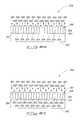
- FIG. 1is a diagrammatic perspective view of a portion of a substrate in process in accordance with an embodiment of the invention.
- FIG. 2is a view of the FIG. 1 substrate taken through line 2 - 2 in FIG. 1 .
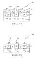
- FIG. 3is a view of the FIG. 1 substrate at a processing step subsequent to that shown by FIG. 1 .
- FIG. 4is a view of the FIG. 3 substrate taken through line 4 - 4 in FIG. 3 .
- FIG. 5is a view of the FIG. 3 substrate at a processing step subsequent to that shown by FIG. 3 .
- FIG. 6is a view of the FIG. 5 substrate taken through line 6 - 6 in FIG. 5 .
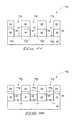
- FIG. 7is a view of the FIG. 5 substrate at a processing step subsequent to that shown by FIG. 5 .
- FIG. 8is a view of the FIG. 7 substrate taken through line 8 - 8 in FIG. 7 .
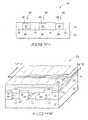
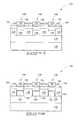
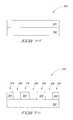
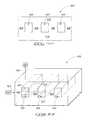
- FIG. 9is a diagrammatic perspective view of a portion of a substrate in process in accordance with an embodiment of the invention.
- FIG. 10is a view of the FIG. 9 substrate taken through line 10 - 10 in FIG. 9 .
- FIG. 11is a view of the FIG. 9 substrate at a processing step subsequent to that shown by FIG. 9 .
- FIG. 12is a view of the FIG. 11 substrate taken through line 12 - 12 in FIG. 11 .
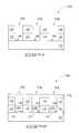
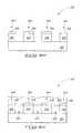
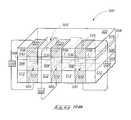
- FIG. 13is a diagrammatic perspective view of a portion of a substrate in process in accordance with an embodiment of the invention.
- FIG. 14is a view of the FIG. 13 substrate at a processing step subsequent to that shown by FIG. 13 .
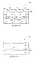
- FIG. 15is a diagrammatic sectional view of a portion of a substrate in process in accordance with an embodiment of the invention.
- FIG. 16is a view of the FIG. 15 substrate at a processing step subsequent to that shown by FIG. 15 .
- FIG. 17is a view of the FIG. 16 substrate at a processing step subsequent to that shown by FIG. 16 .
- FIG. 18is a view of the FIG. 17 substrate at a processing step subsequent to that shown by FIG. 17 .
- FIG. 19is a view of the FIG. 18 substrate at a processing step subsequent to that shown by FIG. 18 .
- FIG. 20is a diagrammatic sectional view of a portion of a substrate in process in accordance with an embodiment of the invention.
- FIG. 21is a view of the FIG. 20 substrate at a processing step subsequent to that shown by FIG. 20 .
- FIG. 22is a diagrammatic sectional view of a portion of a substrate in process in accordance with an embodiment of the invention.
- FIG. 23is a view of the FIG. 22 substrate at a processing step subsequent to that shown by FIG. 22 .
- FIG. 24is a view of the FIG. 23 substrate at a processing step subsequent to that shown by FIG. 23 .
- FIG. 25is a view of the FIG. 24 substrate at a processing step subsequent to that shown by FIG. 24 .
- FIG. 26is a view of the FIG. 25 substrate at a processing step subsequent to that shown by FIG. 25 .
- FIG. 27is a diagrammatic sectional view of a portion of a substrate in process in accordance with an embodiment of the invention.
- FIG. 28is a view of the FIG. 27 substrate at a processing step subsequent to that shown by FIG. 27 .
- FIG. 29is a diagrammatic sectional view of a portion of a substrate in process in accordance with an embodiment of the invention.
- FIG. 30is a view of the FIG. 29 substrate at a processing step subsequent to that shown by FIG. 29 .
- FIG. 31is a diagrammatic sectional view of a portion of a substrate in process in accordance with an embodiment of the invention.
- FIG. 32is a view of the FIG. 31 substrate at a processing step subsequent to that shown by FIG. 31 .
- FIG. 33is a view of the FIG. 32 substrate at a processing step subsequent to that shown by FIG. 32 .
- FIG. 34is a view of the FIG. 33 substrate at a processing step subsequent to that shown by FIG. 33 .
- FIG. 35is a view of the FIG. 34 substrate at a processing step subsequent to that shown by FIG. 34 .
- FIG. 36is a diagrammatic sectional view of a portion of a substrate in process in accordance with an embodiment of the invention.
- FIG. 37is a diagrammatic sectional view of a portion of a substrate in process in accordance with an embodiment of the invention.
- FIG. 38is a view of the FIG. 37 substrate at a processing step subsequent to that shown by FIG. 37 .
- FIG. 39is a diagrammatic sectional view of a portion of a substrate in process in accordance with an embodiment of the invention.
- FIG. 40is a view of the FIG. 39 substrate at a processing step subsequent to that shown by FIG. 39 .
- FIG. 41is a view of the FIG. 40 substrate at a processing step subsequent to that shown by FIG. 40 .
- FIG. 42is a view of the FIG. 41 substrate at a processing step subsequent to that shown by FIG. 41 .
- FIG. 43is a view of the FIG. 42 substrate at a processing step subsequent to that shown by FIG. 42 .
- FIG. 44is a view of the FIG. 43 substrate at a processing step subsequent to that shown by FIG. 43 .
- FIG. 45is a view of the FIG. 44 substrate at a processing step subsequent to that shown by FIG. 44 .
- FIG. 46is a diagrammatic perspective view of a portion of a substrate in process in accordance with an embodiment of the invention.
- FIG. 47is a view of the FIG. 46 substrate taken through line 47 - 47 in FIG. 46 .
- FIG. 48is a diagrammatic perspective view of a portion of a substrate in process in accordance with an embodiment of the invention.
- FIG. 49is a view of the FIG. 48 substrate taken through line 49 - 49 in FIG. 48 .
- FIG. 50is a diagrammatic sectional view of a portion of a substrate in process in accordance with an embodiment of the invention.
- FIG. 51is a view of the FIG. 50 substrate at a processing step subsequent to that shown by FIG. 50 .
- FIG. 52is a view of the FIG. 51 substrate at a processing step subsequent to that shown by FIG. 51 .
- FIG. 53is a view of the FIG. 52 substrate at a processing step subsequent to that shown by FIG. 52 .
- FIG. 54is a diagrammatic sectional view of a portion of a substrate in process in accordance with an embodiment of the invention.
- FIG. 55is a view of the FIG. 54 substrate at a processing step subsequent to that shown by FIG. 54 .
- FIG. 56is a view of the FIG. 55 substrate at a processing step subsequent to that shown by FIG. 55 .
- FIG. 57is a view of the FIG. 56 substrate at a processing step subsequent to that shown by FIG. 56 .
- FIG. 58is a view of the FIG. 57 substrate at a processing step subsequent to that shown by FIG. 57 .
- FIG. 59is a diagrammatic sectional view of a portion of a substrate in process in accordance with an embodiment of the invention.
- FIG. 60is a view of the FIG. 59 substrate at a processing step subsequent to that shown by FIG. 59 .
- FIG. 61is a diagrammatic sectional view of a portion of a substrate in process in accordance with an embodiment of the invention.
- FIG. 62is a view of the FIG. 61 substrate at a processing step subsequent to that shown by FIG. 61 .
- FIG. 63is a view of the FIG. 62 substrate at a processing step subsequent to that shown by FIG. 62 .
- FIG. 64is a diagrammatic sectional view of a portion of a substrate in process in accordance with an embodiment of the invention.
- FIG. 65is a view of the FIG. 64 substrate at a processing step subsequent to that shown by FIG. 64 .
- FIG. 66is a view of the FIG. 65 substrate at a processing step subsequent to that shown by FIG. 65 .
- FIG. 67is a view of the FIG. 66 substrate at a processing step subsequent to that shown by FIG. 66 .
- FIG. 68is a view of the FIG. 67 substrate at a processing step subsequent to that shown by FIG. 67 .
- FIG. 69is a view of the FIG. 68 substrate at a processing step subsequent to that shown by FIG. 68 .
- FIG. 70is a view of the FIG. 69 substrate at a processing step subsequent to that shown by FIG. 69 .
- FIG. 71is a diagrammatic sectional view of a portion of a substrate in process in accordance with an embodiment of the invention.
- FIG. 72is a view of the FIG. 71 substrate at a processing step subsequent to that shown by FIG. 71 .
- FIG. 73is a view of the FIG. 72 substrate at a processing step subsequent to that shown by FIG. 72 .
- FIG. 74is a diagrammatic sectional view of a portion of a substrate in process in accordance with an embodiment of the invention.
- FIG. 75is a view of the FIG. 74 substrate at a processing step subsequent to that of FIG. 74 .
- FIG. 76is a view of the FIG. 75 substrate at a processing step subsequent to that of FIG. 75 .
- FIG. 77is a view of the FIG. 76 substrate at a processing step subsequent to that of FIG. 76 .
- FIG. 78is a view of the FIG. 77 substrate at a processing step subsequent to that of FIG. 77 .
- FIG. 79is a top sectional view of the FIG. 78 substrate along the line 79 - 79 ; with the FIG. 78 view being along the line 78 - 78 of FIG. 79 .
- FIG. 80is a diagrammatic sectional view of a portion of a substrate in process in accordance with an embodiment of the invention.
- FIG. 81is a view of the FIG. 80 substrate at a processing step subsequent to that of FIG. 80 .
- FIG. 82is a view of the FIG. 81 substrate at a processing step subsequent to that of FIG. 81 .
- FIG. 83is a view of the FIG. 82 substrate at a processing step subsequent to that of FIG. 82 .
- FIG. 84is a top sectional view of the FIG. 83 substrate along the line 84 - 84 ; with the FIG. 83 view being along the line 83 - 83 of FIG. 84 .
- FIG. 85is a diagrammatic sectional view of a portion of a substrate in process in accordance with an embodiment of the invention.
- FIG. 86is a view of the FIG. 85 substrate at a processing step subsequent to that of FIG. 85 .
- FIG. 87is a view of the FIG. 86 substrate at a processing step subsequent to that of FIG. 86 .
- FIG. 88is a view of the FIG. 87 substrate at a processing step subsequent to that of FIG. 87 .
- FIG. 89is a view of the FIG. 88 substrate at a processing step subsequent to that of FIG. 88 .
- FIG. 90is a diagrammatic sectional view of a portion of a substrate in process in accordance with an embodiment of the invention.
- FIG. 91is a view of the FIG. 90 substrate at a processing step subsequent to that of FIG. 90 .
- FIG. 92is a view of the FIG. 91 substrate at a processing step subsequent to that of FIG. 91 .
- FIG. 93is a diagrammatic perspective view of the FIG. 92 substrate.
- FIGS. 94 and 95are a diagrammatic sectional view and a diagrammatic top view, respectively, of a portion of a substrate in process in accordance with an embodiment of the invention.
- the view of FIG. 95is along the line 95 - 95 of FIG. 94
- the view of FIG. 94is along the line 94 - 94 of FIG. 95 .
- FIGS. 96 and 97are a diagrammatic sectional view and a diagrammatic top view, respectively, of the substrate of FIGS. 94 and 95 at a processing stage subsequent to that of FIGS. 94 and 95 .
- the view of FIG. 96is along the line 96 - 96 of FIG. 97
- the view of FIG. 97is along the line 97 - 97 of FIG. 96 .
- FIG. 98is a diagrammatic perspective view of the substrate of FIGS. 96 and 97 .
- FIG. 99is a diagrammatic view of a computer embodiment.
- FIG. 100is a block diagram showing particular features of the motherboard of the FIG. 99 computer embodiment.
- FIG. 101is a high level block diagram of an electronic system embodiment.
- FIG. 102is a simplified block diagram of a memory device embodiment.
- FIG. 103is a photomicrograph of a substrate in process in accordance with one embodiment of the invention.
- FIG. 104is a photomicrograph of the FIG. 103 substrate at a processing step subsequent to that of FIG. 103 .
- FIG. 105is a diagrammatic sectional view of a portion of a substrate in process in accordance with an embodiment of the invention, and is alternate processing to that depicted by FIG. 70 subsequent to that depicted by FIG. 69 .
- FIG. 106is a view of the FIG. 105 substrate at a processing step subsequent to that shown by FIG. 106 .
- semiconductor substrateor “semiconductive substrate” is defined to mean any construction comprising semiconductive material, including, but not limited to, bulk semiconductive materials such as a semiconductive wafer (either alone or in assemblies comprising other materials), and semiconductive material layers (either alone or in assemblies comprising other materials).
- substraterefers to any supporting structure, including, but not limited to, the semiconductive substrates described above.
- the covered void(s)may be subsequently filled in whole or in part with solid, liquid, and/or gaseous material(s). One or more remaining voids may be evacuated of gas therein.
- a covered voidmay exist in the final construction being fabricated, a void may be partially filled, or a void may be completely filled such that no portion of the void exists in the final construction being fabricated. Further and regardless, the one or more covered voids may be wholly or partially formed within semiconductive material of the semiconductor substrate or be received entirely outside of any semiconductor material of the semiconductor substrate.
- first material 12comprises a semiconductor material.
- material 12may comprise, consist essentially of, or consist of one or more of Si, Ge, Ga, Ga/Al, Si/Ge, Ga/As, SiC, and Ga/Al/N, and may be monocrystalline, polycrystalline, or amorphous.
- semiconductive material 12may comprise elemental form silicon, for example monocrystalline silicon such as bulk monocrystalline silicon of a bulk wafer.
- substrate 12comprises a monocrystalline-containing substrate comprising a ⁇ 100> plane direction as shown ( FIG. 1 ).
- Second material 14is formed over first material 12 , and is in whole or in part compositionally different from first material 12 .
- Second material 14may be one or more of insulative, conductive, or semiconductive.
- Example semiconductive materialsinclude those described above for first substrate material 12 .
- Example conductive materialsinclude any conductive metal, alloy of conductive metals, or any suitable conductive metal compound.
- Example insulative materialsinclude at least one of silicon dioxide or silicon nitride.
- An example thickness range for second material 14is from about 1,500 Angstroms to about 3,000 Angstroms.
- Third material 16is received over second material 14 , and is in whole or in part compositionally different from second material 14 .
- An example thickness range for material 16is from about 200 Angstroms to about 800 Angstroms.
- Third material 16may be compositionally the same as or different from first material 12 .
- example third materialsinclude elemental-form silicon, including for example elemental-form amorphous silicon and/or monocrystalline silicon, and any one or more of elemental-form W, elemental-form Ti, a silicide, elemental-form Ge, and a combination of Ga and As.
- material 16may be considered as an “epitaxial seed material” which is different compositionally from second material 14 .
- an “epitaxial seed material”is a material which will seed epitaxial growth of a material of the same composition as or different composition from the epitaxial seed material, with some example epitaxial growth being described in examples below.
- the epitaxial seed materialmay or may not have been epitaxially grown itself.
- material 16may be considered as a “seed material” (not preceded by “epitaxial”) which is different compositionally from second material 14 .
- a “seed material”(not preceded by “epitaxial”) is a material which will facilitate growth of a material of the same composition as or different composition from the seed material.
- semiconductor substrate 10may be considered as comprising or defining some mean outermost global surface 15 which may or may not be substantially planar.
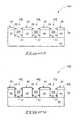
- a plurality of openings 17 , 18 , and 19have been formed through third material 16 and second material 14 to first material 12 .
- suchmay be considered as forming or providing substrate projections 20 , 21 , 22 , and 23 .
- any two immediately adjacent of such projectionsmay be considered as comprising a pair of projections comprising second material 14 which projects upwardly from or relative to first material 12 , and which comprises projection sidewalls 24 .
- Openings 17 , 18 and 19may also, of course, be formed to extend into first material 12 (not shown) as opposed to immediately terminating at the outermost surface thereof.
- Suchprovides but one example embodiment of providing exposed different first and second materials on a semiconductor substrate, where the second material comprises a pair of projections projecting upwardly relative to the first material and comprises sidewalls which in the depicted example comprise walls of an opening.
- An exposed third materialis provided atop the second material projections.
- a plurality of such openingsmay be formed by any suitable etching or other technique(s), and whether existing or yet-to-be developed.
- openings 17 , 18 , and 19are provided to comprise elongated trenches running generally parallel mean outermost global surface 15 .
- trenches 17 , 18 and 19may comprise monocrystalline-containing material bases 26 which run parallel the ⁇ 100> plane direction.
- additional first material 13has been selectively grown (relative to the second material, at least) from exposed first material 12 and selectively (relative to the second material, at least) from exposed third material 16 effective to bridge across the respective pairs of second material projections to form covered voids 28 between the respective pairs of projections.
- selective growthdefines a rate of growth which is at least 2:1 compared to all other different composition exposed material, or at least to some other different composition exposed material to which the selectively grown material is being compared, for at least about 100 Angstroms of growth.
- the selectively growingmay be of conductive material or semiconductive material.
- the selectively growingis devoid of growing detectable first material 13 from at least a majority of second material sidewalls 24 .
- essentially no additional first material 13grows from sidewalls 24 , with the depicted covering of portions of sidewalls 24 by material 13 within openings 17 , 18 , and 19 only occurring as the result of upward growth of material 13 from first material 12 and itself, and downwardly of material 13 from third material 16 and itself.
- former bases 26 of material 12 within openings 17 , 18 , and 19are shown as dashed lines. Such interface of material 12 and 13 may or may not be perceptible.
- the selectively growingis at a selectivity, relative to the second material of at least ten to one, and in one embodiment at least one hundred to one. In one embodiment, the selectively growing of the first material is of at least 100 Angstroms and achieves selectivity relative to the second material of at least one hundred to one.
- the selectively growingcomprises epitaxial silicon-comprising growth.
- a manner of selectively growing epitaxial silicon from example monocrystalline silicon material 12 and where third material 16 comprises monocrystalline silicon, and/or any one or more of elemental-form W, elemental-form Ti, or a silicideincludes chemical vapor deposition using dichlorosilane, hydrogen chloride, and hydrogen at a temperature of 850° C. and at a pressure of 40 Torr.
- the selectively growingcomprises growing any one or more of elemental-form W or a silicide.
- third material 16comprises elemental-form silicon
- elemental-form Wmay be selectively grown from material 16 by chemical vapor deposition using WF 6 and a silane as precursors at 350 degrees C. and 20 mTorr, and otherwise as described in U.S. Pat. No. 5,043,299.
- titanium silicidemay be selectively grown from material 16 by plasma enhanced chemical vapor deposition including simultaneously flowing titanium tetrachloride and hydrogen to the substrate at a temperature of from about 550 degrees C. to about 680 degrees C. at a pressure of about 5 Torr to about 8 Torr (with or without plasma).
- the selectively growingcomprises polysilicon-comprising growth.
- third materialcomprises elemental-form monocrystalline silicon comprising a ⁇ 100> plane direction which is parallel that of the first material.
- openings(which may include trenches) are etched to have sides running parallel such ⁇ 100> plane direction.
- a method of forming a covered void in a semiconductor substratecomprises forming a pair of projections projecting upwardly from a semiconductor substrate.
- any two adjacent of projections 20 , 21 , 22 , and 23may constitute an example pair of such projections.
- Elemental-form siliconis provided atop the pair of projections.
- material/layer 16may comprise any elemental-form silicon.
- a polysilicon-comprising materialis selectively grown relative to at least portions of the projection sidewalls from the elemental-form silicon effective to bridge across the pair of openings to form a covered void between the pair of projections.
- at least some of the selectively grown polysilicon-comprising materialis oxidized to form a silicon dioxide-comprising bridge atop the covered void. In one embodiment, all such material is oxidized.
- the elemental-form siliconis formed by depositing amorphous silicon and annealing such to be polycrystalline and from which the selectively growing of polysilicon-comprising material occurs.
- FIG. 103depicts a photomicrograph of a substrate 900 comprising monocrystalline silicon 902 , silicon dioxide projections 904 , and amorphous silicon 906 .
- Suchwas formed by deposition of amorphous silicon, over silicon dioxide, over monocrystalline silicon substrate 902 .
- the amorphous silicon and silicon dioxidewere etched to form projections 904 having amorphous silicon 906 thereover, with trenches 908 being formed between the projections.
- FIG. 104such was annealed at a temperature of about 625° C. which rendered the amorphous silicon polycrystalline.
- Polysilicon 910was grown therefrom at a temperature of about 850° C. and a pressure of about 40 Torr using H 2 , HCl, and SiH 2 Cl 2 as precursors.
- a method of forming a covered void in a semiconductor substratecomprises forming a pair of projections projecting upwardly from a semiconductor substrate.
- any two adjacent of projections 20 , 21 , 22 , and 23may constitute an example pair of such projections.
- Elemental-form siliconis provided atop the pair of projections.
- material/layer 16may comprise any elemental-form silicon.
- At least one of elemental-form W or a silicideis selectively grown relative to at least portions of the projection sidewalls from the elemental-form silicon effective to bridge across the pair of projections to form a covered void between the pair of projections.
- any of covered voids 28constitute example such covered voids.
- a method of forming a plurality of covered voids in a semiconductor substrateincludes depositing insulative material over an elemental-form silicon-containing material.
- material 12 in the above-described embodimentmay comprise an elemental-form silicon-containing material over which an insulative material 14 is deposited.
- Amorphous siliconis deposited over the insulative material.
- material/layer 16may comprise amorphous silicon which is deposited over an insulative material 14 .
- An elemental-form silicon-comprising materialis selectively grown relative to the insulative material from the elemental-form silicon-containing material and from the amorphous silicon effective to bridge across the plurality of openings to cover the plurality of openings.
- material 13constitutes an example elemental-form silicon-comprising material which has been so selectively grown.
- a method of forming a plurality of covered voids in a semiconductor substratecomprises depositing insulative material over a first elemental-form silicon-containing material.
- a second elemental-form silicon-containing materialis formed over the insulative material.
- a plurality of openingsis etched through the second elemental-form silicon-containing material and the insulative material to the first elemental-form silicon-containing material.
- a first elemental-form silicon-comprising materialis epitaxially grown from the first elemental-form silicon-containing material.
- a second elemental-form silicon-comprising materialis selectively grown relative to the insulative material from the second elemental-form silicon-containing material effective to bridge across the plurality of openings to cover the plurality of openings.
- a method of forming a plurality of covered voids in a semiconductor substratecomprises depositing insulative material over a first elemental-form silicon-containing material. An amorphous elemental-form silicon-containing material is formed over the insulative material. A plurality of openings is etched through the amorphous elemental-form silicon-containing material and the insulative material to the elemental-form silicon-containing material. The amorphous elemental-form silicon-containing material is annealed effective to form a polycrystalline silicon-containing material.
- a first elemental-form silicon-comprising materialis epitaxially grown from the elemental-form silicon-containing material while selectively growing relative to the insulative material a polysilicon-comprising material from the polycrystalline silicon-containing material effective to bridge across the plurality of openings to cover the plurality of openings.
- each covered trench 28(not designated in FIGS. 7 and 8 ) has been filled with one or more conductive materials 30 , whereby for example, the voids exist no more as having been completely filled with solid material.
- conductive materials 30such as may be used to form elongated conductive lines therefrom.
- individual of the elongated trenchesmay be provided to have at least one open end into or through which conductive material may be deposited to within the covered elongated trenches effective to form conductive lines within the trenches.
- suitable chemical vapor deposition and/or atomic layer deposition techniquesmay be utilized to isotropically fill covered elongated trenches from one or more ends, or from other access location(s) thereto.
- Such conductive linesmay be utilized as local interconnects, substantially globally running conductive lines, field effect transistor gate lines, and/or other conductive lines.
- FIGS. 9-12depict an alternate embodiment portion of a substrate 10 a .
- Like numerals from the FIGS. 5-8 embodiment substratehave been utilized where appropriate, with differences being indicated with the suffix “a” or with different numerals.
- FIGS. 9 and 10depict the forming of a gate dielectric 32 within covered elongated trenches 28 a .
- An example such materialis silicon dioxide, which may be formed for example by a thermal oxidation of material 13 where such comprises at least some elemental-form silicon.
- FIGS. 11 and 12depict conductive material 30 a as having been deposited to within the covered elongated trenches over gate dielectric 32 from at least one open end effective to form conductive gate lines within the trenches.
- Field effect transistor source/drain regions 34 and field effect transistor channel regions 36have been formed within example selectively grown semiconductive material 13 . Such may be fabricated by suitable masked or maskless conductivity-modifying doping of material 13 which extends over projections 20 , 21 , 22 , and 23 and bridges over former voids 28 .
- a method of forming field effect transistorsincludes providing a monocrystalline silicon-containing substrate which comprises a ⁇ 100> plane direction. Insulative material is deposited over the monocrystalline silicon-containing substrate. A plurality of trenches are etched through the insulative material to silicon-containing material of the substrate parallel the ⁇ 100> plane direction to provide monocrystalline silicon-containing material bases of the trenches which run parallel the ⁇ 100> plane direction.
- An elemental-form silicon-comprising materialis epitaxially grown from the monocrystalline silicon-containing material of the trench bases and over the insulative material effective to bridge across the trenches with elemental-form silicon-comprising material and form covered trench voids within the trenches.
- the monocrystalline silicon-containing material basesmay be wet etched prior to the epitaxially growing.
- an exposure to a dilute HF solutioncomprises an example such wet etching.
- an exposed epitaxial seed material different from the insulative materialmay be provided over the insulative material prior to the epitaxially growing and from which the elemental-form silicon-comprising material bridging across the trenches is grown during the epitaxially growing.
- the epitaxial seed material and the monocrystalline silicon-containing material basesmay be wet etched prior to the epitaxially growing, for example utilizing a dilute HF solution as described above, or using some other solution.
- At least one of field effect transistor channel regions or field effect transistor source/drain regionsare formed within the elemental-form silicon-comprising material which bridges across the trenches.
- FIG. 12depicts both such field effect transistor regions and field effect transistor source/drain regions being so formed in material 13 received over material 16 .
- field effect transistor gatesare formed within the trench voids.
- an underside of the elemental-form silicon-comprising material bridging across the trenchesis oxidized to at least partially form a gate dielectric on such underside within the covered trench voids. After such oxidizing, conductive material is deposited within the covered trench voids to form field effect transistor gates within the covered trench voids.
- FIGS. 13 and 14depict example second material-comprising projections which resulted in the formation of elongated trenches. Any alternative forms of projections, including combination of different shaped projections, are also of course contemplated.
- alternate example projections 38are depicted in FIGS. 13 and 14 with respect to an alternate embodiment substrate portion 10 b .
- Like numerals from the first-described embodiment substratehave been utilized where appropriate, with differences being indicated with the suffix “b” or with different numerals.
- FIGS. 13 and 14depict projections 38 as comprising spaced free-standing pillars.
- FIG. 14depicts the selectively growing to form material 13 b to comprise a ceiling which covers a void 28 b , with the ceiling be supported at least in part by the plurality of pillars 38 which are received within void 28 b.
- FIG. 15Another embodiment substrate portion is indicated generally with reference numeral 40 in FIG. 15 .
- Suchincludes an example elemental-form silicon-containing material 42 having a conductive material 44 deposited thereover.
- Example elemental-form silicon-containing materialsinclude monocrystalline, polycrystalline, or amorphous silicon alone or in combination with other materials.
- Example conductive materials 44include any one or combination of elemental metals, alloys of elemental metals, and/or conductive metal compounds.
- An example thickness range for conductive material 44is from about 1,500 Angstroms to about 3,000 Angstroms.
- openings 45 , 46 , and 47have been etched through conductive material 44 to elemental-form silicon-containing material 42 .
- openings 45 , 46 , and 47comprise elongated trenches, for example which run generally parallel a mean outermost global surface of the semiconductor substrate, for example as described in some of the other embodiments.
- openings 45 , 46 , and 47may be considered as comprising respective sidewalls 50 and bases 51 .
- the etching tomay also occur into material 42 (not shown) and not necessarily stop thereon.
- insulative material 52At least sidewalls 50 of openings 45 , 46 , and 47 have been lined with an insulative material 52 .
- materialsinclude silicon dioxide and/or silicon nitride.
- An example thickness range for insulative material 52is from 60 Angstroms to 300 Angstroms.
- bases 51are also lined with insulative material 52 while lining sidewalls 50 with insulative material 52 .
- material 52is formed by chemical vapor deposition and/or atomic layer deposition.
- insulative material 52has been etched from atop the elevational outermost surfaces of conductive material 44 and from bases 51 within openings 45 , 46 , and 47 .
- An example technique for doing soincludes utilizing a dry anisotropic fluorocarbon etching chemistry.
- an elemental-form silicon-comprising material 54has been selectively grown relative to the insulative material over a plurality of openings 45 , 46 , and 47 effective to bridge across such openings to cover such openings, thereby forming covered openings or covered voids 49 .
- elemental-form silicon-comprising material 55has also been epitaxially grown from bases 51 within openings 45 , 46 , and 47 while selectively growing elemental-form silicon-comprising material 54 .
- materials 54 and 55may comprise the same or different compositions, and an elemental-form silicon-containing material may be so selectively grown to bridge across the plurality of openings for example as described above where conductive material 44 comprises any one or combination of elemental-form W or a silicide.
- the selectively growing of an elemental-form silicon-comprising material effective to bridge across the plurality of openingsmay be devoid of epitaxially growing elemental-form silicon-comprising material from bases of the plurality of openings.
- FIG. 20depicts an example alternate embodiment substrate portion 40 a compared to that of FIG. 18 . Like numerals from the FIGS. 15-19 embodiment have been utilized where appropriate, with differences being indicated with the suffix “a” or with different numerals.
- FIG. 20depicts alternate processing of a substrate portion 40 a prior or subsequent to that of FIG. 17 .
- elemental-form silicon-comprising material 54has been selectively grown over the plurality of openings 45 , 46 , and 47 to bridge across and cover such openings, forming covered openings or covered voids 49 a.
- an exposed seed material or an exposed epitaxial seed materialmay be provided proximate the tops of the plurality of openings over the conductive material prior to the selective growth, with such selective growth being an epitaxial growth from the exposed epitaxial seed material.
- One alternate example such embodimentis initially described in connection with a substrate portion 40 b in FIGS. 22-26 . Like numerals from the FIGS. 15-19 embodiment have been utilized where appropriate, with differences being indicated with the suffix “b” or with different numerals.
- an exposed seed material 58 or an exposed epitaxial seed material 58has been provided over conductive material 44 .
- Example materialsinclude amorphous silicon, monocrystalline silicon, elemental-form W, elemental-form Ti, a silicide, and combinations thereof.
- An example thickness range for material 58is from about 200 Angstroms to about 800 Angstroms.
- openings 45 b , 46 b , and 47 bhave been etched through material 58 and conductive material 44 to elemental-form silicon-containing material 42 . Accordingly in the depicted embodiment, opening sidewalls 50 b encompass materials 44 and 58 . Also for purposes of the continuing discussion, epitaxial seed material as received proximate the tops of plurality of openings 45 b , 46 b , and 47 b may be considered as comprising elevationally outermost surfaces 60 .
- an insulative material 52 bhas been formed to line openings 45 b , 46 b , and 47 b .
- insulative material 52 bhas been etched effective to remain lining at least sidewalls 50 b of openings 45 b , 46 b , and 47 b .
- elemental-form silicon-comprising material 54 bhas been epitaxially grown over the plurality of openings 45 b , 46 b , and 47 b effective to bridge across such openings to cover such openings, thereby forming covered openings or covered voids 49 b .
- Elemental-form silicon-comprising material 55has also been epitaxially grown from bases 51 of such openings in the depicted embodiment. Further, by way of example only in such embodiment, elevationally outermost surfaces 60 of material 58 were exposed during the selective growth and from which elemental-form silicon-comprising material 54 was grown during such epitaxial growth.
- FIGS. 27 and 28An alternate embodiment substrate 40 c is depicted in FIGS. 27 and 28 . Like numerals with respect to the 40 / 40 a / 40 b embodiments are utilized where appropriate, with differences being indicated with the suffix “c” or with different numerals.
- insulative material 52 chas been formed over sidewalls of material 44 within openings 45 c , 46 c , and 47 c as well as over bases 51 , but not over the sidewalls of material 58 .
- material 52 cmay be formed utilizing a selective thermal oxidation process whereby a conductive material 44 and elemental-form silicon-containing material 42 are selectively oxidized relative to material 58 .
- Such a selective oxidationmay be sufficiently high or essentially infinite for the thickness growth of material 52 c such that none forms on material 58 . Alternately, some insulative material 52 c may so form. In such instance, a timed etch of material 52 c may be conducted to clear oxide from material 58 but not from conductive material 44 or elemental-form silicon-containing material 42 .
- silicidese.g., tungsten silicide, platinum silicide, and cobalt silicide
- tungsten silicideplatinum silicide
- cobalt silicidee.g., tungsten silicide, platinum silicide, and cobalt silicide
- a short dilute HF wet etchmay be used to clear any resulting oxide from material 58 .
- elemental-form silicon-comprising material 54 chas been selectively and/or epitaxially grown over the plurality of openings 45 c , 46 c , and 47 c effective to bridge across and cover such openings, thereby forming covered openings or covered voids 49 c.
- FIGS. 29 and 30depict an alternate embodiment substrate 40 d .
- Like numeralshave been utilized where appropriate with respect to the 40 / 40 a / 40 b / 40 c embodiments, with differences being depicted with the suffix “d” or with different numerals.
- insulative material 52 dhas been formed over the sidewalls of conductive material 44 within openings 45 d , 46 d , and 47 d selectively relative to materials 58 and 42 .
- elemental-form silicon-comprising material 54 chas been selectively grown over the plurality of openings 45 d , 46 d , and 47 d effective to bridge across such openings and cover such openings.
- Epitaxially grown elemental-form silicon-comprising material 55has also been grown from opening bases 51 .
- the above-described 40 / 40 a / 40 b / 40 c / 40 d embodimentsprovide elevationally outermost surfaces 60 of material 58 to be outwardly exposed and from which the elemental-form silicon-comprising material 54 was grown.
- An alternate example embodiment substrate 40 eis initially described with reference to FIGS. 31-35 .
- Like numerals from the above 40 / 40 a / 40 b / 40 c / 40 d embodimentsare utilized where appropriate, with differences being indicated with the suffix “e” or with different numerals.
- a masking or covering layer 64has been formed over material 58 .
- Such materialmay be insulative, conductive, and/or semiconductive.
- material 64comprises silicon nitride.
- At least the sidewalls of the plurality of openings 45 e , 46 e , and 47 e through conductive material 44are lined with an insulative material 52 e , for example and by way of example only analogous to that depicted and described with respect to insulative material 52 c in FIG. 27 .
- elemental-form silicon-comprising material 54 ehas been selectively and/or epitaxially grown over the plurality of openings 45 e , 46 e , and 47 e effective to bridge across and cover such openings, forming covered openings or covered voids 49 e . Accordingly in the example FIG. 33 embodiment, elevationally outermost surfaces 60 of material 58 are covered during such epitaxial growth.
- FIG. 34some subsequent processing of substrate 40 e has been depicted. Specifically, masking material 64 is shown as having been removed substantially selectively relative to elemental-form silicon-comprising material 54 e and material 58 . Further possible subsequent processing is depicted in FIG. 35 , whereby material 58 has been selectively removed relative to elemental-form silicon-comprising material 54 e and conductive material 44 .
- FIG. 36illustrates alternate example subsequent processing with respect to the processing depicted by FIG. 33 .
- Like numerals from the 40 e embodimenthave been utilized where appropriate, with differences being indicated with the suffix “f” or with different numerals.
- elemental-form silicon-comprising material 54 ewas not grown to the point of bridging over masking material 64 .
- FIG. 36depicts wafer portion 40 f having been processed to grow elemental-form silicon-comprising material 54 f to bridge over masking material 64 .
- FIGS. 37 and 38depict an alternate embodiment substrate portion 40 g analogous to that of FIG. 32 , but wherein insulative material 52 g is not formed, or has been removed from, over bases 51 .
- insulative material 52 gis not formed, or has been removed from, over bases 51 .
- Like numerals from the embodiment of FIGS. 32 and 33have been utilized where appropriate, with differences being indicated with the suffix “g”.
- a semiconductor substrate portionis indicated generally with reference numeral 70 .
- Suchcomprises some base substrate 72 , for example and by way of example only, bulk monocrystalline silicon.
- a first material 74is deposited over substrate 72 .
- a second material 76is deposited over first material 74 .
- a third material 78is deposited over second material 76 .
- Second material 76is thereby received intermediate first material 74 and third material 78 , and second material 76 is compositionally different from first material 74 and from third material 78 .
- the first and third materialsmay be compositionally the same or different.
- the first and third materialsmay be insulative, conductive, and/or semiconductive, with insulative being preferred.
- Example materialsinclude one or a combination of silicon dioxide or silicon nitride.
- example second materialsinclude elemental-form silicon (including amorphous and/or crystalline forms of elemental-form silicon), elemental-form W, elemental-form Ti, and a silicide, including mixtures/combinations thereof.
- third material 78may be considered as having an elevationally outermost surface 79 , and which may or may not be planar.
- first material 74may be thicker or thinner than third material 78 .
- third material 78may be thicker or thinner than second material 76 .
- any two or all three of materials 74 , 76 , and 78may be of about the same thickness.
- openings 80have been formed through third material 78 , second material 76 , and first material 74 to substrate material 72 . Such openings may also, of course, extend into material 72 .
- openings 80may be formed by etching, and in one embodiment comprise a plurality of elongated trenches.
- openings 80may be considered as providing or defining respective pairs of upwardly-projecting sidewalls 82 relative to a semiconductor substrate 70 .
- Sidewalls 82have a space 83 therebetween which comprises opposing first, second, and third materials 74 , 76 , and 78 , respectively.
- a fourth material 86has been grown from opposing second material 76 of sidewalls 82 selectively relative at least to first material 74 and third material 78 effective to form a bridge of fourth material 86 across space 83 to form respective covered voids 87 between sidewalls 82 .
- essentially no fourth material 86grows from sidewalls of first material 74 and third material 78 , with the depicted covering of portions of sidewalls of materials 74 and 78 within openings 80 by material 86 only occurring as the result of upward and downward growth of material 86 from itself within openings 80 .
- the second and fourth materialsmay be compositionally the same or different. In one embodiment, such selectively growing forms the fourth material to comprise elemental-form silicon.
- the fourth materialis formed to comprise any one or more of elemental-form W or a silicide.
- Example processing and materialsmay be as described in any of the above-described embodiments.
- FIG. 41depicts an embodiment whereby a material 88 deposits atop and/or also selectively from substrate material 72 during the growth of material 86 from second material 76 . In such event, material 88 may be compositionally the same as or different from material 86 .
- FIG. 41also depicts an embodiment wherein the selectively growing does not grow fourth material 86 to extend over an elevationally outermost surface 79 of third material 78 .
- FIG. 42depicts continued processing and/or an alternate embodiment whereby the selectively growing of material 86 is continued sufficiently to grow fourth material 86 to extend over elevationally outermost surfaces 79 of third material 78 .
- FIG. 43substrate 70 has been polished inwardly to at least third material 78 to leave fourth material 86 bridging over covered voids 87 .
- FIG. 44illustrates example subsequent or continued processing whereby polishing of substrate 70 has been conducted inwardly to at least second material 76 to leave fourth material 86 bridging over covered voids 87 .
- FIG. 45illustrates still subsequent or continued processing whereby substrate 70 has been polished inwardly to first material 74 to still leave some fourth material 86 bridging over covered voids 87 .
- a method of forming a covered void within a semiconductor substrateincludes providing a bulk monocrystalline silicon-containing substrate.
- material 72may constitute a bulk monocrystalline silicon-containing substrate.
- a first insulative materialis deposited over the bulk monocrystalline silicon-containing substrate.
- material 74may comprise an example such first insulative material.
- An elemental-form silicon-containing materialis deposited over the first insulative material.
- material 76may comprise an example such elemental-form silicon-containing material.
- a second insulative materialis deposited over the elemental-form silicon-containing material.
- material 78may comprise such a second insulative material.
- the first insulative materialmay be compositionally be the same as or different from the second insulative material.
- the first insulative materialcomprises silicon dioxide and the second insulative material comprises silicon nitride.
- the elemental-form silicon-containing material deposited over the first insulative materialcomprises amorphous silicon and/or monocrystalline silicon.
- a plurality of trenchesis etched through the second insulative material, the elemental-form silicon-containing material, and the first insulative material to the bulk silicon-containing material of the substrate.
- FIG. 40depicts such example processing. Again of course, etching may occur into material 72 .
- a silicon-comprising materialis selectively grown from the elemental-form silicon-containing material and from the bulk silicon-containing material of the substrate within the trenches effective to bridge across the trenches with elemental-form silicon-comprising material to form covered trench voids within the trenches.
- FIGS. 41 and 42depict examples of such processing.
- at least one of field effect transistor channel regions or field effect transistor source/drain regionsare formed within the elemental-form silicon-comprising material bridging across the trenches.
- the covered openings/voids which are formedmay subsequently be wholly or partially filled with any one or combinations of insulative, conductive, or semiconductive materials.
- any of the above embodimentsmay not form trenches and/or provide other configuration projections forming one or more covered openings/voids.
- the embodiment of FIGS. 13 and 14may be utilized in the context of free-standing pillar formation. Regardless, any other of the above and below attributes with respect to any other of the disclosed embodiments are of course contemplated.
- Embodiments hereinencompass methods of forming a span comprising silicon dioxide.
- an opening comprising sidewallsis formed within a semiconductor substrate.
- the openingmay be wholly or partially formed within semiconductive material of the semiconductor substrate or be received entirely outside of any semiconductor material of the semiconductor substrate.
- An elemental-form silicon-containing materialis selectively grown relative to at least some portion of the sidewalls to bridge across the opening to form a covered cavity within the opening.
- any of the above-depicted and described embodiments of selectively growing an elemental-form silicon-containing material to bridge across an opening to form a covered cavity or void within the openingare of course contemplated.
- FIGS. 46 and 47depict a wafer portion 10 c processed in accordance with an example of the just-described embodiment.
- FIGS. 46 and 47depict substrate portion 10 of FIGS. 5 and 6 at a processing step alternate to that depicted by FIGS. 7 and 8 , and is accordingly designated 10 c .
- Like numerals from the first-described embodimentare utilized where appropriate, with differences being indicated with the suffix “c” or with different numerals.
- FIGS. 46 and 47depict an outermost upper half of selectively grown elemental-form silicon-containing material 13 which bridges across the depicted openings as having been oxidized, thereby forming a silicon dioxide-comprising bridge 90 across the openings over the cavities and leaving bridging silicon-containing material 13 c .
- elemental-form silicon-comprising materialmay be epitaxially grown from a base of the opening or openings while selectively growing the elemental-form silicon-containing material which bridges across the opening, for example as depicted in FIGS. 46 and 47 .
- Elemental-form silicon-containing material 13may be selectively grown from elemental-form silicon-containing material and/or from at least one of elemental-form W, elemental-form Ti, or a silicide. Processing may otherwise be conducted, by way of example only, as described above in connection with the substrate 10 / 10 a / 10 b and other embodiments.
- FIGS. 48 and 49illustrate an alternate embodiment substrate portion 10 d .
- Like numerals from the first-described substrate 10 / 10 c embodimentshave been utilized where appropriate, with differences being indicated with the suffix “d” or with different numerals.
- FIGS. 48 and 49depict substrate portion 10 d wherein all of the selectively grown elemental-form silicon-containing material of FIGS. 5 and 6 has been oxidized to form a silicon dioxide-comprising bridge 90 d across the respective openings over the respective cavities. Processing may otherwise occur as described above with respect to the substrate 10 / 10 a / 10 b / 10 c and other embodiments.
- a substrate portion 100comprises some base substrate 102 , for example monocrystalline silicon and/or at least one other semiconductor material.
- Projections 104 , 105 , and 106project upwardly from substrate 102 , and comprise sidewalls 108 .
- Projections 104 , 105 , and 106comprise different composition first and second materials 110 and 112 , respectively, with second material 112 comprising at least some outwardly-exposed portion which is received over first material 110 .
- First and second materials 110 , 112may be insulative, conductive, semiconductive, and including any combination thereof.
- Example materials of construction and dimensions for materials 110 and 112are as described above in connection with the first-described embodiment for layers 14 and 16 , respectively.
- second material 112may be considered as comprising elevationally outermost surfaces 114 and second material sidewalls 116 .
- a third material 120has been selectively grown from second material 112 elevationally inward along projection sidewalls 108 and effective to bridge across projections 104 , 105 , and 106 with third material 120 to form respective covered voids 122 between adjacent pairs of the projections.
- Example attributes, materials, and methodsare otherwise as described in connection with any of the above embodiments.
- the third materialmay be of the same composition as the second material, or of different composition.
- the third materialcomprises elemental-form silicon, and the selectively growing comprises selective and/or epitaxial silicon-comprising growth.
- the second materialcomprises elemental-form silicon.
- the second materialcomprises any one or more of elemental-form W, elemental-form Ti, or a silicide. In one embodiment, the second material comprises elemental-form silicon, and the selectively growing comprises any one or more of elemental-form W or a silicide. In one embodiment, the second material comprises any one or more of elemental-form W, elemental-form Ti, or a silicide, and the selectively growing comprises epitaxial silicon-comprising growth. In the FIG. 51 embodiment, selective growth of third material 120 occurs from exposed elevationally-outermost surfaces 114 of second material 112 and from exposed sidewalls surfaces 116 of second material 112 . Alternately, portions or all of at least one of such may be covered during the selective growth.
- third material 120has been removed inwardly at least to second material 112 and effective to leave a third material-comprising bridge 120 across the respective adjacent pair of projections over the respective covered voids 122 .
- Such removingmay comprise any one or combination of etching, mechanical polishing, and/or chemical mechanical polishing.
- removing of third material 120may be conducted inwardly to first material 110 , for example as shown in FIG. 53 . Again for example in such instance, such removing of the third material is effective to leave a third material-comprising bridge 120 over the respective pairs of projections over the covered voids.
- the covered voidsmay be provided to comprise elongated trenches running generally parallel a mean outermost global surface of the semiconductor substrate. Further in one embodiment, at least a majority of such trenches may be filled with conductive material to form elongated conductive lines therefrom.
- the pair of projectionsmay be formed to comprise other structures, for example spaced free-standing pillars, prior to the stated selective growth.
- the selective growthmay form one or more voids to be covered by a ceiling supported at least in part by the plurality of pillars received within the void.
- Embodiments hereinalso include methods of cooling semiconductor devices.
- any of the structures shown and described herein which provide covered trenches or openingsmay be utilized in such method embodiments and in structure embodiments.
- Example materials of construction and dimensionsare otherwise as disclosed herein.
- a method of cooling semiconductor devices in accordance with an embodimentcomprises etching trenches into an insulative material.
- An elemental-form silicon-containing materialis selectively grown across the trenches to convert the trenches to elongated covered conduits.
- At least one integrated circuit deviceis formed and is received at least partially within the elemental-form silicon-containing material received at least across one of the elongated covered conduits.
- Coolantis provided within the conduits, and preferably comprises the flowing of coolant therethrough for example in the form of one or both of liquid or gas.
- the trenchesare provided to have exposed trench bases which comprise elemental-form silicon-containing material over which the insulative material is deposited.
- an elemental-form silicon-containing materialwas epitaxially grown from the trench bases during the selectively growing of the elemental-form silicon-containing material across the trenches to convert the trenches to elongated covered conduits.
- etching of the trenchesfirst comprises depositing insulative material over an elemental-form silicon-containing material. The trenches are then etched into such insulative material. An exposed seed material, which is different from the insulative material, is provided over the insulative material prior to the selective growth and from which the elemental-form silicon-comprising material received across the trenches is selectively grown during such selective growth.
- any of the above-described seed materialsmay be utilized, and regardless such seed material may be provided over the insulative material prior to or after the etching to form the trenches. If provided before, the act of etching the plurality of trenches will also occur first through the seed material and then through the insulative material.
- the selective growthcomprises epitaxial growth of the elemental-form silicon-containing material.
- Embodiments hereinalso include methods of forming semiconductor-on-insulator substrates.
- a portion of a semiconductor-on-insulator substrateis indicated generally with reference numeral 130 .
- Suchcomprises some base substrate 132 , an insulator layer 134 received thereover, and a silicon-containing semiconductor layer 136 received over insulator layer 134 .
- Base substrate 132may comprises a bulk monocrystalline silicon-containing substrate.
- Example materials for insulator 134include one or both of silicon dioxide or silicon nitride.
- An example thickness range for layer 134is from about 1,000 Angstroms to about 3,000 Angstroms.
- An example thickness range for silicon-containing semiconductor layer 136is from about 600 Angstroms to about 2,000 Angstroms, with example materials including monocrystalline silicon and SiGe x , where “x” ranges from 0.01 to 2.0.
- openings 138 , 140 , and 142have been etched through semiconductor layer 136 . Such etching may also be conducted to extend openings 138 , 140 , and 142 partially into or completely through insulator layer 134 (not shown in FIG. 55 ). Openings 138 , 140 , and 142 may be of any shape, for example shapes as disclosed herein, with one embodiment being of elongated trenches running generally parallel a mean outermost global surface of the semiconductor-on-insulator substrate. Substrate portion 130 in FIG. 55 is depicted as having a planar outermost global surface defined by the outermost surface of silicon-containing semiconductor layer 136 , although planarity is of course not required.
- an elemental-form silicon-comprising material 144has been epitaxially grown over silicon-containing semiconductor layer 136 received over insulator layer 134 effective to bridge across openings 138 , 140 , and 142 with elemental-form silicon-comprising material, and to form covered voids 146 within openings 138 , 140 , and 142 .
- At least one of field effect transistor channel regions or field effect transistor source/drain regionsare formed within the elemental-form silicon-comprising material bridging across openings 138 , 140 , and 142 .
- FIG. 57depicts both field effect transistor channel regions 154 and field effect transistor source/drain regions 156 formed within material 144 .
- Gate constructions 148have been formed directly over openings 138 , 140 , and 142 . Such are depicted as comprising conductive regions 150 formed over a gate dielectric region 152 .
- Covered voids 146may remain as part of the finished circuitry construction, for example provided with coolant fluid flowing or statically received therein.
- covered voids 146are wholly or partially filled with one, two, or three of any of conductive, semiconductive, and/or insulative materials.
- a field effect transistor gate constructionis provided within previous voids 146 , and perhaps with gate constructions 148 in such embodiment being eliminated. Alternately by way of example only, field effect transistor gate constructions may be provided both within previously covered voids 146 and thereover, for example as depicted in FIG. 58 . Substrate portion 130 in FIG.
- gate dielectric 160is depicted as comprising a gate dielectric 160 and conductive material 162 within previous covered voids 146 .
- example channel regions 154are gated from above and below.
- the gate dielectricmay be formed by a thermal oxidation utilizing gases which access covered voids 146 ( FIG. 57 ) from one or more ends thereof, followed by an isotropic deposition of any suitable conductive material 162 , for example as described elsewhere in this document.
- FIGS. 54-58depict epitaxial growth of an elemental-form silicon-comprising material 144 from exposed portions of an example silicon-containing semiconductor layer 136 .
- an exposed epitaxial seed materialmay be provided over the silicon-containing semiconductor layer prior to the epitaxial growth and from which the elemental-form silicon-comprising material is grown during such epitaxial growth.
- Such an example embodimentis depicted with respect to a substrate portion 130 a in FIGS. 59 and 60 .
- Like numerals from the first-described embodimenthave been utilized where appropriate, with differences being indicated with the suffix “a” or with different numerals.
- FIG. 60depicts substrate portion 130 a as comprising an exposed epitaxial seed material 166 received over silicon-containing semiconductor layer 136 , and through which openings 138 a , 140 a , and 142 a are formed.
- Example epitaxial seed materialsare as described elsewhere in this document.
- FIG. 60depicts subsequent epitaxial growth of an elemental-form silicon-comprising material 144 a over layer 136 effective to bridge across the openings with elemental-form silicon-comprising material 144 a to form covered voids 146 within openings 138 a , 140 a , and 142 a.
- FIGS. 61-63Another embodiment is described in connection with FIGS. 61-63 with respect to a substrate portion 130 b . Like numerals from the substrate portion 130 embodiment are utilized where appropriate, with differences being indicated with the suffix “b” or with different numerals.
- openings 138 b , 140 b , and 142 bhave not only been etched through semiconductor 136 , but also through insulator layer 134 to a bulk monocrystalline silicon-containing material 132 of a bulk monocrystalline silicon-containing substrate. Openings 138 b , 140 b , and 142 b comprise monocrystalline silicon-containing bases 168 . Of course, etching may also occur into material 132 (not shown).
- an elemental-form silicon-comprising material 145is epitaxially grown from monocrystalline silicon-containing bases 168
- an elemental-form silicon-comprising material 144 bis epitaxially grown from over silicon-containing semiconductor layer 136 received over insulator layer 134 effective to bridge across openings 138 b , 140 b , and 142 b , and form covered voids 146 b within such openings.
- At least one of field effect transistor channel regions or field effect transistor source/drain regionsare formed within elemental-form silicon-comprising material 144 b bridging across openings 138 b , 140 b and 142 b.
- FIG. 63depicts the fabrication of gate constructions 172 within what were previously-covered voids 146 b ( FIG. 62 ).
- Dielectric material 174has been formed, for example by thermal oxidation of materials 144 b and 145 within the covered voids 146 b of FIG. 62 .
- a conductive gate material 176has been subsequently deposited thereover, with at least the uppermost dielectric material 174 received against material 144 b comprising a gate dielectric.
- Channel regions 154 b and source/drain regions 156 bhave been formed within epitaxially grown elemental-form silicon-comprising material 144 b.
- integrated circuitrycomprises a semiconductor-on-insulator substrate having some mean outermost global surface.
- the substratecomprises monocrystalline silicon-containing material, an insulator received over the monocrystalline silicon-containing material, and an elemental-form silicon-comprising material received over the insulator.
- a plurality of elongated cooling conduitsruns generally parallel to the mean outermost global surface within the insulator (i.e., within at least some portion of the insulator). Cooling fluid is received within the cooling conduits.
- one or both of field effect transistor channel regions and/or field effect transistor source/drain regionsare received within the elemental-form silicon-comprising material that is over the cooling conduits.
- Example constructions, materials, dimensions, and methods of fabricationare otherwise as described anywhere else in this document.
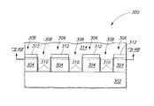
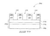
- Embodiments of methods of forming a semiconductor-on-insulator substrateare next described with reference to FIGS. 64-70 with respect to a substrate portion 200 .
- a substrate portion 200such comprises a base substrate 202 having an insulative layer 204 formed thereover.
- an epitaxial seed material 206 or a seed material 206is formed over insulative material 204 .
- base substrate 202comprises a bulk monocrystalline silicon wafer and/or a carrier substrate. Regardless and for purposes of the continuing discussion, base substrate 202 may be considered as comprising a base region 208 , a silicon-containing semiconductor region 212 over base region 208 , and a release region 210 provided intermediate silicon-containing semiconductor region 212 and base region 208 .
- base substrate 202comprises bulk monocrystalline silicon
- release region 210is formed by implanting hydrogen into base substrate 202 .
- a hydrogen-implanted release region 210may be formed by implanting hydrogen ions (H+) at about 40-210 KeV at a dose of about 5E16/cm 2 .
- another example release region 210may be formed to comprise an insulator layer received over base region 208 .
- suchmay be formed by the suitable implant of oxygen atoms and a subsequent anneal to form a silicon dioxide region 210 .
- a suitable silicon dioxide or other layermay be deposited atop a base substrate 208 , and a silicon-containing semiconductor region 212 formed thereover subsequently.
- an example thickness range for release region 210is from about 200 Angstroms to 2 about microns, and some interface 215 is inherently provided or formed relative to release region 210 and silicon-containing semiconductor region 212 .
- cooling trenches 218have been etched into insulative layer 204 to silicon-containing semiconductor region 212 . Where material 206 is provided, cooling trenches 218 are also etched therethrough as shown in the depicted embodiment.
- a bridging material 220has been selectively grown (relative to the insulative layer, at least) over insulative layer 204 effective to bridge across cooling trenches 218 with bridging material, and form covered elongated cooling trenches 224 .
- Example materials and dimensions for, and methods of forming, bridging material 220are as described above in other embodiments for the covering of voids/trenches.
- epitaxial seed materials and seed materialssuch as disclosed may be utilized, and regardless growth of epitaxial material may occur from bases of openings 218 , for example as shown.
- covered elongated cooling trenches 224may, at this point or later, be partially filled with one or more of insulative, semiconductive, and/or conductive materials.
- an insulator layer 223has been formed on an outer surface of bridging material 220 bridging across cooling trenches 218 .
- suchis formed to have a substantially planar outer surface 225 .
- substrate 200has been bonded with a carrier substrate 230 .
- carrier substrate 230comprises some base substrate 232 having an oxide layer 234 formed thereover.
- Insulator layer 223 of substrate 200has been bonded to carrier substrate 230 , and in the depicted embodiment to oxide layer 234 thereof.
- at least one of field effect transistor channel regions or field effect transistor source/drain regionsare formed within silicon-containing semiconductor region 212 , and cooling fluid is provided within cooling trenches 224 .
- FIG. 70depicts subsequent processing wherein a gate dielectric 240 has been formed over silicon-containing semiconductor region 212 , and gates constructions 242 have been formed thereover.
- FIG. 70also depicts channel regions 250 and source/drain regions 252 being formed in silicon-containing semiconductor region 212 .
- Cooling fluidmay ultimately be provided within the covered elongated cooling trenches.
- Such cooling fluidmay comprise flowing gas, for example air, and/or a suitable flowing liquid.
- FIGS. 64-70 embodimentencompasses a method wherein the release region was formed prior to the etching to form trenches 218 .
- base substrate 202 acomprises a base region 208 a and silicon-containing semiconductor region 212 a which is void of a defined release region, at least at this point in the process.
- cooling trenches 218have been etched into insulative layer 204 to silicon-containing semiconductor region 212 .
- release region 210 ahas been formed intermediate silicon-containing semiconductor region 212 a and base region 208 a .
- Suchmay be formed, by way of example only, by implanting one or more of hydrogen atoms and/or oxygen atoms.
- a wholly or partially sacrificial planarized layermay be provided over substrate 200 a prior to such implanting effective to fill openings 218 to provide uniform thickness material for ion implanting therethrough to form release region 210 a . Processing may proceed subsequently as described above, or otherwise, with respect to the FIGS. 64-70 embodiment.
- Embodiments of methods of forming a semiconductor-on-insulator substrateare next described with reference to FIGS. 105 and 106 with respect to a substrate portion 200 b .
- Like numerals from the FIGS. 64-70 substrate portion 200 embodimentare utilized where appropriate, with differences being indicated with the suffix “b” or with different numerals.
- FIG. 105alternate processing to that depicted by FIG. 70 is shown. Specifically, suitable gate dielectric material 227 and conductive first field effect transistor gates 229 have been formed within trenches 224 . Accordingly in this embodiment at least with respect to the depicted trenches 224 , such do not function as cooling trenches within which cooling fluid is ultimately received.
- gate dielectric 231has been formed over silicon-containing semiconductor region 212 .
- Second field effect transistor gates 233have been formed opposite first field effect transistor gates 229 over silicon-containing semiconductor region 212 .
- Field effect transistor channel regions 235have been formed within material of silicon-containing semiconductor region 212 received between first field effect transistor gates 229 and second field effect transistor gates 233 .
- Source/drain regions 237have been formed within silicon-containing semiconductor region 212 .
- Processing sequence to produce the FIG. 106 structuremay of course be in any order with respect to components/regions 227 , 229 , 231 , 233 , 235 , and 237 . Processing may otherwise occur as described above with respect to either of the FIGS. 64-70 embodiment or the FIGS. 71-73 embodiment, and by way of examples only.
- Some embodiments hereininclude electromagnetic radiation guides (such as conduits) and methods of forming electromagnetic radiation guides. An example embodiment is described with reference to FIGS. 74-79 .
- a semiconductor construction 300comprises a base 302 and a material 304 over the base.
- the base 302may comprise one or more semiconductor materials, such as silicon or germanium.
- the basemay be configured to generate electromagnetic radiation upon appropriate electrical stimulus.
- the basemay comprise, consist essentially of, or consist of III/IV material (for example, may contain one or more of InAlP, GaS, and GaN), or a II/VI material (for example, may contain one or both of zinc selenide and cadmium telluride).
- Material 304is ultimately patterned into projections over base 302 , and may comprise any material suitable to form such projections.
- Material 304may be electrically insulative, conductive or semiconductive.
- material 304is electrically insulative and comprises, consists essentially of, or consists of silicon dioxide and/or silicon nitride.
- material 304is patterned into a plurality of projections 306 , with such projections being spaced from one another by gaps 308 extending to base 302 .
- gapsare shown extending only to an upper surface of base 302 , in other embodiments the gaps may extend into base 302 .
- Material 304may be patterned utilizing any suitable processing. For instance, photolithographically patterned photoresist may be provided over material 304 to define the pattern which is ultimately be formed in material 304 ; an etch may be conducted to transfer the pattern from the photoresist to the material 304 ; and subsequently the photoresist may be removed to leave the construction of FIG. 75 .
- a metal-containing layer 310is formed along sidewalls of projections 306 within openings 308 .
- the metal-containing layermay comprise, consist essentially of, or consist of one or more of elemental metal (such as titanium or tungsten), metal alloys, and metal-containing compositions (such as metal nitride).
- the metal-containing layer 310may be formed to line only the sidewalls of projections 304 by any suitable processing. For instance, the metal-containing material may be initially formed as a layer extending across an entire upper topography of construction 300 , and then such layer may be subjected to an anisotropic etch to leave the construction of FIG. 76 .
- seed material 312is formed over upper surfaces of projections 304 .
- the seed materialmay be formed by a selective deposition onto the upper surfaces of projections 304 , or may be formed by a non-selective deposition followed by an etch.
- the seed materialis formed after the patterning of projections 306 in the shown embodiment, in other embodiments the seed material may be provided over material 304 prior to the patterning of the projections. In such other embodiments, the seed material may be patterned during the patterning of the projections.
- the seed materialmay comprise any of the seed materials discussed previously in this disclosure. Accordingly, the seed material may comprise crystalline semiconductor material, tungsten, titanium, silicide, etc.
- a covering material 314is grown from the seed material to bridge across the projections 306 .
- the material 314may comprise the same composition as the seed material 312 . Accordingly, material 314 may merge with the seed material to form a single homogeneous composition extending across the projections 306 and bridging over the openings 308 .
- FIG. 79shows that the openings 308 form a plurality of conduits extending over base 302 .
- base 302may be stimulated to generate electromagnetic radiation which enters the conduits and is then guided by the conduits to desired locations.
- the electromagnetic radiationmay comprise any suitable wavelength, and in some embodiments may correspond to visible light.
- the metal-containing lining (or cladding) 310may polarize electromagnetic radiation generated by base 302 . In some embodiments, the metal-containing lining may be omitted.
- Openings 308may be open spaces at the processing stage of FIG. 78 (as shown), or may be at least partially filled with material.
- a materialmay be provided within the openings that has refractive properties different from those of base 302 , cover 314 and metal-containing layer 310 to enhance retention of electromagnetic radiation within the conduits. If the openings are to be at least partially filled with material, such material may be provided prior to the formation of cover 314 across the openings in some embodiment.
- base 302may comprise a composition which is not an electromagnetic radiation emitter, and instead electromagnetic radiation may be introduced into the conduits from a source other than the base.
- FIGS. 80-84Another example embodiment method of forming an electromagnetic radiation guide is described with reference to FIGS. 80-84 .
- a construction 320comprises a base 322 having a plurality of projections 324 supported thereover.
- the projectionscomprise a material 326 and another material 328 .
- base 322may comprise monocrystalline silicon
- material 326may comprise silicon dioxide
- material 328may comprise monocrystalline silicon.
- construction 320may correspond to a patterned silicon-on-insulator (SOI) structure similar to that of FIG. 61 .
- base 322may be considered to comprise a first material
- material 326may be considered a second material
- material 328may be considered a third material.
- material 328may comprise one or more of elemental-form tungsten, elemental-form titanium, or silicide.
- covering material 330is epitaxially grown from material 328 , and accordingly material 328 functions as a seed layer.
- Material 330may comprise monocrystalline silicon, and accordingly may comprise the same composition as the material of base 322 .
- material 330forms conduits 332 contained between projections 324 , base 322 , and a cover defined by material 330 .
- materials 328 and 330may be oxidized to form an oxide 334 .
- material 326comprises silicon dioxide
- materials 328 and 330comprise silicon
- oxide 334may be a silicon dioxide which merges with the silicon oxide of projections 326 , as shown.
- conduits 332are lined with material 340 , and the lined conduits are then filled with material 342 .
- the materials 340 and 342may be chosen to have light-refracting characteristics which substantially retain particular wavelengths of electromagnetic radiation within the conduits so that such wavelengths may be guided by the conduits from one location to another. For instance, one or both of materials 340 and 342 may have different light refracting properties than the material of base 332 , or one or both of materials 326 and 334 .
- materials 328 and 330will not be oxidized to form material 334 , and in such embodiments one or both of materials 340 and 342 may have different light refracting properties than one or both of materials 328 and 330 .
- one or both of the materials 340 and 342may be omitted.
- one or both of materials 340 and 342may comprise metal.
- the metalmay be in elemental form, alloy form, or in the form of a metal-containing composition (for example a nitride or a silicide).
- FIG. 84shows that conduits 332 having the materials 340 and 342 therein form electromagnetic radiation-guiding paths. Specifically, electromagnetic radiation is diagrammatically illustrated by arrows 344 as entering the conduits at one end, being directed along the conduits, and exiting the conduits at another end.
- Some embodiments hereininclude imager systems and methods of forming imager systems. An example embodiment is described with reference to FIGS. 85-89 .
- a construction 350comprises a semiconductor base 352 and a material 354 formed over the base.
- the material 354may comprise an electrically conductive composition, and may accordingly comprise metal, metal-containing compounds, and/or conductively-doped semiconductor material.
- the material 354comprises a different composition than semiconductor base 352 .
- base 352may comprise monocrystalline silicon.
- a seed region 356is provided over material 354 .
- An approximate boundary where the seed material joins material 354is diagrammatically illustrated with a dashed line 355 .
- the seed materialmay be identical in composition to the remainder of material 354 , and is defined only by its location at an uppermost region of material 354 from which growth of additional materials ultimately occurs.
- the seed regionsmay comprise monocrystalline silicon.
- both material 354 and material 356comprise, consist essentially of, or consist of monocrystalline silicon.
- material 354comprises a composition other than monocrystalline silicon, while material 356 comprises, consists essentially of, or consists of monocrystalline silicon.
- material 354may comprise one or more electrically conductive compositions, such as elemental metal and/or one or more metal-containing compounds.
- material 354 and seed material 356are patterned to form a plurality of openings 358 extending to base 352 , and to form a plurality of projections 360 comprising material 354 and seed material 356 .
- Materials 354 and 356may be patterned by any suitable method. For instance, a photolithographically patterned photoresist mask may be formed over the materials, a pattern may be transferred from the mask to the materials with the one or more suitable etches, and then the mask may be removed to leave the construction of FIG. 86 .
- openings 358are at least partially filled with dielectric material 362 .
- the openingsare entirely filled with dielectric material 362 and a planarized surface 363 extends across material 356 and dielectric material 362 .
- the construction of FIG. 87may be formed by providing dielectric material 362 to entirely fill the openings 358 and to extend across projections 360 , followed by planarization (for example chemical-mechanical polishing) to remove material 362 from over the projections and form the shown planarized surface 363 .
- Dielectric material 362may comprise, consist essentially of, or consist of silicon dioxide.
- the openingsmay be left open rather than being at least partially filled with dielectric material (in other words, the processing of FIG. 87 may be omitted).
- monocrystalline silicon 364is grown from seed material 356 , and over openings 358 .
- the openings 358are filled with dielectric material 362 , and accordingly monocrystalline silicon 364 is grown over such dielectric material.
- a pixel 370(specifically, a CMOS imager device) is formed to be supported by monocrystalline silicon 364 .
- the pixelincludes first and second gate constructions 371 and 373 , and source/drain regions 372 , 382 and 384 ; with source/drain region 372 corresponding to a photodiode.
- the photodiodeextends across several pockets of dielectric material 362 .
- the buried dielectric material 362may provide some electrical isolation to charge flowed into the underlying base 352 , without excluding the ability to use conventional isolation structures, (such as the shallow trench isolation structures 374 ), to isolate pixels from one another in layer 364 .
- the pockets of dielectric material 362may have sub-wavelength width and depth dimensions relative to wavelengths of visible light. Such sub-wavelength width and depth dimensions of the pockets may reduce loss of incident light and improve sensitivity of the pixel. Since silicon has a different index of refraction than dielectric material 362 , some incident light passing through layer 364 will be reflected at the interfaces between dielectric material 362 and material 364 . Light reflected at the silicon-dielectric interface is redirected to the photodiode of the pixel, as shown diagrammatically with arrows 375 representing light in FIG. 89 .
- Pixel 370may be one of numerous identical pixels of a pixel array. Pixel cross-talk between the various pixels of the array may be reduced due to buried dielectric 362 reducing pixel-to-pixel carrier mobility within base 352 .
- Some embodiments hereininclude fluorimetry systems and fluorimetry methods. An example embodiment is described with reference to FIGS. 90-93 .
- a construction 400comprises a base 402 having a plurality of projections 404 supported thereover.
- the projectionscomprise a material 406 and another material 408 .
- base 402may comprise monocrystalline silicon
- material 406may comprise silicon dioxide
- material 408may comprise monocrystalline silicon. Accordingly, construction 400 may correspond to a patterned SOI structure similar to that of FIG. 61 .
- the material 408may be referred to as a seed material.
- the projections 404are spaced from one another by gaps 405 that extend to base 402 .
- monocrystalline semiconductor material 410is grown from seed material 408 to form a cover extending across gaps 405 .
- oxide 412comprises the same material as 406 so that the oxide 412 merges with material 406 .
- FIG. 92also shows base 402 oxidized to form an oxide 414 .
- the oxide 414is shown being of the same composition as material 406 so that the oxide 414 and material 406 merge as a single material.
- material 406 and oxides 412 and 414all consist essentially of, or consist of silicon dioxide.
- the oxides 406 , 412 and 414surround gaps 405 .
- the oxides 406 , 412 and 414may be considered windows surrounding conduits corresponding to gaps 405 .
- Such windowsare transparent to various wavelengths of electromagnetic radiation, and accordingly the construction 400 of FIG. 92 may be utilized as a sample-retaining structure of a fluorimeter.
- FIG. 93shows a perspective view of the construction of FIG. 92 and shows a fluid sample 420 within one of the conduits corresponding to a gap 405 .
- the view of FIG. 93also diagrammatically illustrates the conduits beneath material 414 in dashed-line view.
- FIG. 93shows an electromagnetic radiation emitting source 422 , and an electromagnetic radiation detector 424 .
- the detector and emitterare arranged at right angles relative to one another as is typical of fluorimeters.
- radiation 423is directed toward sample 420 from source 422 , causing a component of the sample to fluoresce.
- the fluorescence 425is then detected by detector 424 .
- the emissionis shown going through one of the projections and detection shown through the cover 414 , in other embodiments the relative locations of the detector and emitter could be reversed. Also, in some embodiments one of the detector and emitter could be positioned beneath base 414 .
- Some embodiments hereininclude nanofluidic channels and methods of forming nanofluidic channels. An example embodiment is described with reference to FIGS. 94-98 .
- a construction 500comprises a base 502 having a plurality of projections 504 supported thereover.
- the projectionscomprise a material 506 and another material 508 .
- base 502may comprise monocrystalline silicon
- material 506may comprise silicon dioxide
- material 508may comprise monocrystalline silicon. Accordingly, construction 500 may correspond to a patterned SOI structure similar to that of FIG. 61 .
- the material 508may be referred to as a seed material.
- the projections 504are spaced from one another by gaps (or trenches) 505 that extend to base 502 .
- Portions of base 502are conductively-doped to form conductive regions 510 at the bottoms of gaps 505 , while leaving insulative regions 512 adjacent the conductive regions.
- the top view of FIG. 95shows that in some embodiments only portions of the base at the bottoms of the gaps 505 are doped to form the regions 510 . Accordingly, there are also insulative regions 512 along some portions of the base at the bottoms of the gaps 505 .
- monocrystalline semiconductor material 514is grown from seed material 508 to form a cover extending across gaps 505 . Such converts the gaps into conduits extending between cover 514 and base 502 . Portions of cover 514 are conductively-doped to form conductive regions 520 over gaps 505 , while leaving insulative regions 522 adjacent the conductive regions.
- the top view of FIG. 97shows that in some embodiments only portions of the cover over the gaps 505 are doped to form the regions 520 , so that there are also insulative regions 522 of the cover directly over some portions of the gaps 505 .
- the gaps 505are diagrammatically illustrated in dashed-line view in FIG. 97 to assist the reader in understanding the location of the gaps relative to the shown conductive and insulative regions of the cover 514 .
- FIG. 98shows a perspective view of the construction of FIGS. 96 and 97 , and shows fluidic samples 530 within the conduits corresponding to gaps 505 .
- the view of FIG. 98also diagrammatically illustrates the conduits 505 beneath material cover 514 in dashed-line view.
- the conductive regions 510 and 520form paired conductive plates offset from one another by spaces corresponding to conduits 505 .
- the paired conductive platesare electrically connected to monitoring apparatuses 550 , 552 and 554 .
- the monitoring apparatusesmay monitor electrical properties between the paired plates to detect changes occurring as a sample fluid 530 passes between the plates. Such changes may be catalogued relative to various macromolecules (such as, for example, nucleotides or proteins) so that construction 500 of FIG. 98 may ultimately be utilized for characterization and/or sequencing of macromolecules.
- three separate monitoring apparatuses 550 , 552 and 554are shown, in other embodiments the monitoring apparatuses may be encompassed by a single processor.
- the conductive platesmay be considered to be a detection system which monitors at least one electrical property of fluid material passing between the plates.
- nanofluidic channelsin other words, channels having at least some dimensions on the order of nanometers
- sequencing and/or other characterization of macromoleculesIt has proven difficult to fabricate nanofluidic channels using conventional processes.
- some processing as disclosed hereinmay be utilized to fabricate nanofluidic channels as shown in FIGS. 94-98 .
- semiconductor processingmay be used to fabricate conductive plates on opposing sides of the channels, and such conductive plates may then be utilized for monitoring materials flowed through the channels.
- the conductive platesmay be conductively-doped regions of semiconductor material (as shown), and/or may comprise patterned metal-containing materials.
- FIG. 99illustrates an embodiment of an electronic system corresponding to a computer system 600 .
- Computer system 600includes a monitor 601 or other communication output device, a keyboard 602 or other communication input device, and a motherboard 604 .
- Motherboard 604may carry a microprocessor 606 or other data processing unit, and at least one memory device 608 .
- Memory device 608may comprise an array of memory cells, and such array may be coupled with addressing circuitry for accessing individual memory cells in the array. Further, the memory cell array may be coupled to a read circuit for reading data from the memory cells.
- the addressing and read circuitrymay be utilized for conveying information between memory device 608 and processor 606 . Such is illustrated in the block diagram of the motherboard 604 shown in FIG. 100 . In such block diagram, the addressing circuitry is illustrated as 610 and the read circuitry is illustrated as 612 .
- Processor device 606may correspond to a processor module, and may comprise various of the structures described in this disclosure.
- Memory device 608may correspond to a memory module, and may comprise various of the structures described in this disclosure.
- FIG. 101illustrates a simplified block diagram of a high-level organization of an electronic system 700 .
- System 700may correspond to, for example, a computer system, a process control system, or any other system that employs a processor and associated memory.
- Electronic system 700has functional elements, including a processor 702 , a control unit 704 , a memory device unit 706 and an input/output (I/O) device 708 (it is to be understood that the system may have a plurality of processors, control units, memory device units and/or I/O devices in various embodiments).
- I/Oinput/output
- electronic system 700will have a native set of instructions that specify operations to be performed on data by the processor 702 and other interactions between the processor 702 , the memory device unit 706 and the I/O device 708 .
- the control unit 704coordinates all operations of the processor 702 , the memory device 706 and the I/O device 708 by continuously cycling through a set of operations that cause instructions to be fetched from the memory device 706 and executed.
- the memory device 706may comprise various of the structures described in this disclosure.
- FIG. 102is a simplified block diagram of an electronic system 800 .
- the system 800includes a memory device 802 that has an array of memory cells 804 , address decoder 806 , row access circuitry 808 , column access circuitry 810 , read/write control circuitry 812 for controlling operations, and input/output circuitry 814 .
- the memory device 802further includes power circuitry 816 , and sensors 820 , such as current sensors for determining whether a memory cell is in a low-threshold conducting state or in a high-threshold non-conducting state.
- the illustrated power circuitry 816includes power supply circuitry 880 , circuitry 882 for providing a reference voltage, circuitry 884 for providing a first wordline with pulses, circuitry 886 for providing a second wordline with pulses, and circuitry 888 for providing a bitline with pulses.
- the system 800also includes a processor 822 , or memory controller for memory accessing.
- the memory device 802receives control signals from the processor 822 over wiring or metallization lines.
- the memory device 802is used to store data which is accessed via I/O lines.
- At least one of the processor 822 or memory device 802may comprise various of the structures described in this disclosure.
- the various electronic systemsmay be fabricated in single-package processing units, or even on a single semiconductor chip, in order to reduce the communication time between the processor and the memory device(s).
- the electronic systemsmay be used in memory modules, device drivers, power modules, communication modems, processor modules, and application-specific modules, and may include multilayer, multichip modules.
- the electronic systemsmay be any of a broad range of systems, such as clocks, televisions, cell phones, personal computers, automobiles, industrial control systems, aircraft, etc.
Landscapes
- Engineering & Computer Science (AREA)
- Physics & Mathematics (AREA)
- Condensed Matter Physics & Semiconductors (AREA)
- General Physics & Mathematics (AREA)
- Manufacturing & Machinery (AREA)
- Computer Hardware Design (AREA)
- Microelectronics & Electronic Packaging (AREA)
- Power Engineering (AREA)
- Chemical & Material Sciences (AREA)
- Materials Engineering (AREA)
- Crystallography & Structural Chemistry (AREA)
- Semiconductor Memories (AREA)
- Thin Film Transistor (AREA)
- Recrystallisation Techniques (AREA)
- Electrodes Of Semiconductors (AREA)
- Insulated Gate Type Field-Effect Transistor (AREA)
- Silicon Compounds (AREA)
- Formation Of Insulating Films (AREA)
- Liquid Deposition Of Substances Of Which Semiconductor Devices Are Composed (AREA)
- Non-Volatile Memory (AREA)
- Crystals, And After-Treatments Of Crystals (AREA)
Abstract
Description
Claims (7)
Priority Applications (2)
| Application Number | Priority Date | Filing Date | Title |
|---|---|---|---|
| US15/687,499US10438839B2 (en) | 2007-02-07 | 2017-08-27 | Methods of forming electromagnetic radiation conduits |
| US16/541,013US10998222B2 (en) | 2007-02-07 | 2019-08-14 | Methods of forming electromagnetic radiation emitters and conduits |
Applications Claiming Priority (5)
| Application Number | Priority Date | Filing Date | Title |
|---|---|---|---|
| US11/704,466US7989322B2 (en) | 2007-02-07 | 2007-02-07 | Methods of forming transistors |
| US11/724,654US8617966B2 (en) | 2007-02-07 | 2007-03-14 | Methods of forming a span comprising silicon dioxide |
| US13/971,169US9117744B2 (en) | 2007-02-07 | 2013-08-20 | Methods of forming a span comprising silicon dioxide |
| US14/712,219US9786548B2 (en) | 2007-02-07 | 2015-05-14 | Methods of forming one or more covered voids in a semiconductor substrate |
| US15/687,499US10438839B2 (en) | 2007-02-07 | 2017-08-27 | Methods of forming electromagnetic radiation conduits |
Related Parent Applications (1)
| Application Number | Title | Priority Date | Filing Date |
|---|---|---|---|
| US14/712,219DivisionUS9786548B2 (en) | 2007-02-07 | 2015-05-14 | Methods of forming one or more covered voids in a semiconductor substrate |
Related Child Applications (1)
| Application Number | Title | Priority Date | Filing Date |
|---|---|---|---|
| US16/541,013DivisionUS10998222B2 (en) | 2007-02-07 | 2019-08-14 | Methods of forming electromagnetic radiation emitters and conduits |
Publications (2)
| Publication Number | Publication Date |
|---|---|
| US20170372942A1 US20170372942A1 (en) | 2017-12-28 |
| US10438839B2true US10438839B2 (en) | 2019-10-08 |
Family
ID=39473792
Family Applications (27)
| Application Number | Title | Priority Date | Filing Date |
|---|---|---|---|
| US11/704,466Active2028-01-18US7989322B2 (en) | 2007-02-07 | 2007-02-07 | Methods of forming transistors |
| US11/724,654Active2029-05-28US8617966B2 (en) | 2007-02-07 | 2007-03-14 | Methods of forming a span comprising silicon dioxide |
| US11/724,638Active2028-11-30US7749786B2 (en) | 2007-02-07 | 2007-03-14 | Methods of forming imager systems |
| US11/724,649Active2030-02-26US8004055B2 (en) | 2007-02-07 | 2007-03-14 | Electromagnetic radiation conduits |
| US11/724,575Active2027-09-25US7709327B2 (en) | 2007-02-07 | 2007-03-14 | Methods of forming semiconductor-on-insulator substrates, and integrated circuitry |
| US12/725,797ActiveUS8039357B2 (en) | 2007-02-07 | 2010-03-17 | Integrated circuitry and methods of forming a semiconductor-on-insulator substrate |
| US13/157,158Active2029-12-15US9059078B2 (en) | 2007-02-07 | 2011-06-09 | Covered void within a semiconductor substrate and method of forming a covered void within a semiconductor substrate |
| US13/157,162Active2029-10-02US9023714B2 (en) | 2007-02-07 | 2011-06-09 | Methods of forming a plurality of covered voids in a semiconductor substrate |
| US13/971,169Active2027-07-04US9117744B2 (en) | 2007-02-07 | 2013-08-20 | Methods of forming a span comprising silicon dioxide |
| US14/712,219ActiveUS9786548B2 (en) | 2007-02-07 | 2015-05-14 | Methods of forming one or more covered voids in a semiconductor substrate |
| US15/684,741ActiveUS9997398B2 (en) | 2007-02-07 | 2017-08-23 | Methods of forming one or more covered voids in a semiconductor substrate |
| US15/684,080ActiveUS10163685B2 (en) | 2007-02-07 | 2017-08-23 | Methods of forming one or more covered voids in a semiconductor substrate |
| US15/684,728ActiveUS10153197B2 (en) | 2007-02-07 | 2017-08-23 | Methods of forming one or more covered voids in a semiconductor substrate |
| US15/684,612ActiveUS10304724B2 (en) | 2007-02-07 | 2017-08-23 | Methods of forming one or more covered voids in a semiconductor substrate |
| US15/684,722ActiveUS10014211B2 (en) | 2007-02-07 | 2017-08-23 | Methods of forming one or more covered voids in a semiconductor substrate |
| US15/687,509Active2027-02-21US10026643B2 (en) | 2007-02-07 | 2017-08-27 | Methods of forming nanofluidic channels |
| US15/687,506Active2027-03-21US10504773B2 (en) | 2007-02-07 | 2017-08-27 | Fluorimetry systems |
| US15/687,499Active2027-03-21US10438839B2 (en) | 2007-02-07 | 2017-08-27 | Methods of forming electromagnetic radiation conduits |
| US15/687,504ActiveUS9922869B2 (en) | 2007-02-07 | 2017-08-27 | Electromagnetic radiation emitters and conduit structures |
| US16/017,874ActiveUS10438840B2 (en) | 2007-02-07 | 2018-06-25 | Semiconductor devices and systems containing nanofluidic channels |
| US16/183,450ActiveUS10580687B2 (en) | 2007-02-07 | 2018-11-07 | Methods of forming one or more covered voids in a semiconductor substrate |
| US16/541,013ActiveUS10998222B2 (en) | 2007-02-07 | 2019-08-14 | Methods of forming electromagnetic radiation emitters and conduits |
| US16/541,003ActiveUS10727109B2 (en) | 2007-02-07 | 2019-08-14 | Fluorimetry methods |
| US16/750,921Active2027-08-17US11348826B2 (en) | 2007-02-07 | 2020-01-23 | Integrated circuitry and methods |
| US17/734,266ActiveUS11869804B2 (en) | 2007-02-07 | 2022-05-02 | Methods of cooling semiconductor devices |
| US18/518,271PendingUS20240087948A1 (en) | 2007-02-07 | 2023-11-22 | Methods of Forming One or More Covered Voids in a Semiconductor Substrate, Methods of Forming Field Effect Transistors, Methods of Forming Semiconductor-on-Insulator Substrates, Methods of Forming a Span Comprising Silicon Dioxide, Methods of Cooling Semiconductor Devices, Methods of Forming Electromagnetic Radiation Emitters and Conduits, Methods of Forming Imager Systems, Methods of Forming Nanofluidic Channels, Fluorimetry Methods, and Integrated Circuitry |
| US18/980,972PendingUS20250112086A1 (en) | 2007-02-07 | 2024-12-13 | Methods of Forming One or More Covered Voids in a Semiconductor Substrate, Methods of Forming Field Effect Transistors, Methods of Forming Semiconductor-on-Insulator Substrates, Methods of Forming a Span Comprising Silicon Dioxide, Methods of Cooling Semiconductor Devices, Methods of Forming Electromagnetic Radiation Emitters and Conduits, Methods of Forming Imager Systems, Methods of Forming Nanofluidic Channels, Fluorimetry Methods, and Integrated Circuitry |
Family Applications Before (17)
| Application Number | Title | Priority Date | Filing Date |
|---|---|---|---|
| US11/704,466Active2028-01-18US7989322B2 (en) | 2007-02-07 | 2007-02-07 | Methods of forming transistors |
| US11/724,654Active2029-05-28US8617966B2 (en) | 2007-02-07 | 2007-03-14 | Methods of forming a span comprising silicon dioxide |
| US11/724,638Active2028-11-30US7749786B2 (en) | 2007-02-07 | 2007-03-14 | Methods of forming imager systems |
| US11/724,649Active2030-02-26US8004055B2 (en) | 2007-02-07 | 2007-03-14 | Electromagnetic radiation conduits |
| US11/724,575Active2027-09-25US7709327B2 (en) | 2007-02-07 | 2007-03-14 | Methods of forming semiconductor-on-insulator substrates, and integrated circuitry |
| US12/725,797ActiveUS8039357B2 (en) | 2007-02-07 | 2010-03-17 | Integrated circuitry and methods of forming a semiconductor-on-insulator substrate |
| US13/157,158Active2029-12-15US9059078B2 (en) | 2007-02-07 | 2011-06-09 | Covered void within a semiconductor substrate and method of forming a covered void within a semiconductor substrate |
| US13/157,162Active2029-10-02US9023714B2 (en) | 2007-02-07 | 2011-06-09 | Methods of forming a plurality of covered voids in a semiconductor substrate |
| US13/971,169Active2027-07-04US9117744B2 (en) | 2007-02-07 | 2013-08-20 | Methods of forming a span comprising silicon dioxide |
| US14/712,219ActiveUS9786548B2 (en) | 2007-02-07 | 2015-05-14 | Methods of forming one or more covered voids in a semiconductor substrate |
| US15/684,741ActiveUS9997398B2 (en) | 2007-02-07 | 2017-08-23 | Methods of forming one or more covered voids in a semiconductor substrate |
| US15/684,080ActiveUS10163685B2 (en) | 2007-02-07 | 2017-08-23 | Methods of forming one or more covered voids in a semiconductor substrate |
| US15/684,728ActiveUS10153197B2 (en) | 2007-02-07 | 2017-08-23 | Methods of forming one or more covered voids in a semiconductor substrate |
| US15/684,612ActiveUS10304724B2 (en) | 2007-02-07 | 2017-08-23 | Methods of forming one or more covered voids in a semiconductor substrate |
| US15/684,722ActiveUS10014211B2 (en) | 2007-02-07 | 2017-08-23 | Methods of forming one or more covered voids in a semiconductor substrate |
| US15/687,509Active2027-02-21US10026643B2 (en) | 2007-02-07 | 2017-08-27 | Methods of forming nanofluidic channels |
| US15/687,506Active2027-03-21US10504773B2 (en) | 2007-02-07 | 2017-08-27 | Fluorimetry systems |
Family Applications After (9)
| Application Number | Title | Priority Date | Filing Date |
|---|---|---|---|
| US15/687,504ActiveUS9922869B2 (en) | 2007-02-07 | 2017-08-27 | Electromagnetic radiation emitters and conduit structures |
| US16/017,874ActiveUS10438840B2 (en) | 2007-02-07 | 2018-06-25 | Semiconductor devices and systems containing nanofluidic channels |
| US16/183,450ActiveUS10580687B2 (en) | 2007-02-07 | 2018-11-07 | Methods of forming one or more covered voids in a semiconductor substrate |
| US16/541,013ActiveUS10998222B2 (en) | 2007-02-07 | 2019-08-14 | Methods of forming electromagnetic radiation emitters and conduits |
| US16/541,003ActiveUS10727109B2 (en) | 2007-02-07 | 2019-08-14 | Fluorimetry methods |
| US16/750,921Active2027-08-17US11348826B2 (en) | 2007-02-07 | 2020-01-23 | Integrated circuitry and methods |
| US17/734,266ActiveUS11869804B2 (en) | 2007-02-07 | 2022-05-02 | Methods of cooling semiconductor devices |
| US18/518,271PendingUS20240087948A1 (en) | 2007-02-07 | 2023-11-22 | Methods of Forming One or More Covered Voids in a Semiconductor Substrate, Methods of Forming Field Effect Transistors, Methods of Forming Semiconductor-on-Insulator Substrates, Methods of Forming a Span Comprising Silicon Dioxide, Methods of Cooling Semiconductor Devices, Methods of Forming Electromagnetic Radiation Emitters and Conduits, Methods of Forming Imager Systems, Methods of Forming Nanofluidic Channels, Fluorimetry Methods, and Integrated Circuitry |
| US18/980,972PendingUS20250112086A1 (en) | 2007-02-07 | 2024-12-13 | Methods of Forming One or More Covered Voids in a Semiconductor Substrate, Methods of Forming Field Effect Transistors, Methods of Forming Semiconductor-on-Insulator Substrates, Methods of Forming a Span Comprising Silicon Dioxide, Methods of Cooling Semiconductor Devices, Methods of Forming Electromagnetic Radiation Emitters and Conduits, Methods of Forming Imager Systems, Methods of Forming Nanofluidic Channels, Fluorimetry Methods, and Integrated Circuitry |
Country Status (3)
| Country | Link |
|---|---|
| US (27) | US7989322B2 (en) |
| TW (3) | TWI380398B (en) |
| WO (1) | WO2008097448A2 (en) |
Families Citing this family (36)
| Publication number | Priority date | Publication date | Assignee | Title |
|---|---|---|---|---|
| US7557002B2 (en)* | 2006-08-18 | 2009-07-07 | Micron Technology, Inc. | Methods of forming transistor devices |
| US7989322B2 (en)* | 2007-02-07 | 2011-08-02 | Micron Technology, Inc. | Methods of forming transistors |
| KR101525590B1 (en)* | 2008-10-08 | 2015-06-04 | 삼성디스플레이 주식회사 | Display substrate and manufacturing method thereof |
| TWI458129B (en)* | 2010-12-21 | 2014-10-21 | Lextar Electronics Corp | Light-emitting diode wafer structure and manufacturing method thereof |
| CN102769002B (en)* | 2011-04-30 | 2016-09-14 | 中国科学院微电子研究所 | Semiconductor device, forming method thereof and packaging structure |
| US8648414B2 (en) | 2011-07-01 | 2014-02-11 | Micron Technology, Inc. | Semiconductor structures including bodies of semiconductor material, devices including such structures and related methods |
| US8395217B1 (en) | 2011-10-27 | 2013-03-12 | International Business Machines Corporation | Isolation in CMOSFET devices utilizing buried air bags |
| WO2013158210A2 (en) | 2012-02-17 | 2013-10-24 | Yale University | Heterogeneous material integration through guided lateral growth |
| CN104380470B (en)* | 2012-05-18 | 2018-01-02 | 富士电机株式会社 | Semiconductor device |
| DE112013004996T5 (en)* | 2012-10-15 | 2015-07-09 | Seoul Viosys Co., Ltd. | Semiconductor device and method for its production |
| KR102022658B1 (en)* | 2012-10-15 | 2019-09-18 | 서울바이오시스 주식회사 | Semiconductor device having insulation structure and method of fabricating the same |
| US8866204B2 (en)* | 2013-01-30 | 2014-10-21 | Stmicroelectronics, Inc. | Method to form finFET/trigate devices on bulk semiconductor wafers |
| US9059335B2 (en)* | 2013-02-27 | 2015-06-16 | Wisconsin Alumni Research Foundation | Anisotropic conducting films for electromagnetic radiation applications |
| US8921992B2 (en)* | 2013-03-14 | 2014-12-30 | Raytheon Company | Stacked wafer with coolant channels |
| US9711352B2 (en) | 2013-03-15 | 2017-07-18 | Yale University | Large-area, laterally-grown epitaxial semiconductor layers |
| US8753953B1 (en)* | 2013-03-15 | 2014-06-17 | International Business Machines Corporation | Self aligned capacitor fabrication |
| US9978589B2 (en) | 2014-04-16 | 2018-05-22 | Yale University | Nitrogen-polar semipolar and gallium-polar semipolar GaN layers and devices on sapphire substrates |
| US9978845B2 (en) | 2014-04-16 | 2018-05-22 | Yale University | Method of obtaining planar semipolar gallium nitride surfaces |
| US9852902B2 (en) | 2014-10-03 | 2017-12-26 | Applied Materials, Inc. | Material deposition for high aspect ratio structures |
| US10573627B2 (en)* | 2015-01-09 | 2020-02-25 | Silicon Genesis Corporation | Three dimensional integrated circuit |
| US20180175008A1 (en)* | 2015-01-09 | 2018-06-21 | Silicon Genesis Corporation | Three dimensional integrated circuit |
| JP6600476B2 (en)* | 2015-03-30 | 2019-10-30 | ルネサスエレクトロニクス株式会社 | Semiconductor device and manufacturing method thereof |
| US9735161B2 (en) | 2015-09-09 | 2017-08-15 | Micron Technology, Inc. | Memory device and fabricating method thereof |
| US9679897B1 (en)* | 2016-04-04 | 2017-06-13 | International Business Machines Corporation | High density nanofluidic structure with precisely controlled nano-channel dimensions |
| US10896818B2 (en) | 2016-08-12 | 2021-01-19 | Yale University | Stacking fault-free semipolar and nonpolar GaN grown on foreign substrates by eliminating the nitrogen polar facets during the growth |
| KR102318560B1 (en)* | 2017-04-12 | 2021-11-01 | 삼성전자주식회사 | Semiconductor device |
| CA3073605C (en) | 2017-08-21 | 2023-03-21 | Eli Lilly And Company | Medication delivery device with sensing system |
| ES2996276T3 (en) | 2017-08-21 | 2025-02-12 | Lilly Co Eli | Dose detection module for a medication delivery device |
| US11740226B2 (en) | 2017-10-13 | 2023-08-29 | Analog Devices International Unlimited Company | Designs and fabrication of nanogap sensors |
| KR20190071227A (en)* | 2017-12-14 | 2019-06-24 | 에스케이하이닉스 주식회사 | Electronic device and method for fabricating the same |
| US10446578B1 (en) | 2018-08-24 | 2019-10-15 | Micron Technology, Inc. | Methods used in forming an array of elevationally-extending strings of memory cells, methods of forming an array of elevationally-extending strings of memory cells, and methods of forming an array of vertical strings of memory cells |
| US10553607B1 (en) | 2018-08-24 | 2020-02-04 | Micron Technology, Inc. | Method of forming an array of elevationally-extending strings of programmable memory cells and method of forming an array of elevationally-extending strings of memory cells |
| FR3085536A1 (en)* | 2018-09-03 | 2020-03-06 | Soitec | CFET DEVICE AND METHOD FOR MANUFACTURING SUCH A DEVICE |
| MX2021009853A (en) | 2019-02-27 | 2021-09-10 | Lilly Co Eli | Medication delivery device with sensing system. |
| US11527623B2 (en)* | 2020-07-28 | 2022-12-13 | Micron Technology, Inc. | Integrated assemblies and methods of forming integrated assemblies |
| US11355392B2 (en) | 2020-08-07 | 2022-06-07 | Micron Technology, Inc | Conductive via of integrated circuitry, memory array comprising strings of memory cells, method of forming a conductive via of integrated circuitry, and method of forming a memory array comprising strings of memory cells |
Citations (94)
| Publication number | Priority date | Publication date | Assignee | Title |
|---|---|---|---|---|
| US4528047A (en) | 1984-06-25 | 1985-07-09 | International Business Machines Corporation | Method for forming a void free isolation structure utilizing etch and refill techniques |
| US4820654A (en) | 1987-12-09 | 1989-04-11 | Ncr Corporation | Isolation of regions in a CMOS structure using selective epitaxial growth |
| US4993143A (en) | 1989-03-06 | 1991-02-19 | Delco Electronics Corporation | Method of making a semiconductive structure useful as a pressure sensor |
| US5021843A (en) | 1983-08-25 | 1991-06-04 | Tadahiro Ohmi | Semiconductor integrated circuit |
| US5281840A (en) | 1991-03-28 | 1994-01-25 | Honeywell Inc. | High mobility integrated drivers for active matrix displays |
| US5374329A (en) | 1992-01-31 | 1994-12-20 | Canon Kabushiki Kaisha | Process for producing a semiconductor wafer |
| US5405802A (en) | 1992-01-31 | 1995-04-11 | Canon Kabushiki Kaisha | Process of fabricating a semiconductor substrate |
| US5453394A (en) | 1992-01-31 | 1995-09-26 | Canon Kabushiki Kaisha | Process for preparing semiconductor substrate by bringing first and second substrates in contact |
| US5767020A (en) | 1991-02-15 | 1998-06-16 | Canon Kabushiki Kaisha | Etching solution for etching porous silicon, etching method using the etching solution and method of preparing semiconductor member using the etching solution |
| US5773355A (en) | 1994-04-08 | 1998-06-30 | Canon Kabushiki Kaisha | Method for manufacturing semiconductor substrate |
| US5841171A (en) | 1996-05-08 | 1998-11-24 | Mitsubishi Denki Kabushiki Kaisha | SOI Semiconductor devices |
| US5849627A (en) | 1990-02-07 | 1998-12-15 | Harris Corporation | Bonded wafer processing with oxidative bonding |
| US5882532A (en) | 1996-05-31 | 1999-03-16 | Hewlett-Packard Company | Fabrication of single-crystal silicon structures using sacrificial-layer wafer bonding |
| US5910672A (en) | 1997-02-26 | 1999-06-08 | Mitsubishi Denki Kabushiki Kaisha | Semiconductor device and method of manufacturing the same |
| US5923046A (en) | 1996-09-13 | 1999-07-13 | Kabushiki Kaisha Toshiba | Quantum dot memory cell |
| US6010921A (en) | 1997-05-23 | 2000-01-04 | Sharp Kabushiki Kaisha | Method of fabricating a field-effect transistor utilizing an SOI substrate |
| US6037634A (en) | 1996-02-02 | 2000-03-14 | Mitsubishi Denki Kabushiki Kaisha | Semiconductor device with first and second elements formed on first and second portions |
| US6048411A (en) | 1997-05-12 | 2000-04-11 | Silicon Genesis Corporation | Silicon-on-silicon hybrid wafer assembly |
| US6071783A (en) | 1998-08-13 | 2000-06-06 | Taiwan Semiconductor Manufacturing Company | Pseudo silicon on insulator MOSFET device |
| US6091076A (en) | 1996-06-14 | 2000-07-18 | Commissariat A L'energie Atomique | Quantum WELL MOS transistor and methods for making same |
| US6093623A (en) | 1998-08-04 | 2000-07-25 | Micron Technology, Inc. | Methods for making silicon-on-insulator structures |
| US6177333B1 (en) | 1999-01-14 | 2001-01-23 | Micron Technology, Inc. | Method for making a trench isolation for semiconductor devices |
| US6204524B1 (en) | 1999-07-14 | 2001-03-20 | Micron Technology, Inc. | CMOS imager with storage capacitor |
| US6215155B1 (en) | 1997-12-19 | 2001-04-10 | Advanced Micro Devices, Inc. | Silicon-on-insulator configuration which is compatible with bulk CMOS architecture |
| US6245636B1 (en) | 1999-10-20 | 2001-06-12 | Advanced Micro Devices, Inc. | Method of formation of pseudo-SOI structures with direct contact of transistor body to the substrate |
| US6255731B1 (en) | 1997-07-30 | 2001-07-03 | Canon Kabushiki Kaisha | SOI bonding structure |
| US6265327B1 (en) | 1997-06-20 | 2001-07-24 | Japan Science And Technology Corp. | Method for forming an insulating film on semiconductor substrate surface and apparatus for carrying out the method |
| US6268630B1 (en) | 1999-03-16 | 2001-07-31 | Sandia Corporation | Silicon-on-insulator field effect transistor with improved body ties for rad-hard applications |
| US20010020722A1 (en) | 2000-03-07 | 2001-09-13 | Chien-Kuo Yang | Step-like silicon on isolation structure |
| US6313014B1 (en) | 1998-06-18 | 2001-11-06 | Canon Kabushiki Kaisha | Semiconductor substrate and manufacturing method of semiconductor substrate |
| US6340829B1 (en) | 1998-05-06 | 2002-01-22 | Mitsubishi Denki Kabushiki Kaisha | Semiconductor device and method for manufacturing the same |
| US20020011670A1 (en) | 2000-06-30 | 2002-01-31 | Kabushiki Kaisha Toshiba | Semiconductor device manufacturing method including forming step of SOI structure and semiconductor device having SOI structure |
| US20020017660A1 (en) | 2000-06-05 | 2002-02-14 | Flavio Villa | Process for manufacturing integrated chemical microreactors of semiconductor material |
| US6350703B1 (en) | 1998-07-08 | 2002-02-26 | Canon Kabushiki Kaisha | Semiconductor substrate and production method thereof |
| EP1184897A1 (en) | 1999-03-17 | 2002-03-06 | Mitsubishi Cable Industries, Ltd. | Semiconductor base and its manufacturing method, and semiconductor crystal manufacturing method |
| US6358791B1 (en) | 1999-06-04 | 2002-03-19 | International Business Machines Corporation | Method for increasing a very-large-scale-integrated (VLSI) capacitor size on bulk silicon and silicon-on-insulator (SOI) wafers and structure formed thereby |
| US20020048844A1 (en) | 2000-10-25 | 2002-04-25 | Kiyofumi Sakaguchi | Semiconductor substrate, method of manufacturing the same, and bonded substrate stack surface shape measuring method |
| US6403485B1 (en) | 2001-05-02 | 2002-06-11 | Chartered Semiconductor Manufacturing Ltd | Method to form a low parasitic capacitance pseudo-SOI CMOS device |
| US20020070454A1 (en) | 2000-11-30 | 2002-06-13 | Seiko Epson Corporation | SOI substrate, element substrate, semiconductor device, electro-optical apparatus, electronic equipment, method of manufacturing the SOI substrate, method of manufacturing the element substrate, and method of manufacturing the electro-optical apparatus |
| US6410938B1 (en) | 2001-04-03 | 2002-06-25 | Advanced Micro Devices, Inc. | Semiconductor-on-insulator device with nitrided buried oxide and method of fabricating |
| US20020090816A1 (en) | 2001-01-03 | 2002-07-11 | Ashby Carol I. | Cantilever epitaxial process |
| US6433401B1 (en) | 1999-04-06 | 2002-08-13 | Analog Devices Imi, Inc. | Microfabricated structures with trench-isolation using bonded-substrates and cavities |
| US20020134503A1 (en) | 2001-03-20 | 2002-09-26 | Accucorp Technical Services, Inc. | Silicon wafers bonded to insulator substrates by low viscosity epoxy wicking |
| US20020158301A1 (en) | 2000-06-05 | 2002-10-31 | Yasushi Urakami | Semiconductor substrate with smooth trench |
| US6509613B1 (en) | 2001-05-04 | 2003-01-21 | Advanced Micro Devices, Inc. | Self-aligned floating body control for SOI device through leakage enhanced buried oxide |
| US6512244B1 (en) | 2001-05-07 | 2003-01-28 | Advanced Micro Devices, Inc. | SOI device with structure for enhancing carrier recombination and method of fabricating same |
| US6531375B1 (en) | 2001-09-18 | 2003-03-11 | International Business Machines Corporation | Method of forming a body contact using BOX modification |
| US6534380B1 (en) | 1997-07-18 | 2003-03-18 | Denso Corporation | Semiconductor substrate and method of manufacturing the same |
| US6552396B1 (en) | 2000-03-14 | 2003-04-22 | International Business Machines Corporation | Matched transistors and methods for forming the same |
| US6552496B2 (en) | 1999-06-28 | 2003-04-22 | Semiconductor Energy Laboratory Co., Ltd. | EL display device and electronic device |
| US20030085424A1 (en) | 2001-11-02 | 2003-05-08 | International Business Machines Corporation | Transistor structure with thick recessed source/drain structures and fabrication process of same |
| US20030116552A1 (en) | 2001-12-20 | 2003-06-26 | Stmicroelectronics Inc. | Heating element for microfluidic and micromechanical applications |
| US6610615B1 (en) | 2000-11-15 | 2003-08-26 | Intel Corporation | Plasma nitridation for reduced leakage gate dielectric layers |
| US6627549B2 (en) | 2000-03-07 | 2003-09-30 | Micron Technology, Inc. | Methods for making nearly planar dielectric films in integrated circuits |
| US6642579B2 (en) | 2001-08-28 | 2003-11-04 | International Business Machines Corporation | Method of reducing the extrinsic body resistance in a silicon-on-insulator body contacted MOSFET |
| US6661065B2 (en) | 2000-09-01 | 2003-12-09 | Mitsubishi Denki Kabushiki Kaisha | Semiconductor device and SOI substrate |
| US6664146B1 (en) | 2001-06-01 | 2003-12-16 | Advanced Micro Devices, Inc. | Integration of fully depleted and partially depleted field effect transistors formed in SOI technology |
| US6670257B1 (en) | 1999-04-09 | 2003-12-30 | Stmicroelectronics S.R.L. | Method for forming horizontal buried channels or cavities in wafers of monocrystalline semiconductor material |
| US6680243B1 (en) | 2001-06-29 | 2004-01-20 | Lsi Logic Corporation | Shallow junction formation |
| US6683364B2 (en) | 2001-07-13 | 2004-01-27 | Samsung Electronics Co., Ltd. | Integrated circuit devices including an isolation region defining an active region area and methods for manufacturing the same |
| EP1427011A1 (en) | 2002-12-04 | 2004-06-09 | STMicroelectronics S.r.l. | Method for realizing microchannels in an integrated structure |
| US20040124446A1 (en) | 2002-12-28 | 2004-07-01 | Borger Wilmer F. | PECVD air gap integration |
| US20040183078A1 (en) | 2003-03-21 | 2004-09-23 | Wang Tien Yang | Semiconductor light-emitting device and method for manufacturing the same |
| US6803637B2 (en) | 2000-11-03 | 2004-10-12 | Robert Bosch Gmbh | Micromechanical component with different doping types so that one type is anodized into porous silicon |
| US6808954B2 (en) | 2001-09-07 | 2004-10-26 | Intel Corporation | Vacuum-cavity MEMS resonator |
| US6870235B2 (en) | 2002-05-15 | 2005-03-22 | Fujitsu Limited | Silicon-on-insulator biosensor device |
| US20050139952A1 (en) | 2003-12-30 | 2005-06-30 | Kwan Joo Koh | Active cell isolation body of a semiconductor device and method for forming the same |
| US20050176222A1 (en) | 2002-05-08 | 2005-08-11 | Atsushi Ogura | Semiconductor substrate manufacturing method and semiconductor device manufacturing method, and semiconductor substrate and semiconductor device manufactured by the methods |
| US20060028305A1 (en) | 2004-08-03 | 2006-02-09 | Banpil Photonics, Inc. | High-Speed Printed Circuit Boards (PCBs) and Manufacturing |
| US20060043515A1 (en) | 2004-08-25 | 2006-03-02 | Loriston Ford | Light block for pixel arrays |
| US7023051B2 (en) | 2003-04-29 | 2006-04-04 | Micron Technology, Inc. | Localized strained semiconductor on insulator |
| US7029989B2 (en) | 2002-10-14 | 2006-04-18 | Hynix Semiconductor Inc. | Semiconductor device and method of manufacturing the same |
| DE102005010821A1 (en) | 2005-03-07 | 2006-09-14 | Technische Universität Berlin | Method for producing a component |
| US7153753B2 (en) | 2003-08-05 | 2006-12-26 | Micron Technology, Inc. | Strained Si/SiGe/SOI islands and processes of making same |
| US7157350B2 (en) | 2004-05-17 | 2007-01-02 | Taiwan Semiconductor Manufacturing Company, Ltd. | Method of forming SOI-like structure in a bulk semiconductor substrate using self-organized atomic migration |
| US20070032092A1 (en) | 2005-08-02 | 2007-02-08 | Denso Corporation | Method for manufacturing semiconductor device having trench |
| US7229895B2 (en) | 2005-01-14 | 2007-06-12 | Micron Technology, Inc | Memory array buried digit line |
| WO2007074027A1 (en) | 2005-12-27 | 2007-07-05 | Commissariat A L'energie Atomique | Simplified method of producing an epitaxially grown structure |
| US20070249138A1 (en) | 2006-04-24 | 2007-10-25 | Micron Technology, Inc. | Buried dielectric slab structure for CMOS imager |
| US20080044979A1 (en) | 2006-08-18 | 2008-02-21 | Micron Technology, Inc. | Integrated circuitry, electromagnetic radiation interaction components, transistor devices and semiconductor construction; and methods of forming integrated circuitry, electromagnetic radiation interaction components, transistor devices and semiconductor constructions |
| US20080085587A1 (en) | 2006-10-04 | 2008-04-10 | Micron Technology, Inc. | Epitaxial silicon growth |
| US20080113483A1 (en) | 2006-11-15 | 2008-05-15 | Micron Technology, Inc. | Methods of etching a pattern layer to form staggered heights therein and intermediate semiconductor device structures |
| US7378704B2 (en) | 2006-03-16 | 2008-05-27 | Micron Technology, Inc. | Semiconductor constructions, and methods of forming semiconductor constructions |
| US7393789B2 (en) | 2005-09-01 | 2008-07-01 | Micron Technology, Inc. | Protective coating for planarization |
| US20080173964A1 (en) | 2007-01-24 | 2008-07-24 | Micron Technology, Inc. | Elevated pocket pixels, imaging devices and systems including the same and method of forming the same |
| US20080188051A1 (en) | 2007-02-07 | 2008-08-07 | Micron Technology, Inc. | Methods of forming one or more covered voids in a semiconductor substrate, methods of forming field effect transistors, methods of forming semiconductor-on-insulator substrates, methods of forming a span comprising silicon dioxide, methods of cooling semiconductor devices, methods of forming electromagnetic radiation emitters and conduits, methods of forming imager systems, methods of forming nanofluidic channels, fluorimetry methods, and integrated circuitry |
| US7416943B2 (en) | 2005-09-01 | 2008-08-26 | Micron Technology, Inc. | Peripheral gate stacks and recessed array gates |
| US20080317423A1 (en)* | 2004-09-02 | 2008-12-25 | Ramot At Tel Aviv University Ltd. | Embedded Channels, Embedded Waveguide And Methods Of Manufacturing And Using The Same |
| US7572572B2 (en) | 2005-09-01 | 2009-08-11 | Micron Technology, Inc. | Methods for forming arrays of small, closely spaced features |
| US7625776B2 (en) | 2006-06-02 | 2009-12-01 | Micron Technology, Inc. | Methods of fabricating intermediate semiconductor structures by selectively etching pockets of implanted silicon |
| US7628932B2 (en) | 2006-06-02 | 2009-12-08 | Micron Technology, Inc. | Wet etch suitable for creating square cuts in si |
| US7682944B2 (en) | 2007-12-14 | 2010-03-23 | Cree, Inc. | Pendeo epitaxial structures and devices |
| US7709341B2 (en) | 2006-06-02 | 2010-05-04 | Micron Technology, Inc. | Methods of shaping vertical single crystal silicon walls and resulting structures |
| US20160365464A1 (en) | 2015-06-11 | 2016-12-15 | Commissariat A L'energie Atomique Et Aux Energies Alternatives | Photodiode spad having an array of pads |
Family Cites Families (10)
| Publication number | Priority date | Publication date | Assignee | Title |
|---|---|---|---|---|
| JP3532625B2 (en)* | 1994-10-06 | 2004-05-31 | 東芝マイクロエレクトロニクス株式会社 | Method for manufacturing semiconductor device |
| US6509313B1 (en)* | 1996-02-28 | 2003-01-21 | Cornell Research Foundation, Inc. | Stimulation of immune response with low doses of cytokines |
| JP4301462B2 (en)* | 1997-09-29 | 2009-07-22 | 川崎マイクロエレクトロニクス株式会社 | Field effect transistor |
| TW411589B (en)* | 1998-02-27 | 2000-11-11 | Mosel Vitelic Inc | Method of manufacturing capacitor bottom electrode and structure thereof |
| US7023989B1 (en)* | 2001-06-19 | 2006-04-04 | Cisco Technology, Inc. | Arrangement for delivering applications to a network enabled telephony device |
| KR100549007B1 (en)* | 2004-03-10 | 2006-02-02 | 삼성전자주식회사 | Transistors of semiconductor device having punch-through prevention film and manufacturing methods thereof |
| ES2372537T3 (en) | 2005-07-29 | 2012-01-23 | The Government Of The United States Of America, As Represented By The Secretary Of Health And Human Services | EXOTOXINS OF MUTED PSEUDOMONES WITH REDUCED ANTIGENICITY. |
| JP2008277696A (en)* | 2007-05-07 | 2008-11-13 | Toshiba Corp | Manufacturing method of semiconductor device |
| CN100565562C (en) | 2007-10-15 | 2009-12-02 | 北京派瑞根科技开发有限公司 | Electronic label security authentication method |
| EP2816453B1 (en) | 2012-02-15 | 2019-03-27 | Murata Manufacturing Co., Ltd. | Touch-style input terminal |
- 2007
- 2007-02-07USUS11/704,466patent/US7989322B2/enactiveActive
- 2007-03-14USUS11/724,654patent/US8617966B2/enactiveActive
- 2007-03-14USUS11/724,638patent/US7749786B2/enactiveActive
- 2007-03-14USUS11/724,649patent/US8004055B2/enactiveActive
- 2007-03-14USUS11/724,575patent/US7709327B2/enactiveActive
- 2008
- 2008-01-23TWTW97102554Apatent/TWI380398B/enactive
- 2008-01-23TWTW104115103Apatent/TWI560740B/enactive
- 2008-01-23TWTW101136073Apatent/TWI490976B/enactive
- 2008-01-28WOPCT/US2008/001126patent/WO2008097448A2/enactiveApplication Filing
- 2010
- 2010-03-17USUS12/725,797patent/US8039357B2/enactiveActive
- 2011
- 2011-06-09USUS13/157,158patent/US9059078B2/enactiveActive
- 2011-06-09USUS13/157,162patent/US9023714B2/enactiveActive
- 2013
- 2013-08-20USUS13/971,169patent/US9117744B2/enactiveActive
- 2015
- 2015-05-14USUS14/712,219patent/US9786548B2/enactiveActive
- 2017
- 2017-08-23USUS15/684,741patent/US9997398B2/enactiveActive
- 2017-08-23USUS15/684,080patent/US10163685B2/enactiveActive
- 2017-08-23USUS15/684,728patent/US10153197B2/enactiveActive
- 2017-08-23USUS15/684,612patent/US10304724B2/enactiveActive
- 2017-08-23USUS15/684,722patent/US10014211B2/enactiveActive
- 2017-08-27USUS15/687,509patent/US10026643B2/enactiveActive
- 2017-08-27USUS15/687,506patent/US10504773B2/enactiveActive
- 2017-08-27USUS15/687,499patent/US10438839B2/enactiveActive
- 2017-08-27USUS15/687,504patent/US9922869B2/enactiveActive
- 2018
- 2018-06-25USUS16/017,874patent/US10438840B2/enactiveActive
- 2018-11-07USUS16/183,450patent/US10580687B2/enactiveActive
- 2019
- 2019-08-14USUS16/541,013patent/US10998222B2/enactiveActive
- 2019-08-14USUS16/541,003patent/US10727109B2/enactiveActive
- 2020
- 2020-01-23USUS16/750,921patent/US11348826B2/enactiveActive
- 2022
- 2022-05-02USUS17/734,266patent/US11869804B2/enactiveActive
- 2023
- 2023-11-22USUS18/518,271patent/US20240087948A1/enactivePending
- 2024
- 2024-12-13USUS18/980,972patent/US20250112086A1/enactivePending
Patent Citations (124)
| Publication number | Priority date | Publication date | Assignee | Title |
|---|---|---|---|---|
| US5021843A (en) | 1983-08-25 | 1991-06-04 | Tadahiro Ohmi | Semiconductor integrated circuit |
| US4528047A (en) | 1984-06-25 | 1985-07-09 | International Business Machines Corporation | Method for forming a void free isolation structure utilizing etch and refill techniques |
| US4820654A (en) | 1987-12-09 | 1989-04-11 | Ncr Corporation | Isolation of regions in a CMOS structure using selective epitaxial growth |
| US4993143A (en) | 1989-03-06 | 1991-02-19 | Delco Electronics Corporation | Method of making a semiconductive structure useful as a pressure sensor |
| US5849627A (en) | 1990-02-07 | 1998-12-15 | Harris Corporation | Bonded wafer processing with oxidative bonding |
| US5767020A (en) | 1991-02-15 | 1998-06-16 | Canon Kabushiki Kaisha | Etching solution for etching porous silicon, etching method using the etching solution and method of preparing semiconductor member using the etching solution |
| US5281840A (en) | 1991-03-28 | 1994-01-25 | Honeywell Inc. | High mobility integrated drivers for active matrix displays |
| US5453394A (en) | 1992-01-31 | 1995-09-26 | Canon Kabushiki Kaisha | Process for preparing semiconductor substrate by bringing first and second substrates in contact |
| US5670411A (en) | 1992-01-31 | 1997-09-23 | Canon Kabushiki Kaisha | Process of making semiconductor-on-insulator substrate |
| US5405802A (en) | 1992-01-31 | 1995-04-11 | Canon Kabushiki Kaisha | Process of fabricating a semiconductor substrate |
| US5374329A (en) | 1992-01-31 | 1994-12-20 | Canon Kabushiki Kaisha | Process for producing a semiconductor wafer |
| US5773355A (en) | 1994-04-08 | 1998-06-30 | Canon Kabushiki Kaisha | Method for manufacturing semiconductor substrate |
| US6037634A (en) | 1996-02-02 | 2000-03-14 | Mitsubishi Denki Kabushiki Kaisha | Semiconductor device with first and second elements formed on first and second portions |
| US5841171A (en) | 1996-05-08 | 1998-11-24 | Mitsubishi Denki Kabushiki Kaisha | SOI Semiconductor devices |
| US5882532A (en) | 1996-05-31 | 1999-03-16 | Hewlett-Packard Company | Fabrication of single-crystal silicon structures using sacrificial-layer wafer bonding |
| US6091076A (en) | 1996-06-14 | 2000-07-18 | Commissariat A L'energie Atomique | Quantum WELL MOS transistor and methods for making same |
| US5923046A (en) | 1996-09-13 | 1999-07-13 | Kabushiki Kaisha Toshiba | Quantum dot memory cell |
| US5910672A (en) | 1997-02-26 | 1999-06-08 | Mitsubishi Denki Kabushiki Kaisha | Semiconductor device and method of manufacturing the same |
| US6048411A (en) | 1997-05-12 | 2000-04-11 | Silicon Genesis Corporation | Silicon-on-silicon hybrid wafer assembly |
| US6010921A (en) | 1997-05-23 | 2000-01-04 | Sharp Kabushiki Kaisha | Method of fabricating a field-effect transistor utilizing an SOI substrate |
| US6265327B1 (en) | 1997-06-20 | 2001-07-24 | Japan Science And Technology Corp. | Method for forming an insulating film on semiconductor substrate surface and apparatus for carrying out the method |
| US6534380B1 (en) | 1997-07-18 | 2003-03-18 | Denso Corporation | Semiconductor substrate and method of manufacturing the same |
| US6255731B1 (en) | 1997-07-30 | 2001-07-03 | Canon Kabushiki Kaisha | SOI bonding structure |
| US6215155B1 (en) | 1997-12-19 | 2001-04-10 | Advanced Micro Devices, Inc. | Silicon-on-insulator configuration which is compatible with bulk CMOS architecture |
| US6340829B1 (en) | 1998-05-06 | 2002-01-22 | Mitsubishi Denki Kabushiki Kaisha | Semiconductor device and method for manufacturing the same |
| US6313014B1 (en) | 1998-06-18 | 2001-11-06 | Canon Kabushiki Kaisha | Semiconductor substrate and manufacturing method of semiconductor substrate |
| US6350703B1 (en) | 1998-07-08 | 2002-02-26 | Canon Kabushiki Kaisha | Semiconductor substrate and production method thereof |
| US6093623A (en) | 1998-08-04 | 2000-07-25 | Micron Technology, Inc. | Methods for making silicon-on-insulator structures |
| US6071783A (en) | 1998-08-13 | 2000-06-06 | Taiwan Semiconductor Manufacturing Company | Pseudo silicon on insulator MOSFET device |
| US6346729B1 (en) | 1998-08-13 | 2002-02-12 | Taiwan Semiconductor Manufacturing Company | Pseudo silicon on insulator MOSFET device |
| US6177333B1 (en) | 1999-01-14 | 2001-01-23 | Micron Technology, Inc. | Method for making a trench isolation for semiconductor devices |
| US6268630B1 (en) | 1999-03-16 | 2001-07-31 | Sandia Corporation | Silicon-on-insulator field effect transistor with improved body ties for rad-hard applications |
| EP1184897A1 (en) | 1999-03-17 | 2002-03-06 | Mitsubishi Cable Industries, Ltd. | Semiconductor base and its manufacturing method, and semiconductor crystal manufacturing method |
| US6433401B1 (en) | 1999-04-06 | 2002-08-13 | Analog Devices Imi, Inc. | Microfabricated structures with trench-isolation using bonded-substrates and cavities |
| US6670257B1 (en) | 1999-04-09 | 2003-12-30 | Stmicroelectronics S.R.L. | Method for forming horizontal buried channels or cavities in wafers of monocrystalline semiconductor material |
| US20020034844A1 (en) | 1999-06-04 | 2002-03-21 | Hsu Louis L. | Method for increasing a very-large-scale-integrated (VLSI) capacitor size on bulk silicon and silicon-on-insulator (SOI) wafers and structure formed thereby |
| US6358791B1 (en) | 1999-06-04 | 2002-03-19 | International Business Machines Corporation | Method for increasing a very-large-scale-integrated (VLSI) capacitor size on bulk silicon and silicon-on-insulator (SOI) wafers and structure formed thereby |
| US6649959B2 (en) | 1999-06-04 | 2003-11-18 | International Business Machines Corporation | Method for increasing a very-large-scale-integrated (VLSI) capacitor size on bulk silicon and silicon-on-insulator (SOI) wafers and structure formed thereby |
| US6552496B2 (en) | 1999-06-28 | 2003-04-22 | Semiconductor Energy Laboratory Co., Ltd. | EL display device and electronic device |
| US6204524B1 (en) | 1999-07-14 | 2001-03-20 | Micron Technology, Inc. | CMOS imager with storage capacitor |
| US6245636B1 (en) | 1999-10-20 | 2001-06-12 | Advanced Micro Devices, Inc. | Method of formation of pseudo-SOI structures with direct contact of transistor body to the substrate |
| US6627549B2 (en) | 2000-03-07 | 2003-09-30 | Micron Technology, Inc. | Methods for making nearly planar dielectric films in integrated circuits |
| US20010020722A1 (en) | 2000-03-07 | 2001-09-13 | Chien-Kuo Yang | Step-like silicon on isolation structure |
| US6552396B1 (en) | 2000-03-14 | 2003-04-22 | International Business Machines Corporation | Matched transistors and methods for forming the same |
| US20020158301A1 (en) | 2000-06-05 | 2002-10-31 | Yasushi Urakami | Semiconductor substrate with smooth trench |
| US20020017660A1 (en) | 2000-06-05 | 2002-02-14 | Flavio Villa | Process for manufacturing integrated chemical microreactors of semiconductor material |
| US6541861B2 (en) | 2000-06-30 | 2003-04-01 | Kabushiki Kaisha Toshiba | Semiconductor device manufacturing method including forming step of SOI structure and semiconductor device having SOI structure |
| US20020011670A1 (en) | 2000-06-30 | 2002-01-31 | Kabushiki Kaisha Toshiba | Semiconductor device manufacturing method including forming step of SOI structure and semiconductor device having SOI structure |
| US6661065B2 (en) | 2000-09-01 | 2003-12-09 | Mitsubishi Denki Kabushiki Kaisha | Semiconductor device and SOI substrate |
| US20020048844A1 (en) | 2000-10-25 | 2002-04-25 | Kiyofumi Sakaguchi | Semiconductor substrate, method of manufacturing the same, and bonded substrate stack surface shape measuring method |
| US6803637B2 (en) | 2000-11-03 | 2004-10-12 | Robert Bosch Gmbh | Micromechanical component with different doping types so that one type is anodized into porous silicon |
| US6610615B1 (en) | 2000-11-15 | 2003-08-26 | Intel Corporation | Plasma nitridation for reduced leakage gate dielectric layers |
| US20020070454A1 (en) | 2000-11-30 | 2002-06-13 | Seiko Epson Corporation | SOI substrate, element substrate, semiconductor device, electro-optical apparatus, electronic equipment, method of manufacturing the SOI substrate, method of manufacturing the element substrate, and method of manufacturing the electro-optical apparatus |
| US20020090816A1 (en) | 2001-01-03 | 2002-07-11 | Ashby Carol I. | Cantilever epitaxial process |
| US20020134503A1 (en) | 2001-03-20 | 2002-09-26 | Accucorp Technical Services, Inc. | Silicon wafers bonded to insulator substrates by low viscosity epoxy wicking |
| US6410938B1 (en) | 2001-04-03 | 2002-06-25 | Advanced Micro Devices, Inc. | Semiconductor-on-insulator device with nitrided buried oxide and method of fabricating |
| US6403485B1 (en) | 2001-05-02 | 2002-06-11 | Chartered Semiconductor Manufacturing Ltd | Method to form a low parasitic capacitance pseudo-SOI CMOS device |
| US6509613B1 (en) | 2001-05-04 | 2003-01-21 | Advanced Micro Devices, Inc. | Self-aligned floating body control for SOI device through leakage enhanced buried oxide |
| US6512244B1 (en) | 2001-05-07 | 2003-01-28 | Advanced Micro Devices, Inc. | SOI device with structure for enhancing carrier recombination and method of fabricating same |
| US6664146B1 (en) | 2001-06-01 | 2003-12-16 | Advanced Micro Devices, Inc. | Integration of fully depleted and partially depleted field effect transistors formed in SOI technology |
| US6680243B1 (en) | 2001-06-29 | 2004-01-20 | Lsi Logic Corporation | Shallow junction formation |
| US6683364B2 (en) | 2001-07-13 | 2004-01-27 | Samsung Electronics Co., Ltd. | Integrated circuit devices including an isolation region defining an active region area and methods for manufacturing the same |
| US6642579B2 (en) | 2001-08-28 | 2003-11-04 | International Business Machines Corporation | Method of reducing the extrinsic body resistance in a silicon-on-insulator body contacted MOSFET |
| US6808954B2 (en) | 2001-09-07 | 2004-10-26 | Intel Corporation | Vacuum-cavity MEMS resonator |
| US6531375B1 (en) | 2001-09-18 | 2003-03-11 | International Business Machines Corporation | Method of forming a body contact using BOX modification |
| US20030085424A1 (en) | 2001-11-02 | 2003-05-08 | International Business Machines Corporation | Transistor structure with thick recessed source/drain structures and fabrication process of same |
| US20030116552A1 (en) | 2001-12-20 | 2003-06-26 | Stmicroelectronics Inc. | Heating element for microfluidic and micromechanical applications |
| US20050176222A1 (en) | 2002-05-08 | 2005-08-11 | Atsushi Ogura | Semiconductor substrate manufacturing method and semiconductor device manufacturing method, and semiconductor substrate and semiconductor device manufactured by the methods |
| US6870235B2 (en) | 2002-05-15 | 2005-03-22 | Fujitsu Limited | Silicon-on-insulator biosensor device |
| US7029989B2 (en) | 2002-10-14 | 2006-04-18 | Hynix Semiconductor Inc. | Semiconductor device and method of manufacturing the same |
| EP1427011A1 (en) | 2002-12-04 | 2004-06-09 | STMicroelectronics S.r.l. | Method for realizing microchannels in an integrated structure |
| US20060207972A1 (en) | 2002-12-04 | 2006-09-21 | Stmicroelectronics S.R.I. | Method for realizing microchannels in an integrated structure |
| US20040124446A1 (en) | 2002-12-28 | 2004-07-01 | Borger Wilmer F. | PECVD air gap integration |
| US20040183078A1 (en) | 2003-03-21 | 2004-09-23 | Wang Tien Yang | Semiconductor light-emitting device and method for manufacturing the same |
| US7023051B2 (en) | 2003-04-29 | 2006-04-04 | Micron Technology, Inc. | Localized strained semiconductor on insulator |
| US7153753B2 (en) | 2003-08-05 | 2006-12-26 | Micron Technology, Inc. | Strained Si/SiGe/SOI islands and processes of making same |
| US20050139952A1 (en) | 2003-12-30 | 2005-06-30 | Kwan Joo Koh | Active cell isolation body of a semiconductor device and method for forming the same |
| US7157350B2 (en) | 2004-05-17 | 2007-01-02 | Taiwan Semiconductor Manufacturing Company, Ltd. | Method of forming SOI-like structure in a bulk semiconductor substrate using self-organized atomic migration |
| US20060028305A1 (en) | 2004-08-03 | 2006-02-09 | Banpil Photonics, Inc. | High-Speed Printed Circuit Boards (PCBs) and Manufacturing |
| US20060043515A1 (en) | 2004-08-25 | 2006-03-02 | Loriston Ford | Light block for pixel arrays |
| US20080317423A1 (en)* | 2004-09-02 | 2008-12-25 | Ramot At Tel Aviv University Ltd. | Embedded Channels, Embedded Waveguide And Methods Of Manufacturing And Using The Same |
| US7229895B2 (en) | 2005-01-14 | 2007-06-12 | Micron Technology, Inc | Memory array buried digit line |
| US7601608B2 (en) | 2005-01-14 | 2009-10-13 | Micron Technologies, Inc. | Memory array buried digit line |
| DE102005010821A1 (en) | 2005-03-07 | 2006-09-14 | Technische Universität Berlin | Method for producing a component |
| US20080048196A1 (en) | 2005-03-07 | 2008-02-28 | Technische Universitat Berlin | Component and Process for Manufacturing the Same |
| US20070032092A1 (en) | 2005-08-02 | 2007-02-08 | Denso Corporation | Method for manufacturing semiconductor device having trench |
| US7416943B2 (en) | 2005-09-01 | 2008-08-26 | Micron Technology, Inc. | Peripheral gate stacks and recessed array gates |
| US7393789B2 (en) | 2005-09-01 | 2008-07-01 | Micron Technology, Inc. | Protective coating for planarization |
| US7572572B2 (en) | 2005-09-01 | 2009-08-11 | Micron Technology, Inc. | Methods for forming arrays of small, closely spaced features |
| US20080261349A1 (en) | 2005-09-01 | 2008-10-23 | Micron Technology, Inc. | Protective coating for planarization |
| US7579259B2 (en) | 2005-12-27 | 2009-08-25 | Commissariat A L'energie Atomique | Simplified method of producing an epitaxially grown structure |
| WO2007074027A1 (en) | 2005-12-27 | 2007-07-05 | Commissariat A L'energie Atomique | Simplified method of producing an epitaxially grown structure |
| US20080272396A1 (en) | 2005-12-27 | 2008-11-06 | Commissariat A L'energie Atomique | Simplified Method of Producing an Epitaxially Grown Structure |
| US7378704B2 (en) | 2006-03-16 | 2008-05-27 | Micron Technology, Inc. | Semiconductor constructions, and methods of forming semiconductor constructions |
| US20070249138A1 (en) | 2006-04-24 | 2007-10-25 | Micron Technology, Inc. | Buried dielectric slab structure for CMOS imager |
| US7628932B2 (en) | 2006-06-02 | 2009-12-08 | Micron Technology, Inc. | Wet etch suitable for creating square cuts in si |
| US7709341B2 (en) | 2006-06-02 | 2010-05-04 | Micron Technology, Inc. | Methods of shaping vertical single crystal silicon walls and resulting structures |
| US7625776B2 (en) | 2006-06-02 | 2009-12-01 | Micron Technology, Inc. | Methods of fabricating intermediate semiconductor structures by selectively etching pockets of implanted silicon |
| US7956416B2 (en) | 2006-08-18 | 2011-06-07 | Micron Technology, Inc. | Integrated circuitry |
| US20080044979A1 (en) | 2006-08-18 | 2008-02-21 | Micron Technology, Inc. | Integrated circuitry, electromagnetic radiation interaction components, transistor devices and semiconductor construction; and methods of forming integrated circuitry, electromagnetic radiation interaction components, transistor devices and semiconductor constructions |
| US7557002B2 (en)* | 2006-08-18 | 2009-07-07 | Micron Technology, Inc. | Methods of forming transistor devices |
| US20090236666A1 (en) | 2006-08-18 | 2009-09-24 | Micron Technology, Inc. | Integrated Circuitry |
| US20080085587A1 (en) | 2006-10-04 | 2008-04-10 | Micron Technology, Inc. | Epitaxial silicon growth |
| US7498265B2 (en) | 2006-10-04 | 2009-03-03 | Micron Technology, Inc. | Epitaxial silicon growth |
| US20080113483A1 (en) | 2006-11-15 | 2008-05-15 | Micron Technology, Inc. | Methods of etching a pattern layer to form staggered heights therein and intermediate semiconductor device structures |
| US20080173964A1 (en) | 2007-01-24 | 2008-07-24 | Micron Technology, Inc. | Elevated pocket pixels, imaging devices and systems including the same and method of forming the same |
| US7709327B2 (en) | 2007-02-07 | 2010-05-04 | Micron Technology, Inc. | Methods of forming semiconductor-on-insulator substrates, and integrated circuitry |
| US20110233734A1 (en) | 2007-02-07 | 2011-09-29 | Micron Technology, Inc. | Methods of Forming One or More Covered Voids in a Semiconductor Substrate, Methods of Forming Field Effect Transistors, Methods of Forming Semiconductor-On-Insulator Substrates, Methods of Forming a Span Comprising Silicon Dioxide, Methods of Cooling Semiconductor Devices, Methods of Forming Electromagnetic Radiation Emitters and Conduits, Methods of Forming Imager Systems, Methods of Forming Nanofluidic Channels, Fluorimetry Methods, and Integrated Circuitry |
| US20080187463A1 (en) | 2007-02-07 | 2008-08-07 | Wells David H | Electromagnetic radiation interaction components, fluorimetry systems, semiconductor constructions, and electromagnetic radiation emitter and conduit construction |
| US20180301370A1 (en) | 2007-02-07 | 2018-10-18 | Micron Technology, Inc. | Methods of Forming One or More Covered Voids in a Semiconductor Substrate, Methods of Forming Field Effect Transistors, Methods of Forming Semiconductor-on-Insulator Substrates, Methods of Forming a Span Comprising Silicon Dioxide, Methods of Cooling Semiconductor Devices, Methods of Forming Electromagnetic Radiation Emitters and Conduits, Methods of Forming Imager Systems, Methods of Forming Nanofluidic Channels, Fluorimetry Methods and Integrated Circuitry |
| US20080188019A1 (en) | 2007-02-07 | 2008-08-07 | Wells David H | Methods of forming electromagnetic radiation emitters and conduits, methods of forming imager systems, methods of forming nanofluidic channels, fluorimetry methods |
| US20080185647A1 (en) | 2007-02-07 | 2008-08-07 | Wells David H | Methods of forming semiconductor-on-insulator substrates, and integrated circuitry |
| US20100171176A1 (en) | 2007-02-07 | 2010-07-08 | Micron Technology, Inc. | Integrated Circuitry And Methods Of Forming A Semiconductor-On-Insulator Substrate |
| US20080188073A1 (en) | 2007-02-07 | 2008-08-07 | Micron Technology, Inc. | Methods of forming a span comprising silicon dioxide |
| US7989322B2 (en) | 2007-02-07 | 2011-08-02 | Micron Technology, Inc. | Methods of forming transistors |
| US20080188051A1 (en) | 2007-02-07 | 2008-08-07 | Micron Technology, Inc. | Methods of forming one or more covered voids in a semiconductor substrate, methods of forming field effect transistors, methods of forming semiconductor-on-insulator substrates, methods of forming a span comprising silicon dioxide, methods of cooling semiconductor devices, methods of forming electromagnetic radiation emitters and conduits, methods of forming imager systems, methods of forming nanofluidic channels, fluorimetry methods, and integrated circuitry |
| US20110256694A1 (en) | 2007-02-07 | 2011-10-20 | Micron Technology, Inc. | Methods of Forming One or More Covered Voids in a Semiconductor Substrate, Methods of Forming Field Effect Transistors, Methods of Forming Semiconductor-On-Insulator Substrates, Methods of Forming a Span Comprising Silicon Dioxide, Methods of Cooling Semiconductor Devices, Methods of Forming Electromagnetic Radiation Emitters and Conduits, Methods of Forming Imager Systems, Methods of Forming Nanofluidic Channels, Fluorimetry Methods, and Integrated Circuitry |
| US20130337630A1 (en) | 2007-02-07 | 2013-12-19 | Micron Technology, Inc. | Methods of Forming a Span Comprising Silicon Dioxide |
| US20150249032A1 (en) | 2007-02-07 | 2015-09-03 | Micron Technology, Inc. | Methods Of Forming One Or More Covered Voids In A Semiconductor Substrate |
| US20170372940A1 (en) | 2007-02-07 | 2017-12-28 | Micron Technology, Inc. | Methods Of Forming One Or More Covered Voids In A Semiconductor Substrate |
| US20170372941A1 (en) | 2007-02-07 | 2017-12-28 | Micron Technology, Inc. | Methods Of Forming One Or More Covered Voids In A Semiconductor Substrate |
| US20170372943A1 (en) | 2007-02-07 | 2017-12-28 | Micron Technology, Inc. | Methods of Forming One or More Covered Voids in a Semiconductor Substrate, Methods of Forming Field Effect Transistors, Methods of Forming Semiconductor-on-Insulator Substrates, Methods of Forming a Span Comprising Silicon Dioxide, Methods of Cooling Semiconductor Devices, Methods of Forming Electromagnetic Radiation Emitters and Conduits, Methods of Forming Imager Systems, Methods of Forming Nanofluidic Channels, Fluorimetry Methods, and Integrated Circuitry |
| US7682944B2 (en) | 2007-12-14 | 2010-03-23 | Cree, Inc. | Pendeo epitaxial structures and devices |
| US20160365464A1 (en) | 2015-06-11 | 2016-12-15 | Commissariat A L'energie Atomique Et Aux Energies Alternatives | Photodiode spad having an array of pads |
Non-Patent Citations (35)
| Title |
|---|
| Bashir et al., Characterization of sidewall defects in selective epitaxial growth of silicon, J. Vac. Sci. Technol. B, vol. 13, No. 3, pp. 923-927 (May/Jun. 1995). |
| Bashir et al., Reduction of sidewall defect induced leakage currents by the use of nitrided field oxides in silicon selective epitaxial growth isolation, J. Vac. Sci. Technol. B , vol. 18, No. 2, pp. 695-699 (Mar./Apr. 2000). |
| Bernstein et al., Chapter 3: SOI Device Electrical Properties, § 3.4 Floating Body Effects, SOI Circuit Design Concepts, pp. 34-53 (Kluwer Academic Publishers, pre-Aug. 2001). |
| Fitzgerald et al., Dislocation Engineering in Strained MOS Materials, IEEE, 4 pages (2005). |
| Forbes et al., "The effect of reactor pressure on selective area epitaxy of GaAs in a close-coupled showerhead reactor", Jornal of Crystal Growth 261 (2004), pp. 427-432. |
| Guo et al., "Fabrication of Size-Controllable Nanofluidic Channels by Nanoimprinting and Its Application for DNA Stretching", 2004 American Chemical Society, Nano Letters, vol. 4, No. 1, pp. 69-73. |
| Hammad et al., The Pseudo-Two-Dimensional Approach to Model the Drain Section in SIO MOSFETs, IEEE Transactions on Electron Devices, vol. 48, No. 2, pp. 386-387 (Feb. 2001). |
| Jastzebski et al., "Device Characterization on Monocrystalline Silicon Grown Over SiO2 by the ELO (Epitaxial Lateral Overgrowth) Process", 1983 IEEE, Vol, EDL-4, No. 2, pp. 32-35. |
| Jurczak et al., "Silicon-on-Nothing (SON)-an Innovated Process for Advanced CMOS," IEEE Transactions on Electron Devices, vol. 47, No. 11 (Nov. 2000). |
| Jurczak et al., "Silicon-on-Nothing (SON)—an Innovated Process for Advanced CMOS," IEEE Transactions on Electron Devices, vol. 47, No. 11 (Nov. 2000). |
| L. Jastrzebski et al., Device Characterization on Monocrystalline Silicon Grown Over SiO2, by the ELO (Epitaxial Lateral Overgrowth) Process, IEEE Electron Device Letters, vol. EDL-4, No. 2 (Feb. 1983). |
| Mazure et al., "Advanced SOI Substrate Manufacturing", 2004 IEEE, pp. 105-110. |
| Medis, et al., "CMOS Active Pixel Image Sensor" IEE Transactions on Electron Devices vol. 41, No. 3. pp. 452-453 (Mar. 1994). |
| Mendis et al.; CMOS Active Pixel Image Sensor; IEEE Transactions on Electron Devices vol. 41, No. 3; Mar. 1994; pp. 452-453. |
| Nixon et al., "256 × 256 Active Pixel Sensor Camera-on-a-Chip" IEEE Journal of Solid-State Circuits vol. 31, No. 12, pp. 2045-2050 (Dec. 1996). |
| Nixon et al., "256 × 256 CMOS Active Pixel Sensor Camera-on-a-Chip" IEEE Journal of Solid State Circuits, vol. 31, No. 12, pp. 2046-2050 (Dec. 1996). |
| Parng et al., DNA Extraction With Parallel Electrodes on Microfluidic System, Technical Proceedings of the 2006 NSTI Nanotechnology Conference and Trade Show, vol. 2, Chapter 8, 2006; 4 p. |
| Parng et al., DNA Extraction With Parellel Electrodes on Microfluidic System, Technical Proceedings of the 2006 NSTI Nanotechnology Conference and Trade Show, vol. 2, Chapter 8, 4 pp. (2006). |
| PCT Form 206, "Invitation to Pay Additional Fees and Where Applicable, Protest Fee", Nov. 12, 2008, 9 pgs. |
| Sato et al., "SON (Silicon on Nothing) MOSFET using ESS (Empty Space in Silicon) technique for SoC applications," IEEE (2001). |
| Seethaler, Nanopore method could revolutionize genome sequencing, EurkAlert!, 2 pages (Apr. 6, 2006). |
| Selvaganapathy et al., "Recent Progress in Microfluidic Devices for Nucleic Acid and Antibody Assays", 2003 IEEE, vol. 91, No. 6, pp. 954-975. |
| Simonite, Nanopore will make for speedy DNA sequencing, NewScientistTech, 3 pages (Apr. 10, 2006). |
| Sivagnaname et al., Stand-by Current in PD-SOI Pseudo-nMOS Circuits, IEEE, pp. 95-96 (2003). |
| Technical Proceedings of the 2006 NSTI Nanotechnology Conference and Trade Show, vol. 2, Nanotech 2006, pp. 1-4. |
| Terada et al., "A New DRAM cell with a Transistor on a Lateral Epitaxial Silicon Layer (TOLE Cell)," IEEE Transactions on Electron Devices, vol. 37, No. 9 (Sep. 1990). |
| U.S. Appl. No. 11/657,013, filed Jan. 24, 2007, Akram. |
| Wang et al., Achieving Low Junction Capacitance on Bulk Si MOSFET Using SDOI Process, Micro Technology, Inc., 12 pages (pre-2004). |
| Wang et al., Nanofluidic channels fabrication and manipulation of DNA molecules, IEEE Proc.-Nanobiotechnol., vol. 153, No. 1, pp. 11-15 (Feb. 2006). |
| Wittkower et al., "Smart-Cut Technology for SOI: A new high volume application for ion implantation", 2000 IEEE, pp. 269-272. |
| WO PCT/US2007/016150 Writ. Opin., Apr. 9, 2008, Micron Technology, Inc. |
| WO PCT/US2008/001126 Search Rept., Feb. 2, 2009, Micron Technology, Inc. |
| WO PCT/US2008/001126 Writ. Opin., Feb. 2, 2009, Micron Technology, Inc. |
| Yeo et al., "80 nm 512M DRAM with Enhanced Data Retention Time Using Partially-Insulated Cell Array Transistor (PiCAT)," 2004 Symposium on VLSI Technology, Digest of Technical Papers, pp. 30-31 (2004). |
| Yeo et al., "A Partially Insulated Field-Effect Transistor (PiFET) as a Candidate for Scaled Transistors," IEEE Electron Device Letters, vol. 25, No. 6 (Jun. 2004). |
Also Published As
Similar Documents
| Publication | Publication Date | Title |
|---|---|---|
| US11869804B2 (en) | Methods of cooling semiconductor devices |
Legal Events
| Date | Code | Title | Description |
|---|---|---|---|
| FEPP | Fee payment procedure | Free format text:ENTITY STATUS SET TO UNDISCOUNTED (ORIGINAL EVENT CODE: BIG.); ENTITY STATUS OF PATENT OWNER: LARGE ENTITY | |
| AS | Assignment | Owner name:U.S. BANK NATIONAL ASSOCIATION, AS COLLATERAL AGENT, MINNESOTA Free format text:SUPPLEMENT NO. 6 TO PATENT SECURITY AGREEMENT;ASSIGNOR:MICRON TECHNOLOGY, INC.;REEL/FRAME:044348/0253 Effective date:20171023 Owner name:MORGAN STANLEY SENIOR FUNDING, INC., AS COLLATERAL AGENT, MARYLAND Free format text:SUPPLEMENT NO. 6 TO PATENT SECURITY AGREEMENT;ASSIGNOR:MICRON TECHNOLOGY, INC.;REEL/FRAME:044653/0333 Effective date:20171023 Owner name:U.S. BANK NATIONAL ASSOCIATION, AS COLLATERAL AGEN Free format text:SUPPLEMENT NO. 6 TO PATENT SECURITY AGREEMENT;ASSIGNOR:MICRON TECHNOLOGY, INC.;REEL/FRAME:044348/0253 Effective date:20171023 Owner name:MORGAN STANLEY SENIOR FUNDING, INC., AS COLLATERAL Free format text:SUPPLEMENT NO. 6 TO PATENT SECURITY AGREEMENT;ASSIGNOR:MICRON TECHNOLOGY, INC.;REEL/FRAME:044653/0333 Effective date:20171023 | |
| AS | Assignment | Owner name:JPMORGAN CHASE BANK, N.A., AS COLLATERAL AGENT, ILLINOIS Free format text:SECURITY INTEREST;ASSIGNORS:MICRON TECHNOLOGY, INC.;MICRON SEMICONDUCTOR PRODUCTS, INC.;REEL/FRAME:047540/0001 Effective date:20180703 Owner name:JPMORGAN CHASE BANK, N.A., AS COLLATERAL AGENT, IL Free format text:SECURITY INTEREST;ASSIGNORS:MICRON TECHNOLOGY, INC.;MICRON SEMICONDUCTOR PRODUCTS, INC.;REEL/FRAME:047540/0001 Effective date:20180703 | |
| AS | Assignment | Owner name:MICRON TECHNOLOGY, INC., IDAHO Free format text:RELEASE BY SECURED PARTY;ASSIGNOR:U.S. BANK NATIONAL ASSOCIATION, AS AGENT;REEL/FRAME:046597/0333 Effective date:20180629 | |
| STPP | Information on status: patent application and granting procedure in general | Free format text:RESPONSE TO NON-FINAL OFFICE ACTION ENTERED AND FORWARDED TO EXAMINER | |
| STPP | Information on status: patent application and granting procedure in general | Free format text:NOTICE OF ALLOWANCE MAILED -- APPLICATION RECEIVED IN OFFICE OF PUBLICATIONS | |
| STPP | Information on status: patent application and granting procedure in general | Free format text:NOTICE OF ALLOWANCE MAILED -- APPLICATION RECEIVED IN OFFICE OF PUBLICATIONS | |
| STPP | Information on status: patent application and granting procedure in general | Free format text:PUBLICATIONS -- ISSUE FEE PAYMENT VERIFIED | |
| STCF | Information on status: patent grant | Free format text:PATENTED CASE | |
| AS | Assignment | Owner name:MICRON TECHNOLOGY, INC., CALIFORNIA Free format text:RELEASE BY SECURED PARTY;ASSIGNOR:MORGAN STANLEY SENIOR FUNDING, INC., AS COLLATERAL AGENT;REEL/FRAME:050709/0838 Effective date:20190731 | |
| AS | Assignment | Owner name:MICRON TECHNOLOGY, INC., IDAHO Free format text:RELEASE BY SECURED PARTY;ASSIGNOR:JPMORGAN CHASE BANK, N.A., AS COLLATERAL AGENT;REEL/FRAME:051028/0001 Effective date:20190731 Owner name:MICRON SEMICONDUCTOR PRODUCTS, INC., IDAHO Free format text:RELEASE BY SECURED PARTY;ASSIGNOR:JPMORGAN CHASE BANK, N.A., AS COLLATERAL AGENT;REEL/FRAME:051028/0001 Effective date:20190731 | |
| MAFP | Maintenance fee payment | Free format text:PAYMENT OF MAINTENANCE FEE, 4TH YEAR, LARGE ENTITY (ORIGINAL EVENT CODE: M1551); ENTITY STATUS OF PATENT OWNER: LARGE ENTITY Year of fee payment:4 |