US10431487B2 - Micro-transfer-printable flip-chip structures and methods - Google Patents
Micro-transfer-printable flip-chip structures and methodsDownload PDFInfo
- Publication number
- US10431487B2 US10431487B2US16/192,779US201816192779AUS10431487B2US 10431487 B2US10431487 B2US 10431487B2US 201816192779 AUS201816192779 AUS 201816192779AUS 10431487 B2US10431487 B2US 10431487B2
- Authority
- US
- United States
- Prior art keywords
- layer
- semiconductor device
- completed semiconductor
- completed
- semiconductor structure
- Prior art date
- Legal status (The legal status is an assumption and is not a legal conclusion. Google has not performed a legal analysis and makes no representation as to the accuracy of the status listed.)
- Active
Links
Images


Classifications
- H—ELECTRICITY
- H01—ELECTRIC ELEMENTS
- H01L—SEMICONDUCTOR DEVICES NOT COVERED BY CLASS H10
- H01L21/00—Processes or apparatus adapted for the manufacture or treatment of semiconductor or solid state devices or of parts thereof
- H01L21/67—Apparatus specially adapted for handling semiconductor or electric solid state devices during manufacture or treatment thereof; Apparatus specially adapted for handling wafers during manufacture or treatment of semiconductor or electric solid state devices or components ; Apparatus not specifically provided for elsewhere
- H01L21/683—Apparatus specially adapted for handling semiconductor or electric solid state devices during manufacture or treatment thereof; Apparatus specially adapted for handling wafers during manufacture or treatment of semiconductor or electric solid state devices or components ; Apparatus not specifically provided for elsewhere for supporting or gripping
- H01L21/6835—Apparatus specially adapted for handling semiconductor or electric solid state devices during manufacture or treatment thereof; Apparatus specially adapted for handling wafers during manufacture or treatment of semiconductor or electric solid state devices or components ; Apparatus not specifically provided for elsewhere for supporting or gripping using temporarily an auxiliary support
- H—ELECTRICITY
- H01—ELECTRIC ELEMENTS
- H01L—SEMICONDUCTOR DEVICES NOT COVERED BY CLASS H10
- H01L24/00—Arrangements for connecting or disconnecting semiconductor or solid-state bodies; Methods or apparatus related thereto
- H01L24/01—Means for bonding being attached to, or being formed on, the surface to be connected, e.g. chip-to-package, die-attach, "first-level" interconnects; Manufacturing methods related thereto
- H01L24/02—Bonding areas ; Manufacturing methods related thereto
- H01L24/04—Structure, shape, material or disposition of the bonding areas prior to the connecting process
- H01L24/05—Structure, shape, material or disposition of the bonding areas prior to the connecting process of an individual bonding area
- H—ELECTRICITY
- H01—ELECTRIC ELEMENTS
- H01L—SEMICONDUCTOR DEVICES NOT COVERED BY CLASS H10
- H01L24/00—Arrangements for connecting or disconnecting semiconductor or solid-state bodies; Methods or apparatus related thereto
- H01L24/01—Means for bonding being attached to, or being formed on, the surface to be connected, e.g. chip-to-package, die-attach, "first-level" interconnects; Manufacturing methods related thereto
- H01L24/02—Bonding areas ; Manufacturing methods related thereto
- H01L24/04—Structure, shape, material or disposition of the bonding areas prior to the connecting process
- H01L24/06—Structure, shape, material or disposition of the bonding areas prior to the connecting process of a plurality of bonding areas
- H—ELECTRICITY
- H01—ELECTRIC ELEMENTS
- H01L—SEMICONDUCTOR DEVICES NOT COVERED BY CLASS H10
- H01L24/00—Arrangements for connecting or disconnecting semiconductor or solid-state bodies; Methods or apparatus related thereto
- H01L24/01—Means for bonding being attached to, or being formed on, the surface to be connected, e.g. chip-to-package, die-attach, "first-level" interconnects; Manufacturing methods related thereto
- H01L24/10—Bump connectors ; Manufacturing methods related thereto
- H01L24/12—Structure, shape, material or disposition of the bump connectors prior to the connecting process
- H01L24/13—Structure, shape, material or disposition of the bump connectors prior to the connecting process of an individual bump connector
- H—ELECTRICITY
- H01—ELECTRIC ELEMENTS
- H01L—SEMICONDUCTOR DEVICES NOT COVERED BY CLASS H10
- H01L24/00—Arrangements for connecting or disconnecting semiconductor or solid-state bodies; Methods or apparatus related thereto
- H01L24/01—Means for bonding being attached to, or being formed on, the surface to be connected, e.g. chip-to-package, die-attach, "first-level" interconnects; Manufacturing methods related thereto
- H01L24/10—Bump connectors ; Manufacturing methods related thereto
- H01L24/12—Structure, shape, material or disposition of the bump connectors prior to the connecting process
- H01L24/14—Structure, shape, material or disposition of the bump connectors prior to the connecting process of a plurality of bump connectors
- H—ELECTRICITY
- H01—ELECTRIC ELEMENTS
- H01L—SEMICONDUCTOR DEVICES NOT COVERED BY CLASS H10
- H01L24/00—Arrangements for connecting or disconnecting semiconductor or solid-state bodies; Methods or apparatus related thereto
- H01L24/93—Batch processes
- H01L24/95—Batch processes at chip-level, i.e. with connecting carried out on a plurality of singulated devices, i.e. on diced chips
- H01L24/97—Batch processes at chip-level, i.e. with connecting carried out on a plurality of singulated devices, i.e. on diced chips the devices being connected to a common substrate, e.g. interposer, said common substrate being separable into individual assemblies after connecting
- H01L33/0079—
- H01L33/0095—
- H01L33/38—
- H01L33/62—
- H—ELECTRICITY
- H10—SEMICONDUCTOR DEVICES; ELECTRIC SOLID-STATE DEVICES NOT OTHERWISE PROVIDED FOR
- H10H—INORGANIC LIGHT-EMITTING SEMICONDUCTOR DEVICES HAVING POTENTIAL BARRIERS
- H10H20/00—Individual inorganic light-emitting semiconductor devices having potential barriers, e.g. light-emitting diodes [LED]
- H10H20/01—Manufacture or treatment
- H10H20/011—Manufacture or treatment of bodies, e.g. forming semiconductor layers
- H10H20/018—Bonding of wafers
- H—ELECTRICITY
- H10—SEMICONDUCTOR DEVICES; ELECTRIC SOLID-STATE DEVICES NOT OTHERWISE PROVIDED FOR
- H10H—INORGANIC LIGHT-EMITTING SEMICONDUCTOR DEVICES HAVING POTENTIAL BARRIERS
- H10H20/00—Individual inorganic light-emitting semiconductor devices having potential barriers, e.g. light-emitting diodes [LED]
- H10H20/80—Constructional details
- H10H20/83—Electrodes
- H10H20/831—Electrodes characterised by their shape
- H—ELECTRICITY
- H10—SEMICONDUCTOR DEVICES; ELECTRIC SOLID-STATE DEVICES NOT OTHERWISE PROVIDED FOR
- H10H—INORGANIC LIGHT-EMITTING SEMICONDUCTOR DEVICES HAVING POTENTIAL BARRIERS
- H10H20/00—Individual inorganic light-emitting semiconductor devices having potential barriers, e.g. light-emitting diodes [LED]
- H10H20/80—Constructional details
- H10H20/85—Packages
- H10H20/857—Interconnections, e.g. lead-frames, bond wires or solder balls
- H—ELECTRICITY
- H01—ELECTRIC ELEMENTS
- H01L—SEMICONDUCTOR DEVICES NOT COVERED BY CLASS H10
- H01L2221/00—Processes or apparatus adapted for the manufacture or treatment of semiconductor or solid state devices or of parts thereof covered by H01L21/00
- H01L2221/67—Apparatus for handling semiconductor or electric solid state devices during manufacture or treatment thereof; Apparatus for handling wafers during manufacture or treatment of semiconductor or electric solid state devices or components; Apparatus not specifically provided for elsewhere
- H01L2221/683—Apparatus for handling semiconductor or electric solid state devices during manufacture or treatment thereof; Apparatus for handling wafers during manufacture or treatment of semiconductor or electric solid state devices or components; Apparatus not specifically provided for elsewhere for supporting or gripping
- H01L2221/68304—Apparatus for handling semiconductor or electric solid state devices during manufacture or treatment thereof; Apparatus for handling wafers during manufacture or treatment of semiconductor or electric solid state devices or components; Apparatus not specifically provided for elsewhere for supporting or gripping using temporarily an auxiliary support
- H01L2221/68318—Auxiliary support including means facilitating the separation of a device or wafer from the auxiliary support
- H—ELECTRICITY
- H01—ELECTRIC ELEMENTS
- H01L—SEMICONDUCTOR DEVICES NOT COVERED BY CLASS H10
- H01L2221/00—Processes or apparatus adapted for the manufacture or treatment of semiconductor or solid state devices or of parts thereof covered by H01L21/00
- H01L2221/67—Apparatus for handling semiconductor or electric solid state devices during manufacture or treatment thereof; Apparatus for handling wafers during manufacture or treatment of semiconductor or electric solid state devices or components; Apparatus not specifically provided for elsewhere
- H01L2221/683—Apparatus for handling semiconductor or electric solid state devices during manufacture or treatment thereof; Apparatus for handling wafers during manufacture or treatment of semiconductor or electric solid state devices or components; Apparatus not specifically provided for elsewhere for supporting or gripping
- H01L2221/68304—Apparatus for handling semiconductor or electric solid state devices during manufacture or treatment thereof; Apparatus for handling wafers during manufacture or treatment of semiconductor or electric solid state devices or components; Apparatus not specifically provided for elsewhere for supporting or gripping using temporarily an auxiliary support
- H01L2221/68354—Apparatus for handling semiconductor or electric solid state devices during manufacture or treatment thereof; Apparatus for handling wafers during manufacture or treatment of semiconductor or electric solid state devices or components; Apparatus not specifically provided for elsewhere for supporting or gripping using temporarily an auxiliary support used to support diced chips prior to mounting
- H—ELECTRICITY
- H01—ELECTRIC ELEMENTS
- H01L—SEMICONDUCTOR DEVICES NOT COVERED BY CLASS H10
- H01L2221/00—Processes or apparatus adapted for the manufacture or treatment of semiconductor or solid state devices or of parts thereof covered by H01L21/00
- H01L2221/67—Apparatus for handling semiconductor or electric solid state devices during manufacture or treatment thereof; Apparatus for handling wafers during manufacture or treatment of semiconductor or electric solid state devices or components; Apparatus not specifically provided for elsewhere
- H01L2221/683—Apparatus for handling semiconductor or electric solid state devices during manufacture or treatment thereof; Apparatus for handling wafers during manufacture or treatment of semiconductor or electric solid state devices or components; Apparatus not specifically provided for elsewhere for supporting or gripping
- H01L2221/68304—Apparatus for handling semiconductor or electric solid state devices during manufacture or treatment thereof; Apparatus for handling wafers during manufacture or treatment of semiconductor or electric solid state devices or components; Apparatus not specifically provided for elsewhere for supporting or gripping using temporarily an auxiliary support
- H01L2221/68368—Apparatus for handling semiconductor or electric solid state devices during manufacture or treatment thereof; Apparatus for handling wafers during manufacture or treatment of semiconductor or electric solid state devices or components; Apparatus not specifically provided for elsewhere for supporting or gripping using temporarily an auxiliary support used in a transfer process involving at least two transfer steps, i.e. including an intermediate handle substrate
- H—ELECTRICITY
- H01—ELECTRIC ELEMENTS
- H01L—SEMICONDUCTOR DEVICES NOT COVERED BY CLASS H10
- H01L2221/00—Processes or apparatus adapted for the manufacture or treatment of semiconductor or solid state devices or of parts thereof covered by H01L21/00
- H01L2221/67—Apparatus for handling semiconductor or electric solid state devices during manufacture or treatment thereof; Apparatus for handling wafers during manufacture or treatment of semiconductor or electric solid state devices or components; Apparatus not specifically provided for elsewhere
- H01L2221/683—Apparatus for handling semiconductor or electric solid state devices during manufacture or treatment thereof; Apparatus for handling wafers during manufacture or treatment of semiconductor or electric solid state devices or components; Apparatus not specifically provided for elsewhere for supporting or gripping
- H01L2221/68304—Apparatus for handling semiconductor or electric solid state devices during manufacture or treatment thereof; Apparatus for handling wafers during manufacture or treatment of semiconductor or electric solid state devices or components; Apparatus not specifically provided for elsewhere for supporting or gripping using temporarily an auxiliary support
- H01L2221/68381—Details of chemical or physical process used for separating the auxiliary support from a device or wafer
- H—ELECTRICITY
- H01—ELECTRIC ELEMENTS
- H01L—SEMICONDUCTOR DEVICES NOT COVERED BY CLASS H10
- H01L2224/00—Indexing scheme for arrangements for connecting or disconnecting semiconductor or solid-state bodies and methods related thereto as covered by H01L24/00
- H01L2224/01—Means for bonding being attached to, or being formed on, the surface to be connected, e.g. chip-to-package, die-attach, "first-level" interconnects; Manufacturing methods related thereto
- H01L2224/02—Bonding areas; Manufacturing methods related thereto
- H01L2224/023—Redistribution layers [RDL] for bonding areas
- H01L2224/0235—Shape of the redistribution layers
- H—ELECTRICITY
- H01—ELECTRIC ELEMENTS
- H01L—SEMICONDUCTOR DEVICES NOT COVERED BY CLASS H10
- H01L2224/00—Indexing scheme for arrangements for connecting or disconnecting semiconductor or solid-state bodies and methods related thereto as covered by H01L24/00
- H01L2224/01—Means for bonding being attached to, or being formed on, the surface to be connected, e.g. chip-to-package, die-attach, "first-level" interconnects; Manufacturing methods related thereto
- H01L2224/02—Bonding areas; Manufacturing methods related thereto
- H01L2224/04—Structure, shape, material or disposition of the bonding areas prior to the connecting process
- H01L2224/0401—Bonding areas specifically adapted for bump connectors, e.g. under bump metallisation [UBM]
- H—ELECTRICITY
- H01—ELECTRIC ELEMENTS
- H01L—SEMICONDUCTOR DEVICES NOT COVERED BY CLASS H10
- H01L2224/00—Indexing scheme for arrangements for connecting or disconnecting semiconductor or solid-state bodies and methods related thereto as covered by H01L24/00
- H01L2224/01—Means for bonding being attached to, or being formed on, the surface to be connected, e.g. chip-to-package, die-attach, "first-level" interconnects; Manufacturing methods related thereto
- H01L2224/02—Bonding areas; Manufacturing methods related thereto
- H01L2224/04—Structure, shape, material or disposition of the bonding areas prior to the connecting process
- H01L2224/05—Structure, shape, material or disposition of the bonding areas prior to the connecting process of an individual bonding area
- H01L2224/0554—External layer
- H01L2224/05541—Structure
- H01L2224/05548—Bonding area integrally formed with a redistribution layer on the semiconductor or solid-state body
- H—ELECTRICITY
- H01—ELECTRIC ELEMENTS
- H01L—SEMICONDUCTOR DEVICES NOT COVERED BY CLASS H10
- H01L2224/00—Indexing scheme for arrangements for connecting or disconnecting semiconductor or solid-state bodies and methods related thereto as covered by H01L24/00
- H01L2224/01—Means for bonding being attached to, or being formed on, the surface to be connected, e.g. chip-to-package, die-attach, "first-level" interconnects; Manufacturing methods related thereto
- H01L2224/02—Bonding areas; Manufacturing methods related thereto
- H01L2224/04—Structure, shape, material or disposition of the bonding areas prior to the connecting process
- H01L2224/05—Structure, shape, material or disposition of the bonding areas prior to the connecting process of an individual bonding area
- H01L2224/0554—External layer
- H01L2224/0555—Shape
- H01L2224/05556—Shape in side view
- H01L2224/05559—Shape in side view non conformal layer on a patterned surface
- H—ELECTRICITY
- H01—ELECTRIC ELEMENTS
- H01L—SEMICONDUCTOR DEVICES NOT COVERED BY CLASS H10
- H01L2224/00—Indexing scheme for arrangements for connecting or disconnecting semiconductor or solid-state bodies and methods related thereto as covered by H01L24/00
- H01L2224/01—Means for bonding being attached to, or being formed on, the surface to be connected, e.g. chip-to-package, die-attach, "first-level" interconnects; Manufacturing methods related thereto
- H01L2224/02—Bonding areas; Manufacturing methods related thereto
- H01L2224/04—Structure, shape, material or disposition of the bonding areas prior to the connecting process
- H01L2224/06—Structure, shape, material or disposition of the bonding areas prior to the connecting process of a plurality of bonding areas
- H01L2224/0601—Structure
- H01L2224/0603—Bonding areas having different sizes, e.g. different heights or widths
- H—ELECTRICITY
- H01—ELECTRIC ELEMENTS
- H01L—SEMICONDUCTOR DEVICES NOT COVERED BY CLASS H10
- H01L2224/00—Indexing scheme for arrangements for connecting or disconnecting semiconductor or solid-state bodies and methods related thereto as covered by H01L24/00
- H01L2224/01—Means for bonding being attached to, or being formed on, the surface to be connected, e.g. chip-to-package, die-attach, "first-level" interconnects; Manufacturing methods related thereto
- H01L2224/02—Bonding areas; Manufacturing methods related thereto
- H01L2224/04—Structure, shape, material or disposition of the bonding areas prior to the connecting process
- H01L2224/06—Structure, shape, material or disposition of the bonding areas prior to the connecting process of a plurality of bonding areas
- H01L2224/061—Disposition
- H01L2224/06102—Disposition the bonding areas being at different heights
- H—ELECTRICITY
- H01—ELECTRIC ELEMENTS
- H01L—SEMICONDUCTOR DEVICES NOT COVERED BY CLASS H10
- H01L2224/00—Indexing scheme for arrangements for connecting or disconnecting semiconductor or solid-state bodies and methods related thereto as covered by H01L24/00
- H01L2224/01—Means for bonding being attached to, or being formed on, the surface to be connected, e.g. chip-to-package, die-attach, "first-level" interconnects; Manufacturing methods related thereto
- H01L2224/10—Bump connectors; Manufacturing methods related thereto
- H01L2224/12—Structure, shape, material or disposition of the bump connectors prior to the connecting process
- H01L2224/13—Structure, shape, material or disposition of the bump connectors prior to the connecting process of an individual bump connector
- H01L2224/13001—Core members of the bump connector
- H01L2224/13005—Structure
- H01L2224/13008—Bump connector integrally formed with a redistribution layer on the semiconductor or solid-state body
- H—ELECTRICITY
- H01—ELECTRIC ELEMENTS
- H01L—SEMICONDUCTOR DEVICES NOT COVERED BY CLASS H10
- H01L2224/00—Indexing scheme for arrangements for connecting or disconnecting semiconductor or solid-state bodies and methods related thereto as covered by H01L24/00
- H01L2224/01—Means for bonding being attached to, or being formed on, the surface to be connected, e.g. chip-to-package, die-attach, "first-level" interconnects; Manufacturing methods related thereto
- H01L2224/10—Bump connectors; Manufacturing methods related thereto
- H01L2224/12—Structure, shape, material or disposition of the bump connectors prior to the connecting process
- H01L2224/13—Structure, shape, material or disposition of the bump connectors prior to the connecting process of an individual bump connector
- H01L2224/13001—Core members of the bump connector
- H01L2224/1301—Shape
- H01L2224/13016—Shape in side view
- H01L2224/13017—Shape in side view being non uniform along the bump connector
- H—ELECTRICITY
- H01—ELECTRIC ELEMENTS
- H01L—SEMICONDUCTOR DEVICES NOT COVERED BY CLASS H10
- H01L2224/00—Indexing scheme for arrangements for connecting or disconnecting semiconductor or solid-state bodies and methods related thereto as covered by H01L24/00
- H01L2224/01—Means for bonding being attached to, or being formed on, the surface to be connected, e.g. chip-to-package, die-attach, "first-level" interconnects; Manufacturing methods related thereto
- H01L2224/10—Bump connectors; Manufacturing methods related thereto
- H01L2224/12—Structure, shape, material or disposition of the bump connectors prior to the connecting process
- H01L2224/13—Structure, shape, material or disposition of the bump connectors prior to the connecting process of an individual bump connector
- H01L2224/13001—Core members of the bump connector
- H01L2224/1302—Disposition
- H01L2224/13024—Disposition the bump connector being disposed on a redistribution layer on the semiconductor or solid-state body
- H—ELECTRICITY
- H01—ELECTRIC ELEMENTS
- H01L—SEMICONDUCTOR DEVICES NOT COVERED BY CLASS H10
- H01L2224/00—Indexing scheme for arrangements for connecting or disconnecting semiconductor or solid-state bodies and methods related thereto as covered by H01L24/00
- H01L2224/01—Means for bonding being attached to, or being formed on, the surface to be connected, e.g. chip-to-package, die-attach, "first-level" interconnects; Manufacturing methods related thereto
- H01L2224/10—Bump connectors; Manufacturing methods related thereto
- H01L2224/12—Structure, shape, material or disposition of the bump connectors prior to the connecting process
- H01L2224/14—Structure, shape, material or disposition of the bump connectors prior to the connecting process of a plurality of bump connectors
- H01L2224/1401—Structure
- H01L2224/1403—Bump connectors having different sizes, e.g. different diameters, heights or widths
- H—ELECTRICITY
- H01—ELECTRIC ELEMENTS
- H01L—SEMICONDUCTOR DEVICES NOT COVERED BY CLASS H10
- H01L2224/00—Indexing scheme for arrangements for connecting or disconnecting semiconductor or solid-state bodies and methods related thereto as covered by H01L24/00
- H01L2224/01—Means for bonding being attached to, or being formed on, the surface to be connected, e.g. chip-to-package, die-attach, "first-level" interconnects; Manufacturing methods related thereto
- H01L2224/10—Bump connectors; Manufacturing methods related thereto
- H01L2224/15—Structure, shape, material or disposition of the bump connectors after the connecting process
- H01L2224/16—Structure, shape, material or disposition of the bump connectors after the connecting process of an individual bump connector
- H01L2224/161—Disposition
- H01L2224/16151—Disposition the bump connector connecting between a semiconductor or solid-state body and an item not being a semiconductor or solid-state body, e.g. chip-to-substrate, chip-to-passive
- H01L2224/16221—Disposition the bump connector connecting between a semiconductor or solid-state body and an item not being a semiconductor or solid-state body, e.g. chip-to-substrate, chip-to-passive the body and the item being stacked
- H01L2224/16225—Disposition the bump connector connecting between a semiconductor or solid-state body and an item not being a semiconductor or solid-state body, e.g. chip-to-substrate, chip-to-passive the body and the item being stacked the item being non-metallic, e.g. insulating substrate with or without metallisation
- H01L2224/16238—Disposition the bump connector connecting between a semiconductor or solid-state body and an item not being a semiconductor or solid-state body, e.g. chip-to-substrate, chip-to-passive the body and the item being stacked the item being non-metallic, e.g. insulating substrate with or without metallisation the bump connector connecting to a bonding area protruding from the surface of the item
- H—ELECTRICITY
- H01—ELECTRIC ELEMENTS
- H01L—SEMICONDUCTOR DEVICES NOT COVERED BY CLASS H10
- H01L2224/00—Indexing scheme for arrangements for connecting or disconnecting semiconductor or solid-state bodies and methods related thereto as covered by H01L24/00
- H01L2224/80—Methods for connecting semiconductor or other solid state bodies using means for bonding being attached to, or being formed on, the surface to be connected
- H01L2224/81—Methods for connecting semiconductor or other solid state bodies using means for bonding being attached to, or being formed on, the surface to be connected using a bump connector
- H01L2224/81001—Methods for connecting semiconductor or other solid state bodies using means for bonding being attached to, or being formed on, the surface to be connected using a bump connector involving a temporary auxiliary member not forming part of the bonding apparatus
- H01L2224/81005—Methods for connecting semiconductor or other solid state bodies using means for bonding being attached to, or being formed on, the surface to be connected using a bump connector involving a temporary auxiliary member not forming part of the bonding apparatus being a temporary or sacrificial substrate
- H—ELECTRICITY
- H01—ELECTRIC ELEMENTS
- H01L—SEMICONDUCTOR DEVICES NOT COVERED BY CLASS H10
- H01L2224/00—Indexing scheme for arrangements for connecting or disconnecting semiconductor or solid-state bodies and methods related thereto as covered by H01L24/00
- H01L2224/80—Methods for connecting semiconductor or other solid state bodies using means for bonding being attached to, or being formed on, the surface to be connected
- H01L2224/81—Methods for connecting semiconductor or other solid state bodies using means for bonding being attached to, or being formed on, the surface to be connected using a bump connector
- H01L2224/8119—Arrangement of the bump connectors prior to mounting
- H01L2224/81191—Arrangement of the bump connectors prior to mounting wherein the bump connectors are disposed only on the semiconductor or solid-state body
- H—ELECTRICITY
- H01—ELECTRIC ELEMENTS
- H01L—SEMICONDUCTOR DEVICES NOT COVERED BY CLASS H10
- H01L2224/00—Indexing scheme for arrangements for connecting or disconnecting semiconductor or solid-state bodies and methods related thereto as covered by H01L24/00
- H01L2224/80—Methods for connecting semiconductor or other solid state bodies using means for bonding being attached to, or being formed on, the surface to be connected
- H01L2224/81—Methods for connecting semiconductor or other solid state bodies using means for bonding being attached to, or being formed on, the surface to be connected using a bump connector
- H01L2224/8119—Arrangement of the bump connectors prior to mounting
- H01L2224/81192—Arrangement of the bump connectors prior to mounting wherein the bump connectors are disposed only on another item or body to be connected to the semiconductor or solid-state body
- H—ELECTRICITY
- H01—ELECTRIC ELEMENTS
- H01L—SEMICONDUCTOR DEVICES NOT COVERED BY CLASS H10
- H01L2224/00—Indexing scheme for arrangements for connecting or disconnecting semiconductor or solid-state bodies and methods related thereto as covered by H01L24/00
- H01L2224/93—Batch processes
- H01L2224/95—Batch processes at chip-level, i.e. with connecting carried out on a plurality of singulated devices, i.e. on diced chips
- H01L2224/9512—Aligning the plurality of semiconductor or solid-state bodies
- H01L2224/95136—Aligning the plurality of semiconductor or solid-state bodies involving guiding structures, e.g. shape matching, spacers or supporting members
- H—ELECTRICITY
- H01—ELECTRIC ELEMENTS
- H01L—SEMICONDUCTOR DEVICES NOT COVERED BY CLASS H10
- H01L2224/00—Indexing scheme for arrangements for connecting or disconnecting semiconductor or solid-state bodies and methods related thereto as covered by H01L24/00
- H01L2224/93—Batch processes
- H01L2224/95—Batch processes at chip-level, i.e. with connecting carried out on a plurality of singulated devices, i.e. on diced chips
- H01L2224/97—Batch processes at chip-level, i.e. with connecting carried out on a plurality of singulated devices, i.e. on diced chips the devices being connected to a common substrate, e.g. interposer, said common substrate being separable into individual assemblies after connecting
- H—ELECTRICITY
- H01—ELECTRIC ELEMENTS
- H01L—SEMICONDUCTOR DEVICES NOT COVERED BY CLASS H10
- H01L24/00—Arrangements for connecting or disconnecting semiconductor or solid-state bodies; Methods or apparatus related thereto
- H01L24/01—Means for bonding being attached to, or being formed on, the surface to be connected, e.g. chip-to-package, die-attach, "first-level" interconnects; Manufacturing methods related thereto
- H01L24/10—Bump connectors ; Manufacturing methods related thereto
- H01L24/15—Structure, shape, material or disposition of the bump connectors after the connecting process
- H01L24/16—Structure, shape, material or disposition of the bump connectors after the connecting process of an individual bump connector
- H—ELECTRICITY
- H01—ELECTRIC ELEMENTS
- H01L—SEMICONDUCTOR DEVICES NOT COVERED BY CLASS H10
- H01L24/00—Arrangements for connecting or disconnecting semiconductor or solid-state bodies; Methods or apparatus related thereto
- H01L24/80—Methods for connecting semiconductor or other solid state bodies using means for bonding being attached to, or being formed on, the surface to be connected
- H01L24/81—Methods for connecting semiconductor or other solid state bodies using means for bonding being attached to, or being formed on, the surface to be connected using a bump connector
- H01L2933/0066—
- H—ELECTRICITY
- H10—SEMICONDUCTOR DEVICES; ELECTRIC SOLID-STATE DEVICES NOT OTHERWISE PROVIDED FOR
- H10H—INORGANIC LIGHT-EMITTING SEMICONDUCTOR DEVICES HAVING POTENTIAL BARRIERS
- H10H20/00—Individual inorganic light-emitting semiconductor devices having potential barriers, e.g. light-emitting diodes [LED]
- H10H20/01—Manufacture or treatment
- H10H20/036—Manufacture or treatment of packages
- H10H20/0364—Manufacture or treatment of packages of interconnections
Definitions
- the present inventionrelates to structures and methods for providing micro-integrated circuits on flip-chip substrates that can be printed using massively parallel micro-transfer printing methods.
- Integrated circuitsare widely used in electronic devices. Integrated circuits are typically formed on a semiconductor wafer using photolithographic processes and then packaged, for example in a ceramic or plastic package, with pins or bumps on the package providing externally accessible electrical connections to the integrated circuit. An unpackaged integrated circuit is often referred to as a die. Each die typically has electrical contact pads on the top of the integrated circuit that are electrically connected to electronic circuits in the integrated circuit. The die is placed in a cavity in the package, the electrical contact pads are wire-bonded to the package pins or bumps, and the package is sealed.
- multiple identical devicesare formed in the semiconductor wafer and the wafer is cut (for example by scribing-and-breaking or by sawing the wafer) into separate integrated circuit dies that are each individually packaged. The packages are then mounted and electrically connected on a printed circuit board to make an electronic system.
- solder bumpssmall spheres of solder (solder bumps) are deposited on the integrated circuit contact pads and the integrated circuit is flipped over so that the top side of the die with the solder bumps is located adjacent to the package or other destination substrate.
- This approachis particularly useful for packages such as pin-grid array packages because they can require less space than a wire-bond process.
- flipping the integrated circuit overcan be difficult for very small integrated circuits, for example having a dimension of less than 200, less than 50 microns, less than 20 microns, less than 10 microns, or less than 5 microns.
- Such small integrated circuit diesare not easily handled without loss or damage using conventional pick-and-place or vacuum tools.
- the bare integrated circuit diesare not separately packaged but are placed on a destination substrate and electrically connected on the destination substrate, for example using photolithographic or printed-circuit board methods, to form an electronic system.
- thiscan be difficult to accomplish when the integrated circuit dies are small.
- an efficient method of transferring bare dies from a relatively small and expensive source substrate (e.g., crystalline semiconductor) to a relatively large and inexpensive destination substrate (e.g., amorphous glass or plastic)is very desirable, since the integrated circuits can provide much higher data processing efficiency than thin-film semiconductor structures formed on large substrates.
- a handle substrateis adhered to the side of the integrated circuits opposite the wafer (the top side), the wafer is removed, for example by grinding, the integrated circuits are adhered to the destination substrate, and the handle substrate is removed.
- the handle substrateis the destination substrate and is not removed. In this case, the integrated circuit is flipped over so that the top side of the integrated circuit is adhered to the destination substrate.
- epitaxial semiconductor layersare formed on a growth substrate, for example a sapphire substrate.
- a handle substrateis adhered to the top side of the semiconductor layers opposite the growth substrate, and the growth substrate is removed.
- the flipped semiconductor layersare then processed to form the integrated circuits.
- U.S. Pat. No. 6,825,559describes such a method to make light emitting diodes.
- micro-transfer printingfor example as described in U.S. Pat. Nos. 8,722,458, 7,622,367 and 8,506,867, each of which is hereby incorporated by reference in its entirety.
- an integrated circuitis disposed (e.g., formed) on a source wafer, for example a semiconductor wafer, and undercut by etching a gap between a bottom side of the integrated circuit and the wafer.
- a stampcontacts a top side of the integrated circuit to adhere the integrated circuit to the stamp, the stamp and integrated circuit are transported to a destination substrate, for example a glass or plastic substrate, the integrated circuit is contacted and adhered to the destination substrate, and the stamp removed to “print” the integrated circuit from the source wafer to the destination substrate.
- Multiple integrated circuitscan be “printed” in a common step with a single stamp.
- the integrated circuitscan then be electrically connected, for example, using conventional photolithographic and printed-circuit board methods.
- 8,722,458teaches, inter alia, transferring light-emitting, light-sensing, or light-collecting semiconductor elements from a wafer substrate to a destination substrate using a patterned elastomer stamp whose spatial pattern matches the location of the semiconductor elements on the wafer substrate.
- GaN micro-LEDsare typically formed on sapphire substrates since sapphire has a smaller crystal lattice mismatch with GaN than other materials, such as silicon.
- a method of making a semiconductor structure suitable for micro-transfer printingcomprises: providing a support substrate; disposing one or more semiconductor layers in, on, or over the support substrate, and optionally processing the semiconductor layers, to make a completed semiconductor device; forming a patterned release layer on or over the completed semiconductor device and optionally at least partly in contact with the support substrate; optionally providing a capping layer on the patterned release layer; providing a handle substrate; disposing a conformable and curable bonding layer on the patterned release layer, on the optional capping layer, or on the handle substrate; locating the handle substrate in contact with the bonding layer and curing the bonding layer to bond the handle substrate to the patterned release layer or to the capping layer; removing the support substrate to expose the completed semiconductor device and optionally expose a portion of the patterned release layer; and if at least a portion of the patterned release layer is not exposed, forming an entry path to expose a portion of the patterned release layer.
- a methodcomprises removing at least a portion of a patterned release layer to form a gap or space between at least a portion of a completed semiconductor device and at least a portion of a bonding layer and to form a tether physically connecting the completed semiconductor device to an anchor disposed on the handle substrate (e.g., wherein the anchor is a portion of the handle substrate or a layer disposed on the handle substrate, such as, for example, a bonding layer, a capping layer, or a dielectric layer).
- a tethercan be disposed in a common plane with an entry path and can be fractured when a completed semiconductor device is micro-transfer printed or the tether can be disposed between the completed semiconductor device and the handle substrate, for example as a post with a physical interface to the completed semiconductor device.
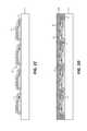
- a semiconductor structurecan include a plurality of completed semiconductor devices and each of the plurality of completed semiconductor devices can have an individual tether and an individual anchor physically connecting the completed semiconductor devices to other structures or layers in the semiconductor structure, such as a bonding or capping layer(s).
- at least two of a plurality of completed semiconductor deviceshave a common structure providing tethers for each completed semiconductor device or a common anchor structure to which the tethers are physically connected.
- At least two of a plurality of completed semiconductor devicescan have a common anchor structure that is a ridge of material that contacts two or more completed semiconductor devices.
- a removal layer such as an ablation or etch-stop layercan be provided between semiconductor layer(s) and a support substrate.
- a destination substrateis provided and a completed semiconductor device is micro-transfer printed from a handle substrate to the destination substrate.
- a support substrateis removed by one or more of laser liftoff, ablation, laser ablation, etching, and grinding.
- a support substratecan be transparent to electromagnetic radiation and removing the support substrate can expose a semiconductor layer to electromagnetic radiation through the support substrate to decompose a portion of the semiconductor layer(s) or completed semiconductor device and form a shock wave in the semiconductor structure.
- an ablation layeris provided between a support substrate and semiconductor layer(s) and the support substrate is removed by exposing the ablation layer to electromagnetic radiation through the support substrate to decompose a portion of the ablation layer and form a shock wave in a completed semiconductor structure.
- a capping layercan have a thickness, layers, structure, and material sufficient to disperse, deflect, reflect, or absorb a shock wave produced by laser ablation of at least a portion of a ablation layer, a portion of a semiconductor layer, or a portion of a completed semiconductor device.
- a support substrateis a semiconductor substrate and disposing one or more semiconductor layers in, on, or over the support substrate includes doping (e.g., implanting) a portion or layer of the semiconductor substrate.
- disposing one or more semiconductor layers in, on, or over a support substratecan include growing the one or more semiconductor layers on the support substrate or growing the one or more semiconductor layers on a growth layer or semiconductor seed layer on the support substrate.
- a semiconductor structure suitable for micro-transfer printingcan include: a handle substrate; a conformable, cured bonding layer disposed in contact with the handle substrate; an optional capping layer disposed in contact with the bonding layer; a patterned release layer disposed in contact with the cured bonding layer or the capping layer, wherein the patterned release layer has an entry path; and a completed semiconductor device disposed on or over the patterned release layer and attached to an anchor disposed on the handle substrate with at least one tether.
- a support substratecan be one or more of sapphire, quartz, silicon, GaAs, GaN, InP, SiC, GaP, GaSb, AN, and MgO.
- a completed semiconductor devicecan include one or more of a semiconductor material, a compound semiconductor material, GaN, Si, InP, SiGe, and GaAs.
- a patterned release layerincludes one or more of germanium, Si, TiW, Al, Ti, a lift-off resist, and a polymer.
- a support substratecan be a growth substrate, have a semiconductor seed layer, or have a semiconductor layer.
- a cured bonding layercan be a cured resin, SU-8, epoxy, a metal layer, a metal alloy layer, a solder layer, or a layer of AuSn.
- a completed semiconductor deviceis exposed and/or an entry path is exposed.
- a removal layeris only a portion of the completed semiconductor device.
- a removal layeris in contact with a completed semiconductor device and is disposed on or over, or is a part of, a support substrate.
- a support substratecan be in contact with a removal layer or with a completed semiconductor device.
- a capping layercan include a plurality of layers.
- a completed semiconductor deviceincludes a semiconductor structure with at least two electrical contacts to the completed semiconductor device that are in different planes.
- a completed semiconductor devicecan include an electrically separate electrode electrically connected to each of the electrical contacts and exposed portions of the electrodes are in a common plane. Exposed portions of the electrodes are used to make electrical contact to external electrical conductors.
- a destination substrate onto which the completed semiconductor device is micro-transfer printedcan have a non-planar surface with a topography that corresponds to a non-planar semiconductor structure surface to facilitate electrical connections between the completed semiconductor device and electrical contact pads on the destination substrate.
- an electrical contactis disposed on the side of a completed semiconductor device adjacent to a support substrate or on the side of the completed semiconductor device adjacent to a patterned release layer.
- Each electrical contactcan include or be connected to a connection post.
- an electrodeis electrically connected to each electrical contact and a connection post is electrically connected to each electrode or the electrode includes or forms a connection post.
- a connection postcan have a first surface adjacent to a surface of the completed semiconductor device and a second opposing surface farther away from the completed semiconductor device than the first surface. The second opposing surface can have a smaller area than the first surface.
- connection postcan have a height that is greater than a dimension of the first surface, the connection post can have a height that is greater than a dimension of the second opposing surface, or the connection post can have a height that is greater than a width of the connection post.
- the present inventionis directed to a method of making a semiconductor structure suitable for transfer printing (e.g., micro-transfer printing), comprising: providing a support substrate; forming a completed semiconductor device disposed in, on, or over the support substrate; forming a patterned release layer on or over the completed semiconductor device; providing a capping layer on the patterned release layer; providing a handle substrate; disposing a conformable and curable bonding layer on the capping layer or on the handle substrate; disposing the handle substrate and the capping layer in contact with the bonding layer; curing the bonding layer to bond the handle substrate to the capping layer; and removing the support substrate to expose the completed semiconductor device (e.g., thereby exposing the completed semiconductor device).
- transfer printinge.g., micro-transfer printing
- the methodcomprises forming an entry path to expose a portion of the patterned release layer. In certain embodiments, the method comprises removing at least a portion of the patterned release layer to form a gap between at least a portion of the completed semiconductor device and at least a portion of the bonding layer; and forming a tether physically connecting the completed semiconductor device to an anchor disposed on the handle substrate (e.g., wherein the anchor is a portion of the handle substrate or a layer disposed on the handle substrate, such as, for example, the bonding layer, the capping layer, or a dielectric layer).
- the methodcomprises: providing a destination substrate; and micro-transfer printing the completed semiconductor device from the handle substrate to the destination substrate.
- the support substrateis transparent to electromagnetic radiation and the method comprises: exposing the semiconductor layer to electromagnetic radiation through the support substrate to decompose a portion of the completed semiconductor device and form a shock wave in the semiconductor structure, wherein the capping layer disperses, reflects, deflects, or absorbs the shock wave.
- the support substrateis transparent to electromagnetic energy, and the method comprises: providing an ablation layer between the support substrate and the completed semiconductor device; and exposing the ablation layer to electromagnetic radiation through the support substrate to decompose a portion of the ablation layer and form a shock wave in the completed semiconductor structure, wherein the capping layer disperses, reflects, deflects, or absorbs the shock wave.
- removing the support substratecomprises one or more of laser liftoff, ablation, laser ablation, etching, and grinding.
- the methodcomprises providing an ablation or etch-stop layer between the completed semiconductor device and the support substrate.
- removing the support substrate to expose the completed semiconductor devicecomprises removing a removal layer (e.g., an ablation layer or an etch-stop layer) (e.g., thereby exposing the completed semiconductor layer).
- the support substrateis a semiconductor substrate and forming the completed semiconductor device comprises: doping a portion or layer of the semiconductor substrate. In certain embodiments, forming the completed semiconductor device comprises: disposing one or more semiconductor layers in, on, or over the support substrate. In certain embodiments, forming the completed semiconductor device comprises growing the one or more semiconductor layers on the support substrate or on a growth layer on the support substrate. In certain embodiments, forming the completed semiconductor device comprises: processing the one or more semiconductor layers.
- the present inventionis directed to a method of making a semiconductor structure suitable for transfer printing (e.g., micro-transfer printing), comprising: providing a support substrate; forming a completed semiconductor device disposed in, on, or over the support substrate; forming a patterned release layer on or over the completed semiconductor device; providing a handle substrate; disposing a conformable and curable bonding layer on the patterned release layer or on the handle substrate; disposing the handle substrate and the patterned release layer in contact with the bonding layer; curing the bonding layer to bond the handle substrate to the patterned release layer; and removing the support substrate to expose the completed semiconductor device (e.g., thereby exposing the completed semiconductor device).
- transfer printinge.g., micro-transfer printing
- the methodcomprises disposing the conformable and curable bonding layer on the patterned release layer, wherein disposing the conformable and curable bonding layer on the patterned release layer comprises disposing the conformable and curable bonding layer on at least one of (i) a portion of a dielectric layer disposed on the completed semiconductor structure and (ii) a portion of the completed semiconductor structure.
- the methodcomprises removing at least a portion of the patterned release layer to form a gap between at least a portion of the completed semiconductor device and at least a portion of the bonding layer; and forming a tether physically connecting the completed semiconductor device to an anchor disposed on the handle substrate (e.g., wherein the anchor is a portion of the handle substrate or a layer disposed on the handle substrate, such as, for example, the bonding layer or a dielectric layer).
- the methodcomprises providing a destination substrate; and micro-transfer printing the completed semiconductor device from the handle substrate to the destination substrate.
- removing the support substratecomprises one or more of laser liftoff, ablation, laser ablation, etching, and grinding.
- the methodcomprises providing an ablation or etch-stop layer between the completed semiconductor device and the support substrate.
- removing the support substrate to expose the completed semiconductor devicecomprises removing a removal layer (e.g., an ablation layer or an etch-stop layer) (e.g., thereby exposing the completed semiconductor device).
- the support substrateis a semiconductor substrate and forming the completed semiconductor device comprises: doping a portion or layer of the semiconductor substrate. In certain embodiments, forming the completed semiconductor device comprises: disposing one or more semiconductor layers in, on, or over the support substrate. In certain embodiments, forming the completed semiconductor device comprises: growing the one or more semiconductor layers on the support substrate or on a growth layer on the support substrate. In certain embodiments, forming the completed semiconductor device comprises: processing the one or more semiconductor layers.
- the present inventionis directed to a semiconductor structure suitable for transfer printing (e.g., micro-transfer printing), comprising: a handle substrate; a cured bonding layer disposed in contact with the handle substrate; a patterned release layer disposed in contact with the cured bonding layer; and a completed semiconductor device disposed on or over the patterned release layer and attached to an anchor disposed on the handle (e.g., wherein the anchor is a portion of the handle substrate or a layer disposed on the handle substrate, such as, for example, the bonding layer or a dielectric layer) substrate with at least one tether.
- a semiconductor structure suitable for transfer printinge.g., micro-transfer printing
- At least one of the completed semiconductor device and a portion of the patterned release layeris exposed.
- the completed semiconductor devicecomprises a semiconductor structure comprising at least two electrical contacts to the completed semiconductor device that are in different planes.
- the completed semiconductor devicecomprises an electrically separate electrode electrically connected to each of the electrical contacts, wherein exposed portions of the electrodes are in a common plane.
- the semiconductor structurecomprises a destination substrate having a non-planar surface that corresponds to a non-planar surface of the completed semiconductor structure.
- the support substratecomprises one or more of sapphire, quartz, silicon, GaAs, GaN, InP, SiC, GaP, GaSb, AlN, and MgO.
- the completed semiconductor devicecomprises one or more of a semiconductor material, a compound semiconductor material, GaN, Si, InP, SiGe, and GaAs.
- the patterned release layercomprises one or more of germanium, Si, TiW, Al, Ti, a lift-off resist, and a polymer.
- the semiconductor structurecomprises one or more electrical contacts on a side of the completed semiconductor device adjacent to the patterned release layer or one or more electrical contacts on a side of the completed semiconductor device opposite the side of the completed semiconductor device adjacent to the patterned release layer (e.g., a side adjacent to a support substrate in the semiconductor structure).
- each electrical contactcomprises a connection post or (ii) the semiconductor structure comprises an electrode electrically connected to each electrical contact and a connection post electrically connected to each electrode (e.g., wherein the electrode comprises or forms a connection post).
- each connection postis tapered (e.g., has a first surface adjacent to a surface of the completed semiconductor device and a second opposing surface and the second opposing surface has a smaller area than an area of the first surface).
- each connection posthas a height to width aspect ratio of greater than 1:1.
- the at least one tetheris disposed between the completed semiconductor device and the handle substrate.
- the support substrateis a growth substrate.
- the support substratecomprises a semiconductor layer or a semiconductor seed layer.
- the cured bonding layercomprises at least one of a cured resin, an epoxy, a metal layer, a metal alloy layer, a solder layer, and a layer of AuSn.
- the present inventionis directed to a semiconductor structure suitable for transfer printing (e.g., micro-transfer printing), comprising: a handle substrate; a cured bonding layer disposed in contact with the handle substrate; a capping layer disposed in contact with the bonding layer; a patterned release layer disposed in contact with the capping layer; and a completed semiconductor device disposed on or over the patterned release layer and attached to an anchor disposed on the handle substrate with at least one tether (e.g., wherein the anchor is a portion of the handle substrate or a layer disposed on the handle substrate, such as, for example, the bonding layer, the capping layer, or a dielectric layer).
- a semiconductor structure suitable for transfer printinge.g., micro-transfer printing
- a semiconductor structure suitable for transfer printingcomprising: a handle substrate; a cured bonding layer disposed in contact with the handle substrate; a capping layer disposed in contact with the bonding layer; a patterned release layer disposed in contact with the capping layer; and
- the completed semiconductor devicecomprises a semiconductor structure comprising at least two electrical contacts to the completed semiconductor device that are in different planes.
- the completed semiconductor devicecomprises an electrically separate electrode electrically connected to each of the electrical contacts, wherein exposed portions of the electrodes are in a common plane.
- the support substratecomprises one or more of sapphire, quartz, silicon, GaAs, GaN, InP, SiC, GaP, GaSb, AlN, and MgO.
- the completed semiconductor devicecomprises one or more of a semiconductor material, a compound semiconductor material, GaN, Si, InP, SiGe, and GaAs.
- the patterned release layercomprises one or more of germanium, Si, TiW, Al, Ti, a lift-off resist, or a polymer.
- the semiconductor structurecomprises one or more electrical contacts on a side of the completed semiconductor device adjacent to the patterned release layer or one or more electrical contacts on a side of the completed semiconductor device opposite the side of the completed semiconductor device adjacent to the patterned release layer (e.g., a side adjacent to a support substrate in the semiconductor structure).
- a surface of the at least one tetheris disposed in a common plane a surface of the completed semiconductor device.
- the semiconductor structurecomprises a plurality of completed semiconductor devices, wherein each of the plurality of completed semiconductor devices comprises an individual tether connected to a unique anchor.
- the semiconductor structurecomprises a plurality of completed semiconductor devices, wherein at least two of the plurality of completed semiconductor devices are physically connected by respective tethers to a common anchor structure.
- surfaces at opposing edges of the completed semiconductor deviceare in a common plane, wherein a first electrical contact is located at the bottom of a well, pit, or depression in the completed semiconductor device and is electrically connected to a first electrode, wherein a second electrical contact electrically separate from the first electrical contact is electrically connected to a second electrode, and wherein the first electrode has a greater height than the height of the second electrode so that exposed portions of the first and second electrodes are in a common plane.
- FIGS. 2A-2Kare successive cross sections illustrating sequential steps in another exemplary method and (ii) another semiconductor structure, according to illustrative embodiments of the present invention
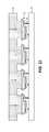
- FIGS. 3A-3Bare successive cross sections illustrating sequential steps in an exemplary method, according to illustrative embodiments of the present invention.
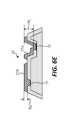
- FIG. 4is a cross section illustrating a semiconductor device with an ablation layer, according to illustrative embodiments of the present invention.
- FIG. 5is a plan view illustrating anchor, an anchor structure, and semiconductor devices on a source substrate, according to illustrative embodiments of the present invention
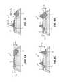
- FIG. 7is a cross section illustrating micro-transfer-printed completed semiconductor devices with a connection post structure and a destination substrate in accordance with an embodiment of the present invention
- FIG. 8is a cross section illustrating a completed semiconductor device with a connection post structure and a destination substrate, according to illustrative embodiments of the present invention.
- FIG. 9is a flow chart illustrating exemplary methods, according to illustrative embodiments of the present invention.
- the present inventionprovides, inter alia, structures and methods to enable micro-transfer printing from devices formed on a sapphire substrate.
- the present inventionalso provides, inter alia, structures and methods to enable micro-transfer printing of flipped integrated circuits adhered to a handle substrate.
- photolithographic processing stepsthat would otherwise disable or destroy release layers and structures needed for transfer printing (e.g., micro-transfer printing) are performed before the construction of the release layer.
- a release layercan be etched and completed semiconductor devices can be transfer printed (e.g., micro-transfer printed) without exposing the completed semiconductor device or release layer to destructive photolithographic process steps.
- Completed semiconductor devicesare otherwise functional devices that do not necessarily include the electrical conductors necessary for providing electrical power to the completed semiconductor devices.
- an exemplary method of making a semiconductor structure 99 ( FIGS. 1E-1G ) suitable for micro-transfer printingincludes providing a support substrate 10 in step 100 and forming a completed semiconductor device 22 (i.e., in this exemplary method by disposing one or more semiconductor layers 20 in, on, or over the support substrate 10 ) in step 105 (as shown in FIG. 1A ).
- a completed semiconductor device 22can be formed by disposing one or more layers or substructures on a support substrate 10 .
- the one or more semiconductor layers 20can optionally be processed in step 110 to make completed semiconductor devices 22 (as shown in FIG. 1B ).
- the processingcan include, for example, patterning materials, adding other materials, and forming structures.
- a support substrate 10comprises at least one of glass, plastic, semiconductor, compound semiconductor, sapphire (e.g., aluminum oxide or Al 2 O 3 ), ceramic, quartz, silicon, GaAs, GaN, InP, SiC, GaP, GaSb, AlN, an MgO.
- a support substrate 10can be a different other substrate suitable for photolithographic processing.
- a support substrate 10can be substantially transparent, for example 50%, 70%, or 90% transparent to at least one of visible, UV, and IR electromagnetic radiation.
- a support substrate 10can include multiple layers, can include one or more semiconductor layers 20 , can be a growth substrate, or can include a growth or semiconductor seed layer on which the one or more semiconductor layers 20 are formed or disposed.
- a support substrate 10can be crystalline or have a crystalline layer.
- One or more semiconductor layers 20can be organic or inorganic, can be crystalline, can be a semiconductor, can be a compound semiconductor, can be doped (e.g., implanted), for example with p or n doping to provide desired electrical structures and functions, or any combination thereof.
- a semiconductor layer in the one or more semiconductor layer 20 in a completed semiconductor device 22can include one or more of GaN, Si, InP, SiGe, and GaAs.
- Each of the one or more semiconductor layers 20can be formed or disposed in step 105 using photolithographic processes including, for example, evaporation or sputtering.
- a support substrate 10is a semiconductor substrate and disposing one or more semiconductor layers 20 in, on, or over the support substrate 10 (step 105 ) includes doping (e.g., implanting) a portion or layer of a semiconductor substrate (e.g., support substrate 10 ) to form the one or more semiconductor layers 20 .
- disposing one or more semiconductor layers 20 in, on, or over a support substrate 10includes growing the one or more semiconductor layers 20 on the support substrate 10 or on a growth layer on the support substrate 10 , for example using epitaxial techniques.
- the support substrate 10can be, but is not necessarily, a crystalline semiconductor substrate or sapphire substrate.
- a support substrate 10is a sapphire substrate.
- a support substrate 10is a crystalline semiconductor substrate.
- the one or more semiconductor layers 20can be optionally processed in step 110 using photolithographic methods, including, for example, evaporation, sputtering, CVD, annealing, or masking using photoresist, exposure to patterned radiation, and etching.
- One or more semiconductor layers 20can be patterned and structured and additional layers and structures can be formed on or in the one or more semiconductor layers 20 , for example, patterned dielectric layers 24 or patterned conductors such as electrical contacts 25 formed, as shown in FIG. 1B .
- Electrical contacts 25can be a metalized portion of one or more of the semiconductor layers 20 or a patterned metal layer over one or more of the semiconductor layers 20 (e.g., with Ag, Al, Ni, Ti, Au, Pd, W, or metal alloys) or simply a designated portion of one or more of the semiconductor layers 20 (e.g., designated for forming electrical connections) and are, in any case, portions of the completed semiconductor device 22 to which electrical connections can be made and power and signals provided to operate the completed semiconductor device 22 .
- a completed semiconductor device 22is formed of one or more semiconductor layers 20 and any additional layers and structures necessary to function as intended.
- a completed semiconductor device 22comprises a dielectric layer 24 (e.g., a patterned dielectric layer).
- a plurality of completed semiconductor devices 22can be disposed on the support substrate 10 (as shown in FIG. 1B , for example).
- a completed semiconductor device 22includes all of the elements necessary to function but does not necessarily include electrical connections to external power or signal sources that enable device operation, or necessarily include protective layers.
- FIG. 1Billustrates a horizontal LED structure with shaped, structured, and doped (e.g., implanted) semiconductor layers 20 , a patterned dielectric layer 24 that defines vias, and two electrical contacts 25 through which electrical power can be transmitted to the semiconductor layers 20 to cause the completed semiconductor device 22 to operate.
- the completed semiconductor device 22results all of the photolithographic steps, such as processing and patterning steps, to make the completed semiconductor device 22 functional.
- a functional completed semiconductor device 22is a device that provides a desired electronic, optical, thermal, mechanical, magnetic, electric field, photonic, or opto-electronic effect when provided with power but does not include the interconnections necessary to provide power or control signals, such as electrical power or control signals (e.g., from a controller).
- a patterned release layer 30is formed or disposed on or over the completed semiconductor device 22 and optionally at least partly in contact with the support substrate 10 (as shown) in step 115 .
- a patterned release layer 30does not contact a support substrate 10 .
- a patterned release layer 30can be formed or disposed using photolithographic methods and materials and can include germanium, Si, TiW, Al, Ti, a lift-off resist, or other polymers.
- a patterned release layer 30 materialcan etch in developer, is not photo-active, or can etch at a higher temperature than photo-active materials such as photo-resists (e.g., greater than 200° C., 300° C., or 400° C.).
- a patterned release layer 30forms a gap 32 or space, for example, after etching the patterned release layer 30 material.
- a gapcan be formed between a completed semiconductor device 22 and a bonding layer 40 after the patterned release layer 30 has been removed.
- a handle substrate 50is provided in step 125 , for example, a glass substrate or a plastic substrate.
- a conformable and curable bonding layer 40is disposed on the patterned release layer 30 (as shown in FIG. 1D ) or on the handle substrate 50 (or on an optional capping layer, discussed further subsequently with respect to FIG. 2C ) in step 130 .
- a conformable and curable bonding layer 40is disposed on a patterned release layer 30 , a portion may also be disposed on a support substrate 10 (as shown in FIG. 1D ).
- a conformable and curable bonding layer 40can have a substantially planar side 42 opposite a non-planar side 44 closer to a completed semiconductor device 22 .
- a handle substrate 50can be substantially transparent, for example 50%, 70%, or 90% transparent to at least one of visible, UV, and IR electromagnetic radiation.
- a bonding layer 40can be, for example, a curable resin, epoxy, SU-8, a metal layer, a metal alloy layer, a solder layer, or AuSn.
- the handle substrate 50is located in contact with the bonding layer 40 and bonded to the completed semiconductor devices 22 , for example, by curing the bonding layer 40 in step 135 (as shown in FIG. 1E ) by providing heat, by cooling, or by providing electromagnetic radiation (e.g., UV light) to the bonding layer 40 , for example through the handle substrate 50 .
- electromagnetic radiatione.g., UV light
- Curing a bonding layer 40can include forming a chemical reaction in a material of the bonding layer 40 or hardening the bonding layer 40 , or by facilitating a phase change from a liquid to a solid (as with a solder).
- a bonding layer 40can be cured by exposing the bonding layer 40 material to light or heat (for example if the bonding layer 40 is a UV-curable resin) or by exposing the bonding layer 40 to heat to melt a metal or metal alloy, disposing a structure in contact with the melted metal or metal alloy, and then cooling the metal.
- a metal or metal alloy bonding layer 40is deposited, heated to melt the metal bonding layer 40 to a liquid, a handle substrate 50 , a capping layer 60 , or a release layer 30 is brought into contact with the melted liquid metal bonding layer 40 , and the melted metal bonding layer 40 is cooled to a solid to adhere the bonding layer 40 to the handle substrate 50 , capping layer 60 , or release layer 30 .
- the support substrate 10is removed to expose the completed semiconductor device 22 and optionally expose a portion of the patterned release layer 30 to the local environment (as shown) in step 140 .
- removing a support substrate 10 to expose a completed semiconductor device 22comprises removing one or more additional layers (e.g., dielectric layers, spacing layers, adhesion layers, growth layers, or removal layers) disposed between the support substrate 10 and the completed semiconductor device 22 . If at least a portion of the patterned release layer 30 is not exposed, an entry path 34 is formed to expose a portion of the patterned release layer 30 (as shown in FIG. 2H , and discussed further subsequently) in step 145 .
- a support substrate 10can be removed, for example, by one or more of laser liftoff, ablation, laser ablation, etching, and grinding. In some embodiments, both grinding and another removal technique, such as etching, are used.
- the release layer 30is removed in step 150 , for example by etching with H 2 O 2 , XeF 2 , HCl, HF, trimethylammonium hydroxide (TMAH), or oxygen plasma.
- etchantcan depend on the material of the patterned release layer 30 .
- H 2 O 2 or XeF 2can be used with a Ge, W, or TiW release layer 30
- XeF 2can be used with a Si release layer 30
- HCl acid mixturescan be used with an Al or Ti release layer 30
- TMAH-based developerscan be used with a lift-off resist release layer 30
- oxygen plasmacan be used with polyimide, epoxy, PMMA, or other organic release layers 30 .
- an etchantis benign to materials found in or exposed on the surface of a completed semiconductor device 22 , a bonding layer 40 , or both. After etching, a patterned release layer 30 forms a gap 32 or space between a completed semiconductor devices 22 and a bonding layer 40 .
- the release layer 30is patterned so that a tether 36 physically connects the completed semiconductor devices 22 to an anchor 38 portion of the bonding layer 40 and holds the completed semiconductor devices 22 in place.
- an anchor 38can be a portion of a handle substrate 50 or a layer disposed on the handle substrate (e.g., between the handle substrate 50 and a completed semiconductor device 22 ), such as, for example, a bonding layer, a capping layer (not shown in FIG. 1G ), or a dielectric layer 24 .
- the tether 36is an interface to a post forming the anchor 38 .
- the anchor 38is a portion of the bonding layer 40 .
- the interfacecan, for example, provide a weak adhesion, for example adhesion provided by van der Waal's forces, and can be an interface with or of metal such as gold, tin, or a solder disposed on a portion of the completed semiconductor device 22 .
- the completed semiconductor devices 22can be micro-transfer printed in step 160 , as illustrated in FIG. 1H (shown with an inverted orientation from FIG. 1G ), with a stamp 80 (e.g., an elastomeric stamp, for example comprising PDMS) comprising stamp pillars 82 that press against and adhere to the completed semiconductor devices 22 and is then separated from the handle substrate 50 (as shown in FIG. 1I ).
- a stamp 80e.g., an elastomeric stamp, for example comprising PDMS
- stamp pillars 82that press against and adhere to the completed semiconductor devices 22 and is then separated from the handle substrate 50 (as shown in FIG. 1I ).
- the completed semiconductor devices 22are brought into aligned contact with a destination substrate 90 (the destination substrate 90 is provided in step 155 ) and adhered to the destination substrate 90 .
- electrical contacts 25 of a completed semiconductor device 22are electrically connected to contact pads 92 formed or disposed on a destination substrate 90 .
- Contact pads 92can be electrically connected to an electrical circuit, for example through electrical conductors on the destination substrate 90 (not shown), to provide electrical power and signals to a completed semiconductor device 22 .
- an alternative exemplary method of making a semiconductor structure 99 (as shown in FIG. 2G-2I ) suitable for micro-transfer printingincludes additional steps and elements as compared to the process and semiconductor structure 99 described with respect to FIGS. 1A-1J .
- a support substrate 10is provided in step 100 that includes a removal layer 26 .
- a removal layer 26can be an ablation layer or an etch-stop layer and can be a layer of a support substrate 10 or a layer disposed on the support substrate 10 .
- a removal layer 26can be patterned.
- Ablation and etch-stop layerscan include one or more of (i) SiO x or SiN x deposited by, for example, plasma-enhanced chemical vapor deposition (PECVD) and (ii) organic layers with or without particles. Additional layers, such as buffer layers (e.g., C—GaN, AlGaN, or doped GaN) or one or more semiconductor growth layers can be provided as well.
- PECVDplasma-enhanced chemical vapor deposition
- Additional layerssuch as buffer layers (e.g., C—GaN, AlGaN, or doped GaN) or one or more semiconductor growth layers can be provided as well.
- a completed semiconductor device 22(i.e., in this exemplary method by disposing one or more semiconductor layers 20 in, on, or over the support substrate 10 ) in step 105 (as shown in FIG. 2A ).
- a completed semiconductor device 22can be formed by disposing one or more layers or substructures on a support substrate 10 .
- the one or more semiconductor layers 20can be processed in step 110 to form the completed semiconductor device 22 (as shown in FIG. 2B ) over or in contact with the removal layer 26 , as described previously.
- a dielectric layer 24 of a completed semiconductor device 22is patterned to extend beyond the completed semiconductor device 22 (e.g., for use in forming anchors 38 and/or tethers 36 ).
- a patterned release layer 30is formed or disposed on or over the completed semiconductor device 22 in step 115 .
- a patterned release layer 30can be at least partially in contact with a dielectric layer 24 rather than a support substrate 10 (in contrast to what is shown in FIG. 1C ).
- a patterned release layer 30is at least partially in contact with a removal layer 26 .
- a capping layer 60is disposed on the release layer 30 in step 120 .
- a capping layer 60is optional and is not present in some embodiments.
- a capping layer 60can be deposited using photolithographic methods such as evaporation, sputtering, plating, atomic layer deposition (ALD), or coating and can include organic or inorganic materials such as SiN x , SiO x , copper, nickel, or other materials.
- a capping layer 60can be non-planar, patterned, structured or shaped, can stiffen the semiconductor structure 99 , or can include multiple layers of different materials that can be selected and formed to control acoustic or mechanical vibrations.
- a handle substrate 50is provided in step 125 and a conformable and curable bonding layer 40 is disposed on the optional capping layer 60 (as shown) or on the handle substrate 50 (not shown), in step 130 .
- a conformable and curable bonding layer 40can have a substantially planar side 42 opposite a non-planar side 44 closer to a completed semiconductor device 22 .
- a handle substrate 50can be substantially transparent, for example 50%, 70%, or 90% transparent to at least one of visible, UV, and IR electromagnetic radiation.
- a bonding layer 40can be, for example, a curable resin, epoxy, SU-8, a metal layer, a metal alloy layer, a solder layer, or AuSn.
- the handle substrate 50is located in contact with the bonding layer 40 and bonded to the completed semiconductor devices 22 by, for example, curing the curable bonding layer 40 in step 135 (as shown in FIG. 2E ), for example by providing time, heat, cooling, or electromagnetic radiation to the bonding layer 40 , for example through the handle substrate 50 .
- the material of the capping layer 60 provided in step 120can be selected to prevent unwanted interactions between the release layer 30 etching chemistry and the bonding layer 40 .
- an etchant that is suitable for etching the release layer 30might also undesirably etch the bonding layer 40 , resulting in compromise a micro-transfer printing process for the completed semiconductor device 22 if not for the presence of the optional capping layer 60 .
- a removal layer 26is exposed to electromagnetic radiation 70 (for example from a laser) through a support substrate 10 (i.e., wherein the support substrate 10 is at least partially transparent to the electromagnetic radiation 70 ) to decompose at least a portion of the removal layer 26 , as illustrated with shading in the removal layer 26 in FIG. 2F .
- a removal layer 26for example an ablation layer, absorbs is heated by the electromagnetic radiation 70 and evaporates or sublimates to a gas or plasma that forcefully dissociates a support substrate 10 from the removal layer 26 .
- Ablation layerscan be selected to complement the support substrate 10 or layer materials formed on or in the support substrate 10 .
- An ablation layercan be the same material as is found in the semiconductor layers 20 , for example GaN.
- GaNcan serve as an ablation layer for sapphire or AlN support substrates 10 .
- GaNAs or InGaNAsSbcan be included in ablation layers or materials grown on GaAs substrates.
- InGaAs, InGaAsP, AlInGaAs, or AlInGaAsPcan be included in ablation layers or materials grown on InP substrates.
- black chromiumcan be an ablation layer.
- Ablation layerscan include organic materials such as vaporizable polymer or materials that incorporate light-absorbing particles such as carbon black or oxidized chromium and that can absorb electromagnetic radiation, facilitate ablation layer heating, and ablate of the layer.
- laser ablationtransfers momentum to a surface and, in some embodiments of the present invention, can form a shock wave (an acoustic or mechanical pulse of high pressure) that passes into and through a completed semiconductor device 22 (or completed semiconductor devices 22 , if multiple are present) and can damage the completed semiconductor device 22 .
- a capping layer 60(and, in some embodiments, to some extent, a bonding layer 40 and/or a release layer 30 ) can dissipate, disperse, deflect, reflect, or absorb the shock wave and prevent or mitigate damage to a completed semiconductor device 22 .
- the layers, materials, and structure of a capping layer 60can be specifically designed to prevent or mitigate damage to a completed semiconductor device 22 .
- a release layer 30comprises germanium, which has a large acoustic impedance and can therefore effectively reflect or redirect at least a portion of a shock wave.
- laser ablationcan be used to remove a support substrate 10 from a semiconductor structure 99 used in a flip-chip micro-transfer printing process, as shown in FIG. 2G .
- removal of a support substrate 10exposes the release layer 30 (e.g., as shown in FIG. 1F ).
- a release layer 30is not exposed in step 140 .
- a release layercan be covered by a dielectric layer 24 .
- a dielectric layer 24is patterned to expose a portion of a release layer 30 , as shown in FIG. 1F .
- the patterned dielectric layer 24is not exposed when the support substrate 10 is removed.
- an entry path 34is formed to expose a portion of the patterned release layer 30 .
- An entry path 34can be formed, for example, by pattern-wise etching a dielectric layer 24 (or other layer disposed over a patterned release layer 30 ).
- the step of forming an entry path 34is the same step as removing a support substrate 10 . That is, in some embodiments, removing a support substrate 10 forms an entry path 34 by exposing a portion of a release layer 30 .
- an “exposed” layer or elementis one that is exposed to the local environment, can be exposed to a processing material such as a chemical etchant, can have materials deposited thereon, or any combination thereof.
- a layere.g., a support substrate 10
- an elemente.g., a completed semiconductor device 22
- one or more other layerse.g., dielectric layers or a remaining portion of a removal layer 26
- a support substrate 10is removed to expose a completed semiconductor device 22 and subsequently a sacrificial dielectric layer and/or remaining portion of a removal layer 26 disposed on the completed semiconductor device 22 is removed thereby providing an exposed completed semiconductor device 22 .
- the release layer 30is removed in step 150 , for example by etching as described above with respect to FIG. 1G .
- the release layer 30forms a gap 32 or space between the completed semiconductor devices 22 and the capping layer 60 .
- a release layer 30 and entry paths 34are patterned so that one or more tethers 36 physically connect a completed semiconductor devices 22 to an anchor 38 disposed on the handle substrate 50 (e.g., wherein the anchor 38 is a portion of a dielectric layer 24 , a capping layer 60 , a handle substrate 50 , or another layer disposed on the handle substrate 50 ) holds the completed semiconductor device 22 in place.
- the completed semiconductor devices 22are physically connected to the anchors 38 , where are portions of the dielectric layer 24 .
- a plurality of tethers 36physically connect each completed semiconductor device 22 to one or more anchors 38 (e.g., a plurality of anchors 38 ).
- a plurality of anchors 38 formed from portions of a bonding layerare physically connected to each completed semiconductor device 22 .
- each tether 36is a portion of the dielectric layer 24 .
- a tether 36can be disposed in a common plane with an entry path 34 or an entry path 34 can extend through or around a tether 36 .
- a tether 36can be separated or broken (e.g., fractured) if pressure is applied to a completed semiconductor device 22 .
- a tether 36is separated during transfer printing (e.g., by overcoming van der Waals forces that adhere a completed semiconductor device 22 to an anchor 38 ).
- a tether 36is fractured during transfer printing (e.g., wherein pressure fractures the dielectric material that the tether 36 is made from).
- the completed semiconductor devices 22can be micro-transfer printed in step 160 , as illustrated in FIG. 2J (shown with an inverted orientation from FIG. 2I ), with a stamp 80 (e.g., an elastomeric stamp, for example comprising PDMS) comprising stamp pillars 82 that press against and adhere to the completed semiconductor devices 22 and is then separated from the handle substrate 50 (as shown in FIG. 2K ).
- the completed semiconductor devices 22are brought into aligned contact with a destination substrate 90 and micro-transfer printed to the destination substrate 90 , as shown and described with respect to FIG. 1J .
- semiconductor layer(s) 20are formed in a support substrate 10 , for example by doping (e.g., implanting) the support substrate 10 to form a layer on or at a surface (e.g., within the surface) of the support substrate 10 in step 105 that is the semiconductor layer(s) 20 .
- the semiconductor layer(s) 20can be processed in step 110 to form the completed semiconductor devices 22 (as shown in FIG. 3B ).
- forming semiconductor layer(s) 20 in step 105can include forming a layer on the support substrate 10 (as shown in FIGS. 1A, 2A ) or forming a layer in the support substrate 10 (as shown in FIG. 3B ).
- a removal layer 26is a portion of a completed semiconductor devices 22 and possibly other layers or a portion of a support substrate 10 (in which case the removal layer 26 includes a portion or layer of the support substrate 10 ).
- ablationcan remove the portion of the structure indicated with the heavy dashed rectangle.
- removing a support substrate 10comprises exposing semiconductor layer(s) 20 or completed semiconductor device 22 to electromagnetic radiation 70 through the support substrate 10 to decompose a portion of the semiconductor layer(s) 20 or the completed semiconductor device 22 and form a shock wave in a semiconductor structure 99 .
- a capping layer 60if present, can disperse, reflect, deflect, or absorb the shock wave.
- each completed semiconductor device 22has at least one individual broken (e.g., fractured) tether 36 as a consequence of micro-transfer printing.
- a broken tether 36can be a fractured structure, as in FIG. 2K .
- a separated tether 36can be an interface formed between two elements for which one element is removed, as in FIG. 1I .
- two or more tethers 36can be part of a common structure and be physically connected to a common anchor 38 .
- Anchors 38can be any portion of a semiconductor structure 99 that is not the completed semiconductor device 22 , for example a bonding layer 40 (as shown in FIG. 1G ), a dielectric layer 24 (as shown in FIG. 2I ), or a capping layer 60 .
- each anchor structure 39comprises three anchors 38 physically connected to the tethers 36 of three corresponding completed semiconductor devices 22 .
- an anchor structure 39comprises a plurality of anchors 38 (e.g., two or more or three or more anchors).
- a completed semiconductor device 22has a semiconductor structure with a planar surface adjacent to a patterned release layer 30 opposite a support substrate 10 so that electrical contacts 25 of the completed semiconductor device are in a common plane.
- This arrangementfacilitates electrical connection between the electrical contacts 25 and contact pads 92 on a destination substrate 90 .
- contact pads 92are likewise in a common plane on a surface of a destination substrate 90 , so that electrical contacts 25 in a common plane can both contact each contact pad 92 at the same time.
- a completed semiconductor device 22has a semiconductor structure with a non-planar surface adjacent to a patterned release layer 30 and opposite a support substrate 10 so that electrical contacts 25 are not in a common plane.
- itcan be necessary to adjust the structure or arrangement of the completed semiconductor device 22 or destination substrate 90 in order to form an electrical connection between the completed semiconductor device 22 and contact pads 92 on the destination substrate 90 when the completed semiconductor device 22 is transfer printed (e.g., micro-transfer printed) to the destination substrate 90 .
- a destination substrate 90has a non-planar surface with a topography that corresponds to a non-planar completed semiconductor device 22 surface. Accordingly, contact pads 92 (which provide at least a portion of the surface topography of a destination substrate 90 ) can have different heights that correspond to different locations of a non-planar completed semiconductor device 22 surface, in particular the different heights of the electrical contacts 25 of the completed semiconductor structures 22 over the destination substrate 90 , so that the contact pads 92 can readily make electrical connections with the electrical contacts 25 .
- the structure of the completed semiconductor devices 22is adapted with electrodes 27 and/or connection posts 29 .
- the completed semiconductor device 22includes a non-semiconductor structure (electrodes 27 ) electrically connected to the electrical contacts 25 on a side of the completed semiconductor device 22 opposite a support substrate 10 (not shown). Exposed portions of the electrodes 27 together form at least a portion of a common planar surface for the completed semiconductor device 22 and provide a surface for forming electrical connections.
- the electrodes 27are electrically connected to the electrical contacts 25 .
- Electrodes 27can be electrically conductive and made of metal or a conductive metal oxide and can be formed using conventional photolithographic methods, for example deposition [e.g., by chemical evaporation or physical vapor deposition (e.g., sputtering)] and patterning (e.g., by pattern-wise etching). Different thicknesses D L , D S can be achieved by multiple deposition and patterning steps.
- each electrical contact 25includes a connection post 29 .
- each electrical contact 25is electrically connected to an electrode 27 and a connection post 29 is electrically connected to each electrode 27 .
- an electrode 27includes or forms a connection post 29 .
- Connection posts 29can be electrically conductive and, for example, can be made of metal or a conductive metal oxide, as can the electrodes 27 and made using photolithographic methods and materials. Connection posts 29 can be made of the same material(s) as electrodes 27 and can be made in common steps or processes.
- a connection post 29 and corresponding electrode 27can be a common structure so that it can be considered that the connection post 29 includes the electrode 27 or the electrode 27 includes the connection post 29 .
- a connection post 29protrudes from a surface of a completed semiconductor device 22 and, when micro-transfer printed to a destination substrate 90 , can electrically connect to contact pads 92 on the destination substrate 90 .
- each connection post 29has a first surface adjacent to a surface of a completed semiconductor device 22 and a second opposing surface, wherein the second opposing surface has a smaller area or dimension D S than an area or dimension D L of the first surface. Therefore, for example, a connection post 29 can have a relatively sharp point and can form a spike, as shown in FIG. 6B .
- a connection post 29is cylindrical or has a constant rectangular cross section parallel to a surface of a completed semiconductor device 22 .
- a connection post 29can have a height that is greater than a dimension of a cross section perpendicular to the height (e.g., a dimension of a first surface or a dimension of the second opposing surface as described in reference to FIG. 6B ).
- a connection post 29has an elongated aspect ratio (e.g., a height to width aspect ratio greater than 1:1), a height that is greater than a width, and, optionally, a sharp point.
- connection posts 29have different heights or dimensions D S , D L so the different connection posts 29 have a common projection distance from the completed semiconductor device 22 .
- a plurality of connection posts 29 connected to a completed semiconductor device 22terminate in a common plane.
- the structures of FIGS. 6A and 6Bare combined to provide connection posts 29 that have a common projection distance from the completed semiconductor device 22 using different electrode 27 thicknesses D S , D L and common connection post 29 sizes.
- surfaces at opposing edges of the completed semiconductor device 22are in a common plane.
- a first one of the electrical contacts 25is located at the bottom of a well, pit, or depression in the completed semiconductor device 22 and is electrically connected to a first electrode 27 A.
- a second electrode 27 Bis in electrical contact with a second electrical contact 25 electrically separate from the first electrical contact 25 .
- the first electrode 27 Ahas a greater height D L than the height D S of the second electrode 27 B so that exposed portions of the first and second electrodes 27 A, 27 B together are in a common plane.
- the electrodes 27are in contact with and electrically connected to the electrical contacts 25 . Exposed portions of the first and second electrodes 27 A, 27 B are used to make electrical contact to external electrical conductors, such as contact pads 92 on a destination substrate 90 .
- Connection posts 29can be formed by repeated masking and deposition processes that build up three-dimensional structures.
- connection postscomprise multiple layers [e.g., made of different materials (e.g., wherein each layer is made of a material that has a different elastic modulus)].
- connection posts 29are made of one or more high elastic modulus metals, such as tungsten.
- a high elastic modulusis an elastic modulus sufficient for a connection post 29 made of the material to maintain its function and structure when pressed into a contact pad 92 disposed on a destination substrate 90 (e.g., electrical conductivity does not degrade due to deformation).
- Connection posts 29can be made by etching one or more layers of electrically conductive metal or metal oxide evaporated or sputtered on a side of semiconductor layers 20 opposite a support substrate 10 .
- Connection posts 29can have a variety of aspect ratios and typically have a peak area smaller than a base area.
- Connection posts 29can have a sharp point for embedding in or piercing contact pads 92 of a destination substrate 90 .
- Connection posts 29 that protrude from semiconductor devicesgenerally are discussed in U.S. Pat. No. 8,889,485, the disclosure of which is incorporated by reference herein in its entirety.
- completed semiconductor devices 22 in accordance with at least one of FIGS. 6B-6Dare illustrated with a destination substrate 90 onto which the completed semiconductor devices 22 are micro-transfer printed.
- the completed semiconductor devices 22 with connection posts 29 disposed thereonare micro-transfer printed onto the destination substrate 90 so that the connection posts 29 are aligned with and will pierce or otherwise electrically connect (e.g., by contacting) with the contact pads 92 of the destination substrate 90 .
- connection posts 29extend a common projection distance from the completed semiconductor device 22
- the top or bottom surfaces of the completed semiconductor devices 22are substantially parallel to the destination substrate 90 .
- the completed semiconductor devices 22(in accordance with FIG. 6B ) have top or bottom surfaces of the completed semiconductor devices 22 that are not substantially parallel to the destination substrate 90 because the connection posts 29 do not project a common distance from the completed semiconductor device 22 .
- the completed semiconductor devices 22can be successfully printed onto the destination substrate 90 and successfully make an electrical connection to the contact pads 92 .
- the completed semiconductor device 22is only slightly tilted or angled with respect to a surface of the destination substrate 90 after transfer printing.
- an exemplary semiconductor structure 99 suitable for micro-transfer printing made by a method disclosed hereinincludes a handle substrate 50 , a cured bonding layer 40 disposed in contact with the handle substrate 50 , an optional capping layer 60 disposed in contact with the bonding layer 40 , a patterned release layer 30 disposed in contact with the cured bonding layer 40 or the capping layer 60 (if present), an entry path 34 existing between the patterned release layer 30 and the local environment, and one or more completed semiconductor devices 22 disposed on or over the patterned release layer 30 and attached to an anchor 38 disposed on the handle substrate 50 with at least one tether 36 .
- a tether 36can be disposed between a completed semiconductor device 22 and a handle substrate 50 , for example, connecting the completed semiconductor device 22 to an anchor 38 post (e.g., wherein the tether 36 is a connection interface).
- a tether 36is disposed in a common plane with an entry path 34 .
- a completed semiconductor device 22can include one or more of a semiconductor material, a compound semiconductor material, GaN, Si, InP, SiGe, and GaAs.
- a patterned release layer 30can include one or more of germanium, Si, TiW, Al, Ti, a lift-off resist, and other polymers and, when etched or otherwise removed, forms a gap 32 or space (e.g., between a bonding layer 40 or a capping layer 60 and a completed semiconductor device 22 ).
- a curable bonding layer 40can comprise or consist essentially of a curable resin, a curable epoxy, a metal layer, a metal alloy layer, a solder layer, or a layer of AuSn, for example.
- a cured bonding layer 40can comprise or consist essentially of a cured resin, epoxy, a metal layer, a metal alloy layer, a solder layer, or a layer of AuSn, for example.
- a completed semiconductor device 22can be exposed or the entry path 34 can be exposed.
- a removal layer 26e.g., an ablation or etch-stop layer
- a semiconductor structure 99includes a removal layer 26 in contact with a completed semiconductor device 22 and is disposed on or over, or is a part of, a support substrate 10 (e.g., can be patterned).
- a support substrate 10is in contact with a completed semiconductor device 22 or a removal layer 26 (and the removal layer 26 is in contact with the completed semiconductor device 22 ).
- a support substrate 10can be one or more of sapphire, quartz, silicon, GaAs, GaN, InP, SiC, GaP, GaSb, AlN, and MgO.
- a support substrate 10can be a growth substrate, can have a semiconductor seed layer, or can be a semiconductor layer 20 .
- a support substrate 10can be removed by laser ablating a removal layer 26 disposed thereon or a portion of a completed semiconductor device 22 , causing a mechanical or acoustic shock wave to propagate through the completed semiconductor device 22 .
- a capping layer 60has a thickness and layer material shape or structure to disperse, deflect, reflect, or absorb the shock wave.
- a capping layer 60can have a plurality of layers and different materials.
- a completed semiconductor device 22includes a semiconductor structure with a non-planar surface adjacent to a patterned release layer 30 .
- a completed semiconductor device 22can include a non-semiconductor structure in contact with the non-planar semiconductor structure surface adjacent to a patterned release layer 30 so that the non-semiconductor structure forms at least a portion of a planar surface for the completed semiconductor device 22 .
- completed semiconductor devices 22can be micro-transfer printed from a handle substrate 50 to a destination substrate 90 .
- a destination substrate 90can have a non-planar surface with a topography that corresponds to a non-planar semiconductor structure surface of the completed semiconductor device 22 .
- a completed semiconductor device 22includes an electrical contact 25 on the side of the completed semiconductor device 22 adjacent to a support substrate 10 or an electrical contact 25 on the side of the completed semiconductor device 22 adjacent to a patterned release layer 30 (as shown, for example, in FIG. 1B ).
- each electrical contact 25includes an electrically conductive connection post 29 .
- an electrodeis disposed on and electrically connected to each electrical contact 25 in a completed semiconductor device 22 and a connection post 29 is electrically connected to each electrode 27 .
- an electrode 27includes or forms a connection post 29 or the connection post 29 includes or forms an electrode 27 .
- Connection posts 29can have a first surface adjacent to a surface of the completed semiconductor device 22 and a second opposing surface with a smaller area than the first surface such that the connection posts are tapered.
- a tapered connection post 29has a height to width aspect ratio greater than 1:1, wherein the width of a connection post 29 is taken from a cross section of the connection post 29 perpendicular to the height dimension [e.g., taken as a maximal width of the connection post 29 (e.g., the width of a base of a connection post 29 )].
- a connection post 29can have a height that is greater than a dimension of the first surface or a height that is greater than a dimension of the second opposing surface.
- a connection post 29can have a sharp point.
- a semiconductor structure 99includes a plurality of completed semiconductor devices 22 each of which has at least one individual tether 36 physically connected to at least one individual anchor 38 . In some embodiments, at least two of the plurality of completed semiconductor devices 22 are physically connected to a common structure comprising at least one tether 36 for each completed semiconductor device 22 . In some embodiments, a semiconductor structure 99 comprises at least one common anchor structure 39 to which a plurality of completed semiconductor structures 22 are physically connected, each by at least one tether 36 .
- At least two of a plurality of completed semiconductor devices 22are physically connected to a common anchor structure 39 that is a ridge of material (e.g., that physically connects to each of two or more completed semiconductor devices 22 at an interface that is a tether 36 ).
- Micro-transfer printable completed semiconductor devices 22 made by methods in accordance with some embodiments of the present inventioncan include one or more of a variety of semiconductor structures, including (for example, but not limited to) a diode, a light-emitting diode (LED), a laser (e.g., a diode laser), a photo-diode (e.g., solar cell), a photo-transistor, a transistor, a sensor, or an integrated circuit.
- a diodee.g., a light-emitting diode (LED), a laser (e.g., a diode laser), a photo-diode (e.g., solar cell), a photo-transistor, a transistor, a sensor, or an integrated circuit.
- LEDlight-emitting diode
- lasere.g., a diode laser
- a photo-diodee.g., solar cell
- a photo-transistore
- micro-transfer printable completed semiconductor devices 22have a length greater than a width, for example having an aspect ratio greater than or equal to 2, 4, 8, 10, 20, or 50, and electrical contacts 25 that are adjacent to the ends of the completed semiconductor devices 22 along the length of the micro-transfer printable completed semiconductor devices 22 .
- Completed semiconductor devices 22can have a variety of different sizes.
- completed semiconductor devices 22have at least one of a width from 2 to 5 ⁇ m, 5 to 10 ⁇ m, 10 to 20 ⁇ m, or 20 to 50 ⁇ m, a length from 2 to 5 ⁇ m, 5 to 10 ⁇ m, 10 to 20 ⁇ m, or 20 to 50 ⁇ m, and a height from 2 to 5 ⁇ m, 4 to 10 ⁇ m, 10 to 20 ⁇ m, or 20 to 50 ⁇ m.
- micro-transfer printable structuresare described, for example, in the paper “AMOLED Displays using Transfer-Printed Integrated Circuits” (Journal of the Society for Information Display, 2011, DOI # 10.1889/JSID19.4.335, 1071-0922/11/1904-0335, pages 335-341) and U.S. Pat. No. 8,889,485, referenced above.
- U.S. Pat. Nos. 8,722,458, 7,622,367 and 8,506,867the disclosure of each of which is hereby incorporated by reference in its entirety.
- Micro-transfer printing using compound micro-assembly structures and methodscan also be used with certain embodiments of the present invention, for example, as described in U.S. patent application Ser. No. 14/822,868, filed Aug. 10, 2015, entitled “Compound Micro-Assembly Strategies and Devices”, the disclosure of which is hereby incorporated by reference in its entirety. Additional details useful in understanding and performing aspects of certain embodiments of the present invention are described in U.S. patent application Ser. No. 14/743,981, filed Jun. 18, 2015, entitled “Micro Assembled LED Displays and Lighting Elements”, the disclosure of which is hereby incorporated by reference in its entirety.
- a first layer on a second layerin some implementations means a first layer directly on and in contact with a second layer.
- a first layer on a second layerincludes a first layer and a second layer with another layer therebetween.
Landscapes
- Engineering & Computer Science (AREA)
- Computer Hardware Design (AREA)
- Microelectronics & Electronic Packaging (AREA)
- Power Engineering (AREA)
- General Physics & Mathematics (AREA)
- Condensed Matter Physics & Semiconductors (AREA)
- Physics & Mathematics (AREA)
- Manufacturing & Machinery (AREA)
- Junction Field-Effect Transistors (AREA)
- Internal Circuitry In Semiconductor Integrated Circuit Devices (AREA)
- Led Device Packages (AREA)
- Thin Film Transistor (AREA)
- Bipolar Transistors (AREA)
Abstract
Description
- DSthickness/dimension
- DLthickness/dimension
- 10 support substrate
- 20 semiconductor layer
- 22 completed semiconductor device
- 24 dielectric layer
- 25 electrical contact
- 26 removal layer
- 27,27A,27B electrode
- 29 connection post
- 30 release layer
- 32 gap
- 34 entry path
- 36 tether
- 38 anchor
- 39 anchor structure
- 40 bonding layer
- 42 bonding layer planar side
- 44 non-planar bonding layer opposite side
- 50 handle substrate
- 60 capping layer
- 70 electromagnetic radiation
- 80 stamp
- 82 stamp pillar
- 90 destination substrate
- 92 contact pads
- 99 semiconductor structure
- 100 provide support substrate step
- 105 dispose semiconductor layer step
- 110 optional process semiconductor layer step
- 115 form patterned release layer step
- 120 optional provide capping layer step
- 125 provide handle substrate step
- 130 dispose bonding layer step
- 135 bond handle substrate step
- 140 remove support substrate step
- 145 optional form entry path step
- 150 etch release layer step
- 155 provide destination substrate step
- 160 micro-transfer print semiconductor device to destination substrate step
Claims (25)
Priority Applications (2)
| Application Number | Priority Date | Filing Date | Title |
|---|---|---|---|
| US16/192,779US10431487B2 (en) | 2016-11-15 | 2018-11-15 | Micro-transfer-printable flip-chip structures and methods |
| US16/544,737US10964583B2 (en) | 2016-11-15 | 2019-08-19 | Micro-transfer-printable flip-chip structures and methods |
Applications Claiming Priority (3)
| Application Number | Priority Date | Filing Date | Title |
|---|---|---|---|
| US201662422365P | 2016-11-15 | 2016-11-15 | |
| US15/811,959US10224231B2 (en) | 2016-11-15 | 2017-11-14 | Micro-transfer-printable flip-chip structures and methods |
| US16/192,779US10431487B2 (en) | 2016-11-15 | 2018-11-15 | Micro-transfer-printable flip-chip structures and methods |
Related Parent Applications (1)
| Application Number | Title | Priority Date | Filing Date |
|---|---|---|---|
| US15/811,959ContinuationUS10224231B2 (en) | 2016-11-15 | 2017-11-14 | Micro-transfer-printable flip-chip structures and methods |
Related Child Applications (1)
| Application Number | Title | Priority Date | Filing Date |
|---|---|---|---|
| US16/544,737ContinuationUS10964583B2 (en) | 2016-11-15 | 2019-08-19 | Micro-transfer-printable flip-chip structures and methods |
Publications (2)
| Publication Number | Publication Date |
|---|---|
| US20190088526A1 US20190088526A1 (en) | 2019-03-21 |
| US10431487B2true US10431487B2 (en) | 2019-10-01 |
Family
ID=60629634
Family Applications (3)
| Application Number | Title | Priority Date | Filing Date |
|---|---|---|---|
| US15/811,959ActiveUS10224231B2 (en) | 2016-11-15 | 2017-11-14 | Micro-transfer-printable flip-chip structures and methods |
| US16/192,779ActiveUS10431487B2 (en) | 2016-11-15 | 2018-11-15 | Micro-transfer-printable flip-chip structures and methods |
| US16/544,737ActiveUS10964583B2 (en) | 2016-11-15 | 2019-08-19 | Micro-transfer-printable flip-chip structures and methods |
Family Applications Before (1)
| Application Number | Title | Priority Date | Filing Date |
|---|---|---|---|
| US15/811,959ActiveUS10224231B2 (en) | 2016-11-15 | 2017-11-14 | Micro-transfer-printable flip-chip structures and methods |
Family Applications After (1)
| Application Number | Title | Priority Date | Filing Date |
|---|---|---|---|
| US16/544,737ActiveUS10964583B2 (en) | 2016-11-15 | 2019-08-19 | Micro-transfer-printable flip-chip structures and methods |
Country Status (4)
| Country | Link |
|---|---|
| US (3) | US10224231B2 (en) |
| EP (1) | EP3542394B1 (en) |
| TW (2) | TWI739949B (en) |
| WO (1) | WO2018091459A1 (en) |
Cited By (4)
| Publication number | Priority date | Publication date | Assignee | Title |
|---|---|---|---|---|
| US11024608B2 (en) | 2017-03-28 | 2021-06-01 | X Display Company Technology Limited | Structures and methods for electrical connection of micro-devices and substrates |
| US11101417B2 (en) | 2019-08-06 | 2021-08-24 | X Display Company Technology Limited | Structures and methods for electrically connecting printed components |
| WO2021239474A1 (en) | 2020-05-29 | 2021-12-02 | X Display Company Technology Limited | White-light-emitting led structures |
| US12009347B1 (en) | 2020-07-13 | 2024-06-11 | Apple Inc. | Nano-tether micro LED structure |
Families Citing this family (55)
| Publication number | Priority date | Publication date | Assignee | Title |
|---|---|---|---|---|
| US9899329B2 (en) | 2010-11-23 | 2018-02-20 | X-Celeprint Limited | Interconnection structures and methods for transfer-printed integrated circuit elements with improved interconnection alignment tolerance |
| US8889485B2 (en) | 2011-06-08 | 2014-11-18 | Semprius, Inc. | Methods for surface attachment of flipped active componenets |
| US9799719B2 (en) | 2014-09-25 | 2017-10-24 | X-Celeprint Limited | Active-matrix touchscreen |
| TWI710061B (en) | 2016-02-25 | 2020-11-11 | 愛爾蘭商艾克斯展示公司技術有限公司 | Efficiently micro-transfer printing micro-scale devices onto large-format substrates |
| US10600671B2 (en) | 2016-11-15 | 2020-03-24 | X-Celeprint Limited | Micro-transfer-printable flip-chip structures and methods |
| US10395966B2 (en) | 2016-11-15 | 2019-08-27 | X-Celeprint Limited | Micro-transfer-printable flip-chip structures and methods |
| EP3542394B1 (en) | 2016-11-15 | 2025-09-24 | X Display Company Technology Limited | Micro-transfer-printable flip-chip structures and manufacturing methods thereof |
| US10998352B2 (en) | 2016-11-25 | 2021-05-04 | Vuereal Inc. | Integration of microdevices into system substrate |
| US10916523B2 (en) | 2016-11-25 | 2021-02-09 | Vuereal Inc. | Microdevice transfer setup and integration of micro-devices into system substrate |
| US20230078708A1 (en)* | 2016-11-25 | 2023-03-16 | Vuereal Inc. | Integration of microdevices into system substrate |
| US10978530B2 (en) | 2016-11-25 | 2021-04-13 | Vuereal Inc. | Integration of microdevices into system substrate |
| US11018285B2 (en)* | 2017-03-23 | 2021-05-25 | Seoul Semiconductor Co., Ltd. | Display device and manufacturing method thereof |
| CN107068665B (en)* | 2017-04-18 | 2019-02-05 | 天津三安光电有限公司 | Miniature light-emitting diode device and method of making the same |
| CN109755370A (en)* | 2017-11-03 | 2019-05-14 | 展晶科技(深圳)有限公司 | Manufacturing method of light-emitting diode microchips |
| US10297585B1 (en) | 2017-12-21 | 2019-05-21 | X-Celeprint Limited | Multi-resolution compound micro-devices |
| US10984708B1 (en)* | 2018-03-30 | 2021-04-20 | Facebook Technologies, Llc | Manufacture LED displays using temporary carriers |
| TWI699870B (en)* | 2018-06-14 | 2020-07-21 | 啟端光電股份有限公司 | Supportting structure of light-emitting diode and method thereof |
| CN108962789A (en)* | 2018-06-25 | 2018-12-07 | 开发晶照明(厦门)有限公司 | Micro element transfer method and micro element transfer equipment |
| CN110739380B (en)* | 2018-07-20 | 2021-02-19 | 錼创显示科技股份有限公司 | Micro light-emitting element and display device |
| TWI785106B (en)* | 2018-08-28 | 2022-12-01 | 晶元光電股份有限公司 | Semiconductor device |
| KR102795373B1 (en)* | 2018-09-21 | 2025-04-11 | 뷰리얼 인크. | Integration of microdevices into system substrate |
| US11528808B2 (en)* | 2018-12-03 | 2022-12-13 | X Display Company Technology Limited | Printing components to substrate posts |
| CN111033737B (en)* | 2019-03-25 | 2024-02-06 | 湖北三安光电有限公司 | Microluminescent component, microluminescent diode and microluminescent diode transfer method |
| CN109873053B (en)* | 2019-04-01 | 2021-02-09 | 北京京东方传感技术有限公司 | Array substrate, its preparation method and digital microfluidic chip |
| WO2020215185A1 (en)* | 2019-04-22 | 2020-10-29 | Boe Technology Group Co., Ltd. | Method of transferring a plurality of micro light emitting diodes to target substrate, array substrate, display apparatus, and transfer strip for transferring a plurality of micro light emitting diodes to target substrate |
| US11538852B2 (en)* | 2019-04-23 | 2022-12-27 | Osram Opto Semiconductors Gmbh | μ-LED, μ-LED device, display and method for the same |
| US11246251B2 (en) | 2019-05-02 | 2022-02-08 | Seagate Technology Llc | Micro-component transfer systems, methods, and devices |
| US10923378B2 (en) | 2019-05-13 | 2021-02-16 | Seagate Technology Llc | Micro-component batch transfer systems, methods, and devices |
| US11488943B2 (en) | 2019-06-14 | 2022-11-01 | X Display Company Technology Limited | Modules with integrated circuits and devices |
| US10944027B2 (en) | 2019-06-14 | 2021-03-09 | X Display Company Technology Limited | Pixel modules with controllers and light emitters |
| CN110224002A (en) | 2019-06-18 | 2019-09-10 | 京东方科技集团股份有限公司 | A kind of microLED panel preparation method and Preparation equipment |
| CN112133795B (en)* | 2019-06-24 | 2022-04-08 | 天津三安光电有限公司 | Method for manufacturing semiconductor light-emitting element structure suitable for transfer |
| JP7340365B2 (en)* | 2019-06-26 | 2023-09-07 | 株式会社ジャパンディスプレイ | Transfer substrate |
| RU2759445C1 (en)* | 2019-07-24 | 2021-11-12 | Боэ Текнолоджи Груп Ко., Лтд. | Display substrate and the method for its manufacture |
| JP6696036B1 (en)* | 2019-08-01 | 2020-05-20 | 信越エンジニアリング株式会社 | Work transfer device, work transfer chuck, and work transfer method |
| CN110491896B (en)* | 2019-08-16 | 2022-01-04 | 錼创显示科技股份有限公司 | Micro light emitting device display device and method of manufacturing the same |
| TWI715155B (en) | 2019-08-16 | 2021-01-01 | 錼創顯示科技股份有限公司 | Micro light emitting device display apparatus and method of fabricating the same |
| US11342213B2 (en)* | 2019-08-23 | 2022-05-24 | Nano Ark Co. | Apparatus and method of micro-devices transfer |
| CN113035736B (en) | 2019-12-09 | 2025-02-25 | 群创光电股份有限公司 | Method for manufacturing electronic device |
| GB2593864B (en)* | 2020-02-28 | 2023-01-04 | X Fab France Sas | Improved transfer printing for RF applications |
| TWI733450B (en)* | 2020-05-15 | 2021-07-11 | 台灣愛司帝科技股份有限公司 | Chip-carrying structure, chip-placing system and chip-placing method |
| US11538849B2 (en) | 2020-05-28 | 2022-12-27 | X Display Company Technology Limited | Multi-LED structures with reduced circuitry |
| US11699677B2 (en)* | 2020-06-30 | 2023-07-11 | Openlight Photonics, Inc. | Die-to-wafer bonding utilizing micro-transfer printing |
| WO2022020946A1 (en)* | 2020-07-27 | 2022-02-03 | Vuereal Inc. | Hybrid release layer for microdevice cartridge |
| CN112960641B (en)* | 2020-10-12 | 2024-01-23 | 重庆康佳光电科技有限公司 | Transfer member, preparation method thereof and transfer head with transfer member |
| CN115117211B (en) | 2021-03-18 | 2025-07-01 | 隆达电子股份有限公司 | Semiconductor chip and light emitting device |
| TWI823087B (en)* | 2021-05-05 | 2023-11-21 | 友達光電股份有限公司 | Device of mass transferring chips |
| TWI757170B (en)* | 2021-05-10 | 2022-03-01 | 友達光電股份有限公司 | Light emitting device and method of light emitting chip mass transfer |
| TWI795790B (en) | 2021-05-26 | 2023-03-11 | 隆達電子股份有限公司 | Light emitting element and display device using the same |
| JP7739964B2 (en)* | 2021-11-17 | 2025-09-17 | 沖電気工業株式会社 | Method for manufacturing electronic structure and electronic circuit |
| CN114499450B (en)* | 2022-01-14 | 2025-05-13 | 福建晶旭半导体科技有限公司 | A BAW filter structure and preparation method |
| TWI816330B (en)* | 2022-03-17 | 2023-09-21 | 晶成半導體股份有限公司 | Optoelectronic semiconductor device |
| US20240071801A1 (en)* | 2022-08-29 | 2024-02-29 | X Display Company Technology Limited | Print-ready wafers with bottom-anchored components |
| KR20240119922A (en)* | 2023-01-30 | 2024-08-07 | 삼성전자주식회사 | Micro light emitting diode chip and method for manufacturing thereof |
| CN117650156A (en)* | 2023-12-14 | 2024-03-05 | 英特盛科技股份有限公司 | Manufacturing method of multi-level packaging microstructure |
Citations (248)
| Publication number | Priority date | Publication date | Assignee | Title |
|---|---|---|---|---|
| US4322735A (en) | 1979-05-11 | 1982-03-30 | Tokyo Shibaura Denki Kabushiki Kaisha | Display device |
| US4330329A (en) | 1979-11-28 | 1982-05-18 | Tanaka Denshi Kogyo Kabushiki Kaisha | Gold bonding wire for semiconductor elements and the semiconductor element |
| US4591659A (en) | 1983-12-22 | 1986-05-27 | Trw Inc. | Multilayer printed circuit board structure |
| US5173759A (en) | 1990-02-06 | 1992-12-22 | Kyocera Corporation | Array of light emitting devices or photo detectors with marker regions |
| US5550066A (en) | 1994-12-14 | 1996-08-27 | Eastman Kodak Company | Method of fabricating a TFT-EL pixel |
| US5563470A (en) | 1994-08-31 | 1996-10-08 | Cornell Research Foundation, Inc. | Tiled panel display assembly |
| US5621555A (en) | 1993-12-31 | 1997-04-15 | Goldstar Co., Ltd. | Liquid crystal display having redundant pixel electrodes and thin film transistors and a manufacturing method thereof |
| US5625202A (en) | 1995-06-08 | 1997-04-29 | University Of Central Florida | Modified wurtzite structure oxide compounds as substrates for III-V nitride compound semiconductor epitaxial thin film growth |
| US5629132A (en) | 1991-03-28 | 1997-05-13 | Aicello Chemical Co., Ltd. | Method for engraving and/or etching with image-carrying mask and photo-sensitive laminate film for use in making the mask |
| US5686790A (en) | 1993-06-22 | 1997-11-11 | Candescent Technologies Corporation | Flat panel device with ceramic backplate |
| US5739800A (en) | 1996-03-04 | 1998-04-14 | Motorola | Integrated electro-optical package with LED display chip and substrate with drivers and central opening |
| US5748161A (en) | 1996-03-04 | 1998-05-05 | Motorola, Inc. | Integrated electro-optical package with independent menu bar |
| US5780933A (en) | 1995-05-12 | 1998-07-14 | Kabushiki Kaisha Toshiba | Substrate for semiconductor device and semiconductor device using the same |
| US5815303A (en) | 1997-06-26 | 1998-09-29 | Xerox Corporation | Fault tolerant projective display having redundant light modulators |
| US5821571A (en) | 1996-06-21 | 1998-10-13 | Motorola, Inc. | Dual sided integrated electro-optical package |
| JPH11142878A (en) | 1997-11-12 | 1999-05-28 | Sharp Corp | Method of forming transistor array panel for display |
| US5994722A (en) | 1996-10-31 | 1999-11-30 | Siemens Aktiengesellschaft | Image display device that emits multicolored light |
| US6025730A (en) | 1997-03-17 | 2000-02-15 | Micron Technology, Inc. | Direct connect interconnect for testing semiconductor dice and wafers |
| US6084579A (en) | 1996-11-29 | 2000-07-04 | Sanyo Electric Co., Ltd. | Display apparatus using electroluminescence elements |
| US6087680A (en) | 1997-01-31 | 2000-07-11 | Siemens Aktiengesellschaft | Led device |
| US6143672A (en) | 1998-05-22 | 2000-11-07 | Advanced Micro Devices, Inc. | Method of reducing metal voidings in 0.25 μm AL interconnect |
| US6142358A (en) | 1997-05-31 | 2000-11-07 | The Regents Of The University Of California | Wafer-to-wafer transfer of microstructures using break-away tethers |
| US6169294B1 (en) | 1998-09-08 | 2001-01-02 | Epistar Co. | Inverted light emitting diode |
| US6184477B1 (en) | 1998-12-02 | 2001-02-06 | Kyocera Corporation | Multi-layer circuit substrate having orthogonal grid ground and power planes |
| US6278242B1 (en) | 2000-03-20 | 2001-08-21 | Eastman Kodak Company | Solid state emissive display with on-demand refresh |
| US20010022564A1 (en) | 1998-07-27 | 2001-09-20 | John S. Youngquist | Led display assembly |
| US6392340B2 (en) | 1998-02-27 | 2002-05-21 | Sanyo Electric Co., Ltd. | Color display apparatus having electroluminescence elements |
| US6392292B1 (en) | 1999-07-08 | 2002-05-21 | Nec Corporation | Multi-level stacked semiconductor bear chips with the same electrode pad patterns |
| US6403985B1 (en) | 1991-01-18 | 2002-06-11 | Kopin Corporation | Method of making light emitting diode displays |
| US6410942B1 (en) | 1999-12-03 | 2002-06-25 | Cree Lighting Company | Enhanced light extraction through the use of micro-LED arrays |
| US6422716B2 (en) | 2000-03-16 | 2002-07-23 | Bjb Gmbh & Co. Kg | Modular led assembly |
| US6424028B1 (en) | 1999-09-28 | 2002-07-23 | Koninklijke Philips Electronics N.V. | Semiconductor devices configured to tolerate connection misalignment |
| US20020096994A1 (en) | 2000-07-18 | 2002-07-25 | Toshiaki Iwafuchi | Image display unit and method of producing image display unit |
| US6466281B1 (en) | 1999-08-23 | 2002-10-15 | Industrial Technology Research Institute | Integrated black matrix/color filter structure for TFT-LCD |
| US6504180B1 (en) | 1998-07-28 | 2003-01-07 | Imec Vzw And Vrije Universiteit | Method of manufacturing surface textured high-efficiency radiating devices and devices obtained therefrom |
| US6577367B2 (en) | 2000-01-12 | 2003-06-10 | Lg. Philips Lcd Co., Ltd | Array substrate for a liquid crystal display device and method for fabricating the same |
| US20030211649A1 (en) | 2002-05-09 | 2003-11-13 | Katsura Hirai | Organic thin-film transistor, organic thin-film transistor sheet and manufacturing method thereof |
| US6660457B1 (en) | 1998-11-26 | 2003-12-09 | Kansai Paint Co., Ltd. | Method of forming conductive pattern |
| US6703780B2 (en) | 2001-01-16 | 2004-03-09 | General Electric Company | Organic electroluminescent device with a ceramic output coupler and method of making the same |
| US6717560B2 (en) | 2000-05-15 | 2004-04-06 | Eastman Kodak Company | Self-illuminating imaging device |
| US6756576B1 (en) | 2000-08-30 | 2004-06-29 | Micron Technology, Inc. | Imaging system having redundant pixel groupings |
| US20040180476A1 (en) | 2000-04-18 | 2004-09-16 | E Ink Corporation | Flexible electronic circuits and displays |
| US20040212296A1 (en) | 2003-04-04 | 2004-10-28 | Nitto Denko Corporation | Organic electroluminescence device, planar light source and display device using the same |
| US6812637B2 (en) | 2003-03-13 | 2004-11-02 | Eastman Kodak Company | OLED display with auxiliary electrode |
| US20040227704A1 (en) | 2003-05-14 | 2004-11-18 | Wen-Chun Wang | Apparatus for improving yields and uniformity of active matrix oled panels |
| US6825559B2 (en) | 2003-01-02 | 2004-11-30 | Cree, Inc. | Group III nitride based flip-chip intergrated circuit and method for fabricating |
| US6828724B2 (en) | 2000-05-17 | 2004-12-07 | Cambridge Display Technology Limited | Light-emitting devices |
| US20040252933A1 (en) | 2003-06-13 | 2004-12-16 | Sylvester Gail M. | Light distribution apparatus |
| US20050006657A1 (en) | 2002-03-18 | 2005-01-13 | Sharp Kabushiki Kaisha | Display apparatus and method for producing the same |
| US20050012076A1 (en) | 2002-09-20 | 2005-01-20 | Sharp Kabushiki Kaisha | Fluorescent member, and illumination device and display device including the same |
| US6853411B2 (en) | 2001-02-20 | 2005-02-08 | Eastman Kodak Company | Light-producing high aperture ratio display having aligned tiles |
| US6897855B1 (en) | 1998-02-17 | 2005-05-24 | Sarnoff Corporation | Tiled electronic display structure |
| US20050116621A1 (en) | 2003-11-18 | 2005-06-02 | Erika Bellmann | Electroluminescent devices and methods of making electroluminescent devices including a color conversion element |
| US20050116324A1 (en) | 2003-11-28 | 2005-06-02 | Tadashi Yamaguchi | Semiconductor device and manufacturing method thereof |
| EP1548571A1 (en) | 2003-12-23 | 2005-06-29 | Barco N.V. | Configurable tiled emissive display |
| US20050140275A1 (en) | 2003-12-29 | 2005-06-30 | L.G.Philips Lcd Co. Ltd. | Organic electroluminescence device |
| US20050168987A1 (en) | 1999-07-26 | 2005-08-04 | Labosphere Institute | Bulk-shaped lens, light-emitting unit, lighting equipment and optical information system |
| US6933532B2 (en) | 2003-03-28 | 2005-08-23 | Eastman Kodak Company | OLED display with photosensor |
| US6936855B1 (en) | 2002-01-16 | 2005-08-30 | Shane Harrah | Bendable high flux LED array |
| US20050202595A1 (en) | 2001-01-31 | 2005-09-15 | Canon Kabushiki Kaisha | Thin-film semiconductor device and method of manufacturing the same |
| US6969624B2 (en) | 2000-12-14 | 2005-11-29 | Sony Corporation | Method of transferring a device, a method of producing a device holding substrate, and a device holding substrate |
| US20050264472A1 (en) | 2002-09-23 | 2005-12-01 | Rast Rodger H | Display methods and systems |
| US6975369B1 (en) | 2002-12-12 | 2005-12-13 | Gelcore, Llc | Liquid crystal display with color backlighting employing light emitting diodes |
| US20050275615A1 (en) | 2004-06-09 | 2005-12-15 | Eastman Kodak Company | Display device using vertical cavity laser arrays |
| US20050285246A1 (en) | 2004-06-25 | 2005-12-29 | Tessera, Inc. | Microelectronic packages and methods therefor |
| US7009220B2 (en) | 2001-12-03 | 2006-03-07 | Sony Corporation | Transferring semiconductor crystal from a substrate to a resin |
| US20060051900A1 (en) | 2004-09-09 | 2006-03-09 | Oki Electric Industry Co., Ltd. | Method of manufacturing a semiconductor device |
| US7012382B2 (en) | 2004-04-30 | 2006-03-14 | Tak Meng Cheang | Light emitting diode based light system with a redundant light source |
| WO2006027730A1 (en) | 2004-09-09 | 2006-03-16 | Philips Intellectual Property & Standards Gmbh | Light-generating body |
| US20060055864A1 (en) | 2002-11-19 | 2006-03-16 | Ishikawa Seisakusho, Ltd. | Pixel control element selection transfer method, pixel control device mounting device used for pixel control element selection transfer method, wiring formation method after pixel control element transfer, and planar display substrate |
| US20060116046A1 (en) | 2001-05-02 | 2006-06-01 | Morley Roland M | Large format emissive display |
| US7091523B2 (en) | 2004-05-13 | 2006-08-15 | Eastman Kodak Company | Color OLED device having improved performance |
| US7098589B2 (en) | 2003-04-15 | 2006-08-29 | Luminus Devices, Inc. | Light emitting devices with high light collimation |
| WO2006099741A1 (en) | 2005-03-24 | 2006-09-28 | Tir Systems Ltd. | Solid-state lighting device package |
| US7127810B2 (en) | 2002-04-25 | 2006-10-31 | Seiko Epson Corporation | Method of manufacturing electronic device including aligning first substrate, second substrate and mask, and transferring object from first substrate to second substrate, including irradiating object on first substrate with light through mask |
| US7169652B2 (en) | 2002-09-26 | 2007-01-30 | Seiko Epson Corporation | Method of manufacturing electro-optical device, electro-optical device, transferred chip, transfer origin substrate |
| US20070035340A1 (en) | 2005-08-12 | 2007-02-15 | Semiconductor Energy Laboratory Co., Ltd. | Semiconductor device, display device and electronic device equipped with the semiconductor device |
| US7195733B2 (en) | 2004-04-27 | 2007-03-27 | The Board Of Trustees Of The University Of Illinois | Composite patterning devices for soft lithography |
| US20070077349A1 (en) | 2005-09-30 | 2007-04-05 | Eastman Kodak Company | Patterning OLED device electrodes and optical material |
| US7259391B2 (en) | 2004-12-22 | 2007-08-21 | General Electric Company | Vertical interconnect for organic electronic devices |
| US20070201056A1 (en) | 2006-02-24 | 2007-08-30 | Eastman Kodak Company | Light-scattering color-conversion material layer |
| US20070235849A1 (en) | 2006-04-06 | 2007-10-11 | Lsi Logic Corporation | Semiconductor package and method using isolated Vss plane to accommodate high speed circuitry ground isolation |
| US7288753B2 (en) | 2004-05-05 | 2007-10-30 | Eastman Kodak Company | OLED display with composite photosensor |
| US20080006843A1 (en) | 2006-02-20 | 2008-01-10 | Industrial Technology Research Institute | Light emitting diode package structure and fabricating method thereof |
| US7354801B2 (en) | 2004-09-21 | 2008-04-08 | Semiconductor Energy Laboratory Co., Ltd. | Method for manufacturing semiconductor device |
| US7394194B2 (en) | 2004-11-23 | 2008-07-01 | Eastman Kodak Company | Tiled display |
| US7402951B2 (en) | 2005-09-27 | 2008-07-22 | Eastman Kodak Company | OLED device having improved contrast |
| WO2008103931A2 (en) | 2007-02-23 | 2008-08-28 | Strategic Patent Acquisitions Llc | Techniques for three dimensional displays |
| US7420221B2 (en) | 2004-09-17 | 2008-09-02 | Matsushita Electric Industrial Co., Ltd. | Semiconductor light-emitting device, lighting module, lighting device and method for manufacturing semiconductor light-emitting device |
| US20080211734A1 (en) | 2005-06-14 | 2008-09-04 | Koninklijke Philips Electronics, N.V. | Combined Single/Multiple View-Display |
| US20080224153A1 (en) | 2006-12-04 | 2008-09-18 | Sony Corporation | Electronic device, method of producing the same, light-emitting diode display unit, and method of producing the same |
| US20080224254A1 (en) | 2003-02-18 | 2008-09-18 | Corning Incorporated | Glass-based SOI structures |
| US7466075B2 (en) | 2005-12-08 | 2008-12-16 | Eastman Kodak Company | OLED device having improved output and contrast with light-scattering layer and contrast-enhancement layer |
| US7479731B2 (en) | 2001-08-20 | 2009-01-20 | Showa Denko K.K. | Multicolor light-emitting lamp and light source |
| US20090023243A1 (en) | 2004-12-28 | 2009-01-22 | Mitsumasa Koyanagi | Method and apparatus for fabricating integrated circuit device using self-organizing function |
| US20090053498A1 (en) | 2003-02-19 | 2009-02-26 | Hidekazu Matsuura | Adhesive film for semiconductor use, metal sheet laminated with adhesive film, wiring circuit laminated with adhesive film, and semiconductor device using same, and method for producing semiconductor device |
| US7521292B2 (en) | 2004-06-04 | 2009-04-21 | The Board Of Trustees Of The University Of Illinois | Stretchable form of single crystal silicon for high performance electronics on rubber substrates |
| US7557367B2 (en) | 2004-06-04 | 2009-07-07 | The Board Of Trustees Of The University Of Illinois | Stretchable semiconductor elements and stretchable electrical circuits |
| US7586497B2 (en) | 2005-12-20 | 2009-09-08 | Eastman Kodak Company | OLED display with improved power performance |
| US7605452B2 (en) | 2005-10-07 | 2009-10-20 | Hitachi Maxell, Ltd. | Semiconductor light-emitting device, semiconductor light-emitting module, and method of manufacturing the semiconductor light-emitting module |
| US20090278141A1 (en) | 2006-06-02 | 2009-11-12 | Seth Coe-Sullivan | Light-emitting devices and displays with improved performance |
| US20090278142A1 (en) | 2008-05-12 | 2009-11-12 | Sony Corporation | Light-emitting diode display and method for manufacturing the same |
| US20090315054A1 (en) | 2008-06-24 | 2009-12-24 | Yu-Sik Kim | Light emitting elements, light emitting devices including light emitting elements and methods of manufacturing such light emitting elements and/or devices |
| US7662545B2 (en) | 2004-10-14 | 2010-02-16 | The Board Of Trustees Of The University Of Illinois | Decal transfer lithography |
| US20100060553A1 (en) | 2008-08-21 | 2010-03-11 | Zimmerman Scott M | LED display utilizing freestanding epitaxial LEDs |
| WO2010032603A1 (en) | 2008-09-19 | 2010-03-25 | Semiconductor Energy Laboratory Co., Ltd. | Semiconductor device and wireless tag using the same |
| US7687812B2 (en) | 2007-06-15 | 2010-03-30 | Tpo Displays Corp. | Light-emitting diode arrays and methods of manufacture |
| US20100078670A1 (en) | 2008-10-01 | 2010-04-01 | Samsung Electronics Co., Ltd. | Light emitting element with improved light extraction efficiency, light emitting device comprising the same, and fabricating method of the light emitting element and the light emitting device |
| US7704684B2 (en) | 2003-12-01 | 2010-04-27 | The Board Of Trustees Of The University Of Illinois | Methods and devices for fabricating three-dimensional nanoscale structures |
| US20100123134A1 (en) | 2008-11-18 | 2010-05-20 | Toshio Nagata | Method of producing semiconductor device and soq (silicon on quartz) substrate used in the method |
| US20100148198A1 (en) | 2008-12-12 | 2010-06-17 | Kabushiki Kaisha Toshiba | Light emitting device and method for manufacturing same |
| US20100186883A1 (en) | 2009-01-29 | 2010-07-29 | Sony Corporation | Method of transferring a device and method of manufacturing a display apparatus |
| US20100190293A1 (en) | 2007-07-23 | 2010-07-29 | Lintec Corporation | Manufacturing Method of Semiconductor Device |
| US20100207852A1 (en) | 2009-02-13 | 2010-08-19 | Cok Ronald S | Dividing pixels between chiplets in display device |
| US20100214247A1 (en) | 2009-02-20 | 2010-08-26 | Acrosense Technology Co., Ltd. | Capacitive Touch Panel |
| US7791271B2 (en) | 2006-02-24 | 2010-09-07 | Global Oled Technology Llc | Top-emitting OLED device with light-scattering layer and color-conversion |
| WO2010102310A2 (en) | 2009-03-03 | 2010-09-10 | Mc10, Inc. | Systems, methods, and devices having stretchable integrated circuitry for sensing and delivering therapy |
| US7799699B2 (en) | 2004-06-04 | 2010-09-21 | The Board Of Trustees Of The University Of Illinois | Printable semiconductor structures and related methods of making and assembling |
| WO2010111601A2 (en) | 2009-03-26 | 2010-09-30 | Semprius, Inc. | Methods of forming printable integrated circuit devices and devices formed thereby |
| US20100258710A1 (en) | 2009-04-14 | 2010-10-14 | Intersil Americas Inc. | Optical sensors that reduce spectral reflections |
| US7816856B2 (en) | 2009-02-25 | 2010-10-19 | Global Oled Technology Llc | Flexible oled display with chiplets |
| US20100264816A1 (en) | 2009-04-15 | 2010-10-21 | Cok Ronald S | Display device with polygonal chiplets |
| US7834541B2 (en) | 2006-10-05 | 2010-11-16 | Global Oled Technology Llc | OLED device having improved light output |
| WO2010132552A1 (en) | 2009-05-12 | 2010-11-18 | The Board Of Trustees Of The University Of Illinois | Printed assemblies of ultrathin, microscale inorganic light emitting diodes for deformable and semitransparent displays |
| US20100289115A1 (en) | 2006-02-15 | 2010-11-18 | Shin-Etsu Chemical Co.,Ltd. | Soi substrate and method for manufacturing soi substrate |
| US20100315319A1 (en) | 2009-06-12 | 2010-12-16 | Cok Ronald S | Display with pixel arrangement |
| US7893612B2 (en) | 2008-02-27 | 2011-02-22 | Global Oled Technology Llc | LED device having improved light output |
| US20110043435A1 (en) | 2009-08-20 | 2011-02-24 | Hebenstreit Joseph J | Amalgamated Display comprising Dissimilar Display Devices |
| US20110067911A1 (en) | 2008-06-12 | 2011-03-24 | Mitsubishi Materials Corporation | Method of bonding parts to substrate using solder paste |
| JP2011066130A (en) | 2009-09-16 | 2011-03-31 | Seiko Epson Corp | Method of manufacturing semiconductor circuit device, semiconductor circuit device, and electronic apparatus |
| US7919342B2 (en) | 2007-03-05 | 2011-04-05 | Eastman Kodak Company | Patterned inorganic LED device |
| US7927976B2 (en) | 2008-07-23 | 2011-04-19 | Semprius, Inc. | Reinforced composite stamp for dry transfer printing of semiconductor elements |
| US7932123B2 (en) | 2006-09-20 | 2011-04-26 | The Board Of Trustees Of The University Of Illinois | Release strategies for making transferable semiconductor structures, devices and device components |
| US20110108800A1 (en) | 2008-06-24 | 2011-05-12 | Pan Shaoher X | Silicon based solid state lighting |
| US7943491B2 (en) | 2004-06-04 | 2011-05-17 | The Board Of Trustees Of The University Of Illinois | Pattern transfer printing by kinetic control of adhesion to an elastomeric stamp |
| US20110133324A1 (en) | 2009-12-03 | 2011-06-09 | Powertech Technology Inc. | Multi-chip stacked package and its mother chip to save interposer |
| US20110147715A1 (en) | 2008-06-16 | 2011-06-23 | Purdue Research Foundation | Medium Scale Carbon Nanotube Thin Film Integrated Circuits on Flexible Plastic Substrates |
| US7969085B2 (en) | 2006-08-18 | 2011-06-28 | Global Oled Technology Llc | Color-change material layer |
| US7972875B2 (en) | 2007-01-17 | 2011-07-05 | The Board Of Trustees Of The University Of Illinois | Optical systems fabricated by printing-based assembly |
| US7999454B2 (en) | 2008-08-14 | 2011-08-16 | Global Oled Technology Llc | OLED device with embedded chip driving |
| US20110211348A1 (en) | 2010-04-01 | 2011-09-01 | Kyong Jun Kim | Light emitting device package and lighting system |
| US8029139B2 (en) | 2008-01-29 | 2011-10-04 | Eastman Kodak Company | 2D/3D switchable color display apparatus with narrow band emitters |
| US20110244225A1 (en) | 2008-11-07 | 2011-10-06 | Nitto Denko Corporation | Transparent substrate and method for production thereof |
| US20120009738A1 (en) | 2010-07-06 | 2012-01-12 | Crawford Grant A | Misalignment correction for embedded microelectronic die applications |
| US20120080692A1 (en) | 2010-10-05 | 2012-04-05 | Sony Corporation | Display panel, display device, illumination panel and illumination device, and methods of manufacturing display panel and illumination panel |
| US20120119249A1 (en) | 2010-11-15 | 2012-05-17 | Kim Tae-Hyung | Light-emitting device and method of manufacturing the same |
| US20120141799A1 (en) | 2010-12-03 | 2012-06-07 | Francis Kub | Film on Graphene on a Substrate and Method and Devices Therefor |
| US8207547B2 (en) | 2009-06-10 | 2012-06-26 | Brudgelux, Inc. | Thin-film LED with P and N contacts electrically isolated from the substrate |
| US8243027B2 (en) | 2006-06-09 | 2012-08-14 | Apple Inc. | Touch screen liquid crystal display |
| US20120223875A1 (en) | 2009-12-09 | 2012-09-06 | Nano And Advanced Materials Institute Limited | Monolithic full-color led micro-display on an active matrix panel manufactured using flip-chip technology |
| US20120223636A1 (en) | 2011-03-06 | 2012-09-06 | Myeong-Ju Shin | Silicate phosphor, method of manufacturing silicate phosphor, and light-generating device having silicate phosphor |
| US8261660B2 (en) | 2009-07-22 | 2012-09-11 | Semprius, Inc. | Vacuum coupled tool apparatus for dry transfer printing semiconductor elements |
| US20120228669A1 (en) | 2009-09-16 | 2012-09-13 | Christopher Bower | High-yield fabrication of large-format substrates with distributed, independent control elements |
| US20120256163A1 (en) | 2011-04-11 | 2012-10-11 | Sanghyuck Yoon | Light emitting unit and display device including the same |
| US8288843B2 (en) | 2009-11-19 | 2012-10-16 | Kabushiki Kaisha Toshiba | Semiconductor light-emitting device and method for manufacturing same |
| US20120313241A1 (en) | 2011-06-08 | 2012-12-13 | Semprius, Inc. | Methods for surface attachment of flipped active components |
| US8334545B2 (en) | 2010-03-24 | 2012-12-18 | Universal Display Corporation | OLED display architecture |
| US20120319563A1 (en) | 2011-06-17 | 2012-12-20 | Citizen Holdings Co., Ltd. | Light-emitting device and manufacturing method of the same |
| US20130015483A1 (en) | 2011-07-12 | 2013-01-17 | Kabushiki Kaisha Toshiba | Semiconductor light emitting device |
| US20130036928A1 (en) | 2011-07-14 | 2013-02-14 | John A. Rogers | Non-contact transfer printing |
| US20130088416A1 (en) | 2011-10-11 | 2013-04-11 | Cambridge Display Technology Limited | OLED Display Driver Circuits and Techniques |
| GB2496183A (en) | 2011-11-05 | 2013-05-08 | Optovate Ltd | Illumination apparatus |
| US8450927B2 (en) | 2007-09-14 | 2013-05-28 | Switch Bulb Company, Inc. | Phosphor-containing LED light bulb |
| US8470701B2 (en) | 2008-04-03 | 2013-06-25 | Advanced Diamond Technologies, Inc. | Printable, flexible and stretchable diamond for thermal management |
| US20130196474A1 (en) | 2010-08-06 | 2013-08-01 | Matthew Meitl | Materials and processes for releasing printable compound semiconductor devices |
| US8502192B2 (en) | 2010-01-12 | 2013-08-06 | Varian Semiconductor Equipment Associates, Inc. | LED with uniform current spreading and method of fabrication |
| US8506867B2 (en) | 2008-11-19 | 2013-08-13 | Semprius, Inc. | Printing semiconductor elements by shear-assisted elastomeric stamp transfer |
| US20130207964A1 (en) | 2012-02-15 | 2013-08-15 | Rod G. Fleck | Imaging structure with embedded light sources |
| US8519543B1 (en) | 2012-07-17 | 2013-08-27 | Futurewei Technologies, Inc. | Large sized silicon interposers overcoming the reticle area limitations |
| US20130221355A1 (en) | 2010-08-26 | 2013-08-29 | Christopher Bower | Structures and methods for testing printable integrated circuits |
| US8531642B2 (en) | 2005-11-14 | 2013-09-10 | Irina Kiryuschev | Display module and tiled display manufacturing method |
| US20130249138A1 (en) | 2003-12-19 | 2013-09-26 | Liquidia Technologies, Inc. | High fidelity nano-structures and arrays for photovoltaics and methods of making the same |
| US8558243B2 (en) | 2011-11-18 | 2013-10-15 | LuxVue Technology Corporation | Micro device array for transfer to a receiving substrate |
| US20130273695A1 (en) | 2010-03-29 | 2013-10-17 | Semprius, Inc. | Selective transfer of active components |
| US20130309792A1 (en) | 2012-05-21 | 2013-11-21 | Michael A. Tischler | Light-emitting dies incorporating wavelength-conversion materials and related methods |
| US8605452B2 (en) | 2011-10-17 | 2013-12-10 | Fu Tai Hua Industry (Shenzhen) Co., Ltd. | Chip card holding mechanism and portable electronic device |
| US20130328190A1 (en) | 2012-06-08 | 2013-12-12 | Taiwan Semiconductor Manufacturing Company, Ltd. | Methods and Apparatus of Packaging Semiconductor Devices |
| US20130333094A1 (en) | 2012-03-30 | 2013-12-19 | The Board Of Trustees Of The University Of Illinois | Appendage Mountable Electronic Devices COnformable to Surfaces |
| US8686447B2 (en) | 2011-03-01 | 2014-04-01 | Sony Corporation | Light emitting unit and display device |
| US20140104243A1 (en) | 2012-10-15 | 2014-04-17 | Kapil V. Sakariya | Content-Based Adaptive Refresh Schemes For Low-Power Displays |
| US20140138543A1 (en) | 2011-10-21 | 2014-05-22 | Santa Barbara Infrared, Inc. | Techniques for Tiling Arrays of Pixel Elements |
| US20140146273A1 (en) | 2012-11-23 | 2014-05-29 | Samsung Display Co., Ltd. | Display panel and display device having the same |
| US20140159043A1 (en) | 2012-12-10 | 2014-06-12 | LuxVue Technology Corporation | Active matrix display panel with ground tie lines |
| US20140175498A1 (en) | 2012-12-21 | 2014-06-26 | Hon Hai Precision Industry Co., Ltd. | Led chip unit with current baffle |
| US8766970B2 (en) | 2008-05-05 | 2014-07-01 | Au Optronics Corporation | Pixel circuit, display panel, and driving method thereof |
| US20140183446A1 (en) | 2012-12-27 | 2014-07-03 | Kabushiki Kaisha Toshiba | Semiconductor light emitting device and method for manufacturing semiconductor light emitting device |
| US8791474B1 (en) | 2013-03-15 | 2014-07-29 | LuxVue Technology Corporation | Light emitting diode display with redundancy scheme |
| US20140217448A1 (en) | 2013-02-05 | 2014-08-07 | Samsung Electronics Co., Ltd. | Semiconductor light emitting device |
| US8803857B2 (en) | 2011-02-10 | 2014-08-12 | Ronald S. Cok | Chiplet display device with serial control |
| WO2014121635A1 (en) | 2013-02-07 | 2014-08-14 | 厦门市三安光电科技有限公司 | White light-emitting device and manufacturing method therefor |
| US20140231851A1 (en) | 2013-02-04 | 2014-08-21 | Industrial Technology Research Institute | Light emitting diode |
| US20140231839A1 (en) | 2012-07-18 | 2014-08-21 | Semicon Light Co., Ltd. | Semiconductor Light Emitting Device |
| US8817369B2 (en) | 2009-08-31 | 2014-08-26 | Samsung Display Co., Ltd. | Three dimensional display device and method of controlling parallax barrier |
| US8835940B2 (en) | 2012-09-24 | 2014-09-16 | LuxVue Technology Corporation | Micro device stabilization post |
| US20140264763A1 (en) | 2013-03-15 | 2014-09-18 | Semprius, Inc. | Engineered substrates for semiconductor epitaxy and methods of fabricating the same |
| WO2014149864A1 (en) | 2013-03-15 | 2014-09-25 | LuxVue Technology Corporation | Light emitting diode display with redundancy scheme and method of fabricating a light emitting diode display with integrated defect detection test |
| US8854294B2 (en) | 2009-03-06 | 2014-10-07 | Apple Inc. | Circuitry for independent gamma adjustment points |
| US8860051B2 (en) | 2006-11-15 | 2014-10-14 | The Regents Of The University Of California | Textured phosphor conversion layer light emitting diode |
| US20140306248A1 (en) | 2012-04-30 | 2014-10-16 | Pukyong National University Industry- University Cooperation Foundation | Light emitting diode package and method for manufacturing the same |
| US20140319486A1 (en) | 2013-04-24 | 2014-10-30 | Samsung Display Co., Ltd. | Organic light-emitting display |
| US8884844B2 (en) | 2012-03-19 | 2014-11-11 | Fitipower Integrated Technology, Inc. | Stacked display device with OLED and electronic paper displays, and driving circuitry therein |
| US8902152B2 (en) | 2007-04-30 | 2014-12-02 | Motorola Mobility Llc | Dual sided electrophoretic display |
| US8941215B2 (en) | 2012-09-24 | 2015-01-27 | LuxVue Technology Corporation | Micro device stabilization post |
| US8946760B2 (en) | 2012-04-02 | 2015-02-03 | Samsung Electronics Co., Ltd. | Semiconductor light emitting device and fabrication method thereof |
| US8987765B2 (en) | 2013-06-17 | 2015-03-24 | LuxVue Technology Corporation | Reflective bank structure and method for integrating a light emitting device |
| US9105813B1 (en) | 2014-05-30 | 2015-08-11 | Mikro Mesa Technology Co., Ltd. | Micro-light-emitting diode |
| US9105714B2 (en) | 2012-12-11 | 2015-08-11 | LuxVue Technology Corporation | Stabilization structure including sacrificial release layer and staging bollards |
| US9111464B2 (en) | 2013-06-18 | 2015-08-18 | LuxVue Technology Corporation | LED display with wavelength conversion layer |
| US9139425B2 (en) | 2010-12-07 | 2015-09-22 | Spts Technologies Limited | Process for manufacturing electro-mechanical systems |
| US20150280066A1 (en) | 2014-03-27 | 2015-10-01 | Kabushiki Kaisha Toshiba | Semiconductor light emitting device |
| US20150280089A1 (en) | 2014-03-27 | 2015-10-01 | Kabushiki Kaisha Toshiba | Semiconductor light-emitting device and method of manufacturing the same |
| US9153171B2 (en) | 2012-12-17 | 2015-10-06 | LuxVue Technology Corporation | Smart pixel lighting and display microcontroller |
| US9161448B2 (en) | 2010-03-29 | 2015-10-13 | Semprius, Inc. | Laser assisted transfer welding process |
| US9166114B2 (en) | 2012-12-11 | 2015-10-20 | LuxVue Technology Corporation | Stabilization structure including sacrificial release layer and staging cavity |
| US9178123B2 (en) | 2012-12-10 | 2015-11-03 | LuxVue Technology Corporation | Light emitting device reflective bank structure |
| US9202996B2 (en) | 2012-11-30 | 2015-12-01 | Corning Incorporated | LED lighting devices with quantum dot glass containment plates |
| US9217541B2 (en) | 2013-05-14 | 2015-12-22 | LuxVue Technology Corporation | Stabilization structure including shear release posts |
| US20150371974A1 (en) | 2014-06-18 | 2015-12-24 | X-Celeprint Limited | Micro assembled led displays and lighting elements |
| US20150372187A1 (en)* | 2014-06-18 | 2015-12-24 | X-Celeprint Limited | Systems and methods for preparing gan and related materials for micro assembly |
| US20150372393A1 (en) | 2014-06-18 | 2015-12-24 | X-Celeprint Limited | Micro assembled high frequency devices and arrays |
| US9252375B2 (en) | 2013-03-15 | 2016-02-02 | LuxVue Technology Corporation | Method of fabricating a light emitting diode display with integrated defect detection test |
| US20160066789A1 (en) | 2013-02-13 | 2016-03-10 | John Rogers | Injectable and implantable cellular-scale electronic devices |
| US20160086855A1 (en)* | 2014-06-18 | 2016-03-24 | X-Celeprint Limited | Systems and methods for controlling release of transferable semiconductor structures |
| WO2016046283A2 (en) | 2014-09-25 | 2016-03-31 | X-Celeprint Limited | Compound micro-assembly strategies and devices |
| US9308649B2 (en) | 2013-02-25 | 2016-04-12 | LuxVue Techonology Corporation | Mass transfer tool manipulator assembly |
| US9358775B2 (en) | 2014-07-20 | 2016-06-07 | X-Celeprint Limited | Apparatus and methods for micro-transfer-printing |
| US9368683B1 (en)* | 2015-05-15 | 2016-06-14 | X-Celeprint Limited | Printable inorganic semiconductor method |
| US9367094B2 (en) | 2013-12-17 | 2016-06-14 | Apple Inc. | Display module and system applications |
| US9412727B2 (en) | 2011-09-20 | 2016-08-09 | Semprius, Inc. | Printing transferable components using microstructured elastomeric surfaces with pressure modulated reversible adhesion |
| US20160308103A1 (en)* | 2013-07-08 | 2016-10-20 | Apple Inc. | Micro device with stabilization post |
| US9478583B2 (en) | 2014-12-08 | 2016-10-25 | Apple Inc. | Wearable display having an array of LEDs on a conformable silicon substrate |
| US9484504B2 (en) | 2013-05-14 | 2016-11-01 | Apple Inc. | Micro LED with wavelength conversion layer |
| US9537069B1 (en) | 2014-09-25 | 2017-01-03 | X-Celeprint Limited | Inorganic light-emitting diode with encapsulating reflector |
| US20170025593A1 (en) | 2014-09-25 | 2017-01-26 | X-Celeprint Limited | Redistribution layer for substrate contacts |
| US9583533B2 (en) | 2014-03-13 | 2017-02-28 | Apple Inc. | LED device with embedded nanowire LEDs |
| US9601356B2 (en) | 2014-06-18 | 2017-03-21 | X-Celeprint Limited | Systems and methods for controlling release of transferable semiconductor structures |
| US20170187976A1 (en) | 2015-12-23 | 2017-06-29 | X-Celeprint Limited | Serial row-select matrix-addressed system |
| US9716082B2 (en) | 2014-08-26 | 2017-07-25 | X-Celeprint Limited | Micro assembled hybrid displays and lighting elements |
| WO2017144573A1 (en) | 2016-02-25 | 2017-08-31 | X-Celeprint Limited | Efficiently micro-transfer printing micro-scale devices onto large-format substrates |
| US20170256521A1 (en) | 2016-03-03 | 2017-09-07 | X-Celeprint Limited | Micro-transfer printable electronic component |
| US9765934B2 (en) | 2011-05-16 | 2017-09-19 | The Board Of Trustees Of The University Of Illinois | Thermally managed LED arrays assembled by printing |
| US20170287789A1 (en) | 2016-04-01 | 2017-10-05 | X-Celeprint Limited | Pressure-activated electrical interconnection by micro-transfer printing |
| US20170338374A1 (en) | 2015-05-21 | 2017-11-23 | Goertek, Inc. | Transferring Method, Manufacturing Method, Device and Electronic Apparatus of Micro-LED |
| US9899329B2 (en) | 2010-11-23 | 2018-02-20 | X-Celeprint Limited | Interconnection structures and methods for transfer-printed integrated circuit elements with improved interconnection alignment tolerance |
| US20180138071A1 (en) | 2016-11-15 | 2018-05-17 | X-Celeprint Limited | Micro-transfer-printable flip-chip structures and methods |
| US20180226287A1 (en) | 2016-11-15 | 2018-08-09 | X-Celeprint Limited | Micro-transfer-printable flip-chip structures and methods |
| US20180286734A1 (en) | 2017-03-28 | 2018-10-04 | X-Celeprint Limited | Micro-device pockets for transfer printing |
| US20180323178A1 (en) | 2017-03-28 | 2018-11-08 | X-Celeprint Limited | Structures and methods for electrical connection of micro-devices and substrates |
Family Cites Families (6)
| Publication number | Priority date | Publication date | Assignee | Title |
|---|---|---|---|---|
| US6537854B1 (en) | 1999-05-24 | 2003-03-25 | Industrial Technology Research Institute | Method for bonding IC chips having multi-layered bumps with corrugated surfaces and devices formed |
| US7291865B2 (en)* | 2004-09-29 | 2007-11-06 | Toyoda Gosei Co., Ltd. | Light-emitting semiconductor device |
| US20090194856A1 (en)* | 2008-02-06 | 2009-08-06 | Gomez Jocel P | Molded package assembly |
| TWI422075B (en)* | 2009-03-13 | 2014-01-01 | Advanced Optoelectronic Tech | Structure of flip-chip semiconductor photoelectric element and manufacturing method thereof |
| KR20110138789A (en)* | 2010-06-22 | 2011-12-28 | 하나 마이크론(주) | Stacked Semiconductor Packages |
| US10600671B2 (en) | 2016-11-15 | 2020-03-24 | X-Celeprint Limited | Micro-transfer-printable flip-chip structures and methods |
- 2017
- 2017-11-14EPEP17811451.8Apatent/EP3542394B1/enactiveActive
- 2017-11-14TWTW106139286Apatent/TWI739949B/enactive
- 2017-11-14WOPCT/EP2017/079195patent/WO2018091459A1/ennot_activeCeased
- 2017-11-14TWTW110138757Apatent/TWI762428B/enactive
- 2017-11-14USUS15/811,959patent/US10224231B2/enactiveActive
- 2018
- 2018-11-15USUS16/192,779patent/US10431487B2/enactiveActive
- 2019
- 2019-08-19USUS16/544,737patent/US10964583B2/enactiveActive
Patent Citations (300)
| Publication number | Priority date | Publication date | Assignee | Title |
|---|---|---|---|---|
| US4322735A (en) | 1979-05-11 | 1982-03-30 | Tokyo Shibaura Denki Kabushiki Kaisha | Display device |
| US4330329A (en) | 1979-11-28 | 1982-05-18 | Tanaka Denshi Kogyo Kabushiki Kaisha | Gold bonding wire for semiconductor elements and the semiconductor element |
| US4591659A (en) | 1983-12-22 | 1986-05-27 | Trw Inc. | Multilayer printed circuit board structure |
| US5173759A (en) | 1990-02-06 | 1992-12-22 | Kyocera Corporation | Array of light emitting devices or photo detectors with marker regions |
| US6403985B1 (en) | 1991-01-18 | 2002-06-11 | Kopin Corporation | Method of making light emitting diode displays |
| US5629132A (en) | 1991-03-28 | 1997-05-13 | Aicello Chemical Co., Ltd. | Method for engraving and/or etching with image-carrying mask and photo-sensitive laminate film for use in making the mask |
| US5629132B1 (en) | 1991-03-28 | 2000-02-08 | Aicello Chemical | Method for engraving and/or etching with image-carrying mask and photo-sensitive laminate film for use in making the mask |
| US5686790A (en) | 1993-06-22 | 1997-11-11 | Candescent Technologies Corporation | Flat panel device with ceramic backplate |
| US5621555A (en) | 1993-12-31 | 1997-04-15 | Goldstar Co., Ltd. | Liquid crystal display having redundant pixel electrodes and thin film transistors and a manufacturing method thereof |
| US5563470A (en) | 1994-08-31 | 1996-10-08 | Cornell Research Foundation, Inc. | Tiled panel display assembly |
| US5550066A (en) | 1994-12-14 | 1996-08-27 | Eastman Kodak Company | Method of fabricating a TFT-EL pixel |
| US5780933A (en) | 1995-05-12 | 1998-07-14 | Kabushiki Kaisha Toshiba | Substrate for semiconductor device and semiconductor device using the same |
| US5625202A (en) | 1995-06-08 | 1997-04-29 | University Of Central Florida | Modified wurtzite structure oxide compounds as substrates for III-V nitride compound semiconductor epitaxial thin film growth |
| US5739800A (en) | 1996-03-04 | 1998-04-14 | Motorola | Integrated electro-optical package with LED display chip and substrate with drivers and central opening |
| US5748161A (en) | 1996-03-04 | 1998-05-05 | Motorola, Inc. | Integrated electro-optical package with independent menu bar |
| US5821571A (en) | 1996-06-21 | 1998-10-13 | Motorola, Inc. | Dual sided integrated electro-optical package |
| US5994722A (en) | 1996-10-31 | 1999-11-30 | Siemens Aktiengesellschaft | Image display device that emits multicolored light |
| US6084579A (en) | 1996-11-29 | 2000-07-04 | Sanyo Electric Co., Ltd. | Display apparatus using electroluminescence elements |
| US6087680A (en) | 1997-01-31 | 2000-07-11 | Siemens Aktiengesellschaft | Led device |
| US6025730A (en) | 1997-03-17 | 2000-02-15 | Micron Technology, Inc. | Direct connect interconnect for testing semiconductor dice and wafers |
| US6142358A (en) | 1997-05-31 | 2000-11-07 | The Regents Of The University Of California | Wafer-to-wafer transfer of microstructures using break-away tethers |
| US5815303A (en) | 1997-06-26 | 1998-09-29 | Xerox Corporation | Fault tolerant projective display having redundant light modulators |
| JPH11142878A (en) | 1997-11-12 | 1999-05-28 | Sharp Corp | Method of forming transistor array panel for display |
| US6897855B1 (en) | 1998-02-17 | 2005-05-24 | Sarnoff Corporation | Tiled electronic display structure |
| US6392340B2 (en) | 1998-02-27 | 2002-05-21 | Sanyo Electric Co., Ltd. | Color display apparatus having electroluminescence elements |
| US6143672A (en) | 1998-05-22 | 2000-11-07 | Advanced Micro Devices, Inc. | Method of reducing metal voidings in 0.25 μm AL interconnect |
| US20010022564A1 (en) | 1998-07-27 | 2001-09-20 | John S. Youngquist | Led display assembly |
| US6504180B1 (en) | 1998-07-28 | 2003-01-07 | Imec Vzw And Vrije Universiteit | Method of manufacturing surface textured high-efficiency radiating devices and devices obtained therefrom |
| US6169294B1 (en) | 1998-09-08 | 2001-01-02 | Epistar Co. | Inverted light emitting diode |
| US6660457B1 (en) | 1998-11-26 | 2003-12-09 | Kansai Paint Co., Ltd. | Method of forming conductive pattern |
| US6184477B1 (en) | 1998-12-02 | 2001-02-06 | Kyocera Corporation | Multi-layer circuit substrate having orthogonal grid ground and power planes |
| US6392292B1 (en) | 1999-07-08 | 2002-05-21 | Nec Corporation | Multi-level stacked semiconductor bear chips with the same electrode pad patterns |
| US20050168987A1 (en) | 1999-07-26 | 2005-08-04 | Labosphere Institute | Bulk-shaped lens, light-emitting unit, lighting equipment and optical information system |
| US6466281B1 (en) | 1999-08-23 | 2002-10-15 | Industrial Technology Research Institute | Integrated black matrix/color filter structure for TFT-LCD |
| US6424028B1 (en) | 1999-09-28 | 2002-07-23 | Koninklijke Philips Electronics N.V. | Semiconductor devices configured to tolerate connection misalignment |
| US6410942B1 (en) | 1999-12-03 | 2002-06-25 | Cree Lighting Company | Enhanced light extraction through the use of micro-LED arrays |
| US6577367B2 (en) | 2000-01-12 | 2003-06-10 | Lg. Philips Lcd Co., Ltd | Array substrate for a liquid crystal display device and method for fabricating the same |
| US6422716B2 (en) | 2000-03-16 | 2002-07-23 | Bjb Gmbh & Co. Kg | Modular led assembly |
| US6278242B1 (en) | 2000-03-20 | 2001-08-21 | Eastman Kodak Company | Solid state emissive display with on-demand refresh |
| US20040180476A1 (en) | 2000-04-18 | 2004-09-16 | E Ink Corporation | Flexible electronic circuits and displays |
| US6717560B2 (en) | 2000-05-15 | 2004-04-06 | Eastman Kodak Company | Self-illuminating imaging device |
| US6828724B2 (en) | 2000-05-17 | 2004-12-07 | Cambridge Display Technology Limited | Light-emitting devices |
| US20020096994A1 (en) | 2000-07-18 | 2002-07-25 | Toshiaki Iwafuchi | Image display unit and method of producing image display unit |
| US7129457B2 (en) | 2000-08-30 | 2006-10-31 | Micron Technology, Inc. | Redundant imaging systems |
| US6756576B1 (en) | 2000-08-30 | 2004-06-29 | Micron Technology, Inc. | Imaging system having redundant pixel groupings |
| US6969624B2 (en) | 2000-12-14 | 2005-11-29 | Sony Corporation | Method of transferring a device, a method of producing a device holding substrate, and a device holding substrate |
| US6703780B2 (en) | 2001-01-16 | 2004-03-09 | General Electric Company | Organic electroluminescent device with a ceramic output coupler and method of making the same |
| US20050202595A1 (en) | 2001-01-31 | 2005-09-15 | Canon Kabushiki Kaisha | Thin-film semiconductor device and method of manufacturing the same |
| US6853411B2 (en) | 2001-02-20 | 2005-02-08 | Eastman Kodak Company | Light-producing high aperture ratio display having aligned tiles |
| US20060116046A1 (en) | 2001-05-02 | 2006-06-01 | Morley Roland M | Large format emissive display |
| US7479731B2 (en) | 2001-08-20 | 2009-01-20 | Showa Denko K.K. | Multicolor light-emitting lamp and light source |
| US7009220B2 (en) | 2001-12-03 | 2006-03-07 | Sony Corporation | Transferring semiconductor crystal from a substrate to a resin |
| US6936855B1 (en) | 2002-01-16 | 2005-08-30 | Shane Harrah | Bendable high flux LED array |
| US20050006657A1 (en) | 2002-03-18 | 2005-01-13 | Sharp Kabushiki Kaisha | Display apparatus and method for producing the same |
| US7127810B2 (en) | 2002-04-25 | 2006-10-31 | Seiko Epson Corporation | Method of manufacturing electronic device including aligning first substrate, second substrate and mask, and transferring object from first substrate to second substrate, including irradiating object on first substrate with light through mask |
| US20030211649A1 (en) | 2002-05-09 | 2003-11-13 | Katsura Hirai | Organic thin-film transistor, organic thin-film transistor sheet and manufacturing method thereof |
| US20050012076A1 (en) | 2002-09-20 | 2005-01-20 | Sharp Kabushiki Kaisha | Fluorescent member, and illumination device and display device including the same |
| US20050264472A1 (en) | 2002-09-23 | 2005-12-01 | Rast Rodger H | Display methods and systems |
| US7169652B2 (en) | 2002-09-26 | 2007-01-30 | Seiko Epson Corporation | Method of manufacturing electro-optical device, electro-optical device, transferred chip, transfer origin substrate |
| US20060055864A1 (en) | 2002-11-19 | 2006-03-16 | Ishikawa Seisakusho, Ltd. | Pixel control element selection transfer method, pixel control device mounting device used for pixel control element selection transfer method, wiring formation method after pixel control element transfer, and planar display substrate |
| US6975369B1 (en) | 2002-12-12 | 2005-12-13 | Gelcore, Llc | Liquid crystal display with color backlighting employing light emitting diodes |
| US6825559B2 (en) | 2003-01-02 | 2004-11-30 | Cree, Inc. | Group III nitride based flip-chip intergrated circuit and method for fabricating |
| US20080224254A1 (en) | 2003-02-18 | 2008-09-18 | Corning Incorporated | Glass-based SOI structures |
| US7605053B2 (en) | 2003-02-18 | 2009-10-20 | Corning Incorporated | Glass-based SOI structures |
| US20090053498A1 (en) | 2003-02-19 | 2009-02-26 | Hidekazu Matsuura | Adhesive film for semiconductor use, metal sheet laminated with adhesive film, wiring circuit laminated with adhesive film, and semiconductor device using same, and method for producing semiconductor device |
| US6812637B2 (en) | 2003-03-13 | 2004-11-02 | Eastman Kodak Company | OLED display with auxiliary electrode |
| US6933532B2 (en) | 2003-03-28 | 2005-08-23 | Eastman Kodak Company | OLED display with photosensor |
| US20040212296A1 (en) | 2003-04-04 | 2004-10-28 | Nitto Denko Corporation | Organic electroluminescence device, planar light source and display device using the same |
| US7098589B2 (en) | 2003-04-15 | 2006-08-29 | Luminus Devices, Inc. | Light emitting devices with high light collimation |
| US20040227704A1 (en) | 2003-05-14 | 2004-11-18 | Wen-Chun Wang | Apparatus for improving yields and uniformity of active matrix oled panels |
| US20040252933A1 (en) | 2003-06-13 | 2004-12-16 | Sylvester Gail M. | Light distribution apparatus |
| US20050116621A1 (en) | 2003-11-18 | 2005-06-02 | Erika Bellmann | Electroluminescent devices and methods of making electroluminescent devices including a color conversion element |
| US20050116324A1 (en) | 2003-11-28 | 2005-06-02 | Tadashi Yamaguchi | Semiconductor device and manufacturing method thereof |
| US7704684B2 (en) | 2003-12-01 | 2010-04-27 | The Board Of Trustees Of The University Of Illinois | Methods and devices for fabricating three-dimensional nanoscale structures |
| US20130249138A1 (en) | 2003-12-19 | 2013-09-26 | Liquidia Technologies, Inc. | High fidelity nano-structures and arrays for photovoltaics and methods of making the same |
| EP1548571A1 (en) | 2003-12-23 | 2005-06-29 | Barco N.V. | Configurable tiled emissive display |
| US20050140275A1 (en) | 2003-12-29 | 2005-06-30 | L.G.Philips Lcd Co. Ltd. | Organic electroluminescence device |
| US7195733B2 (en) | 2004-04-27 | 2007-03-27 | The Board Of Trustees Of The University Of Illinois | Composite patterning devices for soft lithography |
| US7012382B2 (en) | 2004-04-30 | 2006-03-14 | Tak Meng Cheang | Light emitting diode based light system with a redundant light source |
| US7288753B2 (en) | 2004-05-05 | 2007-10-30 | Eastman Kodak Company | OLED display with composite photosensor |
| US7091523B2 (en) | 2004-05-13 | 2006-08-15 | Eastman Kodak Company | Color OLED device having improved performance |
| US8394706B2 (en) | 2004-06-04 | 2013-03-12 | The Board Of Trustees Of The University Of Illinois | Printable semiconductor structures and related methods of making and assembling |
| US8664699B2 (en) | 2004-06-04 | 2014-03-04 | The Board Of Trustees Of The University Of Illinois | Methods and devices for fabricating and assembling printable semiconductor elements |
| US8754396B2 (en) | 2004-06-04 | 2014-06-17 | The Board Of Trustees Of The University Of Illinois | Stretchable form of single crystal silicon for high performance electronics on rubber substrates |
| US7622367B1 (en) | 2004-06-04 | 2009-11-24 | The Board Of Trustees Of The University Of Illinois | Methods and devices for fabricating and assembling printable semiconductor elements |
| US7943491B2 (en) | 2004-06-04 | 2011-05-17 | The Board Of Trustees Of The University Of Illinois | Pattern transfer printing by kinetic control of adhesion to an elastomeric stamp |
| US7799699B2 (en) | 2004-06-04 | 2010-09-21 | The Board Of Trustees Of The University Of Illinois | Printable semiconductor structures and related methods of making and assembling |
| US7557367B2 (en) | 2004-06-04 | 2009-07-07 | The Board Of Trustees Of The University Of Illinois | Stretchable semiconductor elements and stretchable electrical circuits |
| US8198621B2 (en) | 2004-06-04 | 2012-06-12 | The Board Of Trustees Of The University Of Illinois | Stretchable form of single crystal silicon for high performance electronics on rubber substrates |
| US7521292B2 (en) | 2004-06-04 | 2009-04-21 | The Board Of Trustees Of The University Of Illinois | Stretchable form of single crystal silicon for high performance electronics on rubber substrates |
| US8440546B2 (en) | 2004-06-04 | 2013-05-14 | The Board Of Trustees Of The University Of Illinois | Methods and devices for fabricating and assembling printable semiconductor elements |
| US8039847B2 (en) | 2004-06-04 | 2011-10-18 | The Board Of Trustees Of The University Of Illinois | Printable semiconductor structures and related methods of making and assembling |
| US7982296B2 (en) | 2004-06-04 | 2011-07-19 | The Board Of Trustees Of The University Of Illinois | Methods and devices for fabricating and assembling printable semiconductor elements |
| US20050275615A1 (en) | 2004-06-09 | 2005-12-15 | Eastman Kodak Company | Display device using vertical cavity laser arrays |
| US20050285246A1 (en) | 2004-06-25 | 2005-12-29 | Tessera, Inc. | Microelectronic packages and methods therefor |
| US20060051900A1 (en) | 2004-09-09 | 2006-03-09 | Oki Electric Industry Co., Ltd. | Method of manufacturing a semiconductor device |
| WO2006027730A1 (en) | 2004-09-09 | 2006-03-16 | Philips Intellectual Property & Standards Gmbh | Light-generating body |
| US7420221B2 (en) | 2004-09-17 | 2008-09-02 | Matsushita Electric Industrial Co., Ltd. | Semiconductor light-emitting device, lighting module, lighting device and method for manufacturing semiconductor light-emitting device |
| US7354801B2 (en) | 2004-09-21 | 2008-04-08 | Semiconductor Energy Laboratory Co., Ltd. | Method for manufacturing semiconductor device |
| US7662545B2 (en) | 2004-10-14 | 2010-02-16 | The Board Of Trustees Of The University Of Illinois | Decal transfer lithography |
| US7394194B2 (en) | 2004-11-23 | 2008-07-01 | Eastman Kodak Company | Tiled display |
| US7259391B2 (en) | 2004-12-22 | 2007-08-21 | General Electric Company | Vertical interconnect for organic electronic devices |
| US20090023243A1 (en) | 2004-12-28 | 2009-01-22 | Mitsumasa Koyanagi | Method and apparatus for fabricating integrated circuit device using self-organizing function |
| WO2006099741A1 (en) | 2005-03-24 | 2006-09-28 | Tir Systems Ltd. | Solid-state lighting device package |
| US20080211734A1 (en) | 2005-06-14 | 2008-09-04 | Koninklijke Philips Electronics, N.V. | Combined Single/Multiple View-Display |
| US20070035340A1 (en) | 2005-08-12 | 2007-02-15 | Semiconductor Energy Laboratory Co., Ltd. | Semiconductor device, display device and electronic device equipped with the semiconductor device |
| US7402951B2 (en) | 2005-09-27 | 2008-07-22 | Eastman Kodak Company | OLED device having improved contrast |
| US20070077349A1 (en) | 2005-09-30 | 2007-04-05 | Eastman Kodak Company | Patterning OLED device electrodes and optical material |
| US7605452B2 (en) | 2005-10-07 | 2009-10-20 | Hitachi Maxell, Ltd. | Semiconductor light-emitting device, semiconductor light-emitting module, and method of manufacturing the semiconductor light-emitting module |
| US8531642B2 (en) | 2005-11-14 | 2013-09-10 | Irina Kiryuschev | Display module and tiled display manufacturing method |
| US7466075B2 (en) | 2005-12-08 | 2008-12-16 | Eastman Kodak Company | OLED device having improved output and contrast with light-scattering layer and contrast-enhancement layer |
| US7586497B2 (en) | 2005-12-20 | 2009-09-08 | Eastman Kodak Company | OLED display with improved power performance |
| US20100289115A1 (en) | 2006-02-15 | 2010-11-18 | Shin-Etsu Chemical Co.,Ltd. | Soi substrate and method for manufacturing soi substrate |
| US20080006843A1 (en) | 2006-02-20 | 2008-01-10 | Industrial Technology Research Institute | Light emitting diode package structure and fabricating method thereof |
| US7791271B2 (en) | 2006-02-24 | 2010-09-07 | Global Oled Technology Llc | Top-emitting OLED device with light-scattering layer and color-conversion |
| US7990058B2 (en) | 2006-02-24 | 2011-08-02 | Global Oled Technology Llc | Top-emitting OLED device with light-scattering layer and color-conversion |
| US20070201056A1 (en) | 2006-02-24 | 2007-08-30 | Eastman Kodak Company | Light-scattering color-conversion material layer |
| US20070235849A1 (en) | 2006-04-06 | 2007-10-11 | Lsi Logic Corporation | Semiconductor package and method using isolated Vss plane to accommodate high speed circuitry ground isolation |
| US20090278141A1 (en) | 2006-06-02 | 2009-11-12 | Seth Coe-Sullivan | Light-emitting devices and displays with improved performance |
| US8243027B2 (en) | 2006-06-09 | 2012-08-14 | Apple Inc. | Touch screen liquid crystal display |
| US7969085B2 (en) | 2006-08-18 | 2011-06-28 | Global Oled Technology Llc | Color-change material layer |
| US8895406B2 (en) | 2006-09-20 | 2014-11-25 | The Board Of Trustees Of The University Of Illinois | Release strategies for making transferable semiconductor structures, devices and device components |
| US7932123B2 (en) | 2006-09-20 | 2011-04-26 | The Board Of Trustees Of The University Of Illinois | Release strategies for making transferable semiconductor structures, devices and device components |
| US7834541B2 (en) | 2006-10-05 | 2010-11-16 | Global Oled Technology Llc | OLED device having improved light output |
| US8860051B2 (en) | 2006-11-15 | 2014-10-14 | The Regents Of The University Of California | Textured phosphor conversion layer light emitting diode |
| US20080224153A1 (en) | 2006-12-04 | 2008-09-18 | Sony Corporation | Electronic device, method of producing the same, light-emitting diode display unit, and method of producing the same |
| US7972875B2 (en) | 2007-01-17 | 2011-07-05 | The Board Of Trustees Of The University Of Illinois | Optical systems fabricated by printing-based assembly |
| US8722458B2 (en) | 2007-01-17 | 2014-05-13 | The Board Of Trustees Of The University Of Illinois | Optical systems fabricated by printing-based assembly |
| WO2008103931A2 (en) | 2007-02-23 | 2008-08-28 | Strategic Patent Acquisitions Llc | Techniques for three dimensional displays |
| US7919342B2 (en) | 2007-03-05 | 2011-04-05 | Eastman Kodak Company | Patterned inorganic LED device |
| US8902152B2 (en) | 2007-04-30 | 2014-12-02 | Motorola Mobility Llc | Dual sided electrophoretic display |
| US7687812B2 (en) | 2007-06-15 | 2010-03-30 | Tpo Displays Corp. | Light-emitting diode arrays and methods of manufacture |
| US20100190293A1 (en) | 2007-07-23 | 2010-07-29 | Lintec Corporation | Manufacturing Method of Semiconductor Device |
| US8450927B2 (en) | 2007-09-14 | 2013-05-28 | Switch Bulb Company, Inc. | Phosphor-containing LED light bulb |
| US8029139B2 (en) | 2008-01-29 | 2011-10-04 | Eastman Kodak Company | 2D/3D switchable color display apparatus with narrow band emitters |
| US7893612B2 (en) | 2008-02-27 | 2011-02-22 | Global Oled Technology Llc | LED device having improved light output |
| US8470701B2 (en) | 2008-04-03 | 2013-06-25 | Advanced Diamond Technologies, Inc. | Printable, flexible and stretchable diamond for thermal management |
| US8766970B2 (en) | 2008-05-05 | 2014-07-01 | Au Optronics Corporation | Pixel circuit, display panel, and driving method thereof |
| US20090278142A1 (en) | 2008-05-12 | 2009-11-12 | Sony Corporation | Light-emitting diode display and method for manufacturing the same |
| US20110067911A1 (en) | 2008-06-12 | 2011-03-24 | Mitsubishi Materials Corporation | Method of bonding parts to substrate using solder paste |
| US20110147715A1 (en) | 2008-06-16 | 2011-06-23 | Purdue Research Foundation | Medium Scale Carbon Nanotube Thin Film Integrated Circuits on Flexible Plastic Substrates |
| US20090315054A1 (en) | 2008-06-24 | 2009-12-24 | Yu-Sik Kim | Light emitting elements, light emitting devices including light emitting elements and methods of manufacturing such light emitting elements and/or devices |
| US20110108800A1 (en) | 2008-06-24 | 2011-05-12 | Pan Shaoher X | Silicon based solid state lighting |
| US7927976B2 (en) | 2008-07-23 | 2011-04-19 | Semprius, Inc. | Reinforced composite stamp for dry transfer printing of semiconductor elements |
| US7999454B2 (en) | 2008-08-14 | 2011-08-16 | Global Oled Technology Llc | OLED device with embedded chip driving |
| US20100060553A1 (en) | 2008-08-21 | 2010-03-11 | Zimmerman Scott M | LED display utilizing freestanding epitaxial LEDs |
| WO2010032603A1 (en) | 2008-09-19 | 2010-03-25 | Semiconductor Energy Laboratory Co., Ltd. | Semiconductor device and wireless tag using the same |
| US20100078670A1 (en) | 2008-10-01 | 2010-04-01 | Samsung Electronics Co., Ltd. | Light emitting element with improved light extraction efficiency, light emitting device comprising the same, and fabricating method of the light emitting element and the light emitting device |
| US20110244225A1 (en) | 2008-11-07 | 2011-10-06 | Nitto Denko Corporation | Transparent substrate and method for production thereof |
| US20100123134A1 (en) | 2008-11-18 | 2010-05-20 | Toshio Nagata | Method of producing semiconductor device and soq (silicon on quartz) substrate used in the method |
| US8506867B2 (en) | 2008-11-19 | 2013-08-13 | Semprius, Inc. | Printing semiconductor elements by shear-assisted elastomeric stamp transfer |
| US20100148198A1 (en) | 2008-12-12 | 2010-06-17 | Kabushiki Kaisha Toshiba | Light emitting device and method for manufacturing same |
| US20100186883A1 (en) | 2009-01-29 | 2010-07-29 | Sony Corporation | Method of transferring a device and method of manufacturing a display apparatus |
| US20100207852A1 (en) | 2009-02-13 | 2010-08-19 | Cok Ronald S | Dividing pixels between chiplets in display device |
| US20100214247A1 (en) | 2009-02-20 | 2010-08-26 | Acrosense Technology Co., Ltd. | Capacitive Touch Panel |
| US7816856B2 (en) | 2009-02-25 | 2010-10-19 | Global Oled Technology Llc | Flexible oled display with chiplets |
| WO2010102310A2 (en) | 2009-03-03 | 2010-09-10 | Mc10, Inc. | Systems, methods, and devices having stretchable integrated circuitry for sensing and delivering therapy |
| US8854294B2 (en) | 2009-03-06 | 2014-10-07 | Apple Inc. | Circuitry for independent gamma adjustment points |
| WO2010111601A2 (en) | 2009-03-26 | 2010-09-30 | Semprius, Inc. | Methods of forming printable integrated circuit devices and devices formed thereby |
| US8877648B2 (en) | 2009-03-26 | 2014-11-04 | Semprius, Inc. | Methods of forming printable integrated circuit devices by selective etching to suspend the devices from a handling substrate and devices formed thereby |
| US20100258710A1 (en) | 2009-04-14 | 2010-10-14 | Intersil Americas Inc. | Optical sensors that reduce spectral reflections |
| US20100264816A1 (en) | 2009-04-15 | 2010-10-21 | Cok Ronald S | Display device with polygonal chiplets |
| US8865489B2 (en) | 2009-05-12 | 2014-10-21 | The Board Of Trustees Of The University Of Illinois | Printed assemblies of ultrathin, microscale inorganic light emitting diodes for deformable and semitransparent displays |
| WO2010132552A1 (en) | 2009-05-12 | 2010-11-18 | The Board Of Trustees Of The University Of Illinois | Printed assemblies of ultrathin, microscale inorganic light emitting diodes for deformable and semitransparent displays |
| US8207547B2 (en) | 2009-06-10 | 2012-06-26 | Brudgelux, Inc. | Thin-film LED with P and N contacts electrically isolated from the substrate |
| US20100315319A1 (en) | 2009-06-12 | 2010-12-16 | Cok Ronald S | Display with pixel arrangement |
| US8261660B2 (en) | 2009-07-22 | 2012-09-11 | Semprius, Inc. | Vacuum coupled tool apparatus for dry transfer printing semiconductor elements |
| US20110043435A1 (en) | 2009-08-20 | 2011-02-24 | Hebenstreit Joseph J | Amalgamated Display comprising Dissimilar Display Devices |
| US8817369B2 (en) | 2009-08-31 | 2014-08-26 | Samsung Display Co., Ltd. | Three dimensional display device and method of controlling parallax barrier |
| US20120228669A1 (en) | 2009-09-16 | 2012-09-13 | Christopher Bower | High-yield fabrication of large-format substrates with distributed, independent control elements |
| JP2011066130A (en) | 2009-09-16 | 2011-03-31 | Seiko Epson Corp | Method of manufacturing semiconductor circuit device, semiconductor circuit device, and electronic apparatus |
| US8288843B2 (en) | 2009-11-19 | 2012-10-16 | Kabushiki Kaisha Toshiba | Semiconductor light-emitting device and method for manufacturing same |
| US20110133324A1 (en) | 2009-12-03 | 2011-06-09 | Powertech Technology Inc. | Multi-chip stacked package and its mother chip to save interposer |
| US20120223875A1 (en) | 2009-12-09 | 2012-09-06 | Nano And Advanced Materials Institute Limited | Monolithic full-color led micro-display on an active matrix panel manufactured using flip-chip technology |
| US8502192B2 (en) | 2010-01-12 | 2013-08-06 | Varian Semiconductor Equipment Associates, Inc. | LED with uniform current spreading and method of fabrication |
| US8334545B2 (en) | 2010-03-24 | 2012-12-18 | Universal Display Corporation | OLED display architecture |
| US9496155B2 (en) | 2010-03-29 | 2016-11-15 | Semprius, Inc. | Methods of selectively transferring active components |
| US20130273695A1 (en) | 2010-03-29 | 2013-10-17 | Semprius, Inc. | Selective transfer of active components |
| US9161448B2 (en) | 2010-03-29 | 2015-10-13 | Semprius, Inc. | Laser assisted transfer welding process |
| US20110211348A1 (en) | 2010-04-01 | 2011-09-01 | Kyong Jun Kim | Light emitting device package and lighting system |
| US20120009738A1 (en) | 2010-07-06 | 2012-01-12 | Crawford Grant A | Misalignment correction for embedded microelectronic die applications |
| US9355854B2 (en) | 2010-08-06 | 2016-05-31 | Semprius, Inc. | Methods of fabricating printable compound semiconductor devices on release layers |
| US20130196474A1 (en) | 2010-08-06 | 2013-08-01 | Matthew Meitl | Materials and processes for releasing printable compound semiconductor devices |
| US9142468B2 (en) | 2010-08-26 | 2015-09-22 | Semprius, Inc. | Structures and methods for testing printable integrated circuits |
| US20130221355A1 (en) | 2010-08-26 | 2013-08-29 | Christopher Bower | Structures and methods for testing printable integrated circuits |
| US20120080692A1 (en) | 2010-10-05 | 2012-04-05 | Sony Corporation | Display panel, display device, illumination panel and illumination device, and methods of manufacturing display panel and illumination panel |
| US8735932B2 (en) | 2010-11-15 | 2014-05-27 | Samsung Electronics Co., Ltd. | Light-emitting device including a connection layer formed on a side surface thereof |
| US20120119249A1 (en) | 2010-11-15 | 2012-05-17 | Kim Tae-Hyung | Light-emitting device and method of manufacturing the same |
| US9899329B2 (en) | 2010-11-23 | 2018-02-20 | X-Celeprint Limited | Interconnection structures and methods for transfer-printed integrated circuit elements with improved interconnection alignment tolerance |
| US20180130751A1 (en) | 2010-11-23 | 2018-05-10 | X-Celeprint Limited | Interconnection structures and methods for transfer-printed integrated circuit elements with improved interconnection alignment tolerance |
| US20120141799A1 (en) | 2010-12-03 | 2012-06-07 | Francis Kub | Film on Graphene on a Substrate and Method and Devices Therefor |
| US9139425B2 (en) | 2010-12-07 | 2015-09-22 | Spts Technologies Limited | Process for manufacturing electro-mechanical systems |
| US8803857B2 (en) | 2011-02-10 | 2014-08-12 | Ronald S. Cok | Chiplet display device with serial control |
| US8686447B2 (en) | 2011-03-01 | 2014-04-01 | Sony Corporation | Light emitting unit and display device |
| US20120223636A1 (en) | 2011-03-06 | 2012-09-06 | Myeong-Ju Shin | Silicate phosphor, method of manufacturing silicate phosphor, and light-generating device having silicate phosphor |
| US20120256163A1 (en) | 2011-04-11 | 2012-10-11 | Sanghyuck Yoon | Light emitting unit and display device including the same |
| US9765934B2 (en) | 2011-05-16 | 2017-09-19 | The Board Of Trustees Of The University Of Illinois | Thermally managed LED arrays assembled by printing |
| US20120313241A1 (en) | 2011-06-08 | 2012-12-13 | Semprius, Inc. | Methods for surface attachment of flipped active components |
| US8889485B2 (en) | 2011-06-08 | 2014-11-18 | Semprius, Inc. | Methods for surface attachment of flipped active componenets |
| US10008465B2 (en) | 2011-06-08 | 2018-06-26 | X-Celeprint Limited | Methods for surface attachment of flipped active components |
| US20120314388A1 (en) | 2011-06-08 | 2012-12-13 | Semprius, Inc. | Substrates with transferable chiplets |
| US20150135525A1 (en) | 2011-06-08 | 2015-05-21 | Semprius, Inc. | Methods for surface attachment of flipped active components |
| US20180277504A1 (en) | 2011-06-08 | 2018-09-27 | X-Celeprint Limited | Methods for surface attachment of flipped active components |
| US20120319563A1 (en) | 2011-06-17 | 2012-12-20 | Citizen Holdings Co., Ltd. | Light-emitting device and manufacturing method of the same |
| US20130015483A1 (en) | 2011-07-12 | 2013-01-17 | Kabushiki Kaisha Toshiba | Semiconductor light emitting device |
| US9555644B2 (en) | 2011-07-14 | 2017-01-31 | The Board Of Trustees Of The University Of Illinois | Non-contact transfer printing |
| US20170210117A1 (en) | 2011-07-14 | 2017-07-27 | The Board Of Trustees Of The University Of Illinois | Non-Contact Transfer Printing |
| US20130036928A1 (en) | 2011-07-14 | 2013-02-14 | John A. Rogers | Non-contact transfer printing |
| US9412727B2 (en) | 2011-09-20 | 2016-08-09 | Semprius, Inc. | Printing transferable components using microstructured elastomeric surfaces with pressure modulated reversible adhesion |
| US20130088416A1 (en) | 2011-10-11 | 2013-04-11 | Cambridge Display Technology Limited | OLED Display Driver Circuits and Techniques |
| US8605452B2 (en) | 2011-10-17 | 2013-12-10 | Fu Tai Hua Industry (Shenzhen) Co., Ltd. | Chip card holding mechanism and portable electronic device |
| US20140138543A1 (en) | 2011-10-21 | 2014-05-22 | Santa Barbara Infrared, Inc. | Techniques for Tiling Arrays of Pixel Elements |
| GB2496183A (en) | 2011-11-05 | 2013-05-08 | Optovate Ltd | Illumination apparatus |
| WO2013064800A1 (en) | 2011-11-05 | 2013-05-10 | Optovate Limited | Illumination apparatus |
| US8794501B2 (en) | 2011-11-18 | 2014-08-05 | LuxVue Technology Corporation | Method of transferring a light emitting diode |
| US8558243B2 (en) | 2011-11-18 | 2013-10-15 | LuxVue Technology Corporation | Micro device array for transfer to a receiving substrate |
| US20130207964A1 (en) | 2012-02-15 | 2013-08-15 | Rod G. Fleck | Imaging structure with embedded light sources |
| US8884844B2 (en) | 2012-03-19 | 2014-11-11 | Fitipower Integrated Technology, Inc. | Stacked display device with OLED and electronic paper displays, and driving circuitry therein |
| US20130333094A1 (en) | 2012-03-30 | 2013-12-19 | The Board Of Trustees Of The University Of Illinois | Appendage Mountable Electronic Devices COnformable to Surfaces |
| US8946760B2 (en) | 2012-04-02 | 2015-02-03 | Samsung Electronics Co., Ltd. | Semiconductor light emitting device and fabrication method thereof |
| US20140306248A1 (en) | 2012-04-30 | 2014-10-16 | Pukyong National University Industry- University Cooperation Foundation | Light emitting diode package and method for manufacturing the same |
| US20130309792A1 (en) | 2012-05-21 | 2013-11-21 | Michael A. Tischler | Light-emitting dies incorporating wavelength-conversion materials and related methods |
| US20130328190A1 (en) | 2012-06-08 | 2013-12-12 | Taiwan Semiconductor Manufacturing Company, Ltd. | Methods and Apparatus of Packaging Semiconductor Devices |
| US8519543B1 (en) | 2012-07-17 | 2013-08-27 | Futurewei Technologies, Inc. | Large sized silicon interposers overcoming the reticle area limitations |
| US20140231839A1 (en) | 2012-07-18 | 2014-08-21 | Semicon Light Co., Ltd. | Semiconductor Light Emitting Device |
| US8941215B2 (en) | 2012-09-24 | 2015-01-27 | LuxVue Technology Corporation | Micro device stabilization post |
| US8835940B2 (en) | 2012-09-24 | 2014-09-16 | LuxVue Technology Corporation | Micro device stabilization post |
| US20140104243A1 (en) | 2012-10-15 | 2014-04-17 | Kapil V. Sakariya | Content-Based Adaptive Refresh Schemes For Low-Power Displays |
| US20140146273A1 (en) | 2012-11-23 | 2014-05-29 | Samsung Display Co., Ltd. | Display panel and display device having the same |
| US9202996B2 (en) | 2012-11-30 | 2015-12-01 | Corning Incorporated | LED lighting devices with quantum dot glass containment plates |
| US9178123B2 (en) | 2012-12-10 | 2015-11-03 | LuxVue Technology Corporation | Light emitting device reflective bank structure |
| US20140159043A1 (en) | 2012-12-10 | 2014-06-12 | LuxVue Technology Corporation | Active matrix display panel with ground tie lines |
| US9105714B2 (en) | 2012-12-11 | 2015-08-11 | LuxVue Technology Corporation | Stabilization structure including sacrificial release layer and staging bollards |
| US9166114B2 (en) | 2012-12-11 | 2015-10-20 | LuxVue Technology Corporation | Stabilization structure including sacrificial release layer and staging cavity |
| US9153171B2 (en) | 2012-12-17 | 2015-10-06 | LuxVue Technology Corporation | Smart pixel lighting and display microcontroller |
| US9626908B2 (en) | 2012-12-17 | 2017-04-18 | Apple Inc. | Smart pixel lighting and display microcontroller |
| US20170206845A1 (en) | 2012-12-17 | 2017-07-20 | Apple Inc. | Smart pixel lighting and display microcontroller |
| US20140175498A1 (en) | 2012-12-21 | 2014-06-26 | Hon Hai Precision Industry Co., Ltd. | Led chip unit with current baffle |
| US20140183446A1 (en) | 2012-12-27 | 2014-07-03 | Kabushiki Kaisha Toshiba | Semiconductor light emitting device and method for manufacturing semiconductor light emitting device |
| US20140231851A1 (en) | 2013-02-04 | 2014-08-21 | Industrial Technology Research Institute | Light emitting diode |
| US20140217448A1 (en) | 2013-02-05 | 2014-08-07 | Samsung Electronics Co., Ltd. | Semiconductor light emitting device |
| WO2014121635A1 (en) | 2013-02-07 | 2014-08-14 | 厦门市三安光电科技有限公司 | White light-emitting device and manufacturing method therefor |
| US20160066789A1 (en) | 2013-02-13 | 2016-03-10 | John Rogers | Injectable and implantable cellular-scale electronic devices |
| US9308649B2 (en) | 2013-02-25 | 2016-04-12 | LuxVue Techonology Corporation | Mass transfer tool manipulator assembly |
| US20140264763A1 (en) | 2013-03-15 | 2014-09-18 | Semprius, Inc. | Engineered substrates for semiconductor epitaxy and methods of fabricating the same |
| WO2014149864A1 (en) | 2013-03-15 | 2014-09-25 | LuxVue Technology Corporation | Light emitting diode display with redundancy scheme and method of fabricating a light emitting diode display with integrated defect detection test |
| US8791474B1 (en) | 2013-03-15 | 2014-07-29 | LuxVue Technology Corporation | Light emitting diode display with redundancy scheme |
| US9865832B2 (en) | 2013-03-15 | 2018-01-09 | Apple Inc. | Light emitting diode display with redundancy scheme |
| US9252375B2 (en) | 2013-03-15 | 2016-02-02 | LuxVue Technology Corporation | Method of fabricating a light emitting diode display with integrated defect detection test |
| US20140319486A1 (en) | 2013-04-24 | 2014-10-30 | Samsung Display Co., Ltd. | Organic light-emitting display |
| US9217541B2 (en) | 2013-05-14 | 2015-12-22 | LuxVue Technology Corporation | Stabilization structure including shear release posts |
| US9484504B2 (en) | 2013-05-14 | 2016-11-01 | Apple Inc. | Micro LED with wavelength conversion layer |
| US9240397B2 (en) | 2013-06-17 | 2016-01-19 | LuxVue Technology Corporation | Method for integrating a light emitting device |
| US8987765B2 (en) | 2013-06-17 | 2015-03-24 | LuxVue Technology Corporation | Reflective bank structure and method for integrating a light emitting device |
| US9111464B2 (en) | 2013-06-18 | 2015-08-18 | LuxVue Technology Corporation | LED display with wavelength conversion layer |
| US20160308103A1 (en)* | 2013-07-08 | 2016-10-20 | Apple Inc. | Micro device with stabilization post |
| US9367094B2 (en) | 2013-12-17 | 2016-06-14 | Apple Inc. | Display module and system applications |
| US9583533B2 (en) | 2014-03-13 | 2017-02-28 | Apple Inc. | LED device with embedded nanowire LEDs |
| US20150280066A1 (en) | 2014-03-27 | 2015-10-01 | Kabushiki Kaisha Toshiba | Semiconductor light emitting device |
| US20150280089A1 (en) | 2014-03-27 | 2015-10-01 | Kabushiki Kaisha Toshiba | Semiconductor light-emitting device and method of manufacturing the same |
| US9105813B1 (en) | 2014-05-30 | 2015-08-11 | Mikro Mesa Technology Co., Ltd. | Micro-light-emitting diode |
| US20160086855A1 (en)* | 2014-06-18 | 2016-03-24 | X-Celeprint Limited | Systems and methods for controlling release of transferable semiconductor structures |
| US9437782B2 (en) | 2014-06-18 | 2016-09-06 | X-Celeprint Limited | Micro assembled LED displays and lighting elements |
| US9444015B2 (en) | 2014-06-18 | 2016-09-13 | X-Celeprint Limited | Micro assembled LED displays and lighting elements |
| US20160005721A1 (en) | 2014-06-18 | 2016-01-07 | X-Celeprint Limited | Micro assembled led displays and lighting elements |
| US9520537B2 (en) | 2014-06-18 | 2016-12-13 | X-Celeprint Limited | Micro assembled LED displays and lighting elements |
| US9929053B2 (en) | 2014-06-18 | 2018-03-27 | X-Celeprint Limited | Systems and methods for controlling release of transferable semiconductor structures |
| US9761754B2 (en) | 2014-06-18 | 2017-09-12 | X-Celeprint Limited | Systems and methods for preparing GaN and related materials for micro assembly |
| US20150372393A1 (en) | 2014-06-18 | 2015-12-24 | X-Celeprint Limited | Micro assembled high frequency devices and arrays |
| US20160018094A1 (en) | 2014-06-18 | 2016-01-21 | X-Celeprint Limited | Micro assembled led displays and lighting elements |
| US9601356B2 (en) | 2014-06-18 | 2017-03-21 | X-Celeprint Limited | Systems and methods for controlling release of transferable semiconductor structures |
| US20150372187A1 (en)* | 2014-06-18 | 2015-12-24 | X-Celeprint Limited | Systems and methods for preparing gan and related materials for micro assembly |
| US20150371974A1 (en) | 2014-06-18 | 2015-12-24 | X-Celeprint Limited | Micro assembled led displays and lighting elements |
| US20150371585A1 (en) | 2014-06-18 | 2015-12-24 | X-Celeprint Limited | Micro assembled led displays and lighting elements |
| US20150372051A1 (en) | 2014-06-18 | 2015-12-24 | X-Celeprint Limited | Micro assembled led displays and lighting elements |
| US9358775B2 (en) | 2014-07-20 | 2016-06-07 | X-Celeprint Limited | Apparatus and methods for micro-transfer-printing |
| US9716082B2 (en) | 2014-08-26 | 2017-07-25 | X-Celeprint Limited | Micro assembled hybrid displays and lighting elements |
| US9899465B2 (en) | 2014-09-25 | 2018-02-20 | X-Celeprint Limited | Redistribution layer for substrate contacts |
| US20160093600A1 (en) | 2014-09-25 | 2016-03-31 | X-Celeprint Limited | Compound micro-assembly strategies and devices |
| US9741785B2 (en) | 2014-09-25 | 2017-08-22 | X-Celeprint Limited | Display tile structure and tiled display |
| US20180151664A1 (en) | 2014-09-25 | 2018-05-31 | X-Celeprint Limited | Redistribution layer for substrate contacts |
| WO2016046283A2 (en) | 2014-09-25 | 2016-03-31 | X-Celeprint Limited | Compound micro-assembly strategies and devices |
| US20170025593A1 (en) | 2014-09-25 | 2017-01-26 | X-Celeprint Limited | Redistribution layer for substrate contacts |
| US10181507B2 (en) | 2014-09-25 | 2019-01-15 | X-Celeprint Limited | Display tile structure and tiled display |
| US9537069B1 (en) | 2014-09-25 | 2017-01-03 | X-Celeprint Limited | Inorganic light-emitting diode with encapsulating reflector |
| US9478583B2 (en) | 2014-12-08 | 2016-10-25 | Apple Inc. | Wearable display having an array of LEDs on a conformable silicon substrate |
| US9640715B2 (en) | 2015-05-15 | 2017-05-02 | X-Celeprint Limited | Printable inorganic semiconductor structures |
| US9368683B1 (en)* | 2015-05-15 | 2016-06-14 | X-Celeprint Limited | Printable inorganic semiconductor method |
| US20170338374A1 (en) | 2015-05-21 | 2017-11-23 | Goertek, Inc. | Transferring Method, Manufacturing Method, Device and Electronic Apparatus of Micro-LED |
| US20170187976A1 (en) | 2015-12-23 | 2017-06-29 | X-Celeprint Limited | Serial row-select matrix-addressed system |
| US20170250167A1 (en) | 2016-02-25 | 2017-08-31 | X-Celeprint Limited | Efficiently micro-transfer printing micro-scale devices onto large-format substrates |
| WO2017144573A1 (en) | 2016-02-25 | 2017-08-31 | X-Celeprint Limited | Efficiently micro-transfer printing micro-scale devices onto large-format substrates |
| US20170256521A1 (en) | 2016-03-03 | 2017-09-07 | X-Celeprint Limited | Micro-transfer printable electronic component |
| US20170287789A1 (en) | 2016-04-01 | 2017-10-05 | X-Celeprint Limited | Pressure-activated electrical interconnection by micro-transfer printing |
| US20180138071A1 (en) | 2016-11-15 | 2018-05-17 | X-Celeprint Limited | Micro-transfer-printable flip-chip structures and methods |
| WO2018091459A1 (en) | 2016-11-15 | 2018-05-24 | X-Celeprint Limited | Micro-transfer-printable flip-chip structures and methods |
| US20180226287A1 (en) | 2016-11-15 | 2018-08-09 | X-Celeprint Limited | Micro-transfer-printable flip-chip structures and methods |
| US10224231B2 (en) | 2016-11-15 | 2019-03-05 | X-Celeprint Limited | Micro-transfer-printable flip-chip structures and methods |
| US20180286734A1 (en) | 2017-03-28 | 2018-10-04 | X-Celeprint Limited | Micro-device pockets for transfer printing |
| US20180323178A1 (en) | 2017-03-28 | 2018-11-08 | X-Celeprint Limited | Structures and methods for electrical connection of micro-devices and substrates |
Non-Patent Citations (27)
| Title |
|---|
| Bower, C. A. et al., Micro-Transfer-Printing: Heterogeneous Integration of Microscale Semiconductor Devices using Elastomer Stamps, 2014 IEEE Sensors, 3 pages and 1 page IEEE Xplore abstract, date of conference: Nov. 2-5, 2014. |
| Bower, C. A. et al., Transfer Printing: An Approach for Massively Parallel Assembly of Microscale Devices, IEE, Electronic Components and Technology Conference, 2008, pp. 1105-1109. |
| Chesterfield, R. J. et al., 63.3:Multinozzle Printing: a Cost-effective Process for OLED Display Fabrication, SID 2009 Digest, vol. XL:Book II, 951-954. |
| Choi, H. W. et al., Efficient GaN-based Micro-LED Arrays, Mat. Res. Soc. Symp. Proc., 743:L6.28.1-L6.28.6 (2003). |
| Cok, R. S. et al., 60.3: AMOLED Displays Using Transfer-Printed Integrated Circuits, Society for Information Display, 10:902-904, (2010). |
| Cok, R. S. et al., AMOLED displays with transfer-printed integrated circuits, Journal of the SID, 19(4):335-341, (2011). |
| Cok, R. S. et al., Inorganic light-emitting diode displays using micro-transfer printing, Journal of the SID, 25(10):589-609, (2017). |
| Elenius, Peter, Flip-Chip and Wire-Bond Interconnection Technologies, Chip Scale Review, July/August:81-87 (2000). |
| Feng, X. et al., Competing Fracture in Kinetically Controlled Transfer Printing, Langmuir, 23(25):12555-12560, (2007). |
| Gent, A.N., Adhesion and Strength of Viscoelastic Solids. Is There a Relationship between Adhesion and Bulk Properties?, American Chemical Society, Langmuir, 12(19):4492-4496, (1996). |
| Hamer et al., 63.2: AMOLED Displays Using Transfer-Printed Integrated Circuits, SID 09 Digest, 40(2):947-950 (2009). |
| International Search Report, PCT/EP2017/079195 (Micro-Transfer-Printable Flip-Chip Structures and Methods, filed Nov. 14, 2017), issued by ISA/EPO, 5 pages, dated Mar. 13, 2018. |
| Kim, Dae-Hyeong et al., Optimized Structural Designs for Stretchable Silicon Integrated Circuits, Small, 5(24):2841-2847, (2009). |
| Kim, Dae-Hyeong et al., Stretchable and Foldable Silicon Integrated Circuits, Science, 320:507-511, (2008). |
| Kim, S. et al., Microstructural elastomeric surfaces with reversible adhesion and examples of their use in deterministic assembly by transfer printing, PNAS, 107(40):17095-17100 (2010). |
| Kim, T. et al., Kinetically controlled, adhesiveless transfer printing using microstructured stamps, Applied Physics Letters, 94(11):113502-1-113502-3, (2009). |
| Lee, M. S. et al., Optimization of copper pillar bump design for fine pitch flip-chip packages, Microsystems, Packaging, Assembly and Circuits Technology Conference 2009, IMPACT 2009, 4th International, pp. 128-131. |
| Lee, S. H. etal, Laser Lift-Off of GaN Thin Film and its Application to the Flexible Light Emitting Diodes, Proc. of SPIE 8460:846011-1-846011-6 (2012). |
| Lu, N. et al., Bio-Integrated Electronics, IEEE International Conference on IC Design & Technology, DOI: 10.1109/ICICDT.2014.6838615, IEEE May 28, 2014, [retrieved on Jun. 17, 2016] pp. 1-5 (2014). |
| Meitl, M. A. et al., Transfer printing by kinetic control of adhesion to an elastomeric stamp, Nature Material, 5:33-38, (2006). |
| Michel, B. et al., Printing meets lithography: Soft approaches to high-resolution patterning, J. Res. & Dev. 45(5):697-708, (2001). |
| Ohno, Y. and Ohzeki, Y., Development of Ultrathin Bonding Wire for Fine Pitch Bonding, Nippon Steel Technical Report 59:1-5 (1993). |
| Poher, V. et al., Micro-LED arrays: a tool for two-dimensional neuron stimulation, J. Phys. D: Appl. Phys. 41:094014 (2008). |
| Roscher, H., VCSEL Arrays with Redundant Pixel Designs for 10Gbits/s 2-D Space-Parallel MMF Transmission, Annual Report, optoelectronics Department, (2005). |
| Trindade, A.J. et al., Precision transfer printing of ultra-thin AlInGaN micron-size light-emitting diodes, Crown, pp. 217-218, (2012). |
| Written Opinion, PCT/EP2017/079195 (Micro-Transfer-Printable Flip-Chip Structures and Methods, filed Nov. 14, 2017), issued by ISA/EPO, 10 pages, dated Mar. 13, 2018. |
| Yaniv et al., A 640 x 480 Pixel Computer Display Using Pin Diodes with Device Redundancy, 1988 International Display Research Conference, IEEE, CH-2678-1/88:152-154 (1988). |
Cited By (5)
| Publication number | Priority date | Publication date | Assignee | Title |
|---|---|---|---|---|
| US11024608B2 (en) | 2017-03-28 | 2021-06-01 | X Display Company Technology Limited | Structures and methods for electrical connection of micro-devices and substrates |
| US11101417B2 (en) | 2019-08-06 | 2021-08-24 | X Display Company Technology Limited | Structures and methods for electrically connecting printed components |
| US11527691B2 (en) | 2019-08-06 | 2022-12-13 | X Display Company Technology Limited | Structures and methods for electrically connecting printed components |
| WO2021239474A1 (en) | 2020-05-29 | 2021-12-02 | X Display Company Technology Limited | White-light-emitting led structures |
| US12009347B1 (en) | 2020-07-13 | 2024-06-11 | Apple Inc. | Nano-tether micro LED structure |
Also Published As
| Publication number | Publication date |
|---|---|
| US10964583B2 (en) | 2021-03-30 |
| EP3542394B1 (en) | 2025-09-24 |
| US10224231B2 (en) | 2019-03-05 |
| WO2018091459A1 (en) | 2018-05-24 |
| US20190385886A1 (en) | 2019-12-19 |
| EP3542394A1 (en) | 2019-09-25 |
| TW201834133A (en) | 2018-09-16 |
| US20190088526A1 (en) | 2019-03-21 |
| TWI762428B (en) | 2022-04-21 |
| TW202205611A (en) | 2022-02-01 |
| TWI739949B (en) | 2021-09-21 |
| US20180138071A1 (en) | 2018-05-17 |
| WO2018091459A4 (en) | 2018-07-12 |
Similar Documents
| Publication | Publication Date | Title |
|---|---|---|
| US10964583B2 (en) | Micro-transfer-printable flip-chip structures and methods | |
| US10395966B2 (en) | Micro-transfer-printable flip-chip structures and methods | |
| US10600671B2 (en) | Micro-transfer-printable flip-chip structures and methods | |
| US11527691B2 (en) | Structures and methods for electrically connecting printed components | |
| US11024608B2 (en) | Structures and methods for electrical connection of micro-devices and substrates | |
| US20180286734A1 (en) | Micro-device pockets for transfer printing | |
| US11990438B2 (en) | Chiplets with connection posts | |
| US10930623B2 (en) | Micro-transfer printable electronic component | |
| US10749093B2 (en) | Interconnection by lateral transfer printing | |
| US10505079B2 (en) | Flexible devices and methods using laser lift-off | |
| US20220181185A1 (en) | Hybrid tethers for micro-transfer printing | |
| US20240242998A1 (en) | Micro-device substrate structures with posts and indentations | |
| US20210343903A1 (en) | Connection-post structures | |
| US20240071801A1 (en) | Print-ready wafers with bottom-anchored components |
Legal Events
| Date | Code | Title | Description |
|---|---|---|---|
| FEPP | Fee payment procedure | Free format text:ENTITY STATUS SET TO UNDISCOUNTED (ORIGINAL EVENT CODE: BIG.); ENTITY STATUS OF PATENT OWNER: LARGE ENTITY | |
| AS | Assignment | Owner name:X-CELEPRINT LIMITED, IRELAND Free format text:ASSIGNMENT OF ASSIGNORS INTEREST;ASSIGNORS:BOWER, CHRISTOPHER;MEITL, MATTHEW;TRINDADE, ANTONIO JOSE MARQUES;AND OTHERS;SIGNING DATES FROM 20171214 TO 20180109;REEL/FRAME:048348/0264 | |
| STPP | Information on status: patent application and granting procedure in general | Free format text:DOCKETED NEW CASE - READY FOR EXAMINATION | |
| STPP | Information on status: patent application and granting procedure in general | Free format text:NON FINAL ACTION MAILED | |
| STPP | Information on status: patent application and granting procedure in general | Free format text:RESPONSE TO NON-FINAL OFFICE ACTION ENTERED AND FORWARDED TO EXAMINER | |
| STPP | Information on status: patent application and granting procedure in general | Free format text:NOTICE OF ALLOWANCE MAILED -- APPLICATION RECEIVED IN OFFICE OF PUBLICATIONS | |
| STPP | Information on status: patent application and granting procedure in general | Free format text:PUBLICATIONS -- ISSUE FEE PAYMENT VERIFIED | |
| STCF | Information on status: patent grant | Free format text:PATENTED CASE | |
| CC | Certificate of correction | ||
| AS | Assignment | Owner name:X DISPLAY COMPANY TECHNOLOGY LIMITED, IRELAND Free format text:CHANGE OF NAME;ASSIGNOR:X-CELEPRINT LIMITED;REEL/FRAME:052631/0800 Effective date:20191223 | |
| AS | Assignment | Owner name:X DISPLAY COMPANY TECHNOLOGY LIMITED, IRELAND Free format text:CHANGE OF NAME;ASSIGNOR:X-CELEPRINT LIMITED;REEL/FRAME:057498/0800 Effective date:20191223 | |
| FEPP | Fee payment procedure | Free format text:MAINTENANCE FEE REMINDER MAILED (ORIGINAL EVENT CODE: REM.); ENTITY STATUS OF PATENT OWNER: LARGE ENTITY | |
| FEPP | Fee payment procedure | Free format text:SURCHARGE FOR LATE PAYMENT, LARGE ENTITY (ORIGINAL EVENT CODE: M1554); ENTITY STATUS OF PATENT OWNER: LARGE ENTITY | |
| MAFP | Maintenance fee payment | Free format text:PAYMENT OF MAINTENANCE FEE, 4TH YEAR, LARGE ENTITY (ORIGINAL EVENT CODE: M1551); ENTITY STATUS OF PATENT OWNER: LARGE ENTITY Year of fee payment:4 |