US10425115B2 - Systems and methods for configurable hybrid self-interference cancellation - Google Patents
Systems and methods for configurable hybrid self-interference cancellationDownload PDFInfo
- Publication number
- US10425115B2 US10425115B2US16/288,033US201916288033AUS10425115B2US 10425115 B2US10425115 B2US 10425115B2US 201916288033 AUS201916288033 AUS 201916288033AUS 10425115 B2US10425115 B2US 10425115B2
- Authority
- US
- United States
- Prior art keywords
- transmit signal
- signal component
- phase
- path
- quadrature
- Prior art date
- Legal status (The legal status is an assumption and is not a legal conclusion. Google has not performed a legal analysis and makes no representation as to the accuracy of the status listed.)
- Active
Links
Images


Classifications
- H—ELECTRICITY
- H04—ELECTRIC COMMUNICATION TECHNIQUE
- H04B—TRANSMISSION
- H04B1/00—Details of transmission systems, not covered by a single one of groups H04B3/00 - H04B13/00; Details of transmission systems not characterised by the medium used for transmission
- H04B1/06—Receivers
- H04B1/10—Means associated with receiver for limiting or suppressing noise or interference
- H—ELECTRICITY
- H04—ELECTRIC COMMUNICATION TECHNIQUE
- H04B—TRANSMISSION
- H04B1/00—Details of transmission systems, not covered by a single one of groups H04B3/00 - H04B13/00; Details of transmission systems not characterised by the medium used for transmission
- H04B1/38—Transceivers, i.e. devices in which transmitter and receiver form a structural unit and in which at least one part is used for functions of transmitting and receiving
- H04B1/40—Circuits
- H04B1/50—Circuits using different frequencies for the two directions of communication
- H04B1/52—Hybrid arrangements, i.e. arrangements for transition from single-path two-direction transmission to single-direction transmission on each of two paths or vice versa
- H04B1/525—Hybrid arrangements, i.e. arrangements for transition from single-path two-direction transmission to single-direction transmission on each of two paths or vice versa with means for reducing leakage of transmitter signal into the receiver
- H—ELECTRICITY
- H04—ELECTRIC COMMUNICATION TECHNIQUE
- H04B—TRANSMISSION
- H04B1/00—Details of transmission systems, not covered by a single one of groups H04B3/00 - H04B13/00; Details of transmission systems not characterised by the medium used for transmission
- H04B1/38—Transceivers, i.e. devices in which transmitter and receiver form a structural unit and in which at least one part is used for functions of transmitting and receiving
- H04B1/40—Circuits
- H—ELECTRICITY
- H04—ELECTRIC COMMUNICATION TECHNIQUE
- H04L—TRANSMISSION OF DIGITAL INFORMATION, e.g. TELEGRAPHIC COMMUNICATION
- H04L5/00—Arrangements affording multiple use of the transmission path
- H04L5/14—Two-way operation using the same type of signal, i.e. duplex
Definitions
- This inventionrelates generally to the wireless communications field, and more specifically to new and useful systems and methods for configurable hybrid self-interference cancellation.
- FIG. 1is a schematic representation of a full-duplex transceiver
- FIG. 2is a schematic representation of a system of an invention embodiment
- FIG. 3Ais a schematic representation of a primary analog self-interference canceller of a system of an invention embodiment
- FIG. 3Bis a schematic representation of a primary analog self-interference canceller of a system of an invention embodiment
- FIG. 4Ais a schematic representation of a primary analog self-interference canceller of a system of an invention embodiment
- FIG. 4Bis a schematic representation of a primary analog self-interference canceller of a system of an invention embodiment
- FIG. 4Cis a schematic representation of a primary analog self-interference canceller of a system of an invention embodiment
- FIG. 5Ais a schematic representation of an analog vector modulator of a primary analog self-interference canceller of a system of an invention embodiment
- FIG. 5Bis a schematic representation of an analog vector modulator of a primary analog self-interference canceller of a system of an invention embodiment
- FIG. 6Ais a schematic representation of an attenuation circuit of an analog vector modulator of a primary analog self-interference canceller of a system of an invention embodiment
- FIG. 6Bis a schematic representation of an attenuation circuit of an analog vector modulator of a primary analog self-interference canceller of a system of an invention embodiment
- FIG. 6Cis a schematic representation of an attenuation circuit of an analog vector modulator of a primary analog self-interference canceller of a system of an invention embodiment
- FIG. 7Ais a schematic representation of a delayer of a primary analog self-interference canceller of a system of an invention embodiment
- FIG. 7Bis a schematic representation of a delayer of a primary analog self-interference canceller of a system of an invention embodiment
- FIG. 7Cis a schematic representation of a delayer of a primary analog self-interference canceller of a system of an invention embodiment
- FIG. 8is a schematic representation of a combining coupler of a primary analog self-interference canceller of a system of an invention embodiment.
- FIG. 9is a schematic representation of a combining coupler of a secondary analog self-interference canceller of a system of an invention embodiment.
- Wireless communications systemshave revolutionized the way the world communicates, and the rapid growth of communication using such systems has provided increased economic and educational opportunity across all regions and industries.
- the wireless spectrum required for communicationis a finite resource, and the rapid growth in wireless communications has also made the availability of this resource ever scarcer.
- spectral efficiencyhas become increasingly important to wireless communications systems.
- full-duplex wireless communications systemshave substantial value to the wireless communications field, such systems have been known to face challenges due to self-interference; because reception and transmission occur at the same time on the same channel, the received signal at a full-duplex transceiver may include undesired signal components from the signal being transmitted from that transceiver. As a result, full-duplex wireless communications systems often include analog and/or digital self-interference cancellation circuits to reduce self-interference.
- Full-duplex transceiverspreferably sample transmission output as baseband analog signals, intermediate frequency (IF) analog signals, or as radio-frequency (RF) analog signals, but full-duplex transceivers may additionally or alternatively sample transmission output in any suitable manner.
- This sampled transmission outputmay be used by full-duplex transceivers to remove interference from received wireless communications data (e.g., as RF/IF/baseband analog signals or RF/IF/baseband digital signals).
- an analog self-interference cancellation systemis paired with a digital self-interference cancellation system.
- the analog cancellation systemremoves a first portion of self-interference by summing delayed and scaled versions of the RF transmit signal to create an RF self-interference signal, which is then subtracted from the RF receive signal.
- the analog cancellation systemmay perform similar tasks at an intermediate frequency. After the RF (or IF) receive signal has the RF/IF self-interference signal subtracted, it passes through an analog-to-digital converter of the receiver (and becomes a digital receive signal). After this stage, a digital self-interference cancellation signal (created by transforming a digital transmit signal) is then subtracted from the digital receive signal.
- the systems and methods described hereinincrease the performance of full-duplex transceivers as shown in FIG. 1 (and other applicable systems) by mitigating receiver dynamic range issues, thus allowing for increased effectiveness in self-interference cancellation.
- Other applicable systemsinclude active sensing systems (e.g., RADAR), wired communications systems, RFIDs, wireless communications systems, channel emulators, reflectometers, PIM analyzers, and/or any other suitable measurement equipment system, including communication systems where transmit and receive bands are close in frequency, but not overlapping, or even TDD (time division duplex) systems.
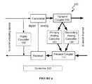
- a system 100 for configurable hybrid self-interference cancellationincludes a transmit coupler 110 , a primary analog self-interference canceller 120 , and a receive coupler 111 .
- the system 100may additionally or alternatively include a secondary analog self-interference canceller 130 , digital self-interference canceller 140 and/or a controller 150 .
- the system 100functions to increase the performance of full-duplex transceivers (or other applicable systems) by performing self-interference cancellation.
- the system 100may perform self-interference cancellation by performing analog and/or digital self-interference cancellation based on any number of sampled analog and/or digital transmit signals.
- the digital self-interference canceller 130may sample a digital transmit signal, as shown in FIG. 2 , but the digital self-interference canceller 130 may additionally or alternatively sample an analog transmit signal (e.g., through an ADC coupled to the analog transmit signal).
- the system 100preferably performs analog and digital self-interference cancellation simultaneously and in parallel but may additionally or alternatively perform analog and/or digital self-interference cancellation at any suitable times and in any order.
- the system 100is preferably implemented using both digital and analog circuitry.
- Digital circuitryis preferably implemented using a general-purpose processor, a digital signal processor, an application specific integrated circuit (ASIC), a field programmable gate array (FPGA) and/or any suitable processor(s) or circuit(s).
- Analog circuitryis preferably implemented using analog integrated circuits (ICs) but may additionally or alternatively be implemented using discrete components (e.g., capacitors, resistors, transistors), wires, transmission lines, transformers, couplers, hybrids, waveguides, digital components, mixed-signal components, or any other suitable components. Both digital and analog circuitry may additionally or alternatively be implemented using optical circuitry (e.g., photonic integrated circuits).
- the system 100preferably includes memory to store configuration data, but may additionally or alternatively be configured using externally stored configuration data or in any suitable manner.
- the system 100preferably is coupled to a receiver.
- the receiverfunctions to receive analog receive signals transmitted over a communications link (e.g., a coaxial cable, a wireless channel).
- the receiverpreferably converts analog receive signals into digital receive signals for processing by a communications system, but may additionally or alternatively not convert analog receive signals (passing them through directly without conversion).
- the receiveris preferably a radio-frequency (RF) receiver, but may additionally or alternatively be any suitable receiver.
- the receiveris preferably coupled to the communications link by a duplexer-coupled RF antenna, but may additionally or alternatively be coupled to the communications link in any suitable manner.
- Some examples of alternative couplingsinclude coupling via one or more dedicated receive antennas.
- the receivermay be coupled to the communications link by a circulator-coupled RF antenna.
- the receiverpreferably includes an analog-to-digital converter (ADC) and a frequency downconverter.
- the receivermay additionally include a low-noise amplifier.
- the receivermay additionally or alternatively include amplifiers, filters, signal processors and/or any other suitable components.
- the receiverincludes only analog processing circuitry (e.g., amplifiers, filters, attenuators, delays).
- the receivermay function to scale, shift, and/or otherwise modify the receive signal.
- the downconverterfunctions to downconvert the analog receive signal from RF (or any other suitable frequency) to a baseband or IF analog receive signal
- the analog-to-digital converter (ADC)functions to convert the baseband or IF analog receive signal to a digital receive signal.
- the system 100is preferably also coupled to a transmitter.
- the transmitterfunctions to transmit signals of the communications system over a communications link to a second communications system.
- the transmitterpreferably converts digital transmit signals into analog transmit signals.
- the transmitteris preferably a radio-frequency (RF) transmitter, but may additionally or alternatively be any suitable transmitter.
- RFradio-frequency
- the transmitteris preferably coupled to the communications link by a duplexer-coupled RF antenna, but may additionally or alternatively be coupled to the communications link in any suitable manner.
- Some examples of alternative couplingsinclude coupling via one or more dedicated transmitter antennas.
- the transmittermay be coupled to the communications link by a circulator-coupled RF antenna.
- the transmitterpreferably includes a digital-to-analog converter (DAC) and a frequency upconverter.
- the transmittermay additionally include a power amplifier.
- the transmittermay additionally or alternatively include amplifiers, filters, signal processors and/or any other suitable components.
- the transmittermay function to scale, phase shift, delay, and/or otherwise modify the transmit signal.
- the digital-to-analog converter (DAC)functions to convert the digital transmit signal to a baseband or IF analog transmit signal
- the upconverterfunctions to upconvert the baseband or IF analog transmit signal from baseband or IF to RF (or any other intended transmission frequency).
- the transmit coupler 110functions to provide a sample of the analog transmit signal for the primary analog canceller 120 , the secondary analog canceller 130 and/or the digital canceller 140 .
- Transmit couplersmay additionally be used to split power between signal paths (e.g., splitting power between different analog canceller 120 blocks).
- the transmit coupler nois preferably a short section directional transmission line coupler, but may additionally or alternatively be any power divider, power combiner, directional coupler, or other type of signal splitter.
- the transmit coupler nois preferably a passive coupler, but may additionally or alternatively be an active coupler (for instance, including power amplifiers).
- the transmit coupler nomay comprise a coupled transmission line coupler, a branch-line coupler, a Lange coupler, a Wilkinson power divider, a hybrid coupler, a hybrid ring coupler, a multiple output divider, a waveguide directional coupler, a waveguide power coupler, a hybrid transformer coupler, a cross-connected transformer coupler, a resistive or capacitive tee, and/or a resistive bridge hybrid coupler.
- the output ports of the transmit coupler noare preferably phase-shifted by ninety degrees, but may additionally or alternatively be in phase or phase shifted by any amount (e.g., zero degrees, 180 degrees).
- the TX couplermay also be included in an active element in the transmitter; e.g. the PA or PMA (post mixer amplifier). This may be attractive with respect to cost and size for highly integrated systems like WLAN or cellular chips sets.
- the RX couplermay be integrated with e.g. the LNA in the receive chain.
- Transmit couplers 110may be arranged in series and/or in parallel. The configuration of multiple transmit couplers 110 in the system 100 is discussed in further detail in later sections.
- the receive coupler 111functions to combine one or more analog self-interference cancellation signals (from analog/digital cancellers) with the analog receive signal.
- the receive coupler 111is preferably a short section directional transmission line coupler, but can additionally or alternatively be any power divider, power combiner, directional coupler, or other type of signal splitter.
- the receive coupler 111is preferably a passive coupler, but can additionally or alternatively be an active coupler (for instance, including power amplifiers).
- the receive coupler 111can comprise a coupled transmission line coupler, a branch-line coupler, a Lange coupler, a Wilkinson power divider, a hybrid coupler, a hybrid ring coupler, a multiple output divider, a waveguide directional coupler, a waveguide power coupler, a hybrid transformer coupler, a cross-connected transformer coupler, a resistive tee, and/or a resistive bridge hybrid coupler.
- the output ports of the receive coupler 111are preferably phase-shifted by ninety degrees, but can additionally or alternatively be in phase or phase shifted by any amount (e.g., zero degrees, 180 degrees).
- Receive couplers 111may be arranged in series and/or in parallel. The configuration of multiple receive couplers 111 in the system 100 is discussed in further detail in later sections.
- the primary analog self-interference canceller 120functions to produce an analog self-interference cancellation signal from the analog transmit signal that can be combined with the analog receive signal to reduce self-interference present in the analog receive signal.
- the receive signalPrior to self-interference cancellation, the receive signal may contain both or either of an intended receive signal and self-interference.
- the receive signal(which may now be referred to as a “composite” receive signal, as it is the result of the combination of the receive signal and the self-interference cancellation signal) preferably still contains the intended receive signal (if one exists), and any remaining self-interference may be referred to as residual self-interference.
- the primary analog self-interference canceller 120is preferably designed to operate at baseband, but may additionally or alternatively be designed to operate at one or multiple IF bands, at one or multiple radio frequency (RF) bands, or at any suitable frequency band(s), using suitable frequency converters.
- RFradio frequency
- the primary analog self-interference canceller 120is preferably implemented as one or more analog circuits that transform an RF transmit signal into an analog self-interference cancellation signal by combining a set of filtered, scaled, phase-shifted, and/or delayed versions of the RF transmit signal, but may additionally or alternatively be implemented as any suitable circuit.
- the primary analog self-interference canceller 120may perform a transformation involving only a single version or copy of the RF transmit signal.
- the transformed signal(the analog self-interference cancellation signal) preferably models at least a part of the self-interference component received at the receiver.
- the primary analog self-interference canceller 120is preferably adaptable to changing self-interference parameters (for example, antenna coupling characteristics between transmit and receive antenna) in addition to changes in the analog circuit characteristics; for example, RF transceiver temperature, analog canceller temperature, ambient temperature, wiring configuration, humidity, and RF transmitter power, signal bandwidth and transmit frequency.
- Adaptation of the primary analog self-interference canceller 120is preferably performed by a tuning circuit, but may additionally or alternatively be performed by a control circuit or other control mechanism included in the cancellers 120 / 130 , the controller 150 , or any other suitable controller.
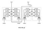
- the primary analog self-interference canceller 120includes sampling couplers 121 , analog vector modulators (AVMs) 122 , delayers 123 , and combining couplers 124 , as exemplified by FIGS. 3A and 3B .
- the primary analog self-interference canceller 120may additionally or alternatively include frequency downconverters 125 , frequency upconverters 126 , and/or amplifiers 127 .
- the analog self-interference canceller 120splits the transmit signal into signal paths (using the sampling couplers 121 if necessary) and transforms each of these signal paths (also referred to as ‘taps’) individually before recombining them at combining couplers 124 .
- transmit signalsare preferably split into quadrature signals (if not already provided as quadrature signals); that is, the input signal is represented by two amplitude-modulated signals that are ninety degrees out of phase with each other.
- the in-phase componentis also called the I component
- the offset-phase componentis called the quadrature (Q) component.
- I and Q signalsmay be combined (as later described in the section on the AVMs 122 ) at different amplitudes to create phase shifts and/or amplitude scaling of the resulting signal.
- the section of the primary analog self-interference canceller 120 implementation of FIG. 3Apreferably includes a single canceller block having three taps.
- Cancellers 120 / 130may alternatively include any number of canceller blocks having any number of taps.
- the use of canceller blocksmay be important in MIMO (multiple-in multiple-out) communication; for example, a canceller 120 may include a block for each self-interference channel (e.g., for a 2 ⁇ 2 MIMO, four blocks: a block for TX 1 interference in the RX 1 channel, a block for TX 2 interference in the RX 1 channel, a block for TX 2 interference in the RX 2 channel, and a block for TX 1 interference in the RX 2 channel). As shown in FIG.
- canceller blocksare used for a 2 ⁇ 2 MIMO system (the boundary between canceller blocks is not explicitly shown, but each vertical pair of AVMs 122 may constitute a canceller block).
- canceller blocksmay share elements; for example, the canceller blocks of FIG. 3B that take input from TX 1 (the leftmost column of AVMs 122 and the column to the right of that one) share delayers 123 , as do the canceller blocks of FIG. 3B that take input from TX 2 .
- canceller blocksmay be switched to different inputs or outputs for any purpose.
- a canceller 120with four canceller blocks, each block having eight taps.
- Such a cancellercould be used in a 2 ⁇ 2 MIMO configuration; e.g., canceller block 120 a generates a signal to cancel self-interference in receive signal RX 1 resulting from interference caused by transmit signal TX 1 , canceller block 120 b generates a signal to cancel self-interference in receive signal RX 1 resulting from interference caused by transmit signal TX 2 , canceller block 120 C generates a signal to cancel self-interference in receive signal RX 2 resulting from interference caused by transmit signal TX 1 , and canceller block 120 d generates a signal to cancel self-interference in receive signal RX 2 resulting from interference caused by transmit signal TX 2 .
- each MIMO channelhas eight taps available to perform cancellation.
- the same cancellercould be used in a SISO configuration with all four blocks (all 32 taps) cancelling self-interference in the receive signal resulting from interference caused by the transmit signal, or in an alternative MIMO configuration (e.g., 2 ⁇ 1, 1 ⁇ 2, etc.).
- the canceller 120may optionally be coupled to switches 16 o to allow for configuration in this manner, as shown in FIG. 4A (an example in which some inputs share components across blocks) and in FIG. 4B (an example in inputs do not share components across blocks).
- I/Q signalsare not explicitly present in FIGS. 4A and 4B (and 4 C) it is understood that they may be implemented as shown in FIGS. 3A and 3B .
- the signals present in the system 100may be differential signals (e.g., a signal may be represented as a V+ and V ⁇ signal pair rather than a single signal referenced to ground), resulting in two or more signals per drawn line in FIGS. 3A and 3B (e.g., I+ and I ⁇ on “I” lines) and four or more signals per drawn line in FIGS. 4A and 4B (e.g., I+, I ⁇ , Q+, Q ⁇ ).
- the canceller 120may allow for switching chains in parallel (as in FIGS. 4A and 4B ), but may also allow for switching chains in series (as shown in FIG. 4C ).
- Switching chains in parallelmay be useful for input/output reassignment (e.g., there are more channels than cancellers, and cancellers can be switched between channels based on use or need; or, in a TDD system, inputs and outputs can be switched in response to a reversal of signal path) or for increasing time resolution in the same channel (in this case, switching paths may optionally include an additional delay to offset the time delays of one block relative to another).
- Switching chains in seriesmay allow for delays to be chained (e.g., as shown in FIG. 4C , the delays on the left are in series with the delays on the right in the pictured switching configuration) which can extend the window of possible time delays achievable by the canceller.
- the upper mentioned canceller block switchingis also applicable in antenna arrays, where groups of antennas are bundled to form beams, which then may be steered into different directions. As a result the different groups of antennas might need cancellers with a different number of taps, and some antennas may not need cancellation.
- the switch blocksmay allow for reducing the total number of cancellers and taps needed and hence saves cost, size and weight.
- canceller blocksmay be statically configured (e.g., by permanent connections to the blocks), they may additionally or alternatively be dynamically configured (e.g., by the switches 160 as shown in FIGS. 4A and 4B or by any other means for routing signals).
- canceller blocksmay be configured by training an antenna array by switching cancellers sequentially to every antenna element or group (round robin) and then selecting the best overall performance of the array. Another mode of operation is to follow a beam steering pattern.
- the signal pathscan be filtered such that signal paths can operate on different frequency sub-bands.
- the frequency sub-bandscan overlap in frequency; there can additionally or alternatively be multiple filters corresponding to the same frequency sub-band.
- the primary canceller 120may include filters.
- the primary analog self-interference canceller 120preferably transforms each tap by phase-shifting and/or scaling the signal components of each tap with an analog vector modulator (AVM) 122 in addition to delaying signal components with delayers 123 . While in some implementations delayers 123 may be per-tap (e.g., as in FIGS. 3A and 3B ), delayers 123 and AVMs 122 may be present in any number, configuration, and/or location in the canceller 120 . The components of the primary analog self-interference canceller 120 may be coupled in any manner that enables analog self-interference cancellation for the system 100 .
- AVManalog vector modulator
- Sampling couplers 121function to split the transmit signal (or other signal components) into multiple transmit signal paths.
- Sampling couplers 121preferably split an input signal into multiple signals having substantially the same waveform as the input signal; power may be split among output signals in any manner.
- a sampling coupler 121 a and 121 bmay have two ⁇ 3 dB ports, while sampling coupler 121 C may have one ⁇ 1.25 dB port and one ⁇ 6 dB port.
- the signal component at vector modulator 122 ahas a signal level of ⁇ 6 dB relative to the transmit signal
- the signal component at 122 bhas ⁇ 7.25 dB
- the signal component at 122 chas ⁇ 12 dB.
- signal splittingmay be performed in the current domain (e.g., through use of parallel loads on the output of an amplifier).
- the sampling coupler 121is preferably a transmission line power divider, but may additionally or alternatively be any suitable power divider, splitter, or coupler.
- the sampling coupler 121may additionally contain any suitable electronics for pre-processing the transmit signal; for example, the sampling coupler 121 may contain an amplifier to increase the power contained in one or more of the output signals.
- Sampling couplers 121may additionally or alternatively include switches or other components enabling the selective routing of signals.
- Each analog canceller 120 blockpreferably includes a sampling coupler 121 ; additionally or alternatively, analog canceller 120 blocks may share one or more sampling couplers 121 .
- sampling couplers 121 and other couplersmay not necessarily be shown explicitly in FIGUREs.
- a sampling coupler 121may be present at each signal path intersection of the system as shown in FIG. 3A .
- the analog vector modulator 122functions to phase shift and/or scale signal components of the analog self-interference canceller 120 .
- the analog vector modulator 122may perform one or more of phase shifting, phase inversion, amplification, and attenuation. Phase shifting can allow the canceller 120 to reflect the contribution of multiple signal components with offset phase, while signal scaling (e.g., attenuation, amplification, inversion) enables the canceller to appropriately match self-interference cancellation signal components to predicted or observed self-interference present in receive signals.
- the analog vector modulator 122When scaling, the analog vector modulator 122 effectively multiplies the transmit signal components by a scale factor. For example, an attenuation of 34% might be represented as a scale factor of 0.66; a gain of 20% might be represented as a scale factor of 1.20; and an attenuation of 10% and a phase inversion might be represented as a scale factor of ⁇ 0.90. Scale factors may be complex; for example, a scale factor of e i ⁇ /2 might be represented as a phase shift of ninety degrees.
- the AVM 122includes a set of multiple scaling cells that operate on quadrature signals.
- the combination of in-phase and quadrature signalscan result in signals of different amplitude and phase.
- x ( t )I ( t )cos ⁇ t ⁇ Q ( t )sin ⁇ t
- I ( t )A ( t )cos ⁇ ( t )
- Q ( t )A ( t )sin ⁇ ( t )
- An AVM 122 operating at baseband frequencies on quadrature signalswould see the signals I and Q as described above. To scale the (eventually resulting) signal, the AVM 122 can scale the I and Q as described above. To scale
- ⁇ 1 ⁇ ( cos ⁇ [ ⁇ 1 ]cos ⁇ [ ⁇ ⁇ ( t ) +
- the AVM 122can apply a first amplitude scaling value (e.g., C) and a first phase shift value (e.g., ⁇ ) to I and Q signals by combining weighted versions of the original I and Q signals.
- “apply”means modifying the I and Q signals in such a way that when recomposed, the resulting signal is scaled and phase shifted (or, alternatively stated, in such a way that the complex baseband signal represented by the I and Q signal components is scaled and phase-shifted).
- production of the quadrature signalsmay result in a substantive image signal at the complex conjugate of the intended signal; i.e., ⁇ (I ⁇ jQ) where ⁇ is a scaling factor less than one (to account for the fact that the image is generally much lower in power than the intended signal). This often occurs due to I/Q imbalance resulting from circuit performance variances.
- the AVM 122may produce weights to correct for the presence of an image based on detections, measurements, and/or estimates of ⁇ (or may otherwise modify amplitude scaling and/or phase shift values in any manner to reduce the presence of the image). For example, assume that a scaling factor of Ce j ⁇ is desired.
- the system 100may additionally or alternatively correct for any other non-idealities (or other parameters of system operation in general) as part of the scale factor generation process.
- Each analog vector modulator 122preferably includes an impedance matching network at its input and output that compensates for variations in the analog vector modulator 122 input and output impedance (and/or phase shift amount) due to changes in signal component frequency or simply transforms the impedance to and from a suitable impedance level for the core of the phase shifter to a standardized impedance level (e.g. 50 ohms).
- the analog vector modulator 122may not include impedance matching networks.
- the impedance matching networksare preferably tunable (e.g., continuously or discretely variable) but may additionally or alternatively be static (i.e., the impedance transformation achieved by using the network is not variable).
- the analog vector modulator 122may generate output signal components using any suitable combination of circuit components. These circuit components may be discrete (e.g., capacitors, inductors) or integrated (e.g., a single element with a fixed capacitance, inductance, resistance and switches), or any other suitable circuit components.
- circuit componentsmay be discrete (e.g., capacitors, inductors) or integrated (e.g., a single element with a fixed capacitance, inductance, resistance and switches), or any other suitable circuit components.
- Scaling stages of the analog vector modulator 122may include attenuators, amplifiers, phase inverters, and/or any other suitable components for scaling transmit signal components.
- Attenuatorsmay be resistive attenuators (T pad, Pi pad, Bridged-T), capacitive dividers, amplifiers with less than unity gain, or any other suitable type of attenuator.
- Amplifiersmay be transistor amplifiers, vacuum tube amplifiers, op-amps, or any other suitable type of amplifier.
- Phase invertersmay be any phase inversion devices, including NPN/PNP phase inversion circuits, transformers and/or inverting amplifiers.
- the analog vector modulators 122preferably are capable of phase shift, attenuation, gain, cutoff (e.g., infinite attenuation), and phase inversion, but may alternatively be capable only of a subset of said capabilities.
- Each analog vector modulator 122preferably includes all five capabilities in a single device but may additionally or alternatively separate capabilities into different sections (e.g., an amplifier with tunable gain but no inversion capability, along with a separate phase shifting circuit).
- the analog vector modulator 122is preferably controlled by a tuning circuit or the controller 150 , but may additionally or alternatively be controlled in any suitable manner.
- some or all AVMs 122are scalers (e.g., attenuators) separated into a set of scaling stages which together preferably apply a total scale adjustment to the associated signal path.
- These scaling stagespreferably may be switched ‘on’ (e.g., applied to the signal path) or ‘off’ (e.g., bypassed, out of signal path), depending on control signals (e.g., determined and sent by the controller iso).
- Thismay be implemented as a physical connection/disconnection in hardware (e.g., a switch, one or more transistors, etc.), firmware, and/or software. Changing the state of the scaling stages may additionally or alternatively be implemented in any suitable manner.
- the resulting scale factor induced by the AVM 122can be determined by which stages are on and which stages are off; for example, an AVM 122 with a 4 dB attenuation stage and an 8 dB attenuation stage ‘on’ might cause an attenuation of 12 dB.
- the AVM 122may not be separated into a set of stages.
- the stagesmay be configured such that various combinations of two or more stages in the ‘on’ or ‘off’ state provide any suitable total scale factor application.
- Each scaling stagepreferably causes a set amount (i.e., non-variable amount) of attenuation or gain.
- scaling stagesmay include tunable elements.
- an attenuation stagemay include a voltage controlled resistor (e.g. realized with a FET); by changing the control voltage of this stage, the resistance (and thus the amount of attenuation experienced by a signal passing through the stage) may be varied.
- an amplifying stagemay include a voltage- or current-controlled amplifier.
- Scaling stagescan be configured to be used with various encoding schemes.
- An encoding schemepreferably specifies how scaling stages are to be configured in order to achieve a particular total scale factor for an AVM 122 . Preferably, this is accomplished by specifying the state (e.g., on or off) of each of a set of switches, each switch configured to disconnect and/or connect one of the scaling stages from the signal pathway. Alternatively, this may be accomplished by adjusting the variable scale factor of each scaling stage, or in any other suitable manner.
- encoding schemescan be used, such as binary encoding, thermometer encoding, and hybrid thermometer encoding.
- a binary encoding schememay enable certain aspects of the AVM 122 architecture, such as requiring fewer individual switches (e.g., bits) to obtain a particular overall scale factor compared to a fully-thermometer encoding scheme.
- a thermometer encoding schememay enable other aspects, such as monotonicity in magnitude and phase during scaler operation, but require more switches compared to a fully binary encoding scheme.
- a hybrid thermometer encoding schemepreferably includes thermometer encoding for a subset of the scaling stages of the AVM 122 , and binary encoding for another subset of the scaling stages of the AVM 122 , so as to take advantage of certain aspects of binary encoding in combination with other particular aspects of thermometer encoding.
- a hybrid thermometer encoding schemecombines attributes of the binary scheme and the thermometer scheme in order to include the desired aspects of both.
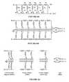
- the AVM 122comprises a novel circuit that attenuates input signals according to a hybrid thermometer scheme, as shown in FIG. 6A and FIG. 6B .
- This circuitcomprises a plurality of attenuation stages in parallel, some of which are shunt resistor stages (e.g., Ra, controlled by S 1 ; Rb, controlled by S 2 ), and some of which are series-shunt resistor stages (e.g., Rc & Rd, controlled by S 3 ; Re & Rf, controlled by S 4 ).
- the AVM 122may additionally include a “sign stage” that flips the polarity of the AVM 122 output.
- the shunt resistor stagesare preferably closer to the input than the series-shunt resistor stages; in such a configuration, while each shunt resistor stage affects attenuation equally (e.g., S 1 ON S 2 OFF is equivalent to S 1 OFF S 2 ON), the effect of each series-shunt resistor stage on attenuation is less farther the stage is from the input (e.g., S 3 ON/OFF has a bigger effect than S 4 ON/OFF).
- the AVM 122may comprise any number of stages coupled in any manner.
- a network composed solely of series-shunt resistor stagesis known as an R ⁇ 2R network for this reason.
- the network of this implementationincludes pure shunt resistor stages (preferably) prior to the series-shunt resistor stages.
- Including shunt resistor stages prior to the series-shunt resistor stagesprovides two advantages: one, input and output impedance are less variant with switch configuration than in a traditional R ⁇ 2R network; two, this configuration is well suited for hybrid thermometer encoding (as described below).
- An example of an attenuator implementing a binary encoding schememay include: a four-stage binary encoded attenuator configured to have 16 phase shift values. That is, the attenuator may have attenuation values corresponding to binary numbers, which in turn correspond to specific attenuator states, such as: 0000 (scale factor: 1), 0001 (scale factor 0.99), 0010 (scale factor 0.96) . . . 1111 (scale factor 0.68). Note that scale factors may be used to describe scaling voltage or scaling power.
- an example of an attenuator implementing a thermometer encoding schememay include: a four-stage thermometer encoded attenuator configured to have five attenuation values. That is, the attenuator may have attenuation values corresponding to thermometer encoded numbers, which in turn correspond to specific attenuator states, such as: 0000 (scale factor 0.90), 0001 (scale factor 0.80), 0011 (scale factor 0.70), 0111 (scale factor 0.60), 1111 (scale factor 0.50).
- An example of an attenuator implementing a hybrid thermometer encoding schememay include eight stages, wherein the first four stages are encoded as in the binary encoded attenuator described above and the latter four stages are encoded as in the thermometer encoded attenuator above.
- Alternative AVMs 122 also implementing a hybrid thermometer encoding schemecan include any suitable number of stages, with any suitable division between the number of binary-encoded stages and the number of thermometer-encoded stages (e.g., 59 stages, wherein 7 stages are binary encoded and 52 stages are thermometer encoded).
- the pure shunt resistor stagesare thermometer encoded, while a set of series-shunt stages immediately following are binary encoded, followed (optionally) by a second set of series-shunt stages (also binary encoded) and/or a sign stage.
- the first set of stagescorresponds to the most significant bits (MSBs) of attenuation (e.g., these stages contribute more to attenuation than the following stages).
- the second set of stageslikewise corresponds to the least significant bits (LSBs) of attenuation.
- the optional third set of stagesmay be used for “trimming” (e.g., attenuation changes that are meant to correct for circuit or element variance between attenuation circuits). Trimming stages are preferably set only when calibrating attenuation circuits, but may additionally or alternatively be altered dynamically (e.g., in response to local temperature differences, in order to maintain matching between settings across AVMs 122 ). Again, differential versions of the AVM 122 may include a sign stage as well.
- stagesmay overlap from a tuning perspective (e.g., some parts of a stage may be tuned more often than other parts of a stage).
- a first part (or substage) of a first stagemay be only tuned at long time intervals, while a second part (or substage) of a first stage may be tuned at the same long time intervals as the first part but additionally at other times as well.
- the controller 150generates a desired scale factor output of the AVM 122 , and encodes the desired scale factor output into discrete values according to the hybrid thermometer encoding scheme described above.
- the discrete valuesmay, in some implementations, be an approximation of the desired outputs based on the configuration of the AVM 122 .
- predetermined attenuation values of each of the attenuation stagesmay permit a range of discrete total attenuation values, and the encoded discrete attenuation value may thus be greater or less than the desired attenuation output by a finite amount.
- the hybrid thermometer encoding schememay transform the desired attenuation output into a discrete attenuation output according to an attenuation curve, and the set of available configurations of the attenuation stages may approximate the attenuation curve in a piecewise linear manner (e.g., linear in power, linear in voltage).
- the controller 150preferably adjusts the total attenuation of the AVM 122 according to the discrete attenuation value thus encoded, preferably by way of activating a subset of the attenuation stages.
- the total attenuation of the AVM 122may alternatively or additionally be adjusted in any suitable manner.
- hybrid thermometer schemes having different parametersmay be selected from by the controller 150 .
- the controller 150may select a first hybrid thermometer encoding scheme intended to minimize reflection coefficients or a second hybrid thermometer encoding scheme intended to maximize cancellation performance.
- the controller 150may automatically select a scheme based on any suitable information; for example, the reflection coefficient minimization scheme may be selected automatically if coefficients of reflection rise above a set threshold.
- the controller 50may select or otherwise modify encoding schemes in any manner (automatically, manually, etc.) based on any suitable information.
- the controller 150increments the total scale factor value of the AVM 122 during operation.
- the attenuation valueis incremented according to a series of steps (e.g., increments) which are computed according to a hybrid thermometer code.
- the stepsmay additionally or alternatively be computed according to an attenuation curve, such that incrementing the total attenuation results in a total attenuation value of a discrete attenuation value along the curve.
- coarse increments of the total attenuation value (or along the attenuation curve)are computed according to a thermometer component of the hybrid thermometer code, and fine increments are computed according to a binary component of the hybrid thermometer code.
- coarse incrementsare preferably any increment greater than any fine increment, but coarse and/or fine increments can additionally or alternatively be any suitable increment.
- thermometer encodinge.g., phase shifting, amplifying
- the delayers 123function to delay transmit signal components, preferably to match corresponding delays in received self-interference.
- the delay introduced by each delayer 123(also referred to as a delayer delay) is preferably variable (i.e., the delayer 123 is a variable delayer), but delayers 123 can additionally or alternatively introduce fixed delays.
- the delayer 123is preferably implemented as an analog delay circuit (e.g., a bucket-brigade device, a long transmission line, RC/LC/RLC active or passive filter networks, surface acoustic wave (SAW) delay lines, a thermo electric or mechanical delay or an optical delay line) but can additionally or alternatively be implemented in any other suitable manner (e.g., delayers may be implemented using digital delayers 123 with ADCs and DACs). If the delayer 123 is a variable delayer, the delay introduced is preferably set by a tuning circuit, but can additionally or alternatively be set in any suitable manner.
- an analog delay circuite.g., a bucket-brigade device, a long transmission line, RC/LC/RLC active or passive filter networks, surface acoustic wave (SAW) delay lines, a thermo electric or mechanical delay or an optical delay line
- SAWsurface acoustic wave
- thermo electric or mechanical delay or an optical delay linee.g., thermo electric or mechanical
- the delayers 123may cover the full band or only partial (sub-) bands; e.g. if it reduces cost or improves performance the total bandwidth of the delay may be split up and suitable sub-band filter devices may be used. Additionally, in order to reduce the number of different delay devices in the bill of material (BOM) or to reduce cost or increase performance, these different sub-bands may be converted into one preferred sub-band via frequency conversion (up- and downmixing).
- BOMbill of material
- Each delayer 123may include an impedance matching network at its input and output that compensates for variations in the delayer 123 input and output impedance (and/or delay amount) due to changes in signal component frequency or transforms the impedance to and from a suitable impedance level for the core of the delayer to a standardized impedance level (50 ohms).
- the delayer 123may not include impedance matching networks.
- the impedance matching networksare preferably tunable (e.g., continuously or discretely variable) but can additionally or alternatively be static (i.e., the impedance transformation achieved by using the network is not variable).
- delayers 123implement active delays such as those shown in FIGS. 7A, 7B, and 7C .
- delayers 123may be configurable in both delay length (e.g., 2.5, 5.0, 10 ns) and delay loss/gain (e.g., ⁇ 4 dB, 0 dB, 4 dB). Further, the delayers 123 may be tuned for bandwidth (e.g., based on the components coupled to the op-amps) and to compensate for process variations.
- bandwidth and delay timesWhile generally there is a tradeoff between bandwidth and delay times (and bandwidth may be selected for that reason), in some scenarios it may be advantageous to alternate, in the same signal path, delays that are more limiting in bandwidth (hereafter referred to as “low pass delayers”) and ones that are less limiting in bandwidth (hereafter referred to as “all pass delayers”). In such a scenario, this alternation may result in flatter gain vs. frequency and delay vs. frequency responses of the delayer 123 chain than otherwise possible. In another case delay times may be altered by switching (additional) delay stages in or out of the signal path without changing the bandwidth using bypass switches.
- variable delay and bandwidthmay be implemented by using a bank of switchable capacitors in the delay implementation shown in FIGS. 7A, 7B, 7C .
- switching to a lower capacitor valuecan give lower delay and wider bandwidth coverage, and vice-versa.
- a switchable bank of resistorscan be used for changing the gain of the delays.
- using small capacitors in parallel with the bandwidth switchallows for trimming out process variations.
- phase shiftcan affect delays (and vice versa), so the vector modulator 122 and delayer 123 may be tuned cooperatively (e.g., if a phase shifting value is changed, a delayer value can also be changed to compensate for unintended delays introduced by the phase shift).
- transmit signal componentsAfter transformation by a vector modulator 122 and/or a delayer 123 , transmit signal components are transformed into self-interference cancellation signal components, which can be combined to form a self-interference cancellation signal.
- Combining couplers 124function to combine the self-interference cancellation signal components to generate an analog self-interference cancellation signal; the analog self-interference cancellation signal can then be combined with an analog receive signal to remove self-interference.
- the combining coupler 124preferably combines self-interference cancellation signal components (resulting from multiple signal paths) and outputs the resulting analog self-interference cancellation signal.
- the combining coupler 124is preferably a transmission line coupler, but can additionally or alternatively be any suitable type of coupler (described in the sampling coupler 121 sections). Combining couplers 124 (like all other couplers of the system 100 ) may optionally contain amplification.
- the combining coupler 124can additionally contain any suitable electronics for post-processing the self-interference cancellation signal before outputting it; for example, the combining coupler 124 can contain an amplifier to increase the power of the self-interference cancellation signal.
- the combining coupler 124may combine signal components to form signals (e.g., self-interference cancellation signal components can be combined to form a self-interference cancellation signal) but may additionally or alternatively combine signal components to form signal super-components, which can later be combined to form signals. Note that there is not any inherent physical difference between signal components, signal super-components, and signals; different terms are used to identify how a signal or signal component is ultimately used.
- a set of first and second signal componentsmay be combined to form a first super-component
- a set of third and fourth signal componentsmay be combined to form a second super-component
- the first and second super-componentsmay be combined to form a signal (or a super-super-component if later combination was to occur, etc.).
- the combining coupler 124may have a fixed or variable combining ratio; variable couplers 124 may, for example, be adjusted during calibration (slow but infrequent) or tuning (fast and frequently), or at any time in any manner.
- the combining coupler 124may include multi-stage amplification.
- the coupler 124may additionally or alternatively feature switches to couple in inputs (e.g., from taps) to various stages of amplification, as shown in FIG. 8 .
- inputsmay be switched or assigned to amplification stages in any manner.
- switch configurationscorrespond to operating modes; i.e., one set of switch configurations corresponds to one operating mode of the combining coupler, whereas a different set of switch configurations corresponds to another operating mode.
- the canceller 120may also contain one or more linearization circuits to compensate for non-linearity generated in the self-interference canceller 120 ; as for example in amplifiers, switches, mixers, scalers, phase shifters and delayers. These linearization circuits may be connected to a single block (local linearization) or comprise an entire signal path (global linearization).
- the primary analog self-interference canceller 120can perform self-interference cancellation at either or both of IF (including baseband) or RF bands. If the primary analog self-interference canceller 120 performs cancellation at IF bands or baseband, the analog self-interference canceller 120 preferably includes a downconverter 125 and an upconverter 126 (as shown in FIG. 3 ). Note further that the analog self-interference canceller 120 may include separate frequency converters operating at different frequencies. The canceller 120 may feature any components operating at any frequency bands. Note that delays at RF frequency may be desirable for maintaining a high level of accuracy of the delayed signal, while IF or optical delays may provide benefits in accommodating more flexible frequency use and wider bandwidths with a smaller area. Delaying may be performed at any frequency in any scenario, however.
- the downconverter 125is preferably substantially similar to the downconverter of the receiver (although details such as LO frequency, linearity and filter configuration can differ between the two), but can additionally or alternatively be any suitable frequency downconverter. Alternatively downconverters 125 may be used for any signal downconversion.
- downconverters 125may additionally decompose input signals into in-phase (I) and quadrature (Q) components; in such cases, the LO phase of the Q mixer is in quadrature with the LO phase to the I mixer.
- the upconverter 126functions to upconvert the carrier frequency of the IF self-interference cancellation signal (received from the primary analog canceller 120 ) to a radio frequency, preparing it for combination with the RF receive signal at the receiver.
- the upconverter 126is preferably communicatively coupled to the receiver and the primary analog canceller 120 , and preferably receives IF self-interference cancellation signals from the primary analog canceller 120 , upconverts the signal to a radio frequency, and passes the resulting RF self-interference cancellation signal to the receiver.
- upconverters 126may be used for any signal upconversion.
- Amplifiers 127may be transistor amplifiers, vacuum tube amplifiers, op-amps, or any other suitable type of amplifier.
- the system 100preferably includes a secondary analog self-interference canceller 130 (alternatively, the system 100 may include or not include the secondary analog self-interference canceller 130 for any configuration).
- the secondary analog self-interference canceller 130is preferably substantially similar to the primary analog self-interference canceller 120 ; however, the secondary canceller 130 preferably operates using different components in different configurations.
- the secondary canceller 130may include sampling couplers 131 , analog vector modulators (AVMs) 132 , delayers 133 , and combining couplers 134 , frequency downconverters 135 , frequency upconverters 136 , and/or amplifiers 137 substantially similar to their analogues in the primary canceller 120 except as otherwise noted.
- AVMsanalog vector modulators
- the secondary analog self-interference canceller 130includes a sampling coupler 131 , a single RF tap (comprising a set of bypassable phase-shifting AVMs 132 and, optionally, a variable-attenuating AVM 132 ), and a combining coupler 134 , as shown in FIG. 9 .
- the secondary canceller 130preferably includes a primary phase shifter (e.g., AVM 132 b ) designed to operate at a primary RF frequency (e.g., a 6 bit phase shifter designed to provide a maximum 360 degree phase shift at 5.5 GHz) and auxiliary phase shifters designed to supplement the primary phase shifter at lower frequencies (e.g., a single bit phase shifter designed to provide 180 degrees of phase shift at 2.2 GHz).
- the auxiliary phase shiftersmay be switched in as needed for lower frequencies and switched out of the signal path at higher frequencies. While either the primary or the auxiliary phase shifters may have variable phase, splitting the phase shifters in this manner may provide substantial power and space savings over a single variable phase shifter for the same bandwidth.
- the secondary canceller 130may be configured in any manner.
- the digital self-interference canceller 140functions to produce a digital self-interference cancellation signal from a digital transmit signal.
- the digital self-interference cancellation signalis preferably converted to an analog self-interference cancellation signal (by a DAC) and combined with the analog self-interference cancellation signals to further reduce self-interference present in the RF receive signal at the receiver 110 . Additionally or alternatively, the digital self-interference cancellation signal can be combined with a digital receive signal.
- the digital self-interference canceller 140preferably samples the RF transmit signal of the transmitter using an ADC (additionally or alternatively, the canceller 140 can sample the digital transmit signal or any other suitable transmit signal) and transforms the sampled and converted RF transmit signal to a digital self-interference signal based on a digital transform configuration.
- the digital transform configurationpreferably includes settings that dictate how the digital self-interference canceller 140 transforms the digital transmit signal to a digital self-interference signal (e.g. coefficients of a generalized memory polynomial used to transform the transmit signal to a self-interference signal).
- the digital self-interference canceller 140can be implemented using a general-purpose processor, a digital signal processor, an application specific integrated circuit (ASIC), a field programmable gate array (FPGA) and/or any suitable processor(s) or circuit(s).
- the digital self-interference canceller 140preferably includes memory to store configuration data, but can additionally or alternatively be configured using externally stored configuration data or in any suitable manner.
- the digital self-interference canceller 140is substantially similar to the digital self-interference canceller of U.S. patent application Ser. No. 14/456,320, filed 11 Aug. 2014, which is incorporated in its entirety by this reference.
- the digital self-interference canceller 140can couple to transmit and receive signals in a number of ways.
- the digital self-interference canceller 140can use a converted RF transmit signal as input as well as provide a converted digital self-interference cancellation signal as output.
- the digital self-interference canceller 140can use the digital transmit signal as input as a well as provide a digital self-interference cancellation signal as output (directly to the digital receive signal).
- the digital self-interference cancellercan additionally or alternatively couple to transmit signals in any combination of digital and analog receive signals.
- the digital self-interference canceller 140can additionally or alternatively couple to IF transmit signals and/or IF self-interference cancellation signals.
- the controller 150functions to control the analog self-interference cancellers 120 / 130 , and in particular components thereof (e.g., delayers 123 / 133 , the vector modulators 122 / 132 ).
- the controller 150can additionally or alternatively function to control any portion of the system 100 (e.g., the digital self-interference canceller 140 ).
- the controller 150may control switches or other configuration parameters of delayers 123 .
- the methods of the preferred embodiment and variations thereofcan be embodied and/or implemented at least in part as a machine configured to receive a computer-readable medium storing computer-readable instructions.
- the instructionsare preferably executed by computer-executable components preferably integrated with a self-interference cancellation system.
- the computer-readable mediumcan be stored on any suitable computer-readable media such as RAMs, ROMs, flash memory, EEPROMs, optical devices (CD or DVD), hard drives, floppy drives, or any suitable device.
- the computer-executable componentis preferably a general or application specific processor, but any suitable dedicated hardware or hardware/firmware combination device can alternatively or additionally execute the instructions.
Landscapes
- Engineering & Computer Science (AREA)
- Signal Processing (AREA)
- Computer Networks & Wireless Communication (AREA)
- Transmitters (AREA)
- Transceivers (AREA)
- Noise Elimination (AREA)
Abstract
Description
x(t)=A(t)cos[ωt+ϕ(t)]=A(t)(cos[ωt] cos[ϕ(t)]−sin[ωt]sin[ϕ(t)])
Written in IQ form, the same signal is simply:
x(t)=I(t)cos ωt−Q(t)sin ωt
I(t)=A(t)cos ϕ(t)
Q(t)=A(t)sin ϕ(t)
And the equivalent complex baseband signal is
xB(t)=I(t)+jQ(t)
An
x0(t)=A(t)cos[ωt+ϕ(t)]
I0(t)=A(t)cos[ϕ(t)]
Q0(t)=A(t)sin[ϕ(t)]
To get the desired result, I and Q are scaled as follows:
And likewise,
This technique is commonly used, for example, to generate phase-shifted and/or scaled signals from a digital signal. Unfortunately, its applicability to RF signals is inherently limited. A closer examination of the equations above shows that the I and Q scale factors are not expressible as constants (both include functions of ϕ(t)). In a real world situation, it may not be possible to know A(t) and/or ϕ(t) independently.
CejϕxB=A1(I0(t)cos ϕ1−Q0(t)sin ϕ1)+jA1(I0(t)sin ϕ1+Q0(t)cos ϕ1)
and thus:
I1(t)=A1cos ϕ1I0(t)−A1sin ϕ1Q0(t)
Q1(t)=A1sin ϕ1I0(t)+A1cos ϕ1Q0(t)
While this is no longer a simple scalar multiplication of I and Q components, it is a linear combination of these components (which does not require knowledge of A(t) or ϕ(t) independently).
w1=Ccos ϕ
w2=−Csin ϕ
w3=Csin ϕ
w4=Ccos ϕ
the complex scalar of Cejϕcan be applied to the signal.
Cejϕ(I(1+δ)+jQ(1−δ))=C(I(1+δ)cos ϕ−Q(1−δ)sin ϕ)+jC(I(1+δ)sin ϕ+Q(1−δ)cos ϕ)
While it is not possible to produce a scalar that can correct for the presence of an image (solving, one can find that the “corrected scale” K varies based on I and Q):
by manipulating I and Q components individually we can nevertheless produce such a corrected response. Using the circuit of
produces the desired results (i.e., applying the weights provides the same effect as scaling by K would: K(I(1+δ)+jQ(1−δ))=Cejϕ(1+jQ)).
Claims (24)
Priority Applications (3)
| Application Number | Priority Date | Filing Date | Title |
|---|---|---|---|
| US16/288,033US10425115B2 (en) | 2018-02-27 | 2019-02-27 | Systems and methods for configurable hybrid self-interference cancellation |
| US16/539,759US10804943B2 (en) | 2018-02-27 | 2019-08-13 | Systems and methods for configurable hybrid self-interference cancellation |
| US17/005,683US11128329B2 (en) | 2018-02-27 | 2020-08-28 | Systems and methods for configurable hybrid self-interference cancellation |
Applications Claiming Priority (3)
| Application Number | Priority Date | Filing Date | Title |
|---|---|---|---|
| US201862635671P | 2018-02-27 | 2018-02-27 | |
| US201862740833P | 2018-10-03 | 2018-10-03 | |
| US16/288,033US10425115B2 (en) | 2018-02-27 | 2019-02-27 | Systems and methods for configurable hybrid self-interference cancellation |
Related Child Applications (1)
| Application Number | Title | Priority Date | Filing Date |
|---|---|---|---|
| US16/539,759ContinuationUS10804943B2 (en) | 2018-02-27 | 2019-08-13 | Systems and methods for configurable hybrid self-interference cancellation |
Publications (2)
| Publication Number | Publication Date |
|---|---|
| US20190268029A1 US20190268029A1 (en) | 2019-08-29 |
| US10425115B2true US10425115B2 (en) | 2019-09-24 |
Family
ID=67684737
Family Applications (3)
| Application Number | Title | Priority Date | Filing Date |
|---|---|---|---|
| US16/288,033ActiveUS10425115B2 (en) | 2018-02-27 | 2019-02-27 | Systems and methods for configurable hybrid self-interference cancellation |
| US16/539,759ActiveUS10804943B2 (en) | 2018-02-27 | 2019-08-13 | Systems and methods for configurable hybrid self-interference cancellation |
| US17/005,683ActiveUS11128329B2 (en) | 2018-02-27 | 2020-08-28 | Systems and methods for configurable hybrid self-interference cancellation |
Family Applications After (2)
| Application Number | Title | Priority Date | Filing Date |
|---|---|---|---|
| US16/539,759ActiveUS10804943B2 (en) | 2018-02-27 | 2019-08-13 | Systems and methods for configurable hybrid self-interference cancellation |
| US17/005,683ActiveUS11128329B2 (en) | 2018-02-27 | 2020-08-28 | Systems and methods for configurable hybrid self-interference cancellation |
Country Status (6)
| Country | Link |
|---|---|
| US (3) | US10425115B2 (en) |
| EP (1) | EP3759844A4 (en) |
| JP (1) | JP7096346B2 (en) |
| KR (2) | KR20210152573A (en) |
| CN (1) | CN111771345B (en) |
| WO (1) | WO2019169047A1 (en) |
Cited By (3)
| Publication number | Priority date | Publication date | Assignee | Title |
|---|---|---|---|---|
| US11057067B1 (en)* | 2020-04-13 | 2021-07-06 | Bae Systems Information And Electronic Systems Integration Inc. | Self-interference signal cancellation |
| WO2022025672A1 (en)* | 2020-07-30 | 2022-02-03 | Samsung Electronics Co., Ltd. | Hybrid self-interference cancelation in frequency division duplexing system |
| US20220150041A1 (en)* | 2020-11-12 | 2022-05-12 | Avago Technologies International Sales Pte.Limited | Capacitive hybrid with pga for full duplex transceivers |
Families Citing this family (7)
| Publication number | Priority date | Publication date | Assignee | Title |
|---|---|---|---|---|
| US10812118B2 (en)* | 2017-12-04 | 2020-10-20 | Massachusetts Institute Of Technology | Methods and apparatus for photonic-enabled radio-frequency (RF) cancellation |
| US11962339B2 (en)* | 2020-08-25 | 2024-04-16 | Samsung Electronics Co., Ltd. | Method and apparatus for reduced size RF filter |
| CN116565522A (en)* | 2022-01-29 | 2023-08-08 | 北京华航无线电测量研究所 | A Signal Transmitting and Receiving Method of a Low-Profile Co-Aperture Multi-Phase Central Array Antenna |
| US12136920B2 (en)* | 2022-03-01 | 2024-11-05 | Qualcomm Incorporated | Current-mode radio frequency attenuators |
| CN115396048B (en)* | 2022-07-11 | 2024-03-26 | 中国电子科技集团公司第二十九研究所 | A passive wideband quadrature signal calibration circuit and system |
| US12401552B2 (en) | 2022-11-17 | 2025-08-26 | Nxp Usa, Inc. | Interference cancellation in a multi-radio system and apparatus for cancellation |
| JP7577892B1 (en) | 2024-07-17 | 2024-11-05 | ソフトバンク株式会社 | Interference suppression circuit, transmission/reception circuit, and radio device |
Citations (226)
| Publication number | Priority date | Publication date | Assignee | Title |
|---|---|---|---|---|
| US3922617A (en) | 1974-11-18 | 1975-11-25 | Cutler Hammer Inc | Adaptive feed forward system |
| US4321624A (en) | 1978-10-30 | 1982-03-23 | Rca Corporation | AFT Circuit |
| US4395688A (en) | 1981-08-11 | 1983-07-26 | Harris Corporation | Linear phase filter with self-equalized group delay |
| US4952193A (en) | 1989-03-02 | 1990-08-28 | American Nucleonics Corporation | Interference cancelling system and method |
| US5027253A (en) | 1990-04-09 | 1991-06-25 | Ibm Corporation | Printed circuit boards and cards having buried thin film capacitors and processing techniques for fabricating said boards and cards |
| US5212827A (en) | 1991-02-04 | 1993-05-18 | Motorola, Inc. | Zero intermediate frequency noise blanker |
| US5262740A (en) | 1992-04-09 | 1993-11-16 | Itt Corporation | Microstrip transformer apparatus |
| US5278529A (en) | 1992-02-13 | 1994-01-11 | Itt Corporation | Broadband microstrip filter apparatus having inteleaved resonator sections |
| US5355103A (en) | 1990-06-29 | 1994-10-11 | American Nucleonics Corporation | Fast settling, wide dynamic range vector modulator |
| EP0755141A2 (en) | 1995-07-19 | 1997-01-22 | Sharp Kabushiki Kaisha | Adaptive decision feedback equalization for communication systems |
| US5691978A (en) | 1995-04-07 | 1997-11-25 | Signal Science, Inc. | Self-cancelling full-duplex RF communication system |
| US5734957A (en) | 1993-12-22 | 1998-03-31 | Canon Kabushiki Kaisha | Image forming apparatus with toner re-use feature |
| US5734967A (en) | 1994-02-17 | 1998-03-31 | Motorola, Inc. | Method and apparatus for reducing self interference in a communication system |
| US5734305A (en) | 1995-03-22 | 1998-03-31 | Lk-Products Oy | Stepwise switched filter |
| US5790658A (en) | 1996-10-28 | 1998-08-04 | Advanced Micro Devices, Inc. | High performance echo canceller for high speed modem |
| US5818385A (en) | 1994-06-10 | 1998-10-06 | Bartholomew; Darin E. | Antenna system and method |
| CN1204898A (en) | 1997-06-30 | 1999-01-13 | 哈里公司 | Apparatus with reduced A/D dynamic range requirement in compensating feedback system |
| US5930301A (en) | 1996-06-25 | 1999-07-27 | Harris Corporation | Up-conversion mechanism employing side lobe-selective pre-distortion filter and frequency replica-selecting bandpass filter respectively installed upstream and downstream of digital-to-analog converter |
| US6037848A (en) | 1996-09-26 | 2000-03-14 | Lk-Products Oy | Electrically regulated filter having a selectable stop band |
| US6215812B1 (en) | 1999-01-28 | 2001-04-10 | Bae Systems Canada Inc. | Interference canceller for the protection of direct-sequence spread-spectrum communications from high-power narrowband interference |
| US6240150B1 (en) | 1998-05-12 | 2001-05-29 | Nortel Networks Limited | Method and apparatus for filtering interference in a modem receiver |
| JP2001196994A (en) | 2000-01-06 | 2001-07-19 | Kddi Corp | Repeater device for code division multiple access system |
| US6300849B1 (en) | 1998-11-27 | 2001-10-09 | Kyocera Corporation | Distributed element filter |
| US6307169B1 (en) | 2000-02-01 | 2001-10-23 | Motorola Inc. | Micro-electromechanical switch |
| US20020034191A1 (en) | 1998-02-12 | 2002-03-21 | Shattil Steve J. | Method and apparatus for transmitting and receiving signals having a carrier interferometry architecture |
| US20020064245A1 (en) | 2000-10-10 | 2002-05-30 | Mccorkle John W. | Ultra wide bandwidth noise cancellation mechanism and method |
| US20020072344A1 (en) | 2000-08-22 | 2002-06-13 | Souissi Slim Salah | Method and apparatus for transmitter noise cancellation in an RF communications system |
| US6411250B1 (en) | 1997-09-01 | 2002-06-25 | Cambridge Consultants Limited | Electromagnetic sensor system |
| US20020109631A1 (en) | 1999-08-11 | 2002-08-15 | China Academy Of Telecommunications Technology | Method of interference cancellation based on smart antenna |
| US20020154717A1 (en) | 2000-12-19 | 2002-10-24 | Telefonaktiebolaget Lm Ericsson (Publ) | Weighting factor setting method for subtractive interference canceller, interference canceller unit using said weighting factor and interference canceller |
| US20020172265A1 (en) | 2001-03-30 | 2002-11-21 | Kenney Thomas J. | Successive user data multipath interference cancellation |
| US6490328B1 (en) | 1999-05-11 | 2002-12-03 | Intel Corporation | High speed data transceiver in harsh wiring networks |
| US20030022395A1 (en) | 2001-07-17 | 2003-01-30 | Thoughtbeam, Inc. | Structure and method for fabricating an integrated phased array circuit |
| US20030031279A1 (en) | 2001-08-08 | 2003-02-13 | Viasat, Inc. | Method and apparatus for relayed communication using band-pass signals for self-interference cancellation |
| US6539204B1 (en) | 2000-09-29 | 2003-03-25 | Mobilian Corporation | Analog active cancellation of a wireless coupled transmit signal |
| JP2003148748A (en) | 2001-11-15 | 2003-05-21 | Nissei Oobaru Kk | Radiative heater and manufacturing method for reflecting plate for radiative heater |
| US20030099287A1 (en) | 2001-10-31 | 2003-05-29 | Bernard Arambepola | Method of and apparatus for detecting impulsive noise, method of operating a demodulator, demodulator and radio receiver |
| US20030104787A1 (en) | 2001-12-05 | 2003-06-05 | Viasat, Inc. | Multi-channel self-interference cancellation method and apparatus for relayed communication |
| US20030112860A1 (en) | 2001-12-18 | 2003-06-19 | Erdogan Alper Tunga | Method and system for shortening channel impulse response using time domain equalization filter |
| US6583021B2 (en) | 2001-06-30 | 2003-06-24 | Hynix Semiconductor Inc. | Method of fabricating capacitor having hafnium oxide |
| US20030148748A1 (en) | 2002-02-01 | 2003-08-07 | Shah Peter Jivan | Distortion reduction in a wireless communication device |
| US6612987B2 (en) | 2001-12-05 | 2003-09-02 | Koninklijke Philips Electronics N.V. | Apparatus and method for selectively optimizing an acoustic transducer |
| US6657950B1 (en) | 1999-02-19 | 2003-12-02 | Cisco Technology, Inc. | Optimal filtering and upconversion in OFDM systems |
| US20030222732A1 (en) | 2002-05-29 | 2003-12-04 | Superconductor Technologies, Inc. | Narrow-band filters with zig-zag hairpin resonator |
| US20040106381A1 (en) | 2002-09-06 | 2004-06-03 | Engim Incorporated | Transmit signal cancellation in wireless receivers |
| US6778599B1 (en) | 2000-03-09 | 2004-08-17 | Tioga Technologies | Digital transceiver with multi-rate processing |
| US6784766B2 (en) | 2002-08-21 | 2004-08-31 | Raytheon Company | MEMS tunable filters |
| US6815739B2 (en) | 2001-05-18 | 2004-11-09 | Corporation For National Research Initiatives | Radio frequency microelectromechanical systems (MEMS) devices on low-temperature co-fired ceramic (LTCC) substrates |
| US20040266378A1 (en) | 2001-08-10 | 2004-12-30 | Keisuke Fukamachi | Bypass filter, multi-band antenna switch circuit, and layered module composite part and communication device using them |
| US20050030888A1 (en) | 2003-08-04 | 2005-02-10 | Thesling William H. | Orthogonal frequency digital multiplexing correlation canceller |
| US20050078743A1 (en) | 1999-08-10 | 2005-04-14 | Aki Shohara | Radio frequency control for communication systems |
| US20050094722A1 (en) | 2003-10-02 | 2005-05-05 | Hiroshi Takatori | Analog adaptive FIR filter having independent coefficient sets for each filter tap |
| US20050101267A1 (en) | 2003-11-07 | 2005-05-12 | Andrew Corporation, A Delaware Corporation | Frequency conversion techniques |
| US20050129152A1 (en) | 2003-12-15 | 2005-06-16 | Hillstrom Timothy L. | Method and sytem for noise reduction in measurement receivers using automatic noise subtraction |
| US6915112B1 (en) | 2000-11-12 | 2005-07-05 | Intel Corporation | Active cancellation tuning to reduce a wireless coupled transmit signal |
| US20050159128A1 (en) | 2001-06-21 | 2005-07-21 | Collins Glenn D. | Adaptive canceller for frequency reuse systems |
| US20050242830A1 (en) | 2004-04-30 | 2005-11-03 | Humphrey Guy H | Hybrid binary/thermometer code for controlled-voltage integrated circuit output drivers |
| US20050250466A1 (en) | 2004-04-26 | 2005-11-10 | Hellosoft Inc. | Method and apparatus for improving MLSE in the presence of co-channel interferer for GSM/GPRS systems |
| US6965657B1 (en) | 1999-12-01 | 2005-11-15 | Velocity Communication, Inc. | Method and apparatus for interference cancellation in shared communication mediums |
| US20050254555A1 (en) | 2004-05-17 | 2005-11-17 | Teague Edward H | Interference control via selective blanking/attenuation of interfering transmissions |
| US6975186B2 (en) | 2001-12-12 | 2005-12-13 | Sony Corporation | Filter circuit |
| US20050282500A1 (en) | 2004-06-16 | 2005-12-22 | Wang Yi-Pin E | Benign interference suppression for received signal quality estimation |
| US20060030277A1 (en) | 2004-02-10 | 2006-02-09 | Cyr Russell J | Programmable radio transceiver |
| US20060029124A1 (en) | 2004-08-04 | 2006-02-09 | Telefonaktiebolaget Lm Ericsson (Publ) | Reduced complexity soft value generation for MIMO JD-GRAKE receivers |
| US20060058022A1 (en) | 2004-08-27 | 2006-03-16 | Mark Webster | Systems and methods for calibrating transmission of an antenna array |
| US20060083297A1 (en) | 2004-10-13 | 2006-04-20 | Analog Devices, Inc. | Filters for communication systems |
| US20060153283A1 (en) | 2005-01-13 | 2006-07-13 | Scharf Louis L | Interference cancellation in adjoint operators for communication receivers |
| US20060209754A1 (en) | 2005-03-16 | 2006-09-21 | Ji Tingfang | Channel structures for a quasi-orthogonal multiple-access communication system |
| US20060240769A1 (en) | 2004-04-06 | 2006-10-26 | Proctor Jr James A | Transmission canceller for wireless local area network |
| US20060273853A1 (en) | 2005-06-03 | 2006-12-07 | Ntt Docomo, Inc. | Feed forward amplifier for multiple frequency bands |
| CN1901362A (en) | 2005-07-21 | 2007-01-24 | 阿尔卡特公司 | Adaptive digital pre-distortion system |
| US20070105509A1 (en) | 2005-11-09 | 2007-05-10 | Texas Instruments Inc. | RF transmission leakage mitigator, method of mitigating an RF transmission leakage and CDMA tranceiver employing the same |
| US7230316B2 (en) | 2002-12-27 | 2007-06-12 | Semiconductor Energy Laboratory Co., Ltd. | Semiconductor device having transferred integrated circuit |
| US7239219B2 (en) | 2001-12-03 | 2007-07-03 | Microfabrica Inc. | Miniature RF and microwave components and methods for fabricating such components |
| US20070207748A1 (en) | 2001-04-11 | 2007-09-06 | Kyocera Wireless Corp. | Antenna interface unit |
| US20070207747A1 (en) | 2006-03-06 | 2007-09-06 | Paul Johnson | Single frequency duplex radio link |
| US20070223617A1 (en) | 2006-03-24 | 2007-09-27 | Samsung Electro-Mechanics Co., Ltd. | Multi-port-based mimo antenna receiver |
| US20070249314A1 (en) | 2004-03-19 | 2007-10-25 | Sirit Technologies Inc. | Adjusting parameters associated with transmitter leakage |
| US20070274372A1 (en) | 2006-05-29 | 2007-11-29 | Tokyo Institute Of Technology | Radio communication apparatus and radio communication method |
| US20070283220A1 (en) | 2006-05-16 | 2007-12-06 | Nokia Corporation | Method, apparatus and computer program product providing soft iterative recursive least squares (RLS) channel estimator |
| US20070296625A1 (en) | 2004-12-23 | 2007-12-27 | Bruzzone Stephen P | Wideband interference cancellation using dsp algorithms |
| US20080037801A1 (en) | 2006-08-10 | 2008-02-14 | Cambridge Silicon Radio, Ltd. | Dual microphone noise reduction for headset application |
| US20080075189A1 (en) | 2006-09-21 | 2008-03-27 | Broadcom Corporation, A California Corporation | Equalizer coefficient determination in the frequency domain for MIMO/MISO radio |
| US20080089397A1 (en) | 2006-10-17 | 2008-04-17 | Interdigital Technology Corporation | Transceiver with hybrid adaptive self-interference canceller for removing transmitter generated noise to prevent modem jamming |
| US20080107046A1 (en) | 2006-11-06 | 2008-05-08 | Nokia Corporation | Analog signal path modeling for self-interference cancellation |
| US7372420B1 (en) | 2006-11-13 | 2008-05-13 | The Boeing Company | Electronically scanned antenna with secondary phase shifters |
| US20080131133A1 (en) | 2006-05-17 | 2008-06-05 | Blunt Shannon D | Low sinr backscatter communications system and method |
| US20080144852A1 (en) | 2006-12-14 | 2008-06-19 | Ford Global Technologies, Llc | Multi-chamber noise control system |
| US20080192636A1 (en) | 2005-02-07 | 2008-08-14 | Briscoe Robert J | Policing Networks |
| EP1959625A1 (en) | 2007-02-14 | 2008-08-20 | NTT DoCoMo Inc. | Receiver apparatus for detecting narrowband interference in a multi-carrier receive signal |
| US20080219339A1 (en) | 2007-03-09 | 2008-09-11 | Qualcomm Incorporated | Channel estimation using frequency smoothing |
| US20080219377A1 (en) | 2007-03-06 | 2008-09-11 | Sige Semiconductor Inc. | Transmitter crosstalk cancellation in multi-standard wireless transceivers |
| US20080279122A1 (en) | 2007-05-07 | 2008-11-13 | Ntt Docomo, Inc | Leakage power reduction apparatus |
| US7468642B2 (en) | 2006-12-12 | 2008-12-23 | International Business Machines Corporation | Multi band pass filters |
| US20090022089A1 (en) | 2007-07-16 | 2009-01-22 | Rudrapatna Ashok N | Architecture to support network-wide multiple-in-multiple-out wireless communication |
| US20090034437A1 (en) | 2007-07-31 | 2009-02-05 | Samsung Electronics Co., Ltd. | Apparatus and method for canceling interference in relay station in a communication system |
| US20090047914A1 (en) | 2003-05-27 | 2009-02-19 | Interdigital Technology Corporation | Multi-mode radio with interference cancellation circuit |
| US20090115912A1 (en) | 2007-11-05 | 2009-05-07 | Mediatek Inc. | Television signal receiver capable of cancelling linear and non-linear distortion |
| US20090180404A1 (en) | 2008-01-14 | 2009-07-16 | Samsung Electronics Co., Ltd. | Apparatus and method for interference cancellation and synchronization maintenance over interference channel estimation in communication system based on full-duplex relay |
| US20090186582A1 (en) | 2008-01-22 | 2009-07-23 | Khurram Muhammad | System and method for transmission interference cancellation in full duplex transceiver |
| US20090213770A1 (en) | 2008-02-27 | 2009-08-27 | Fenghao Mu | Active Cancellation of Transmitter Leakage in a Wireless Transceiver |
| US20090221231A1 (en) | 2008-02-29 | 2009-09-03 | The Hong Kong University Of Science And Technology | Multi-user mimo relay protocol with self-interference cancellation |
| US20090262852A1 (en) | 2008-01-16 | 2009-10-22 | Orlik Philip V | Coding for Large Antenna Arrays in MIMO Networks |
| US7622989B2 (en) | 2007-04-30 | 2009-11-24 | The Regents Of The University Of California | Multi-band, inductor re-use low noise amplifier |
| US20090303908A1 (en) | 2008-06-04 | 2009-12-10 | Budhaditya Deb | System and method for adjusting media access control parameters in a wireless network |
| US20100014614A1 (en) | 2006-07-28 | 2010-01-21 | Mstar Semiconductor, Inc. | Digital Radio Systems |
| US20100014600A1 (en) | 2008-07-18 | 2010-01-21 | Advanced Micro Devices, Inc. | Window position optimization for pilot-aided ofdm system |
| US20100022201A1 (en) | 2008-07-22 | 2010-01-28 | Patrick Vandenameele | Apparatus and method for reducing self-interference in a radio system |
| US20100031036A1 (en) | 2007-12-21 | 2010-02-04 | Harris Corporation | Secure wireless communications system and related method |
| US7667557B2 (en) | 2005-12-06 | 2010-02-23 | Tdk Corporation | Thin-film bandpass filter using inductor-capacitor resonators |
| US20100056166A1 (en) | 2006-11-07 | 2010-03-04 | Qualcomm Incorporated | Method and Apparatus for Reinforcement of Broadcast Transmissions in MBSFN Inactive Areas |
| US20100103900A1 (en) | 2006-12-08 | 2010-04-29 | Choong-Il Yeh | Beamforming method and device |
| US20100117693A1 (en) | 2008-11-07 | 2010-05-13 | Viasat, Inc. | Dual conversion transmitter with single local oscillator |
| US20100136900A1 (en) | 2008-12-02 | 2010-06-03 | Fujitsu Limited | Radio Relay Device and Method |
| US20100150070A1 (en) | 2008-12-16 | 2010-06-17 | Electronics And Telecommunication Research Institute | Sensor node having self localization function and self localization method thereof |
| US20100150033A1 (en) | 2008-12-16 | 2010-06-17 | General Electric Company | Software radio frequency canceller |
| US20100159858A1 (en) | 2008-12-19 | 2010-06-24 | Paul Wilkinson Dent | Strong Signal Tolerant OFDM Receiver and Receiving Methods |
| US20100159837A1 (en) | 2008-12-19 | 2010-06-24 | Paul Wilkinson Dent | Own Transmitter Interference Tolerant Transceiver and Receiving Methods |
| US20100165895A1 (en) | 2008-12-30 | 2010-07-01 | Imtinan Elahi | Methods and apparatus for canceling distortion in full-duplex transceivers |
| US20100208854A1 (en) | 2005-11-15 | 2010-08-19 | Tommy Guess | Iterative Interference Cancellation for MIMO-OFDM Receivers |
| US20100215124A1 (en) | 2009-02-24 | 2010-08-26 | Samsung Electronics Co., Ltd. | Apparatus and operating method of digital rf receiver in a wireless communication system |
| US20100226416A1 (en) | 2009-03-05 | 2010-09-09 | Telefonaktiebolaget Lm Ericsson (Publ) | Compensating Pre-Filter for an OFDM Transmitter |
| US20100226356A1 (en) | 2009-03-06 | 2010-09-09 | Sahin Mustafa E | Method for iterative interference cancellation for co-channel multi-carrier and narrowband systems |
| US20100232324A1 (en) | 2009-03-16 | 2010-09-16 | Microsoft Corporation | Full-Duplex Wireless Communications |
| EP2237434A1 (en) | 2009-04-02 | 2010-10-06 | Thales Nederland B.V. | An apparatus for emitting and receiving radio-frequency signals, comprising a circuit to cancel interferences |
| US20100266057A1 (en) | 2009-04-16 | 2010-10-21 | Shweta Shrivastava | Group resource allocation techniques for ieee 802.16m |
| US7825751B2 (en) | 2006-05-24 | 2010-11-02 | Kabushiki Kaisha Toshiba | Resonant circuit, filter circuit, and antenna device |
| US20100279602A1 (en) | 2007-12-21 | 2010-11-04 | Telefonaktiebolaget Lm Ericsson (Publ) | Node and a Method for use in a Wireless Communications System |
| US20100295716A1 (en) | 2009-05-19 | 2010-11-25 | Kabushiki Kaisha Toshiba | Interference reduction device |
| EP2267946A2 (en) | 2009-06-23 | 2010-12-29 | Uniloc Usa, Inc. | System and method for traffic information delivery |
| US20110013735A1 (en) | 2009-07-16 | 2011-01-20 | Industrial Technology Research Institute | Progressive parallel interference canceller and method and receiver thereof |
| US20110013684A1 (en) | 2009-07-14 | 2011-01-20 | Nokia Corporation | Channel estimates in a SIC receiver for a multi-transmitter array transmission scheme |
| US20110026509A1 (en) | 2008-04-25 | 2011-02-03 | Akio Tanaka | Wireless communication apparatus |
| US20110081880A1 (en) | 2009-10-01 | 2011-04-07 | Samsung Electronics Co. Ltd. | Wideband receiver for wireless communication system and method for controlling the same |
| US20110149714A1 (en) | 2009-12-21 | 2011-06-23 | Qualcomm Incorporated | Method and apparatus for adaptive non-linear self-jamming interference cancellation |
| US20110171922A1 (en) | 2010-01-08 | 2011-07-14 | Samsung Electro-Mechanics Company | Systems, methods, and apparatuses for reducing interference at the front-end of a communications receiving device |
| US7990231B2 (en) | 2005-03-10 | 2011-08-02 | Soshin Electric Co., Ltd. | Delay line |
| US20110216813A1 (en) | 2008-11-14 | 2011-09-08 | Telefonaktiebolaget Lm Ericsson (Publ) | Method and Arrangement in a Communication System |
| US20110222631A1 (en) | 2010-03-11 | 2011-09-15 | Samsung Electronics Co., Ltd. | Apparatus for receiving signal and method of compensating phase mismatch thereof |
| US20110227664A1 (en) | 2008-12-01 | 2011-09-22 | Nortel Networks Limited | Frequency Agile Filter Using a Digital Filter and Bandstop Filtering |
| US20110243202A1 (en) | 2010-04-01 | 2011-10-06 | Ismail Lakkis | Cancellation System for Millimeter-Wave Radar |
| US20110250858A1 (en) | 2010-04-08 | 2011-10-13 | Qualcomm Incorporated | Frequency selection and transition over white space |
| US20110254639A1 (en) | 2008-12-26 | 2011-10-20 | Taiyo Yuden Co., Ltd. | Duplexer and electronic device |
| US20110256857A1 (en) | 2010-04-20 | 2011-10-20 | Intersil Americas Inc. | Systems and Methods for Improving Antenna Isolation Using Signal Cancellation |
| US20110268232A1 (en) | 2010-05-03 | 2011-11-03 | Chester Park | Inter-carrier bandwidth control for mitigating iq imbalance |
| US8055235B1 (en) | 2008-05-02 | 2011-11-08 | Hypres, Inc. | System and method for digital interference cancellation |
| US20110311067A1 (en) | 2009-02-13 | 2011-12-22 | University Of Florida Research Foundation, Inc. | Digital sound leveling device and method to reduce the risk of noise induced hearing loss |
| US20110319044A1 (en) | 2010-06-28 | 2011-12-29 | Itt Manufacturing Enterprises, Inc. (A Subsidiary Of Itt Corporation) | Adaptive cancellation of multi-path interferences |
| US8093963B2 (en) | 2006-12-01 | 2012-01-10 | Hitachi Metals, Ltd. | Laminated bandpass filter, high-frequency component and communications apparatus comprising them |
| US20120021153A1 (en) | 2010-07-21 | 2012-01-26 | Bhandari Yashpal J | Silicone Polyimide Compositions With Improved Flame Retardance |
| JP2012021153A (en) | 2010-07-13 | 2012-02-02 | Xerox Corp | Radiation curable solid ink compositions suitable for transfuse printing application |
| US20120052892A1 (en) | 2010-08-25 | 2012-03-01 | Powerwave Technologies, Inc. | Transmit leakage cancellation in a wide bandwidth distributed antenna system |
| US20120063369A1 (en) | 2010-09-14 | 2012-03-15 | Qualcomm Incorporated | Method and apparatus for mitigating relay interference |
| US20120063373A1 (en) | 2010-09-15 | 2012-03-15 | Interdigital Patent Holdings, Inc. | Method and apparatus for dynamic bandwidth provisioning in frequency division duplex systems |
| US20120115412A1 (en) | 2010-11-05 | 2012-05-10 | Qualcomm Incorporated | Iq imbalance compensation in interference cancellation repeater using a zero-if radio architecture |
| US20120140685A1 (en) | 2010-12-01 | 2012-06-07 | Infineon Technologies Ag | Simplified adaptive filter algorithm for the cancellation of tx-induced even order intermodulation products |
| US20120147790A1 (en) | 2010-12-13 | 2012-06-14 | Nec Laboratories America, Inc. | Method for a Canceling Self Interference Signal Using Active Noise Cancellation in RF Circuits and Transmission Lines for Full Duplex Simultaneous (In Time) and Overlapping (In Space) Wireless Transmission & Reception on the Same Frequency band |
| US20120201153A1 (en) | 2011-02-03 | 2012-08-09 | Dinesh Bharadia | Adaptive techniques for full duplex communications |
| US20120224497A1 (en) | 2011-03-03 | 2012-09-06 | Telefonaktiebolaget L M Ericsson (Publ) | Signal Quality Measurement Based On Transmitter Status |
| US8325001B2 (en) | 2005-08-04 | 2012-12-04 | The Regents Of The University Of California | Interleaved three-dimensional on-chip differential inductors and transformers |
| US8345433B2 (en) | 2004-07-08 | 2013-01-01 | Avx Corporation | Heterogeneous organic laminate stack ups for high frequency applications |
| US20130005284A1 (en) | 2010-03-23 | 2013-01-03 | Telefonaktiebolaget Lm Ericsson (Publ) | Circuit and Method for Interference Reduction |
| US8378763B2 (en) | 2009-09-29 | 2013-02-19 | Tdk Corporation | Layered bandpass filter |
| US20130044791A1 (en) | 2011-08-18 | 2013-02-21 | Qualcomm Incorporated | Joint linear and non-linear cancellation of transmit self-jamming interference |
| US20130076433A1 (en) | 2011-09-22 | 2013-03-28 | Roger A. Fratti | Adaptive filter with coefficient determination based on output of real time clock |
| US8410871B2 (en) | 2007-11-01 | 2013-04-02 | Samsung Electronics Co., Ltd. | Tunable resonator and tunable filter |
| US20130089009A1 (en) | 2011-09-19 | 2013-04-11 | Li Erran Li | Method and apparatus for interference cancellation for antenna arrays |
| US8422540B1 (en) | 2012-06-21 | 2013-04-16 | CBF Networks, Inc. | Intelligent backhaul radio with zero division duplexing |
| US20130114468A1 (en) | 2011-11-07 | 2013-05-09 | Dennis Hui | Dynamic space division duplex (sdd) wireless communications with multiple antennas using self-interference cancellation |
| US20130120190A1 (en)* | 2011-11-14 | 2013-05-16 | Earl W. McCune, Jr. | Phased array transmission methods and apparatus |
| US20130155913A1 (en) | 2011-12-14 | 2013-06-20 | Redline Communications Inc. | Single channel full duplex wireless communication |
| US20130166259A1 (en) | 2011-11-17 | 2013-06-27 | Analog Devices, Inc. | System linearization |
| US20130194984A1 (en) | 2012-01-16 | 2013-08-01 | Huawei Technologies Co., Ltd. | Method and apparatus for handling full-duplex interference |
| US8502623B2 (en) | 2008-07-09 | 2013-08-06 | Advanced Semiconductor Engineering, Inc. | Band pass filter |
| US20130207745A1 (en) | 2012-02-13 | 2013-08-15 | Qualcomm Incorporated | 3d rf l-c filters using through glass vias |
| US20130215805A1 (en) | 2012-02-08 | 2013-08-22 | The Board Of Trustees Of The Leland Stanford Junior University | Systems and Methods for Full-Duplex Signal Shaping |
| US20130225101A1 (en) | 2012-02-27 | 2013-08-29 | Intel Mobile Communications GmbH | Second-order filter with notch for use in receivers to effectively suppress the transmitter blockers |
| US20130253917A1 (en) | 2010-12-09 | 2013-09-26 | Dolby International Ab | Psychoacoustic filter design for rational resamplers |
| US8547188B2 (en) | 2009-02-23 | 2013-10-01 | Tdk Corporation | Filter with integrated loading capacitors |
| US20130259343A1 (en) | 2012-03-28 | 2013-10-03 | Siemens Corporation | Alternating direction of multipliers method for parallel mri reconstruction |
| US20130273871A1 (en) | 2012-04-11 | 2013-10-17 | Research In Motion Limited | Radio receiver with reconfigurable baseband channel filter |
| US20130286903A1 (en) | 2012-04-25 | 2013-10-31 | Nec Laboratories America, Inc. | Interference Cancellation for Full-Duplex Communications |
| US20130294523A1 (en) | 2011-07-21 | 2013-11-07 | Luca Rossato | Signal processing and tiered signal encoding |
| US20130301487A1 (en) | 2012-05-13 | 2013-11-14 | Amir Keyvan Khandani | Full Duplex Wireless Transmission with Self-Interference Cancellation |
| US20130301488A1 (en) | 2012-02-08 | 2013-11-14 | The Board Of Trustees Of The Leland Stanford Junior University | Systems and methods for cancelling interference using multiple attenuation delays |
| US20130308717A1 (en) | 2012-04-13 | 2013-11-21 | Alexander Maltsev | Millimeter-wave transceiver with coarse and fine beamforming with interference suppression and method |
| US20130315211A1 (en) | 2012-05-25 | 2013-11-28 | University Of Southern California | Airsync: enabling distributed multiuser mimo with full multiplexing gain |
| WO2013185106A1 (en) | 2012-06-08 | 2013-12-12 | The Board Of Trustees Of The Leland Stanford Junior University | Systems and methods for cancelling interference using multiple attenuation delays |
| US20140011461A1 (en) | 2012-07-03 | 2014-01-09 | Infineon Technologies Ag | System and Method for Attenuating a Signal in a Radio Frequency System |
| US20140016515A1 (en) | 2012-07-13 | 2014-01-16 | At&T Intellectual Property I, L.P. | System and method for full duplex cancellation |
| US20140126437A1 (en) | 2012-11-07 | 2014-05-08 | Qualcomm Incorporated | Methods and apparatus for communication mode selection based on content type |
| US8755756B1 (en) | 2009-04-29 | 2014-06-17 | Qualcomm Incorporated | Active cancellation of interference in a wireless communication system |
| US20140169236A1 (en) | 2012-12-13 | 2014-06-19 | Kumu Networks | Feed forward signal cancellation |
| US20140185533A1 (en) | 2012-12-28 | 2014-07-03 | David Haub | Method and apparatus for transmitter optimization based on allocated transmission band |
| US20140206300A1 (en) | 2010-02-26 | 2014-07-24 | Intersil Americas Inc. | Methods and systems for noise and interference cancellation |
| US20140219139A1 (en) | 2013-02-04 | 2014-08-07 | Kumu Networks | Signal cancellation using feedforward and feedback paths |
| US20140219449A1 (en) | 2013-02-01 | 2014-08-07 | Steve J. Shattil | LPI/LPD Communication Systems |
| US20140313946A1 (en) | 2013-04-17 | 2014-10-23 | Lsi Corporation | Non-Linear Interference Cancellation For Wireless Transceivers |
| US20140348018A1 (en)* | 2011-02-03 | 2014-11-27 | The Board Of Trustees Of The Leland Stanford Junior University | Self-interference cancellation |
| US20140348032A1 (en) | 2012-02-09 | 2014-11-27 | The Regents Of The University Of California | Methods and systems for full duplex wireless communications |
| US20140376416A1 (en) | 2011-12-20 | 2014-12-25 | Yang-seok Choi | Techniques to simultaneously transmit and receive over the same radiofrequency carrier |
| US20150049834A1 (en) | 2013-08-14 | 2015-02-19 | Kumu Networks, Inc. | Systems and methods for phase noise mitigation |
| US20150078217A1 (en) | 2013-09-11 | 2015-03-19 | Kumu Networks, Inc. | Systems for delay-matched analog self-interference cancellation |
| US20150139122A1 (en) | 2013-11-21 | 2015-05-21 | Qualcomm Incorporated | Shared non-linear interference cancellation module for multiple radios coexistence and methods for using the same |
| US20150146765A1 (en) | 2013-11-27 | 2015-05-28 | Harris Corporation | Communications device with simultaneous transmit and receive and related methods |
| US20150156003A1 (en) | 2013-11-30 | 2015-06-04 | Amir Keyvan Khandani | Wireless Full-Duplex System and Method with Self-Interference Sampling |
| US20150156004A1 (en) | 2013-11-30 | 2015-06-04 | Amir Keyvan Khandani | Wireless Full-Duplex System and Method Using Sideband Test Signals |
| US20150171903A1 (en) | 2013-12-12 | 2015-06-18 | Kumu Networks, Inc. | Systems and methods for hybrid self-interference cancellation |
| US9065519B2 (en) | 2010-05-27 | 2015-06-23 | Ubiqam Ltd. | Method and system of interference cancelation in collocated transceivers configurations |
| US20150188646A1 (en) | 2013-08-09 | 2015-07-02 | Kumu Networks, Inc. | Systems and methods for self-interference canceller tuning |
| US20150215937A1 (en) | 2014-01-30 | 2015-07-30 | Amir Keyvan Khandani | Adapter and Associated Method for Full-Duplex Wireless Communication |
| US20150249444A1 (en) | 2012-09-28 | 2015-09-03 | Samsung Electronics Co., Ltd. | Apparatus and method of correcting output characteristics in a power combination apparatus |
| US9136883B1 (en) | 2014-08-20 | 2015-09-15 | Futurewei Technologies, Inc. | Analog compensation circuit and method |
| US20150270865A1 (en) | 2014-03-19 | 2015-09-24 | Trellisware Technologies, Inc. | Joint analog and digital interference cancellation in wireless systems |
| US9312895B1 (en) | 2008-08-07 | 2016-04-12 | Hypres, Inc. | Two stage radio frequency interference cancellation system and method |
| US20160218769A1 (en) | 2015-01-27 | 2016-07-28 | Electronics And Telecommunications Research Institute | Method and apparatus for canceling self-interference |
| US20160266245A1 (en) | 2013-08-09 | 2016-09-15 | The Board Of Trustees Of The Leland Stanford Junior University | Backscatter estimation using progressive self interference cancellation |
| US20160380799A1 (en) | 2015-06-25 | 2016-12-29 | Electronics And Telecommunications Research Institute | Method and apparatus for tuning finite impulse response filter in in-band full duplex transceiver |
| US20170019190A1 (en) | 2015-07-16 | 2017-01-19 | LGS Innovations LLC | Digital self-interference residual cancellation |
| US20170041165A1 (en) | 2014-04-25 | 2017-02-09 | Huawei Technologies Co., Ltd. | Method for estimating response of baseband self-interference channel and apparatus |
| US20170104506A1 (en) | 2014-06-26 | 2017-04-13 | Huawei Technologies Co., Ltd. | Interference cancellation apparatus and method |
| US20170141886A1 (en) | 2015-11-13 | 2017-05-18 | National Instruments Corporation | Channel Quality Reporting for Full-Duplex Radio |
| US20170180160A1 (en) | 2015-12-16 | 2017-06-22 | Kumu Networks, Inc. | Systems and methods for adaptively-tuned digital self-interference cancellation |
| US20170179916A1 (en) | 2015-12-16 | 2017-06-22 | Kumu Networks, Inc. | Time delay filters |
| US20170187404A1 (en) | 2015-10-13 | 2017-06-29 | Kumu Networks, Inc. | Systems for integrated self-interference cancellation |
| US20180013466A1 (en) | 2015-01-23 | 2018-01-11 | Lg Electronics Inc. | Method and device for removing self-interference signal in environment using fdr mode |
Family Cites Families (17)
| Publication number | Priority date | Publication date | Assignee | Title |
|---|---|---|---|---|
| DE19522206A1 (en) | 1995-06-22 | 1997-01-02 | Thomson Brandt Gmbh | Camera with a white cap |
| JP2009194639A (en)* | 2008-02-14 | 2009-08-27 | Panasonic Corp | Communication device |
| US8036606B2 (en)* | 2009-02-03 | 2011-10-11 | Ubidyne, Inc. | Method and apparatus for interference cancellation |
| US10243719B2 (en) | 2011-11-09 | 2019-03-26 | The Board Of Trustees Of The Leland Stanford Junior University | Self-interference cancellation for MIMO radios |
| US9350398B2 (en) | 2012-05-21 | 2016-05-24 | L-3 Communications Corporation | Multiple interferer cancellation for communications systems |
| US9025646B2 (en)* | 2013-03-14 | 2015-05-05 | Qualcomm, Incorporated | Transmit leakage cancellation |
| WO2015021461A1 (en)* | 2013-08-09 | 2015-02-12 | Kumu Networks, Inc. | Systems and methods for non-linear digital self-interference cancellation |
| US9306618B2 (en)* | 2013-09-16 | 2016-04-05 | Scintera Networks Llc | Filter enhancer and method |
| US10230422B2 (en)* | 2013-12-12 | 2019-03-12 | Kumu Networks, Inc. | Systems and methods for modified frequency-isolation self-interference cancellation |
| US9337877B2 (en)* | 2014-04-28 | 2016-05-10 | Motorola Solutions, Inc. | Method and system for multiband interference mitigation with multipath cancellation |
| US9276682B2 (en) | 2014-05-23 | 2016-03-01 | Kumu Networks, Inc. | Systems and methods for multi-rate digital self-interference cancellation |
| WO2015196398A1 (en)* | 2014-06-26 | 2015-12-30 | 华为技术有限公司 | Wireless communication method and system, and full-duplex wireless transceiver |
| US9712313B2 (en)* | 2014-11-03 | 2017-07-18 | Kumu Networks, Inc. | Systems for multi-peak-filter-based analog self-interference cancellation |
| US9698836B2 (en)* | 2015-03-23 | 2017-07-04 | Hong Kong Applied Science And Technology Research Institute Co. Ltd. | Systems and methods for mitigation of self-interference in spectrally efficient full duplex communications |
| US9893746B2 (en) | 2015-06-25 | 2018-02-13 | Intel Corporation | Energy efficient polynomial kernel generation in full-duplex radio communication |
| WO2018183384A1 (en) | 2017-03-27 | 2018-10-04 | Kumu Networks, Inc. | Systems and methods for intelligently-tunded digital self-interference cancellation |
| US10491249B2 (en) | 2017-10-20 | 2019-11-26 | Intel Corporation | Method and apparatus for self-interference cancelation in a full duplex network |
- 2019
- 2019-02-27EPEP19759948.3Apatent/EP3759844A4/ennot_activeWithdrawn
- 2019-02-27JPJP2020544016Apatent/JP7096346B2/enactiveActive
- 2019-02-27KRKR1020217039410Apatent/KR20210152573A/ennot_activeCeased
- 2019-02-27CNCN201980015635.XApatent/CN111771345B/enactiveActive
- 2019-02-27USUS16/288,033patent/US10425115B2/enactiveActive
- 2019-02-27WOPCT/US2019/019910patent/WO2019169047A1/ennot_activeCeased
- 2019-02-27KRKR1020207025848Apatent/KR102339808B1/enactiveActive
- 2019-08-13USUS16/539,759patent/US10804943B2/enactiveActive
- 2020
- 2020-08-28USUS17/005,683patent/US11128329B2/enactiveActive
Patent Citations (363)
| Publication number | Priority date | Publication date | Assignee | Title |
|---|---|---|---|---|
| US3922617A (en) | 1974-11-18 | 1975-11-25 | Cutler Hammer Inc | Adaptive feed forward system |
| US4321624A (en) | 1978-10-30 | 1982-03-23 | Rca Corporation | AFT Circuit |
| US4395688A (en) | 1981-08-11 | 1983-07-26 | Harris Corporation | Linear phase filter with self-equalized group delay |
| US4952193A (en) | 1989-03-02 | 1990-08-28 | American Nucleonics Corporation | Interference cancelling system and method |
| US5027253A (en) | 1990-04-09 | 1991-06-25 | Ibm Corporation | Printed circuit boards and cards having buried thin film capacitors and processing techniques for fabricating said boards and cards |
| US5355103A (en) | 1990-06-29 | 1994-10-11 | American Nucleonics Corporation | Fast settling, wide dynamic range vector modulator |
| US5212827A (en) | 1991-02-04 | 1993-05-18 | Motorola, Inc. | Zero intermediate frequency noise blanker |
| US5278529A (en) | 1992-02-13 | 1994-01-11 | Itt Corporation | Broadband microstrip filter apparatus having inteleaved resonator sections |
| US5262740A (en) | 1992-04-09 | 1993-11-16 | Itt Corporation | Microstrip transformer apparatus |
| US5734957A (en) | 1993-12-22 | 1998-03-31 | Canon Kabushiki Kaisha | Image forming apparatus with toner re-use feature |
| US5734967A (en) | 1994-02-17 | 1998-03-31 | Motorola, Inc. | Method and apparatus for reducing self interference in a communication system |
| US5818385A (en) | 1994-06-10 | 1998-10-06 | Bartholomew; Darin E. | Antenna system and method |
| US5734305A (en) | 1995-03-22 | 1998-03-31 | Lk-Products Oy | Stepwise switched filter |
| US5691978A (en) | 1995-04-07 | 1997-11-25 | Signal Science, Inc. | Self-cancelling full-duplex RF communication system |
| EP0755141A3 (en) | 1995-07-19 | 1998-10-21 | Sharp Kabushiki Kaisha | Adaptive decision feedback equalization for communication systems |
| EP0755141A2 (en) | 1995-07-19 | 1997-01-22 | Sharp Kabushiki Kaisha | Adaptive decision feedback equalization for communication systems |
| US5930301A (en) | 1996-06-25 | 1999-07-27 | Harris Corporation | Up-conversion mechanism employing side lobe-selective pre-distortion filter and frequency replica-selecting bandpass filter respectively installed upstream and downstream of digital-to-analog converter |
| US6037848A (en) | 1996-09-26 | 2000-03-14 | Lk-Products Oy | Electrically regulated filter having a selectable stop band |
| US5790658A (en) | 1996-10-28 | 1998-08-04 | Advanced Micro Devices, Inc. | High performance echo canceller for high speed modem |
| CN1204898A (en) | 1997-06-30 | 1999-01-13 | 哈里公司 | Apparatus with reduced A/D dynamic range requirement in compensating feedback system |
| US6411250B1 (en) | 1997-09-01 | 2002-06-25 | Cambridge Consultants Limited | Electromagnetic sensor system |
| US20020034191A1 (en) | 1998-02-12 | 2002-03-21 | Shattil Steve J. | Method and apparatus for transmitting and receiving signals having a carrier interferometry architecture |
| US6686879B2 (en) | 1998-02-12 | 2004-02-03 | Genghiscomm, Llc | Method and apparatus for transmitting and receiving signals having a carrier interferometry architecture |
| US6240150B1 (en) | 1998-05-12 | 2001-05-29 | Nortel Networks Limited | Method and apparatus for filtering interference in a modem receiver |
| US6300849B1 (en) | 1998-11-27 | 2001-10-09 | Kyocera Corporation | Distributed element filter |
| US6215812B1 (en) | 1999-01-28 | 2001-04-10 | Bae Systems Canada Inc. | Interference canceller for the protection of direct-sequence spread-spectrum communications from high-power narrowband interference |
| US6657950B1 (en) | 1999-02-19 | 2003-12-02 | Cisco Technology, Inc. | Optimal filtering and upconversion in OFDM systems |
| US6490328B1 (en) | 1999-05-11 | 2002-12-03 | Intel Corporation | High speed data transceiver in harsh wiring networks |
| US20050078743A1 (en) | 1999-08-10 | 2005-04-14 | Aki Shohara | Radio frequency control for communication systems |
| US6985705B2 (en) | 1999-08-10 | 2006-01-10 | Broadcom Corporation | Radio frequency control for communication systems |
| US6639551B2 (en) | 1999-08-11 | 2003-10-28 | China Academy Of Telecommunications Technology | Method of interference cancellation based on smart antenna |
| US20020109631A1 (en) | 1999-08-11 | 2002-08-15 | China Academy Of Telecommunications Technology | Method of interference cancellation based on smart antenna |
| RU2256985C2 (en) | 1999-08-11 | 2005-07-20 | Чайна Акэдеми Оф Телекоммьюникейшнс Текнолоджи | Noise suppression method depending on intelligent antenna |
| US6965657B1 (en) | 1999-12-01 | 2005-11-15 | Velocity Communication, Inc. | Method and apparatus for interference cancellation in shared communication mediums |
| JP2001196994A (en) | 2000-01-06 | 2001-07-19 | Kddi Corp | Repeater device for code division multiple access system |
| US6307169B1 (en) | 2000-02-01 | 2001-10-23 | Motorola Inc. | Micro-electromechanical switch |
| US6778599B1 (en) | 2000-03-09 | 2004-08-17 | Tioga Technologies | Digital transceiver with multi-rate processing |
| US20020072344A1 (en) | 2000-08-22 | 2002-06-13 | Souissi Slim Salah | Method and apparatus for transmitter noise cancellation in an RF communications system |
| US6567649B2 (en) | 2000-08-22 | 2003-05-20 | Novatel Wireless, Inc. | Method and apparatus for transmitter noise cancellation in an RF communications system |
| US6539204B1 (en) | 2000-09-29 | 2003-03-25 | Mobilian Corporation | Analog active cancellation of a wireless coupled transmit signal |
| US20020064245A1 (en) | 2000-10-10 | 2002-05-30 | Mccorkle John W. | Ultra wide bandwidth noise cancellation mechanism and method |
| US7177341B2 (en) | 2000-10-10 | 2007-02-13 | Freescale Semiconductor, Inc. | Ultra wide bandwidth noise cancellation mechanism and method |
| US6915112B1 (en) | 2000-11-12 | 2005-07-05 | Intel Corporation | Active cancellation tuning to reduce a wireless coupled transmit signal |
| US20020154717A1 (en) | 2000-12-19 | 2002-10-24 | Telefonaktiebolaget Lm Ericsson (Publ) | Weighting factor setting method for subtractive interference canceller, interference canceller unit using said weighting factor and interference canceller |
| US20020172265A1 (en) | 2001-03-30 | 2002-11-21 | Kenney Thomas J. | Successive user data multipath interference cancellation |
| US6580771B2 (en) | 2001-03-30 | 2003-06-17 | Nokia Corporation | Successive user data multipath interference cancellation |
| US20070207748A1 (en) | 2001-04-11 | 2007-09-06 | Kyocera Wireless Corp. | Antenna interface unit |
| US7509100B2 (en) | 2001-04-11 | 2009-03-24 | Kyocera Wireless Corp. | Antenna interface unit |
| US6815739B2 (en) | 2001-05-18 | 2004-11-09 | Corporation For National Research Initiatives | Radio frequency microelectromechanical systems (MEMS) devices on low-temperature co-fired ceramic (LTCC) substrates |
| US20050159128A1 (en) | 2001-06-21 | 2005-07-21 | Collins Glenn D. | Adaptive canceller for frequency reuse systems |
| US7228104B2 (en) | 2001-06-21 | 2007-06-05 | Applied Signal Technology, Inc. | Adaptive canceller for frequency reuse systems |
| US6583021B2 (en) | 2001-06-30 | 2003-06-24 | Hynix Semiconductor Inc. | Method of fabricating capacitor having hafnium oxide |
| US20030022395A1 (en) | 2001-07-17 | 2003-01-30 | Thoughtbeam, Inc. | Structure and method for fabricating an integrated phased array circuit |
| US6907093B2 (en) | 2001-08-08 | 2005-06-14 | Viasat, Inc. | Method and apparatus for relayed communication using band-pass signals for self-interference cancellation |
| US20030031279A1 (en) | 2001-08-08 | 2003-02-13 | Viasat, Inc. | Method and apparatus for relayed communication using band-pass signals for self-interference cancellation |
| US7349505B2 (en) | 2001-08-08 | 2008-03-25 | Viasat, Inc. | Relayed communication with versatile self-interference cancellation |
| US20050190870A1 (en) | 2001-08-08 | 2005-09-01 | Viasat, Inc. | Relayed communication with versatile self-interference cancellation |
| US7057472B2 (en) | 2001-08-10 | 2006-06-06 | Hitachi Metals, Ltd. | Bypass filter, multi-band antenna switch circuit, and layered module composite part and communication device using them |
| US20040266378A1 (en) | 2001-08-10 | 2004-12-30 | Keisuke Fukamachi | Bypass filter, multi-band antenna switch circuit, and layered module composite part and communication device using them |
| US20030099287A1 (en) | 2001-10-31 | 2003-05-29 | Bernard Arambepola | Method of and apparatus for detecting impulsive noise, method of operating a demodulator, demodulator and radio receiver |
| US7302024B2 (en) | 2001-10-31 | 2007-11-27 | Intel Corporation | Method of and apparatus for detecting impulsive noise, method of operating a demodulator, demodulator and radio receiver |
| JP2003148748A (en) | 2001-11-15 | 2003-05-21 | Nissei Oobaru Kk | Radiative heater and manufacturing method for reflecting plate for radiative heater |
| US7239219B2 (en) | 2001-12-03 | 2007-07-03 | Microfabrica Inc. | Miniature RF and microwave components and methods for fabricating such components |
| US6725017B2 (en) | 2001-12-05 | 2004-04-20 | Viasat, Inc. | Multi-channel self-interference cancellation method and apparatus for relayed communication |
| US6612987B2 (en) | 2001-12-05 | 2003-09-02 | Koninklijke Philips Electronics N.V. | Apparatus and method for selectively optimizing an acoustic transducer |
| US20030104787A1 (en) | 2001-12-05 | 2003-06-05 | Viasat, Inc. | Multi-channel self-interference cancellation method and apparatus for relayed communication |
| US6975186B2 (en) | 2001-12-12 | 2005-12-13 | Sony Corporation | Filter circuit |
| US20030112860A1 (en) | 2001-12-18 | 2003-06-19 | Erdogan Alper Tunga | Method and system for shortening channel impulse response using time domain equalization filter |
| US7139543B2 (en) | 2002-02-01 | 2006-11-21 | Qualcomm Incorporated | Distortion reduction in a wireless communication device |
| US20030148748A1 (en) | 2002-02-01 | 2003-08-07 | Shah Peter Jivan | Distortion reduction in a wireless communication device |
| US20030222732A1 (en) | 2002-05-29 | 2003-12-04 | Superconductor Technologies, Inc. | Narrow-band filters with zig-zag hairpin resonator |
| US6784766B2 (en) | 2002-08-21 | 2004-08-31 | Raytheon Company | MEMS tunable filters |
| US20040106381A1 (en) | 2002-09-06 | 2004-06-03 | Engim Incorporated | Transmit signal cancellation in wireless receivers |
| US7230316B2 (en) | 2002-12-27 | 2007-06-12 | Semiconductor Energy Laboratory Co., Ltd. | Semiconductor device having transferred integrated circuit |
| US7962170B2 (en) | 2003-05-27 | 2011-06-14 | Interdigital Technology Corporation | Multi-mode radio with interference cancellation circuit |
| US20090047914A1 (en) | 2003-05-27 | 2009-02-19 | Interdigital Technology Corporation | Multi-mode radio with interference cancellation circuit |
| US20050030888A1 (en) | 2003-08-04 | 2005-02-10 | Thesling William H. | Orthogonal frequency digital multiplexing correlation canceller |
| US7426242B2 (en) | 2003-08-04 | 2008-09-16 | Viasat, Inc. | Orthogonal frequency digital multiplexing correlation canceller |
| US20050094722A1 (en) | 2003-10-02 | 2005-05-05 | Hiroshi Takatori | Analog adaptive FIR filter having independent coefficient sets for each filter tap |
| US7188135B2 (en) | 2003-10-02 | 2007-03-06 | Keyeye Communications | Analog adaptive FIR filter having independent coefficient sets for each filter tap |
| US7336940B2 (en) | 2003-11-07 | 2008-02-26 | Andrew Corporation | Frequency conversion techniques using antiphase mixing |
| US20050101267A1 (en) | 2003-11-07 | 2005-05-12 | Andrew Corporation, A Delaware Corporation | Frequency conversion techniques |
| US7266358B2 (en) | 2003-12-15 | 2007-09-04 | Agilent Technologies, Inc. | Method and system for noise reduction in measurement receivers using automatic noise subtraction |
| US20050129152A1 (en) | 2003-12-15 | 2005-06-16 | Hillstrom Timothy L. | Method and sytem for noise reduction in measurement receivers using automatic noise subtraction |
| US20060030277A1 (en) | 2004-02-10 | 2006-02-09 | Cyr Russell J | Programmable radio transceiver |
| US7508898B2 (en) | 2004-02-10 | 2009-03-24 | Bitwave Semiconductor, Inc. | Programmable radio transceiver |
| US20070249314A1 (en) | 2004-03-19 | 2007-10-25 | Sirit Technologies Inc. | Adjusting parameters associated with transmitter leakage |
| US20060240769A1 (en) | 2004-04-06 | 2006-10-26 | Proctor Jr James A | Transmission canceller for wireless local area network |
| US8027642B2 (en) | 2004-04-06 | 2011-09-27 | Qualcomm Incorporated | Transmission canceller for wireless local area network |
| US20050250466A1 (en) | 2004-04-26 | 2005-11-10 | Hellosoft Inc. | Method and apparatus for improving MLSE in the presence of co-channel interferer for GSM/GPRS systems |
| US20050242830A1 (en) | 2004-04-30 | 2005-11-03 | Humphrey Guy H | Hybrid binary/thermometer code for controlled-voltage integrated circuit output drivers |
| US8085831B2 (en) | 2004-05-17 | 2011-12-27 | Qualcomm Incorporated | Interference control via selective blanking/attenuation of interfering transmissions |
| US20050254555A1 (en) | 2004-05-17 | 2005-11-17 | Teague Edward H | Interference control via selective blanking/attenuation of interfering transmissions |
| US7773950B2 (en) | 2004-06-16 | 2010-08-10 | Telefonaktiebolaget Lm Ericsson (Publ) | Benign interference suppression for received signal quality estimation |
| US20050282500A1 (en) | 2004-06-16 | 2005-12-22 | Wang Yi-Pin E | Benign interference suppression for received signal quality estimation |
| US8345433B2 (en) | 2004-07-08 | 2013-01-01 | Avx Corporation | Heterogeneous organic laminate stack ups for high frequency applications |
| US20060029124A1 (en) | 2004-08-04 | 2006-02-09 | Telefonaktiebolaget Lm Ericsson (Publ) | Reduced complexity soft value generation for MIMO JD-GRAKE receivers |
| US7397843B2 (en) | 2004-08-04 | 2008-07-08 | Telefonaktiebolaget L L M Ericsson (Publ) | Reduced complexity soft value generation for multiple-input multiple-output (MIMO) joint detection generalized RAKE (JD-GRAKE) receivers |
| US20060058022A1 (en) | 2004-08-27 | 2006-03-16 | Mark Webster | Systems and methods for calibrating transmission of an antenna array |
| US20060083297A1 (en) | 2004-10-13 | 2006-04-20 | Analog Devices, Inc. | Filters for communication systems |
| US8417750B2 (en) | 2004-10-13 | 2013-04-09 | Mediatek Inc. | Filters for communication systems |
| US20070296625A1 (en) | 2004-12-23 | 2007-12-27 | Bruzzone Stephen P | Wideband interference cancellation using dsp algorithms |
| US7362257B2 (en) | 2004-12-23 | 2008-04-22 | Radix Technology, Inc. | Wideband interference cancellation using DSP algorithms |
| US20060153283A1 (en) | 2005-01-13 | 2006-07-13 | Scharf Louis L | Interference cancellation in adjoint operators for communication receivers |
| US7948878B2 (en) | 2005-02-07 | 2011-05-24 | British Telecommunications Plc | Policing networks |
| US20080192636A1 (en) | 2005-02-07 | 2008-08-14 | Briscoe Robert J | Policing Networks |
| US7990231B2 (en) | 2005-03-10 | 2011-08-02 | Soshin Electric Co., Ltd. | Delay line |
| US8446892B2 (en) | 2005-03-16 | 2013-05-21 | Qualcomm Incorporated | Channel structures for a quasi-orthogonal multiple-access communication system |
| US20060209754A1 (en) | 2005-03-16 | 2006-09-21 | Ji Tingfang | Channel structures for a quasi-orthogonal multiple-access communication system |
| US20060273853A1 (en) | 2005-06-03 | 2006-12-07 | Ntt Docomo, Inc. | Feed forward amplifier for multiple frequency bands |
| US7336128B2 (en) | 2005-06-03 | 2008-02-26 | Ntt Docomo, Inc. | Feed forward amplifier for multiple frequency bands |
| US20070018722A1 (en) | 2005-07-21 | 2007-01-25 | Alcatel | Adaptive digital pre-distortion system |
| US7348844B2 (en) | 2005-07-21 | 2008-03-25 | Alcatel | Adaptive digital pre-distortion system |
| CN1901362A (en) | 2005-07-21 | 2007-01-24 | 阿尔卡特公司 | Adaptive digital pre-distortion system |
| US8325001B2 (en) | 2005-08-04 | 2012-12-04 | The Regents Of The University Of California | Interleaved three-dimensional on-chip differential inductors and transformers |
| US20070105509A1 (en) | 2005-11-09 | 2007-05-10 | Texas Instruments Inc. | RF transmission leakage mitigator, method of mitigating an RF transmission leakage and CDMA tranceiver employing the same |
| US7706755B2 (en) | 2005-11-09 | 2010-04-27 | Texas Instruments Incorporated | Digital, down-converted RF residual leakage signal mitigating RF residual leakage |
| US20100208854A1 (en) | 2005-11-15 | 2010-08-19 | Tommy Guess | Iterative Interference Cancellation for MIMO-OFDM Receivers |
| US8218697B2 (en) | 2005-11-15 | 2012-07-10 | Rambus Inc. | Iterative interference cancellation for MIMO-OFDM receivers |
| US7667557B2 (en) | 2005-12-06 | 2010-02-23 | Tdk Corporation | Thin-film bandpass filter using inductor-capacitor resonators |
| US20070207747A1 (en) | 2006-03-06 | 2007-09-06 | Paul Johnson | Single frequency duplex radio link |
| US20070223617A1 (en) | 2006-03-24 | 2007-09-27 | Samsung Electro-Mechanics Co., Ltd. | Multi-port-based mimo antenna receiver |
| US8060803B2 (en) | 2006-05-16 | 2011-11-15 | Nokia Corporation | Method, apparatus and computer program product providing soft iterative recursive least squares (RLS) channel estimator |
| US20070283220A1 (en) | 2006-05-16 | 2007-12-06 | Nokia Corporation | Method, apparatus and computer program product providing soft iterative recursive least squares (RLS) channel estimator |
| US20080131133A1 (en) | 2006-05-17 | 2008-06-05 | Blunt Shannon D | Low sinr backscatter communications system and method |
| US7825751B2 (en) | 2006-05-24 | 2010-11-02 | Kabushiki Kaisha Toshiba | Resonant circuit, filter circuit, and antenna device |
| US20070274372A1 (en) | 2006-05-29 | 2007-11-29 | Tokyo Institute Of Technology | Radio communication apparatus and radio communication method |
| US7778611B2 (en) | 2006-05-29 | 2010-08-17 | Tokyo Institute Of Technology | Radio communication apparatus and radio communication method |
| US8270456B2 (en) | 2006-07-28 | 2012-09-18 | Mstar Semiconductor, Inc. | Digital radio systems |
| US20100014614A1 (en) | 2006-07-28 | 2010-01-21 | Mstar Semiconductor, Inc. | Digital Radio Systems |
| US7773759B2 (en) | 2006-08-10 | 2010-08-10 | Cambridge Silicon Radio, Ltd. | Dual microphone noise reduction for headset application |
| US20080037801A1 (en) | 2006-08-10 | 2008-02-14 | Cambridge Silicon Radio, Ltd. | Dual microphone noise reduction for headset application |
| US20080075189A1 (en) | 2006-09-21 | 2008-03-27 | Broadcom Corporation, A California Corporation | Equalizer coefficient determination in the frequency domain for MIMO/MISO radio |
| US20080089397A1 (en) | 2006-10-17 | 2008-04-17 | Interdigital Technology Corporation | Transceiver with hybrid adaptive self-interference canceller for removing transmitter generated noise to prevent modem jamming |
| US7869527B2 (en) | 2006-10-17 | 2011-01-11 | Interdigital Technology Corporation | Transceiver with hybrid adaptive self-interference canceller for removing transmitter generated noise to prevent modem jamming |
| US8023438B2 (en) | 2006-11-06 | 2011-09-20 | Nokia Corporation | Analog signal path modeling for self-interference cancellation |
| US20080107046A1 (en) | 2006-11-06 | 2008-05-08 | Nokia Corporation | Analog signal path modeling for self-interference cancellation |
| US8391878B2 (en) | 2006-11-07 | 2013-03-05 | Qualcomm Incorporated | Method and apparatus for reinforcement of broadcast transmissions in MBSFN inactive areas |
| US20100056166A1 (en) | 2006-11-07 | 2010-03-04 | Qualcomm Incorporated | Method and Apparatus for Reinforcement of Broadcast Transmissions in MBSFN Inactive Areas |
| US20080111754A1 (en) | 2006-11-13 | 2008-05-15 | The Boeing Company | Electronically scanned antenna with secondary phase shifters |
| US7372420B1 (en) | 2006-11-13 | 2008-05-13 | The Boeing Company | Electronically scanned antenna with secondary phase shifters |
| US8093963B2 (en) | 2006-12-01 | 2012-01-10 | Hitachi Metals, Ltd. | Laminated bandpass filter, high-frequency component and communications apparatus comprising them |
| US20100103900A1 (en) | 2006-12-08 | 2010-04-29 | Choong-Il Yeh | Beamforming method and device |
| US7468642B2 (en) | 2006-12-12 | 2008-12-23 | International Business Machines Corporation | Multi band pass filters |
| US8005235B2 (en) | 2006-12-14 | 2011-08-23 | Ford Global Technologies, Llc | Multi-chamber noise control system |
| US20080144852A1 (en) | 2006-12-14 | 2008-06-19 | Ford Global Technologies, Llc | Multi-chamber noise control system |
| EP1959625A1 (en) | 2007-02-14 | 2008-08-20 | NTT DoCoMo Inc. | Receiver apparatus for detecting narrowband interference in a multi-carrier receive signal |
| EP1959625B1 (en) | 2007-02-14 | 2009-02-18 | NTT DoCoMo Inc. | Receiver apparatus for detecting narrowband interference in a multi-carrier receive signal |
| US20080219377A1 (en) | 2007-03-06 | 2008-09-11 | Sige Semiconductor Inc. | Transmitter crosstalk cancellation in multi-standard wireless transceivers |
| US8081695B2 (en) | 2007-03-09 | 2011-12-20 | Qualcomm, Incorporated | Channel estimation using frequency smoothing |
| US20080219339A1 (en) | 2007-03-09 | 2008-09-11 | Qualcomm Incorporated | Channel estimation using frequency smoothing |
| US7622989B2 (en) | 2007-04-30 | 2009-11-24 | The Regents Of The University Of California | Multi-band, inductor re-use low noise amplifier |
| US20080279122A1 (en) | 2007-05-07 | 2008-11-13 | Ntt Docomo, Inc | Leakage power reduction apparatus |
| US8086191B2 (en) | 2007-05-07 | 2011-12-27 | Ntt Docomo, Inc. | Leakage power reduction apparatus |
| US20090022089A1 (en) | 2007-07-16 | 2009-01-22 | Rudrapatna Ashok N | Architecture to support network-wide multiple-in-multiple-out wireless communication |
| US8032183B2 (en) | 2007-07-16 | 2011-10-04 | Alcatel Lucent | Architecture to support network-wide multiple-in-multiple-out wireless communication |
| US7733813B2 (en) | 2007-07-31 | 2010-06-08 | Samsung Electronics Co., Ltd. | Apparatus and method for canceling interference in relay station in a communication system |
| US20090034437A1 (en) | 2007-07-31 | 2009-02-05 | Samsung Electronics Co., Ltd. | Apparatus and method for canceling interference in relay station in a communication system |
| US8410871B2 (en) | 2007-11-01 | 2013-04-02 | Samsung Electronics Co., Ltd. | Tunable resonator and tunable filter |
| US8502924B2 (en) | 2007-11-05 | 2013-08-06 | Mediatek Inc. | Television signal receiver capable of cancelling linear and non-linear distortion |
| US20090115912A1 (en) | 2007-11-05 | 2009-05-07 | Mediatek Inc. | Television signal receiver capable of cancelling linear and non-linear distortion |
| US20100031036A1 (en) | 2007-12-21 | 2010-02-04 | Harris Corporation | Secure wireless communications system and related method |
| US20100279602A1 (en) | 2007-12-21 | 2010-11-04 | Telefonaktiebolaget Lm Ericsson (Publ) | Node and a Method for use in a Wireless Communications System |
| US7987363B2 (en) | 2007-12-21 | 2011-07-26 | Harris Corporation | Secure wireless communications system and related method |
| US8750786B2 (en) | 2007-12-21 | 2014-06-10 | Telefonaktiebolaget Lm Ericsson (Publ) | Forwarding node in a wireless communication system |
| US8155046B2 (en) | 2008-01-14 | 2012-04-10 | Samsung Electronics Co., Ltd. | Apparatus and method for interference cancellation and synchronization maintenance over interference channel estimation in communication system based on full-duplex relay |
| US20090180404A1 (en) | 2008-01-14 | 2009-07-16 | Samsung Electronics Co., Ltd. | Apparatus and method for interference cancellation and synchronization maintenance over interference channel estimation in communication system based on full-duplex relay |
| US20090262852A1 (en) | 2008-01-16 | 2009-10-22 | Orlik Philip V | Coding for Large Antenna Arrays in MIMO Networks |
| US8179990B2 (en) | 2008-01-16 | 2012-05-15 | Mitsubishi Electric Research Laboratories, Inc. | Coding for large antenna arrays in MIMO networks |
| US8306480B2 (en) | 2008-01-22 | 2012-11-06 | Texas Instruments Incorporated | System and method for transmission interference cancellation in full duplex transceiver |
| US20090186582A1 (en) | 2008-01-22 | 2009-07-23 | Khurram Muhammad | System and method for transmission interference cancellation in full duplex transceiver |
| US20090213770A1 (en) | 2008-02-27 | 2009-08-27 | Fenghao Mu | Active Cancellation of Transmitter Leakage in a Wireless Transceiver |
| US8175535B2 (en) | 2008-02-27 | 2012-05-08 | Telefonaktiebolaget Lm Ericsson (Publ) | Active cancellation of transmitter leakage in a wireless transceiver |
| US20090221231A1 (en) | 2008-02-29 | 2009-09-03 | The Hong Kong University Of Science And Technology | Multi-user mimo relay protocol with self-interference cancellation |
| US8457549B2 (en) | 2008-02-29 | 2013-06-04 | Lingna Holdings Pte., Llc | Multi-user MIMO relay protocol with self-interference cancellation |
| US20110026509A1 (en) | 2008-04-25 | 2011-02-03 | Akio Tanaka | Wireless communication apparatus |
| US8055235B1 (en) | 2008-05-02 | 2011-11-08 | Hypres, Inc. | System and method for digital interference cancellation |
| US20090303908A1 (en) | 2008-06-04 | 2009-12-10 | Budhaditya Deb | System and method for adjusting media access control parameters in a wireless network |
| US8509129B2 (en) | 2008-06-04 | 2013-08-13 | General Electric Company | System and method for adjusting media access control parameters in a wireless network |
| US8502623B2 (en) | 2008-07-09 | 2013-08-06 | Advanced Semiconductor Engineering, Inc. | Band pass filter |
| US20100014600A1 (en) | 2008-07-18 | 2010-01-21 | Advanced Micro Devices, Inc. | Window position optimization for pilot-aided ofdm system |
| US8625686B2 (en) | 2008-07-18 | 2014-01-07 | Advanced Micro Devices, Inc. | Window position optimization for pilot-aided OFDM system |
| US20100022201A1 (en) | 2008-07-22 | 2010-01-28 | Patrick Vandenameele | Apparatus and method for reducing self-interference in a radio system |
| US8498585B2 (en) | 2008-07-22 | 2013-07-30 | Huawei Technologies Co., Ltd. | Apparatus and method for reducing self-interference in a radio system |
| US9312895B1 (en) | 2008-08-07 | 2016-04-12 | Hypres, Inc. | Two stage radio frequency interference cancellation system and method |
| US8385855B2 (en) | 2008-11-07 | 2013-02-26 | Viasat, Inc. | Dual conversion transmitter with single local oscillator |
| US20100117693A1 (en) | 2008-11-07 | 2010-05-13 | Viasat, Inc. | Dual conversion transmitter with single local oscillator |
| US8649417B2 (en) | 2008-11-14 | 2014-02-11 | Telefonaktiebolaget Lm Ericsson (Publ) | Method and arrangement in a communication system |
| US20110216813A1 (en) | 2008-11-14 | 2011-09-08 | Telefonaktiebolaget Lm Ericsson (Publ) | Method and Arrangement in a Communication System |
| US20110227664A1 (en) | 2008-12-01 | 2011-09-22 | Nortel Networks Limited | Frequency Agile Filter Using a Digital Filter and Bandstop Filtering |
| US8385871B2 (en) | 2008-12-01 | 2013-02-26 | Rockstar Consortium Us Lp | Frequency agile filter using a digital filter and bandstop filtering |
| US20100136900A1 (en) | 2008-12-02 | 2010-06-03 | Fujitsu Limited | Radio Relay Device and Method |
| US9130747B2 (en) | 2008-12-16 | 2015-09-08 | General Electric Company | Software radio frequency canceller |
| US8462697B2 (en) | 2008-12-16 | 2013-06-11 | Electronics And Telecommunications Research Institute | Sensor node having self localization function and self localization method thereof |
| US20100150070A1 (en) | 2008-12-16 | 2010-06-17 | Electronics And Telecommunication Research Institute | Sensor node having self localization function and self localization method thereof |
| US20100150033A1 (en) | 2008-12-16 | 2010-06-17 | General Electric Company | Software radio frequency canceller |
| US20100159837A1 (en) | 2008-12-19 | 2010-06-24 | Paul Wilkinson Dent | Own Transmitter Interference Tolerant Transceiver and Receiving Methods |
| US8090320B2 (en) | 2008-12-19 | 2012-01-03 | Telefonaktiebolaget Lm Ericsson (Publ) | Strong signal tolerant OFDM receiver and receiving methods |
| US20100159858A1 (en) | 2008-12-19 | 2010-06-24 | Paul Wilkinson Dent | Strong Signal Tolerant OFDM Receiver and Receiving Methods |
| US20110254639A1 (en) | 2008-12-26 | 2011-10-20 | Taiyo Yuden Co., Ltd. | Duplexer and electronic device |
| US8274342B2 (en) | 2008-12-26 | 2012-09-25 | Taiyo Yuden Co., Ltd. | Duplexer and electronic device |
| US20100165895A1 (en) | 2008-12-30 | 2010-07-01 | Imtinan Elahi | Methods and apparatus for canceling distortion in full-duplex transceivers |
| US8300561B2 (en) | 2008-12-30 | 2012-10-30 | Texas Instruments Incorporated | Methods and apparatus for canceling distortion in full-duplex transceivers |
| US8804975B2 (en) | 2009-02-13 | 2014-08-12 | University Of Florida Research Foundation, Incorporated | Digital sound leveling device and method to reduce the risk of noise induced hearing loss |
| US20110311067A1 (en) | 2009-02-13 | 2011-12-22 | University Of Florida Research Foundation, Inc. | Digital sound leveling device and method to reduce the risk of noise induced hearing loss |
| US8547188B2 (en) | 2009-02-23 | 2013-10-01 | Tdk Corporation | Filter with integrated loading capacitors |
| US20100215124A1 (en) | 2009-02-24 | 2010-08-26 | Samsung Electronics Co., Ltd. | Apparatus and operating method of digital rf receiver in a wireless communication system |
| US20100226416A1 (en) | 2009-03-05 | 2010-09-09 | Telefonaktiebolaget Lm Ericsson (Publ) | Compensating Pre-Filter for an OFDM Transmitter |
| US8160176B2 (en) | 2009-03-05 | 2012-04-17 | Telefonaktiebolaget Lm Ericsson (Publ) | Compensating pre-filter for an OFDM transmitter |
| US20100226448A1 (en) | 2009-03-05 | 2010-09-09 | Paul Wilkinson Dent | Channel extrapolation from one frequency and time to another |
| US8155595B2 (en) | 2009-03-06 | 2012-04-10 | Ntt Docomo, Inc. | Method for iterative interference cancellation for co-channel multi-carrier and narrowband systems |
| US20100226356A1 (en) | 2009-03-06 | 2010-09-09 | Sahin Mustafa E | Method for iterative interference cancellation for co-channel multi-carrier and narrowband systems |
| US20100232324A1 (en) | 2009-03-16 | 2010-09-16 | Microsoft Corporation | Full-Duplex Wireless Communications |
| US8031744B2 (en) | 2009-03-16 | 2011-10-04 | Microsoft Corporation | Full-duplex wireless communications |
| EP2237434A1 (en) | 2009-04-02 | 2010-10-06 | Thales Nederland B.V. | An apparatus for emitting and receiving radio-frequency signals, comprising a circuit to cancel interferences |
| US8351533B2 (en) | 2009-04-16 | 2013-01-08 | Intel Corporation | Group resource allocation techniques for IEEE 802.16m |
| US20100266057A1 (en) | 2009-04-16 | 2010-10-21 | Shweta Shrivastava | Group resource allocation techniques for ieee 802.16m |
| US8755756B1 (en) | 2009-04-29 | 2014-06-17 | Qualcomm Incorporated | Active cancellation of interference in a wireless communication system |
| US20100295716A1 (en) | 2009-05-19 | 2010-11-25 | Kabushiki Kaisha Toshiba | Interference reduction device |
| US7999715B2 (en) | 2009-05-19 | 2011-08-16 | Kabushiki Kaisha Toshiba | Interference reduction device |
| EP2267946A2 (en) | 2009-06-23 | 2010-12-29 | Uniloc Usa, Inc. | System and method for traffic information delivery |
| US20110013684A1 (en) | 2009-07-14 | 2011-01-20 | Nokia Corporation | Channel estimates in a SIC receiver for a multi-transmitter array transmission scheme |
| US20110013735A1 (en) | 2009-07-16 | 2011-01-20 | Industrial Technology Research Institute | Progressive parallel interference canceller and method and receiver thereof |
| US8331477B2 (en) | 2009-07-16 | 2012-12-11 | Industrial Technology Research Institute | Progressive parallel interference canceller and method and receiver thereof |
| US8378763B2 (en) | 2009-09-29 | 2013-02-19 | Tdk Corporation | Layered bandpass filter |
| US20110081880A1 (en) | 2009-10-01 | 2011-04-07 | Samsung Electronics Co. Ltd. | Wideband receiver for wireless communication system and method for controlling the same |
| US8467757B2 (en) | 2009-10-01 | 2013-06-18 | Samsung Electronics Co., Ltd. | Wideband receiver for wireless communication system and method for controlling the same |
| US20110149714A1 (en) | 2009-12-21 | 2011-06-23 | Qualcomm Incorporated | Method and apparatus for adaptive non-linear self-jamming interference cancellation |
| US8744377B2 (en) | 2009-12-21 | 2014-06-03 | Qualcomm Incorporated | Method and apparatus for adaptive non-linear self-jamming interference cancellation |
| US8521090B2 (en) | 2010-01-08 | 2013-08-27 | Samsung Electro-Mechanics | Systems, methods, and apparatuses for reducing interference at the front-end of a communications receiving device |
| US20110171922A1 (en) | 2010-01-08 | 2011-07-14 | Samsung Electro-Mechanics Company | Systems, methods, and apparatuses for reducing interference at the front-end of a communications receiving device |
| US20140206300A1 (en) | 2010-02-26 | 2014-07-24 | Intersil Americas Inc. | Methods and systems for noise and interference cancellation |
| US9231712B2 (en) | 2010-02-26 | 2016-01-05 | Intersil Americas Inc. | Methods and systems for noise and interference cancellation |
| US8619916B2 (en) | 2010-03-11 | 2013-12-31 | Samsung Electronics Co., Ltd. | Apparatus for receiving signal and method of compensating phase mismatch thereof |
| US20110222631A1 (en) | 2010-03-11 | 2011-09-15 | Samsung Electronics Co., Ltd. | Apparatus for receiving signal and method of compensating phase mismatch thereof |
| US20130005284A1 (en) | 2010-03-23 | 2013-01-03 | Telefonaktiebolaget Lm Ericsson (Publ) | Circuit and Method for Interference Reduction |
| US8626090B2 (en) | 2010-03-23 | 2014-01-07 | Telefonaktiebolaget Lm Ericsson (Publ) | Circuit and method for interference reduction |
| US8611401B2 (en) | 2010-04-01 | 2013-12-17 | Adeptence, Llc | Cancellation system for millimeter-wave radar |
| US20110243202A1 (en) | 2010-04-01 | 2011-10-06 | Ismail Lakkis | Cancellation System for Millimeter-Wave Radar |
| US8787907B2 (en) | 2010-04-08 | 2014-07-22 | Qualcomm Incorporated | Frequency selection and transition over white space |
| US20110250858A1 (en) | 2010-04-08 | 2011-10-13 | Qualcomm Incorporated | Frequency selection and transition over white space |
| US20110256857A1 (en) | 2010-04-20 | 2011-10-20 | Intersil Americas Inc. | Systems and Methods for Improving Antenna Isolation Using Signal Cancellation |
| US20110268232A1 (en) | 2010-05-03 | 2011-11-03 | Chester Park | Inter-carrier bandwidth control for mitigating iq imbalance |
| US8798177B2 (en) | 2010-05-03 | 2014-08-05 | Telefonaktiebolaget L M Ericsson (Publ) | Inter-carrier bandwidth control for mitigating IQ imbalance |
| US9065519B2 (en) | 2010-05-27 | 2015-06-23 | Ubiqam Ltd. | Method and system of interference cancelation in collocated transceivers configurations |
| US8428542B2 (en) | 2010-06-28 | 2013-04-23 | Exelis, Inc. | Adaptive cancellation of multi-path interferences |
| US20110319044A1 (en) | 2010-06-28 | 2011-12-29 | Itt Manufacturing Enterprises, Inc. (A Subsidiary Of Itt Corporation) | Adaptive cancellation of multi-path interferences |
| JP2012021153A (en) | 2010-07-13 | 2012-02-02 | Xerox Corp | Radiation curable solid ink compositions suitable for transfuse printing application |
| US20120021153A1 (en) | 2010-07-21 | 2012-01-26 | Bhandari Yashpal J | Silicone Polyimide Compositions With Improved Flame Retardance |
| US8349933B2 (en) | 2010-07-21 | 2013-01-08 | Sabic Innovative Plastics Ip B.V. | Silicone polyimide compositions with improved flame retardance |
| US9698861B2 (en) | 2010-08-25 | 2017-07-04 | Intel Corporation | RF module for wireless unit configured for self-interference cancellation |
| US20120052892A1 (en) | 2010-08-25 | 2012-03-01 | Powerwave Technologies, Inc. | Transmit leakage cancellation in a wide bandwidth distributed antenna system |
| US9042838B2 (en) | 2010-08-25 | 2015-05-26 | Intel Corporation | Transmit leakage cancellation in a wide bandwidth distributed antenna system |
| US20150303984A1 (en) | 2010-08-25 | 2015-10-22 | Richard Neil Braithwaite | Transmit leakage cancellation in a wide bandwidth distributed antenna system |
| US20120063369A1 (en) | 2010-09-14 | 2012-03-15 | Qualcomm Incorporated | Method and apparatus for mitigating relay interference |
| US9185711B2 (en) | 2010-09-14 | 2015-11-10 | Qualcomm Incorporated | Method and apparatus for mitigating relay interference |
| US20120063373A1 (en) | 2010-09-15 | 2012-03-15 | Interdigital Patent Holdings, Inc. | Method and apparatus for dynamic bandwidth provisioning in frequency division duplex systems |
| US9413500B2 (en) | 2010-09-15 | 2016-08-09 | Interdigital Patent Holdings, Inc. | Method and apparatus for dynamic bandwidth provisioning in frequency division duplex systems |
| US20120115412A1 (en) | 2010-11-05 | 2012-05-10 | Qualcomm Incorporated | Iq imbalance compensation in interference cancellation repeater using a zero-if radio architecture |
| US20120140685A1 (en) | 2010-12-01 | 2012-06-07 | Infineon Technologies Ag | Simplified adaptive filter algorithm for the cancellation of tx-induced even order intermodulation products |
| US20130253917A1 (en) | 2010-12-09 | 2013-09-26 | Dolby International Ab | Psychoacoustic filter design for rational resamplers |
| US20120155335A1 (en) | 2010-12-13 | 2012-06-21 | Nec Laboratories America, Inc. | Method for a Canceling Self Interference Signal Using Active Noise Cancellation in the Air for Full Duplex Simultaneous (In Time) and Overlapping (In Space) Wireless Transmission & Reception on the Same Frequency band |
| US20120155336A1 (en) | 2010-12-13 | 2012-06-21 | Nec Laboratories America, Inc. | Method For A canceling Self Interference Signal Using Passive Noise Cancellation For Full-Duplex Simultaneous (in Time) and Overlapping (In Space) Wireless transmission and Reception On The Same Frequency Band |
| US8837332B2 (en) | 2010-12-13 | 2014-09-16 | Nec Laboratories America, Inc. | Method for a canceling self interference signal using passive noise cancellation for full-duplex simultaneous (in time) and overlapping (in space) wireless transmission and reception on the same frequency band |
| US20120147790A1 (en) | 2010-12-13 | 2012-06-14 | Nec Laboratories America, Inc. | Method for a Canceling Self Interference Signal Using Active Noise Cancellation in RF Circuits and Transmission Lines for Full Duplex Simultaneous (In Time) and Overlapping (In Space) Wireless Transmission & Reception on the Same Frequency band |
| US20120154249A1 (en) | 2010-12-13 | 2012-06-21 | Nec Laboratories America, Inc. | Method for antenna cancellation for wireless communication |
| US8879433B2 (en) | 2010-12-13 | 2014-11-04 | Nec Laboratories America, Inc. | Method for a canceling self interference signal using active noise cancellation in the air for full duplex simultaneous (in time) and overlapping (in space) wireless transmission and reception on the same frequency band |
| US20120201153A1 (en) | 2011-02-03 | 2012-08-09 | Dinesh Bharadia | Adaptive techniques for full duplex communications |
| US20120201173A1 (en) | 2011-02-03 | 2012-08-09 | Mayank Jain | Single channel full duplex wireless communications |
| US20140348018A1 (en)* | 2011-02-03 | 2014-11-27 | The Board Of Trustees Of The Leland Stanford Junior University | Self-interference cancellation |
| US20120224497A1 (en) | 2011-03-03 | 2012-09-06 | Telefonaktiebolaget L M Ericsson (Publ) | Signal Quality Measurement Based On Transmitter Status |
| US20130294523A1 (en) | 2011-07-21 | 2013-11-07 | Luca Rossato | Signal processing and tiered signal encoding |
| US8711943B2 (en) | 2011-07-21 | 2014-04-29 | Luca Rossato | Signal processing and tiered signal encoding |
| US8767869B2 (en) | 2011-08-18 | 2014-07-01 | Qualcomm Incorporated | Joint linear and non-linear cancellation of transmit self-jamming interference |
| US20130044791A1 (en) | 2011-08-18 | 2013-02-21 | Qualcomm Incorporated | Joint linear and non-linear cancellation of transmit self-jamming interference |
| US9124475B2 (en) | 2011-09-19 | 2015-09-01 | Alcatel Lucent | Method and apparatus for interference cancellation for antenna arrays |
| US20130089009A1 (en) | 2011-09-19 | 2013-04-11 | Li Erran Li | Method and apparatus for interference cancellation for antenna arrays |
| US20130076433A1 (en) | 2011-09-22 | 2013-03-28 | Roger A. Fratti | Adaptive filter with coefficient determination based on output of real time clock |
| US8456230B2 (en) | 2011-09-22 | 2013-06-04 | Lsi Corporation | Adaptive filter with coefficient determination based on output of real time clock |
| US20130114468A1 (en) | 2011-11-07 | 2013-05-09 | Dennis Hui | Dynamic space division duplex (sdd) wireless communications with multiple antennas using self-interference cancellation |
| US9019849B2 (en) | 2011-11-07 | 2015-04-28 | Telefonaktiebolaget L M Ericsson (Publ) | Dynamic space division duplex (SDD) wireless communications with multiple antennas using self-interference cancellation |
| US20130120190A1 (en)* | 2011-11-14 | 2013-05-16 | Earl W. McCune, Jr. | Phased array transmission methods and apparatus |
| US20130166259A1 (en) | 2011-11-17 | 2013-06-27 | Analog Devices, Inc. | System linearization |
| US8576752B2 (en) | 2011-12-14 | 2013-11-05 | Redline Communications, Inc. | Single channel full duplex wireless communication |
| US20130155913A1 (en) | 2011-12-14 | 2013-06-20 | Redline Communications Inc. | Single channel full duplex wireless communication |
| US9537543B2 (en) | 2011-12-20 | 2017-01-03 | Intel Corporation | Techniques to simultaneously transmit and receive over the same radiofrequency carrier |
| US20140376416A1 (en) | 2011-12-20 | 2014-12-25 | Yang-seok Choi | Techniques to simultaneously transmit and receive over the same radiofrequency carrier |
| US8913528B2 (en) | 2012-01-16 | 2014-12-16 | Huawei Technologies Co., Ltd. | Method and apparatus for handling full-duplex interference |
| US20130194984A1 (en) | 2012-01-16 | 2013-08-01 | Huawei Technologies Co., Ltd. | Method and apparatus for handling full-duplex interference |
| US20130215805A1 (en) | 2012-02-08 | 2013-08-22 | The Board Of Trustees Of The Leland Stanford Junior University | Systems and Methods for Full-Duplex Signal Shaping |
| US9325432B2 (en) | 2012-02-08 | 2016-04-26 | The Board Of Trustees Of The Leland Stanford Junior University | Systems and methods for full-duplex signal shaping |
| US9331737B2 (en) | 2012-02-08 | 2016-05-03 | The Board Of Trustees Of The Leland Stanford Junior University | Systems and methods for cancelling interference using multiple attenuation delays |
| US20130301488A1 (en) | 2012-02-08 | 2013-11-14 | The Board Of Trustees Of The Leland Stanford Junior University | Systems and methods for cancelling interference using multiple attenuation delays |
| US20140348032A1 (en) | 2012-02-09 | 2014-11-27 | The Regents Of The University Of California | Methods and systems for full duplex wireless communications |
| US20130207745A1 (en) | 2012-02-13 | 2013-08-15 | Qualcomm Incorporated | 3d rf l-c filters using through glass vias |
| US20130225101A1 (en) | 2012-02-27 | 2013-08-29 | Intel Mobile Communications GmbH | Second-order filter with notch for use in receivers to effectively suppress the transmitter blockers |
| US9112476B2 (en) | 2012-02-27 | 2015-08-18 | Intel Deutschland Gmbh | Second-order filter with notch for use in receivers to effectively suppress the transmitter blockers |
| US20130259343A1 (en) | 2012-03-28 | 2013-10-03 | Siemens Corporation | Alternating direction of multipliers method for parallel mri reconstruction |
| US8879811B2 (en) | 2012-03-28 | 2014-11-04 | Siemens Aktiengesellschaft | Alternating direction of multipliers method for parallel MRI reconstruction |
| US8600331B2 (en) | 2012-04-11 | 2013-12-03 | Black Berry Limited | Radio receiver with reconfigurable baseband channel filter |
| US20130273871A1 (en) | 2012-04-11 | 2013-10-17 | Research In Motion Limited | Radio receiver with reconfigurable baseband channel filter |
| US9160430B2 (en) | 2012-04-13 | 2015-10-13 | Intel Corporation | Millimeter-wave transceiver with coarse and fine beamforming with interference suppression and method |
| US20130308717A1 (en) | 2012-04-13 | 2013-11-21 | Alexander Maltsev | Millimeter-wave transceiver with coarse and fine beamforming with interference suppression and method |
| US20130286903A1 (en) | 2012-04-25 | 2013-10-31 | Nec Laboratories America, Inc. | Interference Cancellation for Full-Duplex Communications |
| US9184902B2 (en) | 2012-04-25 | 2015-11-10 | Nec Laboratories America, Inc. | Interference cancellation for full-duplex communications |
| US9713010B2 (en) | 2012-05-13 | 2017-07-18 | Amir Keyvan Khandani | Full duplex wireless transmission with self-interference cancellation |
| US20130301487A1 (en) | 2012-05-13 | 2013-11-14 | Amir Keyvan Khandani | Full Duplex Wireless Transmission with Self-Interference Cancellation |
| WO2013173250A1 (en) | 2012-05-13 | 2013-11-21 | Invention Mine Llc | Full duplex wireless transmission with self-interference cancellation |
| US8995410B2 (en) | 2012-05-25 | 2015-03-31 | University Of Southern California | Airsync: enabling distributed multiuser MIMO with full multiplexing gain |
| US20130315211A1 (en) | 2012-05-25 | 2013-11-28 | University Of Southern California | Airsync: enabling distributed multiuser mimo with full multiplexing gain |
| WO2013185106A1 (en) | 2012-06-08 | 2013-12-12 | The Board Of Trustees Of The Leland Stanford Junior University | Systems and methods for cancelling interference using multiple attenuation delays |
| US8422540B1 (en) | 2012-06-21 | 2013-04-16 | CBF Networks, Inc. | Intelligent backhaul radio with zero division duplexing |
| US20140011461A1 (en) | 2012-07-03 | 2014-01-09 | Infineon Technologies Ag | System and Method for Attenuating a Signal in a Radio Frequency System |
| US20140016515A1 (en) | 2012-07-13 | 2014-01-16 | At&T Intellectual Property I, L.P. | System and method for full duplex cancellation |
| US8842584B2 (en) | 2012-07-13 | 2014-09-23 | At&T Intellectual Property I, L.P. | System and method for full duplex cancellation |
| US20160036582A1 (en) | 2012-07-13 | 2016-02-04 | At&T Intellectual Property I, L.P. | System and method for full duplex cancellation |
| US20150009868A1 (en) | 2012-07-13 | 2015-01-08 | At&T Intellectual Property I, L.P. | System and method for full duplex cancellation |
| US9166766B2 (en) | 2012-07-13 | 2015-10-20 | At&T Intellectual Property I, L.P. | System and method for full duplex cancellation |
| US9264024B2 (en) | 2012-09-28 | 2016-02-16 | Samsung Electronics Co., Ltd. | Apparatus and method of correcting output characteristics in a power combination apparatus |
| US20150249444A1 (en) | 2012-09-28 | 2015-09-03 | Samsung Electronics Co., Ltd. | Apparatus and method of correcting output characteristics in a power combination apparatus |
| US9014069B2 (en) | 2012-11-07 | 2015-04-21 | Qualcomm Incorporated | Methods and apparatus for communication mode selection based on content type |
| US20140126437A1 (en) | 2012-11-07 | 2014-05-08 | Qualcomm Incorporated | Methods and apparatus for communication mode selection based on content type |
| US20140169236A1 (en) | 2012-12-13 | 2014-06-19 | Kumu Networks | Feed forward signal cancellation |
| WO2014093916A1 (en) | 2012-12-13 | 2014-06-19 | Kumu Networks | Feed forward signal cancellation |
| US9031567B2 (en) | 2012-12-28 | 2015-05-12 | Spreadtrum Communications Usa Inc. | Method and apparatus for transmitter optimization based on allocated transmission band |
| US20140185533A1 (en) | 2012-12-28 | 2014-07-03 | David Haub | Method and apparatus for transmitter optimization based on allocated transmission band |
| US20140219449A1 (en) | 2013-02-01 | 2014-08-07 | Steve J. Shattil | LPI/LPD Communication Systems |
| US8929550B2 (en) | 2013-02-01 | 2015-01-06 | Department 13, LLC | LPI/LPD communication systems |
| US9490963B2 (en) | 2013-02-04 | 2016-11-08 | Kumu Networks, Inc. | Signal cancellation using feedforward and feedback paths |
| US20140219139A1 (en) | 2013-02-04 | 2014-08-07 | Kumu Networks | Signal cancellation using feedforward and feedback paths |
| US20140313946A1 (en) | 2013-04-17 | 2014-10-23 | Lsi Corporation | Non-Linear Interference Cancellation For Wireless Transceivers |
| US20150188646A1 (en) | 2013-08-09 | 2015-07-02 | Kumu Networks, Inc. | Systems and methods for self-interference canceller tuning |
| US20160266245A1 (en) | 2013-08-09 | 2016-09-15 | The Board Of Trustees Of The Leland Stanford Junior University | Backscatter estimation using progressive self interference cancellation |
| US9698860B2 (en) | 2013-08-09 | 2017-07-04 | Kumu Networks, Inc. | Systems and methods for self-interference canceller tuning |
| US20150049834A1 (en) | 2013-08-14 | 2015-02-19 | Kumu Networks, Inc. | Systems and methods for phase noise mitigation |
| US9054795B2 (en) | 2013-08-14 | 2015-06-09 | Kumu Networks, Inc. | Systems and methods for phase noise mitigation |
| US20150078217A1 (en) | 2013-09-11 | 2015-03-19 | Kumu Networks, Inc. | Systems for delay-matched analog self-interference cancellation |
| US20150139122A1 (en) | 2013-11-21 | 2015-05-21 | Qualcomm Incorporated | Shared non-linear interference cancellation module for multiple radios coexistence and methods for using the same |
| US20150146765A1 (en) | 2013-11-27 | 2015-05-28 | Harris Corporation | Communications device with simultaneous transmit and receive and related methods |
| US9461698B2 (en) | 2013-11-27 | 2016-10-04 | Harris Corporation | Communications device with simultaneous transmit and receive and related methods |
| US9236996B2 (en) | 2013-11-30 | 2016-01-12 | Amir Keyvan Khandani | Wireless full-duplex system and method using sideband test signals |
| US9413516B2 (en) | 2013-11-30 | 2016-08-09 | Amir Keyvan Khandani | Wireless full-duplex system and method with self-interference sampling |
| US20150156004A1 (en) | 2013-11-30 | 2015-06-04 | Amir Keyvan Khandani | Wireless Full-Duplex System and Method Using Sideband Test Signals |
| US20150156003A1 (en) | 2013-11-30 | 2015-06-04 | Amir Keyvan Khandani | Wireless Full-Duplex System and Method with Self-Interference Sampling |
| US20150171903A1 (en) | 2013-12-12 | 2015-06-18 | Kumu Networks, Inc. | Systems and methods for hybrid self-interference cancellation |
| US9077421B1 (en) | 2013-12-12 | 2015-07-07 | Kumu Networks, Inc. | Systems and methods for hybrid self-interference cancellation |
| US20150215937A1 (en) | 2014-01-30 | 2015-07-30 | Amir Keyvan Khandani | Adapter and Associated Method for Full-Duplex Wireless Communication |
| US20150270865A1 (en) | 2014-03-19 | 2015-09-24 | Trellisware Technologies, Inc. | Joint analog and digital interference cancellation in wireless systems |
| US9231647B2 (en) | 2014-03-19 | 2016-01-05 | Trellisware Technologies, Inc. | Joint analog and digital interference cancellation in wireless systems |
| US20170041165A1 (en) | 2014-04-25 | 2017-02-09 | Huawei Technologies Co., Ltd. | Method for estimating response of baseband self-interference channel and apparatus |
| US20170104506A1 (en) | 2014-06-26 | 2017-04-13 | Huawei Technologies Co., Ltd. | Interference cancellation apparatus and method |
| US9973224B2 (en) | 2014-06-26 | 2018-05-15 | Huawei Technologies Co., Ltd. | Interference cancellation apparatus and method |
| US9136883B1 (en) | 2014-08-20 | 2015-09-15 | Futurewei Technologies, Inc. | Analog compensation circuit and method |
| US20180013466A1 (en) | 2015-01-23 | 2018-01-11 | Lg Electronics Inc. | Method and device for removing self-interference signal in environment using fdr mode |
| US20160218769A1 (en) | 2015-01-27 | 2016-07-28 | Electronics And Telecommunications Research Institute | Method and apparatus for canceling self-interference |
| US20160380799A1 (en) | 2015-06-25 | 2016-12-29 | Electronics And Telecommunications Research Institute | Method and apparatus for tuning finite impulse response filter in in-band full duplex transceiver |
| US20170019190A1 (en) | 2015-07-16 | 2017-01-19 | LGS Innovations LLC | Digital self-interference residual cancellation |
| US9647705B2 (en) | 2015-07-16 | 2017-05-09 | LGS Innovations LLC | Digital self-interference residual cancellation |
| US20170187404A1 (en) | 2015-10-13 | 2017-06-29 | Kumu Networks, Inc. | Systems for integrated self-interference cancellation |
| US20170141886A1 (en) | 2015-11-13 | 2017-05-18 | National Instruments Corporation | Channel Quality Reporting for Full-Duplex Radio |
| US9935757B2 (en) | 2015-11-13 | 2018-04-03 | National Instruments Corporation | Channel quality reporting for full-duplex radio |
| US20170179916A1 (en) | 2015-12-16 | 2017-06-22 | Kumu Networks, Inc. | Time delay filters |
| US20170180160A1 (en) | 2015-12-16 | 2017-06-22 | Kumu Networks, Inc. | Systems and methods for adaptively-tuned digital self-interference cancellation |
Non-Patent Citations (6)
| Title |
|---|
| "Bharadia, "Full Duplex Backscatter," Proceeding s of the 12th ACM Workshop on Hot Topics in Networks, 7 pages, ACM, (2013)." |
| "International Search Report and Written Opinion of the ISA, dated May 13, 2019, for application No. PCT/US19/19910." |
| "McMichael et al., "Optimal Tuning of Analog Self-Interference Cancellers for Full-Duple Wireless Communication", Oct. 1-5, 2012, Fiftieth Annual Allerton Conference, Illinois, USA, pp. 246-251." |
| Hua, Yingbo , et al., "Full Duplex Radios", SIGOMM, Aug. 12-16, 2013, Hong Kong, China, Copyright 2013 ACM 978-1-4503-2056-6/6/13/08, 12 pages, Aug. 12, 2013. |
| Riihonen, Taneli , et al., "Mitigation of Loopback Self-Interference in Full-Duplex MIMO Relays", EEE Transactions on Signal Processing, vol. 59, No. 12, Dec. 1, 2011. |
| Shenghong, Li , et al., "Full-Duplex Wireless Communication Using Transmitter Output Based Echo Cancellation", EEE Globecom 2011, Dec. 5, 2011, Dec. 5, 2011. |
Cited By (7)
| Publication number | Priority date | Publication date | Assignee | Title |
|---|---|---|---|---|
| US11057067B1 (en)* | 2020-04-13 | 2021-07-06 | Bae Systems Information And Electronic Systems Integration Inc. | Self-interference signal cancellation |
| WO2022025672A1 (en)* | 2020-07-30 | 2022-02-03 | Samsung Electronics Co., Ltd. | Hybrid self-interference cancelation in frequency division duplexing system |
| US11606116B2 (en) | 2020-07-30 | 2023-03-14 | Samsung Electronics Co., Ltd. | Hybrid self-interference cancelation in frequency division duplexing system |
| US20220150041A1 (en)* | 2020-11-12 | 2022-05-12 | Avago Technologies International Sales Pte.Limited | Capacitive hybrid with pga for full duplex transceivers |
| US12058083B2 (en)* | 2020-11-12 | 2024-08-06 | Avago Technologies International Sales Pte. Limited | Capacitive hybrid with PGA for full duplex transceivers |
| US20240356719A1 (en)* | 2020-11-12 | 2024-10-24 | Avago Technologies International Sales Pte. Limited | Capacitive hybrid with pga for full duplex transceivers |
| US12438688B2 (en)* | 2020-11-12 | 2025-10-07 | Avago Technologies International Sales Pte. Limited | Capacitive hybrid with PGA for full duplex transceivers |
Also Published As
| Publication number | Publication date |
|---|---|
| JP7096346B2 (en) | 2022-07-05 |
| EP3759844A1 (en) | 2021-01-06 |
| JP2021514165A (en) | 2021-06-03 |
| CN111771345A (en) | 2020-10-13 |
| US11128329B2 (en) | 2021-09-21 |
| KR20200118172A (en) | 2020-10-14 |
| WO2019169047A1 (en) | 2019-09-06 |
| US10804943B2 (en) | 2020-10-13 |
| US20200395966A1 (en) | 2020-12-17 |
| US20190372611A1 (en) | 2019-12-05 |
| CN111771345B (en) | 2021-08-31 |
| KR20210152573A (en) | 2021-12-15 |
| US20190268029A1 (en) | 2019-08-29 |
| KR102339808B1 (en) | 2021-12-16 |
| EP3759844A4 (en) | 2021-11-24 |
Similar Documents
| Publication | Publication Date | Title |
|---|---|---|
| US10425115B2 (en) | Systems and methods for configurable hybrid self-interference cancellation | |
| US10243598B2 (en) | Systems for integrated self-interference cancellation | |
| US9832003B2 (en) | Systems and methods for self-interference canceller tuning | |
| US9712313B2 (en) | Systems for multi-peak-filter-based analog self-interference cancellation | |
| US9712312B2 (en) | Systems and methods for near band interference cancellation | |
| US9455756B2 (en) | Systems and methods for frequency independent analog self-interference cancellation | |
| US9521023B2 (en) | Systems for analog phase shifting | |
| US9520983B2 (en) | Systems for delay-matched analog self-interference cancellation | |
| US10382085B2 (en) | Analog self-interference cancellation systems for CMTS | |
| US9438288B2 (en) | System providing reduced intermodulation distortion | |
| US20150333847A1 (en) | Systems and methods for frequency-isolated self-interference cancellation | |
| US10230422B2 (en) | Systems and methods for modified frequency-isolation self-interference cancellation | |
| US11356235B2 (en) | Self-interference cancellation for in-band full duplex single antenna communication systems | |
| EP3133787B1 (en) | Quarter wavelength unit delay and complex weighting coefficient continuous-time filters | |
| US20160285504A1 (en) | All-analog and hybrid radio interference cancelation using cables, attenuators and power splitters | |
| US20240305329A1 (en) | Systems and methods for signal path isolation for neutral-host hardware | |
| Pfannenmüller et al. | An Electrical Balance Duplexer Architecture Without Inherent Insertion Loss Limitation |
Legal Events
| Date | Code | Title | Description |
|---|---|---|---|
| FEPP | Fee payment procedure | Free format text:ENTITY STATUS SET TO UNDISCOUNTED (ORIGINAL EVENT CODE: BIG.); ENTITY STATUS OF PATENT OWNER: SMALL ENTITY | |
| AS | Assignment | Owner name:KUMU NETWORKS, INC., CALIFORNIA Free format text:ASSIGNMENT OF ASSIGNORS INTEREST;ASSIGNORS:HAHN, WILHELM STEFFEN;RIDDLE, ALFRED;LANDI, ERNIE;AND OTHERS;SIGNING DATES FROM 20190307 TO 20190309;REEL/FRAME:048561/0056 | |
| FEPP | Fee payment procedure | Free format text:ENTITY STATUS SET TO SMALL (ORIGINAL EVENT CODE: SMAL); ENTITY STATUS OF PATENT OWNER: SMALL ENTITY | |
| STCF | Information on status: patent grant | Free format text:PATENTED CASE | |
| MAFP | Maintenance fee payment | Free format text:PAYMENT OF MAINTENANCE FEE, 4TH YR, SMALL ENTITY (ORIGINAL EVENT CODE: M2551); ENTITY STATUS OF PATENT OWNER: SMALL ENTITY Year of fee payment:4 | |
| AS | Assignment | Owner name:QUALCOMM INCORPORATED, CALIFORNIA Free format text:ASSIGNMENT OF ASSIGNORS INTEREST;ASSIGNOR:KUMU NETWORKS, INC.;REEL/FRAME:066090/0165 Effective date:20231219 | |
| AS | Assignment | Owner name:KUMU NETWORKS, INC., CALIFORNIA Free format text:ASSIGNMENT OF ASSIGNORS INTEREST;ASSIGNOR:SIEH, DAI;REEL/FRAME:066957/0219 Effective date:20160606 Owner name:KUMU NETWORKS, INC., CALIFORNIA Free format text:ASSIGNMENT OF ASSIGNORS INTEREST;ASSIGNOR:RIDDLE, ALFRED;REEL/FRAME:066957/0086 Effective date:20150309 Owner name:KUMU NETWORKS, INC., CALIFORNIA Free format text:ASSIGNMENT OF ASSIGNORS INTEREST;ASSIGNOR:LANDI, ERNIE;REEL/FRAME:066956/0936 Effective date:20141201 Owner name:KUMU NETWORKS, INC., CALIFORNIA Free format text:ASSIGNMENT OF ASSIGNORS INTEREST;ASSIGNOR:HAHN, WILHELM STEFFEN;REEL/FRAME:066956/0720 Effective date:20140127 Owner name:KUMU NETWORKS, INC., CALIFORNIA Free format text:ASSIGNMENT OF ASSIGNORS INTEREST;ASSIGNOR:CHOI, JUNG IL;REEL/FRAME:066953/0646 Effective date:20111010 Owner name:KUMU NETWORKS, INC., CALIFORNIA Free format text:ASSIGNMENT OF ASSIGNORS INTEREST;ASSIGNOR:JAIN, MAYANK;REEL/FRAME:066953/0589 Effective date:20111010 | |
| FEPP | Fee payment procedure | Free format text:ENTITY STATUS SET TO UNDISCOUNTED (ORIGINAL EVENT CODE: BIG.); ENTITY STATUS OF PATENT OWNER: LARGE ENTITY | |
| AS | Assignment | Owner name:INDUSTRIAL DESIGN, LLC, FLORIDA Free format text:ASSIGNMENT OF ASSIGNORS INTEREST;ASSIGNOR:VR OPTICS, LLC;REEL/FRAME:068625/0977 Effective date:20240827 |