US10424572B2 - Optical systems fabricated by printing-based assembly - Google Patents
Optical systems fabricated by printing-based assemblyDownload PDFInfo
- Publication number
- US10424572B2 US10424572B2US15/402,684US201715402684AUS10424572B2US 10424572 B2US10424572 B2US 10424572B2US 201715402684 AUS201715402684 AUS 201715402684AUS 10424572 B2US10424572 B2US 10424572B2
- Authority
- US
- United States
- Prior art keywords
- substrate
- printable semiconductor
- present
- printable
- millimeters
- Prior art date
- Legal status (The legal status is an assumption and is not a legal conclusion. Google has not performed a legal analysis and makes no representation as to the accuracy of the status listed.)
- Active
Links
Images


Classifications
- H—ELECTRICITY
- H10—SEMICONDUCTOR DEVICES; ELECTRIC SOLID-STATE DEVICES NOT OTHERWISE PROVIDED FOR
- H10H—INORGANIC LIGHT-EMITTING SEMICONDUCTOR DEVICES HAVING POTENTIAL BARRIERS
- H10H29/00—Integrated devices, or assemblies of multiple devices, comprising at least one light-emitting semiconductor element covered by group H10H20/00
- H10H29/10—Integrated devices comprising at least one light-emitting semiconductor component covered by group H10H20/00
- H—ELECTRICITY
- H01—ELECTRIC ELEMENTS
- H01L—SEMICONDUCTOR DEVICES NOT COVERED BY CLASS H10
- H01L25/00—Assemblies consisting of a plurality of semiconductor or other solid state devices
- H01L25/50—Multistep manufacturing processes of assemblies consisting of devices, the devices being individual devices of subclass H10D or integrated devices of class H10
- H—ELECTRICITY
- H01—ELECTRIC ELEMENTS
- H01L—SEMICONDUCTOR DEVICES NOT COVERED BY CLASS H10
- H01L21/00—Processes or apparatus adapted for the manufacture or treatment of semiconductor or solid state devices or of parts thereof
- H—ELECTRICITY
- H01—ELECTRIC ELEMENTS
- H01L—SEMICONDUCTOR DEVICES NOT COVERED BY CLASS H10
- H01L24/00—Arrangements for connecting or disconnecting semiconductor or solid-state bodies; Methods or apparatus related thereto
- H01L24/71—Means for bonding not being attached to, or not being formed on, the surface to be connected
- H01L24/72—Detachable connecting means consisting of mechanical auxiliary parts connecting the device, e.g. pressure contacts using springs or clips
- H—ELECTRICITY
- H01—ELECTRIC ELEMENTS
- H01L—SEMICONDUCTOR DEVICES NOT COVERED BY CLASS H10
- H01L24/00—Arrangements for connecting or disconnecting semiconductor or solid-state bodies; Methods or apparatus related thereto
- H01L24/74—Apparatus for manufacturing arrangements for connecting or disconnecting semiconductor or solid-state bodies
- H01L24/75—Apparatus for connecting with bump connectors or layer connectors
- H—ELECTRICITY
- H01—ELECTRIC ELEMENTS
- H01L—SEMICONDUCTOR DEVICES NOT COVERED BY CLASS H10
- H01L24/00—Arrangements for connecting or disconnecting semiconductor or solid-state bodies; Methods or apparatus related thereto
- H01L24/80—Methods for connecting semiconductor or other solid state bodies using means for bonding being attached to, or being formed on, the surface to be connected
- H01L24/83—Methods for connecting semiconductor or other solid state bodies using means for bonding being attached to, or being formed on, the surface to be connected using a layer connector
- H—ELECTRICITY
- H01—ELECTRIC ELEMENTS
- H01L—SEMICONDUCTOR DEVICES NOT COVERED BY CLASS H10
- H01L25/00—Assemblies consisting of a plurality of semiconductor or other solid state devices
- H01L25/03—Assemblies consisting of a plurality of semiconductor or other solid state devices all the devices being of a type provided for in a single subclass of subclasses H10B, H10D, H10F, H10H, H10K or H10N, e.g. assemblies of rectifier diodes
- H01L25/04—Assemblies consisting of a plurality of semiconductor or other solid state devices all the devices being of a type provided for in a single subclass of subclasses H10B, H10D, H10F, H10H, H10K or H10N, e.g. assemblies of rectifier diodes the devices not having separate containers
- H01L25/041—Assemblies consisting of a plurality of semiconductor or other solid state devices all the devices being of a type provided for in a single subclass of subclasses H10B, H10D, H10F, H10H, H10K or H10N, e.g. assemblies of rectifier diodes the devices not having separate containers the devices being of a type provided for in subclass H10F
- H01L25/042—Assemblies consisting of a plurality of semiconductor or other solid state devices all the devices being of a type provided for in a single subclass of subclasses H10B, H10D, H10F, H10H, H10K or H10N, e.g. assemblies of rectifier diodes the devices not having separate containers the devices being of a type provided for in subclass H10F the devices being arranged next to each other
- H—ELECTRICITY
- H01—ELECTRIC ELEMENTS
- H01L—SEMICONDUCTOR DEVICES NOT COVERED BY CLASS H10
- H01L25/00—Assemblies consisting of a plurality of semiconductor or other solid state devices
- H01L25/03—Assemblies consisting of a plurality of semiconductor or other solid state devices all the devices being of a type provided for in a single subclass of subclasses H10B, H10D, H10F, H10H, H10K or H10N, e.g. assemblies of rectifier diodes
- H01L25/04—Assemblies consisting of a plurality of semiconductor or other solid state devices all the devices being of a type provided for in a single subclass of subclasses H10B, H10D, H10F, H10H, H10K or H10N, e.g. assemblies of rectifier diodes the devices not having separate containers
- H01L25/075—Assemblies consisting of a plurality of semiconductor or other solid state devices all the devices being of a type provided for in a single subclass of subclasses H10B, H10D, H10F, H10H, H10K or H10N, e.g. assemblies of rectifier diodes the devices not having separate containers the devices being of a type provided for in group H10H20/00
- H01L25/0753—Assemblies consisting of a plurality of semiconductor or other solid state devices all the devices being of a type provided for in a single subclass of subclasses H10B, H10D, H10F, H10H, H10K or H10N, e.g. assemblies of rectifier diodes the devices not having separate containers the devices being of a type provided for in group H10H20/00 the devices being arranged next to each other
- H—ELECTRICITY
- H01—ELECTRIC ELEMENTS
- H01L—SEMICONDUCTOR DEVICES NOT COVERED BY CLASS H10
- H01L25/00—Assemblies consisting of a plurality of semiconductor or other solid state devices
- H01L25/16—Assemblies consisting of a plurality of semiconductor or other solid state devices the devices being of types provided for in two or more different subclasses of H10B, H10D, H10F, H10H, H10K or H10N, e.g. forming hybrid circuits
- H01L25/167—Assemblies consisting of a plurality of semiconductor or other solid state devices the devices being of types provided for in two or more different subclasses of H10B, H10D, H10F, H10H, H10K or H10N, e.g. forming hybrid circuits comprising optoelectronic devices, e.g. LED, photodiodes
- H01L27/1214—
- H01L27/124—
- H01L27/1285—
- H01L27/1292—
- H01L27/14627—
- H01L27/14636—
- H01L27/14643—
- H01L31/02005—
- H01L31/02008—
- H01L31/02168—
- H01L31/02325—
- H01L31/02327—
- H01L31/0288—
- H01L31/03046—
- H01L31/043—
- H01L31/0525—
- H01L31/0543—
- H01L31/0547—
- H01L31/0693—
- H01L31/0725—
- H01L31/167—
- H01L31/1804—
- H01L31/1824—
- H01L31/1868—
- H01L31/1876—
- H01L31/1892—
- H01L33/005—
- H01L33/0079—
- H01L33/06—
- H01L33/30—
- H01L33/483—
- H01L33/52—
- H01L33/54—
- H01L33/56—
- H01L33/58—
- H01L33/62—
- H—ELECTRICITY
- H01—ELECTRIC ELEMENTS
- H01S—DEVICES USING THE PROCESS OF LIGHT AMPLIFICATION BY STIMULATED EMISSION OF RADIATION [LASER] TO AMPLIFY OR GENERATE LIGHT; DEVICES USING STIMULATED EMISSION OF ELECTROMAGNETIC RADIATION IN WAVE RANGES OTHER THAN OPTICAL
- H01S5/00—Semiconductor lasers
- H01S5/02—Structural details or components not essential to laser action
- H01S5/0206—Substrates, e.g. growth, shape, material, removal or bonding
- H01S5/021—Silicon based substrates
- H—ELECTRICITY
- H01—ELECTRIC ELEMENTS
- H01S—DEVICES USING THE PROCESS OF LIGHT AMPLIFICATION BY STIMULATED EMISSION OF RADIATION [LASER] TO AMPLIFY OR GENERATE LIGHT; DEVICES USING STIMULATED EMISSION OF ELECTROMAGNETIC RADIATION IN WAVE RANGES OTHER THAN OPTICAL
- H01S5/00—Semiconductor lasers
- H01S5/02—Structural details or components not essential to laser action
- H01S5/022—Mountings; Housings
- H01S5/0225—Out-coupling of light
- H01S5/02251—Out-coupling of light using optical fibres
- H01S5/02284—
- H—ELECTRICITY
- H01—ELECTRIC ELEMENTS
- H01S—DEVICES USING THE PROCESS OF LIGHT AMPLIFICATION BY STIMULATED EMISSION OF RADIATION [LASER] TO AMPLIFY OR GENERATE LIGHT; DEVICES USING STIMULATED EMISSION OF ELECTROMAGNETIC RADIATION IN WAVE RANGES OTHER THAN OPTICAL
- H01S5/00—Semiconductor lasers
- H01S5/10—Construction or shape of the optical resonator, e.g. extended or external cavity, coupled cavities, bent-guide, varying width, thickness or composition of the active region
- H01S5/18—Surface-emitting [SE] lasers, e.g. having both horizontal and vertical cavities
- H01S5/183—Surface-emitting [SE] lasers, e.g. having both horizontal and vertical cavities having only vertical cavities, e.g. vertical cavity surface-emitting lasers [VCSEL]
- H—ELECTRICITY
- H01—ELECTRIC ELEMENTS
- H01S—DEVICES USING THE PROCESS OF LIGHT AMPLIFICATION BY STIMULATED EMISSION OF RADIATION [LASER] TO AMPLIFY OR GENERATE LIGHT; DEVICES USING STIMULATED EMISSION OF ELECTROMAGNETIC RADIATION IN WAVE RANGES OTHER THAN OPTICAL
- H01S5/00—Semiconductor lasers
- H01S5/30—Structure or shape of the active region; Materials used for the active region
- H01S5/3013—AIIIBV compounds
- H—ELECTRICITY
- H01—ELECTRIC ELEMENTS
- H01S—DEVICES USING THE PROCESS OF LIGHT AMPLIFICATION BY STIMULATED EMISSION OF RADIATION [LASER] TO AMPLIFY OR GENERATE LIGHT; DEVICES USING STIMULATED EMISSION OF ELECTROMAGNETIC RADIATION IN WAVE RANGES OTHER THAN OPTICAL
- H01S5/00—Semiconductor lasers
- H01S5/30—Structure or shape of the active region; Materials used for the active region
- H01S5/34—Structure or shape of the active region; Materials used for the active region comprising quantum well or superlattice structures, e.g. single quantum well [SQW] lasers, multiple quantum well [MQW] lasers or graded index separate confinement heterostructure [GRINSCH] lasers
- H01S5/343—Structure or shape of the active region; Materials used for the active region comprising quantum well or superlattice structures, e.g. single quantum well [SQW] lasers, multiple quantum well [MQW] lasers or graded index separate confinement heterostructure [GRINSCH] lasers in AIIIBV compounds, e.g. AlGaAs-laser, InP-based laser
- H01S5/34326—Structure or shape of the active region; Materials used for the active region comprising quantum well or superlattice structures, e.g. single quantum well [SQW] lasers, multiple quantum well [MQW] lasers or graded index separate confinement heterostructure [GRINSCH] lasers in AIIIBV compounds, e.g. AlGaAs-laser, InP-based laser with a well layer based on InGa(Al)P, e.g. red laser
- H—ELECTRICITY
- H01—ELECTRIC ELEMENTS
- H01S—DEVICES USING THE PROCESS OF LIGHT AMPLIFICATION BY STIMULATED EMISSION OF RADIATION [LASER] TO AMPLIFY OR GENERATE LIGHT; DEVICES USING STIMULATED EMISSION OF ELECTROMAGNETIC RADIATION IN WAVE RANGES OTHER THAN OPTICAL
- H01S5/00—Semiconductor lasers
- H01S5/40—Arrangement of two or more semiconductor lasers, not provided for in groups H01S5/02 - H01S5/30
- H01S5/42—Arrays of surface emitting lasers
- H01S5/423—Arrays of surface emitting lasers having a vertical cavity
- H—ELECTRICITY
- H10—SEMICONDUCTOR DEVICES; ELECTRIC SOLID-STATE DEVICES NOT OTHERWISE PROVIDED FOR
- H10D—INORGANIC ELECTRIC SEMICONDUCTOR DEVICES
- H10D86/00—Integrated devices formed in or on insulating or conducting substrates, e.g. formed in silicon-on-insulator [SOI] substrates or on stainless steel or glass substrates
- H10D86/01—Manufacture or treatment
- H10D86/021—Manufacture or treatment of multiple TFTs
- H10D86/0221—Manufacture or treatment of multiple TFTs comprising manufacture, treatment or patterning of TFT semiconductor bodies
- H10D86/0223—Manufacture or treatment of multiple TFTs comprising manufacture, treatment or patterning of TFT semiconductor bodies comprising crystallisation of amorphous, microcrystalline or polycrystalline semiconductor materials
- H10D86/0229—Manufacture or treatment of multiple TFTs comprising manufacture, treatment or patterning of TFT semiconductor bodies comprising crystallisation of amorphous, microcrystalline or polycrystalline semiconductor materials characterised by control of the annealing or irradiation parameters
- H—ELECTRICITY
- H10—SEMICONDUCTOR DEVICES; ELECTRIC SOLID-STATE DEVICES NOT OTHERWISE PROVIDED FOR
- H10D—INORGANIC ELECTRIC SEMICONDUCTOR DEVICES
- H10D86/00—Integrated devices formed in or on insulating or conducting substrates, e.g. formed in silicon-on-insulator [SOI] substrates or on stainless steel or glass substrates
- H10D86/01—Manufacture or treatment
- H10D86/021—Manufacture or treatment of multiple TFTs
- H10D86/0241—Manufacture or treatment of multiple TFTs using liquid deposition, e.g. printing
- H—ELECTRICITY
- H10—SEMICONDUCTOR DEVICES; ELECTRIC SOLID-STATE DEVICES NOT OTHERWISE PROVIDED FOR
- H10D—INORGANIC ELECTRIC SEMICONDUCTOR DEVICES
- H10D86/00—Integrated devices formed in or on insulating or conducting substrates, e.g. formed in silicon-on-insulator [SOI] substrates or on stainless steel or glass substrates
- H10D86/40—Integrated devices formed in or on insulating or conducting substrates, e.g. formed in silicon-on-insulator [SOI] substrates or on stainless steel or glass substrates characterised by multiple TFTs
- H10D86/441—Interconnections, e.g. scanning lines
- H—ELECTRICITY
- H10—SEMICONDUCTOR DEVICES; ELECTRIC SOLID-STATE DEVICES NOT OTHERWISE PROVIDED FOR
- H10D—INORGANIC ELECTRIC SEMICONDUCTOR DEVICES
- H10D86/00—Integrated devices formed in or on insulating or conducting substrates, e.g. formed in silicon-on-insulator [SOI] substrates or on stainless steel or glass substrates
- H10D86/40—Integrated devices formed in or on insulating or conducting substrates, e.g. formed in silicon-on-insulator [SOI] substrates or on stainless steel or glass substrates characterised by multiple TFTs
- H10D86/60—Integrated devices formed in or on insulating or conducting substrates, e.g. formed in silicon-on-insulator [SOI] substrates or on stainless steel or glass substrates characterised by multiple TFTs wherein the TFTs are in active matrices
- H—ELECTRICITY
- H10—SEMICONDUCTOR DEVICES; ELECTRIC SOLID-STATE DEVICES NOT OTHERWISE PROVIDED FOR
- H10F—INORGANIC SEMICONDUCTOR DEVICES SENSITIVE TO INFRARED RADIATION, LIGHT, ELECTROMAGNETIC RADIATION OF SHORTER WAVELENGTH OR CORPUSCULAR RADIATION
- H10F10/00—Individual photovoltaic cells, e.g. solar cells
- H10F10/10—Individual photovoltaic cells, e.g. solar cells having potential barriers
- H10F10/14—Photovoltaic cells having only PN homojunction potential barriers
- H10F10/144—Photovoltaic cells having only PN homojunction potential barriers comprising only Group III-V materials, e.g. GaAs,AlGaAs, or InP photovoltaic cells
- H—ELECTRICITY
- H10—SEMICONDUCTOR DEVICES; ELECTRIC SOLID-STATE DEVICES NOT OTHERWISE PROVIDED FOR
- H10F—INORGANIC SEMICONDUCTOR DEVICES SENSITIVE TO INFRARED RADIATION, LIGHT, ELECTROMAGNETIC RADIATION OF SHORTER WAVELENGTH OR CORPUSCULAR RADIATION
- H10F10/00—Individual photovoltaic cells, e.g. solar cells
- H10F10/10—Individual photovoltaic cells, e.g. solar cells having potential barriers
- H10F10/16—Photovoltaic cells having only PN heterojunction potential barriers
- H10F10/161—Photovoltaic cells having only PN heterojunction potential barriers comprising multiple PN heterojunctions, e.g. tandem cells
- H—ELECTRICITY
- H10—SEMICONDUCTOR DEVICES; ELECTRIC SOLID-STATE DEVICES NOT OTHERWISE PROVIDED FOR
- H10F—INORGANIC SEMICONDUCTOR DEVICES SENSITIVE TO INFRARED RADIATION, LIGHT, ELECTROMAGNETIC RADIATION OF SHORTER WAVELENGTH OR CORPUSCULAR RADIATION
- H10F19/00—Integrated devices, or assemblies of multiple devices, comprising at least one photovoltaic cell covered by group H10F10/00, e.g. photovoltaic modules
- H10F19/40—Integrated devices, or assemblies of multiple devices, comprising at least one photovoltaic cell covered by group H10F10/00, e.g. photovoltaic modules comprising photovoltaic cells in a mechanically stacked configuration
- H—ELECTRICITY
- H10—SEMICONDUCTOR DEVICES; ELECTRIC SOLID-STATE DEVICES NOT OTHERWISE PROVIDED FOR
- H10F—INORGANIC SEMICONDUCTOR DEVICES SENSITIVE TO INFRARED RADIATION, LIGHT, ELECTROMAGNETIC RADIATION OF SHORTER WAVELENGTH OR CORPUSCULAR RADIATION
- H10F39/00—Integrated devices, or assemblies of multiple devices, comprising at least one element covered by group H10F30/00, e.g. radiation detectors comprising photodiode arrays
- H10F39/10—Integrated devices
- H10F39/12—Image sensors
- H10F39/18—Complementary metal-oxide-semiconductor [CMOS] image sensors; Photodiode array image sensors
- H—ELECTRICITY
- H10—SEMICONDUCTOR DEVICES; ELECTRIC SOLID-STATE DEVICES NOT OTHERWISE PROVIDED FOR
- H10F—INORGANIC SEMICONDUCTOR DEVICES SENSITIVE TO INFRARED RADIATION, LIGHT, ELECTROMAGNETIC RADIATION OF SHORTER WAVELENGTH OR CORPUSCULAR RADIATION
- H10F39/00—Integrated devices, or assemblies of multiple devices, comprising at least one element covered by group H10F30/00, e.g. radiation detectors comprising photodiode arrays
- H10F39/80—Constructional details of image sensors
- H10F39/806—Optical elements or arrangements associated with the image sensors
- H10F39/8063—Microlenses
- H—ELECTRICITY
- H10—SEMICONDUCTOR DEVICES; ELECTRIC SOLID-STATE DEVICES NOT OTHERWISE PROVIDED FOR
- H10F—INORGANIC SEMICONDUCTOR DEVICES SENSITIVE TO INFRARED RADIATION, LIGHT, ELECTROMAGNETIC RADIATION OF SHORTER WAVELENGTH OR CORPUSCULAR RADIATION
- H10F39/00—Integrated devices, or assemblies of multiple devices, comprising at least one element covered by group H10F30/00, e.g. radiation detectors comprising photodiode arrays
- H10F39/80—Constructional details of image sensors
- H10F39/811—Interconnections
- H—ELECTRICITY
- H10—SEMICONDUCTOR DEVICES; ELECTRIC SOLID-STATE DEVICES NOT OTHERWISE PROVIDED FOR
- H10F—INORGANIC SEMICONDUCTOR DEVICES SENSITIVE TO INFRARED RADIATION, LIGHT, ELECTROMAGNETIC RADIATION OF SHORTER WAVELENGTH OR CORPUSCULAR RADIATION
- H10F55/00—Radiation-sensitive semiconductor devices covered by groups H10F10/00, H10F19/00 or H10F30/00 being structurally associated with electric light sources and electrically or optically coupled thereto
- H10F55/20—Radiation-sensitive semiconductor devices covered by groups H10F10/00, H10F19/00 or H10F30/00 being structurally associated with electric light sources and electrically or optically coupled thereto wherein the electric light source controls the radiation-sensitive semiconductor devices, e.g. optocouplers
- H10F55/25—Radiation-sensitive semiconductor devices covered by groups H10F10/00, H10F19/00 or H10F30/00 being structurally associated with electric light sources and electrically or optically coupled thereto wherein the electric light source controls the radiation-sensitive semiconductor devices, e.g. optocouplers wherein the radiation-sensitive devices and the electric light source are all semiconductor devices
- H—ELECTRICITY
- H10—SEMICONDUCTOR DEVICES; ELECTRIC SOLID-STATE DEVICES NOT OTHERWISE PROVIDED FOR
- H10F—INORGANIC SEMICONDUCTOR DEVICES SENSITIVE TO INFRARED RADIATION, LIGHT, ELECTROMAGNETIC RADIATION OF SHORTER WAVELENGTH OR CORPUSCULAR RADIATION
- H10F71/00—Manufacture or treatment of devices covered by this subclass
- H10F71/121—The active layers comprising only Group IV materials
- H10F71/1224—The active layers comprising only Group IV materials comprising microcrystalline silicon
- H—ELECTRICITY
- H10—SEMICONDUCTOR DEVICES; ELECTRIC SOLID-STATE DEVICES NOT OTHERWISE PROVIDED FOR
- H10F—INORGANIC SEMICONDUCTOR DEVICES SENSITIVE TO INFRARED RADIATION, LIGHT, ELECTROMAGNETIC RADIATION OF SHORTER WAVELENGTH OR CORPUSCULAR RADIATION
- H10F71/00—Manufacture or treatment of devices covered by this subclass
- H10F71/129—Passivating
- H—ELECTRICITY
- H10—SEMICONDUCTOR DEVICES; ELECTRIC SOLID-STATE DEVICES NOT OTHERWISE PROVIDED FOR
- H10F—INORGANIC SEMICONDUCTOR DEVICES SENSITIVE TO INFRARED RADIATION, LIGHT, ELECTROMAGNETIC RADIATION OF SHORTER WAVELENGTH OR CORPUSCULAR RADIATION
- H10F71/00—Manufacture or treatment of devices covered by this subclass
- H10F71/137—Batch treatment of the devices
- H—ELECTRICITY
- H10—SEMICONDUCTOR DEVICES; ELECTRIC SOLID-STATE DEVICES NOT OTHERWISE PROVIDED FOR
- H10F—INORGANIC SEMICONDUCTOR DEVICES SENSITIVE TO INFRARED RADIATION, LIGHT, ELECTROMAGNETIC RADIATION OF SHORTER WAVELENGTH OR CORPUSCULAR RADIATION
- H10F71/00—Manufacture or treatment of devices covered by this subclass
- H10F71/139—Manufacture or treatment of devices covered by this subclass using temporary substrates
- H—ELECTRICITY
- H10—SEMICONDUCTOR DEVICES; ELECTRIC SOLID-STATE DEVICES NOT OTHERWISE PROVIDED FOR
- H10F—INORGANIC SEMICONDUCTOR DEVICES SENSITIVE TO INFRARED RADIATION, LIGHT, ELECTROMAGNETIC RADIATION OF SHORTER WAVELENGTH OR CORPUSCULAR RADIATION
- H10F77/00—Constructional details of devices covered by this subclass
- H10F77/10—Semiconductor bodies
- H10F77/12—Active materials
- H10F77/122—Active materials comprising only Group IV materials
- H10F77/1223—Active materials comprising only Group IV materials characterised by the dopants
- H—ELECTRICITY
- H10—SEMICONDUCTOR DEVICES; ELECTRIC SOLID-STATE DEVICES NOT OTHERWISE PROVIDED FOR
- H10F—INORGANIC SEMICONDUCTOR DEVICES SENSITIVE TO INFRARED RADIATION, LIGHT, ELECTROMAGNETIC RADIATION OF SHORTER WAVELENGTH OR CORPUSCULAR RADIATION
- H10F77/00—Constructional details of devices covered by this subclass
- H10F77/10—Semiconductor bodies
- H10F77/12—Active materials
- H10F77/124—Active materials comprising only Group III-V materials, e.g. GaAs
- H10F77/1248—Active materials comprising only Group III-V materials, e.g. GaAs having three or more elements, e.g. GaAlAs, InGaAs or InGaAsP
- H—ELECTRICITY
- H10—SEMICONDUCTOR DEVICES; ELECTRIC SOLID-STATE DEVICES NOT OTHERWISE PROVIDED FOR
- H10F—INORGANIC SEMICONDUCTOR DEVICES SENSITIVE TO INFRARED RADIATION, LIGHT, ELECTROMAGNETIC RADIATION OF SHORTER WAVELENGTH OR CORPUSCULAR RADIATION
- H10F77/00—Constructional details of devices covered by this subclass
- H10F77/30—Coatings
- H10F77/306—Coatings for devices having potential barriers
- H10F77/311—Coatings for devices having potential barriers for photovoltaic cells
- H10F77/315—Coatings for devices having potential barriers for photovoltaic cells the coatings being antireflective or having enhancing optical properties
- H—ELECTRICITY
- H10—SEMICONDUCTOR DEVICES; ELECTRIC SOLID-STATE DEVICES NOT OTHERWISE PROVIDED FOR
- H10F—INORGANIC SEMICONDUCTOR DEVICES SENSITIVE TO INFRARED RADIATION, LIGHT, ELECTROMAGNETIC RADIATION OF SHORTER WAVELENGTH OR CORPUSCULAR RADIATION
- H10F77/00—Constructional details of devices covered by this subclass
- H10F77/40—Optical elements or arrangements
- H10F77/407—Optical elements or arrangements indirectly associated with the devices
- H—ELECTRICITY
- H10—SEMICONDUCTOR DEVICES; ELECTRIC SOLID-STATE DEVICES NOT OTHERWISE PROVIDED FOR
- H10F—INORGANIC SEMICONDUCTOR DEVICES SENSITIVE TO INFRARED RADIATION, LIGHT, ELECTROMAGNETIC RADIATION OF SHORTER WAVELENGTH OR CORPUSCULAR RADIATION
- H10F77/00—Constructional details of devices covered by this subclass
- H10F77/40—Optical elements or arrangements
- H10F77/413—Optical elements or arrangements directly associated or integrated with the devices, e.g. back reflectors
- H—ELECTRICITY
- H10—SEMICONDUCTOR DEVICES; ELECTRIC SOLID-STATE DEVICES NOT OTHERWISE PROVIDED FOR
- H10F—INORGANIC SEMICONDUCTOR DEVICES SENSITIVE TO INFRARED RADIATION, LIGHT, ELECTROMAGNETIC RADIATION OF SHORTER WAVELENGTH OR CORPUSCULAR RADIATION
- H10F77/00—Constructional details of devices covered by this subclass
- H10F77/40—Optical elements or arrangements
- H10F77/42—Optical elements or arrangements directly associated or integrated with photovoltaic cells, e.g. light-reflecting means or light-concentrating means
- H10F77/484—Refractive light-concentrating means, e.g. lenses
- H—ELECTRICITY
- H10—SEMICONDUCTOR DEVICES; ELECTRIC SOLID-STATE DEVICES NOT OTHERWISE PROVIDED FOR
- H10F—INORGANIC SEMICONDUCTOR DEVICES SENSITIVE TO INFRARED RADIATION, LIGHT, ELECTROMAGNETIC RADIATION OF SHORTER WAVELENGTH OR CORPUSCULAR RADIATION
- H10F77/00—Constructional details of devices covered by this subclass
- H10F77/40—Optical elements or arrangements
- H10F77/42—Optical elements or arrangements directly associated or integrated with photovoltaic cells, e.g. light-reflecting means or light-concentrating means
- H10F77/488—Reflecting light-concentrating means, e.g. parabolic mirrors or concentrators using total internal reflection
- H—ELECTRICITY
- H10—SEMICONDUCTOR DEVICES; ELECTRIC SOLID-STATE DEVICES NOT OTHERWISE PROVIDED FOR
- H10F—INORGANIC SEMICONDUCTOR DEVICES SENSITIVE TO INFRARED RADIATION, LIGHT, ELECTROMAGNETIC RADIATION OF SHORTER WAVELENGTH OR CORPUSCULAR RADIATION
- H10F77/00—Constructional details of devices covered by this subclass
- H10F77/60—Arrangements for cooling, heating, ventilating or compensating for temperature fluctuations
- H10F77/63—Arrangements for cooling directly associated or integrated with photovoltaic cells, e.g. heat sinks directly associated with the photovoltaic cells or integrated Peltier elements for active cooling
- H10F77/67—Arrangements for cooling directly associated or integrated with photovoltaic cells, e.g. heat sinks directly associated with the photovoltaic cells or integrated Peltier elements for active cooling including means to utilise heat energy directly associated with the photovoltaic cells, e.g. integrated Seebeck elements
- H—ELECTRICITY
- H10—SEMICONDUCTOR DEVICES; ELECTRIC SOLID-STATE DEVICES NOT OTHERWISE PROVIDED FOR
- H10F—INORGANIC SEMICONDUCTOR DEVICES SENSITIVE TO INFRARED RADIATION, LIGHT, ELECTROMAGNETIC RADIATION OF SHORTER WAVELENGTH OR CORPUSCULAR RADIATION
- H10F77/00—Constructional details of devices covered by this subclass
- H10F77/93—Interconnections
- H10F77/933—Interconnections for devices having potential barriers
- H10F77/935—Interconnections for devices having potential barriers for photovoltaic devices or modules
- H—ELECTRICITY
- H10—SEMICONDUCTOR DEVICES; ELECTRIC SOLID-STATE DEVICES NOT OTHERWISE PROVIDED FOR
- H10H—INORGANIC LIGHT-EMITTING SEMICONDUCTOR DEVICES HAVING POTENTIAL BARRIERS
- H10H20/00—Individual inorganic light-emitting semiconductor devices having potential barriers, e.g. light-emitting diodes [LED]
- H10H20/01—Manufacture or treatment
- H10H20/011—Manufacture or treatment of bodies, e.g. forming semiconductor layers
- H10H20/018—Bonding of wafers
- H—ELECTRICITY
- H10—SEMICONDUCTOR DEVICES; ELECTRIC SOLID-STATE DEVICES NOT OTHERWISE PROVIDED FOR
- H10H—INORGANIC LIGHT-EMITTING SEMICONDUCTOR DEVICES HAVING POTENTIAL BARRIERS
- H10H20/00—Individual inorganic light-emitting semiconductor devices having potential barriers, e.g. light-emitting diodes [LED]
- H10H20/80—Constructional details
- H10H20/81—Bodies
- H10H20/811—Bodies having quantum effect structures or superlattices, e.g. tunnel junctions
- H10H20/812—Bodies having quantum effect structures or superlattices, e.g. tunnel junctions within the light-emitting regions, e.g. having quantum confinement structures
- H—ELECTRICITY
- H10—SEMICONDUCTOR DEVICES; ELECTRIC SOLID-STATE DEVICES NOT OTHERWISE PROVIDED FOR
- H10H—INORGANIC LIGHT-EMITTING SEMICONDUCTOR DEVICES HAVING POTENTIAL BARRIERS
- H10H20/00—Individual inorganic light-emitting semiconductor devices having potential barriers, e.g. light-emitting diodes [LED]
- H10H20/80—Constructional details
- H10H20/81—Bodies
- H10H20/822—Materials of the light-emitting regions
- H10H20/824—Materials of the light-emitting regions comprising only Group III-V materials, e.g. GaP
- H—ELECTRICITY
- H10—SEMICONDUCTOR DEVICES; ELECTRIC SOLID-STATE DEVICES NOT OTHERWISE PROVIDED FOR
- H10H—INORGANIC LIGHT-EMITTING SEMICONDUCTOR DEVICES HAVING POTENTIAL BARRIERS
- H10H20/00—Individual inorganic light-emitting semiconductor devices having potential barriers, e.g. light-emitting diodes [LED]
- H10H20/80—Constructional details
- H10H20/85—Packages
- H10H20/8506—Containers
- H—ELECTRICITY
- H10—SEMICONDUCTOR DEVICES; ELECTRIC SOLID-STATE DEVICES NOT OTHERWISE PROVIDED FOR
- H10H—INORGANIC LIGHT-EMITTING SEMICONDUCTOR DEVICES HAVING POTENTIAL BARRIERS
- H10H20/00—Individual inorganic light-emitting semiconductor devices having potential barriers, e.g. light-emitting diodes [LED]
- H10H20/80—Constructional details
- H10H20/85—Packages
- H10H20/852—Encapsulations
- H10H20/853—Encapsulations characterised by their shape
- H—ELECTRICITY
- H10—SEMICONDUCTOR DEVICES; ELECTRIC SOLID-STATE DEVICES NOT OTHERWISE PROVIDED FOR
- H10H—INORGANIC LIGHT-EMITTING SEMICONDUCTOR DEVICES HAVING POTENTIAL BARRIERS
- H10H20/00—Individual inorganic light-emitting semiconductor devices having potential barriers, e.g. light-emitting diodes [LED]
- H10H20/80—Constructional details
- H10H20/85—Packages
- H10H20/852—Encapsulations
- H10H20/854—Encapsulations characterised by their material, e.g. epoxy or silicone resins
- H—ELECTRICITY
- H10—SEMICONDUCTOR DEVICES; ELECTRIC SOLID-STATE DEVICES NOT OTHERWISE PROVIDED FOR
- H10H—INORGANIC LIGHT-EMITTING SEMICONDUCTOR DEVICES HAVING POTENTIAL BARRIERS
- H10H20/00—Individual inorganic light-emitting semiconductor devices having potential barriers, e.g. light-emitting diodes [LED]
- H10H20/80—Constructional details
- H10H20/85—Packages
- H10H20/855—Optical field-shaping means, e.g. lenses
- H—ELECTRICITY
- H10—SEMICONDUCTOR DEVICES; ELECTRIC SOLID-STATE DEVICES NOT OTHERWISE PROVIDED FOR
- H10H—INORGANIC LIGHT-EMITTING SEMICONDUCTOR DEVICES HAVING POTENTIAL BARRIERS
- H10H20/00—Individual inorganic light-emitting semiconductor devices having potential barriers, e.g. light-emitting diodes [LED]
- H10H20/80—Constructional details
- H10H20/85—Packages
- H10H20/857—Interconnections, e.g. lead-frames, bond wires or solder balls
- B—PERFORMING OPERATIONS; TRANSPORTING
- B81—MICROSTRUCTURAL TECHNOLOGY
- B81C—PROCESSES OR APPARATUS SPECIALLY ADAPTED FOR THE MANUFACTURE OR TREATMENT OF MICROSTRUCTURAL DEVICES OR SYSTEMS
- B81C2201/00—Manufacture or treatment of microstructural devices or systems
- B81C2201/01—Manufacture or treatment of microstructural devices or systems in or on a substrate
- B81C2201/0174—Manufacture or treatment of microstructural devices or systems in or on a substrate for making multi-layered devices, film deposition or growing
- B81C2201/0183—Selective deposition
- B81C2201/0185—Printing, e.g. microcontact printing
- B—PERFORMING OPERATIONS; TRANSPORTING
- B82—NANOTECHNOLOGY
- B82Y—SPECIFIC USES OR APPLICATIONS OF NANOSTRUCTURES; MEASUREMENT OR ANALYSIS OF NANOSTRUCTURES; MANUFACTURE OR TREATMENT OF NANOSTRUCTURES
- B82Y10/00—Nanotechnology for information processing, storage or transmission, e.g. quantum computing or single electron logic
- H—ELECTRICITY
- H01—ELECTRIC ELEMENTS
- H01L—SEMICONDUCTOR DEVICES NOT COVERED BY CLASS H10
- H01L2224/00—Indexing scheme for arrangements for connecting or disconnecting semiconductor or solid-state bodies and methods related thereto as covered by H01L24/00
- H01L2224/01—Means for bonding being attached to, or being formed on, the surface to be connected, e.g. chip-to-package, die-attach, "first-level" interconnects; Manufacturing methods related thereto
- H01L2224/26—Layer connectors, e.g. plate connectors, solder or adhesive layers; Manufacturing methods related thereto
- H01L2224/28—Structure, shape, material or disposition of the layer connectors prior to the connecting process
- H01L2224/29—Structure, shape, material or disposition of the layer connectors prior to the connecting process of an individual layer connector
- H01L2224/29001—Core members of the layer connector
- H01L2224/29099—Material
- H01L2224/2919—Material with a principal constituent of the material being a polymer, e.g. polyester, phenolic based polymer, epoxy
- H—ELECTRICITY
- H01—ELECTRIC ELEMENTS
- H01L—SEMICONDUCTOR DEVICES NOT COVERED BY CLASS H10
- H01L2224/00—Indexing scheme for arrangements for connecting or disconnecting semiconductor or solid-state bodies and methods related thereto as covered by H01L24/00
- H01L2224/01—Means for bonding being attached to, or being formed on, the surface to be connected, e.g. chip-to-package, die-attach, "first-level" interconnects; Manufacturing methods related thereto
- H01L2224/26—Layer connectors, e.g. plate connectors, solder or adhesive layers; Manufacturing methods related thereto
- H01L2224/31—Structure, shape, material or disposition of the layer connectors after the connecting process
- H01L2224/32—Structure, shape, material or disposition of the layer connectors after the connecting process of an individual layer connector
- H01L2224/321—Disposition
- H01L2224/32151—Disposition the layer connector connecting between a semiconductor or solid-state body and an item not being a semiconductor or solid-state body, e.g. chip-to-substrate, chip-to-passive
- H01L2224/32221—Disposition the layer connector connecting between a semiconductor or solid-state body and an item not being a semiconductor or solid-state body, e.g. chip-to-substrate, chip-to-passive the body and the item being stacked
- H01L2224/32225—Disposition the layer connector connecting between a semiconductor or solid-state body and an item not being a semiconductor or solid-state body, e.g. chip-to-substrate, chip-to-passive the body and the item being stacked the item being non-metallic, e.g. insulating substrate with or without metallisation
- H—ELECTRICITY
- H01—ELECTRIC ELEMENTS
- H01L—SEMICONDUCTOR DEVICES NOT COVERED BY CLASS H10
- H01L2224/00—Indexing scheme for arrangements for connecting or disconnecting semiconductor or solid-state bodies and methods related thereto as covered by H01L24/00
- H01L2224/74—Apparatus for manufacturing arrangements for connecting or disconnecting semiconductor or solid-state bodies and for methods related thereto
- H01L2224/75—Apparatus for connecting with bump connectors or layer connectors
- H01L2224/757—Means for aligning
- H01L2224/75753—Means for optical alignment, e.g. sensors
- H—ELECTRICITY
- H01—ELECTRIC ELEMENTS
- H01L—SEMICONDUCTOR DEVICES NOT COVERED BY CLASS H10
- H01L2224/00—Indexing scheme for arrangements for connecting or disconnecting semiconductor or solid-state bodies and methods related thereto as covered by H01L24/00
- H01L2224/74—Apparatus for manufacturing arrangements for connecting or disconnecting semiconductor or solid-state bodies and for methods related thereto
- H01L2224/75—Apparatus for connecting with bump connectors or layer connectors
- H01L2224/759—Means for monitoring the connection process
- H01L2224/75901—Means for monitoring the connection process using a computer, e.g. fully- or semi-automatic bonding
- H—ELECTRICITY
- H01—ELECTRIC ELEMENTS
- H01L—SEMICONDUCTOR DEVICES NOT COVERED BY CLASS H10
- H01L2224/00—Indexing scheme for arrangements for connecting or disconnecting semiconductor or solid-state bodies and methods related thereto as covered by H01L24/00
- H01L2224/74—Apparatus for manufacturing arrangements for connecting or disconnecting semiconductor or solid-state bodies and for methods related thereto
- H01L2224/75—Apparatus for connecting with bump connectors or layer connectors
- H01L2224/7598—Apparatus for connecting with bump connectors or layer connectors specially adapted for batch processes
- H—ELECTRICITY
- H01—ELECTRIC ELEMENTS
- H01L—SEMICONDUCTOR DEVICES NOT COVERED BY CLASS H10
- H01L2224/00—Indexing scheme for arrangements for connecting or disconnecting semiconductor or solid-state bodies and methods related thereto as covered by H01L24/00
- H01L2224/80—Methods for connecting semiconductor or other solid state bodies using means for bonding being attached to, or being formed on, the surface to be connected
- H01L2224/83—Methods for connecting semiconductor or other solid state bodies using means for bonding being attached to, or being formed on, the surface to be connected using a layer connector
- H01L2224/83001—Methods for connecting semiconductor or other solid state bodies using means for bonding being attached to, or being formed on, the surface to be connected using a layer connector involving a temporary auxiliary member not forming part of the bonding apparatus
- H01L2224/83005—Methods for connecting semiconductor or other solid state bodies using means for bonding being attached to, or being formed on, the surface to be connected using a layer connector involving a temporary auxiliary member not forming part of the bonding apparatus being a temporary or sacrificial substrate
- H—ELECTRICITY
- H01—ELECTRIC ELEMENTS
- H01L—SEMICONDUCTOR DEVICES NOT COVERED BY CLASS H10
- H01L2224/00—Indexing scheme for arrangements for connecting or disconnecting semiconductor or solid-state bodies and methods related thereto as covered by H01L24/00
- H01L2224/93—Batch processes
- H01L2224/95—Batch processes at chip-level, i.e. with connecting carried out on a plurality of singulated devices, i.e. on diced chips
- H01L2224/97—Batch processes at chip-level, i.e. with connecting carried out on a plurality of singulated devices, i.e. on diced chips the devices being connected to a common substrate, e.g. interposer, said common substrate being separable into individual assemblies after connecting
- H—ELECTRICITY
- H01—ELECTRIC ELEMENTS
- H01L—SEMICONDUCTOR DEVICES NOT COVERED BY CLASS H10
- H01L24/00—Arrangements for connecting or disconnecting semiconductor or solid-state bodies; Methods or apparatus related thereto
- H01L24/01—Means for bonding being attached to, or being formed on, the surface to be connected, e.g. chip-to-package, die-attach, "first-level" interconnects; Manufacturing methods related thereto
- H01L24/26—Layer connectors, e.g. plate connectors, solder or adhesive layers; Manufacturing methods related thereto
- H01L24/28—Structure, shape, material or disposition of the layer connectors prior to the connecting process
- H01L24/29—Structure, shape, material or disposition of the layer connectors prior to the connecting process of an individual layer connector
- H—ELECTRICITY
- H01—ELECTRIC ELEMENTS
- H01L—SEMICONDUCTOR DEVICES NOT COVERED BY CLASS H10
- H01L24/00—Arrangements for connecting or disconnecting semiconductor or solid-state bodies; Methods or apparatus related thereto
- H01L24/01—Means for bonding being attached to, or being formed on, the surface to be connected, e.g. chip-to-package, die-attach, "first-level" interconnects; Manufacturing methods related thereto
- H01L24/26—Layer connectors, e.g. plate connectors, solder or adhesive layers; Manufacturing methods related thereto
- H01L24/31—Structure, shape, material or disposition of the layer connectors after the connecting process
- H01L24/32—Structure, shape, material or disposition of the layer connectors after the connecting process of an individual layer connector
- H01L29/78603—
- H01L29/78681—
- H—ELECTRICITY
- H01—ELECTRIC ELEMENTS
- H01L—SEMICONDUCTOR DEVICES NOT COVERED BY CLASS H10
- H01L2924/00—Indexing scheme for arrangements or methods for connecting or disconnecting semiconductor or solid-state bodies as covered by H01L24/00
- H—ELECTRICITY
- H01—ELECTRIC ELEMENTS
- H01L—SEMICONDUCTOR DEVICES NOT COVERED BY CLASS H10
- H01L2924/00—Indexing scheme for arrangements or methods for connecting or disconnecting semiconductor or solid-state bodies as covered by H01L24/00
- H01L2924/0001—Technical content checked by a classifier
- H01L2924/0002—Not covered by any one of groups H01L24/00, H01L24/00 and H01L2224/00
- H—ELECTRICITY
- H01—ELECTRIC ELEMENTS
- H01L—SEMICONDUCTOR DEVICES NOT COVERED BY CLASS H10
- H01L2924/00—Indexing scheme for arrangements or methods for connecting or disconnecting semiconductor or solid-state bodies as covered by H01L24/00
- H01L2924/10—Details of semiconductor or other solid state devices to be connected
- H01L2924/11—Device type
- H01L2924/12—Passive devices, e.g. 2 terminal devices
- H01L2924/1204—Optical Diode
- H01L2924/12041—LED
- H01L2933/005—
- H01L2933/0058—
- H01L2933/0066—
- H01L2933/0091—
- H—ELECTRICITY
- H10—SEMICONDUCTOR DEVICES; ELECTRIC SOLID-STATE DEVICES NOT OTHERWISE PROVIDED FOR
- H10D—INORGANIC ELECTRIC SEMICONDUCTOR DEVICES
- H10D30/00—Field-effect transistors [FET]
- H10D30/60—Insulated-gate field-effect transistors [IGFET]
- H10D30/67—Thin-film transistors [TFT]
- H10D30/674—Thin-film transistors [TFT] characterised by the active materials
- H10D30/675—Group III-V materials, Group II-VI materials, Group IV-VI materials, selenium or tellurium
- H—ELECTRICITY
- H10—SEMICONDUCTOR DEVICES; ELECTRIC SOLID-STATE DEVICES NOT OTHERWISE PROVIDED FOR
- H10D—INORGANIC ELECTRIC SEMICONDUCTOR DEVICES
- H10D30/00—Field-effect transistors [FET]
- H10D30/60—Insulated-gate field-effect transistors [IGFET]
- H10D30/67—Thin-film transistors [TFT]
- H10D30/6758—Thin-film transistors [TFT] characterised by the insulating substrates
- H—ELECTRICITY
- H10—SEMICONDUCTOR DEVICES; ELECTRIC SOLID-STATE DEVICES NOT OTHERWISE PROVIDED FOR
- H10H—INORGANIC LIGHT-EMITTING SEMICONDUCTOR DEVICES HAVING POTENTIAL BARRIERS
- H10H20/00—Individual inorganic light-emitting semiconductor devices having potential barriers, e.g. light-emitting diodes [LED]
- H10H20/01—Manufacture or treatment
- H10H20/036—Manufacture or treatment of packages
- H10H20/0362—Manufacture or treatment of packages of encapsulations
- H—ELECTRICITY
- H10—SEMICONDUCTOR DEVICES; ELECTRIC SOLID-STATE DEVICES NOT OTHERWISE PROVIDED FOR
- H10H—INORGANIC LIGHT-EMITTING SEMICONDUCTOR DEVICES HAVING POTENTIAL BARRIERS
- H10H20/00—Individual inorganic light-emitting semiconductor devices having potential barriers, e.g. light-emitting diodes [LED]
- H10H20/01—Manufacture or treatment
- H10H20/036—Manufacture or treatment of packages
- H10H20/0363—Manufacture or treatment of packages of optical field-shaping means
- H—ELECTRICITY
- H10—SEMICONDUCTOR DEVICES; ELECTRIC SOLID-STATE DEVICES NOT OTHERWISE PROVIDED FOR
- H10H—INORGANIC LIGHT-EMITTING SEMICONDUCTOR DEVICES HAVING POTENTIAL BARRIERS
- H10H20/00—Individual inorganic light-emitting semiconductor devices having potential barriers, e.g. light-emitting diodes [LED]
- H10H20/01—Manufacture or treatment
- H10H20/036—Manufacture or treatment of packages
- H10H20/0364—Manufacture or treatment of packages of interconnections
- H—ELECTRICITY
- H10—SEMICONDUCTOR DEVICES; ELECTRIC SOLID-STATE DEVICES NOT OTHERWISE PROVIDED FOR
- H10H—INORGANIC LIGHT-EMITTING SEMICONDUCTOR DEVICES HAVING POTENTIAL BARRIERS
- H10H20/00—Individual inorganic light-emitting semiconductor devices having potential barriers, e.g. light-emitting diodes [LED]
- H10H20/80—Constructional details
- H10H20/882—Scattering means
- Y—GENERAL TAGGING OF NEW TECHNOLOGICAL DEVELOPMENTS; GENERAL TAGGING OF CROSS-SECTIONAL TECHNOLOGIES SPANNING OVER SEVERAL SECTIONS OF THE IPC; TECHNICAL SUBJECTS COVERED BY FORMER USPC CROSS-REFERENCE ART COLLECTIONS [XRACs] AND DIGESTS
- Y02—TECHNOLOGIES OR APPLICATIONS FOR MITIGATION OR ADAPTATION AGAINST CLIMATE CHANGE
- Y02E—REDUCTION OF GREENHOUSE GAS [GHG] EMISSIONS, RELATED TO ENERGY GENERATION, TRANSMISSION OR DISTRIBUTION
- Y02E10/00—Energy generation through renewable energy sources
- Y02E10/50—Photovoltaic [PV] energy
- Y02E10/52—PV systems with concentrators
- Y—GENERAL TAGGING OF NEW TECHNOLOGICAL DEVELOPMENTS; GENERAL TAGGING OF CROSS-SECTIONAL TECHNOLOGIES SPANNING OVER SEVERAL SECTIONS OF THE IPC; TECHNICAL SUBJECTS COVERED BY FORMER USPC CROSS-REFERENCE ART COLLECTIONS [XRACs] AND DIGESTS
- Y02—TECHNOLOGIES OR APPLICATIONS FOR MITIGATION OR ADAPTATION AGAINST CLIMATE CHANGE
- Y02E—REDUCTION OF GREENHOUSE GAS [GHG] EMISSIONS, RELATED TO ENERGY GENERATION, TRANSMISSION OR DISTRIBUTION
- Y02E10/00—Energy generation through renewable energy sources
- Y02E10/50—Photovoltaic [PV] energy
- Y02E10/544—Solar cells from Group III-V materials
- Y—GENERAL TAGGING OF NEW TECHNOLOGICAL DEVELOPMENTS; GENERAL TAGGING OF CROSS-SECTIONAL TECHNOLOGIES SPANNING OVER SEVERAL SECTIONS OF THE IPC; TECHNICAL SUBJECTS COVERED BY FORMER USPC CROSS-REFERENCE ART COLLECTIONS [XRACs] AND DIGESTS
- Y02—TECHNOLOGIES OR APPLICATIONS FOR MITIGATION OR ADAPTATION AGAINST CLIMATE CHANGE
- Y02E—REDUCTION OF GREENHOUSE GAS [GHG] EMISSIONS, RELATED TO ENERGY GENERATION, TRANSMISSION OR DISTRIBUTION
- Y02E10/00—Energy generation through renewable energy sources
- Y02E10/50—Photovoltaic [PV] energy
- Y02E10/545—Microcrystalline silicon PV cells
- Y—GENERAL TAGGING OF NEW TECHNOLOGICAL DEVELOPMENTS; GENERAL TAGGING OF CROSS-SECTIONAL TECHNOLOGIES SPANNING OVER SEVERAL SECTIONS OF THE IPC; TECHNICAL SUBJECTS COVERED BY FORMER USPC CROSS-REFERENCE ART COLLECTIONS [XRACs] AND DIGESTS
- Y02—TECHNOLOGIES OR APPLICATIONS FOR MITIGATION OR ADAPTATION AGAINST CLIMATE CHANGE
- Y02E—REDUCTION OF GREENHOUSE GAS [GHG] EMISSIONS, RELATED TO ENERGY GENERATION, TRANSMISSION OR DISTRIBUTION
- Y02E10/00—Energy generation through renewable energy sources
- Y02E10/50—Photovoltaic [PV] energy
- Y02E10/547—Monocrystalline silicon PV cells
- Y—GENERAL TAGGING OF NEW TECHNOLOGICAL DEVELOPMENTS; GENERAL TAGGING OF CROSS-SECTIONAL TECHNOLOGIES SPANNING OVER SEVERAL SECTIONS OF THE IPC; TECHNICAL SUBJECTS COVERED BY FORMER USPC CROSS-REFERENCE ART COLLECTIONS [XRACs] AND DIGESTS
- Y02—TECHNOLOGIES OR APPLICATIONS FOR MITIGATION OR ADAPTATION AGAINST CLIMATE CHANGE
- Y02P—CLIMATE CHANGE MITIGATION TECHNOLOGIES IN THE PRODUCTION OR PROCESSING OF GOODS
- Y02P70/00—Climate change mitigation technologies in the production process for final industrial or consumer products
- Y02P70/50—Manufacturing or production processes characterised by the final manufactured product
- Y02P70/521—
Definitions
- plastic substratesprovide a platform for electronic devices less susceptible to damage and/or electronic performance degradation caused by mechanical stress.
- the inherent flexibility and deformability of plastic substrate materialsallows these materials to be integrated into useful shapes, form factors and configurations not possible with conventional brittle silicon based electronic devices.
- device fabrication on flexible, shapeable and/or bendable plastic substrateshas potential to enable a class of functional devices having revolutionary functional capabilities, such as electronic paper, wearable computers, large-area sensors and high resolution displays, that are not feasible using established silicon-based technologies.
- electronic device assembly on flexible plastic substrateshas potential for low cost commercial implementation via high speed processing techniques, such as printing, capable of assembling electronic devices over large substrate areas.
- Macroelectronicsis a rapidly expanding area of technology which has generated considerable interest in developing commercially feasible flexible electronic systems and processing strategies.
- the field of macroelectronicsrelates to microelectronic systems wherein microelectronic devices and device arrays are distributed and integrated on large area substrates significantly exceeding the physical dimensions of conventional semiconductor wafers.
- a number of macroelectronic productshave been successfully commercialized including large area macroelectronic flat panel display products. The majority of these display systems comprise amorphous or polycrystalline silicon thin film transistor arrays patterned onto rigid glass substrates.
- Macroelectronic display devices having substrate dimensions as large as 100's of meters squaredhave been achieved.
- Other macroelectronic products in developmentinclude photovoltaic device arrays, large area sensors and RFID technology.
- U.S. Pat. No. 7,622,367, application Ser. No. 11/145,574 and U.S. Pat. No. 7,557,367, application Ser. No. 11/145,542, both filed on Jun. 2, 2005,disclose a high yield fabrication platform using printable semiconductor elements for making electronic devices, optoelectronic devices and other functional electronic assemblies by versatile, low cost and high area printing techniques.
- the disclosed methods and compositionsprovide for the transfer, assembly and/or and integration of microsized and/or nanosized semiconductor elements using dry transfer contact printing and/or solution printing techniques providing good placement accuracy, registration and pattern fidelity over large substrate areas.
- the disclosed methodsprovide important processing advantages enabling the integration of high quality semiconductor materials fabricated using conventional high temperature processing methods onto substrates by printing techniques which may be independently carried out at relatively low temperatures ( ⁇ about 400 degrees Celsius) compatible with a range of useful substrate materials, including flexible plastic substrates.
- Flexible thin film transistors fabricated using printable semiconductor materialsexhibit good electronic performance characteristics, such as device field effect mobilities greater than 300 cm 2 V ⁇ 1 s ⁇ 1 and on/off ratios greater than 10 3 , when in flexed and non-flexed conformations.
- the present inventionprovides optical devices and systems fabricated, at least in part, via printing-based assembly and integration of printable functional materials and/or semiconductor-based devices and device components.
- the present inventionprovides light emitting systems, light collecting systems, light sensing systems and photovoltaic systems comprising printable semiconductor elements, including large area, high performance macroelectronic devices.
- Optical systems of the present inventioncomprise printable semiconductor containing structures (e.g., printable semiconductor elements) assembled, organized and/or integrated with other device components via printing techniques that exhibit performance characteristics and functionality comparable to single crystalline semiconductor based devices fabricated using conventional high temperature processing methods.
- Optical systems of the present inventionhave device geometries and configurations, such as form factors, component densities, and component positions, accessed by printing that provide a range of useful device functionalities.
- Optical systems of the present inventioninclude devices and device arrays exhibiting a range of useful physical and mechanical properties including flexibility, shapeability, conformability and/or stretchablity.
- Optical systems of the present inventioninclude, however, devices and device arrays provided on conventional rigid or semi-rigid substrates, in addition to devices and device arrays provided on flexible, shapeable and/or stretchable substrates.
- This inventionalso provides device fabrication and processing steps, methods and materials strategies for making optical systems at least in part via printing techniques, including contact printing, for example using a conformable transfer devices, such as an elastomeric transfer device (e.g., elastomer layer or stamp).
- a conformable transfer devicesuch as an elastomeric transfer device (e.g., elastomer layer or stamp).
- methods of the present inventionprovide a high-throughput, low cost fabrication platform for making a range of high performance optical systems, including light emitting systems, light collecting systems, light sensing systems and photovoltaic systems. Processing provided by the present methods is compatible with large area substrates, such as device substrates for microelectronic devices, arrays and systems, and is useful for fabrication applications requiring patterning of layered materials, such as patterning printable structures and/or thin film layers for electronic and electro-optic devices.
- Methods of the present inventionare complementary to conventional microfabrication and nanofabrication platforms, and can be effectively integrated into existing photolithographic, etching and thin film deposition device patterning strategies, systems and infrastructure.
- the present device fabrication methodsprovide a number of advantages over conventional fabrication platforms including the ability to integrate very high quality semiconductor materials, such as single crystalline semiconductors and semiconductor-based electronic devices/device components, into optical systems provided on large area substrates, polymer device substrates, and substrates having contoured a conformation.
- the present inventionprovides processing methods using high quality bulk semiconductor wafer starting materials that are processed to provide large yields of printable semiconductor elements with preselected physical dimensions and shapes that may be subsequently transferred, assembled and integrated into optical systems via printing.
- An advantage provided by the present printing-based device fabrication methodsis that the printable semiconductor elements retain desirable electronic properties, optical properties and compositions of the high quality bulk wafer starting material (e.g., mobility, purity and doping etc.) while having different mechanical properties (e.g., flexibility, stretchability etc.) that are useful for target applications such as flexible electronics.
- use of printing-based assembly and integrationfor example via contact printing or solution printing, is compatible with device fabrication over large areas, including areas greatly exceeding the dimensions of the bulk wafer starting material.
- This aspect of the present inventionis particularly attractive for applications in macroelectronics. Further, the present semiconductor processing and device assembly methods provide for very efficient use of virtually the entire starting semiconductor material for making printable semiconductor elements that can be assembled and integrated into a large number of devices or device components. This aspect of the present invention is advantageous because very little of the high quality semiconductor wafer starting material is wasted or discarded during processing, thereby providing a processing platform capable of low cost fabrication of optical systems.
- the present inventionprovides optical systems comprising printable semiconductor elements, including printable semiconductor-based electronic devices/device components, assembled, organized and/or integrated using contact printing.
- the inventionprovides a semiconductor-based optical system made by a method comprising the steps of: (i) providing a device substrate having a receiving surface; and (ii) assembling one or more plurality of printable semiconductor elements on the receiving surface of the substrate via contact printing.
- the optical system of this aspect of the present inventioncomprises an array of semiconductor-based devices or device components assembled on the receiving surface of the substrate via contact printing.
- each of the printable semiconductor elements of the optical systemcomprises a semiconductor structure having a length selected from the range of 0.0001 millimeters to 1000 millimeters, a width selected from the range of 0.0001 millimeters to 1000 millimeters and a thickness selected from the range of 0.00001 millimeters to 3 millimeters.
- printable semiconductor elementscomprise on or more semiconductor devices selected from the group consisting of LED, solar cell, diode, p-n junctions, photovoltaic systems, semiconductor-based sensor, laser, transistor and photodiode, having a length selected from the range of 0.0001 millimeters to 1000 millimeters, a width selected from the range of 0.0001 millimeters to 1000 millimeters and a thickness selected from the range of 0.00001 millimeters to 3 millimeters.
- the printable semiconductor elementcomprises a semiconductor structure having a length selected from the range of 0.02 millimeters to 30 millimeters, and a width selected from the range of 0.02 millimeters to 30 millimeters, preferably for some applications a length selected from the range of 0.1 millimeters to 1 millimeter, and a width selected from the range of 0.1 millimeters to 1 millimeter, preferably for some applications a length selected from the range of 1 millimeters to 10 millimeters, and a width selected from the range of 1 millimeter to 10 millimeters.
- the printable semiconductor elementcomprises a semiconductor structure having a thickness selected from the range of 0.0003 millimeters to 0.3 millimeters, preferably for some applications a thickness selected from the range of 0.002 millimeters to 0.02 millimeters.
- the printable semiconductor elementcomprises a semiconductor structure having a length selected from the range of 100 nanometers to 1000 microns, a width selected from the range of 100 nanometers to 1000 microns and a thickness selected from the range of 10 nanometers to 1000 microns.
- the printable semiconductor element(s)is/are an electronic device or a component of an electronic device. In an embodiment, the printable semiconductor element(s) is/are selected from the group consisting of: an LED, a laser, a solar cell, a sensor, a diode, a transistor, and a photodiode. In an embodiment, the printable semiconductor element(s) comprises the semiconductor structure integrated with at least one additional structure selected from the group consisting of: another semiconductor structure; a dielectric structure; conductive structure, and an optical structure. In an embodiment, the printable semiconductor element comprises the semiconductor structure integrated with at least one electronic device component selected from the group consisting of: an electrode, a dielectric layer, an optical coating, a metal contact pad and a semiconductor channel. In an embodiment, the system further comprises an electrically conducting grid or mesh provided in electrical contact with at least a portion of said printable semiconductor elements, wherein the electrically conducting grid or mesh providing at least one electrode for said system.
- Useful contact printing methods for assembling, organizing and/or integrating printable semiconductor elements of this aspectinclude dry transfer contact printing, microcontact or nanocontact printing, microtransfer or nanotransfer printing and self assembly assisted printing.
- Use of contact printingis beneficial in the present optical systems because it allows assembly and integration of a plurality of printable semiconductor in selected orientations and positions relative to each other.
- Contact printing in the present inventionalso enables effective transfer, assembly and integration of diverse classes of materials and structures, including semiconductors (e.g., inorganic semiconductors, single crystalline semiconductors, organic semiconductors, carbon nanomaterials etc.), dielectrics, and conductors.
- Contact printing methods of the present inventionoptionally provide high precision registered transfer and assembly of printable semiconductor elements in preselected positions and spatial orientations relative to one or more device components prepatterned on a device substrate.
- Contact printingis also compatible with a wide range of substrate types, including conventional rigid or semi-rigid substrates such as glasses, ceramics and metals, and substrates having physical and mechanical properties attractive for specific applications, such as flexible substrates, bendable substrates, shapeable substrates, conformable substrates and/or stretchable substrates.
- Contact printing assembly of printable semiconductor structuresis compatible, for example, with low temperature processing (e.g., less than or equal to 298K). This attribute allows the present optical systems to be implemented using a range of substrate materials including those that decompose or degrade at high temperatures, such as polymer and plastic substrates.
- Contact printing transfer, assembly and integration of device elementsis also beneficial because it can be implemented via low cost and high-throughput printing techniques and systems, such as roll-to-roll printing and flexographic printing methods and systems.
- the present inventioninclude methods wherein contact printing is carried out using a conformable transfer device, such as an elastomeric transfer device capable of establishing conformal contact with external surfaces of printable semiconductor elements.
- contact printingis carried out using an elastomeric stamp.
- the step of contact printing-based assembly of printable semiconductorcomprises the steps of: (i) providing a conformable transfer device having one or more contact surfaces; (ii) establishing conformal contact between an external surface of the printable semiconductor element and the contact surface of the conformable transfer device, wherein the conformal contact bonds the printable semiconductor element to the contact surface; (iii) contacting the printable semiconductor element bonded to the contact surface and the receiving surface of the device substrate; and (iv) separating the printable semiconductor element and the contact surface of the conformable transfer device, thereby assembling the printable semiconductor element on the receiving surface of the device substrate.
- the step of contacting the printable semiconductor element bonded to the contact surface and the receiving surface of the device substratecomprises establishing conformal contact between the contact surface of the transfer device having the printable semiconductor element(s) and the receiving surface.
- the printable semiconductor element(s) on the contact surfaceare brought into contact with an adhesive and/or planarizing layer provided on the receiving surface to facilitate release and assembly on the device substrate.
- elastomeric transfer devicessuch as elastomer layers or stamps including PDMS stamps and layers, is useful in some methods given the ability of these devices to establish conformal contact with printable semiconductor elements, and the receiving surfaces, external surface and internal surfaces of device substrates and optical components.
- Use of printable semiconductor materials and printable semiconductor-based electronic devices/device components in embodiments of this aspectprovides the capable of integrating a range of high quality semiconductor materials for fabricating optical systems exhibiting excellent device performance and functionality.
- Useful printable semiconductor elementsinclude, semiconductor elements derived from high quality semiconductor wafer sources, including single crystalline semiconductors, polycrystalline semiconductors, and doped semiconductors.
- the printable semiconductor elementcomprises a unitary inorganic semiconductor structure.
- the printable semiconductor elementcomprises a single crystalline semiconductor material.
- printable semiconductor structuresprovides the capability of integrating printable structures comprising semiconductor electronic, optical and opto-electronic devices, device components and/or semiconductor heterostructures, such as hybrid materials made via high temperature processing and subsequently assembled on a substrate via printing.
- printable semiconductor elements of the present inventioncomprise functional electronic devices or device components, such as p-n junctions, semiconductor diodes, light emitting diodes, semiconductor lasers (e.g., Vertical-Cavity Surface-Emitting Lasers (VCSEL)), and/or photovoltaic cells.
- VCSELVertical-Cavity Surface-Emitting Lasers
- the printable semiconductor elementsare assembled on said device substrate such that they generate a multilayer structure on said receiving surface.
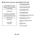
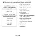
- the multilayer structurecomprises mechanically-stacked solar cells.
- the printable semiconductor elementsare solar cells having different band-gaps.
- an optical system of the present inventionmay optionally comprise a variety of additional device elements including, but not limited to, optical components, dielectric structures, conductive structures, adhesive layers or structures, connecting structures, encapsulating structures, planarizing structures, electro-optic elements and/or thin film structures and arrays of these structures.
- an optical system of the present inventionfurther comprises one or more passive or active optical components selected from the group consisting of: collecting optics, concentrating optics, diffusing optics, dispersive optics, optical fibers and arrays thereof, lenses and arrays thereof, diffusers, reflectors, Bragg reflectors, waveguides (“light-pipes”), and optical coatings (e.g., reflective coatings or antireflective coatings).
- active and/or passive optical componentsare spatially aligned with respect to at least one of the printable semiconductor elements provided on the device substrate.
- Optical systems of this aspect of the present inventionmay optionally comprise a variety of additional device components including, but not limited to, electrical interconnects, electrodes, insulators and electro-optical elements.
- Printed-based assemblymay be used to assembly and integrate additional device elements and additional device components, in addition to assembly and integration of these additional elements by variety of techniques well known in the field of microelectronics, including but not limited to, optical photolithography, deposition techniques (e.g., chemical vapor deposition, physical vapor deposition, atomic layer deposition, sputtering deposition etc.), soft lithography, spin coating and laser ablation patterning.
- Printing-based assemblyprovides a very high degree of control over the physical dimensions, geometry, relative spatial orientation and organization, doping levels and materials purity of the printable semiconductor elements assembled and integrated into the present optical systems.
- printable semiconductor elements of the optical systemare provided on the receiving surface of the substrate with a density equal to or greater than 5 semiconductor elements mm ⁇ 1 , preferably for some embodiments a density equal to or greater than 50 semiconductor elements mm ⁇ 1 , and preferably for some applications a density equal to or greater than 100 semiconductor elements mm ⁇ 1 .
- the printable semiconductor elements of the optical systemhave at least one longitudinal physical dimension (e.g., length, width etc.), optionally two longitudinal physical dimensions, less than or equal to 2000 nanometers, and in some embodiments less than or equal to 500 nanometers.
- each printable semiconductor element of the optical systemhas at least one cross-sectional physical dimension (e.g. thickness) less than or equal to 100 microns, preferably for some applications less than or equal to 10 microns, and preferably for some applications less than or equal to 1 microns.
- the positions of the printable semiconductor elements in the optical system relative to each otherare selected to within 10,000 nanometers.
- Printable semiconductor elementsmay be assembled in selected orientations with respect to each other or other device elements of optical systems of the present invention.
- printable semiconductor elements of the optical systemare longitudinal aligned with respect to each other.
- the present inventionincludes, for example, optical systems wherein printable semiconductor elements extend lengths that are parallel to within 3 degrees of each other.
- the optical systemfurther comprising first and second electrodes provided on the receiving surface, wherein the printable semiconductor elements are in electrical contact with at least one of the electrodes, and wherein the printable semiconductor elements provide a fill factor between the first and second electrodes greater than or equal to 10%, preferably for some embodiments equal to or larger than 50%.
- the present inventionalso includes optical systems comprising printable semiconductor elements arranged in a low density (or sparse) configuration.
- a low density configurationhas benefits for some applications, as the amount of semiconductor incorporated in the device is low, thus, accessing lower costs.
- semiconductor elementsmay be arrange on a substrate so that the density of semiconductor elements is low enough such that the system is optically transparent, preferably for some embodiments more than 50% optical transparent at selected wavelength.
- printable semiconductor elements of the optical systemare provided on the receiving surface of the substrate with a density equal to or less than 1000 semiconductor elements mm ⁇ 1 , preferably for some embodiments a density equal to or less than 500 semiconductor elements mm ⁇ 1 , and more preferably for some embodiments a density equal to or less than 50 semiconductor elements mm ⁇ 1 .
- the semiconductor elementscover less than or equal to 10% of the receiving surface of the target substrate; in another embodiment less than or equal to 1%; and in another embodiment less than or equal to 0.1%.
- the optical systemfurther comprising first and second electrodes provided on the receiving surface, wherein the printable semiconductor elements are in electrical contact with at least one of the electrodes, and wherein the printable semiconductor elements provide a fill factor between the first and second electrodes less than or equal to 10%, preferably for some embodiments less than or equal to 5%.
- the present inventionincludes optical systems comprising printable semiconductor elements assembled and integrated onto a range of useful substrate materials, including glass substrates, polymer substrate, plastic substrates, metal substrates, ceramic substrates, wafer substrates, and composite substrates.
- substrate materialsincluding glass substrates, polymer substrate, plastic substrates, metal substrates, ceramic substrates, wafer substrates, and composite substrates.
- Substrates useful in the present optical systemsinclude those having useful mechanical and/or physical properties such as flexibility, shapeability, stretchability, mechanical ruggedness and optical transparency at selected wavelengths.
- optical systems of the present inventioncomprise printable semiconductor elements assembled and integrated onto a device substrate prepatterned with device components.
- optical systems of the present inventioncomprise printable semiconductor elements assembled and integrated onto a device substrate having a selected optically functionality, such as a device substrate comprising a lens, lens array, optical window, reflector, optical coating, series of optical coatings, or optically transparent substrate optionally having one or more optical coatings such as reflective coatings or anti reflective coatings.
- optical systems of the present inventioncomprise printable semiconductor elements assembled and integrated onto a device substrate having a contoured receiving surface, such as a concave receiving surface, convex receiving surface, a spherical surface, an elliptical surface or receiving surface having a complex contour with both concave regions and convex regions.
- Optical systems of the present inventionmay further comprise one or more encapsulating layers, planarizing layers, laminating layers, cover layers and/or bonding layers.
- Encapsulating layers, laminating layers, planarizing layers, covering layers or bonding layersmay be provided on top of printable semiconductor elements or other device components to provide enhanced mechanical stability and ruggedness.
- Encapsulating layers, laminating layers, planarizing layers, covering layers or bonding layersmay be provided in a configuration so as to mechanically, optically and/or electrically interconnect device components and structures of the present optical systems.
- Encapsulating layers, laminating layers, covering layers, planarizing layers, or bonding layersmay comprise layers of deposited material, spin coated layers and/or molded layers.
- Encapsulating layers, laminating layers, covering layers, planarizing layers, or bonding layersare preferably at least partially optically transparent for some optical systems and applications of the present invention.
- Useful encapsulating layers, laminating layers, planarizing layers, covering layers and/or bonding layersmay comprise one or more polymers, composite polymers, metals, dielectric materials, epoxy materials or prepolymer materials.
- printable semiconductor elementsare bonded or otherwise integrated to the receiving surface via one or more of the following: (i) cold welding the semiconductor elements to the receiving surface via a metal layer provided between the printable semiconductor elements and the receiving layer; (ii) provided via an adhesive layer provided between the printable semiconductor elements and the receiving layer; or (iii) provided by a lamination, encapsulation or planarizing layer provided on top of the printable semiconductor elements and the receiving layer. If the adhesive layer is metal, this layer can also serve to establish electrical contact to the printable semiconductor element during printing-based assembly and integration.
- the composition and thickness of an encapsulating, laminating or planarizing layeris selected such that the printable semiconductor elements, such as printed semiconductor devices and/or device components, assembled on a device substrate are placed near or on the neutral mechanical plane.
- the printable semiconductor elementssuch as printed semiconductor devices and/or device components
- an encapsulating or laminating layeris provided on top of assembled printable semiconductor elements, wherein the encapsulating or laminating layer has a composition and thickness similar to that of the device substrate.
- matching the encapsulating and/or laminating layer composition and thickness dimension with that of the device substrateresults in the printable semiconductor elements residing near the neutral mechanical plane.
- the thickness and Young's modulus of the encapsulating and/or laminating layermay be selected to result in the printable semiconductor elements residing near the neutral mechanical plane.
- An advantage of processing methods and device geometries wherein printable semiconductor elements reside near the neutral mechanical plane of the deviceis that strain on these elements are minimized during bending or deformation. This strategy for managing strains generated during bending has benefits for minimizing delamination or other degradation of the device result from bending induced strain.
- optical systems of the present inventionprovide light emitting optical systems, including, but not limited to, advanced lighting systems, arrays of light emitting diodes, arrays of semiconductor lasers (e.g., VCSELs), passive matrix LED (light emitting diode) displays, active matrix LED displays, ILED (inorganic light emitting diode) displays, macroelectronic display devices, and flat panel displays.
- optical systems of the present inventionprovide light sensing optical systems including, optical sensors and sensor arrays, flexible sensors, stretchable sensors, conformal sensors and sensor skins.
- optical systems of the present inventionprovide optical systems providing both light emitting and light sensing functionality such as sheet scanners.
- Optical systems of the present inventioninclude energy conversion and storage systems including photovoltaic devices, device arrays and systems including solar cell arrays.
- optical systems of the present inventioncomprise a plurality of one or more LEDs, photovoltaic cells, semiconductor lasers, photodiodes, and electro-optical elements having at least two physical dimensions (e.g., length, width, diameter or thickness) less than 200 microns.
- the present inventionprovides an optical system comprising an array of solar cells, wherein each cell in the array has at least two physical dimensions (e.g., length, width, diameter or thickness) less than 200 microns.
- the present inventionprovides an optical system comprising an array of LEDs, wherein each LED in the array has a thickness less than 3 microns, and preferably for some applications less than 1 micron.
- the present inventionprovides a method for making an optical system comprising the steps: (i) providing a device substrate having a receiving surface; and (ii) assembling one or more printable semiconductor elements on the receiving surface of the substrate via contact printing; wherein each of the printable semiconductor elements comprise a semiconductor structure having a length selected from the range of 0.0001 millimeters to 1000 millimeters, a width selected from the range of 0.0001 millimeters to 1000 millimeters and a thickness selected from the range of 0.00001 millimeters to 3 millimeters.
- the printable semiconductor elementcomprises a semiconductor structure having a length selected from the range of 0.02 millimeters to 30 millimeters, and a width selected from the range of 0.02 millimeters to 30 millimeters, preferably for some applications a length selected from the range of 0.1 millimeters to 1 millimeter, and a width selected from the range of 0.1 millimeters to 1 millimeter, preferably for some applications a length selected from the range of 1 millimeters to 10 millimeters, and a width selected from the range of 1 millimeter to 10 millimeters.
- the printable semiconductor elementcomprises a semiconductor structure having a thickness selected from the range of 0.0003 millimeters to 0.3 millimeters, preferably for some applications a thickness selected from the range of 0.002 millimeters to 0.02 millimeters.
- the printable semiconductor elementcomprises a semiconductor structure having a length selected from the range of 100 nanometers to 1000 microns, a width selected from the range of 100 nanometers to 1000 microns and a thickness selected from the range of 10 nanometers to 1000 microns.
- Useful contact printing methods useful in this aspect of the present inventioninclude dry transfer contact printing, microcontact or nanocontact printing, microtransfer or nanotransfer printing and self assembly assisted printing.
- methods of the present inventionemploy contact printing as implemented using a conformable transfer device, such as an elastomeric transfer device (e.g., elastomeric stamp, composite stamp or layer).
- a plurality of printable semiconductor elementsare assembled on the receiving surface of the substrate, for example in a dense or spares configuration.
- methods of this aspect of the present inventionfurther comprise the step of prepatterning the device substrate with one or more device components.
- methods of this aspect of the present inventionfurther comprise the step of providing one or more optical components in optical communication or optical registration with the printable semiconductor elements.
- the printable semiconductor elementcomprises a unitary inorganic semiconductor structure.
- the printable semiconductor elementcomprises a single crystalline semiconductor material.
- methods of the present inventioninclude the step of providing a laminating layer, such as a polymer or elastomer layer on top of at least a portion of the printable semiconductor elements assembled on the receiving surface of the substrate.
- methods of the present inventioninclude the step of planarizing at least a portion of the printable semiconductor elements assembled on the receiving surface of the substrate.
- methods of the present inventioninclude the steps of: (i) providing a planarizing layer to the receiving surface and (ii) embedding at least a portion of the printable semiconductor elements in the planarizing layer.
- methods of the present inventioninclude the step of patterning one or more electrical contacts, electrodes, contact pads or other electrical interconnect structures on at least a portion of the printable semiconductor elements.
- Methods of this aspect of the present inventionfurther comprise the step of assembling and/or integrating one or more additional device components onto the device substrate, such as optical components, electronic components and/or electro-optical components.
- Assembling and/or integrating additional device components in the present methodscan be implemented in combination with a large number of other fabrication techniques, including, but not limited to, lithographic patterning (e.g., optical lithograph and soft lithography), deposition techniques (e.g., CVD, PVD, ALD, etc.), laser ablation patterning, molding techniques (e.g., replica molding), spin coating, self assembly, contact printing, and solution printing.
- lithographic patterninge.g., optical lithograph and soft lithography
- deposition techniquese.g., CVD, PVD, ALD, etc.
- laser ablation patterninge.g., molding techniques (e.g., replica molding)
- spin coatingself assembly
- contact printinge.g., contact printing, and solution printing.
- a combination of optical lithography and deposition techniquesare used to pattern the device substrate prior to or after printing-based assembly of the printable semiconductor elements.
- replica moldingis used to generate optical components, such as a lens array or diffusers, which are subsequently patterned with printable semiconductor elements via contact printing.
- printable semiconductor elements provided on a device substrateare electrically connected to electrodes and electrical interconnects patterned on the device substrate using a combination of optical lithography and deposition techniques.
- an optical systemcomprising a multilayer structure is generated by repeated transfer and assembly steps of printable semiconductor elements, such as thin film transistors, LEDs, semiconductor lasers and/or photovoltaic devices, printed on the device substrate, optionally in combination with additional processing carried out via spin coating, deposition and encapsulation/planarizing steps for integrating additional device components, such as electrode, interconnects, adhesive layers, lamination layers, optical components and encapsulation or planarizing layers.
- printable semiconductor elementssuch as thin film transistors, LEDs, semiconductor lasers and/or photovoltaic devices
- the method of this aspectfurther comprises the step of providing one or more optical components in optical communication or optical registration with the printable semiconductor elements, for example optical components selected from the group consisting of: collecting optics, diffusing optics, dispersive optics, optical fibers and arrays thereof, lenses and arrays thereof, diffusers, reflectors, Bragg reflectors, and optical coatings (e.g., reflective coatings or antireflective coatings).
- optical componentsselected from the group consisting of: collecting optics, diffusing optics, dispersive optics, optical fibers and arrays thereof, lenses and arrays thereof, diffusers, reflectors, Bragg reflectors, and optical coatings (e.g., reflective coatings or antireflective coatings).
- methods of the present inventionmay optionally include the step of providing an array of optical components in optical communication or optical registration with at least a portion of the printable semiconductor elements.
- an optical component of the arrayis individually addressed to each of the printable semiconductor elements.
- the array of optical componentsis fabricated via replica molding; wherein the
- a method of the present inventionfurther comprises providing one or more electrodes in electrical contact with the printable semiconductor elements provided on the device substrate.
- electrodesare defined and integrated into optical systems using a combination of optical lithographic patterning and deposition techniques (e.g., thermal deposition, chemical vapor deposition or physical vapor deposition).
- electrodesare assemble and interconnected with devices elements using printing.
- Methods of the present inventionare useful for providing optical systems on large areas of a receiving surface of a substrate.
- printable semiconductor elementsare provided on an area of the receiving substrate selected over the range of 0.05 m 2 to 10 meters 2 , and preferably for some applications selected over the range of 0.05 m 2 to 1 meters 2
- the present methodsfurther comprise the step of providing an adhesive layer to the receiving surface prior to the assembling step.
- Adhesive layersare useful in the present invention for bonding or otherwise affixing printable semiconductor elements and other device elements to the receiving surface of the substrate.
- Useful adhesive layersinclude but are not limited to one or more metal layers or a polymer layers.
- the present methodsfurther comprise the step of providing a laminating, planarizing or encapsulating layer on the printable semiconductor elements. Laminating, planarizing or encapsulating layers are useful in the present methods for at least partially encapsulating or laminating printable semiconductor elements and other elements on the receiving surface.
- the method of the present inventionfurther comprises the steps of: (i) providing an inorganic semiconductor wafer; (ii) generating the plurality of printable semiconductor elements from the semiconductor wafer; and (iii) transferring the plurality of printable semiconductor elements from the wafer to the receiving surface via contact printing, thereby assembling the plurality of printable semiconductor elements on the receiving surface of the substrate.
- the plurality of printable semiconductor elementsare assembled on the receiving surface of the substrate and on the receiving surfaces of one or more additional substrates, wherein the plurality of printable semiconductor elements assembled on the substrates comprises at least 5% to 50% by mass of the semiconductor wafer. This aspect of the present invention is beneficial because it provides for very efficient use of the semiconductor wafer starting material resulting in low cost fabrication of optical systems.
- the “plurality of printable semiconductor elements assembled on the substrates”may comprise a very low fraction ( ⁇ about 5% by mass or area) of the final, device substrate.
- the printed systemsmay exhibit a low fill-factor of the semiconductor.
- the advantage of a low-fill factoris that it requires a small amount of semiconductor material, which in these cases is expensive on a per-area basis, to populate large areas of final, device substrate(s).
- the present inventionprovides a method of making a semiconductor-based optical system comprising the steps of: (i) providing an optical component having an external surface and an internal surface; (ii) providing a electrically conducting grid or mesh on the internal surface of the optical component; (iii) providing a device substrate having a receiving surface; (iv) assembling a plurality of printable semiconductor elements on the receiving surface of the substrate via contact printing; wherein each of the printable semiconductor elements comprise a unitary inorganic semiconductor structure having a length selected from the range of 0.0001 millimeters to 1000 millimeters, a width selected from the range of 0.0001 millimeters to 1000 millimeters and a thickness selected from the range of 0.00001 millimeters to 3 millimeters; and (v) transferring the optical component having the grid or mesh to the substrate, wherein the optical component is positioned on top of the semiconductor elements assembled on the on the receiving surface of the substrate, and wherein the grid or mesh is provided between the optical component and the semiconductor elements.
- the printable semiconductor elementcomprises a semiconductor structure having a length selected from the range of 0.02 millimeters to 30 millimeters, and a width selected from the range of 0.02 millimeters to 30 millimeters, preferably for some applications a length selected from the range of 0.1 millimeters to 1 millimeter, and a width selected from the range of 0.1 millimeters to 1 millimeter, preferably for some applications a length selected from the range of 1 millimeters to 10 millimeters, and a width selected from the range of 1 millimeter to 10 millimeters.
- the printable semiconductor elementcomprises a semiconductor structure having a thickness selected from the range of 0.0003 millimeters to 0.3 millimeters, preferably for some applications a thickness selected from the range of 0.002 millimeters to 0.02 millimeters.
- the printable semiconductor elementcomprises a semiconductor structure having a length selected from the range of 100 nanometers to 1000 microns, a width selected from the range of 100 nanometers to 1000 microns and a thickness selected from the range of 10 nanometers to 1000 microns.
- the printable semiconductor elementcomprises a unitary inorganic semiconductor structure. In a method of the present invention, the printable semiconductor element comprises a single crystalline semiconductor material.
- FIG. 1provides a schematic showing optical systems provided by the present invention.
- the present inventionprovides a number of classes of optical systems and related methods of making these systems, including systems for light generation and systems for light harvesting comprising printed inorganic optoelectronic systems with integrated optical components in registry.
- FIG. 2 A-Eprovides schematic diagrams of optical systems of the present invention comprising printable semiconductor elements.
- FIG. 2Ashows a printed LED array with integrated optical diffuser.
- FIG. 2Bshows a VCSEL array on a silicon chip with integrated optical fibers.
- FIG. 2Cshows a printed photovoltaic array with integrated optical collectors.
- FIG. 2Dshows an artificial eye sensor comprising a printed photodiode array on a collecting lens.
- FIG. 2Eshows a sheet scanner having both light sensing and light generation functionality and comprising a printed array LED and photodiode components and integrated collection optics provided on a polymer or other low cost substrate.
- FIG. 3provides a process flow schematic for the fabrication of a single pixel element of a printed inorganic active matrix LED display of the present invention.
- FIG. 4provides a schematic illustration (not to scale) of a printed active matrix LED display on a glass substrate.
- the display showncomprises 100 pixels and is an approximately 11 inch display.
- Thin film transistor (TFT) elements, LED elements, gate lines, anode lines and data lines of the deviceare indicated in FIG. 4 .
- FIG. 5provides photographs ( FIG. 5A ) and operating current-voltage characteristics ( FIG. 5B ) of a single pixel of an active matrix LED display on a (transparent) glass substrate.
- the single pixel of an active matrix LED displaycomprises a printed TFT structure, a LED structure, gate electrode and electrical interconnects.
- FIG. 5Bprovides a plot of current (A) verses drive bias (V) for the single pixel of an active matrix LED display.
- FIGS. 6A-6Cprovide photographs of a 64 pixel active matrix LED display on a (transparent) glass substrate.
- FIG. 6Aprovides a photograph of a 64 pixel partial LED display (Note: missing top contacts) comprising 1 mm transistors printed on to the device substrate and ILEDs manually placed on the substrate. In the device shown in FIG. 6A pixels are provided at a 4 mm pitch.
- FIG. 6Bprovides a photograph of a printed silicon TFT with interdigitated channel (thin green line) for high-current operation.
- FIG. 6Cprovides a photograph of two pixels illuminated by placing a transparent common anode electrical contact against the LEDs.
- FIG. 7Aprovides a process flow schematic for the fabrication of a single pixel element of a printed inorganic passive matrix LED display.
- FIG. 7Bprovides a process flow schematic for establishing electrical contact by compression of a (soft) substrate/layer.
- FIG. 8provides a schematic illustration (not to scale) of a printed passive matrix printed inorganic LED display. As shown in FIG. 8 the display comprises a bottom substrate, electrode network, printed ILED, PDMS layer and top substrate.
- FIG. 9provides photographs of passively addressed printed inorganic LED displays/arrays on glass and flexible PET substrates.
- FIG. 10provides a process flow schematic for printing inorganic light emitters and collectors via cold-weld bonding techniques.
- FIG. 11provides a process flow schematic for printing using a donor cartridge and cold-weld bonding technique.
- a cartridgeis patterned with SU-8.
- ILED structuresare placed on the patterned surface of the cartridge.
- a stampis used to take up the ILED structures and subsequently print the ILED structures on a substrate prepatterned with electrodes via transfer printing.
- the bottom panel of FIG. 11shows an example of a LED structure printed using this method.
- FIG. 12provides a schematic of an optical system of the present invention wherein diffusing optics are integrated with printable LED structures.
- PDMSis molded on rough polystyrene.
- a comparison of panels (a) and (b)show the affect of incorporation of a diffuser in this optical system.
- the diffusercan be a rough molded PDMS structure. This figure demonstrates that diffusers can effectively increase the size of the luminous region.
- FIG. 13provides a schematic of diffusing optics comprising radial density gradient scattering centers useful for LED lighting systems of the present invention.
- a printed LED structure under metalis provided in optical communication with a plurality of optical scattering centers.
- the bottom panel in FIG. 13shows a cross sectional view of scattering centers comprising relief features in a transparent substrate.
- FIG. 14Aprovides an exemplary epilayer structure for the fabrication of printable micro-LEDs.
- the epilayer structurecomprises a series of device layers, sacrificial layers and a handle wafer. Individual layers in the epilayer structure are shown in the bottom panel of FIG. 14A .
- FIG. 14Bprovides an exemplary epilayer structure for the fabrication of printable micro-LEDs comprising quantum well emissive layers.
- the epilayer structurecomprises a series of semiconductor layers provided between p-cladding and n-cladding layers. Specific compositions of each layer in the epilayer structure are provided.
- FIG. 14Cprovides a table indicating the composition, thickness, doping and functionality of each layer in the epilayer structure for the fabrication of printable micro-LEDs.
- FIG. 14Aprovides an exemplary epilayer structure for the fabrication of printable micro-LEDs.
- the epilayer structurecomprises a series of device layers, sacrificial layers and a handle wafer. Individual layers in the epilayer structure are shown in the bottom panel of FIG. 14A .
- FIG. 14Dillustrates an example of a mother wafer from which printable p-on-n GaAs solar cells may be produced by photolithography and etching layers 9 through 4 and selectively removing layer 3 by a wet chemical etch.
- FIG. 14Eillustrates provides another example of a mother wafer from which printable n-on-p GaAs solar cells may be produced by photolithography and etching layers 9 through 4 and selectively removing layer 3 by a wet chemical etch.
- FIG. 15provides schematic diagrams illustrating the imperceptible pixilation/high degree of transparency from low fill-factor, micro-sized ( ⁇ ⁇ 100 micron footprint) LEDs.
- the optical systemcomprises: (i) a first glass coated ITO or a low-fill factor metal mesh layer; (ii) printed micro LEDS structures; and (iii) a second glass coated ITO or a low-fill factor metal mesh layer. Top views are provided corresponding to the off state and the on state. A magnification of the top view is also provided showing the positioning of micro LED structures.
- FIG. 16provides schemes for the release of printable light-emitting inorganic semiconductor micro-elements: micro-LEDs or VCSELs.
- Scheme 1describes the release of such elements by encapsulating them in a polymer, e.g. photoresist, and releasing them from the wafer on which they were grown by selectively etching an Al x Ga 1-x As (x>about 70%) sacrificial layer using hydrofluoric acid.
- Scheme 2describes release by encapsulating them in a conformal dielectric (e.g. silicon nitride) and releasing them from the wafer by selectively oxidizing the AlGaAs and etching the oxidized material using aqueous potassium hydroxide.
- a conformal dielectrice.g. silicon nitride
- Scheme 3describes release by encapsulating them with a polymer, e.g. photoresist, followed by selective etching of a buried GaAs sacrificial layer using an aqueous mixture of citric acid and hydrogen peroxide.
- the AlGaAsprotects the underside of the light emitting element from the citric acid-based etchant.
- FIG. 17Aprovides a schematic process flow diagram illustrating fabrication of integrated solar cell/collector arrays by printing solar cells.
- FIG. 17Bprovides a schematic process flow diagram illustrating fabrication of integrated solar cell/collector arrays via interconnection of registry of an optical array.
- FIG. 17Cprovides a schematic process flow diagram illustrating the operation of the integrated solar cell/collector arrays.
- FIG. 18Aprovides a schematic ray diagram (not to scale) showing operation of the integrated low-level collecting optics (lens) and solar-cell arrays of an optical system of the present invention. As shown in FIG. 18A radiation is collected by the concentrator and focused on printed microsolar cells.
- FIG. 18Bshows an expanded view of a microcell of the present invention comprising an antireflection layer, top contact and p-n junction.
- FIG. 19provide a schematic diagram illustration of light harvesting via reduction of semiconductor materials costs in a sheet-like form factor.
- the collector sizeis approximately 2 mm
- the solar cell sizeis approximately 0.1 mm
- the area multiplicationratio of collector area and solar cell area
- 1 ft 2 of processed semiconductor waferresults in approximately 400 ft 2 of light-harvesting area.
- This calculationdemonstrates the methods and optical systems of the present invention provide a high efficiency and low cost fabrication strategy for high performance photovoltaic devices and systems.
- FIG. 20provides a schematic diagram of a collecting optic and heterogenously composed solar cell of a solar cell array (sympevolent/diventegration) of the present invention.
- collecting opticsare provided in optical communication with a nitride/phosophide and/or arsenide solar cell and silicon solar cell assembled on the device substrate via contact printing.
- FIG. 20also provides ray diagram of the incident light shown collection and focus functionality of a concentrator and individually addressed solar cells.
- Single crystal multilayer solar cellsi.e. third generation solar cells
- FIG. 21provides a schematic process flow diagram for fabrication of an integrated solar cell and lens array using a combination of replica molding methods and contact printing.
- a master lens arrayis used to generate a negative replica mold, for example via replica molding or imprinting techniques.
- the molded PDMS layeris used to generate a plano-concave polymer lens array by casting the polymer against the negative replica.
- solar cells printed onto a device substrateare provided in optical communication with the lens array so as to generate an optical system of the present invention.
- FIG. 22demonstrates the ability of Fresnel lenses, a type of concentrating/collecting optic, to focus light to a small area for use in light harvesting systems described by the present invention.
- Fresnel lens arrayscan be used as optical concentrators due to its advantageous features such as thin form factor and light weight compared with conventional lenses.
- the figureshows a focal area measurement for spherical and cylindrical Fresnel lenses.
- FIG. 23provides a schematic diagram illustrating an optical system of the present invention wherein horizontal light pipes and/or waveguides are provided for light harvesting.
- This optical systemuses transparent, structured media of appropriate index of refraction to capture normally- or obliquely-incident light and guide it in the plane of the substrate to a solar cell or solar cell array.
- FIG. 24provides a schematic showing an exemplary printable silicon solar cell fabricated using a silicon on insulator SOI wafer.
- the solar cellcomprises a doped top surface with a P/As mixture and is supported by a buried oxide layer of the SOI wafer.
- FIG. 24shows the solar cell multilayer structure comprising a n + -Si (P/As) layer and p-Si(B) layer.
- FIG. 25provides a schematic process flow diagram illustrating a method of transferring a printable solar cell to substrate using contact printing and subsequent cold welding processing to affix the solar cell to a device substrate.
- FIG. 26provides a schematic diagram (not to scale) showing a top view (in parallel) of an exemplary configuration for top contacts to solar arrays of the present invention.
- Microsolar cellsshown in gray
- Metal featuresare provided having widths of 60 microns and length on the order of 1 inch.
- the metal featuresprovide the top contacts of a solar cell device array of the present invention.
- This figuresshows a flexible strip light made of blue LEDs and a thin kapton substrate with a bending radius equal to 0.85 cm.
- FIG. 27provides a schematic diagram of an “artificial eye” sensor of the current invention.
- the sensorcomprises inorganic photodiode arrays distributed on a lens having spherical curvature. Various lens shapes and angles are shown in FIG. 27
- FIG. 28provides a schematic diagram illustrating wrapping a planar sheet around a spherical surface demonstrating the necessity of stretchability in an exemplary “artificial eye” sensor. As shown in FIG. 28 , conformal positioning of the planar sheet requires some degree of stretchability to avoid failure.
- FIG. 29provide a schematic processes flow diagram showing a method for making a microsolar cell array of the present invention.
- FIG. 30Estimated Short Circuit Current (J SC ) and AM1.5 Efficiency as a function of Silicon Thickness.
- FIG. 31Scanning Electron Micrographs Showing Sequential Formation of Si Multilayer Ribbon Stacks.
- FIG. 32provides a schematic diagram of a connection scheme where the Si ribbons comprising p-type silicon with a thin n-type layer on top to form the emitter. Left side shows the as-transferred Si Ribbons, right shows the connection (direct-write or screen-printing). Only four Si Ribbons are shown for clarity.
- FIG. 33provides a schematic of a solar cell array of the present invention using PDMS for concentrating solar illumination.
- FIG. 34provides images showing results of printing single crystal silicon onto plastic, glass, Si wafers, InP wafers and thin film a-Si.
- the microstamping process of the present inventionis compatible with a wide range of substrates.
- FIG. 35shows a schematic illustration of an exemplary process of the present invention, as applied to the printing of printable inorganic semiconductor-based LEDs.
- FIG. 36provides an image and a schematic illustration of a printer useful in the present methods of fabricating conformable LED lighting systems.
- FIG. 37provides images of square (part a) and linear (part b) lighting devices that comprise passively addressed blue inorganic LEDs assembled on plastic substrates via contact printing.
- the device in part (b)represents a conformal ILED-based thin film lighting device of the present invention.
- FIG. 38provides a schematic process flow diagram of a method of fabricating a conformable LED lighting system of the present invention.
- FIG. 39provides a process flow diagram for fabricating an ILED light device of the present invention comprising a flexible strip.
- FIG. 40provides a cross sectional view of a conformal ILED lighting system of the present invention comprising top and bottom PET substrates (approximately 175 microns thick), ILEDS structures (approximately 100 microns thick), electrodes and a PDMS encapsulating coating.
- FIG. 41provides images of ILED lighting systems of the present invention in an unbent state, a first bent state with a bending radius of 7 cm, a second bent state with a bending radius of 5 cm, third bent state with a bending radius of 4.5 cm, a fourth bent state with a bending radius of 3 cm and in a state upon release of the bending stress.
- the images in FIG. 42confirm that conformal ILED lighting systems of the present invention provide useful optical properties in bent configurations.
- FIG. 42provides an image of a flexible strip light made of blue LEDs and thin kapton substrates with bending radius equal to 0.85 cm.
- FIG. 43provides schematics showing two methods for assembling ILED structures on the device substrate.
- FIG. 44provides a schematic for the formation of a micro single crystal silicon solar cell with low-level concentrating lens.
- the micro structuresare transferred from PDMS onto an embedded electrode which serves as the back electrical contact for the device.
- the siliconis transferred by laminating the PDMS onto the electrode surface and slowly peeling the PDMS back.
- step (b)planarization followed by the formation of the top metal contacts is performed.
- the deviceis completed by integrating a low concentration cylindrical lens array made from PDMS onto the device (step c). In this final step it can be seen that the device was designed such that the rows of silicon cells align with the focal point of the lens array.
- FIG. 45provides images of a silicon solar cell transferred to a glass substrate.
- (a)Optical image of a single cell on a glass substrate with both top and bottom electrical contacts.
- FIG. 46provides images of a solar cell array joined to cylindrical collecting optics.
- FIG. 47provides a schematic diagram for generating optical concentrator arrays with integrated metal contacts onto mS-Silicon solar cells (micro-silicon solar cells). The process starts off with retrieval of a metal mesh pattern from a substrate (shown dark blue) via a PDMS molded lens array. The lens array/mesh pattern can then be laminated in registry onto an array of silicon solar cells.
- FIG. 48illustrates the process flow for generating solar cells and integrated concentrating optics.
- FIG. 49provides images of a micro solar cell array printed onto gold bus lines on glass substrates via a thin PDMS adhesive layer. Also shown are current-voltage characteristics for the solar cell array.
- FIG. 50provides a schematic illustration of microcells of (a) vertical-type, (b) transverse-type, (c) combination of both types.
- FIG. 51provides a schematic diagram illustrating a method of the present invention for making large area optical systems using micromanipulation via transfer printing. This techniques provides for massively parallel assembly of inorganic semiconductor elements and semiconductor devices having micro-sized and/or nanosized physical dimensions.
- FIG. 52provide a plot of current (A) versus applied voltage (V) for a inorganic LED device assembled via transfer printing.
- FIG. 53Aprovide a plot of current (A) versus applied voltage (V) for a printed thin-film inorganic LED device assembled on a plastic substrate via transfer printing.
- FIG. 53Aalso provide a schematic diagram of the assembled device.
- FIG. 53Bprovides a schematic diagram shown an exemplary ILED epilayer structure useful in the present invention.
- FIGS. 54A and 54Bprovides schematic diagrams of systems of the present invention comprising planarized printable semiconductor elements.
- FIG. 55provides a flow diagram illustrating processing steps in methods of the present invention for making semiconductor-based optical systems comprising planarized printable semiconductor elements, such as printable semiconductor-based electronic devices and device components.
- FIG. 56provides experimental results characterizing the impact of step edges on establishing electrical contact to and/or between printable semiconductor elements.
- FIG. 57provides a process flow diagram for making printable semiconductor elements comprising vertical solar cells that can be subsequently assembled and interconnected to fabricate a solar cell array.
- FIG. 58provides SEM images of microsolar cells of different thicknesses fabricated from bulk wafers. (Top to bottom: 8 microns, 16 microns, 22 microns thick).
- FIG. 59provides a plot showing IV characteristics of an individual solar cell device fabricated using the present processing platform.
- FIG. 60shows processing for generating top contacts for the vertical solar cells and related electronic performance data.
- FIG. 61provides a schematic showing a solar cell layout of transverse type solar cells to be patterned on a ⁇ 111> p-type Si wafer and capable of subsequent assembly and integration via contact printing.
- FIG. 62provides a schematic showing the doping scheme wherein boron (P+) and phosphorous (n+) doped regions are patterned on the external surface of the patterned semiconductor ribbons.
- FIG. 63provides an overview schematic showing the process flow for cell patterning and doping steps.
- FIG. 64provides a schematic diagram showing processing steps for patterning solar cell ribbons illustrating photolithography and STS deep RIE etching process steps.
- FIG. 65shows results from KOH refining processing of the sidewalls of the patterned ribbons.
- FIG. 66provides a schematic diagram for boron doping processing. After the KOH refining step, boron doping for formation of top p+ contact is conducted.
- FIG. 67provides a schematic diagram for phosphorous doping processing
- FIG. 68provides a schematic diagram showing sidewall passivation processing.
- FIG. 69provides a schematic diagram showing processing for the formation of a KOH etching window.
- FIG. 70provides micrographs showing KOH etching processing and bottom boron doping processing.
- FIG. 71provides images showing transfer of the solar cell ribbons from the source wafer using a PDMS transfer device.
- FIG. 72provides a schematic diagram illustrating contact printing and planarization processing steps.
- FIG. 73provides an imaging showing the results of metallization processing.
- FIG. 74provides a schematic diagram of the metallization process showing an Al metal layer, SiO 2 dielectric layer, Cr/Au layer, solar cell, planarizing layer and device substrate.
- FIGS. 75A and 75Bprovide schematic diagrams exemplifying the expressions “lateral dimensions” and “cross sectional dimensions” as used in the present description.
- FIG. 75Aprovides a top plan view of printable semiconductor elements comprising 4 semiconductor ribbons 6005 .
- the expression “lateral dimension”is exemplified by the length 6000 and width 6010 of the semiconductor ribbons 6005 .
- FIG. 75Bprovides a cross sectional view of the printable semiconductor elements comprising 4 semiconductor ribbons 6005 .
- FIG. 76shows an array of printable GaAs/InGaAlP red LEDs printed on PET substrates.
- Collecting and “Concentrating”, as applied to optics and optical components,refers to the characteristic of optical components and device components that they direct light from a relatively large area and direct that light to another area, in some cases a smaller area.
- collecting and concentration optical components and/or optical componentsare useful for light detection or power harvesting by printed inorganic solar cells or photodiodes.
- Printrelates to materials, structures, device components and/or integrated functional devices that are capable of transfer, assembly, patterning, organizing and/or integrating onto or into substrates without exposure of the substrate to high temperatures (i.e. at temperatures less than or equal to about 400 degrees Celsius).
- printable materials, elements, device components and devicesare capable of transfer, assembly, patterning, organizing and/or integrating onto or into substrates via solution printing or contact printing.
- Print semiconductor elementsof the present invention comprise semiconductor structures that are able to be assembled and/or integrated onto substrate surfaces, for example using by dry transfer contact printing and/or solution printing methods.
- printable semiconductor elements of the present inventionare unitary single crystalline, polycrystalline or microcrystalline inorganic semiconductor structures.
- printable semiconductor elementsare connected to a substrate, such as a mother wafer, via one or more bridge elements.
- a unitary structureis a monolithic element having features that are mechanically connected.
- Semiconductor elements of the present inventionmay be undoped or doped, may have a selected spatial distribution of dopants and may be doped with a plurality of different dopant materials, including P and N type dopants.
- Printable semiconductor elements and structures of the present inventionmay include holes or perforations through one dimension of the elements to facilitate their release from a wafer by the introduction of a chemical release agent.
- the present inventionincludes microstructured printable semiconductor elements having at least one cross sectional dimension (e.g., thickness) selected over the range of 1 micron to 1000 microns.
- the present inventionincludes nanostructured printable semiconductor elements having at least one cross sectional dimension (e.g., thickness) selected over the range of 1 to 1000 nanometers.
- a printable semiconductor element of the present inventionhas a thickness dimensions less than of equal or 1000 microns, preferably for some applications a thickness dimensions less than or equal to 100 microns, preferably for some applications a thickness dimensions less than or equal to 10 microns and preferably for some applications a thickness dimensions less than or equal to 1 microns.
- printable semiconductor elements useful in many applicationscomprises elements derived from “top down” processing of high purity bulk materials, such as high purity crystalline semiconductor wafers generated using conventional high temperature processing techniques.
- printable semiconductor elements of the present inventioncomprise composite heterogeneous structures having a semiconductor operational connected to or otherwise integrated with at least one additional device component or structure, such as a conducting layer, dielectric layer, electrode, additional semiconductor structure or any combination of these.
- the printable semiconductor element(s)comprises a semiconductor structure integrated with at least one additional structure selected from the group consisting of: another semiconductor structure; a dielectric structure; conductive structure, and an optical structure (e.g., optical coatings, reflectors, windows, optical filter, collecting, diffusing or concentration optic etc.).
- the printable semiconductor element(s)comprises a semiconductor structure integrated with at least one electronic device component selected from the group consisting of: an electrode, a dielectric layer, an optical coating, a metal contact pad a semiconductor channel.
- printable semiconductor elements of the present inventioncomprise stretchable semiconductor elements, bendable semiconductor elements and/or heterogeneous semiconductor elements (e.g., semiconductor structures integrated with one or more additional materials such as dielectrics, other semiconductors, conductors, ceramics etc.).
- Printable semiconductor elementsinclude, printable semiconductor devices and components thereof, including but not limited to printable LEDs, lasers, solar cells, p-n junctions, photovoltaics, photodiodes, diodes, transistors, integrated circuits, and sensors.
- Cross sectional dimensionrefers to the dimensions of a cross section of device, device component or material.
- Cross sectional dimensionsinclude the thickness, radius, or diameter of a printable semiconductor element.
- printable semiconductor elements having a ribbon shapeare characterized by a thickness cross sectional dimension.
- printable semiconductor elements having a cylindrical shapeare characterized by a diameter (alternatively radius) cross sectional dimension.
- “Longitudinally oriented in a substantially parallel configuration”refers to an orientation such that the longitudinal axes of a population of elements, such as printable semiconductor elements, are oriented substantially parallel to a selected alignment axis.
- substantially parallel to a selected axisrefers to an orientation within 10 degrees of an absolutely parallel orientation, more preferably within 5 degrees of an absolutely parallel orientation.
- a flexible material, structure, device or device componentmay be deformed into a curved shape without introducing strain larger than or equal to 5%, preferably for some applications larger than or equal to 1%, and more preferably for some applications larger than or equal to 0.5%.
- semiconductorrefers to any material that is a material that is an insulator at a very low temperature, but which has a appreciable electrical conductivity at a temperatures of about 300 Kelvin. In the present description, use of the term semiconductor is intended to be consistent with use of this term in the art of microelectronics and electrical devices.
- Semiconductors useful in the present inventionmay comprise element semiconductors, such as silicon, germanium and diamond, and compound semiconductors, such as group IV compound semiconductors such as SiC and SiGe, group III-V semiconductors such as AlSb, AlAs, Aln, AlP, BN, GaSb, GaAs, GaN, GaP, InSb, InAs, InN, and InP, group III-V ternary semiconductors alloys such as Al x Ga 1-x As, group II-VI semiconductors such as CsSe, CdS, CdTe, ZnO, ZnSe, ZnS, and ZnTe, group I-VII semiconductors CuCl, group IV-VI semiconductors such as PbS, PbTe and SnS, layer semiconductors such as PbI 2 , MoS 2 and GaSe, oxide semiconductors such as CuO and Cu 2 O.
- group IV compound semiconductorssuch as SiC and SiGe
- group III-V semiconductorssuch as AlSb, Al
- semiconductorincludes intrinsic semiconductors and extrinsic semiconductors that are doped with one or more selected materials, including semiconductor having p-type doping materials and n-type doping materials, to provide beneficial electrical properties useful for a given application or device.
- semiconductorincludes composite materials comprising a mixture of semiconductors and/or dopants.
- Specific semiconductor materials useful for in some applications of the present inventioninclude, but are not limited to, Si, Ge, SiC, AlP, AlAs, AlSb, GaN, GaP, GaAs, GaSb, InP, InAs, GaSb, InP, InAs, InSb, ZnO, ZnSe, ZnTe, CdS, CdSe, ZnSe, ZnTe, CdS, CdSe, CdTe, HgS, PbS, PbSe, PbTe, AlGaAs, AlInAs, AlInP, GaAsP, GaInAs, GaInP, AlGaAsSb, AlGaInP, and GaInAsP.
- Porous silicon semiconductor materialsare useful for applications of the present invention in the field of sensors and light emitting materials, such as light emitting diodes (LEDs) and solid state lasers.
- Impurities of semiconductor materialsare atoms, elements, ions and/or molecules other than the semiconductor material(s) themselves or any dopants provided to the semiconductor material. Impurities are undesirable materials present in semiconductor materials which may negatively impact the electrical properties of semiconductor materials, and include but are not limited to oxygen, carbon, and metals including heavy metals. Heavy metal impurities include, but are not limited to, the group of elements between copper and lead on the periodic table, calcium, sodium, and all ions, compounds and/or complexes thereof.
- Plasticrefers to any synthetic or naturally occurring material or combination of materials that can be molded or shaped, generally when heated, and hardened into a desired shape.
- Exemplary plastics useful in the devices and methods of the present inventioninclude, but are not limited to, polymers, resins and cellulose derivatives.
- the term plasticis intended to include composite plastic materials comprising one or more plastics with one or more additives, such as structural enhancers, fillers, fibers, plasticizers, stabilizers or additives which may provide desired chemical or physical properties.
- Elastomerrefers to a polymeric material which can be stretched or deformed and return to its original shape without substantial permanent deformation. Elastomers commonly undergo substantially elastic deformations. Exemplary elastomers useful in the present invention may comprise, polymers, copolymers, composite materials or mixtures of polymers and copolymers. Elastomeric layer refers to a layer comprising at least one elastomer. Elastomeric layers may also include dopants and other non-elastomeric materials.
- Elastomers useful in the present inventionmay include, but are not limited to, thermoplastic elastomers, styrenic materials, olefenic materials, polyolefin, polyurethane thermoplastic elastomers, polyamides, synthetic rubbers, PDMS, polybutadiene, polyisobutylene, poly(styrene-butadiene-styrene), polyurethanes, polychloroprene and silicones.
- Elastomersprovide elastomeric stamps useful in the present methods.
- Transfer devicerefers to a device or device component capable of receiving, relocating, assembling and/or integrating an element or array of elements, such as one or more printable semiconductor elements.
- Transfer devices useful in the present inventioninclude conformable transfer devices, having one or more contact surfaces capable of establishing conformal contact with elements undergoing transfer. The present methods and compositions are particularly well suited for implementation in connection with a transfer device comprising an elastomeric transfer device.
- Useful elastomeric transfer devicesincluding an, elastomeric stamp, composite elastomeric stamp, an elastomeric layer, plurality of elastomeric layers and an elastomeric layer coupled to a substrate such as a glass, ceramic, metal or polymer substrate.
- Large arearefers to an area, such as the area of a receiving surface of a substrate used for device fabrication, greater than or equal to 36 square inches.
- Conformal contactrefers to contact established between surfaces, coated surfaces, and/or surfaces having materials deposited thereon which may be useful for transferring, assembling, organizing and integrating structures (such as printable semiconductor elements) on a substrate surface.
- conformal contactinvolves a macroscopic adaptation of one or more contact surfaces of a conformable transfer device to the overall shape of a substrate surface or the surface of an object such as a printable semiconductor element.
- conformal contactinvolves a microscopic adaptation of one or more contact surfaces of a conformable transfer device to a substrate surface leading to an intimate contact with out voids. The term conformal contact is intended to be consistent with use of this term in the art of soft lithography.
- Conformal contactmay be established between one or more bare contact surfaces of a conformable transfer device and a substrate surface.
- conformal contactmay be established between one or more coated contact surfaces, for example contact surfaces having a transfer material, printable semiconductor element, device component, and/or device deposited thereon, of a conformable transfer device and a substrate surface.
- conformal contactmay be established between one or more bare or coated contact surfaces of a conformable transfer device and a substrate surface coated with a material such as a transfer material, solid photoresist layer, prepolymer layer, liquid, thin film or fluid.
- “Placement accuracy”refers to the ability of a transfer method or device to transfer a printable element, such as a printable semiconductor element, to a selected position, either relative to the position of other device components, such as electrodes, or relative to a selected region of a receiving surface.
- “Good placement” accuracyrefers to methods and devices capable of transferring a printable element to a selected position relative to another device or device component or relative to a selected region of a receiving surface with spatial deviations from the absolutely correct position less than or equal to 50 microns, more preferably less than or equal to 20 microns for some applications and even more preferably less than or equal to 5 microns for some applications.
- the present inventionprovides devices comprising at least one printable element transferred with good placement accuracy.
- Optical communicationrefers to a configuration of two or more elements wherein one or more beams of electromagnetic radiation are capable of propagating from one element to the other element. Elements in optical communication may be in direct optical communication or indirect optical communication. “Direct optical communication” refers to a configuration of two or more elements wherein one or more beams of electromagnetic radiation propagate directly from a first device element to another without use of optical components for steering and/or combining the beams. “Indirect optical communication” on the other hand refers to a configuration of two or more elements wherein one or more beams of electromagnetic radiation propagate between two elements via one or more device components including, but not limited to, wave guides, fiber optic elements, reflectors, filters, prisms, lenses, gratings and any combination of these device components.
- the present inventionrelates to the following fields: collecting optics, diffusing optics, displays, pick and place assembly, vertical cavity surface-emitting lasers (VCSELS) and arrays thereof, LEDs and arrays thereof, transparent electronics, photovoltaic arrays, solar cells and arrays thereof, flexible electronics, micromanipulation, plastic electronics, displays, transfer printing, LEDs, transparent electronics, stretchable electronics, and flexible electronics.
- VSELSvertical cavity surface-emitting lasers
- the present inventionprovides optical devices and device arrays, for example LED arrays, laser arrays, optical sensors and sensor arrays, and photovoltaic arrays, comprising printable, high quality inorganic semiconductor elements assembled and integrated via transfer printing techniques.
- Assembly and integration methods of the present inventioninclude dry contact printing of printable semiconductor elements, replica molding for making device substrate such as device substrates having integrated optical components (e.g., lens arrays) and lamination processing steps.
- the inventionprovides a new type of display that generates images by the coordinated operation of assemblies of light-emitting diodes (LEDs) or other light emitting or collecting devices.
- the imagesmay be high definition, as those on a computer monitor or television, or they may provide simple illumination in a way similar to fluorescent lights.
- the inventionis formed by the assembly of small inorganic light emitting devices, transistors, and electrically conductive interconnects. Transfer printing and other novel fabrication processes may be used to perform the assembly of these components and to impart new functionality to them, e.g. stretchability.
- the inventionmay be built on a range of substrates, including rigid materials (e.g. glass), flexible materials (e.g. thin plastic), and even stretchable materials (e.g. elastomers), imparting a number of benefits to these display and illumination products, including a high-degree of transparency, flexibility, and/or stretchability, as well as mechanical toughness and low weight.
- the inventionis therefore useful for a number of applications, including architectural elements and devices that can dynamically conform to complex contours of objects, for example in the aerospace, transportation, medical, and fashion industries.
- the light emitters (LEDs) usedare capable of high-speed operation and great brightness, enabling effective display of images even in full sunlight (e.g. for outdoor displays).
- novel transfer printing and other fabrication processes of the present inventionin addition to imparting functionality to the displays, enable the production of systems of the invention at costs lower than those required to produce other, less versatile types of displays (e.g. conventional LED displays).
- novel transfer printing and other fabrication proceduresalso enables systems of the invention to achieve levels of brightness, large-area coverage, transparency, mechanical properties, operating lifetime, and/or resolution combinations that are not available to other display technologies (liquid crystal displays, organic LED displays, conventional LED displays, cathode ray tube displays, etc.).
- FIG. 1provides a schematic showing optical systems provided by the present invention.
- the present inventionprovides a number of classes of optical systems and related methods of making these systems, including systems for light generation and systems for light harvesting, comprising printed inorganic optical and optoelectronic systems with integrated optical components in registry.
- Light generation systemsinclude printed LED displays, micro LED devices, passive matrix LED displays, active matrix LED displays, printed VCSEL systems and printed semiconductor laser arrays, optionally comprising light diffusing optics, light focusing optics and/or light filtering optics.
- Light harvesting systemsinclude sensors, such as artificial eye sensors, sphere/plane convertible stamp sensors and sphere confirmable stretchable semiconductor based sensors, and photovoltaic systems, such as photovoltaic arrays, microsolar cells, optionally comprising collecting optics.
- Optical systems of the present inventioninclude stretchable devices and systems, flexible devices and systems and rigid devices and systems.
- FIG. 2 A-Eprovides schematic diagrams of optical systems of the present invention comprising printable semiconductor elements.
- FIG. 2Ashows a printed LED array with integrated optical diffuser.
- FIG. 2Bshows a VCSEL array on a silicon chip with integrated optical fibers.
- FIG. 2Cshows a printed photovoltaic array with integrated optical collectors.
- FIG. 2Dshows an artificial eye sensor comprising a printed photodiode array on a collecting lens.
- FIG. 2Eshows a sheet scanner having both light sensing and light generation functionality and comprising a printed array LED and photodiode components and integrated collection optics provided on a polymer or other low cost substrate.
- FIG. 3provides a process flow schematic for the fabrication of a single pixel element of a printed inorganic active matrix LED display of the present invention.
- Panel 1illustrates the step of preparing gate electrodes on substrate.
- Panel 2illustrates the step of spin-coat thin-film adhesive on the patterned substrate.
- Panel 3illustrates the step of printing a thin-film transistor structure on the adhesive layer, for example using contact printing.
- Panel 4illustrates the step of depositing (or printing) electrode lines so as to interconnect the printed transistor structure.
- Panel 5illustrates the step of printing an LED structure onto one or more electrodes. In some embodiments, bonding of these elements is achieved by cold-welding.
- Panel 6illustrates the step of encapsulating or planarizing the device components, for example using a photocurable epoxy.
- Panel 7illustrates the step of depositing or printing electrical contacts to top the LED electrode structure.
- FIG. 4provides a schematic illustration (not to scale) of a printed active matrix LED display on a glass substrate.
- the display showncomprises 100 pixels and is an approximately 11 inch display.
- Thin film transistor (TFT) elements, LED elements, gate lines, anode lines and data lines of the deviceare indicated in FIG. 4 .
- TFT and LED structuresare assembled via printing, for example using one or more elastomeric stamps. Metal lines are patterned with shadow masks.
- the bottom plateholds LED structures, data and gate lines, and TFT structures.
- the top plateholds the anode lines.
- FIG. 5provides photographs ( FIG. 5A ) and operating current-voltage characteristics ( FIG. 5B ) of a single pixel of an active matrix LED display on a (transparent) glass substrate.
- the single pixel of an active matrix LED displaycomprises a printed TFT structure, a LED structure, gate electrode and electrical interconnects.
- FIG. 5Bprovides a plot of current (A) verses drive bias (V) for the single pixel of an active matrix LED display.
- FIGS. 6A-6Cprovide photographs of a 64 pixel active matrix LED display on a (transparent) glass substrate.
- FIG. 6Aprovides a photograph of a 64 pixel partial LED display (Note: missing top contacts) comprising 1 mm transistors printed on to the device substrate and ILEDs manually placed on the substrate. In the device shown in FIG. 6A , pixels are provided at a 4 mm pitch.
- FIG. 6Bprovides a photograph of a printed silicon TFT with interdigitated channel (thin green line) for high-current operation.
- FIG. 6Cprovides a photograph of two pixels illuminated by placing a transparent common anode electrical contact against the LEDs.
- FIG. 7Aprovides a process flow schematic for the fabrication of a single pixel element of a printed inorganic passive matrix LED display.
- Panel 1illustrates the step of spin coating a layer of elastomer precursor onto a receiving surface of the substrate. After spin casting the elastomer precursor layer is at least partially cured.
- Panel 2illustrates the step of depositing an electrode.
- Panel 3illustrates the step of printing an ILED structure onto the electrode, for example via contact printing.
- Panel 4illustrates the step of laminating the top electrode, wherein the top electrode is housed on a second substrate. This processing steps achieves contacting of the printed LED structure.
- FIG. 7Bprovides a process flow schematic for establishing electrical contact by compression of a (soft) substrate/layer.
- Panel 1illustrates the step of placing a component between 2 substrates (at least one soft—e.g., elastomer) prepatterned with integrated electrodes.
- Panel 2illustrates the step of activating the substrate surfaces for strong bonding upon contact, for example via oxygen plasma treatment for bonding PDMS to PDMS or PDMS to glass.
- Panel 3illustrates the step of pressing the two substrates together, for example by “sandwiching” the component. In this processing step sufficient pressure is applied to deform the soft layer and bring the two surfaces into contact. After bonding, the electrical contact is maintained by residual pressure.
- Panel 4illustrates a similar process as shown in Panel 3, using optional relief features to facilitate contact and engineer a stronger bonding interface, for example via reduction of stress concentration points.
- FIG. 8provides a schematic illustration (not to scale) of a printed passive matrix printed inorganic LED display. As shown in FIG. 8 , the display comprises a bottom substrate, electrode network, printed ILED, PDMS layer and top substrate.
- FIG. 9provides photographs of passively addressed printed inorganic LED displays/arrays on glass and flexible PET substrates.
- FIG. 10provides a process flow schematic for printing inorganic light emitters and collectors via cold-weld bonding techniques.
- Panel 1illustrates the step of evaporating metal (e.g. gold, indium, silver, etc.) onto an inorganic element disposed on a transfer device (e.g., an elastomeric stamp). As shown in panel 1 metal is also evaporated on the receiving surface of a substrate.
- Panel 2illustrates the step of contacting the stamp and inorganic element to receiving surface, and optionally applying heat or pressure to induce cold-welding of metal films.
- Panel 3illustrates the step of removing the stamp, thereby resulting in transfer and assembly of the inorganic elements via contact printing.
- FIG. 11provides a process flow schematic for printing techniques of the present invention using a donor cartridge and cold-weld bonding technique.
- a cartridgeis patterned with SU-8.
- ILED structuresare placed on the patterned surface of the cartridge.
- a stampis used to take up the ILED structures and subsequently print the ILED structures on a substrate prepatterned with electrodes via transfer printing.
- the bottom panel of FIG. 11shows an example of a LED structure printed and assembled using this method.
- FIG. 12provides a schematic of an optical system of the present invention wherein diffusing optics are integrated with printable LED structures.
- PDMSis molded on rough polystyrene.
- a comparison of panels (a) and (b)show the affect of incorporation of a diffuser in this optical system.
- the diffusercan be a rough molded PDMS structure. This figure demonstrates that diffusers can effectively increase the size of the luminous region.
- FIG. 13provides a schematic of diffusing optics comprising a plurality of radial density gradient scattering centers useful for LED lighting systems of the present invention.
- a printed LED structure under metalis provided in optical communication with a plurality of optical scattering centers.
- the bottom panel in FIG. 13shows a cross sectional view of scattering centers comprising relief features in a transparent substrate.
- FIG. 14Aprovides an exemplary epilayer structure for the fabrication of printable micro-LEDs.
- the epilayer structurecomprises a series of device layers, sacrificial layers and a handle wafer. Individual layers in the epilayer structure are shown in the bottom panel of FIG. 14A .
- FIG. 14Bprovides an exemplary epilayer structure for the fabrication of printable micro-LEDs comprising quantum well emissive layers.
- the epilayer structurecomprises a series of semiconductor layers provided between p-cladding and n-cladding layers. Specific compositions of each layer in the epilayer structure are provided.
- FIG. 14Cprovides a table indicating the composition, thickness, doping and functionality of each layer in the epilayer structure for the fabrication of printable micro-LEDs.
- FIG. 14Dillustrates an example of a mother wafer from which printable p-on-n GaAs solar cells may be produced by photolithography and etching layers 9 through 4 and selectively removing layer 3 by a wet chemical etch.
- FIG. 14Eillustrates provides another example of a mother wafer from which printable n-on-p GaAs solar cells may be produced by photolithography and etching layers 9 through 4 and selectively removing layer 3 by a wet chemical etch.
- FIG. 15provides schematic diagrams illustrating the imperceptible pixilation/high degree of transparency from low fill-factor, micro-sized ( ⁇ ⁇ 100 micron footprint) LEDs.
- the optical systemcomprises: (i) a first glass coated ITO or a low-fill factor metal mesh layer; (ii) printed micro LEDS structures; and (iii) a second glass coated ITO or a low-fill factor metal mesh layer. Top views are provided corresponding to the off state and the on state. A magnification of the top view is also provided showing the positioning of micro LED structures.
- FIG. 16provides schemes for the release of printable light-emitting inorganic semiconductor micro-elements: micro-LEDs or VCSELs.
- Scheme 1describes the release of such elements by encapsulating them in a polymer, e.g. photoresist, and releasing them from the wafer on which they were grown by selectively etching an Al x Ga 1-x As (x>about 70%) sacrificial layer using hydrofluoric acid.
- Scheme 2describes release by encapsulating them in a conformal dielectric (e.g. silicon nitride) and releasing them from the wafer by selectively oxidizing the AlGaAs and etching the oxidized material using aqueous potassium hydroxide.
- a conformal dielectrice.g. silicon nitride
- Scheme 3describes release by encapsulating them with a polymer, e.g. photoresist, followed by selective etching of a buried GaAs sacrificial layer using an aqueous mixture of citric acid and hydrogen peroxide.
- a polymere.g. photoresist
- the AlGaAsprotects the underside of the light emitting element from the citric acid-based etchant.
- FIG. 17Aprovides a schematic process flow diagram illustrating fabrication of integrated solar cell/collector arrays by printing solar cells.
- solar microcellsare fabricated in a dense array on a wafer.
- a stampis brought into contact with the dense solar cell array and used to transfer the solar cells from the wafer to a target assembly substrate.
- the solar microcells in the arrayare transferred onto the back electrode of the target assembly substrate via contact printing.
- FIG. 17Bprovides a schematic process flow diagram illustrating fabrication of integrated solar cell/collector arrays via interconnection of registry of an optical array.
- solar microcellsare printed on a target substrate. The substrate is further processed to provide front electrode and an insulating layer.
- FIG. 17Cprovides a schematic process flow diagram illustrating the operation of the integrated solar cell/collector arrays.
- each microlens collector/concentratoris individually addressed and optically aligned with a single crystal solar cell, as shown in the top panel of FIG. 17C .
- the front electrode, insulating layer and back electrodeare also shown in this figure.
- the bottom panel of FIG. 17Cschematically shows interaction of sun light with the optical system.
- FIG. 18Aprovides a schematic diagram (not to scale) showing operation of the integrated collecting/concentrating optics (lens) and solar-cell arrays of an optical system of the present invention.
- the collection and focusing of incident lightis provided by the ray diagrams provided in this figure, which show light incident to the optical concentrator is focused on the active area of a printed microsolar cell addressed to the optical concentrator.
- a gold layerprovides a bonding layer to affix the microsolar cell to the device substrate.
- FIG. 18Bshows an expanded view of a microsolar cell of the present invention assembled via printing.
- the solar cellis a multilayer structure comprising an antireflection layer, top contact, p-n junction and a bottom aluminum layer.
- FIG. 19provides a schematic diagram illustrating design and fabrication strategies of the present invention for light harvesting via reduction of semiconductor materials costs in a sheet-like form factor.
- the collector sizeis approximately 2 mm
- the solar cell sizeis approximately 0.1 mm
- the area multiplicationis approximately 400.
- 1 ft 2 of processed semiconductor waferresults in approximately 400 ft 2 of light-harvesting area.
- This calculationdemonstrates that the methods and optical systems of the present invention provide a high efficiency and low cost fabrication strategy for high performance photovoltaic devices and systems.
- FIG. 20provides a schematic diagram of a collecting/concentrating optic and heterogenously composed solar cell of a solar cell array (sympevolent/diventegration) of the present invention.
- collecting opticsare provided in optical communication with a nitride/phosophide and/or arsenide solar cell and silicon solar cell assembled on the device substrate via contact printing.
- FIG. 20also provides ray diagram of the incident light showing collection and focus functionality of a concentrator and individually addressed solar cells.
- Single crystal multilayer solar cellsi.e. third generation solar cells
- FIG. 21provides a schematic process flow diagram for fabrication of an integrated solar cell and lens array using a combination of replica molding methods and contact printing.
- a master lens arrayis used to generate a negative replica mold, for example via replica molding or imprinting techniques.
- the molded PDMS layeris used to generate a plano-concave polymer lens array by casting the polymer against the negative replica.
- solar cells printed onto a device substrateare provided in optical communication with the lens array so as to generate an optical system of the present invention.
- FIG. 22demonstrates the ability of Fresnel lenses, a type of concentrating/collecting optic, to focus light to a small area for use in light harvesting systems described by the present invention.
- Fresnel lens arrayscan be used as optical concentrators due to their advantageous features such as thin form factor and light weight compared with conventional lenses.
- FIG. 22shows a focal area measurement for spherical and cylindrical Fresnel lenses.
- FIG. 23provides a schematic diagram illustrating an optical system of the present invention wherein horizontal light pipes and/or waveguides are provided for light harvesting.
- This optical systemuses transparent, structured media of appropriate index of refraction to capture normally- or obliguely-incident light and guide it in the plane of the substrate to a solar cell or solar cell array.
- a plurality of waveguide structures, such as light pipes,are in optical communication and individually addressed a solar cell such that the light collected by each waveguide is directed to the solar cell.
- FIG. 24provides a schematic showing an exemplary printable silicon solar cell fabricated using a silicon on insulator SOI wafer.
- the solar cellcomprises a doped top surface with a P/As mixture and is supported by a buried oxide layer of the SOI wafer.
- FIG. 24shows the solar cell multilayer structure comprising a n + -Si (P/As) layer and p-Si(B) layer.
- the silicon solar cellis assembled into a photovoltaic system via a method comprising the steps of: (i) patterning the surface of the SOI wafer, for example using ICP-RIE, so as to define the physical dimensions of one or more printable solar cell structures; (ii) releasing printable solar cell structures, for example via HF undercut etch processing wherein the buried oxide layer is selectively etched thereby releasing the printable solar cell structures; (iii) retrieving the silicon printable structures, for example using an elastomeric (e.g., PDMS) stamp which is contacted with the released printable solar cell structures and pulled away from the SOI substrate, thereby transferring the printable solar cell structures from the substrate to the elastomeric stamp; (iv) depositing back metallization of the printable solar cell structures, for example using CVD, PVD or thermal deposition methods; (v) transferring printable silicon structures having back metallization from the elastomeric stamp to a metallized device substrate via contact printing, optionally in combination with a cold-
- FIG. 25provides a schematic process flow diagram illustrating a method of transferring a printable solar cell to substrate using contact printing and subsequent cold welding processing to affix the solar cell to a device substrate.
- the solar cellis contacted with an elastomeric stamp (e.g. PDMS stamp).
- a thin gold layeris provided to the external aluminum layer of the printable solar cell.
- the surface of the solar cell having the thin gold layeris contacted with a metallized receiving surface of the device substrate.
- the elastomeric stampis subsequently moved away from the substrate resulting in transfer of the printable solar cell to the device substrate.
- the transferred solar cellis annealed to activate the aluminum doped p + region.
- FIG. 26provides a schematic diagram (not to scale) showing a top view (in parallel) of an exemplary configuration for top contacts to solar arrays of the present invention.
- Microsolar cellsshown in gray
- Metal featuresare provided having widths of about 60 microns and lengths on the order of 1 inch. The metal features provide the top contacts of a solar cell device array of the present invention.
- FIG. 27provides a schematic diagram of an “artificial eye” sensor of the current invention.
- the sensorcomprises an inorganic photodiode array distributed on a lens having spherical curvature.
- FIG. 28provides a schematic diagram illustrating the process of wrapping a planar sheet around a spherical surface demonstrating the necessity of stretchability in an exemplary “artificial eye” sensor. As shown in FIG. 28 , conformal positioning of the planar sheet on a spherical receiving surface requires some degree of stretchability to avoid failure.
- PV energy conversionis the direct conversion of sunlight into electricity using a semiconductor device structure.
- the most common technology in the PV industryis based on single crystalline and polycrystalline silicon technology.
- silicon PV technologyhas high materials costs, due to the relatively inefficient use of the bulk silicon material.
- bulk crystalline siliconis sawn into wafers, which are then processed into solar cells and soldered together to form the final module.
- Typical multicrystalline efficienciesare on the order of 15%; high-performance, single-crystal silicon has been produced with 20% efficiency.
- 57% of the costis in materials, and of that total material cost 42% comes from the crystalline Si.
- these modulesare rigid and heavy.
- Ultra Thin Flexible Solar (UTFS) technologyprovides the means of achieving a lightweight, flexible solar module with both high efficiency and lower materials costs. Since we start with a pure silicon substrate, it enables the use of high precision and high-temperature wafer processing to fabricate state-of-the-art performance solar cells.
- the present inventionprovides Ultra Thin Flexible Solar (UTFS) Devices generated via a novel fabrication platform combining:
- Methods and systems of the present inventionutilize a microstamping contact printing process that avoids certain problems associated with past silicon transfer technologies; namely, the cracking and defects formed by attempting to transfer relatively large pieces of silicon.
- the present microstamping contact printing processalso reduces the overall module assembly cost (compared to conventional die pick-and-place techniques) as thousands of micro-cells can be transfer-printed in parallel.
- the solar cell devices and fabrication methods of the present inventionhave several advantages including its applicable to a wide variety of high quality crystalline semiconductors including but not limited to single crystalline silicon and other higher-efficiency materials, such as Gallium Arsenide (GaAs).
- GaAsGallium Arsenide
- combination of an ultra-thin solar cell and a polymer substrateprovides devices and systems having low weight and good mechanical flexibility.
- Polypropyleneis a polymer useful for this aspect of the present systems and methods.
- FIG. 29provides a schematic of a process flow diagram showing a method for making a microsolar cell array of the present invention.
- a Si waferis processed so as to generate a plurality of silicon-based microsolar cell ribbons.
- the silicon-based microsolar cell ribbonsare released from the substrate.
- the released ribbonsare lifted off and transferred to a polymer device substrate via contact printing using an elastomeric transfer device. Ribbons of silicon are assembled into a photovoltaic device array via subsequent processing including the step of providing device interconnects to the microsolar cells, and optionally light collection and concentrating optics such as a lens array.
- thin ( ⁇ 10 ⁇ m) silicon solar cellsare transferred to polymer substrates and interconnected to form a module in a manner that retains flexibility.
- Selection of the thickness of the silicon component of the silicon solar cellis an important parameter in the present invention.
- the thin silicon componentis thick enough to achieve a desired efficiency of ⁇ 15%.
- the primary impact of thickness on the cell performanceis on the collected current; with a thinner cell, less photons are absorbed and hence less current is generated.
- FIG. 30provides a plot of Si Layer thickness verses short circuit current (J SC ) as calculated for a simulated Si cell exposed to the AM1.5 standard spectrum used for terrestrial-based solar cells. For these calculations, we assume that the light makes three total passes through the Si layer (Once initially, once after reflection off of the back, and again after subsequent reflection off of the front side), and that the quantum efficiency of the cell is relatively high (90%).
- a silicon thickness on the order of 10-15 micronswould be required in some embodiments of the present invention to achieve the desired AM1.5 efficiency of 15%. It should be noted that this relatively thick absorber layer is due to the fact that silicon is an indirect-bandgap material. A similar solar cell using a direct-bandgap material, such as gallium arsenide, can be thinner.
- Multilayer stacks of printable silicon ribbonscan be formed by using a combination of RIE and wet etching.
- FIG. 31provides scanning electron micrographs showing sequential formation of Si multilayer ribbon stacks useful in some embodiments of the present invention. These are high-quality, dimensionally-uniform ribbons. By appropriate processing into p-n diodes, these can be converted into silicon solar cells.
- Previous silicon transfer techniquestypically glue the liftoff layer to a glass carrier, and also transfer relatively large areas of silicon ( ⁇ 5 cm 2 ).
- One of the major issues with these transfer techniquesare cracks and defects formed in the Si layer.
- a polymer such PET or PENis useful for the substrate in terrestrial applications.
- a space-rated polyamide such as Kaptoncan be used as a substrate material. Kapton is mechanically suitable for space applications, although it is known to degrade in low earth orbit due to the presence of atomic oxygen (AO).
- AOatomic oxygen
- FIG. 32provides a schematic diagram of a connection scheme where the Si ribbons comprise p-type silicon with a thin n-type layer on top to form the emitter.
- connection linescomprising conducting ink are printed onto the ribbons, either via a direct-write process or via screen-printing.
- the bottom panelshows the as-transferred Si Ribbons and the top panel shows the connection (direct-write or screen-printing). Only four Si Ribbons are shown for clarity.
- FIG. 33provides a schematic of a solar cell array of the present invention using a PDMS concentrator array for concentrating solar illumination.
- the semiconductor materials costsis much lower. Even assuming a waste of 50%, with a 15% module with 15-micron thick silicon the materials costs are estimated at ⁇ $0.02/Watt. This cost savings is primarily due to the better utilization of the silicon; in effect, we are ‘spreading’ the silicon over a greater area than in convention methods and devices.
- the printing processinvolves the liftoff of the device element from the mother substrate onto the stamp, followed by the delivery of these elements from the surface of the stamp to the target substrate.
- the transferis accomplished either by stronger van der Waals bonding between the element and the target substrate than between the element and the stamp or by the use of strong adhesive layers on the target substrate.
- the area of contact between the element and the coated or uncoated surface of the target substratemust be sufficiently high to enable efficient transfer.
- the dominant requirementis for the bottom surfaces of the elements and the top surfaces of the target substrate to be sufficiently smooth to enable large contact areas. This requirement can be satisfied for a wide range of systems of interest.
- the systems considered in this exampleare extremely well situated to meet these flatness requirements, since they involve elements with polished back surface and target substrates that will consist of polished semiconductor wafers.
- FIG. 34provides images showing results of printing single crystal silicon onto plastic, glass, Si wafers, InP wafers and thin film a-Si.
- the microstamping process of the present inventionis compatible with a wide range of substrates.
- the stamps used to pick-up and transfer the ‘chiplets’are typically made by casting and curing a ⁇ 1 cm thick piece of rubber against a “master” substrate.
- the patterns present on the surface of the “master”can be replicated with extremely high fidelity (down to the nanometer scale) when low modulus silicone such as poly-dimethylsiloxane (PDMS) are used to fabricate the stamps.
- PDMSpoly-dimethylsiloxane
- single layer stamps made out of this soft materialcan easily be deformed during the printing process. As a result, coarse placement accuracy is sometimes realized with these soft stamps.
- the present inventionincludes, however, use of composite stamps that provide excellent placement accuracy and pattern fidelity.
- U.S. patent application Ser. No. 11/115,954, for “Composite Patterning Devices for Soft Lithography”, issued as U.S. Pat. No. 7,195,733,describes composite stamps designs and methods useful in the present invention and is hereby incorporated by reference in its entirety.
- a low modulus materialsuch as PDMS
- PDMSlow modulus material
- Additional thin layerssuch as plastic films or glass fibers
- in-plane modulusis used to prevent in-plane mechanical deformations during the transfer.
- the printing systemscomprise: (1) stamps with designs optimized for efficient transfer and for minimal distortions in the placement of the printed elements, (2) physical mounting jigs for these stamps and translation stages for moving the substrate and the stamp with sub-micron precision, (3) load cells interfaced to the stamps for force feedback control of contact during the ‘inking’ and ‘printing’ steps, and (4) vision systems that allow multilevel registration.
- printing systems useful in the present inventioncan handle target device substrates with sizes up to 300 ⁇ 400 mm and donor wafers with diameters up to 4 inches. The registration is accomplished with a long working distance microscope and CCD camera that allows alignment marks on the surfaces of transparent stamps to be registered to alignment marks on the donor wafers and the target substrates. The accuracy with which the stamps can be positioned and aligned is ⁇ 0.5 ⁇ m. The registration accuracy, when implemented with new types of distortion-free composite stamps, is also in this range.
- the present inventionprovides printing based techniques that provide a means to integrate inorganic light emitting diodes with thin flexible substrates. This approach, as implemented with automated high precision printer systems, is useful for fabricating light-weight and mechanically conformable interior lighting elements for automotive and other applications, in a manner that is compatible with low cost manufacturing.
- the present methods and systemsinvolve fabrication of conformable ILED-based thin film lighting devices followed by application to surfaces using adhesive bonding. Methods may also optionally include processing involving incorporation of encapsulation and planarizing materials, coatings and layers to enhance mechanical properties of the system.
- the sizes of the thin film structures, the numbers and spacings of the ILEDs and other aspectsdetermine the device designs for specific application.
- FIG. 35shows a schematic illustration of an exemplary process of the present invention, as applied to the printing of printable inorganic semiconductor-based LEDs.
- the transfer of the ink to, and from, an elastomeric stampis affected by kinetically modulating the adhesion energy at the stamp-‘ink’ and ‘ink’-substrate surfaces.
- printable inorganic semiconductor-based LEDsplay the role of the ‘ink’.
- This type of processis capable of manipulating semiconductor materials or devices with lateral dimensions between 100 nm and hundreds of microns, and with thicknesses between 20 nm and hundreds of microns.
- Electronic and optoelectronic systems of various typeshave been demonstrated with this approach, on substrates ranging from rigid glass, polymer and semiconductor wafers to thin flexible sheets of plastic.
- the printing itselfis performed with a fully automated printer that provides both force and feedback control of the transfer process, together with microscope based vision systems for alignment.
- FIG. 36provides an image and a schematic illustration of a printer useful in the present methods of fabricating conformable ILED-based thin film lighting systems.
- FIG. 37provides images of square (part a) and linear (part b) lighting devices that comprise passively addressed blue inorganic LEDs assembled on plastic substrates via contact printing.
- the device in part (b)represents a demonstration of a thin film lighting device comprising a conformable ILED-based lighting system of the present invention.
- a small version of a blue ILED-based thin film lighting deviceis also shown in FIG. 37 .
- conformable LED lighting systems of the present inventionhave utility for lighting applications for automobiles and other vehicles.
- the present inventionprovides reliable and low cost ILED-based thin film lighting devices that can be integrated in a conformal way with the relevant surfaces of an automobile or other vehicle.
- FIG. 39provides a schematic process flow diagram of a method of fabricating a conformable LED lighting system of the present invention.
- an adhesive materialis (NOA) is used to fix ILED and top/bottom substrate before injection of PDMS.
- external power linesare installed before injection of PDMS to prevent contamination of the external pad region, as shown in FIG. 39 .
- sampleis installed with tilted angle in a vacuum chamber to remove air in injected PDMS, as shown in FIG. 39 .
- pressureis applied between two substrates to keep a contact between the ILEDs and electrodes, as shown in FIG. 39 . Injection of a PDMS encapsulating layer is useful for improving the bending characteristics of the device (particularly in slow bending motion) and injection of PDMS achieves a stable contact property.
- FIG. 39provides a process flow diagram for fabricating a ILED light device of the present invention comprising a flexible strip.
- a thin PDMS layeris provided on a PET film. Electrodes are defined and deposited via evaporation of Ti/Au and shadow masking technique. Printable ILED device elements are transferred and assembled onto the substrate via contact printing.
- an adhesivee.g., NOA
- NOAan adhesive
- the external pad and wireis fixed and a PDMS adhesive is inject and cured, optionally under vacuum conditions, so as to encapsulate/planarize the ILED structures.
- FIG. 40provides a cross sectional view of a conformal ILED lighting system of the present invention comprising top and bottom PET substrates (approximately 175 microns thick), ILEDS structures (approximately 100 microns thick), electrodes and a PDMS encapsulating coating or layer (approximately 20-40 microns thick).
- FIG. 41provides images of ILED lighting systems of the present invention in an unbent state, a first bent state with a bending radius of 7 cm, a second bent state with a bending radius of 5 cm, third bent state with a bending radius of 4.5 cm, a fourth bent state with a bending radius of 3 cm and in a state upon release of the bending stress.
- the images in FIG. 41confirm that conformal ILED lighting systems of the present invention provide useful optical properties in bent configurations.
- FIG. 42provides an image of a flexible strip light made of blue LEDs and thin kapton substrates with bending radius equal to 0.85 cm.
- FIG. 43provides schematics showing two methods for assembling ILED structures on the device substrate.
- the lower panelshows an assembly method using alignment by hand and the upper panel show an assembly method using an aligner.
- alignerWhen we use an aligner to align ILED on electrode, the number of operating ILED are greatly increased because a damage of electrodes is reduced compared to use tweezers. This method also enhances alignment between the ILED and electrode structures.
- FIG. 44provides a schematic for the formation of a micro single crystal silicon solar cell with low-level concentrating lens.
- the micro structuresare transferred from PDMS onto an embedded electrode which serves as the back electrical contact for the device.
- the siliconis transferred by laminating the PDMS onto the electrode surface and slowly peeling the PDMS back.
- step (b)planarization followed by the formation of the top metal contacts is performed.
- the deviceis completed by integrating a low concentration cylindrical lens array made from PDMS onto the device (step c). In this final step it can be seen that the device was designed such that the rows of silicon cells align with the focal point of the lens array.
- FIG. 45provides images of a silicon solar cell transferred to a glass substrate.
- (a)Optical image of a single cell on a glass substrate with both top and bottom electrical contacts.
- FIG. 46provides images of a solar cell array joined to cylindrical collecting optics.
- FIG. 47provides a schematic diagram for generating optical concentrator arrays with integrated metal contacts onto mS-Silicon solar cells. The process starts off with retrieval of a metal mesh pattern from a substrate (shown dark blue) via a PDMS molded lens array. In some embodiments, the lens array/mesh pattern is laminated in registry onto an array of silicon solar cells.
- FIG. 48describes the process flow for generating solar cells and integrated concentrating optics.
- FIG. 49provides images of a micro solar cell array printed onto gold bus lines on glass substrates via a thin PDMS adhesive layer.
- FIG. 50provides a schematic illustration of microcells of (a) vertical-type, (b) transverse-type, (c) combination of both types.
- the processing scheme for producing bulk quantities of single crystal Si micro-ribbons from bulk silicon wafershas been recently developed. The approach begins with a controlled deep reactive ion etching process to create well-defined ribbon structures. Subsequent side-wall passivation either from angled electron beam evaporation deposition of metals or from chemical vapor deposition of SiO 2 /Si 3 N 4 can function as a physical mask for highly anisotropic wet chemical (e.g. KOH) etching. This single-step etching process thus can produce micro-ribbon arrays in printing-ready forms.
- KOHhighly anisotropic wet chemical
- Both vertical and transverse type pn-junctionsare provided by the present invention, which has its own advantages over the other in microcell configurations.
- Vertical type pn-junctionshave been mainly pursued for photovoltaic applications due to its easy processing with bulk wafers and large junction area.
- transverse type pn-junctionshave more choices in terms of transfer methods, usable substrates, and a possibility of back-side illumination (i.e. eliminating shadowing issues due to metal grids), while they may exhibit limited performance on account of their intrinsically small junction area.
- Another design of the present inventionis a combination of vertical and transverse junctions, which may take above-mentioned advantages.
- n + -p-p +All of the junction structures (n + -p-p + ) can be readily fabricated by selective doping process, in which thermal diffusion of spin-on-dopant is conducted with PECVD-grown SiO 2 doping mask of appropriate thickness and pattern.
- n + -emitter dopingis done first before creating microcell patterns, while back p + -doping as back-surface-field (BSF) is accomplished after the microcell patterning process, by a transfer of the patterned microcells onto a substrate covered with dopants and a subsequent thermal diffusion. After this BSF doping step, the microcells can be transferred again to any desired substrate.
- BSFback-surface-field
- transverse type cellsprocess of selective n + and p + doping is more straightforward than vertical cells, simply by using patterned doping masks repetitively. Microcells are created after finishing these doping processes.
- front side dopingis obtained in a similar manner with transverse type cells, while back side doping is implemented by following the procedure of BSF formation in vertical type cells.
- the present inventionalso includes ILED displays with matrix structure as well as strip-light without a method using PDMS cassette.
- the present inventionprovides methods and systems useful for establishing good electrical connection of semiconductor-based optical systems fabricated by contact printing methods.
- Processing steps and device geometries of the present inventionprovide efficient, mechanically robust and highly conductive electrical connection between electronic devices and/or device components assembled via contact printing.
- the present processing steps and device geometriesare compatible with a range of electrical interconnect patterning and processing techniques including photolithographic processing, deposition techniques and/or soft lithographic (e.g., contact printing) patterning.
- planarizingrefers to a process wherein one or more printable semiconductor elements are integrated with a device substrate such that a surface structure is formed having an exposed surface with a substantially planar geometry.
- the exposed surface having a substantially planar geometryincludes one or more individual surfaces of the printed semiconductor element(s) that can be patterned with device electrical interconnect structures, for example using optical lithography and deposition techniques.
- a planar geometrygenerally refers to a surface configuration wherein all points on the surface occupy a common plane.
- a substantially planar geometryincludes some deviation from an absolutely planar configuration.
- a substantially planar geometryincludes deviations in surface position from an absolutely planar configuration of less than 2 microns, preferably for some embodiments deviations in surface position from an absolutely planar configuration of less than 1 micron, and more preferably for some embodiments deviations in surface position from an absolutely planar configuration of less than 500 nanometers.
- Planarization in the present inventionis achieved by providing materials, layers and/or structures adjacent to printed semiconductor elements such that the step edges of these structures are reduced and/or minimized, thereby allowing for effective patterning and integration of electrical interconnection structures.
- the space between adjacent printed semiconductor elementsis filled with or otherwise occupying by portions of device substrate itself, other materials, layers or structures provided to the device substrate or a combination of these.
- Planarizingmay be achieved in the present invention using a number of processing methods including embedding one or more printable semiconductor elements into a receiving surface of a device substrate or a planarizing layer provided thereon.
- planarizing in the present inventionmay be achieved in the present invention may be achieved by assembling printable semiconductor elements on a receiving surface of a device substrate by contact printing and subsequently providing materials or layers adjacent to the printable semiconductor elements, and in some embodiments between adjacent printed semiconductor elements, so reduce or minimize the step edges of the printed structures.
- the present inventionprovides a method of making a semiconductor-based optical system comprising the steps of: (i) providing a device substrate having a receiving surface; (ii) assembling one or more printable semiconductor elements on the receiving surface of the substrate via contact printing; and (iii) planarizing the printable semiconductor element(s) assembled on the receiving surface, thereby making the semiconductor-based optical system.
- the planarizing stepgenerates a substantially planar and/or smooth top surface on the device substrate including the printable semiconductor element(s).
- the substantially planar and/or smooth top surfacegenerates includes exposed surfaces of one or more planarized printable semiconductor elements assembled on the receiving surface.
- the printable semiconductor elementcomprises a unitary inorganic semiconductor structure.
- the printable semiconductor elementcomprises a single crystalline semiconductor material.
- a method of the present inventionfurther comprises the step of curing, polymerizing or cross linking the planarizing layer having the printable semiconductor element embedded therein, thereby fixing the printable semiconductor element in the planarizing layer.
- Planarizing layers of the methods and systems of this aspect of the present inventionare also useful for mechanical integrating printable semiconductor elements with a device substrate.
- a method of the present inventionfurther comprising the steps of patterning one or more electrodes/electrical interconnects to one or more exposed surfaces of the planarized printable semiconductor element included in the substantially planar and/or smooth top surface.
- Patterning electrodes and interconnectscan be achieved by means known in the art including, but not limited to, optical lithography, deposition techniques (e.g., CVD, PVD, thermal deposition, sputtering deposition, plasma deposition etc.), soft lithography (e.g., contact printing) and combinations of these.
- a method of the present inventioncomprising the steps: (i) assembling a plurality of printable semiconductor elements on the receiving surface of the substrate via contact printing; and (ii) planarizing the plurality of printable semiconductor elements assembled on the receiving surface.
- the planarizing stepgenerates a substantially planar top surface on the device substrate having the printable semiconductor element(s).
- the substantially planar top surfacecomprises an exposed surface of each of the printed semiconductor elements assembled on the receiving surface.
- the planarized semiconductor elements assembled on the receiving surfaceexhibit step edge features that are less than 2 microns, preferably for some applications less than 1 micron and more preferably for some applications less than 500 nanometers. This aspect of the invention is useful for generating structure that can be effective electrically interconnected, for example using lithographic patterning and thin film deposition methods.
- the planarizing step of this methodcomprises embedding the printable semiconductor element(s) into the device substrate.
- Techniques for embedding one or more printable semiconductor elements directly into a device substrateinclude raising the temperature of a polymer device substrate so as to achieve a physical state (e.g. viscosity) capable of displacement during contact printing.
- planarizingmay be achieved by direct integration of printable semiconductor elements into prepatterned recessed features in the receiving surface of the receiving substrate.
- planarizing step of this methodcomprises embedding the printable semiconductor element(s) in a planarizing layer provided on the receiving surface of the device substrate.
- a planarizing layerrefers to a layer of material supported by the receiving substrate such that printed semiconductor elements can be embedded or implanted into the planarizing layer.
- planarizing layerscomprise materials, such as low viscosity fluids, that are capable of physical displacement or rearrangement so as to accommodate printed semiconductor elements.
- planarizing layers of the present inventionare capable of chemical or physical transformation after receiving printable semiconductor elements to harden, solidify or otherwise change phase or viscosity such that the embedded printed semiconductor elements are held in place.
- the planarizing layeris a prepolymer layer that is polymerized after receiving the printable semiconductor elements.
- the planarizing layeris a polymer layer that is cross linked after receiving the printable semiconductor elements.
- the present inventionincludes methods wherein the planarizing layer is provided to the receiving surface or structure thereon and subsequently contacted with the printable semiconductor element(s).
- the planarizing layerreceives the printable semiconductor elements assembled on the receiving surface.
- the present inventionincludes methods wherein the planarizing layer is provided to the receiving surface after the step of assembling the printable semiconductor element(s) on the receiving surface.
- the planarizing layeris provided so as to fill-in or build up regions of the receiving substrate so as to planarize the printed semiconductor elements.
- Planarizing layers of the present inventionmay comprise a range of materials including, but not limited to, polymers, prepolymers, composite materials having a polymer component, gels, adhesives and combinations thereof.
- planarizing layerspreferably comprise one or more low viscosity materials capable of physical displacement or rearrangement to accommodate and embed printable semiconductor elements.
- a planarizing layercomprises a material having a viscosity selected over the range of 1-1000 centipoise.
- Planarizing layers for some device fabrication applicationshave a thickness comparable to the printable semiconductor elements assembled on a receiving surface.
- a planarizing layer of the present inventionhas a thickness selected over the range of 10 nanometers to 10000 microns.
- a planarizing layer of the present inventionhas a thickness similar (e.g., within a factor of 1.5) to that of the printable semiconductor elements assembled on the receiving surface.
- the thickness of the planarizing layeris selected over the range of 0.0003 mm to 0.3 mm, preferably for some applications selected over the range of 0.002 mm to 0.02 mm
- a semiconductor-based optical system of the present inventioncomprises: (i) a device substrate having a receiving surface; and (i) one more planarized printable semiconductor elements supported by the receiving surface; wherein the device substrate having the one or more printable semiconductor elements has the substantially planar top surface that includes at least a portion of the printable semiconductor elements, wherein the printable semiconductor elements comprise a unitary inorganic semiconductor structure having a length selected from the range of 0.0001 millimeters to 1000 millimeters, a width selected from the range of 0.0001 millimeters to 1000 millimeters and a thickness selected from the range of 0.00001 millimeters to 3 millimeters.
- the printable semiconductor elementcomprises a semiconductor structure having a length selected from the range of 0.02 millimeters to 30 millimeters, and a width selected from the range of 0.02 millimeters to 30 millimeters, preferably for some applications a length selected from the range of 0.1 millimeters to 1 millimeter, and a width selected from the range of 0.1 millimeters to 1 millimeter, preferably for some applications a length selected from the range of 1 millimeters to 10 millimeters, and a width selected from the range of 1 millimeter to 10 millimeters.
- the printable semiconductor elementcomprises a semiconductor structure having a thickness selected from the range of 0.0003 millimeters to 0.3 millimeters, preferably for some applications a thickness selected from the range of 0.002 millimeters to 0.02 millimeters.
- the printable semiconductor elementcomprises a semiconductor structure having a length selected from the range of 100 nanometers to 1000 microns, a width selected from the range of 100 nanometers to 1000 microns and a thickness selected from the range of 10 nanometers to 1000 microns.
- the system of the present inventionfurther comprises a planarizing layer provided on the receiving surface of the device substrate, wherein the printable semiconductor elements are embedded in the planarizing layer.
- the printable semiconductor elementsare printable electronic devices or electronic device components, such as LEDs, solar cells, lasers, sensors, transistors, diodes, p-n junctions, integrated circuits, photovoltaic systems or a component of these.
- FIGS. 54A and 54Bprovides schematic diagrams of systems of the present invention comprising planarized printable semiconductor elements.
- Printable semiconductor elements 5010are embedded in the device substrate 5000 itself (See FIG. 54A ) or alternatively in a planarizing layer 5020 (See FIG. 54B ) provided on a receiving surface of device substrate 5000 .
- the planarized configurationresults in a top exposed surface 5015 having a substantially planar geometry which includes some deviation from an absolute planar configuration.
- top exposed surface 5015including exposed surfaces of the planarized printable semiconductor elements 5010 in addition to exposed surfaces of substrate 5000 or planarizing layer 5020 .
- FIG. 55provides a flow diagram illustrating processing steps in methods of the present invention for making semiconductor-based optical systems comprising planarized printable semiconductor elements, such as printable semiconductor-based electronic devices and device components.
- FIG. 56provides experimental results characterizing the impact of step edges on establishing electrical contact to and/or between printable semiconductor elements. Experimental result corresponding to printed semiconductor elements comprising silicon bars having step edge dimensions of 290 nm, 700 nm, 1.25 microns and 2.5 microns. Inset of FIG. 56 shows a micrograph and schematic showing the device and electrical contact geometries. As shown in this figure, good conductivity (e.g., resistance less than 10 ohm) is observed for step edge dimensions up to 1.25 microns.
- good conductivitye.g., resistance less than 10 ohm
- Planarizing methods of the present inventiontherefore, have significant value in minimizing the magnitude of step edges in assembled printable semiconductor elements, thereby accessing planarized device geometries capable of effective implementation of device interconnects and electrodes.
- the printable semiconductor element(s)comprises a semiconductor structure having a length selected from the range of 0.02 millimeters to 30 millimeters, and a width selected from the range of 0.02 millimeters to 30 millimeters.
- the printable semiconductor element(s)comprises a semiconductor structure having at least one longitudinal physical dimension selected from the range of 0.1 millimeters to 1 millimeter.
- the printable semiconductor element(s)comprises a semiconductor structure having at least one longitudinal physical dimension selected from the range of 1 millimeters to 10 millimeters.
- the printable semiconductor element(s)comprises a semiconductor structure having at least one cross sectional dimension selected from the range of 0.0003 millimeters to 0.3 millimeters. In a system of this aspect, the printable semiconductor element(s) comprises a semiconductor structure at least one cross sectional dimension selected from the range of 0.002 millimeters to 0.02 millimeters.
- the systemrelates, in an aspect, to a plurality of planarized printable semiconductor elements supported by said receiving surface; wherein said device substrate having said printable semiconductor element has said substantially planar top surface that includes at least a portion of said planarized printable semiconductor elements, wherein each of said printable semiconductor element comprises a semiconductor structure having a length selected from the range of 0.0001 millimeters to 1000 millimeters, a width selected from the range of 0.0001 millimeters to 1000 millimeters and a thickness selected from the range of 0.00001 millimeters to 3 millimeters.
- the systemfurther comprises a planarizing layer provided on said receiving surface of said device substrate, wherein said printable semiconductor element is embedded in said planarizing layer.
- systemfurther comprises one or more electrodes or electrical interconnects patterned on said substantially planar top surface.
- said printable semiconductor elementis a printable electronic device or electronic device component.
- the printable semiconductor elementis a LED, a solar cell, a laser, a sensor, diode, p-n junction, transistor, integrated circuit or a component thereof.
- the printable semiconductor elementcomprises said semiconductor structure integrated with at least one additional structure selected from the group consisting of: another semiconductor structure; a dielectric structure; conductive structure, and an optical structure.
- the printable semiconductor elementcomprises said semiconductor structure integrated with at least one electronic device component selected from the group consisting of: an electrode, a dielectric layer, an optical coating, a metal contact pad and a semiconductor channel.
- the printable semiconductor elementhas a thickness selected from the range of 100 nanometers to 100 microns.
- the present inventionincludes other strategies for avoid or mitigating the effect of step edges in establishing electrical connection between to and/or between printable semiconductor elements.
- the printable semiconductor elementsare fabricate such that they have at least one side having a sloping or otherwise gradually tapering edge.
- the sloping edgeprovides a gradual change at the edge of the printable semiconductor element, as opposed to an right angle configuration where the change on the edge of the printable semiconductor element is abrupt.
- printable semiconductor elementsare assembled such that a side having the sloping edge(s) is exposed upon contact with the receiving surface. This geometry allows access to, and subsequent processing on, the exposed side having the sloping edges for integration of electrical interconnects.
- the present of the sloping edges of the printable semiconductor elementstherefore, reduces the impact of step edges in integrating electrical interconnection structures and electrodes.
- the present inventionalso include device geometries and processing methods wherein an electrically conducting mesh or grid electrode is used to electrically interconnect printable semiconductor elements assembled via contact printing.
- Mesh and grid electrical interconnection elements and/or electrodesare optionally assembled via contact printing methods on a receiving surface of a device substrate, optical systems or optical component or assembled via contact printing methods on exposed surfaces of printed semiconductor elements, optionally using a conformable transfer device.
- Advantages of the use of mesh and grid electrodesinclude that fact that they can be effectively patterned over large areas, thereby, allowing for greater tolerance in the placement accuracy of printable semiconductor elements assembled via contact printing due. This processing and design advantage results in a relaxation of processing constraints and device geometry tolerances involved in contact printing-based assembly of printable semiconductor elements.
- mesh and grid electrodes and device interconnectssignificantly relaxes design and placement constraints on the alignment and positions of the printable semiconductor elements assembled by contact printing.
- use of mesh and grid electrodesallows a large number of printable semiconductor elements to be effectively electrically interconnected in a single (or small number) of processing steps.
- the thickness and/or fill factor of mesh or grid electrodescan be selected such that they are optically transparent, which allows these components to be implemented in optical systems requiring transmission of electromagnetic radiation through the mesh or grid, such as displays, photovoltaic systems, optical sensing systems and multifunctional optical systems.
- the grid or meshis more than 50% optical transparent at a selected wavelength of electromagnetic radiation.
- methods of the present inventioncomprise the step of providing an electrically conducting grid or mesh in electrical contact with at least a portion of the printable semiconductor elements assembled on a receiving surface of a device substrate, thereby establishing electrical contact from the mesh to at least a portion of the printable semiconductor elements.
- the electrical connection from the grid or mesh to said printable semiconductor elementsis established by contact printing.
- the grid or meshprovides one or more electrodes or electrical interconnection structures in some of the optical systems of the present invention.
- the step of providing the grid or mesh in electrical contact with at least a portion of the printable semiconductor elementsmay be carried out via contact printing-based processing, for example using a conformable transfer device such as an elastomeric (e.g., PDMS) stamp.
- a conformable transfer devicesuch as an elastomeric (e.g., PDMS) stamp.
- this processing stepcomprises the step of transferring the grid or mesh onto the receiving surface of device substrate via contact printing, and subsequently assembling printable semiconductor elements on one or more surfaces of the printed grid or mesh, thereby establishing electrical connection between these device elements.
- this processing stepcomprises the step of transferring via contact printing the grid or mesh onto one or more exposed surfaces of printable semiconductor elements previously assembled onto the receiving surface of the device substrate, thereby establishing electrical connection between these device elements.
- the present inventionprovides a method of making a semiconductor-based optical system comprising the steps of: (i) providing an optical component having an internal surface; (ii) providing a electrically conducting grid or mesh on said internal surface of said optical component; (iii) providing a device substrate having a receiving surface; (iv) assembling a plurality of printable semiconductor elements on said receiving surface of said substrate via contact printing; wherein each of said printable semiconductor elements comprise a semiconductor structure having a length selected from the range of 0.0001 millimeters to 1000 millimeters, a width selected from the range of 0.0001 millimeters to 1000 millimeters and a thickness selected from the range of 0.00001 millimeters to 3 millimeters; and (v) transferring said optical component having said grid or mesh to said device substrate, wherein said optical component is positioned on top of said semiconductor elements assembled on said on said receiving surface of said substrate, wherein said electrically conducting grid or mesh is provided between said optical component and said semiconductor elements, and wherein said metal grid or mesh is provided
- the printable semiconductor elementcomprises a semiconductor structure having a length selected from the range of 0.02 millimeters to 30 millimeters, and a width selected from the range of 0.02 millimeters to 30 millimeters, preferably for some applications a length selected from the range of 0.1 millimeters to 1 millimeter, and a width selected from the range of 0.1 millimeters to 1 millimeter, preferably for some applications a length selected from the range of 1 millimeters to 10 millimeters, and a width selected from the range of 1 millimeter to 10 millimeters.
- the printable semiconductor elementcomprises a semiconductor structure having a thickness selected from the range of 0.0003 millimeters to 0.3 millimeters, preferably for some applications a thickness selected from the range of 0.002 millimeters to 0.02 millimeters.
- the printable semiconductor elementcomprises a semiconductor structure having a length selected from the range of 100 nanometers to 1000 microns, a width selected from the range of 100 nanometers to 1000 microns and a thickness selected from the range of 10 nanometers to 1000 microns.
- steps (i) and/or (v) in the method recited aboveis carried out via contact printing methods, for example using a conformable transfer device such as an elastomeric stamp.
- the electrically conducting mesh or gridcomprises one or more metals.
- the electrically conducting mesh or gridcomprises one or more semiconductor materials.
- the printable semiconductor elementcomprises a unitary inorganic semiconductor structure.
- the printable semiconductor elementcomprises a single crystalline semiconductor material.
- said step of transferring said optical component on top of said semiconductor elements assembled on said on said receiving surface of said substratecomprises printing said optical component on top of said semiconductor elements assembled on said on said receiving surface of said substrate using contact printing.
- methods of the present inventioninclude the step of assembling the printable semiconductor element said receiving surface via dry transfer contact printing, optionally using a conformable transfer device such as an elastomeric transfer device.
- Mesh or grids useful as electrical interconnect structures and/or electrodesmay comprise any conductive material including metals and semiconductors (including doped semiconductors).
- mesh or grids useful as electrical interconnect structures and/or electrodesmay have a thickness selected over the range of 10 nanometers to 10000 microns.
- Use of thin and/or low fill factor grid or mesh structuresis useful for some embodiments, as these structures can be implemented such that they are optically transparent, for example transmitting greater than 10%, 30% 50% or 70% of incident electromagnetic radiation having a selected wavelength.
- Fill factors of mesh or grid structures for some applicationsrange between 5% and 80%, preferably between 10-50%. In some embodiments, use of mesh or grid structures having a fill factor less than 30% is preferred.
- Mesh or grid structures useful for electrical interconnect structures and/or electrodes of the present inventionmay optionally be a laminated, planarized and/or encapsulated structure.
- the mesh or grid structureis bonded to an elastomeric layer, such as a PDMS layer, to facilitate handling, transfer and/or integration, for example using contact printing methods, optionally using a conformable transfer device such as an elastomeric stamp.
- elastomeric layers for some applicationshave thicknesses ranging from 1 micron to 1000 microns. Use of an elastomeric layer in some embodiments allows the grid or mesh electrode or interconnect structure to deform and move so as to generate good electrical connect with printed semiconductor elements.
- the mesh or grid structureis also coupled to a support, such as glass or polymer substrate.
- a supportsuch as glass or polymer substrate.
- the mesh or grid structureis mechanically coupled to an elastomeric layer coupled to and a glass or polymer substrate.
- the elastomer layeris positioned between the mesh or grid structure and the glass or polymer substrate.
- the printable semiconductor element in these methodsis an electronic device or component of an electronic device, such as an LED, a laser, a solar cell, a sensor, a diode, a transistor, and a photodiode.
- the printable semiconductor element in these methodshas a thickness selected from the range of 100 nanometers to 100 microns
- the present inventionprovides a semiconductor-based optical system comprising: (i) a device substrate having a receiving surface; (ii) a plurality of printable semiconductor elements supported by said receiving surface; wherein each of said printable semiconductor element comprises a semiconductor structure having a length selected from the range of 0.0001 millimeters to 1000 millimeters, a width selected from the range of 0.0001 millimeters to 1000 millimeters and a thickness selected from the range of 0.00001 millimeters to 3 millimeters; and (iii) a metal grid or mesh provided in electrical contact with said plurality of printable semiconductor elements supported by said receiving surface.
- the printable semiconductor elementcomprises a semiconductor structure having a length selected from the range of 0.02 millimeters to 30 millimeters, and a width selected from the range of 0.02 millimeters to 30 millimeters, preferably for some applications a length selected from the range of 0.1 millimeters to 1 millimeter, and a width selected from the range of 0.1 millimeters to 1 millimeter, preferably for some applications a length selected from the range of 1 millimeters to 10 millimeters, and a width selected from the range of 1 millimeter to 10 millimeters.
- the printable semiconductor elementcomprises a semiconductor structure having a thickness selected from the range of 0.0003 millimeters to 0.3 millimeters, preferably for some applications a thickness selected from the range of 0.002 millimeters to 0.02 millimeters.
- the printable semiconductor elementcomprises a semiconductor structure having a length selected from the range of 100 nanometers to 1000 microns, a width selected from the range of 100 nanometers to 1000 microns and a thickness selected from the range of 10 nanometers to 1000 microns.
- the printable semiconductor elementsare assembled on said receiving surface by contact printing.
- said metal grid or meshis a laminated structure.
- the metal grid or meshis bonded to an elastomeric layer, such as a PDMS layer, and in some embodiments the elastomeric layer is bonded to a glass substrate, wherein said elastomeric layer is positioned between said metal grid or mesh and said glass substrate.
- the metal grid or meshis provided between said receiving surface and said printable semiconductor elements.
- the metal grid or meshis provided on one or more external surfaces of the printable semiconductor elements.
- metal grid or meshis optically transparent and/or has a fill factor less than 30%.
- the printable semiconductor element(s)comprise a unitary, inorganic semiconductor structure.
- the printable semiconductor element(s)comprises a semiconductor structure having a length selected from the range of 0.02 millimeters to 30 millimeters, and a width selected from the range of 0.02 millimeters to 30 millimeters.
- the printable semiconductor element(s)comprises a semiconductor structure having at least one longitudinal physical dimension selected from the range of 0.1 millimeters to 1 millimeter.
- the printable semiconductor element(s)comprise a semiconductor structure having at least one longitudinal physical dimension selected from the range of 1 millimeters to 10 millimeters.
- the printable semiconductor element(s)comprises a semiconductor structure having at least one cross sectional dimension selected from the range of 0.0003 millimeters to 0.3 millimeters. In a system of this aspect, the printable semiconductor element(s) comprises a semiconductor structure at least one cross sectional dimension selected from the range of 0.002 millimeters to 0.02 millimeters. In a system of this aspect, the printable semiconductor elements are assembled on the receiving surface by contact printing. In a system of this aspect, the grid or mesh comprises one or more metals. In a system of this aspect, the grid or mesh is a laminated structure.
- the grid or meshis bonded to an elastomeric layer, and optionally elastomeric layer is bonded to a glass substrate, wherein the elastomeric layer is positioned between the grid or mesh and the glass substrate, and optionally the grid or mesh is provided between the receiving surface and the printable semiconductor elements.
- the grid or meshis provided on external surfaces of the printable semiconductor elements.
- the grid or meshis more than 50% optically transparent.
- the grid or meshhas a fill factor less than 30%.
- the present inventionalso include electrode interconnect geometries for printable semiconductor elements, such as printable semiconductor devices and device components, that facilitate electrode patterning and electrical interconnection as assembly via contact printing.
- These interconnect geometriesare applicable to a range of printable electronic devices and components thereof, including solar cells, LEDs, transistors, diodes, lasers and sensors.
- a printable semiconductor element of the present inventionhas a device geometry such that the contact structures, such as contact pads or other electrical interconnection structures, for making electrical connection are provided on a single side of the printable semiconductor element.
- the side of the printable semiconductor element that has the electrical contactsis exposed or otherwise accessible upon the step of assembling the printable semiconductor element on a device substrate, optical system or optical component.
- This designis particularly attractive for printable semiconductor elements comprising electronic devices require two or more electrical contacts to different components of the device such as a solar cell, LED or transistor.
- the device geometryis selected to allow two or more electrical interconnects to be provided on a single side of the printable semiconductor device and device component.
- the doping and doped components of a printable semiconductor devices and device componentsis selected and or spatially arranged to allow electrical interconnects to be provided on a single side of the printable semiconductor device and device component.
- An advantage of the contact printing-based processing methods of the present inventionis that they are compatible with device assembly and integration directly on a range of optical systems and optical components thereof. This allows for a range of useful structures and device geometries to be efficiently accessed using the present fabrication methods.
- the present inventionprovides a method of making a semiconductor-based optical system comprising the steps of: (i) providing an optical system or optical component having a receiving surface; and (ii) assembling one or more printable semiconductor elements on said receiving surface of said optical system or optical component via contact printing; wherein each of said printable semiconductor element comprises a semiconductor structure having a length selected from the range of 0.0001 millimeters to 1000 millimeters, a width selected from the range of 0.0001 millimeters to 1000 millimeters and a thickness selected from the range of 0.00001 millimeters to 3 millimeters.
- the printable semiconductor elementcomprises a semiconductor structure having a length selected from the range of 0.02 millimeters to 30 millimeters, and a width selected from the range of 0.02 millimeters to 30 millimeters, preferably for some applications a length selected from the range of 0.1 millimeters to 1 millimeter, and a width selected from the range of 0.1 millimeters to 1 millimeter, preferably for some applications a length selected from the range of 1 millimeters to 10 millimeters, and a width selected from the range of 1 millimeter to 10 millimeters.
- the printable semiconductor elementcomprises a semiconductor structure having a thickness selected from the range of 0.0003 millimeters to 0.3 millimeters, preferably for some applications a thickness selected from the range of 0.002 millimeters to 0.02 millimeters.
- the printable semiconductor elementcomprises a semiconductor structure having a length selected from the range of 100 nanometers to 1000 microns, a width selected from the range of 100 nanometers to 1000 microns and a thickness selected from the range of 10 nanometers to 1000 microns.
- the printable semiconductor elementsare assembled on a contoured receiving surface of said optical component, such as the curved surface(s) of a lens, lens array, waveguide or array of waveguides.
- the printable semiconductor elementsare assembled are assembled on a planar receiving surface(s) of said optical component.
- printable semiconductor elementssuch as printable semiconductor based electronic devices and/or device components, are assemble on a receiving surface of an optical systems or component selected from the group consisting of a lens, a lens array, a reflector, an array of reflectors, a waveguide, an array of waveguides, an optical coating, an array of optical coatings, an optical filter, an array of optical filters, a fiber optic element and an array of fiber optic elements.
- printable semiconductor elementsare assembled on an optical component or system fabricated by replica molding, such as a lens or lens array fabricated by replica molding.
- printable semiconductor elementsare assembled on a PDMS molded optical structure, such as such as a PDMS molded lens or lens array.
- Printing based assemblyallows the assembled printable semiconductor elements to accurately and/or precisely spatially aligned and/or individually addressed to features and parts of an optical system or optical component.
- contact printingallows each of the components in an array of optical components to be spatially aligned with respect to at least one of said printable semiconductor elements, for example aligned to within 100 microns or preferably to within 10 microns.
- contact printingallows each of the components in an array of optical components to be individually addressed to at least one of said printable semiconductor elements.
- Direct contact printing onto surfaces of optical systems and componentsenables fabrication of range of systems including display systems, photovoltaic systems, sensors, and multifunctional optical systems.
- the type and functionality of the optical system generatedwill depend at least in part on the type of printable element printed and the type of optical system or component that receives the printable semiconductor elements.
- the printable semiconductor element assembled on the surface of optical systems and componentsare electronic devices or components of electronic devices, such as LEDs, lasers, solar cells, sensors, diodes, transistors, and photodiodes.
- the printable semiconductor element assembled on the surface of optical systems and componentshave thicknesses selected from the range of 100 nanometers to 100 microns.
- printable semiconductor elementsare assembled on said receiving surface of an optical system or optical component via dry transfer contact printing.
- printable semiconductor elementsare assembled on said receiving surface of an optical system or optical component using a conformable transfer device, such as an elastomeric transfer device (e.g., PDMS stamp).
- a method of this aspect of the presentcomprises the steps of: (i) providing said conformable transfer device having a contact surface; (ii) establishing conformal contact between an external surface of said printable semiconductor element and said contact surface of said conformable transfer device, wherein said conformal contact bonds said printable semiconductor element to said contact surface; (iii) contacting said printable semiconductor element bonded to said contact surface and said receiving surface of said optical component; and (iv) separating said printable semiconductor element and said contact surface of said conformable transfer device, thereby assembling said printable semiconductor element on said receiving surface of said optical component.
- the present methodsprovide an effective processing platform for the fabrication of high performance photovoltaic systems including solar cell arrays.
- FIG. 57provides a process flow diagram for making printable semiconductor elements comprising vertical solar cells that can be subsequently assembled and interconnected to fabricate a solar cell array. Steps A-E in FIG. 57 demonstrate various processes and conditions for making printable solar cell ribbons from a Si ( 111 ) p-type wafer.
- Process step A in FIG. 57demonstrates processing steps and conditions for the back surface field formation.
- a 3 inch p-type Si 111 waferis cleaved into 6 equal parts.
- the processed waferis cleaned using Ace/IPA and Piranha clean.
- Boron (B219) SODis spun on and the wafer.
- the wafer with boronis annealed at 250° C.
- the boronis driven in, for example, at 1150° C. for 45 mins. Any glass residue is removed.
- Process steps B and C in FIG. 57demonstrate processing steps and conditions for ribbon formation.
- a 300 nm PECVD oxideis use to make the resist pattern.
- the PRis patterned to define the ribbon spatial dimensions and wet etch exposed oxide with BOE.
- ICP-DRIE ⁇ 25-30 mmis used to generate deep trenches (12 min etch time) into the exposed silicon.
- Exemplary ribbon dimensions and trench dimensionsare shown in FIG. 57 .
- the processed waferis cleaned in RCA 1 and KOH refining for about 4 mins to remove some of the sidewall roughness.
- PECVD 100 nm SiO 2 and 600 nm Si 3 N 4is deposited everywhere. Angled evaporation 60 degree stage) of Ti/Au 3/50 nm is used in this processing step.
- the waferis exposed to RIE etching of the exposed oxide and nitride layers.
- Wet etching using KOHis next used to undercut the ribbons, for example, using a ⁇ 35% KOH solution.
- the metal mask layersare subsequently removed.
- the oxide and nitride layersare maintained for subsequent doping processing.
- Process steps D and E in FIG. 57demonstrate processing steps and conditions for emitter formation.
- a n-type dopantsuch as P509
- the n-type dopante.g., P509
- the n-type dopantis driven, for example, at 950° C. for 15 mins. This creates a Junction that is about 500 nm thick.
- the layersare removed and transfer printed onto receiving substrates with meshes or NOA.
- FIG. 58provides SEM images of microsolar cells of different thicknesses fabricated from bulk wafers. (Top to bottom: 8 microns, 16 microns, 22 microns thick).
- FIG. 59provides a plot showing IV characteristics of an individual solar cell device fabricated using the present processing platform. This example device shows efficiency of 9%.
- the inset to FIG. 59shows the Si solar cells with a vertical geometry printed onto a bottom bus electrode.
- FIG. 60shows processing for generating top contacts for the vertical solar cells and related electronic performance data.
- the vertical solar cellsare printed onto a Au or Cu mesh structure as shown in panels A and B.
- a second Au meshis printed (laminated) on top of the cells and serves as the top contact.
- Panel Cshows a plot of the IV curve of printed contacts, modules fabricated in this way show total efficiency of 6%.
- the Inset in panel Cshows the top and bottom printed mesh electrodes onto the silicon solar cells.
- FIG. 61provides a schematic showing a solar cell layout of transverse type solar cells to be patterned on a ⁇ 111>p-type Si wafer and capable of subsequent assembly and integration via contact printing.
- the physical dimensions of solar cell ribbons, bridge elements, trenches and a mother waferare provided in FIG. 61 .
- doping processis conducted.
- FIG. 62provides a schematic showing the doping scheme wherein boron (P+) and phosphorous (n+) doped regions are patterned on the external surface of the patterned semiconductor ribbons.
- the top boron dopingis for making top p+ contact while the top phosphorous doping for making pn junctions.
- the sidewall doping strategyis implemented purposefully to increase a junction area and to prevent possible short-circuit formation during the metallization step.
- the bottom p+ dopingis done for creating back-surface-field (BSF) after undercut of bottom surface with KOH etching process.
- FIG. 63provides an overview schematic showing the process flow for cell patterning and doping steps.
- the solar cell patternsare formed on the wafer using photolithography and dry etching.
- spatially localized boron dopingis carried out for window formation and diffusion.
- spatially localized phosphor dopingis carried out for window formation and diffusion.
- the patterned solar cellsare undercut employing top and side wall passivation and KOH etching.
- bottom boron dopingis carried out.
- FIG. 64provides a schematic diagram showing processing steps for patterning solar cell ribbons illustrating photolithography and STS deep RIE etching process steps.
- the first step in the process flowis to make cell patterns through photolithography and deep reactive ion etching (Bosch process) on bulk ⁇ 111> Si wafer.
- etching maskPECVD SiO 2 and positive photoresist are used.
- SF 6 and O 2are used for etching and C 4 H 8 for passivation.
- the etched structurehas sidewall ripples, which are smoothen out subsequently with KOH. Also shown in FIG.
- FIG. 64are micrographs of process wafer after removal of photoresist and SiO 2 masking layers.
- FIG. 65shows results from KOH refining processing of the sidewalls of the patterned ribbons. To remove the sidewall ripples, a short time KOH refining process is conducted. During the process, the top surface is protected with PECVD SiO 2 .
- FIG. 66provides a schematic diagram for boron doping processing. After the KOH refining step, boron doping for formation of top p+ contact is conducted. PECVD SiO 2 (900 nm) is deposited as a doping mask layer and a doping window is created by photolithography and BOE wet etching. As a doping agent, either spin-on-dopant or solid state doping source can be used. The diffusion process is conducted at 1000-1150° C. under nitrogen (solid state source) or nitrogen/oxygen (75/25, spin-on-dopant) atmosphere. Also shown in FIG. 66 is a micrograph of the masked ribbon structures having a doping window for localized boron doping. Also shown in FIG. 66 is a plot of current versus voltage indicating a 400 ohm resistance.
- FIG. 67provides a schematic diagram for phosphorous doping processing. Phosphorous doping is followed after the boron doping in order to create a shallow junction (100-300 nm). In a similar way to boron doping process, phosphorous doping window is made with PECVD SiO 2 deposition, photolithography, and BOE wet-etching process. As a doping source, spin-on-dopant is used and applied by spin-coating. The diffusion is conducted at 950 C under N 2 /O 2 (75/25) atmosphere. Also shown in FIG. 67 is a micrograph of the masked ribbon structures for localized phosphorous doping. Also shown in FIG. 67 is a plot of current versus voltage indicating a 80 ohm resistance.
- FIG. 68provides a schematic diagram showing sidewall passivation processing.
- PECVD Si 3 N 4is deposited as a protecting layer in KOH undercut process.
- Cr and Auare deposited with a 60° angle from the sample surface, in order to make metal protecting layers on top and sidewalls except the bottom surface.
- the metal cover surfaceis protected from subsequent dry etch processing, and thus functions as a passivation layer for the KOH wet-etching step.
- the thickness of the cellscan be readily controlled by adjusting metal deposition angle.
- RIE with CHF3/O2 and SF6will expose Si at the bottom surface, where KOH etching can be initiated.
- FIG. 69provides a schematic diagram showing processing for the formation of a KOH etching window.
- FIG. 70provides micrographs showing KOH etching processing and bottom boron doping processing.
- the bottom surfaceis etched with KOH at 90 C for 30 min, which results in print-ready cell structure capable of assembly via contact printing, for example using an elastomeric conformable transfer device.
- the Si3N4 protecting layercan be still used as a barrier for boron doping.
- Boron dopingis conducted at 1000 C for 10 min subsequently.
- FIG. 71provides images showing transfer of the solar cell ribbons from the source wafer using a PDMS transfer device.
- FIG. 72provides a schematic diagram illustrating contact printing and planarization processing steps. Also shown in FIG. 72 are images of print assembled solar cells. After microcells are picked up by PDMS stamp, they are printed onto receiving substrates such as glass, PET, or Kapton using NOA as an adhesive. This printing technique by itself also completes the planarization of cells, which are important to make metal interconnections. First, NOA61 is coated onto a UVO treated substrate, then microcells on PDMS are placed on top of the NOA. Due to the weight of the stamp and cells, the microcells are fully embedded in the NOA except the top surface where PDMS stamp is covered. After the partial curing under UV light, the PDMS stamp can be retrieved and the microcells are embedded and form a planar surface for following metallization steps.
- NOA61is coated onto a UVO treated substrate
- microcells on PDMSare placed on top of the NOA. Due to the weight of the stamp and cells, the microcells are fully embedded in the NOA except the top
- FIG. 73provides an imaging showing the results of metallization processing.
- FIG. 74provides a schematic diagram of the metallization process showing an Al metal layer, SiO 2 dielectric layer, Cr/Au layer, solar cell, planarizing layer and device substrate.
- metalsare deposited on the entire cell surface and selective areas are etched back with metal etchant using a photoresist or NOA as a etching protecting layer.
- those metal linesare isolated and encapsulated with SiO 2 and Al is deposited over the surface to form a reflective layer.
- Anti-reflection coatingcan be further added either the bottom surface of the substrate or at the bottom of the cells before the transfer. With this cell configuration and printing strategy, we can also use the roughness of the bottom cell surface from KOH etching step as a surface texturization.
- the methods and systems of the present inventionare capable of implementation with printable semiconductor elements, including printable semiconductor based devices and device components, having a wide range of physical dimensions and shapes.
- printable semiconductor elementsincluding printable semiconductor based devices and device components
- the versatility of the present invention with respect to the physical dimensions and shapes of printable semiconductor elements assembled via contact printingenables a wide range of device fabrication applications and accesses a wide range of electronic, optical, opto-electronic device configurations and layouts.
- FIGS. 75A and 75Bprovide schematic diagrams exemplifying the expressions “lateral dimensions” and “cross sectional dimensions” as used in the present description.
- FIG. 75Aprovides a top plan view of printable semiconductor elements comprising 4 semiconductor ribbons 6005 .
- the expression “lateral dimension”is exemplified by the length 6000 and width 6010 of the semiconductor ribbons 6005 .
- FIG. 75Bprovides a cross sectional view of the printable semiconductor elements comprising 4 semiconductor ribbons 6005 .
- the expression “cross sectional dimension”is exemplified by the thickness 6015 of the semiconductor ribbons 6005 .
- one or more of the lateral dimensions, such as lengths and widths, of the printable semiconductor elements, including printable semiconductor based devices and device components,are selected over the range of 0.1 mm to 10 mm.
- One or more of the lateral dimensionsare selected over the range of 0.1 mm to 1 mm for some applications, and selected over the range of 1 mm to 10 mm for some applications.
- Use of printable semiconductor elements having these lateral dimensionsinclude, but are not limited to, membrane solar cells and photovoltaic systems thereof.
- one or more of the lateral dimensions, such as lengths and widths, of the printable semiconductor elements, including printable semiconductor based devices and device components,are selected over the range of 0.02 mm to 30 mm.
- Use of printable semiconductor elements having these lateral dimensionsinclude, but are not limited to, optoelectronic semiconductor elements and systems thereof.
- one or more of the lateral dimensions, such as lengths and widths, of the printable semiconductor elements, including printable semiconductor based devices and device components,are selected over the range of 0.0001 mm to 1000 mm.
- One or more of the lateral dimensions, such as lengths and widths,are preferably selected over the range of 0.0001 mm to 300 mm for some applications
- one or more of the cross sectional dimensions, such as thicknesses, of the printable semiconductor elements, including printable semiconductor based devices and device componentsare selected over the range of 0.002 mm to 0.02 mm.
- One or more of the cross sectional dimensions, such as thicknesses, of the printable semiconductor elements, including printable semiconductor based devices and device componentsare selected over the range of 0.0003 mm to 0.3 mm for some applications.
- One or more of the cross sectional dimensions, such as thicknesses, of the printable semiconductor elements, including printable semiconductor based devices and device componentsare selected over the range of 0.00001 mm to 3 mm for some applications.
- the printable semiconductor elementcomprises a semiconductor structure having a length selected from the range of 0.02 millimeters to 30 millimeters, and a width selected from the range of 0.02 millimeters to 30 millimeters.
- the printable semiconductor elementcomprises a semiconductor structure having a length selected from the range of 0.1 millimeters to 1 millimeter, and a width selected from the range of 0.1 millimeters to 1 millimeter.
- the printable semiconductor elementcomprises a semiconductor structure having a length selected from the range of 1 millimeters to 10 millimeters, and a width selected from the range of 1 millimeter to 10 millimeters.
- the printable semiconductor elementcomprises a semiconductor structure having a thickness selected from the range of 0.0003 millimeters to 0.3 millimeters. In an optical system of the present invention, the printable semiconductor element comprises a semiconductor structure having a thickness selected from the range of 0.002 millimeters to 0.02 millimeters. In an optical system of the present invention, the printable semiconductor element has at least one longitudinal physical dimension less than or equal to 200 microns. In an optical system of the present invention, the printable semiconductor element has at least one cross-sectional physical dimension selected over the range of 10 nanometers to 10 microns.
- the present inventionincludes optical system comprising a plurality of printable semiconductor elements, such as printable electronic devices or device components, assembled via contact printing.
- the optical systemfurther comprises a plurality of printable semiconductor elements on said receiving surface of said substrate via contact printing; wherein each of said printable semiconductor elements comprises a semiconductor structure having a length selected from the range of 0.0001 millimeters to 1000 millimeters, a width selected from the range of 0.0001 millimeters to 1000 millimeters and a thickness selected from the range of 0.00001 millimeters to 3 millimeters.
- Example 8Printable GaAs/InGaAlP Red LEDs Printed on PET Substrates
- FIG. 76shows an array of printable GaAs/InGaAlP red LEDs printed on PET substrates.
- PET substratesare coated with a thin (1-2 micron) layer of PDMS, the PDMS is cured thermally, and an array of sparse gold meshes is printed onto the substrate via contact printing. 1 mm ⁇ 1 mm ⁇ ⁇ 0.3 mm LEDs are then contact printed onto the mesh electrodes.
- a thin PDMS substrate housing another array of meshesis laminated against the substrate to form electrical contact to the top of the LEDs and allow operation at ⁇ 5 V (top left and right).
- the thin PDMS substratealso serves as mechanical encapsulation of the LED array
Landscapes
- Engineering & Computer Science (AREA)
- Physics & Mathematics (AREA)
- Microelectronics & Electronic Packaging (AREA)
- Condensed Matter Physics & Semiconductors (AREA)
- General Physics & Mathematics (AREA)
- Power Engineering (AREA)
- Computer Hardware Design (AREA)
- Optics & Photonics (AREA)
- Electromagnetism (AREA)
- Manufacturing & Machinery (AREA)
- Sustainable Development (AREA)
- Life Sciences & Earth Sciences (AREA)
- Light Receiving Elements (AREA)
- Led Device Packages (AREA)
- Photovoltaic Devices (AREA)
- Sustainable Energy (AREA)
- Semiconductor Lasers (AREA)
- Exposure Of Semiconductors, Excluding Electron Or Ion Beam Exposure (AREA)
- Led Devices (AREA)
- Electroluminescent Light Sources (AREA)
- Optical Elements Other Than Lenses (AREA)
- Lenses (AREA)
Abstract
Description
- 1. An ultra-thin (less than 20 microns thickness) crystalline silicon solar cell, grown and etched on a single-crystal silicon wafer. The size of this cell is much less (e.g., two orders of magnitude) than those used in previous silicon-transfer processes, for example the solar cells have lengths and width that are on the order of 100 microns in some embodiments;
- 2. An innovative microstamping process which removes the silicon solar cell from the mother wafer and transfers it to a flexible polymer substrate; and
- 3. Automated interconnect of the transferred cells to form the final module, if required.
| TABLE 1 |
| Summary of Experimental Conditions for Testing the Mechanical |
| Properties of Conformal ILED Sensors. |
| Bending |
| Substrate | Operating | Operating | Radius | Operating |
| # | PDMS | PET | Electroplating | Check | 1 | Injection | Check 2 | (Max.) | Check 3 | ||
| 1 | ◯ | ◯ | Ti/Au(5/300 nm) | X | 50% | ◯ | 50% | 3 | 50 | Improve | |
| 2 | ◯ | ◯ | Ti/Au(5/300 nm) | X | 90% | ◯ | 90% | 3 | 80% | ||
| 3 | ◯ | ◯ | Ti/Au(5/300 nm) | X | 70% | ◯ | 70% | 3 cm | 70% | ||
| 4 | ◯ | ◯ | Al/Ti/Au(700/5/50 nm) | X | 50% | — | — | — | — | ||
| 5 | X | ◯ | Al/Ti/Au(500/5/100 nm) | ◯ | 80% | ◯ | 80% | 3 | 80% | Improve | |
| 6 | X | ◯ | Ti/Au(5/300 nm) | X | 60% | ◯ | 60% | 3 | 50% | However, | |
| working | |||||||||||
| problem after | |||||||||||
| test | |||||||||||
| 7 | ◯ | ◯ | Ti/Au(5/300 nm) | ◯ | X | X | X | X | X | Delamination | |
| of electrode | |||||||||||
| from | |||||||||||
| substrate for | |||||||||||
| electroplating | |||||||||||
Claims (22)
Priority Applications (1)
| Application Number | Priority Date | Filing Date | Title |
|---|---|---|---|
| US15/402,684US10424572B2 (en) | 2007-01-17 | 2017-01-10 | Optical systems fabricated by printing-based assembly |
Applications Claiming Priority (7)
| Application Number | Priority Date | Filing Date | Title |
|---|---|---|---|
| US88530607P | 2007-01-17 | 2007-01-17 | |
| US94461107P | 2007-06-18 | 2007-06-18 | |
| US11/981,380US7972875B2 (en) | 2007-01-17 | 2007-10-31 | Optical systems fabricated by printing-based assembly |
| US13/100,774US8722458B2 (en) | 2007-01-17 | 2011-05-04 | Optical systems fabricated by printing-based assembly |
| US14/209,481US9117940B2 (en) | 2007-01-17 | 2014-03-13 | Optical systems fabricated by printing-based assembly |
| US14/800,363US9601671B2 (en) | 2007-01-17 | 2015-07-15 | Optical systems fabricated by printing-based assembly |
| US15/402,684US10424572B2 (en) | 2007-01-17 | 2017-01-10 | Optical systems fabricated by printing-based assembly |
Related Parent Applications (1)
| Application Number | Title | Priority Date | Filing Date |
|---|---|---|---|
| US14/800,363ContinuationUS9601671B2 (en) | 2007-01-17 | 2015-07-15 | Optical systems fabricated by printing-based assembly |
Publications (2)
| Publication Number | Publication Date |
|---|---|
| US20170179100A1 US20170179100A1 (en) | 2017-06-22 |
| US10424572B2true US10424572B2 (en) | 2019-09-24 |
Family
ID=40032188
Family Applications (9)
| Application Number | Title | Priority Date | Filing Date |
|---|---|---|---|
| US11/981,380Active2029-08-23US7972875B2 (en) | 2007-01-17 | 2007-10-31 | Optical systems fabricated by printing-based assembly |
| US13/100,774Active2028-10-09US8722458B2 (en) | 2007-01-17 | 2011-05-04 | Optical systems fabricated by printing-based assembly |
| US14/209,481ActiveUS9117940B2 (en) | 2007-01-17 | 2014-03-13 | Optical systems fabricated by printing-based assembly |
| US14/800,363ActiveUS9601671B2 (en) | 2007-01-17 | 2015-07-15 | Optical systems fabricated by printing-based assembly |
| US15/402,718ActiveUS10361180B2 (en) | 2007-01-17 | 2017-01-10 | Optical systems fabricated by printing-based assembly |
| US15/402,684ActiveUS10424572B2 (en) | 2007-01-17 | 2017-01-10 | Optical systems fabricated by printing-based assembly |
| US15/402,723Active2028-01-19US10504882B2 (en) | 2007-01-17 | 2017-01-10 | Optical systems fabricated by printing-based assembly |
| US16/667,215ActiveUS11309305B2 (en) | 2007-01-17 | 2019-10-29 | Optical systems fabricated by printing-based assembly |
| US17/690,952Active2028-01-26US12136620B2 (en) | 2007-01-17 | 2022-03-09 | Optical systems fabricated by printing-based assembly |
Family Applications Before (5)
| Application Number | Title | Priority Date | Filing Date |
|---|---|---|---|
| US11/981,380Active2029-08-23US7972875B2 (en) | 2007-01-17 | 2007-10-31 | Optical systems fabricated by printing-based assembly |
| US13/100,774Active2028-10-09US8722458B2 (en) | 2007-01-17 | 2011-05-04 | Optical systems fabricated by printing-based assembly |
| US14/209,481ActiveUS9117940B2 (en) | 2007-01-17 | 2014-03-13 | Optical systems fabricated by printing-based assembly |
| US14/800,363ActiveUS9601671B2 (en) | 2007-01-17 | 2015-07-15 | Optical systems fabricated by printing-based assembly |
| US15/402,718ActiveUS10361180B2 (en) | 2007-01-17 | 2017-01-10 | Optical systems fabricated by printing-based assembly |
Family Applications After (3)
| Application Number | Title | Priority Date | Filing Date |
|---|---|---|---|
| US15/402,723Active2028-01-19US10504882B2 (en) | 2007-01-17 | 2017-01-10 | Optical systems fabricated by printing-based assembly |
| US16/667,215ActiveUS11309305B2 (en) | 2007-01-17 | 2019-10-29 | Optical systems fabricated by printing-based assembly |
| US17/690,952Active2028-01-26US12136620B2 (en) | 2007-01-17 | 2022-03-09 | Optical systems fabricated by printing-based assembly |
Country Status (8)
| Country | Link |
|---|---|
| US (9) | US7972875B2 (en) |
| EP (1) | EP2104954B1 (en) |
| JP (3) | JP5700750B2 (en) |
| KR (3) | KR101519038B1 (en) |
| CN (4) | CN102176486B (en) |
| MY (1) | MY149292A (en) |
| TW (4) | TWI609204B (en) |
| WO (1) | WO2008143635A1 (en) |
Cited By (6)
| Publication number | Priority date | Publication date | Assignee | Title |
|---|---|---|---|---|
| US11088268B2 (en) | 2004-06-04 | 2021-08-10 | The Board Of Trustees Of The University Of Illinois | Methods and devices for fabricating and assembling printable semiconductor elements |
| US11154201B2 (en) | 2016-04-01 | 2021-10-26 | The Board Of Trustees Of The University Of Illinois | Implantable medical devices for optogenetics |
| US11160489B2 (en) | 2015-07-02 | 2021-11-02 | The Board Of Trustees Of The University Of Illinois | Wireless optofluidic systems for programmable in vivo pharmacology and optogenetics |
| US11309305B2 (en) | 2007-01-17 | 2022-04-19 | The Board Of Trustees Of The University Of Illinois | Optical systems fabricated by printing-based assembly |
| US11456258B2 (en) | 2004-06-04 | 2022-09-27 | The Board Of Trustees Of The University Of Illinois | Stretchable form of single crystal silicon for high performance electronics on rubber substrates |
| US11596329B2 (en) | 2016-06-17 | 2023-03-07 | The Board Of Trustees Of The University Of Illinois | Soft, wearable microfluidic systems capable of capture, storage and sensing of biofluids |
Families Citing this family (689)
| Publication number | Priority date | Publication date | Assignee | Title |
|---|---|---|---|---|
| US7799699B2 (en) | 2004-06-04 | 2010-09-21 | The Board Of Trustees Of The University Of Illinois | Printable semiconductor structures and related methods of making and assembling |
| US8217381B2 (en)* | 2004-06-04 | 2012-07-10 | The Board Of Trustees Of The University Of Illinois | Controlled buckling structures in semiconductor interconnects and nanomembranes for stretchable electronics |
| KR20140072135A (en)* | 2006-01-31 | 2014-06-12 | 다우 코닝 코포레이션 | Soft lithographic moulding of surface relief output couplers for organic light emitting diodes |
| KR101588019B1 (en) | 2006-09-20 | 2016-02-12 | 더 보오드 오브 트러스티스 오브 더 유니버시티 오브 일리노이즈 | Release strategies for making transferable semiconductor structures, devices and device components |
| US9343593B2 (en) | 2007-05-31 | 2016-05-17 | Nthdegree Technologies Worldwide Inc | Printable composition of a liquid or gel suspension of diodes |
| US8852467B2 (en) | 2007-05-31 | 2014-10-07 | Nthdegree Technologies Worldwide Inc | Method of manufacturing a printable composition of a liquid or gel suspension of diodes |
| US8384630B2 (en) | 2007-05-31 | 2013-02-26 | Nthdegree Technologies Worldwide Inc | Light emitting, photovoltaic or other electronic apparatus and system |
| US8674593B2 (en) | 2007-05-31 | 2014-03-18 | Nthdegree Technologies Worldwide Inc | Diode for a printable composition |
| US9534772B2 (en) | 2007-05-31 | 2017-01-03 | Nthdegree Technologies Worldwide Inc | Apparatus with light emitting diodes |
| US9425357B2 (en) | 2007-05-31 | 2016-08-23 | Nthdegree Technologies Worldwide Inc. | Diode for a printable composition |
| US9018833B2 (en) | 2007-05-31 | 2015-04-28 | Nthdegree Technologies Worldwide Inc | Apparatus with light emitting or absorbing diodes |
| US8415879B2 (en) | 2007-05-31 | 2013-04-09 | Nthdegree Technologies Worldwide Inc | Diode for a printable composition |
| US8809126B2 (en) | 2007-05-31 | 2014-08-19 | Nthdegree Technologies Worldwide Inc | Printable composition of a liquid or gel suspension of diodes |
| US8846457B2 (en) | 2007-05-31 | 2014-09-30 | Nthdegree Technologies Worldwide Inc | Printable composition of a liquid or gel suspension of diodes |
| US9419179B2 (en) | 2007-05-31 | 2016-08-16 | Nthdegree Technologies Worldwide Inc | Diode for a printable composition |
| US8877101B2 (en) | 2007-05-31 | 2014-11-04 | Nthdegree Technologies Worldwide Inc | Method of manufacturing a light emitting, power generating or other electronic apparatus |
| TWI723953B (en) | 2008-03-05 | 2021-04-11 | 美國伊利諾大學理事會 | Stretchable and foldable electronic devices |
| FR2933786B1 (en)* | 2008-07-11 | 2010-08-20 | Thales Sa | OPTICAL DEVICE COMPRISING GAINP-BASED PHOTONIC CRYSTAL WITHOUT TWO PHOTON ABSORPTION |
| US7927976B2 (en) | 2008-07-23 | 2011-04-19 | Semprius, Inc. | Reinforced composite stamp for dry transfer printing of semiconductor elements |
| US8679888B2 (en) | 2008-09-24 | 2014-03-25 | The Board Of Trustees Of The University Of Illinois | Arrays of ultrathin silicon solar microcells |
| US8886334B2 (en) | 2008-10-07 | 2014-11-11 | Mc10, Inc. | Systems, methods, and devices using stretchable or flexible electronics for medical applications |
| JP5646492B2 (en) | 2008-10-07 | 2014-12-24 | エムシー10 インコーポレイテッドMc10,Inc. | Stretchable integrated circuit and device with sensor array |
| US8372726B2 (en) | 2008-10-07 | 2013-02-12 | Mc10, Inc. | Methods and applications of non-planar imaging arrays |
| US8097926B2 (en) | 2008-10-07 | 2012-01-17 | Mc10, Inc. | Systems, methods, and devices having stretchable integrated circuitry for sensing and delivering therapy |
| US8389862B2 (en) | 2008-10-07 | 2013-03-05 | Mc10, Inc. | Extremely stretchable electronics |
| GB0819449D0 (en)* | 2008-10-23 | 2008-12-03 | Cambridge Display Tech Ltd | Display drivers |
| GB0819450D0 (en)* | 2008-10-23 | 2008-12-03 | Cambridge Display Tech Ltd | Oled driver chiplet integration |
| KR101736722B1 (en) | 2008-11-19 | 2017-05-17 | 셈프리어스 아이엔씨. | Printing semiconductor elements by shear-assisted elastomeric stamp transfer |
| DE102009016289A1 (en)* | 2009-01-02 | 2010-07-15 | Singulus Technologies Ag | Object e.g. square-shaped wafer, identifying method for tracking object in production process, involves detecting unique, characteristic, optical features of object, and storing detected features as indicator of object |
| EP2386117A4 (en)* | 2009-01-12 | 2017-12-27 | Mc10, Inc. | Methods and applications of non-planar imaging arrays |
| KR20100087932A (en)* | 2009-01-29 | 2010-08-06 | 삼성전기주식회사 | A method for die attach using self-assemble monolayer and a package substrate attached die using the self-assemble monolayer |
| WO2010091391A2 (en) | 2009-02-09 | 2010-08-12 | Semprius, Inc. | Concentrator-type photovoltaic (cpv) modules, receivers and sub-receivers and methods of forming same |
| WO2010111601A2 (en) | 2009-03-26 | 2010-09-30 | Semprius, Inc. | Methods of forming printable integrated circuit devices and devices formed thereby |
| JP4871973B2 (en)* | 2009-04-28 | 2012-02-08 | 株式会社沖データ | Semiconductor thin film element manufacturing method, semiconductor wafer, and semiconductor thin film element |
| EP2430652B1 (en)* | 2009-05-12 | 2019-11-20 | The Board of Trustees of the University of Illionis | Printed assemblies of ultrathin, microscale inorganic light emitting diodes for deformable and semitransparent displays |
| US8889482B2 (en)* | 2009-06-14 | 2014-11-18 | Jayna Sheats | Methods to fabricate integrated circuits by assembling components |
| US8261660B2 (en) | 2009-07-22 | 2012-09-11 | Semprius, Inc. | Vacuum coupled tool apparatus for dry transfer printing semiconductor elements |
| US20120065937A1 (en)* | 2009-10-01 | 2012-03-15 | Mc10, Inc. | Methods and apparatus for measuring technical parameters of equipment, tools and components via conformal electronics |
| WO2011041727A1 (en) | 2009-10-01 | 2011-04-07 | Mc10, Inc. | Protective cases with integrated electronics |
| US8605766B2 (en) | 2009-10-13 | 2013-12-10 | Skorpios Technologies, Inc. | Method and system for hybrid integration of a tunable laser and a mach zehnder modulator |
| US11181688B2 (en) | 2009-10-13 | 2021-11-23 | Skorpios Technologies, Inc. | Integration of an unprocessed, direct-bandgap chip into a silicon photonic device |
| US9882073B2 (en) | 2013-10-09 | 2018-01-30 | Skorpios Technologies, Inc. | Structures for bonding a direct-bandgap chip to a silicon photonic device |
| US8559470B2 (en) | 2009-10-13 | 2013-10-15 | Skorpios Technologies, Inc. | Method and system for hybrid integration of a tunable laser and a phase modulator |
| US8630326B2 (en) | 2009-10-13 | 2014-01-14 | Skorpios Technologies, Inc. | Method and system of heterogeneous substrate bonding for photonic integration |
| US8615025B2 (en)* | 2009-10-13 | 2013-12-24 | Skorpios Technologies, Inc. | Method and system for hybrid integration of a tunable laser |
| US8867578B2 (en) | 2009-10-13 | 2014-10-21 | Skorpios Technologies, Inc. | Method and system for hybrid integration of a tunable laser for a cable TV transmitter |
| US9316785B2 (en) | 2013-10-09 | 2016-04-19 | Skorpios Technologies, Inc. | Integration of an unprocessed, direct-bandgap chip into a silicon photonic device |
| US8611388B2 (en) | 2009-10-13 | 2013-12-17 | Skorpios Technologies, Inc. | Method and system for heterogeneous substrate bonding of waveguide receivers |
| US8368995B2 (en) | 2009-10-13 | 2013-02-05 | Skorpios Technologies, Inc. | Method and system for hybrid integration of an opto-electronic integrated circuit |
| US10441185B2 (en) | 2009-12-16 | 2019-10-15 | The Board Of Trustees Of The University Of Illinois | Flexible and stretchable electronic systems for epidermal electronics |
| US9936574B2 (en) | 2009-12-16 | 2018-04-03 | The Board Of Trustees Of The University Of Illinois | Waterproof stretchable optoelectronics |
| US10918298B2 (en) | 2009-12-16 | 2021-02-16 | The Board Of Trustees Of The University Of Illinois | High-speed, high-resolution electrophysiology in-vivo using conformal electronics |
| WO2011112931A1 (en) | 2010-03-12 | 2011-09-15 | The Board Of Trustees Of The University Of Illinois | Waterproof stretchable optoelectronics |
| EP2547258B1 (en) | 2010-03-17 | 2015-08-05 | The Board of Trustees of the University of Illionis | Implantable biomedical devices on bioresorbable substrates |
| WO2011126726A1 (en)* | 2010-03-29 | 2011-10-13 | Semprius, Inc. | Electrically bonded arrays of transfer printed active components |
| US9161448B2 (en) | 2010-03-29 | 2015-10-13 | Semprius, Inc. | Laser assisted transfer welding process |
| WO2011139290A1 (en)* | 2010-05-07 | 2011-11-10 | Entech Solar, Inc. | Improved concentrating linear photovoltaic receiver and method for manufacturing same |
| US20130153934A1 (en)* | 2010-06-07 | 2013-06-20 | Matthew Meitl | Photovoltaic devices with off-axis image display |
| CN102309106A (en)* | 2010-07-08 | 2012-01-11 | 富士迈半导体精密工业(上海)有限公司 | Luminous solar umbrella |
| TWI427829B (en) | 2010-07-26 | 2014-02-21 | Epistar Corp | Semiconductor photoelectric element and manufacturing method thereof |
| TWI419317B (en)* | 2010-08-09 | 2013-12-11 | Memsor Corp | Photosensitive structure manufacturing method |
| WO2012027458A1 (en) | 2010-08-26 | 2012-03-01 | Semprius, Inc. | Structures and methods for testing printable integrated circuits |
| CN103594461B (en)* | 2010-09-01 | 2016-10-05 | 无限科技全球公司 | Printed constituent of diode, diode or the liquid of other two ends integrated circuits or soliquid and preparation method thereof |
| KR20130117766A (en)* | 2010-09-01 | 2013-10-28 | 엔티에이치 디그리 테크놀로지스 월드와이드 인코포레이티드 | Diodes, printable compositions of a liquid or gel suspension of diodes or other two-terminal integrated circuits, and methods of making same |
| DE102010044404A1 (en)* | 2010-09-04 | 2012-03-08 | Leica Microsystems (Schweiz) Ag | Image sensor, video camera and microscope |
| US9455242B2 (en) | 2010-09-06 | 2016-09-27 | Epistar Corporation | Semiconductor optoelectronic device |
| CA3012355C (en) | 2010-10-06 | 2023-05-16 | Profusa, Inc. | Tissue-integrating sensors |
| US9899329B2 (en) | 2010-11-23 | 2018-02-20 | X-Celeprint Limited | Interconnection structures and methods for transfer-printed integrated circuit elements with improved interconnection alignment tolerance |
| JP5165157B2 (en)* | 2010-12-01 | 2013-03-21 | パナソニック株式会社 | Fresnel fly-eye microlens array for focusing on solar cells |
| US9922967B2 (en) | 2010-12-08 | 2018-03-20 | Skorpios Technologies, Inc. | Multilevel template assisted wafer bonding |
| US9442285B2 (en) | 2011-01-14 | 2016-09-13 | The Board Of Trustees Of The University Of Illinois | Optical component array having adjustable curvature |
| EP2482333A1 (en)* | 2011-01-31 | 2012-08-01 | AZURSPACE Solar Power GmbH | Solar cell receiver |
| TWI404638B (en)* | 2011-03-16 | 2013-08-11 | Wistron Corp | Method and transfer system for transferring film to workpiece by supercritical fluid |
| US9765934B2 (en) | 2011-05-16 | 2017-09-19 | The Board Of Trustees Of The University Of Illinois | Thermally managed LED arrays assembled by printing |
| JP2014523633A (en)* | 2011-05-27 | 2014-09-11 | エムシー10 インコーポレイテッド | Electronic, optical and / or mechanical devices and systems and methods of manufacturing these devices and systems |
| WO2012167096A2 (en) | 2011-06-03 | 2012-12-06 | The Board Of Trustees Of The University Of Illinois | Conformable actively multiplexed high-density surface electrode array for brain interfacing |
| US8889485B2 (en) | 2011-06-08 | 2014-11-18 | Semprius, Inc. | Methods for surface attachment of flipped active componenets |
| US9977188B2 (en) | 2011-08-30 | 2018-05-22 | Skorpios Technologies, Inc. | Integrated photonics mode expander |
| US9412727B2 (en) | 2011-09-20 | 2016-08-09 | Semprius, Inc. | Printing transferable components using microstructured elastomeric surfaces with pressure modulated reversible adhesion |
| US10038113B1 (en) | 2011-09-22 | 2018-07-31 | National Technology & Engineering Solutions Of Sandia, Llc | Moldable photovoltaic solar cell module |
| TWI442587B (en)* | 2011-11-11 | 2014-06-21 | Hon Hai Prec Ind Co Ltd | Housing panel and electronic device using the same |
| US8333860B1 (en) | 2011-11-18 | 2012-12-18 | LuxVue Technology Corporation | Method of transferring a micro device |
| US8573469B2 (en) | 2011-11-18 | 2013-11-05 | LuxVue Technology Corporation | Method of forming a micro LED structure and array of micro LED structures with an electrically insulating layer |
| US8794501B2 (en) | 2011-11-18 | 2014-08-05 | LuxVue Technology Corporation | Method of transferring a light emitting diode |
| US8518204B2 (en) | 2011-11-18 | 2013-08-27 | LuxVue Technology Corporation | Method of fabricating and transferring a micro device and an array of micro devices utilizing an intermediate electrically conductive bonding layer |
| US8349116B1 (en) | 2011-11-18 | 2013-01-08 | LuxVue Technology Corporation | Micro device transfer head heater assembly and method of transferring a micro device |
| US8912020B2 (en) | 2011-11-23 | 2014-12-16 | International Business Machines Corporation | Integrating active matrix inorganic light emitting diodes for display devices |
| KR101979354B1 (en) | 2011-12-01 | 2019-08-29 | 더 보오드 오브 트러스티스 오브 더 유니버시티 오브 일리노이즈 | Transient devices designed to undergo programmable transformations |
| US20130146120A1 (en)* | 2011-12-09 | 2013-06-13 | Semprius, Inc. | High concentration photovoltaic modules and methods of fabricating the same |
| US8736008B2 (en) | 2012-01-04 | 2014-05-27 | General Electric Company | Photodiode array and methods of fabrication |
| US8896010B2 (en) | 2012-01-24 | 2014-11-25 | Cooledge Lighting Inc. | Wafer-level flip chip device packages and related methods |
| WO2013112435A1 (en) | 2012-01-24 | 2013-08-01 | Cooledge Lighting Inc. | Light - emitting devices having discrete phosphor chips and fabrication methods |
| US8907362B2 (en) | 2012-01-24 | 2014-12-09 | Cooledge Lighting Inc. | Light-emitting dies incorporating wavelength-conversion materials and related methods |
| US9773750B2 (en) | 2012-02-09 | 2017-09-26 | Apple Inc. | Method of transferring and bonding an array of micro devices |
| US8456969B1 (en) | 2012-03-27 | 2013-06-04 | Seagate Technology Llc | Laser integrated recording head for heat assisted magnetic recording |
| JP2015521303A (en) | 2012-03-30 | 2015-07-27 | ザ ボード オブ トラスティーズ オブ ザ ユニヴァーシ | An electronic device that can be attached to the surface and can be attached to an accessory |
| US9548332B2 (en) | 2012-04-27 | 2017-01-17 | Apple Inc. | Method of forming a micro LED device with self-aligned metallization stack |
| US9105492B2 (en) | 2012-05-08 | 2015-08-11 | LuxVue Technology Corporation | Compliant micro device transfer head |
| US8415771B1 (en) | 2012-05-25 | 2013-04-09 | LuxVue Technology Corporation | Micro device transfer head with silicon electrode |
| US9034754B2 (en) | 2012-05-25 | 2015-05-19 | LuxVue Technology Corporation | Method of forming a micro device transfer head with silicon electrode |
| US9917224B2 (en) | 2012-05-29 | 2018-03-13 | Essence Solar Solutions Ltd. | Photovoltaic module assembly |
| US8569115B1 (en) | 2012-07-06 | 2013-10-29 | LuxVue Technology Corporation | Method of forming a compliant bipolar micro device transfer head with silicon electrodes |
| US8415767B1 (en) | 2012-07-06 | 2013-04-09 | LuxVue Technology Corporation | Compliant bipolar micro device transfer head with silicon electrodes |
| US8383506B1 (en) | 2012-07-06 | 2013-02-26 | LuxVue Technology Corporation | Method of forming a compliant monopolar micro device transfer head with silicon electrode |
| US8415768B1 (en) | 2012-07-06 | 2013-04-09 | LuxVue Technology Corporation | Compliant monopolar micro device transfer head with silicon electrode |
| US8933433B2 (en) | 2012-07-30 | 2015-01-13 | LuxVue Technology Corporation | Method and structure for receiving a micro device |
| US20140048128A1 (en)* | 2012-08-16 | 2014-02-20 | Semprius, Inc. | Surface mountable solar receiver with integrated through substrate interconnect and optical element cradle |
| KR101922118B1 (en)* | 2012-08-27 | 2018-11-26 | 삼성전자주식회사 | Flexible semiconductor device and method of manufacturing the same |
| US20140065359A1 (en)* | 2012-08-30 | 2014-03-06 | Jawaharial Nehru Centre for Advanced Scientific Researc | Graphene ribbons and methods for their preparation and use |
| US8791530B2 (en) | 2012-09-06 | 2014-07-29 | LuxVue Technology Corporation | Compliant micro device transfer head with integrated electrode leads |
| US9162880B2 (en) | 2012-09-07 | 2015-10-20 | LuxVue Technology Corporation | Mass transfer tool |
| US8941215B2 (en) | 2012-09-24 | 2015-01-27 | LuxVue Technology Corporation | Micro device stabilization post |
| US8835940B2 (en) | 2012-09-24 | 2014-09-16 | LuxVue Technology Corporation | Micro device stabilization post |
| US9171794B2 (en) | 2012-10-09 | 2015-10-27 | Mc10, Inc. | Embedding thin chips in polymer |
| US9558721B2 (en) | 2012-10-15 | 2017-01-31 | Apple Inc. | Content-based adaptive refresh schemes for low-power displays |
| TWI485452B (en)* | 2012-10-31 | 2015-05-21 | Compal Electronics Inc | Composite light guide plate manufacturing method |
| CN103811593B (en) | 2012-11-12 | 2018-06-19 | 晶元光电股份有限公司 | Method for manufacturing semiconductor photoelectric element |
| KR101402228B1 (en)* | 2012-11-19 | 2014-06-20 | 한국기계연구원 | A metal mesh electrode and a solar cell comprising the same |
| KR101968637B1 (en)* | 2012-12-07 | 2019-04-12 | 삼성전자주식회사 | Flexible semiconductor device and method of manufacturing the same |
| US9159700B2 (en) | 2012-12-10 | 2015-10-13 | LuxVue Technology Corporation | Active matrix emissive micro LED display |
| US9255001B2 (en) | 2012-12-10 | 2016-02-09 | LuxVue Technology Corporation | Micro device transfer head array with metal electrodes |
| US9236815B2 (en) | 2012-12-10 | 2016-01-12 | LuxVue Technology Corporation | Compliant micro device transfer head array with metal electrodes |
| US9029880B2 (en) | 2012-12-10 | 2015-05-12 | LuxVue Technology Corporation | Active matrix display panel with ground tie lines |
| US9178123B2 (en) | 2012-12-10 | 2015-11-03 | LuxVue Technology Corporation | Light emitting device reflective bank structure |
| US9166114B2 (en)* | 2012-12-11 | 2015-10-20 | LuxVue Technology Corporation | Stabilization structure including sacrificial release layer and staging cavity |
| US9105714B2 (en)* | 2012-12-11 | 2015-08-11 | LuxVue Technology Corporation | Stabilization structure including sacrificial release layer and staging bollards |
| US9391042B2 (en) | 2012-12-14 | 2016-07-12 | Apple Inc. | Micro device transfer system with pivot mount |
| US9314930B2 (en) | 2012-12-14 | 2016-04-19 | LuxVue Technology Corporation | Micro pick up array with integrated pivot mount |
| US9153171B2 (en) | 2012-12-17 | 2015-10-06 | LuxVue Technology Corporation | Smart pixel lighting and display microcontroller |
| US11673155B2 (en) | 2012-12-27 | 2023-06-13 | Kateeva, Inc. | Techniques for arrayed printing of a permanent layer with improved speed and accuracy |
| CN105073434B (en) | 2012-12-27 | 2017-12-26 | 科迪华公司 | Method and system for printing ink volume control to deposit fluid within precise tolerances |
| US12330178B2 (en) | 2012-12-27 | 2025-06-17 | Kateeva, Inc. | Techniques for arrayed printing of a permanent layer with improved speed and accuracy |
| US10497633B2 (en) | 2013-02-06 | 2019-12-03 | The Board Of Trustees Of The University Of Illinois | Stretchable electronic systems with fluid containment |
| US9613911B2 (en) | 2013-02-06 | 2017-04-04 | The Board Of Trustees Of The University Of Illinois | Self-similar and fractal design for stretchable electronics |
| US10840536B2 (en) | 2013-02-06 | 2020-11-17 | The Board Of Trustees Of The University Of Illinois | Stretchable electronic systems with containment chambers |
| WO2014126927A1 (en) | 2013-02-13 | 2014-08-21 | The Board Of Trustees Of The University Of Illinois | Injectable and implantable cellular-scale electronic devices |
| US9095980B2 (en) | 2013-02-25 | 2015-08-04 | LuxVue Technology Corporation | Micro pick up array mount with integrated displacement sensor |
| US9308649B2 (en) | 2013-02-25 | 2016-04-12 | LuxVue Techonology Corporation | Mass transfer tool manipulator assembly |
| US9875974B2 (en) | 2013-03-08 | 2018-01-23 | The Board Of Trustees Of The University Of Illinois | Processing techniques for silicon-based transient devices |
| US8846416B1 (en)* | 2013-03-13 | 2014-09-30 | Taiwan Semiconductor Manufacturing Company, Ltd. | Method for forming biochips and biochips with non-organic landings for improved thermal budget |
| CN113274007B (en) | 2013-03-14 | 2024-10-18 | 普罗菲尤萨股份有限公司 | Method and device for correcting an optical signal |
| US8791474B1 (en) | 2013-03-15 | 2014-07-29 | LuxVue Technology Corporation | Light emitting diode display with redundancy scheme |
| US9252375B2 (en) | 2013-03-15 | 2016-02-02 | LuxVue Technology Corporation | Method of fabricating a light emitting diode display with integrated defect detection test |
| US9825229B2 (en) | 2013-04-04 | 2017-11-21 | The Board Of Trustees Of The University Of Illinois | Purification of carbon nanotubes via selective heating |
| EP2984910B1 (en) | 2013-04-12 | 2020-01-01 | The Board of Trustees of the University of Illionis | Inorganic and organic transient electronic devices |
| US10292263B2 (en) | 2013-04-12 | 2019-05-14 | The Board Of Trustees Of The University Of Illinois | Biodegradable materials for multilayer transient printed circuit boards |
| US9484504B2 (en) | 2013-05-14 | 2016-11-01 | Apple Inc. | Micro LED with wavelength conversion layer |
| US9217541B2 (en) | 2013-05-14 | 2015-12-22 | LuxVue Technology Corporation | Stabilization structure including shear release posts |
| US9136161B2 (en) | 2013-06-04 | 2015-09-15 | LuxVue Technology Corporation | Micro pick up array with compliant contact |
| EP3003131B1 (en) | 2013-06-06 | 2020-05-27 | Profusa, Inc. | Apparatus for detecting optical signals from implanted sensors |
| EP3008553B1 (en)* | 2013-06-12 | 2023-06-07 | Rohinni, Inc. | Keyboard backlighting with deposited light-generating sources |
| US8987765B2 (en) | 2013-06-17 | 2015-03-24 | LuxVue Technology Corporation | Reflective bank structure and method for integrating a light emitting device |
| US9111464B2 (en) | 2013-06-18 | 2015-08-18 | LuxVue Technology Corporation | LED display with wavelength conversion layer |
| US8928021B1 (en) | 2013-06-18 | 2015-01-06 | LuxVue Technology Corporation | LED light pipe |
| US9035279B2 (en) | 2013-07-08 | 2015-05-19 | LuxVue Technology Corporation | Micro device with stabilization post |
| JP6608359B2 (en)* | 2013-07-19 | 2019-11-20 | ルミレッズ ホールディング ベーフェー | PCLED with optical element without substrate carrier |
| US9296111B2 (en) | 2013-07-22 | 2016-03-29 | LuxVue Technology Corporation | Micro pick up array alignment encoder |
| US9087764B2 (en) | 2013-07-26 | 2015-07-21 | LuxVue Technology Corporation | Adhesive wafer bonding with controlled thickness variation |
| US9153548B2 (en) | 2013-09-16 | 2015-10-06 | Lux Vue Technology Corporation | Adhesive wafer bonding with sacrificial spacers for controlled thickness variation |
| JP6561363B2 (en) | 2013-10-02 | 2019-08-21 | ザ ボード オブ トラスティーズ オブ ザ ユニヴァーシティー オブ イリノイ | Organ-mounted electronic device |
| US9452708B2 (en) | 2013-11-21 | 2016-09-27 | Ford Global Technologies, Llc | Vehicle badge |
| US10363867B2 (en) | 2013-11-21 | 2019-07-30 | Ford Global Technologies, Llc | Printed LED trim panel lamp |
| US9868387B2 (en) | 2013-11-21 | 2018-01-16 | Ford Global Technologies, Llc | Photoluminescent printed LED molding |
| US9464886B2 (en) | 2013-11-21 | 2016-10-11 | Ford Global Technologies, Llc | Luminescent hitch angle detection component |
| US9463736B2 (en) | 2013-11-21 | 2016-10-11 | Ford Global Technologies, Llc | Illuminated steering assembly |
| US9573517B2 (en) | 2013-11-21 | 2017-02-21 | Ford Global Technologies, Llc | Door illumination and warning system |
| US9399427B2 (en) | 2013-11-21 | 2016-07-26 | Ford Global Technologies, Llc | Photoluminescent device holder |
| US9573516B2 (en) | 2013-11-21 | 2017-02-21 | Ford Global Technologies, Llc | Rear vehicle lighting system |
| US9440583B2 (en) | 2013-11-21 | 2016-09-13 | Ford Global Technologies, Llc | Vehicle dome lighting system with photoluminescent structure |
| US9583968B2 (en) | 2013-11-21 | 2017-02-28 | Ford Global Technologies, Llc | Photoluminescent disinfecting and charging bin |
| US9499092B2 (en) | 2013-11-21 | 2016-11-22 | Ford Global Technologies, Llc | Illuminating molding for a vehicle |
| US9434294B2 (en) | 2013-11-21 | 2016-09-06 | Ford Global Technologies, Llc | Photoluminescent vehicle badge |
| US9487136B2 (en) | 2013-11-21 | 2016-11-08 | Ford Global Technologies, Llc | System and method to locate vehicle equipment |
| US9487128B2 (en) | 2013-11-21 | 2016-11-08 | Ford Global Technologies, Llc | Illuminating running board |
| US9961745B2 (en) | 2013-11-21 | 2018-05-01 | Ford Global Technologies, Llc | Printed LED rylene dye welcome/farewell lighting |
| US9538874B2 (en) | 2013-11-21 | 2017-01-10 | Ford Global Technologies, Llc | Photoluminescent cupholder illumination |
| US9464776B2 (en) | 2013-11-21 | 2016-10-11 | Ford Global Technologies, Llc | Vehicle light system with illuminating exhaust |
| US9492575B2 (en) | 2013-11-21 | 2016-11-15 | Ford Global Technologies, Llc | Color changing and disinfecting surfaces |
| US9539941B2 (en) | 2013-11-21 | 2017-01-10 | Ford Global Technologies, Llc | Photoluminescent cupholder illumination |
| US9539940B2 (en) | 2013-11-21 | 2017-01-10 | Ford Global Technologies, Llc | Illuminated indicator |
| US9393903B2 (en) | 2013-11-21 | 2016-07-19 | Ford Global Technologies, Llc | Photoluminescent engine compartment lighting |
| US9499096B2 (en) | 2013-11-21 | 2016-11-22 | Ford Global Technologies, Llc | Photoluminescent vehicle reading lamp |
| US9598632B2 (en) | 2013-11-21 | 2017-03-21 | Ford Global Technologies, Llc | Method for depositing photoluminescent material |
| US9499113B2 (en) | 2013-11-21 | 2016-11-22 | Ford Global Technologies, Llc | Luminescent grille bar assembly |
| US9797575B2 (en) | 2013-11-21 | 2017-10-24 | Ford Global Technologies, Llc | Light-producing assembly for a vehicle |
| US9950658B2 (en) | 2013-11-21 | 2018-04-24 | Ford Global Technologies, Llc | Privacy window system |
| US9393904B2 (en) | 2013-11-21 | 2016-07-19 | Ford Global Technologies, Llc | Photoluminescent engine compartment lighting |
| US9587800B2 (en) | 2013-11-21 | 2017-03-07 | Ford Global Technologies, Llc | Luminescent vehicle molding |
| US9457712B2 (en) | 2013-11-21 | 2016-10-04 | Ford Global Technologies, Llc | Vehicle sun visor providing luminescent lighting |
| US9446709B2 (en) | 2013-11-21 | 2016-09-20 | Ford Global Technologies, Llc | Vehicle backlit assembly with photoluminescent structure |
| US9902320B2 (en) | 2013-11-21 | 2018-02-27 | Ford Global Technologies, Llc | Photoluminescent color changing dome map lamp |
| US9393905B2 (en) | 2013-11-21 | 2016-07-19 | Ford Global Technologies, Llc | Photoluminescent vehicle compartment light |
| US9764686B2 (en) | 2013-11-21 | 2017-09-19 | Ford Global Technologies, Llc | Light-producing assembly for a vehicle |
| US9839098B2 (en) | 2013-11-21 | 2017-12-05 | Ford Global Technologies, Llc | Light assembly operable as a dome lamp |
| US9849831B2 (en) | 2013-11-21 | 2017-12-26 | Ford Global Technologies, Llc | Printed LED storage compartment |
| US9682651B2 (en) | 2013-11-21 | 2017-06-20 | Ford Global Technologies, Llc | Vehicle lighting system with improved substrate |
| US9387802B2 (en) | 2013-11-21 | 2016-07-12 | Ford Global Technologies, Llc | Photoluminescent power distribution box |
| US9434297B2 (en) | 2013-11-21 | 2016-09-06 | Ford Global Technologies, Llc | Photoluminescent vehicle graphics |
| US9440579B2 (en) | 2013-11-21 | 2016-09-13 | Ford Global Technologies, Llc | Photoluminescent step handle |
| US9931991B2 (en) | 2013-11-21 | 2018-04-03 | Ford Global Technologies, Llc | Rotating garment hook |
| US9771019B2 (en) | 2013-11-21 | 2017-09-26 | Ford Global Technologies, Inc. | Photoluminescent vehicle illumination |
| US9463737B2 (en) | 2013-11-21 | 2016-10-11 | Ford Global Technologies, Llc | Illuminated seatbelt assembly |
| US9487135B2 (en) | 2013-11-21 | 2016-11-08 | Ford Global Technologies, Llc | Dome light assembly |
| US9440584B2 (en) | 2013-11-21 | 2016-09-13 | Ford Global Technologies, Llc | Photoluminescent vehicle console |
| US9533613B2 (en) | 2013-11-21 | 2017-01-03 | Ford Global Technologies, Llc | Photoluminescent fuel filler door |
| US9459453B2 (en) | 2013-11-21 | 2016-10-04 | Ford Global Technologies, Llc | Windshield display system |
| US9464803B2 (en) | 2013-11-21 | 2016-10-11 | Ford Global Technologies, Llc | Illuminated speaker |
| US9499090B2 (en) | 2013-11-21 | 2016-11-22 | Ford Global Technologies, Llc | Spoiler using photoluminescent illumination |
| US9682649B2 (en) | 2013-11-21 | 2017-06-20 | Ford Global Technologies, Inc. | Photoluminescent winch apparatus |
| US9688192B2 (en) | 2013-11-21 | 2017-06-27 | Ford Global Technologies, Llc | Vehicle having interior and exterior lighting on tailgate |
| US9463738B2 (en) | 2013-11-21 | 2016-10-11 | Ford Global Technologies, Llc | Seatbelt lighting system |
| US9688186B2 (en) | 2013-11-21 | 2017-06-27 | Ford Global Technologies, Llc | Illuminating decal for a vehicle |
| US9481297B2 (en) | 2013-11-21 | 2016-11-01 | Ford Global Technologies, Llc | Illuminated steering assembly |
| US9694743B2 (en) | 2013-11-21 | 2017-07-04 | Ford Global Technologies, Llc | Dual purpose lighting assembly |
| US9625115B2 (en) | 2013-11-21 | 2017-04-18 | Ford Global Technologies, Llc | Photoluminescent vehicle graphics |
| US9810401B2 (en) | 2013-11-21 | 2017-11-07 | Ford Global Technologies, Llc | Luminescent trim light assembly |
| US10064256B2 (en) | 2013-11-21 | 2018-08-28 | Ford Global Technologies, Llc | System and method for remote activation of vehicle lighting |
| US9789810B2 (en) | 2013-11-21 | 2017-10-17 | Ford Global Technologies, Llc | Photoluminescent vehicle panel |
| US9613549B2 (en) | 2013-11-21 | 2017-04-04 | Ford Global Technologies, Llc | Illuminating badge for a vehicle |
| US9796304B2 (en) | 2013-11-21 | 2017-10-24 | Ford Global Technologies, Llc | Vehicle floor lighting system having a pivotable base with light-producing assembly coupled to base |
| US9487126B2 (en) | 2013-11-21 | 2016-11-08 | Ford Global Technologies, Llc | Photoluminescent puddle lamp |
| US9463739B2 (en) | 2013-11-21 | 2016-10-11 | Ford Global Technologies, Llc | Sun visor with photoluminescent structure |
| US10041650B2 (en) | 2013-11-21 | 2018-08-07 | Ford Global Technologies, Llc | Illuminated instrument panel storage compartment |
| US9464887B2 (en) | 2013-11-21 | 2016-10-11 | Ford Global Technologies, Llc | Illuminated hitch angle detection component |
| US9469244B2 (en) | 2013-11-21 | 2016-10-18 | Ford Global Technologies, Llc | Luminescent vehicle seal |
| US9821708B2 (en) | 2013-11-21 | 2017-11-21 | Ford Global Technologies, Llc | Illuminated exterior strip |
| US9809160B2 (en) | 2013-11-21 | 2017-11-07 | Ford Global Technologies, Llc | Tailgate illumination system |
| US9782504B2 (en) | 2013-11-21 | 2017-10-10 | Ford Global Technologies, Inc. | Self-disinfecting surface with printed LEDs for a surface of a vehicle |
| US9527438B2 (en) | 2013-11-21 | 2016-12-27 | Ford Global Technologies, Llc | Photoluminescent blind spot warning indicator |
| US9989216B2 (en) | 2013-11-21 | 2018-06-05 | Ford Global Technologies, Llc | Interior exterior moving designs |
| US9586518B2 (en) | 2013-11-21 | 2017-03-07 | Ford Global Technologies, Llc | Luminescent grille bar assembly |
| US9463734B2 (en) | 2013-11-21 | 2016-10-11 | Ford Global Technologies, Llc | Illuminated seatbelt assembly |
| US9539939B2 (en) | 2013-11-21 | 2017-01-10 | Ford Global Technologies, Llc | Photoluminescent logo for vehicle trim and fabric |
| US9969323B2 (en) | 2013-11-21 | 2018-05-15 | Ford Global Technologies, Llc | Vehicle lighting system employing a light strip |
| US9905743B2 (en) | 2013-11-21 | 2018-02-27 | Ford Global Technologies, Llc | Printed LED heat sink double lock |
| US9495040B2 (en) | 2013-11-21 | 2016-11-15 | Ford Global Technologies, Llc | Selectively visible user interface |
| US9487127B2 (en) | 2013-11-21 | 2016-11-08 | Ford Global Technologies, Llc | Photoluminescent vehicle step lamp |
| US10400978B2 (en) | 2013-11-21 | 2019-09-03 | Ford Global Technologies, Llc | Photoluminescent lighting apparatus for vehicles |
| US9586523B2 (en) | 2013-11-21 | 2017-03-07 | Ford Global Technologies, Llc | Vehicle lighting assembly |
| US9796325B2 (en) | 2013-11-21 | 2017-10-24 | Ford Global Technologies, Llc | Exterior light system for a vehicle |
| US9434304B2 (en) | 2013-11-21 | 2016-09-06 | Ford Global Technologies, Llc | Illuminated vehicle compartment |
| US9371033B2 (en) | 2013-11-21 | 2016-06-21 | Ford Global Technologies, Llc | Vehicle sunshade assembly |
| US9434302B2 (en) | 2013-11-21 | 2016-09-06 | Ford Global Technologies,Llc | Photoluminescent bin lamp |
| US9649877B2 (en) | 2013-11-21 | 2017-05-16 | Ford Global Technologies, Llc | Vehicle light system with illuminating wheel assembly |
| US9434301B2 (en) | 2013-11-21 | 2016-09-06 | Ford Global Technologies, Llc | Hidden photoluminescent vehicle user interface |
| US9493113B2 (en) | 2013-11-21 | 2016-11-15 | Ford Global Technologies, Llc | Photoluminescent cargo area illumination |
| WO2015088510A1 (en)* | 2013-12-11 | 2015-06-18 | Empire Technology Development Llc | Preparation and usage of optical waveguides |
| CN107825886B (en) | 2013-12-12 | 2020-04-14 | 科迪华公司 | Method of manufacturing electronic device |
| US9367094B2 (en) | 2013-12-17 | 2016-06-14 | Apple Inc. | Display module and system applications |
| US9768345B2 (en) | 2013-12-20 | 2017-09-19 | Apple Inc. | LED with current injection confinement trench |
| US9450147B2 (en) | 2013-12-27 | 2016-09-20 | Apple Inc. | LED with internally confined current injection area |
| US9583466B2 (en) | 2013-12-27 | 2017-02-28 | Apple Inc. | Etch removal of current distribution layer for LED current confinement |
| US10120266B2 (en) | 2014-01-06 | 2018-11-06 | Lumileds Llc | Thin LED flash for camera |
| CN106165111A (en)* | 2014-01-15 | 2016-11-23 | 密歇根大学董事会 | Integration of epitaxial exfoliated solar cells with mini-parabolic concentrator arrays via printing method |
| US9343443B2 (en) | 2014-02-05 | 2016-05-17 | Cooledge Lighting, Inc. | Light-emitting dies incorporating wavelength-conversion materials and related methods |
| US9542638B2 (en) | 2014-02-18 | 2017-01-10 | Apple Inc. | RFID tag and micro chip integration design |
| JP6466070B2 (en)* | 2014-03-05 | 2019-02-06 | 株式会社東芝 | Transparent conductor and device using the same |
| US9664855B2 (en) | 2014-03-07 | 2017-05-30 | Skorpios Technologies, Inc. | Wide shoulder, high order mode filter for thick-silicon waveguides |
| US9583533B2 (en) | 2014-03-13 | 2017-02-28 | Apple Inc. | LED device with embedded nanowire LEDs |
| DE102014104240A1 (en)* | 2014-03-26 | 2015-10-01 | Sick Ag | Optical sensor |
| US10141465B2 (en) | 2014-04-04 | 2018-11-27 | The Regents Of The University Of Michigan | Epitaxial lift-off processed GaAs thin-film solar cells integrated with non-tracking mini-compound parabolic concentrators |
| US10003173B2 (en) | 2014-04-23 | 2018-06-19 | Skorpios Technologies, Inc. | Widely tunable laser control |
| US9522468B2 (en) | 2014-05-08 | 2016-12-20 | Apple Inc. | Mass transfer tool manipulator assembly with remote center of compliance |
| US9318475B2 (en) | 2014-05-15 | 2016-04-19 | LuxVue Technology Corporation | Flexible display and method of formation with sacrificial release layer |
| US9202953B1 (en)* | 2014-05-16 | 2015-12-01 | National Cheng Kung University | Method for manufacturing solar cell with nano-structural film |
| WO2015183992A1 (en) | 2014-05-27 | 2015-12-03 | Skorpios Technologies, Inc. | Waveguide mode expander using amorphous silicon |
| US9741286B2 (en) | 2014-06-03 | 2017-08-22 | Apple Inc. | Interactive display panel with emitting and sensing diodes |
| US9624100B2 (en) | 2014-06-12 | 2017-04-18 | Apple Inc. | Micro pick up array pivot mount with integrated strain sensing elements |
| US9425151B2 (en) | 2014-06-17 | 2016-08-23 | Apple Inc. | Compliant electrostatic transfer head with spring support layer |
| US9570002B2 (en) | 2014-06-17 | 2017-02-14 | Apple Inc. | Interactive display panel with IR diodes |
| US9444015B2 (en) | 2014-06-18 | 2016-09-13 | X-Celeprint Limited | Micro assembled LED displays and lighting elements |
| US9865600B2 (en) | 2014-06-18 | 2018-01-09 | X-Celeprint Limited | Printed capacitors |
| US10050351B2 (en) | 2014-06-18 | 2018-08-14 | X-Celeprint Limited | Multilayer printed capacitors |
| TWI697057B (en) | 2014-06-18 | 2020-06-21 | 愛爾蘭商艾克斯展示公司技術有限公司 | Systems and methods for controlling release of transferable semiconductor structures |
| US9929053B2 (en) | 2014-06-18 | 2018-03-27 | X-Celeprint Limited | Systems and methods for controlling release of transferable semiconductor structures |
| WO2015193436A1 (en) | 2014-06-18 | 2015-12-23 | X-Celeprint Limited | Systems and methods for preparing gan and related materials for micro assembly |
| CN104062765B (en)* | 2014-07-11 | 2016-11-23 | 张家港康得新光电材料有限公司 | 2D and 3D image switching display device and lenticular lens element |
| US9358775B2 (en) | 2014-07-20 | 2016-06-07 | X-Celeprint Limited | Apparatus and methods for micro-transfer-printing |
| US10252463B2 (en) | 2014-07-22 | 2019-04-09 | Nabil A. Amro | Compact instrument with exchangeable modules for multiple microfabrication and/or nanofabrication methods |
| US10736551B2 (en) | 2014-08-11 | 2020-08-11 | The Board Of Trustees Of The University Of Illinois | Epidermal photonic systems and methods |
| WO2016025468A2 (en) | 2014-08-11 | 2016-02-18 | The Board Of Trustees Of The University Of Illinois | Devices and related methods for epidermal characterization of biofluids |
| KR20170041872A (en) | 2014-08-11 | 2017-04-17 | 더 보오드 오브 트러스티스 오브 더 유니버시티 오브 일리노이즈 | Epidermal devices for analysis of temperature and thermal transport characteristics |
| WO2016030422A1 (en) | 2014-08-26 | 2016-03-03 | X-Celeprint Limited | Micro assembled hybrid displays and lighting elements |
| US9537069B1 (en) | 2014-09-25 | 2017-01-03 | X-Celeprint Limited | Inorganic light-emitting diode with encapsulating reflector |
| US9818725B2 (en) | 2015-06-01 | 2017-11-14 | X-Celeprint Limited | Inorganic-light-emitter display with integrated black matrix |
| US9799261B2 (en) | 2014-09-25 | 2017-10-24 | X-Celeprint Limited | Self-compensating circuit for faulty display pixels |
| US9991163B2 (en) | 2014-09-25 | 2018-06-05 | X-Celeprint Limited | Small-aperture-ratio display with electrical component |
| US9468050B1 (en) | 2014-09-25 | 2016-10-11 | X-Celeprint Limited | Self-compensating circuit for faulty display pixels |
| US9799719B2 (en) | 2014-09-25 | 2017-10-24 | X-Celeprint Limited | Active-matrix touchscreen |
| US9828244B2 (en) | 2014-09-30 | 2017-11-28 | Apple Inc. | Compliant electrostatic transfer head with defined cavity |
| US9705432B2 (en) | 2014-09-30 | 2017-07-11 | Apple Inc. | Micro pick up array pivot mount design for strain amplification |
| US9530921B2 (en)* | 2014-10-02 | 2016-12-27 | International Business Machines Corporation | Multi-junction solar cell |
| DE112015004894B4 (en)* | 2014-10-28 | 2022-11-03 | Analog Devices, Inc. | transfer printing process |
| US10538028B2 (en) | 2014-11-17 | 2020-01-21 | The Board Of Trustees Of The University Of Illinois | Deterministic assembly of complex, three-dimensional architectures by compressive buckling |
| US10984821B1 (en) | 2014-11-19 | 2021-04-20 | Seagate Technology Llc | Transfer-printed near-field transducer and heat sink |
| US10069029B1 (en) | 2014-11-19 | 2018-09-04 | Seagate Technology Llc | Transfer-printed photonics |
| US9607638B1 (en) | 2014-11-19 | 2017-03-28 | Seagate Technology Llc | Recording head with an on-wafer integrated laser |
| US9576595B1 (en) | 2014-11-19 | 2017-02-21 | Seagate Technology Llc | Transfer printing an epitaxial layer to a read/write head to form an integral laser |
| US9478583B2 (en) | 2014-12-08 | 2016-10-25 | Apple Inc. | Wearable display having an array of LEDs on a conformable silicon substrate |
| KR102340855B1 (en)* | 2015-01-15 | 2021-12-17 | 삼성디스플레이 주식회사 | Stretchable display device |
| CN107851586B (en)* | 2015-01-23 | 2021-07-06 | 维耶尔公司 | Selective microdevice transfer to acceptor substrates |
| WO2016134306A1 (en) | 2015-02-20 | 2016-08-25 | Mc10, Inc. | Automated detection and configuration of wearable devices based on on-body status, location, and/or orientation |
| US9484332B2 (en)* | 2015-03-18 | 2016-11-01 | Intel Corporation | Micro solar cell powered micro LED display |
| EP3271950B1 (en) | 2015-03-18 | 2019-03-06 | The Regents Of The University Of Michigan | Strain relief epitaxial lift-off via pre-patterned mesas |
| US9559245B2 (en)* | 2015-03-23 | 2017-01-31 | Sunpower Corporation | Blister-free polycrystalline silicon for solar cells |
| CN107667306B (en) | 2015-04-20 | 2021-12-21 | 斯考皮欧技术有限公司 | Vertical output coupler for photonic devices |
| US9467190B1 (en) | 2015-04-23 | 2016-10-11 | Connor Sport Court International, Llc | Mobile electronic device covering |
| US9640715B2 (en) | 2015-05-15 | 2017-05-02 | X-Celeprint Limited | Printable inorganic semiconductor structures |
| MX2017015587A (en) | 2015-06-01 | 2018-08-23 | Univ Illinois | Alternative approach to uv sensing. |
| AU2016270807A1 (en) | 2015-06-01 | 2017-12-14 | The Board Of Trustees Of The University Of Illinois | Miniaturized electronic systems with wireless power and near-field communication capabilities |
| WO2016195397A1 (en)* | 2015-06-05 | 2016-12-08 | 광주과학기술원 | Insertable photoelectric device using absorption of light penetrating skin and electronic apparatus having same photoelectric device |
| US10102794B2 (en) | 2015-06-09 | 2018-10-16 | X-Celeprint Limited | Distributed charge-pump power-supply system |
| US9871345B2 (en) | 2015-06-09 | 2018-01-16 | X-Celeprint Limited | Crystalline color-conversion device |
| US11061276B2 (en) | 2015-06-18 | 2021-07-13 | X Display Company Technology Limited | Laser array display |
| US10133426B2 (en) | 2015-06-18 | 2018-11-20 | X-Celeprint Limited | Display with micro-LED front light |
| US9704821B2 (en) | 2015-08-11 | 2017-07-11 | X-Celeprint Limited | Stamp with structured posts |
| US10255834B2 (en) | 2015-07-23 | 2019-04-09 | X-Celeprint Limited | Parallel redundant chiplet system for controlling display pixels |
| US9969078B2 (en)* | 2015-08-03 | 2018-05-15 | Mikro Mesa Technology Co., Ltd. | Transfer head array and transferring method |
| US10373856B2 (en) | 2015-08-03 | 2019-08-06 | Mikro Mesa Technology Co., Ltd. | Transfer head array |
| US10468363B2 (en) | 2015-08-10 | 2019-11-05 | X-Celeprint Limited | Chiplets with connection posts |
| US10168039B2 (en) | 2015-08-10 | 2019-01-01 | Ford Global Technologies, Llc | Illuminated badge for a vehicle |
| US9640108B2 (en) | 2015-08-25 | 2017-05-02 | X-Celeprint Limited | Bit-plane pulse width modulated digital display system |
| US10380930B2 (en) | 2015-08-24 | 2019-08-13 | X-Celeprint Limited | Heterogeneous light emitter display system |
| GB2541970B (en) | 2015-09-02 | 2020-08-19 | Facebook Tech Llc | Display manufacture |
| GB2545155B (en)* | 2015-09-02 | 2020-04-01 | Facebook Tech Llc | Assembly of semiconductor devices |
| US10600823B2 (en) | 2015-09-02 | 2020-03-24 | Facebook Technologies, Llc | Assembly of semiconductor devices |
| GB2549734B (en) | 2016-04-26 | 2020-01-01 | Facebook Tech Llc | A display |
| GB2544728B (en) | 2015-11-17 | 2020-08-19 | Facebook Tech Llc | Redundancy in inorganic light emitting diode displays |
| US10032757B2 (en) | 2015-09-04 | 2018-07-24 | Hong Kong Beida Jade Bird Display Limited | Projection display system |
| US10304811B2 (en) | 2015-09-04 | 2019-05-28 | Hong Kong Beida Jade Bird Display Limited | Light-emitting diode display panel with micro lens array |
| US10177127B2 (en) | 2015-09-04 | 2019-01-08 | Hong Kong Beida Jade Bird Display Limited | Semiconductor apparatus and method of manufacturing the same |
| US9663967B2 (en) | 2015-09-11 | 2017-05-30 | Ford Global Technologies, Llc | Illuminated latch system |
| US9899556B2 (en) | 2015-09-14 | 2018-02-20 | Wisconsin Alumni Research Foundation | Hybrid tandem solar cells with improved tunnel junction structures |
| US10230048B2 (en) | 2015-09-29 | 2019-03-12 | X-Celeprint Limited | OLEDs for micro transfer printing |
| US10418501B2 (en) | 2015-10-02 | 2019-09-17 | X-Celeprint Limited | Wafer-integrated, ultra-low profile concentrated photovoltaics (CPV) for space applications |
| US9463735B1 (en) | 2015-10-06 | 2016-10-11 | Ford Global Technologies, Llc | Vehicle visor assembly with illuminating check assembly |
| US9653640B2 (en) | 2015-10-09 | 2017-05-16 | Wisconsin Alumni Research Foundation | Metal-oxide-semiconductor field-effect phototransistors based on single crystalline semiconductor thin films |
| TWI581355B (en) | 2015-11-06 | 2017-05-01 | 友達光電股份有限公司 | Method of transposing micro-components |
| US9694739B2 (en) | 2015-11-10 | 2017-07-04 | Ford Global Technologies, Llc | Disinfecting handle |
| US10925543B2 (en) | 2015-11-11 | 2021-02-23 | The Board Of Trustees Of The University Of Illinois | Bioresorbable silicon electronics for transient implants |
| US9889791B2 (en) | 2015-12-01 | 2018-02-13 | Ford Global Technologies, Llc | Illuminated badge for a vehicle |
| US10418933B2 (en) | 2015-12-08 | 2019-09-17 | Alta Devices, Inc. | Versatile flexible circuit interconnection for flexible solar cells |
| US10066819B2 (en) | 2015-12-09 | 2018-09-04 | X-Celeprint Limited | Micro-light-emitting diode backlight system |
| CN105428443A (en)* | 2015-12-11 | 2016-03-23 | 中国电子科技集团公司第十八研究所 | Flexible concentrating solar cell |
| US10023100B2 (en) | 2015-12-14 | 2018-07-17 | Ford Global Technologies, Llc | Illuminated trim assembly |
| US9500333B1 (en) | 2015-12-18 | 2016-11-22 | Ford Global Technologies, Llc | Phosphorescent lighting assembly |
| US10091446B2 (en) | 2015-12-23 | 2018-10-02 | X-Celeprint Limited | Active-matrix displays with common pixel control |
| US9930277B2 (en) | 2015-12-23 | 2018-03-27 | X-Celeprint Limited | Serial row-select matrix-addressed system |
| US9786646B2 (en) | 2015-12-23 | 2017-10-10 | X-Celeprint Limited | Matrix addressed device repair |
| US9928771B2 (en) | 2015-12-24 | 2018-03-27 | X-Celeprint Limited | Distributed pulse width modulation control |
| US9855799B2 (en) | 2016-02-09 | 2018-01-02 | Ford Global Technologies, Llc | Fuel level indicator |
| US10300843B2 (en) | 2016-01-12 | 2019-05-28 | Ford Global Technologies, Llc | Vehicle illumination assembly |
| US10501007B2 (en) | 2016-01-12 | 2019-12-10 | Ford Global Technologies, Llc | Fuel port illumination device |
| US10235911B2 (en) | 2016-01-12 | 2019-03-19 | Ford Global Technologies, Llc | Illuminating badge for a vehicle |
| JP6959697B2 (en) | 2016-01-15 | 2021-11-05 | ロヒンニ リミテッド ライアビリティ カンパニー | Devices and methods that are backlit through a cover on the device |
| US10011219B2 (en) | 2016-01-18 | 2018-07-03 | Ford Global Technologies, Llc | Illuminated badge |
| US9927114B2 (en) | 2016-01-21 | 2018-03-27 | Ford Global Technologies, Llc | Illumination apparatus utilizing conductive polymers |
| US9517723B1 (en) | 2016-01-21 | 2016-12-13 | Ford Global Technologies, Llc | Illuminated tie-down cleat |
| US10090420B2 (en) | 2016-01-22 | 2018-10-02 | Solar Junction Corporation | Via etch method for back contact multijunction solar cells |
| US9586519B1 (en) | 2016-01-27 | 2017-03-07 | Ford Global Technologies, Llc | Vehicle rear illumination |
| US9623797B1 (en) | 2016-02-04 | 2017-04-18 | Ford Global Technologies, Llc | Lift gate lamp |
| US11230471B2 (en) | 2016-02-05 | 2022-01-25 | X-Celeprint Limited | Micro-transfer-printed compound sensor device |
| US9499093B1 (en) | 2016-02-08 | 2016-11-22 | Ford Global Technologies, Llc | Retractable running board with long-persistance phosphor lighting |
| US9499094B1 (en) | 2016-02-08 | 2016-11-22 | Ford Global Technologies, Llc | Retractable running board with long-persistence phosphor lighting |
| US10189401B2 (en) | 2016-02-09 | 2019-01-29 | Ford Global Technologies, Llc | Vehicle light strip with optical element |
| US9664354B1 (en) | 2016-02-11 | 2017-05-30 | Ford Global Technologies, Llc | Illumination assembly |
| TWI889383B (en)* | 2016-02-12 | 2025-07-01 | 光程研創股份有限公司 | Optical apparatus |
| US10361677B2 (en) | 2016-02-18 | 2019-07-23 | X-Celeprint Limited | Transverse bulk acoustic wave filter |
| US10200013B2 (en) | 2016-02-18 | 2019-02-05 | X-Celeprint Limited | Micro-transfer-printed acoustic wave filter device |
| US10109753B2 (en) | 2016-02-19 | 2018-10-23 | X-Celeprint Limited | Compound micro-transfer-printed optical filter device |
| US10277386B2 (en) | 2016-02-22 | 2019-04-30 | Mc10, Inc. | System, devices, and method for on-body data and power transmission |
| US9656598B1 (en) | 2016-02-23 | 2017-05-23 | Ford Global Technologies, Llc | Vehicle badge |
| TWI710061B (en) | 2016-02-25 | 2020-11-11 | 愛爾蘭商艾克斯展示公司技術有限公司 | Efficiently micro-transfer printing micro-scale devices onto large-format substrates |
| US9751458B1 (en) | 2016-02-26 | 2017-09-05 | Ford Global Technologies, Llc | Vehicle illumination system |
| US10150326B2 (en) | 2016-02-29 | 2018-12-11 | X-Celeprint Limited | Hybrid document with variable state |
| US10193025B2 (en) | 2016-02-29 | 2019-01-29 | X-Celeprint Limited | Inorganic LED pixel structure |
| US10150325B2 (en) | 2016-02-29 | 2018-12-11 | X-Celeprint Limited | Hybrid banknote with electronic indicia |
| US10153257B2 (en) | 2016-03-03 | 2018-12-11 | X-Celeprint Limited | Micro-printed display |
| US10153256B2 (en) | 2016-03-03 | 2018-12-11 | X-Celeprint Limited | Micro-transfer printable electronic component |
| US10501025B2 (en) | 2016-03-04 | 2019-12-10 | Ford Global Technologies, Llc | Vehicle badge |
| US9688189B1 (en) | 2016-03-09 | 2017-06-27 | Ford Global Technologies, Llc | Illuminated license plate |
| US10118568B2 (en) | 2016-03-09 | 2018-11-06 | Ford Global Technologies, Llc | Vehicle badge having discretely illuminated portions |
| US9688190B1 (en) | 2016-03-15 | 2017-06-27 | Ford Global Technologies, Llc | License plate illumination system |
| US10917953B2 (en) | 2016-03-21 | 2021-02-09 | X Display Company Technology Limited | Electrically parallel fused LEDs |
| US10223962B2 (en) | 2016-03-21 | 2019-03-05 | X-Celeprint Limited | Display with fused LEDs |
| US9963001B2 (en) | 2016-03-24 | 2018-05-08 | Ford Global Technologies, Llc | Vehicle wheel illumination assembly using photoluminescent material |
| US10103069B2 (en) | 2016-04-01 | 2018-10-16 | X-Celeprint Limited | Pressure-activated electrical interconnection by micro-transfer printing |
| US10008483B2 (en) | 2016-04-05 | 2018-06-26 | X-Celeprint Limited | Micro-transfer printed LED and color filter structure |
| US10199546B2 (en) | 2016-04-05 | 2019-02-05 | X-Celeprint Limited | Color-filter device |
| US10081296B2 (en) | 2016-04-06 | 2018-09-25 | Ford Global Technologies, Llc | Illuminated exterior strip with photoluminescent structure and retroreflective layer |
| US9997102B2 (en) | 2016-04-19 | 2018-06-12 | X-Celeprint Limited | Wirelessly powered display and system |
| US10198890B2 (en) | 2016-04-19 | 2019-02-05 | X-Celeprint Limited | Hybrid banknote with electronic indicia using near-field-communications |
| CN109310340A (en) | 2016-04-19 | 2019-02-05 | Mc10股份有限公司 | Method and system for measuring sweat |
| KR102417917B1 (en) | 2016-04-26 | 2022-07-07 | 삼성전자주식회사 | Process system and operation method thereof |
| US9714749B1 (en) | 2016-05-10 | 2017-07-25 | Ford Global Technologies, Llc | Illuminated vehicle grille assembly |
| US9758088B1 (en) | 2016-05-10 | 2017-09-12 | Ford Global Technologies, Llc | Auxiliary lighting roof rack |
| US10360846B2 (en) | 2016-05-10 | 2019-07-23 | X-Celeprint Limited | Distributed pulse-width modulation system with multi-bit digital storage and output device |
| US9738219B1 (en) | 2016-05-11 | 2017-08-22 | Ford Global Technologies, Llc | Illuminated vehicle trim |
| US10064259B2 (en) | 2016-05-11 | 2018-08-28 | Ford Global Technologies, Llc | Illuminated vehicle badge |
| US9688215B1 (en) | 2016-05-11 | 2017-06-27 | Ford Global Technologies, Llc | Iridescent vehicle applique |
| US10420189B2 (en) | 2016-05-11 | 2019-09-17 | Ford Global Technologies, Llc | Vehicle lighting assembly |
| US10631373B2 (en) | 2016-05-12 | 2020-04-21 | Ford Global Technologies, Llc | Heated windshield indicator |
| US9821710B1 (en) | 2016-05-12 | 2017-11-21 | Ford Global Technologies, Llc | Lighting apparatus for vehicle decklid |
| US10037985B2 (en) | 2016-05-17 | 2018-07-31 | X-Celeprint Limited | Compound micro-transfer-printed power transistor device |
| US10622700B2 (en) | 2016-05-18 | 2020-04-14 | X-Celeprint Limited | Antenna with micro-transfer-printed circuit element |
| US9586527B1 (en) | 2016-05-18 | 2017-03-07 | Ford Global Technologies, Llc | Wheel well step assembly of vehicle |
| US9821717B1 (en) | 2016-05-18 | 2017-11-21 | Ford Global Technologies, Llc | Box step with release button that illuminates |
| US9896020B2 (en) | 2016-05-23 | 2018-02-20 | Ford Global Technologies, Llc | Vehicle lighting assembly |
| US9994144B2 (en) | 2016-05-23 | 2018-06-12 | Ford Global Technologies, Llc | Illuminated automotive glazings |
| US9925917B2 (en) | 2016-05-26 | 2018-03-27 | Ford Global Technologies, Llc | Concealed lighting for vehicles |
| US9680035B1 (en) | 2016-05-27 | 2017-06-13 | Solar Junction Corporation | Surface mount solar cell with integrated coverglass |
| US9997501B2 (en) | 2016-06-01 | 2018-06-12 | X-Celeprint Limited | Micro-transfer-printed light-emitting diode device |
| US9937855B2 (en) | 2016-06-02 | 2018-04-10 | Ford Global Technologies, Llc | Automotive window glazings |
| US10453826B2 (en) | 2016-06-03 | 2019-10-22 | X-Celeprint Limited | Voltage-balanced serial iLED pixel and display |
| US9803822B1 (en) | 2016-06-03 | 2017-10-31 | Ford Global Technologies, Llc | Vehicle illumination assembly |
| US10343622B2 (en) | 2016-06-09 | 2019-07-09 | Ford Global Technologies, Llc | Interior and exterior iridescent vehicle appliques |
| US11137641B2 (en) | 2016-06-10 | 2021-10-05 | X Display Company Technology Limited | LED structure with polarized light emission |
| US10205338B2 (en) | 2016-06-13 | 2019-02-12 | Ford Global Technologies, Llc | Illuminated vehicle charging assembly |
| US9604567B1 (en) | 2016-06-15 | 2017-03-28 | Ford Global Technologies, Llc | Luminescent trailer hitch plug |
| US10131237B2 (en) | 2016-06-22 | 2018-11-20 | Ford Global Technologies, Llc | Illuminated vehicle charging system |
| US9855888B1 (en) | 2016-06-29 | 2018-01-02 | Ford Global Technologies, Llc | Photoluminescent vehicle appliques |
| FR3053760B1 (en)* | 2016-07-05 | 2020-07-17 | Valeo Vision | LIGHT SOURCE AND CORRESPONDING LIGHT MODULE FOR A MOTOR VEHICLE |
| US9840191B1 (en) | 2016-07-12 | 2017-12-12 | Ford Global Technologies, Llc | Vehicle lamp assembly |
| KR102106977B1 (en)* | 2016-07-13 | 2020-05-08 | 한국전자통신연구원 | Electronic device and method of fabricating the same |
| US9855797B1 (en) | 2016-07-13 | 2018-01-02 | Ford Global Technologies, Llc | Illuminated system for a vehicle |
| US9889801B2 (en) | 2016-07-14 | 2018-02-13 | Ford Global Technologies, Llc | Vehicle lighting assembly |
| US9573518B1 (en) | 2016-07-15 | 2017-02-21 | Ford Global Technologies, Llc | Floor console IR bin light |
| US9840193B1 (en) | 2016-07-15 | 2017-12-12 | Ford Global Technologies, Llc | Vehicle lighting assembly |
| US9604569B1 (en) | 2016-07-19 | 2017-03-28 | Ford Global Technologies, Llc | Window lighting system of a vehicle |
| US10222698B2 (en) | 2016-07-28 | 2019-03-05 | X-Celeprint Limited | Chiplets with wicking posts |
| US9587967B1 (en) | 2016-08-04 | 2017-03-07 | Ford Global Technologies, Llc | Vehicle container illumination |
| US11064609B2 (en) | 2016-08-04 | 2021-07-13 | X Display Company Technology Limited | Printable 3D electronic structure |
| US9573519B1 (en) | 2016-08-08 | 2017-02-21 | Ford Global Technologies, Llc | Engine compartment lighting to moving parts |
| US9845047B1 (en) | 2016-08-08 | 2017-12-19 | Ford Global Technologies, Llc | Light system |
| US9573520B1 (en) | 2016-08-09 | 2017-02-21 | Ford Global Technologies, Llc | Luminescent console storage bin |
| US10447347B2 (en) | 2016-08-12 | 2019-10-15 | Mc10, Inc. | Wireless charger and high speed data off-loader |
| US9997399B2 (en)* | 2016-08-16 | 2018-06-12 | Mikro Mesa Technology Co., Ltd. | Method for transferring semiconductor structure |
| US9827903B1 (en) | 2016-08-18 | 2017-11-28 | Ford Global Technologies, Llc | Illuminated trim panel |
| US9616823B1 (en) | 2016-08-22 | 2017-04-11 | Ford Global Technologies, Llc | Illuminated badge for a vehicle |
| US10173604B2 (en) | 2016-08-24 | 2019-01-08 | Ford Global Technologies, Llc | Illuminated vehicle console |
| US10047911B2 (en) | 2016-08-31 | 2018-08-14 | Ford Global Technologies, Llc | Photoluminescent emission system |
| US10047659B2 (en) | 2016-08-31 | 2018-08-14 | Ford Global Technologies, Llc | Photoluminescent engine indicium |
| US9604568B1 (en) | 2016-09-01 | 2017-03-28 | Ford Global Technologies, Llc | Vehicle light system |
| US10308175B2 (en) | 2016-09-08 | 2019-06-04 | Ford Global Technologies, Llc | Illumination apparatus for vehicle accessory |
| US10075013B2 (en) | 2016-09-08 | 2018-09-11 | Ford Global Technologies, Llc | Vehicle apparatus for charging photoluminescent utilities |
| US10065555B2 (en) | 2016-09-08 | 2018-09-04 | Ford Global Technologies, Llc | Directional approach lighting |
| US10043396B2 (en) | 2016-09-13 | 2018-08-07 | Ford Global Technologies, Llc | Passenger pickup system and method using autonomous shuttle vehicle |
| US9980341B2 (en) | 2016-09-22 | 2018-05-22 | X-Celeprint Limited | Multi-LED components |
| US9593820B1 (en) | 2016-09-28 | 2017-03-14 | Ford Global Technologies, Llc | Vehicle illumination system |
| US9863171B1 (en) | 2016-09-28 | 2018-01-09 | Ford Global Technologies, Llc | Vehicle compartment |
| US10157880B2 (en) | 2016-10-03 | 2018-12-18 | X-Celeprint Limited | Micro-transfer printing with volatile adhesive layer |
| US10046688B2 (en) | 2016-10-06 | 2018-08-14 | Ford Global Technologies, Llc | Vehicle containing sales bins |
| US10137829B2 (en) | 2016-10-06 | 2018-11-27 | Ford Global Technologies, Llc | Smart drop off lighting system |
| US9914390B1 (en) | 2016-10-19 | 2018-03-13 | Ford Global Technologies, Llc | Vehicle shade assembly |
| US9707887B1 (en) | 2016-10-19 | 2017-07-18 | Ford Global Technologies, Llc | Vehicle mirror assembly |
| US10086700B2 (en) | 2016-10-20 | 2018-10-02 | Ford Global Technologies, Llc | Illuminated switch |
| US9802534B1 (en) | 2016-10-21 | 2017-10-31 | Ford Global Technologies, Llc | Illuminated vehicle compartment |
| TWI598859B (en) | 2016-10-26 | 2017-09-11 | 友達光電股份有限公司 | Electronic device and manufacturing method thereof |
| US10782002B2 (en) | 2016-10-28 | 2020-09-22 | X Display Company Technology Limited | LED optical components |
| US10035473B2 (en) | 2016-11-04 | 2018-07-31 | Ford Global Technologies, Llc | Vehicle trim components |
| US11027462B2 (en) | 2016-11-09 | 2021-06-08 | The Board Of Trustees Of Western Michigan University | Polydimethylsiloxane films and method of manufacture |
| US10347168B2 (en) | 2016-11-10 | 2019-07-09 | X-Celeprint Limited | Spatially dithered high-resolution |
| US10395966B2 (en) | 2016-11-15 | 2019-08-27 | X-Celeprint Limited | Micro-transfer-printable flip-chip structures and methods |
| US10600671B2 (en) | 2016-11-15 | 2020-03-24 | X-Celeprint Limited | Micro-transfer-printable flip-chip structures and methods |
| EP3542394B1 (en) | 2016-11-15 | 2025-09-24 | X Display Company Technology Limited | Micro-transfer-printable flip-chip structures and manufacturing methods thereof |
| US9902314B1 (en) | 2016-11-17 | 2018-02-27 | Ford Global Technologies, Llc | Vehicle light system |
| US10998352B2 (en) | 2016-11-25 | 2021-05-04 | Vuereal Inc. | Integration of microdevices into system substrate |
| US10916523B2 (en) | 2016-11-25 | 2021-02-09 | Vuereal Inc. | Microdevice transfer setup and integration of micro-devices into system substrate |
| US10978530B2 (en) | 2016-11-25 | 2021-04-13 | Vuereal Inc. | Integration of microdevices into system substrate |
| US20230078708A1 (en) | 2016-11-25 | 2023-03-16 | Vuereal Inc. | Integration of microdevices into system substrate |
| US10220784B2 (en) | 2016-11-29 | 2019-03-05 | Ford Global Technologies, Llc | Luminescent windshield display |
| US10783917B1 (en) | 2016-11-29 | 2020-09-22 | Seagate Technology Llc | Recording head with transfer-printed laser diode unit formed of non-self-supporting layers |
| US9994089B1 (en) | 2016-11-29 | 2018-06-12 | Ford Global Technologies, Llc | Vehicle curtain |
| US10971890B2 (en)* | 2016-12-05 | 2021-04-06 | Goertek, Inc. | Micro laser diode transfer method and manufacturing method |
| US20200006924A1 (en)* | 2016-12-05 | 2020-01-02 | Goertek, Inc. | Micro Laser Diode Display Device and Electronics Apparatus |
| US10106074B2 (en) | 2016-12-07 | 2018-10-23 | Ford Global Technologies, Llc | Vehicle lamp system |
| US10118538B2 (en) | 2016-12-07 | 2018-11-06 | Ford Global Technologies, Llc | Illuminated rack |
| US10422501B2 (en) | 2016-12-14 | 2019-09-24 | Ford Global Technologies, Llc | Vehicle lighting assembly |
| US10438859B2 (en) | 2016-12-19 | 2019-10-08 | X-Celeprint Limited | Transfer printed device repair |
| US10297502B2 (en) | 2016-12-19 | 2019-05-21 | X-Celeprint Limited | Isolation structure for micro-transfer-printable devices |
| WO2018112742A1 (en) | 2016-12-20 | 2018-06-28 | Zhejiang Kaiying New Materials Co., Ltd. | Interdigitated back contact metal-insulator-semiconductor solar cell with printed oxide tunnel junctions |
| US10832609B2 (en) | 2017-01-10 | 2020-11-10 | X Display Company Technology Limited | Digital-drive pulse-width-modulated output system |
| EP3346238B1 (en) | 2017-01-10 | 2022-03-02 | Melexis Technologies SA | Sensor with multiple sensing elements |
| US10144365B2 (en) | 2017-01-10 | 2018-12-04 | Ford Global Technologies, Llc | Vehicle badge |
| US9815402B1 (en) | 2017-01-16 | 2017-11-14 | Ford Global Technologies, Llc | Tailgate and cargo box illumination |
| US10332868B2 (en) | 2017-01-26 | 2019-06-25 | X-Celeprint Limited | Stacked pixel structures |
| US10173582B2 (en) | 2017-01-26 | 2019-01-08 | Ford Global Technologies, Llc | Light system |
| US10053006B1 (en) | 2017-01-31 | 2018-08-21 | Ford Global Technologies, Llc | Illuminated assembly |
| US9849830B1 (en) | 2017-02-01 | 2017-12-26 | Ford Global Technologies, Llc | Tailgate illumination |
| US10041163B1 (en) | 2017-02-03 | 2018-08-07 | Ge-Hitachi Nuclear Energy Americas Llc | Plasma spray coating for sealing a defect area in a workpiece |
| US10468391B2 (en) | 2017-02-08 | 2019-11-05 | X-Celeprint Limited | Inorganic light-emitting-diode displays with multi-ILED pixels |
| US10427593B2 (en) | 2017-02-09 | 2019-10-01 | Ford Global Technologies, Llc | Vehicle light assembly |
| US9896023B1 (en) | 2017-02-09 | 2018-02-20 | Ford Global Technologies, Llc | Vehicle rear lighting assembly |
| US10166914B2 (en)* | 2017-02-27 | 2019-01-01 | GM Global Technology Operations LLC | Separable display article |
| US9849829B1 (en) | 2017-03-02 | 2017-12-26 | Ford Global Technologies, Llc | Vehicle light system |
| US9758090B1 (en) | 2017-03-03 | 2017-09-12 | Ford Global Technologies, Llc | Interior side marker |
| US10240737B2 (en) | 2017-03-06 | 2019-03-26 | Ford Global Technologies, Llc | Vehicle light assembly |
| US10150396B2 (en) | 2017-03-08 | 2018-12-11 | Ford Global Technologies, Llc | Vehicle cup holder assembly with photoluminescent accessory for increasing the number of available cup holders |
| US10195985B2 (en) | 2017-03-08 | 2019-02-05 | Ford Global Technologies, Llc | Vehicle light system |
| US10399483B2 (en) | 2017-03-08 | 2019-09-03 | Ford Global Technologies, Llc | Vehicle illumination assembly |
| US10396137B2 (en) | 2017-03-10 | 2019-08-27 | X-Celeprint Limited | Testing transfer-print micro-devices on wafer |
| US10611298B2 (en) | 2017-03-13 | 2020-04-07 | Ford Global Technologies, Llc | Illuminated cargo carrier |
| US20180265043A1 (en)* | 2017-03-14 | 2018-09-20 | Ford Global Technologies, Llc | Proximity switch and humidity sensor assembly |
| US10166913B2 (en) | 2017-03-15 | 2019-01-01 | Ford Global Technologies, Llc | Side marker illumination |
| US10465879B2 (en) | 2017-03-27 | 2019-11-05 | Ford Global Technologies, Llc | Vehicular light assemblies with LED-excited photoluminescent lightguide |
| US11024608B2 (en) | 2017-03-28 | 2021-06-01 | X Display Company Technology Limited | Structures and methods for electrical connection of micro-devices and substrates |
| US10483678B2 (en) | 2017-03-29 | 2019-11-19 | Ford Global Technologies, Llc | Vehicle electrical connector |
| US10569696B2 (en) | 2017-04-03 | 2020-02-25 | Ford Global Technologies, Llc | Vehicle illuminated airflow control device |
| WO2018187176A1 (en)* | 2017-04-03 | 2018-10-11 | The Johns Hopkins University | Flexible integrated concentrators for solar cells |
| CN110869796A (en) | 2017-04-12 | 2020-03-06 | 感应光子公司 | Device including integrated detector and subminiature vertical cavity surface emitting laser emitter |
| US10023110B1 (en) | 2017-04-21 | 2018-07-17 | Ford Global Technologies, Llc | Vehicle badge sensor assembly |
| US10468397B2 (en) | 2017-05-05 | 2019-11-05 | X-Celeprint Limited | Matrix addressed tiles and arrays |
| US10035463B1 (en) | 2017-05-10 | 2018-07-31 | Ford Global Technologies, Llc | Door retention system |
| US10399486B2 (en) | 2017-05-10 | 2019-09-03 | Ford Global Technologies, Llc | Vehicle door removal and storage |
| US9963066B1 (en) | 2017-05-15 | 2018-05-08 | Ford Global Technologies, Llc | Vehicle running board that provides light excitation |
| CN106970481A (en)* | 2017-05-23 | 2017-07-21 | 深圳市华星光电技术有限公司 | The preparation method of organic function layer in display panel |
| US10059238B1 (en) | 2017-05-30 | 2018-08-28 | Ford Global Technologies, Llc | Vehicle seating assembly |
| US10144337B1 (en) | 2017-06-02 | 2018-12-04 | Ford Global Technologies, Llc | Vehicle light assembly |
| US10804880B2 (en) | 2018-12-03 | 2020-10-13 | X-Celeprint Limited | Device structures with acoustic wave transducers and connection posts |
| US10493904B2 (en) | 2017-07-17 | 2019-12-03 | Ford Global Technologies, Llc | Vehicle light assembly |
| US10502690B2 (en) | 2017-07-18 | 2019-12-10 | Ford Global Technologies, Llc | Indicator system for vehicle wear components |
| US10137831B1 (en) | 2017-07-19 | 2018-11-27 | Ford Global Technologies, Llc | Vehicle seal assembly |
| US10943946B2 (en) | 2017-07-21 | 2021-03-09 | X Display Company Technology Limited | iLED displays with substrate holes |
| EP3659188B1 (en)* | 2017-07-25 | 2022-10-19 | Lumentum Operations LLC | A single-chip series connected vcsel array |
| EP3659186B1 (en)* | 2017-07-25 | 2022-02-16 | AMS Sensors Singapore Pte. Ltd. | Wafer-level methods for manufacturing uniform layers of material on optoelectronic modules |
| US10832935B2 (en) | 2017-08-14 | 2020-11-10 | X Display Company Technology Limited | Multi-level micro-device tethers |
| WO2019035653A1 (en) | 2017-08-18 | 2019-02-21 | 엘지이노텍 주식회사 | Surface emitting laser package |
| US10160405B1 (en) | 2017-08-22 | 2018-12-25 | Ford Global Technologies, Llc | Vehicle decal assembly |
| US10186177B1 (en) | 2017-09-13 | 2019-01-22 | Ford Global Technologies, Llc | Vehicle windshield lighting assembly |
| EP3457154B1 (en) | 2017-09-13 | 2020-04-08 | Melexis Technologies SA | Stray field rejection in magnetic sensors |
| US10137825B1 (en) | 2017-10-02 | 2018-11-27 | Ford Global Technologies, Llc | Vehicle lamp assembly |
| DE102017122879A1 (en)* | 2017-10-02 | 2019-04-04 | Bayerisches Zentrum für Angewandte Energieforschung e.V. | Device for sensor-based data acquisition |
| US20210190893A1 (en) | 2017-10-06 | 2021-06-24 | Melexis Technologies Nv | Magnetic sensor sensitivity matching calibration |
| EP3467528B1 (en) | 2017-10-06 | 2020-05-20 | Melexis Technologies NV | Magnetic sensor sensitivity matching calibration |
| US10391943B2 (en) | 2017-10-09 | 2019-08-27 | Ford Global Technologies, Llc | Vehicle lamp assembly |
| EP3470862B1 (en) | 2017-10-10 | 2022-03-02 | Melexis Bulgaria Ltd. | Sensor defect diagnostic circuit |
| US10207636B1 (en) | 2017-10-18 | 2019-02-19 | Ford Global Technologies, Llc | Seatbelt stowage assembly |
| US10895539B2 (en)* | 2017-10-20 | 2021-01-19 | Lam Research Corporation | In-situ chamber clean end point detection systems and methods using computer vision systems |
| US10649148B2 (en) | 2017-10-25 | 2020-05-12 | Skorpios Technologies, Inc. | Multistage spot size converter in silicon photonics |
| US10189414B1 (en) | 2017-10-26 | 2019-01-29 | Ford Global Technologies, Llc | Vehicle storage assembly |
| EP3477322B1 (en) | 2017-10-27 | 2021-06-16 | Melexis Technologies SA | Magnetic sensor with integrated solenoid |
| US10836200B2 (en) | 2017-11-13 | 2020-11-17 | X Display Company Technology Limited | Rigid micro-modules with ILED and light conductor |
| US10510937B2 (en) | 2017-11-22 | 2019-12-17 | X-Celeprint Limited | Interconnection by lateral transfer printing |
| US10998296B2 (en)* | 2017-12-07 | 2021-05-04 | Zkw Group Gmbh | In-vehicle display device using semiconductor light-emitting device |
| US10325791B1 (en) | 2017-12-13 | 2019-06-18 | Facebook Technologies, Llc | Formation of elastomeric layer on selective regions of light emitting device |
| JP2019109101A (en)* | 2017-12-18 | 2019-07-04 | 株式会社ヨコオ | Inspection jig |
| US10297585B1 (en) | 2017-12-21 | 2019-05-21 | X-Celeprint Limited | Multi-resolution compound micro-devices |
| EP3732707B1 (en)* | 2017-12-27 | 2025-05-28 | ams-OSRAM International GmbH | Semiconductor devices and methods for producing the same |
| US10723258B2 (en) | 2018-01-04 | 2020-07-28 | Ford Global Technologies, Llc | Vehicle lamp assembly |
| US11423928B1 (en) | 2018-01-19 | 2022-08-23 | Seagate Technology Llc | Processing for forming single-grain near-field transducer |
| US10593827B2 (en) | 2018-01-24 | 2020-03-17 | X-Celeprint Limited | Device source wafers with patterned dissociation interfaces |
| KR102095215B1 (en)* | 2018-02-08 | 2020-04-23 | 한국과학기술원 | Active-Matrix RGB vertical microLED display using transfer member and selective-transferring method |
| US10723257B2 (en) | 2018-02-14 | 2020-07-28 | Ford Global Technologies, Llc | Multi-color luminescent grille for a vehicle |
| US11069376B1 (en) | 2018-02-21 | 2021-07-20 | Seagate Technology Llc | Waveguide with optical isolator for heat-assisted magnetic recording |
| US10690920B2 (en) | 2018-02-28 | 2020-06-23 | X Display Company Technology Limited | Displays with transparent bezels |
| US11189605B2 (en) | 2018-02-28 | 2021-11-30 | X Display Company Technology Limited | Displays with transparent bezels |
| US10627092B2 (en) | 2018-03-05 | 2020-04-21 | Ford Global Technologies, Llc | Vehicle grille assembly |
| US10281113B1 (en) | 2018-03-05 | 2019-05-07 | Ford Global Technologies, Llc | Vehicle grille |
| DE102018104936A1 (en)* | 2018-03-05 | 2019-09-05 | Osram Opto Semiconductors Gmbh | Semiconductor component and method for producing a semiconductor component |
| US11387212B2 (en)* | 2018-03-14 | 2022-07-12 | Boe Technology Group Co., Ltd. | Method of transferring a plurality of micro light emitting diodes to a target substrate, array substrate and display apparatus thereof |
| FR3079663B1 (en)* | 2018-04-03 | 2020-05-08 | Commissariat A L'energie Atomique Et Aux Energies Alternatives | SUPPORT FOR THE FORMATION OF AN OPTOELECTRONIC COMPONENT, OPTOELECTRONIC COMPONENT AND METHOD FOR MANUFACTURING SUCH A SUPPORT AND SUCH A COMPONENT |
| US11362229B2 (en) | 2018-04-04 | 2022-06-14 | California Institute Of Technology | Epitaxy-free nanowire cell process for the manufacture of photovoltaics |
| US10703263B2 (en) | 2018-04-11 | 2020-07-07 | Ford Global Technologies, Llc | Vehicle light system |
| US10457196B1 (en) | 2018-04-11 | 2019-10-29 | Ford Global Technologies, Llc | Vehicle light assembly |
| WO2019204809A1 (en)* | 2018-04-20 | 2019-10-24 | California Institute Of Technology | Micro-grid luminescent solar concentrators and related methods of manufacturing |
| US10778223B2 (en) | 2018-04-23 | 2020-09-15 | Ford Global Technologies, Llc | Hidden switch assembly |
| US10910355B2 (en) | 2018-04-30 | 2021-02-02 | X Display Company Technology Limited | Bezel-free displays |
| US10505079B2 (en) | 2018-05-09 | 2019-12-10 | X-Celeprint Limited | Flexible devices and methods using laser lift-off |
| CN110504338A (en)* | 2018-05-18 | 2019-11-26 | 睿明科技股份有限公司 | Micro component technology and method for manufacturing display panel |
| US10644044B2 (en) | 2018-05-31 | 2020-05-05 | National Research Council Of Canada | Methods of manufacturing printable photodetector array panels |
| EP3581951A1 (en) | 2018-06-12 | 2019-12-18 | Melexis Bulgaria Ltd. | Sensor saturation fault detection |
| US10832934B2 (en) | 2018-06-14 | 2020-11-10 | X Display Company Technology Limited | Multi-layer tethers for micro-transfer printing |
| TWI691068B (en)* | 2018-06-15 | 2020-04-11 | 群邁通訊股份有限公司 | Display module and electronic device with the same |
| US10714001B2 (en) | 2018-07-11 | 2020-07-14 | X Display Company Technology Limited | Micro-light-emitting-diode displays |
| US10991852B2 (en)* | 2018-07-25 | 2021-04-27 | Jmicro Inc. | Transparent light-emitting display film, method of manufacturing the same, and transparent light-emitting signage using the same |
| CN109038207B (en)* | 2018-07-27 | 2020-11-27 | 中国科学院苏州纳米技术与纳米仿生研究所 | A temperature-controlled VCSEL device and method of making the same |
| US12236825B2 (en) | 2018-08-13 | 2025-02-25 | X Display Company Technology Limited | Redundant pixel layouts |
| US10796971B2 (en) | 2018-08-13 | 2020-10-06 | X Display Company Technology Limited | Pressure-activated electrical interconnection with additive repair |
| US11041338B2 (en) | 2018-08-21 | 2021-06-22 | California Institute Of Technology | Windows implementing effectively transparent conductors and related methods of manufacturing |
| US12107387B2 (en)* | 2018-08-22 | 2024-10-01 | Shenzhen Raysees Ai Technology Co. Ltd. | Vertical cavity surface emitting laser (VCSEL) array package and manufacturing method |
| KR102364569B1 (en) | 2018-08-24 | 2022-02-17 | 주식회사 엘지화학 | Electrode substrate for transparent light emitting device display and transparent light emitting device display comprising the same |
| US10576893B1 (en) | 2018-10-08 | 2020-03-03 | Ford Global Technologies, Llc | Vehicle light assembly |
| US11270983B2 (en) | 2018-10-15 | 2022-03-08 | Semtech Corporation | System and method for providing mechanical isolation of assembled diodes |
| US10573544B1 (en) | 2018-10-17 | 2020-02-25 | X-Celeprint Limited | Micro-transfer printing with selective component removal |
| US10796938B2 (en) | 2018-10-17 | 2020-10-06 | X Display Company Technology Limited | Micro-transfer printing with selective component removal |
| EP3647741B1 (en) | 2018-10-29 | 2022-08-03 | Melexis Bulgaria Ltd. | Sensor diagnostic device and method |
| US11482979B2 (en) | 2018-12-03 | 2022-10-25 | X Display Company Technology Limited | Printing components over substrate post edges |
| US11528808B2 (en) | 2018-12-03 | 2022-12-13 | X Display Company Technology Limited | Printing components to substrate posts |
| US12162747B2 (en) | 2018-12-03 | 2024-12-10 | X-Celeprint Limited | Enclosed cavity structures |
| US10790173B2 (en) | 2018-12-03 | 2020-09-29 | X Display Company Technology Limited | Printed components on substrate posts |
| US11274035B2 (en) | 2019-04-24 | 2022-03-15 | X-Celeprint Limited | Overhanging device structures and related methods of manufacture |
| US11282786B2 (en) | 2018-12-12 | 2022-03-22 | X Display Company Technology Limited | Laser-formed interconnects for redundant devices |
| US11483937B2 (en) | 2018-12-28 | 2022-10-25 | X Display Company Technology Limited | Methods of making printed structures |
| US10720551B1 (en) | 2019-01-03 | 2020-07-21 | Ford Global Technologies, Llc | Vehicle lamps |
| US11251139B2 (en) | 2019-01-22 | 2022-02-15 | X-Celeprint Limited | Secure integrated-circuit systems |
| US11322460B2 (en) | 2019-01-22 | 2022-05-03 | X-Celeprint Limited | Secure integrated-circuit systems |
| US11360263B2 (en) | 2019-01-31 | 2022-06-14 | Skorpios Technologies. Inc. | Self-aligned spot size converter |
| US11088121B2 (en) | 2019-02-13 | 2021-08-10 | X Display Company Technology Limited | Printed LED arrays with large-scale uniformity |
| US10748793B1 (en) | 2019-02-13 | 2020-08-18 | X Display Company Technology Limited | Printing component arrays with different orientations |
| US11398399B2 (en) | 2019-03-08 | 2022-07-26 | X Display Company Technology Limited | Components with backside adhesive layers |
| US11164934B2 (en) | 2019-03-12 | 2021-11-02 | X Display Company Technology Limited | Tiled displays with black-matrix support screens |
| US11094870B2 (en) | 2019-03-12 | 2021-08-17 | X Display Company Technology Limited | Surface-mountable pixel packages and pixel engines |
| WO2020205800A1 (en) | 2019-03-29 | 2020-10-08 | California Institute Of Technology | Apparatus and systems for incorporating effective transparent catalyst for photoelectrochemical application |
| US10714374B1 (en) | 2019-05-09 | 2020-07-14 | X Display Company Technology Limited | High-precision printed structures |
| US10749045B1 (en)* | 2019-05-23 | 2020-08-18 | Zhejiang Kaiying New Materials Co., Ltd. | Solar cell side surface interconnects |
| US10622502B1 (en) | 2019-05-23 | 2020-04-14 | Zhejiang Kaiying New Materials Co., Ltd. | Solar cell edge interconnects |
| US11488943B2 (en) | 2019-06-14 | 2022-11-01 | X Display Company Technology Limited | Modules with integrated circuits and devices |
| US10944027B2 (en) | 2019-06-14 | 2021-03-09 | X Display Company Technology Limited | Pixel modules with controllers and light emitters |
| US11101417B2 (en) | 2019-08-06 | 2021-08-24 | X Display Company Technology Limited | Structures and methods for electrically connecting printed components |
| KR102423085B1 (en)* | 2019-09-20 | 2022-07-21 | 주식회사 라이팩 | Ultra-small Transmitter Optical Sub-Assembly and Its Manufacturing Method Using Semiconductor Packaging Process |
| CN112599507A (en)* | 2019-10-02 | 2021-04-02 | 北京易美新创科技有限公司 | LED screen, display device and method for setting chip of LED screen |
| US11589764B1 (en) | 2019-10-30 | 2023-02-28 | Brigham Young University | Methods and devices for aligning miniaturized spectrometers and impedance sensors in wearable devices |
| US11637540B2 (en) | 2019-10-30 | 2023-04-25 | X-Celeprint Limited | Non-linear tethers for suspended devices |
| US11626856B2 (en) | 2019-10-30 | 2023-04-11 | X-Celeprint Limited | Non-linear tethers for suspended devices |
| US11127889B2 (en) | 2019-10-30 | 2021-09-21 | X Display Company Technology Limited | Displays with unpatterned layers of light-absorbing material |
| US11630316B1 (en) | 2019-10-30 | 2023-04-18 | Brigham Young University | Miniaturized collimators |
| US11877845B1 (en) | 2019-10-30 | 2024-01-23 | Brigham Young University | Miniaturized spectrometers on transparent substrates |
| US11471078B1 (en) | 2019-10-30 | 2022-10-18 | Brigham Young University | Miniaturized spectrometers for wearable devices |
| US11766216B2 (en)* | 2019-12-11 | 2023-09-26 | Rockley Photonics Limited | Optical sensing module |
| US11062936B1 (en) | 2019-12-19 | 2021-07-13 | X Display Company Technology Limited | Transfer stamps with multiple separate pedestals |
| US11886001B2 (en)* | 2019-12-20 | 2024-01-30 | Snap Inc. | Optical waveguide fabrication process |
| US11315909B2 (en) | 2019-12-20 | 2022-04-26 | X Display Company Technology Limited | Displays with embedded light emitters |
| US11037912B1 (en) | 2020-01-31 | 2021-06-15 | X Display Company Technology Limited | LED color displays with multiple LEDs connected in series and parallel in different sub-pixels of a pixel |
| US11588081B2 (en)* | 2020-03-04 | 2023-02-21 | Advanced Semiconductor Engineering, Inc. | Semiconductor device package |
| US11387178B2 (en) | 2020-03-06 | 2022-07-12 | X-Celeprint Limited | Printable 3D electronic components and structures |
| US11850874B2 (en) | 2020-03-30 | 2023-12-26 | X Display Company Technology Limited | Micro-transfer printing stamps and components |
| EP3890454A1 (en) | 2020-04-02 | 2021-10-06 | Koninklijke Philips N.V. | Preventing liquid ingress in a device |
| EP4143895A2 (en) | 2020-05-01 | 2023-03-08 | X-Celeprint Limited | Hybrid documents with electronic indicia and piezoelectric power components usable in such documents |
| US12414471B2 (en) | 2020-05-01 | 2025-09-09 | X-Celeprint Limited | Piezoelectric power components |
| WO2021224284A1 (en) | 2020-05-05 | 2021-11-11 | X-Celeprint Limited | Enclosed cavity structures |
| US11088007B1 (en) | 2020-05-07 | 2021-08-10 | X-Celeprint Limited | Component tethers with spacers |
| US11495561B2 (en) | 2020-05-11 | 2022-11-08 | X Display Company Technology Limited | Multilayer electrical conductors for transfer printing |
| US11088093B1 (en) | 2020-05-28 | 2021-08-10 | X-Celeprint Limited | Micro-component anti-stiction structures |
| US11538849B2 (en) | 2020-05-28 | 2022-12-27 | X Display Company Technology Limited | Multi-LED structures with reduced circuitry |
| US11777065B2 (en) | 2020-05-29 | 2023-10-03 | X Display Company Technology Limited | White-light-emitting LED structures |
| CN111599800B (en)* | 2020-05-29 | 2022-04-01 | 上海天马微电子有限公司 | Display panel, display device and preparation method of display panel |
| US12402418B2 (en) | 2020-06-12 | 2025-08-26 | California Institute Of Technology | Systems and methods for non-epitaxial high Schottky-barrier heterojunction solar cells |
| US20220347778A1 (en)* | 2020-06-28 | 2022-11-03 | Orbotech Ltd. | Laser Printing of Solder Pastes |
| US11316086B2 (en) | 2020-07-10 | 2022-04-26 | X Display Company Technology Limited | Printed structures with electrical contact having reflowable polymer core |
| US11282439B2 (en) | 2020-07-16 | 2022-03-22 | X Display Company Technology Limited | Analog pulse-width-modulation control circuits |
| US11742450B2 (en) | 2020-08-31 | 2023-08-29 | X Display Company Technology Limited | Hybrid electro-optically controlled matrix-addressed systems |
| TWI749955B (en)* | 2020-09-28 | 2021-12-11 | 天虹科技股份有限公司 | Manufacturing method and manufacturing machine for reducing non-radiative recombination of micro led |
| US12006205B2 (en) | 2020-10-08 | 2024-06-11 | X-Celeprint Limited | Micro-device structures with etch holes |
| US11952266B2 (en) | 2020-10-08 | 2024-04-09 | X-Celeprint Limited | Micro-device structures with etch holes |
| US11488518B2 (en) | 2020-10-19 | 2022-11-01 | X Display Company Technology Limited | Pixel group and column token display architectures |
| US11495172B2 (en) | 2020-10-19 | 2022-11-08 | X Display Company Technology Limited | Pixel group and column token display architectures |
| CN114384723B (en)* | 2020-10-20 | 2023-06-13 | 京东方科技集团股份有限公司 | A front light source, manufacturing method thereof, and display device |
| US11152395B1 (en) | 2020-11-12 | 2021-10-19 | X-Celeprint Limited | Monolithic multi-FETs |
| US11588075B2 (en) | 2020-11-24 | 2023-02-21 | X Display Company Technology Limited | Displays with interpolated pixels |
| US12322695B2 (en) | 2020-12-01 | 2025-06-03 | Ferric Inc. | Magnetic core with hard ferromagnetic biasing layers and structures containing same |
| US12057340B2 (en) | 2020-12-04 | 2024-08-06 | X-Celeprint Limited | Hybrid tethers for micro-transfer printing |
| US11482562B2 (en) | 2020-12-30 | 2022-10-25 | Applied Materials, Inc. | Methods for forming image sensors |
| KR20220100748A (en)* | 2021-01-08 | 2022-07-18 | 삼성디스플레이 주식회사 | Ink leveling device and method for manufacturing of the same |
| US11490519B2 (en) | 2021-01-11 | 2022-11-01 | X-Celeprint Limited | Printed stacked micro-devices |
| US11430375B1 (en) | 2021-03-19 | 2022-08-30 | X Display Company Technology Limited | Pulse-density-modulation pixel control circuits and devices including them |
| US12068430B2 (en) | 2021-04-19 | 2024-08-20 | Xerox Corporation | System and method for repairing vacancies resulting from mass transfer of devices |
| CN113225129A (en)* | 2021-05-07 | 2021-08-06 | 中国科学院半导体研究所 | Conformal space optical communication omnidirectional receiving equipment and method |
| US12074583B2 (en) | 2021-05-11 | 2024-08-27 | X Display Company Technology Limited | Printing components to adhesive substrate posts |
| US12260798B2 (en) | 2021-06-06 | 2025-03-25 | X Display Company Technology Limited | Displays with distributed pixel interpolation |
| US11386826B1 (en) | 2021-06-22 | 2022-07-12 | X Display Company Technology Limited | Flat-panel pixel arrays with signal regeneration |
| US12224091B2 (en) | 2021-07-16 | 2025-02-11 | Ferric Inc. | Ferromagnetic-polymer composite material and structures comprising same |
| US11568796B1 (en) | 2021-07-29 | 2023-01-31 | X Display Company Technology Limited | Displays with current-controlled pixel clusters |
| US11862607B2 (en) | 2021-08-16 | 2024-01-02 | Micron Technology, Inc. | Composite dielectric structures for semiconductor die assemblies and associated systems and methods |
| US12237310B2 (en) | 2021-11-15 | 2025-02-25 | X-Celeprint Limited | Disaggregated transistor devices |
| US11677039B2 (en) | 2021-11-18 | 2023-06-13 | International Business Machines Corporation | Vertical silicon and III-V photovoltaics integration with silicon electronics |
| US12438015B2 (en) | 2021-12-17 | 2025-10-07 | X-Celeprint Limited | Stamps with structured microposts |
| US12016131B2 (en) | 2021-12-30 | 2024-06-18 | X Display Company Technology Limited | Transfer printing high-precision devices |
| US12300150B2 (en) | 2022-01-07 | 2025-05-13 | X Display Company Technology Limited | Color-agnostic pixel repair sites |
| US12237443B2 (en) | 2022-02-15 | 2025-02-25 | X-Celeprint Limited | Printed components in device pockets |
| WO2023183050A1 (en)* | 2022-03-22 | 2023-09-28 | Ferric Inc. | Method for manufacturing ferromagnetic-dielectric composite material |
| US12125713B2 (en) | 2022-03-22 | 2024-10-22 | Ferric Inc. | Method for manufacturing ferromagnetic-dielectric composite material |
| US11906133B2 (en) | 2022-03-31 | 2024-02-20 | Alliance Sports Group, L.P. | Outdoor lighting apparatus |
| US12288511B2 (en) | 2022-04-01 | 2025-04-29 | X Display Company Technology Limited | Dynamic-voltage control for displays |
| US11568803B1 (en) | 2022-04-27 | 2023-01-31 | X Display Company Technology Limited | Multi-row buffering for active-matrix cluster displays |
| WO2023217637A1 (en) | 2022-05-09 | 2023-11-16 | X-Celeprint Limited | High-precision printed structures and methods of making |
| US12396101B2 (en) | 2022-05-09 | 2025-08-19 | X-Celeprint Limited | Flexible electronic structures |
| US12394361B2 (en) | 2022-07-08 | 2025-08-19 | X Display Company Technology Limited | Multiplexed column drivers for passive-matrix control |
| CN115347450A (en)* | 2022-08-22 | 2022-11-15 | 福建慧芯激光科技有限公司 | Method for realizing wafer level integration of III-V group compound semiconductor optical chip and silicon-based electronic chip |
| TWI832395B (en)* | 2022-08-25 | 2024-02-11 | 聚積科技股份有限公司 | Assembly type light emitting diode display device |
| US12112678B2 (en) | 2022-08-29 | 2024-10-08 | X Display Company Technology Limited | Hybrid pulse-width-modulation pixels |
| US12218415B2 (en) | 2022-09-09 | 2025-02-04 | X-Celeprint Limited | Antenna encapsulation |
| CN115274986B (en)* | 2022-09-29 | 2022-12-16 | 惠科股份有限公司 | Growth substrate, display panel and manufacturing method thereof |
| EP4599279A1 (en) | 2022-10-07 | 2025-08-13 | X-Celeprint Limited | Transfer-printed micro-optical components |
| US12387658B2 (en) | 2022-11-30 | 2025-08-12 | X Display Company Technology Limited | Display dimming for pulse-width-modulation pixel control |
| US12039917B2 (en) | 2022-12-02 | 2024-07-16 | X Display Company Technology Limited | Displays with hybrid-control pixel clusters |
| US12323099B2 (en)* | 2023-03-03 | 2025-06-03 | Saudi Arabian Oil Company | Polymer based photovoltaic modules with embedded optical sensors |
| TWI865259B (en)* | 2023-12-20 | 2024-12-01 | 友達光電股份有限公司 | Display panel and manufacturing method thereof |
| US20250208502A1 (en) | 2023-12-22 | 2025-06-26 | X-Celeprint Limited | Stamps for micro-transfer-printing with curved stamp post ends |
| WO2025181008A1 (en)* | 2024-03-01 | 2025-09-04 | Ams-Osram International Gmbh | Method of producing an optoelectronic component and optoelectronic component |
Citations (216)
| Publication number | Priority date | Publication date | Assignee | Title |
|---|---|---|---|---|
| US4058418A (en) | 1974-04-01 | 1977-11-15 | Solarex Corporation | Fabrication of thin film solar cells utilizing epitaxial deposition onto a liquid surface to obtain lateral growth |
| GB1499509A (en) | 1973-12-28 | 1978-02-01 | Sony Corp | Light emitting diode display devices |
| JPS5752143A (en) | 1980-09-16 | 1982-03-27 | Toshiba Corp | Mounting method and device for semiconductor pellet |
| US4392451A (en) | 1980-12-31 | 1983-07-12 | The Boeing Company | Apparatus for forming thin-film heterojunction solar cells employing materials selected from the class of I-III-VI2 chalcopyrite compounds |
| US4471003A (en) | 1980-11-25 | 1984-09-11 | Cann Gordon L | Magnetoplasmadynamic apparatus and process for the separation and deposition of materials |
| US4487162A (en) | 1980-11-25 | 1984-12-11 | Cann Gordon L | Magnetoplasmadynamic apparatus for the separation and deposition of materials |
| US4663828A (en) | 1985-10-11 | 1987-05-12 | Energy Conversion Devices, Inc. | Process and apparatus for continuous production of lightweight arrays of photovoltaic cells |
| US4761335A (en) | 1985-03-07 | 1988-08-02 | National Starch And Chemical Corporation | Alpha-particle protection of semiconductor devices |
| US4766670A (en) | 1987-02-02 | 1988-08-30 | International Business Machines Corporation | Full panel electronic packaging structure and method of making same |
| US4784720A (en) | 1985-05-03 | 1988-11-15 | Texas Instruments Incorporated | Trench etch process for a single-wafer RIE dry etch reactor |
| US4855017A (en) | 1985-05-03 | 1989-08-08 | Texas Instruments Incorporated | Trench etch process for a single-wafer RIE dry etch reactor |
| US5118361A (en) | 1990-05-21 | 1992-06-02 | The Boeing Company | Terrestrial concentrator solar cell module |
| US5204144A (en) | 1991-05-10 | 1993-04-20 | Celestech, Inc. | Method for plasma deposition on apertured substrates |
| JPH06118441A (en) | 1991-11-05 | 1994-04-28 | Tadanobu Kato | Display cell |
| US5313094A (en) | 1992-01-28 | 1994-05-17 | International Business Machines Corportion | Thermal dissipation of integrated circuits using diamond paths |
| DE4241045C1 (en) | 1992-12-05 | 1994-05-26 | Bosch Gmbh Robert | Process for anisotropic etching of silicon |
| US5434751A (en) | 1994-04-11 | 1995-07-18 | Martin Marietta Corporation | Reworkable high density interconnect structure incorporating a release layer |
| JPH08102552A (en) | 1994-09-30 | 1996-04-16 | Rohm Co Ltd | Semiconductor light emitting device and its manufacture |
| US5525815A (en) | 1994-10-03 | 1996-06-11 | General Electric Company | Diamond film structure with high thermal conductivity |
| US5545291A (en) | 1993-12-17 | 1996-08-13 | The Regents Of The University Of California | Method for fabricating self-assembling microstructures |
| US5648148A (en) | 1993-12-30 | 1997-07-15 | Saint Gobain/Norton Industrial Ceramics Corp. | Thermal management of electronic components using synthetic diamond |
| US5691245A (en) | 1996-10-28 | 1997-11-25 | He Holdings, Inc. | Methods of forming two-sided HDMI interconnect structures |
| US5753529A (en) | 1994-05-05 | 1998-05-19 | Siliconix Incorporated | Surface mount and flip chip technology for total integrated circuit isolation |
| US5767578A (en) | 1994-10-12 | 1998-06-16 | Siliconix Incorporated | Surface mount and flip chip technology with diamond film passivation for total integated circuit isolation |
| US5772905A (en) | 1995-11-15 | 1998-06-30 | Regents Of The University Of Minnesota | Nanoimprint lithography |
| US5817242A (en) | 1995-08-04 | 1998-10-06 | International Business Machines Corporation | Stamp for a lithographic process |
| US5824186A (en) | 1993-12-17 | 1998-10-20 | The Regents Of The University Of California | Method and apparatus for fabricating self-assembling microstructures |
| US5904545A (en) | 1993-12-17 | 1999-05-18 | The Regents Of The University Of California | Apparatus for fabricating self-assembling microstructures |
| US5907189A (en) | 1997-05-29 | 1999-05-25 | Lsi Logic Corporation | Conformal diamond coating for thermal improvement of electronic packages |
| US5915180A (en) | 1994-04-06 | 1999-06-22 | Denso Corporation | Process for producing a semiconductor device having a single thermal oxidizing step |
| EP0929097A2 (en) | 1998-01-07 | 1999-07-14 | Nec Corporation | Semiconductor device assembly method and semiconductor device produced by the method |
| US5925897A (en) | 1997-02-14 | 1999-07-20 | Oberman; David B. | Optoelectronic semiconductor diodes and devices comprising same |
| US5928001A (en) | 1997-09-08 | 1999-07-27 | Motorola, Inc. | Surface mountable flexible interconnect |
| TW367570B (en) | 1996-10-17 | 1999-08-21 | Seiko Epson Corp | Semiconductor device and manufacturing method thereof, circuit board and flexible board |
| US5955781A (en) | 1998-01-13 | 1999-09-21 | International Business Machines Corporation | Embedded thermal conductors for semiconductor chips |
| US5976683A (en) | 1996-10-24 | 1999-11-02 | Leybold Systems Gmbh | Coating system transparent to light and reflecting thermal radiation |
| US5998291A (en) | 1997-04-07 | 1999-12-07 | Raytheon Company | Attachment method for assembly of high density multiple interconnect structures |
| JPH11338385A (en) | 1998-05-22 | 1999-12-10 | Stanley Electric Co Ltd | Method of manufacturing LED display device and its manufacturing apparatus |
| US6080608A (en) | 1993-10-29 | 2000-06-27 | Vlsi Technology, Inc. | Polysilicon pillar heat sinks for semiconductor on insulator circuits |
| WO2000046854A1 (en) | 1999-02-05 | 2000-08-10 | Alien Technology Corporation | Apparatuses and methods for forming assemblies |
| WO2000049658A1 (en) | 1999-02-16 | 2000-08-24 | Alien Technology Corporation | Functionally symmetric integrated circuit die |
| WO2000049421A1 (en) | 1999-02-16 | 2000-08-24 | Alien Technology Corporation | Testing integrated circuit dice |
| WO2000055915A1 (en) | 1999-03-16 | 2000-09-21 | Alien Technology Corporation | Web process interconnect in electronic assemblies |
| WO2000055916A1 (en) | 1999-03-16 | 2000-09-21 | Alien Technology Corporation | Methods and apparatus for fabricating a multiple modular assembly |
| US6225149B1 (en) | 1999-05-03 | 2001-05-01 | Feng Yuan Gan | Methods to fabricate thin film transistors and circuits |
| WO2001031082A1 (en) | 1999-10-28 | 2001-05-03 | P1 Diamond, Inc. | Improved diamond thermal management components |
| WO2001033621A2 (en) | 1999-11-02 | 2001-05-10 | Alien Technology Corporation | Methods for forming openings in a substrate and methods for creating assemblies |
| US6265326B1 (en) | 1997-07-04 | 2001-07-24 | Fuji Electric Co., Ltd. | Method for forming thermal oxide film of silicon carbide semiconductor device |
| US6274508B1 (en) | 1999-02-05 | 2001-08-14 | Alien Technology Corporation | Apparatuses and methods used in forming assemblies |
| US6277712B1 (en) | 1999-03-31 | 2001-08-21 | Samsung Electronics Co., Ltd. | Multilayered wafer with thick sacrificial layer using porous silicon or porous silicon oxide and fabrication method thereof |
| US6281038B1 (en) | 1999-02-05 | 2001-08-28 | Alien Technology Corporation | Methods for forming assemblies |
| US6317175B1 (en) | 1990-12-31 | 2001-11-13 | Kopin Corporation | Single crystal silicon arrayed devices with optical shield between transistor and substrate |
| US6316283B1 (en) | 1998-03-25 | 2001-11-13 | Asulab Sa | Batch manufacturing method for photovoltaic cells |
| JP2001332383A (en) | 2000-03-17 | 2001-11-30 | Seiko Epson Corp | Method of manufacturing organic EL display, method of arranging semiconductor element, method of manufacturing semiconductor device |
| US6334960B1 (en) | 1999-03-11 | 2002-01-01 | Board Of Regents, The University Of Texas System | Step and flash imprint lithography |
| JP2002092984A (en) | 2000-09-18 | 2002-03-29 | Hitachi Maxell Ltd | Stamper, manufacturing method thereof, and plastic substrate |
| WO2002027701A2 (en) | 2000-09-27 | 2002-04-04 | Alien Technology Corporation | Display devices with draving integrated circuits arranged within the display area |
| JP2002118124A (en) | 2000-10-06 | 2002-04-19 | Sony Corp | Device mounting method |
| WO2002043032A2 (en) | 2000-11-21 | 2002-05-30 | Avery Dennison Corporation | Display device and methods of manufacture and control |
| US6403985B1 (en)* | 1991-01-18 | 2002-06-11 | Kopin Corporation | Method of making light emitting diode displays |
| US6403397B1 (en) | 2000-06-28 | 2002-06-11 | Agere Systems Guardian Corp. | Process for fabricating organic semiconductor device involving selective patterning |
| US6413790B1 (en) | 1999-07-21 | 2002-07-02 | E Ink Corporation | Preferred methods for producing electrical circuit elements used to control an electronic display |
| US6417025B1 (en) | 2001-04-02 | 2002-07-09 | Alien Technology Corporation | Integrated circuit packages assembled utilizing fluidic self-assembly |
| TW494257B (en) | 1997-03-18 | 2002-07-11 | Massachusetts Inst Technology | Printable electronic display |
| US6420266B1 (en) | 1999-11-02 | 2002-07-16 | Alien Technology Corporation | Methods for creating elements of predetermined shape and apparatuses using these elements |
| US6459418B1 (en) | 1995-07-20 | 2002-10-01 | E Ink Corporation | Displays combining active and non-active inks |
| JP2002289912A (en) | 2001-03-26 | 2002-10-04 | Canon Inc | Surface light emitting device, surface light emitting device array, and method of manufacturing the same |
| WO2002092778A2 (en) | 2001-05-17 | 2002-11-21 | The Board Of Trustees Of The Leland Stanford Junior University | Device and method for three-dimensional spatial localization and functional interconnection of different types of cells |
| WO2002097708A2 (en) | 2001-05-31 | 2002-12-05 | Alien Technology Corporation | Methods and apparatuses to identify devices |
| WO2002097724A1 (en) | 2001-05-31 | 2002-12-05 | Alien Technology Corporation | Multi-feature-size electronic structures |
| WO2002099068A2 (en) | 2001-06-05 | 2002-12-12 | Exelixis, Inc. | Lces as modifiers of the p53 pathway and methods of use |
| US20030006527A1 (en) | 2001-06-22 | 2003-01-09 | Rabolt John F. | Method of fabricating micron-and submicron-scale elastomeric templates for surface patterning |
| US6527964B1 (en) | 1999-11-02 | 2003-03-04 | Alien Technology Corporation | Methods and apparatuses for improved flow in performing fluidic self assembly |
| WO2003032240A2 (en) | 2001-10-09 | 2003-04-17 | Alien Technology Corporation | Methods and apparatuses for identification |
| US6555408B1 (en) | 1999-02-05 | 2003-04-29 | Alien Technology Corporation | Methods for transferring elements from a template to a substrate |
| US20030082889A1 (en) | 2001-10-30 | 2003-05-01 | Junya Maruyama | Semiconductor device and method of manufacturing the same |
| WO2003049201A1 (en) | 2001-12-04 | 2003-06-12 | Origin Energy Solar Pty Ltd | Method of making thin silicon sheets for solar cells |
| US6580151B2 (en) | 1997-10-15 | 2003-06-17 | Stmicroelectronics S.A. | Mechanical resistance of a single-crystal silicon wafer |
| US6590346B1 (en) | 2001-07-16 | 2003-07-08 | Alien Technology Corporation | Double-metal background driven displays |
| WO2003063211A1 (en) | 2002-01-23 | 2003-07-31 | Alien Technology Corporation | Apparatus incorporating small-feature-size and large-feature-size components and method for making same |
| US6606079B1 (en) | 1999-02-16 | 2003-08-12 | Alien Technology Corporation | Pixel integrated circuit |
| US6608370B1 (en) | 2002-01-28 | 2003-08-19 | Motorola, Inc. | Semiconductor wafer having a thin die and tethers and methods of making the same |
| US6613610B2 (en) | 2000-07-18 | 2003-09-02 | Sony Corporation | Image display unit and method of producing image display unit |
| US6623579B1 (en) | 1999-11-02 | 2003-09-23 | Alien Technology Corporation | Methods and apparatus for fluidic self assembly |
| US20030179978A1 (en)* | 2002-03-25 | 2003-09-25 | Canon Kabushiki Kaisha | Optical transmission sheet, optoelectric apparatus, and optical transmission method |
| US20030178316A1 (en) | 2000-06-30 | 2003-09-25 | President And Fellows Of Harvard College | Electric microcontact printing method and apparatus |
| JP2003289136A (en) | 2002-03-28 | 2003-10-10 | Toshiba Corp | Active matrix substrate, manufacturing method thereof, and display device |
| WO2003085700A2 (en) | 2002-04-02 | 2003-10-16 | Nanosys, Inc. | Methods of making, positioning and orienting nanostructures, nanostructure arrays and nanostructure devices |
| JP2003297974A (en) | 2002-03-29 | 2003-10-17 | Seiko Epson Corp | Semiconductor device, electro-optical device, and method of manufacturing semiconductor device |
| US6639578B1 (en) | 1995-07-20 | 2003-10-28 | E Ink Corporation | Flexible displays |
| EP1357773A2 (en) | 2002-04-25 | 2003-10-29 | Matsushita Electric Industrial Co., Ltd. | Wiring transfer sheet and method for producing the same, and wiring board and method for producing the same |
| WO2003092073A2 (en) | 2002-04-23 | 2003-11-06 | Alien Technology Corporation | Electrical contacts for flexible displays |
| US6657289B1 (en) | 2001-07-13 | 2003-12-02 | Alien Technology Corporation | Apparatus relating to block configurations and fluidic self-assembly processes |
| US6655286B2 (en) | 2001-01-19 | 2003-12-02 | Lucent Technologies Inc. | Method for preventing distortions in a flexibly transferred feature pattern |
| US6661037B2 (en) | 2001-07-20 | 2003-12-09 | Microlink Devices, Inc. | Low emitter resistance contacts to GaAs high speed HBT |
| US20030227116A1 (en) | 2002-04-29 | 2003-12-11 | Marcus Halik | Surface-functionalized inorganic semiconductor particles as electrical semiconductors for microelectronics applications |
| WO2004003535A1 (en) | 2002-06-27 | 2004-01-08 | Nanosys Inc. | Planar nanowire based sensor elements, devices, systems and methods for using and making same |
| US6683663B1 (en) | 1999-02-05 | 2004-01-27 | Alien Technology Corporation | Web fabrication of devices |
| US20040026684A1 (en) | 2002-04-02 | 2004-02-12 | Nanosys, Inc. | Nanowire heterostructures for encoding information |
| US6693384B1 (en) | 2002-02-01 | 2004-02-17 | Alien Technology Corporation | Interconnect structure for electronic devices |
| WO2004022714A2 (en) | 2002-09-05 | 2004-03-18 | Nanosys, Inc. | Organic species that facilitate charge transfer to or from nanostructures |
| WO2004023527A2 (en) | 2002-09-05 | 2004-03-18 | Nanosys, Inc. | Nanostructure and nanocomposite based compositions and photovoltaic devices |
| WO2004022637A2 (en) | 2002-09-05 | 2004-03-18 | Nanosys, Inc. | Nanocomposites |
| WO2004024407A1 (en) | 2002-08-27 | 2004-03-25 | Nanosys Gmbh | Method for applying a hydrophobic coating to the surface of a porous substrate, maintaining its porosity |
| WO2004027822A2 (en) | 2002-09-05 | 2004-04-01 | Nanosys, Inc. | Oriented nanostructures and methods of preparing |
| WO2004032193A2 (en) | 2002-09-30 | 2004-04-15 | Nanosys, Inc. | Large-area nanoenabled macroelectronic substrates and uses therefor |
| WO2004032191A2 (en) | 2002-09-30 | 2004-04-15 | Nanosys, Inc. | Applications of nano-enabled large area macroelectronic substrates incorporating nanowires and nanowire composites |
| WO2004032190A2 (en) | 2002-09-30 | 2004-04-15 | Nanosys, Inc. | Integrated displays using nanowire transistors |
| US6723576B2 (en) | 2000-06-30 | 2004-04-20 | Seiko Epson Corporation | Disposing method for semiconductor elements |
| WO2004034025A2 (en) | 2002-10-10 | 2004-04-22 | Nanosys, Inc. | Nano-chem-fet based biosensors |
| US20040079464A1 (en) | 2001-02-26 | 2004-04-29 | Hiroyuki Kumakura | Manufacturing method for electric device |
| US6731353B1 (en) | 2001-08-17 | 2004-05-04 | Alien Technology Corporation | Method and apparatus for transferring blocks |
| US6730990B2 (en) | 2000-06-30 | 2004-05-04 | Seiko Epson Corporation | Mountable microstructure and optical transmission apparatus |
| US6743982B2 (en) | 2000-11-29 | 2004-06-01 | Xerox Corporation | Stretchable interconnects using stress gradient films |
| US20040112964A1 (en) | 2002-09-30 | 2004-06-17 | Nanosys, Inc. | Applications of nano-enabled large area macroelectronic substrates incorporating nanowires and nanowire composites |
| JP2004214478A (en) | 2003-01-07 | 2004-07-29 | Rohm Co Ltd | Semiconductor light-emitting device |
| US6780696B1 (en) | 2000-09-12 | 2004-08-24 | Alien Technology Corporation | Method and apparatus for self-assembly of functional blocks on a substrate facilitated by electrode pairs |
| US6784450B2 (en) | 2001-07-20 | 2004-08-31 | Microlink Devices, Inc. | Graded base GaAsSb for high speed GaAs HBT |
| US6787052B1 (en) | 2000-06-19 | 2004-09-07 | Vladimir Vaganov | Method for fabricating microstructures with deep anisotropic etching of thick silicon wafers |
| US20040192082A1 (en) | 2003-03-28 | 2004-09-30 | Sigurd Wagner | Stretchable and elastic interconnects |
| WO2004086289A2 (en) | 2003-03-24 | 2004-10-07 | Alien Technology Corporation | Rfid tags and processes for producing rfid tags |
| JP2004281630A (en) | 2003-03-14 | 2004-10-07 | Sony Corp | Element transfer method, substrate for element transfer, and display device |
| US20040206448A1 (en) | 2003-04-17 | 2004-10-21 | Nanosys, Inc. | Structures, systems and methods for joining articles and materials and uses therefor |
| US20040211458A1 (en) | 2003-04-28 | 2004-10-28 | General Electric Company | Tandem photovoltaic cell stacks |
| US20040211459A1 (en) | 2002-07-31 | 2004-10-28 | Kyocera Corporation | Photovoltaic power generation system |
| US6814898B1 (en) | 2000-10-17 | 2004-11-09 | Seagate Technology Llc | Imprint lithography utilizing room temperature embossing |
| WO2004100252A1 (en) | 2003-05-09 | 2004-11-18 | Origin Energy Solar Pty Ltd | Separating and assembling semiconductor strips |
| WO2004105456A1 (en) | 2003-05-16 | 2004-12-02 | Alien Technology Corporation | Transfer assembly for manufacturing electronic devices |
| US20040250950A1 (en) | 2003-04-17 | 2004-12-16 | Nanosys, Inc. | Structures, systems and methods for joining articles and materials and uses therefor |
| US6844673B1 (en) | 2001-12-06 | 2005-01-18 | Alien Technology Corporation | Split-fabrication for light emitting display structures |
| WO2005005679A2 (en) | 2003-04-28 | 2005-01-20 | Nanosys, Inc. | Super-hydrophobic surfaces, methods of their construction and uses therefor |
| US20050020094A1 (en) | 2003-07-21 | 2005-01-27 | Micron Technology, Inc. | Strained semiconductor by full wafer bonding |
| US6848162B2 (en) | 2002-08-02 | 2005-02-01 | Matrics, Inc. | System and method of transferring dies using an adhesive surface |
| US6850312B2 (en) | 1999-03-16 | 2005-02-01 | Alien Technology Corporation | Apparatuses and methods for flexible displays |
| US20050038498A1 (en) | 2003-04-17 | 2005-02-17 | Nanosys, Inc. | Medical device applications of nanostructured surfaces |
| WO2005015480A2 (en) | 2003-08-09 | 2005-02-17 | Alien Technology Corporation | Methods and apparatuses to identify devices |
| WO2005017962A2 (en) | 2003-08-04 | 2005-02-24 | Nanosys, Inc. | System and process for producing nanowire composites and electronic substrates therefrom |
| US6863219B1 (en) | 2001-08-17 | 2005-03-08 | Alien Technology Corporation | Apparatuses and methods for forming electronic assemblies |
| US6864570B2 (en) | 1993-12-17 | 2005-03-08 | The Regents Of The University Of California | Method and apparatus for fabricating self-assembling microstructures |
| WO2005022120A2 (en) | 2003-03-11 | 2005-03-10 | Nanosys, Inc. | Process for producing nanocrystals and nanocrystals produced thereby |
| WO2005029578A1 (en) | 2003-09-24 | 2005-03-31 | Koninklijke Philips Electronics N.V. | Semiconductor device, method of manufacturing same, identification label and information carrier |
| CN1606175A (en) | 2003-10-08 | 2005-04-13 | 夏普株式会社 | Solar cell making method and solar cell made thereby |
| US6887450B2 (en) | 2002-01-02 | 2005-05-03 | Zyvex Corporation | Directional assembly of carbon nanotube strings |
| US6900094B2 (en) | 2001-06-14 | 2005-05-31 | Amberwave Systems Corporation | Method of selective removal of SiGe alloys |
| WO2005054119A2 (en) | 2003-12-01 | 2005-06-16 | The Board Of Trustees Of The University Of Illinois | Methods and devices for fabricating three-dimensional nanoscale structures |
| US6917061B2 (en) | 2001-07-20 | 2005-07-12 | Microlink Devices, Inc. | AlGaAs or InGaP low turn-on voltage GaAs-based heterojunction bipolar transistor |
| US6949199B1 (en) | 2001-08-16 | 2005-09-27 | Seagate Technology Llc | Heat-transfer-stamp process for thermal imprint lithography |
| US6950220B2 (en) | 2002-03-18 | 2005-09-27 | E Ink Corporation | Electro-optic displays, and methods for driving same |
| US20050214962A1 (en)* | 2004-03-29 | 2005-09-29 | Daniels John J | Light active sheet and methods for making the same |
| US20050227389A1 (en) | 2004-04-13 | 2005-10-13 | Rabin Bhattacharya | Deformable organic devices |
| US20050233546A1 (en) | 2001-09-06 | 2005-10-20 | Toyoharu Oohata | Method of transferring devices, method of arranging devices using the same, and method of manufacturing an image display system |
| WO2005099310A2 (en) | 2004-03-29 | 2005-10-20 | Articulated Technologies, Llc | Roll-to-roll fabricated light sheet and encapsulated semiconductor circuit devices |
| US20050238967A1 (en) | 2004-04-27 | 2005-10-27 | The Board Of Trustees Of The University Of Illinois | Composite patterning devices for soft lithography |
| JP2005311333A (en) | 2004-03-22 | 2005-11-04 | Semiconductor Energy Lab Co Ltd | Method of forminig thin film integrated circuit |
| US20050255686A1 (en) | 2004-05-11 | 2005-11-17 | Takaharu Yamano | Method of manufacturing semiconductor device |
| WO2005122285A2 (en) | 2004-06-04 | 2005-12-22 | The Board Of Trustees Of The University Of Illinois | Methods and devices for fabricating and assembling printable semiconductor elements |
| US6984934B2 (en) | 2001-07-10 | 2006-01-10 | The Trustees Of Princeton University | Micro-lens arrays for display intensity enhancement |
| US6989285B2 (en) | 1996-05-20 | 2006-01-24 | Micron Technology, Inc. | Method of fabrication of stacked semiconductor devices |
| US20060049485A1 (en) | 2004-08-19 | 2006-03-09 | Microlink Devices, Inc. | High on-state breakdown heterojunction bipolar transistor |
| US20060061708A1 (en) | 2004-09-17 | 2006-03-23 | Hitachi Maxell, Ltd. | Microlens array, method of fabricating microlens array, and liquid crystal display apparatus with microlens array |
| US7029951B2 (en) | 2003-09-12 | 2006-04-18 | International Business Machines Corporation | Cooling system for a semiconductor device and method of fabricating same |
| US7033961B1 (en) | 2003-07-15 | 2006-04-25 | Rf Micro Devices, Inc. | Epitaxy/substrate release layer |
| KR20060052545A (en) | 2004-11-10 | 2006-05-19 | 소니 도이치린드 게엠베하 | Stamps for soft lithography, in particular microcontact printing, and methods of making the same |
| JP2006147876A (en) | 2004-11-19 | 2006-06-08 | Sony Corp | Semiconductor light-emitting device, manufacturing method therefor, and manufacturing method for image display device |
| US20060127817A1 (en) | 2004-12-10 | 2006-06-15 | Eastman Kodak Company | In-line fabrication of curved surface transistors |
| US20060134893A1 (en) | 2004-12-16 | 2006-06-22 | Savage Donald E | Fabrication of strained heterojunction structures |
| US20060132025A1 (en) | 2004-12-22 | 2006-06-22 | Eastman Kodak Company | Flexible display designed for minimal mechanical strain |
| US7067903B2 (en) | 2002-11-07 | 2006-06-27 | Kabushiki Kaisha Kobe Seiko Sho | Heat spreader and semiconductor device and package using the same |
| US20060214173A1 (en) | 2005-03-28 | 2006-09-28 | Goldeneye, Inc. | Light emitting diodes and methods of fabrication |
| US7116318B2 (en) | 2002-04-24 | 2006-10-03 | E Ink Corporation | Backplanes for display applications, and components for use therein |
| US7132313B2 (en) | 2001-04-06 | 2006-11-07 | Intel Corporation | Diamond heat spreading and cooling technique for integrated circuits |
| WO2006130721A2 (en) | 2005-06-02 | 2006-12-07 | The Board Of Trustees Of The University Of Illinois | Printable semiconductor structures and related methods of making and assembling |
| US7148512B2 (en) | 2004-03-12 | 2006-12-12 | Hon Hai Precision Industry Co., Ltd. | Thermal interface with silver-filled carbon nanotubes |
| US20060279191A1 (en) | 2005-06-10 | 2006-12-14 | Geohegan David B | Fabrication of high thermal conductivity arrays of carbon nanotubes and their composites |
| US20060286785A1 (en) | 2004-06-04 | 2006-12-21 | The Board Of Trustees Of The University Of Illinois | A Stretchable Form of Single Crystal Silicon for High Performance Electronics on Rubber Substrates |
| WO2007000037A1 (en) | 2005-06-29 | 2007-01-04 | Mitchell, Richard, J. | Bendable high flux led array |
| US7169546B2 (en) | 2002-03-01 | 2007-01-30 | Dai Nippon Printing Co., Ltd. | Thermally transferable image protective sheet, method for protective layer formation, and record produced by said method |
| US20070032089A1 (en) | 2004-06-04 | 2007-02-08 | The Board Of Trustees Of The University Of Illinois | Printable Semiconductor Structures and Related Methods of Making and Assembling |
| US7186624B2 (en) | 2000-11-27 | 2007-03-06 | Kopin Corporation | Bipolar transistor with lattice matched base layer |
| US7253442B2 (en) | 2004-04-02 | 2007-08-07 | Tsing Hua University | Thermal interface material with carbon nanotubes |
| US7255919B2 (en) | 2002-03-13 | 2007-08-14 | Mitsui Mining & Smelting Co., Ltd. | Mold release layer transferring film and laminate film |
| US20070215273A1 (en)* | 2006-03-14 | 2007-09-20 | Regents Of The University Of Minnesota | Approaching programmable self-assembly: heterogeneous integration of chip-scale components on planar and non-planar surfaces |
| US20070227586A1 (en) | 2006-03-31 | 2007-10-04 | Kla-Tencor Technologies Corporation | Detection and ablation of localized shunting defects in photovoltaics |
| WO2007126412A2 (en) | 2006-03-03 | 2007-11-08 | The Board Of Trustees Of The University Of Illinois | Methods of making spatially aligned nanotubes and nanotube arrays |
| US20080000871A1 (en) | 2005-08-29 | 2008-01-03 | Kahp-Yang Suh | Method for forming nanostructure having high aspect ratio and method for forming nanopattern using the same |
| US20080055581A1 (en) | 2004-04-27 | 2008-03-06 | Rogers John A | Devices and methods for pattern generation by ink lithography |
| WO2008030960A2 (en) | 2006-09-06 | 2008-03-13 | The Board Of Trustees Of The University Of Illinois | Controlled buckling structures in semiconductor interconnects and nanomembranes for stretchable electronics |
| WO2008030666A2 (en) | 2006-07-25 | 2008-03-13 | The Board Of Trustees Of The University Of Illinois | Multispectral plasmonic crystal sensors |
| WO2008036837A2 (en) | 2006-09-20 | 2008-03-27 | The Board Of Trustees Of The University Of Illinois | Release strategies for making transferable semiconductor structures, devices and device components |
| US7374968B2 (en) | 2005-01-28 | 2008-05-20 | Hewlett-Packard Development Company, L.P. | Method of utilizing a contact printing stamp |
| US20080157235A1 (en) | 2004-06-04 | 2008-07-03 | Rogers John A | Controlled buckling structures in semiconductor interconnects and nanomembranes for stretchable electronics |
| US7425523B2 (en) | 2004-07-05 | 2008-09-16 | Dai Nippon Printing Co., Ltd. | Thermal transfer recording material and thermal transfer recording method |
| WO2008143635A1 (en) | 2007-01-17 | 2008-11-27 | The Board Of Trustees Of The University Of Illinois | Optical systems fabricated by printing-based assembly |
| WO2009011709A1 (en) | 2007-07-19 | 2009-01-22 | The Board Of Trustees Of The University Of Illinois | High resolution electrohydrodynamic jet printing for manufacturing systems |
| US20090199960A1 (en) | 2004-06-04 | 2009-08-13 | Nuzzo Ralph G | Pattern Transfer Printing by Kinetic Control of Adhesion to an Elastomeric Stamp |
| WO2009111641A1 (en) | 2008-03-05 | 2009-09-11 | The Board Of Trustees Of The University Of Illinois | Stretchable and foldable electronic devices |
| US20090289246A1 (en) | 2006-08-09 | 2009-11-26 | Gernot Schneider | Method for producing at least one multilayer body, and multilayer body |
| WO2010005707A1 (en) | 2008-06-16 | 2010-01-14 | The Board Of Trustees Of The University Of Illinois | Medium scale carbon nanotube thin film integrated circuits on flexible plastic substrates |
| US20100052112A1 (en) | 2008-04-03 | 2010-03-04 | Rogers John A | Printable, Flexible and Stretchable Diamond for Thermal Management |
| WO2010036807A1 (en) | 2008-09-24 | 2010-04-01 | The Board Of Trustees Of The University Of Illinois | Arrays of ultrathin silicon solar microcells |
| US7700402B2 (en) | 2003-10-24 | 2010-04-20 | Leonhard Kurz Stiftung & Co. Kg | Method for production of a film |
| WO2010132552A1 (en) | 2009-05-12 | 2010-11-18 | The Board Of Trustees Of The University Of Illinois | Printed assemblies of ultrathin, microscale inorganic light emitting diodes for deformable and semitransparent displays |
| WO2011084450A1 (en) | 2009-12-16 | 2011-07-14 | The Board Of Trustees Of The University Of Illinois | Electrophysiology in-vivo using conformal electronics |
| WO2011115643A1 (en) | 2010-03-17 | 2011-09-22 | The Board Of Trustees Of The University Of Illinois | Implantable biomedical devices on bioresorbable substrates |
| US20120165759A1 (en) | 2009-12-16 | 2012-06-28 | Rogers John A | Waterproof stretchable optoelectronics |
| US20120261551A1 (en) | 2011-01-14 | 2012-10-18 | Rogers John A | Optical component array having adjustable curvature |
| US20120320581A1 (en) | 2011-05-16 | 2012-12-20 | Rogers John A | Thermally Managed LED Arrays Assembled by Printing |
| US20130041235A1 (en) | 2009-12-16 | 2013-02-14 | John A. Rogers | Flexible and Stretchable Electronic Systems for Epidermal Electronics |
| US20130036928A1 (en) | 2011-07-14 | 2013-02-14 | John A. Rogers | Non-contact transfer printing |
| US20130140649A1 (en) | 2011-12-01 | 2013-06-06 | John A. Rogers | Transient devices designed to undergo programmable transformations |
| US8562095B2 (en) | 2010-11-01 | 2013-10-22 | The Board Of Trustees Of The University Of Illinois | High resolution sensing and control of electrohydrodynamic jet printing |
| US20130333094A1 (en) | 2012-03-30 | 2013-12-19 | The Board Of Trustees Of The University Of Illinois | Appendage Mountable Electronic Devices COnformable to Surfaces |
| US20140220422A1 (en) | 2013-02-06 | 2014-08-07 | The Board Of Trustees Of The University Of Illinois | Stretchable electronic systems with fluid containment |
| US20140305900A1 (en) | 2013-04-12 | 2014-10-16 | The Board Of Trustees Of The University Of Illinois | Transient electronic devices comprising inorganic or hybrid inorganic and organic substrates and encapsulates |
| US8934965B2 (en) | 2011-06-03 | 2015-01-13 | The Board Of Trustees Of The University Of Illinois | Conformable actively multiplexed high-density surface electrode array for brain interfacing |
| US9057994B2 (en) | 2010-01-08 | 2015-06-16 | The Board Of Trustees Of The University Of Illinois | High resolution printing of charge |
Family Cites Families (53)
| Publication number | Priority date | Publication date | Assignee | Title |
|---|---|---|---|---|
| FR2650472A1 (en) | 1989-07-27 | 1991-02-01 | Bull Sa | METHOD FOR DEPOSITING AN INSULATING LAYER ON A CONDUCTIVE LAYER OF THE MULTI-LAYER NETWORK OF A HIGH DENSITY INTEGRATED CIRCUIT CONNECTION CARD, AND RESULTING CARD |
| WO1997046054A1 (en)* | 1996-05-29 | 1997-12-04 | Idemitsu Kosan Co., Ltd. | Organic el device |
| JP2980046B2 (en)* | 1997-02-03 | 1999-11-22 | 日本電気株式会社 | Semiconductor device mounting structure and mounting method |
| US6142358A (en)* | 1997-05-31 | 2000-11-07 | The Regents Of The University Of California | Wafer-to-wafer transfer of microstructures using break-away tethers |
| US6455347B1 (en)* | 1999-06-14 | 2002-09-24 | Kaneka Corporation | Method of fabricating thin-film photovoltaic module |
| US6340822B1 (en)* | 1999-10-05 | 2002-01-22 | Agere Systems Guardian Corp. | Article comprising vertically nano-interconnected circuit devices and method for making the same |
| TW478089B (en)* | 1999-10-29 | 2002-03-01 | Hitachi Ltd | Semiconductor device and the manufacturing method thereof |
| US6812057B2 (en)* | 2000-07-07 | 2004-11-02 | Nippon Sheet Glass Co., Ltd. | Method of producing an optical module |
| DE10037715A1 (en) | 2000-08-02 | 2002-02-14 | Endress Hauser Gmbh Co | Device for measuring the level of a product in a container |
| JP4724924B2 (en) | 2001-02-08 | 2011-07-13 | ソニー株式会社 | Manufacturing method of display device |
| FR2820952B1 (en)* | 2001-02-16 | 2003-05-16 | Lucas Sa G | DISTRIBUTOR MIXER OF CATTLE FEED PRODUCTS |
| TW554388B (en)* | 2001-03-30 | 2003-09-21 | Univ California | Methods of fabricating nanostructures and nanowires and devices fabricated therefrom |
| JP4321978B2 (en) | 2001-05-21 | 2009-08-26 | イビデン株式会社 | Multilayer printed wiring board and method for producing multilayer printed wiring board |
| JP4734770B2 (en)* | 2001-06-12 | 2011-07-27 | ソニー株式会社 | Manufacturing method of resin forming element, manufacturing method of image display device, and manufacturing method of lighting device |
| US6716767B2 (en) | 2001-10-31 | 2004-04-06 | Brewer Science, Inc. | Contact planarization materials that generate no volatile byproducts or residue during curing |
| JP4719464B2 (en)* | 2002-05-08 | 2011-07-06 | エージェンシー フォー サイエンス,テクノロジー アンド リサーチ | Method for imprinting micro / nano structures on a substrate |
| US7038373B2 (en)* | 2002-07-16 | 2006-05-02 | Eastman Kodak Company | Organic light emitting diode display |
| US20040055777A1 (en)* | 2002-09-24 | 2004-03-25 | David Wiekhorst | Communication wire |
| US7067867B2 (en)* | 2002-09-30 | 2006-06-27 | Nanosys, Inc. | Large-area nonenabled macroelectronic substrates and uses therefor |
| CA2538276A1 (en)* | 2003-09-08 | 2005-03-17 | Group Iv Semiconductor Inc. | Solid state white light emitter and display using same |
| JP2005093649A (en)* | 2003-09-17 | 2005-04-07 | Oki Data Corp | Semiconductor composite device, LED print head, and image forming apparatus using the same |
| US7381579B2 (en)* | 2004-02-26 | 2008-06-03 | Samsung Sdi Co., Ltd. | Donor sheet, method of manufacturing the same, method of manufacturing TFT using the donor sheet, and method of manufacturing flat panel display device using the donor sheet |
| JPWO2005086557A1 (en)* | 2004-03-03 | 2008-01-24 | 株式会社ブリヂストン | Electromagnetic shielding light transmitting window material, display panel, and solar cell module manufacturing method |
| US20050247944A1 (en)* | 2004-05-05 | 2005-11-10 | Haque Ashim S | Semiconductor light emitting device with flexible substrate |
| US20060160373A1 (en) | 2005-01-14 | 2006-07-20 | Cabot Corporation | Processes for planarizing substrates and encapsulating printable electronic features |
| JP4809632B2 (en)* | 2005-06-01 | 2011-11-09 | ルネサスエレクトロニクス株式会社 | Manufacturing method of semiconductor device |
| MY151572A (en)* | 2005-06-02 | 2014-06-13 | Univ Illinois | Printable semiconductor structures and related methods of making and assembling |
| WO2007086903A2 (en)* | 2005-08-24 | 2007-08-02 | The Trustees Of Boston College | Apparatus and methods for solar energy conversion using nanocoax structures |
| US9613911B2 (en) | 2013-02-06 | 2017-04-04 | The Board Of Trustees Of The University Of Illinois | Self-similar and fractal design for stretchable electronics |
| US10840536B2 (en) | 2013-02-06 | 2020-11-17 | The Board Of Trustees Of The University Of Illinois | Stretchable electronic systems with containment chambers |
| WO2014126927A1 (en) | 2013-02-13 | 2014-08-21 | The Board Of Trustees Of The University Of Illinois | Injectable and implantable cellular-scale electronic devices |
| US9875974B2 (en) | 2013-03-08 | 2018-01-23 | The Board Of Trustees Of The University Of Illinois | Processing techniques for silicon-based transient devices |
| US9825229B2 (en) | 2013-04-04 | 2017-11-21 | The Board Of Trustees Of The University Of Illinois | Purification of carbon nanotubes via selective heating |
| US10292263B2 (en) | 2013-04-12 | 2019-05-14 | The Board Of Trustees Of The University Of Illinois | Biodegradable materials for multilayer transient printed circuit boards |
| JP6561363B2 (en) | 2013-10-02 | 2019-08-21 | ザ ボード オブ トラスティーズ オブ ザ ユニヴァーシティー オブ イリノイ | Organ-mounted electronic device |
| TWI697057B (en) | 2014-06-18 | 2020-06-21 | 愛爾蘭商艾克斯展示公司技術有限公司 | Systems and methods for controlling release of transferable semiconductor structures |
| US9929053B2 (en) | 2014-06-18 | 2018-03-27 | X-Celeprint Limited | Systems and methods for controlling release of transferable semiconductor structures |
| KR20170041872A (en) | 2014-08-11 | 2017-04-17 | 더 보오드 오브 트러스티스 오브 더 유니버시티 오브 일리노이즈 | Epidermal devices for analysis of temperature and thermal transport characteristics |
| WO2016025468A2 (en) | 2014-08-11 | 2016-02-18 | The Board Of Trustees Of The University Of Illinois | Devices and related methods for epidermal characterization of biofluids |
| US10736551B2 (en) | 2014-08-11 | 2020-08-11 | The Board Of Trustees Of The University Of Illinois | Epidermal photonic systems and methods |
| EP2985645B1 (en) | 2014-08-13 | 2019-10-16 | Caliopa NV | Method for producing an integrated optical circuit |
| US20170347891A1 (en) | 2014-10-01 | 2017-12-07 | The Board Of Trustees Of The University Of Illinois | Thermal Transport Characteristics of Human Skin Measured In Vivo Using Thermal Elements |
| US10538028B2 (en) | 2014-11-17 | 2020-01-21 | The Board Of Trustees Of The University Of Illinois | Deterministic assembly of complex, three-dimensional architectures by compressive buckling |
| US20170020402A1 (en) | 2015-05-04 | 2017-01-26 | The Board Of Trustees Of The University Of Illinois | Implantable and bioresorbable sensors |
| MX2017015587A (en) | 2015-06-01 | 2018-08-23 | Univ Illinois | Alternative approach to uv sensing. |
| AU2016270807A1 (en) | 2015-06-01 | 2017-12-14 | The Board Of Trustees Of The University Of Illinois | Miniaturized electronic systems with wireless power and near-field communication capabilities |
| US11160489B2 (en) | 2015-07-02 | 2021-11-02 | The Board Of Trustees Of The University Of Illinois | Wireless optofluidic systems for programmable in vivo pharmacology and optogenetics |
| US20180192952A1 (en) | 2015-07-02 | 2018-07-12 | The Board Of Trustees Of The University Of Illinois | Fully implantable soft medical devices for interfacing with biological tissue |
| US9728934B2 (en) | 2015-08-31 | 2017-08-08 | Avago Technologies General Ip (Singapore) Pte. Ltd. | Back-side-emitting vertical cavity surface emitting laser (VCSEL) wafer bonded to a heat-dissipation wafer, devices and methods |
| US10925543B2 (en) | 2015-11-11 | 2021-02-23 | The Board Of Trustees Of The University Of Illinois | Bioresorbable silicon electronics for transient implants |
| WO2017173339A1 (en) | 2016-04-01 | 2017-10-05 | The Board Of Trustees Of The University Of Illinois | Implantable medical devices for optogenetics |
| US10653342B2 (en) | 2016-06-17 | 2020-05-19 | The Board Of Trustees Of The University Of Illinois | Soft, wearable microfluidic systems capable of capture, storage, and sensing of biofluids |
| US11394720B2 (en) | 2019-12-30 | 2022-07-19 | Itron, Inc. | Time synchronization using trust aggregation |
- 2007
- 2007-10-31EPEP07874095.8Apatent/EP2104954B1/enactiveActive
- 2007-10-31USUS11/981,380patent/US7972875B2/enactiveActive
- 2007-10-31WOPCT/US2007/022959patent/WO2008143635A1/enactiveApplication Filing
- 2007-10-31KRKR1020097017067Apatent/KR101519038B1/enactiveActive
- 2007-10-31CNCN201110076041.5Apatent/CN102176486B/enactiveActive
- 2007-10-31JPJP2009546361Apatent/JP5700750B2/enactiveActive
- 2007-10-31MYMYPI20092671Apatent/MY149292A/enunknown
- 2007-10-31CNCN2007800499821Apatent/CN101617406B/ennot_activeCeased
- 2007-10-31KRKR1020147005142Apatent/KR101610885B1/enactiveActive
- 2007-10-31KRKR1020147033798Apatent/KR101636750B1/enactiveActive
- 2007-10-31CNCN201510002775.7Apatent/CN104637954B/enactiveActive
- 2007-10-31CNCN201510272379.6Apatent/CN105826345B/enactiveActive
- 2008
- 2008-01-15TWTW104137759Apatent/TWI609204B/enactive
- 2008-01-15TWTW103134300Apatent/TWI515463B/enactive
- 2008-01-15TWTW097101510Apatent/TWI457618B/enactive
- 2008-01-15TWTW106131415Apatent/TWI654453B/enactive
- 2011
- 2011-05-04USUS13/100,774patent/US8722458B2/enactiveActive
- 2014
- 2014-03-12JPJP2014049106Apatent/JP5804610B2/enactiveActive
- 2014-03-13USUS14/209,481patent/US9117940B2/enactiveActive
- 2015
- 2015-07-15USUS14/800,363patent/US9601671B2/enactiveActive
- 2015-08-28JPJP2015169007Apatent/JP6245767B2/enactiveActive
- 2017
- 2017-01-10USUS15/402,718patent/US10361180B2/enactiveActive
- 2017-01-10USUS15/402,684patent/US10424572B2/enactiveActive
- 2017-01-10USUS15/402,723patent/US10504882B2/enactiveActive
- 2019
- 2019-10-29USUS16/667,215patent/US11309305B2/enactiveActive
- 2022
- 2022-03-09USUS17/690,952patent/US12136620B2/enactiveActive
Patent Citations (306)
| Publication number | Priority date | Publication date | Assignee | Title |
|---|---|---|---|---|
| GB1499509A (en) | 1973-12-28 | 1978-02-01 | Sony Corp | Light emitting diode display devices |
| US4058418A (en) | 1974-04-01 | 1977-11-15 | Solarex Corporation | Fabrication of thin film solar cells utilizing epitaxial deposition onto a liquid surface to obtain lateral growth |
| JPS5752143A (en) | 1980-09-16 | 1982-03-27 | Toshiba Corp | Mounting method and device for semiconductor pellet |
| US4471003A (en) | 1980-11-25 | 1984-09-11 | Cann Gordon L | Magnetoplasmadynamic apparatus and process for the separation and deposition of materials |
| US4487162A (en) | 1980-11-25 | 1984-12-11 | Cann Gordon L | Magnetoplasmadynamic apparatus for the separation and deposition of materials |
| US4392451A (en) | 1980-12-31 | 1983-07-12 | The Boeing Company | Apparatus for forming thin-film heterojunction solar cells employing materials selected from the class of I-III-VI2 chalcopyrite compounds |
| US4761335A (en) | 1985-03-07 | 1988-08-02 | National Starch And Chemical Corporation | Alpha-particle protection of semiconductor devices |
| US4855017A (en) | 1985-05-03 | 1989-08-08 | Texas Instruments Incorporated | Trench etch process for a single-wafer RIE dry etch reactor |
| US4784720A (en) | 1985-05-03 | 1988-11-15 | Texas Instruments Incorporated | Trench etch process for a single-wafer RIE dry etch reactor |
| US4663828A (en) | 1985-10-11 | 1987-05-12 | Energy Conversion Devices, Inc. | Process and apparatus for continuous production of lightweight arrays of photovoltaic cells |
| US4766670A (en) | 1987-02-02 | 1988-08-30 | International Business Machines Corporation | Full panel electronic packaging structure and method of making same |
| US5118361A (en) | 1990-05-21 | 1992-06-02 | The Boeing Company | Terrestrial concentrator solar cell module |
| TW221525B (en) | 1990-05-21 | 1994-03-01 | Boeing Co | |
| US6317175B1 (en) | 1990-12-31 | 2001-11-13 | Kopin Corporation | Single crystal silicon arrayed devices with optical shield between transistor and substrate |
| US6403985B1 (en)* | 1991-01-18 | 2002-06-11 | Kopin Corporation | Method of making light emitting diode displays |
| US5204144A (en) | 1991-05-10 | 1993-04-20 | Celestech, Inc. | Method for plasma deposition on apertured substrates |
| JPH06118441A (en) | 1991-11-05 | 1994-04-28 | Tadanobu Kato | Display cell |
| US5313094A (en) | 1992-01-28 | 1994-05-17 | International Business Machines Corportion | Thermal dissipation of integrated circuits using diamond paths |
| US5501893A (en) | 1992-12-05 | 1996-03-26 | Robert Bosch Gmbh | Method of anisotropically etching silicon |
| DE4241045C1 (en) | 1992-12-05 | 1994-05-26 | Bosch Gmbh Robert | Process for anisotropic etching of silicon |
| US6080608A (en) | 1993-10-29 | 2000-06-27 | Vlsi Technology, Inc. | Polysilicon pillar heat sinks for semiconductor on insulator circuits |
| US5545291A (en) | 1993-12-17 | 1996-08-13 | The Regents Of The University Of California | Method for fabricating self-assembling microstructures |
| US6864570B2 (en) | 1993-12-17 | 2005-03-08 | The Regents Of The University Of California | Method and apparatus for fabricating self-assembling microstructures |
| US5824186A (en) | 1993-12-17 | 1998-10-20 | The Regents Of The University Of California | Method and apparatus for fabricating self-assembling microstructures |
| US5904545A (en) | 1993-12-17 | 1999-05-18 | The Regents Of The University Of California | Apparatus for fabricating self-assembling microstructures |
| US5783856A (en) | 1993-12-17 | 1998-07-21 | The Regents Of The University Of California | Method for fabricating self-assembling microstructures |
| US5648148A (en) | 1993-12-30 | 1997-07-15 | Saint Gobain/Norton Industrial Ceramics Corp. | Thermal management of electronic components using synthetic diamond |
| US5915180A (en) | 1994-04-06 | 1999-06-22 | Denso Corporation | Process for producing a semiconductor device having a single thermal oxidizing step |
| US5434751A (en) | 1994-04-11 | 1995-07-18 | Martin Marietta Corporation | Reworkable high density interconnect structure incorporating a release layer |
| US5753529A (en) | 1994-05-05 | 1998-05-19 | Siliconix Incorporated | Surface mount and flip chip technology for total integrated circuit isolation |
| US5757081A (en) | 1994-05-05 | 1998-05-26 | Siliconix Incorporated | Surface mount and flip chip technology for total integrated circuit isolation |
| JPH08102552A (en) | 1994-09-30 | 1996-04-16 | Rohm Co Ltd | Semiconductor light emitting device and its manufacture |
| US5525815A (en) | 1994-10-03 | 1996-06-11 | General Electric Company | Diamond film structure with high thermal conductivity |
| US5767578A (en) | 1994-10-12 | 1998-06-16 | Siliconix Incorporated | Surface mount and flip chip technology with diamond film passivation for total integated circuit isolation |
| US6639578B1 (en) | 1995-07-20 | 2003-10-28 | E Ink Corporation | Flexible displays |
| US6459418B1 (en) | 1995-07-20 | 2002-10-01 | E Ink Corporation | Displays combining active and non-active inks |
| US5817242A (en) | 1995-08-04 | 1998-10-06 | International Business Machines Corporation | Stamp for a lithographic process |
| US5772905A (en) | 1995-11-15 | 1998-06-30 | Regents Of The University Of Minnesota | Nanoimprint lithography |
| US6989285B2 (en) | 1996-05-20 | 2006-01-24 | Micron Technology, Inc. | Method of fabrication of stacked semiconductor devices |
| TW367570B (en) | 1996-10-17 | 1999-08-21 | Seiko Epson Corp | Semiconductor device and manufacturing method thereof, circuit board and flexible board |
| US5976683A (en) | 1996-10-24 | 1999-11-02 | Leybold Systems Gmbh | Coating system transparent to light and reflecting thermal radiation |
| US5691245A (en) | 1996-10-28 | 1997-11-25 | He Holdings, Inc. | Methods of forming two-sided HDMI interconnect structures |
| US5925897A (en) | 1997-02-14 | 1999-07-20 | Oberman; David B. | Optoelectronic semiconductor diodes and devices comprising same |
| TW494257B (en) | 1997-03-18 | 2002-07-11 | Massachusetts Inst Technology | Printable electronic display |
| US5998291A (en) | 1997-04-07 | 1999-12-07 | Raytheon Company | Attachment method for assembly of high density multiple interconnect structures |
| US5907189A (en) | 1997-05-29 | 1999-05-25 | Lsi Logic Corporation | Conformal diamond coating for thermal improvement of electronic packages |
| US6265326B1 (en) | 1997-07-04 | 2001-07-24 | Fuji Electric Co., Ltd. | Method for forming thermal oxide film of silicon carbide semiconductor device |
| US5928001A (en) | 1997-09-08 | 1999-07-27 | Motorola, Inc. | Surface mountable flexible interconnect |
| US6580151B2 (en) | 1997-10-15 | 2003-06-17 | Stmicroelectronics S.A. | Mechanical resistance of a single-crystal silicon wafer |
| EP0929097A2 (en) | 1998-01-07 | 1999-07-14 | Nec Corporation | Semiconductor device assembly method and semiconductor device produced by the method |
| CN1222758A (en) | 1998-01-07 | 1999-07-14 | 日本电气株式会社 | Semiconductor device assembly method and semiconductor device manufactured by the method |
| US5955781A (en) | 1998-01-13 | 1999-09-21 | International Business Machines Corporation | Embedded thermal conductors for semiconductor chips |
| US6316283B1 (en) | 1998-03-25 | 2001-11-13 | Asulab Sa | Batch manufacturing method for photovoltaic cells |
| JPH11338385A (en) | 1998-05-22 | 1999-12-10 | Stanley Electric Co Ltd | Method of manufacturing LED display device and its manufacturing apparatus |
| WO2000046854A1 (en) | 1999-02-05 | 2000-08-10 | Alien Technology Corporation | Apparatuses and methods for forming assemblies |
| US6683663B1 (en) | 1999-02-05 | 2004-01-27 | Alien Technology Corporation | Web fabrication of devices |
| US6665044B1 (en) | 1999-02-05 | 2003-12-16 | Alien Technology Corporation | Apparatuses and methods for forming electronic assemblies |
| US6274508B1 (en) | 1999-02-05 | 2001-08-14 | Alien Technology Corporation | Apparatuses and methods used in forming assemblies |
| US6281038B1 (en) | 1999-02-05 | 2001-08-28 | Alien Technology Corporation | Methods for forming assemblies |
| US6555408B1 (en) | 1999-02-05 | 2003-04-29 | Alien Technology Corporation | Methods for transferring elements from a template to a substrate |
| WO2000049421A1 (en) | 1999-02-16 | 2000-08-24 | Alien Technology Corporation | Testing integrated circuit dice |
| WO2000049658A1 (en) | 1999-02-16 | 2000-08-24 | Alien Technology Corporation | Functionally symmetric integrated circuit die |
| US6606079B1 (en) | 1999-02-16 | 2003-08-12 | Alien Technology Corporation | Pixel integrated circuit |
| US6291896B1 (en) | 1999-02-16 | 2001-09-18 | Alien Technology Corporation | Functionally symmetric integrated circuit die |
| US6380729B1 (en) | 1999-02-16 | 2002-04-30 | Alien Technology Corporation | Testing integrated circuit dice |
| US6334960B1 (en) | 1999-03-11 | 2002-01-01 | Board Of Regents, The University Of Texas System | Step and flash imprint lithography |
| WO2000055916A1 (en) | 1999-03-16 | 2000-09-21 | Alien Technology Corporation | Methods and apparatus for fabricating a multiple modular assembly |
| US6468638B2 (en) | 1999-03-16 | 2002-10-22 | Alien Technology Corporation | Web process interconnect in electronic assemblies |
| WO2000055915A1 (en) | 1999-03-16 | 2000-09-21 | Alien Technology Corporation | Web process interconnect in electronic assemblies |
| US6850312B2 (en) | 1999-03-16 | 2005-02-01 | Alien Technology Corporation | Apparatuses and methods for flexible displays |
| US6316278B1 (en) | 1999-03-16 | 2001-11-13 | Alien Technology Corporation | Methods for fabricating a multiple modular assembly |
| US6277712B1 (en) | 1999-03-31 | 2001-08-21 | Samsung Electronics Co., Ltd. | Multilayered wafer with thick sacrificial layer using porous silicon or porous silicon oxide and fabrication method thereof |
| US6225149B1 (en) | 1999-05-03 | 2001-05-01 | Feng Yuan Gan | Methods to fabricate thin film transistors and circuits |
| US6413790B1 (en) | 1999-07-21 | 2002-07-02 | E Ink Corporation | Preferred methods for producing electrical circuit elements used to control an electronic display |
| WO2001031082A1 (en) | 1999-10-28 | 2001-05-03 | P1 Diamond, Inc. | Improved diamond thermal management components |
| US6586338B2 (en) | 1999-11-02 | 2003-07-01 | Alien Technology Corporation | Methods for creating elements of predetermined shape and apparatus using these elements |
| US6479395B1 (en) | 1999-11-02 | 2002-11-12 | Alien Technology Corporation | Methods for forming openings in a substrate and apparatuses with these openings and methods for creating assemblies with openings |
| US6623579B1 (en) | 1999-11-02 | 2003-09-23 | Alien Technology Corporation | Methods and apparatus for fluidic self assembly |
| WO2001033621A2 (en) | 1999-11-02 | 2001-05-10 | Alien Technology Corporation | Methods for forming openings in a substrate and methods for creating assemblies |
| US6420266B1 (en) | 1999-11-02 | 2002-07-16 | Alien Technology Corporation | Methods for creating elements of predetermined shape and apparatuses using these elements |
| US6527964B1 (en) | 1999-11-02 | 2003-03-04 | Alien Technology Corporation | Methods and apparatuses for improved flow in performing fluidic self assembly |
| JP2001332383A (en) | 2000-03-17 | 2001-11-30 | Seiko Epson Corp | Method of manufacturing organic EL display, method of arranging semiconductor element, method of manufacturing semiconductor device |
| US6787052B1 (en) | 2000-06-19 | 2004-09-07 | Vladimir Vaganov | Method for fabricating microstructures with deep anisotropic etching of thick silicon wafers |
| US6403397B1 (en) | 2000-06-28 | 2002-06-11 | Agere Systems Guardian Corp. | Process for fabricating organic semiconductor device involving selective patterning |
| US6723576B2 (en) | 2000-06-30 | 2004-04-20 | Seiko Epson Corporation | Disposing method for semiconductor elements |
| US20030178316A1 (en) | 2000-06-30 | 2003-09-25 | President And Fellows Of Harvard College | Electric microcontact printing method and apparatus |
| US6730990B2 (en) | 2000-06-30 | 2004-05-04 | Seiko Epson Corporation | Mountable microstructure and optical transmission apparatus |
| US6613610B2 (en) | 2000-07-18 | 2003-09-02 | Sony Corporation | Image display unit and method of producing image display unit |
| US6780696B1 (en) | 2000-09-12 | 2004-08-24 | Alien Technology Corporation | Method and apparatus for self-assembly of functional blocks on a substrate facilitated by electrode pairs |
| JP2002092984A (en) | 2000-09-18 | 2002-03-29 | Hitachi Maxell Ltd | Stamper, manufacturing method thereof, and plastic substrate |
| WO2002027701A2 (en) | 2000-09-27 | 2002-04-04 | Alien Technology Corporation | Display devices with draving integrated circuits arranged within the display area |
| JP2002118124A (en) | 2000-10-06 | 2002-04-19 | Sony Corp | Device mounting method |
| US6961993B2 (en) | 2000-10-06 | 2005-11-08 | Sony Corporation | Method of transferring and mounting elements |
| US6814898B1 (en) | 2000-10-17 | 2004-11-09 | Seagate Technology Llc | Imprint lithography utilizing room temperature embossing |
| WO2002043032A2 (en) | 2000-11-21 | 2002-05-30 | Avery Dennison Corporation | Display device and methods of manufacture and control |
| US7186624B2 (en) | 2000-11-27 | 2007-03-06 | Kopin Corporation | Bipolar transistor with lattice matched base layer |
| US6743982B2 (en) | 2000-11-29 | 2004-06-01 | Xerox Corporation | Stretchable interconnects using stress gradient films |
| US6655286B2 (en) | 2001-01-19 | 2003-12-02 | Lucent Technologies Inc. | Method for preventing distortions in a flexibly transferred feature pattern |
| US20040079464A1 (en) | 2001-02-26 | 2004-04-29 | Hiroyuki Kumakura | Manufacturing method for electric device |
| JP2002289912A (en) | 2001-03-26 | 2002-10-04 | Canon Inc | Surface light emitting device, surface light emitting device array, and method of manufacturing the same |
| US6566744B2 (en) | 2001-04-02 | 2003-05-20 | Alien Technology Corporation | Integrated circuit packages assembled utilizing fluidic self-assembly |
| US6417025B1 (en) | 2001-04-02 | 2002-07-09 | Alien Technology Corporation | Integrated circuit packages assembled utilizing fluidic self-assembly |
| US7132313B2 (en) | 2001-04-06 | 2006-11-07 | Intel Corporation | Diamond heat spreading and cooling technique for integrated circuits |
| US6864435B2 (en) | 2001-04-25 | 2005-03-08 | Alien Technology Corporation | Electrical contacts for flexible displays |
| WO2002092778A2 (en) | 2001-05-17 | 2002-11-21 | The Board Of Trustees Of The Leland Stanford Junior University | Device and method for three-dimensional spatial localization and functional interconnection of different types of cells |
| US6606247B2 (en) | 2001-05-31 | 2003-08-12 | Alien Technology Corporation | Multi-feature-size electronic structures |
| US6816380B2 (en) | 2001-05-31 | 2004-11-09 | Alien Technology Corporation | Electronic devices with small functional elements supported on a carrier |
| WO2002097708A2 (en) | 2001-05-31 | 2002-12-05 | Alien Technology Corporation | Methods and apparatuses to identify devices |
| WO2002097724A1 (en) | 2001-05-31 | 2002-12-05 | Alien Technology Corporation | Multi-feature-size electronic structures |
| WO2002099068A2 (en) | 2001-06-05 | 2002-12-12 | Exelixis, Inc. | Lces as modifiers of the p53 pathway and methods of use |
| US6900094B2 (en) | 2001-06-14 | 2005-05-31 | Amberwave Systems Corporation | Method of selective removal of SiGe alloys |
| US20030006527A1 (en) | 2001-06-22 | 2003-01-09 | Rabolt John F. | Method of fabricating micron-and submicron-scale elastomeric templates for surface patterning |
| US6984934B2 (en) | 2001-07-10 | 2006-01-10 | The Trustees Of Princeton University | Micro-lens arrays for display intensity enhancement |
| US6657289B1 (en) | 2001-07-13 | 2003-12-02 | Alien Technology Corporation | Apparatus relating to block configurations and fluidic self-assembly processes |
| US6590346B1 (en) | 2001-07-16 | 2003-07-08 | Alien Technology Corporation | Double-metal background driven displays |
| US6661037B2 (en) | 2001-07-20 | 2003-12-09 | Microlink Devices, Inc. | Low emitter resistance contacts to GaAs high speed HBT |
| US6784450B2 (en) | 2001-07-20 | 2004-08-31 | Microlink Devices, Inc. | Graded base GaAsSb for high speed GaAs HBT |
| US6917061B2 (en) | 2001-07-20 | 2005-07-12 | Microlink Devices, Inc. | AlGaAs or InGaP low turn-on voltage GaAs-based heterojunction bipolar transistor |
| US6949199B1 (en) | 2001-08-16 | 2005-09-27 | Seagate Technology Llc | Heat-transfer-stamp process for thermal imprint lithography |
| US6731353B1 (en) | 2001-08-17 | 2004-05-04 | Alien Technology Corporation | Method and apparatus for transferring blocks |
| US6863219B1 (en) | 2001-08-17 | 2005-03-08 | Alien Technology Corporation | Apparatuses and methods for forming electronic assemblies |
| US20050233546A1 (en) | 2001-09-06 | 2005-10-20 | Toyoharu Oohata | Method of transferring devices, method of arranging devices using the same, and method of manufacturing an image display system |
| WO2003032240A2 (en) | 2001-10-09 | 2003-04-17 | Alien Technology Corporation | Methods and apparatuses for identification |
| US20030082889A1 (en) | 2001-10-30 | 2003-05-01 | Junya Maruyama | Semiconductor device and method of manufacturing the same |
| US7169669B2 (en) | 2001-12-04 | 2007-01-30 | Origin Energy Solar Pty. Ltd. | Method of making thin silicon sheets for solar cells |
| WO2003049201A1 (en) | 2001-12-04 | 2003-06-12 | Origin Energy Solar Pty Ltd | Method of making thin silicon sheets for solar cells |
| US6844673B1 (en) | 2001-12-06 | 2005-01-18 | Alien Technology Corporation | Split-fabrication for light emitting display structures |
| US6887450B2 (en) | 2002-01-02 | 2005-05-03 | Zyvex Corporation | Directional assembly of carbon nanotube strings |
| WO2003063211A1 (en) | 2002-01-23 | 2003-07-31 | Alien Technology Corporation | Apparatus incorporating small-feature-size and large-feature-size components and method for making same |
| US6608370B1 (en) | 2002-01-28 | 2003-08-19 | Motorola, Inc. | Semiconductor wafer having a thin die and tethers and methods of making the same |
| US6693384B1 (en) | 2002-02-01 | 2004-02-17 | Alien Technology Corporation | Interconnect structure for electronic devices |
| US7169546B2 (en) | 2002-03-01 | 2007-01-30 | Dai Nippon Printing Co., Ltd. | Thermally transferable image protective sheet, method for protective layer formation, and record produced by said method |
| US7255919B2 (en) | 2002-03-13 | 2007-08-14 | Mitsui Mining & Smelting Co., Ltd. | Mold release layer transferring film and laminate film |
| US6950220B2 (en) | 2002-03-18 | 2005-09-27 | E Ink Corporation | Electro-optic displays, and methods for driving same |
| US20030179978A1 (en)* | 2002-03-25 | 2003-09-25 | Canon Kabushiki Kaisha | Optical transmission sheet, optoelectric apparatus, and optical transmission method |
| JP2003289136A (en) | 2002-03-28 | 2003-10-10 | Toshiba Corp | Active matrix substrate, manufacturing method thereof, and display device |
| JP2003297974A (en) | 2002-03-29 | 2003-10-17 | Seiko Epson Corp | Semiconductor device, electro-optical device, and method of manufacturing semiconductor device |
| WO2003085701A2 (en) | 2002-04-02 | 2003-10-16 | Nanosys, Inc. | Methods of positions and/or orienting nanostructures |
| US6872645B2 (en) | 2002-04-02 | 2005-03-29 | Nanosys, Inc. | Methods of positioning and/or orienting nanostructures |
| US20040005723A1 (en) | 2002-04-02 | 2004-01-08 | Nanosys, Inc. | Methods of making, positioning and orienting nanostructures, nanostructure arrays and nanostructure devices |
| WO2003085700A2 (en) | 2002-04-02 | 2003-10-16 | Nanosys, Inc. | Methods of making, positioning and orienting nanostructures, nanostructure arrays and nanostructure devices |
| US20040026684A1 (en) | 2002-04-02 | 2004-02-12 | Nanosys, Inc. | Nanowire heterostructures for encoding information |
| WO2003092073A2 (en) | 2002-04-23 | 2003-11-06 | Alien Technology Corporation | Electrical contacts for flexible displays |
| US7116318B2 (en) | 2002-04-24 | 2006-10-03 | E Ink Corporation | Backplanes for display applications, and components for use therein |
| CN1454045A (en) | 2002-04-25 | 2003-11-05 | 松下电器产业株式会社 | Wiring transfer sheet material and producing method thereof, wiring substrate and producing method thereof |
| EP1357773A2 (en) | 2002-04-25 | 2003-10-29 | Matsushita Electric Industrial Co., Ltd. | Wiring transfer sheet and method for producing the same, and wiring board and method for producing the same |
| US20030227116A1 (en) | 2002-04-29 | 2003-12-11 | Marcus Halik | Surface-functionalized inorganic semiconductor particles as electrical semiconductors for microelectronics applications |
| US20040136866A1 (en) | 2002-06-27 | 2004-07-15 | Nanosys, Inc. | Planar nanowire based sensor elements, devices, systems and methods for using and making same |
| WO2004003535A1 (en) | 2002-06-27 | 2004-01-08 | Nanosys Inc. | Planar nanowire based sensor elements, devices, systems and methods for using and making same |
| US20040211459A1 (en) | 2002-07-31 | 2004-10-28 | Kyocera Corporation | Photovoltaic power generation system |
| US6848162B2 (en) | 2002-08-02 | 2005-02-01 | Matrics, Inc. | System and method of transferring dies using an adhesive surface |
| WO2004024407A1 (en) | 2002-08-27 | 2004-03-25 | Nanosys Gmbh | Method for applying a hydrophobic coating to the surface of a porous substrate, maintaining its porosity |
| US20040146560A1 (en) | 2002-09-05 | 2004-07-29 | Nanosys, Inc. | Oriented nanostructures and methods of preparing |
| WO2004022637A2 (en) | 2002-09-05 | 2004-03-18 | Nanosys, Inc. | Nanocomposites |
| WO2004027822A2 (en) | 2002-09-05 | 2004-04-01 | Nanosys, Inc. | Oriented nanostructures and methods of preparing |
| US6949206B2 (en) | 2002-09-05 | 2005-09-27 | Nanosys, Inc. | Organic species that facilitate charge transfer to or from nanostructures |
| US6878871B2 (en) | 2002-09-05 | 2005-04-12 | Nanosys, Inc. | Nanostructure and nanocomposite based compositions and photovoltaic devices |
| US20040178390A1 (en) | 2002-09-05 | 2004-09-16 | Nanosys, Inc. | Organic species that facilitate charge transfer to or from nanostructures |
| WO2004023527A2 (en) | 2002-09-05 | 2004-03-18 | Nanosys, Inc. | Nanostructure and nanocomposite based compositions and photovoltaic devices |
| WO2004022714A2 (en) | 2002-09-05 | 2004-03-18 | Nanosys, Inc. | Organic species that facilitate charge transfer to or from nanostructures |
| US20040095658A1 (en) | 2002-09-05 | 2004-05-20 | Nanosys, Inc. | Nanocomposites |
| US20040112964A1 (en) | 2002-09-30 | 2004-06-17 | Nanosys, Inc. | Applications of nano-enabled large area macroelectronic substrates incorporating nanowires and nanowire composites |
| WO2004032190A2 (en) | 2002-09-30 | 2004-04-15 | Nanosys, Inc. | Integrated displays using nanowire transistors |
| WO2004032191A2 (en) | 2002-09-30 | 2004-04-15 | Nanosys, Inc. | Applications of nano-enabled large area macroelectronic substrates incorporating nanowires and nanowire composites |
| WO2004032193A2 (en) | 2002-09-30 | 2004-04-15 | Nanosys, Inc. | Large-area nanoenabled macroelectronic substrates and uses therefor |
| WO2004034025A2 (en) | 2002-10-10 | 2004-04-22 | Nanosys, Inc. | Nano-chem-fet based biosensors |
| US7067903B2 (en) | 2002-11-07 | 2006-06-27 | Kabushiki Kaisha Kobe Seiko Sho | Heat spreader and semiconductor device and package using the same |
| JP2004214478A (en) | 2003-01-07 | 2004-07-29 | Rohm Co Ltd | Semiconductor light-emitting device |
| WO2005022120A2 (en) | 2003-03-11 | 2005-03-10 | Nanosys, Inc. | Process for producing nanocrystals and nanocrystals produced thereby |
| JP2004281630A (en) | 2003-03-14 | 2004-10-07 | Sony Corp | Element transfer method, substrate for element transfer, and display device |
| WO2004086289A2 (en) | 2003-03-24 | 2004-10-07 | Alien Technology Corporation | Rfid tags and processes for producing rfid tags |
| US20040192082A1 (en) | 2003-03-28 | 2004-09-30 | Sigurd Wagner | Stretchable and elastic interconnects |
| US20040250950A1 (en) | 2003-04-17 | 2004-12-16 | Nanosys, Inc. | Structures, systems and methods for joining articles and materials and uses therefor |
| US20040206448A1 (en) | 2003-04-17 | 2004-10-21 | Nanosys, Inc. | Structures, systems and methods for joining articles and materials and uses therefor |
| US20050038498A1 (en) | 2003-04-17 | 2005-02-17 | Nanosys, Inc. | Medical device applications of nanostructured surfaces |
| WO2004094303A2 (en) | 2003-04-17 | 2004-11-04 | Nanosys, Inc. | Structures, systems and methods for joining articles and materials and uses therefor |
| WO2005005679A2 (en) | 2003-04-28 | 2005-01-20 | Nanosys, Inc. | Super-hydrophobic surfaces, methods of their construction and uses therefor |
| US20040211458A1 (en) | 2003-04-28 | 2004-10-28 | General Electric Company | Tandem photovoltaic cell stacks |
| WO2004100252A1 (en) | 2003-05-09 | 2004-11-18 | Origin Energy Solar Pty Ltd | Separating and assembling semiconductor strips |
| WO2004105456A1 (en) | 2003-05-16 | 2004-12-02 | Alien Technology Corporation | Transfer assembly for manufacturing electronic devices |
| US7033961B1 (en) | 2003-07-15 | 2006-04-25 | Rf Micro Devices, Inc. | Epitaxy/substrate release layer |
| US20060244105A1 (en) | 2003-07-21 | 2006-11-02 | Micron Technology, Inc. | Strained semiconductor by full wafer bonding |
| US20050020094A1 (en) | 2003-07-21 | 2005-01-27 | Micron Technology, Inc. | Strained semiconductor by full wafer bonding |
| WO2005017962A2 (en) | 2003-08-04 | 2005-02-24 | Nanosys, Inc. | System and process for producing nanowire composites and electronic substrates therefrom |
| WO2005015480A2 (en) | 2003-08-09 | 2005-02-17 | Alien Technology Corporation | Methods and apparatuses to identify devices |
| US7170164B2 (en) | 2003-09-12 | 2007-01-30 | International Business Machines Corporation | Cooling system for a semiconductor device and method of fabricating same |
| US7029951B2 (en) | 2003-09-12 | 2006-04-18 | International Business Machines Corporation | Cooling system for a semiconductor device and method of fabricating same |
| WO2005029578A1 (en) | 2003-09-24 | 2005-03-31 | Koninklijke Philips Electronics N.V. | Semiconductor device, method of manufacturing same, identification label and information carrier |
| US20050194037A1 (en) | 2003-10-08 | 2005-09-08 | Sharp Kabushiki Kaisha | Method of manufacturing solar cell and solar cell manufactured thereby |
| CN1606175A (en) | 2003-10-08 | 2005-04-13 | 夏普株式会社 | Solar cell making method and solar cell made thereby |
| US7700402B2 (en) | 2003-10-24 | 2010-04-20 | Leonhard Kurz Stiftung & Co. Kg | Method for production of a film |
| US7704684B2 (en) | 2003-12-01 | 2010-04-27 | The Board Of Trustees Of The University Of Illinois | Methods and devices for fabricating three-dimensional nanoscale structures |
| US20060286488A1 (en) | 2003-12-01 | 2006-12-21 | Rogers John A | Methods and devices for fabricating three-dimensional nanoscale structures |
| WO2005054119A2 (en) | 2003-12-01 | 2005-06-16 | The Board Of Trustees Of The University Of Illinois | Methods and devices for fabricating three-dimensional nanoscale structures |
| US7148512B2 (en) | 2004-03-12 | 2006-12-12 | Hon Hai Precision Industry Co., Ltd. | Thermal interface with silver-filled carbon nanotubes |
| JP2005311333A (en) | 2004-03-22 | 2005-11-04 | Semiconductor Energy Lab Co Ltd | Method of forminig thin film integrated circuit |
| WO2005099310A2 (en) | 2004-03-29 | 2005-10-20 | Articulated Technologies, Llc | Roll-to-roll fabricated light sheet and encapsulated semiconductor circuit devices |
| US7052924B2 (en) | 2004-03-29 | 2006-05-30 | Articulated Technologies, Llc | Light active sheet and methods for making the same |
| US20050214962A1 (en)* | 2004-03-29 | 2005-09-29 | Daniels John J | Light active sheet and methods for making the same |
| US7253442B2 (en) | 2004-04-02 | 2007-08-07 | Tsing Hua University | Thermal interface material with carbon nanotubes |
| US20050227389A1 (en) | 2004-04-13 | 2005-10-13 | Rabin Bhattacharya | Deformable organic devices |
| US20050238967A1 (en) | 2004-04-27 | 2005-10-27 | The Board Of Trustees Of The University Of Illinois | Composite patterning devices for soft lithography |
| US20080055581A1 (en) | 2004-04-27 | 2008-03-06 | Rogers John A | Devices and methods for pattern generation by ink lithography |
| WO2005104756A2 (en) | 2004-04-27 | 2005-11-10 | The Board Of Trustees Of The University Of Illinois | Composite patterning devices for soft lithography |
| US7195733B2 (en) | 2004-04-27 | 2007-03-27 | The Board Of Trustees Of The University Of Illinois | Composite patterning devices for soft lithography |
| US20050255686A1 (en) | 2004-05-11 | 2005-11-17 | Takaharu Yamano | Method of manufacturing semiconductor device |
| US20130100618A1 (en) | 2004-06-04 | 2013-04-25 | The Board Of Trustees Of The University Of Illinoi | Stretchable Form of Single Crystal Silicon for High Performance Electronics on Rubber Substrates |
| US7799699B2 (en) | 2004-06-04 | 2010-09-21 | The Board Of Trustees Of The University Of Illinois | Printable semiconductor structures and related methods of making and assembling |
| US8394706B2 (en) | 2004-06-04 | 2013-03-12 | The Board Of Trustees Of The University Of Illinois | Printable semiconductor structures and related methods of making and assembling |
| US20060286785A1 (en) | 2004-06-04 | 2006-12-21 | The Board Of Trustees Of The University Of Illinois | A Stretchable Form of Single Crystal Silicon for High Performance Electronics on Rubber Substrates |
| US8198621B2 (en) | 2004-06-04 | 2012-06-12 | The Board Of Trustees Of The University Of Illinois | Stretchable form of single crystal silicon for high performance electronics on rubber substrates |
| US8039847B2 (en) | 2004-06-04 | 2011-10-18 | The Board Of Trustees Of The University Of Illinois | Printable semiconductor structures and related methods of making and assembling |
| WO2005122285A2 (en) | 2004-06-04 | 2005-12-22 | The Board Of Trustees Of The University Of Illinois | Methods and devices for fabricating and assembling printable semiconductor elements |
| US7982296B2 (en) | 2004-06-04 | 2011-07-19 | The Board Of Trustees Of The University Of Illinois | Methods and devices for fabricating and assembling printable semiconductor elements |
| US20070032089A1 (en) | 2004-06-04 | 2007-02-08 | The Board Of Trustees Of The University Of Illinois | Printable Semiconductor Structures and Related Methods of Making and Assembling |
| US8440546B2 (en) | 2004-06-04 | 2013-05-14 | The Board Of Trustees Of The University Of Illinois | Methods and devices for fabricating and assembling printable semiconductor elements |
| US7943491B2 (en) | 2004-06-04 | 2011-05-17 | The Board Of Trustees Of The University Of Illinois | Pattern transfer printing by kinetic control of adhesion to an elastomeric stamp |
| US8664699B2 (en) | 2004-06-04 | 2014-03-04 | The Board Of Trustees Of The University Of Illinois | Methods and devices for fabricating and assembling printable semiconductor elements |
| US8729524B2 (en) | 2004-06-04 | 2014-05-20 | The Board Of Trustees Of The University Of Illinois | Controlled buckling structures in semiconductor interconnects and nanomembranes for stretchable electronics |
| US8217381B2 (en) | 2004-06-04 | 2012-07-10 | The Board Of Trustees Of The University Of Illinois | Controlled buckling structures in semiconductor interconnects and nanomembranes for stretchable electronics |
| US20060038182A1 (en) | 2004-06-04 | 2006-02-23 | The Board Of Trustees Of The University | Stretchable semiconductor elements and stretchable electrical circuits |
| US8754396B2 (en) | 2004-06-04 | 2014-06-17 | The Board Of Trustees Of The University Of Illinois | Stretchable form of single crystal silicon for high performance electronics on rubber substrates |
| US20100059863A1 (en) | 2004-06-04 | 2010-03-11 | The Board Of Trustees Of The University Of Illinois | Stretchable Form of Single Crystal Silicon for High Performance Electronics on Rubber Substrates |
| US20140191236A1 (en) | 2004-06-04 | 2014-07-10 | The Board Of Trustees Of The University Of Iiiinois | Methods and Devices for Fabricating and Assembling Printable Semiconductor Elements |
| US20090294803A1 (en) | 2004-06-04 | 2009-12-03 | The Board Of Trustees Of The University Of Illinois | Methods and devices for fabricating and assembling printable semiconductor elements |
| US7622367B1 (en) | 2004-06-04 | 2009-11-24 | The Board Of Trustees Of The University Of Illinois | Methods and devices for fabricating and assembling printable semiconductor elements |
| US20090199960A1 (en) | 2004-06-04 | 2009-08-13 | Nuzzo Ralph G | Pattern Transfer Printing by Kinetic Control of Adhesion to an Elastomeric Stamp |
| US7557367B2 (en) | 2004-06-04 | 2009-07-07 | The Board Of Trustees Of The University Of Illinois | Stretchable semiconductor elements and stretchable electrical circuits |
| US7521292B2 (en) | 2004-06-04 | 2009-04-21 | The Board Of Trustees Of The University Of Illinois | Stretchable form of single crystal silicon for high performance electronics on rubber substrates |
| US20140374872A1 (en) | 2004-06-04 | 2014-12-25 | The Board Of Trustees Of The University Of Illinois | Controlled Buckling Structures in Semiconductor Interconnects and Nanomembranes for Stretchable Electronics |
| US20080157235A1 (en) | 2004-06-04 | 2008-07-03 | Rogers John A | Controlled buckling structures in semiconductor interconnects and nanomembranes for stretchable electronics |
| US9105555B2 (en) | 2004-06-04 | 2015-08-11 | The Board Of Trustees Of The University Of Illinois | Stretchable form of single crystal silicon for high performance electronics on rubber substrates |
| US7425523B2 (en) | 2004-07-05 | 2008-09-16 | Dai Nippon Printing Co., Ltd. | Thermal transfer recording material and thermal transfer recording method |
| US20060049485A1 (en) | 2004-08-19 | 2006-03-09 | Microlink Devices, Inc. | High on-state breakdown heterojunction bipolar transistor |
| KR20060051369A (en) | 2004-09-17 | 2006-05-19 | 히다치 막셀 가부시키가이샤 | Manufacturing method of micro lens array and micro lens array and liquid crystal display device equipped with the micro lens array |
| US20060061708A1 (en) | 2004-09-17 | 2006-03-23 | Hitachi Maxell, Ltd. | Microlens array, method of fabricating microlens array, and liquid crystal display apparatus with microlens array |
| KR20060052545A (en) | 2004-11-10 | 2006-05-19 | 소니 도이치린드 게엠베하 | Stamps for soft lithography, in particular microcontact printing, and methods of making the same |
| US8079305B2 (en) | 2004-11-10 | 2011-12-20 | Sony Deutschland Gmbh | Stamp for soft lithography, in particular micro contact printing and a method of preparing the same |
| JP2006147876A (en) | 2004-11-19 | 2006-06-08 | Sony Corp | Semiconductor light-emitting device, manufacturing method therefor, and manufacturing method for image display device |
| US20060127817A1 (en) | 2004-12-10 | 2006-06-15 | Eastman Kodak Company | In-line fabrication of curved surface transistors |
| US20060134893A1 (en) | 2004-12-16 | 2006-06-22 | Savage Donald E | Fabrication of strained heterojunction structures |
| US20060132025A1 (en) | 2004-12-22 | 2006-06-22 | Eastman Kodak Company | Flexible display designed for minimal mechanical strain |
| US7374968B2 (en) | 2005-01-28 | 2008-05-20 | Hewlett-Packard Development Company, L.P. | Method of utilizing a contact printing stamp |
| US20060214173A1 (en) | 2005-03-28 | 2006-09-28 | Goldeneye, Inc. | Light emitting diodes and methods of fabrication |
| WO2006130721A2 (en) | 2005-06-02 | 2006-12-07 | The Board Of Trustees Of The University Of Illinois | Printable semiconductor structures and related methods of making and assembling |
| US20060279191A1 (en) | 2005-06-10 | 2006-12-14 | Geohegan David B | Fabrication of high thermal conductivity arrays of carbon nanotubes and their composites |
| WO2007000037A1 (en) | 2005-06-29 | 2007-01-04 | Mitchell, Richard, J. | Bendable high flux led array |
| US20080000871A1 (en) | 2005-08-29 | 2008-01-03 | Kahp-Yang Suh | Method for forming nanostructure having high aspect ratio and method for forming nanopattern using the same |
| WO2007126412A2 (en) | 2006-03-03 | 2007-11-08 | The Board Of Trustees Of The University Of Illinois | Methods of making spatially aligned nanotubes and nanotube arrays |
| US8367035B2 (en) | 2006-03-03 | 2013-02-05 | The Board Of Trustees Of The University Of Illinois | Methods of making spatially aligned nanotubes and nanotube arrays |
| US20070215273A1 (en)* | 2006-03-14 | 2007-09-20 | Regents Of The University Of Minnesota | Approaching programmable self-assembly: heterogeneous integration of chip-scale components on planar and non-planar surfaces |
| US20070227586A1 (en) | 2006-03-31 | 2007-10-04 | Kla-Tencor Technologies Corporation | Detection and ablation of localized shunting defects in photovoltaics |
| WO2008030666A2 (en) | 2006-07-25 | 2008-03-13 | The Board Of Trustees Of The University Of Illinois | Multispectral plasmonic crystal sensors |
| US7705280B2 (en) | 2006-07-25 | 2010-04-27 | The Board Of Trustees Of The University Of Illinois | Multispectral plasmonic crystal sensors |
| US20080212102A1 (en) | 2006-07-25 | 2008-09-04 | Nuzzo Ralph G | Multispectral plasmonic crystal sensors |
| US20090289246A1 (en) | 2006-08-09 | 2009-11-26 | Gernot Schneider | Method for producing at least one multilayer body, and multilayer body |
| WO2008030960A2 (en) | 2006-09-06 | 2008-03-13 | The Board Of Trustees Of The University Of Illinois | Controlled buckling structures in semiconductor interconnects and nanomembranes for stretchable electronics |
| TW200836353A (en) | 2006-09-06 | 2008-09-01 | Univ Illinois | Controlled buckling structures in semiconductor interconnects and nanomembranes for stretchable electronics |
| US7932123B2 (en) | 2006-09-20 | 2011-04-26 | The Board Of Trustees Of The University Of Illinois | Release strategies for making transferable semiconductor structures, devices and device components |
| US8895406B2 (en) | 2006-09-20 | 2014-11-25 | The Board Of Trustees Of The University Of Illinois | Release strategies for making transferable semiconductor structures, devices and device components |
| US20140361409A1 (en) | 2006-09-20 | 2014-12-11 | The Board Of Trustees Of The University Of Illinois | Release Strategies for Making Transferable Semiconductor Structures, Devices and Device Components |
| WO2008036837A2 (en) | 2006-09-20 | 2008-03-27 | The Board Of Trustees Of The University Of Illinois | Release strategies for making transferable semiconductor structures, devices and device components |
| US20110316120A1 (en) | 2006-09-20 | 2011-12-29 | The Board Of Trustees Of The University Of Illinois | Release Strategies for Making Transferable Semiconductor Structures, Devices and Device Components |
| US20080108171A1 (en) | 2006-09-20 | 2008-05-08 | Rogers John A | Release strategies for making transferable semiconductor structures, devices and device components |
| WO2008055054A2 (en) | 2006-10-27 | 2008-05-08 | The Board Of Trustees Of The University Of Illinois | Devices and methods for pattern generation by ink lithography |
| US7972875B2 (en) | 2007-01-17 | 2011-07-05 | The Board Of Trustees Of The University Of Illinois | Optical systems fabricated by printing-based assembly |
| US8722458B2 (en) | 2007-01-17 | 2014-05-13 | The Board Of Trustees Of The University Of Illinois | Optical systems fabricated by printing-based assembly |
| US20170179356A1 (en) | 2007-01-17 | 2017-06-22 | The Board Of Trustees Of The University Of Illinois | Optical systems fabricated by printing-based assembly |
| US20170179085A1 (en) | 2007-01-17 | 2017-06-22 | The Board Of Trustees Of The University Of Illinois | Optical systems fabricated by printing-based assembly |
| US20170179100A1 (en) | 2007-01-17 | 2017-06-22 | The Board Of Trustees Of The University Of Illinois | Optical systems fabricated by printing-based assembly |
| US9117940B2 (en) | 2007-01-17 | 2015-08-25 | The Board Of Trustees Of The University Of Illinois | Optical systems fabricated by printing-based assembly |
| WO2008143635A1 (en) | 2007-01-17 | 2008-11-27 | The Board Of Trustees Of The University Of Illinois | Optical systems fabricated by printing-based assembly |
| US20100283069A1 (en) | 2007-01-17 | 2010-11-11 | John Rogers | Optical systems fabricated by printing-based assembly |
| US9061494B2 (en) | 2007-07-19 | 2015-06-23 | The Board Of Trustees Of The University Of Illinois | High resolution electrohydrodynamic jet printing for manufacturing systems |
| WO2009011709A1 (en) | 2007-07-19 | 2009-01-22 | The Board Of Trustees Of The University Of Illinois | High resolution electrohydrodynamic jet printing for manufacturing systems |
| US20150181700A1 (en) | 2008-03-05 | 2015-06-25 | The Board Of Trustees Of The University Of Illinois | Stretchable and Foldable Electronic Devices |
| WO2009111641A1 (en) | 2008-03-05 | 2009-09-11 | The Board Of Trustees Of The University Of Illinois | Stretchable and foldable electronic devices |
| US8552299B2 (en) | 2008-03-05 | 2013-10-08 | The Board Of Trustees Of The University Of Illinois | Stretchable and foldable electronic devices |
| US20100052112A1 (en) | 2008-04-03 | 2010-03-04 | Rogers John A | Printable, Flexible and Stretchable Diamond for Thermal Management |
| US8470701B2 (en) | 2008-04-03 | 2013-06-25 | Advanced Diamond Technologies, Inc. | Printable, flexible and stretchable diamond for thermal management |
| WO2010005707A1 (en) | 2008-06-16 | 2010-01-14 | The Board Of Trustees Of The University Of Illinois | Medium scale carbon nanotube thin film integrated circuits on flexible plastic substrates |
| US8946683B2 (en) | 2008-06-16 | 2015-02-03 | The Board Of Trustees Of The University Of Illinois | Medium scale carbon nanotube thin film integrated circuits on flexible plastic substrates |
| WO2010036807A1 (en) | 2008-09-24 | 2010-04-01 | The Board Of Trustees Of The University Of Illinois | Arrays of ultrathin silicon solar microcells |
| US9105782B2 (en) | 2008-09-24 | 2015-08-11 | The Board Of Trustees Of The University Of Illinois | Arrays of ultrathin silicon solar microcells |
| US8679888B2 (en) | 2008-09-24 | 2014-03-25 | The Board Of Trustees Of The University Of Illinois | Arrays of ultrathin silicon solar microcells |
| US8865489B2 (en) | 2009-05-12 | 2014-10-21 | The Board Of Trustees Of The University Of Illinois | Printed assemblies of ultrathin, microscale inorganic light emitting diodes for deformable and semitransparent displays |
| WO2010132552A1 (en) | 2009-05-12 | 2010-11-18 | The Board Of Trustees Of The University Of Illinois | Printed assemblies of ultrathin, microscale inorganic light emitting diodes for deformable and semitransparent displays |
| US20150132873A1 (en) | 2009-05-12 | 2015-05-14 | The Board Of Trustees Of The University Of Illinois | Printed Assemblies of Ultrathin, Microscale Inorganic Light Emitting Diodes for Deformable and Semitransparent Displays |
| US20120157804A1 (en) | 2009-12-16 | 2012-06-21 | Rogers John A | High-Speed, High-Resolution Electrophysiology In-Vivo Using Conformal Electronics |
| US20120165759A1 (en) | 2009-12-16 | 2012-06-28 | Rogers John A | Waterproof stretchable optoelectronics |
| WO2011084450A1 (en) | 2009-12-16 | 2011-07-14 | The Board Of Trustees Of The University Of Illinois | Electrophysiology in-vivo using conformal electronics |
| US20130041235A1 (en) | 2009-12-16 | 2013-02-14 | John A. Rogers | Flexible and Stretchable Electronic Systems for Epidermal Electronics |
| US9057994B2 (en) | 2010-01-08 | 2015-06-16 | The Board Of Trustees Of The University Of Illinois | High resolution printing of charge |
| US8666471B2 (en) | 2010-03-17 | 2014-03-04 | The Board Of Trustees Of The University Of Illinois | Implantable biomedical devices on bioresorbable substrates |
| US20140163390A1 (en) | 2010-03-17 | 2014-06-12 | The Board Of Trustees Of The University Of Lllinois | Implantable Biomedical Devices on Bioresorbable Substrates |
| WO2011115643A1 (en) | 2010-03-17 | 2011-09-22 | The Board Of Trustees Of The University Of Illinois | Implantable biomedical devices on bioresorbable substrates |
| US8562095B2 (en) | 2010-11-01 | 2013-10-22 | The Board Of Trustees Of The University Of Illinois | High resolution sensing and control of electrohydrodynamic jet printing |
| US20120261551A1 (en) | 2011-01-14 | 2012-10-18 | Rogers John A | Optical component array having adjustable curvature |
| US20120320581A1 (en) | 2011-05-16 | 2012-12-20 | Rogers John A | Thermally Managed LED Arrays Assembled by Printing |
| US8934965B2 (en) | 2011-06-03 | 2015-01-13 | The Board Of Trustees Of The University Of Illinois | Conformable actively multiplexed high-density surface electrode array for brain interfacing |
| US20130036928A1 (en) | 2011-07-14 | 2013-02-14 | John A. Rogers | Non-contact transfer printing |
| US20130140649A1 (en) | 2011-12-01 | 2013-06-06 | John A. Rogers | Transient devices designed to undergo programmable transformations |
| US20130333094A1 (en) | 2012-03-30 | 2013-12-19 | The Board Of Trustees Of The University Of Illinois | Appendage Mountable Electronic Devices COnformable to Surfaces |
| US20140220422A1 (en) | 2013-02-06 | 2014-08-07 | The Board Of Trustees Of The University Of Illinois | Stretchable electronic systems with fluid containment |
| US20140323968A1 (en) | 2013-04-12 | 2014-10-30 | The Board Of Trustees Of The University Of Illinois | Materials, electronic systems and modes for active and passive transience |
| US20140305900A1 (en) | 2013-04-12 | 2014-10-16 | The Board Of Trustees Of The University Of Illinois | Transient electronic devices comprising inorganic or hybrid inorganic and organic substrates and encapsulates |
Non-Patent Citations (737)
| Title |
|---|
| Abbaschian et al. (Dec. 2005) "High Pressure-High Temperature Growth of Diamond Crystals Using Split Sphere Apparatus," Diamond Relat. Mater. 14(11-12):1916-1919. |
| Adachi et al (1982) "Chemical Etching of InGaAsP/InP DH Wafer," J. Electrochem. Soc. 129:1053-1062. |
| Adachi et al. (1983) "Chemical Etching Characteristics of (001)GaAs," J. Electrochem. Soc. 130:2427-2435. |
| Ago et al. (2005) "Aligned Growth of Isolated Single-Walled Carbon Nanotubes Programmed vby Atomic Arrangement of Substrate Surface," Chem. Phys. Lett. 408:433-438. |
| Ago et al. (2006) "Synthesis of Horizontally-Aligned Single-Walled Carbon Nanotubes with Controllable Density on Sapphire Surface and Polarized Raman Spectroscopy," Chem. Phys. Lett. 421:399-403. |
| Ahmed et al. (Web Release Oct. 11, 2005) "Extending the 3ω-Method to the MHz Range for Thermal Conductivity Measurements of Diamond Thin Films," Diamond Relat. Mater. 15(2-3):389-393. |
| Ahn et al. (2007) "Bendable Integrated Circuits on Plastic Substrates by Use of Printed Ribbons of Single-Crystalline Silicon," Appl. Phys. Lett. 90:213501. |
| Ahn et al. (Dec. 15, 2006) "Heterogeneous Three-Dimensional Electronics by Use of Printed Semiconductor Nanomaterials," Science 314:1754-1757. |
| Ahn et al. (Jun. 2006) "High-Speed Mechanically Flexible Single-Crystal Silicon Thin-Film Transistors on Plastic Substrates," IEEE Electron Dev. Lett. 27(6):460-462. |
| Alivisatos et al. (1996) "Semiconductor Clusters, Nanocrystals, and Quantum Dots," Science 271:933-937. |
| Alivisatos et al. (1998) "From Molecules to Materials: Current Trends and Future Directions," Adv. Mater. 10:1297-1336. |
| Allen et al. (Feb. 20, 2006) "Nanomaterial Transfer Using Hot Embossing for Flexible Electronic Devices," Appl. Phys. Lett. 88:083112. |
| Al-Sarawi et al. (Feb. 1998) "A Review of 3-D Packaging Technology," IEEE Trans. Comp. Packag. Manufac. Technol. B 21(1):2-14. |
| Amano et al. (Feb. 3, 1986) "Metalorganic Vapor Phase Epitaxial Growth of a High Quality GaN Film Using an AIN Buffer Layer," Appl. Phys. Lett. 48(5):353-355. |
| Ambrosy et al. (1996) "Silicon Motherboards for Multichannel Optical Modules," IEEE Trans. Compon. Pack. A 19:34-40. |
| Andersson et al. (Oct. 16, 2002) "Active Matrix Displays Based on All-Organic Electrochemical Smart Pixels Printed on Paper," Adv. Mater. 14:1460-1464. |
| Ando et al. (2004) "Self-Aligned Self-Assembly Process for Fabricating Organic Thin-Film Transistors," Appl. Phys. Lett. 85:1849-1851. |
| Angadi et al. (Web Release Jun. 1, 2006) "Thermal Transport and Grain Boundary Conductance in Ultrananocrystalline Diamond Thin Films," J. Appl. Phys. 99:114301. |
| Aoki et al. (2003) "Microassembly of Semiconductor Three Dimensional Photonic Crystals," Nat. Mater. 2:117-121. |
| Arnold et al. (2003) "Field-Effect Transistors Based on Single Semiconducting Oxide Nanobelts," J. Phys. Chem. B 107(3):659-663. |
| Ayón et al. (Jan. 1999) "Characterization of a Time Multiplexed Inductively Coupled Plasma Etcher," J. Electrochem. Soc. 146(1):339-349. |
| Baca et al. (2008) "Semiconductor Wires and Ribbons for High-Performance Flexible Electronics," Angew. Chem. Int. Ed. 47:5524-5542. |
| Bachtold et al. (Nov. 9, 2001) "Logic Circuits with Carbon Nanotube Transistors," Science 294:1317-1320. |
| Bae et al. (Jul. 1, 2002) "Single-Crystalline Gallium Nitride Nanobelts," Appl. Phys. Lett. 81(1):126-128. |
| Balmer et al. (2005) "Diffusion of Alkanethiols in PDMS and its Implications on Microcontact Printing (μCP)," Langmuir 21(2):622-632. |
| Banerjee et al. (May 2001) "3-D ICs: A Novel Chip Design for Improving Deep-Submicrometerinterconnect Performance and Systems-on-Chip Integration," Proc. IEEE 89(5):602-633. |
| Bao et al. (1997) "High-Performance Plastic Transistors Fabricated by Printing Techniques," Chem. Mater. 9:1299-1301. |
| Bao et al. (1999) "Printable Organic and Polymeric Semiconducting Materials and Devices," J. Mater. Chem. 9:1895-1904. |
| Barquins, M. (1992) "Adherence, Friction and Wear of Rubber-Like Materials," Wear 158:87-117. |
| Bates, F.S. (1991) "Polymer-Polymer Phase Behavior," Science 251:898-905. |
| Battaglia et al. (2003) "Colloidal Two-Dimensional Systems: CdSe Quantum Shells and Wells," Angew. Chem. Int. Ed. 442:5035-5039. |
| Bauer et al. (2004) "Biological Applications of High Aspect Ratio Nanoparticles," J. Mater. Chem. 14:517-526. |
| Berg et al. (2003) "Tailored Micropatters Through Weak Polyelectrolyte Stamping," Langmuir 19:2231-2237. |
| Bernard et al. (1998) "Printing Patterns of Proteins," Langmuir 14(9):2225-2229. |
| Bett et al. (Aug. 1999) "III-V Compounds for Solar Cell Applications," Appl. Phys. A. Mater. Sci. 69(2):119-129. |
| Bhunia et al. (2004) "Free-Standing and Vertically Aligned InP Nanowires Grown by Metalorganic Vapor Phase Epitaxy," Physica E 21:583-587. |
| Bhushan et al. (Nov. 2004) "Multiwalled Carbon Nanotube AFM Probes for Surface Characterization of Micro/Nanostructures," Microsyst. Technol. 10(8-9):633-639. |
| Bietsch et al. (Oct. 1, 2000) "Conformal Contact and Pattern Stability of Stamps Used for Soft Lithography," J. Appl. Phys. 88(7):4310-4318. |
| Bishay et al. (2000) "Temperature Coefficient of the Surface Resistivity of Two-Dimensional Island Gold Films," J. Phys. D. Appl. Phys. 33(18):2218-2222. |
| Blanchet et al. (2003) "Large Area, High Resolution, Dry Printing of Conducting Polymers for Organic Electronics," Appl. Phys. Lett. 82:463-465. |
| Blanchet et al. (2003) "Printing Techniques for Plastic Electronics," J. Imag. Sci. Tech. 47(4):296-303. |
| Blazdell et al. (Nov. 1999) "Preparation of Ceramic Inks for Solid Freeforming Using a Continuous Jet Printer," J. Mat. Syn. Process. 7(6):349-356. |
| Boltau et al. (1998) "Surface-Induced Structure Formation of Polymer Blends on Patterned Substrates," Nature 391:877-879. |
| Boncheva et al. (Mar. 15, 2005) "Magnetic Self-Assembly of Three-Dimensional Surfaces from Planar Sheets," Proc. Natl. Acad. Sci. USA 102(11):3924-3929. |
| Boncheva et al. (Mar. 8, 2005) "Templated Self-Assembly: Formation of Folded Structures by Relaxation of Pre-Stressed, Planar Tapes. The Path to Ubiquitous and Low-cost Organic Electronic Appliances on Plastic," Adv. Mater. 17(5):553-557. |
| Bowden et al. (1997) "Self Assembly of Mesoscale Objects into Ordered Two-Dimensional Arrays," Science 276:233-235. |
| Bowden et al. (1998) "Spontaneous Formation of Ordered Structures in Thin Films of Metals Supported on an Elastomeric Polymer," Nature 393:146-149. |
| Bowden et al. (2001) "Molecule-Mimetic Chemistry and Mesoscale Self-Assembly," Acc. Chem. Res. 34:231-238. |
| Bracher et al. (2009) "Shaped Films of Ionotropic Hydrogels Fabricated Using Templates of Patterns Paper," Adv. Mater. 21:445-450. |
| Bradley et al. (2003) "Flexible Nanotube Electronics," Nano Lett., vol. 3, No. 10, pp. 1353-1355. |
| Braun et al. (1999) "Electrochemically Grown Photonic Crystals," Nature 402:603-604. |
| Britton et al. (Web Release Oct. 25, 2005) "Microstructural Defect Characterization of a Si:H Deposited by Low Temperature HW-CVD on Paper Substrates," Thin Solid Films 501(1-2):79-83. |
| Brown et al. (Dec. 19, 2001) "Heterogeneous Materials Integration: Compliant Substrates to Active Device and Materials Packaging," Mater. Sci. Eng. B 87(3):317-322. |
| Brown, H.R. (1991) "The Adhesion Between Polymers," Ann. Rev. Mater. Sci. 21:463-489. |
| Bruschi et al. (2001) "Micromachined Silicon Suspended Wires With Submicrometric Dimensions," Microelectron. Eng. 57-58:959-965. |
| Buma et al. (2001) "High-Frequency Ultrasound Array Element Using Thermoelastic Expansion in an Elastomeric Film," Appl. Phys. Lett. 79:548-550. |
| Burdinski et al. (2005) "Single Etch Patterning of Stacked Silver and Molybdenum Alloy Layers on Glass Using Microcontat Wave Printing," J. Am. Chem. Soc. 127(31):10786-10787. |
| Burdinski, D. (non-dated) "Soft Lithography and Microcontact Wave Printing," http://www.research.philips.com/technologies/light_dev_microsys/softlitho/index.html, Downloaded May 23, 2007. |
| Burgin et al. (2000) "Large Area Submicrometer Contact Printing Using a Contact Aligner," Langmuir 16:5371-5375. |
| Burns et al. (2003) "Printing of Polymer Thin-Film Transistors for Active-Matrix-Display Applications," J. Soc. Inf. Display 11:599-604. |
| Campbell et al. (2000) "Fabrication of Photonic Crystals for the Visible Spectrum by Holographic Lithography," Nature 404:53-56. |
| Cao et al. (2006) "Highly Bendable,Transparent Thin-Film Transistors That Use Carbon-Nanotube-Based Conductors and Semiconductors with Elastomeric Delectrics," Adv. Mater. 18(3):304-309. |
| Cao et al. (2006) "Transparent flexible organic thin-film transistors that use printed single-walled carbon nanotube electrodes," Applied Physics Letters 88:113511. |
| Cao et al. (Jul. 24, 2008) "Medium-Scale Carbon Nanotube Thin-Film Integrated Circuits on Flexible Plastic Substrates," Nature 454:495-500. |
| Carr et al. (1998) "Measurement of Nanomechanical Resonant Structures in Single-Crystal Silicon," J. Vac. Sci. Technol. B 16:3821-3824. |
| Chadhury et al. (1991) "Direct Measurement of Interfacial Interactions Between Semispherical Lenses and Flat Sheets of Poly(dimethylsiloxane) and their Chemical Derivatives," Langmuir 7:1013-1025. |
| Chang et al. (1994) "Process Techniques," "Lithography," and "Device-Related Physics and Principles," In; GaAs High-Speed Devices: Physics, Technology and Circuit Application, John Wiley and Sons, New York, pp. 115-278. |
| Chen et al. (2003) "Characterization of Pd-GaAs Schottly Diodes Prepared by the Electrodes Plating Technique," Semiconductor. Sci. Technol. 18:620-626. |
| Chen et al. (2003) "Electronic Paper: Flexible Active-Matrix Electronics Ink Display," Nature 423:136. |
| Chen et al. (2005) "InGaN Nanorings and Nanodots by Selective Area Epitaxy," Appl. Phys. Lett. 87:143111. |
| Chen et al. (2005) "The Role of Metal-Nanotube Caontact in the Performance of Carbon Nanotube Field-Effect Transistors," Nano Lett. 5(7)1497-1502. |
| Chen et al. (Feb. 27, 2006) "Complementary Carbon Nanotube-Gated Carbon Nanotube Thin-Fim Transistor," Appl. Phys. Lett. 88:093502. |
| Chen et al. (Jun. 2002) Effect of Process Parameters on the Surface Morphology and Mechanical Performance of Silicon Structures After Deep Reactive Ion Etching (DRIE) J. Microelectromech. Syst. 11(3):264-275. |
| Chen et al. (Mar. 2004) "A Family of Herringbone Patterns in Thin Films," Scr. Mater. 50(6):797-801. |
| Chen et al. (Mar. 24, 2006) "An Integrated Logic Crcuit Assembled on a Single Carbon Nanotube," Science 311:1735. |
| Chen et al. (Sep. 2004) "Herringbone Buckling Patterns of Compressed Thin Films on Compliant Substrates," J. Appl. Mech. 71:597-603. |
| Cheng et al. (2005) "Ink-Jet Printing, Self-Assembled Polyelectrolytes, and Electroless Plating: Low Cost Fabrication of Circuits on a Flexible Substrate at Room Temperature," Macromol. Rapid Commun. 26:247-264. |
| Childs et al. (2002) "Decal Transfer Microlithography: A New Soft-Lithographic Patterning Method," J. Am. Chem. Soc. 124:13583-13596. |
| Childs et al. (2005) "Masterless Soft-Lithography: Patterning UV/Ozone-Induced Adhesion on Poly(dimethylsiloxane) Surfaces," Langmuir 21:10096-10105. |
| Childs et al. (Aug. 14, 2004) "Patterning of Thin-Film Microstructures on Non-Planar Substrate Surfaces Using Decal Transfer Lithography," Adv. Mater. 16(15):1323-1327. |
| Choi et al. (2007) "Biaxially Stretchable 'Wavy' Silicon Nanomembranes," Nano Lett. 7(6):1655-1663. |
| Choi et al. (2007) "Biaxially Stretchable ‘Wavy’ Silicon Nanomembranes," Nano Lett. 7(6):1655-1663. |
| Choi et al. (Web Release Jan. 25, 2005) "Simple Detachment Patterning of Organic Layers and its Applications to Organic Light-Emitting Diodes," Adv. Mater. 17(2):166-171. |
| Chou et al. (2004) "An Orientation-Controlled Pentacene Film Aligned by Photoaligned Polyimide for Organic Thin-Film Transistor Applications," Adv. Func. Mater. 14:811-815. |
| Chou et al. (Jun. 8, 1999) "Micromachining on (111)-Oriented Silicon," Sens. Actuators A 75(3):271-277. |
| Chu et al. (2005) "High-Performance Organic Thin-Film Transistors with Metal Oxide/Metal Bilayer Electrode," Appl. Phys. Lett. 87:193508. |
| Chung et al. (2000) Silicon Nanowire Devices Appl. Phys. Lett. 76(15):2068-2070. |
| Chung et al. (Jul. 1, 2003) "A Study on Formation of Al and Al2O3 on the Porous Paper by DC Magnetron Sputtering," Surf. Coat. Technol. 171(1-3):65-70. |
| Collins et al. (Apr. 27, 2001) "Engineering Carbon Nanotubes and Nanotube Circuits Using Electrical Breakdown," Science 292:706-709. |
| Creagh et al. (2003) "Design and Performance of Inkjet Print Heads for Non-Graphic-Arts Applications," MRS Bull. 28:807-811. |
| Crone et al. (Feb. 3, 2000) "Large-Scale Complementary Integrated Circuits Based on Organic Transistors," Nature 403:521-523. |
| Crowder et al. (1998) "Low-Temperature Single-Crystal Si TFTs Fabricated on Si Films Processed via Sequential Lateral Solidification," IEEE Electron. Dev. Lett. 19:306-308. |
| Cui et al. (2001) "Nanowire Nanosensors for Highly Sensitive and Selective Detection of Biological and Chemical Species," Science 293:1289-1292. |
| Dai et al. (2002) "Gallium Oxide Nanoribbons and Nanosheets," J. Phys. Chem. B 106(5):902-904. |
| Dai et al. (2003) "Novel Nanostructures of Functional Oxides Synthesized by Thermal Evaporation," Adv. Funct. Mater. 13:9-24. |
| Davidson et al. (2004) "Supercritical Fluid-Liquid-Solid Synthesis of Gallium Arsenide Nanowires Seeded by Alkanethiol-Stabilized Gold Nanocrystals," Adv. Mater. 16:646-649. |
| de Gans (2004) "Inkjet Printing of Polymers: State of the Art and Future Developments," Adv. Mater. 16(3):203-213. |
| De Sio et al. (Web Release May 18, 2005) "Electro-Optical Response of a Single-Crystal Diamond Ultraviolet Photoconductor in Transverse Configuration," Appl. Phys. Lett. 86:213504. |
| DeBoer et al. (2004) "Organic Single-Crystal Field-Effect Transistors," Phys. Stat. Sol. 201:1302-1331. |
| Decision of Refusal corresponding to Japanese Patent Application No. P2007-515549, Dispatched Sep. 4, 2012-English translation only. |
| Decision of Refusal corresponding to Japanese Patent Application No. P2007-515549, Dispatched Sep. 4, 2012—English translation only. |
| Decision of Rejection corresponding to Korean Patent Application No. 10-2007-7000216, dated Sep. 19, 2012-includes English Translation. |
| Decision of Rejection corresponding to Korean Patent Application No. 10-2007-7000216, dated Sep. 19, 2012—includes English Translation. |
| Deen et al. (2004) "Electrical Characterization of Polymer-Based FETs Fabricated by Spin-Coating Poly(3-alkylthiophene)s," IEEE Trans. Electron Devices 51:1892-1901. |
| Delmerche et al. (1997) "Stability of Molded Polydimethylsiloxane Microstructures," Adv. Mat. 9:741-746. |
| Deruelle et al. (1995) "Adhesion at the Solid-Elastomer Interface: Influence of Interfacial Chains," Macromol. 28:7419-7428. |
| Derycke et al. (Sep. 2001) "Carbon Nanotube Inter- and Intramolecular Logic Gates," Nano Lett. 1(9):453-456. |
| Desai et al. (Feb. 1999) "Nanopore Technology for Biomedical Applications," Biomed. Microdevices 2(1):11-40. |
| Dick et al. (Jun. 2004) "Synthesis of Branched 'Nanotrees' by Controlled Seeding of Multiples Branching Events," Nat. Mater. 3:380-384. |
| Dick et al. (Jun. 2004) "Synthesis of Branched ‘Nanotrees’ by Controlled Seeding of Multiples Branching Events," Nat. Mater. 3:380-384. |
| Dimroth et al. (Mar. 2007) "High Efficiency Multijunction Solar Cells," MRS Bull. 32:230-235. |
| Ding et al. (Oct. 4, 2004) "Self Catalysis and Phase Transformation in the Formation of CdSe Nanosaws," Adv. Mater. 16(19):1740-1743. |
| Dinsmore et al. (2002) "Colloidosomes: Selectively Permeable Capsules Composed of Colloidal Particles," Science 298:1006-1009. |
| Divliansky et al. (2003) "Fabrication of Three-Dimensional Polymer Photonic Crystal Structures Using Single Diffraction Element Interference Lithography," Appl. Phys. Lett. 82(11):1667-1669. |
| Dodabalapur A. (Apr. 2006) "Organic and Polymer Transistors for Electronics," Mater Today 9(4):24-30. |
| Dodabalapur et al. (1995) "Organic Transistors: Two-Dimensional Transport and Improved Electrical Characteristics," Science 268:270-271. |
| Duan et al. (2000) "General Synthesis of Compound Semiconductor Nanowires," Adv. Mater. 12:298-302. |
| Duan et al. (2003) "High-performance Thin-Film Transistors Using Semiconductor Nanowires and Nanoribbons," Nature 425:274-278. |
| Duan X, (2003) "Semiconductor Nanowires: From Nanoelectronics to Macroelectronics," Abstract from a presentation given at the 11th Foresight Conference on Molecular Nanotechnology, Oct. 10-20, Burlingame, CA. |
| Duboz et al. (1998) "Transistors and Detectors Based on GaN-Related Materials," In; Group III Nitride Semiconductor Compounds, Gill, B. ed., Clarendon, Oxford, pp. 343-387. |
| Duesberg et al. (2000) "Polarized Raman Spectroscopy on Isolated Single-Wall Carbon Nanotubes," Phys. Rev. Lett., vol. 85, No. 25, pp. 5436-5439. |
| Duffy et al. (1998) "Rapid Prototyping of Microfluidic Systems in Poly(dimethylsiloxane)," Anal. Chem. 70:4974-4984. |
| Durkop et al. (2004) "Extraordinary Mobility in Semiconducting Carbon Nanotube," Nano Lett. 4(1):35-39. |
| Eder et al. (Apr. 5, 2004) "Organic Electronics on Paper," Appl. Phys. Lett. 84(14):2673-2675. |
| Edrington et al. (2001) "Polymer-Based Photonic Crystals," Adv. Mater. 13:421-425. |
| Efimenko et al. (Oct. 15, 2002) "Surface Modification of Sylgard-184 Poly(dimethyl Siloxane) Networks by Ultraviolet and Ultraviolet/Ozone Treatment," J. Colloid Interface Sci. 254(2):306-315. |
| Eftekhari, G. (1993) "Variation in the Effective Richardson Constant of Metal-GaAs and Metal-InP Contacta Due to the Effect of Processing Parameters," Phys. Status Solid A-Appl. Res. 140:189-194. |
| Eftekhari, G. (1993) "Variation in the Effective Richardson Constant of Metal—GaAs and Metal—InP Contacta Due to the Effect of Processing Parameters," Phys. Status Solid A—Appl. Res. 140:189-194. |
| Ensell, G. (1995) "Free Standing Single-Crystal Silicon Microstructures," J. Micromech. Microeng. 5:1-4. |
| European Search Opinion and Supplementary Search Report, Corresponding to European Application No. 07874095, dated Jan. 20, 2016, 11 pages. |
| Examination Report and Response, Corresponding to Malaysian Patent Application No. PI 20062672, dated Aug. 28, 2009. |
| Examination Report, Corresponding to European Application No. EP 05 756 327.2, dated Jan. 20, 2010. |
| Examination Report, Corresponding to Malaysian Patent Application No. PI 20092343, dated Jun. 15, 2010. |
| Examination Report, Corresponding to Malaysian Patent Publication No. PI 20052553, dated Mar. 13, 2009. |
| Examination Report, Corresponding to Singapore Patent Application No. 200608359- 6, dated Aug. 27, 2008. |
| Examination Report, Response and Search Report, Corresponding to Malaysian Patent Application No. PI 20062537, dated Nov. 20, 2009. |
| Examination Report, Written Opinion and Response, Corresponding to Singapore Patent Application No. 2007/18082-1, dated Feb. 26, 2009. |
| Faez et al. (1999) "An Elastomeric Conductor Based on Poluaniline Prepared by Mechanical Mixing," Polymer 40:5497-5503. |
| Felgner et al. (1996) "Flexural Rigidity of Microtubules Measured with the Use of Optical Tweezers," J. Cell Sci. 109:509-516. |
| Fink et al. (1999) "Block Copolymers as Photonic Bandgap Materials," J. Lightwave Tech. 17:1963-1969. |
| First Office Action corresponding to Chinese Patent Application No. 2015100027757, dated Mar. 20, 2017-English translation only-8 pages. |
| First Office Action corresponding to Chinese Patent Application No. 2015100027757, dated Mar. 20, 2017—English translation only—8 pages. |
| Flewitt et al. (2005) "Low-Temperature Deposition of Hydrogenated Amorphous Silicon in an Electron Cyclotron Resonance Reactor for Flexible Displays," Proc. IEEE 93:1364-1373. |
| Folch et al. (1999) "Wafer-Level In-Registry Microstamping," J. Microelectromech. Syst. 8:85-89. |
| Forment et al. (2004) "Influence of Hydrogen Treatment and Annealing Processes Upon the Schottky Barrier Height of Au/n-GaAs and Ti/n-GaAs Diodes," Semicond. Sci. Technol. 19:1391-1396. |
| Forrest et al. (2004) "The Path to Ubiquitous and Low-Cost Organic Electronic Appliances on Plastic," Nature 428:911-918. |
| Fortunato et al. (2005) "Flexible a-Si: H Position-Sensitive Detectors," Proc. IEEE 93:1281-1286. |
| Fortunato et al. (Sep. 2008) "High-Performance Flexible Hybrid Field-Effect Transistors Based on Cellulose Fiber Paper," IEEE Electron. Dev. Lett. 29(9):988-990. |
| Freire et al. (1999) "Thermal Stability of Polyethylene Terephthalate (PET): Oligomer Distribution and Formation of Volatiles," Packag. Technol. Sci. 12:29-36. |
| Freund, L.B. (2000) "The Mechanics of Electronic Materials," Int. J. Solids Struct. 37:185-196. |
| Friedman et al. (2005) "High-Speed Integrated Nanowire Circuits," Nature 434:1085-. |
| Fu et al. (Jan. 10, 2003) "Patterning of Diamond Microstructures on Si Substrate by Bulk and Surface Micromachining," J. Mater. Process. Technol. 132(1-3):73-81. |
| Furneaux et al. (1989) "The Formation of Controlled-Porosity Membranes from Anodically Oxidized Aluminum," Nature 337:147-149. |
| Gan et al. (2002) "Preparation of Thin-Film Transostros With Chemical Bath Deposited CdSe and CdS Thin Films," IEEE Trans. Electron. Dev. 49:15-18. |
| Gao et al. (Sep. 9, 2005) "Conversion of Zinc Oxide Nanobelts into Superlattice-Structures Nanohelices," Science 309:1700-1704. |
| Garcia et al. (2004) "Etchant Anisotropy Controls the Step Bunching Instability in KOH Etching of Silicon," Phys. Rev. Lett. 93(16):166102. |
| Garnier et al. (1994) "All-Polymer Field-Effect Transistor Realized by Printing Techniques," Science 265:1684-1686. |
| Geim et al. (Mar. 2007) "The Rise of Graphene," Nature Mater. 6:183-191. |
| Geissler et al. (2003) "Fabrication of Metal Nanowires Using Microcontact Printing," Langmuir 19(15):6301-6311. |
| Geissler et al. (Jun. 2003) "Selective Wet-Etching of Microcontact-Printed Cu Substrates with Control Over the Etch Profile," Microelec. Eng. 67-68:326-332. |
| Gelinck et al. (2000) "High-Performance All-Polymer Integrated Circuits," Appl. Phys. Lett. 77:1487-1489. |
| Gelinck et al. (2004) "Fleible Active-Matrix Displays and Shift Registers Based on Solution-Processed Organic Transistors," Nat. Mater. 3:106-110. |
| Georgakilas et al. (2002) "Wafer-Scale Integration of GaAs Optoelectronic Devices with Standard Si Integrated Circuits Using a Low-Temperature Bonding Procedure," Appl. Phys. Lett. 81:5099-5101. |
| Givargizov, E.I. (1991) "Applications," In; Oriented Crystallization on Amorphous Substrates, Plenum Press, New York, pp. 341-363. |
| Goetting et al. (1999) "Microcontact Printing of Alkanephosphonic Acids on Aluminum: Pattern Transfer by Wet Chemical Etching," Langmuir 15:1182-1191. |
| Goldman et al. (1996) "Correlation of Buffer Strain Relaxation Modes with Transport Properties of Two-Dimensional Electron Gases," J. Apple. Phys. 80:6849-6854. |
| Goldmann et al. (2004) "Hole Mobility in Organic Single Crystals Measured by a "Flip-Crystal" Field-Effect Technique," J. Appl. Phys. 96:2080-2086. |
| Goldsmith, T.H. (Sep. 1990) "Optimization, Constraint, and History in the Evolution of Eyes," Quart. Rev. Biol. 65(3):281-322. |
| Gratz et al. (1991) "Atomic Force Microscopy of Atomic-Scale Ledges and Etch Pits Formed During Dissolution of Quartz," Science, 251:1343-1346. |
| Gray et al. (Dec. 2001) "Screen Printed Organic Thin Film Transistors (OTFTs) on a Flexible Substrate," Proc. SPIE 4466:89-94. |
| Gray et al. (Mar. 5, 2004) "High-Conductivity Elastomeric Electronics," Adv. Mater. 16(5):393-397. |
| Grayson, T. (2002) "Curved Focal Plane Wide Field of View Telescope Design," Proc. SPIE 4849:269-274. |
| Gruen et al. (Mar. 21, 1994) "Fullerenes as Precursors for Diamond Film Growth Without Hydrogen or Oxygen Additions," Appl. Phys. Lett. 65(12):1502-1504. |
| Gudiksen et al. (Web Release Apr. 18, 2001) "Synthetic Control of the Diameter and Length of Single Crystal Semiconductor Nanowires," J. Phys. Chem. B 105:4062-4064. |
| Guo et al. (Aug. 19, 2002) "Metal-Insulator-Semiconductor Electrostatics of Carbon Nanotubes," Appl. Phys. Lett. 81(8):1486-1488. |
| Gur et al. (2005) "Air-Stable All-Inorganic Nanocrystal Solar Cells Processed from Solution," Science 310:462-465. |
| Gurbuz et al. (Jul. 2005) "Diamond Semiconductor Technology for RF Device Applications." Solid State Electron. 49(7):1055-1070. |
| Haisma et al. (2002) "Contact Bonding, Including Direct-Bonding in a Historical and Recent Context of Materials Science and Technology, Physics and Chemistry," Mater. Sci Eng. 37:1-60. |
| Halik et al. (2004) "Low-Voltage Organic Transistors with an Amorphous Molecular Gate Dielectric," Nature 431:963-966. |
| Hamedi et al. (May 2007) "Towards Woven Logic from Organic Electronic Fibres," Nat. Mater. 6:357-362. |
| Hamilton et al. (2004) "Field-Effect Mobility of Organic Polymer Thin-Film Transistors," Chem. Mater. 16:4699-4704. |
| Han et al. (2005) "Template-Free Directional Growth of Single-Walled Carbon Nanotues on a- and r-Plane Sapphire," J. Am. Chem. Soc. 127:5294-5295. |
| Harada et al. (2001) "Catalytic Amplification of the Soft Lithographic Patterning of Si. Nonelectrochemical Orthogonal Fabrication of Photoluminescent Porous Si Pixel Arrays," J. Am. Chem. Soc. 123:8709-8717. |
| Harkonen et al. (Jun. 8, 2006) "4 W Single-Transverse Mode VECSEL Utilizing Intra-Cavity Diamond Heat Spreader," Electron Lett. 42(12):693-694. |
| He et al. (2005) "Si Nanowire Bridges in Microtrenches: Integration of Growth into Device Fabrication," Adv. Mater. 17:2098-2102. |
| Heffelfinger et al. (1997) "Steps and the structure of the (0001) α-alumina surface," Surf. Sci., 370:L168-L172. |
| Hillbrog et al. (Web Release Dec. 30, 2003) "Nanoscale Hydrophobic Recovery: A Chemical Force Microscopy Study of UV/Ozone-Treated Cross-Linker Poly(dimethylsiloxane)," Langmuir 20(3):785-794. |
| Hines et al. (2005) "Nanotransfer Printing of Organic and Carbon Nanotube Thin-Film Transistors on Plastic Substrates," Appl. Phys. Lett. 86:163101. |
| Holmes et al. (Feb. 25, 2000) "Control of Thickness and Orientation of Solution-Grown Silicon Nanowires," Science 287:1471-1473. |
| Horn et al. (1992) "Contact Electrification and Adhesion Between Dissimilar Materials," Science 256:362-364. |
| Hoyer, P. (1996) "Semiconductor Nanotube Formation by a Two-Step Template Process," Adv. Mater. 8:857-859. |
| Hsia et al. (2005) "Collapse of Stamps for Soft Lithography Due to Interfacial Adhesion," Appl. Phys. Lett. 86:154106. |
| Hsu et al. (2002) "Amorphous Si TFTs on Plastically Deformed Spherical Domes," J. Non-Crystalline Solids 299-302:1355-1359. |
| Hsu et al. (2003) "Nature of Electrical Contacts in a Metal-Molecule-Semiconductor System," J. Vac. Sci. Technol. B 21(4):1928-1935. |
| Hsu et al. (Jan. 15, 2004) "Spherical Deformation of Compliant Substrates with Semiconductor Device Islands," J. Appl. Phys. 95(2):705-712. |
| Hsu et al. (Mar. 2004) "Effects of Mechanical Strain on TFT's on Spherical Domes," IEEE Trans. Electron Dev. 51(3):371-377. |
| Hu et al. (1997) "Using Soft Lithography to Fabricate GaAs/AlGaAs Heterostructure Field Effect Transistors," Appl. Phys. Lett. 71:2020-2022. |
| Hu et al. (1999) Chemistry and Physics in One Dimension: Synthesis and Properties of Nanowires and Nanotubes, Acc. Chem. Res. 32:435-445. |
| Hu et al. (2004) "Percolation in Transparent and Conducting Carbon Nanotube Networks," Nano Lett., vol. 4, No. 12, pp. 2513-2517. |
| Huang et al. (2001) "Directed Assembly of One-Dimensional Nanostructures into Functional Networks," Science 291:630-633. |
| Huang et al. (2001) "Room-Temperature Ultraviolet Nanowire Nanolasers," Science 292:1897-1899. |
| Huang et al. (2003) "Growth of Millimeter-Long and Horizontally Aligned Single-Walled Carbon Nanotubes on Flat Substrates," J. Am. Chem. Soc., 125:5636-5637. |
| Huang et al. (2004) "Long and Oriented Single-Walled Carbon Nanotubes Grown by Ethanol Chemical Vapor Deposition," J. Phys. Chem. B. 108:16451-16456. |
| Huang et al. (2004) "Self-Organizing High-Density Single-Walled Carbon Nanotube Arrays from Surfactant Suspensions," Nanotechnol. 15:1450-1454. |
| Huang et al. (2005) "Nanomechanical Architecture of Strained Bilayer Thin Films: From Design Principles to Experimental Fabrication," Adv. Mater. 17(23):2860-2864. |
| Huang et al. (2005) "Nanowires for Integrated Multicolor Nanophotonics," Small 1(1):142-147. |
| Huang et al. (2005) "Nonlinear Analyses of Wrinkles in a Film Bonded to a Compliant Substrate," J. Mech. Phys. Solids 53:2101-2118. |
| Huang et al. (2005) "Stamp Collapse in Soft Lithography," Langmuir 21:8058-8068. |
| Huang et al. (Jan. 16, 2001) "Catalytic Growth of Zinc Oxide Nanowires by Vapor Transport," Adv. Mater. 13(2):113-116. |
| Huck et al. (2000) "Ordering of Spontaneously Formed Buckles on Planar Surfaces," Langmuir 16:3497-3501. |
| Huie, J.C. (2003) "Guided Molecular Self Assembly: A review of Recent Efforts," Smart Mater. Struct. 12:264-271. |
| Huitema et al. (2001) "Plastic Transistors in Active-Matrix Displays," Nature 414:599. |
| Hur et al. (2005) "Printed thin-film transistors and complementary logic gates that use polymer-coated single-walled carbon nanotube networks," J. Appl. Phys., 98, 114302. |
| Hur et al. (205) "Organic Nanodelectrics for Low Voltage Carbon Nanotube Thin Film Transistors and Complementary Logc Gates," J. Am. Chem. Soc. 127:13808-13809. |
| Hur et al. (Dec. 2004) "Nanotransfer Printing by Use of Noncovalent Surface Forces: Applications to Thin-Film Transistors that Use Single-Walled Carbon Nanotube Networks and Semiconducting Polymers," Appl. Phys. Lett. 85(23):5730-5732. |
| Hur etal. (Jun. 13, 2005) "Extreme Bendability of Single Walled Carbon Nanotube Networks Transferred From High-Temperature Growth Substrates to Plastic and Their Use in Thin-Film Transistors," Appl. Phys. Lett. 243502. |
| Hutchinson et al. (1992) "Mixed Mode Cracking in Layered Materials," Adv. Appl. Mech. 29:63-191. |
| Imparato et al. (2005) "Excimer Laser Induced Crystallization of Amorphous Silicon on Flexible Polymer Substrates," Thin Solid Films 487:58-62. |
| International Search Report and Written Opinion, Corresponding to International Application No. PCT/2005/014449, dated Jul. 3. 2008. |
| International Search Report and Written Opinion, Corresponding to International Application No. PCT/US2006/032125, dated Mar. 21, 2008. |
| International Search Report and Written Opinion, Corresponding to International Application No. PCT/US2009/036192, dated Jul. 6, 2009. |
| International Search Report and Written Opinion, Corresponding to International Application No. PCT/US2009/058231, dated Nov. 17, 2009. |
| International Search Report and Written Opinion, Corresponding to International PCT Application No. PCT/US05/19354, dated Apr. 18, 2007. |
| International Search Report and Written Opinion, Corresponding to International PCT Application No. PCT/US2006/021161, dated Feb. 28, 2008. |
| International Search Report and Written Opinion, Corresponding to International PCT Application No. PCT/US2007/022959, dated Oct. 14, 2008. |
| International Search Report and Written Opinion, Corresponding to International PCT Application No. PCT/US2007/077759, dated Apr. 11, 2008. |
| International Search Report and Written Opinion, Corresponding to International PCT Application No. PCT/US2007/079070, dated Apr. 23, 2008. |
| Isberg et al. (Sep. 6, 2002) "High Carrier Mobility in Single-Crystal Plasma-Deposited Diamond," Science 297:1670-1672. |
| Islam et al. (Jan. 16, 2003) "High Weight Fraction Surfactant Solubilization of Single-Wall Carbon Nanotubes in Water," Nano Lett. 3(2):269-273. |
| Ismach et al. (2004) "Atomic-Step-Templated Formation of Single Wall Carbon Nanotube Patters," Angew. Chem. Int. Ed. 43:6140-6143. |
| Itoh et al. (1991) "Cathodoluminescence Properties of Undoped and Zn-Doped AlxGa1-xN Grown by Metaloganic Vapor Phase Epitaxy," Jap. J. Appl. Phys. 30:1604-1608. |
| Jabbour et al. (2001) "Screen Printing for the Fabrication of Organic Light-Emitting Devices," IEEE J. Select. Top. Quantum. Electron. 7:769-773. |
| Jackman et al. (Aug. 4, 1995) "Fabrication of Submicrometer Features on Curved Substrates by Microcontact Printing," Science 269:664-666. |
| Jacobs et al. (2002) "Fabrication of a Cylindrical Display by Patterned Assembly," Science 296:323-325. |
| Jain et al. (2000) "III-Nitrides: Growth, Characterization, and Properties," J. Appl. Phys. 87:965-1006. |
| Jain et al. (2005) "Flexible Electronics and Displays: High-Resolution, Roll-to-Roll, Projection Lithography and Photoblation processing Technologies for Hiogh-Throughput Production," Proc. IEEE 93:1500-1510. |
| James et al. (1998) "Patterned Protein Layers on Solid Substrates by This Stamp Microcontact Printing," Langmuir 14:742-744. |
| Jang et al. (2003) "Lateral Growth of Aligned Multiwalled Carbon Nanotubes Under Electric Fiels," Solid State Commun. 126:305-308. |
| Jang et al. (2006) "Low-Voltage and High-Field-Effect Mobility Organic Transistors with a Polymer Insulator," Appl. Phys. Lett. 88:072101. |
| Javey et al. (2002) "High-κ Dielectrics for Advanced Carbon-Nanotube Transistors and Logic Gates," Nature Mater. 1:241-246. |
| Javey et al. (2005) "High Performance n-Type Carbon Nanotube Field-Effect Transistors with Chemically Doped Contacts," Nano Lett., vol. 5, No. 2, pp. 345-348. |
| Javey et al. (Aug. 7, 2003) "Ballistic Carbon Nanotube Field-Effect Transistors," Nature 424:654-657. |
| Jenkins et al. (1994) "Gallium Arsenide Transistors: Realization Through a Molecularly Designs Insulator," Science 263:1751-1753. |
| Jeon et al. (1995) "Patterning of Dielectric Oxide Thin Layers by Microcontact Printing of Self-Assembled Monolayers," J. Mater. Res. 10:2996-2999. |
| Jeon et al. (2004) "Fabricating Complex Three-Dimensional Nanostructures with High Resolution Conformable Phase Masks," Proc. Natl. Acad. Sci. USA 101:12428-12433. |
| Jeon et al. (2004) "Three Dimensional Nanofabrication with Arubber Stamps and Conformable Photomasks," Adv. Mater. 16:593-600. |
| Jeon et al. (Aug. 4, 2004) "Three Dimensional Nanofabrication with Rubber Stamps and Conformable Photomasks," Adv. Mater. 16(15):1369-1375. |
| Jiang et a. (Oct. 2, 2007) "Finite Deformation Mechanics in Buckled Thin Films on Compliant Supports," Proc. Natl. Acad. Sci. USA 104(40):15607-15612. |
| Jiang et al. (1999) "Preparation of Macroporous Metal Films from Colloidal Crystals," J. Am. Chem. Soc. 121:7957-7958. |
| Jiang et al. (2002) "Polymer-on-Polymer Stamping: Universal Approaches to Chemically Patterned Surfaces," Langmuir 18:2607-2615. |
| Jin et al. (2004) "Scalable Interconnection and Integration of Nanowire Devices Without Registration," Nano Lett. 4:915-919. |
| Jin et al. (2004) "Soft Lithographic Fabrication of an Image Sensor Array on a Curved Substrate," J. Vac. Sci. Technol. B 22(5):2548-2551. |
| Jiyun, C.H. (2003) "Guided Molecular Self-Assembly: A Review of Recent Efforts," Smart Mater. Struct. 12:264-271. |
| Joachim et al. (Nov. 30, 2000) "Electronics Using Hybrid-Molecular and Mono-Molecular Devices," Nature 408:541-548. |
| Johnson et al. (1999) "Ordered Mesoporous Polymers of Tunable Pore Size from Colloidal Silica Templates," Science 283:963-965. |
| Jones et al. (Jul./Aug. 2004) "Stretchable Wavy Metal Interconnects," J. Vac. Sci. Technol. A 22(4):1723-1725. |
| Joo et al. (2006) "Low-Temperature Solution-Phase Synthesis of Quantum Well Structures CdSe Nanoribbons," J. Am. Chem. Soc. 128(17):5632-5633. |
| Jortner et al. (2002) "Nanostructured Advanced Materials Perspectives and Directions," Pure Appl. Chem. 74(9):1491-1506. |
| Joselevich (2002) "Vectorial Growth of Metallic and Semiconducting Single-Wall Carbon Nanotubes," Nano Lett., vol. 2, No. 10, pp. 1137-1141. |
| Kagan (1999) "Organic-Inorganic Hybrid Materials as Semiconducting Channels in Thin-Film Field-Effect Transistors," Science 286:945-947. |
| Kagan et al. (2001) "Patterning Organic-Inorganic Thin-Film Transistors Using Microcontact Printed Templates," Appl. Phys Lett. 79(21):3536-3538. |
| Kagan et al. (2003) Thin Film Transistors, Dekker, New York, pp. 1-34. |
| Kane et al. (2000) "Analog and Digital Circuits Using Organic Thin-Film Transistors on Polyester Substrates," IEEE Electron. Dev. Lett. 21:534-536. |
| Kang et al. (Apr. 2007) "High-Performance Electronics Using Dnese, Perfectly aligned Arrays of Single-Walled Carbon Nanotubes," Nat. Nanotechnol. 2(4):230-236. |
| Kar et al. (2005) "Controlled Synthesis and Photoluminescence Properties of ZnS Nanowires and Nanoribbons," J. Phys. Chem. B 109(8):3298-3302. |
| Kar et al. (2005) "Synthesis and Optical Properties of CdS Nanoribbons," J. Phys. Chem B. 109(41):19134-19138. |
| Kar et al. (2006) "Shape Selective Growth of CdS One-Dimensional Nanostructures by a Thermal Evaporation Process," . Phys. Chem. B. 110(10):4542-4547. |
| Karnik et al. (2003) "Lateral Polysilicon p+-p-n+and p+-n-n+Diodes," Solid-State Electronics 47:653-659. |
| Karnik et al. (2003) "Multiple Lateral Polysilicon Diodes as Temperature Sensors for Chemical Microreaction Systems," Jpn. J. Appl. Phys. 42:1200-1205. |
| Kato et al. (2004) The Characteristic Improvement of Si(111) Metal-Oxide-Semiconductor Field-Effect Transistor by Long-Time Hydrogen Annealing, Jpn. J. Appl. Phys. 43(10):6848-6853. |
| Katz et al. (2001) "Synthetic Chemistry for Ultrapure, Processable, and High-Mobility Organic Transistor Semiconductors," Acc. Chem. Res. 34:359-369. |
| Katz, H.E. (2004) "Recent Advances in Semiconductor Performance and Printing Processes for Organic Transistor-Based Electronics," Chem. Mater. 16:4748-4756. |
| Kawata et al. (2001) "Finer Features for Functional Microdevices," Nature 412:697-698. |
| Kendall, D.L. (1979) "Vertical Etching of Silicon at Very High Apect Ratios," Ann. Rev. Mater. Sci. 9:373-403. |
| Khakani et al. (2006) "Lateral Growth of Single Wall Carbon Nanotubes on Various Substrates by Means of an 'All-Laser' Synthesis Approach," Diamond Relat. Mater. 15:1064-1069. |
| Khakani et al. (2006) "Lateral Growth of Single Wall Carbon Nanotubes on Various Substrates by Means of an ‘All-Laser’ Synthesis Approach," Diamond Relat. Mater. 15:1064-1069. |
| Khan et al. (1993) "High Electron Mobility Transistor Based on a GaN-AlxGa1-xN Heterojunction," Appl. Phys. Lett. 63:1214-1215. |
| Khang et al. (2006) "A Stretchable Form of Single-Crystal Silicon for High-Performance Electronics on Rubber Substraights," Science 311:208-212. |
| Kilby, J.S. (1976) "Invention of the Integrated Circuit," IEEE Trans. Electron. Dev. 23:648-654. |
| Kim et al. (2000) "Field Emission from Carbon Nanotubes for Displays," Diamond and Related Mater. 9(3-6):1184-1189. |
| Kim et al. (2002) "Nanolithography Based on Patterned Metal Transfer and its Application to Organic Electronic Devices," Appl. Phys. Lett. 80:4051-4053. |
| Kim et al. (2003) "Epitaxial Self-Assembly of Block Copolymers on Lithographically Defined Nanopatterned Substrates," Nature 424:411-414. |
| Kim et al. (2009) "Optimized Structural Designs for Stretchable Silicon Integrated Circuits," Small 5(24):2841-2847. |
| Kim et al. (Apr. 25, 2008) "Stretchable and Foldable Silicon Integrated Circuits," Science 320:507-511. |
| Kim et al. (Dec. 2, 2008) "Materials and Noncoplanar Mesh Designs for Integrated Circuits with Linear Elastic Responses to Extreme Mechanical Deformations," Proc. Natl. Acad. Sci. USA 105(48):18675-18680. |
| Kim et al. (Jan. 2008) "Complementary Logic Gates and Ring Oscillators Plastic Substrates by Use of Printed Ribbons Single-Crystalline Silicon," IEEE Electron. Dev. Lett. 29(1):73-76. |
| Kim et al. (Nov. 15, 1999) "Direct Observation of Electron Emission Site on Boron-Doped Polycrystalline Diamond Thin Films Using an Ultra-High-Vacuum Scanning Tunneling Microscope," Appl. Phys. Lett. 75(20):3219-3221. |
| Kim et al. (Oct. 2004) "Organic TFT Array on a Paper Substrate," IEEE Electron. Dev. Lett. 25(10):702-704. |
| Kim et al. (Web Release Feb. 29, 2008) "Highly Emissive Self-Assembled Organic Nanoparticles Having Dual Color Capacity for Targeted Immunofluorescence Labeling," Adv. Mater. 20(6):1117-1121. |
| Kim et al. (Web Release Jul. 6, 2009) "Ultrathin Silicon Circuits with Strain-Isolation Layers and Mesh Layouts for High-Performance Electronics on Fabric, Vinyl, Leather and Paper," Adv. Mater. 21(36):3703-3707. |
| Kim, Y.S. (Web Release Aug. 9, 2005) "Microheater-Integrated Single Gas Sensor Array Chip Fabricated on Flexible Polyimide Substrate," Sens. Actuators B 114(1):410-417. |
| Klauk et al. (2002) "High-Mobility Polymer Gate Dielectric Pentacene Thin Film Transistors," J. Appl. Phys. 92:5259-5263. |
| Klein-Wiele et al. (2003) "Fabrication of Periodic Nanostructures by Phase-Controlled Multiple-Beam Interference," Appl. Phys. Lett. 83(23):4707-4709. |
| Knipp et al. (2003) "Pentacine Thin Film Transistors on Inorganic Dielectrics: Morphology, Structural Properties, and Electronic Transport," Appl. Phys. Lett. 93:347-355. |
| Ko et al. (2006) "Bulk Quantities of Single-Crystal Silicon Micro-/Nanoribbons Generated from Bulk Wafers," Nano Lett. 6(10):2318-2324. |
| Ko et al. (Aug. 7, 2008) "A Hemispherical Electronic Eye Camera Based on Compressible Silicon Optoelectronics," Nature 454:748-753. |
| Ko et al. (Web Release Oct. 28, 2009) "Curvilinear Electronics Formed Using Silicon Membrane Circuits and Elastomeric Transfer Elements," Small 5(23):2703-2709. |
| Kocabas et al. (2004) "Aligned Arrays of Single-Walled Carbon Nanotubes Generated from Random Networks by Orientationally Selective Laser Ablation," Nano Lett., vol. 4, No. 12, pp. 2421-2426. |
| Kocabas et al. (2005) "Guided Growth of Large-Scale, Horizontally Aligned Arrays of Single-Walled Carbon Nanotubes and Their Use in Thin-Film Transstors," Small 1(11):1110-1116. |
| Kocabas et al. (2006) "Large Area Aligned Arrays of SWNTs for High Performance Thin Film Transistors," American Physical Society, APS March Meeting, Mar. 13-17, Abstract # W31.004. |
| Kocabas et al. (2006) "Spatially Selective Guided Growth of High-Coverage Arrays and Random Networks of Single-Walled Carbon Nanotbes and Thir Integration into Electronic Devices," J. Am. Chem. Soc. 128:4540-4541. |
| Kocabas et al. (Feb. 5, 2008) "Radio Frequency Analog Electronics Based on Carbon Nanotube Transistors," Proc. Natl. Acad. Sci. USA 105(5):1405-1409. |
| Kodambaka et al. (2006) "Control of Si Nanowire Growth by Oxygen," Nano Lett. 6(6):1292-1296. |
| Koide et al. (2000) "Patterned Luminescence of Organic Light-Emitting Diodes by Hot Microcontact Printing (HCP) of Self-Assembled Monolayers," J. Am. Chem. Soc. 122:11266-11267. |
| Konagai et al. (1978) "High Efficiency GaAs Thin Film Solar Cells by Peeled Film Technology," J. Cryst. Growth 45:277-280. |
| Kong et al. (2004) "Single-Crystal Nanorings Formed by Epitaxial Self-Coating of Polar Nanobelts," Science 303:1348-1351. |
| Kong et al. (Jan. 28, 2000) "Nanotube Molecular Wires as Chemical Sensors," Science 287:622-625. |
| Kong et al. (Oct. 2003) "Structure of Indium Oxide Nanobelts," Solid State Commun. 128(1):1-4. |
| Kong et al. (Oct. 29, 1998) "Synthesis of Individual Single-Walled Carbon Nonotubes on Patterned Silicon Wafers," Nature 395:878-881. |
| Kudo et al. (Web Release Jun. 13, 2006) "A Flexible and Wearable Glucose Sensor Based on Functional Polymers with Soft-MEMS Techniques," Biosens. Bioelectron. 22:558-562. |
| Kulkarni et al. (2002) "Mesoscale Organization of Metal Nanocrystals," Pure Appl. Chem 74(9):1581-1591. |
| Kumar et al. (1993) "Features of Gold Having Micrometer to Centimeter Dimensions can be Formed Through a Combination of Stamping with an Elastomeric Stamp and an Alkanethiol "Ink" Followed by Chemical Etching," Appl. Phys. Lett. 63(4):2002-2004. |
| Kumar et al. (1994) "Patterning Self-Assembled Monolayers: Applications in Materials Science," Langmuir 10:1498-1511. |
| Kumar et al. (2002) "Thermally-Stable Low-Resistance Ti/Al/Mo/Au Multilayer Ohmic Contacts on n-GaN," J. Appl. Phys. 92:1712-1714. |
| Kumar et al. (2005) "Percolating in Finite Nanotube Networks," Phys. Rev. Lett., 95, 066802. |
| Kuo et al. (1985) "Effect of Mismatch Strain on Band Gap in III-V Semiconductors," J. Appl. Phys. 57:5428-5432. |
| Kuykendall et al. (Aug. 2004) "Crystallographic Alignment of High Density Gallium Nitride Nanowire Arrays," Nat. Mater. 3:524-528. |
| Lacour et al. (2005) "Stretchable Interconnects for Elastic Electronic Surfaces," Proc. IEEE 93:1459-1467. |
| Lacour et al. (Apr. 14, 2003) "Stretchable Gold Conductors on Elastomeric Substrates," Appl. Phys. Lett. 82(15):2404-. |
| Lacour et al. (Apr. 2004) "Design and Performance of Thin Metal Film Interconnects for Skin-Like Electronic Circuits," IEEE Electron. Dev. Lett. 25(4):179-181. |
| Lacour et al. (Dec. 2004) "An Elastically Stretchable TFT Circuit," IEEE Electron Dev. Lett. 25(12):792-794. |
| Lacour et al. (Web Release Jul. 14, 2006) "Stiff Subcircuit Islands of Diamondlike Carbon for Stretchable Electronics," J. Appl. Phys. 100:014913. |
| Lacour et al. (Web Release May 16, 2006) "Mechanisms of Reversible Stretchability of Thin Metal Films on Elastomeric Substrates," Appl. Phys. Lett. 88:204103. |
| Laimer et al. (Mar. 1997) "Diamond Growth in a Direct-Current Low-Pressure Supersonic Plasmajet," Diamond Relat. Mater. 6:406-410. |
| Lambacher et al. (2004) "Electrical Imaging of Neuronal Activity by Multi-Transistor-Array (MTA) Recording at 7.8 μm Resolution," Appl. Phys. A 79:1607-1611. |
| Landes et al. (2002) "Some Properties of Spherical and Rod-Shaped Semiconductor and Metal Nanocrystals," Pure Appl. Chem. 74(9):1675-1692. |
| Law et al. (2004) "Semiconductor Nanowires and Nanotubes," Ann. Rev. Mater. Res. 34:83-122. |
| Law et al. (Aug. 27, 2004) "Nanoribbon Waveguides for Subwavelength Photonics Integration," Science 305:1269-1273. |
| Lay et al. (2004) "Simple Route to Large-Scale Ordered Arrays of Liquid-Deposited Carbon Nanotubes," Nano Lett., vol. 4, No. 4, pp. 603-606. |
| Leclercq et al. (1998) "III-V Micromachined Devices for Microsystems," Microelectronics J. 29:613-619. |
| Lecomte et al. (Apr. 2006) "Degradation Mechanism of Diethylene Glycol Units in a Terephthalate Polymer," Polym. Degrade. Stab. 91(4):681-689. |
| Lee et al. (2000) "Thin Film Transistors for Displays on Plastic Substrates," Solid State Electron. 44:1431-1434. |
| Lee et al. (2003) "High-Performance Poly-Si TFTs on Plastic Substrates Using a Nano-Structured Separation Layer Approach," IEEE Elec. Dev. Lett. 24:19-21. |
| Lee et al. (2004)"Organic Light-Emitting Diodes Formed by Soft Contact Lamination," Proc. Natl. Acad. Sci. USA 101(2):429-433. |
| Lee et al. (2005) "A Printable Form of Single-Crystalline Gallium Nitride for Flexable Optoelectronic Systems," Small 1:1164-1168. |
| Lee et al. (2005) "Large-Area, Selective Transfer of Microstructured Silicon (μs-Si): A Printing-Based Approach to High-Performance Thin0Film Transistors Supported on Flexible Substraights," Adv. Mater. 17:2332-2336. |
| Lee et al. (2006) "Micron and Submicron Patterning of Polydimethylsiloxane Resists on Electronic Materials by Decal Transfer Lithography and Reactive Ion-Beam Etching: Application to the Fabrication of High-Mobility, Thin-Film Transistors," Appl. Phys. Lett. 100:084907/1-7. |
| Lee et al. (Apr. 2005) "Fabrication of Stable Metallic Patterns Embedded in Poly(dimethylsiloxane) and Model Applications in Non-Planar Electronic and Lab-on-a-Chip Device Patterning," Adv. Funct. Mater. 15(4):557-566. |
| Lee et al. (Dec. 1999) "The Surface/Bulk Micromachining (SBM) Process: A New Method for Fabricating Released MEMS in Single Crystal Silicon," J. Microelectromech. Syst. 8(4):409-416. |
| Lee et al. (Feb. 2001) "Application of Carbon Nanotubes to Field Emission Displays," Diamond and Related Mater. 10(2):265-270. |
| Lee et al. (Feb. 2005) "Weave Patterned Organic Transistors on Fiber for E-Textiles," IEEE Trans. Electron. Dev. 52(2):269-275. |
| Létant et al. (Jun. 2003) "Functionalized Silicon Membranes for Selective Bio-Organisms Capture," Nat. Mater. 2:391-395. |
| Li et al. (2002) "High-Resolution Contact Printing with Dendrimers," Nano Lett. 2(4):347-349. |
| Li et al. (2003) "Ultrathin Single-Crystalline-Silicon Cantilever Resonators: Fabrication Technology and Significant Specimen Size effect on Young's Modulus," Appl. Phys. Lett. 83:3081-3083. |
| Li et al. (2004) "Electrospinning of Nanofibers: Reinventing the Wheel," Adv. Mater. 16(14):1151-1170. |
| Li et al. (2006) "Catalyst-Assisted Formation of Nanocantilever Arrays on ZnS Nanoribbons by Post-Annealing Treatment," J. Phys. Chem. B 110(13):6759-6762. |
| Li et al. (Dec. 2005) "Compliant Thin Film Patterns of Stiff Materials as Platforms for Stretchable Electronics," J. Mater. Res. 20(12):3274-3277. |
| Li et al. (Jul. 1, 2002) "ZnO Nanobelts Grown on Si Substrate," Appl. Phys. Lett. 81:144-146. |
| Lieber, C. (2001) "The Incredible Shrinking Circuit," Sci. Am. 285(3):58-64. |
| Lieber, C.M. (2003) "Nanoscale Science and Technology: Building a Bog Future from Small Things," MRS. Bull. 28:486-. |
| Lieber, C.M. (2003) "Nanoscale Science and Technology: Building a Bog Future from Small Things," MRS. Bull. 28:486-491. |
| Lim et al. (2005) "Flexible Membrane Pressure Sensor," Sens. Act. A 119:332-335. |
| Lima et al. (2007) "Creating Micro- and Nanostructures on Tubular and Spherical Surfaces," J. Vac. Sci. Technol. B 25(6):2412-2418. |
| Lin et al. (Sep. 2005) "High-Performance Carbon Nanotube Field-Effect Transistor With Tunable Polarities," IEEE Trans. Nano 4(5):481-489. |
| Linder et al. (1994) "Fabrication Technology for Wafer Through-Hole Interconnections and Three-Dimensional Stacks of Chips and Wafers," Proc. IEEE Micro. Electro Mech. Syst. 349-354. |
| Ling et al. (2004) "Thin Film Deposition, Patterning, and Printing in Organic Thin Film Transistors," Chem. Mater. 16:4824-4840. |
| Liu et al. (1999) "Controlled deposition of individual single-walled carbon nanotubes on chemically functionalized templates," Chem. Phys. Lett., 303:125-129. |
| Long et al. (1990) "Heterostructure FETs and Bipolar Transistors," In; Gallium Arsenide Digital Integrated Circuit Design, McGraw-Hill, New York, pp. 58-69. |
| Loo et al. (2002) "Additive, Nanoscale Patterning of Metal Films with a Stamp and a Surface Chemistry Mediated Transfer Process: Applications in Plastic Electronics," Appl. Phys. Lett. 81:562-564. |
| Loo et al. (2002) "High-Resolution Transfer Printing on GaAs Surfaces Using Alkane Dithiol Monolayers," J. Vac. Sci. Technol. B 20(6):2853-2856. |
| Loo et al. (2002) "Interfacial Chemistries for Nanoscale Transfer Printing," J. Am. Chem. Soc. 124:7654-7655. |
| Loo et al. (2002) "Soft, Conformable Electrical Contacts for Organic Semiconductors: High-Resolution Plastic Circuits by Lamination," Proc. Natl. Acad. Sci. USA 99(16):10252-10256. |
| Loo et al. (2003) "Electrical Contacts to Molecular Layers by Nanotransfer Printing," Nano Lett. 3(7):913-917. |
| Lopes et al. (Sep. 2004) "Thermal Conductivity of PET/(LDPE/AI) Composites Determined by MDSC," Polym. Test.23(6):637-643. |
| Lu et al. (Dec. 2006) "Electronic Materials-Buckling Down for Flexible Electronics," Nat. Nanotechnol. 1:163-164. |
| Lu et al. (Jul. 19, 2005) "One Dimensional Hole Gas in Germanium/Silicon Nanowire Heterostructures," Proc. Nat. Acad. Sci. USA 102(29):10046-10051. |
| Lu et al. (Nov. 2008) "Nanowire Transistor Performance Limits and Applications," IEEE Trans Electron Dev. 55(11):2859-2876. |
| Luan et al. (1992) "An Experimental Study of the Source/Drain Parasitic Resistance Effects in Amorphous Silicon Thin Film Transistors," J. Appl. Phys. 72:766-772. |
| Ma et al. (2004) "Single-Crystal CdSe Nanosaws," J. Am. Chem. Soc. 126(3):708-709. |
| Mack et al. (2006) "Mechanically Flexible Thin-Film Transistors that Use Ultrathin Ribbons of Silicon Derived from Bulk Wafers," Appl. Phys. Lett. 88:213101. |
| Madou, M. (1997) "Etch-Stop Techniques," In; Fundamentals of Microfabrication, CRC Press, New York, pp. 193-199. |
| Maikap et al. (2004) "Mechanically Strained-Si NMOSFETs," IEEE Electron. Dev. Lett. 25:40-42. |
| Maldovan et al. (2004) "Diamond-Structured Photonic Crystals," Nature Materials 3:593-600. |
| Mandlik et al. (Aug. 2006) "Fully Elastic Interconnects on Nanopatterned Elastomeric Substrates," IEEE Electron Dev. Lett. 27(8):650-652. |
| Manna et al. (Web Release May 25, 2003) "Controlled Growth of Tetrapod-Branched Inorganic Nanocrystals," Nat. Mater. 2:382-385. |
| Markovich et al. (1999) "Architectonic Quantum Dot Solids," Acc. Chem. Res. 32:415-423. |
| Marquette et al. (2004) "Conducting Elastomer Surface Texturing: A Path to Electrode Spotting Application to the Biochip Production," Biosens. Bioelectron. 20:197-203. |
| Martensson et al. (2004) "Nanowire Arrays Defined by Nanoimprint Lithography," Nano Lett. 4:699-702. |
| Martin, C.R. (1995) "Template Synthesis of Electronically Conductive Polymer Nanostructures," Acc. Chem. Res. 28:61-68. |
| Mas-Torrent et al. (2006) "Large Photoresponsivity in High-Mobility Single-Crystal Organic Field-Effect Phototransistors," ChemPhysChem 7:86-88. |
| Masuda et al. (2000) "Fabrication of Ordered Diamonds/Metal Nanocomposite Structures," Chem. Lett. 10:1112-1113. |
| Matsunaga et al. (2003) "An Improved GaAs Device Model for the Simulation of Analog Integrated Circuit," IEEE Trans. Elect. Dev. 50:1194-1199. |
| McAlpine et al. (2003) "High-Performance Nanowire Electronics and Photonics on Glass and Plastic Substrates," Nano Lett. 3:1531-1535. |
| McAlpine et al. (2005) "High-Performance Nanowire Electronics and Photonics and Nanoscale Patterning on Flexible Plastic Substrates," Proc. IEEE 93:1357-1363. |
| McCaldin et al. (1971) "Diffusivity and Solubility of Si in the Al Metallization of Integrated Circuits," Appl. Phys. Lett. 19:524-517. |
| Meisel et al. (2004) "Three-Dimensional Photonic Crystals by Holographic Lithography Using the Umbrella Configuration: Symmetries and Complete Photonic Band Gaps," Phys. Rev. B. 70:165101:1-10. |
| Meitl et al. (2004) "Solution Casting and Transfer Printing Single-Walled Carbon Nanotube Films," Nano Lett. 4:1643-1947. |
| Meitl et al. (2006) "Transfer Printing by Kinetic Control of Adhesion to an Elastomeric Stamp," Nat. Mater. 5:33-38. |
| Meitl et al. (Web Release Feb. 22, 2007) "Stress Focusing for Controlled Fracture in Microelectromechanical Systems," Appl. Phys. Lett. 90:083110. |
| Melosh et al. (2003) "Ultrahigh-Density Nanowire Lattices and Circuits," Science 300:112-115. |
| Menard et al. (2004) "A Printable Form of Silicon for High Performance Thin Film Transistors on Plastic Substrates," Appl. Phys. Lett. 84:5398-5400. |
| Menard et al. (2004) "High-Performance n- and p-Type Single-Crystal Organic Transistors with Free-Space Gate Dielectrics," Adv. Mat. 16:2097-2101. |
| Menard et al. (2004) "Improved Surface Chemistries, Thin Film Deposition Techniques, and Stamp Designs for Nanotransfer Printing," Langmuir 20:6871-6878. |
| Menard et al. (2005) "Bendable Single Crystal Silicon Thin Film Transistors Formed by Printing on Plastic Substrates," Appl. Phys. Lett. 86(093507):1-3. |
| Miao et al. (2003) "Micromachining of Three-Dimensional GaAs Membrane Structures Using High-Energy Nitrogen Implantation," J. Micromech. Microeng. 13:35-39. |
| Michel et al. (2001) Printing Meets Lithography: Soft Approaches to High-Resolution Patterning, IBM J. Res. Dev. 45:697-719. |
| Miller et al. (2002) "Direct Printing of Polymer Microstructures on Flat and Spherical Surfaces Using a Letterpress Technique," J. Vac. Sci. Technol. B 20(6):2320-2327. |
| Milliron et al. (2004) "Colloidal Nanocrystal Heterostructures with Linear and Branched Topology," Nature 430:190-195. |
| Min, G. (Apr. 4, 2003) "Plastic Electronics and Their Packaging Technologies," Syn. Metals. 135:141-143. |
| Mirkin et al. (2001) "Emerging Methods for Micro- and Nanofabrication," MRS Bulletin 26(7):506-507. |
| Misewich et al. (May 2, 2003) "Electronically Induced Optical Emission from a Carbon Nanotube FET," Science 300:783-786. |
| Mishra et al. (2002) "AlGaN/GaN HEMTs-an Overview of Device Operation and Applications," Proc. IEEE 90:1022-1031. |
| Mishra et al. (2002) "AlGaN/GaN HEMTs—an Overview of Device Operation and Applications," Proc. IEEE 90:1022-1031. |
| Mitzi et al. (2004) "High-Mobility Ulltrathin Semiconducting Films Prepared by Spin Coating," Nature 428:299-303. |
| Moon et al. (2002) "Ink-Jet Printing of Binders for Ceramic Components," J. Am. Ceram. Soc. 85:755-762. |
| Moore et al. (Sep. 9, 2003) "Individually Suspended Single-Walled Carbon Nanotubes in Various Surfactants," Nano Lett. 3(10):1379-1382. |
| Morales et al. (Jan. 9, 1998) "A Laser Ablation Method for the Synthesis of Crystalline Semiconductor Nanowires," Science 279:208-211. |
| Morent et al. (2007) "Adhesion Enhancement by a Dielectric Barrier Discharge of PDMS used for Flexible and Stretchable Electronics," J. Phys. D. Appl. Phys. 40:7392-7401. |
| Mori et al. (1978) "A New Etching Solution System, H3PO4-H2O2-H2O, for GaAs and its Kinetics," J. Electrochem. Soc. 125:1510-1514. |
| Mori et al. (1978) "A New Etching Solution System, H3PO4—H2O2—H2O, for GaAs and its Kinetics," J. Electrochem. Soc. 125:1510-1514. |
| Morkoc et al. (1995) "High-Luminosity Blue and Blue-Green Gallium Nitride Light-Emitting Diodes," Science 267:51-55. |
| Morkved et al. (1994) "Mesoscopic Self-Assembly of Gold Islands on Diblock-Copolymer Films," Appl. Phys. Lett. 64:422-424. |
| Morra et al. (1990) "On the Aging of Oxygen Plasma-Treated Polydimthylsiloxane Surfaces," J. Colloid Interface Sci. 137:11-24. |
| Murakami et al. (2005) "Polarization Dependence of the Optical Absorption of Single-Walled Carbon Nanotubes," Phys. Rev. Lett., 94, 087402. |
| Namazu et al. (2000) "Evaluation of Size Effect on Mechanical Properties of Single Crystal Silicon by Nanoscale Bending Test Using AFM," J. MEMS 9:450-459. |
| Nath et al. (2002) "Nanotubes of the Disulfides of Groups 4 and 5 Metals," Pure Appl. Chem. 74(9):1545-1552. |
| Nathan et al. (2000) "Amorphous Silicon Detector and Thin Film Transistor Technology for Large-Area Imaging of X-Rays,." Microelectron J. 31:883-891. |
| Nathan et al. (2002) "Amorphous Silicon Technology for Large Area Digital X-Ray and Optical Imaging," Microelectronics Reliability 42:735-746. |
| Newman et al. (2004) "Introduction to Organic Thin Film Transistors and Design of n-Channel Organic Semiconductors," Chem. Mater. 16:4436-4451. |
| Nirmal et al. (1999) "Luminescence Photophysics in Semiconductor Nanocrystals," Acc. Chem. Res. 32:407-414. |
| Noda et al. (1996) "New Realization Method for Three-Dimensional Photonic Crystal in Optical Wavelength Region," Jpn. J. Appl. Phys. 35:L909-L912. |
| Nomura et al. (2004) "Room-Temperature Fabrication of Transparent Flexible Thin-Film Transistors Using Oxide Semiconductors," Nature 432:488-492. |
| Notice of Allowance corresponding to Korean Patent Application No. 10-2009-7007923, dated May 19, 2014-includes English translation. |
| Notice of Allowance corresponding to Korean Patent Application No. 10-2009-7007923, dated May 19, 2014—includes English translation. |
| Notice of Allowance corresponding to Taiwanese Patent Application No. 096135244 with Search Report dated Nov. 24, 2013-English translation of Search Report results only. |
| Notice of Allowance corresponding to Taiwanese Patent Application No. 096135244 with Search Report dated Nov. 24, 2013—English translation of Search Report results only. |
| Notice of Allowance of Patent corresponding to Korean Patent Application No. 10-2014-7033798, dated Apr. 1, 2016-English translation only. |
| Notice of Allowance of Patent corresponding to Korean Patent Application No. 10-2014-7033798, dated Apr. 1, 2016—English translation only. |
| Notice of Reasons for Rejection corresponding to Japanese Patent Application No. 2013-144886, dated Jul. 8, 2014-includes English translation. |
| Notice of Reasons for Rejection corresponding to Japanese Patent Application No. 2013-144886, dated Jul. 8, 2014—includes English translation. |
| Notice of Reasons for Rejection corresponding to Japanese Patent Application No. P2006-165159, dated Apr. 24, 2012-includes English translation. |
| Notice of Reasons for Rejection corresponding to Japanese Patent Application No. P2006-165159, dated Apr. 24, 2012—includes English translation. |
| Notice of Reasons for Rejection corresponding to Japanese Patent Application No. P2008-514820, dated May 8, 2012-includes English translation. |
| Notice of Reasons for Rejection corresponding to Japanese Patent Application No. P2008-514820, dated May 8, 2012—includes English translation. |
| Notice of Reasons for Rejection corresponding to Japanese Patent Application No. P2009-546361, dated Jul. 3, 2012-includes English translation. |
| Notice of Reasons for Rejection corresponding to Japanese Patent Application No. P2009-546361, dated Jul. 3, 2012—includes English translation. |
| Notice of Reasons for Rejection corresponding to Japanese Patent Application No. P2015-169007, dated Jun. 28, 2016-English translation only. |
| Notice of Reasons for Rejection corresponding to Japanese Patent Application No. P2015-169007, dated Jun. 28, 2016—English translation only. |
| Notice of Reasons for Rejection corresponding to Japanese Patent Application No. P2015-169007, dated Mar. 14, 2017-English translation only. |
| Notice of Reasons for Rejection corresponding to Japanese Patent Application No. P2015-169007, dated Mar. 14, 2017—English translation only. |
| Novoselov et al. (Oct. 22, 2004) "Electric Field Effect in Atomically Thin Carbon Films," Science 306:666-669. |
| O'Connell et al. (Jul. 26, 2002) "Bang Gap Fluorescence from Individual Single-Walled Caarbon Nanotubes," Science 297:593-596. |
| Odom et al. (2002) "Improved Pattern Transfer in Soft Lithography Using Composite Stamps," Langmuir 18(13):5314-5320. |
| Office Action and Response, Corresponding to Malaysian Patent Publication No. PI 20052553, dated Mar. 13, 2009 and Dec. 8, 2009. |
| Office Action and Response, Corresponding to U.S. Appl. No. 11/421,654, dated Sep. 29, 2009. |
| Office Action and Response, Corresponding to U.S. Appl. No. 11/423,287, dated Feb. 13, 2008. |
| Office Action Corresponding to Chinese Patent Application No. 200780049982.1, dated May 12, 2010. |
| Office Action corresponding to Chinese Patent Application No. 201110076041.5, dated Jan. 23, 2014-English translation only-9 pages. |
| Office Action corresponding to Chinese Patent Application No. 201110076041.5, dated Jan. 23, 2014—English translation only—9 pages. |
| Office Action corresponding to Korean Patent Application No. 10-2014-7005142, dated Mar. 18, 2015-with English translation. |
| Office Action corresponding to Korean Patent Application No. 10-2014-7005142, dated Mar. 18, 2015—with English translation. |
| Office Action corresponding to Korean Patent Application No. 10-2014-7033798, dated Mar. 18, 2015-with English translation. |
| Office Action corresponding to Korean Patent Application No. 10-2014-7033798, dated Mar. 18, 2015—with English translation. |
| Office Action corresponding to Taiwanese Patent Application No. 103134300, dated Mar. 23, 2015-with English translation. |
| Office Action corresponding to Taiwanese Patent Application No. 103134300, dated Mar. 23, 2015—with English translation. |
| Office Action corresponding to Taiwanese Patent Application No. 104137759, dated Jan. 20, 2017. |
| Office Action Corresponding to U.S. Appl. No. 11/851,182, dated Apr. 1, 2010. |
| Office Action, Corresponding to Chinese Patent Application No. 200580013574.1, dated May 11, 2010. |
| Office Action, Corresponding to Taiwan Patent Application No. 095121212, dated May 7, 2010. |
| Office Action, Corresponding to U.S. Appl. No. 11/981,380, dated Sep. 23, 2010. |
| Office Actions and Responses, Corresponding to U.S. Appl. No. 11/145,542, dated Apr. 5, 2007 and Dec. 23, 2008. |
| Office Actions, Corresponding to Chinese Patent Application No. 200580018159.5, dated Jan. 23, 2009 and Feb. 12, 2010. |
| Ohzono et al. (2004) "Ordering of Microwrinkle Patterns by Compressive Strain," Phys. Rev. B 69(13)132202. |
| Ohzono et al. (Web Release Jul. 7, 2005) "Geometry-Dependent Stripe Rearrangement Processes Induced by Strain on Preordered Microwrinkle Patterns," Langmuir 21(16):7230-7237. |
| Ong et al. (2004) "High-Performance Semiconducting Poolythiophenes for Organic Thin-Film Transistors," J. Am. Chem. Soc. 126:3378-3379. |
| Ong et al. (2005) "Design of High-Performance Regioreular Polythiophenes for Organic Thin-Film Transistors," Proc. IEEE 93:1412-1419. |
| Origin Energy (May 2004) "Fact Sheet-Sliver Cells," www.orginenergy.com.au/sliver. |
| Origin Energy (May 2004) "Fact Sheet—Sliver Cells," www.orginenergy.com.au/sliver. |
| O'Riordan et al. (2004) "Field Configured Assembly: Programmed Manipulation and Self-Assembly at the Mesoscale," Nano Lett. 4:761-765. |
| Ouyang et al. (2002) "High-Performance, Flexible Polymer Light-Emitting Diodes Fabricated by a Continuous Polymer Coating Process," Adv. Mat. 14:915-918. |
| Ouyang et al. (2008) "High Frequency Properties of Electro-Textiles for Wearable Antenna Applications," IEEE Trans. Antennas Propag. 56(2):381-389. |
| Ouyang et al. (Web Release Mar. 20, 2000) "Conversion of Some Siloxane Polymers to Silicon Oxide by UV/Ozone Photochemical Processes," Chem. Mater. 12(6):1591-1596. |
| Pan et al. (2001) "Nanobelts of Semiconducting Oxides," Science 291:1947-1949. |
| Panev et al. (2003) "Sharp Excitation from Single InAs Quantum Dots in GaAs Nanowires," Appl. Phys. Lett. 83:2238-2240. |
| Pardo et al. (2000) "Application of Screen Printing in the Fabrication of Organic Ligh-Emitting Devices," Adv. Mater. 12(17):1249-1252. |
| Park et al. (1997) "Block Copolymer Lithography: Periodic Arrays of ˜1011 Holes in 1 Square Centimeter," Science 276:1401-1404. |
| Park et al. (1998) "Fabrication of Three-Dimensional Macroporous Membranes with Assemblies of Microspheres as templates," Chem. Mater. 10:1745-1747. |
| Patton et al. (Mar. 1998) "Effect of Diamond like Carbon Coating and Surface Topography on the Performance of Metal Evaporated Magnetic Tapes," IEEE Trans Magn. 34(2):575-587. |
| Paul et al. (Apr. 2003) "Patterning Spherical Surfaces at the Two Hundred Nanometer Scale Using Soft Lithography," Adv. Func. Mater. 13(4):259-263. |
| Pearton et al. (1999) "GaN: Processing, Defects, and Devices," J. Appl. Phys. 86:1-78. |
| Peng et al. (Mar. 2, 2000) "Shape Control of CdSe Nanocrystals," Nature 404:59-61. |
| Piazza et al. (2005) "Protective Diamond-Like Carbon Coatings for Future Optical Storage Disks," Diamond Relat. Mater. 14:994-999. |
| Podzorov et al. (2005) "Hall Effect in the Accumulation Layers on the Surface of Orgaic Semiconductors," Phys. Rev. lett. 95:226601. |
| Pushpa et al. (2002) "Stars and Stripes. Nanoscale Misfit Dislocation Patterns on Surfaces," Pure Appl. Chem. 74(9):1663-1671. |
| Quake et al (2000) "From Micro- to Nanofabrication with Soft Materials," Science 290:1536-1540. |
| Radtke et al. (Feb. 5, 2007) "Laser-Lithography on Non-Planar Surfaces," Opt. Exp. 15(3):1167-1174. |
| Raman et al. (1989) "Study of Mesa Undercuts Produced in GaAs with H3PO4-Based Etchants," J. Electrochem. Soc. 136:2405-2410. |
| Rao et al. (2003) "Large-scale assembly of carbon nanotubes," Nature, 425:36-37. |
| Razeghi et al. (1994) "High-Power Laser Diode Based on In GaAsP Alloys," Nature 369:631-633. |
| Razouk et al. (Sep. 1979) "Dependence of Interface State Density on Silicon Thermal Oxidation Process Variables," J. Electrochem. Soc. 126(9):1573-1581. |
| Reuss et al. (Jul. 2005) "Macroelectronics: Perspectives on Technology and Applications," Proc. IEEE 93(7):1239-1256. |
| Reuss et al. (Jun. 2006) "Macroelectronics," MRS Bull. 31:447-454. |
| Ribas et al. (1998) "Bulk Micromachining Characterization of 1.2 μm HEMT MMIC Technology for GaAs MEMS Design," Mater. Sci. Eng. B 51:267-273. |
| Ridley et al. (1999) "All-Inorganic Field Effect Transistors Fabricated by Printing," Science 286:746-749. |
| Roberts et al. (1979) "Looking at Rubber Adhesion," Rubber Chem. Technol. 52:23-42. |
| Roberts et al. (Mar. 2006) "Elastically Relaxed Free-Standing Strained-Silicon Nanomembranes," Nat. Mater. 5:388-393. |
| Robinson et al. (1983) "GaAs Readied for High-Speed Microcircuits," Science 219:275-277. |
| Roelkens et al. (Dec. 2005) "Integration of InP/InGaAsP Photodetectors onto Silicon-on-Insulator Waveguide Circuits," Optics Express 13(25):10102-10108. |
| Rogers et al. (1997) "Using an Elastomeric Phase Mask for Sub-100 nm Photolithography in the Optical Near Field," Appl. Phys. Lett. 70:2658-2660. |
| Rogers et al. (1998) "Generating ˜90 Nanometer Features Using Near Field Contact Mode Photolithography with an Elastomeric Phase Mask," J. Vac. Sci. Technol. 16(1):59-68. |
| Rogers et al. (1998) "Quantifying Distortions in Soft Lithography," J. Vac. Sci. Technol. 16:88-97. |
| Rogers et al. (1998) "Using Printing and Molding Techniques to Produce Distributed Feedback and Bragg Reflector Resonators for Plastic Lasers," Appl. Phys. Lett. 73:1766-1768. |
| Rogers et al. (1999) Printing Process Sutable for Reel-to-Reel Production of High-Performance Organic Transistors and Circuits, Adv. Mater. 11(9):741-745. |
| Rogers et al. (2002) "Paper-Like Electronic Displays: Large-Area Rubber-Stamped Plastic Sheets of Electronics and Microencazpsulated Electrophoretic Inks," Proc. Nat. Acad. Sci. USA 98:4835-4840. |
| Rogers et al. (2002) "Printed Plastic Electronics and Paperlike Displays," J. Polym. Sci. Part A. Polym. Chem. 40:3327-3334. |
| Rogers et al. (Mar. 2000) "Organic Smart Pixels and Complementary Inverter Circuits Formed on Plastic Substrates by Casting and Rubber Stamping," IEEE Electron Dev. Lett. 21(3)100-103. |
| Rogers, J.A. (2001) "Rubber Stamping for Plastic Electronics and Fiber Optics," MRS Bulletin 26(7):530-534. |
| Rogers, J.A. (2001) "Toward Paperlike Displays," Science 291:1502-1503. |
| Rosenblatt et al. (2002) "High Performance Electrolyte Gated Carbon Nanotube Transistors," Nano Lett. 2(8):869-872. |
| Rotkin et al. (2003) "Universal Description of Channel Conductivity for Nanotube and Nanowire Transistors," Appl. Phys. Lett. 83:1623-1625. |
| Roundy et al. (2003) "Photonic Crystal Structure with Square Symetry within Each Layer and a Three-Dimensional Band Gap," Appl. Phys Lett. 82:3835-3837. |
| Ruchehoeft et al. (2000) "Optimal Strategy for Controlling Linewidth on Spherical Focal Surface Arrays," J. Vac. Sci. Technol. B 18(6):3185-3189. |
| Samuelson et al. (2004) "Semiconductor Nanowires for Novel One-Dimensional Devices," Physica E 21:560-567. |
| Sangwal et al. (1997) "Nature of multilayer steps on the {100} cleavage planes of MgO single crystals," Surf. Sci., 383:78-87. |
| Sanyal et al. (2002) "Morphology of Nanostructures Materials," Pure Appl. Chem. 74(9):1553-1570. |
| Sazonov et al. (2005) "Low-Temperature Materials and Thin-Film Transistors for Flexible Electronics," Proc. IEEE 93:1420-1428. |
| Schermer et al. (Web Release Apr. 28, 2005) "Thin-Film GaAs Epitaxial Lift-Off Solar Cells for Space Applications," Prog. Photovoltaics: Res. Applic. 13:587-596. |
| Schermer et al. (Web Release Jan. 19, 2006) "Photon Confinement in High-Efficiency, Thin-Film III-V Solar Cells Obtained by Epitaxial Lift-Off," Thin Solid Films 511-512:645-653. |
| Schlegel et al. (2002) "Structures of quartz (1010)- and (1011)-water interfaces determined by X-ray reflectivity and atomic force microscopy of natural growth surfaces," Geochim. Cosmochim. Acta, vol. 66, No. 17, pp. 3037-3054. |
| Schmid et al. (2003) "Preparation of metallic Films on Elastomeric Stamps and Their Application on Contact Processing and Contact Printing," Adv. Funct. Mater. 13:145-153. |
| Schmid et al. (Mar. 25, 2000) "Siloxane Polymers for High-Resolution, High-Accuracy Soft Lithography," Macromolecules 33(8):3042-3049. |
| Schmidt et al. (Mar. 8, 2001) "Thin Solid Films Roll up into Nanotubes," Nature 410:168. |
| Schneider et al. (2008) "Mechanical Properties of Silicones for MEMS," J. Micromech. Microeng. 18:065008. |
| Schon et al. (1995) "Ambipolar Pentacene Field-Effect Transistors and Inverters," Science 287:1022-1023. |
| Schrieber et al. (1998) "The Effectiveness of Silane Adhesion Promotors in the Performance of Polyurethane Adhesives," J. Adhesion 68:31-44. |
| Scnable et al. (1969) "Aluminum Metallization; Advantages and Limitations for Integrated Circuit Applications," IEEE 57:1570-1580. |
| Scorzoni et al. (Oct. 4, 2004) "On the Relationship Between the Temperature coefficient of Resistance and the Thermal Conductance of Intearated Metal Resistors," Sens Actuators A 116(1):137-144. |
| Search and Examination Report, Corresponding to Singapore Application No. 200904208-6, dated Dec. 17, 2010. |
| Search Report and Examination Report Corresponding to Singapore Patent Application No. 200901178-4, dated Mar. 13, 2010. |
| Search Report Corresponding to Singapore Patent Application No. SG 200607372-0, dated Oct. 17, 2007. |
| Search Report Corresponding to Taiwanese Patent Application No. 095121212, dated Oct. 8, 2010. |
| Search Report, Corresponding to Republic of China (Taiwan) Patent Application No. 094118507, dated Feb. 24, 2007. |
| Second Office Action corresponding to Chinese Patent Application No. 201110076041.5, dated Nov. 5, 2012-includes English Translation. |
| Second Office Action corresponding to Chinese Patent Application No. 201110076041.5, dated Nov. 5, 2012—includes English Translation. |
| Seidel et al. (2004) "High-Current Nanotube Transistors," Nano Lett., vol. 4, No. 5, pp. 831-834. |
| Sekitani et al. (2005) "Bending Experiment on Pentacene Fiield-Effect Transistors on Plastic Films," Appl. Phys. Lett. 86:073511. |
| Sekitani et al. (Sep. 12, 2008) "A Rubberlike Stretchable Active Matrix Using Elastic Conductors," Science 321:1468-1472. |
| Sen et al. (2002) "Nonequilibrium Processes for Generating Silicon Nanostructures in Single-Crystalline Silicon," Pure Appl. Chem. 74(9):1631-1641. |
| Serikawa et al. (May 1, 2000) "High-Mobility Poly-Si Thin Film Transistors Fabricated on Stainless-Steel Foils by Low-Temperature Processes Using Sputter-Depositions," Jpn. J. Appl. Phys. 39:L393-L395. |
| Servanti et al. (2005) "Functional Pixel Circuits for Elastic AMOLED displays," Proc. IEEE 93:1257-1264. |
| Service, R.F. (Aug. 15, 2003) "Electronic Textiles Charge Ahead," Science 301:909-911. |
| Shan et al. (2004) "From Si Source Gas Directly to Positioned, Electrically Contained Si Nanowires: The Self-Assembling 'Grow-in-Place' Approach," Nano Lett. 4(11):2085-2089. |
| Shan et al. (2004) "From Si Source Gas Directly to Positioned, Electrically Contained Si Nanowires: The Self-Assembling ‘Grow-in-Place’ Approach," Nano Lett. 4(11):2085-2089. |
| Sharp et al. (2003) "Holographic Photonic Crystals with Diamond Symmetry," Phys. Rev. B 68:205102/1-205102/6. |
| Sheraw et al. (2002) "Organic Thin-Film Transistor-Driven Polymer-Dispersed Liquid Crystal Displays on Flexible Polymeric Substrates," Appl. Phys. Lett. 80:1088-1090. |
| Shetty et al. (2005) "Formation and Characterization of Silicon Films on Flexible Polymer Substrates," Mater. Lett. 59:872-875. |
| Shi et al. (2001) "Free-Standing Single Crystal Silicon Nanoribbons," J. Am. Chem. Soc. 123(44):11095-11096. |
| Shi et al. (Sep. 2000) "Synthesis of Large Areas of Highly Oriented, Very Long Silicon Nanowires," Adv. Mater. 12(18):1343-1345. |
| Shtein et al. (Oct. 15, 2004) "Direct Mask-Free Patterning of Molecular Organic Semiconductors Using Organic Vapor Jet Printing," J. Appl. Phys. 96(8):4500-4507. |
| Shull et al. (1998) "Axisymmetric Adhesion Tests of Soft Materials," Macromol. Chem. Phys. 199:489-511. |
| Siegel et al. (Web Release Feb. 7, 2007) "Microsolidics: Fabrication of Three-Dimensional Metallic Microstructures in Poly(dimethylsiloxane)," Adv. Mater. 19(5):727-733. |
| Sim et al. (1993) "An Analytical Back-Gate Bias Effect Model for Ultrathin SOI CMOS Devices," IEEE Trans. Elec. Dev. 40:755-765. |
| Sirringhaus et al. (2003) "Inkjet Printing of Functional Materials," MRS Bull. 28:802-806. |
| Sirringhaus et al. (Dec. 15, 2000) "High-Resolution Inkjet Printing of All-Polymer Transistor Circuits," Science 290:2123-2126. |
| Sirringhaus, H. (2005) "Device Physics of Solution-Processed Organic Field-Effect Transistors," Adv. Mater. 17:2411-2425. |
| Smay et al. (2002) "Colloidal Inks for Directed Assembly of 3-D Periodic Structures," Langmuir 18:5429-5437. |
| Smith et al. (2000) "Electric-Field Assisted Assembly and Alignment of Metallic Nanowires," Appl. Phys. Lett. 77(9):1399-1401. |
| Snow et al. (2003) "Random networks of carbon nanotubes as an electronic material," Appl. Phys. Lett., vol. 82, No. 13, pp. 2145-2147. |
| Snow et al. (2005) "High-mobility carbon-nanotube transistors on a polymeric substrate," Appl. Phys. Lett., 86, 033105. |
| Someya et al. (2005) "Conformable, Flexible, Large-Area Networks of Pressure and Thermal Sensors with Organic Transistor Active Matrixes," Proc. Nat. Acad. Sci. USA 102:12321-12325. |
| Someya et al. (2005) "Integration of Organic FETs with Organic Photodiodes for a Large Area, Flexible, and Lightweight Sheet Image Scanners," IEEE Trans. Electron Devices 52:2502-2511. |
| Someya et al. (Jul. 6, 2004) "A Large-Area, Flexible, Pressure Sensor Matric with Organic Field-Effect Transistors for Artificial Skin Applications," Proc. Nat. Acad. Sci. USA 101(27):9966-9970. |
| Soole et al. (Mar. 1991) "InGaAs Metal-Semiconductor-Metal Photodetectors for Long Wavelength Optical Communications," IEEE J. Quantum Electron. 27(3):737-752. |
| Srinivasan et al. (Web Release Mar. 26, 2007) "Piezoelectric/Ultrananocrystalline Diamond Heterostructures for High-Performance Multifunctional Micro/Nanoelectromechanical Systems," Appl. Phys. Lett. 90:134101. |
| Stafford et al. (Aug. 2004) "A Buckling-Based Metrology for Measureing the Elastic Moduli of Polymeric Thin Films," Nature Mater. 3:545-550. |
| Star et al. (2004) "Nanotube Optoelectric Memory Devices," Nano Lett., vol. 4, No. 9, pp. 1587-1591. |
| Storm et al. (Aug. 2003) "Fabrication of Solid-State Nanopores with Single-Nanometre Precision," Nat. Mater. 2:537-540. |
| Streetman et al. (2000) "Intrinsic Material," In; Solid State Electronic Devices, 5th Ed., Prentice Hall; Upper Saddle River, NJ; pp. 74-75. |
| Strukov et al. (2005) "CMOL FPGA: A Reconfigurable Architecture for Hybrid Digital Circuits with Two-Terminal Nanodevices," Nanotechnology 16:888-900. |
| Su et al. (2000) "Lattice-Oriented Growth of Single-Walled Carbon Nanotubes," J. Phys. Chem. B 104(28):6505-6508. |
| Sumant et al. (Apr. 2005) "Toward the Ultimate Tribological Interface: Surface Chemistry and Nanotribology of Ultrananocrystalline Diamond," Adv. Mater. 17(8):1039-1045. |
| Sun et al. (2004) "Fabricating Semiconductor Nano/Microwires and Transfer Printing Ordered Arrays of Them onto Plastic Substrates," Nano Lett. 4:1953-1959. |
| Sun et al. (2005) "Advances in Organic Field-Effect Transistors," J. Mater. Chem. 15:53-65. |
| Sun et al. (2005) "Bendable GaAs Metal-Semiconductor Field-Effect Transistors Formed with a Printed GaAs Wire Arrays on Plastic Substrates," Appl. Phys. Lett. 87:083501. |
| Sun et al. (2005) "Photolithographic Route to the Fabrication of Micro/Nanowires of III-V Semiconductors," Adv. Fuct. Mater. 15:30-40. |
| Sun et al. (2007) "Controlled Buckling of Semiconductor Nanoribbons for Stretchable Electronics," Nat. Nanotechnol. 1:201-207. |
| Sun et al. (2007) "Inorganic Semiconductors for Flexible Electronics," Adv. Mater. 19:1897-1916. |
| Sun et al. (2007) "Structural Forms of Single Crystal Semiconductor Nanoribbons for High-Performance Stretchable Electronics," J. Mater Chem. 17:832-840. |
| Sun et al. (Nov. 2006) "Buckled and Wavy Ribbons of GaAs for High-Performance Electronics on Elastomeric Substrates," Adv. Mater. 18(21):2857-2862. |
| Sundar et al. (2004) "Elastomeric Transistor Stamps: Reversible Probing of CHaarge Transport in Organic Crystals," Science 303:1644-1646. |
| Suo et al. (Feb. 22, 1999) "Mechanics of Rollable and Foldable Film-on-Foil Electronics," Appl. Phys. Lett. 74(8):1177-1179. |
| Supplementary European Search Report, Corresponding to European Application No. 05 75 6327, dated Sep. 25, 2009. |
| Swain et al. (2004) "Curved CCD Detector Devices and Arrays for Multi-Spectral Astrophysical Application and Terrestrial Stereo Panoramic Cameras," Proc. SPIE 5499:281-301. |
| Sze et al. (1985) Semiconductor Devices, Physics and Technology, 2nd ed., Wiley, New York, pp. 190-192. |
| Sze, S. (1985) Semiconductor Devices: Physics and Technology, New York: Wiley, pp. 428-467. |
| Sze, S. (1988) VLSI Technology, Mcgraw-Hill, 327-374, 566-611. |
| Sze, S. (1994) Semiconductor Sensors, John Wiley and Sons: New York, pp. 17-95. |
| Takamoto et al. (Jan. 20, 1997) "Over 30% Efficient InGaP/GaAs Tandem Solar Cells," Appl. Phys. Lett. 70(3):381-383. |
| Talapin et al. (Oct. 7, 2005) "PbSe Nanocrystal Solids for n- and p-Channel Thin Film Field-Effect Transistors," Science 310:86-89. |
| Tan et al. (Apr. 12, 2004) "Performance Enhancement of InGaN Light Emitting Diodes by Laser-Lift-off and Transfer from Sapphire to Copper Substrate," Appl. Phys. Lett. 84(15):2757-2759. |
| Tanase et al. (2002) "Magnetic Trapping and Self-Assembly of Multicomponent Nanowires," J. Appl. Phys. 91:8549-8551. |
| Tang et al. (2005) "One-Dimensional Assemblies of Nanoparticles: Preparation, Properties, and Promise," Adv. Mater. 17:951-962. |
| Tao et al. (2003) "Langmuir-Blodgett Silver Nanowire Monolayers for Molecular Sensing Using Surface-Enhanced Raman Spectroscopy," Nano Lett. 3:1229-1233. |
| Tate et al. (2000) "Anodization and Microcontact Printing on Electroless Silver: Solution-Based Fabrication Procedures for Low-Voltage Electronic Systems with Organic Active Components," Langmuir 16:6054-6060. |
| Teshima et al. (2001) "Room-Temperature Deposition of High-Purity Silicon Oxide Films by RF Plasma-Enhanced CVD," Surf. Coat. Technol. 146-147:451-456. |
| Theiss et al. (1998) "PolySilicon Thin Film Transistors Fabricated at 100° C. on a Flexible Plastic Substrate," IEDM 98:257-260. |
| Toader et al. (2004) "Photonic Band Gap Architectures for Holographic Lithography," Phy. Rev. Lett. 043905/1-043905/4. |
| Toader et al. (2004) "Photonic Band Gaps Based on Tetragonal Lattices of Slanted Pores," Phys. Rev. Lett. 90:233901/1-233901/4. |
| Tong (1999) Semiconductor Wafer Bonding: Science and Technology, John Wiley; New York, pp. 187-221. |
| Trau et al. (1997) "Microscopic Patterning of Orientated Mesoscopic Silica Through Guided Growth," Nature 390:674-676. |
| Trentler et al. (1995) "Solution-Liquid-Solid Growth of Crytalline III-V Semiconductors: An Analogy to Vapor-Liquid-Solid Growth," Science 270:1791-1794. |
| Tseng et al. (Web Release Dec. 19, 2003) "Monolithic Integration of Carbon Nanotube Devices with Silicon MOS Technology" Nano Lett. 4(1):123-127. |
| U.S. Appl. No. 11/001,689, filed Dec. 1, 2004, 2006/0286488, Dec. 21, 2006, U.S. Pat. No. 7,704,684, Apr. 27, 2010. |
| U.S. Appl. No. 11/115,954, filed Apr. 27, 2005, 2005/0238967, Oct. 27, 2005, U.S. Pat. No. 7,195,733, Mar. 27, 2007. |
| U.S. Appl. No. 11/145,542, filed Jun. 2, 2005, 2006/0038182, Feb. 23, 2006, U.S. Pat. No. 7,557,367, Jul. 7, 2009. |
| U.S. Appl. No. 11/145,574, filed Jun. 2, 2005, 2009/0294803, Dec. 3, 2009, U.S. Pat. No. 7,622,367, Nov. 24, 2009. |
| U.S. Appl. No. 11/421,654, filed Jun. 1, 2006, 2007/0032089, Feb. 8, 2007, U.S. Pat. No. 7,799,699, Sep. 21, 2010. |
| U.S. Appl. No. 11/423,192, filed Jun. 9, 2006, 2009/0199960, Aug. 13, 2009, U.S. Pat. No. 7,943,491, May 17, 2011. |
| U.S. Appl. No. 11/423,287, filed Jun. 9, 2006, 2006/0286785, Dec. 21, 2006, U.S. Pat. No. 7,521,292, Apr. 21, 2009. |
| U.S. Appl. No. 11/465,317, filed Aug. 17, 2006. |
| U.S. Appl. No. 11/675,659, filed Feb. 16, 2007, 2008/0055581, Mar. 6, 2008. |
| U.S. Appl. No. 11/782,799, filed Jul. 25, 2007, 2008/0212102, Sep. 4, 2008, U.S. Pat. No. 7,705,280, Apr. 27, 2010. |
| U.S. Appl. No. 11/851,182, filed Sep. 6, 2007, 2008/0157235, Jul. 3, 2008, U.S. Pat. No. 8,217,381, Jul. 10, 2012. |
| U.S. Appl. No. 11/858,788, filed Sep. 20, 2007, 2008/0108171, May 8, 2008, U.S. Pat. No. 7,932,123, Apr. 26, 2011. |
| U.S. Appl. No. 11/981,380, filed Oct. 31, 2007, 2010/0283069, Nov. 11, 2010, U.S. Pat. No. 7,972,875, Jul. 5, 2011. |
| U.S. Appl. No. 12/372,605, filed Feb. 17, 2009. |
| U.S. Appl. No. 12/398,811, filed Mar. 5, 2009, 2010/0002402, Jan. 7, 2010, U.S. Pat. No. 8,552,299, Oct. 8, 2013. |
| U.S. Appl. No. 12/405,475, filed Mar. 17, 2009, 2010/0059863, Mar. 11, 2010, U.S. Pat. No. 8,198,621, Jun. 12, 2012. |
| U.S. Appl. No. 12/418,071, filed Apr. 3, 2009, 2010/0052112, Mar. 4, 2010, U.S. Pat. No. 8,470,701, Jun. 25, 2013. |
| U.S. Appl. No. 12/564,566, filed Sep. 22, 2009, 2010/0072577, Mar. 25, 2010, U.S. Pat. No. 7,982,296, Jul. 19, 2011. |
| U.S. Appl. No. 12/669,287, filed Jan. 15, 2010, 2011/0187798, Aug. 4, 2011, U.S. Pat. No. 9,061,494, Jun. 23, 2015. |
| U.S. Appl. No. 12/778,588, filed May 12, 2010, 2010/0317132, Dec. 16, 2010, U.S. Pat. No. 8,865,489, Oct. 21, 2014. |
| U.S. Appl. No. 12/778,588, filed Sep. 5, 2014, 2015/0132873, May 14, 2015, U.S. Pat. No. 9,647,171, May 9, 2017. |
| U.S. Appl. No. 12/844,492, filed Jul. 27, 2010, 2010/0289124, Nov. 18, 2010, U.S. Pat. No. 8,039,847, Oct. 18, 2011. |
| U.S. Appl. No. 12/892,001, filed Sep. 28, 2010, 2011/0230747, Sep. 22, 2011, U.S. Pat. No. 8,666,471, Mar. 4, 2014. |
| U.S. Appl. No. 12/916,934, filed Nov. 1, 2010, 2012/0105528, May 3, 2012, U.S. Pat. No. 8,562,095, Oct. 22, 2013. |
| U.S. Appl. No. 12/947,120, filed Nov. 16, 2010, 2011/0170225, Jul. 14, 2011, U.S. Pat. No. 9,057,994, Jun. 16, 2015. |
| U.S. Appl. No. 12/968,637, filed Dec. 15, 2010, 2012/0157804, Jun. 21, 2012. |
| U.S. Appl. No. 12/996,924, filed Dec. 8, 2010, 2011/0147715, Jun. 23, 2011, U.S. Pat. No. 8,946,683, Feb. 3, 2015. |
| U.S. Appl. No. 13/046,191, filed Mar. 11, 2011, 2012/0165759, Jun. 28, 2012. |
| U.S. Appl. No. 13/071,027, filed Mar. 24, 2011, 2011/0171813, Jul. 14, 2011, U.S. Pat. No. 8,895,406, Nov. 25, 2014. |
| U.S. Appl. No. 13/095,502, filed Apr. 27, 2011. |
| U.S. Appl. No. 13/100,774, filed May 4, 2011, 2011/0266561, Nov. 3, 2011, U.S. Pat. No. 8,722,458, May 13, 2014. |
| U.S. Appl. No. 13/113,504, filed May 23, 2011, 2011/0220890, Sep. 15, 2011, U.S. Pat. No. 8,440,546, May 14, 2013. |
| U.S. Appl. No. 13/120,486, filed Aug. 4, 2011, 2011/0277813, Nov. 17, 2011, U.S. Pat. No. 8,679,888, Mar. 25, 2014. |
| U.S. Appl. No. 13/228,041, filed Sep. 8, 2011, 2011/0316120, Dec. 29, 2011. |
| U.S. Appl. No. 13/270,954, filed Oct. 11, 2011, 2012/0083099, Apr. 5, 2012, U.S. Pat. No. 8,394,706, Mar. 12, 2013. |
| U.S. Appl. No. 13/349,336, filed Jan. 12, 2012, 2012/0261551, Oct. 18, 2012. |
| U.S. Appl. No. 13/441,598, filed Apr. 6, 2012, 2012/0327608, Dec. 27, 2012, U.S. Pat. No. 8,729,524, May 20, 2014. |
| U.S. Appl. No. 13/441,618, filed Apr. 6, 2012, 2013/0100618, Apr. 25, 2013, U.S. Pat. No. 8,754,396, Jun. 17, 2014. |
| U.S. Appl. No. 13/472,165, filed May 15, 2012, 2012/0320581, Dec. 20, 2012. |
| U.S. Appl. No. 13/486,726, filed Jun. 1, 2012, 2013/0072775, Mar. 21, 2013, U.S. Pat. No. 8,934,965, Jan. 13, 2015. |
| U.S. Appl. No. 13/492,636, filed Jun. 8, 2012, 2013/0041235, Feb. 14, 2013. |
| U.S. Appl. No. 13/549,291, filed Jul. 13, 2012, 2013/0036928, Feb. 14, 2013. |
| U.S. Appl. No. 13/596,343, filed Aug. 28, 2012, 2012/0321785, Dec. 20, 2012, U.S. Pat. No. 8,367,035, Feb. 5, 2013. |
| U.S. Appl. No. 13/624,096, filed Sep. 21, 2012, 2013/0140649, Jun. 6, 2013. |
| U.S. Appl. No. 13/801,868, filed Mar. 13, 2013, 2013/0320503, Dec. 5, 2013, U.S. Pat. No. 8,664,699, Mar. 4, 2014. |
| U.S. Appl. No. 13/835,284, filed Mar. 15, 2013, 2014/0220422, Aug. 7, 2014. |
| U.S. Appl. No. 13/853,770, filed Mar. 29, 2013, 2013/0333094, Dec. 19, 2013. |
| U.S. Appl. No. 14/140,299, filed Dec. 24, 2013, 2014/0163390, Jun. 12, 2014. |
| U.S. Appl. No. 14/155,010, filed Jan. 14, 2014, 2014/0191236, Jul. 10, 2014. |
| U.S. Appl. No. 14/173,525, filed Feb. 5, 2014 2014/0216524, Aug. 7, 2014, U.S. Pat. No. 9,105,782, Aug. 11, 2015. |
| U.S. Appl. No. 14/209,481, filed Mar. 13, 2014, 2014/0373898, Dec. 25, 2014, U.S. Pat. No. 9,117,940, Aug. 25, 2015. |
| U.S. Appl. No. 14/220,910, filed Mar. 20, 2014, 2014/0374872, Dec. 25, 2014. |
| U.S. Appl. No. 14/220,923, filed Mar. 20, 2014, 2015/0001462, Jan. 1, 2015, U.S. Pat. No. 9,105,555, Aug. 11, 2015. |
| U.S. Appl. No. 14/246,962, filed Apr. 7, 2014, 2014/0361409, Dec. 11, 2014. |
| U.S. Appl. No. 14/250,671, filed Apr. 11, 2014, 2014/0305900, Oct. 16, 2014. |
| U.S. Appl. No. 14/251,259, filed Apr. 11, 2014, 2014/0323968, Oct. 30, 2014. |
| U.S. Appl. No. 14/521,319, filed Oct. 22, 2014, 2015/0181700, Jun. 25, 2015. |
| U.S. Appl. No. 14/800,363, filed Jul. 15, 2015, 2016/0072027, Mar. 10, 2016, U.S. Pat. No. 9,601,671, Mar. 21, 2017. |
| U.S. Appl. No. 15/402,684, filed Jan. 10, 2017, 2017/0179100, Jun. 22, 2017. |
| U.S. Appl. No. 15/402,718, filed Jan. 10, 2017, 2017/0179085, Jun. 22, 2017. |
| U.S. Appl. No. 15/402,723, filed Jan. 10, 2017, 2017/0179356, Jun. 22, 2017. |
| Ucjikoga, S. (2002) "Low-Temperature Polycrystalline Silicon Thin-Film Transistor Technologies ofr System-on-Glass Displays," MRS Bull. 27:881-. |
| Urruchi et al. (2000) "Etching of DLC Films Using a Low Intensity Oxygen Plasma Jet," Diamond Relat. Mater. 9:685-688. |
| Vanhollenbeke et al. (2000) "Compliant Substrate Technology: Integration of Mismatched Materials for Opto-Electronic Applications," Prog. Cryst. Growth Charact. Mater. 41(1-4):1-55. |
| Velev et al. (1997) "Porous silica via colloidal crystallization," Nature 389:447-448. |
| Vilan et al. (2000) "Molecular Control Over Au/GaAs Diodes," Nature 404:166-168. |
| Vlasov et al. (2001) "On-Chip Natural Assembly of Silicon Photonic Bandgap Crystals," Nature 414:289-293. |
| Voss, D. (2000) "Cheap and Cheerful Circuits," Nature 407:442-444. |
| Wagner et al. (2003) "Silicon for Thin-Film Transistors," Thin Solid Films 430:15-19. |
| Wagner et al. (2005) "Electronic Skin: Architecture and Components," Physica E 25:326-334. |
| Wagner et al. (Mar. 1, 1964) "Vapor-Liquid-Solid Mechanism of Single Crystal Growth," Appl. Phys. Lett. 4(5):89-90. |
| Wang et al. (2003) "A Solution-Phase, Precursor Route to Polycrystalline SnO2 Nanowores that can be Used for Gas Sensing under Ambient Conditions," J. Am. Chem. Soc. 125:16176-16177. |
| Wang et al. (2005) "Electronically Selective Chemical Functionalization of Carbon Nanotubes: Correlation between Raman Spectral and Electrical Responses," J. Am. Chem. Soc., 127:11460-11468. |
| Wang et al. (2005) "Oxidation Resistant Germanium Nanowires: Bulk Synthesis, Long Chain Alkanethiol Functionalization, and Langmuir-Blodgett Assembly," J. Am. Chem. Soc. 127(33):11871-11875. |
| Wang et al. (2006) "Direct Synthesis and Characterization of CdS Nanobelts," Appl. Phys. Lett. 89:033102. |
| Weber et al. (Jan. 2004) "A Novel Low-Cost, High Efficiency Micromachined Silicon Solar Cell," IEEE Electron Device Lett. 25(1):37-39. |
| Wen et al. (Web Release Dec. 4, 2004) "Controlled Growth of Large-Area, Uniform, Vertically Aligned Arrays of α-Fe2O2 Nanobelts and Nanowires," J. Phys. Chem. B 109(1):215-220. |
| Whang et al. (2003) "Large-Scale Hierarchical Organization of Nanowire Arrays for Integrated Nanosystems," Nano Lett. 3(9):1255-1259. |
| Williams et al. (Oct. 2006) "Growth and Properties of Nanocrystalline Diamond Films," Phys. Stat. Sol. A 203(13):3375-3386. |
| Williams et al. (Web Release Jan. 23, 2006) "Comparison of the Growth and Properties of Ultranocrystalline Diamond and Nanocrystalline Diamond," Diamond Relat. Mater. 15:654-658. |
| Willner et al. (2002) "Functional Nanoparticle Architectures for Senoric, Optoelectronic, and Bioelectronic Applications," Pure Appl. Chem. 74(9):1773-1783. |
| Wind et al. (May 20, 2002) "Vertical Scaling of Carbon Nanotube-Field-Effect Transitors Using Top Gate Electrodes," Appl. Phys. Lett. 80(20):3871-3819. |
| Won et al. (2004) "Effect of Mechanical and Electrical Stresses on the Performance of an a-Si:H TFT on Plastic Substrate," J. Electrochem. Soc. 151:G167-G170. |
| Wu et al. (2001) "Amorphous Silicon Crystallization and Polysilicon Thin Film Transistors on SiO2 Passivated Steel Foil Substrates," Apple. Surf. Sci 175-176:753-758. |
| Wu et al. (2001) "Direct Observation of Vapor-Liquid-Solid Nanowire Growth," J. Am. Chem. Soc. 123(13):3165-3166. |
| Wu et al. (2001) "Thermal Oxide of Polycrystalline Silicon on Steel Foil as a Thin-Film Transitor Gate Dielectric," Appl. Phys. Lett. 78:3729-2731. |
| Wu et al. (2002) "Block-by-Block Growth of Single-Crystalline Si/SiGe Superlattice Nanowires," Nano Lett. 2(2):83-86. |
| Wu et al. (2002) "Growth of Au-Catalyzed Ordered GaAs Nanowire Arrays by Molecular-Beam Epitaxy," Appl. Phys. Lett. 81:5177-5179. |
| Wu et al. (2002) "Inorganic Semiconductor Nanowires: Rational Growth, Assembly, and Novel Properties," Chem. Eur. J. 8(6):1261-1268. |
| Wu et al. (2003) "Growth, Branching, and Kinking of Molecular-Beam Epitaxial (110) GaAs Nanowires," Appl. Phys. Lett. 83:3368-3370. |
| Wu et al. (Jul. 1, 2004) "Single-Crystal Metallic Nanowires and Metal/Semiconductor Nanowire Heterostructures," Nature 430:61-65. |
| Wu et al. (Nov. 2002) "Complementary Metal-Oxide-Semiconductor Thin-Film Transistor Circuits from a High-Temperature Polycrystalline Silicon Process on Steel Foil Substrates," IEEE Trans. Electr. Dev. 49(11):1993-2000. |
| Xia (1998) "Soft Lithography" Angew. Chem. Int. Ed. 37:551-575. |
| Xia et al. (1996) "Shadowed Sputtering of Gold on V-Shaped Microtrenches Etched in Silicon and Applications in Microfabrication," Adv. Mater. 8(9):765-768. |
| Xia et al. (1998) "Soft Lithography," Annu. Rev. Mater. Sci. 28:153-184. |
| Xia et al. (1999) "Unconventional Methods for Fabricating and Patterning Nanostructures," Chem. Rev. 99:1823-1848. |
| Xia et al. (2003) "One-Dimensional Nanostructures: Synthesis, Characterization and Applications," Adv. Mater. 15:353-389. |
| Xia et al. (Jul. 19, 1996) "Complex Optical Surfaces Formed by Replica Molding Against Elastomeric Masters," Science 273:347-349. |
| Xiang et al. (Mar. 25, 2006) "Ge/Si Nanowire Heterostructures as High-Performance Field-Effect Transistors," Nature 441:489-493. |
| Xiao et al. (2003) "High-mobility thin-film transistors based on aligned carbon nanotubes," Appl. Phys. Lett., vol. 83, No. 1, pp. 150-152. |
| Xie et al. (May 2003) "Polymer-Controlled Growth of Sb2Se3 Nanoribbons Via a Hydrothermal Process," J. Cryst. Growth 252(4):570-574. |
| Xin et al. (Jun. 2005) "Evaluation of Polydimethylsiloxane Scaffolds with Physiologically-Relevant Elastic Moduli: Interplay of Substrate Mechanics and Surface Chemistry Effects on Vascular Smooth Muscle Cell Response," Biomaterials 26(16):3123-3129. |
| Yang et al. (1997) "Mesoporous Silica with Micrometer-Scale Desgns," Adv. Mater. 9:811-814. |
| Yang et al. (2000) "Stability of Low-Temperature Amorphous Silicon Thin Film Transistors Formed on Glass and Transparent Plastic Substrates," J. Vac. Sci. Technol. B 18:683-689. |
| Yang et al. (2002) "Creating Periodic Three-Dimensional Structures by Multibeam Interface of Visible Laser," Chem. Mater. 14:2831-2833. |
| Yang et al. (Dec. 2007) "RFID Tag and RF Structures on a Paper Substrate Using Inkjet-Printing Technology," IEEE Trans. Microw. Theory Tech. 55(12):2894-2901. |
| Yang, P. (2005) "The Chemistry and Physics of Semiconductor Nanowires," MRS Bull. 30:85-. |
| Yanina et al. (2002) "Terraces and ledges on (001) spinel surfaces," Surf. Sci., 513:L402-L412. |
| Yao et al. (Mar. 2000) "High-Field Effect Electrical Transport in Single-Walled Carbon Nanotubes," Phys. Rev. Lett. 84(13):2941-2944. |
| Yeh et al. (1994) "Fluidic Self-Assembly for the Integration of GaAs Light Emitting Diodes on Si Substrates," IEEE Photon. Techn. Lett. 6:706-708. |
| Yin et al. (2000) "A Soft Lithography Approach to the Fabrication of Nanostructures of Single Crystalline Silicon with Well-Defined Dimensions and Shapes," Adv. Mater. 12:1426-1430. |
| Yin et al. (2005) "Colloidal Nanocrystal Synthesis and the Organic-Inorganic Interface," Nature 437:664-670. |
| Yoon et al. (2005) "Low-Voltage Organic Field-Effect Transistors and Inverters Enabled by Ultrathin Cross-Linked Polymers as Gate Dielectrics," J. Am. Chem. Soc. 127:10388-10395. |
| Yu et al. (2000) "Silicon Nanowires: Preparation, Device Fabrication, and Transport Properties," J. Phys. Chem. B 104(50):11864-11870. |
| Yu et al. (2003) "Solution-Liquid-Solid Growth of Soluble GaAs Nanowires," Adv. Mater. 15:416-419. |
| Yu et al. (2003) "Two-Versus Three-Dimensional Quantum Confinement in Indium Phosphide Wires and Dots," Nat. Mater. 2:517-520. |
| Yuan et al. (2006) "High-Speed Strained-Single-Crystal-Silicon Thin-Film Transistors on Flexible Polymers," J. Appl. Phys. 100:013708. |
| Yurelki et al. (Jul. 24, 2004) "Small-Angle Neutron Scattering from Surfactant-Assisted Aqueous Dispersions of Carbon Nanotubes," J. Am. Chem. Soc. 126(32):9902-9903. |
| Zakhidov et al. (1998) "Carbon Structure with Three-Dimensional Periodicity at Optical Wavelengths," Science 282:897-901. |
| Zaumseil et al. (2003) "Nanoscale Organic Transistors that use Source/Drain Electrodes Supported by High Resolution Rubber Stamps," Appl. Phys. Lett. 82(5):793-795. |
| Zaumseil et al. (2003) "Three-Dimensional and Multilayer Nanostructures Formed by Nanotransfer Printing," Nano Lett. 3(9):1223-1227. |
| Zhang et al. (2001) "Electric-field-directed growth of aligned single-walled carbon nanotubes," Appl. Phys. Lett., vol. 79, No. 19. pp. 3155-3157. |
| Zhang et al. (2005) "Low-Temperature Growth and Photoluminescence Property of ZnS Nanoribbons," J. Phys. Chem. B 109(39):18352-18355. |
| Zhang et al. (2006) "Anomalous Coiling of SiGe/Si and SiGe/Si/Cr Helical Nanobelts," Nano Lett. 6(7):1311-1317. |
| Zhang et al. (Apr. 2003) "Oxide-Assisted Growth of Semiconducting Nanowires," Adv. Mater. 15(7-8):635-640. |
| Zhang et al. (Apr. 5, 2004) "Structure and Photoiluminescence of ZnSe Nanoribbons Grown by Metal Organic Chemical Vapor Deposition," Appl. Phys. Lett. 84(14):2641-2643. |
| Zhang et al. (Feb. 9, 2006) "Electronic Transport in Nanometre-Scale Silicon-on-Insulator Membranes," Nature 439:703-706. |
| Zhao et al. (Mar. 2007) "Improved Field Emission Properties from Metal-Coated Diamond Films," Diamond Relat Mater. 16(3):650-653. |
| Zheng et al. (2004) "Shape-and Solder-Directed Self-Assembly to Package Semiconductor Device Segments," Appl. Phys. Lett. 85:3635-3637. |
| Zheng et al. (Aug. 31, 2004) "Sequential Shape-and-Solder-Directed Self Assembly of Functional Microsystems," Proc. Natl. Acad. Sci. USA 101(35):12814-12817. |
| Zhou et al. (2002) "An Efficient Two-Photon-Generated Photoacid Applied to Positive-Tone 3D Microfabrication," Science 296:1106-1109. |
| Zhou et al. (2004) "p-Channel, n-Channel Thin Film Transistors and p-n Diodes Based on Single Wall Carbon Nanotube Networks," Nano Lett. 4:2031-2035. |
| Zhou et al. (2005) "Band Structure, Phonon Scattering, and the Performance Limit of Single-Walled Carbon Nanotube Transistors," Phys. Rev. Lett. 95:146805. |
| Zhou et al. (2005) "Mechanism for Stamp Collapse in Soft Lithography," Appl. Phys. Lett. 87:251925. |
| Zhu et al. (2005) "Spin on Dopants for High-Performance Single Crystal Silicon Transistors on Flexible Plastic Substrates," Appl. Phys. Lett. 86(133507)1-3. |
Cited By (8)
| Publication number | Priority date | Publication date | Assignee | Title |
|---|---|---|---|---|
| US11088268B2 (en) | 2004-06-04 | 2021-08-10 | The Board Of Trustees Of The University Of Illinois | Methods and devices for fabricating and assembling printable semiconductor elements |
| US11456258B2 (en) | 2004-06-04 | 2022-09-27 | The Board Of Trustees Of The University Of Illinois | Stretchable form of single crystal silicon for high performance electronics on rubber substrates |
| US12074213B2 (en) | 2004-06-04 | 2024-08-27 | The Board Of Trustees Of The University Of Illinois | Methods and devices for fabricating and assembling printable semiconductor elements |
| US11309305B2 (en) | 2007-01-17 | 2022-04-19 | The Board Of Trustees Of The University Of Illinois | Optical systems fabricated by printing-based assembly |
| US12136620B2 (en) | 2007-01-17 | 2024-11-05 | The Board Of Trustees Of The University Of Illinois | Optical systems fabricated by printing-based assembly |
| US11160489B2 (en) | 2015-07-02 | 2021-11-02 | The Board Of Trustees Of The University Of Illinois | Wireless optofluidic systems for programmable in vivo pharmacology and optogenetics |
| US11154201B2 (en) | 2016-04-01 | 2021-10-26 | The Board Of Trustees Of The University Of Illinois | Implantable medical devices for optogenetics |
| US11596329B2 (en) | 2016-06-17 | 2023-03-07 | The Board Of Trustees Of The University Of Illinois | Soft, wearable microfluidic systems capable of capture, storage and sensing of biofluids |
Also Published As
Similar Documents
| Publication | Publication Date | Title |
|---|---|---|
| US12136620B2 (en) | Optical systems fabricated by printing-based assembly | |
| US9105782B2 (en) | Arrays of ultrathin silicon solar microcells |
Legal Events
| Date | Code | Title | Description |
|---|---|---|---|
| AS | Assignment | Owner name:THE BOARD OF TRUSTEES OF THE UNIVERSITY OF ILLINOI Free format text:ASSIGNMENT OF ASSIGNORS INTEREST;ASSIGNORS:ROGERS, JOHN A.;NUZZO, RALPH G.;MEITL, MATTHEW;AND OTHERS;SIGNING DATES FROM 20100323 TO 20100723;REEL/FRAME:041926/0259 Owner name:SEMPRIUS, INC., NORTH CAROLINA Free format text:ASSIGNMENT OF ASSIGNORS INTEREST;ASSIGNOR:MENARD, ETIENNE;REEL/FRAME:041529/0191 Effective date:20100326 | |
| AS | Assignment | Owner name:SEMPRIUS (ASSIGNMENT FOR THE BENEFIT OF CREDITORS), LLC, CALIFORNIA Free format text:ASSIGNMENT OF ASSIGNORS INTEREST;ASSIGNOR:SEMPRIUS, INC.;REEL/FRAME:042231/0140 Effective date:20170131 Owner name:SEMPRIUS (ASSIGNMENT FOR THE BENEFIT OF CREDITORS) Free format text:ASSIGNMENT OF ASSIGNORS INTEREST;ASSIGNOR:SEMPRIUS, INC.;REEL/FRAME:042231/0140 Effective date:20170131 | |
| AS | Assignment | Owner name:X-CELEPRINT LIMITED, IRELAND Free format text:ASSIGNMENT OF ASSIGNORS INTEREST;ASSIGNOR:SEMPRIUS (ASSIGNMENT FOR THE BENEFIT OF CREDITORS), LLC;REEL/FRAME:042244/0531 Effective date:20170330 | |
| AS | Assignment | Owner name:UNITED STATES DEPARTMENT OF ENERGY, DISTRICT OF CO Free format text:CONFIRMATORY LICENSE;ASSIGNOR:UNIVERSITY OF ILLINOIS AT URBANA-CHAMPAIGN;REEL/FRAME:046432/0480 Effective date:20170227 | |
| STPP | Information on status: patent application and granting procedure in general | Free format text:NON FINAL ACTION MAILED | |
| STPP | Information on status: patent application and granting procedure in general | Free format text:RESPONSE TO NON-FINAL OFFICE ACTION ENTERED AND FORWARDED TO EXAMINER | |
| STPP | Information on status: patent application and granting procedure in general | Free format text:NOTICE OF ALLOWANCE MAILED -- APPLICATION RECEIVED IN OFFICE OF PUBLICATIONS | |
| STPP | Information on status: patent application and granting procedure in general | Free format text:AWAITING TC RESP, ISSUE FEE PAYMENT RECEIVED | |
| STPP | Information on status: patent application and granting procedure in general | Free format text:PUBLICATIONS -- ISSUE FEE PAYMENT VERIFIED | |
| STCF | Information on status: patent grant | Free format text:PATENTED CASE | |
| AS | Assignment | Owner name:X DISPLAY COMPANY TECHNOLOGY LIMITED, IRELAND Free format text:CHANGE OF NAME;ASSIGNOR:X-CELEPRINT LIMITED;REEL/FRAME:052631/0800 Effective date:20191223 | |
| AS | Assignment | Owner name:X DISPLAY COMPANY TECHNOLOGY LIMITED, IRELAND Free format text:CHANGE OF NAME;ASSIGNOR:X-CELEPRINT LIMITED;REEL/FRAME:057501/0765 Effective date:20191223 | |
| MAFP | Maintenance fee payment | Free format text:PAYMENT OF MAINTENANCE FEE, 4TH YEAR, LARGE ENTITY (ORIGINAL EVENT CODE: M1551); ENTITY STATUS OF PATENT OWNER: LARGE ENTITY Year of fee payment:4 |