US10424521B2 - Programmable stitch chaining of die-level interconnects for reliability testing - Google Patents
Programmable stitch chaining of die-level interconnects for reliability testingDownload PDFInfo
- Publication number
- US10424521B2 US10424521B2US14/276,262US201414276262AUS10424521B2US 10424521 B2US10424521 B2US 10424521B2US 201414276262 AUS201414276262 AUS 201414276262AUS 10424521 B2US10424521 B2US 10424521B2
- Authority
- US
- United States
- Prior art keywords
- die
- fuse
- pads
- fuse elements
- fuses
- Prior art date
- Legal status (The legal status is an assumption and is not a legal conclusion. Google has not performed a legal analysis and makes no representation as to the accuracy of the status listed.)
- Active, expires
Links
Images


Classifications
- H—ELECTRICITY
- H01—ELECTRIC ELEMENTS
- H01L—SEMICONDUCTOR DEVICES NOT COVERED BY CLASS H10
- H01L22/00—Testing or measuring during manufacture or treatment; Reliability measurements, i.e. testing of parts without further processing to modify the parts as such; Structural arrangements therefor
- H01L22/30—Structural arrangements specially adapted for testing or measuring during manufacture or treatment, or specially adapted for reliability measurements
- H01L22/34—Circuits for electrically characterising or monitoring manufacturing processes, e. g. whole test die, wafers filled with test structures, on-board-devices incorporated on each die, process control monitors or pad structures thereof, devices in scribe line
- G—PHYSICS
- G01—MEASURING; TESTING
- G01R—MEASURING ELECTRIC VARIABLES; MEASURING MAGNETIC VARIABLES
- G01R31/00—Arrangements for testing electric properties; Arrangements for locating electric faults; Arrangements for electrical testing characterised by what is being tested not provided for elsewhere
- G01R31/26—Testing of individual semiconductor devices
- G01R31/2607—Circuits therefor
- G—PHYSICS
- G01—MEASURING; TESTING
- G01R—MEASURING ELECTRIC VARIABLES; MEASURING MAGNETIC VARIABLES
- G01R31/00—Arrangements for testing electric properties; Arrangements for locating electric faults; Arrangements for electrical testing characterised by what is being tested not provided for elsewhere
- G01R31/28—Testing of electronic circuits, e.g. by signal tracer
- G01R31/2851—Testing of integrated circuits [IC]
- G01R31/2855—Environmental, reliability or burn-in testing
- G01R31/2856—Internal circuit aspects, e.g. built-in test features; Test chips; Measuring material aspects, e.g. electro migration [EM]
- H—ELECTRICITY
- H01—ELECTRIC ELEMENTS
- H01L—SEMICONDUCTOR DEVICES NOT COVERED BY CLASS H10
- H01L22/00—Testing or measuring during manufacture or treatment; Reliability measurements, i.e. testing of parts without further processing to modify the parts as such; Structural arrangements therefor
- H01L22/10—Measuring as part of the manufacturing process
- H01L22/14—Measuring as part of the manufacturing process for electrical parameters, e.g. resistance, deep-levels, CV, diffusions by electrical means
- H—ELECTRICITY
- H01—ELECTRIC ELEMENTS
- H01L—SEMICONDUCTOR DEVICES NOT COVERED BY CLASS H10
- H01L23/00—Details of semiconductor or other solid state devices
- H01L23/52—Arrangements for conducting electric current within the device in operation from one component to another, i.e. interconnections, e.g. wires, lead frames
- H01L23/522—Arrangements for conducting electric current within the device in operation from one component to another, i.e. interconnections, e.g. wires, lead frames including external interconnections consisting of a multilayer structure of conductive and insulating layers inseparably formed on the semiconductor body
- H01L23/525—Arrangements for conducting electric current within the device in operation from one component to another, i.e. interconnections, e.g. wires, lead frames including external interconnections consisting of a multilayer structure of conductive and insulating layers inseparably formed on the semiconductor body with adaptable interconnections
- H01L23/5256—Arrangements for conducting electric current within the device in operation from one component to another, i.e. interconnections, e.g. wires, lead frames including external interconnections consisting of a multilayer structure of conductive and insulating layers inseparably formed on the semiconductor body with adaptable interconnections comprising fuses, i.e. connections having their state changed from conductive to non-conductive
- H—ELECTRICITY
- H01—ELECTRIC ELEMENTS
- H01L—SEMICONDUCTOR DEVICES NOT COVERED BY CLASS H10
- H01L2224/00—Indexing scheme for arrangements for connecting or disconnecting semiconductor or solid-state bodies and methods related thereto as covered by H01L24/00
- H01L2224/01—Means for bonding being attached to, or being formed on, the surface to be connected, e.g. chip-to-package, die-attach, "first-level" interconnects; Manufacturing methods related thereto
- H01L2224/10—Bump connectors; Manufacturing methods related thereto
- H01L2224/15—Structure, shape, material or disposition of the bump connectors after the connecting process
- H01L2224/16—Structure, shape, material or disposition of the bump connectors after the connecting process of an individual bump connector
- H01L2224/161—Disposition
- H01L2224/16151—Disposition the bump connector connecting between a semiconductor or solid-state body and an item not being a semiconductor or solid-state body, e.g. chip-to-substrate, chip-to-passive
- H01L2224/16221—Disposition the bump connector connecting between a semiconductor or solid-state body and an item not being a semiconductor or solid-state body, e.g. chip-to-substrate, chip-to-passive the body and the item being stacked
- H01L2224/16225—Disposition the bump connector connecting between a semiconductor or solid-state body and an item not being a semiconductor or solid-state body, e.g. chip-to-substrate, chip-to-passive the body and the item being stacked the item being non-metallic, e.g. insulating substrate with or without metallisation
- H—ELECTRICITY
- H01—ELECTRIC ELEMENTS
- H01L—SEMICONDUCTOR DEVICES NOT COVERED BY CLASS H10
- H01L23/00—Details of semiconductor or other solid state devices
- H01L23/52—Arrangements for conducting electric current within the device in operation from one component to another, i.e. interconnections, e.g. wires, lead frames
- H01L23/522—Arrangements for conducting electric current within the device in operation from one component to another, i.e. interconnections, e.g. wires, lead frames including external interconnections consisting of a multilayer structure of conductive and insulating layers inseparably formed on the semiconductor body
- H01L23/525—Arrangements for conducting electric current within the device in operation from one component to another, i.e. interconnections, e.g. wires, lead frames including external interconnections consisting of a multilayer structure of conductive and insulating layers inseparably formed on the semiconductor body with adaptable interconnections
- H01L23/5252—Arrangements for conducting electric current within the device in operation from one component to another, i.e. interconnections, e.g. wires, lead frames including external interconnections consisting of a multilayer structure of conductive and insulating layers inseparably formed on the semiconductor body with adaptable interconnections comprising anti-fuses, i.e. connections having their state changed from non-conductive to conductive
- H—ELECTRICITY
- H01—ELECTRIC ELEMENTS
- H01L—SEMICONDUCTOR DEVICES NOT COVERED BY CLASS H10
- H01L2924/00—Indexing scheme for arrangements or methods for connecting or disconnecting semiconductor or solid-state bodies as covered by H01L24/00
- H01L2924/15—Details of package parts other than the semiconductor or other solid state devices to be connected
- H01L2924/151—Die mounting substrate
- H01L2924/153—Connection portion
- H01L2924/1531—Connection portion the connection portion being formed only on the surface of the substrate opposite to the die mounting surface
- H01L2924/15311—Connection portion the connection portion being formed only on the surface of the substrate opposite to the die mounting surface being a ball array, e.g. BGA
Definitions
- the present disclosurerelates generally to integrated circuit (IC) packaging and, more particularly, to IC package testing.
- Integrated circuit (IC) devicesare modeled and tested throughout the fabrication process in order to assure that the components of the IC device are meeting both industry standards and customer requirements. While it is common in the industry to test and gather board level reliability (BLR) test net data for ball grid array (BGA) interconnects and other board-level interconnects using production parts, BLR data for die-level interconnect test nets conventionally has been difficult to obtain on production parts, and thus manufacturers typically have to resort to the design and fabrication of a function specific IC test vehicle and component package to enable daisy chain testing of the die-level interconnects of the IC package design. Designing a special test vehicle chip solely for die-level daisy chain testing can be impractical in view of the expense and resources involved, but the lack of this test data can place the manufacturer at a disadvantage relative to its competitors.
- BLRboard level reliability
- BGAball grid array
- FIG. 1illustrates a cross-sectional view of an integrated circuit (IC) device implementing a programmable stitch chain formed between a die and a substrate in accordance with some embodiments.
- ICintegrated circuit
- FIG. 2illustrates a top view of the die of the IC device of FIG. 1 including a plurality of pads configured according to a production mode in accordance with some embodiments.
- FIG. 3illustrates a top view of the die of the IC device of FIGS. 1 and 2 during programming of the die for a test mode in accordance with some embodiments.
- FIG. 4illustrates a top view of the die of the IC device of FIGS. 1 and 2 including the plurality of pads configured according to the test mode in accordance with some embodiments.
- FIG. 5illustrates a top view of an alternative implementation of the die of the IC device of FIG. 1 in which fuse elements are disposed in a keep-out zone of the die in accordance with some embodiments.
- FIG. 6illustrates a top view of the die of the IC device of FIGS. 1 and 5 during programming of the die for a test mode in accordance with some embodiments.
- FIGS. 1-6illustrate embodiments of an integrated circuit (IC) device implementing a die that is designed and fabricated to operate in either a production mode or a test mode.
- the IC deviceWhen in production mode, the IC device operates according to its production design and function (that is, for use in a non-test environment).
- test modethe die reconfigures the connections between certain die pads so as to form pad-to-pad links that, in conjunction with links formed between pads on the substrate on which the die is disposed, form a stitch chain that routes back and forth between the die and substrate through the die-substrate interconnects, and thus facilitates board level reliability (BLR) testing of the die-level interconnects of the IC device.
- BLRboard level reliability
- the techniques described hereinprovide an ability to convert a distributable, or saleable, production die to a test die.
- This featurecan be designed into each production die design, and one or more of the production-run die therefore may be selected and repurposed as test dies for use in test IC devices by reprogramming the production-run die from the production mode to the test mode.
- the programmability of the die for the default production and optional test modesis achieved through the use of fuse elements that, when in the production mode, selectively couple certain die pads to their respective power or signal busses and decouple certain die pads from each other, and when in the test mode, decouple certain die pads from their respective power or signal busses and couple certain die pads together to form links in a corresponding stitch chain that is then formed between the die and the substrate through the corresponding die-substrate interconnects.
- the fuse elementmay be operate as a fuse (fabricated as conductive but can be programmed to be non-conductive) or as an anti-fuse (fabricated as non-conductive but can be programmed to be conductive).
- the fuse elementscan be implemented as sacrificial fuses and anti-fuses (e.g., metal or polysilicon strips), as electronic fuses (e-fuses) and anti-electronic fuses (anti-e-fuses), or combinations thereof.
- the programming of the fuse elementscan be performed by a variety of techniques.
- sacrificial fusesare programmed to be non-conductive by “blowing” the sacrificial fuse element by the use of over-current or the use of laser trimming while electronic fuses are programmed to be conductive or non-conductive by the use of a programming signal.
- anti-fuserefers to either a sacrificial anti-fuse or an anti-e-fuse unless otherwise noted, and the term “fuse” refers to either a sacrificial fuse or an e-fuse, unless otherwise noted.
- the test mode featureinvolves only the use of pads connected to power busses or are otherwise used for conducting power rather than signaling.
- pads connected to power bussesFor ease of illustration, various example implementations are described below in the context of pads connected to power busses. However, these techniques are not limited to this context, and in some embodiments the techniques described herein may be used for pads connected to signal busses or otherwise connected signal I/O, or for a combination of signal bus pads and power bus pads.
- Circumstances of the IC to package assembly processoften render the die-level interconnects at the periphery of a die the least reliable die-level interconnects in an IC device or package.
- the implementation of the stitch chain for testing purposesis focused on the power pads at the periphery of the die, specifically at the corners of the die.
- one stitch chainmay be designed to incorporate the power pads formed at one corner of the die, while another stitch chain may be designed to incorporate the power pads formed at the opposite corner of the die.
- a stitch chainmay involve power pads disposed along one or more edges of the die.
- some or all of the fuse elements used to enable the test mode programmabilitymay be disposed in corner regions or other keep-out zones (i.e., those areas of the die in which the circuit layout design otherwise is prevented from using due to constraints related to singulation, thermal management, mounting, etc.) at the periphery of the die and in which circuitry typically is not formed due to reliability concerns on the part of the fabrication plant.
- the programmability circuitrycan use floorplan space on the die that otherwise would go unused.
- the programmability circuitrytherefore can be implemented in a manner that does not substantially displace other circuitry in the floorplan of the die, and thus does not impact the die size appreciably.
- FIG. 1illustrates a cross-sectional view of an integrated circuit (IC) device 100 configurable into either a production mode for distribution purposes, such as sale, or other use for its designed purposes, or a test mode for use in die-level interconnect and other BLR testing in accordance with some embodiments.
- the IC device 100comprises a die 102 disposed on a substrate 104 in a flip-chip, or controlled collapse chip connection (C 4 ), configuration, whereby die-level interconnects 105 are formed between the die 102 and the substrate 104 .
- C 4controlled collapse chip connection
- Each die-level interconnect 105comprises a die pad 106 disposed at a top metal layer 110 of the die 102 , a substrate pad 107 disposed at a top metal layer 111 of the substrate 104 , and a solder bump 108 (also commonly referred to as a C 4 bump) electrically and mechanically coupling the pads 106 and 107 together.
- the substrate 104is connected to a printed circuit board (PCB) 112 via board-level interconnects 114 .
- PCBprinted circuit board
- Each board-level interconnect 114comprises a substrate pad 115 disposed at a surface 117 of the substrate 104 opposite the top metal layer 111 , a PCB pad 116 disposed at a surface 118 of the PCB 112 , and a solder ball 120 or other package-level pin electrically and mechanically coupling the pads 115 and 116 together. Note that while the embodiments detailed herein are described with respect to a flip-chip configuration, the following techniques can be implemented utilizing wirebond technology or other interconnect methods.
- the die 102implements fuse elements that permit the die 102 to be configured according to a production mode or a test mode.
- the fuse elementsare configured such that the die pads 106 are connected to respective power busses or signaling busses/interconnects per the intended saleable production design of the die 102 .
- the fuse elementsare reconfigured such that certain die pads 106 are reconnected in pairs so as to form corresponding links in a daisy chain, and a test version of the substrate 104 is implemented such that certain substrate pads 107 are connected in pairs so as to form corresponding intervening links in the daisy chain, such that when the die 102 (programmed for the test mode) and the test version of the substrate 104 are connected, an electrically-continuous daisy chain is formed in the IC device 100 such that the daisy chain stitches between the links in die pads 106 and links in substrate pads 107 via the die-level interconnects 105 .
- FIG. 1depicts an example configuration whereby the die 102 is programmed for this test mode and mounted on a test version of the substrate 104 .
- a stitch chain 130is formed that may be used during board level testing to test the reliability of the die-level interconnects 105 . Reliability testing can include monitoring for changes in resistance across the stitch chain 130 as the test IC device 100 is repeatedly heated and cooled.
- the stitch chain 130routes through metal layers of the PCB 112 into the substrate 104 via a board-level interconnect 132 (an instance of the board-level interconnect 114 ), and then stitches multiple times between the die 102 and the substrate 104 via die-level interconnects 134 , 136 , 138 , and 140 (instances of the die-level interconnects 105 ).
- the stitch chain 130then routes back to the PCB 112 from the substrate 104 via board-level interconnect 142 (another instance of the board-level interconnect 114 ).
- the interconnects involved in this stitch chain 130are in the same plane as that represented by the cross-section view of FIG. 1 . However, as described in greater detail below, the interconnects involved in a stitch chain often are clustered in the corners of the die or otherwise clustered along the periphery of the die.
- This test configuration of the die 102 for forming part of the stitch chain 130is achieved through the use of fuse elements formed at one or more layers of the die 102 .
- the fuse elementsmay be implemented as sacrificial fuses or sacrificial anti-fuses, as e-fuses or anti-e-fuses, or combinations thereof, depending on the connection to be formed by the particular fuse element during test mode and during production mode.
- programming the die 102 for test modecauses anti-fuses 152 and 154 to be rendered conductive, and fuse 156 to be rendered non-conductive.
- the die pad 106 of the die-level interconnect 134is electrically connected to the die-pad 106 of the die-level interconnect 136 , and thus the illustrated link 162 in the stitch chain 130 is formed.
- anti-fuse 154rendered conductive, the die pad 106 of the die-level interconnect 138 is electrically connected to the die-pad 106 of the die-level interconnect 140 , and thus the illustrated link 164 in the stitch chain 130 is formed.
- fuse 156With fuse 156 rendered non-conductive, a conductive link is severed between the die pads 106 of the die-level interconnects 136 and 138 , thereby permitting the implementation of the illustrated link 166 of the stitch chain 130 between the pads 107 of the die-level interconnects 136 and 138 in the substrate 104 .
- Fuse elementssuch as fuse element 168 , also may be implemented in the substrate 104 to permit the substrate 104 to be programmed for test mode in the same manner.
- FIGS. 2-4together illustrate the process of reconfiguring a die from the production mode to the test mode using sacrificial fuse elements in accordance with some embodiments.
- FIG. 2depicts a top view of a die 202 (corresponding to the die 102 , FIG. 1 ) programmed for the production mode.
- the top metal layer of the die 202implements die pads 201 and 206 that are coupled to respective VDD power buses 226 and 234 via a plurality of fuses 208 and 212 , as well as die pad 204 that is coupled to VDD power bus 230 through conventional metal wiring in the die not requiring the use of a fuse element.
- the die pads 201 , 204 , and 206are connected to the VDD power busses 226 , 230 , and 234 in this mode, the die pads 201 , 204 , and 206 also are referred to herein as “power pads” 201 , 204 , and 206 .
- the top metal layer of the die 202further implements die pads 214 and 216 that are coupled to respective VSS power busses 228 and 232 by a plurality of fuses 218 and 220 .
- the die pads 214 and 216also are referred to herein as “ground pads” 214 and 216 .
- the die 202further implements anti-fuse 222 connected between power pad 201 and ground pad 214 and anti-fuse 224 connected between power pad 206 and ground pad 216 .
- the top metal layer 202is generally reserved for die pads with the VDD and VSS power busses being implemented in the metal layers of the die.
- the fuses 208 , 212 , 218 , and 220are “unprogrammed” and thus conductive, and thereby couple the die pads 202 , 206 , 214 , and 216 to their respective power busses.
- the anti-fuses 222 and 224are likewise “unprogrammed,” and thus non-conductive, thereby preventing connectivity between the power pad 201 and the ground pad 214 and preventing connectivity between the power pad 206 and the ground pad 216 .
- FIG. 3a top-view of the die 202 during the process of programming the die 202 to enter the test mode is illustrated.
- the fuse elements of this exampleare sacrificial fuses and sacrificial anti-fuses, their programming is achieved by applying a current to the fuse element via probe pins applied to the corresponding pads connected to the fuse element.
- application of a threshold voltage to the power pad 201 via probe pin 238“programs” the fuse 208 so as to render the fuse 208 non-conductive, thereby electrically isolating the power pad 201 from the VDD bus 226 .
- a threshold voltage to the ground pad 214 via probe pin 240“programs” the fuse 218 so as to render the fuse 218 non-conductive, thereby electrically isolating the ground pad 214 from the VSS bus 228 .
- a voltage differential between the power pad 201 and the ground pad 214 caused by the probe pins 238 and 240“programs” the anti-fuse 222 so as to render the anti-fuse 222 conductive, thereby electrically connecting the power pad 201 and the ground pad 214 .
- FIG. 4illustrates, via a top view of the die 202 , a stitch chain, or daisy chain, 400 formed in die 202 after it has been programmed for the test mode (as shown in FIG. 3 ) and bonded to a test substrate, such as the substrate 104 of FIG. 1 .
- a substrate-level link 402 of the stitch chain 400is created by a conductive path formed through a PCB and the test substrate, and through a die-level interconnect (for example, a solder bump) incorporating the pad 201 and the corresponding pad in the substrate.
- the substrate-level link 402is followed in the stitch chain 400 by a die-level link 404 formed between the power pad 201 and the ground pad 214 via the programmed anti-fuse 222 .
- the die-level link 404is followed in the stitch chain 400 by a substrate-level link 406 formed as an electrical path from the ground pad 214 to corresponding substrate pad through a solder bump, and from this substrate pad to another substrate pad through one or more metal interconnects in the metal layers in the substrate, and from this other substrate pad up to the ground pad 216 through a corresponding solder bump.
- the next link, die-level link 408is formed as a conductive path between the ground pad 216 and the power pad 206 due to the programmed anti-fuse 224 .
- the die-level link 408is then followed by a substrate-level link 410 formed by the die-level interconnect connecting the power pad 206 to a corresponding pad of the substrate and then on to another stitch in the chain (not shown), or out through the test substrate and to a PCB.
- a test apparatuscan drive a current through the stitch chain 400 through the PCB while repeatedly heating and cooling the test apparatus in a thermal cycling environment, and observe the stitch chain for changes in resistance or a complete open during the test process.
- BLR datacan be generated for the die-level interconnects involved in the stitch chain, and thus the die-level interconnects for the IC device can be characterized.
- BLR data for die-level interconnectscan be provided to customers without requiring the design and fabrication of separate test die merely for testing purposes, as opposed to the die described herein that are manufactured as part of a standard production run.
- FIGS. 5 and 6together illustrate a process to reconfigure the die from the production mode to the test mode using sacrificial fuse elements in accordance with some embodiments.
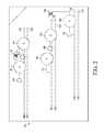
- FIG. 5depicts a top view of a die 502 (corresponding to the die 102 , FIG. 1 ) programmed for the production mode in which the fuse elements are disposed in a corner keep-out zone 503 of the die 502 , with the connections between the pads of the die 502 and the fuse elements of the keep-out zone 503 depicted by pairs of letters A-M, wherein each pair of letters indicates a portion of the connection coupling the pad and its respective bus line or fuse element.
- the top metal layer of the die 502implements die pads 501 and 504 that are coupled to respective VDD power buses 524 and 532 through a plurality of fuses 512 and 522 , with die pad 501 coupled to fuse 512 and VDD power bus 524 through connection pair A-B and die pad 504 coupled to fuse 522 and VDD power bus 532 through connection pair K-L.
- die pads 501 and 504are connected to the VDD power busses 524 and 532 in this mode, the die pads 501 and 504 also are referred to herein as “power pads” 501 and 504 .
- the top metal layer of the die 502further implements die pads 508 and 510 that are coupled to respective VSS power busses 526 and 530 by a plurality of fuses 516 and 518 , with die pad 508 coupled to fuse 516 and VDD power bus 526 through connection pair E-F and die pad 510 coupled to fuse 518 and VDD power bus 530 through connection pair G-H.
- die pads 508 and 510are connected to the VSS power busses 526 and 530 in this mode, the die pads 508 and 510 also are referred to herein as “ground pads” 508 and 510 .
- the die 502further implements anti-fuse 514 connected between power pad 501 and ground pad 508 and anti-fuse 520 connected between power pad 504 and ground pad 510 , with power pad 501 and ground pad 508 being coupled through connection pair C-D and power pad 504 and ground pad 510 being coupled through connection pair I-J.
- the fuse elements in the example of FIGS. 5 and 6comprise electronic fuses and electronic anti-fuses, and thus are “programmed” via application of a programming signal.
- the top metal layer of the die 502further implements a die pad 506 that is coupled to fuses 512 , 514 , 516 , 518 , 520 , and 522 through connection M.
- the die pad 506serves to program all of the fuses and anti-fuses located in the keep-out zone 503 by distributing an activation signal received through a probe applied to the die pad 506 , and thus the die pad 506 is also referred to herein as “activation pad 506 .”
- the fuses 512 , 516 , 518 , and 522are “unprogrammed” and thus conductive, thereby coupling the die pads 501 , 504 , 508 , and 510 to their respective power busses. Further, the anti-fuses 516 and 520 are likewise “unprogrammed,” and thus non-conductive, thereby preventing connectivity between the power pad 501 and the ground pad 508 and preventing connectivity between the power pad 504 and the ground pad 510 .
- FIG. 6a top-view of the die 502 during the process of programming the die 502 to enter the test mode is illustrated.
- This test mode programmingis achieved by applying an activation signal to the fuse elements through a probe pin 602 applied to the activation pad 506 connected to the fuse elements disposed in the keep-out zone 503 , thus forming a stitch chain 600 formed in an IC device implementing the die 502 after it has been programmed for the test mode.
- the fuse elementsare shown in their programmed state in FIG. 6 with the fuses having been rendered non-conductive and the anti-fuses having been rendered conductive by probe pin 602 .
- application of the activation signal to the activation pad 506 via probe pin 602“programs” the fuse 512 so as to render the fuse 512 non-conductive, thereby electrically isolating the power pad 501 from the VDD bus 524 .
- application of the activation signal to the activation pad 506 through probe pin 602“programs” the fuse 516 so as to render the fuse 516 non-conductive, thereby electrically isolating the ground pad 508 from the VSS bus 526 .
- the activation signal introduced by the probe pin 602“programs” the anti-fuse 514 so as to render the anti-fuse 514 conductive, thereby electrically connecting the power pad 501 and the ground pad 508 .
- applications of the activation signal to the activation pad 506 through probe pin 602“programs” fuses 518 and 522 and anti-fuse 520 , which in turn electrically isolates ground pad 510 from VSS bus 530 and power pad 504 from VDD bus 532 , respectively, while electrically connecting ground pad 510 and power pad 504 .
- a stitch chain 600is formed in an IC device implementing the die 502 after it has been bonded to a test substrate, such as the substrate 104 of FIG. 1 .
- a substrate-level link 604 of the stitch chain 600is formed by a conductive path formed through a PCB and the test substrate, and through a solder bump or other die-level interconnect incorporating the pad 501 .
- the substrate-level link 604is followed in the stitch chain 600 by a die-level link 606 formed between the power pad 501 and the ground pad 508 through the programmed anti-fuse 514 .
- the die-level link 606is followed in the stitch chain 600 by a substrate-level link 608 formed as an electrical path from the ground pad 508 through a solder bump to corresponding substrate pad, and from this substrate pad to another substrate pad through one or more metal interconnects in the metal layers in the substrate, and from this other substrate pad up to the ground pad 510 through a corresponding solder bump.
- the next link, die-level link 610is formed as a conductive path between the ground pad 510 and the power pad 504 due to the programmed anti-fuse 520 .
- the die-level link 610is then followed by a substrate-level link 612 formed by the substrate-level interconnect connecting the power pad 504 through a solder bump to a corresponding substrate pad of the substrate then on to another stitch in the chain (not shown) or out through the test substrate and to a PCB.
- BLR datacan be generated regarding the die-level interconnects to provide to customers. While all of the die fabricated in a standard production run according to the design illustrated in FIGS. 5 and 6 can likewise be programmed for testing as described above, only a subset of the die will be programmed and tested with the remaining die being implemented into IC devices that are sold or distributed to customers.
Landscapes
- Engineering & Computer Science (AREA)
- Manufacturing & Machinery (AREA)
- Computer Hardware Design (AREA)
- Microelectronics & Electronic Packaging (AREA)
- General Physics & Mathematics (AREA)
- Physics & Mathematics (AREA)
- Power Engineering (AREA)
- General Engineering & Computer Science (AREA)
- Environmental & Geological Engineering (AREA)
- Condensed Matter Physics & Semiconductors (AREA)
- Automation & Control Theory (AREA)
- Semiconductor Integrated Circuits (AREA)
- Design And Manufacture Of Integrated Circuits (AREA)
Abstract
Description
Claims (14)
Priority Applications (1)
| Application Number | Priority Date | Filing Date | Title |
|---|---|---|---|
| US14/276,262US10424521B2 (en) | 2014-05-13 | 2014-05-13 | Programmable stitch chaining of die-level interconnects for reliability testing |
Applications Claiming Priority (1)
| Application Number | Priority Date | Filing Date | Title |
|---|---|---|---|
| US14/276,262US10424521B2 (en) | 2014-05-13 | 2014-05-13 | Programmable stitch chaining of die-level interconnects for reliability testing |
Publications (2)
| Publication Number | Publication Date |
|---|---|
| US20150332980A1 US20150332980A1 (en) | 2015-11-19 |
| US10424521B2true US10424521B2 (en) | 2019-09-24 |
Family
ID=54539130
Family Applications (1)
| Application Number | Title | Priority Date | Filing Date |
|---|---|---|---|
| US14/276,262Active2036-04-28US10424521B2 (en) | 2014-05-13 | 2014-05-13 | Programmable stitch chaining of die-level interconnects for reliability testing |
Country Status (1)
| Country | Link |
|---|---|
| US (1) | US10424521B2 (en) |
Cited By (1)
| Publication number | Priority date | Publication date | Assignee | Title |
|---|---|---|---|---|
| US20220367352A1 (en)* | 2020-11-24 | 2022-11-17 | Taiwan Semiconductor Manufacturing Company Ltd. | Semiconductor structure and method for forming thereof |
Families Citing this family (2)
| Publication number | Priority date | Publication date | Assignee | Title |
|---|---|---|---|---|
| US10396033B1 (en)* | 2018-07-23 | 2019-08-27 | Qualcomm Incorporated | First power buses and second power buses extending in a first direction |
| CN116666248B (en)* | 2023-07-26 | 2023-11-17 | 北京象帝先计算技术有限公司 | Test result abnormality determination method, device, electronic equipment and readable storage medium |
Citations (12)
| Publication number | Priority date | Publication date | Assignee | Title |
|---|---|---|---|---|
| US5813881A (en)* | 1994-02-08 | 1998-09-29 | Prolinx Labs Corporation | Programmable cable and cable adapter using fuses and antifuses |
| US6605956B2 (en)* | 1995-12-22 | 2003-08-12 | Micron Technology, Inc. | Device and method for testing integrated circuit dice in an integrated circuit module |
| US6804156B2 (en) | 2002-10-08 | 2004-10-12 | Kabushiki Kaisha Toshiba | Semiconductor integrated circuit device |
| US6911360B2 (en) | 2003-04-29 | 2005-06-28 | Freescale Semiconductor, Inc. | Fuse and method for forming |
| US20050181546A1 (en)* | 2002-07-08 | 2005-08-18 | Madurawe Raminda U. | Methods for fabricating fuse programmable three dimensional integrated circuits |
| US20050263850A1 (en)* | 2004-05-25 | 2005-12-01 | International Business Machines Corporation | Trench type buried on-chip precision programmable resistor |
| US7340644B2 (en) | 2002-12-02 | 2008-03-04 | Marvell World Trade Ltd. | Self-reparable semiconductor and method thereof |
| US20090224242A1 (en)* | 2002-06-20 | 2009-09-10 | Micron Technology, Inc. | Isolation circuit |
| US20100283085A1 (en)* | 2009-05-06 | 2010-11-11 | Majid Bemanian | Massively Parallel Interconnect Fabric for Complex Semiconductor Devices |
| US20110002188A1 (en)* | 2009-07-06 | 2011-01-06 | International Business Machines Corporation | Apparatus for Nonvolatile Multi-Programmable Electronic Fuse System |
| US8349666B1 (en) | 2011-07-22 | 2013-01-08 | Freescale Semiconductor, Inc. | Fused buss for plating features on a semiconductor die |
| US20130020674A1 (en)* | 2011-07-22 | 2013-01-24 | Leal George R | Fused buss for plating features on a semiconductor die |
- 2014
- 2014-05-13USUS14/276,262patent/US10424521B2/enactiveActive
Patent Citations (13)
| Publication number | Priority date | Publication date | Assignee | Title |
|---|---|---|---|---|
| US5813881A (en)* | 1994-02-08 | 1998-09-29 | Prolinx Labs Corporation | Programmable cable and cable adapter using fuses and antifuses |
| US6605956B2 (en)* | 1995-12-22 | 2003-08-12 | Micron Technology, Inc. | Device and method for testing integrated circuit dice in an integrated circuit module |
| US20090224242A1 (en)* | 2002-06-20 | 2009-09-10 | Micron Technology, Inc. | Isolation circuit |
| US20050181546A1 (en)* | 2002-07-08 | 2005-08-18 | Madurawe Raminda U. | Methods for fabricating fuse programmable three dimensional integrated circuits |
| US6804156B2 (en) | 2002-10-08 | 2004-10-12 | Kabushiki Kaisha Toshiba | Semiconductor integrated circuit device |
| US7340644B2 (en) | 2002-12-02 | 2008-03-04 | Marvell World Trade Ltd. | Self-reparable semiconductor and method thereof |
| US6911360B2 (en) | 2003-04-29 | 2005-06-28 | Freescale Semiconductor, Inc. | Fuse and method for forming |
| US20050263850A1 (en)* | 2004-05-25 | 2005-12-01 | International Business Machines Corporation | Trench type buried on-chip precision programmable resistor |
| US20100283085A1 (en)* | 2009-05-06 | 2010-11-11 | Majid Bemanian | Massively Parallel Interconnect Fabric for Complex Semiconductor Devices |
| US20110002188A1 (en)* | 2009-07-06 | 2011-01-06 | International Business Machines Corporation | Apparatus for Nonvolatile Multi-Programmable Electronic Fuse System |
| US8349666B1 (en) | 2011-07-22 | 2013-01-08 | Freescale Semiconductor, Inc. | Fused buss for plating features on a semiconductor die |
| US20130020674A1 (en)* | 2011-07-22 | 2013-01-24 | Leal George R | Fused buss for plating features on a semiconductor die |
| US8368172B1 (en) | 2011-07-22 | 2013-02-05 | Freescale Semiconductor, Inc. | Fused buss for plating features on a semiconductor die |
Cited By (2)
| Publication number | Priority date | Publication date | Assignee | Title |
|---|---|---|---|---|
| US20220367352A1 (en)* | 2020-11-24 | 2022-11-17 | Taiwan Semiconductor Manufacturing Company Ltd. | Semiconductor structure and method for forming thereof |
| US11854969B2 (en)* | 2020-11-24 | 2023-12-26 | Taiwan Semiconductor Manufacturing Company Ltd. | Semiconductor structure and method for forming thereof |
Also Published As
| Publication number | Publication date |
|---|---|
| US20150332980A1 (en) | 2015-11-19 |
Similar Documents
| Publication | Publication Date | Title |
|---|---|---|
| US8476735B2 (en) | Programmable semiconductor interposer for electronic package and method of forming | |
| US7968916B2 (en) | Circuit and method for interconnecting stacked integrated circuit dies | |
| US7511299B1 (en) | Packaged integrated circuit with raised test points | |
| WO2002050898A1 (en) | Semiconductor integrated circuit device | |
| KR101560691B1 (en) | Integrated circuit chip customization using backside access | |
| KR101460355B1 (en) | Integrated circuit and method of manufacturing the same | |
| KR102708729B1 (en) | Semiconductor package | |
| US10424521B2 (en) | Programmable stitch chaining of die-level interconnects for reliability testing | |
| US9412674B1 (en) | Shielded wire arrangement for die testing | |
| TWI694567B (en) | Printed circuit boards and testing method thereof, and method of manufacturing semiconductor packages | |
| KR101452203B1 (en) | Programmable rom using two bonded strata and method of operation | |
| US6732266B1 (en) | Method and apparatus for reconfiguring circuit board and integrated circuit packet arrangement with one-time programmable elements | |
| US7605462B2 (en) | Universal substrate for a semiconductor device having selectively activated fuses | |
| JPH06349926A (en) | Semiconductor device | |
| US8717059B2 (en) | Die having wire bond alignment sensing structures | |
| CN102148167B (en) | Manufacturing method of stackable packaging structure | |
| US7131033B1 (en) | Substrate configurable JTAG ID scheme | |
| JP2000349130A (en) | Semiconductor integrated circuit board and manufacture thereof and check of characteristics thereof | |
| US20150076656A1 (en) | Electronic fuse having a substantially uniform thermal profile | |
| CN101083260A (en) | Semiconductor chip with die area | |
| US10580720B1 (en) | Silicon interposer with fuse-selectable routing array | |
| US11574884B2 (en) | Multi-function bond pad | |
| JP3674052B2 (en) | IC wafer and burn-in method using the same | |
| US8741742B2 (en) | Method of fabricating an integrated circuit without ground contact pad | |
| JP4056252B2 (en) | Manufacturing method of semiconductor device |
Legal Events
| Date | Code | Title | Description |
|---|---|---|---|
| AS | Assignment | Owner name:FREESCALE SEMICONDUCTOR, INC., TEXAS Free format text:ASSIGNMENT OF ASSIGNORS INTEREST;ASSIGNOR:LEAL, GEORGE R.;REEL/FRAME:032879/0120 Effective date:20140507 | |
| AS | Assignment | Owner name:CITIBANK, N.A., AS NOTES COLLATERAL AGENT, NEW YORK Free format text:SUPPLEMENT TO IP SECURITY AGREEMENT;ASSIGNOR:FREESCALE SEMICONDUCTOR, INC.;REEL/FRAME:033462/0267 Effective date:20140729 Owner name:CITIBANK, N.A., AS NOTES COLLATERAL AGENT, NEW YORK Free format text:SUPPLEMENT TO IP SECURITY AGREEMENT;ASSIGNOR:FREESCALE SEMICONDUCTOR, INC.;REEL/FRAME:033460/0337 Effective date:20140729 Owner name:CITIBANK, N.A., AS NOTES COLLATERAL AGENT, NEW YORK Free format text:SUPPLEMENT TO IP SECURITY AGREEMENT;ASSIGNOR:FREESCALE SEMICONDUCTOR, INC.;REEL/FRAME:033462/0293 Effective date:20140729 Owner name:CITIBANK, N.A., AS NOTES COLLATERAL AGENT, NEW YOR Free format text:SUPPLEMENT TO IP SECURITY AGREEMENT;ASSIGNOR:FREESCALE SEMICONDUCTOR, INC.;REEL/FRAME:033462/0293 Effective date:20140729 Owner name:CITIBANK, N.A., AS NOTES COLLATERAL AGENT, NEW YOR Free format text:SUPPLEMENT TO IP SECURITY AGREEMENT;ASSIGNOR:FREESCALE SEMICONDUCTOR, INC.;REEL/FRAME:033462/0267 Effective date:20140729 Owner name:CITIBANK, N.A., AS NOTES COLLATERAL AGENT, NEW YOR Free format text:SUPPLEMENT TO IP SECURITY AGREEMENT;ASSIGNOR:FREESCALE SEMICONDUCTOR, INC.;REEL/FRAME:033460/0337 Effective date:20140729 | |
| AS | Assignment | Owner name:FREESCALE SEMICONDUCTOR, INC., TEXAS Free format text:PATENT RELEASE;ASSIGNOR:CITIBANK, N.A., AS COLLATERAL AGENT;REEL/FRAME:037357/0903 Effective date:20151207 | |
| AS | Assignment | Owner name:MORGAN STANLEY SENIOR FUNDING, INC., MARYLAND Free format text:ASSIGNMENT AND ASSUMPTION OF SECURITY INTEREST IN PATENTS;ASSIGNOR:CITIBANK, N.A.;REEL/FRAME:037444/0082 Effective date:20151207 Owner name:MORGAN STANLEY SENIOR FUNDING, INC., MARYLAND Free format text:ASSIGNMENT AND ASSUMPTION OF SECURITY INTEREST IN PATENTS;ASSIGNOR:CITIBANK, N.A.;REEL/FRAME:037444/0109 Effective date:20151207 | |
| AS | Assignment | Owner name:MORGAN STANLEY SENIOR FUNDING, INC., MARYLAND Free format text:SECURITY AGREEMENT SUPPLEMENT;ASSIGNOR:NXP B.V.;REEL/FRAME:038017/0058 Effective date:20160218 | |
| AS | Assignment | Owner name:MORGAN STANLEY SENIOR FUNDING, INC., MARYLAND Free format text:SUPPLEMENT TO THE SECURITY AGREEMENT;ASSIGNOR:FREESCALE SEMICONDUCTOR, INC.;REEL/FRAME:039138/0001 Effective date:20160525 | |
| AS | Assignment | Owner name:MORGAN STANLEY SENIOR FUNDING, INC., MARYLAND Free format text:CORRECTIVE ASSIGNMENT TO CORRECT THE REMOVE APPLICATION 12092129 PREVIOUSLY RECORDED ON REEL 038017 FRAME 0058. ASSIGNOR(S) HEREBY CONFIRMS THE SECURITY AGREEMENT SUPPLEMENT;ASSIGNOR:NXP B.V.;REEL/FRAME:039361/0212 Effective date:20160218 | |
| AS | Assignment | Owner name:MORGAN STANLEY SENIOR FUNDING, INC., MARYLAND Free format text:CORRECTIVE ASSIGNMENT TO CORRECT THE REMOVE APPLICATION 14/258,829 AND REPLACE ITWITH 14/258,629 PREVIOUSLY RECORDED ON REEL 037444 FRAME 0082. ASSIGNOR(S) HEREBY CONFIRMS THE ASSIGNMENT AND ASSUMPTION OFSECURITY INTEREST IN PATENTS;ASSIGNOR:CITIBANK, N.A.;REEL/FRAME:039639/0332 Effective date:20151207 Owner name:MORGAN STANLEY SENIOR FUNDING, INC., MARYLAND Free format text:CORRECTIVE ASSIGNMENT TO CORRECT THE REMOVE APPLICATION14/258,829 AND REPLACE IT WITH 14/258,629 PREVIOUSLY RECORDED ON REEL 037444 FRAME 0109. ASSIGNOR(S) HEREBY CONFIRMS THE ASSIGNMENT AND ASSUMPTION OF SECURITY INTEREST IN PATENTS;ASSIGNOR:CITIBANK, N.A.;REEL/FRAME:039639/0208 Effective date:20151207 Owner name:MORGAN STANLEY SENIOR FUNDING, INC., MARYLAND Free format text:CORRECTIVE ASSIGNMENT OF INCORRECT APPLICATION 14/258,829 PREVIOUSLY RECORDED ON REEL 037444 FRAME 0109. ASSIGNOR(S) HEREBY CONFIRMS THE ASSIGNMENT AND ASSUMPTION OF SECURITY INTEREST IN PATENTS;ASSIGNOR:CITIBANK, N.A.;REEL/FRAME:039639/0208 Effective date:20151207 | |
| AS | Assignment | Owner name:NXP, B.V., F/K/A FREESCALE SEMICONDUCTOR, INC., NETHERLANDS Free format text:RELEASE BY SECURED PARTY;ASSIGNOR:MORGAN STANLEY SENIOR FUNDING, INC.;REEL/FRAME:040925/0001 Effective date:20160912 Owner name:NXP, B.V., F/K/A FREESCALE SEMICONDUCTOR, INC., NE Free format text:RELEASE BY SECURED PARTY;ASSIGNOR:MORGAN STANLEY SENIOR FUNDING, INC.;REEL/FRAME:040925/0001 Effective date:20160912 | |
| AS | Assignment | Owner name:NXP B.V., NETHERLANDS Free format text:RELEASE BY SECURED PARTY;ASSIGNOR:MORGAN STANLEY SENIOR FUNDING, INC.;REEL/FRAME:040928/0001 Effective date:20160622 | |
| AS | Assignment | Owner name:NXP USA, INC., TEXAS Free format text:CHANGE OF NAME;ASSIGNOR:FREESCALE SEMICONDUCTOR INC.;REEL/FRAME:040626/0683 Effective date:20161107 | |
| AS | Assignment | Owner name:NXP USA, INC., TEXAS Free format text:CORRECTIVE ASSIGNMENT TO CORRECT THE NATURE OF CONVEYANCE PREVIOUSLY RECORDED AT REEL: 040626 FRAME: 0683. ASSIGNOR(S) HEREBY CONFIRMS THE MERGER AND CHANGE OF NAME;ASSIGNOR:FREESCALE SEMICONDUCTOR INC.;REEL/FRAME:041414/0883 Effective date:20161107 Owner name:NXP USA, INC., TEXAS Free format text:CORRECTIVE ASSIGNMENT TO CORRECT THE NATURE OF CONVEYANCE PREVIOUSLY RECORDED AT REEL: 040626 FRAME: 0683. ASSIGNOR(S) HEREBY CONFIRMS THE MERGER AND CHANGE OF NAME EFFECTIVE NOVEMBER 7, 2016;ASSIGNORS:NXP SEMICONDUCTORS USA, INC. (MERGED INTO);FREESCALE SEMICONDUCTOR, INC. (UNDER);SIGNING DATES FROM 20161104 TO 20161107;REEL/FRAME:041414/0883 | |
| AS | Assignment | Owner name:MORGAN STANLEY SENIOR FUNDING, INC., MARYLAND Free format text:CORRECTIVE ASSIGNMENT TO CORRECT THE REMOVE APPLICATION 12681366 PREVIOUSLY RECORDED ON REEL 039361 FRAME 0212. ASSIGNOR(S) HEREBY CONFIRMS THE SECURITY AGREEMENT SUPPLEMENT;ASSIGNOR:NXP B.V.;REEL/FRAME:042762/0145 Effective date:20160218 Owner name:MORGAN STANLEY SENIOR FUNDING, INC., MARYLAND Free format text:CORRECTIVE ASSIGNMENT TO CORRECT THE REMOVE APPLICATION 12681366 PREVIOUSLY RECORDED ON REEL 038017 FRAME 0058. ASSIGNOR(S) HEREBY CONFIRMS THE SECURITY AGREEMENT SUPPLEMENT;ASSIGNOR:NXP B.V.;REEL/FRAME:042985/0001 Effective date:20160218 | |
| STPP | Information on status: patent application and granting procedure in general | Free format text:NOTICE OF ALLOWANCE MAILED -- APPLICATION RECEIVED IN OFFICE OF PUBLICATIONS | |
| STPP | Information on status: patent application and granting procedure in general | Free format text:PUBLICATIONS -- ISSUE FEE PAYMENT RECEIVED | |
| STPP | Information on status: patent application and granting procedure in general | Free format text:PUBLICATIONS -- ISSUE FEE PAYMENT VERIFIED | |
| STCF | Information on status: patent grant | Free format text:PATENTED CASE | |
| AS | Assignment | Owner name:NXP B.V., NETHERLANDS Free format text:RELEASE BY SECURED PARTY;ASSIGNOR:MORGAN STANLEY SENIOR FUNDING, INC.;REEL/FRAME:050745/0001 Effective date:20190903 Owner name:NXP B.V., NETHERLANDS Free format text:RELEASE BY SECURED PARTY;ASSIGNOR:MORGAN STANLEY SENIOR FUNDING, INC.;REEL/FRAME:050744/0097 Effective date:20190903 | |
| AS | Assignment | Owner name:MORGAN STANLEY SENIOR FUNDING, INC., MARYLAND Free format text:CORRECTIVE ASSIGNMENT TO CORRECT THE REMOVE APPLICATION 12298143 PREVIOUSLY RECORDED ON REEL 042762 FRAME 0145. ASSIGNOR(S) HEREBY CONFIRMS THE SECURITY AGREEMENT SUPPLEMENT;ASSIGNOR:NXP B.V.;REEL/FRAME:051145/0184 Effective date:20160218 Owner name:MORGAN STANLEY SENIOR FUNDING, INC., MARYLAND Free format text:CORRECTIVE ASSIGNMENT TO CORRECT THE REMOVE APPLICATION 12298143 PREVIOUSLY RECORDED ON REEL 039361 FRAME 0212. ASSIGNOR(S) HEREBY CONFIRMS THE SECURITY AGREEMENT SUPPLEMENT;ASSIGNOR:NXP B.V.;REEL/FRAME:051029/0387 Effective date:20160218 Owner name:MORGAN STANLEY SENIOR FUNDING, INC., MARYLAND Free format text:CORRECTIVE ASSIGNMENT TO CORRECT THE REMOVE APPLICATION 12298143 PREVIOUSLY RECORDED ON REEL 042985 FRAME 0001. ASSIGNOR(S) HEREBY CONFIRMS THE SECURITY AGREEMENT SUPPLEMENT;ASSIGNOR:NXP B.V.;REEL/FRAME:051029/0001 Effective date:20160218 Owner name:MORGAN STANLEY SENIOR FUNDING, INC., MARYLAND Free format text:CORRECTIVE ASSIGNMENT TO CORRECT THE REMOVE APPLICATION12298143 PREVIOUSLY RECORDED ON REEL 042985 FRAME 0001. ASSIGNOR(S) HEREBY CONFIRMS THE SECURITY AGREEMENT SUPPLEMENT;ASSIGNOR:NXP B.V.;REEL/FRAME:051029/0001 Effective date:20160218 Owner name:MORGAN STANLEY SENIOR FUNDING, INC., MARYLAND Free format text:CORRECTIVE ASSIGNMENT TO CORRECT THE REMOVE APPLICATION 12298143 PREVIOUSLY RECORDED ON REEL 038017 FRAME 0058. ASSIGNOR(S) HEREBY CONFIRMS THE SECURITY AGREEMENT SUPPLEMENT;ASSIGNOR:NXP B.V.;REEL/FRAME:051030/0001 Effective date:20160218 Owner name:MORGAN STANLEY SENIOR FUNDING, INC., MARYLAND Free format text:CORRECTIVE ASSIGNMENT TO CORRECT THE REMOVE APPLICATION12298143 PREVIOUSLY RECORDED ON REEL 039361 FRAME 0212. ASSIGNOR(S) HEREBY CONFIRMS THE SECURITY AGREEMENT SUPPLEMENT;ASSIGNOR:NXP B.V.;REEL/FRAME:051029/0387 Effective date:20160218 Owner name:MORGAN STANLEY SENIOR FUNDING, INC., MARYLAND Free format text:CORRECTIVE ASSIGNMENT TO CORRECT THE REMOVE APPLICATION12298143 PREVIOUSLY RECORDED ON REEL 042762 FRAME 0145. ASSIGNOR(S) HEREBY CONFIRMS THE SECURITY AGREEMENT SUPPLEMENT;ASSIGNOR:NXP B.V.;REEL/FRAME:051145/0184 Effective date:20160218 | |
| AS | Assignment | Owner name:NXP B.V., NETHERLANDS Free format text:CORRECTIVE ASSIGNMENT TO CORRECT THE REMOVEAPPLICATION 11759915 AND REPLACE IT WITH APPLICATION11759935 PREVIOUSLY RECORDED ON REEL 040928 FRAME 0001. ASSIGNOR(S) HEREBY CONFIRMS THE RELEASE OF SECURITYINTEREST;ASSIGNOR:MORGAN STANLEY SENIOR FUNDING, INC.;REEL/FRAME:052915/0001 Effective date:20160622 | |
| AS | Assignment | Owner name:NXP, B.V. F/K/A FREESCALE SEMICONDUCTOR, INC., NETHERLANDS Free format text:CORRECTIVE ASSIGNMENT TO CORRECT THE REMOVEAPPLICATION 11759915 AND REPLACE IT WITH APPLICATION11759935 PREVIOUSLY RECORDED ON REEL 040925 FRAME 0001. ASSIGNOR(S) HEREBY CONFIRMS THE RELEASE OF SECURITYINTEREST;ASSIGNOR:MORGAN STANLEY SENIOR FUNDING, INC.;REEL/FRAME:052917/0001 Effective date:20160912 | |
| MAFP | Maintenance fee payment | Free format text:PAYMENT OF MAINTENANCE FEE, 4TH YEAR, LARGE ENTITY (ORIGINAL EVENT CODE: M1551); ENTITY STATUS OF PATENT OWNER: LARGE ENTITY Year of fee payment:4 |