US10422767B2 - Chemical sensor with consistent sensor surface areas - Google Patents
Chemical sensor with consistent sensor surface areasDownload PDFInfo
- Publication number
- US10422767B2 US10422767B2US15/614,589US201715614589AUS10422767B2US 10422767 B2US10422767 B2US 10422767B2US 201715614589 AUS201715614589 AUS 201715614589AUS 10422767 B2US10422767 B2US 10422767B2
- Authority
- US
- United States
- Prior art keywords
- dielectric
- opening
- conductive element
- conductive material
- floating gate
- Prior art date
- Legal status (The legal status is an assumption and is not a legal conclusion. Google has not performed a legal analysis and makes no representation as to the accuracy of the status listed.)
- Active
Links
- 239000000126substanceSubstances0.000titleclaimsabstractdescription85
- 239000004020conductorSubstances0.000claimsabstractdescription85
- 238000007667floatingMethods0.000claimsabstractdescription34
- 230000005669field effectEffects0.000claimsabstractdescription13
- 238000000034methodMethods0.000claimsdescription73
- 238000006243chemical reactionMethods0.000claimsdescription69
- 229920002120photoresistant polymerPolymers0.000claimsdescription14
- 238000004519manufacturing processMethods0.000claimsdescription13
- 238000000151depositionMethods0.000claimsdescription11
- 238000005530etchingMethods0.000claimsdescription11
- NRTOMJZYCJJWKI-UHFFFAOYSA-NTitanium nitrideChemical compound[Ti]#NNRTOMJZYCJJWKI-UHFFFAOYSA-N0.000claimsdescription9
- RTAQQCXQSZGOHL-UHFFFAOYSA-NTitaniumChemical compound[Ti]RTAQQCXQSZGOHL-UHFFFAOYSA-N0.000claimsdescription8
- 229910052719titaniumInorganic materials0.000claimsdescription8
- 239000010936titaniumSubstances0.000claimsdescription8
- 229910010293ceramic materialInorganic materials0.000claimsdescription3
- 239000007769metal materialSubstances0.000claimsdescription3
- 229910052710siliconInorganic materials0.000claimsdescription3
- 239000010703siliconSubstances0.000claimsdescription3
- GWEVSGVZZGPLCZ-UHFFFAOYSA-NTitan oxideChemical compoundO=[Ti]=OGWEVSGVZZGPLCZ-UHFFFAOYSA-N0.000claimsdescription2
- 229910045601alloyInorganic materials0.000claimsdescription2
- 239000000956alloySubstances0.000claimsdescription2
- UQZIWOQVLUASCR-UHFFFAOYSA-Nalumane;titaniumChemical compound[AlH3].[Ti]UQZIWOQVLUASCR-UHFFFAOYSA-N0.000claimsdescription2
- MZLGASXMSKOWSE-UHFFFAOYSA-Ntantalum nitrideChemical compound[Ta]#NMZLGASXMSKOWSE-UHFFFAOYSA-N0.000claimsdescription2
- OGIDPMRJRNCKJF-UHFFFAOYSA-Ntitanium oxideInorganic materials[Ti]=OOGIDPMRJRNCKJF-UHFFFAOYSA-N0.000claimsdescription2
- 150000004767nitridesChemical class0.000claims1
- 239000000463materialSubstances0.000abstractdescription37
- 239000003989dielectric materialSubstances0.000description48
- 239000010410layerSubstances0.000description43
- 230000008569processEffects0.000description21
- 239000003153chemical reaction reagentSubstances0.000description18
- 150000002500ionsChemical class0.000description15
- VYPSYNLAJGMNEJ-UHFFFAOYSA-NSilicium dioxideChemical compoundO=[Si]=OVYPSYNLAJGMNEJ-UHFFFAOYSA-N0.000description14
- 239000012491analyteSubstances0.000description12
- 150000007523nucleic acidsChemical class0.000description11
- 238000000231atomic layer depositionMethods0.000description10
- 238000004518low pressure chemical vapour depositionMethods0.000description10
- 108020004707nucleic acidsProteins0.000description10
- 102000039446nucleic acidsHuman genes0.000description10
- 238000000623plasma-assisted chemical vapour depositionMethods0.000description10
- 238000012163sequencing techniqueMethods0.000description9
- 238000003491arrayMethods0.000description7
- 239000002773nucleotideSubstances0.000description7
- 125000003729nucleotide groupChemical group0.000description7
- 229910052581Si3N4Inorganic materials0.000description6
- 229910052751metalInorganic materials0.000description6
- 239000002184metalSubstances0.000description6
- 235000012239silicon dioxideNutrition0.000description6
- 239000000377silicon dioxideSubstances0.000description6
- HQVNEWCFYHHQES-UHFFFAOYSA-Nsilicon nitrideChemical compoundN12[Si]34N5[Si]62N3[Si]51N64HQVNEWCFYHHQES-UHFFFAOYSA-N0.000description6
- 239000000758substrateSubstances0.000description6
- 239000006227byproductSubstances0.000description5
- 238000005229chemical vapour depositionMethods0.000description5
- 238000012545processingMethods0.000description5
- 238000005546reactive sputteringMethods0.000description5
- 239000004065semiconductorSubstances0.000description5
- 239000011540sensing materialSubstances0.000description5
- 239000007787solidSubstances0.000description5
- 238000004544sputter depositionMethods0.000description5
- 239000012530fluidSubstances0.000description4
- 230000036961partial effectEffects0.000description4
- 238000001020plasma etchingMethods0.000description4
- 238000012408PCR amplificationMethods0.000description3
- 238000001514detection methodMethods0.000description3
- 239000001257hydrogenSubstances0.000description3
- 229910052739hydrogenInorganic materials0.000description3
- -1hydrogen ionsChemical class0.000description3
- 230000004044responseEffects0.000description3
- 230000035945sensitivityEffects0.000description3
- 239000007790solid phaseSubstances0.000description3
- YCKRFDGAMUMZLT-UHFFFAOYSA-NFluorine atomChemical compound[F]YCKRFDGAMUMZLT-UHFFFAOYSA-N0.000description2
- XEEYBQQBJWHFJM-UHFFFAOYSA-NIronChemical compound[Fe]XEEYBQQBJWHFJM-UHFFFAOYSA-N0.000description2
- PXHVJJICTQNCMI-UHFFFAOYSA-NNickelChemical compound[Ni]PXHVJJICTQNCMI-UHFFFAOYSA-N0.000description2
- KDLHZDBZIXYQEI-UHFFFAOYSA-NPalladiumChemical compound[Pd]KDLHZDBZIXYQEI-UHFFFAOYSA-N0.000description2
- BQCADISMDOOEFD-UHFFFAOYSA-NSilverChemical compound[Ag]BQCADISMDOOEFD-UHFFFAOYSA-N0.000description2
- 229910052782aluminiumInorganic materials0.000description2
- XAGFODPZIPBFFR-UHFFFAOYSA-NaluminiumChemical compound[Al]XAGFODPZIPBFFR-UHFFFAOYSA-N0.000description2
- 230000003321amplificationEffects0.000description2
- 230000004888barrier functionEffects0.000description2
- 239000011324beadSubstances0.000description2
- 230000031018biological processes and functionsEffects0.000description2
- 230000008859changeEffects0.000description2
- 238000004891communicationMethods0.000description2
- 230000008021depositionEffects0.000description2
- 238000010586diagramMethods0.000description2
- 238000009792diffusion processMethods0.000description2
- 238000002474experimental methodMethods0.000description2
- 229910052731fluorineInorganic materials0.000description2
- 239000011737fluorineSubstances0.000description2
- 230000006870functionEffects0.000description2
- 238000010348incorporationMethods0.000description2
- 238000005468ion implantationMethods0.000description2
- 238000002372labellingMethods0.000description2
- 239000011859microparticleSubstances0.000description2
- 238000012986modificationMethods0.000description2
- 230000004048modificationEffects0.000description2
- 238000012544monitoring processMethods0.000description2
- 238000003541multi-stage reactionMethods0.000description2
- 238000003199nucleic acid amplification methodMethods0.000description2
- 239000002245particleSubstances0.000description2
- BASFCYQUMIYNBI-UHFFFAOYSA-NplatinumChemical compound[Pt]BASFCYQUMIYNBI-UHFFFAOYSA-N0.000description2
- 229910021420polycrystalline siliconInorganic materials0.000description2
- 229920005591polysiliconPolymers0.000description2
- 230000009467reductionEffects0.000description2
- 230000002829reductive effectEffects0.000description2
- 229910052814silicon oxideInorganic materials0.000description2
- 229910052709silverInorganic materials0.000description2
- 239000004332silverSubstances0.000description2
- WXAHAOIEHWDLLL-UHFFFAOYSA-Ntitanium hydrobromideChemical compound[Ti].BrWXAHAOIEHWDLLL-UHFFFAOYSA-N0.000description2
- WFKWXMTUELFFGS-UHFFFAOYSA-NtungstenChemical compound[W]WFKWXMTUELFFGS-UHFFFAOYSA-N0.000description2
- 229910052721tungstenInorganic materials0.000description2
- 239000010937tungstenSubstances0.000description2
- 238000005406washingMethods0.000description2
- 239000002699waste materialSubstances0.000description2
- 108091093088AmpliconProteins0.000description1
- WKBOTKDWSSQWDR-UHFFFAOYSA-NBromine atomChemical compound[Br]WKBOTKDWSSQWDR-UHFFFAOYSA-N0.000description1
- OYPRJOBELJOOCE-UHFFFAOYSA-NCalciumChemical compound[Ca]OYPRJOBELJOOCE-UHFFFAOYSA-N0.000description1
- RYGMFSIKBFXOCR-UHFFFAOYSA-NCopperChemical compound[Cu]RYGMFSIKBFXOCR-UHFFFAOYSA-N0.000description1
- 238000001712DNA sequencingMethods0.000description1
- DGAQECJNVWCQMB-PUAWFVPOSA-MIlexoside XXIXChemical compoundC[C@@H]1CC[C@@]2(CC[C@@]3(C(=CC[C@H]4[C@]3(CC[C@@H]5[C@@]4(CC[C@@H](C5(C)C)OS(=O)(=O)[O-])C)C)[C@@H]2[C@]1(C)O)C)C(=O)O[C@H]6[C@@H]([C@H]([C@@H]([C@H](O6)CO)O)O)O.[Na+]DGAQECJNVWCQMB-PUAWFVPOSA-M0.000description1
- 229910002651NO3Inorganic materials0.000description1
- NHNBFGGVMKEFGY-UHFFFAOYSA-NNitrateChemical compound[O-][N+]([O-])=ONHNBFGGVMKEFGY-UHFFFAOYSA-N0.000description1
- 108091028043Nucleic acid sequenceProteins0.000description1
- 102000018120RecombinasesHuman genes0.000description1
- 108010091086RecombinasesProteins0.000description1
- XUIMIQQOPSSXEZ-UHFFFAOYSA-NSiliconChemical compound[Si]XUIMIQQOPSSXEZ-UHFFFAOYSA-N0.000description1
- 108010067973ValinomycinProteins0.000description1
- QCWXUUIWCKQGHC-UHFFFAOYSA-NZirconiumChemical compound[Zr]QCWXUUIWCKQGHC-UHFFFAOYSA-N0.000description1
- 238000004458analytical methodMethods0.000description1
- 230000008901benefitEffects0.000description1
- 230000015572biosynthetic processEffects0.000description1
- GDTBXPJZTBHREO-UHFFFAOYSA-NbromineSubstancesBrBrGDTBXPJZTBHREO-UHFFFAOYSA-N0.000description1
- 229910052794bromiumInorganic materials0.000description1
- 229910052791calciumInorganic materials0.000description1
- 239000011575calciumSubstances0.000description1
- 239000000919ceramicSubstances0.000description1
- 238000001311chemical methods and processMethods0.000description1
- 230000000295complement effectEffects0.000description1
- FCFNRCROJUBPLU-UHFFFAOYSA-Ncompound M126Natural productsCC(C)C1NC(=O)C(C)OC(=O)C(C(C)C)NC(=O)C(C(C)C)OC(=O)C(C(C)C)NC(=O)C(C)OC(=O)C(C(C)C)NC(=O)C(C(C)C)OC(=O)C(C(C)C)NC(=O)C(C)OC(=O)C(C(C)C)NC(=O)C(C(C)C)OC1=OFCFNRCROJUBPLU-UHFFFAOYSA-N0.000description1
- 150000001875compoundsChemical class0.000description1
- 239000000470constituentSubstances0.000description1
- 229910052802copperInorganic materials0.000description1
- 239000010949copperSubstances0.000description1
- 230000007423decreaseEffects0.000description1
- 230000003247decreasing effectEffects0.000description1
- 230000005595deprotonationEffects0.000description1
- 238000010537deprotonation reactionMethods0.000description1
- 239000000839emulsionSubstances0.000description1
- 238000005516engineering processMethods0.000description1
- 239000012634fragmentSubstances0.000description1
- 239000007789gasSubstances0.000description1
- 239000000499gelSubstances0.000description1
- PCHJSUWPFVWCPO-UHFFFAOYSA-NgoldChemical compound[Au]PCHJSUWPFVWCPO-UHFFFAOYSA-N0.000description1
- 229910052737goldInorganic materials0.000description1
- 239000010931goldSubstances0.000description1
- 229910052735hafniumInorganic materials0.000description1
- VBJZVLUMGGDVMO-UHFFFAOYSA-Nhafnium atomChemical compound[Hf]VBJZVLUMGGDVMO-UHFFFAOYSA-N0.000description1
- PNDPGZBMCMUPRI-UHFFFAOYSA-NiodineChemical compoundIIPNDPGZBMCMUPRI-UHFFFAOYSA-N0.000description1
- 229910052741iridiumInorganic materials0.000description1
- GKOZUEZYRPOHIO-UHFFFAOYSA-Niridium atomChemical compound[Ir]GKOZUEZYRPOHIO-UHFFFAOYSA-N0.000description1
- 229910052742ironInorganic materials0.000description1
- 229910052746lanthanumInorganic materials0.000description1
- FZLIPJUXYLNCLC-UHFFFAOYSA-Nlanthanum atomChemical compound[La]FZLIPJUXYLNCLC-UHFFFAOYSA-N0.000description1
- 230000000670limiting effectEffects0.000description1
- 238000005259measurementMethods0.000description1
- 230000007246mechanismEffects0.000description1
- 229910044991metal oxideInorganic materials0.000description1
- 150000004706metal oxidesChemical class0.000description1
- 150000002739metalsChemical class0.000description1
- 239000002105nanoparticleSubstances0.000description1
- 230000001537neural effectEffects0.000description1
- 229910052759nickelInorganic materials0.000description1
- BPUBBGLMJRNUCC-UHFFFAOYSA-Noxygen(2-);tantalum(5+)Chemical class[O-2].[O-2].[O-2].[O-2].[O-2].[Ta+5].[Ta+5]BPUBBGLMJRNUCC-UHFFFAOYSA-N0.000description1
- 229910052763palladiumInorganic materials0.000description1
- 230000037361pathwayEffects0.000description1
- 229910052697platinumInorganic materials0.000description1
- 229920000915polyvinyl chloridePolymers0.000description1
- 239000004800polyvinyl chlorideSubstances0.000description1
- 229910001414potassium ionInorganic materials0.000description1
- 230000005588protonationEffects0.000description1
- 239000000376reactantSubstances0.000description1
- 238000005096rolling processMethods0.000description1
- 238000000926separation methodMethods0.000description1
- 239000002356single layerSubstances0.000description1
- 229910052708sodiumInorganic materials0.000description1
- 239000011734sodiumSubstances0.000description1
- 230000003068static effectEffects0.000description1
- 238000003860storageMethods0.000description1
- 229910052715tantalumInorganic materials0.000description1
- GUVRBAGPIYLISA-UHFFFAOYSA-Ntantalum atomChemical compound[Ta]GUVRBAGPIYLISA-UHFFFAOYSA-N0.000description1
- 229910001936tantalum oxideInorganic materials0.000description1
- 238000000427thin-film depositionMethods0.000description1
- 235000011178triphosphateNutrition0.000description1
- 239000001226triphosphateSubstances0.000description1
- UNXRWKVEANCORM-UHFFFAOYSA-Ntriphosphoric acidChemical compoundOP(O)(=O)OP(O)(=O)OP(O)(O)=OUNXRWKVEANCORM-UHFFFAOYSA-N0.000description1
- FCFNRCROJUBPLU-DNDCDFAISA-NvalinomycinChemical compoundCC(C)[C@@H]1NC(=O)[C@H](C)OC(=O)[C@@H](C(C)C)NC(=O)[C@@H](C(C)C)OC(=O)[C@H](C(C)C)NC(=O)[C@H](C)OC(=O)[C@@H](C(C)C)NC(=O)[C@@H](C(C)C)OC(=O)[C@H](C(C)C)NC(=O)[C@H](C)OC(=O)[C@@H](C(C)C)NC(=O)[C@@H](C(C)C)OC1=OFCFNRCROJUBPLU-DNDCDFAISA-N0.000description1
- 229910052726zirconiumInorganic materials0.000description1
Images


Classifications
- G—PHYSICS
- G01—MEASURING; TESTING
- G01N—INVESTIGATING OR ANALYSING MATERIALS BY DETERMINING THEIR CHEMICAL OR PHYSICAL PROPERTIES
- G01N27/00—Investigating or analysing materials by the use of electric, electrochemical, or magnetic means
- G01N27/26—Investigating or analysing materials by the use of electric, electrochemical, or magnetic means by investigating electrochemical variables; by using electrolysis or electrophoresis
- G01N27/403—Cells and electrode assemblies
- G01N27/414—Ion-sensitive or chemical field-effect transistors, i.e. ISFETS or CHEMFETS
- B—PERFORMING OPERATIONS; TRANSPORTING
- B01—PHYSICAL OR CHEMICAL PROCESSES OR APPARATUS IN GENERAL
- B01L—CHEMICAL OR PHYSICAL LABORATORY APPARATUS FOR GENERAL USE
- B01L3/00—Containers or dishes for laboratory use, e.g. laboratory glassware; Droppers
- B01L3/50—Containers for the purpose of retaining a material to be analysed, e.g. test tubes
- B01L3/502—Containers for the purpose of retaining a material to be analysed, e.g. test tubes with fluid transport, e.g. in multi-compartment structures
- B01L3/5027—Containers for the purpose of retaining a material to be analysed, e.g. test tubes with fluid transport, e.g. in multi-compartment structures by integrated microfluidic structures, i.e. dimensions of channels and chambers are such that surface tension forces are important, e.g. lab-on-a-chip
- B01L3/502761—Containers for the purpose of retaining a material to be analysed, e.g. test tubes with fluid transport, e.g. in multi-compartment structures by integrated microfluidic structures, i.e. dimensions of channels and chambers are such that surface tension forces are important, e.g. lab-on-a-chip specially adapted for handling suspended solids or molecules independently from the bulk fluid flow, e.g. for trapping or sorting beads, for physically stretching molecules
- G—PHYSICS
- G01—MEASURING; TESTING
- G01N—INVESTIGATING OR ANALYSING MATERIALS BY DETERMINING THEIR CHEMICAL OR PHYSICAL PROPERTIES
- G01N27/00—Investigating or analysing materials by the use of electric, electrochemical, or magnetic means
- G01N27/26—Investigating or analysing materials by the use of electric, electrochemical, or magnetic means by investigating electrochemical variables; by using electrolysis or electrophoresis
- G01N27/403—Cells and electrode assemblies
- G01N27/414—Ion-sensitive or chemical field-effect transistors, i.e. ISFETS or CHEMFETS
- G01N27/4148—Integrated circuits therefor, e.g. fabricated by CMOS processing
- H01L21/28273—
- H—ELECTRICITY
- H10—SEMICONDUCTOR DEVICES; ELECTRIC SOLID-STATE DEVICES NOT OTHERWISE PROVIDED FOR
- H10D—INORGANIC ELECTRIC SEMICONDUCTOR DEVICES
- H10D64/00—Electrodes of devices having potential barriers
- H10D64/01—Manufacture or treatment
- H10D64/031—Manufacture or treatment of data-storage electrodes
- H10D64/035—Manufacture or treatment of data-storage electrodes comprising conductor-insulator-conductor-insulator-semiconductor structures
- B—PERFORMING OPERATIONS; TRANSPORTING
- B01—PHYSICAL OR CHEMICAL PROCESSES OR APPARATUS IN GENERAL
- B01L—CHEMICAL OR PHYSICAL LABORATORY APPARATUS FOR GENERAL USE
- B01L2200/00—Solutions for specific problems relating to chemical or physical laboratory apparatus
- B01L2200/06—Fluid handling related problems
- B01L2200/0647—Handling flowable solids, e.g. microscopic beads, cells, particles
- B01L2200/0668—Trapping microscopic beads
- B—PERFORMING OPERATIONS; TRANSPORTING
- B01—PHYSICAL OR CHEMICAL PROCESSES OR APPARATUS IN GENERAL
- B01L—CHEMICAL OR PHYSICAL LABORATORY APPARATUS FOR GENERAL USE
- B01L2300/00—Additional constructional details
- B01L2300/06—Auxiliary integrated devices, integrated components
- B01L2300/0627—Sensor or part of a sensor is integrated
- B01L2300/0636—Integrated biosensor, microarrays
- B—PERFORMING OPERATIONS; TRANSPORTING
- B01—PHYSICAL OR CHEMICAL PROCESSES OR APPARATUS IN GENERAL
- B01L—CHEMICAL OR PHYSICAL LABORATORY APPARATUS FOR GENERAL USE
- B01L2300/00—Additional constructional details
- B01L2300/08—Geometry, shape and general structure
- B01L2300/0861—Configuration of multiple channels and/or chambers in a single devices
- B01L2300/0877—Flow chambers
- G—PHYSICS
- G01—MEASURING; TESTING
- G01N—INVESTIGATING OR ANALYSING MATERIALS BY DETERMINING THEIR CHEMICAL OR PHYSICAL PROPERTIES
- G01N27/00—Investigating or analysing materials by the use of electric, electrochemical, or magnetic means
- G01N27/26—Investigating or analysing materials by the use of electric, electrochemical, or magnetic means by investigating electrochemical variables; by using electrolysis or electrophoresis
- G01N27/403—Cells and electrode assemblies
- G01N27/414—Ion-sensitive or chemical field-effect transistors, i.e. ISFETS or CHEMFETS
- G01N27/4145—Ion-sensitive or chemical field-effect transistors, i.e. ISFETS or CHEMFETS specially adapted for biomolecules, e.g. gate electrode with immobilised receptors
Definitions
- the present disclosurerelates to sensors for chemical analysis, and to methods for manufacturing such sensors.
- a variety of types of chemical sensorshave been used in the detection of chemical processes.
- One typeis a chemically-sensitive field effect transistor (chemFET).
- a chemFETincludes a source and a drain separated by a channel region, and a chemically sensitive area coupled to the channel region.
- the operation of the chemFETis based on the modulation of channel conductance, caused by changes in charge at the sensitive area due to a chemical reaction occurring nearby.
- the modulation of the channel conductancechanges the threshold voltage of the chemFET, which can be measured to detect and/or determine characteristics of the chemical reaction.
- the threshold voltagemay for example be measured by applying appropriate bias voltages to the source and drain, and measuring a resulting current flowing through the chemFET.
- the threshold voltagemay be measured by driving a known current through the chemFET, and measuring a resulting voltage at the source or drain.
- ISFETion-sensitive field effect transistor
- An ion-sensitive field effect transistoris a type of chemFET that includes an ion-sensitive layer at the sensitive area.
- the presence of ions in an analyte solutionalters the surface potential at the interface between the ion-sensitive layer and the analyte solution, due to the protonation or deprotonation of surface charge groups caused by the ions present in the analyte solution.
- the change in surface potential at the sensitive area of the ISFETaffects the threshold voltage of the device, which can be measured to indicate the presence and/or concentration of ions within the solution.
- Arrays of ISFETsmay be used for monitoring chemical reactions, such as DNA sequencing reactions, based on the detection of ions present, generated, or used during the reactions.
- a chemical sensorin one embodiment, includes a chemically-sensitive field effect transistor including a floating gate conductor having an upper surface; a material defining an opening extending to the upper surface of the floating gate conductor, the material comprising a first dielectric underlying a second dielectric; and a conductive element contacting the upper surface of the floating gate conductor and extending a distance along a sidewall of the opening.
- the opening of the chemical sensormay include a lower portion within the first dielectric, and an upper portion within the second dielectric.
- a width of the lower portion of the openingis substantially the same as a width of the upper portion.
- the conductive elementis conformal with a shape of the opening.
- the conductive elementextends to an upper surface of the second dielectric.
- the conductive elementincludes an inner surface defining a lower portion of a reaction region for the chemical sensor, and the second dielectric includes an inner surface defining an upper portion of the opening.
- the conductive elementcomprises an electrically conductive material, and an inner surface of the conductive element includes an oxide of the electrically conductive material.
- a sensing surface of the chemical sensorincludes an inner surface of the conductive element.
- the chemically-sensitive field effect transistorgenerates a sensor signal in response to a chemical reaction occurring proximate to the conductive element.
- the floating gate conductorcomprises a plurality of conductors electrically coupled to one another and separated by dielectric layers, and the floating gate conductor is an uppermost conductor in the plurality of conductors.
- a method for manufacturing a chemical sensorincludes forming a chemically-sensitive field effect transistor including a floating gate conductor having an upper surface; forming a material defining an opening extending to the upper surface of the floating gate conductor, the material comprising a first dielectric underlying a second dielectric; and forming a conductive element contacting the upper surface of the floating gate conductor and extending a distance along a sidewall of the opening.
- forming the material and forming the conductive elementmay include forming the first dielectric on the floating gate conductor, the first dielectric defining a cavity extending to the upper surface of the floating gate conductor; forming the second dielectric thereon; etching the second dielectric to expose the conductive element, thereby defining an opening; and forming the conductive element within the opening.
- forming the conductive element within the openingmay include depositing a conductive material within the opening and on an upper surface of the first dielectric; and removing at least a portion of the conductive material from the upper surface of the second dielectric.
- removing at least the portion of the conductive materialmay comprises depositing a layer of photoresist within the opening; and removing at least a portion of the conductive material together with the photoresist from the upper surface of the second dielectric.
- the conductive materialcomprises titanium.
- the openingis a nanowell.
- the forming a conductive elementincludes depositing a conductive material conformally within the opening.
- the conductive elementincludes an inner surface defining a lower portion of a reaction region for the chemical sensor, and the second dielectric includes an inner surface defining an upper portion of the opening.
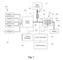
- FIG. 1illustrates a block diagram of components of a system for nucleic acid sequencing according to an exemplary embodiment.
- FIG. 2illustrates a cross-sectional view of a portion of the integrated circuit device and flow cell according to an exemplary embodiment.
- FIG. 3illustrates a cross-sectional view of two representative chemical sensors and their corresponding reaction regions according to a first embodiment.
- FIGS. 4 to 12illustrate stages in a manufacturing process for forming an array of chemical sensors and corresponding reaction regions according to a first embodiment.
- FIGS. 13 to 25illustrate stages in a manufacturing process for forming an array of chemical sensors and corresponding reaction regions according to a second embodiment.
- a chemical detection deviceincludes low noise chemical sensors, such as chemically-sensitive field effect transistors (chemFETs), for detecting chemical reactions within overlying, operationally associated reaction regions. Reducing the plan or top view area (or footprint) of individual chemical sensors and the overlying reaction regions allows for higher density devices. However, as the dimensions of the chemical sensors are reduced, Applicants have found that a corresponding reduction in the sensing surface area of the sensors can significantly impact performance. For example, for chemical sensors having sensing surfaces defined at the bottom of the reaction regions, reducing the plan view dimensions (e.g. the width or diameter) of the reaction regions results in a similar reduction in the sensing surface areas.
- chemFETschemically-sensitive field effect transistors
- Chemical sensors described hereinhave sensing surface areas which are not limited to a two-dimensional area at the bottom of the reaction regions.
- the sensing surface of the chemical sensorincludes a generally horizontal portion along the bottom surface of the reaction region, as well as a generally vertical portion extending along a sidewall of an opening containing the reaction region. The distance that the generally vertical portion extends along the sidewall is defined by the thickness of a dielectric material that forms a lower portion of the opening.
- the dielectric materialcan be deposited using a process (e.g. thin film deposition) which results in very small thickness variation across the array. In doing so, the sensor surface areas of the chemical sensors can be very well controlled, resulting in uniform chemical sensor performance across the array and thus simplifying the downstream signal processing.
- the chemical sensorBy extending the sensing surface in the generally vertical direction, the chemical sensor can have a small footprint, while also having a sufficiently large sensing surface area to avoid the noise issues associated with small sensing surfaces.
- the footprint of a chemical sensoris determined in part by the width (e.g. diameter) of the overlying reaction region and can be made small, allowing for a high density array.
- the sensing surfaceextends a controlled distance up the sidewall, the sensing surface area can be relatively large. As a result, low noise chemical sensors can be provided in a high density array, such that the characteristics of reactions can be accurately detected.
- FIG. 1illustrates a block diagram of components of a system for nucleic acid sequencing according to an exemplary embodiment.
- the componentsinclude a flow cell 101 on an integrated circuit device 100 , a reference electrode 108 , a plurality of reagents 114 for sequencing, a valve block 116 , a wash solution 110 , a valve 112 , a fluidics controller 118 , lines 120 / 122 / 126 , passages 104 / 109 / 111 , a waste container 106 , an array controller 124 , and a user interface 128 .
- the integrated circuit device 100includes a microwell array 107 overlying a sensor array that includes chemical sensors as described herein.
- the flow cell 101includes an inlet 102 , an outlet 103 , and a flow chamber 105 defining a flow path for the reagents 114 over the microwell array 107 .
- the reference electrode 108may be of any suitable type or shape, including a concentric cylinder with a fluid passage or a wire inserted into a lumen of passage 111 .
- the reagents 114may be driven through the fluid pathways, valves, and flow cell 101 by pumps, gas pressure, vacuum, or other suitable methods, and may be discarded into the waste container 106 after exiting the outlet 103 of the flow cell 101 .
- the fluidics controller 118may control driving forces for the reagents 114 and the operation of valve 112 and valve block 116 with suitable software.
- the microwell array 107includes reaction regions, also referred to herein as microwells, which are operationally associated with corresponding chemical sensors in the sensor array. For example, each reaction region may be coupled to a chemical sensor suitable for detecting an analyte or reaction property of interest within that reaction region.
- the microwell array 107may be integrated in the integrated circuit device 100 , so that the microwell array 107 and the sensor array are part of a single device or chip.
- the flow cell 101may have a variety of configurations for controlling the path and flow rate of reagents 114 over the microwell array 107 .
- the array controller 124provides bias voltages and timing and control signals to the integrated circuit device 100 for reading the chemical sensors of the sensor array.
- the array controller 124also provides a reference bias voltage to the reference electrode 108 to bias the reagents 114 flowing over the microwell array 107 .
- the array controller 124collects and processes output signals from the chemical sensors of the sensor array through output ports on the integrated circuit device 100 via bus 127 .
- the array controller 124may be a computer or other computing means.
- the array controller 124may include memory for storage of data and software applications, a processor for accessing data and executing applications, and components that facilitate communication with the various components of the system in FIG. 1 .
- the array controller 124is external to the integrated circuit device 100 . In some alternative embodiments, some or all of the functions performed by the array controller 124 are carried out by a controller or other data processor on the integrated circuit device 100 .
- the values of the output signals from the chemical sensorsindicate physical and/or chemical parameters of one or more reactions taking place in the corresponding reaction regions in the microwell array 107 .
- the values of the output signalsmay be processed using the techniques disclosed in Rearick et al., U.S. patent application Ser. No. 13/339,846, filed Dec. 29, 2011, based on U.S. Prov. Pat. Appl. Nos. 61/428,743, filed Dec. 30, 2010, and 61/429,328, filed Jan. 3, 2011, and in Hubbell, U.S. patent application Ser. No. 13/339,753, filed Dec. 29, 2011, based on U.S. Prov. Pat. Appl. No. 61/428,097, filed Dec.
- the user interface 128may display information about the flow cell 101 and the output signals received from chemical sensors in the sensor array on the integrated circuit device 100 .
- the user interface 128may also display instrument settings and controls, and allow a user to enter or set instrument settings and controls.
- the fluidics controller 118may control delivery of the individual reagents 114 to the flow cell 101 and integrated circuit device 100 in a predetermined sequence, for predetermined durations, at predetermined flow rates.
- the array controller 124can then collect and analyze the output signals of the chemical sensors indicating chemical reactions occurring in response to the delivery of the reagents 114 .
- the systemmay also monitor and control the temperature of the integrated circuit device 100 , so that reactions take place and measurements are made at a known predetermined temperature.
- the systemmay be configured to let a single fluid or reagent contact the reference electrode 108 throughout an entire multi-step reaction during operation.
- the valve 112may be shut to prevent any wash solution 110 from flowing into passage 109 as the reagents 114 are flowing. Although the flow of wash solution may be stopped, there may still be uninterrupted fluid and electrical communication between the reference electrode 108 , passage 109 , and the microwell array 107 .
- the distance between the reference electrode 108 and the junction between passages 109 and 111may be selected so that little or no amount of the reagents flowing in passage 109 (and possibly diffusing into passage 111 ) reach the reference electrode 108 .
- the wash solution 110may be selected as being in continuous contact with the reference electrode 108 , which may be especially useful for multi-step reactions using frequent wash steps.
- FIG. 2illustrates cross-sectional and expanded views of a portion of the integrated circuit device 100 and flow cell 101 .
- the integrated circuit device 100includes the microwell array 107 of reaction regions operationally associated with sensor array 205 .
- the flow chamber 105 of the flow cell 101confines a reagent flow 208 of delivered reagents across open ends of the reaction regions in the microwell array 107 .
- the volume, shape, aspect ratio (such as base width-to-well depth ratio), and other dimensional characteristics of the reaction regionsmay be selected based on the nature of the reaction taking place, as well as the reagents, byproducts, or labeling techniques (if any) that are employed.
- the chemical sensors of the sensor array 205are responsive to (and generate output signals related to) chemical reactions within associated reaction regions in the microwell array 107 to detect an analyte or reaction property of interest.
- the chemical sensors of the sensor array 205may for example be chemically sensitive field-effect transistors (chemFETs), such as ion-sensitive field effect transistors (ISFETs). Examples of chemical sensors and array configurations that may be used in embodiments are described in Schultz et al., U.S. patent application Ser. No. 12/785,667 (now U.S. Pat. No. 8,546,128), filed May 24, 2010, titled “Fluidics System for Sequential Delivery of Reagents”; Rotherberg et al., U.S. patent application Ser. No.
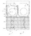
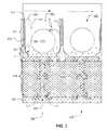
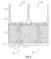
- FIG. 3illustrates a cross-sectional view of two representative chemical sensors and their corresponding reaction regions according to a first embodiment.
- two chemical sensors 350 , 351are shown, representing a small portion of a sensor array that can include millions of chemical sensors.
- Chemical sensor 350is coupled to corresponding reaction region 301
- chemical sensor 351is coupled to corresponding reaction region 302 .
- Chemical sensor 350is representative of the chemical sensors in the sensor array.
- the chemical sensor 350is a chemically-sensitive field effect transistor (chemFET), more specifically an ion-sensitive field effect transistor (ISFET) in this example.
- the chemical sensor 350includes a floating gate structure 318 having a sensor plate 320 coupled to the reaction region 301 by an electrically conductive element 370 .
- the sensor plate 320is the uppermost floating gate conductor in the floating gate structure 318 .
- the floating gate structure 318includes multiple patterned layers of conductive material within layers of dielectric material 319 .
- the chemical sensor 350also includes a source region 321 and a drain region 322 within a semiconductor substrate 354 .
- the source region 321 and the drain region 322comprise doped semiconductor material have a conductivity type different from the conductivity type of the substrate 354 .
- the source region 321 and the drain region 322may comprise doped P-type semiconductor material, and the substrate may comprise doped N-type semiconductor material.
- Channel region 323separates the source region 321 and the drain region 322 .
- the floating gate structure 318overlies the channel region 323 , and is separated from the substrate 354 by a gate dielectric 352 .
- the gate dielectric 352may be for example silicon dioxide. Alternatively, other dielectrics may be used for the gate dielectric 352 .
- the reaction region 301is within an opening having a sidewall 303 extending through dielectric materials 310 , 308 to the upper surface of the sensor plate 320 .
- Each of the dielectric materials 310 , 308may comprise one or more layers of material, such as silicon dioxide or silicon nitride.
- the openingincludes a lower portion 314 within dielectric material 308 and proximate to the sensor plate 320 .
- the openingalso includes an upper portion 315 within the dielectric material 310 and extending from the lower portion 314 to the upper surface of the dielectric material 310 .
- the width of the upper portion 315 of the openingis substantially the same as the width of the lower portion 314 of the opening.
- the width of the upper portion 315 of the openingmay be greater than the width of the lower portion 314 of the opening, or vice versa.
- the openingmay for example have a circular cross-section.
- the openingmay be non-circular.
- the cross-sectionmay be square, rectangular, hexagonal, or irregularly shaped.
- the dimensions of the openings, and their pitch,can vary from embodiment to embodiment.
- the openingscan have a characteristic diameter, defined as the square root of 4 times the plan view cross-sectional area (A) divided by Pi (e.g., sqrt(4*A/ ⁇ )), of not greater than 5 micrometers, such as not greater than 3.5 micrometers, not greater than 2.0 micrometers, not greater than 1.6 micrometers, not greater than 1.0 micrometers, not greater than 0.8 micrometers, not greater than 0.6 micrometers, not greater than 0.4 micrometers, not greater than 0.2 micrometers or even not greater than 0.1 micrometers.
- a characteristic diameterdefined as the square root of 4 times the plan view cross-sectional area (A) divided by Pi (e.g., sqrt(4*A/ ⁇ )
- the lower portion 314 of the openingincludes the electrically conductive element 370 on the sidewall 303 of the dielectric material 310 .
- the inner surface 371 of the electrically conductive element 370defines a lower segment of the reaction region 301 . That is, there is no intervening deposited material layer between the inner surface 371 of the electrically conductive element 370 and the reaction region 301 for the chemical sensor 350 .
- the inner surface 371 of the electrically conductive element 370is conformal to the opening and acts as the sensing surface for the chemical sensor 350 . It should be understood by those skilled in the art that precise shape and dimension of the electrically conductive element 370 , as with all other materials illustrated in the figures, is process dependant.
- the electrically conductive element 370is a conformal layer of material within the lower portion 314 of the opening, such that the electrically conductive element 370 extends across the upper surface of the sensor plate 320 . In the illustrated embodiment, the electrically conductive element 370 extends beyond the lower portion 314 of the opening and into the upper portion 315 of the opening.
- the inner surface of the dielectric material 310defines an upper segment of the reaction region 301 .
- the conductive element 370may for example extend along at least 5% of the sidewall 303 , at least 10%, at least 25%, at least 50%, at least 75%, or at least 85% of the sidewall 303 , or even extend along 99% of the sidewall 303 .
- the conformal inner surface 371 of the electrically conductive element 370allows the chemical sensor 350 to have a small plan view area, while also having a sufficiently large surface area to avoid the noise issues associated with small sensing surfaces.
- the plan view area of the chemical sensor 350is determined in part by the width (or diameter) of the reaction region 301 and can be made small, allowing for a high density array.
- the sensing surfaceextends up the sidewall 303 , the sensing surface area depends upon the distance of this extension and the circumference of the reaction region 301 , and can be relatively large. As a result, low noise chemical sensors 350 , 351 can be provided in a high density array, such that the characteristics of reactions can be accurately detected.
- a thin oxide of the material of the electrically conductive element 370may be grown which acts as a sensing material (e.g. an ion-sensitive sensing material) for the chemical sensor 350 . Whether an oxide is formed depends on the conductive material, the manufacturing processes performed, and the conditions under which the device is operated.
- the electrically conductive element 370may be titanium nitride, and titanium oxide or titanium oxynitride may be grown on the inner surface 371 of the conductive element 370 during manufacturing and/or during exposure to solutions during use.
- the electrically conductive element 370is shown as a single layer of material.
- the electrically conductive element 370may comprise one or more layers of a variety of electrically conductive materials, such as metals or ceramics, depending upon the embodiment.
- the conductive materialcan be for example a metallic material or alloy thereof, or can be a ceramic material, or a combination thereof.
- An exemplary metallic materialincludes one of aluminum, copper, nickel, titanium, silver, gold, platinum, hafnium, lanthanum, tantalum, tungsten, iridium, zirconium, palladium, or a combination thereof.
- An exemplary ceramic materialincludes one of titanium nitride, titanium aluminum nitride, titanium oxynitride, tantalum nitride or a combination thereof.
- an additional conformal sensing material(not shown) is deposited on the conductive element 370 and within the openings.
- the sensing materialmay comprise one or more of a variety of different materials to facilitate sensitivity to particular ions.
- silicon nitride or silicon oxynitride, as well as metal oxides such as silicon oxide, aluminum or tantalum oxidesgenerally provide sensitivity to hydrogen ions
- sensing materials comprising polyvinyl chloride containing valinomycinprovide sensitivity to potassium ions.
- Materials sensitive to other ionssuch as sodium, silver, iron, bromine, iodine, calcium, and nitrate may also be used, depending upon the embodiment.
- reactants, wash solutions, and other reagentsmay move in and out of the reaction region 301 by a diffusion mechanism 340 .
- the chemical sensor 350is responsive to (and generates an output signal related to) the amount of charge 324 proximate to the conductive element 370 .
- the presence of charge 324 in an analyte solutionalters the surface potential at the interface between the conductive element 370 and the analyte solution within the reaction region 301 .
- Changes in the charge 324cause changes in the voltage on the floating gate structure 318 , which in turn changes in the threshold voltage of the transistor. This change in threshold voltage can be measured by measuring the current in the channel region 323 between the source region 321 and a drain region 322 .
- the chemical sensor 350can be used directly to provide a current-based output signal on an array line connected to the source region 321 or drain region 322 , or indirectly with additional circuitry to provide a voltage-based output signal.
- the charge 324may be more highly concentrated near the bottom of the reaction region 301 , the distance that the conductive element 370 extends up the sidewall 303 of the opening is a tradeoff between the amplitude of the desired signal detected in response to the charge 324 , and the fluidic noise due to random fluctuation of charge between the conductive element 370 and the analyte solution.
- Increasing the distance that the conductive element 370 extends up the sidewall 303increases the fluidic interface area for the chemical sensor 350 , which acts to reduce the fluidic noise.
- the concentration of charge 324decreases with distance from the bottom of the reaction region 301 .
- upper sidewall segments of the conductive element 370detect portions of the signal from areas having lower charge concentration, which can reduce the overall amplitude of the desired signal detected by the sensor 350 .
- decreasing the distance the conductive element 370 extends up the sidewall 303reduces the sensing surface area and thus increases the fluidic noise, but also increases the overall amplitude of the desired signal detected by the sensor 350 .
- the conductive element 370extends along the sidewall 303 at which SNR is maximum.
- the optimal distancecan vary from embodiment to embodiment depending on the material characteristics of the conductive element 370 and the dielectric material 310 , the volume, shape, aspect ratio (such as base width-to-well depth ratio), and other dimensional characteristics of the reaction regions, the nature of the reaction taking place, as well as the reagents, byproducts, or labeling techniques (if any) that are employed.
- the optimal distancemay for example be determined empirically.
- the distance the conductive element 370 extends along the sidewall 303is defined by the etch time of the deposited layer, for example.
- the dielectric material 310 and electrically conductive element 370can be etched using a timed etch process, for example, which results in selectivity of distance 309 (e.g. the distance dielectric material 310 extends beyond electrically conductive element 370 ). In doing so, the sensor surface areas of the chemical sensors can be controlled, resulting in uniform chemical sensor performance across the array and simplifying the downstream signal processing.
- reactions carried out in the reaction region 301can be analytical reactions to identify or determine characteristics or properties of an analyte of interest. Such reactions can generate directly or indirectly byproducts that affect the amount of charge adjacent to the electrically conductive element 370 . If such byproducts are produced in small amounts or rapidly decay or react with other constituents, multiple copies of the same analyte may be analyzed in the reaction region 301 at the same time in order to increase the output signal generated. In an embodiment, multiple copies of an analyte may be attached to a solid phase support 312 , as shown in FIG. 3 , either before or after deposition into the reaction region 301 .
- the solid phase support 312may be microparticles, nanoparticles, beads, solid or porous gels, or the like. For simplicity and ease of explanation, solid phase support 312 is also referred herein as a particle.
- a nucleic acid analytemultiple, connected copies may be made by rolling circle amplification (RCA), exponential RCA, Recombinase Polymerase Amplification (RPA), Polymerase Chain Reaction amplification (PCR), emulsion PCR amplification, or like techniques, to produce an amplicon without the need of a solid support.
- RCArolling circle amplification
- RPARecombinase Polymerase Amplification
- PCRPolymerase Chain Reaction amplification
- emulsion PCR amplificationor like techniques
- a nucleotide incorporation eventmay be determined by detecting ions (e.g., hydrogen ions) that are generated as natural by-products of polymerase-catalyzed nucleotide extension reactions. This may be used to sequence a sample or template nucleic acid, which may be a fragment of a nucleic acid sequence of interest, for example, and which may be directly or indirectly attached as a clonal population to a solid support, such as a particle, microparticle, bead, etc.
- ionse.g., hydrogen ions
- the sample or template nucleic acidmay be operably associated to a primer and polymerase and may be subjected to repeated cycles or “flows” of deoxynucleoside triphosphate (“dNTP”) addition (which may be referred to herein as “nucleotide flows” from which nucleotide incorporations may result) and washing.
- dNTPdeoxynucleoside triphosphate
- the primermay be annealed to the sample or template so that the primer's 3 ′ end can be extended by a polymerase whenever dNTPs complementary to the next base in the template are added.
- the identity of the type, sequence and number of nucleotide(s) associated with a sample nucleic acid present in a reaction region coupled to a chemical sensorcan be determined.
- FIGS. 4 to 12illustrate stages in a manufacturing process for forming an array of chemical sensors and corresponding reaction regions according to a first embodiment.
- FIG. 4illustrates a structure 400 formed in a first stage.
- the structure 400includes the floating gate structures (e.g. floating gate structure 318 ) for the chemical sensors 350 , 351 .
- the structure 400can be formed by depositing a layer of gate dielectric material on the semiconductor substrate 354 , and depositing a layer of polysilicon (or other electrically conductive material) on the layer of gate dielectric material.
- the layer of polysilicon and the layer gate dielectric materialcan then be etched using an etch mask to form the gate dielectric elements (e.g. gate dielectric 352 ) and the lowermost conductive material element of the floating gate structures.
- ion implantationcan then be performed to form the source and drain regions (e.g. source region 321 and a drain region 322 ) of the chemical sensors.
- a first layer of the dielectric material 319can then be deposited over the lowermost conductive material elements.
- Conductive plugscan then be formed within vias etched in the first layer of dielectric material 319 to contact the lowermost conductive material elements of the floating gate structures.
- a layer of conductive materialcan then be deposited on the first layer of the dielectric material 319 and patterned to form second conductive material elements electrically connected to the conductive plugs. This process can then be repeated multiple times to form the completed floating gate structure 318 shown in FIG. 4 .
- Forming the structure 400 in FIG. 4can also include forming additional elements such as array lines (e.g. row lines, column lines, etc.) for accessing the chemical sensors, additional doped regions in the substrate 354 , and other circuitry (e.g. select switches, access circuitry, bias circuitry etc.) used to operate the chemical sensors, depending upon the device and array configuration in which the chemical sensors described herein are implemented.
- the elements of the structuremay for example be manufactured using techniques described in Schultz et al., U.S. patent application Ser. No. 12/785,667 (now U.S. Pat. No.
- dielectric material 308 having a given thicknessis deposited on the structure 400 illustrated in FIG. 4 , resulting in the structure illustrated in FIG. 5 .
- the dielectric material 308comprises one or more dielectric layers of dielectric.
- the dielectric material 308may be deposited using a process which results in very small variation in the thickness across the array.
- the dielectric material 308may comprise silicon oxide and be deposited using high density plasma (HDP) deposition.
- HDPhigh density plasma
- Various other techniquesmay be used, such as sputtering, reactive sputtering, atomic layer deposition (ALD), low pressure chemical vapor deposition (LPCVD), plasma enhanced chemical vapor deposition (PECVD), metal organic chemical vapor deposition (MOCVD), etc.
- the dielectric material 308 of the structure in FIG. 5is etched to form cavities 600 , 602 extending to the upper surfaces of the floating gate structures of the chemical sensors 350 , 351 , resulting in the structure illustrated in FIG. 6 .
- the cavities 600 , 602may for example be formed by using a lithographic process to pattern a layer of photoresist on the dielectric material 308 to define the locations of the cavities 600 , 602 , and then anisotropically etching the dielectric material 308 using the patterned photoreist as an etch mask.
- the anisotropic etching of the dielectric material 308may for example be a dry etch process, such as a fluorine based Reactive Ion Etching (RIE) process.
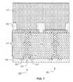
- dielectric material 310is formed on the structure illustrated in FIG. 6 , resulting in the structure illustrated in FIG. 7 .
- the dielectric material 310may comprise one or more layers of deposited dielectric material, such as silicon dioxide or silicon nitride.
- the conductive material 900comprises one or more layers of electrically conductive material.
- the conductive material 900may be a layer of titanium nitride, or a layer of titanium.
- other and/or additional conductive materialsmay be used, such as those described above with reference to the conductive element 370 .
- more than one layer of conductive materialmay be deposited.
- the conductive material 900may be deposited using various techniques, such as sputtering, reactive sputtering, atomic layer deposition (ALD), low pressure chemical vapor deposition (LPCVD), plasma enhanced chemical vapor deposition (PECVD), metal organic chemical vapor deposition (MOCVD), etc.
- conductive element 370may be formed to take various shapes and thicknesses that may be determined based on material and techniques described above. For example, instead of the depiction of conductive element 370 as illustrated in FIG. 3 , one may imagine conductive element 370 is formed such that it is conformal with the solid support (rounded to follow the shape of solid support 312 ).
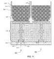
- material 1000is formed on the structure illustrated in FIG. 9 , resulting in the structure illustrated in FIG. 10 .
- the material 1000may comprise one or more layers of deposited dielectric material, such as silicon dioxide or silicon nitride.
- material 1000may comprise photoresist.
- a partial etch of material 1000 and conductive material 900is performed such that distance 309 of dielectric material 310 is revealed (that is, distance 309 of sidewall 303 is exposed), resulting in the structure illustrated in FIG. 11 .
- Material 1000 and electrically conductive material 900may be etched together or separately depending on the process and/or material(s) used.
- a partial etchmay be performed using at least one of an O2 resist etch, Ar sputter breakthrough etch, and Hydrogen Bromide Titanium etch.
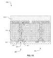
- material 1000is etched to form openings defining reaction regions 301 , 302 extending to the conductive element 370 , 900 , resulting in the structure illustrated in FIG. 12 .
- residual photoresistmay need to be cleaned from the opening using techniques known to those skilled in the art, for example, O2 plasma ash.
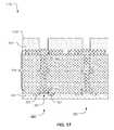
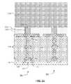
- FIG. 13illustrates a cross-sectional view of two representative chemical sensors and their corresponding reaction regions according to a second embodiment.
- the structure of the two representative chemical sensors illustrated in FIG. 13differs in one aspect from the two representative chemical sensors illustrated in FIG. 3 in that FIG. 13 includes vias over sensor plates 320 on top of which the microwells/nanowells are built. Accordingly, fabrication for the structure in FIG. 3 is different from fabrication of FIG. 13 , as is explained in greater detail below.
- FIGS. 14-25illustrate stages in a manufacturing process for forming an array of chemical devices and corresponding well structures according to an exemplary embodiment.
- FIG. 14illustrates a structure 1400 including the floating gate structures (e.g. floating gate structure 318 ) for the chemical devices 350 , 351 .
- the structure 1400can be formed in accordance with the structure 400 described in detail above with reference to FIG. 4 .
- a dielectric material 1503may be formed on the sensor plate 320 of the field effect transistor of the chemical device 350 .
- FIG. 16the dielectric material 1503 of the structure 1500 in FIG.
- the openings 1618 , 1620may, for example, be formed by using a lithographic process to pattern a layer of photoresist on the dielectric material 1503 to define the locations of the openings 1618 , 1620 , and then anisotropically etching the dielectric material 1503 using the patterned photoreist as an etch mask.
- the anisotropic etching of the dielectric material 1503may, for example, be a dry etch process, such as a fluorine based Reactive Ion Etching (RIE) process.
- RIEfluorine based Reactive Ion Etching
- the openings 1618 , 1620are separated by a distance 1630 and the openings 1618 , 1620 are of a suitable dimension for a via.
- the separation distance 1630may be a minimum feature size for the process (e.g. a lithographic process) used to form the openings 1618 , 1620 .
- the distance 1630may be significantly more than the width 1620 .
- a layer of conductive material 1704is deposited on the structure 1600 illustrated in FIG. 16 , resulting in the structure 1700 illustrated in FIG. 17 .
- Conductive material 1704may be referred to as a conductive liner.
- the conductive material 1704may comprise one or more layers of electrically conductive material.
- the conductive material 1704may be a layer of titanium nitride, or a layer of titanium. Alternatively, other and/or additional conductive materials may be used, such as those described above with reference to the electrically conductive element. In addition, more than one layer of conductive material may be deposited.
- the conductive material 1704may be deposited using various techniques, such as sputtering, reactive sputtering, atomic layer deposition (ALD), low pressure chemical vapor deposition (LPCVD), plasma enhanced chemical vapor deposition (PECVD), metal organic chemical vapor deposition (MOCVD), etc.
- a layer of conductive material 1805such as tungsten, for example, is deposited on the structure 1700 illustrated in FIG. 17 , resulting in the structure 1800 illustrated in FIG. 18 .
- the conductive material 1805may be deposited using various techniques, such as sputtering, reactive sputtering, atomic layer deposition (ALD), low pressure chemical vapor deposition (LPCVD), plasma enhanced chemical vapor deposition (PECVD), metal organic chemical vapor deposition (MOCVD), etc. or any other suitable techniques.
- conductive material 1704 and conductive material 1805are planarized using a Chemical Mechanical Planarization (CMP) process, for example, resulting in the structure 1900 illustrated in FIG. 19 .
- CMPChemical Mechanical Planarization
- a via barrier linermay be formed on the planarized conductive material 1704 and conductive material 1805 .
- the via barrier linermay comprise titanium nitride.
- dielectric material 2006is formed on the structure illustrated in FIG. 19 , resulting in the structure illustrated in FIG. 20 .
- the dielectric material 2006may comprise one or more layers of deposited dielectric material, such as silicon dioxide or silicon nitride.
- dielectric material 2006is etched to form openings extending to planarized conductive material 1704 and conductive material 1805 and dielectric material 1503 , resulting in the structure illustrated in FIG. 21 .
- Dielectric material 1503may be partially etched when the openings are formed such that conductive material 1704 and conductive material 1805 are raised above dielectric material 1503 and protrude into the opening, as seen in the illustrated embodiment.
- a conformal layer of conductive material 2200is deposited on the structure illustrated in FIG.
- the conductive material 2200comprises one or more layers of electrically conductive material.
- the conductive material 2200may be a layer of titanium nitride, or a layer of titanium.
- other and/or additional conductive materialsmay be used, such as those described above with reference to the conductive element 370 .
- more than one layer of conductive materialmay be deposited.
- the conductive material 2200may be deposited using various techniques, such as sputtering, reactive sputtering, atomic layer deposition (ALD), low pressure chemical vapor deposition (LPCVD), plasma enhanced chemical vapor deposition (PECVD), metal organic chemical vapor deposition (MOCVD), etc.
- material 2300is formed on the structure illustrated in FIG. 22 , resulting in the structure illustrated in FIG. 23 .
- the material 2300may comprise one or more layers of deposited dielectric material, such as silicon dioxide or silicon nitride.
- material 2300may comprise photoresist.
- a partial etch of material 2300 and conductive material 2200is performed such that distance 1309 of dielectric material 310 is revealed (that is, distance 309 of sidewall 1303 is exposed), resulting in the structure illustrated in FIG. 24 .
- Material 2300 and conductive material 2200may be etched together or separately depending on the process and/or material(s) used.
- a partial etchmay be performed using at least one of an O2 resist etch, Ar sputter breakthrough etch, and Hydrogen Bromide Titanium etch.
- material 2300is etched to form openings defining reaction regions 301 , 302 extending to the conductive elements 370 , 2200 , resulting in the structure illustrated in FIG. 25 .
- residual photoresistmay need to be cleaned from the opening using techniques known to those skilled in the art, for example, O2 plasma ash.
Landscapes
- Chemical & Material Sciences (AREA)
- Health & Medical Sciences (AREA)
- Life Sciences & Earth Sciences (AREA)
- Physics & Mathematics (AREA)
- General Health & Medical Sciences (AREA)
- Microelectronics & Electronic Packaging (AREA)
- Engineering & Computer Science (AREA)
- Chemical Kinetics & Catalysis (AREA)
- Analytical Chemistry (AREA)
- Molecular Biology (AREA)
- Electrochemistry (AREA)
- Biochemistry (AREA)
- General Physics & Mathematics (AREA)
- Immunology (AREA)
- Pathology (AREA)
- Computer Hardware Design (AREA)
- Fluid Mechanics (AREA)
- Dispersion Chemistry (AREA)
- Hematology (AREA)
- Clinical Laboratory Science (AREA)
- Investigating Or Analyzing Materials By The Use Of Electric Means (AREA)
- Apparatus Associated With Microorganisms And Enzymes (AREA)
Abstract
Description
This application is a divisional of U.S. patent application Ser. No. 14/939,101 filed Nov. 12, 2015, which is a divisional of U.S. patent application Ser. No. 14/198,417 filed Mar. 5, 2014, which claims priority to U.S. Provisional Application No. 61/900,907 filed Nov. 6, 2013 and 61/790,866 filed Mar. 15, 2013, the entire contents of which are incorporated by reference herein in their entirety.
The present disclosure relates to sensors for chemical analysis, and to methods for manufacturing such sensors.
A variety of types of chemical sensors have been used in the detection of chemical processes. One type is a chemically-sensitive field effect transistor (chemFET). A chemFET includes a source and a drain separated by a channel region, and a chemically sensitive area coupled to the channel region. The operation of the chemFET is based on the modulation of channel conductance, caused by changes in charge at the sensitive area due to a chemical reaction occurring nearby. The modulation of the channel conductance changes the threshold voltage of the chemFET, which can be measured to detect and/or determine characteristics of the chemical reaction. The threshold voltage may for example be measured by applying appropriate bias voltages to the source and drain, and measuring a resulting current flowing through the chemFET. As another example, the threshold voltage may be measured by driving a known current through the chemFET, and measuring a resulting voltage at the source or drain.
An ion-sensitive field effect transistor (ISFET) is a type of chemFET that includes an ion-sensitive layer at the sensitive area. The presence of ions in an analyte solution alters the surface potential at the interface between the ion-sensitive layer and the analyte solution, due to the protonation or deprotonation of surface charge groups caused by the ions present in the analyte solution. The change in surface potential at the sensitive area of the ISFET affects the threshold voltage of the device, which can be measured to indicate the presence and/or concentration of ions within the solution. Arrays of ISFETs may be used for monitoring chemical reactions, such as DNA sequencing reactions, based on the detection of ions present, generated, or used during the reactions. See, for example, Rothberg et al., U.S. patent application Ser. No. 12/002,291 (now U.S. Pat. No. 7,948,015), filed Dec. 14, 2009, based on U.S. Prov. Pat. Appl. Nos. 60/956,324, filed Aug. 16, 2007, 60/968,748, filed Jul. 10, 2007, and 60/870,073, filed Dec. 14, 2006, which is incorporated by reference herein in its entirety. More generally, large arrays of chemFETs or other types of chemical sensors may be employed to detect and measure static and/or dynamic amounts or concentrations of a variety of analytes (e.g. hydrogen ions, other ions, compounds, etc.) in a variety of processes. The processes may for example be biological or chemical reactions, cell or tissue cultures or monitoring neural activity, nucleic acid sequencing, etc.
An issue that arises in the operation of large scale chemical sensor arrays is the susceptibility of the sensor output signals to noise. Specifically, the noise affects the accuracy of the downstream signal processing used to determine the characteristics of the chemical and/or biological process being detected by the sensors. In addition, chemical sensor performance variation across the array results in undesirable differences in the sensor output signals, which further complicates the downstream signal processing. It is therefore desirable to provide devices including low noise chemical sensors, and methods for manufacturing such devices.
In one embodiment, a chemical sensor is described. The chemical sensor includes a chemically-sensitive field effect transistor including a floating gate conductor having an upper surface; a material defining an opening extending to the upper surface of the floating gate conductor, the material comprising a first dielectric underlying a second dielectric; and a conductive element contacting the upper surface of the floating gate conductor and extending a distance along a sidewall of the opening. In an exemplary embodiment, the opening of the chemical sensor may include a lower portion within the first dielectric, and an upper portion within the second dielectric. In another embodiment, a width of the lower portion of the opening is substantially the same as a width of the upper portion. In yet another embodiment, the conductive element is conformal with a shape of the opening. In one embodiment, the conductive element extends to an upper surface of the second dielectric. In an exemplary embodiment, the conductive element includes an inner surface defining a lower portion of a reaction region for the chemical sensor, and the second dielectric includes an inner surface defining an upper portion of the opening. In an exemplary embodiment, the conductive element comprises an electrically conductive material, and an inner surface of the conductive element includes an oxide of the electrically conductive material. In another embodiment, a sensing surface of the chemical sensor includes an inner surface of the conductive element. In yet another embodiment, the chemically-sensitive field effect transistor generates a sensor signal in response to a chemical reaction occurring proximate to the conductive element. In one embodiment, the floating gate conductor comprises a plurality of conductors electrically coupled to one another and separated by dielectric layers, and the floating gate conductor is an uppermost conductor in the plurality of conductors.
In another embodiment, a method for manufacturing a chemical sensor is described. The method includes forming a chemically-sensitive field effect transistor including a floating gate conductor having an upper surface; forming a material defining an opening extending to the upper surface of the floating gate conductor, the material comprising a first dielectric underlying a second dielectric; and forming a conductive element contacting the upper surface of the floating gate conductor and extending a distance along a sidewall of the opening. In an exemplary embodiment, forming the material and forming the conductive element may include forming the first dielectric on the floating gate conductor, the first dielectric defining a cavity extending to the upper surface of the floating gate conductor; forming the second dielectric thereon; etching the second dielectric to expose the conductive element, thereby defining an opening; and forming the conductive element within the opening. According to another embodiment, forming the conductive element within the opening may include depositing a conductive material within the opening and on an upper surface of the first dielectric; and removing at least a portion of the conductive material from the upper surface of the second dielectric. In yet another embodiment, removing at least the portion of the conductive material may comprises depositing a layer of photoresist within the opening; and removing at least a portion of the conductive material together with the photoresist from the upper surface of the second dielectric. In one embodiment, the conductive material comprises titanium. In an exemplary embodiment, the opening is a nanowell. In an exemplary embodiment, the forming a conductive element includes depositing a conductive material conformally within the opening. In another embodiment, the conductive element includes an inner surface defining a lower portion of a reaction region for the chemical sensor, and the second dielectric includes an inner surface defining an upper portion of the opening.
Particular aspects of one embodiment of the subject matter described in this specification are set forth in the drawings and the description below. Other features, aspects, and advantages of the subject matter will become apparent from the description, the drawings, and the claims.
A chemical detection device is described that includes low noise chemical sensors, such as chemically-sensitive field effect transistors (chemFETs), for detecting chemical reactions within overlying, operationally associated reaction regions. Reducing the plan or top view area (or footprint) of individual chemical sensors and the overlying reaction regions allows for higher density devices. However, as the dimensions of the chemical sensors are reduced, Applicants have found that a corresponding reduction in the sensing surface area of the sensors can significantly impact performance. For example, for chemical sensors having sensing surfaces defined at the bottom of the reaction regions, reducing the plan view dimensions (e.g. the width or diameter) of the reaction regions results in a similar reduction in the sensing surface areas. Applicants have found that as the sensing surface area is reduced to technology limits, fluidic noise due to the random fluctuation of charge on the sensing surface contributes to an increasing proportion of the total variation in sensing surface potential. This can significantly reduce the signal-to-noise ratio (SNR) of the sensor output signal, which affects the accuracy of the downstream signal processing used to determine the characteristics of the chemical and/or biological process being detected by the sensor.
Chemical sensors described herein have sensing surface areas which are not limited to a two-dimensional area at the bottom of the reaction regions. In embodiments described herein, the sensing surface of the chemical sensor includes a generally horizontal portion along the bottom surface of the reaction region, as well as a generally vertical portion extending along a sidewall of an opening containing the reaction region. The distance that the generally vertical portion extends along the sidewall is defined by the thickness of a dielectric material that forms a lower portion of the opening. The dielectric material can be deposited using a process (e.g. thin film deposition) which results in very small thickness variation across the array. In doing so, the sensor surface areas of the chemical sensors can be very well controlled, resulting in uniform chemical sensor performance across the array and thus simplifying the downstream signal processing. By extending the sensing surface in the generally vertical direction, the chemical sensor can have a small footprint, while also having a sufficiently large sensing surface area to avoid the noise issues associated with small sensing surfaces. The footprint of a chemical sensor is determined in part by the width (e.g. diameter) of the overlying reaction region and can be made small, allowing for a high density array. In addition, because the sensing surface extends a controlled distance up the sidewall, the sensing surface area can be relatively large. As a result, low noise chemical sensors can be provided in a high density array, such that the characteristics of reactions can be accurately detected.
Themicrowell array 107 includes reaction regions, also referred to herein as microwells, which are operationally associated with corresponding chemical sensors in the sensor array. For example, each reaction region may be coupled to a chemical sensor suitable for detecting an analyte or reaction property of interest within that reaction region. Themicrowell array 107 may be integrated in theintegrated circuit device 100, so that themicrowell array 107 and the sensor array are part of a single device or chip. Theflow cell 101 may have a variety of configurations for controlling the path and flow rate ofreagents 114 over themicrowell array 107. Thearray controller 124 provides bias voltages and timing and control signals to theintegrated circuit device 100 for reading the chemical sensors of the sensor array. Thearray controller 124 also provides a reference bias voltage to thereference electrode 108 to bias thereagents 114 flowing over themicrowell array 107.
During an experiment, thearray controller 124 collects and processes output signals from the chemical sensors of the sensor array through output ports on theintegrated circuit device 100 viabus 127. Thearray controller 124 may be a computer or other computing means. Thearray controller 124 may include memory for storage of data and software applications, a processor for accessing data and executing applications, and components that facilitate communication with the various components of the system inFIG. 1 . In the illustrated embodiment, thearray controller 124 is external to theintegrated circuit device 100. In some alternative embodiments, some or all of the functions performed by thearray controller 124 are carried out by a controller or other data processor on theintegrated circuit device 100. The values of the output signals from the chemical sensors indicate physical and/or chemical parameters of one or more reactions taking place in the corresponding reaction regions in themicrowell array 107. For example, in an exemplary embodiment, the values of the output signals may be processed using the techniques disclosed in Rearick et al., U.S. patent application Ser. No. 13/339,846, filed Dec. 29, 2011, based on U.S. Prov. Pat. Appl. Nos. 61/428,743, filed Dec. 30, 2010, and 61/429,328, filed Jan. 3, 2011, and in Hubbell, U.S. patent application Ser. No. 13/339,753, filed Dec. 29, 2011, based on U.S. Prov. Pat. Appl. No. 61/428,097, filed Dec. 29, 2010, each of which are incorporated by reference herein. Theuser interface 128 may display information about theflow cell 101 and the output signals received from chemical sensors in the sensor array on theintegrated circuit device 100. Theuser interface 128 may also display instrument settings and controls, and allow a user to enter or set instrument settings and controls.
Thefluidics controller 118 may control delivery of theindividual reagents 114 to theflow cell 101 andintegrated circuit device 100 in a predetermined sequence, for predetermined durations, at predetermined flow rates. Thearray controller 124 can then collect and analyze the output signals of the chemical sensors indicating chemical reactions occurring in response to the delivery of thereagents 114. During the experiment, the system may also monitor and control the temperature of theintegrated circuit device 100, so that reactions take place and measurements are made at a known predetermined temperature.
The system may be configured to let a single fluid or reagent contact thereference electrode 108 throughout an entire multi-step reaction during operation. Thevalve 112 may be shut to prevent anywash solution 110 from flowing intopassage 109 as thereagents 114 are flowing. Although the flow of wash solution may be stopped, there may still be uninterrupted fluid and electrical communication between thereference electrode 108,passage 109, and themicrowell array 107. The distance between thereference electrode 108 and the junction betweenpassages reference electrode 108. In an exemplary embodiment, thewash solution 110 may be selected as being in continuous contact with thereference electrode 108, which may be especially useful for multi-step reactions using frequent wash steps.
Thechemical sensor 350 also includes asource region 321 and adrain region 322 within asemiconductor substrate 354. Thesource region 321 and thedrain region 322 comprise doped semiconductor material have a conductivity type different from the conductivity type of thesubstrate 354. For example, thesource region 321 and thedrain region 322 may comprise doped P-type semiconductor material, and the substrate may comprise doped N-type semiconductor material.Channel region 323 separates thesource region 321 and thedrain region 322. The floatinggate structure 318 overlies thechannel region 323, and is separated from thesubstrate 354 by agate dielectric 352. Thegate dielectric 352 may be for example silicon dioxide. Alternatively, other dielectrics may be used for thegate dielectric 352.
As shown inFIG. 3 , thereaction region 301 is within an opening having asidewall 303 extending throughdielectric materials sensor plate 320. Each of thedielectric materials lower portion 314 withindielectric material 308 and proximate to thesensor plate 320. The opening also includes anupper portion 315 within thedielectric material 310 and extending from thelower portion 314 to the upper surface of thedielectric material 310. In the illustrated embodiment, the width of theupper portion 315 of the opening is substantially the same as the width of thelower portion 314 of the opening. However, depending on the material(s) and/or etch process used to create the opening, the width of theupper portion 315 of the opening may be greater than the width of thelower portion 314 of the opening, or vice versa. The opening may for example have a circular cross-section. Alternatively, the opening may be non-circular. For example, the cross-section may be square, rectangular, hexagonal, or irregularly shaped. The dimensions of the openings, and their pitch, can vary from embodiment to embodiment. In some embodiments, the openings can have a characteristic diameter, defined as the square root of 4 times the plan view cross-sectional area (A) divided by Pi (e.g., sqrt(4*A/π)), of not greater than 5 micrometers, such as not greater than 3.5 micrometers, not greater than 2.0 micrometers, not greater than 1.6 micrometers, not greater than 1.0 micrometers, not greater than 0.8 micrometers, not greater than 0.6 micrometers, not greater than 0.4 micrometers, not greater than 0.2 micrometers or even not greater than 0.1 micrometers.
Thelower portion 314 of the opening includes the electricallyconductive element 370 on thesidewall 303 of thedielectric material 310. In the illustrated embodiment, the inner surface371 of the electricallyconductive element 370 defines a lower segment of thereaction region 301. That is, there is no intervening deposited material layer between the inner surface371 of the electricallyconductive element 370 and thereaction region 301 for thechemical sensor 350. As a result of this structure, the inner surface371 of the electricallyconductive element 370 is conformal to the opening and acts as the sensing surface for thechemical sensor 350. It should be understood by those skilled in the art that precise shape and dimension of the electricallyconductive element 370, as with all other materials illustrated in the figures, is process dependant.
In the illustrated embodiment, the electricallyconductive element 370 is a conformal layer of material within thelower portion 314 of the opening, such that the electricallyconductive element 370 extends across the upper surface of thesensor plate 320. In the illustrated embodiment, the electricallyconductive element 370 extends beyond thelower portion 314 of the opening and into theupper portion 315 of the opening. The inner surface of thedielectric material 310 defines an upper segment of thereaction region 301. Theconductive element 370 may for example extend along at least 5% of thesidewall 303, at least 10%, at least 25%, at least 50%, at least 75%, or at least 85% of thesidewall 303, or even extend along 99% of thesidewall 303. The conformal inner surface371 of the electricallyconductive element 370 allows thechemical sensor 350 to have a small plan view area, while also having a sufficiently large surface area to avoid the noise issues associated with small sensing surfaces. The plan view area of thechemical sensor 350 is determined in part by the width (or diameter) of thereaction region 301 and can be made small, allowing for a high density array. In addition, because the sensing surface extends up thesidewall 303, the sensing surface area depends upon the distance of this extension and the circumference of thereaction region 301, and can be relatively large. As a result, lownoise chemical sensors
During manufacturing and/or operation of the device, a thin oxide of the material of the electricallyconductive element 370 may be grown which acts as a sensing material (e.g. an ion-sensitive sensing material) for thechemical sensor 350. Whether an oxide is formed depends on the conductive material, the manufacturing processes performed, and the conditions under which the device is operated. For example, in one embodiment the electricallyconductive element 370 may be titanium nitride, and titanium oxide or titanium oxynitride may be grown on the inner surface371 of theconductive element 370 during manufacturing and/or during exposure to solutions during use. In the illustrated example, the electricallyconductive element 370 is shown as a single layer of material. More generally, the electricallyconductive element 370 may comprise one or more layers of a variety of electrically conductive materials, such as metals or ceramics, depending upon the embodiment. The conductive material can be for example a metallic material or alloy thereof, or can be a ceramic material, or a combination thereof. An exemplary metallic material includes one of aluminum, copper, nickel, titanium, silver, gold, platinum, hafnium, lanthanum, tantalum, tungsten, iridium, zirconium, palladium, or a combination thereof. An exemplary ceramic material includes one of titanium nitride, titanium aluminum nitride, titanium oxynitride, tantalum nitride or a combination thereof. In some alternative embodiments, an additional conformal sensing material (not shown) is deposited on theconductive element 370 and within the openings. The sensing material may comprise one or more of a variety of different materials to facilitate sensitivity to particular ions. For example, silicon nitride or silicon oxynitride, as well as metal oxides such as silicon oxide, aluminum or tantalum oxides, generally provide sensitivity to hydrogen ions, whereas sensing materials comprising polyvinyl chloride containing valinomycin provide sensitivity to potassium ions. Materials sensitive to other ions such as sodium, silver, iron, bromine, iodine, calcium, and nitrate may also be used, depending upon the embodiment.
In operation, reactants, wash solutions, and other reagents may move in and out of thereaction region 301 by adiffusion mechanism 340. Thechemical sensor 350 is responsive to (and generates an output signal related to) the amount of charge324 proximate to theconductive element 370. The presence of charge324 in an analyte solution alters the surface potential at the interface between theconductive element 370 and the analyte solution within thereaction region 301. Changes in the charge324 cause changes in the voltage on the floatinggate structure 318, which in turn changes in the threshold voltage of the transistor. This change in threshold voltage can be measured by measuring the current in thechannel region 323 between thesource region 321 and adrain region 322. As a result, thechemical sensor 350 can be used directly to provide a current-based output signal on an array line connected to thesource region 321 or drainregion 322, or indirectly with additional circuitry to provide a voltage-based output signal. Because the charge324 may be more highly concentrated near the bottom of thereaction region 301, the distance that theconductive element 370 extends up thesidewall 303 of the opening is a tradeoff between the amplitude of the desired signal detected in response to the charge324, and the fluidic noise due to random fluctuation of charge between theconductive element 370 and the analyte solution. Increasing the distance that theconductive element 370 extends up thesidewall 303 increases the fluidic interface area for thechemical sensor 350, which acts to reduce the fluidic noise. However, due to the diffusion of charge324 out of thereaction region 301, the concentration of charge324 decreases with distance from the bottom of thereaction region 301. As a result, upper sidewall segments of theconductive element 370 detect portions of the signal from areas having lower charge concentration, which can reduce the overall amplitude of the desired signal detected by thesensor 350. In contrast, decreasing the distance theconductive element 370 extends up thesidewall 303 reduces the sensing surface area and thus increases the fluidic noise, but also increases the overall amplitude of the desired signal detected by thesensor 350.
For a very small sensing surface area, Applicants have found that the fluidic noise changes as a function of the sensing surface area differently than the amplitude of the desired signal. Because the SNR of the sensor output signal is the ratio of these two quantities, there is an optimal distance theconductive element 370 extends along thesidewall 303 at which SNR is maximum. The optimal distance can vary from embodiment to embodiment depending on the material characteristics of theconductive element 370 and thedielectric material 310, the volume, shape, aspect ratio (such as base width-to-well depth ratio), and other dimensional characteristics of the reaction regions, the nature of the reaction taking place, as well as the reagents, byproducts, or labeling techniques (if any) that are employed. The optimal distance may for example be determined empirically.
As described in more detail below with respect toFIGS. 4 to 12 , the distance theconductive element 370 extends along thesidewall 303 is defined by the etch time of the deposited layer, for example. Thedielectric material 310 and electricallyconductive element 370 can be etched using a timed etch process, for example, which results in selectivity of distance309 (e.g. thedistance dielectric material 310 extends beyond electrically conductive element370). In doing so, the sensor surface areas of the chemical sensors can be controlled, resulting in uniform chemical sensor performance across the array and simplifying the downstream signal processing.
In an embodiment, reactions carried out in thereaction region 301 can be analytical reactions to identify or determine characteristics or properties of an analyte of interest. Such reactions can generate directly or indirectly byproducts that affect the amount of charge adjacent to the electricallyconductive element 370. If such byproducts are produced in small amounts or rapidly decay or react with other constituents, multiple copies of the same analyte may be analyzed in thereaction region 301 at the same time in order to increase the output signal generated. In an embodiment, multiple copies of an analyte may be attached to asolid phase support 312, as shown inFIG. 3 , either before or after deposition into thereaction region 301. Thesolid phase support 312 may be microparticles, nanoparticles, beads, solid or porous gels, or the like. For simplicity and ease of explanation,solid phase support 312 is also referred herein as a particle. For a nucleic acid analyte, multiple, connected copies may be made by rolling circle amplification (RCA), exponential RCA, Recombinase Polymerase Amplification (RPA), Polymerase Chain Reaction amplification (PCR), emulsion PCR amplification, or like techniques, to produce an amplicon without the need of a solid support.
In various exemplary embodiments, the methods, systems, and computer readable media described herein may advantageously be used to process and/or analyze data and signals obtained from electronic or charged-based nucleic acid sequencing. In electronic or charged-based sequencing (such as, pH-based sequencing), a nucleotide incorporation event may be determined by detecting ions (e.g., hydrogen ions) that are generated as natural by-products of polymerase-catalyzed nucleotide extension reactions. This may be used to sequence a sample or template nucleic acid, which may be a fragment of a nucleic acid sequence of interest, for example, and which may be directly or indirectly attached as a clonal population to a solid support, such as a particle, microparticle, bead, etc. The sample or template nucleic acid may be operably associated to a primer and polymerase and may be subjected to repeated cycles or “flows” of deoxynucleoside triphosphate (“dNTP”) addition (which may be referred to herein as “nucleotide flows” from which nucleotide incorporations may result) and washing. The primer may be annealed to the sample or template so that the primer's3′ end can be extended by a polymerase whenever dNTPs complementary to the next base in the template are added. Then, based on the known sequence of nucleotide flows and on measured output signals of the chemical sensors indicative of ion concentration during each nucleotide flow, the identity of the type, sequence and number of nucleotide(s) associated with a sample nucleic acid present in a reaction region coupled to a chemical sensor can be determined.
Next,dielectric material 308 having a given thickness is deposited on thestructure 400 illustrated inFIG. 4 , resulting in the structure illustrated inFIG. 5 . Thedielectric material 308 comprises one or more dielectric layers of dielectric. Thedielectric material 308 may be deposited using a process which results in very small variation in the thickness across the array. For example, thedielectric material 308 may comprise silicon oxide and be deposited using high density plasma (HDP) deposition. Various other techniques may be used, such as sputtering, reactive sputtering, atomic layer deposition (ALD), low pressure chemical vapor deposition (LPCVD), plasma enhanced chemical vapor deposition (PECVD), metal organic chemical vapor deposition (MOCVD), etc. Next, thedielectric material 308 of the structure inFIG. 5 is etched to formcavities chemical sensors FIG. 6 . Thecavities dielectric material 308 to define the locations of thecavities dielectric material 308 using the patterned photoreist as an etch mask. The anisotropic etching of thedielectric material 308 may for example be a dry etch process, such as a fluorine based Reactive Ion Etching (RIE) process. Next,dielectric material 310 is formed on the structure illustrated inFIG. 6 , resulting in the structure illustrated inFIG. 7 . Thedielectric material 310 may comprise one or more layers of deposited dielectric material, such as silicon dioxide or silicon nitride.
Next,dielectric material 310 is etched to form openings definingreaction regions sensor plate 320, resulting in the structure illustrated inFIG. 8 . Next, a conformal layer ofconductive material 900 is deposited on the structure illustrated inFIG. 8 , resulting in the structure illustrated inFIG. 9 . Theconductive material 900 comprises one or more layers of electrically conductive material. For example, theconductive material 900 may be a layer of titanium nitride, or a layer of titanium. Alternatively, other and/or additional conductive materials may be used, such as those described above with reference to theconductive element 370. In addition, more than one layer of conductive material may be deposited. Theconductive material 900 may be deposited using various techniques, such as sputtering, reactive sputtering, atomic layer deposition (ALD), low pressure chemical vapor deposition (LPCVD), plasma enhanced chemical vapor deposition (PECVD), metal organic chemical vapor deposition (MOCVD), etc. In contemplated embodiments,conductive element 370 may be formed to take various shapes and thicknesses that may be determined based on material and techniques described above. For example, instead of the depiction ofconductive element 370 as illustrated inFIG. 3 , one may imagineconductive element 370 is formed such that it is conformal with the solid support (rounded to follow the shape of solid support312).
Next,material 1000 is formed on the structure illustrated inFIG. 9 , resulting in the structure illustrated inFIG. 10 . Thematerial 1000 may comprise one or more layers of deposited dielectric material, such as silicon dioxide or silicon nitride. Alternatively,material 1000 may comprise photoresist. In one embodiment, where thematerial 1000 comprises photoresist, a partial etch ofmaterial 1000 andconductive material 900 is performed such thatdistance 309 ofdielectric material 310 is revealed (that is,distance 309 ofsidewall 303 is exposed), resulting in the structure illustrated inFIG. 11 .Material 1000 and electricallyconductive material 900 may be etched together or separately depending on the process and/or material(s) used. For example, a partial etch may be performed using at least one of an O2 resist etch, Ar sputter breakthrough etch, and Hydrogen Bromide Titanium etch. Next,material 1000 is etched to form openings definingreaction regions conductive element FIG. 12 . In one embodiment, residual photoresist may need to be cleaned from the opening using techniques known to those skilled in the art, for example, O2 plasma ash.
Next, a layer ofconductive material 1805 such as tungsten, for example, is deposited on thestructure 1700 illustrated inFIG. 17 , resulting in thestructure 1800 illustrated inFIG. 18 . Theconductive material 1805 may be deposited using various techniques, such as sputtering, reactive sputtering, atomic layer deposition (ALD), low pressure chemical vapor deposition (LPCVD), plasma enhanced chemical vapor deposition (PECVD), metal organic chemical vapor deposition (MOCVD), etc. or any other suitable techniques. Next,conductive material 1704 andconductive material 1805 are planarized using a Chemical Mechanical Planarization (CMP) process, for example, resulting in thestructure 1900 illustrated inFIG. 19 . As an optional, additional step, a via barrier liner (not shown) may be formed on the planarizedconductive material 1704 andconductive material 1805. For example, the via barrier liner may comprise titanium nitride.
Next,dielectric material 2006 is formed on the structure illustrated inFIG. 19 , resulting in the structure illustrated inFIG. 20 . Thedielectric material 2006 may comprise one or more layers of deposited dielectric material, such as silicon dioxide or silicon nitride. Next,dielectric material 2006 is etched to form openings extending to planarizedconductive material 1704 andconductive material 1805 anddielectric material 1503, resulting in the structure illustrated inFIG. 21 .Dielectric material 1503 may be partially etched when the openings are formed such thatconductive material 1704 andconductive material 1805 are raised abovedielectric material 1503 and protrude into the opening, as seen in the illustrated embodiment. Next, a conformal layer ofconductive material 2200 is deposited on the structure illustrated inFIG. 21 , resulting in the structure illustrated inFIG. 22 . Theconductive material 2200 comprises one or more layers of electrically conductive material. For example, theconductive material 2200 may be a layer of titanium nitride, or a layer of titanium. Alternatively, other and/or additional conductive materials may be used, such as those described above with reference to theconductive element 370. In addition, more than one layer of conductive material may be deposited. Theconductive material 2200 may be deposited using various techniques, such as sputtering, reactive sputtering, atomic layer deposition (ALD), low pressure chemical vapor deposition (LPCVD), plasma enhanced chemical vapor deposition (PECVD), metal organic chemical vapor deposition (MOCVD), etc.
Next,material 2300 is formed on the structure illustrated inFIG. 22 , resulting in the structure illustrated inFIG. 23 . Thematerial 2300 may comprise one or more layers of deposited dielectric material, such as silicon dioxide or silicon nitride. Alternatively,material 2300 may comprise photoresist. In one embodiment, where thematerial 2300 comprises photoresist, a partial etch ofmaterial 2300 andconductive material 2200 is performed such thatdistance 1309 ofdielectric material 310 is revealed (that is,distance 309 ofsidewall 1303 is exposed), resulting in the structure illustrated inFIG. 24 .Material 2300 andconductive material 2200 may be etched together or separately depending on the process and/or material(s) used. For example, a partial etch may be performed using at least one of an O2 resist etch, Ar sputter breakthrough etch, and Hydrogen Bromide Titanium etch. Next,material 2300 is etched to form openings definingreaction regions conductive elements FIG. 25 . In one embodiment, residual photoresist may need to be cleaned from the opening using techniques known to those skilled in the art, for example, O2 plasma ash.
While the present invention is disclosed by reference to the preferred embodiments and examples detailed above, it is to be understood that these examples are intended in an illustrative rather than in a limiting sense. It is contemplated that modifications and combinations will readily occur to those skilled in the art, which modifications and combinations will be within the spirit of the invention and the scope of the following claims. What is claimed is:
Claims (20)
1. A method for manufacturing a chemical sensor, the method comprising:
forming a chemically-sensitive field effect transistor including a floating gate conductor having an upper surface;
forming a first dielectric on the floating gate conductor;
etching the first dielectric to define a cavity extending to the upper surface of the floating gate conductor;
depositing a second dielectric thereon;
etching the second dielectric to expose the upper surface of the floating gate conductor, thereby defining an opening, a width at an upper portion of the opening being greater than a width at a lower portion of the opening; and
forming a conductive element within the opening, the conductive element contacting the upper surface of the floating gate conductor and extending a distance along a sidewall of the opening.
2. The method ofclaim 1 , wherein forming the conductive element within the opening comprises:
depositing a conductive material within the opening and on an upper surface of the first dielectric; and
removing at least a portion of the conductive material from the upper surface of the second dielectric.
3. The method ofclaim 2 , wherein removing at least the portion of the conductive material comprises:
depositing a layer of photoresist within the opening; and
removing at least a portion of the conductive material together with the photoresist from the upper surface of the second dielectric.
4. The method ofclaim 3 , further comprising removing remaining photoresist.
5. The method ofclaim 1 , wherein the conductive material element comprises titanium.
6. The method ofclaim 1 , wherein the opening is a nanowell.
7. The method ofclaim 1 , wherein the forming a conductive element includes depositing a conductive material conformally within the opening.
8. The method ofclaim 1 , wherein the conductive element includes an inner surface defining a lower portion of a reaction region for the chemical sensor, and the second dielectric includes an inner surface defining an upper portion of the opening.
9. The method ofclaim 3 , wherein removing at least a portion of the conductive material together with the photoresist includes removing conductive material to exposes a sidewall of the opening.
10. The method ofclaim 1 , wherein etching the first dielectric to define a cavity includes etching to leave a portion of the first dielectric to extend over the floating gate conductor.
11. The method ofclaim 1 , wherein the first dielectric includes an oxide of silicon.
12. The method ofclaim 1 , wherein the second dielectric includes a nitride of silicon.
13. The method ofclaim 1 , wherein the conductive element includes titanium nitride.
14. The method ofclaim 1 , further comprising growing a titanium oxide or oxynitride over the titanium nitride.
15. The method ofclaim 1 , further comprising growing an oxide over the conductive element.
16. The method ofclaim 1 , wherein the lower portion of the opening is defined by the first dielectric.
17. The method ofclaim 1 , wherein the upper portion of the opening is defined by the second dielectric.
18. The method ofclaim 1 , wherein etching the second dielectric includes etching a portion of the first dielectric.
19. The method ofclaim 1 , wherein the conductive element includes a metallic material or alloy thereof.
20. The method ofclaim 1 , wherein the conductive element includes a ceramic material selected from the group consisting of titanium nitride, titanium aluminum nitride, tantalum nitride, and a combination thereof.
Priority Applications (1)
| Application Number | Priority Date | Filing Date | Title |
|---|---|---|---|
| US15/614,589US10422767B2 (en) | 2013-03-15 | 2017-06-05 | Chemical sensor with consistent sensor surface areas |
Applications Claiming Priority (5)
| Application Number | Priority Date | Filing Date | Title |
|---|---|---|---|
| US201361790866P | 2013-03-15 | 2013-03-15 | |
| US201361900907P | 2013-11-06 | 2013-11-06 | |
| US14/198,417US20140264472A1 (en) | 2013-03-15 | 2014-03-05 | Chemical sensor with consistent sensor surface areas |
| US14/939,101US9671363B2 (en) | 2013-03-15 | 2015-11-12 | Chemical sensor with consistent sensor surface areas |
| US15/614,589US10422767B2 (en) | 2013-03-15 | 2017-06-05 | Chemical sensor with consistent sensor surface areas |
Related Parent Applications (1)
| Application Number | Title | Priority Date | Filing Date |
|---|---|---|---|
| US14/939,101DivisionUS9671363B2 (en) | 2013-03-15 | 2015-11-12 | Chemical sensor with consistent sensor surface areas |
Publications (2)
| Publication Number | Publication Date |
|---|---|
| US20180128773A1 US20180128773A1 (en) | 2018-05-10 |
| US10422767B2true US10422767B2 (en) | 2019-09-24 |
Family
ID=50349935
Family Applications (3)
| Application Number | Title | Priority Date | Filing Date |
|---|---|---|---|
| US14/198,417AbandonedUS20140264472A1 (en) | 2013-03-15 | 2014-03-05 | Chemical sensor with consistent sensor surface areas |
| US14/939,101ActiveUS9671363B2 (en) | 2013-03-15 | 2015-11-12 | Chemical sensor with consistent sensor surface areas |
| US15/614,589ActiveUS10422767B2 (en) | 2013-03-15 | 2017-06-05 | Chemical sensor with consistent sensor surface areas |
Family Applications Before (2)
| Application Number | Title | Priority Date | Filing Date |
|---|---|---|---|
| US14/198,417AbandonedUS20140264472A1 (en) | 2013-03-15 | 2014-03-05 | Chemical sensor with consistent sensor surface areas |
| US14/939,101ActiveUS9671363B2 (en) | 2013-03-15 | 2015-11-12 | Chemical sensor with consistent sensor surface areas |
Country Status (5)
| Country | Link |
|---|---|
| US (3) | US20140264472A1 (en) |
| EP (1) | EP2972280B1 (en) |
| JP (2) | JP2016510895A (en) |
| CN (1) | CN105264366B (en) |
| WO (1) | WO2014149780A1 (en) |
Families Citing this family (22)
| Publication number | Priority date | Publication date | Assignee | Title |
|---|---|---|---|---|
| CA2672315A1 (en) | 2006-12-14 | 2008-06-26 | Ion Torrent Systems Incorporated | Methods and apparatus for measuring analytes using large scale fet arrays |
| US8776573B2 (en) | 2009-05-29 | 2014-07-15 | Life Technologies Corporation | Methods and apparatus for measuring analytes |
| JP2013540259A (en) | 2010-06-30 | 2013-10-31 | ライフ テクノロジーズ コーポレーション | Array column integrator |
| WO2012003363A1 (en) | 2010-06-30 | 2012-01-05 | Life Technologies Corporation | Ion-sensing charge-accumulation circuits and methods |
| US11307166B2 (en) | 2010-07-01 | 2022-04-19 | Life Technologies Corporation | Column ADC |
| US9970984B2 (en) | 2011-12-01 | 2018-05-15 | Life Technologies Corporation | Method and apparatus for identifying defects in a chemical sensor array |
| US9841398B2 (en) | 2013-01-08 | 2017-12-12 | Life Technologies Corporation | Methods for manufacturing well structures for low-noise chemical sensors |
| JP6671274B2 (en) | 2013-03-15 | 2020-03-25 | ライフ テクノロジーズ コーポレーション | Chemical device with thin conductive element |
| EP2972280B1 (en)* | 2013-03-15 | 2021-09-29 | Life Technologies Corporation | Chemical sensor with consistent sensor surface areas |
| US10458942B2 (en) | 2013-06-10 | 2019-10-29 | Life Technologies Corporation | Chemical sensor array having multiple sensors per well |
| US9023674B2 (en)* | 2013-09-20 | 2015-05-05 | Taiwan Semiconductor Manufacturing Company, Ltd. | Biosensing well array with protective layer |
| KR102593647B1 (en) | 2014-12-18 | 2023-10-26 | 라이프 테크놀로지스 코포레이션 | High data rate integrated circuit with transmitter configuration |
| US10077472B2 (en) | 2014-12-18 | 2018-09-18 | Life Technologies Corporation | High data rate integrated circuit with power management |
| JP6352843B2 (en)* | 2015-03-24 | 2018-07-04 | 東芝メモリ株式会社 | Semiconductor memory device |
| CN107923869B (en)* | 2015-08-25 | 2021-10-08 | 生命技术公司 | Design of deep microwell and method of making the same |
| CN108291251A (en) | 2015-09-22 | 2018-07-17 | 生命技术公司 | System and method for foranalysis of nucleic acids |
| EP3510388A1 (en)* | 2016-09-09 | 2019-07-17 | Life Technologies Corporation | Chemically-sensitive field-effect transistor with microwell structure and method for producing the same |
| WO2018187511A1 (en)* | 2017-04-04 | 2018-10-11 | Life Technologies Corporation | Method for making a well disposed over a sensor |
| CN107090404B (en)* | 2017-04-21 | 2019-08-13 | 京东方科技集团股份有限公司 | A kind of gene sequencing chip and gene order surveying method, gene sequencing device |
| US11338294B2 (en) | 2017-04-27 | 2022-05-24 | Polybiomics, Inc. | Orthogonal polybiosensing and imaging systems |
| EP3615921A4 (en)* | 2017-04-27 | 2021-04-14 | Polybiomics, Inc. | Orthogonal polybiosensing and imaging systems |
| CN112585459B (en)* | 2018-08-17 | 2024-01-02 | 生命技术公司 | Method of forming an ion sensor |
Citations (517)
| Publication number | Priority date | Publication date | Assignee | Title |
|---|---|---|---|---|
| US3531258A (en) | 1967-11-16 | 1970-09-29 | Us Health Education & Welfare | Apparatus for the automated synthesis of peptides |
| US4008736A (en) | 1974-03-21 | 1977-02-22 | Wittmann Liebold Brigitte | Valve arrangement for distributing fluids |
| US4086642A (en) | 1975-01-16 | 1978-04-25 | Hitachi, Ltd. | Protective circuit and device for metal-oxide-semiconductor field effect transistor and method for fabricating the device |
| JPS5870155A (en) | 1981-07-24 | 1983-04-26 | フオンダシヨン・スイス・プ−ル・ラ・レシエルシユ・アン・ミクロテクニク | Semiconductor device responding to ion |
| US4411741A (en) | 1982-01-12 | 1983-10-25 | University Of Utah | Apparatus and method for measuring the concentration of components in fluids |
| US4438354A (en) | 1981-08-14 | 1984-03-20 | American Microsystems, Incorporated | Monolithic programmable gain-integrator stage |
| US4437969A (en) | 1981-04-09 | 1984-03-20 | Corning Glass Works | Offset-gate chemical-sensitive field-effect transistors (OG-CHEMFETS) with electrolytically-programmable selectivity |
| US4444644A (en) | 1981-02-17 | 1984-04-24 | Sumitomo Electric Industries, Ltd. | PH Electrode |
| US4490678A (en) | 1981-05-15 | 1984-12-25 | Licentia Patent-Verwaltungs-G.M.B.H. | Method of and an apparatus for measuring ion concentrations in solutions |
| US4558845A (en) | 1982-09-22 | 1985-12-17 | Hunkapiller Michael W | Zero dead volume valve |
| US4641084A (en) | 1983-12-15 | 1987-02-03 | Olympus Optical Co., Ltd. | Ion concentration measuring apparatus |
| US4660063A (en) | 1985-03-18 | 1987-04-21 | General Electric Company | Immersion type ISFET |
| EP0223618A2 (en) | 1985-07-18 | 1987-05-27 | New York Medical College | Automatable process for nucleotide sequencing |
| US4691167A (en) | 1983-08-24 | 1987-09-01 | Sentron V.O.F. | Apparatus for determining the activity of an ion (pIon) in a liquid |
| JPS62237349A (en) | 1986-04-08 | 1987-10-17 | Nec Corp | Instrument for measuring distribution of hydrogen ion concentration |
| US4701253A (en) | 1983-11-03 | 1987-10-20 | Sentron V.O.F. | ISFET-based measuring device and method for correcting drift |
| US4722830A (en) | 1986-05-05 | 1988-02-02 | General Electric Company | Automated multiple stream analysis system |
| US4743954A (en) | 1985-06-07 | 1988-05-10 | University Of Utah | Integrated circuit for a chemical-selective sensor with voltage output |
| US4764797A (en) | 1985-09-14 | 1988-08-16 | Thorn Emi Plc | Chemical-sensitive semiconductor device |
| US4777019A (en) | 1985-04-12 | 1988-10-11 | Thomas Dandekar | Biosensor |
| US4822566A (en) | 1985-11-19 | 1989-04-18 | The Johns Hopkins University | Optimized capacitive sensor for chemical analysis and measurement |
| US4864229A (en) | 1986-05-03 | 1989-09-05 | Integrated Ionics, Inc. | Method and apparatus for testing chemical and ionic sensors |
| WO1989009283A1 (en) | 1988-03-25 | 1989-10-05 | Edward David Hyman | Pyrophosphate-based method and apparatus for sequencing nucleic acids |
| US4874499A (en) | 1988-05-23 | 1989-10-17 | Massachusetts Institute Of Technology | Electrochemical microsensors and method of making such sensors |
| US4893088A (en) | 1988-11-16 | 1990-01-09 | Harris Corporation | Transimpedance focal plane processor |
| US4927736A (en) | 1987-07-21 | 1990-05-22 | Hoechst Celanese Corporation | Hydroxy polyimides and high temperature positive photoresists therefrom |
| WO1990005910A1 (en) | 1988-11-14 | 1990-05-31 | I Stat Corp | Wholly microfabricated biosensors and process for the manufacture and use thereof |
| JPH02250331A (en) | 1989-03-24 | 1990-10-08 | Hitachi Ltd | Semiconductor device and its manufacture |
| JPH02310931A (en) | 1989-05-25 | 1990-12-26 | Mitsubishi Electric Corp | Semiconductor device and its manufacturing method |
| US5009766A (en) | 1988-02-08 | 1991-04-23 | I-Stat Corporation | Metal oxide electrodes |
| US5038192A (en) | 1989-04-28 | 1991-08-06 | International Business Machines Corporation | Gate array cell having FETs of different and optimized sizes |
| US5082788A (en) | 1986-08-27 | 1992-01-21 | Porton Instruments, Inc. | Method of sequencing peptides and proteins using a valve block assembly |
| US5110441A (en) | 1989-12-14 | 1992-05-05 | Monsanto Company | Solid state ph sensor |
| US5113870A (en) | 1987-05-01 | 1992-05-19 | Rossenfeld Joel P | Method and apparatus for the analysis, display and classification of event related potentials by interpretation of P3 responses |
| US5126759A (en) | 1990-06-26 | 1992-06-30 | Eastman Kodak Company | Non-impact printer with token bit control of data and current regulation signals |
| US5126022A (en) | 1990-02-28 | 1992-06-30 | Soane Tecnologies, Inc. | Method and device for moving molecules by the application of a plurality of electrical fields |
| US5132418A (en) | 1980-02-29 | 1992-07-21 | University Patents, Inc. | Process for preparing polynucleotides |
| US5138251A (en) | 1989-10-04 | 1992-08-11 | Olympus Optical Co., Ltd. | Fet sensor apparatus of flow-cell adaptive type and method of manufacturing the same |
| US5140393A (en) | 1985-10-08 | 1992-08-18 | Sharp Kabushiki Kaisha | Sensor device |
| US5142236A (en) | 1989-10-16 | 1992-08-25 | Marelli Autronica Spa | Switched-capacitor circuit having a full-wave-rectifying and integrating function |
| US5151587A (en) | 1990-01-10 | 1992-09-29 | Seiko Instruments Inc. | Image sensor having an array of operative and dummy bipolar transistors and pairs of pixel selecting switches connected thereto |
| US5151759A (en) | 1989-03-02 | 1992-09-29 | Thunderbird Technologies, Inc. | Fermi threshold silicon-on-insulator field effect transistor |
| US5164319A (en) | 1985-08-22 | 1992-11-17 | Molecular Devices Corporation | Multiple chemically modulated capacitance determination |
| JPH0580115A (en) | 1991-09-19 | 1993-04-02 | Fujitsu Ltd | Nonvolatile random access memory device and method of detecting floating gate voltage level in nonvolatile random access memory device |
| US5202576A (en) | 1990-08-29 | 1993-04-13 | Texas Instruments Incorporated | Asymmetrical non-volatile memory cell, arrays and methods for fabricating same |
| US5284566A (en) | 1993-01-04 | 1994-02-08 | Bacharach, Inc. | Electrochemical gas sensor with wraparound reference electrode |
| DE4232532A1 (en) | 1992-09-29 | 1994-04-28 | Ct Fuer Intelligente Sensorik | Ion-sensitive field effect transistor mfr. for higher reliability - involves electrostatic protection by diodes within well and substrate of CMOS structure in conjunction with pseudo-reference electrode |
| US5313984A (en) | 1992-09-24 | 1994-05-24 | Santa Barbara Research Center | Multi-fluid, variable sequence, zero dead volume valve and system |
| US5317407A (en) | 1991-03-11 | 1994-05-31 | General Electric Company | Fixed-pattern noise correction circuitry for solid-state imager |
| US5319226A (en) | 1991-09-06 | 1994-06-07 | Dong Jin Kim | Method of fabricating an ion sensitive field effect transistor with a Ta2 O5 hydrogen ion sensing membrane |
| US5407854A (en) | 1994-01-19 | 1995-04-18 | General Signal Corporation | ESD protection of ISFET sensors |
| US5436149A (en) | 1993-02-19 | 1995-07-25 | Barnes; Wayne M. | Thermostable DNA polymerase with enhanced thermostability and enhanced length and efficiency of primer extension |
| US5439839A (en) | 1994-07-13 | 1995-08-08 | Winbond Electronics Corporation | Self-aligned source/drain MOS process |
| DE4430811C1 (en) | 1994-08-30 | 1995-09-07 | Fraunhofer Ges Forschung | Ion-sensitive FET prodn., useful for mfg. integrated liq. sensor circuit |
| US5466348A (en) | 1991-10-21 | 1995-11-14 | Holm-Kennedy; James W. | Methods and devices for enhanced biochemical sensing |
| US5475337A (en) | 1992-07-24 | 1995-12-12 | Nec Corporation | Switched capacitor amplifier circuit |
| US5490971A (en) | 1994-10-25 | 1996-02-13 | Sippican, Inc. | Chemical detector |
| US5498392A (en) | 1992-05-01 | 1996-03-12 | Trustees Of The University Of Pennsylvania | Mesoscale polynucleotide amplification device and method |
| US5520787A (en) | 1994-02-09 | 1996-05-28 | Abbott Laboratories | Diagnostic flow cell device |
| DE19512117A1 (en) | 1995-04-04 | 1996-10-10 | Itt Ind Gmbh Deutsche | Measuring device |
| US5583462A (en) | 1993-04-26 | 1996-12-10 | Unifet Incorporated | Method and apparatus for multiplexing devices having long thermal time constants |
| US5587894A (en) | 1994-03-28 | 1996-12-24 | Matsushita Electric Works, Ltd. | Power source device |
| US5587128A (en) | 1992-05-01 | 1996-12-24 | The Trustees Of The University Of Pennsylvania | Mesoscale polynucleotide amplification devices |
| US5593838A (en) | 1994-11-10 | 1997-01-14 | David Sarnoff Research Center, Inc. | Partitioned microelectronic device array |
| US5600451A (en) | 1993-08-12 | 1997-02-04 | Sony Corporation | Charge transfer device and output circuit thereof |
| US5627403A (en) | 1993-05-31 | 1997-05-06 | Sgs-Thomson Microelectronics S.R.L. | Adhesion between dielectric layers in an integrated circuit |
| US5631704A (en) | 1994-10-14 | 1997-05-20 | Lucent Technologies, Inc. | Active pixel sensor and imaging system having differential mode |
| US5637469A (en) | 1992-05-01 | 1997-06-10 | Trustees Of The University Of Pennsylvania | Methods and apparatus for the detection of an analyte utilizing mesoscale flow systems |
| US5646558A (en) | 1995-09-27 | 1997-07-08 | Intel Corporation | Plurality of distinct multiplexers that operate as a single multiplexer |
| US5650649A (en) | 1993-12-14 | 1997-07-22 | Nec Corporation | Floating gate type field effect transistor having control gate applied with pulses for evacuating carriers from p-type semiconductor floating gate |
| US5702964A (en) | 1995-10-17 | 1997-12-30 | Lg Semicon, Co., Ltd. | Method for forming a semiconductor device having a floating gate |
| JPH1078827A (en) | 1996-09-02 | 1998-03-24 | Yokogawa Electric Corp | IC start circuit |
| WO1998013523A1 (en) | 1996-09-27 | 1998-04-02 | Pyrosequencing Ab | Method of sequencing dna |
| US5793230A (en) | 1997-02-26 | 1998-08-11 | Sandia Corporation | Sensor readout detector circuit |
| WO1998046797A1 (en) | 1997-04-16 | 1998-10-22 | Immunological Associates Of Denver | Nucleic acid archiving |
| US5830645A (en) | 1994-12-09 | 1998-11-03 | The Regents Of The University Of California | Comparative fluorescence hybridization to nucleic acid arrays |
| US5846708A (en) | 1991-11-19 | 1998-12-08 | Massachusetts Institiute Of Technology | Optical and electrical methods and apparatus for molecule detection |
| US5894284A (en) | 1996-12-02 | 1999-04-13 | Motorola, Inc. | Common-mode output sensing circuit |
| WO1999019717A1 (en) | 1997-10-15 | 1999-04-22 | Aclara Biosciences, Inc. | Laminate microstructure device and method for making same |
| US5907765A (en) | 1995-06-30 | 1999-05-25 | Motorola, Inc. | Method for forming a semiconductor sensor device |
| US5912560A (en) | 1997-02-25 | 1999-06-15 | Waferscale Integration Inc. | Charge pump circuit for voltage boosting in integrated semiconductor circuits |
| US5911873A (en) | 1997-05-02 | 1999-06-15 | Rosemount Analytical Inc. | Apparatus and method for operating an ISFET at multiple drain currents and gate-source voltages allowing for diagnostics and control of isopotential points |
| US5923421A (en) | 1997-07-24 | 1999-07-13 | Lockheed Martin Energy Research Corporation | Chemical detection using calorimetric spectroscopy |
| US5922591A (en) | 1995-06-29 | 1999-07-13 | Affymetrix, Inc. | Integrated nucleic acid diagnostic device |
| US5944970A (en) | 1997-04-29 | 1999-08-31 | Honeywell Inc. | Solid state electrochemical sensors |
| JPH11266404A (en) | 1997-12-31 | 1999-09-28 | Texas Instr Inc <Ti> | Mismatch-independent reset sensing for CMOS area array sensors |
| US5958703A (en) | 1996-12-03 | 1999-09-28 | Glaxo Group Limited | Use of modified tethers in screening compound libraries |
| US5965452A (en) | 1996-07-09 | 1999-10-12 | Nanogen, Inc. | Multiplexed active biologic array |
| US6001299A (en) | 1995-02-21 | 1999-12-14 | Japan Vilene Company, Ltd. | Process and apparatus for manufacturing an electret article |
| US6002299A (en) | 1997-06-10 | 1999-12-14 | Cirrus Logic, Inc. | High-order multipath operational amplifier with dynamic offset reduction, controlled saturation current limiting, and current feedback for enhanced conditional stability |
| US6010607A (en) | 1994-08-01 | 2000-01-04 | Lockheed Martin Energy Research Corporation | Apparatus and method for performing microfluidic manipulations for chemical analysis and synthesis |
| US6021172A (en) | 1994-01-28 | 2000-02-01 | California Institute Of Technology | Active pixel sensor having intra-pixel charge transfer with analog-to-digital converter |
| JP2000055874A (en) | 1998-08-03 | 2000-02-25 | Horiba Ltd | Isfet array |
| US6054034A (en) | 1990-02-28 | 2000-04-25 | Aclara Biosciences, Inc. | Acrylic microchannels and their use in electrophoretic applications |
| US6107032A (en) | 1996-12-20 | 2000-08-22 | Roche Diagnostics Gmbh | Method for the direct, exponential amplification and sequencing of DNA molecules and its application |
| US6191444B1 (en) | 1998-09-03 | 2001-02-20 | Micron Technology, Inc. | Mini flash process and circuit |
| US6195585B1 (en) | 1998-06-26 | 2001-02-27 | Advanced Bionics Corporation | Remote monitoring of implantable cochlear stimulator |
| WO2001020039A2 (en) | 1999-09-16 | 2001-03-22 | Curagen Corporation | Method of sequencing a nucleic acid |
| WO2001042498A1 (en) | 1999-12-10 | 2001-06-14 | Toyo Boseki Kabushiki Kaisha | Method of detecting nucleotide polymorphism |
| US6255678B1 (en) | 1997-05-29 | 2001-07-03 | Horiba, Ltd. | Apparatus for measuring physical and chemical phenomena |
| WO2001047804A1 (en) | 1999-12-28 | 2001-07-05 | Merck Patent Gmbh | Method for producing high-purity sulphuric acid |
| US20010007418A1 (en) | 1999-12-14 | 2001-07-12 | Matsushita Electric Industrial Co., Ltd. | Common mode bias generator |
| US6275061B1 (en) | 1998-09-25 | 2001-08-14 | Kabushiki Kaisha Toshiba | Testing method for a substrate of active matrix display panel |
| US6294133B1 (en) | 1998-01-14 | 2001-09-25 | Horiba, Ltd. | Multiple detecting apparatus for physical phenomenon and/or chemical phenomenon |
| US20010024790A1 (en) | 2000-03-17 | 2001-09-27 | Hitachi, Ltd. | DNA base sequencing system |
| WO2001081896A1 (en) | 2000-04-24 | 2001-11-01 | Eagle Research & Development, Llc | An ultra-fast nucleic acid sequencing device and a method for making and using the same |
| US6327410B1 (en) | 1997-03-14 | 2001-12-04 | The Trustees Of Tufts College | Target analyte sensors utilizing Microspheres |
| US20020001801A1 (en) | 2000-02-16 | 2002-01-03 | Jian-Bing Fan | Parallel genotyping of multiple patient samples |
| US20020012937A1 (en) | 2000-06-23 | 2002-01-31 | Tender Leonard M. | Microelectronic device and method for label-free detection and quantification of biological and chemical molecules |
| US20020012930A1 (en) | 1999-09-16 | 2002-01-31 | Rothberg Jonathan M. | Method of sequencing a nucleic acid |
| US6353324B1 (en) | 1998-11-06 | 2002-03-05 | Bridge Semiconductor Corporation | Electronic circuit |
| US6355431B1 (en) | 1999-04-20 | 2002-03-12 | Illumina, Inc. | Detection of nucleic acid amplification reactions using bead arrays |
| US6361671B1 (en) | 1999-01-11 | 2002-03-26 | The Regents Of The University Of California | Microfabricated capillary electrophoresis chip and method for simultaneously detecting multiple redox labels |
| WO2002024322A2 (en) | 2000-09-19 | 2002-03-28 | Aclara Biosciences, Inc. | Microfluidic chip having integrated electrodes |
| US20020042388A1 (en) | 2001-05-01 | 2002-04-11 | Cooper Mark J. | Lyophilizable and enhanced compacted nucleic acids |
| US20020042059A1 (en) | 1997-03-05 | 2002-04-11 | The Regents Of The University Of Michigan | Compositions and methods for analysis of nucleic acids |
| US6372291B1 (en) | 1999-12-23 | 2002-04-16 | Applied Materials, Inc. | In situ deposition and integration of silicon nitride in a high density plasma reactor |
| US6376256B1 (en) | 1996-08-21 | 2002-04-23 | Smithkline Beecham Corporation | Rapid process for arraying and synthesizing bead-based combinatorial libraries |
| US20020050611A1 (en) | 1999-02-22 | 2002-05-02 | Yissum Research Development Company Of The Hebrew University Of Jerusalem | Hybrid electrical device with biological components |
| US6384684B1 (en) | 1999-11-13 | 2002-05-07 | U.S. Philips Corporation | Amplifier |
| US20020061529A1 (en) | 1998-05-22 | 2002-05-23 | Lynx Therapeutics, Inc. | System and apparatus for sequential processing of analytes |
| US6399952B1 (en) | 1999-05-12 | 2002-06-04 | Aclara Biosciences, Inc. | Multiplexed fluorescent detection in microfluidic devices |
| US6403957B1 (en) | 1989-06-07 | 2002-06-11 | Affymetrix, Inc. | Nucleic acid reading and analysis system |
| US6406848B1 (en) | 1997-05-23 | 2002-06-18 | Lynx Therapeutics, Inc. | Planar arrays of microparticle-bound polynucleotides |
| US20020081714A1 (en) | 2000-05-05 | 2002-06-27 | Maneesh Jain | Devices and methods to form a randomly ordered array of magnetic beads and uses thereof |
| US6413792B1 (en) | 2000-04-24 | 2002-07-02 | Eagle Research Development, Llc | Ultra-fast nucleic acid sequencing device and a method for making and using the same |
| US20020085136A1 (en) | 2000-12-29 | 2002-07-04 | Hong-Man Moon | Array substrate for IPS mode liquid crystal display device |
| US20020086318A1 (en) | 2000-11-17 | 2002-07-04 | Manalis Scott R. | Direct DNA sequencing with a transcription protein and a nanometer scale electrometer |
| US20020094533A1 (en) | 2000-10-10 | 2002-07-18 | Hess Robert A. | Apparatus for assay, synthesis and storage, and methods of manufacture, use, and manipulation thereof |
| US6429027B1 (en) | 1998-12-28 | 2002-08-06 | Illumina, Inc. | Composite arrays utilizing microspheres |
| JP2002221510A (en) | 2001-01-26 | 2002-08-09 | Japan Science & Technology Corp | Storage type chemical / physical phenomenon detection device |
| US6433386B1 (en) | 1997-10-20 | 2002-08-13 | Samsung Electronics Co., Ltd. | Sense FET having a selectable sense current ratio and method of manufacturing the same |
| US6432360B1 (en) | 1997-10-10 | 2002-08-13 | President And Fellows Of Harvard College | Replica amplification of nucleic acid arrays |
| US20020117694A1 (en) | 2000-12-22 | 2002-08-29 | Seiko Epson Corporation | Sensor cell |
| US20020132221A1 (en) | 1998-06-24 | 2002-09-19 | Mark S. Chee | Decoding of array sensors with microspheres |
| JP2002272463A (en) | 2001-03-22 | 2002-09-24 | Olympus Optical Co Ltd | Method for judging form of monobasic polymorphism |
| EP1243925A2 (en) | 2001-03-21 | 2002-09-25 | Olympus Optical Co., Ltd. | Biochemical examination method |
| US6459398B1 (en) | 1999-07-20 | 2002-10-01 | D.S.P.C. Technologies Ltd. | Pulse modulated digital to analog converter (DAC) |
| US6465178B2 (en) | 1997-09-30 | 2002-10-15 | Surmodics, Inc. | Target molecule attachment to surfaces |
| US20020150909A1 (en) | 1999-02-09 | 2002-10-17 | Stuelpnagel John R. | Automated information processing in randomly ordered arrays |
| WO2002086162A1 (en) | 2001-04-23 | 2002-10-31 | Samsung Electronics Co., Ltd. | Molecular detection chip including mosfet, molecular detection device employing the chip, and molecular detection method using the device |
| US6475728B1 (en) | 1997-06-11 | 2002-11-05 | Ecole Centrale De Lyon | Method for identifying and/or analyzing biological substances, present in a conductive liquid, device and affinity sensor used for implementing said method |
| US20020168678A1 (en) | 2000-06-07 | 2002-11-14 | Li-Cor, Inc. | Flowcell system for nucleic acid sequencing |
| US20020172963A1 (en) | 2001-01-10 | 2002-11-21 | Kelley Shana O. | DNA-bridged carbon nanotube arrays |
| US6485944B1 (en) | 1997-10-10 | 2002-11-26 | President And Fellows Of Harvard College | Replica amplification of nucleic acid arrays |
| US6490220B1 (en) | 2001-08-13 | 2002-12-03 | Micron Technology, Inc. | Method for reliably shutting off oscillator pulses to a charge-pump |
| US6499499B2 (en) | 2001-04-20 | 2002-12-31 | Nanostream, Inc. | Flow control in multi-stream microfluidic devices |
| US6511803B1 (en) | 1997-10-10 | 2003-01-28 | President And Fellows Of Harvard College | Replica amplification of nucleic acid arrays |
| US20030020334A1 (en) | 2001-07-19 | 2003-01-30 | Nisshinbo Industries, Inc. | Capacitor unit with electric double layer capacitors, control method and control apparatus for the same, and accumulator system for motor vehicles |
| US6518024B2 (en) | 1999-12-13 | 2003-02-11 | Motorola, Inc. | Electrochemical detection of single base extension |
| US6518146B1 (en) | 2002-01-09 | 2003-02-11 | Motorola, Inc. | Semiconductor device structure and method for forming |
| US20030032052A1 (en) | 1999-08-02 | 2003-02-13 | Molecular Dynamics, Inc. | Methods and apparatus for template capture and normalization for submicroliter reaction |
| US20030044833A1 (en) | 2001-09-06 | 2003-03-06 | Randox Laboratories Ltd. | Biomolecule array |
| US20030044799A1 (en) | 2001-08-31 | 2003-03-06 | Matson Robert S. | Analysis using a distributed sample |
| US6535824B1 (en) | 1998-12-11 | 2003-03-18 | Symyx Technologies, Inc. | Sensor array-based system and method for rapid materials characterization |
| US20030054396A1 (en) | 2001-09-07 | 2003-03-20 | Weiner Michael P. | Enzymatic light amplification |
| US6537881B1 (en) | 2000-10-16 | 2003-03-25 | Advanced Micro Devices, Inc. | Process for fabricating a non-volatile memory device |
| US6538593B2 (en) | 1997-10-30 | 2003-03-25 | The Board Of Trustees Of The Leland Stanford Junior University | Method and apparatus for converting a low dynamic range analog signal to a large dynamic range floating-point digital representation |
| US20030064366A1 (en) | 2000-07-07 | 2003-04-03 | Susan Hardin | Real-time sequence determination |
| US6545620B2 (en) | 2000-02-14 | 2003-04-08 | Koninklijke Philips Electronics N.V. | Current-to-voltage converter with controllable gain, and signal processing circuit comprising such a converter |
| US6571189B2 (en) | 2001-05-14 | 2003-05-27 | Hewlett-Packard Company | System and method for scanner calibration |
| US20030108867A1 (en) | 1999-04-20 | 2003-06-12 | Chee Mark S | Nucleic acid sequencing using microsphere arrays |
| US20030119020A1 (en) | 2001-07-17 | 2003-06-26 | Stevens Priscilla Wilkins | Solid-phase reactions |
| US20030124572A1 (en) | 2001-07-30 | 2003-07-03 | Favor Of Meso Scale Technologies, Llc. | Assay electrode having immobilized lipid/protein layers, methods of making the same and methods of using the same for luminescence test measurements |
| US20030124599A1 (en) | 2001-11-14 | 2003-07-03 | Shiping Chen | Biochemical analysis system with combinatorial chemistry applications |
| US20030141928A1 (en) | 2002-01-26 | 2003-07-31 | Samsung Electronics Co., Ltd. | Power amplifier clipping circuit for minimizing output distortion |
| US20030141929A1 (en) | 2002-01-31 | 2003-07-31 | Intel Corporation | Differential amplifier offset adjustment |
| US6602702B1 (en) | 1999-07-16 | 2003-08-05 | The University Of Texas System | Detection system based on an analyte reactive particle |
| US20030148301A1 (en) | 1999-12-10 | 2003-08-07 | Toshiya Aono | Method of detecting nucleotide polymorphism |
| US6605428B2 (en) | 1996-12-20 | 2003-08-12 | Roche Diagnostics Gmbh | Method for the direct, exponential amplification and sequencing of DNA molecules and its application |
| US20030152929A1 (en) | 2002-02-11 | 2003-08-14 | Matsushita Electric Industrial Co., Ltd. | Method and apparatus for detecting DNA hybridization |
| US20030152994A1 (en) | 1996-04-03 | 2003-08-14 | Applera Corporation | Device and method for multiple analyte detection |
| US20030155942A1 (en) | 2000-03-30 | 2003-08-21 | Roland Thewes | Sensor array and method for detecting the condition of a transistor in a sensor array |
| US6613513B1 (en) | 1999-02-23 | 2003-09-02 | Caliper Technologies Corp. | Sequencing by incorporation |
| US6613525B2 (en) | 1996-07-30 | 2003-09-02 | Aclara Biosciences, Inc. | Microfluidic apparatus and method for purification and processing |
| WO2003073088A2 (en) | 2001-03-09 | 2003-09-04 | Christofer Toumazou | Apparatus and method for the detection of localised fluctuactions of ionic charge by ion sensitive field effect transistors during a chemical reaction |
| US20030175990A1 (en) | 2002-03-14 | 2003-09-18 | Hayenga Jon W. | Microfluidic channel network device |
| US6624637B1 (en) | 1998-12-16 | 2003-09-23 | Endress + Hauser Conducta Gesellschaft für Mess - und Regeltechnik mbH + Co. | Device for measuring the concentrations in a measuring liquid |
| US6627154B1 (en) | 1998-04-09 | 2003-09-30 | Cyrano Sciences Inc. | Electronic techniques for analyte detection |
| US20030186262A1 (en) | 2000-03-01 | 2003-10-02 | Fabrice Cailloux | Novel dna chips |
| JP2003279532A (en) | 2002-03-22 | 2003-10-02 | Horiba Ltd | Chemical concentration sensor and method for measuring the same |
| WO2003092325A1 (en) | 2002-04-26 | 2003-11-06 | Tayca Corporation | Composite piezoelectric vibrator |
| US20030211502A1 (en) | 2000-04-24 | 2003-11-13 | Sauer Jon R. | Ultra-fast nucleic acid sequencing device and a method for making and using the same |
| JP2003322633A (en) | 2002-05-01 | 2003-11-14 | Seiko Epson Corp | Sensor cell, biosensor, and manufacturing method thereof |
| US20030215857A1 (en) | 1996-12-20 | 2003-11-20 | Roche Diagnostics Gmbh | Method for the direct, exponential amplification and sequencing of DNA molecules and its application |
| US20030215791A1 (en) | 2002-05-20 | 2003-11-20 | Applied Spectral Imaging Ltd. | Method of and system for multiplexed analysis by spectral imaging |
| US6654505B2 (en) | 1994-10-13 | 2003-11-25 | Lynx Therapeutics, Inc. | System and apparatus for sequential processing of analytes |
| US20030224419A1 (en) | 1997-05-23 | 2003-12-04 | Lynx Therapeutics, Inc. | Data analysis and display system for ligation-based DNA sequencing |
| EP1371974A1 (en) | 2001-02-14 | 2003-12-17 | Akihiko Tanioka | Apparatus for detecting interaction between biopolymer and ligand and method thereof |
| US20030231531A1 (en) | 2002-03-19 | 2003-12-18 | Baxter Gregory T. | Electronic gain cell based charge sensor |
| US6671341B1 (en) | 1999-09-17 | 2003-12-30 | Agere Systems, Inc. | Glitch-free phase switching synthesizer |
| US20040002470A1 (en) | 2000-04-13 | 2004-01-01 | Tim Keith | Novel human gene relating to respiratory diseases, obesity, and inflammatory bowel disease |
| US20040012998A1 (en) | 2002-06-19 | 2004-01-22 | Sandisk Corporation | Deep wordline trench to shield cross coupling between adjacent cells for scaled NAND |
| US6682899B2 (en) | 1996-12-12 | 2004-01-27 | Prolume, Ltd. | Apparatus and method for detecting and identifying infectious agents |
| US6686638B2 (en) | 2000-12-23 | 2004-02-03 | Robert Bosch Gmbh | Micromechanical component including function components suspended movably above a substrate |
| US20040023253A1 (en) | 2001-06-11 | 2004-02-05 | Sandeep Kunwar | Device structure for closely spaced electrodes |
| WO2004017068A1 (en) | 2002-08-12 | 2004-02-26 | Hitachi High-Technologies Corporation | Method of detecting nucleic acid by using dna microarrays and nucleic acid detection apparatus |
| US20040038420A1 (en) | 2002-08-20 | 2004-02-26 | Nanogen, Inc. | Programmable multiplexed active biologic array |
| US6700814B1 (en) | 2002-10-30 | 2004-03-02 | Motorola, Inc. | Sense amplifier bias circuit for a memory having at least two distinct resistance states |
| US20040079636A1 (en) | 2002-10-25 | 2004-04-29 | Chin Hsia | Biomedical ion sensitive semiconductor sensor and sensor array |
| WO2004040291A1 (en) | 2002-10-29 | 2004-05-13 | Cornell Research Foundation, Inc. | Chemical-sensitive floating gate field effect transistor |
| US20040106211A1 (en) | 2000-02-18 | 2004-06-03 | Trustees Of Tufts College | Intelligent electro-optical sensor array and method for analyte detection |
| WO2004048962A1 (en) | 2002-11-28 | 2004-06-10 | Christian Schneider | Integrated electronic circuit comprising field effect sensors for detecting biomolecules |
| US20040121354A1 (en) | 2002-09-06 | 2004-06-24 | Hitachi Ltd. | System and method for detecting biological and chemical material |
| EP1432818A1 (en) | 2001-08-31 | 2004-06-30 | Xtrana, Inc. | Nucleic acid archiving |
| US20040130377A1 (en) | 2002-11-26 | 2004-07-08 | Akira Takeda | Switched capacitor amplifier circuit and electronic device |
| US20040136866A1 (en) | 2002-06-27 | 2004-07-15 | Nanosys, Inc. | Planar nanowire based sensor elements, devices, systems and methods for using and making same |
| US20040146849A1 (en) | 2002-01-24 | 2004-07-29 | Mingxian Huang | Biochips including ion transport detecting structures and methods of use |
| KR100442838B1 (en) | 2001-12-11 | 2004-08-02 | 삼성전자주식회사 | Method for detecting immobilization of probes and method for detecting binding degree between the probes and target samples |
| US6780591B2 (en) | 1998-05-01 | 2004-08-24 | Arizona Board Of Regents | Method of determining the nucleotide sequence of oligonucleotides and DNA molecules |
| US6787111B2 (en) | 1998-07-02 | 2004-09-07 | Amersham Biosciences (Sv) Corp. | Apparatus and method for filling and cleaning channels and inlet ports in microchips used for biological analysis |
| US6795006B1 (en) | 2003-07-18 | 2004-09-21 | Zarlink Semiconductor Ab | Integrator reset mechanism |
| US20040185484A1 (en) | 2003-01-29 | 2004-09-23 | Costa Gina L. | Method for preparing single-stranded DNA libraries |
| US20040185591A1 (en) | 2003-03-19 | 2004-09-23 | Hsiung Stephen S.K. | Method for fabricating a titanium nitride sensing membrane on an EGFET |
| WO2004081234A2 (en) | 2003-03-10 | 2004-09-23 | Casio Computer Co., Ltd. | Dna analyzing apparatus, dna sensor, and analyzing method |
| JP2004271384A (en) | 2003-03-10 | 2004-09-30 | Casio Comput Co Ltd | DNA analyzer and analysis method |
| US20040197803A1 (en) | 2002-12-06 | 2004-10-07 | Hidenobu Yaku | Method, primer and kit for determining base type |
| US20040207384A1 (en) | 2001-07-10 | 2004-10-21 | Infineon Technologies Ag | Measuring cell and measuring field comprising measuring cells of this type, use of a measuring and use of a measuring field |
| KR100455283B1 (en) | 2001-04-23 | 2004-11-08 | 삼성전자주식회사 | Molecular detection chip including MOSFET fabricated in the sidewall of molecular flux channel, molecular detection apparatus having the same, fabrication method for the same, and method for molecular detection using the molecular detection apparatus |
| US20040235216A1 (en) | 2000-08-28 | 2004-11-25 | Rhodes Howard E. | Multi-trench region for accumulation of photo-generated charge in a CMOS imager |
| US20040241887A1 (en) | 2001-08-27 | 2004-12-02 | Tatsuhisa Fujii | Sensor for inspection instrument and inspection instrument |
| JP2004343441A (en) | 2003-05-15 | 2004-12-02 | Denso Corp | Light receiving circuit and distance measuring unit |
| US6828100B1 (en) | 1999-01-22 | 2004-12-07 | Biotage Ab | Method of DNA sequencing |
| US20040246019A1 (en) | 2003-05-21 | 2004-12-09 | International Business Machines Corporation | Inspection device and inspection method for active matrix panel, and manufacturing method for active matrix organic light emitting diode panel |
| US20040248161A1 (en) | 1999-09-16 | 2004-12-09 | Rothberg Jonathan M. | Method of sequencing a nucleic acid |
| US20050009022A1 (en) | 2001-07-06 | 2005-01-13 | Weiner Michael P. | Method for isolation of independent, parallel chemical micro-reactions using a porous filter |
| US20050006234A1 (en) | 2003-02-13 | 2005-01-13 | Arjang Hassibi | Semiconductor electrochemical bio-sensor array |
| US20050017190A1 (en) | 2001-10-16 | 2005-01-27 | Infineon Technologies Ag | Biosensor circuit and sensor array consisting of a plurality of said biosensor circuits and biosensor array |
| US20050031490A1 (en) | 2001-03-09 | 2005-02-10 | Walter Gumbrecht | Module for an analysis device, applicator as an exchange part of the analysis device and analysis device associated therewith |
| US20050032075A1 (en) | 2002-10-01 | 2005-02-10 | Hidenobu Yaku | Method of detecting primer extension reaction, method of discriminating base type, device for discriminating base type, device for detecting pyrophosphate, method of detecting nucleic acid and tip for introducing sample solution |
| CN1582334A (en) | 2001-12-19 | 2005-02-16 | 株式会社日立高新技术 | Potentionmetric DNA microarray, Process for producing same and method of analyzig nucleuic acid |
| WO2005015156A2 (en) | 2003-08-04 | 2005-02-17 | Idaho Research Foundation, Inc. | Molecular detector |
| CN1585896A (en) | 2001-11-16 | 2005-02-23 | 株式会社Bio-X | FET type sensor, method for detecting ion concentration using same, and method for detecting base sequence |
| US20050042627A1 (en) | 2002-01-25 | 2005-02-24 | Raj Chakrabarti | Methods and compositions for polynucleotide amplification |
| WO2005022142A1 (en) | 2003-08-29 | 2005-03-10 | National Institute For Materials Science | Biomolecule detecting element and method for analyzing nucleic acid using the same |
| US20050058990A1 (en) | 2001-03-24 | 2005-03-17 | Antonio Guia | Biochip devices for ion transport measurement, methods of manufacture, and methods of use |
| US20050067372A1 (en) | 2003-09-25 | 2005-03-31 | Hitachi Global Technologies Netherlands B.V. | Method for forming a read transducer by ion milling and chemical mechanical polishing to eliminate nonuniformity near the MR sensor |
| US6878255B1 (en) | 1999-11-05 | 2005-04-12 | Arrowhead Center, Inc. | Microfluidic devices with thick-film electrochemical detection |
| US6888194B2 (en) | 2002-02-27 | 2005-05-03 | Nec Electronics Corporation | Nonvolatile semiconductor memory device, manufacturing method thereof, and operating method thereof |
| US20050093072A1 (en) | 2003-11-04 | 2005-05-05 | International Business Machines Corporation | Method of assessing potential for charging damage in soi designs and structures for eliminating potential for damage |
| US20050095602A1 (en) | 2003-11-04 | 2005-05-05 | West Jason A. | Microfluidic integrated microarrays for biological detection |
| US20050093645A1 (en) | 2003-09-24 | 2005-05-05 | Toru Watanabe | Impedance circuit, and filter circuit, amplifier circuit, semiconductor integrated circuit, electronic component, and wireless communications device using the same |
| US20050100939A1 (en) | 2003-09-18 | 2005-05-12 | Eugeni Namsaraev | System and methods for enhancing signal-to-noise ratios of microarray-based measurements |
| WO2005043160A2 (en) | 2003-10-31 | 2005-05-12 | University Of Hawaii | Ultrasensitive biochemical sensing platform |
| US20050106587A1 (en) | 2001-12-21 | 2005-05-19 | Micronas Gmbh | Method for determining of nucleic acid analytes |
| JP2005515475A (en) | 2002-01-21 | 2005-05-26 | サントル ナショナル ドゥ ラ ルシェルシュ シアンティフィク | Detection of molecular probes immobilized in the reactive zone of the sensor |
| WO2005047878A1 (en) | 2003-11-11 | 2005-05-26 | Endress+Hauser Conducta Gesellschaft Für Mess- Und Regeltechnik Mbh + Co. Kg | Sensor arrangement provided with several potentiometric sensors |
| US6906524B2 (en) | 2003-05-09 | 2005-06-14 | Chung-Yuan Christian University | Electronic circuit for ion sensor |
| WO2005054431A2 (en) | 2003-12-01 | 2005-06-16 | 454 Corporation | Method for isolation of independent, parallel chemical micro-reactions using a porous filter |
| US20050142033A1 (en) | 2003-11-04 | 2005-06-30 | Meso Scale Technologies, Llc. | Modular assay plates, reader systems and methods for test measurements |
| WO2005062049A2 (en) | 2003-12-22 | 2005-07-07 | Interuniversitair Microelektronica Centrum (Imec) | The use of microelectronic structures for patterned deposition of molecules onto surfaces |
| US20050151181A1 (en) | 2004-01-09 | 2005-07-14 | International Business Machines Corporation | Nitrided sti liner oxide for reduced corner device impact on vertical device performance |
| US6919211B1 (en) | 1989-06-07 | 2005-07-19 | Affymetrix, Inc. | Polypeptide arrays |
| US20050156207A1 (en) | 2004-01-21 | 2005-07-21 | Yoshiaki Yazawa | Examination apparatus for biological sample and chemical sample |
| US20050156584A1 (en) | 2004-01-21 | 2005-07-21 | Rosemount Analytical Inc. | Ion sensitive field effect transistor (ISFET) sensor with improved gate configuration |
| US20050181440A1 (en) | 1999-04-20 | 2005-08-18 | Illumina, Inc. | Nucleic acid sequencing using microsphere arrays |
| JP2005218310A (en) | 2004-02-03 | 2005-08-18 | National Institute For Materials Science | Gene detection field effect device and gene polymorphism analysis method using the same |
| US20050189960A1 (en) | 2004-02-26 | 2005-09-01 | Agilent Technologies, Inc. | Method for testing a thin film transistor array |
| WO2005084367A2 (en) | 2004-03-03 | 2005-09-15 | The Trustees Of Columbia University In The City Of New York | Photocleavable fluorescent nucleotides for dna sequencing on chip constructed by site-specific coupling chemistry |
| US20050202582A1 (en) | 2002-07-31 | 2005-09-15 | Infineon Technologies Ag | Sensor arrangement with improved spatial and temporal resolution |
| US20050206548A1 (en) | 2004-02-23 | 2005-09-22 | Yoshinori Muramatsu | Method and apparatus for AD conversion, semiconductor device for detecting distribution of physical quantity, and electronic apparatus |
| WO2005090961A1 (en) | 2004-03-24 | 2005-09-29 | Japan Science And Technology Agency | Measuring method in which biomolecule configuration and information are detected using is-fet and system therefor |
| US20050212016A1 (en) | 2004-03-23 | 2005-09-29 | Fujitsu Limited | On-chip integrated detector for analyzing fluids |
| US20050221473A1 (en) | 2004-03-30 | 2005-10-06 | Intel Corporation | Sensor array integrated circuits |
| US20050230245A1 (en) | 2004-04-16 | 2005-10-20 | Technion Research & Development Foundation Ltd. | Ion concentration sensor |
| US20050230271A1 (en) | 2004-01-12 | 2005-10-20 | Kalle Levon | Floating gate field effect transistors for chemical and/or biological sensing |
| US20050239132A1 (en) | 2002-11-05 | 2005-10-27 | Holger Klapproth | Method and device for determining a concentration of ligands in an analysed sample |
| US6960437B2 (en) | 2001-04-06 | 2005-11-01 | California Institute Of Technology | Nucleic acid amplification utilizing microfluidic devices |
| US20050266456A1 (en) | 2004-04-30 | 2005-12-01 | Li-Cor, Inc. | Field-switch sequencing |
| US20050282224A1 (en) | 1999-07-28 | 2005-12-22 | Serono Genetics Institute S.A. | Method for carrying out a biochemical protocol in continuous flow in a microreactor |
| US20050285155A1 (en) | 2004-06-28 | 2005-12-29 | Nitronex Corporation | Semiconductor device-based sensors and methods associated with the same |
| US20060000772A1 (en) | 2002-11-29 | 2006-01-05 | Toru Sano | Separation apparatus and separation method |
| WO2006005967A1 (en) | 2004-07-13 | 2006-01-19 | Dna Electronics Limited | Signal processing circuit comprising ion sensitive field effect transistor and method of monitoring a property of a fluid |
| US20060024711A1 (en) | 2004-07-02 | 2006-02-02 | Helicos Biosciences Corporation | Methods for nucleic acid amplification and sequence determination |
| US20060035400A1 (en) | 2004-08-10 | 2006-02-16 | Industrial Technology Research Institute | Apparatus of ion sensitive thin film transistor and method of manufacturing of the same |
| US20060040297A1 (en) | 2003-01-29 | 2006-02-23 | Leamon John H | Methods of amplifying and sequencing nucleic acids |
| WO2006022370A1 (en) | 2004-08-27 | 2006-03-02 | National Institute For Materials Science | Method of analyzing dna sequence using field-effect device, and base sequence analyzer |
| US20060051807A1 (en) | 2004-06-10 | 2006-03-09 | Fuller Carl W | Rapid parallel nucleic acid analysis |
| US20060057025A1 (en) | 2002-10-14 | 2006-03-16 | Bjorn-Oliver Eversmann | Sensor arrangement and method for operating a sensor arrangement |
| US20060057604A1 (en) | 2004-03-15 | 2006-03-16 | Thinkfar Nanotechnology Corporation | Method for electrically detecting oligo-nucleotides with nano-particles |
| DE102004044299A1 (en) | 2004-09-10 | 2006-03-30 | Forschungszentrum Jülich GmbH | Apparatus and method for detecting charged macromolecules |
| US7022288B1 (en) | 2002-11-13 | 2006-04-04 | The United States Of America As Represented By The Secretary Of The Navy | Chemical detection sensor system |
| US7037687B2 (en) | 1998-05-01 | 2006-05-02 | Arizona Board Of Regents | Method of determining the nucleotide sequence of oligonucleotides and DNA molecules |
| JP2006138846A (en) | 2004-10-14 | 2006-06-01 | Toshiba Corp | Nucleic acid detection sensor, nucleic acid detection chip and nucleic acid detection apparatus |
| WO2006056226A1 (en) | 2004-11-26 | 2006-06-01 | Micronas Gmbh | Electric component |
| EP1669749A1 (en) | 2004-12-10 | 2006-06-14 | Horiba, Ltd. | FET based method and apparatus for measuring physical or chemical phenomena |
| US20060154399A1 (en) | 2000-04-24 | 2006-07-13 | Sauer Jon R | Ultra-fast nucleic acid sequencing device and a method for making and using the same |
| US20060166203A1 (en) | 2002-09-27 | 2006-07-27 | Nigel Tooke | New sequencing method for sequencing rna molecules |
| US7085502B2 (en) | 2002-07-30 | 2006-08-01 | Amplification Technologies, Inc. | High sensitivity, high resolution detection of signals |
| US7090975B2 (en) | 1998-03-13 | 2006-08-15 | Promega Corporation | Pyrophosphorolysis and incorporation of nucleotide method for nucleic acid detection |
| US7092757B2 (en) | 2002-07-12 | 2006-08-15 | Cardiac Pacemakers, Inc. | Minute ventilation sensor with dynamically adjusted excitation current |
| US20060182664A1 (en) | 2005-02-14 | 2006-08-17 | Peck Bill J | Flow cell devices, systems and methods of using the same |
| US7097973B1 (en) | 1999-06-14 | 2006-08-29 | Alpha Mos | Method for monitoring molecular species within a medium |
| US20060197118A1 (en) | 2003-09-19 | 2006-09-07 | Piero Migliorato | Detection of molecular interactions using a field effect transistor |
| US20060199493A1 (en) | 2005-02-04 | 2006-09-07 | Hartmann Richard Jr | Vent assembly |
| US20060199193A1 (en) | 2005-03-04 | 2006-09-07 | Tae-Woong Koo | Sensor arrays and nucleic acid sequencing applications |
| US20060205061A1 (en) | 2004-11-24 | 2006-09-14 | California Institute Of Technology | Biosensors based upon actuated desorption |
| US20060216812A1 (en) | 2004-03-18 | 2006-09-28 | Jun Okada | Nucleic acid detection cassette and nucleic acid detection device |
| US20060219558A1 (en) | 2005-04-05 | 2006-10-05 | Hafeman Dean G | Improved Methods and Devices for Concentration and Fractionation of Analytes for Chemical Analysis including Matrix-Assisted Laser Desorption/Ionization (MALDI) Mass Spectrometry (MS) |
| US20060228721A1 (en) | 2005-04-12 | 2006-10-12 | Leamon John H | Methods for determining sequence variants using ultra-deep sequencing |
| JP2006284225A (en) | 2005-03-31 | 2006-10-19 | Horiba Ltd | Potential measuring method and measuring instrument |
| US7129554B2 (en) | 2000-12-11 | 2006-10-31 | President & Fellows Of Harvard College | Nanosensors |
| US20060246497A1 (en) | 2005-04-27 | 2006-11-02 | Jung-Tang Huang | Ultra-rapid DNA sequencing method with nano-transistors array based devices |
| US20060244147A1 (en) | 2005-01-25 | 2006-11-02 | Samsung Electronics Co., Ltd. | Dielectric structures having high dielectric constants, methods of forming the dielectric structures, non-volatile semiconductor memory devices having the dielectric structures and methods of manufacturing the non-volatile semiconductor memory devices |
| US20060266946A1 (en) | 2004-12-22 | 2006-11-30 | Michel Defrise | Fourier re-binning of time-of- flight positron emission tomography data |
| US20060269927A1 (en) | 2005-05-25 | 2006-11-30 | Lieber Charles M | Nanoscale sensors |
| US20060289726A1 (en) | 2005-06-13 | 2006-12-28 | Christian Paulus | Circuit arrangement |
| WO2007002204A2 (en) | 2005-06-21 | 2007-01-04 | The Trustees Of Columbia University In The City Of New York | Pyrosequencing methods and related compostions |
| US7169560B2 (en) | 2003-11-12 | 2007-01-30 | Helicos Biosciences Corporation | Short cycle methods for sequencing polynucleotides |
| US20070031291A1 (en) | 2005-08-08 | 2007-02-08 | Piech Garrett A | Optical interrogation system and method for increasing a read-out speed of a spectrometer |
| US7190026B2 (en) | 2004-08-23 | 2007-03-13 | Enpirion, Inc. | Integrated circuit employable with a power converter |
| US20070059741A1 (en) | 2005-09-15 | 2007-03-15 | Hitachi, Ltd. | Deoxyribonucleic acid measuring apparatus and method of measuring deoxyribonucleic acid |
| US7193453B2 (en) | 2005-06-29 | 2007-03-20 | Leadtrend Technology Corp. | Dual loop voltage regulation circuit of power supply chip |
| US7192745B2 (en) | 2001-03-02 | 2007-03-20 | Roche Molecular Systems, Inc. | Method for the determination of a nucleic acid using a control |
| US20070069291A1 (en) | 2005-07-11 | 2007-03-29 | Stuber Michael A | Method and apparatus improving gate oxide reliability by controlling accumulated charge |
| US20070087401A1 (en) | 2003-10-17 | 2007-04-19 | Andy Neilson | Analysis of metabolic activity in cells using extracellular flux rate measurements |
| US20070087362A1 (en) | 2004-02-27 | 2007-04-19 | President And Fellows Of Harvard College | Polony fluorescent in situ sequencing beads |
| US20070095663A1 (en) | 2005-11-01 | 2007-05-03 | National Yunlin University Of Science And Technology | Preparation of a PH sensor, the prepared PH sensor, system comprising the same and measurement using the system |
| US20070099208A1 (en) | 2005-06-15 | 2007-05-03 | Radoje Drmanac | Single molecule arrays for genetic and chemical analysis |
| US20070099173A1 (en) | 2003-06-10 | 2007-05-03 | Yissum Research Development Company Of The Hebrew University Of Jerusalem | Electronic device for communication with living cells |
| US20070096164A1 (en) | 2005-10-31 | 2007-05-03 | Peters Kevin F | Sensing system |
| US7220550B2 (en) | 1997-05-14 | 2007-05-22 | Keensense, Inc. | Molecular wire injection sensors |
| US20070117099A1 (en) | 2005-11-18 | 2007-05-24 | Mei Technologies, Inc. | Process and apparatus for combinatorial synthesis |
| US7223540B2 (en) | 2000-10-20 | 2007-05-29 | The Board Of Trustees Of The Leland Stanford Junior University | Transient electrical signal based methods and devices for characterizing molecular interaction and/or motion in a sample |
| US7229799B2 (en) | 1998-12-14 | 2007-06-12 | Li-Cor, Inc. | System and method for nucleic acid sequencing by polymerase synthesis |
| US20070138132A1 (en) | 2003-06-12 | 2007-06-21 | Barth Phillip W | Nanopore with resonant tunneling electrodes |
| US7238323B2 (en) | 1997-04-04 | 2007-07-03 | Caliper Life Sciences, Inc. | Microfluidic sequencing systems |
| US7239188B1 (en) | 2005-11-01 | 2007-07-03 | Integrated Device Technology, Inc. | Locked-loop integrated circuits having speed tracking circuits therein |
| US7265929B2 (en) | 2005-06-14 | 2007-09-04 | Matsushita Electric Industrial Co., Ltd. | Method of controlling an actuator, and disk apparatus using the same method |
| US20070212681A1 (en) | 2004-08-30 | 2007-09-13 | Benjamin Shapiro | Cell canaries for biochemical pathogen detection |
| US20070217963A1 (en) | 2005-09-29 | 2007-09-20 | Elizarov Arkadij M | Microfluidic chip capable of synthesizing radioactively labeled molecules on a scale suitable for human imaging with positron emission tomography |
| JP2007243003A (en) | 2006-03-10 | 2007-09-20 | Oki Electric Ind Co Ltd | Manufacturing method of semiconductor device |
| US7276749B2 (en) | 2002-02-05 | 2007-10-02 | E-Phocus, Inc. | Image sensor with microcrystalline germanium photodiode layer |
| US20070233477A1 (en) | 2006-03-30 | 2007-10-04 | Infima Ltd. | Lossless Data Compression Using Adaptive Context Modeling |
| US7279588B2 (en) | 2003-12-02 | 2007-10-09 | Seoul National University Foundation | Dinuclear metal complex and pyrophosphate assay using the same |
| US20070247170A1 (en) | 2004-06-09 | 2007-10-25 | Massimo Barbaro | Field-Effect Device for the Detection of Small Quantities of Electric Charge, Such as Those Generated in Bio-Molecular Process, Bound in the Vicinity of the Surface |
| US20070250274A1 (en) | 2006-02-06 | 2007-10-25 | Visigen Biotechnologies, Inc. | Method for analyzing dynamic detectable events at the single molecule level |
| US20070252176A1 (en) | 2006-04-26 | 2007-11-01 | Samsung Electronics Co., Ltd., | Field effect transistor for detecting ionic material and method of detecting ionic material using the same |
| US7291496B2 (en) | 2003-05-22 | 2007-11-06 | University Of Hawaii | Ultrasensitive biochemical sensor |
| US20070262363A1 (en) | 2003-02-28 | 2007-11-15 | Board Of Regents, University Of Texas System | Low temperature fabrication of discrete silicon-containing substrates and devices |
| US7298475B2 (en) | 2002-08-22 | 2007-11-20 | The Secretary Of State For Defence | Method and apparatus for stand-off chemical detection |
| US7297518B2 (en) | 2001-03-12 | 2007-11-20 | California Institute Of Technology | Methods and apparatus for analyzing polynucleotide sequences by asynchronous base extension |
| US7303875B1 (en) | 2002-10-10 | 2007-12-04 | Nanosys, Inc. | Nano-chem-FET based biosensors |
| US20070278488A1 (en) | 2006-06-01 | 2007-12-06 | Epson Imaging Devices Corporation | Electro-optical device and electronic apparatus |
| EP1870703A1 (en) | 2005-03-11 | 2007-12-26 | National University Corporation Toyohashi University of Technology | Cumulative chemical/physical phenomenon detecting apparatus |
| US20080003142A1 (en) | 2006-05-11 | 2008-01-03 | Link Darren R | Microfluidic devices |
| US7317484B2 (en) | 2003-02-26 | 2008-01-08 | Digital Imaging Systems Gmbh | CMOS APS readout scheme that combines reset drain current and the source follower output |
| WO2008007716A1 (en) | 2006-07-13 | 2008-01-17 | National University Corporation Nagoya University | Material detection device |
| US20080012007A1 (en) | 2004-04-01 | 2008-01-17 | Nanyang Technological University | Addressable Transistor Chip For Conducting Assays |
| US20080035494A1 (en) | 2006-03-17 | 2008-02-14 | Gomez Romel D R | Apparatus for microarray binding sensors having biological probe materials using carbon nanotube transistors |
| US7335526B2 (en) | 2005-10-31 | 2008-02-26 | Hewlett-Packard Development Company, L.P. | Sensing system |
| US20080047836A1 (en) | 2002-12-05 | 2008-02-28 | David Strand | Configurable Microfluidic Substrate Assembly |
| US20080063566A1 (en) | 2004-09-03 | 2008-03-13 | Mitsubishi Chemical Corporation | Sensor Unit and Reaction Field Cell Unit and Analyzer |
| US20080085219A1 (en) | 2006-10-05 | 2008-04-10 | Beebe David J | Microfluidic platform and method |
| US7359058B2 (en) | 2004-11-18 | 2008-04-15 | Morgan Research Corporation | Miniature fourier transform spectrophotometer |
| US20080096216A1 (en) | 1999-06-28 | 2008-04-24 | California Institute Of Technology | Methods and apparatuses for analyzing polynucleotide sequences |
| US20080094074A1 (en) | 2006-09-27 | 2008-04-24 | Myongseob Kim | Transistor with floating gate and electret |
| US7363717B2 (en) | 2004-04-13 | 2008-04-29 | Gyrodata, Incorporated | System and method for using rotation sensors within a borehole |
| US20080111161A1 (en) | 2006-11-09 | 2008-05-15 | Fraunhofer-Gesellschaft Zur Forderung Der Angewandten Forschung E.V. | Protective structure for semiconductor sensors |
| WO2008058282A2 (en) | 2006-11-09 | 2008-05-15 | Complete Genomics, Inc. | Methods and compositions for large-scale analysis of nucleic acids using dna deletions |
| US20080115361A1 (en) | 2000-03-02 | 2008-05-22 | Microchips, Inc. | Method for Making Reservoir-Based Sensor Device |
| US20080121946A1 (en) | 2006-08-31 | 2008-05-29 | Youn Doo Hyeb | Method of forming sensor for detecting gases and biochemical materials, integrated circuit having the sensor, and method of manufacturing the integrated circuit |
| US7381936B2 (en) | 2004-10-29 | 2008-06-03 | Ess Technology, Inc. | Self-calibrating anti-blooming circuit for CMOS image sensor having a spillover protection performance in response to a spillover condition |
| US20080136933A1 (en) | 2006-12-11 | 2008-06-12 | Digital Imaging Systems Gmbh | Apparatus for controlling operation of a multiple photosensor pixel image sensor |
| US20080145910A1 (en) | 2006-12-19 | 2008-06-19 | Sigma Aldrich Company | Stabilized compositions of thermostable dna polymerase and anionic or zwitterionic detergent |
| WO2008076406A2 (en) | 2006-12-14 | 2008-06-26 | Ion Torrent Systems Incorporated | Methods and apparatus for measuring analytes using large scale fet arrays |
| US20080164917A1 (en) | 2007-01-10 | 2008-07-10 | Floyd Brian A | Circuits and methods for implementing sub-integer-n frequency dividers using phase rotators |
| US20080166727A1 (en) | 2006-12-20 | 2008-07-10 | The Board Of Trustees Of The Leland Stanford Junior University | Heat and pH Measurement for Sequencing of DNA |
| US20080176271A1 (en) | 2000-05-15 | 2008-07-24 | Silver James H | Sensors for detecting substances indicative of stroke, ischemia, infection or inflammation |
| US20080178692A1 (en) | 2007-01-29 | 2008-07-31 | Searete Llc, A Limited Liability Corporation Of The State Of Delaware | Fluidic methods |
| US20080186093A1 (en) | 2005-08-19 | 2008-08-07 | Micron Technology, Inc. | Switched capacitor amplifier with higher gain and improved closed-loop gain accuracy |
| US20080197022A1 (en) | 2007-02-20 | 2008-08-21 | Denso Corporation | Gas sensor control apparatus designed to ensure accuracy of measurement in gas sensor |
| US20080205559A1 (en) | 2007-02-28 | 2008-08-28 | Seiko Epson Corporation | Template pulse generating circuit, communication device, and communication method |
| US20080204048A1 (en) | 2002-12-03 | 2008-08-28 | James Stasiak | Free-standing nanowire sensor and method for detecting an analyte in a fluid |
| US7419636B2 (en) | 2000-10-17 | 2008-09-02 | Nomadics, Inc. | Vapor sensing instruments for ultra trace chemical detection |
| US20080210931A1 (en) | 2004-08-10 | 2008-09-04 | Nugent Truong | Methods for forming an undercut region and electronic devices incorporating the same |
| WO2008107014A1 (en) | 2007-03-02 | 2008-09-12 | Dna Electronics Ltd | Qpcr using solid-state ph sensing |
| JP2008215974A (en) | 2007-03-02 | 2008-09-18 | Citizen Holdings Co Ltd | Field effect transistor type ion sensor |
| US20080230386A1 (en) | 2006-04-18 | 2008-09-25 | Vijay Srinivasan | Sample Processing Droplet Actuator, System and Method |
| EP1975246A1 (en) | 2007-03-29 | 2008-10-01 | Micronas Holding GmbH | Label free sequencing on a solid surface using a field effect transistor |
| WO2008133719A2 (en) | 2006-11-06 | 2008-11-06 | Biowarn Llc | Methodology and apparatus for the detection of biological substances |
| US7466258B1 (en) | 2005-10-07 | 2008-12-16 | Cornell Research Foundation, Inc. | Asynchronous analog-to-digital converter and method |
| US7465512B2 (en) | 2003-10-03 | 2008-12-16 | Rolls-Royce Plc | Solid oxide fuel cell stack |
| US7470352B2 (en) | 2001-10-16 | 2008-12-30 | Infineon Technologies Ag | Sensor arrangement |
| US7476504B2 (en) | 2005-01-31 | 2009-01-13 | Pacific Biosciences Of California, Inc. | Use of reversible extension terminator in nucleic acid sequencing |
| WO2009012112A1 (en) | 2007-07-13 | 2009-01-22 | The Board Of Trustees Of The Leland Stanford Junior University | Method and apparatus using electric field for improved biological assays |
| US20090026082A1 (en) | 2006-12-14 | 2009-01-29 | Ion Torrent Systems Incorporated | Methods and apparatus for measuring analytes using large scale FET arrays |
| US20090030117A1 (en) | 2003-08-08 | 2009-01-29 | Boston Scientific Scimed, Inc. | Porous polymeric particle comprising polyvinyl alcohol and having interior to surface porosity-gradient |
| WO2009014155A1 (en) | 2007-07-25 | 2009-01-29 | Semiconductor Energy Laboratory Co., Ltd. | Photoelectric conversion device and electronic device having the same |
| US20090033370A1 (en) | 2007-08-03 | 2009-02-05 | Tower Semiconductor Ltd. | Comparator with low supplies current spike and input offset cancellation |
| US7499513B1 (en) | 2004-12-23 | 2009-03-03 | Xilinx, Inc. | Method and apparatus for providing frequency synthesis and phase alignment in an integrated circuit |
| US20090062132A1 (en) | 2007-08-29 | 2009-03-05 | Borner Scott R | Alternative nucleic acid sequencing methods |
| US20090075383A1 (en) | 2005-11-04 | 2009-03-19 | Bio Syntech Canada Inc. | Composition and method for efficient delivery of nucleic acids to cells using chitosan |
| US20090075838A1 (en) | 2002-09-16 | 2009-03-19 | The Board Of Trustees Of The Leland Stanford Junior University | Biological Analysis Arrangement and Approach Therefor |
| WO2009041917A1 (en) | 2007-09-28 | 2009-04-02 | Agency For Science, Technology And Research | Method of electrically detecting a nucleic acid molecule |
| US7515124B2 (en) | 2004-05-24 | 2009-04-07 | Rohm Co., Ltd. | Organic EL drive circuit and organic EL display device using the same organic EL drive circuit |
| US20090120905A1 (en) | 2002-11-01 | 2009-05-14 | Georgia Tech Research Corporation | Sacrificial Compositions And Methods Of Fabricating A Structure Using Sacrificial Compositions |
| US20090121258A1 (en) | 2007-11-13 | 2009-05-14 | International Business Machines Corporation | Field effect transistor containing a wide band gap semiconductor material in a drain |
| US7534097B2 (en) | 2004-10-15 | 2009-05-19 | Nanyang Technological University | Method and apparatus for controlling multi-fluid flow in a micro channel |
| US20090127689A1 (en) | 2005-08-26 | 2009-05-21 | Micron Technology, Inc. | Microelectronic device packages, stacked microelectronic device packages, and methods for manufacturing microelectronic devices |
| US7538827B2 (en) | 2005-11-17 | 2009-05-26 | Chunghwa Picture Tubes, Ltd. | Pixel structure |
| US20090140763A1 (en) | 2007-12-03 | 2009-06-04 | Yeo-Hwang Kim | Method of measuring on-resistance in backside drain wafer |
| US20090149607A1 (en) | 2005-05-06 | 2009-06-11 | Khalku Karim | Synthetic receptor |
| WO2009074926A1 (en) | 2007-12-13 | 2009-06-18 | Nxp B.V. | A biosensor device and a method of sequencing biological particles |
| US20090156425A1 (en) | 1997-03-14 | 2009-06-18 | Walt David R | Methods for detecting target analytes and enzymatic reactions |
| WO2009081890A1 (en) | 2007-12-20 | 2009-07-02 | National University Corporation Toyohashi University Of Technology | Combined detector |
| US20090194416A1 (en) | 2008-01-31 | 2009-08-06 | Chung Yuan Christian University | Potentiometric biosensor for detection of creatinine and forming method thereof |
| US20090201032A1 (en) | 2005-12-19 | 2009-08-13 | Alison Burdett | Sensor circuits |
| DE102008012899A1 (en) | 2008-03-06 | 2009-09-10 | Robert Bosch Gmbh | Method for operating a gas sensor |
| US7590211B1 (en) | 2006-04-07 | 2009-09-15 | Altera Corporation | Programmable logic device integrated circuit with communications channels having sharing phase-locked-loop circuitry |
| US7609303B1 (en) | 2004-10-12 | 2009-10-27 | Melexis Tessenderlo Nv | Low noise active pixel image sensor using a modified reset value |
| US7608810B2 (en) | 2005-07-22 | 2009-10-27 | Rohm Co., Ltd. | Semiconductor device, module, and electronic device including a conversion circuit having a second switch rendered conductive together with a first switch |
| US7612817B2 (en) | 2001-11-06 | 2009-11-03 | Hiok Nam Tay | CMOS image sensor with noise cancellation |
| US7612369B2 (en) | 2002-06-14 | 2009-11-03 | Hewlett-Packard Development Company, L.P. | Memory device having a semiconducting polymer film |
| US20090273386A1 (en) | 2008-05-01 | 2009-11-05 | Custom One Design, Inc | Apparatus for current-to-voltage integration for current-to-digital converter |
| TW200946904A (en) | 2008-05-08 | 2009-11-16 | Univ Nat Yunlin Sci & Tech | Method for forming an extended gate field effect transistor (EGFET) based sensor and the sensor formed thereby |
| US20090299138A1 (en) | 2008-06-03 | 2009-12-03 | Olympus Medical Systems Corp. | Imaging apparatus and in-vivo image obtaining apparatus |
| GB2461127A (en) | 2008-06-25 | 2009-12-30 | Ion Torrent Systems Inc | A chemFET with PPi receptor |
| WO2009158006A2 (en) | 2008-06-26 | 2009-12-30 | Ion Torrent Systems Incorporated | Methods and apparatus for detecting molecular interactions using fet arrays |
| WO2010008480A2 (en) | 2008-06-25 | 2010-01-21 | Ion Torrent Systems Incorporated | Methods and apparatus for measuring analytes using large scale fet arrays |
| US20100012900A1 (en) | 2006-09-01 | 2010-01-21 | E.I. Du Pont De Nemours And Company | Non-ignitable gaseous composition comprising difluoromethane and tetrafluoroethylene |
| US20100026814A1 (en) | 2006-06-30 | 2010-02-04 | Sony Corporation | Solid-state image pick-up device, data transmission method, and image pickup apparatus |
| US20100039146A1 (en) | 2008-08-13 | 2010-02-18 | Sung Bae Park | High-Speed Multiplexer and Semiconductor Device Including the Same |
| US7667501B2 (en) | 2008-03-19 | 2010-02-23 | Texas Instruments Incorporated | Correlated double sampling technique |
| US20100052765A1 (en) | 2008-09-03 | 2010-03-04 | Nec Electronics Corporation | Semiconductor integrated circuit and method of leveling switching noise thereof |
| CN101676714A (en) | 2008-09-16 | 2010-03-24 | 中研应用感测科技股份有限公司 | integrated ion sensor |
| WO2010047804A1 (en) | 2008-10-22 | 2010-04-29 | Ion Torrent Systems Incorporated | Integrated sensor arrays for biological and chemical analysis |
| US20100105373A1 (en) | 2008-10-28 | 2010-04-29 | Qualcomm Incorporated | Location Information For Control of Mode/Technology |
| US20100103184A1 (en) | 2008-10-24 | 2010-04-29 | Chih-Ping Chen | Driving Circuit for Detecting Line Short defects |
| US20100137143A1 (en) | 2008-10-22 | 2010-06-03 | Ion Torrent Systems Incorporated | Methods and apparatus for measuring analytes |
| US20100133547A1 (en) | 2005-08-08 | 2010-06-03 | Mike Kunze | Semiconductor Sensor |
| US7733401B2 (en) | 2004-08-06 | 2010-06-08 | Canon Kabushiki Kaisha | Image capturing apparatus |
| US20100156454A1 (en) | 2008-12-24 | 2010-06-24 | Agere Systems, Inc. | Hot-Electron Injection Testing of Transistors on a Wafer |
| US20100176463A1 (en) | 2007-07-19 | 2010-07-15 | Renesas Technology Corp. | Semiconductor device and manufacturing method of the same |
| US7785785B2 (en) | 2004-11-12 | 2010-08-31 | The Board Of Trustees Of The Leland Stanford Junior University | Charge perturbation detection system for DNA and other molecules |
| US7794584B2 (en) | 2005-10-12 | 2010-09-14 | The Research Foundation Of State University Of New York | pH-change sensor and method |
| US20100244106A1 (en) | 2009-03-27 | 2010-09-30 | National Semiconductor Corporation | Fabrication and structure of asymmetric field-effect transistors using L-shaped spacers |
| US7821806B2 (en) | 2008-06-18 | 2010-10-26 | Nscore Inc. | Nonvolatile semiconductor memory circuit utilizing a MIS transistor as a memory cell |
| US20100282617A1 (en) | 2006-12-14 | 2010-11-11 | Ion Torrent Systems Incorporated | Methods and apparatus for detecting molecular interactions using fet arrays |
| WO2010138182A2 (en) | 2009-05-29 | 2010-12-02 | Ion Torrent Systems Incorporated | Methods and apparatus for measuring analytes |
| WO2010138186A1 (en) | 2009-05-29 | 2010-12-02 | Ion Torrent Systems Incorporated | Fluidics system for sequential delivery of reagents |
| US20100300895A1 (en) | 2009-05-29 | 2010-12-02 | Ion Torrent Systems, Inc. | Apparatus and methods for performing electrochemical reactions |
| US7859029B2 (en) | 2006-01-09 | 2010-12-28 | Samsung Electronics Co., Ltd. | FET-based sensor for detecting ionic material, ionic material detecting device using the FET-based sensor, and method of detecting ionic material using the FET-based sensor |
| US7875440B2 (en) | 1998-05-01 | 2011-01-25 | Arizona Board Of Regents | Method of determining the nucleotide sequence of oligonucleotides and DNA molecules |
| US7885490B2 (en) | 2008-03-10 | 2011-02-08 | Octrolix Bv | Optical chemical detector and method |
| US20110037121A1 (en) | 2009-08-16 | 2011-02-17 | Tung-Hsing Lee | Input/output electrostatic discharge device with reduced junction breakdown voltage |
| US20110062972A1 (en) | 2009-09-11 | 2011-03-17 | Agency For Science, Technology And Research | Method of determining a sensitivity of a biosensor arrangement, and biosensor sensitivity determining system |
| US7923240B2 (en) | 2006-03-31 | 2011-04-12 | Intel Corporation | Photo-activated field effect transistor for bioanalyte detection |
| US7927797B2 (en) | 2004-01-28 | 2011-04-19 | 454 Life Sciences Corporation | Nucleic acid amplification with continuous flow emulsion |
| CN102054839A (en) | 2009-10-28 | 2011-05-11 | 无锡华润上华半导体有限公司 | Metal oxide semiconductor (MOS) field effect transistor (FET) structure and preparation method thereof |
| US20110114827A1 (en) | 2009-08-18 | 2011-05-19 | Panasonic Corporation | Voltage generator circuit, digital-to-analog converter, ramp generator circuit, analog-to-digital converter, image sensor system, and method for generating voltage |
| US7955995B2 (en) | 2006-05-26 | 2011-06-07 | Semiconductor Energy Laboratory Co., Ltd. | Nonvolatile semiconductor memory device and manufacturing method thereof, semiconductor device and manufacturing method thereof, and manufacturing method of insulating film |
| US20110165557A1 (en) | 2008-09-10 | 2011-07-07 | Electronics And Telecommunications Research Institute | Apparatus and method for detecting biomolecules |
| US20110169056A1 (en) | 2010-01-11 | 2011-07-14 | National Chip Implementation Center National Applied Research Laboratories. | Hydrogen ion-sensitive field effect transistor and manufacturing method thereof |
| US20110181253A1 (en) | 2010-01-27 | 2011-07-28 | Intersil Americas Inc. | System and method for high precision current sensing |
| US20110262903A1 (en) | 2010-02-26 | 2011-10-27 | Life Technologies Corporation | Modified Proteins and Methods of Making and Using Same |
| US8067731B2 (en) | 2008-03-08 | 2011-11-29 | Scott Technologies, Inc. | Chemical detection method and system |
| US8072188B2 (en) | 2008-03-19 | 2011-12-06 | Sansha Electric Manufacturing Co., Ltd. | Power supply device for charge/discharge device, and charge/discharge device |
| US20110299337A1 (en) | 2010-06-04 | 2011-12-08 | Freescale Semiconductor, Inc. | Methods and apparatus for an isfet |
| US20120001237A1 (en) | 2010-06-30 | 2012-01-05 | Life Technologies Corporation | Two-transistor pixel array |
| WO2012003359A1 (en) | 2010-06-30 | 2012-01-05 | Life Technologies Corporation | Methods and apparatus for testing isfet arrays |
| US20120000274A1 (en) | 2010-06-30 | 2012-01-05 | Life Technologies Corporation | Ion-sensing charge-accumulation circuits and methods |
| US20120001235A1 (en) | 2010-07-03 | 2012-01-05 | Life Technologies Corporation | Chemically sensitive sensor with lightly doped drains |
| US20120012900A1 (en) | 2010-07-14 | 2012-01-19 | Macronix International Co., Ltd. | Semiconductor bio-sensors and methods of manufacturing the same |
| US8114591B2 (en) | 2001-03-09 | 2012-02-14 | Dna Electronics Ltd. | Sensing apparatus and method |
| US20120045368A1 (en) | 2010-08-18 | 2012-02-23 | Life Technologies Corporation | Chemical Coating of Microwell for Electrochemical Detection Device |
| US8124936B1 (en) | 2007-12-13 | 2012-02-28 | The United States Of America As Represented By The Secretary Of The Army | Stand-off chemical detector |
| US20120060587A1 (en) | 2010-09-13 | 2012-03-15 | Babcock Jeffrey A | Gas Detector that Utilizes an Electric Field to Assist in the Collection and Removal of Gas Molecules |
| US20120067723A1 (en) | 2010-08-23 | 2012-03-22 | Life Technologies Corporation | Temperature Control of Chemical Detection System |
| US20120074956A1 (en) | 2010-09-24 | 2012-03-29 | Life Technologies Corporation | Method and system for delta double sampling |
| WO2012046137A1 (en) | 2010-10-08 | 2012-04-12 | Dna Electronics Ltd. | Isfet device |
| US20120143531A1 (en) | 2010-01-07 | 2012-06-07 | Life Technologies Corporation | Fluidics interface systems and methods |
| US8199859B2 (en) | 1999-10-19 | 2012-06-12 | Rambus Inc. | Integrating receiver with precharge circuitry |
| US20120154018A1 (en) | 2010-12-20 | 2012-06-21 | Samsung Electro-Mechanics Co., Ltd. | High frequency semiconductor switch |
| US20120161207A1 (en) | 2009-11-23 | 2012-06-28 | Homyk Andrew P | Chemical sensing and/or measuring devices and methods |
| US20120173159A1 (en) | 2010-12-30 | 2012-07-05 | Life Technologies Corporation | Methods, systems, and computer readable media for nucleic acid sequencing |
| US8231831B2 (en) | 2006-10-06 | 2012-07-31 | Sharp Laboratories Of America, Inc. | Micro-pixelated fluid-assay structure |
| US20120249192A1 (en) | 2011-03-28 | 2012-10-04 | Renesas Electronics Corporation | Clock generation circuit, processor system using same, and clock frequency control method |
| US20120261274A1 (en) | 2009-05-29 | 2012-10-18 | Life Technologies Corporation | Methods and apparatus for measuring analytes |
| WO2012152308A1 (en) | 2011-05-06 | 2012-11-15 | X-Fab Semiconductor Foundries Ag | Ion sensitive field effect transistor |
| US8340914B2 (en) | 2004-11-08 | 2012-12-25 | Gatewood Joe M | Methods and systems for compressing and comparing genomic data |
| US8343856B2 (en) | 2005-12-02 | 2013-01-01 | International Rectifier Corporation | Method for forming gallium nitride devices with conductive regions |
| US8383396B2 (en) | 2004-07-21 | 2013-02-26 | Hitachi, Ltd. | Apparatus and method for measuring biological material |
| US8383896B2 (en) | 2010-07-28 | 2013-02-26 | Monsanto Technology Llc | Soybean variety A1023758 |
| US20130056353A1 (en) | 2011-09-07 | 2013-03-07 | Technion Research And Development Foundation Ltd. | Ion sensitive detector |
| US20130105868A1 (en) | 2011-10-31 | 2013-05-02 | Taiwan Semiconductor Manufacturing Company, Ltd., ("Tsmc") | Cmos compatible biofet |
| US8449824B2 (en) | 2002-09-09 | 2013-05-28 | Yizhong Sun | Sensor instrument system including method for detecting analytes in fluids |
| US20130135018A1 (en) | 2011-11-30 | 2013-05-30 | Taiwan Semiconductor Manufacturing Company, Ltd. | Phase-locked loops that share a loop filter |
| US20130189790A1 (en) | 2012-01-19 | 2013-07-25 | Life Technologies Corporation | Sensor arrays and methods for making same |
| US8552771B1 (en) | 2012-05-29 | 2013-10-08 | Life Technologies Corporation | System for reducing noise in a chemical sensor array |
| US20130281307A1 (en) | 2010-12-17 | 2013-10-24 | Life Technologies Corporation | Nucleic acid amplification |
| US20130341734A1 (en) | 2012-06-21 | 2013-12-26 | Nxp B.V. | Integrated circuit with sensors and manufacturing method |
| US20140080717A1 (en) | 2010-12-17 | 2014-03-20 | Life Technologies Corporation | Nucleic acid amplification |
| US8685298B2 (en) | 2009-06-05 | 2014-04-01 | Boehler Schmiedetechnik Gmbh & Co Kg | Method for hot shaping a workpiece and agent for reducing the heat emission |
| US8728844B1 (en) | 2012-12-05 | 2014-05-20 | Taiwan Semiconductor Manufacturing Company, Ltd. | Backside CMOS compatible bioFET with no plasma induced damage |
| WO2014077783A1 (en) | 2012-11-15 | 2014-05-22 | Nanyang Technological University | Image capture device and image capture system |
| US8747748B2 (en) | 2012-01-19 | 2014-06-10 | Life Technologies Corporation | Chemical sensor with conductive cup-shaped sensor surface |
| US8776573B2 (en) | 2009-05-29 | 2014-07-15 | Life Technologies Corporation | Methods and apparatus for measuring analytes |
| US20140234981A1 (en) | 2011-09-30 | 2014-08-21 | Stc.Unm | Double gate ion sensitive field effect transistor |
| US20140235452A1 (en) | 2010-09-15 | 2014-08-21 | Life Technologies Corporation | Methods and apparatus for measuring analytes |
| US8821798B2 (en) | 2012-01-19 | 2014-09-02 | Life Technologies Corporation | Titanium nitride as sensing layer for microwell structure |
| US8841217B1 (en) | 2013-03-13 | 2014-09-23 | Life Technologies Corporation | Chemical sensor with protruded sensor surface |
| US8847637B1 (en) | 2012-05-24 | 2014-09-30 | Massachusetts Institute Of Technology | Time-interleaved multi-modulus frequency divider |
| US20140308752A1 (en) | 2013-04-10 | 2014-10-16 | Taiwan Semiconductor Manufacturing Company, Ltd. | Biosensing well array by self-alignment and selective etching |
| US20140364320A1 (en) | 2013-06-10 | 2014-12-11 | Life Technologies Corporation | Chemical Sensor Array Having Multiple Sensors Per Well |
| US20140367748A1 (en) | 2013-06-14 | 2014-12-18 | International Business Machines Corporation | EXTENDED GATE SENSOR FOR pH SENSING |
| US8945912B2 (en) | 2008-09-29 | 2015-02-03 | The Board Of Trustees Of The University Of Illinois | DNA sequencing and amplification systems using nanoscale field effect sensor arrays |
| US8962366B2 (en) | 2013-01-28 | 2015-02-24 | Life Technologies Corporation | Self-aligned well structures for low-noise chemical sensors |
| US8963216B2 (en) | 2013-03-13 | 2015-02-24 | Life Technologies Corporation | Chemical sensor with sidewall spacer sensor surface |
| US20150097214A1 (en) | 2013-10-09 | 2015-04-09 | Taiwan Semiconductor Manufacturing Company Limited | Structures, apparatuses and methods for fabricating sensors in multi-layer structures |
| US9023674B2 (en) | 2013-09-20 | 2015-05-05 | Taiwan Semiconductor Manufacturing Company, Ltd. | Biosensing well array with protective layer |
| US9267914B2 (en) | 2011-10-03 | 2016-02-23 | Life Technologies Corporation | Electric field directed loading of microwell array |
| US20160178568A1 (en) | 2014-12-17 | 2016-06-23 | Taiwan Semiconductor Manufacturing Co., Ltd. | Integrated biosensor |
| US9389199B2 (en) | 2013-03-14 | 2016-07-12 | Taiwan Semiconductor Manufacturing Company, Ltd. | Backside sensing bioFET with enhanced performance |
| US20170059514A1 (en) | 2014-12-18 | 2017-03-02 | Agilome, Inc. | Chemically-sensitive field effect transistors, systems, and methods for manufacturing and using the same |
| US20170102356A1 (en) | 2015-10-08 | 2017-04-13 | Taiwan Semiconductor Manufacturing Company Ltd. | Semiconductor device and method of manufacturing the same |
| US9671363B2 (en)* | 2013-03-15 | 2017-06-06 | Life Technologies Corporation | Chemical sensor with consistent sensor surface areas |
Family Cites Families (4)
| Publication number | Priority date | Publication date | Assignee | Title |
|---|---|---|---|---|
| US6475889B1 (en)* | 2000-04-11 | 2002-11-05 | Cree, Inc. | Method of forming vias in silicon carbide and resulting devices and circuits |
| JP2010511885A (en)* | 2006-12-08 | 2010-04-15 | コーニンクレッカ フィリップス エレクトロニクス エヌ ヴィ | Method for manufacturing a semiconductor sensor device and semiconductor sensor device obtained by such a method |
| CN102466652A (en)* | 2010-11-19 | 2012-05-23 | 财团法人工业技术研究院 | Blood Analysis Microsystem |
| AT12462U3 (en) | 2012-01-09 | 2013-05-15 | Plansee Se | X-RAY STREAM WITH AT LEAST PARTICULARLY RADIAL LAYERED GRINDING STRUCTURE |
- 2014
- 2014-03-05EPEP14712488.7Apatent/EP2972280B1/enactiveActive
- 2014-03-05WOPCT/US2014/020900patent/WO2014149780A1/enactiveApplication Filing
- 2014-03-05JPJP2016500687Apatent/JP2016510895A/enactivePending
- 2014-03-05USUS14/198,417patent/US20140264472A1/ennot_activeAbandoned
- 2014-03-05CNCN201480016068.7Apatent/CN105264366B/enactiveActive
- 2015
- 2015-11-12USUS14/939,101patent/US9671363B2/enactiveActive
- 2017
- 2017-06-05USUS15/614,589patent/US10422767B2/enactiveActive
- 2019
- 2019-11-01JPJP2019199636Apatent/JP2020042034A/enactivePending
Patent Citations (812)
| Publication number | Priority date | Publication date | Assignee | Title |
|---|---|---|---|---|
| US3531258A (en) | 1967-11-16 | 1970-09-29 | Us Health Education & Welfare | Apparatus for the automated synthesis of peptides |
| US4008736A (en) | 1974-03-21 | 1977-02-22 | Wittmann Liebold Brigitte | Valve arrangement for distributing fluids |
| US4086642A (en) | 1975-01-16 | 1978-04-25 | Hitachi, Ltd. | Protective circuit and device for metal-oxide-semiconductor field effect transistor and method for fabricating the device |
| US5132418A (en) | 1980-02-29 | 1992-07-21 | University Patents, Inc. | Process for preparing polynucleotides |
| US4444644A (en) | 1981-02-17 | 1984-04-24 | Sumitomo Electric Industries, Ltd. | PH Electrode |
| US4437969A (en) | 1981-04-09 | 1984-03-20 | Corning Glass Works | Offset-gate chemical-sensitive field-effect transistors (OG-CHEMFETS) with electrolytically-programmable selectivity |
| US4490678A (en) | 1981-05-15 | 1984-12-25 | Licentia Patent-Verwaltungs-G.M.B.H. | Method of and an apparatus for measuring ion concentrations in solutions |
| JPS5870155A (en) | 1981-07-24 | 1983-04-26 | フオンダシヨン・スイス・プ−ル・ラ・レシエルシユ・アン・ミクロテクニク | Semiconductor device responding to ion |
| US4438354A (en) | 1981-08-14 | 1984-03-20 | American Microsystems, Incorporated | Monolithic programmable gain-integrator stage |
| US4411741A (en) | 1982-01-12 | 1983-10-25 | University Of Utah | Apparatus and method for measuring the concentration of components in fluids |
| US4558845A (en) | 1982-09-22 | 1985-12-17 | Hunkapiller Michael W | Zero dead volume valve |
| US4691167A (en) | 1983-08-24 | 1987-09-01 | Sentron V.O.F. | Apparatus for determining the activity of an ion (pIon) in a liquid |
| US4701253A (en) | 1983-11-03 | 1987-10-20 | Sentron V.O.F. | ISFET-based measuring device and method for correcting drift |
| US4641084A (en) | 1983-12-15 | 1987-02-03 | Olympus Optical Co., Ltd. | Ion concentration measuring apparatus |
| US4660063A (en) | 1985-03-18 | 1987-04-21 | General Electric Company | Immersion type ISFET |
| US4777019A (en) | 1985-04-12 | 1988-10-11 | Thomas Dandekar | Biosensor |
| US4743954A (en) | 1985-06-07 | 1988-05-10 | University Of Utah | Integrated circuit for a chemical-selective sensor with voltage output |
| US4863849A (en) | 1985-07-18 | 1989-09-05 | New York Medical College | Automatable process for sequencing nucleotide |
| EP0223618A2 (en) | 1985-07-18 | 1987-05-27 | New York Medical College | Automatable process for nucleotide sequencing |
| US5164319A (en) | 1985-08-22 | 1992-11-17 | Molecular Devices Corporation | Multiple chemically modulated capacitance determination |
| US4764797A (en) | 1985-09-14 | 1988-08-16 | Thorn Emi Plc | Chemical-sensitive semiconductor device |
| US5140393A (en) | 1985-10-08 | 1992-08-18 | Sharp Kabushiki Kaisha | Sensor device |
| US4822566A (en) | 1985-11-19 | 1989-04-18 | The Johns Hopkins University | Optimized capacitive sensor for chemical analysis and measurement |
| JPS62237349A (en) | 1986-04-08 | 1987-10-17 | Nec Corp | Instrument for measuring distribution of hydrogen ion concentration |
| US4864229A (en) | 1986-05-03 | 1989-09-05 | Integrated Ionics, Inc. | Method and apparatus for testing chemical and ionic sensors |
| US4722830A (en) | 1986-05-05 | 1988-02-02 | General Electric Company | Automated multiple stream analysis system |
| US5082788A (en) | 1986-08-27 | 1992-01-21 | Porton Instruments, Inc. | Method of sequencing peptides and proteins using a valve block assembly |
| US5113870A (en) | 1987-05-01 | 1992-05-19 | Rossenfeld Joel P | Method and apparatus for the analysis, display and classification of event related potentials by interpretation of P3 responses |
| US4927736A (en) | 1987-07-21 | 1990-05-22 | Hoechst Celanese Corporation | Hydroxy polyimides and high temperature positive photoresists therefrom |
| US5009766A (en) | 1988-02-08 | 1991-04-23 | I-Stat Corporation | Metal oxide electrodes |
| WO1989009283A1 (en) | 1988-03-25 | 1989-10-05 | Edward David Hyman | Pyrophosphate-based method and apparatus for sequencing nucleic acids |
| US4971903A (en) | 1988-03-25 | 1990-11-20 | Edward Hyman | Pyrophosphate-based method and apparatus for sequencing nucleic acids |
| US4874499A (en) | 1988-05-23 | 1989-10-17 | Massachusetts Institute Of Technology | Electrochemical microsensors and method of making such sensors |
| WO1990005910A1 (en) | 1988-11-14 | 1990-05-31 | I Stat Corp | Wholly microfabricated biosensors and process for the manufacture and use thereof |
| US5554339A (en) | 1988-11-14 | 1996-09-10 | I-Stat Corporation | Process for the manufacture of wholly microfabricated biosensors |
| US4893088A (en) | 1988-11-16 | 1990-01-09 | Harris Corporation | Transimpedance focal plane processor |
| US5151759A (en) | 1989-03-02 | 1992-09-29 | Thunderbird Technologies, Inc. | Fermi threshold silicon-on-insulator field effect transistor |
| JPH02250331A (en) | 1989-03-24 | 1990-10-08 | Hitachi Ltd | Semiconductor device and its manufacture |
| US5038192A (en) | 1989-04-28 | 1991-08-06 | International Business Machines Corporation | Gate array cell having FETs of different and optimized sizes |
| JPH02310931A (en) | 1989-05-25 | 1990-12-26 | Mitsubishi Electric Corp | Semiconductor device and its manufacturing method |
| US6919211B1 (en) | 1989-06-07 | 2005-07-19 | Affymetrix, Inc. | Polypeptide arrays |
| US6403957B1 (en) | 1989-06-07 | 2002-06-11 | Affymetrix, Inc. | Nucleic acid reading and analysis system |
| US5138251A (en) | 1989-10-04 | 1992-08-11 | Olympus Optical Co., Ltd. | Fet sensor apparatus of flow-cell adaptive type and method of manufacturing the same |
| US5142236A (en) | 1989-10-16 | 1992-08-25 | Marelli Autronica Spa | Switched-capacitor circuit having a full-wave-rectifying and integrating function |
| US5110441A (en) | 1989-12-14 | 1992-05-05 | Monsanto Company | Solid state ph sensor |
| US5151587A (en) | 1990-01-10 | 1992-09-29 | Seiko Instruments Inc. | Image sensor having an array of operative and dummy bipolar transistors and pairs of pixel selecting switches connected thereto |
| US5126022A (en) | 1990-02-28 | 1992-06-30 | Soane Tecnologies, Inc. | Method and device for moving molecules by the application of a plurality of electrical fields |
| US6054034A (en) | 1990-02-28 | 2000-04-25 | Aclara Biosciences, Inc. | Acrylic microchannels and their use in electrophoretic applications |
| US5126759A (en) | 1990-06-26 | 1992-06-30 | Eastman Kodak Company | Non-impact printer with token bit control of data and current regulation signals |
| US5202576A (en) | 1990-08-29 | 1993-04-13 | Texas Instruments Incorporated | Asymmetrical non-volatile memory cell, arrays and methods for fabricating same |
| US5317407A (en) | 1991-03-11 | 1994-05-31 | General Electric Company | Fixed-pattern noise correction circuitry for solid-state imager |
| US5319226A (en) | 1991-09-06 | 1994-06-07 | Dong Jin Kim | Method of fabricating an ion sensitive field effect transistor with a Ta2 O5 hydrogen ion sensing membrane |
| JPH0580115A (en) | 1991-09-19 | 1993-04-02 | Fujitsu Ltd | Nonvolatile random access memory device and method of detecting floating gate voltage level in nonvolatile random access memory device |
| US5466348A (en) | 1991-10-21 | 1995-11-14 | Holm-Kennedy; James W. | Methods and devices for enhanced biochemical sensing |
| US5846708A (en) | 1991-11-19 | 1998-12-08 | Massachusetts Institiute Of Technology | Optical and electrical methods and apparatus for molecule detection |
| US5587128A (en) | 1992-05-01 | 1996-12-24 | The Trustees Of The University Of Pennsylvania | Mesoscale polynucleotide amplification devices |
| US5637469A (en) | 1992-05-01 | 1997-06-10 | Trustees Of The University Of Pennsylvania | Methods and apparatus for the detection of an analyte utilizing mesoscale flow systems |
| US5498392A (en) | 1992-05-01 | 1996-03-12 | Trustees Of The University Of Pennsylvania | Mesoscale polynucleotide amplification device and method |
| US5475337A (en) | 1992-07-24 | 1995-12-12 | Nec Corporation | Switched capacitor amplifier circuit |
| US5313984A (en) | 1992-09-24 | 1994-05-24 | Santa Barbara Research Center | Multi-fluid, variable sequence, zero dead volume valve and system |
| DE4232532A1 (en) | 1992-09-29 | 1994-04-28 | Ct Fuer Intelligente Sensorik | Ion-sensitive field effect transistor mfr. for higher reliability - involves electrostatic protection by diodes within well and substrate of CMOS structure in conjunction with pseudo-reference electrode |
| US5284566A (en) | 1993-01-04 | 1994-02-08 | Bacharach, Inc. | Electrochemical gas sensor with wraparound reference electrode |
| US5436149A (en) | 1993-02-19 | 1995-07-25 | Barnes; Wayne M. | Thermostable DNA polymerase with enhanced thermostability and enhanced length and efficiency of primer extension |
| US5583462A (en) | 1993-04-26 | 1996-12-10 | Unifet Incorporated | Method and apparatus for multiplexing devices having long thermal time constants |
| US5627403A (en) | 1993-05-31 | 1997-05-06 | Sgs-Thomson Microelectronics S.R.L. | Adhesion between dielectric layers in an integrated circuit |
| US5600451A (en) | 1993-08-12 | 1997-02-04 | Sony Corporation | Charge transfer device and output circuit thereof |
| US5650649A (en) | 1993-12-14 | 1997-07-22 | Nec Corporation | Floating gate type field effect transistor having control gate applied with pulses for evacuating carriers from p-type semiconductor floating gate |
| US5407854A (en) | 1994-01-19 | 1995-04-18 | General Signal Corporation | ESD protection of ISFET sensors |
| US6021172A (en) | 1994-01-28 | 2000-02-01 | California Institute Of Technology | Active pixel sensor having intra-pixel charge transfer with analog-to-digital converter |
| US5520787A (en) | 1994-02-09 | 1996-05-28 | Abbott Laboratories | Diagnostic flow cell device |
| US5587894A (en) | 1994-03-28 | 1996-12-24 | Matsushita Electric Works, Ltd. | Power source device |
| US5439839A (en) | 1994-07-13 | 1995-08-08 | Winbond Electronics Corporation | Self-aligned source/drain MOS process |
| US6010607A (en) | 1994-08-01 | 2000-01-04 | Lockheed Martin Energy Research Corporation | Apparatus and method for performing microfluidic manipulations for chemical analysis and synthesis |
| US6033546A (en) | 1994-08-01 | 2000-03-07 | Lockheed Martin Energy Research Corporation | Apparatus and method for performing microfluidic manipulations for chemical analysis and synthesis |
| DE4430811C1 (en) | 1994-08-30 | 1995-09-07 | Fraunhofer Ges Forschung | Ion-sensitive FET prodn., useful for mfg. integrated liq. sensor circuit |
| US6654505B2 (en) | 1994-10-13 | 2003-11-25 | Lynx Therapeutics, Inc. | System and apparatus for sequential processing of analytes |
| US5631704A (en) | 1994-10-14 | 1997-05-20 | Lucent Technologies, Inc. | Active pixel sensor and imaging system having differential mode |
| US5490971A (en) | 1994-10-25 | 1996-02-13 | Sippican, Inc. | Chemical detector |
| US5593838A (en) | 1994-11-10 | 1997-01-14 | David Sarnoff Research Center, Inc. | Partitioned microelectronic device array |
| US5830645A (en) | 1994-12-09 | 1998-11-03 | The Regents Of The University Of California | Comparative fluorescence hybridization to nucleic acid arrays |
| US6001299A (en) | 1995-02-21 | 1999-12-14 | Japan Vilene Company, Ltd. | Process and apparatus for manufacturing an electret article |
| DE19512117A1 (en) | 1995-04-04 | 1996-10-10 | Itt Ind Gmbh Deutsche | Measuring device |
| US6280586B1 (en) | 1995-04-04 | 2001-08-28 | Micronas Gmbh | Measuring device using biological cells or chemical biologically active substances contained in an analyte |
| US5922591A (en) | 1995-06-29 | 1999-07-13 | Affymetrix, Inc. | Integrated nucleic acid diagnostic device |
| US5907765A (en) | 1995-06-30 | 1999-05-25 | Motorola, Inc. | Method for forming a semiconductor sensor device |
| US5646558A (en) | 1995-09-27 | 1997-07-08 | Intel Corporation | Plurality of distinct multiplexers that operate as a single multiplexer |
| US5702964A (en) | 1995-10-17 | 1997-12-30 | Lg Semicon, Co., Ltd. | Method for forming a semiconductor device having a floating gate |
| US20030152994A1 (en) | 1996-04-03 | 2003-08-14 | Applera Corporation | Device and method for multiple analyte detection |
| US6682936B2 (en) | 1996-07-09 | 2004-01-27 | Nanogen, Inc. | Addressable biologic electrode array |
| US5965452A (en) | 1996-07-09 | 1999-10-12 | Nanogen, Inc. | Multiplexed active biologic array |
| US20020029971A1 (en) | 1996-07-09 | 2002-03-14 | Nanogen, Inc. | Multiplexed active biologic array |
| US7045097B2 (en) | 1996-07-09 | 2006-05-16 | Nanogen, Inc. | Biologic electrode array with integrated optical detector |
| US6613525B2 (en) | 1996-07-30 | 2003-09-02 | Aclara Biosciences, Inc. | Microfluidic apparatus and method for purification and processing |
| US6376256B1 (en) | 1996-08-21 | 2002-04-23 | Smithkline Beecham Corporation | Rapid process for arraying and synthesizing bead-based combinatorial libraries |
| JPH1078827A (en) | 1996-09-02 | 1998-03-24 | Yokogawa Electric Corp | IC start circuit |
| US6210891B1 (en) | 1996-09-27 | 2001-04-03 | Pyrosequencing Ab | Method of sequencing DNA |
| WO1998013523A1 (en) | 1996-09-27 | 1998-04-02 | Pyrosequencing Ab | Method of sequencing dna |
| US5894284A (en) | 1996-12-02 | 1999-04-13 | Motorola, Inc. | Common-mode output sensing circuit |
| US5958703A (en) | 1996-12-03 | 1999-09-28 | Glaxo Group Limited | Use of modified tethers in screening compound libraries |
| US6682899B2 (en) | 1996-12-12 | 2004-01-27 | Prolume, Ltd. | Apparatus and method for detecting and identifying infectious agents |
| US6107032A (en) | 1996-12-20 | 2000-08-22 | Roche Diagnostics Gmbh | Method for the direct, exponential amplification and sequencing of DNA molecules and its application |
| US20030215857A1 (en) | 1996-12-20 | 2003-11-20 | Roche Diagnostics Gmbh | Method for the direct, exponential amplification and sequencing of DNA molecules and its application |
| US6605428B2 (en) | 1996-12-20 | 2003-08-12 | Roche Diagnostics Gmbh | Method for the direct, exponential amplification and sequencing of DNA molecules and its application |
| US5912560A (en) | 1997-02-25 | 1999-06-15 | Waferscale Integration Inc. | Charge pump circuit for voltage boosting in integrated semiconductor circuits |
| US5793230A (en) | 1997-02-26 | 1998-08-11 | Sandia Corporation | Sensor readout detector circuit |
| US6762022B2 (en) | 1997-03-05 | 2004-07-13 | The Regents Of The University Of Michigan | Compositions and methods for analysis of nucleic acids |
| US20020042059A1 (en) | 1997-03-05 | 2002-04-11 | The Regents Of The University Of Michigan | Compositions and methods for analysis of nucleic acids |
| US20090156425A1 (en) | 1997-03-14 | 2009-06-18 | Walt David R | Methods for detecting target analytes and enzymatic reactions |
| US7622294B2 (en) | 1997-03-14 | 2009-11-24 | Trustees Of Tufts College | Methods for detecting target analytes and enzymatic reactions |
| US6859570B2 (en) | 1997-03-14 | 2005-02-22 | Trustees Of Tufts College, Tufts University | Target analyte sensors utilizing microspheres |
| US6327410B1 (en) | 1997-03-14 | 2001-12-04 | The Trustees Of Tufts College | Target analyte sensors utilizing Microspheres |
| US20090170728A1 (en) | 1997-03-14 | 2009-07-02 | Walt David R | Methods for detecting target analytes and enzymatic reactions |
| US7238323B2 (en) | 1997-04-04 | 2007-07-03 | Caliper Life Sciences, Inc. | Microfluidic sequencing systems |
| US7087387B2 (en) | 1997-04-16 | 2006-08-08 | Applera Corporation | Nucleic acid archiving |
| WO1998046797A1 (en) | 1997-04-16 | 1998-10-22 | Immunological Associates Of Denver | Nucleic acid archiving |
| US5944970A (en) | 1997-04-29 | 1999-08-31 | Honeywell Inc. | Solid state electrochemical sensors |
| US5911873A (en) | 1997-05-02 | 1999-06-15 | Rosemount Analytical Inc. | Apparatus and method for operating an ISFET at multiple drain currents and gate-source voltages allowing for diagnostics and control of isopotential points |
| US7220550B2 (en) | 1997-05-14 | 2007-05-22 | Keensense, Inc. | Molecular wire injection sensors |
| US20030224419A1 (en) | 1997-05-23 | 2003-12-04 | Lynx Therapeutics, Inc. | Data analysis and display system for ligation-based DNA sequencing |
| US20030077615A1 (en) | 1997-05-23 | 2003-04-24 | Lynx Therapeutics, Inc. | Planar arrays of microparticle-bound polynucleotides |
| US6831994B2 (en) | 1997-05-23 | 2004-12-14 | Lynx Therapeutics, Inc. | System and apparatus for sequential processing of analytes |
| US7282370B2 (en) | 1997-05-23 | 2007-10-16 | Solexa, Inc. | System and apparatus for sequential processing of analytes |
| US6806052B2 (en) | 1997-05-23 | 2004-10-19 | Lynx Therapeutics, Inc. | Planar arrays of microparticle-bound polynucleotides |
| US20090143244A1 (en) | 1997-05-23 | 2009-06-04 | Solexa, Inc. | System and apparatus for sequential processing of analytes |
| US8361713B2 (en) | 1997-05-23 | 2013-01-29 | Illumina, Inc. | System and apparatus for sequential processing of analytes |
| US6406848B1 (en) | 1997-05-23 | 2002-06-18 | Lynx Therapeutics, Inc. | Planar arrays of microparticle-bound polynucleotides |
| US6255678B1 (en) | 1997-05-29 | 2001-07-03 | Horiba, Ltd. | Apparatus for measuring physical and chemical phenomena |
| US6002299A (en) | 1997-06-10 | 1999-12-14 | Cirrus Logic, Inc. | High-order multipath operational amplifier with dynamic offset reduction, controlled saturation current limiting, and current feedback for enhanced conditional stability |
| US6475728B1 (en) | 1997-06-11 | 2002-11-05 | Ecole Centrale De Lyon | Method for identifying and/or analyzing biological substances, present in a conductive liquid, device and affinity sensor used for implementing said method |
| US5923421A (en) | 1997-07-24 | 1999-07-13 | Lockheed Martin Energy Research Corporation | Chemical detection using calorimetric spectroscopy |
| US6465178B2 (en) | 1997-09-30 | 2002-10-15 | Surmodics, Inc. | Target molecule attachment to surfaces |
| US6511803B1 (en) | 1997-10-10 | 2003-01-28 | President And Fellows Of Harvard College | Replica amplification of nucleic acid arrays |
| US7785790B1 (en) | 1997-10-10 | 2010-08-31 | President And Fellows Of Harvard College | Replica amplification of nucleic acid arrays |
| US6432360B1 (en) | 1997-10-10 | 2002-08-13 | President And Fellows Of Harvard College | Replica amplification of nucleic acid arrays |
| US6485944B1 (en) | 1997-10-10 | 2002-11-26 | President And Fellows Of Harvard College | Replica amplification of nucleic acid arrays |
| WO1999019717A1 (en) | 1997-10-15 | 1999-04-22 | Aclara Biosciences, Inc. | Laminate microstructure device and method for making same |
| US6433386B1 (en) | 1997-10-20 | 2002-08-13 | Samsung Electronics Co., Ltd. | Sense FET having a selectable sense current ratio and method of manufacturing the same |
| US6538593B2 (en) | 1997-10-30 | 2003-03-25 | The Board Of Trustees Of The Leland Stanford Junior University | Method and apparatus for converting a low dynamic range analog signal to a large dynamic range floating-point digital representation |
| JPH11266404A (en) | 1997-12-31 | 1999-09-28 | Texas Instr Inc <Ti> | Mismatch-independent reset sensing for CMOS area array sensors |
| US6618083B1 (en) | 1997-12-31 | 2003-09-09 | Texas Instruments Incorporated | Mismatch-independent reset sensing for CMOS area array sensors |
| US6294133B1 (en) | 1998-01-14 | 2001-09-25 | Horiba, Ltd. | Multiple detecting apparatus for physical phenomenon and/or chemical phenomenon |
| US7090975B2 (en) | 1998-03-13 | 2006-08-15 | Promega Corporation | Pyrophosphorolysis and incorporation of nucleotide method for nucleic acid detection |
| US6627154B1 (en) | 1998-04-09 | 2003-09-30 | Cyrano Sciences Inc. | Electronic techniques for analyte detection |
| US20050032076A1 (en) | 1998-05-01 | 2005-02-10 | Arizona Board Of Regents | Method of determining the nucleotide sequence of oligonucleotides and dna molecules |
| US6780591B2 (en) | 1998-05-01 | 2004-08-24 | Arizona Board Of Regents | Method of determining the nucleotide sequence of oligonucleotides and DNA molecules |
| US7037687B2 (en) | 1998-05-01 | 2006-05-02 | Arizona Board Of Regents | Method of determining the nucleotide sequence of oligonucleotides and DNA molecules |
| US7645596B2 (en) | 1998-05-01 | 2010-01-12 | Arizona Board Of Regents | Method of determining the nucleotide sequence of oligonucleotides and DNA molecules |
| US7875440B2 (en) | 1998-05-01 | 2011-01-25 | Arizona Board Of Regents | Method of determining the nucleotide sequence of oligonucleotides and DNA molecules |
| US6969488B2 (en) | 1998-05-22 | 2005-11-29 | Solexa, Inc. | System and apparatus for sequential processing of analytes |
| US20020061529A1 (en) | 1998-05-22 | 2002-05-23 | Lynx Therapeutics, Inc. | System and apparatus for sequential processing of analytes |
| US20020132221A1 (en) | 1998-06-24 | 2002-09-19 | Mark S. Chee | Decoding of array sensors with microspheres |
| US7060431B2 (en) | 1998-06-24 | 2006-06-13 | Illumina, Inc. | Method of making and decoding of array sensors with microspheres |
| US20070231824A1 (en) | 1998-06-24 | 2007-10-04 | Illumina, Inc. | Multiplex decoding of array sensors with microspheres |
| US20050233318A1 (en) | 1998-06-24 | 2005-10-20 | Chee Mark S | Decoding of array sensors with microspheres |
| US7033754B2 (en) | 1998-06-24 | 2006-04-25 | Illumina, Inc. | Decoding of array sensors with microspheres |
| US20060073513A1 (en) | 1998-06-24 | 2006-04-06 | Chee Mark S | Multiplex decoding of array sensors with microspheres |
| US20030157504A1 (en) | 1998-06-24 | 2003-08-21 | Chee Mark S. | Multiplex decoding of array sensors with microspheres |
| US7226734B2 (en) | 1998-06-24 | 2007-06-05 | Illumina, Inc. | Multiplex decoding of array sensors with microspheres |
| US7455971B2 (en) | 1998-06-24 | 2008-11-25 | Illumina, Inc. | Multiplex decoding of array sensors with microspheres |
| US6195585B1 (en) | 1998-06-26 | 2001-02-27 | Advanced Bionics Corporation | Remote monitoring of implantable cochlear stimulator |
| US6787111B2 (en) | 1998-07-02 | 2004-09-07 | Amersham Biosciences (Sv) Corp. | Apparatus and method for filling and cleaning channels and inlet ports in microchips used for biological analysis |
| JP2000055874A (en) | 1998-08-03 | 2000-02-25 | Horiba Ltd | Isfet array |
| US6191444B1 (en) | 1998-09-03 | 2001-02-20 | Micron Technology, Inc. | Mini flash process and circuit |
| US6275061B1 (en) | 1998-09-25 | 2001-08-14 | Kabushiki Kaisha Toshiba | Testing method for a substrate of active matrix display panel |
| US6353324B1 (en) | 1998-11-06 | 2002-03-05 | Bridge Semiconductor Corporation | Electronic circuit |
| US6535824B1 (en) | 1998-12-11 | 2003-03-18 | Symyx Technologies, Inc. | Sensor array-based system and method for rapid materials characterization |
| US7229799B2 (en) | 1998-12-14 | 2007-06-12 | Li-Cor, Inc. | System and method for nucleic acid sequencing by polymerase synthesis |
| US6624637B1 (en) | 1998-12-16 | 2003-09-23 | Endress + Hauser Conducta Gesellschaft für Mess - und Regeltechnik mbH + Co. | Device for measuring the concentrations in a measuring liquid |
| US6429027B1 (en) | 1998-12-28 | 2002-08-06 | Illumina, Inc. | Composite arrays utilizing microspheres |
| US20020187515A1 (en) | 1998-12-28 | 2002-12-12 | Illumina, Inc. | Composite arrays utilizing microspheres |
| US6998274B2 (en) | 1998-12-28 | 2006-02-14 | Illumina, Inc. | Composite arrays utilizing microspheres |
| US6361671B1 (en) | 1999-01-11 | 2002-03-26 | The Regents Of The University Of California | Microfabricated capillary electrophoresis chip and method for simultaneously detecting multiple redox labels |
| US6828100B1 (en) | 1999-01-22 | 2004-12-07 | Biotage Ab | Method of DNA sequencing |
| US20020150909A1 (en) | 1999-02-09 | 2002-10-17 | Stuelpnagel John R. | Automated information processing in randomly ordered arrays |
| US20020050611A1 (en) | 1999-02-22 | 2002-05-02 | Yissum Research Development Company Of The Hebrew University Of Jerusalem | Hybrid electrical device with biological components |
| US6703660B2 (en) | 1999-02-22 | 2004-03-09 | Yissum Research Development Company Of The Hebrew University Of Jerusalem | Hybrid electrical device with biological components |
| US6613513B1 (en) | 1999-02-23 | 2003-09-02 | Caliper Technologies Corp. | Sequencing by incorporation |
| US7105300B2 (en) | 1999-02-23 | 2006-09-12 | Caliper Life Sciences, Inc. | Sequencing by incorporation |
| US6355431B1 (en) | 1999-04-20 | 2002-03-12 | Illumina, Inc. | Detection of nucleic acid amplification reactions using bead arrays |
| US20030108867A1 (en) | 1999-04-20 | 2003-06-12 | Chee Mark S | Nucleic acid sequencing using microsphere arrays |
| US20050191698A1 (en) | 1999-04-20 | 2005-09-01 | Illumina, Inc. | Nucleic acid sequencing using microsphere arrays |
| US20050181440A1 (en) | 1999-04-20 | 2005-08-18 | Illumina, Inc. | Nucleic acid sequencing using microsphere arrays |
| US6399952B1 (en) | 1999-05-12 | 2002-06-04 | Aclara Biosciences, Inc. | Multiplexed fluorescent detection in microfluidic devices |
| US7097973B1 (en) | 1999-06-14 | 2006-08-29 | Alpha Mos | Method for monitoring molecular species within a medium |
| US20080096216A1 (en) | 1999-06-28 | 2008-04-24 | California Institute Of Technology | Methods and apparatuses for analyzing polynucleotide sequences |
| US6602702B1 (en) | 1999-07-16 | 2003-08-05 | The University Of Texas System | Detection system based on an analyte reactive particle |
| US6459398B1 (en) | 1999-07-20 | 2002-10-01 | D.S.P.C. Technologies Ltd. | Pulse modulated digital to analog converter (DAC) |
| US20050282224A1 (en) | 1999-07-28 | 2005-12-22 | Serono Genetics Institute S.A. | Method for carrying out a biochemical protocol in continuous flow in a microreactor |
| US6927045B2 (en) | 1999-08-02 | 2005-08-09 | Amersham Biosciences (Sv) Corp | Methods and apparatus for template capture and normalization for submicroliter reaction |
| US20030032052A1 (en) | 1999-08-02 | 2003-02-13 | Molecular Dynamics, Inc. | Methods and apparatus for template capture and normalization for submicroliter reaction |
| US7244559B2 (en) | 1999-09-16 | 2007-07-17 | 454 Life Sciences Corporation | Method of sequencing a nucleic acid |
| US7335762B2 (en) | 1999-09-16 | 2008-02-26 | 454 Life Sciences Corporation | Apparatus and method for sequencing a nucleic acid |
| US20030148344A1 (en) | 1999-09-16 | 2003-08-07 | Rothberg Jonathan M. | Method of sequencing a nucleic acid |
| WO2001020039A2 (en) | 1999-09-16 | 2001-03-22 | Curagen Corporation | Method of sequencing a nucleic acid |
| US20020012933A1 (en) | 1999-09-16 | 2002-01-31 | Curagen Corporation | Method of sequencing a nucleic acid |
| US20030100102A1 (en) | 1999-09-16 | 2003-05-29 | Rothberg Jonathan M. | Apparatus and method for sequencing a nucleic acid |
| US7211390B2 (en) | 1999-09-16 | 2007-05-01 | 454 Life Sciences Corporation | Method of sequencing a nucleic acid |
| US20040248161A1 (en) | 1999-09-16 | 2004-12-09 | Rothberg Jonathan M. | Method of sequencing a nucleic acid |
| US20020012930A1 (en) | 1999-09-16 | 2002-01-31 | Rothberg Jonathan M. | Method of sequencing a nucleic acid |
| US7264929B2 (en) | 1999-09-16 | 2007-09-04 | 454 Life Sciences Corporation | Method of sequencing a nucleic acid |
| US6274320B1 (en) | 1999-09-16 | 2001-08-14 | Curagen Corporation | Method of sequencing a nucleic acid |
| US20070092872A1 (en) | 1999-09-16 | 2007-04-26 | Rothberg Jonathan M | Apparatus and method for sequencing a nucleic acid |
| US6671341B1 (en) | 1999-09-17 | 2003-12-30 | Agere Systems, Inc. | Glitch-free phase switching synthesizer |
| US8199859B2 (en) | 1999-10-19 | 2012-06-12 | Rambus Inc. | Integrating receiver with precharge circuitry |
| US6878255B1 (en) | 1999-11-05 | 2005-04-12 | Arrowhead Center, Inc. | Microfluidic devices with thick-film electrochemical detection |
| US6384684B1 (en) | 1999-11-13 | 2002-05-07 | U.S. Philips Corporation | Amplifier |
| WO2001042498A1 (en) | 1999-12-10 | 2001-06-14 | Toyo Boseki Kabushiki Kaisha | Method of detecting nucleotide polymorphism |
| US20030148301A1 (en) | 1999-12-10 | 2003-08-07 | Toshiya Aono | Method of detecting nucleotide polymorphism |
| US6518024B2 (en) | 1999-12-13 | 2003-02-11 | Motorola, Inc. | Electrochemical detection of single base extension |
| US20010007418A1 (en) | 1999-12-14 | 2001-07-12 | Matsushita Electric Industrial Co., Ltd. | Common mode bias generator |
| US6262568B1 (en) | 1999-12-14 | 2001-07-17 | Matsushita Electric Industrial Co., Ltd. | Common mode bias generator |
| US6372291B1 (en) | 1999-12-23 | 2002-04-16 | Applied Materials, Inc. | In situ deposition and integration of silicon nitride in a high density plasma reactor |
| WO2001047804A1 (en) | 1999-12-28 | 2001-07-05 | Merck Patent Gmbh | Method for producing high-purity sulphuric acid |
| US6545620B2 (en) | 2000-02-14 | 2003-04-08 | Koninklijke Philips Electronics N.V. | Current-to-voltage converter with controllable gain, and signal processing circuit comprising such a converter |
| US20020001801A1 (en) | 2000-02-16 | 2002-01-03 | Jian-Bing Fan | Parallel genotyping of multiple patient samples |
| US7285384B2 (en) | 2000-02-16 | 2007-10-23 | Illuminia, Inc. | Parallel genotyping of multiple patient samples |
| US20040106211A1 (en) | 2000-02-18 | 2004-06-03 | Trustees Of Tufts College | Intelligent electro-optical sensor array and method for analyte detection |
| US20030186262A1 (en) | 2000-03-01 | 2003-10-02 | Fabrice Cailloux | Novel dna chips |
| US20080115361A1 (en) | 2000-03-02 | 2008-05-22 | Microchips, Inc. | Method for Making Reservoir-Based Sensor Device |
| US7614135B2 (en) | 2000-03-02 | 2009-11-10 | Microchips, Inc. | Method for making reservoir-based sensor device |
| US20010024790A1 (en) | 2000-03-17 | 2001-09-27 | Hitachi, Ltd. | DNA base sequencing system |
| US6841128B2 (en) | 2000-03-17 | 2005-01-11 | Hitachi, Ltd. | DNA base sequencing system |
| US20030155942A1 (en) | 2000-03-30 | 2003-08-21 | Roland Thewes | Sensor array and method for detecting the condition of a transistor in a sensor array |
| JP2004510125A (en) | 2000-03-30 | 2004-04-02 | インフィネオン テクノロジーズ アクチェンゲゼルシャフト | Sensor array and method for detecting the state of a transistor in a sensor array |
| US20040002470A1 (en) | 2000-04-13 | 2004-01-01 | Tim Keith | Novel human gene relating to respiratory diseases, obesity, and inflammatory bowel disease |
| US20030211502A1 (en) | 2000-04-24 | 2003-11-13 | Sauer Jon R. | Ultra-fast nucleic acid sequencing device and a method for making and using the same |
| US6413792B1 (en) | 2000-04-24 | 2002-07-02 | Eagle Research Development, Llc | Ultra-fast nucleic acid sequencing device and a method for making and using the same |
| WO2001081896A1 (en) | 2000-04-24 | 2001-11-01 | Eagle Research & Development, Llc | An ultra-fast nucleic acid sequencing device and a method for making and using the same |
| US20060154399A1 (en) | 2000-04-24 | 2006-07-13 | Sauer Jon R | Ultra-fast nucleic acid sequencing device and a method for making and using the same |
| US20020081714A1 (en) | 2000-05-05 | 2002-06-27 | Maneesh Jain | Devices and methods to form a randomly ordered array of magnetic beads and uses thereof |
| US20080176271A1 (en) | 2000-05-15 | 2008-07-24 | Silver James H | Sensors for detecting substances indicative of stroke, ischemia, infection or inflammation |
| US8133698B2 (en) | 2000-05-15 | 2012-03-13 | Silver James H | Sensors for detecting substances indicative of stroke, ischemia, infection or inflammation |
| US20020168678A1 (en) | 2000-06-07 | 2002-11-14 | Li-Cor, Inc. | Flowcell system for nucleic acid sequencing |
| US6482639B2 (en) | 2000-06-23 | 2002-11-19 | The United States Of America As Represented By The Secretary Of The Navy | Microelectronic device and method for label-free detection and quantification of biological and chemical molecules |
| US20020012937A1 (en) | 2000-06-23 | 2002-01-31 | Tender Leonard M. | Microelectronic device and method for label-free detection and quantification of biological and chemical molecules |
| US20070172865A1 (en) | 2000-07-07 | 2007-07-26 | Susan Hardin | Sequence determination in confined regions |
| US20030064366A1 (en) | 2000-07-07 | 2003-04-03 | Susan Hardin | Real-time sequence determination |
| US7091059B2 (en) | 2000-08-28 | 2006-08-15 | Micron Technology, Inc. | Method of forming a photosensor comprising a plurality of trenches |
| US20040235216A1 (en) | 2000-08-28 | 2004-11-25 | Rhodes Howard E. | Multi-trench region for accumulation of photo-generated charge in a CMOS imager |
| WO2002024322A2 (en) | 2000-09-19 | 2002-03-28 | Aclara Biosciences, Inc. | Microfluidic chip having integrated electrodes |
| US6939451B2 (en) | 2000-09-19 | 2005-09-06 | Aclara Biosciences, Inc. | Microfluidic chip having integrated electrodes |
| US20020094533A1 (en) | 2000-10-10 | 2002-07-18 | Hess Robert A. | Apparatus for assay, synthesis and storage, and methods of manufacture, use, and manipulation thereof |
| US6716629B2 (en) | 2000-10-10 | 2004-04-06 | Biotrove, Inc. | Apparatus for assay, synthesis and storage, and methods of manufacture, use, and manipulation thereof |
| US6537881B1 (en) | 2000-10-16 | 2003-03-25 | Advanced Micro Devices, Inc. | Process for fabricating a non-volatile memory device |
| US7419636B2 (en) | 2000-10-17 | 2008-09-02 | Nomadics, Inc. | Vapor sensing instruments for ultra trace chemical detection |
| US7223540B2 (en) | 2000-10-20 | 2007-05-29 | The Board Of Trustees Of The Leland Stanford Junior University | Transient electrical signal based methods and devices for characterizing molecular interaction and/or motion in a sample |
| US6770472B2 (en) | 2000-11-17 | 2004-08-03 | The Board Of Trustees Of The Leland Stanford Junior University | Direct DNA sequencing with a transcription protein and a nanometer scale electrometer |
| US20020086318A1 (en) | 2000-11-17 | 2002-07-04 | Manalis Scott R. | Direct DNA sequencing with a transcription protein and a nanometer scale electrometer |
| US7129554B2 (en) | 2000-12-11 | 2006-10-31 | President & Fellows Of Harvard College | Nanosensors |
| US6657269B2 (en) | 2000-12-22 | 2003-12-02 | Seiko Epson Corporation | Sensor cell |
| US20020117694A1 (en) | 2000-12-22 | 2002-08-29 | Seiko Epson Corporation | Sensor cell |
| JP2003004697A (en) | 2000-12-22 | 2003-01-08 | Seiko Epson Corp | Sensor cell |
| US6686638B2 (en) | 2000-12-23 | 2004-02-03 | Robert Bosch Gmbh | Micromechanical component including function components suspended movably above a substrate |
| US20020085136A1 (en) | 2000-12-29 | 2002-07-04 | Hong-Man Moon | Array substrate for IPS mode liquid crystal display device |
| US6958216B2 (en) | 2001-01-10 | 2005-10-25 | The Trustees Of Boston College | DNA-bridged carbon nanotube arrays |
| US20020172963A1 (en) | 2001-01-10 | 2002-11-21 | Kelley Shana O. | DNA-bridged carbon nanotube arrays |
| JP2002221510A (en) | 2001-01-26 | 2002-08-09 | Japan Science & Technology Corp | Storage type chemical / physical phenomenon detection device |
| EP1371974A1 (en) | 2001-02-14 | 2003-12-17 | Akihiko Tanioka | Apparatus for detecting interaction between biopolymer and ligand and method thereof |
| US7192745B2 (en) | 2001-03-02 | 2007-03-20 | Roche Molecular Systems, Inc. | Method for the determination of a nucleic acid using a control |
| US7462709B2 (en) | 2001-03-02 | 2008-12-09 | Roche Molecular Systems, Inc. | Method for the determination of a nucleic acid using a control |
| US7686929B2 (en) | 2001-03-09 | 2010-03-30 | Dna Electronics Limited | Sensing apparatus and method |
| US20050031490A1 (en) | 2001-03-09 | 2005-02-10 | Walter Gumbrecht | Module for an analysis device, applicator as an exchange part of the analysis device and analysis device associated therewith |
| JP2005518541A (en) | 2001-03-09 | 2005-06-23 | クリストファー トマゾウ, | Detection apparatus and detection method |
| US20080032295A1 (en) | 2001-03-09 | 2008-02-07 | Dna Electronics Ltd. | Sensing apparatus and method |
| US7888015B2 (en) | 2001-03-09 | 2011-02-15 | Dna Electronics Ltd. | qPCR using solid-state sensing |
| US20040134798A1 (en) | 2001-03-09 | 2004-07-15 | Christofer Toumazou | Sensing apparatus and method |
| WO2003073088A2 (en) | 2001-03-09 | 2003-09-04 | Christofer Toumazou | Apparatus and method for the detection of localised fluctuactions of ionic charge by ion sensitive field effect transistors during a chemical reaction |
| US8114591B2 (en) | 2001-03-09 | 2012-02-14 | Dna Electronics Ltd. | Sensing apparatus and method |
| US7297518B2 (en) | 2001-03-12 | 2007-11-20 | California Institute Of Technology | Methods and apparatus for analyzing polynucleotide sequences by asynchronous base extension |
| EP1243925A2 (en) | 2001-03-21 | 2002-09-25 | Olympus Optical Co., Ltd. | Biochemical examination method |
| WO2002077287A1 (en) | 2001-03-21 | 2002-10-03 | Curagen Corporation | Apparatus and method for sequencing a nucleic acid |
| US20030068629A1 (en) | 2001-03-21 | 2003-04-10 | Rothberg Jonathan M. | Apparatus and method for sequencing a nucleic acid |
| JP2002272463A (en) | 2001-03-22 | 2002-09-24 | Olympus Optical Co Ltd | Method for judging form of monobasic polymorphism |
| US20050058990A1 (en) | 2001-03-24 | 2005-03-17 | Antonio Guia | Biochip devices for ion transport measurement, methods of manufacture, and methods of use |
| US6960437B2 (en) | 2001-04-06 | 2005-11-01 | California Institute Of Technology | Nucleic acid amplification utilizing microfluidic devices |
| US6499499B2 (en) | 2001-04-20 | 2002-12-31 | Nanostream, Inc. | Flow control in multi-stream microfluidic devices |
| US20030102510A1 (en) | 2001-04-23 | 2003-06-05 | Lim Geun-Bae | Molecular detection chip including mosfet , molecular detection device employing the chip, and molecular detection method using the device |
| WO2002086162A1 (en) | 2001-04-23 | 2002-10-31 | Samsung Electronics Co., Ltd. | Molecular detection chip including mosfet, molecular detection device employing the chip, and molecular detection method using the device |
| KR100455283B1 (en) | 2001-04-23 | 2004-11-08 | 삼성전자주식회사 | Molecular detection chip including MOSFET fabricated in the sidewall of molecular flux channel, molecular detection apparatus having the same, fabrication method for the same, and method for molecular detection using the molecular detection apparatus |
| US7235389B2 (en) | 2001-04-23 | 2007-06-26 | Samsung Electronics Co., Ltd. | Molecular detection device and chip including MOSFET |
| US20020042388A1 (en) | 2001-05-01 | 2002-04-11 | Cooper Mark J. | Lyophilizable and enhanced compacted nucleic acids |
| US6571189B2 (en) | 2001-05-14 | 2003-05-27 | Hewlett-Packard Company | System and method for scanner calibration |
| US20040023253A1 (en) | 2001-06-11 | 2004-02-05 | Sandeep Kunwar | Device structure for closely spaced electrodes |
| US20050009022A1 (en) | 2001-07-06 | 2005-01-13 | Weiner Michael P. | Method for isolation of independent, parallel chemical micro-reactions using a porous filter |
| US7084641B2 (en) | 2001-07-10 | 2006-08-01 | Infineon Technologies Ag | Measuring cell and measuring field comprising measuring cells of this type, use of a measuring and use of a measuring field |
| US20040207384A1 (en) | 2001-07-10 | 2004-10-21 | Infineon Technologies Ag | Measuring cell and measuring field comprising measuring cells of this type, use of a measuring and use of a measuring field |
| US20030119020A1 (en) | 2001-07-17 | 2003-06-26 | Stevens Priscilla Wilkins | Solid-phase reactions |
| US20030020334A1 (en) | 2001-07-19 | 2003-01-30 | Nisshinbo Industries, Inc. | Capacitor unit with electric double layer capacitors, control method and control apparatus for the same, and accumulator system for motor vehicles |
| US20030124572A1 (en) | 2001-07-30 | 2003-07-03 | Favor Of Meso Scale Technologies, Llc. | Assay electrode having immobilized lipid/protein layers, methods of making the same and methods of using the same for luminescence test measurements |
| US6490220B1 (en) | 2001-08-13 | 2002-12-03 | Micron Technology, Inc. | Method for reliably shutting off oscillator pulses to a charge-pump |
| US7173445B2 (en) | 2001-08-27 | 2007-02-06 | Oht Inc. | Sensor for inspection instrument and inspection instrument |
| US20040241887A1 (en) | 2001-08-27 | 2004-12-02 | Tatsuhisa Fujii | Sensor for inspection instrument and inspection instrument |
| US6929944B2 (en) | 2001-08-31 | 2005-08-16 | Beckman Coulter, Inc. | Analysis using a distributed sample |
| EP1432818A1 (en) | 2001-08-31 | 2004-06-30 | Xtrana, Inc. | Nucleic acid archiving |
| US20030044799A1 (en) | 2001-08-31 | 2003-03-06 | Matson Robert S. | Analysis using a distributed sample |
| US20030044833A1 (en) | 2001-09-06 | 2003-03-06 | Randox Laboratories Ltd. | Biomolecule array |
| US20030054396A1 (en) | 2001-09-07 | 2003-03-20 | Weiner Michael P. | Enzymatic light amplification |
| US7470352B2 (en) | 2001-10-16 | 2008-12-30 | Infineon Technologies Ag | Sensor arrangement |
| US7019305B2 (en) | 2001-10-16 | 2006-03-28 | Infineon Technologies Ag | Biosensor circuit and sensor array consisting of a plurality of said biosensor circuits and biosensor array |
| US20050017190A1 (en) | 2001-10-16 | 2005-01-27 | Infineon Technologies Ag | Biosensor circuit and sensor array consisting of a plurality of said biosensor circuits and biosensor array |
| US7612817B2 (en) | 2001-11-06 | 2009-11-03 | Hiok Nam Tay | CMOS image sensor with noise cancellation |
| US20030124599A1 (en) | 2001-11-14 | 2003-07-03 | Shiping Chen | Biochemical analysis system with combinatorial chemistry applications |
| CN1585896A (en) | 2001-11-16 | 2005-02-23 | 株式会社Bio-X | FET type sensor, method for detecting ion concentration using same, and method for detecting base sequence |
| US7049645B2 (en) | 2001-11-16 | 2006-05-23 | Bio-X Inc. | FET type sensor, ion density detecting method comprising this sensor, and base sequence detecting method |
| US20050062093A1 (en) | 2001-11-16 | 2005-03-24 | Kazuaki Sawada | Fet type sensor, ion density detecting method comprising this sensor, and base sequence detecting method |
| KR100442838B1 (en) | 2001-12-11 | 2004-08-02 | 삼성전자주식회사 | Method for detecting immobilization of probes and method for detecting binding degree between the probes and target samples |
| CN1582334A (en) | 2001-12-19 | 2005-02-16 | 株式会社日立高新技术 | Potentionmetric DNA microarray, Process for producing same and method of analyzig nucleuic acid |
| US20050106587A1 (en) | 2001-12-21 | 2005-05-19 | Micronas Gmbh | Method for determining of nucleic acid analytes |
| US6518146B1 (en) | 2002-01-09 | 2003-02-11 | Motorola, Inc. | Semiconductor device structure and method for forming |
| JP2005515475A (en) | 2002-01-21 | 2005-05-26 | サントル ナショナル ドゥ ラ ルシェルシュ シアンティフィク | Detection of molecular probes immobilized in the reactive zone of the sensor |
| US20040146849A1 (en) | 2002-01-24 | 2004-07-29 | Mingxian Huang | Biochips including ion transport detecting structures and methods of use |
| US7772383B2 (en) | 2002-01-25 | 2010-08-10 | The Trustees Of Princeton University | Chemical PCR: Compositions for enhancing polynucleotide amplification reactions |
| US20050042627A1 (en) | 2002-01-25 | 2005-02-24 | Raj Chakrabarti | Methods and compositions for polynucleotide amplification |
| US20030141928A1 (en) | 2002-01-26 | 2003-07-31 | Samsung Electronics Co., Ltd. | Power amplifier clipping circuit for minimizing output distortion |
| US20030141929A1 (en) | 2002-01-31 | 2003-07-31 | Intel Corporation | Differential amplifier offset adjustment |
| US7276749B2 (en) | 2002-02-05 | 2007-10-02 | E-Phocus, Inc. | Image sensor with microcrystalline germanium photodiode layer |
| US6926865B2 (en) | 2002-02-11 | 2005-08-09 | Matsushita Electric Industrial Co., Ltd. | Method and apparatus for detecting DNA hybridization |
| US20030152929A1 (en) | 2002-02-11 | 2003-08-14 | Matsushita Electric Industrial Co., Ltd. | Method and apparatus for detecting DNA hybridization |
| US6888194B2 (en) | 2002-02-27 | 2005-05-03 | Nec Electronics Corporation | Nonvolatile semiconductor memory device, manufacturing method thereof, and operating method thereof |
| US20030175990A1 (en) | 2002-03-14 | 2003-09-18 | Hayenga Jon W. | Microfluidic channel network device |
| US7223371B2 (en) | 2002-03-14 | 2007-05-29 | Micronics, Inc. | Microfluidic channel network device |
| US20030231531A1 (en) | 2002-03-19 | 2003-12-18 | Baxter Gregory T. | Electronic gain cell based charge sensor |
| US6953958B2 (en) | 2002-03-19 | 2005-10-11 | Cornell Research Foundation, Inc. | Electronic gain cell based charge sensor |
| JP2003279532A (en) | 2002-03-22 | 2003-10-02 | Horiba Ltd | Chemical concentration sensor and method for measuring the same |
| WO2003092325A1 (en) | 2002-04-26 | 2003-11-06 | Tayca Corporation | Composite piezoelectric vibrator |
| JP2003322633A (en) | 2002-05-01 | 2003-11-14 | Seiko Epson Corp | Sensor cell, biosensor, and manufacturing method thereof |
| US20030215791A1 (en) | 2002-05-20 | 2003-11-20 | Applied Spectral Imaging Ltd. | Method of and system for multiplexed analysis by spectral imaging |
| US7612369B2 (en) | 2002-06-14 | 2009-11-03 | Hewlett-Packard Development Company, L.P. | Memory device having a semiconducting polymer film |
| US6898121B2 (en) | 2002-06-19 | 2005-05-24 | Sandisk Corporation | Deep wordline trench to shield cross coupling between adjacent cells for scaled NAND |
| US20040012998A1 (en) | 2002-06-19 | 2004-01-22 | Sandisk Corporation | Deep wordline trench to shield cross coupling between adjacent cells for scaled NAND |
| US20040136866A1 (en) | 2002-06-27 | 2004-07-15 | Nanosys, Inc. | Planar nanowire based sensor elements, devices, systems and methods for using and making same |
| US7092757B2 (en) | 2002-07-12 | 2006-08-15 | Cardiac Pacemakers, Inc. | Minute ventilation sensor with dynamically adjusted excitation current |
| US7085502B2 (en) | 2002-07-30 | 2006-08-01 | Amplification Technologies, Inc. | High sensitivity, high resolution detection of signals |
| US20050202582A1 (en) | 2002-07-31 | 2005-09-15 | Infineon Technologies Ag | Sensor arrangement with improved spatial and temporal resolution |
| WO2004017068A1 (en) | 2002-08-12 | 2004-02-26 | Hitachi High-Technologies Corporation | Method of detecting nucleic acid by using dna microarrays and nucleic acid detection apparatus |
| EP1542009A1 (en) | 2002-08-12 | 2005-06-15 | Hitachi High-Technologies Corporation | Method of detecting nucleic acid by using dna microarrays and nucleic acid detection apparatus |
| CN1703623A (en) | 2002-08-12 | 2005-11-30 | 株式会社日立高新技术 | Nucleic acid detection method and nucleic acid detection device using DNA microarray |
| US20040038420A1 (en) | 2002-08-20 | 2004-02-26 | Nanogen, Inc. | Programmable multiplexed active biologic array |
| US7267751B2 (en) | 2002-08-20 | 2007-09-11 | Nanogen, Inc. | Programmable multiplexed active biologic array |
| US7298475B2 (en) | 2002-08-22 | 2007-11-20 | The Secretary Of State For Defence | Method and apparatus for stand-off chemical detection |
| US20040121354A1 (en) | 2002-09-06 | 2004-06-24 | Hitachi Ltd. | System and method for detecting biological and chemical material |
| US8449824B2 (en) | 2002-09-09 | 2013-05-28 | Yizhong Sun | Sensor instrument system including method for detecting analytes in fluids |
| US20090075838A1 (en) | 2002-09-16 | 2009-03-19 | The Board Of Trustees Of The Leland Stanford Junior University | Biological Analysis Arrangement and Approach Therefor |
| US7595883B1 (en) | 2002-09-16 | 2009-09-29 | The Board Of Trustees Of The Leland Stanford Junior University | Biological analysis arrangement and approach therefor |
| US20060166203A1 (en) | 2002-09-27 | 2006-07-27 | Nigel Tooke | New sequencing method for sequencing rna molecules |
| US20050032075A1 (en) | 2002-10-01 | 2005-02-10 | Hidenobu Yaku | Method of detecting primer extension reaction, method of discriminating base type, device for discriminating base type, device for detecting pyrophosphate, method of detecting nucleic acid and tip for introducing sample solution |
| US7303875B1 (en) | 2002-10-10 | 2007-12-04 | Nanosys, Inc. | Nano-chem-FET based biosensors |
| US20060057025A1 (en) | 2002-10-14 | 2006-03-16 | Bjorn-Oliver Eversmann | Sensor arrangement and method for operating a sensor arrangement |
| US20040079636A1 (en) | 2002-10-25 | 2004-04-29 | Chin Hsia | Biomedical ion sensitive semiconductor sensor and sensor array |
| WO2004040291A1 (en) | 2002-10-29 | 2004-05-13 | Cornell Research Foundation, Inc. | Chemical-sensitive floating gate field effect transistor |
| US6700814B1 (en) | 2002-10-30 | 2004-03-02 | Motorola, Inc. | Sense amplifier bias circuit for a memory having at least two distinct resistance states |
| US20090120905A1 (en) | 2002-11-01 | 2009-05-14 | Georgia Tech Research Corporation | Sacrificial Compositions And Methods Of Fabricating A Structure Using Sacrificial Compositions |
| US20050239132A1 (en) | 2002-11-05 | 2005-10-27 | Holger Klapproth | Method and device for determining a concentration of ligands in an analysed sample |
| US7022288B1 (en) | 2002-11-13 | 2006-04-04 | The United States Of America As Represented By The Secretary Of The Navy | Chemical detection sensor system |
| US20040130377A1 (en) | 2002-11-26 | 2004-07-08 | Akira Takeda | Switched capacitor amplifier circuit and electronic device |
| WO2004048962A1 (en) | 2002-11-28 | 2004-06-10 | Christian Schneider | Integrated electronic circuit comprising field effect sensors for detecting biomolecules |
| US20060000772A1 (en) | 2002-11-29 | 2006-01-05 | Toru Sano | Separation apparatus and separation method |
| US20080204048A1 (en) | 2002-12-03 | 2008-08-28 | James Stasiak | Free-standing nanowire sensor and method for detecting an analyte in a fluid |
| US20080047836A1 (en) | 2002-12-05 | 2008-02-28 | David Strand | Configurable Microfluidic Substrate Assembly |
| US20040197803A1 (en) | 2002-12-06 | 2004-10-07 | Hidenobu Yaku | Method, primer and kit for determining base type |
| US7244567B2 (en) | 2003-01-29 | 2007-07-17 | 454 Life Sciences Corporation | Double ended sequencing |
| US20060134633A1 (en) | 2003-01-29 | 2006-06-22 | Yi-Ju Chen | Double ended sequencing |
| US20060040297A1 (en) | 2003-01-29 | 2006-02-23 | Leamon John H | Methods of amplifying and sequencing nucleic acids |
| US20050079510A1 (en) | 2003-01-29 | 2005-04-14 | Jan Berka | Bead emulsion nucleic acid amplification |
| US7575865B2 (en) | 2003-01-29 | 2009-08-18 | 454 Life Sciences Corporation | Methods of amplifying and sequencing nucleic acids |
| US20080132693A1 (en) | 2003-01-29 | 2008-06-05 | Jan Berka | Bead emulsion nucleic acid amplification |
| US7842457B2 (en) | 2003-01-29 | 2010-11-30 | 454 Life Sciences Corporation | Bead emulsion nucleic acid amplification |
| US20090048124A1 (en) | 2003-01-29 | 2009-02-19 | Leamon John H | Methods of amplifying and sequencing nucleic acids |
| US20040185484A1 (en) | 2003-01-29 | 2004-09-23 | Costa Gina L. | Method for preparing single-stranded DNA libraries |
| US8012690B2 (en) | 2003-01-29 | 2011-09-06 | 454 Life Sciences Corporation | Bead emulsion nucleic acid amplification |
| US7323305B2 (en) | 2003-01-29 | 2008-01-29 | 454 Life Sciences Corporation | Methods of amplifying and sequencing nucleic acids |
| US20050130173A1 (en) | 2003-01-29 | 2005-06-16 | Leamon John H. | Methods of amplifying and sequencing nucleic acids |
| US20050006234A1 (en) | 2003-02-13 | 2005-01-13 | Arjang Hassibi | Semiconductor electrochemical bio-sensor array |
| US7317484B2 (en) | 2003-02-26 | 2008-01-08 | Digital Imaging Systems Gmbh | CMOS APS readout scheme that combines reset drain current and the source follower output |
| US20070262363A1 (en) | 2003-02-28 | 2007-11-15 | Board Of Regents, University Of Texas System | Low temperature fabrication of discrete silicon-containing substrates and devices |
| WO2004081234A2 (en) | 2003-03-10 | 2004-09-23 | Casio Computer Co., Ltd. | Dna analyzing apparatus, dna sensor, and analyzing method |
| JP2004271384A (en) | 2003-03-10 | 2004-09-30 | Casio Comput Co Ltd | DNA analyzer and analysis method |
| US7824900B2 (en) | 2003-03-10 | 2010-11-02 | Casio Computer Co., Ltd. | DNA analyzing apparatus, DNA sensor, and analyzing method |
| US20040185591A1 (en) | 2003-03-19 | 2004-09-23 | Hsiung Stephen S.K. | Method for fabricating a titanium nitride sensing membrane on an EGFET |
| US6906524B2 (en) | 2003-05-09 | 2005-06-14 | Chung-Yuan Christian University | Electronic circuit for ion sensor |
| JP2004343441A (en) | 2003-05-15 | 2004-12-02 | Denso Corp | Light receiving circuit and distance measuring unit |
| US20040246019A1 (en) | 2003-05-21 | 2004-12-09 | International Business Machines Corporation | Inspection device and inspection method for active matrix panel, and manufacturing method for active matrix organic light emitting diode panel |
| US7106089B2 (en) | 2003-05-21 | 2006-09-12 | International Business Machines Corporation | Inspection device and inspection method for active matrix panel, and manufacturing method for active matrix organic light emitting diode panel |
| US7291496B2 (en) | 2003-05-22 | 2007-11-06 | University Of Hawaii | Ultrasensitive biochemical sensor |
| US20070099173A1 (en) | 2003-06-10 | 2007-05-03 | Yissum Research Development Company Of The Hebrew University Of Jerusalem | Electronic device for communication with living cells |
| US20070138132A1 (en) | 2003-06-12 | 2007-06-21 | Barth Phillip W | Nanopore with resonant tunneling electrodes |
| US6795006B1 (en) | 2003-07-18 | 2004-09-21 | Zarlink Semiconductor Ab | Integrator reset mechanism |
| WO2005015156A2 (en) | 2003-08-04 | 2005-02-17 | Idaho Research Foundation, Inc. | Molecular detector |
| US20090030117A1 (en) | 2003-08-08 | 2009-01-29 | Boston Scientific Scimed, Inc. | Porous polymeric particle comprising polyvinyl alcohol and having interior to surface porosity-gradient |
| US7842377B2 (en) | 2003-08-08 | 2010-11-30 | Boston Scientific Scimed, Inc. | Porous polymeric particle comprising polyvinyl alcohol and having interior to surface porosity-gradient |
| US20060141474A1 (en) | 2003-08-29 | 2006-06-29 | Yuji Miyahara | Biomolecule detecting element and method for analyzing nucleic acid using the same |
| WO2005022142A1 (en) | 2003-08-29 | 2005-03-10 | National Institute For Materials Science | Biomolecule detecting element and method for analyzing nucleic acid using the same |
| JP2005077210A (en) | 2003-08-29 | 2005-03-24 | National Institute For Materials Science | Biomolecule detection element and nucleic acid analysis method using the same |
| CN1826525A (en) | 2003-08-29 | 2006-08-30 | 独立行政法人物质·材料研究机构 | Biomolecular detection element and method for analyzing nucleic acid using it |
| US20050100939A1 (en) | 2003-09-18 | 2005-05-12 | Eugeni Namsaraev | System and methods for enhancing signal-to-noise ratios of microarray-based measurements |
| US20060197118A1 (en) | 2003-09-19 | 2006-09-07 | Piero Migliorato | Detection of molecular interactions using a field effect transistor |
| US20050093645A1 (en) | 2003-09-24 | 2005-05-05 | Toru Watanabe | Impedance circuit, and filter circuit, amplifier circuit, semiconductor integrated circuit, electronic component, and wireless communications device using the same |
| US20050067372A1 (en) | 2003-09-25 | 2005-03-31 | Hitachi Global Technologies Netherlands B.V. | Method for forming a read transducer by ion milling and chemical mechanical polishing to eliminate nonuniformity near the MR sensor |
| US7008550B2 (en) | 2003-09-25 | 2006-03-07 | Hitachi Global Storage Technologies Netherlands B.V. | Method for forming a read transducer by ion milling and chemical mechanical polishing to eliminate nonuniformity near the MR sensor |
| US7465512B2 (en) | 2003-10-03 | 2008-12-16 | Rolls-Royce Plc | Solid oxide fuel cell stack |
| US20070087401A1 (en) | 2003-10-17 | 2007-04-19 | Andy Neilson | Analysis of metabolic activity in cells using extracellular flux rate measurements |
| US7317216B2 (en) | 2003-10-31 | 2008-01-08 | University Of Hawaii | Ultrasensitive biochemical sensing platform |
| WO2005043160A2 (en) | 2003-10-31 | 2005-05-12 | University Of Hawaii | Ultrasensitive biochemical sensing platform |
| US20050224346A1 (en) | 2003-10-31 | 2005-10-13 | Holm-Kennedy James W | Ultrasensitive biochemical sensing platform |
| US7067886B2 (en) | 2003-11-04 | 2006-06-27 | International Business Machines Corporation | Method of assessing potential for charging damage in SOI designs and structures for eliminating potential for damage |
| US20050093072A1 (en) | 2003-11-04 | 2005-05-05 | International Business Machines Corporation | Method of assessing potential for charging damage in soi designs and structures for eliminating potential for damage |
| US7981362B2 (en) | 2003-11-04 | 2011-07-19 | Meso Scale Technologies, Llc | Modular assay plates, reader systems and methods for test measurements |
| US20050142033A1 (en) | 2003-11-04 | 2005-06-30 | Meso Scale Technologies, Llc. | Modular assay plates, reader systems and methods for test measurements |
| US20050095602A1 (en) | 2003-11-04 | 2005-05-05 | West Jason A. | Microfluidic integrated microarrays for biological detection |
| WO2005047878A1 (en) | 2003-11-11 | 2005-05-26 | Endress+Hauser Conducta Gesellschaft Für Mess- Und Regeltechnik Mbh + Co. Kg | Sensor arrangement provided with several potentiometric sensors |
| US7394263B2 (en) | 2003-11-11 | 2008-07-01 | Endress + Hauser Conducta Gesellschaft Fur Mess-U. Regeltechnik Mbh +Co. Kg | Sensor arrangement with a plurality of potentiometric sensors |
| US7169560B2 (en) | 2003-11-12 | 2007-01-30 | Helicos Biosciences Corporation | Short cycle methods for sequencing polynucleotides |
| WO2005054431A2 (en) | 2003-12-01 | 2005-06-16 | 454 Corporation | Method for isolation of independent, parallel chemical micro-reactions using a porous filter |
| US7279588B2 (en) | 2003-12-02 | 2007-10-09 | Seoul National University Foundation | Dinuclear metal complex and pyrophosphate assay using the same |
| WO2005062049A2 (en) | 2003-12-22 | 2005-07-07 | Interuniversitair Microelektronica Centrum (Imec) | The use of microelectronic structures for patterned deposition of molecules onto surfaces |
| US20050151181A1 (en) | 2004-01-09 | 2005-07-14 | International Business Machines Corporation | Nitrided sti liner oxide for reduced corner device impact on vertical device performance |
| US20050230271A1 (en) | 2004-01-12 | 2005-10-20 | Kalle Levon | Floating gate field effect transistors for chemical and/or biological sensing |
| US7462512B2 (en) | 2004-01-12 | 2008-12-09 | Polytechnic University | Floating gate field effect transistors for chemical and/or biological sensing |
| EP1557884A2 (en) | 2004-01-21 | 2005-07-27 | Hitachi, Ltd. | Examination apparatus for biological sample and chemical sample |
| US20050156207A1 (en) | 2004-01-21 | 2005-07-21 | Yoshiaki Yazawa | Examination apparatus for biological sample and chemical sample |
| WO2005073706A1 (en) | 2004-01-21 | 2005-08-11 | Rosemount Analytical Inc. | Ion sensitive field effect transistor (isfet) sensor with improved gate configuration |
| US7888708B2 (en) | 2004-01-21 | 2011-02-15 | Hitachi, Ltd. | Examination apparatus for biological sample and chemical sample |
| US20050156584A1 (en) | 2004-01-21 | 2005-07-21 | Rosemount Analytical Inc. | Ion sensitive field effect transistor (ISFET) sensor with improved gate configuration |
| JP2005207797A (en) | 2004-01-21 | 2005-08-04 | Hitachi Ltd | Biological and chemical sample inspection equipment |
| US7927797B2 (en) | 2004-01-28 | 2011-04-19 | 454 Life Sciences Corporation | Nucleic acid amplification with continuous flow emulsion |
| JP2005218310A (en) | 2004-02-03 | 2005-08-18 | National Institute For Materials Science | Gene detection field effect device and gene polymorphism analysis method using the same |
| US7695907B2 (en) | 2004-02-03 | 2010-04-13 | National Institute For Materials Science | Gene detection field-effect device and method of analyzing gene polymorphism therewith |
| JP2010022063A (en) | 2004-02-23 | 2010-01-28 | Sony Corp | Method and apparatus for ad conversion |
| US20050206548A1 (en) | 2004-02-23 | 2005-09-22 | Yoshinori Muramatsu | Method and apparatus for AD conversion, semiconductor device for detecting distribution of physical quantity, and electronic apparatus |
| US20050189960A1 (en) | 2004-02-26 | 2005-09-01 | Agilent Technologies, Inc. | Method for testing a thin film transistor array |
| US20070087362A1 (en) | 2004-02-27 | 2007-04-19 | President And Fellows Of Harvard College | Polony fluorescent in situ sequencing beads |
| US7425431B2 (en) | 2004-02-27 | 2008-09-16 | President And Fellows Of Harvard College | Polony fluorescent in situ sequencing beads |
| WO2005084367A2 (en) | 2004-03-03 | 2005-09-15 | The Trustees Of Columbia University In The City Of New York | Photocleavable fluorescent nucleotides for dna sequencing on chip constructed by site-specific coupling chemistry |
| US20060057604A1 (en) | 2004-03-15 | 2006-03-16 | Thinkfar Nanotechnology Corporation | Method for electrically detecting oligo-nucleotides with nano-particles |
| US20060216812A1 (en) | 2004-03-18 | 2006-09-28 | Jun Okada | Nucleic acid detection cassette and nucleic acid detection device |
| US7482153B2 (en) | 2004-03-18 | 2009-01-27 | Kabushiki Kaisha Toshiba | Nucleic acid detection cassette and nucleic acid detection device |
| US20050212016A1 (en) | 2004-03-23 | 2005-09-29 | Fujitsu Limited | On-chip integrated detector for analyzing fluids |
| WO2005090961A1 (en) | 2004-03-24 | 2005-09-29 | Japan Science And Technology Agency | Measuring method in which biomolecule configuration and information are detected using is-fet and system therefor |
| US20050221473A1 (en) | 2004-03-30 | 2005-10-06 | Intel Corporation | Sensor array integrated circuits |
| US20080012007A1 (en) | 2004-04-01 | 2008-01-17 | Nanyang Technological University | Addressable Transistor Chip For Conducting Assays |
| US8138496B2 (en) | 2004-04-01 | 2012-03-20 | Nanyang Technological University | Addressable transistor chip for conducting assays |
| US7363717B2 (en) | 2004-04-13 | 2008-04-29 | Gyrodata, Incorporated | System and method for using rotation sensors within a borehole |
| US20050230245A1 (en) | 2004-04-16 | 2005-10-20 | Technion Research & Development Foundation Ltd. | Ion concentration sensor |
| US20050266456A1 (en) | 2004-04-30 | 2005-12-01 | Li-Cor, Inc. | Field-switch sequencing |
| US7462452B2 (en) | 2004-04-30 | 2008-12-09 | Pacific Biosciences Of California, Inc. | Field-switch sequencing |
| US7515124B2 (en) | 2004-05-24 | 2009-04-07 | Rohm Co., Ltd. | Organic EL drive circuit and organic EL display device using the same organic EL drive circuit |
| US20070247170A1 (en) | 2004-06-09 | 2007-10-25 | Massimo Barbaro | Field-Effect Device for the Detection of Small Quantities of Electric Charge, Such as Those Generated in Bio-Molecular Process, Bound in the Vicinity of the Surface |
| US20060051807A1 (en) | 2004-06-10 | 2006-03-09 | Fuller Carl W | Rapid parallel nucleic acid analysis |
| US7264934B2 (en) | 2004-06-10 | 2007-09-04 | Ge Healthcare Bio-Sciences Corp. | Rapid parallel nucleic acid analysis |
| US7361946B2 (en) | 2004-06-28 | 2008-04-22 | Nitronex Corporation | Semiconductor device-based sensors |
| US20080185616A1 (en) | 2004-06-28 | 2008-08-07 | Nitronex Corporation | Semiconductor device-based sensors and methods associated with the same |
| US20050285155A1 (en) | 2004-06-28 | 2005-12-29 | Nitronex Corporation | Semiconductor device-based sensors and methods associated with the same |
| US20060024711A1 (en) | 2004-07-02 | 2006-02-02 | Helicos Biosciences Corporation | Methods for nucleic acid amplification and sequence determination |
| US7649358B2 (en) | 2004-07-13 | 2010-01-19 | Dna Electronics Ltd. | Signal processing circuit comprising ion sensitive field effect transistor and method of monitoring a property of a fluid |
| WO2006005967A1 (en) | 2004-07-13 | 2006-01-19 | Dna Electronics Limited | Signal processing circuit comprising ion sensitive field effect transistor and method of monitoring a property of a fluid |
| US8383396B2 (en) | 2004-07-21 | 2013-02-26 | Hitachi, Ltd. | Apparatus and method for measuring biological material |
| US7733401B2 (en) | 2004-08-06 | 2010-06-08 | Canon Kabushiki Kaisha | Image capturing apparatus |
| US20080210931A1 (en) | 2004-08-10 | 2008-09-04 | Nugent Truong | Methods for forming an undercut region and electronic devices incorporating the same |
| US20060035400A1 (en) | 2004-08-10 | 2006-02-16 | Industrial Technology Research Institute | Apparatus of ion sensitive thin film transistor and method of manufacturing of the same |
| US7190026B2 (en) | 2004-08-23 | 2007-03-13 | Enpirion, Inc. | Integrated circuit employable with a power converter |
| US7888013B2 (en) | 2004-08-27 | 2011-02-15 | National Institute For Materials Science | Method of analyzing DNA sequence using field-effect device, and base sequence analyzer |
| WO2006022370A1 (en) | 2004-08-27 | 2006-03-02 | National Institute For Materials Science | Method of analyzing dna sequence using field-effect device, and base sequence analyzer |
| US20070212681A1 (en) | 2004-08-30 | 2007-09-13 | Benjamin Shapiro | Cell canaries for biochemical pathogen detection |
| US20080063566A1 (en) | 2004-09-03 | 2008-03-13 | Mitsubishi Chemical Corporation | Sensor Unit and Reaction Field Cell Unit and Analyzer |
| DE102004044299A1 (en) | 2004-09-10 | 2006-03-30 | Forschungszentrum Jülich GmbH | Apparatus and method for detecting charged macromolecules |
| US7609303B1 (en) | 2004-10-12 | 2009-10-27 | Melexis Tessenderlo Nv | Low noise active pixel image sensor using a modified reset value |
| JP2006138846A (en) | 2004-10-14 | 2006-06-01 | Toshiba Corp | Nucleic acid detection sensor, nucleic acid detection chip and nucleic acid detection apparatus |
| US7534097B2 (en) | 2004-10-15 | 2009-05-19 | Nanyang Technological University | Method and apparatus for controlling multi-fluid flow in a micro channel |
| US7381936B2 (en) | 2004-10-29 | 2008-06-03 | Ess Technology, Inc. | Self-calibrating anti-blooming circuit for CMOS image sensor having a spillover protection performance in response to a spillover condition |
| US8340914B2 (en) | 2004-11-08 | 2012-12-25 | Gatewood Joe M | Methods and systems for compressing and comparing genomic data |
| US7785785B2 (en) | 2004-11-12 | 2010-08-31 | The Board Of Trustees Of The Leland Stanford Junior University | Charge perturbation detection system for DNA and other molecules |
| US7359058B2 (en) | 2004-11-18 | 2008-04-15 | Morgan Research Corporation | Miniature fourier transform spectrophotometer |
| US20060205061A1 (en) | 2004-11-24 | 2006-09-14 | California Institute Of Technology | Biosensors based upon actuated desorption |
| WO2006056226A1 (en) | 2004-11-26 | 2006-06-01 | Micronas Gmbh | Electric component |
| EP1669749A1 (en) | 2004-12-10 | 2006-06-14 | Horiba, Ltd. | FET based method and apparatus for measuring physical or chemical phenomena |
| US20060266946A1 (en) | 2004-12-22 | 2006-11-30 | Michel Defrise | Fourier re-binning of time-of- flight positron emission tomography data |
| US7499513B1 (en) | 2004-12-23 | 2009-03-03 | Xilinx, Inc. | Method and apparatus for providing frequency synthesis and phase alignment in an integrated circuit |
| US7884398B2 (en) | 2005-01-11 | 2011-02-08 | Polytechnic Institute Of New York University | Floating gate field effect transistors for chemical and/or biological sensing |
| US20090079414A1 (en) | 2005-01-11 | 2009-03-26 | Kalle Levon | Using floating gate field effect transistors for chemical and/or biological sensing |
| US20060244147A1 (en) | 2005-01-25 | 2006-11-02 | Samsung Electronics Co., Ltd. | Dielectric structures having high dielectric constants, methods of forming the dielectric structures, non-volatile semiconductor memory devices having the dielectric structures and methods of manufacturing the non-volatile semiconductor memory devices |
| US7482677B2 (en) | 2005-01-25 | 2009-01-27 | Samsung Electronics Co., Ltd. | Dielectric structures having high dielectric constants, and non-volatile semiconductor memory devices having the dielectric structures |
| US7476504B2 (en) | 2005-01-31 | 2009-01-13 | Pacific Biosciences Of California, Inc. | Use of reversible extension terminator in nucleic acid sequencing |
| US20060199493A1 (en) | 2005-02-04 | 2006-09-07 | Hartmann Richard Jr | Vent assembly |
| US20060182664A1 (en) | 2005-02-14 | 2006-08-17 | Peck Bill J | Flow cell devices, systems and methods of using the same |
| US20060199193A1 (en) | 2005-03-04 | 2006-09-07 | Tae-Woong Koo | Sensor arrays and nucleic acid sequencing applications |
| EP1870703A1 (en) | 2005-03-11 | 2007-12-26 | National University Corporation Toyohashi University of Technology | Cumulative chemical/physical phenomenon detecting apparatus |
| JP2006284225A (en) | 2005-03-31 | 2006-10-19 | Horiba Ltd | Potential measuring method and measuring instrument |
| US20060219558A1 (en) | 2005-04-05 | 2006-10-05 | Hafeman Dean G | Improved Methods and Devices for Concentration and Fractionation of Analytes for Chemical Analysis including Matrix-Assisted Laser Desorption/Ionization (MALDI) Mass Spectrometry (MS) |
| US20060228721A1 (en) | 2005-04-12 | 2006-10-12 | Leamon John H | Methods for determining sequence variants using ultra-deep sequencing |
| US20060246497A1 (en) | 2005-04-27 | 2006-11-02 | Jung-Tang Huang | Ultra-rapid DNA sequencing method with nano-transistors array based devices |
| US20090149607A1 (en) | 2005-05-06 | 2009-06-11 | Khalku Karim | Synthetic receptor |
| US20060269927A1 (en) | 2005-05-25 | 2006-11-30 | Lieber Charles M | Nanoscale sensors |
| US20060289726A1 (en) | 2005-06-13 | 2006-12-28 | Christian Paulus | Circuit arrangement |
| US7265929B2 (en) | 2005-06-14 | 2007-09-04 | Matsushita Electric Industrial Co., Ltd. | Method of controlling an actuator, and disk apparatus using the same method |
| US20070099208A1 (en) | 2005-06-15 | 2007-05-03 | Radoje Drmanac | Single molecule arrays for genetic and chemical analysis |
| US8445194B2 (en) | 2005-06-15 | 2013-05-21 | Callida Genomics, Inc. | Single molecule arrays for genetic and chemical analysis |
| WO2007002204A2 (en) | 2005-06-21 | 2007-01-04 | The Trustees Of Columbia University In The City Of New York | Pyrosequencing methods and related compostions |
| US7193453B2 (en) | 2005-06-29 | 2007-03-20 | Leadtrend Technology Corp. | Dual loop voltage regulation circuit of power supply chip |
| US20070069291A1 (en) | 2005-07-11 | 2007-03-29 | Stuber Michael A | Method and apparatus improving gate oxide reliability by controlling accumulated charge |
| US7890891B2 (en) | 2005-07-11 | 2011-02-15 | Peregrine Semiconductor Corporation | Method and apparatus improving gate oxide reliability by controlling accumulated charge |
| US7608810B2 (en) | 2005-07-22 | 2009-10-27 | Rohm Co., Ltd. | Semiconductor device, module, and electronic device including a conversion circuit having a second switch rendered conductive together with a first switch |
| WO2007086935A2 (en) | 2005-08-01 | 2007-08-02 | 454 Life Sciences Corporation | Methods of amplifying and sequencing nucleic acids |
| US20070031291A1 (en) | 2005-08-08 | 2007-02-08 | Piech Garrett A | Optical interrogation system and method for increasing a read-out speed of a spectrometer |
| US20100133547A1 (en) | 2005-08-08 | 2010-06-03 | Mike Kunze | Semiconductor Sensor |
| US20080186093A1 (en) | 2005-08-19 | 2008-08-07 | Micron Technology, Inc. | Switched capacitor amplifier with higher gain and improved closed-loop gain accuracy |
| US7605650B2 (en) | 2005-08-19 | 2009-10-20 | Micron Technology, Inc. | Switched capacitor amplifier with higher gain and improved closed-loop gain accuracy |
| US20090127689A1 (en) | 2005-08-26 | 2009-05-21 | Micron Technology, Inc. | Microelectronic device packages, stacked microelectronic device packages, and methods for manufacturing microelectronic devices |
| US7838226B2 (en) | 2005-09-15 | 2010-11-23 | Hitachi, Ltd. | Deoxyribonucleic acid measuring apparatus and method of measuring deoxyribonucleic acid |
| US20070059741A1 (en) | 2005-09-15 | 2007-03-15 | Hitachi, Ltd. | Deoxyribonucleic acid measuring apparatus and method of measuring deoxyribonucleic acid |
| US20070217963A1 (en) | 2005-09-29 | 2007-09-20 | Elizarov Arkadij M | Microfluidic chip capable of synthesizing radioactively labeled molecules on a scale suitable for human imaging with positron emission tomography |
| US7466258B1 (en) | 2005-10-07 | 2008-12-16 | Cornell Research Foundation, Inc. | Asynchronous analog-to-digital converter and method |
| US7794584B2 (en) | 2005-10-12 | 2010-09-14 | The Research Foundation Of State University Of New York | pH-change sensor and method |
| US20070096164A1 (en) | 2005-10-31 | 2007-05-03 | Peters Kevin F | Sensing system |
| US7335526B2 (en) | 2005-10-31 | 2008-02-26 | Hewlett-Packard Development Company, L.P. | Sensing system |
| US20070095663A1 (en) | 2005-11-01 | 2007-05-03 | National Yunlin University Of Science And Technology | Preparation of a PH sensor, the prepared PH sensor, system comprising the same and measurement using the system |
| US7239188B1 (en) | 2005-11-01 | 2007-07-03 | Integrated Device Technology, Inc. | Locked-loop integrated circuits having speed tracking circuits therein |
| US20090075383A1 (en) | 2005-11-04 | 2009-03-19 | Bio Syntech Canada Inc. | Composition and method for efficient delivery of nucleic acids to cells using chitosan |
| US7538827B2 (en) | 2005-11-17 | 2009-05-26 | Chunghwa Picture Tubes, Ltd. | Pixel structure |
| US7576037B2 (en) | 2005-11-18 | 2009-08-18 | Mei Technologies, Inc. | Process and apparatus for combinatorial synthesis |
| US20070117099A1 (en) | 2005-11-18 | 2007-05-24 | Mei Technologies, Inc. | Process and apparatus for combinatorial synthesis |
| US8343856B2 (en) | 2005-12-02 | 2013-01-01 | International Rectifier Corporation | Method for forming gallium nitride devices with conductive regions |
| US8232813B2 (en) | 2005-12-19 | 2012-07-31 | Toumaz Technology Limited | Sensor circuits |
| US20090201032A1 (en) | 2005-12-19 | 2009-08-13 | Alison Burdett | Sensor circuits |
| US7859029B2 (en) | 2006-01-09 | 2010-12-28 | Samsung Electronics Co., Ltd. | FET-based sensor for detecting ionic material, ionic material detecting device using the FET-based sensor, and method of detecting ionic material using the FET-based sensor |
| US20070250274A1 (en) | 2006-02-06 | 2007-10-25 | Visigen Biotechnologies, Inc. | Method for analyzing dynamic detectable events at the single molecule level |
| JP2007243003A (en) | 2006-03-10 | 2007-09-20 | Oki Electric Ind Co Ltd | Manufacturing method of semiconductor device |
| US8017938B2 (en) | 2006-03-17 | 2011-09-13 | The United States Of America As Represented By The Department Of Health And Human Services | Apparatus for microarray binding sensors having biological probe materials using carbon nanotube transistors |
| US20080035494A1 (en) | 2006-03-17 | 2008-02-14 | Gomez Romel D R | Apparatus for microarray binding sensors having biological probe materials using carbon nanotube transistors |
| US20070233477A1 (en) | 2006-03-30 | 2007-10-04 | Infima Ltd. | Lossless Data Compression Using Adaptive Context Modeling |
| US7923240B2 (en) | 2006-03-31 | 2011-04-12 | Intel Corporation | Photo-activated field effect transistor for bioanalyte detection |
| US7590211B1 (en) | 2006-04-07 | 2009-09-15 | Altera Corporation | Programmable logic device integrated circuit with communications channels having sharing phase-locked-loop circuitry |
| US20080230386A1 (en) | 2006-04-18 | 2008-09-25 | Vijay Srinivasan | Sample Processing Droplet Actuator, System and Method |
| US20070252176A1 (en) | 2006-04-26 | 2007-11-01 | Samsung Electronics Co., Ltd., | Field effect transistor for detecting ionic material and method of detecting ionic material using the same |
| US8035175B2 (en) | 2006-04-26 | 2011-10-11 | Samsung Electronics Co., Ltd. | Field effect transistor for detecting ionic material and method of detecting ionic material using the same |
| US20080014589A1 (en) | 2006-05-11 | 2008-01-17 | Link Darren R | Microfluidic devices and methods of use thereof |
| US20080003142A1 (en) | 2006-05-11 | 2008-01-03 | Link Darren R | Microfluidic devices |
| US7955995B2 (en) | 2006-05-26 | 2011-06-07 | Semiconductor Energy Laboratory Co., Ltd. | Nonvolatile semiconductor memory device and manufacturing method thereof, semiconductor device and manufacturing method thereof, and manufacturing method of insulating film |
| US20070278488A1 (en) | 2006-06-01 | 2007-12-06 | Epson Imaging Devices Corporation | Electro-optical device and electronic apparatus |
| US20100026814A1 (en) | 2006-06-30 | 2010-02-04 | Sony Corporation | Solid-state image pick-up device, data transmission method, and image pickup apparatus |
| WO2008007716A1 (en) | 2006-07-13 | 2008-01-17 | National University Corporation Nagoya University | Material detection device |
| US20100007326A1 (en) | 2006-07-13 | 2010-01-14 | Kazuo Nakazato | Material Detector |
| US20080121946A1 (en) | 2006-08-31 | 2008-05-29 | Youn Doo Hyeb | Method of forming sensor for detecting gases and biochemical materials, integrated circuit having the sensor, and method of manufacturing the integrated circuit |
| US20100012900A1 (en) | 2006-09-01 | 2010-01-21 | E.I. Du Pont De Nemours And Company | Non-ignitable gaseous composition comprising difluoromethane and tetrafluoroethylene |
| US7960776B2 (en) | 2006-09-27 | 2011-06-14 | Cornell Research Foundation, Inc. | Transistor with floating gate and electret |
| US20080094074A1 (en) | 2006-09-27 | 2008-04-24 | Myongseob Kim | Transistor with floating gate and electret |
| US20080085219A1 (en) | 2006-10-05 | 2008-04-10 | Beebe David J | Microfluidic platform and method |
| US8231831B2 (en) | 2006-10-06 | 2012-07-31 | Sharp Laboratories Of America, Inc. | Micro-pixelated fluid-assay structure |
| WO2008133719A2 (en) | 2006-11-06 | 2008-11-06 | Biowarn Llc | Methodology and apparatus for the detection of biological substances |
| WO2008058282A2 (en) | 2006-11-09 | 2008-05-15 | Complete Genomics, Inc. | Methods and compositions for large-scale analysis of nucleic acids using dna deletions |
| US20080111161A1 (en) | 2006-11-09 | 2008-05-15 | Fraunhofer-Gesellschaft Zur Forderung Der Angewandten Forschung E.V. | Protective structure for semiconductor sensors |
| US20080136933A1 (en) | 2006-12-11 | 2008-06-12 | Digital Imaging Systems Gmbh | Apparatus for controlling operation of a multiple photosensor pixel image sensor |
| CN101669026A (en) | 2006-12-14 | 2010-03-10 | 离子流系统有限公司 | Utilize the method and apparatus of large-scale F ET array measurement analyte |
| US8317999B2 (en) | 2006-12-14 | 2012-11-27 | Life Technologies Corporation | Methods and apparatus for measuring analytes using large scale FET arrays |
| US8766328B2 (en) | 2006-12-14 | 2014-07-01 | Life Technologies Corporation | Chemically-sensitive sample and hold sensors |
| JP2010513869A (en) | 2006-12-14 | 2010-04-30 | イオン トーレント システムズ インコーポレーテッド | Method and apparatus for analyte measurement using large-scale FET arrays |
| US8764969B2 (en) | 2006-12-14 | 2014-07-01 | Life Technologies Corporation | Methods for operating chemically sensitive sensors with sample and hold capacitors |
| US8742472B2 (en) | 2006-12-14 | 2014-06-03 | Life Technologies Corporation | Chemically sensitive sensors with sample and hold capacitors |
| US8692298B2 (en) | 2006-12-14 | 2014-04-08 | Life Technologies Corporation | Chemical sensor array having multiple sensors per well |
| US8685230B2 (en) | 2006-12-14 | 2014-04-01 | Life Technologies Corporation | Methods and apparatus for high-speed operation of a chemically-sensitive sensor array |
| US8658017B2 (en) | 2006-12-14 | 2014-02-25 | Life Technologies Corporation | Methods for operating an array of chemically-sensitive sensors |
| US20100188073A1 (en) | 2006-12-14 | 2010-07-29 | Ion Torrent Systems Incorporated | Methods and apparatus for measuring analytes using large scale fet arrays |
| US20100197507A1 (en) | 2006-12-14 | 2010-08-05 | Ion Torrent Systems Incorporated | Methods and apparatus for measuring analytes using large scale fet arrays |
| WO2008076406A2 (en) | 2006-12-14 | 2008-06-26 | Ion Torrent Systems Incorporated | Methods and apparatus for measuring analytes using large scale fet arrays |
| US8575664B2 (en) | 2006-12-14 | 2013-11-05 | Life Technologies Corporation | Chemically-sensitive sensor array calibration circuitry |
| US8558288B2 (en) | 2006-12-14 | 2013-10-15 | Life Technologies Corporation | Methods and apparatus for measuring analytes using large scale FET arrays |
| US8535513B2 (en) | 2006-12-14 | 2013-09-17 | Life Technologies Corporation | Methods and apparatus for measuring analytes using large scale FET arrays |
| US8530941B2 (en) | 2006-12-14 | 2013-09-10 | Life Technologies Corporation | Methods and apparatus for measuring analytes using large scale FET arrays |
| US8519448B2 (en) | 2006-12-14 | 2013-08-27 | Life Technologies Corporation | Chemically-sensitive array with active and reference sensors |
| US20130217587A1 (en) | 2006-12-14 | 2013-08-22 | Life Technologies Corporation | High density sensor array without wells |
| US20130210641A1 (en) | 2006-12-14 | 2013-08-15 | Life Technologies Corporation | Methods and apparatus for measuring analytes using large scale fet arrays |
| US20100282617A1 (en) | 2006-12-14 | 2010-11-11 | Ion Torrent Systems Incorporated | Methods and apparatus for detecting molecular interactions using fet arrays |
| US8502278B2 (en) | 2006-12-14 | 2013-08-06 | Life Technologies Corporation | Chemically-sensitive sample and hold sensors |
| US8496802B2 (en) | 2006-12-14 | 2013-07-30 | Life Technologies Corporation | Methods for operating chemically-sensitive sample and hold sensors |
| US8492800B2 (en) | 2006-12-14 | 2013-07-23 | Life Technologies Corporation | Chemically sensitive sensors with sample and hold capacitors |
| US20120040844A1 (en) | 2006-12-14 | 2012-02-16 | Life Technologies Corporation | Methods and Apparatus for Measuring Analytes Using Large Scale FET Arrays |
| US8450781B2 (en) | 2006-12-14 | 2013-05-28 | Life Technologies Corporation | Methods and apparatus for measuring analytes using large scale FET arrays |
| US8445945B2 (en) | 2006-12-14 | 2013-05-21 | Life Technologies Corporation | Low noise chemically-sensitive field effect transistors |
| US20120037961A1 (en) | 2006-12-14 | 2012-02-16 | Life Technologies Corporation | Methods and Apparatus for Measuring Analytes Using Large Scale FET Arrays |
| US8441044B2 (en) | 2006-12-14 | 2013-05-14 | Life Technologies Corporation | Methods for manufacturing low noise chemically-sensitive field effect transistors |
| US8435395B2 (en) | 2006-12-14 | 2013-05-07 | Life Technologies Corporation | Methods and apparatus for measuring analytes using large scale FET arrays |
| US8426899B2 (en) | 2006-12-14 | 2013-04-23 | Life Technologies Corporation | Methods and apparatus for measuring analytes using large scale FET arrays |
| US8426898B2 (en) | 2006-12-14 | 2013-04-23 | Life Technologies Corporation | Methods and apparatus for measuring analytes using large scale FET arrays |
| US8415716B2 (en) | 2006-12-14 | 2013-04-09 | Life Technologies Corporation | Chemically sensitive sensors with feedback circuits |
| US20120045844A1 (en) | 2006-12-14 | 2012-02-23 | Life Technologies Corporation | Methods and apparatus for measuring analytes using large scale fet arrays |
| US20120055813A1 (en) | 2006-12-14 | 2012-03-08 | Life Technologies Corporation | Methods and Apparatus for Measuring Analytes Using Large Scale FET Arrays |
| GB2457851A (en) | 2006-12-14 | 2009-09-02 | Ion Torrent Systems Inc | Methods and apparatus for measuring analytes using large scale fet arrays |
| US20130015506A1 (en) | 2006-12-14 | 2013-01-17 | Life Technologies Corporation | Methods and apparatus for measuring analytes using large scale fet arrays |
| US20130017959A1 (en) | 2006-12-14 | 2013-01-17 | Life Technologies Corporation | Methods and apparatus for measuring analytes using large scale fet arrays |
| US20130015505A1 (en) | 2006-12-14 | 2013-01-17 | Life Technologies Corporation | Methods and apparatus for measuring analytes using large scale fet arrays |
| US8349167B2 (en) | 2006-12-14 | 2013-01-08 | Life Technologies Corporation | Methods and apparatus for detecting molecular interactions using FET arrays |
| US20120055811A1 (en) | 2006-12-14 | 2012-03-08 | Life Technologies Corporation | Methods and Apparatus for Measuring Analytes Using Large Scale FET Arrays |
| US20090026082A1 (en) | 2006-12-14 | 2009-01-29 | Ion Torrent Systems Incorporated | Methods and apparatus for measuring analytes using large scale FET arrays |
| US20120322054A1 (en) | 2006-12-14 | 2012-12-20 | Life Technologies Corporation | Methods and Apparatus for Measuring Analytes Using Large Scale FET Arrays |
| US20120034607A1 (en) | 2006-12-14 | 2012-02-09 | Life Technologies Corporation | Methods and apparatus for measuring analytes using large scale fet arrays |
| US20120129728A1 (en) | 2006-12-14 | 2012-05-24 | Life Technologies Corporation | Methods and Apparatus for Measuring Analytes Using Large Scale FET Arrays |
| US20120295795A1 (en) | 2006-12-14 | 2012-11-22 | Life Technologies Corporation | Methods for operating chemically-sensitive sample and hold sensors |
| US20120293158A1 (en) | 2006-12-14 | 2012-11-22 | Life Technologies Corporation | Methods and apparatus for high-speed operation of a chemically-sensitive sensor array |
| US7948015B2 (en) | 2006-12-14 | 2011-05-24 | Life Technologies Corporation | Methods and apparatus for measuring analytes using large scale FET arrays |
| US20090127589A1 (en) | 2006-12-14 | 2009-05-21 | Ion Torrent Systems Incorporated | Methods and apparatus for measuring analytes using large scale FET arrays |
| US8313625B2 (en) | 2006-12-14 | 2012-11-20 | Life Technologies Corporation | Methods and apparatus for measuring analytes using large scale FET arrays |
| US20120129732A1 (en) | 2006-12-14 | 2012-05-24 | Life Technologies Corporation | Methods and Apparatus for Measuring Analytes Using Large Scale FET Arrays |
| US8313639B2 (en) | 2006-12-14 | 2012-11-20 | Life Technologies Corporation | Methods and apparatus for measuring analytes using large scale FET arrays |
| US20120288853A1 (en) | 2006-12-14 | 2012-11-15 | Life Technologies Corporation | Methods for operating chemically sensitive sensors with sample and hold capacitors |
| US20120286332A1 (en) | 2006-12-14 | 2012-11-15 | Life Technologies Corporation | Chemically sensitive sensors with sample and hold capacitors |
| US20120286771A1 (en) | 2006-12-14 | 2012-11-15 | Life Technologies Corporation | Methods for calibrating an array of chemically-sensitive sensors |
| US20120286333A1 (en) | 2006-12-14 | 2012-11-15 | Life Technologies Corporation | Low noise chemically-sensitive field effect transistors |
| US20120288976A1 (en) | 2006-12-14 | 2012-11-15 | Life Technologies Corporation | Methods for manufacturing low noise chemically-sensitive field effect transistors |
| US20120289413A1 (en) | 2006-12-14 | 2012-11-15 | Life Technologies Corporation | Methods for operating an array of chemically-sensitive sensors |
| US20110230375A1 (en) | 2006-12-14 | 2011-09-22 | Life Technologies Corporation | Methods and apparatus for measuring analytes using large scale fet arrays |
| US20120279859A1 (en) | 2006-12-14 | 2012-11-08 | Life Technologies Corporation | Chemically-sensitive array with active and reference sensors |
| US20120280285A1 (en) | 2006-12-14 | 2012-11-08 | Life Technologies Corporation | Chemically sensitive sensors with feedback circuits |
| US20120280286A1 (en) | 2006-12-14 | 2012-11-08 | Life Technologies Corporation | Chemically-sensitive sample and hold sensors |
| US20120283146A1 (en) | 2006-12-14 | 2012-11-08 | Life Technologies Corporation | Chemically-sensitive sensor array calibration circuitry |
| US8306757B2 (en) | 2006-12-14 | 2012-11-06 | Life Technologies Corporation | Methods and apparatus for measuring analytes using large scale FET arrays |
| US20110247933A1 (en) | 2006-12-14 | 2011-10-13 | Life Technologies Corporation | Methods and apparatus for measuring analytes using large scale fet arrays |
| US8293082B2 (en) | 2006-12-14 | 2012-10-23 | Life Technologies Corporation | Methods and apparatus for measuring analytes using large scale FET arrays |
| US8269261B2 (en) | 2006-12-14 | 2012-09-18 | Life Technologies Corporation | Methods and apparatus for measuring analytes using large scale FET arrays |
| US20120129703A1 (en) | 2006-12-14 | 2012-05-24 | Life Technologies Corporation | Methods and Apparatus for Measuring Analytes Using Large Scale FET Arrays |
| US8262900B2 (en) | 2006-12-14 | 2012-09-11 | Life Technologies Corporation | Methods and apparatus for measuring analytes using large scale FET arrays |
| US8264014B2 (en) | 2006-12-14 | 2012-09-11 | Life Technologies Corporation | Methods and apparatus for measuring analytes using large scale FET arrays |
| US20120135870A1 (en) | 2006-12-14 | 2012-05-31 | Life Technologies Corporation | Methods and Apparatus for Measuring Analytes Using Large Scale FET Arrays |
| US20110287945A1 (en) | 2006-12-14 | 2011-11-24 | Life Technologies Corporation | Methods and Apparatus for Measuring Analytes Using Large Scale FET Arrays |
| US7972828B2 (en) | 2006-12-19 | 2011-07-05 | Sigma-Aldrich Co. | Stabilized compositions of thermostable DNA polymerase and anionic or zwitterionic detergent |
| US20080145910A1 (en) | 2006-12-19 | 2008-06-19 | Sigma Aldrich Company | Stabilized compositions of thermostable dna polymerase and anionic or zwitterionic detergent |
| US7932034B2 (en) | 2006-12-20 | 2011-04-26 | The Board Of Trustees Of The Leland Stanford Junior University | Heat and pH measurement for sequencing of DNA |
| US20080166727A1 (en) | 2006-12-20 | 2008-07-10 | The Board Of Trustees Of The Leland Stanford Junior University | Heat and pH Measurement for Sequencing of DNA |
| US20080164917A1 (en) | 2007-01-10 | 2008-07-10 | Floyd Brian A | Circuits and methods for implementing sub-integer-n frequency dividers using phase rotators |
| US20080178692A1 (en) | 2007-01-29 | 2008-07-31 | Searete Llc, A Limited Liability Corporation Of The State Of Delaware | Fluidic methods |
| US8052863B2 (en) | 2007-02-20 | 2011-11-08 | Denso Corporation | Gas sensor control apparatus designed to ensure accuracy of measurement in gas sensor |
| US20080197022A1 (en) | 2007-02-20 | 2008-08-21 | Denso Corporation | Gas sensor control apparatus designed to ensure accuracy of measurement in gas sensor |
| US20080205559A1 (en) | 2007-02-28 | 2008-08-28 | Seiko Epson Corporation | Template pulse generating circuit, communication device, and communication method |
| JP2008215974A (en) | 2007-03-02 | 2008-09-18 | Citizen Holdings Co Ltd | Field effect transistor type ion sensor |
| WO2008107014A1 (en) | 2007-03-02 | 2008-09-12 | Dna Electronics Ltd | Qpcr using solid-state ph sensing |
| EP1975246A1 (en) | 2007-03-29 | 2008-10-01 | Micronas Holding GmbH | Label free sequencing on a solid surface using a field effect transistor |
| US8277628B2 (en) | 2007-07-13 | 2012-10-02 | The Board Of Trustees Of The Leland Stanford Junior University | Method and apparatus using electric field for improved biological assays |
| WO2009012112A1 (en) | 2007-07-13 | 2009-01-22 | The Board Of Trustees Of The Leland Stanford Junior University | Method and apparatus using electric field for improved biological assays |
| US20100176463A1 (en) | 2007-07-19 | 2010-07-15 | Renesas Technology Corp. | Semiconductor device and manufacturing method of the same |
| JP2009047688A (en) | 2007-07-25 | 2009-03-05 | Semiconductor Energy Lab Co Ltd | PHOTOELECTRIC CONVERSION DEVICE AND ELECTRONIC DEVICE HAVING THE PHOTOELECTRIC CONVERSION DEVICE |
| US8154480B2 (en) | 2007-07-25 | 2012-04-10 | Semiconductor Energy Laboratory Co., Ltd. | Photoelectric conversion device and electronic device having the same |
| WO2009014155A1 (en) | 2007-07-25 | 2009-01-29 | Semiconductor Energy Laboratory Co., Ltd. | Photoelectric conversion device and electronic device having the same |
| US20090033370A1 (en) | 2007-08-03 | 2009-02-05 | Tower Semiconductor Ltd. | Comparator with low supplies current spike and input offset cancellation |
| US7609093B2 (en) | 2007-08-03 | 2009-10-27 | Tower Semiconductor Ltd. | Comparator with low supply current spike and input offset cancellation |
| US20090062132A1 (en) | 2007-08-29 | 2009-03-05 | Borner Scott R | Alternative nucleic acid sequencing methods |
| WO2009041917A1 (en) | 2007-09-28 | 2009-04-02 | Agency For Science, Technology And Research | Method of electrically detecting a nucleic acid molecule |
| US20090121258A1 (en) | 2007-11-13 | 2009-05-14 | International Business Machines Corporation | Field effect transistor containing a wide band gap semiconductor material in a drain |
| US20090140763A1 (en) | 2007-12-03 | 2009-06-04 | Yeo-Hwang Kim | Method of measuring on-resistance in backside drain wafer |
| US7859291B2 (en) | 2007-12-03 | 2010-12-28 | Dongbu Hitek Co., Ltd. | Method of measuring on-resistance in backside drain wafer |
| WO2009074926A1 (en) | 2007-12-13 | 2009-06-18 | Nxp B.V. | A biosensor device and a method of sequencing biological particles |
| US20100273166A1 (en) | 2007-12-13 | 2010-10-28 | Nxp B.V. | biosensor device and method of sequencing biological particles |
| US8124936B1 (en) | 2007-12-13 | 2012-02-28 | The United States Of America As Represented By The Secretary Of The Army | Stand-off chemical detector |
| WO2009081890A1 (en) | 2007-12-20 | 2009-07-02 | National University Corporation Toyohashi University Of Technology | Combined detector |
| US20110236263A1 (en) | 2007-12-20 | 2011-09-29 | National University Corporation Toyohashi University Of Technology | Combined Detector |
| US20090194416A1 (en) | 2008-01-31 | 2009-08-06 | Chung Yuan Christian University | Potentiometric biosensor for detection of creatinine and forming method thereof |
| DE102008012899A1 (en) | 2008-03-06 | 2009-09-10 | Robert Bosch Gmbh | Method for operating a gas sensor |
| US8067731B2 (en) | 2008-03-08 | 2011-11-29 | Scott Technologies, Inc. | Chemical detection method and system |
| US7885490B2 (en) | 2008-03-10 | 2011-02-08 | Octrolix Bv | Optical chemical detector and method |
| US7667501B2 (en) | 2008-03-19 | 2010-02-23 | Texas Instruments Incorporated | Correlated double sampling technique |
| US8072188B2 (en) | 2008-03-19 | 2011-12-06 | Sansha Electric Manufacturing Co., Ltd. | Power supply device for charge/discharge device, and charge/discharge device |
| US20090273386A1 (en) | 2008-05-01 | 2009-11-05 | Custom One Design, Inc | Apparatus for current-to-voltage integration for current-to-digital converter |
| TW200946904A (en) | 2008-05-08 | 2009-11-16 | Univ Nat Yunlin Sci & Tech | Method for forming an extended gate field effect transistor (EGFET) based sensor and the sensor formed thereby |
| US20090299138A1 (en) | 2008-06-03 | 2009-12-03 | Olympus Medical Systems Corp. | Imaging apparatus and in-vivo image obtaining apparatus |
| US7821806B2 (en) | 2008-06-18 | 2010-10-26 | Nscore Inc. | Nonvolatile semiconductor memory circuit utilizing a MIS transistor as a memory cell |
| GB2461127A (en) | 2008-06-25 | 2009-12-30 | Ion Torrent Systems Inc | A chemFET with PPi receptor |
| US20120247977A1 (en) | 2008-06-25 | 2012-10-04 | Life Technologies Corporation | Methods and apparatus for measuring analytes using large scale fet arrays |
| CN102203282A (en) | 2008-06-25 | 2011-09-28 | 生命技术公司 | Methods and apparatus for measuring analytes using large scale fet arrays |
| EP2307577A2 (en) | 2008-06-25 | 2011-04-13 | Life Technologies Corporation | Methods and apparatus for measuring analytes using large scale fet arrays |
| WO2010008480A2 (en) | 2008-06-25 | 2010-01-21 | Ion Torrent Systems Incorporated | Methods and apparatus for measuring analytes using large scale fet arrays |
| US8470164B2 (en) | 2008-06-25 | 2013-06-25 | Life Technologies Corporation | Methods and apparatus for measuring analytes using large scale FET arrays |
| US8524057B2 (en) | 2008-06-25 | 2013-09-03 | Life Technologies Corporation | Methods and apparatus for measuring analytes using large scale FET arrays |
| JP2011525810A (en) | 2008-06-25 | 2011-09-29 | ライフ テクノロジーズ コーポレーション | Method and apparatus for measuring analytes using large-scale FET arrays |
| US9458502B2 (en) | 2008-06-25 | 2016-10-04 | Life Technologies Corporation | Methods and apparatus for measuring analytes using large scale FET arrays |
| US20130324421A1 (en) | 2008-06-25 | 2013-12-05 | Life Technologies Corporation | Methods and apparatus for measuring analytes using large scale fet arrays |
| US20110217697A1 (en) | 2008-06-25 | 2011-09-08 | Life Technologies Corporation | Methods and apparatus for measuring analytes using large scale fet arrays |
| WO2009158006A2 (en) | 2008-06-26 | 2009-12-30 | Ion Torrent Systems Incorporated | Methods and apparatus for detecting molecular interactions using fet arrays |
| US20100039146A1 (en) | 2008-08-13 | 2010-02-18 | Sung Bae Park | High-Speed Multiplexer and Semiconductor Device Including the Same |
| US20100052765A1 (en) | 2008-09-03 | 2010-03-04 | Nec Electronics Corporation | Semiconductor integrated circuit and method of leveling switching noise thereof |
| US20110165557A1 (en) | 2008-09-10 | 2011-07-07 | Electronics And Telecommunications Research Institute | Apparatus and method for detecting biomolecules |
| CN101676714A (en) | 2008-09-16 | 2010-03-24 | 中研应用感测科技股份有限公司 | integrated ion sensor |
| US8945912B2 (en) | 2008-09-29 | 2015-02-03 | The Board Of Trustees Of The University Of Illinois | DNA sequencing and amplification systems using nanoscale field effect sensor arrays |
| US20110275522A1 (en) | 2008-10-22 | 2011-11-10 | Life Technologies Corporation | Method and Apparatus for Rapid Nucleic Acid Sequencing |
| US20130217004A1 (en) | 2008-10-22 | 2013-08-22 | Life Technologies Corporation | Methods and apparatus for measuring analytes |
| US8936763B2 (en) | 2008-10-22 | 2015-01-20 | Life Technologies Corporation | Integrated sensor arrays for biological and chemical analysis |
| US20110263463A1 (en) | 2008-10-22 | 2011-10-27 | Life Technologies Corporation | Integrated sensor arrays for biological and chemical analysis |
| CN102301228A (en) | 2008-10-22 | 2011-12-28 | 生命技术公司 | Integrated Sensor Arrays for Biological and Chemical Analysis |
| JP2012506557A (en) | 2008-10-22 | 2012-03-15 | ライフ テクノロジーズ コーポレーション | Integrated sensor arrays for biological and chemical analysis |
| US20100137143A1 (en) | 2008-10-22 | 2010-06-03 | Ion Torrent Systems Incorporated | Methods and apparatus for measuring analytes |
| WO2010047804A1 (en) | 2008-10-22 | 2010-04-29 | Ion Torrent Systems Incorporated | Integrated sensor arrays for biological and chemical analysis |
| US20130210128A1 (en) | 2008-10-22 | 2013-08-15 | Life Technologies Corporation | Methods and apparatus for measuring analytes |
| US20130210182A1 (en) | 2008-10-22 | 2013-08-15 | Life Technologies Corporation | Methods and apparatus for measuring analytes |
| US20110281737A1 (en) | 2008-10-22 | 2011-11-17 | Life Technologies Corporation | Method and Apparatus for Rapid Nucleic Acid Sequencing |
| US20110281741A1 (en) | 2008-10-22 | 2011-11-17 | Life Technologies Corporation | Method and Apparatus for Rapid Nucleic Acid Sequencing |
| US20100103184A1 (en) | 2008-10-24 | 2010-04-29 | Chih-Ping Chen | Driving Circuit for Detecting Line Short defects |
| US8248356B2 (en) | 2008-10-24 | 2012-08-21 | Au Optronics Corp. | Driving circuit for detecting line short defects |
| US20100105373A1 (en) | 2008-10-28 | 2010-04-29 | Qualcomm Incorporated | Location Information For Control of Mode/Technology |
| US20100156454A1 (en) | 2008-12-24 | 2010-06-24 | Agere Systems, Inc. | Hot-Electron Injection Testing of Transistors on a Wafer |
| US7898277B2 (en) | 2008-12-24 | 2011-03-01 | Agere Systems Inc. | Hot-electronic injection testing of transistors on a wafer |
| US20100244106A1 (en) | 2009-03-27 | 2010-09-30 | National Semiconductor Corporation | Fabrication and structure of asymmetric field-effect transistors using L-shaped spacers |
| US20130004949A1 (en) | 2009-05-29 | 2013-01-03 | Life Technologies Corporation | Methods and apparatus for high speed operation of a chemically-sensitive sensor array |
| US20110248320A1 (en) | 2009-05-29 | 2011-10-13 | Life Technologies Corporation | Methods and apparatus for measuring analytes |
| US8742469B2 (en) | 2009-05-29 | 2014-06-03 | Life Technologies Corporation | Active chemically-sensitive sensors with correlated double sampling |
| US20120261274A1 (en) | 2009-05-29 | 2012-10-18 | Life Technologies Corporation | Methods and apparatus for measuring analytes |
| US8263336B2 (en) | 2009-05-29 | 2012-09-11 | Life Technologies Corporation | Methods and apparatus for measuring analytes |
| US8766327B2 (en) | 2009-05-29 | 2014-07-01 | Life Technologies Corporation | Active chemically-sensitive sensors with in-sensor current sources |
| US8776573B2 (en) | 2009-05-29 | 2014-07-15 | Life Technologies Corporation | Methods and apparatus for measuring analytes |
| US20100300895A1 (en) | 2009-05-29 | 2010-12-02 | Ion Torrent Systems, Inc. | Apparatus and methods for performing electrochemical reactions |
| US8673627B2 (en) | 2009-05-29 | 2014-03-18 | Life Technologies Corporation | Apparatus and methods for performing electrochemical reactions |
| US20120013392A1 (en) | 2009-05-29 | 2012-01-19 | Life Technologies Corporation | Methods and apparatus for measuring analytes |
| US20120325683A1 (en) | 2009-05-29 | 2012-12-27 | Life Technologies Corporation | Active chemically-sensitive sensors with in-sensor current sources |
| US20120329192A1 (en) | 2009-05-29 | 2012-12-27 | Life Technologies Corporation | Methods for manufacturing microwell structures of chemically-sensitive sensor arrays |
| US20120326213A1 (en) | 2009-05-29 | 2012-12-27 | Life Technologies Corporation | Microwell structures for chemically-sensitive sensor arrays |
| US20120329044A1 (en) | 2009-05-29 | 2012-12-27 | Life Technologies Corporation | Active chemically-sensitive sensors with correlated double sampling |
| US20120329043A1 (en) | 2009-05-29 | 2012-12-27 | Life Technologies Corporation | Active chemically-sensitive sensors with source follower amplifier |
| US20120326767A1 (en) | 2009-05-29 | 2012-12-27 | Life Technologies Corporation | Active chemically-sensitive sensors |
| US8592154B2 (en) | 2009-05-29 | 2013-11-26 | Life Technologies Corporation | Methods and apparatus for high speed operation of a chemically-sensitive sensor array |
| US8592153B1 (en) | 2009-05-29 | 2013-11-26 | Life Technologies Corporation | Methods for manufacturing high capacitance microwell structures of chemically-sensitive sensors |
| US20130001653A1 (en) | 2009-05-29 | 2013-01-03 | Life Technologies Corporation | Chemically-sensitive field effect transistor based pixel array with protection diodes |
| WO2010138188A1 (en) | 2009-05-29 | 2010-12-02 | Ion Torrent Systems Incorporated | Apparatus and methods for performing electrochemical reactions |
| US20130009214A1 (en) | 2009-05-29 | 2013-01-10 | Life Technologies Corporation | Microwell structures for chemically-sensitive sensor arrays |
| US8748947B2 (en) | 2009-05-29 | 2014-06-10 | Life Technologies Corporation | Active chemically-sensitive sensors with reset switch |
| CN102484267A (en) | 2009-05-29 | 2012-05-30 | 生命技术公司 | Apparatus and methods for performing electrochemical reactions |
| WO2010138182A2 (en) | 2009-05-29 | 2010-12-02 | Ion Torrent Systems Incorporated | Methods and apparatus for measuring analytes |
| US20100301398A1 (en) | 2009-05-29 | 2010-12-02 | Ion Torrent Systems Incorporated | Methods and apparatus for measuring analytes |
| WO2010138186A1 (en) | 2009-05-29 | 2010-12-02 | Ion Torrent Systems Incorporated | Fluidics system for sequential delivery of reagents |
| US8685298B2 (en) | 2009-06-05 | 2014-04-01 | Boehler Schmiedetechnik Gmbh & Co Kg | Method for hot shaping a workpiece and agent for reducing the heat emission |
| US20110037121A1 (en) | 2009-08-16 | 2011-02-17 | Tung-Hsing Lee | Input/output electrostatic discharge device with reduced junction breakdown voltage |
| US20110114827A1 (en) | 2009-08-18 | 2011-05-19 | Panasonic Corporation | Voltage generator circuit, digital-to-analog converter, ramp generator circuit, analog-to-digital converter, image sensor system, and method for generating voltage |
| US20110062972A1 (en) | 2009-09-11 | 2011-03-17 | Agency For Science, Technology And Research | Method of determining a sensitivity of a biosensor arrangement, and biosensor sensitivity determining system |
| CN102054839A (en) | 2009-10-28 | 2011-05-11 | 无锡华润上华半导体有限公司 | Metal oxide semiconductor (MOS) field effect transistor (FET) structure and preparation method thereof |
| US20120161207A1 (en) | 2009-11-23 | 2012-06-28 | Homyk Andrew P | Chemical sensing and/or measuring devices and methods |
| US20120143531A1 (en) | 2010-01-07 | 2012-06-07 | Life Technologies Corporation | Fluidics interface systems and methods |
| US20110169056A1 (en) | 2010-01-11 | 2011-07-14 | National Chip Implementation Center National Applied Research Laboratories. | Hydrogen ion-sensitive field effect transistor and manufacturing method thereof |
| US20110181253A1 (en) | 2010-01-27 | 2011-07-28 | Intersil Americas Inc. | System and method for high precision current sensing |
| US20110262903A1 (en) | 2010-02-26 | 2011-10-27 | Life Technologies Corporation | Modified Proteins and Methods of Making and Using Same |
| US20110299337A1 (en) | 2010-06-04 | 2011-12-08 | Freescale Semiconductor, Inc. | Methods and apparatus for an isfet |
| US20120001615A1 (en) | 2010-06-30 | 2012-01-05 | Life Technologies Corporation | Array column integrator |
| US20120000274A1 (en) | 2010-06-30 | 2012-01-05 | Life Technologies Corporation | Ion-sensing charge-accumulation circuits and methods |
| WO2012003359A1 (en) | 2010-06-30 | 2012-01-05 | Life Technologies Corporation | Methods and apparatus for testing isfet arrays |
| US8983783B2 (en) | 2010-06-30 | 2015-03-17 | Life Technologies Corporation | Chemical detection device having multiple flow channels |
| US20120228136A1 (en) | 2010-06-30 | 2012-09-13 | Life Technologies Corporation | Array Column Integrator |
| US8487790B2 (en) | 2010-06-30 | 2013-07-16 | Life Technologies Corporation | Chemical detection circuit including a serializer circuit |
| US8421437B2 (en) | 2010-06-30 | 2013-04-16 | Life Technologies Corporation | Array column integrator |
| US20120168784A1 (en) | 2010-06-30 | 2012-07-05 | Life Technologies Corporation | Two-Transistor Pixel Array |
| US20120056248A1 (en) | 2010-06-30 | 2012-03-08 | Life Technologies Corporation | One-transistor pixel array |
| WO2012003380A2 (en) | 2010-06-30 | 2012-01-05 | Life Technologies Corporation | Array column integrator |
| US8731847B2 (en) | 2010-06-30 | 2014-05-20 | Life Technologies Corporation | Array configuration and readout scheme |
| US8217433B1 (en) | 2010-06-30 | 2012-07-10 | Life Technologies Corporation | One-transistor pixel array |
| US20120001779A1 (en) | 2010-06-30 | 2012-01-05 | Life Technologies Corporation | Serializer circuit |
| US8247849B2 (en) | 2010-06-30 | 2012-08-21 | Life Technologies Corporation | Two-transistor pixel array |
| WO2012003368A2 (en) | 2010-06-30 | 2012-01-05 | Life Technologies Corporation | Transistor circuits for detection and measurement of chemical reactions and compounds |
| US20120168307A1 (en) | 2010-06-30 | 2012-07-05 | Life Technologies Corporation | One-Transistor Pixel Array with Cascoded Column Circuit |
| US20120001237A1 (en) | 2010-06-30 | 2012-01-05 | Life Technologies Corporation | Two-transistor pixel array |
| WO2012003363A1 (en) | 2010-06-30 | 2012-01-05 | Life Technologies Corporation | Ion-sensing charge-accumulation circuits and methods |
| US20120001236A1 (en) | 2010-06-30 | 2012-01-05 | Life Technologies Corporation | One-transistor pixel array with cascoded column circuit |
| US8823380B2 (en) | 2010-06-30 | 2014-09-02 | Life Technologies Corporation | Capacitive charge pump |
| US20120001646A1 (en) | 2010-06-30 | 2012-01-05 | Life Technologies Corporation | Methods and apparatus for testing isfet arrays |
| US9164070B2 (en) | 2010-06-30 | 2015-10-20 | Life Technologies Corporation | Column adc |
| US20120022795A1 (en) | 2010-06-30 | 2012-01-26 | Life Technologies Corporation | Array configuration and readout scheme |
| US20120001056A1 (en) | 2010-06-30 | 2012-01-05 | Life Technologies Corporation | Ccd-based multi-transistor active pixel sensor array |
| US8653567B2 (en) | 2010-07-03 | 2014-02-18 | Life Technologies Corporation | Chemically sensitive sensor with lightly doped drains |
| WO2012006222A1 (en) | 2010-07-03 | 2012-01-12 | Life Technologies Corporation | Chemically sensitive sensor with lightly doped drains |
| US20120001235A1 (en) | 2010-07-03 | 2012-01-05 | Life Technologies Corporation | Chemically sensitive sensor with lightly doped drains |
| US8357547B2 (en) | 2010-07-14 | 2013-01-22 | Macronix International Co., Ltd. | Semiconductor bio-sensors and methods of manufacturing the same |
| US20120012900A1 (en) | 2010-07-14 | 2012-01-19 | Macronix International Co., Ltd. | Semiconductor bio-sensors and methods of manufacturing the same |
| US8227877B2 (en) | 2010-07-14 | 2012-07-24 | Macronix International Co., Ltd. | Semiconductor bio-sensors and methods of manufacturing the same |
| US8383896B2 (en) | 2010-07-28 | 2013-02-26 | Monsanto Technology Llc | Soybean variety A1023758 |
| US20120045368A1 (en) | 2010-08-18 | 2012-02-23 | Life Technologies Corporation | Chemical Coating of Microwell for Electrochemical Detection Device |
| US20120067723A1 (en) | 2010-08-23 | 2012-03-22 | Life Technologies Corporation | Temperature Control of Chemical Detection System |
| US20120060587A1 (en) | 2010-09-13 | 2012-03-15 | Babcock Jeffrey A | Gas Detector that Utilizes an Electric Field to Assist in the Collection and Removal of Gas Molecules |
| US9618475B2 (en) | 2010-09-15 | 2017-04-11 | Life Technologies Corporation | Methods and apparatus for measuring analytes |
| US20140235463A1 (en) | 2010-09-15 | 2014-08-21 | Life Technologies Corporation | Methods and apparatus for measuring analytes |
| US20140235452A1 (en) | 2010-09-15 | 2014-08-21 | Life Technologies Corporation | Methods and apparatus for measuring analytes |
| US8912005B1 (en) | 2010-09-24 | 2014-12-16 | Life Technologies Corporation | Method and system for delta double sampling |
| US8796036B2 (en) | 2010-09-24 | 2014-08-05 | Life Technologies Corporation | Method and system for delta double sampling |
| US20120074956A1 (en) | 2010-09-24 | 2012-03-29 | Life Technologies Corporation | Method and system for delta double sampling |
| WO2012046137A1 (en) | 2010-10-08 | 2012-04-12 | Dna Electronics Ltd. | Isfet device |
| US20140080717A1 (en) | 2010-12-17 | 2014-03-20 | Life Technologies Corporation | Nucleic acid amplification |
| US20140148345A1 (en) | 2010-12-17 | 2014-05-29 | Life Technologies Corporation | Nucleic acid amplification |
| US20130281307A1 (en) | 2010-12-17 | 2013-10-24 | Life Technologies Corporation | Nucleic acid amplification |
| US20120154018A1 (en) | 2010-12-20 | 2012-06-21 | Samsung Electro-Mechanics Co., Ltd. | High frequency semiconductor switch |
| US20120173159A1 (en) | 2010-12-30 | 2012-07-05 | Life Technologies Corporation | Methods, systems, and computer readable media for nucleic acid sequencing |
| US20120249192A1 (en) | 2011-03-28 | 2012-10-04 | Renesas Electronics Corporation | Clock generation circuit, processor system using same, and clock frequency control method |
| WO2012152308A1 (en) | 2011-05-06 | 2012-11-15 | X-Fab Semiconductor Foundries Ag | Ion sensitive field effect transistor |
| US20130056353A1 (en) | 2011-09-07 | 2013-03-07 | Technion Research And Development Foundation Ltd. | Ion sensitive detector |
| US20140234981A1 (en) | 2011-09-30 | 2014-08-21 | Stc.Unm | Double gate ion sensitive field effect transistor |
| US9267914B2 (en) | 2011-10-03 | 2016-02-23 | Life Technologies Corporation | Electric field directed loading of microwell array |
| US20170038334A1 (en) | 2011-10-03 | 2017-02-09 | Life Technologies Corporation | Electric field directed loading of microwell array |
| US20130105868A1 (en) | 2011-10-31 | 2013-05-02 | Taiwan Semiconductor Manufacturing Company, Ltd., ("Tsmc") | Cmos compatible biofet |
| US20130135018A1 (en) | 2011-11-30 | 2013-05-30 | Taiwan Semiconductor Manufacturing Company, Ltd. | Phase-locked loops that share a loop filter |
| US8747748B2 (en) | 2012-01-19 | 2014-06-10 | Life Technologies Corporation | Chemical sensor with conductive cup-shaped sensor surface |
| US8821798B2 (en) | 2012-01-19 | 2014-09-02 | Life Technologies Corporation | Titanium nitride as sensing layer for microwell structure |
| US20130189790A1 (en) | 2012-01-19 | 2013-07-25 | Life Technologies Corporation | Sensor arrays and methods for making same |
| US8847637B1 (en) | 2012-05-24 | 2014-09-30 | Massachusetts Institute Of Technology | Time-interleaved multi-modulus frequency divider |
| US9270264B2 (en) | 2012-05-29 | 2016-02-23 | Life Technologies Corporation | System for reducing noise in a chemical sensor array |
| US8552771B1 (en) | 2012-05-29 | 2013-10-08 | Life Technologies Corporation | System for reducing noise in a chemical sensor array |
| US8786331B2 (en) | 2012-05-29 | 2014-07-22 | Life Technologies Corporation | System for reducing noise in a chemical sensor array |
| US20130341734A1 (en) | 2012-06-21 | 2013-12-26 | Nxp B.V. | Integrated circuit with sensors and manufacturing method |
| WO2014077783A1 (en) | 2012-11-15 | 2014-05-22 | Nanyang Technological University | Image capture device and image capture system |
| US8728844B1 (en) | 2012-12-05 | 2014-05-20 | Taiwan Semiconductor Manufacturing Company, Ltd. | Backside CMOS compatible bioFET with no plasma induced damage |
| US8962366B2 (en) | 2013-01-28 | 2015-02-24 | Life Technologies Corporation | Self-aligned well structures for low-noise chemical sensors |
| US8963216B2 (en) | 2013-03-13 | 2015-02-24 | Life Technologies Corporation | Chemical sensor with sidewall spacer sensor surface |
| US8841217B1 (en) | 2013-03-13 | 2014-09-23 | Life Technologies Corporation | Chemical sensor with protruded sensor surface |
| US9389199B2 (en) | 2013-03-14 | 2016-07-12 | Taiwan Semiconductor Manufacturing Company, Ltd. | Backside sensing bioFET with enhanced performance |
| US9671363B2 (en)* | 2013-03-15 | 2017-06-06 | Life Technologies Corporation | Chemical sensor with consistent sensor surface areas |
| US20140308752A1 (en) | 2013-04-10 | 2014-10-16 | Taiwan Semiconductor Manufacturing Company, Ltd. | Biosensing well array by self-alignment and selective etching |
| US20140364320A1 (en) | 2013-06-10 | 2014-12-11 | Life Technologies Corporation | Chemical Sensor Array Having Multiple Sensors Per Well |
| US9201041B2 (en) | 2013-06-14 | 2015-12-01 | Globalfoundries Inc | Extended gate sensor for pH sensing |
| US20140367748A1 (en) | 2013-06-14 | 2014-12-18 | International Business Machines Corporation | EXTENDED GATE SENSOR FOR pH SENSING |
| US9023674B2 (en) | 2013-09-20 | 2015-05-05 | Taiwan Semiconductor Manufacturing Company, Ltd. | Biosensing well array with protective layer |
| US20150097214A1 (en) | 2013-10-09 | 2015-04-09 | Taiwan Semiconductor Manufacturing Company Limited | Structures, apparatuses and methods for fabricating sensors in multi-layer structures |
| US20160178568A1 (en) | 2014-12-17 | 2016-06-23 | Taiwan Semiconductor Manufacturing Co., Ltd. | Integrated biosensor |
| US20170059514A1 (en) | 2014-12-18 | 2017-03-02 | Agilome, Inc. | Chemically-sensitive field effect transistors, systems, and methods for manufacturing and using the same |
| US20170102356A1 (en) | 2015-10-08 | 2017-04-13 | Taiwan Semiconductor Manufacturing Company Ltd. | Semiconductor device and method of manufacturing the same |
Non-Patent Citations (300)
| Title |
|---|
| "0V5640 Datasheet Product Specification", 1/4″ color CMOS QSXGA (5 megapixel) image sensor with OmniBSI technology, May 1, 2011, p. 1, line 9 and 2-7, paragraph 1. |
| [No Author Listed], "ISFET Wikipedia article", Wikipedia, Last modified Nov. 7, 2006, 2006. |
| Ahmadian, et al., "Single-nucleotide polymorphism analysis by pyrosequencing", Anal. Biochem, vol. 280, 2000, 103-110. |
| Akiyama et al., "Ion-Sensitive Field-Effect Transistors with Inorganic Gate Oxide for pH Sensing", IEE Transactions on Electron Devices, vol. ED-20(12), 1982, 1936-1941. |
| Anderson et al., "A system for multiplexed direct electrical detection of DNA synthesis", Sensors and Actuators B Chem., vol. 129, 2008, 79-86. |
| AU2011226767, Search Information Statement, Oct. 26, 2011, 1-3. |
| Bandiera et al., "A fully electronic sensor for the measurement of cDNA hybridization kinetics", Biosens Bioelectron, vol. 22, 2007, 2108-2114. |
| Barbaro et al., "A Charge-Modulated FET for Detection of Biomolecular Processes: Conception, Modeling, and Simulation", IEEE Transactions on Electron Devices, vol. 53(1), 2006, 158-166. |
| Barbaro et al., "A CMOS, Fully Integrated Sensor for Electronic Detection of DNA Hybridization", IEEE Electron Device Letters, vol. 27(7), 2006, 595-597. |
| Barbaro et al., "Fully electronic DNA hybridization detection by a standard CMOS biochip", Sensors and Actuators B Chemical, vol. 118, 2006, 41-46. |
| Bashford et al., "Automated bead-trapping apparatus and control system for single-molecule DNA sequencing", Optics Express, vol. 16(5), Mar. 3, 2008, 3445-3455. |
| Baumann et al., "Microelectronic sensor system for microphysiological application on living cells", Sensors Actuators B, vol. 55, 1999, 77-89. |
| Bausells et al., "Ion-sensitive field-effect transistors fabricated in a commercial CMOS technology", Sensors and Actuators B Chemical, vol. 57, 1999, 56-62. |
| Beer et al., "Anion Recognition and Sensing: The State of the Art and Future Perspectives", Angew. Chem. Int. Ed., vol. 40, 2001, 487-516. |
| Bergveld, "ISFET, Theory and Practice", IEEE Sensor Conference, Toronto, Oct. 2003, 1-26. |
| Bergveld, "Thirty years of ISFETOLOGY What happened in the past 30 years and what may happen in the next 30 years", Sensors and Actuators B, vol. 88, 2003, 1-20. |
| Besselink et al., "ISFET Affinity Sensor", Methods in Biotechnology, vol. 7: Affinity Biosensors: Techniques and Protocols, 1998, 173-185. |
| Bobrov et al., "Chemical sensitivity of an ISFET with Ta2O5 membrane in strong acid and alkaline solutions", Sensors and Actuators B, vol. 3, 1991, 75-81. |
| Bockelmann et al., "Detecting DNA by field effect transistor arrays", Proceedings of the 2006 IFIP International Conference on Very Large Scale Integration, 2006, 164-168. |
| Bousse et al., "A process for the combined fabrication of ion sensors and CMOS circuits", IEEE Electron Device Letters, vol. 9(1), 1988, 44-46. |
| Bousse et al., "Zeta potential measurements of Ta2O5 and SiO2 thin films", J. Colloid Interface Sci., vol. 147(1), 1991, 22-32. |
| Brenner et al., "Gene expression analysis by massively parallel signature sequencing (MPSS) on microbead arrays", Nature Biotechnology, vol. 18, No. 6, Jun. 2000, 630-634. |
| Brzozka et al., "Enhanced performance of potassium CHEMFETs by optimization of a polysiloxane membrane", Sensors and Actuators B. Chemical, 18-19, 1994, 38-41. |
| Chan et al., "An Integrated ISFETs Instrumentation System in Standard CMOS Technology", IEEE Journal of Solid-State Circuits, vol. 45, No. 9, Sep. 2010, 1923-1934. |
| Chen et al., "Nanoscale field effect transistor for biomolecular signal amplification", App Phys Letter, vol. 91, 2007, 243511-1-243511-3. |
| Chen et al., "Silicon-based nanoelectronic field-effect pH sensor with local gate control", App Phys Letter, vol. 89, 2006, 223512-1-223512-3. |
| Chin et al., "Titanium Nitride Membrane Application to Extended Gate Field Effect Transistor pH Sensor Using VLSI Technology", Jpn. J. Appl. Phys. vol. 40, Part 1, No. 11, Nov. 2001, 6311-6315. |
| Chou et al., "Letter to the Editor on Simulation of Ta2O5 gate ISFET temperature characteristics", Sensors and Actuators B, vol. 80, 2001, 290-291. |
| Chou et al., "Simulation of Ta2O5 gate ISFET temperature characteristics" Sensor and Actuators B, vol. 71, Letter to the Editor, 2000, 73-76. |
| Chung et al., "ISFET interface circuit embedded with noise rejection capability", Electronics Letters, vol. 40, No. 18, Oct. 2004, 1115-1116. |
| Chung et al., "ISFET performance enhancement by using the improved circuit techniques", Sensors and Actuators B, vol. 113, 2006, 555-562. |
| Chung et al., "New ISFET interface circuit design with temperature compensation", Microelectronics Journal, vol. 37(10), Oct. 1, 2006, 1105-1114. |
| Chung et al., "Temperature compensation electronics for ISFET readout applications", Biomedical Circuits and Systems, IEEE International Workshop Singapore, Dec. 1, 2004, 305-308. |
| Cobben et al., "Transduction of Selective Recognition of Heavy Metal Ions by Chemically Modified Field Effect Transistors (CHEMFETs)", J. Am. Chem. Soc., vol. 114, No. 26, 1992, 10573-10582. |
| Dazhong et al., "Research of CMOS Biosensor IC for Extracellular Electrophysiological Signal Recording and pH value Measuring", Solid-State and Integrated-Circuit Technology, 9th International Conference, NJ USA, Oct. 20, 2008, 2557-2560. |
| Dorf, "The Electrical Engineering Handbook" University of California, Davis, CRC Press, 2 edition, Chapter 3-Linear Circuit Analysis, Jun. 25, 2004, 3-1 to 3-66. |
| Dorf, "The Electrical Engineering Handbook" University of California, Davis, CRC Press, 2 edition, Chapter 3—Linear Circuit Analysis, Jun. 25, 2004, 3-1 to 3-66. |
| Eastman Kodak Company, "Image Sensor Solutions-Full-Frame CCD Image Sensor Performance Specification", www.physics.csbsju.edu/370/photometry/manuals/kaf-1001e.pdf, Feb. 19, 2001. |
| Eijkel et al., "Measuring Donnan-related phenomena using a solid-state ion sensor and a concentration-step method", J. Membrane Sci., vol. 127, 1997, 203-221. |
| Eijkel, "Potentiometric detection and characterization of adsorbed protein using stimulus-response measurement techniques", Thesis, Sep. 3, 1955, 1-147; 160-192. |
| Eltoukhy et al., "A 0.18um CMOS 10-6 lux Bioluminescence Detection System-on-Chip", ISSCC 2004/Session12/Biomicros stems/12.3 2004, 1-3. |
| Eltoukhy et al., "A. 0.18-um CMOS Bioluminescence Detection Lab-on-Chip" IEEE J Solid-State Circuits, vol. 41(3), 2006, 651-662. |
| EP09798251.6, Extend European Search Report, dated Aug. 27, 2013, 1-6. |
| EP09822323.3, European Extended Search Report, dated May 27, 2015, 1-8. |
| EP10780930, European Search Report, dated Jun. 15, 2015, 1-3. |
| EP10780935 , Supplementary European Search Report, dated Sep. 30, 2015, 1-6. |
| EP10780935, European Search Report, dated Jun. 9, 2015, 1-5. |
| EP10857377, European Search Report, dated Jun. 26, 2015, 1-3. |
| EP11801437.2 EP Search Report dated Jul. 8, 2014. |
| EP11801437.2, European Extended Search Report, dated Jul. 25, 2013, 1-10. |
| EP11801439.8, Extended Search Report, dated Mar. 7, 2014, 1-9. |
| EP11804218.3, European Extended Search Report, dated Jul. 11, 2013, 1-3. |
| EP11827128.7, European Search Report, dated Aug. 1, 2013, 5 pages. |
| EP13161312.7, Extend European Search Report, dated Oct. 15, 2013, 1-8. |
| EP13163995.7, EP Search Report, dated Jul. 9, 2014. |
| EP13163995.7, Extend European Search Report, dated Aug. 20, 2013, 1-6. |
| EP13164768.7, European Search Report, dated Aug. 20, 2013, 1-6. |
| EP13174555.6, EP Extended Search Report, dated Dec. 12, 2013, 1-8. |
| EP13174555.6, EP Search Report, dated Nov. 21, 2013, 1-5. |
| EP13177039.8, EP Search Report, dated Nov. 21, 2013, 1-9. |
| EP13177590.0, EP Search Report, dated Nov. 20, 2013, 1-5. |
| EP14152861.2, EP Search Report, dated Jul. 7, 2014, 1-5. |
| EP15170247.9, European Search Report, dated Nov. 10, 2015, 1-4. |
| EP17167536.6, European Search Report, dated Nov. 7, 2017, 1-13. |
| Eriksson et al., "Pyrosequencing technology at elevated temperature", Electrophoresis, vol. 25, 2004, 20-27. |
| Esfandyarpour et al., "Gate-controlled microfluidic chamber with magnetic bead for DNA sequencing-by-synthesis technology", Proc 5th Intl Conf Nanochannels, Microchannels, Minnichannels, Puebla, Mexico (Jun. 18-20, 2007), Jun. 18, 2007, 1-5. |
| Eversmann et al., "A 128 × 128 CMOS Biosensor Array for Extracellular Recording of Neural Activity", IEEE J. Solid-State Circ., vol. 38(12), Dec. 12, 2003, 2306-2317. |
| Faramarzpour et al., "CMOS-Based Active Pixel for Low-Light Level Detection: Analysis and Measurements", IEEE Trans Electron Devices, vol. 54(12), Dec. 2007, 3229-3237. |
| Finn et al., "Towards an Optimization of FET-Based Bio-Sensors" European Cells and Materials, vol. 4, Sup 2, 2002, 21-23. |
| Fraden, "Handbook of Modern Sensors-Physics, Designs, and Applications . . .", 17.3.2 CHEMFET Sensors, 1996, 499-501. |
| Fraden, "Handbook of Modern Sensors—Physics, Designs, and Applications . . .", 17.3.2 CHEMFET Sensors, 1996, 499-501. |
| Fritz et al., "Electronic detection of DNA by its intrinsic molecular charge", PNAS, vol. 99, No. 22, Oct. 2002, 14142-14146. |
| Gardner et al., "Enhancing electronic nose performance by sensor selection using a new integer-based genetic algorithm approach" Science Direct, Sensors and Actuators B, vol. 106, 2005, 114-121. |
| GB0811656.8, Search and Examination Report, dated Mar. 12, 2010. |
| GB0811656.8, Search Report, dated Sep. 21, 2009. |
| GB0811657.6, Search Report under Section 17, dated Oct. 26, 2009. |
| Gracia et al., "Test Structures for ISFET Chemical Sensors", Proc IEEE 1992 Intl Conf Microelec Test Struct, vol. 5, 1992, 156-159. |
| Hammond et al., "A System-on-Chip Digital pH Meter for Use in a Wireless Diagnostic Capsule", IEEE Transactons on Biomedical Engineering, vol. 52(4), 2005, 687-694. |
| Hammond et al., "Design of a Single-Chip pH Sensor Using a Conventional 0.6-μm CMOS Process", IEEE Sensors Journal, vol. 4, No. 6, 2004, 706-712. |
| Hammond et al., "Encapsulation of a liquid-sensing microchip using SU-8 photoresist", MicoElectronic Engineering, vol. 73-74, 2004, 893-897. |
| Hammond et al., "Genomic sequencing and analysis of a Chinese Hamster ovary cell line using Illumina sequencing technology", BMC Genomics, vol. 12:67, 2011, 1-8. |
| Hammond et al., "Performance and system-on-chip integration of an unmodified CMOS ISFET", Science Direct, Sensors and Actuators vol. 111-112, 2005, 254-258. |
| Hammond et al., "Design of a Single-Chip pH Sensor Using a Conventional 0.6—μm CMOS Process", IEEE Sensors Journal, vol. 4, No. 6, 2004, 706-712. |
| Han et al., "Detection of DNA hybridization by a field-effect transistor with covalently attached catcher molecules", Surface and Interface Analysis, 38:, 2006, 176-181. |
| Han, "Label-free detection of biomolecules by a field-effect transistor microarray biosensor with bio-functionalized gate surfaces", Masters Dissertation, 2006, 1-63. |
| Hanshaw et al., "An indicator displacement system for fluorescent detection of phosphate oxyanions under physiological conditions", Science Direct, Tetrahedron Letters, vol. 45, Nov. 15, 2004, 8721-8724. |
| Hara et al., "Dynamic response of a Ta205-gate pH-sensitive field-effect transistor", Sensors Actuators B, vol. 32, 1996, 115-119. |
| Hermon et al., "Miniaturized bio-electronic hybrid for chemical sensing applications", Tech Connect News, Apr. 22, 2008, 1. |
| Hideshima et al., "Detection of tumor marker in blood serum using antibody-modified field effect transistor with optimized BSA blocking", Sensors and Actuations B: Chemical, vol. 161, 2012, 146-150. |
| Hijikata et al., "Identification of a Single Nucleotide Polymorphism in the MXA Gene Promoter (T/T at nt-88) Correlated with the Response of Hepatitis C Patients to Interferon", Intervirology, vol. 43, 2000, 124-127. |
| Hizawa et al., "32 × 32 pH Image Sensors for Real Time Observation of Biochemical Phenomena", Transducers & Eurosensors '07, 14th Intl. Conf. on Solid-State, Actuators and Microsystems, Lyon, France, Jun. 10-14, 2007, 2007, 1311-1312. |
| Hizawa et al., "Fabrication of a two-dimensional pH image sensor using a charge transfer technique", Sensors and Actuators B Chemical, vol. 117, 2006, 509-515. |
| Hizawa et al., "Sensing Characteristics of Charge Transfer Type pH Sensor by Accumulative Operation", IEEE Sensors. EXCO, Daegu, Korea, Oct. 22-25, 2006, 144-147. |
| Ingebrandt et al., "Label-free detection of DNA using field-effect transistors" Phys. stat. sol. (a) 203, No. 14, 2006, 3399-3411. |
| Izuru, "Kojien", published by Owanami, Fourth Edition, with English Translation, 1991, 2683. |
| Jakobson et al., "Low frequency noise and drift in Ion Senstive Field Effect Transistors", Sensors Actuators B, vol. 68, 2000, 134-139. |
| Ji et al., "A CMOS contact imager for locating individual cells", ISCAS, 2006, 3357-3360. |
| Ji et al., "Contact Imaging: Simulation and Experiment", IEEE Trans Circuits Systems-I: Regular Papers, vol. 54(8), 2007, 1698-1710. |
| JP2017-030653, Office Action, dated Feb. 15, 2018, 1-4. |
| Kim et al., "An FET-type charger sensor for highly sensitive detection of DNA sequence" Biosens Bioelectron, vol. 20(1), 2004, 69-74. |
| Klein, "Time effects of ion-sensitive field-effect transistors", Sens Act B, vol. 17, 1989, 203-208. |
| Koch et al., "Protein detection with a novel ISFET-based zeta potential analyzer", Biosensors & Bioelectronics, vol. 14, 1999, 413-421. |
| Krause et al., "Extended gate electrode arrays for extracellular signal recordings", Sensors and Actuators B, vol. 70, 2000, 101-107. |
| Kruise et al., "Detection of protein concentrations using a pH-step titration method", Sensors Actuators B, vol. 44, 1997, 297-303. |
| Leamon et al., "A Massively Parallel PicoTiterPlate Based Platform for Discrete Picoliter-Scale Polymerase Chain Reactions", Electrophoresis, vol. 24, 2003, 3769-3777. |
| Leamon et al., "Cramming More Sequencing Reactions onto Microreactor Chips", Chemical Reviews, vol. 107, 2007, 3367-3376. |
| Lee et al., "An Enhanced Glucose Biosensor Using Charge Transfer Techniques" Biosensors and Bioelectronics, vol. 24, 2008, 650-656. |
| Lee et al., "Ion-sensitive Field-Effect Transistor for Biological Sensing", Sensors, vol. 9, 2009, 7111-7131. |
| Li et al., "Sequence-Specific Label-Free DNA Sensors Based on Silico Nanowires" Nano Letters,, vol. 4, No. 2, 2004, 245-247. |
| Ligler et al., "Array biosensor for detection of toxins", Anal. Bioanal Chem vol. 377, 2003, 469-477. |
| Lin et al., "Practicing the Novolac deep-UV portable conformable masking technique", Journal of Vacuum Science and Technology, Vo. 19, No. 4, 1981, 1313-1319. |
| Liu et al., "An ISFET based sensing array with sensor offset compensation and pH sensitivity enhancement", Proc. of 2010 IEEE Int. Symp. on Circuits and Systems (ISCAS), ISBN:978-1-4244-5308-5, Jun. 2, 2010, 2283-2286. |
| Lohrengel et al., "A new microcell or microreactor for material surface investigations at large current densities", Electrochimica Acta, vol. 49, 2004, 2863-2870. |
| Lui et al., "A Test Chip for ISFET/CMNOS Technology Development" Proc. of the 1996 IEEE Intl. Conf. on Microelectronic Test Structures, vol. 9, 1996, 123-128. |
| Maki et al., "Nanowire-transistor based ultra-sensitive DNA methylation detection" Biosensors & Bioelectronics, 23, 2008, 780-787. |
| Margulies et al., "Genome sequencing in microfabricated high-density picolitre reactors", Nature, vol. 437 (15), Jul. 31, 2005, 376-380. |
| Marshall et al., "DNA chips: an array of possibilities", Nature Biotechnology, vol. 16, 1998, 27-31. |
| Martel et al., "Single-and multi-wall carbon nanotube field-effect transistors" Applied Physics Letters, vol. 73, No. 17, 1998, 2447-2449. |
| Martinoia et al., "A behavioral macromodel of the ISFET in Spice", Sensors Actuators B, vol. 62, 2000, 182-189. |
| Martinoia et al., "Development of ISFET Array-Based Microsystems for Bioelectrochemical measurements of cell populations", Biosensors & Bioelectronics, vol. 16, 2001, 1043-1050. |
| Matsuo et al., "Charge Transfer Type pH Sensor with Super High Sensitivity", the 14th international conference on solid-state sensors actuators and microsystems, France, Jun. 10-14, 2007, 1881-1884. |
| Matula, "Electrical Resistivity of Copper, Gold, Palladium, and Silver" Journal of Physical and Chemical Reference Data, vol. 8.4, 1979, 1147-1298. |
| Medoro et al., "A Lab-on-a-Chip for Cell Detection and Manipulation" IEEE Sensors J, vol. 3(3), 2003, 317-325. |
| Meyburg et al., "N-Channel field-effect transistors with floating gates for extracellular recordings", Biosens Bioelectron, vol. 21(7), 2006, 1037-1044. |
| Milgrew et al., "A 16 × 16 CMOS proton camera array for direct extracellular imaging of hydrogen-ion activity", IEEE Intl Solid-State Circuits Conf, Session 32:24, 2008, 590-591; 638. |
| Milgrew et al., "A large transistor based sensor array chip for direct extracellular imaging", Sensors and Actuators B Chemical, vol. 111-112, 2005, 347-353. |
| Milgrew et al., "A Proton Camera Array Technology for Direct Extracellular Ion Imaging" IEEE International Symposium on Industrial Electronics, 2008, 2051-2055. |
| Milgrew et al., "Matching the transconductance characteristics of CMOS ESFET arrays by removing trapped charge", IEEE Trans Electron Devices, vol. 55(4), 2008, 1074-1079. |
| Milgrew et al., "Microsensor Array Technology for Direct Extracellular Imaging", Apr. 5, 2006, 1-23. |
| Milgrew et al., "The development of scalable sensor arrays using standard CMOS technology", ScienceDirect, Sensors and Actuators, vol. 103, 2004, 37-42. |
| Milgrew et al., "The fabrication of scalable multi-sensor arrays using standard CMOS technology", 2003 IEEE Custom Integrated Circuits Conference, 2003, 513-516. |
| Miyahara et al., "Biochip Using Micromachining Technology", J. Institute of Electrostatics, Japan, vol. 27, No. 6, 2003, 268-272. |
| Miyahara et al., "Direct Transduction of Primer Extension into Electrical Signal Using Genetic Field Effect Transistor", Micro Total Analysis Systems 2004, vol. 1, 2004, 303-305. |
| Miyahara et al., "Potentiometric Detection of DNA Molecules Using Field Effect Transistor" The Japan Society of Applied Physics, No. 3 (Translation included), 2003, 1180, 30A-S2. |
| Morgenshtein et al., "Wheatstone-Bridge readout interface for ISFET/REFET applications", Sensors and Actuators B: Chemical, vol. 98, No. 1, Mar. 2004, 18-27. |
| Moriizum, "Biosensors", Oyo Buturi (monthly publication of the Japan Society of Applied Physics), vol. 54, No. 2, Feb. 10, 1985, 98-114. |
| Naidu et al., "Introduction to Electrical Engineering", Chapter 1-Fundamental Concepts of Electricity, McGraw Hill Education (India) Private Limited, 1995, 1-10. |
| Naidu et al., "Introduction to Electrical Engineering", Chapter 1—Fundamental Concepts of Electricity, McGraw Hill Education (India) Private Limited, 1995, 1-10. |
| Nakazato et al., "28p-Y-7 ISFET sensor array integrated circuits based on standard CMOS process", The 55th annual meeting of the Japan Society of Applied Physics, book of Abstracts, ISBN:978-4-903968-44-5, Mar. 27, 2008, 70. |
| Nakazato, "An Integrated ISFET Sensor Array", Sensors, Nov. 2009, vol. 9, No. 11, ISSN:1424-8220, [online], Internet, URL, http://www.mdpi.com/1424-8220/9/11/8831/pdf, Nov. 2009, 8831-8851. |
| Neaman, "Electronic Circuit Analysis and Design", McGraw Hill Higher Education, 2nd edition, Chapter 6-Basic FET Amplifiers, (reference will be uploaded in 2 parts due to size) part 1 of 2, Dec. 1, 2000, 313-345. |
| Neaman, "Electronic Circuit Analysis and Design", McGraw Hill Higher Education, 2nd edition, Chapter 6-Basic FET Amplifiers, (reference will be uploaded in 2 parts due to size) part 2 of 2, Dec. 1, 2000, 346-381. |
| Neaman, "Electronic Circuit Analysis and Design", McGraw Hill Higher Education, 2nd edition, Chapter 6—Basic FET Amplifiers, (reference will be uploaded in 2 parts due to size) part 1 of 2, Dec. 1, 2000, 313-345. |
| Neaman, "Electronic Circuit Analysis and Design", McGraw Hill Higher Education, 2nd edition, Chapter 6—Basic FET Amplifiers, (reference will be uploaded in 2 parts due to size) part 2 of 2, Dec. 1, 2000, 346-381. |
| Nishiguchi et al., "Si nanowire ion-sensitive field-effect transistors with a shared floating gate", Applied Physics Letters vol. 94, 2009, 163106-1 to 163106-3. |
| Nyren et al., "Enzymatic Method for Continuous Monitoring of Inorganic Pyrophosphate Synthesis", Analytical Biochemistry, vol. 151, 1985, 504-509. |
| Oelbner et al., "Encapsulation of ESFET sensor chips", Sensors Actuators B, vol. 105, 2005, 104-117. |
| Oelbner et al., "Investigation of the dynamic response behaviour of ISFET pH sensors by means of laser Doppler velocimetry (LDV)", Sensors Actuators B, vol. 26-27, 1995, 345-348. |
| Offenhausser et al., "Field-Effect transistor array for monitoring electrical activity from mammalian neurons in culture", Biosensors & Bioelectronics, vol. 12(8), 1997, 819-826. |
| Ohno et al., "Electrolyte-Gated Graphene Field-Effect Transistors for Detecting pH and Protein Adsorption", Nano Letters, vol. 9(9), Jul. 28, 2009, 3318-3322. |
| Palan et al., "New ISFET sensor interface circuit for biomedical applications" Sensors and Actuators B: Chemical: International Journal Devoted to Research and Development of Physical and Chemical Transducers, Elsevier S.A. Ch., vol. 57, No. 1-3, 1999, 63-68. |
| Park et al., "ISFET glucose sensor system with fast recovery characteristics by employing electrolysis", Sensors and Actuators B: Chemical, vol. 83 (1-3), Mar. 15, 2002, 90-97. |
| Patolsky et al., "Nanowire-Based Biosensors", Analyt Chem 1, vol. 78(13), 2006, 4261-4269. |
| PCT/JP2005/001987, International Search Report, dated Apr. 5, 2005. |
| PCT/JP2005/015522, International Preliminary Report on Patentability, dated Mar. 19, 2007. |
| PCT/JP2005/015522, International Search Report, (includes English translation), dated Sep. 27, 2005. |
| PCT/US/2009/05745, International Preliminary Report on Patentability, dated Apr. 26, 2011. |
| PCT/US/2009/05745, International Search Report & Written Opinion, dated Dec. 11, 2009. |
| PCT/US10/01547, International Search Report and Written Opinion, dated Aug. 5, 2010. |
| PCT/US2007/025721 Written Opinion dated Jun. 16, 2009. |
| PCT/US2007/025721, Declaration of Non-Establishment of International Search Report, dated Jul. 15, 2008. |
| PCT/US2007/025721, International Preliminary Report on Patentability, dated Jun. 16, 2009. |
| PCT/US2007/025721, International Search Report & Written Opinion, dated Jun. 16, 2009. |
| PCT/US2009/003766, International Preliminary Report on Patentability, dated Jan. 5, 2011. |
| PCT/US2009/003766, International Search Report & Written Opinion, dated Apr. 8, 2010. |
| PCT/US2009/003797, "International Search Report and Written Opinion" dated Mar. 12, 2010. |
| PCT/US2009/003797, International Search Repor & Written Opinion, dated Mar. 12, 2010. |
| PCT/US2010/001543, International Preliminary Report on Patentability, dated Nov. 29, 2011, 1-8. |
| PCT/US2010/001543, International Search Report and Written Opinion, dated Oct. 13, 2010, 1-12. |
| PCT/US2010/001553 International Search Report dated Jul. 28, 2010, pp. 1-2. |
| PCT/US2010/001553 Written Opinion dated Jul. 14, 2010, pp. 1-6. |
| PCT/US2010/001553, International Preliminary Report on Patentability, dated Dec. 8, 2011, 1-10. |
| PCT/US2010/001553, International Search Report & Written Opinion, dated Jul. 28, 2010, 1-8. |
| PCT/US2010/01547, International Preliminary Report on Patentability, dated Nov. 29, 2011, 1-8. |
| PCT/US2010/048835, International Preliminary Report on Patentability, dated Mar. 19, 2013, 1-7. |
| PCT/US2010/048835, International Search Report & Written Opinion, dated Dec. 16, 2010, 1-12. |
| PCT/US2011/042655 International Search Report dated Oct. 21, 2011, pp. 1-2. |
| PCT/US2011/042655, International Search Report, dated Oct. 21, 2011, 2011, 1-2. |
| PCT/US2011/042660 International Search Report and Written Opinion dated Nov. 2, 2011. |
| PCT/US2011/042660, International Search Report, dated Nov. 2, 2011. |
| PCT/US2011/042665 International Search Report and Written Opinion Nov. 2, 2011. |
| PCT/US2011/042665, International Search Report, dated Nov. 2, 2011. |
| PCT/US2011/042668 International Search Report and Written Opinion dated Oct. 28, 2011. |
| PCT/US2011/042668, International Preliminary Report on Patentability, dated Mar. 26, 2013, 1-11. |
| PCT/US2011/042668, International Search Report, dated Oct. 28, 2011. |
| PCT/US2011/042669, International Search Report & Written Opinion, dated Jan. 9, 2012, 1-5. |
| PCT/US2011/042683, International Preliminary Report on Patentability, dated Jun. 4, 2013, 1-5. |
| PCT/US2011/042683, International Search Report & Written Opinion, dated Feb. 16, 2012. |
| PCT/US2012/058996, International Search Report & Written Opinion, dated Jan. 22, 2013, 1-11. |
| PCT/US2012/071471, International Preliminary Report on Patentability, dated Jun. 24, 2014, 1-8. |
| PCT/US2012/071471, International Search Report & Written Opinion, dated Apr. 24, 2013, 1-14. |
| PCT/US2012/071482, International Preliminary Report, dated Jun. 24, 2014, 1-7. |
| PCT/US2012/071482, International Search Report & Written Opinion, dated May 23, 2013, 1-11. |
| PCT/US2013/022129, International Preliminary Report on Patentability, dated Jul. 22, 2014, 1-11. |
| PCT/US2013/022129, International Search Report & Written Opinion, dated Aug. 9, 2013, 1-18. |
| PCT/US2013/022140, International Preliminary Report on Patentability, dated Jul. 22, 2014, 1-9. |
| PCT/US2013/022140, International Search Report of the International Searching Authority and Written Opinion, dated May 2, 2013, 1-15. |
| PCT/US2014/020887, International Preliminary Report on Patentability, dated Sep. 15, 2015, 1-8. |
| PCT/US2014/020887, International Search Report and Written Opinion, dated May 30, 2014, 1-12. |
| PCT/US2014/020892, International Search Report and Written Opinion dated Jun. 3, 2014. |
| PCT/US2014/040923, International Preliminary Report on Patentability, dated Dec. 15, 2015, 1-8. |
| PCT/US2014/040923, International Search Report & Written Opinion, dated Sep. 1, 2014, 1-14. |
| PCT/US2015/006623, Internationaql Preliminary Report on Patenability, dated Jun. 29, 2017, 1-13. |
| PCT/US2015/066023, International Search Report & Written Opinion, dated Mar. 14, 2016, 1-18. |
| PCT/US2015/066052, International Preliminary Report on Patentability, dated Jun. 29, 2017, 1-16. |
| PCT/US2015/066052, International Search Report & Written Opinion, dated Apr. 7, 2016, 1-19. |
| PCT/US2015/066110, International Search Report & Written Opinion, dated Mar. 17, 2016, 1-14. |
| Poghossian et al., "Functional testing and characterization of ISFETs on wafer level by means of a micro-droplet cell", Sensors, vol. 6, 2006, 397-404. |
| Pollack et al., "Genome-wide analysis of DNA copy-numbe changes using cDNA microarrays", Nature Genetics, Nature America Inc., vol. 23, Sep. 1999, 41-46. |
| Pourmand et al., "Direct electrical detection of DNA synthesis", PNAS, vol. 103(17), 2006, 6466-6470. |
| Pouthas et al., "Spatially resolved electronic detection of biopolymers", Phys Rev, vol. 70, 2004, 031906-1-031906-8. |
| Premanode et al., "A composite ISFED readout circuit employing current feedback", Sensors Actuators B, vol. 127, 2007, 486-490. |
| Premanode et al., "A novel, low power biosensor for real time monitoring of creatine and urea in peritoneal dialysis", Sensors Actuators B, vol. 120, 2007, 732-735. |
| Premanode et al., "Drift Reduction in Ion-Sensitive FETs using correlated double sampling", Electronics Letters, vol. 43, No. 16, Aug. 2, 2007, 857 (2 pages). |
| Premanode et al., "Ultra-low power precision ISFET readout using global current feedback", Electronic Letters, vol. 42, No. 22, Oct. 2006, 1264-1265. |
| Purushothaman et al., "Protons and single nucleotide polymorphism detection: A simple use for the Ion Sensitive Field Effect Transistor", Sensors and Actuators B Chemical, vol. 114(2), 2006, 964-968. |
| Purushothaman et al., "Towards Fast Solid State DNA Sequencing", IEEE ISCAS 2002 Proceedings, Circuits and Systems, vol. 4, 2002, IV-169-IV-172. |
| Rodriguez-Villegas, "Solution to trapped charge in FGMOS transistors" Electronics Letters, vol. 39(19), 2003. |
| Ronaghi et al., "A Sequencing Method Based on Real-Time Pyrophosphate", Science, vol. 281, 1998, 363-365. |
| Rothberg et al., "An integrated semiconductor device enabling non-optical genome sequencing", Nature, vol. 475, No. 7356, Jul. 21, 2011, 348-352. |
| Rowe et al., "An Array Immunosensor for Simultaneous Detection of Clinical Analytes", Anal. Chem. vol. 71, 1999, 433-439. |
| Sakata et al., "Cell-based field effect devices fo cell adhesion analysis", Intl. Conf. on Microtechnologies in Medicine and Biology, May 9-12, 2006, Okinawa, Japan, 2006, 177-179. |
| Sakata et al., "Detection of DNA recognition events using multi-well field effect transistor", Biosensors and Bioelectronics vol. 21, 2005, 827-832. |
| Sakata et al., "Detection sensitivity of genetic field effect transistor combined with charged nanoparticle-DNA conjugate", Proc. of 2006 Intl. Conf. on Microtechnologies in Medicine and Biology, May 9-12, 2005 Okinawa, Japan, 2006, 97-100. |
| Sakata et al., "Direct detection of single nucleotide polymorphism using genetic field effect transistor", Digest of Papers Microprocesses and Nanotechnology 2004, Osaka, Japan, 2004 International Microprocesses and Nanotechnology Conference, 2004, 226-227. |
| Sakata et al., "Direct Detection of Single-Base Extension Reaction Using Genetic Field Effect Transistor", Proc. of 3rd Ann. Intl. IEEE EMBS Special Topic Conf. on Microtechnologies in Medicine and Biology, Kahuku, Oahu, HI, May 12-15, 2005, 2005, 219-222. |
| Sakata et al., "Direct transduction of allele-specific primer extension into electrical signal using genetic field effect transistor", Biosensors and Bioelectronics, vol. 22, 2007, 1311-1316. |
| Sakata et al., "DNA Analysis Chip Based on Field-Effect Transistors" Japanese Journal of Applied Physics, vol. 44(4B), 2005, 2854-2859. |
| Sakata et al., "DNA Sequencing Based on Intrinsic Molecular Charges", Angewandte Chemie International Edition 2006, vol. 118, 2006, 2283-2286. |
| Sakata et al., "DNA Sequencing Based on Intrinsic Molecular Charges", Angewandte Chemie International Edition 2006, vol. 45, 2006, 2225-2228. |
| Sakata et al., "DNA Sequencing Using Genetic Field Effect Transistor", 13th Intl. Conf. on Solid-State Sensors, Actuators and Microsystems, Jun. 5-9, 2005, Seoul, Korea, 2005, 1676-1679. |
| Sakata et al., "Potential Behavior of Biochemically Modified Gold Electrode for Extended-Gate Field-Effect Transistor", Japanese Journal of Applied Physics, vol. 44(4B), 2005, 2860-2863. |
| Sakata et al., "Potential Response of Genetic Field Effect Transistor to Charged Nanoparticle-DNA Conjugate", Digest of Papers Microprocesses and Nanotechnology 2005, Tokyo, Japan, 2005 Intl Microprocesses and Nanotech Conference, Hotel Bellclassic, 2005, 42-43. |
| Sakata et al., "Potentiometric Detection of Allele Specific Oligonucleotide Hybridization Using Genetic Field Effect Transistor" Micro Total Analysis Systems 2004, 8th Intl. Conf. on Miniaturized Systems for Chemistry and Life Sciences, Sep. 26-30, 2004, Malmo, Sweden, 2004, 300-302. |
| Sakata et al., "Potentiometric Detection of DNA Molecules Hybridization Using Gene Field Effect Transistor and Intercalator", Materials Research Society Symposium Proceedings, vol. 782, Micro- and Nanosystems, Dec. 1-3, 2003, Boston, Massachusetts, 2004, 393-398. |
| Sakata et al., "Potentiometric Detection of DNA Using Genetic Transistor" Denki Gakkai Kenkyukai Shiryo Chemical Sensor Kenkyukai, CHS-03-51-55, 2003, 1-5. |
| Sakata et al., "Potentiometric Detection of Single Nucleotide Polymorphism by Using a Genetic Field-effect transistor", ChemBioChem, vol. 6, 2005, 703-710. |
| Sakata et al., Immobilization of oligonucleotide probes on Si3N4 surface and its application to genetic field effect transistor, Materials Science and Engineering: C, vol. 24, 2004, 827-832. |
| Sakurai et al., "Real-Time Monitoring of DNA Polymerase Reactions by a Micro ISFET pH Sensor", Anal Chem, vol. 64(17), 1992, 1996-1997. |
| Salama, "CMOS luminescence detection lab-on-chip: modeling, design, and characterization", Thesis, Presented at Stanford University, 2005, ii-78. |
| Salama, "Modeling and simulation of luminescence detection platforms", Biosensors & Bioelectronics, 2004, 1377-1386. |
| Sawada et al., "A novel fused sensor for photo- and ion-sensing", Sensors Actuators B, vol. 106, 2005, 614-618. |
| Sawada et al., "Highly sensitive ion sensors using charge transfer technique" Sensors Actuators B, vol. 98, 2004, 69-72. |
| Schasfoort et al., "A new approach to immunoFET operation", Biosensors & Bioelectronics, vol. 5, 1990, 103-124. |
| Schasfoort et al., "Field-effect flow control for microfabricated fluidic networks", Science, vol. 286(5441), 1999, 942-945. |
| Schoning et al., "Bio FEDs (Field-Effect Devices): State-of-the-Art and New Directions", Electroanalysis, vol. 18(19-20), 2006, 1893-1900. |
| Schoning et al., "Recent advances in biologically sensitive field-effect transistors (BioFETs)", Analyst, vol. 127(9), 2002, 1137-1151. |
| Schroder, "6. Oxide and Interface Trapped Charges, Oxide Thickness", Semiconductor Material and Device Characterization, John Wiley & Sons, ISBN: 978-0-471-73906-7, Feb. 17, 2006, 319-387. |
| Seong-Jin et al., "Label-Free CMOS DNA Quantification With On-Chip Noise Reduction Schemes", Solid-State Sensors, Actuators and Microsystems Conference, IEEE, Jun. 10, 2013, 947-950. |
| SG200903992-6, Search and Examination Report (Favourable), Jan. 20, 2011, 1-12. |
| Shah, "Microfabrication of a parellel-array DNA pyrosequencing chip", NNIN REU Research Accomplishments, 2005, 130-131. |
| Shepherd et al., "A biochemical translinear principle with weak inversion ISFETs", IEEE Trans. Circuits Syst-I, vol. 52(12), Dec. 2005, 2614-2619. |
| Shepherd et al., "A novel voltage-clamped CMOS ISFET sensor interface", IEEE, 2007, 3331-3334. |
| Shepherd et al., "Towards Direct Biochemical Analysis with Weak Inversion ISFETS", IEEE International Workshop on Biomedical Circuits & Systems, 2004, S1.5-5-S1.5.8. |
| Shepherd et al., "Towards direct biochemical analysis with weak inversion ISFETS", Intl Workshop on Biomedical. . . , 2004, S1.5-5-S1.5-8. |
| Shepherd et al., "Weak inversion ISFETs for ultra-low power biochemical sensing and real-time analysis", Sensors Actuators B, vol. 107, 2005, 468-473. |
| Shi et al., "Radical Capillary Array Electrophoresis Microplace and Scanner for High-Performance Nucleic Acid Analysis", Anal. Chem., vol. 71(23), 1999, 5354-5361. |
| Sia et al., "Microfluidic devices fabricated in poly(dimethylsiloxane) for biological studies", Electrophoresis, vol. 24, 2003, 3563-3576. |
| Sibbald et al., "A miniature flowthrough cell with a four-function ChemFET integrated circuit for simultaneous measurements of potassium, hydrogen, calcium and sodium ions", Analytica chimica acta., 159, 1984, 47-62. |
| Simonian et al., "FET based biosensors for the direct detection of organophosphate neurotoxins", Electroanalysis, vol. 16(22), 2004, 1896-1906. |
| Souteyrand et al., "Direct detection of the hybridization of synthetic homo-oligomer DNA sequences by field effect", J Phys Chem B, vol. 101(15), 1997, 2980-2985. |
| Starodub et al., "Immunosensor for the determination of the herbicide simazine based on an ion-selective field-effect transistor", Analytica Chimica Acta, vol. 424, 2000, 37-43. |
| Takenaka et al., "DNA Sensing on a DNA Probe-Modified Electrode Using Ferrocenylnaphthalene Dimide as the Electrochemically Active Ligand", Anal. Chem., vol. 72, No.6, 2000, 1334-1341. |
| Temes et al., "A Tutorial Discussion of the Oversampling Method for A/D and D/A Conversion", 1990 IEEE International Symposium on Circuits and Systems, vol. 2 of 4, 1990, 5 pages. |
| Terada et al., "Further Study of Vth-Mismatch Evaluation Circuit", Proceedings of IEEE 2004 Int. Conference on Microelectronic Test Structures, vol. 17, Mar. 22, 2004, 155-159. |
| Thewes et al., "CMOS-based Biosencor Arrays", Proceedings of the Design, Automation and Test in Europe Conference and Exhibition, 2005, 2 pages. |
| Tokuda et al., "A CMOS image sensor with optical and potential dual imaging function for on-chip bioscientific applications", Sensors and Actuators A, vol. 125, No. 2, 2006, 273-280. |
| Tomaszewsk et al., "Electrical characterization of ISFETs" J Telecomm Info Technol, Mar. 2007, 55-60. |
| Toumazou et al., "Using transistors to linearase biochemistry", Electronics Letters, vol. 43(2), Jan. 18, 2007, 1-3. |
| Truman, "Monitoring liquid transport and chemical composition in lab on . . .", Lab on a Chip, vol. 6, 2006, 1220-1228. |
| TW106101966, Taiwan Search Report, dated Jan. 2, 2018, 1 pg. |
| Unger et al., "Monolithic Microfabricated Valves and Pumps by Multilayer Soft Lithography", Science, vol. 288, 2000, 113-116. |
| Uslu et al., "Labelfree fully electronic nucleic acid detection system based on a field-effect transistor device", Biosens & Bioelectron, vol. 19(12), 2004, 1723-1731. |
| Van Der Schoot et al., "The Use of a Multi-ISFET Sensor Fabricated in a Single Substrate", Letter to the Editors, Sensors and Actuators, vol. 12, 1987, 463-468. |
| Van Der Wouden et al., "Directional flow induced by synchronized longitudinal and zeta-potential controlling AC-electrical fields", Lab Chip, vol. 6(10), 2006, 1300-1305. |
| Van Hal et al., "A general model to describe the electrostatic potential at electrolyte oxide interfaces", Advances in Colloid and Interface Science, vol. 69, 1996, 31-62. |
| Van Kerkhof et al., "ISFET Responses on a stepwise change in electrolyte concentration at constant pH", Sensors Actuators B: Chemical, vol. 18-19, 1994, 56-59. |
| Van Kerkhof et al., "The ISFET based heparin sensor with a monolayer of protamine as affinity ligand", Biosensors & Bioelectronics, vol. 10(3), 1995, 269-282. |
| Van Kerkhof, "The Development of an ISFET based heparin sensor using the ion-step measuring method", Biosensors and Bioelectronics, vol. 9, Nos. 9-10, 1993, 463-472. |
| Van Kerkhof, "The Development of an ISFET-based Heparin Sensor", Thesis, 1994. |
| Vardalas, "Twists and Turns in the Development of the Transistor" IEEE-USA Today's Engineer Online, May 2003, 6 pages. |
| Voigt et al., "Diamond-like carbon-gate pH-ISFET", Sensors and Actuators B., vol. 44, 1997, 441-445. |
| Wagner et al., "'All-in-one' solid-state device based on a light-addressable potentiometric sensor platform", Sensors and Actuators B, vol. 117, 2006, 472-479. |
| Wagner et al., "‘All-in-one’ solid-state device based on a light-addressable potentiometric sensor platform", Sensors and Actuators B, vol. 117, 2006, 472-479. |
| Wang et al., "Label-free detection of small-molecule-protein interactions by using nanowire nanosensors", Proc. of the Natl. Acad.of Sciences (PNAS), vol. 102(9), 2005, 3208-3212. |
| Wen-Yaw et al., "New ISFET interface circuit design with tempreature Compensation" CiteSeerx-URL: http://citeseerx.ist.psu.edu/viewdoc/download?doi=10.1.1.95.2321&rep=rep1&type=pdf, 2006, 1. |
| Wen-Yaw et al., "New ISFET interface circuit design with tempreature Compensation" CiteSeerx—URL: http://citeseerx.ist.psu.edu/viewdoc/download?doi=10.1.1.95.2321&rep=rep1&type=pdf, 2006, 1. |
| Wilhelm et al., "pH Sensor Based on Differential Measurements on One pH-FET Chip", Sensors and Actuators B, vol. 4, 1991, 145-149. |
| Woia, "Modelling the short time response of ISFET sensors", Sensors and Actuators B, vol. 24-25, 1995, 211-217. |
| Woias et al., "Slow pH response effects of silicon nitride ISFET sensors", Sensors and Actuators B, vol. 48, 1998, 501-504. |
| Wood et al., "Base composition-independent hybridization in tetramethylammonium chloride: a method for oligonucleotide screening of highly complex gene libraries", Proceedings of the National Academy of Sciences, vol. 82, 1985, 1585-1588. |
| Wu et al., "DNA and protein microarray printing on silicon nitride waveguide surfaces", Biosensens Bioelectron, vol. 21(7), 2006, 1252-1263. |
| Xu et al., "Analytical Aspects of FET-Based Biosensors", Frontiers in Bioscience, vol. 10, 2005, 420-430. |
| Yeow et al., "A very large integrated pH-ISFET sensor array chip compatible with standard CMOS processes", Sensor and Actuators B, vol. 44, 1997, 434-440. |
| Yoshida et al., "Development of a Wide Range pH Sensor based on Electrolyte-Insulator-Semiconductor Structure with Corrosion-Resistant Al2O3-Ta2O5 and Al2O3-ZrO2", Journal of the Electrochemical Society vol. 151(3), 2004, H53-H58. |
| Yoshida et al., "Development of a Wide Range pH Sensor based on Electrolyte-Insulator-Semiconductor Structure with Corrosion-Resistant Al2O3—Ta2O5 and Al2O3—ZrO2", Journal of the Electrochemical Society vol. 151(3), 2004, H53-H58. |
| Yuqing et al., "Ion sensitive field effect trnasducer-based biosensors", Biotechnology Advances, vol. 21, 2003, 527-534. |
| Zhang et al., "32-Channel Full Customized CMOS Biosensor Chip for Extracellular neural Signal Recording", Proc. of the 2nd Intl. IEEE EMBs Conf. on Neural Engineering, Arlington, Virginia, 2005, v-viii. |
| Zhao et al., "Floating-Gate Ion Sensitive Field-Effect Transistor for Chemical and Biological Sensing", MRS Proceedings, vol. 828, 2005, 349-354. |
| Zhou et al., "Quantitative detection of single nucleotide polymorphisms for a pooled sample by a bioluminometric assay coupled with modified primer extension reactions (BAMPER)", Nuc. Acids Res., vol. 29(19), e93, 2001, 1-11. |
Also Published As
| Publication number | Publication date |
|---|---|
| JP2016510895A (en) | 2016-04-11 |
| EP2972280A1 (en) | 2016-01-20 |
| US20140264472A1 (en) | 2014-09-18 |
| WO2014149780A1 (en) | 2014-09-25 |
| US20160077045A1 (en) | 2016-03-17 |
| US20180128773A1 (en) | 2018-05-10 |
| EP2972280B1 (en) | 2021-09-29 |
| CN105264366B (en) | 2019-04-16 |
| CN105264366A (en) | 2016-01-20 |
| US9671363B2 (en) | 2017-06-06 |
| JP2020042034A (en) | 2020-03-19 |
Similar Documents
| Publication | Publication Date | Title |
|---|---|---|
| US10422767B2 (en) | Chemical sensor with consistent sensor surface areas | |
| US9995708B2 (en) | Chemical sensor with sidewall spacer sensor surface | |
| US8841217B1 (en) | Chemical sensor with protruded sensor surface | |
| US8962366B2 (en) | Self-aligned well structures for low-noise chemical sensors | |
| US10481124B2 (en) | Chemical device with thin conductive element | |
| JP2020042034A6 (en) | Chemical sensor with consistent sensor surface area | |
| US9116117B2 (en) | Chemical sensor with sidewall sensor surface | |
| US9128044B2 (en) | Chemical sensors with consistent sensor surface areas | |
| US9835585B2 (en) | Chemical sensor with protruded sensor surface | |
| US20220196595A1 (en) | Chemical sensor with air via | |
| US20140264465A1 (en) | Chemical sensors with partially extended sensor surfaces | |
| US20140273324A1 (en) | Methods for manufacturing chemical sensors with extended sensor surfaces | |
| TWI655429B (en) | Chemical sensors with consistent sensor surface areas and method manufacturing the same | |
| TW201518721A (en) | Chemical sensors with consistent sensor surface areas |
Legal Events
| Date | Code | Title | Description |
|---|---|---|---|
| STPP | Information on status: patent application and granting procedure in general | Free format text:NOTICE OF ALLOWANCE MAILED -- APPLICATION RECEIVED IN OFFICE OF PUBLICATIONS | |
| AS | Assignment | Owner name:LIFE TECHNOLOGIES CORPORATION, CALIFORNIA Free format text:ASSIGNMENT OF ASSIGNORS INTEREST;ASSIGNORS:FIFE, KEITH;OWENS, JORDAN;LI, SHIFENG;AND OTHERS;SIGNING DATES FROM 20140507 TO 20140624;REEL/FRAME:048986/0208 | |
| STPP | Information on status: patent application and granting procedure in general | Free format text:PUBLICATIONS -- ISSUE FEE PAYMENT VERIFIED | |
| STCF | Information on status: patent grant | Free format text:PATENTED CASE | |
| MAFP | Maintenance fee payment | Free format text:PAYMENT OF MAINTENANCE FEE, 4TH YEAR, LARGE ENTITY (ORIGINAL EVENT CODE: M1551); ENTITY STATUS OF PATENT OWNER: LARGE ENTITY Year of fee payment:4 |