US10418277B2 - Air gap spacer formation for nano-scale semiconductor devices - Google Patents
Air gap spacer formation for nano-scale semiconductor devicesDownload PDFInfo
- Publication number
- US10418277B2 US10418277B2US15/977,437US201815977437AUS10418277B2US 10418277 B2US10418277 B2US 10418277B2US 201815977437 AUS201815977437 AUS 201815977437AUS 10418277 B2US10418277 B2US 10418277B2
- Authority
- US
- United States
- Prior art keywords
- layer
- metallic
- dielectric material
- air gap
- depositing
- Prior art date
- Legal status (The legal status is an assumption and is not a legal conclusion. Google has not performed a legal analysis and makes no representation as to the accuracy of the status listed.)
- Active
Links
Images


Classifications
- H—ELECTRICITY
- H01—ELECTRIC ELEMENTS
- H01L—SEMICONDUCTOR DEVICES NOT COVERED BY CLASS H10
- H01L21/00—Processes or apparatus adapted for the manufacture or treatment of semiconductor or solid state devices or of parts thereof
- H01L21/70—Manufacture or treatment of devices consisting of a plurality of solid state components formed in or on a common substrate or of parts thereof; Manufacture of integrated circuit devices or of parts thereof
- H01L21/71—Manufacture of specific parts of devices defined in group H01L21/70
- H01L21/768—Applying interconnections to be used for carrying current between separate components within a device comprising conductors and dielectrics
- H01L21/76801—Applying interconnections to be used for carrying current between separate components within a device comprising conductors and dielectrics characterised by the formation and the after-treatment of the dielectrics, e.g. smoothing
- H01L21/7682—Applying interconnections to be used for carrying current between separate components within a device comprising conductors and dielectrics characterised by the formation and the after-treatment of the dielectrics, e.g. smoothing the dielectric comprising air gaps
- H—ELECTRICITY
- H01—ELECTRIC ELEMENTS
- H01L—SEMICONDUCTOR DEVICES NOT COVERED BY CLASS H10
- H01L21/00—Processes or apparatus adapted for the manufacture or treatment of semiconductor or solid state devices or of parts thereof
- H01L21/02—Manufacture or treatment of semiconductor devices or of parts thereof
- H01L21/02104—Forming layers
- H01L21/02107—Forming insulating materials on a substrate
- H01L21/02109—Forming insulating materials on a substrate characterised by the type of layer, e.g. type of material, porous/non-porous, pre-cursors, mixtures or laminates
- H01L21/02112—Forming insulating materials on a substrate characterised by the type of layer, e.g. type of material, porous/non-porous, pre-cursors, mixtures or laminates characterised by the material of the layer
- H01L21/02123—Forming insulating materials on a substrate characterised by the type of layer, e.g. type of material, porous/non-porous, pre-cursors, mixtures or laminates characterised by the material of the layer the material containing silicon
- H01L21/02126—Forming insulating materials on a substrate characterised by the type of layer, e.g. type of material, porous/non-porous, pre-cursors, mixtures or laminates characterised by the material of the layer the material containing silicon the material containing Si, O, and at least one of H, N, C, F, or other non-metal elements, e.g. SiOC, SiOC:H or SiONC
- H—ELECTRICITY
- H01—ELECTRIC ELEMENTS
- H01L—SEMICONDUCTOR DEVICES NOT COVERED BY CLASS H10
- H01L21/00—Processes or apparatus adapted for the manufacture or treatment of semiconductor or solid state devices or of parts thereof
- H01L21/02—Manufacture or treatment of semiconductor devices or of parts thereof
- H01L21/02104—Forming layers
- H01L21/02107—Forming insulating materials on a substrate
- H01L21/02109—Forming insulating materials on a substrate characterised by the type of layer, e.g. type of material, porous/non-porous, pre-cursors, mixtures or laminates
- H01L21/02112—Forming insulating materials on a substrate characterised by the type of layer, e.g. type of material, porous/non-porous, pre-cursors, mixtures or laminates characterised by the material of the layer
- H01L21/02123—Forming insulating materials on a substrate characterised by the type of layer, e.g. type of material, porous/non-porous, pre-cursors, mixtures or laminates characterised by the material of the layer the material containing silicon
- H01L21/02167—Forming insulating materials on a substrate characterised by the type of layer, e.g. type of material, porous/non-porous, pre-cursors, mixtures or laminates characterised by the material of the layer the material containing silicon the material being a silicon carbide not containing oxygen, e.g. SiC, SiC:H or silicon carbonitrides
- H—ELECTRICITY
- H01—ELECTRIC ELEMENTS
- H01L—SEMICONDUCTOR DEVICES NOT COVERED BY CLASS H10
- H01L21/00—Processes or apparatus adapted for the manufacture or treatment of semiconductor or solid state devices or of parts thereof
- H01L21/02—Manufacture or treatment of semiconductor devices or of parts thereof
- H01L21/02104—Forming layers
- H01L21/02107—Forming insulating materials on a substrate
- H01L21/02109—Forming insulating materials on a substrate characterised by the type of layer, e.g. type of material, porous/non-porous, pre-cursors, mixtures or laminates
- H01L21/02112—Forming insulating materials on a substrate characterised by the type of layer, e.g. type of material, porous/non-porous, pre-cursors, mixtures or laminates characterised by the material of the layer
- H01L21/02123—Forming insulating materials on a substrate characterised by the type of layer, e.g. type of material, porous/non-porous, pre-cursors, mixtures or laminates characterised by the material of the layer the material containing silicon
- H01L21/0217—Forming insulating materials on a substrate characterised by the type of layer, e.g. type of material, porous/non-porous, pre-cursors, mixtures or laminates characterised by the material of the layer the material containing silicon the material being a silicon nitride not containing oxygen, e.g. SixNy or SixByNz
- H—ELECTRICITY
- H01—ELECTRIC ELEMENTS
- H01L—SEMICONDUCTOR DEVICES NOT COVERED BY CLASS H10
- H01L21/00—Processes or apparatus adapted for the manufacture or treatment of semiconductor or solid state devices or of parts thereof
- H01L21/02—Manufacture or treatment of semiconductor devices or of parts thereof
- H01L21/02104—Forming layers
- H01L21/02107—Forming insulating materials on a substrate
- H01L21/02109—Forming insulating materials on a substrate characterised by the type of layer, e.g. type of material, porous/non-porous, pre-cursors, mixtures or laminates
- H01L21/02205—Forming insulating materials on a substrate characterised by the type of layer, e.g. type of material, porous/non-porous, pre-cursors, mixtures or laminates the layer being characterised by the precursor material for deposition
- H01L21/02208—Forming insulating materials on a substrate characterised by the type of layer, e.g. type of material, porous/non-porous, pre-cursors, mixtures or laminates the layer being characterised by the precursor material for deposition the precursor containing a compound comprising Si
- H01L21/02211—Forming insulating materials on a substrate characterised by the type of layer, e.g. type of material, porous/non-porous, pre-cursors, mixtures or laminates the layer being characterised by the precursor material for deposition the precursor containing a compound comprising Si the compound being a silane, e.g. disilane, methylsilane or chlorosilane
- H—ELECTRICITY
- H01—ELECTRIC ELEMENTS
- H01L—SEMICONDUCTOR DEVICES NOT COVERED BY CLASS H10
- H01L21/00—Processes or apparatus adapted for the manufacture or treatment of semiconductor or solid state devices or of parts thereof
- H01L21/02—Manufacture or treatment of semiconductor devices or of parts thereof
- H01L21/02104—Forming layers
- H01L21/02107—Forming insulating materials on a substrate
- H01L21/02225—Forming insulating materials on a substrate characterised by the process for the formation of the insulating layer
- H01L21/0226—Forming insulating materials on a substrate characterised by the process for the formation of the insulating layer formation by a deposition process
- H01L21/02263—Forming insulating materials on a substrate characterised by the process for the formation of the insulating layer formation by a deposition process deposition from the gas or vapour phase
- H01L21/02271—Forming insulating materials on a substrate characterised by the process for the formation of the insulating layer formation by a deposition process deposition from the gas or vapour phase deposition by decomposition or reaction of gaseous or vapour phase compounds, i.e. chemical vapour deposition
- H01L21/02274—Forming insulating materials on a substrate characterised by the process for the formation of the insulating layer formation by a deposition process deposition from the gas or vapour phase deposition by decomposition or reaction of gaseous or vapour phase compounds, i.e. chemical vapour deposition in the presence of a plasma [PECVD]
- H—ELECTRICITY
- H01—ELECTRIC ELEMENTS
- H01L—SEMICONDUCTOR DEVICES NOT COVERED BY CLASS H10
- H01L21/00—Processes or apparatus adapted for the manufacture or treatment of semiconductor or solid state devices or of parts thereof
- H01L21/70—Manufacture or treatment of devices consisting of a plurality of solid state components formed in or on a common substrate or of parts thereof; Manufacture of integrated circuit devices or of parts thereof
- H01L21/71—Manufacture of specific parts of devices defined in group H01L21/70
- H01L21/768—Applying interconnections to be used for carrying current between separate components within a device comprising conductors and dielectrics
- H01L21/76801—Applying interconnections to be used for carrying current between separate components within a device comprising conductors and dielectrics characterised by the formation and the after-treatment of the dielectrics, e.g. smoothing
- H01L21/76829—Applying interconnections to be used for carrying current between separate components within a device comprising conductors and dielectrics characterised by the formation and the after-treatment of the dielectrics, e.g. smoothing characterised by the formation of thin functional dielectric layers, e.g. dielectric etch-stop, barrier, capping or liner layers
- H01L21/76831—Applying interconnections to be used for carrying current between separate components within a device comprising conductors and dielectrics characterised by the formation and the after-treatment of the dielectrics, e.g. smoothing characterised by the formation of thin functional dielectric layers, e.g. dielectric etch-stop, barrier, capping or liner layers in via holes or trenches, e.g. non-conductive sidewall liners
- H—ELECTRICITY
- H01—ELECTRIC ELEMENTS
- H01L—SEMICONDUCTOR DEVICES NOT COVERED BY CLASS H10
- H01L21/00—Processes or apparatus adapted for the manufacture or treatment of semiconductor or solid state devices or of parts thereof
- H01L21/70—Manufacture or treatment of devices consisting of a plurality of solid state components formed in or on a common substrate or of parts thereof; Manufacture of integrated circuit devices or of parts thereof
- H01L21/71—Manufacture of specific parts of devices defined in group H01L21/70
- H01L21/768—Applying interconnections to be used for carrying current between separate components within a device comprising conductors and dielectrics
- H01L21/76801—Applying interconnections to be used for carrying current between separate components within a device comprising conductors and dielectrics characterised by the formation and the after-treatment of the dielectrics, e.g. smoothing
- H01L21/76829—Applying interconnections to be used for carrying current between separate components within a device comprising conductors and dielectrics characterised by the formation and the after-treatment of the dielectrics, e.g. smoothing characterised by the formation of thin functional dielectric layers, e.g. dielectric etch-stop, barrier, capping or liner layers
- H01L21/76834—Applying interconnections to be used for carrying current between separate components within a device comprising conductors and dielectrics characterised by the formation and the after-treatment of the dielectrics, e.g. smoothing characterised by the formation of thin functional dielectric layers, e.g. dielectric etch-stop, barrier, capping or liner layers formation of thin insulating films on the sidewalls or on top of conductors
- H—ELECTRICITY
- H01—ELECTRIC ELEMENTS
- H01L—SEMICONDUCTOR DEVICES NOT COVERED BY CLASS H10
- H01L21/00—Processes or apparatus adapted for the manufacture or treatment of semiconductor or solid state devices or of parts thereof
- H01L21/70—Manufacture or treatment of devices consisting of a plurality of solid state components formed in or on a common substrate or of parts thereof; Manufacture of integrated circuit devices or of parts thereof
- H01L21/71—Manufacture of specific parts of devices defined in group H01L21/70
- H01L21/768—Applying interconnections to be used for carrying current between separate components within a device comprising conductors and dielectrics
- H01L21/76838—Applying interconnections to be used for carrying current between separate components within a device comprising conductors and dielectrics characterised by the formation and the after-treatment of the conductors
- H01L21/76841—Barrier, adhesion or liner layers
- H01L21/7685—Barrier, adhesion or liner layers the layer covering a conductive structure
- H01L21/76852—Barrier, adhesion or liner layers the layer covering a conductive structure the layer also covering the sidewalls of the conductive structure
- H—ELECTRICITY
- H01—ELECTRIC ELEMENTS
- H01L—SEMICONDUCTOR DEVICES NOT COVERED BY CLASS H10
- H01L21/00—Processes or apparatus adapted for the manufacture or treatment of semiconductor or solid state devices or of parts thereof
- H01L21/70—Manufacture or treatment of devices consisting of a plurality of solid state components formed in or on a common substrate or of parts thereof; Manufacture of integrated circuit devices or of parts thereof
- H01L21/71—Manufacture of specific parts of devices defined in group H01L21/70
- H01L21/768—Applying interconnections to be used for carrying current between separate components within a device comprising conductors and dielectrics
- H01L21/76897—Formation of self-aligned vias or contact plugs, i.e. involving a lithographically uncritical step
- H—ELECTRICITY
- H01—ELECTRIC ELEMENTS
- H01L—SEMICONDUCTOR DEVICES NOT COVERED BY CLASS H10
- H01L23/00—Details of semiconductor or other solid state devices
- H01L23/52—Arrangements for conducting electric current within the device in operation from one component to another, i.e. interconnections, e.g. wires, lead frames
- H01L23/522—Arrangements for conducting electric current within the device in operation from one component to another, i.e. interconnections, e.g. wires, lead frames including external interconnections consisting of a multilayer structure of conductive and insulating layers inseparably formed on the semiconductor body
- H01L23/5222—Capacitive arrangements or effects of, or between wiring layers
- H—ELECTRICITY
- H01—ELECTRIC ELEMENTS
- H01L—SEMICONDUCTOR DEVICES NOT COVERED BY CLASS H10
- H01L23/00—Details of semiconductor or other solid state devices
- H01L23/52—Arrangements for conducting electric current within the device in operation from one component to another, i.e. interconnections, e.g. wires, lead frames
- H01L23/522—Arrangements for conducting electric current within the device in operation from one component to another, i.e. interconnections, e.g. wires, lead frames including external interconnections consisting of a multilayer structure of conductive and insulating layers inseparably formed on the semiconductor body
- H01L23/528—Layout of the interconnection structure
- H—ELECTRICITY
- H01—ELECTRIC ELEMENTS
- H01L—SEMICONDUCTOR DEVICES NOT COVERED BY CLASS H10
- H01L23/00—Details of semiconductor or other solid state devices
- H01L23/52—Arrangements for conducting electric current within the device in operation from one component to another, i.e. interconnections, e.g. wires, lead frames
- H01L23/522—Arrangements for conducting electric current within the device in operation from one component to another, i.e. interconnections, e.g. wires, lead frames including external interconnections consisting of a multilayer structure of conductive and insulating layers inseparably formed on the semiconductor body
- H01L23/532—Arrangements for conducting electric current within the device in operation from one component to another, i.e. interconnections, e.g. wires, lead frames including external interconnections consisting of a multilayer structure of conductive and insulating layers inseparably formed on the semiconductor body characterised by the materials
- H01L23/5329—Insulating materials
- H01L23/53295—Stacked insulating layers
- H01L29/41775—
- H01L29/4991—
- H01L29/6653—
- H01L29/66795—
- H01L29/785—
- H—ELECTRICITY
- H10—SEMICONDUCTOR DEVICES; ELECTRIC SOLID-STATE DEVICES NOT OTHERWISE PROVIDED FOR
- H10D—INORGANIC ELECTRIC SEMICONDUCTOR DEVICES
- H10D30/00—Field-effect transistors [FET]
- H10D30/01—Manufacture or treatment
- H10D30/021—Manufacture or treatment of FETs having insulated gates [IGFET]
- H10D30/024—Manufacture or treatment of FETs having insulated gates [IGFET] of fin field-effect transistors [FinFET]
- H—ELECTRICITY
- H10—SEMICONDUCTOR DEVICES; ELECTRIC SOLID-STATE DEVICES NOT OTHERWISE PROVIDED FOR
- H10D—INORGANIC ELECTRIC SEMICONDUCTOR DEVICES
- H10D30/00—Field-effect transistors [FET]
- H10D30/60—Insulated-gate field-effect transistors [IGFET]
- H10D30/62—Fin field-effect transistors [FinFET]
- H—ELECTRICITY
- H10—SEMICONDUCTOR DEVICES; ELECTRIC SOLID-STATE DEVICES NOT OTHERWISE PROVIDED FOR
- H10D—INORGANIC ELECTRIC SEMICONDUCTOR DEVICES
- H10D64/00—Electrodes of devices having potential barriers
- H10D64/01—Manufacture or treatment
- H10D64/015—Manufacture or treatment removing at least parts of gate spacers, e.g. disposable spacers
- H—ELECTRICITY
- H10—SEMICONDUCTOR DEVICES; ELECTRIC SOLID-STATE DEVICES NOT OTHERWISE PROVIDED FOR
- H10D—INORGANIC ELECTRIC SEMICONDUCTOR DEVICES
- H10D64/00—Electrodes of devices having potential barriers
- H10D64/20—Electrodes characterised by their shapes, relative sizes or dispositions
- H10D64/23—Electrodes carrying the current to be rectified, amplified, oscillated or switched, e.g. sources, drains, anodes or cathodes
- H10D64/251—Source or drain electrodes for field-effect devices
- H10D64/258—Source or drain electrodes for field-effect devices characterised by the relative positions of the source or drain electrodes with respect to the gate electrode
- H—ELECTRICITY
- H10—SEMICONDUCTOR DEVICES; ELECTRIC SOLID-STATE DEVICES NOT OTHERWISE PROVIDED FOR
- H10D—INORGANIC ELECTRIC SEMICONDUCTOR DEVICES
- H10D64/00—Electrodes of devices having potential barriers
- H10D64/60—Electrodes characterised by their materials
- H10D64/66—Electrodes having a conductor capacitively coupled to a semiconductor by an insulator, e.g. MIS electrodes
- H10D64/675—Gate sidewall spacers
- H10D64/679—Gate sidewall spacers comprising air gaps
- H—ELECTRICITY
- H10—SEMICONDUCTOR DEVICES; ELECTRIC SOLID-STATE DEVICES NOT OTHERWISE PROVIDED FOR
- H10D—INORGANIC ELECTRIC SEMICONDUCTOR DEVICES
- H10D86/00—Integrated devices formed in or on insulating or conducting substrates, e.g. formed in silicon-on-insulator [SOI] substrates or on stainless steel or glass substrates
- H10D86/01—Manufacture or treatment
- H10D86/011—Manufacture or treatment comprising FinFETs
- H—ELECTRICITY
- H10—SEMICONDUCTOR DEVICES; ELECTRIC SOLID-STATE DEVICES NOT OTHERWISE PROVIDED FOR
- H10D—INORGANIC ELECTRIC SEMICONDUCTOR DEVICES
- H10D86/00—Integrated devices formed in or on insulating or conducting substrates, e.g. formed in silicon-on-insulator [SOI] substrates or on stainless steel or glass substrates
- H10D86/201—Integrated devices formed in or on insulating or conducting substrates, e.g. formed in silicon-on-insulator [SOI] substrates or on stainless steel or glass substrates the substrates comprising an insulating layer on a semiconductor body, e.g. SOI
- H10D86/215—Integrated devices formed in or on insulating or conducting substrates, e.g. formed in silicon-on-insulator [SOI] substrates or on stainless steel or glass substrates the substrates comprising an insulating layer on a semiconductor body, e.g. SOI comprising FinFETs
- H—ELECTRICITY
- H01—ELECTRIC ELEMENTS
- H01L—SEMICONDUCTOR DEVICES NOT COVERED BY CLASS H10
- H01L21/00—Processes or apparatus adapted for the manufacture or treatment of semiconductor or solid state devices or of parts thereof
- H01L21/70—Manufacture or treatment of devices consisting of a plurality of solid state components formed in or on a common substrate or of parts thereof; Manufacture of integrated circuit devices or of parts thereof
- H01L21/71—Manufacture of specific parts of devices defined in group H01L21/70
- H01L21/768—Applying interconnections to be used for carrying current between separate components within a device comprising conductors and dielectrics
- H01L21/76838—Applying interconnections to be used for carrying current between separate components within a device comprising conductors and dielectrics characterised by the formation and the after-treatment of the conductors
- H01L21/76841—Barrier, adhesion or liner layers
- H01L21/76843—Barrier, adhesion or liner layers formed in openings in a dielectric
- H01L21/76849—Barrier, adhesion or liner layers formed in openings in a dielectric the layer being positioned on top of the main fill metal
Definitions
- the fieldrelates generally semiconductor fabrication and, in particular, to techniques for fabricating air gap spacers for semiconductor devices.
- ULSIultra-large-scale integration
- TDDBrefers to the loss of the insulating properties of a dielectric when it is subjected to voltage/current bias and temperature stress over time. TDDB causes an increase in leakage current and, thus, degrades performance in nano-scale integrated circuits.
- Embodiments of the inventioninclude semiconductor devices having air gap spacers that are formed as part of BEOL or MOL layers of the semiconductor devices, as well as methods for fabricating air gap spacers as part of BEOL and MOL layers of a semiconductor device.
- a method for fabricating a semiconductor devicecomprises forming a first metallic structure and a second metallic structure on a substrate, wherein the first and second metallic structures are disposed adjacent to each other with insulating material disposed between the first and second metallic structures.
- the insulating materialis etched to form a space between the first and second metallic structures.
- a layer of dielectric materialis deposited over the first and second metallic structures to form an air gap in the space between the first and second metallic structures, wherein a portion of the air gap extends above an upper surface of at least one of the first metallic structure and the second metallic structure.
- the first metallic structurecomprises a first metal line formed in an interlevel dielectric layer of a BEOL interconnect structure
- the second metallic structurecomprises a second metal line formed in the ILD layer of the BEOL interconnect structure
- the first metallic structurecomprises a device contact
- the second metallic structurecomprises a gate structure of a transistor.
- the device contactis taller than the gate structure, and the portion of the air gap extends above the gate structure and below an upper surface of the device contact.
- FIGS. 1A and 1Bare schematic views of a semiconductor device comprising air gap spacers that are integrally formed within a BEOL structure of the semiconductor device, according to an embodiment of the invention.
- FIGS. 2A and 2Bschematically illustrate improvements in TDDB reliability and reduced capacitive coupling between metal lines of a BEOL structure, which are realized using air gap structures that are formed using pinch-off deposition methods according to embodiments of the invention, as compared to air gap structures that are formed using conventional methods.
- FIG. 3is a cross-sectional schematic side view of a semiconductor device comprising air gap spacers that are integrally formed within a BEOL structure of the semiconductor device, according to another embodiment of the invention.
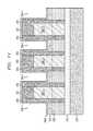
- FIGS. 4 through 10schematically illustrate a method for fabricating the semiconductor device of FIG. 1A , according to an embodiment of the invention, wherein:
- FIG. 4is cross-sectional schematic side view of the semiconductor device at an intermediate stage of fabrication in which a pattern of openings is formed in an ILD (inter-layer dielectric) layer;
- ILDinter-layer dielectric
- FIG. 5is cross-sectional schematic side view of the semiconductor device of FIG. 4 after depositing a conformal layer of liner material and depositing a layer of metallic material to fill the openings in the ILD layer;
- FIG. 6is cross-sectional schematic side view of the semiconductor device of FIG. 5 after planarizing the surface of the semiconductor structure down to the ILD layer to form a metal wiring layer;
- FIG. 7is cross-sectional schematic side view of the semiconductor device of FIG. 6 after forming protective caps on metal lines of the metal wiring layer;
- FIG. 8is cross-sectional schematic side view of the semiconductor device of FIG. 7 after etching the ILD layer to form spaces between the metal lines of the metal wiring layer;
- FIG. 9is a cross-sectional schematic side view of the semiconductor device of FIG. 8 after depositing a conformal layer of insulating material to form an insulating liner that covers exposed surfaces of the metal wiring layer and ILD layer;
- FIG. 10is a cross-sectional schematic side view of the semiconductor device of FIG. 9 which illustrates a process of depositing a dielectric material using a non-conformal deposition process to cause pinch-off regions to begin forming in the deposited dielectric material over the spaces between the metal lines of the metal wiring layer.
- FIG. 11is a cross-sectional schematic side view of a semiconductor device comprising air gap spacers that are integrally formed within a FEOL/MOL structure of the semiconductor device, according to another embodiment of the invention.
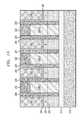
- FIGS. 12 through 19schematically illustrate a method for fabricating the semiconductor device of FIG. 11 , according to an embodiment of the invention, wherein:
- FIG. 12is cross-sectional schematic view of the semiconductor device at an intermediate stage of fabrication in which vertical transistor structures are formed on a semiconductor substrate;
- FIG. 13is cross-sectional schematic side view of the semiconductor device of FIG. 12 after patterning a pre-metal dielectric layer to form contact openings between gate structures of the vertical transistor structures;
- FIG. 14is cross-sectional schematic side view of the semiconductor device of FIG. 13 after forming a conformal liner layer over the surface of the semiconductor device to line the contact openings with a liner material;
- FIG. 15is a cross-sectional schematic side view of the semiconductor device of FIG. 14 , after depositing a layer of metallic material to fill the contact openings with metallic material and planarizing the surface of the semiconductor device to form MOL device contacts;
- FIG. 16is a cross-sectional side view of the semiconductor device of FIG. 15 after recessing gate capping layers and sidewall spacers of the gate structures of the vertical transistor structures;
- FIG. 17is a cross-sectional schematic side view of the semiconductor device of FIG. 16 after depositing a conformal layer of insulating material to form an insulating liner that lines the exposed surfaces of the gate structures and MOL device contacts;
- FIG. 18is a cross-sectional schematic side view of the semiconductor device of FIG. 17 after depositing a dielectric material using a non-conformal deposition process to cause pinch-off regions that form air gaps in spaces between the gate structures and MOL device contacts;
- FIG. 19is a cross-sectional schematic side view of the semiconductor device of FIG. 18 after planarizing the surface of the semiconductor device down to the MOL device contacts and depositing an ILD layer as part of a first interconnect level of a BEOL structure.
- embodiments of the inventioninclude methods for fabricating air gap spacers using “pinch-off” deposition techniques which utilize certain dielectric materials and deposition techniques to control the size and shape of the air gap spacers that are formed and, thereby, optimize air gap spacer formation for a target application.
- the exemplary pinch-off deposition methods as discussed herein to form air gap spacersprovide improved TDDB reliability as well as optimal capacitance reduction in BEOL and MOL layers of semiconductor integrated circuit devices.
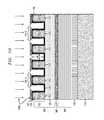
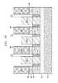
- FIGS. 1A and 1Bare schematic views of a semiconductor device 100 comprising air gap spacers that are integrally formed within a BEOL structure of the semiconductor device, according to an embodiment of the invention.
- FIG. 1Ais a schematic cross-sectional side view of the semiconductor device 100 taken along line 1 A- 1 A in FIG. 1B
- FIG. 1Bis a schematic plan view of the semiconductor device 100 along a plane that includes line 1 B- 1 B as shown in FIG. 1A
- FIG. 1Ais a schematic cross-sectional side view of the semiconductor device 100 in an X-Z plane
- FIGS. 1A and 1Bare plan views showing a layout of various elements within an X-Y plane, as indicated by the respective XYZ Cartesian coordinates shown in FIGS. 1 A and 1 B.
- verticalor “vertical direction” as used herein denotes a Z-direction of the Cartesian coordinates shown in the figures
- horizontalor “horizontal direction” as used herein denotes an X-direction and/or Y-direction of the Cartesian coordinates shown in the figures.
- FIG. 1Aschematically illustrates the semiconductor device 100 comprising a substrate 110 , a FEOL/MOL structure 120 , and a BEOL structure 130 .
- the substrate 110comprises a bulk semiconductor substrate formed of, e.g., silicon, or other types of semiconductor substrate materials that are commonly used in bulk semiconductor fabrication processes such as germanium, silicon-germanium alloy, silicon carbide, silicon-germanium carbide alloy, or compound semiconductor materials (e.g. III-V and II-VI).
- compound semiconductor materialsinclude gallium arsenide, indium arsenide, and indium phosphide.
- the thickness of the base substrate 100will vary depending on the application.
- the substrate 110comprises a SOI (silicon on insulator) substrate, which comprises an insulating layer (e.g., oxide layer) disposed between a base semiconductor substrate (e.g., silicon substrate) and an active semiconductor layer (e.g., active silicon layer) in which active circuit components (e.g., field effect transistors) are formed as part of a FEOL layer.
- SOIsilicon on insulator
- the FEOL/MOL structure 120comprises a FEOL layer formed on the substrate 110 .
- the FEOL layercomprises various semiconductor devices and components that are formed in or on the active surface of the semiconductor substrate 110 to provide integrated circuitry for a target application.
- the FEOL layercomprises FET devices (such as FinFET devices, planar MOSFET device, etc.), bipolar transistors, diodes, capacitors, inductors, resistors, isolation devices, etc., which are formed in or on the active surface of the semiconductor substrate 110 .
- FEOL processestypically include preparing the substrate 110 (or wafer), forming isolation structures (e.g., shallow trench isolation), forming device wells, patterning gate structures, forming spacers, forming source/drain regions (e.g., via implantation), forming silicide contacts on the source/drain regions, forming stress liners, etc.
- the FEOL/MOL structure 120further comprises a MOL layer formed on the FEOL layer.
- the MOL layercomprises a PMD (pre-metal dielectric layer) and conductive contacts (e.g., via contacts) that are formed in the PMD layer.
- the PMD layeris formed on the components and devices of the FEOL layer.
- a pattern of openingsis formed in the PMD layer, and the openings are filled with a conductive material, such as tungsten, to form conducive via contacts that are in electrical contact with device terminals (e.g., source/drain regions, gate contacts, etc.) of the integrated circuitry of the FEOL layer.
- the conductive via contacts of the MOL layerprovide electrical connections between the integrated circuitry of the FEOL layer and a first level of metallization of the BEOL structure 130 .
- the BEOL structure 130is formed on the FEOL/MOL structure 120 to connect the various integrated circuit components of the FEOL layer.
- a BEOL structurecomprises multiple levels dielectric material and levels of metallization embedded in the dielectric material.
- the BEOL metallizationcomprises horizontal wiring, interconnects, pads, etc., as well as vertical wiring in the form of conductive vias that form connections between different interconnect levels of the BEOL structure.
- a BEOL fabrication processinvolves successive depositing and patterning of multiple layers of dielectric and metallic material to form a network of electrical connections between the FEOL devices and to provide I/O connections to external components.
- the BEOL structure 130comprises a first interconnect level 140 , and a second interconnect level 150 .
- the first interconnect level 140is generically depicted, and can include one more low-k inter-level dielectric (ILD) layers and metallic via and wiring levels (e.g., copper damascene structures).
- a capping layer 148is formed between the first interconnect level 140 and the second interconnect level 150 .
- the capping layer 148serves to insulate metallization of the first interconnect level 140 from the dielectric material of the ILD layer 151 .
- the capping layer 148serves to improve interconnect reliability and prevent copper metallization from diffusing into the ILD layer 151 of the second interconnect level 150 .
- the capping layer 148may include any suitable insulating or dielectric material including, but not limited to, silicon nitride (SiN), silicon carbide (SiC), silicon carbon nitride (SiCN), hydrogenated silicon carbide (SiCH), a multilayer stack comprising the same or different types of dielectric materials, etc.
- the capping layer 148can be deposited using standard deposition techniques, for example, chemical vapor deposition.
- the capping layer 148can be formed with a thickness in a range from about 2 nm to about 60 nm.
- the second interconnect level 150comprises an ILD layer 151 and a metal wiring layer 152 formed in the ILD layer 151 .
- the ILD layer 151can be formed using any suitable dielectric material including, but not limited to, silicon oxide (e.g. SiO2), SiN (e.g., (Si3N4), hydrogenated silicon carbon oxide (SiCOH), silicon based low-k dielectrics, porous dielectrics, or other known ULK (ultra-low-k) dielectric materials.
- the ILD layer 151can be deposited using known deposition techniques, such as, for example, ALD (atomic layer deposition), CVD (chemical vapor deposition) PECVD (plasma-enhanced CVD), or PVD (physical vapor deposition).
- the thickness of the ILD layer 151will vary depending on the application, and may have a thickness in a range of about 30 nm to about 200 nm, for example.
- the metal wiring layer 152comprises a plurality of closely spaced metal lines 152 - 1 , 152 - 2 , 152 - 3 , 152 - 4 , 152 - 5 , and 152 - 6 , which are formed within trenches/openings that are patterned in the ILD layer 151 and filled with metallic material to form the metal lines.
- the trenches/openingsare lined with a conformal liner layer 153 which serves as a barrier diffusion layer to prevent migration of the metallic material (e.g., Cu) into the ILD layer 151 , as well as an adhesion layer to provide good adhesion to the metallic material (e.g., Cu) that is used to fill the trenches/openings in the ILD layer 151 and form the metal lines 152 - 1 , . . . , 152 - 6 .
- a conformal liner layer 153which serves as a barrier diffusion layer to prevent migration of the metallic material (e.g., Cu) into the ILD layer 151 , as well as an adhesion layer to provide good adhesion to the metallic material (e.g., Cu) that is used to fill the trenches/openings in the ILD layer 151 and form the metal lines 152 - 1 , . . . , 152 - 6 .
- the second interconnect level 150further comprises protective caps 154 that are selectively formed on an upper surface of the metal lines 152 - 1 , 152 - 2 , 152 - 3 , 152 - 4 , 152 - 5 , and 152 - 6 , a conformal insulating liner 155 that conformally covers the metal wiring layer 152 , and a dielectric capping layer 156 that is deposited using a pinch-off deposition technique to form air gap spacers 158 between the metal lines 152 - 1 , 152 - 2 , 152 - 3 , 152 - 4 , 152 - 5 , and 152 - 6 .
- the protective caps 154 and conformal insulating liner 155serve to protect the metal wiring 152 from potential structural damage or contamination which can result from subsequent processing steps and environmental conditions.
- Example materials and methods for forming the protective caps 154 and the conformal insulating liner 155will be discussed in further detail below with reference to FIGS. 7-9 .
- the air gap spacers 158are formed in spaces between the metal lines 152 - 1 , 152 - 2 , 152 - 3 , 152 - 4 , 152 - 5 , and 152 - 6 of the metal wiring layer 152 as a means to decrease the parasitic capacitive coupling between adjacent metal lines of the metal wiring layer 152 .
- a dielectric air gap integration processis performed as part of the BEOL fabrication process in which portions of the dielectric material of the ILD layer 151 are etched away to form spaces between the metal lines metal lines 152 - 1 , 152 - 2 , 152 - 3 , 152 - 4 , 152 - 5 , and 152 - 6 of the wiring layer 152 .
- the dielectric capping layer 156is formed using a non-conformal deposition process (e.g., chemical vapor deposition) to deposit a dielectric material which forms “pinch-off” regions 156 - 1 above the upper portions of the spaces between the metal lines of the wiring layer 152 , thereby forming the air gap spacers 158 .
- the pinch-off regions 156 - 1are formed above the upper surfaces of the metal lines 152 - 1 , . . . , 152 - 6 of the metal wiring layer 152 , as indicated by the dashed line 1 B- 1 B.
- the air gap spacers 158 that are formed between the metal lines 152 - 1 , . . . , 152 - 6vertically extend into the dielectric capping layer 156 above the metal lines 152 - 1 , . . . , 152 - 6 .
- the air gap spacers 158 formed between the metal lines 152 - 1 , . . . , 152 - 6horizontally extend (e.g., in the Y-direction) past end portions of adjacent metal lines.
- FIG. 1Bthe air gap spacers 158 formed between the metal lines 152 - 1 , . . . , 152 - 6 horizontally extend (e.g., in the Y-direction) past end portions of adjacent metal lines.
- FIG. 1Bshows an example interdigitated comb-comb layout pattern of the metal wiring layer 152 wherein the metal lines 152 - 1 , 152 - 3 , and 152 - 5 are commonly connected at one end to an elongated metal line 152 - 7 , and wherein the metal lines 152 - 2 , 152 - 4 , and 152 - 6 are connected at one end to an elongated metal line 152 - 8 .
- the air gap spacers 158horizontally extend past the open (unconnected) ends of the metal lines 152 - 1 , . . . , 152 - 6 .
- the size and shape of the air gap spacers 158 shown in FIGS. 1A and 1Bprovide improved TDDB reliability, as well as reduced capacitive coupling between the metal lines, for reasons that will now be discussed in further detail with reference to FIGS. 2A and 2B .
- FIGS. 2A and 2Bschematically illustrate improvements in TDDB reliability and reduced capacitive coupling between metal lines of a BEOL structure, which are realized using air gap structures that are formed using pinch-off deposition methods according to embodiments of the invention, as compared to air gap structures that are formed using conventional methods.
- FIG. 2Aschematically illustrates a portion of the metal wiring layer 152 of FIG. 1A including the metal lines 152 - 1 and 152 - 2 , and the air gap 158 which is formed between the metal lines by forming the dielectric capping layer 156 using a pinch-off deposition process according to an embodiment of the invention. As depicted in FIG.
- FIG. 2Aschematically illustrates a semiconductor structure comprising an air gap 168 that is disposed between the same two metal lines 152 - 1 and 152 - 2 having the same width W and spacing S as in FIG. 2A , but wherein the air gap 168 is formed by forming a dielectric capping layer 166 using a conventional pinch-off deposition process.
- the “pinch-off” region 156 - 1is formed in the dielectric capping layer 156 such that the air gap 158 extends above the upper surface of the metal lines 152 - 1 and 152 - 2 .
- a conventional pinch-off deposition processresults in the formation of a pinch-off region 166 - 1 in the dielectric capping layer 166 below the upper surface of the metal lines 152 - 1 and 152 - 2 such that the resulting air gap 168 does not extend above the metal lines 152 - 1 and 152 - 2 .
- the amount of dielectric material that is deposited on the sidewall and bottom surfaces in the space between the metal lines 152 - 1 and 152 - 2 as shown in FIG. 2B using a conventional pinch-off deposition processis significantly greater than the amount of dielectric material that is deposited on the sidewall and bottom surfaces in the space between the metal lines 152 - 1 and 152 - 2 as shown in FIG. 2A using a pinch-off deposition process according to an embodiment of the invention.
- a volume V 1 of the resulting air gap 158 in FIG. 2Ais significantly greater than a volume V 2 of the resulting air gap 168 shown in FIG. 2B .
- the larger volume V 1 of the air gap 158results in a smaller parasitic capacitance between the metal lines metal lines 152 - 1 and 152 - 2 (as compared to the structure of FIG. 2B ).
- there is a reduced effective dielectric constant in the space between metal lines 152 - 1 and 152 - 2 in FIG. 2A as compared to FIG. 2B since there is less dielectric material and a large volume V 1 of air (k1) in the space between the metal lines 152 - 1 and 152 - 2 of FIG. 2A .
- the structure of FIG. 2Aprovides improved TDDB reliability as compared to the structure of FIG. 2B .
- the air gap 158extends above the metal lines 152 - 1 and 152 - 2 , there is a long diffusion/conducting path P 1 between the critical interfaces of the metal lines 152 - 1 and 152 - 2 (the critical interfaces being an interface between the dielectric capping layer 156 and the upper surfaces of the metal lines 152 - 1 and 152 - 2 ).
- Thisis in contrast to a shorter diffusion/conducting path P 2 in the dielectric capping layer 166 between the critical interfaces of the metal lines 152 - 1 and 152 - 2 in the structure shown in FIG.
- a TDDB failure mechanism in the structure of FIG. 2A or 2Bwould result from the breakdown of the dielectric material and the formation of a conducting path through the dielectric material between the upper surfaces of the metal lines 152 - 1 and 152 - 2 due to electron tunneling current.
- the longer diffusion path P 1 in the structure shown in FIG. 2Acoupled with the optional use of a dense dielectric liner 155 material with superior dielectric breakdown strength, would provide improved TDDB reliability of the structure in FIG. 2A as compared to the structure shown in FIG. 2B .
- the horizontal extension of the air gap spacers 158 past the end portions of the metal lines as shown in FIG. 1Bwould further add to an improvement in TDDB reliability and reduced capacitive coupling for the same reasons discussed with reference to FIG. 2A .
- the extension of the air gap 158 past the end of the metal line 152 - 1would provide a long diffusion/conducting path between the critical interface at the open end of the metal line 152 - 1 and the adjacent metal line 152 - 2 .
- FIG. 1Bthe extension of the air gap 158 past the end of the metal line 152 - 1 , for example, would provide a long diffusion/conducting path between the critical interface at the open end of the metal line 152 - 1 and the adjacent metal line 152 - 2 .
- air gap spacerscould be formed between the elongated metal line 152 - 8 and the adjacent open ends of the metal lines 152 - 1 , 152 - 2 and 152 - 5 , and air gap spacers could be formed between the elongated metal line 152 - 7 and the adjacent open ends of the metal lines 152 - 2 , 152 - 4 , and 152 - 6 , to thereby further optimize TDDB reliability and reduce capacitive coupling between the interdigitated comb structures.
- FIG. 3is a cross-sectional schematic side view of a semiconductor device comprising air gap spacers that are integrally formed within a BEOL structure of the semiconductor device, according to another embodiment of the invention.
- FIG. 3schematically illustrates a semiconductor device 100 ′ which is similar in structure to the semiconductor device 100 shown in FIGS. 1A / 1 B, except that the air gap spacers 158 shown in FIG. 3 do not extend past a bottom surface of the metal lines of the metal wiring layer 152 .
- the ILD layer 151would be recessed down to the bottom level of the metal lines (as compared to being recessed below the bottom of the metal lines, as shown in FIG. 8 , to form the extended air gap spacers shown in FIG.
- FIGS. 1A and 3show the BEOL structure 130 having first and second interconnect levels 140 and 150
- the BEOL structure 130can have one or more additional interconnect levels formed over the second interconnect level 150 .
- Such additional interconnect levelscan be formed with air gap spacers using techniques and materials as discussed herein.
- FIG. 4is cross-sectional schematic view of the semiconductor device 100 at an intermediate stage of fabrication in which a pattern of openings 151 - 1 (e.g., damascene openings comprising trenches and via openings) are formed in the ILD layer 151 , according to an embodiment of the invention.
- FIG. 4schematically illustrates the semiconductor device 100 of FIG.
- the openings 151 - 1are shown to have a width W and spaced apart by a distance S.
- the width W of the openingsin the context of forming air gap spacers between closely-spaced metal lines using pinch-off deposition methods, can be in a range of about 2 nm to about 25 nm with a preferred range of about 6 nm to about 10 nm.
- the spacing S between the metal linescan be in a range of about 2 nm to about 25 nm with a preferred range from about 6 nm to about 10 nm.
- a next process module in the exemplary fabrication processcomprises forming the metal wiring layer 152 shown in FIG. 1A using a process flow as schematically illustrated in FIGS. 5 and 6 .
- FIG. 5is cross-sectional schematic view of the semiconductor device of FIG. 4 after depositing a conformal layer of liner material 153 A and depositing a layer of metallic material 152 A on the conformal layer of liner material 153 A to fill the openings 151 - 1 in the ILD layer 151 .
- FIG. 6is cross-sectional schematic view of the semiconductor device of FIG. 5 after planarizing the surface of the semiconductor structure down to the ILD layer 151 to form the metal wiring layer 152 .
- the metal wiring layer 152can be formed using known materials and known techniques.
- the conformal layer of liner material 153 Ais preferably deposited to line the sidewall and bottom surfaces of the openings 151 - 1 in the ILD layer 151 with a thin liner layer.
- the thin liner layermay be formed by conformally depositing one or more thin layers of material such as, for example, tantalum nitride (TaN), cobalt (Co), or ruthenium (Ru), or manganese (Mn) or manganese nitride (MnN) or other liner materials (or combinations of liner materials such as Ta/TaN, TiN, CoWP, NiMoP, NiMoB) which are suitable for the given application.
- the thin liner layerserves multiple purposes.
- the thin liner layerserves as a barrier diffusion layer to prevent migration/diffusion of the metallic material (e.g., Cu) into the ILD layer 151 .
- the thin liner layerserves as an adhesion layer to provide good adhesion to the layer of metallic material 152 A (e.g., Cu) that is used to fill the openings 151 - 1 in the ILD layer 151 .
- the layer of metallic material 152 Acomprises a metallic material such as, for example, copper (Cu), aluminum (Al), tungsten (W), cobalt (Co), or ruthenium (Ru), which is deposited using known techniques such as electroplating, electroless plating, CVD, PVD, or a combination of methods.
- a thin seed layere.g., Cu seed layer
- CVDchemical vapor deposition
- PVDphysical vapor deposition
- the seed layercan be formed of a material which enhances adhesion of the metallic material on the underlying material and which serves as catalytic material during a subsequent plating process.
- a thin conformal Cu seed layercan be deposited over the surface of the substrate using PVD, followed by the electroplating of Cu to fill the openings 151 - 1 (e.g., trenches and vias) formed in the ILD layer 151 and, thus, form a Cu metallization layer 152 .
- the overburden liner, seed, and metallization materialsare then removed by performing a chemical mechanical polishing process (CMP) to planarize the surface of the semiconductor structure down to the ILD layer 151 , resulting in the intermediate structure shown in FIG. 6 .
- CMPchemical mechanical polishing process
- a protective layermay be formed on the exposed surfaces of the metal lines 152 - 1 , . . . , 152 - 6 to protect the metallization from potential damage as a result of subsequent processing conditions and environments.
- FIG. 7is cross-sectional schematic view of the semiconductor device of FIG. 6 after forming protective caps 154 on the metal lines 152 - 1 , . . . , 152 - 6 , according to an embodiment of the invention.
- the protective caps 154may be formed using a selective Co deposition process to selectively deposit a thin capping layer of Co on the exposed surfaces of the metal lines 152 - 1 , . . .
- the protective caps 154can be formed of other materials such as tantalum (Ta) or ruthenium (Ru).
- Tatantalum
- Ruruthenium
- the protective caps 154 on the metal lines 152 - 1 , . . . , 152 - 6are optional features that can be utilized, if desired, to allow for more aggressive etching conditions, etc., when forming air gap spacers and other structures using techniques discussed hereafter.
- a next step in the fabrication processcomprises forming air gap spacers in the second interconnect level 150 using a process flow as schematically depicted in FIGS. 8, 9 and 10 .
- FIG. 8is cross-sectional schematic view of the semiconductor device of FIG. 7 after etching exposed portions of the ILD layer 151 to form spaces 151 - 2 between the metal lines 152 - 1 , . . . , 152 - 6 , according to an embodiment of the invention.
- any suitable maskinge.g., photoresist mask
- etching techniquee.g., RIE (reactive ion etch)
- RIEreactive ion etch
- a dry etch technique using a fluorine-based etchantcan be used to etch away the dielectric material of the ILD layer 151 to form the spaces 151 - 2 .
- the spaces 151 - 2are formed such that the recessed surface of the ILD layer 151 is below the bottom surfaces of the metal lines 152 - 1 , . . .
- the etch processcan be performed such that the spaces 151 - 2 are recessed down to a level of the bottom surfaces of the metal wiring 152 (see FIG. 3 ). In regions of the metal wiring 152 where metal lines are spaced relatively far apart, the ILD layer 151 is not removed, since the interline capacitance between the widely spaced metal lines is assumed to be negligible.
- a next step in the processcomprises depositing a conformal layer of insulating material over the semiconductor structure of FIG. 8 to form the conformal insulating liner 155 as shown in FIG. 9 .
- the conformal insulating liner 155is an optional protective feature that may be formed prior to the pinch-off deposition process to provide added protection to the exposed surfaces of the ILD layer 151 and metal wiring layer 152 .
- the conformal liner layers 153provide some protection to the sidewalls of the metal lines 152 - 1 , . . . , 152 - 6
- the conformal insulating liner 155can provided added protection against oxidation of the metal lines 152 - 1 , . . .
- the conformal insulating liner 155can be formed with one or more robust ultrathin layers of dielectric material which have desired electrical and mechanical characteristics such as low leakage, high electrical breakdown, hydrophobic, etc., and which can sustain low damage from subsequent semiconductor processing steps.
- the conformal insulating liner 155can be formed of a dielectric material such as SiN, SiCN, SiNO, SiCNO, SiBN, SiCBN, SiC, or other dielectric materials having desired electrical/mechanical properties as noted above.
- the conformal insulating liner 155is formed with a thickness in a range of about 0.5 nm to about 5 nm.
- the conformal insulating liner 155can be formed of multiple conformal layers of the same or different dielectric materials, which are deposited using a cyclic deposition process.
- the conformal insulating liner 155can be formed of multiple thin conformal layers of SiN (e.g., 0.1 nm-0.2 nm thick SiN layers) which are sequentially deposited to form a SiN liner layer that has a total desired thickness.
- the spaces 151 - 2 between the metal lines of the metal wiring layer 152are shown to have an initial volume Vi.
- the volume Viis defined by the sidewall and bottom surfaces of the conformal insulating liner 155 and a dashed line L that denotes an upper surface of the conformal insulating liner 155 on the metal wiring layer 152 .
- the initial volume Viwhen the conformal insulating liner 155 is not formed, the initial volume Vi would be defined by the exposed surfaces of the liner layers 153 , the recessed surface of the ILD layer 151 , and an upper surface of the metal lines of the metal wiring layer 152 . As discussed below, a significant portion of the initial volume Vi remains in the spaces 151 - 2 between the metal lines, after formation of the air gap spacers 158 using a pinch-off deposition process according to an embodiment of the invention.
- a next step in the fabrication processcomprises depositing dielectric material over the semiconductor structure of FIG. 9 using a pinch-off deposition process to form the air gap spacers 158 in the spacer 151 - 2 between the metal lines of the metal wiring layer 152 .
- FIG. 10schematically illustrates a process of depositing a layer of dielectric material 156 A using a non-conformal deposition process (e.g., PECVD or PVD) to cause pinch-off regions to begin forming in the deposited dielectric material 156 A over the spaces 151 - 2 between the metal lines of the metal wiring layer 152 , according to an embodiment of the invention.
- PECVDPECVD
- PVDnon-conformal deposition process
- FIG. 1Aillustrates the semiconductor device 100 at the completion of the pinch-off deposition process in which the dielectric capping layer 156 is formed with pinch-off regions 156 - 1 in the dielectric capping layer and air gap spacers 158 formed in the spaces 151 - 2 between the metal lines of the metal wiring layer 152 .
- the structural characteristics (e.g., size, shape, volume, etc.) of the air gap spacers that are formed by pinch-off depositioncan be controlled, for example, based on (i) the type of dielectric material(s) that are used to form the dielectric capping layer 156 , and/or (ii) the deposition process and associated deposition parameters (e.g., gas flow rate, RF power, pressure, deposition rate, etc.) that are used to perform the pinch-off deposition.
- the capping layer 158is formed by PECVD deposition of a low-k dielectric material (e.g., k in a range of about 2.0 to about 5.0).
- Such low-k dielectric materialincludes, but is not limited to, SiCOH, porous p-SiCOH, SiCN, carbon-rich SiCNH, p-SiCNH, SiN, SiC, etc.
- a pinch-off deposition processis implemented by depositing a SiCN dielectric film via a plasma CVD deposition process using an industrial parallel plate single wafer 300 mm CVD reactor with the following deposition parameters: Gas [Trimethyl Silane (200-500 standard cubic centimeter per minute (sccm)) and Ammonia (300-800 sccm)]; RF power [300-600 Watts]; Pressure [2-6 Torr]; and deposition rate [0.5-5 nm/sec].
- GasTrimethyl Silane (200-500 standard cubic centimeter per minute (sccm)) and Ammonia (300-800 sccm)]
- RF power300-600 Watts
- Pressure[2-6 Torr]
- deposition rate[0.5-5 nm/sec].
- the level of conformality of the PECVD deposited dielectric materialcan be controlled to achieve “pinch-off” of the dielectric capping layer either above the surface of adjacent metal lines or below the surface of adjacent metal lines.
- the term “level of conformality” of an insulating/dielectric film deposited over a trench with an aspect ratio R of 2is defined herein as a ratio of the thickness of the insulating/dielectric film as deposited on a sidewall at the middle of the trench location divided by the thickness of the insulating/dielectric film at the top of the trench location.
- the “pinch-off” regions 156 - 1 as shown in FIG. 1Aare formed in the dielectric capping layer 156 above the metal lines of the metal wiring layer 152 . This results in the formation of the air gap spacers 158 which extend above the metal lines of the metal wiring layer 152 .
- the “pinch-off” regionswould be formed in the dielectric capping layer below the upper surface of the metal lines of the metal wiring layer 152 . This would result in the formation of air gap spacers which do not extend above the metal lines of the metal wiring layer 152 .
- a target level of conformality of the PECVD deposited dielectric materialcan be achieved by adjusting the deposition process parameters.
- a lower level of conformalitycan be obtained by increasing the RF power, increasing the pressure and/or increasing the deposition rate (e.g., increase flow rate of precursor materials).
- the “pinch-off” regionsare formed above the metal lines with minimal deposition of the dielectric material on the exposed sidewall and bottom surfaces within the spaces 151 - 2 , resulting in the formation of large, voluminous air gap spacers 158 which extend above the metal lines of the metal wiring layer 152 , as shown in FIGS. 1A and 3 , for example.
- the experimental BEOL test structureshave been fabricated in which a resulting volume of about nVi (wherein n is in a range of about 0.70 to nearly 1.0) has been achieved after forming the air gap spacers using a non-conformal pinch-off deposition process as described herein.
- the dielectric constant of airis about unity, which is much less than the dielectric constant of the dielectric materials that are used to form the conformal insulating liner 155 and the dielectric capping layer 156 .
- the ability to tightly control and minimize the amount of dielectric material that is deposited within the spaces 151 - 2 between adjacent metal lines of the metal wiring layer 152 using techniques as discussed hereinenables optimization of the electrical performance of BEOL structures by reducing the effective dielectric constant (and thus the parasitic capacitance) between adjacent metal lines of the metal wiring layer 152 .
- the ability to perform pinch-off deposition using ULK dielectric materials to form a low-k dielectric capping layer 156 and large voluminous air gap spacers 158results in an overall decrease in the effective dielectric constant (and thus reduced parasitic capacitance) of the BEOL structure.
- air gap spacerscan be formed between MOL device contacts and metallic gate structures of vertical transistor devices in an FEOL/MOL structure using techniques as will be discussed now in further detail with reference to FIGS. 11-19 .
- FIG. 11is a cross-sectional schematic side view of a semiconductor device comprising air gap spacers that are integrally formed within a FEOL/MOL structure of the semiconductor device, according to another embodiment of the invention.
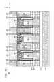
- FIG. 11schematically illustrates a semiconductor device 200 comprising a substrate 210 / 215 which includes a bulk substrate layer 210 and an insulating layer 215 (e.g., a buried oxide layer of an SOI substrate), and a plurality of vertical transistor structures M 1 , M 2 , M 3 (see FIG. 12 ) formed on the substrate 210 / 215 .
- insulating layer 215e.g., a buried oxide layer of an SOI substrate
- the vertical transistor structures M 1 , M 2 , M 3have a standard structural framework comprising a semiconductor fin 220 (which extends along the substrate in an X direction), epitaxially grown source (S)/drain (D) regions 225 , and respective metal gate structures 230 - 1 , 230 - 2 , and 230 - 3 .
- the semiconductor fin 220serves as a vertical channel for the vertical transistor structures M 1 . M 2 , M 3 in regions of the semiconductor fin 220 that are surrounded by the respective metal gate structures 230 - 1 , 230 - 2 , 230 - 3 .
- the semiconductor fin 220can be formed by etching/patterning an active silicon layer that is formed on top of the insulating layer 215 (e.g., an SOI layer of an SOI substrate).
- the semiconductor fin 220is not specifically shown in FIG. 11 , but an upper surface of the semiconductor fin 220 is depicted by the dashed line in FIG. 11 (i.e., channel portions of the semiconductor fin 220 are covered by the gate structures 230 - 1 , 230 - 2 and 230 - 3 , and portions of the semiconductor fin 220 extending from the gate structures are encapsulated in epitaxial material that grown on the exposed surfaces of the semiconductor fin 220 ).
- the metal gate structures 230 - 1 , 230 - 2 , and 230 - 3each comprise a conformal high-k metal gate stack structure formed on a vertical sidewall and upper surface of the semiconductor fin 220 , and a gate electrode formed over the high-k metal gate stack structure.
- Each conformal high-k metal gate stack structurecomprises a conformal layer of gate dielectric material (e.g., high-k dielectric material such as HfO 2 , Al 2 O 3 , etc.) formed on the sidewall and upper surface of the semiconductor fin 220 , and a conformal layer of metallic work function metal material (e.g., Zr, W, Ta, Hf, Ti, Al, Ru, Pa, TaN, TiN, etc.) formed on the conformal layer of gate dielectric material.
- the gate electrode material that is formed on the high-k metal gate stack structurecomprises a low-resistance conductive material including, but not limited to tungsten, aluminum, or any metallic or conductive material that is commonly used to form gate electrode structures.
- the epitaxial source (S)/drain (D) regions 225include epitaxial semiconductor material (e.g., SiGe, III-V compound semiconductor material, etc.) that is epitaxially grown on exposed portions of the semiconductor fin structures 220 which extend out from the metal gate structures 230 - 1 , 230 - 2 , 230 - 3 .
- a plurality of MOL device contacts 240 / 245are formed as part of a MOL layer of the semiconductor device 200 to provide vertical contacts to the source/drain regions 225 .
- Each MOL device contact 240 / 245comprises a liner/barrier layer 240 and a conductive via 245 .
- the metal gate structures 230 - 1 , 230 - 2 , 230 - 3are electrically insulated from the MOL contacts 240 / 245 and other surrounding structures by insulating material layers 234 , 250 , 260 , and air gap spacers 262 .
- the insulating material layersinclude lower sidewall spacers 234 , conformal insulating liners 250 , and dielectric capping layers 260 .
- the lower sidewall spacers 234electrically insulate the metal gate structures 230 - 1 , 230 - 2 , 230 - 3 from the adjacent source/drain regions 223 .
- the conformal insulating liners 250(which are similar in composition and function as the conformal insulating liner 155 of the BEOL structure, FIG. 1A ) conformally cover the sidewall surfaces of the MOL device contacts 240 / 245 and the metal gate structures 230 - 1 , 230 - 2 , 230 - 3 .
- the conformal insulating liners 250are optional features that can be formed to protect the MOL device contacts 240 / 245 and the metal gate structures 230 - 1 , 230 - 2 , 230 - 3 from potential structural damage or contamination which can result from subsequent processing steps and environmental conditions.
- the dielectric capping layers 260are formed by depositing a low-k dielectric material using a pinch-off deposition process to encapsulate the upper regions of the metal gate structures 230 - 1 , 230 - 2 , 230 - 3 with low-k dielectric material, and to form the air gap spacers 262 between the metal gate structures and MOL device contacts.
- a process flow for fabricating the air gap spacers 262will be discussed in further detail below.
- the air gap spacers 262are relatively large and voluminous, and vertically extend above the metal gate structures 230 - 1 , 230 - 2 , 230 - 3 .
- the size and shape of the FEOL/MOL air gap spacers 262 shown in FIG. 11provide improved TDDB reliability, as well as reduced capacitive coupling between the MOL device contacts and metal gate structures.
- the large voluminous air gap spacers 262reduce the effective dielectric constant in the space between the metal gate structures 230 - 1 , 230 - 2 , 230 - 3 and the MOL device contacts 240 / 245 .
- the air gap spacers 262extend above the metal gate structures 230 - 1 , 230 - 2 , 230 - 3 , as shown in FIG.
- the air gap spacers 262 in FIG. 11serve to increase the TDDB reliability of the FEOL/MOL semiconductor structure.
- FIG. 11further illustrates a first interconnect level of a BEOL structure formed over the FEOL/MOL layers, wherein the first interconnect level comprises an ILD layer 270 , and a plurality of metal lines 272 / 274 formed in the ILD layer 270 in electrical contact with respective MOL device contacts 240 / 245 .
- the metal lines 272 / 274are formed by etching openings (e.g., trenches or vias) in the ILD layer 270 , lining the openings with barrier liner layers 272 and filling the openings with metallic material 274 such as copper, using known techniques.
- FIG. 12is cross-sectional schematic view of the semiconductor device 200 at an intermediate stage of fabrication in which vertical transistor structures M 1 , M 2 and M 3 are formed on the semiconductor substrate 210 / 215 .
- the substrate 210 / 215comprises a SOI (silicon on insulator) substrate, wherein the base substrate 210 is formed of silicon, or other types of semiconductor substrate materials that are commonly used in bulk semiconductor fabrication processes such as germanium, silicon-germanium alloy, silicon carbide, silicon-germanium carbide alloy, or compound semiconductor materials (e.g.
- Non-limiting examples of compound semiconductor materialsinclude gallium arsenide, indium arsenide, and indium phosphide.
- the insulating layer 215e.g., oxide layer
- the active semiconductor layere.g., active silicon layer
- the epitaxial source/drain regions 225can be epitaxially grown on exposed portions of the semiconductor fin structure 220 using know methods.
- the metal gate structures 230 - 1 , 230 - 2 and 230 - 3are encapsulated in insulating/dielectric material structures including insulating capping layers 232 , and sidewall spacers 234 .
- the capping layers 232 and sidewall spacers 234are fabricated using known techniques and insulating materials (e.g., SiN).
- the metal gate structures 230 - 1 , 230 - 2 , and 230 - 3can be formed, for example, by a RMG (replacement metal gate) process in which dummy gate structures are initially formed, and then replaced with the metal gate structures 230 - 1 , 230 - 2 , 230 - 3 after formation of the epitaxial source/drain regions 225 , but prior to formation of the MOL device contacts.
- RMGreplacement metal gate
- the PMD layer 236is formed by depositing a layer of dielectric material over the surface of the semiconductor device, and then planarizing the dielectric material down to the upper surface of the capping layers 232 .
- the PMD layer 236may be formed with any suitable insulating/dielectric materials such as, for example, silicon oxide, silicon nitride, hydrogenated silicon carbon oxide, silicon based low-k dielectrics, porous dielectrics, or organic dielectrics including porous organic dielectrics, etc.
- the PMD layer 236may be formed using known deposition techniques, such as, for example, ALD, CVD, PECVD, spin on deposition, or PVD, followed by a standard planarization process (e.g., CMP).
- a next process moduleincludes forming the MOL device contacts using a process flow as schematically illustrated in FIGS. 13, 14 and 15 .
- FIG. 13is cross-sectional schematic side view of the semiconductor device of FIG. 12 after patterning the PMD layer 236 to form contact openings 236 - 1 between the gate structures 230 - 1 , 230 - 2 , 230 - 3 of the vertical transistor structures M 1 , M 2 , M 3 down to the source/drain regions 225 .
- the contact openings 236 - 1can be formed using known etching techniques and etching chemistries to etch the material of the PMD layer 236 selective to the insulating material of the capping layers 232 and sidewall spacers 234 .
- FIG. 14is cross-sectional schematic side view of the semiconductor device of FIG. 13 after depositing a conformal liner layer 240 A over the surface of the semiconductor device.
- the conformal liner layer 240 Amay include a material such as TaN, etc., which serves as a barrier diffusion layer and/or adhesion layer for the metallic material that is used to fill the openings 236 - 1 and form the MOL device contacts.
- FIG. 15is a cross-sectional schematic side view of the semiconductor device of FIG.
- the conductive material 245may comprise copper, tungsten, cobalt, aluminum, or other conductive materials that are suitable for use in forming vertical MOL device contacts to the source/drain regions and gate electrodes.
- MOL gate contactscan be formed in openings that are formed through the PMD layer 236 and capping layers 232 down to an upper surface of the metal gate structures 230 - 1 , 230 - 2 , and 230 - 3 . It is to be understood that the metal gate structures 230 - 1 , 230 - 2 , 230 - 3 extend in the Y-Y direction (in and out of the plane of the drawing sheet, based on the Cartesian coordinate system shown in FIG.
- the MOL gate contactscan be formed in the PMD layer 236 in alignment with the extended end portions of the metal gate structures 230 - 1 , 230 - 2 , 230 - 3 , as is understood by one of ordinary skill in the art.
- a next process moduleincludes forming air gap spacers between the metal gate structures and the MOL device contacts, using a process flow as schematically illustrated in FIGS. 16-19 .
- An initial step in this processincludes etching the gate capping layers 232 and sidewall spacers 234 .
- FIG. 16is a cross-sectional side view of the semiconductor device of FIG. 15 after etching away the gate capping layers 232 and recessing the sidewall spacers 234 down to an upper surface of the semiconductor fin structure 220 , thereby forming narrow spaces S between the sidewalls of the metal gate structures 230 - 1 , 230 - 2 , 230 - 3 and adjacent MOL device contacts 240 / 245 .
- FIG. 16shows that the gate capping layers 232 are completely etched away, in an alternate embodiment, the etch process can be implemented such that a thin layer of the etched gate capping layers 232 remains on the top surfaces of the metal gate structures 230 - 1 , 230 - 2 , 230 - 3 .
- FIG. 17is a cross-sectional schematic side view of the semiconductor device of FIG. 16 after depositing a conformal layer of insulating material 250 A to form an insulating liner on the exposed surfaces of the metal gate structures 230 - 1 , 230 - 2 , 230 - 3 , and the MOL device contacts 240 / 245 .
- the conformal insulating liner layer 250 Ais an optional protective feature that may be formed prior to the pinch-off deposition process to provide added protection to the exposed surfaces of the metal gate structures 230 - 1 , 230 - 2 , 230 - 3 , and the MOL device contacts 240 / 245 , for the same or similar reasons as discussed above.
- the conformal insulating liner layer 250 Acan be formed of one or more robust ultrathin layers of dielectric material which have desired electrical and mechanical characteristics such as low leakage, high electrical breakdown, hydrophobic, etc., and which can sustain low damage from subsequent semiconductor processing steps.
- the conformal insulating liner layer 250 Acan be formed of a dielectric material such as SiN, SiCN, SiNO, SiCNO, SiC or other dielectric materials having desired electrical/mechanical properties as noted above.
- the spacing SFIG.
- the conformal insulating liner layer 250 Ais formed with a thickness in a range of about 1.0 nm to about 2 nm, thereby reducing the spacing S by about 2 nm, to about 4 nm by virtue of the liner layer 250 A on the sidewalls of the adjacent structures.
- the conformal insulating liner layer 250 Acan be formed of multiple conformal layers of the same or different dielectric materials, which are deposited using a cyclic deposition process.
- the conformal insulating liner layer 250 Acan be formed of multiple thin conformal layers of SiN which are sequentially deposited to form a SiN liner layer that has a total desired thickness (e.g., using a plasma CVD or CVD process with Silane and NH3 to cyclically deposit 0.1 nm-0.2 nm thick SiN layers).
- a next step in the fabrication processcomprises depositing dielectric material over the semiconductor structure of FIG. 17 using a pinch-off deposition process to form air gap spacers between the metal gate structures and MOL device contacts.
- FIG. 18is a cross-sectional schematic side view of the semiconductor device of FIG. 17 after depositing a layer of dielectric material 260 A using a non-conformal deposition process to cause pinch-off regions that form the air gap spacers 262 in the narrow spaces between the metal gate structures 230 - 1 , 230 - 2 , 230 - 3 and adjacent MOL device contacts 240 / 245 .
- the structural characteristics (e.g., size, shape, volume, etc.) of the air gap spacers 262 that are formed by pinch-off depositioncan be controlled, for example, based on (i) the type of dielectric material(s) that are used to form the dielectric layer 260 A, and/or (ii) the deposition process and associated deposition parameters (e.g., gas flow rate, RF power, pressure, deposition rate, etc.) that are used to perform the pinch-off deposition.
- the deposition process and associated deposition parameterse.g., gas flow rate, RF power, pressure, deposition rate, etc.
- the layer of dielectric material 260 Ais formed by PECVD deposition of a low-k dielectric material (e.g., kin a range of about 2.0 to about 5.0).
- a low-k dielectric materialincludes, but is not limited to, SiCOH, porous p-SiCOH, SiCN, SiNO, carbon-rich SiCNH, p-SiCNH, SiN, SiC, etc.
- a pinch-off deposition processis implemented by depositing a SiN dielectric film via a plasma CVD deposition process using an industrial parallel plate single wafer 300 mm CVD reactor with the following deposition parameters: gas [Silane (100-500 sccm) and Ammonia (200-1000 sccm)]; RF power [200-600 Watts]; pressure [1-8 Torr]; and deposition rates [0.5-8 nm/sec].
- FIG. 19is a cross-sectional schematic side view of the semiconductor device of FIG. 18 after planarizing the surface of the semiconductor device down to the MOL device contacts and depositing an ILD layer 270 as part of a first interconnect level of a BEOL structure.
- the semiconductor structure of FIG. 18can be planarized using a standard CMP process, wherein the CMP process is performed to remove the overburden dielectric material 260 A and portions of the insulating liner layer 250 A disposed on top of the MOL device contacts, resulting in the structure shown in FIG. 19 . As shown in FIG.
- the remaining portions of the pinch-off deposited dielectric material 260 Aform separate dielectric capping structures 260 over the metal gate structures 230 - 1 , 230 - 2 , 230 - 3 , and separate insulating liners 250 .
- an additional capping layercan be formed on the planarized FEOL/MOL surface to insulate the conductive material 245 of the MOL device contacts from the dielectric material of the ILD layer 270 .
- the experimental resultsdemonstrated that large voluminous air gap spacers (air gap spacers 262 schematically illustrated in FIG. 11 ) can be obtained, which extend above the metal gate structures.
- experimental resultshave demonstrated that the size, shape, volume, etc. of air gap spacers can be optimized for different applications by varying deposition process parameters or the materials used for pinch-off deposition.
- Suitable hardware and systems for implementing the inventionmay include, but are not limited to, personal computers, communication networks, electronic commerce systems, portable communications devices (e.g., cell phones), solid-state media storage devices, functional circuitry, etc. Systems and hardware incorporating such integrated circuits are considered part of the embodiments described herein. Given the teachings of the invention provided herein, one of ordinary skill in the art will be able to contemplate other implementations and applications of the techniques of the invention.
Landscapes
- Engineering & Computer Science (AREA)
- Physics & Mathematics (AREA)
- Microelectronics & Electronic Packaging (AREA)
- General Physics & Mathematics (AREA)
- Computer Hardware Design (AREA)
- Condensed Matter Physics & Semiconductors (AREA)
- Power Engineering (AREA)
- Manufacturing & Machinery (AREA)
- Plasma & Fusion (AREA)
- Chemical & Material Sciences (AREA)
- Chemical Kinetics & Catalysis (AREA)
- Geometry (AREA)
- Internal Circuitry In Semiconductor Integrated Circuit Devices (AREA)
- Insulated Gate Type Field-Effect Transistor (AREA)
- Pressure Sensors (AREA)
Abstract
Description
Claims (20)
Priority Applications (3)
| Application Number | Priority Date | Filing Date | Title |
|---|---|---|---|
| US15/977,437US10418277B2 (en) | 2016-08-09 | 2018-05-11 | Air gap spacer formation for nano-scale semiconductor devices |
| US16/410,178US11658062B2 (en) | 2016-08-09 | 2019-05-13 | Air gap spacer formation for nano-scale semiconductor devices |
| US18/132,333US12224203B2 (en) | 2016-08-09 | 2023-04-07 | Air gap spacer formation for nano-scale semiconductor devices |
Applications Claiming Priority (3)
| Application Number | Priority Date | Filing Date | Title |
|---|---|---|---|
| US15/232,341US9892961B1 (en) | 2016-08-09 | 2016-08-09 | Air gap spacer formation for nano-scale semiconductor devices |
| US15/789,416US10115629B2 (en) | 2016-08-09 | 2017-10-20 | Air gap spacer formation for nano-scale semiconductor devices |
| US15/977,437US10418277B2 (en) | 2016-08-09 | 2018-05-11 | Air gap spacer formation for nano-scale semiconductor devices |
Related Parent Applications (1)
| Application Number | Title | Priority Date | Filing Date |
|---|---|---|---|
| US15/789,416ContinuationUS10115629B2 (en) | 2016-08-09 | 2017-10-20 | Air gap spacer formation for nano-scale semiconductor devices |
Related Child Applications (1)
| Application Number | Title | Priority Date | Filing Date |
|---|---|---|---|
| US16/410,178DivisionUS11658062B2 (en) | 2016-08-09 | 2019-05-13 | Air gap spacer formation for nano-scale semiconductor devices |
Publications (2)
| Publication Number | Publication Date |
|---|---|
| US20180261494A1 US20180261494A1 (en) | 2018-09-13 |
| US10418277B2true US10418277B2 (en) | 2019-09-17 |
Family
ID=61147503
Family Applications (5)
| Application Number | Title | Priority Date | Filing Date |
|---|---|---|---|
| US15/232,341ActiveUS9892961B1 (en) | 2016-08-09 | 2016-08-09 | Air gap spacer formation for nano-scale semiconductor devices |
| US15/789,416ActiveUS10115629B2 (en) | 2016-08-09 | 2017-10-20 | Air gap spacer formation for nano-scale semiconductor devices |
| US15/977,437ActiveUS10418277B2 (en) | 2016-08-09 | 2018-05-11 | Air gap spacer formation for nano-scale semiconductor devices |
| US16/410,178ActiveUS11658062B2 (en) | 2016-08-09 | 2019-05-13 | Air gap spacer formation for nano-scale semiconductor devices |
| US18/132,333ActiveUS12224203B2 (en) | 2016-08-09 | 2023-04-07 | Air gap spacer formation for nano-scale semiconductor devices |
Family Applications Before (2)
| Application Number | Title | Priority Date | Filing Date |
|---|---|---|---|
| US15/232,341ActiveUS9892961B1 (en) | 2016-08-09 | 2016-08-09 | Air gap spacer formation for nano-scale semiconductor devices |
| US15/789,416ActiveUS10115629B2 (en) | 2016-08-09 | 2017-10-20 | Air gap spacer formation for nano-scale semiconductor devices |
Family Applications After (2)
| Application Number | Title | Priority Date | Filing Date |
|---|---|---|---|
| US16/410,178ActiveUS11658062B2 (en) | 2016-08-09 | 2019-05-13 | Air gap spacer formation for nano-scale semiconductor devices |
| US18/132,333ActiveUS12224203B2 (en) | 2016-08-09 | 2023-04-07 | Air gap spacer formation for nano-scale semiconductor devices |
Country Status (6)
| Country | Link |
|---|---|
| US (5) | US9892961B1 (en) |
| JP (3) | JP7102389B2 (en) |
| CN (5) | CN117558708A (en) |
| DE (1) | DE112017003172B4 (en) |
| GB (1) | GB2567363B (en) |
| WO (1) | WO2018029556A1 (en) |
Cited By (81)
| Publication number | Priority date | Publication date | Assignee | Title |
|---|---|---|---|---|
| US10732209B2 (en)* | 2017-08-22 | 2020-08-04 | Taiwan Semiconductor Manufacturing Co., Ltd. | Semiconductor test device and manufacturing method thereof |
| US11462419B2 (en) | 2018-07-06 | 2022-10-04 | Invensas Bonding Technologies, Inc. | Microelectronic assemblies |
| US11476213B2 (en) | 2019-01-14 | 2022-10-18 | Invensas Bonding Technologies, Inc. | Bonded structures without intervening adhesive |
| US11515202B2 (en) | 2005-08-11 | 2022-11-29 | Adeia Semiconductor Bonding Technologies Inc. | 3D IC method and device |
| US11515279B2 (en) | 2018-04-11 | 2022-11-29 | Adeia Semiconductor Bonding Technologies Inc. | Low temperature bonded structures |
| US11538781B2 (en) | 2020-06-30 | 2022-12-27 | Adeia Semiconductor Bonding Technologies Inc. | Integrated device packages including bonded structures |
| US11552041B2 (en) | 2017-09-24 | 2023-01-10 | Adeia Semiconductor Bonding Technologies Inc. | Chemical mechanical polishing for hybrid bonding |
| US11600542B2 (en) | 2017-12-22 | 2023-03-07 | Adeia Semiconductor Bonding Technologies Inc. | Cavity packages |
| US11610846B2 (en) | 2019-04-12 | 2023-03-21 | Adeia Semiconductor Bonding Technologies Inc. | Protective elements for bonded structures including an obstructive element |
| US11621246B2 (en) | 2019-03-29 | 2023-04-04 | Adeia Semiconductor Technologies Llc | Diffused bitline replacement in stacked wafer memory |
| US11626363B2 (en) | 2016-12-29 | 2023-04-11 | Adeia Semiconductor Bonding Technologies Inc. | Bonded structures with integrated passive component |
| US11631586B2 (en) | 2012-08-30 | 2023-04-18 | Adeia Semiconductor Bonding Technologies Inc. | Heterogeneous annealing method |
| US11652083B2 (en) | 2017-05-11 | 2023-05-16 | Adeia Semiconductor Bonding Technologies Inc. | Processed stacked dies |
| US11658173B2 (en) | 2016-05-19 | 2023-05-23 | Adeia Semiconductor Bonding Technologies Inc. | Stacked dies and methods for forming bonded structures |
| US11664357B2 (en) | 2018-07-03 | 2023-05-30 | Adeia Semiconductor Bonding Technologies Inc. | Techniques for joining dissimilar materials in microelectronics |
| US11670615B2 (en) | 2016-12-21 | 2023-06-06 | Adeia Semiconductor Bonding Technologies Inc. | Bonded structures |
| US11694925B2 (en) | 2017-10-06 | 2023-07-04 | Adeia Semiconductor Bonding Technologies Inc. | Diffusion barrier collar for interconnects |
| US11710718B2 (en) | 2015-07-10 | 2023-07-25 | Adeia Semiconductor Technologies Llc | Structures and methods for low temperature bonding using nanoparticles |
| US11715730B2 (en) | 2017-03-16 | 2023-08-01 | Adeia Semiconductor Technologies Llc | Direct-bonded LED arrays including optical elements configured to transmit optical signals from LED elements |
| US11721653B2 (en) | 2019-12-23 | 2023-08-08 | Adeia Semiconductor Bonding Technologies Inc. | Circuitry for electrical redundancy in bonded structures |
| US11728287B2 (en) | 2019-04-12 | 2023-08-15 | Adeia Semiconductor Bonding Technologies Inc. | Wafer-level bonding of obstructive elements |
| US11728273B2 (en) | 2020-09-04 | 2023-08-15 | Adeia Semiconductor Bonding Technologies Inc. | Bonded structure with interconnect structure |
| US11728313B2 (en) | 2018-06-13 | 2023-08-15 | Adeia Semiconductor Bonding Technologies Inc. | Offset pads over TSV |
| US11735523B2 (en) | 2020-05-19 | 2023-08-22 | Adeia Semiconductor Bonding Technologies Inc. | Laterally unconfined structure |
| US11742315B2 (en) | 2017-04-21 | 2023-08-29 | Adeia Semiconductor Bonding Technologies Inc. | Die processing |
| US11742314B2 (en) | 2020-03-31 | 2023-08-29 | Adeia Semiconductor Bonding Technologies Inc. | Reliable hybrid bonded apparatus |
| US11756880B2 (en) | 2018-10-22 | 2023-09-12 | Adeia Semiconductor Bonding Technologies Inc. | Interconnect structures |
| US11764189B2 (en) | 2018-07-06 | 2023-09-19 | Adeia Semiconductor Bonding Technologies Inc. | Molded direct bonded and interconnected stack |
| US11762200B2 (en) | 2019-12-17 | 2023-09-19 | Adeia Semiconductor Bonding Technologies Inc. | Bonded optical devices |
| US11760059B2 (en) | 2003-05-19 | 2023-09-19 | Adeia Semiconductor Bonding Technologies Inc. | Method of room temperature covalent bonding |
| US11764177B2 (en) | 2020-09-04 | 2023-09-19 | Adeia Semiconductor Bonding Technologies Inc. | Bonded structure with interconnect structure |
| US11791307B2 (en) | 2018-04-20 | 2023-10-17 | Adeia Semiconductor Bonding Technologies Inc. | DBI to SI bonding for simplified handle wafer |
| US11790219B2 (en) | 2017-08-03 | 2023-10-17 | Adeia Semiconductor Inc. | Three dimensional circuit implementing machine trained network |
| US11804377B2 (en) | 2018-04-05 | 2023-10-31 | Adeia Semiconductor Bonding Technologies, Inc. | Method for preparing a surface for direct-bonding |
| US11842894B2 (en) | 2019-12-23 | 2023-12-12 | Adeia Semiconductor Bonding Technologies Inc. | Electrical redundancy for bonded structures |
| US11848284B2 (en) | 2019-04-12 | 2023-12-19 | Adeia Semiconductor Bonding Technologies Inc. | Protective elements for bonded structures |
| US11855064B2 (en) | 2018-02-15 | 2023-12-26 | Adeia Semiconductor Bonding Technologies Inc. | Techniques for processing devices |
| US11860415B2 (en) | 2018-02-26 | 2024-01-02 | Adeia Semiconductor Bonding Technologies Inc. | Integrated optical waveguides, direct-bonded waveguide interface joints, optical routing and interconnects |
| US11862604B2 (en) | 2018-06-22 | 2024-01-02 | Adeia Semiconductor Inc. | Systems and methods for releveled bump planes for chiplets |
| US11862602B2 (en) | 2019-11-07 | 2024-01-02 | Adeia Semiconductor Technologies Llc | Scalable architecture for reduced cycles across SOC |
| US11876076B2 (en) | 2019-12-20 | 2024-01-16 | Adeia Semiconductor Technologies Llc | Apparatus for non-volatile random access memory stacks |
| US11881454B2 (en) | 2016-10-07 | 2024-01-23 | Adeia Semiconductor Inc. | Stacked IC structure with orthogonal interconnect layers |
| US11894345B2 (en) | 2018-08-28 | 2024-02-06 | Adeia Semiconductor Inc. | Integrated voltage regulator and passive components |
| US11894326B2 (en) | 2017-03-17 | 2024-02-06 | Adeia Semiconductor Bonding Technologies Inc. | Multi-metal contact structure |
| US11901281B2 (en) | 2019-03-11 | 2024-02-13 | Adeia Semiconductor Bonding Technologies Inc. | Bonded structures with integrated passive component |
| US11908739B2 (en) | 2017-06-05 | 2024-02-20 | Adeia Semiconductor Technologies Llc | Flat metal features for microelectronics applications |
| US11916054B2 (en) | 2018-05-15 | 2024-02-27 | Adeia Semiconductor Bonding Technologies Inc. | Stacked devices and methods of fabrication |
| US11929347B2 (en) | 2020-10-20 | 2024-03-12 | Adeia Semiconductor Technologies Llc | Mixed exposure for large die |
| US11948847B2 (en) | 2017-12-22 | 2024-04-02 | Adeia Semiconductor Bonding Technologies Inc. | Bonded structures |
| US11955463B2 (en) | 2019-06-26 | 2024-04-09 | Adeia Semiconductor Bonding Technologies Inc. | Direct bonded stack structures for increased reliability and improved yield in microelectronics |
| US11955445B2 (en) | 2018-06-13 | 2024-04-09 | Adeia Semiconductor Bonding Technologies Inc. | Metal pads over TSV |
| US11955393B2 (en) | 2018-05-14 | 2024-04-09 | Adeia Semiconductor Bonding Technologies Inc. | Structures for bonding elements including conductive interface features |
| US11967575B2 (en) | 2018-08-29 | 2024-04-23 | Adeia Semiconductor Bonding Technologies Inc. | Bond enhancement structure in microelectronics for trapping contaminants during direct-bonding processes |
| US11973056B2 (en) | 2016-10-27 | 2024-04-30 | Adeia Semiconductor Technologies Llc | Methods for low temperature bonding using nanoparticles |
| US11978681B2 (en) | 2019-04-22 | 2024-05-07 | Adeia Semiconductor Bonding Technologies Inc. | Mitigating surface damage of probe pads in preparation for direct bonding of a substrate |
| US12009338B2 (en) | 2020-03-19 | 2024-06-11 | Adeia Semiconductor Bonding Technologies Inc. | Dimension compensation control for directly bonded structures |
| US12051621B2 (en) | 2016-12-28 | 2024-07-30 | Adeia Semiconductor Bonding Technologies Inc. | Microelectronic assembly from processed substrate |
| US12074092B2 (en) | 2018-05-30 | 2024-08-27 | Adeia Semiconductor Inc. | Hard IP blocks with physically bidirectional passageways |
| US12080672B2 (en) | 2019-09-26 | 2024-09-03 | Adeia Semiconductor Bonding Technologies Inc. | Direct gang bonding methods including directly bonding first element to second element to form bonded structure without adhesive |
| US12094941B2 (en) | 2021-09-14 | 2024-09-17 | Samsung Electronics Co., Ltd. | Semiconductor devices |
| US12100676B2 (en) | 2018-04-11 | 2024-09-24 | Adeia Semiconductor Bonding Technologies Inc. | Low temperature bonded structures |
| US12113054B2 (en) | 2019-10-21 | 2024-10-08 | Adeia Semiconductor Technologies Llc | Non-volatile dynamic random access memory |
| US12136605B2 (en) | 2018-08-31 | 2024-11-05 | Adeia Semiconductor Bonding Technologies Inc. | Layer structures for making direct metal-to-metal bonds at low temperatures in microelectronics and method for forming the same |
| US12142528B2 (en) | 2016-10-07 | 2024-11-12 | Adeia Semiconductor Inc. | 3D chip with shared clock distribution network |
| US12154880B2 (en) | 2018-12-18 | 2024-11-26 | Adeia Semiconductor Bonding Technologies Inc. | Method and structures for low temperature device bonding |
| US12174246B2 (en) | 2019-05-23 | 2024-12-24 | Adeia Semiconductor Bonding Technologies Inc. | Security circuitry for bonded structures |
| US12191267B2 (en) | 2019-03-01 | 2025-01-07 | Adeia Semiconductor Technologies, LLC | Nanowire bonding interconnect for fine-pitch microelectronics |
| US12211809B2 (en) | 2020-12-30 | 2025-01-28 | Adeia Semiconductor Bonding Technologies Inc. | Structure with conductive feature and method of forming same |
| US12272730B2 (en) | 2018-03-29 | 2025-04-08 | Adeia Semiconductor Inc. | Transistor level interconnection methodologies utilizing 3D interconnects |
| US12270970B2 (en) | 2018-03-20 | 2025-04-08 | Adeia Semiconductor Bonding Technologies Inc. | Direct-bonded lamination for improved image clarity in optical devices |
| US12300634B2 (en) | 2021-08-02 | 2025-05-13 | Adeia Semiconductor Bonding Technologies Inc. | Protective semiconductor elements for bonded structures |
| US12322667B2 (en) | 2017-03-21 | 2025-06-03 | Adeia Semiconductor Bonding Technologies Inc. | Seal for microelectronic assembly |
| US12341083B2 (en) | 2023-02-08 | 2025-06-24 | Adeia Semiconductor Bonding Technologies Inc. | Electronic device cooling structures bonded to semiconductor elements |
| US12374641B2 (en) | 2019-06-12 | 2025-07-29 | Adeia Semiconductor Bonding Technologies Inc. | Sealed bonded structures and methods for forming the same |
| US12374556B2 (en) | 2016-12-28 | 2025-07-29 | Adeia Semiconductor Bonding Technologies Inc. | Processing stacked substrates |
| US12374656B2 (en) | 2017-06-15 | 2025-07-29 | Adeia Semiconductor Bonding Technologies Inc. | Multi-chip modules formed using wafer-level processing of a reconstituted wafer |
| US12381168B2 (en) | 2015-08-25 | 2025-08-05 | Adeia Semiconductor Bonding Technologies Inc. | Conductive barrier direct hybrid bonding |
| US12381128B2 (en) | 2020-12-28 | 2025-08-05 | Adeia Semiconductor Bonding Technologies Inc. | Structures with through-substrate vias and methods for forming the same |
| US12406959B2 (en) | 2018-07-26 | 2025-09-02 | Adeia Semiconductor Bonding Technologies Inc. | Post CMP processing for hybrid bonding |
| US12406920B2 (en) | 2022-02-17 | 2025-09-02 | International Business Machines Corporation | Top via interconnect with airgap |
| US12424584B2 (en) | 2020-10-29 | 2025-09-23 | Adeia Semiconductor Bonding Technologies Inc. | Direct bonding methods and structures |
Families Citing this family (58)
| Publication number | Priority date | Publication date | Assignee | Title |
|---|---|---|---|---|
| JP3012543B2 (en) | 1997-02-05 | 2000-02-21 | アルスイス・テクノロジー・アンド・マネージメント・リミテッド | Extrusion molding method and extrusion molding apparatus |
| US9608065B1 (en) | 2016-06-03 | 2017-03-28 | International Business Machines Corporation | Air gap spacer for metal gates |
| US9892961B1 (en) | 2016-08-09 | 2018-02-13 | International Business Machines Corporation | Air gap spacer formation for nano-scale semiconductor devices |
| US10319627B2 (en)* | 2016-12-13 | 2019-06-11 | Globalfoundries Inc. | Air-gap spacers for field-effect transistors |
| US9941211B1 (en)* | 2017-03-24 | 2018-04-10 | International Business Machines Corporation | Reducing metallic interconnect resistivity through application of mechanical strain |
| US10236358B1 (en)* | 2017-10-16 | 2019-03-19 | Globalfoundries Inc. | Integration of gate structures and spacers with air gaps |
| US10600684B2 (en)* | 2017-12-19 | 2020-03-24 | Applied Materials, Inc. | Ultra-thin diffusion barriers |
| JP7158415B2 (en) | 2018-01-11 | 2022-10-21 | ソニーセミコンダクタソリューションズ株式会社 | Semiconductor device, its manufacturing method, and electronic equipment |
| US10388770B1 (en)* | 2018-03-19 | 2019-08-20 | Globalfoundries Inc. | Gate and source/drain contact structures positioned above an active region of a transistor device |
| US11404536B2 (en)* | 2018-03-30 | 2022-08-02 | Intel Corporation | Thin-film transistor structures with gas spacer |
| US10490447B1 (en) | 2018-05-25 | 2019-11-26 | International Business Machines Corporation | Airgap formation in BEOL interconnect structure using sidewall image transfer |
| US10347643B1 (en)* | 2018-06-07 | 2019-07-09 | Micron Technology, Inc. | Methods of forming integrated assemblies having dielectric regions along conductive structures |
| CN108550564B (en)* | 2018-06-12 | 2024-06-07 | 长江存储科技有限责任公司 | Method for forming conductive interconnect structure, conductive interconnect structure and three-dimensional memory |
| US10665499B2 (en)* | 2018-06-28 | 2020-05-26 | Intel Corporation | Integrated circuit with airgaps to control capacitance |
| US10483375B1 (en)* | 2018-07-17 | 2019-11-19 | International Business Machines Coporation | Fin cut etch process for vertical transistor devices |
| US10573753B1 (en)* | 2018-09-10 | 2020-02-25 | Globalfoundries Inc. | Oxide spacer in a contact over active gate finFET and method of production thereof |
| US20200194301A1 (en)* | 2018-12-12 | 2020-06-18 | United Microelectronics Corp. | Metal interconnection and forming method thereof |
| SG11202107157RA (en)* | 2019-01-02 | 2021-07-29 | Applied Materials Inc | Methods for forming films containing silicon boron with low leakage current |
| US10923388B2 (en)* | 2019-01-18 | 2021-02-16 | Globalfoundries U.S. Inc. | Gap fill void and connection structures |
| US10910273B2 (en)* | 2019-02-25 | 2021-02-02 | International Business Machines Corporation | Forming shallow trench isolation regions for nanosheet field-effect transistor devices using sacrificial epitaxial layer |
| CN111696867B (en)* | 2019-03-15 | 2023-09-19 | 中芯国际集成电路制造(上海)有限公司 | Semiconductor structures and formation methods |
| CN110148583B (en)* | 2019-05-14 | 2021-06-18 | 上海华虹宏力半导体制造有限公司 | Method for forming metal interconnection structure |
| US10879379B2 (en) | 2019-05-30 | 2020-12-29 | Taiwan Semiconductor Manufacturing Co., Ltd. | Multi-gate device and related methods |
| US11152486B2 (en)* | 2019-07-15 | 2021-10-19 | Taiwan Semiconductor Manufacturing Co., Ltd. | FinFET semiconductor device having source/drain contact(s) separated by airgap spacer(s) from the gate stack(s) to reduce parasitic capacitance |
| US11227950B2 (en)* | 2019-09-16 | 2022-01-18 | Taiwan Semiconductor Manufacturing Co., Ltd. | Methods of forming air spacers in semiconductor devices |
| US11177344B2 (en) | 2019-09-25 | 2021-11-16 | Taiwan Semiconductor Manufacturing Co., Ltd. | Multi-gate device with air gap spacer and fabrication methods thereof |
| US11094794B2 (en)* | 2019-09-27 | 2021-08-17 | Globalfoundries U.S. Inc. | Air spacer structures |
| US11164776B2 (en)* | 2019-09-30 | 2021-11-02 | International Business Machines Corporation | Metallic interconnect structure |
| KR102751331B1 (en)* | 2019-10-25 | 2025-01-07 | 삼성전자주식회사 | Integrated circuit device and method of manufacturing the same |
| CN112750753B (en)* | 2019-10-29 | 2022-06-03 | 长鑫存储技术有限公司 | Semiconductor device and method for manufacturing the same |
| US11133248B2 (en)* | 2019-11-11 | 2021-09-28 | Xia Tai Xin Semiconductor (Qing Dao) Ltd. | Semiconductor structure and method for fabricating the same |
| JP7603382B2 (en)* | 2019-11-18 | 2024-12-20 | ソニーセミコンダクタソリューションズ株式会社 | Image pickup device and method for manufacturing image pickup device |
| US11127678B2 (en) | 2019-12-10 | 2021-09-21 | Globalfoundries U.S. Inc. | Dual dielectric layer for closing seam in air gap structure |
| CN113013100A (en) | 2019-12-20 | 2021-06-22 | 台湾积体电路制造股份有限公司 | Method for forming semiconductor device |
| US11901220B2 (en)* | 2019-12-20 | 2024-02-13 | Taiwan Semiconductor Manufacturing Co., Ltd. | Bilayer seal material for air gaps in semiconductor devices |
| US10991651B1 (en)* | 2020-03-03 | 2021-04-27 | Nanya Technology Corporation | Interconnection structure having reduced capacitance and method of manufacturing the same |
| CN113497144B (en)* | 2020-04-01 | 2025-01-14 | 中芯国际集成电路制造(上海)有限公司 | Semiconductor structure and method for forming semiconductor structure |
| US11621188B2 (en)* | 2020-04-13 | 2023-04-04 | Nanya Technology Corporation | Method for fabricating a semiconductor device with air gaps |
| US11335638B2 (en)* | 2020-04-15 | 2022-05-17 | Taiwan Semiconductor Manufacturing Co., Ltd. | Reducing RC delay in semiconductor devices |
| US11264390B2 (en)* | 2020-04-16 | 2022-03-01 | Nanya Technology Corporation | Semiconductor memory device with air gaps between conductive features and method for preparing the same |
| US11355435B2 (en) | 2020-04-24 | 2022-06-07 | Nanya Technology Corporation | Semiconductor device with air gaps |
| US11342326B2 (en) | 2020-04-28 | 2022-05-24 | Taiwan Semiconductor Manufacturing Co., Ltd. | Self-aligned etch in semiconductor devices |
| DE102021101178B4 (en) | 2020-04-29 | 2024-10-02 | Taiwan Semiconductor Manufacturing Co., Ltd. | INTEGRATED CIRCUIT STRUCTURE WITH BACK SIDE DIELECTRIC LAYER WITH AIR GAP AND METHOD FOR THE PRODUCTION THEREOF |
| DE102020133440B4 (en)* | 2020-05-29 | 2024-01-11 | Taiwan Semiconductor Manufacturing Co., Ltd. | Dielectric fins with air gap and self-aligned back contact and associated manufacturing processes |
| US11335603B2 (en)* | 2020-06-26 | 2022-05-17 | Taiwan Semiconductor Manufacturing Company, Ltd. | Multi-layered insulating film stack |
| CN113948401B (en)* | 2020-07-16 | 2025-01-10 | 长鑫存储技术有限公司 | Semiconductor structure and method for forming the same |
| US11574870B2 (en)* | 2020-08-11 | 2023-02-07 | Micron Technology, Inc. | Microelectronic devices including conductive structures, and related methods |
| CN114551597A (en)* | 2020-11-26 | 2022-05-27 | 中芯国际集成电路制造(上海)有限公司 | Semiconductor structure and forming method thereof |
| US11978661B2 (en) | 2020-12-11 | 2024-05-07 | Globalfoundries U.S. Inc. | Ultralow-K dielectric-gap wrapped contacts and method |
| CN113161295B (en)* | 2021-04-07 | 2022-04-12 | 长鑫存储技术有限公司 | Semiconductor device and method of making the same |
| US12278176B2 (en)* | 2021-05-06 | 2025-04-15 | Taiwan Semiconductor Manufacturing Company, Ltd. | Integrated circuit structure and method for forming the same |
| CN113611655A (en)* | 2021-06-11 | 2021-11-05 | 联芯集成电路制造(厦门)有限公司 | Semiconductor structure and manufacturing method thereof |
| US12396155B2 (en)* | 2021-06-18 | 2025-08-19 | Intel Corporation | Backend memory with air gaps in upper metal layers |
| US12068193B2 (en)* | 2021-07-16 | 2024-08-20 | Taiwan Semiconductor Manufacturing Company, Ltd. | Semiconductor device structure with interconnect structure having air gap |
| US20230065583A1 (en)* | 2021-08-30 | 2023-03-02 | Taiwan Semiconductor Manufacturing Company, Ltd. | Semiconductor device having thermally conductive air gap structure and method for manufacturing the same |
| US11876117B2 (en)* | 2021-10-18 | 2024-01-16 | International Business Machines Corporation | Field effect transistor with reduced parasitic capacitance and resistance |
| US12261118B2 (en)* | 2022-08-05 | 2025-03-25 | Nanya Technology Corporation | Interconnection structure with composite isolation feature and method for manufacturing the same |
| US20240332166A1 (en)* | 2023-04-02 | 2024-10-03 | Intel Corporation | Integrated circuit structures having air gaps |
Citations (26)
| Publication number | Priority date | Publication date | Assignee | Title |
|---|---|---|---|---|
| US5346484A (en) | 1991-10-08 | 1994-09-13 | Lindert Arnold C M Van | Cushion-like member for abdominal operations |
| US5736446A (en) | 1997-05-21 | 1998-04-07 | Powerchip Semiconductor Corp. | Method of fabricating a MOS device having a gate-side air-gap structure |
| US5914519A (en) | 1997-07-26 | 1999-06-22 | United Microelectronics Corp. | Air-gap spacer of a metal-oxide-semiconductor device |
| US6346484B1 (en) | 2000-08-31 | 2002-02-12 | International Business Machines Corporation | Method for selective extraction of sacrificial place-holding material used in fabrication of air gap-containing interconnect structures |
| US6413852B1 (en) | 2000-08-31 | 2002-07-02 | International Business Machines Corporation | Method of forming multilevel interconnect structure containing air gaps including utilizing both sacrificial and placeholder material |
| US7122462B2 (en) | 2003-11-21 | 2006-10-17 | International Business Machines Corporation | Back end interconnect with a shaped interface |
| US20070040239A1 (en) | 2005-08-18 | 2007-02-22 | International Business Machines Corporation | Integrated beol thin film resistor |
| CN1959976A (en) | 2005-11-03 | 2007-05-09 | 国际商业机器公司 | Back-end metallation structure and manufacturing method thereof |
| US20070218677A1 (en)* | 2006-03-15 | 2007-09-20 | Manfred Engelhardt | Method of Forming Self-Aligned Air-Gaps Using Self-Aligned Capping Layer over Interconnect Lines |
| US20070246804A1 (en)* | 2003-01-14 | 2007-10-25 | Koichi Ohto | Organic insulating film, manufacturing method thereof, semiconductor device using such organic insulating film and manufacturing method thereof |
| US7534696B2 (en) | 2006-05-08 | 2009-05-19 | International Business Machines Corporation | Multilayer interconnect structure containing air gaps and method for making |
| US7790601B1 (en) | 2009-09-17 | 2010-09-07 | International Business Machines Corporation | Forming interconnects with air gaps |
| US7879683B2 (en) | 2007-10-09 | 2011-02-01 | Applied Materials, Inc. | Methods and apparatus of creating airgap in dielectric layers for the reduction of RC delay |
| US7943480B2 (en) | 2008-02-12 | 2011-05-17 | International Business Machines Corporation | Sub-lithographic dimensioned air gap formation and related structure |
| US20110210448A1 (en) | 2007-09-14 | 2011-09-01 | International Business Machines Corporation | Interconnect Structures Incorporating Air-Gap Spacers |
| US20110237075A1 (en) | 2007-09-14 | 2011-09-29 | International Business Machines Corporation | Method for Manufacturing Interconnect Structures Incorporating Air-Gap Spacers |
| US8198189B2 (en) | 2009-05-11 | 2012-06-12 | Samsung Electronics Co., Ltd. | Methods of fabricating integrated circuit devices including air spacers separating conductive structures and contact plugs |
| US8288268B2 (en)* | 2010-04-29 | 2012-10-16 | International Business Machines Corporation | Microelectronic structure including air gap |
| US20130171817A1 (en) | 2011-09-22 | 2013-07-04 | International Business Machines Corporation | Structure and method for reducing vertical crack propagation |
| US8637930B2 (en) | 2011-10-13 | 2014-01-28 | International Business Machines Company | FinFET parasitic capacitance reduction using air gap |
| US8735279B2 (en) | 2011-01-25 | 2014-05-27 | International Business Machines Corporation | Air-dielectric for subtractive etch line and via metallization |
| US20140175659A1 (en) | 2012-12-26 | 2014-06-26 | SK Hynix Inc. | Semiconductor device including air gaps and method of fabricating the same |
| US8941157B2 (en) | 2010-12-31 | 2015-01-27 | SK Hynix Inc. | Semiconductor device and method for fabricating the same |
| US8952452B2 (en)* | 2012-03-20 | 2015-02-10 | Samsung Electronics Co., Ltd. | Semiconductor devices and method of manufacturing the same |
| CN104916578A (en) | 2014-03-12 | 2015-09-16 | 台湾积体电路制造股份有限公司 | Air-gap scheme for BEOL process |
| US9892961B1 (en)* | 2016-08-09 | 2018-02-13 | International Business Machines Corporation | Air gap spacer formation for nano-scale semiconductor devices |
Family Cites Families (42)
| Publication number | Priority date | Publication date | Assignee | Title |
|---|---|---|---|---|
| US5924006A (en)* | 1994-11-28 | 1999-07-13 | United Microelectronics Corp. | Trench surrounded metal pattern |
| US5955786A (en)* | 1995-06-07 | 1999-09-21 | Advanced Micro Devices, Inc. | Semiconductor device using uniform nonconformal deposition for forming low dielectric constant insulation between certain conductive lines |
| JP2002231941A (en)* | 2001-02-06 | 2002-08-16 | Hitachi Ltd | Semiconductor integrated circuit device |
| JP2002329861A (en) | 2001-05-01 | 2002-11-15 | Mitsubishi Electric Corp | Semiconductor device and manufacturing method thereof |
| JP2005136152A (en)* | 2003-10-30 | 2005-05-26 | Renesas Technology Corp | Method for manufacturing semiconductor device |
| JP2006135069A (en)* | 2004-11-05 | 2006-05-25 | Elpida Memory Inc | Semiconductor device and manufacturing method thereof |
| US7892648B2 (en)* | 2005-01-21 | 2011-02-22 | International Business Machines Corporation | SiCOH dielectric material with improved toughness and improved Si-C bonding |
| JP5324734B2 (en)* | 2005-01-21 | 2013-10-23 | インターナショナル・ビジネス・マシーンズ・コーポレーション | Dielectric material and manufacturing method thereof |
| US7442597B2 (en)* | 2005-02-02 | 2008-10-28 | Texas Instruments Incorporated | Systems and methods that selectively modify liner induced stress |
| JP4956919B2 (en)* | 2005-06-08 | 2012-06-20 | 株式会社日立製作所 | Semiconductor device and manufacturing method thereof |
| JP2007200972A (en)* | 2006-01-24 | 2007-08-09 | Nec Electronics Corp | Semiconductor device and manufacturing method thereof |
| US7669785B2 (en) | 2006-04-24 | 2010-03-02 | The Boeing Company | Integrated engine exhaust systems and methods for drag and thermal stress reduction |
| JP4929932B2 (en)* | 2006-09-01 | 2012-05-09 | 東京エレクトロン株式会社 | Film forming method, film forming apparatus, and storage medium |
| US20080265377A1 (en) | 2007-04-30 | 2008-10-30 | International Business Machines Corporation | Air gap with selective pinchoff using an anti-nucleation layer |
| CN101848882B (en) | 2007-09-20 | 2015-04-29 | 巴斯夫欧洲公司 | Electroluminescent device |
| JP2009123743A (en)* | 2007-11-12 | 2009-06-04 | Panasonic Corp | Manufacturing method of semiconductor device |
| JP2009188250A (en)* | 2008-02-07 | 2009-08-20 | Panasonic Corp | Semiconductor device and manufacturing method thereof |
| US7939446B1 (en)* | 2009-11-11 | 2011-05-10 | International Business Machines Corporation | Process for reversing tone of patterns on integerated circuit and structural process for nanoscale fabrication |
| US8232618B2 (en)* | 2010-08-11 | 2012-07-31 | International Business Machines Corporation | Semiconductor structure having a contact-level air gap within the interlayer dielectrics above a semiconductor device and a method of forming the semiconductor structure using a self-assembly approach |
| US8492270B2 (en)* | 2010-09-20 | 2013-07-23 | International Business Machines Corporation | Structure for nano-scale metallization and method for fabricating same |
| JP5665557B2 (en)* | 2011-01-14 | 2015-02-04 | ルネサスエレクトロニクス株式会社 | Semiconductor device and manufacturing method of semiconductor device |
| JP5734757B2 (en)* | 2011-06-16 | 2015-06-17 | 株式会社東芝 | Semiconductor device and manufacturing method thereof |
| KR101842903B1 (en)* | 2011-09-20 | 2018-05-14 | 에이씨엠 리서치 (상하이) 인코포레이티드 | Method for forming air gap interconnect structure |
| KR20200043526A (en)* | 2011-12-20 | 2020-04-27 | 인텔 코포레이션 | Conformal low temperature hermetic dielectric diffusion barriers |
| US20130333923A1 (en)* | 2012-06-13 | 2013-12-19 | International Business Machines Corporation | MODULATED COMPOSITIONAL AND STRESS CONTROLLED MULTILAYER ULTRATHIN CONFORMAL SiNx DIELECTRICS USED IN NANO DEVICE FABRICATION |
| KR101921465B1 (en)* | 2012-08-22 | 2018-11-26 | 삼성전자 주식회사 | Semiconductor device and method for fabricating the same |
| CN103715134B (en)* | 2012-09-29 | 2016-05-25 | 中芯国际集成电路制造(上海)有限公司 | Semiconductor devices and forming method thereof |
| US9231106B2 (en)* | 2013-03-08 | 2016-01-05 | Taiwan Semiconductor Manufacturing Company, Ltd. | FinFET with an asymmetric source/drain structure and method of making same |
| US8981466B2 (en)* | 2013-03-11 | 2015-03-17 | International Business Machines Corporation | Multilayer dielectric structures for semiconductor nano-devices |
| KR102154112B1 (en)* | 2013-08-01 | 2020-09-09 | 삼성전자주식회사 | a semiconductor device including metal interconnections and method for fabricating the same |
| US10269634B2 (en)* | 2013-11-15 | 2019-04-23 | Taiwan Semiconductor Manufacturing Company, Ltd. | Semiconductor device having voids and method of forming same |
| KR102092863B1 (en)* | 2013-12-30 | 2020-03-24 | 삼성전자주식회사 | Semiconductor device and method of fabricating the same |
| US9871121B2 (en) | 2014-03-10 | 2018-01-16 | Qualcomm Incorporated | Semiconductor device having a gap defined therein |
| CN106537576B (en)* | 2014-04-01 | 2019-08-27 | 应用材料公司 | Integrated Metal Spacer and Air Gap Interconnects |
| JP6249888B2 (en)* | 2014-06-19 | 2017-12-20 | ルネサスエレクトロニクス株式会社 | Semiconductor device |
| US9991200B2 (en)* | 2014-09-25 | 2018-06-05 | Taiwan Semiconductor Manufacturing Company, Ltd. | Air gap structure and method |
| US9748311B2 (en)* | 2014-11-07 | 2017-08-29 | Micron Technology, Inc. | Cross-point memory and methods for fabrication of same |
| US9312383B1 (en)* | 2015-08-12 | 2016-04-12 | International Business Machines Corporation | Self-aligned contacts for vertical field effect transistors |
| WO2017052540A1 (en)* | 2015-09-23 | 2017-03-30 | Intel Corporation | Ultra thin helmet dielectric layer for maskless air gap and replacement ild processes |
| US20170365504A1 (en)* | 2016-06-20 | 2017-12-21 | Globalfoundries Inc. | Forming air gap |
| US10032711B2 (en)* | 2016-07-25 | 2018-07-24 | International Business Machines Corporation | Integrating metal-insulator-metal capacitors with air gap process flow |
| US9831346B1 (en)* | 2016-07-27 | 2017-11-28 | GlobalFoundries, Inc. | FinFETs with air-gap spacers and methods for forming the same |
- 2016
- 2016-08-09USUS15/232,341patent/US9892961B1/enactiveActive
- 2017
- 2017-07-21CNCN202311293859.1Apatent/CN117558708A/enactivePending
- 2017-07-21CNCN202311301838.XApatent/CN117457623A/enactivePending
- 2017-07-21GBGB1901614.6Apatent/GB2567363B/enactiveActive
- 2017-07-21CNCN202311296358.9Apatent/CN117423678A/enactivePending
- 2017-07-21JPJP2019502665Apatent/JP7102389B2/enactiveActive
- 2017-07-21DEDE112017003172.9Tpatent/DE112017003172B4/enactiveActive
- 2017-07-21CNCN202311293833.7Apatent/CN117410270A/enactivePending
- 2017-07-21WOPCT/IB2017/054419patent/WO2018029556A1/ennot_activeCeased
- 2017-07-21CNCN201780041377.3Apatent/CN109478534B/enactiveActive
- 2017-10-20USUS15/789,416patent/US10115629B2/enactiveActive
- 2018
- 2018-05-11USUS15/977,437patent/US10418277B2/enactiveActive
- 2019
- 2019-05-13USUS16/410,178patent/US11658062B2/enactiveActive
- 2022
- 2022-07-06JPJP2022108897Apatent/JP2022140451A/enactivePending
- 2023
- 2023-04-07USUS18/132,333patent/US12224203B2/enactiveActive
- 2024
- 2024-10-25JPJP2024188419Apatent/JP2025019065A/enactivePending
Patent Citations (30)
| Publication number | Priority date | Publication date | Assignee | Title |
|---|---|---|---|---|
| US5346484A (en) | 1991-10-08 | 1994-09-13 | Lindert Arnold C M Van | Cushion-like member for abdominal operations |
| US5736446A (en) | 1997-05-21 | 1998-04-07 | Powerchip Semiconductor Corp. | Method of fabricating a MOS device having a gate-side air-gap structure |
| US5914519A (en) | 1997-07-26 | 1999-06-22 | United Microelectronics Corp. | Air-gap spacer of a metal-oxide-semiconductor device |
| US6346484B1 (en) | 2000-08-31 | 2002-02-12 | International Business Machines Corporation | Method for selective extraction of sacrificial place-holding material used in fabrication of air gap-containing interconnect structures |
| US6413852B1 (en) | 2000-08-31 | 2002-07-02 | International Business Machines Corporation | Method of forming multilevel interconnect structure containing air gaps including utilizing both sacrificial and placeholder material |
| US20070246804A1 (en)* | 2003-01-14 | 2007-10-25 | Koichi Ohto | Organic insulating film, manufacturing method thereof, semiconductor device using such organic insulating film and manufacturing method thereof |
| US7122462B2 (en) | 2003-11-21 | 2006-10-17 | International Business Machines Corporation | Back end interconnect with a shaped interface |
| US20070040239A1 (en) | 2005-08-18 | 2007-02-22 | International Business Machines Corporation | Integrated beol thin film resistor |
| CN1959976A (en) | 2005-11-03 | 2007-05-09 | 国际商业机器公司 | Back-end metallation structure and manufacturing method thereof |
| US20070218677A1 (en)* | 2006-03-15 | 2007-09-20 | Manfred Engelhardt | Method of Forming Self-Aligned Air-Gaps Using Self-Aligned Capping Layer over Interconnect Lines |
| US7534696B2 (en) | 2006-05-08 | 2009-05-19 | International Business Machines Corporation | Multilayer interconnect structure containing air gaps and method for making |
| US20110210448A1 (en) | 2007-09-14 | 2011-09-01 | International Business Machines Corporation | Interconnect Structures Incorporating Air-Gap Spacers |
| US20110237075A1 (en) | 2007-09-14 | 2011-09-29 | International Business Machines Corporation | Method for Manufacturing Interconnect Structures Incorporating Air-Gap Spacers |
| US9263391B2 (en) | 2007-09-14 | 2016-02-16 | International Business Machines Corporation | Interconnect structures incorporating air-gap spacers |
| US7879683B2 (en) | 2007-10-09 | 2011-02-01 | Applied Materials, Inc. | Methods and apparatus of creating airgap in dielectric layers for the reduction of RC delay |
| US7943480B2 (en) | 2008-02-12 | 2011-05-17 | International Business Machines Corporation | Sub-lithographic dimensioned air gap formation and related structure |
| US8198189B2 (en) | 2009-05-11 | 2012-06-12 | Samsung Electronics Co., Ltd. | Methods of fabricating integrated circuit devices including air spacers separating conductive structures and contact plugs |
| US7790601B1 (en) | 2009-09-17 | 2010-09-07 | International Business Machines Corporation | Forming interconnects with air gaps |
| US8288268B2 (en)* | 2010-04-29 | 2012-10-16 | International Business Machines Corporation | Microelectronic structure including air gap |
| US9105693B2 (en) | 2010-04-29 | 2015-08-11 | International Business Machines Corporation | Microelectronic structure including air gap |
| US8941157B2 (en) | 2010-12-31 | 2015-01-27 | SK Hynix Inc. | Semiconductor device and method for fabricating the same |
| US8735279B2 (en) | 2011-01-25 | 2014-05-27 | International Business Machines Corporation | Air-dielectric for subtractive etch line and via metallization |
| US8828862B2 (en) | 2011-01-25 | 2014-09-09 | International Business Machines Corporation | Air-dielectric for subtractive etch line and via metallization |
| US20130171817A1 (en) | 2011-09-22 | 2013-07-04 | International Business Machines Corporation | Structure and method for reducing vertical crack propagation |
| US8637384B2 (en) | 2011-10-13 | 2014-01-28 | International Business Machines Corporation | FinFET parasitic capacitance reduction using air gap |
| US8637930B2 (en) | 2011-10-13 | 2014-01-28 | International Business Machines Company | FinFET parasitic capacitance reduction using air gap |
| US8952452B2 (en)* | 2012-03-20 | 2015-02-10 | Samsung Electronics Co., Ltd. | Semiconductor devices and method of manufacturing the same |
| US20140175659A1 (en) | 2012-12-26 | 2014-06-26 | SK Hynix Inc. | Semiconductor device including air gaps and method of fabricating the same |
| CN104916578A (en) | 2014-03-12 | 2015-09-16 | 台湾积体电路制造股份有限公司 | Air-gap scheme for BEOL process |
| US9892961B1 (en)* | 2016-08-09 | 2018-02-13 | International Business Machines Corporation | Air gap spacer formation for nano-scale semiconductor devices |
Non-Patent Citations (2)
| Title |
|---|
| Jemin Park, "Improving CMOS Speed and Switching Power with Air-Gap Structures," University of California at Berkeley, Electrical Engineering and Computer Sciences, Technical Report No. UCB/EECS-2011-84, http://www.eecs.berkeley.edu/Pubs/TechRpts/2011/EECS-2011-84.html, Jul. 21, 2011, 119 pages. |
| List of IBM Patents or Patent Applications Treated as Related. |
Cited By (139)
| Publication number | Priority date | Publication date | Assignee | Title |
|---|---|---|---|---|
| US11760059B2 (en) | 2003-05-19 | 2023-09-19 | Adeia Semiconductor Bonding Technologies Inc. | Method of room temperature covalent bonding |
| US11515202B2 (en) | 2005-08-11 | 2022-11-29 | Adeia Semiconductor Bonding Technologies Inc. | 3D IC method and device |
| US11631586B2 (en) | 2012-08-30 | 2023-04-18 | Adeia Semiconductor Bonding Technologies Inc. | Heterogeneous annealing method |
| US12199069B2 (en) | 2012-08-30 | 2025-01-14 | Adeia Semiconductor Bonding Technologies Inc. | Heterogeneous annealing method and device |
| US11710718B2 (en) | 2015-07-10 | 2023-07-25 | Adeia Semiconductor Technologies Llc | Structures and methods for low temperature bonding using nanoparticles |
| US12381168B2 (en) | 2015-08-25 | 2025-08-05 | Adeia Semiconductor Bonding Technologies Inc. | Conductive barrier direct hybrid bonding |
| US11837596B2 (en) | 2016-05-19 | 2023-12-05 | Adeia Semiconductor Bonding Technologies Inc. | Stacked dies and methods for forming bonded structures |
| US12113056B2 (en) | 2016-05-19 | 2024-10-08 | Adeia Semiconductor Bonding Technologies Inc. | Stacked dies and methods for forming bonded structures |
| US12266650B2 (en) | 2016-05-19 | 2025-04-01 | Adeia Semiconductor Bonding Technologies Inc. | Stacked dies and methods for forming bonded structures |
| US11658173B2 (en) | 2016-05-19 | 2023-05-23 | Adeia Semiconductor Bonding Technologies Inc. | Stacked dies and methods for forming bonded structures |
| US11881454B2 (en) | 2016-10-07 | 2024-01-23 | Adeia Semiconductor Inc. | Stacked IC structure with orthogonal interconnect layers |
| US12142528B2 (en) | 2016-10-07 | 2024-11-12 | Adeia Semiconductor Inc. | 3D chip with shared clock distribution network |
| US12218059B2 (en) | 2016-10-07 | 2025-02-04 | Adeia Semiconductor Inc. | Stacked IC structure with orthogonal interconnect layers |
| US11973056B2 (en) | 2016-10-27 | 2024-04-30 | Adeia Semiconductor Technologies Llc | Methods for low temperature bonding using nanoparticles |
| US12027487B2 (en) | 2016-10-27 | 2024-07-02 | Adeia Semiconductor Technologies Llc | Structures for low temperature bonding using nanoparticles |
| US12100684B2 (en) | 2016-12-21 | 2024-09-24 | Adeia Semiconductor Bonding Technologies Inc. | Bonded structures |
| US11670615B2 (en) | 2016-12-21 | 2023-06-06 | Adeia Semiconductor Bonding Technologies Inc. | Bonded structures |
| US12374556B2 (en) | 2016-12-28 | 2025-07-29 | Adeia Semiconductor Bonding Technologies Inc. | Processing stacked substrates |
| US12051621B2 (en) | 2016-12-28 | 2024-07-30 | Adeia Semiconductor Bonding Technologies Inc. | Microelectronic assembly from processed substrate |
| US11626363B2 (en) | 2016-12-29 | 2023-04-11 | Adeia Semiconductor Bonding Technologies Inc. | Bonded structures with integrated passive component |
| US12057383B2 (en) | 2016-12-29 | 2024-08-06 | Adeia Semiconductor Bonding Technologies Inc. | Bonded structures with integrated passive component |
| US12199082B2 (en) | 2017-03-16 | 2025-01-14 | Adeia Semiconductor Technologies Llc | Method of direct-bonded optoelectronic devices |
| US12166024B2 (en) | 2017-03-16 | 2024-12-10 | Adeia Semiconductor Technologies Llc | Direct-bonded LED arrays drivers |
| US11715730B2 (en) | 2017-03-16 | 2023-08-01 | Adeia Semiconductor Technologies Llc | Direct-bonded LED arrays including optical elements configured to transmit optical signals from LED elements |
| US11894326B2 (en) | 2017-03-17 | 2024-02-06 | Adeia Semiconductor Bonding Technologies Inc. | Multi-metal contact structure |
| US12322667B2 (en) | 2017-03-21 | 2025-06-03 | Adeia Semiconductor Bonding Technologies Inc. | Seal for microelectronic assembly |
| US12381119B2 (en) | 2017-03-21 | 2025-08-05 | Adeia Semiconductor Bonding Technologies Inc. | Seal for microelectronic assembly |
| US11742315B2 (en) | 2017-04-21 | 2023-08-29 | Adeia Semiconductor Bonding Technologies Inc. | Die processing |
| US12431460B2 (en) | 2017-04-21 | 2025-09-30 | Adeia Semiconductor Bonding Technologies Inc. | Die processing |
| US12068278B2 (en) | 2017-05-11 | 2024-08-20 | Adeia Semiconductor Bonding Technologies Inc. | Processed stacked dies |
| US11652083B2 (en) | 2017-05-11 | 2023-05-16 | Adeia Semiconductor Bonding Technologies Inc. | Processed stacked dies |
| US11908739B2 (en) | 2017-06-05 | 2024-02-20 | Adeia Semiconductor Technologies Llc | Flat metal features for microelectronics applications |
| US12374656B2 (en) | 2017-06-15 | 2025-07-29 | Adeia Semiconductor Bonding Technologies Inc. | Multi-chip modules formed using wafer-level processing of a reconstituted wafer |
| US11790219B2 (en) | 2017-08-03 | 2023-10-17 | Adeia Semiconductor Inc. | Three dimensional circuit implementing machine trained network |
| US12248869B2 (en) | 2017-08-03 | 2025-03-11 | Adeia Semiconductor Inc. | Three dimensional circuit implementing machine trained network |
| US11513145B2 (en)* | 2017-08-22 | 2022-11-29 | Taiwan Semiconductor Manufacturing Co., Ltd. | Semiconductor test device and manufacturing method thereof |
| US10732209B2 (en)* | 2017-08-22 | 2020-08-04 | Taiwan Semiconductor Manufacturing Co., Ltd. | Semiconductor test device and manufacturing method thereof |
| US20210018544A1 (en)* | 2017-08-22 | 2021-01-21 | Taiwan Semiconductor Manufacturing Co., Ltd. | Semiconductor test device and manufacturing method thereof |
| US11552041B2 (en) | 2017-09-24 | 2023-01-10 | Adeia Semiconductor Bonding Technologies Inc. | Chemical mechanical polishing for hybrid bonding |
| US12381173B2 (en) | 2017-09-24 | 2025-08-05 | Adeia Semiconductor Bonding Technologies Inc. | Direct hybrid bonding of substrates having microelectronic components with different profiles and/or pitches at the bonding interface |
| US12198981B2 (en) | 2017-10-06 | 2025-01-14 | Adeia Semiconductor Bonding Technologies Inc. | Diffusion barrier collar for interconnects |
| US11694925B2 (en) | 2017-10-06 | 2023-07-04 | Adeia Semiconductor Bonding Technologies Inc. | Diffusion barrier collar for interconnects |
| US12322650B2 (en) | 2017-10-06 | 2025-06-03 | Adeia Semiconductor Bonding Technologies Inc. | Diffusion barrier for interconnects |
| US11600542B2 (en) | 2017-12-22 | 2023-03-07 | Adeia Semiconductor Bonding Technologies Inc. | Cavity packages |
| US11948847B2 (en) | 2017-12-22 | 2024-04-02 | Adeia Semiconductor Bonding Technologies Inc. | Bonded structures |
| US12406975B2 (en) | 2018-02-15 | 2025-09-02 | Adeia Semiconductor Bonding Technologies Inc. | Techniques for processing devices |
| US11855064B2 (en) | 2018-02-15 | 2023-12-26 | Adeia Semiconductor Bonding Technologies Inc. | Techniques for processing devices |
| US12271032B2 (en) | 2018-02-26 | 2025-04-08 | Adeia Semiconductor Bonding Technologies Inc. | Integrated optical waveguides, direct-bonded waveguide interface joints, optical routing and interconnects |
| US11860415B2 (en) | 2018-02-26 | 2024-01-02 | Adeia Semiconductor Bonding Technologies Inc. | Integrated optical waveguides, direct-bonded waveguide interface joints, optical routing and interconnects |
| US12270970B2 (en) | 2018-03-20 | 2025-04-08 | Adeia Semiconductor Bonding Technologies Inc. | Direct-bonded lamination for improved image clarity in optical devices |
| US12272730B2 (en) | 2018-03-29 | 2025-04-08 | Adeia Semiconductor Inc. | Transistor level interconnection methodologies utilizing 3D interconnects |
| US11804377B2 (en) | 2018-04-05 | 2023-10-31 | Adeia Semiconductor Bonding Technologies, Inc. | Method for preparing a surface for direct-bonding |
| US12341018B2 (en) | 2018-04-05 | 2025-06-24 | Adeia Semiconductor Bonding Technologies Inc. | Method for preparing a surface for direct-bonding |
| US12132020B2 (en) | 2018-04-11 | 2024-10-29 | Adeia Semiconductor Bonding Technologies Inc. | Low temperature bonded structures |
| US12046571B2 (en) | 2018-04-11 | 2024-07-23 | Adeia Semiconductor Bonding Technologies Inc. | Low temperature bonded structures |
| US12100676B2 (en) | 2018-04-11 | 2024-09-24 | Adeia Semiconductor Bonding Technologies Inc. | Low temperature bonded structures |
| US11515279B2 (en) | 2018-04-11 | 2022-11-29 | Adeia Semiconductor Bonding Technologies Inc. | Low temperature bonded structures |
| US12438122B2 (en) | 2018-04-20 | 2025-10-07 | Adeia Semiconductor Bonding Technologies Inc. | DBI to Si bonding for simplified handle wafer |
| US12300662B2 (en) | 2018-04-20 | 2025-05-13 | Adeia Semiconductor Bonding Technologies Inc. | DBI to SI bonding for simplified handle wafer |
| US11791307B2 (en) | 2018-04-20 | 2023-10-17 | Adeia Semiconductor Bonding Technologies Inc. | DBI to SI bonding for simplified handle wafer |
| US11955393B2 (en) | 2018-05-14 | 2024-04-09 | Adeia Semiconductor Bonding Technologies Inc. | Structures for bonding elements including conductive interface features |
| US11916054B2 (en) | 2018-05-15 | 2024-02-27 | Adeia Semiconductor Bonding Technologies Inc. | Stacked devices and methods of fabrication |
| US12347820B2 (en) | 2018-05-15 | 2025-07-01 | Adeia Semiconductor Bonding Technologies Inc. | Stacked devices and methods of fabrication |
| US12401011B2 (en) | 2018-05-15 | 2025-08-26 | Adeia Semiconductor Bonding Technologies Inc. | Stacked devices and methods of fabrication |
| US12074092B2 (en) | 2018-05-30 | 2024-08-27 | Adeia Semiconductor Inc. | Hard IP blocks with physically bidirectional passageways |
| US11955445B2 (en) | 2018-06-13 | 2024-04-09 | Adeia Semiconductor Bonding Technologies Inc. | Metal pads over TSV |
| US12205926B2 (en) | 2018-06-13 | 2025-01-21 | Adeia Semiconductor Bonding Technologies Inc. | TSV as pad |
| US11749645B2 (en) | 2018-06-13 | 2023-09-05 | Adeia Semiconductor Bonding Technologies Inc. | TSV as pad |
| US11728313B2 (en) | 2018-06-13 | 2023-08-15 | Adeia Semiconductor Bonding Technologies Inc. | Offset pads over TSV |
| US12243851B2 (en) | 2018-06-13 | 2025-03-04 | Adeia Semiconductor Bonding Technologies Inc. | Offset pads over TSV |
| US11862604B2 (en) | 2018-06-22 | 2024-01-02 | Adeia Semiconductor Inc. | Systems and methods for releveled bump planes for chiplets |
| US11664357B2 (en) | 2018-07-03 | 2023-05-30 | Adeia Semiconductor Bonding Technologies Inc. | Techniques for joining dissimilar materials in microelectronics |
| US12266640B2 (en) | 2018-07-06 | 2025-04-01 | Adeia Semiconductor Bonding Technologies Inc. | Molded direct bonded and interconnected stack |
| US11462419B2 (en) | 2018-07-06 | 2022-10-04 | Invensas Bonding Technologies, Inc. | Microelectronic assemblies |
| US12341025B2 (en) | 2018-07-06 | 2025-06-24 | Adeia Semiconductor Bonding Technologies Inc. | Microelectronic assemblies |
| US11837582B2 (en) | 2018-07-06 | 2023-12-05 | Adeia Semiconductor Bonding Technologies Inc. | Molded direct bonded and interconnected stack |
| US12046482B2 (en) | 2018-07-06 | 2024-07-23 | Adeia Semiconductor Bonding Technologies, Inc. | Microelectronic assemblies |
| US11764189B2 (en) | 2018-07-06 | 2023-09-19 | Adeia Semiconductor Bonding Technologies Inc. | Molded direct bonded and interconnected stack |
| US12406959B2 (en) | 2018-07-26 | 2025-09-02 | Adeia Semiconductor Bonding Technologies Inc. | Post CMP processing for hybrid bonding |
| US12278215B2 (en) | 2018-08-28 | 2025-04-15 | Adeia Semiconductor Inc. | Integrated voltage regulator and passive components |
| US11894345B2 (en) | 2018-08-28 | 2024-02-06 | Adeia Semiconductor Inc. | Integrated voltage regulator and passive components |
| US11967575B2 (en) | 2018-08-29 | 2024-04-23 | Adeia Semiconductor Bonding Technologies Inc. | Bond enhancement structure in microelectronics for trapping contaminants during direct-bonding processes |
| US12136605B2 (en) | 2018-08-31 | 2024-11-05 | Adeia Semiconductor Bonding Technologies Inc. | Layer structures for making direct metal-to-metal bonds at low temperatures in microelectronics and method for forming the same |
| US12125784B2 (en) | 2018-10-22 | 2024-10-22 | Adeia Semiconductor Bonding Technologies Inc. | Interconnect structures |
| US11756880B2 (en) | 2018-10-22 | 2023-09-12 | Adeia Semiconductor Bonding Technologies Inc. | Interconnect structures |
| US12154880B2 (en) | 2018-12-18 | 2024-11-26 | Adeia Semiconductor Bonding Technologies Inc. | Method and structures for low temperature device bonding |
| US11817409B2 (en) | 2019-01-14 | 2023-11-14 | Adeia Semiconductor Bonding Technologies Inc. | Directly bonded structures without intervening adhesive and methods for forming the same |
| US11476213B2 (en) | 2019-01-14 | 2022-10-18 | Invensas Bonding Technologies, Inc. | Bonded structures without intervening adhesive |
| US12191267B2 (en) | 2019-03-01 | 2025-01-07 | Adeia Semiconductor Technologies, LLC | Nanowire bonding interconnect for fine-pitch microelectronics |
| US11901281B2 (en) | 2019-03-11 | 2024-02-13 | Adeia Semiconductor Bonding Technologies Inc. | Bonded structures with integrated passive component |
| US12170268B2 (en) | 2019-03-29 | 2024-12-17 | Adeia Semiconductor Technologies Llc | Embedded metal lines |
| US11621246B2 (en) | 2019-03-29 | 2023-04-04 | Adeia Semiconductor Technologies Llc | Diffused bitline replacement in stacked wafer memory |
| US11978724B2 (en) | 2019-03-29 | 2024-05-07 | Adeia Semiconductor Technologies Llc | Diffused bitline replacement in memory |
| US20230317628A1 (en)* | 2019-04-12 | 2023-10-05 | Adeia Semiconductor Bonding Technologies Inc. | Protective elements for bonded structures |
| US11728287B2 (en) | 2019-04-12 | 2023-08-15 | Adeia Semiconductor Bonding Technologies Inc. | Wafer-level bonding of obstructive elements |
| US12176303B2 (en) | 2019-04-12 | 2024-12-24 | Adeia Semiconductor Bonding Technologies Inc. | Wafer-level bonding of obstructive elements |
| US11848284B2 (en) | 2019-04-12 | 2023-12-19 | Adeia Semiconductor Bonding Technologies Inc. | Protective elements for bonded structures |
| US11610846B2 (en) | 2019-04-12 | 2023-03-21 | Adeia Semiconductor Bonding Technologies Inc. | Protective elements for bonded structures including an obstructive element |
| US12417950B2 (en) | 2019-04-22 | 2025-09-16 | Adeia Semiconductor Bonding Technologies Inc. | Mitigating surface damage of probe pads in preparation for direct bonding of a substrate |
| US11978681B2 (en) | 2019-04-22 | 2024-05-07 | Adeia Semiconductor Bonding Technologies Inc. | Mitigating surface damage of probe pads in preparation for direct bonding of a substrate |
| US12174246B2 (en) | 2019-05-23 | 2024-12-24 | Adeia Semiconductor Bonding Technologies Inc. | Security circuitry for bonded structures |
| US12374641B2 (en) | 2019-06-12 | 2025-07-29 | Adeia Semiconductor Bonding Technologies Inc. | Sealed bonded structures and methods for forming the same |
| US11955463B2 (en) | 2019-06-26 | 2024-04-09 | Adeia Semiconductor Bonding Technologies Inc. | Direct bonded stack structures for increased reliability and improved yield in microelectronics |
| US12272677B2 (en) | 2019-06-26 | 2025-04-08 | Adeia Semiconductor Bonding Technologies Inc. | Direct bonded stack structures for increased reliability and improved yield in microelectronics |
| US12080672B2 (en) | 2019-09-26 | 2024-09-03 | Adeia Semiconductor Bonding Technologies Inc. | Direct gang bonding methods including directly bonding first element to second element to form bonded structure without adhesive |
| US12113054B2 (en) | 2019-10-21 | 2024-10-08 | Adeia Semiconductor Technologies Llc | Non-volatile dynamic random access memory |
| US12255176B2 (en) | 2019-11-07 | 2025-03-18 | Adeia Semiconductor Technologies Llc | Scalable architecture for reduced cycles across SOC |
| US11862602B2 (en) | 2019-11-07 | 2024-01-02 | Adeia Semiconductor Technologies Llc | Scalable architecture for reduced cycles across SOC |
| US11762200B2 (en) | 2019-12-17 | 2023-09-19 | Adeia Semiconductor Bonding Technologies Inc. | Bonded optical devices |
| US12153222B2 (en) | 2019-12-17 | 2024-11-26 | Adeia Semiconductor Bonding Technologies Inc. | Bonded optical devices |
| US11876076B2 (en) | 2019-12-20 | 2024-01-16 | Adeia Semiconductor Technologies Llc | Apparatus for non-volatile random access memory stacks |
| US12288771B2 (en) | 2019-12-20 | 2025-04-29 | Adeia Semiconductor Technologies Llc | Apparatus for non-volatile random access memory stacks |
| US12218107B2 (en) | 2019-12-23 | 2025-02-04 | Adeia Semiconductor Bonding Technologies Inc. | Electrical redundancy for bonded structures |
| US11721653B2 (en) | 2019-12-23 | 2023-08-08 | Adeia Semiconductor Bonding Technologies Inc. | Circuitry for electrical redundancy in bonded structures |
| US12308332B2 (en) | 2019-12-23 | 2025-05-20 | Adeia Semiconductor Bonding Technologies Inc. | Circuitry for electrical redundancy in bonded structures |
| US12431449B2 (en) | 2019-12-23 | 2025-09-30 | Adeia Semiconductor Bonding Technologies Inc. | Circuitry for electrical redundancy in bonded structures |
| US11842894B2 (en) | 2019-12-23 | 2023-12-12 | Adeia Semiconductor Bonding Technologies Inc. | Electrical redundancy for bonded structures |
| US12046583B2 (en) | 2019-12-23 | 2024-07-23 | Adeia Semiconductor Bonding Technologies Inc. | Electrical redundancy for bonded structures |
| US12009338B2 (en) | 2020-03-19 | 2024-06-11 | Adeia Semiconductor Bonding Technologies Inc. | Dimension compensation control for directly bonded structures |
| US12341125B2 (en) | 2020-03-19 | 2025-06-24 | Adeia Semiconductor Bonding Technologies Inc. | Dimension compensation control for directly bonded structures |
| US12300661B2 (en) | 2020-03-31 | 2025-05-13 | Adeia Semiconductor Bonding Technologies Inc. | Reliable hybrid bonded apparatus |
| US11742314B2 (en) | 2020-03-31 | 2023-08-29 | Adeia Semiconductor Bonding Technologies Inc. | Reliable hybrid bonded apparatus |
| US11735523B2 (en) | 2020-05-19 | 2023-08-22 | Adeia Semiconductor Bonding Technologies Inc. | Laterally unconfined structure |
| US12033943B2 (en) | 2020-05-19 | 2024-07-09 | Adeia Semiconductor Bonding Technologies Inc. | Laterally unconfined structure |
| US12046569B2 (en) | 2020-06-30 | 2024-07-23 | Adeia Semiconductor Bonding Technologies Inc. | Integrated device packages with integrated device die and dummy element |
| US11538781B2 (en) | 2020-06-30 | 2022-12-27 | Adeia Semiconductor Bonding Technologies Inc. | Integrated device packages including bonded structures |
| US11631647B2 (en) | 2020-06-30 | 2023-04-18 | Adeia Semiconductor Bonding Technologies Inc. | Integrated device packages with integrated device die and dummy element |
| US12322718B2 (en) | 2020-09-04 | 2025-06-03 | Adeia Semiconductor Bonding Technologies Inc. | Bonded structure with interconnect structure |
| US11728273B2 (en) | 2020-09-04 | 2023-08-15 | Adeia Semiconductor Bonding Technologies Inc. | Bonded structure with interconnect structure |
| US11764177B2 (en) | 2020-09-04 | 2023-09-19 | Adeia Semiconductor Bonding Technologies Inc. | Bonded structure with interconnect structure |
| US12176294B2 (en) | 2020-09-04 | 2024-12-24 | Adeia Semiconductor Bonding Technologies, Inc. | Bonded structure with interconnect structure |
| US11929347B2 (en) | 2020-10-20 | 2024-03-12 | Adeia Semiconductor Technologies Llc | Mixed exposure for large die |
| US12424584B2 (en) | 2020-10-29 | 2025-09-23 | Adeia Semiconductor Bonding Technologies Inc. | Direct bonding methods and structures |
| US12381128B2 (en) | 2020-12-28 | 2025-08-05 | Adeia Semiconductor Bonding Technologies Inc. | Structures with through-substrate vias and methods for forming the same |
| US12211809B2 (en) | 2020-12-30 | 2025-01-28 | Adeia Semiconductor Bonding Technologies Inc. | Structure with conductive feature and method of forming same |
| US12300634B2 (en) | 2021-08-02 | 2025-05-13 | Adeia Semiconductor Bonding Technologies Inc. | Protective semiconductor elements for bonded structures |
| US12094941B2 (en) | 2021-09-14 | 2024-09-17 | Samsung Electronics Co., Ltd. | Semiconductor devices |
| US12406920B2 (en) | 2022-02-17 | 2025-09-02 | International Business Machines Corporation | Top via interconnect with airgap |
| US12341083B2 (en) | 2023-02-08 | 2025-06-24 | Adeia Semiconductor Bonding Technologies Inc. | Electronic device cooling structures bonded to semiconductor elements |
Also Published As
| Publication number | Publication date |
|---|---|
| JP2019527933A (en) | 2019-10-03 |
| CN117423678A (en) | 2024-01-19 |
| GB2567363A (en) | 2019-04-10 |
| CN117558708A (en) | 2024-02-13 |
| CN109478534B (en) | 2023-10-27 |
| US12224203B2 (en) | 2025-02-11 |
| WO2018029556A1 (en) | 2018-02-15 |
| US11658062B2 (en) | 2023-05-23 |
| CN109478534A (en) | 2019-03-15 |
| JP2022140451A (en) | 2022-09-26 |
| US20180047617A1 (en) | 2018-02-15 |
| DE112017003172B4 (en) | 2024-05-29 |
| JP2025019065A (en) | 2025-02-06 |
| US20190267279A1 (en) | 2019-08-29 |
| US20180047615A1 (en) | 2018-02-15 |
| US20240079266A1 (en) | 2024-03-07 |
| US20180261494A1 (en) | 2018-09-13 |
| GB2567363B (en) | 2019-08-28 |
| DE112017003172T5 (en) | 2019-03-28 |
| CN117410270A (en) | 2024-01-16 |
| US10115629B2 (en) | 2018-10-30 |
| GB201901614D0 (en) | 2019-03-27 |
| JP7102389B2 (en) | 2022-07-19 |
| US9892961B1 (en) | 2018-02-13 |
| CN117457623A (en) | 2024-01-26 |
Similar Documents
| Publication | Publication Date | Title |
|---|---|---|
| US12224203B2 (en) | Air gap spacer formation for nano-scale semiconductor devices | |
| US10566430B2 (en) | Field effect transistor devices having gate contacts formed in active region overlapping source/drain contacts | |
| US12424438B2 (en) | Low-k dielectric and processes for forming same | |
| US12080547B2 (en) | Interconnect system with improved low-K dielectrics | |
| US11164776B2 (en) | Metallic interconnect structure | |
| KR20190024521A (en) | Interconnect structure for semiconductor device and methods of fabrication thereof | |
| US20230361039A1 (en) | Interconnect Structure and Method of Forming Thereof | |
| CN114883260A (en) | Method for manufacturing semiconductor device | |
| CN113571517A (en) | Multi-gate device and method of forming the same | |
| US9853025B1 (en) | Thin film metallic resistors formed by surface treatment of insulating layer | |
| US20240395699A1 (en) | Integrated circuit structure and method for forming the same | |
| JP2025528194A (en) | Backside contact for semiconductor devices | |
| US20250087532A1 (en) | Semiconductor device and method for forming the same |
Legal Events
| Date | Code | Title | Description |
|---|---|---|---|
| FEPP | Fee payment procedure | Free format text:ENTITY STATUS SET TO UNDISCOUNTED (ORIGINAL EVENT CODE: BIG.); ENTITY STATUS OF PATENT OWNER: LARGE ENTITY | |
| AS | Assignment | Owner name:INTERNATIONAL BUSINESS MACHINES CORPORATION, NEW Y Free format text:ASSIGNMENT OF ASSIGNORS INTEREST;ASSIGNORS:CHENG, KANGGUO;HAIGH, THOMAS J.;LI, JUNTAO;AND OTHERS;SIGNING DATES FROM 20160803 TO 20160808;REEL/FRAME:046714/0427 | |
| STPP | Information on status: patent application and granting procedure in general | Free format text:NON FINAL ACTION MAILED | |
| STPP | Information on status: patent application and granting procedure in general | Free format text:RESPONSE TO NON-FINAL OFFICE ACTION ENTERED AND FORWARDED TO EXAMINER | |
| STPP | Information on status: patent application and granting procedure in general | Free format text:NOTICE OF ALLOWANCE MAILED -- APPLICATION RECEIVED IN OFFICE OF PUBLICATIONS | |
| STPP | Information on status: patent application and granting procedure in general | Free format text:PUBLICATIONS -- ISSUE FEE PAYMENT RECEIVED | |
| STPP | Information on status: patent application and granting procedure in general | Free format text:PUBLICATIONS -- ISSUE FEE PAYMENT VERIFIED | |
| STCF | Information on status: patent grant | Free format text:PATENTED CASE | |
| AS | Assignment | Owner name:TESSERA, INC., CALIFORNIA Free format text:ASSIGNMENT OF ASSIGNORS INTEREST;ASSIGNOR:INTERNATIONAL BUSINESS MACHINES CORPORATION;REEL/FRAME:051489/0557 Effective date:20191227 | |
| AS | Assignment | Owner name:BANK OF AMERICA, N.A., NORTH CAROLINA Free format text:SECURITY INTEREST;ASSIGNORS:ROVI SOLUTIONS CORPORATION;ROVI TECHNOLOGIES CORPORATION;ROVI GUIDES, INC.;AND OTHERS;REEL/FRAME:053468/0001 Effective date:20200601 | |
| AS | Assignment | Owner name:TESSERA LLC, CALIFORNIA Free format text:CHANGE OF NAME;ASSIGNOR:TESSERA, INC.;REEL/FRAME:059835/0051 Effective date:20211001 | |
| MAFP | Maintenance fee payment | Free format text:PAYMENT OF MAINTENANCE FEE, 4TH YEAR, LARGE ENTITY (ORIGINAL EVENT CODE: M1551); ENTITY STATUS OF PATENT OWNER: LARGE ENTITY Year of fee payment:4 | |
| AS | Assignment | Owner name:ADEIA SEMICONDUCTOR SOLUTIONS LLC, CALIFORNIA Free format text:CHANGE OF NAME;ASSIGNOR:TESSERA LLC;REEL/FRAME:069067/0454 Effective date:20220815 |